US10903328B2 - Method for fabricating semiconductor device - Google Patents
Method for fabricating semiconductor deviceDownload PDFInfo
- Publication number
- US10903328B2 US10903328B2US15/943,717US201815943717AUS10903328B2US 10903328 B2US10903328 B2US 10903328B2US 201815943717 AUS201815943717 AUS 201815943717AUS 10903328 B2US10903328 B2US 10903328B2
- Authority
- US
- United States
- Prior art keywords
- layer
- substrate
- amorphous silicon
- sti
- trenches
- Prior art date
- Legal status (The legal status is an assumption and is not a legal conclusion. Google has not performed a legal analysis and makes no representation as to the accuracy of the status listed.)
- Active, expires
Links
Images


Classifications
- H01L29/4236—
- H—ELECTRICITY
- H01—ELECTRIC ELEMENTS
- H01L—SEMICONDUCTOR DEVICES NOT COVERED BY CLASS H10
- H01L21/00—Processes or apparatus adapted for the manufacture or treatment of semiconductor or solid state devices or of parts thereof
- H01L21/02—Manufacture or treatment of semiconductor devices or of parts thereof
- H01L21/04—Manufacture or treatment of semiconductor devices or of parts thereof the devices having potential barriers, e.g. a PN junction, depletion layer or carrier concentration layer
- H01L21/18—Manufacture or treatment of semiconductor devices or of parts thereof the devices having potential barriers, e.g. a PN junction, depletion layer or carrier concentration layer the devices having semiconductor bodies comprising elements of Group IV of the Periodic Table or AIIIBV compounds with or without impurities, e.g. doping materials
- H01L21/28—Manufacture of electrodes on semiconductor bodies using processes or apparatus not provided for in groups H01L21/20 - H01L21/268
- H01L21/28008—Making conductor-insulator-semiconductor electrodes
- H01L21/28017—Making conductor-insulator-semiconductor electrodes the insulator being formed after the semiconductor body, the semiconductor being silicon
- H01L21/28158—Making the insulator
- H01L21/28229—Making the insulator by deposition of a layer, e.g. metal, metal compound or poysilicon, followed by transformation thereof into an insulating layer
- H—ELECTRICITY
- H10—SEMICONDUCTOR DEVICES; ELECTRIC SOLID-STATE DEVICES NOT OTHERWISE PROVIDED FOR
- H10D—INORGANIC ELECTRIC SEMICONDUCTOR DEVICES
- H10D64/00—Electrodes of devices having potential barriers
- H10D64/20—Electrodes characterised by their shapes, relative sizes or dispositions
- H10D64/27—Electrodes not carrying the current to be rectified, amplified, oscillated or switched, e.g. gates
- H10D64/311—Gate electrodes for field-effect devices
- H10D64/411—Gate electrodes for field-effect devices for FETs
- H10D64/511—Gate electrodes for field-effect devices for FETs for IGFETs
- H10D64/512—Disposition of the gate electrodes, e.g. buried gates
- H10D64/513—Disposition of the gate electrodes, e.g. buried gates within recesses in the substrate, e.g. trench gates, groove gates or buried gates
- H—ELECTRICITY
- H01—ELECTRIC ELEMENTS
- H01L—SEMICONDUCTOR DEVICES NOT COVERED BY CLASS H10
- H01L21/00—Processes or apparatus adapted for the manufacture or treatment of semiconductor or solid state devices or of parts thereof
- H01L21/02—Manufacture or treatment of semiconductor devices or of parts thereof
- H01L21/04—Manufacture or treatment of semiconductor devices or of parts thereof the devices having potential barriers, e.g. a PN junction, depletion layer or carrier concentration layer
- H01L21/18—Manufacture or treatment of semiconductor devices or of parts thereof the devices having potential barriers, e.g. a PN junction, depletion layer or carrier concentration layer the devices having semiconductor bodies comprising elements of Group IV of the Periodic Table or AIIIBV compounds with or without impurities, e.g. doping materials
- H01L21/28—Manufacture of electrodes on semiconductor bodies using processes or apparatus not provided for in groups H01L21/20 - H01L21/268
- H01L21/28008—Making conductor-insulator-semiconductor electrodes
- H01L21/28017—Making conductor-insulator-semiconductor electrodes the insulator being formed after the semiconductor body, the semiconductor being silicon
- H01L21/28026—Making conductor-insulator-semiconductor electrodes the insulator being formed after the semiconductor body, the semiconductor being silicon characterised by the conductor
- H01L21/28088—Making conductor-insulator-semiconductor electrodes the insulator being formed after the semiconductor body, the semiconductor being silicon characterised by the conductor the final conductor layer next to the insulator being a composite, e.g. TiN
- H—ELECTRICITY
- H01—ELECTRIC ELEMENTS
- H01L—SEMICONDUCTOR DEVICES NOT COVERED BY CLASS H10
- H01L21/00—Processes or apparatus adapted for the manufacture or treatment of semiconductor or solid state devices or of parts thereof
- H01L21/70—Manufacture or treatment of devices consisting of a plurality of solid state components formed in or on a common substrate or of parts thereof; Manufacture of integrated circuit devices or of parts thereof
- H01L21/71—Manufacture of specific parts of devices defined in group H01L21/70
- H01L21/76—Making of isolation regions between components
- H01L21/762—Dielectric regions, e.g. EPIC dielectric isolation, LOCOS; Trench refilling techniques, SOI technology, use of channel stoppers
- H01L21/76224—Dielectric regions, e.g. EPIC dielectric isolation, LOCOS; Trench refilling techniques, SOI technology, use of channel stoppers using trench refilling with dielectric materials
- H01L27/10876—
- H—ELECTRICITY
- H10—SEMICONDUCTOR DEVICES; ELECTRIC SOLID-STATE DEVICES NOT OTHERWISE PROVIDED FOR
- H10B—ELECTRONIC MEMORY DEVICES
- H10B12/00—Dynamic random access memory [DRAM] devices
- H10B12/01—Manufacture or treatment
- H—ELECTRICITY
- H10—SEMICONDUCTOR DEVICES; ELECTRIC SOLID-STATE DEVICES NOT OTHERWISE PROVIDED FOR
- H10B—ELECTRONIC MEMORY DEVICES
- H10B12/00—Dynamic random access memory [DRAM] devices
- H10B12/01—Manufacture or treatment
- H10B12/02—Manufacture or treatment for one transistor one-capacitor [1T-1C] memory cells
- H10B12/05—Making the transistor
- H10B12/053—Making the transistor the transistor being at least partially in a trench in the substrate
- H—ELECTRICITY
- H10—SEMICONDUCTOR DEVICES; ELECTRIC SOLID-STATE DEVICES NOT OTHERWISE PROVIDED FOR
- H10B—ELECTRONIC MEMORY DEVICES
- H10B12/00—Dynamic random access memory [DRAM] devices
- H10B12/30—DRAM devices comprising one-transistor - one-capacitor [1T-1C] memory cells
- H10B12/48—Data lines or contacts therefor
- H10B12/482—Bit lines
- H—ELECTRICITY
- H10—SEMICONDUCTOR DEVICES; ELECTRIC SOLID-STATE DEVICES NOT OTHERWISE PROVIDED FOR
- H10B—ELECTRONIC MEMORY DEVICES
- H10B12/00—Dynamic random access memory [DRAM] devices
- H10B12/30—DRAM devices comprising one-transistor - one-capacitor [1T-1C] memory cells
- H10B12/48—Data lines or contacts therefor
- H10B12/485—Bit line contacts
- H—ELECTRICITY
- H10—SEMICONDUCTOR DEVICES; ELECTRIC SOLID-STATE DEVICES NOT OTHERWISE PROVIDED FOR
- H10B—ELECTRONIC MEMORY DEVICES
- H10B12/00—Dynamic random access memory [DRAM] devices
- H10B12/30—DRAM devices comprising one-transistor - one-capacitor [1T-1C] memory cells
- H10B12/48—Data lines or contacts therefor
- H10B12/488—Word lines
- H—ELECTRICITY
- H01—ELECTRIC ELEMENTS
- H01L—SEMICONDUCTOR DEVICES NOT COVERED BY CLASS H10
- H01L21/00—Processes or apparatus adapted for the manufacture or treatment of semiconductor or solid state devices or of parts thereof
- H01L21/02—Manufacture or treatment of semiconductor devices or of parts thereof
- H01L21/04—Manufacture or treatment of semiconductor devices or of parts thereof the devices having potential barriers, e.g. a PN junction, depletion layer or carrier concentration layer
- H01L21/18—Manufacture or treatment of semiconductor devices or of parts thereof the devices having potential barriers, e.g. a PN junction, depletion layer or carrier concentration layer the devices having semiconductor bodies comprising elements of Group IV of the Periodic Table or AIIIBV compounds with or without impurities, e.g. doping materials
- H01L21/28—Manufacture of electrodes on semiconductor bodies using processes or apparatus not provided for in groups H01L21/20 - H01L21/268
- H01L21/28008—Making conductor-insulator-semiconductor electrodes
- H01L21/28017—Making conductor-insulator-semiconductor electrodes the insulator being formed after the semiconductor body, the semiconductor being silicon
- H01L21/28158—Making the insulator
- H01L21/28167—Making the insulator on single crystalline silicon, e.g. using a liquid, i.e. chemical oxidation
- H01L21/28211—Making the insulator on single crystalline silicon, e.g. using a liquid, i.e. chemical oxidation in a gaseous ambient using an oxygen or a water vapour, e.g. RTO, possibly through a layer
Definitions
- the inventionrelates to a method for fabricating semiconductor device, and more particularly to a method for fabricating a dynamic random access memory (DRAM) device.
- DRAMdynamic random access memory
- DRAMdynamic random access memory
- a DRAM unit with buried gate structureincludes a transistor device and a charge storage element to receive electrical signals from bit lines and word lines.
- a transistor deviceto receive electrical signals from bit lines and word lines.
- current DRAM units with buried gate structuresstill pose numerous problems due to limited fabrication capability. Hence, how to effectively improve the performance and reliability of current DRAM device has become an important task in this field.
- a method for fabricating semiconductor deviceincludes the steps of: forming a shallow trench isolation (STI) in the substrate; removing part of the STI to form a trench in a substrate; forming an amorphous silicon layer in the trench and on the STI; performing an oxidation process to transform the amorphous silicon layer into a silicon dioxide layer; and forming a barrier layer and a conductive layer in the trench.
- STIshallow trench isolation
- the oxidation processincludes an in-situ steam generation (ISSG) process, a thickness of the amorphous silicon layer is between 5 Angstroms to 30 Angstroms, and the barrier layer comprises TiN.
- ISSGin-situ steam generation
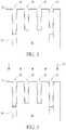
- FIG. 1illustrates a top view of a DRAM device according to an embodiment of the present invention.
- FIGS. 2-4are cross-sectional views illustrating steps of fabricating the DRAM device of FIG. 1 along the sectional line AA′.
- FIGS. 1-4illustrate a method for fabricating a DRAM device according to an embodiment of the present invention, in which FIG. 1 illustrates a top-view diagram and FIGS. 2-4 are cross-sectional views illustrating steps of fabricating the DRAM device of FIG. 1 along the sectional line AA′.
- the present embodimentpertains to fabricate a memory device, and more particularly a DRAM device 10 , in which the DRAM device 10 includes at least a transistor device (not shown) and at least a capacitor structure (not shown) that will be serving as a smallest constituent unit within the DRAM array and also used to receive electrical signals from bit lines 12 and word lines 14 .
- the DRAM device 10includes a substrate 16 such as a semiconductor substrate or wafer made of silicon, a shallow trench isolation (STI) 24 formed in the substrate 16 , and a plurality of active areas (AA) 18 defined on the substrate 16 .
- a memory region 20 and a periphery regionare also defined on the substrate 16 , in which multiple word lines 14 and multiple bit lines 12 are preferably formed on the memory region 20 while other active devices (not shown) could be formed on the periphery region.
- STIshallow trench isolation
- AAactive areas
- the active regions 18are disposed parallel to each other and extending along a first direction
- the word lines 14 or multiple gates 22are disposed within the substrate 16 and passing through the active regions 18 and STIs 24 .
- the gates 22are disposed extending along a second direction, in which the second direction crosses the first direction at an angle less than 90 degrees.
- the bit lines 12on the other hand are disposed on the substrate 16 parallel to each other and extending along a third direction while crossing the active regions 18 and STI 24 , in which the third direction is different from the first direction and orthogonal to the second direction.
- the first direction, second direction, and third directionare all different from each other while the first direction is not orthogonal to both the second direction and the third direction.
- contact plugssuch as bit line contacts (BLC) (not shown) are formed in the active regions 18 adjacent to two sides of the word lines 14 to electrically connect to source/drain region (not shown) of each transistor element and storage node contacts (not shown) are formed to electrically connect to a capacitor.
- BLCbit line contacts
- first trenches 26 and second trenches 28are formed in the substrate 16 and shallow trench isolations (STIs) 24 are disposed on the bottom of the first trenches 26 , in which the top surface of the STIs 24 is slightly lower than the bottom surface of the second trenches 28 .
- STIsshallow trench isolations
- the formation of the first trenches 26 , the second trenches 28 , and the STIs 24could be accomplished by first removing part of the substrate 16 and then forming STIs 24 made of silicon oxide in the substrate 16 such that the top surface of the STIs 24 is even with the top surface of the substrate 16 .
- an etching processis conducted to remove part of the STI 24 as well part of the substrate 16 adjacent to the STI 24 to form trenches, in which the trenches directly on top of the remaining STIs 24 become first trenches 26 while the trenches formed by removing part of the substrate 16 adjacent to the STIs 24 become the second trenches 28 .
- an oxidation process or more specifically an in-situ steam generation (ISSG) process 32is conducted to transform the amorphous silicon layer 30 into a silicon dioxide layer 34 , which will be serving as a gate dielectric layer for gate structures in the later process.
- oxygen gasis injected during the ISSG process 32 so that the injected oxygen gas would react with the amorphous silicon layer 30 to form the silicon dioxide layer 34 preferably without reacting with any of the substrate 16 made from silicon and the newly formed silicon dioxide layer 30 then replaces the place of the original amorphous silicon layer 30 .
- the present inventionpreferably controls the volume and/or flow of the oxygen gas being injected so that all of the amorphous silicon layer 30 would react with the oxygen gas to form the silicon dioxide layer 34 as none of substrate 16 is consumed.
- all of the amorphous silicon layer 30would be consumed or none of the amorphous silicon layer 30 would remain after the amorphous silicon layer 30 is transformed into silicon dioxide layer 34 and the newly formed silicon dioxide layer 34 while replacing the original amorphous silicon layer 30 , would share equal thickness as the original amorphous silicon layer 30 .
- the thickness of the newly formed silicon dioxide layer 34is preferably between 5 Angstroms to 30 Angstroms or most preferably at around 15 Angstroms.
- the substrate 16is preferably not consumed while the amorphous silicon layer 30 is transformed into silicon dioxide layer 34 during the ISSG process 32 , according to an embodiment of the present invention, it would also be desirable to react a small portion of the substrate 16 with oxygen gas to form silicon dioxide for building up the thickness of the silicon dioxide layer 34 slightly after all of the amorphous silicon layer 30 is transformed into the silicon dioxide layer 34 .
- the overall thickness of the silicon dioxide layer 34would be slightly greater than thickness of the original silicon dioxide layer preferably by an increase between 5% to 10%.
- a barrier layer 36 and a conductive layer 38are sequentially formed on the silicon dioxide layer 34 , and an etching back process is conducted to remove part of the conductive layer 38 and part of the barrier layer 36 so that the top surface of the remaining conductive layer 38 and barrier layer 36 is slightly lower than the top surface of the substrate 16 .
- Thisforms first gate structures 40 in the first trenches 26 and second gate structures 42 in the second trenches 28 , in which the first gate structures 40 and second gate structures 42 essentially become the bit lines 12 shown in FIG. 1 .
- a hard mask 44is formed on each of the first gate structures 40 and second gate structures 42 , in which the top surface of the hard mask 44 is even with the top surface of the substrate 16 .
- the barrier layer 36preferably includes a work function metal layer which could be a n-type work function metal layer or p-type work function metal layer depending on the demand of the process or product.
- n-type work function metal layercould include work function metal layer having a work function ranging between 3.9 eV and 4.3 eV such as but not limited to for example titanium aluminide (TiAl), zirconium aluminide (ZrAl), tungsten aluminide (WAl), tantalum aluminide (TaAl), hafnium aluminide (HfAl), or titanium aluminum carbide (TiAlC), but not limited thereto.
- P-type work function metal layeron the other hand could include work function metal layer having a work function ranging between 4.8 eV and 5.2 eV such as but not limited to for example titanium nitride (TiN), tantalum nitride (TaN), or tantalum carbide (TaC), but not limited thereto.
- the conductive layer 38could be made of low resistance material including but not limited to for example Cu, Al, W, TiAl, CoWP, or combination thereof and the hard mask 44 is preferably made of dielectric material such as silicon nitride.
- the present inventionfirst forms an amorphous silicon layer in trenches in the substrate during the fabrication of word lines of a DRAM device, conducts an ISSG process to transform the amorphous silicon layer into silicon dioxide layer, and then deposits a barrier layer and a conductive layer into the trenches to form gates or buried word line structures. Since the present invention replaces the conventional approach of using ALD process to form silicon dioxide layer directly into the trenches with an approach of first depositing an amorphous silicon layer into the trenches and then transforming the amorphous silicon layer by ISSG process into silicon dioxide layer afterwards, it would be desirable for the oxygen gas injected from the ISSG process to react with the amorphous silicon layer instead of the silicon substrate to form silicon dioxide so that over consumption of the substrate could be prevented. By doing so, the overall strength of the silicon dioxide layer could be increased and control of the pitches could be improved substantially.
Landscapes
- Engineering & Computer Science (AREA)
- Manufacturing & Machinery (AREA)
- Physics & Mathematics (AREA)
- Condensed Matter Physics & Semiconductors (AREA)
- General Physics & Mathematics (AREA)
- Computer Hardware Design (AREA)
- Microelectronics & Electronic Packaging (AREA)
- Power Engineering (AREA)
- Chemical & Material Sciences (AREA)
- Composite Materials (AREA)
- Semiconductor Memories (AREA)
Abstract
Description
Claims (4)
Applications Claiming Priority (3)
| Application Number | Priority Date | Filing Date | Title |
|---|---|---|---|
| CN201810189348.8 | 2018-03-08 | ||
| CN201810189348.8ACN110246842A (en) | 2018-03-08 | 2018-03-08 | A method of making semiconductor element |
| CN201810189348 | 2018-03-08 |
Publications (2)
| Publication Number | Publication Date |
|---|---|
| US20190280095A1 US20190280095A1 (en) | 2019-09-12 |
| US10903328B2true US10903328B2 (en) | 2021-01-26 |
Family
ID=67843477
Family Applications (1)
| Application Number | Title | Priority Date | Filing Date |
|---|---|---|---|
| US15/943,717Active2038-07-18US10903328B2 (en) | 2018-03-08 | 2018-04-03 | Method for fabricating semiconductor device |
Country Status (2)
| Country | Link |
|---|---|
| US (1) | US10903328B2 (en) |
| CN (1) | CN110246842A (en) |
Families Citing this family (2)
| Publication number | Priority date | Publication date | Assignee | Title |
|---|---|---|---|---|
| US11251261B2 (en)* | 2019-05-17 | 2022-02-15 | Micron Technology, Inc. | Forming a barrier material on an electrode |
| US11688802B2 (en)* | 2021-02-18 | 2023-06-27 | United Microelectronics Corp. | High electron mobility transistor and fabrication method thereof |
Citations (19)
| Publication number | Priority date | Publication date | Assignee | Title |
|---|---|---|---|---|
| US6020230A (en)* | 1998-04-22 | 2000-02-01 | Texas Instruments-Acer Incorporated | Process to fabricate planarized deep-shallow trench isolation having upper and lower portions with oxidized semiconductor trench fill in the upper portion and semiconductor trench fill in the lower portion |
| US6137152A (en)* | 1998-04-22 | 2000-10-24 | Texas Instruments - Acer Incorporated | Planarized deep-shallow trench isolation for CMOS/bipolar devices |
| US6214696B1 (en)* | 1998-04-22 | 2001-04-10 | Texas Instruments - Acer Incorporated | Method of fabricating deep-shallow trench isolation |
| US6309924B1 (en)* | 2000-06-02 | 2001-10-30 | International Business Machines Corporation | Method of forming self-limiting polysilicon LOCOS for DRAM cell |
| US6391784B1 (en)* | 1999-07-21 | 2002-05-21 | Advanced Micro Devices, Inc. | Spacer-assisted ultranarrow shallow trench isolation formation |
| US20020127818A1 (en)* | 2001-03-02 | 2002-09-12 | Lee Jung-Ii | Recess-free trench isolation structure and method of forming the same |
| US20030040189A1 (en)* | 2001-08-22 | 2003-02-27 | Ping-Yi Chang | Shallow trench isolation fabrication |
| US20050186755A1 (en)* | 2004-02-19 | 2005-08-25 | Smythe John A.Iii | Sub-micron space liner and densification process |
| US20060125043A1 (en)* | 2004-12-10 | 2006-06-15 | Smythe John A Iii | Trench insulation structures and methods |
| US20080150015A1 (en)* | 2006-12-26 | 2008-06-26 | Magnachip Semiconductor, Ltd. | Transistor having recess channel and fabricating method thereof |
| US20090209090A1 (en)* | 2008-02-15 | 2009-08-20 | Hitachi, Ltd. | Manufacturing method of semiconductor device |
| CN101996950A (en) | 2009-08-11 | 2011-03-30 | 海力士半导体有限公司 | Semiconductor device and method of fabricating the same |
| US20130221428A1 (en)* | 2012-02-24 | 2013-08-29 | Prasad Venkatraman | Process of forming an electronic device including a trench and a conductive structure therein |
| US20140162431A1 (en)* | 2012-12-11 | 2014-06-12 | United Microelectronics Corp. | Method for manufacturing semiconductor structure |
| US8772105B2 (en) | 2011-01-03 | 2014-07-08 | Hynix Semiconductor Inc. | Semiconductor device and method for forming the same |
| US20150064929A1 (en)* | 2013-09-05 | 2015-03-05 | United Microelectronics Corp. | Method of gap filling |
| US9064692B2 (en) | 2012-04-19 | 2015-06-23 | Micron Technology, Inc. | DRAM cells and methods of forming silicon dioxide |
| US20150371991A1 (en)* | 2013-02-07 | 2015-12-24 | Hidekazu Nobuto | Semiconductor device and method for manufacturing same |
| US20170186642A1 (en)* | 2015-12-23 | 2017-06-29 | SK Hynix Inc. | Isolation structure and method for manufacturing the same |
- 2018
- 2018-03-08CNCN201810189348.8Apatent/CN110246842A/enactivePending
- 2018-04-03USUS15/943,717patent/US10903328B2/enactiveActive
Patent Citations (20)
| Publication number | Priority date | Publication date | Assignee | Title |
|---|---|---|---|---|
| US6020230A (en)* | 1998-04-22 | 2000-02-01 | Texas Instruments-Acer Incorporated | Process to fabricate planarized deep-shallow trench isolation having upper and lower portions with oxidized semiconductor trench fill in the upper portion and semiconductor trench fill in the lower portion |
| US6137152A (en)* | 1998-04-22 | 2000-10-24 | Texas Instruments - Acer Incorporated | Planarized deep-shallow trench isolation for CMOS/bipolar devices |
| US6214696B1 (en)* | 1998-04-22 | 2001-04-10 | Texas Instruments - Acer Incorporated | Method of fabricating deep-shallow trench isolation |
| US6391784B1 (en)* | 1999-07-21 | 2002-05-21 | Advanced Micro Devices, Inc. | Spacer-assisted ultranarrow shallow trench isolation formation |
| US6309924B1 (en)* | 2000-06-02 | 2001-10-30 | International Business Machines Corporation | Method of forming self-limiting polysilicon LOCOS for DRAM cell |
| US20020127818A1 (en)* | 2001-03-02 | 2002-09-12 | Lee Jung-Ii | Recess-free trench isolation structure and method of forming the same |
| US20030040189A1 (en)* | 2001-08-22 | 2003-02-27 | Ping-Yi Chang | Shallow trench isolation fabrication |
| US20050186755A1 (en)* | 2004-02-19 | 2005-08-25 | Smythe John A.Iii | Sub-micron space liner and densification process |
| US20060125043A1 (en)* | 2004-12-10 | 2006-06-15 | Smythe John A Iii | Trench insulation structures and methods |
| US20080150015A1 (en)* | 2006-12-26 | 2008-06-26 | Magnachip Semiconductor, Ltd. | Transistor having recess channel and fabricating method thereof |
| US20090209090A1 (en)* | 2008-02-15 | 2009-08-20 | Hitachi, Ltd. | Manufacturing method of semiconductor device |
| CN101996950A (en) | 2009-08-11 | 2011-03-30 | 海力士半导体有限公司 | Semiconductor device and method of fabricating the same |
| US8772105B2 (en) | 2011-01-03 | 2014-07-08 | Hynix Semiconductor Inc. | Semiconductor device and method for forming the same |
| US20130221428A1 (en)* | 2012-02-24 | 2013-08-29 | Prasad Venkatraman | Process of forming an electronic device including a trench and a conductive structure therein |
| US9064692B2 (en) | 2012-04-19 | 2015-06-23 | Micron Technology, Inc. | DRAM cells and methods of forming silicon dioxide |
| US20140162431A1 (en)* | 2012-12-11 | 2014-06-12 | United Microelectronics Corp. | Method for manufacturing semiconductor structure |
| US20150371991A1 (en)* | 2013-02-07 | 2015-12-24 | Hidekazu Nobuto | Semiconductor device and method for manufacturing same |
| US20150064929A1 (en)* | 2013-09-05 | 2015-03-05 | United Microelectronics Corp. | Method of gap filling |
| US20170186642A1 (en)* | 2015-12-23 | 2017-06-29 | SK Hynix Inc. | Isolation structure and method for manufacturing the same |
| CN106920770A (en) | 2015-12-23 | 2017-07-04 | 爱思开海力士有限公司 | Isolation structure and method of manufacturing the isolation structure |
Non-Patent Citations (1)
| Title |
|---|
| Lu, Title of Invention: Semiconductor Device and Fabrication Method Thereof, U.S. Appl. No. 15/672,272, filed Aug. 8, 2017. |
Also Published As
| Publication number | Publication date |
|---|---|
| CN110246842A (en) | 2019-09-17 |
| US20190280095A1 (en) | 2019-09-12 |
Similar Documents
| Publication | Publication Date | Title |
|---|---|---|
| US11462545B2 (en) | Semiconductor device and method for fabricating the same | |
| US10497704B2 (en) | Buried word line structure and method of making the same | |
| US11271000B2 (en) | Method for fabricating semiconductor device | |
| US8466052B2 (en) | Method of fabricating semiconductor device having buried wiring | |
| US10043811B1 (en) | Semiconductor structure for preventing row hammering issue in DRAM cell and method for manufacturing the same | |
| US10937701B2 (en) | Semiconductor device | |
| CN108389837A (en) | Transistor arrangement, memory construction and preparation method thereof | |
| US20220352173A1 (en) | Semiconductor device | |
| US20180190661A1 (en) | Semiconductor device and method for fabricating the same | |
| US11222784B2 (en) | Semiconductor device and method for fabricating the same | |
| US10147728B1 (en) | Semiconductor device and method for fabricating the same | |
| TWI652770B (en) | Semiconductor memory structure and preparation method thereof | |
| US20180323190A1 (en) | Semiconductor device and method for fabricating the same | |
| US11688783B1 (en) | Semiconductor device and method for manufacturing the same | |
| US10903328B2 (en) | Method for fabricating semiconductor device | |
| US12075613B2 (en) | Buried word line of a dynamic random access memory and method for fabricating the same | |
| US10374051B1 (en) | Method for fabricating semiconductor device | |
| US10204914B2 (en) | Method for fabricating semiconductor device | |
| US11895830B2 (en) | Method for manufacturing semiconductor device | |
| US20220238437A1 (en) | Semiconductor structure and preparation method thereof | |
| US20250220886A1 (en) | Semiconductor structure and method for forming the same | |
| US20240422963A1 (en) | Semiconductor memory device | |
| US10804365B2 (en) | Semiconductor device and method for fabricating the same | |
| CN114784008A (en) | Semiconductor structure and preparation method thereof | |
| CN117542834A (en) | Memory structure, semiconductor structure and preparation method thereof |
Legal Events
| Date | Code | Title | Description |
|---|---|---|---|
| AS | Assignment | Owner name:FUJIAN JINHUA INTEGRATED CIRCUIT CO., LTD., CHINA Free format text:ASSIGNMENT OF ASSIGNORS INTEREST;ASSIGNORS:CHEN, PO-CHUN;CHANG, CHIA-LUNG;CHEN, YI-WEI;AND OTHERS;REEL/FRAME:045420/0128 Effective date:20180323 Owner name:UNITED MICROELECTRONICS CORP., TAIWAN Free format text:ASSIGNMENT OF ASSIGNORS INTEREST;ASSIGNORS:CHEN, PO-CHUN;CHANG, CHIA-LUNG;CHEN, YI-WEI;AND OTHERS;REEL/FRAME:045420/0128 Effective date:20180323 | |
| FEPP | Fee payment procedure | Free format text:ENTITY STATUS SET TO UNDISCOUNTED (ORIGINAL EVENT CODE: BIG.); ENTITY STATUS OF PATENT OWNER: LARGE ENTITY | |
| STPP | Information on status: patent application and granting procedure in general | Free format text:FINAL REJECTION MAILED | |
| STPP | Information on status: patent application and granting procedure in general | Free format text:PUBLICATIONS -- ISSUE FEE PAYMENT VERIFIED | |
| STCF | Information on status: patent grant | Free format text:PATENTED CASE | |
| MAFP | Maintenance fee payment | Free format text:PAYMENT OF MAINTENANCE FEE, 4TH YEAR, LARGE ENTITY (ORIGINAL EVENT CODE: M1551); ENTITY STATUS OF PATENT OWNER: LARGE ENTITY Year of fee payment:4 |