US10903319B2 - Patterning graphene with a hard mask coating - Google Patents
Patterning graphene with a hard mask coatingDownload PDFInfo
- Publication number
- US10903319B2 US10903319B2US15/623,279US201715623279AUS10903319B2US 10903319 B2US10903319 B2US 10903319B2US 201715623279 AUS201715623279 AUS 201715623279AUS 10903319 B2US10903319 B2US 10903319B2
- Authority
- US
- United States
- Prior art keywords
- graphene
- metal layer
- protective metal
- temporary protective
- portions
- Prior art date
- Legal status (The legal status is an assumption and is not a legal conclusion. Google has not performed a legal analysis and makes no representation as to the accuracy of the status listed.)
- Active
Links
- OKTJSMMVPCPJKN-UHFFFAOYSA-NCarbonChemical compound[C]OKTJSMMVPCPJKN-UHFFFAOYSA-N0.000titleclaimsabstractdescription177
- 229910021389grapheneInorganic materials0.000titleclaimsabstractdescription176
- 238000000059patterningMethods0.000titleclaimsabstractdescription11
- 238000000576coating methodMethods0.000titleclaimsdescription8
- 239000011248coating agentSubstances0.000titleclaimsdescription7
- 229910052751metalInorganic materials0.000claimsabstractdescription101
- 239000002184metalSubstances0.000claimsabstractdescription101
- 238000000034methodMethods0.000claimsabstractdescription55
- 230000008569processEffects0.000claimsabstractdescription5
- 229920002120photoresistant polymerPolymers0.000claimsdescription41
- 230000001681protective effectEffects0.000claimsdescription38
- PCHJSUWPFVWCPO-UHFFFAOYSA-NgoldChemical group[Au]PCHJSUWPFVWCPO-UHFFFAOYSA-N0.000claimsdescription32
- 229910052737goldInorganic materials0.000claimsdescription31
- 239000010931goldSubstances0.000claimsdescription31
- NLKNQRATVPKPDG-UHFFFAOYSA-Mpotassium iodideChemical compound[K+].[I-]NLKNQRATVPKPDG-UHFFFAOYSA-M0.000claimsdescription24
- 238000004806packaging method and processMethods0.000claimsdescription23
- BASFCYQUMIYNBI-UHFFFAOYSA-NplatinumChemical compound[Pt]BASFCYQUMIYNBI-UHFFFAOYSA-N0.000claimsdescription22
- 238000000151depositionMethods0.000claimsdescription17
- 229910052697platinumInorganic materials0.000claimsdescription9
- CSCPPACGZOOCGX-UHFFFAOYSA-NAcetoneChemical compoundCC(C)=OCSCPPACGZOOCGX-UHFFFAOYSA-N0.000claimsdescription8
- KDLHZDBZIXYQEI-UHFFFAOYSA-NPalladiumChemical compound[Pd]KDLHZDBZIXYQEI-UHFFFAOYSA-N0.000claimsdescription8
- 230000005855radiationEffects0.000claimsdescription8
- 238000011109contaminationMethods0.000claimsdescription7
- 239000000463materialSubstances0.000claimsdescription7
- 230000006378damageEffects0.000claimsdescription5
- SYBYTAAJFKOIEJ-UHFFFAOYSA-N3-Methylbutan-2-oneChemical compoundCC(C)C(C)=OSYBYTAAJFKOIEJ-UHFFFAOYSA-N0.000claimsdescription4
- KJTLSVCANCCWHF-UHFFFAOYSA-NRutheniumChemical compound[Ru]KJTLSVCANCCWHF-UHFFFAOYSA-N0.000claimsdescription4
- BQCADISMDOOEFD-UHFFFAOYSA-NSilverChemical compound[Ag]BQCADISMDOOEFD-UHFFFAOYSA-N0.000claimsdescription4
- 229910052741iridiumInorganic materials0.000claimsdescription4
- GKOZUEZYRPOHIO-UHFFFAOYSA-Niridium atomChemical compound[Ir]GKOZUEZYRPOHIO-UHFFFAOYSA-N0.000claimsdescription4
- 229910052762osmiumInorganic materials0.000claimsdescription4
- SYQBFIAQOQZEGI-UHFFFAOYSA-Nosmium atomChemical compound[Os]SYQBFIAQOQZEGI-UHFFFAOYSA-N0.000claimsdescription4
- 229910052763palladiumInorganic materials0.000claimsdescription4
- 229910052703rhodiumInorganic materials0.000claimsdescription4
- 239000010948rhodiumSubstances0.000claimsdescription4
- MHOVAHRLVXNVSD-UHFFFAOYSA-Nrhodium atomChemical compound[Rh]MHOVAHRLVXNVSD-UHFFFAOYSA-N0.000claimsdescription4
- 229910052707rutheniumInorganic materials0.000claimsdescription4
- 229910052709silverInorganic materials0.000claimsdescription4
- 239000004332silverSubstances0.000claimsdescription4
- 239000008367deionised waterSubstances0.000claimsdescription3
- 229910021641deionized waterInorganic materials0.000claimsdescription3
- 238000005868electrolysis reactionMethods0.000claimsdescription3
- 238000010884ion-beam techniqueMethods0.000claimsdescription3
- 238000001020plasma etchingMethods0.000claimsdescription3
- 239000002904solventSubstances0.000claimsdescription3
- 238000004544sputter depositionMethods0.000claimsdescription3
- 238000002207thermal evaporationMethods0.000claimsdescription3
- XLYOFNOQVPJJNP-UHFFFAOYSA-NwaterChemical compoundOXLYOFNOQVPJJNP-UHFFFAOYSA-N0.000claimsdescription3
- 239000004593EpoxySubstances0.000claimsdescription2
- CIBMHJPPKCXONB-UHFFFAOYSA-Npropane-2,2-diolChemical compoundCC(C)(O)OCIBMHJPPKCXONB-UHFFFAOYSA-N0.000claimsdescription2
- 238000011282treatmentMethods0.000claimsdescription2
- 238000005530etchingMethods0.000claims18
- 238000005406washingMethods0.000claims5
- 238000012858packaging processMethods0.000claims1
- 238000005516engineering processMethods0.000abstractdescription17
- 238000001459lithographyMethods0.000abstractdescription2
- 239000010410layerSubstances0.000description87
- 239000011241protective layerSubstances0.000description8
- 239000000758substrateSubstances0.000description7
- 238000010586diagramMethods0.000description4
- 238000004519manufacturing processMethods0.000description4
- 230000003647oxidationEffects0.000description4
- 238000007254oxidation reactionMethods0.000description4
- 238000005260corrosionMethods0.000description3
- 230000007797corrosionEffects0.000description3
- 238000005566electron beam evaporationMethods0.000description3
- 150000002739metalsChemical class0.000description3
- 238000002360preparation methodMethods0.000description3
- RYGMFSIKBFXOCR-UHFFFAOYSA-NCopperChemical compound[Cu]RYGMFSIKBFXOCR-UHFFFAOYSA-N0.000description2
- VYPSYNLAJGMNEJ-UHFFFAOYSA-NSilicium dioxideChemical compoundO=[Si]=OVYPSYNLAJGMNEJ-UHFFFAOYSA-N0.000description2
- 230000004888barrier functionEffects0.000description2
- 229910052802copperInorganic materials0.000description2
- 239000010949copperSubstances0.000description2
- MQUIHBQDYYAEMH-UHFFFAOYSA-NmethedroneChemical compoundCNC(C)C(=O)C1=CC=C(OC)C=C1MQUIHBQDYYAEMH-UHFFFAOYSA-N0.000description2
- 239000002245particleSubstances0.000description2
- 238000012545processingMethods0.000description2
- XFXPMWWXUTWYJX-UHFFFAOYSA-NCyanideChemical compoundN#[C-]XFXPMWWXUTWYJX-UHFFFAOYSA-N0.000description1
- VEXZGXHMUGYJMC-UHFFFAOYSA-NHydrochloric acidChemical classClVEXZGXHMUGYJMC-UHFFFAOYSA-N0.000description1
- XUIMIQQOPSSXEZ-UHFFFAOYSA-NSiliconChemical compound[Si]XUIMIQQOPSSXEZ-UHFFFAOYSA-N0.000description1
- 230000004075alterationEffects0.000description1
- QZPSXPBJTPJTSZ-UHFFFAOYSA-Naqua regiaChemical compoundCl.O[N+]([O-])=OQZPSXPBJTPJTSZ-UHFFFAOYSA-N0.000description1
- 230000008901benefitEffects0.000description1
- 125000004432carbon atomChemical groupC*0.000description1
- 230000008859changeEffects0.000description1
- 238000005229chemical vapour depositionMethods0.000description1
- 238000004140cleaningMethods0.000description1
- 239000004020conductorSubstances0.000description1
- 239000000470constituentSubstances0.000description1
- 238000010276constructionMethods0.000description1
- 238000007598dipping methodMethods0.000description1
- 238000010894electron beam technologyMethods0.000description1
- 238000005538encapsulationMethods0.000description1
- 238000004299exfoliationMethods0.000description1
- 229910002804graphiteInorganic materials0.000description1
- 239000010439graphiteSubstances0.000description1
- 235000011167hydrochloric acidNutrition0.000description1
- 230000007774longtermEffects0.000description1
- 239000000203mixtureSubstances0.000description1
- 230000004048modificationEffects0.000description1
- 238000012986modificationMethods0.000description1
- 238000005192partitionMethods0.000description1
- 230000000704physical effectEffects0.000description1
- 238000007747platingMethods0.000description1
- 229920003229poly(methyl methacrylate)Polymers0.000description1
- 239000004926polymethyl methacrylateSubstances0.000description1
- 238000011160researchMethods0.000description1
- 239000004065semiconductorSubstances0.000description1
- 229910052710siliconInorganic materials0.000description1
- 239000010703siliconSubstances0.000description1
- 235000012239silicon dioxideNutrition0.000description1
- 239000000377silicon dioxideSubstances0.000description1
- 238000000638solvent extractionMethods0.000description1
- 239000000126substanceSubstances0.000description1
- 238000012360testing methodMethods0.000description1
Images


Classifications
- H01L29/1606—
- H—ELECTRICITY
- H01—ELECTRIC ELEMENTS
- H01L—SEMICONDUCTOR DEVICES NOT COVERED BY CLASS H10
- H01L21/00—Processes or apparatus adapted for the manufacture or treatment of semiconductor or solid state devices or of parts thereof
- H01L21/02—Manufacture or treatment of semiconductor devices or of parts thereof
- H01L21/027—Making masks on semiconductor bodies for further photolithographic processing not provided for in group H01L21/18 or H01L21/34
- H01L21/0271—Making masks on semiconductor bodies for further photolithographic processing not provided for in group H01L21/18 or H01L21/34 comprising organic layers
- H01L21/0273—Making masks on semiconductor bodies for further photolithographic processing not provided for in group H01L21/18 or H01L21/34 comprising organic layers characterised by the treatment of photoresist layers
- H01L21/0274—Photolithographic processes
- H—ELECTRICITY
- H01—ELECTRIC ELEMENTS
- H01L—SEMICONDUCTOR DEVICES NOT COVERED BY CLASS H10
- H01L21/00—Processes or apparatus adapted for the manufacture or treatment of semiconductor or solid state devices or of parts thereof
- H01L21/02—Manufacture or treatment of semiconductor devices or of parts thereof
- H01L21/04—Manufacture or treatment of semiconductor devices or of parts thereof the devices having potential barriers, e.g. a PN junction, depletion layer or carrier concentration layer
- H01L21/18—Manufacture or treatment of semiconductor devices or of parts thereof the devices having potential barriers, e.g. a PN junction, depletion layer or carrier concentration layer the devices having semiconductor bodies comprising elements of Group IV of the Periodic Table or AIIIBV compounds with or without impurities, e.g. doping materials
- H01L21/30—Treatment of semiconductor bodies using processes or apparatus not provided for in groups H01L21/20 - H01L21/26
- H01L21/302—Treatment of semiconductor bodies using processes or apparatus not provided for in groups H01L21/20 - H01L21/26 to change their surface-physical characteristics or shape, e.g. etching, polishing, cutting
- H01L21/306—Chemical or electrical treatment, e.g. electrolytic etching
- H01L21/308—Chemical or electrical treatment, e.g. electrolytic etching using masks
- H01L21/3081—Chemical or electrical treatment, e.g. electrolytic etching using masks characterised by their composition, e.g. multilayer masks, materials
- H—ELECTRICITY
- H01—ELECTRIC ELEMENTS
- H01L—SEMICONDUCTOR DEVICES NOT COVERED BY CLASS H10
- H01L21/00—Processes or apparatus adapted for the manufacture or treatment of semiconductor or solid state devices or of parts thereof
- H01L21/02—Manufacture or treatment of semiconductor devices or of parts thereof
- H01L21/02104—Forming layers
- H01L21/02107—Forming insulating materials on a substrate
- H01L21/02109—Forming insulating materials on a substrate characterised by the type of layer, e.g. type of material, porous/non-porous, pre-cursors, mixtures or laminates
- H01L21/02112—Forming insulating materials on a substrate characterised by the type of layer, e.g. type of material, porous/non-porous, pre-cursors, mixtures or laminates characterised by the material of the layer
- H01L21/02115—Forming insulating materials on a substrate characterised by the type of layer, e.g. type of material, porous/non-porous, pre-cursors, mixtures or laminates characterised by the material of the layer the material being carbon, e.g. alpha-C, diamond or hydrogen doped carbon
- H—ELECTRICITY
- H01—ELECTRIC ELEMENTS
- H01L—SEMICONDUCTOR DEVICES NOT COVERED BY CLASS H10
- H01L21/00—Processes or apparatus adapted for the manufacture or treatment of semiconductor or solid state devices or of parts thereof
- H01L21/02—Manufacture or treatment of semiconductor devices or of parts thereof
- H01L21/02104—Forming layers
- H01L21/02107—Forming insulating materials on a substrate
- H01L21/02225—Forming insulating materials on a substrate characterised by the process for the formation of the insulating layer
- H01L21/0226—Forming insulating materials on a substrate characterised by the process for the formation of the insulating layer formation by a deposition process
- H01L21/02263—Forming insulating materials on a substrate characterised by the process for the formation of the insulating layer formation by a deposition process deposition from the gas or vapour phase
- H01L21/02271—Forming insulating materials on a substrate characterised by the process for the formation of the insulating layer formation by a deposition process deposition from the gas or vapour phase deposition by decomposition or reaction of gaseous or vapour phase compounds, i.e. chemical vapour deposition
- H—ELECTRICITY
- H01—ELECTRIC ELEMENTS
- H01L—SEMICONDUCTOR DEVICES NOT COVERED BY CLASS H10
- H01L21/00—Processes or apparatus adapted for the manufacture or treatment of semiconductor or solid state devices or of parts thereof
- H01L21/02—Manufacture or treatment of semiconductor devices or of parts thereof
- H01L21/04—Manufacture or treatment of semiconductor devices or of parts thereof the devices having potential barriers, e.g. a PN junction, depletion layer or carrier concentration layer
- H01L21/18—Manufacture or treatment of semiconductor devices or of parts thereof the devices having potential barriers, e.g. a PN junction, depletion layer or carrier concentration layer the devices having semiconductor bodies comprising elements of Group IV of the Periodic Table or AIIIBV compounds with or without impurities, e.g. doping materials
- H01L21/28—Manufacture of electrodes on semiconductor bodies using processes or apparatus not provided for in groups H01L21/20 - H01L21/268
- H01L21/28008—Making conductor-insulator-semiconductor electrodes
- H01L21/28017—Making conductor-insulator-semiconductor electrodes the insulator being formed after the semiconductor body, the semiconductor being silicon
- H01L21/28026—Making conductor-insulator-semiconductor electrodes the insulator being formed after the semiconductor body, the semiconductor being silicon characterised by the conductor
- H01L21/28079—Making conductor-insulator-semiconductor electrodes the insulator being formed after the semiconductor body, the semiconductor being silicon characterised by the conductor the final conductor layer next to the insulator being a single metal, e.g. Ta, W, Mo, Al
- H—ELECTRICITY
- H01—ELECTRIC ELEMENTS
- H01L—SEMICONDUCTOR DEVICES NOT COVERED BY CLASS H10
- H01L21/00—Processes or apparatus adapted for the manufacture or treatment of semiconductor or solid state devices or of parts thereof
- H01L21/02—Manufacture or treatment of semiconductor devices or of parts thereof
- H01L21/04—Manufacture or treatment of semiconductor devices or of parts thereof the devices having potential barriers, e.g. a PN junction, depletion layer or carrier concentration layer
- H01L21/18—Manufacture or treatment of semiconductor devices or of parts thereof the devices having potential barriers, e.g. a PN junction, depletion layer or carrier concentration layer the devices having semiconductor bodies comprising elements of Group IV of the Periodic Table or AIIIBV compounds with or without impurities, e.g. doping materials
- H01L21/30—Treatment of semiconductor bodies using processes or apparatus not provided for in groups H01L21/20 - H01L21/26
- H01L21/31—Treatment of semiconductor bodies using processes or apparatus not provided for in groups H01L21/20 - H01L21/26 to form insulating layers thereon, e.g. for masking or by using photolithographic techniques; After treatment of these layers; Selection of materials for these layers
- H01L21/3105—After-treatment
- H01L21/311—Etching the insulating layers by chemical or physical means
- H01L21/31105—Etching inorganic layers
- H01L21/31111—Etching inorganic layers by chemical means
- H01L21/31116—Etching inorganic layers by chemical means by dry-etching
- H—ELECTRICITY
- H01—ELECTRIC ELEMENTS
- H01L—SEMICONDUCTOR DEVICES NOT COVERED BY CLASS H10
- H01L21/00—Processes or apparatus adapted for the manufacture or treatment of semiconductor or solid state devices or of parts thereof
- H01L21/02—Manufacture or treatment of semiconductor devices or of parts thereof
- H01L21/04—Manufacture or treatment of semiconductor devices or of parts thereof the devices having potential barriers, e.g. a PN junction, depletion layer or carrier concentration layer
- H01L21/18—Manufacture or treatment of semiconductor devices or of parts thereof the devices having potential barriers, e.g. a PN junction, depletion layer or carrier concentration layer the devices having semiconductor bodies comprising elements of Group IV of the Periodic Table or AIIIBV compounds with or without impurities, e.g. doping materials
- H01L21/30—Treatment of semiconductor bodies using processes or apparatus not provided for in groups H01L21/20 - H01L21/26
- H01L21/31—Treatment of semiconductor bodies using processes or apparatus not provided for in groups H01L21/20 - H01L21/26 to form insulating layers thereon, e.g. for masking or by using photolithographic techniques; After treatment of these layers; Selection of materials for these layers
- H01L21/3105—After-treatment
- H01L21/311—Etching the insulating layers by chemical or physical means
- H01L21/31144—Etching the insulating layers by chemical or physical means using masks
- H—ELECTRICITY
- H10—SEMICONDUCTOR DEVICES; ELECTRIC SOLID-STATE DEVICES NOT OTHERWISE PROVIDED FOR
- H10D—INORGANIC ELECTRIC SEMICONDUCTOR DEVICES
- H10D62/00—Semiconductor bodies, or regions thereof, of devices having potential barriers
- H10D62/80—Semiconductor bodies, or regions thereof, of devices having potential barriers characterised by the materials
- H10D62/881—Semiconductor bodies, or regions thereof, of devices having potential barriers characterised by the materials being a two-dimensional material
- H10D62/882—Graphene
Definitions
- the disclosed technologyrelates generally to depositing a hard mask coating onto a surface of a graphene sheet. More specifically, the present invention relates to depositing a hard mask coating onto a surface of a graphene sheet to provide a protective layer.
- Grapheneis composed of a single thin layer of carbon atoms that are bonded together in a repeating pattern of hexagons. Graphene has many extraordinary properties, which includes high mechanical strength, high electron mobility, and superior thermal conductivity. Because graphene is a great thermal and electrical conductor, graphene material is often used to construct graphene based biosensors, transistors, integrated circuited, and other electronic applications.
- one methodmay include depositing the surface of the graphene sheet directly with a photoresist or polymethylmethacrylate (hereinafter “PMMC”) layer.
- PMMCphotoresist or polymethylmethacrylate
- one methodmay include depositing the surface of the graphene sheet directly with a photoresist or polymethylmethacrylate (hereinafter “PMMC”) layer.
- PMMCpolymethylmethacrylate
- direct contact with the graphene sheetoften leaves a residue on the graphene that cannot be completely removed, even with the application of acetone or other solvents.
- any remaining photoresist or PMMC residue on the surface of the graphenesignificantly lowers the quality of the graphene and is further likely to degrade the overall performance of the graphene based electronic devices and sensors.
- Other methodsmay also include providing a protective copper layer on the surface of the graphene sheet.
- copperis also known to leave a contaminating residue on the graphene sheet that is difficult to completely remove, which also lowers the quality of the graphene and further likely to degrade the performance of the graphene based electronic devices and sensors.
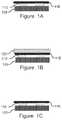
- FIG. 1illustrates the different progressions of depositing a temporary protective layer onto a surface of a graphene sheet according to one embodiment.
- FIG. 1Aillustrates a graphene sheet transferred onto a substrate according to one embodiment.
- FIG. 1Billustrates a graphene sheet with a temporary metal layer according to one embodiment.
- FIG. 1Cillustrates a graphene sheet with a temporary metal layer removed from a surface of the graphene sheet according to one embodiment.
- FIG. 2illustrates the different progressions of patterning a graphene sheet with a hard mask layer according to one embodiment.
- FIG. 2Aillustrates a graphene sheet transferred onto a substrate according to one embodiment.
- FIG. 2Billustrates a graphene sheet with a metal layer according to one embodiment.
- FIG. 2Cillustrates a graphene sheet with a metal layer and a photoresist layer for lithographic patterning according to one embodiment.
- FIG. 2Dillustrates a graphene sheet with a metal layer and a photoresist layer exposed to a radiation source to create a pattern template according to one embodiment.
- FIG. 2Eillustrates a graphene sheet with a metal layer and a photoresist layer exposed to a metal etchant solution to pattern the metal layer according to one embodiment.
- FIG. 2Fillustrates a graphene sheet with a metal layer and a photoresist layer exposed to a plasma etchant solution to pattern the graphene sheet according to one embodiment.
- FIG. 2Gillustrates a patterned graphene sheet with a metal layer according to one embodiment.
- FIG. 2Hillustrates a patterned graphene sheet according to one embodiment
- Some embodiments disclosed hereininclude depositing a temporary protective layer onto a surface of a graphene sheet. It should be noted that depositing layers onto the graphene sheet may include a wide range of techniques as appreciated by one of ordinary skill in the art, such as coating techniques, focused ion beam, filament evaporation, sputter deposition, and electrolysis by way of example only.
- This temporary protective layermay protect the graphene from the environment and prevent the contamination of the graphene sheet.
- the temporary protective layermay include a thin metal layer to protect the graphene from contamination or harm during the packaging and assembly of the graphene based device.
- the thin metal used to coat the graphene sheetmay include gold, by way of example only. Because gold is an inert metal that has the characteristic property of being resistant to corrosion and oxidation, depositing the graphene sheet with a gold layer may protect the graphene. Additionally, due to gold's characteristically inert qualities, the temporary gold layer on the surface of the graphene sheet may further provide thermal protection and prevent oxidation, especially when the graphene is exposed to high temperature treatments during epoxy curing, oven baking, and burn testing. Furthermore, the temporary gold coating may also protect the graphene from potentially being contaminated during wire bonding, encapsulation, wafer dicing, and cleaning. Thus, this allows the graphene to be handled in a factory setting for large manufacturing production.
- inert metalsmay also be used to temporarily coat the graphene sheet, which may include, but are not limited to, ruthenium, rhodium, palladium, silver, osmium, iridium, platinum, and the like.
- FIG. 1Aillustrates a graphene sheet 115 transferred onto a substrate, such as a wafer 105 , according to one embodiment.
- the graphene sheet 115may be grown using chemical vapor deposition, especially when producing large sheets of graphene.
- other methods of growing the graphene layermay also include, but are not limited to, reducing oxidized graphite on a selected substrate or via mechanical exfoliation techniques.
- the graphene sheet 115may then be transferred onto another surface, such as the surface of an electronic chip or sensor. More specifically, the surface of the electronic chip or sensor may include the surface of a thin semi-conductor material, such as a wafer 105 .
- the wafer 105may serve as a foundation upon which the proper electronic integrated circuits can be applied.
- the wafer 105may be a silicon substrate or a silicon dioxide substrate.
- the wafer 105may be coated with platinum 110 , whereby the platinum 110 acts as the bottom electrode to create the proper electrical connections.
- the graphene sheet 115may be treated with a temporary thin metal layer, such as a metal layer 120 , as illustrated in FIG. 1B .
- the metal layer 120may act as a mask or protective barrier configured to protect the graphene from being contaminated or degraded during the preparation of the graphene.
- the wafer 105 with the graphene sheet 115may be placed in an electron beam evaporation chamber.
- Electron beam evaporationis a physical vapor disposition technique whereby an intense electron beam is generated from a filament and steered via electric and magnetic fields to strike source material, such as gold pellets, and to vaporize it within a vacuum environment.
- source materialsuch as gold pellets
- the metal layer 120may include a gold metal layer.
- the metal layer 120may include any inert metal that does not negatively react with graphene.
- the metal layer 120may be any inert metal that has the characteristic property of being resistant to corrosion and oxidation.
- such inert metalsmay include, but are not limited to ruthenium, rhodium, palladium, silver, osmium, iridium, platinum, and the like.
- the temporary gold metal layer 120may range in a thickness from 10 nanometers to 1 micrometer.
- the gold metal layer 120may be applied onto the graphene sheet 115 by dipping the graphene sheet 115 into a gold plating solution.
- other methods of depositing a temporary metal layermay be provided.
- other methodsmay also include utilizing a focused ion beam, filament evaporation, sputter deposition, electrolysis, and the like to provide a temporary gold metal layer 120 on the surface of a graphene sheet 115 .
- metal leads or connectionsmay be established. Furthermore, additional processes or constructions may be made on top of the gold metal layer 120 that are now layered on the surface of the graphene sheet 115 . Again, due to inert nature of the metal layer 120 , the metal layer 120 may help protect the graphene from being contaminated or degraded, even as the graphene is being prepped and assembled for use within select graphene based devices.
- the metal layer 120may now be removed, as illustrated in FIG. 1C .
- the metal layer 120may be washed with potassium iodide solution for a duration ranging from 30 seconds to 5 minutes, or for a time period where all trace of the metal layer 120 is removed from the surface of the graphene sheet 115 .
- the now fully exposed graphene sheet 115may then be washed with deionized water to remove any remaining metal layer particles or other materials left on the surface of the graphene sheet 115 .
- the now exposed graphene sheet 115may further be available for any additional processes required to further manufacture and assemble a proper and functional graphene based device.
- a metal layer placed on top of a graphene sheetmay include additional coatings or layers that are deposited on top of the metal layer, as illustrated in FIG. 2 .
- FIG. 2Aillustrates a graphene sheet 215 transferred onto a substrate according to one embodiment.
- the graphene sheet 215may be treated with a thin metal layer, such as a gold metal layer 220 , as illustrated in FIG. 2B .
- the gold metal layer 220may act as a mask or barrier configured to protect the graphene from being contaminated or degraded.
- the thin metal layermay be any inert metal inert metal that has the characteristic property of being resistant to corrosion and oxidation, such that depositing the graphene sheet with a gold layer protects the graphene from being contaminated or degraded.
- the thin metal layermay include any of the following inert metals or combination thereof: ruthenium, rhodium, palladium, silver, osmium, iridium, platinum, and the like.
- the graphene sheet 215 with the gold metal layer 220may additionally be coated with a photoresist layer 225 , as further illustrated in FIG. 2C .
- the photoresist layer 225may include photosensitive material that experiences a change in its physical properties when exposed to a radiation source. By selectively exposing the photoresist layer 225 with radiation, such exposed areas of the photoresist layer 225 may be etched away, thus exposing portions of the metal gold layer 220 directly underneath the photoresist layer 225 .
- the photoresist layer 225may act as a template for accurately patterning the graphene sheet 215 underneath the photoresist layer 225 .
- the pattern etched onto the photoresist layer 225 via the radiation sourcemay be used as a template to etch the same pattern onto the graphene sheet 215 directly below the photoresist layer 225 .
- the etched away portions of the photoresist layer 225expose portions of gold metal layer 220 directly below.
- the gold metal layer 220must also be etched away in accordance to the pattern etched onto the photoresist layer 225 , as further illustrated in FIG. 2E .
- the wafer 205may be submerged in an etchant solution that etches away only the exposed gold metal layer 220 not covered with the photoresist layer 225 .
- the etchant solutionmay be a potassium iodide solution.
- the etchant solutionneed not be limited to a potassium iodide solution, but instead, may also include a cyanide based chemical or an aqua regia with a mixture of nitric and hydrochloric acids. Because the etchant solution only reacts with the gold and not the photoresist layer 225 , only the exposed gold metal layer 220 is removed and thus forms a negative space pattern in accordance to the pattern etched onto the photoresist layer 225 .
- the graphene sheet 215is now exposed, as further illustrated in FIG. 2E .
- the graphene sheet 215may now be patterned accordingly to the specific pattern that etched away specific portions of the photoresist layer 225 .
- the wafer 205 with the graphene sheet 215may undergo plasma etching, which only removes the exposed graphene sheet 215 in areas where the gold metal layer 125 was removed from the etchant solution, as illustrated in FIG. 2F .
- the graphene sheet 215is now patterned accordingly.
- the photoresist layer 225may now be removed, as further illustrated in FIG. 2G .
- the wafer 205 with the photoresist layer 225may be rinsed with acetone for 2 to 10 minutes followed by isopropanol alcohol for another 1 to 5 minutes, which will effectively and have completely dissolved the photoresist layer 225 .
- solventsmay also be used, such as acetone, methyl isopropyl ketone and the like.
- the wafer 205may be coated with platinum 210 , whereby the platinum 210 acts as the bottom electrode to create the proper electrical connections.
- the gold metal layermay now be removed, as illustrated in FIG. 2H .
- the gold metal layer 220may be washed with potassium iodide solution for 30 seconds to 5 minutes such that the thin metal gold layer 220 is no longer coated on the surface of the graphene sheet 215 .
- the exposed graphene sheet 215may then be washed with deionized water to remove any remaining gold particles or other materials on the surface of the graphene sheet 215 .
- the now exposed patterned graphene sheet 215is available for any further additional processing or preparation.
- moduledoes not imply that the components or functionality described or claimed as part of the module are all configured in a common package. Indeed, any or all of the various components of a module, whether control logic or other components, can be combined in a single package or separately maintained and can further be distributed in multiple groupings or packages or across multiple locations.
Landscapes
- Engineering & Computer Science (AREA)
- Computer Hardware Design (AREA)
- Physics & Mathematics (AREA)
- Condensed Matter Physics & Semiconductors (AREA)
- General Physics & Mathematics (AREA)
- Microelectronics & Electronic Packaging (AREA)
- Power Engineering (AREA)
- Manufacturing & Machinery (AREA)
- Chemical & Material Sciences (AREA)
- Chemical Kinetics & Catalysis (AREA)
- General Chemical & Material Sciences (AREA)
- Inorganic Chemistry (AREA)
- Carbon And Carbon Compounds (AREA)
Abstract
Description
Claims (19)
Priority Applications (5)
| Application Number | Priority Date | Filing Date | Title |
|---|---|---|---|
| US15/623,279US10903319B2 (en) | 2016-06-15 | 2017-06-14 | Patterning graphene with a hard mask coating |
| EP17814130.5AEP3472618A4 (en) | 2016-06-15 | 2017-06-15 | FORMING PATTERNS ON GRAPHENE USING HARD MASK COATING |
| CN201780037219.0ACN109313189B (en) | 2016-06-15 | 2017-06-15 | Patterning graphene with hard mask coating |
| PCT/US2017/037764WO2017218833A1 (en) | 2016-06-15 | 2017-06-15 | Patterning graphene with a hard mask coating |
| KR1020197001157AKR20190020037A (en) | 2016-06-15 | 2017-06-15 | Gravure patterning using hard mask coating |
Applications Claiming Priority (2)
| Application Number | Priority Date | Filing Date | Title |
|---|---|---|---|
| US201662350629P | 2016-06-15 | 2016-06-15 | |
| US15/623,279US10903319B2 (en) | 2016-06-15 | 2017-06-14 | Patterning graphene with a hard mask coating |
Publications (2)
| Publication Number | Publication Date |
|---|---|
| US20170365562A1 US20170365562A1 (en) | 2017-12-21 |
| US10903319B2true US10903319B2 (en) | 2021-01-26 |
Family
ID=60659705
Family Applications (1)
| Application Number | Title | Priority Date | Filing Date |
|---|---|---|---|
| US15/623,279ActiveUS10903319B2 (en) | 2016-06-15 | 2017-06-14 | Patterning graphene with a hard mask coating |
Country Status (5)
| Country | Link |
|---|---|
| US (1) | US10903319B2 (en) |
| EP (1) | EP3472618A4 (en) |
| KR (1) | KR20190020037A (en) |
| CN (1) | CN109313189B (en) |
| WO (1) | WO2017218833A1 (en) |
Cited By (1)
| Publication number | Priority date | Publication date | Assignee | Title |
|---|---|---|---|---|
| US11717202B2 (en) | 2019-04-10 | 2023-08-08 | Foothold Labs Inc. | Mobile lab-on-a-chip diagnostic system |
Families Citing this family (22)
| Publication number | Priority date | Publication date | Assignee | Title |
|---|---|---|---|---|
| US10782285B2 (en) | 2014-10-03 | 2020-09-22 | Rite Taste, LLC | Device and method for chemical analysis |
| EP3709017B1 (en) | 2014-10-03 | 2024-01-03 | Graphene-Dx, Inc. | Device for chemical analysis |
| US11262354B2 (en) | 2014-10-20 | 2022-03-01 | Boston Scientific Scimed, Inc. | Disposable sensor elements, systems, and related methods |
| JP2019527365A (en) | 2016-06-15 | 2019-09-26 | ボストン サイエンティフィック サイムド,インコーポレイテッドBoston Scientific Scimed,Inc. | Gas sampling catheter |
| US11056343B2 (en)* | 2016-06-15 | 2021-07-06 | Cardea Bio, Inc. | Providing a temporary protective layer on a graphene sheet |
| CN109862829A (en) | 2016-10-21 | 2019-06-07 | 波士顿科学国际有限公司 | Gas sampling device |
| CN110769742B (en) | 2017-05-19 | 2022-07-29 | 波士顿科学国际有限公司 | System and method for assessing a patient's health status |
| US10852264B2 (en) | 2017-07-18 | 2020-12-01 | Boston Scientific Scimed, Inc. | Systems and methods for analyte sensing in physiological gas samples |
| US11209416B2 (en) | 2017-07-28 | 2021-12-28 | Graphene-Dx, Inc. | Device and method for chemical analysis |
| WO2019148167A1 (en) | 2018-01-29 | 2019-08-01 | Rite Taste, LLC | Methods and devices for detection of pathogens |
| EP4122389A1 (en) | 2018-02-20 | 2023-01-25 | Regents of the University of Minnesota | Breath sampling mask and system |
| US12055543B2 (en) | 2018-05-24 | 2024-08-06 | Graphene-Dx, Inc. | Methods and devices for detection of THC |
| US11561197B2 (en) | 2018-06-29 | 2023-01-24 | AMMR Joint Venture | Electronic detection of a target based on enzymatic cleavage of a reporter moiety |
| EP3867639A1 (en) | 2018-10-19 | 2021-08-25 | Regents of the University of Minnesota | Systems and methods for detecting a brain condition |
| WO2020112825A1 (en) | 2018-11-27 | 2020-06-04 | Boston Scientific Scimed, Inc. | Systems and methods for detecting a health condition |
| WO2020131567A1 (en) | 2018-12-18 | 2020-06-25 | Boston Scientific Scimed, Inc. | Systems and methods for measuring kinetic response of chemical sensor elements |
| CN114651178A (en) | 2019-09-10 | 2022-06-21 | 波士顿科学国际有限公司 | Gas measuring device and method |
| CN114600255A (en)* | 2020-09-09 | 2022-06-07 | 株式会社东芝 | Transparent electrode, method for manufacturing transparent electrode, and electronic device |
| GB2615341B (en) | 2022-02-04 | 2024-05-29 | Paragraf Ltd | Graphene sensors and a method of manufacture |
| EP4546050A1 (en) | 2023-10-23 | 2025-04-30 | Valstybinis Moksliniu Tyrimu Institutas Fiziniu Ir Technologijos Mokslu Centras | Method for patterning graphene layers through photolithography for a scalable fabrication of graphene devices |
| GB2640120A (en) | 2024-03-22 | 2025-10-15 | Paragraf Ltd | A semiconductor device and method of manufacture thereof |
| GB202404128D0 (en) | 2024-03-22 | 2024-05-08 | Paragraf Ltd | A structure of an electronic device |
Citations (24)
| Publication number | Priority date | Publication date | Assignee | Title |
|---|---|---|---|---|
| US2724392A (en) | 1953-08-06 | 1955-11-22 | Daniel C Cooper | Dipping tank |
| US3951681A (en) | 1973-11-01 | 1976-04-20 | Kolene Corporation | Method for descaling ferrous metals |
| US20020115025A1 (en)* | 1998-11-13 | 2002-08-22 | Mitsubishi Denki Kabushiki Kaisha | Apparatus for removing photoresist film |
| US20060192811A1 (en) | 2005-02-28 | 2006-08-31 | Kia Silverbrook | Substrates adapted for adhesive bonding |
| US20070177788A1 (en) | 2006-01-31 | 2007-08-02 | David Liu | System and method for detecting wafer failure in wet bench applications |
| US20080251862A1 (en)* | 2007-04-12 | 2008-10-16 | Fonash Stephen J | Accumulation field effect microelectronic device and process for the formation thereof |
| US20120073976A1 (en) | 2010-09-23 | 2012-03-29 | Chen-An Chen | Maintainable substrate carrier for electroplating |
| US20120285527A1 (en) | 2011-05-11 | 2012-11-15 | International Business Machines Corporation | Low resistance, low reflection, and low cost contact grids for photovoltaic cells |
| US20120295018A1 (en) | 2010-01-26 | 2012-11-22 | Showa Denko K.K. | Method for producing and device for producing magnetic recording medium |
| US20130099195A1 (en) | 2011-10-19 | 2013-04-25 | Kansas State University Research Foundation | Direct Formation of Graphene on Semiconductor Substrates |
| US20130182373A1 (en) | 2012-01-12 | 2013-07-18 | Korea Advanced Institute Of Science And Technology | Film-type supercapacitor and manufacturing method thereof |
| US20130217215A1 (en) | 2009-09-10 | 2013-08-22 | Lockheed Martin Corporation | Graphene nanoelectronic device fabrication |
| US20140162433A1 (en) | 2012-12-07 | 2014-06-12 | Graphene Frontiers | Methods and Apparatus for Transfer of Films Among Substrates |
| US20140238873A1 (en) | 2013-02-27 | 2014-08-28 | Xuesong Li | Modified bubbling transfer method for graphene delamination |
| WO2015004274A1 (en) | 2013-07-12 | 2015-01-15 | Danmarks Tekniske Universitet | Electrochemical method for transferring graphene |
| US20150038378A1 (en) | 2011-02-16 | 2015-02-05 | Wayne State University | Biocompatible graphene sensor |
| US20150303059A1 (en) | 2014-04-16 | 2015-10-22 | The Government Of The United States Of America, As Represented By The Secretary Of The Navy | Homoepitaxial Tunnel Barriers with Functionalized Graphene-on-Graphene and Methods of Making |
| US20150357596A1 (en) | 2012-06-19 | 2015-12-10 | Koninklijke Philips N.V. | Organic electroluminescent device |
| US20150364567A1 (en)* | 2013-05-21 | 2015-12-17 | The 13Th Research Institute Of China Electronics Technology Group Corporation | Method for manufacturing graphene transistor based on self-aligning technology |
| US20150371848A1 (en) | 2014-06-20 | 2015-12-24 | The Regents Of The University Of California | Method for the fabrication and transfer of graphene |
| US20160033448A1 (en) | 2009-05-29 | 2016-02-04 | Life Technologies Corporation | Active chemically-sensitive sensors with reset switch |
| US20160276588A1 (en) | 2013-11-19 | 2016-09-22 | William Marsh Rice University | Porous siox materials for improvement in siox switching device performances |
| EP3472855A1 (en) | 2016-06-15 | 2019-04-24 | Nanomedical Diagnostics Inc. | Depositing a passivation layer on a graphene sheet |
| EP3472619A1 (en) | 2016-06-15 | 2019-04-24 | Nanomedical Diagnostics Inc. | Providing a temporary protective layer on a graphene street |
Family Cites Families (25)
| Publication number | Priority date | Publication date | Assignee | Title |
|---|---|---|---|---|
| CN1703730A (en)* | 2002-09-30 | 2005-11-30 | 纳米系统公司 | Integrated displays using nanowire transistors |
| US7265942B2 (en)* | 2004-03-30 | 2007-09-04 | Hitachi Global Storage Technologies Netherlands, B.V. | Inductive magnetic head with non-magnetic seed layer gap structure and method for the fabrication thereof |
| CN102217072A (en)* | 2008-09-19 | 2011-10-12 | 南洋理工大学 | Electronic device with channel, electrodes and semiconductor formed on respective bonded substrates |
| CN101404322B (en)* | 2008-11-12 | 2010-10-13 | 北京大学 | Field effect transistor device with graphene as electrode and method for producing the same |
| WO2010061823A1 (en)* | 2008-11-28 | 2010-06-03 | ソニー株式会社 | Thin film transistor manufacturing method, thin film transistor, and electronic device |
| US8614053B2 (en)* | 2009-03-27 | 2013-12-24 | Eastman Chemical Company | Processess and compositions for removing substances from substrates |
| US8494119B2 (en)* | 2010-06-18 | 2013-07-23 | Oxford Instruments Analytical Oy | Radiation window, and a method for its manufacturing |
| WO2012170099A2 (en)* | 2011-03-22 | 2012-12-13 | Massachusetts Institute Of Technology | Direct synthesis of patterned graphene by deposition |
| US8642996B2 (en)* | 2011-04-18 | 2014-02-04 | International Business Machines Corporation | Graphene nanoribbons and carbon nanotubes fabricated from SiC fins or nanowire templates |
| CN102867740B (en)* | 2011-07-05 | 2015-08-12 | 中国科学院金属研究所 | A kind of graphic method of harmless, free of contamination nanometer carbon film |
| US9029228B2 (en)* | 2011-10-19 | 2015-05-12 | SunEdision Semiconductor Limited (UEN201334164H) | Direct and sequential formation of monolayers of boron nitride and graphene on substrates |
| TW201331127A (en)* | 2012-01-17 | 2013-08-01 | Ritedia Corp | Patterned graphene preparation method |
| RU2527699C1 (en)* | 2013-02-20 | 2014-09-10 | федеральное государственное автономное образовательное учреждение высшего профессионального образования "Московский физико-технический институт (государственный университет) | Biological sensor and method of creation of biological sensors |
| CN103151245B (en)* | 2013-03-28 | 2016-02-17 | 中国科学院上海微系统与信息技术研究所 | Film patterning method |
| CN103311276B (en)* | 2013-06-07 | 2016-01-13 | 中国科学院微电子研究所 | Self-aligned graphene field effect transistor and preparation method thereof |
| CN104345082B (en)* | 2013-08-06 | 2017-02-15 | 中国科学院苏州纳米技术与纳米仿生研究所 | Biological sensor, manufacturing method and detection method thereof |
| CN103628652B (en)* | 2013-11-06 | 2016-09-28 | 安徽圣源橡塑科技有限公司 | A kind of functional type coextru-lamination alloy material ground heating floor and preparation method thereof |
| US9520697B2 (en)* | 2014-02-10 | 2016-12-13 | Soraa Laser Diode, Inc. | Manufacturable multi-emitter laser diode |
| CN103811556B (en)* | 2014-02-21 | 2016-08-17 | 西安电子科技大学 | The aluminium sesquioxide gate medium double grid grapheme transistor of silicon substrate and preparation method |
| CN104977347A (en)* | 2014-04-04 | 2015-10-14 | 中国科学院苏州纳米技术与纳米仿生研究所 | Graphene-based chemical or biological sensor and manufacture method thereof |
| CN104319447A (en)* | 2014-10-21 | 2015-01-28 | 电子科技大学 | Multi-layer coplanar waveguide transmission line based on graphene and preparation method thereof |
| CN104535635B (en)* | 2014-12-09 | 2017-10-27 | 湖北中医药大学 | A kind of preparation method of graphene field effect transistor biology sensor |
| US9842831B2 (en)* | 2015-05-14 | 2017-12-12 | Mediatek Inc. | Semiconductor package and fabrication method thereof |
| CN105651845A (en)* | 2015-12-28 | 2016-06-08 | 中国科学院上海微系统与信息技术研究所 | Non-covalently modified graphene field effect transistor-based tumor marker detection sensor and production method thereof |
| CN105647126B (en)* | 2016-04-14 | 2017-10-24 | 中国工程物理研究院化工材料研究所 | Low temperature graphene activeness and quietness epoxy resin composite material and preparation method thereof |
- 2017
- 2017-06-14USUS15/623,279patent/US10903319B2/enactiveActive
- 2017-06-15WOPCT/US2017/037764patent/WO2017218833A1/ennot_activeCeased
- 2017-06-15KRKR1020197001157Apatent/KR20190020037A/ennot_activeWithdrawn
- 2017-06-15EPEP17814130.5Apatent/EP3472618A4/ennot_activeWithdrawn
- 2017-06-15CNCN201780037219.0Apatent/CN109313189B/enactiveActive
Patent Citations (27)
| Publication number | Priority date | Publication date | Assignee | Title |
|---|---|---|---|---|
| US2724392A (en) | 1953-08-06 | 1955-11-22 | Daniel C Cooper | Dipping tank |
| US3951681A (en) | 1973-11-01 | 1976-04-20 | Kolene Corporation | Method for descaling ferrous metals |
| US20020115025A1 (en)* | 1998-11-13 | 2002-08-22 | Mitsubishi Denki Kabushiki Kaisha | Apparatus for removing photoresist film |
| US20060192811A1 (en) | 2005-02-28 | 2006-08-31 | Kia Silverbrook | Substrates adapted for adhesive bonding |
| US20070177788A1 (en) | 2006-01-31 | 2007-08-02 | David Liu | System and method for detecting wafer failure in wet bench applications |
| US20080251862A1 (en)* | 2007-04-12 | 2008-10-16 | Fonash Stephen J | Accumulation field effect microelectronic device and process for the formation thereof |
| US20160033448A1 (en) | 2009-05-29 | 2016-02-04 | Life Technologies Corporation | Active chemically-sensitive sensors with reset switch |
| US20130217215A1 (en) | 2009-09-10 | 2013-08-22 | Lockheed Martin Corporation | Graphene nanoelectronic device fabrication |
| US20120295018A1 (en) | 2010-01-26 | 2012-11-22 | Showa Denko K.K. | Method for producing and device for producing magnetic recording medium |
| US20120073976A1 (en) | 2010-09-23 | 2012-03-29 | Chen-An Chen | Maintainable substrate carrier for electroplating |
| US20150038378A1 (en) | 2011-02-16 | 2015-02-05 | Wayne State University | Biocompatible graphene sensor |
| US20120285527A1 (en) | 2011-05-11 | 2012-11-15 | International Business Machines Corporation | Low resistance, low reflection, and low cost contact grids for photovoltaic cells |
| US20130099195A1 (en) | 2011-10-19 | 2013-04-25 | Kansas State University Research Foundation | Direct Formation of Graphene on Semiconductor Substrates |
| US20130182373A1 (en) | 2012-01-12 | 2013-07-18 | Korea Advanced Institute Of Science And Technology | Film-type supercapacitor and manufacturing method thereof |
| US20150357596A1 (en) | 2012-06-19 | 2015-12-10 | Koninklijke Philips N.V. | Organic electroluminescent device |
| US20140332141A1 (en) | 2012-12-07 | 2014-11-13 | Graphene Frontiers | Methods and appartus for transfer of films among substrates |
| US20140162433A1 (en) | 2012-12-07 | 2014-06-12 | Graphene Frontiers | Methods and Apparatus for Transfer of Films Among Substrates |
| US20140238873A1 (en) | 2013-02-27 | 2014-08-28 | Xuesong Li | Modified bubbling transfer method for graphene delamination |
| US20150364567A1 (en)* | 2013-05-21 | 2015-12-17 | The 13Th Research Institute Of China Electronics Technology Group Corporation | Method for manufacturing graphene transistor based on self-aligning technology |
| US9349825B2 (en) | 2013-05-21 | 2016-05-24 | The 13Th Research Institute Of China Electronics Technology Group Corporation | Method for manufacturing graphene transistor based on self-aligning technology |
| WO2015004274A1 (en) | 2013-07-12 | 2015-01-15 | Danmarks Tekniske Universitet | Electrochemical method for transferring graphene |
| US20160159064A1 (en) | 2013-07-12 | 2016-06-09 | Danmarks Tekniske Universitet | Electrochemical Method for Transferring Graphene |
| US20160276588A1 (en) | 2013-11-19 | 2016-09-22 | William Marsh Rice University | Porous siox materials for improvement in siox switching device performances |
| US20150303059A1 (en) | 2014-04-16 | 2015-10-22 | The Government Of The United States Of America, As Represented By The Secretary Of The Navy | Homoepitaxial Tunnel Barriers with Functionalized Graphene-on-Graphene and Methods of Making |
| US20150371848A1 (en) | 2014-06-20 | 2015-12-24 | The Regents Of The University Of California | Method for the fabrication and transfer of graphene |
| EP3472855A1 (en) | 2016-06-15 | 2019-04-24 | Nanomedical Diagnostics Inc. | Depositing a passivation layer on a graphene sheet |
| EP3472619A1 (en) | 2016-06-15 | 2019-04-24 | Nanomedical Diagnostics Inc. | Providing a temporary protective layer on a graphene street |
Non-Patent Citations (17)
| Title |
|---|
| Chen, E. "III. Wet and Dry Etching," Apr. 12, 2004, pp. 1-18; retreived from <https://www.mrsec.harvard.edu/education/ap298r2004/Erli%20chen%20Fabrication%20III%20-%20Etching.pdf> on Aug. 14, 2017. |
| Corning Museum of Glass, "What is Glass?" Dec. 2, 2011, p. 1, retreived from <http://www.cmog.org/article/what-is-glass> on Nov. 22, 2017. |
| Desai, S. et al., Gold Mediated Exfoliation of Ultralarge Optoelectronically-Perfect Monolayers, Adv. Mater. Mar. 23, 25, 2016, pp. 4053-4058. |
| European Search Report in EP 17814101 dated Jan. 14, 2020. |
| European Search Report in EP 17814130 dated Jan. 10, 2020. |
| International Preliminary Report on Patentability in International Application No. PCT/US2014/037704, dated Dec. 18, 2018. |
| International Preliminary Report on Patentability in International Application No. PCT/US2014/037764, dated Dec. 18, 2018. |
| International Preliminary Report on Patentability in International Application No. PCT/US2014/037769, dated Dec. 18, 2018. |
| International Preliminary Report on Patentability in International Application No. PCT/US2017/037701, dated Dec. 18, 2018. |
| International Search Report and Written Opinion in International Application No. PCT/US2014/037704, dated Sep. 6, 2017. |
| International Search Report and Written Opinion in International Application No. PCT/US2017/033769, dated Sep. 6, 2017. |
| International Search Report and Written Opinion in International Application No. PCT/US2017/0337701, dated Sep. 6, 2017. |
| Jackson, Ronald S., "Wine Tasting: A Professional Handbook," Feb. 1, 2002, retreived from <https://books.google.com/booksid=nOz8XCvAS9EC&pg=PA191> on Nov. 22, 2017. |
| Microchemicals, Photoresist Removal, Nov. 7, 2013, p. 1, retrieved from <https://microchemicals.com/technical_information/photoresist_removal.pdf> on Mar. 27 , 2019. |
| Patent Cooperation Treaty, International Search Report for PCT/US2017/037764, dated Sep. 6, 2017, pp. 1-2. |
| Samaterials, Advantages and Disadvantages of Graphene, Mar. 27, 2014, p. 1-18, retrieved from <https://samaterials.wordpress.com/2014/03/27/advantages-and-disadvantages-of-graphene> on Mar. 27, 2019. |
| Song et al., "Corrosion Protection of Electrically Conductive Surfaces," Metals, 2012, vol. 2, pp. 450-477. |
Cited By (2)
| Publication number | Priority date | Publication date | Assignee | Title |
|---|---|---|---|---|
| US11717202B2 (en) | 2019-04-10 | 2023-08-08 | Foothold Labs Inc. | Mobile lab-on-a-chip diagnostic system |
| US12207925B2 (en) | 2019-04-10 | 2025-01-28 | Foothold Labs Inc. | Mobile lab-on-a-chip diagnostic system |
Also Published As
| Publication number | Publication date |
|---|---|
| EP3472618A4 (en) | 2020-02-19 |
| WO2017218833A1 (en) | 2017-12-21 |
| US20170365562A1 (en) | 2017-12-21 |
| CN109313189A (en) | 2019-02-05 |
| CN109313189B (en) | 2022-03-29 |
| EP3472618A1 (en) | 2019-04-24 |
| KR20190020037A (en) | 2019-02-27 |
Similar Documents
| Publication | Publication Date | Title |
|---|---|---|
| US10903319B2 (en) | Patterning graphene with a hard mask coating | |
| US11056343B2 (en) | Providing a temporary protective layer on a graphene sheet | |
| EP3472855B1 (en) | Depositing a passivation layer on a graphene sheet | |
| TW554557B (en) | Method of forming noble metal thin film pattern | |
| US7169623B2 (en) | System and method for processing a wafer including stop-on-aluminum processing | |
| KR101328275B1 (en) | Chemical peel-off method of manufacturing flexible electronic device, flexible electronic device and flexible substrate | |
| TWI655327B (en) | Method of manufacturing a partially freestanding two-dimensional crystal film and device comprising such a film | |
| JP4274936B2 (en) | Method for mass production of multiple magnetic sensors | |
| JP2012503303A (en) | Electronic component and manufacturing method | |
| JP2000221161A (en) | Production of integrated sensor array | |
| US20250042723A1 (en) | Protective coating for copper surface in sensor | |
| KR20130026008A (en) | Flexible metal substrate and flexible electronic device manufacturing method using a mother substrate having a protective layer and flexible metal substrate and flexible electronic device manufactured by the method | |
| CA2173932A1 (en) | Method for manufacturing an array of microelectrodes | |
| US6319838B1 (en) | Lever arm for a scanning microscope | |
| KR101818592B1 (en) | Method for forming nano scale ceramic pattern on substrate | |
| KR101666080B1 (en) | Method for fabricating carbon nanotube sensor and the carbon nanotube sensor | |
| WO2014209098A1 (en) | Metal electrode with high aspect ratio structures and method of fabricating the same | |
| JP2004119605A (en) | Semiconductor device processing mask, processing method using the same, and semiconductor device | |
| JPS58102580A (en) | Manufacture of tunnel type josephson element | |
| JPS60210887A (en) | Manufacture of josephson junction element |
Legal Events
| Date | Code | Title | Description |
|---|---|---|---|
| AS | Assignment | Owner name:NANOMEDICAL DIAGNOSTICS, INC., CALIFORNIA Free format text:ASSIGNMENT OF ASSIGNORS INTEREST;ASSIGNORS:PAN, DENG;GOLDSMITH, BRETT;REEL/FRAME:042732/0552 Effective date:20170615 | |
| STPP | Information on status: patent application and granting procedure in general | Free format text:NON FINAL ACTION MAILED | |
| STPP | Information on status: patent application and granting procedure in general | Free format text:RESPONSE TO NON-FINAL OFFICE ACTION ENTERED AND FORWARDED TO EXAMINER | |
| STPP | Information on status: patent application and granting procedure in general | Free format text:FINAL REJECTION MAILED | |
| STPP | Information on status: patent application and granting procedure in general | Free format text:RESPONSE AFTER FINAL ACTION FORWARDED TO EXAMINER | |
| STPP | Information on status: patent application and granting procedure in general | Free format text:ADVISORY ACTION MAILED | |
| STPP | Information on status: patent application and granting procedure in general | Free format text:NON FINAL ACTION MAILED | |
| STPP | Information on status: patent application and granting procedure in general | Free format text:NOTICE OF ALLOWANCE MAILED -- APPLICATION RECEIVED IN OFFICE OF PUBLICATIONS | |
| STPP | Information on status: patent application and granting procedure in general | Free format text:PUBLICATIONS -- ISSUE FEE PAYMENT VERIFIED | |
| STCF | Information on status: patent grant | Free format text:PATENTED CASE | |
| AS | Assignment | Owner name:CARDEO BIO, INC., CALIFORNIA Free format text:CHANGE OF NAME;ASSIGNOR:NANOMEDICAL DIAGNOSTICS, INC.;REEL/FRAME:056698/0636 Effective date:20200921 | |
| MAFP | Maintenance fee payment | Free format text:PAYMENT OF MAINTENANCE FEE, 4TH YR, SMALL ENTITY (ORIGINAL EVENT CODE: M2551); ENTITY STATUS OF PATENT OWNER: SMALL ENTITY Year of fee payment:4 |