US10886330B2 - Memory device having overlapping magnetic tunnel junctions in compliance with a reference pitch - Google Patents
Memory device having overlapping magnetic tunnel junctions in compliance with a reference pitchDownload PDFInfo
- Publication number
- US10886330B2 US10886330B2US15/859,150US201715859150AUS10886330B2US 10886330 B2US10886330 B2US 10886330B2US 201715859150 AUS201715859150 AUS 201715859150AUS 10886330 B2US10886330 B2US 10886330B2
- Authority
- US
- United States
- Prior art keywords
- pmtj
- component
- level
- memory cell
- memory device
- Prior art date
- Legal status (The legal status is an assumption and is not a legal conclusion. Google has not performed a legal analysis and makes no representation as to the accuracy of the status listed.)
- Active
Links
Images


Classifications
- H01L27/228—
- G—PHYSICS
- G11—INFORMATION STORAGE
- G11C—STATIC STORES
- G11C11/00—Digital stores characterised by the use of particular electric or magnetic storage elements; Storage elements therefor
- G11C11/02—Digital stores characterised by the use of particular electric or magnetic storage elements; Storage elements therefor using magnetic elements
- G11C11/16—Digital stores characterised by the use of particular electric or magnetic storage elements; Storage elements therefor using magnetic elements using elements in which the storage effect is based on magnetic spin effect
- G11C11/161—Digital stores characterised by the use of particular electric or magnetic storage elements; Storage elements therefor using magnetic elements using elements in which the storage effect is based on magnetic spin effect details concerning the memory cell structure, e.g. the layers of the ferromagnetic memory cell
- G—PHYSICS
- G11—INFORMATION STORAGE
- G11C—STATIC STORES
- G11C11/00—Digital stores characterised by the use of particular electric or magnetic storage elements; Storage elements therefor
- G11C11/02—Digital stores characterised by the use of particular electric or magnetic storage elements; Storage elements therefor using magnetic elements
- G11C11/16—Digital stores characterised by the use of particular electric or magnetic storage elements; Storage elements therefor using magnetic elements using elements in which the storage effect is based on magnetic spin effect
- G11C11/165—Auxiliary circuits
- G11C11/1659—Cell access
- H01L43/02—
- H01L43/08—
- H01L43/12—
- H—ELECTRICITY
- H10—SEMICONDUCTOR DEVICES; ELECTRIC SOLID-STATE DEVICES NOT OTHERWISE PROVIDED FOR
- H10B—ELECTRONIC MEMORY DEVICES
- H10B61/00—Magnetic memory devices, e.g. magnetoresistive RAM [MRAM] devices
- H10B61/20—Magnetic memory devices, e.g. magnetoresistive RAM [MRAM] devices comprising components having three or more electrodes, e.g. transistors
- H10B61/22—Magnetic memory devices, e.g. magnetoresistive RAM [MRAM] devices comprising components having three or more electrodes, e.g. transistors of the field-effect transistor [FET] type
- H—ELECTRICITY
- H10—SEMICONDUCTOR DEVICES; ELECTRIC SOLID-STATE DEVICES NOT OTHERWISE PROVIDED FOR
- H10N—ELECTRIC SOLID-STATE DEVICES NOT OTHERWISE PROVIDED FOR
- H10N50/00—Galvanomagnetic devices
- H10N50/01—Manufacture or treatment
- H—ELECTRICITY
- H10—SEMICONDUCTOR DEVICES; ELECTRIC SOLID-STATE DEVICES NOT OTHERWISE PROVIDED FOR
- H10N—ELECTRIC SOLID-STATE DEVICES NOT OTHERWISE PROVIDED FOR
- H10N50/00—Galvanomagnetic devices
- H10N50/80—Constructional details
- H—ELECTRICITY
- H01—ELECTRIC ELEMENTS
- H01L—SEMICONDUCTOR DEVICES NOT COVERED BY CLASS H10
- H01L23/00—Details of semiconductor or other solid state devices
- H01L23/52—Arrangements for conducting electric current within the device in operation from one component to another, i.e. interconnections, e.g. wires, lead frames
- H01L23/522—Arrangements for conducting electric current within the device in operation from one component to another, i.e. interconnections, e.g. wires, lead frames including external interconnections consisting of a multilayer structure of conductive and insulating layers inseparably formed on the semiconductor body
- H01L23/5226—Via connections in a multilevel interconnection structure
- H—ELECTRICITY
- H10—SEMICONDUCTOR DEVICES; ELECTRIC SOLID-STATE DEVICES NOT OTHERWISE PROVIDED FOR
- H10N—ELECTRIC SOLID-STATE DEVICES NOT OTHERWISE PROVIDED FOR
- H10N50/00—Galvanomagnetic devices
- H10N50/10—Magnetoresistive devices
Definitions
- the present inventionrelates to the field of memory device structure fabrication.
- Some memory devicesinclude storage components that operate based upon electromagnetic principles.
- Magnetic memory devicestypically store information by adjusting and holding magnetic fields within components of the device.
- Stored information(e.g., bits, logical ones and zeros, true/false indications, etc.) corresponds to a state of the magnetic fields and resulting electrically resistive characteristics.
- a memory cell that includes a magnetic tunnel junction (MTJ)is one type of magnetic memory structure.
- a MTJtypically includes ferromagnetic portions separated by a non-magnetic material. The magnetic orientation or spin of a ferromagnetic portion can be altered and results in a change to the electrical resistive characteristics of the device. The change in resistive characteristics can have different impacts on an electric current passing through the structure. The state or characteristics of the current are associated with indications of the stored information.
- a MTJtypically has a circular configuration and is referred to as a pillar MTJ (pMTJ).
- pMTJpillar MTJ
- Conventional lithography toolscurrently can typically print MTJ circles or pillars down to sizes of approximately 70 nm in diameter with 20 nm separation between adjacent MTJs. This results in a conventional pitch of about 90 nm.
- the size of a traditional MTJcan optionally be trimmed down (e.g., to 20 or 30 nm) to make smaller pillars.
- the densityremains substantially the same as the initial pitch limitation even if the MTJ is trimmed. While trimming down from the initial size to a smaller final size may enable improved current or voltage characteristic, trimming traditionally does not help increase density. Thus, traditional memory cell pitch and density improvement is typically limited by lithography capabilities.
- a magnetic tunnel junction memory devicecomprises: a first pillar magnetic tunnel junction (pMTJ) memory cell that includes a first pMTJ located in a first level in the semiconductor device; and a second pillar magnetic tunnel junction (pMTJ) memory cell that includes a second pMTJ located in a second level in the semiconductor device, wherein the location of the second pMTJ with respect to the first pMTJ is coordinated to comply with a reference pitch for the memory cells.
- a reference pitchis associated with a pitch between a first pitch reference component in a first pMTJ memory cell and the second pitch reference component in the second pMTJ memory cell.
- the first pitch reference componentis a first switch coupled to the first pMTJ and the second pitch reference component is a second switch coupled to the second pMTJ.
- the first switch and second switchcan be transistors.
- a portion of the second pMTJcan overlap a portion of the first pMTJ and the overlap is coordinated to comply with a reference pitch for the memory cell.
- the reference pitch coordinationcan facilitate reduced pitch between memory cells and increased information storage capacity per memory device area.
- the overlap of pMTJscorresponds to an offset in pattern difference between the first level and the second level.
- lithographic printing capabilities with respect to the first pitch reference component and the second pitch reference componentsets the reference pitch.
- the first pitch reference componentcan be a first via coupled to the first pMTJ and the second pitch reference component can be a second via coupled to the second pMTJ.
- available space between first via and the second viasets the reference pitch.
- a memory devicecomprises: a first pillar magnetic tunnel junction (pMTJ) memory cell that includes a first pMTJ located in a first level in the memory device; and a second pillar magnetic tunnel junction (pMTJ) memory cell that includes a second pMTJ located in a second level in the memory device, wherein the location of the second pMTJ with respect to the first pMTJ is coordinated to comply with a reference pitch for the memory cells.
- the memory devicecan also include a third component coupled to the first pMTJ and a fourth component coupled to the second pMTJ. The overlap can correspond to a compensation associated with a pitch distance between the third component and the second component.
- the overlapcan correspond to a compensation associated with a pitch distance between the third component and the fourth component.
- the first pMTJ and third componentare included in a first memory cell and the second MTJ and fourth component are included in a second memory cell.
- the lithographic printing capabilities with respect to the third component and the fourth componentsets the pitch between the first memory cell and second memory cell and the overlap of the first pMTJ and second PMTJ is adjusted accordingly.
- the third component and fourth componentare transistors.
- the third component and fourth componentare vias.
- a memory devicecomprises: a first memory cell with a first magnetic tunnel junction (MTJ) located in a first level; and a second memory cell with a second magnetic tunnel junction (MTJ) located in a second level, wherein the location of the first pMTJ and the second pMTJ with respect to each other and a plane perpendicular to the first level and the second level is coordinated to comply with a reference pitch for the memory cells.
- a third componentcan be included in the first memory cell and a fourth component can be included in the second memory cell.
- the reference pitchcan be coordinated with a pitch distance between the third component and the fourth component.
- the memory deviceis a magnoresistive random access memory (MRAM).
- a portion of the second MTJcan overlap a portion of the first MTJ, and the plane perpendicular to the first level and the second level can traverse the overlap.
- Respective edges of the second MTJ and the first MTJcan be aligned along a plane perpendicular to the first level and the second level.
- FIG. 1Ais a block diagram of an exemplary memory cell configuration in accordance with one embodiment.
- FIG. 1Bis a block diagram of another exemplary memory cell configuration in accordance with one embodiment.
- FIG. 2is a block diagram comparison of exemplary memory cell configurations in accordance with one embodiment.
- FIG. 3is a block diagram of a memory array of pMTJ memory cells in which memory pMTJs adjacent to one another in the x and y dimensions alternate between a first level and a second level.
- FIG. 4is a block diagram of an exemplary memory cell array layout without pMTJ overlap and an exemplary memory cell array layout with pMTJ overlap in accordance with one embodiment.
- FIG. 5is a block diagram top view comparison of two pMTJs that do not overlap and two pMTJs that do overlap in accordance with one embodiment.
- FIG. 6is a block diagram of another exemplary configuration of a plurality of memory cells in accordance with one embodiment.
- FIG. 7is a block diagram top view of pitch reference components included in an array in accordance with one embodiment.
- FIG. 8illustrates a magnetic tunnel junction (“MTJ”) in accordance with one embodiment.
- FIG. 9is a flow chart of a fabrication method in accordance with one embodiment.
- FIG. 10is a flow chart of a fabrication processes in accordance with one embodiment.
- FIG. 11is a flow chart of an exemplary memory fabrication method in accordance with one embodiment.
- Embodiments of the present inventionfacilitate convenient and efficient increased memory cell density configuration.
- a first portion of a first memory cellis located in a first layer and a first portion of a second memory cell is located in a second layer.
- the first portion of a first memory celloverlaps the first portion of the second memory cell.
- the first portions of the respective memory cellscan be portions of magnetic tunnel junctions (MTJs).
- MTJsmagnetic tunnel junctions
- a portion of a MTJ in one memory cellis in one layer of a semiconductor device and a portion of a MTJ in another memory cell is in another layer, wherein the MTJ portions overlap results in decreased pitch between memory cells.
- the amount of overlap of the MTJscan correspond to a difference between a first minimum lithographic process printing limitation and a second minimum lithographic process printing limitation.
- the first minimum lithographic process printing limitationcan be associated with a MTJ component formation
- the second minimum lithographic process printing limitationcan be associated with formation of another component (e.g., a switch, a via, etc.) of the respective memory cells.
- the other componentscan be located in a level that is different than the levels that include the MTJs.
- MTJscan be included in a variety of devices.
- an MTJis included in magnetoresistive random-access memory (MRAM).
- MRAMmagnetoresistive random-access memory
- the MTJscan have various configurations.
- the MTJscan be configured as pillar MTJSs (pMTJs).
- the pMTJcan be considered a 3D MTJ structure.
- a fabrication process utilized to form a portion of a memory cellcan have a greater resolution limitation than another fabrication process utilized to form another portion of the memory cell.
- a portion of one memory cellis fabricated in a layer of a semiconductor and overlaps a portion of another memory cell fabricated in another layer of the semiconductor.
- the difference in resolution limitationscan be due to various aspects of the fabrication processes (e.g., different types of lithographic processes, different shapes of sub-components being formed, etc.).
- a fabrication process of a portion of a memory cellhas a greater resolution than a fabrication process of another portion of a memory cell.
- Fabrication of a subcomponent of respective memory cellscan have greater resolution capability than fabrication of another subcomponent of the respective memory cells, and a subcomponent with lesser resolution in a memory cell can overlap a subcomponent with lesser resolution in another memory cell.
- the portions of sub-components of respective memory cells that overlapare portions of MTJs and other portions (e.g. transistors, vias, etc.) of the memory cell are formed by fabrication processes with greater resolution capabilities than fabrication of the MTJ.
- the MTJcan be included in a variety of devices.
- an MTJis included in magnetoresistive random-access memory (MRAM).
- MRAMmagnetoresistive random-access memory
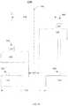
- FIG. 1Ais a block diagram of an exemplary memory cell configuration 100 A in accordance with one embodiment.
- Memory cell configuration 100 Aincludes memory cells 110 and 120 .
- Memory cell 110includes contact 111 , pMTJ 112 , via 113 , and switch 114 .
- Memory cell 120includes contact 121 , pMTJ 122 , via 123 , and switch 124 .
- the pMTJ 112is in a different layer than pMTJ 122 and overlap each other.
- the overlap 155is coordinated with a reference pitch.
- the reference pitchis associated with a pitch between a first pitch reference component in the memory cell 110 and a second pitch reference component in the memory cell 120 .
- the first pitch reference componentis switch 114 and the second pitch reference component is switch 124 and the reference pitch is the distance 177 or pitch between switch 114 and switch 124 .
- the memory cellscan achieve a pitch of 175 from the middle of memory cell 110 to the middle of memory cell 120 .
- the lithographic process utilized to create the reference componentsallows reference components to have a smaller size and pitch than lithographic process limitation utilized to create the pMTJs.
- Reference componentse.g., switch 114 , via 113 , etc.
- the lithographic process utilized to create the reference componentscan also allow the space between reference components in the same level or plane to have smaller spacing than a lithographic process utilized to create pMTJs in the same level or plane.
- memory cell configuration 100 Aincludes levels or layers 10 , 20 , 30 , 40 , 50 , 60 , and 70 .
- Contact 121is included in level 70 .
- the pMTJ 122is included in level 60 .
- Contact 111is included in level 50 .
- level 50is an interconnection or redistribution layer.
- the pMTJ 112is included in layer 40 .
- the vias 113 and 124are included in layer 30 .
- the switches 114 and 124are included in layer 20 .
- Layer 10is a substrate layer. It is appreciated there can be variations to the component and layer configurations.
- portions of via 123are also included in layers 40 , 50 , and 60 in addition to layer 30 .
- portions of contact 111are also included in layers 60 and 70 and extend to be parallel or equal with the top of contact 121 . It is appreciated that there can be additional layers (e.g., below, above, in between, etc.) of components. Additional layers can include various components (e.g., pMTJs, vias, switches, lines or traces, other components, etc.).
- the relative location or configuration relationship of pMTJs in different levelscan vary.
- the relative location of the pMTJsis based upon a differences in location with respect to a plane perpendicular to the layers or levels.
- a plane 199is perpendicular to the layers or levels.
- portions of pMTJs in different levelscan overlap each other with respect to a plane perpendicular to the levels.
- FIG. 1Athere is an overlap 155 of the pMTJs 112 and 122 .
- plane 199is in or traverses the overlap 155 .
- the pMTJs in different levelscan have a space or gap between each other with respect to a plane perpendicular to the levels.
- FIG. 1Bis a block diagram of another exemplary memory cell configuration 100 B in accordance with one embodiment.
- Memory cell configuration 100 Bis similar to memory cell configuration 100 A except a portion of pMTJs in different levels have spacing or gap between pMTJs in different levels.
- Memory cell configuration 100 Bincludes memory cells 130 and 140 .
- Memory cell 130includes contact 131 , pMTJ 132 , via 133 , and switch 134 .
- Memory cell 140includes contact 141 , pMTJ 142 , via 143 , and switch 144 . It is appreciated that components of memory cell configuration 100 B can be included in multiple layers similar to layers 10 through 70 and so on.
- the pMTJ 132is in a different layer than pMTJ 142 but do not overlap each other.
- the spacing or gap 157crossed over a plane 199 perpendicular to the levels. In one exemplary implementation, plane 199 is in or traverses the gap 157 . In one exemplary implementation, the spacing or gap 157 is coordinated with or based upon a reference pitch.
- the reference pitchis associated with a pitch between a first pitch reference component in the memory cell 130 and a second pitch reference component in the memory cell 140 .
- the first pitch reference componentis switch 134 and second pitch reference component is switch 144
- the reference pitchis the distance 178 or pitch between switch 134 and switch 144 .
- the memory cellscan achieve a pitch of 179 from the middle of memory cell 130 to the middle of memory cell 140 .
- an edge in respective pMTJs in different levelscan align with one another in a plane perpendicular to the levels. In one embodiment, there is not an overlap or spacing between planes of a respective edge of pMTJs in different levels. In one exemplary implementation, there is no overlap (e.g., distance 155 in FIG. 1A is 0) and no space (e.g., distance 157 in FIG. 1B is 0) between respective edges of pMTJs in different levels.
- respective edges of the first pMTJ and second pMTJare located with respect to a plane perpendicular to the first and second level.
- a portion of the first pMTJ and a portion of the second pMTJcan overlap each other and the plane perpendicular to the first and second level traverses the overlap.
- a portion of the first pMTJ and a portion of the second pMTJcan have a space between each other, and the plane perpendicular to the first and second level traverses the space.
- the respective edges of the first pMTJ and the second pMTJcan be aligned with the plane perpendicular to the first and second level.
- the respective edgesare the edges of the pMTJ closest to the plane perpendicular to the levels.
- the respective edgescan be edges of pMTJs closest to a plane similar to plane 199 .
- FIG. 2is a block diagram of exemplary comparison of memory cell configurations in accordance with one embodiment.
- Memory cell 210includes contact 211 , pMTJ 212 , via 213 and switch 214 .
- Memory cell 220includes contact 221 , pMTJ 222 , via 223 and switch 224 .
- Memory cell 230includes contact 231 , pMTJ 232 , via 233 and switch 234 .
- Memory cell 240includes contact 241 , pMTJ 242 , via 243 and switch 244 .
- the pMTJs 212 and 222are in different layers from one another while the pMTJs 232 and 242 are in the same level as one another. By overlapping the pMTJs 212 and 222 in different levels, the pitch 251 between memory cells 210 and 220 is less or smaller than the memory cell pitch 252 between memory cells 230 and 240 .
- the pMTJsare included in a MRAM.
- the pMTJsare coupled to selector switches that are utilized to select or not select the memory cell during various operations (e.g., read, write, erase, etc.).
- adjacent switchesin the X and Y directions
- portions of the pMTJscan overlap. The resulting reduced memory cell pitch size enables increased memory cell density and higher information or bits/area capacity for an MRAM chip.
- FIG. 3is a block diagram of a memory array of pMTJ memory cells (e.g., 311 , 321 , 312 , etc.) in accordance with one embodiment.
- the pMTJs adjacent to one another in the x and y dimensionsalternate between a first level 1 and second level 2 .
- pMTJ memory cell 311is in level 2
- pMTJ memory cells 321 and 312are in level 1 .
- FIG. 4is a block diagram of an exemplary memory cell array 410 layout without pMTJ overlap and an exemplary memory cell array 420 layout with pMTJ overlap in accordance with one embodiment.
- Memory cell array 410includes a plurality of memory cells (e.g., memory cells 411 , 412 , 414 , 415 , etc).
- the layoutillustrates the pitch size 488 as defined by lithography limitations.
- the solid circular linese.g., 477 , 497 , etc.
- outlining the memory cells or dotsrepresent the dot size after lithography.
- the figurealso shows the size of the dots or memory cells after trimming.
- Memory cell array 420includes a plurality of memory cells (e.g., memory cells 421 , 422 , 423 , 425 , etc).
- the layout illustrates the pitch size 489is not tied to lithography limitations associated with the pMTJ. In one embodiment, the pitch size 489 corresponds to pitch limitations of components other than the pMTJ.
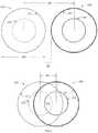
- FIG. 5is a block diagram top view of two pMTJs 570 and 580 that do not overlap and two pMTJs 510 and 520 that overlap in accordance with one embodiment.
- the solid line 571indicates the lithographic printing or formation boundaries of a pMTJ 570 in a fabrication level and the solid line 581 indicates the lithographic printing or formation boundaries of pMTJ 580 in the same fabrication level.
- the dashed line 572indicates the trimming boundaries of pMTJ 510 and dashed line 582 indicates the trimming boundaries of pMTJ 520 .
- the pitch 592 between pMTJ 570 and pMTJ 580is determined by the pMTJ lithographic formation limitations or resolution 595 and the spacing limitation 597 .
- the spacing limitation 597can be influenced or adjusted to compensate for various factors (e.g., minimum spacing lithographic formation limitations, capacitance considerations, electrical interference, etc.).
- the solid line 511indicates the lithographic printing or formation boundaries of pMTJ 510 in one fabrication level and the solid line 531 indicates the lithographic printing or formation boundaries of pMTJ 530 in another fabrication level.
- the dashed line 512indicates the trimming boundaries of pMTJ 510 in the first level and the dashed line 532 indicates the trimming boundaries of pMTJ 530 in the second level.
- the pMTJ 510 and pMTJ 530still include an overlap 552 after trimming.
- the pitch 591is smaller than pitch 592 as the pMTJs 510 and 530 associated with pitch 591 have an overlap and the pMTJs 570 and 580 associated with pitch 592 do not overlap.
- placement of a pMTJcan be configured based upon considerations or coordination associated with multiple pitch reference components.
- the placement of a pMTJis configured based upon a lithographic limitation associated with formation of a switch and a lithographic limitation associated with the formation of a via.
- the placement of a pMTJ 232can be configured based upon a lithographic limitation associated with formation of switches 234 , 224 , and 244 and a lithographic limitation associated with the formation of vias 223 and 243 .
- the placement of via 243 with respect to an edge of switch 244may limit the placement of the pMTJ 232 . If via 243 is limited to a location closer to the middle of the switch 244 , this may limit the ability of pMTJ 232 to shift and thus may limit the overlap and resulting pitch.
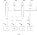
- FIG. 6is a block diagram of an exemplary memory cell array configuration 600 in accordance with one embodiment.
- Memory cell configuration 600includes memory cells 610 , 620 , 630 , and 640 .
- Memory cell 610includes contact 611 , pMTJ 612 , via 613 , and switch 614 .
- Memory cell 620includes contact 621 , pMTJ 622 , via 623 , and switch 624 .
- Memory cell 630includes contact 631 , pMTJ 632 , via 633 , and switch 634 .
- Memory cell 640includes contact 641 , pMTJ 642 , via 643 , and switch 644 .
- the pMTJs 612 and 632are in different layers than pMTJ 622 and 642 .
- the pitch cell between memory cells 610 , 620 , 630 , and 640can be maintained based upon a reference pitch.
- a pMTJ on one levelcan overlap multiple pMTJs on another level. For example, pMTJ 622 in the second level overlaps pMTJs 612 and 632 in the first level, and pMTJs 622 and 642 in the second level overlap pMTJs 632 .
- FIG. 7is a block diagram top view of pitch reference components included in an array in accordance with one embodiment.
- the pitch reference componentsinclude 711 , 712 , 713 , 721 , 722 , 723 , 731 , 732 , and 733 .
- the pitch reference componentscan have different shapes (e.g., square, rectangular, circular, etc.).
- pitch reference component 731has a width of 2f in the x direction and a length of 3f in the y direction, where f is the minimum lithographic process distance or resolution available for the device fabrication. The minimum lithographic process distance or resolution available for the device fabrication can correspond to a line or trace width.
- FIG. 8illustrates a magnetic tunnel junction (“MTJ”) 800 in accordance with one embodiment.
- MTJ 800includes one or more seed layers 810 provided at the bottom of stack 800 to initiate a desired crystalline growth in the above-deposited layers.
- An antiferromagnetic layer 812is disposed over seed layers 810 .
- MTJ 830is deposited on top of synthetic antiferromagnetic (SAF) layer 820 .
- SAFsynthetic antiferromagnetic
- MTJ 830includes reference layer 832 , which is a magnetic layer, a non-magnetic tunneling barrier layer (i.e., the insulator) 834 , and the free layer 836 , which is also a magnetic layer.
- SAFsynthetic antiferromagnetic
- reference layer 832can actually be part of SAF layer 820 , but forms one of the ferromagnetic plates of MTJ 830 when the non-magnetic tunneling barrier layer 834 and free layer 836 are formed on reference layer 832 .
- magnetic reference layer 832has a magnetization direction perpendicular to its plane.
- free layer 836also has a magnetization direction perpendicular to its plane, but its direction can vary by 180 degrees.
- the first magnetic layer 814is disposed over seed layer 810 .
- SAF layer 820also has an antiferromagnetic coupling layer 816 disposed over the first magnetic layer 814 .
- a nonmagnetic spacer 840is disposed on top of MTJ 830 and a polarizer 850 is disposed on top of the nonmagnetic spacer 840 .
- Polarizer 850is a magnetic layer that has a magnetic direction that may be parallel to its plane and orthogonal to the magnetic direction of the reference layer 832 and free layer 836 . Polarizer 850 is provided to polarize a current of electrons (“spin-aligned electrons”) applied to MTJ structure 830 .
- a capping layer 860can be provided on top of perpendicular polarizer 850 to protect the layers below on MTJ stack 800 .
- a hard mask 870is deposited over capping layers 860 and is provided to pattern the underlying layers of the MTJ structure 800 , using a reactive ion etch (RIE) and ion beam etch processes.
- RIEreactive ion etch
- the MTJ structureis similar to portions of a pMTJ (e.g., pMTJ 112 , 122 , 132 , 142 , 612 , 622 , 421 , 422 , etc.)
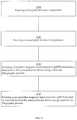
- FIG. 9is a flow chart of an exemplary fabrication method in accordance with one embodiment.
- switch structuresare formed.
- the switchesare transistors.
- the transistorscan be a complimentary metal oxide silicon (CMOS) transistors.
- CMOScomplimentary metal oxide silicon
- a switchis configured to selectively operate a memory cell during various activities (e.g., read, write, erase, etc.).
- conductor viasare formed.
- the conductor viasare coupled to the switches.
- formation of the conductor viasinclude, leveling or smoothing off (e.g., CMP, etc.) the top of the vias, depositing an insulation layer (e.g., oxide, etc.), etching a via space in the insulation layer, and filling the space in with a via conductor (e.g., metal, etc.).
- MTJ structures or componentsare formed.
- One group of MTJ structuresare formed in one layer of the semiconductor and another group of MTJ structures is form in another layer.
- the location of portions of the MTJ structure formed in one layer and portions of the MTJ structure formed in the other layercan be coordinated based upon a reference pitch. Portions of the MTJ structure formed in one layer can overlap portions of the MTJ structure formed in the other layer.
- the MTJ structuresare coupled to the vias.
- the MTJ structuresare coupled to the vias in an alternating pattern so that groups of MTJs from different layers are coupled to every other switch structure respectively in an X and Y planar direction.
- the MTJsare formed in a circular or pillar configuration.
- the formation of the MTJscan include magnetic material deposition (pMTJ), hard mask deposition, pMTJ annealing, photolithography for pillar definition, reactive ion retching of hard mask, ion beam etching of the pMTJ to form pillars, insulator deposition and smoothing the surface with CMP (chemical mechanical polishing) for the next level of pMTJ formation and so on.
- pMTJmagnetic material deposition
- hard mask depositionpMTJ annealing
- photolithography for pillar definitionreactive ion retching of hard mask
- ion beam etching of the pMTJ to form pillarsinsulator deposition and smoothing the surface with CMP (chemical mechanical polishing) for the next level of pMTJ formation and so on.
- CMPchemical mechanical polishing
- contactsare formed.
- the contactsare coupled to the MTJs.
- MTJsmultiple layers can be fabricated. It is appreciated, there can be more than 2 layers or levels (e.g., 3, 4, 5, etc.) than include MTJs, pMTJs, and so on. Again, it is appreciated MTJs in different levels can be configured or located based upon a reference pitch. MTJs in different levels can include overlapping portions. It is appreciated other components of the memory cell (e.g., switches, transistors, vias, contacts, traces, etc.) can be included in multiple levels. The components (e.g., switches, transistors, vias, contacts. traces, etc.) can be configured or located based upon a reference pitch. Components in different levels can include overlapping portions.
- switches, transistors, vias, contacts. traces, etc.can be configured or located based upon a reference pitch.
- similar lithographic mask patternsare utilized to form different layers of MTJs.
- similar lithographic masks utilized to form layers in which MTJs overlap, except the respective lithographic masksinclude an offset in the patterns of another and the offset corresponds to the overlap.
- the MTJ fabrication in multiple layerscan include multiple anneal processes.
- the number of MTJ layersis coordinated and balanced with impacts associated with the annealing processes.
- a fabrication process utilized to form a portion of a memory cellcan have a greater resolution limitation than another fabrication process utilized to form another portion of the memory cell.
- FIG. 10is a flow chart of exemplary fabrication processes in accordance with one embodiment.
- a portion of one memory cellis fabricated in a layer of a semiconductor.
- the portionis fabricated using one fabrication process that has a first set of fabrication limitations.
- the set of limitationscan be resolution limitations.
- the set of limitationscan correspond to the type of fabrication process.
- the fabrication processcan be a lithographic process.
- the lithographic processcan include an ion beam etch process, a plasma etch process, a reactive etch process, and so on.
- the portion of the memory cellcan be a subcomponent.
- the memory cell subcomponentcan be a switch, via, and so on.
- the portionoverlaps a portion of another memory cell.
- the portioncan be in a different layer as the portion of the of the other memory cell.
- the portiondoes not overlap a portion of another memory cell.
- the portioncan be in the same layer as the portion of the of the other memory cell.
- the overlapped portion of the other memory cellis in a different layer.
- another portion of the memory cellis fabricated.
- the other portionis fabricated using a fabrication process that has a second set of fabrication limitations.
- the second set of fabrications limitationscan include different resolution limitations than the first set of fabrication limitations.
- the set of limitationscan correspond to the type of fabrication process.
- the fabrication processcan be a lithographic process.
- the lithographic processcan include an ion beam etch process, a plasma etch process, a reactive etch process, and so on.
- the portion of the memory cellcan be a subcomponent.
- the memory cell subcomponentcan be a pMTJ.
- the portioncan be fabricated to overlap a portion of another memory cell. The overlapped portion of the other memory cell is in a different layer.
- FIG. 11is a flow chart of memory fabrication method 1100 in accordance with one embodiment.
- the location of a second pMTJ and a first pMTJ with respect to one anotheris coordinated based upon a reference pitch distance.
- the reference pitch distancecan be based upon a pitch between a first pitch reference component and a second pitch reference component.
- lithographic printing capabilities with respect to the first pitch reference component and the second pitch reference componentis used to set or determine the reference pitch.
- a first pitch reference componentis formed.
- the first pitch reference componentcan be a switch.
- the reference component sizecan be based upon a minimum lithographic processing dimension.
- the reference component sizecan be reduced and based upon a minimum trimming processing dimension.
- a second pitch reference componentis formed.
- the second pitch reference componentcan be a switch.
- the reference component sizecan be based upon a minimum lithographic processing dimension.
- a first pillar magnetic tunnel junction (pMTJ) located in a first level in a semiconductor deviceis formed using a first run lithographic process.
- the first pitch reference componentis coupled to the first pMTJ.
- a second pillar magnetic tunnel junctionlocated in a second level in the semiconductor device if formed using a second run lithographic process.
- the second pitch reference componentis coupled to the second pMTJ.
- the location of the second pMTJ with respect to the first pMTJis coordinated to comply with a reference pitch for memory cells.
- the location of the second pMTJ and the second pMTJ with respect to each other and a plane perpendicular to the first level and the second levelcan be coordinated to comply with a reference pitch for the memory cells.
- a portion of the second MTJcan overlap a portion of the first MTJ and the plane perpendicular to the first level and the second level traverses the overlap.
- Respective edges of the second MTJ and the first MTJare aligned along the plane perpendicular to the first level and the second level.
- the MTJscan be included in a pillar configuration and included in pMTJs.
- a portion of the second pMTJoverlaps a portion of the first pMTJ wherein the overlap corresponds to an offset in pattern difference between the first level and the second level.
- a first lithographic maskcan be utilized to form the first pMTJ and a second lithographic mask can be utilized to form the second pMTJ, wherein lithographic patterns for forming the first pMTJ and second pMTJ are the same except they are offset from one another to correspond to the overlap.
- a minimum lithographic processing dimension associated with the first pitch reference component and the second pitch reference componentis less than a minimum/lithographic processing dimension associated with the first pMTJ and the second pMTJ.
- the fabrication processes utilized to form the first pitch reference component and the second pitch referencehave a greater resolution than fabrication processes utilized to form the first pMTJ and second pMTJ.
- the smallest dimensioncan correspond to a conductive line trace.
- the pMTJscan be formed using a hard mask and ion beam etch.
- the first pMTJ and the second pMTJcan also be trimmed.
- the memory cellsare included in memory cell array of a memory device.
- the memory devicecan be a magnoresistive random access memory (MRAM).
- Embodiments of the present inventioncan facilitate efficient and effective memory cell density configuration.
- MTJ components of a memory cellare configured in different levels and the pitch between the MTJ components of between memory cells can be adjusted or based upon a reference pitch.
- the reference pitchcan correspond to components formed by processes that facilitate relatively tight or close pitches.
- the reference pitchcan be narrower than pitches otherwise associated with traditional magnetic memory cell formation. The closer or tighter pitches can enable increased memory cell density. The increased memory cell density in turn can enable greater information storage per device area.
- embodiments of the present inventioncan be compatible and implemented with a variety of different types of tangible memory or storage (e.g., RAM, DRAM, flash, hard drive, CD, DVD, etc.).
- the memory or storagewhile able to be changed or rewritten, can be considered a non-transitory storage medium.
- a non-transitory storage mediumit is not intend to limit characteristics of the medium, and can include a variety of storage mediums (e.g., programmable, erasable, nonprogrammable, read/write, read only, etc.) and “non-transitory” computer-readable media comprises all computer-readable media, with the sole exception being a transitory, propagating signal.
- the specificationincludes a listing of exemplary concepts or embodiments associated with the novel approach. It is also appreciated that the listing is not exhaustive and does not necessarily include all possible implementation.
- the concepts and embodimentscan be implemented in hardware.
- the methods or processdescribe operations performed by various processing components or units.
- instructions, or directions associated with the methods, processes, operations etc.can be stored in a memory and cause a processor to implement the operations, functions, actions, etc.
- a memory storage management systems and methodscan include the exemplary concepts or embodiments. It is also appreciated that the listing is not exhaustive and does not necessarily include all possible implementations.
- the concepts and embodimentscan be implemented in hardware, firmware, software, and so on.
- the following conceptsinclude methods or processes that describe operations performed by various processing components or units.
- instructions or directions associated with the methods, processes, operations etc.can be stored in a memory and cause a processor to implement the operations, functions, actions, etc.
Landscapes
- Engineering & Computer Science (AREA)
- Computer Hardware Design (AREA)
- Manufacturing & Machinery (AREA)
- Mram Or Spin Memory Techniques (AREA)
- Hall/Mr Elements (AREA)
Abstract
Description
Claims (21)
Priority Applications (1)
| Application Number | Priority Date | Filing Date | Title |
|---|---|---|---|
| US15/859,150US10886330B2 (en) | 2017-12-29 | 2017-12-29 | Memory device having overlapping magnetic tunnel junctions in compliance with a reference pitch |
Applications Claiming Priority (1)
| Application Number | Priority Date | Filing Date | Title |
|---|---|---|---|
| US15/859,150US10886330B2 (en) | 2017-12-29 | 2017-12-29 | Memory device having overlapping magnetic tunnel junctions in compliance with a reference pitch |
Publications (2)
| Publication Number | Publication Date |
|---|---|
| US20190206936A1 US20190206936A1 (en) | 2019-07-04 |
| US10886330B2true US10886330B2 (en) | 2021-01-05 |
Family
ID=67058984
Family Applications (1)
| Application Number | Title | Priority Date | Filing Date |
|---|---|---|---|
| US15/859,150ActiveUS10886330B2 (en) | 2017-12-29 | 2017-12-29 | Memory device having overlapping magnetic tunnel junctions in compliance with a reference pitch |
Country Status (1)
| Country | Link |
|---|---|
| US (1) | US10886330B2 (en) |
Cited By (2)
| Publication number | Priority date | Publication date | Assignee | Title |
|---|---|---|---|---|
| US11302697B2 (en)* | 2020-01-28 | 2022-04-12 | Integrated Silicon Solution, (Cayman) Inc. | DRAM with selective epitaxial cell transistor |
| US11410714B2 (en)* | 2019-09-16 | 2022-08-09 | Taiwan Semiconductor Manufacturing Co., Ltd. | Magnetoresistive memory device and manufacturing method thereof |
Families Citing this family (2)
| Publication number | Priority date | Publication date | Assignee | Title |
|---|---|---|---|---|
| US10840439B2 (en) | 2017-12-29 | 2020-11-17 | Spin Memory, Inc. | Magnetic tunnel junction (MTJ) fabrication methods and systems |
| CN114530550B (en)* | 2020-11-23 | 2025-07-15 | 江苏鲁汶仪器股份有限公司 | A method for etching a magnetic tunnel junction of MRAM |
Citations (414)
| Publication number | Priority date | Publication date | Assignee | Title |
|---|---|---|---|---|
| JPS5635666B1 (en) | 1971-06-28 | 1981-08-19 | ||
| US4597487A (en) | 1983-07-28 | 1986-07-01 | Creative Technology, Inc. | Method and apparatus for selective scrap metal collections |
| US5541868A (en) | 1995-02-21 | 1996-07-30 | The United States Of America As Represented By The Secretary Of The Navy | Annular GMR-based memory element |
| US5559952A (en) | 1993-03-23 | 1996-09-24 | Kabushiki Kaisha Toshiba | Display controller incorporating cache memory dedicated for VRAM |
| US5629549A (en) | 1995-04-21 | 1997-05-13 | Johnson; Mark B. | Magnetic spin transistor device, logic gate & method of operation |
| US5640343A (en) | 1996-03-18 | 1997-06-17 | International Business Machines Corporation | Magnetic memory array using magnetic tunnel junction devices in the memory cells |
| US5654566A (en) | 1995-04-21 | 1997-08-05 | Johnson; Mark B. | Magnetic spin injected field effect transistor and method of operation |
| US5691936A (en) | 1995-08-21 | 1997-11-25 | Matsushita Electric Industrial Co., Ltd. | Magnetoresistive element and memory element |
| US5695864A (en) | 1995-09-28 | 1997-12-09 | International Business Machines Corporation | Electronic device using magnetic components |
| US5695846A (en) | 1995-01-12 | 1997-12-09 | The Procter & Gamble Company | Zero scrap absorbent core formation process and products derived from web-based absorbent materials |
| JPH104012A (en) | 1996-06-17 | 1998-01-06 | Sharp Corp | Magnetoresistive element, method of manufacturing the same, and magnetic head using the same |
| US5732016A (en) | 1996-07-02 | 1998-03-24 | Motorola | Memory cell structure in a magnetic random access memory and a method for fabricating thereof |
| US5751647A (en) | 1995-02-13 | 1998-05-12 | Micron Technology, Inc. | On-chip memory redundancy circuitry for programmable non-volatile memories, and methods for programming same |
| US5856897A (en) | 1996-11-27 | 1999-01-05 | International Business Machines Corporation | Self-biased dual spin valve sensor |
| US5896252A (en) | 1995-08-11 | 1999-04-20 | Fujitsu Limited | Multilayer spin valve magneto-resistive effect magnetic head with free magnetic layer including two sublayers and magnetic disk drive including same |
| JPH11120758A (en) | 1997-10-09 | 1999-04-30 | Sony Corp | Nonvolatile random access memory |
| US5966323A (en) | 1997-12-18 | 1999-10-12 | Motorola, Inc. | Low switching field magnetoresistive tunneling junction for high density arrays |
| JPH11352867A (en) | 1998-06-05 | 1999-12-24 | Nippon Telegr & Teleph Corp <Ntt> | Server-client type learning support system, method, and recording medium storing learning support program |
| US6016269A (en) | 1998-09-30 | 2000-01-18 | Motorola, Inc. | Quantum random address memory with magnetic readout and/or nano-memory elements |
| US6055179A (en) | 1998-05-19 | 2000-04-25 | Canon Kk | Memory device utilizing giant magnetoresistance effect |
| US6064948A (en) | 1998-03-02 | 2000-05-16 | Tanisys Technology, Inc. | Tester systems |
| US6075941A (en) | 1997-01-29 | 2000-06-13 | International Business Machines Corporation | Microcomputer |
| US6097579A (en) | 1998-08-21 | 2000-08-01 | International Business Machines Corporation | Tunnel junction head structure without current shunting |
| US6112295A (en) | 1998-09-24 | 2000-08-29 | Intel Corporation | High frequency pipeline decoupling queue with non-overlapping read and write signals within a single clock cycle |
| US6124711A (en) | 1996-01-19 | 2000-09-26 | Fujitsu Limited | Magnetic sensor using tunnel resistance to detect an external magnetic field |
| US6134138A (en) | 1999-07-30 | 2000-10-17 | Honeywell Inc. | Method and apparatus for reading a magnetoresistive memory |
| US6140838A (en) | 1995-04-21 | 2000-10-31 | Johnson; Mark B. | High density and high speed magneto-electronic logic family |
| US6154139A (en) | 1998-04-21 | 2000-11-28 | Versus Technology | Method and system for locating subjects within a tracking environment |
| US6172902B1 (en) | 1998-08-12 | 2001-01-09 | Ecole Polytechnique Federale De Lausanne (Epfl) | Non-volatile magnetic random access memory |
| US6233690B1 (en) | 1998-09-17 | 2001-05-15 | Intel Corporation | Mechanism for saving power on long latency stalls |
| US6233172B1 (en) | 1999-12-17 | 2001-05-15 | Motorola, Inc. | Magnetic element with dual magnetic states and fabrication method thereof |
| US6243288B1 (en) | 1999-08-26 | 2001-06-05 | Hitachi, Ltd. | Giant magnetoresistive sensor, thin-film read/write head and magnetic recording apparatus using the sensor |
| US6252798B1 (en) | 1997-06-27 | 2001-06-26 | Kabushiki Kaisha Toshiba | Nonvolatile semiconductor memory device capable of controlling mutual timing of write voltage pulse and transfer voltage pulse |
| US6256223B1 (en) | 1998-07-28 | 2001-07-03 | International Business Machines Corporation | Current-induced magnetic switching device and memory including the same |
| JP2001195878A (en) | 1999-10-25 | 2001-07-19 | Canon Inc | Magnetoresistive memory, method of reproducing information recorded in the memory, and reproducing apparatus therefor |
| US6292389B1 (en) | 1999-07-19 | 2001-09-18 | Motorola, Inc. | Magnetic element with improved field response and fabricating method thereof |
| US6347049B1 (en) | 2001-07-25 | 2002-02-12 | International Business Machines Corporation | Low resistance magnetic tunnel junction device with bilayer or multilayer tunnel barrier |
| US6385082B1 (en) | 2000-11-08 | 2002-05-07 | International Business Machines Corp. | Thermally-assisted magnetic random access memory (MRAM) |
| FR2817998A1 (en) | 2000-12-07 | 2002-06-14 | Commissariat Energie Atomique | Magnetic device incorporating a magnetic layer for polarising the spin of electrons and rotation of magnetisation for the realisation of magnetic memory |
| US20020090533A1 (en) | 1999-11-23 | 2002-07-11 | Jing Zhang | Method and system for reducing assymetry in a spin valve having a synthetic pinned layer |
| US6436526B1 (en) | 1999-06-17 | 2002-08-20 | Matsushita Electric Industrial Co., Ltd. | Magneto-resistance effect element, magneto-resistance effect memory cell, MRAM and method for performing information write to or read from the magneto-resistance effect memory cell |
| US6442681B1 (en) | 1998-12-28 | 2002-08-27 | Bull Hn Information Systems Inc. | Pipelined central processor managing the execution of instructions with proximate successive branches in a cache-based data processing system while performing block mode transfer predictions |
| US6458603B1 (en) | 2000-10-10 | 2002-10-01 | Infineon Technologies Ag | Method of fabricating a micro-technical structure, and micro-technical component |
| US6493197B2 (en) | 1999-06-29 | 2002-12-10 | Fujitsu Limited | Magneto-resistance effect type head and information reproducing apparatus |
| JP2002357489A (en) | 2001-05-31 | 2002-12-13 | Matsushita Electric Ind Co Ltd | Stress sensor |
| US6522137B1 (en) | 2000-06-28 | 2003-02-18 | Schlumberger Technology Corporation | Two-dimensional magnetic resonance imaging in a borehole |
| US6538918B2 (en) | 2000-08-14 | 2003-03-25 | Micron Technology, Inc. | Pulsed write techniques for magneto-resistive memories |
| US6545903B1 (en) | 2001-12-17 | 2003-04-08 | Texas Instruments Incorporated | Self-aligned resistive plugs for forming memory cell with phase change material |
| US6545906B1 (en) | 2001-10-16 | 2003-04-08 | Motorola, Inc. | Method of writing to scalable magnetoresistance random access memory element |
| US20030085186A1 (en) | 2001-10-31 | 2003-05-08 | Norihiro Fujioka | Chemical reinforcing holders for glass substrate |
| US6563681B1 (en) | 1999-05-31 | 2003-05-13 | Tdk Corporation | Magnetoresistance effect film and magnetoresistance effect type head |
| US6566246B1 (en) | 2001-05-21 | 2003-05-20 | Novellus Systems, Inc. | Deposition of conformal copper seed layers by control of barrier layer morphology |
| FR2832542A1 (en) | 2001-11-16 | 2003-05-23 | Commissariat Energie Atomique | MAGNETIC DEVICE WITH MAGNETIC TUNNEL JUNCTION, MEMORY AND WRITING AND READING METHODS USING THE SAME |
| US20030117840A1 (en) | 2001-12-20 | 2003-06-26 | Manish Sharma | Magnetic memory device having soft reference layer |
| US6603677B2 (en) | 2000-12-07 | 2003-08-05 | Commissariat A L'energie Atomique | Three-layered stacked magnetic spin polarization device with memory |
| US20030151944A1 (en) | 2001-12-27 | 2003-08-14 | Kabushiki Kaisha Toshiba | Magnetic switching element and a magnetic memory |
| US6608776B2 (en) | 2000-11-14 | 2003-08-19 | Mitsubishi Denki Kabushiki Kaisha | Thin film magnetic memory device having a highly integrated memory array |
| EP1345277A1 (en) | 2000-12-21 | 2003-09-17 | Fujitsu Limited | Magnetoresistive device, magnetic head, and magnetic disk player |
| US6635367B2 (en) | 2001-03-19 | 2003-10-21 | Hitachi, Ltd. | Magnetic recording medium |
| US20030197984A1 (en) | 1999-09-16 | 2003-10-23 | Kabushiki Kaisha Toshiba | Magnetoresistive element and magnetic memory device |
| JP2003318461A (en) | 2002-04-22 | 2003-11-07 | Matsushita Electric Ind Co Ltd | Magnetoresistive element, magnetic head, magnetic memory and magnetic recording device using the same |
| US6653153B2 (en) | 2000-07-03 | 2003-11-25 | Merck & Co., Inc. | Methods for encoding combinatorial libraries |
| US6654278B1 (en) | 2002-07-31 | 2003-11-25 | Motorola, Inc. | Magnetoresistance random access memory |
| US20030218903A1 (en) | 2002-05-24 | 2003-11-27 | International Business Machines | Nonvolatile memory device utilizing spin-valve-type designs and current pulses |
| US6677165B1 (en) | 2003-03-20 | 2004-01-13 | Micron Technology, Inc. | Magnetoresistive random access memory (MRAM) cell patterning |
| US20040012994A1 (en) | 2002-07-17 | 2004-01-22 | Slaughter Jon M. | Multi-state magnetoresistance random access cell with improved memory storage density |
| US20040026369A1 (en) | 2002-08-12 | 2004-02-12 | Chentsau Ying | Method of etching magnetic materials |
| US6710984B1 (en) | 1999-09-24 | 2004-03-23 | Kabushiki Kaisha Toshiba | Magnetoresistive effect device utilizing a magnetization-coupling layer which couples adjacent ferromagnetic layers perpendicularly |
| US6714444B2 (en) | 2002-08-06 | 2004-03-30 | Grandis, Inc. | Magnetic element utilizing spin transfer and an MRAM device using the magnetic element |
| US6713195B2 (en) | 2001-01-05 | 2004-03-30 | Nve Corporation | Magnetic devices using nanocomposite materials |
| US20040061154A1 (en) | 2002-09-27 | 2004-04-01 | Yiming Huai | Thermally stable magnetic elements utilizing spin transfer and an MRAM device using the magnetic element |
| US6731537B2 (en) | 2001-09-12 | 2004-05-04 | Renesas Technology Corp. | Non-volatile memory device and data storing method |
| US20040094785A1 (en) | 2002-11-18 | 2004-05-20 | Xiaochun Zhu | Magentic memory element and memory device including same |
| US6744086B2 (en) | 2001-05-15 | 2004-06-01 | Nve Corporation | Current switched magnetoresistive memory cell |
| US20040130936A1 (en) | 2003-01-07 | 2004-07-08 | Grandis Inc. | Spin-transfer multilayer stack containing magnetic layers with resettable magnetization |
| US6765824B2 (en) | 2002-03-29 | 2004-07-20 | Kabushiki Kaisha Toshiba | Magneto-resistance element capable of controlling the position and size of edge domain and the coercivity and magnetic memory |
| US6772036B2 (en) | 2001-08-30 | 2004-08-03 | Fisher-Rosemount Systems, Inc. | Control system using process model |
| US6773515B2 (en) | 2002-01-16 | 2004-08-10 | Headway Technologies, Inc. | FeTa nano-oxide layer as a capping layer for enhancement of giant magnetoresistance in bottom spin valve structures |
| US6777730B2 (en) | 2001-08-31 | 2004-08-17 | Nve Corporation | Antiparallel magnetoresistive memory cells |
| US6785159B2 (en) | 2002-08-29 | 2004-08-31 | Micron Technology, Inc. | Combination etch stop and in situ resistor in a magnetoresistive memory and methods for fabricating same |
| US20040173315A1 (en) | 2003-03-04 | 2004-09-09 | Charles Leung | Apparatus and method for reducing impurities in a semiconductor material |
| US6812437B2 (en) | 2000-04-28 | 2004-11-02 | The Holmes Group, Inc. | Electronic control circuit |
| US6829161B2 (en) | 2003-01-10 | 2004-12-07 | Grandis, Inc. | Magnetostatically coupled magnetic elements utilizing spin transfer and an MRAM device using the magnetic element |
| US20040257717A1 (en) | 2003-06-18 | 2004-12-23 | Manish Sharma | Coupled ferromagnetic systems having modified interfaces |
| US6835423B2 (en) | 2000-04-28 | 2004-12-28 | Freescale Semiconductor, Inc. | Method of fabricating a magnetic element with insulating veils |
| US6839821B2 (en) | 1999-11-16 | 2005-01-04 | Lexar Media, Inc. | Method and apparatus for memory control circuit |
| US6842317B2 (en) | 2002-04-22 | 2005-01-11 | Matsushita Electric Industrial Co., Ltd. | Magnetoresistive element, magnetic head, magnetic memory and magnetic recording apparatus using the same |
| US6842366B2 (en) | 2002-09-09 | 2005-01-11 | Renesas Technology Corp. | Thin film magnetic memory device executing self-reference type data read |
| US6847547B2 (en) | 2003-02-28 | 2005-01-25 | Grandis, Inc. | Magnetostatically coupled magnetic elements utilizing spin transfer and an MRAM device using the magnetic element |
| JP2005044848A (en) | 2003-07-23 | 2005-02-17 | Toshiba Corp | Magnetic memory device and method of manufacturing magnetic memory device |
| US20050041342A1 (en) | 2003-08-21 | 2005-02-24 | Yiming Huai | Magnetoresistive element having reduced spin transfer induced noise |
| US20050051820A1 (en) | 2003-09-10 | 2005-03-10 | George Stojakovic | Fabrication process for a magnetic tunnel junction device |
| US20050063222A1 (en) | 2003-09-19 | 2005-03-24 | Yiming Huai | Current confined pass layer for magnetic elements utilizing spin-transfer and an MRAM device using such magnetic elements |
| US6888742B1 (en) | 2002-08-28 | 2005-05-03 | Grandis, Inc. | Off-axis pinned layer magnetic element utilizing spin transfer and an MRAM device using the magnetic element |
| US20050104101A1 (en) | 2003-11-19 | 2005-05-19 | International Business Machines Corporation | Spin-current switched magnetic memory element suitable for circuit integration and method of fabricating the memory element |
| US6902807B1 (en) | 2002-09-13 | 2005-06-07 | Flex Products, Inc. | Alignable diffractive pigment flakes |
| JP2005150482A (en) | 2003-11-18 | 2005-06-09 | Sony Corp | Magnetoresistive element and magnetic memory device |
| US6906369B2 (en) | 2003-02-10 | 2005-06-14 | Massachusetts Institute Of Technology | Magnetic memory elements using 360° walls |
| US20050128842A1 (en) | 2003-11-07 | 2005-06-16 | Alexander Wei | Annular magnetic nanostructures |
| US20050136600A1 (en) | 2003-12-22 | 2005-06-23 | Yiming Huai | Magnetic elements with ballistic magnetoresistance utilizing spin-transfer and an MRAM device using such magnetic elements |
| US20050158881A1 (en) | 2004-01-15 | 2005-07-21 | Manish Sharma | Method of making toroidal mram cells |
| US20050180202A1 (en) | 2004-02-13 | 2005-08-18 | Yiming Huai | Method and system for providing heat assisted switching of a magnetic element utilizing spin transfer |
| US6933155B2 (en) | 2003-05-21 | 2005-08-23 | Grandis, Inc. | Methods for providing a sub .15 micron magnetic memory structure |
| US20050184839A1 (en) | 2004-02-19 | 2005-08-25 | Nguyen Paul P. | Spin transfer magnetic element having low saturation magnetization free layers |
| US6938142B2 (en) | 2002-08-28 | 2005-08-30 | Micron Technology, Inc. | Multi-bank memory accesses using posted writes |
| US6958927B1 (en) | 2002-10-09 | 2005-10-25 | Grandis Inc. | Magnetic element utilizing spin-transfer and half-metals and an MRAM device using the magnetic element |
| US6958507B2 (en) | 2003-08-04 | 2005-10-25 | Hitachi, Ltd. | Semiconductor memory pipeline buffer |
| US20050237787A1 (en) | 2004-04-21 | 2005-10-27 | Yiming Huai | Spin transfer magnetic elements with spin depolarization layers |
| US6967863B2 (en) | 2004-02-25 | 2005-11-22 | Grandis, Inc. | Perpendicular magnetization magnetic element utilizing spin transfer |
| US20050280058A1 (en) | 2004-06-16 | 2005-12-22 | Mahendra Pakala | Re-configurable logic elements using heat assisted magnetic tunneling elements |
| US6980469B2 (en) | 2003-08-19 | 2005-12-27 | New York University | High speed low power magnetic devices based on current induced spin-momentum transfer |
| US6985385B2 (en) | 2003-08-26 | 2006-01-10 | Grandis, Inc. | Magnetic memory element utilizing spin transfer switching and storing multiple bits |
| US20060018057A1 (en) | 2004-07-26 | 2006-01-26 | Yiming Huai | Magnetic tunnel junction having diffusion stop layer |
| US6992359B2 (en) | 2004-02-26 | 2006-01-31 | Grandis, Inc. | Spin transfer magnetic element with free layers having high perpendicular anisotropy and in-plane equilibrium magnetization |
| US6995962B2 (en) | 2001-03-12 | 2006-02-07 | Kabushiki Kaisha Toshiba | Ferromagnetic double tunnel junction element with asymmetric energy band |
| US7002839B2 (en) | 2003-04-23 | 2006-02-21 | Keio University | Magnetic ring unit and magnetic memory device |
| US7002339B2 (en) | 2004-05-31 | 2006-02-21 | Denso Corporation | Rotation angle detecting device |
| US7006371B2 (en) | 2002-12-04 | 2006-02-28 | Sharp Kabushiki Kaisha | Semiconductor memory device and method for programming and erasing a memory cell |
| US7006375B2 (en) | 2003-06-06 | 2006-02-28 | Seagate Technology Llc | Hybrid write mechanism for high speed and high density magnetic random access memory |
| US7005958B2 (en) | 2002-06-14 | 2006-02-28 | Honeywell International Inc. | Dual axis magnetic sensor |
| US7009877B1 (en) | 2003-11-14 | 2006-03-07 | Grandis, Inc. | Three-terminal magnetostatically coupled spin transfer-based MRAM cell |
| US20060049472A1 (en) | 2004-09-09 | 2006-03-09 | Zhitao Diao | Magnetic elements with spin engineered insertion layers and MRAM devices using the magnetic elements |
| US20060077734A1 (en) | 2004-09-30 | 2006-04-13 | Fong John Y | Direct mapped repair cache systems and methods |
| US7033126B2 (en) | 2003-04-02 | 2006-04-25 | Asm International N.V. | Method and apparatus for loading a batch of wafers into a wafer boat |
| US20060087880A1 (en) | 2004-10-22 | 2006-04-27 | Mancoff Frederick B | Spin-transfer based MRAM using angular-dependent selectivity |
| US20060092696A1 (en) | 2004-11-01 | 2006-05-04 | Kazuhiro Bessho | Storage element and memory |
| US7041598B2 (en) | 2003-06-25 | 2006-05-09 | Hewlett-Packard Development Company, L.P. | Directional ion etching process for patterning self-aligned via contacts |
| US7045368B2 (en) | 2004-05-19 | 2006-05-16 | Headway Technologies, Inc. | MRAM cell structure and method of fabrication |
| US7057922B2 (en) | 2003-09-12 | 2006-06-06 | Sharp Kabushiki Kaisha | Nonvolatile semiconductor memory device |
| US20060132990A1 (en) | 2004-12-20 | 2006-06-22 | Kabushiki Kaisha Toshiba | Magnetic recording element, magnetic recording apparatus and recording method of information |
| US20060227465A1 (en) | 2005-03-22 | 2006-10-12 | Kabushiki Kaisha Toshiba | Magneto-resistance effect element and magnetic memory |
| US20070019337A1 (en) | 2005-07-19 | 2007-01-25 | Dmytro Apalkov | Magnetic elements having improved switching characteristics and magnetic memory devices using the magnetic elements |
| US7187577B1 (en) | 2005-11-23 | 2007-03-06 | Grandis, Inc. | Method and system for providing current balanced writing for memory cells and magnetic devices |
| US7203129B2 (en) | 2004-02-16 | 2007-04-10 | Taiwan Semiconductor Manufacturing Company, Ltd. | Segmented MRAM memory array |
| US7203802B2 (en) | 2003-04-25 | 2007-04-10 | International Business Machines Corporation | System and method for using a buffer to facilitate log catchup for online operations |
| US20070096229A1 (en) | 2005-10-28 | 2007-05-03 | Masatoshi Yoshikawa | Magnetoresistive element and magnetic memory device |
| US7273780B2 (en) | 2004-06-24 | 2007-09-25 | Samsung Electronics Co., Ltd. | Semiconductor device having box-shaped cylindrical storage nodes and fabrication method thereof |
| US7283333B2 (en) | 2004-02-11 | 2007-10-16 | Hitachi Global Storage Technologies Netherlands B.V. | Self-pinned double tunnel junction head |
| US20070242501A1 (en) | 2006-04-18 | 2007-10-18 | Industrial Technology Research Institute | Structure and access method for magnetic memory cell and circuit of magnetic memory |
| US7324387B1 (en) | 2006-04-18 | 2008-01-29 | Maxim Integrated Products, Inc. | Low power high density random access memory flash cells and arrays |
| US7324389B2 (en) | 2006-03-24 | 2008-01-29 | Sandisk Corporation | Non-volatile memory with redundancy data buffered in remote buffer circuits |
| US7335960B2 (en) | 2003-12-10 | 2008-02-26 | Headway Technologies, Inc. | MRAM cell with flat topography and controlled bit line to free layer distance and method of manufacture |
| US20080049488A1 (en) | 2006-08-28 | 2008-02-28 | Rizzo Nicholas D | Spin-transfer based MRAM with reduced critical current density |
| US7352021B2 (en) | 2003-07-10 | 2008-04-01 | Samsung Electronics Co., Ltd. | Magnetic random access memory devices having titanium-rich lower electrodes with oxide layer and oriented tunneling barrier |
| US20080079530A1 (en) | 2006-10-02 | 2008-04-03 | Weidman Timothy W | Integrated magnetic features |
| US7372722B2 (en) | 2003-09-29 | 2008-05-13 | Samsung Electronics Co., Ltd. | Methods of operating magnetic random access memory devices including heat-generating structures |
| US20080112094A1 (en) | 2003-08-19 | 2008-05-15 | New York University | High speed low power annular magnetic devices based on current induced spin-momentum transfer |
| US7376006B2 (en) | 2005-05-13 | 2008-05-20 | International Business Machines Corporation | Enhanced programming performance in a nonvolatile memory device having a bipolar programmable storage element |
| US7386765B2 (en) | 2003-09-29 | 2008-06-10 | Intel Corporation | Memory device having error checking and correction |
| US20080151614A1 (en) | 2006-12-22 | 2008-06-26 | Magic Technologies, Inc. | Spin transfer MRAM device with magnetic biasing |
| FR2910716A1 (en) | 2006-12-26 | 2008-06-27 | Commissariat Energie Atomique | MULTILAYER MAGNETIC DEVICE, METHOD FOR PRODUCING THE SAME, MAGNETIC FIELD SENSOR, MAGNETIC MEMORY, AND LOGIC HOLDER USING SUCH A DEVICE |
| US7404017B2 (en) | 2004-01-16 | 2008-07-22 | International Business Machines Corporation | Method for managing data flow through a processing system |
| US7421535B2 (en) | 2004-05-10 | 2008-09-02 | International Business Machines Corporation | Method for demoting tracks from cache |
| US7436699B2 (en) | 2006-01-10 | 2008-10-14 | Renesas Technology Corp. | Nonvolatile semiconductor memory device |
| US7449345B2 (en) | 2004-06-15 | 2008-11-11 | Headway Technologies, Inc. | Capping structure for enhancing dR/R of the MTJ device |
| US7453719B2 (en) | 2003-04-21 | 2008-11-18 | Nec Corporation | Magnetic random access memory with improved data reading method |
| US20080297292A1 (en) | 2005-07-21 | 2008-12-04 | Bernard Viala | Radio Frequency Device with Magnetic Element, Method for Making Such a Magnetic Element |
| JP2009027177A (en) | 2007-07-23 | 2009-02-05 | Magic Technologies Inc | STT-MTJ-MRAM cell and manufacturing method thereof |
| US20090046501A1 (en) | 2006-04-27 | 2009-02-19 | Yadav Technology, Inc. | Low-cost non-volatile flash-ram memory |
| US7502249B1 (en) | 2006-07-17 | 2009-03-10 | Grandis, Inc. | Method and system for using a pulsed field to assist spin transfer induced switching of magnetic memory elements |
| US20090072185A1 (en) | 2001-07-31 | 2009-03-19 | Jds Uniphase Corporation | Anisotropic Magnetic Flakes |
| US7511985B2 (en) | 2006-05-18 | 2009-03-31 | Sharp Kabushiki Kaisha | Semiconductor memory device |
| US7515485B2 (en) | 2006-12-18 | 2009-04-07 | Micron Technology, Inc. | External clock tracking pipelined latch scheme |
| US20090091037A1 (en) | 2007-10-03 | 2009-04-09 | Solomon Assefa | Methods for Fabricating Contacts to Pillar Structures in Integrated Circuits |
| US20090098413A1 (en) | 2007-10-16 | 2009-04-16 | Hitachi, Ltd. | Dot-patterned structure magnetic recording medium and method for production thereof |
| US7542326B2 (en) | 2006-08-22 | 2009-06-02 | Sharp Kabushiki Kaisha | Semiconductor memory device |
| US7541117B2 (en) | 2006-04-18 | 2009-06-02 | Sony Corporation | Mask pattern generating method |
| US20090146231A1 (en) | 2007-12-05 | 2009-06-11 | Kuper Cynthia A | Magnetic memory device having a C-shaped structure and method of manufacturing the same |
| US20090161421A1 (en) | 2006-04-06 | 2009-06-25 | Samsung Electronics Co., Ltd. | Phase change memory devices and systems, and related programming methods |
| WO2009080636A1 (en) | 2007-12-21 | 2009-07-02 | Commissariat A L'energie Atomique | Method for modeling a magnetic tunnel junction with spin-polarized current writing |
| US20090209102A1 (en) | 2008-02-14 | 2009-08-20 | Magic Technologies, Inc. | Use of CMP to contact a MTJ structure without forming a via |
| US7582166B2 (en) | 2003-08-01 | 2009-09-01 | Sgl Carbon, Llc | Holder for supporting wafers during semiconductor manufacture |
| US20090231909A1 (en) | 2005-10-14 | 2009-09-17 | Commissariat A L'energie Atomique | Magnetoresistive Tunnel Junction Magnetic Device and Its Application to MRAM |
| US7598555B1 (en) | 2003-08-22 | 2009-10-06 | International Business Machines Corporation | MgO tunnel barriers and method of formation |
| US7619431B2 (en) | 2003-12-23 | 2009-11-17 | Nxp B.V. | High sensitivity magnetic built-in current sensor |
| US7633800B2 (en) | 2007-08-08 | 2009-12-15 | Atmel Corporation | Redundancy scheme in memory |
| US7642612B2 (en) | 2005-06-17 | 2010-01-05 | Semiconductor Energy Laboratory Co., Ltd. | Semiconductor device and manufacturing method thereof |
| US20100019297A1 (en)* | 2008-07-25 | 2010-01-28 | Hynix Semiconductor Inc. | Multi-Stacked Spin Transfer Torque Magnetic Random Access Memory and Method of Manufacturing the Same |
| US7660161B2 (en) | 2007-01-19 | 2010-02-09 | Silicon Storage Technology, Inc. | Integrated flash memory systems and methods for load compensation |
| US7675792B2 (en) | 2007-09-26 | 2010-03-09 | Intel Corporation | Generating reference currents compensated for process variation in non-volatile memories |
| US7696551B2 (en) | 2007-09-20 | 2010-04-13 | Magic Technologies, Inc. | Composite hard mask for the etching of nanometer size magnetic multilayer based device |
| US20100124091A1 (en) | 2008-11-13 | 2010-05-20 | Ingenia Holdings (Uk) Limited | Magnetic Data Storage Device and Method |
| US7733699B2 (en) | 2006-05-04 | 2010-06-08 | Micron Technology, Inc. | Mimicking program verify drain resistance in a memory device |
| US7739559B2 (en) | 2005-05-30 | 2010-06-15 | Spansion Llc | Semiconductor device and program data redundancy method therefor |
| US20100162065A1 (en) | 2008-12-19 | 2010-06-24 | Unity Semiconductor Corporation | Protecting integrity of data in multi-layered memory with data redundancy |
| US20100193891A1 (en) | 2008-02-18 | 2010-08-05 | Taiwan Semiconductor Manufacturing Company, Ltd. | In-Situ Formed Capping Layer in MTJ Devices |
| US7773439B2 (en) | 2006-04-13 | 2010-08-10 | Hynix Semiconductor Inc. | Test operation of multi-port memory device |
| US7796439B2 (en) | 2007-01-23 | 2010-09-14 | Kabushiki Kaisha Toshiba | Semiconductor memory device and write method thereof |
| US20100246254A1 (en) | 2007-12-13 | 2010-09-30 | Crocus Technology Sa | Magnetic memory with a thermally assisted writing procedure |
| US7810017B2 (en) | 2006-03-20 | 2010-10-05 | Micron Technology, Inc. | Variable sector-count ECC |
| US20100271870A1 (en) | 2009-04-28 | 2010-10-28 | Seagate Technology Llc | Magnetic stack having assist layer |
| US20100290275A1 (en) | 2009-05-15 | 2010-11-18 | Kyoung Wook Park | Phase change memory apparatus |
| US7852662B2 (en) | 2007-04-24 | 2010-12-14 | Magic Technologies, Inc. | Spin-torque MRAM: spin-RAM, array |
| US7861141B2 (en) | 2005-10-21 | 2010-12-28 | Mediatek Inc. | Method and device for error analysis of optical disc |
| CA2766141A1 (en) | 2009-06-24 | 2011-01-13 | New York University | High speed low power magnetic devices based on current induced spin-momentum transfer |
| US7881095B2 (en) | 2008-08-08 | 2011-02-01 | Seagate Technology Llc | Asymmetric write current compensation using gate overdrive for resistive sense memory cells |
| US20110032645A1 (en) | 2009-08-04 | 2011-02-10 | Canon Anelva Corporation | Magnetic sensor stack body, method of forming the same, film formation control program, and recording medium |
| US20110061786A1 (en) | 2009-09-15 | 2011-03-17 | The Regents Of The University Of California | Process for making customized particles by stochastic excitation |
| US7916515B2 (en) | 2009-03-10 | 2011-03-29 | Seagate Technology Llc | Non-volatile memory read/write verify |
| US20110089511A1 (en) | 2007-02-12 | 2011-04-21 | Avalanche Technology, Inc. | Magnetic Random Access Memory (MRAM) Manufacturing Process for a Small Magnetic Tunnel Junction (MTJ) Design with a Low Programming Current Requirement |
| US7936595B2 (en) | 2005-12-31 | 2011-05-03 | Institute Of Physics, Chinese Academy Of Sciences | Close shaped magnetic multi-layer film comprising or not comprising a metal core and the manufacture method and the application of the same |
| US20110133298A1 (en) | 2009-12-08 | 2011-06-09 | Qualcomm Incorporated | Spin-Transfer Switching Magnetic Element Utilizing a Composite Free Layer Comprising a Superparamagnetic Layer |
| US7986544B2 (en) | 2006-11-03 | 2011-07-26 | New York University | Electronic devices based on current induced magnetization dynamics in single magnetic layers |
| US8028119B2 (en) | 2005-05-20 | 2011-09-27 | Renesas Electronics Corporation | Memory module, cache system and address conversion method |
| US8041879B2 (en) | 2005-02-18 | 2011-10-18 | Sandisk Il Ltd | Flash memory backup system and method |
| US8055957B2 (en) | 2007-05-22 | 2011-11-08 | Renesas Electronics Corporation | Semiconductor integrated circuit device having fail-safe mode and memory control method |
| US8058925B2 (en) | 2009-04-24 | 2011-11-15 | The Boeing Company | Adaptive temporal filtering of single event effects |
| US8059460B2 (en) | 2009-02-02 | 2011-11-15 | Hynix Semiconductor Inc. | Method of programming nonvolatile memory device |
| US8072821B2 (en) | 2008-11-06 | 2011-12-06 | Elpida Memory, Inc. | Semiconductor memory device that can perform successive accesses |
| US8077496B2 (en) | 2008-09-26 | 2011-12-13 | Samsung Electronics Co., Ltd. | Nonvolatile memory device and method of driving the same |
| US8080365B2 (en) | 2007-12-14 | 2011-12-20 | Fujitsu Limited | Thiopyran derivative, polymer, resist composition, and method for manufacturing semiconductor device using such resist composition |
| US8094480B2 (en) | 2008-05-30 | 2012-01-10 | Elpida Memory, Inc. | Semiconductor device |
| US20120052258A1 (en) | 2009-05-18 | 2012-03-01 | Imec | Patterning of and contacting magnetic layers |
| US20120069649A1 (en) | 2006-10-20 | 2012-03-22 | Avalanche Technology, Inc. | Non-uniform switching based non-volatile magnetic based memory |
| US8144509B2 (en) | 2008-06-27 | 2012-03-27 | Qualcomm Incorporated | Write operation for spin transfer torque magnetoresistive random access memory with reduced bit cell size |
| US8148970B2 (en) | 2009-09-02 | 2012-04-03 | Kabushiki Kaisha Toshiba | Reference current generating circuit |
| US8201024B2 (en) | 2010-05-17 | 2012-06-12 | Microsoft Corporation | Managing memory faults |
| US20120155158A1 (en) | 2010-12-20 | 2012-06-21 | Sony Corporation | Storage device and writing control method |
| US20120155156A1 (en) | 2009-08-10 | 2012-06-21 | Grandis, Inc. | Method and system for providing magnetic tunneling junction elements having improved performance through capping layer induced perpendicular anisotropy and memories using such magnetic elements |
| US8223534B2 (en) | 2009-04-03 | 2012-07-17 | Taiwan Semiconductor Manufacturing Company, Ltd. | Raising programming currents of magnetic tunnel junctions using word line overdrive and high-k metal gate |
| US20120181642A1 (en) | 2011-01-13 | 2012-07-19 | Crocus Technology Sa | Magnetic tunnel junction comprising a polarizing layer |
| US20120188818A1 (en) | 2009-10-20 | 2012-07-26 | Avalanche Technology, Inc. | Low-crystallization temperature MTJ for Spin-Transfer Torque Magnetic Random Access Memory (STTMRAM) |
| US8255742B2 (en) | 2009-11-18 | 2012-08-28 | Microsoft Corporation | Dynamically replicated memory |
| US8278996B2 (en) | 2009-09-02 | 2012-10-02 | Kabushiki Kaisha Toshiba | Reference current generating circuit |
| US8279666B2 (en) | 2009-05-27 | 2012-10-02 | Institut Polytechnique De Grenoble | Spin polarised magnetic device |
| US8295082B2 (en) | 2008-08-15 | 2012-10-23 | Qualcomm Incorporated | Gate level reconfigurable magnetic logic |
| US8295073B2 (en) | 2009-01-30 | 2012-10-23 | Unity Semiconductor Corporation | Non-volatile dual port third dimensional memory |
| US20120280336A1 (en) | 2011-05-04 | 2012-11-08 | Magic Technologies, Inc. | Multilayers having reduced perpendicular demagnetizing field using moment dilution for spintronic applications |
| US20120280339A1 (en) | 2011-02-16 | 2012-11-08 | Avalanche Technology, Inc. | PERPENDICULAR MAGNETIC TUNNEL JUNCTION (pMTJ) WITH IN-PLANE MAGNETO-STATIC SWITCHING-ENHANCING LAYER |
| US20120294078A1 (en) | 2003-08-19 | 2012-11-22 | New York University | Bipolar spin-transfer switching |
| US20120299133A1 (en) | 2011-05-24 | 2012-11-29 | Jongpil Son | Magnetic devices and methods of fabricating the same |
| US8334213B2 (en) | 2009-06-05 | 2012-12-18 | Magic Technologies, Inc. | Bottom electrode etching process in MRAM cell |
| US8345474B2 (en) | 2009-04-29 | 2013-01-01 | Samsung Electronics Co., Ltd. | Magnetic memory devices including magnetic layers having different products of saturated magnetization and thickness and related methods |
| US20130001506A1 (en) | 2011-06-29 | 2013-01-03 | Motoyuki Sato | Resistance change memory and method of manufacturing the same |
| US20130001652A1 (en) | 2011-07-01 | 2013-01-03 | Masatoshi Yoshikawa | Magnetoresistive element and method of manufacturing the same |
| US8349536B2 (en) | 2008-05-29 | 2013-01-08 | Fujitsu Limited | Dithiane derivative, polymer, resist composition, and method for manufacturing semiconductor device using such resist composition |
| JP2013012546A (en) | 2011-06-28 | 2013-01-17 | Toshiba Corp | Manufacturing method of nonvolatile storage device |
| US20130021841A1 (en) | 2011-07-20 | 2013-01-24 | Avalanche Technology, Inc. | Perpendicular magnetic random access memory (mram) device with a stable reference cell |
| US8374050B2 (en) | 2010-06-04 | 2013-02-12 | Lsi Corporation | Multi-port memory using single-port memory cells |
| US8415650B2 (en) | 2009-07-02 | 2013-04-09 | Actel Corporation | Front to back resistive random access memory cells |
| US8422330B2 (en) | 2010-12-24 | 2013-04-16 | Fujitsu Limited | Memory controller and memory controlling method |
| US8432727B2 (en) | 2010-04-29 | 2013-04-30 | Qualcomm Incorporated | Invalid write prevention for STT-MRAM array |
| US8441844B2 (en) | 2010-07-07 | 2013-05-14 | Crocus Technology Sa | Method for writing in a MRAM-based memory device with reduced power consumption |
| US8456926B2 (en) | 2010-11-18 | 2013-06-04 | Grandis, Inc. | Memory write error correction circuit |
| US8456883B1 (en) | 2012-05-29 | 2013-06-04 | Headway Technologies, Inc. | Method of spin torque MRAM process integration |
| US8492381B2 (en) | 2008-10-27 | 2013-07-23 | Signal Pharmaceuticals, Llc | Pyrazino[2,3-b]pyrazine mTOR kinase inhibitor for oncology indications and diseases associated with the mTOR/PI3K/Akt pathway |
| US8495432B2 (en) | 2009-12-15 | 2013-07-23 | International Business Machines Corporation | Blocking write access to memory modules of a solid state drive |
| US8492881B2 (en) | 2009-04-01 | 2013-07-23 | Renesas Electronics Corporation | Magnetic storage device |
| US8535952B2 (en) | 2006-02-25 | 2013-09-17 | Avalanche Technology, Inc. | Method for manufacturing non-volatile magnetic memory |
| US8539303B2 (en) | 2010-12-20 | 2013-09-17 | Intel Corporation | Low overhead error correcting code protection for stored information |
| US20130244344A1 (en) | 2008-02-29 | 2013-09-19 | Roger Klas Malmhall | Method for manufacturing high density non-volatile magnetic memory |
| US8549303B2 (en) | 2000-06-05 | 2013-10-01 | West Services, Inc. | Apparatus, system and method for electronically signing electronic transcripts |
| US20130267042A1 (en) | 2012-04-10 | 2013-10-10 | Kimihiro Satoh | MRAM Fabrication Method with Sidewall Cleaning |
| US8558334B2 (en) | 2011-03-07 | 2013-10-15 | Renesas Electronics Corporation | Semiconductor device and method of manufacturing the semiconductor device |
| US20130270661A1 (en) | 2012-04-16 | 2013-10-17 | Ge Yi | Magnetoresistive random access memory cell design |
| US8582353B2 (en) | 2009-12-30 | 2013-11-12 | Hynix Semiconductor Inc. | Nonvolatile memory device |
| US20130307097A1 (en) | 2012-05-15 | 2013-11-21 | Ge Yi | Magnetoresistive random access memory cell design |
| US8593868B2 (en) | 2011-04-21 | 2013-11-26 | Hynix Semiconductor Inc. | Semiconductor memory device |
| US20130341801A1 (en) | 2012-06-22 | 2013-12-26 | Kimihiro Satoh | Redeposition Control in MRAM Fabrication Process |
| US8617408B2 (en) | 2011-10-18 | 2013-12-31 | HGST Netherlands B.V. | Method for manufacturing a magnetic read sensor with narrow track width using amorphous carbon as a hard mask and localized CMP |
| US8625339B2 (en) | 2011-04-11 | 2014-01-07 | Grandis, Inc. | Multi-cell per memory-bit circuit and method |
| US20140009994A1 (en) | 2012-07-06 | 2014-01-09 | International Business Machines Corporation | Domain wall motion in perpendicularly magnetized wires having artificial antiferromagnetically coupled multilayers with engineered interfaces |
| US8634232B2 (en) | 2011-04-06 | 2014-01-21 | SK Hynix Inc. | Write driver circuit for MRAM, MRAM and layout structure thereof |
| KR20140015246A (en) | 2010-08-02 | 2014-02-06 | 카타리니 마스텔리, 줄리아 | Composition comprising glutathione reductase and oxidized glutathione, and therapeutic uses thereof |
| US20140042571A1 (en) | 2010-12-10 | 2014-02-13 | Avalanche Technology Inc. | Magnetic random access memory having perpendicular enhancement layer |
| JP2014039061A (en) | 2013-10-24 | 2014-02-27 | Renesas Electronics Corp | Semiconductor device manufacturing method |
| US8667331B2 (en) | 2011-06-16 | 2014-03-04 | Hitachi, Ltd. | Storage system and control method for storing write data requested by a host computer |
| US20140070341A1 (en) | 2012-09-11 | 2014-03-13 | Headway Technologies, Inc. | Minimal Thickness Synthetic Antiferromagnetic (SAF) Structure with Perpendicular Magnetic Anisotropy for STT-MRAM |
| US20140103472A1 (en) | 2012-10-17 | 2014-04-17 | New York University | Inverted orthogonal spin transfer layer stack |
| US8705279B2 (en) | 2011-10-26 | 2014-04-22 | SK Hynix Inc. | Nonvolatile memory device and reading method thereof |
| US8716817B2 (en) | 2011-09-21 | 2014-05-06 | Kabushiki Kaisha Toshiba | Magnetic memory element and nonvolatile memory device |
| US8722543B2 (en) | 2010-07-30 | 2014-05-13 | Headway Technologies, Inc. | Composite hard mask with upper sacrificial dielectric layer for the patterning and etching of nanometer size MRAM devices |
| US20140136870A1 (en) | 2012-11-14 | 2014-05-15 | Advanced Micro Devices, Inc. | Tracking memory bank utility and cost for intelligent shutdown decisions |
| US8737137B1 (en) | 2013-01-22 | 2014-05-27 | Freescale Semiconductor, Inc. | Flash memory with bias voltage for word line/row driver |
| US20140151837A1 (en) | 2010-09-30 | 2014-06-05 | Samsung Electronics Co., Ltd. | Image sensor |
| US20140169085A1 (en) | 2012-12-07 | 2014-06-19 | The Regents Of The University Of California | Voltage-controlled magnetic memory element with canted magnetization |
| US20140177316A1 (en) | 2012-12-21 | 2014-06-26 | Sony Corporation | Non-volatile memory system with reset verification mechanism and method of operation thereof |
| US20140175583A1 (en)* | 2012-12-21 | 2014-06-26 | Brian S. Doyle | Perpendicular spin transfer torque memory (sttm) device having offset cells and method to form same |
| US8780617B2 (en) | 2011-12-08 | 2014-07-15 | Samsung Electronics Co., Ltd. | Semiconductor memory device and method of performing burn-in test on the same |
| US8792269B1 (en) | 2013-03-15 | 2014-07-29 | Avalanche Technology, Inc. | Fast programming of magnetic random access memory (MRAM) |
| US20140217531A1 (en) | 2011-05-10 | 2014-08-07 | Headway Technologies, Inc. | Co/Ni Multilayers with Improved Out-of-Plane Anisotropy for Magnetic Device Applications |
| US8817525B2 (en) | 2012-08-03 | 2014-08-26 | Sharp Kabushiki Kaisha | Semiconductor memory device |
| US8832530B2 (en) | 2012-09-26 | 2014-09-09 | Intel Corporation | Techniques associated with a read and write window budget for a two level memory system |
| US20140252439A1 (en) | 2013-03-08 | 2014-09-11 | T3Memory, Inc. | Mram having spin hall effect writing and method of making the same |
| US20140281284A1 (en) | 2013-03-13 | 2014-09-18 | Lsi Corporation | Multi-read port memory |
| US20140264671A1 (en) | 2013-03-15 | 2014-09-18 | Samsung Electronics Co., Ltd. | Magnetic junctions having insertion layers and magnetic memories using the magnetic junctions |
| US8852760B2 (en) | 2012-04-17 | 2014-10-07 | Headway Technologies, Inc. | Free layer with high thermal stability for magnetic device applications by insertion of a boron dusting layer |
| US8862808B2 (en) | 2011-03-28 | 2014-10-14 | Fujitsu Limited | Control apparatus and control method |
| US8867258B2 (en) | 2010-03-22 | 2014-10-21 | Qualcomm Incorporated | Memory cell that includes multiple non-volatile memories |
| US8902628B2 (en) | 2011-06-09 | 2014-12-02 | Samsung Electronics Co., Ltd. | Resistive memory device and sensing margin trimming method thereof |
| JP2015002352A (en) | 2013-06-17 | 2015-01-05 | アイメックImec | Magnetic memory element |
| US8966345B2 (en) | 2012-11-28 | 2015-02-24 | Intel Corporation | Selective error correction in memory to reduce power consumption |
| US20150056368A1 (en) | 2012-02-28 | 2015-02-26 | Headway Technologies, Inc. | High Thermal Stability Reference Structure with Out-of-Plane Anisotropy for Magnetic Device Applications |
| US9019754B1 (en) | 2013-12-17 | 2015-04-28 | Micron Technology, Inc. | State determination in resistance variable memory |
| US9026888B2 (en) | 2012-12-21 | 2015-05-05 | Intel Corporation | Method, system and apparatus for providing access to error correction information |
| US9025378B2 (en) | 2012-09-06 | 2015-05-05 | Kabushiki Kaisha Toshiba | Semiconductor memory device |
| US9030899B2 (en) | 2013-10-07 | 2015-05-12 | SK Hynix Inc. | Memory device with post package repair, operation method of the same and memory system including the same |
| US9037812B2 (en) | 2011-11-17 | 2015-05-19 | Intel Corporation | Method, apparatus and system for memory validation |
| US9043674B2 (en) | 2012-12-26 | 2015-05-26 | Intel Corporation | Error detection and correction apparatus and method |
| US9076530B2 (en) | 2013-02-07 | 2015-07-07 | Seagate Technology Llc | Non-volatile write buffer data retention pending scheduled verification |
| US9104595B2 (en) | 2013-03-12 | 2015-08-11 | Intel Corporation | Selective remedial action based on category of detected error for a memory read |
| US9104581B2 (en) | 2010-06-24 | 2015-08-11 | International Business Machines Corporation | eDRAM refresh in a high performance cache architecture |
| US9136463B2 (en) | 2007-11-20 | 2015-09-15 | Qualcomm Incorporated | Method of forming a magnetic tunnel junction structure |
| US9140747B2 (en) | 2013-07-22 | 2015-09-22 | Qualcomm Incorporated | Sense amplifier offset voltage reduction |
| US20150279904A1 (en) | 2014-04-01 | 2015-10-01 | Spin Transfer Technologies, Inc. | Magnetic tunnel junction for mram device |
| US9165787B2 (en) | 2013-03-15 | 2015-10-20 | SK Hynix Inc. | Electronic devices having semiconductor memory units and method for fabricating the same |
| US9166155B2 (en) | 2012-08-14 | 2015-10-20 | Everspin Technologies, Inc. | Method of manufacturing a magnetoresistive-based device |
| US9165629B2 (en) | 2013-03-12 | 2015-10-20 | Taiwan Semiconductor Manufacturing Co., Ltd. | Method and apparatus for MRAM sense reference trimming |
| US9178958B2 (en) | 2010-12-17 | 2015-11-03 | Facebook, Inc. | Distributed storage system |
| US9189326B2 (en) | 2013-10-08 | 2015-11-17 | Advanced Micro Devices, Inc. | Detecting and correcting hard errors in a memory array |
| US9190471B2 (en) | 2012-04-13 | 2015-11-17 | Globalfoundries U.S.2 Llc | Semiconductor structure having a source and a drain with reverse facets |
| US9231191B2 (en) | 2012-08-20 | 2016-01-05 | Industrial Technology Research Institute | Magnetic tunnel junction device and method of making same |
| US9229306B2 (en) | 2011-03-18 | 2016-01-05 | Nec Display Solutions, Ltd. | Illumination optical system and projector including fluorophore |
| US9229853B2 (en) | 2011-12-20 | 2016-01-05 | Intel Corporation | Method and system for data de-duplication |
| US9245608B2 (en) | 2011-09-22 | 2016-01-26 | Qualcomm Incorporated | Thermally tolerant perpendicular magnetic anisotropy coupled elements for spin-transfer torque switching device |
| US9250990B2 (en) | 2013-09-24 | 2016-02-02 | Intel Corporation | Use of error correction pointers to handle errors in memory |
| US9250997B2 (en) | 2012-11-27 | 2016-02-02 | Samsung Electronics Co., Ltd. | Semiconductor memory device including non-volatile memory, cache memory, and computer system |
| US9251896B2 (en) | 2013-04-26 | 2016-02-02 | Panasonic Intellectual Property Management Co., Ltd. | Variable resistance nonvolatile memory device and method for writing into the same |
| US9257483B2 (en) | 2010-01-13 | 2016-02-09 | Hitachi, Ltd. | Magnetic memory, method of manufacturing the same, and method of driving the same |
| US9263667B1 (en) | 2014-07-25 | 2016-02-16 | Spin Transfer Technologies, Inc. | Method for manufacturing MTJ memory device |
| US9286186B2 (en) | 2013-11-14 | 2016-03-15 | Accemic Gmbh & Co. Kg | Trace-data processing and profiling device |
| US20160087193A1 (en) | 2014-09-22 | 2016-03-24 | Spin Transfer Technologies, Inc. | Magnetic tunnel junction structure for mram device |
| US9299412B2 (en) | 2014-02-26 | 2016-03-29 | Intel Corporation | Write operations in spin transfer torque memory |
| US9298552B2 (en) | 2013-09-27 | 2016-03-29 | Intel Corporation | Using read values from previous decoding operations to calculate soft bit information in an error recovery operation |
| US9317429B2 (en) | 2011-09-30 | 2016-04-19 | Intel Corporation | Apparatus and method for implementing a multi-level memory hierarchy over common memory channels |
| US9324457B2 (en) | 2014-03-12 | 2016-04-26 | Kabushiki Kaisha Toshiba | Nonvolatile memory |
| US9342403B2 (en) | 2014-03-28 | 2016-05-17 | Intel Corporation | Method and apparatus for managing a spin transfer torque memory |
| US9341939B1 (en) | 2014-10-30 | 2016-05-17 | Seagate Technology Llc | Transmission balancing for phase shift mask with a trim mask |
| US9349482B2 (en) | 2014-07-23 | 2016-05-24 | Samsung Electronics Co., Ltd. | Nonvolatile memory device and operating method thereof |
| US9351899B2 (en) | 2014-01-21 | 2016-05-31 | International Business Machines Corporation | Dynamic temperature adjustments in spin transfer torque magnetoresistive random-access memory (STT-MRAM) |
| US9362486B2 (en) | 2014-09-29 | 2016-06-07 | Samsung Electronics Co., Ltd. | Magnetic memory device having perpendicular magnetic tunnel junction pattern and method of forming the same |
| US9378817B2 (en) | 2011-03-25 | 2016-06-28 | Panasonic Intellectual Property Management Co., Ltd. | Variable resistance nonvolatile memory element writing method and variable resistance nonvolatile memory device |
| US9379314B2 (en) | 2013-12-17 | 2016-06-28 | Qualcomm Incorporated | Hybrid synthetic antiferromagnetic layer for perpendicular magnetic tunnel junction (MTJ) |
| US9389954B2 (en) | 2014-02-26 | 2016-07-12 | Freescale Semiconductor, Inc. | Memory redundancy to replace addresses with multiple errors |
| US9396065B2 (en) | 2014-06-25 | 2016-07-19 | Intel Corporation | Extensible memory hub |
| US9396991B2 (en) | 2014-08-25 | 2016-07-19 | Globalfoundries Inc. | Multilayered contact structure having nickel, copper, and nickel-iron layers |
| US9401336B2 (en) | 2014-11-04 | 2016-07-26 | International Business Machines Corporation | Dual layer stack for contact formation |
| US9418721B2 (en) | 2014-01-21 | 2016-08-16 | International Business Machines Corporation | Determining and storing bit error rate relationships in spin transfer torque magnetoresistive random-access memory (STT-MRAM) |
| US9450180B1 (en) | 2015-11-03 | 2016-09-20 | International Business Machines Corporation | Structure and method to reduce shorting in STT-MRAM device |
| US9449720B1 (en) | 2015-11-17 | 2016-09-20 | Macronix International Co., Ltd. | Dynamic redundancy repair |
| US9455013B2 (en) | 2013-09-27 | 2016-09-27 | Qualcomm Incorporated | System and method to trim reference levels in a resistive memory |
| US20160283385A1 (en) | 2015-03-27 | 2016-09-29 | James A. Boyd | Fail-safe write back caching mode device driver for non volatile storage device |
| US9472748B2 (en) | 2011-12-30 | 2016-10-18 | Intel Corporation | Balancing energy barrier between states in perpendicular magnetic tunnel junctions |
| US9472282B2 (en) | 2015-01-06 | 2016-10-18 | Samsung Electronics Co., Ltd. | Resistive memory device and method of operating the same |
| US20160315118A1 (en) | 2015-04-21 | 2016-10-27 | Spin Transfer Technologies, Inc. | High annealing temperature perpendicular magnetic anisotropy structure for magnetic random access memory |
| US9484527B2 (en) | 2013-11-01 | 2016-11-01 | Institute Of Physics, Chinese Academy Of Sciences | Nanometer magnetic multilayer film for temperature sensor and manufacturing method therefor |
| US9490054B2 (en) | 2012-10-11 | 2016-11-08 | Headway Technologies, Inc. | Seed layer for multilayer magnetic materials |
| US9488416B2 (en) | 2011-11-28 | 2016-11-08 | Mitsubishi Hitachi Power Systems, Ltd. | Multistage pressure condenser and steam turbine plant having the same |
| US9508456B1 (en) | 2015-06-16 | 2016-11-29 | SK Hynix Inc. | Self repair device and method thereof |
| US9520192B2 (en) | 2014-06-30 | 2016-12-13 | Intel Corporation | Resistive memory write operation with merged reset |
| US9520128B2 (en) | 2014-09-23 | 2016-12-13 | Intel Corporation | Frame skipping with extrapolation and outputs on demand neural network for automatic speech recognition |
| US20160378592A1 (en) | 2014-03-20 | 2016-12-29 | Kabushiki Kaisha Toshiba | Cache memory and processor system |
| US9548116B2 (en) | 2014-11-26 | 2017-01-17 | Nxp Usa, Inc. | Resistive memory with program verify and erase verify capability |
| US9548445B2 (en) | 2012-07-27 | 2017-01-17 | Qualcomm Incorporated | Amorphous alloy space for perpendicular MTJs |
| US9553102B2 (en) | 2014-08-19 | 2017-01-24 | Applied Materials, Inc. | Tungsten separation |
| US9583167B2 (en) | 2015-04-29 | 2017-02-28 | Globalfoundries Singapore Pte. Ltd. | Low power memory cell with high sensing margin |
| US20170062712A1 (en) | 2013-06-05 | 2017-03-02 | SK Hynix Inc. | Electronic device and method for fabricating the same |
| US9594683B2 (en) | 2013-12-03 | 2017-03-14 | International Business Machines Corporation | Data processing in a multiple processor system to maintain multiple processor cache memory access coherency |
| US9600183B2 (en) | 2014-09-22 | 2017-03-21 | Intel Corporation | Apparatus, system and method for determining comparison information based on memory data |
| US9608038B2 (en) | 2010-12-10 | 2017-03-28 | Avalanche Technology, Inc. | Magnetic tunnel junction (MTJ) memory element having tri-layer perpendicular reference layer |
| US9614007B2 (en)* | 2015-07-20 | 2017-04-04 | Micron Technology, Inc. | Memory arrays |
| US9634237B2 (en) | 2014-12-23 | 2017-04-25 | Qualcomm Incorporated | Ultrathin perpendicular pinned layer structure for magnetic tunneling junction devices |
| US9640267B2 (en) | 2014-03-31 | 2017-05-02 | Renesas Elctronics Corporation | Semiconductor device, pre-write program, and restoration program |
| US20170123991A1 (en) | 2015-10-28 | 2017-05-04 | Sandisk Technologies Inc. | System and method for utilization of a data buffer in a storage device |
| US9646701B2 (en) | 2015-04-09 | 2017-05-09 | SK Hynix Inc. | Non-volatile semiconductor memory device and improved verification and programming method for the same |
| US20170133104A1 (en) | 2015-11-11 | 2017-05-11 | Imagination Technologies Limited | Hardware Monitor to Verify Memory Units |
| US9652321B2 (en) | 2014-09-23 | 2017-05-16 | Intel Corporation | Recovery algorithm in non-volatile memory |
| US9697140B2 (en) | 2014-09-23 | 2017-07-04 | Intel Corporation | Encryption integrity check with CRC encryption in memory using a word count- and address-derived nonce |
| US20170199459A1 (en) | 2016-01-13 | 2017-07-13 | Samsung Electronics Co., Ltd. | Methods of forming patterns using compositions for an underlayer of photoresist |
| US9720616B2 (en) | 2008-06-18 | 2017-08-01 | Super Talent Technology, Corp. | Data-retention controller/driver for stand-alone or hosted card reader, solid-state-drive (SSD), or super-enhanced-endurance SSD (SEED) |
| US9728712B2 (en) | 2015-04-21 | 2017-08-08 | Spin Transfer Technologies, Inc. | Spin transfer torque structure for MRAM devices having a spin current injection capping layer |
| US9741926B1 (en) | 2016-01-28 | 2017-08-22 | Spin Transfer Technologies, Inc. | Memory cell having magnetic tunnel junction and thermal stability enhancement layer |
| US20170256584A1 (en)* | 2016-03-01 | 2017-09-07 | Kabushiki Kaisha Toshiba | Magnetoresistive memory device and manufacturing method of the same |
| US9772555B2 (en) | 2015-06-02 | 2017-09-26 | Samsung Electronics Co., Ltd. | Methods of forming patterns using photoresists |
| US9773974B2 (en) | 2015-07-30 | 2017-09-26 | Spin Transfer Technologies, Inc. | Polishing stop layer(s) for processing arrays of semiconductor elements |
| US9780300B2 (en) | 2011-02-16 | 2017-10-03 | Avalanche Technology, Inc. | Magnetic memory element with composite perpendicular enhancement layer |
| US9793319B2 (en) | 2014-05-21 | 2017-10-17 | Avalanche Technology, Inc. | Multilayered seed structure for perpendicular MTJ memory element |
| US9853292B2 (en) | 2009-05-11 | 2017-12-26 | Nexeon Limited | Electrode composition for a secondary battery cell |
| US9853206B2 (en) | 2015-06-16 | 2017-12-26 | Spin Transfer Technologies, Inc. | Precessional spin current structure for MRAM |
| US9858976B2 (en) | 2016-03-16 | 2018-01-02 | Kabushiki Kaisha Toshiba | Nonvolatile RAM comprising a write circuit and a read circuit operating in parallel |
| US9859333B2 (en) | 2013-08-02 | 2018-01-02 | Samsung Electronics Co., Ltd. | Magnetic memory devices having a perpendicular magnetic tunnel junction |
| US9865806B2 (en) | 2013-06-05 | 2018-01-09 | SK Hynix Inc. | Electronic device and method for fabricating the same |
| US20180033957A1 (en) | 2016-07-26 | 2018-02-01 | Shanghai CiYu Information Technologies Co., LTD | Method to make magnetic ramdom accesss memroy array with small footprint |
| US20180097006A1 (en) | 2016-10-05 | 2018-04-05 | Samsung Electronics Co., Ltd. | Semiconductor Memory Devices |
| US20180114589A1 (en) | 2016-09-27 | 2018-04-26 | Spin Transfer Technologies, Inc. | Method of reading data from a memory device using dynamic redundancy registers |
| US20180122449A1 (en) | 2016-09-27 | 2018-05-03 | Spin Transfer Technologies, Inc. | Memory instruction pipeline with an additional write stage in a memory device that uses dynamic redundancy registers |
| US20180122450A1 (en) | 2016-09-27 | 2018-05-03 | Spin Transfer Technologies, Inc. | Smart cache design to prevent overflow for a memory device with a dynamic redundancy register |
| US20180121361A1 (en) | 2016-09-27 | 2018-05-03 | Spin Transfer Technologies, Inc. | Memory device with a plurality of memory banks where each memory bank is associated with a corresponding memory instruction pipeline and a dynamic redundancy register |
| US20180122446A1 (en) | 2016-09-27 | 2018-05-03 | Spin Transfer Technologies, Inc. | Memory device with a dual y-multiplexer structure for performing two simultaneous operations on the same row of a memory bank |
| US20180122447A1 (en) | 2016-09-27 | 2018-05-03 | Spin Transfer Technologies, Inc. | Method of writing contents in memory during a power up sequence using a dynamic redundancy register in a memory device |
| US20180119278A1 (en) | 2015-04-13 | 2018-05-03 | Kornmeyer Carbon-Group Gmbh | Pecvd boat |
| US20180121117A1 (en) | 2016-09-27 | 2018-05-03 | Spin Transfer Technologies, Inc. | Method of processing incompleted memory operations in a memory device during a power up sequence and a power down sequence using a dynamic redundancy register |
| US20180121355A1 (en) | 2016-09-27 | 2018-05-03 | Spin Transfer Technologies, Inc. | Method of flushing the contents of a dynamic redundancy register to a secure storage area during a power down in a memory device |
| US20180122448A1 (en) | 2016-09-27 | 2018-05-03 | Spin Transfer Technologies, Inc. | Memory instruction pipeline with a pre-read stage for a write operation for reducing power consumption in a memory device that uses dynamic redundancy registers |
| US10008662B2 (en) | 2015-03-12 | 2018-06-26 | Taiwan Semiconductor Manufacturing Co., Ltd. | Perpendicular magnetic tunneling junction (MTJ) for improved magnetoresistive random-access memory (MRAM) process |
| US10026609B2 (en) | 2014-10-23 | 2018-07-17 | Board Of Regents, The University Of Texas System | Nanoshape patterning techniques that allow high-speed and low-cost fabrication of nanoshape structures |
| US20180211821A1 (en) | 2017-01-23 | 2018-07-26 | Infineon Technologies Ag | Wafer chuck and processing arrangement |
| US10038137B2 (en) | 2016-09-30 | 2018-07-31 | Taiwan Semiconductor Manufacturing Co., Ltd. | MRAM device and method for fabricating the same |
| US10043967B2 (en) | 2014-08-07 | 2018-08-07 | Qualcomm Incorporated | Self-compensation of stray field of perpendicular magnetic elements |
| US10042588B2 (en) | 2016-07-12 | 2018-08-07 | SK Hynix Inc. | Electronic device and operating method thereof |
| US10043851B1 (en) | 2017-08-03 | 2018-08-07 | Headway Technologies, Inc. | Etch selectivity by introducing oxidants to noble gas during physical magnetic tunnel junction (MTJ) etching |
| US20180233362A1 (en) | 2017-02-15 | 2018-08-16 | International Business Machines Corporation | Method to improve adhesion of photoresist on silicon substrate for extreme ultraviolet and electron beam lithography |
| US10062837B2 (en) | 2015-11-25 | 2018-08-28 | Samsung Electronics Co., Ltd. | Method of forming magnetic patterns, and method of manufacturing magnetic memory devices |
| US20180248113A1 (en) | 2017-02-28 | 2018-08-30 | Spin Transfer Technologies, Inc. | Precessional spin current structure for mram |
| US20180248110A1 (en) | 2017-02-28 | 2018-08-30 | Spin Transfer Technologies, Inc. | Precessional spin current structure for mram |
| US20180269254A1 (en)* | 2017-01-05 | 2018-09-20 | Micron Technology, Inc. | Memory devices, systems, and methods of fabrication |
| US20180285714A1 (en)* | 2017-04-03 | 2018-10-04 | Gyrfalcon Technology Inc. | Fabrication methods of memory subsystem used in cnn based digital ic for ai |
| US20180286916A1 (en)* | 2015-06-02 | 2018-10-04 | Intel Corporation | High density memory architecture using back side metal layers |
| US10115446B1 (en) | 2015-04-21 | 2018-10-30 | Spin Transfer Technologies, Inc. | Spin transfer torque MRAM device with error buffer |
| US20180331279A1 (en) | 2017-05-15 | 2018-11-15 | Headway Technologies, Inc. | Combined Physical and Chemical Etch to Reduce Magnetic Tunnel Junction (MTJ) Sidewall Damage |
| US10134988B2 (en) | 2013-12-13 | 2018-11-20 | E I Du Pont De Nemours And Company | System for forming an electroactive layer |
| US10163479B2 (en) | 2015-08-14 | 2018-12-25 | Spin Transfer Technologies, Inc. | Method and apparatus for bipolar memory write-verify |
| US10186614B2 (en) | 2015-02-06 | 2019-01-22 | Semiconductor Energy Laboratory Co., Ltd. | Semiconductor device and manufacturing method thereof |
| US20190067566A1 (en)* | 2017-08-29 | 2019-02-28 | Everspin Technologies, Inc. | Method of manufacturing integrated circuits |
- 2017
- 2017-12-29USUS15/859,150patent/US10886330B2/enactiveActive
Patent Citations (517)
| Publication number | Priority date | Publication date | Assignee | Title |
|---|---|---|---|---|
| JPS5635666B1 (en) | 1971-06-28 | 1981-08-19 | ||
| US4597487A (en) | 1983-07-28 | 1986-07-01 | Creative Technology, Inc. | Method and apparatus for selective scrap metal collections |
| US5559952A (en) | 1993-03-23 | 1996-09-24 | Kabushiki Kaisha Toshiba | Display controller incorporating cache memory dedicated for VRAM |
| US5695846A (en) | 1995-01-12 | 1997-12-09 | The Procter & Gamble Company | Zero scrap absorbent core formation process and products derived from web-based absorbent materials |
| US5751647A (en) | 1995-02-13 | 1998-05-12 | Micron Technology, Inc. | On-chip memory redundancy circuitry for programmable non-volatile memories, and methods for programming same |
| US5541868A (en) | 1995-02-21 | 1996-07-30 | The United States Of America As Represented By The Secretary Of The Navy | Annular GMR-based memory element |
| US5629549A (en) | 1995-04-21 | 1997-05-13 | Johnson; Mark B. | Magnetic spin transistor device, logic gate & method of operation |
| US5654566A (en) | 1995-04-21 | 1997-08-05 | Johnson; Mark B. | Magnetic spin injected field effect transistor and method of operation |
| US6140838A (en) | 1995-04-21 | 2000-10-31 | Johnson; Mark B. | High density and high speed magneto-electronic logic family |
| US5896252A (en) | 1995-08-11 | 1999-04-20 | Fujitsu Limited | Multilayer spin valve magneto-resistive effect magnetic head with free magnetic layer including two sublayers and magnetic disk drive including same |
| US5691936A (en) | 1995-08-21 | 1997-11-25 | Matsushita Electric Industrial Co., Ltd. | Magnetoresistive element and memory element |
| US5695864A (en) | 1995-09-28 | 1997-12-09 | International Business Machines Corporation | Electronic device using magnetic components |
| US6124711A (en) | 1996-01-19 | 2000-09-26 | Fujitsu Limited | Magnetic sensor using tunnel resistance to detect an external magnetic field |
| US5640343A (en) | 1996-03-18 | 1997-06-17 | International Business Machines Corporation | Magnetic memory array using magnetic tunnel junction devices in the memory cells |
| JPH104012A (en) | 1996-06-17 | 1998-01-06 | Sharp Corp | Magnetoresistive element, method of manufacturing the same, and magnetic head using the same |
| US5732016A (en) | 1996-07-02 | 1998-03-24 | Motorola | Memory cell structure in a magnetic random access memory and a method for fabricating thereof |
| US5856897A (en) | 1996-11-27 | 1999-01-05 | International Business Machines Corporation | Self-biased dual spin valve sensor |
| US6075941A (en) | 1997-01-29 | 2000-06-13 | International Business Machines Corporation | Microcomputer |
| US6252798B1 (en) | 1997-06-27 | 2001-06-26 | Kabushiki Kaisha Toshiba | Nonvolatile semiconductor memory device capable of controlling mutual timing of write voltage pulse and transfer voltage pulse |
| JPH11120758A (en) | 1997-10-09 | 1999-04-30 | Sony Corp | Nonvolatile random access memory |
| US5966323A (en) | 1997-12-18 | 1999-10-12 | Motorola, Inc. | Low switching field magnetoresistive tunneling junction for high density arrays |
| US6064948A (en) | 1998-03-02 | 2000-05-16 | Tanisys Technology, Inc. | Tester systems |
| US6154139A (en) | 1998-04-21 | 2000-11-28 | Versus Technology | Method and system for locating subjects within a tracking environment |
| US6055179A (en) | 1998-05-19 | 2000-04-25 | Canon Kk | Memory device utilizing giant magnetoresistance effect |
| JPH11352867A (en) | 1998-06-05 | 1999-12-24 | Nippon Telegr & Teleph Corp <Ntt> | Server-client type learning support system, method, and recording medium storing learning support program |
| US6256223B1 (en) | 1998-07-28 | 2001-07-03 | International Business Machines Corporation | Current-induced magnetic switching device and memory including the same |
| US6172902B1 (en) | 1998-08-12 | 2001-01-09 | Ecole Polytechnique Federale De Lausanne (Epfl) | Non-volatile magnetic random access memory |
| US6097579A (en) | 1998-08-21 | 2000-08-01 | International Business Machines Corporation | Tunnel junction head structure without current shunting |
| US6233690B1 (en) | 1998-09-17 | 2001-05-15 | Intel Corporation | Mechanism for saving power on long latency stalls |
| US6112295A (en) | 1998-09-24 | 2000-08-29 | Intel Corporation | High frequency pipeline decoupling queue with non-overlapping read and write signals within a single clock cycle |
| US6016269A (en) | 1998-09-30 | 2000-01-18 | Motorola, Inc. | Quantum random address memory with magnetic readout and/or nano-memory elements |
| US6442681B1 (en) | 1998-12-28 | 2002-08-27 | Bull Hn Information Systems Inc. | Pipelined central processor managing the execution of instructions with proximate successive branches in a cache-based data processing system while performing block mode transfer predictions |
| US6563681B1 (en) | 1999-05-31 | 2003-05-13 | Tdk Corporation | Magnetoresistance effect film and magnetoresistance effect type head |
| US6436526B1 (en) | 1999-06-17 | 2002-08-20 | Matsushita Electric Industrial Co., Ltd. | Magneto-resistance effect element, magneto-resistance effect memory cell, MRAM and method for performing information write to or read from the magneto-resistance effect memory cell |
| US6493197B2 (en) | 1999-06-29 | 2002-12-10 | Fujitsu Limited | Magneto-resistance effect type head and information reproducing apparatus |
| US6292389B1 (en) | 1999-07-19 | 2001-09-18 | Motorola, Inc. | Magnetic element with improved field response and fabricating method thereof |
| US6376260B1 (en) | 1999-07-19 | 2002-04-23 | Motorola, Inc. | Magnetic element with improved field response and fabricating method thereof |
| US6134138A (en) | 1999-07-30 | 2000-10-17 | Honeywell Inc. | Method and apparatus for reading a magnetoresistive memory |
| US6243288B1 (en) | 1999-08-26 | 2001-06-05 | Hitachi, Ltd. | Giant magnetoresistive sensor, thin-film read/write head and magnetic recording apparatus using the sensor |
| US20030197984A1 (en) | 1999-09-16 | 2003-10-23 | Kabushiki Kaisha Toshiba | Magnetoresistive element and magnetic memory device |
| US6751074B2 (en) | 1999-09-16 | 2004-06-15 | Kabushiki Kaisha Toshiba | Magnetic memory having antiferromagnetically coupled recording layer |
| US6710984B1 (en) | 1999-09-24 | 2004-03-23 | Kabushiki Kaisha Toshiba | Magnetoresistive effect device utilizing a magnetization-coupling layer which couples adjacent ferromagnetic layers perpendicularly |
| JP2001195878A (en) | 1999-10-25 | 2001-07-19 | Canon Inc | Magnetoresistive memory, method of reproducing information recorded in the memory, and reproducing apparatus therefor |
| US6839821B2 (en) | 1999-11-16 | 2005-01-04 | Lexar Media, Inc. | Method and apparatus for memory control circuit |
| US6447935B1 (en) | 1999-11-23 | 2002-09-10 | Read-Rite Corporation | Method and system for reducing assymetry in a spin valve having a synthetic pinned layer |
| US20020090533A1 (en) | 1999-11-23 | 2002-07-11 | Jing Zhang | Method and system for reducing assymetry in a spin valve having a synthetic pinned layer |
| US6233172B1 (en) | 1999-12-17 | 2001-05-15 | Motorola, Inc. | Magnetic element with dual magnetic states and fabrication method thereof |
| US6812437B2 (en) | 2000-04-28 | 2004-11-02 | The Holmes Group, Inc. | Electronic control circuit |
| US6835423B2 (en) | 2000-04-28 | 2004-12-28 | Freescale Semiconductor, Inc. | Method of fabricating a magnetic element with insulating veils |
| US8549303B2 (en) | 2000-06-05 | 2013-10-01 | West Services, Inc. | Apparatus, system and method for electronically signing electronic transcripts |
| US6522137B1 (en) | 2000-06-28 | 2003-02-18 | Schlumberger Technology Corporation | Two-dimensional magnetic resonance imaging in a borehole |
| US6653153B2 (en) | 2000-07-03 | 2003-11-25 | Merck & Co., Inc. | Methods for encoding combinatorial libraries |
| US6538918B2 (en) | 2000-08-14 | 2003-03-25 | Micron Technology, Inc. | Pulsed write techniques for magneto-resistive memories |
| US6458603B1 (en) | 2000-10-10 | 2002-10-01 | Infineon Technologies Ag | Method of fabricating a micro-technical structure, and micro-technical component |
| US6385082B1 (en) | 2000-11-08 | 2002-05-07 | International Business Machines Corp. | Thermally-assisted magnetic random access memory (MRAM) |
| US6608776B2 (en) | 2000-11-14 | 2003-08-19 | Mitsubishi Denki Kabushiki Kaisha | Thin film magnetic memory device having a highly integrated memory array |
| JP2002261352A (en) | 2000-12-07 | 2002-09-13 | Commiss Energ Atom | Magnetic spin magnetization device and magnetization rotating device having storage function, and writing method using the device |
| US6603677B2 (en) | 2000-12-07 | 2003-08-05 | Commissariat A L'energie Atomique | Three-layered stacked magnetic spin polarization device with memory |
| US20020105823A1 (en) | 2000-12-07 | 2002-08-08 | Commissariat A L'energie Atomique | Magnetic spin polarisation and magnetisation rotation device with memory and writing process, using such a device |
| FR2817998A1 (en) | 2000-12-07 | 2002-06-14 | Commissariat Energie Atomique | Magnetic device incorporating a magnetic layer for polarising the spin of electrons and rotation of magnetisation for the realisation of magnetic memory |
| US6532164B2 (en) | 2000-12-07 | 2003-03-11 | Commissariat A L'energie Atomique | Magnetic spin polarization and magnetization rotation device with memory and writing process, using such a device |
| EP1345277A1 (en) | 2000-12-21 | 2003-09-17 | Fujitsu Limited | Magnetoresistive device, magnetic head, and magnetic disk player |
| US6713195B2 (en) | 2001-01-05 | 2004-03-30 | Nve Corporation | Magnetic devices using nanocomposite materials |
| US6995962B2 (en) | 2001-03-12 | 2006-02-07 | Kabushiki Kaisha Toshiba | Ferromagnetic double tunnel junction element with asymmetric energy band |
| US6635367B2 (en) | 2001-03-19 | 2003-10-21 | Hitachi, Ltd. | Magnetic recording medium |
| US6744086B2 (en) | 2001-05-15 | 2004-06-01 | Nve Corporation | Current switched magnetoresistive memory cell |
| US6566246B1 (en) | 2001-05-21 | 2003-05-20 | Novellus Systems, Inc. | Deposition of conformal copper seed layers by control of barrier layer morphology |
| JP2002357489A (en) | 2001-05-31 | 2002-12-13 | Matsushita Electric Ind Co Ltd | Stress sensor |
| US6347049B1 (en) | 2001-07-25 | 2002-02-12 | International Business Machines Corporation | Low resistance magnetic tunnel junction device with bilayer or multilayer tunnel barrier |
| US20090072185A1 (en) | 2001-07-31 | 2009-03-19 | Jds Uniphase Corporation | Anisotropic Magnetic Flakes |
| US9662925B2 (en) | 2001-07-31 | 2017-05-30 | Viavi Solutions Inc. | Anisotropic magnetic flakes |
| US6772036B2 (en) | 2001-08-30 | 2004-08-03 | Fisher-Rosemount Systems, Inc. | Control system using process model |
| US6777730B2 (en) | 2001-08-31 | 2004-08-17 | Nve Corporation | Antiparallel magnetoresistive memory cells |
| US6731537B2 (en) | 2001-09-12 | 2004-05-04 | Renesas Technology Corp. | Non-volatile memory device and data storing method |
| US6545906B1 (en) | 2001-10-16 | 2003-04-08 | Motorola, Inc. | Method of writing to scalable magnetoresistance random access memory element |
| US20030085186A1 (en) | 2001-10-31 | 2003-05-08 | Norihiro Fujioka | Chemical reinforcing holders for glass substrate |
| FR2832542A1 (en) | 2001-11-16 | 2003-05-23 | Commissariat Energie Atomique | MAGNETIC DEVICE WITH MAGNETIC TUNNEL JUNCTION, MEMORY AND WRITING AND READING METHODS USING THE SAME |
| US6545903B1 (en) | 2001-12-17 | 2003-04-08 | Texas Instruments Incorporated | Self-aligned resistive plugs for forming memory cell with phase change material |
| US6750491B2 (en) | 2001-12-20 | 2004-06-15 | Hewlett-Packard Development Company, L.P. | Magnetic memory device having soft reference layer |
| US20030117840A1 (en) | 2001-12-20 | 2003-06-26 | Manish Sharma | Magnetic memory device having soft reference layer |
| US20030151944A1 (en) | 2001-12-27 | 2003-08-14 | Kabushiki Kaisha Toshiba | Magnetic switching element and a magnetic memory |
| US6807091B2 (en) | 2001-12-27 | 2004-10-19 | Kabushiki Kaisha Toshiba | Magnetic switching element and a magnetic memory |
| US7262941B2 (en) | 2002-01-16 | 2007-08-28 | Headway Technologies, Inc. | FeTa nano-oxide layer as a capping layer for enhancement of giant magnetoresistance in bottom spin valve structures |
| US6773515B2 (en) | 2002-01-16 | 2004-08-10 | Headway Technologies, Inc. | FeTa nano-oxide layer as a capping layer for enhancement of giant magnetoresistance in bottom spin valve structures |
| US6765824B2 (en) | 2002-03-29 | 2004-07-20 | Kabushiki Kaisha Toshiba | Magneto-resistance element capable of controlling the position and size of edge domain and the coercivity and magnetic memory |
| JP2003318461A (en) | 2002-04-22 | 2003-11-07 | Matsushita Electric Ind Co Ltd | Magnetoresistive element, magnetic head, magnetic memory and magnetic recording device using the same |
| US6842317B2 (en) | 2002-04-22 | 2005-01-11 | Matsushita Electric Industrial Co., Ltd. | Magnetoresistive element, magnetic head, magnetic memory and magnetic recording apparatus using the same |
| US20030218903A1 (en) | 2002-05-24 | 2003-11-27 | International Business Machines | Nonvolatile memory device utilizing spin-valve-type designs and current pulses |
| US6879512B2 (en) | 2002-05-24 | 2005-04-12 | International Business Machines Corporation | Nonvolatile memory device utilizing spin-valve-type designs and current pulses |
| US7005958B2 (en) | 2002-06-14 | 2006-02-28 | Honeywell International Inc. | Dual axis magnetic sensor |
| JP2005535111A (en) | 2002-07-17 | 2005-11-17 | フリースケール セミコンダクター インコーポレイテッド | Multilevel MRAM with improved memory density |
| US20040012994A1 (en) | 2002-07-17 | 2004-01-22 | Slaughter Jon M. | Multi-state magnetoresistance random access cell with improved memory storage density |
| US7095646B2 (en) | 2002-07-17 | 2006-08-22 | Freescale Semiconductor, Inc. | Multi-state magnetoresistance random access cell with improved memory storage density |
| US6654278B1 (en) | 2002-07-31 | 2003-11-25 | Motorola, Inc. | Magnetoresistance random access memory |
| US7106624B2 (en) | 2002-08-06 | 2006-09-12 | Grandis, Inc. | Magnetic element utilizing spin transfer and an mram device using the magnetic element |
| US20050201023A1 (en) | 2002-08-06 | 2005-09-15 | Yiming Huai | Magnetic element utilizing spin transfer and an MRAM device using the magnetic element |
| US6920063B2 (en) | 2002-08-06 | 2005-07-19 | Grandis, Inc. | Magnetic element utilizing spin transfer and an MRAM device using the magnetic element |
| US6714444B2 (en) | 2002-08-06 | 2004-03-30 | Grandis, Inc. | Magnetic element utilizing spin transfer and an MRAM device using the magnetic element |
| US20040026369A1 (en) | 2002-08-12 | 2004-02-12 | Chentsau Ying | Method of etching magnetic materials |
| US6938142B2 (en) | 2002-08-28 | 2005-08-30 | Micron Technology, Inc. | Multi-bank memory accesses using posted writes |
| US6888742B1 (en) | 2002-08-28 | 2005-05-03 | Grandis, Inc. | Off-axis pinned layer magnetic element utilizing spin transfer and an MRAM device using the magnetic element |
| US6785159B2 (en) | 2002-08-29 | 2004-08-31 | Micron Technology, Inc. | Combination etch stop and in situ resistor in a magnetoresistive memory and methods for fabricating same |
| US6842366B2 (en) | 2002-09-09 | 2005-01-11 | Renesas Technology Corp. | Thin film magnetic memory device executing self-reference type data read |
| US6902807B1 (en) | 2002-09-13 | 2005-06-07 | Flex Products, Inc. | Alignable diffractive pigment flakes |
| US20040061154A1 (en) | 2002-09-27 | 2004-04-01 | Yiming Huai | Thermally stable magnetic elements utilizing spin transfer and an MRAM device using the magnetic element |
| US6838740B2 (en) | 2002-09-27 | 2005-01-04 | Grandis, Inc. | Thermally stable magnetic elements utilizing spin transfer and an MRAM device using the magnetic element |
| US7227773B1 (en) | 2002-10-09 | 2007-06-05 | Grandis, Inc. | Magnetic element utilizing spin-transfer and half-metals and an MRAM device using the magnetic element |
| US6958927B1 (en) | 2002-10-09 | 2005-10-25 | Grandis Inc. | Magnetic element utilizing spin-transfer and half-metals and an MRAM device using the magnetic element |
| US6956257B2 (en) | 2002-11-18 | 2005-10-18 | Carnegie Mellon University | Magnetic memory element and memory device including same |
| US20040094785A1 (en) | 2002-11-18 | 2004-05-20 | Xiaochun Zhu | Magentic memory element and memory device including same |
| US7006371B2 (en) | 2002-12-04 | 2006-02-28 | Sharp Kabushiki Kaisha | Semiconductor memory device and method for programming and erasing a memory cell |
| US7190611B2 (en) | 2003-01-07 | 2007-03-13 | Grandis, Inc. | Spin-transfer multilayer stack containing magnetic layers with resettable magnetization |
| US20040130936A1 (en) | 2003-01-07 | 2004-07-08 | Grandis Inc. | Spin-transfer multilayer stack containing magnetic layers with resettable magnetization |
| US6829161B2 (en) | 2003-01-10 | 2004-12-07 | Grandis, Inc. | Magnetostatically coupled magnetic elements utilizing spin transfer and an MRAM device using the magnetic element |
| US6906369B2 (en) | 2003-02-10 | 2005-06-14 | Massachusetts Institute Of Technology | Magnetic memory elements using 360° walls |
| US6847547B2 (en) | 2003-02-28 | 2005-01-25 | Grandis, Inc. | Magnetostatically coupled magnetic elements utilizing spin transfer and an MRAM device using the magnetic element |
| US20040173315A1 (en) | 2003-03-04 | 2004-09-09 | Charles Leung | Apparatus and method for reducing impurities in a semiconductor material |
| US6677165B1 (en) | 2003-03-20 | 2004-01-13 | Micron Technology, Inc. | Magnetoresistive random access memory (MRAM) cell patterning |
| US6887719B2 (en) | 2003-03-20 | 2005-05-03 | Micron Technology, Inc. | Magnetoresistive random access memory (MRAM) cell patterning |
| US7033126B2 (en) | 2003-04-02 | 2006-04-25 | Asm International N.V. | Method and apparatus for loading a batch of wafers into a wafer boat |
| US7453719B2 (en) | 2003-04-21 | 2008-11-18 | Nec Corporation | Magnetic random access memory with improved data reading method |
| US7002839B2 (en) | 2003-04-23 | 2006-02-21 | Keio University | Magnetic ring unit and magnetic memory device |
| US7203802B2 (en) | 2003-04-25 | 2007-04-10 | International Business Machines Corporation | System and method for using a buffer to facilitate log catchup for online operations |
| US6933155B2 (en) | 2003-05-21 | 2005-08-23 | Grandis, Inc. | Methods for providing a sub .15 micron magnetic memory structure |
| US7006375B2 (en) | 2003-06-06 | 2006-02-28 | Seagate Technology Llc | Hybrid write mechanism for high speed and high density magnetic random access memory |
| US7054119B2 (en) | 2003-06-18 | 2006-05-30 | Hewlett-Packard Development Company, L.P. | Coupled ferromagnetic systems having modified interfaces |
| US20040257717A1 (en) | 2003-06-18 | 2004-12-23 | Manish Sharma | Coupled ferromagnetic systems having modified interfaces |
| US7041598B2 (en) | 2003-06-25 | 2006-05-09 | Hewlett-Packard Development Company, L.P. | Directional ion etching process for patterning self-aligned via contacts |
| US7352021B2 (en) | 2003-07-10 | 2008-04-01 | Samsung Electronics Co., Ltd. | Magnetic random access memory devices having titanium-rich lower electrodes with oxide layer and oriented tunneling barrier |
| US7351594B2 (en) | 2003-07-10 | 2008-04-01 | Samsung Electronics Co., Ltd. | Methods of forming magnetic random access memory devices having titanium-rich lower electrodes with oxide layer and oriented tunneling barrier |
| JP2005044848A (en) | 2003-07-23 | 2005-02-17 | Toshiba Corp | Magnetic memory device and method of manufacturing magnetic memory device |
| US7582166B2 (en) | 2003-08-01 | 2009-09-01 | Sgl Carbon, Llc | Holder for supporting wafers during semiconductor manufacture |
| US6958507B2 (en) | 2003-08-04 | 2005-10-25 | Hitachi, Ltd. | Semiconductor memory pipeline buffer |
| US7573737B2 (en) | 2003-08-19 | 2009-08-11 | New York University | High speed low power magnetic devices based on current induced spin-momentum transfer |
| US20120294078A1 (en) | 2003-08-19 | 2012-11-22 | New York University | Bipolar spin-transfer switching |
| US20080112094A1 (en) | 2003-08-19 | 2008-05-15 | New York University | High speed low power annular magnetic devices based on current induced spin-momentum transfer |
| US20080259508A2 (en) | 2003-08-19 | 2008-10-23 | New York University | High speed low power magnetic devices based on current induced spin-momentum transfer |
| JP2008524830A (en) | 2003-08-19 | 2008-07-10 | ニューヨーク・ユニバーシティ | High-speed and low-power magnetic devices based on current-induced spin moment transfer |
| US8363465B2 (en) | 2003-08-19 | 2013-01-29 | New York University | High speed low power magnetic devices based on current induced spin-momentum transfer |
| US7307876B2 (en) | 2003-08-19 | 2007-12-11 | New York University | High speed low power annular magnetic devices based on current induced spin-momentum transfer |
| US7911832B2 (en) | 2003-08-19 | 2011-03-22 | New York University | High speed low power magnetic devices based on current induced spin-momentum transfer |
| US6980469B2 (en) | 2003-08-19 | 2005-12-27 | New York University | High speed low power magnetic devices based on current induced spin-momentum transfer |
| US8755222B2 (en) | 2003-08-19 | 2014-06-17 | New York University | Bipolar spin-transfer switching |
| US7170778B2 (en) | 2003-08-19 | 2007-01-30 | New York University | High speed low power magnetic devices based on current induced spin-momentum transfer |
| US7245462B2 (en) | 2003-08-21 | 2007-07-17 | Grandis, Inc. | Magnetoresistive element having reduced spin transfer induced noise |
| US20050041342A1 (en) | 2003-08-21 | 2005-02-24 | Yiming Huai | Magnetoresistive element having reduced spin transfer induced noise |
| US7598555B1 (en) | 2003-08-22 | 2009-10-06 | International Business Machines Corporation | MgO tunnel barriers and method of formation |
| US6985385B2 (en) | 2003-08-26 | 2006-01-10 | Grandis, Inc. | Magnetic memory element utilizing spin transfer switching and storing multiple bits |
| US20050051820A1 (en) | 2003-09-10 | 2005-03-10 | George Stojakovic | Fabrication process for a magnetic tunnel junction device |
| US6984529B2 (en) | 2003-09-10 | 2006-01-10 | Infineon Technologies Ag | Fabrication process for a magnetic tunnel junction device |
| US7057922B2 (en) | 2003-09-12 | 2006-06-06 | Sharp Kabushiki Kaisha | Nonvolatile semiconductor memory device |
| US20050063222A1 (en) | 2003-09-19 | 2005-03-24 | Yiming Huai | Current confined pass layer for magnetic elements utilizing spin-transfer and an MRAM device using such magnetic elements |
| US7161829B2 (en) | 2003-09-19 | 2007-01-09 | Grandis, Inc. | Current confined pass layer for magnetic elements utilizing spin-transfer and an MRAM device using such magnetic elements |
| US7386765B2 (en) | 2003-09-29 | 2008-06-10 | Intel Corporation | Memory device having error checking and correction |
| US7372722B2 (en) | 2003-09-29 | 2008-05-13 | Samsung Electronics Co., Ltd. | Methods of operating magnetic random access memory devices including heat-generating structures |
| US20050128842A1 (en) | 2003-11-07 | 2005-06-16 | Alexander Wei | Annular magnetic nanostructures |
| US7009877B1 (en) | 2003-11-14 | 2006-03-07 | Grandis, Inc. | Three-terminal magnetostatically coupled spin transfer-based MRAM cell |
| JP2005150482A (en) | 2003-11-18 | 2005-06-09 | Sony Corp | Magnetoresistive element and magnetic memory device |
| US20050104101A1 (en) | 2003-11-19 | 2005-05-19 | International Business Machines Corporation | Spin-current switched magnetic memory element suitable for circuit integration and method of fabricating the memory element |
| US7602000B2 (en) | 2003-11-19 | 2009-10-13 | International Business Machines Corporation | Spin-current switched magnetic memory element suitable for circuit integration and method of fabricating the memory element |
| US7335960B2 (en) | 2003-12-10 | 2008-02-26 | Headway Technologies, Inc. | MRAM cell with flat topography and controlled bit line to free layer distance and method of manufacture |
| US20050136600A1 (en) | 2003-12-22 | 2005-06-23 | Yiming Huai | Magnetic elements with ballistic magnetoresistance utilizing spin-transfer and an MRAM device using such magnetic elements |
| US7619431B2 (en) | 2003-12-23 | 2009-11-17 | Nxp B.V. | High sensitivity magnetic built-in current sensor |
| US20050158881A1 (en) | 2004-01-15 | 2005-07-21 | Manish Sharma | Method of making toroidal mram cells |
| US6936479B2 (en) | 2004-01-15 | 2005-08-30 | Hewlett-Packard Development Company, L.P. | Method of making toroidal MRAM cells |
| US7404017B2 (en) | 2004-01-16 | 2008-07-22 | International Business Machines Corporation | Method for managing data flow through a processing system |
| US7283333B2 (en) | 2004-02-11 | 2007-10-16 | Hitachi Global Storage Technologies Netherlands B.V. | Self-pinned double tunnel junction head |
| US7110287B2 (en) | 2004-02-13 | 2006-09-19 | Grandis, Inc. | Method and system for providing heat assisted switching of a magnetic element utilizing spin transfer |
| US20050180202A1 (en) | 2004-02-13 | 2005-08-18 | Yiming Huai | Method and system for providing heat assisted switching of a magnetic element utilizing spin transfer |
| US7203129B2 (en) | 2004-02-16 | 2007-04-10 | Taiwan Semiconductor Manufacturing Company, Ltd. | Segmented MRAM memory array |
| US7242045B2 (en) | 2004-02-19 | 2007-07-10 | Grandis, Inc. | Spin transfer magnetic element having low saturation magnetization free layers |
| US20050184839A1 (en) | 2004-02-19 | 2005-08-25 | Nguyen Paul P. | Spin transfer magnetic element having low saturation magnetization free layers |
| US6967863B2 (en) | 2004-02-25 | 2005-11-22 | Grandis, Inc. | Perpendicular magnetization magnetic element utilizing spin transfer |
| US6992359B2 (en) | 2004-02-26 | 2006-01-31 | Grandis, Inc. | Spin transfer magnetic element with free layers having high perpendicular anisotropy and in-plane equilibrium magnetization |
| US7233039B2 (en) | 2004-04-21 | 2007-06-19 | Grandis, Inc. | Spin transfer magnetic elements with spin depolarization layers |
| US20050237787A1 (en) | 2004-04-21 | 2005-10-27 | Yiming Huai | Spin transfer magnetic elements with spin depolarization layers |
| US7421535B2 (en) | 2004-05-10 | 2008-09-02 | International Business Machines Corporation | Method for demoting tracks from cache |
| US7476919B2 (en) | 2004-05-19 | 2009-01-13 | Headway Technologies, Inc. | MRAM cell structure and method of fabrication |
| US7045368B2 (en) | 2004-05-19 | 2006-05-16 | Headway Technologies, Inc. | MRAM cell structure and method of fabrication |
| US7002339B2 (en) | 2004-05-31 | 2006-02-21 | Denso Corporation | Rotation angle detecting device |
| US7449345B2 (en) | 2004-06-15 | 2008-11-11 | Headway Technologies, Inc. | Capping structure for enhancing dR/R of the MTJ device |
| US20050280058A1 (en) | 2004-06-16 | 2005-12-22 | Mahendra Pakala | Re-configurable logic elements using heat assisted magnetic tunneling elements |
| US7098494B2 (en) | 2004-06-16 | 2006-08-29 | Grandis, Inc. | Re-configurable logic elements using heat assisted magnetic tunneling elements |
| US7273780B2 (en) | 2004-06-24 | 2007-09-25 | Samsung Electronics Co., Ltd. | Semiconductor device having box-shaped cylindrical storage nodes and fabrication method thereof |
| US20060018057A1 (en) | 2004-07-26 | 2006-01-26 | Yiming Huai | Magnetic tunnel junction having diffusion stop layer |
| US7576956B2 (en) | 2004-07-26 | 2009-08-18 | Grandis Inc. | Magnetic tunnel junction having diffusion stop layer |
| US20060049472A1 (en) | 2004-09-09 | 2006-03-09 | Zhitao Diao | Magnetic elements with spin engineered insertion layers and MRAM devices using the magnetic elements |
| US7369427B2 (en) | 2004-09-09 | 2008-05-06 | Grandis, Inc. | Magnetic elements with spin engineered insertion layers and MRAM devices using the magnetic elements |
| US20060077734A1 (en) | 2004-09-30 | 2006-04-13 | Fong John Y | Direct mapped repair cache systems and methods |
| US20060087880A1 (en) | 2004-10-22 | 2006-04-27 | Mancoff Frederick B | Spin-transfer based MRAM using angular-dependent selectivity |
| US7149106B2 (en) | 2004-10-22 | 2006-12-12 | Freescale Semiconductor, Inc. | Spin-transfer based MRAM using angular-dependent selectivity |
| US20060092696A1 (en) | 2004-11-01 | 2006-05-04 | Kazuhiro Bessho | Storage element and memory |
| JP2006128579A (en) | 2004-11-01 | 2006-05-18 | Sony Corp | Storage element and memory |
| US7313015B2 (en) | 2004-11-01 | 2007-12-25 | Sony Corporation | Storage element and memory including a storage layer a magnetization fixed layer and a drive layer |
| US20060132990A1 (en) | 2004-12-20 | 2006-06-22 | Kabushiki Kaisha Toshiba | Magnetic recording element, magnetic recording apparatus and recording method of information |
| US7532503B2 (en) | 2004-12-20 | 2009-05-12 | Kabushiki Kaisha Toshiba | Magnetic recording element, magnetic recording apparatus and recording method of information |
| US8041879B2 (en) | 2005-02-18 | 2011-10-18 | Sandisk Il Ltd | Flash memory backup system and method |
| US20060227465A1 (en) | 2005-03-22 | 2006-10-12 | Kabushiki Kaisha Toshiba | Magneto-resistance effect element and magnetic memory |
| US7663171B2 (en) | 2005-03-22 | 2010-02-16 | Kabushiki Kaisha Toshiba | Magneto-resistance effect element and magnetic memory |
| US7376006B2 (en) | 2005-05-13 | 2008-05-20 | International Business Machines Corporation | Enhanced programming performance in a nonvolatile memory device having a bipolar programmable storage element |
| US8028119B2 (en) | 2005-05-20 | 2011-09-27 | Renesas Electronics Corporation | Memory module, cache system and address conversion method |
| US7739559B2 (en) | 2005-05-30 | 2010-06-15 | Spansion Llc | Semiconductor device and program data redundancy method therefor |
| US7776665B2 (en) | 2005-06-17 | 2010-08-17 | Semiconductor Energy Laboratory Co., Ltd. | Semiconductor device and manufacturing method thereof |
| US7642612B2 (en) | 2005-06-17 | 2010-01-05 | Semiconductor Energy Laboratory Co., Ltd. | Semiconductor device and manufacturing method thereof |
| US20070019337A1 (en) | 2005-07-19 | 2007-01-25 | Dmytro Apalkov | Magnetic elements having improved switching characteristics and magnetic memory devices using the magnetic elements |
| US20080297292A1 (en) | 2005-07-21 | 2008-12-04 | Bernard Viala | Radio Frequency Device with Magnetic Element, Method for Making Such a Magnetic Element |
| US7821818B2 (en) | 2005-10-14 | 2010-10-26 | Comissariat a l'Energie Atomique et aux Energies Alternatives | Magnetoresistive tunnel junction magnetic device and its application to MRAM |
| US20090231909A1 (en) | 2005-10-14 | 2009-09-17 | Commissariat A L'energie Atomique | Magnetoresistive Tunnel Junction Magnetic Device and Its Application to MRAM |
| US7861141B2 (en) | 2005-10-21 | 2010-12-28 | Mediatek Inc. | Method and device for error analysis of optical disc |
| US20070096229A1 (en) | 2005-10-28 | 2007-05-03 | Masatoshi Yoshikawa | Magnetoresistive element and magnetic memory device |
| US7187577B1 (en) | 2005-11-23 | 2007-03-06 | Grandis, Inc. | Method and system for providing current balanced writing for memory cells and magnetic devices |
| US7936595B2 (en) | 2005-12-31 | 2011-05-03 | Institute Of Physics, Chinese Academy Of Sciences | Close shaped magnetic multi-layer film comprising or not comprising a metal core and the manufacture method and the application of the same |
| US7436699B2 (en) | 2006-01-10 | 2008-10-14 | Renesas Technology Corp. | Nonvolatile semiconductor memory device |
| US8535952B2 (en) | 2006-02-25 | 2013-09-17 | Avalanche Technology, Inc. | Method for manufacturing non-volatile magnetic memory |
| US7810017B2 (en) | 2006-03-20 | 2010-10-05 | Micron Technology, Inc. | Variable sector-count ECC |
| US7324389B2 (en) | 2006-03-24 | 2008-01-29 | Sandisk Corporation | Non-volatile memory with redundancy data buffered in remote buffer circuits |
| US8159867B2 (en) | 2006-04-06 | 2012-04-17 | Samsung Electronics Co., Ltd. | Phase change memory devices and systems, and related programming methods |
| US20090161421A1 (en) | 2006-04-06 | 2009-06-25 | Samsung Electronics Co., Ltd. | Phase change memory devices and systems, and related programming methods |
| US7773439B2 (en) | 2006-04-13 | 2010-08-10 | Hynix Semiconductor Inc. | Test operation of multi-port memory device |
| US7324387B1 (en) | 2006-04-18 | 2008-01-29 | Maxim Integrated Products, Inc. | Low power high density random access memory flash cells and arrays |
| US7515458B2 (en) | 2006-04-18 | 2009-04-07 | Industrial Technology Research Institute | Structure and access method for magnetic memory cell and circuit of magnetic memory |
| US20070242501A1 (en) | 2006-04-18 | 2007-10-18 | Industrial Technology Research Institute | Structure and access method for magnetic memory cell and circuit of magnetic memory |
| US7541117B2 (en) | 2006-04-18 | 2009-06-02 | Sony Corporation | Mask pattern generating method |
| US20090046501A1 (en) | 2006-04-27 | 2009-02-19 | Yadav Technology, Inc. | Low-cost non-volatile flash-ram memory |
| US8120949B2 (en) | 2006-04-27 | 2012-02-21 | Avalanche Technology, Inc. | Low-cost non-volatile flash-RAM memory |
| US7733699B2 (en) | 2006-05-04 | 2010-06-08 | Micron Technology, Inc. | Mimicking program verify drain resistance in a memory device |
| US7511985B2 (en) | 2006-05-18 | 2009-03-31 | Sharp Kabushiki Kaisha | Semiconductor memory device |
| US7502249B1 (en) | 2006-07-17 | 2009-03-10 | Grandis, Inc. | Method and system for using a pulsed field to assist spin transfer induced switching of magnetic memory elements |
| US7542326B2 (en) | 2006-08-22 | 2009-06-02 | Sharp Kabushiki Kaisha | Semiconductor memory device |
| US20080049488A1 (en) | 2006-08-28 | 2008-02-28 | Rizzo Nicholas D | Spin-transfer based MRAM with reduced critical current density |
| US7502253B2 (en) | 2006-08-28 | 2009-03-10 | Everspin Technologies, Inc. | Spin-transfer based MRAM with reduced critical current density |
| US20080079530A1 (en) | 2006-10-02 | 2008-04-03 | Weidman Timothy W | Integrated magnetic features |
| US8477530B2 (en) | 2006-10-20 | 2013-07-02 | Avalanche Technology, Inc. | Non-uniform switching based non-volatile magnetic based memory |
| US20120069649A1 (en) | 2006-10-20 | 2012-03-22 | Avalanche Technology, Inc. | Non-uniform switching based non-volatile magnetic based memory |
| US7986544B2 (en) | 2006-11-03 | 2011-07-26 | New York University | Electronic devices based on current induced magnetization dynamics in single magnetic layers |
| US7515485B2 (en) | 2006-12-18 | 2009-04-07 | Micron Technology, Inc. | External clock tracking pipelined latch scheme |
| US7508042B2 (en) | 2006-12-22 | 2009-03-24 | Magic Technologies, Inc. | Spin transfer MRAM device with magnetic biasing |
| US20080151614A1 (en) | 2006-12-22 | 2008-06-26 | Magic Technologies, Inc. | Spin transfer MRAM device with magnetic biasing |
| FR2910716A1 (en) | 2006-12-26 | 2008-06-27 | Commissariat Energie Atomique | MULTILAYER MAGNETIC DEVICE, METHOD FOR PRODUCING THE SAME, MAGNETIC FIELD SENSOR, MAGNETIC MEMORY, AND LOGIC HOLDER USING SUCH A DEVICE |
| US7660161B2 (en) | 2007-01-19 | 2010-02-09 | Silicon Storage Technology, Inc. | Integrated flash memory systems and methods for load compensation |
| US7796439B2 (en) | 2007-01-23 | 2010-09-14 | Kabushiki Kaisha Toshiba | Semiconductor memory device and write method thereof |
| US8542524B2 (en) | 2007-02-12 | 2013-09-24 | Avalanche Technology, Inc. | Magnetic random access memory (MRAM) manufacturing process for a small magnetic tunnel junction (MTJ) design with a low programming current requirement |
| US20110089511A1 (en) | 2007-02-12 | 2011-04-21 | Avalanche Technology, Inc. | Magnetic Random Access Memory (MRAM) Manufacturing Process for a Small Magnetic Tunnel Junction (MTJ) Design with a Low Programming Current Requirement |
| US7852662B2 (en) | 2007-04-24 | 2010-12-14 | Magic Technologies, Inc. | Spin-torque MRAM: spin-RAM, array |
| US8055957B2 (en) | 2007-05-22 | 2011-11-08 | Renesas Electronics Corporation | Semiconductor integrated circuit device having fail-safe mode and memory control method |
| JP2009027177A (en) | 2007-07-23 | 2009-02-05 | Magic Technologies Inc | STT-MTJ-MRAM cell and manufacturing method thereof |
| US7633800B2 (en) | 2007-08-08 | 2009-12-15 | Atmel Corporation | Redundancy scheme in memory |
| US7696551B2 (en) | 2007-09-20 | 2010-04-13 | Magic Technologies, Inc. | Composite hard mask for the etching of nanometer size magnetic multilayer based device |
| US7675792B2 (en) | 2007-09-26 | 2010-03-09 | Intel Corporation | Generating reference currents compensated for process variation in non-volatile memories |
| US20090091037A1 (en) | 2007-10-03 | 2009-04-09 | Solomon Assefa | Methods for Fabricating Contacts to Pillar Structures in Integrated Circuits |
| US8008095B2 (en) | 2007-10-03 | 2011-08-30 | International Business Machines Corporation | Methods for fabricating contacts to pillar structures in integrated circuits |
| US20090098413A1 (en) | 2007-10-16 | 2009-04-16 | Hitachi, Ltd. | Dot-patterned structure magnetic recording medium and method for production thereof |
| US9136463B2 (en) | 2007-11-20 | 2015-09-15 | Qualcomm Incorporated | Method of forming a magnetic tunnel junction structure |
| US20090146231A1 (en) | 2007-12-05 | 2009-06-11 | Kuper Cynthia A | Magnetic memory device having a C-shaped structure and method of manufacturing the same |
| US8102701B2 (en) | 2007-12-13 | 2012-01-24 | Crocus Technology Sa | Magnetic memory with a thermally assisted writing procedure |
| US20100246254A1 (en) | 2007-12-13 | 2010-09-30 | Crocus Technology Sa | Magnetic memory with a thermally assisted writing procedure |
| US8080365B2 (en) | 2007-12-14 | 2011-12-20 | Fujitsu Limited | Thiopyran derivative, polymer, resist composition, and method for manufacturing semiconductor device using such resist composition |
| US8088556B2 (en) | 2007-12-14 | 2012-01-03 | Fujitsu Limited | Thiopyran derivative, polymer, resist composition, and method for manufacturing semiconductor device using such resist composition |
| WO2009080636A1 (en) | 2007-12-21 | 2009-07-02 | Commissariat A L'energie Atomique | Method for modeling a magnetic tunnel junction with spin-polarized current writing |
| US8105948B2 (en) | 2008-02-14 | 2012-01-31 | Magic Technologies, Inc. | Use of CMP to contact a MTJ structure without forming a via |
| US20090209102A1 (en) | 2008-02-14 | 2009-08-20 | Magic Technologies, Inc. | Use of CMP to contact a MTJ structure without forming a via |
| US8143683B2 (en) | 2008-02-18 | 2012-03-27 | Taiwan Semiconductor Manufacturing Co., Ltd. | In-situ formed capping layer in MTJ devices |
| US20100193891A1 (en) | 2008-02-18 | 2010-08-05 | Taiwan Semiconductor Manufacturing Company, Ltd. | In-Situ Formed Capping Layer in MTJ Devices |
| US20130244344A1 (en) | 2008-02-29 | 2013-09-19 | Roger Klas Malmhall | Method for manufacturing high density non-volatile magnetic memory |
| US8802451B2 (en) | 2008-02-29 | 2014-08-12 | Avalanche Technology Inc. | Method for manufacturing high density non-volatile magnetic memory |
| US8349536B2 (en) | 2008-05-29 | 2013-01-08 | Fujitsu Limited | Dithiane derivative, polymer, resist composition, and method for manufacturing semiconductor device using such resist composition |
| US8094480B2 (en) | 2008-05-30 | 2012-01-10 | Elpida Memory, Inc. | Semiconductor device |
| US9720616B2 (en) | 2008-06-18 | 2017-08-01 | Super Talent Technology, Corp. | Data-retention controller/driver for stand-alone or hosted card reader, solid-state-drive (SSD), or super-enhanced-endurance SSD (SEED) |
| US8144509B2 (en) | 2008-06-27 | 2012-03-27 | Qualcomm Incorporated | Write operation for spin transfer torque magnetoresistive random access memory with reduced bit cell size |
| US20100019297A1 (en)* | 2008-07-25 | 2010-01-28 | Hynix Semiconductor Inc. | Multi-Stacked Spin Transfer Torque Magnetic Random Access Memory and Method of Manufacturing the Same |
| US7881095B2 (en) | 2008-08-08 | 2011-02-01 | Seagate Technology Llc | Asymmetric write current compensation using gate overdrive for resistive sense memory cells |
| US8295082B2 (en) | 2008-08-15 | 2012-10-23 | Qualcomm Incorporated | Gate level reconfigurable magnetic logic |
| US8077496B2 (en) | 2008-09-26 | 2011-12-13 | Samsung Electronics Co., Ltd. | Nonvolatile memory device and method of driving the same |
| US8492381B2 (en) | 2008-10-27 | 2013-07-23 | Signal Pharmaceuticals, Llc | Pyrazino[2,3-b]pyrazine mTOR kinase inhibitor for oncology indications and diseases associated with the mTOR/PI3K/Akt pathway |
| US8072821B2 (en) | 2008-11-06 | 2011-12-06 | Elpida Memory, Inc. | Semiconductor memory device that can perform successive accesses |
| US20100124091A1 (en) | 2008-11-13 | 2010-05-20 | Ingenia Holdings (Uk) Limited | Magnetic Data Storage Device and Method |
| US20100162065A1 (en) | 2008-12-19 | 2010-06-24 | Unity Semiconductor Corporation | Protecting integrity of data in multi-layered memory with data redundancy |
| US8295073B2 (en) | 2009-01-30 | 2012-10-23 | Unity Semiconductor Corporation | Non-volatile dual port third dimensional memory |
| US8059460B2 (en) | 2009-02-02 | 2011-11-15 | Hynix Semiconductor Inc. | Method of programming nonvolatile memory device |
| US7916515B2 (en) | 2009-03-10 | 2011-03-29 | Seagate Technology Llc | Non-volatile memory read/write verify |
| US8492881B2 (en) | 2009-04-01 | 2013-07-23 | Renesas Electronics Corporation | Magnetic storage device |
| US8223534B2 (en) | 2009-04-03 | 2012-07-17 | Taiwan Semiconductor Manufacturing Company, Ltd. | Raising programming currents of magnetic tunnel junctions using word line overdrive and high-k metal gate |
| US8058925B2 (en) | 2009-04-24 | 2011-11-15 | The Boeing Company | Adaptive temporal filtering of single event effects |
| US20100271870A1 (en) | 2009-04-28 | 2010-10-28 | Seagate Technology Llc | Magnetic stack having assist layer |
| US8416620B2 (en) | 2009-04-28 | 2013-04-09 | Seagate Technology Llc | Magnetic stack having assist layer |
| US7936598B2 (en) | 2009-04-28 | 2011-05-03 | Seagate Technology | Magnetic stack having assist layer |
| US20110058412A1 (en) | 2009-04-28 | 2011-03-10 | Seagate Technology Llc | Magnetic stack having assist layer |
| US8345474B2 (en) | 2009-04-29 | 2013-01-01 | Samsung Electronics Co., Ltd. | Magnetic memory devices including magnetic layers having different products of saturated magnetization and thickness and related methods |
| US9853292B2 (en) | 2009-05-11 | 2017-12-26 | Nexeon Limited | Electrode composition for a secondary battery cell |
| US7983077B2 (en) | 2009-05-15 | 2011-07-19 | Hynix Semiconductor Inc. | Phase change memory apparatus |
| US20100290275A1 (en) | 2009-05-15 | 2010-11-18 | Kyoung Wook Park | Phase change memory apparatus |
| US20120052258A1 (en) | 2009-05-18 | 2012-03-01 | Imec | Patterning of and contacting magnetic layers |
| US8590139B2 (en) | 2009-05-18 | 2013-11-26 | Imec | Patterning of and contacting magnetic layers |
| US8279666B2 (en) | 2009-05-27 | 2012-10-02 | Institut Polytechnique De Grenoble | Spin polarised magnetic device |
| US8334213B2 (en) | 2009-06-05 | 2012-12-18 | Magic Technologies, Inc. | Bottom electrode etching process in MRAM cell |
| WO2011005484A2 (en) | 2009-06-24 | 2011-01-13 | New York University | High speed low power magnetic devices based on current induced spin-momentum transfer |
| CA2766141A1 (en) | 2009-06-24 | 2011-01-13 | New York University | High speed low power magnetic devices based on current induced spin-momentum transfer |
| US8415650B2 (en) | 2009-07-02 | 2013-04-09 | Actel Corporation | Front to back resistive random access memory cells |
| US20110032645A1 (en) | 2009-08-04 | 2011-02-10 | Canon Anelva Corporation | Magnetic sensor stack body, method of forming the same, film formation control program, and recording medium |
| US8810974B2 (en) | 2009-08-04 | 2014-08-19 | Canon Anelva Corporation | Magnetic sensor stack body, method of forming the same, film formation control program, and recording medium |
| US20120155156A1 (en) | 2009-08-10 | 2012-06-21 | Grandis, Inc. | Method and system for providing magnetic tunneling junction elements having improved performance through capping layer induced perpendicular anisotropy and memories using such magnetic elements |
| US8148970B2 (en) | 2009-09-02 | 2012-04-03 | Kabushiki Kaisha Toshiba | Reference current generating circuit |
| US8278996B2 (en) | 2009-09-02 | 2012-10-02 | Kabushiki Kaisha Toshiba | Reference current generating circuit |
| US20110061786A1 (en) | 2009-09-15 | 2011-03-17 | The Regents Of The University Of California | Process for making customized particles by stochastic excitation |
| US20120188818A1 (en) | 2009-10-20 | 2012-07-26 | Avalanche Technology, Inc. | Low-crystallization temperature MTJ for Spin-Transfer Torque Magnetic Random Access Memory (STTMRAM) |
| US8422286B2 (en) | 2009-10-20 | 2013-04-16 | Avalanche Technology, Inc. | Low-crystallization temperature MTJ for spin-transfer torque magnetic random access memory (STTMRAM) |
| US8255742B2 (en) | 2009-11-18 | 2012-08-28 | Microsoft Corporation | Dynamically replicated memory |
| US8362580B2 (en) | 2009-12-08 | 2013-01-29 | Qualcomm Incorporated | Spin-transfer switching magnetic element utilizing a composite free layer comprising a superparamagnetic layer |
| US20110133298A1 (en) | 2009-12-08 | 2011-06-09 | Qualcomm Incorporated | Spin-Transfer Switching Magnetic Element Utilizing a Composite Free Layer Comprising a Superparamagnetic Layer |
| US8495432B2 (en) | 2009-12-15 | 2013-07-23 | International Business Machines Corporation | Blocking write access to memory modules of a solid state drive |
| US8582353B2 (en) | 2009-12-30 | 2013-11-12 | Hynix Semiconductor Inc. | Nonvolatile memory device |
| US9257483B2 (en) | 2010-01-13 | 2016-02-09 | Hitachi, Ltd. | Magnetic memory, method of manufacturing the same, and method of driving the same |
| US8867258B2 (en) | 2010-03-22 | 2014-10-21 | Qualcomm Incorporated | Memory cell that includes multiple non-volatile memories |
| US8432727B2 (en) | 2010-04-29 | 2013-04-30 | Qualcomm Incorporated | Invalid write prevention for STT-MRAM array |
| US8201024B2 (en) | 2010-05-17 | 2012-06-12 | Microsoft Corporation | Managing memory faults |
| US8386836B2 (en) | 2010-05-17 | 2013-02-26 | Microsoft Corporation | Managing memory faults |
| US8374050B2 (en) | 2010-06-04 | 2013-02-12 | Lsi Corporation | Multi-port memory using single-port memory cells |
| US9104581B2 (en) | 2010-06-24 | 2015-08-11 | International Business Machines Corporation | eDRAM refresh in a high performance cache architecture |
| US8441844B2 (en) | 2010-07-07 | 2013-05-14 | Crocus Technology Sa | Method for writing in a MRAM-based memory device with reduced power consumption |
| US8722543B2 (en) | 2010-07-30 | 2014-05-13 | Headway Technologies, Inc. | Composite hard mask with upper sacrificial dielectric layer for the patterning and etching of nanometer size MRAM devices |
| KR20140015246A (en) | 2010-08-02 | 2014-02-06 | 카타리니 마스텔리, 줄리아 | Composition comprising glutathione reductase and oxidized glutathione, and therapeutic uses thereof |
| US20140151837A1 (en) | 2010-09-30 | 2014-06-05 | Samsung Electronics Co., Ltd. | Image sensor |
| US8456926B2 (en) | 2010-11-18 | 2013-06-04 | Grandis, Inc. | Memory write error correction circuit |
| US9070855B2 (en) | 2010-12-10 | 2015-06-30 | Avalanche Technology, Inc. | Magnetic random access memory having perpendicular enhancement layer |
| US9608038B2 (en) | 2010-12-10 | 2017-03-28 | Avalanche Technology, Inc. | Magnetic tunnel junction (MTJ) memory element having tri-layer perpendicular reference layer |
| US20140042571A1 (en) | 2010-12-10 | 2014-02-13 | Avalanche Technology Inc. | Magnetic random access memory having perpendicular enhancement layer |
| US9178958B2 (en) | 2010-12-17 | 2015-11-03 | Facebook, Inc. | Distributed storage system |
| US20120155158A1 (en) | 2010-12-20 | 2012-06-21 | Sony Corporation | Storage device and writing control method |
| US8539303B2 (en) | 2010-12-20 | 2013-09-17 | Intel Corporation | Low overhead error correcting code protection for stored information |
| US8422330B2 (en) | 2010-12-24 | 2013-04-16 | Fujitsu Limited | Memory controller and memory controlling method |
| US20120181642A1 (en) | 2011-01-13 | 2012-07-19 | Crocus Technology Sa | Magnetic tunnel junction comprising a polarizing layer |
| US8609439B2 (en) | 2011-01-13 | 2013-12-17 | Crocus Technology Sa | Magnetic tunnel junction comprising a polarizing layer |
| US20120280339A1 (en) | 2011-02-16 | 2012-11-08 | Avalanche Technology, Inc. | PERPENDICULAR MAGNETIC TUNNEL JUNCTION (pMTJ) WITH IN-PLANE MAGNETO-STATIC SWITCHING-ENHANCING LAYER |
| US9196332B2 (en) | 2011-02-16 | 2015-11-24 | Avalanche Technology, Inc. | Perpendicular magnetic tunnel junction (pMTJ) with in-plane magneto-static switching-enhancing layer |
| US9780300B2 (en) | 2011-02-16 | 2017-10-03 | Avalanche Technology, Inc. | Magnetic memory element with composite perpendicular enhancement layer |
| US8558334B2 (en) | 2011-03-07 | 2013-10-15 | Renesas Electronics Corporation | Semiconductor device and method of manufacturing the semiconductor device |
| US9229306B2 (en) | 2011-03-18 | 2016-01-05 | Nec Display Solutions, Ltd. | Illumination optical system and projector including fluorophore |
| US9378817B2 (en) | 2011-03-25 | 2016-06-28 | Panasonic Intellectual Property Management Co., Ltd. | Variable resistance nonvolatile memory element writing method and variable resistance nonvolatile memory device |
| US8862808B2 (en) | 2011-03-28 | 2014-10-14 | Fujitsu Limited | Control apparatus and control method |
| US8634232B2 (en) | 2011-04-06 | 2014-01-21 | SK Hynix Inc. | Write driver circuit for MRAM, MRAM and layout structure thereof |
| US8625339B2 (en) | 2011-04-11 | 2014-01-07 | Grandis, Inc. | Multi-cell per memory-bit circuit and method |
| US8593868B2 (en) | 2011-04-21 | 2013-11-26 | Hynix Semiconductor Inc. | Semiconductor memory device |
| US20120280336A1 (en) | 2011-05-04 | 2012-11-08 | Magic Technologies, Inc. | Multilayers having reduced perpendicular demagnetizing field using moment dilution for spintronic applications |
| US8592927B2 (en) | 2011-05-04 | 2013-11-26 | Magic Technologies, Inc. | Multilayers having reduced perpendicular demagnetizing field using moment dilution for spintronic applications |
| US20140217531A1 (en) | 2011-05-10 | 2014-08-07 | Headway Technologies, Inc. | Co/Ni Multilayers with Improved Out-of-Plane Anisotropy for Magnetic Device Applications |
| US8987849B2 (en) | 2011-05-10 | 2015-03-24 | Headway Technologies, Inc. | Co/Ni multilayers with improved out-of-plane anisotropy for magnetic device applications |
| US20120299133A1 (en) | 2011-05-24 | 2012-11-29 | Jongpil Son | Magnetic devices and methods of fabricating the same |
| US8853807B2 (en) | 2011-05-24 | 2014-10-07 | Samsung Electronics Co., Ltd. | Magnetic devices and methods of fabricating the same |
| US8902628B2 (en) | 2011-06-09 | 2014-12-02 | Samsung Electronics Co., Ltd. | Resistive memory device and sensing margin trimming method thereof |
| US8667331B2 (en) | 2011-06-16 | 2014-03-04 | Hitachi, Ltd. | Storage system and control method for storing write data requested by a host computer |
| JP2013012546A (en) | 2011-06-28 | 2013-01-17 | Toshiba Corp | Manufacturing method of nonvolatile storage device |
| US20130001506A1 (en) | 2011-06-29 | 2013-01-03 | Motoyuki Sato | Resistance change memory and method of manufacturing the same |
| US8779410B2 (en) | 2011-06-29 | 2014-07-15 | Kabushiki Kaisha Toshiba | Resistance change memory and method of manufacturing the same |
| US20130001652A1 (en) | 2011-07-01 | 2013-01-03 | Masatoshi Yoshikawa | Magnetoresistive element and method of manufacturing the same |
| US8716818B2 (en) | 2011-07-01 | 2014-05-06 | Kabushiki Kaisha Toshiba | Magnetoresistive element and method of manufacturing the same |
| US8559215B2 (en) | 2011-07-20 | 2013-10-15 | Avalanche Technology, Inc. | Perpendicular magnetic random access memory (MRAM) device with a stable reference cell |
| US20130021841A1 (en) | 2011-07-20 | 2013-01-24 | Avalanche Technology, Inc. | Perpendicular magnetic random access memory (mram) device with a stable reference cell |
| US8716817B2 (en) | 2011-09-21 | 2014-05-06 | Kabushiki Kaisha Toshiba | Magnetic memory element and nonvolatile memory device |
| US9935258B2 (en) | 2011-09-22 | 2018-04-03 | Qualcomm Incorporated | Thermally tolerant perpendicular magnetic anisotropy coupled elements for spin-transfer torque switching device |
| US9245608B2 (en) | 2011-09-22 | 2016-01-26 | Qualcomm Incorporated | Thermally tolerant perpendicular magnetic anisotropy coupled elements for spin-transfer torque switching device |
| US9317429B2 (en) | 2011-09-30 | 2016-04-19 | Intel Corporation | Apparatus and method for implementing a multi-level memory hierarchy over common memory channels |
| US8617408B2 (en) | 2011-10-18 | 2013-12-31 | HGST Netherlands B.V. | Method for manufacturing a magnetic read sensor with narrow track width using amorphous carbon as a hard mask and localized CMP |
| US8705279B2 (en) | 2011-10-26 | 2014-04-22 | SK Hynix Inc. | Nonvolatile memory device and reading method thereof |
| US9037812B2 (en) | 2011-11-17 | 2015-05-19 | Intel Corporation | Method, apparatus and system for memory validation |
| US9488416B2 (en) | 2011-11-28 | 2016-11-08 | Mitsubishi Hitachi Power Systems, Ltd. | Multistage pressure condenser and steam turbine plant having the same |
| US8780617B2 (en) | 2011-12-08 | 2014-07-15 | Samsung Electronics Co., Ltd. | Semiconductor memory device and method of performing burn-in test on the same |
| US9229853B2 (en) | 2011-12-20 | 2016-01-05 | Intel Corporation | Method and system for data de-duplication |
| US9472748B2 (en) | 2011-12-30 | 2016-10-18 | Intel Corporation | Balancing energy barrier between states in perpendicular magnetic tunnel junctions |
| US9466789B2 (en) | 2012-02-28 | 2016-10-11 | Headway Technologies, Inc. | Method of making a high thermal stability reference structure with out-of-plane anisotropy for magnetic device applications |
| US20150056368A1 (en) | 2012-02-28 | 2015-02-26 | Headway Technologies, Inc. | High Thermal Stability Reference Structure with Out-of-Plane Anisotropy for Magnetic Device Applications |
| US20130267042A1 (en) | 2012-04-10 | 2013-10-10 | Kimihiro Satoh | MRAM Fabrication Method with Sidewall Cleaning |
| US8574928B2 (en) | 2012-04-10 | 2013-11-05 | Avalanche Technology Inc. | MRAM fabrication method with sidewall cleaning |
| US9190471B2 (en) | 2012-04-13 | 2015-11-17 | Globalfoundries U.S.2 Llc | Semiconductor structure having a source and a drain with reverse facets |
| US20130270661A1 (en) | 2012-04-16 | 2013-10-17 | Ge Yi | Magnetoresistive random access memory cell design |
| US8852760B2 (en) | 2012-04-17 | 2014-10-07 | Headway Technologies, Inc. | Free layer with high thermal stability for magnetic device applications by insertion of a boron dusting layer |
| US20130307097A1 (en) | 2012-05-15 | 2013-11-21 | Ge Yi | Magnetoresistive random access memory cell design |
| US8456883B1 (en) | 2012-05-29 | 2013-06-04 | Headway Technologies, Inc. | Method of spin torque MRAM process integration |
| US8883520B2 (en) | 2012-06-22 | 2014-11-11 | Avalanche Technology, Inc. | Redeposition control in MRAM fabrication process |
| US20130341801A1 (en) | 2012-06-22 | 2013-12-26 | Kimihiro Satoh | Redeposition Control in MRAM Fabrication Process |
| US20140009994A1 (en) | 2012-07-06 | 2014-01-09 | International Business Machines Corporation | Domain wall motion in perpendicularly magnetized wires having artificial antiferromagnetically coupled multilayers with engineered interfaces |
| US8687415B2 (en) | 2012-07-06 | 2014-04-01 | International Business Machines Corporation | Domain wall motion in perpendicularly magnetized wires having artificial antiferromagnetically coupled multilayers with engineered interfaces |
| US9548445B2 (en) | 2012-07-27 | 2017-01-17 | Qualcomm Incorporated | Amorphous alloy space for perpendicular MTJs |
| US8817525B2 (en) | 2012-08-03 | 2014-08-26 | Sharp Kabushiki Kaisha | Semiconductor memory device |
| US9166155B2 (en) | 2012-08-14 | 2015-10-20 | Everspin Technologies, Inc. | Method of manufacturing a magnetoresistive-based device |
| US9231191B2 (en) | 2012-08-20 | 2016-01-05 | Industrial Technology Research Institute | Magnetic tunnel junction device and method of making same |
| US9025378B2 (en) | 2012-09-06 | 2015-05-05 | Kabushiki Kaisha Toshiba | Semiconductor memory device |
| US8860156B2 (en) | 2012-09-11 | 2014-10-14 | Headway Technologies, Inc. | Minimal thickness synthetic antiferromagnetic (SAF) structure with perpendicular magnetic anisotropy for STT-MRAM |
| US20140070341A1 (en) | 2012-09-11 | 2014-03-13 | Headway Technologies, Inc. | Minimal Thickness Synthetic Antiferromagnetic (SAF) Structure with Perpendicular Magnetic Anisotropy for STT-MRAM |
| US8832530B2 (en) | 2012-09-26 | 2014-09-09 | Intel Corporation | Techniques associated with a read and write window budget for a two level memory system |
| US9490054B2 (en) | 2012-10-11 | 2016-11-08 | Headway Technologies, Inc. | Seed layer for multilayer magnetic materials |
| US9082888B2 (en) | 2012-10-17 | 2015-07-14 | New York University | Inverted orthogonal spin transfer layer stack |
| US20140103472A1 (en) | 2012-10-17 | 2014-04-17 | New York University | Inverted orthogonal spin transfer layer stack |
| WO2014062681A1 (en) | 2012-10-17 | 2014-04-24 | New York University | Inverted orthogonal spin transfer layer stack |
| US20140136870A1 (en) | 2012-11-14 | 2014-05-15 | Advanced Micro Devices, Inc. | Tracking memory bank utility and cost for intelligent shutdown decisions |
| US9250997B2 (en) | 2012-11-27 | 2016-02-02 | Samsung Electronics Co., Ltd. | Semiconductor memory device including non-volatile memory, cache memory, and computer system |
| US8966345B2 (en) | 2012-11-28 | 2015-02-24 | Intel Corporation | Selective error correction in memory to reduce power consumption |
| US20140169085A1 (en) | 2012-12-07 | 2014-06-19 | The Regents Of The University Of California | Voltage-controlled magnetic memory element with canted magnetization |
| US9036407B2 (en) | 2012-12-07 | 2015-05-19 | The Regents Of The University Of California | Voltage-controlled magnetic memory element with canted magnetization |
| US20140175583A1 (en)* | 2012-12-21 | 2014-06-26 | Brian S. Doyle | Perpendicular spin transfer torque memory (sttm) device having offset cells and method to form same |
| US9026888B2 (en) | 2012-12-21 | 2015-05-05 | Intel Corporation | Method, system and apparatus for providing access to error correction information |
| US20140177316A1 (en) | 2012-12-21 | 2014-06-26 | Sony Corporation | Non-volatile memory system with reset verification mechanism and method of operation thereof |
| US9070441B2 (en) | 2012-12-21 | 2015-06-30 | Sony Corporation | Non-volatile memory system with reset verification mechanism and method of operation thereof |
| US9043674B2 (en) | 2012-12-26 | 2015-05-26 | Intel Corporation | Error detection and correction apparatus and method |
| US8737137B1 (en) | 2013-01-22 | 2014-05-27 | Freescale Semiconductor, Inc. | Flash memory with bias voltage for word line/row driver |
| US9076530B2 (en) | 2013-02-07 | 2015-07-07 | Seagate Technology Llc | Non-volatile write buffer data retention pending scheduled verification |
| US20140252439A1 (en) | 2013-03-08 | 2014-09-11 | T3Memory, Inc. | Mram having spin hall effect writing and method of making the same |
| US9165629B2 (en) | 2013-03-12 | 2015-10-20 | Taiwan Semiconductor Manufacturing Co., Ltd. | Method and apparatus for MRAM sense reference trimming |
| US9104595B2 (en) | 2013-03-12 | 2015-08-11 | Intel Corporation | Selective remedial action based on category of detected error for a memory read |
| US20140281284A1 (en) | 2013-03-13 | 2014-09-18 | Lsi Corporation | Multi-read port memory |
| US9130155B2 (en) | 2013-03-15 | 2015-09-08 | Samsung Electronics Co., Ltd. | Magnetic junctions having insertion layers and magnetic memories using the magnetic junctions |
| US9165787B2 (en) | 2013-03-15 | 2015-10-20 | SK Hynix Inc. | Electronic devices having semiconductor memory units and method for fabricating the same |
| US8792269B1 (en) | 2013-03-15 | 2014-07-29 | Avalanche Technology, Inc. | Fast programming of magnetic random access memory (MRAM) |
| US20140264671A1 (en) | 2013-03-15 | 2014-09-18 | Samsung Electronics Co., Ltd. | Magnetic junctions having insertion layers and magnetic memories using the magnetic junctions |
| US9251896B2 (en) | 2013-04-26 | 2016-02-02 | Panasonic Intellectual Property Management Co., Ltd. | Variable resistance nonvolatile memory device and method for writing into the same |
| US9865806B2 (en) | 2013-06-05 | 2018-01-09 | SK Hynix Inc. | Electronic device and method for fabricating the same |
| US20170062712A1 (en) | 2013-06-05 | 2017-03-02 | SK Hynix Inc. | Electronic device and method for fabricating the same |
| US20180130945A1 (en) | 2013-06-05 | 2018-05-10 | SK Hynix Inc. | Electronic device and method for fabricating the same |
| JP2015002352A (en) | 2013-06-17 | 2015-01-05 | アイメックImec | Magnetic memory element |
| US9140747B2 (en) | 2013-07-22 | 2015-09-22 | Qualcomm Incorporated | Sense amplifier offset voltage reduction |
| US9859333B2 (en) | 2013-08-02 | 2018-01-02 | Samsung Electronics Co., Ltd. | Magnetic memory devices having a perpendicular magnetic tunnel junction |
| US9250990B2 (en) | 2013-09-24 | 2016-02-02 | Intel Corporation | Use of error correction pointers to handle errors in memory |
| US9298552B2 (en) | 2013-09-27 | 2016-03-29 | Intel Corporation | Using read values from previous decoding operations to calculate soft bit information in an error recovery operation |
| US9455013B2 (en) | 2013-09-27 | 2016-09-27 | Qualcomm Incorporated | System and method to trim reference levels in a resistive memory |
| US9030899B2 (en) | 2013-10-07 | 2015-05-12 | SK Hynix Inc. | Memory device with post package repair, operation method of the same and memory system including the same |
| US9189326B2 (en) | 2013-10-08 | 2015-11-17 | Advanced Micro Devices, Inc. | Detecting and correcting hard errors in a memory array |
| JP5635666B2 (en) | 2013-10-24 | 2014-12-03 | ルネサスエレクトロニクス株式会社 | Manufacturing method of semiconductor device |
| JP2014039061A (en) | 2013-10-24 | 2014-02-27 | Renesas Electronics Corp | Semiconductor device manufacturing method |
| US9484527B2 (en) | 2013-11-01 | 2016-11-01 | Institute Of Physics, Chinese Academy Of Sciences | Nanometer magnetic multilayer film for temperature sensor and manufacturing method therefor |
| US9286186B2 (en) | 2013-11-14 | 2016-03-15 | Accemic Gmbh & Co. Kg | Trace-data processing and profiling device |
| US9594683B2 (en) | 2013-12-03 | 2017-03-14 | International Business Machines Corporation | Data processing in a multiple processor system to maintain multiple processor cache memory access coherency |
| US10134988B2 (en) | 2013-12-13 | 2018-11-20 | E I Du Pont De Nemours And Company | System for forming an electroactive layer |
| US9019754B1 (en) | 2013-12-17 | 2015-04-28 | Micron Technology, Inc. | State determination in resistance variable memory |
| US9379314B2 (en) | 2013-12-17 | 2016-06-28 | Qualcomm Incorporated | Hybrid synthetic antiferromagnetic layer for perpendicular magnetic tunnel junction (MTJ) |
| US9351899B2 (en) | 2014-01-21 | 2016-05-31 | International Business Machines Corporation | Dynamic temperature adjustments in spin transfer torque magnetoresistive random-access memory (STT-MRAM) |
| US9431084B2 (en) | 2014-01-21 | 2016-08-30 | International Business Machines Corporation | Determining and storing bit error rate relationships in spin transfer torque magnetoresistive random-access memory (STT-MRAM) |
| US9418721B2 (en) | 2014-01-21 | 2016-08-16 | International Business Machines Corporation | Determining and storing bit error rate relationships in spin transfer torque magnetoresistive random-access memory (STT-MRAM) |
| US9389954B2 (en) | 2014-02-26 | 2016-07-12 | Freescale Semiconductor, Inc. | Memory redundancy to replace addresses with multiple errors |
| US9299412B2 (en) | 2014-02-26 | 2016-03-29 | Intel Corporation | Write operations in spin transfer torque memory |
| US9324457B2 (en) | 2014-03-12 | 2016-04-26 | Kabushiki Kaisha Toshiba | Nonvolatile memory |
| US20160378592A1 (en) | 2014-03-20 | 2016-12-29 | Kabushiki Kaisha Toshiba | Cache memory and processor system |
| US9342403B2 (en) | 2014-03-28 | 2016-05-17 | Intel Corporation | Method and apparatus for managing a spin transfer torque memory |
| US9640267B2 (en) | 2014-03-31 | 2017-05-02 | Renesas Elctronics Corporation | Semiconductor device, pre-write program, and restoration program |
| US20150279904A1 (en) | 2014-04-01 | 2015-10-01 | Spin Transfer Technologies, Inc. | Magnetic tunnel junction for mram device |
| US9793319B2 (en) | 2014-05-21 | 2017-10-17 | Avalanche Technology, Inc. | Multilayered seed structure for perpendicular MTJ memory element |
| US9396065B2 (en) | 2014-06-25 | 2016-07-19 | Intel Corporation | Extensible memory hub |
| US9520192B2 (en) | 2014-06-30 | 2016-12-13 | Intel Corporation | Resistive memory write operation with merged reset |
| US9349482B2 (en) | 2014-07-23 | 2016-05-24 | Samsung Electronics Co., Ltd. | Nonvolatile memory device and operating method thereof |
| CN105706259A (en) | 2014-07-25 | 2016-06-22 | 斯平转换技术公司 | Method for manufacturing MTJ memory device |
| US9263667B1 (en) | 2014-07-25 | 2016-02-16 | Spin Transfer Technologies, Inc. | Method for manufacturing MTJ memory device |
| US9406876B2 (en) | 2014-07-25 | 2016-08-02 | Spin Transfer Technologies, Inc. | Method for manufacturing MTJ memory device |
| US20160163973A1 (en) | 2014-07-25 | 2016-06-09 | Spin Transfer Technologies, Inc. | Method for manufacturing mtj memory device |
| US10043967B2 (en) | 2014-08-07 | 2018-08-07 | Qualcomm Incorporated | Self-compensation of stray field of perpendicular magnetic elements |
| US9553102B2 (en) | 2014-08-19 | 2017-01-24 | Applied Materials, Inc. | Tungsten separation |
| US9853006B2 (en) | 2014-08-25 | 2017-12-26 | Globalfoundries Inc. | Semiconductor device contact structure having stacked nickel, copper, and tin layers |
| US9396991B2 (en) | 2014-08-25 | 2016-07-19 | Globalfoundries Inc. | Multilayered contact structure having nickel, copper, and nickel-iron layers |
| US20160087193A1 (en) | 2014-09-22 | 2016-03-24 | Spin Transfer Technologies, Inc. | Magnetic tunnel junction structure for mram device |
| US9600183B2 (en) | 2014-09-22 | 2017-03-21 | Intel Corporation | Apparatus, system and method for determining comparison information based on memory data |
| US20160218278A1 (en) | 2014-09-22 | 2016-07-28 | Spin Transfer Technologies, Inc. | Magnetic tunnel junction structure for mram device |
| US9337412B2 (en) | 2014-09-22 | 2016-05-10 | Spin Transfer Technologies, Inc. | Magnetic tunnel junction structure for MRAM device |
| US9652321B2 (en) | 2014-09-23 | 2017-05-16 | Intel Corporation | Recovery algorithm in non-volatile memory |
| US9520128B2 (en) | 2014-09-23 | 2016-12-13 | Intel Corporation | Frame skipping with extrapolation and outputs on demand neural network for automatic speech recognition |
| US9697140B2 (en) | 2014-09-23 | 2017-07-04 | Intel Corporation | Encryption integrity check with CRC encryption in memory using a word count- and address-derived nonce |
| US9362486B2 (en) | 2014-09-29 | 2016-06-07 | Samsung Electronics Co., Ltd. | Magnetic memory device having perpendicular magnetic tunnel junction pattern and method of forming the same |
| US10026609B2 (en) | 2014-10-23 | 2018-07-17 | Board Of Regents, The University Of Texas System | Nanoshape patterning techniques that allow high-speed and low-cost fabrication of nanoshape structures |
| US9341939B1 (en) | 2014-10-30 | 2016-05-17 | Seagate Technology Llc | Transmission balancing for phase shift mask with a trim mask |
| US9401336B2 (en) | 2014-11-04 | 2016-07-26 | International Business Machines Corporation | Dual layer stack for contact formation |
| US9548116B2 (en) | 2014-11-26 | 2017-01-17 | Nxp Usa, Inc. | Resistive memory with program verify and erase verify capability |
| US9634237B2 (en) | 2014-12-23 | 2017-04-25 | Qualcomm Incorporated | Ultrathin perpendicular pinned layer structure for magnetic tunneling junction devices |
| US9472282B2 (en) | 2015-01-06 | 2016-10-18 | Samsung Electronics Co., Ltd. | Resistive memory device and method of operating the same |
| US10186614B2 (en) | 2015-02-06 | 2019-01-22 | Semiconductor Energy Laboratory Co., Ltd. | Semiconductor device and manufacturing method thereof |
| US10008662B2 (en) | 2015-03-12 | 2018-06-26 | Taiwan Semiconductor Manufacturing Co., Ltd. | Perpendicular magnetic tunneling junction (MTJ) for improved magnetoresistive random-access memory (MRAM) process |
| US20160283385A1 (en) | 2015-03-27 | 2016-09-29 | James A. Boyd | Fail-safe write back caching mode device driver for non volatile storage device |
| US9646701B2 (en) | 2015-04-09 | 2017-05-09 | SK Hynix Inc. | Non-volatile semiconductor memory device and improved verification and programming method for the same |
| US20180119278A1 (en) | 2015-04-13 | 2018-05-03 | Kornmeyer Carbon-Group Gmbh | Pecvd boat |
| US10115446B1 (en) | 2015-04-21 | 2018-10-30 | Spin Transfer Technologies, Inc. | Spin transfer torque MRAM device with error buffer |
| US20160315118A1 (en) | 2015-04-21 | 2016-10-27 | Spin Transfer Technologies, Inc. | High annealing temperature perpendicular magnetic anisotropy structure for magnetic random access memory |
| US9728712B2 (en) | 2015-04-21 | 2017-08-08 | Spin Transfer Technologies, Inc. | Spin transfer torque structure for MRAM devices having a spin current injection capping layer |
| US9583167B2 (en) | 2015-04-29 | 2017-02-28 | Globalfoundries Singapore Pte. Ltd. | Low power memory cell with high sensing margin |
| US9772555B2 (en) | 2015-06-02 | 2017-09-26 | Samsung Electronics Co., Ltd. | Methods of forming patterns using photoresists |
| US20180286916A1 (en)* | 2015-06-02 | 2018-10-04 | Intel Corporation | High density memory architecture using back side metal layers |
| US9508456B1 (en) | 2015-06-16 | 2016-11-29 | SK Hynix Inc. | Self repair device and method thereof |
| US9853206B2 (en) | 2015-06-16 | 2017-12-26 | Spin Transfer Technologies, Inc. | Precessional spin current structure for MRAM |
| US9614007B2 (en)* | 2015-07-20 | 2017-04-04 | Micron Technology, Inc. | Memory arrays |
| US9773974B2 (en) | 2015-07-30 | 2017-09-26 | Spin Transfer Technologies, Inc. | Polishing stop layer(s) for processing arrays of semiconductor elements |
| US10163479B2 (en) | 2015-08-14 | 2018-12-25 | Spin Transfer Technologies, Inc. | Method and apparatus for bipolar memory write-verify |
| US20170123991A1 (en) | 2015-10-28 | 2017-05-04 | Sandisk Technologies Inc. | System and method for utilization of a data buffer in a storage device |
| US9450180B1 (en) | 2015-11-03 | 2016-09-20 | International Business Machines Corporation | Structure and method to reduce shorting in STT-MRAM device |
| US20170133104A1 (en) | 2015-11-11 | 2017-05-11 | Imagination Technologies Limited | Hardware Monitor to Verify Memory Units |
| US9449720B1 (en) | 2015-11-17 | 2016-09-20 | Macronix International Co., Ltd. | Dynamic redundancy repair |
| US10062837B2 (en) | 2015-11-25 | 2018-08-28 | Samsung Electronics Co., Ltd. | Method of forming magnetic patterns, and method of manufacturing magnetic memory devices |
| US20170199459A1 (en) | 2016-01-13 | 2017-07-13 | Samsung Electronics Co., Ltd. | Methods of forming patterns using compositions for an underlayer of photoresist |
| US9741926B1 (en) | 2016-01-28 | 2017-08-22 | Spin Transfer Technologies, Inc. | Memory cell having magnetic tunnel junction and thermal stability enhancement layer |
| US20170256584A1 (en)* | 2016-03-01 | 2017-09-07 | Kabushiki Kaisha Toshiba | Magnetoresistive memory device and manufacturing method of the same |
| US9858976B2 (en) | 2016-03-16 | 2018-01-02 | Kabushiki Kaisha Toshiba | Nonvolatile RAM comprising a write circuit and a read circuit operating in parallel |
| US10042588B2 (en) | 2016-07-12 | 2018-08-07 | SK Hynix Inc. | Electronic device and operating method thereof |
| US20180033957A1 (en) | 2016-07-26 | 2018-02-01 | Shanghai CiYu Information Technologies Co., LTD | Method to make magnetic ramdom accesss memroy array with small footprint |
| US20180121361A1 (en) | 2016-09-27 | 2018-05-03 | Spin Transfer Technologies, Inc. | Memory device with a plurality of memory banks where each memory bank is associated with a corresponding memory instruction pipeline and a dynamic redundancy register |
| US20180122447A1 (en) | 2016-09-27 | 2018-05-03 | Spin Transfer Technologies, Inc. | Method of writing contents in memory during a power up sequence using a dynamic redundancy register in a memory device |
| US20180122449A1 (en) | 2016-09-27 | 2018-05-03 | Spin Transfer Technologies, Inc. | Memory instruction pipeline with an additional write stage in a memory device that uses dynamic redundancy registers |
| US20180122448A1 (en) | 2016-09-27 | 2018-05-03 | Spin Transfer Technologies, Inc. | Memory instruction pipeline with a pre-read stage for a write operation for reducing power consumption in a memory device that uses dynamic redundancy registers |
| US20180121355A1 (en) | 2016-09-27 | 2018-05-03 | Spin Transfer Technologies, Inc. | Method of flushing the contents of a dynamic redundancy register to a secure storage area during a power down in a memory device |
| US20180121117A1 (en) | 2016-09-27 | 2018-05-03 | Spin Transfer Technologies, Inc. | Method of processing incompleted memory operations in a memory device during a power up sequence and a power down sequence using a dynamic redundancy register |
| US20180122450A1 (en) | 2016-09-27 | 2018-05-03 | Spin Transfer Technologies, Inc. | Smart cache design to prevent overflow for a memory device with a dynamic redundancy register |
| US20180122446A1 (en) | 2016-09-27 | 2018-05-03 | Spin Transfer Technologies, Inc. | Memory device with a dual y-multiplexer structure for performing two simultaneous operations on the same row of a memory bank |
| US20180114589A1 (en) | 2016-09-27 | 2018-04-26 | Spin Transfer Technologies, Inc. | Method of reading data from a memory device using dynamic redundancy registers |
| US10038137B2 (en) | 2016-09-30 | 2018-07-31 | Taiwan Semiconductor Manufacturing Co., Ltd. | MRAM device and method for fabricating the same |
| US20180097006A1 (en) | 2016-10-05 | 2018-04-05 | Samsung Electronics Co., Ltd. | Semiconductor Memory Devices |
| US20180269254A1 (en)* | 2017-01-05 | 2018-09-20 | Micron Technology, Inc. | Memory devices, systems, and methods of fabrication |
| US20180211821A1 (en) | 2017-01-23 | 2018-07-26 | Infineon Technologies Ag | Wafer chuck and processing arrangement |
| US20180233363A1 (en) | 2017-02-15 | 2018-08-16 | International Business Machines Corporation | Method to improve adhesion of photoresist on silicon substrate for extreme ultraviolet and electron beam lithography |
| US20180233362A1 (en) | 2017-02-15 | 2018-08-16 | International Business Machines Corporation | Method to improve adhesion of photoresist on silicon substrate for extreme ultraviolet and electron beam lithography |
| US20180248113A1 (en) | 2017-02-28 | 2018-08-30 | Spin Transfer Technologies, Inc. | Precessional spin current structure for mram |
| US20180248110A1 (en) | 2017-02-28 | 2018-08-30 | Spin Transfer Technologies, Inc. | Precessional spin current structure for mram |
| US20180285714A1 (en)* | 2017-04-03 | 2018-10-04 | Gyrfalcon Technology Inc. | Fabrication methods of memory subsystem used in cnn based digital ic for ai |
| US20180331279A1 (en) | 2017-05-15 | 2018-11-15 | Headway Technologies, Inc. | Combined Physical and Chemical Etch to Reduce Magnetic Tunnel Junction (MTJ) Sidewall Damage |
| US10043851B1 (en) | 2017-08-03 | 2018-08-07 | Headway Technologies, Inc. | Etch selectivity by introducing oxidants to noble gas during physical magnetic tunnel junction (MTJ) etching |
| US20190067566A1 (en)* | 2017-08-29 | 2019-02-28 | Everspin Technologies, Inc. | Method of manufacturing integrated circuits |
Non-Patent Citations (12)
| Title |
|---|
| "Magnetic Technology Spintronics, Media and Interface", Data Storage Institute, R&D Highlights, Sep. 2010, 3 pages. |
| Bhatti Sabpreet et al., "Spintronics Based Random Access Memory: a Review," Material Today, Nov. 2107, pp. 530-548, vol. 20, No. 9, Elsevier. |
| Daniel Scott Matic, "A Magnetic Tunnel Junction Compact Model for STT-RAM and MeRAM", Master Thesis University of California, Los Angeles, 2013, pp. 43. |
| Helia Naeimi, et al., "STTRAM Scaling and Retention Failure," Intel Technology Journal, vol. 17, Issue 1, 2013, pp. 54-75 (22 pages). |
| K.J. Lee, et al., "Analytical Investigation of Spin-Transfer Dynamics Using a Perpendicular-to-Plane Polarizer", Applied Physics Letters, American Insitute of Physics, vol. 86, (2005), pp. 022505-1 to 022505-3 (3 pages). |
| Kirsten Martens, et al., "Thermally Induced Magnetic Switching in Thin Ferromagnetic Annuli", NSF grants PHY-0351964 (DLS), 2005, 11 pages. |
| Kristen Martens, et al., "Magnetic Reversal in Nanoscropic Ferromagnetic Rings", NSF grants PHY-0351964 (DLS) 2005, 23 pages. |
| R.H. Kock, et al., "Thermally Assisted Magnetization Reversal in Submicron-Sized Magnetic Thin Films", Physical Review Letters, The American Physical Society, vol. 84, No, 23, Jun. 5, 2000, pp. 5419-5422 (4 pages). |
| S. Ikeda, et al., "A Perpendicular-Anisotropy CoFeB-MgO Magnetic Tunnel Junction", Nature Materials, vol. 9, Sep. 2010, pp. 721-721 (4 pages). |
| S. Ikeda, et al., "A Perpendicular-Anisotropy CoFeB—MgO Magnetic Tunnel Junction", Nature Materials, vol. 9, Sep. 2010, pp. 721-721 (4 pages). |
| US 2016/0218273 A1, 06/2016, Pinarbasi (withdrawn) |
| US 7,026,672 B2, 04/2006, Grandis (withdrawn) |
Cited By (6)
| Publication number | Priority date | Publication date | Assignee | Title |
|---|---|---|---|---|
| US11410714B2 (en)* | 2019-09-16 | 2022-08-09 | Taiwan Semiconductor Manufacturing Co., Ltd. | Magnetoresistive memory device and manufacturing method thereof |
| US11749328B2 (en) | 2019-09-16 | 2023-09-05 | Taiwan Semiconductor Manufacturing Co., Ltd. | Magnetoresistive memory device and manufacturing method thereof |
| US12315541B2 (en) | 2019-09-16 | 2025-05-27 | Taiwan Semiconductor Manufacturing Co., Ltd. | Magnetoresistive memory device and manufacturing method thereof |
| US11302697B2 (en)* | 2020-01-28 | 2022-04-12 | Integrated Silicon Solution, (Cayman) Inc. | DRAM with selective epitaxial cell transistor |
| US20220189961A1 (en)* | 2020-01-28 | 2022-06-16 | Integrated Silicon Solution, (Cayman) Inc. | Dram with selective epitaxial cell transistor |
| US11626407B2 (en)* | 2020-01-28 | 2023-04-11 | Integrated Silicon Solution, (Cayman) Inc. | DRAM with selective epitaxial cell transistor |
Also Published As
| Publication number | Publication date |
|---|---|
| US20190206936A1 (en) | 2019-07-04 |
Similar Documents
| Publication | Publication Date | Title |
|---|---|---|
| US10840439B2 (en) | Magnetic tunnel junction (MTJ) fabrication methods and systems | |
| US10424727B2 (en) | Spin transfer torque cell for magnetic random access memory | |
| US9406876B2 (en) | Method for manufacturing MTJ memory device | |
| US10643682B2 (en) | Magnetic memory | |
| US10886330B2 (en) | Memory device having overlapping magnetic tunnel junctions in compliance with a reference pitch | |
| US7880249B2 (en) | Spacer structure in MRAM cell and method of its fabrication | |
| CN101960630B (en) | Method of forming a magnetic tunnel junction structure | |
| US12029045B2 (en) | Multi terminal device stack systems and methods | |
| US11626559B2 (en) | Multi terminal device stack formation methods | |
| US6900491B2 (en) | Magnetic memory | |
| US20110076784A1 (en) | Fabrication of Magnetic Element Arrays | |
| US8729648B2 (en) | Magnetic body device and manufacturing method thereof | |
| US20200251527A1 (en) | Magnetoresistive random access memory device and method of manufacturing the same | |
| US10438995B2 (en) | Devices including magnetic tunnel junctions integrated with selectors | |
| TW201246459A (en) | Confined cell structures and methods of forming confined cell structures | |
| US10615337B2 (en) | Process for creating a high density magnetic tunnel junction array test platform | |
| JP2008305827A (en) | Magnetic memory and magnetic memory writing method |
Legal Events
| Date | Code | Title | Description |
|---|---|---|---|
| FEPP | Fee payment procedure | Free format text:ENTITY STATUS SET TO UNDISCOUNTED (ORIGINAL EVENT CODE: BIG.); ENTITY STATUS OF PATENT OWNER: LARGE ENTITY | |
| AS | Assignment | Owner name:SPIN TRANSFER TECHNOLOGIES, INC., CALIFORNIA Free format text:ASSIGNMENT OF ASSIGNORS INTEREST;ASSIGNORS:PINARBASI, MUSTAFA;BOONE, THOMAS;SHRIVASTAVA, PRACHI;AND OTHERS;SIGNING DATES FROM 20180523 TO 20180625;REEL/FRAME:046244/0160 | |
| AS | Assignment | Owner name:SPIN MEMORY, INC., CALIFORNIA Free format text:CHANGE OF NAME;ASSIGNOR:SPIN TRANSFER TECHNOLOGIES, INC.;REEL/FRAME:049421/0501 Effective date:20181108 | |
| STPP | Information on status: patent application and granting procedure in general | Free format text:NON FINAL ACTION MAILED | |
| STPP | Information on status: patent application and granting procedure in general | Free format text:RESPONSE TO NON-FINAL OFFICE ACTION ENTERED AND FORWARDED TO EXAMINER | |
| STPP | Information on status: patent application and granting procedure in general | Free format text:FINAL REJECTION MAILED | |
| STPP | Information on status: patent application and granting procedure in general | Free format text:DOCKETED NEW CASE - READY FOR EXAMINATION | |
| STCF | Information on status: patent grant | Free format text:PATENTED CASE | |
| FEPP | Fee payment procedure | Free format text:ENTITY STATUS SET TO SMALL (ORIGINAL EVENT CODE: SMAL); ENTITY STATUS OF PATENT OWNER: LARGE ENTITY Free format text:ENTITY STATUS SET TO SMALL (ORIGINAL EVENT CODE: SMAL); ENTITY STATUS OF PATENT OWNER: SMALL ENTITY | |
| AS | Assignment | Owner name:SPIN (ASSIGNMENT FOR THE BENEFIT OF CREDITORS), LLC, CALIFORNIA Free format text:ASSIGNMENT OF ASSIGNORS INTEREST;ASSIGNOR:SPIN MEMORY, INC.;REEL/FRAME:056927/0038 Effective date:20210625 | |
| AS | Assignment | Owner name:INTEGRATED SILICON SOLUTION, (CAYMAN) INC., CAYMAN ISLANDS Free format text:ASSIGNMENT OF ASSIGNORS INTEREST;ASSIGNOR:SPIN (ASSIGNMENT FOR BENEFIT OF CREDITORS), LLC;REEL/FRAME:057473/0319 Effective date:20210821 | |
| FEPP | Fee payment procedure | Free format text:ENTITY STATUS SET TO UNDISCOUNTED (ORIGINAL EVENT CODE: BIG.); ENTITY STATUS OF PATENT OWNER: LARGE ENTITY | |
| MAFP | Maintenance fee payment | Free format text:PAYMENT OF MAINTENANCE FEE, 4TH YEAR, LARGE ENTITY (ORIGINAL EVENT CODE: M1551); ENTITY STATUS OF PATENT OWNER: LARGE ENTITY Year of fee payment:4 |