US10868224B2 - Wavelength converted light emitting device - Google Patents
Wavelength converted light emitting deviceDownload PDFInfo
- Publication number
- US10868224B2 US10868224B2US14/997,713US201614997713AUS10868224B2US 10868224 B2US10868224 B2US 10868224B2US 201614997713 AUS201614997713 AUS 201614997713AUS 10868224 B2US10868224 B2US 10868224B2
- Authority
- US
- United States
- Prior art keywords
- light emitting
- emitting devices
- wafer
- plane
- attaching
- Prior art date
- Legal status (The legal status is an assumption and is not a legal conclusion. Google has not performed a legal analysis and makes no representation as to the accuracy of the status listed.)
- Active, expires
Links
Images


Classifications
- H01L33/505—
- H—ELECTRICITY
- H10—SEMICONDUCTOR DEVICES; ELECTRIC SOLID-STATE DEVICES NOT OTHERWISE PROVIDED FOR
- H10H—INORGANIC LIGHT-EMITTING SEMICONDUCTOR DEVICES HAVING POTENTIAL BARRIERS
- H10H20/00—Individual inorganic light-emitting semiconductor devices having potential barriers, e.g. light-emitting diodes [LED]
- H10H20/80—Constructional details
- H10H20/85—Packages
- H10H20/851—Wavelength conversion means
- H10H20/8514—Wavelength conversion means characterised by their shape, e.g. plate or foil
- H—ELECTRICITY
- H01—ELECTRIC ELEMENTS
- H01L—SEMICONDUCTOR DEVICES NOT COVERED BY CLASS H10
- H01L21/00—Processes or apparatus adapted for the manufacture or treatment of semiconductor or solid state devices or of parts thereof
- H01L21/67—Apparatus specially adapted for handling semiconductor or electric solid state devices during manufacture or treatment thereof; Apparatus specially adapted for handling wafers during manufacture or treatment of semiconductor or electric solid state devices or components ; Apparatus not specifically provided for elsewhere
- H01L21/683—Apparatus specially adapted for handling semiconductor or electric solid state devices during manufacture or treatment thereof; Apparatus specially adapted for handling wafers during manufacture or treatment of semiconductor or electric solid state devices or components ; Apparatus not specifically provided for elsewhere for supporting or gripping
- H01L21/6835—Apparatus specially adapted for handling semiconductor or electric solid state devices during manufacture or treatment thereof; Apparatus specially adapted for handling wafers during manufacture or treatment of semiconductor or electric solid state devices or components ; Apparatus not specifically provided for elsewhere for supporting or gripping using temporarily an auxiliary support
- H01L21/6836—Wafer tapes, e.g. grinding or dicing support tapes
- H—ELECTRICITY
- H01—ELECTRIC ELEMENTS
- H01L—SEMICONDUCTOR DEVICES NOT COVERED BY CLASS H10
- H01L22/00—Testing or measuring during manufacture or treatment; Reliability measurements, i.e. testing of parts without further processing to modify the parts as such; Structural arrangements therefor
- H01L22/10—Measuring as part of the manufacturing process
- H01L22/14—Measuring as part of the manufacturing process for electrical parameters, e.g. resistance, deep-levels, CV, diffusions by electrical means
- H01L27/156—
- H01L33/0095—
- H01L33/36—
- H01L33/502—
- H01L33/52—
- H—ELECTRICITY
- H10—SEMICONDUCTOR DEVICES; ELECTRIC SOLID-STATE DEVICES NOT OTHERWISE PROVIDED FOR
- H10H—INORGANIC LIGHT-EMITTING SEMICONDUCTOR DEVICES HAVING POTENTIAL BARRIERS
- H10H20/00—Individual inorganic light-emitting semiconductor devices having potential barriers, e.g. light-emitting diodes [LED]
- H10H20/01—Manufacture or treatment
- H—ELECTRICITY
- H10—SEMICONDUCTOR DEVICES; ELECTRIC SOLID-STATE DEVICES NOT OTHERWISE PROVIDED FOR
- H10H—INORGANIC LIGHT-EMITTING SEMICONDUCTOR DEVICES HAVING POTENTIAL BARRIERS
- H10H20/00—Individual inorganic light-emitting semiconductor devices having potential barriers, e.g. light-emitting diodes [LED]
- H10H20/80—Constructional details
- H10H20/83—Electrodes
- H—ELECTRICITY
- H10—SEMICONDUCTOR DEVICES; ELECTRIC SOLID-STATE DEVICES NOT OTHERWISE PROVIDED FOR
- H10H—INORGANIC LIGHT-EMITTING SEMICONDUCTOR DEVICES HAVING POTENTIAL BARRIERS
- H10H20/00—Individual inorganic light-emitting semiconductor devices having potential barriers, e.g. light-emitting diodes [LED]
- H10H20/80—Constructional details
- H10H20/85—Packages
- H10H20/851—Wavelength conversion means
- H10H20/8511—Wavelength conversion means characterised by their material, e.g. binder
- H10H20/8512—Wavelength conversion materials
- H—ELECTRICITY
- H10—SEMICONDUCTOR DEVICES; ELECTRIC SOLID-STATE DEVICES NOT OTHERWISE PROVIDED FOR
- H10H—INORGANIC LIGHT-EMITTING SEMICONDUCTOR DEVICES HAVING POTENTIAL BARRIERS
- H10H20/00—Individual inorganic light-emitting semiconductor devices having potential barriers, e.g. light-emitting diodes [LED]
- H10H20/80—Constructional details
- H10H20/85—Packages
- H10H20/852—Encapsulations
- H—ELECTRICITY
- H10—SEMICONDUCTOR DEVICES; ELECTRIC SOLID-STATE DEVICES NOT OTHERWISE PROVIDED FOR
- H10H—INORGANIC LIGHT-EMITTING SEMICONDUCTOR DEVICES HAVING POTENTIAL BARRIERS
- H10H29/00—Integrated devices, or assemblies of multiple devices, comprising at least one light-emitting semiconductor element covered by group H10H20/00
- H10H29/10—Integrated devices comprising at least one light-emitting semiconductor component covered by group H10H20/00
- H10H29/14—Integrated devices comprising at least one light-emitting semiconductor component covered by group H10H20/00 comprising multiple light-emitting semiconductor components
- H10H29/142—Two-dimensional arrangements, e.g. asymmetric LED layout
- H—ELECTRICITY
- H01—ELECTRIC ELEMENTS
- H01L—SEMICONDUCTOR DEVICES NOT COVERED BY CLASS H10
- H01L2221/00—Processes or apparatus adapted for the manufacture or treatment of semiconductor or solid state devices or of parts thereof covered by H01L21/00
- H01L2221/67—Apparatus for handling semiconductor or electric solid state devices during manufacture or treatment thereof; Apparatus for handling wafers during manufacture or treatment of semiconductor or electric solid state devices or components; Apparatus not specifically provided for elsewhere
- H01L2221/683—Apparatus for handling semiconductor or electric solid state devices during manufacture or treatment thereof; Apparatus for handling wafers during manufacture or treatment of semiconductor or electric solid state devices or components; Apparatus not specifically provided for elsewhere for supporting or gripping
- H01L2221/68304—Apparatus for handling semiconductor or electric solid state devices during manufacture or treatment thereof; Apparatus for handling wafers during manufacture or treatment of semiconductor or electric solid state devices or components; Apparatus not specifically provided for elsewhere for supporting or gripping using temporarily an auxiliary support
- H01L2221/68327—Apparatus for handling semiconductor or electric solid state devices during manufacture or treatment thereof; Apparatus for handling wafers during manufacture or treatment of semiconductor or electric solid state devices or components; Apparatus not specifically provided for elsewhere for supporting or gripping using temporarily an auxiliary support used during dicing or grinding
- H01L2221/68336—Apparatus for handling semiconductor or electric solid state devices during manufacture or treatment thereof; Apparatus for handling wafers during manufacture or treatment of semiconductor or electric solid state devices or components; Apparatus not specifically provided for elsewhere for supporting or gripping using temporarily an auxiliary support used during dicing or grinding involving stretching of the auxiliary support post dicing
- H01L2933/0033—
- H01L2933/0041—
- H01L2933/005—
- H—ELECTRICITY
- H10—SEMICONDUCTOR DEVICES; ELECTRIC SOLID-STATE DEVICES NOT OTHERWISE PROVIDED FOR
- H10H—INORGANIC LIGHT-EMITTING SEMICONDUCTOR DEVICES HAVING POTENTIAL BARRIERS
- H10H20/00—Individual inorganic light-emitting semiconductor devices having potential barriers, e.g. light-emitting diodes [LED]
- H10H20/01—Manufacture or treatment
- H10H20/036—Manufacture or treatment of packages
- H10H20/0361—Manufacture or treatment of packages of wavelength conversion means
- H—ELECTRICITY
- H10—SEMICONDUCTOR DEVICES; ELECTRIC SOLID-STATE DEVICES NOT OTHERWISE PROVIDED FOR
- H10H—INORGANIC LIGHT-EMITTING SEMICONDUCTOR DEVICES HAVING POTENTIAL BARRIERS
- H10H20/00—Individual inorganic light-emitting semiconductor devices having potential barriers, e.g. light-emitting diodes [LED]
- H10H20/01—Manufacture or treatment
- H10H20/036—Manufacture or treatment of packages
- H10H20/0362—Manufacture or treatment of packages of encapsulations
Definitions
- the present inventionrelates to a wavelength-converted semiconductor light emitting device on a chip-scale package.
- LEDslight emitting diodes
- RCLEDsresonant cavity light emitting diodes
- VCSELssurface-emitting lasers
- edge emitting lasersare among the most efficient light sources currently available.
- Materials systems currently of interest in the manufacture of high-brightness light emitting devices capable of operation across the visible spectruminclude Group III-V semiconductors, particularly binary, ternary, and quaternary alloys of gallium, aluminum, indium, and nitrogen, also referred to as III-nitride materials.
- III-nitride light emitting devicesare fabricated by epitaxially growing a stack of semiconductor layers of different compositions and dopant concentrations on a sapphire, silicon carbide, III-nitride, or other suitable substrate by metal-organic chemical vapor deposition (MOCVD), molecular beam epitaxy (MBE), or other epitaxial techniques.
- MOCVDmetal-organic chemical vapor deposition
- MBEmolecular beam epitaxy
- the stackoften includes one or more n-type layers doped with, for example, Si, formed over the substrate, one or more light emitting layers in an active region formed over the n-type layer or layers, and one or more p-type layers doped with, for example, Mg, formed over the active region. Electrical contacts are formed on the n- and p-type regions.
- III-nitride light emitting devicesoften emit blue or UV light.
- one or more wavelength converting materialssuch as phosphors are often disposed in the path of the blue or UV light emitted from the LED.
- a single phosphor that emits yellow lightmay be used, or two phosphors that emit green and red light may be used.
- Some of the light emitted by the LEDis wavelength-converted by the phosphor.
- the wavelength-converted light emitted by the phosphormixes with unconverted light emitted by the LED such that the overall appearance of light from the device is white.
- FIG. 1illustrates a process for forming a wavelength-converted light emitting device mounted on a chip-scale package, described in more detail in US 2010/0279437.
- a chip-scale packagerefers to a package for the light emitting device that is attached to the semiconductor light emitting device structure in a wafer-scale process.
- LEDsare formed on a growth wafer.
- a carrier waferis temporarily bonded to the device wafer.
- a removable adhesiveis first applied over the top of the device wafer then a carrier wafer is bonded to the top of the device wafer.
- the device waferis flipped over and the growth wafer is removed.
- a window waferis bonded to the device wafer.
- the window waferprovides mechanical strength to the device wafer for subsequent processing.
- the window wafermay include a wavelength converting structure for modifying the emission spectrum to provide a desired color such as amber for signal lights or multiple colors for a white light emitter.
- the structuremay be a ceramic phosphor, a suitable transparent substrate or carrier such as a sapphire or glass layer, or a filter such as a distributed Bragg reflector.
- the carrier waferis removed from the device wafer.
- the device waferis mounted from the bottom side to a stretch film.
- the stretch filmmay be a blue tape, a white tape, a UV tape, or other suitable materials that allows adhesion to a flexible (expandable) substrate.
- the LEDs in the device waferare singulated into individual dice, for example using a laser, a scribe, or a saw.
- the LED dicemay have edge emission that degrades color-over-angle uniformity.
- the stretch filmis expanded to laterally separate the LED dice to create the spaces between neighboring dice.
- a reflective coatingis applied over the tops of the LEDs and in the spaces between them.
- the reflective coating in the spaces between the LED diceis optionally broken or weakened (e.g., cleaved).
- the stretch filmis expanded again to further laterally separate the LED dice.
- portions of the reflective coating on the top of the LED diceis removed. Afterwards only portions of the reflective coating on the sides of the LED dice remains. Portions of the reflective coating on the sides of the LED dice may control edge emission, improve color-over-angle uniformity, and improve brightness.
- the LEDsare flipped over and transferred to another stretch film to expose n-type bond pads and p-type bond pads on the LED dice for testing in process 130 .
- Embodiments of the inventioninclude a semiconductor structure comprising a light emitting layer.
- the semiconductor structureis attached to a support such that the semiconductor structure and the support are mechanically self-supporting.
- a wavelength converting materialextends over the sides of the semiconductor structure and the support. In some embodiments, the thickness of the wavelength converting material varies less than 20% over the top and sides of the semiconductor structure and the support.
- a methodincludes attaching a plurality of light emitting devices to a substrate.
- Each light emitting deviceincludes a support attached to a semiconductor structure comprising a light emitting layer.
- Each light emitting deviceis mechanically self-supporting. Neighboring devices are spaced apart on the substrate.
- a wavelength converting materialis disposed over the plurality of light emitting devices. The wavelength converting material extends over the sides of each semiconductor structure and support.
- FIG. 1illustrates a method of forming a wavelength-converted LED.
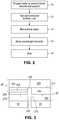
- FIG. 2illustrates a method of forming a wavelength-converted light emitting device according to embodiments of the invention.
- FIG. 3is a cross sectional view of a semiconductor structure attached to a support.
- FIG. 4is a plan view of a reconstituted wafer.
- FIG. 5is a cross sectional view of a wavelength-converted light emitting device according to embodiments of the invention.
- leakage of unconverted light from the sides of a chip-scale packaged light emitting deviceis prevented or reduced by forming a reflective material on the sides of the light emitting device.
- wavelength converting materialrather than a reflective material is formed on the sides of a chip-scale packaged light emitting device.
- FIG. 2illustrates a method of forming a wavelength-converted semiconductor light emitting device according to embodiments of the invention.
- the semiconductor light emitting devicesare III-nitride LEDs that emit blue or UV light
- semiconductor light emitting devices besides LEDssuch as laser diodes and semiconductor light emitting devices made from other materials systems such as other III-V materials, III-phosphide, III-arsenide, II-VI materials, ZnO, or Si-based materials may be used.
- FIG. 3is a cross sectional view of a portion of a wafer of semiconductor light emitting devices attached to a support.
- a semiconductor structure 20is first grown on a growth substrate (not shown in FIG. 3 ) as is known in the art.
- the growth substratemay be any suitable substrate such as, for example, sapphire, SiC, Si, GaN, or composite substrates.
- the semiconductor structure 20includes a light emitting or active region sandwiched between n- and p-type regions.
- An n-type regionmay be grown first and may include multiple layers of different compositions and dopant concentration including, for example, preparation layers such as buffer layers or nucleation layers, and/or layers designed to facilitate removal of the growth substrate, which may be n-type or not intentionally doped, and n- or even p-type device layers designed for particular optical, material, or electrical properties desirable for the light emitting region to efficiently emit light.
- a light emitting or active regionis grown over the n-type region. Examples of suitable light emitting regions include a single thick or thin light emitting layer, or a multiple quantum well light emitting region including multiple thin or thick light emitting layers separated by barrier layers.
- a p-type regionmay then be grown over the light emitting region.
- the p-type regionmay include multiple layers of different composition, thickness, and dopant concentration, including layers that are not intentionally doped, or n-type layers.
- the total thickness of all the semiconductor material in the deviceis less than 10 ⁇ m in some embodiments and less than 6 ⁇ m in some embodiments.
- a metal p-contactis formed on the p-type region. If a majority of light is directed out of the semiconductor structure through a surface opposite the p-contact, such as in a flip chip device, the p-contact may be reflective.
- a flip chip devicemay be formed by patterning the semiconductor structure by standard photolithographic operations and etching the semiconductor structure to remove a portion of the entire thickness of the p-type region and a portion of the entire thickness of the light emitting region, to form a mesa which reveals a surface of the n-type region on which a metal n-contact is formed.
- the mesa and p- and n-contactsmay be formed in any suitable manner.
- the semiconductor structure 20is etched down to an insulating layer, which may be an insulating semiconductor layer that is part of the semiconductor structure 20 , or the growth substrate.
- the p- and n-contactsmay be redistributed by a stack of insulating layers and metals as is known in the art to form at least two large electrical pads.
- One of the electrical padsis electrically connected to the p-type region of the semiconductor structure 20 and the other of the electrical pads is electrically connected to the n-type region of the semiconductor structure 20 .
- Electrical padsmay be any suitable conductive material including, for example, copper, gold, and alloys.
- the electrical padsare electrically isolated from each other by a gap which may be filled with an insulating material such as a dielectric, air, or other ambient gas.
- the p- and n-contacts, the metal/dielectric stack to redistribute the contacts, and the electrical padsare well known in the art and are illustrated in FIG. 3 as electrical connection structure 22 .
- the semiconductor structure 20is connected to a support 24 through electrical connection structure 22 .
- Support 24is a structure that mechanically supports semiconductor structure 20 and that is diced at the same time as semiconductor structure 20 , when the wafer of devices is divided into individual or groups of devices.
- Support 24is attached to semiconductor structure 20 on a wafer scale.
- support 24is a self-supporting structure suitable to attach the semiconductor light emitting device to a substrate such as a PC board.
- the surface of support 24 opposite semiconductor structure 20may be reflow-solderable. Any suitable support may be used.
- suitable supports 24include (1) an insulating or semi-insulating wafer with conductive vias for forming electrical connections to the electrical connection structure 22 , such as a silicon wafer, which may be attached to the semiconductor structure by, for example, gold-gold interconnects, (2) thick metal bonding pads formed on electrical connection structure 22 , for example by plating, or (3) any other suitable mount.
- the individual semiconductor devices on the wafer illustrated in FIG. 3are tested to identify good devices, and optionally to identify characteristics of each device, such as the peak emission wavelength, brightness, etc.
- the wafer including the semiconductor structure 20 , electrical connection structure 22 , and support 24is then diced, to divide the wafer into individual devices or groups of devices.
- the growth substrateis removed from the semiconductor structure before dicing, as is known in the art.
- the growth substrateremains part of the final structure and is therefore diced at the same time as the semiconductor structure.
- the semiconductor structureis diced with the growth substrate still attached, then the growth substrate is later removed at a die-level rather than a wafer level.
- Dicingcan be performed by any suitable method such as scribe-and-break with a laser scribe or sawing and is well known in the art. Since the semiconductor structure 20 , connection structure 22 and support 24 are diced at the same time, support 24 is substantially the same width as the semiconductor structure 20 for each device or group of devices, as illustrated below in FIG. 5 . The device may have substantially vertical sidewalls, as illustrated in FIG. 5 .
- stage 14a reconstituted wafer of devices is formed.
- a reconstituted waferis illustrated in FIG. 4 .
- Individual devices or groups of devices 26 diced in stage 12are connected to a substrate 28 .
- Substrate 28can be any suitable structure that supports devices 26 , such as an inflexible structure such as a board or a flexible structure such as wafer handling tape, for example.
- only known good devicesbased on the test described above in reference to stage 12 , are connected to substrate 28 in the reconstituted wafer. Since device testing is done before wavelength converting material is applied in stage 16 and only good devices are used, no wavelength converting material is wasted on bad devices (i.e. nonfunctional or non-light-emitting devices), which may reduce cost.
- a suitable peak wavelength rangemay be as narrow as 5 nm in some embodiments.
- the wafer of devicesis attached to handling tape, diced while attached to the handling tape, then the reconstituted wafer is formed by stretching the handling tape to separate the devices after dicing.
- the spacing 30 between devices 26 on the reconstituted waferis at least as wide as required to cleave the wavelength converting material formed over the wafer, described below. In some embodiments, the spacing may be wide enough to create an overhang 38 (illustrated in FIG. 5 ) of wavelength converting material on the sides of the devices.
- the overhangmay be, for example, at least as thick as the wavelength converting material layer, or it may be wider or narrower.
- the dotted lines 32 on FIG. 4show where the wavelength converting material layer is cleaved to separate the devices on the reconstituted wafer, described below in stage 18 .
- the wavelength converting material layeris 50 ⁇ m thick.
- the spacing 30 between devices 26may be at least 100 ⁇ m, such that the overhang of wavelength converting material on the sides of each device 26 is at least 50 ⁇ m. In some embodiments, the devices are spaced such that no overhang 38 is created.
- the aspect ratio of the reconstituted waferis selected to match the shape of a pre-fabricated wavelength converting film.
- the wafer which is diced in stage 12is typically a round wafer.
- the reconstituted wafer formed in stage 14may be rectangular, sized to match a rectangular sheet of pre-fabricated wavelength-converting film.
- a wavelength-converting materialis applied over the devices 26 on the reconstituted wafer.
- the wavelength converting materialmay be formed such that all or only a portion of the light emitted by the light emitting device and incident on the wavelength converting material may be converted by the wavelength converting material. Unconverted light emitted by the light emitting device may be part of the final spectrum of light, though it need not be.
- Examples of common combinationsinclude a blue-emitting LED combined with a yellow-emitting wavelength converting material, a blue-emitting LED combined with green- and red-emitting wavelength converting materials, a UV-emitting LED combined with blue- and yellow-emitting wavelength converting material, and a UV-emitting LED combined with blue-, green-, and red-emitting wavelength converting materials.
- Wavelength converting materials emitting other colors of lightmay be added to tailor the spectrum of light emitted from the device.
- the wavelength converting materialmay be conventional phosphor particles, organic semiconductors, II-VI or III-V semiconductors, II-VI or III-V semiconductor quantum dots or nanocrystals, dyes, polymers, or materials such as GaN that luminesce.
- Phosphor particlesmay have an average diameter between 5 and 50 ⁇ m in some embodiments.
- Any suitable phosphormay be used, including but not limited to garnet-based phosphors such as Y 3 Al 5 O 12 :Ce (YAG), Lu 3 Al 5 O 12 :Ce (LuAG), Y 3 Al 5-x O 12 :Ce (YAlGaG), (Ba 1-x Sr x )SiO 3 :Eu (BOSE), and nitride-based phosphors such as (Ca,Sr)AlSiN 3 :Eu and (Ca,Sr,Ba) 2 Si 5 N 8 :Eu.
- garnet-based phosphorssuch as Y 3 Al 5 O 12 :Ce (YAG), Lu 3 Al 5 O 12 :Ce (LuAG), Y 3 Al 5-x O 12 :Ce (YAlGaG), (Ba 1-x Sr x )SiO 3 :Eu (BOSE
- the wavelength converting materialis formed to conformally coat devices 26 on the reconstituted wafer with a substantially uniform thickness.
- the thickness of the wavelength converting material over the top and sides of each device and between devicesmay vary less than 50% in some embodiments, less than 20% in some embodiments, and less than 10% in some embodiments.
- One example of a wavelength converting materialis a luminescent film, formed as follows: one or more conventional powder phosphors are mixed with a binder such as acrylic or silicone to achieve a target phosphor density.
- the phosphor/binder sheetis formed to have a target thickness, for example by spinning the mixture on a flat surface or molding the phosphor sheet.
- Phosphormay be mixed with a binder in liquid form which is then cured or dried to form a flexible luminescent film.
- the luminescent filmis pressed over the reconstituted wafer in stage 16 .
- wavelength converting materialis molded over devices 26 , for example by placing a mold over devices 26 , filling the mold with phosphor mixed with binder material, curing the binder material, then removing the mold.
- FIG. 5illustrates a single device after being separated from the reconstituted wafer in stage 18 .
- Wavelength converting material 34covers the top and sides of semiconductor structure 20 and support 24 to prevent leakage of unconverted light from the sides of semiconductor structure 20 .
- the width of optional overhang 38 on the sides of device 26depends on the spacing on the reconstituted wafer, as described above.
- the embodiments described abovemay have advantages over the method illustrated in FIG. 1 .
- Cleaving a wavelength converting material in stage 18 of FIG. 2(such as a 50 ⁇ m thick phosphor and silicone film for example) is easier than cleaving a semiconductor wafer, carrier wafer, and ceramic phosphor as described above in process 116 of FIG. 1 .
- only known good dieare covered with wavelength converting material. Ease of cleaving and using only known good devices may improve yield and reduce cost.
Landscapes
- Engineering & Computer Science (AREA)
- Manufacturing & Machinery (AREA)
- Computer Hardware Design (AREA)
- Microelectronics & Electronic Packaging (AREA)
- Power Engineering (AREA)
- Physics & Mathematics (AREA)
- Condensed Matter Physics & Semiconductors (AREA)
- General Physics & Mathematics (AREA)
- Led Device Packages (AREA)
- Led Devices (AREA)
Abstract
Description
Claims (16)
Priority Applications (1)
| Application Number | Priority Date | Filing Date | Title |
|---|---|---|---|
| US14/997,713US10868224B2 (en) | 2012-02-10 | 2016-01-18 | Wavelength converted light emitting device |
Applications Claiming Priority (4)
| Application Number | Priority Date | Filing Date | Title |
|---|---|---|---|
| US201261597358P | 2012-02-10 | 2012-02-10 | |
| PCT/IB2013/051009WO2013118072A2 (en) | 2012-02-10 | 2013-02-07 | Wavelength converted light emitting device |
| US201414375461A | 2014-07-30 | 2014-07-30 | |
| US14/997,713US10868224B2 (en) | 2012-02-10 | 2016-01-18 | Wavelength converted light emitting device |
Related Parent Applications (2)
| Application Number | Title | Priority Date | Filing Date |
|---|---|---|---|
| PCT/IB2013/051009DivisionWO2013118072A2 (en) | 2012-02-10 | 2013-02-07 | Wavelength converted light emitting device |
| US14/375,461DivisionUS9257617B2 (en) | 2012-02-10 | 2013-02-07 | Wavelength converted light emitting device |
Publications (2)
| Publication Number | Publication Date |
|---|---|
| US20160133803A1 US20160133803A1 (en) | 2016-05-12 |
| US10868224B2true US10868224B2 (en) | 2020-12-15 |
Family
ID=48048079
Family Applications (2)
| Application Number | Title | Priority Date | Filing Date |
|---|---|---|---|
| US14/375,461ActiveUS9257617B2 (en) | 2012-02-10 | 2013-02-07 | Wavelength converted light emitting device |
| US14/997,713Active2034-01-04US10868224B2 (en) | 2012-02-10 | 2016-01-18 | Wavelength converted light emitting device |
Family Applications Before (1)
| Application Number | Title | Priority Date | Filing Date |
|---|---|---|---|
| US14/375,461ActiveUS9257617B2 (en) | 2012-02-10 | 2013-02-07 | Wavelength converted light emitting device |
Country Status (3)
| Country | Link |
|---|---|
| US (2) | US9257617B2 (en) |
| TW (1) | TW201340416A (en) |
| WO (1) | WO2013118072A2 (en) |
Families Citing this family (13)
| Publication number | Priority date | Publication date | Assignee | Title |
|---|---|---|---|---|
| DE102013111503B4 (en)* | 2013-10-18 | 2021-08-05 | OSRAM Opto Semiconductors Gesellschaft mit beschränkter Haftung | Optoelectronic semiconductor chip, optoelectronic component and method for separating semiconductor chips |
| CN104716245A (en)* | 2013-12-13 | 2015-06-17 | 晶元光电股份有限公司 | Light emitting device and manufacturing method thereof |
| KR102299238B1 (en)* | 2014-01-08 | 2021-09-07 | 루미리즈 홀딩 비.브이. | Wavelength converted semiconductor light emitting device |
| JP6974324B2 (en) | 2015-12-29 | 2021-12-01 | ルミレッズ ホールディング ベーフェー | Flip chip LED with side reflector and phosphor |
| KR102700918B1 (en)* | 2015-12-29 | 2024-09-02 | 루미리즈 홀딩 비.브이. | Flip chip LED with side reflectors and phosphors |
| US10222681B2 (en) | 2016-11-07 | 2019-03-05 | Limileds LLC | Segmented light or optical power emitting device with fully converting wavelength converting material and methods of operation |
| JP2018152463A (en)* | 2017-03-13 | 2018-09-27 | スタンレー電気株式会社 | Semiconductor light-emitting device |
| KR102475924B1 (en)* | 2017-08-31 | 2022-12-08 | 쑤저우 레킨 세미컨덕터 컴퍼니 리미티드 | Semiconductor device and head lamp including the same |
| US11355548B2 (en)* | 2017-12-20 | 2022-06-07 | Lumileds Llc | Monolithic segmented LED array architecture |
| US10490428B2 (en) | 2017-12-22 | 2019-11-26 | Lumidleds LLC | Method and system for dual stretching of wafers for isolated segmented chip scale packages |
| EP4016594A1 (en)* | 2020-12-15 | 2022-06-22 | Micledi Microdisplays BV | Method and system to produce dies for a wafer reconstitution |
| EP4250357A1 (en) | 2022-03-24 | 2023-09-27 | Micledi Microdisplays BV | A polychrome wafer structure, a polychrome display device, and a method for production |
| US20240413131A1 (en) | 2022-03-24 | 2024-12-12 | Micledi Microdisplays Bv | A polychrome wafer structure, a polychrome display device, and a method for production |
Citations (49)
| Publication number | Priority date | Publication date | Assignee | Title |
|---|---|---|---|---|
| US5770867A (en) | 1995-02-14 | 1998-06-23 | Sharp Kabushiki Kaisha | Photocoupler device with light-transmissive resin including fillers and a producing process thereof |
| US20050130390A1 (en)* | 2003-12-11 | 2005-06-16 | Peter Andrews | Semiconductor substrate assemblies and methods for preparing and dicing the same |
| EP1643566A1 (en) | 2003-06-13 | 2006-04-05 | Rohm Co., Ltd. | Process for producing light-emitting diode element emitting white light |
| US20060226758A1 (en) | 2005-04-08 | 2006-10-12 | Nichia Corporation | Light emitting device with silicone resin layer formed by screen printing |
| US20070045653A1 (en) | 2002-09-27 | 2007-03-01 | Krames Michael R | Selective filtering of wavelength-converted semiconductor light emitting devices |
| US20070085105A1 (en) | 2005-10-18 | 2007-04-19 | Goldeneye, Inc. | Light emitting diode and side emitting lens |
| US20070096131A1 (en)* | 2005-10-28 | 2007-05-03 | Lumileds Lighting U.S. Llc | Laminating encapsulant film containing phosphor over LEDS |
| US7276736B2 (en) | 1996-09-20 | 2007-10-02 | Osram Gmbh | Wavelength-converting casting composition and white light-emitting semiconductor component |
| US20080076316A1 (en)* | 2004-09-23 | 2008-03-27 | Cree, Inc. | Methods of manufacturing semiconductor light emitting devices including patternable films comprising transparent silicone and phosphor |
| US20080121911A1 (en)* | 2006-11-28 | 2008-05-29 | Cree, Inc. | Optical preforms for solid state light emitting dice, and methods and systems for fabricating and assembling same |
| US20080179611A1 (en)* | 2007-01-22 | 2008-07-31 | Cree, Inc. | Wafer level phosphor coating method and devices fabricated utilizing method |
| US20080290351A1 (en) | 2007-05-24 | 2008-11-27 | Shuichi Ajiki | Semiconductor light emitting apparatus |
| US20090057690A1 (en)* | 2007-01-22 | 2009-03-05 | Cree, Inc. | Wafer level phosphor coating technique for warm light emitting diodes |
| US7521862B2 (en) | 2006-11-20 | 2009-04-21 | Philips Lumileds Lighting Co., Llc | Light emitting device including luminescent ceramic and light-scattering material |
| US20090173960A1 (en) | 2004-06-09 | 2009-07-09 | Koninklijke Philips Electronics N.V. | Semiconductor light emitting device with pre-fabricated wavelength converting element |
| US20090179207A1 (en)* | 2008-01-11 | 2009-07-16 | Cree, Inc. | Flip-chip phosphor coating method and devices fabricated utilizing method |
| DE102008010512A1 (en) | 2008-02-22 | 2009-08-27 | Osram Opto Semiconductors Gmbh | Optoelectronic component, particularly light emitting diode or photodiode, has semiconductor chip with chip lower side, and two electrical bondings with contact lower sides |
| US7601550B2 (en) | 2000-03-03 | 2009-10-13 | Osram Gmbh | Methods for producing a light emitting semiconductor body with a luminescence converter element |
| US20090261358A1 (en)* | 2008-03-31 | 2009-10-22 | Cree, Inc. | Emission tuning methods and devices fabricated utilizing methods |
| US7692259B2 (en) | 2005-09-07 | 2010-04-06 | Toyoda Gosei Co., Ltd. | Solid-state element device |
| US20100140633A1 (en)* | 2009-02-19 | 2010-06-10 | David Todd Emerson | Methods for Combining Light Emitting Devices in a Package and Packages Including Combined Light Emitting Devices |
| US20100155750A1 (en)* | 2008-12-23 | 2010-06-24 | Cree, Inc. | Color correction for wafer level white LEDs |
| US20100190280A1 (en)* | 2009-01-27 | 2010-07-29 | Citizen Electronics Co., Ltd. | Manufacturing method of light-emitting diode |
| US20100279437A1 (en) | 2009-05-01 | 2010-11-04 | Koninklijke Philips Electronics N.V. | Controlling edge emission in package-free led die |
| US20100308354A1 (en)* | 2009-06-09 | 2010-12-09 | Koninklijke Philips Electronics N.V. | Led with remote phosphor layer and reflective submount |
| US20110175117A1 (en) | 2008-09-25 | 2011-07-21 | Koninklijke Philips Electronics N.V. | Coated light emitting device and method for coating thereof |
| US20110198780A1 (en)* | 2010-02-16 | 2011-08-18 | Koninklijke Philips Electronics N.V. | Light emitting device with molded wavelength converting layer |
| US8017246B2 (en) | 2007-11-08 | 2011-09-13 | Philips Lumileds Lighting Company, Llc | Silicone resin for protecting a light transmitting surface of an optoelectronic device |
| US8030672B2 (en) | 2008-02-27 | 2011-10-04 | Stanley Electric Co., Ltd. | Semiconductor light emitting device including a plurality of semiconductor light emitting elements and a wavelength conversion layer having different thickness portions |
| EP2393131A1 (en) | 2010-06-03 | 2011-12-07 | Kabushiki Kaisha Toshiba | Semiconductor light emitting device and method for manufacturing same |
| US20110300644A1 (en)* | 2010-06-07 | 2011-12-08 | Kabushiki Kaisha Toshiba | Method for manufacturing semiconductor light emitting device |
| JP2011253882A (en) | 2010-06-01 | 2011-12-15 | Toshiba Corp | Light-emitting device and method of manufacturing the same |
| US8207552B2 (en) | 2002-06-26 | 2012-06-26 | Lg Electronics Inc. | Thin film light emitting diode |
| US20120193670A1 (en) | 2011-01-31 | 2012-08-02 | Seoul Semiconductor Co., Ltd. | Light emitting device having wavelength converting layer and method of fabricating the same |
| US20130139868A1 (en) | 2011-12-06 | 2013-06-06 | Nitto Denko Corporation | Wavelength conversion material as encapsulate for solar module systems to enhance solar harvesting efficiency |
| US8541798B2 (en) | 2006-09-27 | 2013-09-24 | Kabushiki Kaisha Toshiba | Semiconductor light emitting device, and backlight and display device comprising the semiconductor light emitting device |
| US20130264600A1 (en) | 2010-12-10 | 2013-10-10 | Chung Hoon Lee | Method of fabricating semiconductor device using gang bonding and semiconductor device fabricated by the same |
| US8569083B2 (en) | 2008-07-16 | 2013-10-29 | Epistar Corporation | Light-emitting device with narrow dominant wavelength distribution and method of making the same |
| US20130320382A1 (en) | 2011-05-17 | 2013-12-05 | Kabushiki Kaisha Toshiba | Semiconductor light emitting device |
| US8664635B2 (en) | 2010-05-18 | 2014-03-04 | Seoul Semiconductor Co., Ltd. | Light emitting diode chip having wavelength converting layer and method of fabricating the same, and package having the light emitting diode chip and method of fabricating the same |
| US8704254B2 (en) | 2006-12-22 | 2014-04-22 | Philips Lumileds Lighting Company, Llc | Light emitting device including a filter |
| US8704262B2 (en) | 2011-08-11 | 2014-04-22 | Goldeneye, Inc. | Solid state light sources with common luminescent and heat dissipating surfaces |
| US8759125B2 (en) | 2012-01-24 | 2014-06-24 | Cooledge Lighting Inc. | Light-emitting dies incorporating wavelength-conversion materials and related methods |
| US20140179029A1 (en) | 2011-08-26 | 2014-06-26 | Koninklijke Philips Electronics N.V. | Method of processing a semiconductor structure |
| US20140198528A1 (en) | 2011-08-17 | 2014-07-17 | Samsung Electronics Co., Ltd. | Wavelength conversion chip for a light emitting diode, and method for manufacturing same |
| US8957429B2 (en) | 2012-02-07 | 2015-02-17 | Epistar Corporation | Light emitting diode with wavelength conversion layer |
| US20150084537A1 (en) | 2008-11-14 | 2015-03-26 | Samsung Electronics Co., Ltd. | Semiconductor light emitting device |
| US9046634B2 (en) | 2007-06-14 | 2015-06-02 | Philips Lumileds Lighting Company, Llc | Thin flash or video recording light using low profile side emitting LED |
| US9087974B2 (en) | 2012-03-23 | 2015-07-21 | Kabushiki Kaisha Toshiba | Semiconductor light emitting device and method for manufacturing the same |
- 2013
- 2013-02-07WOPCT/IB2013/051009patent/WO2013118072A2/enactiveApplication Filing
- 2013-02-07USUS14/375,461patent/US9257617B2/enactiveActive
- 2013-02-08TWTW102105228Apatent/TW201340416A/enunknown
- 2016
- 2016-01-18USUS14/997,713patent/US10868224B2/enactiveActive
Patent Citations (54)
| Publication number | Priority date | Publication date | Assignee | Title |
|---|---|---|---|---|
| US5770867A (en) | 1995-02-14 | 1998-06-23 | Sharp Kabushiki Kaisha | Photocoupler device with light-transmissive resin including fillers and a producing process thereof |
| US7276736B2 (en) | 1996-09-20 | 2007-10-02 | Osram Gmbh | Wavelength-converting casting composition and white light-emitting semiconductor component |
| US7601550B2 (en) | 2000-03-03 | 2009-10-13 | Osram Gmbh | Methods for producing a light emitting semiconductor body with a luminescence converter element |
| US8207552B2 (en) | 2002-06-26 | 2012-06-26 | Lg Electronics Inc. | Thin film light emitting diode |
| US20070045653A1 (en) | 2002-09-27 | 2007-03-01 | Krames Michael R | Selective filtering of wavelength-converted semiconductor light emitting devices |
| EP1643566A1 (en) | 2003-06-13 | 2006-04-05 | Rohm Co., Ltd. | Process for producing light-emitting diode element emitting white light |
| US20060118510A1 (en)* | 2003-06-13 | 2006-06-08 | Takehiro Fujii | Process for producing light-emitting diode element emitting white light |
| US20050130390A1 (en)* | 2003-12-11 | 2005-06-16 | Peter Andrews | Semiconductor substrate assemblies and methods for preparing and dicing the same |
| US20090173960A1 (en) | 2004-06-09 | 2009-07-09 | Koninklijke Philips Electronics N.V. | Semiconductor light emitting device with pre-fabricated wavelength converting element |
| US20080076316A1 (en)* | 2004-09-23 | 2008-03-27 | Cree, Inc. | Methods of manufacturing semiconductor light emitting devices including patternable films comprising transparent silicone and phosphor |
| US20060226758A1 (en) | 2005-04-08 | 2006-10-12 | Nichia Corporation | Light emitting device with silicone resin layer formed by screen printing |
| US7692259B2 (en) | 2005-09-07 | 2010-04-06 | Toyoda Gosei Co., Ltd. | Solid-state element device |
| US20070085105A1 (en) | 2005-10-18 | 2007-04-19 | Goldeneye, Inc. | Light emitting diode and side emitting lens |
| US20070096131A1 (en)* | 2005-10-28 | 2007-05-03 | Lumileds Lighting U.S. Llc | Laminating encapsulant film containing phosphor over LEDS |
| US7344952B2 (en)* | 2005-10-28 | 2008-03-18 | Philips Lumileds Lighting Company, Llc | Laminating encapsulant film containing phosphor over LEDs |
| US8541798B2 (en) | 2006-09-27 | 2013-09-24 | Kabushiki Kaisha Toshiba | Semiconductor light emitting device, and backlight and display device comprising the semiconductor light emitting device |
| US7521862B2 (en) | 2006-11-20 | 2009-04-21 | Philips Lumileds Lighting Co., Llc | Light emitting device including luminescent ceramic and light-scattering material |
| US20080121911A1 (en)* | 2006-11-28 | 2008-05-29 | Cree, Inc. | Optical preforms for solid state light emitting dice, and methods and systems for fabricating and assembling same |
| US8704254B2 (en) | 2006-12-22 | 2014-04-22 | Philips Lumileds Lighting Company, Llc | Light emitting device including a filter |
| US20080179611A1 (en)* | 2007-01-22 | 2008-07-31 | Cree, Inc. | Wafer level phosphor coating method and devices fabricated utilizing method |
| US20090057690A1 (en)* | 2007-01-22 | 2009-03-05 | Cree, Inc. | Wafer level phosphor coating technique for warm light emitting diodes |
| US20080290351A1 (en) | 2007-05-24 | 2008-11-27 | Shuichi Ajiki | Semiconductor light emitting apparatus |
| US9046634B2 (en) | 2007-06-14 | 2015-06-02 | Philips Lumileds Lighting Company, Llc | Thin flash or video recording light using low profile side emitting LED |
| US8017246B2 (en) | 2007-11-08 | 2011-09-13 | Philips Lumileds Lighting Company, Llc | Silicone resin for protecting a light transmitting surface of an optoelectronic device |
| US20090179207A1 (en)* | 2008-01-11 | 2009-07-16 | Cree, Inc. | Flip-chip phosphor coating method and devices fabricated utilizing method |
| DE102008010512A1 (en) | 2008-02-22 | 2009-08-27 | Osram Opto Semiconductors Gmbh | Optoelectronic component, particularly light emitting diode or photodiode, has semiconductor chip with chip lower side, and two electrical bondings with contact lower sides |
| US8030672B2 (en) | 2008-02-27 | 2011-10-04 | Stanley Electric Co., Ltd. | Semiconductor light emitting device including a plurality of semiconductor light emitting elements and a wavelength conversion layer having different thickness portions |
| US20090261358A1 (en)* | 2008-03-31 | 2009-10-22 | Cree, Inc. | Emission tuning methods and devices fabricated utilizing methods |
| US8569083B2 (en) | 2008-07-16 | 2013-10-29 | Epistar Corporation | Light-emitting device with narrow dominant wavelength distribution and method of making the same |
| US20110175117A1 (en) | 2008-09-25 | 2011-07-21 | Koninklijke Philips Electronics N.V. | Coated light emitting device and method for coating thereof |
| US20150084537A1 (en) | 2008-11-14 | 2015-03-26 | Samsung Electronics Co., Ltd. | Semiconductor light emitting device |
| US20100155750A1 (en)* | 2008-12-23 | 2010-06-24 | Cree, Inc. | Color correction for wafer level white LEDs |
| US20100190280A1 (en)* | 2009-01-27 | 2010-07-29 | Citizen Electronics Co., Ltd. | Manufacturing method of light-emitting diode |
| US20100140633A1 (en)* | 2009-02-19 | 2010-06-10 | David Todd Emerson | Methods for Combining Light Emitting Devices in a Package and Packages Including Combined Light Emitting Devices |
| US20100279437A1 (en) | 2009-05-01 | 2010-11-04 | Koninklijke Philips Electronics N.V. | Controlling edge emission in package-free led die |
| US20100308354A1 (en)* | 2009-06-09 | 2010-12-09 | Koninklijke Philips Electronics N.V. | Led with remote phosphor layer and reflective submount |
| US20110198780A1 (en)* | 2010-02-16 | 2011-08-18 | Koninklijke Philips Electronics N.V. | Light emitting device with molded wavelength converting layer |
| US8664635B2 (en) | 2010-05-18 | 2014-03-04 | Seoul Semiconductor Co., Ltd. | Light emitting diode chip having wavelength converting layer and method of fabricating the same, and package having the light emitting diode chip and method of fabricating the same |
| JP2011253882A (en) | 2010-06-01 | 2011-12-15 | Toshiba Corp | Light-emitting device and method of manufacturing the same |
| US20120061703A1 (en) | 2010-06-01 | 2012-03-15 | Kabushiki Kaisha Toshiba | Light emitting device and manufacturing method of light emitting device |
| US20110297980A1 (en)* | 2010-06-03 | 2011-12-08 | Kabushiki Kaisha Toshiba | Semiconductor light emitting device and method for manufacturing same |
| EP2393131A1 (en) | 2010-06-03 | 2011-12-07 | Kabushiki Kaisha Toshiba | Semiconductor light emitting device and method for manufacturing same |
| US8399275B2 (en) | 2010-06-07 | 2013-03-19 | Kabushiki Kaisha Toshiba | Method for manufacturing semiconductor light emitting device |
| US20110300644A1 (en)* | 2010-06-07 | 2011-12-08 | Kabushiki Kaisha Toshiba | Method for manufacturing semiconductor light emitting device |
| US20130264600A1 (en) | 2010-12-10 | 2013-10-10 | Chung Hoon Lee | Method of fabricating semiconductor device using gang bonding and semiconductor device fabricated by the same |
| US20120193670A1 (en) | 2011-01-31 | 2012-08-02 | Seoul Semiconductor Co., Ltd. | Light emitting device having wavelength converting layer and method of fabricating the same |
| US20130320382A1 (en) | 2011-05-17 | 2013-12-05 | Kabushiki Kaisha Toshiba | Semiconductor light emitting device |
| US8704262B2 (en) | 2011-08-11 | 2014-04-22 | Goldeneye, Inc. | Solid state light sources with common luminescent and heat dissipating surfaces |
| US20140198528A1 (en) | 2011-08-17 | 2014-07-17 | Samsung Electronics Co., Ltd. | Wavelength conversion chip for a light emitting diode, and method for manufacturing same |
| US20140179029A1 (en) | 2011-08-26 | 2014-06-26 | Koninklijke Philips Electronics N.V. | Method of processing a semiconductor structure |
| US20130139868A1 (en) | 2011-12-06 | 2013-06-06 | Nitto Denko Corporation | Wavelength conversion material as encapsulate for solar module systems to enhance solar harvesting efficiency |
| US8759125B2 (en) | 2012-01-24 | 2014-06-24 | Cooledge Lighting Inc. | Light-emitting dies incorporating wavelength-conversion materials and related methods |
| US8957429B2 (en) | 2012-02-07 | 2015-02-17 | Epistar Corporation | Light emitting diode with wavelength conversion layer |
| US9087974B2 (en) | 2012-03-23 | 2015-07-21 | Kabushiki Kaisha Toshiba | Semiconductor light emitting device and method for manufacturing the same |
Non-Patent Citations (1)
| Title |
|---|
| International Search Report and Written Opinion from International Application No. PCT/IB2013/051009 dated Aug. 3, 2013. |
Also Published As
| Publication number | Publication date |
|---|---|
| US9257617B2 (en) | 2016-02-09 |
| WO2013118072A2 (en) | 2013-08-15 |
| TW201340416A (en) | 2013-10-01 |
| US20150008466A1 (en) | 2015-01-08 |
| WO2013118072A3 (en) | 2013-11-07 |
| US20160133803A1 (en) | 2016-05-12 |
Similar Documents
| Publication | Publication Date | Title |
|---|---|---|
| US10868224B2 (en) | Wavelength converted light emitting device | |
| US10957821B2 (en) | Wavelength converted semiconductor light emitting device | |
| US9871167B2 (en) | Top emitting semiconductor light emitting device | |
| JP5918221B2 (en) | LED chip manufacturing method | |
| US20200295241A1 (en) | Wavelength converted light emitting device with small source size | |
| US9324926B2 (en) | Wavelength converted light emitting device | |
| US10199549B2 (en) | Light emitting device with an optical element and a reflector | |
| US10998473B2 (en) | Packaged wavelength converted light emitting device | |
| US20200295235A1 (en) | Wavelength converted semiconductor light emitting device | |
| US20170352788A1 (en) | Light emitting device with wavelength converting side coat | |
| US9935244B2 (en) | Light emitting device including a filter and a protective layer | |
| US20180068988A1 (en) | Device with multiple, stacked light emitting devices |
Legal Events
| Date | Code | Title | Description |
|---|---|---|---|
| AS | Assignment | Owner name:DEUTSCHE BANK AG NEW YORK BRANCH, AS COLLATERAL AGENT, NEW YORK Free format text:SECURITY INTEREST;ASSIGNOR:LUMILEDS LLC;REEL/FRAME:043108/0001 Effective date:20170630 Owner name:DEUTSCHE BANK AG NEW YORK BRANCH, AS COLLATERAL AG Free format text:SECURITY INTEREST;ASSIGNOR:LUMILEDS LLC;REEL/FRAME:043108/0001 Effective date:20170630 | |
| AS | Assignment | Owner name:KONINKLIJKE PHILIPS ELECTRONICS N.V., NETHERLANDS Free format text:ASSIGNMENT OF ASSIGNORS INTEREST;ASSIGNOR:BIERHUIZEN, SERGE JOEL ARMAND;REEL/FRAME:044218/0806 Effective date:20130208 | |
| AS | Assignment | Owner name:KONINKLIJKE PHILIPS N.V., NETHERLANDS Free format text:CHANGE OF NAME;ASSIGNOR:KONINKLIJKE PHILIPS ELECTRONICS N.V.;REEL/FRAME:044723/0025 Effective date:20130515 | |
| AS | Assignment | Owner name:LUMILEDS LLC, CALIFORNIA Free format text:ASSIGNMENT OF ASSIGNORS INTEREST;ASSIGNOR:KONINKLIJKE PHILIPS N.V.;REEL/FRAME:044792/0018 Effective date:20170630 | |
| STPP | Information on status: patent application and granting procedure in general | Free format text:FINAL REJECTION MAILED | |
| STPP | Information on status: patent application and granting procedure in general | Free format text:ADVISORY ACTION MAILED | |
| STPP | Information on status: patent application and granting procedure in general | Free format text:DOCKETED NEW CASE - READY FOR EXAMINATION | |
| STPP | Information on status: patent application and granting procedure in general | Free format text:RESPONSE TO NON-FINAL OFFICE ACTION ENTERED AND FORWARDED TO EXAMINER | |
| STPP | Information on status: patent application and granting procedure in general | Free format text:PUBLICATIONS -- ISSUE FEE PAYMENT VERIFIED | |
| STCF | Information on status: patent grant | Free format text:PATENTED CASE | |
| AS | Assignment | Owner name:SOUND POINT AGENCY LLC, NEW YORK Free format text:SECURITY INTEREST;ASSIGNORS:LUMILEDS LLC;LUMILEDS HOLDING B.V.;REEL/FRAME:062299/0338 Effective date:20221230 | |
| MAFP | Maintenance fee payment | Free format text:PAYMENT OF MAINTENANCE FEE, 4TH YEAR, LARGE ENTITY (ORIGINAL EVENT CODE: M1551); ENTITY STATUS OF PATENT OWNER: LARGE ENTITY Year of fee payment:4 | |
| AS | Assignment | Owner name:LUMILEDS HOLDING B.V., NETHERLANDS Free format text:RELEASE BY SECURED PARTY;ASSIGNOR:SOUND POINT AGENCY LLC;REEL/FRAME:070046/0001 Effective date:20240731 Owner name:LUMILEDS LLC, CALIFORNIA Free format text:RELEASE BY SECURED PARTY;ASSIGNOR:SOUND POINT AGENCY LLC;REEL/FRAME:070046/0001 Effective date:20240731 | |
| AS | Assignment | Owner name:LUMILEDS SINGAPORE PTE. LTD., SINGAPORE Free format text:ASSIGNMENT OF ASSIGNORS INTEREST;ASSIGNOR:LUMILEDS LLC;REEL/FRAME:071888/0086 Effective date:20250708 |