US10859872B2 - Method to utilize force sensors to adjust the LCD pattern or brightness on a display - Google Patents
Method to utilize force sensors to adjust the LCD pattern or brightness on a displayDownload PDFInfo
- Publication number
- US10859872B2 US10859872B2US16/103,227US201816103227AUS10859872B2US 10859872 B2US10859872 B2US 10859872B2US 201816103227 AUS201816103227 AUS 201816103227AUS 10859872 B2US10859872 B2US 10859872B2
- Authority
- US
- United States
- Prior art keywords
- display
- stress
- stress sensors
- force
- control system
- Prior art date
- Legal status (The legal status is an assumption and is not a legal conclusion. Google has not performed a legal analysis and makes no representation as to the accuracy of the status listed.)
- Active
Links
Images


Classifications
- G—PHYSICS
- G02—OPTICS
- G02F—OPTICAL DEVICES OR ARRANGEMENTS FOR THE CONTROL OF LIGHT BY MODIFICATION OF THE OPTICAL PROPERTIES OF THE MEDIA OF THE ELEMENTS INVOLVED THEREIN; NON-LINEAR OPTICS; FREQUENCY-CHANGING OF LIGHT; OPTICAL LOGIC ELEMENTS; OPTICAL ANALOGUE/DIGITAL CONVERTERS
- G02F1/00—Devices or arrangements for the control of the intensity, colour, phase, polarisation or direction of light arriving from an independent light source, e.g. switching, gating or modulating; Non-linear optics
- G02F1/01—Devices or arrangements for the control of the intensity, colour, phase, polarisation or direction of light arriving from an independent light source, e.g. switching, gating or modulating; Non-linear optics for the control of the intensity, phase, polarisation or colour
- G02F1/13—Devices or arrangements for the control of the intensity, colour, phase, polarisation or direction of light arriving from an independent light source, e.g. switching, gating or modulating; Non-linear optics for the control of the intensity, phase, polarisation or colour based on liquid crystals, e.g. single liquid crystal display cells
- G02F1/133—Constructional arrangements; Operation of liquid crystal cells; Circuit arrangements
- G02F1/1333—Constructional arrangements; Manufacturing methods
- G02F1/1335—Structural association of cells with optical devices, e.g. polarisers or reflectors
- G02F1/1336—Illuminating devices
- G02F1/133602—Direct backlight
- G02F1/133611—Direct backlight including means for improving the brightness uniformity
- G—PHYSICS
- G09—EDUCATION; CRYPTOGRAPHY; DISPLAY; ADVERTISING; SEALS
- G09G—ARRANGEMENTS OR CIRCUITS FOR CONTROL OF INDICATING DEVICES USING STATIC MEANS TO PRESENT VARIABLE INFORMATION
- G09G3/00—Control arrangements or circuits, of interest only in connection with visual indicators other than cathode-ray tubes
- G09G3/20—Control arrangements or circuits, of interest only in connection with visual indicators other than cathode-ray tubes for presentation of an assembly of a number of characters, e.g. a page, by composing the assembly by combination of individual elements arranged in a matrix no fixed position being assigned to or needed to be assigned to the individual characters or partial characters
- G09G3/34—Control arrangements or circuits, of interest only in connection with visual indicators other than cathode-ray tubes for presentation of an assembly of a number of characters, e.g. a page, by composing the assembly by combination of individual elements arranged in a matrix no fixed position being assigned to or needed to be assigned to the individual characters or partial characters by control of light from an independent source
- G09G3/3406—Control of illumination source
- G09G3/342—Control of illumination source using several illumination sources separately controlled corresponding to different display panel areas, e.g. along one dimension such as lines
- G—PHYSICS
- G02—OPTICS
- G02F—OPTICAL DEVICES OR ARRANGEMENTS FOR THE CONTROL OF LIGHT BY MODIFICATION OF THE OPTICAL PROPERTIES OF THE MEDIA OF THE ELEMENTS INVOLVED THEREIN; NON-LINEAR OPTICS; FREQUENCY-CHANGING OF LIGHT; OPTICAL LOGIC ELEMENTS; OPTICAL ANALOGUE/DIGITAL CONVERTERS
- G02F1/00—Devices or arrangements for the control of the intensity, colour, phase, polarisation or direction of light arriving from an independent light source, e.g. switching, gating or modulating; Non-linear optics
- G02F1/01—Devices or arrangements for the control of the intensity, colour, phase, polarisation or direction of light arriving from an independent light source, e.g. switching, gating or modulating; Non-linear optics for the control of the intensity, phase, polarisation or colour
- G02F1/13—Devices or arrangements for the control of the intensity, colour, phase, polarisation or direction of light arriving from an independent light source, e.g. switching, gating or modulating; Non-linear optics for the control of the intensity, phase, polarisation or colour based on liquid crystals, e.g. single liquid crystal display cells
- G02F1/133—Constructional arrangements; Operation of liquid crystal cells; Circuit arrangements
- G02F1/1333—Constructional arrangements; Manufacturing methods
- G02F1/1335—Structural association of cells with optical devices, e.g. polarisers or reflectors
- G02F1/1336—Illuminating devices
- G02F1/133602—Direct backlight
- G02F1/133606—Direct backlight including a specially adapted diffusing, scattering or light controlling members
- G—PHYSICS
- G02—OPTICS
- G02F—OPTICAL DEVICES OR ARRANGEMENTS FOR THE CONTROL OF LIGHT BY MODIFICATION OF THE OPTICAL PROPERTIES OF THE MEDIA OF THE ELEMENTS INVOLVED THEREIN; NON-LINEAR OPTICS; FREQUENCY-CHANGING OF LIGHT; OPTICAL LOGIC ELEMENTS; OPTICAL ANALOGUE/DIGITAL CONVERTERS
- G02F1/00—Devices or arrangements for the control of the intensity, colour, phase, polarisation or direction of light arriving from an independent light source, e.g. switching, gating or modulating; Non-linear optics
- G02F1/01—Devices or arrangements for the control of the intensity, colour, phase, polarisation or direction of light arriving from an independent light source, e.g. switching, gating or modulating; Non-linear optics for the control of the intensity, phase, polarisation or colour
- G02F1/13—Devices or arrangements for the control of the intensity, colour, phase, polarisation or direction of light arriving from an independent light source, e.g. switching, gating or modulating; Non-linear optics for the control of the intensity, phase, polarisation or colour based on liquid crystals, e.g. single liquid crystal display cells
- G02F1/133—Constructional arrangements; Operation of liquid crystal cells; Circuit arrangements
- G02F1/1333—Constructional arrangements; Manufacturing methods
- G02F1/1335—Structural association of cells with optical devices, e.g. polarisers or reflectors
- G02F1/1336—Illuminating devices
- G02F1/133602—Direct backlight
- G02F1/133608—Direct backlight including particular frames or supporting means
- G—PHYSICS
- G09—EDUCATION; CRYPTOGRAPHY; DISPLAY; ADVERTISING; SEALS
- G09G—ARRANGEMENTS OR CIRCUITS FOR CONTROL OF INDICATING DEVICES USING STATIC MEANS TO PRESENT VARIABLE INFORMATION
- G09G3/00—Control arrangements or circuits, of interest only in connection with visual indicators other than cathode-ray tubes
- G09G3/20—Control arrangements or circuits, of interest only in connection with visual indicators other than cathode-ray tubes for presentation of an assembly of a number of characters, e.g. a page, by composing the assembly by combination of individual elements arranged in a matrix no fixed position being assigned to or needed to be assigned to the individual characters or partial characters
- G09G3/34—Control arrangements or circuits, of interest only in connection with visual indicators other than cathode-ray tubes for presentation of an assembly of a number of characters, e.g. a page, by composing the assembly by combination of individual elements arranged in a matrix no fixed position being assigned to or needed to be assigned to the individual characters or partial characters by control of light from an independent source
- G09G3/36—Control arrangements or circuits, of interest only in connection with visual indicators other than cathode-ray tubes for presentation of an assembly of a number of characters, e.g. a page, by composing the assembly by combination of individual elements arranged in a matrix no fixed position being assigned to or needed to be assigned to the individual characters or partial characters by control of light from an independent source using liquid crystals
- G—PHYSICS
- G02—OPTICS
- G02F—OPTICAL DEVICES OR ARRANGEMENTS FOR THE CONTROL OF LIGHT BY MODIFICATION OF THE OPTICAL PROPERTIES OF THE MEDIA OF THE ELEMENTS INVOLVED THEREIN; NON-LINEAR OPTICS; FREQUENCY-CHANGING OF LIGHT; OPTICAL LOGIC ELEMENTS; OPTICAL ANALOGUE/DIGITAL CONVERTERS
- G02F1/00—Devices or arrangements for the control of the intensity, colour, phase, polarisation or direction of light arriving from an independent light source, e.g. switching, gating or modulating; Non-linear optics
- G02F1/01—Devices or arrangements for the control of the intensity, colour, phase, polarisation or direction of light arriving from an independent light source, e.g. switching, gating or modulating; Non-linear optics for the control of the intensity, phase, polarisation or colour
- G02F1/13—Devices or arrangements for the control of the intensity, colour, phase, polarisation or direction of light arriving from an independent light source, e.g. switching, gating or modulating; Non-linear optics for the control of the intensity, phase, polarisation or colour based on liquid crystals, e.g. single liquid crystal display cells
- G02F1/133—Constructional arrangements; Operation of liquid crystal cells; Circuit arrangements
- G02F1/1333—Constructional arrangements; Manufacturing methods
- G02F1/13338—Input devices, e.g. touch panels
- G—PHYSICS
- G09—EDUCATION; CRYPTOGRAPHY; DISPLAY; ADVERTISING; SEALS
- G09G—ARRANGEMENTS OR CIRCUITS FOR CONTROL OF INDICATING DEVICES USING STATIC MEANS TO PRESENT VARIABLE INFORMATION
- G09G2320/00—Control of display operating conditions
- G09G2320/06—Adjustment of display parameters
- G09G2320/0626—Adjustment of display parameters for control of overall brightness
- G—PHYSICS
- G09—EDUCATION; CRYPTOGRAPHY; DISPLAY; ADVERTISING; SEALS
- G09G—ARRANGEMENTS OR CIRCUITS FOR CONTROL OF INDICATING DEVICES USING STATIC MEANS TO PRESENT VARIABLE INFORMATION
- G09G2320/00—Control of display operating conditions
- G09G2320/06—Adjustment of display parameters
- G09G2320/0686—Adjustment of display parameters with two or more screen areas displaying information with different brightness or colours
Definitions
- the present disclosurerelates generally to display devices, and more specifically to a method to utilize force sensors to adjust the LCD pattern or brightness on a display.
- Display deviceshave to operate in conjunction with mechanical structures, but these mechanical structures can cause the display devices to function improperly.
- a systemcomprising a display, a display cover, a plurality of sensors disposed between the display and the display cover and a lighting control system coupled to the display and the plurality of sensors.
- the lighting control systemis configured to receive one or more signals from the plurality of sensors and to reduce a backlight level of a subgroup of lighting elements associated with the one or more sensors associated with the one or more signals, wherein the subgroup of lighting elements is one of a plurality of subgroups of lighting elements of the display.
- FIG. 1is a diagram of a display having force sensors, in accordance with an example embodiment of the present disclosure
- FIG. 2is a diagram of backlight control zones, in accordance with an example embodiment of the present disclosure.
- FIG. 3is a diagram of an algorithm for controlling backlight control zones, in accordance with an example embodiment of the present disclosure.
- a display devicesuch as a liquid crystal display (LCD) screen panel or other suitable display device, for a lap top computer or other suitable user devices can include a cover or other mechanical feature that is used to hold the LCD panel or other display device in the hinge-up position, to protect the LCD panel or other display device from getting damaged by external stress, to cover connectors or other electrical and mechanical parts inside the user device, and also for decorative or other non-functional purposes.
- LCDliquid crystal display
- cover or other mechanical featurethat is used to hold the LCD panel or other display device in the hinge-up position, to protect the LCD panel or other display device from getting damaged by external stress, to cover connectors or other electrical and mechanical parts inside the user device, and also for decorative or other non-functional purposes.
- cover or other mechanical featurethat is used to hold the LCD panel or other display device in the hinge-up position, to protect the LCD panel or other display device from getting damaged by external stress, to cover connectors or other electrical and mechanical parts inside the user device, and also for decorative or other non-functional purposes.
- the gap between the cover and the LCD panel or other display device on a laptop or other user devicecan experience forces due to the application of an identifier on the cover, which can cause the cover to transfer more stress onto the LCD panel or other display device from the user or other case components.
- the LCD panels and other display devicesare also getting thinner and more delicate, which can also cause the LCD panels or other display devices to cause light leakage or any undesired optical artifacts from the display device, such as when the cover conveys too much of such mechanical stresses onto the display device panel, which can happen for an in-plane switching panel in a dark-room environment or in other applications.
- the present disclosurereduces or eliminates these problems by adding one or more force or strain gauges between the cover and the LCD panel or other display device, to provide feedback to adjust the displayed pattern or brightness based upon the stress distribution of the cover.
- These force sensorssuch as force gauges or strain gauges, can be placed between the cover and the LCD panel or other display device, to obtain the stress distribution that the cover applies around edges of the LCD panel/display device.
- a control devicesuch as a controller board or other suitable component, receives and processes the signals from force sensors.
- the stress distribution datais output to a graphics controller that is configured to adjust a displayed pattern or brightness at any areas around edges of the LCD panel/display device where the cover applies stress.
- the present disclosureprovides a number of important technical features.
- One important technical featureis the prevention of customer complaints arising from light leakage on a laptop or other user device, such as for applications that are used under a low-light environment. These applications include computer gaming, displays on audiovisual display devices and other similar applications and devices.
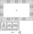
- FIG. 1is a diagram of a display 100 having force sensors, in accordance with an example embodiment of the present disclosure.
- Display 100includes LCD screen 102 , cover 104 , sensors 106 A through 106 J, stress-corrected backlight system 108 , stress sensor analysis system 110 , pixel mapping system 112 and backlight adjustment system 114 , each of which can be implemented in hardware or a suitable combination of hardware and software.
- LCD screen 102is a liquid crystal display or other suitable displays, including but not limited to an in-plane switching panel, a light-emitting diode display, an indium gallium zinc oxide display, an active-matrix organic light-emitting diode or other suitable devices.
- LCD screen 102can include a plurality of controllable backlight regions.
- Cover 104is disposed around the periphery of LCD screen 102 , and can be a structural component that is used to contain LCD screen 102 and to secure it to a frame, as well as an ornamental component that includes ornamentation.
- Cover 104can be fabricated from metal, polymer, composite or other suitable materials or combinations of materials. Although cover 104 is shown as rectangular with a uniform peripheral width, cover 104 can have a variable width, and can have other dimensional components (such as a thickness or irregular cross section), different shapes (such as square, round, oblong, irregular) and other suitable structural features.
- Sensors 106 A through 106 Jcan be one or more force sensitive resistors, force sensors, strain sensors, strain gauges, pressure sensors or other suitable devices that can detect a load or force applied to LCD screen 102 , cover 104 or other structural components such as a base, a support, a strut, a frame or so forth, where the load or force can cause a light-emitting device to generate undesired optical artifacts.
- LCD screen 102can have a peripheral cover 104 that hides cabling, structural supports and other components, where cover 104 or other components can cause a load or force to be applied to LCD screen 102 in a manner that causes light to be emitted from the periphery of LCD screen 102 , the intersection between LCD screen 102 and cover 104 or other locations.
- Sensors 106 A through 106 Jcan detect such forces or loads and can generate an associated signal that can be processed by stress-corrected backlight system 108 or other suitable systems, to generate backlight controls or other controls for one or more light-emitting elements of LCD screen 102 .
- sensors 106 A through 106 Jare shown disposed on top of cover 104 , that is only for illustrative purposes, and sensors 106 A through 106 J can typically be disposed underneath cover 104 , or in other suitable locations as a function of the structural design of cover 104 and associated structural components.
- sensors 106 A through 106 Jare shown connected in series, they can have separate connections to stress-corrected backlight system 108 , such as to separate input pins, can be coupled to a common bus (such as a time multiplexed analog or digital signal bus) or can have other suitable connections
- Stress-corrected backlight system 108receives stress, load or other sensor signals from sensors 106 A through 106 J and generates one or more lighting controls to compensate for a load, stress or other force applied to LCD screen 102 , cover 104 or other structural components.
- stress-corrected backlight system 108 and each of its associated sub-systemscan be a controller board provided with LCD screen 102 , can be implemented as part of the driver for LCD screen 102 or can be implemented in other suitable manners, and can include a processor and firmware, one or more application-specific integrated circuits or other suitable devices, as discussed further herein.
- Stress sensor analysis system 110is configured to receive electrical signals from sensors 106 A through 106 J and generates associated stress data, load data, force data or other suitable data.
- stress sensor analysis system 110can be configured to read a voltage generated by each of sensors 106 A through 106 J, such as at a different pin, at a different time slot or in other suitable manners, and can process the voltage using one or more conversion algorithms to generate data representative of a stress, load, force or other physical parameter.
- the datacan be stored in one or more registers or otherwise processed for subsequent use.
- Pixel mapping system 112is configured to receive pixel address data and converts stress or strain sensor locations to associated pixel addresses. In one example embodiment, pixel mapping system 112 can be used to associate each of sensors 106 A through 106 J with one or more light producing elements, such as to control a backlight level or for other suitable purposes.
- Backlight adjustment system 114is configured to receive control signals from stress sensor analysis system 110 , pixel mapping system 112 and other suitable control signals and to adjust a lighting for one or more light emitting elements.
- a stress, strain, force or other signal measured by one or more of sensors 106 A through 106 Jcan be converted into a backlight reduction percentage, where a pulse width modulation (PWM) backlight brightness is reduced in a linear or non-linear manner as a function of the signal measured by one or more of sensors 106 A through 106 J.
- PWMpulse width modulation
- a maximum force or other signal valuecan be empirically determined, where the maximum force requires a complete reduction in backlight level, and the corresponding reduction in backlight level for lower levels of force can be empirically determined, linearly or non-linearly extrapolated, or otherwise determined.
- system 100provides a system and method to utilize force sensors or other suitable sensors to adjust an LCD pattern or brightness on a display, so as to prevent leakage from areas adjacent to covers or other structural components.
- System 100provides the technical feature of preventing inadvertent or undesired optical artifacts generation due to force or strain.
- FIG. 2is a diagram of backlight control zones 200 , in accordance with an example embodiment of the present disclosure.
- Backlight control zones 200include sections 202 through 222 , each of which are associated with a subset of light emitting elements of a display.
- the addresses or other control information for the light emitting elements in each of sections 202 through 222can be identified by a variable or in other suitable manners, to allow the light emitting elements to be controlled to reduce inadvertent light emission, as discussed herein.
- FIG. 3is a diagram of an algorithm 300 for controlling backlight control zones, in accordance with an example embodiment of the present disclosure.
- Algorithm 300can be implemented in hardware or a suitable combination of hardware and software.
- Algorithm 300begins at 302 , where one or more load, stress, strain, force or other suitable sensors are read.
- the sensorscan be read by detecting a voltage at a predetermined input pin of a controller board, by monitoring a plurality of time slots or other suitable signals on a bus or in other suitable manners.
- the voltagecan be converted into an associated sensor reading value, can be stored in a data file or register, or other suitable steps can also or alternatively be performed.
- the algorithmthen proceeds to 304 .
- a non-zero readingit is determined whether a non-zero reading has been obtained.
- an associated voltage or other suitable signalwill not be generated, such that a non-zero reading correlates to sensor activity.
- the margin of error for a sensor readingcan require that any reading that is less than a predetermined amount be treated as if it were a zero reading, or other suitable processes can also or alternatively be used. If a non-zero reading has been obtained, the algorithm proceeds to 306 , otherwise the algorithm proceeds to 308 .
- background lightingis adjusted.
- the background lightingcan be adjusted by modifying a pulse width modulation signal to incrementally reduce a backlight signal, or other suitable processes can also or alternatively be used.
- the algorithmthen proceeds to 308 .
- one or more load, stress, strain, force or other suitable sensorsare read.
- the sensorscan be read by detecting a voltage at a predetermined input pin of a controller board, by monitoring a plurality of time slots or other suitable signals on a bus or in other suitable manners.
- the voltagecan be converted into an associated sensor reading value, can be stored in a data file or register, or other suitable steps can also or alternatively be performed.
- the algorithmthen proceeds to 310 .
- a zero readingit is determined whether a zero reading has been obtained.
- the sensorsare not reading a signal, then an associated voltage or other suitable signal will not be generated, such that a non-zero reading correlates to sensor activity.
- the margin of error for a sensor readingcan require that any reading that is less than a predetermined amount be treated as if it were a zero reading, or other suitable processes can also or alternatively be used. If it is determined that a zero reading has been not been obtained, the algorithm returns to 302 , otherwise the algorithm proceeds to 312 .
- background lightingis adjusted.
- the background lightingcan be adjusted by modifying a pulse width modulation signal to increase a backlight signal, or other suitable processes can also or alternatively be used.
- the algorithmthen returns to 302 .
- algorithm 300is shown as a flow chart, one or more flow charts, one or more objects or agents, one or more state machines, one or more threads or other suitable programming paradigms can also or alternatively be used to implement algorithm 300 .
- “hardware”can include a combination of discrete components, an integrated circuit, an application-specific integrated circuit, a field programmable gate array, or other suitable hardware.
- “software”can include one or more objects, agents, threads, lines of code, subroutines, separate software applications, two or more lines of code or other suitable software structures operating in two or more software applications, on one or more processors (where a processor includes one or more microcomputers or other suitable data processing units, memory devices, input-output devices, displays, data input devices such as a keyboard or a mouse, peripherals such as printers and speakers, associated drivers, control cards, power sources, network devices, docking station devices, or other suitable devices operating under control of software systems in conjunction with the processor or other devices), or other suitable software structures.
- softwarecan include one or more lines of code or other suitable software structures operating in a general purpose software application, such as an operating system, and one or more lines of code or other suitable software structures operating in a specific purpose software application.
- the term “couple” and its cognate terms, such as “couples” and “coupled,”can include a physical connection (such as a copper conductor), a virtual connection (such as through randomly assigned memory locations of a data memory device), a logical connection (such as through logical gates of a semiconducting device), other suitable connections, or a suitable combination of such connections.
- datacan refer to a suitable structure for using, conveying or storing data, such as a data field, a data buffer, a data message having the data value and sender/receiver address data, a control message having the data value and one or more operators that cause the receiving system or component to perform a function using the data, or other suitable hardware or software components for the electronic processing of data.
- a software systemis a system that operates on a processor to perform predetermined functions in response to predetermined data fields.
- a systemcan be defined by the function it performs and the data fields that it performs the function on.
- a NAME systemwhere NAME is typically the name of the general function that is performed by the system, refers to a software system that is configured to operate on a processor and to perform the disclosed function on the disclosed data fields. Unless a specific algorithm is disclosed, then any suitable algorithm that would be known to one of skill in the art for performing the function using the associated data fields is contemplated as falling within the scope of the disclosure.
- a message system that generates a message that includes a sender address field, a recipient address field and a message fieldwould encompass software operating on a processor that can obtain the sender address field, recipient address field and message field from a suitable system or device of the processor, such as a buffer device or buffer system, can assemble the sender address field, recipient address field and message field into a suitable electronic message format (such as an electronic mail message, a TCP/IP message or any other suitable message format that has a sender address field, a recipient address field and message field), and can transmit the electronic message using electronic messaging systems and devices of the processor over a communications medium, such as a network.
- a suitable electronic message formatsuch as an electronic mail message, a TCP/IP message or any other suitable message format that has a sender address field, a recipient address field and message field
Landscapes
- Physics & Mathematics (AREA)
- Nonlinear Science (AREA)
- General Physics & Mathematics (AREA)
- Chemical & Material Sciences (AREA)
- Crystallography & Structural Chemistry (AREA)
- Engineering & Computer Science (AREA)
- Mathematical Physics (AREA)
- Optics & Photonics (AREA)
- Computer Hardware Design (AREA)
- Theoretical Computer Science (AREA)
- Liquid Crystal Display Device Control (AREA)
- Control Of Indicators Other Than Cathode Ray Tubes (AREA)
Abstract
Description
Claims (20)
Priority Applications (1)
| Application Number | Priority Date | Filing Date | Title |
|---|---|---|---|
| US16/103,227US10859872B2 (en) | 2018-08-14 | 2018-08-14 | Method to utilize force sensors to adjust the LCD pattern or brightness on a display |
Applications Claiming Priority (1)
| Application Number | Priority Date | Filing Date | Title |
|---|---|---|---|
| US16/103,227US10859872B2 (en) | 2018-08-14 | 2018-08-14 | Method to utilize force sensors to adjust the LCD pattern or brightness on a display |
Publications (2)
| Publication Number | Publication Date |
|---|---|
| US20200057342A1 US20200057342A1 (en) | 2020-02-20 |
| US10859872B2true US10859872B2 (en) | 2020-12-08 |
Family
ID=69523997
Family Applications (1)
| Application Number | Title | Priority Date | Filing Date |
|---|---|---|---|
| US16/103,227ActiveUS10859872B2 (en) | 2018-08-14 | 2018-08-14 | Method to utilize force sensors to adjust the LCD pattern or brightness on a display |
Country Status (1)
| Country | Link |
|---|---|
| US (1) | US10859872B2 (en) |
Citations (15)
| Publication number | Priority date | Publication date | Assignee | Title |
|---|---|---|---|---|
| KR100415510B1 (en) | 2001-03-15 | 2004-01-16 | 삼성전자주식회사 | Liquid crystal display device with a function of adaptive brightness intensifier and method for therefor |
| JP3891499B2 (en) | 1995-04-14 | 2007-03-14 | パイオニア株式会社 | Brightness adjustment device for plasma display panel |
| KR100849964B1 (en) | 2000-12-08 | 2008-08-01 | 실리콘그래픽스 인코포레이티드 | System and method for calibrating a display |
| JP4170899B2 (en) | 2001-06-11 | 2008-10-22 | ゲノア・テクノロジーズ・リミテッド | Apparatus, system and method for color display |
| US20090102399A1 (en)* | 2007-10-22 | 2009-04-23 | Funai Electric Co., Ltd. | Backlight led drive circuit |
| US20100123686A1 (en)* | 2008-11-19 | 2010-05-20 | Sony Ericsson Mobile Communications Ab | Piezoresistive force sensor integrated in a display |
| EP0801376B1 (en) | 1996-04-12 | 2010-07-14 | THOMSON multimedia | Select line driver for a display matrix with toggling backplane |
| JP4918028B2 (en) | 2004-04-09 | 2012-04-18 | サムスン エレクトロニクス カンパニー リミテッド | New arrangement and arrangement of sub-pixels for high-brightness displays |
| JP5082028B2 (en) | 2003-03-04 | 2012-11-28 | 奇美電子股▲ふん▼有限公司 | Driving method of pixel circuit for display |
| KR101260033B1 (en) | 2009-07-16 | 2013-05-06 | 소니 컴퓨터 엔터테인먼트 아메리카 엘엘씨 | Display viewing system and methods for optimizing display view based on active tracking |
| US20140028575A1 (en)* | 2012-07-26 | 2014-01-30 | Apple Inc. | Gesture and Touch Input Detection Through Force Sensing |
| US20140125618A1 (en)* | 2010-09-30 | 2014-05-08 | Fitbit, Inc. | Selection of display power mode based on sensor data |
| US8872753B2 (en) | 2006-08-31 | 2014-10-28 | Ati Technologies Ulc | Adjusting brightness of a display image in a display having an adjustable intensity light source |
| US20160125815A1 (en)* | 2014-11-04 | 2016-05-05 | Symbol Technologies, Inc. | System and method for controlling display brightness |
| JP6006941B2 (en) | 2001-02-27 | 2016-10-12 | ドルビー ラボラトリーズ ライセンシング コーポレイション | Locally dimmed display device and method |
- 2018
- 2018-08-14USUS16/103,227patent/US10859872B2/enactiveActive
Patent Citations (15)
| Publication number | Priority date | Publication date | Assignee | Title |
|---|---|---|---|---|
| JP3891499B2 (en) | 1995-04-14 | 2007-03-14 | パイオニア株式会社 | Brightness adjustment device for plasma display panel |
| EP0801376B1 (en) | 1996-04-12 | 2010-07-14 | THOMSON multimedia | Select line driver for a display matrix with toggling backplane |
| KR100849964B1 (en) | 2000-12-08 | 2008-08-01 | 실리콘그래픽스 인코포레이티드 | System and method for calibrating a display |
| JP6006941B2 (en) | 2001-02-27 | 2016-10-12 | ドルビー ラボラトリーズ ライセンシング コーポレイション | Locally dimmed display device and method |
| KR100415510B1 (en) | 2001-03-15 | 2004-01-16 | 삼성전자주식회사 | Liquid crystal display device with a function of adaptive brightness intensifier and method for therefor |
| JP4170899B2 (en) | 2001-06-11 | 2008-10-22 | ゲノア・テクノロジーズ・リミテッド | Apparatus, system and method for color display |
| JP5082028B2 (en) | 2003-03-04 | 2012-11-28 | 奇美電子股▲ふん▼有限公司 | Driving method of pixel circuit for display |
| JP4918028B2 (en) | 2004-04-09 | 2012-04-18 | サムスン エレクトロニクス カンパニー リミテッド | New arrangement and arrangement of sub-pixels for high-brightness displays |
| US8872753B2 (en) | 2006-08-31 | 2014-10-28 | Ati Technologies Ulc | Adjusting brightness of a display image in a display having an adjustable intensity light source |
| US20090102399A1 (en)* | 2007-10-22 | 2009-04-23 | Funai Electric Co., Ltd. | Backlight led drive circuit |
| US20100123686A1 (en)* | 2008-11-19 | 2010-05-20 | Sony Ericsson Mobile Communications Ab | Piezoresistive force sensor integrated in a display |
| KR101260033B1 (en) | 2009-07-16 | 2013-05-06 | 소니 컴퓨터 엔터테인먼트 아메리카 엘엘씨 | Display viewing system and methods for optimizing display view based on active tracking |
| US20140125618A1 (en)* | 2010-09-30 | 2014-05-08 | Fitbit, Inc. | Selection of display power mode based on sensor data |
| US20140028575A1 (en)* | 2012-07-26 | 2014-01-30 | Apple Inc. | Gesture and Touch Input Detection Through Force Sensing |
| US20160125815A1 (en)* | 2014-11-04 | 2016-05-05 | Symbol Technologies, Inc. | System and method for controlling display brightness |
Also Published As
| Publication number | Publication date |
|---|---|
| US20200057342A1 (en) | 2020-02-20 |
Similar Documents
| Publication | Publication Date | Title |
|---|---|---|
| US8963901B2 (en) | Display device and method for adjusting gray-level of image frame depending on environment illumination | |
| CN112071267B (en) | Brightness adjusting method, brightness adjusting device, terminal equipment and storage medium | |
| KR101710577B1 (en) | Methode for compensating data and display apparatus for performing the method | |
| EP2335219B1 (en) | Backlight simulation at reduced resolutions to determine spatial modulation of light for high dynamic range images | |
| US9107249B2 (en) | Adjusting brightness of an optical touch panel | |
| US7508387B2 (en) | On demand calibration of imaging displays | |
| US10803830B2 (en) | Device and method for mura correction | |
| EP3007160A1 (en) | Timing controller, organic light-emitting diode (oled) display having the same and method for driving the oled display | |
| US9344450B2 (en) | Detecting phishing of a matrix barcode | |
| CN114203119B (en) | Display control method, display control device, electronic equipment and storage medium | |
| US20180336846A1 (en) | Light emitting diode (led) backlight control for reproduction of high dynamic range (hdr) content using standard dynamic range (sdr) liquid crystal display (lcd) panels | |
| US9824648B2 (en) | Transparent display apparatus and method for driving transparent display panel thereof | |
| KR20020086932A (en) | Window brightness enhancement for LCD display | |
| AU772938B2 (en) | Contrast adjusting circuit | |
| US9830888B2 (en) | Gaze driven display front of screen performance | |
| CN110827781A (en) | Adjusting circuit, display screen, display device and display method | |
| US10859872B2 (en) | Method to utilize force sensors to adjust the LCD pattern or brightness on a display | |
| US20110069082A1 (en) | Image control apparatus, information processing apparatus, image control method, and recording medium | |
| CN113674712A (en) | Display screen backlight correction method, device and system, storage medium and display system | |
| JP2015518976A (en) | Electronic display devices | |
| CN103236239B (en) | Display method and display system applied to same | |
| CN106023951B (en) | Electronic equipment and its display control program and method | |
| CN101965551A (en) | Liquid crystal display uniformity | |
| CN113077756B (en) | Gray scale and dimming control system and method using variable gamma | |
| CN114927104A (en) | Method and device for displaying picture, storage medium and electronic equipment |
Legal Events
| Date | Code | Title | Description |
|---|---|---|---|
| FEPP | Fee payment procedure | Free format text:ENTITY STATUS SET TO UNDISCOUNTED (ORIGINAL EVENT CODE: BIG.); ENTITY STATUS OF PATENT OWNER: LARGE ENTITY | |
| AS | Assignment | Owner name:DELL PRODUCTS L.P., TEXAS Free format text:ASSIGNMENT OF ASSIGNORS INTEREST;ASSIGNORS:CHEN, CHING-FENG;HUNG, MENG-FENG;LIN, YU-LUNG;AND OTHERS;SIGNING DATES FROM 20180814 TO 20180815;REEL/FRAME:046676/0274 | |
| AS | Assignment | Owner name:THE BANK OF NEW YORK MELLON TRUST COMPANY, N.A., TEXAS Free format text:SECURITY AGREEMENT;ASSIGNORS:CREDANT TECHNOLOGIES, INC.;DELL INTERNATIONAL L.L.C.;DELL MARKETING L.P.;AND OTHERS;REEL/FRAME:049452/0223 Effective date:20190320 | |
| STPP | Information on status: patent application and granting procedure in general | Free format text:FINAL REJECTION MAILED | |
| AS | Assignment | Owner name:THE BANK OF NEW YORK MELLON TRUST COMPANY, N.A., TEXAS Free format text:SECURITY AGREEMENT;ASSIGNORS:CREDANT TECHNOLOGIES INC.;DELL INTERNATIONAL L.L.C.;DELL MARKETING L.P.;AND OTHERS;REEL/FRAME:053546/0001 Effective date:20200409 | |
| STPP | Information on status: patent application and granting procedure in general | Free format text:ADVISORY ACTION MAILED | |
| STPP | Information on status: patent application and granting procedure in general | Free format text:DOCKETED NEW CASE - READY FOR EXAMINATION | |
| STPP | Information on status: patent application and granting procedure in general | Free format text:NON FINAL ACTION MAILED | |
| STPP | Information on status: patent application and granting procedure in general | Free format text:NOTICE OF ALLOWANCE MAILED -- APPLICATION RECEIVED IN OFFICE OF PUBLICATIONS | |
| STCF | Information on status: patent grant | Free format text:PATENTED CASE | |
| AS | Assignment | Owner name:CREDIT SUISSE AG, CAYMAN ISLANDS BRANCH, NORTH CAROLINA Free format text:SECURITY AGREEMENT;ASSIGNORS:DELL PRODUCTS, L.P.;EMC IP HOLDING COMPANY LLC;REEL/FRAME:057682/0830 Effective date:20211001 | |
| AS | Assignment | Owner name:DELL MARKETING L.P. (ON BEHALF OF ITSELF AND AS SUCCESSOR-IN-INTEREST TO CREDANT TECHNOLOGIES, INC.), TEXAS Free format text:RELEASE OF SECURITY INTEREST IN PATENTS PREVIOUSLY RECORDED AT REEL/FRAME (053546/0001);ASSIGNOR:THE BANK OF NEW YORK MELLON TRUST COMPANY, N.A., AS NOTES COLLATERAL AGENT;REEL/FRAME:071642/0001 Effective date:20220329 Owner name:DELL INTERNATIONAL L.L.C., TEXAS Free format text:RELEASE OF SECURITY INTEREST IN PATENTS PREVIOUSLY RECORDED AT REEL/FRAME (053546/0001);ASSIGNOR:THE BANK OF NEW YORK MELLON TRUST COMPANY, N.A., AS NOTES COLLATERAL AGENT;REEL/FRAME:071642/0001 Effective date:20220329 Owner name:DELL PRODUCTS L.P., TEXAS Free format text:RELEASE OF SECURITY INTEREST IN PATENTS PREVIOUSLY RECORDED AT REEL/FRAME (053546/0001);ASSIGNOR:THE BANK OF NEW YORK MELLON TRUST COMPANY, N.A., AS NOTES COLLATERAL AGENT;REEL/FRAME:071642/0001 Effective date:20220329 Owner name:DELL USA L.P., TEXAS Free format text:RELEASE OF SECURITY INTEREST IN PATENTS PREVIOUSLY RECORDED AT REEL/FRAME (053546/0001);ASSIGNOR:THE BANK OF NEW YORK MELLON TRUST COMPANY, N.A., AS NOTES COLLATERAL AGENT;REEL/FRAME:071642/0001 Effective date:20220329 Owner name:EMC CORPORATION, MASSACHUSETTS Free format text:RELEASE OF SECURITY INTEREST IN PATENTS PREVIOUSLY RECORDED AT REEL/FRAME (053546/0001);ASSIGNOR:THE BANK OF NEW YORK MELLON TRUST COMPANY, N.A., AS NOTES COLLATERAL AGENT;REEL/FRAME:071642/0001 Effective date:20220329 Owner name:DELL MARKETING CORPORATION (SUCCESSOR-IN-INTEREST TO FORCE10 NETWORKS, INC. AND WYSE TECHNOLOGY L.L.C.), TEXAS Free format text:RELEASE OF SECURITY INTEREST IN PATENTS PREVIOUSLY RECORDED AT REEL/FRAME (053546/0001);ASSIGNOR:THE BANK OF NEW YORK MELLON TRUST COMPANY, N.A., AS NOTES COLLATERAL AGENT;REEL/FRAME:071642/0001 Effective date:20220329 Owner name:EMC IP HOLDING COMPANY LLC, TEXAS Free format text:RELEASE OF SECURITY INTEREST IN PATENTS PREVIOUSLY RECORDED AT REEL/FRAME (053546/0001);ASSIGNOR:THE BANK OF NEW YORK MELLON TRUST COMPANY, N.A., AS NOTES COLLATERAL AGENT;REEL/FRAME:071642/0001 Effective date:20220329 | |
| MAFP | Maintenance fee payment | Free format text:PAYMENT OF MAINTENANCE FEE, 4TH YEAR, LARGE ENTITY (ORIGINAL EVENT CODE: M1551); ENTITY STATUS OF PATENT OWNER: LARGE ENTITY Year of fee payment:4 |