US10857722B2 - Method and system for laser-based, wavelength specific infrared irradiation treatment - Google Patents
Method and system for laser-based, wavelength specific infrared irradiation treatmentDownload PDFInfo
- Publication number
- US10857722B2 US10857722B2US11/448,630US44863006AUS10857722B2US 10857722 B2US10857722 B2US 10857722B2US 44863006 AUS44863006 AUS 44863006AUS 10857722 B2US10857722 B2US 10857722B2
- Authority
- US
- United States
- Prior art keywords
- set forth
- target
- laser diode
- irradiation
- radiant energy
- Prior art date
- Legal status (The legal status is an assumption and is not a legal conclusion. Google has not performed a legal analysis and makes no representation as to the accuracy of the status listed.)
- Active, expires
Links
- 238000000034methodMethods0.000titleclaimsdescription128
- 238000011282treatmentMethods0.000titleclaimsdescription30
- 238000010438heat treatmentMethods0.000claimsabstractdescription112
- 230000005855radiationEffects0.000claimsabstractdescription59
- 238000012545processingMethods0.000claimsabstractdescription21
- 238000002347injectionMethods0.000claimsabstractdescription10
- 239000007924injectionSubstances0.000claimsabstractdescription10
- 239000000463materialSubstances0.000claimsdescription72
- 239000004065semiconductorSubstances0.000claimsdescription56
- 238000010521absorption reactionMethods0.000claimsdescription47
- 238000000071blow mouldingMethods0.000claimsdescription42
- 230000008569processEffects0.000claimsdescription38
- 238000012544monitoring processMethods0.000claimsdescription33
- VYPSYNLAJGMNEJ-UHFFFAOYSA-Nsilicon dioxideInorganic materialsO=[Si]=OVYPSYNLAJGMNEJ-UHFFFAOYSA-N0.000claimsdescription32
- 239000010453quartzSubstances0.000claimsdescription30
- 238000004519manufacturing processMethods0.000claimsdescription27
- 238000003491arrayMethods0.000claimsdescription22
- 238000006243chemical reactionMethods0.000claimsdescription20
- 239000004033plasticSubstances0.000claimsdescription19
- 229920003023plasticPolymers0.000claimsdescription19
- 238000001816coolingMethods0.000claimsdescription18
- 230000033001locomotionEffects0.000claimsdescription18
- GPXJNWSHGFTCBW-UHFFFAOYSA-NIndium phosphideChemical compound[In]#PGPXJNWSHGFTCBW-UHFFFAOYSA-N0.000claimsdescription15
- 239000007787solidSubstances0.000claimsdescription12
- 238000007669thermal treatmentMethods0.000claimsdescription10
- 229920001169thermoplasticPolymers0.000claimsdescription10
- 239000004416thermosoftening plasticSubstances0.000claimsdescription10
- 239000000203mixtureSubstances0.000claimsdescription9
- 230000001360synchronised effectEffects0.000claimsdescription9
- 230000001976improved effectEffects0.000claimsdescription8
- 239000007788liquidSubstances0.000claimsdescription8
- 239000002918waste heatSubstances0.000claimsdescription8
- 230000008859changeEffects0.000claimsdescription5
- 230000001678irradiating effectEffects0.000claimsdescription5
- 238000012986modificationMethods0.000claimsdescription4
- 230000004048modificationEffects0.000claimsdescription4
- 230000035515penetrationEffects0.000claimsdescription4
- 238000009529body temperature measurementMethods0.000claimsdescription3
- 238000000465mouldingMethods0.000claimsdescription3
- 239000012815thermoplastic materialSubstances0.000claimsdescription3
- 239000002131composite materialSubstances0.000claimsdescription2
- 238000004093laser heatingMethods0.000claimsdescription2
- 230000003190augmentative effectEffects0.000claims2
- 230000003416augmentationEffects0.000claims1
- 230000008901benefitEffects0.000abstractdescription15
- 230000004936stimulating effectEffects0.000abstractdescription2
- 230000009102absorptionEffects0.000description39
- 238000005253claddingMethods0.000description39
- 239000002096quantum dotSubstances0.000description32
- 239000000758substrateSubstances0.000description30
- 229920000139polyethylene terephthalatePolymers0.000description28
- 239000005020polyethylene terephthalateSubstances0.000description28
- 238000005516engineering processMethods0.000description22
- 230000005540biological transmissionEffects0.000description17
- 235000013305foodNutrition0.000description15
- 230000003750conditioning effectEffects0.000description14
- 238000010411cookingMethods0.000description14
- 230000001965increasing effectEffects0.000description13
- 229910052738indiumInorganic materials0.000description13
- APFVFJFRJDLVQX-UHFFFAOYSA-Nindium atomChemical compound[In]APFVFJFRJDLVQX-UHFFFAOYSA-N0.000description13
- 238000001746injection mouldingMethods0.000description12
- 239000003570airSubstances0.000description11
- 238000013459approachMethods0.000description10
- RPQDHPTXJYYUPQ-UHFFFAOYSA-Nindium arsenideChemical compound[In]#[As]RPQDHPTXJYYUPQ-UHFFFAOYSA-N0.000description10
- 229910052785arsenicInorganic materials0.000description9
- RQNWIZPPADIBDY-UHFFFAOYSA-Narsenic atomChemical compound[As]RQNWIZPPADIBDY-UHFFFAOYSA-N0.000description9
- 238000007664blowingMethods0.000description9
- 238000013461designMethods0.000description9
- 229910000673Indium arsenideInorganic materials0.000description8
- 239000004020conductorSubstances0.000description8
- 230000006872improvementEffects0.000description8
- 230000003466anti-cipated effectEffects0.000description7
- 230000002939deleterious effectEffects0.000description7
- 239000011159matrix materialSubstances0.000description7
- 230000003287optical effectEffects0.000description7
- 238000001228spectrumMethods0.000description7
- 238000012546transferMethods0.000description7
- 230000000694effectsEffects0.000description6
- 230000005670electromagnetic radiationEffects0.000description6
- XLYOFNOQVPJJNP-UHFFFAOYSA-NwaterSubstancesOXLYOFNOQVPJJNP-UHFFFAOYSA-N0.000description6
- 238000005265energy consumptionMethods0.000description5
- 239000003292glueSubstances0.000description5
- PCHJSUWPFVWCPO-UHFFFAOYSA-NgoldChemical compound[Au]PCHJSUWPFVWCPO-UHFFFAOYSA-N0.000description5
- 239000010931goldSubstances0.000description5
- 230000002829reductive effectEffects0.000description5
- 229910052710siliconInorganic materials0.000description5
- 239000010703siliconSubstances0.000description5
- 229910000530Gallium indium arsenideInorganic materials0.000description4
- HCHKCACWOHOZIP-UHFFFAOYSA-NZincChemical compound[Zn]HCHKCACWOHOZIP-UHFFFAOYSA-N0.000description4
- KXNLCSXBJCPWGL-UHFFFAOYSA-N[Ga].[As].[In]Chemical compound[Ga].[As].[In]KXNLCSXBJCPWGL-UHFFFAOYSA-N0.000description4
- 238000000576coating methodMethods0.000description4
- 230000007423decreaseEffects0.000description4
- 239000003989dielectric materialSubstances0.000description4
- 230000004907fluxEffects0.000description4
- 229910052737goldInorganic materials0.000description4
- 230000003993interactionEffects0.000description4
- 238000005457optimizationMethods0.000description4
- 238000002360preparation methodMethods0.000description4
- 230000004044responseEffects0.000description4
- 238000009736wettingMethods0.000description4
- 229910052725zincInorganic materials0.000description4
- 239000011701zincSubstances0.000description4
- 241000282412HomoSpecies0.000description3
- 241001465754MetazoaSpecies0.000description3
- -1Polyethylene TerephthalatePolymers0.000description3
- 239000006096absorbing agentSubstances0.000description3
- 230000004888barrier functionEffects0.000description3
- 235000013361beverageNutrition0.000description3
- RZVXOCDCIIFGGH-UHFFFAOYSA-Nchromium goldChemical compound[Cr].[Au]RZVXOCDCIIFGGH-UHFFFAOYSA-N0.000description3
- 150000001875compoundsChemical class0.000description3
- 230000001276controlling effectEffects0.000description3
- 230000000875corresponding effectEffects0.000description3
- 230000006378damageEffects0.000description3
- 238000009826distributionMethods0.000description3
- 239000002019doping agentSubstances0.000description3
- 238000001035dryingMethods0.000description3
- 230000035876healingEffects0.000description3
- 238000002329infrared spectrumMethods0.000description3
- 238000010102injection blow mouldingMethods0.000description3
- 210000000056organAnatomy0.000description3
- 238000013021overheatingMethods0.000description3
- 230000009467reductionEffects0.000description3
- 230000003595spectral effectEffects0.000description3
- 238000003856thermoformingMethods0.000description3
- JBRZTFJDHDCESZ-UHFFFAOYSA-NAsGaChemical compound[As]#[Ga]JBRZTFJDHDCESZ-UHFFFAOYSA-N0.000description2
- 229910000927Ge alloyInorganic materials0.000description2
- 229910000990Ni alloyInorganic materials0.000description2
- XUIMIQQOPSSXEZ-UHFFFAOYSA-NSiliconChemical compound[Si]XUIMIQQOPSSXEZ-UHFFFAOYSA-N0.000description2
- 229910001297Zn alloyInorganic materials0.000description2
- BYDQGSVXQDOSJJ-UHFFFAOYSA-N[Ge].[Au]Chemical compound[Ge].[Au]BYDQGSVXQDOSJJ-UHFFFAOYSA-N0.000description2
- 230000002411adverseEffects0.000description2
- 229910052782aluminiumInorganic materials0.000description2
- XAGFODPZIPBFFR-UHFFFAOYSA-NaluminiumChemical compound[Al]XAGFODPZIPBFFR-UHFFFAOYSA-N0.000description2
- 230000009286beneficial effectEffects0.000description2
- 239000011248coating agentSubstances0.000description2
- 230000003247decreasing effectEffects0.000description2
- 230000007547defectEffects0.000description2
- 230000007812deficiencyEffects0.000description2
- 230000005611electricityEffects0.000description2
- 238000011156evaluationMethods0.000description2
- 239000000835fiberSubstances0.000description2
- MSNOMDLPLDYDME-UHFFFAOYSA-Ngold nickelChemical compound[Ni].[Au]MSNOMDLPLDYDME-UHFFFAOYSA-N0.000description2
- BHEPBYXIRTUNPN-UHFFFAOYSA-Nhydridophosphorus(.) (triplet)Chemical compound[PH]BHEPBYXIRTUNPN-UHFFFAOYSA-N0.000description2
- 238000003475laminationMethods0.000description2
- 230000000670limiting effectEffects0.000description2
- 238000002156mixingMethods0.000description2
- 239000003973paintSubstances0.000description2
- 238000011160researchMethods0.000description2
- 230000000638stimulationEffects0.000description2
- 239000000126substanceSubstances0.000description2
- 230000008093supporting effectEffects0.000description2
- 239000013077target materialSubstances0.000description2
- 230000007704transitionEffects0.000description2
- 238000011277treatment modalityMethods0.000description2
- 230000000007visual effectEffects0.000description2
- 238000003855Adhesive LaminationMethods0.000description1
- 229910001020Au alloyInorganic materials0.000description1
- OKTJSMMVPCPJKN-UHFFFAOYSA-NCarbonChemical compound[C]OKTJSMMVPCPJKN-UHFFFAOYSA-N0.000description1
- VYZAMTAEIAYCRO-UHFFFAOYSA-NChromiumChemical compound[Cr]VYZAMTAEIAYCRO-UHFFFAOYSA-N0.000description1
- 206010010904ConvulsionDiseases0.000description1
- RYGMFSIKBFXOCR-UHFFFAOYSA-NCopperChemical compound[Cu]RYGMFSIKBFXOCR-UHFFFAOYSA-N0.000description1
- 229910000599Cr alloyInorganic materials0.000description1
- 208000032131Diabetic NeuropathiesDiseases0.000description1
- 241000196324EmbryophytaSpecies0.000description1
- 102000004190EnzymesHuman genes0.000description1
- 108090000790EnzymesProteins0.000description1
- GYHNNYVSQQEPJS-UHFFFAOYSA-NGalliumChemical compound[Ga]GYHNNYVSQQEPJS-UHFFFAOYSA-N0.000description1
- 229910001218Gallium arsenideInorganic materials0.000description1
- FYYHWMGAXLPEAU-UHFFFAOYSA-NMagnesiumChemical compound[Mg]FYYHWMGAXLPEAU-UHFFFAOYSA-N0.000description1
- 206010028813NauseaDiseases0.000description1
- 238000001069Raman spectroscopyMethods0.000description1
- BUGBHKTXTAQXES-UHFFFAOYSA-NSeleniumChemical compound[Se]BUGBHKTXTAQXES-UHFFFAOYSA-N0.000description1
- NINIDFKCEFEMDL-UHFFFAOYSA-NSulfurChemical compound[S]NINIDFKCEFEMDL-UHFFFAOYSA-N0.000description1
- 208000002240Tennis ElbowDiseases0.000description1
- ATJFFYVFTNAWJD-UHFFFAOYSA-NTinChemical compound[Sn]ATJFFYVFTNAWJD-UHFFFAOYSA-N0.000description1
- RTAQQCXQSZGOHL-UHFFFAOYSA-NTitaniumChemical compound[Ti]RTAQQCXQSZGOHL-UHFFFAOYSA-N0.000description1
- 230000004308accommodationEffects0.000description1
- 230000009471actionEffects0.000description1
- 239000000654additiveSubstances0.000description1
- 239000000853adhesiveSubstances0.000description1
- 230000001070adhesive effectEffects0.000description1
- 238000004378air conditioningMethods0.000description1
- 230000004075alterationEffects0.000description1
- AJGDITRVXRPLBY-UHFFFAOYSA-Naluminum indiumChemical compound[Al].[In]AJGDITRVXRPLBY-UHFFFAOYSA-N0.000description1
- 239000012080ambient airSubstances0.000description1
- 235000013405beerNutrition0.000description1
- 229910052790berylliumInorganic materials0.000description1
- ATBAMAFKBVZNFJ-UHFFFAOYSA-Nberyllium atomChemical compound[Be]ATBAMAFKBVZNFJ-UHFFFAOYSA-N0.000description1
- 230000015572biosynthetic processEffects0.000description1
- 229910052793cadmiumInorganic materials0.000description1
- BDOSMKKIYDKNTQ-UHFFFAOYSA-Ncadmium atomChemical compound[Cd]BDOSMKKIYDKNTQ-UHFFFAOYSA-N0.000description1
- 229910052799carbonInorganic materials0.000description1
- 235000012174carbonated soft drinkNutrition0.000description1
- 239000000969carrierSubstances0.000description1
- 229910052804chromiumInorganic materials0.000description1
- 239000011651chromiumSubstances0.000description1
- 239000000788chromium alloySubstances0.000description1
- 230000015271coagulationEffects0.000description1
- 238000005345coagulationMethods0.000description1
- 230000001427coherent effectEffects0.000description1
- 238000000748compression mouldingMethods0.000description1
- 238000010276constructionMethods0.000description1
- 239000012611container materialSubstances0.000description1
- 239000000109continuous materialSubstances0.000description1
- 229910052802copperInorganic materials0.000description1
- 239000010949copperSubstances0.000description1
- 230000002596correlated effectEffects0.000description1
- 239000013078crystalSubstances0.000description1
- 230000001419dependent effectEffects0.000description1
- 238000000151depositionMethods0.000description1
- 230000008021depositionEffects0.000description1
- 230000006866deteriorationEffects0.000description1
- 238000011161developmentMethods0.000description1
- 238000011982device technologyMethods0.000description1
- 238000000295emission spectrumMethods0.000description1
- 230000007613environmental effectEffects0.000description1
- 230000004438eyesightEffects0.000description1
- 229910052733galliumInorganic materials0.000description1
- 239000007789gasSubstances0.000description1
- 229910052732germaniumInorganic materials0.000description1
- GNPVGFCGXDBREM-UHFFFAOYSA-Ngermanium atomChemical compound[Ge]GNPVGFCGXDBREM-UHFFFAOYSA-N0.000description1
- 239000011521glassSubstances0.000description1
- SAOPTAQUONRHEV-UHFFFAOYSA-Ngold zincChemical compound[Zn].[Au]SAOPTAQUONRHEV-UHFFFAOYSA-N0.000description1
- 230000017525heat dissipationEffects0.000description1
- 208000014617hemorrhoidDiseases0.000description1
- 229940088597hormoneDrugs0.000description1
- 239000005556hormoneSubstances0.000description1
- 238000010348incorporationMethods0.000description1
- 230000001939inductive effectEffects0.000description1
- 230000031700light absorptionEffects0.000description1
- 229910052749magnesiumInorganic materials0.000description1
- 239000011777magnesiumSubstances0.000description1
- 238000007726management methodMethods0.000description1
- 239000007769metal materialSubstances0.000description1
- OSWPMRLSEDHDFF-UHFFFAOYSA-Nmethyl salicylateChemical compoundCOC(=O)C1=CC=CC=C1OOSWPMRLSEDHDFF-UHFFFAOYSA-N0.000description1
- 238000004476mid-IR spectroscopyMethods0.000description1
- 238000009828non-uniform distributionMethods0.000description1
- 239000011368organic materialSubstances0.000description1
- 125000002524organometallic groupChemical group0.000description1
- 238000004806packaging method and processMethods0.000description1
- 238000012536packaging technologyMethods0.000description1
- 230000010287polarizationEffects0.000description1
- 229920000642polymerPolymers0.000description1
- 230000008092positive effectEffects0.000description1
- 239000002994raw materialSubstances0.000description1
- 239000011347resinSubstances0.000description1
- 229920005989resinPolymers0.000description1
- 230000000717retained effectEffects0.000description1
- 238000012552reviewMethods0.000description1
- 238000005070samplingMethods0.000description1
- 229910052711seleniumInorganic materials0.000description1
- 239000011669seleniumSubstances0.000description1
- 238000007493shaping processMethods0.000description1
- 229910052814silicon oxideInorganic materials0.000description1
- 239000002002slurrySubstances0.000description1
- 239000000243solutionSubstances0.000description1
- 239000007921spraySubstances0.000description1
- 230000006641stabilisationEffects0.000description1
- 238000011105stabilizationMethods0.000description1
- 229910052717sulfurInorganic materials0.000description1
- 239000011593sulfurSubstances0.000description1
- 238000004381surface treatmentMethods0.000description1
- 230000009885systemic effectEffects0.000description1
- 229910052714telluriumInorganic materials0.000description1
- PORWMNRCUJJQNO-UHFFFAOYSA-Ntellurium atomChemical compound[Te]PORWMNRCUJJQNO-UHFFFAOYSA-N0.000description1
- 239000002470thermal conductorSubstances0.000description1
- 229910052718tinInorganic materials0.000description1
- 230000000451tissue damageEffects0.000description1
- 231100000827tissue damageToxicity0.000description1
- 229910052719titaniumInorganic materials0.000description1
- 239000010936titaniumSubstances0.000description1
- 238000011269treatment regimenMethods0.000description1
- 238000000927vapour-phase epitaxyMethods0.000description1
Images


Classifications
- B—PERFORMING OPERATIONS; TRANSPORTING
- B29—WORKING OF PLASTICS; WORKING OF SUBSTANCES IN A PLASTIC STATE IN GENERAL
- B29C—SHAPING OR JOINING OF PLASTICS; SHAPING OF MATERIAL IN A PLASTIC STATE, NOT OTHERWISE PROVIDED FOR; AFTER-TREATMENT OF THE SHAPED PRODUCTS, e.g. REPAIRING
- B29C49/00—Blow-moulding, i.e. blowing a preform or parison to a desired shape within a mould; Apparatus therefor
- B29C49/42—Component parts, details or accessories; Auxiliary operations
- B29C49/64—Heating or cooling preforms, parisons or blown articles
- B29C49/68—Ovens specially adapted for heating preforms or parisons
- B—PERFORMING OPERATIONS; TRANSPORTING
- B29—WORKING OF PLASTICS; WORKING OF SUBSTANCES IN A PLASTIC STATE IN GENERAL
- B29B—PREPARATION OR PRETREATMENT OF THE MATERIAL TO BE SHAPED; MAKING GRANULES OR PREFORMS; RECOVERY OF PLASTICS OR OTHER CONSTITUENTS OF WASTE MATERIAL CONTAINING PLASTICS
- B29B13/00—Conditioning or physical treatment of the material to be shaped
- B29B13/02—Conditioning or physical treatment of the material to be shaped by heating
- B29B13/023—Half-products, e.g. films, plates
- B29B13/024—Hollow bodies, e.g. tubes or profiles
- B—PERFORMING OPERATIONS; TRANSPORTING
- B29—WORKING OF PLASTICS; WORKING OF SUBSTANCES IN A PLASTIC STATE IN GENERAL
- B29C—SHAPING OR JOINING OF PLASTICS; SHAPING OF MATERIAL IN A PLASTIC STATE, NOT OTHERWISE PROVIDED FOR; AFTER-TREATMENT OF THE SHAPED PRODUCTS, e.g. REPAIRING
- B29C48/00—Extrusion moulding, i.e. expressing the moulding material through a die or nozzle which imparts the desired form; Apparatus therefor
- B29C48/25—Component parts, details or accessories; Auxiliary operations
- B29C48/92—Measuring, controlling or regulating
- B—PERFORMING OPERATIONS; TRANSPORTING
- B29—WORKING OF PLASTICS; WORKING OF SUBSTANCES IN A PLASTIC STATE IN GENERAL
- B29C—SHAPING OR JOINING OF PLASTICS; SHAPING OF MATERIAL IN A PLASTIC STATE, NOT OTHERWISE PROVIDED FOR; AFTER-TREATMENT OF THE SHAPED PRODUCTS, e.g. REPAIRING
- B29C49/00—Blow-moulding, i.e. blowing a preform or parison to a desired shape within a mould; Apparatus therefor
- B29C49/42—Component parts, details or accessories; Auxiliary operations
- B29C49/78—Measuring, controlling or regulating
- H—ELECTRICITY
- H05—ELECTRIC TECHNIQUES NOT OTHERWISE PROVIDED FOR
- H05B—ELECTRIC HEATING; ELECTRIC LIGHT SOURCES NOT OTHERWISE PROVIDED FOR; CIRCUIT ARRANGEMENTS FOR ELECTRIC LIGHT SOURCES, IN GENERAL
- H05B3/00—Ohmic-resistance heating
- H05B3/0033—Heating devices using lamps
- H05B3/0038—Heating devices using lamps for industrial applications
- H05B3/0057—Heating devices using lamps for industrial applications for plastic handling and treatment
- B—PERFORMING OPERATIONS; TRANSPORTING
- B29—WORKING OF PLASTICS; WORKING OF SUBSTANCES IN A PLASTIC STATE IN GENERAL
- B29C—SHAPING OR JOINING OF PLASTICS; SHAPING OF MATERIAL IN A PLASTIC STATE, NOT OTHERWISE PROVIDED FOR; AFTER-TREATMENT OF THE SHAPED PRODUCTS, e.g. REPAIRING
- B29C35/00—Heating, cooling or curing, e.g. crosslinking or vulcanising; Apparatus therefor
- B29C35/02—Heating or curing, e.g. crosslinking or vulcanizing during moulding, e.g. in a mould
- B29C35/08—Heating or curing, e.g. crosslinking or vulcanizing during moulding, e.g. in a mould by wave energy or particle radiation
- B29C35/0805—Heating or curing, e.g. crosslinking or vulcanizing during moulding, e.g. in a mould by wave energy or particle radiation using electromagnetic radiation
- B29C2035/0822—Heating or curing, e.g. crosslinking or vulcanizing during moulding, e.g. in a mould by wave energy or particle radiation using electromagnetic radiation using IR radiation
- B—PERFORMING OPERATIONS; TRANSPORTING
- B29—WORKING OF PLASTICS; WORKING OF SUBSTANCES IN A PLASTIC STATE IN GENERAL
- B29C—SHAPING OR JOINING OF PLASTICS; SHAPING OF MATERIAL IN A PLASTIC STATE, NOT OTHERWISE PROVIDED FOR; AFTER-TREATMENT OF THE SHAPED PRODUCTS, e.g. REPAIRING
- B29C49/00—Blow-moulding, i.e. blowing a preform or parison to a desired shape within a mould; Apparatus therefor
- B29C49/42—Component parts, details or accessories; Auxiliary operations
- B29C49/78—Measuring, controlling or regulating
- B29C49/786—Temperature
- B29C2049/7867—Temperature of the heating or cooling means
- B29C2049/78675—Temperature of the heating or cooling means of the heating means
- B—PERFORMING OPERATIONS; TRANSPORTING
- B29—WORKING OF PLASTICS; WORKING OF SUBSTANCES IN A PLASTIC STATE IN GENERAL
- B29C—SHAPING OR JOINING OF PLASTICS; SHAPING OF MATERIAL IN A PLASTIC STATE, NOT OTHERWISE PROVIDED FOR; AFTER-TREATMENT OF THE SHAPED PRODUCTS, e.g. REPAIRING
- B29C2949/00—Indexing scheme relating to blow-moulding
- B29C2949/07—Preforms or parisons characterised by their configuration
- B29C2949/0715—Preforms or parisons characterised by their configuration the preform having one end closed
- B—PERFORMING OPERATIONS; TRANSPORTING
- B29—WORKING OF PLASTICS; WORKING OF SUBSTANCES IN A PLASTIC STATE IN GENERAL
- B29C—SHAPING OR JOINING OF PLASTICS; SHAPING OF MATERIAL IN A PLASTIC STATE, NOT OTHERWISE PROVIDED FOR; AFTER-TREATMENT OF THE SHAPED PRODUCTS, e.g. REPAIRING
- B29C35/00—Heating, cooling or curing, e.g. crosslinking or vulcanising; Apparatus therefor
- B29C35/02—Heating or curing, e.g. crosslinking or vulcanizing during moulding, e.g. in a mould
- B29C35/08—Heating or curing, e.g. crosslinking or vulcanizing during moulding, e.g. in a mould by wave energy or particle radiation
- B—PERFORMING OPERATIONS; TRANSPORTING
- B29—WORKING OF PLASTICS; WORKING OF SUBSTANCES IN A PLASTIC STATE IN GENERAL
- B29C—SHAPING OR JOINING OF PLASTICS; SHAPING OF MATERIAL IN A PLASTIC STATE, NOT OTHERWISE PROVIDED FOR; AFTER-TREATMENT OF THE SHAPED PRODUCTS, e.g. REPAIRING
- B29C49/00—Blow-moulding, i.e. blowing a preform or parison to a desired shape within a mould; Apparatus therefor
- B29C49/02—Combined blow-moulding and manufacture of the preform or the parison
- B29C49/06—Injection blow-moulding
Definitions
- This inventionrelates to the direct injection of selected thermal-infrared (IR) wavelength radiation or energy into targeted entities for a wide range of heating, processing, or treatment purposes.
- these purposesmay include heating, raising or maintaining the temperature of articles, or stimulating a target item in a range of different industrial, medical, consumer, or commercial circumstances.
- the methods and system described hereinare especially applicable to operations that require or benefit from the ability to irradiate at specifically selected wavelengths or to pulse or inject the radiation.
- the inventionis particularly advantageous when the target is moving at higher speeds and in a non-contact environment with the target.
- the inventionprovides for an infrared laser-based system of selected narrow wavelengths which is highly programmable for a wide range of end applications.
- the inventionteaches a new and novel type of infrared irradiation system which is comprised of one or more lasers most suitably made from a new class of narrow wavelength solid-state radiation emitting devices (REDs), one variant of which will be specifically referenced later in this document.
- REDsnarrow wavelength solid-state radiation emitting devices
- this inventionis directed to a novel and efficient way of injecting one or more specific optimal wavelengths of infrared radiation into a target for the purpose of, in some way, affecting the target's temperature.
- the “target” for the infrared injectionmay be from a wide variety of items ranging from individual components in a manufacturing operation, to a region of treatment on a continuous coil of material, to food in a cooking process, or to human patients in a medical treatment environment.
- an ideal infrared heating systemoptimally raises the temperature of a target with the least energy consumption.
- a systemmay comprise a device that can directly convert its electrical power input to a radiant electromagnetic energy output, with the chosen single or narrow band wavelengths that are aimed at a target, such that the energy comprising the irradiation is partially or fully absorbed by the target and converted to heat.
- the more efficiently the electrical input is converted to radiant electromagnetic outputthe more efficiently the system can perform.
- the radiation emitting device chosen for useshould have an instant “on” and instant “off” characteristic such that when the target is not being irradiated, neither the input nor the output energy is wasted.
- the more efficiently the exposed target absorbs the radiant electromagnetic energy to directly convert it to heatthe more efficiently the system can function.
- the infrared portion of the spectrumis generally divided into three wavelength classifications. These are generally categorized as near-infrared, middle-infrared, and long-infrared wavelengths bands. While exact cutoff points are not clearly established for these general regions, it is generally accepted that the near-infrared region spans the range starting at the upper limit of human visibility (about 780 NM) and 1.5 micrometers.
- the middle-infrared regionspans the range from 1.5 to 5 micrometers.
- the long-wave-infrared regionis generally thought to be between 5 and 14 micrometers and beyond. It is generally considered that true thermal infrared is comprised of the middle, long, and ultra-long wavelength bands. Near-infrared radiation by contrast, tends to behave much more like non-visible lights.
- the radiant infrared sourcesthat have been used in industrial, commercial, and medical, heating treatment or process equipment previously produce a broad band of wavelengths which are rarely limited to one section of the infrared spectrum. Although their broad band output may peak in a particular range of the infrared spectrum, they typically have output tails which extends well into adjacent regions.
- quartz infrared heating lampswhich are well known in the art and are used for various process heating operations, will often produce a peak output in the 0.8 to 1 micrometer range. Although the output may peak between 0.8 and 1 micrometers, these lamps have substantial output in a wide continuous set of wavelength bands from the ultraviolet (UV) through the visible and out to about 3.5 micrometers in the middle-infrared. Clearly, although the peak output of a quartz lamp is in the near-infrared range, there is substantial output in both the visible range and in the mid-infrared ranges. It is, therefore, not possible with the existing broad spectrum infrared sources to be selective as to the preferred wavelength or wavelengths that would be the most desired for any given heating, processing or treatment application.
- quartz infrared lightsare widely used in industry for both the discrete components and the continuous material processing industries.
- a variety of methodologieswould typically be used to help direct the emission from the quartz lamps onto the target under process including a variety of reflector-types. Regardless of how the energy is focused onto the target, the quartz lamps are typically energized continuously. This is true whether the target under process is a continuously produced article or discrete components. The reason for this is primarily due to the relatively slow thermal response time of quartz lamps which typically measure on the order of seconds. Quartz lamps are “slow on” and “slow off” devices and cannot practically and productively turned on and off rapidly or pulsed for short durations of on time.
- An area of specific need for improved energy injectionrelates to blow molding operations. More specifically, plastic bottle stretch blow-molding systems thermally condition preforms prior to stretch blow molding operations.
- One aspect of this processis known in the art as a reheat operation.
- preforms that have been formed by way of a thermal injection molding or compression molding processare allowed to thermally cool and stabilize to an ambient or room temperature.
- the preformsare fed into a stretch blow molding system, an early stage of which heats up the preforms to a temperature wherein a selected portion of the thermoplastic preform material is at a temperature optimized for subsequent blow-molding operations.
- the preformsare being transported through a heating section or oven along the path to the blow molding section of the machine.
- the preformsare first mechanically stretched and then blown typically with multiple steps of high pressure air, into vessels or containers of larger volume.
- An example of such a containeris a disposable PET water or carbonated soft drink bottle.
- the disadvantages of the current methodare the unnecessary heating of air and adjacent structures, poor tuning ability of the irradiance distribution on the container, large physical space requirements, the inability to selectively heat specific spots or bands on the performs, the reduced ability to quickly adapt heating distribution to new requirements, such as a lot changeover to different sized containers, and consequential problems generated by the same. For instance, incomplete absorption of the light by the container preform causes more service power for the tunnel, more service power to remove the excess heat from ambient inside the plant, more space for the tunnel to allow for more gradual and uniform heating, more frequent service intervals for burnt out bulbs, and more variability in the heating from un-even bulb deterioration.
- U.S. Pat. No. 5,322,651describes an improvement in the method for thermally treating thermoplastic preforms.
- the conventional practice of using broadband infrared (IR) radiation heating for the thermal treatment of plastic preformsis described. Quoting text from this patent, “In comparison with other heating or thermal treatment methods such as convection and conduction, and considering the low thermal conductivity of the material, heating using infrared radiation gives advantageous output and allows increased production rates.”
- This patentis describing the broadband infrared sources that are commonly in use throughout the PET industry today.
- thermoplastic preformssuch as PET preforms
- PET preformsare heated to a temperature of about 105° C.
- Thisis typically accomplished in state-of-the-art blow molding machines using commercially available broadband quartz infrared lamps.
- high-speed/high-production machinesthese often take the form of large banks of very high wattage bulbs.
- the composite energy draw of all the banks of quartz lampsbecomes a huge current draw amounting to many hundreds of kilowatts on the fastest machines.
- Two factors associated with these types of IR heating elements that have an effect on the overall energy conversion efficiency performance of the overall heating systemare the color temperature of the lamp filament and the optical transmission properties of the filament bulb.
- Another factor that has a significant impact on the overall energy conversion performance of the thermal conditioning subsystems of the current state-of-the-art blow molding machinesis the flux control or lensing measures used to direct the IR radiation emitted by the heating elements into the volume of the preforms being transported through the system.
- some measures to direct the IR radiant flux emitted by quartz lamps into the volume of the preformsare being deployed.
- metallized reflectorswork well to reduce the amount of emitted IR radiation that is wasted in these systems.
- Still another factor that has an impact on the energy conversion efficiency performance of the IR heating subsystemis the degree to which input energy to the typically stationary IR heating elements is synchronized to the movement of the preforms moving through the heating system. More specifically, if a fixed amount of input energy is continuously consumed by a stationary IR heating element, even at times when there are no preforms in the immediate vicinity of the heater due to continuous preform movement through the system, the energy conversion efficiency performance of the systems is obviously not optimized. In practice, the slow physical response times of commercial quartz lamps and the relatively fast preform transfer speeds of state-of-the-art blow molding machines precludes any attempt of successfully modulating the lamp input power to synchronize it with discrete part movement and, thus, achieve an improvement in overall energy conversion efficiency performance.
- U.S. Pat. Nos. 5,925,710, 6,022,920, and 6,503,586 B1all describe similar methods to increase the percentage of energy emitted by IR lamps that is absorbed by transported preforms used in a blow molding process. All of these patents describe, in varying amounts of detail, the general practice in state-of-the-art reheat blow molding machines to use quartz lamps as the IR heating elements. In a reheat blow molding process, preforms that have previously been injection molded and allowed to stabilize to room temperature are reheated to blowing temperatures just prior to blow molding operations. These above reference patents describe how polymers in general, and PET in particular, can be heated more efficiently by IR absorption than is possible using conduction or convection means.
- quartz lampsare operated at a filament temperature of around 3000° K. At this temperature, the lamps have a peak radiant emission at around 0.8 micrometer.
- the emissionis a blackbody type emission, as it is known in the art, the quartz filament emits a continuous spectrum of energy from X-ray to very long IR. At 3000° K, the emission rises through the visible region, peaks at 0.8 micrometer, and then gradually decreases as it begins to overlap the regions of significant PET absorption starting at around 1.6 micrometer.
- the quartz material used to fabricate the bulb of commercial quartz lampshas an upper transmission limit of approximately 3.5 micrometer. Beyond this wavelength, any energy emitted by the enclosed filament is, for the most part, absorbed by the quartz glass sheath that encloses the filament and is therefore not directly available for preform heating.
- U.S. Pat. No. 5,206,039describes a one-stage injection molding/blow molding system consisting of an improved means of conditioning and transporting preforms from the injection stage to the blowing stage of the process.
- the independent operation of an injection molding machine and a blow molding machine, each adding a significant amount of energy into the process of thermally conditioning the thermoplastic materialis described as wasteful.
- This patentteaches that using a single-stage manufacturing process reduces both overall energy consumption rates and manufacturing costs. This reduction in energy consumption comes primarily from the fact that most of the thermal energy required to enable the blow molding operation is retained by the preform following the injection molding stage.
- the preformis not allowed to stabilize to room temperature after the injection molding process. Rather, the preforms move directly from the injection molding stage to a thermal conditioning section and then on to the blow molding section.
- the thermal conditioning section described in the '039 patenthas the properties of being able to add smaller amounts of thermal energy as well as subjecting the preforms to controlled stabilization periods. This differs from the requirements of a thermal conditioning section in the 2-stage process of a reheat blow-molding machine wherein large amounts of energy are required to heat the preforms to the blowing temperature. Though the operation of single-stage injection molding/blow molding machines are known in the art, finished container quality problems persist for these machines. These quality problems are linked to preform-to-preform temperature variations as the stream of preforms enters the blowing stage.
- LEDsare constructed out of suitably N- and P-doped semiconductor material.
- a volume of semiconductor material suitably processed to contain a P-doped region placed in direct contact with an N-doped region of the same materialis given the generic name of diode.
- Diodeshave many important electrical and photoelectrical properties as is well known in the art.
- a characteristic bandgapexists in the material.
- This bandgaprelates to the difference in energy level of an electron located in the conduction band in the N-region to the energy level of an electron in a lower available P-region orbital.
- electron energy level transitions from N-region conduction orbitals to lower P-region orbitalsbegin to happen resulting in the emission of a photon for each such electron transition.
- the exact energy level or, alternately, wavelength of the emitted photoncorresponds to the drop in energy of the conducted electron.
- laser diodesoperate as direct current-to-photon emitters. Unlike filament or other blackbody type emitters, there is no requirement to transfer input energy into the intermediate form of heat prior to being able to extract an output photon. Because of this direct current-to-photon behavior, laser diodes have the property of being extremely fast acting. Laser diodes have been used in numerous applications requiring the generation of extremely high pulse rate UV, visible, and/or near IR light.
- laser diodesemit over a relatively limited wavelength range corresponding to the specific bandgap of the semiconductor material being used.
- the subject inventionprovides for the implementation of small or substantial quantities of infrared radiation devices that are highly wavelength selectable and can facilitate the use of infrared radiation for whole new classes of applications and techniques that have not been available historically.
- An aspect of this inventionis to provide a molding or other process or treatment system with a thermal IR heating system possessing improved IR energy conversion efficiency performance.
- Another aspect of this inventionis to provide an IR heating system having IR penetration depth performance tuned to the particular material being processed or targeted.
- Another aspect of this inventionis to provide a thermal IR radiation system which can incorporate an engineered mixture of REDs (such as laser-based REDs) which produce IR radiation at such selected narrow wavelength bands as may be optimal for classes of applications.
- REDssuch as laser-based REDs
- Another aspect of this inventionis to provide an IR heating system capable of being driven in a pulsed mode; said pulsed mode being particularly suited to providing IR heat to discretely manufactured parts as they are transported during the manufacturing process or to facilitate synchronous tracking of targets of the irradiation.
- Another aspect of this inventionis to provide an IR heating system that is precisely directable or aimable to exactly where the radiant heat energy is best applied.
- Another aspect of this inventionis to provide an IR heating system capable of working in conjunction with a preform temperature measurement system to provide preform-specific IR heating capability.
- Another aspect of this inventionis to provide IR laser heating elements that are fabricated as arrays of direct current-to-photon IR solid-state laser emitters or laser radiance emitting diodes (REDs).
- REDslaser radiance emitting diodes
- Yet another advantage of this inventionis to provide an infrared irradiation system of substantial radiant output at selected, highly specific single or multiple narrow wavelength bands.
- Yet another advantage of this inventionis the functionality to produce powerful, thermal infrared radiation and to be highly programmable for at least one of position, intensity, wavelength, irradiation contact duration, turn-on/turn-off rates, directionality, pulsing frequency, and product tracking.
- Yet another advantage of the inventionis the facilitation of a more input energy efficient methodology for injecting heat energy into a target component compared to current broadband sources.
- Yet another advantage of the invention in heating bottle preformsis in retaining the ability to heat efficiently without requiring additives to the target components which reduce visual qualities and add cost.
- Yet another aspect of this inventionis to provide a general radiant heating system for a wide range of applications to which it can be adapted to provide the increased functionality of wavelength selective infrared radiation in combination with the programmability and pulsing capability.
- Yet another advantage of the inventionis that it facilitates the non-radiant heat being easily conducted away to another location where it is needed or can be conducted out of the using environment to reduce ambient or non-target heating.
- Yet another advantage of the inventionis functionality to produce selected wavelength infrared radiation and to be highly programmable for at least one of laser irradiation position, intensity, wavelength, scanning pattern, scanning overlap, turn on/off rates, directionality, pulsing frequency, and target tracking.
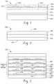
- FIG. 1is a cross-sectional view of a portion of an exemplary semiconductor device implemented in one embodiment of the present invention.
- FIG. 2is a cross-sectional view of a buffer layer of an exemplary semiconductor device implemented in one embodiment of the present invention.
- FIG. 3is a cross-sectional view of a quantum dot layer of an exemplary semiconductor device implemented in one embodiment of the present invention.
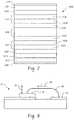
- FIG. 4is a cross-sectional view of a radiation emitting diode including a quantum dot layer implemented in one embodiment of the present invention.
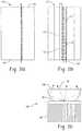
- FIG. 5is a cross-sectional view of a radiation emitting diode including a quantum dot layer implemented in one embodiment of the present invention.
- FIG. 6is a cross-sectional view of a radiation emitting diode including a quantum dot layer implemented in to one embodiment of the present invention.
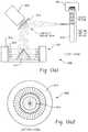
- FIG. 7is a cross-sectional view of a laser diode including a quantum dot layer implemented in one embodiment of the present invention.
- FIG. 8shows a graphical representation of a single RED semiconductor device.
- FIGS. 9 and 10show the relative percentage of infrared energy transmitted through a 10 mil thick section of PET as a function of wavelength.
- FIGS. 11 a , 11 b , and 11 cshow a typical ensemble of individual RED emitters packaged together into a RED heater element.
- FIGS. 12 a and 12 bshow the preferred deployment of RED heater elements within a blow molder.
- FIGS. 13 a and 13 bshow a further embodiment of the present invention showing implementation of RED based laser diodes.
- FIG. 14shows a preferred method for the thermal treatment of preforms as described by this invention.
- FIGS. 15-17show alternate methods for the thermal treatment of thermoplastic preforms according to this invention.
- FIG. 18shows RED heater elements being advantageously applied to a dynamically transported part.
- the subject inventionis directly related to a novel and new approach to be able to directly output substantial quantities of infrared laser radiation at selected wavelengths for the purpose of replacing such broadband type radiant heating sources.
- Many types of laserswould be useful for practicing this invention but gas and chemical lasers, while capable of producing large amounts of optical power, are much more difficult to control and are not available in many of the necessary wavelengths. Whether in their native wavelength output or when specially adapted for selected wavelengths, they can be quite expensive.
- solid state lasersare typically more practical to mount integrate, and control and more economical.
- the identified devices for the preferred embodimentare the first of a new class of devices that are just becoming available and are more efficient quantum converters of input energy. They also can be manufactured at a substantially wide range of selected wavelengths which may be required for some materials or applications.
- REDsradiation emitting diodes
- the deviceshave the property of emitting radiant electromagnetic energy in a tightly limited wavelength range.
- REDscan be tuned to emit at specific wavelengths that are most advantageous to a particular radiant treatment application.
- Those REDs tuned to preform as laser diodesmay be referred to as L-REDs, or laser radiance emitting diodes.
- Direct electron (or electric current)-to-photon conversionsas contemplated within these described embodiments occur within a narrow wavelength range often referred to as pseudo-monochromatic, consistent with the intrinsic band-gap and quantum dot geometry of this fabricated diode emitter. It is anticipated that the half-power bandwidths of candidate laser diode emitters will fall somewhere within the 20-500 nanometer range.
- the narrow width of infrared emitters of this typeshould support a variety of wavelength-specific irradiation applications as identified within the content of this complete disclosure.
- One family of RED devices and the technology with which to make themare subject of a separate patent application, U.S. Application Ser. No. 60/628,330, filed on Nov.
- semiconductor devicesare known in the art. They are employed in photovoltaic cells that convert electromagnetic radiation to electricity. These devices can also be employed as light emitting diodes (LEDs), which convert electrical energy into electromagnetic radiation (e.g., light).
- LEDslight emitting diodes
- a desired bandgap (electron volts) or a desired wavelength (microns)is targeted, and the semiconductor is prepared in a manner such that it can meet that desired bandgap range or wavelength range.
- the ability to achieve a particular wavelength of emission or electron volt of energyis not trivial. Indeed, the semiconductor is limited by the selection of particular materials, their energy gap, their lattice constant, and their inherent emission capabilities.
- One technique that has been employed to tailor the semiconductor deviceis to employ binary or tertiary compounds. By varying the compositional characteristics of the device, technologically useful devices have been engineered.
- quantum dotscan be included within the semiconductor device. These dots are believed to quantum confine carriers and thereby alter the energy of photon emission compared to a bulk sample of the same semiconductor.
- U.S. Pat. No. 6,507,042teaches semiconductor devices including a quantum dot layer. Specifically, it teaches quantum dots of indium arsenide (InAs) that are deposited on a layer of indium gallium arsenide (In x Ga 1-x As).
- the emission wavelength of the photons associated with the quantum dotscan be controlled by controlling the amount of lattice mismatching between the quantum dots (i.e., InAs) and the layer onto which the dots are deposited (i.e., In x Ga 1-x As).
- This patentalso discloses the fact that the lattice mismatching between an In x Ga 1-x As substrate and an InAs quantum dot can be controlled by altering the level of indium within the In x Ga 1-x As substrate. As the amount of indium within the In x Ga 1-x As substrate is increased, the degree of mismatching is decreased, and the wavelength associated with photon emission is increased (i.e., the energy gap is decreased).
- this patentdiscloses that an increase in the amount of indium within the substrate from about 10% to about 20% can increase the wavelength of the associated photon from about 1.1 ⁇ m to about 1.3 ⁇ m.
- a REDprovides a semiconductor device comprising an In x Ga 1-x As layer, where x is a molar fraction of from about 0.64 to about 0.72 percent by weight indium, and quantum dots located on said In x Ga 1-x As layer, where the quantum dots comprise InAs or Al z In 1-z As, where z is a molar fraction of less than about 5 percent by weight aluminum.
- the present inventionalso includes a semiconductor device comprising a quantum dot comprising InAs or Al z In 1-z As, where z is a molar fraction of less than about 5 percent by weight aluminum, and a cladding layer that contacts at least a portion of the quantum dot, where the lattice constant of the quantum dot and said cladding layer are mismatched by at least 1.8% and by less than 2.4%.
- the semiconductor devicesinclude a quantum dot layer including indium arsenide (InAs) or aluminum indium arsenide (Al z In 1-z As where z is equal to or less than 0.05) quantum dots on an indium gallium arsenide (In x Ga 1-x As) layer, which may be referred to as an In x Ga 1-x As matrix cladding.
- the lattice constant of the dots and the In x Ga 1-x As matrix layerare mismatched.
- the lattice mismatchmay be at least 1.8%, in other embodiments at least 1.9%, in other embodiments at least 2.0%, and in other embodiments at least 2.05%.
- the mismatchmay be less than 3.2, in other embodiments less than 3.0%, in other embodiments less than 2.5%, and in other embodiments less than 2.2%.
- the lattice constant of the In x Ga 1-x As matrix claddingis less than the lattice constant of the dots.
- the molar concentration of indium (i.e., x) within this cladding matrix layermay be from about 0.55 to about 0.80, optionally from about 0.65 to about 0.75, optionally from about 0.66 to about 0.72, and optionally from about 0.67 to about 0.70.
- the In x Ga 1-x As cladding matrixis located on an indium phosphorous arsenide (InP 1-y As y ) layer that is lattice matched to the In x Ga 1-x As cladding matrix.
- the InP 1-y As y layer onto which the In x Ga 1-x As cladding is depositedis a one of a plurality of graded (continuous or discrete) InP 1-y As y layers that exist between the In x Ga 1-x As cladding and the substrate onto which the semiconductor is supported.
- the substratecomprises an indium phosphide (InP) wafer.
- the semiconductormay also include one or more other layers, such as In x Ga 1-x As layers, positioned between the In x Ga 1-x As cladding and the substrate.
- FIG. 1is shown in FIG. 1 .
- FIG. 1as well as the other figures, are schematic representations and are not drawn to scale with respect to the thickness of each layer or component, or with respect to the relative thickness or dimension between each layer comparatively.
- Device 1000includes substrate 1020 , optional conduction layer 1025 , buffer structure 1030 , cladding layer 1040 , and dot layer 1050 .
- some semiconductor devicesoperate by converting electrical current to electromagnetic radiation or electromagnetic radiation to electrical current. The ability to control electromagnetic radiation or electrical current within these devices is known in the art. This disclosure does not necessarily alter these conventional designs, many of which are known in the art of manufacturing or designing semiconductor devices.
- substrate 1020comprises indium phosphide (InP).
- the thickness of InP substrate 1020may be greater than 250 microns, in other embodiments greater than 300 microns, and in other embodiments greater than 350 microns.
- the thicknessmay be less than 700 microns, in other embodiments less than 600 microns, and in other embodiments less than 500 microns.
- the semiconductor devices envisionedmay optionally include an epitaxially grown layer of indium phosphide (InP).
- the thickness of this epitaxially grown indium phosphide layermay be from about 10 nm to about 1 micron.
- optional conduction layer 1025comprises indium gallium arsenide (In x Ga 1-x As).
- the molar concentration of indium (i.e., x) within this layermay be from about 0.51 to about 0.55, optionally from about 0.52 to about 0.54, and optionally from about 0.53 to about 0.535.
- conduction layer 1025is lattice matched to the InP substrate.
- Conduction layer 1025may be doped to a given value and of an appropriate thickness in order to provide sufficient electrical conductivity for a given device.
- the thicknessmay be from about 0.05 micron to about 2 microns, optionally from about 0.1 micron to about 1 micron.
- buffer layer 1030comprises indium phosphorous arsenide (InP 1-y As y ). In certain embodiments, the buffer layer 1030 comprises at least two, optionally at least three, optionally at least four, and optionally at least five InP 1-y As y layers, with the lattice constant of each layer increasing as the layers are positioned further from substrate 1020 .
- buffer structure 1030includes first buffer layer 1032 , second buffer layer 1034 , and third buffer layer 1036 .
- the bottom layer surface 1031 of buffer structure 1030is adjacent to substrate 1020
- the top planer surface 1039 of buffer structure 1030is adjacent to barrier layer 1040 .
- the lattice constant of second layer 1034is greater than first layer 1032
- the lattice constant of third layer 1036is greater than second layer 1034 .
- first buffer layer 1032may include about 0.10 to about 0.18 molar fraction arsenic (i.e., y)
- second buffer layer 1034may include about 0.22 to about 0.34 molar fraction arsenic
- third buffer layer 1036may include about 0.34 to about 0.40 molar fraction arsenic.
- the increase in arsenic between adjacent buffer layersis less than 0.17 molar fraction. It is believed that any defects formed between successive buffer layers, which may result due to the change in lattice constant resulting from the increase in the arsenic content, will not be deleterious to the semiconductor. Techniques for using critical composition grading in this fashion are known as described in U.S. Pat. No. 6,482,672, which is incorporated herein by reference.
- the thickness of first buffer layer 1032may be from about 0.3 to about 1 micron. In one or more embodiments, the top buffer layer is generally thicker to ensure complete relaxation of the lattice structure.
- the individual buffer layer at or near the top 1039 of buffer structure 1030(e.g., buffer layer 1036 ) is engineered to have a lattice constant that is from about 5.869 ⁇ to about 5.960 ⁇ , optionally from about 5.870 ⁇ to about 5.932 ⁇ .
- the individual buffer layer at or near the bottom 1031 of buffer structure 1030is preferably engineered within the confines of the critical composition grading technique.
- the amount of arsenic present within the first buffer layeris less than 17 mole fraction.
- Cladding layer 1040comprises In x Ga 1-x As. In one or more embodiments, this layer is preferably lattice matched to the in-plane lattice constant of the top buffer layer at or near the top 1039 of buffer structure 1030 .
- lattice matchedrefers to successive layers that are characterized by a lattice constant that are within 500 parts per million (i.e., 0.005%) of one another.
- cladding layer 1040may have a thickness that is from about 10 angstroms to about 5 microns, optionally from about 50 nm to about 1 micron, and optionally from about 100 nm to about 0.5 microns.
- quantum dot layer 1050comprises indium arsenide (InAs).
- Layer 1050preferably includes wetting layer 1051 and quantum dots 1052 .
- the thickness of wetting layer 1051may be one or two mono layers.
- the thickness of dots 1052measured from the bottom 1053 of layer 1050 and the peak of the dot 1055 may be from about 10 nm to about 200 nm, optionally from about 20 nm to about 100 nm, and optionally from about 30 nm to about 150 nm.
- the average diameter of dots 1052may be greater than 10 nm, optionally greater than 40 nm, and optionally greater than 70 nm.
- quantum layer 1050includes multiple layers of dots.
- quantum dot 1050may include first dot layer 1052 , second dot layer 1054 , third dot layer 1056 , and fourth dot layer 1058 .
- Each layercomprises indium arsenide InAs, and includes wetting layers 1053 , 1055 , 1057 , and 1059 , respectively.
- Each dot layerlikewise includes dots 1055 .
- the characteristics of the each dot layer, including the wetting layer and the dots,are substantially similar although they need not be identical.
- intermediate cladding layers 1062 , 1064 , 1066 , and 1068Disposed between each of dot layers 1052 , 1054 , 1056 , and 1058 , are intermediate cladding layers 1062 , 1064 , 1066 , and 1068 , respectively.
- These intermediate cladding layerscomprise In x Ga 1-x As.
- the In x Ga 1-x As intermediate cladding layersare substantially similar or identical to cladding layer 1040 .
- the intermediate cladding layersare preferably lattice matched to barrier layer 1040 , which is preferably lattice matched to top buffer layer 1036 .
- the thickness of intermediate layers 1062 , 1064 , 1066 , and 1068may be from about 3 nm to about 50 nm, optionally from about 5 nm to about 30 nm, and optionally from about 10 nm to about 20 nm.
- regions or layers surrounding the quantum dot layermay be positively or negatively doped to manipulate current flow.
- Techniques for manipulating current flow within semiconductor devicesis know in the art as described, for example, in U.S. Pat. Nos. 6,573,527, 6,482,672, and 6,507,042, which are incorporated herein by reference.
- regions or layerscan be doped “p-type” by employing zinc, carbon, cadmium, beryllium, or magnesium.
- regions or layerscan be doped “n-type” by employing silicon, sulfur, tellurium, selenium, germanium, or tin.
- the various semiconductor layerscan be prepared by employing organo-metallic vapor phase epitaxy (OMVPE).
- OMVPEorgano-metallic vapor phase epitaxy
- the dot layeris prepared by employing a self-forming technique such as the Stranski-Krastanov mode (S-K mode). This technique is described in U.S. Pat. No. 6,507,042, which is incorporated herein by reference.
- RED 1100includes base contact 1105 , infrared reflector 1110 , semi-insulating semiconductor substrate 1115 , n-type lateral conduction layer (LCL) 1120 , n-type buffer layer 1125 , cladding layer 1130 , quantum dot layer 1135 , cladding layer 1140 , p-type layer 1145 , p-type layer 1150 , and emitter contact 1155 .
- LCLn-type lateral conduction layer
- Base contact 1105infrared reflector 1110 , semi-insulating semiconductor substrate 1115 , n-type lateral conduction layer (LCL) 1120 , n-type buffer layer 1125 , cladding layer 1130 , quantum dot layer 1135 , and cladding layer 1140 are analogous to those semiconductor layers described above.
- LCLn-type lateral conduction layer
- Base contact 1105may include numerous highly conductive materials. Exemplary materials include gold, gold-zinc alloys (especially when adjacent to p-regions), gold-germanium alloy, or gold-nickel alloys, or chromium-gold (especially when adjacent to n-regions). The thickness of base contact 1105 may be from about 0.5 to about 2.0 microns. A thin layer of titanium or chromium may be used to increase the adhesion between the gold and the dielectric material.
- Infrared reflector 1110comprises a reflective material and optionally a dielectric material.
- a silicon oxidecan be employed as the dielectric material and gold can be deposited thereon as an infrared reflective material.
- the thickness of reflector 1110may be form about 0.5 to about 2 microns.
- Substrate 1115comprises InP.
- the thickness of substrate 1115may be from about 300 to about 600 microns.
- Lateral conduction layer 1120comprises In x Ga 1-x As that is lattice matched (i.e. within 500 ppm) to InP substrate 1115 . Also, in one or more embodiments, layer 1120 is n-doped. The preferred dopant is silicon, and the preferred degree of doping concentration may be from about 1 to about 3 E 19/cm 3 . The thickness of lateral conduction layer 1120 may be from about 0.5 to about 2.0 microns.
- Buffer layer 1125comprises three graded layers of InP 1-y As y in a fashion consistent with that described above.
- Layer 1125is preferably n-doped.
- the preferred dopantis silicon, and the doping density may be from about 0.1 to about 3 E 9/cm 3 .
- Cladding layer 1130comprises In x Ga 1-x As that is lattice matched to the in-plane lattice constant (i.e. within 500 ppm) of the top of buffer layer 1125 (i.e. the third grade or sub-layer thereof.
- In x Ga 1-x As cladding layer 1130comprises from about 0.60 to about 0.70 percent mole fraction indium.
- the thickness of cladding layer 1130is about 0.1 to about 2 microns.
- Quantum dot layer 1135comprises InAs dots as described above with respect to the teachings of this invention.
- the intermediate layers between each dot layerinclude In x Ga 1-x As cladding similar to cladding layer 1130 (i.e., lattice matched).
- the amount of indium in one or more successive intermediate cladding layersmay include less indium than cladding layer 1130 or a previous or lower intermediate layer.
- Cladding layer 1140comprises In x Ga 1-x As that is lattice matched (i.e. within 500 ppm) to the top of buffer later 1125 (i.e. the third grade or sub-layer thereof).
- Confinement layer 1145comprises InP 1-y As y that is lattice matched to In x Ga 1-x As layer 1140 . Also, in one or more embodiments, layer 1145 is p-doped. The preferred dopant is zinc and the doping concentration may be from about 0.1 to about 4 E 19/cm 3 . The thickness of confinement layer 1145 may be from about 20 nm to about 200 nm.
- Contact layer 1150comprises In x Ga 1-x As that is lattice matched to confinement layer 1145 .
- Contact layer 1150is preferably p-doped (e.g., doped with zinc).
- the doping concentrationmay be from about 1 to about 4 E 19/cm 3 .
- the thickness of contact layer 1150is from about 0.5 to about 2 microns.
- the contact layer 1150may be removed from the entire surface except under layer 1155 .
- Emitter contact 1155may include any highly conductive material.
- the conductive materialincludes a gold/zinc alloy.
- FIG. 5Another embodiment is shown in FIG. 5 .
- Semiconductor device 1200is configured as a radiation emitting diode with a tunnel junction within the p region. This design advantageously provides for lower resistance contacts and lower resistance current distribution. Many aspects of semiconductor 1200 are analogous to semiconductor 1100 shown in FIG. 4 .
- contact 1205may be analogous to contact 1105
- reflector 1210may be analogous to reflector 1110
- substrate 1215may be analogous to substrate 1115
- lateral conduction layer 1220may be analogous to conduction layer 1120
- buffer layer 1225may be analogous to buffer layer 1125
- cladding layer 1230may be analogous to cladding layer 1130
- dot layer 1235may be analogous to dot layer 1135
- cladding layer 1240may be analogous to cladding layer 1140
- confinement layer 1245may be analogous to confinement layer 1145 .
- Tunnel junction layer 1247comprises In x Ga 1-x As that is lattice matched to confinement layer 1245 .
- the thickness of tunnel junction layer 1247is about 20 to about 50 nm.
- Tunnel junction layer 1247is preferably p-doped (e.g., with zinc), and the doping concentration may be from about 1 to about 4 E 19/cm 3 .
- Tunnel junction layer 1250comprises In x Ga 1-x As that is lattice matched to tunnel junction 1247 .
- the thickness of tunnel junction layer 1250is from about 20 to about 5,000 nm.
- Tunnel junction layer 1250is preferably n-doped (e.g., silicon), and the doping concentration is from about 1 to about 4 E 19/cm 3 .
- Emitter contact 1255may include a variety of conductive materials, but preferably comprises those materials that are preferred for n-regions such as chromium-gold, gold-germanium alloys, or gold-nickel alloys.
- FIG. 6Another embodiment of an RED is shown in FIG. 6 .
- Semiconductor device 1300is configured as a radiation emitting diode in a similar fashion to the RED shown in FIG. 5 except that electromagnetic radiation can be emitted through the substrate of the semiconductor device due at least in part to the absence of the base reflector (e.g., the absence of a reflector such as 1210 shown in FIG. 5 ).
- the semiconductor device 1300 shown in FIG. 6includes an emitter contact/infrared reflector 1355 , which is a “full contact” covering the entire surface (or substantially all of the surface) of the device.
- device 1300is similar to device 1200 .
- contact 1305may be analogous to contact 1205
- substrate 1315may be analogous to substrate 1215
- lateral conduction layer 1320may be analogous to conduction layer 1220
- buffer layer 1325may be analogous to buffer layer 1225
- cladding layer 1330may be analogous to cladding layer 1230
- dot layer 1335may be analogous to dot layer 1235
- cladding layer 1340may be analogous to cladding layer 1240
- confinement layer 1345may be analogous to confinement layer 1245
- tunnel junction layer 1347is analogous to tunnel junction layer 1247
- tunnel junction layer 1350is analogous to tunnel junction layer 1250 .
- Laser 1600includes contact 1605 , which can comprise any conductive material such as gold-chromium alloys.
- the thickness of contact layer 1605is from about 0.5 microns to about 2.0 microns.
- Substrate 1610comprises indium phosphide that is preferably n-doped at a concentration of about 5 to about 10 E 18/cm 3 .
- the thickness of substrate 1610is from about 250 to about 600 microns.
- Optional epitaxial indium phosphide layer 1615is preferably n-doped at a concentration of about 0.24 E 19/cm 3 to about 1 E 19/cm 3 .
- the thickness of epitaxial layer 615is from about 10 nm to about 500 nm.
- Grated InP 1-y As y layer 1620is analogous to the grated InP 1-y As y buffer shown in FIG. 2 .
- Buffer 1620is preferably n-doped at a concentration at about 1 to about 9 E 18/cm 3 .
- Layer 1625 and 1630form wave guide 1627 .
- Layer 1625comprises indium gallium arsenide phosphide (In 1-x GA x As z P 1-z ).
- Layer 1630likewise comprises In 1-x GA x As z P 1-z .
- Both layers 1625 and 1630are lattice matched to the top of layer 1620 .
- layers 1625 and 1630comprise about 0 to about 0.3 molar fraction gallium and 0 to about 0.8 molar fraction arsenic.
- Layer 1625is about 0.5 to about 2 microns thick, and is n-doped at a concentration of about 1-9 E 18/cm 3 .
- Layer 1630is about 500 to about 1,500 nm, and is n-doped at a concentration of about 0.5 to 1 E 18/cm 3 .
- Confinement layer 1635 , dot layer 1640 , and confinement layer 1645are similar to the dot and confinement layers described above with respect to the other embodiments.
- confinement layer 1635is analogous to confinement layer 1040 and dot layer 1640 us analogous to dot layer 1050 shown in FIG. 3 .
- the number of dot layers employed within the dot region of the laser deviceis in excess of 5 dot layers, optionally in excess of 7 dot layers, and optionally in excess of 9 dot layers (e.g., cycles).
- Confinement layers 1635 and 1645may have a thickness from about 125 to about 500 nm and are lattice matched to the wave guide. Layers 1635 , 1640 , and 1645 are preferably non-doped (i.e., they are intrinsic).
- Layers 1650 and 1655form wave guide 1653 .
- layers 1650 and 1655comprise In 1-x GA x As z P 1-z that is lattice matched to the top of buffer 1620 .
- Layer 1650is about 500 to about 1,500 nm p-doped at a concentration of about 0.5 to about 1 E 18/cm 3 .
- Layer 655is about 1 to about 2 microns thick and is p-doped at a concentration of about 1 to about 9 E 18/cm 3 .
- layer 1660is a buffer layer that is analogous to buffer layer 1620 . That is, the molar fraction of arsenic decreases as each grade is further from the quantum dots. Layer 1660 is preferably p-doped at a concentration of 1-9 E 18/cm 3 .
- Layer 1665comprises indium phosphide (InP).
- the thickness of layer 1665is about 200 to about 500 nm thick and is preferably p-doped at a concentration of about 1 to about 4 E 19/cm 3 .
- Layer 1670is a contact layer analogous to other contact layers described in previous embodiments.
- layers 1660 , 1665 , and 1670can be analogous to other configurations described with respect to other embodiments.
- these layerscan be analogous to layers 1145 , 1150 , and 1155 shown in FIG. 4 .
- layers analogous to 1245 , 1247 , 1250 , and 1255 shown in FIG. 5can be substituted for layers 1660 , 1665 , and 1670 .
- RED based laser diodesmay be implemented in a variety of manners, an example of which will be described in connection with FIG. 13 .
- semiconductor lasers and other laser diodesmay be employed with suitable modifications.
- other enabling technologiesmay be developed for efficiently producing limited bandwidth irradiation in advantageous wavelengths.
- these deviceswill be RED based laser diodes (also referred to as L-REDs).
- L-REDsRED based laser diodes
- the arrayscan range from single devices to more typically hundreds, thousands, or unlimited number arrays of devices depending on the types and sizes of devices used, the output required, and the wavelengths needed for a particular implementation of the invention.
- the RED deviceswill usually be mounted on circuit boards which have at least a heat dissipation capability, if not special heat removal accommodations. Often the RED devices will be mounted on such circuit boards in a very high density/close proximity deployment. It is possible to take advantage of recent innovations in die mounting and circuit board construction to maximize density where desirable for high-powered applications. For example, such techniques as used with flip chips are advantageous for such purposes. Although the efficiency of the RED devices is good for this unique class of diode device, the majority of the electrical energy input is converted directly into localized heat. This waste heat must be conducted away from the semi-conductor junction to prevent overheating and burning out the individual devices. For the highest density arrays, they may likely use flip-chip and chip-on-board packaging technology with active and/or passive cooling.
- the x by y arraysmay also comprise a mix of RED devices which represent at least two different selected wavelengths of infrared radiation in a range from, for example, 1 micrometer to 5 micrometers.
- the RED deviceswill be deployed advantageously in variously sized arrays, some of which may be three dimensional or non-planar in nature for better irradiation of certain types of targets. This is true for at least the following reasons:
- RED devicesBecause of the typical end uses of diodes, they have been manufactured in a manner that minimizes cost by reducing the size of the junction. It therefore requires less semiconductor wafer area which is directly correlated to cost.
- the end use of RED deviceswill often require substantial radiated energy output in the form of more photons. It has been theorized that REDs could be manufactured with creative ways of forming a large photon producing footprint junction area. By so doing, it would be possible to produce RED devices capable of sustaining dramatically higher mid-infrared, radiant output. If such devices are available, then the absolute number of RED devices needed to practice this invention could be reduced.
- the inventioncan be practiced with a single device for lower powered applications, single wavelength applications, or, if the RED devices can be manufactured with sufficient output capability.
- the RED device arraysas integrated circuits.
- the REDswould be arrayed within the confines of a single piece of silicon, Gallium Arsenide, Indium Phosphide, or other suitable substrate but with multiple junctions or an enlarged bandgap areas that function as the photon production sites on the chip. They could be similar to other integrated circuit packages which use ball grid arrays for electrical connectivity. Such device packages could then be used as the array, facilitating the desired electrical connectivity for connection to and control by the control system.
- an important design parameteris the control of the junction or bandgap temperature which should not be allowed to reach approximately 1000 to 105° C., with current chemistries, before damage begins to occur.
- the design for mounting each RED die to the circuit boardshould consider the importance of removing the heat from the device as efficiently as possible. For example, heat can be removed by conduction through the stud bumps that are also intended for electrical conduction to the anode and cathode respectively of the device.
- the circuit board on which the devices are mountedmust be chosen for good heat conduction as well so that the heat may be carried away from the devices which in many applications will employ heat sinks or a cooling jacket as needed to keep the circuit board cool.
- variables to be considered in view of the targeted applicationinclude packaging, ease of deployment, costs, electronic connectivity, control to programmability considerations, cooling, environment of deployment, power routing, power supply, string voltage, string geometry, irradiation requirements, safety and many others that one skilled in the appropriate arts will understand.
- PET resin materialPolyethylene terephthalate
- PET resin materialas it is known in the industry
- the PET materialis highly absorptive in the long wavelength region and is highly transmissive in the visible and near-infrared wavelength regions. Its transmission varies dramatically between 1 micrometers and 5 micrometers. Its transmission not only varies dramatically in that range but it varies frequently and abruptly and often very substantially sometimes within 0.1 micrometers.
- PEThas a very strong absorption. This means that if infrared radiation was introduced to PET at 2.9 micrometers, it would nearly all be absorbed right at the surface or outer skin of the material. If it were desirable to heat only the outer surface of the material, then this wavelength could be used. Since PET is a very poor conductor of heat (has a low coefficient of thermal conductivity) and since it is more desirable in stretch blow molding operations to heat the PET material deeply from within and evenly all the way through its volume, this is, in practice, a bad wavelength at which to heat PET properly.
- PET materialis highly transmissive. This means that a high percentage of the radiation at this wavelength that impacts the surface of the PET, will be transmitted through the PET and will exit without imparting any preferential heating, hence be largely wasted. It is important to note that the transmission of electromagnetic energy decreases exponentially as a function of thickness for all dielectric materials, so the material thickness has a substantial impact on the choice for the optimal wavelength for a given material.
- PET thermoplastic materialhas been used here as an example, the principles hold true for a very wide range of different types of materials used in different industries and for different types of processes.
- PEN or PLAare materials to which these principles may apply.
- a glue or adhesive lamination systemis illustrative.
- the parent material that is to be gluedis very transmissive at a chosen infrared wavelength.
- the heat-cured glue that is to be employedmight be very absorptive at that same wavelength.
- the processis further optimized because the glue, and not the adjacent parent material, is heated.
- optimum pointsare found within various widely diverse kinds of processing or heating applications within industry.
- quartz infrared heating bulbsor other conventional heating devices, that are currently in wide usage.
- quartz bulbsare used for a range of things including heating sheets of plastic material in preparation for thermo-forming operations.
- the subject inventionbe utilized as an alternative to the existing functionality of quartz infrared lamps or other conventional heating devices, but it can be envisaged to add substantial additional functionality.
- the present inventionby contrast, can either generate radiant energy in a continuously energized or alternately a pulsed mode. Because the basic RED devices of the subject invention have an extremely fast response time which measures in microseconds, it can be more energy efficient to turn the energy on when it is needed or when a target component is within the targeted area and then turn it off when the component is no longer in the targeted area.
- the added functionality of being able to pulse energize the infrared sourcecan lead to a considerable improvement in overall energy efficiency of many radiant heating applications.
- REDsinfrared radiation emitting devices
- the infrared emitting devices that are nearest the target devicewould be the ones that would be energized.
- the “energizing wave”could be passed down the array.
- thermoforming sheetthermoforming sheet
- well known electronics synchronization techniquescan be used to turn on the right devices at the desired intensity according to a programmable controller or computer's instructions.
- the devices within the arrayscould be turned on by the control system for their desired output intensity in either a “continuous” mode or a “pulsed” mode. Either mode could modulate the intensity as a function of time to the most desirable output condition.
- This controlcan be of groups of devices or down to individual RED devices.
- the RED devicescan be wired in strings of most desired geometry. These strings or groups of strings may then be programmably controlled as the application requirements dictate. Practicality will sometimes dictate that the RED devices are driven in groups or strings to facilitate voltages that are most convenient and to reduce the cost of individual device control.
- the strings or arrays of REDsmay be controlled by simply supplying current in an open loop configuration or more sophisticated control may be employed.
- the fact intensive evaluation of any specific applicationwill dictate the amount and level of infrared radiant control that is appropriate.
- the control circuitrycould continuously monitor and modulate the input current, voltage, or the specific output.
- the monitoring for most desirable radiant output or resultcould be implemented by directly measuring the output of the infrared array or, alternatively, some parameter associated with the target object of the infrared radiation. This could be performed by a continuum of different technologies from incorporating simple thermocouples or pyrometers up to much more sophisticated technologies that could take the form of, for example, infrared cameras.
- One skilled in the artwill be able to recommend a particular closed loop monitoring technique that is economically sensible and justifiable for a particular application of the invention.
- Both direct and indirect methods of monitoringcan be incorporated. For example, if a particular material is being heated for the purpose of reaching a formable temperature range, it may be desirable to measure the force needed to form the material and use that data as at least a portion of the feedback for modulation of the infrared radiation arrays. Many other direct or indirect feedback means are possible to facilitate optimization and control of the output of the subject invention.
- a target materialto be cured or dried without substantially affecting the substrate or parent material. It may well be that the parent material can be damaged by such processing. It is more desirable to not induce heat into it while still inducing heat into the target material.
- the subject inventionfacilitates this type of selective heating.
- the medical industryhas been experimenting with a wide range of visible light and near-infrared radiant treatments. It has been theorized that certain wavelengths of electromagnetic energy stimulate and promote healing. It has also been postulated that irradiation with certain wavelengths can stimulate the production of enzymes, hormones, antibodies, and other chemicals within the body as well as to stimulate activity in sluggish organs. It is beyond the scope of this patent to examine any of the specific details or treatment methodologies or the merit of such postulations.
- the subject inventioncan provide a solid state, wavelength selectable, and programmable mid-infrared radiation source that can facilitate a wide range of such medical treatment modalities.
- a very high percentage of the human bodyis composed elementally of water, therefore it is likely that the transmission/absorption curves for water are a good starting point for a rough approximation for much human tissue.
- Through extensive researchit is possible to develop precise curves for all types of tissue in humans, animals, and plants. It is also possible to develop the relationship between various kinds of healing or stimulation that might be sought from organs or tissue and relate that to the transmission/absorption curves.
- By carefully selecting the wavelength or combination of wavelengthsit would be possible to develop treatment regimens which could have a positive effect with a wide range of maladies and ailments.
- the irradiation arrays of the present inventionare of the appropriate size and/or shape to be used in a wide range of invasive or non-invasive treatments. While the treatment techniques, modalities and configurations are beyond the scope of this discussion; the invention is the first of its kind available to make solid state, wavelength selective irradiation available in the middle-infrared wavelength bands. It can be configured for a wide range of modalities and treatment types. Due to its highly flexible form factor and programmable nature it is capable of being configured for a particular body size and weight to produce the appropriate angles, intensities, and wavelengths for custom treatment.
- Infrared radiationis being utilized for an increasing number of medical applications from hemorrhoid treatments to dermatology.
- One example of infrared treatment that is currently performed with broadband infrared sourcesis called infrared coagulation treatment.
- diabetic peripheral neuropathyis sometimes treated with infrared lamp treatments.
- Tennis elbow and other similar ailmentsare often currently treated with broadband infrared lamps as well.
- the incorporation of the present invention's ability to generate specific wavelengths of radiation as well as its ability to generate pulsed irradiationmay provide substantial improvement in these treatments. It also may provide for better patient toleration and comfort.
- the inventionalso facilitates manufacturing a medical device that could be powered with inherently safe voltages.
- the pulsing of the irradiation energymay prove to be a key aspect associated with many medical treatment applications. Continuous irradiation may cause tissue overheating while a pulsed irradiation may prove to provide enough stimulation without the deleterious effect of overheating, discomfort, or tissue damage.
- the very fact that the devices/arrays can be pulsed at extremely high rates with turn-on times measured in microseconds or fasterprovides another useful property. It is anticipated that very high intensity pulses of radiation may be tolerated without damage to the arrays if they are activated for very short duty cycles, since the semi-conductor junction overheat would not have time to occur with such short pulse times. This would allow greater summed instantaneous intensity which could facilitate penetration through more tissue.
- the frequency at which the pulsing occursmay also prove to be important. It is known within the literature that certain frequencies of irradiation to humans can have healing or, alternatively, deleterious effects. For example, certain amplitude modulation frequencies or combinations of frequencies of visible light can cause humans to become nauseous and yet other amplitude modulation frequencies or combinations of frequencies can cause epileptic seizures. As further medical research is done it may indeed determine that the pulsing frequency, waveform shape, or combination of frequencies along with the selected wavelength or combination of wavelengths have a very substantial effect on the success of various radiation treatments. It is very likely that many of the treatment modalities which will utilize this invention are not yet understood nor realized since the subject invention has not been available to researchers or practitioners.
- ovens and heating systemsare used in the preparation of food throughout human history. Since most of them are well known, it is beyond the scope of this patent application to describe the full range of such ovens and heating systems.
- microwave cookingwhich utilizes non-infrared/non-thermal source cooking technology
- broadband heating sourcesof various types.
- the infrared heating sources and elements that are used in such ovensare broad-band sources. They do not have the ability to produce specific wavelengths of infrared energy that might be most advantageous to the particular cooking situation or the product being cooked.
- the subject inventionwould allow for the selection of a wavelength at which that particular food product is highly absorptive. The result would be that when irradiated at the chosen wavelength the infrared energy would all be absorbed very close to the surface, thus causing the desired heating and/or browning action to take place right at the surface. Conversely, if it is desired not to overheat the surface but rather to cook the food from very deeply within it, then it is possible to choose a wavelength or combination of selected wavelengths at which the particular food is much more transmissive so that the desired cooking result can be achieved. Thus the radiant energy will be absorbed progressively as it penetrates to the desired depth.
- RED elementsthat irradiate at different wavelengths, it is possible to further optimize a cooking result.
- one element typewould be chosen at a wavelength wherein the absorption of radiant energy is low, thus allowing deep-heat penetration to occur.
- a second element typewould be chosen wherein the absorption of radiant energy is high thus facilitating surface heating to occur.
- a third RED element typecould be conceived to be chosen at a wavelength intermediate to these two extremes in absorption.
- any of the applications of the subject inventionit is possible to use various lensing or beam guiding devices to achieve the desired directionality of the irradiation energy.
- the chosen beam guiding devicesmust be chosen appropriately to function at the wavelength of radiation that is being guided or directed.
- By utilizing well understood techniques for diffraction, refraction, and reflectionit is possible to direct energy from different portions of an array of RED devices in desired directions.
- By programmably controlling the particular devices that are turned on, and by modulating their intensitiesit is possible to achieve a wide range of irradiation selectivity.
- steady state or pulsing mode and by further programming which devices are pulsed at what timeit is possible to raise the functionality even further.
- FIG. 8gives a graphical indication of a single RED component 10 .
- the RED 10comprises a stack 20 .
- the stack 20may take a variety of configurations, such as the stacks of semiconductor layers and the like illustrated in connection with FIGS. 1-7 .
- the contact 40(corresponding, for example, to contacts 1105 , 1205 and 1305 ) of the RED 10 is made to the stack 20 through wire 80 .
- photons 70are emitted that possess a characteristic energy or wavelength consistent with the configuration of the stack 20 .
- FIGS. 9 and 10show the relative percentage of IR energy transmitted within a 10 mil thick section of PET as a function of wavelength.
- quartz transmission rangeup to 3.5 micrometer
- the presence of strong absorption bandsare evident at several wavelengths including 2.3 micrometer, 2.8 micrometer, and 3.4 micrometer.
- the basic concept associated with the subject inventionis the use of RED elements designed and chosen to operate at a selected wavelength(s) within the 1 micrometer to 3.5 micrometer range as the fundamental heating elements within the thermal conditioning section of blow molding machines.
- FIGS. 11 a , 11 b , and 11 cshow an example ensemble of individual RED emitters 10 packaged together into a suitable RED heater element 100 .
- the REDs 10are physically mounted so that N-doped regions are directly attached to a cathode bus 120 .
- the cathode bus 120is ideally fabricated out of a material such as copper, or gold, which is both a good conductor of electricity as well as heat.
- the corresponding regions of the REDs 10are connected via bond wires 80 to the anode bus 110 .
- the anode buswould have the same thermal and electrical properties as the cathode bus.
- Input voltageis externally generated across the 2 bus bars causing a current (I) to flow within the REDs 10 resulting in the emission of IR photons or radiant energy, such as that shown at 170 .
- a reflector 130is used in the preferred embodiment to direct the radiant energy into a preferred direction away from the RED heater element 100 .
- the small physical extent of the REDs 10make it possible to more easily direct the radiant energy 170 that is emitted into a preferred direction. This statement being comparatively applied to the case of a much larger coiled filament; such a relationship between the physical size of an emitter and the ability to direct the resultant radiant flux using traditional lensing means being well known in the art.
- a heat sink 140is used to conduct waste heat generated in the process of creating IR radiant energy 170 away from the RED heater element 100 .
- the heat sink 140could be implemented using various means known within industry. These means include passive heat sinking, active heat sinking using convection air cooling, and active heat sinking using water or liquid cooling.
- the liquid cooling through, for example, a liquid jackethas the advantage of being able to conduct away the substantial amount of heat that is generated from the quantity of electrical energy that was not converted to radiant photons. Through the liquid media, this heat can be conducted to an outdoor location or to another area where heat is needed. If the heat is conducted out of the factory or to another location then air conditioning/cooling energy could be substantially reduced.
- a bulb 150is optimally used in this embodiment of the invention.
- the primary function of the bulb 150 as applied hereis to protect the REDs 10 and bonding wires 80 from being damaged.
- the bulb 150is preferably constructed out of quartz due to its transmission range that extends from the visible through 3.5 micrometer. However, other optical materials including glass having a transmission range extending beyond the wavelength of operation of the REDs 10 could also be used.
- FIGS. 12 a and 12 bOne deployment of the RED heater element 100 , within a blow molder, is depicted in FIGS. 12 a and 12 b .
- preforms 240enter into a thermal monitoring and conditioning system 210 via a transfer system 220 .
- the preforms 240could come into the thermal monitoring and control system 210 at room temperature, having been previously injection molded at some earlier time.
- the preforms 240could come directly from an injection molding process as is done in single-stage injection molding/blow molding systems.
- the preformscould be made by one of several other processes. Whatever the form and timing of preform manufacturing, entering in this fashion, the preforms 240 would have varying amounts of latent heat contained within them.
- the preforms 240are transported through the thermal monitoring and control system 210 via a conveyor 250 , such conveyors being well known in industry. As the preforms 240 travel through the thermal monitoring and control system 210 , they are subjected to radiant IR energy 170 emitted by a series of RED heater elements 100 . These RED heater elements may advantageously take the form of laser-based RED elements (L-REDs), which will be described in further detail below. The IR energy 170 emitted by these RED heater elements 100 is directly absorbed by the preforms 240 in preparation of entering the blowing system 230 . It should be appreciated that the energy may be continuous or pulsed, as a function of the supply or drive current and/or other design objectives.
- L-REDslaser-based RED elements
- control systemsuch control system 280 , in one form, controls this functionality.
- control systemis operative to pulse the system at electrical current levels that are substantially greater than recommended steady state current levels to achieve higher momentary emitted intensity in pulsed operation and respond to an input signal from an associated sensor capability to determine a timing of the pulsed operation
- a convection cooling system 260is also preferably deployed. This system removes waste heat from the air and mechanics that are in proximity to the preforms 240 under process.
- a conduction cooling devicemay also be employed to do so. Heating of preforms by convection and/or conduction is known in the art to be deleterious to the overall thermal conditioning process. This is because PET is a very poor thermal conductor and heating the outer periphery of the preform results in uneven through heating, with too cool a center and a too warm outer skin.
- temperature sensors 270which may take the form of an intelligent sensor or camera that is capable of monitoring a target in at least one aspect beyond that which a single point temperature measurement sensor is capable
- a temperature control system 280a temperature control system 280 .
- These aspects of the preferred blow molder designare particularly applicable to the attributes of a one-stage blow molding system.
- the preforms 240enter into the thermal monitoring and conditioning system 210 containing latent heat energy obtained during the injection molding stage.
- a temperature monitoring and control system 280By monitoring the temperature and thus the heat content of the incoming preforms 240 (or specific subsections of such performs), it is possible for a temperature monitoring and control system 280 to generate preform-specific (or subsection specific) heating requirements and then communicate these requirements in the form of drive signals to the individual RED heater elements 100 .
- the solid-state nature and associated fast response times of RED emitters 10make them particularly suited to allow the electrical supply current or on-time to be modulated as a function of time or preform movement. Also, subsections of the RED array may be controlled, as will be appreciated.
- the temperature control system 280 used to enact such output controlcould be implemented as an industrial PC as custom embedded logic or as or an industrial programmable logic controller (PLC), the nature and operation all three are well known within industry.
- the control system, such as that shown as 280may be configured a variety of ways to meet the objectives herein. However, as some examples, the system may control on/off status, electrical current flow and locations of activated devices for each wavelength in an RED array.
- a method for heating the container using laser radiationis provided.
- the laser lightilluminates the container, normally in its “preform” stage, so as to soften it through the absorption of light.
- the containeris subsequently blow formed.
- the method of delivering the energy, and the choice of wavelength(s)can be varied, in accordance with the needs of the application.
- the selected narrow wavelength rangemay be specifically tuned to the heating requirements of the material from which the particular target component is manufactured.
- it is possible to manufacture the diode devices to near-monochromatic wavelength specificityit is not usually needed to be that narrow. Often, if the wavelength is centered in the absorption band correctly, plus or minus 20 or even 50 nanometers may be just fine.
- the selected wavelengths chosen for usemay be anywhere in the range from 1.0 to 5.0 microns, or may, more practically, be selected from the narrower range of 1.5 to 3.5 microns.
- the absorption rate characteristics of the material at the different wavelengthsis a factor. If more than one absorber is involved, a “door and window” evaluation may be appropriate if, for example, one material is to be heated but not the other.
- the absorption band for a particular materialmay be selected based on, or to optimize, desired depth of heating, location of heating, speed of heating or thickness to be heated.
- the laser diodes (or other devices) contemplated hereinmay be used to pump other oscillating elements to achieve desired wavelengths.
- the proposed methodquickly solves most of the aforementioned issues, and renders irrelevant the remainder.
- the principal requirement for any radiative heat transfer methodis matching the spectral absorption of the material to the spectral output of the radiating source.
- Standard lasershave many wavelengths from which to choose for satisfying this requirement.
- Wall plug efficiency for most lasersis between 10 and 20%, which, when matched properly to the absorption of the target, will result in 8-15% heat transfer efficiency, compared to only several % for the existing method.
- the spatial coherence of laser lightallows it to be placed exactly where it is needed. This contrasts favorably to the standard practice, where the light is emitted in all directions from the bulb filament, and must be collected and pointed in the correct direction.
- the physics of extended sourcesrenders this very inefficient.
- lasersare inherently bright, and laser light of the appropriate wavelengths propagates through free space with little loss, hence extraneous heating is no longer an issue. Lasers are typically water cooled, and excess heat goes into the water jacket, not ambient, making heat management much more straightforward. Many lasers are also instantly adjustable, over a wide range of intensities, and in some applications, their spatial intensity is rapidly adjustable as well.
- the laser lightis shaped refractively or diffractively, to the desired spatial and intensity profile, before it strikes the plastic target component or a container preform.
- a typical preformwhich is nominally cylindrical
- a combination of lensesis used to expand and collimate the beam, then a simple cylinder lens is adequate to produce a rectangular profile.
- the nominal Gaussian intensity profile of the typical TEMoo laser outputcan be modified as well with several methods, depending on desired final intensity profile.
- a “top hat”, or flat top profileis desirable, and can be produced by several well known methods, such as faceted beam integrators, holographic elements (HOE), and microlens arrays.
- Non-uniform distributionsare usually more appropriate, as different segments of the container typically require more heat. These can be best accomplished with HOEs, although they can also be generated with beam apodizers. However, apodizers work by selectively absorbing portions of the beam, and lead to increased inefficiency.
- the ideal systemwould start with the choice of laser wavelength. This is driven by the container material and thickness. For a PET preform with 4 mm walls, then a wavelength around 2 um would provide for about 90% absorption through the entire thickness of both walls of the preform. This is determined by using Beer's law and the coefficient of absorption for PET (alpha). There are several lasers to choose from that emit around 2 microns; Raman shifted YAG, Ho:YAG, and Tm:YAG. These are all YAG variant solid state lasers, and are very reliable.
- Spatial and irradiance profiling of the beamis best accomplished by a combination of diffractive and refractive elements, For instance, the beam is expanded, collimated, and homogenized by a Galilean expander, followed by a faceted beam integrator.
- the resultant square, uniform intensity beamstrikes an HOE, which has been designed to change the input into a rectangular shape with an intensity profile which is higher at the top and is reduced to about 1 ⁇ 2 max at the bottom. The exact shape is dependent on the container, but most require more heating at the top.
- HOEsare very efficient devices, and are relatively inexpensive to manufacture. However, some, materials may require longer wavelength lasers, requiring exotic material for the HOEs.
- the remainder of the systemrequires a means of triggering the laser to expose the container preform at the time when it is in the center of the irradiation pattern. It is not necessary, and may be advantageous, for the spatial profile to be smaller than the container itself, and for the pulse duration to be long enough for the container preform to sweep through the profile. Some means for providing multiple exposures is required as well, because each container preform will need multiple exposures or a prescribed length of exposure time. This can be accomplished by several means, the most direct of which is to have a mirror arranged to follow a container for a specified distance, thus allowing the intensity profile to be maintained on it for a longer time. Often, it will be desirable for the target to rotate as it is traversing through the exposure area so that all sides may be exposed to the radiant energy.
- Another approachis through the use of a scanning beam.
- the primary difference between the stationary and scanned beam approachesis in the replacement of all of the beam shaping apparatus with two devices; an electro-mechanical, served, or acousto-optical scanner, and some means for variable attenuation.
- the operative principleis to deposit energy from the raw laser beam into the target component by rapidly scanning the beam across the surface of it. If the scan rate of the laser is very fast relative to the motion of the targeted component and the desired rate of heating, then there is no difference between the two methods, from the target's perspective. All of the other considerations apply, but avoiding the extra optics can be advantageous.
- the scanned approachdoes not require HOEs to be designed and manufactured beforehand.
- Spatial profilesare implemented by changing the scan limits, and intensity changes can be implemented by either slowing the scanner down where more heat is desired, or re-scanning some areas, or dithering die scan. It is also possible to implement an active attenuator, either in the laser itself, or a lambda/2 plate, for polarization based attenuation. Any method which causes the laser to put out less optical power for the same input power will adversely affect efficiency. Changing the scan is preferable.
- This approachhas another benefit, in that following the target while it proceeds through the tunnel is built into this approach, whereas some form of it must be adapted to the “stationary” beam approach to account for the targeted component rapidly moving in and out of the profile too quickly to absorb enough energy with just the one pass.
- a system 2000is illustrated. It should be understood that the system could be adopted to be a scanning system or a stationary system. Selection of one of those systems is a function of whether certain components (as will be described) are rendered movable.
- the systemuses laser diodes (e.g. L-REDs) and could be used as a replacement for the heater elements 100 and otherwise integrated into the system of FIGS. 12 a and b . Minor modifications to the system, including the thermal monitoring and control system 210 may be desired to accommodate the replacement; however, any such changes will be apparent to those skilled in the art.
- L-REDslaser diodes
- control of the system through use of the control subsystem 280may be adapted to also include control of the scanner device (to be described) of the system to achieve timing in the system so that the laser diode output energy is synchronized to the conveyance.
- control of the scanner deviceto be described
- pulsing and continuous mode operationwould be controlled in the system by the control subsystem 280 and other components of the system.
- the system 2000includes an implementation of an RED based laser diode array to generate that appropriate energy wavelengths contemplated by the subject embodiments.
- the system 2000includes a solid state RED based laser array 2002 , a scanner means 2004 and a transport system 2006 for exemplary target components or preforms 2008 to deliver the components to a thermal treatment region of the system.
- the array 2002includes a circuit board supporting the RED based laser diode devices 2010 supported within a cooling jacket 2012 .
- the arrayis operative to emit one or more selected wavelengths of infrared radiant energy within the wavelength range from 1.0 to 5.0 microns via direct electrical current-to-photon conversion process.
- the L-REDsare disposed in the array in an arrangement which facilitates emitting a substantial portion of energy into the target components.
- the array 2002also uses a conical mirror 2014 .
- the scanner meansmay be an X-Y scanner or simply a Y scanner supporting a mirror 2016 .
- the scanner means 2004may take the form of a galvanometer that is capable of moving a mirror in the X and Y directions. This X and Y motion would typically be programmably controlled to repeat the motion that is the desired radiation pattern. This would allow for areas of the target components to be radiated by the laser beams.
- the systemmay be set-up to take advantage of the fact that the target components may be in motion in one direction (e.g. the X direction) as they are conveyed by the transport system 2006 .
- the scanner meansneed only be operable to move the beams in, for example, the Y direction to achieve irradiation of selected areas of the target components.
- each laser diode of an array of laser diodescould be focused on specific points, for example. It may be desired to use a beam expander lens in order to make sure that the array of projected lasers have the desired coverage area and beam overlaps which would be appropriate to the application. In this case one or both of the scanner means or the conical mirror, might not even be necessary.
- individual L-REDsmay or may not use any collimation or focusing techniques, depending on the specific application.
- the output patterns of such devicesmay overlap to adequately and more desireously cover the surface of a target.
- combinations of L-REDs with some having collimated or focused beams and other L-REDs having diverging irradiation beamsmay be implemented. Nonetheless, as shown in FIGS. 13 a and 13 b , in operation, the system 2000 is able to generate laser beams from the array of diodes 2002 .
- the arraymay take a variety of configurations to suit the application.
- the arraymay contain devices generating a single wavelength or multiple wavelengths.
- devices generating a first wavelength of energymay be strategically mixed with devices generating a second wavelength of energy to achieve a desired result.
- the x-by-y array of diodesis shaped into at least a portion of a cylindrical configuration to facilitate the ultimate delivery of energy from the laser source to the target component. As shown, these beams are directed toward a non-planar, e.g., a generally conical, mirror 2014 which reflects the rays toward the scanner device or means 2004 .
- any suitable non-planar mirrormay be implemented, any such mirror being shaped to facilitate improved delivery of thermal infrared radiant energy from the laser diodes into the target component, or portions of the target component.
- the scanner device 2004then focuses the rays onto selected regions of the target component 2008 , e.g. a preform as shown.
- a variety of forms of a scanner device 2004may be implemented. For example, multiple scanners may be implemented, the exact number of which depends on the speed of processing, the number of target components, etc. In one form, as shown in FIG. 13 b , multiple scanners 2004 are shown as being positioned to adequately inject heat into a plurality of target components in, for example, a blow molding environment. Of course, in the environment of a slower process, or an environment of scanners having improved speed of operation, fewer scanners may accomplish the application. In some applications, a single scanner may suffice.
- multiple scanner devices 2004are displayed in the system 2000 .
- the optional conical mirrors 2002are representatively shown in association with each scanner device 2004 .
- a conveyance device, such as at 2006 , and product carrier sites 2007are also shown.
- a tracking arc 2005 for laser 6 (one of the scanner devices 2004 ) and example irradiation beams 2003are also illustrated.
- An assignment chartis displayed to illustrate the operation of the system. As shown, laser 1 irradiates the first, seventh, thirteenth, . . . etc. target component as it passes by the laser 1 .
- the other laser scanner devicesirradiate respective components as shown in the chart.
- a similar or programmed tracking arc to that of arc 2005is possessed by each scanner device.
- each componentis irradiated for a sufficient amount of time and can be irradiated specific to its needs.
- the number of scanners, the tracking arcs, and number of components treated by each scanner devicewill vary as a function of the design and objectives of a particular system.
- the scanner device 2004may have a mirror 2016 associated with the scanner device, the mirror 2016 being operative to direct the radiant energy into the selected portions of the target components.
- the devicemay also be capable of redirecting the radiant energy within a planar, two dimensional scanning region, whereby a third dimension of motion is provided by a conveyance means which moves the target through the irradiation region.
- the devicemay also be capable of redirecting the radiant energy within a three dimensional scanning region.
- the scanning deviceis programmable so the at least one of the amount of time, quantity of irradiation, or the placement of the irradiation can be controlled through signals determined by the control system.
- input to the control systemis supplied by temperature sensors or cameras (e.g. infrared cameras) which, in conjunction with suitable routines, can determine the amount and timing of irradiation required. This configuration provides suitable feedback for closing the loops on the system.
- fiber optic technologymay be used to gather energy at the laser source and deliver it to the contemplated target area.
- fiber optic configurationsmay replace other types of optics that may be used to collimate or focus the transmitted energy.
- FIGS. 14-17illustrate methods according to the present invention. It should be appreciated that these methods may be implemented using suitable software and hardware combinations and techniques. For example, the noted hardware elements may be controlled by a software routines stored and executed with the temperature control system 280 .
- a preferred method 300 for the thermal treatment of thermoplastic preformsis shown outlining the basic steps of operation.
- Preforms 240are transported via a conveyor 250 through a thermal monitoring and control system 210 (Step 305 ).
- the preforms 240are irradiated using scanning thermal infrared lasers (e.g. an array 2002 of laser-based REDs or laser diodes) contained within the thermal monitoring and control system 210 (Step 310 ).
- a convection cooling system 260is used to remove waste heat from the air and mechanical components within the thermal monitoring and control system 210 (Step 315 ).
- Step 301Another method 301 for the treatment of thermoplastic preforms is outlined in FIG. 15 .
- Step 310the process of irradiating preforms 240 using scanning infrared lasers (e.g. laser-based REDs or laser diodes) is replaced with Step 320 .
- preforms 240are irradiated synchronously to their motion through the thermal monitoring and conditioning system 210 .
- This synchronous, pulse irradiationprovides substantial additional energy efficiency because the L-RED devices that are currently aimed at the perform are the only ones that are turned on at any given instant.
- the maximum output of the pulsed energyis synchronously timed to the transport of individual targets.
- thermoplastic preformsYet another method 302 for the treatment of thermoplastic preforms is outlined in FIG. 16 .
- the temperature of incoming preforms 240is measured using temperature sensors 270 . This is done to gauge the latent heat energy of preforms 240 as they enter into the system (Step 325 ) and therefore, how much heat (or exposure time) must be added to bring it up to the desired temperature for proper blowing.
- the preforms 240are then transported via a conveyor 250 through a thermal monitoring and control system 210 (Step 305 ).
- a temperature control system 280using the temperature information supplied by the temperature sensors 270 to generate a preferred control signal to be applied to the scanning infrared laser subsystem (e.g.
- Step 330an array of laser-based REDs or laser diodes
- the preferred control signalis then communicated from the temperature control system 280 to the scanning infrared laser subsystem (Step 335 ).
- the preforms 240are then irradiated using the lasers contained within the thermal monitoring and control systems 210 (Step 310 ).
- a convection cooling system 260is then used to remove waste heat from the air and mechanical components within the thermal monitoring and control system 210 (Step 315 ).
- Step 310the process of irradiating preforms 240 using a scanning infrared laser subsystem (e.g. having an array of laser-based REDs or laser diodes), is replaced with Step 320 .
- preforms 240are pulse irradiated synchronously to their motion through the thermal monitoring and conditioning system 210 .
Landscapes
- Engineering & Computer Science (AREA)
- Mechanical Engineering (AREA)
- Physics & Mathematics (AREA)
- Thermal Sciences (AREA)
- Manufacturing & Machinery (AREA)
- Health & Medical Sciences (AREA)
- Toxicology (AREA)
- Oral & Maxillofacial Surgery (AREA)
- Blow-Moulding Or Thermoforming Of Plastics Or The Like (AREA)
- Processing And Handling Of Plastics And Other Materials For Molding In General (AREA)
- Radiation-Therapy Devices (AREA)
- Laser Surgery Devices (AREA)
- Heating, Cooling, Or Curing Plastics Or The Like In General (AREA)
- Laser Beam Processing (AREA)
Abstract
Description
- 1. To provide sufficient output power by combining the output of the multiple devices.
- 2. To provide for enough ‘spread’ of output over a larger surface than a single device could properly irradiate.
- 3. To provide the functionality that the programmability of an array of RED devices can bring to an application.
- 4. To allow mixing into the array devices that are tuned to different specified wavelengths for many functional reasons described in this document.
- 5. To facilitate matching the ‘geometry’ of the output to the particular application requirement.
- 6. To facilitate matching the devices mounting location, radiating angles and economics to the application requirements.
- 7. To facilitate the synchronization of the output to a moving target or for other ‘output motion’.
- 8. To accommodate driving groups of devices with common control circuitry.
- 9. To accommodate multi-stage heating techniques.
I(t)=Io(e−αt)
In this equation, Iois the initial intensity of the beam and α is the specific absorption coefficient for the material. As time t increases, the intensity of the beam undergoes exponential decay which is caused by radiant energy within the original beam being absorbed by the host material. For this reason, the use of infrared radiation heating to achieve optimum cooking results entails a complex interaction between the thickness of the food items, the applied infrared radiant intensity, the irradiation wavelength, and the material absorption coefficient(s).
Claims (86)
Priority Applications (14)
| Application Number | Priority Date | Filing Date | Title |
|---|---|---|---|
| US11/448,630US10857722B2 (en) | 2004-12-03 | 2006-06-07 | Method and system for laser-based, wavelength specific infrared irradiation treatment |
| JP2009514353AJP2009539646A (en) | 2006-06-07 | 2007-06-06 | Method and system for wavelength specific thermal radiation and processing |
| PCT/US2007/013306WO2007149221A2 (en) | 2006-06-07 | 2007-06-06 | A method and system for laser-based, wavelength specific infrared irradiation treatment |
| CNA200780021014XACN101466526A (en) | 2006-06-07 | 2007-06-06 | A method and system for laser-based, wavelength specific infrared irradiation treatment |
| CA002652585ACA2652585A1 (en) | 2006-06-07 | 2007-06-06 | A method and system for laser-based, wavelength specific infrared irradiation treatment |
| MX2008014491AMX2008014491A (en) | 2006-06-07 | 2007-06-06 | A method and system for laser-based, wavelength specific infrared irradiation treatment. |
| BRPI0712681-6ABRPI0712681A2 (en) | 2006-06-07 | 2007-06-06 | method and system for laser-based specific wavelength infrared irradiation treatment |
| SG2011041183ASG172683A1 (en) | 2006-06-07 | 2007-06-06 | A method and system for laser-based, wavelength specific infrared irradiation treatment |
| AU2007261699AAU2007261699A1 (en) | 2006-06-07 | 2007-06-06 | A method and system for laser-based, wavelength specific infrared irradiation treatment |
| RU2008151925/05ARU2430832C2 (en) | 2006-06-07 | 2007-06-06 | Method of processing by preset wave length laser radiation and system to this end |
| KR1020087029781AKR20090015955A (en) | 2006-06-07 | 2007-06-06 | Methods and Systems for Laser-Based, Wavelength-Specific Infrared Irradiation |
| EP07809350AEP2024163A4 (en) | 2006-06-07 | 2007-06-06 | METHOD AND DEVICE FOR LASER PROCESSING BY INFRARED IRRADIATION OF SPECIFIC WAVE LENGTH |
| UAA200814060AUA94751C2 (en) | 2006-06-07 | 2007-06-06 | Method and system for laser-based wavelength specific infrared irradiation treatment |
| RU2011125603/05ARU2011125603A (en) | 2006-06-07 | 2011-06-23 | METHOD FOR PROCESSING INFRARED LASER RADIATION WITH A SET WAVE LENGTH AND INTENDED FOR THIS SYSTEM |
Applications Claiming Priority (2)
| Application Number | Priority Date | Filing Date | Title |
|---|---|---|---|
| US11/003,679US7425296B2 (en) | 2004-12-03 | 2004-12-03 | Method and system for wavelength specific thermal irradiation and treatment |
| US11/448,630US10857722B2 (en) | 2004-12-03 | 2006-06-07 | Method and system for laser-based, wavelength specific infrared irradiation treatment |
Related Parent Applications (1)
| Application Number | Title | Priority Date | Filing Date |
|---|---|---|---|
| US11/003,679Continuation-In-PartUS7425296B2 (en) | 2004-12-03 | 2004-12-03 | Method and system for wavelength specific thermal irradiation and treatment |
Publications (2)
| Publication Number | Publication Date |
|---|---|
| US20070096352A1 US20070096352A1 (en) | 2007-05-03 |
| US10857722B2true US10857722B2 (en) | 2020-12-08 |
Family
ID=38833948
Family Applications (1)
| Application Number | Title | Priority Date | Filing Date |
|---|---|---|---|
| US11/448,630Active2026-10-01US10857722B2 (en) | 2004-12-03 | 2006-06-07 | Method and system for laser-based, wavelength specific infrared irradiation treatment |
Country Status (13)
| Country | Link |
|---|---|
| US (1) | US10857722B2 (en) |
| EP (1) | EP2024163A4 (en) |
| JP (1) | JP2009539646A (en) |
| KR (1) | KR20090015955A (en) |
| CN (1) | CN101466526A (en) |
| AU (1) | AU2007261699A1 (en) |
| BR (1) | BRPI0712681A2 (en) |
| CA (1) | CA2652585A1 (en) |
| MX (1) | MX2008014491A (en) |
| RU (2) | RU2430832C2 (en) |
| SG (1) | SG172683A1 (en) |
| UA (1) | UA94751C2 (en) |
| WO (1) | WO2007149221A2 (en) |
Cited By (6)
| Publication number | Priority date | Publication date | Assignee | Title |
|---|---|---|---|---|
| US11426921B2 (en)* | 2020-01-24 | 2022-08-30 | Smi S.P.A. | Preform heating device |
| US11440238B2 (en)* | 2019-07-22 | 2022-09-13 | Smi S.P.A. | Preform heating system |
| US11633758B2 (en) | 2019-04-19 | 2023-04-25 | Photex Inc. | System and method for inside of can curing |
| US20250001670A1 (en)* | 2021-06-29 | 2025-01-02 | Discma Ag | Method of blow molding using a closed-loop oven system |
| US12280396B2 (en) | 2019-04-19 | 2025-04-22 | Photex Inc. | Narrowband can manufacturing |
| WO2025184317A1 (en)* | 2024-03-01 | 2025-09-04 | Pti Ip Llc | Method and system for curing coatings from the inside out |
Families Citing this family (61)
| Publication number | Priority date | Publication date | Assignee | Title |
|---|---|---|---|---|
| FR2878185B1 (en)* | 2004-11-22 | 2008-11-07 | Sidel Sas | PROCESS FOR MANUFACTURING CONTAINERS COMPRISING A HEATING STEP BY MEANS OF A COHERENT ELECTROMAGNETIC RADIATION BEAM |
| US10687391B2 (en)* | 2004-12-03 | 2020-06-16 | Pressco Ip Llc | Method and system for digital narrowband, wavelength specific cooking, curing, food preparation, and processing |
| US10857722B2 (en) | 2004-12-03 | 2020-12-08 | Pressco Ip Llc | Method and system for laser-based, wavelength specific infrared irradiation treatment |
| US7425296B2 (en) | 2004-12-03 | 2008-09-16 | Pressco Technology Inc. | Method and system for wavelength specific thermal irradiation and treatment |
| JP4577103B2 (en)* | 2005-06-10 | 2010-11-10 | 株式会社デンソー | Laser welding quality determination method and apparatus |
| KR100754178B1 (en)* | 2005-08-16 | 2007-09-03 | 삼성전자주식회사 | Exposure apparatus employing an organic light emitting diode array as a light emitting source and an image forming apparatus using the same |
| FR2913210B1 (en)* | 2007-03-02 | 2009-05-29 | Sidel Participations | IMPROVEMENTS IN THE HEATING OF PLASTIC MATERIALS BY INFRARED RADIATION |
| JP2010526645A (en) | 2007-05-11 | 2010-08-05 | クラリメディックス・インコーポレイテッド | Visible light regulation of mitochondrial function in hypoxia and disease |
| KR101632239B1 (en)* | 2007-06-08 | 2016-06-21 | 프레스코 테크놀로지 인크. | A Method And System for Wavelength Specific Thermal Irradiation and Treatment |
| FR2917005B1 (en)* | 2007-06-11 | 2009-08-28 | Sidel Participations | HEATING FACILITY FOR PREFORMING BODIES FOR BLOWING CONTAINERS |
| JP5513479B2 (en)* | 2008-03-26 | 2014-06-04 | ダウ・コーニング・コーポレイション | Silicone composition and organic light emitting diode |
| FR2935924B1 (en)* | 2008-09-18 | 2010-11-12 | Sidel Participations | DEVICE AND METHOD FOR MEASURING THE WALL TEMPERATURE OF A CONTAINER BLANK |
| FR2938789B1 (en)* | 2008-11-24 | 2013-03-29 | Gregoire Lize | METHOD AND DEVICE FOR INFRARED HEATING OF PLASTIC PREFORMS. |
| WO2010102263A1 (en)* | 2009-03-05 | 2010-09-10 | Pressco Technology, Inc. | Digital heat injection by way of surface emitting semi-conductor devices |
| CN102413712A (en)* | 2009-03-05 | 2012-04-11 | 派拉斯科技术公司 | Methods and systems for digital narrowband wavelength specific cooking, ripening, food preparation and processing |
| EP2421690B1 (en) | 2009-04-21 | 2018-03-21 | Koninklijke Philips N.V. | Heating system and method of heating a body of a preform |
| DE102009025839A1 (en)* | 2009-05-19 | 2010-11-25 | Krones Ag | Method and tempering device for heating preforms prior to their transformation into containers |
| US20110006462A1 (en)* | 2009-07-10 | 2011-01-13 | Cochran Don W | Method and system for moldless bottle manufacturing |
| JP5468835B2 (en)* | 2009-07-27 | 2014-04-09 | リンテック株式会社 | Light irradiation apparatus and light irradiation method |
| WO2011017650A1 (en) | 2009-08-06 | 2011-02-10 | Pressco Technology Inc. | Shaped target absorption and dispersion modeling |
| JP5883789B2 (en) | 2009-09-15 | 2016-03-15 | コーニンクレッカ フィリップス エヌ ヴェKoninklijke Philips N.V. | How to heat a preform |
| WO2011035259A1 (en)* | 2009-09-18 | 2011-03-24 | Pressco Technology Inc. | A narrowband de-icing and ice release system and method |
| FR2957294B1 (en)* | 2010-03-10 | 2012-04-20 | Sidel Participations | UNIT FOR TREATMENT OF RADIATION HOLLOW BODIES, EQUIPPED WITH A RADIATION CONTAINMENT SAS |
| BR112012028574A2 (en)* | 2010-05-07 | 2019-09-24 | Pressco Ip Llc | corner cube irradiation control |
| US20120061054A1 (en)* | 2010-06-01 | 2012-03-15 | Katz Jonathan M | Distributed cooling of arrayed semi-conductor radiation emitting devices |
| RU2583906C2 (en) | 2010-06-11 | 2016-05-10 | Пресско АйПи ЛЛК | Kitchenware and containers for food preparation used during culinary food treatment with help of narrow-band radiation as well as corresponding devices and methods |
| US9332877B2 (en) | 2010-06-11 | 2016-05-10 | Pressco Ip Llc | Cookware and cook-packs for narrowband irradiation cooking and systems and methods thereof |
| CN101950773A (en)* | 2010-08-09 | 2011-01-19 | 上海联孚新能源科技有限公司 | Preparation method of multi-junction solar cell tunnel junction |
| IT1402720B1 (en)* | 2010-11-19 | 2013-09-18 | Sacmi | APPARATUS FOR HEATING PREFORMATIONS IN THERMOPLASTIC MATERIAL. |
| FR2976514B1 (en)* | 2011-06-17 | 2013-07-12 | Sidel Participations | METHOD FOR HEATING RECOVERY RINKS |
| FR2976841B1 (en) | 2011-06-23 | 2013-08-02 | Sidel Participations | PROCESS FOR HEATING A CONTAINER BLANK WITH LOW EXTERNAL WALL TEMPERATURE |
| US10137651B2 (en) | 2011-08-11 | 2018-11-27 | The Boeing Company | Heating system for composite rework of aircraft |
| US10160163B2 (en) | 2011-08-11 | 2018-12-25 | The Boeing Company | Heating system for composite rework of aircraft |
| GB201114048D0 (en)* | 2011-08-16 | 2011-09-28 | Intrinsiq Materials Ltd | Curing system |
| FR2982790B1 (en)* | 2011-11-21 | 2014-03-14 | Sidel Participations | UNIT FOR THERMAL TREATMENT OF REFLECTIVE PLUGS WITH QUADRING DOUBLE-THREADED WALLS |
| ES2672235T3 (en)* | 2012-01-17 | 2018-06-13 | Koninklijke Philips N.V. | Heating system to heat a living being |
| RU2492939C1 (en)* | 2012-02-27 | 2013-09-20 | Общество с ограниченной ответственностью "Центр инноваций и кооперации" | Uv led irradiator |
| DE102012215581A1 (en)* | 2012-09-03 | 2014-03-06 | Krones Ag | Device for heating plastic containers for preparation of bottles, has narrow-band light source for emitting light having wavelength in a range, in which thirty to fifty percent of irradiated energy is absorbed in wall of plastic container |
| GB2522807B (en) | 2012-10-29 | 2015-12-16 | Ir Focus Aps | Infra-red device for focused heating |
| FR3001912B1 (en)* | 2013-02-14 | 2015-02-27 | Sidel Participations | "PROCESS FOR OBTAINING A RECIPIENT MARK HAVING A STEP FOR MARKING A PREFORM" |
| JP6021685B2 (en)* | 2013-02-22 | 2016-11-09 | 三菱重工食品包装機械株式会社 | Preform heating device |
| US10064940B2 (en) | 2013-12-11 | 2018-09-04 | Siva Therapeutics Inc. | Multifunctional radiation delivery apparatus and method |
| AU2014393063B2 (en) | 2014-05-07 | 2017-08-31 | Alcon Inc. | Technique for photodisruptive multi-pulse treatment of a material |
| CN107251320A (en)* | 2014-11-04 | 2017-10-13 | 菲力尔监测有限公司 | Multiband Wavelength Selective Structures |
| CN108135186A (en)* | 2015-09-01 | 2018-06-08 | 派拉斯科Ip有限责任公司 | Integrated power supply and control system and method |
| MX392831B (en)* | 2016-01-22 | 2025-03-24 | Pressco Ip Llc | A SYSTEM AND METHOD FOR PRODUCING AN ENGINEERING IRRADIATION PATTERN IN A NARROWBAND SYSTEM. |
| US10465976B2 (en) | 2016-05-19 | 2019-11-05 | Bsh Home Appliances Corporation | Cooking within a refrigeration cavity |
| CN107775942A (en)* | 2016-08-31 | 2018-03-09 | 岱纳包装(天津)有限公司 | A kind of method of extrusion glue embryo adjust automatically and control extrusion-blown modling based on 3D scannings |
| CN107775946A (en)* | 2016-08-31 | 2018-03-09 | 岱纳包装(天津)有限公司 | A kind of human-computer interaction intelligent closed-loop control full-automatic blowing coating line and technique |
| CN108174467B (en)* | 2017-06-01 | 2024-05-14 | 欧普照明股份有限公司 | LED heating method, device, assembly, bathroom heater and warmer |
| JP6896866B2 (en)* | 2017-08-24 | 2021-06-30 | 三菱重工業株式会社 | Infrared heating device |
| NL2021342A (en) | 2017-09-04 | 2019-03-11 | Asml Netherlands Bv | Heating system |
| RU2757033C2 (en)* | 2017-11-27 | 2021-10-11 | Булат Малихович Абдрашитов | Laser cooling system |
| IT201800010825A1 (en)* | 2018-12-05 | 2020-06-05 | Gea Procomac Spa | HEATING APPARATUS FOR PREFORMS IN THERMOPLASTIC MATERIAL |
| CN114514102B (en)* | 2019-08-14 | 2023-10-31 | 康宁股份有限公司 | Systems and methods for hardening wet extrudates by circumferential irradiation |
| RU194343U1 (en)* | 2019-09-05 | 2019-12-06 | Общество с ограниченной ответственностью "НАК инжиниринг" | Iron |
| DE102020116681A1 (en)* | 2020-06-24 | 2021-12-30 | Krones Aktiengesellschaft | Device and method for heating plastic preforms with adjustable focusing device |
| CN114449693A (en)* | 2020-10-30 | 2022-05-06 | 肇昇精密科技有限公司 | Prepreg manufacturing apparatus and heating member thereof |
| DE102021107545A1 (en)* | 2021-03-25 | 2022-09-29 | Krones Aktiengesellschaft | Method and device for analyzing plastic preforms |
| RU208724U1 (en)* | 2021-05-21 | 2022-01-11 | федеральное государственное автономное образовательное учреждение высшего образования "Санкт-Петербургский политехнический университет Петра Великого" (ФГАОУ ВО "СПбПУ") | Forming device for layered growth with heating system |
| DE102021119650A1 (en)* | 2021-07-28 | 2023-02-02 | Khs Gmbh | Method and device for manufacturing containers |
Citations (311)
| Publication number | Priority date | Publication date | Assignee | Title |
|---|---|---|---|---|
| US2145196A (en) | 1933-11-16 | 1939-01-24 | Hygrade Sylvania Corp | Apparatus for treating foodstuffs |
| US2864932A (en) | 1954-08-19 | 1958-12-16 | Walter O Forrer | Infrared cooking oven |
| US3037443A (en) | 1955-01-26 | 1962-06-05 | Newkirk Floyd | Means for heating prepared and packaged sandwiches and similar articles of food |
| US3242804A (en) | 1963-03-05 | 1966-03-29 | Voigtlaender Ag | Slide projector with a mechanically driven slide-changing and magazine-stepping device |
| US3304406A (en) | 1963-08-14 | 1967-02-14 | Square Mfg Company | Infrared oven for heating food in packages |
| US3309553A (en) | 1963-08-16 | 1967-03-14 | Varian Associates | Solid state radiation emitters |
| US3456579A (en) | 1967-04-26 | 1969-07-22 | Francis J Woods | Packaged food display and heating device |
| US3632249A (en) | 1969-07-01 | 1972-01-04 | Cypro Inc | Apparatus for molding hollow plastic articles |
| US3632200A (en) | 1969-10-13 | 1972-01-04 | Gerald J Frey | Magazine-type slide projector |
| US3765813A (en) | 1970-01-15 | 1973-10-16 | L Moore | Blow molding apparatus |
| US3899611A (en) | 1972-05-22 | 1975-08-12 | Scm Corp | Curing by actinic radiation |
| US4009042A (en) | 1976-01-15 | 1977-02-22 | Corning Glass Works | Transparent, infra-red transmitting glass-ceramics |
| US4018612A (en) | 1976-03-25 | 1977-04-19 | Corning Glass Works | Transparent beta-quartz glass-ceramics |
| US4020232A (en) | 1974-05-17 | 1977-04-26 | Mitsubishi Paper Mills, Ltd. | Heat-sensitive recording sheets |
| US4058699A (en) | 1975-08-01 | 1977-11-15 | Arthur D. Little, Inc. | Radiant zone heating apparatus and method |
| US4096369A (en) | 1975-11-20 | 1978-06-20 | Matsushita Electric Industrial Co., Ltd. | Microwave oven |
| US4097715A (en) | 1977-05-16 | 1978-06-27 | General Refractories Company | Laser jet bell kiln |
| US4115280A (en) | 1970-11-12 | 1978-09-19 | Massachusetts Institute Of Technology | Apparatus for altering the biological and chemical activity of molecular species |
| US4135077A (en) | 1976-09-16 | 1979-01-16 | Wills Kendall S | Laser bread browning apparatus |
| US4147487A (en) | 1976-04-16 | 1979-04-03 | Owens-Illinois, Inc. | Heating system for the manufacture of plastic articles |
| US4163238A (en) | 1978-06-09 | 1979-07-31 | The United States Of America As Represented By The Secretary Of The Army | Infrared semiconductor device with superlattice region |
| US4224096A (en) | 1976-03-25 | 1980-09-23 | W. R. Grace & Co. | Laser sealing of thermoplastic material |
| US4228345A (en) | 1978-12-28 | 1980-10-14 | Black Body Corporation | Traveling infrared bell oven system |
| EP0040528A1 (en) | 1980-05-16 | 1981-11-25 | United Biscuits (Uk) Limited | Radiant heat cooking apparatus |
| US4304978A (en) | 1978-10-05 | 1981-12-08 | Coherent, Inc. | Heat treating using a laser |
| JPS5723727A (en) | 1980-07-21 | 1982-02-08 | Toshiba Corp | High frequency heater device with heating unit |
| JPS5780030A (en) | 1980-11-06 | 1982-05-19 | Mitsubishi Plastics Ind Ltd | Manufacture of plastic bottle |
| US4331858A (en) | 1980-02-14 | 1982-05-25 | Pet Incorporated | Open hearth oven |
| US4374678A (en) | 1981-06-01 | 1983-02-22 | Texas Instruments Incorporated | Process for forming HgCoTe alloys selectively by IR illumination |
| JPS5843751A (en) | 1981-09-08 | 1983-03-14 | ユナイテツド・ビスケツツ(ユ−ケイ)リミテツド | Food heating method and apparatus |
| JPS5914778A (en) | 1982-07-16 | 1984-01-25 | Nobuhide Maeda | Thawing of frozen food |
| US4453806A (en) | 1982-01-13 | 1984-06-12 | The United States Of America As Represented By The Secretary Of The Air Force | Eye safe laser transmitter |
| US4455319A (en) | 1982-07-06 | 1984-06-19 | Toastmaster, Inc. | Method of effecting long wavelength radiation cooking |
| US4456811A (en) | 1982-06-21 | 1984-06-26 | Avco Everett Research Laboratory, Inc. | Method of and apparatus for heat treating axisymmetric surfaces with an annular laser beam |
| US4459458A (en) | 1982-08-30 | 1984-07-10 | The Warner & Swasey Company | Machine tool with laser heat treating |
| JPS59184626A (en) | 1983-04-06 | 1984-10-20 | Mitsubishi Heavy Ind Ltd | Blown stretch pipe forming method |
| US4481405A (en) | 1983-04-27 | 1984-11-06 | Malick Franklin S | Cooking appliance |
| US4486639A (en) | 1982-07-19 | 1984-12-04 | Control Data Corporation | Microwave oven quartz lamp heaters |
| US4507538A (en) | 1982-10-22 | 1985-03-26 | Mostek Corporation | Laser hardening with selective shielding |
| US4606723A (en) | 1984-03-28 | 1986-08-19 | Sidel | Method and apparatus for heating thermoplastic bottle preforms |
| US4617439A (en) | 1984-10-02 | 1986-10-14 | Valeo | Process for heating a substance, for purposes of vulcanization or polymerization |
| CN85101777A (en) | 1985-04-01 | 1987-01-31 | 欧文斯-伊利诺衣公司 | blow molding machine |
| US4665298A (en) | 1984-08-20 | 1987-05-12 | Fiat Auto S.P.A. | Apparatus for effecting treatment of metal workpieces by means of a power laser |
| US4672169A (en) | 1985-03-21 | 1987-06-09 | Standard Oil Company (Indiana) | Apparatus and method for heating materials with a laser heat source |
| US4692583A (en) | 1985-08-12 | 1987-09-08 | Kabushiki Kaisha Toshiba | Surface heat treating apparatus |
| US4720480A (en) | 1985-02-28 | 1988-01-19 | Dai Nippon Insatsu Kabushiki Kaisha | Sheet for heat transference |
| US4754141A (en) | 1985-08-22 | 1988-06-28 | High Technology Sensors, Inc. | Modulated infrared source |
| US4764561A (en) | 1987-06-12 | 1988-08-16 | Nalco Chemical Company | Melamine-formaldehyde/styrene-acrylate paint detackification composition |
| US4810092A (en) | 1986-02-21 | 1989-03-07 | Midac Corporation | Economical spectrometer unit having simplified structure |
| US4816694A (en) | 1985-08-15 | 1989-03-28 | Sanders Associates, Inc. | Radiation system |
| US4820682A (en) | 1986-10-08 | 1989-04-11 | Fuji Photo Film Co., Ltd. | Heat sensitive recording materials |
| JPH01108940A (en) | 1987-10-23 | 1989-04-26 | Tokyo Sokuhan Kk | Food processing method |
| US4840933A (en) | 1986-05-26 | 1989-06-20 | Fuji Photo Film Co., Ltd. | Heat sensitive recording material |
| US4857501A (en) | 1986-12-25 | 1989-08-15 | Fuji Photo Film Co., Ltd. | Manufacturing method of a heat sensitive recording material |
| US4865748A (en) | 1988-04-20 | 1989-09-12 | Aqua-D Corp. | Method and system for variable frequency electromagnetic water treatment |
| US4894509A (en) | 1988-12-13 | 1990-01-16 | International Business Machines Corporation | Laser assisted heater bar for multiple lead attachment |
| US4899908A (en) | 1988-12-30 | 1990-02-13 | Dale Kardiak | Vending machine for dispensing heated peanuts |
| US4900891A (en) | 1988-06-20 | 1990-02-13 | Roger Vega | Laser ice removal system |
| US4929411A (en) | 1987-12-01 | 1990-05-29 | Fuji Photo Film Co., Ltd. | Heat-sensitive recording material |
| US4948937A (en) | 1988-12-23 | 1990-08-14 | Itt Corporation | Apparatus and method for heat cleaning semiconductor material |
| JPH02286218A (en) | 1989-04-27 | 1990-11-26 | Aisin Seiki Co Ltd | Heating cylinder of molding machine having radiation and heat transfer function |
| US4989791A (en) | 1988-07-01 | 1991-02-05 | Ridenour Ralph Gaylord | Valve nozzle assembly |
| US4999333A (en) | 1987-10-02 | 1991-03-12 | Fuji Photo Film Co., Ltd. | Heat sensitive recording material |
| US5010659A (en) | 1989-09-08 | 1991-04-30 | W. R. Grace & Co.-Conn. | Infrared drying system |
| US5028580A (en) | 1987-10-02 | 1991-07-02 | Fuji Photo Film Co., Ltd. | Heat sensitive recording material |
| US5036179A (en) | 1988-05-19 | 1991-07-30 | Quadlux, Inc. | Visible light and infra-red cooking apparatus |
| US5061836A (en) | 1990-01-18 | 1991-10-29 | United Technologies Corporation | Microwave deicing for aircraft engine propulsor blades |
| US5066222A (en) | 1989-03-14 | 1991-11-19 | Bekum Maschinenfabriken Gmbh | Method and apparatus for heating and conveying plastic preforms prior to mold blowing operations |
| US5068512A (en) | 1988-04-07 | 1991-11-26 | European Atomic Energy Community | Device for producing amorphous ceramic products or metal alloys |
| US5110209A (en) | 1984-08-31 | 1992-05-05 | B. V. Optische Industrie "De Oude Delft" | Method and apparatus for adjusting the alignment of a sighting device and a pivotable member |
| US5146239A (en) | 1989-12-08 | 1992-09-08 | Tokyo Electric Co., Ltd. | Tag printer |
| JPH04254234A (en) | 1991-01-30 | 1992-09-09 | Suzuki Motor Corp | Light waveguide type window glass |
| US5160556A (en) | 1990-08-22 | 1992-11-03 | United Container Machinery Group, Inc. | Method of hardening corrugating rolls |
| US5163179A (en) | 1991-07-18 | 1992-11-10 | The United States Of America As Represented By The Secretary Of The Air Force | Platinum silicide infrared diode |
| US5178990A (en) | 1989-08-15 | 1993-01-12 | Jujo Paper Co., Ltd. | Method of identifying output, main wavelength, etc., of light |
| US5206039A (en) | 1991-09-24 | 1993-04-27 | Valyi Emery I | Apparatus for conditioning pressure molded plastic articles |
| US5208434A (en) | 1991-01-10 | 1993-05-04 | Nippon Steel Corporation | Method and apparatus for laser heat treatment for metal wire |
| EP0322353B1 (en) | 1987-12-21 | 1993-08-04 | Matsushita Electric Industrial Co., Ltd. | Method and apparatus for producing optical element |
| JPH05200843A (en) | 1991-07-01 | 1993-08-10 | Sidel Sa | Method and device for heating plastic material preform with relatively thick wall |
| US5246910A (en) | 1991-03-22 | 1993-09-21 | Konica Corporation | Image-receiving sheet for thermal transfer recording and a thermal transfer recording method |
| US5250775A (en) | 1991-03-20 | 1993-10-05 | Matsushita Electric Industrial Co., Ltd. | Electric cooking apparatus adapted for generating high power output containing a battery |
| US5258825A (en) | 1991-11-13 | 1993-11-02 | Perten Instruments North America, Inc. | Optical compositional analyzer apparatus and method for detection of ash in wheat and milled wheat products |
| US5260258A (en) | 1985-02-28 | 1993-11-09 | Dai Nippon Insatsu Kabushiki Kaisha | Sheet for heat transference |
| US5260715A (en) | 1988-06-28 | 1993-11-09 | Fuji Photo Film Co., Ltd. | Method of and apparatus for thermally recording image on a transparent heat sensitive material |
| US5261415A (en) | 1991-07-12 | 1993-11-16 | Ciba Corning Diagnostics Corp. | CO2 mainstream capnography sensor |
| CN2147089Y (en) | 1992-11-17 | 1993-11-24 | 双鸭山市第四塑料厂 | Joint for rotary blow plastics machine head |
| US5270285A (en) | 1965-02-28 | 1993-12-14 | Dai Nippon Insatsu Kabushiki Kaisha | Sheet for heat transference |
| US5288471A (en) | 1991-01-14 | 1994-02-22 | Officine De Cartigliano S.P.A. | Apparatus for preserving biological products |
| US5293019A (en) | 1991-07-15 | 1994-03-08 | Goldstar Co., Ltd. | Automatic cooking apparatus and method for microwave oven |
| DE4234342A1 (en) | 1992-10-12 | 1994-04-14 | Fraunhofer Ges Forschung | Working materials with laser beam - using high power laser diodes, for welding, drilling, cutting, soldering and heat treating various materials |
| US5305297A (en) | 1990-03-14 | 1994-04-19 | Matsushita Electric Industrial Co., Ltd. | Method for determining optimum irradiation conditions in optical data recording |
| JPH06105642A (en) | 1992-09-28 | 1994-04-19 | Isao Watanabe | Powder of dried marine product, production of the same powder, apparatus for producing the same powder, method for forming powder of dried marine product, formed product of the same powder, forming frame for forming into the same formed product and seasoning and food additive consisting of powder of dried marine product |
| US5308233A (en) | 1992-05-20 | 1994-05-03 | Sidel | Thermal treatment unit for the manufacture of pet containers |
| US5318362A (en) | 1990-04-10 | 1994-06-07 | Luxtron Corporation | Non-contact techniques for measuring temperature of radiation-heated objects |
| US5322651A (en) | 1992-04-03 | 1994-06-21 | Sidel | Method and apparatus for the thermal treatment of thermoplastic preforms |
| US5340418A (en) | 1992-02-27 | 1994-08-23 | Hayes Wheels International, Inc. | Method for producing a cast aluminum vehicle wheel |
| US5349211A (en) | 1992-03-26 | 1994-09-20 | Nec Corporation | Semiconductor infrared emitting device with oblique side surface with respect to the cleavage |
| US5364645A (en) | 1992-10-30 | 1994-11-15 | The Regents Of The University Of California | Method of controlling microorganisms by pulsed ultraviolet laser radiation |
| US5382441A (en) | 1993-04-16 | 1995-01-17 | The Pillsbury Company | Method of processing food utilizing infrared radiation |
| JPH0740955A (en) | 1993-07-28 | 1995-02-10 | Toyo Seikan Kaisha Ltd | Method and apparatus for manufacturing biaxially stretched plastic bottle having excellent heat resistance |
| JPH0749126A (en) | 1993-08-06 | 1995-02-21 | Matsushita Electric Ind Co Ltd | Cooking device |
| US5408488A (en) | 1993-07-09 | 1995-04-18 | Kabushiki Kaisha Toshiba | Semiconductor laser device |
| US5457299A (en) | 1993-10-29 | 1995-10-10 | International Business Machines Corporation | Semiconductor chip packaging method which heat cures an encapsulant deposited on a chip using a laser beam to heat the back side of the chip |
| US5509733A (en) | 1993-12-21 | 1996-04-23 | Ta Instruments, Inc. | Infrared heated differential thermal analyzer |
| US5517005A (en) | 1988-05-19 | 1996-05-14 | Quadlux, Inc. | Visible light and infra-red cooking apparatus |
| US5553532A (en) | 1993-10-12 | 1996-09-10 | Centro De Investigacion Y De Estudios Avanzados Del I.P.N. | Apparatus for cooking food products using very low and low frequency radio waves |
| US5565119A (en) | 1995-04-28 | 1996-10-15 | International Business Machines Corporation | Method and apparatus for soldering with a multiple tip and associated optical fiber heating device |
| US5567459A (en) | 1993-10-12 | 1996-10-22 | Centro De Investigacion Y De Estudios Avanzados-Del I.P.N. | Method of cooking corn dough tortillas using infrared radiation |
| US5589210A (en) | 1995-08-23 | 1996-12-31 | Centro De Investigacion Y De Estudios-Avanzados Del I.P.N. | Method for cooking wheat flour products by using infrared radiation |
| JPH0927388A (en) | 1995-07-12 | 1997-01-28 | Matsushita Electric Ind Co Ltd | High frequency heating equipment |
| JPH0942685A (en) | 1995-07-31 | 1997-02-14 | Matsushita Electric Ind Co Ltd | Cooking device |
| US5607711A (en) | 1995-11-01 | 1997-03-04 | The Regents Of The University Of California | Method of controlling insects and mites with pulsed ultraviolet light |
| US5610930A (en) | 1995-03-02 | 1997-03-11 | Hughes Aircraft Company | Voltage adding diode laser array |
| JPH09145066A (en) | 1995-11-28 | 1997-06-06 | Matsushita Electric Ind Co Ltd | Cooking device |
| US5643620A (en) | 1995-08-09 | 1997-07-01 | Electra Form, Inc. | Continuous injection molding system |
| US5658667A (en) | 1994-07-22 | 1997-08-19 | Fujicopian Co., Ltd. | Thermal transfer recording material |
| US5665259A (en) | 1988-05-19 | 1997-09-09 | Quadlux, Inc. | Method of cooking food in a lightwave oven using visible light without vaporizing all surface water on the food |
| US5681521A (en) | 1993-04-15 | 1997-10-28 | Sidel | Process and equipment for heat treatment of the body of a preform or of an intermediate-stage container made of a thermoplastic material |
| JPH09293587A (en) | 1996-04-26 | 1997-11-11 | Miyamura Denki Kk | Conveyer device of microwave oven |
| US5691989A (en) | 1991-07-26 | 1997-11-25 | Accuwave Corporation | Wavelength stabilized laser sources using feedback from volume holograms |
| US5698866A (en) | 1994-09-19 | 1997-12-16 | Pdt Systems, Inc. | Uniform illuminator for phototherapy |
| JPH1014776A (en) | 1996-06-28 | 1998-01-20 | Main:Kk | Grilled food cooking instrument |
| US5714249A (en) | 1995-06-13 | 1998-02-03 | Fujicopian Co., Ltd. | Thermal transfer recording material |
| US5721286A (en) | 1991-11-14 | 1998-02-24 | Lockheed Martin Energy Systems, Inc. | Method for curing polymers using variable-frequency microwave heating |
| US5726423A (en) | 1988-05-19 | 1998-03-10 | Quadlux, Inc. | Apparatus and method for regulating cooking time in a radiant energy oven |
| US5740314A (en) | 1995-08-25 | 1998-04-14 | Edison Welding Institute | IR heating lamp array with reflectors modified by removal of segments thereof |
| US5741583A (en) | 1995-10-09 | 1998-04-21 | Fujicopian Co., Ltd. | Thermal transfer recording material |
| US5780821A (en) | 1996-02-23 | 1998-07-14 | Samsung Electronics Co., Ltd. | Method of controlling food thawing and cooking operations of a microwave oven |
| JPH10249930A (en) | 1997-03-18 | 1998-09-22 | Toyo Seikan Kaisha Ltd | Apparatus and method for detecting heating state of blank for molding container |
| WO1998042050A1 (en) | 1997-03-18 | 1998-09-24 | Sdl, Inc. | Pulsed semiconductor laser high power amplifier system and exemplary applications |
| US5820820A (en) | 1997-04-18 | 1998-10-13 | Pierce; Brian N. | Method of thermally and selectively separating water and or solvents from solids under vacuum utilizing radiant heat |
| US5823474A (en) | 1996-09-05 | 1998-10-20 | Sunlase, Inc. | Aircraft ice detection and de-icing using lasers |
| FR2762799A1 (en) | 1997-05-02 | 1998-11-06 | Ca Greiner & Sohne Ges Mbh | DEVICE FOR THE POST-TREATMENT OF AT LEAST ONE EXTRUDED AND CALIBRATED AND / OR COOLED OBJECT, AS WELL AS ITS MANUFACTURING METHOD |
| US5834313A (en) | 1997-09-19 | 1998-11-10 | Johnson & Johnson Medical, Inc. | Container monitoring system |
| EP0895719A1 (en) | 1997-08-06 | 1999-02-10 | Hus Products Limited | Infra-red sterilisation of packaged food |
| US5883362A (en) | 1988-05-19 | 1999-03-16 | Quadlux, Inc. | Apparatus and method for regulating cooking time in a lightwave oven |
| CN2310523Y (en) | 1997-10-07 | 1999-03-17 | 魏传勤 | Box for baking |
| US5886313A (en) | 1994-08-23 | 1999-03-23 | Fraunhofer-Gesellschaft Zur Foerderung Der Angewandten Forschung E.V. | Laser diode array device for bonding metal plates |
| US5888644A (en) | 1995-07-17 | 1999-03-30 | Fujicopian Co., Ltd. | Thermal transfer recording material |
| US5909037A (en) | 1998-01-12 | 1999-06-01 | Hewlett-Packard Company | Bi-level injection molded leadframe |
| US5910264A (en) | 1994-06-27 | 1999-06-08 | Dauliach; Michel Henri | Electrical cooking apparatus for cooking precooked, deep-frozen or fresh food, of the fryer type, with no oil bath |
| US5925710A (en) | 1997-04-23 | 1999-07-20 | Hoechst Celanese Corporation | Infrared absorbing polyester packaging polymer |
| US5928220A (en)* | 1997-06-10 | 1999-07-27 | Shimoji; Yutaka | Cordless dental and surgical laser |
| US5935709A (en) | 1995-11-22 | 1999-08-10 | Fujicopian Co., Ltd. | Thermal transfer recording material |
| US5953356A (en) | 1997-11-04 | 1999-09-14 | Wisconsin Alumni Research Foundation | Intersubband quantum box semiconductor laser |
| US5954980A (en) | 1988-05-19 | 1999-09-21 | Quadlux, Inc. | Apparatus and method for uniformly cooking food with asymmetrically placed radiant energy sources |
| US5958271A (en) | 1997-09-23 | 1999-09-28 | Quadlux, Inc. | Lightwave oven and method of cooking therewith with cookware reflectivity compensation |
| US5976450A (en) | 1990-09-13 | 1999-11-02 | Mreijen; Hubertus | Preform for polyester bottle |
| US5985203A (en) | 1996-07-20 | 1999-11-16 | Mckechnie Plastics Limited | Method for shaping thermoplastic tubes |
| JPH11342083A (en) | 1998-06-03 | 1999-12-14 | Matsushita Electric Ind Co Ltd | Oven toaster |
| US6011242A (en) | 1993-11-01 | 2000-01-04 | Quadlux, Inc. | Method and apparatus of cooking food in a lightwave oven |
| US6013900A (en) | 1997-09-23 | 2000-01-11 | Quadlux, Inc. | High efficiency lightwave oven |
| US6018144A (en) | 1995-11-13 | 2000-01-25 | Radiant Technology Corporation | Method of conveying moieties through an IR conveyor furnace with controlled temperature profile for large area processing multichip modules |
| US6018146A (en) | 1998-12-28 | 2000-01-25 | General Electric Company | Radiant oven |
| US6022920A (en) | 1998-01-23 | 2000-02-08 | Eastman Chemical Company | Method for the production of clear bottles having improved reheat |
| USRE36561E (en) | 1985-04-15 | 2000-02-08 | Dai Nippon Insatsu Kabushiki Kaisha | Sheet for heat transference and method for using the same |
| KR20000009949A (en) | 1998-07-29 | 2000-02-15 | 구자홍 | Microwave oven having heating resource of different wave length |
| US6037580A (en) | 1996-10-09 | 2000-03-14 | Seb S.A. | Safety device for cooking appliance |
| US6038786A (en) | 1998-04-16 | 2000-03-21 | Excel Dryer Inc. | Hand dryer |
| WO2000015097A2 (en) | 1998-09-11 | 2000-03-23 | Berkshire Laboratories, Inc. | Methods for using resonant acoustic energy to detect or effect structures |
| US6057528A (en) | 1998-06-02 | 2000-05-02 | Amana Company, L.P. | Compact high speed oven |
| US6069345A (en) | 1997-12-11 | 2000-05-30 | Quadlux, Inc. | Apparatus and method for cooking food with a controlled spectrum |
| US6080146A (en) | 1998-02-24 | 2000-06-27 | Altshuler; Gregory | Method and apparatus for hair removal |
| US6080436A (en) | 1999-06-14 | 2000-06-27 | Lenahan; Terrance F. | Bread refreshing method |
| JP2000205573A (en) | 1999-01-07 | 2000-07-25 | Matsushita Electric Ind Co Ltd | Even Star |
| US6106761A (en) | 1995-09-20 | 2000-08-22 | Wirsbo Bruks Ab | Method for heating and/or cross-linking of polymers and apparatus therefor |
| US6113837A (en) | 1997-11-24 | 2000-09-05 | Johnson Controls Interiors Technology Corp. | Method of forming products from thermoformable foam with infrared receptors |
| US6133551A (en) | 1998-03-12 | 2000-10-17 | Morrison; John W. | Kiln |
| RU2157958C1 (en) | 1999-04-05 | 2000-10-20 | Новгородский государственный университет им. Ярослава Мудрого | Method for automatic control of grain drying process and apparatus for performing the same |
| US6146677A (en) | 1998-05-01 | 2000-11-14 | Remco Techologies, Inc. | High efficiency infrared oven |
| US6174388B1 (en) | 1999-03-15 | 2001-01-16 | Lockheed Martin Energy Research Corp. | Rapid infrared heating of a surface |
| US6174404B1 (en) | 1994-10-27 | 2001-01-16 | Supercom Ltd | Laminated plastic cards and process and apparatus for making them |
| JP2001027417A (en) | 2000-01-01 | 2001-01-30 | Sanyo Electric Co Ltd | Microwave oven |
| US6204492B1 (en) | 1999-09-20 | 2001-03-20 | Graphic Packaging Corporation | Abuse-tolerant metallic packaging materials for microwave cooking |
| US6206325B1 (en) | 1998-09-18 | 2001-03-27 | Sunlase, Inc. | Onboard aircraft de-icing using lasers |
| WO2001047397A1 (en) | 1999-12-23 | 2001-07-05 | Alan Nuttall Limited | Programmed food cabinet |
| JP2001245645A (en) | 2000-03-07 | 2001-09-11 | Mitsubishi Electric Corp | Method and apparatus for freezing fresh foods |
| JP2001245582A (en) | 2000-03-07 | 2001-09-11 | Hatco Corp | Oven device for rapid heating of food |
| US6294769B1 (en) | 1999-05-12 | 2001-09-25 | Mccarter David | Infrared food warming device |
| US20020005892A1 (en) | 2000-06-28 | 2002-01-17 | Erwin Herre | Illuminating unit for an article-sensing camera |
| JP2002026452A (en) | 2000-07-12 | 2002-01-25 | Toyota Central Res & Dev Lab Inc | Surface emitting light source, method of manufacturing the same, light source for laser beam machine |
| US6348676B2 (en) | 2000-03-25 | 2002-02-19 | Lg Electronics Inc. | Rapid cooking device using infrared light |
| US6359256B1 (en) | 1999-09-16 | 2002-03-19 | Precitec Gmbh | Changing device for a laser machining tool |
| US6357504B1 (en) | 1999-07-29 | 2002-03-19 | Owens Corning Fiberglas Technology, Inc. | Technology for attaching facing system to insulation product |
| US6361301B1 (en) | 2000-02-21 | 2002-03-26 | Plastipak Packaging, Inc. | Heater assembly for blow molding plastic preforms |
| US6372318B1 (en) | 1992-07-07 | 2002-04-16 | Continental Pet Technologies, Inc. | Method of forming container with high-crystallinity sidewall and low-crystallinity base |
| WO2002032652A1 (en) | 2000-10-17 | 2002-04-25 | Advanced Photonics Technologies Ag | Stretch blow-moulding method and a heating section |
| US6387089B1 (en) | 1995-09-15 | 2002-05-14 | Lumenis Ltd. | Method and apparatus for skin rejuvination and wrinkle smoothing |
| JP2002147762A (en) | 2000-11-14 | 2002-05-22 | Fuji Photo Film Co Ltd | Food cooking apparatus |
| US20020062161A1 (en) | 1999-04-23 | 2002-05-23 | Carsten Dusterhoft | Automated method and apparatus for the non-cutting shaping of a body |
| US6400737B1 (en) | 1999-12-14 | 2002-06-04 | Agere Systems Guardian Corp. | Automatic closed-looped gain adjustment for a temperature tuned, wavelength stabilized laser source in a closed-loop feedback control system |
| EP0938962B1 (en) | 1994-09-16 | 2002-06-26 | Nissei Asb Machine Co., Ltd. | Blow molding apparatus |
| US6417481B2 (en) | 1999-12-23 | 2002-07-09 | Leister Process Technologies | Method and a device for heating at least two elements by means of laser beams of high energy density |
| US20020088800A1 (en) | 2000-04-28 | 2002-07-11 | Miller Thomas L. | Conveyorized oven with automated door |
| US6444946B1 (en) | 1999-04-29 | 2002-09-03 | Bielomatik Leuze Gmbh + Co. | Method and apparatus for welding |
| DE10106607A1 (en) | 2001-02-13 | 2002-09-12 | Carsten Duesterhoeft | Laser heating of thermoplastics prior to e.g. moulding or drawing, comprises using a computer to control the laser, and determining the temperature distribution using measuring instruments |
| US6451152B1 (en) | 2000-05-24 | 2002-09-17 | The Boeing Company | Method for heating and controlling temperature of composite material during automated placement |
| US6450941B1 (en) | 1994-01-21 | 2002-09-17 | Eric Larsen | Device for the stimulation of body cells through electromagnetic radiation |
| US6460735B1 (en) | 2001-01-24 | 2002-10-08 | Shlomo Greenwald | Beverage dispenser having selectable temperature |
| US6461929B1 (en) | 1999-01-16 | 2002-10-08 | Koninklijke Philips Electronics N.V. | Method for the fine tuning of a passive electronic component |
| JP2002535159A (en) | 1999-01-19 | 2002-10-22 | イー・ベー・カー・アー・パクニオン・ゲゼルシャフト・ミット・ベシュレンクテル・ハフツング | Devices for welding tubular containers made of plastic, especially pipe ends |
| US6482672B1 (en) | 1997-11-06 | 2002-11-19 | Essential Research, Inc. | Using a critical composition grading technique to deposit InGaAs epitaxial layers on InP substrates |
| US20020172736A1 (en) | 2001-05-07 | 2002-11-21 | Jean-Pierre Chasles | Injection press for molding pieces of elastomer |
| US20020190659A1 (en) | 1999-09-24 | 2002-12-19 | Cao Group, Inc. | Light for use in activating light-activated materials, the light having a plurality of light emitting semiconductor chips emitting light of differing peak wavelengths to provide a wide light spectrum profile |
| US20030003296A1 (en) | 2000-01-26 | 2003-01-02 | Thomas Dries | Packaging material made of biaxially oriented polyolefin film |
| US20030002548A1 (en) | 2000-12-21 | 2003-01-02 | Bogie Boscha | Laser-diode assembly with external bragg grating for narrow-bandwidth light and a method of narrowing linewidth of the spectrum |
| US6503586B1 (en) | 1998-02-25 | 2003-01-07 | Arteva North America S.A.R.L. | Title improved infrared absorbing polyester packaging polymer |
| US6507042B1 (en) | 1998-12-25 | 2003-01-14 | Fujitsu Limited | Semiconductor device and method of manufacturing the same |
| DE10131620A1 (en) | 2001-06-29 | 2003-01-16 | Adphos Advanced Photonics Tech | Method and device for drying and / or crosslinking or heating by means of electromagnetic radiation |
| US20030010988A1 (en) | 2001-07-11 | 2003-01-16 | Motorola, Inc. | Structure and method for fabricating semiconductor structures with integrated optical components and controller |
| DE10147664A1 (en) | 2001-09-27 | 2003-04-10 | P A T Ges Zur Foerderung Innov | Device for browning or re-heating bread-like food in flat form for use in gastronomic operations passes laser beam over surface to be processed in scanning motion, e.g. to write text |
| US6560893B1 (en) | 1995-06-05 | 2003-05-13 | Sharon F. Bakalar | Method and apparatus for heat treating webs |
| US6573527B1 (en) | 1996-04-05 | 2003-06-03 | Fujitsu Limited | Quantum semiconductor device including quantum dots and a fabrication process thereof |
| US20030116561A1 (en) | 2001-12-07 | 2003-06-26 | Jong-Chull Shon | Microwave oven and method of controlling thereof |
| JP2003190024A (en) | 2001-12-27 | 2003-07-08 | Sanyo Electric Co Ltd | Grill system |
| US6594090B2 (en) | 2001-08-27 | 2003-07-15 | Eastman Kodak Company | Laser projection display system |
| US20030147159A1 (en) | 2002-02-01 | 2003-08-07 | Metastable Instruments, Inc. | Method and apparatus for cleaning with internally reflected electromagnetic radiation |
| US6605080B1 (en)* | 1998-03-27 | 2003-08-12 | The General Hospital Corporation | Method and apparatus for the selective targeting of lipid-rich tissues |
| US6610969B2 (en) | 2000-04-03 | 2003-08-26 | Forschungszentrum Karlsruhe Gmbh | Compact microwave system for de-icing and for preventing icing of the outer surfaces of hollow or shell structures which are exposed to meterological influences |
| US6617539B1 (en) | 1998-09-11 | 2003-09-09 | Japan Science And Technology Kawaguchi | Laser heating apparatus |
| US6621039B2 (en) | 2000-11-27 | 2003-09-16 | The National University Of Singapore | Method and apparatus for creating a free-form three-dimensional metal part using high-temperature direct laser melting |
| US20030175412A1 (en) | 2000-05-08 | 2003-09-18 | Bar K O Kai | Method and arrangement for the production of a thin layered structure |
| US6638413B1 (en) | 1989-10-10 | 2003-10-28 | Lectro Press, Inc. | Methods and apparatus for electrolysis of water |
| JP2003532529A (en) | 2000-05-08 | 2003-11-05 | アドヴァンスト フォトニックス テクノロジーズ アーゲー | Method and apparatus for producing thin layer structure |
| US6660968B1 (en) | 1999-04-30 | 2003-12-09 | Saint-Gobain Glass France | Heated glass panes, in particular for vehicles |
| US6670570B2 (en) | 2001-06-15 | 2003-12-30 | L'air Liquide - Societe Anonyme A Directoire Et Couseil De Surveillance Pour L'etude Et L'exploitation Des Procedes Georges Claude | Methods and apparatus for localized heating of metallic and non-metallic surfaces |
| US20040010298A1 (en) | 2001-12-27 | 2004-01-15 | Gregory Altshuler | Method and apparatus for improved vascular related treatment |
| WO2004009318A1 (en) | 2001-01-26 | 2004-01-29 | Exfo Photonic Solutions Inc. | Addressable semiconductor array light source for localized radiation delivery |
| US20040026400A1 (en) | 2002-08-09 | 2004-02-12 | Ptak John C. | LED heat lamp arrays for CVD heating |
| RU36622U1 (en) | 2003-11-11 | 2004-03-20 | Республиканское унитарное производственное предприятие "Витязь" | DEVICE FOR LIGHT HEATING SYSTEM |
| US6710281B1 (en) | 2002-12-20 | 2004-03-23 | Duane H. Wachnuk | Laser based heat exchanger |
| US20040056006A1 (en) | 1998-10-01 | 2004-03-25 | The Welding Institute | Welding method |
| JP2004111765A (en) | 2002-09-20 | 2004-04-08 | Gigaphoton Inc | Narrow-band laser device |
| DE19603974B4 (en) | 1996-01-26 | 2004-05-19 | Udo Prof. Dr.-Ing. Hellwig | Process for deforming bodies and material webs |
| CN2619776Y (en) | 2003-05-13 | 2004-06-09 | 杨文镛 | Circulation system for drawing shaper |
| FR2848906A1 (en) | 2002-12-23 | 2004-06-25 | Sidel Sa | METHOD AND INSTALLATION FOR MANUFACTURING A PLASTIC CONTAINER |
| US6815206B2 (en) | 1997-09-19 | 2004-11-09 | Ethicon, Inc. | Container monitoring system |
| US6826267B2 (en) | 2000-07-18 | 2004-11-30 | General Electric Company | Internet enabled appliance command structure |
| US20050000641A1 (en) | 2001-09-29 | 2005-01-06 | Siegfried Hartmann | Method for laser welding plastic parts |
| US6845635B2 (en) | 2000-11-06 | 2005-01-25 | Hoya Corporation | Method of manufacturing glass substrate for information recording media, glass substrate for information recording media manufactured using the method, and information recording medium using the glass substrate |
| JP2005040475A (en) | 2003-07-25 | 2005-02-17 | Takeshi Nishisaka | Far-infrared sterilizing method and far-infrared sterilizer |
| US6857368B2 (en) | 2001-10-10 | 2005-02-22 | Heidelberger Druckmaschinen Ag | Device and method for supplying radiant energy onto a printing substrate in a planographic printing press |
| US20050092318A1 (en) | 2003-09-25 | 2005-05-05 | Holger Haustein | Cooking appliance door with an inner borosilicate glass window pane and cooking appliance with said door |
| US6892927B2 (en) | 2003-04-24 | 2005-05-17 | Intel Corporation | Method and apparatus for bonding a wire to a bond pad on a device |
| US20050123659A1 (en) | 1997-08-19 | 2005-06-09 | Claudio Torghele | Pizza making method and system |
| JP2005172779A (en) | 2003-12-10 | 2005-06-30 | Semiconductor Res Found | Method and apparatus for measuring bacteria, virus and toxic substance by irradiation with electromagnetic wave |
| US6914226B2 (en) | 2000-12-05 | 2005-07-05 | Comdel, Inc. | Oven for heating a product with RF energy |
| WO2005065917A1 (en) | 2003-12-19 | 2005-07-21 | Sidel Participations | Furnace for heating a preform, provided with two cooling fans |
| WO2005068161A1 (en) | 2003-12-19 | 2005-07-28 | Sidel Participations | Preform heating module equipped with an aerodynamically profiled air baffle and oven comprising at least one such module |
| US6928235B2 (en) | 1999-07-19 | 2005-08-09 | Shirley Pollack | Forced air dryer for infant's bottom |
| US20050173400A1 (en) | 2004-02-10 | 2005-08-11 | Hp Intellectual Corporation | Multi-purpose oven using infrared heating for reduced cooking time |
| US20050180482A1 (en) | 2004-01-23 | 2005-08-18 | Osowski Mark L. | Very low cost surface emitting laser diode arrays |
| JP2005237464A (en) | 2004-02-24 | 2005-09-08 | Rinnai Corp | Cooking vessel and cooker storing the cooking vessel |
| EP1575755A1 (en) | 2002-12-12 | 2005-09-21 | Sidel | Oven for heating moving thermoplastic material container blanks |
| JP2005261613A (en) | 2004-03-18 | 2005-09-29 | Matsushita Electric Ind Co Ltd | Door and cooking device using the same |
| US20050228428A1 (en) | 2004-04-07 | 2005-10-13 | Afsar Ali | Balloon catheters and methods for manufacturing balloons for balloon catheters |
| US6967716B1 (en) | 1999-04-23 | 2005-11-22 | Pressco Technology Inc. | Apparatus and method for inspecting multi-layer plastic containers |
| US20050274398A1 (en) | 2004-06-14 | 2005-12-15 | Fonville Carl E | Windshield wiper de-icing |
| WO2005123367A1 (en) | 2004-06-15 | 2005-12-29 | Sidel Participations | Improved cooling circuit for a preform oven and method of implementing one such circuit |
| FR2872734A1 (en) | 2004-07-08 | 2006-01-13 | Sidel Sa Sa | PREFORM HEATER HAVING A CONTROLLER FOR DISPLACING A HEATING MEANS BETWEEN INDEXED POSITIONS |
| US7009140B2 (en) | 2001-04-18 | 2006-03-07 | Cymer, Inc. | Laser thin film poly-silicon annealing optical system |
| US20060048881A1 (en) | 2004-09-08 | 2006-03-09 | Evans Richard B | Laser-assisted placement of veiled composite material |
| US7015422B2 (en) | 2000-12-21 | 2006-03-21 | Mattson Technology, Inc. | System and process for heating semiconductor wafers by optimizing absorption of electromagnetic energy |
| US7019271B2 (en) | 2002-02-08 | 2006-03-28 | Graphic Packaging International, Inc. | Insulating microwave interactive packaging |
| US20060081135A1 (en) | 2004-08-16 | 2006-04-20 | Britton Douglas F | Industrial overline imaging system and method |
| WO2006045926A1 (en) | 2004-10-22 | 2006-05-04 | Sidel Participations | Method and device for heating thermoplastic blanks |
| FR2878185A1 (en) | 2004-11-22 | 2006-05-26 | Sidel Sas | PROCESS FOR MANUFACTURING CONTAINERS COMPRISING A HEATING STEP BY MEANS OF A COHERENT ELECTROMAGNETIC RADIATION BEAM |
| US20060118983A1 (en) | 2004-12-03 | 2006-06-08 | Cochran Don W | Method and system for wavelength specific thermal irradiation and treatment |
| US7060942B2 (en) | 2001-04-11 | 2006-06-13 | Hardt Equipment Manufacturing Inc. | Cooking apparatus and method therefor |
| US7063820B2 (en) | 2003-06-16 | 2006-06-20 | University Of Florida Research Foundation, Inc. | Photoelectrochemical air disinfection |
| US7118563B2 (en) | 2003-02-25 | 2006-10-10 | Spectragenics, Inc. | Self-contained, diode-laser-based dermatologic treatment apparatus |
| WO2006128102A2 (en) | 2005-05-27 | 2006-11-30 | Princeton University | Self-repair and enhancement of nanostructures by liquification under guiding conditions |
| US20060281833A1 (en) | 2005-06-14 | 2006-12-14 | Siemens Power Generation, Inc. | Mix of grafted and non-grafted particles in a resin |
| US7150552B2 (en) | 2001-06-20 | 2006-12-19 | Daimlerchrysler Ag | Vehicle headlight |
| US20070012307A1 (en) | 2004-03-23 | 2007-01-18 | Middleby Corporation | Conveyor oven apparatus and method |
| US7166821B2 (en) | 2004-03-29 | 2007-01-23 | Adamski Joseph R | Radiant convection warming drawer |
| US20070023661A1 (en) | 2003-08-26 | 2007-02-01 | Redshift Systems Corporation | Infrared camera system |
| US7184614B2 (en) | 2001-12-10 | 2007-02-27 | Inolase 2002 Ltd. | Method and apparatus for improving safety during exposure to a monochromatic light source |
| US20070096352A1 (en) | 2004-12-03 | 2007-05-03 | Cochran Don W | Method and system for laser-based, wavelength specific infrared irradiation treatment |
| US7220378B2 (en) | 2004-01-07 | 2007-05-22 | Pressco Technology Inc. | Method and apparatus for the measurement and control of both the inside and outside surface temperature of thermoplastic preforms during stretch blow molding operations |
| US7231871B1 (en) | 2000-02-10 | 2007-06-19 | Wegra Beheer B.V. | Baking apparatus and method for baking edible products |
| US7307243B2 (en) | 2003-05-09 | 2007-12-11 | North Carolina State University | Dynamic radiant food preparation methods and systems |
| US7319213B2 (en) | 2001-11-07 | 2008-01-15 | Graphic Packaging International, Inc. | Microwave packaging with indentation patterns |
| US7336895B2 (en) | 2004-02-03 | 2008-02-26 | Olympus Corporation | Diffuser panel and optical apparatus which uses this diffuser panel |
| US7351252B2 (en)* | 2002-06-19 | 2008-04-01 | Palomar Medical Technologies, Inc. | Method and apparatus for photothermal treatment of tissue at depth |
| JP2008124358A (en) | 2006-11-15 | 2008-05-29 | Sumitomo Electric Ind Ltd | Laser module |
| WO2008075280A1 (en) | 2006-12-19 | 2008-06-26 | Philips Intellectual Property & Standards Gmbh | System for and method of heating objects in a production line |
| CN201098016Y (en) | 2007-10-08 | 2008-08-13 | 广东新宝电器股份有限公司 | Full-automatic bread slice baking machine |
| US20080245788A1 (en) | 2006-12-08 | 2008-10-09 | Choong Vi-En | Electric appliance with interior lighting |
| US20080264406A1 (en) | 2007-04-24 | 2008-10-30 | Constantin Burtea | Conveyor oven with hybrid heating sources |
| WO2008154503A2 (en) | 2007-06-08 | 2008-12-18 | Pressco Technology Inc. | A method and system for wavelength specific thermal irradiation and treatment |
| US20090127478A1 (en) | 2006-05-26 | 2009-05-21 | Nalux Co., Ltd. | Infrared Source and Method of Manufacturing the Same |
| US7616872B2 (en) | 2001-12-26 | 2009-11-10 | Mattson Technology Canada, Inc. | Temperature measurement and heat-treating methods and systems |
| US20100080542A1 (en) | 2008-09-29 | 2010-04-01 | Honeywell International Inc. | Infrared led apparatus and surface heater |
| US20100089906A1 (en) | 2007-03-02 | 2010-04-15 | Sidel Participations | heating plastics via infrared radiation |
| US20100127435A1 (en) | 2007-04-25 | 2010-05-27 | Sidel Participations | Method of heating preforms for the manufacture of containers |
| US7805065B2 (en) | 2004-02-05 | 2010-09-28 | Worldbest Corporation | Radiator apparatus |
| US20110002677A1 (en) | 2004-12-03 | 2011-01-06 | Cochran Don W | Method and system for digital narrowband, wavelength specific cooking, curing, food preparation, and processing |
| US20110002675A1 (en) | 2009-03-05 | 2011-01-06 | Cochran Don W | Digital heat injection by way of surface emitting semi-conductor devices |
| US20110059211A1 (en) | 2009-09-04 | 2011-03-10 | Harnek Chandi | Apparatus and method with individual preparation and hybrid heating for making generally flat dough based products |
| US20110067726A1 (en) | 2009-09-18 | 2011-03-24 | Cochran Don W | Narrowband de-icing and ice release system and method |
| US20110147374A1 (en) | 2009-12-22 | 2011-06-23 | Dbk David + Baader Gmbh | Electric heating apparatus for heating infant food by means of electromagnetic radiation |
| US8097857B2 (en) | 2001-05-21 | 2012-01-17 | Pressco Technology Inc. | Apparatus and method for providing snapshot action thermal infrared imaging within automated process control article inspection applications |
| US20120063753A1 (en) | 2010-06-11 | 2012-03-15 | Cochran Don W | Cookware and cook-packs for narrowband irradiation cooking and systems and methods thereof |
| US20120196011A1 (en) | 2009-08-07 | 2012-08-02 | Felix Perry D | Method and apparatus for surface sanitizing of food products in a cooking appliance using ultraviolet light |
| WO2012125118A1 (en) | 2011-03-11 | 2012-09-20 | Inderjit Singh | A method and apparatus for plasma assisted laser cooking of food products |
| US20120319016A1 (en) | 2011-06-20 | 2012-12-20 | Delphi Technologies, Inc. | Infrared light distribution pattern control using object detection and electrowetting devices |
| US20130008318A1 (en) | 2011-07-07 | 2013-01-10 | General Electric Company | Reducing door temperatures by tinted glass, aluminum paint on glass, and insulation screening on glass |
| US20130056649A1 (en) | 2010-03-10 | 2013-03-07 | Sidel Participations | Unit for treating blanks of hollow bodies with radiation, provided with a radiation-containment airlock |
| US8442084B2 (en) | 2002-10-03 | 2013-05-14 | Laser Operations Llc | High performance vertically emitting lasers |
| AU2014202581A1 (en) | 2009-03-05 | 2014-06-05 | Pressco Technology, Inc. | A method and system for digital narrowband, wavelength specific cooking, curing, food preparation, and processing |
Family Cites Families (4)
| Publication number | Priority date | Publication date | Assignee | Title |
|---|---|---|---|---|
| RU2048272C1 (en)* | 1992-09-28 | 1995-11-20 | Николай Константинович Толочко | Apparatus for manufacturing three-dimensional articles from powder materials |
| DE10000859A1 (en)* | 1999-04-23 | 2000-10-26 | Carsten Duesterhoeft | Automatic process for reshaping a thin side wall of a component involves measuring deviations between actual and set geometries and using to locally heating areas to be reshaped under pressure |
| RU2186681C2 (en)* | 1999-10-06 | 2002-08-10 | Шиляев Николай Иванович | Method for stratified synthesis of articles and device for its realization |
| US6979420B2 (en)* | 2002-03-28 | 2005-12-27 | Scimed Life Systems, Inc. | Method of molding balloon catheters employing microwave energy |
- 2006
- 2006-06-07USUS11/448,630patent/US10857722B2/enactiveActive
- 2007
- 2007-06-06SGSG2011041183Apatent/SG172683A1/enunknown
- 2007-06-06AUAU2007261699Apatent/AU2007261699A1/ennot_activeAbandoned
- 2007-06-06CNCNA200780021014XApatent/CN101466526A/enactivePending
- 2007-06-06WOPCT/US2007/013306patent/WO2007149221A2/enactiveApplication Filing
- 2007-06-06KRKR1020087029781Apatent/KR20090015955A/ennot_activeWithdrawn
- 2007-06-06BRBRPI0712681-6Apatent/BRPI0712681A2/ennot_activeIP Right Cessation
- 2007-06-06CACA002652585Apatent/CA2652585A1/ennot_activeAbandoned
- 2007-06-06MXMX2008014491Apatent/MX2008014491A/ennot_activeApplication Discontinuation
- 2007-06-06UAUAA200814060Apatent/UA94751C2/enunknown
- 2007-06-06EPEP07809350Apatent/EP2024163A4/ennot_activeWithdrawn
- 2007-06-06RURU2008151925/05Apatent/RU2430832C2/ennot_activeIP Right Cessation
- 2007-06-06JPJP2009514353Apatent/JP2009539646A/enactivePending
- 2011
- 2011-06-23RURU2011125603/05Apatent/RU2011125603A/ennot_activeApplication Discontinuation
Patent Citations (358)
| Publication number | Priority date | Publication date | Assignee | Title |
|---|---|---|---|---|
| US2145196A (en) | 1933-11-16 | 1939-01-24 | Hygrade Sylvania Corp | Apparatus for treating foodstuffs |
| US2864932A (en) | 1954-08-19 | 1958-12-16 | Walter O Forrer | Infrared cooking oven |
| US3037443A (en) | 1955-01-26 | 1962-06-05 | Newkirk Floyd | Means for heating prepared and packaged sandwiches and similar articles of food |
| US3242804A (en) | 1963-03-05 | 1966-03-29 | Voigtlaender Ag | Slide projector with a mechanically driven slide-changing and magazine-stepping device |
| US3304406A (en) | 1963-08-14 | 1967-02-14 | Square Mfg Company | Infrared oven for heating food in packages |
| US3309553A (en) | 1963-08-16 | 1967-03-14 | Varian Associates | Solid state radiation emitters |
| US5270285A (en) | 1965-02-28 | 1993-12-14 | Dai Nippon Insatsu Kabushiki Kaisha | Sheet for heat transference |
| US3456579A (en) | 1967-04-26 | 1969-07-22 | Francis J Woods | Packaged food display and heating device |
| US3632249A (en) | 1969-07-01 | 1972-01-04 | Cypro Inc | Apparatus for molding hollow plastic articles |
| US3632200A (en) | 1969-10-13 | 1972-01-04 | Gerald J Frey | Magazine-type slide projector |
| US3765813A (en) | 1970-01-15 | 1973-10-16 | L Moore | Blow molding apparatus |
| US4115280A (en) | 1970-11-12 | 1978-09-19 | Massachusetts Institute Of Technology | Apparatus for altering the biological and chemical activity of molecular species |
| US3899611A (en) | 1972-05-22 | 1975-08-12 | Scm Corp | Curing by actinic radiation |
| US4020232A (en) | 1974-05-17 | 1977-04-26 | Mitsubishi Paper Mills, Ltd. | Heat-sensitive recording sheets |
| US4058699A (en) | 1975-08-01 | 1977-11-15 | Arthur D. Little, Inc. | Radiant zone heating apparatus and method |
| US4096369A (en) | 1975-11-20 | 1978-06-20 | Matsushita Electric Industrial Co., Ltd. | Microwave oven |
| US4009042A (en) | 1976-01-15 | 1977-02-22 | Corning Glass Works | Transparent, infra-red transmitting glass-ceramics |
| US4018612A (en) | 1976-03-25 | 1977-04-19 | Corning Glass Works | Transparent beta-quartz glass-ceramics |
| US4224096A (en) | 1976-03-25 | 1980-09-23 | W. R. Grace & Co. | Laser sealing of thermoplastic material |
| US4147487A (en) | 1976-04-16 | 1979-04-03 | Owens-Illinois, Inc. | Heating system for the manufacture of plastic articles |
| US4135077A (en) | 1976-09-16 | 1979-01-16 | Wills Kendall S | Laser bread browning apparatus |
| US4097715A (en) | 1977-05-16 | 1978-06-27 | General Refractories Company | Laser jet bell kiln |
| US4163238A (en) | 1978-06-09 | 1979-07-31 | The United States Of America As Represented By The Secretary Of The Army | Infrared semiconductor device with superlattice region |
| US4304978A (en) | 1978-10-05 | 1981-12-08 | Coherent, Inc. | Heat treating using a laser |
| US4228345A (en) | 1978-12-28 | 1980-10-14 | Black Body Corporation | Traveling infrared bell oven system |
| US4331858A (en) | 1980-02-14 | 1982-05-25 | Pet Incorporated | Open hearth oven |
| EP0040528A1 (en) | 1980-05-16 | 1981-11-25 | United Biscuits (Uk) Limited | Radiant heat cooking apparatus |
| JPS5723727A (en) | 1980-07-21 | 1982-02-08 | Toshiba Corp | High frequency heater device with heating unit |
| JPS5780030A (en) | 1980-11-06 | 1982-05-19 | Mitsubishi Plastics Ind Ltd | Manufacture of plastic bottle |
| US4374678A (en) | 1981-06-01 | 1983-02-22 | Texas Instruments Incorporated | Process for forming HgCoTe alloys selectively by IR illumination |
| JPS5843751A (en) | 1981-09-08 | 1983-03-14 | ユナイテツド・ビスケツツ(ユ−ケイ)リミテツド | Food heating method and apparatus |
| US4453806A (en) | 1982-01-13 | 1984-06-12 | The United States Of America As Represented By The Secretary Of The Air Force | Eye safe laser transmitter |
| US4456811A (en) | 1982-06-21 | 1984-06-26 | Avco Everett Research Laboratory, Inc. | Method of and apparatus for heat treating axisymmetric surfaces with an annular laser beam |
| US4455319A (en) | 1982-07-06 | 1984-06-19 | Toastmaster, Inc. | Method of effecting long wavelength radiation cooking |
| JPS5914778A (en) | 1982-07-16 | 1984-01-25 | Nobuhide Maeda | Thawing of frozen food |
| US4486639A (en) | 1982-07-19 | 1984-12-04 | Control Data Corporation | Microwave oven quartz lamp heaters |
| US4459458A (en) | 1982-08-30 | 1984-07-10 | The Warner & Swasey Company | Machine tool with laser heat treating |
| US4507538A (en) | 1982-10-22 | 1985-03-26 | Mostek Corporation | Laser hardening with selective shielding |
| JPS59184626A (en) | 1983-04-06 | 1984-10-20 | Mitsubishi Heavy Ind Ltd | Blown stretch pipe forming method |
| US4481405A (en) | 1983-04-27 | 1984-11-06 | Malick Franklin S | Cooking appliance |
| US4606723A (en) | 1984-03-28 | 1986-08-19 | Sidel | Method and apparatus for heating thermoplastic bottle preforms |
| US4665298A (en) | 1984-08-20 | 1987-05-12 | Fiat Auto S.P.A. | Apparatus for effecting treatment of metal workpieces by means of a power laser |
| US5110209A (en) | 1984-08-31 | 1992-05-05 | B. V. Optische Industrie "De Oude Delft" | Method and apparatus for adjusting the alignment of a sighting device and a pivotable member |
| US4617439A (en) | 1984-10-02 | 1986-10-14 | Valeo | Process for heating a substance, for purposes of vulcanization or polymerization |
| US4820686A (en) | 1985-02-28 | 1989-04-11 | Dai Nippon Insatsu Kabushiki Kaisha | Sheet for heat transference |
| US4720480A (en) | 1985-02-28 | 1988-01-19 | Dai Nippon Insatsu Kabushiki Kaisha | Sheet for heat transference |
| US5260258A (en) | 1985-02-28 | 1993-11-09 | Dai Nippon Insatsu Kabushiki Kaisha | Sheet for heat transference |
| US4923847A (en) | 1985-02-28 | 1990-05-08 | Dai Nippon Insatsu Kabushiki Kaisha | Sheet for heat transference and method for using the same |
| US5352652A (en) | 1985-02-28 | 1994-10-04 | Dai Nippon Insatus Kabushiki Kaisha | Heat transfer sheet |
| US5130292A (en) | 1985-02-28 | 1992-07-14 | Dai Nippon Insatsu Kabushiki Kaisha | Sheet for heat transference and method for using the same |
| US5439872A (en) | 1985-02-28 | 1995-08-08 | Dai Nippon Insatsu Kabushiki Kaisha | Image-receiving sheet |
| US4672169A (en) | 1985-03-21 | 1987-06-09 | Standard Oil Company (Indiana) | Apparatus and method for heating materials with a laser heat source |
| CN85101777A (en) | 1985-04-01 | 1987-01-31 | 欧文斯-伊利诺衣公司 | blow molding machine |
| USRE36561E (en) | 1985-04-15 | 2000-02-08 | Dai Nippon Insatsu Kabushiki Kaisha | Sheet for heat transference and method for using the same |
| US4692583A (en) | 1985-08-12 | 1987-09-08 | Kabushiki Kaisha Toshiba | Surface heat treating apparatus |
| US4816694A (en) | 1985-08-15 | 1989-03-28 | Sanders Associates, Inc. | Radiation system |
| US4754141A (en) | 1985-08-22 | 1988-06-28 | High Technology Sensors, Inc. | Modulated infrared source |
| US4810092A (en) | 1986-02-21 | 1989-03-07 | Midac Corporation | Economical spectrometer unit having simplified structure |
| US4840933A (en) | 1986-05-26 | 1989-06-20 | Fuji Photo Film Co., Ltd. | Heat sensitive recording material |
| US4820682A (en) | 1986-10-08 | 1989-04-11 | Fuji Photo Film Co., Ltd. | Heat sensitive recording materials |
| US4857501A (en) | 1986-12-25 | 1989-08-15 | Fuji Photo Film Co., Ltd. | Manufacturing method of a heat sensitive recording material |
| US4764561A (en) | 1987-06-12 | 1988-08-16 | Nalco Chemical Company | Melamine-formaldehyde/styrene-acrylate paint detackification composition |
| US4999333A (en) | 1987-10-02 | 1991-03-12 | Fuji Photo Film Co., Ltd. | Heat sensitive recording material |
| US5028580A (en) | 1987-10-02 | 1991-07-02 | Fuji Photo Film Co., Ltd. | Heat sensitive recording material |
| JPH01108940A (en) | 1987-10-23 | 1989-04-26 | Tokyo Sokuhan Kk | Food processing method |
| US4929411A (en) | 1987-12-01 | 1990-05-29 | Fuji Photo Film Co., Ltd. | Heat-sensitive recording material |
| EP0322353B1 (en) | 1987-12-21 | 1993-08-04 | Matsushita Electric Industrial Co., Ltd. | Method and apparatus for producing optical element |
| US5068512A (en) | 1988-04-07 | 1991-11-26 | European Atomic Energy Community | Device for producing amorphous ceramic products or metal alloys |
| US4865748A (en) | 1988-04-20 | 1989-09-12 | Aqua-D Corp. | Method and system for variable frequency electromagnetic water treatment |
| US5695669A (en) | 1988-05-19 | 1997-12-09 | Quadlux, Inc. | Method and apparatus of cooking food in a lightwave oven |
| US5665259A (en) | 1988-05-19 | 1997-09-09 | Quadlux, Inc. | Method of cooking food in a lightwave oven using visible light without vaporizing all surface water on the food |
| US5036179A (en) | 1988-05-19 | 1991-07-30 | Quadlux, Inc. | Visible light and infra-red cooking apparatus |
| US5954980A (en) | 1988-05-19 | 1999-09-21 | Quadlux, Inc. | Apparatus and method for uniformly cooking food with asymmetrically placed radiant energy sources |
| USRE36724E (en) | 1988-05-19 | 2000-06-06 | Quadlux, Inc. | Visible light and infra-red cooking apparatus |
| US5883362A (en) | 1988-05-19 | 1999-03-16 | Quadlux, Inc. | Apparatus and method for regulating cooking time in a lightwave oven |
| US5517005A (en) | 1988-05-19 | 1996-05-14 | Quadlux, Inc. | Visible light and infra-red cooking apparatus |
| US5736713A (en) | 1988-05-19 | 1998-04-07 | Quadlux, Inc. | Method and apparatus of cooking food in a lightwave oven |
| US5726423A (en) | 1988-05-19 | 1998-03-10 | Quadlux, Inc. | Apparatus and method for regulating cooking time in a radiant energy oven |
| US4900891A (en) | 1988-06-20 | 1990-02-13 | Roger Vega | Laser ice removal system |
| US5260715A (en) | 1988-06-28 | 1993-11-09 | Fuji Photo Film Co., Ltd. | Method of and apparatus for thermally recording image on a transparent heat sensitive material |
| US4989791A (en) | 1988-07-01 | 1991-02-05 | Ridenour Ralph Gaylord | Valve nozzle assembly |
| US4894509A (en) | 1988-12-13 | 1990-01-16 | International Business Machines Corporation | Laser assisted heater bar for multiple lead attachment |
| US4948937A (en) | 1988-12-23 | 1990-08-14 | Itt Corporation | Apparatus and method for heat cleaning semiconductor material |
| US4899908A (en) | 1988-12-30 | 1990-02-13 | Dale Kardiak | Vending machine for dispensing heated peanuts |
| US5066222A (en) | 1989-03-14 | 1991-11-19 | Bekum Maschinenfabriken Gmbh | Method and apparatus for heating and conveying plastic preforms prior to mold blowing operations |
| JPH02286218A (en) | 1989-04-27 | 1990-11-26 | Aisin Seiki Co Ltd | Heating cylinder of molding machine having radiation and heat transfer function |
| US5178990A (en) | 1989-08-15 | 1993-01-12 | Jujo Paper Co., Ltd. | Method of identifying output, main wavelength, etc., of light |
| US5010659A (en) | 1989-09-08 | 1991-04-30 | W. R. Grace & Co.-Conn. | Infrared drying system |
| US6638413B1 (en) | 1989-10-10 | 2003-10-28 | Lectro Press, Inc. | Methods and apparatus for electrolysis of water |
| US5146239A (en) | 1989-12-08 | 1992-09-08 | Tokyo Electric Co., Ltd. | Tag printer |
| US5061836A (en) | 1990-01-18 | 1991-10-29 | United Technologies Corporation | Microwave deicing for aircraft engine propulsor blades |
| US5305297A (en) | 1990-03-14 | 1994-04-19 | Matsushita Electric Industrial Co., Ltd. | Method for determining optimum irradiation conditions in optical data recording |
| US5318362A (en) | 1990-04-10 | 1994-06-07 | Luxtron Corporation | Non-contact techniques for measuring temperature of radiation-heated objects |
| US5160556A (en) | 1990-08-22 | 1992-11-03 | United Container Machinery Group, Inc. | Method of hardening corrugating rolls |
| US5976450A (en) | 1990-09-13 | 1999-11-02 | Mreijen; Hubertus | Preform for polyester bottle |
| US5208434A (en) | 1991-01-10 | 1993-05-04 | Nippon Steel Corporation | Method and apparatus for laser heat treatment for metal wire |
| US5288471A (en) | 1991-01-14 | 1994-02-22 | Officine De Cartigliano S.P.A. | Apparatus for preserving biological products |
| JPH04254234A (en) | 1991-01-30 | 1992-09-09 | Suzuki Motor Corp | Light waveguide type window glass |
| US5250775A (en) | 1991-03-20 | 1993-10-05 | Matsushita Electric Industrial Co., Ltd. | Electric cooking apparatus adapted for generating high power output containing a battery |
| US5246910A (en) | 1991-03-22 | 1993-09-21 | Konica Corporation | Image-receiving sheet for thermal transfer recording and a thermal transfer recording method |
| US5256341A (en) | 1991-07-01 | 1993-10-26 | Sidel | Method and apparatus for infrared heating of plastic preforms |
| JPH05200843A (en) | 1991-07-01 | 1993-08-10 | Sidel Sa | Method and device for heating plastic material preform with relatively thick wall |
| US5261415A (en) | 1991-07-12 | 1993-11-16 | Ciba Corning Diagnostics Corp. | CO2 mainstream capnography sensor |
| US5293019A (en) | 1991-07-15 | 1994-03-08 | Goldstar Co., Ltd. | Automatic cooking apparatus and method for microwave oven |
| US5163179A (en) | 1991-07-18 | 1992-11-10 | The United States Of America As Represented By The Secretary Of The Air Force | Platinum silicide infrared diode |
| US5691989A (en) | 1991-07-26 | 1997-11-25 | Accuwave Corporation | Wavelength stabilized laser sources using feedback from volume holograms |
| US5206039A (en) | 1991-09-24 | 1993-04-27 | Valyi Emery I | Apparatus for conditioning pressure molded plastic articles |
| US5258825A (en) | 1991-11-13 | 1993-11-02 | Perten Instruments North America, Inc. | Optical compositional analyzer apparatus and method for detection of ash in wheat and milled wheat products |
| US5721286A (en) | 1991-11-14 | 1998-02-24 | Lockheed Martin Energy Systems, Inc. | Method for curing polymers using variable-frequency microwave heating |
| US5340418A (en) | 1992-02-27 | 1994-08-23 | Hayes Wheels International, Inc. | Method for producing a cast aluminum vehicle wheel |
| US5349211A (en) | 1992-03-26 | 1994-09-20 | Nec Corporation | Semiconductor infrared emitting device with oblique side surface with respect to the cleavage |
| US5322651A (en) | 1992-04-03 | 1994-06-21 | Sidel | Method and apparatus for the thermal treatment of thermoplastic preforms |
| US5308233A (en) | 1992-05-20 | 1994-05-03 | Sidel | Thermal treatment unit for the manufacture of pet containers |
| US6372318B1 (en) | 1992-07-07 | 2002-04-16 | Continental Pet Technologies, Inc. | Method of forming container with high-crystallinity sidewall and low-crystallinity base |
| JPH06105642A (en) | 1992-09-28 | 1994-04-19 | Isao Watanabe | Powder of dried marine product, production of the same powder, apparatus for producing the same powder, method for forming powder of dried marine product, formed product of the same powder, forming frame for forming into the same formed product and seasoning and food additive consisting of powder of dried marine product |
| DE4234342A1 (en) | 1992-10-12 | 1994-04-14 | Fraunhofer Ges Forschung | Working materials with laser beam - using high power laser diodes, for welding, drilling, cutting, soldering and heat treating various materials |
| US5364645A (en) | 1992-10-30 | 1994-11-15 | The Regents Of The University Of California | Method of controlling microorganisms by pulsed ultraviolet laser radiation |
| CN2147089Y (en) | 1992-11-17 | 1993-11-24 | 双鸭山市第四塑料厂 | Joint for rotary blow plastics machine head |
| US6113840A (en) | 1993-04-15 | 2000-09-05 | Sidel | Process for heat treatment of the body of a preform or of an intermediate-stage container made of a thermoplastic material |
| US5681521A (en) | 1993-04-15 | 1997-10-28 | Sidel | Process and equipment for heat treatment of the body of a preform or of an intermediate-stage container made of a thermoplastic material |
| US5382441A (en) | 1993-04-16 | 1995-01-17 | The Pillsbury Company | Method of processing food utilizing infrared radiation |
| US5408488A (en) | 1993-07-09 | 1995-04-18 | Kabushiki Kaisha Toshiba | Semiconductor laser device |
| US5611987A (en) | 1993-07-28 | 1997-03-18 | Toyo Seikan Kaisha, Ltd. | Process for producing biaxially drawn plastic bottles having excellent heat resistance |
| JPH0740955A (en) | 1993-07-28 | 1995-02-10 | Toyo Seikan Kaisha Ltd | Method and apparatus for manufacturing biaxially stretched plastic bottle having excellent heat resistance |
| JPH0749126A (en) | 1993-08-06 | 1995-02-21 | Matsushita Electric Ind Co Ltd | Cooking device |
| US5553532A (en) | 1993-10-12 | 1996-09-10 | Centro De Investigacion Y De Estudios Avanzados Del I.P.N. | Apparatus for cooking food products using very low and low frequency radio waves |
| US5567459A (en) | 1993-10-12 | 1996-10-22 | Centro De Investigacion Y De Estudios Avanzados-Del I.P.N. | Method of cooking corn dough tortillas using infrared radiation |
| US5457299A (en) | 1993-10-29 | 1995-10-10 | International Business Machines Corporation | Semiconductor chip packaging method which heat cures an encapsulant deposited on a chip using a laser beam to heat the back side of the chip |
| US6011242A (en) | 1993-11-01 | 2000-01-04 | Quadlux, Inc. | Method and apparatus of cooking food in a lightwave oven |
| US5509733A (en) | 1993-12-21 | 1996-04-23 | Ta Instruments, Inc. | Infrared heated differential thermal analyzer |
| US6450941B1 (en) | 1994-01-21 | 2002-09-17 | Eric Larsen | Device for the stimulation of body cells through electromagnetic radiation |
| US5910264A (en) | 1994-06-27 | 1999-06-08 | Dauliach; Michel Henri | Electrical cooking apparatus for cooking precooked, deep-frozen or fresh food, of the fryer type, with no oil bath |
| US5658667A (en) | 1994-07-22 | 1997-08-19 | Fujicopian Co., Ltd. | Thermal transfer recording material |
| US5773149A (en) | 1994-07-22 | 1998-06-30 | Fujicopian Co., Ltd. | Thermal transfer recording material |
| US5882797A (en) | 1994-07-22 | 1999-03-16 | Fujicopian Co., Ltd. | Thermal transfer recording material |
| US5886313A (en) | 1994-08-23 | 1999-03-23 | Fraunhofer-Gesellschaft Zur Foerderung Der Angewandten Forschung E.V. | Laser diode array device for bonding metal plates |
| EP0938962B1 (en) | 1994-09-16 | 2002-06-26 | Nissei Asb Machine Co., Ltd. | Blow molding apparatus |
| US5698866A (en) | 1994-09-19 | 1997-12-16 | Pdt Systems, Inc. | Uniform illuminator for phototherapy |
| US6174404B1 (en) | 1994-10-27 | 2001-01-16 | Supercom Ltd | Laminated plastic cards and process and apparatus for making them |
| US5610930A (en) | 1995-03-02 | 1997-03-11 | Hughes Aircraft Company | Voltage adding diode laser array |
| US5565119A (en) | 1995-04-28 | 1996-10-15 | International Business Machines Corporation | Method and apparatus for soldering with a multiple tip and associated optical fiber heating device |
| US6560893B1 (en) | 1995-06-05 | 2003-05-13 | Sharon F. Bakalar | Method and apparatus for heat treating webs |
| US5714249A (en) | 1995-06-13 | 1998-02-03 | Fujicopian Co., Ltd. | Thermal transfer recording material |
| JPH0927388A (en) | 1995-07-12 | 1997-01-28 | Matsushita Electric Ind Co Ltd | High frequency heating equipment |
| US5888644A (en) | 1995-07-17 | 1999-03-30 | Fujicopian Co., Ltd. | Thermal transfer recording material |
| JPH0942685A (en) | 1995-07-31 | 1997-02-14 | Matsushita Electric Ind Co Ltd | Cooking device |
| US5643620A (en) | 1995-08-09 | 1997-07-01 | Electra Form, Inc. | Continuous injection molding system |
| US5589210A (en) | 1995-08-23 | 1996-12-31 | Centro De Investigacion Y De Estudios-Avanzados Del I.P.N. | Method for cooking wheat flour products by using infrared radiation |
| US5740314A (en) | 1995-08-25 | 1998-04-14 | Edison Welding Institute | IR heating lamp array with reflectors modified by removal of segments thereof |
| US6387089B1 (en) | 1995-09-15 | 2002-05-14 | Lumenis Ltd. | Method and apparatus for skin rejuvination and wrinkle smoothing |
| US6106761A (en) | 1995-09-20 | 2000-08-22 | Wirsbo Bruks Ab | Method for heating and/or cross-linking of polymers and apparatus therefor |
| US5741583A (en) | 1995-10-09 | 1998-04-21 | Fujicopian Co., Ltd. | Thermal transfer recording material |
| US5607711A (en) | 1995-11-01 | 1997-03-04 | The Regents Of The University Of California | Method of controlling insects and mites with pulsed ultraviolet light |
| WO1997016080A1 (en) | 1995-11-01 | 1997-05-09 | The Regents Of The University Of California | Method of controlling insects and mites with pulsed ultraviolet light |
| US6018144A (en) | 1995-11-13 | 2000-01-25 | Radiant Technology Corporation | Method of conveying moieties through an IR conveyor furnace with controlled temperature profile for large area processing multichip modules |
| US5935709A (en) | 1995-11-22 | 1999-08-10 | Fujicopian Co., Ltd. | Thermal transfer recording material |
| JPH09145066A (en) | 1995-11-28 | 1997-06-06 | Matsushita Electric Ind Co Ltd | Cooking device |
| DE19603974B4 (en) | 1996-01-26 | 2004-05-19 | Udo Prof. Dr.-Ing. Hellwig | Process for deforming bodies and material webs |
| US5780821A (en) | 1996-02-23 | 1998-07-14 | Samsung Electronics Co., Ltd. | Method of controlling food thawing and cooking operations of a microwave oven |
| RU2124280C1 (en) | 1996-02-23 | 1998-12-27 | Самсунг Электроникс Ко., Лтд | Technique for regulation of processes of unfreezing and preparation of foods in microwave oven |
| US6573527B1 (en) | 1996-04-05 | 2003-06-03 | Fujitsu Limited | Quantum semiconductor device including quantum dots and a fabrication process thereof |
| JPH09293587A (en) | 1996-04-26 | 1997-11-11 | Miyamura Denki Kk | Conveyer device of microwave oven |
| JPH1014776A (en) | 1996-06-28 | 1998-01-20 | Main:Kk | Grilled food cooking instrument |
| US5985203A (en) | 1996-07-20 | 1999-11-16 | Mckechnie Plastics Limited | Method for shaping thermoplastic tubes |
| US5823474A (en) | 1996-09-05 | 1998-10-20 | Sunlase, Inc. | Aircraft ice detection and de-icing using lasers |
| US6037580A (en) | 1996-10-09 | 2000-03-14 | Seb S.A. | Safety device for cooking appliance |
| US6335941B1 (en) | 1997-02-19 | 2002-01-01 | Sdl, Inc. | Semiconductor laser highpower amplifier system |
| US6433306B1 (en) | 1997-02-19 | 2002-08-13 | Jds Uniphase Corp. | Semiconductor laser high power amplifier system for materials processing |
| US6151338A (en) | 1997-02-19 | 2000-11-21 | Sdl, Inc. | High power laser optical amplifier system |
| US6347007B1 (en) | 1997-02-19 | 2002-02-12 | Sdl, Inc. | Semiconductor laser high power amplifier system |
| JPH10249930A (en) | 1997-03-18 | 1998-09-22 | Toyo Seikan Kaisha Ltd | Apparatus and method for detecting heating state of blank for molding container |
| WO1998042050A1 (en) | 1997-03-18 | 1998-09-24 | Sdl, Inc. | Pulsed semiconductor laser high power amplifier system and exemplary applications |
| US5820820A (en) | 1997-04-18 | 1998-10-13 | Pierce; Brian N. | Method of thermally and selectively separating water and or solvents from solids under vacuum utilizing radiant heat |
| US5925710A (en) | 1997-04-23 | 1999-07-20 | Hoechst Celanese Corporation | Infrared absorbing polyester packaging polymer |
| FR2762799A1 (en) | 1997-05-02 | 1998-11-06 | Ca Greiner & Sohne Ges Mbh | DEVICE FOR THE POST-TREATMENT OF AT LEAST ONE EXTRUDED AND CALIBRATED AND / OR COOLED OBJECT, AS WELL AS ITS MANUFACTURING METHOD |
| US5928220A (en)* | 1997-06-10 | 1999-07-27 | Shimoji; Yutaka | Cordless dental and surgical laser |
| EP0895719A1 (en) | 1997-08-06 | 1999-02-10 | Hus Products Limited | Infra-red sterilisation of packaged food |
| US20050123659A1 (en) | 1997-08-19 | 2005-06-09 | Claudio Torghele | Pizza making method and system |
| US6915734B2 (en) | 1997-08-19 | 2005-07-12 | Arios, S.A. | Pizza making method and system |
| US5834313A (en) | 1997-09-19 | 1998-11-10 | Johnson & Johnson Medical, Inc. | Container monitoring system |
| US6193931B1 (en) | 1997-09-19 | 2001-02-27 | Ethicon, Inc. | Container monitoring system |
| US6815206B2 (en) | 1997-09-19 | 2004-11-09 | Ethicon, Inc. | Container monitoring system |
| US5958271A (en) | 1997-09-23 | 1999-09-28 | Quadlux, Inc. | Lightwave oven and method of cooking therewith with cookware reflectivity compensation |
| US6013900A (en) | 1997-09-23 | 2000-01-11 | Quadlux, Inc. | High efficiency lightwave oven |
| CN2310523Y (en) | 1997-10-07 | 1999-03-17 | 魏传勤 | Box for baking |
| US5953356A (en) | 1997-11-04 | 1999-09-14 | Wisconsin Alumni Research Foundation | Intersubband quantum box semiconductor laser |
| US6482672B1 (en) | 1997-11-06 | 2002-11-19 | Essential Research, Inc. | Using a critical composition grading technique to deposit InGaAs epitaxial layers on InP substrates |
| US6113837A (en) | 1997-11-24 | 2000-09-05 | Johnson Controls Interiors Technology Corp. | Method of forming products from thermoformable foam with infrared receptors |
| US6069345A (en) | 1997-12-11 | 2000-05-30 | Quadlux, Inc. | Apparatus and method for cooking food with a controlled spectrum |
| US5909037A (en) | 1998-01-12 | 1999-06-01 | Hewlett-Packard Company | Bi-level injection molded leadframe |
| US6022920A (en) | 1998-01-23 | 2000-02-08 | Eastman Chemical Company | Method for the production of clear bottles having improved reheat |
| US6080146A (en) | 1998-02-24 | 2000-06-27 | Altshuler; Gregory | Method and apparatus for hair removal |
| US6503586B1 (en) | 1998-02-25 | 2003-01-07 | Arteva North America S.A.R.L. | Title improved infrared absorbing polyester packaging polymer |
| US6133551A (en) | 1998-03-12 | 2000-10-17 | Morrison; John W. | Kiln |
| US6605080B1 (en)* | 1998-03-27 | 2003-08-12 | The General Hospital Corporation | Method and apparatus for the selective targeting of lipid-rich tissues |
| US6038786A (en) | 1998-04-16 | 2000-03-21 | Excel Dryer Inc. | Hand dryer |
| US6146677A (en) | 1998-05-01 | 2000-11-14 | Remco Techologies, Inc. | High efficiency infrared oven |
| US6057528A (en) | 1998-06-02 | 2000-05-02 | Amana Company, L.P. | Compact high speed oven |
| JPH11342083A (en) | 1998-06-03 | 1999-12-14 | Matsushita Electric Ind Co Ltd | Oven toaster |
| KR20000009949A (en) | 1998-07-29 | 2000-02-15 | 구자홍 | Microwave oven having heating resource of different wave length |
| US6617539B1 (en) | 1998-09-11 | 2003-09-09 | Japan Science And Technology Kawaguchi | Laser heating apparatus |
| WO2000015097A2 (en) | 1998-09-11 | 2000-03-23 | Berkshire Laboratories, Inc. | Methods for using resonant acoustic energy to detect or effect structures |
| US6206325B1 (en) | 1998-09-18 | 2001-03-27 | Sunlase, Inc. | Onboard aircraft de-icing using lasers |
| US20040056006A1 (en) | 1998-10-01 | 2004-03-25 | The Welding Institute | Welding method |
| US6507042B1 (en) | 1998-12-25 | 2003-01-14 | Fujitsu Limited | Semiconductor device and method of manufacturing the same |
| US6018146A (en) | 1998-12-28 | 2000-01-25 | General Electric Company | Radiant oven |
| JP2000205573A (en) | 1999-01-07 | 2000-07-25 | Matsushita Electric Ind Co Ltd | Even Star |
| US6461929B1 (en) | 1999-01-16 | 2002-10-08 | Koninklijke Philips Electronics N.V. | Method for the fine tuning of a passive electronic component |
| JP2002535159A (en) | 1999-01-19 | 2002-10-22 | イー・ベー・カー・アー・パクニオン・ゲゼルシャフト・ミット・ベシュレンクテル・ハフツング | Devices for welding tubular containers made of plastic, especially pipe ends |
| US6476345B1 (en) | 1999-01-19 | 2002-11-05 | Iwka Pacunion Gmbh | Device for welding together the ends of tubular plastic containers, notably tubes |
| US6667111B2 (en) | 1999-03-15 | 2003-12-23 | Ut Battelle Llc | Rapid infrared heating of a surface |
| US6174388B1 (en) | 1999-03-15 | 2001-01-16 | Lockheed Martin Energy Research Corp. | Rapid infrared heating of a surface |
| US6437292B1 (en) | 1999-03-15 | 2002-08-20 | U.T. Battelle, Llc | Rapid infrared heating of a surface |
| RU2157958C1 (en) | 1999-04-05 | 2000-10-20 | Новгородский государственный университет им. Ярослава Мудрого | Method for automatic control of grain drying process and apparatus for performing the same |
| US20020062161A1 (en) | 1999-04-23 | 2002-05-23 | Carsten Dusterhoft | Automated method and apparatus for the non-cutting shaping of a body |
| US6967716B1 (en) | 1999-04-23 | 2005-11-22 | Pressco Technology Inc. | Apparatus and method for inspecting multi-layer plastic containers |
| US6444946B1 (en) | 1999-04-29 | 2002-09-03 | Bielomatik Leuze Gmbh + Co. | Method and apparatus for welding |
| US6660968B1 (en) | 1999-04-30 | 2003-12-09 | Saint-Gobain Glass France | Heated glass panes, in particular for vehicles |
| US6294769B1 (en) | 1999-05-12 | 2001-09-25 | Mccarter David | Infrared food warming device |
| US6080436A (en) | 1999-06-14 | 2000-06-27 | Lenahan; Terrance F. | Bread refreshing method |
| US6928235B2 (en) | 1999-07-19 | 2005-08-09 | Shirley Pollack | Forced air dryer for infant's bottom |
| US6357504B1 (en) | 1999-07-29 | 2002-03-19 | Owens Corning Fiberglas Technology, Inc. | Technology for attaching facing system to insulation product |
| US6359256B1 (en) | 1999-09-16 | 2002-03-19 | Precitec Gmbh | Changing device for a laser machining tool |
| US6204492B1 (en) | 1999-09-20 | 2001-03-20 | Graphic Packaging Corporation | Abuse-tolerant metallic packaging materials for microwave cooking |
| US20020190659A1 (en) | 1999-09-24 | 2002-12-19 | Cao Group, Inc. | Light for use in activating light-activated materials, the light having a plurality of light emitting semiconductor chips emitting light of differing peak wavelengths to provide a wide light spectrum profile |
| US6400737B1 (en) | 1999-12-14 | 2002-06-04 | Agere Systems Guardian Corp. | Automatic closed-looped gain adjustment for a temperature tuned, wavelength stabilized laser source in a closed-loop feedback control system |
| US6417481B2 (en) | 1999-12-23 | 2002-07-09 | Leister Process Technologies | Method and a device for heating at least two elements by means of laser beams of high energy density |
| WO2001047397A1 (en) | 1999-12-23 | 2001-07-05 | Alan Nuttall Limited | Programmed food cabinet |
| JP2001027417A (en) | 2000-01-01 | 2001-01-30 | Sanyo Electric Co Ltd | Microwave oven |
| US20030003296A1 (en) | 2000-01-26 | 2003-01-02 | Thomas Dries | Packaging material made of biaxially oriented polyolefin film |
| US7231871B1 (en) | 2000-02-10 | 2007-06-19 | Wegra Beheer B.V. | Baking apparatus and method for baking edible products |
| US6361301B1 (en) | 2000-02-21 | 2002-03-26 | Plastipak Packaging, Inc. | Heater assembly for blow molding plastic preforms |
| US6384381B2 (en) | 2000-03-07 | 2002-05-07 | Hatco Corporation | Oven device for rapid heating of food items |
| JP2001245645A (en) | 2000-03-07 | 2001-09-11 | Mitsubishi Electric Corp | Method and apparatus for freezing fresh foods |
| JP2001245582A (en) | 2000-03-07 | 2001-09-11 | Hatco Corp | Oven device for rapid heating of food |
| US6348676B2 (en) | 2000-03-25 | 2002-02-19 | Lg Electronics Inc. | Rapid cooking device using infrared light |
| US6610969B2 (en) | 2000-04-03 | 2003-08-26 | Forschungszentrum Karlsruhe Gmbh | Compact microwave system for de-icing and for preventing icing of the outer surfaces of hollow or shell structures which are exposed to meterological influences |
| US20020088800A1 (en) | 2000-04-28 | 2002-07-11 | Miller Thomas L. | Conveyorized oven with automated door |
| JP2003532529A (en) | 2000-05-08 | 2003-11-05 | アドヴァンスト フォトニックス テクノロジーズ アーゲー | Method and apparatus for producing thin layer structure |
| US20030175412A1 (en) | 2000-05-08 | 2003-09-18 | Bar K O Kai | Method and arrangement for the production of a thin layered structure |
| US6451152B1 (en) | 2000-05-24 | 2002-09-17 | The Boeing Company | Method for heating and controlling temperature of composite material during automated placement |
| US20020005892A1 (en) | 2000-06-28 | 2002-01-17 | Erwin Herre | Illuminating unit for an article-sensing camera |
| JP2002026452A (en) | 2000-07-12 | 2002-01-25 | Toyota Central Res & Dev Lab Inc | Surface emitting light source, method of manufacturing the same, light source for laser beam machine |
| US6826267B2 (en) | 2000-07-18 | 2004-11-30 | General Electric Company | Internet enabled appliance command structure |
| WO2002032652A1 (en) | 2000-10-17 | 2002-04-25 | Advanced Photonics Technologies Ag | Stretch blow-moulding method and a heating section |
| US6845635B2 (en) | 2000-11-06 | 2005-01-25 | Hoya Corporation | Method of manufacturing glass substrate for information recording media, glass substrate for information recording media manufactured using the method, and information recording medium using the glass substrate |
| JP2002147762A (en) | 2000-11-14 | 2002-05-22 | Fuji Photo Film Co Ltd | Food cooking apparatus |
| US6621039B2 (en) | 2000-11-27 | 2003-09-16 | The National University Of Singapore | Method and apparatus for creating a free-form three-dimensional metal part using high-temperature direct laser melting |
| US6914226B2 (en) | 2000-12-05 | 2005-07-05 | Comdel, Inc. | Oven for heating a product with RF energy |
| US7015422B2 (en) | 2000-12-21 | 2006-03-21 | Mattson Technology, Inc. | System and process for heating semiconductor wafers by optimizing absorption of electromagnetic energy |
| US20030002548A1 (en) | 2000-12-21 | 2003-01-02 | Bogie Boscha | Laser-diode assembly with external bragg grating for narrow-bandwidth light and a method of narrowing linewidth of the spectrum |
| US6460735B1 (en) | 2001-01-24 | 2002-10-08 | Shlomo Greenwald | Beverage dispenser having selectable temperature |
| WO2004009318A1 (en) | 2001-01-26 | 2004-01-29 | Exfo Photonic Solutions Inc. | Addressable semiconductor array light source for localized radiation delivery |
| DE10106607A1 (en) | 2001-02-13 | 2002-09-12 | Carsten Duesterhoeft | Laser heating of thermoplastics prior to e.g. moulding or drawing, comprises using a computer to control the laser, and determining the temperature distribution using measuring instruments |
| US7060942B2 (en) | 2001-04-11 | 2006-06-13 | Hardt Equipment Manufacturing Inc. | Cooking apparatus and method therefor |
| US7009140B2 (en) | 2001-04-18 | 2006-03-07 | Cymer, Inc. | Laser thin film poly-silicon annealing optical system |
| US20020172736A1 (en) | 2001-05-07 | 2002-11-21 | Jean-Pierre Chasles | Injection press for molding pieces of elastomer |
| US8097857B2 (en) | 2001-05-21 | 2012-01-17 | Pressco Technology Inc. | Apparatus and method for providing snapshot action thermal infrared imaging within automated process control article inspection applications |
| US6670570B2 (en) | 2001-06-15 | 2003-12-30 | L'air Liquide - Societe Anonyme A Directoire Et Couseil De Surveillance Pour L'etude Et L'exploitation Des Procedes Georges Claude | Methods and apparatus for localized heating of metallic and non-metallic surfaces |
| US7150552B2 (en) | 2001-06-20 | 2006-12-19 | Daimlerchrysler Ag | Vehicle headlight |
| DE10131620A1 (en) | 2001-06-29 | 2003-01-16 | Adphos Advanced Photonics Tech | Method and device for drying and / or crosslinking or heating by means of electromagnetic radiation |
| US20030010988A1 (en) | 2001-07-11 | 2003-01-16 | Motorola, Inc. | Structure and method for fabricating semiconductor structures with integrated optical components and controller |
| US6594090B2 (en) | 2001-08-27 | 2003-07-15 | Eastman Kodak Company | Laser projection display system |
| DE10147664A1 (en) | 2001-09-27 | 2003-04-10 | P A T Ges Zur Foerderung Innov | Device for browning or re-heating bread-like food in flat form for use in gastronomic operations passes laser beam over surface to be processed in scanning motion, e.g. to write text |
| US20050000641A1 (en) | 2001-09-29 | 2005-01-06 | Siegfried Hartmann | Method for laser welding plastic parts |
| US6857368B2 (en) | 2001-10-10 | 2005-02-22 | Heidelberger Druckmaschinen Ag | Device and method for supplying radiant energy onto a printing substrate in a planographic printing press |
| US7319213B2 (en) | 2001-11-07 | 2008-01-15 | Graphic Packaging International, Inc. | Microwave packaging with indentation patterns |
| US20030116561A1 (en) | 2001-12-07 | 2003-06-26 | Jong-Chull Shon | Microwave oven and method of controlling thereof |
| US7184614B2 (en) | 2001-12-10 | 2007-02-27 | Inolase 2002 Ltd. | Method and apparatus for improving safety during exposure to a monochromatic light source |
| US7616872B2 (en) | 2001-12-26 | 2009-11-10 | Mattson Technology Canada, Inc. | Temperature measurement and heat-treating methods and systems |
| US20040010298A1 (en) | 2001-12-27 | 2004-01-15 | Gregory Altshuler | Method and apparatus for improved vascular related treatment |
| JP2003190024A (en) | 2001-12-27 | 2003-07-08 | Sanyo Electric Co Ltd | Grill system |
| US20030147159A1 (en) | 2002-02-01 | 2003-08-07 | Metastable Instruments, Inc. | Method and apparatus for cleaning with internally reflected electromagnetic radiation |
| US7019271B2 (en) | 2002-02-08 | 2006-03-28 | Graphic Packaging International, Inc. | Insulating microwave interactive packaging |
| US7351252B2 (en)* | 2002-06-19 | 2008-04-01 | Palomar Medical Technologies, Inc. | Method and apparatus for photothermal treatment of tissue at depth |
| US20050077280A1 (en) | 2002-08-09 | 2005-04-14 | Ptak John C. | LED heat lamp arrays for CVD heating |
| US7173216B2 (en) | 2002-08-09 | 2007-02-06 | Asm America, Inc. | LED heat lamp arrays for CVD heating |
| US6818864B2 (en) | 2002-08-09 | 2004-11-16 | Asm America, Inc. | LED heat lamp arrays for CVD heating |
| US20040026400A1 (en) | 2002-08-09 | 2004-02-12 | Ptak John C. | LED heat lamp arrays for CVD heating |
| JP2004111765A (en) | 2002-09-20 | 2004-04-08 | Gigaphoton Inc | Narrow-band laser device |
| US8442084B2 (en) | 2002-10-03 | 2013-05-14 | Laser Operations Llc | High performance vertically emitting lasers |
| US20060011604A1 (en) | 2002-12-12 | 2006-01-19 | Sidel | Oven for heating moving thermoplastic material container blanks |
| EP1575755A1 (en) | 2002-12-12 | 2005-09-21 | Sidel | Oven for heating moving thermoplastic material container blanks |
| US6710281B1 (en) | 2002-12-20 | 2004-03-23 | Duane H. Wachnuk | Laser based heat exchanger |
| FR2848906A1 (en) | 2002-12-23 | 2004-06-25 | Sidel Sa | METHOD AND INSTALLATION FOR MANUFACTURING A PLASTIC CONTAINER |
| EP1587664A1 (en) | 2002-12-23 | 2005-10-26 | Sidel | Method and installation for the production of a plastic container |
| US20060097417A1 (en) | 2002-12-23 | 2006-05-11 | Gerard Emmer | Method and installation for the production of a plastic container |
| US7118563B2 (en) | 2003-02-25 | 2006-10-10 | Spectragenics, Inc. | Self-contained, diode-laser-based dermatologic treatment apparatus |
| US6892927B2 (en) | 2003-04-24 | 2005-05-17 | Intel Corporation | Method and apparatus for bonding a wire to a bond pad on a device |
| US7307243B2 (en) | 2003-05-09 | 2007-12-11 | North Carolina State University | Dynamic radiant food preparation methods and systems |
| CN2619776Y (en) | 2003-05-13 | 2004-06-09 | 杨文镛 | Circulation system for drawing shaper |
| US7063820B2 (en) | 2003-06-16 | 2006-06-20 | University Of Florida Research Foundation, Inc. | Photoelectrochemical air disinfection |
| JP2005040475A (en) | 2003-07-25 | 2005-02-17 | Takeshi Nishisaka | Far-infrared sterilizing method and far-infrared sterilizer |
| US20070023661A1 (en) | 2003-08-26 | 2007-02-01 | Redshift Systems Corporation | Infrared camera system |
| US20050092318A1 (en) | 2003-09-25 | 2005-05-05 | Holger Haustein | Cooking appliance door with an inner borosilicate glass window pane and cooking appliance with said door |
| RU36622U1 (en) | 2003-11-11 | 2004-03-20 | Республиканское унитарное производственное предприятие "Витязь" | DEVICE FOR LIGHT HEATING SYSTEM |
| JP2005172779A (en) | 2003-12-10 | 2005-06-30 | Semiconductor Res Found | Method and apparatus for measuring bacteria, virus and toxic substance by irradiation with electromagnetic wave |
| WO2005068161A1 (en) | 2003-12-19 | 2005-07-28 | Sidel Participations | Preform heating module equipped with an aerodynamically profiled air baffle and oven comprising at least one such module |
| WO2005065917A1 (en) | 2003-12-19 | 2005-07-21 | Sidel Participations | Furnace for heating a preform, provided with two cooling fans |
| US7220378B2 (en) | 2004-01-07 | 2007-05-22 | Pressco Technology Inc. | Method and apparatus for the measurement and control of both the inside and outside surface temperature of thermoplastic preforms during stretch blow molding operations |
| US20050180482A1 (en) | 2004-01-23 | 2005-08-18 | Osowski Mark L. | Very low cost surface emitting laser diode arrays |
| US7336895B2 (en) | 2004-02-03 | 2008-02-26 | Olympus Corporation | Diffuser panel and optical apparatus which uses this diffuser panel |
| US8229291B2 (en) | 2004-02-05 | 2012-07-24 | Worldbest Corporation | Radiator apparatus |
| US7805065B2 (en) | 2004-02-05 | 2010-09-28 | Worldbest Corporation | Radiator apparatus |
| US20120134655A1 (en) | 2004-02-05 | 2012-05-31 | Paul Kam Ching Chan | Radiator apparatus |
| US20120134654A1 (en) | 2004-02-05 | 2012-05-31 | Paul Kam Ching Chan | Radiator apparatus |
| US20050173400A1 (en) | 2004-02-10 | 2005-08-11 | Hp Intellectual Corporation | Multi-purpose oven using infrared heating for reduced cooking time |
| JP2005237464A (en) | 2004-02-24 | 2005-09-08 | Rinnai Corp | Cooking vessel and cooker storing the cooking vessel |
| JP2005261613A (en) | 2004-03-18 | 2005-09-29 | Matsushita Electric Ind Co Ltd | Door and cooking device using the same |
| US20070012307A1 (en) | 2004-03-23 | 2007-01-18 | Middleby Corporation | Conveyor oven apparatus and method |
| US7166821B2 (en) | 2004-03-29 | 2007-01-23 | Adamski Joseph R | Radiant convection warming drawer |
| US20050228428A1 (en) | 2004-04-07 | 2005-10-13 | Afsar Ali | Balloon catheters and methods for manufacturing balloons for balloon catheters |
| US20050274398A1 (en) | 2004-06-14 | 2005-12-15 | Fonville Carl E | Windshield wiper de-icing |
| WO2005123367A1 (en) | 2004-06-15 | 2005-12-29 | Sidel Participations | Improved cooling circuit for a preform oven and method of implementing one such circuit |
| FR2872734A1 (en) | 2004-07-08 | 2006-01-13 | Sidel Sa Sa | PREFORM HEATER HAVING A CONTROLLER FOR DISPLACING A HEATING MEANS BETWEEN INDEXED POSITIONS |
| WO2006010694A1 (en) | 2004-07-08 | 2006-02-02 | Sidel Participations | Preform-heating furnace comprising a member for controlling the movement of a heating means between indexed positions |
| US20060081135A1 (en) | 2004-08-16 | 2006-04-20 | Britton Douglas F | Industrial overline imaging system and method |
| US20060048881A1 (en) | 2004-09-08 | 2006-03-09 | Evans Richard B | Laser-assisted placement of veiled composite material |
| WO2006045926A1 (en) | 2004-10-22 | 2006-05-04 | Sidel Participations | Method and device for heating thermoplastic blanks |
| US20100007061A1 (en)* | 2004-11-22 | 2010-01-14 | Sidel Participations | Method and installation for the production of containers |
| US20080099961A1 (en) | 2004-11-22 | 2008-05-01 | Sidel Participations | Method and Installation for the Production of Containers |
| WO2006056673A1 (en) | 2004-11-22 | 2006-06-01 | Sidel Participations | Method and installation for the production of containers |
| US20100072673A1 (en)* | 2004-11-22 | 2010-03-25 | Sidel Participations | Method and installation for the production of containers |
| US20090214690A1 (en) | 2004-11-22 | 2009-08-27 | Sidel Participations | Method and installation for the production of containers |
| FR2878185A1 (en) | 2004-11-22 | 2006-05-26 | Sidel Sas | PROCESS FOR MANUFACTURING CONTAINERS COMPRISING A HEATING STEP BY MEANS OF A COHERENT ELECTROMAGNETIC RADIATION BEAM |
| US7425296B2 (en)* | 2004-12-03 | 2008-09-16 | Pressco Technology Inc. | Method and system for wavelength specific thermal irradiation and treatment |
| US20060280825A1 (en) | 2004-12-03 | 2006-12-14 | Pressco Technology Inc. | Method and system for wavelength specific thermal irradiation and treatment |
| US20060118983A1 (en) | 2004-12-03 | 2006-06-08 | Cochran Don W | Method and system for wavelength specific thermal irradiation and treatment |
| WO2006060690A2 (en) | 2004-12-03 | 2006-06-08 | Pressco Technology Inc. | A method and system for wavelength specific thermal irradiation and treatment |
| US20110002677A1 (en) | 2004-12-03 | 2011-01-06 | Cochran Don W | Method and system for digital narrowband, wavelength specific cooking, curing, food preparation, and processing |
| US20070096352A1 (en) | 2004-12-03 | 2007-05-03 | Cochran Don W | Method and system for laser-based, wavelength specific infrared irradiation treatment |
| WO2006128102A2 (en) | 2005-05-27 | 2006-11-30 | Princeton University | Self-repair and enhancement of nanostructures by liquification under guiding conditions |
| US20060281833A1 (en) | 2005-06-14 | 2006-12-14 | Siemens Power Generation, Inc. | Mix of grafted and non-grafted particles in a resin |
| US20090127478A1 (en) | 2006-05-26 | 2009-05-21 | Nalux Co., Ltd. | Infrared Source and Method of Manufacturing the Same |
| US8017923B2 (en) | 2006-05-26 | 2011-09-13 | Nalux Co., Ltd | Infrared source and method of manufacturing the same |
| JP2008124358A (en) | 2006-11-15 | 2008-05-29 | Sumitomo Electric Ind Ltd | Laser module |
| US20080245788A1 (en) | 2006-12-08 | 2008-10-09 | Choong Vi-En | Electric appliance with interior lighting |
| WO2008075280A1 (en) | 2006-12-19 | 2008-06-26 | Philips Intellectual Property & Standards Gmbh | System for and method of heating objects in a production line |
| US20100089906A1 (en) | 2007-03-02 | 2010-04-15 | Sidel Participations | heating plastics via infrared radiation |
| US8546277B2 (en) | 2007-03-02 | 2013-10-01 | Sidel Participations | Heating plastics via infrared radiation |
| US7800023B2 (en) | 2007-04-24 | 2010-09-21 | Prince Castle LLC | Conveyor oven with hybrid heating sources |
| US20080264406A1 (en) | 2007-04-24 | 2008-10-30 | Constantin Burtea | Conveyor oven with hybrid heating sources |
| US20100127435A1 (en) | 2007-04-25 | 2010-05-27 | Sidel Participations | Method of heating preforms for the manufacture of containers |
| WO2008154503A2 (en) | 2007-06-08 | 2008-12-18 | Pressco Technology Inc. | A method and system for wavelength specific thermal irradiation and treatment |
| US20090102083A1 (en) | 2007-06-08 | 2009-04-23 | Cochran Don W | Method and System for Wavelength Specific Thermal Irradiation and Treatment |
| CN201098016Y (en) | 2007-10-08 | 2008-08-13 | 广东新宝电器股份有限公司 | Full-automatic bread slice baking machine |
| US20100080542A1 (en) | 2008-09-29 | 2010-04-01 | Honeywell International Inc. | Infrared led apparatus and surface heater |
| US20110002675A1 (en) | 2009-03-05 | 2011-01-06 | Cochran Don W | Digital heat injection by way of surface emitting semi-conductor devices |
| AU2014202581A1 (en) | 2009-03-05 | 2014-06-05 | Pressco Technology, Inc. | A method and system for digital narrowband, wavelength specific cooking, curing, food preparation, and processing |
| US20120196011A1 (en) | 2009-08-07 | 2012-08-02 | Felix Perry D | Method and apparatus for surface sanitizing of food products in a cooking appliance using ultraviolet light |
| US20110059211A1 (en) | 2009-09-04 | 2011-03-10 | Harnek Chandi | Apparatus and method with individual preparation and hybrid heating for making generally flat dough based products |
| US20110067726A1 (en) | 2009-09-18 | 2011-03-24 | Cochran Don W | Narrowband de-icing and ice release system and method |
| US20110147374A1 (en) | 2009-12-22 | 2011-06-23 | Dbk David + Baader Gmbh | Electric heating apparatus for heating infant food by means of electromagnetic radiation |
| US20130056649A1 (en) | 2010-03-10 | 2013-03-07 | Sidel Participations | Unit for treating blanks of hollow bodies with radiation, provided with a radiation-containment airlock |
| US20120063753A1 (en) | 2010-06-11 | 2012-03-15 | Cochran Don W | Cookware and cook-packs for narrowband irradiation cooking and systems and methods thereof |
| WO2012125118A1 (en) | 2011-03-11 | 2012-09-20 | Inderjit Singh | A method and apparatus for plasma assisted laser cooking of food products |
| US20120319016A1 (en) | 2011-06-20 | 2012-12-20 | Delphi Technologies, Inc. | Infrared light distribution pattern control using object detection and electrowetting devices |
| US20130008318A1 (en) | 2011-07-07 | 2013-01-10 | General Electric Company | Reducing door temperatures by tinted glass, aluminum paint on glass, and insulation screening on glass |
Non-Patent Citations (42)
| Title |
|---|
| "Combination Therapies Offer New Management Options for Acne and Rosacea," American Academy of Dermatology, press release, New York, NY, Oct. 17, 2001. |
| "Infrared Heat for Glass Processing," www.heraeus-noblelight.com excerpt, Aug. 31, 2004. |
| "Intense Pulsed Light," www.yestheyrefake.net excerpt, Apr. 20, 2004. |
| "Lasers in dermatology: Four decades of progress," Journal of the American Academy of Dermatology, vol. 49, Jul. 23, 2003. |
| "Lasers Offer New Medical and Cosmetic Treatment Options for Patients with Skin of Color," American Academy of Dermatology, press release, Chicago, IL, Jul. 17, 2003. |
| "Low Energy Photon (LEPT)-Light Emitting Diode (LED)-Light Therapy," Allied Light Therapy, Mar. 3, 2004. |
| "Medical Issue: Laser Treatement of Rosacea," Google Answers, May 6, 2003. |
| "MR-IR LEDs" www.roithner-laser.com excerpt, Aug. 4, 2004. |
| "Nice3and Coors-UV-Curable Coatings for Aluminum Can Production," Bob Brady, (publication source and date unknown but appears to be authored approximately 1994-1995 based on last line of p. 1). |
| "Photodynamic therapy of actinic keratoses with topical aminolevulinic acid hydrochloride and fluorescent blue light," Journal of the American Academy of Dermatology, vol. 45, part 1, No. 1, Jul. 2001. |
| "Phototherapy treatment of psoriasis today," Journal of the American Academy of Dermatology, vol. 49, part 2, No. 2, Aug. 2003. |
| "Pulse-Light Treatments Get the Red Out," Health Leader archive 010927, Mar. 3, 2004. |
| "Skin Contact Monochromatic Infrared Energy," Blue Cross of California, Medical Policy 2.01.22. |
| "Thin-Disk Lasers Position Themselves in Industry," R&D Magazine, Apr. 2005. |
| "Low Energy Photon (LEPT)—Light Emitting Diode (LED)—Light Therapy," Allied Light Therapy, Mar. 3, 2004. |
| Alaiti, Samer, et al. "Tacrolimus (FK506) Ointment for Atopic Dermatitis: A Phase I Study in Adults and Children." Journal of the American Academy of Dermatology. Jan. 1998, vol. 38, No. 1, pp. 69-76. |
| Consideration of SIPO (China) statement (contained in Apr. 15, 2015 document) described in accompanying Information Disclosure Statement. |
| Feldman, Steven R., et al. "Destructive Procedures are the Standard of Care for Treatment of Actinic Keratoses." Journal of the American Academy of Dermatology. Jan. 1999, vol. 40, No. 1, pp. 43-47. |
| Fleischer, Alan B. et al. "Procedures for Skin Diseases Performed by Physicians in 1993 and 1994: Analysis of data from the National Ambulatory Medical Care Survey." Journal of the American Academy of Dermatology. Nov. 1997, part 1, vol. 37, No. 5, pp. 719-724. |
| Friedlander, S. F., et al. "Severe and Extensive Atopic Dermatitis in Children as Young as 3 Months." Journal of the American Academy of Dermatology. Mar. 2002, vol. 46, No. 3, pp. 387-393. |
| Gold, Michael H. "A Single Center, Open Label Investigator Study of Photodynamic Therapy in the Treatment of Sebaceous gland hyperplasia with Topical 20% 5-Aminolevulinic Acid with visible blue light or Intense Pulsed Light." Journal of the American Academy of Dermatology. Mar. 2004, part 2, vol. 50, No. 3, p. P164. |
| Goyal, A.K. et al. "Wavelength Beam Combining of Mid-IR Semiconductor Lasers," Lasers and Electro-Optics Society, 2001. LEOS 2001. The 14th Annual Meeting of the IEEE© 2001, pp. 532-533. |
| Hanifin, Jon M., et al. "Tacrolimus Ointment for the Treatment of Atopic Dermatitis in Adult Patients: Part I, Efficacy." Journal of the American Academy of Dermatology. Jan. 2001, part 2, vol. 44, No. 1, pp. S28-S38. |
| Hecker, David, et al. "Interactions Between Tazarotene and Ultraviolet Light." Journal of the American Academy of Dermatology. Dec. 1999, vol. 41, No. 6, pp. 927-930. |
| http://inhabitat.com/dont-make-eye-contact-electric-audi-a2-concept-will-pac. . ., Laura K. Cowan, "Don't Make Eye Contact: Electric Audi A2 Concept Will Pack Laser Tail Lights," 9 pages, printed Oct. 23, 2019 (dated Sep. 8, 2011). |
| http://rayotek.com/tech-specs/material-comparisons.htm, "Choosing the Right Material What is the difference between glass and crystalline material?" Rayotek Scientific Inc. Synthetic Sapphiravs. Glass, Fused Quartz & Silica, (4 pages-Wayback Machine-Internet Archive, Dec. 4, 2011; 3 pages printed Dec. 19, 2011). |
| http://rayotek.com/tech-specs/material-comparisons.htm, "Choosing the Right Material What is the difference between glass and crystalline material?" Rayotek Scientific Inc. Synthetic Sapphiravs. Glass, Fused Quartz & Silica, (4 pages—Wayback Machine—Internet Archive, Dec. 4, 2011; 3 pages printed Dec. 19, 2011). |
| http://wot.motortrend.com/bmw-shows-us-how-its-laser-headlights-and-dyna. . ., Scott Evans, "BMW's Laser Headlights-BMW Shows us How its Freakin' Laser Light Show works," 5 pages, printed Jan. 3, 2012 (copyright 2012). |
| http://wot.motortrend.com/bmw-shows-us-how-its-laser-headlights-and-dyna. . ., Scott Evans, "BMW's Laser Headlights—BMW Shows us How its Freakin' Laser Light Show works," 5 pages, printed Jan. 3, 2012 (copyright 2012). |
| http://www.thorlabs.com/NewGroupPage9_PF.cfm?Guide=10&Categ. . ., Thorlabs, Engineered Diffusers, 7 pages, printed Apr. 5, 2013. |
| International Search Report dated Jul. 15, 2008. |
| Lebwohl, Mark, et al. "Interactions Between Calcipotriene and Ultraviolet Light." Journal of the American Academy of Dermatology. Jul. 1997, vol. 37, No. 1, pp. 93-95. |
| Morton, Colin A., et al. "The Efficacy of Violet Light in the Treatment of Acne." Journal of the American Academy of Dermatology. Mar. 2004, part 2, vol. 50, No. 3, p. P15. |
| Nestor, Mark S. "Combination Phototherapy and Adapalene in the Treatment of Acne Vulgaris." Journal of the American Academy of Dermatology. Mar. 2004, part 2, vol. 50, No. 3, p. P170. |
| Paller, Amy, et al. "A 12-Week Study of Tacrolimus Ointment for the Treatment of Atopic Dermatitis in Pediatric Patients." Journal of the American Academy of Dermatology. Jan. 2001, part 2, vol. 44, No. 1, pp. S47-S57. |
| Rattunde, M. et al. "Power Efficiency of GaSb Based 2.0 μm Diode Lasers," Lasers and Electro-Optics Society, 2001. LEOS 2001. The 14th Annual Meeting of the IEEE© 2001, pp. 530-531. |
| Soter, Nicholas A, et al. "Tacrolimus Ointment for the Treatment of Atopic Dermatitis in Adult Patients: Part II, Safety." Journal of the American Academy of Dermatology. Jan. 2001, part 2, vol. 44, No. 1, pp. S39-S46. |
| Tasso R. M. Sales, Structured Microlens Arrays for Beam Shaping, Proceedings of SPIE Vo. 5175 Laser Beam Shaping IV, pp. 109-120, 2003. |
| Tasso Sales et al., Microlens diffusers and beam shapers for light-emitting diode (LED) sources, Optics InfoBase, pp. 1-2, printed Apr. 5, 2013. |
| Wagner, Joachim. "Diode Lasers for High-Power Applications at 2 μm," White Paper, Fraunhofer Institute, Germany © 2001, pp. 24-25. |
| Wiese, Arne, "Potential Savings for Preform Heating by Using NIR Technology," PETnology Europe 2007 Conference Presentation (Mar. 26, 2007) (16 pages). |
| Wolfe, William L., Zissis, George J., Eds. The Infrared Handbook. Environmental Research Institute of Michigan. © 1989 pp. (5-56)-(5-57). |
Cited By (6)
| Publication number | Priority date | Publication date | Assignee | Title |
|---|---|---|---|---|
| US11633758B2 (en) | 2019-04-19 | 2023-04-25 | Photex Inc. | System and method for inside of can curing |
| US12280396B2 (en) | 2019-04-19 | 2025-04-22 | Photex Inc. | Narrowband can manufacturing |
| US11440238B2 (en)* | 2019-07-22 | 2022-09-13 | Smi S.P.A. | Preform heating system |
| US11426921B2 (en)* | 2020-01-24 | 2022-08-30 | Smi S.P.A. | Preform heating device |
| US20250001670A1 (en)* | 2021-06-29 | 2025-01-02 | Discma Ag | Method of blow molding using a closed-loop oven system |
| WO2025184317A1 (en)* | 2024-03-01 | 2025-09-04 | Pti Ip Llc | Method and system for curing coatings from the inside out |
Also Published As
| Publication number | Publication date |
|---|---|
| CA2652585A1 (en) | 2007-12-27 |
| CN101466526A (en) | 2009-06-24 |
| SG172683A1 (en) | 2011-07-28 |
| BRPI0712681A2 (en) | 2012-06-26 |
| KR20090015955A (en) | 2009-02-12 |
| RU2008151925A (en) | 2010-07-20 |
| RU2011125603A (en) | 2012-12-27 |
| MX2008014491A (en) | 2009-04-14 |
| WO2007149221A3 (en) | 2008-09-12 |
| EP2024163A4 (en) | 2010-02-24 |
| RU2430832C2 (en) | 2011-10-10 |
| AU2007261699A1 (en) | 2007-12-27 |
| US20070096352A1 (en) | 2007-05-03 |
| WO2007149221A2 (en) | 2007-12-27 |
| JP2009539646A (en) | 2009-11-19 |
| UA94751C2 (en) | 2011-06-10 |
| EP2024163A2 (en) | 2009-02-18 |
Similar Documents
| Publication | Publication Date | Title |
|---|---|---|
| US10857722B2 (en) | Method and system for laser-based, wavelength specific infrared irradiation treatment | |
| US7425296B2 (en) | Method and system for wavelength specific thermal irradiation and treatment | |
| KR101632239B1 (en) | A Method And System for Wavelength Specific Thermal Irradiation and Treatment | |
| AU2017219150A1 (en) | A method and system for wavelength specific thermal irradiation and treatment | |
| HK1160814A (en) | A method and system for wavelength specific thermal irradiation and treatment | |
| HK1161057A (en) | A method and system for wavelength specific thermal irradiation and treatment | |
| HK1111655B (en) | A method and system for wavelength specific thermal irradiation and treatment | |
| HK1133412A (en) | A method and system for laser-based, wavelength specific infrared irradiation treatment |
Legal Events
| Date | Code | Title | Description |
|---|---|---|---|
| AS | Assignment | Owner name:PRESSCO TECHNOLOGY INC., OHIO Free format text:ASSIGNMENT OF ASSIGNORS INTEREST;ASSIGNORS:COCHRAN, DON W.;MORGAN, NOEL EDWARD;ROSS, DENWOOD F., III;AND OTHERS;SIGNING DATES FROM 20060809 TO 20061019;REEL/FRAME:018760/0198 Owner name:PRESSCO TECHNOLOGY INC., OHIO Free format text:ASSIGNMENT OF ASSIGNORS INTEREST;ASSIGNORS:COCHRAN, DON W.;MORGAN, NOEL EDWARD;ROSS, DENWOOD F., III;AND OTHERS;REEL/FRAME:018760/0198;SIGNING DATES FROM 20060809 TO 20061019 | |
| STPP | Information on status: patent application and granting procedure in general | Free format text:NON FINAL ACTION MAILED | |
| AS | Assignment | Owner name:PRESSCO IP LLC, OHIO Free format text:ASSIGNMENT OF ASSIGNORS INTEREST;ASSIGNOR:PRESSCO TECHNOLOGY INC.;REEL/FRAME:048710/0739 Effective date:20190326 | |
| STPP | Information on status: patent application and granting procedure in general | Free format text:RESPONSE TO NON-FINAL OFFICE ACTION ENTERED AND FORWARDED TO EXAMINER | |
| STPP | Information on status: patent application and granting procedure in general | Free format text:NOTICE OF ALLOWANCE MAILED -- APPLICATION RECEIVED IN OFFICE OF PUBLICATIONS | |
| STPP | Information on status: patent application and granting procedure in general | Free format text:DOCKETED NEW CASE - READY FOR EXAMINATION | |
| STPP | Information on status: patent application and granting procedure in general | Free format text:NON FINAL ACTION MAILED | |
| STPP | Information on status: patent application and granting procedure in general | Free format text:RESPONSE TO NON-FINAL OFFICE ACTION ENTERED AND FORWARDED TO EXAMINER | |
| FEPP | Fee payment procedure | Free format text:ENTITY STATUS SET TO UNDISCOUNTED (ORIGINAL EVENT CODE: BIG.); ENTITY STATUS OF PATENT OWNER: LARGE ENTITY | |
| STPP | Information on status: patent application and granting procedure in general | Free format text:PUBLICATIONS -- ISSUE FEE PAYMENT VERIFIED | |
| STCF | Information on status: patent grant | Free format text:PATENTED CASE | |
| MAFP | Maintenance fee payment | Free format text:PAYMENT OF MAINTENANCE FEE, 4TH YEAR, LARGE ENTITY (ORIGINAL EVENT CODE: M1551); ENTITY STATUS OF PATENT OWNER: LARGE ENTITY Year of fee payment:4 |