US10854483B2 - High pressure steam anneal processing apparatus - Google Patents
High pressure steam anneal processing apparatusDownload PDFInfo
- Publication number
- US10854483B2 US10854483B2US16/157,808US201816157808AUS10854483B2US 10854483 B2US10854483 B2US 10854483B2US 201816157808 AUS201816157808 AUS 201816157808AUS 10854483 B2US10854483 B2US 10854483B2
- Authority
- US
- United States
- Prior art keywords
- cassette
- chamber body
- batch processing
- disposed
- bottom wall
- Prior art date
- Legal status (The legal status is an assumption and is not a legal conclusion. Google has not performed a legal analysis and makes no representation as to the accuracy of the status listed.)
- Active, expires
Links
- 238000012545processingMethods0.000titleclaimsabstractdescription143
- 239000000758substrateSubstances0.000claimsabstractdescription44
- 239000012530fluidSubstances0.000claimsdescription75
- 238000011068loading methodMethods0.000claimsdescription22
- 238000001816coolingMethods0.000claimsdescription9
- 238000000137annealingMethods0.000abstractdescription15
- 239000004065semiconductorSubstances0.000abstractdescription11
- 238000002955isolationMethods0.000description17
- 239000007789gasSubstances0.000description11
- 238000000034methodMethods0.000description9
- 238000003860storageMethods0.000description8
- 230000008569processEffects0.000description7
- 238000009529body temperature measurementMethods0.000description6
- 238000004891communicationMethods0.000description6
- 238000009833condensationMethods0.000description6
- 230000005494condensationEffects0.000description6
- 239000000463materialSubstances0.000description6
- 239000003570airSubstances0.000description5
- 238000012546transferMethods0.000description5
- PXHVJJICTQNCMI-UHFFFAOYSA-NNickelChemical compound[Ni]PXHVJJICTQNCMI-UHFFFAOYSA-N0.000description4
- 230000008901benefitEffects0.000description4
- 239000000919ceramicSubstances0.000description4
- 229910052751metalInorganic materials0.000description4
- 239000002184metalSubstances0.000description4
- 238000007789sealingMethods0.000description4
- 229920006169PerfluoroelastomerPolymers0.000description3
- QVGXLLKOCUKJST-UHFFFAOYSA-Natomic oxygenChemical compound[O]QVGXLLKOCUKJST-UHFFFAOYSA-N0.000description3
- 239000012809cooling fluidSubstances0.000description3
- 238000010438heat treatmentMethods0.000description3
- 239000001301oxygenSubstances0.000description3
- 229910052760oxygenInorganic materials0.000description3
- 229920000642polymerPolymers0.000description3
- 229910000851Alloy steelInorganic materials0.000description2
- QGZKDVFQNNGYKY-UHFFFAOYSA-NAmmoniaChemical compoundNQGZKDVFQNNGYKY-UHFFFAOYSA-N0.000description2
- MHAJPDPJQMAIIY-UHFFFAOYSA-NHydrogen peroxideChemical compoundOOMHAJPDPJQMAIIY-UHFFFAOYSA-N0.000description2
- 229910045601alloyInorganic materials0.000description2
- 239000000956alloySubstances0.000description2
- 230000015572biosynthetic processEffects0.000description2
- 230000006835compressionEffects0.000description2
- 238000007906compressionMethods0.000description2
- 230000003247decreasing effectEffects0.000description2
- 238000011049fillingMethods0.000description2
- 230000006870functionEffects0.000description2
- 239000007792gaseous phaseSubstances0.000description2
- 229910000856hastalloyInorganic materials0.000description2
- 239000013529heat transfer fluidSubstances0.000description2
- 238000004519manufacturing processMethods0.000description2
- 230000000116mitigating effectEffects0.000description2
- 229910052759nickelInorganic materials0.000description2
- QJGQUHMNIGDVPM-UHFFFAOYSA-Nnitrogen groupChemical group[N]QJGQUHMNIGDVPM-UHFFFAOYSA-N0.000description2
- 239000010453quartzSubstances0.000description2
- 238000000926separation methodMethods0.000description2
- VYPSYNLAJGMNEJ-UHFFFAOYSA-Nsilicon dioxideInorganic materialsO=[Si]=OVYPSYNLAJGMNEJ-UHFFFAOYSA-N0.000description2
- 230000003068static effectEffects0.000description2
- OKTJSMMVPCPJKN-UHFFFAOYSA-NCarbonChemical compound[C]OKTJSMMVPCPJKN-UHFFFAOYSA-N0.000description1
- 229920000049Carbon (fiber)Polymers0.000description1
- 229910000599Cr alloyInorganic materials0.000description1
- 229910000792MonelInorganic materials0.000description1
- XUIMIQQOPSSXEZ-UHFFFAOYSA-NSiliconChemical compound[Si]XUIMIQQOPSSXEZ-UHFFFAOYSA-N0.000description1
- 229910052782aluminiumInorganic materials0.000description1
- XAGFODPZIPBFFR-UHFFFAOYSA-NaluminiumChemical compound[Al]XAGFODPZIPBFFR-UHFFFAOYSA-N0.000description1
- 239000012080ambient airSubstances0.000description1
- 229910021529ammoniaInorganic materials0.000description1
- 239000004917carbon fiberSubstances0.000description1
- 239000012159carrier gasSubstances0.000description1
- 230000015556catabolic processEffects0.000description1
- 230000008859changeEffects0.000description1
- 239000003153chemical reaction reagentSubstances0.000description1
- 239000000788chromium alloySubstances0.000description1
- 239000011248coating agentSubstances0.000description1
- 238000000576coating methodMethods0.000description1
- 239000002131composite materialSubstances0.000description1
- 238000011109contaminationMethods0.000description1
- 230000001276controlling effectEffects0.000description1
- 238000005260corrosionMethods0.000description1
- 230000007797corrosionEffects0.000description1
- 238000006731degradation reactionMethods0.000description1
- 230000008021depositionEffects0.000description1
- 239000002019doping agentSubstances0.000description1
- 239000012636effectorSubstances0.000description1
- 230000000694effectsEffects0.000description1
- 229910002804graphiteInorganic materials0.000description1
- 239000010439graphiteSubstances0.000description1
- 229910001026inconelInorganic materials0.000description1
- 238000009434installationMethods0.000description1
- 239000011810insulating materialSubstances0.000description1
- 238000009413insulationMethods0.000description1
- VNWKTOKETHGBQD-UHFFFAOYSA-NmethaneChemical compoundCVNWKTOKETHGBQD-UHFFFAOYSA-N0.000description1
- 238000012986modificationMethods0.000description1
- 230000004048modificationEffects0.000description1
- 229910052605nesosilicateInorganic materials0.000description1
- 239000012811non-conductive materialSubstances0.000description1
- 150000003961organosilicon compoundsChemical class0.000description1
- 150000004762orthosilicatesChemical class0.000description1
- 239000002245particleSubstances0.000description1
- 230000002093peripheral effectEffects0.000description1
- 239000002243precursorSubstances0.000description1
- 230000001902propagating effectEffects0.000description1
- 238000005086pumpingMethods0.000description1
- 238000010926purgeMethods0.000description1
- 238000004064recyclingMethods0.000description1
- 230000001105regulatory effectEffects0.000description1
- 229910052710siliconInorganic materials0.000description1
- 239000010703siliconSubstances0.000description1
- 239000010935stainless steelSubstances0.000description1
- 229910001220stainless steelInorganic materials0.000description1
- -1steamSubstances0.000description1
- XLYOFNOQVPJJNP-UHFFFAOYSA-NwaterSubstancesOXLYOFNOQVPJJNP-UHFFFAOYSA-N0.000description1
Images


Classifications
- H—ELECTRICITY
- H01—ELECTRIC ELEMENTS
- H01L—SEMICONDUCTOR DEVICES NOT COVERED BY CLASS H10
- H01L21/00—Processes or apparatus adapted for the manufacture or treatment of semiconductor or solid state devices or of parts thereof
- H01L21/67—Apparatus specially adapted for handling semiconductor or electric solid state devices during manufacture or treatment thereof; Apparatus specially adapted for handling wafers during manufacture or treatment of semiconductor or electric solid state devices or components ; Apparatus not specifically provided for elsewhere
- H01L21/67005—Apparatus not specifically provided for elsewhere
- H01L21/67011—Apparatus for manufacture or treatment
- H01L21/67098—Apparatus for thermal treatment
- H01L21/67109—Apparatus for thermal treatment mainly by convection
- H—ELECTRICITY
- H01—ELECTRIC ELEMENTS
- H01L—SEMICONDUCTOR DEVICES NOT COVERED BY CLASS H10
- H01L21/00—Processes or apparatus adapted for the manufacture or treatment of semiconductor or solid state devices or of parts thereof
- H01L21/67—Apparatus specially adapted for handling semiconductor or electric solid state devices during manufacture or treatment thereof; Apparatus specially adapted for handling wafers during manufacture or treatment of semiconductor or electric solid state devices or components ; Apparatus not specifically provided for elsewhere
- H01L21/67005—Apparatus not specifically provided for elsewhere
- H01L21/67011—Apparatus for manufacture or treatment
- H01L21/67098—Apparatus for thermal treatment
- H01L21/67103—Apparatus for thermal treatment mainly by conduction
- H—ELECTRICITY
- H01—ELECTRIC ELEMENTS
- H01L—SEMICONDUCTOR DEVICES NOT COVERED BY CLASS H10
- H01L21/00—Processes or apparatus adapted for the manufacture or treatment of semiconductor or solid state devices or of parts thereof
- H01L21/67—Apparatus specially adapted for handling semiconductor or electric solid state devices during manufacture or treatment thereof; Apparatus specially adapted for handling wafers during manufacture or treatment of semiconductor or electric solid state devices or components ; Apparatus not specifically provided for elsewhere
- H01L21/67005—Apparatus not specifically provided for elsewhere
- H01L21/67011—Apparatus for manufacture or treatment
- H01L21/67126—Apparatus for sealing, encapsulating, glassing, decapsulating or the like
- H—ELECTRICITY
- H01—ELECTRIC ELEMENTS
- H01L—SEMICONDUCTOR DEVICES NOT COVERED BY CLASS H10
- H01L21/00—Processes or apparatus adapted for the manufacture or treatment of semiconductor or solid state devices or of parts thereof
- H01L21/67—Apparatus specially adapted for handling semiconductor or electric solid state devices during manufacture or treatment thereof; Apparatus specially adapted for handling wafers during manufacture or treatment of semiconductor or electric solid state devices or components ; Apparatus not specifically provided for elsewhere
- H01L21/67005—Apparatus not specifically provided for elsewhere
- H01L21/67011—Apparatus for manufacture or treatment
- H01L21/67155—Apparatus for manufacturing or treating in a plurality of work-stations
- H01L21/6719—Apparatus for manufacturing or treating in a plurality of work-stations characterized by the construction of the processing chambers, e.g. modular processing chambers
- H—ELECTRICITY
- H01—ELECTRIC ELEMENTS
- H01L—SEMICONDUCTOR DEVICES NOT COVERED BY CLASS H10
- H01L21/00—Processes or apparatus adapted for the manufacture or treatment of semiconductor or solid state devices or of parts thereof
- H01L21/67—Apparatus specially adapted for handling semiconductor or electric solid state devices during manufacture or treatment thereof; Apparatus specially adapted for handling wafers during manufacture or treatment of semiconductor or electric solid state devices or components ; Apparatus not specifically provided for elsewhere
- H01L21/67005—Apparatus not specifically provided for elsewhere
- H01L21/67242—Apparatus for monitoring, sorting or marking
- H01L21/67248—Temperature monitoring
- H—ELECTRICITY
- H01—ELECTRIC ELEMENTS
- H01L—SEMICONDUCTOR DEVICES NOT COVERED BY CLASS H10
- H01L21/00—Processes or apparatus adapted for the manufacture or treatment of semiconductor or solid state devices or of parts thereof
- H01L21/67—Apparatus specially adapted for handling semiconductor or electric solid state devices during manufacture or treatment thereof; Apparatus specially adapted for handling wafers during manufacture or treatment of semiconductor or electric solid state devices or components ; Apparatus not specifically provided for elsewhere
- H01L21/673—Apparatus specially adapted for handling semiconductor or electric solid state devices during manufacture or treatment thereof; Apparatus specially adapted for handling wafers during manufacture or treatment of semiconductor or electric solid state devices or components ; Apparatus not specifically provided for elsewhere using specially adapted carriers or holders; Fixing the workpieces on such carriers or holders
- H01L21/6732—Vertical carrier comprising wall type elements whereby the substrates are horizontally supported, e.g. comprising sidewalls
- H—ELECTRICITY
- H01—ELECTRIC ELEMENTS
- H01L—SEMICONDUCTOR DEVICES NOT COVERED BY CLASS H10
- H01L21/00—Processes or apparatus adapted for the manufacture or treatment of semiconductor or solid state devices or of parts thereof
- H01L21/67—Apparatus specially adapted for handling semiconductor or electric solid state devices during manufacture or treatment thereof; Apparatus specially adapted for handling wafers during manufacture or treatment of semiconductor or electric solid state devices or components ; Apparatus not specifically provided for elsewhere
- H01L21/673—Apparatus specially adapted for handling semiconductor or electric solid state devices during manufacture or treatment thereof; Apparatus specially adapted for handling wafers during manufacture or treatment of semiconductor or electric solid state devices or components ; Apparatus not specifically provided for elsewhere using specially adapted carriers or holders; Fixing the workpieces on such carriers or holders
- H01L21/6735—Closed carriers
- H01L21/67389—Closed carriers characterised by atmosphere control
- H—ELECTRICITY
- H01—ELECTRIC ELEMENTS
- H01L—SEMICONDUCTOR DEVICES NOT COVERED BY CLASS H10
- H01L21/00—Processes or apparatus adapted for the manufacture or treatment of semiconductor or solid state devices or of parts thereof
- H01L21/67—Apparatus specially adapted for handling semiconductor or electric solid state devices during manufacture or treatment thereof; Apparatus specially adapted for handling wafers during manufacture or treatment of semiconductor or electric solid state devices or components ; Apparatus not specifically provided for elsewhere
- H01L21/683—Apparatus specially adapted for handling semiconductor or electric solid state devices during manufacture or treatment thereof; Apparatus specially adapted for handling wafers during manufacture or treatment of semiconductor or electric solid state devices or components ; Apparatus not specifically provided for elsewhere for supporting or gripping
- H01L21/687—Apparatus specially adapted for handling semiconductor or electric solid state devices during manufacture or treatment thereof; Apparatus specially adapted for handling wafers during manufacture or treatment of semiconductor or electric solid state devices or components ; Apparatus not specifically provided for elsewhere for supporting or gripping using mechanical means, e.g. chucks, clamps or pinches
- H01L21/68714—Apparatus specially adapted for handling semiconductor or electric solid state devices during manufacture or treatment thereof; Apparatus specially adapted for handling wafers during manufacture or treatment of semiconductor or electric solid state devices or components ; Apparatus not specifically provided for elsewhere for supporting or gripping using mechanical means, e.g. chucks, clamps or pinches the wafers being placed on a susceptor, stage or support
- H01L21/68792—Apparatus specially adapted for handling semiconductor or electric solid state devices during manufacture or treatment thereof; Apparatus specially adapted for handling wafers during manufacture or treatment of semiconductor or electric solid state devices or components ; Apparatus not specifically provided for elsewhere for supporting or gripping using mechanical means, e.g. chucks, clamps or pinches the wafers being placed on a susceptor, stage or support characterised by the construction of the shaft
Definitions
- Formation of a semiconductor deviceinvolves deposition of one or more films over a semiconductor substrate.
- the filmsare used to create the circuitry required to manufacture the semiconductor device.
- Annealingis a heat treatment process used to achieve various effects on the deposited films to improve their electrical properties. For example, annealing can be used to activate dopants, densify the deposited films, or change states of grown films.
- Embodiments of the disclosuregenerally relate to an apparatus for annealing one or more semiconductor substrates.
- a batch processing chamberincludes a chamber body enclosing an internal volume, a cassette moveably disposed within the internal volume, and a plug coupled to a bottom wall of the cassette.
- the chamber bodyhas an opening through a bottom wall of the chamber body.
- a shaftis disposed through the opening formed in the chamber body and coupled to the cassette.
- the chamber bodyis interfaced with one or more heaters operable to maintain the chamber body at a temperature of greater than 290° C.
- the cassetteis configured to be raised to a first position to load a plurality of substrates thereon, and lowered into a second position beneath the first position for processing.
- the plugincludes a downward-facing seal configured to engage with a top surface of the bottom wall of the chamber body when the cassette is in the second position. The seal circumscribes the opening and shaft, and seals against the bottom wall of the chamber body.
- a batch processing chamberin another embodiment, includes a chamber body enclosing an internal volume, a cassette moveably disposed within the internal volume and a hollow cylindrical shell disposed within the internal volume.
- the chamber bodyis interfaced with one or more heaters operable to maintain the chamber body at a temperature of greater than 290° C.
- the cassetteis movable between a first position and a second position beneath the first position. In the first position, the cassette is disposed above the shell. In the second position, the cassette is circumscribed by the shell.
- One or more heatersare disposed between an inner surface of the shell and the cassette.
- a batch processing chamberin yet another embodiment, includes a chamber body enclosing an internal volume, a cassette moveably disposed within the internal volume, a plug coupled to a bottom wall of the cassette, a hollow cylindrical shell disposed within the internal volume, a lid disposed on the cassette and a door configured to sealably close a loading port formed through a sidewall of the chamber body.
- the chamber bodyincludes one or more heaters operable to maintain the chamber body at a temperature of greater than 290° C.
- the cassettehas one or more gas entry openings formed through a bottom wall thereof.
- the cassetteis movable between a first position and a second position below the first position. In the first position, the cassette is disposed above the shell. In the second position, the cassette is laterally circumscribed by the shell.
- the plugis coupled to a shaft and includes a downward-facing seal that surrounds the opening and is configured to engage with a top surface of the bottom wall of the chamber body when the cassette is in the second position.
- the plugalso includes a cooling channel disposed within.
- the shellhas one or more heaters disposed on an inner surface thereof.
- the lidhas a diameter greater than an outer diameter of the shell.
- FIG. 1Ais a schematic sectional view of a batch processing chamber with a cassette in a raised position for loading a plurality of substrates into the cassette.
- FIG. 1Bis a schematic sectional view of the batch processing chamber with the cassette in a lowered position for processing the plurality of substrates.
- FIG. 1Cis a schematic bottom view of the cassette.
- FIG. 1Dis a partial schematic sectional view of a cylindrical shell positioned within the batch processing chamber.
- FIG. 1Eis a schematic sectional view of a slit valve door in an open configuration.
- FIG. 1Fis a schematic sectional view of a slit valve door in a closed configuration.
- FIG. 2is a schematic view of a temperature-controlled inlet fluid circuit connected to an inlet of the batch processing chamber.
- FIG. 3is a schematic view of a temperature-controlled outlet fluid circuit connected to an outlet of the batch processing chamber.
- an apparatusis a batch processing chamber that operates to process a plurality semiconductor substrates located on a cassette that is disposed within the batch processing chamber.
- the batch processing chamberanneals the substrates under a pressure of up to 70 bar and at a temperature of up to 550° C. when the cassette is in a lowered, e.g., processing, position.
- a bottom wall of the cassetteincludes a downwardly facing seal that closes the batch processing chamber when the cassette is in a lowered position.
- the batch processing chamberincorporates a hollow cylindrical shell.
- the shellfunctions to retain heat generated by one or more heaters disposed within the bounds of the shell and located between the shell and the cassette. The shell also substantially reduces the amount of heat transferred to sidewalls of the processing chamber.
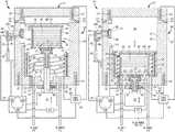
- FIG. 1is a schematic sectional view of a batch processing chamber 100 with a cassette 130 disposed in a first position, e.g., a raised position or a loading position, for loading a plurality of substrates 135 into the cassette 130 .
- the batch processing chamber 100has a chamber body 110 enclosing an internal volume 150 , and a lid 111 disposed on the chamber body 110 .
- the chamber body 110has an annular shape, though in other embodiments the body 110 may be rectangular or any closed shape.
- the chamber body 110may be fabricated in one or more sections.
- the chamber body 110includes lid 111 includes a bottom wall 115 , a sidewall 117 .
- the bottom wall 115has an inner surface 151 and an outer surface 153 .
- the sidewall 117has an inner surface 155 and an outer surface 157 .
- the lid 111 and the chamber body 110are held together by a static seal 118 .
- a cooling channel 119is disposed adjacent to the static seal 118 .
- the chamber body 110may include an upper spool and a lower spool positioned between the bottom 115 and the lid 111 .
- the chamber body 110may be fabricated from nickel-based steel alloys that exhibit high resistance to corrosion, such as but not limited to one or more Hastelloy®, Iconel®, and Monel® alloys.
- One or more cartridge heaters 112are disposed within the chamber body 110 , for example, within a recess of the bottom 115 or the sidewall 117 .
- the heaters 112are configured to actively heat the chamber body 110 and maintain the chamber body 110 at a temperature of greater than 290° C.
- Each of the heaters 112may be a resistive coil, a lamp, a ceramic heater, a graphite-based carbon fiber composite (CFC) heater, a stainless steel heater or an aluminum heater.
- the heaters 112are powered by a power source 105 .
- a temperature sensor 114is coupled to the chamber body 110 and configured to monitor the temperature of the chamber body 110 . Power to the heaters 112 is controlled by the controller 180 through feedback received from the temperature sensor 114 .
- the liner 116is disposed between a shell 120 and the sidewall 117 , advantageously reducing the amount of heat transferred between the shell 120 and the sidewall 117 , thus assisting regulating the temperature of the sidewall 117 .
- the cassette 130is moveably disposed within the internal volume 150 .
- the cassette 130may be fabricated from quartz, ceramic, or other thermally non-conductive material.
- the cassette 130houses a plurality of substrates 135 therein to facilitate transfer of the plurality of substrates 135 into and out of the batch processing chamber 100 .
- the cassette 130facilitates transfer of substrates 135 between a first position within the batch processing chamber 100 and a second position within the batch processing chamber 100 such that the substrates 135 are annealed at an elevated pressure and an elevated temperature.
- FIG. 1Cis a schematic bottom view of the cassette 130 .
- the bottom wall 134 of the cassette 130includes one or more spokes 104 radially extending from a central portion 330 to an annular-shaped peripheral portion 131 , defining the apertures 133 between adjacent spokes 104 .
- a plug 172is coupled to the bottom wall 134 of the cassette 130 .
- the plug 172includes one or more seals 175 .
- the sealsmay be disposed on a lower surface of the plug 172 .
- the plug 172is positioned vertically above an opening 154 formed through the bottom wall 115 of the chamber body 110 .
- the plug 172actuates vertically up and down with the cassette 130 during operation of the batch processing chamber 100 .
- the opening 154includes a stepped upper profile formed in the inner surface 151 and configured to accommodate the plug 172 therein.
- the plug 172is actuated vertically downward and engages a bottom surface of the stepped profile of the opening 154 with the seal 175 , thereby forming a seal between the plug 172 and the bottom wall 115 to prevent fluid flow through the opening 154 of the batch processing chamber 100 .
- the seal 175is made from a high-temperature polymer, such as but not limited to a perfluoroelastomer.
- the seal 175is an O-ring.
- the plug 172may be excluded.
- the bottom wall 134 of the cassette 130seals against the bottom 115 . It is contemplated that in such an example, the seals 175 may be positioned on a lower surface of the bottom wall 134 of the cassette 130 , or optionally, the seals 175 may be excluded.
- the plug 172also includes a cooling channel 176 disposed therein adjacent to the seal 175 .
- the cooling channel 176is fluidly connected to a cooling fluid source 177 .
- a cooling fluidsuch as but not limited to an inert, dielectric, and high-performance heat transfer fluid, may be circulated within the cooling channel 176 .
- the cooling channel 176is configured to cool the plug 172 and the seal 175 to maintain the seal 175 below a maximum integrity temperature (e.g., about 325° C.) during operation, thereby prolonging the useful life of the seal 175 .
- the plug 172is coupled to a shaft 174 which moves the plug 172 and the cassette 130 up and down within the internal volume 150 .
- the plug 172is disposed at an upper end of the shaft 174 , and may be a separate component of the shaft 174 or may be integrally formed therewith.
- a lower end of the shaft 174is coupled to an actuator 170 which facilitates motion of the shaft 174 .
- the shaft 174 and the actuator 170are controlled by the controller 180 .
- the batch processing chamber 100also includes a vacuum lip seal 160 .
- the vacuum lip seal 160is positioned adjacent the outer surface 153 of the bottom wall 115 , between the outer surface 153 and the actuator 170 .
- the vacuum lip seal 160includes a seal 165 to facilitate sealing of the vacuum lip seal 160 around the shaft 174 .
- the seal 165may be made from a high-temperature polymer, such as but not limited to a perfluoroelastomer.
- the vacuum lip seal 160functions as a back-up or redundant seal to the seals 175 . In the event of failure of the seal 175 , pressurized fluid or air escaping from the internal volume 150 is directed through an outlet 169 which is fluidly connected to a pump (not shown).
- the vacuum lip seal 160prevents leakage of pressurized processing fluid or air from the internal volume 150 , or ingress of ambient air into the internal volume 150 .
- the batch processing chamber 100also includes a thermal break 178 .
- the thermal breakis positioned adjacent an upper surface of the plug 172 and a lower surface of the bottom wall 134 of the cassette 130 .
- the thermal break 178may be adhered to the bottom wall 134 , or to the upper surface of the plug 172 .
- the thermal break 178is fabricated from ceramic, however, other materials are also contemplated.
- the thermal break 178is configured to restrict the flow of heat from the cassette 130 to outside the chamber by mitigating heat transfer between the cassette 130 and the shaft 174 .
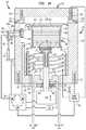
- FIG. 1Dis a partial schematic sectional view of a cylindrical shell positioned within the batch processing chamber.
- the cylindrical shell 120is positioned between the cassette 130 (when in the lowered position) and the optional insulating liner 116 .
- the shell 120includes a wall 123 having a heater 127 coupled to an inner surface 106 thereof.
- the shell 120is configured to heat a processing region 125 located within the wall 123 , and to shield an outer region 129 outside the wall 123 from the heat in the processing region 125 . Stated otherwise, the shell 120 facilitates thermal separation between the processing region 125 and the outer region 129 .
- the wall 123may be fabricated from a highly reflective sheet metal or a nickel-based steel alloy such as Hastelloy® alloy.
- An outer surface 107 of the wall 123may optionally be coated with an insulating layer (not shown) to further facilitate thermal separation between the processing region 125 and the outer region 129 .
- the inner surface 106 of the wall 123has a plurality of hooks 126 , such as ceramic hooks, coupled thereto.
- the plurality of hooks 126supports one or more heaters 127 thereon.
- the heaters 127are arranged in a helical or axially-aligned configured, and are configured to heat the processing region 125 and the plurality of substrates 135 placed therein during an annealing operation.
- the one or more heaters 127are configured to heat the processing region 125 to a temperature of up to 550° C.
- the heatersmay be for, example, resistive heaters, formed from nick-chromium alloy.
- the heaters 127 within the shell 120are electrically connected to the power source 105 .
- the inner surface 106is thermally reflective and is configured to reflect heat generated by the heaters 127 back into the processing region 125 .
- the inner surface 1may include a reflective coating thereon to further enhance thermal reflection.
- a pressure sensor 122is positioned in the processing region 125 on an inner surface 151 of the bottom 115 .
- the pressure sensor 122is configured to measure the pressure of the processing region 125 during the annealing process.
- a temperature sensor 124is positioned in the processing region 125 on the inner surface 151 of the bottom 115 adjacent the pressure sensor 122 , and the temperature sensor 124 is configured to measure the temperature of the processing region 125 during the annealing process.
- FIG. 1Dalso illustrates an example of the thermal break 178 .
- the thermal break 178is shaped as a capsulated cup. The capsulate cup minimizes contact with the bottom wall 134 of the cassette 130 .
- the thermal break 178has a thin cylindrical wall 108 surrounding a hollow central portion 109 .
- the hollow central portion 109 and the thin cylindrical wallreduce heat transfer between the cassette 130 and the plug 172 .
- the thermal break 178may omit the hollow central portion 109 .
- the thermal break 178may be formed from a thermally insulating material.
- FIG. 1Eis a schematic sectional view of a slit valve door 195 in an open configuration.
- FIG. 1Fis a schematic sectional view of a slit valve 195 door in a closed configuration.
- a slit valve door 195is used to provide access to the internal volume 150 through the loading port 158 by selectively opening and closing the loading port 158 .
- the slit valve door 195is configured to engage an inner surface 155 of the sidewall 117 surrounding the loading port 158 .
- a seal 199facilitates closure of the slit valve door 195 by sealing over the loading port 158 . Elevated pressures within the internal volume 150 force the slit valve door 195 and the seal 199 into engagement with the inner surface 155 , further.
- the seal 199may be made from a high-temperature polymer, such as but not limited to a perfluoroelastomer. In some embodiments, the seal 199 may be an O-ring.
- the slit valve door 195includes a rotating pin 105 a positioned in an elongated slot 105 b .
- the pin 105 acouples the slit valve door 195 to a bar 198 a .
- the bar 198 ais coupled to a horizontal actuator 194 a and a vertical actuator 190 .
- the horizontal actuator 194 ais configured to linearly move one end of the slit valve door 195 within the internal volume 150 towards and away from the loading port 158 .
- the slit valve door 195pivots about a pin 105 c while the pin 105 a moves within the elongated slot 105 b .
- a second horizontal actuator 194 bmay facilitate movement of the slit valve door 195 away from the inner surface 155 via a bar 198 b .
- the slit valve door 195may be pivoted into a non-vertical orientation, such as about 45 degrees relative to the inner surface 155 , to provide for ingress and egress of substrates.
- the horizontal actuators 194 a , 194 bmay be coupled to a bracket 196 , which is coupled to the vertical actuator 190 by a link 192 , to facilitate actuation of the bracket 196 .
- an inlet port 152is formed through the bottom wall 115 of the chamber body 110 and fluidly connects an inlet conduit 259 (shown in FIG. 2 ) to the internal volume 150 .
- An outlet port 156is also formed through the bottom wall 115 and connects the internal volume 150 to an outlet conduit 361 (shown in FIG. 3 ).
- the inlet port 152is fluidly coupled to a gas supply source to provide one or more gases (e.g., reagents, precursors, purge gas, or carrier gas).
- FIG. 2schematically illustrates a temperature-controlled inlet fluid circuit 200 .
- the temperature-controlled inlet fluid circuit 200is fluidly connectable to the inlet port 152 via an inlet conduit 259 .
- the inlet fluid circuit 200includes a gas panel 250 , a source conduit 257 , and an inlet isolation valve 255 coupled to the inlet conduit 259 .
- One or more heaters 252 , 254 , and 258are interfaced with different portions of the inlet fluid circuit 200 to facilitate temperature control throughout the inlet fluid circuit 200 .
- One or more temperature sensors 251 , 253 , and 256are interfaced with different portions of the inlet fluid circuit 200 to obtain temperature measurements and provide the temperature measurement information to the controller 180 , thereby facilitating feedback control.
- the source conduit 257is interfaced with and in thermal communication with the heater 252 .
- the inlet isolation valve 255is interfaced with and in thermal communication with the heater 254 .
- the inlet conduit 259is interfaced with and in thermal communication with the heater 258 .
- the temperature sensor 251is interfaced with the source conduit 257 and configured to measure the temperature of the source conduit 257 .
- the temperature sensor 253is interfaced with the inlet isolation valve 255 and configured to measure the temperature of the inlet isolation valve 255 .
- the temperature sensor 256is interfaced with the inlet conduit 259 and configured to measure the temperature of the inlet conduit 259 .
- a temperature reading device 205receives and displays the temperature measurements from the temperature sensors 251 , 253 and 256 .
- the temperature reading device 205sends the temperature information to the controller 180 to facilitate temperature control of the inlet fluid circuit 200 .
- FIG. 3schematically illustrates a temperature-controlled outlet fluid circuit 300 .
- the outlet fluid circuit 300is fluidly connectable to the outlet port 156 via an outlet conduit 361 .
- the outlet fluid circuit 300includes an outlet isolation valve 365 , an exhaust conduit 263 , a condenser 360 , and a pump 378 .
- One or more heaters 362 , 364 , and 366are interfaced with different portions of the outlet fluid circuit 300 to facilitate thermal control of the outlet fluid circuit 300 .
- One or more temperature sensors 367 , 368 , and 369are interfaced with different portions of the outlet fluid circuit 300 to obtain temperature measurements and provide the temperature measurement information to the controller 180 .
- the outlet conduit 361is interfaced with and in thermal communication with the heater 362 .
- the outlet isolation valve 265is interfaced with and in thermal communication with the heater 364 .
- the exhaust conduit 363is interfaced with and in thermal communication with the heater 366 .
- the temperature sensor 367is interfaced with the outlet conduit 361 and configured to measure the temperature of the outlet conduit 361 .
- the temperature sensor 368is interfaced with the outlet isolation valve 365 and configured to measure the temperature of the outlet isolation valve 365 .
- the temperature sensor 369is interfaced with the exhaust conduit 363 and configured to measure the temperature of the exhaust conduit 363 .
- a temperature reading device 305receives and displays the temperature measurements from the temperature sensors 367 , 368 and 369 .
- the temperature reading device 305sends the temperature information to the controller 180 to facilitate temperature control of the outlet fluid circuit 300 .
- a condenser 360is fluidly coupled to the internal volume 150 and configured to condense a processing fluid exiting the internal volume 150 through the outlet conduit 361 .
- the condensed processing fluid exiting the condenser 360may be routed through a heat exchanger 370 via an isolation valve 375 .
- the heat exchanger 370is configured to further cool the condensed processing fluid so that the processing fluid may be more easily managed.
- the condenser 360is fluidly connected to the isolation valve 375 by a condenser conduit 372 .
- the heat exchanger 370is coupled to the isolation valve 375 by a heat exchanger conduit 374 .
- a pump 378is fluidly connected to the heat exchanger 370 by a pump conduit 376 to facilitate pumping of the liquefied processing fluid from the heat exchanger 370 to a container (not shown) for recycling, reuse or disposal.
- the heaters 252 , 254 , 258 , 362 , 364 , and 366are configured to maintain a processing fluid that is flowing through the fluid circuits 200 and 300 at a predetermined temperature.
- the predetermined temperatureis greater than a condensation point of the processing fluid.
- the heaters 252 , 254 , 258 , 362 , 364 , and 366may be optionally covered with a layer of thermal insulation to prevent loss of heat into the outside environment, thereby improving temperature control efficiency of the fluid inlet circuit 200 and the fluid outlet circuit 300 .
- the heaters 252 , 254 , 258 , 362 , 364 , and 366may be lamps, resistive heating elements, fluid conduits for flowing a heat transfer fluid, or other suitable heating devices.
- the heaters 252 , 254 , 258 , 362 , 364 , and 366are resistive heaters wound around the elements of the fluid circuits 200 and 300 .
- the heaters 252 , 254 , 258 , 362 , 364 , and 366are individually coupled to the power source 105 .
- each of the heaters 252 , 254 , 258 , 362 , 364 , and 366may be independently controlled.
- the temperature sensors 251 , 253 , 256 , 367 , 368 and 369may each be a non-contact sensor, such as an infrared sensor, or a contact sensor, such as a thermocouple.
- the inlet isolation valve 255 and the outlet isolation valve 365are shutoff valves.
- the inlet isolation valve 255is open, the outlet isolation valve 365 is closed such that a processing fluid flowing through source conduit 257 enters into the inlet conduit 259 and the processing region 125 within the internal volume 150 .
- the outlet isolation valve 365is open, the inlet isolation valve 255 is closed such that a gaseous product is removed from the processing region 125 and flows through the outlet conduit 361 and the exhaust conduit 363 into the condenser 360 .
- the processing fluidis selected according to the process requirements for the desired annealing of the substrates in the batch processing chamber 100 .
- the processing fluidmay comprise an oxygen-containing and/or nitrogen-containing gas, such as oxygen, steam, water, hydrogen peroxide, and/or ammonia.
- the processing fluidmay contain a silicon-containing gas such as but not limited to one or more organosilicon compounds, one or more tetraalkyl orthosilicates, one or more disiloxanes, or any combination thereof.
- the processing fluidmay be steam under a pressure of up to 70 bar and at a temperature of about 550° C.
- the batch processing chamberalso includes a controller 180 .
- the controller 180controls the operation of the actuators 170 , 194 a , 194 b , and 190 , as well as the power source 105 of the batch processing chamber 100 .
- the controller 180is also connected to the cooling fluid source 177 , the inlet fluid circuit 200 ( FIG. 2 ) and the outlet fluid circuit 300 ( FIG. 3 ).
- the controller 180is communicatively connected to the pressure sensor 122 and the temperature sensors 114 and 124 .
- the controller 180includes a central processing unit (CPU) 182 , a memory 184 , and a support circuit 186 .
- the CPU 182may be any form of general purpose computer processor that may be used in an industrial setting.
- the memory 184may be random access memory, read only memory, floppy, or hard disk drive, or other form of digital storage.
- the support circuit 186is conventionally coupled to the CPU 182 and may include cache, clock circuits, input/output systems, power supplies, and/or the like.
- the batch processing chamber 100is configured for annealing a plurality of substrates 135 under a pressure of up to 70 bars and at a temperature of about 550° C.
- the heaters 112are powered on to pre-heat the batch processing chamber 100 and maintain the internal volume 150 at a temperature of greater than 290° C. to avoid condensation of a super-heated processing fluid subsequently introduced into the batch processing chamber 100 .
- the controllerdrives one or more actuators 190 , 194 a , 194 b to open the loading port 158 .
- the shaft 174is actuated by the actuator 170 to raise the cassette 130 within the internal volume 150 of the batch processing chamber 100 .
- the shaft 174incrementally aligns each substrate storage slot 138 with the loading port 158 so that the plurality of substrates 135 from a robotic end effector (not shown) can be loaded individually on a respective substrate storage slot 138 .
- the loading port 158is closed.
- the shaft 174is actuated by the actuator 170 to lower the cassette 130 within the internal volume 150 of the batch processing chamber 100 .
- the plug 172engages the inner surface 151 to seal the opening 154 .
- the lid 140 of the cassette 130is disposed over the wall 123 of the shell 120 , thus defining the processing region 125 .
- the heaters 127 positioned within the interior of the shell 120are powered on by the power source 105 to maintain the processing region 125 and the plurality of substrates 135 at a temperature of about 550° C.
- a processing fluid in a super-heated stateis introduced by the gas panel 250 into the processing region 125 through the inlet conduit 259 of the inlet fluid circuit 200 .
- the outlet fluid circuit 300is non-operational during introduction of fluid through the inlet conduit 259 .
- the pressure at which the fluid is appliedis increased incrementally.
- the fluidis steam which is introduced into the processing region 125 until a pressure of about 70 bar is established within the processing region 125 . Once a desired pressure is established within the processing region, the flow of fluid is halted.
- the plurality of substrates 135is exposed to the processing fluid, e.g., steam, under high pressure and at a high temperature to anneal the plurality of substrates 135 .
- the processing fluide.g., steam
- the processing region 125 , the inlet conduit 259 and the outlet conduit 361are maintained at a temperature and pressure such that the processing fluid stays in gaseous phase.
- the temperatures of the processing region 125 , the inlet conduit 259 and the outlet conduit 361are maintained at a temperature greater than the condensation point of the processing fluid at the applied pressure.
- the processing region 125 , the inlet conduit 259 and the outlet conduit 361are maintained at a pressure less than the condensation pressure of the processing gas at the applied temperature.
- the controller 180uses information from the temperature sensors 114 and 124 , the temperature reading devices 205 and 305 , and the pressure sensor 122 to control the flow of processing fluid, the applied pressure, and applied heat with respect to the batch processing chamber 100 .
- the outlet fluid circuit 300is activated to facilitate removal of the processing fluid form the processing region 125 .
- the processing fluidexits the processing region through the outlet conduit 361 of the outlet fluid circuit 300 .
- the inlet fluid circuit 200is non-operational during removal of processing gas from the processing region 125 .
- the heater 127is powered off after removal of the processing fluid from the processing region 125 to mitigate the formation of condensate within the processing region 125 .
- the shaft 174is then actuated by the actuator 170 to raise the cassette 130 within the internal volume 150 of the batch processing chamber 100 .
- the loading port 158is then opened via actuation of the slit valve door 195 , and the substrates 135 are removed individually from the batch processing chamber 100 .
- the batch processing chamber 100operates at a pressure less than 0.5 atm, when loading and unloading the plurality of substrates 135 to/from the cassette 130 .
- the vacuum lip seal 160is active as the shaft 174 moves the cassette 130 up and down within the internal volume 150 .
- the vacuum lip seal 160prevents the leakage of additional pressurized fluid or air into the internal volume 150 by sealing around the shaft 174 .
- the vacuum lip sealis coupled to a vacuum pump (not shown) to withdraw fluid or air through an outlet 169 .
- the vacuum lip seal 160facilitates removal of any pressurized processing fluid through the outlet 169 such that the vacuum integrity of the batch processing chamber 100 can be maintained during the low-pressure operation.
- the batch processing chamber described hereinoffers a number of benefits.
- the batch processing chamberis configured to operate under high pressure as well as under vacuum.
- the batch processing chamberincorporates a hollow cylindrical shell having a number of heaters disposed on the inner surface to heat a plurality of substrates up to 550° C. during processing, such as annealing.
- the shellacts as a heat shield to prevent the heat inside the shell from propagating to the chamber walls, allowing the temperature of the chamber walls to remain in a range from about 290° C. to about 325° C. Maintaining the temperature of the chamber walls in a range from about 290° C. to about 325° C. enables the use of seals to close the ports to the chamber without temperature degradation of the seals. Without the use of such seals, metal seals would be needed. However, metal seals require permanent installation and have limited reuse capability. Additionally, metal seals have a tendency to generate unwanted particle contamination.
- sealsallows the use pressure to form a more robust seal. It is contemplated that the disclosed plug coupled and the slit valve door both benefit from such seal positioning.
Landscapes
- Engineering & Computer Science (AREA)
- Physics & Mathematics (AREA)
- Condensed Matter Physics & Semiconductors (AREA)
- General Physics & Mathematics (AREA)
- Manufacturing & Machinery (AREA)
- Computer Hardware Design (AREA)
- Microelectronics & Electronic Packaging (AREA)
- Power Engineering (AREA)
- Chemical Vapour Deposition (AREA)
- Container, Conveyance, Adherence, Positioning, Of Wafer (AREA)
Abstract
Description
Claims (20)
Priority Applications (1)
| Application Number | Priority Date | Filing Date | Title |
|---|---|---|---|
| US16/157,808US10854483B2 (en) | 2017-11-16 | 2018-10-11 | High pressure steam anneal processing apparatus |
Applications Claiming Priority (2)
| Application Number | Priority Date | Filing Date | Title |
|---|---|---|---|
| US201762586935P | 2017-11-16 | 2017-11-16 | |
| US16/157,808US10854483B2 (en) | 2017-11-16 | 2018-10-11 | High pressure steam anneal processing apparatus |
Publications (2)
| Publication Number | Publication Date |
|---|---|
| US20190148186A1 US20190148186A1 (en) | 2019-05-16 |
| US10854483B2true US10854483B2 (en) | 2020-12-01 |
Family
ID=66433522
Family Applications (1)
| Application Number | Title | Priority Date | Filing Date |
|---|---|---|---|
| US16/157,808Active2039-03-14US10854483B2 (en) | 2017-11-16 | 2018-10-11 | High pressure steam anneal processing apparatus |
Country Status (7)
| Country | Link |
|---|---|
| US (1) | US10854483B2 (en) |
| JP (1) | JP7330181B2 (en) |
| KR (1) | KR102622303B1 (en) |
| CN (1) | CN111373519B (en) |
| SG (1) | SG11202003438QA (en) |
| TW (2) | TWI700748B (en) |
| WO (1) | WO2019099125A1 (en) |
Cited By (12)
| Publication number | Priority date | Publication date | Assignee | Title |
|---|---|---|---|---|
| US11177128B2 (en) | 2017-09-12 | 2021-11-16 | Applied Materials, Inc. | Apparatus and methods for manufacturing semiconductor structures using protective barrier layer |
| US11361978B2 (en) | 2018-07-25 | 2022-06-14 | Applied Materials, Inc. | Gas delivery module |
| US11462417B2 (en) | 2017-08-18 | 2022-10-04 | Applied Materials, Inc. | High pressure and high temperature anneal chamber |
| US11527421B2 (en) | 2017-11-11 | 2022-12-13 | Micromaterials, LLC | Gas delivery system for high pressure processing chamber |
| US11581183B2 (en) | 2018-05-08 | 2023-02-14 | Applied Materials, Inc. | Methods of forming amorphous carbon hard mask layers and hard mask layers formed therefrom |
| US11610773B2 (en) | 2017-11-17 | 2023-03-21 | Applied Materials, Inc. | Condenser system for high pressure processing system |
| US11694912B2 (en) | 2017-08-18 | 2023-07-04 | Applied Materials, Inc. | High pressure and high temperature anneal chamber |
| US11705337B2 (en) | 2017-05-25 | 2023-07-18 | Applied Materials, Inc. | Tungsten defluorination by high pressure treatment |
| US11749555B2 (en) | 2018-12-07 | 2023-09-05 | Applied Materials, Inc. | Semiconductor processing system |
| US11881411B2 (en) | 2018-03-09 | 2024-01-23 | Applied Materials, Inc. | High pressure annealing process for metal containing materials |
| US11901222B2 (en) | 2020-02-17 | 2024-02-13 | Applied Materials, Inc. | Multi-step process for flowable gap-fill film |
| US12198951B2 (en) | 2017-03-10 | 2025-01-14 | Applied Materials, Inc. | High pressure wafer processing systems and related methods |
Families Citing this family (8)
| Publication number | Priority date | Publication date | Assignee | Title |
|---|---|---|---|---|
| US10714331B2 (en) | 2018-04-04 | 2020-07-14 | Applied Materials, Inc. | Method to fabricate thermally stable low K-FinFET spacer |
| US10675581B2 (en) | 2018-08-06 | 2020-06-09 | Applied Materials, Inc. | Gas abatement apparatus |
| CN112640065B (en) | 2018-10-30 | 2024-10-01 | 应用材料公司 | Method for etching structures for semiconductor applications |
| WO2020101935A1 (en) | 2018-11-16 | 2020-05-22 | Applied Materials, Inc. | Film deposition using enhanced diffusion process |
| US11415230B2 (en)* | 2020-03-31 | 2022-08-16 | Applied Material, Inc. | Slit valve pneumatic control |
| US12002668B2 (en)* | 2021-06-25 | 2024-06-04 | Applied Materials, Inc. | Thermal management hardware for uniform temperature control for enhanced bake-out for cluster tool |
| JP7465855B2 (en)* | 2021-09-27 | 2024-04-11 | 芝浦メカトロニクス株式会社 | Heat treatment device, loading/unloading tool, and method for forming organic film |
| CN117542767B (en)* | 2024-01-10 | 2024-03-26 | 合肥费舍罗热工装备有限公司 | Vertical semiconductor welding furnace |
Citations (292)
| Publication number | Priority date | Publication date | Assignee | Title |
|---|---|---|---|---|
| US4524587A (en) | 1967-01-10 | 1985-06-25 | Kantor Frederick W | Rotary thermodynamic apparatus and method |
| JPS634616A (en) | 1986-06-25 | 1988-01-09 | Hitachi Tokyo Electron Co Ltd | Steam treating unit |
| US4879259A (en) | 1987-09-28 | 1989-11-07 | The Board Of Trustees Of The Leland Stanford Junion University | Rapid thermal annealing of gallium arsenide with trimethyl arsenic overpressure |
| US5050540A (en) | 1991-01-29 | 1991-09-24 | Arne Lindberg | Method of gas blanketing a boiler |
| US5092728A (en)* | 1987-10-15 | 1992-03-03 | Epsilon Technology, Inc. | Substrate loading apparatus for a CVD process |
| US5114513A (en) | 1988-10-27 | 1992-05-19 | Omron Tateisi Electronics Co. | Optical device and manufacturing method thereof |
| US5126117A (en) | 1990-05-22 | 1992-06-30 | Custom Engineered Materials, Inc. | Device for preventing accidental releases of hazardous gases |
| US5149378A (en) | 1989-04-10 | 1992-09-22 | Hashimoto Kasei Kabushiki-Kaisya | Tungsten film forming apparatus |
| US5175123A (en) | 1990-11-13 | 1992-12-29 | Motorola, Inc. | High-pressure polysilicon encapsulated localized oxidation of silicon |
| US5319212A (en) | 1992-10-07 | 1994-06-07 | Genus, Inc. | Method of monitoring ion beam current in ion implantation apparatus for use in manufacturing semiconductors |
| US5329095A (en)* | 1992-04-09 | 1994-07-12 | Tokyo Electron Kabushiki Kaisha | Thermal treatment apparatus utilizing heated lid |
| JPH06283496A (en) | 1993-03-26 | 1994-10-07 | Dainippon Screen Mfg Co Ltd | Dryer of substrate after washing |
| US5366905A (en) | 1991-11-05 | 1994-11-22 | Fujitsu Limited | Method for producing conducting layers for a semiconductor device |
| JPH0748489B2 (en) | 1987-07-27 | 1995-05-24 | 富士通株式会社 | Plasma processing device |
| US5578132A (en) | 1993-07-07 | 1996-11-26 | Tokyo Electron Kabushiki Kaisha | Apparatus for heat treating semiconductors at normal pressure and low pressure |
| US5590695A (en) | 1993-04-28 | 1997-01-07 | Advanced Delivery & Chemical Systems, Inc. | Manifold systems for high purity chemical delivery systems |
| US5620524A (en) | 1995-02-27 | 1997-04-15 | Fan; Chiko | Apparatus for fluid delivery in chemical vapor deposition systems |
| US5808245A (en) | 1995-01-03 | 1998-09-15 | Donaldson Company, Inc. | Vertical mount catalytic converter muffler |
| US5858051A (en) | 1995-05-08 | 1999-01-12 | Toshiba Machine Co., Ltd. | Method of manufacturing optical waveguide |
| US5879756A (en) | 1996-09-19 | 1999-03-09 | Lambda Technologies, Inc. | Curing polymer layers on semiconductor substrates using variable frequency microwave energy |
| US5880041A (en) | 1994-05-27 | 1999-03-09 | Motorola Inc. | Method for forming a dielectric layer using high pressure |
| US5940985A (en) | 1996-03-01 | 1999-08-24 | Tokyo Electron Limited | Apparatus and method for drying substrates |
| US6082950A (en) | 1996-11-18 | 2000-07-04 | Applied Materials, Inc. | Front end wafer staging with wafer cassette turntables and on-the-fly wafer center finding |
| US6136664A (en) | 1997-08-07 | 2000-10-24 | International Business Machines Corporation | Filling of high aspect ratio trench isolation |
| US6150286A (en) | 2000-01-03 | 2000-11-21 | Advanced Micro Devices, Inc. | Method of making an ultra thin silicon nitride film |
| US6164963A (en)* | 1997-03-07 | 2000-12-26 | Weaver; Robert A. | Semiconductor furnace processing vessel base |
| US6164412A (en) | 1998-04-03 | 2000-12-26 | Arvin Industries, Inc. | Muffler |
| JP2001110729A (en) | 1999-10-06 | 2001-04-20 | Mitsubishi Heavy Ind Ltd | Apparratus for continuously manufacturing method of semiconductor element |
| US6242368B1 (en) | 1996-03-29 | 2001-06-05 | Praxair Technology, Inc. | Removal of carbon from substrate surface |
| US6251751B1 (en) | 1997-10-16 | 2001-06-26 | International Business Machines Corporation | Bulk and strained silicon on insulator using local selective oxidation |
| US6299753B1 (en) | 1999-09-01 | 2001-10-09 | Applied Materials, Inc. | Double pressure vessel chemical dispenser unit |
| US20010029108A1 (en) | 2000-03-06 | 2001-10-11 | Kouji Tometsuka | Substrate processeing apparatus, substrate processing method and electronic device manufacturing method |
| US20010041122A1 (en) | 1998-09-28 | 2001-11-15 | Applied Materials, Inc. | Single wafer load lock with internal wafer transport |
| US6319766B1 (en) | 2000-02-22 | 2001-11-20 | Applied Materials, Inc. | Method of tantalum nitride deposition by tantalum oxide densification |
| US20010050096A1 (en) | 2000-04-18 | 2001-12-13 | Costantini Michael A. | Supercritical fluid delivery and recovery system for semiconductor wafer processing |
| US6334266B1 (en) | 1999-09-20 | 2002-01-01 | S.C. Fluids, Inc. | Supercritical fluid drying system and method of use |
| US6368412B1 (en) | 1997-11-18 | 2002-04-09 | Nec Corporation | Apparatus with high temperature gas releasing means for vapor deposition of parylene polymer without peeling |
| US20020066535A1 (en) | 1995-07-10 | 2002-06-06 | William Brown | Exhaust system for treating process gas effluent |
| US20020073922A1 (en) | 1996-11-13 | 2002-06-20 | Jonathan Frankel | Chamber liner for high temperature processing chamber |
| US6442980B2 (en) | 1997-11-26 | 2002-09-03 | Chart Inc. | Carbon dioxide dry cleaning system |
| US20020122885A1 (en) | 2001-03-01 | 2002-09-05 | Micron Technology, Inc. | Methods, systems, and apparatus for uniform chemical-vapor depositions |
| US20020134439A1 (en) | 2001-03-22 | 2002-09-26 | Hiroyuki Kawasaki | Gas recirculation flow control method and apparatus for use in vacuum system |
| US20020151128A1 (en) | 1996-01-22 | 2002-10-17 | Lane Richard H. | High-pressure anneal process for integrated circuits |
| US20020148492A1 (en) | 2001-04-17 | 2002-10-17 | Kabushiki Kaisha Kobe Seiko Sho | High-pressure processing apparatus |
| US6468490B1 (en) | 2000-06-29 | 2002-10-22 | Applied Materials, Inc. | Abatement of fluorine gas from effluent |
| US20020155714A1 (en) | 2001-04-20 | 2002-10-24 | Kawasaki Microelectronics, Inc. Mihama-Ku, Japan | Method of conditioning an etching chamber and method of processing semiconductor substrate using the etching chamber |
| US6500603B1 (en) | 1999-11-11 | 2002-12-31 | Mitsui Chemicals, Inc. | Method for manufacturing polymer optical waveguide |
| US20030030945A1 (en) | 2001-08-10 | 2003-02-13 | Seagate Technology Llc | Tunneling magnetoresistive sensor with spin polarized current injection |
| JP2003051474A (en) | 2001-08-03 | 2003-02-21 | Kobe Steel Ltd | High-pressure processing apparatus |
| US20030049372A1 (en) | 1997-08-11 | 2003-03-13 | Cook Robert C. | High rate deposition at low pressures in a small batch reactor |
| US20030101938A1 (en) | 1998-10-27 | 2003-06-05 | Applied Materials, Inc. | Apparatus for the deposition of high dielectric constant films |
| US6583497B2 (en) | 1999-08-17 | 2003-06-24 | Applied Materials Inc. | Surface treatment of c-doped SiO2 film to enhance film stability during O2 ashing |
| KR20030052162A (en) | 2001-12-20 | 2003-06-26 | 동부전자 주식회사 | Post treatment method for metal line of semiconductor device |
| US20030148631A1 (en) | 1999-11-08 | 2003-08-07 | Taiwan Semiconductor Manufacturing Company | Oxidative annealing method for forming etched spin-on-glass (SOG) planarizing layer with uniform etch profile |
| US20030148035A1 (en) | 2002-02-07 | 2003-08-07 | Applied Materials, Inc. | Article for use in a semiconductor processing chamber and method of fabricating same |
| US6619304B2 (en) | 2001-09-13 | 2003-09-16 | Micell Technologies, Inc. | Pressure chamber assembly including non-mechanical drive means |
| US20030207593A1 (en) | 2002-05-02 | 2003-11-06 | Micron Technology, Inc. | Atomic layer deposition and conversion |
| US20040025908A1 (en) | 2000-04-18 | 2004-02-12 | Stephen Douglas | Supercritical fluid delivery system for semiconductor wafer processing |
| US20040060519A1 (en) | 2002-10-01 | 2004-04-01 | Seh America Inc. | Quartz to quartz seal using expanded PTFE gasket material |
| JP2004127958A (en) | 2002-09-30 | 2004-04-22 | Kyoshin Engineering:Kk | Apparatus and method for performing high pressure anneal steam treatment |
| US20040074869A1 (en) | 2002-10-18 | 2004-04-22 | Applied Materials, Inc. | Fluorine free integrated process for etching aluminum including chamber dry clean |
| US6730885B2 (en)* | 2000-07-06 | 2004-05-04 | Tokyo Electron Limited | Batch type heat treatment system, method for controlling same, and heat treatment method |
| US6733592B2 (en)* | 1999-03-17 | 2004-05-11 | Kobe Steel, Ltd. | High-temperature and high-pressure treatment device |
| US20040112409A1 (en) | 2002-12-16 | 2004-06-17 | Supercritical Sysems, Inc. | Fluoride in supercritical fluid for photoresist and residue removal |
| US6797336B2 (en) | 2001-03-22 | 2004-09-28 | Ambp Tech Corporation | Multi-component substances and processes for preparation thereof |
| US20040219800A1 (en) | 2001-06-22 | 2004-11-04 | Marcel Tognetti | Thermal oxidation process control by controlling oxidation agent partial pressure |
| US20040248392A1 (en) | 2003-02-04 | 2004-12-09 | Applied Materials, Inc. | Tailoring nitrogen profile in silicon oxynitride using rapid thermal annealing with ammonia under ultra-low pressure |
| US20050003655A1 (en) | 1998-02-27 | 2005-01-06 | Micron Technology, Inc. | MOCVD process using ozone as a reactant to deposit a metal oxide barrier layer |
| JP2005064269A (en) | 2003-08-13 | 2005-03-10 | Kobe Steel Ltd | High pressure processing method |
| WO2005057663A2 (en) | 2003-12-10 | 2005-06-23 | Koninklijke Philips Electronics N.V. | Method and apparatus for fabrication of metal-oxide semiconductor integrated circuit devices |
| US20050136684A1 (en) | 2003-12-23 | 2005-06-23 | Applied Materials, Inc. | Gap-fill techniques |
| TW200529284A (en) | 2004-02-19 | 2005-09-01 | Taiwan Semiconductor Mfg | An intelligent full automation controlled flow for a semiconductor furnace tool |
| US20050191828A1 (en) | 2000-08-11 | 2005-09-01 | Applied Materials, Inc. | Method for ion implanting insulator material to reduce dielectric constant |
| US20050198971A1 (en) | 2002-10-02 | 2005-09-15 | Kelly Leitch | High pressure CO2 purification and supply system |
| US20050250347A1 (en) | 2003-12-31 | 2005-11-10 | Bailey Christopher M | Method and apparatus for maintaining by-product volatility in deposition process |
| JP2005333015A (en) | 2004-05-20 | 2005-12-02 | Kobe Steel Ltd | Method for desiccating microstructure, and microstructure obtained thereby |
| US20050269291A1 (en) | 2004-06-04 | 2005-12-08 | Tokyo Electron Limited | Method of operating a processing system for treating a substrate |
| US20060003596A1 (en) | 2004-07-01 | 2006-01-05 | Micron Technology, Inc. | Low temperature process for polysilazane oxidation/densification |
| US20060105107A1 (en) | 2004-10-15 | 2006-05-18 | Lindeboom Bartholomeus H L | Reactor design for reduced particulate generation |
| US20060124613A1 (en) | 2002-05-08 | 2006-06-15 | Satyendra Kumar | Plasma-assisted heat treatment |
| US7084079B2 (en) | 2001-08-10 | 2006-08-01 | International Business Machines Corporation | Method for low temperature chemical vapor deposition of low-k films using selected cyclosiloxane and ozone gases for semiconductor applications |
| US20060175012A1 (en) | 2005-02-07 | 2006-08-10 | Beung-Keun Lee | Semiconductor fabrication equipment and method for controlling pressure |
| US20060207633A1 (en) | 2005-03-21 | 2006-09-21 | Pkl Co., Ltd. | Device and method for cleaning photomask |
| US7111630B2 (en) | 2001-05-17 | 2006-09-26 | Dainippon Screen Mfg. Co., Ltd. | High pressure processing apparatus and method |
| US7114517B2 (en) | 2001-11-26 | 2006-10-03 | Sund Wesley E | High purity fluid delivery system |
| US20060226117A1 (en) | 2005-03-29 | 2006-10-12 | Bertram Ronald T | Phase change based heating element system and method |
| US7128570B2 (en)* | 2004-01-21 | 2006-10-31 | Asm International N.V. | Method and apparatus for purging seals in a thermal reactor |
| US20060279025A1 (en) | 2005-06-10 | 2006-12-14 | Babak Heidari | Pattern replication with intermediate stamp |
| US20060290017A1 (en) | 2005-06-28 | 2006-12-28 | Masaki Yanagisawa | Method for transcribing patterns on resin body, method for manufacturing planar waveguide, and method for manufacturing micro-lens |
| US20070012402A1 (en) | 2003-07-08 | 2007-01-18 | Sundew Technologies, Llc | Apparatus and method for downstream pressure control and sub-atmospheric reactive gas abatement |
| US20070045753A1 (en) | 2005-08-30 | 2007-03-01 | Sangwoo Pae | Semiconductor device having a metal gate electrode formed on an annealed high-k gate dielectric layer |
| US7211525B1 (en) | 2005-03-16 | 2007-05-01 | Novellus Systems, Inc. | Hydrogen treatment enhanced gap fill |
| TW200721316A (en) | 2005-08-05 | 2007-06-01 | Hitachi Int Electric Inc | Substrate processing apparatus, cooling gas feed nozzle and method for manufacturing semiconductor device |
| KR20070075383A (en) | 2003-03-07 | 2007-07-18 | 동경 엘렉트론 주식회사 | Tungsten Film Formation Method |
| US20070187386A1 (en) | 2006-02-10 | 2007-08-16 | Poongsan Microtec Corporation | Methods and apparatuses for high pressure gas annealing |
| US20070204797A1 (en) | 2006-03-03 | 2007-09-06 | Andreas Fischer | Methods and apparatus for selective pre-coating of a plasma processing chamber |
| US20070212850A1 (en) | 2002-09-19 | 2007-09-13 | Applied Materials, Inc. | Gap-fill depositions in the formation of silicon containing dielectric materials |
| JP2007242791A (en) | 2006-03-07 | 2007-09-20 | Hitachi Kokusai Electric Inc | Substrate processing equipment |
| US7282458B2 (en) | 2004-01-16 | 2007-10-16 | International Business Machines Corporation | Low K and ultra low K SiCOH dielectric films and methods to form the same |
| US20070243317A1 (en) | 2002-07-15 | 2007-10-18 | Du Bois Dale R | Thermal Processing System and Configurable Vertical Chamber |
| US20070256559A1 (en) | 2006-05-08 | 2007-11-08 | The Board Of Trustees Of The University Of Illinois | Integrated vacuum absorption steam cycle gas separation |
| US20080074658A1 (en) | 2003-12-23 | 2008-03-27 | Davis Matthew F | Method and apparatus for performing limited area spectral analysis |
| US7351057B2 (en)* | 2005-04-27 | 2008-04-01 | Asm International N.V. | Door plate for furnace |
| JP2008073611A (en) | 2006-09-21 | 2008-04-03 | Dainippon Screen Mfg Co Ltd | High pressure treating device |
| US20080083109A1 (en) | 2006-09-25 | 2008-04-10 | Hitachi Kokusai Electric Inc. | Substrate processing apparatus and attaching/detaching method of reaction vessel |
| US7361231B2 (en) | 2005-07-01 | 2008-04-22 | Ekc Technology, Inc. | System and method for mid-pressure dense phase gas and ultrasonic cleaning |
| US20080115726A1 (en) | 2004-08-27 | 2008-05-22 | Applied Materials, Inc. | gap-fill depositions introducing hydroxyl-containing precursors in the formation of silicon containing dielectric materials |
| US20080121882A1 (en) | 2006-11-07 | 2008-05-29 | Jack Hwang | Method to reduce junction leakage through partial regrowth with ultrafast anneal and structures formed thereby |
| WO2008089178A2 (en) | 2007-01-16 | 2008-07-24 | Varian Semiconductor Equipment Associates, Inc. | Plasma source with liner for reducing metal contamination |
| US20080210273A1 (en) | 2005-11-08 | 2008-09-04 | Tokyo Electron Limited | Batch photoresist dry strip and ash system and process |
| US20080251904A1 (en) | 2007-04-13 | 2008-10-16 | Infineon Technologies Ag | Curing layers of a semiconductor product using electromagnetic fields |
| US7460760B2 (en) | 2005-09-13 | 2008-12-02 | Electronics And Telecommunications Research Institute | Optical waveguide master and method of manufacturing the same |
| US20090018688A1 (en) | 2007-06-15 | 2009-01-15 | Applied Materials, Inc. | Methods and systems for designing and validating operation of abatement systems |
| KR20090011463A (en) | 2007-07-26 | 2009-02-02 | 주식회사 풍산마이크로텍 | Method of manufacturing semiconductor device through high pressure oxygen heat treatment |
| US20090032190A1 (en)* | 2007-07-31 | 2009-02-05 | Tokyo Electron Limited | Plasma processing apparatus of batch type |
| US7491658B2 (en) | 2004-10-13 | 2009-02-17 | International Business Machines Corporation | Ultra low k plasma enhanced chemical vapor deposition processes using a single bifunctional precursor containing both a SiCOH matrix functionality and organic porogen functionality |
| US7503334B1 (en) | 2002-02-05 | 2009-03-17 | Novellus Systems, Inc. | Apparatus and methods for processing semiconductor substrates using supercritical fluids |
| US20090081884A1 (en) | 2007-09-24 | 2009-03-26 | Yoshitaka Yokota | Method of improving oxide growth rate of selective oxidation processes |
| US7521089B2 (en) | 2002-06-13 | 2009-04-21 | Tokyo Electron Limited | Method and apparatus for controlling the movement of CVD reaction byproduct gases to adjacent process chambers |
| KR20090040867A (en) | 2007-10-22 | 2009-04-27 | 어플라이드 머티어리얼스, 인코포레이티드 | How to Form a Dielectric Layer in a Trench |
| US20090110622A1 (en) | 2007-10-26 | 2009-04-30 | Applied Materials, Inc. | Methods and apparatus for smart abatement using an improved fuel circuit |
| US7541297B2 (en) | 2007-10-22 | 2009-06-02 | Applied Materials, Inc. | Method and system for improving dielectric film quality for void free gap fill |
| JP2009129927A (en) | 2007-11-19 | 2009-06-11 | Jgc Catalysts & Chemicals Ltd | Method of repairing damaged low-dielectric constant silica-based film and low-dielectric-constant silica-based film restored by the same |
| KR20090064279A (en) | 2007-12-14 | 2009-06-18 | 노벨러스 시스템즈, 인코포레이티드 | Protective layer for damage-free gap filling |
| US20090180847A1 (en) | 2005-08-26 | 2009-07-16 | George Xinsheng Guo | Multi-chamber vacuum processing and transfer system |
| US20090186481A1 (en) | 2008-01-22 | 2009-07-23 | Tokyo Electron Limited | Method for integrating selective low-temperature ruthenium deposition into copper metallization of a semiconductor device |
| US7576441B2 (en) | 2003-06-17 | 2009-08-18 | Micron Technology, Inc. | Boron-doped amorphous carbon film for use as a hard etch mask during the formation of a semiconductor device |
| US20090233449A1 (en) | 2005-02-22 | 2009-09-17 | Xactix, Inc. | Etching chamber with subchamber |
| US20090243126A1 (en) | 2008-03-31 | 2009-10-01 | Ryuta Washiya | Method and apparatus for imprinting microstructure and stamper therefor |
| US20100006211A1 (en) | 2007-03-22 | 2010-01-14 | 3M Innovative Properties Company | Microreplication tools and patterns using laser induced thermal embossing |
| US20100012292A1 (en) | 2007-03-31 | 2010-01-21 | Tokyo Electron Limited | Trap apparatus, exhaust system and processing system using same |
| US7650965B2 (en) | 2006-06-09 | 2010-01-26 | Emcon Technologies Llc | Exhaust system |
| US7651959B2 (en) | 2007-12-03 | 2010-01-26 | Asm Japan K.K. | Method for forming silazane-based dielectric film |
| US20100022068A1 (en) | 2008-07-25 | 2010-01-28 | Neng-Kuo Chen | Sti film property using sod post-treatment |
| KR20100035000A (en) | 2008-09-25 | 2010-04-02 | 삼성전자주식회사 | Semiconductor device having isolation layer with isolation trench of different aspect ratio and isolation trench gap fill method of fabricating the same |
| US20100173495A1 (en) | 2004-11-22 | 2010-07-08 | Applied Materials, Inc. | Substrate processing apparatus using a batch processing chamber |
| JP2010205854A (en) | 2009-03-02 | 2010-09-16 | Fujitsu Semiconductor Ltd | Method of manufacturing semiconductor device |
| US7815739B2 (en)* | 2005-02-18 | 2010-10-19 | Tokyo Electron Limited | Vertical batch processing apparatus |
| CN101871043A (en) | 2010-06-25 | 2010-10-27 | 东莞市康汇聚线材科技有限公司 | Annealing furnace steam generator and control method thereof |
| US7825038B2 (en) | 2006-05-30 | 2010-11-02 | Applied Materials, Inc. | Chemical vapor deposition of high quality flow-like silicon dioxide using a silicon containing precursor and atomic oxygen |
| US7825042B2 (en) | 2000-01-18 | 2010-11-02 | Applied Materials, Inc. | Very low dielectric constant plasma-enhanced CVD films |
| US20100304027A1 (en) | 2009-05-27 | 2010-12-02 | Applied Materials, Inc. | Substrate processing system and methods thereof |
| US20100320459A1 (en) | 2009-06-22 | 2010-12-23 | Fujifilm Corporation | Thin film transistor and method of producing thin film transistor |
| US20100327422A1 (en) | 2009-06-29 | 2010-12-30 | Samsung Electronics Co., Ltd | Semiconductor chip, method of fabricating the same, and stack module and memory card including the same |
| US7867923B2 (en) | 2007-10-22 | 2011-01-11 | Applied Materials, Inc. | High quality silicon oxide films by remote plasma CVD from disilane precursors |
| US7891228B2 (en) | 2008-11-18 | 2011-02-22 | Mks Instruments, Inc. | Dual-mode mass flow verification and mass flow delivery system and method |
| US20110151677A1 (en) | 2009-12-21 | 2011-06-23 | Applied Materials, Inc. | Wet oxidation process performed on a dielectric material formed from a flowable cvd process |
| US20110165781A1 (en) | 2010-01-06 | 2011-07-07 | Applied Materials, Inc. | Flowable dielectric using oxide liner |
| US20110198736A1 (en) | 2010-02-17 | 2011-08-18 | Asm America, Inc. | Reactive site deactivation against vapor deposition |
| US8027089B2 (en) | 2005-10-07 | 2011-09-27 | Nikon Corporation | Minute structure and its manufacturing method |
| KR20110136532A (en) | 2010-06-15 | 2011-12-21 | 서울대학교산학협력단 | 1T DRAM device having two gates in the recessed body, its operation method and manufacturing method |
| JP2012503883A (en) | 2008-09-24 | 2012-02-09 | ラム リサーチ コーポレーション | Method and system for preventing feature collapse during microelectronic topography manufacturing |
| US20120048304A1 (en) | 2010-08-30 | 2012-03-01 | Yukiko Kitajima | Supercritical drying method and supercritical drying system |
| US20120056173A1 (en) | 2010-09-03 | 2012-03-08 | Applied Materials, Inc. | Staggered thin film transistor and method of forming the same |
| US20120060868A1 (en) | 2005-06-07 | 2012-03-15 | Donald Gray | Microscale fluid delivery system |
| US20120142192A1 (en) | 2010-07-30 | 2012-06-07 | Applied Materials, Inc. | Oxide-rich liner layer for flowable cvd gapfill |
| US20120175822A1 (en) | 2009-09-16 | 2012-07-12 | Bridgestone Corporation | Photo-curable transfer sheet and method for forming concave-convex pattern using the same |
| US20120252210A1 (en) | 2011-03-30 | 2012-10-04 | Tokyo Electron Limited | Method for modifying metal cap layers in semiconductor devices |
| WO2012133583A1 (en) | 2011-03-30 | 2012-10-04 | 大日本印刷株式会社 | Supercritical drying device and supercritical drying method |
| JP2012204656A (en) | 2011-03-25 | 2012-10-22 | Toshiba Corp | Supercritical drying method of semiconductor substrate |
| US8306026B2 (en) | 2005-12-15 | 2012-11-06 | Toshiba America Research, Inc. | Last hop topology sensitive multicasting key management |
| US20120285492A1 (en) | 2011-05-12 | 2012-11-15 | Applied Materials, Inc. | Methods of dry stripping boron-carbon films |
| US20120304485A1 (en) | 2011-05-30 | 2012-12-06 | Tokyo Electron Limited | Substrate processing method, substrate processing apparatus, and storage medium |
| US8349085B2 (en) | 2007-01-31 | 2013-01-08 | Tokyo Electron Limited | Substrate processing apparatus |
| JP2013516788A (en) | 2010-01-07 | 2013-05-13 | アプライド マテリアルズ インコーポレイテッド | In situ ozone curing for radical component CVD |
| US8449942B2 (en) | 2009-11-12 | 2013-05-28 | Applied Materials, Inc. | Methods of curing non-carbon flowable CVD films |
| JP2013105777A (en) | 2011-11-10 | 2013-05-30 | Tokyo Electron Ltd | Substrate processing apparatus, substrate processing method and storage medium |
| US8455368B2 (en) | 2007-05-25 | 2013-06-04 | Applied Materials, Inc. | Methods and apparatus for assembling and operating electronic device manufacturing systems |
| US8466073B2 (en) | 2011-06-03 | 2013-06-18 | Applied Materials, Inc. | Capping layer for reduced outgassing |
| KR101287035B1 (en) | 2013-05-07 | 2013-07-17 | 호용종합건설주식회사 | Boiler system for pipe regeneration |
| US20130194350A1 (en) | 2012-01-31 | 2013-08-01 | Ricoh Company, Ltd. | Thin film forming apparatus, thin film forming method, electro-mechanical transducer element, liquid ejecting head, and inkjet recording apparatus |
| JP2013179244A (en) | 2011-05-30 | 2013-09-09 | Toshiba Corp | Method for processing substrate, device for processing substrate and storage medium |
| US20130233170A1 (en) | 2005-09-13 | 2013-09-12 | Rasirc | Methods and devices for producing high purity steam |
| US8536065B2 (en) | 2010-10-05 | 2013-09-17 | Applied Materials, Inc. | Ultra high selectivity doped amorphous carbon strippable hardmask development and integration |
| US8557712B1 (en) | 2008-12-15 | 2013-10-15 | Novellus Systems, Inc. | PECVD flowable dielectric gap fill |
| US8563445B2 (en) | 2010-03-05 | 2013-10-22 | Applied Materials, Inc. | Conformal layers by radical-component CVD |
| US20130288485A1 (en) | 2012-04-30 | 2013-10-31 | Applied Materials, Inc. | Densification for flowable films |
| US20130330042A1 (en) | 2011-12-09 | 2013-12-12 | Furukawa Electric Co., Ltd. | Optical branching element and optical branching circuit |
| US20130337171A1 (en) | 2012-06-13 | 2013-12-19 | Qualcomm Mems Technologies, Inc. | N2 purged o-ring for chamber in chamber ald system |
| KR20140003776A (en) | 2012-06-28 | 2014-01-10 | 주식회사 메카로닉스 | Preparation of a high resistivity zno thin film |
| US20140023320A1 (en) | 2011-03-25 | 2014-01-23 | Seo Young Lee | Lightwave Circuit and Method for Manufacturing Same |
| JP2014019912A (en) | 2012-07-19 | 2014-02-03 | Tokyo Electron Ltd | Method of depositing tungsten film |
| US20140045300A1 (en) | 2012-08-10 | 2014-02-13 | Taiwan Semiconductor Manufacturing Co., Ltd. | Warpage control in a package-on-package structure |
| US20140076494A1 (en) | 2012-09-18 | 2014-03-20 | Tokyo Electron Limited | Processing system |
| US20140134827A1 (en) | 2010-04-15 | 2014-05-15 | Novellus Systems, Inc. | Conformal film deposition for gapfill |
| US20140138802A1 (en) | 2011-06-16 | 2014-05-22 | Fujifilm Manufacturing Europe Bv | Method and Device for Manufacturing a Barrier Layer on a Flexible Substrate |
| US8741788B2 (en) | 2009-08-06 | 2014-06-03 | Applied Materials, Inc. | Formation of silicon oxide using non-carbon flowable CVD processes |
| US20140183743A1 (en) | 2012-12-27 | 2014-07-03 | Tokyo Electron Limited | Manganese metal film forming method, processing system, electronic device manufacturing method and electronic device |
| US20140235068A1 (en) | 2011-11-01 | 2014-08-21 | Hitachi Kokusai Electric Inc. | Method of manufacturing semiconductor device, apparatus for manufacturing semiconductor device, and non-transitory computer-readable recording medium |
| US20140231384A1 (en) | 2013-02-19 | 2014-08-21 | Applied Materials, Inc. | Hdd patterning using flowable cvd film |
| US20140239291A1 (en) | 2013-02-27 | 2014-08-28 | Inha-Industry Partnership Institute | Metal-oxide semiconductor thin film transistors and methods of manufacturing the same |
| CN104047676A (en) | 2014-06-14 | 2014-09-17 | 马根昌 | Improved opposite impact silencer |
| US20140264237A1 (en) | 2013-03-13 | 2014-09-18 | Macronix International Co., Ltd. | Resistive ram and fabrication method |
| US20140268080A1 (en) | 2013-03-12 | 2014-09-18 | Applied Materials, Inc. | Planarized extreme ultraviolet lithography blank, and manufacturing and lithography systems therefor |
| US20140284821A1 (en) | 2013-03-22 | 2014-09-25 | Robert L. Hubbard | Method of curing thermoplastics with microwave energy |
| CN104089491A (en) | 2014-07-03 | 2014-10-08 | 肇庆宏旺金属实业有限公司 | Waste heat recycling system of annealing furnace |
| US8871656B2 (en) | 2012-03-05 | 2014-10-28 | Applied Materials, Inc. | Flowable films using alternative silicon precursors |
| US20140322921A1 (en) | 2013-04-26 | 2014-10-30 | Iftikhar Ahmad | Method and apparatus for microwave treatment of dielectric films |
| KR20140135744A (en) | 2012-02-13 | 2014-11-26 | 어플라이드 머티어리얼스, 인코포레이티드 | Methods and apparatus for selective oxidation of a substrate |
| US8906761B2 (en) | 2012-09-10 | 2014-12-09 | Samsung Electronics Co., Ltd. | Method of manufacturing for semiconductor device using expandable material |
| US20150000870A1 (en) | 2013-06-24 | 2015-01-01 | Ebara Corporation | Exhaust gas abatement system |
| KR20150006587A (en) | 2013-07-09 | 2015-01-19 | 주식회사 에스케이테크놀러지 | Vacuum chamber with purge apparatus of high temperature and high pressure injection type and cleaning method using it |
| TW201507174A (en) | 2013-08-09 | 2015-02-16 | Tsmc Solar Ltd | Method for forming chalcogenide semiconductor absorber material and system for forming chalcogenide semiconductor absorber material |
| US20150050807A1 (en) | 2013-08-16 | 2015-02-19 | Applied Materials, Inc. | Tungsten deposition with tungsten hexafluoride (wf6) etchback |
| US20150056819A1 (en) | 2013-08-21 | 2015-02-26 | Applied Materials, Inc. | Variable frequency microwave (vfm) processes and applications in semiconductor thin film fabrications |
| US20150091009A1 (en) | 2008-07-31 | 2015-04-02 | Semiconductor Energy Laboratory Co., Ltd. | Semiconductor device and manufacturing method thereof |
| US20150099342A1 (en) | 2013-10-04 | 2015-04-09 | Taiwan Semiconductor Manufacturing Company, Ltd. | Mechanism of Forming a Trench Structure |
| US20150159272A1 (en)* | 2012-06-27 | 2015-06-11 | Inoct Co., Ltd | Substrate heating device and process chamber |
| US20150179501A1 (en) | 2013-12-24 | 2015-06-25 | Ritesh Jhaveri | Techniques for trench isolation using flowable dielectric materials |
| US9121515B2 (en)* | 2011-03-18 | 2015-09-01 | Tokyo Electron Limited | Gate valve unit, substrate processing device and substrate processing method thereof |
| US20150255581A1 (en) | 2014-03-06 | 2015-09-10 | Taiwan Semiconductor Manufacturing Company, Ltd. | Semiconductor Devices and Methods of Manufacture Thereof |
| US9153442B2 (en) | 2013-03-15 | 2015-10-06 | Applied Materials, Inc. | Processing systems and methods for halide scavenging |
| US9157730B2 (en) | 2012-10-26 | 2015-10-13 | Applied Materials, Inc. | PECVD process |
| US20150292736A1 (en) | 2010-05-03 | 2015-10-15 | Powerdyne, Inc. | System and method for reutilizing co2 from combusted carbonaceous material |
| US20150309073A1 (en) | 2012-07-13 | 2015-10-29 | Northwestern University | Multifunctional graphene coated scanning tips |
| KR20150122432A (en) | 2014-04-23 | 2015-11-02 | 주식회사 풍산 | Method of forming spin on glass type insulation layer using high pressure annealing |
| US20150322286A1 (en) | 2012-11-27 | 2015-11-12 | The Regents Of The University Of California | Polymerized Metal-Organic Material for Printable Photonic Devices |
| US20150364348A1 (en) | 2013-02-20 | 2015-12-17 | Kookje Electric Korea Co., Ltd. | Gas phase etching apparatus |
| US20160027887A1 (en) | 2014-01-03 | 2016-01-28 | Boe Technology Group Co., Ltd. | Array substrate and fabrication method thereof, and display device |
| US20160035600A1 (en) | 2014-07-31 | 2016-02-04 | Poongsan Corporation | Methods and apparatuses for deuterium recovery |
| US20160064482A1 (en) | 2014-02-14 | 2016-03-03 | International Business Machines Corporation | Nanowire transistor structures with merged source/drain regions using auxiliary pillars |
| US20160064209A1 (en) | 2013-02-06 | 2016-03-03 | Applied Materials, Inc. | Methods of dry stripping boron-carbon films |
| US20160076149A1 (en) | 2013-05-31 | 2016-03-17 | Hitachi Kokusai Electric Inc. | Substrate processing apparatus, method of manufacturing semiconductor device and furnace lid |
| US9306026B2 (en) | 2012-08-24 | 2016-04-05 | Japan Science And Technology Agency | Semiconductor structure having aluminum oxynitride film on germanium layer and method of fabricating the same |
| US20160111272A1 (en) | 2015-12-28 | 2016-04-21 | L'Air Liquide, Société Anonyme pour l'Etude et l'Exploitation des Procédés Georges Claude | Vapor deposition of silicon-containing films using penta-substituted disilanes |
| US20160118391A1 (en) | 2014-10-22 | 2016-04-28 | SanDisk Technologies, Inc. | Deuterium anneal of semiconductor channels in a three-dimensional memory structure |
| WO2016065219A1 (en) | 2014-10-24 | 2016-04-28 | Air Products And Chemicals, Inc. | Compositions and methods using same for deposition of silicon-containing film |
| US9362107B2 (en) | 2014-09-30 | 2016-06-07 | Applied Materials, Inc. | Flowable low-k dielectric gapfill treatment |
| US20160163540A1 (en) | 2014-12-09 | 2016-06-09 | Taiwan Semiconductor Manufacturing Co., Ltd | Method for curing flowable layer |
| US20160208414A1 (en) | 2013-09-04 | 2016-07-21 | Showa Denko K.K. | METHOD FOR PRODUCING SiC EPITAXIAL WAFER |
| US20160260526A1 (en) | 2015-02-13 | 2016-09-08 | Alexander Otto | Multifilament superconducting wire with high resistance sleeves |
| US20160273758A1 (en) | 2013-10-24 | 2016-09-22 | Shin-Etsu Chemical Co., Ltd. | Superheated steam treatment apparatus |
| US20160314964A1 (en) | 2015-04-21 | 2016-10-27 | Lam Research Corporation | Gap fill using carbon-based films |
| US9484406B1 (en) | 2015-09-03 | 2016-11-01 | Applied Materials, Inc. | Method for fabricating nanowires for horizontal gate all around devices for semiconductor applications |
| US20160329190A1 (en) | 2015-05-08 | 2016-11-10 | Varian Semiconductor Equipment Associates, Inc. | Apparatus For Heating And Processing A Substrate |
| US20160329458A1 (en) | 2015-05-08 | 2016-11-10 | Varian Semiconductor Equipment Associates, Inc. | Substrate Handling And Heating System |
| US20160336405A1 (en) | 2015-05-11 | 2016-11-17 | Applied Materials, Inc. | Horizontal gate all around and finfet device isolation |
| US20160334162A1 (en) | 2015-05-15 | 2016-11-17 | Semes Co., Ltd. | Method and apparatus for drying substrate |
| US20160353522A1 (en) | 2015-05-27 | 2016-12-01 | Applied Materials, Inc. | Methods and apparatus for a microwave batch curing process |
| US20160358809A1 (en) | 2008-09-22 | 2016-12-08 | Applied Materials, Inc. | Shutter disk for physical vapor deposition chamber |
| US20160355927A1 (en) | 2015-06-05 | 2016-12-08 | Applied Materials, Inc. | Susceptor Position and Rotation Apparatus and Methods of Use |
| US20160379854A1 (en) | 2015-06-29 | 2016-12-29 | Varian Semiconductor Equipment Associates, Inc. | Vacuum Compatible LED Substrate Heater |
| US20160379853A1 (en) | 2015-06-29 | 2016-12-29 | Varian Semiconductor Equipment Associates, Inc. | Electrostatic Chuck With LED Heating |
| US20170005204A1 (en) | 2009-11-20 | 2017-01-05 | Semiconductor Energy Laboratory Co., Ltd. | Method for manufacturing semiconductor device |
| US20170011932A1 (en) | 2015-07-06 | 2017-01-12 | Globalfoundries Inc. | High-pressure anneal |
| US9570551B1 (en) | 2016-02-05 | 2017-02-14 | International Business Machines Corporation | Replacement III-V or germanium nanowires by unilateral confined epitaxial growth |
| US20170084487A1 (en) | 2014-06-16 | 2017-03-23 | Intel Corporation | Seam healing of metal interconnects |
| US20170104062A1 (en) | 2015-10-12 | 2017-04-13 | International Business Machines Corporation | Stacked Nanowires |
| US20170140996A1 (en) | 2015-11-16 | 2017-05-18 | Taiwan Semiconductor Manufacturing Company, Ltd. | Horizontal Gate-All-Around Device Having Wrapped-Around Source and Drain |
| US20170162413A1 (en) | 2011-06-28 | 2017-06-08 | Brooks Automation (Germany) Gmbh | Semiconductor stocker systems and methods |
| US20170160012A1 (en) | 2014-09-08 | 2017-06-08 | Mitsubishi Electric Corporation | Semiconductor annealing apparatus |
| US20170194430A1 (en) | 2016-01-05 | 2017-07-06 | Applied Materials, Inc. | Method for fabricating nanowires for horizontal gate all around devices for semiconductor applications |
| US20170253968A1 (en) | 2016-03-02 | 2017-09-07 | Hitachi Kokusai Electric Inc. | Substrate processing apparatus |
| US20170263702A1 (en) | 2014-09-22 | 2017-09-14 | International Business Machines Corporation | Self-forming spacers using oxidation |
| US20170314125A1 (en) | 2016-04-27 | 2017-11-02 | Applied Materials, Inc. | Atomic layer deposition of protective coatings for semiconductor process chamber components |
| US20170358483A1 (en) | 2016-06-14 | 2017-12-14 | Applied Materials, Inc. | Oxidative Volumetric Expansion Of Metals And Metal Containing Compounds |
| US20180003567A1 (en) | 2016-06-30 | 2018-01-04 | Varian Semiconductor Equipment Associates, Inc. | Semiconductor Workpiece Temperature Measurement System |
| US20180019249A1 (en) | 2016-07-13 | 2018-01-18 | Globalfoundries Singapore Pte. Ltd. | Integrated circuits with programmable memory and methods for producing the same |
| US20180023192A1 (en) | 2015-02-06 | 2018-01-25 | Versum Materials Us, Llc | Compositions and methods using same for carbon doped silicon containing films |
| US20180096874A1 (en) | 2016-10-03 | 2018-04-05 | Applied Materials, Inc. | Dynamic leveling process heater lift |
| US20180261480A1 (en) | 2017-03-10 | 2018-09-13 | Applied Materials, Inc. | High pressure wafer processing systems and related methods |
| US10083834B2 (en) | 2016-09-30 | 2018-09-25 | Applied Materials, Inc. | Methods of forming self-aligned vias |
| US20180286674A1 (en) | 2017-03-31 | 2018-10-04 | Applied Materials, Inc. | Two-step process for gapfilling high aspect ratio trenches with amorphous silicon film |
| US10096516B1 (en) | 2017-08-18 | 2018-10-09 | Applied Materials, Inc. | Method of forming a barrier layer for through via applications |
| US20180308669A1 (en) | 2017-04-21 | 2018-10-25 | Applied Materials, Inc. | Electrode assembly |
| US20180315626A1 (en) | 2017-05-01 | 2018-11-01 | Applied Materials, Inc. | High pressure anneal chamber with vacuum isolation and pre-processing environment |
| US20180323093A1 (en) | 2017-05-03 | 2018-11-08 | Applied Materials, Inc. | Integrated substrate temperature measurement on high temperature ceramic heater |
| US20180337027A1 (en) | 2017-05-19 | 2018-11-22 | Applied Materials, Inc. | Apparatus for collection and subsequent reaction of liquid and solid effluent into gaseous effluent |
| US20180342384A1 (en) | 2017-05-25 | 2018-11-29 | Applied Materials, Inc. | High pressure treatment of silicon nitride film |
| US20180350563A1 (en) | 2017-06-02 | 2018-12-06 | Applied Materials, Inc. | Quality improvement of films deposited on a substrate |
| US20190019708A1 (en) | 2015-04-20 | 2019-01-17 | Applied Materials, Inc. | Buffer Chamber Wafer Heating Mechanism And Supporting Robots |
| US20190057879A1 (en) | 2017-08-18 | 2019-02-21 | Applied Materials, Inc. | High pressure and high temperature anneal chamber |
| US20190119769A1 (en) | 2017-07-14 | 2019-04-25 | Micromaterials, LLC. | Gas delivery system for high pressure processing chamber |
| US10276411B2 (en) | 2017-08-18 | 2019-04-30 | Applied Materials, Inc. | High pressure and high temperature anneal chamber |
| US20190139793A1 (en) | 2017-11-03 | 2019-05-09 | Applied Materials, Inc. | Annealing system and method |
| US20190148178A1 (en) | 2017-11-11 | 2019-05-16 | Micromaterials, LLC | Gas delivery system for high pressure processing chamber |
| US20190157074A1 (en) | 2017-11-17 | 2019-05-23 | Applied Materials, Inc. | Condenser system for high pressure processing system |
| US20190198368A1 (en) | 2013-03-15 | 2019-06-27 | Applied Materials, Inc. | Wafer processing systems including multi-position batch load lock apparatus with temperature control capability |
| US20190228982A1 (en) | 2018-01-24 | 2019-07-25 | Applied Materials, Inc. | Seam healing using high pressure anneal |
| US20190259625A1 (en) | 2018-02-22 | 2019-08-22 | Micromaterials Llc | Method for depositing and reflow of a high quality etch resistant gapfill dielectric film |
| US20190258153A1 (en) | 2018-02-22 | 2019-08-22 | Applied Materials, Inc. | Method for processing a mask substrate to enable better film quality |
| US20190259638A1 (en) | 2015-01-22 | 2019-08-22 | Applied Materials, Inc. | Batch Heating and Cooling Chamber or Loadlock |
| US20190279879A1 (en) | 2018-03-09 | 2019-09-12 | Applied Materials, Inc. | High pressure annealing process for metal containing materials |
| US20190311896A1 (en) | 2018-04-04 | 2019-10-10 | Applied Materials, Inc. | Method to fabricate thermally stable low k-finfet spacer |
| US20190326138A1 (en) | 2018-04-20 | 2019-10-24 | Applied Materials, Inc. | Ceramic wafer heater with integrated pressurized helium cooling |
| US20190360633A1 (en) | 2018-05-25 | 2019-11-28 | Applied Materials, Inc. | Precision dynamic leveling mechanism with long motion capability |
| US20190360100A1 (en) | 2018-05-25 | 2019-11-28 | Applied Materials, Inc. | Ground path systems for providing a shorter and symmetrical ground path |
| US20190368035A1 (en) | 2018-06-01 | 2019-12-05 | Applied Materials, Inc. | In-situ cvd and ald coating of chamber to control metal contamination |
| US20190375105A1 (en) | 2013-03-15 | 2019-12-12 | Applied Materials, Inc. | Substrate deposition systems, robot transfer apparatus, and methods for electronic device manufacturing |
| US20200035513A1 (en) | 2018-07-25 | 2020-01-30 | Applied Materials, Inc. | Processing apparatus |
| US20200035509A1 (en) | 2018-07-25 | 2020-01-30 | Applied Materials, Inc. | Gas delivery module |
| US20200098574A1 (en) | 2017-05-25 | 2020-03-26 | Applied Materials, Inc. | Tungsten defluorination by high pressure treatment |
Family Cites Families (12)
| Publication number | Priority date | Publication date | Assignee | Title |
|---|---|---|---|---|
| JPS4820850B1 (en)* | 1970-11-21 | 1973-06-25 | ||
| US5730885A (en)* | 1996-12-03 | 1998-03-24 | Union Carbide Chemicals & Plastics Technology Corporation | Screen packs for reducing gels in polypropylene copolymers |
| US6352593B1 (en)* | 1997-08-11 | 2002-03-05 | Torrex Equipment Corp. | Mini-batch process chamber |
| JP4342745B2 (en)* | 2000-09-27 | 2009-10-14 | 株式会社日立国際電気 | Substrate processing method and semiconductor device manufacturing method |
| JP4015818B2 (en)* | 2001-03-28 | 2007-11-28 | 株式会社日立国際電気 | Semiconductor manufacturing equipment |
| WO2004007800A1 (en)* | 2002-07-15 | 2004-01-22 | Aviza Technology, Inc. | Thermal processing apparatus and method for evacuating a process chamber |
| JPWO2004075272A1 (en)* | 2003-02-21 | 2006-06-01 | 株式会社日立国際電気 | Substrate processing apparatus and semiconductor device manufacturing method |
| US20080257260A9 (en)* | 2005-09-30 | 2008-10-23 | Applied Materials, Inc. | Batch wafer handling system |
| US7371998B2 (en)* | 2006-07-05 | 2008-05-13 | Semitool, Inc. | Thermal wafer processor |
| US20090004405A1 (en)* | 2007-06-29 | 2009-01-01 | Applied Materials, Inc. | Thermal Batch Reactor with Removable Susceptors |
| CN105575848B (en)* | 2014-10-17 | 2018-08-28 | 中微半导体设备(上海)有限公司 | Vacuum lock system and processing method for substrate |
| KR101744201B1 (en)* | 2015-12-28 | 2017-06-12 | 주식회사 유진테크 | Apparatus for processing substrate |
- 2018
- 2018-10-11JPJP2020526392Apatent/JP7330181B2/enactiveActive
- 2018-10-11WOPCT/US2018/055401patent/WO2019099125A1/ennot_activeCeased
- 2018-10-11CNCN201880072145.9Apatent/CN111373519B/enactiveActive
- 2018-10-11SGSG11202003438QApatent/SG11202003438QA/enunknown
- 2018-10-11USUS16/157,808patent/US10854483B2/enactiveActive
- 2018-10-11KRKR1020207016728Apatent/KR102622303B1/enactiveActive
- 2018-10-15TWTW108138212Apatent/TWI700748B/enactive
- 2018-10-15TWTW107136151Apatent/TWI678737B/ennot_activeIP Right Cessation
Patent Citations (311)
| Publication number | Priority date | Publication date | Assignee | Title |
|---|---|---|---|---|
| US4524587A (en) | 1967-01-10 | 1985-06-25 | Kantor Frederick W | Rotary thermodynamic apparatus and method |
| JPS634616A (en) | 1986-06-25 | 1988-01-09 | Hitachi Tokyo Electron Co Ltd | Steam treating unit |
| JPH0748489B2 (en) | 1987-07-27 | 1995-05-24 | 富士通株式会社 | Plasma processing device |
| US4879259A (en) | 1987-09-28 | 1989-11-07 | The Board Of Trustees Of The Leland Stanford Junion University | Rapid thermal annealing of gallium arsenide with trimethyl arsenic overpressure |
| US5092728A (en)* | 1987-10-15 | 1992-03-03 | Epsilon Technology, Inc. | Substrate loading apparatus for a CVD process |
| US5114513A (en) | 1988-10-27 | 1992-05-19 | Omron Tateisi Electronics Co. | Optical device and manufacturing method thereof |
| US5149378A (en) | 1989-04-10 | 1992-09-22 | Hashimoto Kasei Kabushiki-Kaisya | Tungsten film forming apparatus |
| US5126117A (en) | 1990-05-22 | 1992-06-30 | Custom Engineered Materials, Inc. | Device for preventing accidental releases of hazardous gases |
| US5175123A (en) | 1990-11-13 | 1992-12-29 | Motorola, Inc. | High-pressure polysilicon encapsulated localized oxidation of silicon |
| US5050540A (en) | 1991-01-29 | 1991-09-24 | Arne Lindberg | Method of gas blanketing a boiler |
| US5366905A (en) | 1991-11-05 | 1994-11-22 | Fujitsu Limited | Method for producing conducting layers for a semiconductor device |
| US5329095A (en)* | 1992-04-09 | 1994-07-12 | Tokyo Electron Kabushiki Kaisha | Thermal treatment apparatus utilizing heated lid |
| US5319212A (en) | 1992-10-07 | 1994-06-07 | Genus, Inc. | Method of monitoring ion beam current in ion implantation apparatus for use in manufacturing semiconductors |
| JPH06283496A (en) | 1993-03-26 | 1994-10-07 | Dainippon Screen Mfg Co Ltd | Dryer of substrate after washing |
| US5590695A (en) | 1993-04-28 | 1997-01-07 | Advanced Delivery & Chemical Systems, Inc. | Manifold systems for high purity chemical delivery systems |
| US5578132A (en) | 1993-07-07 | 1996-11-26 | Tokyo Electron Kabushiki Kaisha | Apparatus for heat treating semiconductors at normal pressure and low pressure |
| US5880041A (en) | 1994-05-27 | 1999-03-09 | Motorola Inc. | Method for forming a dielectric layer using high pressure |
| US5808245A (en) | 1995-01-03 | 1998-09-15 | Donaldson Company, Inc. | Vertical mount catalytic converter muffler |
| US5620524A (en) | 1995-02-27 | 1997-04-15 | Fan; Chiko | Apparatus for fluid delivery in chemical vapor deposition systems |
| US5858051A (en) | 1995-05-08 | 1999-01-12 | Toshiba Machine Co., Ltd. | Method of manufacturing optical waveguide |
| US20020066535A1 (en) | 1995-07-10 | 2002-06-06 | William Brown | Exhaust system for treating process gas effluent |
| US20020151128A1 (en) | 1996-01-22 | 2002-10-17 | Lane Richard H. | High-pressure anneal process for integrated circuits |
| US5940985A (en) | 1996-03-01 | 1999-08-24 | Tokyo Electron Limited | Apparatus and method for drying substrates |
| US6242368B1 (en) | 1996-03-29 | 2001-06-05 | Praxair Technology, Inc. | Removal of carbon from substrate surface |
| US5879756A (en) | 1996-09-19 | 1999-03-09 | Lambda Technologies, Inc. | Curing polymer layers on semiconductor substrates using variable frequency microwave energy |
| US20020073922A1 (en) | 1996-11-13 | 2002-06-20 | Jonathan Frankel | Chamber liner for high temperature processing chamber |
| US6082950A (en) | 1996-11-18 | 2000-07-04 | Applied Materials, Inc. | Front end wafer staging with wafer cassette turntables and on-the-fly wafer center finding |
| US6164963A (en)* | 1997-03-07 | 2000-12-26 | Weaver; Robert A. | Semiconductor furnace processing vessel base |
| US6136664A (en) | 1997-08-07 | 2000-10-24 | International Business Machines Corporation | Filling of high aspect ratio trench isolation |
| US20030049372A1 (en) | 1997-08-11 | 2003-03-13 | Cook Robert C. | High rate deposition at low pressures in a small batch reactor |
| US6251751B1 (en) | 1997-10-16 | 2001-06-26 | International Business Machines Corporation | Bulk and strained silicon on insulator using local selective oxidation |
| US6368412B1 (en) | 1997-11-18 | 2002-04-09 | Nec Corporation | Apparatus with high temperature gas releasing means for vapor deposition of parylene polymer without peeling |
| US6442980B2 (en) | 1997-11-26 | 2002-09-03 | Chart Inc. | Carbon dioxide dry cleaning system |
| US20050003655A1 (en) | 1998-02-27 | 2005-01-06 | Micron Technology, Inc. | MOCVD process using ozone as a reactant to deposit a metal oxide barrier layer |
| US6164412A (en) | 1998-04-03 | 2000-12-26 | Arvin Industries, Inc. | Muffler |
| US20010041122A1 (en) | 1998-09-28 | 2001-11-15 | Applied Materials, Inc. | Single wafer load lock with internal wafer transport |
| US20030101938A1 (en) | 1998-10-27 | 2003-06-05 | Applied Materials, Inc. | Apparatus for the deposition of high dielectric constant films |
| US6733592B2 (en)* | 1999-03-17 | 2004-05-11 | Kobe Steel, Ltd. | High-temperature and high-pressure treatment device |
| US6583497B2 (en) | 1999-08-17 | 2003-06-24 | Applied Materials Inc. | Surface treatment of c-doped SiO2 film to enhance film stability during O2 ashing |
| US6299753B1 (en) | 1999-09-01 | 2001-10-09 | Applied Materials, Inc. | Double pressure vessel chemical dispenser unit |
| US6334266B1 (en) | 1999-09-20 | 2002-01-01 | S.C. Fluids, Inc. | Supercritical fluid drying system and method of use |
| JP2001110729A (en) | 1999-10-06 | 2001-04-20 | Mitsubishi Heavy Ind Ltd | Apparratus for continuously manufacturing method of semiconductor element |
| US20030148631A1 (en) | 1999-11-08 | 2003-08-07 | Taiwan Semiconductor Manufacturing Company | Oxidative annealing method for forming etched spin-on-glass (SOG) planarizing layer with uniform etch profile |
| US6500603B1 (en) | 1999-11-11 | 2002-12-31 | Mitsui Chemicals, Inc. | Method for manufacturing polymer optical waveguide |
| US6150286A (en) | 2000-01-03 | 2000-11-21 | Advanced Micro Devices, Inc. | Method of making an ultra thin silicon nitride film |
| US7825042B2 (en) | 2000-01-18 | 2010-11-02 | Applied Materials, Inc. | Very low dielectric constant plasma-enhanced CVD films |
| US6319766B1 (en) | 2000-02-22 | 2001-11-20 | Applied Materials, Inc. | Method of tantalum nitride deposition by tantalum oxide densification |
| US20010029108A1 (en) | 2000-03-06 | 2001-10-11 | Kouji Tometsuka | Substrate processeing apparatus, substrate processing method and electronic device manufacturing method |
| US20040025908A1 (en) | 2000-04-18 | 2004-02-12 | Stephen Douglas | Supercritical fluid delivery system for semiconductor wafer processing |
| US20010050096A1 (en) | 2000-04-18 | 2001-12-13 | Costantini Michael A. | Supercritical fluid delivery and recovery system for semiconductor wafer processing |
| US6468490B1 (en) | 2000-06-29 | 2002-10-22 | Applied Materials, Inc. | Abatement of fluorine gas from effluent |
| US6730885B2 (en)* | 2000-07-06 | 2004-05-04 | Tokyo Electron Limited | Batch type heat treatment system, method for controlling same, and heat treatment method |
| US20050191828A1 (en) | 2000-08-11 | 2005-09-01 | Applied Materials, Inc. | Method for ion implanting insulator material to reduce dielectric constant |
| US20020122885A1 (en) | 2001-03-01 | 2002-09-05 | Micron Technology, Inc. | Methods, systems, and apparatus for uniform chemical-vapor depositions |
| US6797336B2 (en) | 2001-03-22 | 2004-09-28 | Ambp Tech Corporation | Multi-component substances and processes for preparation thereof |
| US20020134439A1 (en) | 2001-03-22 | 2002-09-26 | Hiroyuki Kawasaki | Gas recirculation flow control method and apparatus for use in vacuum system |
| US20020148492A1 (en) | 2001-04-17 | 2002-10-17 | Kabushiki Kaisha Kobe Seiko Sho | High-pressure processing apparatus |
| US20020155714A1 (en) | 2001-04-20 | 2002-10-24 | Kawasaki Microelectronics, Inc. Mihama-Ku, Japan | Method of conditioning an etching chamber and method of processing semiconductor substrate using the etching chamber |
| US7111630B2 (en) | 2001-05-17 | 2006-09-26 | Dainippon Screen Mfg. Co., Ltd. | High pressure processing apparatus and method |
| US20040219800A1 (en) | 2001-06-22 | 2004-11-04 | Marcel Tognetti | Thermal oxidation process control by controlling oxidation agent partial pressure |
| JP2003051474A (en) | 2001-08-03 | 2003-02-21 | Kobe Steel Ltd | High-pressure processing apparatus |
| US7084079B2 (en) | 2001-08-10 | 2006-08-01 | International Business Machines Corporation | Method for low temperature chemical vapor deposition of low-k films using selected cyclosiloxane and ozone gases for semiconductor applications |
| US20030030945A1 (en) | 2001-08-10 | 2003-02-13 | Seagate Technology Llc | Tunneling magnetoresistive sensor with spin polarized current injection |
| US6619304B2 (en) | 2001-09-13 | 2003-09-16 | Micell Technologies, Inc. | Pressure chamber assembly including non-mechanical drive means |
| US7114517B2 (en) | 2001-11-26 | 2006-10-03 | Sund Wesley E | High purity fluid delivery system |
| KR20030052162A (en) | 2001-12-20 | 2003-06-26 | 동부전자 주식회사 | Post treatment method for metal line of semiconductor device |
| US7503334B1 (en) | 2002-02-05 | 2009-03-17 | Novellus Systems, Inc. | Apparatus and methods for processing semiconductor substrates using supercritical fluids |
| US20030148035A1 (en) | 2002-02-07 | 2003-08-07 | Applied Materials, Inc. | Article for use in a semiconductor processing chamber and method of fabricating same |
| US20030207593A1 (en) | 2002-05-02 | 2003-11-06 | Micron Technology, Inc. | Atomic layer deposition and conversion |
| US20060124613A1 (en) | 2002-05-08 | 2006-06-15 | Satyendra Kumar | Plasma-assisted heat treatment |
| US7521089B2 (en) | 2002-06-13 | 2009-04-21 | Tokyo Electron Limited | Method and apparatus for controlling the movement of CVD reaction byproduct gases to adjacent process chambers |
| US20070243317A1 (en) | 2002-07-15 | 2007-10-18 | Du Bois Dale R | Thermal Processing System and Configurable Vertical Chamber |
| US20070212850A1 (en) | 2002-09-19 | 2007-09-13 | Applied Materials, Inc. | Gap-fill depositions in the formation of silicon containing dielectric materials |
| JP2004127958A (en) | 2002-09-30 | 2004-04-22 | Kyoshin Engineering:Kk | Apparatus and method for performing high pressure anneal steam treatment |
| US20040060519A1 (en) | 2002-10-01 | 2004-04-01 | Seh America Inc. | Quartz to quartz seal using expanded PTFE gasket material |
| US7055333B2 (en) | 2002-10-02 | 2006-06-06 | The Boc Group, Inc. | High pressure CO2 purification and supply system |
| US20050198971A1 (en) | 2002-10-02 | 2005-09-15 | Kelly Leitch | High pressure CO2 purification and supply system |
| US20040074869A1 (en) | 2002-10-18 | 2004-04-22 | Applied Materials, Inc. | Fluorine free integrated process for etching aluminum including chamber dry clean |
| US20040112409A1 (en) | 2002-12-16 | 2004-06-17 | Supercritical Sysems, Inc. | Fluoride in supercritical fluid for photoresist and residue removal |
| US20040248392A1 (en) | 2003-02-04 | 2004-12-09 | Applied Materials, Inc. | Tailoring nitrogen profile in silicon oxynitride using rapid thermal annealing with ammonia under ultra-low pressure |
| KR20070075383A (en) | 2003-03-07 | 2007-07-18 | 동경 엘렉트론 주식회사 | Tungsten Film Formation Method |
| US7576441B2 (en) | 2003-06-17 | 2009-08-18 | Micron Technology, Inc. | Boron-doped amorphous carbon film for use as a hard etch mask during the formation of a semiconductor device |
| US20070012402A1 (en) | 2003-07-08 | 2007-01-18 | Sundew Technologies, Llc | Apparatus and method for downstream pressure control and sub-atmospheric reactive gas abatement |
| US20050051194A1 (en) | 2003-08-13 | 2005-03-10 | Kabushiki Kaisha Kobe Seiko Sho (Kobe Steel, Ltd.) | Method for high-pressure processing |
| JP2005064269A (en) | 2003-08-13 | 2005-03-10 | Kobe Steel Ltd | High pressure processing method |
| WO2005057663A2 (en) | 2003-12-10 | 2005-06-23 | Koninklijke Philips Electronics N.V. | Method and apparatus for fabrication of metal-oxide semiconductor integrated circuit devices |
| US20080074658A1 (en) | 2003-12-23 | 2008-03-27 | Davis Matthew F | Method and apparatus for performing limited area spectral analysis |
| US20050136684A1 (en) | 2003-12-23 | 2005-06-23 | Applied Materials, Inc. | Gap-fill techniques |
| US20050250347A1 (en) | 2003-12-31 | 2005-11-10 | Bailey Christopher M | Method and apparatus for maintaining by-product volatility in deposition process |
| US7282458B2 (en) | 2004-01-16 | 2007-10-16 | International Business Machines Corporation | Low K and ultra low K SiCOH dielectric films and methods to form the same |
| US7128570B2 (en)* | 2004-01-21 | 2006-10-31 | Asm International N.V. | Method and apparatus for purging seals in a thermal reactor |
| TW200529284A (en) | 2004-02-19 | 2005-09-01 | Taiwan Semiconductor Mfg | An intelligent full automation controlled flow for a semiconductor furnace tool |
| JP2005333015A (en) | 2004-05-20 | 2005-12-02 | Kobe Steel Ltd | Method for desiccating microstructure, and microstructure obtained thereby |
| US20050269291A1 (en) | 2004-06-04 | 2005-12-08 | Tokyo Electron Limited | Method of operating a processing system for treating a substrate |
| US7521378B2 (en) | 2004-07-01 | 2009-04-21 | Micron Technology, Inc. | Low temperature process for polysilazane oxidation/densification |
| US20060003596A1 (en) | 2004-07-01 | 2006-01-05 | Micron Technology, Inc. | Low temperature process for polysilazane oxidation/densification |
| US20080115726A1 (en) | 2004-08-27 | 2008-05-22 | Applied Materials, Inc. | gap-fill depositions introducing hydroxyl-containing precursors in the formation of silicon containing dielectric materials |
| US7491658B2 (en) | 2004-10-13 | 2009-02-17 | International Business Machines Corporation | Ultra low k plasma enhanced chemical vapor deposition processes using a single bifunctional precursor containing both a SiCOH matrix functionality and organic porogen functionality |
| US20060105107A1 (en) | 2004-10-15 | 2006-05-18 | Lindeboom Bartholomeus H L | Reactor design for reduced particulate generation |
| US20100173495A1 (en) | 2004-11-22 | 2010-07-08 | Applied Materials, Inc. | Substrate processing apparatus using a batch processing chamber |
| US20060175012A1 (en) | 2005-02-07 | 2006-08-10 | Beung-Keun Lee | Semiconductor fabrication equipment and method for controlling pressure |
| US7815739B2 (en)* | 2005-02-18 | 2010-10-19 | Tokyo Electron Limited | Vertical batch processing apparatus |
| US20090233449A1 (en) | 2005-02-22 | 2009-09-17 | Xactix, Inc. | Etching chamber with subchamber |
| US7211525B1 (en) | 2005-03-16 | 2007-05-01 | Novellus Systems, Inc. | Hydrogen treatment enhanced gap fill |
| US20060207633A1 (en) | 2005-03-21 | 2006-09-21 | Pkl Co., Ltd. | Device and method for cleaning photomask |
| US20060226117A1 (en) | 2005-03-29 | 2006-10-12 | Bertram Ronald T | Phase change based heating element system and method |
| US7351057B2 (en)* | 2005-04-27 | 2008-04-01 | Asm International N.V. | Door plate for furnace |
| US20120060868A1 (en) | 2005-06-07 | 2012-03-15 | Donald Gray | Microscale fluid delivery system |
| US20060279025A1 (en) | 2005-06-10 | 2006-12-14 | Babak Heidari | Pattern replication with intermediate stamp |
| US20060290017A1 (en) | 2005-06-28 | 2006-12-28 | Masaki Yanagisawa | Method for transcribing patterns on resin body, method for manufacturing planar waveguide, and method for manufacturing micro-lens |
| US7361231B2 (en) | 2005-07-01 | 2008-04-22 | Ekc Technology, Inc. | System and method for mid-pressure dense phase gas and ultrasonic cleaning |
| TW200721316A (en) | 2005-08-05 | 2007-06-01 | Hitachi Int Electric Inc | Substrate processing apparatus, cooling gas feed nozzle and method for manufacturing semiconductor device |
| US20090180847A1 (en) | 2005-08-26 | 2009-07-16 | George Xinsheng Guo | Multi-chamber vacuum processing and transfer system |
| US20070045753A1 (en) | 2005-08-30 | 2007-03-01 | Sangwoo Pae | Semiconductor device having a metal gate electrode formed on an annealed high-k gate dielectric layer |
| US7460760B2 (en) | 2005-09-13 | 2008-12-02 | Electronics And Telecommunications Research Institute | Optical waveguide master and method of manufacturing the same |
| US20130233170A1 (en) | 2005-09-13 | 2013-09-12 | Rasirc | Methods and devices for producing high purity steam |
| US8027089B2 (en) | 2005-10-07 | 2011-09-27 | Nikon Corporation | Minute structure and its manufacturing method |
| US20080210273A1 (en) | 2005-11-08 | 2008-09-04 | Tokyo Electron Limited | Batch photoresist dry strip and ash system and process |
| US8306026B2 (en) | 2005-12-15 | 2012-11-06 | Toshiba America Research, Inc. | Last hop topology sensitive multicasting key management |
| US8936834B2 (en) | 2006-02-10 | 2015-01-20 | Poongsan Microtec Corporation | Computer readable medium for high pressure gas annealing |
| US20130302916A1 (en) | 2006-02-10 | 2013-11-14 | Poongsan Microtec Corporation | Methods and apparatuses for high pressure gas annealing |
| US8481123B2 (en) | 2006-02-10 | 2013-07-09 | Poongsan Microtec Corporation | Method for high pressure gas annealing |
| US20070187386A1 (en) | 2006-02-10 | 2007-08-16 | Poongsan Microtec Corporation | Methods and apparatuses for high pressure gas annealing |
| US20090148965A1 (en) | 2006-02-10 | 2009-06-11 | Poongsan Microtec Corporation | Method and apparatuses for high pressure gas annealing |
| US20070204797A1 (en) | 2006-03-03 | 2007-09-06 | Andreas Fischer | Methods and apparatus for selective pre-coating of a plasma processing chamber |
| JP2007242791A (en) | 2006-03-07 | 2007-09-20 | Hitachi Kokusai Electric Inc | Substrate processing equipment |
| US20070256559A1 (en) | 2006-05-08 | 2007-11-08 | The Board Of Trustees Of The University Of Illinois | Integrated vacuum absorption steam cycle gas separation |
| US7825038B2 (en) | 2006-05-30 | 2010-11-02 | Applied Materials, Inc. | Chemical vapor deposition of high quality flow-like silicon dioxide using a silicon containing precursor and atomic oxygen |
| US7650965B2 (en) | 2006-06-09 | 2010-01-26 | Emcon Technologies Llc | Exhaust system |
| JP2008073611A (en) | 2006-09-21 | 2008-04-03 | Dainippon Screen Mfg Co Ltd | High pressure treating device |
| US20080083109A1 (en) | 2006-09-25 | 2008-04-10 | Hitachi Kokusai Electric Inc. | Substrate processing apparatus and attaching/detaching method of reaction vessel |
| US20080121882A1 (en) | 2006-11-07 | 2008-05-29 | Jack Hwang | Method to reduce junction leakage through partial regrowth with ultrafast anneal and structures formed thereby |
| WO2008089178A2 (en) | 2007-01-16 | 2008-07-24 | Varian Semiconductor Equipment Associates, Inc. | Plasma source with liner for reducing metal contamination |
| US8349085B2 (en) | 2007-01-31 | 2013-01-08 | Tokyo Electron Limited | Substrate processing apparatus |
| US20100006211A1 (en) | 2007-03-22 | 2010-01-14 | 3M Innovative Properties Company | Microreplication tools and patterns using laser induced thermal embossing |
| US20100012292A1 (en) | 2007-03-31 | 2010-01-21 | Tokyo Electron Limited | Trap apparatus, exhaust system and processing system using same |
| US20080251904A1 (en) | 2007-04-13 | 2008-10-16 | Infineon Technologies Ag | Curing layers of a semiconductor product using electromagnetic fields |
| US8455368B2 (en) | 2007-05-25 | 2013-06-04 | Applied Materials, Inc. | Methods and apparatus for assembling and operating electronic device manufacturing systems |
| US20090018688A1 (en) | 2007-06-15 | 2009-01-15 | Applied Materials, Inc. | Methods and systems for designing and validating operation of abatement systems |
| KR20090011463A (en) | 2007-07-26 | 2009-02-02 | 주식회사 풍산마이크로텍 | Method of manufacturing semiconductor device through high pressure oxygen heat treatment |
| US20090032190A1 (en)* | 2007-07-31 | 2009-02-05 | Tokyo Electron Limited | Plasma processing apparatus of batch type |
| US20090081884A1 (en) | 2007-09-24 | 2009-03-26 | Yoshitaka Yokota | Method of improving oxide growth rate of selective oxidation processes |
| US7867923B2 (en) | 2007-10-22 | 2011-01-11 | Applied Materials, Inc. | High quality silicon oxide films by remote plasma CVD from disilane precursors |
| US7541297B2 (en) | 2007-10-22 | 2009-06-02 | Applied Materials, Inc. | Method and system for improving dielectric film quality for void free gap fill |
| KR20090040867A (en) | 2007-10-22 | 2009-04-27 | 어플라이드 머티어리얼스, 인코포레이티드 | How to Form a Dielectric Layer in a Trench |
| US20090110622A1 (en) | 2007-10-26 | 2009-04-30 | Applied Materials, Inc. | Methods and apparatus for smart abatement using an improved fuel circuit |
| JP2009129927A (en) | 2007-11-19 | 2009-06-11 | Jgc Catalysts & Chemicals Ltd | Method of repairing damaged low-dielectric constant silica-based film and low-dielectric-constant silica-based film restored by the same |
| US7651959B2 (en) | 2007-12-03 | 2010-01-26 | Asm Japan K.K. | Method for forming silazane-based dielectric film |
| KR20090064279A (en) | 2007-12-14 | 2009-06-18 | 노벨러스 시스템즈, 인코포레이티드 | Protective layer for damage-free gap filling |
| US20090186481A1 (en) | 2008-01-22 | 2009-07-23 | Tokyo Electron Limited | Method for integrating selective low-temperature ruthenium deposition into copper metallization of a semiconductor device |
| US20090243126A1 (en) | 2008-03-31 | 2009-10-01 | Ryuta Washiya | Method and apparatus for imprinting microstructure and stamper therefor |
| US7655532B1 (en) | 2008-07-25 | 2010-02-02 | Taiwan Semiconductor Manufacturing Company, Ltd. | STI film property using SOD post-treatment |
| US20100022068A1 (en) | 2008-07-25 | 2010-01-28 | Neng-Kuo Chen | Sti film property using sod post-treatment |
| US20150091009A1 (en) | 2008-07-31 | 2015-04-02 | Semiconductor Energy Laboratory Co., Ltd. | Semiconductor device and manufacturing method thereof |
| US20160358809A1 (en) | 2008-09-22 | 2016-12-08 | Applied Materials, Inc. | Shutter disk for physical vapor deposition chamber |
| US20200075392A1 (en) | 2008-09-22 | 2020-03-05 | Applied Materials, Inc. | Shutter disk for physical vapor deposition chamber |
| JP2012503883A (en) | 2008-09-24 | 2012-02-09 | ラム リサーチ コーポレーション | Method and system for preventing feature collapse during microelectronic topography manufacturing |
| KR20100035000A (en) | 2008-09-25 | 2010-04-02 | 삼성전자주식회사 | Semiconductor device having isolation layer with isolation trench of different aspect ratio and isolation trench gap fill method of fabricating the same |
| US7891228B2 (en) | 2008-11-18 | 2011-02-22 | Mks Instruments, Inc. | Dual-mode mass flow verification and mass flow delivery system and method |
| US8557712B1 (en) | 2008-12-15 | 2013-10-15 | Novellus Systems, Inc. | PECVD flowable dielectric gap fill |
| JP2010205854A (en) | 2009-03-02 | 2010-09-16 | Fujitsu Semiconductor Ltd | Method of manufacturing semiconductor device |
| US20100304027A1 (en) | 2009-05-27 | 2010-12-02 | Applied Materials, Inc. | Substrate processing system and methods thereof |
| US20100320459A1 (en) | 2009-06-22 | 2010-12-23 | Fujifilm Corporation | Thin film transistor and method of producing thin film transistor |
| US20100327422A1 (en) | 2009-06-29 | 2010-12-30 | Samsung Electronics Co., Ltd | Semiconductor chip, method of fabricating the same, and stack module and memory card including the same |
| US8741788B2 (en) | 2009-08-06 | 2014-06-03 | Applied Materials, Inc. | Formation of silicon oxide using non-carbon flowable CVD processes |
| US20120175822A1 (en) | 2009-09-16 | 2012-07-12 | Bridgestone Corporation | Photo-curable transfer sheet and method for forming concave-convex pattern using the same |
| US8449942B2 (en) | 2009-11-12 | 2013-05-28 | Applied Materials, Inc. | Methods of curing non-carbon flowable CVD films |
| US20170005204A1 (en) | 2009-11-20 | 2017-01-05 | Semiconductor Energy Laboratory Co., Ltd. | Method for manufacturing semiconductor device |
| US20110151677A1 (en) | 2009-12-21 | 2011-06-23 | Applied Materials, Inc. | Wet oxidation process performed on a dielectric material formed from a flowable cvd process |
| US8647992B2 (en) | 2010-01-06 | 2014-02-11 | Applied Materials, Inc. | Flowable dielectric using oxide liner |
| US20110165781A1 (en) | 2010-01-06 | 2011-07-07 | Applied Materials, Inc. | Flowable dielectric using oxide liner |
| JP2013516788A (en) | 2010-01-07 | 2013-05-13 | アプライド マテリアルズ インコーポレイテッド | In situ ozone curing for radical component CVD |
| US20110198736A1 (en) | 2010-02-17 | 2011-08-18 | Asm America, Inc. | Reactive site deactivation against vapor deposition |
| WO2011103062A2 (en) | 2010-02-17 | 2011-08-25 | Asm America, Inc. | Reactive site deactivation against vapor deposition |
| US8563445B2 (en) | 2010-03-05 | 2013-10-22 | Applied Materials, Inc. | Conformal layers by radical-component CVD |
| US20140134827A1 (en) | 2010-04-15 | 2014-05-15 | Novellus Systems, Inc. | Conformal film deposition for gapfill |
| US20150292736A1 (en) | 2010-05-03 | 2015-10-15 | Powerdyne, Inc. | System and method for reutilizing co2 from combusted carbonaceous material |
| KR20110136532A (en) | 2010-06-15 | 2011-12-21 | 서울대학교산학협력단 | 1T DRAM device having two gates in the recessed body, its operation method and manufacturing method |
| CN101871043A (en) | 2010-06-25 | 2010-10-27 | 东莞市康汇聚线材科技有限公司 | Annealing furnace steam generator and control method thereof |
| US8318584B2 (en) | 2010-07-30 | 2012-11-27 | Applied Materials, Inc. | Oxide-rich liner layer for flowable CVD gapfill |
| US20120142192A1 (en) | 2010-07-30 | 2012-06-07 | Applied Materials, Inc. | Oxide-rich liner layer for flowable cvd gapfill |
| US20120048304A1 (en) | 2010-08-30 | 2012-03-01 | Yukiko Kitajima | Supercritical drying method and supercritical drying system |
| US20120056173A1 (en) | 2010-09-03 | 2012-03-08 | Applied Materials, Inc. | Staggered thin film transistor and method of forming the same |
| US8536065B2 (en) | 2010-10-05 | 2013-09-17 | Applied Materials, Inc. | Ultra high selectivity doped amorphous carbon strippable hardmask development and integration |
| US9121515B2 (en)* | 2011-03-18 | 2015-09-01 | Tokyo Electron Limited | Gate valve unit, substrate processing device and substrate processing method thereof |
| JP2012204656A (en) | 2011-03-25 | 2012-10-22 | Toshiba Corp | Supercritical drying method of semiconductor substrate |
| US20140023320A1 (en) | 2011-03-25 | 2014-01-23 | Seo Young Lee | Lightwave Circuit and Method for Manufacturing Same |
| US20120252210A1 (en) | 2011-03-30 | 2012-10-04 | Tokyo Electron Limited | Method for modifying metal cap layers in semiconductor devices |
| WO2012133583A1 (en) | 2011-03-30 | 2012-10-04 | 大日本印刷株式会社 | Supercritical drying device and supercritical drying method |
| US20120285492A1 (en) | 2011-05-12 | 2012-11-15 | Applied Materials, Inc. | Methods of dry stripping boron-carbon films |
| US20120304485A1 (en) | 2011-05-30 | 2012-12-06 | Tokyo Electron Limited | Substrate processing method, substrate processing apparatus, and storage medium |
| JP2013179244A (en) | 2011-05-30 | 2013-09-09 | Toshiba Corp | Method for processing substrate, device for processing substrate and storage medium |
| US8466073B2 (en) | 2011-06-03 | 2013-06-18 | Applied Materials, Inc. | Capping layer for reduced outgassing |
| US20140138802A1 (en) | 2011-06-16 | 2014-05-22 | Fujifilm Manufacturing Europe Bv | Method and Device for Manufacturing a Barrier Layer on a Flexible Substrate |
| US20170162413A1 (en) | 2011-06-28 | 2017-06-08 | Brooks Automation (Germany) Gmbh | Semiconductor stocker systems and methods |
| US20140235068A1 (en) | 2011-11-01 | 2014-08-21 | Hitachi Kokusai Electric Inc. | Method of manufacturing semiconductor device, apparatus for manufacturing semiconductor device, and non-transitory computer-readable recording medium |
| JP2013105777A (en) | 2011-11-10 | 2013-05-30 | Tokyo Electron Ltd | Substrate processing apparatus, substrate processing method and storage medium |
| US20130330042A1 (en) | 2011-12-09 | 2013-12-12 | Furukawa Electric Co., Ltd. | Optical branching element and optical branching circuit |
| US20130194350A1 (en) | 2012-01-31 | 2013-08-01 | Ricoh Company, Ltd. | Thin film forming apparatus, thin film forming method, electro-mechanical transducer element, liquid ejecting head, and inkjet recording apparatus |
| KR20140135744A (en) | 2012-02-13 | 2014-11-26 | 어플라이드 머티어리얼스, 인코포레이티드 | Methods and apparatus for selective oxidation of a substrate |
| US8871656B2 (en) | 2012-03-05 | 2014-10-28 | Applied Materials, Inc. | Flowable films using alternative silicon precursors |
| US20130288485A1 (en) | 2012-04-30 | 2013-10-31 | Applied Materials, Inc. | Densification for flowable films |
| US20130337171A1 (en) | 2012-06-13 | 2013-12-19 | Qualcomm Mems Technologies, Inc. | N2 purged o-ring for chamber in chamber ald system |
| US20150159272A1 (en)* | 2012-06-27 | 2015-06-11 | Inoct Co., Ltd | Substrate heating device and process chamber |
| KR20140003776A (en) | 2012-06-28 | 2014-01-10 | 주식회사 메카로닉스 | Preparation of a high resistivity zno thin film |
| US20150309073A1 (en) | 2012-07-13 | 2015-10-29 | Northwestern University | Multifunctional graphene coated scanning tips |
| JP2014019912A (en) | 2012-07-19 | 2014-02-03 | Tokyo Electron Ltd | Method of depositing tungsten film |
| US20140045300A1 (en) | 2012-08-10 | 2014-02-13 | Taiwan Semiconductor Manufacturing Co., Ltd. | Warpage control in a package-on-package structure |
| US9306026B2 (en) | 2012-08-24 | 2016-04-05 | Japan Science And Technology Agency | Semiconductor structure having aluminum oxynitride film on germanium layer and method of fabricating the same |
| US8906761B2 (en) | 2012-09-10 | 2014-12-09 | Samsung Electronics Co., Ltd. | Method of manufacturing for semiconductor device using expandable material |
| US20140076494A1 (en) | 2012-09-18 | 2014-03-20 | Tokyo Electron Limited | Processing system |
| US9157730B2 (en) | 2012-10-26 | 2015-10-13 | Applied Materials, Inc. | PECVD process |
| US20150322286A1 (en) | 2012-11-27 | 2015-11-12 | The Regents Of The University Of California | Polymerized Metal-Organic Material for Printable Photonic Devices |
| US20140183743A1 (en) | 2012-12-27 | 2014-07-03 | Tokyo Electron Limited | Manganese metal film forming method, processing system, electronic device manufacturing method and electronic device |
| US20160064209A1 (en) | 2013-02-06 | 2016-03-03 | Applied Materials, Inc. | Methods of dry stripping boron-carbon films |
| US20140231384A1 (en) | 2013-02-19 | 2014-08-21 | Applied Materials, Inc. | Hdd patterning using flowable cvd film |
| US20150364348A1 (en) | 2013-02-20 | 2015-12-17 | Kookje Electric Korea Co., Ltd. | Gas phase etching apparatus |
| US20140239291A1 (en) | 2013-02-27 | 2014-08-28 | Inha-Industry Partnership Institute | Metal-oxide semiconductor thin film transistors and methods of manufacturing the same |
| US20160274454A1 (en) | 2013-03-12 | 2016-09-22 | Applied Materials, Inc. | System and method for manufacturing planarized extreme ultraviolet lithography blank |
| US20140268080A1 (en) | 2013-03-12 | 2014-09-18 | Applied Materials, Inc. | Planarized extreme ultraviolet lithography blank, and manufacturing and lithography systems therefor |
| US20140264237A1 (en) | 2013-03-13 | 2014-09-18 | Macronix International Co., Ltd. | Resistive ram and fabrication method |
| US20190375105A1 (en) | 2013-03-15 | 2019-12-12 | Applied Materials, Inc. | Substrate deposition systems, robot transfer apparatus, and methods for electronic device manufacturing |
| US20190198368A1 (en) | 2013-03-15 | 2019-06-27 | Applied Materials, Inc. | Wafer processing systems including multi-position batch load lock apparatus with temperature control capability |
| US9153442B2 (en) | 2013-03-15 | 2015-10-06 | Applied Materials, Inc. | Processing systems and methods for halide scavenging |
| US20140284821A1 (en) | 2013-03-22 | 2014-09-25 | Robert L. Hubbard | Method of curing thermoplastics with microwave energy |
| US20140322921A1 (en) | 2013-04-26 | 2014-10-30 | Iftikhar Ahmad | Method and apparatus for microwave treatment of dielectric films |
| KR101287035B1 (en) | 2013-05-07 | 2013-07-17 | 호용종합건설주식회사 | Boiler system for pipe regeneration |
| US20160076149A1 (en) | 2013-05-31 | 2016-03-17 | Hitachi Kokusai Electric Inc. | Substrate processing apparatus, method of manufacturing semiconductor device and furnace lid |
| US20150000870A1 (en) | 2013-06-24 | 2015-01-01 | Ebara Corporation | Exhaust gas abatement system |
| KR20150006587A (en) | 2013-07-09 | 2015-01-19 | 주식회사 에스케이테크놀러지 | Vacuum chamber with purge apparatus of high temperature and high pressure injection type and cleaning method using it |
| TW201507174A (en) | 2013-08-09 | 2015-02-16 | Tsmc Solar Ltd | Method for forming chalcogenide semiconductor absorber material and system for forming chalcogenide semiconductor absorber material |
| US20150050807A1 (en) | 2013-08-16 | 2015-02-19 | Applied Materials, Inc. | Tungsten deposition with tungsten hexafluoride (wf6) etchback |
| US20150056819A1 (en) | 2013-08-21 | 2015-02-26 | Applied Materials, Inc. | Variable frequency microwave (vfm) processes and applications in semiconductor thin film fabrications |
| US20160208414A1 (en) | 2013-09-04 | 2016-07-21 | Showa Denko K.K. | METHOD FOR PRODUCING SiC EPITAXIAL WAFER |
| US20150099342A1 (en) | 2013-10-04 | 2015-04-09 | Taiwan Semiconductor Manufacturing Company, Ltd. | Mechanism of Forming a Trench Structure |
| US20160273758A1 (en) | 2013-10-24 | 2016-09-22 | Shin-Etsu Chemical Co., Ltd. | Superheated steam treatment apparatus |
| US20150179501A1 (en) | 2013-12-24 | 2015-06-25 | Ritesh Jhaveri | Techniques for trench isolation using flowable dielectric materials |
| US20160027887A1 (en) | 2014-01-03 | 2016-01-28 | Boe Technology Group Co., Ltd. | Array substrate and fabrication method thereof, and display device |
| US20160064482A1 (en) | 2014-02-14 | 2016-03-03 | International Business Machines Corporation | Nanowire transistor structures with merged source/drain regions using auxiliary pillars |
| US20150255581A1 (en) | 2014-03-06 | 2015-09-10 | Taiwan Semiconductor Manufacturing Company, Ltd. | Semiconductor Devices and Methods of Manufacture Thereof |
| KR20150122432A (en) | 2014-04-23 | 2015-11-02 | 주식회사 풍산 | Method of forming spin on glass type insulation layer using high pressure annealing |
| CN104047676A (en) | 2014-06-14 | 2014-09-17 | 马根昌 | Improved opposite impact silencer |
| US20170084487A1 (en) | 2014-06-16 | 2017-03-23 | Intel Corporation | Seam healing of metal interconnects |
| CN104089491A (en) | 2014-07-03 | 2014-10-08 | 肇庆宏旺金属实业有限公司 | Waste heat recycling system of annealing furnace |
| US20160086831A1 (en) | 2014-07-31 | 2016-03-24 | Poongsan Corporation | Methods and apparatuses for deuterium recovery |
| US9257314B1 (en) | 2014-07-31 | 2016-02-09 | Poongsan Corporation | Methods and apparatuses for deuterium recovery |
| WO2016018593A1 (en) | 2014-07-31 | 2016-02-04 | Poongsan Corporation | Methods and apparatuses for deuterium recovery |
| US20160035600A1 (en) | 2014-07-31 | 2016-02-04 | Poongsan Corporation | Methods and apparatuses for deuterium recovery |
| US20170160012A1 (en) | 2014-09-08 | 2017-06-08 | Mitsubishi Electric Corporation | Semiconductor annealing apparatus |
| US20170263702A1 (en) | 2014-09-22 | 2017-09-14 | International Business Machines Corporation | Self-forming spacers using oxidation |
| US9362107B2 (en) | 2014-09-30 | 2016-06-07 | Applied Materials, Inc. | Flowable low-k dielectric gapfill treatment |
| US20160118391A1 (en) | 2014-10-22 | 2016-04-28 | SanDisk Technologies, Inc. | Deuterium anneal of semiconductor channels in a three-dimensional memory structure |
| WO2016065219A1 (en) | 2014-10-24 | 2016-04-28 | Air Products And Chemicals, Inc. | Compositions and methods using same for deposition of silicon-containing film |
| US20160163540A1 (en) | 2014-12-09 | 2016-06-09 | Taiwan Semiconductor Manufacturing Co., Ltd | Method for curing flowable layer |
| US20190259638A1 (en) | 2015-01-22 | 2019-08-22 | Applied Materials, Inc. | Batch Heating and Cooling Chamber or Loadlock |
| US20180023192A1 (en) | 2015-02-06 | 2018-01-25 | Versum Materials Us, Llc | Compositions and methods using same for carbon doped silicon containing films |
| US20160260526A1 (en) | 2015-02-13 | 2016-09-08 | Alexander Otto | Multifilament superconducting wire with high resistance sleeves |
| US20190019708A1 (en) | 2015-04-20 | 2019-01-17 | Applied Materials, Inc. | Buffer Chamber Wafer Heating Mechanism And Supporting Robots |
| US20160314964A1 (en) | 2015-04-21 | 2016-10-27 | Lam Research Corporation | Gap fill using carbon-based films |
| US20160329458A1 (en) | 2015-05-08 | 2016-11-10 | Varian Semiconductor Equipment Associates, Inc. | Substrate Handling And Heating System |
| US20160329190A1 (en) | 2015-05-08 | 2016-11-10 | Varian Semiconductor Equipment Associates, Inc. | Apparatus For Heating And Processing A Substrate |
| US20160336405A1 (en) | 2015-05-11 | 2016-11-17 | Applied Materials, Inc. | Horizontal gate all around and finfet device isolation |
| US20160334162A1 (en) | 2015-05-15 | 2016-11-17 | Semes Co., Ltd. | Method and apparatus for drying substrate |
| US20160353522A1 (en) | 2015-05-27 | 2016-12-01 | Applied Materials, Inc. | Methods and apparatus for a microwave batch curing process |
| US20160355927A1 (en) | 2015-06-05 | 2016-12-08 | Applied Materials, Inc. | Susceptor Position and Rotation Apparatus and Methods of Use |
| US20160379853A1 (en) | 2015-06-29 | 2016-12-29 | Varian Semiconductor Equipment Associates, Inc. | Electrostatic Chuck With LED Heating |
| US20160379854A1 (en) | 2015-06-29 | 2016-12-29 | Varian Semiconductor Equipment Associates, Inc. | Vacuum Compatible LED Substrate Heater |
| US20170011932A1 (en) | 2015-07-06 | 2017-01-12 | Globalfoundries Inc. | High-pressure anneal |
| US9484406B1 (en) | 2015-09-03 | 2016-11-01 | Applied Materials, Inc. | Method for fabricating nanowires for horizontal gate all around devices for semiconductor applications |
| US20170104062A1 (en) | 2015-10-12 | 2017-04-13 | International Business Machines Corporation | Stacked Nanowires |
| US20170140996A1 (en) | 2015-11-16 | 2017-05-18 | Taiwan Semiconductor Manufacturing Company, Ltd. | Horizontal Gate-All-Around Device Having Wrapped-Around Source and Drain |
| US20160111272A1 (en) | 2015-12-28 | 2016-04-21 | L'Air Liquide, Société Anonyme pour l'Etude et l'Exploitation des Procédés Georges Claude | Vapor deposition of silicon-containing films using penta-substituted disilanes |
| US20170194430A1 (en) | 2016-01-05 | 2017-07-06 | Applied Materials, Inc. | Method for fabricating nanowires for horizontal gate all around devices for semiconductor applications |
| US9570551B1 (en) | 2016-02-05 | 2017-02-14 | International Business Machines Corporation | Replacement III-V or germanium nanowires by unilateral confined epitaxial growth |
| US20170253968A1 (en) | 2016-03-02 | 2017-09-07 | Hitachi Kokusai Electric Inc. | Substrate processing apparatus |
| US20170314125A1 (en) | 2016-04-27 | 2017-11-02 | Applied Materials, Inc. | Atomic layer deposition of protective coatings for semiconductor process chamber components |
| US20170358483A1 (en) | 2016-06-14 | 2017-12-14 | Applied Materials, Inc. | Oxidative Volumetric Expansion Of Metals And Metal Containing Compounds |
| US20180003567A1 (en) | 2016-06-30 | 2018-01-04 | Varian Semiconductor Equipment Associates, Inc. | Semiconductor Workpiece Temperature Measurement System |
| US20190170591A1 (en) | 2016-06-30 | 2019-06-06 | Varian Semiconductor Equipment Associates, Inc. | Semiconductor Workpiece Temperature Measurement System |
| US20180019249A1 (en) | 2016-07-13 | 2018-01-18 | Globalfoundries Singapore Pte. Ltd. | Integrated circuits with programmable memory and methods for producing the same |
| US10083834B2 (en) | 2016-09-30 | 2018-09-25 | Applied Materials, Inc. | Methods of forming self-aligned vias |
| US20180096874A1 (en) | 2016-10-03 | 2018-04-05 | Applied Materials, Inc. | Dynamic leveling process heater lift |
| US20190229004A1 (en) | 2016-10-03 | 2019-07-25 | Applied Materials, Inc. | Dynamic leveling process heater lift |
| US20180261480A1 (en) | 2017-03-10 | 2018-09-13 | Applied Materials, Inc. | High pressure wafer processing systems and related methods |
| US20180286674A1 (en) | 2017-03-31 | 2018-10-04 | Applied Materials, Inc. | Two-step process for gapfilling high aspect ratio trenches with amorphous silicon film |
| US20180308669A1 (en) | 2017-04-21 | 2018-10-25 | Applied Materials, Inc. | Electrode assembly |
| US20180315626A1 (en) | 2017-05-01 | 2018-11-01 | Applied Materials, Inc. | High pressure anneal chamber with vacuum isolation and pre-processing environment |
| US20180323093A1 (en) | 2017-05-03 | 2018-11-08 | Applied Materials, Inc. | Integrated substrate temperature measurement on high temperature ceramic heater |
| US20180337027A1 (en) | 2017-05-19 | 2018-11-22 | Applied Materials, Inc. | Apparatus for collection and subsequent reaction of liquid and solid effluent into gaseous effluent |
| US20180342384A1 (en) | 2017-05-25 | 2018-11-29 | Applied Materials, Inc. | High pressure treatment of silicon nitride film |
| US20200098574A1 (en) | 2017-05-25 | 2020-03-26 | Applied Materials, Inc. | Tungsten defluorination by high pressure treatment |
| US20180350563A1 (en) | 2017-06-02 | 2018-12-06 | Applied Materials, Inc. | Quality improvement of films deposited on a substrate |
| US20190119769A1 (en) | 2017-07-14 | 2019-04-25 | Micromaterials, LLC. | Gas delivery system for high pressure processing chamber |
| US20190057879A1 (en) | 2017-08-18 | 2019-02-21 | Applied Materials, Inc. | High pressure and high temperature anneal chamber |
| US10096516B1 (en) | 2017-08-18 | 2018-10-09 | Applied Materials, Inc. | Method of forming a barrier layer for through via applications |
| US20190237345A1 (en) | 2017-08-18 | 2019-08-01 | Applied Materials, Inc. | High pressure and high temperature anneal chamber |
| US10276411B2 (en) | 2017-08-18 | 2019-04-30 | Applied Materials, Inc. | High pressure and high temperature anneal chamber |
| US20190139793A1 (en) | 2017-11-03 | 2019-05-09 | Applied Materials, Inc. | Annealing system and method |
| US20190148178A1 (en) | 2017-11-11 | 2019-05-16 | Micromaterials, LLC | Gas delivery system for high pressure processing chamber |
| US20190157074A1 (en) | 2017-11-17 | 2019-05-23 | Applied Materials, Inc. | Condenser system for high pressure processing system |
| US20190228982A1 (en) | 2018-01-24 | 2019-07-25 | Applied Materials, Inc. | Seam healing using high pressure anneal |
| US20190258153A1 (en) | 2018-02-22 | 2019-08-22 | Applied Materials, Inc. | Method for processing a mask substrate to enable better film quality |
| US20190259625A1 (en) | 2018-02-22 | 2019-08-22 | Micromaterials Llc | Method for depositing and reflow of a high quality etch resistant gapfill dielectric film |
| US20190279879A1 (en) | 2018-03-09 | 2019-09-12 | Applied Materials, Inc. | High pressure annealing process for metal containing materials |
| US20190311896A1 (en) | 2018-04-04 | 2019-10-10 | Applied Materials, Inc. | Method to fabricate thermally stable low k-finfet spacer |
| US20190326138A1 (en) | 2018-04-20 | 2019-10-24 | Applied Materials, Inc. | Ceramic wafer heater with integrated pressurized helium cooling |
| US20190360633A1 (en) | 2018-05-25 | 2019-11-28 | Applied Materials, Inc. | Precision dynamic leveling mechanism with long motion capability |
| US20190360100A1 (en) | 2018-05-25 | 2019-11-28 | Applied Materials, Inc. | Ground path systems for providing a shorter and symmetrical ground path |
| US20190368035A1 (en) | 2018-06-01 | 2019-12-05 | Applied Materials, Inc. | In-situ cvd and ald coating of chamber to control metal contamination |
| US20200035513A1 (en) | 2018-07-25 | 2020-01-30 | Applied Materials, Inc. | Processing apparatus |
| US20200035509A1 (en) | 2018-07-25 | 2020-01-30 | Applied Materials, Inc. | Gas delivery module |
Non-Patent Citations (35)
| Title |
|---|
| Chen, Yang et al., "Analysis of Supercritical Carbon Dioxide Heat Exchangers in Cooling Process", International Refrigeration and Air Conditioning Conference at Purdue, Jul. 17-20, 2006, pp. 1-8. |
| Haskel Pressure on Demand, Pneumatic and Hydraulic Driven Gas Boosters, Apr. 30, 2016, 36 pp. |
| International Search Report and Written Opinion dated Aug. 24, 2018 for Application No. PCT/US2018/034284. |
| International Search Report and Written Opinion dated Nov. 30, 2018 for Application No. PCT/US2018/041688. |
| International Search Report and Written Opinion for International Application No. PCT/US2019/029602 dated Aug. 14, 2019. |
| International Search Report and Written Opinion for International Application No. PCT/US2019/040195 dated Oct. 25, 2019. |
| International Search Report and Written Opinion for International Application No. PCT/US2019/059659 dated Feb. 26, 2020. |
| International Search Report and Written Opinion for PCT/US2018/021715 dated Jun. 22, 2018. |
| International Search Report and Written Opinion for PCT/US2018/035210 dated Aug. 24, 2018. |
| International Search Report and Written Opinion for PCT/US2018/037539 dated Oct. 5, 2018. |
| International Search Report and Written Opinion for PCT/US2018/038822 dated Oct. 26, 2018. |
| International Search Report and Written Opinion for PCT/US2018/043160 dated Jan. 31, 2019. |
| International Search Report and Written Opinion for PCT/US2018/050464 dated Jan. 4, 2019. |
| International Search Report and Written Opinion for PCT/US2018/059643 dated Feb. 26, 2019. |
| International Search Report and Written Opinion for PCT/US2018/059676 dated May 23, 2019. |
| International Search Report and Written Opinion for PCT/US2019/014759 dated May 14, 2019. |
| International Search Report and Written Opinion for PCT/US2019/015332 dated May 15, 2019. |
| International Search Report and Written Opinion for PCT/US2019/023431 dated Jul. 5, 2019. |
| International Search Report and Written Opinion for PCT/US2019/056447 dated Feb. 7, 2020. |
| International Search Report and Written Opinion from PCT/US2018/034036 dated Aug. 24, 2018. |
| International Search Report and Written Opinion from PCT/US2019/012161 dated Apr. 30, 2019. |
| International Search Report, Application No. PCT/US2018/028258 dated Aug. 9, 2018. |
| Kato, T. et al., "Heat Transfer Characteristics of a Plate-Fin Type Supercritical/Liquid Helium Heat Exchanger", ICEC 14 Proceedings Supplement, 1992, pp. 260-263. |
| KR Office Action dated Feb. 4, 2020 for Application No. 10-2018-0133399. |
| Lee, Ho-Saeng et al., "The cooling heat transfer characteristics of the supercritical CO2 in mico-fin tube", Springer, Oct. 2, 2012, pp. 173-184. |
| Office Action for Japanese Application No. 2018-517285 dated Oct. 23, 2019. |
| Office Action for Japanese Application No. 2018-546484 dated Oct. 8, 2019. |
| Office Action for Taiwan Patent Application No. 108111501 dated Nov. 14, 2019. |
| Office Action from Taiwan Patent Application No. 108104585 dated Jan. 30, 2020, with concise statement of relevance. |
| Pedestal definition from Dictionary.com, printed on Feb. 10, 2020 (year 2020). |
| Shimoyama, Takehiro et al., "Porous Aluminum for Heat Exchanger", Hitachi Chemical, pp. 19-20. |
| Taiwan Office Action dated Feb. 21, 2020 for Application No. 108138212. |
| Taiwan Office Action dated Jul. 3, 2019 for Application No. 107136181. |
| Taiwan Office Action dated Jun. 11, 2019 for Application No. 107138905. |
| Taiwan Office Action dated Nov. 19, 2019 for Application No. 108103415. |
Cited By (14)
| Publication number | Priority date | Publication date | Assignee | Title |
|---|---|---|---|---|
| US12198951B2 (en) | 2017-03-10 | 2025-01-14 | Applied Materials, Inc. | High pressure wafer processing systems and related methods |
| US11705337B2 (en) | 2017-05-25 | 2023-07-18 | Applied Materials, Inc. | Tungsten defluorination by high pressure treatment |
| US11462417B2 (en) | 2017-08-18 | 2022-10-04 | Applied Materials, Inc. | High pressure and high temperature anneal chamber |
| US11469113B2 (en) | 2017-08-18 | 2022-10-11 | Applied Materials, Inc. | High pressure and high temperature anneal chamber |
| US11694912B2 (en) | 2017-08-18 | 2023-07-04 | Applied Materials, Inc. | High pressure and high temperature anneal chamber |
| US11177128B2 (en) | 2017-09-12 | 2021-11-16 | Applied Materials, Inc. | Apparatus and methods for manufacturing semiconductor structures using protective barrier layer |
| US11527421B2 (en) | 2017-11-11 | 2022-12-13 | Micromaterials, LLC | Gas delivery system for high pressure processing chamber |
| US11756803B2 (en) | 2017-11-11 | 2023-09-12 | Applied Materials, Inc. | Gas delivery system for high pressure processing chamber |
| US11610773B2 (en) | 2017-11-17 | 2023-03-21 | Applied Materials, Inc. | Condenser system for high pressure processing system |
| US11881411B2 (en) | 2018-03-09 | 2024-01-23 | Applied Materials, Inc. | High pressure annealing process for metal containing materials |
| US11581183B2 (en) | 2018-05-08 | 2023-02-14 | Applied Materials, Inc. | Methods of forming amorphous carbon hard mask layers and hard mask layers formed therefrom |
| US11361978B2 (en) | 2018-07-25 | 2022-06-14 | Applied Materials, Inc. | Gas delivery module |
| US11749555B2 (en) | 2018-12-07 | 2023-09-05 | Applied Materials, Inc. | Semiconductor processing system |
| US11901222B2 (en) | 2020-02-17 | 2024-02-13 | Applied Materials, Inc. | Multi-step process for flowable gap-fill film |
Also Published As
| Publication number | Publication date |
|---|---|
| CN111373519A (en) | 2020-07-03 |
| TW202006826A (en) | 2020-02-01 |
| JP2021503716A (en) | 2021-02-12 |
| WO2019099125A1 (en) | 2019-05-23 |
| CN111373519B (en) | 2021-11-23 |
| TWI678737B (en) | 2019-12-01 |
| TWI700748B (en) | 2020-08-01 |
| TW201923903A (en) | 2019-06-16 |
| SG11202003438QA (en) | 2020-05-28 |
| KR20200075009A (en) | 2020-06-25 |
| US20190148186A1 (en) | 2019-05-16 |
| KR102622303B1 (en) | 2024-01-05 |
| JP7330181B2 (en) | 2023-08-21 |
Similar Documents
| Publication | Publication Date | Title |
|---|---|---|
| US10854483B2 (en) | High pressure steam anneal processing apparatus | |
| US11694912B2 (en) | High pressure and high temperature anneal chamber | |
| US11469113B2 (en) | High pressure and high temperature anneal chamber | |
| US7575431B2 (en) | Vertical heat processing apparatus and method for using the same | |
| JP6294365B2 (en) | Substrate processing apparatus, semiconductor device manufacturing method, program, and recording medium | |
| US11866822B2 (en) | Vaporizer, substrate processing apparatus, and method of manufacturing semiconductor device | |
| CN110419095A (en) | Substrate processing apparatus, heating unit, and manufacturing method of semiconductor device | |
| KR20200112696A (en) | Heat treatment apparatus and film deposition method | |
| JP7507619B2 (en) | Film forming method and film forming apparatus | |
| JP2011204945A (en) | Substrate treatment apparatus and method of manufacturing semiconductor device | |
| JP2014216489A (en) | Exhaust gas cooling device, substrate processing apparatus, substrate processing method, process of manufacturing semiconductor device, and process of manufacturing substrate | |
| KR20230043718A (en) | Substrate processing method and substrate processing system | |
| JP2013201288A (en) | Substrate processing apparatus, substrate processing method, and manufacturing method of semiconductor device | |
| KR20070017850A (en) | Heat treatment equipment |
Legal Events
| Date | Code | Title | Description |
|---|---|---|---|
| FEPP | Fee payment procedure | Free format text:ENTITY STATUS SET TO UNDISCOUNTED (ORIGINAL EVENT CODE: BIG.); ENTITY STATUS OF PATENT OWNER: LARGE ENTITY | |
| STPP | Information on status: patent application and granting procedure in general | Free format text:DOCKETED NEW CASE - READY FOR EXAMINATION | |
| AS | Assignment | Owner name:APPLIED MATERIALS, INC., CALIFORNIA Free format text:ASSIGNMENT OF ASSIGNORS INTEREST;ASSIGNORS:SCHALLER, JASON M.;VOPAT, ROBERT BRENT;CARLSON, CHARLES T.;AND OTHERS;SIGNING DATES FROM 20190128 TO 20190423;REEL/FRAME:048979/0178 | |
| STPP | Information on status: patent application and granting procedure in general | Free format text:NON FINAL ACTION MAILED | |
| STPP | Information on status: patent application and granting procedure in general | Free format text:RESPONSE TO NON-FINAL OFFICE ACTION ENTERED AND FORWARDED TO EXAMINER | |
| STPP | Information on status: patent application and granting procedure in general | Free format text:PUBLICATIONS -- ISSUE FEE PAYMENT RECEIVED | |
| STCF | Information on status: patent grant | Free format text:PATENTED CASE | |
| MAFP | Maintenance fee payment | Free format text:PAYMENT OF MAINTENANCE FEE, 4TH YEAR, LARGE ENTITY (ORIGINAL EVENT CODE: M1551); ENTITY STATUS OF PATENT OWNER: LARGE ENTITY Year of fee payment:4 |