US10854284B1 - Computational memory cell and processing array device with ratioless write port - Google Patents
Computational memory cell and processing array device with ratioless write portDownload PDFInfo
- Publication number
- US10854284B1 US10854284B1US16/785,141US202016785141AUS10854284B1US 10854284 B1US10854284 B1US 10854284B1US 202016785141 AUS202016785141 AUS 202016785141AUS 10854284 B1US10854284 B1US 10854284B1
- Authority
- US
- United States
- Prior art keywords
- write
- cell
- bit line
- read
- storage
- Prior art date
- Legal status (The legal status is an assumption and is not a legal conclusion. Google has not performed a legal analysis and makes no representation as to the accuracy of the status listed.)
- Active
Links
Images


Classifications
- G—PHYSICS
- G11—INFORMATION STORAGE
- G11C—STATIC STORES
- G11C7/00—Arrangements for writing information into, or reading information out from, a digital store
- G11C7/10—Input/output [I/O] data interface arrangements, e.g. I/O data control circuits, I/O data buffers
- G11C7/1006—Data managing, e.g. manipulating data before writing or reading out, data bus switches or control circuits therefor
- G—PHYSICS
- G11—INFORMATION STORAGE
- G11C—STATIC STORES
- G11C11/00—Digital stores characterised by the use of particular electric or magnetic storage elements; Storage elements therefor
- G11C11/21—Digital stores characterised by the use of particular electric or magnetic storage elements; Storage elements therefor using electric elements
- G11C11/34—Digital stores characterised by the use of particular electric or magnetic storage elements; Storage elements therefor using electric elements using semiconductor devices
- G11C11/40—Digital stores characterised by the use of particular electric or magnetic storage elements; Storage elements therefor using electric elements using semiconductor devices using transistors
- G11C11/41—Digital stores characterised by the use of particular electric or magnetic storage elements; Storage elements therefor using electric elements using semiconductor devices using transistors forming static cells with positive feedback, i.e. cells not needing refreshing or charge regeneration, e.g. bistable multivibrator or Schmitt trigger
- G11C11/412—Digital stores characterised by the use of particular electric or magnetic storage elements; Storage elements therefor using electric elements using semiconductor devices using transistors forming static cells with positive feedback, i.e. cells not needing refreshing or charge regeneration, e.g. bistable multivibrator or Schmitt trigger using field-effect transistors only
- G—PHYSICS
- G11—INFORMATION STORAGE
- G11C—STATIC STORES
- G11C11/00—Digital stores characterised by the use of particular electric or magnetic storage elements; Storage elements therefor
- G11C11/21—Digital stores characterised by the use of particular electric or magnetic storage elements; Storage elements therefor using electric elements
- G11C11/34—Digital stores characterised by the use of particular electric or magnetic storage elements; Storage elements therefor using electric elements using semiconductor devices
- G11C11/40—Digital stores characterised by the use of particular electric or magnetic storage elements; Storage elements therefor using electric elements using semiconductor devices using transistors
- G11C11/41—Digital stores characterised by the use of particular electric or magnetic storage elements; Storage elements therefor using electric elements using semiconductor devices using transistors forming static cells with positive feedback, i.e. cells not needing refreshing or charge regeneration, e.g. bistable multivibrator or Schmitt trigger
- G11C11/413—Auxiliary circuits, e.g. for addressing, decoding, driving, writing, sensing, timing or power reduction
- G11C11/417—Auxiliary circuits, e.g. for addressing, decoding, driving, writing, sensing, timing or power reduction for memory cells of the field-effect type
- G11C11/418—Address circuits
- G—PHYSICS
- G11—INFORMATION STORAGE
- G11C—STATIC STORES
- G11C11/00—Digital stores characterised by the use of particular electric or magnetic storage elements; Storage elements therefor
- G11C11/21—Digital stores characterised by the use of particular electric or magnetic storage elements; Storage elements therefor using electric elements
- G11C11/34—Digital stores characterised by the use of particular electric or magnetic storage elements; Storage elements therefor using electric elements using semiconductor devices
- G11C11/40—Digital stores characterised by the use of particular electric or magnetic storage elements; Storage elements therefor using electric elements using semiconductor devices using transistors
- G11C11/41—Digital stores characterised by the use of particular electric or magnetic storage elements; Storage elements therefor using electric elements using semiconductor devices using transistors forming static cells with positive feedback, i.e. cells not needing refreshing or charge regeneration, e.g. bistable multivibrator or Schmitt trigger
- G11C11/413—Auxiliary circuits, e.g. for addressing, decoding, driving, writing, sensing, timing or power reduction
- G11C11/417—Auxiliary circuits, e.g. for addressing, decoding, driving, writing, sensing, timing or power reduction for memory cells of the field-effect type
- G11C11/419—Read-write [R-W] circuits
- G—PHYSICS
- G11—INFORMATION STORAGE
- G11C—STATIC STORES
- G11C15/00—Digital stores in which information comprising one or more characteristic parts is written into the store and in which information is read-out by searching for one or more of these characteristic parts, i.e. associative or content-addressed stores
- G11C15/04—Digital stores in which information comprising one or more characteristic parts is written into the store and in which information is read-out by searching for one or more of these characteristic parts, i.e. associative or content-addressed stores using semiconductor elements
Definitions
- the disclosurerelates generally to a static random access memory cell that may be used for computations.
- An array of memory cellssuch as dynamic random access memory (DRAM) cells, static random access memory (SRAM) cells, content addressable memory (CAM) cells or non-volatile memory cells, is a well-known mechanism used in various computer or processor based devices to store digital bits of data.
- the various computer and processor based devicesmay include computer systems, smartphone devices, consumer electronic products, televisions, internet switches and routers and the like.
- the array of memory cellsare typically packaged in an integrated circuit or may be packaged within an integrated circuit that also has a processing device within the integrated circuit.
- the different types of typical memory cellshave different capabilities and characteristics that distinguish each type of memory cell. For example, DRAM cells take longer to access, lose their data contents unless periodically refreshed, but are relatively cheap to manufacture due to the simple structure of each DRAM cell.
- SRAM cellshave faster access times, do not lose their data content unless power is removed from the SRAM cell and are relatively more expensive since each SRAM cell is more complicated than a DRAM cell.
- CAM cellshave a unique function of being able to address content easily within the cells and are more expensive to manufacture since each CAM cell requires more circuitry to achieve the content addressing functionality.
- the computation devicesmay include a microprocessor, a CPU, a microcontroller and the like. These computation devices are typically manufactured on an integrated circuit, but may also be manufactured on an integrated circuit that also has some amount of memory integrated onto the integrated circuit. In these known integrated circuits with a computation device and memory, the computation device performs the computation of the digital binary data bits while the memory is used to store various digital binary data including, for example, the instructions being executed by the computation device and the data being operated on by the computation device.
- a processor array to perform computationsmay be formed from memory cells. These devices may be known as in-memory computational devices.
- Big data operationsare data processing operations in which a large amount of data must be processed.
- Machine learninguses artificial intelligence algorithms to analyze data and typically require a lot of data to perform.
- the big data operations and machine learningalso are typically very computationally intensive applications that often encounter input/output issues due to a bandwidth bottleneck between the computational device and the memory that stores the data.
- the above in-memory computational devicesmay be used, for example, for these big data operations and machine learning applications since the in-memory computational devices perform the computations within the memory thereby eliminating the bandwidth bottleneck.
- An SRAM cellcan be configured to perform Boolean operations such as AND, OR, NAND and NOR, Exclusive OR and NOR. This SRAM cell can also support a Selective Write operation.
- the typical SRAM cellrequires stronger writing transistors than the transistors in the storage latch to over write the storage data.
- a ratio of the transistor strengths of the write transistor and the storage transistormay be known as a write ratio.
- the write ratiois 2 to 3 meaning that the writing transistor is 2 to 3 times of the strength of the storage transistor for the writing to be successful.
- a computational memory cellthat may be an SRAM cell, with a write port to perform Boolean operations such as AND, OR, NAND, NOR, XOR (Exclusive OR) and XNOR (Exclusive NOR) that is able to do the writing ratioless.
- FIG. 1illustrates a dual port SRAM cell that can perform Boolean operations
- FIG. 2illustrates an implementation of a processing array that has a plurality of the SRAM cells shown in FIG. 1 and performs logic functions;
- FIG. 3illustrates a write port truth table for the dual port SRAM cell of FIG. 1 with a selective write function
- FIG. 4illustrates an implementation of a dual port SRAM cell that can perform Boolean operations and ratioless selective write.
- FIG. 5illustrates an implementation of a 3-port SRAM cell that can perform basic Boolean operations, XOR and XNOR functions and ratioless selective write
- FIG. 6illustrates an implementation of a processing array that has a plurality of the SRAM cells shown in FIG. 5 and performs basic Boolean operations, XOR and XNOR functions.
- the disclosureis particularly applicable to a CMOS implemented memory cell and processing array with a plurality of the memory cells that are capable to performing logic functions with a ratioless write port and it is in this context that the disclosure will be described. It will be appreciated, however, that the memory cell and processing array has greater utility and is not limited to the below disclosed implementations since the memory cell may be constructed using different processes and may have different circuit configurations than those disclosed below that perform the logic function and so are within the scope of this disclosure.
- a dual port SRAM and 3-port cellsare disclosed below and in the figures.
- the SRAM computation cell and processing arraymay also be implemented with an SRAM cell having more ports and the disclosure is not limited to the SRAM cells disclosed below. It is also understood that the SRAM cells having more ports may be slightly differently constructed than the SRAM cells shown in the figures, but one skilled in the art would understand how to construct those SRAMs with more ports from the disclosure below.
- SRAM cellfor computation and the processing array using the memory cells may be implemented using various different types of memory cells including DRAMs, CAMs, non-volatile memory cells and non-volatile memory devices and these implementations using the various types of memory cells are within the scope of the disclosure.
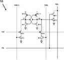
- FIG. 1illustrates a dual port SRAM cell 10 that may be used for computation.
- the dual port SRAM cellmay include two cross coupled inverters (transistors M 17 , M 19 pair as one inverter and transistors M 18 and M 110 pair as another inverter) that form a latch or storage cell and access transistors M 11 -M 16 that are coupled together as shown in FIG. 1 to form an SRAM cell.
- the SRAM cellmay be operated as a storage latch and may have a read port and a write port so that the SRAM cell is a dual port SRAM cell.
- the two invertersare cross coupled since the input of the first inverter is connected to the output of the second inverter and the output of the first inverter is coupled to the input of the second inverter as shown in FIG. 1 .
- a Write Word linecarries a signal and is called WE (see FIG. 1 ) and a write bit line and its complement are called WBL and WBLb, respectively.
- the Write word line (WE)is coupled to the gate of each of the two access transistors M 15 , M 16 that are part of the SRAM cell.
- the write bit line and its complement (WBL and WBLb)are each coupled to a gate of the respective access transistors M 13 , M 14 as shown in FIG. 1 and M 13 is coupled to M 15 and M 14 is coupled to M 16 .
- the source of each of transistors M 13 and M 14is coupled to ground.
- the drain of each of those access transistors M 15 , M 16is coupled to each side of the cross coupled inverters (labeled D and Db in FIG. 1 ).
- the circuit in FIG. 1may also have a read word line RE, a read bit line RBL and a read port formed by transistors M 11 , M 12 coupled together to form an isolation circuit.
- the read word line REmay be coupled to the gate of transistor M 11 that forms part of the read port while the read bit line is coupled to the drain terminal of transistor M 11 .
- the gate of transistor M 12may be coupled to the Db output from the cross coupled inverters and the source of transistor M 12 may be coupled to ground.
- the dual port SRAM cellmay read data stored in the latch using a signal on the read word line (RE) to address/activate the dual port SRAM cell and the read bit line (RBL) to read the data stored in the dual port SRAM cell.
- the dual port SRAM cellmay write data into the dual port SRAM cell by addressing/activating the dual port SRAM cell using a signal on the write word line (WE) and then writing data into the dual port SRAM cell using the write bit lines (WBL, WBLb).
- multiple cellscan be turned on to perform an AND function between the data stored in the cells that were turned on.
- a number of cells in a column of the processing array 20 in FIG. 2such as cell 00 , . . . , cell m 0 , may be activated by the RE signal for each of those cells.
- RBLis pre-charged high and if the Db signal of all cells that are turned on by RE are “0”, then RBL stays high.
- the gate of transistor M 11is turned on by the RE signal, the gate of M 12 is not turned on since the Db signal is low.
- the RBL lineis not connected to the ground to which the source of transistor M 12 is connected and the RBL line is not discharged.
- the write operationis activated by WE and the data is written by toggling of WBL and WBLb.
- the read operationis activated by RE and the read data is accessed on RBL.
- the Db signal of the cell 10may be coupled to a gate of transistor M 12 to drive the RBL line.
- the Db signalis isolated from the RBL line and its signal/voltage level by the transistors M 11 , M 12 (together forming the isolation circuit). Because the Db signal/value is isolated from the RBL line and signal/voltage level, the Db signal is not susceptible to the lower bit line level caused by multiple “0” data stored in multiple cells. Therefore, for the cell in FIG. 1 , there is no limitation of how many cells can be turned on to drive RBL.
- the celloffers more operands for the Boolean functions such as AND function described above and NOR/OR/NAND/XOR/XNOR functions described in co-pending and commonly owned Ser. No. 15/709,401 filed Sep. 19, 2017 (now issued as U.S. Pat. No. 10,249,362 on Apr. 2, 2019) and Ser. No. 15/709,399 filed Sep. 19, 2017 and U.S. Provisional Application No. 62/430,767 filed Dec. 6, 2016 (incorporated herein by reference) since there is no limit of how many cells can be turned on to drive RBL.
- FIG. 2illustrates a processing array device 20 that may incorporate the dual port SRAM cell of FIG. 1 , in which each cell, such as cell 00 , . . . , cell 0 n and cell m 0 , . . . , cell mn, is the cell shown in FIG. 1 .
- the cellsform an array of cells laid out as shown in FIG. 2 .
- the processing array 20may perform computations using the computational capabilities of the dual port SRAM cell described above.
- the array device 20may be formed by M word lines (such as RE 0 , WE 0 , . . . , REm, WEm) and N bit lines (such as WBL 0 , WBLb 0 , RBL 0 , . . .
- the array device 20may also include a word line generator 24 (WL Generator) that generates word line signals as well as a plurality of bit line read/write logic 26 (such as BL Read/Write Logic 0, . . . , BL Read/Write Logic n) that perform read and write operations using the bit lines.
- WL Generatorword line generator 24
- bit line read/write logic 26such as BL Read/Write Logic 0, . . . , BL Read/Write Logic n
- the array device 20may be manufactured on an integrated circuit or may be integrated into another integrated circuit depending on the use of the processing array 20 .
- the word line generator 24may generate one or multiple RE signals in a cycle to turn on/activate one or more cells and the RBL lines of the cells activated by the RE signal form AND or NOR functions whose output is sent to a respective BL Read/Write Logic ( 26 o , . . . , 26 n ).
- Each BL Read/Write Logic 26processes the RBL result (the result of the AND or NOR operation) and sends the results back to its WBL/WBLb for use/writing back to the same BL, or to the neighboring BL Read/Write Logic 26 for use/writing back to the neighboring BL, or send it out of the processing array.
- the BL Read/Write logic 26can store the RBL result from its own bit line or from the neighboring bit line in a latch within the BL Read/Write Logic so that, during a next or later cycle, the BL Read/Write logic 26 can perform logic with the latched data that is the RBL result.
- the word line generator 24In a write cycle, the word line generator 24 generates one or more WE signals for the cells into which data is to be written.
- the BL Read/Write Logic( 26 o , . . . , 26 n ) processes the write data, either from its own RBL, or from the neighboring RBL, or from out of the processing array 20 .
- the ability of BL Read/Write Logic 26 to process the data from the neighboring bit linemeans that the data can be shifting from one bit line to the neighboring bit line and one or more or all bit lines in the processing array may be shifting concurrently.
- the circuit 40 in FIG. 4improves the write port transistor size issue by modifying the circuit shown in FIG. 1 to be ratioless during a write operation.
- the table in FIG. 3applies to circuit 40 in FIG. 4 since the circuit 40 in FIG. 4 has the same elements and operates in the same manner as the circuit 10 in FIG. 1 , but has a ratioless write operation as described below.
- the cell 40may also replace the cell 10 and be used seamlessly in the processing array 20 in FIG. 2 .
- write port transistor M 43 , M 44 , M 45 and M 46may be the same minimum size of transistor as PMOS transistors M 49 , M 410 , M 411 and M 412 .
- the cell 40 sizecan be reduced and the write port is not affected by the write ratio.
- M 411 or M 412may be turned ON when WBLb or WBL is 1. This could leave D or Db as floating 1 which is acceptable because the write cycle is only for a short period of time and nodes D and Db have enough capacitance to hold the change to keep the value in the storage cell unchanged in this situation.
- both WBLb and WBLare low to keep the cross coupled transistors M 47 , M 48 , M 49 and M 410 operating as the cross coupled latch of the SRAM cell 40 .
- series transistor pair M 49 , M 411 and M 410 , M 412can swap position to achieve the same function.
- M 49may have its gate tied to Db and is coupled to VDD and the source of M 411 while M 411 has its gate tied to WBLb that is coupled to D.
- series transistor pair M 43 , M 45 and M 44 , M 46can swap position to achieve the same function.
- a ratioless writeis performed with write bit line (WBL) or complementary write bit line (WBLb) to write the “0” node of the storage latch with its pull up transistor disabled and to write the “1” node of the storage latch with its pull up transistor enabled.
- WBLwrite bit line
- WBLbcomplementary write bit line
- the cell 40 in FIG. 4can be used in the processing array 20 in FIG. 2 in the same way as cell 10 in FIG. 1 .
- FIG. 5illustrates an implementation of a 3-port SRAM cell 50 that can perform basic Boolean operations, XOR and XNOR functions and ratioless selective write.
- the cell 50has the same storage latch and write port circuitry as cell 40 , therefore, the same ratioless selective write operation as cell 40 .
- the cell 50 in FIG. 5adds another read port to the cell 40 in FIG. 4 .
- Transistors M 513 and M 514are added to form the second read port and an isolation circuit for that second read port.
- the complementary read word line REbmay be coupled to the gate of transistor M 513 that forms part of the read port while the complementary read bit line RBLb is coupled to the drain terminal of transistor M 513 .
- the gate of transistor M 514may be coupled to the D output from the cross coupled inverters and the source of transistor M 514 may be coupled to ground.
- multiple cellscan be turned on to perform an AND function between the complementary data stored in the cells that were turned on.
- FIG. 6illustrates an implementation of a processing array 60 that has a plurality of the 3-port SRAM cells shown in FIG. 5 in an array and split segments (Segment 1 and Segment 2 as shown) and each of the bit line (BL) read/write logic circuitry 64 (BL Read/Write Logic 0, . . . , BL Read/Write Logic n for each bit line) in the middle of each bit line.
- This processing arrayhas a word line generator 62 that generates control signals (RE 0 , . . . , REm, REb 0 , . . . , REbm and WEO, . . . , WEm) and each bit line has the two segments.
- segment 1has RBLs 1 and RBLs 1 b read bit lines (RBL 0 s 1 , . . . , RBLns 1 and RBL 0 s 1 b , . . . , RBLns 1 b ) with number of cells connected on it (cell 00 , . . . , cell 0 n in the example in FIG. 6 ) which are all connected to the BL read/write circuitry 64 and segment 2 has RBLs 2 and RBLs 2 b lines (RBL 0 s 2 , . . . , RBLns 2 and RBL 0 s 2 b , . . .
- the word line generatormay generate one or multiple RE, REb signals in a cycle to turn on/activate one or more cells and the RBL, RBLb lines of the cells activated by the RE and REb signals form AND or NOR functions whose output is sent to the respective BL Read/Write Logic 64 for each bit line.
- Each BL Read/Write Logic 64processes the RBL result (the result of the AND or NOR operation) and sends the results back to its WBL/WBLb for use/writing back to the same cell, or to the neighboring BL Read/Write Logic for use/writing back to the neighboring cell, or send it out of the processing array.
- the BL Read/Write logic 64can store the RBL result from its own bit line or from the neighboring bit line in a latch within the BL Read/Write Logic so that, during a next or later cycle, the Read/Write logic can perform logic with the latched data that is the RBL result.
- the word line generator 62In a write cycle using the processing array in FIG. 6 , the word line generator 62 generates one or more WE signals for the one or more cells into which data is to be written.
- the BL Read/Write Logic 64processes the write data, either from its own RBL, or from the neighboring RBL, or from out of the processing array.
- the ability of BL Read/Write Logic 64 to process the data from the neighboring bit linemeans that the data can be shifting from one bit line to the neighboring bit line and one or more or all bit lines in the processing array may be shifting concurrently.
- the cells 40 and 50 described hereare for computation memory applications, but these cells in FIGS. 4 and 5 can be operated as an SRAM cell with great noise immunity and ultralow VDD operation.
- the VDD operation levelcan be as low as the threshold voltage of NMOS and PMOS transistors of the cell.
- the VDD operation level for storageis as low as the threshold voltage of NMOS and PMOS transistors for the cross coupled latch to be active.
- the read bit line voltage levelwill not affect the stability of the storage node.
- the read bit lineis pre-charged high and be discharged by the turning on of the read port access transistors.
- the VDD operation levelis as low as the threshold voltage of read port NMOS transistors.
- the writing to the storage latchoccurs by just turning on the NMOS or PMOS transistors of the write port without write ratio.
- the VDD operation levelis as low as the threshold voltage of write port NMOS and PMOS transistors.
- system and method disclosed hereinmay be implemented via one or more components, systems, servers, appliances, other subcomponents, or distributed between such elements.
- systemsmay include an/or involve, inter alia, components such as software modules, general-purpose CPU, RAM, etc. found in general-purpose computers.
- componentssuch as software modules, general-purpose CPU, RAM, etc. found in general-purpose computers.
- a servermay include or involve components such as CPU, RAM, etc., such as those found in general-purpose computers.
- system and method hereinmay be achieved via implementations with disparate or entirely different software, hardware and/or firmware components, beyond that set forth above.
- componentse.g., software, processing components, etc.
- computer-readable mediaassociated with or embodying the present inventions
- aspects of the innovations hereinmay be implemented consistent with numerous general purpose or special purpose computing systems or configurations.
- exemplary computing systems, environments, and/or configurationsmay include, but are not limited to: software or other components within or embodied on personal computers, servers or server computing devices such as routing/connectivity components, hand-held or laptop devices, multiprocessor systems, microprocessor-based systems, set top boxes, consumer electronic devices, network PCs, other existing computer platforms, distributed computing environments that include one or more of the above systems or devices, etc.
- aspects of the system and methodmay be achieved via or performed by logic and/or logic instructions including program modules, executed in association with such components or circuitry, for example.
- program modulesmay include routines, programs, objects, components, data structures, etc. that perform particular tasks or implement particular instructions herein.
- the inventionsmay also be practiced in the context of distributed software, computer, or circuit settings where circuitry is connected via communication buses, circuitry or links. In distributed settings, control/instructions may occur from both local and remote computer storage media including memory storage devices.
- Computer readable mediacan be any available media that is resident on, associable with, or can be accessed by such circuits and/or computing components.
- Computer readable mediamay comprise computer storage media and communication media.
- Computer storage mediaincludes volatile and nonvolatile, removable and non-removable media implemented in any method or technology for storage of information such as computer readable instructions, data structures, program modules or other data.
- Computer storage mediaincludes, but is not limited to, RAM, ROM, EEPROM, flash memory or other memory technology, CD-ROM, digital versatile disks (DVD) or other optical storage, magnetic tape, magnetic disk storage or other magnetic storage devices, or any other medium which can be used to store the desired information and can accessed by computing component.
- Communication mediamay comprise computer readable instructions, data structures, program modules and/or other components. Further, communication media may include wired media such as a wired network or direct-wired connection, however no media of any such type herein includes transitory media. Combinations of the any of the above are also included within the scope of computer readable media.
- the terms component, module, device, etc.may refer to any type of logical or functional software elements, circuits, blocks and/or processes that may be implemented in a variety of ways.
- the functions of various circuits and/or blockscan be combined with one another into any other number of modules.
- Each modulemay even be implemented as a software program stored on a tangible memory (e.g., random access memory, read only memory, CD-ROM memory, hard disk drive, etc.) to be read by a central processing unit to implement the functions of the innovations herein.
- the modulescan comprise programming instructions transmitted to a general purpose computer or to processing/graphics hardware via a transmission carrier wave.
- the modulescan be implemented as hardware logic circuitry implementing the functions encompassed by the innovations herein.
- the modulescan be implemented using special purpose instructions (SIMD instructions), field programmable logic arrays or any mix thereof which provides the desired level performance and cost.
- SIMD instructionsspecial purpose instructions
- features consistent with the disclosuremay be implemented via computer-hardware, software and/or firmware.
- the systems and methods disclosed hereinmay be embodied in various forms including, for example, a data processor, such as a computer that also includes a database, digital electronic circuitry, firmware, software, or in combinations of them.
- a data processorsuch as a computer that also includes a database
- digital electronic circuitrysuch as a computer
- firmwaresuch as a firmware
- softwaresuch as a computer
- the systems and methods disclosed hereinmay be implemented with any combination of hardware, software and/or firmware.
- the above-noted features and other aspects and principles of the innovations hereinmay be implemented in various environments.
- Such environments and related applicationsmay be specially constructed for performing the various routines, processes and/or operations according to the invention or they may include a general-purpose computer or computing platform selectively activated or reconfigured by code to provide the necessary functionality.
- the processes disclosed hereinare not inherently related to any particular computer, network, architecture, environment, or other apparatus, and may be implemented by a suitable combination of hardware, software, and/or firmware.
- various general-purpose machinesmay be used with programs written in accordance with teachings of the invention, or it may be more convenient to construct a specialized apparatus or system to perform the required methods and techniques.
- aspects of the method and system described herein, such as the logicmay also be implemented as functionality programmed into any of a variety of circuitry, including programmable logic devices (“PLDs”), such as field programmable gate arrays (“FPGAs”), programmable array logic (“PAL”) devices, electrically programmable logic and memory devices and standard cell-based devices, as well as application specific integrated circuits.
- PLDsprogrammable logic devices
- FPGAsfield programmable gate arrays
- PALprogrammable array logic
- Some other possibilities for implementing aspectsinclude: memory devices, microcontrollers with memory (such as EEPROM), embedded microprocessors, firmware, software, etc.
- aspectsmay be embodied in microprocessors having software-based circuit emulation, discrete logic (sequential and combinatorial), custom devices, fuzzy (neural) logic, quantum devices, and hybrids of any of the above device types.
- the underlying device technologiesmay be provided in a variety of component types, e.g., metal-oxide semiconductor field-effect transistor (“MOSFET”) technologies like complementary metal-oxide semiconductor (“CMOS”), bipolar technologies like emitter-coupled logic (“ECL”), polymer technologies (e.g., silicon-conjugated polymer and metal-conjugated polymer-metal structures), mixed analog and digital, and so on.
- MOSFETmetal-oxide semiconductor field-effect transistor
- CMOScomplementary metal-oxide semiconductor
- ECLemitter-coupled logic
- polymer technologiese.g., silicon-conjugated polymer and metal-conjugated polymer-metal structures
- mixed analog and digitaland so on.
- the words “comprise,” “comprising,” and the likeare to be construed in an inclusive sense as opposed to an exclusive or exhaustive sense; that is to say, in a sense of “including, but not limited to.” Words using the singular or plural number also include the plural or singular number respectively. Additionally, the words “herein,” “hereunder,” “above,” “below,” and words of similar import refer to this application as a whole and not to any particular portions of this application. When the word “or” is used in reference to a list of two or more items, that word covers all of the following interpretations of the word: any of the items in the list, all of the items in the list and any combination of the items in the list.
Landscapes
- Engineering & Computer Science (AREA)
- Microelectronics & Electronic Packaging (AREA)
- Computer Hardware Design (AREA)
- Static Random-Access Memory (AREA)
Abstract
Description
This application is a continuation in part of U.S. application Ser. No. 15/709,401 filed Sep. 19, 2017 (now issued as U.S. Pat. No. 10,249,362 on Apr. 2, 2019) and Ser. No. 15/709,399 filed Sep. 19, 2017, both of which claim the benefit under 35 USC 119(e) of U.S. Provisional Application No. 62/430,767 filed Dec. 6, 2016 and entitled “Computational Dual Port SRAM Cell And Processing Array Device Using The Dual Port SRAM Cells For Xor And Xnor Computations”, the entirety of all of which are incorporated herein by reference.
The disclosure relates generally to a static random access memory cell that may be used for computations.
An array of memory cells, such as dynamic random access memory (DRAM) cells, static random access memory (SRAM) cells, content addressable memory (CAM) cells or non-volatile memory cells, is a well-known mechanism used in various computer or processor based devices to store digital bits of data. The various computer and processor based devices may include computer systems, smartphone devices, consumer electronic products, televisions, internet switches and routers and the like. The array of memory cells are typically packaged in an integrated circuit or may be packaged within an integrated circuit that also has a processing device within the integrated circuit. The different types of typical memory cells have different capabilities and characteristics that distinguish each type of memory cell. For example, DRAM cells take longer to access, lose their data contents unless periodically refreshed, but are relatively cheap to manufacture due to the simple structure of each DRAM cell. SRAM cells, on the other hand, have faster access times, do not lose their data content unless power is removed from the SRAM cell and are relatively more expensive since each SRAM cell is more complicated than a DRAM cell. CAM cells have a unique function of being able to address content easily within the cells and are more expensive to manufacture since each CAM cell requires more circuitry to achieve the content addressing functionality.
Various computation devices that may be used to perform computations on digital, binary data are also well-known. The computation devices may include a microprocessor, a CPU, a microcontroller and the like. These computation devices are typically manufactured on an integrated circuit, but may also be manufactured on an integrated circuit that also has some amount of memory integrated onto the integrated circuit. In these known integrated circuits with a computation device and memory, the computation device performs the computation of the digital binary data bits while the memory is used to store various digital binary data including, for example, the instructions being executed by the computation device and the data being operated on by the computation device.
More recently, devices have been introduced that use memory arrays or storage cells to perform computation operations. In some of these devices, a processor array to perform computations may be formed from memory cells. These devices may be known as in-memory computational devices.
Big data operations are data processing operations in which a large amount of data must be processed. Machine learning uses artificial intelligence algorithms to analyze data and typically require a lot of data to perform. The big data operations and machine learning also are typically very computationally intensive applications that often encounter input/output issues due to a bandwidth bottleneck between the computational device and the memory that stores the data. The above in-memory computational devices may be used, for example, for these big data operations and machine learning applications since the in-memory computational devices perform the computations within the memory thereby eliminating the bandwidth bottleneck.
An SRAM cell can be configured to perform Boolean operations such as AND, OR, NAND and NOR, Exclusive OR and NOR. This SRAM cell can also support a Selective Write operation. However, the typical SRAM cell requires stronger writing transistors than the transistors in the storage latch to over write the storage data. A ratio of the transistor strengths of the write transistor and the storage transistor may be known as a write ratio. For a typical SRAM cell, the write ratio is 2 to 3 meaning that the writing transistor is 2 to 3 times of the strength of the storage transistor for the writing to be successful. Thus, it is desired to provide a computational memory cell, that may be an SRAM cell, with a write port to perform Boolean operations such as AND, OR, NAND, NOR, XOR (Exclusive OR) and XNOR (Exclusive NOR) that is able to do the writing ratioless.
The disclosure is particularly applicable to a CMOS implemented memory cell and processing array with a plurality of the memory cells that are capable to performing logic functions with a ratioless write port and it is in this context that the disclosure will be described. It will be appreciated, however, that the memory cell and processing array has greater utility and is not limited to the below disclosed implementations since the memory cell may be constructed using different processes and may have different circuit configurations than those disclosed below that perform the logic function and so are within the scope of this disclosure. For purposes of illustration, a dual port SRAM and 3-port cells are disclosed below and in the figures. However, it is understood that the SRAM computation cell and processing array may also be implemented with an SRAM cell having more ports and the disclosure is not limited to the SRAM cells disclosed below. It is also understood that the SRAM cells having more ports may be slightly differently constructed than the SRAM cells shown in the figures, but one skilled in the art would understand how to construct those SRAMs with more ports from the disclosure below.
Furthermore, although an SRAM cell is used in the examples below, it is understood that the disclosed memory cell for computation and the processing array using the memory cells may be implemented using various different types of memory cells including DRAMs, CAMs, non-volatile memory cells and non-volatile memory devices and these implementations using the various types of memory cells are within the scope of the disclosure.
A Write Word line carries a signal and is called WE (seeFIG. 1 ) and a write bit line and its complement are called WBL and WBLb, respectively. The Write word line (WE) is coupled to the gate of each of the two access transistors M15, M16 that are part of the SRAM cell. The write bit line and its complement (WBL and WBLb) are each coupled to a gate of the respective access transistors M13, M14 as shown inFIG. 1 and M13 is coupled to M15 and M14 is coupled to M16. The source of each of transistors M13 and M14 is coupled to ground. The drain of each of those access transistors M15, M16 is coupled to each side of the cross coupled inverters (labeled D and Db inFIG. 1 ).
The circuit inFIG. 1 may also have a read word line RE, a read bit line RBL and a read port formed by transistors M11, M12 coupled together to form an isolation circuit. The read word line RE may be coupled to the gate of transistor M11 that forms part of the read port while the read bit line is coupled to the drain terminal of transistor M11. The gate of transistor M12 may be coupled to the Db output from the cross coupled inverters and the source of transistor M12 may be coupled to ground.
In operation, the dual port SRAM cell may read data stored in the latch using a signal on the read word line (RE) to address/activate the dual port SRAM cell and the read bit line (RBL) to read the data stored in the dual port SRAM cell. The dual port SRAM cell may write data into the dual port SRAM cell by addressing/activating the dual port SRAM cell using a signal on the write word line (WE) and then writing data into the dual port SRAM cell using the write bit lines (WBL, WBLb).
During reading, multiple cells (with only a single cell being shown inFIG. 1 but multiple cells shown inFIG. 2 ) can be turned on to perform an AND function between the data stored in the cells that were turned on. For example, a number of cells in a column of theprocessing array 20 inFIG. 2 , such ascell 00, . . . , cell m0, may be activated by the RE signal for each of those cells. Thus, at the beginning of the read cycle, RBL is pre-charged high and if the Db signal of all cells that are turned on by RE are “0”, then RBL stays high. Although the gate of transistor M11 is turned on by the RE signal, the gate of M12 is not turned on since the Db signal is low. As a result, the RBL line is not connected to the ground to which the source of transistor M12 is connected and the RBL line is not discharged. The write operation is activated by WE and the data is written by toggling of WBL and WBLb. The read operation is activated by RE and the read data is accessed on RBL.
Thecell 10 may further be used for computation where RBL is also used to perform logic operation(s). If the Db signal of any or all of the cells activated is “1” then RBL is discharged to 0 since the gate of M12 is turned on and the RBL line is connected to ground. As a result, RBL=NOR (Db0, Db1, etc.) where Db0, Db1, etc. are the complementary data of the SRAM cells that have been turned on by the RE signal. Alternatively, RBL=NOR (Db0, Db1, etc.)=AND (D0, D1, etc.), where D0, D1, etc. are the true data of the cells that have been turned on by the RE signal.
As shown inFIG. 1 , the Db signal of thecell 10 may be coupled to a gate of transistor M12 to drive the RBL line. The Db signal is isolated from the RBL line and its signal/voltage level by the transistors M11, M12 (together forming the isolation circuit). Because the Db signal/value is isolated from the RBL line and signal/voltage level, the Db signal is not susceptible to the lower bit line level caused by multiple “0” data stored in multiple cells. Therefore, for the cell inFIG. 1 , there is no limitation of how many cells can be turned on to drive RBL. As a result, the cell (and the device made up of multiple cells) offers more operands for the Boolean functions such as AND function described above and NOR/OR/NAND/XOR/XNOR functions described in co-pending and commonly owned Ser. No. 15/709,401 filed Sep. 19, 2017 (now issued as U.S. Pat. No. 10,249,362 on Apr. 2, 2019) and Ser. No. 15/709,399 filed Sep. 19, 2017 and U.S. Provisional Application No. 62/430,767 filed Dec. 6, 2016 (incorporated herein by reference) since there is no limit of how many cells can be turned on to drive RBL. In addition to the AND function described above, theSRAM cell 10 inFIG. 1 also may perform a NOR function by storing inverted data. Specifically, if D is stored at the gate of M12, instead of Db, then RBL=NOR (D0, D1, etc.).
In a read cycle, theword line generator 24 may generate one or multiple RE signals in a cycle to turn on/activate one or more cells and the RBL lines of the cells activated by the RE signal form AND or NOR functions whose output is sent to a respective BL Read/Write Logic (26o, . . . ,26n). Each BL Read/Write Logic26 processes the RBL result (the result of the AND or NOR operation) and sends the results back to its WBL/WBLb for use/writing back to the same BL, or to the neighboring BL Read/Write Logic26 for use/writing back to the neighboring BL, or send it out of the processing array. Alternatively, the BL Read/Write logic26 can store the RBL result from its own bit line or from the neighboring bit line in a latch within the BL Read/Write Logic so that, during a next or later cycle, the BL Read/Write logic26 can perform logic with the latched data that is the RBL result.
In a write cycle, theword line generator 24 generates one or more WE signals for the cells into which data is to be written. The BL Read/Write Logic (26o, . . . ,26n) processes the write data, either from its own RBL, or from the neighboring RBL, or from out of theprocessing array 20. The ability of BL Read/Write Logic26 to process the data from the neighboring bit line means that the data can be shifting from one bit line to the neighboring bit line and one or more or all bit lines in the processing array may be shifting concurrently. The BL Read/Write Logic26 can also decide not to write for a Selective Write operation based on the RBL result. For example, the data on the WBL line can be written to a cell if RBL=1. If RBL=0, then the write operation is not performed.
The write operation for the circuit is now described in more detail with reference toFIG. 1 . When WE=1 and either WBL and WBLb is 1, the writing is performed. To write D from 1 to 0, then WBLb=1 and WBL=0, M13 and M15 are turned on to overcome the strength of PMOS transistor M19. On 16 nm or more advanced process technology with FINFET transistors, PMOS transistor normally has almost same driver strength as an NMOS transistor, and driver strength of M13 and M15 in series need to be 3 times or more than the driver strength of M19 to be able to perform the writing successfully. Therefore M13 and M15 each needs to be 6 times of driver strength of M19. Similarly M14 and M16 each needs to be 6 times of M110. This makes M13, M14, M15 and M16 transistors sizes very large that in turn results in thecell 10 size ofFIG. 1 being large.
Thecircuit 40 inFIG. 4 improves the write port transistor size issue by modifying the circuit shown inFIG. 1 to be ratioless during a write operation. The table inFIG. 3 applies tocircuit 40 inFIG. 4 since thecircuit 40 inFIG. 4 has the same elements and operates in the same manner as thecircuit 10 inFIG. 1 , but has a ratioless write operation as described below. Thecell 40 may also replace thecell 10 and be used seamlessly in theprocessing array 20 inFIG. 2 .
In thecell 40 inFIG. 4 , if WE=0, no write is performed by the circuit inFIG. 4 . If WE is 1, then the storage nodes D and its complement Db are written by WBL and WBLb in which D=1 and Db=0 if WBL=1 and WBLb=0 and D=0 and D=1 if WBL=0 and WBLb=1. If both WBL and WBLb are 0, then no write is performed so thiscell 40 can perform a selective write function with WBL=WBLb=0 and with WE=1 as did thecircuit 10 inFIG. 1 .
InFIG. 4 , when WE=1, WBLb=1 and WBL=0, transistors M43 and M45 are on and data D is written from 1 to 0 without the pull up strength of series PMOS transistors of M49 and M411 because transistor M411 is turned off when its gate is tied to WBLb which is 1. Furthermore, because WBL=0, transistor M412 is turned on and data D is pulled down to 0, therefore Db is pulled up from 0 to 1 and the writing is completed. In this write operation using thecircuit 40 inFIG. 4 , there is no write ratio in the write operation as M43 and M45 pull down D without the need to overcome the PMOS pull up strength of the storage transistor.
Similarly, when WE=1, WBLb=0 and WBL=1, transistors M44 and M46 are on and data Db is written from 1 to 0 without needing to overcome the pull up strength of series PMOS transistor M410 and M412 because transistor M412 is turned off with the gate tied to WBL. Similarly, in this write operation, there is no write ratio in the write operation as M44 and M46 operate without the need to overcome the storage PMOS pull up strength.
In this manner, write port transistor M43, M44, M45 and M46 may be the same minimum size of transistor as PMOS transistors M49, M410, M411 and M412. Thus, thecell 40 size can be reduced and the write port is not affected by the write ratio. Note that when WE=0, no write is performed, but M411 or M412 may be turned ON when WBLb or WBL is 1. This could leave D or Db as floating 1 which is acceptable because the write cycle is only for a short period of time and nodes D and Db have enough capacitance to hold the change to keep the value in the storage cell unchanged in this situation. In the normal operation when it is not a write cycle, both WBLb and WBL are low to keep the cross coupled transistors M47, M48, M49 and M410 operating as the cross coupled latch of theSRAM cell 40.
In thecircuit 40 shown inFIG. 4 , series transistor pair M49, M411 and M410, M412 can swap position to achieve the same function. For example, M49 may have its gate tied to Db and is coupled to VDD and the source of M411 while M411 has its gate tied to WBLb that is coupled to D. Similarly series transistor pair M43, M45 and M44, M46 can swap position to achieve the same function.
In summary, a ratioless write is performed with write bit line (WBL) or complementary write bit line (WBLb) to write the “0” node of the storage latch with its pull up transistor disabled and to write the “1” node of the storage latch with its pull up transistor enabled. Thecell 40 inFIG. 4 can be used in theprocessing array 20 inFIG. 2 in the same way ascell 10 inFIG. 1 .
During reading, multiple cells (with only a single cell being shown inFIG. 5 but multiple cells shown in aprocessing array 60 inFIG. 6 ) can be turned on to perform an AND function between the complementary data stored in the cells that were turned on. During the read, the RBLb line is precharged high. If the D signal of any or all of the cells activated is “1” then RBLb is discharged to 0 since the gate of M514 is turned on and the RBLb line is connected to ground. As a result, RBLb=NOR (D0, D1, etc.) where D0, D1, etc. are the data of the SRAM cells that have been turned on by the REb signal. Alternatively, RBLb=NOR (D0, D1, etc.)=AND (Db0, Db1, etc.), where Db0, Db1, etc. are the complement data of the cells that have been turned on by the REb signal. Thus,cell 50 performs as 3-port SRAM cell with a write port (controlled by WE) and2 read ports (controlled by RE and Reb) with RBL=AND (D0, D1, etc) and RBLb=(D0b, D1b, etc).
In a read cycle, the word line generator may generate one or multiple RE, REb signals in a cycle to turn on/activate one or more cells and the RBL, RBLb lines of the cells activated by the RE and REb signals form AND or NOR functions whose output is sent to the respective BL Read/Write Logic 64 for each bit line. Each BL Read/Write Logic 64 processes the RBL result (the result of the AND or NOR operation) and sends the results back to its WBL/WBLb for use/writing back to the same cell, or to the neighboring BL Read/Write Logic for use/writing back to the neighboring cell, or send it out of the processing array. Alternatively, the BL Read/Write logic 64 can store the RBL result from its own bit line or from the neighboring bit line in a latch within the BL Read/Write Logic so that, during a next or later cycle, the Read/Write logic can perform logic with the latched data that is the RBL result.
In a write cycle using the processing array inFIG. 6 , theword line generator 62 generates one or more WE signals for the one or more cells into which data is to be written. The BL Read/Write Logic 64 processes the write data, either from its own RBL, or from the neighboring RBL, or from out of the processing array. The ability of BL Read/Write Logic 64 to process the data from the neighboring bit line (note the connections between the bit lines and each BL Read/Write Logic64) means that the data can be shifting from one bit line to the neighboring bit line and one or more or all bit lines in the processing array may be shifting concurrently. The BL Read/Write Logic 64 can also decide not to write for a Selective Write operation based on the RBL or RBLb result. For example, the data on the WBL line can be written to a cell if RBL=1. If RBL=0, then write operation is not performed.
SRAM Ultralow VDD Operation SRAM
Thecells FIGS. 4 and 5 can be operated as an SRAM cell with great noise immunity and ultralow VDD operation. Specifically, the VDD operation level can be as low as the threshold voltage of NMOS and PMOS transistors of the cell.
Isolated Storage Latch:
the read or write operation will not affect the stability of storage latch. The VDD operation level for storage is as low as the threshold voltage of NMOS and PMOS transistors for the cross coupled latch to be active.
Buffered Read:
the read bit line voltage level will not affect the stability of the storage node. The read bit line is pre-charged high and be discharged by the turning on of the read port access transistors. The VDD operation level is as low as the threshold voltage of read port NMOS transistors.
Ratioless Write:
The writing to the storage latch occurs by just turning on the NMOS or PMOS transistors of the write port without write ratio. The VDD operation level is as low as the threshold voltage of write port NMOS and PMOS transistors.
The foregoing description, for purpose of explanation, has been described with reference to specific embodiments. However, the illustrative discussions above are not intended to be exhaustive or to limit the disclosure to the precise forms disclosed. Many modifications and variations are possible in view of the above teachings. The embodiments were chosen and described in order to best explain the principles of the disclosure and its practical applications, to thereby enable others skilled in the art to best utilize the disclosure and various embodiments with various modifications as are suited to the particular use contemplated.
The system and method disclosed herein may be implemented via one or more components, systems, servers, appliances, other subcomponents, or distributed between such elements. When implemented as a system, such systems may include an/or involve, inter alia, components such as software modules, general-purpose CPU, RAM, etc. found in general-purpose computers. In implementations where the innovations reside on a server, such a server may include or involve components such as CPU, RAM, etc., such as those found in general-purpose computers.
Additionally, the system and method herein may be achieved via implementations with disparate or entirely different software, hardware and/or firmware components, beyond that set forth above. With regard to such other components (e.g., software, processing components, etc.) and/or computer-readable media associated with or embodying the present inventions, for example, aspects of the innovations herein may be implemented consistent with numerous general purpose or special purpose computing systems or configurations. Various exemplary computing systems, environments, and/or configurations that may be suitable for use with the innovations herein may include, but are not limited to: software or other components within or embodied on personal computers, servers or server computing devices such as routing/connectivity components, hand-held or laptop devices, multiprocessor systems, microprocessor-based systems, set top boxes, consumer electronic devices, network PCs, other existing computer platforms, distributed computing environments that include one or more of the above systems or devices, etc.
In some instances, aspects of the system and method may be achieved via or performed by logic and/or logic instructions including program modules, executed in association with such components or circuitry, for example. In general, program modules may include routines, programs, objects, components, data structures, etc. that perform particular tasks or implement particular instructions herein. The inventions may also be practiced in the context of distributed software, computer, or circuit settings where circuitry is connected via communication buses, circuitry or links. In distributed settings, control/instructions may occur from both local and remote computer storage media including memory storage devices.
The software, circuitry and components herein may also include and/or utilize one or more type of computer readable media. Computer readable media can be any available media that is resident on, associable with, or can be accessed by such circuits and/or computing components. By way of example, and not limitation, computer readable media may comprise computer storage media and communication media. Computer storage media includes volatile and nonvolatile, removable and non-removable media implemented in any method or technology for storage of information such as computer readable instructions, data structures, program modules or other data. Computer storage media includes, but is not limited to, RAM, ROM, EEPROM, flash memory or other memory technology, CD-ROM, digital versatile disks (DVD) or other optical storage, magnetic tape, magnetic disk storage or other magnetic storage devices, or any other medium which can be used to store the desired information and can accessed by computing component. Communication media may comprise computer readable instructions, data structures, program modules and/or other components. Further, communication media may include wired media such as a wired network or direct-wired connection, however no media of any such type herein includes transitory media. Combinations of the any of the above are also included within the scope of computer readable media.
In the present description, the terms component, module, device, etc. may refer to any type of logical or functional software elements, circuits, blocks and/or processes that may be implemented in a variety of ways. For example, the functions of various circuits and/or blocks can be combined with one another into any other number of modules. Each module may even be implemented as a software program stored on a tangible memory (e.g., random access memory, read only memory, CD-ROM memory, hard disk drive, etc.) to be read by a central processing unit to implement the functions of the innovations herein. Or, the modules can comprise programming instructions transmitted to a general purpose computer or to processing/graphics hardware via a transmission carrier wave. Also, the modules can be implemented as hardware logic circuitry implementing the functions encompassed by the innovations herein. Finally, the modules can be implemented using special purpose instructions (SIMD instructions), field programmable logic arrays or any mix thereof which provides the desired level performance and cost.
As disclosed herein, features consistent with the disclosure may be implemented via computer-hardware, software and/or firmware. For example, the systems and methods disclosed herein may be embodied in various forms including, for example, a data processor, such as a computer that also includes a database, digital electronic circuitry, firmware, software, or in combinations of them. Further, while some of the disclosed implementations describe specific hardware components, systems and methods consistent with the innovations herein may be implemented with any combination of hardware, software and/or firmware. Moreover, the above-noted features and other aspects and principles of the innovations herein may be implemented in various environments. Such environments and related applications may be specially constructed for performing the various routines, processes and/or operations according to the invention or they may include a general-purpose computer or computing platform selectively activated or reconfigured by code to provide the necessary functionality. The processes disclosed herein are not inherently related to any particular computer, network, architecture, environment, or other apparatus, and may be implemented by a suitable combination of hardware, software, and/or firmware. For example, various general-purpose machines may be used with programs written in accordance with teachings of the invention, or it may be more convenient to construct a specialized apparatus or system to perform the required methods and techniques.
Aspects of the method and system described herein, such as the logic, may also be implemented as functionality programmed into any of a variety of circuitry, including programmable logic devices (“PLDs”), such as field programmable gate arrays (“FPGAs”), programmable array logic (“PAL”) devices, electrically programmable logic and memory devices and standard cell-based devices, as well as application specific integrated circuits. Some other possibilities for implementing aspects include: memory devices, microcontrollers with memory (such as EEPROM), embedded microprocessors, firmware, software, etc. Furthermore, aspects may be embodied in microprocessors having software-based circuit emulation, discrete logic (sequential and combinatorial), custom devices, fuzzy (neural) logic, quantum devices, and hybrids of any of the above device types. The underlying device technologies may be provided in a variety of component types, e.g., metal-oxide semiconductor field-effect transistor (“MOSFET”) technologies like complementary metal-oxide semiconductor (“CMOS”), bipolar technologies like emitter-coupled logic (“ECL”), polymer technologies (e.g., silicon-conjugated polymer and metal-conjugated polymer-metal structures), mixed analog and digital, and so on.
It should also be noted that the various logic and/or functions disclosed herein may be enabled using any number of combinations of hardware, firmware, and/or as data and/or instructions embodied in various machine-readable or computer-readable media, in terms of their behavioral, register transfer, logic component, and/or other characteristics. Computer-readable media in which such formatted data and/or instructions may be embodied include, but are not limited to, non-volatile storage media in various forms (e.g., optical, magnetic or semiconductor storage media) though again does not include transitory media. Unless the context clearly requires otherwise, throughout the description, the words “comprise,” “comprising,” and the like are to be construed in an inclusive sense as opposed to an exclusive or exhaustive sense; that is to say, in a sense of “including, but not limited to.” Words using the singular or plural number also include the plural or singular number respectively. Additionally, the words “herein,” “hereunder,” “above,” “below,” and words of similar import refer to this application as a whole and not to any particular portions of this application. When the word “or” is used in reference to a list of two or more items, that word covers all of the following interpretations of the word: any of the items in the list, all of the items in the list and any combination of the items in the list.
Although certain presently preferred implementations of the invention have been specifically described herein, it will be apparent to those skilled in the art to which the invention pertains that variations and modifications of the various implementations shown and described herein may be made without departing from the spirit and scope of the invention. Accordingly, it is intended that the invention be limited only to the extent required by the applicable rules of law.
While the foregoing has been with reference to a particular embodiment of the disclosure, it will be appreciated by those skilled in the art that changes in this embodiment may be made without departing from the principles and spirit of the disclosure, the scope of which is defined by the appended claims
Claims (18)
1. A memory computation cell, comprising:
a storage cell having at least one storage PMOS transistor;
at least one read bit line coupled to the storage cell through a read port wherein the read port buffers the storage cell from signals on the at least one read bit line and wherein the read bit line is configured to provide read access to a piece of data stored in the storage cell;
wherein the memory computation cell is capable of performing a logic function when the memory computation cell is connected to the at least one read bit line with at least one other memory cell and the read bit line result in the logic function of 2 or more cells; and
a ratioless write port coupled to the storage cell that provides write access to the storage cell, the ratioless write port permitting data to be written into the storage cell without overcoming a drive strength of the storage PMOS transistor.
2. The memory computation cell ofclaim 1 , wherein the ratioless write port further comprises a write bit line and a complement write bit line, wherein a gate of PMOS transfer transistors are each connected to the write bit line and complement write bit line, respectively.
3. The memory computation cell ofclaim 2 , wherein the storage cell further comprises a first inverter having an input and an output and a second inverter having an input coupled to the output of the first inverter and an output coupled to the input of the first inverter, the first inverter including the at least one storage PMOS transistor that is coupled to a first transfer PMOS transistor and the second inverter including a second storage PMOS transistor that is coupled to a second transfer PMOS transistor.
4. The memory computation cell ofclaim 2 , wherein the read port has an isolation circuit that buffers the storage cell from signals on the at least one read bit line.
5. The memory computation cell ofclaim 1 that is capable of performing a selective write operation.
6. The memory computation cell ofclaim 4 further comprising a second read port connected to a complementary read bit line that is coupleable to at least one other memory cell and by turning on the complementary read word line of the memory computation cell to have a second logic result between read word line and the storage cell data of one memory cell on the read bit line.
7. The memory computation cell ofclaim 3 , wherein the transfer PMOS transistor turns off to cut off the storage PMOS transistor.
8. The memory computation cell ofclaim 2 , wherein the at least one storage PMOS transistor is a same size as each of the transfer PMOS transistors.
9. A processing array, comprising:
a plurality of memory cells arranged in an array, wherein each memory cell has a storage cell with at least one storage PMOS transistor, a read port for reading data from the storage cell and a write port for writing data to the storage cell, wherein the read port buffers the storage cell from signals on at least one read bit line and wherein the read bit line is configured to provide read access to a piece of data stored in the storage cell;
a word line generator that is coupled to a read word line signal and a write word line signal for each memory cell in the array;
a plurality of bit line read and write logic circuits that are coupled to the read bit line, write bit line and a complementary write bit line of each memory cell;
each memory cell being coupled to a write word line and a read word line whose signals are generated by the word line generator and also being coupled to a read bit line, a write bit line and a complementary write bit line that are sensed by one of the plurality of bit line read and write logic circuits;
the write port being a ratioless write port that provides write access to the storage cell, the ratioless write port permitting data to be written into the storage cell without overcoming a drive strength of the at least one storage PMOS transistor; and
wherein two or more of the memory cells are coupled to at least one read bit line and activated to perform one of a Boolean operations.
10. The processing array ofclaim 9 , wherein the ratioless write port further comprises a write bit line and a complement write bit line, wherein a gate of transfer PMOS transistors are each connected to the write bit line and complement write bit line, respectively.
11. The processing array ofclaim 10 , wherein the storage cell in each memory cell further comprises a first inverter having an input and an output and a second inverter having an input coupled to the output of the first inverter and an output coupled to the input of the first inverter, the first inverter including the at least one storage PMOS transistor that is coupled to a first transfer PMOS transistor and the second inverter including a second storage PMOS transistor that is coupled to a second transfer PMOS transistor.
12. The processing array ofclaim 10 , wherein the read port further comprises an isolation circuit that buffers the storage cell from signals on the at least one read bit line.
13. The processing array ofclaim 9 that is capable of performing a selective write operation.
14. The processing array ofclaim 12 , wherein each memory cells further comprises a second read port connected to a complementary read bit line; and wherein two or more of the memory cells are coupled to at a complementary read bit line and activated to perform another one of a Boolean operations.
15. The processing array ofclaim 11 , wherein the transfer PMOS transistor turns off to cut off the storage PMOS transistor.
16. The processing array ofclaim 10 , wherein the at least one storage PMOS transistor is a same size as each of the transfer PMOS transistors.
17. A method for write operation in a computational memory cell, the method comprising:
activating a write word line coupled to a computational memory cell in order to write a piece of data to a storage cell of the computational memory cell, the storage cell having at least one storage PMOS transistor;
activating either of a write bit line or a complementary write bit line coupled to the computing memory cell;
turning off a transistor whose gate is coupled to either of the write bit line or the complementary write bit line that is in turn connected to the at least one storage PMOS transistor; and
performing a write operation into the storage cell without overcoming a drive strength of the at least one storage PMOS transistor.
18. The method ofclaim 17 further comprising cutting off the at least one storage PMOS transistor when the transistor is turned off.
Priority Applications (4)
| Application Number | Priority Date | Filing Date | Title |
|---|---|---|---|
| US16/785,141US10854284B1 (en) | 2016-12-06 | 2020-02-07 | Computational memory cell and processing array device with ratioless write port |
| TW110104531ATWI777404B (en) | 2020-02-07 | 2021-02-05 | Computational memory cell and processing array device with ratioless write port |
| EP21155509.9AEP3863014A1 (en) | 2020-02-07 | 2021-02-05 | Computational memory cell and processing array device with ratioless write port |
| CN202110166435.3ACN113257305B (en) | 2020-02-07 | 2021-02-05 | Computational memory unit and processing array device with incompatible write port |
Applications Claiming Priority (4)
| Application Number | Priority Date | Filing Date | Title |
|---|---|---|---|
| US201662430767P | 2016-12-06 | 2016-12-06 | |
| US15/709,399US10998040B2 (en) | 2016-12-06 | 2017-09-19 | Computational memory cell and processing array device using the memory cells for XOR and XNOR computations |
| US15/709,401US10249362B2 (en) | 2016-12-06 | 2017-09-19 | Computational memory cell and processing array device using the memory cells for XOR and XNOR computations |
| US16/785,141US10854284B1 (en) | 2016-12-06 | 2020-02-07 | Computational memory cell and processing array device with ratioless write port |
Related Parent Applications (1)
| Application Number | Title | Priority Date | Filing Date |
|---|---|---|---|
| US15/709,399Continuation-In-PartUS10998040B2 (en) | 2016-12-06 | 2017-09-19 | Computational memory cell and processing array device using the memory cells for XOR and XNOR computations |
Publications (1)
| Publication Number | Publication Date |
|---|---|
| US10854284B1true US10854284B1 (en) | 2020-12-01 |
Family
ID=73554664
Family Applications (1)
| Application Number | Title | Priority Date | Filing Date |
|---|---|---|---|
| US16/785,141ActiveUS10854284B1 (en) | 2016-12-06 | 2020-02-07 | Computational memory cell and processing array device with ratioless write port |
Country Status (1)
| Country | Link |
|---|---|
| US (1) | US10854284B1 (en) |
Cited By (12)
| Publication number | Priority date | Publication date | Assignee | Title |
|---|---|---|---|---|
| US10891076B1 (en) | 2016-12-06 | 2021-01-12 | Gsi Technology, Inc. | Results processing circuits and methods associated with computational memory cells |
| US10930341B1 (en) | 2019-06-18 | 2021-02-23 | Gsi Technology, Inc. | Processing array device that performs one cycle full adder operation and bit line read/write logic features |
| US10943648B1 (en) | 2016-12-06 | 2021-03-09 | Gsi Technology, Inc. | Ultra low VDD memory cell with ratioless write port |
| US10958272B2 (en) | 2019-06-18 | 2021-03-23 | Gsi Technology, Inc. | Computational memory cell and processing array device using complementary exclusive or memory cells |
| US10998040B2 (en) | 2016-12-06 | 2021-05-04 | Gsi Technology, Inc. | Computational memory cell and processing array device using the memory cells for XOR and XNOR computations |
| US11094374B1 (en) | 2016-12-06 | 2021-08-17 | Gsi Technology, Inc. | Write data processing circuits and methods associated with computational memory cells |
| US11150903B2 (en) | 2016-12-06 | 2021-10-19 | Gsi Technology, Inc. | Computational memory cell and processing array device using memory cells |
| US11194548B2 (en) | 2019-06-18 | 2021-12-07 | Gsi Technology, Inc. | Processing array device that performs one cycle full adder operation and bit line read/write logic features |
| US11205476B1 (en) | 2016-12-06 | 2021-12-21 | Gsi Technology, Inc. | Read data processing circuits and methods associated with computational memory cells |
| US11227653B1 (en) | 2016-12-06 | 2022-01-18 | Gsi Technology, Inc. | Storage array circuits and methods for computational memory cells |
| US11409528B2 (en) | 2016-12-06 | 2022-08-09 | Gsi Technology, Inc. | Orthogonal data transposition system and method during data transfers to/from a processing array |
| US12315589B2 (en)* | 2023-03-01 | 2025-05-27 | Nvidia Corporation | Multi-voltage RAM used to cross clock and voltage domains |
Citations (346)
| Publication number | Priority date | Publication date | Assignee | Title |
|---|---|---|---|---|
| US3451694A (en) | 1967-09-21 | 1969-06-24 | Eaton Yale & Towne | Vehicle safety mechanism |
| US3747952A (en) | 1971-09-17 | 1973-07-24 | R Graebe | Protective device |
| US3795412A (en) | 1972-06-16 | 1974-03-05 | A John | Vehicle occupant restraint system |
| US4227717A (en) | 1979-04-04 | 1980-10-14 | Bouvier Julien J | Motorcycle safety device |
| US4308505A (en) | 1979-06-13 | 1981-12-29 | Trw, Inc. | Frequency detector device and method |
| US4587496A (en) | 1984-09-12 | 1986-05-06 | General Signal Corporation | Fast acquisition phase-lock loop |
| US4594564A (en) | 1984-06-11 | 1986-06-10 | Signetics Corporation | Frequency detector for use with phase locked loop |
| US4677394A (en) | 1985-07-19 | 1987-06-30 | Siemens Aktiengesellschaft | Method and apparatus for calibrating an adjustable frequency generator |
| US4716322A (en) | 1986-03-25 | 1987-12-29 | Texas Instruments Incorporated | Power-up control circuit including a comparator, Schmitt trigger, and latch |
| US4741006A (en) | 1984-07-12 | 1988-04-26 | Kabushiki Kaisha Toshiba | Up/down counter device with reduced number of discrete circuit elements |
| US4856035A (en) | 1988-05-26 | 1989-08-08 | Raytheon Company | CMOS binary up/down counter |
| US5008636A (en) | 1988-10-28 | 1991-04-16 | Apollo Computer, Inc. | Apparatus for low skew system clock distribution and generation of 2X frequency clocks |
| US5302916A (en) | 1992-12-21 | 1994-04-12 | At&T Bell Laboratories | Wide range digital frequency detector |
| US5375089A (en) | 1993-10-05 | 1994-12-20 | Advanced Micro Devices, Inc. | Plural port memory system utilizing a memory having a read port and a write port |
| US5382922A (en) | 1993-12-23 | 1995-01-17 | International Business Machines Corporation | Calibration systems and methods for setting PLL gain characteristics and center frequency |
| US5400274A (en) | 1994-05-02 | 1995-03-21 | Motorola Inc. | Memory having looped global data lines for propagation delay matching |
| US5473574A (en) | 1992-02-06 | 1995-12-05 | International Business Machines Corporation | Multi-port static random access memory with fast write-thru scheme |
| US5530383A (en) | 1994-12-05 | 1996-06-25 | May; Michael R. | Method and apparatus for a frequency detection circuit for use in a phase locked loop |
| US5535159A (en) | 1992-09-17 | 1996-07-09 | Mitsubishi Denki Kabushiki Kaisha | Multiport memory cell circuit having read buffer for reducing read access time |
| US5563834A (en) | 1992-08-14 | 1996-10-08 | Harris Corporation | Multiport memory and method |
| US5587672A (en) | 1995-09-25 | 1996-12-24 | Neomagic Corp. | Dynamic logic having power-down mode with periodic clock refresh for a low-power graphics controller |
| US5608354A (en) | 1994-09-26 | 1997-03-04 | Nec Corporation | Phase-locked loop circuit obtaining the phase difference between time series pulse strings and a reference frequency |
| US5661419A (en) | 1996-05-23 | 1997-08-26 | Sun Microsystems, Inc. | Dynamic phase-frequency detector circuit |
| US5696468A (en) | 1996-02-29 | 1997-12-09 | Qualcomm Incorporated | Method and apparatus for autocalibrating the center frequency of a voltage controlled oscillator of a phase locked loop |
| US5736872A (en) | 1994-01-31 | 1998-04-07 | Sgs-Thomson Microelectronics S.A. | Low voltage high speed phase frequency detector |
| US5744979A (en) | 1992-07-23 | 1998-04-28 | Xilinx, Inc. | FPGA having logic cells configured by SRAM memory cells and interconnect configured by antifuses |
| US5744991A (en) | 1995-10-16 | 1998-04-28 | Altera Corporation | System for distributing clocks using a delay lock loop in a programmable logic circuit |
| US5748044A (en) | 1996-10-11 | 1998-05-05 | Silicon Motion, Inc. | Dual VCO phase-locked loop |
| US5768559A (en) | 1991-05-20 | 1998-06-16 | Fujitsu Limited | Multiple bank structured memory access device having flexible setting of a pipeline stage number |
| US5805912A (en) | 1991-03-01 | 1998-09-08 | Advanced Micro Devices | Microprocessor arranged to synchronously access an external memory operating at a slower rate than the microproccessor |
| US5883853A (en) | 1996-12-12 | 1999-03-16 | Micron Technology, Inc. | Clock frequency detector for a synchronous memory device |
| US5937204A (en) | 1997-05-30 | 1999-08-10 | Helwett-Packard, Co. | Dual-pipeline architecture for enhancing the performance of graphics memory |
| US5942949A (en) | 1997-10-14 | 1999-08-24 | Lucent Technologies Inc. | Self-calibrating phase-lock loop with auto-trim operations for selecting an appropriate oscillator operating curve |
| US5963059A (en) | 1997-12-19 | 1999-10-05 | Advanced Micro Devices, Inc. | Phase frequency detector having reduced blind spot |
| US5969986A (en) | 1998-06-23 | 1999-10-19 | Invox Technology | High-bandwidth read and write architectures for non-volatile memories |
| US5969576A (en) | 1997-12-22 | 1999-10-19 | Philips Electronics North America Corporation | Phase locked loop lock condition detector |
| US5977801A (en) | 1997-07-07 | 1999-11-02 | International Business Machines Corporation | Self-resetting phase/frequency detector with reduced dead zone |
| US5999458A (en) | 1997-12-10 | 1999-12-07 | Fujitsu Limited | Latch circuit, data output circuit and semiconductor device having the circuits |
| US6058063A (en) | 1997-11-07 | 2000-05-02 | Samsung Electronics Co., Ltd. | Integrated circuit memory devices having reduced power consumption requirements during standby mode operation |
| US6100736A (en) | 1997-06-05 | 2000-08-08 | Cirrus Logic, Inc | Frequency doubler using digital delay lock loop |
| US6100721A (en) | 1999-02-01 | 2000-08-08 | Motorola, Inc. | Circuit and method of extending the linear range of a phase frequency detector |
| US6115320A (en) | 1998-02-23 | 2000-09-05 | Integrated Device Technology, Inc. | Separate byte control on fully synchronous pipelined SRAM |
| US6133770A (en) | 1997-11-28 | 2000-10-17 | Nec Corporation | Phase locked loop circuit |
| US6167487A (en) | 1997-03-07 | 2000-12-26 | Mitsubishi Electronics America, Inc. | Multi-port RAM having functionally identical ports |
| US6175282B1 (en) | 1998-10-09 | 2001-01-16 | International Business Machines Corporation | Method for calibrating a VCO characteristic and automatically calibrated PLL having a VCO |
| US6263452B1 (en) | 1989-12-22 | 2001-07-17 | Compaq Computer Corporation | Fault-tolerant computer system with online recovery and reintegration of redundant components |
| US6262937B1 (en) | 1998-03-13 | 2001-07-17 | Cypress Semiconductor Corp. | Synchronous random access memory having a read/write address bus and process for writing to and reading from the same |
| US6265902B1 (en) | 1999-11-02 | 2001-07-24 | Ericsson Inc. | Slip-detecting phase detector and method for improving phase-lock loop lock time |
| US6286077B1 (en) | 1997-12-29 | 2001-09-04 | Hyundai Electronics Industries Co., Ltd. | Synchronous semiconductor memory device with a plurality of memory modules which has an additional function for masking a data strobe signal outputted from each memory module |
| US6310880B1 (en) | 2000-03-17 | 2001-10-30 | Silicon Aquarius, Inc. | Content addressable memory cells and systems and devices using the same |
| US20010052822A1 (en) | 2000-06-08 | 2001-12-20 | Young-Ho Kim | Phase Locked loop with high-speed locking characteristic |
| US20020006072A1 (en) | 2000-07-10 | 2002-01-17 | Mitsubishi Denki Kabushiki Kaisha | Memory device |
| DE10133281A1 (en) | 2000-07-10 | 2002-01-31 | Mitsubishi Electric Corp | Memory device e.g. multiport SRAM used in integrated circuit, has switch connected between write data bit line and storage node, which conducts only when both write word line and write control line are active |
| US6366524B1 (en) | 2000-07-28 | 2002-04-02 | Micron Technology Inc. | Address decoding in multiple-bank memory architectures |
| US6377127B1 (en) | 1999-11-10 | 2002-04-23 | Nec Corporation | Phase locked loop circuit |
| US6381684B1 (en) | 1999-04-26 | 2002-04-30 | Integrated Device Technology, Inc. | Quad data rate RAM |
| US6385122B1 (en) | 2001-01-31 | 2002-05-07 | Virage Logic Corp. | Row and column accessible memory with a built-in multiplex |
| US20020060938A1 (en) | 2000-11-21 | 2002-05-23 | Samsung Electronics Co., Ltd. | Semiconductor memory device and data read method thereof |
| US6407642B2 (en) | 2000-01-07 | 2002-06-18 | Matsushita Electric Industrial Co., Ltd. | Frequency detector and phase-locked loop circuit including the detector |
| US6418077B1 (en) | 1997-12-17 | 2002-07-09 | Fujitsu Limited | Memory access methods and devices for use with random access memories |
| US6441691B1 (en) | 2001-03-09 | 2002-08-27 | Ericsson Inc. | PLL cycle slip compensation |
| US6448757B2 (en) | 1996-06-28 | 2002-09-10 | Curtin University Of Technology | Precise digital frequency detection |
| US20020136074A1 (en) | 2001-02-15 | 2002-09-26 | Satoru Hanzawa | Semiconductor device |
| US20020154565A1 (en) | 2001-04-18 | 2002-10-24 | Samsung Electronics Co., Ltd. | Method and apparatus for read operation and write operation in semiconductor memory device |
| US6473334B1 (en) | 2001-10-31 | 2002-10-29 | Compaq Information Technologies Group, L.P. | Multi-ported SRAM cell with shared bit and word lines and separate read and write ports |
| US20020168935A1 (en) | 2001-03-21 | 2002-11-14 | Samsung Electronics Co., Ltd. | Symbol combining device for multi-path diversity |
| US6483361B1 (en) | 2001-05-18 | 2002-11-19 | National Semiconductor Corporation | Lock detector for determining phase lock condition in PLL on a period-by-period basis according to desired phase error |
| US6504417B1 (en) | 2001-08-15 | 2003-01-07 | International Business Machines Corporation | Active trim circuit for CMOS on-chip resistors |
| US20030016689A1 (en) | 2001-07-17 | 2003-01-23 | Hoof Werner Van | Switch fabric with dual port memory emulation scheme |
| US6538475B1 (en) | 2000-03-15 | 2003-03-25 | Intel Corporation | Phase detector |
| US6567338B1 (en) | 1996-04-19 | 2003-05-20 | Integrated Device Technology, Inc. | Fully synchronous pipelined RAM |
| US20030107913A1 (en) | 2001-12-07 | 2003-06-12 | Mitsubishi Denki Kabushiki Kaisha | Semiconductor memory circuit hard to cause soft error |
| US6594194B2 (en) | 2001-07-11 | 2003-07-15 | Sun Microsystems, Inc. | Memory array with common word line |
| US20030185329A1 (en) | 2002-02-21 | 2003-10-02 | Intersil Americas Inc. | Phase detector and method for a shortening phase-error-correction pulse |
| US6642747B1 (en) | 2002-03-15 | 2003-11-04 | National Semiconductor Corporation | Frequency detector for a phase locked loop system |
| US6661267B2 (en) | 2002-05-06 | 2003-12-09 | International Business Machines Corporation | Coarse calibration circuit using variable step sizes to reduce jitter and a dynamic course calibration (DCC) circuit for a 2 GHz VCO |
| US6665222B2 (en) | 1997-04-25 | 2003-12-16 | Micron Technology, Inc. | Synchronous dynamic random access memory device |
| US6683930B1 (en) | 1999-12-23 | 2004-01-27 | Cypress Semiconductor Corp. | Digital phase/frequency detector, and clock generator and data recovery PLL containing the same |
| US6683502B1 (en) | 2002-03-12 | 2004-01-27 | Xilinx, Inc. | Process compensated phase locked loop |
| US20040053510A1 (en) | 2002-09-16 | 2004-03-18 | Little Casey J. | System for and method of unlimited voltage multi ported sram cells |
| US20040052152A1 (en) | 2002-09-17 | 2004-03-18 | Mitsubishi Denki Kabushiki Kaisha | Semiconductor memory device with clock generating circuit |
| US20040062138A1 (en) | 2002-09-30 | 2004-04-01 | Torsten Partsch | On-die detection of the system operation frequency in a DRAM to adjust DRAM operations |
| US6732247B2 (en) | 2001-01-17 | 2004-05-04 | University Of Washington | Multi-ported memory having pipelined data banks |
| US20040090413A1 (en) | 2002-11-12 | 2004-05-13 | Samsung Electronics Co., Ltd. | Apparatus for adjusting sampling phase of digital display and adjustment method thereof |
| US6744277B1 (en) | 2001-05-06 | 2004-06-01 | Altera Corporation | Programmable current reference circuit |
| US6757854B1 (en) | 1999-09-16 | 2004-06-29 | Lsi Logic Corporation | Detecting faults in dual port FIFO memories |
| US20040160250A1 (en) | 2003-01-09 | 2004-08-19 | Se-Jun Kim | Analog delay locked loop with tracking analog-digital converter |
| US20040169565A1 (en) | 2003-02-27 | 2004-09-02 | Richard Gaggl | Tuning circuit for a filter |
| US6789209B1 (en) | 1999-10-08 | 2004-09-07 | Fujitsu Limited | Semiconductor integrated circuit device |
| US20040199803A1 (en) | 2001-10-26 | 2004-10-07 | Fujitsu Limited | Semiconductor integrated circuit device, an electronic apparatus including the device, and a power consumption reduction method |
| US6816019B2 (en) | 2001-06-19 | 2004-11-09 | Stmicroelectronics S.R.L. | Automatically calibrated phase locked loop system and associated methods |
| US20040240301A1 (en) | 2003-06-02 | 2004-12-02 | Silicon Aquarius Incorporated | Multiple data path memories and systems |
| US6836419B2 (en) | 2002-08-23 | 2004-12-28 | Micron Technology, Inc. | Split word line ternary CAM architecture |
| US20040264286A1 (en) | 2003-06-12 | 2004-12-30 | Ware Frederick A. | Apparatus and method including a memory device having multiple sets of memory banks with duplicated data emulating a fast access time, fixed latency memory device |
| US20040264279A1 (en) | 2003-06-26 | 2004-12-30 | International Business Machines Corporation | High performance gain cell architecture |
| US6838951B1 (en) | 2002-06-12 | 2005-01-04 | Rf Micro Devices, Inc. | Frequency synthesizer having VCO bias current compensation |
| US20050026329A1 (en) | 2002-08-22 | 2005-02-03 | Samsung Electronics Co., Ltd. | Semiconductor device for applying well bias and method of fabricating the same |
| US20050024912A1 (en) | 2003-07-28 | 2005-02-03 | Mosaic Systems, Inc. | System and method for providing a redundant memory array in a semiconductor memory integrated circuit |
| US6853696B1 (en) | 1999-12-20 | 2005-02-08 | Nortel Networks Limited | Method and apparatus for clock recovery and data qualification |
| US6854059B2 (en) | 2000-06-07 | 2005-02-08 | Conexant Systems, Inc. | Method and apparatus for medium access control in powerline communication network systems |
| US6856202B2 (en) | 2003-04-14 | 2005-02-15 | Wolfson Microelectronics, Plc | Phase/frequency detector and phase lock loop circuit |
| US20050036394A1 (en) | 2003-07-14 | 2005-02-17 | Atsushi Shiraishi | Semiconductor device having a data latching or storing function |
| US6859107B1 (en) | 2001-09-05 | 2005-02-22 | Silicon Image, Inc. | Frequency comparator with hysteresis between locked and unlocked conditions |
| US6882237B2 (en) | 2003-04-30 | 2005-04-19 | Zarlink Semiconductor Inc. | Capture range control mechanism for voltage controlled oscillators |
| US6897696B2 (en) | 2002-10-02 | 2005-05-24 | Via Technologies, Inc. | Duty-cycle adjustable buffer and method and method for operating same |
| US6933789B2 (en) | 2003-11-13 | 2005-08-23 | Skyworks Solutions, Inc. | On-chip VCO calibration |
| US20050186930A1 (en) | 1999-10-21 | 2005-08-25 | Ahmadreza Rofougaran | Adaptive radio transceiver with offset PLL with subsampling mixers |
| US6938142B2 (en) | 2002-08-28 | 2005-08-30 | Micron Technology, Inc. | Multi-bank memory accesses using posted writes |
| US6940328B2 (en) | 2002-08-28 | 2005-09-06 | Micron Technology, Inc. | Methods and apparatus for duty cycle control |
| US6954091B2 (en) | 2003-11-25 | 2005-10-11 | Lsi Logic Corporation | Programmable phase-locked loop |
| US20050226079A1 (en) | 2004-04-08 | 2005-10-13 | Yiming Zhu | Methods and apparatus for dual port memory devices having hidden refresh and double bandwidth |
| US20050226357A1 (en) | 2004-04-08 | 2005-10-13 | Mitsubishi Denki Kabushiki Kaisha | Automatic frequency correction PLL circuit |
| US20050253658A1 (en) | 2002-11-22 | 2005-11-17 | Nec Corporation | Pll circuit |
| JP2005346922A (en) | 2005-09-01 | 2005-12-15 | Renesas Technology Corp | Synchronous semiconductor memory apparatus |
| US20050285862A1 (en) | 2004-06-09 | 2005-12-29 | Renesas Technology Corp. | Semiconductor device and semiconductor signal processing apparatus |
| US6998922B2 (en) | 2003-09-08 | 2006-02-14 | Broadcom Corp. | Phase locked loop modulator calibration techniques |
| US7002416B2 (en) | 2004-06-29 | 2006-02-21 | Micrel, Inc. | Circuit for driving a voltage controlled oscillator for frequency modulation |
| US7003065B2 (en) | 2001-03-09 | 2006-02-21 | Ericsson Inc. | PLL cycle slip detection |
| US20060039227A1 (en) | 2004-08-17 | 2006-02-23 | Lawrence Lai | Memory device having staggered memory operations |
| US20060055434A1 (en) | 2004-09-11 | 2006-03-16 | Geum-Young Tak | Phase frequency detector |
| US7017090B2 (en) | 2001-08-02 | 2006-03-21 | Renesas Technology Corp. | Semiconductor module including semiconductor memory device shiftable to test mode as well as semiconductor memory device used therein |
| US7019569B2 (en) | 2004-07-09 | 2006-03-28 | Faraday Technology Corp. | Method of implementing multi-transfer curve phase lock loop |
| US7042792B2 (en) | 2004-01-14 | 2006-05-09 | Integrated Device Technology, Inc. | Multi-port memory cells for use in FIFO applications that support data transfers between cache and supplemental memory arrays |
| US7042271B2 (en) | 2004-05-06 | 2006-05-09 | Broadcom Corporation | Resistor compensation apparatus |
| US7042793B2 (en) | 2004-06-03 | 2006-05-09 | Matsushita Electric Industrial Co., Ltd. | Semiconductor memory device |
| US7046093B1 (en) | 2003-08-27 | 2006-05-16 | Intergrated Device Technology, Inc. | Dynamic phase-locked loop circuits and methods of operation thereof |
| US7047146B2 (en) | 2003-12-19 | 2006-05-16 | Airoha Technology Corp | Method for automatically calibrating the frequency range of a PLL and associated PLL capable of automatic calibration |
| US20060119443A1 (en) | 2004-12-08 | 2006-06-08 | Via Technologies Inc. | Damping coefficient variation mechanism in a phase locked loop |
| US20060139105A1 (en) | 2004-12-28 | 2006-06-29 | Adrian Maxim | Method and apparatus to achieve a process, temperature and divider modulus independent PLL loop bandwidth and damping factor using open-loop calibration techniques |
| US20060143428A1 (en) | 2004-12-10 | 2006-06-29 | Renesas Technology Corp. | Semiconductor signal processing device |
| US7099643B2 (en) | 2003-05-27 | 2006-08-29 | Broadcom Corporation | Analog open-loop VCO calibration method |
| US20060248305A1 (en) | 2005-04-13 | 2006-11-02 | Wayne Fang | Memory device having width-dependent output latency |
| US7141961B2 (en) | 2004-01-30 | 2006-11-28 | Sanyo Electric Co., Ltd. | Method and device for generating clock signal |
| US7142477B1 (en) | 2004-06-18 | 2006-11-28 | Cypress Semiconductor Corp. | Memory interface system and method for reducing cycle time of sequential read and write accesses using separate address and data buses |
| US7152009B2 (en) | 2002-11-29 | 2006-12-19 | Matsushita Electric Industrial Co., Ltd. | Parameter correction circuit and parameter correction method |
| US20070001721A1 (en) | 2005-07-01 | 2007-01-04 | Chi-Yang Chen | Power-on reset circuit |
| US7180816B2 (en) | 2004-09-09 | 2007-02-20 | Samsung Electronics Co., Ltd. | Address coding method and address decoder for reducing sensing noise during refresh operation of memory device |
| US20070047283A1 (en) | 2005-08-26 | 2007-03-01 | Renesas Technology Corp. | Semiconductor device |
| US20070058407A1 (en) | 2005-09-12 | 2007-03-15 | Renesas Technology Corp. | Semiconductor memory device |
| US7200713B2 (en) | 2004-03-29 | 2007-04-03 | Intel Corporation | Method of implementing off-chip cache memory in dual-use SRAM memory for network processors |
| US7218157B2 (en) | 2002-08-30 | 2007-05-15 | Nxp B.V. | Phase locked loop |
| US20070109030A1 (en) | 2004-04-26 | 2007-05-17 | Samsung Electronics Co., Ltd. | Phase-Locked Loop Integrated Circuits Having Fast Phase Locking Characteristics |
| US20070115739A1 (en) | 2005-11-24 | 2007-05-24 | Via Technologies Inc. | Output circuit of a memory and method thereof |
| US7233214B2 (en) | 2004-08-13 | 2007-06-19 | Samsung Electronics Co., Ltd. | Voltage-controlled oscillators with controlled operating range and related bias circuits and methods |
| US20070139997A1 (en) | 2005-12-19 | 2007-06-21 | Toshikazu Suzuki | Semiconductor memory |
| US7246215B2 (en) | 2003-11-26 | 2007-07-17 | Intel Corporation | Systolic memory arrays |
| US20070171713A1 (en) | 2006-01-23 | 2007-07-26 | Freescale Semiconductor, Inc. | Electronic device and method for operating a memory circuit |
| US20070189101A1 (en) | 2005-05-17 | 2007-08-16 | Atmel Corporation | Fast read port for register file |
| US7263152B2 (en) | 2003-11-18 | 2007-08-28 | Analog Devices, Inc. | Phase-locked loop structures with enhanced signal stability |
| US7269402B2 (en) | 2002-05-31 | 2007-09-11 | Renesas Technology Corp. | PLL circuit having a multi-band oscillator and compensating oscillation frequency |
| US20070229129A1 (en) | 2006-03-28 | 2007-10-04 | Nec Corporation | Pll circuit |
| US7282999B2 (en) | 2004-07-30 | 2007-10-16 | Infineon Technologies Ag | Method and device for generating a clock signal using a phase difference signal and a feedback signal |
| US7312629B2 (en) | 2006-05-17 | 2007-12-25 | Sony Corporation | Programmable impedance control circuit calibrated at Voh, Vol level |
| US7313040B2 (en) | 2005-10-28 | 2007-12-25 | Sony Corporation | Dynamic sense amplifier for SRAM |
| US20080010429A1 (en) | 2003-06-02 | 2008-01-10 | Rao G R Mohan | Pipelined semiconductor memories and systems |
| US7330080B1 (en) | 2004-11-04 | 2008-02-12 | Transmeta Corporation | Ring based impedance control of an output driver |
| US7340577B1 (en) | 2002-05-29 | 2008-03-04 | Nvidia Corporation | Method and system for efficiently executing reads after writes in a memory employing delayed write data |
| US20080068096A1 (en) | 2006-02-28 | 2008-03-20 | Feng Kai D | Frequency divider monitor of phase lock loop |
| US7349515B1 (en) | 2003-09-22 | 2008-03-25 | Cypress Semiconductor Corporation | Method and an apparatus to improve production yield of phase locked loops |
| US7352249B2 (en) | 2003-10-03 | 2008-04-01 | Analog Devices, Inc. | Phase-locked loop bandwidth calibration circuit and method thereof |
| US20080079467A1 (en) | 2006-09-29 | 2008-04-03 | Mediatek Inc. | Power-on reset circuits |
| US20080080230A1 (en) | 2006-09-27 | 2008-04-03 | Taiwan Semiconductor Manufacturing Co., Ltd. | Two-port SRAM with a high speed sensing scheme |
| US7355907B2 (en) | 2005-10-28 | 2008-04-08 | Sony Corporation | Performing read and write operations in the same cycle for an SRAM device |
| US7355482B2 (en) | 2006-02-17 | 2008-04-08 | Seiko Epson Corporation | Methods and apparatus for compensating a variable oscillator for process, voltage, and temperature variations using a replica oscillator |
| US7369000B2 (en) | 2004-04-15 | 2008-05-06 | Mediatek Incorporation | Adaptive frequency detector of phase locked loop |
| US7375593B2 (en) | 2005-01-19 | 2008-05-20 | Paul William Ronald Self | Circuits and methods of generating and controlling signals on an integrated circuit |
| US20080117707A1 (en) | 2006-11-20 | 2008-05-22 | Freescale Semiconductor, Inc. | Memory device having concurrent write and read cycles and method thereof |
| US20080129402A1 (en) | 2006-09-19 | 2008-06-05 | Faraday Technology Corp. | Automatic switching phase-locked loop |
| US7389457B2 (en) | 2005-10-28 | 2008-06-17 | Sony Corporation | Shift registers free of timing race boundary scan registers with two-phase clock control |
| US20080155362A1 (en) | 2006-10-24 | 2008-06-26 | Leland Chang | Test Structure for Characterizing Multi-Port Static Random Access Memory and Register File Arrays |
| US20080175039A1 (en) | 2006-12-28 | 2008-07-24 | Commissariat A L'energie Atomique | Memory cell provided with dual-gate transistors, with independent asymmetric gates |
| US20080181029A1 (en) | 2007-01-30 | 2008-07-31 | International Business Machines Corporation | Techniques For Improving Write Stability Of Memory With Decoupled Read And Write Bit Lines |
| US7439816B1 (en) | 2005-09-28 | 2008-10-21 | Cypress Semiconductor Corporation | Phase-locked loop fast lock circuit and method |
| US20080265957A1 (en) | 2007-04-25 | 2008-10-30 | Luong Trong V | Self-Resetting Phase Frequency Detector with Multiple Ranges of Clock Difference |
| US20080273361A1 (en) | 2007-05-02 | 2008-11-06 | Dudeck Dennis E | Memory Cell for Content-Addressable Memory |
| US7464282B1 (en) | 2003-09-03 | 2008-12-09 | T-Ram Semiconductor, Inc. | Apparatus and method for producing dummy data and output clock generator using same |
| US7463101B2 (en) | 2004-05-21 | 2008-12-09 | Sunplus Technology Co., Ltd. | Voltage controlled oscillator with temperature and process compensation |
| US20090027947A1 (en) | 2005-02-03 | 2009-01-29 | Taiho Pharmaceutical Co., Ltd. | Semiconductor memory device and driving method thereof |
| US7487315B2 (en) | 2005-09-14 | 2009-02-03 | Via Technologies, Inc. | Accessing apparatus capable of reducing power consumption and accessing method thereof |
| US7489164B2 (en) | 2004-05-17 | 2009-02-10 | Raminda Udaya Madurawe | Multi-port memory devices |
| US7512033B2 (en) | 2005-02-28 | 2009-03-31 | Hynix Semiconductor Inc. | Apparatus and method for controlling clock signal in semiconductor memory device |
| US20090089646A1 (en) | 2007-10-02 | 2009-04-02 | Masanobu Hirose | Semiconductor storage device |
| US7516385B2 (en) | 2006-04-28 | 2009-04-07 | Sony Corporation | Test semiconductor device in full frequency with half frequency tester |
| US20090141566A1 (en) | 2007-12-03 | 2009-06-04 | International Business Machines Corporation | Structure for implementing memory array device with built in computation capability |
| US7545223B2 (en) | 2006-09-14 | 2009-06-09 | Nec Electronics Corporation | PLL circuit |
| US20090154257A1 (en) | 2007-12-17 | 2009-06-18 | Fujitsu Microelectronics Limited | Memory system and control method for memory |
| US20090161468A1 (en) | 2007-12-19 | 2009-06-25 | Fujitsu Microelectronics Limited | Semiconductor memory, memory system, and memory access control method |
| US7565480B2 (en) | 2002-06-20 | 2009-07-21 | Rambus Inc. | Dynamic memory supporting simultaneous refresh and data-access transactions |
| US7577225B2 (en) | 2005-07-28 | 2009-08-18 | Agere Systems Inc. | Digital phase-looked loop |
| US20090231943A1 (en) | 2008-03-12 | 2009-09-17 | Qimonda North America Corporation | Multi-Bank Memory Device Method and Apparatus |
| US7592847B2 (en) | 2007-03-22 | 2009-09-22 | Mediatek Inc. | Phase frequency detector and phase-locked loop |
| US7595657B2 (en) | 2007-05-01 | 2009-09-29 | Sony Corporation | Dynamic dual control on-die termination |
| US20090256642A1 (en) | 2008-04-09 | 2009-10-15 | John Paul Lesso | Locked-loop circuit |
| US7622996B2 (en) | 2006-09-07 | 2009-11-24 | Realtek Semiconductor Corp. | Multi-loop phase locked loop circuit |
| US20090296869A1 (en) | 2008-05-30 | 2009-12-03 | Mediatek Inc. | Communication systems, clock generation circuits thereof, and method for generating clock signal |
| US7630230B2 (en) | 2002-10-02 | 2009-12-08 | Cisco Technology, Inc. | Static random access memory architecture |
| US7633322B1 (en) | 2007-04-06 | 2009-12-15 | Altera Corporation | Digital loop circuit for programmable logic device |
| US7635988B2 (en) | 2007-11-19 | 2009-12-22 | Tier Logic, Inc. | Multi-port thin-film memory devices |
| US20090319871A1 (en) | 2008-06-24 | 2009-12-24 | Yutaka Shirai | Memory system with semiconductor memory and its data transfer method |
| US7646648B2 (en) | 2007-12-03 | 2010-01-12 | International Business Machines Corporation | Apparatus and method for implementing memory array device with built in computational capability |
| US7646215B2 (en) | 2008-03-24 | 2010-01-12 | Sony Corporation | Efficient method for implementing programmable impedance output drivers and programmable input on die termination on a bi-directional data bus |
| US7660149B2 (en) | 2006-12-07 | 2010-02-09 | Taiwan Semiconductor Manufacturing Co., Ltd. | SRAM cell with separate read and write ports |
| US7659783B2 (en) | 2007-07-16 | 2010-02-09 | Micrel, Inc. | System and method for phase-locked loop (PLL) for high-speed memory interface (HSMI) |
| US7663415B2 (en) | 2005-12-30 | 2010-02-16 | Stmicroelectronics Pvt. Ltd. | Phase locked loop (PLL) method and architecture |
| US7667678B2 (en) | 2003-05-20 | 2010-02-23 | Syndiant, Inc. | Recursive feedback control of light modulating elements |
| US7675331B2 (en) | 2007-03-31 | 2010-03-09 | Hynix Semiconductor, Inc. | Power-up signal generating circuit and method for driving the same |
| US7689941B1 (en)* | 2006-06-01 | 2010-03-30 | Altera Corporation | Write margin calculation tool for dual-port random-access-memory circuitry |
| US20100085086A1 (en) | 2008-07-29 | 2010-04-08 | Fujitsu Limited | Digital Frequency Detector |
| US7719330B2 (en) | 2007-12-26 | 2010-05-18 | Ali Corporation | Phase locked loop device and control method thereof |
| US7719329B1 (en) | 2007-06-15 | 2010-05-18 | Cypress Semiconductor Corporation | Phase-locked loop fast lock circuit and method |
| US7728675B1 (en) | 2006-03-31 | 2010-06-01 | Cypress Semiconductor Corporation | Fast lock circuit for a phase lock loop |
| US7737743B1 (en) | 2008-03-07 | 2010-06-15 | National Semiconductor Corporation | Phase-locked loop including sampling phase detector and charge pump with pulse width control |
| US20100157715A1 (en) | 2008-12-18 | 2010-06-24 | Hong-Beom Pyeon | Semiconductor device with main memory unit and auxiliary memory unit requiring preset operation |
| US7746182B2 (en) | 2007-11-02 | 2010-06-29 | Texas Instruments Incorporated | Systems and methods for voltage controlled oscillator calibration |
| US7746181B1 (en) | 2005-01-28 | 2010-06-29 | Cypress Semiconductor Corporation | Circuit and method for extending the usable frequency range of a phase locked loop (PLL) |
| US20100169675A1 (en) | 2008-12-25 | 2010-07-01 | Kabushiki Kaisha Toshiba | Synchronizing circuit |
| US7750683B2 (en) | 2008-07-25 | 2010-07-06 | Etron Technology, Inc. | Phase/frequency detector |
| US20100172190A1 (en) | 2007-09-18 | 2010-07-08 | Zikbit, Inc. | Processor Arrays Made of Standard Memory Cells |
| US20100177571A1 (en) | 2009-01-14 | 2010-07-15 | Micron Technology, Inc. | Memory bank signal coupling buffer and method |
| US7760040B2 (en) | 2006-01-20 | 2010-07-20 | Sirf Technology, Inc. | Method of eliminating temperature induced band switching in ultra wideband voltage controlled oscillator |
| US7760032B2 (en) | 2007-04-20 | 2010-07-20 | Tialinx, Inc. | Self-compensating voltage-controlled oscillator |
| US7760532B2 (en) | 2001-03-15 | 2010-07-20 | Micron Technology, Inc. | Multi-bank memory |
| US7782655B2 (en) | 2008-07-01 | 2010-08-24 | Jeng-Jye Shau | Ultra-low power hybrid sub-threshold circuits |
| US20100214815A1 (en) | 2009-02-20 | 2010-08-26 | Honkai Tam | Multiple threshold voltage register file cell |
| US20100232202A1 (en) | 2009-03-16 | 2010-09-16 | Freescale Semiconductor, Inc. | Dual port memory device |
| US7812644B2 (en) | 2007-06-25 | 2010-10-12 | Samsung Electronics Co., Ltd. | Digital frequency detector and digital phase locked loop using the digital frequency detector |
| US20100260001A1 (en) | 2009-04-13 | 2010-10-14 | Advanced Micro Devices, Inc. | Memory device and methods thereof |
| US20100271138A1 (en) | 2009-04-23 | 2010-10-28 | Freescale Semiconductor, Inc | Phase-locked loop and method for operating the same |
| US7830212B2 (en) | 2007-07-30 | 2010-11-09 | Mediatek Inc. | Phase locked loop, voltage controlled oscillator, and phase-frequency detector |
| US7839177B1 (en) | 2008-11-07 | 2010-11-23 | Altera Corporation | Techniques for phase detection with fast reset |
| US7843721B1 (en) | 2008-09-18 | 2010-11-30 | Suvolta, Inc. | Memory cell including an emitter follower and emitter follower sensing scheme and method of reading data therefrom |
| US7843239B2 (en) | 2008-01-02 | 2010-11-30 | Samsung Electronics Co., Ltd. | Dividing circuit and phase locked loop using the same |
| US7848725B2 (en) | 2007-07-02 | 2010-12-07 | Broadcom Corporation | RF transmitter with stable on-chip PLL |
| US20100322022A1 (en) | 2009-06-19 | 2010-12-23 | Renesas Electronics Corporation | Semiconductor storage device |
| US7859919B2 (en) | 2008-08-27 | 2010-12-28 | Freescale Semiconductor, Inc. | Memory device and method thereof |
| US7876163B2 (en) | 2007-08-06 | 2011-01-25 | Renesas Electronics Corporation | Voltage-controlled oscillator circuit and phase locked loop circuit using the same |
| US20110063898A1 (en) | 2009-09-11 | 2011-03-17 | Grandis, Inc. | Method and system for providing a hierarchical data path for spin transfer torque random access memory |
| US7920409B1 (en) | 2007-06-05 | 2011-04-05 | Arizona Board Of Regents For And On Behalf Of Arizona State University | SRAM cell with intrinsically high stability and low leakage |
| US7924599B1 (en) | 1987-06-02 | 2011-04-12 | Ramtron International Corporation | Non-volatile memory circuit using ferroelectric capacitor storage element |
| US7940088B1 (en) | 2009-03-31 | 2011-05-10 | Pmc-Sierra, Inc. | High speed phase frequency detector |
| US7944256B2 (en) | 2007-03-07 | 2011-05-17 | Hitachi, Ltd. | Semiconductor integrated circuit device |
| US7956695B1 (en) | 2007-06-12 | 2011-06-07 | Altera Corporation | High-frequency low-gain ring VCO for clock-data recovery in high-speed serial interface of a programmable logic device |
| US7965108B2 (en) | 2007-04-26 | 2011-06-21 | Mediatek Inc. | Frequency synthesizer |
| US20110153932A1 (en) | 2004-09-30 | 2011-06-23 | Rambus Inc. | Multi-column addressing mode memory system including an integrated circuit memory device |
| US8004920B2 (en) | 2007-05-29 | 2011-08-23 | Micron Technology, Inc. | Power saving memory apparatus, systems, and methods |
| US8008956B1 (en) | 2010-05-18 | 2011-08-30 | Kwangwoon University Industry-Academic Collaboration Foundation | Frequency synthesizer and high-speed automatic calibration device therefor |
| US8044724B2 (en) | 2008-09-22 | 2011-10-25 | Mosys, Inc. | Low jitter large frequency tuning LC PLL for multi-speed clocking applications |
| US20110267914A1 (en) | 2009-01-20 | 2011-11-03 | Panasonic Corporation | Semiconductor memory device |
| US20110280307A1 (en) | 1998-11-09 | 2011-11-17 | Macinnis Alexander G | Video and Graphics System with Video Scaling |
| US8063707B2 (en) | 2009-05-08 | 2011-11-22 | Mediatek Inc. | Phase locked loop |
| US20110292743A1 (en) | 2010-06-01 | 2011-12-01 | Randy Zimmerman | Sequential access memory elements |
| US8087690B2 (en) | 2008-06-03 | 2012-01-03 | Hyundai Motor Company | Airbag system for vehicle |
| US20120049911A1 (en) | 2010-08-26 | 2012-03-01 | Yamaha Corporation | Clock Generation Circuit |
| US8174332B1 (en) | 2005-06-07 | 2012-05-08 | Cypress Semiconductor Corporation | Phase lock loop pre-charging system and method |
| US20120133114A1 (en) | 2010-11-29 | 2012-05-31 | Hyundai Motor Company | Internal airbag device |
| US20120153999A1 (en) | 2010-12-17 | 2012-06-21 | Kwan-Dong Kim | Clock signal generation circuit |
| US8218707B2 (en) | 2003-06-25 | 2012-07-10 | Mosaid Technologies Incorporated | Intialization circuit for delay locked loop |
| US8242820B2 (en) | 2009-12-28 | 2012-08-14 | Hynix Semiconductor Inc. | Phase locked loop and method for operating the same |
| US8258831B1 (en) | 2009-11-09 | 2012-09-04 | Marvell Israel (M.I.S.L) Ltd. | Method and apparatus for clock generator lock detector |
| US20120242382A1 (en) | 2011-03-25 | 2012-09-27 | Kabushiki Kaisha Toshiba | Phase adjuster and semiconductor apparatus |
| US20120243347A1 (en) | 2010-09-23 | 2012-09-27 | Taiwan Semiconductor Manufacturing Company, Ltd. | Memory cells having a row-based read and/or write support circuitry |
| US8284593B2 (en) | 2010-04-14 | 2012-10-09 | Freescale Semiconductor, Inc. | Multi-port memory having a variable number of used write ports |
| US8294502B2 (en) | 2011-03-04 | 2012-10-23 | Altera Corporation | Delay circuitry |
| US20120281459A1 (en) | 2011-05-08 | 2012-11-08 | Ben-Gurion University Of The Negev Research And Development Authority | Ultra low power memory cell with a supply feedback loop configured for minimal leakage operation |
| US20120327704A1 (en) | 2011-06-21 | 2012-12-27 | Taiwan Semiconductor Manufacturing Co., Ltd. | Semiconductor memories |
| US20130039131A1 (en) | 2011-08-12 | 2013-02-14 | Robert Haig | Systems And Methods Involving Multi-Bank, Dual- Or Multi-Pipe SRAMs |
| US8400200B1 (en) | 2011-07-09 | 2013-03-19 | Gsi Technology, Inc. | Systems and methods including features of power supply noise reduction and/or power-saving for high speed delay lines |
| US20130083591A1 (en) | 2011-09-29 | 2013-04-04 | John J. Wuu | Alternating Wordline Connection in 8T Cells for Improving Resiliency to Multi-Bit SER Upsets |
| US8488408B1 (en) | 2011-07-20 | 2013-07-16 | Gsi Technology, Inc. | Systems and methods including clock features such as minimization of simultaneous switching outputs (SSO) effects involving echo clocks |
| US8493774B2 (en) | 2011-06-17 | 2013-07-23 | International Business Machines Corporation | Performing logic functions on more than one memory cell within an array of memory cells |
| US8526256B2 (en) | 2011-09-16 | 2013-09-03 | International Business Machines Corporation | Single-ended sense amplifier with read-assist |
| US8542050B2 (en) | 2005-10-28 | 2013-09-24 | Sony Corporation | Minimized line skew generator |
| US8593860B2 (en) | 2011-12-09 | 2013-11-26 | Gsi Technology, Inc. | Systems and methods of sectioned bit line memory arrays |
| US8625334B2 (en) | 2011-12-16 | 2014-01-07 | Taiwan Semiconductor Manufacturing Company, Ltd. | Memory cell |
| US8643418B2 (en) | 2011-06-02 | 2014-02-04 | Micron Technology, Inc. | Apparatus and methods for altering the timing of a clock signal |
| US20140056093A1 (en) | 2012-08-24 | 2014-02-27 | Cypress Semiconductor Corporation | Access methods and circuits for memory devices having multiple banks |
| US8693236B2 (en) | 2011-12-09 | 2014-04-08 | Gsi Technology, Inc. | Systems and methods of sectioned bit line memory arrays, including hierarchical and/or other features |
| US8692621B2 (en) | 2011-12-21 | 2014-04-08 | Fairchild Semiconductor Corporation | Methods and apparatus for oscillator frequency calibration |
| US20140125390A1 (en) | 2012-11-06 | 2014-05-08 | Micron Technology, Inc. | Apparatuses and methods for duty cycle adjustment |
| US20140136778A1 (en) | 2012-11-15 | 2014-05-15 | Nvidia Corporation | System, method, and computer program product for implementing a storage array |
| US20140185366A1 (en) | 2013-01-03 | 2014-07-03 | Lsi Corporation | Pre-charge tracking of global read lines in high speed sram |
| US8817550B1 (en) | 2011-12-02 | 2014-08-26 | Gsi Technology, Inc. | Systems and methods of semiconductor memory devices including features of output buffer initialization circuit(s) and/or multiple power-up detection/handling |
| US8837207B1 (en) | 2013-04-23 | 2014-09-16 | National Chiao Tung University | Static memory and memory cell thereof |
| US20140269019A1 (en) | 2013-03-15 | 2014-09-18 | Pramod Kolar | Dual-port static random access memory (sram) |
| US20150003148A1 (en) | 2012-03-15 | 2015-01-01 | Memoir Systems, Inc. | Methods and Apparatus for Designing and Constructing Dual Write Memory Circuits with Voltage Assist |
| US20150029782A1 (en) | 2013-07-29 | 2015-01-29 | Qualcomm Incorporated | Wide range multiport bitcell |
| US20150063052A1 (en) | 2013-08-30 | 2015-03-05 | Micron Technology, Inc. | Independently addressable memory array address spaces |
| US8995162B2 (en) | 2013-09-04 | 2015-03-31 | Huazhong University Of Science And Technology | Radiation-hardened memory storage unit |
| US9018992B1 (en) | 2009-12-30 | 2015-04-28 | Gsi Technology, Inc. | Systems and methods involving phase detection with adaptive locking/detection features |
| US9030893B2 (en) | 2013-02-06 | 2015-05-12 | Qualcomm Incorporated | Write driver for write assistance in memory device |
| US9053768B2 (en) | 2013-03-14 | 2015-06-09 | Gsi Technology, Inc. | Systems and methods of pipelined output latching involving synchronous memory arrays |
| US9059691B2 (en) | 2012-12-31 | 2015-06-16 | Taiwan Semiconductor Manufacturing Company, Ltd. | Duty cycle detection and correction circuit in an integrated circuit |
| US9070477B1 (en) | 2012-12-12 | 2015-06-30 | Mie Fujitsu Semiconductor Limited | Bit interleaved low voltage static random access memory (SRAM) and related methods |
| CN104752431A (en) | 2013-12-27 | 2015-07-01 | 三星电子株式会社 | Semiconductor devices and methods of fabricating semiconductor devices |
| US9083356B1 (en) | 2013-03-14 | 2015-07-14 | Gsi Technology, Inc. | Systems and methods of phase-locked loop involving closed-loop, continuous frequency range, auto calibration and/or other features |
| US9094025B1 (en) | 2013-03-15 | 2015-07-28 | Gsi Technology, Inc. | Systems and methods of phase frequency detection involving features such as improved clock edge handling circuitry/aspects |
| US20150213858A1 (en) | 2014-01-24 | 2015-07-30 | Taiwan Semiconductor Manufacturing Company, Ltd. | Reading data from a memory cell |
| US20150248927A1 (en) | 2014-02-28 | 2015-09-03 | Taiwan Semiconductor Manufacturing Company, Ltd. | Multi-port memory cell |
| US9142285B2 (en) | 2013-12-13 | 2015-09-22 | National Chiao Tung University | Multi-port SRAM with shared write bit-line architecture and selective read path for low power operation |
| US20150279453A1 (en) | 2014-03-31 | 2015-10-01 | Taiwan Semiconductor Manufacturing Company, Ltd. | Memory circuit having shared word line |
| US9159391B1 (en) | 2012-12-13 | 2015-10-13 | Gsi Technology, Inc. | Systems and methods of double/quad data rate memory involving input latching, self-timing and/or other features |
| US20150302917A1 (en) | 2014-04-17 | 2015-10-22 | Stmicroelectronics International N.V. | SRAM Cell and Cell Layout Method |
| US9171634B2 (en) | 2013-03-14 | 2015-10-27 | Arm Limited | Memory device and method of controlling leakage current within such a memory device |
| US20150310901A1 (en) | 2014-04-24 | 2015-10-29 | Qualcomm Incorporated | Memory with a sleep mode |
| US9177646B2 (en) | 2013-05-06 | 2015-11-03 | International Business Machines Corporation | Implementing computational memory from content-addressable memory |
| US20150357028A1 (en) | 2014-06-05 | 2015-12-10 | Gsi Technology, Inc. | Systems and Methods Involving Multi-Bank, Dual-Pipe Memory Circuitry |
| US9240229B1 (en) | 2012-03-15 | 2016-01-19 | Gsi Technology, Inc. | Systems and methods involving control-I/O buffer enable circuits and/or features of saving power in standby mode |
| US20160064068A1 (en) | 2014-08-29 | 2016-03-03 | Qualcomm Incorporated | Silicon germanium read port for a static random access memory register file |
| US9318174B1 (en) | 2013-03-15 | 2016-04-19 | Gsi Technology, Inc. | Memory systems and methods involving high speed local address circuitry |
| US20160141023A1 (en) | 2014-11-17 | 2016-05-19 | Industry-Academic Cooperation Foundation, Yonsei University | Memory device |
| US9356611B1 (en) | 2009-12-30 | 2016-05-31 | Gsi Technology, Inc. | Systems and methods involving phase detection with adaptive locking/detection features |
| US9385032B2 (en) | 2013-03-15 | 2016-07-05 | Gsi Technology, Inc. | Systems and methods involving data bus inversion memory circuitry, configuration and/or operation |
| US9384822B2 (en) | 2013-03-15 | 2016-07-05 | Gsi Technology, Inc. | Systems and methods involving data bus inversion memory circuitry, configuration and/or operation including data signals grouped into 10 bits and/or other features |
| US9396790B1 (en) | 2015-06-30 | 2016-07-19 | Stmicroelectronics International N.V. | Multi-supply dual port register file |
| US9396795B1 (en) | 2014-12-30 | 2016-07-19 | The Regents Of The University Of Michigan | Storage device supporting logical operations, methods and storage medium |
| US9401200B1 (en) | 2014-12-22 | 2016-07-26 | Altera Corporation | Memory cells with p-type diffusion read-only port |
| US20160225437A1 (en) | 2015-02-04 | 2016-08-04 | Altera Corporation | Methods and apparatus for reducing power consumption in memory circuitry by controlling precharge duration |
| US20160225436A1 (en) | 2015-01-30 | 2016-08-04 | Qualcomm Incorporated | Memory device with adaptive voltage scaling based on error information |
| US9413295B1 (en) | 2013-03-15 | 2016-08-09 | Gsi Technology, Inc. | Systems and methods of phase frequency detection with clock edge overriding reset, extending detection range, improvement of cycle slipping and/or other features |
| US20160247559A1 (en) | 2015-02-23 | 2016-08-25 | Qualcomm Incorporated | Read-assist circuits for memory bit cells employing a p-type field-effect transistor (pfet) read port(s), and related memory systems and methods |
| US9431079B1 (en) | 2012-12-13 | 2016-08-30 | Gsi Technology, Inc. | Systems and methods of memory and memory operation involving input latching, self-timing and/or other features |
| US9443575B2 (en) | 2013-10-04 | 2016-09-13 | Renesas Electronics Corporation | Semiconductor memory |
| US20160284392A1 (en) | 2015-03-24 | 2016-09-29 | Globalfoundries Inc. | Memory cell, memory device including a plurality of memory cells and method including read and write operations at a memory cell |
| US20160329092A1 (en) | 2015-05-05 | 2016-11-10 | Gsi Technology Inc. | Sram multi-cell operations |
| US9494647B1 (en) | 2013-12-31 | 2016-11-15 | Gsi Technology, Inc. | Systems and methods involving data inversion devices, circuitry, schemes and/or related aspects |
| US9613684B2 (en) | 2014-06-05 | 2017-04-04 | Gsi Technology, Inc. | Systems and methods involving propagating read and write address and data through multi-bank memory circuitry |
| US9640540B1 (en) | 2016-07-19 | 2017-05-02 | Taiwan Semiconductor Manufacturing Co., Ltd. | Structure and method for an SRAM circuit |
| US9692429B1 (en) | 2012-11-15 | 2017-06-27 | Gsi Technology, Inc. | Systems and methods involving fast-acquisition lock features associated with phase locked loop circuitry |
| US9697890B1 (en) | 2016-06-01 | 2017-07-04 | Taiwan Semiconductor Manufacturing Co., Ltd. | Memory and interface circuit for bit line of memory |
| US20170194046A1 (en) | 2015-12-31 | 2017-07-06 | Arm Limited | Port Modes for Use With Memory |
| US9789840B2 (en) | 2016-03-18 | 2017-10-17 | Ford Global Technologies, Llc | Downwardly inflatable vehicle airbag |
| US20170345505A1 (en) | 2016-05-24 | 2017-11-30 | Commissariat à l'énergie atomique et aux énergies alternatives | Memory circuit capable of implementing calculation operations |
| US9853633B1 (en) | 2015-06-22 | 2017-12-26 | Gsi Technology, Inc. | Systems and methods involving lock-loop circuits, clock signal alignment, phase-averaging feedback clock circuitry |
| US9916889B1 (en) | 2016-12-01 | 2018-03-13 | Intel Corporation | Memory circuitry with row-wise gating capabilities |
| US9935635B2 (en) | 2015-08-28 | 2018-04-03 | Gsi Technology, Inc. | Systems and methods involving pseudo complementary output buffer circuitry/schemes, power noise reduction and/or other features |
| US20180122456A1 (en) | 2016-10-27 | 2018-05-03 | Samsung Electronics Co., Ltd. | Dpu architecture |
| US20180158518A1 (en)* | 2016-12-06 | 2018-06-07 | Gsi Technology, Inc. | Computational memory cell and processing array device using memory cells |
| US20180158519A1 (en) | 2016-12-06 | 2018-06-07 | Gsi Technology, Inc. | Computational memory cell and processing array device using the memory cells for xor and xnor computations |
| US20180157621A1 (en) | 2016-12-06 | 2018-06-07 | Gsi Technology Inc. | Four steps associative full adder |
| US10065594B2 (en) | 2015-11-18 | 2018-09-04 | Toyota Jidosha Kabushiki Kaisha | Airbag device and airbag fabrication method |
| US10153042B2 (en) | 2013-11-28 | 2018-12-11 | Gsi Technology Inc. | In-memory computational device with bit line processors |
| US10249312B2 (en) | 2015-10-08 | 2019-04-02 | Qualcomm Incorporated | Quantization of spatial vectors |
| US20200160905A1 (en) | 2018-11-16 | 2020-05-21 | Commissariat à l'énergie atomique et aux énergies alternatives | Memory circuit capable of implementing calculation operations |
| US10673440B1 (en) | 2019-08-13 | 2020-06-02 | Xilinx, Inc. | Unified programmable computational memory and configuration network |
| US10770133B1 (en) | 2016-12-06 | 2020-09-08 | Gsi Technology, Inc. | Read and write data processing circuits and methods associated with computational memory cells that provides write inhibits and read bit line pre-charge inhibits |
| US10777262B1 (en) | 2016-12-06 | 2020-09-15 | Gsi Technology, Inc. | Read data processing circuits and methods associated memory cells |
- 2020
- 2020-02-07USUS16/785,141patent/US10854284B1/enactiveActive
Patent Citations (389)
| Publication number | Priority date | Publication date | Assignee | Title |
|---|---|---|---|---|
| US3451694A (en) | 1967-09-21 | 1969-06-24 | Eaton Yale & Towne | Vehicle safety mechanism |
| US3747952A (en) | 1971-09-17 | 1973-07-24 | R Graebe | Protective device |
| US3795412A (en) | 1972-06-16 | 1974-03-05 | A John | Vehicle occupant restraint system |
| US4227717A (en) | 1979-04-04 | 1980-10-14 | Bouvier Julien J | Motorcycle safety device |
| US4308505A (en) | 1979-06-13 | 1981-12-29 | Trw, Inc. | Frequency detector device and method |
| US4594564A (en) | 1984-06-11 | 1986-06-10 | Signetics Corporation | Frequency detector for use with phase locked loop |
| US4741006A (en) | 1984-07-12 | 1988-04-26 | Kabushiki Kaisha Toshiba | Up/down counter device with reduced number of discrete circuit elements |
| US4587496A (en) | 1984-09-12 | 1986-05-06 | General Signal Corporation | Fast acquisition phase-lock loop |
| US4677394A (en) | 1985-07-19 | 1987-06-30 | Siemens Aktiengesellschaft | Method and apparatus for calibrating an adjustable frequency generator |
| US4716322A (en) | 1986-03-25 | 1987-12-29 | Texas Instruments Incorporated | Power-up control circuit including a comparator, Schmitt trigger, and latch |
| US7924599B1 (en) | 1987-06-02 | 2011-04-12 | Ramtron International Corporation | Non-volatile memory circuit using ferroelectric capacitor storage element |
| US4856035A (en) | 1988-05-26 | 1989-08-08 | Raytheon Company | CMOS binary up/down counter |
| US5008636A (en) | 1988-10-28 | 1991-04-16 | Apollo Computer, Inc. | Apparatus for low skew system clock distribution and generation of 2X frequency clocks |
| US6263452B1 (en) | 1989-12-22 | 2001-07-17 | Compaq Computer Corporation | Fault-tolerant computer system with online recovery and reintegration of redundant components |
| US5805912A (en) | 1991-03-01 | 1998-09-08 | Advanced Micro Devices | Microprocessor arranged to synchronously access an external memory operating at a slower rate than the microproccessor |
| US5768559A (en) | 1991-05-20 | 1998-06-16 | Fujitsu Limited | Multiple bank structured memory access device having flexible setting of a pipeline stage number |
| US5473574A (en) | 1992-02-06 | 1995-12-05 | International Business Machines Corporation | Multi-port static random access memory with fast write-thru scheme |
| US5744979A (en) | 1992-07-23 | 1998-04-28 | Xilinx, Inc. | FPGA having logic cells configured by SRAM memory cells and interconnect configured by antifuses |
| US5563834A (en) | 1992-08-14 | 1996-10-08 | Harris Corporation | Multiport memory and method |
| US5535159A (en) | 1992-09-17 | 1996-07-09 | Mitsubishi Denki Kabushiki Kaisha | Multiport memory cell circuit having read buffer for reducing read access time |
| US5302916A (en) | 1992-12-21 | 1994-04-12 | At&T Bell Laboratories | Wide range digital frequency detector |
| US5375089A (en) | 1993-10-05 | 1994-12-20 | Advanced Micro Devices, Inc. | Plural port memory system utilizing a memory having a read port and a write port |
| US5382922A (en) | 1993-12-23 | 1995-01-17 | International Business Machines Corporation | Calibration systems and methods for setting PLL gain characteristics and center frequency |
| US5736872A (en) | 1994-01-31 | 1998-04-07 | Sgs-Thomson Microelectronics S.A. | Low voltage high speed phase frequency detector |
| US5400274A (en) | 1994-05-02 | 1995-03-21 | Motorola Inc. | Memory having looped global data lines for propagation delay matching |
| US5608354A (en) | 1994-09-26 | 1997-03-04 | Nec Corporation | Phase-locked loop circuit obtaining the phase difference between time series pulse strings and a reference frequency |
| US5530383A (en) | 1994-12-05 | 1996-06-25 | May; Michael R. | Method and apparatus for a frequency detection circuit for use in a phase locked loop |
| US5587672A (en) | 1995-09-25 | 1996-12-24 | Neomagic Corp. | Dynamic logic having power-down mode with periodic clock refresh for a low-power graphics controller |
| US5744991A (en) | 1995-10-16 | 1998-04-28 | Altera Corporation | System for distributing clocks using a delay lock loop in a programmable logic circuit |
| US5696468A (en) | 1996-02-29 | 1997-12-09 | Qualcomm Incorporated | Method and apparatus for autocalibrating the center frequency of a voltage controlled oscillator of a phase locked loop |
| US6567338B1 (en) | 1996-04-19 | 2003-05-20 | Integrated Device Technology, Inc. | Fully synchronous pipelined RAM |
| US5661419A (en) | 1996-05-23 | 1997-08-26 | Sun Microsystems, Inc. | Dynamic phase-frequency detector circuit |
| US6448757B2 (en) | 1996-06-28 | 2002-09-10 | Curtin University Of Technology | Precise digital frequency detection |
| US5748044A (en) | 1996-10-11 | 1998-05-05 | Silicon Motion, Inc. | Dual VCO phase-locked loop |
| US5883853A (en) | 1996-12-12 | 1999-03-16 | Micron Technology, Inc. | Clock frequency detector for a synchronous memory device |
| US6167487A (en) | 1997-03-07 | 2000-12-26 | Mitsubishi Electronics America, Inc. | Multi-port RAM having functionally identical ports |
| US6665222B2 (en) | 1997-04-25 | 2003-12-16 | Micron Technology, Inc. | Synchronous dynamic random access memory device |
| US5937204A (en) | 1997-05-30 | 1999-08-10 | Helwett-Packard, Co. | Dual-pipeline architecture for enhancing the performance of graphics memory |
| US6100736A (en) | 1997-06-05 | 2000-08-08 | Cirrus Logic, Inc | Frequency doubler using digital delay lock loop |
| US5977801A (en) | 1997-07-07 | 1999-11-02 | International Business Machines Corporation | Self-resetting phase/frequency detector with reduced dead zone |
| US6114920A (en) | 1997-10-14 | 2000-09-05 | Lucent Technologies Inc. | Self-calibrating voltage-controlled oscillator for asynchronous phase applications |
| US5942949A (en) | 1997-10-14 | 1999-08-24 | Lucent Technologies Inc. | Self-calibrating phase-lock loop with auto-trim operations for selecting an appropriate oscillator operating curve |
| US6058063A (en) | 1997-11-07 | 2000-05-02 | Samsung Electronics Co., Ltd. | Integrated circuit memory devices having reduced power consumption requirements during standby mode operation |
| US6133770A (en) | 1997-11-28 | 2000-10-17 | Nec Corporation | Phase locked loop circuit |
| US5999458A (en) | 1997-12-10 | 1999-12-07 | Fujitsu Limited | Latch circuit, data output circuit and semiconductor device having the circuits |
| US6418077B1 (en) | 1997-12-17 | 2002-07-09 | Fujitsu Limited | Memory access methods and devices for use with random access memories |
| US5963059A (en) | 1997-12-19 | 1999-10-05 | Advanced Micro Devices, Inc. | Phase frequency detector having reduced blind spot |
| US5969576A (en) | 1997-12-22 | 1999-10-19 | Philips Electronics North America Corporation | Phase locked loop lock condition detector |
| US6286077B1 (en) | 1997-12-29 | 2001-09-04 | Hyundai Electronics Industries Co., Ltd. | Synchronous semiconductor memory device with a plurality of memory modules which has an additional function for masking a data strobe signal outputted from each memory module |
| US6115320A (en) | 1998-02-23 | 2000-09-05 | Integrated Device Technology, Inc. | Separate byte control on fully synchronous pipelined SRAM |
| US6262937B1 (en) | 1998-03-13 | 2001-07-17 | Cypress Semiconductor Corp. | Synchronous random access memory having a read/write address bus and process for writing to and reading from the same |
| US5969986A (en) | 1998-06-23 | 1999-10-19 | Invox Technology | High-bandwidth read and write architectures for non-volatile memories |
| US6175282B1 (en) | 1998-10-09 | 2001-01-16 | International Business Machines Corporation | Method for calibrating a VCO characteristic and automatically calibrated PLL having a VCO |
| US20110280307A1 (en) | 1998-11-09 | 2011-11-17 | Macinnis Alexander G | Video and Graphics System with Video Scaling |
| US6100721A (en) | 1999-02-01 | 2000-08-08 | Motorola, Inc. | Circuit and method of extending the linear range of a phase frequency detector |
| US6381684B1 (en) | 1999-04-26 | 2002-04-30 | Integrated Device Technology, Inc. | Quad data rate RAM |
| US6757854B1 (en) | 1999-09-16 | 2004-06-29 | Lsi Logic Corporation | Detecting faults in dual port FIFO memories |
| US6789209B1 (en) | 1999-10-08 | 2004-09-07 | Fujitsu Limited | Semiconductor integrated circuit device |
| US20050186930A1 (en) | 1999-10-21 | 2005-08-25 | Ahmadreza Rofougaran | Adaptive radio transceiver with offset PLL with subsampling mixers |
| US6265902B1 (en) | 1999-11-02 | 2001-07-24 | Ericsson Inc. | Slip-detecting phase detector and method for improving phase-lock loop lock time |
| US6377127B1 (en) | 1999-11-10 | 2002-04-23 | Nec Corporation | Phase locked loop circuit |
| US6853696B1 (en) | 1999-12-20 | 2005-02-08 | Nortel Networks Limited | Method and apparatus for clock recovery and data qualification |
| US6683930B1 (en) | 1999-12-23 | 2004-01-27 | Cypress Semiconductor Corp. | Digital phase/frequency detector, and clock generator and data recovery PLL containing the same |
| US6407642B2 (en) | 2000-01-07 | 2002-06-18 | Matsushita Electric Industrial Co., Ltd. | Frequency detector and phase-locked loop circuit including the detector |
| US6538475B1 (en) | 2000-03-15 | 2003-03-25 | Intel Corporation | Phase detector |
| US6310880B1 (en) | 2000-03-17 | 2001-10-30 | Silicon Aquarius, Inc. | Content addressable memory cells and systems and devices using the same |
| US6854059B2 (en) | 2000-06-07 | 2005-02-08 | Conexant Systems, Inc. | Method and apparatus for medium access control in powerline communication network systems |
| US20010052822A1 (en) | 2000-06-08 | 2001-12-20 | Young-Ho Kim | Phase Locked loop with high-speed locking characteristic |
| US20020006072A1 (en) | 2000-07-10 | 2002-01-17 | Mitsubishi Denki Kabushiki Kaisha | Memory device |
| DE10133281A1 (en) | 2000-07-10 | 2002-01-31 | Mitsubishi Electric Corp | Memory device e.g. multiport SRAM used in integrated circuit, has switch connected between write data bit line and storage node, which conducts only when both write word line and write control line are active |
| US6366524B1 (en) | 2000-07-28 | 2002-04-02 | Micron Technology Inc. | Address decoding in multiple-bank memory architectures |
| US20020060938A1 (en) | 2000-11-21 | 2002-05-23 | Samsung Electronics Co., Ltd. | Semiconductor memory device and data read method thereof |
| US6732247B2 (en) | 2001-01-17 | 2004-05-04 | University Of Washington | Multi-ported memory having pipelined data banks |
| US6385122B1 (en) | 2001-01-31 | 2002-05-07 | Virage Logic Corp. | Row and column accessible memory with a built-in multiplex |
| US20020136074A1 (en) | 2001-02-15 | 2002-09-26 | Satoru Hanzawa | Semiconductor device |
| US6441691B1 (en) | 2001-03-09 | 2002-08-27 | Ericsson Inc. | PLL cycle slip compensation |
| US7003065B2 (en) | 2001-03-09 | 2006-02-21 | Ericsson Inc. | PLL cycle slip detection |
| US7760532B2 (en) | 2001-03-15 | 2010-07-20 | Micron Technology, Inc. | Multi-bank memory |
| US20020168935A1 (en) | 2001-03-21 | 2002-11-14 | Samsung Electronics Co., Ltd. | Symbol combining device for multi-path diversity |
| US20020154565A1 (en) | 2001-04-18 | 2002-10-24 | Samsung Electronics Co., Ltd. | Method and apparatus for read operation and write operation in semiconductor memory device |
| US6744277B1 (en) | 2001-05-06 | 2004-06-01 | Altera Corporation | Programmable current reference circuit |
| US6483361B1 (en) | 2001-05-18 | 2002-11-19 | National Semiconductor Corporation | Lock detector for determining phase lock condition in PLL on a period-by-period basis according to desired phase error |
| US6816019B2 (en) | 2001-06-19 | 2004-11-09 | Stmicroelectronics S.R.L. | Automatically calibrated phase locked loop system and associated methods |
| US6594194B2 (en) | 2001-07-11 | 2003-07-15 | Sun Microsystems, Inc. | Memory array with common word line |
| US20030016689A1 (en) | 2001-07-17 | 2003-01-23 | Hoof Werner Van | Switch fabric with dual port memory emulation scheme |
| US7017090B2 (en) | 2001-08-02 | 2006-03-21 | Renesas Technology Corp. | Semiconductor module including semiconductor memory device shiftable to test mode as well as semiconductor memory device used therein |
| US6504417B1 (en) | 2001-08-15 | 2003-01-07 | International Business Machines Corporation | Active trim circuit for CMOS on-chip resistors |
| US6859107B1 (en) | 2001-09-05 | 2005-02-22 | Silicon Image, Inc. | Frequency comparator with hysteresis between locked and unlocked conditions |
| US20040199803A1 (en) | 2001-10-26 | 2004-10-07 | Fujitsu Limited | Semiconductor integrated circuit device, an electronic apparatus including the device, and a power consumption reduction method |
| US6473334B1 (en) | 2001-10-31 | 2002-10-29 | Compaq Information Technologies Group, L.P. | Multi-ported SRAM cell with shared bit and word lines and separate read and write ports |
| US20030107913A1 (en) | 2001-12-07 | 2003-06-12 | Mitsubishi Denki Kabushiki Kaisha | Semiconductor memory circuit hard to cause soft error |
| US20030185329A1 (en) | 2002-02-21 | 2003-10-02 | Intersil Americas Inc. | Phase detector and method for a shortening phase-error-correction pulse |
| US6683502B1 (en) | 2002-03-12 | 2004-01-27 | Xilinx, Inc. | Process compensated phase locked loop |
| US6642747B1 (en) | 2002-03-15 | 2003-11-04 | National Semiconductor Corporation | Frequency detector for a phase locked loop system |
| US6661267B2 (en) | 2002-05-06 | 2003-12-09 | International Business Machines Corporation | Coarse calibration circuit using variable step sizes to reduce jitter and a dynamic course calibration (DCC) circuit for a 2 GHz VCO |
| US7340577B1 (en) | 2002-05-29 | 2008-03-04 | Nvidia Corporation | Method and system for efficiently executing reads after writes in a memory employing delayed write data |
| US7269402B2 (en) | 2002-05-31 | 2007-09-11 | Renesas Technology Corp. | PLL circuit having a multi-band oscillator and compensating oscillation frequency |
| US6838951B1 (en) | 2002-06-12 | 2005-01-04 | Rf Micro Devices, Inc. | Frequency synthesizer having VCO bias current compensation |
| US7565480B2 (en) | 2002-06-20 | 2009-07-21 | Rambus Inc. | Dynamic memory supporting simultaneous refresh and data-access transactions |
| US20050026329A1 (en) | 2002-08-22 | 2005-02-03 | Samsung Electronics Co., Ltd. | Semiconductor device for applying well bias and method of fabricating the same |
| US6836419B2 (en) | 2002-08-23 | 2004-12-28 | Micron Technology, Inc. | Split word line ternary CAM architecture |
| US7916554B2 (en) | 2002-08-28 | 2011-03-29 | Round Rock Research, Llc | Multi-bank memory accesses using posted writes |
| US6938142B2 (en) | 2002-08-28 | 2005-08-30 | Micron Technology, Inc. | Multi-bank memory accesses using posted writes |
| US6940328B2 (en) | 2002-08-28 | 2005-09-06 | Micron Technology, Inc. | Methods and apparatus for duty cycle control |
| US7218157B2 (en) | 2002-08-30 | 2007-05-15 | Nxp B.V. | Phase locked loop |
| US20040053510A1 (en) | 2002-09-16 | 2004-03-18 | Little Casey J. | System for and method of unlimited voltage multi ported sram cells |
| US6842396B2 (en) | 2002-09-17 | 2005-01-11 | Renesas Technology Corp. | Semiconductor memory device with clock generating circuit |
| US20040052152A1 (en) | 2002-09-17 | 2004-03-18 | Mitsubishi Denki Kabushiki Kaisha | Semiconductor memory device with clock generating circuit |
| US20040062138A1 (en) | 2002-09-30 | 2004-04-01 | Torsten Partsch | On-die detection of the system operation frequency in a DRAM to adjust DRAM operations |
| US6897696B2 (en) | 2002-10-02 | 2005-05-24 | Via Technologies, Inc. | Duty-cycle adjustable buffer and method and method for operating same |
| US7630230B2 (en) | 2002-10-02 | 2009-12-08 | Cisco Technology, Inc. | Static random access memory architecture |
| US20040090413A1 (en) | 2002-11-12 | 2004-05-13 | Samsung Electronics Co., Ltd. | Apparatus for adjusting sampling phase of digital display and adjustment method thereof |
| US20050253658A1 (en) | 2002-11-22 | 2005-11-17 | Nec Corporation | Pll circuit |
| US7152009B2 (en) | 2002-11-29 | 2006-12-19 | Matsushita Electric Industrial Co., Ltd. | Parameter correction circuit and parameter correction method |
| US20040160250A1 (en) | 2003-01-09 | 2004-08-19 | Se-Jun Kim | Analog delay locked loop with tracking analog-digital converter |
| US20040169565A1 (en) | 2003-02-27 | 2004-09-02 | Richard Gaggl | Tuning circuit for a filter |
| US7002404B2 (en) | 2003-02-27 | 2006-02-21 | Infineon Technologies Ag | Tuning circuit for a filter |
| US6856202B2 (en) | 2003-04-14 | 2005-02-15 | Wolfson Microelectronics, Plc | Phase/frequency detector and phase lock loop circuit |
| US6882237B2 (en) | 2003-04-30 | 2005-04-19 | Zarlink Semiconductor Inc. | Capture range control mechanism for voltage controlled oscillators |
| US7667678B2 (en) | 2003-05-20 | 2010-02-23 | Syndiant, Inc. | Recursive feedback control of light modulating elements |
| US7099643B2 (en) | 2003-05-27 | 2006-08-29 | Broadcom Corporation | Analog open-loop VCO calibration method |
| US20040240301A1 (en) | 2003-06-02 | 2004-12-02 | Silicon Aquarius Incorporated | Multiple data path memories and systems |
| US20080010429A1 (en) | 2003-06-02 | 2008-01-10 | Rao G R Mohan | Pipelined semiconductor memories and systems |
| US20040264286A1 (en) | 2003-06-12 | 2004-12-30 | Ware Frederick A. | Apparatus and method including a memory device having multiple sets of memory banks with duplicated data emulating a fast access time, fixed latency memory device |
| US8218707B2 (en) | 2003-06-25 | 2012-07-10 | Mosaid Technologies Incorporated | Intialization circuit for delay locked loop |
| US20040264279A1 (en) | 2003-06-26 | 2004-12-30 | International Business Machines Corporation | High performance gain cell architecture |
| US20050036394A1 (en) | 2003-07-14 | 2005-02-17 | Atsushi Shiraishi | Semiconductor device having a data latching or storing function |
| US20050024912A1 (en) | 2003-07-28 | 2005-02-03 | Mosaic Systems, Inc. | System and method for providing a redundant memory array in a semiconductor memory integrated circuit |
| US7046093B1 (en) | 2003-08-27 | 2006-05-16 | Intergrated Device Technology, Inc. | Dynamic phase-locked loop circuits and methods of operation thereof |
| US7464282B1 (en) | 2003-09-03 | 2008-12-09 | T-Ram Semiconductor, Inc. | Apparatus and method for producing dummy data and output clock generator using same |
| US6998922B2 (en) | 2003-09-08 | 2006-02-14 | Broadcom Corp. | Phase locked loop modulator calibration techniques |
| US7538623B2 (en) | 2003-09-08 | 2009-05-26 | Broadcom Corporation | Phase locked loop modulator calibration techniques |
| US7349515B1 (en) | 2003-09-22 | 2008-03-25 | Cypress Semiconductor Corporation | Method and an apparatus to improve production yield of phase locked loops |
| US7352249B2 (en) | 2003-10-03 | 2008-04-01 | Analog Devices, Inc. | Phase-locked loop bandwidth calibration circuit and method thereof |
| US6933789B2 (en) | 2003-11-13 | 2005-08-23 | Skyworks Solutions, Inc. | On-chip VCO calibration |
| US7263152B2 (en) | 2003-11-18 | 2007-08-28 | Analog Devices, Inc. | Phase-locked loop structures with enhanced signal stability |
| US6954091B2 (en) | 2003-11-25 | 2005-10-11 | Lsi Logic Corporation | Programmable phase-locked loop |
| US7246215B2 (en) | 2003-11-26 | 2007-07-17 | Intel Corporation | Systolic memory arrays |
| US7047146B2 (en) | 2003-12-19 | 2006-05-16 | Airoha Technology Corp | Method for automatically calibrating the frequency range of a PLL and associated PLL capable of automatic calibration |
| US7042792B2 (en) | 2004-01-14 | 2006-05-09 | Integrated Device Technology, Inc. | Multi-port memory cells for use in FIFO applications that support data transfers between cache and supplemental memory arrays |
| US7141961B2 (en) | 2004-01-30 | 2006-11-28 | Sanyo Electric Co., Ltd. | Method and device for generating clock signal |
| US7200713B2 (en) | 2004-03-29 | 2007-04-03 | Intel Corporation | Method of implementing off-chip cache memory in dual-use SRAM memory for network processors |
| US20050226079A1 (en) | 2004-04-08 | 2005-10-13 | Yiming Zhu | Methods and apparatus for dual port memory devices having hidden refresh and double bandwidth |
| US20050226357A1 (en) | 2004-04-08 | 2005-10-13 | Mitsubishi Denki Kabushiki Kaisha | Automatic frequency correction PLL circuit |
| US7369000B2 (en) | 2004-04-15 | 2008-05-06 | Mediatek Incorporation | Adaptive frequency detector of phase locked loop |
| US20070109030A1 (en) | 2004-04-26 | 2007-05-17 | Samsung Electronics Co., Ltd. | Phase-Locked Loop Integrated Circuits Having Fast Phase Locking Characteristics |
| US7042271B2 (en) | 2004-05-06 | 2006-05-09 | Broadcom Corporation | Resistor compensation apparatus |
| US7489164B2 (en) | 2004-05-17 | 2009-02-10 | Raminda Udaya Madurawe | Multi-port memory devices |
| US7463101B2 (en) | 2004-05-21 | 2008-12-09 | Sunplus Technology Co., Ltd. | Voltage controlled oscillator with temperature and process compensation |
| US7042793B2 (en) | 2004-06-03 | 2006-05-09 | Matsushita Electric Industrial Co., Ltd. | Semiconductor memory device |
| US8089819B2 (en) | 2004-06-09 | 2012-01-03 | Renesas Electronics Corporation | Semiconductor device and semiconductor signal processing apparatus |
| US20050285862A1 (en) | 2004-06-09 | 2005-12-29 | Renesas Technology Corp. | Semiconductor device and semiconductor signal processing apparatus |
| US7142477B1 (en) | 2004-06-18 | 2006-11-28 | Cypress Semiconductor Corp. | Memory interface system and method for reducing cycle time of sequential read and write accesses using separate address and data buses |
| US7002416B2 (en) | 2004-06-29 | 2006-02-21 | Micrel, Inc. | Circuit for driving a voltage controlled oscillator for frequency modulation |
| US7019569B2 (en) | 2004-07-09 | 2006-03-28 | Faraday Technology Corp. | Method of implementing multi-transfer curve phase lock loop |
| US7282999B2 (en) | 2004-07-30 | 2007-10-16 | Infineon Technologies Ag | Method and device for generating a clock signal using a phase difference signal and a feedback signal |
| US7233214B2 (en) | 2004-08-13 | 2007-06-19 | Samsung Electronics Co., Ltd. | Voltage-controlled oscillators with controlled operating range and related bias circuits and methods |
| US20060039227A1 (en) | 2004-08-17 | 2006-02-23 | Lawrence Lai | Memory device having staggered memory operations |
| US7180816B2 (en) | 2004-09-09 | 2007-02-20 | Samsung Electronics Co., Ltd. | Address coding method and address decoder for reducing sensing noise during refresh operation of memory device |
| US20060055434A1 (en) | 2004-09-11 | 2006-03-16 | Geum-Young Tak | Phase frequency detector |
| US20110153932A1 (en) | 2004-09-30 | 2011-06-23 | Rambus Inc. | Multi-column addressing mode memory system including an integrated circuit memory device |
| US7330080B1 (en) | 2004-11-04 | 2008-02-12 | Transmeta Corporation | Ring based impedance control of an output driver |
| US7053666B2 (en) | 2004-11-09 | 2006-05-30 | Electronics And Telecommunications Research Institute | Phase frequency detector |
| US20060119443A1 (en) | 2004-12-08 | 2006-06-08 | Via Technologies Inc. | Damping coefficient variation mechanism in a phase locked loop |
| US20060143428A1 (en) | 2004-12-10 | 2006-06-29 | Renesas Technology Corp. | Semiconductor signal processing device |
| US20060139105A1 (en) | 2004-12-28 | 2006-06-29 | Adrian Maxim | Method and apparatus to achieve a process, temperature and divider modulus independent PLL loop bandwidth and damping factor using open-loop calibration techniques |
| US7095287B2 (en) | 2004-12-28 | 2006-08-22 | Silicon Laboratories Inc. | Method and apparatus to achieve a process, temperature and divider modulus independent PLL loop bandwidth and damping factor using open-loop calibration techniques |
| US7375593B2 (en) | 2005-01-19 | 2008-05-20 | Paul William Ronald Self | Circuits and methods of generating and controlling signals on an integrated circuit |
| US7746181B1 (en) | 2005-01-28 | 2010-06-29 | Cypress Semiconductor Corporation | Circuit and method for extending the usable frequency range of a phase locked loop (PLL) |
| US20090027947A1 (en) | 2005-02-03 | 2009-01-29 | Taiho Pharmaceutical Co., Ltd. | Semiconductor memory device and driving method thereof |
| US7512033B2 (en) | 2005-02-28 | 2009-03-31 | Hynix Semiconductor Inc. | Apparatus and method for controlling clock signal in semiconductor memory device |
| US20060248305A1 (en) | 2005-04-13 | 2006-11-02 | Wayne Fang | Memory device having width-dependent output latency |
| US20070189101A1 (en) | 2005-05-17 | 2007-08-16 | Atmel Corporation | Fast read port for register file |
| US8174332B1 (en) | 2005-06-07 | 2012-05-08 | Cypress Semiconductor Corporation | Phase lock loop pre-charging system and method |
| US20070001721A1 (en) | 2005-07-01 | 2007-01-04 | Chi-Yang Chen | Power-on reset circuit |
| US7577225B2 (en) | 2005-07-28 | 2009-08-18 | Agere Systems Inc. | Digital phase-looked loop |
| US20070047283A1 (en) | 2005-08-26 | 2007-03-01 | Renesas Technology Corp. | Semiconductor device |
| JP2005346922A (en) | 2005-09-01 | 2005-12-15 | Renesas Technology Corp | Synchronous semiconductor memory apparatus |
| US20070058407A1 (en) | 2005-09-12 | 2007-03-15 | Renesas Technology Corp. | Semiconductor memory device |
| US7487315B2 (en) | 2005-09-14 | 2009-02-03 | Via Technologies, Inc. | Accessing apparatus capable of reducing power consumption and accessing method thereof |
| US7439816B1 (en) | 2005-09-28 | 2008-10-21 | Cypress Semiconductor Corporation | Phase-locked loop fast lock circuit and method |
| US7920665B1 (en) | 2005-09-28 | 2011-04-05 | Cypress Semiconductor Corporation | Symmetrical range controller circuit and method |
| US7313040B2 (en) | 2005-10-28 | 2007-12-25 | Sony Corporation | Dynamic sense amplifier for SRAM |
| US7355907B2 (en) | 2005-10-28 | 2008-04-08 | Sony Corporation | Performing read and write operations in the same cycle for an SRAM device |
| US8542050B2 (en) | 2005-10-28 | 2013-09-24 | Sony Corporation | Minimized line skew generator |
| US7389457B2 (en) | 2005-10-28 | 2008-06-17 | Sony Corporation | Shift registers free of timing race boundary scan registers with two-phase clock control |
| US20070115739A1 (en) | 2005-11-24 | 2007-05-24 | Via Technologies Inc. | Output circuit of a memory and method thereof |
| US20070139997A1 (en) | 2005-12-19 | 2007-06-21 | Toshikazu Suzuki | Semiconductor memory |
| US7663415B2 (en) | 2005-12-30 | 2010-02-16 | Stmicroelectronics Pvt. Ltd. | Phase locked loop (PLL) method and architecture |
| US7760040B2 (en) | 2006-01-20 | 2010-07-20 | Sirf Technology, Inc. | Method of eliminating temperature induced band switching in ultra wideband voltage controlled oscillator |
| US20070171713A1 (en) | 2006-01-23 | 2007-07-26 | Freescale Semiconductor, Inc. | Electronic device and method for operating a memory circuit |
| US7355482B2 (en) | 2006-02-17 | 2008-04-08 | Seiko Epson Corporation | Methods and apparatus for compensating a variable oscillator for process, voltage, and temperature variations using a replica oscillator |
| US20080068096A1 (en) | 2006-02-28 | 2008-03-20 | Feng Kai D | Frequency divider monitor of phase lock loop |
| US20070229129A1 (en) | 2006-03-28 | 2007-10-04 | Nec Corporation | Pll circuit |
| US7728675B1 (en) | 2006-03-31 | 2010-06-01 | Cypress Semiconductor Corporation | Fast lock circuit for a phase lock loop |
| US7516385B2 (en) | 2006-04-28 | 2009-04-07 | Sony Corporation | Test semiconductor device in full frequency with half frequency tester |
| US7312629B2 (en) | 2006-05-17 | 2007-12-25 | Sony Corporation | Programmable impedance control circuit calibrated at Voh, Vol level |
| US7689941B1 (en)* | 2006-06-01 | 2010-03-30 | Altera Corporation | Write margin calculation tool for dual-port random-access-memory circuitry |
| US7622996B2 (en) | 2006-09-07 | 2009-11-24 | Realtek Semiconductor Corp. | Multi-loop phase locked loop circuit |
| US7545223B2 (en) | 2006-09-14 | 2009-06-09 | Nec Electronics Corporation | PLL circuit |
| US20080129402A1 (en) | 2006-09-19 | 2008-06-05 | Faraday Technology Corp. | Automatic switching phase-locked loop |
| US20080080230A1 (en) | 2006-09-27 | 2008-04-03 | Taiwan Semiconductor Manufacturing Co., Ltd. | Two-port SRAM with a high speed sensing scheme |
| US20080079467A1 (en) | 2006-09-29 | 2008-04-03 | Mediatek Inc. | Power-on reset circuits |
| US20080155362A1 (en) | 2006-10-24 | 2008-06-26 | Leland Chang | Test Structure for Characterizing Multi-Port Static Random Access Memory and Register File Arrays |
| US20080117707A1 (en) | 2006-11-20 | 2008-05-22 | Freescale Semiconductor, Inc. | Memory device having concurrent write and read cycles and method thereof |
| US7660149B2 (en) | 2006-12-07 | 2010-02-09 | Taiwan Semiconductor Manufacturing Co., Ltd. | SRAM cell with separate read and write ports |
| US20080175039A1 (en) | 2006-12-28 | 2008-07-24 | Commissariat A L'energie Atomique | Memory cell provided with dual-gate transistors, with independent asymmetric gates |
| US20080181029A1 (en) | 2007-01-30 | 2008-07-31 | International Business Machines Corporation | Techniques For Improving Write Stability Of Memory With Decoupled Read And Write Bit Lines |
| US7944256B2 (en) | 2007-03-07 | 2011-05-17 | Hitachi, Ltd. | Semiconductor integrated circuit device |
| US7592847B2 (en) | 2007-03-22 | 2009-09-22 | Mediatek Inc. | Phase frequency detector and phase-locked loop |
| US7675331B2 (en) | 2007-03-31 | 2010-03-09 | Hynix Semiconductor, Inc. | Power-up signal generating circuit and method for driving the same |
| US7633322B1 (en) | 2007-04-06 | 2009-12-15 | Altera Corporation | Digital loop circuit for programmable logic device |
| US7760032B2 (en) | 2007-04-20 | 2010-07-20 | Tialinx, Inc. | Self-compensating voltage-controlled oscillator |
| US20080265957A1 (en) | 2007-04-25 | 2008-10-30 | Luong Trong V | Self-Resetting Phase Frequency Detector with Multiple Ranges of Clock Difference |
| US7965108B2 (en) | 2007-04-26 | 2011-06-21 | Mediatek Inc. | Frequency synthesizer |
| US7595657B2 (en) | 2007-05-01 | 2009-09-29 | Sony Corporation | Dynamic dual control on-die termination |
| US20080273361A1 (en) | 2007-05-02 | 2008-11-06 | Dudeck Dennis E | Memory Cell for Content-Addressable Memory |
| US20110299353A1 (en) | 2007-05-29 | 2011-12-08 | Yutaka Ito | Power saving memory apparatus, systems, and methods |
| US8004920B2 (en) | 2007-05-29 | 2011-08-23 | Micron Technology, Inc. | Power saving memory apparatus, systems, and methods |
| US7920409B1 (en) | 2007-06-05 | 2011-04-05 | Arizona Board Of Regents For And On Behalf Of Arizona State University | SRAM cell with intrinsically high stability and low leakage |
| US7956695B1 (en) | 2007-06-12 | 2011-06-07 | Altera Corporation | High-frequency low-gain ring VCO for clock-data recovery in high-speed serial interface of a programmable logic device |
| US7719329B1 (en) | 2007-06-15 | 2010-05-18 | Cypress Semiconductor Corporation | Phase-locked loop fast lock circuit and method |
| US7812644B2 (en) | 2007-06-25 | 2010-10-12 | Samsung Electronics Co., Ltd. | Digital frequency detector and digital phase locked loop using the digital frequency detector |
| US7848725B2 (en) | 2007-07-02 | 2010-12-07 | Broadcom Corporation | RF transmitter with stable on-chip PLL |
| US7659783B2 (en) | 2007-07-16 | 2010-02-09 | Micrel, Inc. | System and method for phase-locked loop (PLL) for high-speed memory interface (HSMI) |
| US20110018597A1 (en) | 2007-07-30 | 2011-01-27 | Mediatek Inc. | Phase Locked Loop and Phase-Frequency Detector |
| US7830212B2 (en) | 2007-07-30 | 2010-11-09 | Mediatek Inc. | Phase locked loop, voltage controlled oscillator, and phase-frequency detector |
| US7876163B2 (en) | 2007-08-06 | 2011-01-25 | Renesas Electronics Corporation | Voltage-controlled oscillator circuit and phase locked loop circuit using the same |
| US20100172190A1 (en) | 2007-09-18 | 2010-07-08 | Zikbit, Inc. | Processor Arrays Made of Standard Memory Cells |
| US20090089646A1 (en) | 2007-10-02 | 2009-04-02 | Masanobu Hirose | Semiconductor storage device |
| US7746182B2 (en) | 2007-11-02 | 2010-06-29 | Texas Instruments Incorporated | Systems and methods for voltage controlled oscillator calibration |
| US7635988B2 (en) | 2007-11-19 | 2009-12-22 | Tier Logic, Inc. | Multi-port thin-film memory devices |
| US8117567B2 (en) | 2007-12-03 | 2012-02-14 | International Business Machines Corporation | Structure for implementing memory array device with built in computation capability |
| US20090141566A1 (en) | 2007-12-03 | 2009-06-04 | International Business Machines Corporation | Structure for implementing memory array device with built in computation capability |
| US7646648B2 (en) | 2007-12-03 | 2010-01-12 | International Business Machines Corporation | Apparatus and method for implementing memory array device with built in computational capability |
| US20090154257A1 (en) | 2007-12-17 | 2009-06-18 | Fujitsu Microelectronics Limited | Memory system and control method for memory |
| US20090161468A1 (en) | 2007-12-19 | 2009-06-25 | Fujitsu Microelectronics Limited | Semiconductor memory, memory system, and memory access control method |
| US7719330B2 (en) | 2007-12-26 | 2010-05-18 | Ali Corporation | Phase locked loop device and control method thereof |
| US7843239B2 (en) | 2008-01-02 | 2010-11-30 | Samsung Electronics Co., Ltd. | Dividing circuit and phase locked loop using the same |
| US7737743B1 (en) | 2008-03-07 | 2010-06-15 | National Semiconductor Corporation | Phase-locked loop including sampling phase detector and charge pump with pulse width control |
| US20090231943A1 (en) | 2008-03-12 | 2009-09-17 | Qimonda North America Corporation | Multi-Bank Memory Device Method and Apparatus |
| US7646215B2 (en) | 2008-03-24 | 2010-01-12 | Sony Corporation | Efficient method for implementing programmable impedance output drivers and programmable input on die termination on a bi-directional data bus |
| US20090256642A1 (en) | 2008-04-09 | 2009-10-15 | John Paul Lesso | Locked-loop circuit |
| US20090296869A1 (en) | 2008-05-30 | 2009-12-03 | Mediatek Inc. | Communication systems, clock generation circuits thereof, and method for generating clock signal |
| US8087690B2 (en) | 2008-06-03 | 2012-01-03 | Hyundai Motor Company | Airbag system for vehicle |
| US20090319871A1 (en) | 2008-06-24 | 2009-12-24 | Yutaka Shirai | Memory system with semiconductor memory and its data transfer method |
| US7782655B2 (en) | 2008-07-01 | 2010-08-24 | Jeng-Jye Shau | Ultra-low power hybrid sub-threshold circuits |
| US7750683B2 (en) | 2008-07-25 | 2010-07-06 | Etron Technology, Inc. | Phase/frequency detector |
| US20100085086A1 (en) | 2008-07-29 | 2010-04-08 | Fujitsu Limited | Digital Frequency Detector |
| US7859919B2 (en) | 2008-08-27 | 2010-12-28 | Freescale Semiconductor, Inc. | Memory device and method thereof |
| US7843721B1 (en) | 2008-09-18 | 2010-11-30 | Suvolta, Inc. | Memory cell including an emitter follower and emitter follower sensing scheme and method of reading data therefrom |
| US8044724B2 (en) | 2008-09-22 | 2011-10-25 | Mosys, Inc. | Low jitter large frequency tuning LC PLL for multi-speed clocking applications |
| US7839177B1 (en) | 2008-11-07 | 2010-11-23 | Altera Corporation | Techniques for phase detection with fast reset |
| US20100157715A1 (en) | 2008-12-18 | 2010-06-24 | Hong-Beom Pyeon | Semiconductor device with main memory unit and auxiliary memory unit requiring preset operation |
| US20100169675A1 (en) | 2008-12-25 | 2010-07-01 | Kabushiki Kaisha Toshiba | Synchronizing circuit |
| US20100177571A1 (en) | 2009-01-14 | 2010-07-15 | Micron Technology, Inc. | Memory bank signal coupling buffer and method |
| US20110267914A1 (en) | 2009-01-20 | 2011-11-03 | Panasonic Corporation | Semiconductor memory device |
| US20100214815A1 (en) | 2009-02-20 | 2010-08-26 | Honkai Tam | Multiple threshold voltage register file cell |
| US20100232202A1 (en) | 2009-03-16 | 2010-09-16 | Freescale Semiconductor, Inc. | Dual port memory device |
| US7940088B1 (en) | 2009-03-31 | 2011-05-10 | Pmc-Sierra, Inc. | High speed phase frequency detector |
| US20100260001A1 (en) | 2009-04-13 | 2010-10-14 | Advanced Micro Devices, Inc. | Memory device and methods thereof |
| US20100271138A1 (en) | 2009-04-23 | 2010-10-28 | Freescale Semiconductor, Inc | Phase-locked loop and method for operating the same |
| US8063707B2 (en) | 2009-05-08 | 2011-11-22 | Mediatek Inc. | Phase locked loop |
| US20100322022A1 (en) | 2009-06-19 | 2010-12-23 | Renesas Electronics Corporation | Semiconductor storage device |
| US20110063898A1 (en) | 2009-09-11 | 2011-03-17 | Grandis, Inc. | Method and system for providing a hierarchical data path for spin transfer torque random access memory |
| US8258831B1 (en) | 2009-11-09 | 2012-09-04 | Marvell Israel (M.I.S.L) Ltd. | Method and apparatus for clock generator lock detector |
| US8242820B2 (en) | 2009-12-28 | 2012-08-14 | Hynix Semiconductor Inc. | Phase locked loop and method for operating the same |
| US9018992B1 (en) | 2009-12-30 | 2015-04-28 | Gsi Technology, Inc. | Systems and methods involving phase detection with adaptive locking/detection features |
| US9356611B1 (en) | 2009-12-30 | 2016-05-31 | Gsi Technology, Inc. | Systems and methods involving phase detection with adaptive locking/detection features |
| US8284593B2 (en) | 2010-04-14 | 2012-10-09 | Freescale Semiconductor, Inc. | Multi-port memory having a variable number of used write ports |
| US8008956B1 (en) | 2010-05-18 | 2011-08-30 | Kwangwoon University Industry-Academic Collaboration Foundation | Frequency synthesizer and high-speed automatic calibration device therefor |
| US20110292743A1 (en) | 2010-06-01 | 2011-12-01 | Randy Zimmerman | Sequential access memory elements |
| US20120049911A1 (en) | 2010-08-26 | 2012-03-01 | Yamaha Corporation | Clock Generation Circuit |
| US20120243347A1 (en) | 2010-09-23 | 2012-09-27 | Taiwan Semiconductor Manufacturing Company, Ltd. | Memory cells having a row-based read and/or write support circuitry |
| US20120133114A1 (en) | 2010-11-29 | 2012-05-31 | Hyundai Motor Company | Internal airbag device |
| US20120153999A1 (en) | 2010-12-17 | 2012-06-21 | Kwan-Dong Kim | Clock signal generation circuit |
| US8294502B2 (en) | 2011-03-04 | 2012-10-23 | Altera Corporation | Delay circuitry |
| US20120242382A1 (en) | 2011-03-25 | 2012-09-27 | Kabushiki Kaisha Toshiba | Phase adjuster and semiconductor apparatus |
| US20120281459A1 (en) | 2011-05-08 | 2012-11-08 | Ben-Gurion University Of The Negev Research And Development Authority | Ultra low power memory cell with a supply feedback loop configured for minimal leakage operation |
| US8643418B2 (en) | 2011-06-02 | 2014-02-04 | Micron Technology, Inc. | Apparatus and methods for altering the timing of a clock signal |
| US8493774B2 (en) | 2011-06-17 | 2013-07-23 | International Business Machines Corporation | Performing logic functions on more than one memory cell within an array of memory cells |
| US20120327704A1 (en) | 2011-06-21 | 2012-12-27 | Taiwan Semiconductor Manufacturing Co., Ltd. | Semiconductor memories |
| US8575982B1 (en) | 2011-07-09 | 2013-11-05 | Gsi Technology, Inc. | Systems and methods including features of power supply noise reduction and/or power-saving for high speed delay lines |
| US8400200B1 (en) | 2011-07-09 | 2013-03-19 | Gsi Technology, Inc. | Systems and methods including features of power supply noise reduction and/or power-saving for high speed delay lines |
| US8885439B1 (en) | 2011-07-20 | 2014-11-11 | Gsi Technology Inc. | Systems and methods including clock features such as minimization of simultaneous switching outputs (SSO) effects involving echo clocks |
| US8488408B1 (en) | 2011-07-20 | 2013-07-16 | Gsi Technology, Inc. | Systems and methods including clock features such as minimization of simultaneous switching outputs (SSO) effects involving echo clocks |
| US20130039131A1 (en) | 2011-08-12 | 2013-02-14 | Robert Haig | Systems And Methods Involving Multi-Bank, Dual- Or Multi-Pipe SRAMs |
| US9196324B2 (en) | 2011-08-12 | 2015-11-24 | Gsi Technology, Inc. | Systems and methods involving multi-bank, dual- or multi-pipe SRAMs |
| US9679631B2 (en) | 2011-08-12 | 2017-06-13 | Gsi Technology, Inc. | Systems and methods involving multi-bank, dual- or multi-pipe SRAMs |
| US8526256B2 (en) | 2011-09-16 | 2013-09-03 | International Business Machines Corporation | Single-ended sense amplifier with read-assist |
| US20130083591A1 (en) | 2011-09-29 | 2013-04-04 | John J. Wuu | Alternating Wordline Connection in 8T Cells for Improving Resiliency to Multi-Bit SER Upsets |
| US8817550B1 (en) | 2011-12-02 | 2014-08-26 | Gsi Technology, Inc. | Systems and methods of semiconductor memory devices including features of output buffer initialization circuit(s) and/or multiple power-up detection/handling |
| US9311971B1 (en) | 2011-12-02 | 2016-04-12 | Gsi Technology, Inc. | Systems and methods of semiconductor memory devices including features of output buffer initialization circuit(s) and/or multiple power-up detection/handling |
| US8693236B2 (en) | 2011-12-09 | 2014-04-08 | Gsi Technology, Inc. | Systems and methods of sectioned bit line memory arrays, including hierarchical and/or other features |
| US20160005458A1 (en) | 2011-12-09 | 2016-01-07 | Gsi Technology Inc. | Systems and Methods of Sectioned Bit Line Memory Arrays, Including Hierarchical and/or Other Features |
| US9135986B2 (en) | 2011-12-09 | 2015-09-15 | Gsi Technology, Inc. | Systems and methods of sectioned bit line memory arrays, including hierarchical and/or other features |
| US8593860B2 (en) | 2011-12-09 | 2013-11-26 | Gsi Technology, Inc. | Systems and methods of sectioned bit line memory arrays |
| US8625334B2 (en) | 2011-12-16 | 2014-01-07 | Taiwan Semiconductor Manufacturing Company, Ltd. | Memory cell |
| US8692621B2 (en) | 2011-12-21 | 2014-04-08 | Fairchild Semiconductor Corporation | Methods and apparatus for oscillator frequency calibration |
| US9804856B2 (en) | 2012-03-15 | 2017-10-31 | Gsi Technology, Inc. | Systems and methods involving control-I/O buffer enable circuits and/or features of saving power in standby mode |
| US20150003148A1 (en) | 2012-03-15 | 2015-01-01 | Memoir Systems, Inc. | Methods and Apparatus for Designing and Constructing Dual Write Memory Circuits with Voltage Assist |
| US9240229B1 (en) | 2012-03-15 | 2016-01-19 | Gsi Technology, Inc. | Systems and methods involving control-I/O buffer enable circuits and/or features of saving power in standby mode |
| US20140056093A1 (en) | 2012-08-24 | 2014-02-27 | Cypress Semiconductor Corporation | Access methods and circuits for memory devices having multiple banks |
| US20140125390A1 (en) | 2012-11-06 | 2014-05-08 | Micron Technology, Inc. | Apparatuses and methods for duty cycle adjustment |
| US20140136778A1 (en) | 2012-11-15 | 2014-05-15 | Nvidia Corporation | System, method, and computer program product for implementing a storage array |
| US9859902B2 (en) | 2012-11-15 | 2018-01-02 | Gsi Technology, Inc. | Systems and method involving fast-acquisition lock features associated with phase locked loop circuitry |
| US9093135B2 (en) | 2012-11-15 | 2015-07-28 | Nvidia Corporation | System, method, and computer program product for implementing a storage array |
| US20180123603A1 (en) | 2012-11-15 | 2018-05-03 | Gsi Technology, Inc. | Systems and method involving fast-acquisition lock features associated with phase locked loop circuitry |
| US9692429B1 (en) | 2012-11-15 | 2017-06-27 | Gsi Technology, Inc. | Systems and methods involving fast-acquisition lock features associated with phase locked loop circuitry |
| US9070477B1 (en) | 2012-12-12 | 2015-06-30 | Mie Fujitsu Semiconductor Limited | Bit interleaved low voltage static random access memory (SRAM) and related methods |
| US9159391B1 (en) | 2012-12-13 | 2015-10-13 | Gsi Technology, Inc. | Systems and methods of double/quad data rate memory involving input latching, self-timing and/or other features |
| US9484076B1 (en) | 2012-12-13 | 2016-11-01 | Gsi Technology, Inc. | Systems and methods of double/quad data rate memory involving input latching, self-timing and/or other features |
| US9431079B1 (en) | 2012-12-13 | 2016-08-30 | Gsi Technology, Inc. | Systems and methods of memory and memory operation involving input latching, self-timing and/or other features |
| US9059691B2 (en) | 2012-12-31 | 2015-06-16 | Taiwan Semiconductor Manufacturing Company, Ltd. | Duty cycle detection and correction circuit in an integrated circuit |
| US20140185366A1 (en) | 2013-01-03 | 2014-07-03 | Lsi Corporation | Pre-charge tracking of global read lines in high speed sram |
| US9030893B2 (en) | 2013-02-06 | 2015-05-12 | Qualcomm Incorporated | Write driver for write assistance in memory device |
| US9083356B1 (en) | 2013-03-14 | 2015-07-14 | Gsi Technology, Inc. | Systems and methods of phase-locked loop involving closed-loop, continuous frequency range, auto calibration and/or other features |
| US9729159B1 (en) | 2013-03-14 | 2017-08-08 | Gsi Technology, Inc. | Systems and methods of phase-locked loop involving closed-loop, continuous frequency range, auto calibration and/or other features |
| US9412440B1 (en) | 2013-03-14 | 2016-08-09 | Gsi Technology, Inc. | Systems and methods of pipelined output latching involving synchronous memory arrays |
| US9608651B1 (en) | 2013-03-14 | 2017-03-28 | Gsi Technology, Inc. | Systems and methods of phase-locked loop involving closed-loop, continuous frequency range, auto calibration and/or other features |
| US9171634B2 (en) | 2013-03-14 | 2015-10-27 | Arm Limited | Memory device and method of controlling leakage current within such a memory device |
| US10535381B2 (en) | 2013-03-14 | 2020-01-14 | Gsi Technology, Inc. | Systems and methods of pipelined output latching involving synchronous memory arrays |
| US9966118B2 (en) | 2013-03-14 | 2018-05-08 | Gsi Technology, Inc. | Systems and methods of pipelined output latching involving synchronous memory arrays |
| US9847111B2 (en) | 2013-03-14 | 2017-12-19 | Gsi Technology, Inc. | Systems and methods of pipelined output latching involving synchronous memory arrays |
| US9722618B1 (en) | 2013-03-14 | 2017-08-01 | Gsi Technology, Inc. | Systems and methods of phase-locked loop involving closed-loop, continuous frequency range, auto calibration and/or other features |
| US9053768B2 (en) | 2013-03-14 | 2015-06-09 | Gsi Technology, Inc. | Systems and methods of pipelined output latching involving synchronous memory arrays |
| US10192592B2 (en) | 2013-03-15 | 2019-01-29 | Gsi Technology, Inc. | Systems and methods involving data bus inversion memory circuitry, configuration and/or operation including data signals grouped into 10 bits and/or other features |
| US9853634B2 (en) | 2013-03-15 | 2017-12-26 | Gsi Technology, Inc. | Systems and methods of phase frequency detection with clock edge overriding reset, extending detection range, improvement of cycle slipping and/or other features |
| US9094025B1 (en) | 2013-03-15 | 2015-07-28 | Gsi Technology, Inc. | Systems and methods of phase frequency detection involving features such as improved clock edge handling circuitry/aspects |
| US9318174B1 (en) | 2013-03-15 | 2016-04-19 | Gsi Technology, Inc. | Memory systems and methods involving high speed local address circuitry |
| US20140269019A1 (en) | 2013-03-15 | 2014-09-18 | Pramod Kolar | Dual-port static random access memory (sram) |
| US9413295B1 (en) | 2013-03-15 | 2016-08-09 | Gsi Technology, Inc. | Systems and methods of phase frequency detection with clock edge overriding reset, extending detection range, improvement of cycle slipping and/or other features |
| US9385032B2 (en) | 2013-03-15 | 2016-07-05 | Gsi Technology, Inc. | Systems and methods involving data bus inversion memory circuitry, configuration and/or operation |
| US9384822B2 (en) | 2013-03-15 | 2016-07-05 | Gsi Technology, Inc. | Systems and methods involving data bus inversion memory circuitry, configuration and/or operation including data signals grouped into 10 bits and/or other features |
| US9613670B2 (en) | 2013-03-15 | 2017-04-04 | Gsi Technology, Inc. | Memory systems and methods involving high speed local address circuitry |
| US8837207B1 (en) | 2013-04-23 | 2014-09-16 | National Chiao Tung University | Static memory and memory cell thereof |
| US9177646B2 (en) | 2013-05-06 | 2015-11-03 | International Business Machines Corporation | Implementing computational memory from content-addressable memory |
| US20150029782A1 (en) | 2013-07-29 | 2015-01-29 | Qualcomm Incorporated | Wide range multiport bitcell |
| US8971096B2 (en) | 2013-07-29 | 2015-03-03 | Qualcomm Incorporated | Wide range multiport bitcell |
| US20150063052A1 (en) | 2013-08-30 | 2015-03-05 | Micron Technology, Inc. | Independently addressable memory array address spaces |
| US8995162B2 (en) | 2013-09-04 | 2015-03-31 | Huazhong University Of Science And Technology | Radiation-hardened memory storage unit |
| US9443575B2 (en) | 2013-10-04 | 2016-09-13 | Renesas Electronics Corporation | Semiconductor memory |
| US10153042B2 (en) | 2013-11-28 | 2018-12-11 | Gsi Technology Inc. | In-memory computational device with bit line processors |
| US9142285B2 (en) | 2013-12-13 | 2015-09-22 | National Chiao Tung University | Multi-port SRAM with shared write bit-line architecture and selective read path for low power operation |
| US20150187763A1 (en) | 2013-12-27 | 2015-07-02 | Kug-Hwan Kim | Semiconductor devices and methods of fabricating semiconductor devices |
| CN104752431A (en) | 2013-12-27 | 2015-07-01 | 三星电子株式会社 | Semiconductor devices and methods of fabricating semiconductor devices |
| US9494647B1 (en) | 2013-12-31 | 2016-11-15 | Gsi Technology, Inc. | Systems and methods involving data inversion devices, circuitry, schemes and/or related aspects |
| US20150213858A1 (en) | 2014-01-24 | 2015-07-30 | Taiwan Semiconductor Manufacturing Company, Ltd. | Reading data from a memory cell |
| US20150248927A1 (en) | 2014-02-28 | 2015-09-03 | Taiwan Semiconductor Manufacturing Company, Ltd. | Multi-port memory cell |
| US20150279453A1 (en) | 2014-03-31 | 2015-10-01 | Taiwan Semiconductor Manufacturing Company, Ltd. | Memory circuit having shared word line |
| US20150302917A1 (en) | 2014-04-17 | 2015-10-22 | Stmicroelectronics International N.V. | SRAM Cell and Cell Layout Method |
| US20150310901A1 (en) | 2014-04-24 | 2015-10-29 | Qualcomm Incorporated | Memory with a sleep mode |
| US9613684B2 (en) | 2014-06-05 | 2017-04-04 | Gsi Technology, Inc. | Systems and methods involving propagating read and write address and data through multi-bank memory circuitry |
| US20150357028A1 (en) | 2014-06-05 | 2015-12-10 | Gsi Technology, Inc. | Systems and Methods Involving Multi-Bank, Dual-Pipe Memory Circuitry |
| US20160064068A1 (en) | 2014-08-29 | 2016-03-03 | Qualcomm Incorporated | Silicon germanium read port for a static random access memory register file |
| US9552872B2 (en) | 2014-11-17 | 2017-01-24 | Industry-Academic Cooperation Foundation, Yonsei University | Memory device |
| US20160141023A1 (en) | 2014-11-17 | 2016-05-19 | Industry-Academic Cooperation Foundation, Yonsei University | Memory device |
| US9401200B1 (en) | 2014-12-22 | 2016-07-26 | Altera Corporation | Memory cells with p-type diffusion read-only port |
| US9396795B1 (en) | 2014-12-30 | 2016-07-19 | The Regents Of The University Of Michigan | Storage device supporting logical operations, methods and storage medium |
| US20160225436A1 (en) | 2015-01-30 | 2016-08-04 | Qualcomm Incorporated | Memory device with adaptive voltage scaling based on error information |
| US20160225437A1 (en) | 2015-02-04 | 2016-08-04 | Altera Corporation | Methods and apparatus for reducing power consumption in memory circuitry by controlling precharge duration |
| US20160247559A1 (en) | 2015-02-23 | 2016-08-25 | Qualcomm Incorporated | Read-assist circuits for memory bit cells employing a p-type field-effect transistor (pfet) read port(s), and related memory systems and methods |
| US20160284392A1 (en) | 2015-03-24 | 2016-09-29 | Globalfoundries Inc. | Memory cell, memory device including a plurality of memory cells and method including read and write operations at a memory cell |
| US20160329092A1 (en) | 2015-05-05 | 2016-11-10 | Gsi Technology Inc. | Sram multi-cell operations |
| US10425070B2 (en) | 2015-06-22 | 2019-09-24 | Gsi Technology, Inc. | Systems and methods involving lock-loop circuits, clock signal alignment, phase-averaging feedback clock circuitry |
| US9853633B1 (en) | 2015-06-22 | 2017-12-26 | Gsi Technology, Inc. | Systems and methods involving lock-loop circuits, clock signal alignment, phase-averaging feedback clock circuitry |
| US9396790B1 (en) | 2015-06-30 | 2016-07-19 | Stmicroelectronics International N.V. | Multi-supply dual port register file |
| US9935635B2 (en) | 2015-08-28 | 2018-04-03 | Gsi Technology, Inc. | Systems and methods involving pseudo complementary output buffer circuitry/schemes, power noise reduction and/or other features |
| US10249312B2 (en) | 2015-10-08 | 2019-04-02 | Qualcomm Incorporated | Quantization of spatial vectors |
| US10065594B2 (en) | 2015-11-18 | 2018-09-04 | Toyota Jidosha Kabushiki Kaisha | Airbag device and airbag fabrication method |
| US20170194046A1 (en) | 2015-12-31 | 2017-07-06 | Arm Limited | Port Modes for Use With Memory |
| US9789840B2 (en) | 2016-03-18 | 2017-10-17 | Ford Global Technologies, Llc | Downwardly inflatable vehicle airbag |
| US20170345505A1 (en) | 2016-05-24 | 2017-11-30 | Commissariat à l'énergie atomique et aux énergies alternatives | Memory circuit capable of implementing calculation operations |
| US9697890B1 (en) | 2016-06-01 | 2017-07-04 | Taiwan Semiconductor Manufacturing Co., Ltd. | Memory and interface circuit for bit line of memory |
| US9640540B1 (en) | 2016-07-19 | 2017-05-02 | Taiwan Semiconductor Manufacturing Co., Ltd. | Structure and method for an SRAM circuit |
| US20180122456A1 (en) | 2016-10-27 | 2018-05-03 | Samsung Electronics Co., Ltd. | Dpu architecture |
| US9916889B1 (en) | 2016-12-01 | 2018-03-13 | Intel Corporation | Memory circuitry with row-wise gating capabilities |
| US20180157621A1 (en) | 2016-12-06 | 2018-06-07 | Gsi Technology Inc. | Four steps associative full adder |
| US20180158520A1 (en) | 2016-12-06 | 2018-06-07 | Gsi Technology, Inc. | Computational memory cell and processing array device using the memory cells for xor and xnor computations |
| US10249362B2 (en) | 2016-12-06 | 2019-04-02 | Gsi Technology, Inc. | Computational memory cell and processing array device using the memory cells for XOR and XNOR computations |
| US20180158517A1 (en) | 2016-12-06 | 2018-06-07 | Gsi Technology, Inc. | Computational memory cell and processing array device using memory cells |
| US20180158519A1 (en) | 2016-12-06 | 2018-06-07 | Gsi Technology, Inc. | Computational memory cell and processing array device using the memory cells for xor and xnor computations |
| US10521229B2 (en) | 2016-12-06 | 2019-12-31 | Gsi Technology, Inc. | Computational memory cell and processing array device using memory cells |
| US20180158518A1 (en)* | 2016-12-06 | 2018-06-07 | Gsi Technology, Inc. | Computational memory cell and processing array device using memory cells |
| US10770133B1 (en) | 2016-12-06 | 2020-09-08 | Gsi Technology, Inc. | Read and write data processing circuits and methods associated with computational memory cells that provides write inhibits and read bit line pre-charge inhibits |
| US10777262B1 (en) | 2016-12-06 | 2020-09-15 | Gsi Technology, Inc. | Read data processing circuits and methods associated memory cells |
| US20200301707A1 (en) | 2016-12-06 | 2020-09-24 | Gsi Technology, Inc. | Computational memory cell and processing array device using memory cells |
| US20200160905A1 (en) | 2018-11-16 | 2020-05-21 | Commissariat à l'énergie atomique et aux énergies alternatives | Memory circuit capable of implementing calculation operations |
| US10673440B1 (en) | 2019-08-13 | 2020-06-02 | Xilinx, Inc. | Unified programmable computational memory and configuration network |
Non-Patent Citations (1)
| Title |
|---|
| US 10,564,982 B1, 02/2020, Oh et al. (withdrawn) |
Cited By (15)
| Publication number | Priority date | Publication date | Assignee | Title |
|---|---|---|---|---|
| US11205476B1 (en) | 2016-12-06 | 2021-12-21 | Gsi Technology, Inc. | Read data processing circuits and methods associated with computational memory cells |
| US11227653B1 (en) | 2016-12-06 | 2022-01-18 | Gsi Technology, Inc. | Storage array circuits and methods for computational memory cells |
| US10943648B1 (en) | 2016-12-06 | 2021-03-09 | Gsi Technology, Inc. | Ultra low VDD memory cell with ratioless write port |
| US11763881B2 (en) | 2016-12-06 | 2023-09-19 | Gsi Technology, Inc. | Computational memory cell and processing array device using the memory cells for XOR and XNOR computations |
| US10998040B2 (en) | 2016-12-06 | 2021-05-04 | Gsi Technology, Inc. | Computational memory cell and processing array device using the memory cells for XOR and XNOR computations |
| US11094374B1 (en) | 2016-12-06 | 2021-08-17 | Gsi Technology, Inc. | Write data processing circuits and methods associated with computational memory cells |
| US11409528B2 (en) | 2016-12-06 | 2022-08-09 | Gsi Technology, Inc. | Orthogonal data transposition system and method during data transfers to/from a processing array |
| US11257540B2 (en) | 2016-12-06 | 2022-02-22 | Gsi Technology, Inc. | Write data processing methods associated with computational memory cells |
| US11150903B2 (en) | 2016-12-06 | 2021-10-19 | Gsi Technology, Inc. | Computational memory cell and processing array device using memory cells |
| US10891076B1 (en) | 2016-12-06 | 2021-01-12 | Gsi Technology, Inc. | Results processing circuits and methods associated with computational memory cells |
| US11194519B2 (en) | 2016-12-06 | 2021-12-07 | Gsi Technology, Inc. | Results processing circuits and methods associated with computational memory cells |
| US11194548B2 (en) | 2019-06-18 | 2021-12-07 | Gsi Technology, Inc. | Processing array device that performs one cycle full adder operation and bit line read/write logic features |
| US10930341B1 (en) | 2019-06-18 | 2021-02-23 | Gsi Technology, Inc. | Processing array device that performs one cycle full adder operation and bit line read/write logic features |
| US10958272B2 (en) | 2019-06-18 | 2021-03-23 | Gsi Technology, Inc. | Computational memory cell and processing array device using complementary exclusive or memory cells |
| US12315589B2 (en)* | 2023-03-01 | 2025-05-27 | Nvidia Corporation | Multi-voltage RAM used to cross clock and voltage domains |
Similar Documents
| Publication | Publication Date | Title |
|---|---|---|
| US10854284B1 (en) | Computational memory cell and processing array device with ratioless write port | |
| US11150903B2 (en) | Computational memory cell and processing array device using memory cells | |
| US11763881B2 (en) | Computational memory cell and processing array device using the memory cells for XOR and XNOR computations | |
| US10943648B1 (en) | Ultra low VDD memory cell with ratioless write port | |
| US10877731B1 (en) | Processing array device that performs one cycle full adder operation and bit line read/write logic features | |
| US10958272B2 (en) | Computational memory cell and processing array device using complementary exclusive or memory cells | |
| US10930341B1 (en) | Processing array device that performs one cycle full adder operation and bit line read/write logic features | |
| US11205476B1 (en) | Read data processing circuits and methods associated with computational memory cells | |
| US11194519B2 (en) | Results processing circuits and methods associated with computational memory cells | |
| US10847212B1 (en) | Read and write data processing circuits and methods associated with computational memory cells using two read multiplexers | |
| US10847213B1 (en) | Write data processing circuits and methods associated with computational memory cells | |
| KR102172380B1 (en) | Ternery memory cell and memory device including the same | |
| US20160358654A1 (en) | Low-power ternary content addressable memory | |
| EP3863014A1 (en) | Computational memory cell and processing array device with ratioless write port | |
| CN120199300A (en) | Memory bit cell with balanced diffusion layout |
Legal Events
| Date | Code | Title | Description |
|---|---|---|---|
| FEPP | Fee payment procedure | Free format text:ENTITY STATUS SET TO UNDISCOUNTED (ORIGINAL EVENT CODE: BIG.); ENTITY STATUS OF PATENT OWNER: SMALL ENTITY | |
| FEPP | Fee payment procedure | Free format text:ENTITY STATUS SET TO SMALL (ORIGINAL EVENT CODE: SMAL); ENTITY STATUS OF PATENT OWNER: SMALL ENTITY | |
| STCF | Information on status: patent grant | Free format text:PATENTED CASE | |
| MAFP | Maintenance fee payment | Free format text:PAYMENT OF MAINTENANCE FEE, 4TH YR, SMALL ENTITY (ORIGINAL EVENT CODE: M2551); ENTITY STATUS OF PATENT OWNER: SMALL ENTITY Year of fee payment:4 |