US10847902B2 - Enhanced phase shifter circuit to reduce RF cables - Google Patents
Enhanced phase shifter circuit to reduce RF cablesDownload PDFInfo
- Publication number
- US10847902B2 US10847902B2US16/178,633US201816178633AUS10847902B2US 10847902 B2US10847902 B2US 10847902B2US 201816178633 AUS201816178633 AUS 201816178633AUS 10847902 B2US10847902 B2US 10847902B2
- Authority
- US
- United States
- Prior art keywords
- band
- phase shifter
- antenna system
- port
- variable phase
- Prior art date
- Legal status (The legal status is an assumption and is not a legal conclusion. Google has not performed a legal analysis and makes no representation as to the accuracy of the status listed.)
- Active, expires
Links
Images


Classifications
- H—ELECTRICITY
- H01—ELECTRIC ELEMENTS
- H01Q—ANTENNAS, i.e. RADIO AERIALS
- H01Q21/00—Antenna arrays or systems
- H01Q21/30—Combinations of separate antenna units operating in different wavebands and connected to a common feeder system
- H—ELECTRICITY
- H01—ELECTRIC ELEMENTS
- H01P—WAVEGUIDES; RESONATORS, LINES, OR OTHER DEVICES OF THE WAVEGUIDE TYPE
- H01P1/00—Auxiliary devices
- H01P1/18—Phase-shifters
- H01P1/184—Strip line phase-shifters
- H—ELECTRICITY
- H01—ELECTRIC ELEMENTS
- H01Q—ANTENNAS, i.e. RADIO AERIALS
- H01Q1/00—Details of, or arrangements associated with, antennas
- H01Q1/12—Supports; Mounting means
- H01Q1/22—Supports; Mounting means by structural association with other equipment or articles
- H01Q1/24—Supports; Mounting means by structural association with other equipment or articles with receiving set
- H01Q1/241—Supports; Mounting means by structural association with other equipment or articles with receiving set used in mobile communications, e.g. GSM
- H01Q1/246—Supports; Mounting means by structural association with other equipment or articles with receiving set used in mobile communications, e.g. GSM specially adapted for base stations
- H—ELECTRICITY
- H01—ELECTRIC ELEMENTS
- H01Q—ANTENNAS, i.e. RADIO AERIALS
- H01Q1/00—Details of, or arrangements associated with, antennas
- H01Q1/36—Structural form of radiating elements, e.g. cone, spiral, umbrella; Particular materials used therewith
- H01Q1/38—Structural form of radiating elements, e.g. cone, spiral, umbrella; Particular materials used therewith formed by a conductive layer on an insulating support
- H—ELECTRICITY
- H01—ELECTRIC ELEMENTS
- H01Q—ANTENNAS, i.e. RADIO AERIALS
- H01Q3/00—Arrangements for changing or varying the orientation or the shape of the directional pattern of the waves radiated from an antenna or antenna system
- H01Q3/26—Arrangements for changing or varying the orientation or the shape of the directional pattern of the waves radiated from an antenna or antenna system varying the relative phase or relative amplitude of energisation between two or more active radiating elements; varying the distribution of energy across a radiating aperture
- H01Q3/30—Arrangements for changing or varying the orientation or the shape of the directional pattern of the waves radiated from an antenna or antenna system varying the relative phase or relative amplitude of energisation between two or more active radiating elements; varying the distribution of energy across a radiating aperture varying the relative phase between the radiating elements of an array
- H01Q3/34—Arrangements for changing or varying the orientation or the shape of the directional pattern of the waves radiated from an antenna or antenna system varying the relative phase or relative amplitude of energisation between two or more active radiating elements; varying the distribution of energy across a radiating aperture varying the relative phase between the radiating elements of an array by electrical means
- H01Q3/36—Arrangements for changing or varying the orientation or the shape of the directional pattern of the waves radiated from an antenna or antenna system varying the relative phase or relative amplitude of energisation between two or more active radiating elements; varying the distribution of energy across a radiating aperture varying the relative phase between the radiating elements of an array by electrical means with variable phase-shifters
- H—ELECTRICITY
- H01—ELECTRIC ELEMENTS
- H01Q—ANTENNAS, i.e. RADIO AERIALS
- H01Q5/00—Arrangements for simultaneous operation of antennas on two or more different wavebands, e.g. dual-band or multi-band arrangements
- H01Q5/20—Arrangements for simultaneous operation of antennas on two or more different wavebands, e.g. dual-band or multi-band arrangements characterised by the operating wavebands
- H01Q5/28—Arrangements for establishing polarisation or beam width over two or more different wavebands
- H—ELECTRICITY
- H01—ELECTRIC ELEMENTS
- H01Q—ANTENNAS, i.e. RADIO AERIALS
- H01Q5/00—Arrangements for simultaneous operation of antennas on two or more different wavebands, e.g. dual-band or multi-band arrangements
- H01Q5/50—Feeding or matching arrangements for broad-band or multi-band operation
- H—ELECTRICITY
- H01—ELECTRIC ELEMENTS
- H01P—WAVEGUIDES; RESONATORS, LINES, OR OTHER DEVICES OF THE WAVEGUIDE TYPE
- H01P1/00—Auxiliary devices
- H01P1/20—Frequency-selective devices, e.g. filters
- H01P1/213—Frequency-selective devices, e.g. filters combining or separating two or more different frequencies
- H01P1/2135—Frequency-selective devices, e.g. filters combining or separating two or more different frequencies using strip line filters
Definitions
- the present inventionrelates generally to wireless communications antennas.
- the inventionrelates to an improved feed network for using an array of radiating elements for more than one band of communications frequencies.
- Dual band antennas for wireless voice and data communicationsare known.
- common frequency bands for GSM servicesinclude GSM900 and GSM1800.
- GSM900operates at 880-960 MHz.
- GSM1800operates in the frequency range of 1710-1880 MHz.
- Antennas for communications in these bands of frequenciestypically include an array of radiating elements connected by a feed network.
- the dimensions of radiating elementsare typically matched to the wavelength of the intended band of operation. Because the wavelength of the 900 MHz band is longer than the wavelength of the 1800 MHz band, the radiating elements for one band are typically not used for the other band.
- dual band antennashave been developed which include different radiating elements for the two bands. See, for example, U.S. Pat. Nos. 6,295,028, 6,333,720, 7,238,101 and 7,405,710 the disclosures of which are incorporated by reference.
- wide band radiating elementsare being developed.
- there are at least two arrays of radiating elementsincluding one or more arrays of low band elements for low bands of operating frequencies (e.g., GSM900 and/or Digital Dividend at 790-862 MHz), and one or more arrays of high band radiating elements for high bands of operating frequencies (e.g., GSM1800 and/or UTMS at 1920 MHz-2170 MHz).
- One solutionis to add additional antennas to a tower to operate at the LTE and higher frequencies.
- simply adding antennasposes issues with tower loading and site permitting/zoning regulations.
- Another solutionis to provide a multiband antenna that includes at least one array of radiating elements for each frequency band. See, for example, U.S. Pat. Pub. No. 2012/0280878, the disclosure of which is incorporated by reference.
- multiband antennasmay result an increase in antenna width to accommodate an increasing number of arrays of radiating elements.
- a wider antennamay not fit in an existing location or, if it may physically be mounted to an existing tower, the tower may not have been designed to accommodate the extra wind loading of a wider antenna.
- the replacement of a tower structureis an expense that cellular communications network operators would prefer to avoid when upgrading from a single band antenna to a dual band antenna.
- zoning regulationscan prevent of using bigger antennas in some areas.
- Hofmannsuggests using diplexers to combine a LTE frequency band at 2.6 GHz, with a SCDMA frequency band at 1.9-2.0 GHz, and applying both bands to a common radiating element. This helps reduce antenna width, but at a cost of increasing the number of coaxial transmission lines in the antenna.
- FIG. 2 of Hofmanneight dual polarized radiating elements are illustrated per column. For each column, there would be eight LTE coaxial lines and eight SCDMA coaxial lines, for each of two polarizations, yielding a total of 32 coaxial lines per column. Given that there are four columns illustrated, the solution of Hofmann would require 128 coaxial lines just between the phase shifters and the diplexers.
- a multi-band antenna systemmay include an array of wide-band radiating elements and a multi-band electrical tilt circuit.
- the multi-band electrical tilt circuitmay include a plurality of combiners, a first RF band variable phase shifter and a second RF band variable phase shifter implemented in a common medium.
- the common mediummay comprise a PCB, a stripline circuit, or the like.
- Each combiner of the plurality of combinersmay include a combined port, a first RF band port, and a second RF band port. The combined ports of the combiners are coupled to the array of wide-band radiating elements.
- the first RF band variable phase shifterhas a first plurality of variably phase shifted ports connected to the first RF band ports of the plurality of combiners via transmission line
- the second RF band variable phase shifterhas a second plurality of variably phase-shifted ports connected to the second RF band ports of the plurality of combiners via transmission line.
- the first RF band variable phase shifteris configurable independently from the second RF band variable phase shifter.
- the common mediumcomprises a single printed circuit board
- the plurality of combiners, at least a fixed portion of the first RF band phase shifter and at least a fixed portion of the second RF band phase shifterare fabricated as part of the single printed circuit board.
- the multi-band electrical tilt circuitmay further comprise a third band, fourth band, or more bands, by including a corresponding number of additional band phase shifters and additional ports on the combiners.
- the number of combinersmay equal a number of wide-band radiating elements.
- the combinersmay be implemented using stepped impedance microstrip on PCB.
- the combinersmay comprise diplexers and/or duplexers.
- the multi-band antenna system of claim 1may be implemented as a dual polarized antenna system.
- the wide-band radiating elementscomprise dual-polarized wide-band radiating elements and the multi-band electrical tilt circuit comprises a first polarization multi-band electrical tilt circuit, coupled to a first polarization element of the dual polarized wide band radiating elements, the multi-band antenna system further comprising a second polarization multi-band electrical tilt circuit coupled to a second polarization element of the dual polarized wide-band radiating elements.
- first multi-band electrical tilt circuitimplemented in a common medium coupled to first polarization feeds of the dual polarized wideband radiating elements
- second multi-band electrical tilt circuitimplemented in another common medium coupled to second polarization feeds of the dual polarized wideband radiating elements.
- FIG. 1is a schematic view of a dual band electric tilt circuit board according to one example of the invention.
- FIG. 2is a schematic view of a dual band electric tilt circuit board in the context of an antenna system.
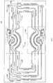
- FIG. 3is one example of a printed circuit board layout for a dual band electric tilt circuit board according to the present invention.
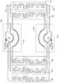
- FIG. 4is a second example of a printed circuit board layout according to the present invention including a plurality of diplexers mounted directly on the circuit board.
- FIG. 5is another view of the example of FIG. 4 , with cavity housings removed to reveal more detail.
- FIG. 6is a detailed view of a diplexer that may be used in the printed circuit board layout of FIGS. 4 and 5 .
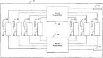
- a multi-band electrical tilt circuit board 10is illustrated in schematic form in FIG. 1 .
- “multi-band”refers to two or more bands.
- the multi-band electrical tilt circuit board 10includes a transmission line termination 12 for a first RF band, a transmission line termination 14 for a second RF band, a first RF band variable phase shifter 16 , and a second RF band variable phase shifter 18 .
- the transmission line termination 12is for terminating a transmission line, such as a coaxial cable, from a radio operating in the first RF band
- transmission line termination 14is for terminating a transmission line from a radio operating in the second RF band.
- transmission line terminationson the back or bottom of the antenna system, with an intermediate cable between the termination and the multi-band electrical tilt circuit band 10 .
- the transmission line terminations 12 , 14may comprise solder pads or a capacitive coupling.
- This multi-band electrical tilt circuit board 10may be suitable for an antenna having a single polarization. In another example, two multi-band electrical tilt circuit boards 10 are employed, one for each polarization of a dual-polarized antenna.
- the phase shifters 16 , 18may comprise variable differential, arcuate phase shifters as illustrated in U.S. Pat. No. 7,907,096, which is incorporated by reference.
- a rotatable wiper armvariably couples an RF signal to a fixed arcuate transmission line.
- the phase shiftersperform a 1:7 power division (which may or may not be tapered) in the direction of radio transmission, and a 7:1 combination in the direction of radio reception.
- phase shiftersperform a 1:7 power division (which may or may not be tapered) in the direction of radio transmission, and a 7:1 combination in the direction of radio reception.
- phase shiftersmay be used without departing from the scope and spirit of the invention.
- the terms “input” and “output”refer to the direction of RF signals when transmitting from a base station radio to the radiating elements of an antenna.
- the devices hereinalso operate in the receive direction, and the terms “input” and “output” would be reversed if considering RF signal flow from radiating elements to the base station radios.
- an inputis coupled to transmission line termination 12 .
- the phase shifterhas seven output ports, six of which are differentially variably phase shifted. There is also one output which maintains a fixed phase shift, however, an output having a fixed phase relationship to the input is optional.
- the seven outputs of the phase shifters 16 , 18are individually coupled to seven combiners 20 .
- Each combiner 20has three ports: 1) a first RF band port coupled to an output of phase shifter 16 ; 2) a second RF band port coupled to an output of phase shifter 18 ; and 3) a combined port.
- the first and second RF band ports of the combiner 20are coupled to corresponding outputs on phase shifters 16 , 18 .
- the first RF band port of a first combiner 20is coupled to the first output of first RF band phase shifter 16 and the second RF band port of the first combiner 20 is coupled to the first output of second RF band phase shifter 18 .
- the first RF band port of each combiner 20is configured to pass signals corresponding to the first RF band
- the second RF band port of each combiner 20is configured to pass signals corresponding to the second RF band.
- the combined port of each combiner 20is coupled to a cable termination 22 .
- the combined portis configured to pass both the first RF band and the second RF band.
- the multi-band electrical tilt circuit board 10may be implemented in a common medium.
- the common mediummay comprise a printed circuit board, an air suspended stripline construction, or other suitable medium.
- the phase shifters 16 , 18may be implemented on a common medium and the combiners 20 may be fabricated separately and mounted on the common medium.
- the combinersmay be implemented as a microstrip-fed cavity filter that is soldered onto a PCB including phase shifters 16 , 18 .
- a multi-band electrical tilt circuit board 10may be configured for high band or low band operation.
- the first RF bandmay comprise 880-960 MHz and the second RF band may comprise 790-862 MHz.
- the first RF bandmay be 1710-1880 MHz and the second RF band may be 1920 MHz-2170 MHz.
- a third RF band at 2.5-2.7 GHzmay be included.
- the first RF bandmay be 1710-2170 MHz and the second RF band may be 2.5-2.7 GHz. Additional combinations of bands are contemplated.
- each antenna element 34is coupled to a combiner 20 by way of a coaxial transmission line 32 and a cable termination 22 .
- each radiating elementmay be associated with a circuit board or boards for terminating coaxial transmission line 36 and for providing a balun for converting RF signals from unbalanced to balanced and back.
- the transmission line termination 12terminates coaxial transmission line 36 from a radio operating in the first RF band
- transmission line termination 14terminates coaxial transmission line 38 from a radio operating in the second RF band.
- a fixed portion of a first band phase shifter 116 , a second band phase shifter 118 and the diplexers 120 a - 120 gare implemented using printed circuit board (PCB) fabrication techniques. Also illustrated are coaxial terminations 112 and 114 . Rotatable wiper arms for the phase shifters 116 , 118 are not illustrated to enhance clarity of the fixed portions of the phase shifters 116 , 118 . Most preferably, the fixed portion of the phase shifters 116 , 118 and the diplexers 120 a - 120 g are fabricated on a common PCB with microstrip transmission lines providing the connections between the components. This allows for a significant reduction in cables required.
- PCBprinted circuit board
- each of a plurality of diplexers 220are implemented as a microstrip-fed cavity filter including a cavity housing 240 .
- the microstrip portion of the diplexer 220may be fabricated on the same PCB as a fixed portion of a first band phase shifter 216 and a second band phase shifter 218 .
- the diplexers 220are separately fabricated PCB and cavity housing combinations, and are soldered directly to a PCB including first band phase shifter 216 and second band phase shifter 218 .
- the diplexersmay comprise two series notch filters (see, e.g., FIGS. 5 and 6 ) with a common port 222 in the middle, a first band input 224 at one end, and a second band input 226 at the other end.
- the cavity housing 240may be machined to provide a cavity enclosing each notch filter of the diplexer 220 .
- Tuning plugs 242may also be included to further tune the frequency response of the notch filters.
- FIG. 5illustrates the multi-band electrical tilt circuit board 210 with the cavity housings 240 removed.
- the diplexers 220each have a common port 222 first band input 224 , and a second band input 226 .
- the illustrated examplecontains three notch filters 228 a between the first band input 224 and the common port 222 , and three notch filters 228 b between the second band input 226 and the common port 222 .
- the notch filters 228 a , 228 bare configured to pass the first and second bands, respectively, and block other frequencies.
- the diplexersmay use a number of resonant stubs that act as stop-band filters, blocking energy in specific bands.
- the resonant frequencymost heavily depends on the length of the stub and how the stub is terminated. For example an open-circuited stub will block frequencies such that the stub is a quarter-wavelength long while a short-circuited stub will block frequencies such that the stub is a half-wavelength long.
- the impedance of the stubalso impacts its performance and in many cases performance either in terms of amount of rejection in dB or bandwidth in frequency are improved by dividing the stub into subsections each with its own separate impedance.
- FIGS. 4 and 5Also illustrated in FIGS. 4 and 5 are coaxial terminations 212 and 214 .
- Rotatable wiper arms for the phase shifters 216 , 218are not illustrated to enhance clarity of the fixed portions of the phase shifters 216 , 218 .
- the fixed portion of the phase shifters 216 , 218 and the diplexers 220are fabricated on a common PCB with microstrip transmission lines providing the connections between the components. This allows for a significant reduction in cables required.
- the structure of the present inventionpermits independent adjustment of downtilt for each band. Additionally, the present invention reduces weight and cabling complexity relative to prior-known solutions.
Landscapes
- Engineering & Computer Science (AREA)
- Computer Networks & Wireless Communication (AREA)
- Variable-Direction Aerials And Aerial Arrays (AREA)
- Waveguide Switches, Polarizers, And Phase Shifters (AREA)
Abstract
Description
Claims (20)
Priority Applications (1)
| Application Number | Priority Date | Filing Date | Title |
|---|---|---|---|
| US16/178,633US10847902B2 (en) | 2014-01-10 | 2018-11-02 | Enhanced phase shifter circuit to reduce RF cables |
Applications Claiming Priority (4)
| Application Number | Priority Date | Filing Date | Title |
|---|---|---|---|
| US201461925903P | 2014-01-10 | 2014-01-10 | |
| US14/274,321US9444151B2 (en) | 2014-01-10 | 2014-05-09 | Enhanced phase shifter circuit to reduce RF cables |
| US15/244,300US10148017B2 (en) | 2014-01-10 | 2016-08-23 | Enhanced phase shifter circuit to reduce RF cables |
| US16/178,633US10847902B2 (en) | 2014-01-10 | 2018-11-02 | Enhanced phase shifter circuit to reduce RF cables |
Related Parent Applications (1)
| Application Number | Title | Priority Date | Filing Date |
|---|---|---|---|
| US15/244,300ContinuationUS10148017B2 (en) | 2014-01-10 | 2016-08-23 | Enhanced phase shifter circuit to reduce RF cables |
Publications (2)
| Publication Number | Publication Date |
|---|---|
| US20190074602A1 US20190074602A1 (en) | 2019-03-07 |
| US10847902B2true US10847902B2 (en) | 2020-11-24 |
Family
ID=53522122
Family Applications (3)
| Application Number | Title | Priority Date | Filing Date |
|---|---|---|---|
| US14/274,321Active2034-11-04US9444151B2 (en) | 2014-01-10 | 2014-05-09 | Enhanced phase shifter circuit to reduce RF cables |
| US15/244,300Active2034-06-12US10148017B2 (en) | 2014-01-10 | 2016-08-23 | Enhanced phase shifter circuit to reduce RF cables |
| US16/178,633Active2034-05-19US10847902B2 (en) | 2014-01-10 | 2018-11-02 | Enhanced phase shifter circuit to reduce RF cables |
Family Applications Before (2)
| Application Number | Title | Priority Date | Filing Date |
|---|---|---|---|
| US14/274,321Active2034-11-04US9444151B2 (en) | 2014-01-10 | 2014-05-09 | Enhanced phase shifter circuit to reduce RF cables |
| US15/244,300Active2034-06-12US10148017B2 (en) | 2014-01-10 | 2016-08-23 | Enhanced phase shifter circuit to reduce RF cables |
Country Status (4)
| Country | Link |
|---|---|
| US (3) | US9444151B2 (en) |
| EP (1) | EP3092677B1 (en) |
| CN (1) | CN105849971B (en) |
| WO (1) | WO2015105568A1 (en) |
Families Citing this family (22)
| Publication number | Priority date | Publication date | Assignee | Title |
|---|---|---|---|---|
| EP2706613B1 (en)* | 2012-09-11 | 2017-11-22 | Alcatel Lucent | Multi-band antenna with variable electrical tilt |
| MX375655B (en) | 2015-06-01 | 2025-03-06 | Huawei Tech Co Ltd | COMBINED PHASE SHIFTER AND MULTI-BAND ANTENNA NETWORK SYSTEM. |
| CN107710499B (en)* | 2015-06-23 | 2020-07-07 | 华为技术有限公司 | Phase shifters and antennas |
| US10790576B2 (en) | 2015-12-14 | 2020-09-29 | Commscope Technologies Llc | Multi-band base station antennas having multi-layer feed boards |
| CN109314291B (en)* | 2016-06-17 | 2020-11-27 | 康普技术有限责任公司 | Phased Array Antenna with Multistage Phase Shifters |
| EP3419104B1 (en) | 2017-06-22 | 2022-03-09 | CommScope Technologies LLC | Cellular communication systems having antenna arrays therein with enhanced half power beam width (hpbw) control |
| US11342668B2 (en) | 2017-06-22 | 2022-05-24 | Commscope Technologies Llc | Cellular communication systems having antenna arrays therein with enhanced half power beam width (HPBW) control |
| CN111837294A (en) | 2018-03-05 | 2020-10-27 | 康普技术有限责任公司 | Antenna array with shared radiating elements exhibiting reduced azimuthal beamwidth and increased isolation |
| US10469120B1 (en) | 2018-09-28 | 2019-11-05 | Apple Inc. | Radio frequency front-end circuitry intermediate driver systems and methods |
| DE102018130570B4 (en) | 2018-11-30 | 2022-10-27 | Telefonaktiebolaget Lm Ericsson (Publ) | Mobile radio antenna for connection to at least one mobile radio base station |
| US11626659B2 (en)* | 2019-05-03 | 2023-04-11 | Echodyne Corp. | Antenna unit with phase-shifting modulator, and related antenna, subsystem, system, and method |
| CN112186368A (en)* | 2019-07-03 | 2021-01-05 | 康普技术有限责任公司 | Feed network for antenna, antenna and feed method for antenna |
| CN112864548B (en)* | 2019-11-12 | 2025-02-11 | 户外无线网络有限公司 | Cavity phase shifter and base station antenna |
| CN113258261B (en) | 2020-02-13 | 2025-07-25 | 户外无线网络有限公司 | Antenna assembly and base station antenna with same |
| CN211829185U (en) | 2020-05-29 | 2020-10-30 | 康普技术有限责任公司 | Base station antenna |
| CN111628252A (en)* | 2020-07-10 | 2020-09-04 | 摩比天线技术(深圳)有限公司 | Integrated Phase Shifter and ESC Antenna |
| CN111817009B (en)* | 2020-07-28 | 2022-01-11 | 武汉虹信科技发展有限责任公司 | Dual-frequency feed network and antenna |
| CN114447542A (en)* | 2020-10-30 | 2022-05-06 | 康普技术有限责任公司 | Slider, phase shifter and base station antenna |
| CN112736378B (en)* | 2020-12-01 | 2021-12-14 | 武汉虹信科技发展有限责任公司 | Filtering phase shifter and antenna |
| CN114284655A (en)* | 2022-02-16 | 2022-04-05 | 江苏亨鑫科技有限公司 | Combiner phase shifter and antenna |
| US12407099B2 (en)* | 2022-08-18 | 2025-09-02 | Outdoor Wireless Networks LLC | Phase shifter for base station antenna |
| CN117673737A (en)* | 2022-09-01 | 2024-03-08 | 康普技术有限责任公司 | Base station antenna |
Citations (14)
| Publication number | Priority date | Publication date | Assignee | Title |
|---|---|---|---|---|
| US4689627A (en) | 1983-05-20 | 1987-08-25 | Hughes Aircraft Company | Dual band phased antenna array using wideband element with diplexer |
| US5982252A (en)* | 1998-04-27 | 1999-11-09 | Werlatone, Inc. | High power broadband non-directional combiner |
| US6067053A (en) | 1995-12-14 | 2000-05-23 | Ems Technologies, Inc. | Dual polarized array antenna |
| US6384680B1 (en) | 2000-01-19 | 2002-05-07 | Hitachi, Ltd. | RF amplifier with plural combiners |
| US20020053954A1 (en)* | 2000-10-26 | 2002-05-09 | Khosro Shamsaifar | Electronically tunable RF diplexers tuned by tunable capacitors |
| US20050046514A1 (en) | 2003-08-28 | 2005-03-03 | Janoschka Darin M. | Wiper-type phase shifter with cantilever shoe and dual-polarization antenna with commonly driven phase shifters |
| GB2410838A (en) | 2002-01-11 | 2005-08-10 | Csa Ltd | Antenna with adjustable beam direction |
| CN101587989A (en) | 2008-01-25 | 2009-11-25 | 北卡罗来纳康普股份有限公司 | Phase shifter and the antenna that comprises phase shifter |
| CN102347529A (en) | 2010-08-04 | 2012-02-08 | 诺基亚西门子通信公司 | Broadband antenna used to process at least two frequency bands in radio communications system or radio standard, and radio base station system thereof |
| WO2012016941A1 (en) | 2010-08-04 | 2012-02-09 | Nokia Siemens Networks Oy | Broadband antenna and radio base station system for processing at least two frequency bands or radio standards in a radio communications system |
| WO2012048343A1 (en) | 2010-10-08 | 2012-04-12 | Commscope, Inc. Of North Carolina | Antenna having active and passive feed networks |
| US20120113874A1 (en)* | 2010-11-09 | 2012-05-10 | Sanguinetti Louie J | Wireless circuitry with simultaneous voice and data capabilities and reduced intermodulation distortion |
| CN103107387A (en) | 2013-02-08 | 2013-05-15 | 华为技术有限公司 | Phase shifter with filter element, filter element and antenna |
| EP2629358A2 (en) | 2012-01-10 | 2013-08-21 | Huawei Technologies Co., Ltd. | Phase shifter and antenna |
Family Cites Families (11)
| Publication number | Priority date | Publication date | Assignee | Title |
|---|---|---|---|---|
| US4206428A (en)* | 1978-10-20 | 1980-06-03 | Tx Rx Systems Inc. | Series notch filter and multicoupler utilizing same |
| DE19823749C2 (en) | 1998-05-27 | 2002-07-11 | Kathrein Werke Kg | Dual polarized multi-range antenna |
| SE512439C2 (en) | 1998-06-26 | 2000-03-20 | Allgon Ab | Dual band antenna |
| DE19938862C1 (en)* | 1999-08-17 | 2001-03-15 | Kathrein Werke Kg | High frequency phase shifter assembly |
| EP1509969A4 (en) | 2002-03-26 | 2005-08-31 | Andrew Corp | Multiband dual polarized adjustable beamtilt base station antenna |
| US7238101B2 (en) | 2004-05-20 | 2007-07-03 | Delphi Technologies, Inc. | Thermally conditioned vehicle seat |
| GB0622435D0 (en)* | 2006-11-10 | 2006-12-20 | Quintel Technology Ltd | Electrically tilted antenna system with polarisation diversity |
| WO2009132044A1 (en)* | 2008-04-21 | 2009-10-29 | Spx Corporation | Phased-array antenna filter and diplexer for a super economical broadcast system |
| AU2010233056A1 (en) | 2010-10-14 | 2010-12-23 | Chris Sampson | Method and System for Managing Organisations |
| US8674895B2 (en) | 2011-05-03 | 2014-03-18 | Andrew Llc | Multiband antenna |
| CN203521615U (en)* | 2013-10-28 | 2014-04-02 | 华为技术有限公司 | base station antenna |
- 2014
- 2014-05-09USUS14/274,321patent/US9444151B2/enactiveActive
- 2014-11-04CNCN201480071320.4Apatent/CN105849971B/enactiveActive
- 2014-11-04WOPCT/US2014/063882patent/WO2015105568A1/enactiveApplication Filing
- 2014-11-04EPEP14802746.9Apatent/EP3092677B1/enactiveActive
- 2016
- 2016-08-23USUS15/244,300patent/US10148017B2/enactiveActive
- 2018
- 2018-11-02USUS16/178,633patent/US10847902B2/enactiveActive
Patent Citations (15)
| Publication number | Priority date | Publication date | Assignee | Title |
|---|---|---|---|---|
| US4689627A (en) | 1983-05-20 | 1987-08-25 | Hughes Aircraft Company | Dual band phased antenna array using wideband element with diplexer |
| US6067053A (en) | 1995-12-14 | 2000-05-23 | Ems Technologies, Inc. | Dual polarized array antenna |
| US5982252A (en)* | 1998-04-27 | 1999-11-09 | Werlatone, Inc. | High power broadband non-directional combiner |
| US6384680B1 (en) | 2000-01-19 | 2002-05-07 | Hitachi, Ltd. | RF amplifier with plural combiners |
| US20020053954A1 (en)* | 2000-10-26 | 2002-05-09 | Khosro Shamsaifar | Electronically tunable RF diplexers tuned by tunable capacitors |
| GB2410838A (en) | 2002-01-11 | 2005-08-10 | Csa Ltd | Antenna with adjustable beam direction |
| US20050046514A1 (en) | 2003-08-28 | 2005-03-03 | Janoschka Darin M. | Wiper-type phase shifter with cantilever shoe and dual-polarization antenna with commonly driven phase shifters |
| US7170466B2 (en) | 2003-08-28 | 2007-01-30 | Ems Technologies, Inc. | Wiper-type phase shifter with cantilever shoe and dual-polarization antenna with commonly driven phase shifters |
| CN101587989A (en) | 2008-01-25 | 2009-11-25 | 北卡罗来纳康普股份有限公司 | Phase shifter and the antenna that comprises phase shifter |
| CN102347529A (en) | 2010-08-04 | 2012-02-08 | 诺基亚西门子通信公司 | Broadband antenna used to process at least two frequency bands in radio communications system or radio standard, and radio base station system thereof |
| WO2012016941A1 (en) | 2010-08-04 | 2012-02-09 | Nokia Siemens Networks Oy | Broadband antenna and radio base station system for processing at least two frequency bands or radio standards in a radio communications system |
| WO2012048343A1 (en) | 2010-10-08 | 2012-04-12 | Commscope, Inc. Of North Carolina | Antenna having active and passive feed networks |
| US20120113874A1 (en)* | 2010-11-09 | 2012-05-10 | Sanguinetti Louie J | Wireless circuitry with simultaneous voice and data capabilities and reduced intermodulation distortion |
| EP2629358A2 (en) | 2012-01-10 | 2013-08-21 | Huawei Technologies Co., Ltd. | Phase shifter and antenna |
| CN103107387A (en) | 2013-02-08 | 2013-05-15 | 华为技术有限公司 | Phase shifter with filter element, filter element and antenna |
Non-Patent Citations (6)
| Title |
|---|
| Communication pursuant to Article 94(3) EPC corresponding to European Patent Application No. 14802746.9 (dated Sep. 18, 2017) (9 pages). |
| International Search Report regarding related International Application PCT/US2014/063882, dated Feb. 9, 2015 (5 pages). |
| Notification Concerning Transmittal of International Preliminary Report on Patentability, PCT/US2014/063882, Jul. 21, 2016, 8 pages. |
| Office Action from corresponding Chinese Application No. 201480071320.4, dated May 15, 2019, 9 pages. |
| Office Action from corresponding European Patent Application No. 14802746.9, dated Jun. 26, 2018. |
| Written Opinion of the International Searching Authority regarding related International Application PCT/US2014/063882, dated Feb. 9, 2015 (9 pages). |
Also Published As
| Publication number | Publication date |
|---|---|
| US20150200467A1 (en) | 2015-07-16 |
| CN105849971B (en) | 2019-08-20 |
| EP3092677A1 (en) | 2016-11-16 |
| EP3092677B1 (en) | 2019-08-14 |
| US20160359239A1 (en) | 2016-12-08 |
| US9444151B2 (en) | 2016-09-13 |
| WO2015105568A1 (en) | 2015-07-16 |
| CN105849971A (en) | 2016-08-10 |
| US20190074602A1 (en) | 2019-03-07 |
| US10148017B2 (en) | 2018-12-04 |
Similar Documents
| Publication | Publication Date | Title |
|---|---|---|
| US10847902B2 (en) | Enhanced phase shifter circuit to reduce RF cables | |
| US11296425B2 (en) | Dual-polarized duplex antenna and dual-band base station antenna array composed thereof | |
| CN110429374B (en) | Broadband dual-polarized filtering base station antenna unit, base station antenna array and communication equipment | |
| US10833411B2 (en) | Concentrated wireless device providing operability in multiple frequency regions | |
| KR101858777B1 (en) | Balanced Antenna System | |
| CN107275808B (en) | Ultra-wideband radiators and associated antenna arrays | |
| US7289064B2 (en) | Compact multi-band, multi-port antenna | |
| US8786499B2 (en) | Multiband antenna system and methods | |
| CN102893452B (en) | There is the dual-port antenna of the separate antenna branch including respective wave filter | |
| US9306266B2 (en) | Multi-band antenna for wireless communication | |
| CN103168389B (en) | Antennas with active and passive feed networks | |
| EP2521222A1 (en) | Multiband antenna | |
| CN1389003A (en) | Antenna arrangement | |
| KR20020093114A (en) | Multiband antenna arrangement for radio communications apparatus | |
| CN107403996A (en) | A kind of multiple coupled terminal antenna of metal edge frame and mobile terminal device | |
| US20250125540A1 (en) | Multiband cross-dipole radiating elements and base station antennas including arrays of such radiating elements | |
| EP3888181B1 (en) | Mobile radio antenna for connection to at least one mobile base station | |
| CN102738566A (en) | Miniaturized three-band satellite communication antenna | |
| CN213242793U (en) | Low frequency radiation unit and broadband base station antenna | |
| CN1788390B (en) | Improvements in or relating to wireless terminals | |
| CN218160762U (en) | Multi-frequency combiner | |
| CN216085258U (en) | Low-cost compact three-frequency combiner | |
| US12308534B2 (en) | Antenna device | |
| US20250149797A1 (en) | Antenna module | |
| Boyle et al. | A novel dual-fed, self-diplexing PIFA and RF front-end (PIN-DF/sup 2/-PIFA) |
Legal Events
| Date | Code | Title | Description |
|---|---|---|---|
| FEPP | Fee payment procedure | Free format text:ENTITY STATUS SET TO UNDISCOUNTED (ORIGINAL EVENT CODE: BIG.); ENTITY STATUS OF PATENT OWNER: LARGE ENTITY | |
| STPP | Information on status: patent application and granting procedure in general | Free format text:DOCKETED NEW CASE - READY FOR EXAMINATION | |
| AS | Assignment | Owner name:WILMINGTON TRUST, NATIONAL ASSOCIATION, AS COLLATE Free format text:PATENT SECURITY AGREEMENT;ASSIGNOR:COMMSCOPE TECHNOLOGIES LLC;REEL/FRAME:049892/0051 Effective date:20190404 Owner name:JPMORGAN CHASE BANK, N.A., NEW YORK Free format text:ABL SECURITY AGREEMENT;ASSIGNORS:COMMSCOPE, INC. OF NORTH CAROLINA;COMMSCOPE TECHNOLOGIES LLC;ARRIS ENTERPRISES LLC;AND OTHERS;REEL/FRAME:049892/0396 Effective date:20190404 Owner name:JPMORGAN CHASE BANK, N.A., NEW YORK Free format text:TERM LOAN SECURITY AGREEMENT;ASSIGNORS:COMMSCOPE, INC. OF NORTH CAROLINA;COMMSCOPE TECHNOLOGIES LLC;ARRIS ENTERPRISES LLC;AND OTHERS;REEL/FRAME:049905/0504 Effective date:20190404 Owner name:WILMINGTON TRUST, NATIONAL ASSOCIATION, AS COLLATERAL AGENT, CONNECTICUT Free format text:PATENT SECURITY AGREEMENT;ASSIGNOR:COMMSCOPE TECHNOLOGIES LLC;REEL/FRAME:049892/0051 Effective date:20190404 | |
| STPP | Information on status: patent application and granting procedure in general | Free format text:RESPONSE TO NON-FINAL OFFICE ACTION ENTERED AND FORWARDED TO EXAMINER | |
| STPP | Information on status: patent application and granting procedure in general | Free format text:NOTICE OF ALLOWANCE MAILED -- APPLICATION RECEIVED IN OFFICE OF PUBLICATIONS | |
| STPP | Information on status: patent application and granting procedure in general | Free format text:NOTICE OF ALLOWANCE MAILED -- APPLICATION RECEIVED IN OFFICE OF PUBLICATIONS | |
| STPP | Information on status: patent application and granting procedure in general | Free format text:PUBLICATIONS -- ISSUE FEE PAYMENT VERIFIED | |
| STCF | Information on status: patent grant | Free format text:PATENTED CASE | |
| AS | Assignment | Owner name:WILMINGTON TRUST, DELAWARE Free format text:SECURITY INTEREST;ASSIGNORS:ARRIS SOLUTIONS, INC.;ARRIS ENTERPRISES LLC;COMMSCOPE TECHNOLOGIES LLC;AND OTHERS;REEL/FRAME:060752/0001 Effective date:20211115 | |
| MAFP | Maintenance fee payment | Free format text:PAYMENT OF MAINTENANCE FEE, 4TH YEAR, LARGE ENTITY (ORIGINAL EVENT CODE: M1551); ENTITY STATUS OF PATENT OWNER: LARGE ENTITY Year of fee payment:4 | |
| AS | Assignment | Owner name:OUTDOOR WIRELESS NETWORKS LLC, NORTH CAROLINA Free format text:ASSIGNMENT OF ASSIGNORS INTEREST;ASSIGNOR:COMMSCOPE TECHNOLOGIES LLC;REEL/FRAME:068107/0089 Effective date:20240701 | |
| AS | Assignment | Owner name:JPMORGAN CHASE BANK, N.A., AS COLLATERAL AGENT, NEW YORK Free format text:PATENT SECURITY AGREEMENT (TERM);ASSIGNOR:OUTDOOR WIRELESS NETWORKS LLC;REEL/FRAME:068770/0632 Effective date:20240813 Owner name:JPMORGAN CHASE BANK, N.A., AS COLLATERAL AGENT, NEW YORK Free format text:PATENT SECURITY AGREEMENT (ABL);ASSIGNOR:OUTDOOR WIRELESS NETWORKS LLC;REEL/FRAME:068770/0460 Effective date:20240813 | |
| AS | Assignment | Owner name:APOLLO ADMINISTRATIVE AGENCY LLC, NEW YORK Free format text:SECURITY INTEREST;ASSIGNORS:ARRIS ENTERPRISES LLC;COMMSCOPE TECHNOLOGIES LLC;COMMSCOPE INC., OF NORTH CAROLINA;AND OTHERS;REEL/FRAME:069889/0114 Effective date:20241217 | |
| AS | Assignment | Owner name:OUTDOOR WIRELESS NETWORKS LLC, NORTH CAROLINA Free format text:RELEASE OF SECURITY INTEREST AT REEL/FRAME 068770/0632;ASSIGNOR:JPMORGAN CHASE BANK, N.A., AS COLLATERAL AGENT;REEL/FRAME:069743/0264 Effective date:20241217 Owner name:RUCKUS WIRELESS, LLC (F/K/A RUCKUS WIRELESS, INC.), NORTH CAROLINA Free format text:RELEASE OF SECURITY INTEREST AT REEL/FRAME 049905/0504;ASSIGNOR:JPMORGAN CHASE BANK, N.A., AS COLLATERAL AGENT;REEL/FRAME:071477/0255 Effective date:20241217 Owner name:COMMSCOPE TECHNOLOGIES LLC, NORTH CAROLINA Free format text:RELEASE OF SECURITY INTEREST AT REEL/FRAME 049905/0504;ASSIGNOR:JPMORGAN CHASE BANK, N.A., AS COLLATERAL AGENT;REEL/FRAME:071477/0255 Effective date:20241217 Owner name:COMMSCOPE, INC. OF NORTH CAROLINA, NORTH CAROLINA Free format text:RELEASE OF SECURITY INTEREST AT REEL/FRAME 049905/0504;ASSIGNOR:JPMORGAN CHASE BANK, N.A., AS COLLATERAL AGENT;REEL/FRAME:071477/0255 Effective date:20241217 Owner name:ARRIS SOLUTIONS, INC., NORTH CAROLINA Free format text:RELEASE OF SECURITY INTEREST AT REEL/FRAME 049905/0504;ASSIGNOR:JPMORGAN CHASE BANK, N.A., AS COLLATERAL AGENT;REEL/FRAME:071477/0255 Effective date:20241217 Owner name:ARRIS TECHNOLOGY, INC., NORTH CAROLINA Free format text:RELEASE OF SECURITY INTEREST AT REEL/FRAME 049905/0504;ASSIGNOR:JPMORGAN CHASE BANK, N.A., AS COLLATERAL AGENT;REEL/FRAME:071477/0255 Effective date:20241217 Owner name:ARRIS ENTERPRISES LLC (F/K/A ARRIS ENTERPRISES, INC.), NORTH CAROLINA Free format text:RELEASE OF SECURITY INTEREST AT REEL/FRAME 049905/0504;ASSIGNOR:JPMORGAN CHASE BANK, N.A., AS COLLATERAL AGENT;REEL/FRAME:071477/0255 Effective date:20241217 | |
| AS | Assignment | Owner name:OUTDOOR WIRELESS NETWORKS LLC, NORTH CAROLINA Free format text:PARTIAL TERMINATION AND RELEASE OF SECURITY INTEREST IN PATENTS RECORDED AT REEL 069889/FRAME 0114;ASSIGNOR:APOLLO ADMINISTRATIVE AGENCY LLC;REEL/FRAME:070154/0341 Effective date:20250131 Owner name:OUTDOOR WIRELESS NETWORKS LLC, NORTH CAROLINA Free format text:PARTIAL TERMINATION AND RELEASE OF SECURITY INTEREST IN PATENTS;ASSIGNOR:U.S. BANK TRUST COMPANY, NATIONAL ASSOCIATION;REEL/FRAME:070154/0183 Effective date:20250131 Owner name:OUTDOOR WIRELESS NETWORKS LLC, NORTH CAROLINA Free format text:RELEASE (REEL 068770 / FRAME 0460);ASSIGNOR:JPMORGAN CHASE BANK, N.A.;REEL/FRAME:070149/0432 Effective date:20250131 |