US10847540B2 - 3D semiconductor memory device and structure - Google Patents
3D semiconductor memory device and structureDownload PDFInfo
- Publication number
- US10847540B2 US10847540B2US16/526,763US201916526763AUS10847540B2US 10847540 B2US10847540 B2US 10847540B2US 201916526763 AUS201916526763 AUS 201916526763AUS 10847540 B2US10847540 B2US 10847540B2
- Authority
- US
- United States
- Prior art keywords
- memory
- line
- gate
- lines
- illustrates
- Prior art date
- Legal status (The legal status is an assumption and is not a legal conclusion. Google has not performed a legal analysis and makes no representation as to the accuracy of the status listed.)
- Active - Reinstated
Links
Images


Classifications
- H—ELECTRICITY
- H10—SEMICONDUCTOR DEVICES; ELECTRIC SOLID-STATE DEVICES NOT OTHERWISE PROVIDED FOR
- H10B—ELECTRONIC MEMORY DEVICES
- H10B43/00—EEPROM devices comprising charge-trapping gate insulators
- H10B43/20—EEPROM devices comprising charge-trapping gate insulators characterised by three-dimensional arrangements, e.g. with cells on different height levels
- H10B43/23—EEPROM devices comprising charge-trapping gate insulators characterised by three-dimensional arrangements, e.g. with cells on different height levels with source and drain on different levels, e.g. with sloping channels
- H10B43/27—EEPROM devices comprising charge-trapping gate insulators characterised by three-dimensional arrangements, e.g. with cells on different height levels with source and drain on different levels, e.g. with sloping channels the channels comprising vertical portions, e.g. U-shaped channels
- G—PHYSICS
- G11—INFORMATION STORAGE
- G11C—STATIC STORES
- G11C16/00—Erasable programmable read-only memories
- G11C16/02—Erasable programmable read-only memories electrically programmable
- G11C16/04—Erasable programmable read-only memories electrically programmable using variable threshold transistors, e.g. FAMOS
- G11C16/0408—Erasable programmable read-only memories electrically programmable using variable threshold transistors, e.g. FAMOS comprising cells containing floating gate transistors
- G11C16/0416—Erasable programmable read-only memories electrically programmable using variable threshold transistors, e.g. FAMOS comprising cells containing floating gate transistors comprising cells containing a single floating gate transistor and no select transistor, e.g. UV EPROM
- H01L27/11582—
- G—PHYSICS
- G11—INFORMATION STORAGE
- G11C—STATIC STORES
- G11C11/00—Digital stores characterised by the use of particular electric or magnetic storage elements; Storage elements therefor
- G11C11/56—Digital stores characterised by the use of particular electric or magnetic storage elements; Storage elements therefor using storage elements with more than two stable states represented by steps, e.g. of voltage, current, phase, frequency
- G11C11/5671—Digital stores characterised by the use of particular electric or magnetic storage elements; Storage elements therefor using storage elements with more than two stable states represented by steps, e.g. of voltage, current, phase, frequency using charge trapping in an insulator
- G—PHYSICS
- G11—INFORMATION STORAGE
- G11C—STATIC STORES
- G11C16/00—Erasable programmable read-only memories
- G11C16/02—Erasable programmable read-only memories electrically programmable
- G11C16/06—Auxiliary circuits, e.g. for writing into memory
- G11C16/10—Programming or data input circuits
- G—PHYSICS
- G11—INFORMATION STORAGE
- G11C—STATIC STORES
- G11C16/00—Erasable programmable read-only memories
- G11C16/02—Erasable programmable read-only memories electrically programmable
- G11C16/06—Auxiliary circuits, e.g. for writing into memory
- G11C16/10—Programming or data input circuits
- G11C16/14—Circuits for erasing electrically, e.g. erase voltage switching circuits
- G—PHYSICS
- G11—INFORMATION STORAGE
- G11C—STATIC STORES
- G11C16/00—Erasable programmable read-only memories
- G11C16/02—Erasable programmable read-only memories electrically programmable
- G11C16/06—Auxiliary circuits, e.g. for writing into memory
- G11C16/26—Sensing or reading circuits; Data output circuits
- G—PHYSICS
- G11—INFORMATION STORAGE
- G11C—STATIC STORES
- G11C16/00—Erasable programmable read-only memories
- G11C16/02—Erasable programmable read-only memories electrically programmable
- G11C16/06—Auxiliary circuits, e.g. for writing into memory
- G11C16/34—Determination of programming status, e.g. threshold voltage, overprogramming or underprogramming, retention
- G11C16/3418—Disturbance prevention or evaluation; Refreshing of disturbed memory data
- H—ELECTRICITY
- H01—ELECTRIC ELEMENTS
- H01L—SEMICONDUCTOR DEVICES NOT COVERED BY CLASS H10
- H01L21/00—Processes or apparatus adapted for the manufacture or treatment of semiconductor or solid state devices or of parts thereof
- H01L21/02—Manufacture or treatment of semiconductor devices or of parts thereof
- H01L21/02104—Forming layers
- H01L21/02365—Forming inorganic semiconducting materials on a substrate
- H01L21/02518—Deposited layers
- H01L21/02521—Materials
- H01L21/02524—Group 14 semiconducting materials
- H01L21/02532—Silicon, silicon germanium, germanium
- H—ELECTRICITY
- H01—ELECTRIC ELEMENTS
- H01L—SEMICONDUCTOR DEVICES NOT COVERED BY CLASS H10
- H01L21/00—Processes or apparatus adapted for the manufacture or treatment of semiconductor or solid state devices or of parts thereof
- H01L21/02—Manufacture or treatment of semiconductor devices or of parts thereof
- H01L21/02104—Forming layers
- H01L21/02365—Forming inorganic semiconducting materials on a substrate
- H01L21/02612—Formation types
- H01L21/02617—Deposition types
- H01L21/02636—Selective deposition, e.g. simultaneous growth of mono- and non-monocrystalline semiconductor materials
- H—ELECTRICITY
- H01—ELECTRIC ELEMENTS
- H01L—SEMICONDUCTOR DEVICES NOT COVERED BY CLASS H10
- H01L21/00—Processes or apparatus adapted for the manufacture or treatment of semiconductor or solid state devices or of parts thereof
- H01L21/02—Manufacture or treatment of semiconductor devices or of parts thereof
- H01L21/02104—Forming layers
- H01L21/02365—Forming inorganic semiconducting materials on a substrate
- H01L21/02656—Special treatments
- H01L21/02664—Aftertreatments
- H01L21/02667—Crystallisation or recrystallisation of non-monocrystalline semiconductor materials, e.g. regrowth
- H01L21/02675—Crystallisation or recrystallisation of non-monocrystalline semiconductor materials, e.g. regrowth using laser beams
- H—ELECTRICITY
- H01—ELECTRIC ELEMENTS
- H01L—SEMICONDUCTOR DEVICES NOT COVERED BY CLASS H10
- H01L21/00—Processes or apparatus adapted for the manufacture or treatment of semiconductor or solid state devices or of parts thereof
- H01L21/02—Manufacture or treatment of semiconductor devices or of parts thereof
- H01L21/027—Making masks on semiconductor bodies for further photolithographic processing not provided for in group H01L21/18 or H01L21/34
- H01L21/033—Making masks on semiconductor bodies for further photolithographic processing not provided for in group H01L21/18 or H01L21/34 comprising inorganic layers
- H01L21/0332—Making masks on semiconductor bodies for further photolithographic processing not provided for in group H01L21/18 or H01L21/34 comprising inorganic layers characterised by their composition, e.g. multilayer masks, materials
- H—ELECTRICITY
- H01—ELECTRIC ELEMENTS
- H01L—SEMICONDUCTOR DEVICES NOT COVERED BY CLASS H10
- H01L21/00—Processes or apparatus adapted for the manufacture or treatment of semiconductor or solid state devices or of parts thereof
- H01L21/02—Manufacture or treatment of semiconductor devices or of parts thereof
- H01L21/04—Manufacture or treatment of semiconductor devices or of parts thereof the devices having potential barriers, e.g. a PN junction, depletion layer or carrier concentration layer
- H01L21/18—Manufacture or treatment of semiconductor devices or of parts thereof the devices having potential barriers, e.g. a PN junction, depletion layer or carrier concentration layer the devices having semiconductor bodies comprising elements of Group IV of the Periodic Table or AIIIBV compounds with or without impurities, e.g. doping materials
- H01L21/30—Treatment of semiconductor bodies using processes or apparatus not provided for in groups H01L21/20 - H01L21/26
- H01L21/31—Treatment of semiconductor bodies using processes or apparatus not provided for in groups H01L21/20 - H01L21/26 to form insulating layers thereon, e.g. for masking or by using photolithographic techniques; After treatment of these layers; Selection of materials for these layers
- H01L21/3105—After-treatment
- H01L21/311—Etching the insulating layers by chemical or physical means
- H01L21/31105—Etching inorganic layers
- H01L21/31111—Etching inorganic layers by chemical means
- H01L21/31116—Etching inorganic layers by chemical means by dry-etching
- H—ELECTRICITY
- H01—ELECTRIC ELEMENTS
- H01L—SEMICONDUCTOR DEVICES NOT COVERED BY CLASS H10
- H01L21/00—Processes or apparatus adapted for the manufacture or treatment of semiconductor or solid state devices or of parts thereof
- H01L21/02—Manufacture or treatment of semiconductor devices or of parts thereof
- H01L21/04—Manufacture or treatment of semiconductor devices or of parts thereof the devices having potential barriers, e.g. a PN junction, depletion layer or carrier concentration layer
- H01L21/18—Manufacture or treatment of semiconductor devices or of parts thereof the devices having potential barriers, e.g. a PN junction, depletion layer or carrier concentration layer the devices having semiconductor bodies comprising elements of Group IV of the Periodic Table or AIIIBV compounds with or without impurities, e.g. doping materials
- H01L21/30—Treatment of semiconductor bodies using processes or apparatus not provided for in groups H01L21/20 - H01L21/26
- H01L21/31—Treatment of semiconductor bodies using processes or apparatus not provided for in groups H01L21/20 - H01L21/26 to form insulating layers thereon, e.g. for masking or by using photolithographic techniques; After treatment of these layers; Selection of materials for these layers
- H01L21/3205—Deposition of non-insulating-, e.g. conductive- or resistive-, layers on insulating layers; After-treatment of these layers
- H01L21/321—After treatment
- H01L21/32115—Planarisation
- H01L21/3212—Planarisation by chemical mechanical polishing [CMP]
- H—ELECTRICITY
- H01—ELECTRIC ELEMENTS
- H01L—SEMICONDUCTOR DEVICES NOT COVERED BY CLASS H10
- H01L23/00—Details of semiconductor or other solid state devices
- H01L23/52—Arrangements for conducting electric current within the device in operation from one component to another, i.e. interconnections, e.g. wires, lead frames
- H01L23/522—Arrangements for conducting electric current within the device in operation from one component to another, i.e. interconnections, e.g. wires, lead frames including external interconnections consisting of a multilayer structure of conductive and insulating layers inseparably formed on the semiconductor body
- H01L23/528—Layout of the interconnection structure
- H01L27/10802—
- H01L27/11565—
- H01L27/11573—
- H01L27/2481—
- H01L29/1037—
- H01L29/40117—
- H01L29/7923—
- H01L29/7926—
- H—ELECTRICITY
- H10—SEMICONDUCTOR DEVICES; ELECTRIC SOLID-STATE DEVICES NOT OTHERWISE PROVIDED FOR
- H10B—ELECTRONIC MEMORY DEVICES
- H10B12/00—Dynamic random access memory [DRAM] devices
- H10B12/20—DRAM devices comprising floating-body transistors, e.g. floating-body cells
- H—ELECTRICITY
- H10—SEMICONDUCTOR DEVICES; ELECTRIC SOLID-STATE DEVICES NOT OTHERWISE PROVIDED FOR
- H10B—ELECTRONIC MEMORY DEVICES
- H10B43/00—EEPROM devices comprising charge-trapping gate insulators
- H10B43/10—EEPROM devices comprising charge-trapping gate insulators characterised by the top-view layout
- H—ELECTRICITY
- H10—SEMICONDUCTOR DEVICES; ELECTRIC SOLID-STATE DEVICES NOT OTHERWISE PROVIDED FOR
- H10B—ELECTRONIC MEMORY DEVICES
- H10B43/00—EEPROM devices comprising charge-trapping gate insulators
- H10B43/20—EEPROM devices comprising charge-trapping gate insulators characterised by three-dimensional arrangements, e.g. with cells on different height levels
- H—ELECTRICITY
- H10—SEMICONDUCTOR DEVICES; ELECTRIC SOLID-STATE DEVICES NOT OTHERWISE PROVIDED FOR
- H10B—ELECTRONIC MEMORY DEVICES
- H10B43/00—EEPROM devices comprising charge-trapping gate insulators
- H10B43/40—EEPROM devices comprising charge-trapping gate insulators characterised by the peripheral circuit region
- H—ELECTRICITY
- H10—SEMICONDUCTOR DEVICES; ELECTRIC SOLID-STATE DEVICES NOT OTHERWISE PROVIDED FOR
- H10B—ELECTRONIC MEMORY DEVICES
- H10B63/00—Resistance change memory devices, e.g. resistive RAM [ReRAM] devices
- H10B63/30—Resistance change memory devices, e.g. resistive RAM [ReRAM] devices comprising selection components having three or more electrodes, e.g. transistors
- H—ELECTRICITY
- H10—SEMICONDUCTOR DEVICES; ELECTRIC SOLID-STATE DEVICES NOT OTHERWISE PROVIDED FOR
- H10B—ELECTRONIC MEMORY DEVICES
- H10B63/00—Resistance change memory devices, e.g. resistive RAM [ReRAM] devices
- H10B63/80—Arrangements comprising multiple bistable or multi-stable switching components of the same type on a plane parallel to the substrate, e.g. cross-point arrays
- H10B63/84—Arrangements comprising multiple bistable or multi-stable switching components of the same type on a plane parallel to the substrate, e.g. cross-point arrays arranged in a direction perpendicular to the substrate, e.g. 3D cell arrays
- H10B63/845—Arrangements comprising multiple bistable or multi-stable switching components of the same type on a plane parallel to the substrate, e.g. cross-point arrays arranged in a direction perpendicular to the substrate, e.g. 3D cell arrays the switching components being connected to a common vertical conductor
- H—ELECTRICITY
- H10—SEMICONDUCTOR DEVICES; ELECTRIC SOLID-STATE DEVICES NOT OTHERWISE PROVIDED FOR
- H10D—INORGANIC ELECTRIC SEMICONDUCTOR DEVICES
- H10D30/00—Field-effect transistors [FET]
- H10D30/60—Insulated-gate field-effect transistors [IGFET]
- H10D30/69—IGFETs having charge trapping gate insulators, e.g. MNOS transistors
- H10D30/691—IGFETs having charge trapping gate insulators, e.g. MNOS transistors having more than two programming levels
- H—ELECTRICITY
- H10—SEMICONDUCTOR DEVICES; ELECTRIC SOLID-STATE DEVICES NOT OTHERWISE PROVIDED FOR
- H10D—INORGANIC ELECTRIC SEMICONDUCTOR DEVICES
- H10D30/00—Field-effect transistors [FET]
- H10D30/60—Insulated-gate field-effect transistors [IGFET]
- H10D30/69—IGFETs having charge trapping gate insulators, e.g. MNOS transistors
- H10D30/693—Vertical IGFETs having charge trapping gate insulators
- H—ELECTRICITY
- H10—SEMICONDUCTOR DEVICES; ELECTRIC SOLID-STATE DEVICES NOT OTHERWISE PROVIDED FOR
- H10D—INORGANIC ELECTRIC SEMICONDUCTOR DEVICES
- H10D62/00—Semiconductor bodies, or regions thereof, of devices having potential barriers
- H10D62/10—Shapes, relative sizes or dispositions of the regions of the semiconductor bodies; Shapes of the semiconductor bodies
- H10D62/17—Semiconductor regions connected to electrodes not carrying current to be rectified, amplified or switched, e.g. channel regions
- H10D62/213—Channel regions of field-effect devices
- H10D62/221—Channel regions of field-effect devices of FETs
- H10D62/235—Channel regions of field-effect devices of FETs of IGFETs
- H10D62/292—Non-planar channels of IGFETs
- H—ELECTRICITY
- H10—SEMICONDUCTOR DEVICES; ELECTRIC SOLID-STATE DEVICES NOT OTHERWISE PROVIDED FOR
- H10D—INORGANIC ELECTRIC SEMICONDUCTOR DEVICES
- H10D64/00—Electrodes of devices having potential barriers
- H10D64/01—Manufacture or treatment
- H10D64/031—Manufacture or treatment of data-storage electrodes
- H10D64/037—Manufacture or treatment of data-storage electrodes comprising charge-trapping insulators
- G—PHYSICS
- G11—INFORMATION STORAGE
- G11C—STATIC STORES
- G11C11/00—Digital stores characterised by the use of particular electric or magnetic storage elements; Storage elements therefor
- G11C11/56—Digital stores characterised by the use of particular electric or magnetic storage elements; Storage elements therefor using storage elements with more than two stable states represented by steps, e.g. of voltage, current, phase, frequency
- G11C11/5621—Digital stores characterised by the use of particular electric or magnetic storage elements; Storage elements therefor using storage elements with more than two stable states represented by steps, e.g. of voltage, current, phase, frequency using charge storage in a floating gate
- G11C11/5628—Programming or writing circuits; Data input circuits
- G11C11/5635—Erasing circuits
- G—PHYSICS
- G11—INFORMATION STORAGE
- G11C—STATIC STORES
- G11C11/00—Digital stores characterised by the use of particular electric or magnetic storage elements; Storage elements therefor
- G11C11/56—Digital stores characterised by the use of particular electric or magnetic storage elements; Storage elements therefor using storage elements with more than two stable states represented by steps, e.g. of voltage, current, phase, frequency
- G11C11/5621—Digital stores characterised by the use of particular electric or magnetic storage elements; Storage elements therefor using storage elements with more than two stable states represented by steps, e.g. of voltage, current, phase, frequency using charge storage in a floating gate
- G11C11/5642—Sensing or reading circuits; Data output circuits
- H01L27/11519—
- H01L27/11526—
- H01L27/11556—
- H01L29/40114—
- H01L29/7883—
- H01L29/7889—
- H—ELECTRICITY
- H10—SEMICONDUCTOR DEVICES; ELECTRIC SOLID-STATE DEVICES NOT OTHERWISE PROVIDED FOR
- H10B—ELECTRONIC MEMORY DEVICES
- H10B41/00—Electrically erasable-and-programmable ROM [EEPROM] devices comprising floating gates
- H10B41/10—Electrically erasable-and-programmable ROM [EEPROM] devices comprising floating gates characterised by the top-view layout
- H—ELECTRICITY
- H10—SEMICONDUCTOR DEVICES; ELECTRIC SOLID-STATE DEVICES NOT OTHERWISE PROVIDED FOR
- H10B—ELECTRONIC MEMORY DEVICES
- H10B41/00—Electrically erasable-and-programmable ROM [EEPROM] devices comprising floating gates
- H10B41/20—Electrically erasable-and-programmable ROM [EEPROM] devices comprising floating gates characterised by three-dimensional arrangements, e.g. with cells on different height levels
- H10B41/23—Electrically erasable-and-programmable ROM [EEPROM] devices comprising floating gates characterised by three-dimensional arrangements, e.g. with cells on different height levels with source and drain on different levels, e.g. with sloping channels
- H10B41/27—Electrically erasable-and-programmable ROM [EEPROM] devices comprising floating gates characterised by three-dimensional arrangements, e.g. with cells on different height levels with source and drain on different levels, e.g. with sloping channels the channels comprising vertical portions, e.g. U-shaped channels
- H—ELECTRICITY
- H10—SEMICONDUCTOR DEVICES; ELECTRIC SOLID-STATE DEVICES NOT OTHERWISE PROVIDED FOR
- H10B—ELECTRONIC MEMORY DEVICES
- H10B41/00—Electrically erasable-and-programmable ROM [EEPROM] devices comprising floating gates
- H10B41/40—Electrically erasable-and-programmable ROM [EEPROM] devices comprising floating gates characterised by the peripheral circuit region
- H—ELECTRICITY
- H10—SEMICONDUCTOR DEVICES; ELECTRIC SOLID-STATE DEVICES NOT OTHERWISE PROVIDED FOR
- H10D—INORGANIC ELECTRIC SEMICONDUCTOR DEVICES
- H10D30/00—Field-effect transistors [FET]
- H10D30/60—Insulated-gate field-effect transistors [IGFET]
- H10D30/68—Floating-gate IGFETs
- H10D30/681—Floating-gate IGFETs having only two programming levels
- H10D30/683—Floating-gate IGFETs having only two programming levels programmed by tunnelling of carriers, e.g. Fowler-Nordheim tunnelling
- H—ELECTRICITY
- H10—SEMICONDUCTOR DEVICES; ELECTRIC SOLID-STATE DEVICES NOT OTHERWISE PROVIDED FOR
- H10D—INORGANIC ELECTRIC SEMICONDUCTOR DEVICES
- H10D30/00—Field-effect transistors [FET]
- H10D30/60—Insulated-gate field-effect transistors [IGFET]
- H10D30/68—Floating-gate IGFETs
- H10D30/689—Vertical floating-gate IGFETs
- H—ELECTRICITY
- H10—SEMICONDUCTOR DEVICES; ELECTRIC SOLID-STATE DEVICES NOT OTHERWISE PROVIDED FOR
- H10D—INORGANIC ELECTRIC SEMICONDUCTOR DEVICES
- H10D64/00—Electrodes of devices having potential barriers
- H10D64/01—Manufacture or treatment
- H10D64/031—Manufacture or treatment of data-storage electrodes
- H10D64/035—Manufacture or treatment of data-storage electrodes comprising conductor-insulator-conductor-insulator-semiconductor structures
Definitions
- This applicationrelates to the general field of Integrated Circuit (IC) devices and fabrication methods, and more particularly to multilayer or Three Dimensional Integrated Memory Circuit (3D-Memory) devices and fabrication methods.
- ICIntegrated Circuit
- 3D-MemoryThree Dimensional Integrated Memory Circuit
- CMOSComplementary Metal Oxide Semiconductor
- 3D stacking of semiconductor devices or chipsis one avenue to tackle the wire issues.
- the transistors in ICscan be placed closer to each other. This reduces wire lengths and keeps wiring delay low.
- the inventionmay be directed to multilayer or Three Dimensional Integrated Circuit (3D IC) devices and fabrication methods.
- 3D ICThree Dimensional Integrated Circuit
- a multilevel semiconductor devicecomprising: a first level comprising a first array of first memory cells and a first control line; a second level comprising a second array of second memory cells and a second control line; a third level comprising a third array of third memory cells and a third control line, wherein said second level overlays said first level, and wherein said third level overlays said second level; a first access pillar; a second access pillar; a third access pillar; and memory control circuits designed to individually control cells of said first memory cells, said second memory cells and said third memory cells, wherein said device comprises an array of units, wherein each of said units comprises a plurality of said first memory cells, a plurality of said second memory cells, a plurality of said third memory cells, and a portion of said memory control circuits, wherein said array of units comprise at least eight rows and eight columns of units, and wherein said memory control is designed to control independently each of said units.
- a 3D memory devicecomprising: a first horizontal bit-line; a second horizontal bit-line disposed above said first horizontal bit-line, wherein said first horizontal bit-line and said second horizontal bit-line function as a source or a drain for a plurality of parallel vertically-oriented memory transistors, wherein said first horizontal bit-line and said second horizontal bit-line are self-aligned being formed following the same lithography step; and conductive memory control lines, wherein a first portion of said conductive memory control lines are disposed at least partially directly underneath said plurality of parallel vertically-oriented memory transistors, and wherein a second portion of said conductive memory control lines are disposed at least partially directly above said plurality of parallel vertically-oriented memory transistors.
- a 3D memory devicecomprising: a first horizontal bit-line; and a second horizontal bit-line disposed above said first horizontal bit-line, wherein said first horizontal bit-line and said second horizontal bit-line function as a source or a drain for a plurality of parallel vertically-oriented memory transistors, wherein said first horizontal bit-line and said second horizontal bit-line are self-aligned being formed following the same lithography step, wherein said plurality of parallel vertically-oriented memory transistors each comprise a tunneling oxide region and a charge trap region, and wherein said tunneling oxide region is thinner than 1 nm or does not exist.
- a 3D memory devicecomprising: a first horizontal bit-line; a second horizontal bit-line disposed above said first horizontal bit-line, wherein said first horizontal bit-line and said second horizontal bit-line function as a source or a drain for a plurality of parallel vertically-oriented memory transistors, wherein said first horizontal bit-line and said second horizontal bit-line are self-aligned being formed following the same lithography step, wherein said plurality of parallel vertically-oriented memory transistors comprise first memory transistors and second memory transistors, wherein between a pair of said first memory transistors is disposed at least one of said second memory transistors, wherein said pair of said first memory transistors are controlled by a first gate-line and said second memory transistors are controlled by second gate-lines, wherein said first gate-line is isolated from said second gate-lines by isolation structures, and wherein said isolation structures each comprise two oxide layers and a nitride layer, said nitride layer is disposed between said two oxide layers.
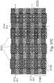
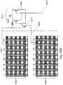
- FIGS. 1A and 1Bare example illustrations of forming multilayer porous structures
- FIG. 2is an example illustration of multilayer porous structures
- FIGS. 3A-3Pare example illustrations of the formation and structure of a floating body 3D DRAM memory
- FIG. 4Ais an example illustration of a non-volatile floating body cell
- FIG. 4Bis an example illustration of a stable two states one transistor memory structure 3D DRAM memory cell
- FIG. 4Cis an example illustration of a non-volatile 3D TRAM memory
- FIGS. 5A-5Dare example illustrations of 3D memory arrangements
- FIGS. 6A-6Bare example illustrations of the formation and structure of 3D Memory with dual functionality
- FIGS. 7A-7Hare example illustrations of the formation and structure of vertically oriented 3D memories
- FIGS. 8A-8Fare example illustrations of the formation and structure of a NOR type 3D memory
- FIGS. 9A-9Dare example illustrations of the formation and structure of a NOR type 3D universal memory
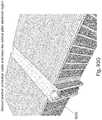
- FIG. 10is an example illustration of a portion of the formation and structure of a multi sided ONO faceted NOR type 3D memory
- FIG. 11is an example illustration of an additional portion of the formation and structure of a multi sided ONO faceted NOR type 3D memory
- FIGS. 12A-12Care example illustrations of additional portions of the formation and structure of a multi sided ONO faceted NOR type 3D memory
- FIGS. 13A and 13Bare example illustrations of an additional portion of the formation and structure of a multi sided ONO faceted NOR type 3D memory
- FIGS. 14A-14Care example illustrations of a NOR cell structure
- FIGS. 15A-15Dare example illustrations of operation modes of a 4-Gate 3D NOR cell
- FIG. 16is an example illustration of a channel with a facet holding bit 1 and bit 2 ;
- FIG. 17is an example illustration of operating conditions for the cell of FIG. 16 ;
- FIG. 18is an example illustration of a channel with a facet holding 4 bits
- FIG. 19is an example illustration of operating conditions for the cell of FIG. 18 ;
- FIG. 20is an example illustration of a channel with a facet holding 6 bits
- FIG. 21is an example illustration of operating conditions for the cell of FIG. 20 ;
- FIG. 22is an example illustration of a channel with a facet holding 8 bits
- FIG. 23is an example illustration of operating conditions for the cell of FIG. 22 ;
- FIG. 24is an example illustration of a memory addressing format
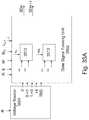
- FIGS. 25A-25Bare example illustrations of block diagrams of circuit control circuits
- FIG. 26is an example illustration of a architecture of a 3D-NOR array
- FIG. 27is an example illustration of distributed bits allocation for a 3D NOR cell
- FIG. 28is an example illustration of focusing the trapping region to a zone of charge trapping region
- FIG. 29is an additional example illustration of focusing the trapping region to a zone of charge trapping region
- FIG. 30is an example illustration of reading a zone of charge trapping region
- FIG. 31is an example illustration of a block erase operation on a zone of charge trapping region
- FIG. 32A-32Bare example illustrations of block diagrams of optional circuits to generate signals
- FIG. 33is an additional example illustration of a memory addressing format
- FIGS. 34A-34Care additional example illustrations of block diagrams of circuit control circuits
- FIGS. 35A-35Bare additional example illustrations of block diagrams of circuit control circuits
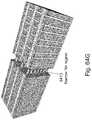
- FIGS. 36A-36Lare example illustrations of an additional portion of the formation and structure of a multi sided ONO faceted NOR type 3D memory PHTs
- FIGS. 37A-37Cexample illustrations of an additional portion of the formation and structure of a multi sided ONO faceted NOR type 3D memory PHTs
- FIG. 38Ais an example illustration of three operating states for which the PHT could be programmed.
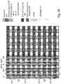
- FIGS. 38B-38Dare example illustrations of an exemplary single cell, 2 ⁇ 2 and 5 ⁇ 16 arrays of a memory
- FIGS. 39A-39Fare illustrations of the symbols defined for logic cell formation of the memory fabric
- FIGS. 40A-40Bare example illustrations of LUT circuits
- FIG. 41is an example illustration of a LUT4 of FIG. 40A implemented in the NOR fabric
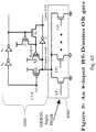
- FIG. 42is an example illustration of an 8-input HE-Domino OR gate
- FIG. 43Ais an example illustration of a Programmable logic array PLA structure
- FIGS. 43B-43Eare example illustrations of utilizing a NOR substrate to implement logic structures and circuits
- FIGS. 44A-44Bare example illustrations of forming logic structures and circuits utilizing LUTs
- FIG. 45is an example illustration of two programmable NANDs
- FIG. 46is an example illustration table of programming of the two NAND rows of FIG. 45 to support LUT-2 functionality
- FIGS. 47A-47Bare example illustrations of 8 rows of programmable NANDs
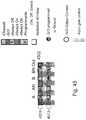
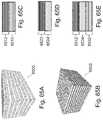
- FIG. 48Ais an example illustration of use of a ridge to construct a programmable function complementing the ‘AND of NANDs’ of FIG. 45 ;
- FIG. 48Bis an example illustration table of programming of the ‘AND of NANDs’ of FIG. 48A ;
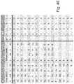
- FIGS. 49A-49Bare example illustrations of the use of a ridge to construct a programmable function LUT-4 using 8 rows of ‘OR of ANDs’;
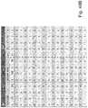
- FIG. 49Cis an example illustration table of programming of the programmable function LUT-4 using 8 rows of ‘OR of Ands’ of FIGS. 49 a and 49 B;
- FIG. 49Dis an example illustration of an alternative for the LUT-4 of FIG. 49B ;
- FIG. 49Eis an example illustration an alternative for the LUT-4 of FIG. 49D ;
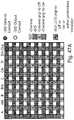
- FIGS. 50A-50Bare example illustrations of two LUT-4 placed back to back on the same ridge and two LUT-4s as one PLA with AND of 8 NANDs;
- FIGS. 51A-51Bare example illustrations of two LUT-4s of OR_AND type place back to back on the same ridge and two LUT-4s as one PLA with OR of 8 ANDs;
- FIG. 52is an example illustration of another use of the 3D-NOR fabric wherein a signal could be routed through;
- FIGS. 53A-53Bare example illustrations of a re-buffered cell and alternative re-buffering with full inverters
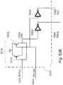
- FIG. 54is an example illustration of an alternative circuit for the complementing signal reconstruction utilizing a differential amplifier circuit
- FIG. 55Ais an example illustration of an alternative structure of the 3D NOR fabric which could leave some bridges between the ridges to support full three dimensional routing within the 3D NOR fabric;
- FIG. 55Bis an example illustration of an exemplary structure in 3D perspective showing JLT bridges of FIG. 55A ;
- FIGS. 56A-56Gare example illustrations of a review the system process flow
- FIGS. 57A-57Dare example illustrations of a stack structure variations
- FIGS. 58A-58Iare example illustrations of a process flow for forming a 3D-NOR design which supports junctionless transistors on the S/D lines;
- FIGS. 59A-59Dare example illustrations of cut views of the structures of FIG. 58I ;
- FIGS. 60A-60Bare example illustrations of an embedded lateral junctionless transistor and operation modes
- FIGS. 61A-61Bare example illustrations of conditions to program a junctionless transistor
- FIGS. 62A-62Bare example illustrations of a conditions to program a vertical NPN transistor
- FIGS. 63A-63Gare example illustrations of a programmable stair-case per layer connection structure and programmation method
- FIGS. 64A-64Kare example illustrations of formation and structure of designated JLTs
- FIGS. 65A-65Eare example illustrations of alternative structures leveraging multilayer 3D stacks
- FIGS. 66A-66Care example illustrations of formation and structure of multilayer 3D stacks
- FIGS. 67A-67Kare example illustrations of formation and structure of RRAM or OTP pillars
- FIGS. 68A-68Hare example illustrations of programming transistors to overcome S/D lines disconnection with the fabric
- FIGS. 69A-69Dare example illustrations of access devices to the RRAM/OTP pillars
- FIGS. 70A-70Bare example illustrations of signal structuring
- FIG. 71is an example illustration of signal re-buffering
- FIG. 72is an example illustration of a clocked output reconstruction circuit
- FIGS. 73A-73Bare example illustrations of a structure being programmed to act as two LUT-2s
- FIGS. 74A-74Gare example illustrations of logic/programming access to the RRAM/OTP pillars
- FIGS. 75A-75Bare example illustrations of RRAM/OTP pillars connecting to a connectivity structure
- FIGS. 76A-76Eare example illustrations of an alternative for forming an NPN select device for the RRAM/OTP pillars
- FIGS. 77A-77Dare example illustrations of forming an NPN rather than forming JLTs by ‘necking’.
- FIGS. 78A-78Bare example illustrations of 3D NOR fabrics
- FIG. 79is an example illustration of the function of a 2 bit decoder with 4 outputs implemented in a 3D NOR fabric
- FIG. 80is an example illustration of the function of a de-multiplexer with 4 outputs implemented in a 3D NOR fabric
- FIG. 81is an example illustration of the function of a full adder implemented in a 3D NOR fabric
- FIG. 82is an example illustration of the function of 4 signals output enable buffers implemented in a 3D NOR fabric
- FIG. 83is an example illustration of clocked half latch reconstruction circuit interfaced to a 3D NOR fabric
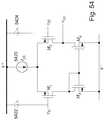
- FIG. 84is an example illustration of modified ‘domino logic’ reconstruction circuit interfaced to a 3D NOR fabric
- FIG. 85is an example illustration of a 3D NOR fabric implementing a unit of 32 bits of NV memory
- FIG. 86is an example illustration of a signal chart and table for the operation of a floating body memory in a 3DNOR fabric
- FIG. 87is an example illustration of a floating body memory implemented in a 3DNOR fabric with dual access to each channel;
- FIG. 88is an example illustration of another operation mode for a floating body memory in a 3DNOR fabric
- FIGS. 89A-89Bare example illustrations of two complementing logic units implemented in a 3DNOR fabric
- FIG. 90is an example illustration of a modification to the process/structure to enable logic density doubling
- FIGS. 91A-91Bare example illustrations of stack structure variations for a 3D programmable system
- FIGS. 92A-92Bare example illustrations of Lateral RRAM for Y direction connectivity in a 3DNOR fabric
- FIGS. 93A-93Jare example illustrations of a process flow for adding Lateral RRAM for Y direction connectivity to a 3D NOR fabric
- FIGS. 94A-94Care example illustrations of forming a LUT-4 structure in a 3D NOR fabric
- FIG. 95is an example illustration of an alternative for a LUT-4 structure.
- FIG. 96is an example illustration of a selector circuit.
- Some drawing figuresmay describe process flows for building devices.
- the process flowswhich may be a sequence of steps for building a device, may have many structures, numerals and labels that may be common between two or more adjacent steps. In such cases, some labels, numerals and structures used for a certain step's figure may have been described in the previous steps' figures.
- Memory architecturesinclude at least two important types—NAND and NOR.
- the NAND architectureprovides higher densities as the transistors forming the memory cells are serially connected with only an external connection at the beginning and end of the cell string as is illustrated in at least U.S. Pat. No. 8,114,757, FIGS. 37A-37G.
- NOR architecturesare less dense but provide faster access and could work sometimes when the NAND architecture cannot as individual NOR memory cells are directly accessible and in many cases both its source and drain are accessible, such as being illustrated in at least U.S. Pat. No. 8,114,757, FIGS. 30A-30M.
- the memory cellcould be constructed with conventional N type or P type transistors where the channel doping may be of opposite type with respect to the source drain doping or the memory cell could utilize a junction-less transistor construction where the gate could fully deplete the channel when in the off-state.
- the junction-less transistoris attractive as it may take less processing steps (or provide other device advantages such as low leakage off-state) to form the memory array without the need to form a change in doping along the transistor.
- 3D Memory architecturesare utilizing a horizontal memory transistor, for example, such as illustrated in at least U.S. Pat. No. 8,114,757, at least FIGS. 37A-37G and FIGS. 30A-30M.
- Othersmay use vertical memory transistors, for example, such as in the Toshiba BiCS architecture such as illustrated in at least U.S. Pat. No. 7,852,675.
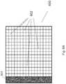
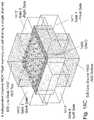
- a base donor substrate 110may be used to form a dual porous layer for future cut layer 113 on which an epitaxial process may be used to form relatively thick crystalline layer 120 .
- Future cut layer 113may include two porous layers; an upper layer of porous silicon, which may contain microscopic pores of diameter of a few nm, and below this is formed a lower layer of porous silicon for which the pore diameter may be a few (or more) times greater (similar to FIG. 23 of U.S. application Ser. No. 14/642,724), for the future ‘cut’ or cleave.
- the epitaxial formation of relatively thick crystalline layer 120could include successively altering the addition of dopants to further support the following steps.
- thick crystalline layer 120may be converted to a multilayer of alternating low porosity over high porosity as illustrated in FIG. 1B , which is similar to FIG. 41B of Ser. No. 14/642,724.
- the alternating-porosity multilayercan be converted later into alternating multilayer of monocrystalline-Si over insulating SiO 2 , as described below.
- FIG. 1Billustrates relatively thick crystalline layer 120 after going through a porous formation process which forms multilayer structure 122 .
- Multilayer structure 122may include layer 144 , layer 142 , layer 140 , layer 138 , layer 136 , layer 134 and layer 132 .
- Multilayer structure 122may include base donor wafer substrate 110 with porous cut layer 113 for the planed transfer of the fabricated multilayer structure over the target wafer, which could include the memory peripherals circuits prefabricated on the target wafer.
- multilayer structure 122may not include porous cut layer 113 when the transfer to a target wafer is not intended.
- Layer 144could be the portion of layer 120 which remains after the multi-layer processing.
- the alternating layerscould have alternating porosity levels such as layers 132 , 136 , 140 with porosity of less than 30% or less than 40% while layers 134 , 138 , 142 with porosity over 50% or over 60%, or layers 132 , 136 , 140 with a porosity of less than 55% while layers 134 , 138 , 142 with porosity over 65%, or other alternating level of porosity based on the target application, process, and engineering choices.
- Each layermay include a varying porosity thru its thickness, or a number of sublayers of varying porosity.
- the number of alternating layers included in multilayer structure 122could be made as high as the number of layers needed for the 3D memory (for example, greater than 20, greater than 40, greater than 60, or greater than 100) or for the transferring of a subset of multilayer structures one on top of the other to form the desired final structure.
- the porosity modulationcould be achieved, for example, by (1) alternating the anodizing current, or (2) changing the illumination of the silicon structure while in the anodizing process, or (3) by first alternating the doping as layer 120 is being grown through epitaxial process, or (4) etching & oxidizing multilayers of Si X Ge 1-X /Si.
- Layer 144could be the portion of layer 120 which is left un-processed by the modulated-porosity process. Below are listed few embodiments of the above method of forming a c-Si/SiO 2 multilayer from an alternated porosity multilayer:
- U.S. patent application Ser. No. 12/436,249incorporated herein by reference, teaches an alternative method for the formation of the multilayer structure 122 with alternating doping.
- the methodstarts by multiple depositions of amorphous silicon with alternating doping, then performing a solid phase recrystallization to convert the stack into a stack of p-type doped single crystal Si-containing layers using a high temperature recrystallization, with recrystallization temperatures from 550° C. to 700° C. After recrystallization, the single crystal Si-containing layers could be subjected to anodization and so forth as presented in ii-iv above.
- U.S. patent application Ser. No. 12/436,249teaches a few alternatives for the formation of the alternating doping layer structure which could be employed herein for the 3D memory multilayer structure formation.
- the epitaxial layer 120could include alternating n doped and n+ doped layers.
- the porous formation of the n doped layersmay be assisted by light to form the holes for the anodizing process to effectively work as had been presented in S. Frohnhoff et. al., Thin Solid Films, in press (1994), U.S. patent application Ser. Nos. 10/674,648, 11/038,500, 12/436,249 and U.S. Pat. No. 7,772,096, all of these incorporated herein by reference.
- the structurecould be oxidized and then annealed as presented in steps iii and iv above.
- a method to form alternating layers of coarse and fine porous layersis by alternating the anodizing current similar to the description in “Porous silicon multilayer structures: A photonic band gap analysis” by J. E. Lugo et al J. Appl. Phys. 91, 4966 (2002), U.S. Pat. No. 7,560,018, U.S. patent application Ser. No. 10/344,153, European patent EP0979994, and “Photonic band gaps analysis of Thue-Morse multilayers made of porous silicon” by L. Moretti at el, 26 Jun. 2006/Vol. 14, No. 13 OPTICS EXPRESS, all of these incorporated herein by reference. Following the anodizing step the structure could be oxidized and then annealed as presented in steps iii and iv above.
- the anodizing stepcould be done as a single wafer process or by using a batch mode as illustrated in U.S. Pat. No. 8,906,218, incorporated herein by reference and other similar patents assigned to a company called Solexel.
- the multilayer structure 122may be formed by first forming multilayer structure of alternating n type over p type.
- a methodis illustrated in U.S. Pat. No. 8,470,689 and in ““Silicon millefeuille”: From a silicon wafer to multiple thin crystalline films in a single step” by D. Hernandez et al., Applied Physics Letters 102, 172102 (2013); incorporated herein by reference.
- These methodsleverage the fact that n type silicon would not become porous without light while p type silicon would only need current for the anodizing process to take place.
- the multilayer of n over pcould be first etched to form the multilayer pattern such as is illustrated in FIG.
- a multilayer structurecould be achieved by successive epitaxial growths of n type silicon over p+ type silicon multiple times for which the n silicon could be etched at a much higher rate than the p+ silicon.
- Another alternativeis to form multilayers of silicon over Si 1-x Ge x as illustrated in “New class of Si-based superlattices: Alternating layers of crystalline Si and porous amorphous Si 1-x Ge x alloys” by R. W. Fathauer et al., Appl. Phys. Lett. 61 (19), 9 Nov. 1992, incorporated herein by reference.
- a multilayer structurethere is high degree of selectivity in etching Si 1-x Ge x layers over Si layers. This may be followed by oxidation such as step iii. and anneal iv. could provide multilayers of silicon over oxide.
- An alternative method to the modulated-porosity method for forming c-Si/SiO 2 multilayersmay be to utilize the Bosch process.
- a technique used for deep hole etchhas been applied to form structures of crystalline lines one on top of the other each with oxide all around. Similar techniques could be used to form the base structure for 3D memory.
- c-Si/SiO 2 multilayer structuresYet another alternative for forming c-Si/SiO 2 multilayer structures is direct epitaxy of silicon, special oxide, and silicon again.
- the special oxideis a rare-earth oxide which if deposited properly would keep the crystal structure of the silicon to allow crystalline silicon on top of it as presented in U.S. patent application publication US 2014/0291752, incorporated herein by reference.
- the epitaxy process of multilayers of an n+ type layer over a p type layercould be done at lower temperatures to reduce the dopant movement of the n+ layer, at the lower portion of the multilayer structure, into the p type layer as the multilayer structure is being formed.
- epitaxial processes in the artwhich allow good quality layers to be formed while keeping the process temperature below 600° C.
- suchhas been presented in papers by D. SHAHRJERDI, titled “Low-Temperature Epitaxy of Compressively Strained Silicon Directly on Silicon Substrates” published at Journal of ELECTRONIC MATERIALS, Vol. 41, No. 3, 2012; by S.
- An advantage of using oxidized porous silicon for isolating the silicon layers for the 3D memory structureis the ability to easily and selectively etch portions of these oxidized porous layers to allow the gate formation to have a larger coverage of the transistor channel to have an increased control on the memory transistor, for example, such as with gate all around or a ‘mostly’ gate all around transistor structure.
- the area on top and under the channelcould be etched so in the follow-on processing step of oxide and gate formation it would form a larger coverage of the channel which could be a gate all around configuration for better channel control.
- Base wafers or substrates, or acceptor wafers or substrates, or target wafers substrates hereinmay be substantially comprised of a crystalline material, for example, mono-crystalline silicon or germanium, or may be an engineered substrate/wafer such as, for example, an SOI (Silicon on Insulator) wafer or GeOI (Germanium on Insulator) substrate.
- donor wafers hereinmay be substantially comprised of a crystalline material and may include, for example, mono-crystalline silicon or germanium, or may be an engineered substrate/wafer such as, for example, an SOI (Silicon on Insulator) wafer or GeOI (Germanium on Insulator) substrate, depending on design and process flow choices.
- the described memory structurewould be arranged as a process flow forming a type of a 3D memory structure. These flows could be considered as a Lego part which could be mixed in different ways forming other variations, thus forming many types of devices. Some of these variations will be presented but as with Lego there too many variations to describe all of them. It is appreciated that artisan in the art could use these elements of process and architecture to construct other variations utilizing the teaching provided herein.
- the mono-crystalcould be doped and could have either an isolative layer in-between or sacrificial layer which could be replaced at some point in the process with an isolative layer.
- the multilayer structurecould be fully ready or partially readied with the etching of vertical holes or trench shapes, as required for the memory structure to follow, and allows the completion of the multilayer structure which may include selective etching of the sacrificial layers in-between.
- a volatile 3D memory using floating body chargeis described in U.S. Pat. No. 8,114,757, incorporated herein by reference, as related to at least FIGS. 30A-30M and FIGS. 31A-31K .
- the followingis an additional alternative for forming a 3D DRAM volatile memory.
- 3D Memorymay be multi-layers of 2D memory in which memory cells are placed as a matrix with rows and columns. These memory cells are controlled by memory control lines such as bit-lines, source-lines, and word-lines, usually in a perpendicular arrangement, so that by selecting a specific bit-line and specific word-line one may select a specific memory cell to write to or read from. In a 3D memory matrix, having three dimensions, selecting a specific memory cell requires the selecting of the specific layer which could be done by additional memory control lines such as select-lines. As been presented herein, some of the select lines could be integrated in the semiconductor layer in which the memory devices are built into (for example, FIGS. 8F and 85 ). Other select lines could be deposited or formed thru epitaxial growth. These memory control lines could therefore be comprising semiconductor materials such as silicon or conductive metal layers such as tungsten aluminum or copper. Such as FIGS. 3 and 4 of incorporated application U.S. 62/215,112.
- ‘self refresh’Another alternative that would not require changes in the device structure presented is to use what could be called ‘self refresh’.
- a refresh cyclemeans that each cell is being read and re-written individually.
- ‘self refresh’many or even all cells could be refreshed together by driving a specific current (may be a current range or minimum current) through them.
- the cell holding ‘zero’will keep its zero state and the cell holding ‘one’ will get recharged to recover their lost of floating body charge due to leakage. This technique had been detailed in a paper by Takashi Ohsawa et. al.
- ReRAMresistive-memory
- a 3D ReRAMhas been described in U.S. Pat. No. 9,117,749, incorporated herein by reference.
- ReRAMperform the memory function by having the resistivity change which could be achieved by driving current through the ReRAM variable resistivity medium and could be sense by measuring current or voltage through that medium.
- materialsthat could be used for ReRAM and some of those are oxides with additional materials which could be driven into the oxide to change it resistivity.
- U.S. Pat. No. 8,390,326incorporated herein by reference present the use of silicon oxide for such use.
- a subclass of the ReRAMare structure that allow only one time programing (“OTP”) of these mediums such as presented in U.S. Pat. No. 8,330,189 incorporated herein by reference.
- T-RAM cellA form of T-RAM cell has been described in a paper by Ahmad Z Badwan et. al. titled “SOT Field-Effect Diode DRAM Cell: Design and Operation” published in IEEE Electron Device Letters, Vol. 34, No. 8 Aug. 2013, incorporated herein by reference.
- the T-RAM structured presented here and the method to process themcould be adapted to build FED (Field-Effect Diode) structure and to form a 3D-FED RAM device.
- FEDField-Effect Diode
- a volatile 3D memory using floating body chargeis described in U.S. Pat. No. 8,114,757, incorporated herein by reference, as related to at least FIGS. 30A-30M and FIGS. 31A-31K .
- the followingis an additional alternative for forming a 3D DRAM volatile memory.
- 3D Memorymay be multi-layers of 2D memory in which memory cells are placed as a matrix with rows and columns. These memory cells are controlled by memory control lines such as bit-lines, source-lines, and word-lines, usually in a perpendicular arrangement, so that by selecting a specific bit-line and specific word-line one may select a specific memory cell to write to or read from. In a 3D memory matrix, having three dimensions, selecting a specific memory cell requires the selecting of the specific layer which could be done by additional memory control lines such as select-lines. As been presented herein, some of the select lines could be integrated in the semiconductor layer in which the memory devices are built into (for example, FIGS. 8F and 85 ). Other select lines could be deposited or formed thru epitaxial growth. These memory control lines could therefore be comprising semiconductor materials such as silicon or conductive metal layers such as tungsten aluminum or copper.
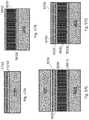
- FIG. 3Aillustrates a starting multilayer structure 302 , comprising p-type or n-type silicon 304 and isolation or sacrificial layer in-between 306 formed by many of the processes presented herein.
- a hard mask 308such as silicon nitride may be patterned on top for the following etch step.
- FIG. 3Billustrates the multilayer structure 310 after an etch step.
- FIG. 3Cillustrates the structure 311 after deposition of isolative material 312 , such as SiO2, and etching holes 314 for the following step of gate stack.
- isolative material 312such as SiO2
- etching holes 314for the following step of gate stack.
- FIG. 3Dillustrates the structure 320 after forming the gate stack 322 .
- the gate stackmay include agate dielectric and a gate electrode material, which could be formed by CVD or ALD of first a gate oxide and then gate material which could be metal or in-situ doped polysilicon.
- a high quality thermal oxidemay also be utilized via techniques such as radical oxidation. For example, by a TEL SPA (slot plane antenna) tool/machine, wherein oxygen radicals are generated and utilized to form thin thermal oxides (generally of single crystal silicon) at less than 400 deg C.
- the gate formationcould be two independent side gate columns as illustrated or tied double gate or even gate all around. For the gate all around, it may require that the step of etching the gate holes 314 will include a non-directional isotropic etch step to etch the in-between layer to allow the following gate all around formation.
- FIG. 3Eillustrates the structure 321 after stripping off the dielectric 312 , and then a step of diffusion doping to form the source 324 regions and the drain regions 326 .
- the source regions 324would be connected to the source line (“SL”) and the strip of the drain regions 323 would become later part of the bit-lines (“BL”).
- the SL and the BLcan be used interchangeably depending on the array arrangement.
- These diffusion dopingwill convert all the exposed silicon areas that are not protected by the gates structures 322 from p type to n+ type or n type to p+ type. This will form transistors in the small pin structures 325 , while the common strips 327 would serve as simple conductor acting as the bit-lines or the source-lines for the memories that could be formed by the pins transistors 325 .
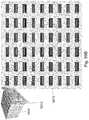
- FIG. 3Fillustrates the structure 331 with extension of the bit lines 334 which could be used for a stair-case per layer access.
- An optional select gate 332could be used to select memory branch.
- FIG. 3Gillustrates the structure 331 after forming stair-case 336 of the bit line extension 334 and after forming the vertical connections to the bit-lines 337 and to the transistor sources 338 .
- FIG. 3Hillustrates the structure after adding the grid of connections.
- the illustrationis one option for structuring bit-lines 356 , select-gate lines 358 , source-lines 352 and word-lines 354 .
- These connectivity structureallow selecting a specific cell such that select gate lines 358 allow selecting the ‘x’ location by selecting the ‘x’ branches, the word-lines 354 select the ‘y’ location by selecting the gates in ‘y’ direction, and the bit-lines 356 select the ‘z’ location by selecting the drain in ‘z’ direction.
- the optional select-gate lines 358allow selecting of the bank of transistors in the bank along ‘x’ direction.
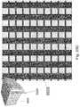
- FIG. 3Iillustrates the structure after adding the grid of connections with an alternative structure of word-lines and bit-lines.
- the gate materialis common along the multiple pins, which would serve as simple conductor acting as the word-lines.
- FIG. 3Jillustrates optional silicidation of the bit lines 327 to reduce their resistance.
- silicidation 362First only the areas designated for silicidation 362 are being exposed while all other areas are being protected by photoresist or isolation oxide. Then a metal such as Ni, Ti, Co, or other known in the art material, is deposited making contact with the bit lines side walls 362 . Then thermal reaction is achieved by the use of Rapid Thermal Anneal (RTA) or laser anneal. Then the unreacted metal is etched away.
- RTARapid Thermal Anneal
- FIG. 3Killustrates a 3D memory of 3 column structure.
- the transistors source forming the memory cellare connected by vertical line 338 of FIG. 3G connecting with the transistors source side wall. It is enlarged view at FIG. 3K .
- this conductive vertical column 364a selective epitaxy process could be used to form this vertical connection.
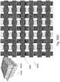
- FIG. 3Lillustrates the structure with protective cover of oxide or other protective material 366 and trench opening the side walls of the memory transistors source 368 .
- the opening of the trenches 366could include a step for selective removal of part of the vertical isolation between the sources of the stack transistors.
- FIG. 3Millustrates the structure after a step of epitaxial growth for forming a vertical column connecting all the sources in a stack 370 . These columns could be silicide to further improve their connectivity.
- FIG. 3Nillustrates the structure after adding contacts 372 from the top.
- FIGS. 3A-3Nwere made for ease of drawings and understanding. Persons skilled in the art would understand that techniques common in memory design could be used to increase memory bit density. Such as mirroring the transistors along the bit lines sharing the bit lines for right side transistor and left side transistors and mirroring across source side sharing the vertical source lines. Such structure is been illustrated in U.S. Pat. No. 8,114,757, as related to FIGS. 30A-30M and FIGS. 31A-31K.
- FIG. 3Oillustrates another alternative where the vertical line connecting the source side of the stack transistors 376 are shared but the horizontal in silicon bit-lines first bit-line 374 and second bit-line 375 are not shared.
- One advantage of not sharing the bit-lines first bit-line 374 and second bit-line 375is the option to add silicidation as was described in respect to FIG. 3J .
- FIG. 3Pillustrates another alternative where the horizontal bit lines of the stack transistors 384 are shared but the vertical line connecting the source side of the stack transistors first xtor 385 and second xtor 386 are not shared.
- FIG. 4Aillustrates a charge storage (may be a floating-body or charge trap, etc.) memory cell, of the type utilized for 3D RAM such as illustrated with respect to FIG. 3A-3P herein, enhanced to support a non-volatile option by adding between the gate 408 and the channel 404 , charge storage layer 414 isolated with tunneling oxide 412 and isolating control oxide 416 .
- the memory cellmay include n type drain 402 , p type channel 404 and n type source 406 .
- the process forming the tunneling oxide 412 , charge storage layer 414 , control oxide 416 and gate 408could be utilizing successive steps of ALD (Atomic Layer Deposition) or other type of deposition process, in place of single gate layer deposition described before.
- ALDAtomic Layer Deposition
- Each memory cellcould function as high speed volatile RAM and also as low power non-volatile floating gate or charge trap memory. For some applications the combination of high speed RAM with low power non-volatile built in back-up could be attractive.
- Such a dual use channelis also presented in U.S. Pat. No. 7,158,410, and papers by J. W. Han et al. titled “A Unified-RAM (URAM) Cell for Multi-Functioning Capacitorless DRAM and NVM” published by IEDM 2007 and by Dong-Il Moon et al.
- URAMUnified-RAM
- FIG. 4Billustrates enhancements supporting the non-volatile memory option concept of FIG. 4A to the 3D memory illustrated as related to FIG. 3A-3P .
- FIG. 4Cillustrates enhancements supporting the non-volatile memory option concept of FIG. 4A to the 3D memory illustrated as related to FIG. 14A-14H of U.S. Patent Application No. 62/221,618, incorporated herein by reference.
- a select transistoris presented at the upper layer of a 3D memory cell column as presented in respect to FIG. 8 and the related description there.
- Such per column select transistorcould be effective for many of the memory structures presented herein.
- this top layer select transistorcould be processed together with the transistors forming the memory cell underneath by sharing the same lithography process and other processes, thus the top select transistor ends up being at least partially self-aligned with the memory cells underneath it. Having these select transistors could give additional control flexibility and could provide a buffer to the memory cells to improve overall memory access speed and assist the read or write operations.
- a detailed descriptionis provided for the process to add such select transistors to one of the 3D T-RAM structure presented herein. It would be obvious for a semiconductor memory artisan to apply the concept to many of the other memory structure presented herein.
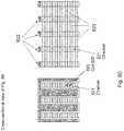
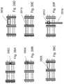
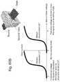
- FIG. 5Aillustrates prior art 2D memory device.
- the memory cells 2D matrix 502is surrounded by memory control circuits 504 such as decoders, sense amplifiers and interfaces with external devices. Circuits 504 are called accordingly memory peripherals.
- the memory control lines 506are running across the memory array columns and rows all the way to the peripherals circuits.
- FIG. 5Billustrates side view side view cross-section of cross section of prior art 3D memory device.
- 3D memoryalso known as 3D-NAND
- the memory cell 3D matrix 512is still surrounded by the memory control circuits 514 such as decoders, sense amplifiers and interfaces with external devices.
- the memory peripherals circuitsare being processed in very similar way to the 2D memory circuits on the silicon wafer substrate.
- the control lines 516are running through the memory array columns and rows all the way across the memory matrix, some of these control lines are being built on top of the 3D matrix and some of those going through the bulk body of the memory matrix but at the edges they are brought down to the 2D peripheral circuits.
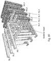
- FIG. 5Cillustrates side view cross-section of a 3D memory formed in accordance with the present invention using the techniques presented herein.
- the 3D memory matrix 522comprises columns and rows having the control circuits 524 which could still be called peripherals circuits but they could be formed on top of the memory matrix.
- control lines 526are built underneath the peripheral circuits, in-between the peripheral circuits 524 and the memory matrix 522 .
- FIG. 5Dillustrates a side-view cross section of an alternative 3D memories formed using the techniques presented herein in which the control lines and the control circuits are also underneath the memory cell matrix.
- This new type of 3D memoriescould be constructed to achieve significant advantage over the prior art by utilizing the 3D architecture as illustrated in at least FIGS. 5C and 5D , to break the control lines 526 into smaller chunks with the control circuits being repeated for each chunk. Shorter control lines could allow reduction of memory access read and write and refresh and could allow faster memory access time. The stair-case for layer access could impact device cost if it is repeated too often.
- the memory architectureshould be designed to use long control lines to the memory within the same layer for as long as possible so having the other (vertical) control lines relatively short while the per layer control lines are still long, could achieve the benefits of low power and fast access maintained for most of the time.
- these 3D memorycould be enhanced to include dual functionality—a high speed volatile memory and a low power low speed non volatile memory.
- These figuresillustrate non-volatile cells utilizing charge trap or floating gate technology.
- other non-volatile memory technologiescould be implemented such as Re-RAM, M-RAM, Phase-Change, etc.
- Re-RAMcharge trap or floating gate technology
- M-RAMMagnetoresistive RAM
- Phase-ChangePhase-Change
- splitting the gatecould be used to increase the non-volatile memory denisty for cells that the channel is wide enough to allow 2-bit per cell techniques.
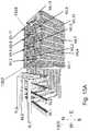
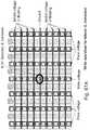
- FIG. 6Aillustrates the top view construction of 3D memory 600 for such enhanced operation.
- the side memory control circuits 601control the interface to external devices both for instruction, and data in and out. These circuits 601 could include the per-layer decoders and control to support all internal memory blocks so the stair-case area overhead could be minimized.
- the 3D memoryis than partitioned to many blocks 602 each is a sub-memory structure with its own top peripherals circuits to control most of its control lines. In such design the operation of moving data from one portion to the other (for example, one block 602 to another block 602 ) could be done in parallel in all the units reducing the time and power by orders of magnitude.
- the side memory control circuits 601could synchronize these operations so it will be done one layer at a time.
- FIG. 6Billustrates the block diagram of peripherals circuit of a block 602 .
- the block diagram 604 of such unit block control circuitscould include:
- Central controller 630commanding and controlling these operations for sleep mode recovery mode etc.
- In-Out interface controllerto interface with data and with the device controller 601 .
- Sense Amplifiers 620to sense the data of a memory cell according to the mode of operation and to convert side memory control circuits 601 to a digital bit which could be temporarily stored in the unit memory cash 634 .
- Signal generators 618to generate the required voltages and current for the proper read write of the memory cells. Some of these circuitry, such as charge pumps, could be shared by all units and be placed in side memory control circuits 601 .
- Blocks 612 , 614 , 616 , 617 for the various control linessuch as bit-lines, word-lines, gate-lines, select lines etc.
- the layer decoders 616might be removed from the unit 604 into the general per-layer circuits at side memory control circuits 601 .
- Additional advantage for such memory architectureis the potential ability to move in and out very large blocks of data as many blocks 602 could be accessed in parallel. If only a single per-layer stair case is used for maximum array efficiency than the parallel action would be limited to single layer at a time. For many applications this could be managed by proper system data structure and control.
- Such 3D Memorycould include redundancy circuitry to allow repair of control functions as well as replacement of faulty memory bits.
- the architecture of FIG. 5Dcould be used to allow access to substantially all of the memory control lines from both side—top and bottom and to have duplication of the device control circuit 524 at the bottom.
- redundancy schemecould be broken down to the memory block control units 602 level. So if one unit block control circuits are faulty then it is replaced by its compatible one on the other end/side. Alternatively each unit block control circuitry could be built with two stratum one being a back-up for the other as was detailed herein before.
- the memory control redundancycould be applied to any of the 3D memories herein.
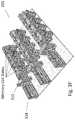
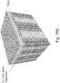
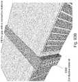
- FIGS. 7-13Another embodiment of monolithic 3D memory according to the present invention is demonstrated in FIGS. 7-13 and outlined below. It utilizes mono-crystalline transistors whose channels are vertically oriented so the current flows vertically through the device across each of the device layers rather than horizontally along the device layers. Yet, this structure is designed to be low cost by sharing lithography, etch and deposition of multiple layers together forming self-aligned vertically oriented transistors.
- FIG. 7Aillustrates the starting material structure for these vertically oriented 3D memories. It has interchanging layers of designated source/drain (S/D) material 702 over designated channel material 704 . These layers could be processed by epitaxial steps with in-situ alternating N/N+ type to P/P+ type doping and/or between alternating silicon to SiGe layer, etc. The selection of the composition of these layers could include consideration of a choice of a high etch selectivity process between adjacent layers to enable faster etching of the designated channel layers 704 than the (S/D) layers 702 . The thickness of these layers could be from a few nm up to hundreds of nm.
- Suppression of dopant diffusionmay be accomplished by use of low temperature epitaxial processes, for example the AMAT 450-500 deg C. epi process.
- interlayer diffusion barriersmay be employed, for example, such as a thin single or double atomic layer of a diffusion suppressor, such as carbon.
- composition of the S/D layers 702could be N+ silicon while the channel layers 704 could be P type silicon and the selective etch process would utilize anodic etching as detailed in U.S. Pat. No. 8,470,689 and as was described herein.
- N+ siliconfor the (S/D) layers 702 and P type SiGe for channel layers 704 and the later selective etch
- a hard mask material 706is deposited.
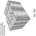
- FIG. 7Billustrates etching the structure to form multilayer ridges 709 and valleys 708 in between resulted in repeating ridges structure 707 .
- the width of the ridges and the valleyscould be from 10 nm or even lower to a few hundreds of nm. At current state of technology about 50 nm could be good choice.
- the width of the ridges and the valleyscould be set in consideration of the thickness of layers 702 / 704 , the type of memory build and other consideration. Similar width and thickness could be appropriate.
- FIG. 7Cillustrates the structure after a step of selective isotropic etches of the channel layers 704 , forming horizontal notches 719 while keeping the S/D layers 710 mostly untouched.
- a selective plasma etchmay be used. The selectivity may be greatly increased by first forming pores in the desired regions of the channel layers by selective anodization processing. Then the plasma etch would be very selective. Warm KOH may also be utilized to selectively etch down the ⁇ 100> crystallographic planes.
- FIG. 7Dillustrates the structure after depositing a stack of tunneling oxide layer/charge trap layer/control oxide layer 712 such as oxide/nitride/oxide and gate conductive material 714 .
- the stepcould be done by Atomic Layer Deposition (ALD) or alternative processes used for semiconductor device fabrications.
- a directional anisotropic etch stepmay be used to remove substantially all gate material from the side walls of the S/D layers 713 .
- a slight touch-up isotropic etchmay also be employed to remove stringers.
- FIG. 7Eillustrates the structure after filling the trenches 708 of FIG. 7B with insulating material 716 , followed by an etch step which forms vertical gaps 720 along the ridges 709 of FIG. 7B to form vertical strings 722 of alternating N+/P material.
- the etch stepcould be done in two steps. First anisotropic etch the stack of multilayer of alternating 702 / 704 to form the vertical individual strings 722 , and then isotropic selective etch to remove the source/drain 702 in-between the gate stack 712 , while leaving the horizontal going gate and oxide lines. The etching may be stopped before the lowest N+ layer so it will serve as a common ground. Conductive etch stop layers may be employed.
- FIG. 7Fillustrates a vertical cross-sectional view along the metal gate word line of the structure of FIG. 7E .
- the empty spaces left after removal of the in-between channel material 734may serve as memory cell isolation.
- the remaining bottom material 738could serve as a common ground line.
- the lower gate line 740could serve as ground select gate.
- the top of the vertical strings 732would serve as the string drain region and could be connected later to the bit-lines (BL).
- the obtained structureforms a matrix vertically oriented non-volatile NAND memory cells.
- the horizontal control gates 742form the memory word lines controlling current through the vertical channels between successive source/drain layers, and may form vertical NAND strings.
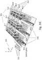
- FIG. 7Gillustrates a vertical cross section of one vertical NAND string 736 perpendicular to the metal-gate word-line direction.
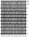
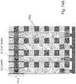
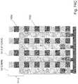
- FIG. 7Hillustrates the 3D NAND memory structure after adding the grid of memory control lines: word-lines 765 , bit-lines 767 , string select-lines 761 and ground select-lines 763 .
- the horizontal per layer line through the matrixcould be the limiting factor of the power performance of the device with respect to how long it could be made.
- the area required for the stair-case interconnect structuredictates longer lines to save in silicon real-estate and reduce cost per bit.
- a preferred designmight place such stair-case on both sides of the line which could help reduce cell to cell variation in addition to improving power and delay. If the device is fractured into multiple blocks real estate efficiency can be improved by sharing each stair case between both the right and the left sides of each block.
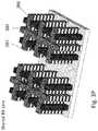
- FIG. 8Aillustrates a structure for the formation of a NOR type 3D memory. It starts from the structure 2007 illustrated in FIG. 20B of the incorporated U.S. patent application 62/221,618.
- Masking an etching techniquesare used to form first elongated strips of vertically alternating N+/P type single crystal silicon, coated by dielectric multilayer of tunneling-oxide layer, charge-trap layer and control gate oxide layer forming the charge storage stack 802 .
- a gate 804 materialsuch as tungsten (W) or polysilicon or other form of memory array gate material is deposited, said charge storage stack 802 and gate overcoat 804 being patterned by masking and etching techniques to form second elongated strips perpendicular to the direction of said first elongated strips.
- the deposition stepcould use ALD techniques.
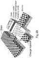
- FIG. 8Billustrates the structure after selective isotropic etching the channel material layer wherever not covered by the gate stack, leaving voids 812 in between the horizontal strips of the un-etched S/D material. Under the gate stack the channels 814 are not etched as they are protected by the gate stack.
- FIG. 8Cillustrates a cross section of the structure of FIG. 8B .
- the gates 822control the conductivity between the source and the drain 820 through the channel 821 .
- the S/D materialacts as source and drain under the gates 822 and as conductive lines 823 used to conduct the memory cell sensing current to the sense-amplifier circuitry (not shown) the memory control line connecting the S/D along the layer for each ridge.
- the S/D materialis selected to be N+ silicon and the channel material is selected to be P type silicon, then each memory cell would include an NPN transistor with two sidegate stacks to form a non-volatile memory cell.
- An alternative technique for selective removal of the P type material regions between channels while not etching the channel regions and the N type S/D linesis to use an anodizing process which would etch the P regions between channels to convert them to porous regions.
- the anodizing wet etchingis highly selective and would not affect the N type S/D lines, especially if the process is done in dark as previously discussed such as in U.S. Pat. No. 8,470,689.
- the S/D linescould be used to deliver the anodizing current throughout various regions of the structure.
- An additional enhancementcould be added by using positive voltage on substantially all of gates 804 conductors.
- FIG. 8Dillustrates a top view the ridge structure of FIG. 8A in which the leftmost side gate 832 (a shown in this example) is made without oxide underneath making it the anode delivering the positive anodizing current to all the N type S/D lines.
- the top most plate 834illustrates the connection to all other gates 836 to deliver the depletion voltage to protect the P channel from being etched during the anodizing step.
- the delivery plates leftmost side gate 832 and top most plate 834could be etched off. Then the porous region could be etched away, leveraging the many orders of magnitude higher etch rate of porous regions vs. solid silicon regions, to remove out all these porous regions, thus forming the structure illustrated in FIG. 8B .
- a selective wet etchfor example, warm KOH or TMAH, may be utilized to selectively etch the ⁇ 100> planes and much slower on the ⁇ 110> planes, thus minimizing undesirable undercutting.
- the above process of anodizingcould be extended to achieve further an all-layer anodization under the ridge structure to support a following step of transferring the complete 3D NOR structure to another wafer cutting the formed porous layer underneath.
- the all-layer cut porous formationcould alternatively be formed after the step of the second formation of O/N/O layer as illustrated in FIG. 10 .
- a directional etch-RIEcould be applied opening the bottom of the area in between RIDGE allowing anodizing process to be applied to form cut porous underneath the 3D NOR structure illustrated in FIG. 10 .
- Such a process and structurecould allow flipping the NOR structure and bonding it on top of another wafer to add control lines and control circuits on the other side of the NOR structure. This could be an alternative to having the porous already there from the start as previously discussed herein.
- FIG. 8Eillustrates the 3D NOR structure after adding interconnection to the control lines.
- the shared gates forming word-lines WL 1 , WL 2 , WL 3run perpendicular the ridges controlled by word-lines WL 1 , WL 2 , WL 3 .
- the interconnect stair caseis used to connect control signals to the in-layer S/D lines.
- the interconnect line BL 1controls the S/D of the first layer of all the ridges in the memory block, BL 2 controls the second layers and so forth.
- the select-linescontrol the access of the bit lines to the S/D of the ridges.
- SL 1control the access to the first ridge, SL 2 to the second ridge and so forth.
- the ridge controlmay be constructed by first removing the channel material at the region designated for ridge control. Then the select gate transistors are formed on the S/D line as outlined above.
- the select gate transistorsmay be designed to function as junction less transistors or as gate all around nano-wires. In some cases it might be desired to thin the S/D lines in the region designated as junction less transistor or nano-wire to achieve better gate control. Such thinning would narrow these regions to about 20 nm thickness or about 15 nm or about 10 nm.
- FIG. 8Fillustrates another embodiment of 3D NOR structure for control for the per layer control lines. It provides a 3D NOR structure without using select gates. Instead, the bit addressing can be made by selecting a pair of source line (SL) and bit line (BL).
- the unit celluses a single BL sharing two cells.
- the S/D linesare split to odd layers jointly connected by select-lines in parallel to the word-lines.
- the source lineis considered as the select line.
- SL 1connects the S/D lines of layer 1
- SL 2connects the S/D lines of layer 3 and so forth.
- the even layers except layer 4are connected per ridge along the ridge direction by bit-lines in vertical orientation to the word lines.
- the layer 4is left floating to separate the upper and lower unit cell. Accordingly BL 1 connects the S/D of all even layers except 4 of the first ridge, BL 2 connects the S/D of all even layers of the second ridge and so forth.
- BL 1connects the S/D of all even layers except 4 of the first ridge
- BL 2connects the S/D of all even layers of the second ridge and so forth.
- ridge 1may be connected to respectively SL 1 , SL 2 , SL 3 , SL 4 , SL 5 , SL 6 while per ridge layer 1, 4, 7, 10, . . . of ridge 1 are connected to BL 1 and those of ridge 2 to BL 2 and so forth
- BLxbit-line
- Slyselect-line
- the architecture referred to by naming as 3D NOR and illustrated herein in reference to FIG. 8A to 8E and in similar illustrations hereinis also similar to a structure to what is called in the art ‘AND’ nonvolatile memory architecture, for example as presented in a patent such as U.S. Pat. No. 7,414,889, and as 1T MONOS as in a paper by Hidenori Mitani et al. titled “A 90 nm Embedded 1T-MONOS Flash Macro for Automotive Applications . . . ” presented at ISSCC 2016, both incorporated herein by reference.
- Additional enhancement to such 3D NORis to break the gate control to two independent side gates—left gates and right gates, as shown in FIG. 9A .
- control line WL 1 _Rwill control all the right side gates and WL 1 _L would control all the left side gates.
- Such splitcould allow doubling the storage capacity.
- a channel width of 50 nm or largerhas been used for such ‘two bit’ per cell functionality.
- These two gate control linescan be placed on the top connection layer side by side as illustrated in FIG. 9A , or alternatively one on top and one under bottom as illustrated in FIG. 9B .
- Another known enhancementis to control the amount of charge being stored in a cell to allow multi-level voltages per cell, hence coding more than 1 bit per cell.
- These different enhancement techniquescould be combined to achieve even higher number of bits per cell. Accordingly if each corner is designed to hold 4 levels then the cell could store 16 bits. If more levels are managed at each corner than the storage capacity of a cell could be even higher.
- FIG. 9Dillustrates a memory block with a stair case on both sides of the S/D lines. This could be useful for redundancy and better access time and less access time variation between cells along the ridge.
- FIG. 11illustrates the structure after adding in the new side gates material 1102 which could be polysilicon or alternative conductor such as tungsten.
- This depositioncould start with ALD and then other methods of depositions such as CVD.
- FIG. 12Aillustrates the structure after step of CMP which also form isolated side gate lines 1202 for the two facet of the channel.
- FIG. 12Bshow the structure at orthogonal cut across the new gate regions 1202 showing the S/D bit-lines 1204 going through and isolated from the new conductive gates by the O/N/O layers which were deposited for the other facet of the channel and do also provide isolation from all other structures.
- the new gate region 1202becomes continuous along the WL direction by filling the new gate material 1202 in between S/D regions.
- FIG. 12Cis a ‘cut’ look in between the ridges showing the new gates 1202 and the old gates 1212 .
- FIG. 13Aillustrates the structure after adding the control lines. It utilizes similar concepts to the structure illustrated in FIG. 8E , but with each word-line of FIG. 8E is broken into two word-lines similar to the illustration of FIG. 9A or its two sided alternative FIG. 9B .
- the new gatesare forming new word lines in FIG. 13A —word-lines: WL 1 , WL 4 , WL 7 , WL 10 .
- FIG. 13Billustrates the structure after adding control lines of the alternative illustrated in FIG. 8E .
- the word lines illustrated in FIG. 13Bcould be arranged such that WL 2 , WL 5 , WL 8 , . . . , are elevated to an upper layer and WL 3 , WL 6 , WL 9 , . . . are moved using short strips to overlay WL 4 , WL 7 , WL 10 ; so accordingly two metal pitches could support those the word-lines per channel.
- FIG. 14Ais an illustration of one memory cell within the 3D NOR memory fabric illustrated in at least FIG. 11 to FIG. 13B .
- FIG. 14Bis an illustration of the memory cell of FIG. 14A in an ‘exploded view’ broken up into three illustrative components.
- the memory cellmay include the 1 st gates, first front gate 1441 and first back gate 1443 ; the 2nd gates, left side second gate 1444 and right side second gate 1442 ; and (at the lower part of FIG. 14B ) the memory channel 1440 , the top S/D line 1432 , and the bottom S/D line 1430 .
- FIG. 14Billustrates a fundamental structure of the memory cell being a substantially cubic P (could be other shapes) memory channel 1440 with top and bottom facets connected to N+S/D lines top S/D line 1432 and bottom S/D line 1430 while the side facets are isolated by the first O/N/O and second O/N/O.
- Thisis effectively a floating body (“FB”) NPN transistor which could also be used for floating body random access memory (“FB-RAM”) as was presented before in respect to FIG. 4A .
- FBfloating body
- FB-RAMfloating body random access memory
- the memory cell within the 3D NOR memory fabricis a Universal memory which could be used for non-volatile (“NV”) storage using the charge trap in the O/N/O gate first and second gate stack or as high speed volatile FB-RAM leveraging the floating body of the P channel.
- NVnon-volatile
- the FB-RAMcould be refreshed using techniques described elsewhere and herein using the terms such as ‘periodic refresh’, ‘self-refresh’ or “Autonomous Refresh”.
- FIG. 14Cis a ‘zoomed-in’ illustration of the memory channel of FIGS. 14A and 14B showing portions of the top S/D line 1402 , the bottom S/D line 1400 , and the four side gates: the front gate 1411 , the new right gate 1412 , the back gate 1413 , and the new left gate 1414 .
- every adjacent memory cellhas a gate in between acting as, for example, a right gate to one channel and a left gate for the adjacent channel.
- FIG. 15Aillustrates a simple operation mode of the 4-Gate 3D NOR in which each facet is independently operated & controlled by that facet gate allowing 4 bits per cell.
- Deploying the well-known MirrorBit control by source-drain swapping and properly operating to Top S/D line and the Bottom S/D linecould be used to double the bit per facet resulting with a total 8 bits per cell.
- every bit locationcould be extended to multiple coded by multilevel technique in which the operation could charge different amounts of charge based on the data. Common in the industry today are 8 levels corresponding to 3 bit stored in one bit location site. Accordingly FIG. 15A could represent 24 bits per cell.
- FIG. 15Aillustrate a more advanced operation mode of the 4-Gate 3D NOR in which three gates are involved for operating the memory cell.
- the facet gateperforms the main function while the two other gates provide charge direction to focus the operation into the right corner or to the left corner. This yields 4 sites per facet and 16 bits for the memory cell.
- FIG. 15Billustrate a more advanced operation mode of the 4-Gate 3D NOR in which three gates are involve for operating the memory cell.
- the facet gateperforms the main function while the two other adjacent gates provide charge direction to focus the operation into the right corner or to the left corner by enhancing or suppressing the electric field by choosing proper voltage level and polarity. This yield 4 sites per facet and 16 bits for the memory cell.
- FIG. 15Cillustrate even more advanced operation mode of the 4-Gate 3D NOR in which three gates are involved for operating the memory cell.
- the facet gateperforms the main function while the two other adjacent gates provide charge direction to focus the operation into the right corner, to the left corner or to the middle by enhancing or suppressing the electric field by choosing proper voltage level and polarity. This yields 6 sites per facet and 24 bits for the memory cell.
- FIG. 15Dillustrate very advanced operation mode of the 4-Gate 3D NOR in which three gates are involved for operating the memory cell.
- the facet gateperforms the main function while the two other side gates provide charge direction to focus the operation into 4 sites along the facet edge facing the S/D lines yielding 8 sites per facet and 32 bits for the memory cell by enhancing or suppressing the electric field by more fine tuning proper voltage level and polarity.
- More sites per edgecould be designed based on channel sizes & technology parameters considering how many levels per site are designed and other considerations.
- the memory channelhas one facet facing and connecting to the top S/D line (S/Dtop) and one to the bottom S/D line (S/Dbottom), it has four gate controlled facet.
- the tableis referring the gate controlling that facet would be called C-Gate, the supporting gate on its right side would be called R-Gate, and the one on its left L-Gate.
- the tablesuggests specific voltages but those could be consider relative values, based upon design and engineering considerations.
- the voltage to perform write into the charge trapsis called 8 v and accordingly the erase is ⁇ 8V. Values such as 2 v, 4 v and 6 v are high enough to direct the charge but not high enough to cause significant charge trapping.
- FIG. 16illustrates a channel with a facet holding bit 1 and bit 2 , controlled by C-Gate 1606 with right gate R-Gate 1609 and left gate L-Gate 1608 , a top S/D line 1604 S/Dtop close to Bit 1 and a bottom S/D line 1602 S/Dbottom close to Bit 2
- FIG. 17illustrates an example of the operating conditions for that storage facet.
- the readis by measuring the current (Vth) between the S/Dtop to S/Dbottom when pulsing S/Dtop from low to high, and swapping it for reading Bit 2 .
- Vththe current between the S/Dtop to S/Dbottom when pulsing S/Dtop from low to high
- swapping it for reading Bit 2These operating conditions are well known as this is the common NOR with MirrorBit.
- FIG. 18illustrates 4 bit naming and locations on a facet.
- FIG. 19illustrates the operating condition for that storage facet.
- the readis by measuring the current (Vth) between the S/Dtop to S/Dbottom when pulsing S/Dtop from low to high.
- FIG. 20illustrates 6 bit naming and locations on a facet.
- FIG. 21illustrates the operating condition for that storage facet.
- the readis by measuring the current (Vth) between the S/Dtop to S/Dbottom when pulsing S/Dtop from low to high.
- FIG. 22illustrates 8 bit naming and location on a facet.
- FIG. 23illustrates the operating condition for that storage facet.
- the readis by measuring the current (Vth) between the S/Dtop to S/Dbottom when pulsing S/Dtop from low to high.
- the memory peripheral circuits for the memory matrixincluding the circuits to generate the required signals for the memory control lines and the sense circuits to sense the memory content is a well-practiced memory engineering task.
- the memory structure presented hereinadds some less common variation as a word-line controlling a gate may function as a R-Gate or as C-Gate or as L-Gate depend on the specific channel currently in action. In the following we review the high level architecture for such a memory control circuit.
- the gate control lines of the cells adjacent to a channel which is being written to or read fromcould be put into negative voltage such as ⁇ 4 v to disable these adjacent channels.
- a WL 4is active as being the control gate (C-Gate) for the channel between underneath 1302 between WL 2 and WL 3 , so WL 2 and WL 3 are acting as L-Gate and R-Gate respectively, then WL 5 , WL 6 are both being set to ⁇ 4 v negative (which still do not erase), and also WL 7 could be set to ⁇ 4 v negative, so the right channel to WL 4 underneath 1304 is deactivated to avoid disturb.
- FIG. 24illustrate a memory addressing format 2400 which could include 0-2 bits to select the specific facet (F 0-l ), a few bits to select the specific Channel (C 0-l ), a few bits to select the specific layer (L 0-k ), a few bits to select the specific Ridge (R 0-j ) and a few bits to select the specific memory Block (B 0-i ).
- the decoding function of the Block and Ridgeis straight forward.
- FIG. 25Aillustrates block diagram of the circuit controlling each of the bit-lines—S/D line 1 in which l denotes the layer.
- the decoder 2506will assert one line of the 1 lines for each layer.
- the signal generator 2508will provide the required signals that could be applied to the S/D line.
- the signal generator 2404will activate signals only to the S/D line 1′ for ‘bottom’ function activated by l′ or ‘top’ function activated by 1′+1 to provide the proper signal to the selected channel according to the table of FIG. 23 and the operation control as signaled by the S/D control 2502 to activate write, read or erase.
- FIG. 25Billustrates a general block diagram of the circuits to control the word-lines.
- Each word-linecould function as R-Gate, C-Gate or L-Gate according to the Chanel decoding and the Facet decoding.
- the Gate-Linescould affect two channels so the decoding needs to account for it and activate the function based on the choice of Channel Facet and for some also odd or even Ridge. For each gate lines three channels may need to be considered.
- the circuitcould be varied to support the three flavors of gates (WL 1 , WL 4 , WL 7 . . . ), (WL 2 , WL 5 , WL 8 , . . . ) and (WL 3 , WL 6 , WL 9 , . . . ).
- a circuit as illustrated in FIG. 25Bcould be constructed.
- the circuitcould be activated if one of the lines (C ⁇ 1, C, or C+1) is activated by the channel decoder 2514 .
- a word-line WL mcould function as R-Gate, C-Gate or L-Gate according to the selection of Facet as decoded by the Facet decoder 2516 and the activated channel line.
- Each WL mcould have a channel signal generator 2500 which could include three generators, one for the R-Gate function 2517 , one for the C-Gate function 2518 , and one for the L-Gate function 2519 . These generators would generate the right signal according to the selected function as could be signaled by the Write/read control 2512 and using reference signals provided by the reference signal source 2528 .
- the reference signal generator 2528provides the required signals to operate the read write operations. All the voltages suggested herein are suggested voltages for some conceptual 3D-NOR. These signal levels could be adjusted for specific designs based on the choice of materials, process flow, layer thicknesses, and feature sizes.
- Another known enhancement techniqueis to control the amount of charge being trapped in a cell to allow coding of more than 1 bit based on the amount of charge.
- These different enhancement techniquescould be combined to achieve an even higher number of bits per cell.
- Current charge trap memoriesare known to achieve 3 bits or 8 levels per cell.
- a white paper titled “MirrorBit® Quad Technology: The First 4-bit-per-cell Flash Memory SpansionTM MirrorBit Quad Technology to Expand Flash Memory Innovation for Electronic Devices”was published by Spansion-www.spansion, Doc. 43704A (September 2006), incorporated herein by reference. The paper shows the use of MirrorBit in which every bit site could be programmed to one of 4 levels representing 2 bits, providing in total 4 bits per cell.
- Adapting such to the HD-NORcould result with 54 bits per cell non-volatile memory structure. And the structure could be organized to have some of the memory used as fast access FB-RAM for which a self-refresh mode could be added.
- known techniquessuch as Probabilistic error correction in multi-bit-per-cell flash memory as described in U.S. Pat. No. 8,966,342, incorporated herein by reference, could be integrated for increased robustness of such memory operations.
- FIG. 26illustrates an exemplary architecture of a 3D-NOR array. It could be a standalone device structure or embedded within a larger SoC. It illustrates a modular memory structure of 64 memory blocks, for example, forst memory block 2601 and second memory block 2602 with the peripheral circuits built-in a corresponding modular structure with 8 top units Pt_i to control the word-lines and additional 8 bottom units Pb_i to control the word-lines, and 8 left side units Pl_i to control the bit-lines and 8 right side units Pr_i to control the bit-lines. These could be used to drive the control lines from both sides to improve performance and reduce variability.
- the S/D line resistivityBy accessing from both sides the S/D line resistivity could be neutralized as the overall resistivity of the Source line access plus the Drain line access would be the same and would not highly dependent on the specific memory cell location along the ridge. Accordingly the read and write to a specific cell within a ridge would be substantially similar for all cells of that ridge In addition it could also be used as redundancy so that single control unit failures could be recovered.
- This architecturecould also support additional modes of operation.
- the structurecould be designed to allow independent access to 8 blocks provided none of them share the Peripherals circuits. It could designed to support synchronized access of up to 8 units sharing the same row or sharing the same column and or the same layer, reducing access power and still provides multiple bits.
- the corners Clt, Crt, Clb, Crbcould be used for device top level control for the operating mode, to generate the special voltage source required for read and write, and for interface to external devices.
- FIG. 20illustrates a structure for which the number of bits sited within a facet is 6 challenging the decoding function.
- An optional solutionis to find a memory allocation which would be close enough to bridge over this challenge with minimal cost.
- a facet of 6 sitesmight allow each site to have 3 levels representing a total memory space of 18 bits. This could be mapped to an address space of 4 bit which would need 16 memory storage options out of the potential 18.
- a simple look up tablecould be used for the circuit to support such memory allocation.
- 3 layerscould be used to form the 18 memory sites of which 16 would be used.
- the three gates control of the charge trap layers of this 3D-NOR as illustrated in FIG. 22could be used for distributed bits allocation rather than distinct sites, is illustrated in FIG. 27 .
- FIG. 28illustrates the concept of utilizing the right gate 2811 and left gate 2813 to focus the trapping region to a zone of trapping region 2802 driven by the control gate 2801 high ‘programming’ voltage.
- the R-Gate voltage and the L-Gate voltageneed to be below the voltage which forces charges into the charge trap layer (write) or off the charge trap layer (erase).
- the negative voltage of the right gatedepletes the channel region under its control 2812 while the negative voltage of the left gate depletes the channel region under its control 2814 focus the region of charge trapping. Controlling the process could allow a scanning of the region within the channel for which charge could be available and accordingly allows forming a distribution of charges trapped at the trapping layer. This could be done by controlling the voltage of the side gates to form a scanning like charges within the channel while control of the control gate 2801 programming voltage and the S/D charges forming current could control the amount of charges being trapped at the ‘focus’ zone 2802 .
- FIG. 29illustrates the use of positive voltage to form trapping ‘focus’. Adding positive voltage to the R-Gate and L-Gate could be used to extend the width of the controlled regions within the channel.
- FIG. 30illustrates the concept of using the scanning concept for reading.
- the R-Gate and the L-Gatecould be controlled to form scanning just like in writing but the C-Gate voltage is kept below the voltage that drive charges in or out of the charge trap layer, and by monitoring the current through the channel by sensing the selected S/D lines and monitoring their current.
- FIG. 31illustrates a block erase operation in which all the charges are being forced out from their respective trap zones.
- This distributed form of storagecould help reduce the sensitivity to local defect and increase the overall memory capacity.
- Every ‘bit site’could be represented by one of these vectors. So for n bits we would have n vectors. Writing a bit would be like adding a vector to the charge trap surface by scanning along the channel and modulating the amount stored according to the vector. Reading would be the inverse which could be the effect of multiplying the stored values by the reading vector. Accordingly if the vector was stored the value of the reading would be ‘1’ and if it was not than it would be ‘0’. The vector itself could be multiplied by a scalar which would represent multilevel per vector.
- FIG. 32Aillustrates a block diagram of optional circuits to generate the signal for such a storage approach.
- a counter 3202will start counting per each write pulse or read pulse. The counting bits would be inputted into a look-up-table (LUT) 3204 along with additional vector selection bits—V bits from the charge address 3200 .
- the look-up-table 3204would carry the full set of vectors of which would be selected by the inputted V bits.
- the counterwould facilitate the scanning process by going along the vector address Similar circuits could be used for the generator of each of the control signal for the R-Gate and L-Gate.
- the output of the LUT 3204could be inputted to a digital to analog converter 3206 . This circuit could be used for the read scanning signal generator and the write scanning signal generators.
- the signals 3208 for the R-Gate and L-Gatecould be the same for read or write.
- Scalar multiplicationcould be achieved by the C-Gate and S/D signal, yet it could be alternatively achieved by controlling the scan time so by doubling the time double amount of charge could be trapped. Time control is less common as it impact the memory access time.
- FIG. 32Billustrates a block diagram of optional circuits to generate the signal for such a storage approach.
- a counter 3212will start counting per each write pulse or read pulse.
- the counting bitswould be inputted into a look-up-table (LUT) 3214 along with additional vector selection bits—V bits from the charge address 3210 .
- the look-up-table 3214would carry the full set of vectors of which would be selected by the inputted V bits. This is optional as the vector could be defined by the scanning process related to FIG. 32A , and accordingly the Vector LUT 3214 would become a fixed voltage or could incorporate the scalar multiplication currently illustrated by the reference voltage generator 3217 .
- the counter 3212would control the write and read operation during the scanning process Similar circuits could be used for the generator of each of the control signal for the C-Gate and S/D lines.
- the output of the LUT 3214could be inputted to a multiplying digital to analog converter 3216 .
- the scalarcould be represented the level from the Reference voltage generator 3217 according to the S bits from the charge address 3210 could be provided to the D to A 3216 .
- This circuitcould be used for the read signal generator and the write signal generators.
- the signals 3218would support the write operation with a high positive voltage, the read operation with a mid-positive voltage and erase operation with high negative voltage.
- FIG. 33illustrates an alternative addressing option 3300 .
- the addresscould include a Ridge address with bits i+1 bits (Ridge 0-i ), layer address with j+1 bits (C 0-j ) which select the active bit-lines the S/D, Row address with k+1 bits (R 0-k ) which select the active channel column within the Ridge as would be controlled by the selected word-lines, Facet address with 2 bits (F 0-l ) to select one of the 4 facets and accordingly the role of the gates surrounding the selected channel column, Bit address with 2 bits (Bi 0-2 ) selecting one of the 8 bits within the facet and accordingly the voltage applied to the selected gates, and Level address with 2 bits (L 0-1 ) for an optional 4 levels of charge within the selected bit.
- the Ridge addressingis the higher level addressing and may be part of the S/D lines peripheral circuit.
- S/D linesare controlled by the structure illustrated in FIG. 8E the related peripheral circuits are selecting one SL line to be active while all other are disabled so that Ridge is active while all other Ridges are disabled. Accordingly the following discussion is for the active Ridge.
- each of this decoding optionrepresent a physical structure that is designed to be an integer by power of 2 (1, 2, 4, 8, 16, . . . ). For cases that this is not the case, some changes could be desired such as was discussed herein before.
- FIG. 34Aillustrates the first part of the word-line/gates related peripherals circuits.
- Voltage Source Circuits 3404are the voltage generation circuits, which may be centralized circuits including charge pumps and other power supply type circuits generating the various voltages required for the 3D-NOR memory operations including voltages indicated in the table of FIG. 23 and other tables and discussions herein.
- Gate Signal Forming Unit 3402 circuitsmay be signal forming and selectors to generate the four gates signal outputs: Gr for the R-Gate of FIG. 23 , Gt for the C-Gate of FIG. 23 , Gl for the L-Gate of FIG. 23 , and Gb which indicate the bottom gate or the inverse side of the channel in respect to the primary gate, also called the control gate or C-Gate.
- Gb for many memory operationcould be left floating.
- These signalsare the functional signals as indicated in FIG. 22 . These signals would be connected to the selected gate of the selected channel and would be applied based on the selected facet. The formation of these signals would be according to the memory operation if write is indicted by W signal or read indicated by R signal and also according to the selected bit as indicted by address signals Bi 0-2 , FIG. 22 and the table of FIG. 23 could be used to guide the detail functions of these circuits.
- the L 0-1 addresswould indicate the level of charge stored or read from the selected bit. Changing stored levels could be achieved by additional write voltage levels such as, for example, 10 volts, 11 volts, 12 volts, etc. (adjusted to the device technology employed) or by modulating the writing/reading time or combination of these.
- the Gate Signal Forming Unit 3402could include the corresponding circuits to implement the bit levels.
- FIG. 34Billustrates the Gate Signal Switch 3406 circuits. Its inputs may be the four gate signals (Gr, Gt, Gl, Gb) and the Address bits selecting the facet—F 0-1 . It could include decoder circuit 3408 to generate four enabling signal (e 0 , e 1 , e 2 , e 3 ) of which one is active to enable selecting one of the four signals allocation 3412 , 3414 , 3416 , 3418 to output the 4 gate signal in the proper allocation based on the selected facet to the 4 gate signal outputs: GSr, GU, GSl, Gd.
- enabling signale 0 , e 1 , e 2 , e 3
- FIG. 34Cillustrates the circuits to drive these centralized signals GSr, GU, GSl, Gd, to selected word-lines while all other word-line are disabled.
- FIG. 13illustrates a 3D-NOR structure with active four facet, with compass 1300 those facet could be called North facet, East facet, South facet and West fact.
- Each channel column 1302may be controlled by four gates, one on ‘North’ facet WL 2 , one on the South facet WL 3 , one on the East facet WL 4 and one on the West facet WL 1 .
- the East/West gateis a dual function, the East gate of Channel Column 1302 , is also the West gate of channel column 1304 .
- channel column 1302which could be indicated by integer symbol ‘n’ based on the address bits R 0-k would select one ‘n’ North gate, one ‘n’ South gate, one West gate while the ‘n’ East gate is also the ‘n+1’ West gate of the ‘n+1’ channel 1304 , as is illustrated in FIG. 13 .
- the four centralized signalsare forming a bus like signals for the word-lines available to be selected for the selected channel column gates.
- Unit 3450could include the buffers and drive electronics. These are designed according to system considerations such as access time, power and so forth.
- the Row Address lines R 0-k and their complementary signalscould be delivered as another bus-like signals. For each channel a large fan-in NAND gate could be used with decoding like connection to the Row address so NAND 3430 is activated to “0” only once the Row address is addressing channel ‘n’ (respectively NAND 3429 is activated to “0” only once the Row address is addressing channel ‘n ⁇ 1’).
- selector block 3439For each channel there is also a dedicated selector block—for ‘n ⁇ 1’ selector block 3439 , for ‘n’ selector block 3440 , and for ‘n+1’ selector block 3441 .
- Each selector blockhas three selectors, two are one-of-two selectors M 2 , and one is one-of-three selectors M 3 . These selectors could use a full transmission gate or other switching type circuits.
- NAND 3430is activated and accordingly the selector M 3 of 3440 would select GSl signal to drive gate line related to West gate such as WL 1 -Wn, the first M 2 selector of 3440 would select Gu signal to drive gate line related to the North gate such as WL 2 -Nn, the second M 2 selector of 3440 would select Gd signal to drive gate line related to South gate such as WL 3 -Sn, and selector M 3 of 3441 would select GSr signal to drive gate line related to the West gate of the n+1 column channel which could be the East gate of the n channel column WL 4 -Wn+1.
- All non-activated selectors(M 2 , M 3 ) will output “0”, or may be left floating in some configuration, which will prevent their respective channel to be affected or affect the memory operations. Accordingly providing the proper signal to perform the desired operation to the addressed bit within the addressed facet on the addressed channel.
- the peripherals circuit for driving the bit-lines—the S/D linescould be made.
- the following peripherals circuitsare to support the bit-lines—BL 1 , BL 2 , BL 3 , . . . —for the structure illustrated in FIG. 8E , these circuits could be modified to support the alternative structure which is illustrated in FIG. 13 .
- the decoding for the select-lines—SL, SL 2 , SL 3 , . . .could be done with wide fan-in NAND receiving the address lines Ridge 0-i and their complementary signal lines to decode the active Ridge and enable the bit-lines signals of the selected Ridge activate that Ridge S/D lines.
- FIG. 35Aillustrates the first part of the bit-lines S/D lines related peripherals circuits.
- Voltage Source Circuits 3504 circuitsmay be the voltage generation circuits, those are centralized circuits including charge pumps and other power supply type circuits generating the various voltages require for the 3D-NOR memory operations including voltages indicated in the table of FIG. 23 and other tables and discussions herein. For reading bits a pulse to the S/D lines could be used and accordingly the R signal indicating a read function is an input for Voltage Source Circuits 3504 .
- Gate Signal Forming Unit 3502 circuitsmay be signal forming and selectors to generate the two acting bit-line signals outputs: SDn for the S/Dbottom of FIG. 23 , and SDn+1 for S/Dtop of FIG. 23 .
- the L 0-1 addresswould indicate the level of charge stored or read from the selected bit, this optional input for the case S/D lines may be used for the level modulation.
- FIG. 35Aalso illustrates the swapping between the S/D lines for the role of Source or Drain. While physically these lines are fixed the swapping is done electronically by enabling either buffers 3512 or buffers two 3513 .
- NBi 0is the inversion of signal Bi 0 .
- FIG. 35Billustrates the circuits which may be used to drive these centralized signals SDn and SDn+1 to selected bit-lines while all other bit-lines are disabled.
- FIG. 13Aillustrates the naming and structure of the S/D lines.
- Each channel column 1302is also controlled by the two S/D lines one below it and one on top of it: The below S/Dn line BL 1 , and the top S/Dn+1 BL 2 .
- BL 1The below S/Dn line BL 1
- BL 4. . .
- FIG. 35Billustrates the circuits which may be used to drive these centralized signals SDn and SDn+1 to selected bit-lines while all other bit-lines are disabled.
- FIG. 13Aillustrates the naming and structure of the S/D lines.
- Each channel column 1302is also controlled by the two S/D lines one below it and one on top of it: The below S/Dn line BL 1 , and the top S/Dn+1 BL 2 .
- the two centralized signals(SDn, SDn+1) are forming bus-like signals for the bit-lines available to be selected for the selected column.
- Unit 3550could include the buffers and drive electronics. These are designed according to system consideration such as access time, power and so forth.
- the layer Address lines C 0-j and their complementary signalscould be delivered as another bus like signals.
- NAND 3530is activated to “0” only once the layer address is addressing layer ‘n’ (respectively NAND 3529 is activated to “0” only once the layer address is addressing layer ‘n ⁇ 1’).
- selector block 3539For each layer there is also a dedicated selector block—for ‘n ⁇ 1’ selector block 3539 , for ‘n’ selector block 3540 , and for ‘n+1’ selector block 3541 .
- Each selector blockhas one-of-three selector M 3 . These selectors could use a full transmission gate or other switching type circuits.
- NAND 3530may be activated and accordingly the selector M 3 of 3540 would select SDn signal to drive bit-line to S/Dn at 3520 related such as BL 1 , and selector M 3 of 3541 would select SDn+1 signal to drive bit line related to S/Dn+1 such as BL 2 . All non-activated selectors (M 3 ) will output “0”, or may be left floating in some configuration, which will prevent their respected channel to be affected or affect the memory operations. Accordingly providing the proper signal to perform the desired operation to the addressed bit within the addressed facet on the addressed channel.
- the M 3 selectorcould be constructed to select between two active signals or leave the output floating which will render that line in-active.
- the units Voltage Source Circuits 3404 and/or 3504could be designed to provide the proper signals as was described herein for the word-line, bit-line operations of the 3D-NOR memory including such that were described in respect to FIG. 27 to FIG. 32B . Those signals could be routed to the acting S/D line and acting gate-lines using an architecture as presented in respect to FIG. 34A to FIG. 35B .
- the O/N/O stacks within the 3D NOR fabriccould be designed independently; for example, the facet(s) related to/under the first gates and the facet(s) related to/under the second gates could be different in many ways. It could include the same materials with different thickness or different materials. Some of such O/N/O stack materials have been presented in paper by Chun Zhao titled “Review on Non-Volatile Memory with High-k Dielectrics: Flash for Generation Beyond 32 nm” published at Materials 2014, 7, 5117-5145; doi:10.3390/ma7075117, incorporated herein by reference.
- the O/N/O stackcould include band gap engineering for better performance. Such band gape engineering has been described in papers such as by Dong Hua. Li et al.
- the active O/N/O-2 stackis formed in-between the S/D lines.
- the flow as describedwill likely deposit the O/N/O material on substantially all exposed surfaces and not just on the desired facet. This implies that the O/N/O stack is deposited on the upper surface of the S/D segment and on the lower S/D segment and accordingly reduces the area for the second gates by two times the O/N/O-2 thickness in each direction. In some application it could be advantageous to make the O/N/O-2 stack extra thin. Such could result in shorter retention time but also with shorter write and erase times.
- Such ultra-thin O/N/Ois sometimes considered a DRAM (Dynamic Random Access Memory) alternative.
- 3D NOR memorycould integrate multiple memories types in one device such as conventional NV (Non-Volatile) memory in the facets controlled by first gates and faster memories with shorter retention time in the facets controlled by second gates.
- NVNon-Volatile
- Such memoriesare presented in papers such as by H. Clement Wann and Chenming Hu titled “High-Endurance Ultra-Thin Tunnel Oxide in MONOS Device Structure for Dynamic Memory Application” published at IEEE ELECTRON DEVICE LETERS, VOL. 16, NO. 11, NOVEMBER 1995; by Dong-Il Moon et al.
- Additional optional enhancementis to combine two level of memory forming structure in the gate stack such as presented by Daniel Schinke et al titled “Computing with Novel Floating-Gate Devices” published at IEEE Computer magazine FEBRUARY 2011; and also described by Daniel Johannes Schinke A dissertation submitted to the graduate Faculty of North Carolina State University 2011, titled “Computing with Novel Floating Gate Devices”; by Biplab Sarkar titled “Dual Floating Gate Unified Memory MOSFET With Simultaneous Dynamic and Non-Volatile Operation” published at IEEE ELECTRON DEVICE LETTERS, VOL. 35, NO.
- Radical oxidationcould be used for the formation of a high quality oxide such as for the formation of the tunneling oxide.
- a TEL SPAslot plane antenna
- oxygen radicalsare generated and utilized to form thin thermal oxides (generally of single crystal silicon) at less than 400 deg C.
- FIG. 12Aillustrates a 3D-NOR structure in which every channel column 1200 may be surrounded by a charge trap—O/N/O layer and control gates.
- First O/N/O-1 stack 1201is controlled by first control gate 1211 (which is connected to word-lines WL 2 , WL 3 , WL 5 , WL 6 , . . . of FIG. 13 ).
- Second O/N/O-2 stack 1203is controlled by second control gate 1202 (which is connected to word-lines WL 4 , WL 7 . . . of FIG. 13 ).
- O/N/O-2could simplify the process if O/N/O-2 is constructed/formed so it will allow selectively etching O/N/O-1 without etching or degrading O/N/O-2.
- the charge-transfer-oxide layer of O/N/O-2could be made with an oxide layer that has good etch selectivity to the O/N/O-1 layers.
- FIG. 36Aillustrates an X-section view cut along the bit line direction across the channel facet interface with the Ridge after flipping the 3D-NOR structure of FIG. 12A , by layer transfer technique onto a carrier wafer.
- the first S/D layer 3602which is now on the top could be made extra thick for this alternative application.
- the channel 3603 and the S/D layers 3604are made with normal thickness.
- the second gate 3606is covered with the second O/N/O-2 3612 (not shown) and the first O/N/O-1 3611 is illustrated at the top surface.
- FIG. 36Billustrates a top view of the structure before etching the top layer of the first O/N/O-1 3611 , preferably with a selective etcher so to not degrade the second O/N/O-2 3609 . Then performing an etch step for the removal of the first O/N/O-1 3621 .
- the top viewalso marks the cut-view locations which would be used in following illustrations.
- FIG. 36Cillustrates the structure from a cut view along line 3612 which is a cut view along the bit-line across the column channel facet interface with the first O/N/O-1 facing the Ridge walls.
- FIG. 36Dillustrates the structure from a cut view along line 3613 which is a cut view along the bit-line across the gate area in between Ridges.
- FIG. 36Eillustrates the structure from a cut view along line 3614 which is a cut view along the word-line across the first gate area in between the channel column.
- FIG. 36Fillustrates the structure from a cut view along line 3613 which is a cut view along the bit-line across the gates area in between Ridges, after etching the top portion of the exposed first gate material 3630 .
- FIG. 36Gillustrates the structure from a cut view along line 3614 which is a cut view along the word-line across the first gate area in between the channel column, after etching the top portion of the exposed first gate material 3630 .
- FIG. 36Hillustrates the structure from a cut view along line 3614 after oxidation of the exposed top surface of the first gates 3632 or growing isolation on it.
- FIG. 36Iillustrates the structure from a cut view along line 3614 after etching the exposed side wall O/N/O-1 3634 .
- FIG. 36Jillustrates the structure from a cut view along line 3614 after filling the holes with P doped silicon 3636 .
- FIG. 36Killustrates the structure from a cut view along line 3614 after re-crystallization of the P silicon with laser or alternative technique forming crystallized silicon 3638 .
- FIG. 36Lillustrates the structure from top view showing the new formed NPN 3640 device with side O/N/O-2 3642 controlled by the second gates 3642 .
- PKTprogrammable horizontal transistors
- FIG. 37Aillustrates the structure of FIG. 36C in which a hard-mask may be formed as patterned hard mask 5241 leaving the top of the Channel column and the O/N/O-1 top layer uncovered.
- FIG. 37Billustrates the structure after performing of an epitaxial growth of N+ silicon 3722 over the exposed top portion of the top S/D. It should be noted that in this alternative that S/D layer could have a conventional thickness similar to the other S/D layers.
- FIG. 37Cillustrates the structure after P type silicon is deposited to form the horizontal channel 3723 in between the epi-grown N+ silicon.
- the channel formationcould include a-Si or polysilicon deposition, CMP and then laser crystallization, thus resulting with PHT 3740 .
- PHTscould be programmed by the first gates using the top part of O/N/O-1, or by forming additional O/N/O-3 and new horizontal gate in replacement of the hard mask 3721 .
- the horizontal transistor source and drainare part of a vertical transistors of adjacent Ridges which are part of the 3D-NOR structure. Using these two Ridges first bit-lines (BL 1 ) and the appropriate second gates (WLn, WLn+3) these new horizontal transistors could be programmed to three operating modes: Always off, top gate controlled (un-programmed), or always on.
- FIG. 38Aillustrates these three operating states for which the PHT could be programmed to.
- FIG. 38Bis an illustration of an exemplary single cell of such memory substrate with S/D lines of N+ type silicon 3804 , 3806 and P ⁇ type silicon 3802 in between. The charge trap regions and the gates are not shown as they are or on the sides of P ⁇ type silicon 3802 .
- FIG. 38Cillustrates 4 such cells arranged as a 2 ⁇ 2 array and FIG. 38D illustrates a larger array of 5 ⁇ 16 cells.
- FIG. 39Aillustrates an indication of forming a cut in the S/D line 3902 .
- FIG. 39Billustrates connecting the S/D line to a ground 3904 .
- Thiscould be a programmable ground which would be activated at normal operation and deactivated at programming time.
- FIG. 39Cillustrates a channel being programmed 3906 to either an always on “0” or to an always off “1”. This could replace the SRAM cell in a Look-Up-Table.
- FIG. 39Dillustrates programming the channel to always on 3908 .
- FIG. 39Eillustrates programming the channel to always off 3910 .
- FIG. 39Fillustrates the channel functioning as an active transistor with conductor 3914 going across it connected to the transistor gate as indicted by 3912 .
- FIG. 40Ais from one of Xilinx early patents U.S. Pat. No. 4,706,216 incorporated herein by reference.
- FIG. 40Aillustrates the classic 4 bit Look-Up-Table (LUT4) which uses 16 SRAM bit-cells and a decoder constructed by N type transistors.
- FIG. 40Billustrates such a LUT4 with the additional input drivers to buffer the 4 inputs and for their inversion for controlling the decoder, and the output signal reconstruction circuits to reconstruct the decoder output to a full “0”/“1” signal.
- Some of the extra circuitswould be constructed on the upper custom silicon layer while the main LUT4 of FIG. 40A could be implemented in the NOR substrate as is illustrated in FIG. 41 with symbol map on its left.
- the substrate of N channel transistors tightly packed in a 2D array in which every transistor could be configured as an active transistor or a connected path or a disconnected pathprovides a useful configurable terrain which could be used to form high density NV memory, high speed DRAM and or highly configurable logic terrain.
- a substrate overlaid by custom fabriccould be used to form many attractive systems.
- a NOR substrate of N channel transistorscould be configured as domino logic that is known to be a very high speed design technique utilizing primarily N channel transistors.
- FIG. 42is a copy of FIG. 3 there illustrating the “Domino part” 4200 which is build by just N channel transistors and the signal reconstruction portion 4202 which include clock circuits CLK a pre-charge circuits Q 1 and keeper circuits Q 2 , I 1 , I 2 , I 3 , N 1 , P 1 , which could be build on the overlaying custom fabric 1790 herein.
- Another alternativewas presented in a recent paper by Tonmoy Roy et al, titled “Novel FinFET Domino Logic Circuit Using Dual Keepers” published at: ICEEICT, 2014, incorporated herein by reference. Many other variations are known in the art with various specific names which we could refer to them all as domino logic.
- configurable logiccould be formed in such 3D-NOR substrates.
- the most used fabric for which there currently is a wide range of design toolsare the LUT based fabrics used for the most advanced FPGA and the PLA/PLD based fabrics used for some lower complexity smaller devices.
- FIG. 43Aillustrates a simple prior art Programmable logic array PLA structure. These approaches were further developed with industry naming them Programmable array logic PAL, PLD and Complex programmable logic device CPLD.
- FIG. 43Billustrates the first step of utilizing a NOR substrate to implement such a PLA.
- the left side 4312illustrates the multiple NAND gates implementation. Each channel could be programmed to either left as active transistor or programmed to be always on marked by 4302 symbol.
- the left side 4312illustrates 9 horizontal strings of NAND gate 4322 each with 6 inputs.
- Channel programmed isolation 4320is isolating the NAND portion from the wired-or portion 4314 . In these drawing the symbols defined herein before in FIGS. 39A-F and FIG. 41 are used whenever possible.
- wired-or portion 4314there are isolated central bars 4342 for which there are programmable connections 4324 to each side to the wired-or bar.
- the two groupsare isolated with isolations 4321 .
- FIG. 43Cis illustrating adding the top connection over the structure of FIG. 43B .
- the vertical connection bars 4332are the input signals A, AN, B, BN, C, CN connected to all Programmable NAND strings.
- the horizontal connections 4336are connecting the ‘NAND” outputs to the two bar 4342 .
- the outputs of the programmable wired-orare Q 1 , Q 2 , Q 3 and Q 4 .X.
- the left side 4312 of 43 Billustrates construction of a wide AND circuit that is common for select lines decoder.
- the AND of FIG. 43B and FIG. Cis oriented for the Gate-Lines/Word-Lines.
- FIG. 43Dillustrates forming a high fan in AND oriented for the S/D lines—Bit-Lines.
- FIG. 43Duse symbols used before herein. All of the non-marked channels could be programmed to either ‘left as active transistor’ or made to be ‘always on’ and accordingly form the proper address decoding function.
- the output of the AND circuitsare marked as BL 1 to BL 5 .
- FIG. 43Eillustrates the overlay of the horizontal connection lines bringing in the addresses marked as Address 0 -A 0 and its inverted signal A 0 N to address 8 -A 8 and its inverted signal A 8 N.
- the N type LUT circuit illustrated in FIG. 40A and FIG. 40B and the use of the pull-up-inverter signal reconstruction circuit 4001is less than optimal.
- the domino logic clock base reconstruction circuit 4202could be limiting.
- An alternative approachcould be used as is illustrated FIG. 44A . It uses a half P MOS latch circuit 4414 . The half P MOS latch 4414 would get as inputs, the output L-Out 4422 of the first LUT 4402 , which could be a connection path to ground—zero signal or floating line—high resistivity, and the output L-OutN 4424 of the first LUT-N 4404 , which, too, could be a connection path to ground—zero signal or floating line—high resistivity.
- the inputs to both LUT 4402 and LUT-N 4404are the same input signals (A, B, C, D) and their inversion (AN, BN, CN, DN) 4412 .
- the twp LUTare programmed to be complementing each other so if L-Out 4422 is low (‘0’) then L-OutN is high-impedance and the inverse when L-Out 4422 is high-impedance then L-OutN is low (‘0’). Accordingly the half P MOS latch circuit 4414 converts these complementing signal to normal logic signal Output 4426 which would be low (‘0’ also called Vss) when L-Out 4422 is low and would be high (Vdd) when L-OutN is low (‘0’).
- the broken line 4410indicates the transitions of signals from the customizing the HD-NOR fabric to an overlaying upper layer of CMOS fabric which could carrying the CMOS circuits 4412 and 4414 .
- FIG. 44Aillustrates forming a true 0/1 output using LUTs of programmable N type transistor fabric. This structure indicates doubling the resources as it uses two LUTs which complement each other. But if the circuit layout would leverage the triangular shape of these LUT circuits then the area penalty could be reduced as has been illustrated by FIG. 44B , in which the LUT 4408 -N is flipped horizontally in respect to LUT 4406 to provide a more efficient circuit density and layout packing.
- DCVSdifferential cascade voltage switch logic circuit
- An alternative to building a programmable logic fabric on the 3D NOR backsideis to build programmable logic fabric within the 3D NOR fabric.
- some of the ridges or portion of themcould be targeted for logic integration by using narrow enough S/D lines so in that a portion the S/D region surrounded by second gates are effectively junction-less transistors gated by their respective second gates.
- FIG. 45illustrates 2 programmable NANDs 4511 , 4512 of two inputs and their complements (A, AN, B, BN) with output 4502 .
- This programmable structurecould be programmed to form any two input logic functions and accordingly function as a LUT-2.
- the table in FIG. 46presents the programming of these two NAND rows to support the LUT-2 functionality.
- the left side of the tableshows the output function according to the two inputs ‘a’ and ‘b’ which could be the function inputs (A, B).
- the tableshows ‘1’ for high impedance output 4502 , as the high impedance output could be reconstruct to a high logic level—‘1’ by a following circuit as was discussed herein.
- the right siderepresents the programming of the respective transistors of the First NAND row 4511 under the respective gate line and respective transistors of the Second NAND row 4512 under the respective gate line.
- the tableuses the following symbols:
- the first gates of the 3D NOR fabriccould be used to program each of the channels in the NPN vertical channel column, while the second gates could be used to program the horizontal S/D junctionless transistor (“JLT”) channels, as is illustrated in FIG. 47B .
- LUT-4scould be arranged along a ridge while their surrounding ridges may function as memories. Since the LUT-4 would need circuits for supporting functions such as half latch 4414 , CMOS circuits 4412 , signal reconstruction circuit 4202 , restore buffer 4002 , it could be desired to have more than 5 rows of memory ridge for each logic ridge.
- the first gates and the second gates associated with logic functioncould be disconnected using litho and prices from the gates of the memory ridges, and by use of multiplexers could be made to have dual function.
- the programming modeit may be connected to the memory gates and in logic mode be connected to the logic signals.
- junctionless transistorscould need a very thin channel of less than 20 nm to have a low leakage comparable with comparable NPN transistor the use of them for programmable logic such as LUT-4 and especially when using two complementing LUT-4s with half latch 4414 reconstruction, could be effective even for larger channel widths, due to the differential function of the circuit and the use of junction less transistors in an N only serially connected structure as illustrated in FIG. 47 . This may provide increasing yield in the face of process variation.
- FIG. 48Aillustrates use of a ridge to construct a programmable function complementing the ‘AND of NANDs’ of FIG. 45 . It is an ‘OR of ANDs’.
- FIG. 48Aillustrates 2 programmable ANDs 4811 , 4812 of two inputs and their complements (A, AN, B, BN) with output 4802 . By being a full inversion of the structure of FIG. 45 this structure is also a programmable LUT-2. The right side presents the symbol map.
- the table of FIG. 48Bpresents an optional programming of first AND 4811 and the second AND 4812 to construct a LUT-2.
- the left side of the tableindicates the programming of the respective channels under each of the respective gate inputs (A, A, AN, B, BN) while the right side presents the resultant output 4802 for each programming choice according to the input signals —A (a), B (b).
- FIG. 49Aillustrates use of a ridge to construct a programmable function LUT-4 using 8 rows of ‘OR of ANDs’.
- the active logic gatescould be first gates (those controlling the channel column) as is illustrated in FIG. 49B .
- One programming optionis to leverage the table of FIG. 48B to have 4 LUT-2 option and program the channel under the other inputs (C, CN, D, DN) so the LUT-2 that is being affected is controlled by the other inputs.
- Using the AND structure such as FIG. 49B for a LUT-4provides the option to form junctionless transistors only at the edge of the LUT-4 while keeping the other portion of the S/D line as regular lines (with S/D & channel widths and thicknesses greater than about 20 nm).
- FIG. 49Dillustrates an alternative for the LUT-4 of FIG. 49B when the lower S/D line 4940 is grounded and accordingly the output is at the upper S/D line 4942 .
- FIG. 49Eillustrates an alternative for the LUT-4 of FIG. 49D in which the LUT-4 utilizes only four layers with JLTs. It uses two structures such as portion 4954 part of the LUT-4 of FIG. 49D , first portion 4964 and second portion 4966 . Both portions need to be connecting to ‘zero’ first signal 4965 and second signal 4967 to form the full LUT-4.
- An additional P type transistor 4970 with pull up (very high value resistor or circuit element) 4976could be added to the half latch reconstruction circuit 4974 to implement the OR function in the control logic portion.
- a complementing LUT-4could be connected to the other side of the half-latch 4972 to complete the function.
- the ‘OR of ANDs’ implementationmake a far less use of the junctionless transistor aspect of the S/D lines. It could be implemented even without use of this junctionless transistor by segmenting the ridges to groups of 8 channel columns with the area density penalty associated with such segmentation especially due to the potential stair-case access per layer structure.
- the fabriccould be even programmed to allocate regions to LUT type or PLA type according to the need of specific products or type of product.
- FIG. 50A to FIG. 51Bare to illustrate this flexibility
- FIG. 50Aillustrates two LUT-4 place back to back on the same ridge.
- the programmed statuses of the left and right half plane of LUT-4sare complementary.
- the left and right half plane of LUT-4correspond to LUT 4406 and LUT-N 4408 of FIG. 44B , respectively and each of the outputs are connected to the input of half latch 4414 of FIG. 44B .
- FIG. 50Billustrates the structure of FIG. 50A configured instead of two LUT-4s to one PLA with AND of 8 NANDs (of 8 inputs: A-H and their complements).
- the shared ‘ground’ channel column 5002is programmed as disconnects vertically and accordingly connecting the two NANDs of each row to one long NAND, and the left most output 5003 is replaced with ‘ground’ input 5004 .
- FIG. 51Aillustrates two LUT-4s of OR_AND type place back to back on the same ridge.
- FIG. 51Billustrates the structure of FIG. 51A configured instead of two LUT-4s to one PLA with OR of 8 ANDs (of 8 inputs: A-H and their complements). The disconnects between these LUTs are removed 5104 and they become 8 long AND of 8 inputs: A-H and their complements.
- FIG. 51BUsing the structure of FIG. 51B to complement the structure of FIG. 50B and a half latch 4414 could provide logic signals of 8 NAND terms of 8 inputs.
- 3D NOR fabricAn additional flexibility of the 3D NOR fabric is the ability to allocate more rows for the programmable logic cell, if those are available in the fabric. So if the 8 input function requires more than 8 terms then by programming more rows it could be assigned in. A full LUT-8 would require 128 rows.
- FIG. 52illustrates routing the left output O 1 over to the right to O 12 using the 9th row 5202 .
- FIG. 53Aillustrates a re-buffered cell that could be used as part of supporting circuits for routing signals using the 3D-NOR fabric.
- the two complementing routed signal R-out 5322 and RN-out 5324re-crossing from the 3D NOR fabric to the support circuit above illustrated by crossing 5326 .
- the half latch signal reconstruction circuit 5314 using relatively small P transistors first p 5310 and second p 5312could then drive relatively large N transistors first n 5311 and second n 5313 forming the ‘re-buffered’ signals R-in 5332 and RN-in 5334 back into the 3D NOR fabric.
- the relatively large N transistors first n 5311 and second n 5313could be 1.5, 2.0, 2.5, 3, 5, 10 times wider than relatively small P transistors first p 5310 and second p 5312 . Accordingly the two complementing signals of one is path to ground ‘0’ and one is floating ‘HR’ would be re-strengthened back to the 3D fabric—one is path to ground ‘0’ with far lower resistivity—‘on’ of either 5310 / 5311 or 5312 / 5313 and the other is high resistivity ‘HR’.
- FIG. 53Billustrates an alternative re-buffering utilizing full inverters first inverter 5300 and second inverter 5302 feeding back to the 3D NOR fabric full complementing signals R-in 5342 and RN-in 5344 .
- FIG. 54illustrates an alternative circuit for the complementing signal reconstruction utilizing a differential amplifier circuit instead of a half-latch.
- a differential amplifiercould provide faster signal reconstruction due to the high gain of such circuit.
- a differential amplifiercould consume higher power as it operates in the active mode of the transistor while a half latch only uses active mode in transition phase.
- An alternative approach to reduce this operating mode poweris to activate the circuit by activating its main current source 5420 only when the signal needs to be detected using a clock signal.
- Optional tiny current sources first source 5422 and second source 5424could be used to lightly pull up the input signal V I1 , V I2 , for the resistivity input signals.
- differential amplifiercould be used for signal reconstruction for logic output and routing output throughout this application and inventions herein and could help reduce the overall logic signal swing (Vdd-Vss) to reduce power and thermal loads or improve operating speed.
- Vdd-Vssoverall logic signal swing
- An artisan in the artwould know how to implement differential amplifier herein throughout as an alternative to a half latch reconstruction circuit.
- FIG. 55Billustrates an exemplary structure in 3D perspective showing JLT bridges 5546 controlled by their gates 5536 .
- the channel column 5508 (marked by “C” on FIG. 55A ) 5528would be covered and controlled by first O/N/O and first gates (WL 2 , WL 3 , WL 5 , WL 6 , WL 8 , WL 9 , . . . ) while the in-between 5510 , 5520 , 5526 , including the bridges (marked by “B” on FIG. 55A ) would be covered and controlled by second O/N/O and second gates (WL 1 , WL 4 , WL 7 , . . . ).
- the S/D regions between the bridges 5506 and the channel column 5516could be designed to not be junctionless transistors either by leaving thicker than 20 nm gox, having them extra doped, removing enough of the second gate material over them or other methods.
- the bridgeswould then be a programmable connection between adjacent ridge S/D lines. And accordingly allow routing signal between ridges.
- 3D NORAn alternative for the use of the 3D NOR is to use 3D NAND fabric such as the one illustrated in FIG. 7G or as known in the art as 3D-NAND or V-NAND, in order to form a programmable 3D NAND fabric.
- a LUT circuit like the one illustrated in FIG. 47 rotated by 90 degreescould be implemented using word lines for the inputs (A, AN, B, BN, C, CN, D, DN) and the bit line as outputs.
- the gatesneed to be connected for dual function—programming and LUT use.
- the LUT usethe gates are kept independent for each ridge so each ridge could form its own LUT logic. And simlarly are the outputs of each ridge which for memory use can connected together with the bit limes.
- An additional challengeis the need to add stair cases for each independent LUT, making the 3D-NAND less convenient for programmable logic.
- FIG. 56Aillustrates such starting step having a multilayer (such as N+, P, N+, P, . . . ) structure 5620 over a cut layers 5613 over a carrier 5610 .
- a multilayersuch as N+, P, N+, P, . . .
- FIG. 56Billustrates the processing of the multilayer structure 5620 to 3D NOR structure 5630 and adding on the word-lines 5632 .
- FIG. 56Cillustrates flipping the structure on top of a new carrier 5640 .
- FIG. 56Dillustrates processing the back of the 3D-NOR fabric to add the connection of logic gates (LUT, . . . ) 5634 .
- the substrate 5650could then be removed as illustrated in FIG. 56G .
- the circuits on 5654could be connected to the connection of logic gates (LUT, . . . ) 5634 using the smart alignment technique—“smart alignment”—such as presented in U.S. Pat. No. 7,986,042, incorporated herein by reference as relate to FIGS. 73,74,75,77,79 .
- This side wafer approachallow the decoupling of the 3D NOR fabrication process from the fabrication of the support circuits. It could allow using a relatively less dense process for generic 3D NOR and an advanced high density process for the support circuits. For example, if the rule used for 3D NOR uses a minimum size of F 1 and accordingly the contact area for complementing LUT 4 ⁇ 80-100 F 1 2 .
- the basic circuits to support such LUT 4 structureare five of the half latch (on for each input signal A, B, C, D and one as just signal re-buffer) and drive illustrated in FIG. 53B and periodically a Flip-Flop. It could be estimated that this minimum circuit could be placed in an area of 2000-3000 F 2 2 .
- FIG. 57Aillustrates peripheral circuits 5754 built over cut structure 5743 over carrier 5750 .
- FIG. 57Billustrates the 3D NOR fabric of FIG. 56B .
- FIG. 57Cillustrates flipping and bonding the wafer of the peripherals circuits of FIG. 57A on top of the 3D NOR fabric of FIG. 56B .
- FIG. 57Aillustrates peripheral circuits 5754 built over cut structure 5743 over carrier 5750 .
- FIG. 57Billustrates the 3D NOR fabric of FIG. 56B .
- FIG. 57Cillustrates flipping and bonding the wafer of the peripherals circuits of FIG. 57A on top of the 3D NOR fabric of FIG. 56B .
- 57Dillustrates the structure after removal of the carrier 5750 and cleaning the cut structure 5743 residues, and then utilizing the “smart-alignment” adding connections 5756 to connect the peripheral circuits 5754 to the word-lines and the bit-lines of the 3D NOR fabric.
- the through fabric viascould enable the logic fabric to control independently each unit to provide a multi-core type programmable fabric. Buses could be established on both sides to allow data to be transferred between cores and to external devices. Other layers could be added in to form even more complex systems with the option of adding in a range of communication circuits such as SER-DES and/or wireless communication with external devices. In this way this additional layer could be tested before integrating them with the 3D-NOR could fabric, and various redundancy techniques could be used with such 3D systems to provide better yield and field repair of the 3D programmable system.
- FIG. 58Aillustrates an alternative process flow for forming a 3D-NOR design which supports junctionless transistors on the S/D lines.
- the illustrated stackis designed wherein N+ type layer 5804 may be thinner than about 20 nm while the P type layer 5802 could be made thicker such as about 40 nm or even thicker, for example, 2 ⁇ , 3 ⁇ , 4 ⁇ , even 5 ⁇ the thickness of N+ type layer 5804 and then covering the stack with hard mask material 5806 , such as, for example, Silicon Nitride or DLC, for the following patterning step.
- FIG. 58Billustrates the structure after deep trench etching forming ridges 5810 with deep valleys in between.
- FIG. 58Cillustrates the structure after deposition of a first dummy oxide and patterning/etching/forming vertical strips 5812 of the first dummy oxide.
- the oxides of this structuremay be other dielectrics given various engineering, design, process integration and cost considerations.
- FIG. 58Dillustrates the structure after depositing, using process such as ALD, of the first charge trap, first O/N/O 5820 , covered by first gate material 5822 , followed by chemical mechanical polishing the first gate material 5822 until the first gate material 5582 becomes separated by hard mask 5806 .
- the first gate materials 5582are vertically arranged and independently controlled.
- FIG. 58Eillustrates the structure after removing the first dummy oxide.
- FIG. 58Fillustrates the structure after filling in the structure with a second dummy silicon oxide 5830 . Some of these filling steps may include CMP or other top layer removal of excess material.
- FIG. 58Gillustrates the structure after patterning the second dummy oxide 5832 .
- This second oxidecould serve as a spacer to protect first O/N/O 5820 from accidental write due to a second gate, which may be subsequently formed.
- FIG. 58Hillustrates the structure after selective etch of the uncovered P regions.
- the structure of uncovered P regioncan be selectively removed before the second dummy oxide deposition and after the first dummy oxide removal.
- the second oxidecould serve as a spacer to not only protect first O/N/O 5820 from accidental write due to a second gate but much more the second oxide could serve as a spacer in the formation of parasitic sidewall vertical NPN transistors gated by the second gate that will be subsequently formed.
- FIG. 58Iillustrates the structure after depositing, using process such as ALD, the second charge trap—second O/N/O and covering it with the second gate material 5840 .
- FIG. 59Aillustrates a cut view 5905 of the structure 5900 along the S/D lines and through the S/D lines as indicated in the side illustration first plane 5904 in reference to the structure 5900 .
- Structure 5900is an illustration of the structure of FIG. 58I .
- the second gate 5908will control the junction-less transistor embedded in the S/D lines 5906 .
- the second dummy oxideprovides spacing 5902 to the P regions channel 5909 , so the second gate would not substantially affect the vertical NPN transistor between the S/D lines.
- FIG. 59Billustrates a cut view 5915 of the structure along the word-lines vertically to the S/D lines through the second gate as indicated in the side illustrations second plane 5914 in reference to the structure 5900 .
- FIG. 59Cillustrates a cut view 5925 of the structure along the word-lines vertically to the S/D lines through the first gate as indicated in the side illustrations third plane 5924 in reference to the structure 5900 .
- FIG. 59Dillustrates a horizontal cut view 5935 of the structure through the S/D lines 5936 along the word-lines vertically to the S/D lines through the first gate as indicated in the side illustrations fourth plane 5934 in reference to the structure 5900 .
- FIG. 60Aillustrates one junctionless transistor embedded within the S/D lines with second O/N/O and second gate surrounding it.
- the S/D line thickness T JLis critical to allow the second gate and/or the charge trap to turn the channel off. To be substantially effective the channel thickness could be made thinner than 20 nm (T JL ⁇ 20 nm).
- FIG. 60Billustrates the junctionless transistor and the three operating modes with the second gate and the second charge trap—Always Off, Gate controlled, Always On.
- FIG. 61Aillustrates the conditions to program a junctionless transistor, such as selected JLT 6101 , as presented in the table in FIG. 61B .
- the voltages suggested in FIG. 61Bare an example, various alternative write conditions can be used, may be similar to the various write schemes available in NAND flash memory.
- FIG. 62Aillustrates the conditions to program a vertical NPN transistor, such as selected vertical NPN transistor 6201 , as presented in the table in FIG. 62B .
- the voltage suggested in FIG. 62Bis an example so the various alternative write conditions can be used like there are various write scheme available in NOR flash memory
- FIG. 63illustrates an alternative for using the combination of the vertical NPN transistors and horizontal junctionless transistors to form the equivalent of a stair-case per layer connection by programming rather than by process.
- FIG. 63Billustrates a small structure of 4 channel columns 1 st CC 6311 , 2 nd CC 6312 , 3 rd CC 6313 , 4 th CC 6314 and 5 S/D lines 1 st SD 6331 , 2 nd SD 6332 , 3 rd SD 6333 , 4 th SD 6334 , 5 th SD 6335 .
- a direct contactcould be made to the top S/D of the 4 channel columns and to the respective first gates of these columns and to the second gates in between 1 st SG 6321 , 2 nd SG 6322 , 3 rd SG 6323 , 4 th SG 6324 .
- a symbol mapis provided which will be utilized for G- FIGS. 63B-63G .
- FIG. 63Cillustrates the first step of programming. Using the top contact 1 st CC 6311 of the first channel column and its first gate the channel is programmed to always “On” and so forth for the second channel column 2 nd CC 6312 , the third 3 rd CC 6313 and the fourth 4 th CC 6314 .
- FIG. 63Dillustrates the following step of programming.
- the JLTs of the second S/D line 2 nd SD 6332are programmed “off”.
- the JLT left of the first column 1 st CC 6311 of the second S/D line 2 nd SD 6332is programmed “on”.
- FIG. 63Eillustrates the following step of programming. Now the second channels and the third S/D line 3 rd SD 6333 are program as illustrated.
- FIG. 63Fillustrates the following step of programming. Now the third channels and the fourth S/D line 6334 are programmed as illustrated.
- FIG. 63Gillustrates the following step of programming. Now the fourth channels and the fifth S/D line 6335 are program as illustrated.
- ripple programmingcould be extended to complete forming access per layer S/D line as an alternative to the stair-case process.
- JLTjunctionless
- FIG. 64Aillustrates a top view of such patterning of the layers stack forming ridges 6400 with designated “necks, N” 1 st neck 6406 and 2 nd neck 6412 for future JLTs.
- the figurealso illustrates bridges 6422 between bridges over the “valleys” 6402 where this bridges ‘B’ are also designated as future JLT.
- the figureillustrates regions designated “C” for channel columns 6410 and region designated “A” for regular second gates 6408 .
- the S/D regions approaching the “bridges” 6422are designated “S” 6404 as they are designed to keep functioning as an effective conductor while they could share the “bridge” 6422 gates. By properly sizing the “S” 6404 they would be kept large enough from being substantially affected by the “bridge” 6422 gates.
- FIG. 64Billustrates the structure after dummy oxide 1 and forming first O/N/O and first gates 6420 . After forming these second gates the P regions are etched in all regions not covered by first gates, as discussed before.
- FIG. 64Cillustrates the structure after optional patterning an removal of regions of dummy oxide 1 thus forming dummy oxide N regions 6424 in preparation for a future ‘necking step’.
- FIG. 64Dillustrates the structure after forming second O/N/O and second gates 6428 on all uncovered regions.
- FIG. 64Eillustrates the structure after removal of the dummy oxide N regions 6424 .
- a ‘necking’ stepcould be performed assisted with patterning or a non-directional all-around silicon removal step.
- an Atomic Layer Etch (“ALE”)could be used to allow good etch control so to avoid over etching.
- ALE techniqueshad been improved recently and as reported could allow controlled etching of about one or two nm increments of silicon.
- a third O/N/O and third gatescould be deposited on at least all the designated JLT regions 6432 (could be approximately similar in shape to dummy oxide N regions 6424 ) as illustrated in FIG. 64F .
- FIG. 64Gillustrates a neck 6413 designated for JLT in a 3D view
- FIG. 64Hillustrates the third gates 6433 controlling the JLT in a 3D view.
- FIG. 64Iillustrates an alternative of an etch step opening 6443 the regions for JLT formation, thus exposing N+S/D bars 6441 .
- FIG. 64Jillustrates the structure after an ALE process reduces the N+S/D bars 6441 to below about 20 nm thickness in at least one dimension necks thus forming reduced N+ bars 6451 to enable them to function as a JLT.
- FIG. 64Killustrates the structure after adding third O/N/O and third gates 6453 to control the JLT.
- Forming the necking for the JLT transistorsis a relatively challenging process due to the small size the S/D lines need to be necked to allow the gate to control the JLT channel.
- the differential type of programmable logic structure presented hereinallows the device to function in a wide range and wide variation of these JLTs. Yet a poor gate control of these JLT would increase the power wasting of the logic circuit.
- An optional approachcould be to use less than 8 layers for the logic by allocating more ridges such as two or four with fewer layers to perform the comparable function.
- FIG. 65Aillustrates a first stack design 6500 for a 3D NOR memory fabric and FIG. 65B illustrates a second stack design 6502 for 3D NOR logic fabric.
- FIG. 65Cillustrates a stack of logic 6512 , such as 3D NOR logic, over a stack of memory 6510 , such as 3D NOR memory.
- FIG. 65Dillustrates a stack of logic 6522 over a stack of routing 6524 and
- FIG. 65Eillustrates a stack of logic 6532 over a stack of routing 6534 over a stack of memory 5532 .
- One such Z direction change techniqueis the thickness of the various layers in the stack.
- the stackcould be formed by epitaxial growth, changing the gases time or other process parameters could result in a stack with Z direction changes which could enable forming multilayer structures of about 50 nm per layer in thickness in the memory portion and forming multilayer structures of less than about 20 nm per layer for the N+ layers in the logic portion.
- Another alternativeis to put a blocking hard pattern in between the memory stack and the logic stack.
- FIG. 66Aillustrates a multi-layer stack 6600 for logic fabric with shadow of the planned pattern of FIG. 64A with planned locations for ‘bridges’ 6602 between ridges 6400 .
- FIG. 66Billustrates forming a hard mask 6612 for these designated bridge locations.
- FIG. 66Cillustrates adding on top of the structure of FIG. 66B a second multi-layer stack 6620 designated for the 3D NOR memory fabric. The second layer could be added by bonding using layer transfer techniques or by a second phase of epitaxial growth which would soon grow and cover the hard mask 6612 . Then add on top hard mask 6640 to define the ridges and open the ‘valleys’ 6642 for etch.
- the memory stackwould be formed into ridges 6640 while the logic stack underneath would formed into ridges with bridges 6612 in the designated locations.
- a alignment marksneed to be formed in the logic stack so the ridges hard mask pattern could be aligned properly with bridges buried hard mask.
- Other variations of this conceptcould be used in conjunction with layer/stack transfer step to direct the processing step from the proper side.
- the second O/N/O and second gates, or a portion of themcould be replaced by Resistive Random Access Memory—“R-RAM” or One Time Programmable—“OTP” structure.
- this programmable postcould be programmed to form bridges between adjacent ridges and between layers of the same ridge offering a very rich connectivity fabric.
- a flowcould start by modifying the flow in respect to FIG. 64C in which the protection of necking regions 6424 could be done by resist or other form of masking.
- the starting pointcould be the 3D NOR structure as illustrated in FIG. 8B .
- the region designated to have R-RAM pillarsare first filled with oxide in a non-directional deposition step in order to fill in with oxide those regions in which the P type silicon was removed.
- using a directional oxide etchopen the regions designated for RRAM by removing the oxide in regions other than in-between the S/D lines as illustrated in FIG. 67A .
- RRAM or OTP pillar formationsusing deposition techniques and sequence of RRAM or OTP formation layer—thin oxide as is illustrated in FIG. 67B , and conductive electrodes as is illustrated in FIG. 67C .
- FIG. 67Eillustrates the resulting structure of a cut view (plane 6799 ) perpendicular to the S/D lines 6740 (at FIG. 67G ).
- OTP RRAMmulti-stage programmed technology, partially forming/programing to an intermediate resistance value and un-programming for emulation, and then a final full programmation to a low resistance value.
- FIG. 67Fillustrates the structure after the step of deposition of the RRAM/OTP layers 6728 .
- FIG. 67Gillustrates the structure after removing the top surface of these layers by CMP or other technique, exposing the individual pillars 6738 .
- Dash line 6740will be utilized in FIG. 67G .
- select devicesFor proper operation a select device should be added to each pillar.
- These select devicescould be an active transistor or a diode.
- the select devicecould use the vertical transistor or diode embedded within the ridges or may added in as polysilicon TFT devices.
- a simple flowcould start by first etching the very top portion of these pillars.
- FIG. 67Hillustrates a side cut view along dash line 6740 . It illustrates the RRAM/OTP electrodes filled 6742 , the thin oxide barriers 6744 , the S/D lines 6746 , and the filled oxide 6748 between the S/D lines. Oxide, of course, could instead be a semiconductor process/device compatible dielectric.
- FIG. 67Iillustrates the structure after removing the top portion of the RRAM/OTP electrode thus forming voids 6752 .
- FIG. 67Jillustrates the structure after filling in an N in-situ doped poly silicon 6754 .
- FIG. 67Killustrates the structure after follow-on filling in a P in-situ doped poly silicon 6756 , thus completing the select device.
- the electrode itselfcould be part of the diode and the filling step could utilize one material type to complete the diode.
- the structurecould include both type of pillars, RRAM and OTP.
- the OTPcould function well for routing which might not need to be altered, for example, such as providing ground “0” to the lower S/D bar of the LUT-4; while the RRAM could function well for connections that would be desired to be reprogrammed.
- the junctionless transistor portions arranged in the horizontal planeare selectively replaced by the RRAM and/or OTP.
- These pillarscould also be used for signal input or output by adding additional select elements such as diodes or transistors to protect interference with the pillar programming operation. It is important to note that the RRAM and OTP represented herein are desired to be Ohmic rather than self-rectifying.
- the pillarcould now be connected to word-lines. It could be desired to connect them in odd/even similar to the first gates connection illustration of FIG. 13A (WL 2 , WL 3 , WL 5 , WL 6 , . . . ).
- OTP pillarsare easier to construct, could offer easier programming and be good enough for most routing applications.
- RRAMoffer re-programmability and could also be used as embedded non-volatile memory.
- RRAM pillarscould also be used to reduce the need for a JLT process.
- S/D lines for the logic Ridgescould be made with built-in disconnection gaps.
- RRAM pillarscould be used to bridge the gaps with the help of the adjacent Ridge S/D lines for the programming phase.
- routing fabriccould be a bit less efficient as vertical gaps could be made in all ridges of the fabric in odd/even phases, or other patterns, and RRAM pillars could be used to route signals to adjacent ridges for routing in the S/D lines direction.
- RRAM pillarscould also be used to allow the ripple programming option for per layer bit-lines structure formation as an alternative to the troublesome stair-case process. For this a modified flow of the one presented in FIG. 63B-63G could be used.
- first vertical transistorscould be programmed to “On” by first S/D contact 6311 and the corresponding first gate.
- first RRAM pillarcould be connected to second S/D line 6332 .
- second vertical transistorcould be turned “On”, and then third S/D line 6333 could be connected to second RRAM pillar. And so forth for all S/D lines. Then all the turned “On” vertical transistors could be turned Off and the correspond RRAM pillars could provide per layer connection to the S/D lines.
- RRAM/OTPprogrammable vertical pillars
- a self-testcould be used to write and test read all locations in the fabric to identify defects and such permanently disconnected S/D lines.
- a flowcould be performed to program those transistors and overcome their S/D lines disconnection. Such flow could be illustrated using FIG. 68 .
- FIG. 68Ais a modified illustration from FIG. 63A illustrating the replacement of second gates with RRAM pillars 1 st RRP 6821 , 2 nd RRP 6822 , 3 rd RRP 6823 , 4 th RRP 6824 .
- the S/D line 6 th SD 6336has a JLT neck 6830 while the S/D line 5 th SD 6835 has its JLT ‘neck’ 6831 disconnected and so are the JLTs of S/D lines 3 rd SD 6833 and 4 th SD 6834 .
- FIG. 68Billustrates the first step of the ripple recovery flow. It illustrates ripple tuning “On” the junction of column 1 st CC 6811 in between S/D lines 2 nd SD 6832 and 3 rd SD 6833 .
- FIG. 68Cillustrates the following step of the ripple recovery flow. It illustrates connecting the RRAM pillar 1 st RRP 6821 to the S/D line 3 rd SD 6833 using S/D line 2 nd SD 6832 and the recent turned On transistor.
- FIG. 68Dillustrates the following step of the ripple recovery flow. It illustrates connecting the RRAM pillar 2 nd RRP 6822 to the S/D line 4 th SD 6834 using S/D line 2 nd SD 6832 after the ripple tuning “On” of the junction of column 1 st CC 6811 in between S/D lines 3 rd SD 6833 and 4 th SD 6834 .
- FIG. 68Eillustrates the following step of the ripple recovery flow. It illustrates connecting the RRAM pillar 3 rd RRP 6823 to the S/D line 5 th SD 6835 using S/D line 2 nd SD 6832 after the ripple tuning “On” of the junction of column 1 st CC 6811 in between S/D lines 4th SD 6834 and 5 th SD 6835 .
- FIG. 68Fillustrates the following step of the ripple recovery flow. It illustrates erasing the “On” transistors of column 1st CC 6811 .
- FIG. 68Gillustrates the following step of the ripple recovery flow. It illustrates connecting pillar 2 nd RRP 6822 also to S/D line 2 nd SD 6832 and connecting pillar 3 rd RRP 6823 also to S/D line 1 st SD 6831 . Now the channels between disconnected S/D bars 4 th SD 6834 and 5 th SD 6835 could be programmed by S/D lines 1 st SD 6831 and 2 nd SD 6832 using the RRAM pillars 2 nd RRP 6822 and 3 rd RRP 6823 .
- FIG. 68Hillustrates the following step of the ripple recovery flow. It illustrates disconnecting pillar 3 rd RRP 6823 from S/D 1 st SD 6831 and connecting the RRAM pillar 1 st RRP 6821 instead. Now the channels between disconnected S/D bars 3 rd SD 6833 and 4 th SD 6834 could be programmed by S/D lines 1 st SD 6831 and 2 nd SD 6832 using the RRAM pillars 2 nd RRP 6822 and 3 rd RRP 6823 .
- the pillarscould be disconnected from the unbroken S/D lines 1 st SD 6831 and 2 nd SD 6832 and normal programming could resume. There are other variations and alternative recovery flows that could be made possible using the RRAM/OTP pillars.
- diode access deviceto the RRAM/OTP 6902 pillars electrode in two steps forming NP diodes for the odd pillars 6956 and PN diodes for the even pillars 6946 as is illustrated in FIG. 69A . In such case these pillars could be connected to the word-line 9690 as illustrated in FIG. 69B .
- the programming of the RRAM/OTPwill use positive voltage for the even pillars programming and negative voltage for the odd pillars programming.
- FIG. 69Cillustrates formation of reverse diodes 1 st RD 6972 and 2 nd RD 6974 on the other side/end of the RRAM/OTP pillars 6902 .
- FIG. 69Dillustrates the structure flipped so the word-line for the RRAM/OTP pillar programming is now at the bottom while the top side of the Pillar could be used for signal Input 6972 of the Fabric or Output 6974
- FIG. 70Aillustrates an example of signal structuring.
- Complementing logic signalsare routed within the fabric using S/D segments, pillar segments and/or vertical channel column segments arriving to the top side of the fabric 1 st Out 7002 and 2 nd Out 7004 . These signals may be then reconstructed by the half latch 7074 , which may be disposed in the overlaying logic support circuits, and then fed to the gates of the next level LUT-X. Such could be implemented for each of the LUTs inputs.
- the dashed lineis indicating the physical separation of the circuit portion within the 3D NOR fabric and the circuit portion within the logic layer/stack.
- FIG. 70Billustrates alternative signal structuring. It uses a similar structure as half latch 7084 but instead of having the P transistors connected directly to Vdd they are connected a high resistance element 7082 . This modified half latch is less of signal reconstruction circuit and more wire conditioning circuit supporting lower power operating option.
- FIG. 71illustrates optional signal re-buffering.
- the routed signal Output 7104 and its complement OutputN 7102may be output through the pillar, reconstructed by half latch 7174 and re-driven by two N transistors 1 st N 7120 and 2 nd N 7122 and fed back to the fabric via 1 st Input 7114 and 2 nd Input 7112 through the appropriate pillars.
- FIG. 72illustrates optional clocked output reconstruction circuit 7274 .
- the circuitcould include clocked control to allow the signal to reach the half-latch only when the clock signal is high and otherwise the lines are pulled up by weak pull up structure 7214 . Such could help reduce the power consumption and provide a latched input to the LUTs.
- the embedded JLT 6451could be replaced by P doped poly silicon thus forming a lateral NPN transistor integrated into the S/D lines.
- the flowcould start first by filling oxide in-between S/D lines just as was shown for the RRAM/OTP pillar formation flow. Then, using non directional etch in defined window regions designated for lateral channel are etch in the S/D lines. Then P doped poly silicon may be deposited in a non-directional deposition techniques such as ALD could be used to fully fill the etched S/D regions. Then using directional etch the side poly is removed leaving the poly integrated with the S/D lines. Laser and other annealing techniques could be used to crystallize the poly silicon and integrate it with S/D N type silicon to complete formation of the lateral NPN transistors. Then third O/N/O and gate could be deposited and formed, substantially completing the structure.
- the RRAM/OTP pillars 7302 , 7304could be used to form connection into the LUT-X logic cell to enable cell programming such as converting one LUT-4 into two LUT-2s, as is illustrated in FIG. 73B .
- This flexibilitycould be used in many ways, for example, such as outputting of a mid-term within a LUT-X, or inputting terms from other functions.
- FIG. 73Aillustrates the LUT-4 structure of FIG. 49C with adding the ‘input’ pillars 7302 and output pillars 7304 .
- FIG. 73Billustrates the structure being programmed to act as two LUT-2s.
- the symbol map on the rightincludes symbol 7301 to indicate connection from pillar to the S/D strip.
- a “0” signalis connected by pillars 7312 to the base of two LUT-2s 1 st L2 7354 and 2 nd L2 7356 . In between them the channel is programmed to “Off”—X.
- the LUT-2 1 st L2 7354could use pillar Out 1 7314 as its output and the LUT-2 2nd L2 7356 could use pillar Out 2 7315 as its output.
- Many variationscould be implemented including which of the 4 inputs (A, B, C, D) would act on each of the LUT-2s (1 st L2 7354 , 2 nd L2 7356 )
- FIG. 74Aillustrates an alternative for the logic access to the RRAM/OTP pillars 7402 .
- Using poly silicon deposition into the top pillars NPN TFT transistors 7412could be formed.
- FIG. 74Billustrates the structure after a step of timed directional etch of the RRAM/OTP electrodes following with non-directional etch of the resistive switching material.
- FIG. 74Cillustrates the structure after directional deposition of N type polysilicon 7404 .
- FIG. 74Dillustrates the structure after ALD of 3 rd O/N/O 7406 , followed by directional etch (or potentially a light CMP) to remove it from the top surface of the N type polysilicon 7404 .
- FIG. 74Eillustrates the structure after directional deposition of P type polysilicon 7408 .
- FIG. 74Fillustrates the structure after an additional direction deposition of N type polysilicon 7410 .
- An annealingsuch as laser annealing could be used to improve the performance of the newly formed top select device NPN transistor at the top region 7412 of RRAM/OTP pillars.
- the top S/D lines 7411would act as the gate for the programming of the 3 rd O/N/O 7406 to program these select transistors.
- FIG. 74Gillustrates an alternative for the programming access. It illustrates NPNs with a fourth O/N/O to provide programmable access to the Input/Output and through the control circuit Y direction routing, and no diodes 7451 at the bottom programming access, but rather Odd programming access 7452 and even programming access 7454 .
- FIG. 75Aillustrates the RRAM/OTP pillars 7502 usage to connect to a connectivity structure.
- the control circuits 7512which overlays the 3D NOR fabric could be processed to provide metal connection grid 7520 to support long track connectivity, for example, long track 7514 . Such could be architected to add long tracks to the programmable fabric.
- Metal connection grid 7520may be integrated within the metallization of control circuits 7512 layer, or may be constructed as a separate layer or layers.
- FIG. 75Billustrates an alternative in which multiple RRAM/OTP pillars 7502 may have programmable connection 7532 to a shared Y direction strip 7534 as part of the Y direction connection fabric 7530 constructed as part of the overlaying control circuits.
- Differential routingis an option that has some advantages but does consume twice the routing resources.
- mixing differential routing with conventional single ended routingcould provide better overall optimization. Having mixed types of routing resources such as conventional metal routing over the control circuits 7530 and silicon through RRAM/OTP connection and through ONO programmable transistors in the 3D NOR fabric might advise mixing also the routing techniques. Accordingly standard single ended could be use for signals over metal while differential type could be used for the other type of routing resources.
- An alternative for forming an NPN select device for the RRAM/OTP pillaris by depositing or transferring an NPN layer and then etch it thus leaving select device on top of each pillar.
- FIG. 76Aillustrates a step of depositing oxide isolation and patterning it to expose the pillars 7602 .
- FIG. 76Billustrates the structure after depositing N+/P/N+ polysilicon layers 7604 or alternatively layer transferring N+/P/N+ mono-crystal layers.
- FIG. 76Cillustrates the structure after patterning and etching away and leaving vertical NPN 7606 devices on top of the RRAM/OTP pillars.
- the process for the select transistormay use a more advanced node than that used in the 3D fabric core process.
- the vertical NPN select transistor and select gatecan be accommodated within the pitch of the ridge.
- FIG. 76Dillustrates the structure after adding isolation oxide and etch back and then O/N/O deposition over the vertical NPN 7606 devices.
- a directional etchbackmay optionally be performed.
- FIG. 76Eillustrates the structure after forming 3 rd gate 7666 in S/D line direction. Additional isolation oxide may be deposited and planarized.
- an NPNmay be formed by replacing the ‘neck’ with P type poly silicon as is illustrated in the following FIGS. 77A-77D .
- FIG. 77Aillustrates a designated region for lateral transistors. It could start with a region such as the one designed for RRAM/OTP pillars similar to FIG. 67A which may be processed with an isotropic S/D line etch resulting with the structure of FIG. 77A .
- FIG. 77Billustrates the structure of FIG. 77A after filling-in using a conformal P type poly silicon deposition.
- FIG. 77Cillustrates the structure after directional etch of the poly silicon from the valleys.
- a laser annealing or other type of annealingcould be used to improve the performance of the formed lateral NPN transistors 7704 .
- FIG. 77Dillustrates the structure after adding second O/N/O and second gates 7702 .
- This kind of lateral NPNcould be formed as an alternative to JLTs as were been presented herein.
- This charge trap 3D NOR memorycould be used also for brain-like storage where charges are being added to memory locations in similar fashion to the human brain synapse.
- a memory structure and variationsThere are many ways to form other variations of these structures that would be obvious to an artisan in the semiconductor memory domain to form by the presented elements described herein. These may include exchanging n type with p type and vice versa, increase density by sharing control lines, silicidation of some in-silicon control lines, improve speed and reduce variation by strengthening bit-lines and word-line with upper layer parallel running and periodically connected metal lines.
- the sizing of the structure and accordingly of the memory channelcould be designed in consideration of access time, operation time memory durability costs and many other considerations.
- the 3D structureprovides interesting attributes as more memory could be added by having a larger number of layers. Processing a higher number of layers is easier when the dimensions of the patterns within the layer are relatively larger. In general the historic trend of the industry has been to make devices smaller and smaller to reduce cost per storage bit and increase memory integration.
- bit storagewill be limited both in how much charge and accordingly how many levels could be stored in one charge trap site Additionally, bit storage will be limited by how many sites could be used on one facet without cross interference between them, also called the second-bit effect (SBE), retention time, reliability, and control-lines resistance and capacity (RC) are all negatively impacted as well.
- SBEsecond-bit effect
- RCcontrol-lines resistance and capacity
- the individual memory cellcould be kept relatively large to achieve the desired attributes of bit capacity on a individual facet both in number of sites and how many levels are stored in each site. This will achieve the desired reliability retention and access time while increasing the number of layers to increase memory integration and reduce cost per memory cell.
- the dimension of—length, width, and height of the memory cell channelcould be designed accordingly and those could be relatively similar resulting with a cube like channel or varied to so they are very different.
- the formation of the O/N/O structurecould be modified to enable a charge trap structure that has on its own multiple layers to allow more levels for the multilevel bit storage techniques.
- the differential amplifier circuit illustrated in FIG. 54 hereincould be used to enhance the performance of the 3D NOR logic fabric described herein. It could be used both for LUT output reconstruction and other logic function output reconstruction and also for routing signal reconstruction. These types of signal reconstruction tend to consume more power and using it in combination with a clocking circuit might help reduce such power expenditure. Also a new type of device, for example, such as SOI Lateral Bipolar transistors as been presented by Tak H. Ning in a paper titled “A Perspective on Future Nanoelectronic Devices” published at IEEE VLSI-TSA 13, incorporated herein by reference, could be used for such circuit.
- the 3D NOR fabricuses the O/N/O ‘mirror bit’ aspect to store many bits on each facet and accordingly a none conducting charge trap is valuable to increase memory storage.
- the use of 3D NOR fabric for logic and routingdoes not leverage this aspect and accordingly a floating gate such as polysilicon could be as useful.
- An artisan in the artcould do the proper modifications to the process flows presented in here for alternatives utilizing the 3D NOR structure described herein utilizing alternative storage mediums such as floating gate, ReRAM, in which the O/N/O structure could be replaced by ReRAM structure, floating gate based structure and so forth.
- the structure of this 3D NORcould be modified by changing the gate stack to construct a 3D-DRAM using the floating body technique.
- the Floating body of the 3D-DRAM or of the 3D-NOR Universal memorycould be refreshed using the self-refresh described herein.
- a silicidationcould be used in some portions of the S/D lines such as for regions designated to be potential contacts to the RRAM/OTP pillars as is illustrated in FIG. 67A . This can lower contact resistance and also improve the S/D effective resistivity.
- the 3D NOR fabriccould be programmed to enable additional LUT type functions and other programmable functions. In the following sections, some of these other non LUT functions are presented.
- FIG. 78Aillustrates an exemplary generic structure of the top 9 S/D lines between lateral S/D line transistors 7802 ; having 8 first gates 7804 and 7 RRAM/OTP pillars 7806 .
- FIG. 78Billustrates an exemplary structure of the top 10 S/D lines.
- FIG. 79illustrates implementing the structure of the top 10 S/D lines shown in FIG. 78B for a 2 bit (A, B) decoder with 4 outputs (O- 00 , O- 01 , O- 10 , O- 11 ). The 4 outputs are dumped into pillars through each S/D lines connected RRAM/OTP.
- a pillar 7902may be used to connect two S/D segments, first S/D segment 7904 and second S/D segment 7906 , to ground (‘0’), where the first S/D segment 7904 feeds the ground signal into two top programmable 8 channels first top channel 7912 and second top channel 7914 and the second S/D segment 7906 feeds the ground signal into two bottom programmable 8 channels, first bottom channel 7916 and second bottom channel 7918 .
- the adjacent ridgecould be programmed to form an inverse decoding. This function impacts 4 outputs which would otherwise would have required 4 structures for its implementation. The structure flexibility increases utilization and performance while reducing power consumption.
- FIG. 80illustrates implementing a 2 bit (S 1 , S 2 ) de-multiplexer with 4 outputs (O- 00 , O- 01 , O- 10 , O- 11 ).
- a pillar 8002may be used to connect two S/D segments, first S/D segment 8004 and second S/D segment 8006 to ground an input A, otherwise this structure is similar to the decoder of FIG. 79 .
- the adjacent ridgecould be programmed to form the same decoding for input signal AN. This function impacts 4 outputs which would otherwise would have required 4 structures for its implementation. The structure flexibility increases utilization and performance while reducing power consumption
- FIG. 80could be also be extended further to be used as a multiplexer in which the 4 outputs (O- 00 , O- 01 , O- 10 , O- 11 ) are used as inputs of which one would be connected the output pillar 8002 based on the selection of the control input gate lines (S 1 , S 1 N, S 2 , S 2 N).
- FIG. 81illustrates using the NOR fabric structure for implementing the function of a full adder illustrated by adder schematic 8100 .
- the mid S/D segment 8102is the result of an XOR of A, B inputs. It connected by a pillar and on logic circuit 8110 to the input D.
- the carry-in inputis input C.
- the second XORis implemented using three S/D segments.
- the Cout outputwould be at third S/D segment 8108 using AND function 8106 of A,B input ‘daisy chained OR’ and the AND function of the Cin and the first XOR.
- An adjacent ridgecould be used to form the inversion function.
- FIG. 81is an illustration of the fabric usability for one of many types of logic functions. For example:
- Two function outputscould be wired together forming a wired-AND function (one of the functions is low and the result is low).
- An output of one functioncould be used in a following function by connecting it instead of the ‘0’ input forming a ‘daisy chain’ OR connection (one of the function is ‘high’ and the output is ‘high’).
- a structure for LUT-4could be degraded to LUT-3 with one input function as OE.
- FIG. 82illustrates the 8 gates structure used for 4 signals output enable buffers, first OE buffer 8201 , second OE buffer 8202 , second OE buffer 8203 , and fourth OE buffer 8204 .
- FIG. 83illustrates a clocked half latch reconstruction circuit 8374 in which the logic outputs first logic output 8301 and second logic output 8302 could affect the half latch only at the up phase of the Ck 8304 signal.
- the latched signalsare then fed to the next level as inputs, for example, such as illustrated for D and DN.
- FIG. 84illustrates such a reconstruction circuit 8474 .
- the single ended output 8402could function to affect the clocked half latch when active but if it is at a high resistivity state then at the high phase of the clock signal a pull up could activate a transistor 8414 to reset the half latch instead of the missing complement output.
- FIG. 85illustrates a unit of 32 bits of NV memory. This particular configuration utilizes a fixed top control circuit connection such as is illustrated in FIG. 83 in which gates are connected in pairs, the signal and its complement (D, DN). In such configuration only half of the channels are utilized as memory indicated as “b” in the drawing) while the other half are programmed to always off (“X”).
- select linesS 1 , S 2 , S 3 , S 4 .
- One of thosecould be selected by connecting it to “ground” while the other are kept at high resistivity/floating.
- a 2 to 4 circuitFIG. 79 ) could be used for this. Then by controlling one of the 4 gates inputs—A, B, C, D, the memory content of half of the channels would affect the output O 1 while the other half would affect the other output O 2 .
- the RRAM/OTP pillarsmay be programmed to be connected as illustrated in FIG. 85 . Therefore, output pillar can be arbitrarily connected to the any of S/D segments upon design considerations. For example, output pillar O 1 is connected to S/D segments—Seg 1 8501 , Seg 5 8505 , Seg 9 8509 , so output pillar O 2 is connected to S/D segments—Seg 3 8503 , and Seg 7 8507 . And Select input S 1 is connected to segment Seg 2 8502 . Select input S 2 is connected to segment Seg 4 8504 . Select input S 3 is connected to segment Seg 6 8506 . And select input S 4 is connected to segment Seg 8 8508 .
- the structurecould be programmed in pairs, a ridge and its complement, for double output reconstruction. If a single ended output reconstruction is used then the memory density could be doubled.
- FIG. 86Apresents the signal chart and FIG. 86B a table for the operation of such a floating body memory including the conditions for “Autonomous Refresh”.
- the WL in the tableis equivalent to a gate of the 3D NOR fabric, the BL and SL correspond to a pair of S/D lines, respectively, and the substrate shown in the table corresponds to a gate located on opposite site of the WL gate.
- the voltage shown in the tableis exemplary but the values can be varied according to the design and other engineering considerations.
- the 3D NOR fabricprovides dual access to each channel location. From the ‘bottom’ the programming of the fabric and from the top the programmable logic and using reconstruction circuits.
- the bottom circuits 8710could be designed to provide the refresh signals as illustrated in FIG. 87 .
- the RRAM/OTP pillarcould be used through diodes to provide the BL—Refresh of 2.4V through B 1 refresh line.
- the gate side controlcould be used for the WL signal for the refresh through the W 1 refresh lines.
- the dual access to each channel locationenables the data access and refresh operation, simultaneously. This scheme may save latency due to interruption for the refresh, which results in an access time
- the top circuit 8720illustrates two sections.
- the left sideis the direct access for reading the memory using the other side of the RRAM/OTP pillars to individually access the ‘bit-lines’ of each memory row—b 1 , b 2 , b 3 , b 4 , b 5 , b 6 .
- Thiscould be done using the differential approach by having the adjacent ridge storing the complement data and using the half latch or differential amplifier circuit to compare the corresponding ‘bit-lines’ for the selected memory column by selecting one gate line acting as word-line—w 1 , w 2 , w 3 , w 4 , w 5 , w 6 , w 7 , w 8 .
- the SL linesare the segments marked “0” and are shared between two memory cells.
- the other S/D segmentsare used for the BL lines.
- the right side of the structureis providing the write voltages for the structure Vpp (2.4V) or Vpp ⁇ ( ⁇ 1.5V). It utilizes three S/D segments marked as Vpp/Vpp ⁇ to distribute these writing voltages which then could be activated for the selected row by the gate control of one of p 1 , p 2 , p 3 , p 4 , p 5 , p 6 .
- the write control portioncould support multiple memory structures if connected in series to the left side bit memory structure.
- Both types of memoryare dual port as they are accessible from the ‘top’—the logic fabric side and from the ‘bottom’, the programming side.
- FIGS. 88A and 88BAnother mode of “Autonomous Refresh” could be used as outlined in the referenced paper and is illustrated in FIGS. 88A and 88B , which would be very applicable to the 3D NOR fabric having two independent gates for each channel. Again the bottom circuits 8710 cold provide the “Autonomous Refresh” function.
- the top control circuit 8720 for the RAM portionis dedicated and accordingly FIG. 87 illustrates an independent control for each gate lines (w 1 , w 2 , . . . p 1 , p 2 , . . . ) and not by pairs.
- These dedicated portions of the top logic control circuitcould provide the circuit to select the write signals (2.4V/ ⁇ 1.5V) for the write ‘1” write “0” which be connected in inverse to the two adjacent ridges, so write ‘1’ could be attached with write ‘0’ to the corresponding channel in the adjacent ridge.
- the top control circuitcould also include a sense amplifier circuit to determine the content of a memory cell being read. Sense amplifiers for memory read are known in the art.
- the memory structurecould include a two complementing memory bank which improves the read speed or could be structured as high density with one memory cell per stored bit, in which the detection is made against a predefined reference.
- the utilization of the 3D-NOR fabric for logicis highly dependent on the efficiency of the overlying control circuit. If the process node used for the control logic is advanced enough then substantially all of the fabric ridges could be used for logic operations. If the control logic circuit density is further improved it might be desired to improve the overall logic density by having the two complementing logic units, one underneath the other, as is illustrated in FIG. 89A .
- the upper LUT4 8910shares the starting point of the S/D segment connected to ground “0” 8915 , with the complimentary logic in LUT4-Not 8912 .
- LUT4 8910may be considered to be ‘above’ or ‘on top of’ LUT4-Not 8912 .
- FIG. 89Billustrates the connection of ground “0” 8915 to the middle S/D line using an RRAM/OTP pillar, and the output L, LN connected by RRAM/OTP pillars.
- the input gates(A, AN, B, BN, . . . ) are shared between the top and the bottom LUTs function. Accordingly the useful NOR Fabric logic density could be doubled.
- FIG. 90illustrates the modification to the process/structure to enable this density doubling. It is a modification on FIG. 36B-4 ( 36 E). To achieve an effective double density, the gate structure in the valleys between ridges needs to be split into two independent gates: first gate 9006 to control the channel of the right ridge 9008 and second gate 9004 for the left ridge 9002 . The ALD process for forming the first gate stack would be modified to enable splitting the gate.
- FIG. 91Aillustrated a 3D programmable system including a carrying substrate 9110 , a smart connection layer 9156 connecting the peripherals programming circuit 9154 to the 3D-NOR fabric 9130 with overlaying logic control circuit 9164 .
- FIG. 91Billustrates the structure adapted to support logic on both sides, the bottom NOR fabric 9112 with its bottom control circuits 9174 , and the top NOR fabric 9102 with its top control circuits 9164 .
- the programming peripherals circuits 9154could be multiplexed with the bottom logic control circuits 9174 with access to the gates.
- the gatescould be allocated between right side of the ridge and left side and top control and bottom control circuits.
- the fabrication of the 3D NOR fabriccould include isolation of the gate between top and bottom using technique such as the one described in respect to FIG. 65A-E .
- FIG. 92Ais very similar to FIG. 64E . It illustrates a first bridge segment 9202 formation that extends across a group of ridges and then interrupt 9204 and then continue again as second bridge segment 9203 .
- the Lateral RRAM formationstarts before the necking.
- a thin oxide barrieris deposited using ALD or similar technique.
- the RRAM electrodeis deposited using ALD or similar technique, followed by a directional etch step leaving the conductive electrodes only in between the ‘bridges’ and the S/D region (Under S and B, and optional under N). Effectively forming strips of lateral RRAM which stop at interrupt regions 9204 . This in-between the S/D lines RRAM could help the routing of signal in the ‘Y’ direction 9200 .
- necking stepcould be done followed by its O/N/O and gate formation.
- the programming of the Lateral RRAM portioncan be conducted by the resistance change across the resistive switching material.
- the resistive switching materials incorporated hereincan be electrolyte materials such as conductive bridge material, or phase change materials where its crystallographic phase can be changed from amorphous-to-crystalline or crystalline-to-amorphous by Joule heating, or a thin oxide layer where its oxygen vacancies form charge traps or conductive filaments.
- the resistance across the resistive switching materialsis substantially changed from before to after the programming.
- the resistive changing materialis normally insulating, but it is made to be conductive through the conductive path, which is called programming.
- the programmingcan be carried out by applying a high voltage, depending on material and design considerations for example such as 5 V, between a pillar and an S/D segment crossing a node to be programming. If the multi-time programmability is available, the programmed state can be erased. For example, if the erase mechanism involves the movement of oxygen vacancies, a high negative voltage such as ⁇ 5 V is applied between a pillar and an S/D segment crossing a node to be erased. Alternatively, if the erase mechanism involves Joule heating, a high positive voltage but less than the programming voltage such as 3 V is applied between a pillar and an S/D segment crossing a node to be erased. During the programming or erasing operations, the lateral junctionless transistors on the selected pair of S/D segments are all turned on by applying a pass voltage to the second gate lines regardless of the programmed statues of the JLTs.
- a high voltagedepending on material and design considerations for example such as 5 V
- FIG. 92Billustrates a programming support pillar 9224 constructed to support the lateral RRAM programming.
- a window(where pillar 9224 is desired) is defined in the space 9204 between lateral RRAM.
- a non directional/isotropic etch stepis performed to etch the RRAM electrodes region in contact with the window (where pillar 9224 is desired).
- the whole windowis filled with N+ type poly silicon.
- using directional/anisotropic etching the N+ polyis removed from all uncovered area so the N+ poly is left only in the region in which the electrode was etched away.
- the window(where pillar 9224 is desired) is filled with P+ poly forming a conductive pillar 9224 with diode feeding each of the lateral RRAMs.
- these pillars 9224could be connected forming a fourth gate to be used to start the lateral RRAM programming by feeding positive voltage through the P+ poly pillars to the lateral RRAMs. Then the lateral RRAM connection to the selected regions of the selected S/D lines could be done by selecting specific locations of the specific S/D segment to be connected to the relevant lateral RRAM.
- FIG. 93Aillustrates a 3D perspective view of the structure illustrated in FIG. 92A . It illustrates the protective mask 9304 protecting the regions of first gates and the vertical RRAM/OTP pillars.
- the exposed region of the S/D marked as “S”, “B” in FIG. 92Amay be covered with resistive switching material 9302 deposited using ALD or similar technique as was described in respect to FIG. 92A .
- the lateral RRAMcould alternatively be constructed as One Time Programmable (‘OTP’) and accordingly instead of resistive switching material 9302 it could be breakable isolative material such as thin silicon oxide or, for example, a combination of amorphous silicon, silicon oxide and silicon nitride.
- OTPOne Time Programmable
- FIG. 93Bis a 3D illustration of the structure after the conductive electrode material 9308 has been deposited.
- FIG. 93Cis a 3D illustration of the structure after a directional etch-RIE process removing the conductive electrode material from all regions other than in between the S/D region, leaving the lateral electrodes of the RRAM materials 9310 in between the S/D segments marked as “S”, “B” in FIG. 92A .
- FIG. 93Dis a 3D illustration of the structure after a lithographic step exposing all the regions 9312 marked as “B”, which are the S/D segments bridging the ‘ridges’ in the ‘valleys’, in FIG. 92A . Then using an isotropic/non directional etch, this ‘B’ could be now etched. In this step, only the N+ regions 9313 exposed are etched and discontinued/disconnected in the Y direction, but the lateral electrode 9310 remains and is continuous along the Y-direction by utilizing the appropriate etch selectivity.
- FIG. 93Eis a 3D illustration of the structure after the N+ regions 9313 removal.
- FIG. 93Fis a 3D illustration of the structure after removal of the protective oxide used for the “B” regions removal.
- FIG. 93Gis a 3D illustration of the structure after additional lithographic step of forming protection with designated windows 9320 for forming lateral RRAM activation pillars as was discussed in reference to conductive pillar 9224 of FIG. 92B .
- FIG. 93His a 3D illustration of the structure after formation of pillars 9322 .
- These pillarscould be made with a conductive material which would form a ‘Schottky diode’ once contacting the RRAM lateral electrode. So substantially every contact between the pillars 9322 and the lateral RRAM electrodes 9310 would be a rectifying contact 9324 .
- FIG. 93Iis a vertical cut illustration of the structure.
- the vertical cutis along the lateral RRAM direction 9350 as is illustrated in the upper left side. It illustrates the rectifying contact 9324 between the pillars 9323 and the lateral RRAM electrodes 9311 .
- the resistive switching material 9303or the thin oxide for the OTP case.
- FIG. 93Jis a vertical cut illustration of the structure marked with the optional Y direction connections first path 9352 and second path 9354 being programmed using the lateral RRAMs.
- a specific S/D regionmay be set to conductive to ground or negative programming voltage and then the pillars 9322 may be connected to the programming voltage thus forming connection between the S/D region and the lateral RRAM, and so forth to all the desired connections between S/D regions and the designated RRAM electrodes.
- the pillars 9322 main functionis to enable the lateral RRAM programming.
- the Schottky diodesenable the programming with no undesired conductive path between lateral RRAMs of different layers.
- FIG. 94Aillustrates another alternative for the 3D NOR fabric for logic application.
- the lateral transistorssuch as first lateral 9404 and second lateral 9408 [for example, such as the JLT 6406 (or 6412 or 6451 ) or NPN 7704 herein], are placed between every 4th vertical NPN (for example left 4-set NPN 9402 and right 4-set NPN 9406 ).
- Such finer segmentation of the S/D stripsenables alternative formations of the LUT-4 as is illustrated in FIGS. 94B and 94C .
- FIG. 94Billustrates the use of the structure of FIG. 94A to form a LUT-4.
- NPN 9402On the left 4-set NPN 9402 there are four independent LUT-2s for inputs A and B (and their complements AN, BN) marked by dash lines first LUT-2 9412, second LUT-2 9414, third LUT-2 9416, and fourth LUT-2 9418.
- a ground “0”could be brought in the middle lateral S/D segments first segment 9413 and second segment 9417 by an RRAM/OTP pillar.
- a LUT-4could be programmed into the structure of FIG. 94A .
- FIG. 94Cillustrates the structure of FIG. 94B with the gates and RRAM/OTP pillars shown.
- FIG. 95illustrates additional alternative for a LUT-4 structure.
- the selector between the 4 LUT-2 sub-structures first sub-structure 9412 , second sub-structure 9414 , third sub-structure 9416 , fourth sub-structure 9418is done at the overlaid control circuit instead of in the NOR fabric.
- FIG. 95illustrates the use of the RRAM/OTP pillars to bring out the LUT-2 sub-structures, for example, first pillar 9506 for third sub-structure 9416 and second pillar 9508 for fourth sub-structure 9418 . Additional pillars could be used to bring out the additional sub-structures second sub-structure 9412 and third sub-structure 9414 —not shown.
- FIG. 96illustrates the selector 9610 formed by the overlaying control circuit selecting one of the 4 sub-structure outputs first output 9602 , second output 9604 , third output 9606 , fourth output 9608 according to the C, D and their complements CN, DN inputs.
- the output of the selector output 9612could be connected to the reconstruction circuit 9614 which could be a half latch to form full signal output 9626 or an alternative reconstruction circuit Similar structures could be used for the complementing LUT-4 to drive the complementing output signal 9622 .
- Another alternativeis to utilize the 3D NOR fabric floating-body memory structure for Synapse type circuit as is presented in paper such as one by Min-Woo Kwon et al titled “Integrate-and-Fire Neuron Circuit and Synaptic Device using Floating Body MOSFET with Spike Timing-Dependent Plasticity” published by JOURNAL OF SEMICONDUCTOR TECHNOLOGY AND SCIENCE, VOL. 15, NO. 6, DECEMBER, 2015, incorporated herein by reference.
- 3D memory structure and variationsThere are many ways to form other variations of these structures that would be obvious to artisan in the semiconductor memory domain to form by the presented elements described herein. These may include exchanging n type with p type and vice versa, increase density by sharing control lines, silicidation of some in silicon control lines, providing stair case on both sides of memory blocks to improve speed and reduce variation including sharing staircase in between two blocks and other presented variations herein. Many of these options had been presented in some memory options in more details and it would be obvious to artisan in the semiconductor memory domain to apply to the other memory structures.
- NPN transistorsOther types of transistors with the corresponding modification of process and materials could be used as alternative such as junction-less transistors, or non-silicon transistors (for example SiGe, CNT, and so on). Those alternatives could be implemented leveraging the special benefits of the architecture disclosed herein.
Landscapes
- Engineering & Computer Science (AREA)
- Physics & Mathematics (AREA)
- Microelectronics & Electronic Packaging (AREA)
- Computer Hardware Design (AREA)
- Condensed Matter Physics & Semiconductors (AREA)
- General Physics & Mathematics (AREA)
- Power Engineering (AREA)
- Manufacturing & Machinery (AREA)
- Chemical & Material Sciences (AREA)
- Inorganic Chemistry (AREA)
- Optics & Photonics (AREA)
- Crystallography & Structural Chemistry (AREA)
- Geometry (AREA)
- Chemical Kinetics & Catalysis (AREA)
- General Chemical & Material Sciences (AREA)
- Semiconductor Memories (AREA)
- Non-Volatile Memory (AREA)
Abstract
Description
- Through-silicon via (TSV) technology: Multiple layers of transistors (with or without wiring levels) can be constructed separately. Following this, they can be bonded to each other and connected to each other with through-silicon vias (TSVs).
- Monolithic 3D technology: With this approach, multiple layers of transistors and wires can be monolithically constructed. Some monolithic 3D and 3DIC approaches are described in U.S. Pat. Nos. 8,273,610, 8,298,875, 8,362,482, 8,378,715, 8,379,458, 8,450,804, 8,557,632, 8,574,929, 8,581,349, 8,642,416, 8,669,778, 8,674,470, 8,687,399, 8,742,476, 8,803,206, 8,836,073, 8,902,663, 8,994,404, 9,023,688, 9,029,173, 9,030,858, 9,117,749, 9,142,553, 9,219,005, 9,385,058, 9,406,670, 9,460,978, 9,509,313, 9,640,531, 9,691,760, 9,711,407, 9,721,927, 9,799,761, 9,871,034, 9,953,870, 9,953,994, 10,014,292, 10,014,318; and pending U.S. patent application Publications and application Ser. Nos. 14/642,724, 15/150,395, 15/173,686, 62/651,722; 62/681,249, 62/713,345, 62/770,751; and PCT Applications (and Publications): PCT/US2010/052093, PCT/US2011/042071 (WO2012/015550), PCT/US2016/52726 (WO2017053329), PCT/US2017/052359 (WO2018/071143), PCT/US2018/016759 (WO2018144957), and PCT/US2018/52332 (WO 2019/060798). The entire contents of the foregoing patents, publications, and applications are incorporated herein by reference.
- Electro-Optics: There is also work done for integrated monolithic 3D including layers of different crystals, such as U.S. Pat. Nos. 8,283,215, 8,163,581, 8,753,913, 8,823,122, 9,197,804, 9,419,031 and 9,941,319. The entire contents of the foregoing patents, publications, and applications are incorporated herein by reference.
- i—Epitaxially grow alternating layers of
p+ layers p Layers - ii—Perform an anodization process in a hydrofluoric acid (HF) containing electrolyte solution to convert the doped layers to porous layers. The
p+ p - iii—Perform an oxidization process to convert the
p+ - iv—Perform a high temperature annealing, for example, such as at 1,000° C. for a few hours, to convert the
p
Alternatively, the above steps ii-iv can be carried out afterholes 151 are formed by masking and etch processes as shown inFIG. 2 , whereholes 151 may be filled by, for example, contact metal or gate stacks in subsequent processing (not shown).Holes 151 may include regions of opening (not shown). Thus a second desiredmultilayer structure 124 may be formed.
- i—Epitaxially grow alternating layers of
- Front side bit &
Back side bit 4 Front side WL and Back side channel - Upper bit &
Lower bit 4 Source Line & Bit Line Swapping - Left side bit &
right side bit 4 Left staircase access & right staircase access
- Front side bit &
- On—Always on
- X—Always Off
- T—Gate control
- No symbol—Don't care
For a LUT-3, 4 NAND rows would be needed, and for a LUT-4 8 rows as is illustrated inFIG. 47A .
Claims (20)
Priority Applications (10)
| Application Number | Priority Date | Filing Date | Title |
|---|---|---|---|
| US16/526,763US10847540B2 (en) | 2015-10-24 | 2019-07-30 | 3D semiconductor memory device and structure |
| US17/063,397US11114464B2 (en) | 2015-10-24 | 2020-10-05 | 3D semiconductor device and structure |
| US17/396,711US11233069B2 (en) | 2015-10-24 | 2021-08-08 | 3D semiconductor device and structure |
| US17/524,737US11296115B1 (en) | 2015-10-24 | 2021-11-11 | 3D semiconductor device and structure |
| US17/665,560US12016181B2 (en) | 2015-10-24 | 2022-02-06 | 3D semiconductor device and structure with logic and memory |
| US18/515,255US11991884B1 (en) | 2015-10-24 | 2023-11-21 | 3D semiconductor device and structure with logic and memory |
| US18/516,958US12035531B2 (en) | 2015-10-24 | 2023-11-22 | 3D semiconductor device and structure with logic and memory |
| US18/527,356US12120880B1 (en) | 2015-10-24 | 2023-12-03 | 3D semiconductor device and structure with logic and memory |
| US18/738,721US12219769B2 (en) | 2015-10-24 | 2024-06-10 | 3D semiconductor device and structure with logic and memory |
| US18/991,631US12389602B2 (en) | 2015-10-24 | 2024-12-22 | 3D semiconductor device and structure with logic and memory |
Applications Claiming Priority (9)
| Application Number | Priority Date | Filing Date | Title |
|---|---|---|---|
| US201562246054P | 2015-10-24 | 2015-10-24 | |
| US201562266610P | 2015-12-12 | 2015-12-12 | |
| US201562271251P | 2015-12-27 | 2015-12-27 | |
| US201662276953P | 2016-01-10 | 2016-01-10 | |
| US201662286362P | 2016-01-23 | 2016-01-23 | |
| US201662307568P | 2016-03-14 | 2016-03-14 | |
| US15/333,138US10014318B2 (en) | 2015-10-24 | 2016-10-24 | Semiconductor memory device, structure and methods |
| US15/990,611US10418369B2 (en) | 2015-10-24 | 2018-05-26 | Multi-level semiconductor memory device and structure |
| US16/526,763US10847540B2 (en) | 2015-10-24 | 2019-07-30 | 3D semiconductor memory device and structure |
Related Parent Applications (1)
| Application Number | Title | Priority Date | Filing Date |
|---|---|---|---|
| US15/990,611Continuation-In-PartUS10418369B2 (en) | 2015-10-24 | 2018-05-26 | Multi-level semiconductor memory device and structure |
Related Child Applications (1)
| Application Number | Title | Priority Date | Filing Date |
|---|---|---|---|
| US17/063,397Continuation-In-PartUS11114464B2 (en) | 2015-10-24 | 2020-10-05 | 3D semiconductor device and structure |
Publications (2)
| Publication Number | Publication Date |
|---|---|
| US20200013800A1 US20200013800A1 (en) | 2020-01-09 |
| US10847540B2true US10847540B2 (en) | 2020-11-24 |
Family
ID=69101621
Family Applications (1)
| Application Number | Title | Priority Date | Filing Date |
|---|---|---|---|
| US16/526,763Active - ReinstatedUS10847540B2 (en) | 2015-10-24 | 2019-07-30 | 3D semiconductor memory device and structure |
Country Status (1)
| Country | Link |
|---|---|
| US (1) | US10847540B2 (en) |
Cited By (3)
| Publication number | Priority date | Publication date | Assignee | Title |
|---|---|---|---|---|
| US11233062B2 (en)* | 2019-08-02 | 2022-01-25 | Samsung Electronics Co., Ltd. | Semiconductor device |
| US20230413544A1 (en)* | 2020-10-21 | 2023-12-21 | Taiwan Semiconductor Manufacturing Co., Ltd. | Three-dimensional memory device and method of manufacture |
| US20240006253A1 (en)* | 2022-06-30 | 2024-01-04 | Nanya Technology Corporation | Method for manufacturing a semiconductor structure for detecting vertical electrical leakage |
Families Citing this family (5)
| Publication number | Priority date | Publication date | Assignee | Title |
|---|---|---|---|---|
| US11049873B2 (en)* | 2018-09-24 | 2021-06-29 | Sunrise Memory Corporation | Epitaxial monocrystalline channel for storage transistors in 3-dimensional memory structures and methods for formation thereof |
| KR102554712B1 (en)* | 2019-01-11 | 2023-07-14 | 삼성전자주식회사 | Semiconductor device |
| US11101287B2 (en)* | 2019-11-25 | 2021-08-24 | Macronix International Co., Ltd. | Three dimensional memory device |
| JP6908738B1 (en)* | 2020-01-06 | 2021-07-28 | ウィンボンド エレクトロニクス コーポレーション | Resistive random access memory |
| CN113013257A (en)* | 2021-02-24 | 2021-06-22 | 北京大学 | Nanowire type synaptic transistor without tunneling oxide layer and preparation method thereof |
Citations (798)
| Publication number | Priority date | Publication date | Assignee | Title |
|---|---|---|---|---|
| US3007090A (en) | 1957-09-04 | 1961-10-31 | Ibm | Back resistance control for junction semiconductor devices |
| US3819959A (en) | 1970-12-04 | 1974-06-25 | Ibm | Two phase charge-coupled semiconductor device |
| US4009483A (en) | 1974-04-04 | 1977-02-22 | Motorola, Inc. | Implementation of surface sensitive semiconductor devices |
| US4197555A (en) | 1975-12-29 | 1980-04-08 | Fujitsu Limited | Semiconductor device |
| US4213139A (en) | 1978-05-18 | 1980-07-15 | Texas Instruments Incorporated | Double level polysilicon series transistor cell |
| US4400715A (en) | 1980-11-19 | 1983-08-23 | International Business Machines Corporation | Thin film semiconductor device and method for manufacture |
| US4487635A (en) | 1982-03-25 | 1984-12-11 | Director-General Of The Agency Of Industrial Science & Technology | Method of fabricating a multi-layer type semiconductor device including crystal growth by spirally directing energy beam |
| US4510670A (en) | 1982-03-30 | 1985-04-16 | Siemens Aktiengesellschaft | Method for the manufacture of integrated MOS-field effect transistor circuits silicon gate technology having diffusion zones coated with silicide as low-impedance printed conductors |
| US4522657A (en) | 1983-10-20 | 1985-06-11 | Westinghouse Electric Corp. | Low temperature process for annealing shallow implanted N+/P junctions |
| US4612083A (en) | 1984-07-20 | 1986-09-16 | Nec Corporation | Process of fabricating three-dimensional semiconductor device |
| US4643950A (en) | 1985-05-09 | 1987-02-17 | Agency Of Industrial Science And Technology | Semiconductor device |
| US4704785A (en) | 1986-08-01 | 1987-11-10 | Texas Instruments Incorporated | Process for making a buried conductor by fusing two wafers |
| US4711858A (en) | 1985-07-12 | 1987-12-08 | International Business Machines Corporation | Method of fabricating a self-aligned metal-semiconductor FET having an insulator spacer |
| US4721885A (en) | 1987-02-11 | 1988-01-26 | Sri International | Very high speed integrated microelectronic tubes |
| US4733288A (en) | 1982-06-30 | 1988-03-22 | Fujitsu Limited | Gate-array chip |
| US4732312A (en) | 1986-11-10 | 1988-03-22 | Grumman Aerospace Corporation | Method for diffusion bonding of alloys having low solubility oxides |
| US4829018A (en) | 1986-06-27 | 1989-05-09 | Wahlstrom Sven E | Multilevel integrated circuits employing fused oxide layers |
| US4854986A (en) | 1987-05-13 | 1989-08-08 | Harris Corporation | Bonding technique to join two or more silicon wafers |
| US4866304A (en) | 1988-05-23 | 1989-09-12 | Motorola, Inc. | BICMOS NAND gate |
| US4939568A (en) | 1986-03-20 | 1990-07-03 | Fujitsu Limited | Three-dimensional integrated circuit and manufacturing method thereof |
| US4956307A (en) | 1988-11-10 | 1990-09-11 | Texas Instruments, Incorporated | Thin oxide sidewall insulators for silicon-over-insulator transistors |
| US5012153A (en) | 1989-12-22 | 1991-04-30 | Atkinson Gary M | Split collector vacuum field effect transistor |
| US5032007A (en) | 1988-04-07 | 1991-07-16 | Honeywell, Inc. | Apparatus and method for an electronically controlled color filter for use in information display applications |
| US5047979A (en) | 1990-06-15 | 1991-09-10 | Integrated Device Technology, Inc. | High density SRAM circuit with ratio independent memory cells |
| US5087585A (en) | 1989-07-11 | 1992-02-11 | Nec Corporation | Method of stacking semiconductor substrates for fabrication of three-dimensional integrated circuit |
| US5093704A (en) | 1986-09-26 | 1992-03-03 | Canon Kabushiki Kaisha | Semiconductor device having a semiconductor region in which a band gap being continuously graded |
| US5106775A (en) | 1987-12-10 | 1992-04-21 | Hitachi, Ltd. | Process for manufacturing vertical dynamic random access memories |
| US5152857A (en) | 1990-03-29 | 1992-10-06 | Shin-Etsu Handotai Co., Ltd. | Method for preparing a substrate for semiconductor devices |
| US5162879A (en) | 1990-04-06 | 1992-11-10 | Texas Instruments Incorporated | Diffusionless conductor/oxide semiconductor field effect transistor and methods for making and using the same |
| US5189500A (en) | 1989-09-22 | 1993-02-23 | Mitsubishi Denki Kabushiki Kaisha | Multi-layer type semiconductor device with semiconductor element layers stacked in opposite directions and manufacturing method thereof |
| US5217916A (en) | 1989-10-03 | 1993-06-08 | Trw Inc. | Method of making an adaptive configurable gate array |
| US5250460A (en) | 1991-10-11 | 1993-10-05 | Canon Kabushiki Kaisha | Method of producing semiconductor substrate |
| US5258643A (en) | 1991-07-25 | 1993-11-02 | Massachusetts Institute Of Technology | Electrically programmable link structures and methods of making same |
| US5265047A (en) | 1992-03-09 | 1993-11-23 | Monolithic System Technology | High density SRAM circuit with single-ended memory cells |
| US5266511A (en) | 1991-10-02 | 1993-11-30 | Fujitsu Limited | Process for manufacturing three dimensional IC's |
| US5277748A (en) | 1992-01-31 | 1994-01-11 | Canon Kabushiki Kaisha | Semiconductor device substrate and process for preparing the same |
| US5286670A (en) | 1991-05-08 | 1994-02-15 | Korea Electronics And Telecommunications Research Institute | Method of manufacturing a semiconductor device having buried elements with electrical characteristic |
| US5294556A (en) | 1990-07-20 | 1994-03-15 | Fujitsu Limited | Method for fabricating an SOI device in alignment with a device region formed in a semiconductor substrate |
| US5308782A (en) | 1992-03-02 | 1994-05-03 | Motorola | Semiconductor memory device and method of formation |
| US5312771A (en) | 1990-03-24 | 1994-05-17 | Canon Kabushiki Kaisha | Optical annealing method for semiconductor layer and method for producing semiconductor device employing the same semiconductor layer |
| US5317236A (en) | 1990-12-31 | 1994-05-31 | Kopin Corporation | Single crystal silicon arrayed devices for display panels |
| US5355022A (en) | 1991-09-10 | 1994-10-11 | Mitsubishi Denki Kabushiki Kaisha | Stacked-type semiconductor device |
| US5371037A (en) | 1990-08-03 | 1994-12-06 | Canon Kabushiki Kaisha | Semiconductor member and process for preparing semiconductor member |
| US5374581A (en) | 1991-07-31 | 1994-12-20 | Canon Kabushiki Kaisha | Method for preparing semiconductor member |
| US5374564A (en) | 1991-09-18 | 1994-12-20 | Commissariat A L'energie Atomique | Process for the production of thin semiconductor material films |
| US5424560A (en) | 1994-05-31 | 1995-06-13 | Motorola, Inc. | Integrated multicolor organic led array |
| US5475280A (en) | 1992-03-04 | 1995-12-12 | Mcnc | Vertical microelectronic field emission devices |
| US5478762A (en) | 1995-03-16 | 1995-12-26 | Taiwan Semiconductor Manufacturing Company | Method for producing patterning alignment marks in oxide |
| US5485031A (en) | 1993-11-22 | 1996-01-16 | Actel Corporation | Antifuse structure suitable for VLSI application |
| US5498978A (en) | 1993-05-07 | 1996-03-12 | Kabushiki Kaisha Toshiba | Field programmable gate array |
| US5527423A (en) | 1994-10-06 | 1996-06-18 | Cabot Corporation | Chemical mechanical polishing slurry for metal layers |
| US5535342A (en) | 1992-11-05 | 1996-07-09 | Giga Operations Corporation | Pld connector for module having configuration of either first PLD or second PLD and reconfigurable bus for communication of two different bus protocols |
| US5554870A (en) | 1994-02-04 | 1996-09-10 | Motorola, Inc. | Integrated circuit having both vertical and horizontal devices and process for making the same |
| US5563084A (en) | 1994-09-22 | 1996-10-08 | Fraunhofer-Gesellschaft zur F orderung der angewandten Forschung e.V. | Method of making a three-dimensional integrated circuit |
| US5583349A (en) | 1995-11-02 | 1996-12-10 | Motorola | Full color light emitting diode display |
| US5583350A (en) | 1995-11-02 | 1996-12-10 | Motorola | Full color light emitting diode display assembly |
| US5586291A (en) | 1994-12-23 | 1996-12-17 | Emc Corporation | Disk controller with volatile and non-volatile cache memories |
| US5594563A (en) | 1994-05-31 | 1997-01-14 | Honeywell Inc. | High resolution subtractive color projection system |
| US5604137A (en) | 1991-09-25 | 1997-02-18 | Semiconductor Energy Laboratory Co., Ltd. | Method for forming a multilayer integrated circuit |
| US5617991A (en) | 1995-12-01 | 1997-04-08 | Advanced Micro Devices, Inc. | Method for electrically conductive metal-to-metal bonding |
| US5627106A (en) | 1994-05-06 | 1997-05-06 | United Microelectronics Corporation | Trench method for three dimensional chip connecting during IC fabrication |
| US5656553A (en) | 1994-08-22 | 1997-08-12 | International Business Machines Corporation | Method for forming a monolithic electronic module by dicing wafer stacks |
| US5656548A (en) | 1993-09-30 | 1997-08-12 | Kopin Corporation | Method for forming three dimensional processor using transferred thin film circuits |
| US5659194A (en) | 1994-01-28 | 1997-08-19 | Mitsubishi Denki Kabushiki Kaisha | Semiconductor device having metal silicide film |
| US5670411A (en) | 1992-01-31 | 1997-09-23 | Canon Kabushiki Kaisha | Process of making semiconductor-on-insulator substrate |
| US5695557A (en) | 1993-12-28 | 1997-12-09 | Canon Kabushiki Kaisha | Process for producing a semiconductor substrate |
| US5701027A (en) | 1991-04-26 | 1997-12-23 | Quicklogic Corporation | Programmable interconnect structures and programmable integrated circuits |
| US5707745A (en) | 1994-12-13 | 1998-01-13 | The Trustees Of Princeton University | Multicolor organic light emitting devices |
| US5714395A (en) | 1995-09-13 | 1998-02-03 | Commissariat A L'energie Atomique | Process for the manufacture of thin films of semiconductor material |
| US5737748A (en) | 1995-03-15 | 1998-04-07 | Texas Instruments Incorporated | Microprocessor unit having a first level write-through cache memory and a smaller second-level write-back cache memory |
| US5739552A (en) | 1994-10-24 | 1998-04-14 | Mitsubishi Denki Kabushiki Kaisha | Semiconductor light emitting diode producing visible light |
| US5744979A (en) | 1992-07-23 | 1998-04-28 | Xilinx, Inc. | FPGA having logic cells configured by SRAM memory cells and interconnect configured by antifuses |
| US5748161A (en) | 1996-03-04 | 1998-05-05 | Motorola, Inc. | Integrated electro-optical package with independent menu bar |
| US5770483A (en) | 1996-10-08 | 1998-06-23 | Advanced Micro Devices, Inc. | Multi-level transistor fabrication method with high performance drain-to-gate connection |
| US5770881A (en) | 1996-09-12 | 1998-06-23 | International Business Machines Coproration | SOI FET design to reduce transient bipolar current |
| US5781031A (en) | 1995-11-21 | 1998-07-14 | International Business Machines Corporation | Programmable logic array |
| US5817574A (en) | 1993-12-29 | 1998-10-06 | Intel Corporation | Method of forming a high surface area interconnection structure |
| US5829026A (en) | 1994-11-22 | 1998-10-27 | Monolithic System Technology, Inc. | Method and structure for implementing a cache memory using a DRAM array |
| US5835396A (en) | 1996-10-17 | 1998-11-10 | Zhang; Guobiao | Three-dimensional read-only memory |
| US5854123A (en) | 1995-10-06 | 1998-12-29 | Canon Kabushiki Kaisha | Method for producing semiconductor substrate |
| US5861929A (en) | 1990-12-31 | 1999-01-19 | Kopin Corporation | Active matrix color display with multiple cells and connection through substrate |
| US5877070A (en) | 1997-05-31 | 1999-03-02 | Max-Planck Society | Method for the transfer of thin layers of monocrystalline material to a desirable substrate |
| US5877034A (en) | 1994-09-22 | 1999-03-02 | Fraunhofer Gesellschaft Zur Foerderung Der Angwandten Forschung E.V. | Method of making a three-dimensional integrated circuit |
| US5883525A (en) | 1994-04-01 | 1999-03-16 | Xilinx, Inc. | FPGA architecture with repeatable titles including routing matrices and logic matrices |
| US5882987A (en) | 1997-08-26 | 1999-03-16 | International Business Machines Corporation | Smart-cut process for the production of thin semiconductor material films |
| US5889903A (en) | 1996-12-31 | 1999-03-30 | Intel Corporation | Method and apparatus for distributing an optical clock in an integrated circuit |
| US5893721A (en) | 1997-03-24 | 1999-04-13 | Motorola, Inc. | Method of manufacture of active matrix LED array |
| US5915167A (en) | 1997-04-04 | 1999-06-22 | Elm Technology Corporation | Three dimensional structure memory |
| US5920788A (en) | 1995-06-07 | 1999-07-06 | Micron Technology, Inc. | Chalcogenide memory cell with a plurality of chalcogenide electrodes |
| US5937312A (en) | 1995-03-23 | 1999-08-10 | Sibond L.L.C. | Single-etch stop process for the manufacture of silicon-on-insulator wafers |
| US5943574A (en) | 1998-02-23 | 1999-08-24 | Motorola, Inc. | Method of fabricating 3D multilayer semiconductor circuits |
| US5952681A (en) | 1997-11-24 | 1999-09-14 | Chen; Hsing | Light emitting diode emitting red, green and blue light |
| US5952680A (en) | 1994-10-11 | 1999-09-14 | International Business Machines Corporation | Monolithic array of light emitting diodes for the generation of light at multiple wavelengths and its use for multicolor display applications |
| US5965875A (en) | 1998-04-24 | 1999-10-12 | Foveon, Inc. | Color separation in an active pixel cell imaging array using a triple-well structure |
| US5977961A (en) | 1996-06-19 | 1999-11-02 | Sun Microsystems, Inc. | Method and apparatus for amplitude band enabled addressing arrayed elements |
| US5977579A (en) | 1998-12-03 | 1999-11-02 | Micron Technology, Inc. | Trench dram cell with vertical device and buried word lines |
| US5985742A (en) | 1997-05-12 | 1999-11-16 | Silicon Genesis Corporation | Controlled cleavage process and device for patterned films |
| US5994746A (en) | 1998-01-15 | 1999-11-30 | Siemens Aktiengesellschaft | Memory cell configuration and method for its fabrication |
| US5998808A (en) | 1997-06-27 | 1999-12-07 | Sony Corporation | Three-dimensional integrated circuit device and its manufacturing method |
| US6001693A (en) | 1994-10-06 | 1999-12-14 | Yeouchung; Yen | Method of making a metal to metal antifuse |
| US6009496A (en) | 1997-10-30 | 1999-12-28 | Winbond Electronics Corp. | Microcontroller with programmable embedded flash memory |
| US6020252A (en) | 1996-05-15 | 2000-02-01 | Commissariat A L'energie Atomique | Method of producing a thin layer of semiconductor material |
| US6020263A (en) | 1996-10-31 | 2000-02-01 | Taiwan Semiconductor Manufacturing Company, Ltd. | Method of recovering alignment marks after chemical mechanical polishing of tungsten |
| US6027958A (en) | 1996-07-11 | 2000-02-22 | Kopin Corporation | Transferred flexible integrated circuit |
| US6052498A (en) | 1997-12-19 | 2000-04-18 | Intel Corporation | Method and apparatus providing an optical input/output bus through the back side of an integrated circuit die |
| US6054370A (en) | 1998-06-30 | 2000-04-25 | Intel Corporation | Method of delaminating a pre-fabricated transistor layer from a substrate for placement on another wafer |
| US6057212A (en) | 1998-05-04 | 2000-05-02 | International Business Machines Corporation | Method for making bonded metal back-plane substrates |
| US6071795A (en) | 1998-01-23 | 2000-06-06 | The Regents Of The University Of California | Separation of thin films from transparent substrates by selective optical processing |
| US6075268A (en) | 1996-11-07 | 2000-06-13 | Advanced Micro Devices, Inc. | Ultra high density inverter using a stacked transistor arrangement |
| US6103597A (en) | 1996-04-11 | 2000-08-15 | Commissariat A L'energie Atomique | Method of obtaining a thin film of semiconductor material |
| US6111260A (en) | 1997-06-10 | 2000-08-29 | Advanced Micro Devices, Inc. | Method and apparatus for in situ anneal during ion implant |
| US6125217A (en) | 1998-06-26 | 2000-09-26 | Intel Corporation | Clock distribution network |
| US6153495A (en) | 1998-03-09 | 2000-11-28 | Intersil Corporation | Advanced methods for making semiconductor devices by low temperature direct bonding |
| US6191007B1 (en) | 1997-04-28 | 2001-02-20 | Denso Corporation | Method for manufacturing a semiconductor substrate |
| US6200878B1 (en) | 1997-12-26 | 2001-03-13 | Canon Kabushiki Kaisha | SOI substrate processing method |
| US20010000005A1 (en) | 1994-12-13 | 2001-03-15 | Forrest Stephen R. | Transparent contacts for organic devices |
| US6222203B1 (en) | 1996-06-18 | 2001-04-24 | Sony Corporation | Selfluminous display device having light emission sources having substantially non-overlapping spectra levels |
| US6226197B1 (en) | 1998-10-23 | 2001-05-01 | Canon Kabushiki Kaisha | Magnetic thin film memory, method of writing information in it, and me |
| US6229161B1 (en) | 1998-06-05 | 2001-05-08 | Stanford University | Semiconductor capacitively-coupled NDR device and its applications in high-density high-speed memories and in power switches |
| US6242778B1 (en) | 1998-09-22 | 2001-06-05 | International Business Machines Corporation | Cooling method for silicon on insulator devices |
| US6242324B1 (en) | 1999-08-10 | 2001-06-05 | The United States Of America As Represented By The Secretary Of The Navy | Method for fabricating singe crystal materials over CMOS devices |
| US6252465B1 (en) | 1999-06-25 | 2001-06-26 | Mitsubishi Denki Kabushiki Kaisha | Data phase locked loop circuit |
| US6259623B1 (en) | 1999-06-17 | 2001-07-10 | Nec Corporation | Static random access memory (SRAM) circuit |
| US6261935B1 (en) | 1999-12-13 | 2001-07-17 | Chartered Semiconductor Manufacturing Ltd. | Method of forming contact to polysilicon gate for MOS devices |
| US6264805B1 (en) | 1994-12-13 | 2001-07-24 | The Trustees Of Princeton University | Method of fabricating transparent contacts for organic devices |
| US6281102B1 (en) | 2000-01-13 | 2001-08-28 | Integrated Device Technology, Inc. | Cobalt silicide structure for improving gate oxide integrity and method for fabricating same |
| US6294018B1 (en) | 1999-09-15 | 2001-09-25 | Lucent Technologies | Alignment techniques for epitaxial growth processes |
| US20010028059A1 (en) | 1997-12-08 | 2001-10-11 | Emma Philip George | Merged logic and memory combining thin film and bulk Si transistors |
| US6306705B1 (en) | 1997-07-03 | 2001-10-23 | Micron Technology, Inc. | Methods of forming capacitors, DRAM arrays, and monolithic integrated circuits |
| US6321134B1 (en) | 1997-07-29 | 2001-11-20 | Silicon Genesis Corporation | Clustertool system software using plasma immersion ion implantation |
| US6322903B1 (en) | 1999-12-06 | 2001-11-27 | Tru-Si Technologies, Inc. | Package of integrated circuits and vertical integration |
| US6331790B1 (en) | 2000-03-10 | 2001-12-18 | Easic Corporation | Customizable and programmable cell array |
| US6331943B1 (en) | 2000-08-28 | 2001-12-18 | Motorola, Inc. | MTJ MRAM series-parallel architecture |
| US6331468B1 (en) | 1998-05-11 | 2001-12-18 | Lsi Logic Corporation | Formation of integrated circuit structure using one or more silicon layers for implantation and out-diffusion in formation of defect-free source/drain regions and also for subsequent formation of silicon nitride spacers |
| US20020025604A1 (en) | 2000-08-30 | 2002-02-28 | Sandip Tiwari | Low temperature semiconductor layering and three-dimensional electronic circuits using the layering |
| US20020024140A1 (en) | 2000-03-31 | 2002-02-28 | Takashi Nakajima | Semiconductor device |
| US6353492B2 (en) | 1997-08-27 | 2002-03-05 | The Microoptical Corporation | Method of fabrication of a torsional micro-mechanical mirror system |
| US6355976B1 (en) | 1992-05-14 | 2002-03-12 | Reveo, Inc | Three-dimensional packaging technology for multi-layered integrated circuits |
| US6355501B1 (en) | 2000-09-21 | 2002-03-12 | International Business Machines Corporation | Three-dimensional chip stacking assembly |
| US6358631B1 (en) | 1994-12-13 | 2002-03-19 | The Trustees Of Princeton University | Mixed vapor deposited films for electroluminescent devices |
| US6377504B1 (en) | 2000-12-12 | 2002-04-23 | Tachuon Semiconductor Corp | High-density memory utilizing multiplexers to reduce bit line pitch constraints |
| US6376337B1 (en) | 1997-11-10 | 2002-04-23 | Nanodynamics, Inc. | Epitaxial SiOx barrier/insulation layer |
| US6380046B1 (en) | 1998-06-22 | 2002-04-30 | Semiconductor Energy Laboratory Co., Ltd. | Method of manufacturing a semiconductor device |
| US6392253B1 (en) | 1998-08-10 | 2002-05-21 | Arjun J. Saxena | Semiconductor device with single crystal films grown on arrayed nucleation sites on amorphous and/or non-single crystal surfaces |
| US6404043B1 (en) | 2000-06-21 | 2002-06-11 | Dense-Pac Microsystems, Inc. | Panel stacking of BGA devices to form three-dimensional modules |
| US20020074668A1 (en) | 2000-12-14 | 2002-06-20 | International Business Machines Corporation | Multi-chip integrated circuit module |
| US6417108B1 (en) | 1998-02-04 | 2002-07-09 | Canon Kabushiki Kaisha | Semiconductor substrate and method of manufacturing the same |
| US20020090758A1 (en) | 2000-09-19 | 2002-07-11 | Silicon Genesis Corporation | Method and resulting device for manufacturing for double gated transistors |
| US6420215B1 (en) | 2000-04-28 | 2002-07-16 | Matrix Semiconductor, Inc. | Three-dimensional memory array and method of fabrication |
| US6423614B1 (en) | 1998-06-30 | 2002-07-23 | Intel Corporation | Method of delaminating a thin film using non-thermal techniques |
| US20020096681A1 (en) | 1997-12-15 | 2002-07-25 | Semiconductor Energy Laboratory Co., Ltd. | Semiconductor device and method of manufacturing the semiconductor device |
| US6429481B1 (en) | 1997-11-14 | 2002-08-06 | Fairchild Semiconductor Corporation | Field effect transistor and method of its manufacture |
| US6429484B1 (en) | 2000-08-07 | 2002-08-06 | Advanced Micro Devices, Inc. | Multiple active layer structure and a method of making such a structure |
| US6430734B1 (en) | 1999-04-15 | 2002-08-06 | Sycon Design, Inc. | Method for determining bus line routing for components of an integrated circuit |
| US20020113289A1 (en) | 2000-02-04 | 2002-08-22 | Cordes Michael James | Method and apparatus for thermal management of integrated circuits |
| US6448615B1 (en) | 1998-02-26 | 2002-09-10 | Micron Technology, Inc. | Methods, structures, and circuits for transistors with gate-to-body capacitive coupling |
| US20020132465A1 (en) | 1997-04-04 | 2002-09-19 | Elm Technology Corporation | Reconfigurable integrated circuit memory |
| US20020141233A1 (en) | 2001-03-29 | 2002-10-03 | Keiji Hosotani | Semiconductor memory device including memory cell portion and peripheral circuit portion |
| US20020140091A1 (en) | 1999-07-15 | 2002-10-03 | Callahan John M. | Dual die memory |
| US20020153569A1 (en) | 2001-03-23 | 2002-10-24 | Seiko Epson Corporation | Electrooptical substrate device and manufacturing method for same, electrooptical apparatus, electronic apparatus and manufacturing method for a substrate device |
| US6475869B1 (en) | 2001-02-26 | 2002-11-05 | Advanced Micro Devices, Inc. | Method of forming a double gate transistor having an epitaxial silicon/germanium channel region |
| US6476493B2 (en) | 1999-08-10 | 2002-11-05 | Easic Corp | Semiconductor device |
| US6479821B1 (en) | 2000-09-11 | 2002-11-12 | Ultratech Stepper, Inc. | Thermally induced phase switch for laser thermal processing |
| US6483707B1 (en) | 2001-06-07 | 2002-11-19 | Loctite Corporation | Heat sink and thermal interface having shielding to attenuate electromagnetic interference |
| US20020175401A1 (en) | 2001-05-25 | 2002-11-28 | Siliconware Precision Industries Co., Ltd. | Semiconductor package with stacked chips |
| US20020180069A1 (en) | 1996-05-24 | 2002-12-05 | Houston Theodore W. | SOI DRAM having P-doped poly gate for a memory pass transistor |
| EP1267594A2 (en) | 2000-02-09 | 2002-12-18 | Matsushita Electric Industrial Co., Ltd. | Transfer material, method for producing the same and wiring substrate produced by using the same |
| US20020190232A1 (en) | 2001-06-18 | 2002-12-19 | Motorola, Inc. | Structure and method for fabricating semiconductor structures and devices for detecting smoke |
| US20020199110A1 (en) | 2001-06-13 | 2002-12-26 | Algotronix Ltd. | Method of protecting intellectual property cores on field programmable gate array |
| US20030015713A1 (en) | 2001-07-17 | 2003-01-23 | Yoo Myung Cheol | Diode having high brightness and method thereof |
| US6515511B2 (en) | 2000-02-17 | 2003-02-04 | Nec Corporation | Semiconductor integrated circuit and semiconductor integrated circuit device |
| US6515334B2 (en) | 1997-01-18 | 2003-02-04 | Semiconductor Energy Laboratory Co., Ltd. | Hybrid circuit and electronic device using same |
| US20030032262A1 (en) | 2000-08-29 | 2003-02-13 | Dennison Charles H. | Silicon on insulator DRAM process utilizing both fully and partially depleted devices |
| US6526559B2 (en) | 2001-04-13 | 2003-02-25 | Interface & Control Systems, Inc. | Method for creating circuit redundancy in programmable logic devices |
| US6534352B1 (en) | 2000-06-21 | 2003-03-18 | Hynix Semiconductor Inc. | Method for fabricating a MOSFET device |
| US6534382B1 (en) | 1996-12-18 | 2003-03-18 | Canon Kabushiki Kaisha | Process for producing semiconductor article |
| US20030061555A1 (en) | 2001-09-25 | 2003-03-27 | Kabushiki Kaisha Toshiba | Semiconductor integrated circuit |
| US20030060034A1 (en) | 1999-04-02 | 2003-03-27 | Imec Vzw, A Research Center In The Country Of Belgium | Method of transferring ultra-thin substrates and application of the method to the manufacture of a multi-layer thin film device |
| US20030059999A1 (en) | 2000-06-12 | 2003-03-27 | Fernando Gonzalez | Methods of forming semiconductor constructions |
| US6544837B1 (en) | 2000-03-17 | 2003-04-08 | International Business Machines Corporation | SOI stacked DRAM logic |
| US6545314B2 (en) | 1997-11-13 | 2003-04-08 | Micron Technology, Inc. | Memory using insulator traps |
| US20030067043A1 (en) | 2001-10-07 | 2003-04-10 | Guobiao Zhang | Three-dimensional memory |
| US20030076706A1 (en) | 2001-10-22 | 2003-04-24 | Nec Corporation | Semiconductor device |
| US6555901B1 (en) | 1996-10-04 | 2003-04-29 | Denso Corporation | Semiconductor device including eutectic bonding portion and method for manufacturing the same |
| US6563139B2 (en) | 2001-09-11 | 2003-05-13 | Chang Hsiu Hen | Package structure of full color LED form by overlap cascaded die bonding |
| US20030102079A1 (en) | 2000-01-17 | 2003-06-05 | Edvard Kalvesten | Method of joining components |
| US20030107117A1 (en) | 2000-08-21 | 2003-06-12 | Agere Systems Inc. | Semiconductor manufacturing using modular substrates |
| US6580124B1 (en) | 2000-08-14 | 2003-06-17 | Matrix Semiconductor Inc. | Multigate semiconductor device with vertical channel current and method of fabrication |
| US6580289B2 (en) | 2001-06-08 | 2003-06-17 | Viasic, Inc. | Cell architecture to reduce customization in a semiconductor device |
| US20030113963A1 (en) | 2001-07-24 | 2003-06-19 | Helmut Wurzer | Method for fabricating an integrated semiconductor circuit |
| US20030119279A1 (en) | 2000-03-22 | 2003-06-26 | Ziptronix | Three dimensional device integration method and integrated device |
| US20030153163A1 (en) | 2001-12-21 | 2003-08-14 | Fabrice Letertre | Support-integrated donor wafers for repeated thin donor layer separation |
| US20030157748A1 (en) | 2002-02-20 | 2003-08-21 | Kim Sarah E. | Process of vertically stacking multiple wafers supporting different active integrated circuit (IC) devices |
| US20030160888A1 (en) | 2002-02-26 | 2003-08-28 | Kazuo Yoshikawa | Autofocus adapter |
| US6617694B2 (en) | 2000-09-08 | 2003-09-09 | Seiko Epson Corporation | Semiconductor chip, semiconductor device, methods of fabricating thereof, circuit board and electronic device |
| US20030173631A1 (en) | 2000-06-30 | 2003-09-18 | Tadamasa Murakami | Semiconductor device for providing a noise shield |
| US6627985B2 (en) | 2001-12-05 | 2003-09-30 | Arbor Company Llp | Reconfigurable processor module comprising hybrid stacked integrated circuit die elements |
| US6627518B1 (en) | 1998-02-27 | 2003-09-30 | Seiko Epson Corporation | Method for making three-dimensional device |
| US6630713B2 (en) | 1998-11-10 | 2003-10-07 | Micron Technology, Inc. | Low temperature silicon wafer bond process with bulk material bond strength |
| US6635588B1 (en) | 2000-06-12 | 2003-10-21 | Ultratech Stepper, Inc. | Method for laser thermal processing using thermally induced reflectivity switch |
| US20030206036A1 (en) | 2000-03-10 | 2003-11-06 | Easic Corporation | Customizable and programmable cell array |
| US6653712B2 (en) | 2000-04-28 | 2003-11-25 | Matrix Semiconductor, Inc. | Three-dimensional memory array and method of fabrication |
| US6653209B1 (en) | 1999-09-30 | 2003-11-25 | Canon Kabushiki Kaisha | Method of producing silicon thin film, method of constructing SOI substrate and semiconductor device |
| US20030224582A1 (en) | 1996-08-27 | 2003-12-04 | Seiko Epson Corporation | Exfoliating method, transferring method of thin film device, and thin film device, thin film integrated circuit device, and liquid crystal display device produced by the same |
| US20030224596A1 (en) | 2002-05-29 | 2003-12-04 | Gerd Marxsen | Method and system for improving the manufacturing of metal damascene structures |
| US6661085B2 (en) | 2002-02-06 | 2003-12-09 | Intel Corporation | Barrier structure against corrosion and contamination in three-dimensional (3-D) wafer-to-wafer vertical stack |
| US20040007376A1 (en) | 2002-07-09 | 2004-01-15 | Eric Urdahl | Integrated thermal vias |
| US20040014299A1 (en) | 2000-11-06 | 2004-01-22 | Hubert Moriceau | Method for making a stacked structure comprising a thin film adhering to a target substrate |
| US6686253B2 (en) | 1999-10-28 | 2004-02-03 | Easic Corporation | Method for design and manufacture of semiconductors |
| US6689660B1 (en) | 1997-07-08 | 2004-02-10 | Micron Technology, Inc. | 4 F2 folded bit line DRAM cell structure having buried bit and word lines |
| US20040033676A1 (en) | 2002-04-23 | 2004-02-19 | Stmicroelectronics S.A. | Electronic components and method of fabricating the same |
| US20040036126A1 (en) | 2002-08-23 | 2004-02-26 | Chau Robert S. | Tri-gate devices and methods of fabrication |
| US6701071B2 (en) | 2000-01-11 | 2004-03-02 | Minolta Co., Ltd. | Lens barrel with built-in blur correction mechanism |
| US6703328B2 (en) | 2001-01-31 | 2004-03-09 | Renesas Technology Corporation | Semiconductor device manufacturing method |
| US20040047539A1 (en) | 1998-10-27 | 2004-03-11 | Akihiko Okubora | Optical waveguide and method for producing same |
| US20040061176A1 (en) | 2002-09-25 | 2004-04-01 | Yutaka Takafuji | Single-crystal silicon substrate, SOI substrate, semiconductor device, display device, and manufacturing method of semiconductor device |
| US20040113207A1 (en) | 2002-12-11 | 2004-06-17 | International Business Machines Corporation | Vertical MOSFET SRAM cell |
| US6756633B2 (en) | 2001-12-27 | 2004-06-29 | Silicon Storage Technology, Inc. | Semiconductor memory array of floating gate memory cells with horizontally oriented floating gate edges |
| US6759282B2 (en) | 2001-06-12 | 2004-07-06 | International Business Machines Corporation | Method and structure for buried circuits and devices |
| US20040143797A1 (en) | 2003-01-17 | 2004-07-22 | Infineon Technologies North America Corp. | 7-Tracks standard cell library |
| US20040152272A1 (en) | 2001-03-23 | 2004-08-05 | Denis Fladre | Fabrication method of so1 semiconductor devices |
| US20040150070A1 (en) | 2003-02-03 | 2004-08-05 | Nec Electronics Corporation | Semiconductor device and method for manufacturing the same |
| US20040150068A1 (en) | 1992-04-08 | 2004-08-05 | Elm Technology Corporation | Membrane 3D IC fabrication |
| US6774010B2 (en) | 2001-01-25 | 2004-08-10 | International Business Machines Corporation | Transferable device-containing layer for silicon-on-insulator applications |
| US20040156172A1 (en) | 2003-02-07 | 2004-08-12 | Siliconware Precision Industries, Ltd., Taiwan | Thermally enhanced semicoductor package with emi shielding |
| US20040156233A1 (en) | 2003-02-10 | 2004-08-12 | Arup Bhattacharyya | TFT-based random access memory cells comprising thyristors |
| US20040166649A1 (en) | 2003-01-24 | 2004-08-26 | Soitec & Cea | Layer transfer method |
| US20040164425A1 (en) | 2001-07-10 | 2004-08-26 | Yukihiro Urakawa | Memory chip and semiconductor device using the memory chip and manufacturing method of those |
| US20040175902A1 (en) | 2001-08-14 | 2004-09-09 | Olivier Rayssac | Method of obtaining a self-supported thin semiconductor layer for electronic circuits |
| US20040174732A1 (en) | 2003-03-06 | 2004-09-09 | Sharp Kabushiki Kaisha | Non-volatile semiconductor memory device |
| US20040178819A1 (en) | 2003-03-12 | 2004-09-16 | Xilinx, Inc. | Multi-chip programmable logic device having configurable logic circuitry and configuration data storage on different dice |
| US20040195572A1 (en) | 2003-02-12 | 2004-10-07 | Kiyoshi Kato | Semiconductor device |
| US6806171B1 (en) | 2001-08-24 | 2004-10-19 | Silicon Wafer Technologies, Inc. | Method of producing a thin layer of crystalline material |
| US6805979B2 (en) | 2001-05-18 | 2004-10-19 | Sharp Kabushiki Kaisha | Transfer film and process for producing organic electroluminescent device using the same |
| US20040219765A1 (en) | 2002-12-31 | 2004-11-04 | Rafael Reif | Method of forming a multi-layer semiconductor structure incorporating a processing handle member |
| US6815781B2 (en) | 2001-09-25 | 2004-11-09 | Matrix Semiconductor, Inc. | Inverted staggered thin film transistor with salicided source/drain structures and method of making same |
| US20040229444A1 (en) | 2003-02-18 | 2004-11-18 | Couillard James G. | Glass-based SOI structures |
| US6821826B1 (en) | 2003-09-30 | 2004-11-23 | International Business Machines Corporation | Three dimensional CMOS integrated circuits having device layers built on different crystal oriented wafers |
| US20040259312A1 (en) | 2001-05-29 | 2004-12-23 | Till Schlosser | DRAM cell arrangement with vertical MOS transistors, and method for its fabrication |
| US20040262635A1 (en) | 2003-06-24 | 2004-12-30 | Sang-Yun Lee | Three-dimensional integrated circuit structure and method of making same |
| US20040262772A1 (en) | 2003-06-30 | 2004-12-30 | Shriram Ramanathan | Methods for bonding wafers using a metal interlayer |
| US20050003592A1 (en) | 2003-06-18 | 2005-01-06 | Jones A. Brooke | All-around MOSFET gate and methods of manufacture thereof |
| US6841813B2 (en) | 2001-08-13 | 2005-01-11 | Matrix Semiconductor, Inc. | TFT mask ROM and method for making same |
| US20050010725A1 (en) | 2003-07-07 | 2005-01-13 | Eilert Sean E. | Method and apparatus for generating a device ID for stacked devices |
| US20050023656A1 (en) | 2002-08-08 | 2005-02-03 | Leedy Glenn J. | Vertical system integration |
| US20050045919A1 (en) | 2003-08-27 | 2005-03-03 | Nec Corporation | Semiconductor device |
| US6864534B2 (en) | 2000-10-25 | 2005-03-08 | Renesas Technology Corp. | Semiconductor wafer |
| US20050067625A1 (en) | 2003-09-29 | 2005-03-31 | Sanyo Electric Co., Ltd. | Semiconductor light-emitting device |
| US6875671B2 (en) | 2001-09-12 | 2005-04-05 | Reveo, Inc. | Method of fabricating vertical integrated circuits |
| US20050073060A1 (en) | 2003-10-02 | 2005-04-07 | Suman Datta | Method and apparatus for improving stability of a 6T CMOS SRAM cell |
| US20050082526A1 (en) | 2003-10-15 | 2005-04-21 | International Business Machines Corporation | Techniques for layer transfer processing |
| US6888375B2 (en) | 2000-09-02 | 2005-05-03 | Actel Corporation | Tileable field-programmable gate array architecture |
| US20050098822A1 (en) | 2003-11-10 | 2005-05-12 | Leo Mathew | Transistor having three electrically isolated electrodes and method of formation |
| US20050110041A1 (en) | 2001-05-08 | 2005-05-26 | Boutros Karim S. | Integrated semiconductor circuits on photo-active Germanium substrates |
| US20050121676A1 (en) | 2001-12-04 | 2005-06-09 | Fried David M. | FinFET SRAM cell using low mobility plane for cell stability and method for forming |
| US20050121789A1 (en) | 2003-12-04 | 2005-06-09 | Madurawe Raminda U. | Programmable structured arrays |
| US20050130429A1 (en) | 2003-12-10 | 2005-06-16 | Soitec | Surface treatment for multi-layer wafers formed from layers of materials chosen from among semiconducting materials |
| US20050130351A1 (en) | 1992-04-08 | 2005-06-16 | Elm Technology Corporation | Methods for maskless lithography |
| US20050148137A1 (en) | 2003-12-30 | 2005-07-07 | Brask Justin K. | Nonplanar transistors with metal gate electrodes |
| US6927431B2 (en) | 2001-02-28 | 2005-08-09 | Micron Technology, Inc. | Semiconductor circuit constructions |
| US6943067B2 (en) | 2002-01-08 | 2005-09-13 | Advanced Micro Devices, Inc. | Three-dimensional integrated semiconductor devices |
| US6943407B2 (en) | 2003-06-17 | 2005-09-13 | International Business Machines Corporation | Low leakage heterojunction vertical transistors and high performance devices thereof |
| US6949421B1 (en) | 2002-11-06 | 2005-09-27 | National Semiconductor Corporation | Method of forming a vertical MOS transistor |
| US20050218521A1 (en) | 2004-06-21 | 2005-10-06 | Sang-Yun Lee | Electronic circuit with embedded memory |
| US6953956B2 (en) | 2002-12-18 | 2005-10-11 | Easic Corporation | Semiconductor device having borderless logic array and flexible I/O |
| US20050225237A1 (en) | 2004-04-08 | 2005-10-13 | Eastman Kodak Company | Oled microcavity subpixels and color filter elements |
| US6967149B2 (en) | 2003-11-20 | 2005-11-22 | Hewlett-Packard Development Company, L.P. | Storage structure with cleaved layer |
| US20050266659A1 (en) | 2002-01-23 | 2005-12-01 | S.O.I.Tec Silicon On Insulator Technologies S.A. | Methods for transferring a useful layer of silicon carbide to a receiving substrate |
| US20050273749A1 (en) | 2004-06-04 | 2005-12-08 | Kirk Robert S | Structured ASIC device with configurable die size and selectable embedded functions |
| US20050280156A1 (en) | 2004-06-21 | 2005-12-22 | Sang-Yun Lee | Semiconductor device with base support structure |
| US20050280061A1 (en) | 2004-06-21 | 2005-12-22 | Sang-Yun Lee | Vertical memory device structures |
| US20050280154A1 (en) | 2004-06-21 | 2005-12-22 | Sang-Yun Lee | Semiconductor memory device |
| US20050280155A1 (en) | 2004-06-21 | 2005-12-22 | Sang-Yun Lee | Semiconductor bonding and layer transfer method |
| US20050280090A1 (en) | 2003-11-05 | 2005-12-22 | Anderson Brent A | Method of fabricating a FinFET |
| US20050282019A1 (en) | 2004-06-18 | 2005-12-22 | Sharp Kabushiki Kaisha | Method for manufacturing semiconductor substrate and semiconductor substrate |
| US20060014331A1 (en) | 2004-06-30 | 2006-01-19 | Intel Corporation | Floating-body DRAM in tri-gate technology |
| US20060024923A1 (en) | 2004-08-02 | 2006-02-02 | Chandrasekhar Sarma | Deep alignment marks on edge chips for subsequent alignment of opaque layers |
| US6995456B2 (en) | 2004-03-12 | 2006-02-07 | International Business Machines Corporation | High-performance CMOS SOI devices on hybrid crystal-oriented substrates |
| US6995430B2 (en) | 2002-06-07 | 2006-02-07 | Amberwave Systems Corporation | Strained-semiconductor-on-insulator device structures |
| US20060033110A1 (en) | 2004-08-16 | 2006-02-16 | Alam Syed M | Three dimensional integrated circuit and method of design |
| US20060043367A1 (en) | 2004-09-01 | 2006-03-02 | Mao-Yi Chang | Semiconductor device and method of fabricating a low temperature poly-silicon layer |
| US20060049449A1 (en) | 2004-09-06 | 2006-03-09 | Kabushiki Kaisha Toshiba | Non-volatile semiconductor memory and method for fabricating a non-volatile semiconductor memory |
| US7015719B1 (en) | 2000-09-02 | 2006-03-21 | Actel Corporation | Tileable field-programmable gate array architecture |
| US7016569B2 (en) | 2002-07-31 | 2006-03-21 | Georgia Tech Research Corporation | Back-side-of-die, through-wafer guided-wave optical clock distribution networks, method of fabrication thereof, and uses thereof |
| US7019557B2 (en) | 2003-12-24 | 2006-03-28 | Viciciv Technology | Look-up table based logic macro-cells |
| US7018875B2 (en) | 2002-07-08 | 2006-03-28 | Viciciv Technology | Insulated-gate field-effect thin film transistors |
| US20060067122A1 (en) | 2004-09-29 | 2006-03-30 | Martin Verhoeven | Charge-trapping memory cell |
| US20060065953A1 (en) | 2004-09-30 | 2006-03-30 | Sun-Joon Kim | Semiconductor die with protective layer and related method of processing a semiconductor wafer |
| US20060071322A1 (en) | 2004-10-05 | 2006-04-06 | Tamotsu Kitamura | Automatic trace determination method and apparatus for automatically determining optimal trace positions on substrate using computation |
| US20060071332A1 (en) | 2004-09-29 | 2006-04-06 | Actel Corporation | Face-to-face bonded I/O circuit die and functional logic circuit die system |
| US20060083280A1 (en) | 2004-10-19 | 2006-04-20 | Commissariat A L'energie Atomique | Method for producing multilayers on a substrate |
| US7043106B2 (en) | 2002-07-22 | 2006-05-09 | Applied Materials, Inc. | Optical ready wafers |
| US20060108627A1 (en) | 2004-11-24 | 2006-05-25 | Samsung Electronics Co., Ltd. | NAND flash memory devices including multi-layer memory cell transistor structures and methods of fabricating the same |
| US20060108613A1 (en) | 2004-11-25 | 2006-05-25 | Young Joo Song | CMOS image sensor |
| US20060113522A1 (en) | 2003-06-23 | 2006-06-01 | Sharp Laboratories Of America, Inc. | Strained silicon fin structure |
| US20060121690A1 (en) | 2002-12-20 | 2006-06-08 | Pogge H B | Three-dimensional device fabrication method |
| US20060118935A1 (en) | 2003-04-02 | 2006-06-08 | Eiji Kamiyama | Laminated semiconductor substrate process for producing the same |
| US7064579B2 (en) | 2002-07-08 | 2006-06-20 | Viciciv Technology | Alterable application specific integrated circuit (ASIC) |
| US7068072B2 (en) | 2003-06-30 | 2006-06-27 | Xilinx, Inc. | Integrated circuit with interface tile for coupling to a stacked-die second integrated circuit |
| US20060150137A1 (en) | 2002-07-08 | 2006-07-06 | Madurawe Raminda U | Three dimensional integrated circuits |
| US7078739B1 (en) | 2003-11-12 | 2006-07-18 | T-Ram Semiconductor, Inc. | Thyristor-based memory and its method of operation |
| US20060158511A1 (en) | 2003-07-10 | 2006-07-20 | Ocuity Limited | Alignment of elements of a display apparatus |
| US20060170046A1 (en) | 2005-01-31 | 2006-08-03 | Fujitsu Limited | Semiconductor device and manufacturing method thereof |
| US20060181202A1 (en) | 2004-02-06 | 2006-08-17 | Liang-Sheng Liao | Color organic OLED device |
| US7094667B1 (en) | 2000-12-28 | 2006-08-22 | Bower Robert W | Smooth thin film layers produced by low temperature hydrogen ion cut |
| US20060189095A1 (en) | 2000-11-27 | 2006-08-24 | S.O.I.Tec Silicon on Insulator Technologies S.A., a French company | Semiconductor substrates having useful and transfer layers |
| US7098691B2 (en) | 2004-07-27 | 2006-08-29 | Easic Corporation | Structured integrated circuit device |
| US20060194401A1 (en) | 2005-02-28 | 2006-08-31 | Texas Instruments, Incorporated | Method for manufacturing a semiconductor device having an alignment feature formed using an N-type dopant and a wet oxidation process |
| US20060195729A1 (en) | 2001-12-05 | 2006-08-31 | Arbor Company Llp | Reconfigurable processor module comprising hybrid stacked integrated circuit die elements |
| US7109092B2 (en) | 2003-05-19 | 2006-09-19 | Ziptronix, Inc. | Method of room temperature covalent bonding |
| US7110629B2 (en) | 2002-07-22 | 2006-09-19 | Applied Materials, Inc. | Optical ready substrates |
| US20060207087A1 (en) | 2005-03-21 | 2006-09-21 | Honeywell International, Inc. | Method of manufacturing vibrating micromechanical structures |
| US7112815B2 (en) | 2004-02-25 | 2006-09-26 | Micron Technology, Inc. | Multi-layer memory arrays |
| US7115966B2 (en) | 2002-10-29 | 2006-10-03 | Renesas Technology Corp. | Semiconductor device |
| US20060224814A1 (en) | 2005-02-28 | 2006-10-05 | Sung-Hoon Kim | Semiconductor memory devices having controllable input/output bit architectures and related methods |
| US20060237777A1 (en) | 2005-04-22 | 2006-10-26 | Yang-Kyu Choi | Multi-bit non-volatile memory device having a dual-gate and method of manufacturing the same, and method of multi-bit cell operation |
| US20060249859A1 (en) | 2005-05-05 | 2006-11-09 | Eiles Travis M | Metrology system and method for stacked wafer alignment |
| US7148119B1 (en) | 1994-03-10 | 2006-12-12 | Canon Kabushiki Kaisha | Process for production of semiconductor substrate |
| US20070004150A1 (en) | 2005-07-04 | 2007-01-04 | System General Corp. | Electrostatic discharge protection semiconductor structure |
| US20070014508A1 (en) | 2005-07-13 | 2007-01-18 | Young-Kai Chen | Monlithically coupled waveguide and phototransistor |
| US7166520B1 (en) | 2005-08-08 | 2007-01-23 | Silicon Genesis Corporation | Thin handle substrate method and structure for fabricating devices using one or more films provided by a layer transfer process |
| US7170807B2 (en) | 2002-04-18 | 2007-01-30 | Innovative Silicon S.A. | Data storage device and refreshing method for use with such device |
| US7180091B2 (en) | 2001-08-01 | 2007-02-20 | Semiconductor Energy Laboratory Co., Ltd. | Semiconductor device and manufacturing method thereof |
| US7180379B1 (en) | 2004-05-03 | 2007-02-20 | National Semiconductor Corporation | Laser powered clock circuit with a substantially reduced clock skew |
| US7183611B2 (en) | 2003-06-03 | 2007-02-27 | Micron Technology, Inc. | SRAM constructions, and electronic systems comprising SRAM constructions |
| US7189489B2 (en) | 2001-06-11 | 2007-03-13 | Ciba Specialty Chemicals Corporation | Oxime ester photoiniators having a combined structure |
| US20070063259A1 (en) | 2004-09-02 | 2007-03-22 | Micron Technology, Inc. | Floating-gate memory cell |
| US20070072391A1 (en) | 2003-12-23 | 2007-03-29 | Commissariat A L'energie Atomique | Method of sealing two plates with the formation of an ohmic contact therebetween |
| US20070077743A1 (en) | 2005-09-30 | 2007-04-05 | Rao Rajesh A | Multiple fin formation |
| US20070076509A1 (en) | 2002-08-28 | 2007-04-05 | Guobiao Zhang | Three-Dimensional Mask-Programmable Read-Only Memory |
| US20070077694A1 (en) | 2003-06-24 | 2007-04-05 | Sang-Yun Lee | Three-dimensional integrated circuit structure |
| US7205204B2 (en) | 2003-10-22 | 2007-04-17 | Sharp Kabushiki Kaisha | Semiconductor device and fabrication method for the same |
| US7209384B1 (en) | 2005-12-08 | 2007-04-24 | Juhan Kim | Planar capacitor memory cell and its applications |
| US20070090416A1 (en) | 2005-09-28 | 2007-04-26 | Doyle Brian S | CMOS devices with a single work function gate electrode and method of fabrication |
| US20070103191A1 (en) | 2002-04-03 | 2007-05-10 | Sony Corporation | Semiconductor-integrated circuit utilizing magnetoresistive effect elements |
| US20070102737A1 (en) | 2003-09-19 | 2007-05-10 | Mitsuhiro Kashiwabara | Display unit, method of manufacturing same, organic light emitting unit, and method of manufacturing same |
| US7217636B1 (en) | 2005-02-09 | 2007-05-15 | Translucent Inc. | Semiconductor-on-insulator silicon wafer |
| US20070109831A1 (en) | 2005-11-15 | 2007-05-17 | Siva Raghuram | Semiconductor product and method for forming a semiconductor product |
| US20070111406A1 (en) | 2003-07-21 | 2007-05-17 | Joshi Rajiv V | FET Channel Having a Strained Lattice Structure Along Multiple Surfaces |
| US7223612B2 (en) | 2004-07-26 | 2007-05-29 | Infineon Technologies Ag | Alignment of MTJ stack to conductive lines in the absence of topography |
| US20070135013A1 (en) | 2001-09-12 | 2007-06-14 | Faris Sadeg M | Microchannel plate and method of manufacturing microchannel plate |
| US20070132049A1 (en) | 2005-12-12 | 2007-06-14 | Stipe Barry C | Unipolar resistance random access memory (RRAM) device and vertically stacked architecture |
| US20070141781A1 (en) | 2005-12-20 | 2007-06-21 | Samsung Electronics Co., Ltd. | Multi-bit non-volatile memory devices and methods of fabricating the same |
| US20070158831A1 (en) | 2006-01-10 | 2007-07-12 | Samsung Electronics Co., Ltd. | Methods of manufacturing a three-dimensional semiconductor device and semiconductor devices fabricated thereby |
| US20070158659A1 (en) | 2004-01-29 | 2007-07-12 | Rwe Space Solar Power Gmbh | Semiconductor Structure Comprising Active Zones |
| US20070176214A1 (en) | 2006-01-27 | 2007-08-02 | Wook-Hyun Kwon | Multilevel integrated circuit devices and methods of forming the same |
| US7256104B2 (en) | 2003-05-21 | 2007-08-14 | Canon Kabushiki Kaisha | Substrate manufacturing method and substrate processing apparatus |
| US20070187775A1 (en) | 2006-02-16 | 2007-08-16 | Serguei Okhonin | Multi-bit memory cell having electrically floating body transistor, and method of programming and reading same |
| US7259091B2 (en) | 2004-07-30 | 2007-08-21 | Advanced Micro Devices, Inc. | Technique for forming a passivation layer prior to depositing a barrier layer in a copper metallization layer |
| US20070194453A1 (en) | 2006-01-27 | 2007-08-23 | Kanad Chakraborty | Integrated circuit architecture for reducing interconnect parasitics |
| US20070206408A1 (en) | 2006-03-02 | 2007-09-06 | Schwerin Ulrike G | Phase change memory fabricated using self-aligned processing |
| US20070210336A1 (en) | 2002-07-08 | 2007-09-13 | Madurawe Raminda U | Semiconductor devices fabricated with different processing options |
| US7271420B2 (en) | 2004-07-07 | 2007-09-18 | Cao Group, Inc. | Monolitholic LED chip to emit multiple colors |
| US20070218622A1 (en) | 2006-03-15 | 2007-09-20 | Sharp Laboratories Of America, Inc. | Method of fabricating local interconnects on a silicon-germanium 3D CMOS |
| US20070215903A1 (en) | 2006-03-15 | 2007-09-20 | Kozo Sakamoto | Power semiconductor device |
| US20070228383A1 (en) | 2006-03-31 | 2007-10-04 | Kerry Bernstein | 3-dimensional integrated circuit architecture, structure and method for fabrication thereof |
| US7284226B1 (en) | 2004-10-01 | 2007-10-16 | Xilinx, Inc. | Methods and structures of providing modular integrated circuits |
| US20070252201A1 (en) | 2006-03-27 | 2007-11-01 | Masaru Kito | Nonvolatile semiconductor memory device and manufacturing method thereof |
| US20070252203A1 (en) | 2004-09-30 | 2007-11-01 | International Business Machines Corporation | Structure and method for manufacturing mosfet with super-steep retrograded island |
| US7296201B2 (en) | 2005-10-29 | 2007-11-13 | Dafca, Inc. | Method to locate logic errors and defects in digital circuits |
| US20070262457A1 (en) | 1998-12-21 | 2007-11-15 | Mou-Shiung Lin | Top layers of metal for high performance IC's |
| US20070275520A1 (en) | 2006-05-25 | 2007-11-29 | Elpida Memory, Inc. | Method of manufacturing semiconductor device |
| US20070283298A1 (en) | 2006-03-31 | 2007-12-06 | Kerry Bernstein | Structure comprising 3-dimensional integrated circuit architecture, circuit structure, and instructions for fabrication thereof |
| US7312109B2 (en) | 2002-07-08 | 2007-12-25 | Viciciv, Inc. | Methods for fabricating fuse programmable three dimensional integrated circuits |
| US20070297232A1 (en) | 2006-06-22 | 2007-12-27 | Kabushiki Kaisha Toshiba | Nonvolatile semiconductor memory |
| US20070296073A1 (en) | 2006-06-27 | 2007-12-27 | Taiwan Semiconductor Manufacturing Co., Ltd. | Three dimensional integrated circuit and method of making the same |
| US7314788B2 (en) | 2003-09-04 | 2008-01-01 | Taiwan Semiconductor Manufacturing Company, Ltd. | Standard cell back bias architecture |
| US20080003818A1 (en) | 2006-06-30 | 2008-01-03 | Robert Seidel | Nano imprint technique with increased flexibility with respect to alignment and feature shaping |
| US20080001204A1 (en) | 2006-06-29 | 2008-01-03 | Samsung Electronics Co., Ltd. | Non-volatile memory device and method for fabricating the same |
| US20080030228A1 (en) | 2006-08-03 | 2008-02-07 | Lior Amarilio | Cells of a customizable logic array device having independently accessible circuit elements |
| US7335573B2 (en) | 2001-11-30 | 2008-02-26 | Semiconductor Energy Laboratory Co., Ltd. | Vehicle, display device and manufacturing method for a semiconductor device |
| US20080048239A1 (en) | 2006-08-23 | 2008-02-28 | Zong-Liang Huo | Semiconductor memory device having DRAM cell mode and non-volatile memory cell mode and operation method thereof |
| US7338884B2 (en) | 2001-09-03 | 2008-03-04 | Nec Corporation | Interconnecting substrate for carrying semiconductor device, method of producing thereof and package of semiconductor device |
| US20080054359A1 (en) | 2006-08-31 | 2008-03-06 | International Business Machines Corporation | Three-dimensional semiconductor structure and method for fabrication thereof |
| US7342415B2 (en) | 2004-11-08 | 2008-03-11 | Tabula, Inc. | Configurable IC with interconnect circuits that also perform storage operations |
| US20080072182A1 (en) | 2006-09-19 | 2008-03-20 | The Regents Of The University Of California | Structured and parameterized model order reduction |
| US20080067573A1 (en) | 2006-09-14 | 2008-03-20 | Young-Chul Jang | Stacked memory and method for forming the same |
| US20080070340A1 (en) | 2006-09-14 | 2008-03-20 | Nicholas Francis Borrelli | Image sensor using thin-film SOI |
| US20080099819A1 (en) | 2006-10-17 | 2008-05-01 | Kabushiki Kaisha Toshiba | Nonvolatile semiconductor storage apparatus and method for manufacturing the same |
| US20080099780A1 (en) | 2006-10-26 | 2008-05-01 | Anh Chuong Tran | Method for producing group iii - group v vertical light-emitting diodes |
| US7369435B2 (en) | 2002-06-21 | 2008-05-06 | Micron Technology, Inc. | Write once read only memory employing floating gates |
| US20080108171A1 (en) | 2006-09-20 | 2008-05-08 | Rogers John A | Release strategies for making transferable semiconductor structures, devices and device components |
| US20080123418A1 (en) | 2006-11-29 | 2008-05-29 | Yuniarto Widjaja | Semiconductor memory having both volatile and non-volatile functionality and method of operating |
| US20080124845A1 (en) | 2006-11-28 | 2008-05-29 | Taiwan Semiconductor Manufacturing Co., Ltd. | Stacked structures and methods of fabricating stacked structures |
| US7381989B2 (en) | 2005-03-07 | 2008-06-03 | Samsung Electronics Co., Ltd. | Semiconductor device including upper and lower transistors and interconnection between upper and lower transistors |
| US20080128745A1 (en) | 2006-12-04 | 2008-06-05 | Mastro Michael A | Group iii-nitride growth on silicon or silicon germanium substrates and method and devices therefor |
| US20080128780A1 (en) | 2006-11-30 | 2008-06-05 | Kiyohito Nishihara | Non-volatile semiconductor storage device |
| US20080136455A1 (en) | 2005-01-21 | 2008-06-12 | Novatrans Group Sa | Electronic Device and Method and Performing Logic Functions |
| US20080135949A1 (en) | 2006-12-08 | 2008-06-12 | Agency For Science, Technology And Research | Stacked silicon-germanium nanowire structure and method of forming the same |
| US20080142959A1 (en) | 2005-10-11 | 2008-06-19 | Demulder Edward M | Method and Structure for Optimizing Yield of 3-D Chip Manufacture |
| US20080142937A1 (en) | 2006-12-18 | 2008-06-19 | Mediatek Inc. | Leadframe on heat sink (lohs) semiconductor packages and fabrication methods thereof |
| US20080143379A1 (en) | 2006-12-15 | 2008-06-19 | Richard Norman | Reprogrammable circuit board with alignment-insensitive support for multiple component contact types |
| US7393722B1 (en) | 2001-10-02 | 2008-07-01 | Actel Corporation | Reprogrammable metal-to-metal antifuse employing carbon-containing antifuse material |
| US20080160431A1 (en) | 2006-11-22 | 2008-07-03 | Jeffrey Scott | Apparatus and method for conformal mask manufacturing |
| US20080160726A1 (en) | 2006-12-27 | 2008-07-03 | Samsung Electronics Co., Ltd. | Methods of fabricating semiconductor devices including channel layers having improved defect density and surface roughness characteristics |
| US20080165521A1 (en) | 2007-01-09 | 2008-07-10 | Kerry Bernstein | Three-dimensional architecture for self-checking and self-repairing integrated circuits |
| US7402483B2 (en) | 2004-07-30 | 2008-07-22 | Samsung Electronics Co., Ltd. | Methods of forming a multi-bridge-channel MOSFET |
| US20080175032A1 (en) | 2007-01-23 | 2008-07-24 | Kabushiki Kaisha Toshiba | Semiconductor memory and method for manufacturing the same |
| US20080179678A1 (en) | 2007-01-26 | 2008-07-31 | International Business Machines Corporation | Two-sided semiconductor-on-insulator structures and methods of manufacturing the same |
| US20080180132A1 (en) | 2007-01-25 | 2008-07-31 | Nec Electronics Corporation | Semiconductor device and method of fabricating the same |
| US20080185648A1 (en) | 2007-02-02 | 2008-08-07 | Samsung Electronics Co., Ltd. | One Transistor DRAM Device and Method of Forming the Same |
| US20080194068A1 (en) | 2007-02-13 | 2008-08-14 | Qimonda Ag | Method of manufacturing a 3-d channel field-effect transistor and an integrated circuit |
| US20080191312A1 (en) | 2003-06-24 | 2008-08-14 | Oh Choonsik | Semiconductor circuit |
| US20080191247A1 (en) | 2007-02-12 | 2008-08-14 | Samsung Electronics Co., Ltd. | Nonvolatile memory transistor having poly-silicon fin, stacked nonvolatile memory device having the transistor, method of fabricating the transistor, and method of fabricating the device |
| US20080203452A1 (en) | 2007-02-26 | 2008-08-28 | Samsung Electronics Co., Ltd. | Cmos image sensors including backside illumination structure and method of manufacturing image sensor |
| US7419844B2 (en) | 2006-03-17 | 2008-09-02 | Sharp Laboratories Of America, Inc. | Real-time CMOS imager having stacked photodiodes fabricated on SOI wafer |
| US20080213982A1 (en) | 2007-03-02 | 2008-09-04 | Samsung Electronics Co., Ltd. | Method of fabricating semiconductor wafer |
| US20080220558A1 (en) | 2007-03-08 | 2008-09-11 | Integrated Photovoltaics, Inc. | Plasma spraying for semiconductor grade silicon |
| US20080220565A1 (en) | 2007-03-09 | 2008-09-11 | Chao-Shun Hsu | Design techniques for stacking identical memory dies |
| US20080224260A1 (en) | 2007-03-13 | 2008-09-18 | Easic Corporation | Programmable Vias for Structured ASICs |
| US20080239818A1 (en)* | 2007-03-27 | 2008-10-02 | Sandisk 3D Llc | Three dimensional nand memory |
| US20080242028A1 (en)* | 2007-03-27 | 2008-10-02 | Sandisk 3D Llc | Method of making three dimensional nand memory |
| US7432185B2 (en) | 2005-04-18 | 2008-10-07 | Samsung Electronics Co., Ltd. | Method of forming semiconductor device having stacked transistors |
| US20080248618A1 (en) | 2005-02-10 | 2008-10-09 | Micron Technology, Inc. | ATOMIC LAYER DEPOSITION OF CeO2/Al2O3 FILMS AS GATE DIELECTRICS |
| US20080251862A1 (en) | 2007-04-12 | 2008-10-16 | Fonash Stephen J | Accumulation field effect microelectronic device and process for the formation thereof |
| US20080254561A2 (en) | 2003-06-04 | 2008-10-16 | Myung Yoo | Method of fabricating vertical structure compound semiconductor devices |
| US20080254623A1 (en) | 2001-05-22 | 2008-10-16 | Novellus Systems, Inc. | Methods for growing low-resistivity tungsten for high aspect ratio and small features |
| US7439773B2 (en) | 2005-10-11 | 2008-10-21 | Casic Corporation | Integrated circuit communication techniques |
| US20080261378A1 (en) | 2005-04-04 | 2008-10-23 | Tohoku Techno Arch Co., Ltd. | Method for Growth of Gan Single Crystal, Method for Preparation of Gan Substrate, Process for Producing Gan-Based Element, and Gan-Based Element |
| US20080266960A1 (en) | 2007-04-30 | 2008-10-30 | Macronix International Co., Ltd. | Non-volatile memory and manufacturing method and operating method thereof and circuit system including the non-volatile memory |
| US20080272492A1 (en) | 2007-05-01 | 2008-11-06 | Freescale Semiconductor, Inc. | Method of blocking a void during contact formation process and device having the same |
| US20080277778A1 (en) | 2007-05-10 | 2008-11-13 | Furman Bruce K | Layer Transfer Process and Functionally Enhanced Integrated Circuits Products Thereby |
| US20080283875A1 (en) | 2005-06-14 | 2008-11-20 | Koichi Mukasa | Field effect transistor, biosensor provided with it, and detecting method |
| US20080283873A1 (en) | 2007-05-14 | 2008-11-20 | Samsung Electronics Co., Ltd. | Semiconductor device and method of manufacturing the same |
| US7459752B2 (en) | 2004-06-30 | 2008-12-02 | International Business Machines Corporation | Ultra thin body fully-depleted SOI MOSFETs |
| US20080296681A1 (en) | 2007-05-30 | 2008-12-04 | Infineon Technologies Agam Campeon | Contact structure for finfet device |
| US7463502B2 (en) | 2003-06-03 | 2008-12-09 | Hitachi Global Storage Technologies Netherlands B.V. | Ultra low-cost solid-state memory |
| US7463062B2 (en) | 2004-07-27 | 2008-12-09 | Easic Corporation | Structured integrated circuit device |
| US20080315351A1 (en) | 2007-06-20 | 2008-12-25 | Semiconductor Energy Laboratory Co., Ltd. | Semiconductor substrate and maehtod for manufacturing the same |
| US20080315253A1 (en) | 2006-02-13 | 2008-12-25 | Wisconsin Alumni Research Foundation | Front and backside processed thin film electronic devices |
| US7470142B2 (en) | 2004-06-21 | 2008-12-30 | Sang-Yun Lee | Wafer bonding method |
| US7470598B2 (en) | 2004-06-21 | 2008-12-30 | Sang-Yun Lee | Semiconductor layer structure and method of making the same |
| US20090001469A1 (en) | 2007-06-29 | 2009-01-01 | Yasunori Yoshida | Display device and method for manufacturing the same |
| US20090001504A1 (en) | 2006-03-28 | 2009-01-01 | Michiko Takei | Method for Transferring Semiconductor Element, Method for Manufacturing Semiconductor Device, and Semiconductor Device |
| US7476939B2 (en) | 2004-11-04 | 2009-01-13 | Innovative Silicon Isi Sa | Memory cell having an electrically floating body transistor and programming technique therefor |
| US7477540B2 (en) | 2004-12-22 | 2009-01-13 | Innovative Silicon Isi Sa | Bipolar reading technique for a memory cell having an electrically floating body transistor |
| US20090016716A1 (en) | 2007-07-12 | 2009-01-15 | Aidi Corporation | Fiber array unit with integrated optical power monitor |
| US20090026541A1 (en) | 2007-07-27 | 2009-01-29 | Hynix Semiconductor Inc. | Vertical floating body cell of a semiconductor device and method for fabricating the same |
| US20090026618A1 (en) | 2007-07-25 | 2009-01-29 | Samsung Electronics Co., Ltd. | Semiconductor device including interlayer interconnecting structures and methods of forming the same |
| US7486563B2 (en) | 2004-12-13 | 2009-02-03 | Innovative Silicon Isi Sa | Sense amplifier circuitry and architecture to write data into and/or read from memory cells |
| US7485968B2 (en) | 2005-08-11 | 2009-02-03 | Ziptronix, Inc. | 3D IC method and device |
| US20090032899A1 (en) | 2007-07-31 | 2009-02-05 | Nec Electronics Corporation | Integrated circuit design based on scan design technology |
| US20090032951A1 (en) | 2007-08-02 | 2009-02-05 | International Business Machines Corporation | Small Area, Robust Silicon Via Structure and Process |
| US7488980B2 (en) | 2003-09-18 | 2009-02-10 | Sharp Kabushiki Kaisha | Thin film semiconductor device and fabrication method therefor |
| US7492632B2 (en) | 2006-04-07 | 2009-02-17 | Innovative Silicon Isi Sa | Memory array having a programmable word length, and method of operating same |
| US7495473B2 (en) | 2004-12-29 | 2009-02-24 | Actel Corporation | Non-volatile look-up table for an FPGA |
| US20090052827A1 (en) | 2006-10-09 | 2009-02-26 | Colorado School Of Mines | Silicon-Compatible Surface Plasmon Optical Elements |
| US20090055789A1 (en) | 2005-07-26 | 2009-02-26 | Mcilrath Lisa G | Methods and systems for computer aided design of 3d integrated circuits |
| US7499358B2 (en) | 2005-09-19 | 2009-03-03 | Innovative Silicon Isi Sa | Method and circuitry to generate a reference current for reading a memory cell, and device implementing same |
| US7499352B2 (en) | 2006-05-19 | 2009-03-03 | Innovative Silicon Isi Sa | Integrated circuit having memory array including row redundancy, and method of programming, controlling and/or operating same |
| US7498675B2 (en) | 2003-03-31 | 2009-03-03 | Micron Technology, Inc. | Semiconductor component having plate, stacked dice and conductive vias |
| US20090061572A1 (en) | 2003-06-27 | 2009-03-05 | Intel Corporation | Nonplanar semiconductor device with partially or fully wrapped around gate electrode and methods of fabrication |
| US20090057879A1 (en) | 2007-08-28 | 2009-03-05 | Reseach Triangle Institute | Structure and process for electrical interconnect and thermal management |
| US20090070721A1 (en) | 2007-09-12 | 2009-03-12 | Solomon Research Llc | Three dimensional memory in a system on a chip |
| US20090066365A1 (en) | 2007-09-12 | 2009-03-12 | Solomon Research Llc | Reprogrammable three dimensional field programmable gate arrays |
| US20090065827A1 (en) | 2007-09-07 | 2009-03-12 | Joon Hwang | Image Sensor and Manufacturing Method Thereof |
| US20090070727A1 (en) | 2007-09-12 | 2009-03-12 | Solomon Research Llc | Three dimensional integrated circuits and methods of fabrication |
| US20090066366A1 (en) | 2007-09-12 | 2009-03-12 | Solomon Research Llc | Reprogrammable three dimensional intelligent system on a chip |
| US20090081848A1 (en) | 2007-09-21 | 2009-03-26 | Varian Semiconductor Equipment Associates, Inc. | Wafer bonding activated by ion implantation |
| US20090079000A1 (en) | 2007-09-21 | 2009-03-26 | Semiconductor Energy Laboratory Co., Ltd. | Semiconductor device |
| US20090078970A1 (en) | 2007-09-21 | 2009-03-26 | Semiconductor Energy Laboratory Co., Ltd | Semiconductor device |
| US20090087759A1 (en) | 2005-12-01 | 2009-04-02 | Akira Matsumoto | Oxime Ester Photoinitiators |
| US7514748B2 (en) | 2002-04-18 | 2009-04-07 | Innovative Silicon Isi Sa | Semiconductor device |
| US20090096024A1 (en) | 2007-10-16 | 2009-04-16 | Semiconductor Energy Laboratory Co., Ltd. | Semiconductor device and manufacturing method thereof |
| US20090096009A1 (en) | 2007-10-16 | 2009-04-16 | Promos Technologies Pte. Ltd. | Nonvolatile memories which combine a dielectric, charge-trapping layer with a floating gate |
| US7521806B2 (en) | 2005-06-14 | 2009-04-21 | John Trezza | Chip spanning connection |
| US7525186B2 (en) | 2006-09-30 | 2009-04-28 | Hynix Semiconductor Inc. | Stack package having guard ring which insulates through-via interconnection plug and method for manufacturing the same |
| US20090108318A1 (en) | 2007-10-24 | 2009-04-30 | Samsung Electronics Co., Ltd. | Integrated Circuit Semiconductor Device Including Stacked Level Transistors and Fabrication Method Thereof |
| US20090115042A1 (en) | 2004-06-04 | 2009-05-07 | Zycube Co., Ltd. | Semiconductor device having three-dimensional stacked structure and method of fabricating the same |
| US7535089B2 (en) | 2005-11-01 | 2009-05-19 | Massachusetts Institute Of Technology | Monolithically integrated light emitting devices |
| US20090128189A1 (en) | 2007-11-19 | 2009-05-21 | Raminda Udaya Madurawe | Three dimensional programmable devices |
| US20090134397A1 (en) | 2007-11-27 | 2009-05-28 | Semiconductor Energy Laboratory Co., Ltd. | Method for manufacturing semiconductor device, semiconductor device and electronic appliance |
| US7541616B2 (en) | 2001-06-18 | 2009-06-02 | Innovative Silicon Isi Sa | Semiconductor device |
| US20090144678A1 (en) | 2007-11-30 | 2009-06-04 | International Business Machines Corporation | Method and on-chip control apparatus for enhancing process reliability and process variability through 3d integration |
| US20090144669A1 (en) | 2007-11-29 | 2009-06-04 | International Business Machines Corporation | Method and arrangement for enhancing process variability and lifetime reliability through 3d integration |
| US20090146172A1 (en) | 2007-12-05 | 2009-06-11 | Luminus Devices, Inc. | Component Attach Methods and Related Device Structures |
| US7547589B2 (en) | 2003-05-15 | 2009-06-16 | Seiko Epson Corporation | Method for fabricating semiconductor device, and electro-optical device, integrated circuit and electronic apparatus including the semiconductor device |
| US20090159870A1 (en) | 2007-12-20 | 2009-06-25 | Hung-Cheng Lin | Light emitting diode element and method for fabricating the same |
| US20090161401A1 (en) | 2007-12-24 | 2009-06-25 | Christoph Bilger | Multi-die Memory, Apparatus and Multi-die Memory Stack |
| US20090160482A1 (en) | 2007-12-20 | 2009-06-25 | Xilinx, Inc. | Formation of a hybrid integrated circuit device |
| US20090162993A1 (en) | 2005-11-24 | 2009-06-25 | Hajime Yui | Method for fabricating semiconductor device |
| US7553745B2 (en) | 2005-01-27 | 2009-06-30 | Infineon Technologies Ag | Integrated circuit package, panel and methods of manufacturing the same |
| US20090166627A1 (en) | 2007-12-27 | 2009-07-02 | Chang-Hun Han | Image sensor and method for manufacturing the same |
| US7557367B2 (en) | 2004-06-04 | 2009-07-07 | The Board Of Trustees Of The University Of Illinois | Stretchable semiconductor elements and stretchable electrical circuits |
| US7558141B2 (en) | 2007-01-05 | 2009-07-07 | Kabushiki Kaisha Toshiba | Memory system, semiconductor memory device and method of driving same |
| US20090174018A1 (en) | 2008-01-09 | 2009-07-09 | Micron Technology, Inc. | Construction methods for backside illuminated image sensors |
| US20090179268A1 (en) | 2008-01-11 | 2009-07-16 | International Business Machines Corporation | Design structures for high-voltage integrated circuits |
| US7563659B2 (en) | 2003-12-06 | 2009-07-21 | Samsung Electronics Co., Ltd. | Method of fabricating poly-crystalline silicon thin film and method of fabricating transistor using the same |
| US20090185407A1 (en) | 2005-07-28 | 2009-07-23 | Samsung Electronics Co., Ltd. | Semiconductor Memory Device Having Transistors of Stacked Structure |
| US7566855B2 (en) | 2005-08-25 | 2009-07-28 | Richard Ian Olsen | Digital camera with integrated infrared (IR) response |
| US7566974B2 (en) | 2004-09-29 | 2009-07-28 | Sandisk 3D, Llc | Doped polysilicon via connecting polysilicon layers |
| US20090194829A1 (en) | 2008-01-31 | 2009-08-06 | Shine Chung | MEMS Packaging Including Integrated Circuit Dies |
| US20090194152A1 (en) | 2008-02-04 | 2009-08-06 | National Taiwan University | Thin-film solar cell having hetero-junction of semiconductor and method for fabricating the same |
| US20090194836A1 (en) | 2007-12-27 | 2009-08-06 | Kim Jong-Man | Image sensor and method for manufacturing the same |
| US20090204933A1 (en) | 2008-01-28 | 2009-08-13 | Actel Corporation | Single event transient mitigation and measurement in integrated circuits |
| US20090212317A1 (en) | 2008-02-27 | 2009-08-27 | Lumination Llc | Circuit board for direct flip chip attachment |
| US20090218627A1 (en) | 2008-02-28 | 2009-09-03 | International Business Machines Corporation | Field effect device structure including self-aligned spacer shaped contact |
| US20090221110A1 (en) | 2006-10-23 | 2009-09-03 | Samsung Electro-Mechanics Co., Ltd. | Vertical light emitting diode and method of manufacturing the same |
| US7586778B2 (en) | 2006-10-24 | 2009-09-08 | Macronix International Co., Ltd. | Methods of operating a bistable resistance random access memory with multiple memory layers and multilevel memory states |
| US20090224364A1 (en) | 2003-06-24 | 2009-09-10 | Oh Choonsik | Semiconductor circuit and method of fabricating the same |
| US20090224330A1 (en) | 2005-07-28 | 2009-09-10 | Hong Chang Min | Semiconductor Memory Device and Method for Arranging and Manufacturing the Same |
| US7589375B2 (en) | 2005-03-22 | 2009-09-15 | Samsung Electronics Co., Ltd. | Non-volatile memory devices including etching protection layers and methods of forming the same |
| US20090234331A1 (en) | 2004-11-29 | 2009-09-17 | Koninklijke Philips Electronics, N.V. | Electronically controlled pill and system having at least one sensor for delivering at least one medicament |
| US20090230462A1 (en) | 2008-03-17 | 2009-09-17 | Kabushiki Kaisha Toshiba | Non-volatile semiconductor storage device and method of manufacturing the same |
| US20090236749A1 (en) | 2008-03-18 | 2009-09-24 | Infineon Technologies Ag | Electronic device and manufacturing thereof |
| US20090242893A1 (en) | 2005-09-05 | 2009-10-01 | Kazuhide Tomiyasu | Semiconductor device, production method thereof, and display device |
| US20090250686A1 (en) | 2008-04-04 | 2009-10-08 | The Regents Of The University Of California | METHOD FOR FABRICATION OF SEMIPOLAR (Al, In, Ga, B)N BASED LIGHT EMITTING DIODES |
| US20090262572A1 (en) | 2008-04-22 | 2009-10-22 | International Business Machines Corporation | Multilayer storage class memory using externally heated phase change material |
| US20090262583A1 (en) | 2008-04-18 | 2009-10-22 | Macronix International Co., Ltd. | Floating gate memory device with interpoly charge trapping structure |
| US20090263942A1 (en) | 2008-04-18 | 2009-10-22 | Semiconductor Energy Laboratory Co., Ltd. | Semiconductor device and method for manufacturing the same |
| US7608848B2 (en) | 2006-05-09 | 2009-10-27 | Macronix International Co., Ltd. | Bridge resistance random access memory device with a singular contact structure |
| US20090268983A1 (en) | 2005-07-25 | 2009-10-29 | The Regents Of The University Of California | Digital imaging system and method using multiple digital image sensors to produce large high-resolution gapless mosaic images |
| US20090267233A1 (en) | 1996-11-04 | 2009-10-29 | Sang-Yun Lee | Bonded semiconductor structure and method of making the same |
| US7612411B2 (en) | 2005-08-03 | 2009-11-03 | Walker Andrew J | Dual-gate device and method |
| US20090272989A1 (en) | 2008-05-01 | 2009-11-05 | Frank Shum | Light emitting device having stacked multiple leds |
| US7615462B2 (en) | 2002-02-20 | 2009-11-10 | Intel Corporation | Etch stop layer for silicon (Si) via etch in three-dimensional (3-D) wafer-to-wafer vertical stack |
| US20090290434A1 (en) | 2006-12-22 | 2009-11-26 | Sidense Corp. | Dual function data register |
| US20090294836A1 (en) | 2008-06-03 | 2009-12-03 | Kabushiki Kaisha Toshiba | Nonvolatile semiconductor storage device and method for manufacturing same |
| US20090294822A1 (en) | 2008-06-02 | 2009-12-03 | Commissariat A L'energie Atomique | Circuit with transistors integrated in three dimensions and having a dynamically adjustable threshold voltage vt |
| US20090294990A1 (en) | 2005-06-30 | 2009-12-03 | Elpida Memory, Inc. | Semiconductor memory device and manufacturing method thereof |
| US20090294861A1 (en) | 2008-06-02 | 2009-12-03 | Commissariat A L'energie Atomique | Sram memory cell having transistors integrated at several levels and the threshold voltage vt of which is dynamically adjustable |
| US20090302394A1 (en) | 2008-06-10 | 2009-12-10 | Toshiba America Research, Inc. | Cmos integrated circuits with bonded layers containing functional electronic devices |
| US20090302294A1 (en) | 2008-06-05 | 2009-12-10 | Kim Hyoung-Joon | Multi-bit phase-change memory device |
| US20090302387A1 (en) | 2006-04-07 | 2009-12-10 | International Business Machines Corporation | Integrated circuit chip with fets having mixed body thicknesses and method of manufacture thereof |
| US7632738B2 (en) | 2003-06-24 | 2009-12-15 | Sang-Yun Lee | Wafer bonding method |
| US20090309152A1 (en) | 2008-06-11 | 2009-12-17 | Roman Knoefler | Integrated Circuits Having a Contact Region and Methods for Manufacturing the Same |
| US20090315095A1 (en) | 2008-06-20 | 2009-12-24 | Samsung Electronics Co., Ltd. | Multiple-layer non-volatile memory devices, memory systems employing such devices, and methods of fabrication thereof |
| US20090317950A1 (en) | 2008-06-24 | 2009-12-24 | Oki Semiconductor Co., Ltd. | Method of manufacturing semiconductor device |
| US20090325343A1 (en) | 2003-06-24 | 2009-12-31 | Sang-Yun Lee | Bonded semiconductor structure and method of fabricating the same |
| US20090321948A1 (en) | 2008-06-27 | 2009-12-31 | Taiwan Semiconductor Manufacturing Company, Ltd. | Method for stacking devices |
| US20090321830A1 (en) | 2006-05-15 | 2009-12-31 | Carnegie Mellon University | Integrated circuit device, system, and method of fabrication |
| US20090321853A1 (en) | 2007-06-27 | 2009-12-31 | International Business Machines Corporation | HIGH-k/METAL GATE MOSFET WITH REDUCED PARASITIC CAPACITANCE |
| US20100001282A1 (en) | 2008-07-03 | 2010-01-07 | Semiconductor Manufacturing International (Shanghai) Corporation | Tft floating gate memory cell structures |
| US20100013049A1 (en) | 2008-07-18 | 2010-01-21 | Kabushiki Kaisha Toshiba | Semiconductor memory device and method for manufacturing same |
| US20100025825A1 (en) | 2008-08-04 | 2010-02-04 | Degraw Danielle L | Metal adhesion by induced surface roughness |
| US20100025766A1 (en) | 2006-12-15 | 2010-02-04 | Nxp, B.V. | Transistor device and method of manufacturing such a transistor device |
| US20100031217A1 (en) | 2008-07-30 | 2010-02-04 | Synopsys, Inc. | Method and system for facilitating floorplanning for 3d ic |
| US20100032635A1 (en) | 2008-08-08 | 2010-02-11 | Qimonda Ag | Array of low resistive vertical diodes and method of production |
| US20100038743A1 (en) | 2003-06-24 | 2010-02-18 | Sang-Yun Lee | Information storage system which includes a bonded semiconductor structure |
| US20100038699A1 (en) | 2008-08-18 | 2010-02-18 | Kabushiki Kaisha Toshiba | Nonvolatile semiconductor memory device and method for manufacturing same |
| US7666723B2 (en) | 2007-02-22 | 2010-02-23 | International Business Machines Corporation | Methods of forming wiring to transistor and related transistor |
| US20100045849A1 (en) | 2008-08-25 | 2010-02-25 | Canon Kabushiki Kaisha | Image sensing apparatus, image sensing system and focus detection method |
| US7671460B2 (en) | 2006-01-25 | 2010-03-02 | Teledyne Licensing, Llc | Buried via technology for three dimensional integrated circuits |
| US7670912B2 (en) | 2003-05-15 | 2010-03-02 | Samsung Electronics Co., Ltd. | Methods of fabricating multichannel metal oxide semiconductor (MOS) transistors |
| US20100052134A1 (en) | 2008-08-29 | 2010-03-04 | Thomas Werner | 3-d integrated semiconductor device comprising intermediate heat spreading capabilities |
| US7674687B2 (en) | 2005-07-27 | 2010-03-09 | Silicon Genesis Corporation | Method and structure for fabricating multiple tiled regions onto a plate using a controlled cleaving process |
| US20100059796A1 (en) | 2008-09-09 | 2010-03-11 | Sandisk 3D Llc | Shared masks for x-lines and shared masks for y-lines for fabrication of 3D memory arrays |
| US20100058580A1 (en) | 2008-09-06 | 2010-03-11 | Farhang Yazdani | Stacking Integrated Circuits containing Serializer and Deserializer Blocks using Through Silicon Via |
| US20100059864A1 (en) | 2008-09-09 | 2010-03-11 | Infineon Technologies Ag | Method of manufacturing a semiconductor device including etching to etch stop regions |
| US7687872B2 (en) | 2006-07-24 | 2010-03-30 | Stmicroelectronics (Crolles) 2 Sas | Back-lit image sensor with a uniform substrate temperature |
| US7687372B2 (en) | 2005-04-08 | 2010-03-30 | Versatilis Llc | System and method for manufacturing thick and thin film devices using a donee layer cleaved from a crystalline donor |
| US7688619B2 (en) | 2005-11-28 | 2010-03-30 | Macronix International Co., Ltd. | Phase change memory cell and manufacturing method |
| US20100078770A1 (en) | 2008-09-26 | 2010-04-01 | International Business Machines Corporation | Lock and Key Through-Via Method for Wafer Level 3 D Integration and Structures Produced |
| US7697316B2 (en) | 2006-12-07 | 2010-04-13 | Macronix International Co., Ltd. | Multi-level cell resistance random access memory with metal oxides |
| US20100090188A1 (en) | 2008-10-15 | 2010-04-15 | Takuya Futatsuyama | Semiconductor device |
| US20100089627A1 (en) | 2008-10-13 | 2010-04-15 | Unimicron Technology Corp. | Multilayer three-dimensional circuit structure and manufacturing method thereof |
| US7709932B2 (en) | 2003-07-01 | 2010-05-04 | Renesas Technology Corp. | Semiconductor wafer having a separation portion on a peripheral area |
| US20100112810A1 (en) | 2007-09-13 | 2010-05-06 | Macronix International Co., Ltd. | Resistive random access memory and method for manufacturing the same |
| US20100112753A1 (en) | 2003-06-24 | 2010-05-06 | Sang-Yun Lee | Semiconductor memory device |
| US20100117048A1 (en) | 2008-11-07 | 2010-05-13 | Macronix International Co., Ltd. | Memory cell access device having a pn-junction with polycrystalline and single-crystal semiconductor regions |
| US7719876B2 (en) | 2008-07-31 | 2010-05-18 | Unity Semiconductor Corporation | Preservation circuit and methods to maintain values representing data in one or more layers of memory |
| US20100123202A1 (en) | 2008-11-14 | 2010-05-20 | Qimonda Ag | Integrated circuit with stacked devices |
| US20100123480A1 (en) | 2006-12-20 | 2010-05-20 | Fujitsu Limited | Semiconductor device, method of manufacturing same, and apparatus for designing same |
| US7728326B2 (en) | 2001-06-20 | 2010-06-01 | Semiconductor Energy Laboratory Co., Ltd. | Light emitting device and electronic apparatus |
| US20100133695A1 (en) | 2003-01-12 | 2010-06-03 | Sang-Yun Lee | Electronic circuit with embedded memory |
| US20100137143A1 (en) | 2008-10-22 | 2010-06-03 | Ion Torrent Systems Incorporated | Methods and apparatus for measuring analytes |
| US20100133704A1 (en) | 2008-12-01 | 2010-06-03 | Stats Chippac, Ltd. | Semiconductor Device and Method of Forming an Interposer Package with Through Silicon Vias |
| US7732301B1 (en) | 2007-04-20 | 2010-06-08 | Pinnington Thomas Henry | Bonded intermediate substrate and method of making same |
| US20100139836A1 (en) | 2007-08-10 | 2010-06-10 | Takahiro Horikoshi | Substrate Bonding Apparatus and Substrate Bonding Method |
| US20100140790A1 (en) | 2008-12-05 | 2010-06-10 | Seagate Technology Llc | Chip having thermal vias and spreaders of cvd diamond |
| US7742331B2 (en) | 2007-03-29 | 2010-06-22 | Kabushiki Kaisha Toshiba | Nonvolatile semiconductor memory device and data erase/write method thereof |
| US7741673B2 (en) | 2006-12-13 | 2010-06-22 | Samsung Electronics Co., Ltd. | Floating body memory and method of fabricating the same |
| US20100155932A1 (en) | 2008-12-24 | 2010-06-24 | International Business Machines Corporation | Bonded semiconductor substrate including a cooling mechanism |
| US20100157117A1 (en) | 2008-12-18 | 2010-06-24 | Yu Wang | Vertical stack of image sensors with cutoff color filters |
| US20100159650A1 (en) | 2008-12-18 | 2010-06-24 | Song Ho-Ju | Methods of fabricating semiconductor device having capacitorless one-transistor memory cell |
| US7745250B2 (en) | 2006-12-27 | 2010-06-29 | Dongbu Hitek Co., Ltd. | Image sensor and method for manufacturing the same |
| US7749884B2 (en) | 2008-05-06 | 2010-07-06 | Astrowatt, Inc. | Method of forming an electronic device using a separation-enhancing species |
| US7750669B2 (en) | 2005-01-06 | 2010-07-06 | Justin Martin Spangaro | Reprogrammable integrated circuit |
| US7755622B2 (en) | 2005-12-16 | 2010-07-13 | Jean-Mark Yvon | Flattening a three-dimensional wire harness representation to two dimensions |
| US7759043B2 (en) | 2004-08-18 | 2010-07-20 | Ciba Specialty Chemicals Corp. | Oxime ester photoinitiators |
| US20100181600A1 (en) | 2009-01-22 | 2010-07-22 | Law Oscar M K | Programmable Transistor Array Design Methodology |
| US20100190334A1 (en) | 2003-06-24 | 2010-07-29 | Sang-Yun Lee | Three-dimensional semiconductor structure and method of manufacturing the same |
| US7768115B2 (en) | 2006-01-26 | 2010-08-03 | Samsung Electronics Co., Ltd. | Stack chip and stack chip package having the same |
| US20100193884A1 (en) | 2009-02-02 | 2010-08-05 | Woo Tae Park | Method of Fabricating High Aspect Ratio Transducer Using Metal Compression Bonding |
| US20100193964A1 (en) | 2009-02-03 | 2010-08-05 | International Business Machines Corporation | method of making 3d integrated circuits and structures formed thereby |
| US7772096B2 (en) | 2008-07-10 | 2010-08-10 | International Machines Corporation | Formation of SOI by oxidation of silicon with engineered porosity gradient |
| US7774735B1 (en) | 2007-03-07 | 2010-08-10 | Cadence Design Systems, Inc | Integrated circuit netlist migration |
| US7772039B2 (en) | 2004-06-04 | 2010-08-10 | Infineon Technologies Ag | Procedure for arranging chips of a first substrate on a second substrate |
| US7777330B2 (en) | 2008-02-05 | 2010-08-17 | Freescale Semiconductor, Inc. | High bandwidth cache-to-processing unit communication in a multiple processor/cache system |
| US7776715B2 (en) | 2005-07-26 | 2010-08-17 | Micron Technology, Inc. | Reverse construction memory cell |
| US7786460B2 (en) | 2005-11-15 | 2010-08-31 | Macronix International Co., Ltd. | Phase change memory device and manufacturing method |
| US20100221867A1 (en) | 2009-05-06 | 2010-09-02 | International Business Machines Corporation | Low cost soi substrates for monolithic solar cells |
| US20100219392A1 (en) | 2009-02-27 | 2010-09-02 | Nobuyoshi Awaya | Nonvolatile semiconductor memory device and manufacturing method for same |
| US7790524B2 (en) | 2008-01-11 | 2010-09-07 | International Business Machines Corporation | Device and design structures for memory cells in a non-volatile random access memory and methods of fabricating such device structures |
| US20100225002A1 (en) | 2009-03-06 | 2010-09-09 | Taiwan Semiconductor Manufacturing Company, Ltd. | Three-Dimensional System-in-Package Architecture |
| US20100224876A1 (en) | 2009-03-05 | 2010-09-09 | International Business Machines Corporation | Two-Sided Semiconductor Structure |
| US20100224915A1 (en) | 2006-01-16 | 2010-09-09 | Matsushita Electric Industrial Co., Ltd. | Method for producing semiconductor chip, and field effect transistor and method for manufacturing same |
| US20100232200A1 (en) | 2009-03-10 | 2010-09-16 | Shepard Daniel R | Vertical switch three-dimensional memory array |
| US7800099B2 (en) | 2001-10-01 | 2010-09-21 | Semiconductor Energy Laboratory Co., Ltd. | Light emitting device, electronic equipment, and organic polarizing film |
| US7800163B2 (en) | 2007-10-05 | 2010-09-21 | Kabushiki Kaisha Toshiba | Non-volatile semiconductor storage device |
| US20100252934A1 (en) | 2009-04-07 | 2010-10-07 | Taiwan Semiconductor Manufacturing Company, Ltd. | Three-Dimensional Semiconductor Architecture |
| US7816721B2 (en) | 2004-11-11 | 2010-10-19 | Semiconductor Energy Laboratory Co., Ltd. | Transmission/reception semiconductor device with memory element and antenna on same side of conductive adhesive |
| US20100264551A1 (en) | 2009-04-20 | 2010-10-21 | International Business Machines Corporation | Three dimensional integrated circuit integration using dielectric bonding first and through via formation last |
| US20100276662A1 (en) | 2008-09-05 | 2010-11-04 | University College Cork, National University Of Ireland | Junctionless metal-oxide-semiconductor transistor |
| US20100289144A1 (en) | 2009-05-14 | 2010-11-18 | International Business Machines Corporation | 3d integration structure and method using bonded metal planes |
| US20100297844A1 (en) | 2009-05-21 | 2010-11-25 | Chartered Semiconductor Manufacturing Ltd. | Integrated circuit system with through silicon via and method of manufacture thereof |
| US7843718B2 (en) | 2007-07-26 | 2010-11-30 | Samsung Electronics Co., Ltd. | Non-volatile memory devices including stacked NAND-type resistive memory cell strings and methods of fabricating the same |
| US20100308211A1 (en) | 2009-06-04 | 2010-12-09 | Samsung Electronics Co., Ltd. | Optoelectronic shutter, method of operating the same and optical apparatus including the optoelectronic shutter |
| US20100307572A1 (en) | 2009-06-09 | 2010-12-09 | International Business Machines Corporation | Heterojunction III-V Photovoltaic Cell Fabrication |
| US20100308863A1 (en) | 2004-03-24 | 2010-12-09 | Gliese Joerg | Architecture of Function Blocks and Wirings in a Structured ASIC and Configurable Driver Cell of a Logic Cell Zone |
| US20100320514A1 (en) | 2009-06-19 | 2010-12-23 | Tredwell Timothy J | Digital radiography imager with buried interconnect layer in silicon-on-glass and method of fabricating same |
| US20100320526A1 (en) | 2009-06-22 | 2010-12-23 | Kabushiki Kaisha Toshiba | Nonvolatile semiconductor memory device and method for manufacturing same |
| US20100330728A1 (en) | 2009-06-26 | 2010-12-30 | Mccarten John P | Method of aligning elements in a back-illuminated image sensor |
| US7863095B2 (en) | 2008-06-30 | 2011-01-04 | Headway Technologies, Inc. | Method of manufacturing layered chip package |
| US7864568B2 (en) | 2006-12-07 | 2011-01-04 | Renesas Electronics Corporation | Semiconductor storage device |
| US20110001172A1 (en) | 2005-03-29 | 2011-01-06 | Sang-Yun Lee | Three-dimensional integrated circuit structure |
| US20110003438A1 (en) | 2005-03-29 | 2011-01-06 | Sang-Yun Lee | Three-dimensional integrated circuit structure |
| US20110024724A1 (en) | 2008-02-21 | 2011-02-03 | Sunlight Photonics Inc. | Multi-layered electro-optic devices |
| US20110027967A1 (en) | 2009-07-08 | 2011-02-03 | Imec | Method for insertion bonding and device thus obtained |
| US20110026263A1 (en) | 2008-06-27 | 2011-02-03 | Bridgelux, Inc. | Surface-textured encapsulations for use with light emitting diodes |
| US20110037052A1 (en) | 2006-12-11 | 2011-02-17 | The Regents Of The University Of California | Metalorganic chemical vapor deposition (mocvd) growth of high performance non-polar iii-nitride optical devices |
| US20110042696A1 (en) | 2004-08-04 | 2011-02-24 | Cambridge Display Technology Limited | Organic Electroluminescent Device |
| US20110049336A1 (en) | 2009-08-28 | 2011-03-03 | Sony Corporation | Solid-state imaging device, manufacturing method therefor, and electronic device |
| US20110053332A1 (en) | 2003-06-24 | 2011-03-03 | Sang-Yun Lee | Semiconductor circuit |
| US20110050125A1 (en) | 2005-01-10 | 2011-03-03 | Cree, Inc. | Multi-chip light emitting device lamps for providing high-cri warm white light and light fixtures including the same |
| US20110101537A1 (en) | 2009-10-29 | 2011-05-05 | International Business Machines Corporation | Hybrid bonding interface for 3-dimensional chip integration |
| US20110111560A1 (en) | 2008-09-26 | 2011-05-12 | International Business Machines Corporation | Lock and Key Through-Via Method for Wafer Level 3D Integration and Structures Produced Thereby |
| US20110115023A1 (en) | 2009-11-18 | 2011-05-19 | International Business Machines Corporation | HYBRID FinFET/PLANAR SOI FETs |
| US20110128777A1 (en) | 2009-11-27 | 2011-06-02 | Semiconductor Energy Laboratory Co., Ltd. | Semiconductor device |
| US20110134683A1 (en) | 2009-11-06 | 2011-06-09 | Semiconductor Energy Laboratory Co., Ltd. | Semiconductor device |
| US20110143506A1 (en) | 2009-12-10 | 2011-06-16 | Sang-Yun Lee | Method for fabricating a semiconductor memory device |
| US7965102B1 (en) | 2006-10-02 | 2011-06-21 | Xilinx, Inc. | Formation of columnar application specific circuitry using a columnar programmable device |
| US20110147849A1 (en) | 2009-09-07 | 2011-06-23 | Commiss. A L'energie Atom. Et Aux Energ. Alterna. | Integrated circuit with electrostatically coupled mos transistors and method for producing such an integrated circuit |
| US20110147791A1 (en) | 2009-12-21 | 2011-06-23 | Alliance For Sustainable Energy, Llc | Growth of coincident site lattice matched semiconductor layers and devices on crystalline substrates |
| US7969193B1 (en) | 2010-07-06 | 2011-06-28 | National Tsing Hua University | Differential sensing and TSV timing control scheme for 3D-IC |
| US7968965B2 (en) | 2007-12-21 | 2011-06-28 | Dongbu Hitek Co., Ltd. | Semiconductor device and method for fabricating the same |
| US20110159635A1 (en) | 2009-12-30 | 2011-06-30 | Doan Hung Q | Method for forming deep isolation in imagers |
| US20110170331A1 (en) | 2010-01-08 | 2011-07-14 | Jeong-Hoon Oh | Semiconductor devices and methods of driving the same |
| US7983065B2 (en) | 2009-04-08 | 2011-07-19 | Sandisk 3D Llc | Three-dimensional array of re-programmable non-volatile memory elements having vertical bit lines |
| US20110199825A1 (en)* | 2010-02-17 | 2011-08-18 | Samsung Electronics Co., Ltd. | Nonvolatile memory device, operating method thereof, and memory system including the same |
| US20110204917A1 (en) | 2010-02-25 | 2011-08-25 | Avago Technologies Enterprise IP (Singapore) Pte. Ltd. | Configurable memory sheet and package assembly |
| US8008732B2 (en) | 2006-09-21 | 2011-08-30 | Kabushiki Kaisha Toshiba | Semiconductor memory and method of manufacturing the same |
| US8014195B2 (en) | 2008-02-06 | 2011-09-06 | Micron Technology, Inc. | Single transistor memory cell |
| US20110221022A1 (en) | 2007-06-04 | 2011-09-15 | Sony Corporation | Optical member, solid-state imaging device, and manufacturing method |
| US20110222356A1 (en) | 2010-03-15 | 2011-09-15 | Innovative Silicon Isi Sa | Techniques for providing a semiconductor memory device |
| US8022493B2 (en) | 2007-09-27 | 2011-09-20 | Dongbu Hitek Co., Ltd. | Image sensor and manufacturing method thereof |
| US20110227158A1 (en) | 2009-12-04 | 2011-09-22 | Institute of Microelectronics, Chinese Academy of Sciences | 3d integrated circuit structure, semiconductor device and method of manufacturing same |
| US8031544B2 (en) | 2008-01-15 | 2011-10-04 | Samsung Electronics Co., Ltd. | Semiconductor memory device with three-dimensional array and repair method thereof |
| US8030780B2 (en) | 2008-10-16 | 2011-10-04 | Micron Technology, Inc. | Semiconductor substrates with unitary vias and via terminals, and associated systems and methods |
| US20110241082A1 (en) | 2006-05-16 | 2011-10-06 | International Business Machines Corporation | Double-sided integrated circuit chips |
| US8044448B2 (en) | 2008-07-25 | 2011-10-25 | Kabushiki Kaisha Toshiba | Nonvolatile semiconductor memory device |
| US20110286283A1 (en) | 2010-05-21 | 2011-11-24 | Macronix International Co., Ltd. | 3d two-bit-per-cell nand flash memory |
| US20110284992A1 (en) | 2010-05-24 | 2011-11-24 | Institute of Microelectronics, Chinese Academy of Sciences | 3d integrated circuit and method of manufacturing the same |
| US20110284946A1 (en) | 2008-03-26 | 2011-11-24 | Kabushiki Kaisha Toshiba | Semiconductor memory and method for manufacturing same |
| US8068364B2 (en) | 2008-04-23 | 2011-11-29 | Kabushiki Kaisha Toshiba | Three dimensional stacked nonvolatile semiconductor memory |
| US20110304765A1 (en) | 2009-02-18 | 2011-12-15 | Yogo Takanori | Imaging apparatus |
| US20110309432A1 (en) | 2010-06-22 | 2011-12-22 | Kabushiki Kaisha Toshiba | Nonvolatile semiconductor memory device and method for manufacturing the same |
| US20120001184A1 (en) | 2010-07-02 | 2012-01-05 | Jae-Heung Ha | Organic light-emitting display device |
| US20120003815A1 (en) | 2010-07-02 | 2012-01-05 | Besang Inc. | Semiconductor structure and method of fabricating the same |
| US20120013013A1 (en) | 2010-07-19 | 2012-01-19 | Mariam Sadaka | Temporary semiconductor structure bonding methods and related bonded semiconductor structures |
| US8106520B2 (en) | 2008-09-11 | 2012-01-31 | Micron Technology, Inc. | Signal delivery in stacked device |
| US8107276B2 (en) | 2009-12-04 | 2012-01-31 | International Business Machines Corporation | Resistive memory devices having a not-and (NAND) structure |
| US20120025388A1 (en) | 2010-07-29 | 2012-02-02 | Taiwan Semiconductor Manufacturing Company, Ltd. | Three-dimensional integrated circuit structure having improved power and thermal management |
| US20120034759A1 (en) | 2009-04-06 | 2012-02-09 | Canon Kabushiki Kaisha | Method of manufacturing semiconductor device |
| US20120032250A1 (en) | 2010-07-13 | 2012-02-09 | Samsung Electronics Co., Ltd. | Semiconductor devices |
| US8130547B2 (en) | 2007-11-29 | 2012-03-06 | Zeno Semiconductor, Inc. | Method of maintaining the state of semiconductor memory having electrically floating body transistor |
| US8129258B2 (en) | 2009-12-23 | 2012-03-06 | Xerox Corporation | Method for dicing a semiconductor wafer, a chip diced from a semiconductor wafer, and an array of chips diced from a semiconductor wafer |
| US8129256B2 (en) | 2008-08-19 | 2012-03-06 | International Business Machines Corporation | 3D integrated circuit device fabrication with precisely controllable substrate removal |
| US20120063090A1 (en) | 2010-09-09 | 2012-03-15 | Taiwan Semiconductor Manufacturing Company, Ltd. | Cooling mechanism for stacked die package and method of manufacturing the same |
| US8138502B2 (en) | 2005-08-05 | 2012-03-20 | Semiconductor Energy Laboratory Co., Ltd. | Light-emitting device and manufacturing method thereof |
| US20120074466A1 (en) | 2010-09-28 | 2012-03-29 | Seagate Technology Llc | 3d memory array with vertical transistor |
| US8153520B1 (en) | 2009-08-03 | 2012-04-10 | Novellus Systems, Inc. | Thinning tungsten layer after through silicon via filling |
| US20120086100A1 (en) | 2010-10-06 | 2012-04-12 | International Business Machines Corporation | Cmos structure and method of manufacture |
| US8178919B2 (en) | 2009-07-21 | 2012-05-15 | Kabushiki Kaisha Toshiba | Nonvolatile semiconductor memory device and method for manufacturing same |
| US8184463B2 (en) | 2008-12-18 | 2012-05-22 | Hitachi, Ltd. | Semiconductor apparatus |
| US8185685B2 (en) | 2007-12-14 | 2012-05-22 | Hitachi Global Storage Technologies Netherlands B.V. | NAND flash module replacement for DRAM module |
| US20120126197A1 (en) | 2010-11-19 | 2012-05-24 | National Chiao Tung University | Structure and process of basic complementary logic gate made by junctionless transistors |
| US20120146193A1 (en) | 2010-12-13 | 2012-06-14 | Io Semiconductor, Inc. | Thermal Conduction Paths for Semiconductor Structures |
| US8203187B2 (en) | 2009-03-03 | 2012-06-19 | Macronix International Co., Ltd. | 3D memory array arranged for FN tunneling program and erase |
| US8208279B2 (en) | 2009-03-03 | 2012-06-26 | Macronix International Co., Ltd. | Integrated circuit self aligned 3D memory array and manufacturing method |
| US20120161310A1 (en) | 2010-12-24 | 2012-06-28 | Io Semiconductor, Inc. | Trap Rich Layer for Semiconductor Devices |
| US20120169319A1 (en) | 2009-04-13 | 2012-07-05 | International Business Machines Corporation | Voltage conversion and integrated circuits with stacked voltage domains |
| US20120178211A1 (en) | 2008-12-23 | 2012-07-12 | Intersil Americas Inc. | Co-packaging approach for power converters based on planar devices, structure and method |
| US20120181654A1 (en) | 2011-01-19 | 2012-07-19 | Macronix International Co., Ltd. | Multi-Layer Single Crystal 3D Stackable Memory |
| US20120182801A1 (en) | 2011-01-19 | 2012-07-19 | Macronix International Co., Ltd. | Memory Architecture of 3D NOR Array |
| US8228684B2 (en) | 2007-05-08 | 2012-07-24 | Stmicroelectronics S.R.L. | Multi chip electronic system |
| US20120187444A1 (en) | 2011-01-04 | 2012-07-26 | Semimaterials Co., Ltd. | Template, method for manufacturing the template and method for manufacturing vertical type nitride-based semiconductor light emitting device using the template |
| US20120193785A1 (en) | 2011-02-01 | 2012-08-02 | Megica Corporation | Multichip Packages |
| US8264065B2 (en) | 2009-10-23 | 2012-09-11 | Synopsys, Inc. | ESD/antenna diodes for through-silicon vias |
| US20120241919A1 (en) | 2009-12-11 | 2012-09-27 | Sharp Kabushiki Kaisha | Method for manufacturing semiconductor device, and semiconductor device |
| US8288816B2 (en) | 2010-03-05 | 2012-10-16 | Kabushiki Kaisha Toshiba | Semiconductor memory device and method for manufacturing same |
| US8294199B2 (en) | 2010-07-22 | 2012-10-23 | Kabushiki Kaisha Toshiba | Nonvolatile semiconductor memory device and method for manufacturing the same |
| US20120286822A1 (en) | 2008-09-14 | 2012-11-15 | Raminda Udaya Madurawe | Automated metal pattern generation for integrated cirucits |
| US20120304142A1 (en) | 2010-12-09 | 2012-11-29 | Panasonic Corporation | Design support device of three-dimensional integrated circuit and method thereof |
| US8338882B2 (en) | 2010-03-10 | 2012-12-25 | Kabushiki Kaisha Toshiba | Semiconductor memory device and method for manufacturing same |
| US8343851B2 (en) | 2008-09-18 | 2013-01-01 | Samsung Electronics Co., Ltd. | Wafer temporary bonding method using silicon direct bonding |
| US8355273B2 (en) | 2007-09-19 | 2013-01-15 | Micron Technology, Inc. | Variable-resistance material memories, processes of forming same, and methods of using same |
| US8354308B2 (en) | 2010-08-30 | 2013-01-15 | Samsung Electronics Co., Ltd. | Conductive layer buried-type substrate, method of forming the conductive layer buried-type substrate, and method of fabricating semiconductor device using the conductive layer buried-type substrate |
| US20130026663A1 (en) | 2011-07-28 | 2013-01-31 | Soitec | Method for curing defects in a semiconductor layer |
| US8374033B2 (en) | 2009-07-06 | 2013-02-12 | Kabushiki Kaisha Toshiba | Nonvolatile semiconductor memory device |
| US20130037802A1 (en) | 2011-08-08 | 2013-02-14 | Micron Technology, Inc. | Semiconductor die assemblies, semiconductor devices including same, and methods of fabrication |
| US20130049796A1 (en) | 2011-08-25 | 2013-02-28 | International Business Machines Corporation | Programming the behavior of individual chips or strata in a 3d stack of integrated circuits |
| US20130070506A1 (en) | 2011-09-15 | 2013-03-21 | Elpida Memory Inc. | Semiconductor device having stacked layers |
| US20130082235A1 (en) | 2011-10-04 | 2013-04-04 | Qualcomm Incorporated | Monolithic 3-d integration using graphene |
| US20130097574A1 (en) | 2011-10-18 | 2013-04-18 | National Taiwan University | Method of analytical placement with weighted-average wirelength model |
| US20130100743A1 (en) | 2011-05-02 | 2013-04-25 | Macronix International Co., Ltd. | Method for operating a semiconductor structure |
| US8432751B2 (en) | 2010-12-22 | 2013-04-30 | Intel Corporation | Memory cell using BTI effects in high-k metal gate MOS |
| US8432719B2 (en) | 2011-01-18 | 2013-04-30 | Macronix International Co., Ltd. | Three-dimensional stacked and-type flash memory structure and methods of manufacturing and operating the same hydride |
| US20130128666A1 (en) | 2011-11-21 | 2013-05-23 | Chris Avila | Scrub Techniques for Use with Dynamic Read |
| US8470689B2 (en) | 2010-11-10 | 2013-06-25 | Commissariat A L'energie Atomique Et Aux Energies Alternatives | Method for forming a multilayer structure |
| US20130187720A1 (en) | 2012-01-23 | 2013-07-25 | Nihon Dempa Kogyo Co., Ltd. | Temperature compensation type oscillator |
| US20130196500A1 (en) | 2012-01-31 | 2013-08-01 | Commissariat A L'energie Atomique Et Aux Energies Alternatives | Method for forming a via contacting several levels of semiconductor layers |
| US20130193550A1 (en) | 2012-02-01 | 2013-08-01 | Commissariat A L'energie Atomique Et Aux Energies Alternatives | 3d integrated circuit |
| US8501564B2 (en) | 2009-12-04 | 2013-08-06 | Semiconductor Energy Laboratory Co., Ltd. | Semiconductor element, semiconductor device, and method for manufacturing the same |
| US20130203248A1 (en) | 2010-06-07 | 2013-08-08 | Commissariat A L'energie Atomique Et Aux Energies Alternatives | Integrated circuit having a junctionless depletion-mode fet device |
| US8507972B2 (en) | 2009-06-25 | 2013-08-13 | Kabushiki Kaisha Toshiba | Nonvolatile semiconductor memory device |
| US8508994B2 (en) | 2009-04-30 | 2013-08-13 | Micron Technology, Inc. | Semiconductor device with floating gate and electrically floating body |
| US20130207243A1 (en) | 2012-02-15 | 2013-08-15 | Infineon Technologies Ag | Method of Manufacturing a Semiconductor Device |
| US8513725B2 (en) | 2010-09-21 | 2013-08-20 | Kabushiki Kaisha Toshiba | Nonvolatile semiconductor memory device and method of manufacturing the same |
| US8516408B2 (en) | 2009-05-26 | 2013-08-20 | Lsi Corporation | Optimization of circuits having repeatable circuit instances |
| US8525342B2 (en) | 2010-04-12 | 2013-09-03 | Qualcomm Incorporated | Dual-side interconnected CMOS for stacked integrated circuits |
| US8546956B2 (en) | 2011-11-03 | 2013-10-01 | International Business Machines Corporation | Three-dimensional (3D) integrated circuit with enhanced copper-to-copper bonding |
| US20130263393A1 (en) | 2010-12-07 | 2013-10-10 | Trustees Of Boston University | Self-cleaning solar panels and concentrators with transparent electrodynamic screens |
| US8566762B2 (en) | 2011-03-09 | 2013-10-22 | Panasonic Corportion | Three-dimensional integrated circuit design device, three-dimensional integrated circuit design, method, and program |
| US8611388B2 (en) | 2009-10-13 | 2013-12-17 | Skorpios Technologies, Inc. | Method and system for heterogeneous substrate bonding of waveguide receivers |
| US20130337601A1 (en) | 2012-02-29 | 2013-12-19 | Solexel, Inc. | Structures and methods for high efficiency compound semiconductor solar cells |
| US8619490B2 (en) | 2010-06-10 | 2013-12-31 | Samsung Electronics Co., Ltd. | Semiconductor memory devices |
| US8630326B2 (en) | 2009-10-13 | 2014-01-14 | Skorpios Technologies, Inc. | Method and system of heterogeneous substrate bonding for photonic integration |
| US20140015136A1 (en) | 2012-07-12 | 2014-01-16 | Zhenghao Gan | Ic device including package structure and method of forming the same |
| US20140030871A1 (en) | 2010-12-24 | 2014-01-30 | Io Semiconductor, Inc. | Trap Rich Layer with Through-Silicon-Vias in Semiconductor Devices |
| US8643162B2 (en) | 2007-11-19 | 2014-02-04 | Raminda Udaya Madurawe | Pads and pin-outs in three dimensional integrated circuits |
| US20140035616A1 (en) | 2012-07-31 | 2014-02-06 | Kabushiki Kaisha Toshiba | Reconfigurable integrated circuit device and writing method thereof |
| US8654584B2 (en) | 2010-05-25 | 2014-02-18 | Samsung Electronics Co., Ltd. | Three-dimensional non-volatile memory devices having highly integrated string selection and sense amplifier circuits therein |
| US20140048867A1 (en) | 2012-08-20 | 2014-02-20 | Globalfoundries Singapore Pte. Ltd. | Multi-time programmable memory |
| US8679861B2 (en) | 2007-11-29 | 2014-03-25 | International Business Machines Corporation | Semiconductor chip repair by stacking of a base semiconductor chip and a repair semiconductor chip |
| US20140099761A1 (en) | 2010-12-15 | 2014-04-10 | Samsung Electronics Co., Ltd. | Three dimensional semiconductor memory devices and methods of forming the same |
| US20140103959A1 (en) | 2012-10-11 | 2014-04-17 | Easic Corporation | Architectural Floorplan for a Structured ASIC Manufactured on a 28 NM CMOS Process Lithographic Node or Smaller |
| US20140120695A1 (en) | 2011-05-11 | 2014-05-01 | Shin-Etsu Handotai Co., Ltd. | Method for manufacturing bonded substrate having an insulator layer in part of bonded substrate |
| US20140131885A1 (en) | 2012-11-14 | 2014-05-15 | Qualcomm Incorporated | Hard macro having blockage sites, integrated circuit including same and method of routing through a hard macro |
| US8736068B2 (en) | 2010-10-26 | 2014-05-27 | International Business Machines Corporation | Hybrid bonding techniques for multi-layer semiconductor stacks |
| US20140149958A1 (en) | 2012-11-28 | 2014-05-29 | Qualcomm Incorporated | 3d floorplanning using 2d and 3d blocks |
| US20140146630A1 (en) | 2012-11-28 | 2014-05-29 | Qualcomm Incorporated | Data transfer across power domains |
| US20140151774A1 (en) | 2012-12-04 | 2014-06-05 | Mosaid Technologies Incorporated | Nand flash memory with vertical cell stack structure and method for manufacturing same |
| US8773562B1 (en) | 2013-01-31 | 2014-07-08 | Apple Inc. | Vertically stacked image sensor |
| US20140191357A1 (en) | 2011-08-08 | 2014-07-10 | Siliconfile Technologies Inc. | Multi-substrate image sensor having a dual detection function |
| US20140225235A1 (en) | 2013-02-12 | 2014-08-14 | Qualcomm Incorporated | Three-dimensional (3-d) integrated circuits (3dics) with graphene shield, and related components and methods |
| US20140225218A1 (en) | 2013-02-12 | 2014-08-14 | Qualcomm Incorporated | Ion reduced, ion cut-formed three-dimensional (3d) integrated circuits (ic) (3dics), and related methods and systems |
| US8824183B2 (en) | 2010-12-14 | 2014-09-02 | Sandisk 3D Llc | Non-volatile memory having 3D array of read/write elements with vertical bit lines and select devices and methods thereof |
| US20140252306A1 (en) | 2013-03-07 | 2014-09-11 | Qualcomm Incorporated | Monolithic three dimensional integration of semiconductor integrated circuits |
| US20140253196A1 (en) | 2013-03-05 | 2014-09-11 | Qualcomm Incorporated | Flip-flops in a monolithic three-dimensional (3d) integrated circuit (ic) (3dic) and related methods |
| US20140264228A1 (en) | 2013-03-12 | 2014-09-18 | Globalfoundries Singapore Pte. Ltd. | Fin selector with gated rram |
| US8841777B2 (en) | 2010-01-12 | 2014-09-23 | International Business Machines Corporation | Bonded structure employing metal semiconductor alloy bonding |
| US20150021785A1 (en) | 2013-07-16 | 2015-01-22 | Taiwan Semiconductor Manufacturing Co., Ltd | Hybrid bonding with through substrate via (tsv) |
| US20150034898A1 (en) | 2013-03-14 | 2015-02-05 | Intermolecular Inc. | Confined Defect Profiling within Resistive Random Memory Access Cells |
| US8971114B2 (en) | 2011-02-09 | 2015-03-03 | Samsung Electronics Co., Ltd. | Nonvolatile memory devices and driving methods thereof |
| US9105689B1 (en) | 2014-03-24 | 2015-08-11 | Silanna Semiconductor U.S.A., Inc. | Bonded semiconductor structure with SiGeC layer as etch stop |
| US20150243887A1 (en) | 2014-02-25 | 2015-08-27 | Kabushiki Kaisha Toshiba | Semiconductor memory device and a method of manufacturing the same |
| US20150255418A1 (en) | 2014-03-04 | 2015-09-10 | General Electric Company | Ultra-thin embedded semiconductor device package and method of manufacturing thereof |
| US20150279829A1 (en) | 2014-03-26 | 2015-10-01 | United Microelectronics Corp. | Wafer package process |
| US9172008B2 (en) | 2013-01-24 | 2015-10-27 | Samsung Electronics Co., Ltd. | Semiconductor light emitting device |
| US20150340369A1 (en) | 2014-05-21 | 2015-11-26 | Macronix International Co., Ltd. | 3d independent double gate flash memory |
| US9227456B2 (en) | 2010-12-14 | 2016-01-05 | Sandisk 3D Llc | Memories with cylindrical read/write stacks |
| US9230973B2 (en) | 2013-09-17 | 2016-01-05 | Sandisk Technologies Inc. | Methods of fabricating a three-dimensional non-volatile memory device |
| US20160049201A1 (en) | 2014-08-12 | 2016-02-18 | Macronix International Co., Ltd. | Sub-block erase |
| US9269608B2 (en) | 2014-03-24 | 2016-02-23 | Qualcomm Switch Corp. | Bonded semiconductor structure with SiGeC/SiGeBC layer as etch stop |
| US20160104780A1 (en) | 2010-09-30 | 2016-04-14 | Infineon Technologies Ag | Semiconductor Devices and Methods of Manufacturing Thereof |
| US9334582B2 (en) | 2014-02-17 | 2016-05-10 | Samsung Electronics Co., Ltd. | Apparatus for evaluating quality of crystal, and method and apparatus for manufacturing semiconductor light-emitting device including the apparatus |
| US20160133603A1 (en) | 2013-05-15 | 2016-05-12 | Siliconfile Technologies Inc. | Stack memory |
| US20160141334A1 (en) | 2014-11-14 | 2016-05-19 | Sandisk 3D Llc | Monolithic three dimensional memory arrays with staggered vertical bit line select transistors and methods therfor |
| US20160141299A1 (en) | 2014-11-19 | 2016-05-19 | Macronix International Co., Ltd. | Vertical and 3d memory devices and methods of manufacturing the same |
| US9391090B2 (en) | 2014-08-21 | 2016-07-12 | Samsung Electronics Co., Ltd. | Integrated circuit device including polycrystalline semiconductor film and method of manufacturing the same |
| US9472568B2 (en) | 2013-10-10 | 2016-10-18 | Samsung Electronics Co., Ltd. | Semiconductor device and method of fabricating the same |
| US20160307952A1 (en) | 2015-04-17 | 2016-10-20 | Taiwan Semiconductor Manufacturing Company Ltd. | Image sensing device and manufacturing method thereof |
| US20160343687A1 (en) | 2015-05-19 | 2016-11-24 | Micron Technology, Inc. | Semiconductor device assembly with heat transfer structure formed from semiconductor material |
| US9570683B1 (en) | 2011-06-30 | 2017-02-14 | Crossbar, Inc. | Three-dimensional two-terminal memory with enhanced electric field and segmented interconnects |
| US9589982B1 (en) | 2015-09-15 | 2017-03-07 | Macronix International Co., Ltd. | Structure and method of operation for improved gate capacity for 3D NOR flash memory |
| US20170069601A1 (en) | 2015-09-09 | 2017-03-09 | Samsung Electronics Co., Ltd. | Memory device with separated capacitors |
| US9595530B1 (en) | 2016-07-07 | 2017-03-14 | Sandisk Technologies Llc | Methods and apparatus for vertical bit line structures in three-dimensional nonvolatile memory |
| US20170092371A1 (en)* | 2015-09-30 | 2017-03-30 | Eli Harari | Capacitive-coupled non-volatile thin-film transistor strings in three dimensional arrays |
| US20170098596A1 (en) | 2013-11-12 | 2017-04-06 | Taiwan Semiconductor Manufacturing Co., Ltd. | Apparatus and method of three dimensional conductive lines |
| US9627287B2 (en) | 2013-10-18 | 2017-04-18 | Infineon Technologies Ag | Thinning in package using separation structure as stop |
| US20170148517A1 (en) | 2015-11-25 | 2017-05-25 | Eli Harari | Three-dimensional vertical nor flash thin film transistor strings |
| US9673257B1 (en) | 2016-06-03 | 2017-06-06 | Sandisk Technologies Llc | Vertical thin film transistors with surround gates |
| US20170179146A1 (en) | 2013-11-15 | 2017-06-22 | Samsung Electronics Co., Ltd. | Three-dimensional semiconductor devices and fabricating methods thereof |
| US20170278858A1 (en) | 2016-03-22 | 2017-09-28 | Schiltron Corporation | Monolithic 3-d dynamic memory and method |
| US20180090368A1 (en) | 2015-12-23 | 2018-03-29 | SK Hynix Inc. | Isolation structure and method for manufacturing the same |
| US20180090219A1 (en) | 2015-09-30 | 2018-03-29 | Sunrise Memory Corporation | Multi-gate nor flash thin-film transistor strings arranged in stacked horizontal active strips with vertical control gates |
| US9997530B2 (en) | 2014-06-23 | 2018-06-12 | Samsung Electronics Co., Ltd. | Three-dimensional semiconductor memory device and method of fabricating the same |
| US20180294284A1 (en) | 2017-04-11 | 2018-10-11 | Ahmad Tarakji | Approach to the manufacturing of monolithic 3-dimensional high-rise integrated-circuits with vertically-stacked double-sided fully-depleted silicon-on-insulator transistors |
| US10199354B2 (en) | 2016-12-20 | 2019-02-05 | Intel Corporation | Die sidewall interconnects for 3D chip assemblies |
| US20190043836A1 (en) | 2018-06-18 | 2019-02-07 | Intel Corporation | Three-dimensional (3d) memory with shared control circuitry using wafer-to-wafer bonding |
| US20190067327A1 (en) | 2017-08-28 | 2019-02-28 | Sunrise Memory Corporation | Staggered Word Line Architecture for Reduced Disturb in 3-Dimensional NOR Memory Arrays |
| US20190157296A1 (en) | 2017-11-17 | 2019-05-23 | Sunrise Memory Corporation | Reverse memory cell |
| US20200020718A1 (en) | 2018-07-12 | 2020-01-16 | Sunrise Memory Corporation | Fabrication Method for a 3-Dimensional NOR Memory Array |
| US20200051990A1 (en) | 2018-07-12 | 2020-02-13 | Sunrise Memory Corporation | Device Structure for a 3-Dimensional NOR Memory Array and Methods for Improved Erase Operations Applied Thereto |
| US20200105773A1 (en) | 2018-09-28 | 2020-04-02 | Intel Corporation | Three-Dimensional Ferroelectric NOR-Type Memory |
| US20200227123A1 (en) | 2015-09-30 | 2020-07-16 | Sunrise Memory Corporation | Implementing logic function and generating analog signals using nor memory strings |
| US20200243486A1 (en) | 2019-01-30 | 2020-07-30 | Sunrise Memory Corporation | Device with embedded high-bandwidth, high-capacity memory using wafer bonding |
- 2019
- 2019-07-30USUS16/526,763patent/US10847540B2/enactiveActive - Reinstated
Patent Citations (942)
| Publication number | Priority date | Publication date | Assignee | Title |
|---|---|---|---|---|
| US3007090A (en) | 1957-09-04 | 1961-10-31 | Ibm | Back resistance control for junction semiconductor devices |
| US3819959A (en) | 1970-12-04 | 1974-06-25 | Ibm | Two phase charge-coupled semiconductor device |
| US4009483A (en) | 1974-04-04 | 1977-02-22 | Motorola, Inc. | Implementation of surface sensitive semiconductor devices |
| US4197555A (en) | 1975-12-29 | 1980-04-08 | Fujitsu Limited | Semiconductor device |
| US4213139A (en) | 1978-05-18 | 1980-07-15 | Texas Instruments Incorporated | Double level polysilicon series transistor cell |
| US4400715A (en) | 1980-11-19 | 1983-08-23 | International Business Machines Corporation | Thin film semiconductor device and method for manufacture |
| US4487635A (en) | 1982-03-25 | 1984-12-11 | Director-General Of The Agency Of Industrial Science & Technology | Method of fabricating a multi-layer type semiconductor device including crystal growth by spirally directing energy beam |
| US4510670A (en) | 1982-03-30 | 1985-04-16 | Siemens Aktiengesellschaft | Method for the manufacture of integrated MOS-field effect transistor circuits silicon gate technology having diffusion zones coated with silicide as low-impedance printed conductors |
| US4733288A (en) | 1982-06-30 | 1988-03-22 | Fujitsu Limited | Gate-array chip |
| US4522657A (en) | 1983-10-20 | 1985-06-11 | Westinghouse Electric Corp. | Low temperature process for annealing shallow implanted N+/P junctions |
| US4612083A (en) | 1984-07-20 | 1986-09-16 | Nec Corporation | Process of fabricating three-dimensional semiconductor device |
| US4643950A (en) | 1985-05-09 | 1987-02-17 | Agency Of Industrial Science And Technology | Semiconductor device |
| US4711858A (en) | 1985-07-12 | 1987-12-08 | International Business Machines Corporation | Method of fabricating a self-aligned metal-semiconductor FET having an insulator spacer |
| US4939568A (en) | 1986-03-20 | 1990-07-03 | Fujitsu Limited | Three-dimensional integrated circuit and manufacturing method thereof |
| US4829018A (en) | 1986-06-27 | 1989-05-09 | Wahlstrom Sven E | Multilevel integrated circuits employing fused oxide layers |
| US4704785A (en) | 1986-08-01 | 1987-11-10 | Texas Instruments Incorporated | Process for making a buried conductor by fusing two wafers |
| US5093704A (en) | 1986-09-26 | 1992-03-03 | Canon Kabushiki Kaisha | Semiconductor device having a semiconductor region in which a band gap being continuously graded |
| US4732312A (en) | 1986-11-10 | 1988-03-22 | Grumman Aerospace Corporation | Method for diffusion bonding of alloys having low solubility oxides |
| US4721885A (en) | 1987-02-11 | 1988-01-26 | Sri International | Very high speed integrated microelectronic tubes |
| US4854986A (en) | 1987-05-13 | 1989-08-08 | Harris Corporation | Bonding technique to join two or more silicon wafers |
| US5106775A (en) | 1987-12-10 | 1992-04-21 | Hitachi, Ltd. | Process for manufacturing vertical dynamic random access memories |
| US5032007A (en) | 1988-04-07 | 1991-07-16 | Honeywell, Inc. | Apparatus and method for an electronically controlled color filter for use in information display applications |
| US4866304A (en) | 1988-05-23 | 1989-09-12 | Motorola, Inc. | BICMOS NAND gate |
| US4956307A (en) | 1988-11-10 | 1990-09-11 | Texas Instruments, Incorporated | Thin oxide sidewall insulators for silicon-over-insulator transistors |
| US5087585A (en) | 1989-07-11 | 1992-02-11 | Nec Corporation | Method of stacking semiconductor substrates for fabrication of three-dimensional integrated circuit |
| US5189500A (en) | 1989-09-22 | 1993-02-23 | Mitsubishi Denki Kabushiki Kaisha | Multi-layer type semiconductor device with semiconductor element layers stacked in opposite directions and manufacturing method thereof |
| US5324980A (en) | 1989-09-22 | 1994-06-28 | Mitsubishi Denki Kabushiki Kaisha | Multi-layer type semiconductor device with semiconductor element layers stacked in opposite direction and manufacturing method thereof |
| US5217916A (en) | 1989-10-03 | 1993-06-08 | Trw Inc. | Method of making an adaptive configurable gate array |
| US5012153A (en) | 1989-12-22 | 1991-04-30 | Atkinson Gary M | Split collector vacuum field effect transistor |
| US5312771A (en) | 1990-03-24 | 1994-05-17 | Canon Kabushiki Kaisha | Optical annealing method for semiconductor layer and method for producing semiconductor device employing the same semiconductor layer |
| US5152857A (en) | 1990-03-29 | 1992-10-06 | Shin-Etsu Handotai Co., Ltd. | Method for preparing a substrate for semiconductor devices |
| US5162879A (en) | 1990-04-06 | 1992-11-10 | Texas Instruments Incorporated | Diffusionless conductor/oxide semiconductor field effect transistor and methods for making and using the same |
| US5047979A (en) | 1990-06-15 | 1991-09-10 | Integrated Device Technology, Inc. | High density SRAM circuit with ratio independent memory cells |
| US5294556A (en) | 1990-07-20 | 1994-03-15 | Fujitsu Limited | Method for fabricating an SOI device in alignment with a device region formed in a semiconductor substrate |
| US5371037A (en) | 1990-08-03 | 1994-12-06 | Canon Kabushiki Kaisha | Semiconductor member and process for preparing semiconductor member |
| US5861929A (en) | 1990-12-31 | 1999-01-19 | Kopin Corporation | Active matrix color display with multiple cells and connection through substrate |
| US5317236A (en) | 1990-12-31 | 1994-05-31 | Kopin Corporation | Single crystal silicon arrayed devices for display panels |
| US5701027A (en) | 1991-04-26 | 1997-12-23 | Quicklogic Corporation | Programmable interconnect structures and programmable integrated circuits |
| US5286670A (en) | 1991-05-08 | 1994-02-15 | Korea Electronics And Telecommunications Research Institute | Method of manufacturing a semiconductor device having buried elements with electrical characteristic |
| US5258643A (en) | 1991-07-25 | 1993-11-02 | Massachusetts Institute Of Technology | Electrically programmable link structures and methods of making same |
| US5374581A (en) | 1991-07-31 | 1994-12-20 | Canon Kabushiki Kaisha | Method for preparing semiconductor member |
| US5355022A (en) | 1991-09-10 | 1994-10-11 | Mitsubishi Denki Kabushiki Kaisha | Stacked-type semiconductor device |
| US5374564A (en) | 1991-09-18 | 1994-12-20 | Commissariat A L'energie Atomique | Process for the production of thin semiconductor material films |
| US5604137A (en) | 1991-09-25 | 1997-02-18 | Semiconductor Energy Laboratory Co., Ltd. | Method for forming a multilayer integrated circuit |
| US5266511A (en) | 1991-10-02 | 1993-11-30 | Fujitsu Limited | Process for manufacturing three dimensional IC's |
| US5250460A (en) | 1991-10-11 | 1993-10-05 | Canon Kabushiki Kaisha | Method of producing semiconductor substrate |
| US5277748A (en) | 1992-01-31 | 1994-01-11 | Canon Kabushiki Kaisha | Semiconductor device substrate and process for preparing the same |
| US5670411A (en) | 1992-01-31 | 1997-09-23 | Canon Kabushiki Kaisha | Process of making semiconductor-on-insulator substrate |
| US5308782A (en) | 1992-03-02 | 1994-05-03 | Motorola | Semiconductor memory device and method of formation |
| US5475280A (en) | 1992-03-04 | 1995-12-12 | Mcnc | Vertical microelectronic field emission devices |
| US5265047A (en) | 1992-03-09 | 1993-11-23 | Monolithic System Technology | High density SRAM circuit with single-ended memory cells |
| US20050130351A1 (en) | 1992-04-08 | 2005-06-16 | Elm Technology Corporation | Methods for maskless lithography |
| US20050176174A1 (en) | 1992-04-08 | 2005-08-11 | Elm Technology Corporation | Methodof making an integrated circuit |
| US7242012B2 (en) | 1992-04-08 | 2007-07-10 | Elm Technology Corporation | Lithography device for semiconductor circuit pattern generator |
| US20040150068A1 (en) | 1992-04-08 | 2004-08-05 | Elm Technology Corporation | Membrane 3D IC fabrication |
| US6355976B1 (en) | 1992-05-14 | 2002-03-12 | Reveo, Inc | Three-dimensional packaging technology for multi-layered integrated circuits |
| US5744979A (en) | 1992-07-23 | 1998-04-28 | Xilinx, Inc. | FPGA having logic cells configured by SRAM memory cells and interconnect configured by antifuses |
| US5535342A (en) | 1992-11-05 | 1996-07-09 | Giga Operations Corporation | Pld connector for module having configuration of either first PLD or second PLD and reconfigurable bus for communication of two different bus protocols |
| US5498978A (en) | 1993-05-07 | 1996-03-12 | Kabushiki Kaisha Toshiba | Field programmable gate array |
| US5656548A (en) | 1993-09-30 | 1997-08-12 | Kopin Corporation | Method for forming three dimensional processor using transferred thin film circuits |
| US6624046B1 (en) | 1993-09-30 | 2003-09-23 | Kopin Corporation | Three dimensional processor using transferred thin film circuits |
| US5485031A (en) | 1993-11-22 | 1996-01-16 | Actel Corporation | Antifuse structure suitable for VLSI application |
| US5695557A (en) | 1993-12-28 | 1997-12-09 | Canon Kabushiki Kaisha | Process for producing a semiconductor substrate |
| US5980633A (en) | 1993-12-28 | 1999-11-09 | Canon Kabushiki Kaisha | Process for producing a semiconductor substrate |
| US5817574A (en) | 1993-12-29 | 1998-10-06 | Intel Corporation | Method of forming a high surface area interconnection structure |
| US5659194A (en) | 1994-01-28 | 1997-08-19 | Mitsubishi Denki Kabushiki Kaisha | Semiconductor device having metal silicide film |
| US5554870A (en) | 1994-02-04 | 1996-09-10 | Motorola, Inc. | Integrated circuit having both vertical and horizontal devices and process for making the same |
| US7148119B1 (en) | 1994-03-10 | 2006-12-12 | Canon Kabushiki Kaisha | Process for production of semiconductor substrate |
| US5883525A (en) | 1994-04-01 | 1999-03-16 | Xilinx, Inc. | FPGA architecture with repeatable titles including routing matrices and logic matrices |
| US5627106A (en) | 1994-05-06 | 1997-05-06 | United Microelectronics Corporation | Trench method for three dimensional chip connecting during IC fabrication |
| US5681756A (en) | 1994-05-31 | 1997-10-28 | Motorola | Method of fabricating an integrated multicolor organic led array |
| US5424560A (en) | 1994-05-31 | 1995-06-13 | Motorola, Inc. | Integrated multicolor organic led array |
| US5594563A (en) | 1994-05-31 | 1997-01-14 | Honeywell Inc. | High resolution subtractive color projection system |
| US5656553A (en) | 1994-08-22 | 1997-08-12 | International Business Machines Corporation | Method for forming a monolithic electronic module by dicing wafer stacks |
| US5877034A (en) | 1994-09-22 | 1999-03-02 | Fraunhofer Gesellschaft Zur Foerderung Der Angwandten Forschung E.V. | Method of making a three-dimensional integrated circuit |
| US5563084A (en) | 1994-09-22 | 1996-10-08 | Fraunhofer-Gesellschaft zur F orderung der angewandten Forschung e.V. | Method of making a three-dimensional integrated circuit |
| US6001693A (en) | 1994-10-06 | 1999-12-14 | Yeouchung; Yen | Method of making a metal to metal antifuse |
| US5527423A (en) | 1994-10-06 | 1996-06-18 | Cabot Corporation | Chemical mechanical polishing slurry for metal layers |
| US5952680A (en) | 1994-10-11 | 1999-09-14 | International Business Machines Corporation | Monolithic array of light emitting diodes for the generation of light at multiple wavelengths and its use for multicolor display applications |
| US5739552A (en) | 1994-10-24 | 1998-04-14 | Mitsubishi Denki Kabushiki Kaisha | Semiconductor light emitting diode producing visible light |
| US5829026A (en) | 1994-11-22 | 1998-10-27 | Monolithic System Technology, Inc. | Method and structure for implementing a cache memory using a DRAM array |
| US20020153243A1 (en) | 1994-12-13 | 2002-10-24 | Stephen R Forrest | Method of fabricating transparent contacts for organic devices |
| US20030213967A1 (en) | 1994-12-13 | 2003-11-20 | Forrest Stephen R. | Transparent contacts for organic devices |
| US5707745A (en) | 1994-12-13 | 1998-01-13 | The Trustees Of Princeton University | Multicolor organic light emitting devices |
| US6264805B1 (en) | 1994-12-13 | 2001-07-24 | The Trustees Of Princeton University | Method of fabricating transparent contacts for organic devices |
| US20010000005A1 (en) | 1994-12-13 | 2001-03-15 | Forrest Stephen R. | Transparent contacts for organic devices |
| US6030700A (en) | 1994-12-13 | 2000-02-29 | The Trustees Of Princeton University | Organic light emitting devices |
| US5721160A (en) | 1994-12-13 | 1998-02-24 | The Trustees Of Princeton University | Multicolor organic light emitting devices |
| US6365270B2 (en) | 1994-12-13 | 2002-04-02 | The Trustees Of Princeton University | Organic light emitting devices |
| US6358631B1 (en) | 1994-12-13 | 2002-03-19 | The Trustees Of Princeton University | Mixed vapor deposited films for electroluminescent devices |
| US20010014391A1 (en) | 1994-12-13 | 2001-08-16 | Stephen Ross Forrest | Organic light emitting devices |
| US5757026A (en) | 1994-12-13 | 1998-05-26 | The Trustees Of Princeton University | Multicolor organic light emitting devices |
| US20070132369A1 (en) | 1994-12-13 | 2007-06-14 | Forrest Stephen R | Transparent contacts for organic devices |
| US7173369B2 (en) | 1994-12-13 | 2007-02-06 | The Trustees Of Princeton University | Transparent contacts for organic devices |
| US5586291A (en) | 1994-12-23 | 1996-12-17 | Emc Corporation | Disk controller with volatile and non-volatile cache memories |
| US5737748A (en) | 1995-03-15 | 1998-04-07 | Texas Instruments Incorporated | Microprocessor unit having a first level write-through cache memory and a smaller second-level write-back cache memory |
| US5478762A (en) | 1995-03-16 | 1995-12-26 | Taiwan Semiconductor Manufacturing Company | Method for producing patterning alignment marks in oxide |
| US5937312A (en) | 1995-03-23 | 1999-08-10 | Sibond L.L.C. | Single-etch stop process for the manufacture of silicon-on-insulator wafers |
| US5920788A (en) | 1995-06-07 | 1999-07-06 | Micron Technology, Inc. | Chalcogenide memory cell with a plurality of chalcogenide electrodes |
| US5714395A (en) | 1995-09-13 | 1998-02-03 | Commissariat A L'energie Atomique | Process for the manufacture of thin films of semiconductor material |
| US5854123A (en) | 1995-10-06 | 1998-12-29 | Canon Kabushiki Kaisha | Method for producing semiconductor substrate |
| US5583349A (en) | 1995-11-02 | 1996-12-10 | Motorola | Full color light emitting diode display |
| US5583350A (en) | 1995-11-02 | 1996-12-10 | Motorola | Full color light emitting diode display assembly |
| US5781031A (en) | 1995-11-21 | 1998-07-14 | International Business Machines Corporation | Programmable logic array |
| US5617991A (en) | 1995-12-01 | 1997-04-08 | Advanced Micro Devices, Inc. | Method for electrically conductive metal-to-metal bonding |
| US5748161A (en) | 1996-03-04 | 1998-05-05 | Motorola, Inc. | Integrated electro-optical package with independent menu bar |
| US6103597A (en) | 1996-04-11 | 2000-08-15 | Commissariat A L'energie Atomique | Method of obtaining a thin film of semiconductor material |
| US6809009B2 (en) | 1996-05-15 | 2004-10-26 | Commissariat A L'energie Atomique | Method of producing a thin layer of semiconductor material |
| US6020252A (en) | 1996-05-15 | 2000-02-01 | Commissariat A L'energie Atomique | Method of producing a thin layer of semiconductor material |
| US7067396B2 (en) | 1996-05-15 | 2006-06-27 | Commissariat A L'energie Atomique | Method of producing a thin layer of semiconductor material |
| US20020180069A1 (en) | 1996-05-24 | 2002-12-05 | Houston Theodore W. | SOI DRAM having P-doped poly gate for a memory pass transistor |
| US6222203B1 (en) | 1996-06-18 | 2001-04-24 | Sony Corporation | Selfluminous display device having light emission sources having substantially non-overlapping spectra levels |
| US5977961A (en) | 1996-06-19 | 1999-11-02 | Sun Microsystems, Inc. | Method and apparatus for amplitude band enabled addressing arrayed elements |
| US6027958A (en) | 1996-07-11 | 2000-02-22 | Kopin Corporation | Transferred flexible integrated circuit |
| US20030224582A1 (en) | 1996-08-27 | 2003-12-04 | Seiko Epson Corporation | Exfoliating method, transferring method of thin film device, and thin film device, thin film integrated circuit device, and liquid crystal display device produced by the same |
| US5770881A (en) | 1996-09-12 | 1998-06-23 | International Business Machines Coproration | SOI FET design to reduce transient bipolar current |
| US6555901B1 (en) | 1996-10-04 | 2003-04-29 | Denso Corporation | Semiconductor device including eutectic bonding portion and method for manufacturing the same |
| US5770483A (en) | 1996-10-08 | 1998-06-23 | Advanced Micro Devices, Inc. | Multi-level transistor fabrication method with high performance drain-to-gate connection |
| US5835396A (en) | 1996-10-17 | 1998-11-10 | Zhang; Guobiao | Three-dimensional read-only memory |
| US6020263A (en) | 1996-10-31 | 2000-02-01 | Taiwan Semiconductor Manufacturing Company, Ltd. | Method of recovering alignment marks after chemical mechanical polishing of tungsten |
| US20090267233A1 (en) | 1996-11-04 | 2009-10-29 | Sang-Yun Lee | Bonded semiconductor structure and method of making the same |
| US6075268A (en) | 1996-11-07 | 2000-06-13 | Advanced Micro Devices, Inc. | Ultra high density inverter using a stacked transistor arrangement |
| US6534382B1 (en) | 1996-12-18 | 2003-03-18 | Canon Kabushiki Kaisha | Process for producing semiconductor article |
| US5889903A (en) | 1996-12-31 | 1999-03-30 | Intel Corporation | Method and apparatus for distributing an optical clock in an integrated circuit |
| US6515334B2 (en) | 1997-01-18 | 2003-02-04 | Semiconductor Energy Laboratory Co., Ltd. | Hybrid circuit and electronic device using same |
| US5893721A (en) | 1997-03-24 | 1999-04-13 | Motorola, Inc. | Method of manufacture of active matrix LED array |
| US20020132465A1 (en) | 1997-04-04 | 2002-09-19 | Elm Technology Corporation | Reconfigurable integrated circuit memory |
| US8928119B2 (en) | 1997-04-04 | 2015-01-06 | Glenn J. Leedy | Three dimensional structure memory |
| US5915167A (en) | 1997-04-04 | 1999-06-22 | Elm Technology Corporation | Three dimensional structure memory |
| US6191007B1 (en) | 1997-04-28 | 2001-02-20 | Denso Corporation | Method for manufacturing a semiconductor substrate |
| US20020081823A1 (en) | 1997-05-12 | 2002-06-27 | Silicon Genesis Corporation | Generic layer transfer methodology by controlled cleavage process |
| US5985742A (en) | 1997-05-12 | 1999-11-16 | Silicon Genesis Corporation | Controlled cleavage process and device for patterned films |
| US7371660B2 (en) | 1997-05-12 | 2008-05-13 | Silicon Genesis Corporation | Controlled cleaving process |
| US6528391B1 (en) | 1997-05-12 | 2003-03-04 | Silicon Genesis, Corporation | Controlled cleavage process and device for patterned films |
| US5877070A (en) | 1997-05-31 | 1999-03-02 | Max-Planck Society | Method for the transfer of thin layers of monocrystalline material to a desirable substrate |
| US6111260A (en) | 1997-06-10 | 2000-08-29 | Advanced Micro Devices, Inc. | Method and apparatus for in situ anneal during ion implant |
| US5998808A (en) | 1997-06-27 | 1999-12-07 | Sony Corporation | Three-dimensional integrated circuit device and its manufacturing method |
| US6306705B1 (en) | 1997-07-03 | 2001-10-23 | Micron Technology, Inc. | Methods of forming capacitors, DRAM arrays, and monolithic integrated circuits |
| US6689660B1 (en) | 1997-07-08 | 2004-02-10 | Micron Technology, Inc. | 4 F2 folded bit line DRAM cell structure having buried bit and word lines |
| US6321134B1 (en) | 1997-07-29 | 2001-11-20 | Silicon Genesis Corporation | Clustertool system software using plasma immersion ion implantation |
| US5882987A (en) | 1997-08-26 | 1999-03-16 | International Business Machines Corporation | Smart-cut process for the production of thin semiconductor material films |
| US6353492B2 (en) | 1997-08-27 | 2002-03-05 | The Microoptical Corporation | Method of fabrication of a torsional micro-mechanical mirror system |
| US6009496A (en) | 1997-10-30 | 1999-12-28 | Winbond Electronics Corp. | Microcontroller with programmable embedded flash memory |
| US6376337B1 (en) | 1997-11-10 | 2002-04-23 | Nanodynamics, Inc. | Epitaxial SiOx barrier/insulation layer |
| US6545314B2 (en) | 1997-11-13 | 2003-04-08 | Micron Technology, Inc. | Memory using insulator traps |
| US6429481B1 (en) | 1997-11-14 | 2002-08-06 | Fairchild Semiconductor Corporation | Field effect transistor and method of its manufacture |
| US5952681A (en) | 1997-11-24 | 1999-09-14 | Chen; Hsing | Light emitting diode emitting red, green and blue light |
| US6620659B2 (en) | 1997-12-08 | 2003-09-16 | International Business Machines Corporation | Merged logic and memory combining thin film and bulk Si transistors |
| US20010028059A1 (en) | 1997-12-08 | 2001-10-11 | Emma Philip George | Merged logic and memory combining thin film and bulk Si transistors |
| US20020096681A1 (en) | 1997-12-15 | 2002-07-25 | Semiconductor Energy Laboratory Co., Ltd. | Semiconductor device and method of manufacturing the semiconductor device |
| US6052498A (en) | 1997-12-19 | 2000-04-18 | Intel Corporation | Method and apparatus providing an optical input/output bus through the back side of an integrated circuit die |
| US6200878B1 (en) | 1997-12-26 | 2001-03-13 | Canon Kabushiki Kaisha | SOI substrate processing method |
| US5994746A (en) | 1998-01-15 | 1999-11-30 | Siemens Aktiengesellschaft | Memory cell configuration and method for its fabrication |
| US6071795A (en) | 1998-01-23 | 2000-06-06 | The Regents Of The University Of California | Separation of thin films from transparent substrates by selective optical processing |
| US6417108B1 (en) | 1998-02-04 | 2002-07-09 | Canon Kabushiki Kaisha | Semiconductor substrate and method of manufacturing the same |
| US7245002B2 (en) | 1998-02-04 | 2007-07-17 | Canon Kabushiki Kaisha | Semiconductor substrate having a stepped profile |
| US5943574A (en) | 1998-02-23 | 1999-08-24 | Motorola, Inc. | Method of fabricating 3D multilayer semiconductor circuits |
| US6448615B1 (en) | 1998-02-26 | 2002-09-10 | Micron Technology, Inc. | Methods, structures, and circuits for transistors with gate-to-body capacitive coupling |
| US6627518B1 (en) | 1998-02-27 | 2003-09-30 | Seiko Epson Corporation | Method for making three-dimensional device |
| US6153495A (en) | 1998-03-09 | 2000-11-28 | Intersil Corporation | Advanced methods for making semiconductor devices by low temperature direct bonding |
| US5965875A (en) | 1998-04-24 | 1999-10-12 | Foveon, Inc. | Color separation in an active pixel cell imaging array using a triple-well structure |
| US6057212A (en) | 1998-05-04 | 2000-05-02 | International Business Machines Corporation | Method for making bonded metal back-plane substrates |
| US6331468B1 (en) | 1998-05-11 | 2001-12-18 | Lsi Logic Corporation | Formation of integrated circuit structure using one or more silicon layers for implantation and out-diffusion in formation of defect-free source/drain regions and also for subsequent formation of silicon nitride spacers |
| US6229161B1 (en) | 1998-06-05 | 2001-05-08 | Stanford University | Semiconductor capacitively-coupled NDR device and its applications in high-density high-speed memories and in power switches |
| US6380046B1 (en) | 1998-06-22 | 2002-04-30 | Semiconductor Energy Laboratory Co., Ltd. | Method of manufacturing a semiconductor device |
| US6125217A (en) | 1998-06-26 | 2000-09-26 | Intel Corporation | Clock distribution network |
| US6423614B1 (en) | 1998-06-30 | 2002-07-23 | Intel Corporation | Method of delaminating a thin film using non-thermal techniques |
| US6054370A (en) | 1998-06-30 | 2000-04-25 | Intel Corporation | Method of delaminating a pre-fabricated transistor layer from a substrate for placement on another wafer |
| US6392253B1 (en) | 1998-08-10 | 2002-05-21 | Arjun J. Saxena | Semiconductor device with single crystal films grown on arrayed nucleation sites on amorphous and/or non-single crystal surfaces |
| US6242778B1 (en) | 1998-09-22 | 2001-06-05 | International Business Machines Corporation | Cooling method for silicon on insulator devices |
| US6226197B1 (en) | 1998-10-23 | 2001-05-01 | Canon Kabushiki Kaisha | Magnetic thin film memory, method of writing information in it, and me |
| US20040047539A1 (en) | 1998-10-27 | 2004-03-11 | Akihiko Okubora | Optical waveguide and method for producing same |
| US6630713B2 (en) | 1998-11-10 | 2003-10-07 | Micron Technology, Inc. | Low temperature silicon wafer bond process with bulk material bond strength |
| US5977579A (en) | 1998-12-03 | 1999-11-02 | Micron Technology, Inc. | Trench dram cell with vertical device and buried word lines |
| US20070262457A1 (en) | 1998-12-21 | 2007-11-15 | Mou-Shiung Lin | Top layers of metal for high performance IC's |
| US20030060034A1 (en) | 1999-04-02 | 2003-03-27 | Imec Vzw, A Research Center In The Country Of Belgium | Method of transferring ultra-thin substrates and application of the method to the manufacture of a multi-layer thin film device |
| US6430734B1 (en) | 1999-04-15 | 2002-08-06 | Sycon Design, Inc. | Method for determining bus line routing for components of an integrated circuit |
| US6259623B1 (en) | 1999-06-17 | 2001-07-10 | Nec Corporation | Static random access memory (SRAM) circuit |
| US6252465B1 (en) | 1999-06-25 | 2001-06-26 | Mitsubishi Denki Kabushiki Kaisha | Data phase locked loop circuit |
| US20020140091A1 (en) | 1999-07-15 | 2002-10-03 | Callahan John M. | Dual die memory |
| US6242324B1 (en) | 1999-08-10 | 2001-06-05 | The United States Of America As Represented By The Secretary Of The Navy | Method for fabricating singe crystal materials over CMOS devices |
| US6476493B2 (en) | 1999-08-10 | 2002-11-05 | Easic Corp | Semiconductor device |
| US6294018B1 (en) | 1999-09-15 | 2001-09-25 | Lucent Technologies | Alignment techniques for epitaxial growth processes |
| US6653209B1 (en) | 1999-09-30 | 2003-11-25 | Canon Kabushiki Kaisha | Method of producing silicon thin film, method of constructing SOI substrate and semiconductor device |
| US6686253B2 (en) | 1999-10-28 | 2004-02-03 | Easic Corporation | Method for design and manufacture of semiconductors |
| US6322903B1 (en) | 1999-12-06 | 2001-11-27 | Tru-Si Technologies, Inc. | Package of integrated circuits and vertical integration |
| US6261935B1 (en) | 1999-12-13 | 2001-07-17 | Chartered Semiconductor Manufacturing Ltd. | Method of forming contact to polysilicon gate for MOS devices |
| US6701071B2 (en) | 2000-01-11 | 2004-03-02 | Minolta Co., Ltd. | Lens barrel with built-in blur correction mechanism |
| US6281102B1 (en) | 2000-01-13 | 2001-08-28 | Integrated Device Technology, Inc. | Cobalt silicide structure for improving gate oxide integrity and method for fabricating same |
| US20030102079A1 (en) | 2000-01-17 | 2003-06-05 | Edvard Kalvesten | Method of joining components |
| US20020113289A1 (en) | 2000-02-04 | 2002-08-22 | Cordes Michael James | Method and apparatus for thermal management of integrated circuits |
| EP1267594A2 (en) | 2000-02-09 | 2002-12-18 | Matsushita Electric Industrial Co., Ltd. | Transfer material, method for producing the same and wiring substrate produced by using the same |
| US6515511B2 (en) | 2000-02-17 | 2003-02-04 | Nec Corporation | Semiconductor integrated circuit and semiconductor integrated circuit device |
| US6930511B2 (en) | 2000-03-10 | 2005-08-16 | Easic Corporation | Array of programmable cells with customized interconnections |
| US6331790B1 (en) | 2000-03-10 | 2001-12-18 | Easic Corporation | Customizable and programmable cell array |
| US6819136B2 (en) | 2000-03-10 | 2004-11-16 | Easic Corporation | Customizable and programmable cell array |
| US7068070B2 (en) | 2000-03-10 | 2006-06-27 | Easic Corporation | Customizable and programmable cell array |
| US6642744B2 (en) | 2000-03-10 | 2003-11-04 | Easic Corporation | Customizable and programmable cell array |
| US20030206036A1 (en) | 2000-03-10 | 2003-11-06 | Easic Corporation | Customizable and programmable cell array |
| US6989687B2 (en) | 2000-03-10 | 2006-01-24 | Easic Corporation | Customizable and programmable cell array |
| US6756811B2 (en) | 2000-03-10 | 2004-06-29 | Easic Corporation | Customizable and programmable cell array |
| US6985012B2 (en) | 2000-03-10 | 2006-01-10 | Easic Corporation | Customizable and programmable cell array |
| US6544837B1 (en) | 2000-03-17 | 2003-04-08 | International Business Machines Corporation | SOI stacked DRAM logic |
| US20030119279A1 (en) | 2000-03-22 | 2003-06-26 | Ziptronix | Three dimensional device integration method and integrated device |
| US20020024140A1 (en) | 2000-03-31 | 2002-02-28 | Takashi Nakajima | Semiconductor device |
| US6653712B2 (en) | 2000-04-28 | 2003-11-25 | Matrix Semiconductor, Inc. | Three-dimensional memory array and method of fabrication |
| US6420215B1 (en) | 2000-04-28 | 2002-07-16 | Matrix Semiconductor, Inc. | Three-dimensional memory array and method of fabrication |
| US6635588B1 (en) | 2000-06-12 | 2003-10-21 | Ultratech Stepper, Inc. | Method for laser thermal processing using thermally induced reflectivity switch |
| US6844243B1 (en) | 2000-06-12 | 2005-01-18 | Micron Technology, Inc. | Methods of forming semiconductor constructions |
| US20030059999A1 (en) | 2000-06-12 | 2003-03-27 | Fernando Gonzalez | Methods of forming semiconductor constructions |
| US6638834B2 (en) | 2000-06-12 | 2003-10-28 | Micron Technology, Inc. | Methods of forming semiconductor constructions |
| US6635552B1 (en) | 2000-06-12 | 2003-10-21 | Micron Technology, Inc. | Methods of forming semiconductor constructions |
| US6404043B1 (en) | 2000-06-21 | 2002-06-11 | Dense-Pac Microsystems, Inc. | Panel stacking of BGA devices to form three-dimensional modules |
| US6534352B1 (en) | 2000-06-21 | 2003-03-18 | Hynix Semiconductor Inc. | Method for fabricating a MOSFET device |
| US20030173631A1 (en) | 2000-06-30 | 2003-09-18 | Tadamasa Murakami | Semiconductor device for providing a noise shield |
| US6429484B1 (en) | 2000-08-07 | 2002-08-06 | Advanced Micro Devices, Inc. | Multiple active layer structure and a method of making such a structure |
| US6580124B1 (en) | 2000-08-14 | 2003-06-17 | Matrix Semiconductor Inc. | Multigate semiconductor device with vertical channel current and method of fabrication |
| US20030139011A1 (en) | 2000-08-14 | 2003-07-24 | Matrix Semiconductor, Inc. | Multigate semiconductor device with vertical channel current and method of fabrication |
| US6677204B2 (en) | 2000-08-14 | 2004-01-13 | Matrix Semiconductor, Inc. | Multigate semiconductor device with vertical channel current and method of fabrication |
| US20030107117A1 (en) | 2000-08-21 | 2003-06-12 | Agere Systems Inc. | Semiconductor manufacturing using modular substrates |
| US6331943B1 (en) | 2000-08-28 | 2001-12-18 | Motorola, Inc. | MTJ MRAM series-parallel architecture |
| US20030032262A1 (en) | 2000-08-29 | 2003-02-13 | Dennison Charles H. | Silicon on insulator DRAM process utilizing both fully and partially depleted devices |
| US20020025604A1 (en) | 2000-08-30 | 2002-02-28 | Sandip Tiwari | Low temperature semiconductor layering and three-dimensional electronic circuits using the layering |
| US6600173B2 (en) | 2000-08-30 | 2003-07-29 | Cornell Research Foundation, Inc. | Low temperature semiconductor layering and three-dimensional electronic circuits using the layering |
| US7015719B1 (en) | 2000-09-02 | 2006-03-21 | Actel Corporation | Tileable field-programmable gate array architecture |
| US6888375B2 (en) | 2000-09-02 | 2005-05-03 | Actel Corporation | Tileable field-programmable gate array architecture |
| US6617694B2 (en) | 2000-09-08 | 2003-09-09 | Seiko Epson Corporation | Semiconductor chip, semiconductor device, methods of fabricating thereof, circuit board and electronic device |
| US6479821B1 (en) | 2000-09-11 | 2002-11-12 | Ultratech Stepper, Inc. | Thermally induced phase switch for laser thermal processing |
| US20020090758A1 (en) | 2000-09-19 | 2002-07-11 | Silicon Genesis Corporation | Method and resulting device for manufacturing for double gated transistors |
| US6355501B1 (en) | 2000-09-21 | 2002-03-12 | International Business Machines Corporation | Three-dimensional chip stacking assembly |
| US6864534B2 (en) | 2000-10-25 | 2005-03-08 | Renesas Technology Corp. | Semiconductor wafer |
| US20040014299A1 (en) | 2000-11-06 | 2004-01-22 | Hubert Moriceau | Method for making a stacked structure comprising a thin film adhering to a target substrate |
| US20060189095A1 (en) | 2000-11-27 | 2006-08-24 | S.O.I.Tec Silicon on Insulator Technologies S.A., a French company | Semiconductor substrates having useful and transfer layers |
| US6377504B1 (en) | 2000-12-12 | 2002-04-23 | Tachuon Semiconductor Corp | High-density memory utilizing multiplexers to reduce bit line pitch constraints |
| US6507115B2 (en) | 2000-12-14 | 2003-01-14 | International Business Machines Corporation | Multi-chip integrated circuit module |
| US20020074668A1 (en) | 2000-12-14 | 2002-06-20 | International Business Machines Corporation | Multi-chip integrated circuit module |
| US7094667B1 (en) | 2000-12-28 | 2006-08-22 | Bower Robert W | Smooth thin film layers produced by low temperature hydrogen ion cut |
| US6774010B2 (en) | 2001-01-25 | 2004-08-10 | International Business Machines Corporation | Transferable device-containing layer for silicon-on-insulator applications |
| US6703328B2 (en) | 2001-01-31 | 2004-03-09 | Renesas Technology Corporation | Semiconductor device manufacturing method |
| US6475869B1 (en) | 2001-02-26 | 2002-11-05 | Advanced Micro Devices, Inc. | Method of forming a double gate transistor having an epitaxial silicon/germanium channel region |
| US6927431B2 (en) | 2001-02-28 | 2005-08-09 | Micron Technology, Inc. | Semiconductor circuit constructions |
| US20040152272A1 (en) | 2001-03-23 | 2004-08-05 | Denis Fladre | Fabrication method of so1 semiconductor devices |
| US20020153569A1 (en) | 2001-03-23 | 2002-10-24 | Seiko Epson Corporation | Electrooptical substrate device and manufacturing method for same, electrooptical apparatus, electronic apparatus and manufacturing method for a substrate device |
| US20020141233A1 (en) | 2001-03-29 | 2002-10-03 | Keiji Hosotani | Semiconductor memory device including memory cell portion and peripheral circuit portion |
| US6526559B2 (en) | 2001-04-13 | 2003-02-25 | Interface & Control Systems, Inc. | Method for creating circuit redundancy in programmable logic devices |
| US20050110041A1 (en) | 2001-05-08 | 2005-05-26 | Boutros Karim S. | Integrated semiconductor circuits on photo-active Germanium substrates |
| US6805979B2 (en) | 2001-05-18 | 2004-10-19 | Sharp Kabushiki Kaisha | Transfer film and process for producing organic electroluminescent device using the same |
| US20080254623A1 (en) | 2001-05-22 | 2008-10-16 | Novellus Systems, Inc. | Methods for growing low-resistivity tungsten for high aspect ratio and small features |
| US20020175401A1 (en) | 2001-05-25 | 2002-11-28 | Siliconware Precision Industries Co., Ltd. | Semiconductor package with stacked chips |
| US20040259312A1 (en) | 2001-05-29 | 2004-12-23 | Till Schlosser | DRAM cell arrangement with vertical MOS transistors, and method for its fabrication |
| US6483707B1 (en) | 2001-06-07 | 2002-11-19 | Loctite Corporation | Heat sink and thermal interface having shielding to attenuate electromagnetic interference |
| US6580289B2 (en) | 2001-06-08 | 2003-06-17 | Viasic, Inc. | Cell architecture to reduce customization in a semiconductor device |
| US7189489B2 (en) | 2001-06-11 | 2007-03-13 | Ciba Specialty Chemicals Corporation | Oxime ester photoiniators having a combined structure |
| US6759282B2 (en) | 2001-06-12 | 2004-07-06 | International Business Machines Corporation | Method and structure for buried circuits and devices |
| US7141853B2 (en) | 2001-06-12 | 2006-11-28 | International Business Machines Corporation | Method and structure for buried circuits and devices |
| US20020199110A1 (en) | 2001-06-13 | 2002-12-26 | Algotronix Ltd. | Method of protecting intellectual property cores on field programmable gate array |
| US20020190232A1 (en) | 2001-06-18 | 2002-12-19 | Motorola, Inc. | Structure and method for fabricating semiconductor structures and devices for detecting smoke |
| US7541616B2 (en) | 2001-06-18 | 2009-06-02 | Innovative Silicon Isi Sa | Semiconductor device |
| US7728326B2 (en) | 2001-06-20 | 2010-06-01 | Semiconductor Energy Laboratory Co., Ltd. | Light emitting device and electronic apparatus |
| US20040164425A1 (en) | 2001-07-10 | 2004-08-26 | Yukihiro Urakawa | Memory chip and semiconductor device using the memory chip and manufacturing method of those |
| US20030015713A1 (en) | 2001-07-17 | 2003-01-23 | Yoo Myung Cheol | Diode having high brightness and method thereof |
| US20030113963A1 (en) | 2001-07-24 | 2003-06-19 | Helmut Wurzer | Method for fabricating an integrated semiconductor circuit |
| US7180091B2 (en) | 2001-08-01 | 2007-02-20 | Semiconductor Energy Laboratory Co., Ltd. | Semiconductor device and manufacturing method thereof |
| US6841813B2 (en) | 2001-08-13 | 2005-01-11 | Matrix Semiconductor, Inc. | TFT mask ROM and method for making same |
| US20040175902A1 (en) | 2001-08-14 | 2004-09-09 | Olivier Rayssac | Method of obtaining a self-supported thin semiconductor layer for electronic circuits |
| US6806171B1 (en) | 2001-08-24 | 2004-10-19 | Silicon Wafer Technologies, Inc. | Method of producing a thin layer of crystalline material |
| US7338884B2 (en) | 2001-09-03 | 2008-03-04 | Nec Corporation | Interconnecting substrate for carrying semiconductor device, method of producing thereof and package of semiconductor device |
| US6563139B2 (en) | 2001-09-11 | 2003-05-13 | Chang Hsiu Hen | Package structure of full color LED form by overlap cascaded die bonding |
| US6875671B2 (en) | 2001-09-12 | 2005-04-05 | Reveo, Inc. | Method of fabricating vertical integrated circuits |
| US20070135013A1 (en) | 2001-09-12 | 2007-06-14 | Faris Sadeg M | Microchannel plate and method of manufacturing microchannel plate |
| US20030061555A1 (en) | 2001-09-25 | 2003-03-27 | Kabushiki Kaisha Toshiba | Semiconductor integrated circuit |
| US6815781B2 (en) | 2001-09-25 | 2004-11-09 | Matrix Semiconductor, Inc. | Inverted staggered thin film transistor with salicided source/drain structures and method of making same |
| US7800099B2 (en) | 2001-10-01 | 2010-09-21 | Semiconductor Energy Laboratory Co., Ltd. | Light emitting device, electronic equipment, and organic polarizing film |
| US7393722B1 (en) | 2001-10-02 | 2008-07-01 | Actel Corporation | Reprogrammable metal-to-metal antifuse employing carbon-containing antifuse material |
| US7459763B1 (en) | 2001-10-02 | 2008-12-02 | Actel Corporation | Reprogrammable metal-to-metal antifuse employing carbon-containing antifuse material |
| US20030067043A1 (en) | 2001-10-07 | 2003-04-10 | Guobiao Zhang | Three-dimensional memory |
| US7304355B2 (en) | 2001-10-07 | 2007-12-04 | Guobiao Zhang | Three-dimensional-memory-based self-test integrated circuits and methods |
| US20040155301A1 (en) | 2001-10-07 | 2004-08-12 | Guobiao Zhang | Three-dimensional-memory-based self-test integrated circuits and methods |
| US20030076706A1 (en) | 2001-10-22 | 2003-04-24 | Nec Corporation | Semiconductor device |
| US7335573B2 (en) | 2001-11-30 | 2008-02-26 | Semiconductor Energy Laboratory Co., Ltd. | Vehicle, display device and manufacturing method for a semiconductor device |
| US20050121676A1 (en) | 2001-12-04 | 2005-06-09 | Fried David M. | FinFET SRAM cell using low mobility plane for cell stability and method for forming |
| US6627985B2 (en) | 2001-12-05 | 2003-09-30 | Arbor Company Llp | Reconfigurable processor module comprising hybrid stacked integrated circuit die elements |
| US20060195729A1 (en) | 2001-12-05 | 2006-08-31 | Arbor Company Llp | Reconfigurable processor module comprising hybrid stacked integrated circuit die elements |
| US7282951B2 (en) | 2001-12-05 | 2007-10-16 | Arbor Company Llp | Reconfigurable processor module comprising hybrid stacked integrated circuit die elements |
| US20030153163A1 (en) | 2001-12-21 | 2003-08-14 | Fabrice Letertre | Support-integrated donor wafers for repeated thin donor layer separation |
| US6756633B2 (en) | 2001-12-27 | 2004-06-29 | Silicon Storage Technology, Inc. | Semiconductor memory array of floating gate memory cells with horizontally oriented floating gate edges |
| US6882572B2 (en) | 2001-12-27 | 2005-04-19 | Silicon Storage Technology, Inc. | Method of operating a semiconductor memory array of floating gate memory cells with horizontally oriented edges |
| US6943067B2 (en) | 2002-01-08 | 2005-09-13 | Advanced Micro Devices, Inc. | Three-dimensional integrated semiconductor devices |
| US20050266659A1 (en) | 2002-01-23 | 2005-12-01 | S.O.I.Tec Silicon On Insulator Technologies S.A. | Methods for transferring a useful layer of silicon carbide to a receiving substrate |
| US6661085B2 (en) | 2002-02-06 | 2003-12-09 | Intel Corporation | Barrier structure against corrosion and contamination in three-dimensional (3-D) wafer-to-wafer vertical stack |
| US7615462B2 (en) | 2002-02-20 | 2009-11-10 | Intel Corporation | Etch stop layer for silicon (Si) via etch in three-dimensional (3-D) wafer-to-wafer vertical stack |
| US6762076B2 (en) | 2002-02-20 | 2004-07-13 | Intel Corporation | Process of vertically stacking multiple wafers supporting different active integrated circuit (IC) devices |
| US7157787B2 (en) | 2002-02-20 | 2007-01-02 | Intel Corporation | Process of vertically stacking multiple wafers supporting different active integrated circuit (IC) devices |
| US20030157748A1 (en) | 2002-02-20 | 2003-08-21 | Kim Sarah E. | Process of vertically stacking multiple wafers supporting different active integrated circuit (IC) devices |
| US20070111386A1 (en) | 2002-02-20 | 2007-05-17 | Kim Sarah E | Process of vertically stacking multiple wafers supporting different active integrated circuit (IC) devices |
| US20030160888A1 (en) | 2002-02-26 | 2003-08-28 | Kazuo Yoshikawa | Autofocus adapter |
| US7274207B2 (en) | 2002-04-03 | 2007-09-25 | Sony Corporation | Semiconductor-integrated circuit utilizing magnetoresistive effect elements |
| US20070103191A1 (en) | 2002-04-03 | 2007-05-10 | Sony Corporation | Semiconductor-integrated circuit utilizing magnetoresistive effect elements |
| US7514748B2 (en) | 2002-04-18 | 2009-04-07 | Innovative Silicon Isi Sa | Semiconductor device |
| US7170807B2 (en) | 2002-04-18 | 2007-01-30 | Innovative Silicon S.A. | Data storage device and refreshing method for use with such device |
| US20040033676A1 (en) | 2002-04-23 | 2004-02-19 | Stmicroelectronics S.A. | Electronic components and method of fabricating the same |
| US20030224596A1 (en) | 2002-05-29 | 2003-12-04 | Gerd Marxsen | Method and system for improving the manufacturing of metal damascene structures |
| US6995430B2 (en) | 2002-06-07 | 2006-02-07 | Amberwave Systems Corporation | Strained-semiconductor-on-insulator device structures |
| US7369435B2 (en) | 2002-06-21 | 2008-05-06 | Micron Technology, Inc. | Write once read only memory employing floating gates |
| US20110102014A1 (en) | 2002-07-08 | 2011-05-05 | Raminda Udaya Madurawe | Three dimensional integrated circuits |
| US7018875B2 (en) | 2002-07-08 | 2006-03-28 | Viciciv Technology | Insulated-gate field-effect thin film transistors |
| US20090039918A1 (en) | 2002-07-08 | 2009-02-12 | Raminda Udaya Madurawe | Three dimensional integrated circuits |
| US7312109B2 (en) | 2002-07-08 | 2007-12-25 | Viciciv, Inc. | Methods for fabricating fuse programmable three dimensional integrated circuits |
| US7064579B2 (en) | 2002-07-08 | 2006-06-20 | Viciciv Technology | Alterable application specific integrated circuit (ASIC) |
| US20080150579A1 (en) | 2002-07-08 | 2008-06-26 | Raminda Udaya Madurawe | Alterable Application Specific Integrated Circuit (ASIC) |
| US7362133B2 (en) | 2002-07-08 | 2008-04-22 | Viciciv Technology, Inc. | Three dimensional integrated circuits |
| US20060150137A1 (en) | 2002-07-08 | 2006-07-06 | Madurawe Raminda U | Three dimensional integrated circuits |
| US20070210336A1 (en) | 2002-07-08 | 2007-09-13 | Madurawe Raminda U | Semiconductor devices fabricated with different processing options |
| US7265421B2 (en) | 2002-07-08 | 2007-09-04 | Viciciv Technology | Insulated-gate field-effect thin film transistors |
| US20060179417A1 (en) | 2002-07-08 | 2006-08-10 | Madurawe Raminda U | Alterable application specific integrated circuit (ASIC) |
| US7446563B2 (en) | 2002-07-08 | 2008-11-04 | Tier Logic | Three dimensional integrated circuits |
| US20040007376A1 (en) | 2002-07-09 | 2004-01-15 | Eric Urdahl | Integrated thermal vias |
| US7110629B2 (en) | 2002-07-22 | 2006-09-19 | Applied Materials, Inc. | Optical ready substrates |
| US7043106B2 (en) | 2002-07-22 | 2006-05-09 | Applied Materials, Inc. | Optical ready wafers |
| US7016569B2 (en) | 2002-07-31 | 2006-03-21 | Georgia Tech Research Corporation | Back-side-of-die, through-wafer guided-wave optical clock distribution networks, method of fabrication thereof, and uses thereof |
| US20080254572A1 (en) | 2002-08-08 | 2008-10-16 | Elm Technology Corporation | Vertical system integration |
| US7402897B2 (en) | 2002-08-08 | 2008-07-22 | Elm Technology Corporation | Vertical system integration |
| US20090194768A1 (en) | 2002-08-08 | 2009-08-06 | Leedy Glenn J | Vertical system integration |
| US20080284611A1 (en) | 2002-08-08 | 2008-11-20 | Elm Technology Corporation | Vertical system integration |
| US20050023656A1 (en) | 2002-08-08 | 2005-02-03 | Leedy Glenn J. | Vertical system integration |
| US20080237591A1 (en) | 2002-08-08 | 2008-10-02 | Elm Technology Corporation | Vertical system integration |
| US20040036126A1 (en) | 2002-08-23 | 2004-02-26 | Chau Robert S. | Tri-gate devices and methods of fabrication |
| US20070076509A1 (en) | 2002-08-28 | 2007-04-05 | Guobiao Zhang | Three-Dimensional Mask-Programmable Read-Only Memory |
| US20040061176A1 (en) | 2002-09-25 | 2004-04-01 | Yutaka Takafuji | Single-crystal silicon substrate, SOI substrate, semiconductor device, display device, and manufacturing method of semiconductor device |
| US7508034B2 (en) | 2002-09-25 | 2009-03-24 | Sharp Kabushiki Kaisha | Single-crystal silicon substrate, SOI substrate, semiconductor device, display device, and manufacturing method of semiconductor device |
| US20140117413A1 (en) | 2002-10-08 | 2014-05-01 | Yakimishu Co. Ltd. L.L.C. | Pads and pin-outs in three dimensional integrated circuits |
| US7115966B2 (en) | 2002-10-29 | 2006-10-03 | Renesas Technology Corp. | Semiconductor device |
| US6949421B1 (en) | 2002-11-06 | 2005-09-27 | National Semiconductor Corporation | Method of forming a vertical MOS transistor |
| US20040113207A1 (en) | 2002-12-11 | 2004-06-17 | International Business Machines Corporation | Vertical MOSFET SRAM cell |
| US7105871B2 (en) | 2002-12-18 | 2006-09-12 | Easic Corporation | Semiconductor device |
| US20060033124A1 (en) | 2002-12-18 | 2006-02-16 | Easic Corporation | Method for fabrication of semiconductor device |
| US6953956B2 (en) | 2002-12-18 | 2005-10-11 | Easic Corporation | Semiconductor device having borderless logic array and flexible I/O |
| US20060121690A1 (en) | 2002-12-20 | 2006-06-08 | Pogge H B | Three-dimensional device fabrication method |
| US20040219765A1 (en) | 2002-12-31 | 2004-11-04 | Rafael Reif | Method of forming a multi-layer semiconductor structure incorporating a processing handle member |
| US7067909B2 (en) | 2002-12-31 | 2006-06-27 | Massachusetts Institute Of Technology | Multi-layer integrated semiconductor structure having an electrical shielding portion |
| US20100133695A1 (en) | 2003-01-12 | 2010-06-03 | Sang-Yun Lee | Electronic circuit with embedded memory |
| US20040143797A1 (en) | 2003-01-17 | 2004-07-22 | Infineon Technologies North America Corp. | 7-Tracks standard cell library |
| US20040166649A1 (en) | 2003-01-24 | 2004-08-26 | Soitec & Cea | Layer transfer method |
| US20040150070A1 (en) | 2003-02-03 | 2004-08-05 | Nec Electronics Corporation | Semiconductor device and method for manufacturing the same |
| US20040156172A1 (en) | 2003-02-07 | 2004-08-12 | Siliconware Precision Industries, Ltd., Taiwan | Thermally enhanced semicoductor package with emi shielding |
| US20040156233A1 (en) | 2003-02-10 | 2004-08-12 | Arup Bhattacharyya | TFT-based random access memory cells comprising thyristors |
| US20040195572A1 (en) | 2003-02-12 | 2004-10-07 | Kiyoshi Kato | Semiconductor device |
| US20040229444A1 (en) | 2003-02-18 | 2004-11-18 | Couillard James G. | Glass-based SOI structures |
| US20040174732A1 (en) | 2003-03-06 | 2004-09-09 | Sharp Kabushiki Kaisha | Non-volatile semiconductor memory device |
| US20040178819A1 (en) | 2003-03-12 | 2004-09-16 | Xilinx, Inc. | Multi-chip programmable logic device having configurable logic circuitry and configuration data storage on different dice |
| US6917219B2 (en) | 2003-03-12 | 2005-07-12 | Xilinx, Inc. | Multi-chip programmable logic device having configurable logic circuitry and configuration data storage on different dice |
| US7498675B2 (en) | 2003-03-31 | 2009-03-03 | Micron Technology, Inc. | Semiconductor component having plate, stacked dice and conductive vias |
| US20060118935A1 (en) | 2003-04-02 | 2006-06-08 | Eiji Kamiyama | Laminated semiconductor substrate process for producing the same |
| US7670912B2 (en) | 2003-05-15 | 2010-03-02 | Samsung Electronics Co., Ltd. | Methods of fabricating multichannel metal oxide semiconductor (MOS) transistors |
| US7547589B2 (en) | 2003-05-15 | 2009-06-16 | Seiko Epson Corporation | Method for fabricating semiconductor device, and electro-optical device, integrated circuit and electronic apparatus including the semiconductor device |
| US7109092B2 (en) | 2003-05-19 | 2006-09-19 | Ziptronix, Inc. | Method of room temperature covalent bonding |
| US7256104B2 (en) | 2003-05-21 | 2007-08-14 | Canon Kabushiki Kaisha | Substrate manufacturing method and substrate processing apparatus |
| US20070190746A1 (en) | 2003-05-21 | 2007-08-16 | Canon Kabushiki Kaisha | Substrate processing apparatus |
| US7463502B2 (en) | 2003-06-03 | 2008-12-09 | Hitachi Global Storage Technologies Netherlands B.V. | Ultra low-cost solid-state memory |
| US7183611B2 (en) | 2003-06-03 | 2007-02-27 | Micron Technology, Inc. | SRAM constructions, and electronic systems comprising SRAM constructions |
| US20080254561A2 (en) | 2003-06-04 | 2008-10-16 | Myung Yoo | Method of fabricating vertical structure compound semiconductor devices |
| US6943407B2 (en) | 2003-06-17 | 2005-09-13 | International Business Machines Corporation | Low leakage heterojunction vertical transistors and high performance devices thereof |
| US20050003592A1 (en) | 2003-06-18 | 2005-01-06 | Jones A. Brooke | All-around MOSFET gate and methods of manufacture thereof |
| US7115945B2 (en) | 2003-06-23 | 2006-10-03 | Sharp Laboratories Of America, Inc. | Strained silicon fin structure |
| US20060113522A1 (en) | 2003-06-23 | 2006-06-01 | Sharp Laboratories Of America, Inc. | Strained silicon fin structure |
| US20070077694A1 (en) | 2003-06-24 | 2007-04-05 | Sang-Yun Lee | Three-dimensional integrated circuit structure |
| US20040262635A1 (en) | 2003-06-24 | 2004-12-30 | Sang-Yun Lee | Three-dimensional integrated circuit structure and method of making same |
| US7888764B2 (en) | 2003-06-24 | 2011-02-15 | Sang-Yun Lee | Three-dimensional integrated circuit structure |
| US7799675B2 (en) | 2003-06-24 | 2010-09-21 | Sang-Yun Lee | Bonded semiconductor structure and method of fabricating the same |
| US20090224364A1 (en) | 2003-06-24 | 2009-09-10 | Oh Choonsik | Semiconductor circuit and method of fabricating the same |
| US20090325343A1 (en) | 2003-06-24 | 2009-12-31 | Sang-Yun Lee | Bonded semiconductor structure and method of fabricating the same |
| US20080191312A1 (en) | 2003-06-24 | 2008-08-14 | Oh Choonsik | Semiconductor circuit |
| US20100112753A1 (en) | 2003-06-24 | 2010-05-06 | Sang-Yun Lee | Semiconductor memory device |
| US20110053332A1 (en) | 2003-06-24 | 2011-03-03 | Sang-Yun Lee | Semiconductor circuit |
| US7632738B2 (en) | 2003-06-24 | 2009-12-15 | Sang-Yun Lee | Wafer bonding method |
| US7867822B2 (en) | 2003-06-24 | 2011-01-11 | Sang-Yun Lee | Semiconductor memory device |
| US20100190334A1 (en) | 2003-06-24 | 2010-07-29 | Sang-Yun Lee | Three-dimensional semiconductor structure and method of manufacturing the same |
| US20060275962A1 (en) | 2003-06-24 | 2006-12-07 | Sang-Yun Lee | Three-dimensional integrated circuit structure and method of making same |
| US7800199B2 (en) | 2003-06-24 | 2010-09-21 | Oh Choonsik | Semiconductor circuit |
| US20100038743A1 (en) | 2003-06-24 | 2010-02-18 | Sang-Yun Lee | Information storage system which includes a bonded semiconductor structure |
| US7052941B2 (en) | 2003-06-24 | 2006-05-30 | Sang-Yun Lee | Method for making a three-dimensional integrated circuit structure |
| US20090061572A1 (en) | 2003-06-27 | 2009-03-05 | Intel Corporation | Nonplanar semiconductor device with partially or fully wrapped around gate electrode and methods of fabrication |
| US20040262772A1 (en) | 2003-06-30 | 2004-12-30 | Shriram Ramanathan | Methods for bonding wafers using a metal interlayer |
| US7068072B2 (en) | 2003-06-30 | 2006-06-27 | Xilinx, Inc. | Integrated circuit with interface tile for coupling to a stacked-die second integrated circuit |
| US7709932B2 (en) | 2003-07-01 | 2010-05-04 | Renesas Technology Corp. | Semiconductor wafer having a separation portion on a peripheral area |
| US20050010725A1 (en) | 2003-07-07 | 2005-01-13 | Eilert Sean E. | Method and apparatus for generating a device ID for stacked devices |
| US7111149B2 (en) | 2003-07-07 | 2006-09-19 | Intel Corporation | Method and apparatus for generating a device ID for stacked devices |
| US20060158511A1 (en) | 2003-07-10 | 2006-07-20 | Ocuity Limited | Alignment of elements of a display apparatus |
| US20070111406A1 (en) | 2003-07-21 | 2007-05-17 | Joshi Rajiv V | FET Channel Having a Strained Lattice Structure Along Multiple Surfaces |
| US20050045919A1 (en) | 2003-08-27 | 2005-03-03 | Nec Corporation | Semiconductor device |
| US7314788B2 (en) | 2003-09-04 | 2008-01-01 | Taiwan Semiconductor Manufacturing Company, Ltd. | Standard cell back bias architecture |
| US7488980B2 (en) | 2003-09-18 | 2009-02-10 | Sharp Kabushiki Kaisha | Thin film semiconductor device and fabrication method therefor |
| US20070102737A1 (en) | 2003-09-19 | 2007-05-10 | Mitsuhiro Kashiwabara | Display unit, method of manufacturing same, organic light emitting unit, and method of manufacturing same |
| US20050067625A1 (en) | 2003-09-29 | 2005-03-31 | Sanyo Electric Co., Ltd. | Semiconductor light-emitting device |
| US6821826B1 (en) | 2003-09-30 | 2004-11-23 | International Business Machines Corporation | Three dimensional CMOS integrated circuits having device layers built on different crystal oriented wafers |
| US20050067620A1 (en) | 2003-09-30 | 2005-03-31 | International Business Machines Corporation | Three dimensional CMOS integrated circuits having device layers built on different crystal oriented wafers |
| US20050073060A1 (en) | 2003-10-02 | 2005-04-07 | Suman Datta | Method and apparatus for improving stability of a 6T CMOS SRAM cell |
| US20050082526A1 (en) | 2003-10-15 | 2005-04-21 | International Business Machines Corporation | Techniques for layer transfer processing |
| US20070281439A1 (en) | 2003-10-15 | 2007-12-06 | International Business Machines Corporation | Techniques for Layer Transfer Processing |
| US7205204B2 (en) | 2003-10-22 | 2007-04-17 | Sharp Kabushiki Kaisha | Semiconductor device and fabrication method for the same |
| US7436027B2 (en) | 2003-10-22 | 2008-10-14 | Sharp Kabushiki Kaisha | Semiconductor device and fabrication method for the same |
| US20070108523A1 (en) | 2003-10-22 | 2007-05-17 | Sharp Kabushiki Kaisha | Semiconductor device and fabrication method for the same |
| US20050280090A1 (en) | 2003-11-05 | 2005-12-22 | Anderson Brent A | Method of fabricating a FinFET |
| US20050098822A1 (en) | 2003-11-10 | 2005-05-12 | Leo Mathew | Transistor having three electrically isolated electrodes and method of formation |
| US7078739B1 (en) | 2003-11-12 | 2006-07-18 | T-Ram Semiconductor, Inc. | Thyristor-based memory and its method of operation |
| US6967149B2 (en) | 2003-11-20 | 2005-11-22 | Hewlett-Packard Development Company, L.P. | Storage structure with cleaved layer |
| US20050121789A1 (en) | 2003-12-04 | 2005-06-09 | Madurawe Raminda U. | Programmable structured arrays |
| US20120319728A1 (en) | 2003-12-04 | 2012-12-20 | Raminda Udaya Madurawe | Programmable structured arrays |
| US7563659B2 (en) | 2003-12-06 | 2009-07-21 | Samsung Electronics Co., Ltd. | Method of fabricating poly-crystalline silicon thin film and method of fabricating transistor using the same |
| US20050130429A1 (en) | 2003-12-10 | 2005-06-16 | Soitec | Surface treatment for multi-layer wafers formed from layers of materials chosen from among semiconducting materials |
| US20070072391A1 (en) | 2003-12-23 | 2007-03-29 | Commissariat A L'energie Atomique | Method of sealing two plates with the formation of an ohmic contact therebetween |
| US20070035329A1 (en) | 2003-12-24 | 2007-02-15 | Madurawe Raminda U | Look-up table based logic macro-cells |
| US7019557B2 (en) | 2003-12-24 | 2006-03-28 | Viciciv Technology | Look-up table based logic macro-cells |
| US7105390B2 (en) | 2003-12-30 | 2006-09-12 | Intel Corporation | Nonplanar transistors with metal gate electrodes |
| US20050148137A1 (en) | 2003-12-30 | 2005-07-07 | Brask Justin K. | Nonplanar transistors with metal gate electrodes |
| US7692202B2 (en) | 2004-01-29 | 2010-04-06 | Azur Space Solar Power Gmbh | Semiconductor structure comprising active zones |
| US20070158659A1 (en) | 2004-01-29 | 2007-07-12 | Rwe Space Solar Power Gmbh | Semiconductor Structure Comprising Active Zones |
| US20060181202A1 (en) | 2004-02-06 | 2006-08-17 | Liang-Sheng Liao | Color organic OLED device |
| US7112815B2 (en) | 2004-02-25 | 2006-09-26 | Micron Technology, Inc. | Multi-layer memory arrays |
| US6995456B2 (en) | 2004-03-12 | 2006-02-07 | International Business Machines Corporation | High-performance CMOS SOI devices on hybrid crystal-oriented substrates |
| US20100308863A1 (en) | 2004-03-24 | 2010-12-09 | Gliese Joerg | Architecture of Function Blocks and Wirings in a Structured ASIC and Configurable Driver Cell of a Logic Cell Zone |
| US20050225237A1 (en) | 2004-04-08 | 2005-10-13 | Eastman Kodak Company | Oled microcavity subpixels and color filter elements |
| US7180379B1 (en) | 2004-05-03 | 2007-02-20 | National Semiconductor Corporation | Laser powered clock circuit with a substantially reduced clock skew |
| US7557367B2 (en) | 2004-06-04 | 2009-07-07 | The Board Of Trustees Of The University Of Illinois | Stretchable semiconductor elements and stretchable electrical circuits |
| US7772039B2 (en) | 2004-06-04 | 2010-08-10 | Infineon Technologies Ag | Procedure for arranging chips of a first substrate on a second substrate |
| US20090115042A1 (en) | 2004-06-04 | 2009-05-07 | Zycube Co., Ltd. | Semiconductor device having three-dimensional stacked structure and method of fabricating the same |
| US20050273749A1 (en) | 2004-06-04 | 2005-12-08 | Kirk Robert S | Structured ASIC device with configurable die size and selectable embedded functions |
| US7337425B2 (en) | 2004-06-04 | 2008-02-26 | Ami Semiconductor, Inc. | Structured ASIC device with configurable die size and selectable embedded functions |
| US7622367B1 (en) | 2004-06-04 | 2009-11-24 | The Board Of Trustees Of The University Of Illinois | Methods and devices for fabricating and assembling printable semiconductor elements |
| US20050282019A1 (en) | 2004-06-18 | 2005-12-22 | Sharp Kabushiki Kaisha | Method for manufacturing semiconductor substrate and semiconductor substrate |
| US20050280154A1 (en) | 2004-06-21 | 2005-12-22 | Sang-Yun Lee | Semiconductor memory device |
| US7470598B2 (en) | 2004-06-21 | 2008-12-30 | Sang-Yun Lee | Semiconductor layer structure and method of making the same |
| US20050218521A1 (en) | 2004-06-21 | 2005-10-06 | Sang-Yun Lee | Electronic circuit with embedded memory |
| US7633162B2 (en) | 2004-06-21 | 2009-12-15 | Sang-Yun Lee | Electronic circuit with embedded memory |
| US20080032463A1 (en) | 2004-06-21 | 2008-02-07 | Sang-Yun Lee | Semiconductor memory device |
| US20080038902A1 (en) | 2004-06-21 | 2008-02-14 | Sang-Yun Lee | Semiconductor bonding and layer transfer method |
| US20050280156A1 (en) | 2004-06-21 | 2005-12-22 | Sang-Yun Lee | Semiconductor device with base support structure |
| US20050280061A1 (en) | 2004-06-21 | 2005-12-22 | Sang-Yun Lee | Vertical memory device structures |
| US20050280155A1 (en) | 2004-06-21 | 2005-12-22 | Sang-Yun Lee | Semiconductor bonding and layer transfer method |
| US20080048327A1 (en) | 2004-06-21 | 2008-02-28 | Sang-Yun Lee | Electronic circuit with embedded memory |
| US7718508B2 (en) | 2004-06-21 | 2010-05-18 | Sang-Yun Lee | Semiconductor bonding and layer transfer method |
| US7846814B2 (en) | 2004-06-21 | 2010-12-07 | Sang-Yun Lee | Semiconductor layer structure and method of making the same |
| US7378702B2 (en) | 2004-06-21 | 2008-05-27 | Sang-Yun Lee | Vertical memory device structures |
| US7671371B2 (en) | 2004-06-21 | 2010-03-02 | Sang-Yun Lee | Semiconductor layer structure and method of making the same |
| US7470142B2 (en) | 2004-06-21 | 2008-12-30 | Sang-Yun Lee | Wafer bonding method |
| US7459752B2 (en) | 2004-06-30 | 2008-12-02 | International Business Machines Corporation | Ultra thin body fully-depleted SOI MOSFETs |
| US20060014331A1 (en) | 2004-06-30 | 2006-01-19 | Intel Corporation | Floating-body DRAM in tri-gate technology |
| US7271420B2 (en) | 2004-07-07 | 2007-09-18 | Cao Group, Inc. | Monolitholic LED chip to emit multiple colors |
| US7223612B2 (en) | 2004-07-26 | 2007-05-29 | Infineon Technologies Ag | Alignment of MTJ stack to conductive lines in the absence of topography |
| US7098691B2 (en) | 2004-07-27 | 2006-08-29 | Easic Corporation | Structured integrated circuit device |
| US7157937B2 (en) | 2004-07-27 | 2007-01-02 | Easic Corporation | Structured integrated circuit device |
| US7463062B2 (en) | 2004-07-27 | 2008-12-09 | Easic Corporation | Structured integrated circuit device |
| US7259091B2 (en) | 2004-07-30 | 2007-08-21 | Advanced Micro Devices, Inc. | Technique for forming a passivation layer prior to depositing a barrier layer in a copper metallization layer |
| US7402483B2 (en) | 2004-07-30 | 2008-07-22 | Samsung Electronics Co., Ltd. | Methods of forming a multi-bridge-channel MOSFET |
| US20060024923A1 (en) | 2004-08-02 | 2006-02-02 | Chandrasekhar Sarma | Deep alignment marks on edge chips for subsequent alignment of opaque layers |
| US20110042696A1 (en) | 2004-08-04 | 2011-02-24 | Cambridge Display Technology Limited | Organic Electroluminescent Device |
| US7312487B2 (en) | 2004-08-16 | 2007-12-25 | International Business Machines Corporation | Three dimensional integrated circuit |
| US20060033110A1 (en) | 2004-08-16 | 2006-02-16 | Alam Syed M | Three dimensional integrated circuit and method of design |
| US20070287224A1 (en) | 2004-08-16 | 2007-12-13 | International Business Machines Corperation | Three dimensional integrated circuit and method of design |
| US7723207B2 (en) | 2004-08-16 | 2010-05-25 | International Business Machines Corporation | Three dimensional integrated circuit and method of design |
| US7759043B2 (en) | 2004-08-18 | 2010-07-20 | Ciba Specialty Chemicals Corp. | Oxime ester photoinitiators |
| US20060043367A1 (en) | 2004-09-01 | 2006-03-02 | Mao-Yi Chang | Semiconductor device and method of fabricating a low temperature poly-silicon layer |
| US20070063259A1 (en) | 2004-09-02 | 2007-03-22 | Micron Technology, Inc. | Floating-gate memory cell |
| US20060049449A1 (en) | 2004-09-06 | 2006-03-09 | Kabushiki Kaisha Toshiba | Non-volatile semiconductor memory and method for fabricating a non-volatile semiconductor memory |
| US7358601B1 (en) | 2004-09-29 | 2008-04-15 | Actel Corporation | Architecture for face-to-face bonding between substrate and multiple daughter chips |
| US20060067122A1 (en) | 2004-09-29 | 2006-03-30 | Martin Verhoeven | Charge-trapping memory cell |
| US7459772B2 (en) | 2004-09-29 | 2008-12-02 | Actel Corporation | Face-to-face bonded I/O circuit die and functional logic circuit die system |
| US20060071332A1 (en) | 2004-09-29 | 2006-04-06 | Actel Corporation | Face-to-face bonded I/O circuit die and functional logic circuit die system |
| US7915164B2 (en) | 2004-09-29 | 2011-03-29 | Sandisk 3D Llc | Method for forming doped polysilicon via connecting polysilicon layers |
| US7566974B2 (en) | 2004-09-29 | 2009-07-28 | Sandisk 3D, Llc | Doped polysilicon via connecting polysilicon layers |
| US20070252203A1 (en) | 2004-09-30 | 2007-11-01 | International Business Machines Corporation | Structure and method for manufacturing mosfet with super-steep retrograded island |
| US20060065953A1 (en) | 2004-09-30 | 2006-03-30 | Sun-Joon Kim | Semiconductor die with protective layer and related method of processing a semiconductor wafer |
| US7284226B1 (en) | 2004-10-01 | 2007-10-16 | Xilinx, Inc. | Methods and structures of providing modular integrated circuits |
| US20060071322A1 (en) | 2004-10-05 | 2006-04-06 | Tamotsu Kitamura | Automatic trace determination method and apparatus for automatically determining optimal trace positions on substrate using computation |
| US20060083280A1 (en) | 2004-10-19 | 2006-04-20 | Commissariat A L'energie Atomique | Method for producing multilayers on a substrate |
| US7476939B2 (en) | 2004-11-04 | 2009-01-13 | Innovative Silicon Isi Sa | Memory cell having an electrically floating body transistor and programming technique therefor |
| US7342415B2 (en) | 2004-11-08 | 2008-03-11 | Tabula, Inc. | Configurable IC with interconnect circuits that also perform storage operations |
| US7816721B2 (en) | 2004-11-11 | 2010-10-19 | Semiconductor Energy Laboratory Co., Ltd. | Transmission/reception semiconductor device with memory element and antenna on same side of conductive adhesive |
| US20060108627A1 (en) | 2004-11-24 | 2006-05-25 | Samsung Electronics Co., Ltd. | NAND flash memory devices including multi-layer memory cell transistor structures and methods of fabricating the same |
| US20060108613A1 (en) | 2004-11-25 | 2006-05-25 | Young Joo Song | CMOS image sensor |
| US20090234331A1 (en) | 2004-11-29 | 2009-09-17 | Koninklijke Philips Electronics, N.V. | Electronically controlled pill and system having at least one sensor for delivering at least one medicament |
| US7486563B2 (en) | 2004-12-13 | 2009-02-03 | Innovative Silicon Isi Sa | Sense amplifier circuitry and architecture to write data into and/or read from memory cells |
| US7477540B2 (en) | 2004-12-22 | 2009-01-13 | Innovative Silicon Isi Sa | Bipolar reading technique for a memory cell having an electrically floating body transistor |
| US7495473B2 (en) | 2004-12-29 | 2009-02-24 | Actel Corporation | Non-volatile look-up table for an FPGA |
| US7750669B2 (en) | 2005-01-06 | 2010-07-06 | Justin Martin Spangaro | Reprogrammable integrated circuit |
| US20110050125A1 (en) | 2005-01-10 | 2011-03-03 | Cree, Inc. | Multi-chip light emitting device lamps for providing high-cri warm white light and light fixtures including the same |
| US20080136455A1 (en) | 2005-01-21 | 2008-06-12 | Novatrans Group Sa | Electronic Device and Method and Performing Logic Functions |
| US7553745B2 (en) | 2005-01-27 | 2009-06-30 | Infineon Technologies Ag | Integrated circuit package, panel and methods of manufacturing the same |
| US7795619B2 (en) | 2005-01-31 | 2010-09-14 | Fujitsu Semiconductor Limited | Semiconductor device |
| US20060170046A1 (en) | 2005-01-31 | 2006-08-03 | Fujitsu Limited | Semiconductor device and manufacturing method thereof |
| US7217636B1 (en) | 2005-02-09 | 2007-05-15 | Translucent Inc. | Semiconductor-on-insulator silicon wafer |
| US20080248618A1 (en) | 2005-02-10 | 2008-10-09 | Micron Technology, Inc. | ATOMIC LAYER DEPOSITION OF CeO2/Al2O3 FILMS AS GATE DIELECTRICS |
| US20060194401A1 (en) | 2005-02-28 | 2006-08-31 | Texas Instruments, Incorporated | Method for manufacturing a semiconductor device having an alignment feature formed using an N-type dopant and a wet oxidation process |
| US20060224814A1 (en) | 2005-02-28 | 2006-10-05 | Sung-Hoon Kim | Semiconductor memory devices having controllable input/output bit architectures and related methods |
| US7381989B2 (en) | 2005-03-07 | 2008-06-03 | Samsung Electronics Co., Ltd. | Semiconductor device including upper and lower transistors and interconnection between upper and lower transistors |
| US20060207087A1 (en) | 2005-03-21 | 2006-09-21 | Honeywell International, Inc. | Method of manufacturing vibrating micromechanical structures |
| US7589375B2 (en) | 2005-03-22 | 2009-09-15 | Samsung Electronics Co., Ltd. | Non-volatile memory devices including etching protection layers and methods of forming the same |
| US20110003438A1 (en) | 2005-03-29 | 2011-01-06 | Sang-Yun Lee | Three-dimensional integrated circuit structure |
| US20110001172A1 (en) | 2005-03-29 | 2011-01-06 | Sang-Yun Lee | Three-dimensional integrated circuit structure |
| US20080261378A1 (en) | 2005-04-04 | 2008-10-23 | Tohoku Techno Arch Co., Ltd. | Method for Growth of Gan Single Crystal, Method for Preparation of Gan Substrate, Process for Producing Gan-Based Element, and Gan-Based Element |
| US7687372B2 (en) | 2005-04-08 | 2010-03-30 | Versatilis Llc | System and method for manufacturing thick and thin film devices using a donee layer cleaved from a crystalline donor |
| US7432185B2 (en) | 2005-04-18 | 2008-10-07 | Samsung Electronics Co., Ltd. | Method of forming semiconductor device having stacked transistors |
| US20060237777A1 (en) | 2005-04-22 | 2006-10-26 | Yang-Kyu Choi | Multi-bit non-volatile memory device having a dual-gate and method of manufacturing the same, and method of multi-bit cell operation |
| US20060249859A1 (en) | 2005-05-05 | 2006-11-09 | Eiles Travis M | Metrology system and method for stacked wafer alignment |
| US20080283875A1 (en) | 2005-06-14 | 2008-11-20 | Koichi Mukasa | Field effect transistor, biosensor provided with it, and detecting method |
| US7521806B2 (en) | 2005-06-14 | 2009-04-21 | John Trezza | Chip spanning connection |
| US20090294990A1 (en) | 2005-06-30 | 2009-12-03 | Elpida Memory, Inc. | Semiconductor memory device and manufacturing method thereof |
| US20070004150A1 (en) | 2005-07-04 | 2007-01-04 | System General Corp. | Electrostatic discharge protection semiconductor structure |
| US20070014508A1 (en) | 2005-07-13 | 2007-01-18 | Young-Kai Chen | Monlithically coupled waveguide and phototransistor |
| US20090268983A1 (en) | 2005-07-25 | 2009-10-29 | The Regents Of The University Of California | Digital imaging system and method using multiple digital image sensors to produce large high-resolution gapless mosaic images |
| US20140137061A1 (en) | 2005-07-26 | 2014-05-15 | R3 Logic, Inc. | Methods and systems for computer aided design of 3d integrated circuits |
| US7776715B2 (en) | 2005-07-26 | 2010-08-17 | Micron Technology, Inc. | Reverse construction memory cell |
| US8266560B2 (en) | 2005-07-26 | 2012-09-11 | R3 Logic, Inc. | Methods and systems for computer aided design of 3D integrated circuits |
| US20120317528A1 (en) | 2005-07-26 | 2012-12-13 | R3 Logic, Inc. | Methods and systems for computer aided design of 3d integrated circuits |
| US20090064058A1 (en) | 2005-07-26 | 2009-03-05 | Mcilrath Lisa G | Methods and systems for computer aided design of 3d integrated circuits |
| US8032857B2 (en) | 2005-07-26 | 2011-10-04 | R3 Logic, Inc. | Methods and systems for computer aided design of 3D integrated circuits |
| US20110314437A1 (en) | 2005-07-26 | 2011-12-22 | R3 Logic, Inc. | Methods and systems for computer aided design of 3d integrated circuits |
| US8209649B2 (en) | 2005-07-26 | 2012-06-26 | R3 Logic, Inc | Methods and systems for computer aided design of 3D integrated circuits |
| US20090055789A1 (en) | 2005-07-26 | 2009-02-26 | Mcilrath Lisa G | Methods and systems for computer aided design of 3d integrated circuits |
| US8650516B2 (en) | 2005-07-26 | 2014-02-11 | Lisa G. McIlrath | Methods and systems for computer aided design of 3D integrated circuits |
| US7674687B2 (en) | 2005-07-27 | 2010-03-09 | Silicon Genesis Corporation | Method and structure for fabricating multiple tiled regions onto a plate using a controlled cleaving process |
| US20090224330A1 (en) | 2005-07-28 | 2009-09-10 | Hong Chang Min | Semiconductor Memory Device and Method for Arranging and Manufacturing the Same |
| US20090185407A1 (en) | 2005-07-28 | 2009-07-23 | Samsung Electronics Co., Ltd. | Semiconductor Memory Device Having Transistors of Stacked Structure |
| US7612411B2 (en) | 2005-08-03 | 2009-11-03 | Walker Andrew J | Dual-gate device and method |
| US8497512B2 (en) | 2005-08-05 | 2013-07-30 | Semiconductor Energy Laboratory Co., Ltd. | Light-emitting device and manufacturing method thereof |
| US8138502B2 (en) | 2005-08-05 | 2012-03-20 | Semiconductor Energy Laboratory Co., Ltd. | Light-emitting device and manufacturing method thereof |
| US7351644B2 (en) | 2005-08-08 | 2008-04-01 | Silicon Genesis Corporation | Thin handle substrate method and structure for fabricating devices using one or more films provided by a layer transfer process |
| US7166520B1 (en) | 2005-08-08 | 2007-01-23 | Silicon Genesis Corporation | Thin handle substrate method and structure for fabricating devices using one or more films provided by a layer transfer process |
| US7485968B2 (en) | 2005-08-11 | 2009-02-03 | Ziptronix, Inc. | 3D IC method and device |
| US7566855B2 (en) | 2005-08-25 | 2009-07-28 | Richard Ian Olsen | Digital camera with integrated infrared (IR) response |
| US20090242893A1 (en) | 2005-09-05 | 2009-10-01 | Kazuhide Tomiyasu | Semiconductor device, production method thereof, and display device |
| US7499358B2 (en) | 2005-09-19 | 2009-03-03 | Innovative Silicon Isi Sa | Method and circuitry to generate a reference current for reading a memory cell, and device implementing same |
| US20070090416A1 (en) | 2005-09-28 | 2007-04-26 | Doyle Brian S | CMOS devices with a single work function gate electrode and method of fabrication |
| US20070077743A1 (en) | 2005-09-30 | 2007-04-05 | Rao Rajesh A | Multiple fin formation |
| US20080142959A1 (en) | 2005-10-11 | 2008-06-19 | Demulder Edward M | Method and Structure for Optimizing Yield of 3-D Chip Manufacture |
| US7439773B2 (en) | 2005-10-11 | 2008-10-21 | Casic Corporation | Integrated circuit communication techniques |
| US7296201B2 (en) | 2005-10-29 | 2007-11-13 | Dafca, Inc. | Method to locate logic errors and defects in digital circuits |
| US7535089B2 (en) | 2005-11-01 | 2009-05-19 | Massachusetts Institute Of Technology | Monolithically integrated light emitting devices |
| US20090242935A1 (en) | 2005-11-01 | 2009-10-01 | Massachusetts Institute Of Technology | Monolithically integrated photodetectors |
| US7786460B2 (en) | 2005-11-15 | 2010-08-31 | Macronix International Co., Ltd. | Phase change memory device and manufacturing method |
| US20070109831A1 (en) | 2005-11-15 | 2007-05-17 | Siva Raghuram | Semiconductor product and method for forming a semiconductor product |
| US20090162993A1 (en) | 2005-11-24 | 2009-06-25 | Hajime Yui | Method for fabricating semiconductor device |
| US7688619B2 (en) | 2005-11-28 | 2010-03-30 | Macronix International Co., Ltd. | Phase change memory cell and manufacturing method |
| US20090087759A1 (en) | 2005-12-01 | 2009-04-02 | Akira Matsumoto | Oxime Ester Photoinitiators |
| US20070211535A1 (en) | 2005-12-08 | 2007-09-13 | Juhan Kim | Dynamic random access memory |
| US7209384B1 (en) | 2005-12-08 | 2007-04-24 | Juhan Kim | Planar capacitor memory cell and its applications |
| US20070132049A1 (en) | 2005-12-12 | 2007-06-14 | Stipe Barry C | Unipolar resistance random access memory (RRAM) device and vertically stacked architecture |
| US7755622B2 (en) | 2005-12-16 | 2010-07-13 | Jean-Mark Yvon | Flattening a three-dimensional wire harness representation to two dimensions |
| US20070141781A1 (en) | 2005-12-20 | 2007-06-21 | Samsung Electronics Co., Ltd. | Multi-bit non-volatile memory devices and methods of fabricating the same |
| US20070158831A1 (en) | 2006-01-10 | 2007-07-12 | Samsung Electronics Co., Ltd. | Methods of manufacturing a three-dimensional semiconductor device and semiconductor devices fabricated thereby |
| US20100224915A1 (en) | 2006-01-16 | 2010-09-09 | Matsushita Electric Industrial Co., Ltd. | Method for producing semiconductor chip, and field effect transistor and method for manufacturing same |
| US7671460B2 (en) | 2006-01-25 | 2010-03-02 | Teledyne Licensing, Llc | Buried via technology for three dimensional integrated circuits |
| US7768115B2 (en) | 2006-01-26 | 2010-08-03 | Samsung Electronics Co., Ltd. | Stack chip and stack chip package having the same |
| US20070194453A1 (en) | 2006-01-27 | 2007-08-23 | Kanad Chakraborty | Integrated circuit architecture for reducing interconnect parasitics |
| US20070176214A1 (en) | 2006-01-27 | 2007-08-02 | Wook-Hyun Kwon | Multilevel integrated circuit devices and methods of forming the same |
| US20080315253A1 (en) | 2006-02-13 | 2008-12-25 | Wisconsin Alumni Research Foundation | Front and backside processed thin film electronic devices |
| US20070187775A1 (en) | 2006-02-16 | 2007-08-16 | Serguei Okhonin | Multi-bit memory cell having electrically floating body transistor, and method of programming and reading same |
| US20070206408A1 (en) | 2006-03-02 | 2007-09-06 | Schwerin Ulrike G | Phase change memory fabricated using self-aligned processing |
| US20070215903A1 (en) | 2006-03-15 | 2007-09-20 | Kozo Sakamoto | Power semiconductor device |
| US20070218622A1 (en) | 2006-03-15 | 2007-09-20 | Sharp Laboratories Of America, Inc. | Method of fabricating local interconnects on a silicon-germanium 3D CMOS |
| US7419844B2 (en) | 2006-03-17 | 2008-09-02 | Sharp Laboratories Of America, Inc. | Real-time CMOS imager having stacked photodiodes fabricated on SOI wafer |
| US7800148B2 (en) | 2006-03-17 | 2010-09-21 | Sharp Laboratories Of America, Inc. | CMOS active pixel sensor |
| US20070252201A1 (en) | 2006-03-27 | 2007-11-01 | Masaru Kito | Nonvolatile semiconductor memory device and manufacturing method thereof |
| US20090001504A1 (en) | 2006-03-28 | 2009-01-01 | Michiko Takei | Method for Transferring Semiconductor Element, Method for Manufacturing Semiconductor Device, and Semiconductor Device |
| US20070228383A1 (en) | 2006-03-31 | 2007-10-04 | Kerry Bernstein | 3-dimensional integrated circuit architecture, structure and method for fabrication thereof |
| US7692944B2 (en) | 2006-03-31 | 2010-04-06 | International Business Machines Corporation | 3-dimensional integrated circuit architecture, structure and method for fabrication thereof |
| US20070283298A1 (en) | 2006-03-31 | 2007-12-06 | Kerry Bernstein | Structure comprising 3-dimensional integrated circuit architecture, circuit structure, and instructions for fabrication thereof |
| US7492632B2 (en) | 2006-04-07 | 2009-02-17 | Innovative Silicon Isi Sa | Memory array having a programmable word length, and method of operating same |
| US20090302387A1 (en) | 2006-04-07 | 2009-12-10 | International Business Machines Corporation | Integrated circuit chip with fets having mixed body thicknesses and method of manufacture thereof |
| US7608848B2 (en) | 2006-05-09 | 2009-10-27 | Macronix International Co., Ltd. | Bridge resistance random access memory device with a singular contact structure |
| US20090321830A1 (en) | 2006-05-15 | 2009-12-31 | Carnegie Mellon University | Integrated circuit device, system, and method of fabrication |
| US20110241082A1 (en) | 2006-05-16 | 2011-10-06 | International Business Machines Corporation | Double-sided integrated circuit chips |
| US7499352B2 (en) | 2006-05-19 | 2009-03-03 | Innovative Silicon Isi Sa | Integrated circuit having memory array including row redundancy, and method of programming, controlling and/or operating same |
| US20070275520A1 (en) | 2006-05-25 | 2007-11-29 | Elpida Memory, Inc. | Method of manufacturing semiconductor device |
| US20070297232A1 (en) | 2006-06-22 | 2007-12-27 | Kabushiki Kaisha Toshiba | Nonvolatile semiconductor memory |
| US20070296073A1 (en) | 2006-06-27 | 2007-12-27 | Taiwan Semiconductor Manufacturing Co., Ltd. | Three dimensional integrated circuit and method of making the same |
| US7385283B2 (en) | 2006-06-27 | 2008-06-10 | Taiwan Semiconductor Manufacturing Co., Ltd. | Three dimensional integrated circuit and method of making the same |
| US20080001204A1 (en) | 2006-06-29 | 2008-01-03 | Samsung Electronics Co., Ltd. | Non-volatile memory device and method for fabricating the same |
| US20080003818A1 (en) | 2006-06-30 | 2008-01-03 | Robert Seidel | Nano imprint technique with increased flexibility with respect to alignment and feature shaping |
| US7687872B2 (en) | 2006-07-24 | 2010-03-30 | Stmicroelectronics (Crolles) 2 Sas | Back-lit image sensor with a uniform substrate temperature |
| US20080030228A1 (en) | 2006-08-03 | 2008-02-07 | Lior Amarilio | Cells of a customizable logic array device having independently accessible circuit elements |
| US20080048239A1 (en) | 2006-08-23 | 2008-02-28 | Zong-Liang Huo | Semiconductor memory device having DRAM cell mode and non-volatile memory cell mode and operation method thereof |
| US20080054359A1 (en) | 2006-08-31 | 2008-03-06 | International Business Machines Corporation | Three-dimensional semiconductor structure and method for fabrication thereof |
| US20080067573A1 (en) | 2006-09-14 | 2008-03-20 | Young-Chul Jang | Stacked memory and method for forming the same |
| US20080070340A1 (en) | 2006-09-14 | 2008-03-20 | Nicholas Francis Borrelli | Image sensor using thin-film SOI |
| US20080072182A1 (en) | 2006-09-19 | 2008-03-20 | The Regents Of The University Of California | Structured and parameterized model order reduction |
| US20080108171A1 (en) | 2006-09-20 | 2008-05-08 | Rogers John A | Release strategies for making transferable semiconductor structures, devices and device components |
| US8008732B2 (en) | 2006-09-21 | 2011-08-30 | Kabushiki Kaisha Toshiba | Semiconductor memory and method of manufacturing the same |
| US7525186B2 (en) | 2006-09-30 | 2009-04-28 | Hynix Semiconductor Inc. | Stack package having guard ring which insulates through-via interconnection plug and method for manufacturing the same |
| US7965102B1 (en) | 2006-10-02 | 2011-06-21 | Xilinx, Inc. | Formation of columnar application specific circuitry using a columnar programmable device |
| US20090052827A1 (en) | 2006-10-09 | 2009-02-26 | Colorado School Of Mines | Silicon-Compatible Surface Plasmon Optical Elements |
| US20080099819A1 (en) | 2006-10-17 | 2008-05-01 | Kabushiki Kaisha Toshiba | Nonvolatile semiconductor storage apparatus and method for manufacturing the same |
| US20090221110A1 (en) | 2006-10-23 | 2009-09-03 | Samsung Electro-Mechanics Co., Ltd. | Vertical light emitting diode and method of manufacturing the same |
| US7586778B2 (en) | 2006-10-24 | 2009-09-08 | Macronix International Co., Ltd. | Methods of operating a bistable resistance random access memory with multiple memory layers and multilevel memory states |
| US20080099780A1 (en) | 2006-10-26 | 2008-05-01 | Anh Chuong Tran | Method for producing group iii - group v vertical light-emitting diodes |
| US20080160431A1 (en) | 2006-11-22 | 2008-07-03 | Jeffrey Scott | Apparatus and method for conformal mask manufacturing |
| US20080124845A1 (en) | 2006-11-28 | 2008-05-29 | Taiwan Semiconductor Manufacturing Co., Ltd. | Stacked structures and methods of fabricating stacked structures |
| US20080123418A1 (en) | 2006-11-29 | 2008-05-29 | Yuniarto Widjaja | Semiconductor memory having both volatile and non-volatile functionality and method of operating |
| US20080128780A1 (en) | 2006-11-30 | 2008-06-05 | Kiyohito Nishihara | Non-volatile semiconductor storage device |
| US20080128745A1 (en) | 2006-12-04 | 2008-06-05 | Mastro Michael A | Group iii-nitride growth on silicon or silicon germanium substrates and method and devices therefor |
| US7864568B2 (en) | 2006-12-07 | 2011-01-04 | Renesas Electronics Corporation | Semiconductor storage device |
| US7697316B2 (en) | 2006-12-07 | 2010-04-13 | Macronix International Co., Ltd. | Multi-level cell resistance random access memory with metal oxides |
| US20080135949A1 (en) | 2006-12-08 | 2008-06-12 | Agency For Science, Technology And Research | Stacked silicon-germanium nanowire structure and method of forming the same |
| US20110037052A1 (en) | 2006-12-11 | 2011-02-17 | The Regents Of The University Of California | Metalorganic chemical vapor deposition (mocvd) growth of high performance non-polar iii-nitride optical devices |
| US7741673B2 (en) | 2006-12-13 | 2010-06-22 | Samsung Electronics Co., Ltd. | Floating body memory and method of fabricating the same |
| US20100025766A1 (en) | 2006-12-15 | 2010-02-04 | Nxp, B.V. | Transistor device and method of manufacturing such a transistor device |
| US20080143379A1 (en) | 2006-12-15 | 2008-06-19 | Richard Norman | Reprogrammable circuit board with alignment-insensitive support for multiple component contact types |
| US20080142937A1 (en) | 2006-12-18 | 2008-06-19 | Mediatek Inc. | Leadframe on heat sink (lohs) semiconductor packages and fabrication methods thereof |
| US20100123480A1 (en) | 2006-12-20 | 2010-05-20 | Fujitsu Limited | Semiconductor device, method of manufacturing same, and apparatus for designing same |
| US20090290434A1 (en) | 2006-12-22 | 2009-11-26 | Sidense Corp. | Dual function data register |
| US20080160726A1 (en) | 2006-12-27 | 2008-07-03 | Samsung Electronics Co., Ltd. | Methods of fabricating semiconductor devices including channel layers having improved defect density and surface roughness characteristics |
| US7745250B2 (en) | 2006-12-27 | 2010-06-29 | Dongbu Hitek Co., Ltd. | Image sensor and method for manufacturing the same |
| US7558141B2 (en) | 2007-01-05 | 2009-07-07 | Kabushiki Kaisha Toshiba | Memory system, semiconductor memory device and method of driving same |
| US20080165521A1 (en) | 2007-01-09 | 2008-07-10 | Kerry Bernstein | Three-dimensional architecture for self-checking and self-repairing integrated circuits |
| US20080175032A1 (en) | 2007-01-23 | 2008-07-24 | Kabushiki Kaisha Toshiba | Semiconductor memory and method for manufacturing the same |
| US20080180132A1 (en) | 2007-01-25 | 2008-07-31 | Nec Electronics Corporation | Semiconductor device and method of fabricating the same |
| US20080179678A1 (en) | 2007-01-26 | 2008-07-31 | International Business Machines Corporation | Two-sided semiconductor-on-insulator structures and methods of manufacturing the same |
| US20100330752A1 (en) | 2007-02-02 | 2010-12-30 | Jae-Hun Jeong | Methods of Forming One Transistor DRAM Devices |
| US20080185648A1 (en) | 2007-02-02 | 2008-08-07 | Samsung Electronics Co., Ltd. | One Transistor DRAM Device and Method of Forming the Same |
| US20080191247A1 (en) | 2007-02-12 | 2008-08-14 | Samsung Electronics Co., Ltd. | Nonvolatile memory transistor having poly-silicon fin, stacked nonvolatile memory device having the transistor, method of fabricating the transistor, and method of fabricating the device |
| US20080194068A1 (en) | 2007-02-13 | 2008-08-14 | Qimonda Ag | Method of manufacturing a 3-d channel field-effect transistor and an integrated circuit |
| US7666723B2 (en) | 2007-02-22 | 2010-02-23 | International Business Machines Corporation | Methods of forming wiring to transistor and related transistor |
| US20080203452A1 (en) | 2007-02-26 | 2008-08-28 | Samsung Electronics Co., Ltd. | Cmos image sensors including backside illumination structure and method of manufacturing image sensor |
| US20080213982A1 (en) | 2007-03-02 | 2008-09-04 | Samsung Electronics Co., Ltd. | Method of fabricating semiconductor wafer |
| US7774735B1 (en) | 2007-03-07 | 2010-08-10 | Cadence Design Systems, Inc | Integrated circuit netlist migration |
| US20080220558A1 (en) | 2007-03-08 | 2008-09-11 | Integrated Photovoltaics, Inc. | Plasma spraying for semiconductor grade silicon |
| US20080220565A1 (en) | 2007-03-09 | 2008-09-11 | Chao-Shun Hsu | Design techniques for stacking identical memory dies |
| US20080224260A1 (en) | 2007-03-13 | 2008-09-18 | Easic Corporation | Programmable Vias for Structured ASICs |
| US20080239818A1 (en)* | 2007-03-27 | 2008-10-02 | Sandisk 3D Llc | Three dimensional nand memory |
| US20080242028A1 (en)* | 2007-03-27 | 2008-10-02 | Sandisk 3D Llc | Method of making three dimensional nand memory |
| US7742331B2 (en) | 2007-03-29 | 2010-06-22 | Kabushiki Kaisha Toshiba | Nonvolatile semiconductor memory device and data erase/write method thereof |
| US20080251862A1 (en) | 2007-04-12 | 2008-10-16 | Fonash Stephen J | Accumulation field effect microelectronic device and process for the formation thereof |
| US7732301B1 (en) | 2007-04-20 | 2010-06-08 | Pinnington Thomas Henry | Bonded intermediate substrate and method of making same |
| US20080266960A1 (en) | 2007-04-30 | 2008-10-30 | Macronix International Co., Ltd. | Non-volatile memory and manufacturing method and operating method thereof and circuit system including the non-volatile memory |
| US20080272492A1 (en) | 2007-05-01 | 2008-11-06 | Freescale Semiconductor, Inc. | Method of blocking a void during contact formation process and device having the same |
| US8228684B2 (en) | 2007-05-08 | 2012-07-24 | Stmicroelectronics S.R.L. | Multi chip electronic system |
| US20080277778A1 (en) | 2007-05-10 | 2008-11-13 | Furman Bruce K | Layer Transfer Process and Functionally Enhanced Integrated Circuits Products Thereby |
| US20100081232A1 (en) | 2007-05-10 | 2010-04-01 | International Business Machines Corporation | Layer transfer process and functionally enhanced integrated circuits produced thereby |
| US20080283873A1 (en) | 2007-05-14 | 2008-11-20 | Samsung Electronics Co., Ltd. | Semiconductor device and method of manufacturing the same |
| US7973314B2 (en) | 2007-05-14 | 2011-07-05 | Samsung Electronics Co., Ltd. | Semiconductor device and method of manufacturing the same |
| US20080296681A1 (en) | 2007-05-30 | 2008-12-04 | Infineon Technologies Agam Campeon | Contact structure for finfet device |
| US20110221022A1 (en) | 2007-06-04 | 2011-09-15 | Sony Corporation | Optical member, solid-state imaging device, and manufacturing method |
| US20080315351A1 (en) | 2007-06-20 | 2008-12-25 | Semiconductor Energy Laboratory Co., Ltd. | Semiconductor substrate and maehtod for manufacturing the same |
| US20090321853A1 (en) | 2007-06-27 | 2009-12-31 | International Business Machines Corporation | HIGH-k/METAL GATE MOSFET WITH REDUCED PARASITIC CAPACITANCE |
| US20090001469A1 (en) | 2007-06-29 | 2009-01-01 | Yasunori Yoshida | Display device and method for manufacturing the same |
| US20090016716A1 (en) | 2007-07-12 | 2009-01-15 | Aidi Corporation | Fiber array unit with integrated optical power monitor |
| US20090026618A1 (en) | 2007-07-25 | 2009-01-29 | Samsung Electronics Co., Ltd. | Semiconductor device including interlayer interconnecting structures and methods of forming the same |
| US7843718B2 (en) | 2007-07-26 | 2010-11-30 | Samsung Electronics Co., Ltd. | Non-volatile memory devices including stacked NAND-type resistive memory cell strings and methods of fabricating the same |
| US20090026541A1 (en) | 2007-07-27 | 2009-01-29 | Hynix Semiconductor Inc. | Vertical floating body cell of a semiconductor device and method for fabricating the same |
| US20090032899A1 (en) | 2007-07-31 | 2009-02-05 | Nec Electronics Corporation | Integrated circuit design based on scan design technology |
| US20090032951A1 (en) | 2007-08-02 | 2009-02-05 | International Business Machines Corporation | Small Area, Robust Silicon Via Structure and Process |
| US20100139836A1 (en) | 2007-08-10 | 2010-06-10 | Takahiro Horikoshi | Substrate Bonding Apparatus and Substrate Bonding Method |
| US20090057879A1 (en) | 2007-08-28 | 2009-03-05 | Reseach Triangle Institute | Structure and process for electrical interconnect and thermal management |
| US20090065827A1 (en) | 2007-09-07 | 2009-03-12 | Joon Hwang | Image Sensor and Manufacturing Method Thereof |
| US20090066366A1 (en) | 2007-09-12 | 2009-03-12 | Solomon Research Llc | Reprogrammable three dimensional intelligent system on a chip |
| US20090070727A1 (en) | 2007-09-12 | 2009-03-12 | Solomon Research Llc | Three dimensional integrated circuits and methods of fabrication |
| US20090066365A1 (en) | 2007-09-12 | 2009-03-12 | Solomon Research Llc | Reprogrammable three dimensional field programmable gate arrays |
| US8136071B2 (en) | 2007-09-12 | 2012-03-13 | Neal Solomon | Three dimensional integrated circuits and methods of fabrication |
| US20090070721A1 (en) | 2007-09-12 | 2009-03-12 | Solomon Research Llc | Three dimensional memory in a system on a chip |
| US7692448B2 (en) | 2007-09-12 | 2010-04-06 | Neal Solomon | Reprogrammable three dimensional field programmable gate arrays |
| US20100112810A1 (en) | 2007-09-13 | 2010-05-06 | Macronix International Co., Ltd. | Resistive random access memory and method for manufacturing the same |
| US8603888B2 (en) | 2007-09-19 | 2013-12-10 | Micron Technology, Inc. | Variable-resistance material memories, processes of forming same, and methods of using same |
| US8355273B2 (en) | 2007-09-19 | 2013-01-15 | Micron Technology, Inc. | Variable-resistance material memories, processes of forming same, and methods of using same |
| US20090079000A1 (en) | 2007-09-21 | 2009-03-26 | Semiconductor Energy Laboratory Co., Ltd. | Semiconductor device |
| US8044464B2 (en) | 2007-09-21 | 2011-10-25 | Semiconductor Energy Laboratory Co., Ltd. | Semiconductor device |
| US7982250B2 (en) | 2007-09-21 | 2011-07-19 | Semiconductor Energy Laboratory Co., Ltd. | Semiconductor device |
| US20090078970A1 (en) | 2007-09-21 | 2009-03-26 | Semiconductor Energy Laboratory Co., Ltd | Semiconductor device |
| US20090081848A1 (en) | 2007-09-21 | 2009-03-26 | Varian Semiconductor Equipment Associates, Inc. | Wafer bonding activated by ion implantation |
| US8022493B2 (en) | 2007-09-27 | 2011-09-20 | Dongbu Hitek Co., Ltd. | Image sensor and manufacturing method thereof |
| US7800163B2 (en) | 2007-10-05 | 2010-09-21 | Kabushiki Kaisha Toshiba | Non-volatile semiconductor storage device |
| US8324680B2 (en) | 2007-10-05 | 2012-12-04 | Kabushiki Kaisha Toshiba | Non-volatile semiconductor storage device with laminated vertical memory cell and select transistors |
| US20090096024A1 (en) | 2007-10-16 | 2009-04-16 | Semiconductor Energy Laboratory Co., Ltd. | Semiconductor device and manufacturing method thereof |
| US20090096009A1 (en) | 2007-10-16 | 2009-04-16 | Promos Technologies Pte. Ltd. | Nonvolatile memories which combine a dielectric, charge-trapping layer with a floating gate |
| US20090108318A1 (en) | 2007-10-24 | 2009-04-30 | Samsung Electronics Co., Ltd. | Integrated Circuit Semiconductor Device Including Stacked Level Transistors and Fabrication Method Thereof |
| US8643162B2 (en) | 2007-11-19 | 2014-02-04 | Raminda Udaya Madurawe | Pads and pin-outs in three dimensional integrated circuits |
| US20090128189A1 (en) | 2007-11-19 | 2009-05-21 | Raminda Udaya Madurawe | Three dimensional programmable devices |
| US20090134397A1 (en) | 2007-11-27 | 2009-05-28 | Semiconductor Energy Laboratory Co., Ltd. | Method for manufacturing semiconductor device, semiconductor device and electronic appliance |
| US8130547B2 (en) | 2007-11-29 | 2012-03-06 | Zeno Semiconductor, Inc. | Method of maintaining the state of semiconductor memory having electrically floating body transistor |
| US8514623B2 (en) | 2007-11-29 | 2013-08-20 | Zeno Semiconductor, Inc. | Method of maintaining the state of semiconductor memory having electrically floating body transistor |
| US20170221900A1 (en) | 2007-11-29 | 2017-08-03 | Zeno Semiconductor, Inc. | Method of Maintaining the State of Semiconductor Memory Having Electrically Floating Body Transistor |
| US8679861B2 (en) | 2007-11-29 | 2014-03-25 | International Business Machines Corporation | Semiconductor chip repair by stacking of a base semiconductor chip and a repair semiconductor chip |
| US20090144669A1 (en) | 2007-11-29 | 2009-06-04 | International Business Machines Corporation | Method and arrangement for enhancing process variability and lifetime reliability through 3d integration |
| US20090144678A1 (en) | 2007-11-30 | 2009-06-04 | International Business Machines Corporation | Method and on-chip control apparatus for enhancing process reliability and process variability through 3d integration |
| US20090146172A1 (en) | 2007-12-05 | 2009-06-11 | Luminus Devices, Inc. | Component Attach Methods and Related Device Structures |
| US8185685B2 (en) | 2007-12-14 | 2012-05-22 | Hitachi Global Storage Technologies Netherlands B.V. | NAND flash module replacement for DRAM module |
| US20090159870A1 (en) | 2007-12-20 | 2009-06-25 | Hung-Cheng Lin | Light emitting diode element and method for fabricating the same |
| US20090160482A1 (en) | 2007-12-20 | 2009-06-25 | Xilinx, Inc. | Formation of a hybrid integrated circuit device |
| US7919845B2 (en) | 2007-12-20 | 2011-04-05 | Xilinx, Inc. | Formation of a hybrid integrated circuit device |
| US7968965B2 (en) | 2007-12-21 | 2011-06-28 | Dongbu Hitek Co., Ltd. | Semiconductor device and method for fabricating the same |
| US20090161401A1 (en) | 2007-12-24 | 2009-06-25 | Christoph Bilger | Multi-die Memory, Apparatus and Multi-die Memory Stack |
| US20090194836A1 (en) | 2007-12-27 | 2009-08-06 | Kim Jong-Man | Image sensor and method for manufacturing the same |
| US20090166627A1 (en) | 2007-12-27 | 2009-07-02 | Chang-Hun Han | Image sensor and method for manufacturing the same |
| US20090174018A1 (en) | 2008-01-09 | 2009-07-09 | Micron Technology, Inc. | Construction methods for backside illuminated image sensors |
| US7790524B2 (en) | 2008-01-11 | 2010-09-07 | International Business Machines Corporation | Device and design structures for memory cells in a non-volatile random access memory and methods of fabricating such device structures |
| US7786535B2 (en) | 2008-01-11 | 2010-08-31 | International Business Machines Corporation | Design structures for high-voltage integrated circuits |
| US20090179268A1 (en) | 2008-01-11 | 2009-07-16 | International Business Machines Corporation | Design structures for high-voltage integrated circuits |
| US8031544B2 (en) | 2008-01-15 | 2011-10-04 | Samsung Electronics Co., Ltd. | Semiconductor memory device with three-dimensional array and repair method thereof |
| US20090204933A1 (en) | 2008-01-28 | 2009-08-13 | Actel Corporation | Single event transient mitigation and measurement in integrated circuits |
| US20090194829A1 (en) | 2008-01-31 | 2009-08-06 | Shine Chung | MEMS Packaging Including Integrated Circuit Dies |
| US20090194152A1 (en) | 2008-02-04 | 2009-08-06 | National Taiwan University | Thin-film solar cell having hetero-junction of semiconductor and method for fabricating the same |
| US7777330B2 (en) | 2008-02-05 | 2010-08-17 | Freescale Semiconductor, Inc. | High bandwidth cache-to-processing unit communication in a multiple processor/cache system |
| US8014195B2 (en) | 2008-02-06 | 2011-09-06 | Micron Technology, Inc. | Single transistor memory cell |
| US20110024724A1 (en) | 2008-02-21 | 2011-02-03 | Sunlight Photonics Inc. | Multi-layered electro-optic devices |
| US20090212317A1 (en) | 2008-02-27 | 2009-08-27 | Lumination Llc | Circuit board for direct flip chip attachment |
| US20090218627A1 (en) | 2008-02-28 | 2009-09-03 | International Business Machines Corporation | Field effect device structure including self-aligned spacer shaped contact |
| US20090230462A1 (en) | 2008-03-17 | 2009-09-17 | Kabushiki Kaisha Toshiba | Non-volatile semiconductor storage device and method of manufacturing the same |
| US7910432B2 (en) | 2008-03-17 | 2011-03-22 | Kabushiki Kaisha Toshiba | Non-volatile semiconductor storage device and method of manufacturing the same |
| US20090236749A1 (en) | 2008-03-18 | 2009-09-24 | Infineon Technologies Ag | Electronic device and manufacturing thereof |
| US20110284946A1 (en) | 2008-03-26 | 2011-11-24 | Kabushiki Kaisha Toshiba | Semiconductor memory and method for manufacturing same |
| US20090250686A1 (en) | 2008-04-04 | 2009-10-08 | The Regents Of The University Of California | METHOD FOR FABRICATION OF SEMIPOLAR (Al, In, Ga, B)N BASED LIGHT EMITTING DIODES |
| US20090262583A1 (en) | 2008-04-18 | 2009-10-22 | Macronix International Co., Ltd. | Floating gate memory device with interpoly charge trapping structure |
| US20090263942A1 (en) | 2008-04-18 | 2009-10-22 | Semiconductor Energy Laboratory Co., Ltd. | Semiconductor device and method for manufacturing the same |
| US20090262572A1 (en) | 2008-04-22 | 2009-10-22 | International Business Machines Corporation | Multilayer storage class memory using externally heated phase change material |
| US8068364B2 (en) | 2008-04-23 | 2011-11-29 | Kabushiki Kaisha Toshiba | Three dimensional stacked nonvolatile semiconductor memory |
| US20090272989A1 (en) | 2008-05-01 | 2009-11-05 | Frank Shum | Light emitting device having stacked multiple leds |
| US7749884B2 (en) | 2008-05-06 | 2010-07-06 | Astrowatt, Inc. | Method of forming an electronic device using a separation-enhancing species |
| US20090294861A1 (en) | 2008-06-02 | 2009-12-03 | Commissariat A L'energie Atomique | Sram memory cell having transistors integrated at several levels and the threshold voltage vt of which is dynamically adjustable |
| US20090294822A1 (en) | 2008-06-02 | 2009-12-03 | Commissariat A L'energie Atomique | Circuit with transistors integrated in three dimensions and having a dynamically adjustable threshold voltage vt |
| US8013399B2 (en) | 2008-06-02 | 2011-09-06 | Commissariat A L'energie Atomique | SRAM memory cell having transistors integrated at several levels and the threshold voltage VT of which is dynamically adjustable |
| US8183630B2 (en) | 2008-06-02 | 2012-05-22 | Commissariat A L'energie Atomique | Circuit with transistors integrated in three dimensions and having a dynamically adjustable threshold voltage VT |
| US20090294836A1 (en) | 2008-06-03 | 2009-12-03 | Kabushiki Kaisha Toshiba | Nonvolatile semiconductor storage device and method for manufacturing same |
| US20090302294A1 (en) | 2008-06-05 | 2009-12-10 | Kim Hyoung-Joon | Multi-bit phase-change memory device |
| US20090302394A1 (en) | 2008-06-10 | 2009-12-10 | Toshiba America Research, Inc. | Cmos integrated circuits with bonded layers containing functional electronic devices |
| US20090309152A1 (en) | 2008-06-11 | 2009-12-17 | Roman Knoefler | Integrated Circuits Having a Contact Region and Methods for Manufacturing the Same |
| US20090315095A1 (en) | 2008-06-20 | 2009-12-24 | Samsung Electronics Co., Ltd. | Multiple-layer non-volatile memory devices, memory systems employing such devices, and methods of fabrication thereof |
| US20090317950A1 (en) | 2008-06-24 | 2009-12-24 | Oki Semiconductor Co., Ltd. | Method of manufacturing semiconductor device |
| US20090321948A1 (en) | 2008-06-27 | 2009-12-31 | Taiwan Semiconductor Manufacturing Company, Ltd. | Method for stacking devices |
| US20110026263A1 (en) | 2008-06-27 | 2011-02-03 | Bridgelux, Inc. | Surface-textured encapsulations for use with light emitting diodes |
| US7863095B2 (en) | 2008-06-30 | 2011-01-04 | Headway Technologies, Inc. | Method of manufacturing layered chip package |
| US20100001282A1 (en) | 2008-07-03 | 2010-01-07 | Semiconductor Manufacturing International (Shanghai) Corporation | Tft floating gate memory cell structures |
| US7772096B2 (en) | 2008-07-10 | 2010-08-10 | International Machines Corporation | Formation of SOI by oxidation of silicon with engineered porosity gradient |
| US20100013049A1 (en) | 2008-07-18 | 2010-01-21 | Kabushiki Kaisha Toshiba | Semiconductor memory device and method for manufacturing same |
| US8044448B2 (en) | 2008-07-25 | 2011-10-25 | Kabushiki Kaisha Toshiba | Nonvolatile semiconductor memory device |
| US20100031217A1 (en) | 2008-07-30 | 2010-02-04 | Synopsys, Inc. | Method and system for facilitating floorplanning for 3d ic |
| US7719876B2 (en) | 2008-07-31 | 2010-05-18 | Unity Semiconductor Corporation | Preservation circuit and methods to maintain values representing data in one or more layers of memory |
| US20100025825A1 (en) | 2008-08-04 | 2010-02-04 | Degraw Danielle L | Metal adhesion by induced surface roughness |
| US20100032635A1 (en) | 2008-08-08 | 2010-02-11 | Qimonda Ag | Array of low resistive vertical diodes and method of production |
| US20100038699A1 (en) | 2008-08-18 | 2010-02-18 | Kabushiki Kaisha Toshiba | Nonvolatile semiconductor memory device and method for manufacturing same |
| US8129256B2 (en) | 2008-08-19 | 2012-03-06 | International Business Machines Corporation | 3D integrated circuit device fabrication with precisely controllable substrate removal |
| US20100045849A1 (en) | 2008-08-25 | 2010-02-25 | Canon Kabushiki Kaisha | Image sensing apparatus, image sensing system and focus detection method |
| US20100052134A1 (en) | 2008-08-29 | 2010-03-04 | Thomas Werner | 3-d integrated semiconductor device comprising intermediate heat spreading capabilities |
| US20100276662A1 (en) | 2008-09-05 | 2010-11-04 | University College Cork, National University Of Ireland | Junctionless metal-oxide-semiconductor transistor |
| US20100058580A1 (en) | 2008-09-06 | 2010-03-11 | Farhang Yazdani | Stacking Integrated Circuits containing Serializer and Deserializer Blocks using Through Silicon Via |
| US8014166B2 (en) | 2008-09-06 | 2011-09-06 | Broadpak Corporation | Stacking integrated circuits containing serializer and deserializer blocks using through silicon via |
| US20100059796A1 (en) | 2008-09-09 | 2010-03-11 | Sandisk 3D Llc | Shared masks for x-lines and shared masks for y-lines for fabrication of 3D memory arrays |
| US20100059864A1 (en) | 2008-09-09 | 2010-03-11 | Infineon Technologies Ag | Method of manufacturing a semiconductor device including etching to etch stop regions |
| US8106520B2 (en) | 2008-09-11 | 2012-01-31 | Micron Technology, Inc. | Signal delivery in stacked device |
| US20120286822A1 (en) | 2008-09-14 | 2012-11-15 | Raminda Udaya Madurawe | Automated metal pattern generation for integrated cirucits |
| US8343851B2 (en) | 2008-09-18 | 2013-01-01 | Samsung Electronics Co., Ltd. | Wafer temporary bonding method using silicon direct bonding |
| US20110111560A1 (en) | 2008-09-26 | 2011-05-12 | International Business Machines Corporation | Lock and Key Through-Via Method for Wafer Level 3D Integration and Structures Produced Thereby |
| US20100078770A1 (en) | 2008-09-26 | 2010-04-01 | International Business Machines Corporation | Lock and Key Through-Via Method for Wafer Level 3 D Integration and Structures Produced |
| US20100089627A1 (en) | 2008-10-13 | 2010-04-15 | Unimicron Technology Corp. | Multilayer three-dimensional circuit structure and manufacturing method thereof |
| US20100090188A1 (en) | 2008-10-15 | 2010-04-15 | Takuya Futatsuyama | Semiconductor device |
| US8030780B2 (en) | 2008-10-16 | 2011-10-04 | Micron Technology, Inc. | Semiconductor substrates with unitary vias and via terminals, and associated systems and methods |
| US20100137143A1 (en) | 2008-10-22 | 2010-06-03 | Ion Torrent Systems Incorporated | Methods and apparatus for measuring analytes |
| US20100117048A1 (en) | 2008-11-07 | 2010-05-13 | Macronix International Co., Ltd. | Memory cell access device having a pn-junction with polycrystalline and single-crystal semiconductor regions |
| US20100123202A1 (en) | 2008-11-14 | 2010-05-20 | Qimonda Ag | Integrated circuit with stacked devices |
| US20100133704A1 (en) | 2008-12-01 | 2010-06-03 | Stats Chippac, Ltd. | Semiconductor Device and Method of Forming an Interposer Package with Through Silicon Vias |
| US20100140790A1 (en) | 2008-12-05 | 2010-06-10 | Seagate Technology Llc | Chip having thermal vias and spreaders of cvd diamond |
| US20100159650A1 (en) | 2008-12-18 | 2010-06-24 | Song Ho-Ju | Methods of fabricating semiconductor device having capacitorless one-transistor memory cell |
| US20100157117A1 (en) | 2008-12-18 | 2010-06-24 | Yu Wang | Vertical stack of image sensors with cutoff color filters |
| US8184463B2 (en) | 2008-12-18 | 2012-05-22 | Hitachi, Ltd. | Semiconductor apparatus |
| US20120178211A1 (en) | 2008-12-23 | 2012-07-12 | Intersil Americas Inc. | Co-packaging approach for power converters based on planar devices, structure and method |
| US20100155932A1 (en) | 2008-12-24 | 2010-06-24 | International Business Machines Corporation | Bonded semiconductor substrate including a cooling mechanism |
| US20100181600A1 (en) | 2009-01-22 | 2010-07-22 | Law Oscar M K | Programmable Transistor Array Design Methodology |
| US20100193884A1 (en) | 2009-02-02 | 2010-08-05 | Woo Tae Park | Method of Fabricating High Aspect Ratio Transducer Using Metal Compression Bonding |
| US8158515B2 (en) | 2009-02-03 | 2012-04-17 | International Business Machines Corporation | Method of making 3D integrated circuits |
| US20100193964A1 (en) | 2009-02-03 | 2010-08-05 | International Business Machines Corporation | method of making 3d integrated circuits and structures formed thereby |
| US20110304765A1 (en) | 2009-02-18 | 2011-12-15 | Yogo Takanori | Imaging apparatus |
| US20100219392A1 (en) | 2009-02-27 | 2010-09-02 | Nobuyoshi Awaya | Nonvolatile semiconductor memory device and manufacturing method for same |
| US8208279B2 (en) | 2009-03-03 | 2012-06-26 | Macronix International Co., Ltd. | Integrated circuit self aligned 3D memory array and manufacturing method |
| US8203187B2 (en) | 2009-03-03 | 2012-06-19 | Macronix International Co., Ltd. | 3D memory array arranged for FN tunneling program and erase |
| US8426294B2 (en) | 2009-03-03 | 2013-04-23 | Macronix International Co., Ltd. | 3D memory array arranged for FN tunneling program and erase |
| US20100224876A1 (en) | 2009-03-05 | 2010-09-09 | International Business Machines Corporation | Two-Sided Semiconductor Structure |
| US20100225002A1 (en) | 2009-03-06 | 2010-09-09 | Taiwan Semiconductor Manufacturing Company, Ltd. | Three-Dimensional System-in-Package Architecture |
| US20100232200A1 (en) | 2009-03-10 | 2010-09-16 | Shepard Daniel R | Vertical switch three-dimensional memory array |
| US20120034759A1 (en) | 2009-04-06 | 2012-02-09 | Canon Kabushiki Kaisha | Method of manufacturing semiconductor device |
| US20100252934A1 (en) | 2009-04-07 | 2010-10-07 | Taiwan Semiconductor Manufacturing Company, Ltd. | Three-Dimensional Semiconductor Architecture |
| US7983065B2 (en) | 2009-04-08 | 2011-07-19 | Sandisk 3D Llc | Three-dimensional array of re-programmable non-volatile memory elements having vertical bit lines |
| US20120169319A1 (en) | 2009-04-13 | 2012-07-05 | International Business Machines Corporation | Voltage conversion and integrated circuits with stacked voltage domains |
| US20100264551A1 (en) | 2009-04-20 | 2010-10-21 | International Business Machines Corporation | Three dimensional integrated circuit integration using dielectric bonding first and through via formation last |
| US8508994B2 (en) | 2009-04-30 | 2013-08-13 | Micron Technology, Inc. | Semiconductor device with floating gate and electrically floating body |
| US20100221867A1 (en) | 2009-05-06 | 2010-09-02 | International Business Machines Corporation | Low cost soi substrates for monolithic solar cells |
| US20100289144A1 (en) | 2009-05-14 | 2010-11-18 | International Business Machines Corporation | 3d integration structure and method using bonded metal planes |
| US20100297844A1 (en) | 2009-05-21 | 2010-11-25 | Chartered Semiconductor Manufacturing Ltd. | Integrated circuit system with through silicon via and method of manufacture thereof |
| US8516408B2 (en) | 2009-05-26 | 2013-08-20 | Lsi Corporation | Optimization of circuits having repeatable circuit instances |
| US20100308211A1 (en) | 2009-06-04 | 2010-12-09 | Samsung Electronics Co., Ltd. | Optoelectronic shutter, method of operating the same and optical apparatus including the optoelectronic shutter |
| US20100307572A1 (en) | 2009-06-09 | 2010-12-09 | International Business Machines Corporation | Heterojunction III-V Photovoltaic Cell Fabrication |
| US20100320514A1 (en) | 2009-06-19 | 2010-12-23 | Tredwell Timothy J | Digital radiography imager with buried interconnect layer in silicon-on-glass and method of fabricating same |
| US20100320526A1 (en) | 2009-06-22 | 2010-12-23 | Kabushiki Kaisha Toshiba | Nonvolatile semiconductor memory device and method for manufacturing same |
| US8507972B2 (en) | 2009-06-25 | 2013-08-13 | Kabushiki Kaisha Toshiba | Nonvolatile semiconductor memory device |
| US20100330728A1 (en) | 2009-06-26 | 2010-12-30 | Mccarten John P | Method of aligning elements in a back-illuminated image sensor |
| US8374033B2 (en) | 2009-07-06 | 2013-02-12 | Kabushiki Kaisha Toshiba | Nonvolatile semiconductor memory device |
| US20110027967A1 (en) | 2009-07-08 | 2011-02-03 | Imec | Method for insertion bonding and device thus obtained |
| US8178919B2 (en) | 2009-07-21 | 2012-05-15 | Kabushiki Kaisha Toshiba | Nonvolatile semiconductor memory device and method for manufacturing same |
| US8153520B1 (en) | 2009-08-03 | 2012-04-10 | Novellus Systems, Inc. | Thinning tungsten layer after through silicon via filling |
| US20110049336A1 (en) | 2009-08-28 | 2011-03-03 | Sony Corporation | Solid-state imaging device, manufacturing method therefor, and electronic device |
| US20110147849A1 (en) | 2009-09-07 | 2011-06-23 | Commiss. A L'energie Atom. Et Aux Energ. Alterna. | Integrated circuit with electrostatically coupled mos transistors and method for producing such an integrated circuit |
| US8853785B2 (en) | 2009-09-07 | 2014-10-07 | Commissariat A L'energie Atomique Et Aux Energies Alternatives | Integrated circuit with electrostatically coupled MOS transistors and method for producing such an integrated circuit |
| US8630326B2 (en) | 2009-10-13 | 2014-01-14 | Skorpios Technologies, Inc. | Method and system of heterogeneous substrate bonding for photonic integration |
| US8611388B2 (en) | 2009-10-13 | 2013-12-17 | Skorpios Technologies, Inc. | Method and system for heterogeneous substrate bonding of waveguide receivers |
| US8264065B2 (en) | 2009-10-23 | 2012-09-11 | Synopsys, Inc. | ESD/antenna diodes for through-silicon vias |
| US20110101537A1 (en) | 2009-10-29 | 2011-05-05 | International Business Machines Corporation | Hybrid bonding interface for 3-dimensional chip integration |
| US20110134683A1 (en) | 2009-11-06 | 2011-06-09 | Semiconductor Energy Laboratory Co., Ltd. | Semiconductor device |
| US20110115023A1 (en) | 2009-11-18 | 2011-05-19 | International Business Machines Corporation | HYBRID FinFET/PLANAR SOI FETs |
| US20110128777A1 (en) | 2009-11-27 | 2011-06-02 | Semiconductor Energy Laboratory Co., Ltd. | Semiconductor device |
| US8501564B2 (en) | 2009-12-04 | 2013-08-06 | Semiconductor Energy Laboratory Co., Ltd. | Semiconductor element, semiconductor device, and method for manufacturing the same |
| US20110227158A1 (en) | 2009-12-04 | 2011-09-22 | Institute of Microelectronics, Chinese Academy of Sciences | 3d integrated circuit structure, semiconductor device and method of manufacturing same |
| US8107276B2 (en) | 2009-12-04 | 2012-01-31 | International Business Machines Corporation | Resistive memory devices having a not-and (NAND) structure |
| US20110143506A1 (en) | 2009-12-10 | 2011-06-16 | Sang-Yun Lee | Method for fabricating a semiconductor memory device |
| US20120241919A1 (en) | 2009-12-11 | 2012-09-27 | Sharp Kabushiki Kaisha | Method for manufacturing semiconductor device, and semiconductor device |
| US20110147791A1 (en) | 2009-12-21 | 2011-06-23 | Alliance For Sustainable Energy, Llc | Growth of coincident site lattice matched semiconductor layers and devices on crystalline substrates |
| US8129258B2 (en) | 2009-12-23 | 2012-03-06 | Xerox Corporation | Method for dicing a semiconductor wafer, a chip diced from a semiconductor wafer, and an array of chips diced from a semiconductor wafer |
| US20110159635A1 (en) | 2009-12-30 | 2011-06-30 | Doan Hung Q | Method for forming deep isolation in imagers |
| US20110170331A1 (en) | 2010-01-08 | 2011-07-14 | Jeong-Hoon Oh | Semiconductor devices and methods of driving the same |
| US8841777B2 (en) | 2010-01-12 | 2014-09-23 | International Business Machines Corporation | Bonded structure employing metal semiconductor alloy bonding |
| US20110199825A1 (en)* | 2010-02-17 | 2011-08-18 | Samsung Electronics Co., Ltd. | Nonvolatile memory device, operating method thereof, and memory system including the same |
| US20110204917A1 (en) | 2010-02-25 | 2011-08-25 | Avago Technologies Enterprise IP (Singapore) Pte. Ltd. | Configurable memory sheet and package assembly |
| US8288816B2 (en) | 2010-03-05 | 2012-10-16 | Kabushiki Kaisha Toshiba | Semiconductor memory device and method for manufacturing same |
| US8338882B2 (en) | 2010-03-10 | 2012-12-25 | Kabushiki Kaisha Toshiba | Semiconductor memory device and method for manufacturing same |
| US20110222356A1 (en) | 2010-03-15 | 2011-09-15 | Innovative Silicon Isi Sa | Techniques for providing a semiconductor memory device |
| US8525342B2 (en) | 2010-04-12 | 2013-09-03 | Qualcomm Incorporated | Dual-side interconnected CMOS for stacked integrated circuits |
| US20110286283A1 (en) | 2010-05-21 | 2011-11-24 | Macronix International Co., Ltd. | 3d two-bit-per-cell nand flash memory |
| US20110284992A1 (en) | 2010-05-24 | 2011-11-24 | Institute of Microelectronics, Chinese Academy of Sciences | 3d integrated circuit and method of manufacturing the same |
| US8654584B2 (en) | 2010-05-25 | 2014-02-18 | Samsung Electronics Co., Ltd. | Three-dimensional non-volatile memory devices having highly integrated string selection and sense amplifier circuits therein |
| US20130203248A1 (en) | 2010-06-07 | 2013-08-08 | Commissariat A L'energie Atomique Et Aux Energies Alternatives | Integrated circuit having a junctionless depletion-mode fet device |
| US8619490B2 (en) | 2010-06-10 | 2013-12-31 | Samsung Electronics Co., Ltd. | Semiconductor memory devices |
| US20110309432A1 (en) | 2010-06-22 | 2011-12-22 | Kabushiki Kaisha Toshiba | Nonvolatile semiconductor memory device and method for manufacturing the same |
| US8455941B2 (en) | 2010-06-22 | 2013-06-04 | Kabushiki Kaisha Toshiba | Nonvolatile semiconductor memory device and method for manufacturing the same |
| US20120001184A1 (en) | 2010-07-02 | 2012-01-05 | Jae-Heung Ha | Organic light-emitting display device |
| US20120003815A1 (en) | 2010-07-02 | 2012-01-05 | Besang Inc. | Semiconductor structure and method of fabricating the same |
| US7969193B1 (en) | 2010-07-06 | 2011-06-28 | National Tsing Hua University | Differential sensing and TSV timing control scheme for 3D-IC |
| US20120032250A1 (en) | 2010-07-13 | 2012-02-09 | Samsung Electronics Co., Ltd. | Semiconductor devices |
| US20140357054A1 (en) | 2010-07-13 | 2014-12-04 | Samsung Electronics Co., Ltd. | Methods for fabricating semiconductor devices |
| US20120013013A1 (en) | 2010-07-19 | 2012-01-19 | Mariam Sadaka | Temporary semiconductor structure bonding methods and related bonded semiconductor structures |
| US8294199B2 (en) | 2010-07-22 | 2012-10-23 | Kabushiki Kaisha Toshiba | Nonvolatile semiconductor memory device and method for manufacturing the same |
| US20120025388A1 (en) | 2010-07-29 | 2012-02-02 | Taiwan Semiconductor Manufacturing Company, Ltd. | Three-dimensional integrated circuit structure having improved power and thermal management |
| US8354308B2 (en) | 2010-08-30 | 2013-01-15 | Samsung Electronics Co., Ltd. | Conductive layer buried-type substrate, method of forming the conductive layer buried-type substrate, and method of fabricating semiconductor device using the conductive layer buried-type substrate |
| US20120063090A1 (en) | 2010-09-09 | 2012-03-15 | Taiwan Semiconductor Manufacturing Company, Ltd. | Cooling mechanism for stacked die package and method of manufacturing the same |
| US8896054B2 (en) | 2010-09-21 | 2014-11-25 | Kabushiki Kaisha Toshiba | Nonvolatile semiconductor memory device and method of manufacturing the same |
| US9564450B2 (en) | 2010-09-21 | 2017-02-07 | Kabushiki Kaisha Toshiba | Nonvolatile semiconductor memory device and method of manufacturing the same |
| US8513725B2 (en) | 2010-09-21 | 2013-08-20 | Kabushiki Kaisha Toshiba | Nonvolatile semiconductor memory device and method of manufacturing the same |
| US20120074466A1 (en) | 2010-09-28 | 2012-03-29 | Seagate Technology Llc | 3d memory array with vertical transistor |
| US20160104780A1 (en) | 2010-09-30 | 2016-04-14 | Infineon Technologies Ag | Semiconductor Devices and Methods of Manufacturing Thereof |
| US20120086100A1 (en) | 2010-10-06 | 2012-04-12 | International Business Machines Corporation | Cmos structure and method of manufacture |
| US8736068B2 (en) | 2010-10-26 | 2014-05-27 | International Business Machines Corporation | Hybrid bonding techniques for multi-layer semiconductor stacks |
| US8470689B2 (en) | 2010-11-10 | 2013-06-25 | Commissariat A L'energie Atomique Et Aux Energies Alternatives | Method for forming a multilayer structure |
| US20120126197A1 (en) | 2010-11-19 | 2012-05-24 | National Chiao Tung University | Structure and process of basic complementary logic gate made by junctionless transistors |
| US20130263393A1 (en) | 2010-12-07 | 2013-10-10 | Trustees Of Boston University | Self-cleaning solar panels and concentrators with transparent electrodynamic screens |
| US20120304142A1 (en) | 2010-12-09 | 2012-11-29 | Panasonic Corporation | Design support device of three-dimensional integrated circuit and method thereof |
| US8775998B2 (en) | 2010-12-09 | 2014-07-08 | Panasonic Corporation | Support device of three-dimensional integrated circuit and method thereof |
| US20120146193A1 (en) | 2010-12-13 | 2012-06-14 | Io Semiconductor, Inc. | Thermal Conduction Paths for Semiconductor Structures |
| US9227456B2 (en) | 2010-12-14 | 2016-01-05 | Sandisk 3D Llc | Memories with cylindrical read/write stacks |
| US8824183B2 (en) | 2010-12-14 | 2014-09-02 | Sandisk 3D Llc | Non-volatile memory having 3D array of read/write elements with vertical bit lines and select devices and methods thereof |
| US20140099761A1 (en) | 2010-12-15 | 2014-04-10 | Samsung Electronics Co., Ltd. | Three dimensional semiconductor memory devices and methods of forming the same |
| US8432751B2 (en) | 2010-12-22 | 2013-04-30 | Intel Corporation | Memory cell using BTI effects in high-k metal gate MOS |
| US20140030871A1 (en) | 2010-12-24 | 2014-01-30 | Io Semiconductor, Inc. | Trap Rich Layer with Through-Silicon-Vias in Semiconductor Devices |
| US20120161310A1 (en) | 2010-12-24 | 2012-06-28 | Io Semiconductor, Inc. | Trap Rich Layer for Semiconductor Devices |
| US20120187444A1 (en) | 2011-01-04 | 2012-07-26 | Semimaterials Co., Ltd. | Template, method for manufacturing the template and method for manufacturing vertical type nitride-based semiconductor light emitting device using the template |
| US8432719B2 (en) | 2011-01-18 | 2013-04-30 | Macronix International Co., Ltd. | Three-dimensional stacked and-type flash memory structure and methods of manufacturing and operating the same hydride |
| US20120181654A1 (en) | 2011-01-19 | 2012-07-19 | Macronix International Co., Ltd. | Multi-Layer Single Crystal 3D Stackable Memory |
| US20120182801A1 (en) | 2011-01-19 | 2012-07-19 | Macronix International Co., Ltd. | Memory Architecture of 3D NOR Array |
| US20120193785A1 (en) | 2011-02-01 | 2012-08-02 | Megica Corporation | Multichip Packages |
| US8971114B2 (en) | 2011-02-09 | 2015-03-03 | Samsung Electronics Co., Ltd. | Nonvolatile memory devices and driving methods thereof |
| US8566762B2 (en) | 2011-03-09 | 2013-10-22 | Panasonic Corportion | Three-dimensional integrated circuit design device, three-dimensional integrated circuit design, method, and program |
| US20130100743A1 (en) | 2011-05-02 | 2013-04-25 | Macronix International Co., Ltd. | Method for operating a semiconductor structure |
| US20140120695A1 (en) | 2011-05-11 | 2014-05-01 | Shin-Etsu Handotai Co., Ltd. | Method for manufacturing bonded substrate having an insulator layer in part of bonded substrate |
| US9570683B1 (en) | 2011-06-30 | 2017-02-14 | Crossbar, Inc. | Three-dimensional two-terminal memory with enhanced electric field and segmented interconnects |
| US20130026663A1 (en) | 2011-07-28 | 2013-01-31 | Soitec | Method for curing defects in a semiconductor layer |
| US20130037802A1 (en) | 2011-08-08 | 2013-02-14 | Micron Technology, Inc. | Semiconductor die assemblies, semiconductor devices including same, and methods of fabrication |
| US20140191357A1 (en) | 2011-08-08 | 2014-07-10 | Siliconfile Technologies Inc. | Multi-substrate image sensor having a dual detection function |
| US20130049796A1 (en) | 2011-08-25 | 2013-02-28 | International Business Machines Corporation | Programming the behavior of individual chips or strata in a 3d stack of integrated circuits |
| US20130070506A1 (en) | 2011-09-15 | 2013-03-21 | Elpida Memory Inc. | Semiconductor device having stacked layers |
| US20130082235A1 (en) | 2011-10-04 | 2013-04-04 | Qualcomm Incorporated | Monolithic 3-d integration using graphene |
| US20130097574A1 (en) | 2011-10-18 | 2013-04-18 | National Taiwan University | Method of analytical placement with weighted-average wirelength model |
| US8546956B2 (en) | 2011-11-03 | 2013-10-01 | International Business Machines Corporation | Three-dimensional (3D) integrated circuit with enhanced copper-to-copper bonding |
| US20130128666A1 (en) | 2011-11-21 | 2013-05-23 | Chris Avila | Scrub Techniques for Use with Dynamic Read |
| US20130187720A1 (en) | 2012-01-23 | 2013-07-25 | Nihon Dempa Kogyo Co., Ltd. | Temperature compensation type oscillator |
| US20130196500A1 (en) | 2012-01-31 | 2013-08-01 | Commissariat A L'energie Atomique Et Aux Energies Alternatives | Method for forming a via contacting several levels of semiconductor layers |
| US20130193550A1 (en) | 2012-02-01 | 2013-08-01 | Commissariat A L'energie Atomique Et Aux Energies Alternatives | 3d integrated circuit |
| US20130207243A1 (en) | 2012-02-15 | 2013-08-15 | Infineon Technologies Ag | Method of Manufacturing a Semiconductor Device |
| US20130337601A1 (en) | 2012-02-29 | 2013-12-19 | Solexel, Inc. | Structures and methods for high efficiency compound semiconductor solar cells |
| US20140015136A1 (en) | 2012-07-12 | 2014-01-16 | Zhenghao Gan | Ic device including package structure and method of forming the same |
| US20140035616A1 (en) | 2012-07-31 | 2014-02-06 | Kabushiki Kaisha Toshiba | Reconfigurable integrated circuit device and writing method thereof |
| US20140048867A1 (en) | 2012-08-20 | 2014-02-20 | Globalfoundries Singapore Pte. Ltd. | Multi-time programmable memory |
| US20140103959A1 (en) | 2012-10-11 | 2014-04-17 | Easic Corporation | Architectural Floorplan for a Structured ASIC Manufactured on a 28 NM CMOS Process Lithographic Node or Smaller |
| US20140131885A1 (en) | 2012-11-14 | 2014-05-15 | Qualcomm Incorporated | Hard macro having blockage sites, integrated circuit including same and method of routing through a hard macro |
| US20140145347A1 (en) | 2012-11-28 | 2014-05-29 | Qualcomm Incorporated | Clock distribution network for 3d integrated circuit |
| US20140149958A1 (en) | 2012-11-28 | 2014-05-29 | Qualcomm Incorporated | 3d floorplanning using 2d and 3d blocks |
| US20140146630A1 (en) | 2012-11-28 | 2014-05-29 | Qualcomm Incorporated | Data transfer across power domains |
| US20140151774A1 (en) | 2012-12-04 | 2014-06-05 | Mosaid Technologies Incorporated | Nand flash memory with vertical cell stack structure and method for manufacturing same |
| US9172008B2 (en) | 2013-01-24 | 2015-10-27 | Samsung Electronics Co., Ltd. | Semiconductor light emitting device |
| US8773562B1 (en) | 2013-01-31 | 2014-07-08 | Apple Inc. | Vertically stacked image sensor |
| US20140225218A1 (en) | 2013-02-12 | 2014-08-14 | Qualcomm Incorporated | Ion reduced, ion cut-formed three-dimensional (3d) integrated circuits (ic) (3dics), and related methods and systems |
| US20140225235A1 (en) | 2013-02-12 | 2014-08-14 | Qualcomm Incorporated | Three-dimensional (3-d) integrated circuits (3dics) with graphene shield, and related components and methods |
| US20140253196A1 (en) | 2013-03-05 | 2014-09-11 | Qualcomm Incorporated | Flip-flops in a monolithic three-dimensional (3d) integrated circuit (ic) (3dic) and related methods |
| US20140252306A1 (en) | 2013-03-07 | 2014-09-11 | Qualcomm Incorporated | Monolithic three dimensional integration of semiconductor integrated circuits |
| US20140264228A1 (en) | 2013-03-12 | 2014-09-18 | Globalfoundries Singapore Pte. Ltd. | Fin selector with gated rram |
| US20150034898A1 (en) | 2013-03-14 | 2015-02-05 | Intermolecular Inc. | Confined Defect Profiling within Resistive Random Memory Access Cells |
| US20160133603A1 (en) | 2013-05-15 | 2016-05-12 | Siliconfile Technologies Inc. | Stack memory |
| US20150021785A1 (en) | 2013-07-16 | 2015-01-22 | Taiwan Semiconductor Manufacturing Co., Ltd | Hybrid bonding with through substrate via (tsv) |
| US9230973B2 (en) | 2013-09-17 | 2016-01-05 | Sandisk Technologies Inc. | Methods of fabricating a three-dimensional non-volatile memory device |
| US9472568B2 (en) | 2013-10-10 | 2016-10-18 | Samsung Electronics Co., Ltd. | Semiconductor device and method of fabricating the same |
| US9627287B2 (en) | 2013-10-18 | 2017-04-18 | Infineon Technologies Ag | Thinning in package using separation structure as stop |
| US20170098596A1 (en) | 2013-11-12 | 2017-04-06 | Taiwan Semiconductor Manufacturing Co., Ltd. | Apparatus and method of three dimensional conductive lines |
| US20170179146A1 (en) | 2013-11-15 | 2017-06-22 | Samsung Electronics Co., Ltd. | Three-dimensional semiconductor devices and fabricating methods thereof |
| US9334582B2 (en) | 2014-02-17 | 2016-05-10 | Samsung Electronics Co., Ltd. | Apparatus for evaluating quality of crystal, and method and apparatus for manufacturing semiconductor light-emitting device including the apparatus |
| US20150243887A1 (en) | 2014-02-25 | 2015-08-27 | Kabushiki Kaisha Toshiba | Semiconductor memory device and a method of manufacturing the same |
| US20150255418A1 (en) | 2014-03-04 | 2015-09-10 | General Electric Company | Ultra-thin embedded semiconductor device package and method of manufacturing thereof |
| US9269608B2 (en) | 2014-03-24 | 2016-02-23 | Qualcomm Switch Corp. | Bonded semiconductor structure with SiGeC/SiGeBC layer as etch stop |
| US9105689B1 (en) | 2014-03-24 | 2015-08-11 | Silanna Semiconductor U.S.A., Inc. | Bonded semiconductor structure with SiGeC layer as etch stop |
| US20150279829A1 (en) | 2014-03-26 | 2015-10-01 | United Microelectronics Corp. | Wafer package process |
| US20150340369A1 (en) | 2014-05-21 | 2015-11-26 | Macronix International Co., Ltd. | 3d independent double gate flash memory |
| US9997530B2 (en) | 2014-06-23 | 2018-06-12 | Samsung Electronics Co., Ltd. | Three-dimensional semiconductor memory device and method of fabricating the same |
| US20160049201A1 (en) | 2014-08-12 | 2016-02-18 | Macronix International Co., Ltd. | Sub-block erase |
| US9391090B2 (en) | 2014-08-21 | 2016-07-12 | Samsung Electronics Co., Ltd. | Integrated circuit device including polycrystalline semiconductor film and method of manufacturing the same |
| US20160141334A1 (en) | 2014-11-14 | 2016-05-19 | Sandisk 3D Llc | Monolithic three dimensional memory arrays with staggered vertical bit line select transistors and methods therfor |
| US20160141299A1 (en) | 2014-11-19 | 2016-05-19 | Macronix International Co., Ltd. | Vertical and 3d memory devices and methods of manufacturing the same |
| US20160307952A1 (en) | 2015-04-17 | 2016-10-20 | Taiwan Semiconductor Manufacturing Company Ltd. | Image sensing device and manufacturing method thereof |
| US20160343687A1 (en) | 2015-05-19 | 2016-11-24 | Micron Technology, Inc. | Semiconductor device assembly with heat transfer structure formed from semiconductor material |
| US20170069601A1 (en) | 2015-09-09 | 2017-03-09 | Samsung Electronics Co., Ltd. | Memory device with separated capacitors |
| US9589982B1 (en) | 2015-09-15 | 2017-03-07 | Macronix International Co., Ltd. | Structure and method of operation for improved gate capacity for 3D NOR flash memory |
| US20180090219A1 (en) | 2015-09-30 | 2018-03-29 | Sunrise Memory Corporation | Multi-gate nor flash thin-film transistor strings arranged in stacked horizontal active strips with vertical control gates |
| US20200227123A1 (en) | 2015-09-30 | 2020-07-16 | Sunrise Memory Corporation | Implementing logic function and generating analog signals using nor memory strings |
| US20200020408A1 (en) | 2015-09-30 | 2020-01-16 | Sunrise Memory Corporation | Memory circuit, system and method for rapid retrieval of data sets |
| US20170092371A1 (en)* | 2015-09-30 | 2017-03-30 | Eli Harari | Capacitive-coupled non-volatile thin-film transistor strings in three dimensional arrays |
| US20190006009A1 (en) | 2015-09-30 | 2019-01-03 | Sunrise Memory Corporation | Three-dimensional Vertical NOR Flash Thin-Film Transistor Strings |
| US20180108416A1 (en) | 2015-09-30 | 2018-04-19 | Sunrise Memory Corporation | Three-dimensional vertical nor flash thin-film transistor strings |
| US20170148517A1 (en) | 2015-11-25 | 2017-05-25 | Eli Harari | Three-dimensional vertical nor flash thin film transistor strings |
| US20180090368A1 (en) | 2015-12-23 | 2018-03-29 | SK Hynix Inc. | Isolation structure and method for manufacturing the same |
| US20170278858A1 (en) | 2016-03-22 | 2017-09-28 | Schiltron Corporation | Monolithic 3-d dynamic memory and method |
| US9673257B1 (en) | 2016-06-03 | 2017-06-06 | Sandisk Technologies Llc | Vertical thin film transistors with surround gates |
| US9595530B1 (en) | 2016-07-07 | 2017-03-14 | Sandisk Technologies Llc | Methods and apparatus for vertical bit line structures in three-dimensional nonvolatile memory |
| US10199354B2 (en) | 2016-12-20 | 2019-02-05 | Intel Corporation | Die sidewall interconnects for 3D chip assemblies |
| US20180294284A1 (en) | 2017-04-11 | 2018-10-11 | Ahmad Tarakji | Approach to the manufacturing of monolithic 3-dimensional high-rise integrated-circuits with vertically-stacked double-sided fully-depleted silicon-on-insulator transistors |
| US20190067327A1 (en) | 2017-08-28 | 2019-02-28 | Sunrise Memory Corporation | Staggered Word Line Architecture for Reduced Disturb in 3-Dimensional NOR Memory Arrays |
| US20190157296A1 (en) | 2017-11-17 | 2019-05-23 | Sunrise Memory Corporation | Reverse memory cell |
| US20190043836A1 (en) | 2018-06-18 | 2019-02-07 | Intel Corporation | Three-dimensional (3d) memory with shared control circuitry using wafer-to-wafer bonding |
| US20200020718A1 (en) | 2018-07-12 | 2020-01-16 | Sunrise Memory Corporation | Fabrication Method for a 3-Dimensional NOR Memory Array |
| US20200051990A1 (en) | 2018-07-12 | 2020-02-13 | Sunrise Memory Corporation | Device Structure for a 3-Dimensional NOR Memory Array and Methods for Improved Erase Operations Applied Thereto |
| US20200105773A1 (en) | 2018-09-28 | 2020-04-02 | Intel Corporation | Three-Dimensional Ferroelectric NOR-Type Memory |
| US20200243486A1 (en) | 2019-01-30 | 2020-07-30 | Sunrise Memory Corporation | Device with embedded high-bandwidth, high-capacity memory using wafer bonding |
Non-Patent Citations (288)
| Title |
|---|
| "Jung, S.-M., et al., Three Dimensionally Stacked NAND Flash Memory Technology Using Stacking Single Crystal Si Layers on ILD and TANOS Structure for Beyond 30nm Node", IEDM 2006, Dec. 11-13, 2006. |
| Ababei, C., et al., "Exploring Potential Benefits of 3D FPGA Integration", in book by Becker, J.et al. Eds., "Field Programmable Logic 2004", LNCS 3203, pp. 874-880, 2004, Springer-Verlag Berlin Heidelberg. |
| Abramovici, Breuer and Friedman, Digital Systems Testing and Testable Design, Computer Science Press, 1990, pp. 432-447. |
| Abramovici, M., "In-system silicon validation and debug", (2008) IEEE Design and Test of Computers, 25 (3), pp. 216-223. |
| Abrmovici, M., et al., A reconfigurable design-for-debug infrastructure for SoCs, (2006) Proceedings-Design Automation Conference, pp. 7-12. |
| Abrmovici, M., et al., A reconfigurable design-for-debug infrastructure for SoCs, (2006) Proceedings—Design Automation Conference, pp. 7-12. |
| Agarwal, A., et al., "Efficient production of silicon-on-insulator films by co-implantation of He+ with H+" Applied Physics Letters, vol. 72, No. 9, Mar. 1998, pp. 1086-1088. |
| Agoura Technologies white paper, "Wire Grid Polarizers: a New High Contrast Polarizer Technology for Liquid Crystal Displays", 2008, pp. 1-12. |
| Ahn, J., et al., "High-quality MOSFET's with ultrathin LPCVD gate SiO2," IEEE Electron Device Lett., vol. 13, No. 4, pp. 186-188, Apr. 1992. |
| Ahn, S.W., "Fabrication of a 50 nm half-pitch wire grid polarizer using nanoimprint lithography," Nanotechnology, 2005, pp. 1874-1877, vol. 16, No. 9. |
| Akasaka, Y., "Three Dimensional IC Trends," Proceedings of the IEEE, vol. 24, No. 12, Dec. 1986. |
| Anis, E., et al., "Low cost debug architecture using lossy compression for silicon debug", (2007) Proceedings of the IEEE/ACM Design, pp. 225-230. |
| Anis, E., et al., "On using lossless compression of debug data in embedded logic analysis", (2007) Proceedings of the IEEE International Test Conference, paper 18.3, pp. 1-10. |
| Aspar, B., et al., "Transfer of structured and patterned thin silicon films using the Smart-Cut process", Electronics Letters, Oct. 10, 1996, vol. 32, No. 21, pp. 1985-1986. |
| Austin, T., et al., "Reliable Systems on Unreliable Fabrics", IEEE Design & Test of Computers, Jul./Aug. 2008, vol. 25, issue 4, pp. 322-332. |
| Auth, C., et al., "45nm High-k + Metal Gate Strain-Enchanced Transistors," Symposium on VLSI Technology Digest of Technical Papers, 2008, pp. 128-129. |
| Awano, M., et al., "Advanced DSS MOSFET Technology for Ultrahigh Performance Applications", 2008 Symposium on VLSI Technology Digest of Technical Papers, pp. 24-25. |
| Azevedo, I. L., et al., "The Transition to Solid-State Lighting", Proc. IEEE, vol. 97, No. 3, Mar. 2009, pp. 481-510. |
| Bae, Y.-D., "A Single-Chip Programmable Platform Based on a Multithreaded Processor and Configurable Logic Clusters," 2002 IEEE International Solid-State Circuits Conference, Feb. 3-7, 2002, Digest of Technical Papers, ISSCC, vol. 1, pp. 336-337. |
| Bakir and Meindl, "Integrated Interconnect Technologies for 3D Nanoelectronic Systems", Artech House, 2009, Chapter 13, pp. 389-419. |
| Bakir M., et al., "3D Device-Stacking Technology for Memory," Chptr. 13.4, pp. 407-410, in "Integrated Interconnect Technologies for 3D Nano Electronic Systems", 2009, Artech House. |
| Bangsaruntip, S., et al., "Gate-all-around Silicon Nanowire 25-Stage CMOS Ring Oscillators with Diameter Down to 3 nm", 2010 Symposium on VLSI Technology Digest of papers, pp. 21-22. |
| Bangsaruntip, S., et al., "High performance and highly uniform gate-all-around silicon nanowire MOSFETs with wire size dependent scaling," Electron Devices Meeting (IEDM), 2009 IEEE International, pp. 297-300, Dec. 7-9, 2009. |
| Batude, P., et al., "30 Sequential Integration: A Key Enabling Technology for Heterogeneous C-Integration of New Function With CMOS," IEEE Journal on Emerging and Selected Topics in Circuits and Systems (JETCAS), vol. 2, No. 4, Dec. 2012, pp. 714-722. |
| Batude, P., et al., "3D Monolithic Integration," ISCAS 2011 pp. 2233-2236. |
| Batude, P., et al., "Advances in 3D CMOS Sequential Integration," 2009 IEEE International Electron Devices Meeting (Baltimore, Maryland), Dec. 7-9, 2009, pp. 345-348. |
| Batude, P., et al., "Advances, Challenges and Opportunties in 3D CMOS Sequential Integration," 2011 IEEE International Electron Devices Meeting, paper 7.3, Dec. 2011, pp. 151-154. |
| Batude, P., et al., "Demonstration of low temperature 3D sequential FDSOI integration down to 50nm gate length," 2011 Symposium on VLSI Technology Digest of Technical Papers, pp. 158-159. |
| Bernard, E., et al., "Novel integration process and performances analysis of Low STandby Power (LSTP) 3D Multi-Channel CMOSFET (MCFET) on SOI with Metal / High-K Gate stack", 2008 Symposium on VLSI Technology Digest of Technical Papers, pp. 16-17. |
| Bernstein, K., et al., "Interconnects in the Third Dimension: Design Challenges for 3DICs," Design Automation Conference, 2007, DAC'07, 44th ACM/IEEE, vol., No., pp. 562-567, Jun. 4-8, 2007. |
| Bez, R., et al., "Introduction to Flash memory," Proceedings IEEE, 91(4), 489-502 (2003). |
| Bobba, S. et al., "CELONCEL: Effective Design Technique for 3-D Monolithic Integration targeting High Performance Integrated Circuits"; Asia pacific DAC 2011, paper 4A-4. |
| Bobba, S., et al., "Performance Analysis of 3-D Monolithic Integrated Circuits," 2010 IEEE International 3D Systems Integration Conference (3DIC), Nov. 2010, Munich, pp. 1-4. |
| Borkar, S., "Designing Reliable Systems from Unreliable Components: The Challenges of Transistor Variability and Degradation", IEEE Micro, IEEE Computer Society, Nov.-Dec. 2005, pp. 10-16. |
| Borland, J.O., "Low Temperature Activation of Ion Implanted Dopants: A Review", International Workshop on Junction technology 2002, S7-3, Japan Society of Applied Physics, pp. 85-88. |
| Boule, M., et al., "Adding debug enhancements to assertion checkers for hardware emulation and silicon debug", (2006) Proceedings of the IEEE International Conference on Computer Design, pp. 294-299. |
| Boule, M., et al., "Assertion checkers in verification, silicon debug and in-field diagnosis", (2007) Proceedings-Eighth International Symposium on Quality Electronic Design, ISQED 2007, pp. 613-618. |
| Boule, M., et al., "Assertion checkers in verification, silicon debug and in-field diagnosis", (2007) Proceedings—Eighth International Symposium on Quality Electronic Design, ISQED 2007, pp. 613-618. |
| Brebner, G., "Tooling up for Reconfigurable System Design," IEE Colloquium on Reconfigurable Systems, 1999, Ref. No. 1999/061, pp. 2/1-2/4. |
| Brillouet, M., "Emerging Technologies on Silicon", IEDM 2004, pp. 17-24. |
| Brumfiel, G., "Solar cells sliced and diced", May 19, 2010, Nature News. |
| Brunschweiler, T., et al., "Forced Convective Interlayer Cooling in Vertically Integrated Packages," Proc. Intersoc. Conference on Thermal Management (ITHERM), 2008, pp. 1114-1125. |
| Burr, G. W., et al., "Overview of candidate device technologies for storage-class memory," IBM Journal of Research and Development , vol. 52, No. 4.5, pp. 449-464, Jul. 2008. |
| Burtscher, M., et al., "The VPC trace-compression algorithms", (2005) IEEE Transactions on Computers, 54(11), Nov. 2005, pp. 1329-1344. |
| Celler, G.K. et al., "Frontiers of silicon-on-insulator," J. App. Phys., May 1, 2003, pp. 4955-4978, vol. 93, No. 9. |
| Chan, M., et al., "3-Dimensional Integration for Interconnect Reduction in for Nano-CMOS Technologies", IEEE Tencon, Nov. 23, 2006, Hong Kong. |
| Chang, Wei, et al., "Drain-induced Schottky barrier source-side hot carriers and its application to program local bits of nanowire charge-trapping memories," Japanese Journal of Applied Physics 53, 094001 (2014) pp. 094001-1 to 094001-5. |
| Chen, H. Y., et al., "HfOx Based Vertical Resistive Random Access Memory for Cost Effective 3D Cross-Point Architecture without Cell Selector," Proceedings IEDM 2012, pp. 497-499. |
| Chen, P., et al., "Effects of Hydrogen Implantation Damage on the Performance of InP/InGaAs/InP p-i-n Photodiodes, Transferred on Silicon," Applied Physics Letters, vol. 94, No. 1, Jan. 2009, pp. 012101-1 to 012101-3. |
| Chen, W., et al., "InP Layer Transfer with Masked Implantation," Electrochemical and Solid-State Letters, Issue 12, No. 4, Apr. 2009, H149-150. |
| Chin, Y.K., et al., "Excimer Laser-Annealed Dopant Segregated Schottky (ELA-DSS) Si Nanowire Gate-All-Around (GAA) pFET with Near Zero Effective Schottky Barrier Height (SBH)", IEDM 2009, pp. 935-938. |
| Choi, S.-J., "A Novel TFT with a Laterally Engineered Bandgap for of 3D Logic and Flash Memory", 2010 Symposium of VLSI Technology Digest, pp. 111-112. |
| Choi, S.-J., et al., "High Speed Flash Memory and 1T-DRAM on Dopant Segregated Schottky Barrier (DSSB) FinFET SONOS Device for Multi-functional SoC Applications", 2008 IEDM, pp. 223-226. |
| Choi, S.-J., et al., "Performance Breakthrough in NOR Flash Memory with Dopant-Segregated Schottky-Barrier (DSSB) SONOS Devices", 2009 Symposium of VLSI Technology Digest, pp. 222-223. |
| Choi, Sung-Jin, et al., "Performance Breakthrough in NOR Flash Memory with Dopant-Segregated Schottky-Barrier (DSSB) SONOS Devices," paper 11B-3, 2009 Symposium on VLSI Technology, Digest of Technical Papers, pp. 222-223. |
| Choudhury, D., "3D Integration Technologies for Emerging Microsystems", IEEE Proceedings of the IMS 2010, pp. 1-4. |
| Chuai, D. X., et al., "A Trichromatic Phosphor-Free White Light-Emitting Diode by Using Adhesive Bonding Scheme," Proc. SPIE, 2009, vol. 7635. |
| Chung, S.-W., et al., "Highly Scalable Saddle-Fin (S-Fin) Transistor for Sub-50nm DRAM Technology," 2006 Symposium on VLSI Technology Digest of Technical Papers, pp. 32-33. |
| Clavelier, L., et al., "Engineered Substrates for Future More Moore and More Than Moore Integrated Devices", IEDM 2010, paper 2.6.1, pp. 42-45. |
| Colinge, J. P., et al., "Nanowire transistors without Junctions", Nature Nanotechnology, Feb. 21, 2010, pp. 1-5. |
| Cong, J., et al., "Quantitative Studies of Impact of 3D IC Design on Repeater Usage", Proceedings of International VLSI/ULSI Multilevel Interconnection Conference, pp. 344-348, 2008. |
| Cook III, G. O., et al., "Overview of transient liquid phase and partial transient liquid phase bonding," Journal of Material Science, vol. 46, 2011, pp. 5305-5323. |
| Coudrain, P. et al., "Setting up 3D Sequential Integration for Back-Illuminated CMOS Image Sensors with Highly Miniaturized Pixels with Low Temperature Fully-Depleted SOI Transistors," IEDM, 2008, pp. 1-4. |
| Crawford, M.H., "LEDs for Solid-State Lighting: Performance Challenges and Recent Advances", IEEE Journal of Selected Topics in Quantum Electronics, vol. 15, No. 4, Jul./Aug. 2009, pp. 1028-1040. |
| Crnogorac, F., et al., "Nano-graphoepitaxy of semiconductors for 3D integration", Microelectronic Engineering 84 (2007) 891-894. |
| Crnogorac, F., et al., "Semiconductor crystal islands for three-dimensional integration", J. Vac. Sci. Technol. B 28(6), Nov./Dec. 2010, pp. C6P53-C6P58. |
| Davis, J.A., et.al., "Interconnect Limits on Gigascale Integration(GSI) in the 21st Century", Proc. IEEE, vol. 89, No. 3, pp. 305-324, Mar. 2001. |
| Davis, W.R., et al., "Demystifying 3D Ics: Pros and Cons of Going Vertical", IEEE Design and Test of Computers, Nov.-Dec. 2005, pp. 498-510. |
| Delhougne, R., et al., "First Demonstration of Monocrystalline Silicon Macaroni Channel for 3-D NAND Memory Devices" IEEE VLSI Tech Digest, 2018, pp. 203-204. |
| Demeester, P. et al., "Epitaxial lift-off and its applications," Semicond. Sci. Technol., 1993, pp. 1124-1135, vol. 8. |
| Derakhshandeh, J., et al., "A Study of the CMP Effect on the Quality of Thin Silicon Films Crystallized by Using the u-Czochralski Process," Journal of the Korean Physical Society, vol. 54, No. 1, 2009, pp. 432-436. |
| Diamant, G., et al., "Integrated Circuits based on Nanoscale Vacuum Phototubes", Applied Physics Letters 92, 262903-1 to 262903-3 (2008). |
| Dicioccio, L., et. al., "Direct bonding for wafer level 3D integration", ICICDT 2010, pp. 110-113. |
| Dong, C. et al., "Reconfigurable Circuit Design with Nanomaterials," Design, Automation & Test in Europe Conference & Exhibition, Apr. 20-24, 2009, pp. 442-447. |
| Dong, C., et al., "3-D nFPGA: A Reconfigurable Architecture for 3-D CMOS/Nanomaterial Hybrid Digital Circuits", IEEE Transactions on Circuits and Systems, vol. 54, No. 11, Nov. 2007, pp. 2489-2501. |
| Dong, C., et al., "Performance and Power Evaluation of a 3D CMOS/Nanomaterial Reconfigurable Architecture", ICCAD 2007, pp. 758-764. |
| Dong, X., et al., "Chapter 10: System-Level 3D IC Cost Analysis and Design Exploration", in Xie, Y., et al., "Three-Dimensional Integrated Circuit Design", book in series "Integrated Circuits and Systems" ed. A. Andrakasan, Springer 2010. |
| Doucette, P., "Integrating Photonics: Hitachi, Oki Put LEDs on Silicon," Solid State Technology, Jan. 2007, p. 22, vol. 50, No. 1. |
| Dragoi, et al., "Plasma-activated wafer bonding: the new low-temperature tool for MEMS fabrication", Proc. SPIE, vol. 6589, 65890T (2007). |
| El-Gamal, A., "Trends in CMOS Image Sensor Technology and Design," International Electron Devices Meeting Digest of Technical Papers, Dec. 2002. |
| El-Maleh, A. H., et al., "Transistor-Level Defect Tolerant Digital System Design at the Nanoscale", Research Proposal Submitted to Internal Track Research Grant Programs, 2007. Internal Track Research Grant Programs. |
| En, W. G., et al., "The Genesis Process: A New SOI wafer fabrication method", Proceedings 1998 IEEE International SOI Conference, Oct. 1998, pp. 163-164. |
| Faynot, O. et al., "Planar Fully depleted SOI technology: A Powerful architecture for the 20nm node and beyond," Electron Devices Meeting (IEDM), 2010 IEEE International, vol., No., pp. 3.2.1, 3.2.4, Dec. 6-8, 2010. |
| Feng, J., et al., "Integration of Germanium-on-Insulator and Silicon MOSFETs on a Silicon Substrate," IEEE Electron Device Letters, vol. 27, No. 11, Nov. 2006, pp. 911-913. |
| Flamand, G. et al., "Towards Highly Efficient 4-Terminal Mechanical Photovoltaic Stacks," III-Vs Review, Sep.-Oct. 2006, pp. 24-27, vol. 19, Issue 7. |
| Franzon, P.D. et al., "Design and CAD for 3D Integrated Circuits," 45th ACM/IEEE Design, Automation Conference (DAC), Jun. 8-13, 2008, pp. 668-673. |
| Frieden, B., "Trace port on powerPC 405 cores", (2007) Electronic Product Design, 28 (6), pp. 12-14. |
| Froment, B., et.al., "Nickel vs. Cobalt Silicide integration for sub-50nm CMOS", IMEC ESS Circuits, 2003. pp. 215-219. |
| Gaillardon, P-E., et al., "Can We Go Towards True 3-D Architectures?," DAC 2011, paper 58, pp. 282-283. |
| Gaudin, G., et al., "Low temperature direct wafer to wafer bonding for 3D integration", 3D Systems Integration Conference (3DIC), IEEE, 2010, Munich, Nov. 16-18, 2010, pp. 1-4. |
| Gawlik, G., et al., "GaAs on Si: towards a low-temperature "smart-cut" technology", Vacuum, vol. 70, pp. 103-107 (2003). |
| Gojman, B., et al., "3D Nanowire-Based Programmable Logic", International Conference on Nano-Networks (Nanonets 2006), Sep. 14-16, 2006. |
| Golshani, N., et al., "Monolithic 3D Integration of SRAM and Image Sensor Using Two Layers of Single Grain Silicon", 2010 IEEE International 3D Systems Integration Conference (3DIC), Nov. 16-18, 2010, pp. 1-4. |
| Goplen, B., et al., "Thermal Via Placement in 3DICs," Proceedings of the International Symposium on Physical Design, Apr. 3-6, 2005, San Francisco. |
| Gosele, U., et al., "Semiconductor Wafer Bonding," Annual Review of Materials Science, Aug. 1998, pp. 215-241, vol. 28. |
| Guarini, K. W., et al., "Electrical Integrity of State-of-the-Art 0.13um SOI Device and Circuits Transferred for Three-Dimensional (3D) Integrated Circuit (IC) Fabrication," IEDM 2002, paper 16.6, pp. 943-945. |
| Guo, X. et al., "Cascade single-chip phosphor-free white light emitting diodes," Applied Physics Letters, 2008, pp. 013507-1-013507-3, vol. 92. |
| Guseynov, N. A., et al., "Ultrasonic Treatment Restores the Photoelectric Parameters of Silicon Solar Cells Degraded under the Action of 60Cobalt Gamma Radiation," Technical Physics Letters, vol. 33, No. 1, pp. 18-21 (2007). |
| Gutmann, R.J., et al., "Wafer-Level Three-Dimensional Monolithic Integration for Intelligent Wireless Terminals", Journal of Semiconductor Technology and Science, vol. 4, No. 3, Sep. 2004, pp. 196-203. |
| Hamamoto, T., et al., "Overview and future challenges of floating body RAM (FBRAM) technology for 32 nm technology node and beyond", Solid-State Electronics, vol. 53, Issue 7, Papers Selected from the 38th European Solid-State Device Research Conference-ESSDERC'08, Jul. 2009, pp. 676-683. |
| Hamamoto, T., et al., "Overview and future challenges of floating body RAM (FBRAM) technology for 32 nm technology node and beyond", Solid-State Electronics, vol. 53, Issue 7, Papers Selected from the 38th European Solid-State Device Research Conference—ESSDERC'08, Jul. 2009, pp. 676-683. |
| Hayashi, Y., et al., "A New Three Dimensional IC Fabrication Technology Stacking Thin Film Dual-CMOS Layers", IEDM 1991, paper 25.6.1, pp. 657-660. |
| Hayashi, Y., et al., "Fabrication of Three Dimensional IC Using "Cumulatively Bonded IC" (CUBIC) Technology", 1990 Symposium on VLSI Technology, pp. 95-96. |
| He, M., et al., "Large Polycrystalline Silicon Grains Prepared by Excimer Laser Crystallization of Sputtered Amorphous Silicon Film with Process Temperature at 100 C," Japanese Journal of Applied Physics, vol. 46, No. 3B, 2007, pp. 1245-1249. |
| He, T., et al., "Controllable Molecular Modulation of Conductivity in Silicon-Based Devices", J. Am. Chem. Soc. 2009, 131, 10023-10030. |
| Henley, F., "Engineered Substrates Using the Nanocleave Process", SemiconWest, TechXPOT Conference-Challenges in Device Scaling, Jul. 19, 2006, San Francisco. |
| Henley, F., "Engineered Substrates Using the Nanocleave Process", SemiconWest, TechXPOT Conference—Challenges in Device Scaling, Jul. 19, 2006, San Francisco. |
| Henttinen, K. et al., "Cold ion-cutting of hydrogen implanted Si," J. Nucl. Instr. and Meth. In Phys. Res. B, 2002, pp. 761-766, vol. 190. |
| Henttinen, K. et al., "Mechanically Induced Si Layer Transfer in Hydrogen-Implanted Si Wafers," Applied Physics Letters, Apr. 24, 2000, p. 2370-2372, vol. 76, No. 17. |
| Hoechbauer, T., et al., "Comparison of thermally and mechanically induced Si layer transfer in hydrogen-implanted Si wafers", Nuclear Instruments and Methods in Physics Research B, vol. 216 (2004), pp. 257-263. |
| Hopkins, A.B.T., et al., "Debug support for complex systems on-chip: A review", (2006) IEEE Proceedings: Computers and Digital Techniques, 153 (4), Jul. 2006, pp. 197-207. |
| Hsieh, P-Y, et al.,"Monolithic 3D BEOL FinFET switch arrays using location-controlled-grain technique in voltage regulator with better FOM than 2D regulators", IEDM paper 3.1, pp. IEDM19-46 to IEDM19-49. |
| Hsu, Y.-C., et al., "Visibility enhancement for silicon debug", (2006) Proceedings-Design Automation Conference, Jul. 24-28, 2006, San Francisco, pp. 13-18. |
| Hsu, Y.-C., et al., "Visibility enhancement for silicon debug", (2006) Proceedings—Design Automation Conference, Jul. 24-28, 2006, San Francisco, pp. 13-18. |
| Hubert, A., et al., "A Stacked SONOS Technology, Up to 4 Levels and 6nm Crystalline Nanowires, with Gate-All-Around or Independent Gates (ϕflash), Suitable for Full 3D Integration", International Electron Devices Meeting, 2009, pp. 637-640. |
| Huet, K., "Ultra Low Thermal Budget Laser Thermal Annealing for 3D Semiconductor and Photovoltaic Applications," NCCAVS 2012 Junction Technology Group, Semicon West, San Francisco, Jul. 12, 2012. |
| Huet, K., et al., "Ultra Low Thermal Budget Anneals for 3D Memories: Access Device Formation," Ion Implantation Technology 2012, AIP Conf Proceedings 1496, 135-138 (2012). |
| Hui, K. N., et al., "Design of vertically-stacked polychromatic light-emitting diodes," Optics Express, Jun. 8, 2009, pp. 9873-9878, vol. 17, No. 12. |
| Ishihara, R., et al., "Monolithic 3D-ICs with single grain Si thin film transistors," Solid-State Electronics 71 (2012) pp. 80-87. |
| Iwai, H., et.al., "NiSi Salicide Technology for Scaled CMOS," Microelectronic Engineering, 60 (2002), pp. 157-169. |
| James, D., "65 and 45-nm Devices-an Overview", Semicon West, Jul. 2008, paper No. ctr_024377. |
| James, D., "65 and 45-nm Devices—an Overview", Semicon West, Jul. 2008, paper No. ctr_024377. |
| Jan, C. H., et al., "A 32nm SoC Platform Technology with 2nd Generation High-k/Metal Gate Transistors Optimized for Ultra Low Power, High Performance, and High Density Product Applications," IEEE International Electronic Devices Meeting (IEDM), Dec. 7-9, 2009, pp. 1-4. |
| Johnson, R.C., "Switching LEDs on and off to enlighten wireless communications," EE Times, Jun. 2010, last accessed Oct. 11, 2010, <http://www.embeddedinternetdesign.com/design/225402094>. |
| Josephson, D., et al., "The crazy mixed up world of silicon debug", (2004) Proceedings of the Custom Integrated Circuits Conference, paper 30-1, pp. 665-670. |
| Josephson, D.D., "The manic depression of microprocessor debug", (2002) IEEE International Test Conference (TC), paper 23.4, pp. 657-663. |
| Joyner, J.W., "Opportunities and Limitations of Three-dimensional Integration for Interconnect Design", PhD Thesis, Georgia Institute of Technology, Jul. 2003. |
| Jung, S.-M., et al., "Highly Area Efficient and Cost Effective Double Stacked S3( Stacked Single-crystal Si ) Peripheral CMOS SSTFT and SRAM Cell Technology for 512M bit density SRAM", IEDM 2003, pp. 265-268. |
| Jung, S.-M., et al., "Highly Cost Effective and High Performance 65nm S3( Stacked Single-crystal Si) SRAM Technology with 25F2, 0.16um2 cell and doubly Stacked SSTFT Cell Transistors for Ultra High Density and High Speed Applications", 2005 Symposium on VLSI Technology Digest of Technical papers, pp. 220-221. |
| Jung, S.-M., et al., "Soft Error Immune 0.46pm2 SRAM Cell with MIM Node Capacitor by 65nm CMOS Technology for Ultra High Speed SRAM", IEDM 2003, pp. 289-292. |
| Jung, S.-M., et al., "The revolutionary and truly 3-dimensional 25F2 SRAM technology with the smallest S3 (stacked single-crystal Si) cell, 0.16um2, and SSTFT (stacked single-crystal thin film transistor) for ultra high density SRAM," VLSI Technology, 2004. Digest of Technical Papers, pp. 228-229, Jun. 15-17, 2004. |
| Kada, M., "Development of functionally innovative 3D-integrated circuit (dream chip) technology / high-density 3D-integration technology for multifunctional devices", (2009) IEEE International Conference on 3D System Integration, 3DIC 2009. |
| Kada, M., "Updated results of R&D on functionally innovative 3D-integrated circuit (dream chip) technology in FY2009", (2010) International Microsystems Packaging Assembly and Circuits Technology Conference, IMPACT 2010 and International 3D IC Conference, Proceedings. |
| Kaneko, A., et al., "High-Performance FinFET with Dopant-Segregated Schottky Source/Drain", IEDM 2006. |
| Kawaguchi, N., et al., "Pulsed Green-Laser Annealing for Single-Crystalline Silicon Film Transferred onto Silicon wafer and Non-alkaline Glass by Hydrogen-Induced Exfoliation," Japanese Journal of Appl,ied Physics, vol. 46, No. 1, 2007, pp. 21-23. |
| Khakifirooz, A., "ETSOI Technology for 20nm and Beyond", SOI Consortium Workshop: Fully Depleted SOI, Apr. 28, 2011, Hsinchu Taiwan. |
| Khater, M.H., et al., "High-k/Metal-Gate Fully Depleted SOI CMOS With Single-Silicide Schottky Source/Drain With Sub-30-nm Gate Length", IEEE Electron Device Letters, vol. 31, No. 4, Apr. 2010, pp. 275-277. |
| Kim, G.-S., et al., "A 25-mV-sensitivity 2-Gb/s optimum-logic-threshold capacitive-coupling receiver for wireless wafer probing systems", (2009) IEEE Transactions on Circuits and Systems II: Express Briefs, 56 (9), pp. 709-713. |
| Kim, I.-K., et al.,"Advanced Integration Technology for a Highly Scalable SOI DRAM with SOC (Silicon-On-Capacitors)", IEDM 1996, pp. 96-605-608, 22.5.4. |
| Kim, J., et al., "A Stacked Memory Device on Logic 3D Technology for Ultra-high-density Data Storage," Nanotechnology, vol. 22, 254006 (2011). |
| Kim, J., et al.; "A stacked memory device on logic 3D technology for ultra-high-density data storage"; Nanotechnology 22 (2011) 254006 (7pp). |
| Kim, J.Y., et al., "S-RCAT (sphere-shaped-recess-channel-array transistor) technology for 70nm DRAM feature size and beyond," 2005 Symposium on VLSI Technology Digest of Technical Papers, 2005 pp. 34-35, Jun. 14-16, 2005. |
| Kim, J.Y., et al., "The breakthrough in data retention time of DRAM using Recess-Channel-Array Transistor (RCAT) for 88 nm feature size and beyond," 2003 Symposium on VLSI Technology Digest of Technical Papers, pp. 11-12, Jun. 10-12, 2003. |
| Kim, J.Y., et al., "The excellent scalability of the RCAT (recess-channel-array-transistor) technology for sub-70nm DRAM feature size and beyond," 2005 IEEE VLSI-TSA International Symposium, pp. 33-34, Apr. 25-27, 2005. |
| Kim, K., "From the Future Si Technology Perspective: Challenges and Opportunities", IEDM 2010, pp. 1.1.1-1.1.9. |
| Kim, S.D., et al., "Advanced source/drain engineering for box-shaped ultra shallow junction formation using laser annealing and pre-amorphization implantation in sub-100-nm SOI CMOS," IEEE Trans. Electron Devices, vol. 49, No. 10, pp. 1748-1754, Oct. 2002. |
| Kim, W., et al., "Mufti-layered Vertical Gate NAND Flash overcoming stacking limit for terabit density storage", Symposium on VLSI Technology Digest of Technical Papers, 2009, pp. 188-189. |
| Kim, W., et al., "Multi-Layered Vertical Gate NAND Flash Overcoming Stacking Limit for Terabit Density Storage," Symposium on VLSI Technology, 2009, pp. 188-189. |
| Kim, Y., et al., "Three-Dimensional NAND Flash Architecture Design Based on Single-Crystalline Stacked Array," IEEE Transactions on Electron Devices, vol. 59, No. 1, Jan. 2012, pp. 35-45. |
| Kinoshita, A., et al., "Comprehensive Study on Injection Velocity Enhancement in Dopant-Segregated Schottky MOSFETs", IEDM 2006. |
| Kinoshita, A., et al., "High-performance 50-nm-Gate-Length Schottky-Source/Drain MOSFETs with Dopant-Segregation Junctions", 2005 Symposium on VLSI Technology Digest of Technical Papers, pp. 158-159. |
| Kinoshita, A., et al., "Solution for High-Performance Schottky-Source/Drain MOSFETs: Schottky Barrier Height Engineering with Dopant Segregation Technique", 2004 Symposium on VLSI Technology Digest of Technical Papers, pp. 168-169. |
| Kinoshita, A., et al., "Ultra Low Voltage Operations in Bulk CMOS Logic Circuits with Dopant Segregated Schottky Source/Drain Transistors", IEDM 2006. |
| Ko, C.H., et al., "NiSi Schottky Barrier Process-Strained Si (SB-PSS) CMOS Technology for High Performance Applications", 2006 Symposium on VLSI Technology Digest of Technical Papers. |
| Ko, H.F., et al., "Algorithms for state restoration and trace-signal selection for data acquisition in silicon debug", (2009) IEEE Transactions on Computer-Aided Design of Integrated Circuits and Systems, 28 (2), pp. 285-297. |
| Ko, H.F., et al., "Distributed embedded logic analysis for post-silicon validation of SOCs", (2008) Proceedings of the IEEE International Test Conference, paper 16.3, pp. 755-763. |
| Ko, H.F., et al., "Functional scan chain design at RTL for skewed-load delay fault testing", (2004) Proceedings of the Asian Test Symposium, pp. 454-459. |
| Ko, H.F., et al., "Resource-efficient programmable trigger units for post-silicon validation", (2009) Proceedings of the 14th IEEE European Test Symposium, ETS 2009, pp. 17-22. |
| Koyanagi, M, "Different Approaches to 3D Chips", 3D IC Review, Stanford University, May 2005. |
| Koyanagi, M, "Three-Dimensional Integration Technology and Integrated Systems", ASPDAC 2009 presentation. |
| Koyanagi, M., et al., "Three-Dimensional Integration Technology and Integrated Systems", ASPDAC 2009, paper 4D-1, pp. 409-415. |
| Kunio, T., et al., "Three Dimensional Ics, Having Four Stacked Active Device Layers," IEDM 1989, paper 34.6, pp. 837-840. |
| Kuroda, T., "ThruChip Interface for Heterogeneous Chip Stacking," ElectroChemicalSociety Transactions, 50 (14) 63-68 (2012). |
| Kuroda, T., "Wireless Proximity Communications for 3D System Integration," Future Directions in IC and Package Design Workshop, Oct. 29, 2007. |
| Lajevardi, P., "Design of a 3-Dimension FPGA," Thesis paper, University of British Columbia, Submitted to Dept. of Electrical Engineering and Computer Science, Massachusetts Institute of Technology, Jul. 2005, pp. 1-71. |
| Landesberger, C., et al., "Carrier techniques for thin wafer processing", CS MANTECH Conference, May 14-17, 2007 Austin, Texas, pp. 33-36. |
| Larrieu, G., et al., "Arsenic-Segregated Rare-Earth Suicide Junctions: Reduction of Schottky Barrier and Integration in Metallic n-MOSFETs on SOI", IEEE Electron Device Letters, vol. 30, No. 12, Dec. 2009, pp. 1266-1268. |
| Larrieu, G., et al., "Low Temperature Implementation of Dopant-Segregated Band-edger Metallic S/D junctions in Thin-Body SOI p-MOSFETs", Proceedings IEDM, 2007, pp. 147-150. |
| Lee, B.H., et al., "A Novel CMP Method for cost-effective Bonded SOI Wafer Fabrication," Proceedings 1995 IEEE International Soi Conference, Oct. 1995, pp. 60-61. |
| Lee, B.H., et al., "A Novel Pattern Transfer Process for Bonded SOI Giga-bit DRAMs," Proceedings 1996 IEEE International SOI Conference, Oct. 1996, pp. 114-115. |
| Lee, C.-W., et al., "Junctionless mulligate field-effect transistor," Applied Physics Letters, vol. 94, pp. 053511-1 to -2, 2009. |
| Lee, D., et al., "Single-Crystalline Silicon Micromirrors Actuated by Self-Aligned Vertical Electrostatic Combdrives with Piston-Motion and Rotation Capability," Sensors and Actuators A114, 2004, pp. 423-428. |
| Lee, K. W., et al., "Three-dimensional shared memory fabricated using wafer stacking technology," IEDM Tech. Dig., 2000, pp. 165-168. |
| Lee, M. J., et al., "A Proposal on an Optimized Device Structure With Experimental Studies on Recent Devices for the DRAM Cell Transistor," IEEE Transactions on Electron Devices, vol. 54, No. 12, pp. 3325-3335, Dec. 2007. |
| Lee, R. T.P., et al., "Novel Epitaxial Nickel Aluminide-Silicide with Low Schottky-Barrier and Series Resistance for Enhanced Performance of Dopant-Segregated Source/Drain N-channel MuGFETs", 2007 Symposium on VLSI Technology Digest of Technical Papers, pp. 108-109. |
| Lee, S. Y., et al., "3D IC Architecture for High Density Memories," IEEE International Memory Workshop, p. 1-6, May 2010. |
| Lee, S. Y., et al., "Architecture of 3D Memory Cell Array on 3D IC," IEEE International Memory Workshop, May 20, 2012, Monterey, CA. |
| Lee, Y.-J., et. al, "3D 65nm CMOS with 320° C. Microwave Dopant Activation", IEDM 2010, pp. 1-4. |
| Li, Y. A., et al., "Surface Roughness of Hydrogen Ion Cut Low Temperature Bonded Thin Film Layers", Japan Journal of Applied Physics, vol. 39 (2000), Part 1, No. 1, pp. 275-276. |
| Lin, M., et al., "Performance Benefits of Monolithically Stacked 3DFPGA", FPGA06, Feb. 22-24, 2006, Monterey, California, pp. 113-122. |
| Lin, X., et al., "Local Clustering 3-D Stacked CMOS Technology for Interconnect Loading Reduction", IEEE Transactions on electron Devices, vol. 53, No. 6, Jun. 2006, pp. 1405-1410. |
| Liu, X., et al., "On reusing test access mechanisms for debug data transfer in SoC post-silicon validation", (2008) Proceedings of the Asian Test Symposium, pp. 303-308. |
| Liu, X., et al., "Trace signal selection for visibility enhancement in post-silicon validation", (2009) Proceedings Date, pp. 1338-1343. |
| Lu, N.C.C., et al., "A Buried-Trench DRAM Cell Using a Self-aligned Epitaxy Over Trench Technology," Electron Devices Meeting, IEDM '88 Technical Digest, International, 1988, pp. 588-591. |
| Lue, H.-T., et al., "A Highly Scalable 8-Layer 3D Vertical-Gate (VG) TFT NAND Flash Using Junction-Free Buried Channel BE-SONOS Device," Symposium on VLSI Technology, 2010, pp. 131-132. |
| Luo, Z.S. et al., "Enhancement of (In, Ga)N Light-emitting Diode Performance by Laser Liftoff and Transfer from Sapphire to Silicon," Photonics Technology Letters, Oct. 2002, pp. 1400-1402, vol. 14, No. 10. |
| Ma, X., et al., "A high-quality SOI structure fabricated by low-temperature technology with B+/H+ co-implantation and plasma bonding", Semiconductor Science and Technology, vol. 21, 2006, pp. 959-963. |
| Madan, N., et al., "Leveraging 3D Technology for Improved Reliability," Proceedings of the 40th Annual IEEE/ACM International Symposium on Microarchitecture (MICRO 2007), IEEE Computer Society. |
| Maeda, N., et al., "Development of Sub 10-μm Ultra-Thinning Technology using Device Wafers for 3D Manufacturing of Terabit Memory", 2010 Symposium on VLSI Technology Digest of Technical Papers, pp. 105-106. |
| Marchal, P., et al., "3-D technology assessment: Path-finding the technology/design sweet-spot", (2009) Proceedings of the IEEE, 97 (1), pp. 96-107. |
| McLaughlin, R., et al., "Automated debug of speed path failures using functional tests", (2009) Proceedings of the IEEE VLSI Test Symposium, pp. 91-96. |
| Meindl, J. D., "Beyond Moore's Law: The Interconnect Era", IEEE Computing in Science & Engineering, Jan./Feb. 2003, pp. 20-24. |
| Miller, D.A.B., "Optical interconnects to electronic chips," Applied Optics, vol. 49, No. 25, Sep. 1, 2010, pp. F59-F70. |
| Mistry, K., "A 45nm Logic Technology With High-K+Metal Gate Transistors, Strained Silicon, 9 Cu Interconnect Layers, 193nm Dry Patterning, and 100% Pb-Free Packaging," Electron Devices Meeting, 2007, IEDM 2007, IEEE International, Dec. 10-12, 2007, p. 247. |
| Miura, N., et al., "A Scalable 3D Heterogeneous Multi-Core Processor with Inductive-Coupling ThruChip Interface," IEEE Micro Cool Chips XVI, Yokohama, Apr. 17-19, 2013, pp. 1-3(2013). |
| Moore, B., et al., "High Throughput Non-contact SiP Testing", (2007) Proceedings-International Test Conference, paper 12.3. |
| Moore, B., et al., "High Throughput Non-contact SiP Testing", (2007) Proceedings—International Test Conference, paper 12.3. |
| Morris, K., "On-Chip Debugging-Built-in Logic Analyzers on your FPGA", (2004) Journal of FPGA and Structured ASIC, 2 (3). |
| Morris, K., "On-Chip Debugging—Built-in Logic Analyzers on your FPGA", (2004) Journal of FPGA and Structured ASIC, 2 (3). |
| Motoyoshi, M., "3D-IC Integration," 3rd Stanford and Tohoku University Joint Open Workshop, Dec. 4, 2009, pp. 1-52. |
| Moustris, G. P., et al., "Evolution of autonomous and semi-autonomous robotic surgical systems: a review of the literature," International Journal of Medical Robotics and Computer Assisted Surgery, Wiley Online Library, 2011, DOI: 10.10002/rcs.408. |
| Naito, T., et al., "World's first monolithic 3D-FPGA with TFT SRAM over 90nm 9 layer Cu CMOS", 2010 Symposium on VLSI Technology Digest of Technical Papers, pp. 219-220. |
| Nguyen, P., et al., "Systematic study of the splitting kinetic of H/He co-implanted substrate", SOI Conference, 2003, pp. 132-134. |
| Nicolici, N., et al., "Design-for-debug for post-silicon validation: Can high-level descriptions help?", (2009) Proceedings-IEEE International High-Level Design Validation and Test Workshop, HLDVT, pp. 172-175. |
| Nicolici, N., et al., "Design-for-debug for post-silicon validation: Can high-level descriptions help?", (2009) Proceedings—IEEE International High-Level Design Validation and Test Workshop, HLDVT, pp. 172-175. |
| Oh, H.J., et al., "High-density low-power-operating DRAM device adopting 6F2 cell scheme with novel S-RCAT structure on 80nm feature size and beyond," Solid-State Device Research Conference, ESSDERC 2005. Proceedings of 35th European , pp. 177-180, Sep. 12-16, 2005. |
| Ohsawa, et al., "Autonomous Refresh of Floating Body Cell (FBC)", International Electron Device Meeting, 2008, pp. 801-804. |
| Okhonin, S., et al., "New Generation of Z-RAM", Electron Devices Meeting, 2007. IEDM 2007. IEEE International, pp. 925-928, Dec. 10-12, 2007. |
| Park, J.-H., et al., "N-Channel Germanium MOSFET Fabricated Below 360 ○C by Cobalt-Induced Dopant Activation for Monolithic Three-Dimensional-ICs", IEEE Electron Device Letters, vol. 32, No. 3, Mar. 2011, pp. 234-236. |
| Park, S. G., et al., "Implementation of HfSiON gate dielectric for sub-60nm DRAM dual gate oxide with recess channel array transistor (RCAT) and tungsten gate," International Electron Devices Meeting, IEDM 2004, pp. 515-518, Dec. 13-15, 2004. |
| Park, S.-B., et al., "IFRA: Instruction Footprint Recording and Analysis for Post-Silicon Bug Localization", (2008) Design Automation Conference (DAC08), Jun. 8-13, 2008, Anaheim, CA, USA, pp. 373-378. |
| Park, S.-B., et al., "Post-silicon bug localization in processors using instruction footprint recording and analysis (IFRA)", (2009) IEEE Transactions on Computer-Aided Design of Integrated Circuits and Systems, 28 (10), pp. 1545-1558. |
| Qiang, J-Q, "3-D Hyperintegration and Packaging Technologies for Micro-Nano Systems," Proceedings of the IEEE, 97.1 (2009) pp. 18-30. |
| Qui, Z., et al., "A Comparative Study of Two Different Schemes to Dopant Segregation at NiSi/Si and PtSi/Si Interfaces for Schottky Barrier Height Lowering", IEEE Transactions on Electron Devices, vol. 55, No. 1, Jan. 2008, pp. 396-403. |
| Rachmady, W., et al.,"300mm Heterogeneous 3D Integration of Record Performance Layer Transfer Germanium PMOS with Silicon NMOS for Low Power High Performance Logic Applications", IEDM 2019, paper 29.7, pp. IEDM19-697 to IEDM-700. |
| Radu, I., et al., "Recent Developments of Cu-Cu non-thermo compression bonding for wafer-to-wafer 3D stacking", IEEE 3D Systems Integration Conference (3DIC), Nov. 16-18, 2010. |
| Ragnarsson, L., et al., "Ultralow-EOT (5 Å) Gate-First and Gate-Last High Performance CMOS Achieved by Gate-Electrode Optimization," IEDM Tech. Dig., pp. 663-666, 2009. |
| Rajendran, B., "Sequential 3D IC Fabrication: Challenges and Prospects", Proceedings of VLSI Multi Level Interconnect Conference 2006, pp. 57-64. |
| Rajendran, B., et al., "CMOS transistor processing compatible with monolithic 3-D Integration," Proceedings VMIC 2005. |
| Rajendran, B., et al., "Electrical Integrity of MOS Devices in Laser Annealed 3D IC Structures", proceedings VLSI Multi Level Interconnect Conference 2004, pp. 73-74. |
| Rajendran, B., et al., "Thermal Simulation of laser Annealing for 3D Integration", Proceedings VMIC 2003. |
| Ramaswami, S., "3D TSV IC Processing", 3DIC Technology Forum Semicon Taiwan 2010, Sep. 9, 2010. |
| Razavi, S.A., et al., "A Tileable Switch Module Architecture for Homogeneous 3D FPGAs," IEEE International Conference on 3D System Integration (3DIC), Sep. 28-30, 2009, 4 pages. |
| Riley, M.W., et al., "Cell broadband engine debugging for unknown events", (2007) IEEE Design and Test of Computers, 24 (5), pp. 486-493. |
| Sadaka, M., et al., "Building Blocks for wafer level 3D integration",www.electroiq.com, Aug. 18, 2010, last accessed Aug. 18, 2010. |
| Saxena, P., et al., "Repeater Scaling and Its Impact on CAD", IEEE Transactions on Computer-Aided Design of Integrated Circuits and Systems, vol. 23, No. 4, Apr. 2004. |
| Sekar, D. C., et al., "A 3D-IC Technology with Integrated Microchannel Cooling", Proc. Intl. Interconnect Technology Conference, 2008, pp. 13-15. |
| Sellathamby, C.V., et al., "Non-contact wafer probe using wireless probe cards", (2005) Proceedings-International Test Conference, 2005, pp. 447-452. |
| Sellathamby, C.V., et al., "Non-contact wafer probe using wireless probe cards", (2005) Proceedings—International Test Conference, 2005, pp. 447-452. |
| Sen, P & Kim, C.J., "A Fast Liquid-Metal Droplet Microswitch Using EWOD-Driven Contact-Line Sliding", Journal of Microelectromechanical Systems, vol. 18, No. 1, Feb. 2009, pp. 174-185. |
| Shen, W., et al., "Mercury Droplet Micro switch for Re-configurable Circuit Interconnect", The 12th International Conference on Solid State Sensors, Actuators and Microsystems. Boston, Jun. 8-12, 2003, pp. 464-467. |
| Shi, X., et al., "Characterization of Low-Temperature Processed Single-Crystalline Silicon Thin-Film Transistor on Glass," IEEE Electron Device Letters, vol. 24, No. 9, Sep. 2003, pp. 574-576. |
| Shino, T., et al., "Floating Body RAM Technology and its Scalability to 32nm Node and Beyond," Electron Devices Meeting, 2006, IEDM '06, International, pp. 1-4, Dec. 11-13, 2006. |
| Souri, S. J., "Interconnect Performance in 3-Dimensional Integrated Circuits", PhD Thesis, Stanford, Jul. 2003. |
| Souri, S., et al., "Multiple Si layers ICs: motivation, performance analysis, and design Implications", (2000) Proceedings-Design Automation Conference, pp. 213-220. |
| Souri, S., et al., "Multiple Si layers ICs: motivation, performance analysis, and design Implications", (2000) Proceedings—Design Automation Conference, pp. 213-220. |
| Spangler, L.J. et al., "A Technology for High Performance Single-Crystal Silicon-on-Insulator Transistors," IEEE Electron Device Letters, Apr. 1987, pp. 137-139, vol. 8, No. 4. |
| Srivastava, P. et al., "Silicon Substrate Removal of GaN DHFETs for enhanced (>1100V) Breakdown Voltage," Aug. 2010, IEEE Electron Device Letters, vol. 31, No. 8, pp. 851-852. |
| Steen, S.E., et al., "Overlay as the key to drive wafer scale 3D integration", Microelectronic Engineering 84 (2007) 1412-1415. |
| Subbarao, M., et al., "Depth from Defocus: A Spatial Domain Approach," International Journal of Computer Vision, vol. 13, No. 3, pp. 271-294 (1994). |
| Subbarao, M., et al., "Focused Image Recovery from Two Defocused Images Recorded with Different Camera Settings," IEEE Transactions on Image Processing, vol. 4, No. 12, Dec. 1995, pp. 1613-1628. |
| Suk, S. D., et al., "High performance 5 nm radius twin silicon nanowire MOSFET(TSNWFET): Fabrication on bulk Si wafer, characteristics, and reliability," in Proc. IEDM Tech. Dig., 2005, pp. 717-720. |
| Suntharalingam, V. et al., "Megapixel CMOS Image Sensor Fabricated in Three-Dimensional Integrated Circuit Technology," Solid-State Circuits Conference, Digest of Technical Papers, ISSCC, Aug. 29, 2005, pp. 356-357, vol. 1. |
| Takafuji, Y. et al., "Integration of Single Crystal Si TFTs and Circuits on a Large Glass Substrate," IEEE International Electron Devices Meeting (IEDM), Dec. 7-9, 2009, pp. 1-4. |
| Tan, C.S., et al., "Wafer Level 3-D ICs Process Technology," ISBN-10: 0387765328, Springer, 1st Ed., Sep. 19, 2008, pp. v-xii, 34, 58, and 59. |
| Tanaka, H., et al., "Bit Cost Scalable Technology with Punch and Plug Process for Ultra High Density Flash Memory," VLSI Technology, 2007 IEEE Symposium on , vol., No., pp. 14-15, Jun. 12-14, 2007. |
| Then, Han Wui, et al., "3D heterogeneous integration of high performance high-K metal gate GaN NMOS and Si PMOS transistors on 300mm high resistivity Si substrate for energy-efficient and compact power delivery, RF (5G and beyond) and SoC applications", IEDM 2019, paper 17.3, pp. IEDM19-402 to IEDM19-405. |
| Tong, Q.-Y., et al., "A "smarter-cut" approach to low temperature silicon layer transfer", Applied Physics Letters, vol. 72, No. 1, Jan. 5, 1998, pp. 49-51. |
| Tong, Q.-Y., et al., "Low Temperature Si Layer Splitting", Proceedings 1997 IEEE International SOI Conference, Oct. 1997, pp. 126-127. |
| Topol, A.W., et al., "Enabling SOI-Based Assembly Technology for Three-Dimensional (3D) Integrated Circuits (ICs)," IEDM Tech. Digest, Dec. 5, 2005, pp. 363-366. |
| Uchikoga, S., et al., "Low temperature poly-Si TFT-LCD by excimer laser anneal," Thin Solid Films, vol. 383 (2001), pp. 19-24. |
| Uemoto, Y., et al., "A High-Performance Stacked-CMOS SRAM Cell by Solid Phase Growth Technique", Symposium on VLSI Technology, 2010, pp. 21-22. |
| Unipixel Displays, Inc. white paper, "Time Multi-plexed Optical Shutter (TMOS) Displays", Jun. 2007, pp. 1-49. |
| Valsamakis, E.A., "Generator for a Custom Statistical Bipolar Transistor Model," IEEE Journal of Solid-State Circuits, Apr. 1985, pp. 586-589, vol. SC-20, No. 2. |
| Vanrootselaar, G. J., et al., "Silicon debug: scan chains alone are not enough", (1999) IEEE International Test Conference (TC), pp. 892-902. |
| Vengurlekar, A., et al., "Hydrogen Plasma Enhancement of Boron Activation in Shallow Junctions", Applied Physics Letters, vol. 85, No. 18, Nov. 1, 2004, pp. 4052-4054. |
| Vengurlekar, A., et al., "Mechanism of Dopant Activation Enhancement in Shallow Junctions by Hydrogen", Proceedings of the Materials Research Society, vol. 864, Spring 2005, E9.28.1-6. |
| Vermeulen, B., "Functional debug techniques for embedded systems", (2008) IEEE Design and Test of Computers, 25 (3), pp. 208-215. |
| Vermeulen, B., et al., "Automatic Generation of Breakpoint Hardware for Silicon Debug", Proceeding of the 41st Design Automation Conference, Jun. 7-11, 2004, p. 514-517. |
| Vermeulen, B., et al., "Core-based scan architecture for silicon debug", (2002) IEEE International Test Conference (TC), pp. 638-647. |
| Vermeulen, B., et al., "Design for debug: Catching design errors in digital chips", (2002) IEEE Design and Test of Computers, 19 (3), pp. 37-45. |
| Vinet, M., et. al., "3D monolithic integration: Technological challenges and electrical results", Microelectronic Engineering Apr. 2011 vol. 88, Issue 4, pp. 331-335. |
| Vinet, M., et.al., "Germanium on Insulator and new 3D architectures opportunities for integration", International Journal of Nanotechnology, vol. 7, No. 4, (Aug. 2010) pp. 304-319. |
| Walker, A. J., "Sub-50nm Dual-Gate Thin-Film Transistors for Monolithic 3-D Flash", IEEE Trans. Elect. Dev., vol. 56, No. 11, pp. 2703-2710, Nov. 2009. |
| Weis, M. et al., "Stacked 3-Dimensional 6T SRAM Cell with Independent Double Gate Transistors," IC Design and Technology, May 18-20, 2009. |
| Weldon, M. K., et al., "Mechanism of Silicon Exfoliation Induced by Hydrogen/Helium Co-implantation," Applied Physics Letters, vol. 73, No. 25, pp. 3721-3723 (1998). |
| Wierer, J.J. et al., "High-power AlGaInN flip-chip light-emitting diodes," Applied Physics Letters, May 28, 2001, pp. 3379-3381, vol. 78, No. 22. |
| Wong, S., et al., "Monolithic 3D Integrated Circuits," VLSI Technology, Systems and Applications, 2007, International Symposium on VLSI-TSA 2007, pp. 1-4. |
| Woo, H.-J., et al., "Hydrogen Ion Implantation Mechanism in GaAs-on-insulator Wafer Formation by Ion-cut Process", Journal of Semiconductor Technology and Science, vol. 6, No. 2, Jun. 2006, pp. 95-100. |
| Wu, B., et al., "Extreme ultraviolet lithography and three dimensional circuits," Applied Phyisics Reviews, 1, 011104 (2014). |
| Xie, Y., et al., "Design space exploration for 3D architectures", (2006) ACM Journal on Emerging Technologies in Computing Systems, 2 (2), Apr. 2006, pp. 65-103. |
| Yamada, M. et al., "Phosphor Free High-Luminous-Efficiency White Light-Emitting Diodes Composed of InGaN Multi-Quantum Well," Japanese Journal of Applied Physics, 2002, pp. L246-L248, vol. 41. |
| Yang, M., et al., "High Performance CMOS Fabricated on Hybrid Substrate with Different Crystal Orientation," Proceedings IEDM 2003. |
| Yin, H., et al., "Scalable 3-D finlike poly-Si TFT and its nonvolatile memory application," IEEE Trans. Electron Devices, vol. 55, No. 2, pp. 578-584, Feb. 2008. |
| Yonehara, T. et al., "Eltran®, Novel SOI Wafer Technology," JSAP International, Jul. 2001, pp. 10-16, No. 4. |
| Yonehara, T., et al., "Eltran: SOI-Epi Wafer by Epitaxial Layer transfer from porous Silicon", the 198th Electrochemical Society Meeting, abstract No. 438 (2000). |
| Yoon, J., et al., "GaAs Photovoltaics and optoelectronics using releasable multilayer epitaxial assemblies", Nature, vol. 465, May 20, 2010, pp. 329-334. |
| Yoon, S.W. et al., "Fabrication and Packaging of Microbump Interconnections for 3D TSV," IEEE International Conference on 3D System Integration (3DIC), Sep. 28-30, 2009, pp. 1-5. |
| Yu, C.Y., et al., "Low-temperature fabrication and characterization of Ge-on-insulator structures", Applied Physics Letters, vol. 89, 101913-1 to 101913-2 (2006). |
| Yu, H., et al., "Allocating Power Ground Vias in 3D ICs for Simultaneous Power and Thermal Integrity" ACM Transactions on Design Automation of Electronic Systems (TODAES), vol. 14, No. 3, Article 41, May 2009, pp. 41.1-41.31. |
| Yun, C. H., et al., "Transfer of patterned ion-cut silicon layers", Applied Physics Letters, vol. 73, No. 19, Nov. 1998, pp. 2772-2774. |
| Yun, J-G., et al., "Single-Crystalline Si Stacked Array (STAR) NAND Flash Memory," IEEE Transactions on Electron Devices, vol. 58, No. 4, Apr. 2011, pp. 1006-1014. |
| Zahler, J.M. et al., "Wafer Bonding and Layer Transfer Processes for High Efficiency Solar Cells," NCPV and Solar Program Review Meeting, 2003, pp. 723-726. |
| Zahler, J.M. et al., "Wafer Bonding and Layer Transfer Processes for High Efficiency Solar Cells," Photovoltaic Specialists Conference, Conference Record of the Twenty-Ninth IEEE, May 19-24, 2002, pp. 1039-1042. |
| Zhang, M., et al., "Schottky barrier height modulation using dopant segregation in Schottky-barrier SOI-MOSFETs", Proceeding of ESSDERC, Grenoble, France, 2005, pp. 457-460. |
| Zhang, S., et al., "Stacked CMOS Technology on SOI Substrate," IEEE Electron Device Letters, vol. 25, No. 9, Sep. 2004, pp. 661-663. |
| Zhang, Z., et al., "Sharp Reduction of Contact Resistivities by Effective Schottky Barrier Lowering With Silicides as Diffusion Sources," IEEE Electron Device Letters, vol. 31, No. 7, Jul. 2010, pp. 731-733. |
| Zhu, S., et al., "N-Type Schottky Barrier Source/Drain MOSFET Using Ytterbium Silicide", IEEE Electron Device Letters, vol. 25, No. 8, Aug. 2004, pp. 565-567. |
Cited By (7)
| Publication number | Priority date | Publication date | Assignee | Title |
|---|---|---|---|---|
| US11233062B2 (en)* | 2019-08-02 | 2022-01-25 | Samsung Electronics Co., Ltd. | Semiconductor device |
| US20220149056A1 (en)* | 2019-08-02 | 2022-05-12 | Samsung Electronics Co., Ltd. | Semiconductor device |
| US11637110B2 (en)* | 2019-08-02 | 2023-04-25 | Samsung Electronics Co., Ltd. | Semiconductor device |
| US20230413544A1 (en)* | 2020-10-21 | 2023-12-21 | Taiwan Semiconductor Manufacturing Co., Ltd. | Three-dimensional memory device and method of manufacture |
| US12302557B2 (en)* | 2020-10-21 | 2025-05-13 | Taiwan Semiconductor Manufacturing Co., Ltd. | Three-dimensional memory device and method of manufacture |
| US20240006253A1 (en)* | 2022-06-30 | 2024-01-04 | Nanya Technology Corporation | Method for manufacturing a semiconductor structure for detecting vertical electrical leakage |
| US12283530B2 (en)* | 2022-06-30 | 2025-04-22 | Nanya Technology Corporation | Method for manufacturing a semiconductor structure for detecting vertical electrical leakage |
Also Published As
| Publication number | Publication date |
|---|---|
| US20200013800A1 (en) | 2020-01-09 |
Similar Documents
| Publication | Publication Date | Title |
|---|---|---|
| US10418369B2 (en) | Multi-level semiconductor memory device and structure | |
| US10014318B2 (en) | Semiconductor memory device, structure and methods | |
| US10847540B2 (en) | 3D semiconductor memory device and structure | |
| US11978731B2 (en) | Method to produce a multi-level semiconductor memory device and structure | |
| US10515981B2 (en) | Multilevel semiconductor device and structure with memory | |
| US20190148286A1 (en) | Multi-level semiconductor device and structure with memory | |
| US11296115B1 (en) | 3D semiconductor device and structure | |
| US12016181B2 (en) | 3D semiconductor device and structure with logic and memory | |
| US12389602B2 (en) | 3D semiconductor device and structure with logic and memory | |
| US9953994B2 (en) | Semiconductor memory device and structure | |
| US11114464B2 (en) | 3D semiconductor device and structure | |
| KR20130119327A (en) | Memory device comprising a junctionless thin-film transistor | |
| US12100658B2 (en) | Method to produce a 3D multilayer semiconductor device and structure | |
| US10297599B2 (en) | Semiconductor memory device and structure | |
| US12120880B1 (en) | 3D semiconductor device and structure with logic and memory | |
| US10622365B2 (en) | Semiconductor memory device and structure | |
| US11233069B2 (en) | 3D semiconductor device and structure | |
| US20240215274A1 (en) | 3d semiconductor memory devices and structures | |
| US12219769B2 (en) | 3D semiconductor device and structure with logic and memory | |
| US12035531B2 (en) | 3D semiconductor device and structure with logic and memory | |
| US11991884B1 (en) | 3D semiconductor device and structure with logic and memory | |
| US11937422B2 (en) | Semiconductor memory device and structure | |
| US11114427B2 (en) | 3D semiconductor processor and memory device and structure | |
| US12432926B2 (en) | Method to produce a 3D multilayer semiconductor device and structure | |
| US20240090241A1 (en) | 3d semiconductor memory device and structure |
Legal Events
| Date | Code | Title | Description |
|---|---|---|---|
| FEPP | Fee payment procedure | Free format text:ENTITY STATUS SET TO UNDISCOUNTED (ORIGINAL EVENT CODE: BIG.); ENTITY STATUS OF PATENT OWNER: SMALL ENTITY | |
| FEPP | Fee payment procedure | Free format text:ENTITY STATUS SET TO SMALL (ORIGINAL EVENT CODE: SMAL); ENTITY STATUS OF PATENT OWNER: SMALL ENTITY | |
| STPP | Information on status: patent application and granting procedure in general | Free format text:DOCKETED NEW CASE - READY FOR EXAMINATION | |
| STPP | Information on status: patent application and granting procedure in general | Free format text:NON FINAL ACTION MAILED | |
| ZAAA | Notice of allowance and fees due | Free format text:ORIGINAL CODE: NOA | |
| ZAAB | Notice of allowance mailed | Free format text:ORIGINAL CODE: MN/=. | |
| STPP | Information on status: patent application and granting procedure in general | Free format text:AWAITING TC RESP, ISSUE FEE PAYMENT RECEIVED | |
| STPP | Information on status: patent application and granting procedure in general | Free format text:PUBLICATIONS -- ISSUE FEE PAYMENT VERIFIED | |
| ZAAA | Notice of allowance and fees due | Free format text:ORIGINAL CODE: NOA | |
| STCF | Information on status: patent grant | Free format text:PATENTED CASE | |
| FEPP | Fee payment procedure | Free format text:MAINTENANCE FEE REMINDER MAILED (ORIGINAL EVENT CODE: REM.); ENTITY STATUS OF PATENT OWNER: SMALL ENTITY | |
| LAPS | Lapse for failure to pay maintenance fees | Free format text:PATENT EXPIRED FOR FAILURE TO PAY MAINTENANCE FEES (ORIGINAL EVENT CODE: EXP.); ENTITY STATUS OF PATENT OWNER: SMALL ENTITY | |
| STCH | Information on status: patent discontinuation | Free format text:PATENT EXPIRED DUE TO NONPAYMENT OF MAINTENANCE FEES UNDER 37 CFR 1.362 | |
| FP | Lapsed due to failure to pay maintenance fee | Effective date:20241124 | |
| PRDP | Patent reinstated due to the acceptance of a late maintenance fee | Effective date:20250614 | |
| FEPP | Fee payment procedure | Free format text:PETITION RELATED TO MAINTENANCE FEES FILED (ORIGINAL EVENT CODE: PMFP); ENTITY STATUS OF PATENT OWNER: SMALL ENTITY Free format text:PETITION RELATED TO MAINTENANCE FEES GRANTED (ORIGINAL EVENT CODE: PMFG); ENTITY STATUS OF PATENT OWNER: SMALL ENTITY Free format text:SURCHARGE, PETITION TO ACCEPT PYMT AFTER EXP, UNINTENTIONAL. (ORIGINAL EVENT CODE: M2558); ENTITY STATUS OF PATENT OWNER: SMALL ENTITY | |
| MAFP | Maintenance fee payment | Free format text:PAYMENT OF MAINTENANCE FEE, 4TH YR, SMALL ENTITY (ORIGINAL EVENT CODE: M2551); ENTITY STATUS OF PATENT OWNER: SMALL ENTITY Year of fee payment:4 | |
| STCF | Information on status: patent grant | Free format text:PATENTED CASE |