US10847360B2 - High pressure treatment of silicon nitride film - Google Patents
High pressure treatment of silicon nitride filmDownload PDFInfo
- Publication number
- US10847360B2 US10847360B2US15/605,751US201715605751AUS10847360B2US 10847360 B2US10847360 B2US 10847360B2US 201715605751 AUS201715605751 AUS 201715605751AUS 10847360 B2US10847360 B2US 10847360B2
- Authority
- US
- United States
- Prior art keywords
- chamber
- pressure
- dielectric film
- workpiece
- gas
- Prior art date
- Legal status (The legal status is an assumption and is not a legal conclusion. Google has not performed a legal analysis and makes no representation as to the accuracy of the status listed.)
- Active
Links
Images


Classifications
- H—ELECTRICITY
- H01—ELECTRIC ELEMENTS
- H01L—SEMICONDUCTOR DEVICES NOT COVERED BY CLASS H10
- H01L21/00—Processes or apparatus adapted for the manufacture or treatment of semiconductor or solid state devices or of parts thereof
- H01L21/02—Manufacture or treatment of semiconductor devices or of parts thereof
- H01L21/02104—Forming layers
- H01L21/02365—Forming inorganic semiconducting materials on a substrate
- H01L21/02612—Formation types
- H01L21/02617—Deposition types
- H01L21/0262—Reduction or decomposition of gaseous compounds, e.g. CVD
- C—CHEMISTRY; METALLURGY
- C23—COATING METALLIC MATERIAL; COATING MATERIAL WITH METALLIC MATERIAL; CHEMICAL SURFACE TREATMENT; DIFFUSION TREATMENT OF METALLIC MATERIAL; COATING BY VACUUM EVAPORATION, BY SPUTTERING, BY ION IMPLANTATION OR BY CHEMICAL VAPOUR DEPOSITION, IN GENERAL; INHIBITING CORROSION OF METALLIC MATERIAL OR INCRUSTATION IN GENERAL
- C23C—COATING METALLIC MATERIAL; COATING MATERIAL WITH METALLIC MATERIAL; SURFACE TREATMENT OF METALLIC MATERIAL BY DIFFUSION INTO THE SURFACE, BY CHEMICAL CONVERSION OR SUBSTITUTION; COATING BY VACUUM EVAPORATION, BY SPUTTERING, BY ION IMPLANTATION OR BY CHEMICAL VAPOUR DEPOSITION, IN GENERAL
- C23C16/00—Chemical coating by decomposition of gaseous compounds, without leaving reaction products of surface material in the coating, i.e. chemical vapour deposition [CVD] processes
- C23C16/22—Chemical coating by decomposition of gaseous compounds, without leaving reaction products of surface material in the coating, i.e. chemical vapour deposition [CVD] processes characterised by the deposition of inorganic material, other than metallic material
- C23C16/30—Deposition of compounds, mixtures or solid solutions, e.g. borides, carbides, nitrides
- C23C16/34—Nitrides
- C23C16/345—Silicon nitride
- C—CHEMISTRY; METALLURGY
- C23—COATING METALLIC MATERIAL; COATING MATERIAL WITH METALLIC MATERIAL; CHEMICAL SURFACE TREATMENT; DIFFUSION TREATMENT OF METALLIC MATERIAL; COATING BY VACUUM EVAPORATION, BY SPUTTERING, BY ION IMPLANTATION OR BY CHEMICAL VAPOUR DEPOSITION, IN GENERAL; INHIBITING CORROSION OF METALLIC MATERIAL OR INCRUSTATION IN GENERAL
- C23C—COATING METALLIC MATERIAL; COATING MATERIAL WITH METALLIC MATERIAL; SURFACE TREATMENT OF METALLIC MATERIAL BY DIFFUSION INTO THE SURFACE, BY CHEMICAL CONVERSION OR SUBSTITUTION; COATING BY VACUUM EVAPORATION, BY SPUTTERING, BY ION IMPLANTATION OR BY CHEMICAL VAPOUR DEPOSITION, IN GENERAL
- C23C16/00—Chemical coating by decomposition of gaseous compounds, without leaving reaction products of surface material in the coating, i.e. chemical vapour deposition [CVD] processes
- C23C16/44—Chemical coating by decomposition of gaseous compounds, without leaving reaction products of surface material in the coating, i.e. chemical vapour deposition [CVD] processes characterised by the method of coating
- C23C16/46—Chemical coating by decomposition of gaseous compounds, without leaving reaction products of surface material in the coating, i.e. chemical vapour deposition [CVD] processes characterised by the method of coating characterised by the method used for heating the substrate
- C—CHEMISTRY; METALLURGY
- C23—COATING METALLIC MATERIAL; COATING MATERIAL WITH METALLIC MATERIAL; CHEMICAL SURFACE TREATMENT; DIFFUSION TREATMENT OF METALLIC MATERIAL; COATING BY VACUUM EVAPORATION, BY SPUTTERING, BY ION IMPLANTATION OR BY CHEMICAL VAPOUR DEPOSITION, IN GENERAL; INHIBITING CORROSION OF METALLIC MATERIAL OR INCRUSTATION IN GENERAL
- C23C—COATING METALLIC MATERIAL; COATING MATERIAL WITH METALLIC MATERIAL; SURFACE TREATMENT OF METALLIC MATERIAL BY DIFFUSION INTO THE SURFACE, BY CHEMICAL CONVERSION OR SUBSTITUTION; COATING BY VACUUM EVAPORATION, BY SPUTTERING, BY ION IMPLANTATION OR BY CHEMICAL VAPOUR DEPOSITION, IN GENERAL
- C23C16/00—Chemical coating by decomposition of gaseous compounds, without leaving reaction products of surface material in the coating, i.e. chemical vapour deposition [CVD] processes
- C23C16/56—After-treatment
- H—ELECTRICITY
- H01—ELECTRIC ELEMENTS
- H01L—SEMICONDUCTOR DEVICES NOT COVERED BY CLASS H10
- H01L21/00—Processes or apparatus adapted for the manufacture or treatment of semiconductor or solid state devices or of parts thereof
- H01L21/02—Manufacture or treatment of semiconductor devices or of parts thereof
- H01L21/02104—Forming layers
- H01L21/02107—Forming insulating materials on a substrate
- H01L21/02109—Forming insulating materials on a substrate characterised by the type of layer, e.g. type of material, porous/non-porous, pre-cursors, mixtures or laminates
- H01L21/02112—Forming insulating materials on a substrate characterised by the type of layer, e.g. type of material, porous/non-porous, pre-cursors, mixtures or laminates characterised by the material of the layer
- H01L21/02123—Forming insulating materials on a substrate characterised by the type of layer, e.g. type of material, porous/non-porous, pre-cursors, mixtures or laminates characterised by the material of the layer the material containing silicon
- H01L21/02126—Forming insulating materials on a substrate characterised by the type of layer, e.g. type of material, porous/non-porous, pre-cursors, mixtures or laminates characterised by the material of the layer the material containing silicon the material containing Si, O, and at least one of H, N, C, F, or other non-metal elements, e.g. SiOC, SiOC:H or SiONC
- H01L21/0214—Forming insulating materials on a substrate characterised by the type of layer, e.g. type of material, porous/non-porous, pre-cursors, mixtures or laminates characterised by the material of the layer the material containing silicon the material containing Si, O, and at least one of H, N, C, F, or other non-metal elements, e.g. SiOC, SiOC:H or SiONC the material being a silicon oxynitride, e.g. SiON or SiON:H
- H—ELECTRICITY
- H01—ELECTRIC ELEMENTS
- H01L—SEMICONDUCTOR DEVICES NOT COVERED BY CLASS H10
- H01L21/00—Processes or apparatus adapted for the manufacture or treatment of semiconductor or solid state devices or of parts thereof
- H01L21/02—Manufacture or treatment of semiconductor devices or of parts thereof
- H01L21/02104—Forming layers
- H01L21/02107—Forming insulating materials on a substrate
- H01L21/02109—Forming insulating materials on a substrate characterised by the type of layer, e.g. type of material, porous/non-porous, pre-cursors, mixtures or laminates
- H01L21/02112—Forming insulating materials on a substrate characterised by the type of layer, e.g. type of material, porous/non-porous, pre-cursors, mixtures or laminates characterised by the material of the layer
- H01L21/02123—Forming insulating materials on a substrate characterised by the type of layer, e.g. type of material, porous/non-porous, pre-cursors, mixtures or laminates characterised by the material of the layer the material containing silicon
- H01L21/0217—Forming insulating materials on a substrate characterised by the type of layer, e.g. type of material, porous/non-porous, pre-cursors, mixtures or laminates characterised by the material of the layer the material containing silicon the material being a silicon nitride not containing oxygen, e.g. SixNy or SixByNz
- H—ELECTRICITY
- H01—ELECTRIC ELEMENTS
- H01L—SEMICONDUCTOR DEVICES NOT COVERED BY CLASS H10
- H01L21/00—Processes or apparatus adapted for the manufacture or treatment of semiconductor or solid state devices or of parts thereof
- H01L21/02—Manufacture or treatment of semiconductor devices or of parts thereof
- H01L21/02104—Forming layers
- H01L21/02107—Forming insulating materials on a substrate
- H01L21/02109—Forming insulating materials on a substrate characterised by the type of layer, e.g. type of material, porous/non-porous, pre-cursors, mixtures or laminates
- H01L21/02205—Forming insulating materials on a substrate characterised by the type of layer, e.g. type of material, porous/non-porous, pre-cursors, mixtures or laminates the layer being characterised by the precursor material for deposition
- H01L21/02208—Forming insulating materials on a substrate characterised by the type of layer, e.g. type of material, porous/non-porous, pre-cursors, mixtures or laminates the layer being characterised by the precursor material for deposition the precursor containing a compound comprising Si
- H01L21/02211—Forming insulating materials on a substrate characterised by the type of layer, e.g. type of material, porous/non-porous, pre-cursors, mixtures or laminates the layer being characterised by the precursor material for deposition the precursor containing a compound comprising Si the compound being a silane, e.g. disilane, methylsilane or chlorosilane
- H—ELECTRICITY
- H01—ELECTRIC ELEMENTS
- H01L—SEMICONDUCTOR DEVICES NOT COVERED BY CLASS H10
- H01L21/00—Processes or apparatus adapted for the manufacture or treatment of semiconductor or solid state devices or of parts thereof
- H01L21/02—Manufacture or treatment of semiconductor devices or of parts thereof
- H01L21/02104—Forming layers
- H01L21/02107—Forming insulating materials on a substrate
- H01L21/02109—Forming insulating materials on a substrate characterised by the type of layer, e.g. type of material, porous/non-porous, pre-cursors, mixtures or laminates
- H01L21/02205—Forming insulating materials on a substrate characterised by the type of layer, e.g. type of material, porous/non-porous, pre-cursors, mixtures or laminates the layer being characterised by the precursor material for deposition
- H01L21/02208—Forming insulating materials on a substrate characterised by the type of layer, e.g. type of material, porous/non-porous, pre-cursors, mixtures or laminates the layer being characterised by the precursor material for deposition the precursor containing a compound comprising Si
- H01L21/02219—Forming insulating materials on a substrate characterised by the type of layer, e.g. type of material, porous/non-porous, pre-cursors, mixtures or laminates the layer being characterised by the precursor material for deposition the precursor containing a compound comprising Si the compound comprising silicon and nitrogen
- H—ELECTRICITY
- H01—ELECTRIC ELEMENTS
- H01L—SEMICONDUCTOR DEVICES NOT COVERED BY CLASS H10
- H01L21/00—Processes or apparatus adapted for the manufacture or treatment of semiconductor or solid state devices or of parts thereof
- H01L21/02—Manufacture or treatment of semiconductor devices or of parts thereof
- H01L21/02104—Forming layers
- H01L21/02107—Forming insulating materials on a substrate
- H01L21/02225—Forming insulating materials on a substrate characterised by the process for the formation of the insulating layer
- H01L21/0226—Forming insulating materials on a substrate characterised by the process for the formation of the insulating layer formation by a deposition process
- H01L21/02263—Forming insulating materials on a substrate characterised by the process for the formation of the insulating layer formation by a deposition process deposition from the gas or vapour phase
- H01L21/02271—Forming insulating materials on a substrate characterised by the process for the formation of the insulating layer formation by a deposition process deposition from the gas or vapour phase deposition by decomposition or reaction of gaseous or vapour phase compounds, i.e. chemical vapour deposition
- H—ELECTRICITY
- H01—ELECTRIC ELEMENTS
- H01L—SEMICONDUCTOR DEVICES NOT COVERED BY CLASS H10
- H01L21/00—Processes or apparatus adapted for the manufacture or treatment of semiconductor or solid state devices or of parts thereof
- H01L21/02—Manufacture or treatment of semiconductor devices or of parts thereof
- H01L21/02104—Forming layers
- H01L21/02107—Forming insulating materials on a substrate
- H01L21/02296—Forming insulating materials on a substrate characterised by the treatment performed before or after the formation of the layer
- H01L21/02318—Forming insulating materials on a substrate characterised by the treatment performed before or after the formation of the layer post-treatment
- H01L21/02337—Forming insulating materials on a substrate characterised by the treatment performed before or after the formation of the layer post-treatment treatment by exposure to a gas or vapour
- H—ELECTRICITY
- H01—ELECTRIC ELEMENTS
- H01L—SEMICONDUCTOR DEVICES NOT COVERED BY CLASS H10
- H01L21/00—Processes or apparatus adapted for the manufacture or treatment of semiconductor or solid state devices or of parts thereof
- H01L21/02—Manufacture or treatment of semiconductor devices or of parts thereof
- H01L21/04—Manufacture or treatment of semiconductor devices or of parts thereof the devices having potential barriers, e.g. a PN junction, depletion layer or carrier concentration layer
- H01L21/18—Manufacture or treatment of semiconductor devices or of parts thereof the devices having potential barriers, e.g. a PN junction, depletion layer or carrier concentration layer the devices having semiconductor bodies comprising elements of Group IV of the Periodic Table or AIIIBV compounds with or without impurities, e.g. doping materials
- H01L21/30—Treatment of semiconductor bodies using processes or apparatus not provided for in groups H01L21/20 - H01L21/26
- H01L21/31—Treatment of semiconductor bodies using processes or apparatus not provided for in groups H01L21/20 - H01L21/26 to form insulating layers thereon, e.g. for masking or by using photolithographic techniques; After treatment of these layers; Selection of materials for these layers
- H01L21/3205—Deposition of non-insulating-, e.g. conductive- or resistive-, layers on insulating layers; After-treatment of these layers
- H01L21/321—After treatment
- H01L21/3211—Nitridation of silicon-containing layers
- H—ELECTRICITY
- H01—ELECTRIC ELEMENTS
- H01L—SEMICONDUCTOR DEVICES NOT COVERED BY CLASS H10
- H01L21/00—Processes or apparatus adapted for the manufacture or treatment of semiconductor or solid state devices or of parts thereof
- H01L21/67—Apparatus specially adapted for handling semiconductor or electric solid state devices during manufacture or treatment thereof; Apparatus specially adapted for handling wafers during manufacture or treatment of semiconductor or electric solid state devices or components ; Apparatus not specifically provided for elsewhere
- H01L21/67005—Apparatus not specifically provided for elsewhere
- H01L21/67011—Apparatus for manufacture or treatment
- H01L21/67017—Apparatus for fluid treatment
- H—ELECTRICITY
- H01—ELECTRIC ELEMENTS
- H01L—SEMICONDUCTOR DEVICES NOT COVERED BY CLASS H10
- H01L21/00—Processes or apparatus adapted for the manufacture or treatment of semiconductor or solid state devices or of parts thereof
- H01L21/67—Apparatus specially adapted for handling semiconductor or electric solid state devices during manufacture or treatment thereof; Apparatus specially adapted for handling wafers during manufacture or treatment of semiconductor or electric solid state devices or components ; Apparatus not specifically provided for elsewhere
- H01L21/67005—Apparatus not specifically provided for elsewhere
- H01L21/67011—Apparatus for manufacture or treatment
- H01L21/67098—Apparatus for thermal treatment
- H01L21/67103—Apparatus for thermal treatment mainly by conduction
- H—ELECTRICITY
- H01—ELECTRIC ELEMENTS
- H01L—SEMICONDUCTOR DEVICES NOT COVERED BY CLASS H10
- H01L21/00—Processes or apparatus adapted for the manufacture or treatment of semiconductor or solid state devices or of parts thereof
- H01L21/67—Apparatus specially adapted for handling semiconductor or electric solid state devices during manufacture or treatment thereof; Apparatus specially adapted for handling wafers during manufacture or treatment of semiconductor or electric solid state devices or components ; Apparatus not specifically provided for elsewhere
- H01L21/67005—Apparatus not specifically provided for elsewhere
- H01L21/67011—Apparatus for manufacture or treatment
- H01L21/67098—Apparatus for thermal treatment
- H01L21/67115—Apparatus for thermal treatment mainly by radiation
- H—ELECTRICITY
- H01—ELECTRIC ELEMENTS
- H01L—SEMICONDUCTOR DEVICES NOT COVERED BY CLASS H10
- H01L21/00—Processes or apparatus adapted for the manufacture or treatment of semiconductor or solid state devices or of parts thereof
- H01L21/67—Apparatus specially adapted for handling semiconductor or electric solid state devices during manufacture or treatment thereof; Apparatus specially adapted for handling wafers during manufacture or treatment of semiconductor or electric solid state devices or components ; Apparatus not specifically provided for elsewhere
- H01L21/67005—Apparatus not specifically provided for elsewhere
- H01L21/67011—Apparatus for manufacture or treatment
- H01L21/67126—Apparatus for sealing, encapsulating, glassing, decapsulating or the like
- H—ELECTRICITY
- H01—ELECTRIC ELEMENTS
- H01L—SEMICONDUCTOR DEVICES NOT COVERED BY CLASS H10
- H01L21/00—Processes or apparatus adapted for the manufacture or treatment of semiconductor or solid state devices or of parts thereof
- H01L21/67—Apparatus specially adapted for handling semiconductor or electric solid state devices during manufacture or treatment thereof; Apparatus specially adapted for handling wafers during manufacture or treatment of semiconductor or electric solid state devices or components ; Apparatus not specifically provided for elsewhere
- H01L21/67005—Apparatus not specifically provided for elsewhere
- H01L21/67011—Apparatus for manufacture or treatment
- H01L21/67155—Apparatus for manufacturing or treating in a plurality of work-stations
- H01L21/6719—Apparatus for manufacturing or treating in a plurality of work-stations characterized by the construction of the processing chambers, e.g. modular processing chambers
- H—ELECTRICITY
- H01—ELECTRIC ELEMENTS
- H01L—SEMICONDUCTOR DEVICES NOT COVERED BY CLASS H10
- H01L21/00—Processes or apparatus adapted for the manufacture or treatment of semiconductor or solid state devices or of parts thereof
- H01L21/67—Apparatus specially adapted for handling semiconductor or electric solid state devices during manufacture or treatment thereof; Apparatus specially adapted for handling wafers during manufacture or treatment of semiconductor or electric solid state devices or components ; Apparatus not specifically provided for elsewhere
- H01L21/683—Apparatus specially adapted for handling semiconductor or electric solid state devices during manufacture or treatment thereof; Apparatus specially adapted for handling wafers during manufacture or treatment of semiconductor or electric solid state devices or components ; Apparatus not specifically provided for elsewhere for supporting or gripping
- H01L21/687—Apparatus specially adapted for handling semiconductor or electric solid state devices during manufacture or treatment thereof; Apparatus specially adapted for handling wafers during manufacture or treatment of semiconductor or electric solid state devices or components ; Apparatus not specifically provided for elsewhere for supporting or gripping using mechanical means, e.g. chucks, clamps or pinches
- H01L21/68714—Apparatus specially adapted for handling semiconductor or electric solid state devices during manufacture or treatment thereof; Apparatus specially adapted for handling wafers during manufacture or treatment of semiconductor or electric solid state devices or components ; Apparatus not specifically provided for elsewhere for supporting or gripping using mechanical means, e.g. chucks, clamps or pinches the wafers being placed on a susceptor, stage or support
- H01L21/68742—Apparatus specially adapted for handling semiconductor or electric solid state devices during manufacture or treatment thereof; Apparatus specially adapted for handling wafers during manufacture or treatment of semiconductor or electric solid state devices or components ; Apparatus not specifically provided for elsewhere for supporting or gripping using mechanical means, e.g. chucks, clamps or pinches the wafers being placed on a susceptor, stage or support characterised by a lifting arrangement, e.g. lift pins
- H—ELECTRICITY
- H01—ELECTRIC ELEMENTS
- H01L—SEMICONDUCTOR DEVICES NOT COVERED BY CLASS H10
- H01L21/00—Processes or apparatus adapted for the manufacture or treatment of semiconductor or solid state devices or of parts thereof
- H01L21/67—Apparatus specially adapted for handling semiconductor or electric solid state devices during manufacture or treatment thereof; Apparatus specially adapted for handling wafers during manufacture or treatment of semiconductor or electric solid state devices or components ; Apparatus not specifically provided for elsewhere
- H01L21/683—Apparatus specially adapted for handling semiconductor or electric solid state devices during manufacture or treatment thereof; Apparatus specially adapted for handling wafers during manufacture or treatment of semiconductor or electric solid state devices or components ; Apparatus not specifically provided for elsewhere for supporting or gripping
- H01L21/687—Apparatus specially adapted for handling semiconductor or electric solid state devices during manufacture or treatment thereof; Apparatus specially adapted for handling wafers during manufacture or treatment of semiconductor or electric solid state devices or components ; Apparatus not specifically provided for elsewhere for supporting or gripping using mechanical means, e.g. chucks, clamps or pinches
- H01L21/68714—Apparatus specially adapted for handling semiconductor or electric solid state devices during manufacture or treatment thereof; Apparatus specially adapted for handling wafers during manufacture or treatment of semiconductor or electric solid state devices or components ; Apparatus not specifically provided for elsewhere for supporting or gripping using mechanical means, e.g. chucks, clamps or pinches the wafers being placed on a susceptor, stage or support
- H01L21/68792—Apparatus specially adapted for handling semiconductor or electric solid state devices during manufacture or treatment thereof; Apparatus specially adapted for handling wafers during manufacture or treatment of semiconductor or electric solid state devices or components ; Apparatus not specifically provided for elsewhere for supporting or gripping using mechanical means, e.g. chucks, clamps or pinches the wafers being placed on a susceptor, stage or support characterised by the construction of the shaft
- H01L29/66795—
- H—ELECTRICITY
- H10—SEMICONDUCTOR DEVICES; ELECTRIC SOLID-STATE DEVICES NOT OTHERWISE PROVIDED FOR
- H10D—INORGANIC ELECTRIC SEMICONDUCTOR DEVICES
- H10D30/00—Field-effect transistors [FET]
- H10D30/01—Manufacture or treatment
- H10D30/021—Manufacture or treatment of FETs having insulated gates [IGFET]
- H10D30/024—Manufacture or treatment of FETs having insulated gates [IGFET] of fin field-effect transistors [FinFET]
Definitions
- This inventionconcerns high pressure treatment of a silicon nitride layer on a workpiece such as a semiconductor wafer.
- Micro-electronic circuits and other micro-scale devicesare generally manufactured by the sequential deposition and patterning of multiple layers on a substrate or wafer, such as a silicon or other semiconductor material wafer.
- a substrate or wafersuch as a silicon or other semiconductor material wafer.
- an insulating filme.g., silicon nitride, is deposited on the substrate to form an etch-stop layer, a masking layer, or a gate spacer layer.
- the substrateis typically put through an annealing process in which the substrate is quickly heated, usually to about 200-500° C. and more typically to about 300-400° C.
- the substratemay be held at these temperatures for a relatively short time, e.g., 60-300 seconds.
- the substrateis then rapidly cooled, with the entire process usually taking only a few minutes.
- Annealingmay be used to change the material properties of the layers on the substrate. Annealing may also be used to activate dopants, drive dopants between films on the substrate, change film-to-film or film-to-substrate interfaces, densify deposited films, or to repair damage from ion implantation.
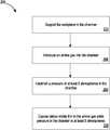
- treating a dielectric film that includes silicon-nitride bonds on a workpieceincludes supporting the workpiece that has the dielectric film that includes silicon-nitride bonds in a chamber, introducing an amine gas into the chamber, establishing a pressure of at least 5 atmospheres in the chamber, and exposing the dielectric film that includes silicon-nitride to the anime gas while the pressure in the chamber is at least 5 atmospheres.
- a temperature of the dielectric filmmay be raised to between 200-500° C.
- the temperature of the silicon nitride filmmay be raised by maintaining a support for the workpiece in the chamber at an elevated temperature.
- the temperature of the dielectric filmmay be raised before establishing the pressure in the chamber of at least 5 atmospheres.
- Establishing the pressure in the chambermay include introducing the amine gas in the chamber.
- the amine gasincludes ammonia gas.
- the amine gasmay include methylamine gas and/or dimethylamine gas.
- the dielectric filmis exposed to the amine gas for at least 5 minutes and no more than an hour.
- the dielectric filmmay be a portion of a fin field-effect transistor (FinFET) in fabrication.
- FinFETfin field-effect transistor
- a method of forming a dielectric material on a workpieceincludes depositing a dielectric film that includes silicon-nitride bonds on the workpiece by flowable chemical vapor deposition (FCVD), and exposing the dielectric film that includes silicon-nitride bonds to an amine gas in a chamber while a pressure in the chamber is at least 5 atmospheres.
- FCVDflowable chemical vapor deposition
- the deposition of the dielectric film on the workpieceis at a temperature below 380° C.
- an annealing systemin another aspect, includes a chamber body that defines a chamber, a support to hold a workpiece with an outer surface of the workpiece exposed to an environment in the chamber, a robot to insert the workpiece into the chamber, a gas supply to provide an amine gas to the chamber, a pressure source coupled to the chamber to raise a pressure in the chamber to at least 5 atmospheres, and a controller coupled to the robot, the gas supply and the pressure source.
- the controlleris configured to cause the robot to transport the workpiece having a dielectric film on it into the chamber, cause the gas supply to supply the amine gas to the chamber, and cause the pressure source to raise a pressure in the chamber to at least 5 atmospheres while the workpiece is held on the support in the chamber.
- the annealing systemmay include a heater to raise a temperature of the workpiece on the support to between 250-500° C.
- the heatermay include a resistive heater embedded in the support, and/or the heater may be a radiative heater in a wall of the chamber body that is positioned to irradiate the workpiece on the support.
- the pressure sourcemay include a pump.
- Post-deposition annealing of a silicon nitride filmcan improve film quality, e.g., by strengthening the Si—N—Si network and reducing impurities (e.g., oxygen and carbon) in the silicon nitride film.
- impuritiese.g., oxygen and carbon
- the use of high pressure amine gasallows for lower temperature to be used during the anneal process by improving the diffusion of the gas into the silicon nitride layer, maintaining a relatively low thermal budget for the post-processing of the workpiece and preserving overall layer structure quality.
- a relatively low thermal budgetreduces temperature-related effects on other pre-existing features on the workpiece (e.g., reduced dopant diffusion).
- lower temperaturesmay be used for depositing the silicon nitride film, thereby reducing intermixing of the silicon nitride layer with adjacent layers (e.g., tungsten film).
- the use of high pressure gasmay also have a physical impact in certain applications, e.g., FCVD silicon nitride gap fill applications, such that the high pressure may affect the reflow of the silicon nitride film to achieve improved void-free gap fill in the silicon nitride film.
- FIG. 1is a block diagram of a high-pressure substrate processing system.
- FIG. 2is a flow diagram of an example process flow for annealing a silicon nitride film by high pressure treatment in a high-pressure substrate processing system.
- FIG. 3depicts an example high-pressure substrate processing system.
- FIG. 4depicts another example of a high-pressure substrate processing system.
- a silicon nitride film deposited on a semiconductor wafercan be used in a patterning process for fabrication of a fin field-effect transistor (FinFET).
- FinFETfin field-effect transistor
- Poor film qualitymay arise in a variety of manners; without being limited to any particular theory, poor film quality can result from impurities during the deposition process.
- using particular deposition chemistries to deposit the silicon nitride filmmay result in defects in the silicon nitride film due to Si—H and N—H bonding.
- defectsarise in the silicon nitride film due to Si—C and C—N bonds. Additionally, after the silicon nitride film is exposed to air, some defects may be converted to Si—O bonds. Physical pinholes and/or voids may also be present in deposited silicon nitride films, causing poor film quality.
- Poor film quality in silicon nitride filmmay also result from incomplete formation of a Si—N—Si network during the deposition process of the silicon nitride layer.
- the high temperatures used to deposit the silicon nitride filmresults in intermixing of the silicon nitride film with surrounding layers (e.g., tungsten).
- surrounding layerse.g., tungsten
- lower deposition temperaturesare used for depositing the silicon nitride film, which results in lower film quality.
- a silicon nitride film deposited on a workpieceis exposed to high pressure (e.g., at least 5 atmospheres) of amine gas (e.g., ammonia gas) while held at elevated temperatures (e.g., 200-500° C.) for a few minutes to an hour.
- high pressuree.g., at least 5 atmospheres
- amine gase.g., ammonia gas
- elevated temperaturese.g. 200-500° C.
- the high pressure treatment described hereincan be effective in reducing dangling Si and N bonds as well as reducing contamination (e.g., Si—C bonds) resulting from the deposition process in the silicon nitride layer.
- the high pressure treatmentcan also be effective in converting Si—H bonds and Si—O bonds to Si—N bonds, and furthermore may be effective in breaking N—H bonds as well. This can reduce detrimental effects such as uneven etch rates and/or high etch rates of the silicon nitride layer and decreased leakage in silicon nitride gate spacers in FinFET devices.
- FIG. 1is a block diagram of a high-pressure substrate processing system 100 .
- the high-pressure substrate processing system 100includes a high pressure chamber 102 .
- the high pressure chamber 102is configured to contain pressures of at least 5 atmospheres, e.g., at least 10 atmospheres, and can be capable of holding vacuum levels of up to 10 ⁇ -3 Torr when under vacuum.
- the high-pressure substrate processing system 100includes a low-pressure environment 104 , e.g., a vacuum chamber, for when a workpiece is being transferred between processing chambers (e.g., from another processing chamber into the high pressure chamber 102 ).
- the relative pressures within the high pressure chamber 102 and the low pressure chamber 104can be controlled independently of each other.
- a robot(not depicted in FIG. 1 ) including a robotic arm can be used to transfer the workpiece into and out of the high pressure chamber 102 , e.g., between the chambers of a multi-chamber substrate processing tool.
- the high pressure chamber 102includes a support, for example, pedestal 106 for supporting a workpiece in the high pressure chamber 102 .
- the pedestal 106supports one or more workpieces using a variety of support mechanisms, for example, the pedestal 106 may support the workpiece with locking pins and springs, and/or the workpiece may rest directly on top of the pedestal 106 .
- the high pressure chamber 102includes one or more heating elements 108 .
- heating element 108 ais a resistive heater and is integrated into the pedestal 106 for heating the workpiece.
- the high pressure chamber 102includes a heating element 108 b , where the heating element 108 b can heat and maintain a selected temperature within the high pressure chamber 102 .
- Heating element 108 bmay be a radiative heater embedded in a wall of the high pressure chamber body, and positioned to irradiate the workpiece on the pedestal 106 . The heat from the heating elements 108 can be sufficient to anneal the workpiece when the workpiece is supported on the pedestal 106 and a gas (if used) has been introduced into the high pressure chamber 102 .
- the heating elements 108may be resistive heating elements, and may heat the workpiece conductively and/or radiatively. Additionally, the heating elements 108 may include a discrete heating coil, or a radiative heater (e.g., an infrared lamp).
- a gas delivery system 110is operable to pressurize and depressurize the high pressure chamber 102 .
- the gas delivery system 110provides a gas mixture to the high pressure chamber 102 to establish a high pressure, e.g., a pressure of at least 5 atmospheres.
- the gas delivery system 110includes an exhaust system 112 to exhaust the gas from the high pressure chamber 102 thereby depressurizing the high pressure chamber 102 .
- the gas delivery systemincludes a pressure source to raise the pressure in the chamber 102 to the high pressure.
- the pressure sourcecan include a pump, e.g., a rotary pump, a scroll pump, or a screw pump, configured to pump gas into the chamber 102 until the desired pressure is reached, and/or a compressed gas cylinder at a pressure sufficient that, after the gas cylinder is fluidically connected to the chamber 102 , the equalized pressure will reach the desired pressure.
- a pumpe.g., a rotary pump, a scroll pump, or a screw pump
- a pumping system 114includes one or more pumps for reducing pressures in the high pressure chamber 102 and/or the vacuum chamber 104 .
- Pumpsmay include one or more rotary pumps, scroll pumps, and screw pumps.
- the pumping system 114can be used to lower the pressure in the vacuum chamber 104 to be at vacuum or near-vacuum pressure, e.g., less than 1 milliTorr.
- the pumping system 114may be used during a pump and purge cycle in the high pressure chamber 102 to reduce presence of contaminants in the high pressure chamber 102 prior to process operation.
- a valve assembly 116isolates the relative pressures between the high pressure chamber 102 and the vacuum chamber 104 .
- the high-pressure environment within the high pressure chamber 102can thus be separated and sealed from the low pressure environment within the vacuum chamber 104 .
- the valve assembly 116is operable to enable the workpiece to be transferred directly between the high pressure chamber 102 and the vacuum chamber 104 .
- the high-pressure substrate processing system 100includes a foreline 118 connected to the vacuum chamber 104 and connected to an outside environment.
- An isolation valve 120is arranged along the foreline 118 to isolate the pressure within the vacuum chamber 104 from the pressure of the outside environment.
- the isolation valve 120can be operated to adjust the pressure within the vacuum chamber 104 and to releases gases within the vacuum chamber 104 .
- the isolation valve 120can be operated in conjunction with the pumping system 114 to regulate the pressure within the vacuum chamber 104 .
- One or more operations of the high-pressure substrate processing system 100may be controlled by one or more controllers 122 .
- the controller 122e.g., a general purpose programmable computer, is connected to and operable to control some or all of the various components of the high-pressure substrate processing system 100 .
- Operations controlled by controller 122may include, for example, temperature regulation of the heating elements 108 within the high pressure chamber 102 , pressure regulation within the high pressure chamber 102 , vacuum regulation within the vacuum chamber 104 , flow rates and gas delivery by the gas delivery system 110 , and operation of one or more pumps in the pumping system 114 .
- the controller 122can be programmed to generate control signals that cause the components of the high-pressure substrate processing system 100 to carry out the process described below with reference to FIG. 2 .
- FIG. 2is a flow diagram of an example process flow 200 for high-pressure annealing of a silicon nitride film on a workpiece in a high-pressure substrate processing system 100 .
- a workpieceincludes a semiconductor substrate (e.g., silicon), with a silicon nitride film deposited on the substrate.
- the silicon nitride filmforms part of a fin field effect transistor (FinFET) structure fabricated on the substrate; the workpiece may also include layers of other materials (e.g., TiN, tungsten).
- the silicon nitride filmmay be deposited on the workpiece using flowable chemical vapor deposition (FCVD) in a separate processing step.
- FCVDflowable chemical vapor deposition
- PECVDplasma-etched chemical vapor deposition
- LPCVDlow pressure chemical vapor deposition
- ALDatomic layer deposition
- the workpieceis inserted into the chamber, e.g., by the robot, and then supported in the chamber, e.g., on a pedestal 106 within the high pressure chamber 102 ( 202 ).
- the high pressure chamber 102 and/or the pedestal 106are maintained at a particular temperature (e.g., 200-500° C.) using one or more heating elements 108 .
- the temperature of the high pressure chamber 102 and/or the pedestal 106may be established prior to introducing the workpiece into the high pressure chamber 102 .
- the temperature of the workpiecemay be established at a particular temperature (e.g., 200-600° C.) through the use of one or more heating elements 108 while the workpiece is supported by the pedestal 106 in the high pressure chamber 102 .
- the temperature of the workpiecee.g., the silicon nitride film on the substrate
- the pressure in the high pressure chamber 102is raised prior to establishing the pressure in the high pressure chamber 102 of at least 5 atmospheres.
- An amine gasis introduced into the high pressure chamber 102 ( 204 ).
- the amine gascan be ammonia gas or another small and reactive amine gas (e.g., methylamine gas or dimethylamine gas).
- multiple different amine gasese.g., ammonia gas and methylamine gas
- the multiple different amine gasese.g., ammonia gas and methylamine gas
- the amine gasmay be mixed with an inert gas (e.g., nitrogen, argon, or helium) prior to being delivered into the high pressure chamber 102 by the gas delivery system 110 , for example, to reduce flammability of the gas mixture.
- an inert gase.g., nitrogen, argon, or helium
- the gas delivery system 110can establish a total pressure of 5 to 50 atmospheres in the high pressure chamber 102 ( 206 ).
- the total pressure in the high pressure chamberis at least 10 atmospheres.
- the total pressure of amine gas in the high pressure chamber 102may be established as a static pressure in the chamber, or may be established through a flow of amine gas in and out of the chamber during the annealing process.
- the total pressure of 5 to 50 atmospherescan be provided by the amine gas.
- the gas introduced into the high pressure chambercan consist of amine gas, i.e., only amine gas is introduced into the high pressure chamber.
- the silicon nitride film on the workpieceis exposed to the amine gas while the high pressure chamber 102 is maintained at the elevated pressure ( 208 ). Exposure times include a few minutes to several hours (e.g., at least 5 minutes, and no more than one hour).
- the annealing temperaturee.g., temperature of the workpiece during the anneal process
- the amine gas pressure in the high pressure chamber 102and exposure times for the high-pressure annealing process, may be interrelated such that optimal operational parameters may be found by adjusting the aforementioned (and other) variables.
- the high pressure amine gas treatmentcan be effective in converting Si—H bonds and Si—O bonds to Si—N bonds, and furthermore may be effective in breaking N—H bonds which will enable the formation of Si—N bonds in the silicon nitride film.
- the amine gasis introduced into the high pressure chamber 102 by the gas delivery system prior to or during the heating process of the workpiece.
- a high pressure of amine gase.g., ammonia gas
- heating elements 108are bringing a workpiece on a pedestal 106 to a particular desired temperature.
- the workpiecemay be heated to a particular temperature while it is in the vacuum chamber 104 and then subsequently transferred to the high pressure chamber 102 by a robot (not depicted), where the amine gas (e.g., ammonia gas) may be introduced.
- the amine gase.g., ammonia gas
- a silicon nitride filmis deposited on a workpiece, which may then undergo the high pressure treatment described herein.
- a silicon nitride filmcan be deposited on the workpiece by flowable chemical vapor deposition (FCVD) using a gas composition of, e.g., trisilylamine/silane/ammonia. Due to a lower (e.g., below 380° C.) deposition temperature for the silicon nitride film, lower film quality may result.
- FCVDflowable chemical vapor deposition
- FCVDflowable chemical vapor deposition
- the silicon nitride filmmay then be exposed to an amine gas in a high pressure chamber 102 while a pressure in the high pressure chamber 102 is at least 5 atmospheres.
- the silicon nitride filmis used as an etch hard-mask, such that a process to etch trenches in the silicon nitride layer may be performed on the silicon nitride layer (e.g., using a plasma gas composition such as a SF6/CH4/N2/O2 plasma) before and/or after the high pressure treatment of the silicon nitride layer on the workpiece.
- a plasma gas compositionsuch as a SF6/CH4/N2/O2 plasma
- FIGS. 3 and 4depict two embodiments of high-pressure substrate processing systems.
- FIG. 3depicts an example high-pressure substrate processing system 300 including a first chamber 302 (e.g., a high pressure chamber 102 ), a pedestal 304 , a second chamber 306 (e.g., a vacuum chamber 104 ), and a controller (e.g., the controller 122 ).
- the high-pressure substrate processing system 300further includes a pumping system (not shown) similar to the pumping system 114 and a gas delivery system 307 similar to the gas delivery system 110 described with respect to FIG. 1 .
- the gas delivery system 307includes an input line 307 a and an exhaust line 307 b .
- the amine gasis introduced into the first chamber 302 through the input line 307 a , and the amine gas is exhausted from the first chamber 302 through the exhaust line 307 b.
- the pedestal 304supports a workpiece (i.e., substrate) 314 on which a film of material (e.g., silicon nitride film) is to be processed through a high pressure treatment.
- the pedestal 304is positioned or positionable within the first chamber 302 .
- the substrate 314sits directly on a flat top surface of the pedestal.
- the substrate 314sits on pins 330 that project from the pedestal.
- the high-pressure substrate processing system 300includes an inner wall 320 , a base 322 , and an outer wall 324 .
- the first chamber 302is provided by a volume within the inner wall 320 , e.g., between the inner wall 320 and the base 322 .
- the second chamber 306is provided by a volume outside the inner wall 320 , e.g., between the inner wall 320 and the outer wall 324 .
- the high-pressure substrate processing system 300further includes a valve assembly 316 between the first chamber 302 and the second chamber 306 that provides the functionality of the valve assembly 116 of FIG. 1 , i.e., it can be operated to isolate the first chamber 302 from the second chamber 306 .
- the valve assembly 316includes the inner wall 320 , the base 322 , and an actuator 323 to move the base 322 relative to the inner wall 320 .
- the actuator 323can be controlled to drive the base 322 to move vertically, e.g., away from or toward the walls 320 defining the first chamber 302 .
- a bellows 328can be used to seal the second chamber 306 from the external atmosphere while permitting the base 322 to move vertically.
- the bellows 328can extend from a bottom of the base 322 to a floor of the second chamber 306 formed by the outer wall 324 .
- the base 322When the valve assembly 316 is in a closed position, the base 322 contacts the walls 320 such that a seal is formed between the base 322 and the walls 320 , thus separating the second chamber 306 from the first chamber 302 .
- the actuator 323is operated to drive the base 322 toward the inner walls 320 with sufficient force to form the seal.
- the sealinhibits air from the first high-pressure chamber 302 from being exhausted into the low-pressure second chamber 306 .
- the base 322When the valve assembly 316 is in an open position, the base 322 is spaced apart from the walls 320 , thereby allowing air to be conducted between the first and second chambers 302 , 306 and also allowing the substrate 314 to be accessed and transferred to another chamber.
- the pedestal 304is thus also movable relative to the inner walls 320 .
- the pedestal 304can be moved to enable the substrate 314 to be more easily accessible by the transfer robot.
- an arm of a transfer robot(not depicted) can extend through an aperture 326 in the outer wall 324 .
- the robot armcan pass through the gap between the inner wall 320 and the base 322 to access the substrate 314 .
- the high-pressure substrate processing system 300includes one or more heating elements 318 configured to apply heat to the substrate 314 .
- the heat from the heating elements 318can be sufficient to anneal the substrate 314 when the substrate 314 is supported on the pedestal 304 and the precursor gas (if used) has been introduced into the first chamber 302 .
- the heating elements 318may be resistive heating elements.
- the one or more heating elements 318may be positioned in, e.g., embedded in, the inner walls 320 defining the first chamber 302 . This heats the inner wall 320 , causing radiative heat to reach the substrate 314 .
- the substrate 314can be held by the pedestal 304 in close proximity to the ceiling of inner wall to improve transmission of heat from the inner wall 320 to the substrate 314 .
- the one or more heating elements 318may be arranged in other locations within the high-pressure substrate processing system 300 , e.g., within the side walls rather than ceiling.
- An example of a heating element 318includes a discrete heating coil.
- a radiative heatere.g., an infrared lamp, can be positioned outside the first chamber 302 and direct infrared radiation through a window in the inner wall 320 .
- Electrical wiresconnect an electrical source (not shown), such as a voltage source, to the heating element, and can connect the one or more heating elements 318 to the controller.
- the controlleris operably connected to the pumping system, the gas delivery system 307 , and the valve assembly 316 for controlling operations to perform the high pressure treatment of a layer of material on the substrate 314 .
- the controllermay also be operably connected to other systems.
- the controllercan also be operably connected to one or more of the transfer robots (not depicted), the one or more heating elements 318 , and/or the actuator 323 .
- the controller 122 shown in FIG. 1includes the controller of the high-pressure substrate processing system 300 .
- the controllercan operate the pumping system to depressurize the second chamber 306 to a low-pressure state, e.g., to a state in which the second chamber 306 has a pressure less than 1 atmosphere, to prepare for transfer of the substrate 314 through the second chamber 306 .
- the low-pressure statecan be a near-vacuum state, e.g., a pressure less than 1 milliTorr.
- the substrate 314is moved through the second chamber 306 by a transfer robot (not shown), while the second chamber 306 is at the low-pressure so that contamination and oxidation of the substrate 314 can be inhibited.
- the substrate 314is transferred into the first chamber 302 for processing.
- the controllercan operate the valve assembly 316 , e.g., open the valve assembly 316 to provide an opening through which the substrate 314 can be transferred into the first chamber 302 .
- the controllercan operate the transfer robot to carry the substrate 314 into the first chamber 302 and to place the substrate 314 on the pedestal 304 .
- the controllercan operate the valve assembly 316 to close the opening, e.g., close the valve assembly 316 , thereby isolating the first and second chambers 302 , 306 from one another.
- the controllercan operate the gas delivery system 307 to introduce the amine gas into the first chamber 302 to pressurize the first chamber 302 .
- the introduction of the amine gascan increase the pressure within the first chamber 302 , for example, to 5 atmospheres or more.
- the amine gas and the proper temperature and pressure conditions in the first chamber 302can cause the high pressure treatment of the material to occur, e.g., as described with reference to FIG. 2 .
- the controllercan operate the one or more heating elements 318 to add heat to the substrate 314 to facilitate the annealing of the layer of material on the substrate 314 .
- the substrate 314can be removed from the first chamber 302 using the transfer robot and, if necessary, the substrate 314 can be transferred to a subsequent process chamber or to the outside environment. Alternatively, the substrate 314 is transferred into a load lock chamber (not shown).
- the controllercan operate the exhaust system of the gas delivery system 307 to depressurize the first chamber 302 before the valve assembly 316 is opened.
- the precursor gasis exhausted from the first chamber 302 to reduce the pressure within the first chamber 202 .
- the pressure in the first chamber 302can be reduced to a near-vacuum pressure such that the pressure differential between the first chamber 302 and the second chamber 306 can be minimized.
- the controllercan open the valve assembly 316 .
- the opened valve assembly 316provides an opening through which the substrate 314 is moved to be transferred into the second chamber 306 .
- the opened valve assembly 316enables the substrate 314 to be transferred directly into the second chamber 306 , e.g., into the low pressure environment of the second chamber 306 .
- FIG. 4depicts another example of a high-pressure substrate processing system 400 including a first chamber 402 (e.g., high pressure chamber 102 ), a pedestal 404 , a second chamber 406 (e.g., vacuum chamber 104 ), and a controller similar to controller 122 shown in FIG. 1 .
- the high-pressure substrate processing system 400is similar to the high-pressure substrate processing system 300 described with respect to FIG. 3 ; unless otherwise specified the various options and implementations are also applicable to this embodiment.
- the gas delivery system and the pumping system of the high-pressure substrate processing system 400are operated in a similar manner to maintain the low and high pressure environments for a substrate 414 processed using the high-pressure substrate processing system 400 .
- the second chamber 406can be defined by volume between inner walls 420 and outer walls 424 .
- the substrate 414is also supportable on the pedestal 404 for processing within the first chamber 402 . Again, the substrate can sit directly on the pedestal 404 , or sit on lift pins 430 that extend through the pedestal.
- the high-pressure substrate processing system 400differs from the high-pressure substrate processing system 300 of FIG. 3 in a few regards.
- inner walls 420 defining the first chamber 402are not movable relative to a base 422 defining the first chamber 402 .
- the pedestal 404is thus fixed relative to the inner walls 420 and the base 422 .
- the pedestal 404is fixed to the base 422 defining the first chamber 402 .
- one or more heating elements 418 of the embodiment depicted in FIG. 4are arranged within the pedestal 404 .
- the substrate 414is thus heated through contact with the pedestal 404 .
- the high-pressure substrate processing system 400further includes a valve assembly 416 between the first chamber 402 and the second chamber 406 that, similar to the valve assembly 316 of FIG. 3 , isolates the first chamber 402 from the second chamber 406 .
- the valve assembly 416is not formed by the walls 420 and the base 422 defining the first chamber 402 , but rather is formed by an arm 425 movable relative to the inner walls 420 and the base 422 of the first chamber 402 .
- the arm 425may be movable relative to the inner walls 420 and the base 422 of the first chamber 402 .
- the valve assembly 416includes a slit valve 423 between the first chamber 402 and the second chamber 406 .
- the slit valve 423includes a slit 423 a and the arm 425 .
- the slit 423 aextends through one of the inner walls 420 of the first chamber 402 .
- a proximal end 425 a of the arm 425is positioned outside of the first chamber 402 while a distal end 425 b of the arm 425 is positioned within the first chamber 402 .
- the proximal end 425 a of the arm 425can be positioned within the second chamber 406 and be driven by an actuator positioned within the second chamber 406 .
- the proximal end 425 a of the arm 425is positioned outside of the second chamber 406 and is thus driven by an actuator 428 that is also positioned outside of the second chamber 406 .
- the arm 425extends through the slit 423 a and is movable relative to the walls 420 so that the arm 425 can be moved to a position in which it forms a seal with the walls 420 .
- the actuator 428is coupled to the proximal end 425 a of the arm 425 and drives the distal end 425 b of the arm 425 relative to the walls 420 .
- the arm 425is also movable vertically to cover or uncover the slit 423 a .
- the proximal end 425 a of the arm 425can be or include a flange that extends substantially parallel to the adjacent inner surface of the inner wall 420 .
- the arm 425is also movable and driven laterally so that the distal end 425 b of the arm 425 can engage or disengage the inner walls 420 .
- the arm 425can also extend through an aperture (e.g., slit) 426 in the outer wall 424 .
- the valve assembly 416is movable between an open position and a closed position.
- the distal end 425 b of the arm 425covers the slit 426 and contacts one of the inner walls 420 , thereby forming the seal to isolate the first chamber 402 from the second chamber 406 .
- the distal end 425 b of the arm 425e.g., the flange, contacts an inner surface of the wall 420 defining the first chamber 402 .
- the distal end 425 b of the arm 425When the valve assembly 416 is in the open position, the distal end 425 b of the arm 425 is spaced laterally apart from the inner walls 420 , e.g., the inner surface of the inner walls 420 . In addition, the distal end 425 b of the arm 425 is positioned vertically so that the slit 426 is uncovered.
- the slit 426thus provides an opening that enables fluidic communication between the first chamber 402 and the second chamber 406 and that also enables the substrate 414 to be moved in and out of the first chamber 402 , e.g., by a robot as discussed above.
- the controllercan operate the high-pressure substrate processing system 400 in a manner similar to the process described with respect to the controller of the high-pressure substrate processing system 300 to transfer the substrate 414 into and out of the first chamber 402 and to perform the high pressure treatment on the layer of material on the substrate 414 .
- the controllercan operate the actuator 428 to drive the arm 425 .
- An advantage of the configuration shown in FIG. 4is that the pressure within the first chamber 402 helps force the distal end 425 b of the arm 425 against the inner surface of the inner wall 420 . Consequently, in contrast to the configuration shown in FIG. 3 , the actuator can be less powerful.
- the controller and other computing devices part of systems described hereincan be implemented in digital electronic circuitry, or in computer software, firmware, or hardware.
- the controllercan include a processor to execute a computer program as stored in a computer program product, e.g., in a non-transitory machine readable storage medium.
- a computer programalso known as a program, software, software application, or code
- Such a computer programcan be written in any form of programming language, including compiled or interpreted languages, and it can be deployed in any form, including as a standalone program or as a module, component, subroutine, or other unit suitable for use in a computing environment.
- silicon nitrideother dielectric films that include silicon-nitride bonds, e.g., silicon oxynitride (SiON) or silicon carbon nitride (SiCN), may be deposited, e.g., by a low temperature or FCVD process, and treated using the high pressure treatment described herein.
- SiONsilicon oxynitride
- SiCNsilicon carbon nitride
Landscapes
- Engineering & Computer Science (AREA)
- Chemical & Material Sciences (AREA)
- Physics & Mathematics (AREA)
- Condensed Matter Physics & Semiconductors (AREA)
- General Physics & Mathematics (AREA)
- Manufacturing & Machinery (AREA)
- Computer Hardware Design (AREA)
- Microelectronics & Electronic Packaging (AREA)
- Power Engineering (AREA)
- Chemical Kinetics & Catalysis (AREA)
- Organic Chemistry (AREA)
- General Chemical & Material Sciences (AREA)
- Materials Engineering (AREA)
- Mechanical Engineering (AREA)
- Metallurgy (AREA)
- Inorganic Chemistry (AREA)
- Health & Medical Sciences (AREA)
- Toxicology (AREA)
- Chemical Vapour Deposition (AREA)
- Formation Of Insulating Films (AREA)
Abstract
Description
Claims (17)
Priority Applications (6)
| Application Number | Priority Date | Filing Date | Title |
|---|---|---|---|
| US15/605,751US10847360B2 (en) | 2017-05-25 | 2017-05-25 | High pressure treatment of silicon nitride film |
| CN201880034510.7ACN110678959B (en) | 2017-05-25 | 2018-05-24 | High Pressure Processing of Silicon Nitride Film |
| PCT/US2018/034284WO2018217967A1 (en) | 2017-05-25 | 2018-05-24 | High pressure treatment of silicon nitride film |
| JP2019564965AJP6952799B2 (en) | 2017-05-25 | 2018-05-24 | High pressure treatment of silicon nitride film |
| EP18805265.8AEP3635769A4 (en) | 2017-05-25 | 2018-05-24 | HIGH PRESSURE TREATMENT OF SILICON NITRIDE FILM |
| KR1020197038172AKR102289791B1 (en) | 2017-05-25 | 2018-05-24 | High Pressure Treatment of Silicon Nitride Membrane |
Applications Claiming Priority (1)
| Application Number | Priority Date | Filing Date | Title |
|---|---|---|---|
| US15/605,751US10847360B2 (en) | 2017-05-25 | 2017-05-25 | High pressure treatment of silicon nitride film |
Publications (2)
| Publication Number | Publication Date |
|---|---|
| US20180342384A1 US20180342384A1 (en) | 2018-11-29 |
| US10847360B2true US10847360B2 (en) | 2020-11-24 |
Family
ID=64395897
Family Applications (1)
| Application Number | Title | Priority Date | Filing Date |
|---|---|---|---|
| US15/605,751ActiveUS10847360B2 (en) | 2017-05-25 | 2017-05-25 | High pressure treatment of silicon nitride film |
Country Status (6)
| Country | Link |
|---|---|
| US (1) | US10847360B2 (en) |
| EP (1) | EP3635769A4 (en) |
| JP (1) | JP6952799B2 (en) |
| KR (1) | KR102289791B1 (en) |
| CN (1) | CN110678959B (en) |
| WO (1) | WO2018217967A1 (en) |
Cited By (12)
| Publication number | Priority date | Publication date | Assignee | Title |
|---|---|---|---|---|
| US11177128B2 (en) | 2017-09-12 | 2021-11-16 | Applied Materials, Inc. | Apparatus and methods for manufacturing semiconductor structures using protective barrier layer |
| US11361978B2 (en) | 2018-07-25 | 2022-06-14 | Applied Materials, Inc. | Gas delivery module |
| US11462417B2 (en) | 2017-08-18 | 2022-10-04 | Applied Materials, Inc. | High pressure and high temperature anneal chamber |
| US11527421B2 (en) | 2017-11-11 | 2022-12-13 | Micromaterials, LLC | Gas delivery system for high pressure processing chamber |
| US11581183B2 (en) | 2018-05-08 | 2023-02-14 | Applied Materials, Inc. | Methods of forming amorphous carbon hard mask layers and hard mask layers formed therefrom |
| US11610773B2 (en) | 2017-11-17 | 2023-03-21 | Applied Materials, Inc. | Condenser system for high pressure processing system |
| US11694912B2 (en) | 2017-08-18 | 2023-07-04 | Applied Materials, Inc. | High pressure and high temperature anneal chamber |
| US11705337B2 (en) | 2017-05-25 | 2023-07-18 | Applied Materials, Inc. | Tungsten defluorination by high pressure treatment |
| US11749555B2 (en) | 2018-12-07 | 2023-09-05 | Applied Materials, Inc. | Semiconductor processing system |
| US11881411B2 (en) | 2018-03-09 | 2024-01-23 | Applied Materials, Inc. | High pressure annealing process for metal containing materials |
| US11901222B2 (en) | 2020-02-17 | 2024-02-13 | Applied Materials, Inc. | Multi-step process for flowable gap-fill film |
| US12198951B2 (en) | 2017-03-10 | 2025-01-14 | Applied Materials, Inc. | High pressure wafer processing systems and related methods |
Families Citing this family (6)
| Publication number | Priority date | Publication date | Assignee | Title |
|---|---|---|---|---|
| JP7330181B2 (en) | 2017-11-16 | 2023-08-21 | アプライド マテリアルズ インコーポレイテッド | High-pressure steam annealing treatment equipment |
| US10714331B2 (en) | 2018-04-04 | 2020-07-14 | Applied Materials, Inc. | Method to fabricate thermally stable low K-FinFET spacer |
| US10675581B2 (en) | 2018-08-06 | 2020-06-09 | Applied Materials, Inc. | Gas abatement apparatus |
| CN112640065B (en) | 2018-10-30 | 2024-10-01 | 应用材料公司 | Method for etching structures for semiconductor applications |
| WO2020101935A1 (en) | 2018-11-16 | 2020-05-22 | Applied Materials, Inc. | Film deposition using enhanced diffusion process |
| WO2024252586A1 (en)* | 2023-06-07 | 2024-12-12 | 株式会社Kokusai Electric | Processing method, semiconductor device manufacturing method, processing device, and program |
Citations (166)
| Publication number | Priority date | Publication date | Assignee | Title |
|---|---|---|---|---|
| US4524587A (en) | 1967-01-10 | 1985-06-25 | Kantor Frederick W | Rotary thermodynamic apparatus and method |
| US5050540A (en) | 1991-01-29 | 1991-09-24 | Arne Lindberg | Method of gas blanketing a boiler |
| US5175123A (en) | 1990-11-13 | 1992-12-29 | Motorola, Inc. | High-pressure polysilicon encapsulated localized oxidation of silicon |
| US5366905A (en) | 1991-11-05 | 1994-11-22 | Fujitsu Limited | Method for producing conducting layers for a semiconductor device |
| JPH0748489B2 (en) | 1987-07-27 | 1995-05-24 | 富士通株式会社 | Plasma processing device |
| US5590695A (en) | 1993-04-28 | 1997-01-07 | Advanced Delivery & Chemical Systems, Inc. | Manifold systems for high purity chemical delivery systems |
| US5620524A (en) | 1995-02-27 | 1997-04-15 | Fan; Chiko | Apparatus for fluid delivery in chemical vapor deposition systems |
| US5808245A (en) | 1995-01-03 | 1998-09-15 | Donaldson Company, Inc. | Vertical mount catalytic converter muffler |
| US5858051A (en) | 1995-05-08 | 1999-01-12 | Toshiba Machine Co., Ltd. | Method of manufacturing optical waveguide |
| US5879756A (en) | 1996-09-19 | 1999-03-09 | Lambda Technologies, Inc. | Curing polymer layers on semiconductor substrates using variable frequency microwave energy |
| US6136664A (en) | 1997-08-07 | 2000-10-24 | International Business Machines Corporation | Filling of high aspect ratio trench isolation |
| US6150286A (en) | 2000-01-03 | 2000-11-21 | Advanced Micro Devices, Inc. | Method of making an ultra thin silicon nitride film |
| US6164412A (en) | 1998-04-03 | 2000-12-26 | Arvin Industries, Inc. | Muffler |
| JP2001110729A (en) | 1999-10-06 | 2001-04-20 | Mitsubishi Heavy Ind Ltd | Apparratus for continuously manufacturing method of semiconductor element |
| US6242368B1 (en) | 1996-03-29 | 2001-06-05 | Praxair Technology, Inc. | Removal of carbon from substrate surface |
| US6251751B1 (en) | 1997-10-16 | 2001-06-26 | International Business Machines Corporation | Bulk and strained silicon on insulator using local selective oxidation |
| US6299753B1 (en) | 1999-09-01 | 2001-10-09 | Applied Materials, Inc. | Double pressure vessel chemical dispenser unit |
| US20010029108A1 (en) | 2000-03-06 | 2001-10-11 | Kouji Tometsuka | Substrate processeing apparatus, substrate processing method and electronic device manufacturing method |
| US20010041122A1 (en) | 1998-09-28 | 2001-11-15 | Applied Materials, Inc. | Single wafer load lock with internal wafer transport |
| US20010050096A1 (en) | 2000-04-18 | 2001-12-13 | Costantini Michael A. | Supercritical fluid delivery and recovery system for semiconductor wafer processing |
| US6334266B1 (en) | 1999-09-20 | 2002-01-01 | S.C. Fluids, Inc. | Supercritical fluid drying system and method of use |
| US6368412B1 (en) | 1997-11-18 | 2002-04-09 | Nec Corporation | Apparatus with high temperature gas releasing means for vapor deposition of parylene polymer without peeling |
| US20020073922A1 (en) | 1996-11-13 | 2002-06-20 | Jonathan Frankel | Chamber liner for high temperature processing chamber |
| US6442980B2 (en) | 1997-11-26 | 2002-09-03 | Chart Inc. | Carbon dioxide dry cleaning system |
| US20020134439A1 (en) | 2001-03-22 | 2002-09-26 | Hiroyuki Kawasaki | Gas recirculation flow control method and apparatus for use in vacuum system |
| US20020151128A1 (en) | 1996-01-22 | 2002-10-17 | Lane Richard H. | High-pressure anneal process for integrated circuits |
| US20020148492A1 (en) | 2001-04-17 | 2002-10-17 | Kabushiki Kaisha Kobe Seiko Sho | High-pressure processing apparatus |
| JP2003051474A (en) | 2001-08-03 | 2003-02-21 | Kobe Steel Ltd | High-pressure processing apparatus |
| US20030101938A1 (en) | 1998-10-27 | 2003-06-05 | Applied Materials, Inc. | Apparatus for the deposition of high dielectric constant films |
| US20030148631A1 (en) | 1999-11-08 | 2003-08-07 | Taiwan Semiconductor Manufacturing Company | Oxidative annealing method for forming etched spin-on-glass (SOG) planarizing layer with uniform etch profile |
| US20030148035A1 (en) | 2002-02-07 | 2003-08-07 | Applied Materials, Inc. | Article for use in a semiconductor processing chamber and method of fabricating same |
| US6619304B2 (en) | 2001-09-13 | 2003-09-16 | Micell Technologies, Inc. | Pressure chamber assembly including non-mechanical drive means |
| US20030207593A1 (en) | 2002-05-02 | 2003-11-06 | Micron Technology, Inc. | Atomic layer deposition and conversion |
| US20040025908A1 (en) | 2000-04-18 | 2004-02-12 | Stephen Douglas | Supercritical fluid delivery system for semiconductor wafer processing |
| US20040060519A1 (en) | 2002-10-01 | 2004-04-01 | Seh America Inc. | Quartz to quartz seal using expanded PTFE gasket material |
| JP2004127958A (en) | 2002-09-30 | 2004-04-22 | Kyoshin Engineering:Kk | Apparatus and method for performing high pressure anneal steam treatment |
| US20040112409A1 (en) | 2002-12-16 | 2004-06-17 | Supercritical Sysems, Inc. | Fluoride in supercritical fluid for photoresist and residue removal |
| US20040219800A1 (en) | 2001-06-22 | 2004-11-04 | Marcel Tognetti | Thermal oxidation process control by controlling oxidation agent partial pressure |
| US20040248392A1 (en) | 2003-02-04 | 2004-12-09 | Applied Materials, Inc. | Tailoring nitrogen profile in silicon oxynitride using rapid thermal annealing with ammonia under ultra-low pressure |
| US20050051194A1 (en) | 2003-08-13 | 2005-03-10 | Kabushiki Kaisha Kobe Seiko Sho (Kobe Steel, Ltd.) | Method for high-pressure processing |
| TW200529284A (en) | 2004-02-19 | 2005-09-01 | Taiwan Semiconductor Mfg | An intelligent full automation controlled flow for a semiconductor furnace tool |
| US20050198971A1 (en) | 2002-10-02 | 2005-09-15 | Kelly Leitch | High pressure CO2 purification and supply system |
| US20050250347A1 (en) | 2003-12-31 | 2005-11-10 | Bailey Christopher M | Method and apparatus for maintaining by-product volatility in deposition process |
| JP2005333015A (en) | 2004-05-20 | 2005-12-02 | Kobe Steel Ltd | Method for desiccating microstructure, and microstructure obtained thereby |
| US20060003596A1 (en) | 2004-07-01 | 2006-01-05 | Micron Technology, Inc. | Low temperature process for polysilazane oxidation/densification |
| US20060124613A1 (en) | 2002-05-08 | 2006-06-15 | Satyendra Kumar | Plasma-assisted heat treatment |
| US20060207633A1 (en) | 2005-03-21 | 2006-09-21 | Pkl Co., Ltd. | Device and method for cleaning photomask |
| US7111630B2 (en) | 2001-05-17 | 2006-09-26 | Dainippon Screen Mfg. Co., Ltd. | High pressure processing apparatus and method |
| US7114517B2 (en) | 2001-11-26 | 2006-10-03 | Sund Wesley E | High purity fluid delivery system |
| US20060226117A1 (en) | 2005-03-29 | 2006-10-12 | Bertram Ronald T | Phase change based heating element system and method |
| US20060279025A1 (en) | 2005-06-10 | 2006-12-14 | Babak Heidari | Pattern replication with intermediate stamp |
| US20070012402A1 (en) | 2003-07-08 | 2007-01-18 | Sundew Technologies, Llc | Apparatus and method for downstream pressure control and sub-atmospheric reactive gas abatement |
| TW200721316A (en) | 2005-08-05 | 2007-06-01 | Hitachi Int Electric Inc | Substrate processing apparatus, cooling gas feed nozzle and method for manufacturing semiconductor device |
| US20070187386A1 (en) | 2006-02-10 | 2007-08-16 | Poongsan Microtec Corporation | Methods and apparatuses for high pressure gas annealing |
| US20070204797A1 (en) | 2006-03-03 | 2007-09-06 | Andreas Fischer | Methods and apparatus for selective pre-coating of a plasma processing chamber |
| JP2007242791A (en) | 2006-03-07 | 2007-09-20 | Hitachi Kokusai Electric Inc | Substrate processing equipment |
| US20070243317A1 (en) | 2002-07-15 | 2007-10-18 | Du Bois Dale R | Thermal Processing System and Configurable Vertical Chamber |
| US20070256559A1 (en) | 2006-05-08 | 2007-11-08 | The Board Of Trustees Of The University Of Illinois | Integrated vacuum absorption steam cycle gas separation |
| US20080074658A1 (en) | 2003-12-23 | 2008-03-27 | Davis Matthew F | Method and apparatus for performing limited area spectral analysis |
| JP2008073611A (en) | 2006-09-21 | 2008-04-03 | Dainippon Screen Mfg Co Ltd | High pressure treating device |
| US7361231B2 (en) | 2005-07-01 | 2008-04-22 | Ekc Technology, Inc. | System and method for mid-pressure dense phase gas and ultrasonic cleaning |
| US20080115726A1 (en) | 2004-08-27 | 2008-05-22 | Applied Materials, Inc. | gap-fill depositions introducing hydroxyl-containing precursors in the formation of silicon containing dielectric materials |
| WO2008089178A2 (en) | 2007-01-16 | 2008-07-24 | Varian Semiconductor Equipment Associates, Inc. | Plasma source with liner for reducing metal contamination |
| US20080210273A1 (en) | 2005-11-08 | 2008-09-04 | Tokyo Electron Limited | Batch photoresist dry strip and ash system and process |
| US7460760B2 (en) | 2005-09-13 | 2008-12-02 | Electronics And Telecommunications Research Institute | Optical waveguide master and method of manufacturing the same |
| KR20090011463A (en) | 2007-07-26 | 2009-02-02 | 주식회사 풍산마이크로텍 | Method of manufacturing semiconductor device through high pressure oxygen heat treatment |
| US7503334B1 (en) | 2002-02-05 | 2009-03-17 | Novellus Systems, Inc. | Apparatus and methods for processing semiconductor substrates using supercritical fluids |
| US20090081884A1 (en) | 2007-09-24 | 2009-03-26 | Yoshitaka Yokota | Method of improving oxide growth rate of selective oxidation processes |
| KR20090040867A (en) | 2007-10-22 | 2009-04-27 | 어플라이드 머티어리얼스, 인코포레이티드 | How to Form a Dielectric Layer in a Trench |
| US20090186481A1 (en) | 2008-01-22 | 2009-07-23 | Tokyo Electron Limited | Method for integrating selective low-temperature ruthenium deposition into copper metallization of a semiconductor device |
| US20090243126A1 (en) | 2008-03-31 | 2009-10-01 | Ryuta Washiya | Method and apparatus for imprinting microstructure and stamper therefor |
| US20100006211A1 (en) | 2007-03-22 | 2010-01-14 | 3M Innovative Properties Company | Microreplication tools and patterns using laser induced thermal embossing |
| US20100012292A1 (en) | 2007-03-31 | 2010-01-21 | Tokyo Electron Limited | Trap apparatus, exhaust system and processing system using same |
| US7651959B2 (en) | 2007-12-03 | 2010-01-26 | Asm Japan K.K. | Method for forming silazane-based dielectric film |
| US7650965B2 (en) | 2006-06-09 | 2010-01-26 | Emcon Technologies Llc | Exhaust system |
| US20100022068A1 (en) | 2008-07-25 | 2010-01-28 | Neng-Kuo Chen | Sti film property using sod post-treatment |
| US20100173495A1 (en) | 2004-11-22 | 2010-07-08 | Applied Materials, Inc. | Substrate processing apparatus using a batch processing chamber |
| JP2010205854A (en) | 2009-03-02 | 2010-09-16 | Fujitsu Semiconductor Ltd | Method of manufacturing semiconductor device |
| CN101871043A (en) | 2010-06-25 | 2010-10-27 | 东莞市康汇聚线材科技有限公司 | Annealing furnace steam generator and control method thereof |
| US20100304027A1 (en) | 2009-05-27 | 2010-12-02 | Applied Materials, Inc. | Substrate processing system and methods thereof |
| US20100320459A1 (en) | 2009-06-22 | 2010-12-23 | Fujifilm Corporation | Thin film transistor and method of producing thin film transistor |
| US7867923B2 (en) | 2007-10-22 | 2011-01-11 | Applied Materials, Inc. | High quality silicon oxide films by remote plasma CVD from disilane precursors |
| US7891228B2 (en) | 2008-11-18 | 2011-02-22 | Mks Instruments, Inc. | Dual-mode mass flow verification and mass flow delivery system and method |
| US20110151677A1 (en)* | 2009-12-21 | 2011-06-23 | Applied Materials, Inc. | Wet oxidation process performed on a dielectric material formed from a flowable cvd process |
| US20110165781A1 (en) | 2010-01-06 | 2011-07-07 | Applied Materials, Inc. | Flowable dielectric using oxide liner |
| US20110198736A1 (en) | 2010-02-17 | 2011-08-18 | Asm America, Inc. | Reactive site deactivation against vapor deposition |
| US8027089B2 (en) | 2005-10-07 | 2011-09-27 | Nikon Corporation | Minute structure and its manufacturing method |
| JP2012503883A (en) | 2008-09-24 | 2012-02-09 | ラム リサーチ コーポレーション | Method and system for preventing feature collapse during microelectronic topography manufacturing |
| US20120048304A1 (en) | 2010-08-30 | 2012-03-01 | Yukiko Kitajima | Supercritical drying method and supercritical drying system |
| US20120056173A1 (en) | 2010-09-03 | 2012-03-08 | Applied Materials, Inc. | Staggered thin film transistor and method of forming the same |
| US20120060868A1 (en) | 2005-06-07 | 2012-03-15 | Donald Gray | Microscale fluid delivery system |
| US20120175822A1 (en) | 2009-09-16 | 2012-07-12 | Bridgestone Corporation | Photo-curable transfer sheet and method for forming concave-convex pattern using the same |
| US20120252210A1 (en) | 2011-03-30 | 2012-10-04 | Tokyo Electron Limited | Method for modifying metal cap layers in semiconductor devices |
| WO2012133583A1 (en) | 2011-03-30 | 2012-10-04 | 大日本印刷株式会社 | Supercritical drying device and supercritical drying method |
| JP2012204656A (en) | 2011-03-25 | 2012-10-22 | Toshiba Corp | Supercritical drying method of semiconductor substrate |
| US20120285492A1 (en) | 2011-05-12 | 2012-11-15 | Applied Materials, Inc. | Methods of dry stripping boron-carbon films |
| US8318584B2 (en) | 2010-07-30 | 2012-11-27 | Applied Materials, Inc. | Oxide-rich liner layer for flowable CVD gapfill |
| US20120304485A1 (en) | 2011-05-30 | 2012-12-06 | Tokyo Electron Limited | Substrate processing method, substrate processing apparatus, and storage medium |
| US8349085B2 (en) | 2007-01-31 | 2013-01-08 | Tokyo Electron Limited | Substrate processing apparatus |
| JP2013516788A (en) | 2010-01-07 | 2013-05-13 | アプライド マテリアルズ インコーポレイテッド | In situ ozone curing for radical component CVD |
| US8449942B2 (en) | 2009-11-12 | 2013-05-28 | Applied Materials, Inc. | Methods of curing non-carbon flowable CVD films |
| JP2013105777A (en) | 2011-11-10 | 2013-05-30 | Tokyo Electron Ltd | Substrate processing apparatus, substrate processing method and storage medium |
| US8466073B2 (en) | 2011-06-03 | 2013-06-18 | Applied Materials, Inc. | Capping layer for reduced outgassing |
| JP2013179244A (en) | 2011-05-30 | 2013-09-09 | Toshiba Corp | Method for processing substrate, device for processing substrate and storage medium |
| US20130233170A1 (en) | 2005-09-13 | 2013-09-12 | Rasirc | Methods and devices for producing high purity steam |
| US8557712B1 (en) | 2008-12-15 | 2013-10-15 | Novellus Systems, Inc. | PECVD flowable dielectric gap fill |
| US20130330042A1 (en) | 2011-12-09 | 2013-12-12 | Furukawa Electric Co., Ltd. | Optical branching element and optical branching circuit |
| US20130337171A1 (en) | 2012-06-13 | 2013-12-19 | Qualcomm Mems Technologies, Inc. | N2 purged o-ring for chamber in chamber ald system |
| KR20140003776A (en) | 2012-06-28 | 2014-01-10 | 주식회사 메카로닉스 | Preparation of a high resistivity zno thin film |
| US20140023320A1 (en) | 2011-03-25 | 2014-01-23 | Seo Young Lee | Lightwave Circuit and Method for Manufacturing Same |
| US20140045300A1 (en) | 2012-08-10 | 2014-02-13 | Taiwan Semiconductor Manufacturing Co., Ltd. | Warpage control in a package-on-package structure |
| US20140134827A1 (en) | 2010-04-15 | 2014-05-15 | Novellus Systems, Inc. | Conformal film deposition for gapfill |
| US20140138802A1 (en) | 2011-06-16 | 2014-05-22 | Fujifilm Manufacturing Europe Bv | Method and Device for Manufacturing a Barrier Layer on a Flexible Substrate |
| US8741788B2 (en) | 2009-08-06 | 2014-06-03 | Applied Materials, Inc. | Formation of silicon oxide using non-carbon flowable CVD processes |
| US20140183743A1 (en) | 2012-12-27 | 2014-07-03 | Tokyo Electron Limited | Manganese metal film forming method, processing system, electronic device manufacturing method and electronic device |
| US20140235068A1 (en) | 2011-11-01 | 2014-08-21 | Hitachi Kokusai Electric Inc. | Method of manufacturing semiconductor device, apparatus for manufacturing semiconductor device, and non-transitory computer-readable recording medium |
| US20140231384A1 (en) | 2013-02-19 | 2014-08-21 | Applied Materials, Inc. | Hdd patterning using flowable cvd film |
| US20140239291A1 (en) | 2013-02-27 | 2014-08-28 | Inha-Industry Partnership Institute | Metal-oxide semiconductor thin film transistors and methods of manufacturing the same |
| CN104047676A (en) | 2014-06-14 | 2014-09-17 | 马根昌 | Improved opposite impact silencer |
| US20140268080A1 (en) | 2013-03-12 | 2014-09-18 | Applied Materials, Inc. | Planarized extreme ultraviolet lithography blank, and manufacturing and lithography systems therefor |
| US20140284821A1 (en) | 2013-03-22 | 2014-09-25 | Robert L. Hubbard | Method of curing thermoplastics with microwave energy |
| CN104089491A (en) | 2014-07-03 | 2014-10-08 | 肇庆宏旺金属实业有限公司 | Waste heat recycling system of annealing furnace |
| US20140322921A1 (en) | 2013-04-26 | 2014-10-30 | Iftikhar Ahmad | Method and apparatus for microwave treatment of dielectric films |
| KR20140135744A (en) | 2012-02-13 | 2014-11-26 | 어플라이드 머티어리얼스, 인코포레이티드 | Methods and apparatus for selective oxidation of a substrate |
| US8906761B2 (en) | 2012-09-10 | 2014-12-09 | Samsung Electronics Co., Ltd. | Method of manufacturing for semiconductor device using expandable material |
| US20150000870A1 (en) | 2013-06-24 | 2015-01-01 | Ebara Corporation | Exhaust gas abatement system |
| KR20150006587A (en) | 2013-07-09 | 2015-01-19 | 주식회사 에스케이테크놀러지 | Vacuum chamber with purge apparatus of high temperature and high pressure injection type and cleaning method using it |
| TW201507174A (en) | 2013-08-09 | 2015-02-16 | Tsmc Solar Ltd | Method for forming chalcogenide semiconductor absorber material and system for forming chalcogenide semiconductor absorber material |
| US20150056819A1 (en) | 2013-08-21 | 2015-02-26 | Applied Materials, Inc. | Variable frequency microwave (vfm) processes and applications in semiconductor thin film fabrications |
| US20150091009A1 (en) | 2008-07-31 | 2015-04-02 | Semiconductor Energy Laboratory Co., Ltd. | Semiconductor device and manufacturing method thereof |
| US20150099342A1 (en) | 2013-10-04 | 2015-04-09 | Taiwan Semiconductor Manufacturing Company, Ltd. | Mechanism of Forming a Trench Structure |
| US20150159272A1 (en) | 2012-06-27 | 2015-06-11 | Inoct Co., Ltd | Substrate heating device and process chamber |
| US20150179501A1 (en) | 2013-12-24 | 2015-06-25 | Ritesh Jhaveri | Techniques for trench isolation using flowable dielectric materials |
| US20150255581A1 (en)* | 2014-03-06 | 2015-09-10 | Taiwan Semiconductor Manufacturing Company, Ltd. | Semiconductor Devices and Methods of Manufacture Thereof |
| US9157730B2 (en) | 2012-10-26 | 2015-10-13 | Applied Materials, Inc. | PECVD process |
| US20150292736A1 (en) | 2010-05-03 | 2015-10-15 | Powerdyne, Inc. | System and method for reutilizing co2 from combusted carbonaceous material |
| US20150309073A1 (en) | 2012-07-13 | 2015-10-29 | Northwestern University | Multifunctional graphene coated scanning tips |
| KR20150122432A (en) | 2014-04-23 | 2015-11-02 | 주식회사 풍산 | Method of forming spin on glass type insulation layer using high pressure annealing |
| US20150322286A1 (en) | 2012-11-27 | 2015-11-12 | The Regents Of The University Of California | Polymerized Metal-Organic Material for Printable Photonic Devices |
| US20150364348A1 (en) | 2013-02-20 | 2015-12-17 | Kookje Electric Korea Co., Ltd. | Gas phase etching apparatus |
| US20160027887A1 (en) | 2014-01-03 | 2016-01-28 | Boe Technology Group Co., Ltd. | Array substrate and fabrication method thereof, and display device |
| US20160035600A1 (en) | 2014-07-31 | 2016-02-04 | Poongsan Corporation | Methods and apparatuses for deuterium recovery |
| US20160076149A1 (en) | 2013-05-31 | 2016-03-17 | Hitachi Kokusai Electric Inc. | Substrate processing apparatus, method of manufacturing semiconductor device and furnace lid |
| US9306026B2 (en) | 2012-08-24 | 2016-04-05 | Japan Science And Technology Agency | Semiconductor structure having aluminum oxynitride film on germanium layer and method of fabricating the same |
| US20160111272A1 (en)* | 2015-12-28 | 2016-04-21 | L'Air Liquide, Société Anonyme pour l'Etude et l'Exploitation des Procédés Georges Claude | Vapor deposition of silicon-containing films using penta-substituted disilanes |
| WO2016065219A1 (en) | 2014-10-24 | 2016-04-28 | Air Products And Chemicals, Inc. | Compositions and methods using same for deposition of silicon-containing film |
| US9362107B2 (en) | 2014-09-30 | 2016-06-07 | Applied Materials, Inc. | Flowable low-k dielectric gapfill treatment |
| US20160163540A1 (en)* | 2014-12-09 | 2016-06-09 | Taiwan Semiconductor Manufacturing Co., Ltd | Method for curing flowable layer |
| US20160208414A1 (en) | 2013-09-04 | 2016-07-21 | Showa Denko K.K. | METHOD FOR PRODUCING SiC EPITAXIAL WAFER |
| US20160273758A1 (en) | 2013-10-24 | 2016-09-22 | Shin-Etsu Chemical Co., Ltd. | Superheated steam treatment apparatus |
| US20160334162A1 (en) | 2015-05-15 | 2016-11-17 | Semes Co., Ltd. | Method and apparatus for drying substrate |
| US20160353522A1 (en) | 2015-05-27 | 2016-12-01 | Applied Materials, Inc. | Methods and apparatus for a microwave batch curing process |
| US20170005204A1 (en) | 2009-11-20 | 2017-01-05 | Semiconductor Energy Laboratory Co., Ltd. | Method for manufacturing semiconductor device |
| US20170104062A1 (en) | 2015-10-12 | 2017-04-13 | International Business Machines Corporation | Stacked Nanowires |
| US20170140996A1 (en) | 2015-11-16 | 2017-05-18 | Taiwan Semiconductor Manufacturing Company, Ltd. | Horizontal Gate-All-Around Device Having Wrapped-Around Source and Drain |
| US20170160012A1 (en) | 2014-09-08 | 2017-06-08 | Mitsubishi Electric Corporation | Semiconductor annealing apparatus |
| US20170194430A1 (en) | 2016-01-05 | 2017-07-06 | Applied Materials, Inc. | Method for fabricating nanowires for horizontal gate all around devices for semiconductor applications |
| US20170253968A1 (en) | 2016-03-02 | 2017-09-07 | Hitachi Kokusai Electric Inc. | Substrate processing apparatus |
| US20170263702A1 (en) | 2014-09-22 | 2017-09-14 | International Business Machines Corporation | Self-forming spacers using oxidation |
| US20170314125A1 (en) | 2016-04-27 | 2017-11-02 | Applied Materials, Inc. | Atomic layer deposition of protective coatings for semiconductor process chamber components |
| US20170358483A1 (en) | 2016-06-14 | 2017-12-14 | Applied Materials, Inc. | Oxidative Volumetric Expansion Of Metals And Metal Containing Compounds |
| US20180023192A1 (en) | 2015-02-06 | 2018-01-25 | Versum Materials Us, Llc | Compositions and methods using same for carbon doped silicon containing films |
| US20180261480A1 (en) | 2017-03-10 | 2018-09-13 | Applied Materials, Inc. | High pressure wafer processing systems and related methods |
| US10083834B2 (en) | 2016-09-30 | 2018-09-25 | Applied Materials, Inc. | Methods of forming self-aligned vias |
| US20180350563A1 (en) | 2017-06-02 | 2018-12-06 | Applied Materials, Inc. | Quality improvement of films deposited on a substrate |
| US20190259625A1 (en) | 2018-02-22 | 2019-08-22 | Micromaterials Llc | Method for depositing and reflow of a high quality etch resistant gapfill dielectric film |
Family Cites Families (13)
| Publication number | Priority date | Publication date | Assignee | Title |
|---|---|---|---|---|
| JPH05226330A (en)* | 1992-01-27 | 1993-09-03 | Nec Corp | Forming method of capacitor insulating film |
| JPH1012816A (en)* | 1996-06-19 | 1998-01-16 | Sony Corp | Manufacture of capacitance element |
| US6063713A (en)* | 1997-11-10 | 2000-05-16 | Micron Technology, Inc. | Methods for forming silicon nitride layers on silicon-comprising substrates |
| JP3350478B2 (en)* | 1999-04-21 | 2002-11-25 | 宮城沖電気株式会社 | Method for manufacturing semiconductor device |
| US7122454B2 (en)* | 2002-06-12 | 2006-10-17 | Applied Materials, Inc. | Method for improving nitrogen profile in plasma nitrided gate dielectric layers |
| US7550381B2 (en)* | 2005-07-18 | 2009-06-23 | Applied Materials, Inc. | Contact clean by remote plasma and repair of silicide surface |
| KR20100082170A (en)* | 2009-01-08 | 2010-07-16 | 삼성전자주식회사 | Methods of forming a silicon oxide layer pattern and an isolation layer |
| JP5051180B2 (en)* | 2009-05-26 | 2012-10-17 | 東京エレクトロン株式会社 | Deposition method |
| US8937353B2 (en)* | 2010-03-01 | 2015-01-20 | Taiwan Semiconductor Manufacturing Co., Ltd. | Dual epitaxial process for a finFET device |
| US8889566B2 (en)* | 2012-09-11 | 2014-11-18 | Applied Materials, Inc. | Low cost flowable dielectric films |
| US8980758B1 (en)* | 2013-09-17 | 2015-03-17 | Applied Materials, Inc. | Methods for etching an etching stop layer utilizing a cyclical etching process |
| KR101649356B1 (en)* | 2014-01-20 | 2016-08-18 | 주식회사 풍산 | Semiconductor Substrate Processing Apparatus |
| WO2017070192A1 (en)* | 2015-10-22 | 2017-04-27 | Applied Materials, Inc. | METHODS OF DEPOSITING FLOWABLE FILMS COMPRISING SiO and SiN |
- 2017
- 2017-05-25USUS15/605,751patent/US10847360B2/enactiveActive
- 2018
- 2018-05-24CNCN201880034510.7Apatent/CN110678959B/enactiveActive
- 2018-05-24KRKR1020197038172Apatent/KR102289791B1/enactiveActive
- 2018-05-24JPJP2019564965Apatent/JP6952799B2/enactiveActive
- 2018-05-24WOPCT/US2018/034284patent/WO2018217967A1/ennot_activeCeased
- 2018-05-24EPEP18805265.8Apatent/EP3635769A4/enactivePending
Patent Citations (175)
| Publication number | Priority date | Publication date | Assignee | Title |
|---|---|---|---|---|
| US4524587A (en) | 1967-01-10 | 1985-06-25 | Kantor Frederick W | Rotary thermodynamic apparatus and method |
| JPH0748489B2 (en) | 1987-07-27 | 1995-05-24 | 富士通株式会社 | Plasma processing device |
| US5175123A (en) | 1990-11-13 | 1992-12-29 | Motorola, Inc. | High-pressure polysilicon encapsulated localized oxidation of silicon |
| US5050540A (en) | 1991-01-29 | 1991-09-24 | Arne Lindberg | Method of gas blanketing a boiler |
| US5366905A (en) | 1991-11-05 | 1994-11-22 | Fujitsu Limited | Method for producing conducting layers for a semiconductor device |
| US5590695A (en) | 1993-04-28 | 1997-01-07 | Advanced Delivery & Chemical Systems, Inc. | Manifold systems for high purity chemical delivery systems |
| US5808245A (en) | 1995-01-03 | 1998-09-15 | Donaldson Company, Inc. | Vertical mount catalytic converter muffler |
| US5620524A (en) | 1995-02-27 | 1997-04-15 | Fan; Chiko | Apparatus for fluid delivery in chemical vapor deposition systems |
| US5858051A (en) | 1995-05-08 | 1999-01-12 | Toshiba Machine Co., Ltd. | Method of manufacturing optical waveguide |
| US20020151128A1 (en) | 1996-01-22 | 2002-10-17 | Lane Richard H. | High-pressure anneal process for integrated circuits |
| US6242368B1 (en) | 1996-03-29 | 2001-06-05 | Praxair Technology, Inc. | Removal of carbon from substrate surface |
| US5879756A (en) | 1996-09-19 | 1999-03-09 | Lambda Technologies, Inc. | Curing polymer layers on semiconductor substrates using variable frequency microwave energy |
| US20020073922A1 (en) | 1996-11-13 | 2002-06-20 | Jonathan Frankel | Chamber liner for high temperature processing chamber |
| US6136664A (en) | 1997-08-07 | 2000-10-24 | International Business Machines Corporation | Filling of high aspect ratio trench isolation |
| US6251751B1 (en) | 1997-10-16 | 2001-06-26 | International Business Machines Corporation | Bulk and strained silicon on insulator using local selective oxidation |
| US6368412B1 (en) | 1997-11-18 | 2002-04-09 | Nec Corporation | Apparatus with high temperature gas releasing means for vapor deposition of parylene polymer without peeling |
| US6442980B2 (en) | 1997-11-26 | 2002-09-03 | Chart Inc. | Carbon dioxide dry cleaning system |
| US6164412A (en) | 1998-04-03 | 2000-12-26 | Arvin Industries, Inc. | Muffler |
| US20010041122A1 (en) | 1998-09-28 | 2001-11-15 | Applied Materials, Inc. | Single wafer load lock with internal wafer transport |
| US20030101938A1 (en) | 1998-10-27 | 2003-06-05 | Applied Materials, Inc. | Apparatus for the deposition of high dielectric constant films |
| US6299753B1 (en) | 1999-09-01 | 2001-10-09 | Applied Materials, Inc. | Double pressure vessel chemical dispenser unit |
| US6334266B1 (en) | 1999-09-20 | 2002-01-01 | S.C. Fluids, Inc. | Supercritical fluid drying system and method of use |
| JP2001110729A (en) | 1999-10-06 | 2001-04-20 | Mitsubishi Heavy Ind Ltd | Apparratus for continuously manufacturing method of semiconductor element |
| US20030148631A1 (en) | 1999-11-08 | 2003-08-07 | Taiwan Semiconductor Manufacturing Company | Oxidative annealing method for forming etched spin-on-glass (SOG) planarizing layer with uniform etch profile |
| US6150286A (en) | 2000-01-03 | 2000-11-21 | Advanced Micro Devices, Inc. | Method of making an ultra thin silicon nitride film |
| US20010029108A1 (en) | 2000-03-06 | 2001-10-11 | Kouji Tometsuka | Substrate processeing apparatus, substrate processing method and electronic device manufacturing method |
| US20010050096A1 (en) | 2000-04-18 | 2001-12-13 | Costantini Michael A. | Supercritical fluid delivery and recovery system for semiconductor wafer processing |
| US20040025908A1 (en) | 2000-04-18 | 2004-02-12 | Stephen Douglas | Supercritical fluid delivery system for semiconductor wafer processing |
| US20020134439A1 (en) | 2001-03-22 | 2002-09-26 | Hiroyuki Kawasaki | Gas recirculation flow control method and apparatus for use in vacuum system |
| US20020148492A1 (en) | 2001-04-17 | 2002-10-17 | Kabushiki Kaisha Kobe Seiko Sho | High-pressure processing apparatus |
| US7111630B2 (en) | 2001-05-17 | 2006-09-26 | Dainippon Screen Mfg. Co., Ltd. | High pressure processing apparatus and method |
| US20040219800A1 (en) | 2001-06-22 | 2004-11-04 | Marcel Tognetti | Thermal oxidation process control by controlling oxidation agent partial pressure |
| JP2003051474A (en) | 2001-08-03 | 2003-02-21 | Kobe Steel Ltd | High-pressure processing apparatus |
| US6619304B2 (en) | 2001-09-13 | 2003-09-16 | Micell Technologies, Inc. | Pressure chamber assembly including non-mechanical drive means |
| US7114517B2 (en) | 2001-11-26 | 2006-10-03 | Sund Wesley E | High purity fluid delivery system |
| US7503334B1 (en) | 2002-02-05 | 2009-03-17 | Novellus Systems, Inc. | Apparatus and methods for processing semiconductor substrates using supercritical fluids |
| US20030148035A1 (en) | 2002-02-07 | 2003-08-07 | Applied Materials, Inc. | Article for use in a semiconductor processing chamber and method of fabricating same |
| US20030207593A1 (en) | 2002-05-02 | 2003-11-06 | Micron Technology, Inc. | Atomic layer deposition and conversion |
| US20060124613A1 (en) | 2002-05-08 | 2006-06-15 | Satyendra Kumar | Plasma-assisted heat treatment |
| US20070243317A1 (en) | 2002-07-15 | 2007-10-18 | Du Bois Dale R | Thermal Processing System and Configurable Vertical Chamber |
| JP2004127958A (en) | 2002-09-30 | 2004-04-22 | Kyoshin Engineering:Kk | Apparatus and method for performing high pressure anneal steam treatment |
| US20040060519A1 (en) | 2002-10-01 | 2004-04-01 | Seh America Inc. | Quartz to quartz seal using expanded PTFE gasket material |
| US20050198971A1 (en) | 2002-10-02 | 2005-09-15 | Kelly Leitch | High pressure CO2 purification and supply system |
| US7055333B2 (en) | 2002-10-02 | 2006-06-06 | The Boc Group, Inc. | High pressure CO2 purification and supply system |
| US20040112409A1 (en) | 2002-12-16 | 2004-06-17 | Supercritical Sysems, Inc. | Fluoride in supercritical fluid for photoresist and residue removal |
| US20040248392A1 (en) | 2003-02-04 | 2004-12-09 | Applied Materials, Inc. | Tailoring nitrogen profile in silicon oxynitride using rapid thermal annealing with ammonia under ultra-low pressure |
| US20070012402A1 (en) | 2003-07-08 | 2007-01-18 | Sundew Technologies, Llc | Apparatus and method for downstream pressure control and sub-atmospheric reactive gas abatement |
| JP2005064269A (en) | 2003-08-13 | 2005-03-10 | Kobe Steel Ltd | High pressure processing method |
| US20050051194A1 (en) | 2003-08-13 | 2005-03-10 | Kabushiki Kaisha Kobe Seiko Sho (Kobe Steel, Ltd.) | Method for high-pressure processing |
| US20080074658A1 (en) | 2003-12-23 | 2008-03-27 | Davis Matthew F | Method and apparatus for performing limited area spectral analysis |
| US20050250347A1 (en) | 2003-12-31 | 2005-11-10 | Bailey Christopher M | Method and apparatus for maintaining by-product volatility in deposition process |
| TW200529284A (en) | 2004-02-19 | 2005-09-01 | Taiwan Semiconductor Mfg | An intelligent full automation controlled flow for a semiconductor furnace tool |
| JP2005333015A (en) | 2004-05-20 | 2005-12-02 | Kobe Steel Ltd | Method for desiccating microstructure, and microstructure obtained thereby |
| US20060003596A1 (en) | 2004-07-01 | 2006-01-05 | Micron Technology, Inc. | Low temperature process for polysilazane oxidation/densification |
| US7521378B2 (en) | 2004-07-01 | 2009-04-21 | Micron Technology, Inc. | Low temperature process for polysilazane oxidation/densification |
| US20080115726A1 (en) | 2004-08-27 | 2008-05-22 | Applied Materials, Inc. | gap-fill depositions introducing hydroxyl-containing precursors in the formation of silicon containing dielectric materials |
| US20100173495A1 (en) | 2004-11-22 | 2010-07-08 | Applied Materials, Inc. | Substrate processing apparatus using a batch processing chamber |
| US20060207633A1 (en) | 2005-03-21 | 2006-09-21 | Pkl Co., Ltd. | Device and method for cleaning photomask |
| US20060226117A1 (en) | 2005-03-29 | 2006-10-12 | Bertram Ronald T | Phase change based heating element system and method |
| US20120060868A1 (en) | 2005-06-07 | 2012-03-15 | Donald Gray | Microscale fluid delivery system |
| US20060279025A1 (en) | 2005-06-10 | 2006-12-14 | Babak Heidari | Pattern replication with intermediate stamp |
| US7361231B2 (en) | 2005-07-01 | 2008-04-22 | Ekc Technology, Inc. | System and method for mid-pressure dense phase gas and ultrasonic cleaning |
| TW200721316A (en) | 2005-08-05 | 2007-06-01 | Hitachi Int Electric Inc | Substrate processing apparatus, cooling gas feed nozzle and method for manufacturing semiconductor device |
| US7460760B2 (en) | 2005-09-13 | 2008-12-02 | Electronics And Telecommunications Research Institute | Optical waveguide master and method of manufacturing the same |
| US20130233170A1 (en) | 2005-09-13 | 2013-09-12 | Rasirc | Methods and devices for producing high purity steam |
| US8027089B2 (en) | 2005-10-07 | 2011-09-27 | Nikon Corporation | Minute structure and its manufacturing method |
| US20080210273A1 (en) | 2005-11-08 | 2008-09-04 | Tokyo Electron Limited | Batch photoresist dry strip and ash system and process |
| US20090148965A1 (en) | 2006-02-10 | 2009-06-11 | Poongsan Microtec Corporation | Method and apparatuses for high pressure gas annealing |
| US20070187386A1 (en) | 2006-02-10 | 2007-08-16 | Poongsan Microtec Corporation | Methods and apparatuses for high pressure gas annealing |
| US8936834B2 (en) | 2006-02-10 | 2015-01-20 | Poongsan Microtec Corporation | Computer readable medium for high pressure gas annealing |
| US8481123B2 (en) | 2006-02-10 | 2013-07-09 | Poongsan Microtec Corporation | Method for high pressure gas annealing |
| US20070204797A1 (en) | 2006-03-03 | 2007-09-06 | Andreas Fischer | Methods and apparatus for selective pre-coating of a plasma processing chamber |
| JP2007242791A (en) | 2006-03-07 | 2007-09-20 | Hitachi Kokusai Electric Inc | Substrate processing equipment |
| US20070256559A1 (en) | 2006-05-08 | 2007-11-08 | The Board Of Trustees Of The University Of Illinois | Integrated vacuum absorption steam cycle gas separation |
| US7650965B2 (en) | 2006-06-09 | 2010-01-26 | Emcon Technologies Llc | Exhaust system |
| JP2008073611A (en) | 2006-09-21 | 2008-04-03 | Dainippon Screen Mfg Co Ltd | High pressure treating device |
| WO2008089178A2 (en) | 2007-01-16 | 2008-07-24 | Varian Semiconductor Equipment Associates, Inc. | Plasma source with liner for reducing metal contamination |
| US8349085B2 (en) | 2007-01-31 | 2013-01-08 | Tokyo Electron Limited | Substrate processing apparatus |
| US20100006211A1 (en) | 2007-03-22 | 2010-01-14 | 3M Innovative Properties Company | Microreplication tools and patterns using laser induced thermal embossing |
| US20100012292A1 (en) | 2007-03-31 | 2010-01-21 | Tokyo Electron Limited | Trap apparatus, exhaust system and processing system using same |
| KR20090011463A (en) | 2007-07-26 | 2009-02-02 | 주식회사 풍산마이크로텍 | Method of manufacturing semiconductor device through high pressure oxygen heat treatment |
| US20090081884A1 (en) | 2007-09-24 | 2009-03-26 | Yoshitaka Yokota | Method of improving oxide growth rate of selective oxidation processes |
| KR20090040867A (en) | 2007-10-22 | 2009-04-27 | 어플라이드 머티어리얼스, 인코포레이티드 | How to Form a Dielectric Layer in a Trench |
| US7867923B2 (en) | 2007-10-22 | 2011-01-11 | Applied Materials, Inc. | High quality silicon oxide films by remote plasma CVD from disilane precursors |
| US7651959B2 (en) | 2007-12-03 | 2010-01-26 | Asm Japan K.K. | Method for forming silazane-based dielectric film |
| US20090186481A1 (en) | 2008-01-22 | 2009-07-23 | Tokyo Electron Limited | Method for integrating selective low-temperature ruthenium deposition into copper metallization of a semiconductor device |
| US20090243126A1 (en) | 2008-03-31 | 2009-10-01 | Ryuta Washiya | Method and apparatus for imprinting microstructure and stamper therefor |
| US7655532B1 (en) | 2008-07-25 | 2010-02-02 | Taiwan Semiconductor Manufacturing Company, Ltd. | STI film property using SOD post-treatment |
| US20100022068A1 (en) | 2008-07-25 | 2010-01-28 | Neng-Kuo Chen | Sti film property using sod post-treatment |
| US20150091009A1 (en) | 2008-07-31 | 2015-04-02 | Semiconductor Energy Laboratory Co., Ltd. | Semiconductor device and manufacturing method thereof |
| JP2012503883A (en) | 2008-09-24 | 2012-02-09 | ラム リサーチ コーポレーション | Method and system for preventing feature collapse during microelectronic topography manufacturing |
| US7891228B2 (en) | 2008-11-18 | 2011-02-22 | Mks Instruments, Inc. | Dual-mode mass flow verification and mass flow delivery system and method |
| US8557712B1 (en) | 2008-12-15 | 2013-10-15 | Novellus Systems, Inc. | PECVD flowable dielectric gap fill |
| JP2010205854A (en) | 2009-03-02 | 2010-09-16 | Fujitsu Semiconductor Ltd | Method of manufacturing semiconductor device |
| US20100304027A1 (en) | 2009-05-27 | 2010-12-02 | Applied Materials, Inc. | Substrate processing system and methods thereof |
| US20100320459A1 (en) | 2009-06-22 | 2010-12-23 | Fujifilm Corporation | Thin film transistor and method of producing thin film transistor |
| US8741788B2 (en) | 2009-08-06 | 2014-06-03 | Applied Materials, Inc. | Formation of silicon oxide using non-carbon flowable CVD processes |
| US20120175822A1 (en) | 2009-09-16 | 2012-07-12 | Bridgestone Corporation | Photo-curable transfer sheet and method for forming concave-convex pattern using the same |
| US8449942B2 (en) | 2009-11-12 | 2013-05-28 | Applied Materials, Inc. | Methods of curing non-carbon flowable CVD films |
| US20170005204A1 (en) | 2009-11-20 | 2017-01-05 | Semiconductor Energy Laboratory Co., Ltd. | Method for manufacturing semiconductor device |
| US20110151677A1 (en)* | 2009-12-21 | 2011-06-23 | Applied Materials, Inc. | Wet oxidation process performed on a dielectric material formed from a flowable cvd process |
| US20110165781A1 (en) | 2010-01-06 | 2011-07-07 | Applied Materials, Inc. | Flowable dielectric using oxide liner |
| JP2013516788A (en) | 2010-01-07 | 2013-05-13 | アプライド マテリアルズ インコーポレイテッド | In situ ozone curing for radical component CVD |
| US20110198736A1 (en) | 2010-02-17 | 2011-08-18 | Asm America, Inc. | Reactive site deactivation against vapor deposition |
| US20140134827A1 (en) | 2010-04-15 | 2014-05-15 | Novellus Systems, Inc. | Conformal film deposition for gapfill |
| US20150292736A1 (en) | 2010-05-03 | 2015-10-15 | Powerdyne, Inc. | System and method for reutilizing co2 from combusted carbonaceous material |
| CN101871043A (en) | 2010-06-25 | 2010-10-27 | 东莞市康汇聚线材科技有限公司 | Annealing furnace steam generator and control method thereof |
| US8318584B2 (en) | 2010-07-30 | 2012-11-27 | Applied Materials, Inc. | Oxide-rich liner layer for flowable CVD gapfill |
| US20120048304A1 (en) | 2010-08-30 | 2012-03-01 | Yukiko Kitajima | Supercritical drying method and supercritical drying system |
| US20120056173A1 (en) | 2010-09-03 | 2012-03-08 | Applied Materials, Inc. | Staggered thin film transistor and method of forming the same |
| US20140023320A1 (en) | 2011-03-25 | 2014-01-23 | Seo Young Lee | Lightwave Circuit and Method for Manufacturing Same |
| JP2012204656A (en) | 2011-03-25 | 2012-10-22 | Toshiba Corp | Supercritical drying method of semiconductor substrate |
| WO2012133583A1 (en) | 2011-03-30 | 2012-10-04 | 大日本印刷株式会社 | Supercritical drying device and supercritical drying method |
| US20120252210A1 (en) | 2011-03-30 | 2012-10-04 | Tokyo Electron Limited | Method for modifying metal cap layers in semiconductor devices |
| US20120285492A1 (en) | 2011-05-12 | 2012-11-15 | Applied Materials, Inc. | Methods of dry stripping boron-carbon films |
| JP2013179244A (en) | 2011-05-30 | 2013-09-09 | Toshiba Corp | Method for processing substrate, device for processing substrate and storage medium |
| US20120304485A1 (en) | 2011-05-30 | 2012-12-06 | Tokyo Electron Limited | Substrate processing method, substrate processing apparatus, and storage medium |
| US8466073B2 (en) | 2011-06-03 | 2013-06-18 | Applied Materials, Inc. | Capping layer for reduced outgassing |
| US20140138802A1 (en) | 2011-06-16 | 2014-05-22 | Fujifilm Manufacturing Europe Bv | Method and Device for Manufacturing a Barrier Layer on a Flexible Substrate |
| US20140235068A1 (en) | 2011-11-01 | 2014-08-21 | Hitachi Kokusai Electric Inc. | Method of manufacturing semiconductor device, apparatus for manufacturing semiconductor device, and non-transitory computer-readable recording medium |
| JP2013105777A (en) | 2011-11-10 | 2013-05-30 | Tokyo Electron Ltd | Substrate processing apparatus, substrate processing method and storage medium |
| US20130330042A1 (en) | 2011-12-09 | 2013-12-12 | Furukawa Electric Co., Ltd. | Optical branching element and optical branching circuit |
| KR20140135744A (en) | 2012-02-13 | 2014-11-26 | 어플라이드 머티어리얼스, 인코포레이티드 | Methods and apparatus for selective oxidation of a substrate |
| US20130337171A1 (en) | 2012-06-13 | 2013-12-19 | Qualcomm Mems Technologies, Inc. | N2 purged o-ring for chamber in chamber ald system |
| US20150159272A1 (en) | 2012-06-27 | 2015-06-11 | Inoct Co., Ltd | Substrate heating device and process chamber |
| KR20140003776A (en) | 2012-06-28 | 2014-01-10 | 주식회사 메카로닉스 | Preparation of a high resistivity zno thin film |
| US20150309073A1 (en) | 2012-07-13 | 2015-10-29 | Northwestern University | Multifunctional graphene coated scanning tips |
| US20140045300A1 (en) | 2012-08-10 | 2014-02-13 | Taiwan Semiconductor Manufacturing Co., Ltd. | Warpage control in a package-on-package structure |
| US9306026B2 (en) | 2012-08-24 | 2016-04-05 | Japan Science And Technology Agency | Semiconductor structure having aluminum oxynitride film on germanium layer and method of fabricating the same |
| US8906761B2 (en) | 2012-09-10 | 2014-12-09 | Samsung Electronics Co., Ltd. | Method of manufacturing for semiconductor device using expandable material |
| US9157730B2 (en) | 2012-10-26 | 2015-10-13 | Applied Materials, Inc. | PECVD process |
| US20150322286A1 (en) | 2012-11-27 | 2015-11-12 | The Regents Of The University Of California | Polymerized Metal-Organic Material for Printable Photonic Devices |
| US20140183743A1 (en) | 2012-12-27 | 2014-07-03 | Tokyo Electron Limited | Manganese metal film forming method, processing system, electronic device manufacturing method and electronic device |
| US20140231384A1 (en) | 2013-02-19 | 2014-08-21 | Applied Materials, Inc. | Hdd patterning using flowable cvd film |
| US20150364348A1 (en) | 2013-02-20 | 2015-12-17 | Kookje Electric Korea Co., Ltd. | Gas phase etching apparatus |
| US20140239291A1 (en) | 2013-02-27 | 2014-08-28 | Inha-Industry Partnership Institute | Metal-oxide semiconductor thin film transistors and methods of manufacturing the same |
| US20160274454A1 (en) | 2013-03-12 | 2016-09-22 | Applied Materials, Inc. | System and method for manufacturing planarized extreme ultraviolet lithography blank |
| US20140268080A1 (en) | 2013-03-12 | 2014-09-18 | Applied Materials, Inc. | Planarized extreme ultraviolet lithography blank, and manufacturing and lithography systems therefor |
| US20140284821A1 (en) | 2013-03-22 | 2014-09-25 | Robert L. Hubbard | Method of curing thermoplastics with microwave energy |
| US20140322921A1 (en) | 2013-04-26 | 2014-10-30 | Iftikhar Ahmad | Method and apparatus for microwave treatment of dielectric films |
| US20160076149A1 (en) | 2013-05-31 | 2016-03-17 | Hitachi Kokusai Electric Inc. | Substrate processing apparatus, method of manufacturing semiconductor device and furnace lid |
| US20150000870A1 (en) | 2013-06-24 | 2015-01-01 | Ebara Corporation | Exhaust gas abatement system |
| KR20150006587A (en) | 2013-07-09 | 2015-01-19 | 주식회사 에스케이테크놀러지 | Vacuum chamber with purge apparatus of high temperature and high pressure injection type and cleaning method using it |
| TW201507174A (en) | 2013-08-09 | 2015-02-16 | Tsmc Solar Ltd | Method for forming chalcogenide semiconductor absorber material and system for forming chalcogenide semiconductor absorber material |
| US20150056819A1 (en) | 2013-08-21 | 2015-02-26 | Applied Materials, Inc. | Variable frequency microwave (vfm) processes and applications in semiconductor thin film fabrications |
| US20160208414A1 (en) | 2013-09-04 | 2016-07-21 | Showa Denko K.K. | METHOD FOR PRODUCING SiC EPITAXIAL WAFER |
| US20150099342A1 (en) | 2013-10-04 | 2015-04-09 | Taiwan Semiconductor Manufacturing Company, Ltd. | Mechanism of Forming a Trench Structure |
| US20160273758A1 (en) | 2013-10-24 | 2016-09-22 | Shin-Etsu Chemical Co., Ltd. | Superheated steam treatment apparatus |
| US20150179501A1 (en) | 2013-12-24 | 2015-06-25 | Ritesh Jhaveri | Techniques for trench isolation using flowable dielectric materials |
| US20160027887A1 (en) | 2014-01-03 | 2016-01-28 | Boe Technology Group Co., Ltd. | Array substrate and fabrication method thereof, and display device |
| US20150255581A1 (en)* | 2014-03-06 | 2015-09-10 | Taiwan Semiconductor Manufacturing Company, Ltd. | Semiconductor Devices and Methods of Manufacture Thereof |
| KR20150122432A (en) | 2014-04-23 | 2015-11-02 | 주식회사 풍산 | Method of forming spin on glass type insulation layer using high pressure annealing |
| CN104047676A (en) | 2014-06-14 | 2014-09-17 | 马根昌 | Improved opposite impact silencer |
| CN104089491A (en) | 2014-07-03 | 2014-10-08 | 肇庆宏旺金属实业有限公司 | Waste heat recycling system of annealing furnace |
| US20160035600A1 (en) | 2014-07-31 | 2016-02-04 | Poongsan Corporation | Methods and apparatuses for deuterium recovery |
| US9257314B1 (en) | 2014-07-31 | 2016-02-09 | Poongsan Corporation | Methods and apparatuses for deuterium recovery |
| US20170160012A1 (en) | 2014-09-08 | 2017-06-08 | Mitsubishi Electric Corporation | Semiconductor annealing apparatus |
| US20170263702A1 (en) | 2014-09-22 | 2017-09-14 | International Business Machines Corporation | Self-forming spacers using oxidation |
| US9362107B2 (en) | 2014-09-30 | 2016-06-07 | Applied Materials, Inc. | Flowable low-k dielectric gapfill treatment |
| WO2016065219A1 (en) | 2014-10-24 | 2016-04-28 | Air Products And Chemicals, Inc. | Compositions and methods using same for deposition of silicon-containing film |
| US20160163540A1 (en)* | 2014-12-09 | 2016-06-09 | Taiwan Semiconductor Manufacturing Co., Ltd | Method for curing flowable layer |
| US20180023192A1 (en) | 2015-02-06 | 2018-01-25 | Versum Materials Us, Llc | Compositions and methods using same for carbon doped silicon containing films |
| US20160334162A1 (en) | 2015-05-15 | 2016-11-17 | Semes Co., Ltd. | Method and apparatus for drying substrate |
| US20160353522A1 (en) | 2015-05-27 | 2016-12-01 | Applied Materials, Inc. | Methods and apparatus for a microwave batch curing process |
| US20170104062A1 (en) | 2015-10-12 | 2017-04-13 | International Business Machines Corporation | Stacked Nanowires |
| US20170140996A1 (en) | 2015-11-16 | 2017-05-18 | Taiwan Semiconductor Manufacturing Company, Ltd. | Horizontal Gate-All-Around Device Having Wrapped-Around Source and Drain |
| US20160111272A1 (en)* | 2015-12-28 | 2016-04-21 | L'Air Liquide, Société Anonyme pour l'Etude et l'Exploitation des Procédés Georges Claude | Vapor deposition of silicon-containing films using penta-substituted disilanes |
| US20170194430A1 (en) | 2016-01-05 | 2017-07-06 | Applied Materials, Inc. | Method for fabricating nanowires for horizontal gate all around devices for semiconductor applications |
| US20170253968A1 (en) | 2016-03-02 | 2017-09-07 | Hitachi Kokusai Electric Inc. | Substrate processing apparatus |
| US20170314125A1 (en) | 2016-04-27 | 2017-11-02 | Applied Materials, Inc. | Atomic layer deposition of protective coatings for semiconductor process chamber components |
| US20170358483A1 (en) | 2016-06-14 | 2017-12-14 | Applied Materials, Inc. | Oxidative Volumetric Expansion Of Metals And Metal Containing Compounds |
| US10083834B2 (en) | 2016-09-30 | 2018-09-25 | Applied Materials, Inc. | Methods of forming self-aligned vias |
| US20180261480A1 (en) | 2017-03-10 | 2018-09-13 | Applied Materials, Inc. | High pressure wafer processing systems and related methods |
| US20180350563A1 (en) | 2017-06-02 | 2018-12-06 | Applied Materials, Inc. | Quality improvement of films deposited on a substrate |
| US20190259625A1 (en) | 2018-02-22 | 2019-08-22 | Micromaterials Llc | Method for depositing and reflow of a high quality etch resistant gapfill dielectric film |
Non-Patent Citations (27)
| Title |
|---|
| Chen, Yang et al., "Analysis of Supercritical Carbon Dioxide Heat Exchangers in Cooling Process", International Refrigeration and Air Conditioning Conference at Purdue, Jul. 17-20, 2006, pp. 1-8. |
| Haskel Pressure on Demand, Pneumatic and Hydraulic Driven Gas Boosters, Apr. 30, 2016, 36 pp. |
| International Search Report and Written Opinion dated Aug. 24, 2018 for Application No. PCT/US2018/034284. |
| International Search Report and Written Opinion dated Nov. 30, 2018 for Application No. PCT/US2018/041688. |
| International Search Report and Written Opinion for International Application No. PCT/US2019/029602 dated Aug. 14, 2019. |
| International Search Report and Written Opinion for International Application No. PCT/US2019/040195 dated Oct. 25, 2019. |
| International Search Report and Written Opinion for PCT/US2018/035210 dated Aug. 24, 2018. |
| International Search Report and Written Opinion for PCT/US2018/037539 dated Oct. 5, 2018. |
| International Search Report and Written Opinion for PCT/US2018/038822 dated Oct. 26, 2018. |
| International Search Report and Written Opinion for PCT/US2018/043160 dated Jan. 31, 2019. |
| International Search Report and Written Opinion for PCT/US2018/059643 dated Feb. 26, 2019. |
| International Search Report and Written Opinion for PCT/US2018/059676 dated May 23, 2019. |
| International Search Report and Written Opinion for PCT/US2019/014759 dated May 14, 2019. |
| International Search Report and Written Opinion for PCT/US2019/015332 dated May 15, 2019. |
| International Search Report and Written Opinion for PCT/US2019/023431 dated Jul. 5, 2019. |
| International Search Report and Written Opinion from PCT/US2019/012161 dated Apr. 30, 2019. |
| International Search Report, Application No. PCT/US2018/028258 dated Aug. 9, 2018. |
| Kato, T. et al., "Heat Transfer Characteristics of a Plate-Fin Type Supercritical/Liquid Helium Heat Exchanger", ICEC 14 Proceedings Supplement, 1992, pp. 260-263. |
| Kim et al., "Effect of ammonia (NH3) plasma treatment on silicon nitride (SiNx) gate dielectric for organic thin film transistor with soluble organic semiconductor," Current Applied Physics, 2011, S67-S72. |
| Lee, Ho-Saeng et al., "The cooling heat transfer characteristics of the supercritical CO2 in mico-fin tube", Springer, Oct. 2, 2012, pp. 173-184. |
| Office Action for Japanese Application No. 2018-517285 dated Oct. 23, 2019. |
| Office Action for Taiwan Patent Application No. 108111501 dated Nov. 14, 2019. |
| Shimoyama, Takehiro et al., "Porous Aluminum for Heat Exchanger", Hitachi Chemical, pp. 19-20. |
| Taiwan Office Action dated Jul. 3, 2019 for Application No. 107136181. |
| Taiwan Office Action dated Jun. 11, 2019 for Application No. 107138905. |
| Taiwan Office Action dated Nov. 19, 2019 for Application No. 108103415. |
| U.S. Appl. No. 62/470,057, filed Mar. 10, 2017, by Liang et al. |
Cited By (14)
| Publication number | Priority date | Publication date | Assignee | Title |
|---|---|---|---|---|
| US12198951B2 (en) | 2017-03-10 | 2025-01-14 | Applied Materials, Inc. | High pressure wafer processing systems and related methods |
| US11705337B2 (en) | 2017-05-25 | 2023-07-18 | Applied Materials, Inc. | Tungsten defluorination by high pressure treatment |
| US11462417B2 (en) | 2017-08-18 | 2022-10-04 | Applied Materials, Inc. | High pressure and high temperature anneal chamber |
| US11469113B2 (en) | 2017-08-18 | 2022-10-11 | Applied Materials, Inc. | High pressure and high temperature anneal chamber |
| US11694912B2 (en) | 2017-08-18 | 2023-07-04 | Applied Materials, Inc. | High pressure and high temperature anneal chamber |
| US11177128B2 (en) | 2017-09-12 | 2021-11-16 | Applied Materials, Inc. | Apparatus and methods for manufacturing semiconductor structures using protective barrier layer |
| US11527421B2 (en) | 2017-11-11 | 2022-12-13 | Micromaterials, LLC | Gas delivery system for high pressure processing chamber |
| US11756803B2 (en) | 2017-11-11 | 2023-09-12 | Applied Materials, Inc. | Gas delivery system for high pressure processing chamber |
| US11610773B2 (en) | 2017-11-17 | 2023-03-21 | Applied Materials, Inc. | Condenser system for high pressure processing system |
| US11881411B2 (en) | 2018-03-09 | 2024-01-23 | Applied Materials, Inc. | High pressure annealing process for metal containing materials |
| US11581183B2 (en) | 2018-05-08 | 2023-02-14 | Applied Materials, Inc. | Methods of forming amorphous carbon hard mask layers and hard mask layers formed therefrom |
| US11361978B2 (en) | 2018-07-25 | 2022-06-14 | Applied Materials, Inc. | Gas delivery module |
| US11749555B2 (en) | 2018-12-07 | 2023-09-05 | Applied Materials, Inc. | Semiconductor processing system |
| US11901222B2 (en) | 2020-02-17 | 2024-02-13 | Applied Materials, Inc. | Multi-step process for flowable gap-fill film |
Also Published As
| Publication number | Publication date |
|---|---|
| CN110678959A (en) | 2020-01-10 |
| KR20200003242A (en) | 2020-01-08 |
| WO2018217967A1 (en) | 2018-11-29 |
| US20180342384A1 (en) | 2018-11-29 |
| JP6952799B2 (en) | 2021-10-20 |
| KR102289791B1 (en) | 2021-08-17 |
| JP2020522133A (en) | 2020-07-27 |
| EP3635769A1 (en) | 2020-04-15 |
| CN110678959B (en) | 2023-07-25 |
| EP3635769A4 (en) | 2021-03-03 |
Similar Documents
| Publication | Publication Date | Title |
|---|---|---|
| US10847360B2 (en) | High pressure treatment of silicon nitride film | |
| US11705337B2 (en) | Tungsten defluorination by high pressure treatment | |
| KR102310823B1 (en) | High Pressure Wafer Processing Systems and Related Methods | |
| JP7433457B2 (en) | Multi-step process for flowable gap-filled membranes |
Legal Events
| Date | Code | Title | Description |
|---|---|---|---|
| AS | Assignment | Owner name:APPLIED MATERIALS INC, CALIFORNIA Free format text:ASSIGNMENT OF ASSIGNORS INTEREST;ASSIGNORS:WONG, KEITH TATSEUN;KANG, SEAN S.;NEMANI, SRINIVAS D.;AND OTHERS;SIGNING DATES FROM 20180111 TO 20180118;REEL/FRAME:044658/0861 | |
| AS | Assignment | Owner name:APPLIED MATERIALS, INC., CALIFORNIA Free format text:ASSIGNMENT OF ASSIGNORS INTEREST;ASSIGNORS:WONG, KEITH TATSEUN;KANG, SEAN S.;NEMANI, SRINIVAS D.;AND OTHERS;SIGNING DATES FROM 20180111 TO 20180118;REEL/FRAME:044871/0725 | |
| STPP | Information on status: patent application and granting procedure in general | Free format text:FINAL REJECTION MAILED | |
| STPP | Information on status: patent application and granting procedure in general | Free format text:RESPONSE AFTER FINAL ACTION FORWARDED TO EXAMINER | |
| STPP | Information on status: patent application and granting procedure in general | Free format text:ADVISORY ACTION MAILED | |
| STPP | Information on status: patent application and granting procedure in general | Free format text:DOCKETED NEW CASE - READY FOR EXAMINATION | |
| STPP | Information on status: patent application and granting procedure in general | Free format text:NON FINAL ACTION MAILED | |
| STPP | Information on status: patent application and granting procedure in general | Free format text:RESPONSE TO NON-FINAL OFFICE ACTION ENTERED AND FORWARDED TO EXAMINER | |
| STPP | Information on status: patent application and granting procedure in general | Free format text:RESPONSE AFTER FINAL ACTION FORWARDED TO EXAMINER | |
| STPP | Information on status: patent application and granting procedure in general | Free format text:NOTICE OF ALLOWANCE MAILED -- APPLICATION RECEIVED IN OFFICE OF PUBLICATIONS | |
| STPP | Information on status: patent application and granting procedure in general | Free format text:PUBLICATIONS -- ISSUE FEE PAYMENT VERIFIED | |
| STCF | Information on status: patent grant | Free format text:PATENTED CASE | |
| MAFP | Maintenance fee payment | Free format text:PAYMENT OF MAINTENANCE FEE, 4TH YEAR, LARGE ENTITY (ORIGINAL EVENT CODE: M1551); ENTITY STATUS OF PATENT OWNER: LARGE ENTITY Year of fee payment:4 |