US10847346B2 - High voltage resistive output stage circuit - Google Patents
High voltage resistive output stage circuitDownload PDFInfo
- Publication number
- US10847346B2 US10847346B2US16/599,318US201916599318AUS10847346B2US 10847346 B2US10847346 B2US 10847346B2US 201916599318 AUS201916599318 AUS 201916599318AUS 10847346 B2US10847346 B2US 10847346B2
- Authority
- US
- United States
- Prior art keywords
- high voltage
- stage
- voltage
- output
- load
- Prior art date
- Legal status (The legal status is an assumption and is not a legal conclusion. Google has not performed a legal analysis and makes no representation as to the accuracy of the status listed.)
- Active
Links
Images


Classifications
- H—ELECTRICITY
- H01—ELECTRIC ELEMENTS
- H01J—ELECTRIC DISCHARGE TUBES OR DISCHARGE LAMPS
- H01J37/00—Discharge tubes with provision for introducing objects or material to be exposed to the discharge, e.g. for the purpose of examination or processing thereof
- H01J37/32—Gas-filled discharge tubes
- H01J37/32009—Arrangements for generation of plasma specially adapted for examination or treatment of objects, e.g. plasma sources
- H01J37/32082—Radio frequency generated discharge
- H01J37/32174—Circuits specially adapted for controlling the RF discharge
- H—ELECTRICITY
- H01—ELECTRIC ELEMENTS
- H01J—ELECTRIC DISCHARGE TUBES OR DISCHARGE LAMPS
- H01J37/00—Discharge tubes with provision for introducing objects or material to be exposed to the discharge, e.g. for the purpose of examination or processing thereof
- H01J37/32—Gas-filled discharge tubes
- H01J37/32009—Arrangements for generation of plasma specially adapted for examination or treatment of objects, e.g. plasma sources
- H01J37/32082—Radio frequency generated discharge
- H01J37/32091—Radio frequency generated discharge the radio frequency energy being capacitively coupled to the plasma
- H—ELECTRICITY
- H01—ELECTRIC ELEMENTS
- H01J—ELECTRIC DISCHARGE TUBES OR DISCHARGE LAMPS
- H01J37/00—Discharge tubes with provision for introducing objects or material to be exposed to the discharge, e.g. for the purpose of examination or processing thereof
- H01J37/32—Gas-filled discharge tubes
- H01J37/32009—Arrangements for generation of plasma specially adapted for examination or treatment of objects, e.g. plasma sources
- H01J37/32082—Radio frequency generated discharge
- H01J37/32137—Radio frequency generated discharge controlling of the discharge by modulation of energy
- H01J37/32146—Amplitude modulation, includes pulsing
- H—ELECTRICITY
- H01—ELECTRIC ELEMENTS
- H01J—ELECTRIC DISCHARGE TUBES OR DISCHARGE LAMPS
- H01J37/00—Discharge tubes with provision for introducing objects or material to be exposed to the discharge, e.g. for the purpose of examination or processing thereof
- H01J37/32—Gas-filled discharge tubes
- H01J37/32009—Arrangements for generation of plasma specially adapted for examination or treatment of objects, e.g. plasma sources
- H01J37/32348—Dielectric barrier discharge
- H—ELECTRICITY
- H03—ELECTRONIC CIRCUITRY
- H03K—PULSE TECHNIQUE
- H03K3/00—Circuits for generating electric pulses; Monostable, bistable or multistable circuits
- H03K3/02—Generators characterised by the type of circuit or by the means used for producing pulses
- H03K3/021—Generators characterised by the type of circuit or by the means used for producing pulses by the use, as active elements, of more than one type of element or means, e.g. BIMOS, composite devices such as IGBT
- H—ELECTRICITY
- H03—ELECTRONIC CIRCUITRY
- H03K—PULSE TECHNIQUE
- H03K3/00—Circuits for generating electric pulses; Monostable, bistable or multistable circuits
- H03K3/02—Generators characterised by the type of circuit or by the means used for producing pulses
- H03K3/53—Generators characterised by the type of circuit or by the means used for producing pulses by the use of an energy-accumulating element discharged through the load by a switching device controlled by an external signal and not incorporating positive feedback
- H03K3/57—Generators characterised by the type of circuit or by the means used for producing pulses by the use of an energy-accumulating element discharged through the load by a switching device controlled by an external signal and not incorporating positive feedback the switching device being a semiconductor device
- H—ELECTRICITY
- H01—ELECTRIC ELEMENTS
- H01J—ELECTRIC DISCHARGE TUBES OR DISCHARGE LAMPS
- H01J2237/00—Discharge tubes exposing object to beam, e.g. for analysis treatment, etching, imaging
- H01J2237/248—Components associated with the control of the tube
- H01J2237/2485—Electric or electronic means
Definitions
- the switching circuitmay include a high voltage switching power supply that produces pulses having a voltage greater than 1 kV and with frequencies greater than 10 kHz and an output.
- the switching circuitmay also include a resistive output stage electrically coupled in parallel with the output and between the output stage and the high voltage switching power supply, the resistive output stage comprising at least one resistor that discharges a load coupled with the output.
- the resistive output stagemay be configured to discharge over about 1 kilowatt of average power during each pulse cycle.
- the outputcan produce a high voltage pulse having a voltage greater than 1 kV and with frequencies greater than 10 kHz with a pulse fall time less than about 400 ns.
- the high voltage switching power supplymay comprise a power supply, at least one switch, and a step-up transformer.
- the resistive output stagemay comprise an inductor.
- the resistance of the resistor in the resistive output stagemay be less than 200 ohms.
- the resistormay comprise a plurality of resistors arranged in series or parallel having a combined capacitance less than about 200 pF.
- the resistive output stageincludes an inductor and a resistor, and wherein the inductance L of the inductor and the resistance R of the resistor are set to satisfy L/R ⁇ tp, where tp is the pulse width of the pulse.
- the resistor in the resistive output stagehas a resistance R and the output is coupled with a load having a capacitance C such that R ⁇ C/tf where tf is the pulse fall time.
- the resistor in the resistive output stageincludes has a resistance R and the output is coupled with a load having a capacitance C such that R ⁇ C/tr where tr is the pulse rise time.
- the resistive output stageincludes a blocking diode.
- the outputproduces a high-voltage, negative bias voltage within a plasma when the high voltage switching power supply is not providing a high voltage pulse.
- the outputcan produce a high voltage pulse having a voltage greater than 1 kV and with frequencies greater than 10 kHz with a pulse fall time less than about 250 ns.
- the high voltage, high frequency switching circuitmay be coupled with a load that is capacitive in nature with a capacitance less than 50 nF, wherein the load capacitance does not hold charges for times greater than 10 ⁇ s.
- the high voltage, high frequency switching circuitmay be coupled with a load that is capacitive in nature and the high voltage, high frequency switching circuit rapidly charges the load capacitance and discharges the load capacitance
- Some embodimentsmay include high voltage, high frequency switching circuit that includes a high voltage switching power supply that produces pulses having a voltage greater than 1 kV and with frequencies greater than 10 kHz; an output; and a resistive output stage electrically coupled to, and in parallel with the output of the high voltage switching power supply, the resistive output stage comprising at least one resistor.
- the outputcan produce a high voltage pulse having a voltage greater than 1 kV with frequencies greater than 10 kHz and with pulse fall times less than about 400 ns, and wherein the output is electrically coupled to a plasma type load.
- the plasma type loadcan be modeled as having capacitive elements less than 20 nF in size.
- a potentialis established to accelerate ions into a surface through the action of the high voltage high frequency switching power supply
- the plasma typeis largely capacitive in nature.
- the plasma type loadincludes a dielectric barrier discharge.
- the high voltage high frequency switching power supplydelivers peak powers greater than 100 kW.
- the high voltage switching power supplycomprises a power supply, at least one switch, and a step-up transformer.
- a pulse generatorincludes one or more of the following stages a driver stage, a transformer stage, a rectifier stage, and an output stage.
- the driver stagemay include at least one of one or more solid state switches such as, for example, an insulated gate bipolar transistor (IGBT) or a metal-oxide-semiconductor field-effect transistor (MOSFET).
- the driver stagemay also have a stray inductance less than 1,000 nH.
- the transformer stagemay be coupled with the driver stage such as, for example, through a balance stage and may include one or more transformers.
- the rectifier stagemay be coupled with the transformer stage and may have a stray inductance less than 1,000 nH.
- the output stagemay be coupled with the rectifier stage.
- the output stagemay output a signal pulse with a voltage greater than 2 kilovolts and a frequency greater than 5 kHz.
- the output stagemay be galvanically isolated from a reference potential.
- a methodincludes the following: generating a first input waveform having a first input frequency, a first input voltage, and a first input duration; outputting a first output pulse having a rise time less than 1,000 nanoseconds, a first output voltage greater than the first input voltage, and a pulse width substantially equal to the first input duration; turning off the first input waveform for a second input duration; generating a second input waveform having a second input frequency, a second input voltage, and a second input duration, wherein the second input duration is different than the first input duration; and outputting a second output pulse having a rise time less than 1,000 nanoseconds, a second output voltage greater than the second input voltage, and a pulse width substantially equal to the second input duration.
- FIG. 1is an example circuit that can be used to control the voltage on a load according to some embodiments.
- FIG. 2is an example circuit that can be used to control the voltage on a load according to some embodiments.
- FIG. 3is an example circuit that can be used to control the voltage on a load according to some embodiments.
- FIG. 4is an example circuit with a resistive output stage according to some embodiments.
- FIG. 5is an example circuit with a resistive output stage according to some embodiments.
- FIG. 6is an example circuit representation of a circuit used to set the ion energy in a plasma according to some embodiments.
- FIG. 7is a single switch configuration that may be used instead of the two-switch configuration, to set the ion energy in a plasma, according to some embodiments.
- FIG. 8shows some example waveforms of the voltage and current within a high voltage switching application according to some embodiments.
- FIG. 9is a circuit diagram of a circuit with a resistive output stage according to some embodiments.
- FIG. 10is an example circuit with a resistive output stage according to some embodiments.
- FIG. 11is an example circuit with a resistive output stage according to some embodiments.
- FIG. 12is an example circuit with a resistive output stage according to some embodiments.
- FIG. 13is an example circuit with a resistive output stage according to some embodiments.
- FIG. 14is an example block diagram of a pulse generator according to some embodiments.
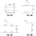
- FIG. 15Ais an example driver stage according to some embodiments described in this document.
- FIG. 15Bis an example balance stage according to some embodiments described in this document.
- FIG. 15Cis an example balance stage according to some embodiments described in this document.
- FIG. 15Dis an example balance stage according to some embodiments described in this document.
- FIG. 15Eis an example transformer stage according to some embodiments described in this document.
- FIG. 15Fis an example rectifier stage according to some embodiments described in this document.
- FIG. 16Ais an example filter stage according to some embodiments described in this document.
- FIG. 16Bis an example filter stage according to some embodiments described in this document.
- FIG. 16Cis an example filter stage according to some embodiments described in this document.
- FIG. 16Dis an example sink stage according to some embodiments described in this document.
- FIG. 17is an example circuit diagram that may comprise all or part of a pulse generator according to some embodiments described in this document.
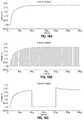
- FIGS. 18A, 18B and 18Care example graphs of an output pulse according to some embodiments described in this document.
- FIG. 19is an example pulse generator according to some embodiments described in this document.
- FIG. 20Ais an example circuit diagram of a portion of a pulse generator according to some embodiments described in this document.
- FIG. 20Bis an example of an output waveform produced from the pulse generator shown in FIG. 20A .
- FIG. 21Ais an example circuit diagram of a portion of a pulse generator according to some embodiments described in this document.
- FIG. 21Bis an example of an output waveform produced from the pulse generator shown in FIG. 21A .
- FIG. 22Ais an example circuit diagram of a portion of a pulse generator according to some embodiments described in this document.
- FIG. 22Bis an example of an output waveform produced from the pulse generator shown in FIG. 22A .
- FIG. 22Cis another example of an output waveform produced from the pulse generator shown in FIG. 22A .
- FIG. 23Ais an example circuit diagram of a portion of a pulse generator according to some embodiments described in this document.
- FIG. 23Bis an example of an output waveform produced from the pulse generator shown in FIG. 23A compared with the input waveform.
- FIG. 23Cis an example of an output waveform produced from the pulse generator shown in FIG. 23A compared with the input waveform.
- FIG. 24Ais an example circuit diagram of a portion of a pulse generator according to some embodiments described in this document.
- FIG. 24Bis an example of an output waveform produced from the pulse generator shown in FIG. 24A compared with the input waveform.
- FIG. 24Cis an example of an output waveform produced from the pulse generator shown in FIG. 24A compared with the input waveform.
- FIG. 25Ais an example circuit diagram 1200 of a portion pulse generator according to some embodiments described in this document.
- FIG. 25Bis an example of an output waveform produced from the pulse generator shown in FIG. 25A compared with the output waveform produced from the pulse generator shown in FIG. 24A .
- FIG. 26Ais an example circuit diagram of a portion of a pulse generator according to some embodiments described in this document.
- FIG. 26Bis an example of an output waveform produced from the pulse generator shown in FIG. 26A .
- FIG. 27Ais an example circuit diagram of a portion of a pulse generator according to some embodiments described in this document.
- FIG. 27Bis an example of an output waveform produced from the pulse generator shown in FIG. 27A .
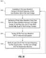
- FIG. 28is a flowchart of a process for producing an arbitrary pulse width output signal according to some embodiments described in this document.
- a resistive output stageis a collection of circuit elements that can be used to control the shape of a voltage waveform on a load.
- a resistive output stagemay include passive elements only (e.g., resistors, capacitors, inductors, etc.); and in other embodiments a resistive output stage may include active circuit elements (e.g., switches) as well as passive circuit elements.
- a resistive output stagefor example, can be used to control the voltage rise time of a waveform and/or the voltage fall time of waveform.
- examples of resistive output stagesare shown and are represented by different symbols such as R, Zp, ZL, ZC, etc. These are examples and should not be viewed as to limit the varieties of resistive output stages covered in the various embodiments described in this document.
- a resistive output stagecan discharge capacitive loads.
- these capacitive loadsmay have small capacitance (e.g., about 10 pF, 100 pF, 500 pF, 1 nF, 10 nF, 100 nF, etc.).
- a rapid dischargeis a pulse having a fall time that is shorter than about 1 ns, 10 ns, 50 ns, 100 ns, 250 ns, 500 ns, 1,000 ns, etc.
- a resistive output stagecan be used in circuits with pulses having a high pulse voltage (e.g., voltages greater than 1 kV, 10 kV, 20 kV, 50 kV, 100 kV, etc.), high frequencies (e.g., frequencies greater than 1 kHz, 10 kHz, 100 kHz, 200 kHz, 500 kHz, 1 MHz, etc.), fast rise times (e.g., rise times less than about 1 ns, 10 ns, 50 ns, 100 ns, 250 ns, 500 ns, 1,000 ns, etc.), fast fall times (e.g., fall times less than about 1 ns, 10 ns, 50 ns, 100 ns, 250 ns, 500 ns, 1,000 ns, etc.) and/or short pulse widths (e.g., pulse widths less than about 1,000 ns, 500 ns, 250 ns, 100 ns, 20 ns,
- the term “high voltage”may include a voltage greater than 1 kV, 10 kV, 20 kV, 50 kV, 100 kV, etc.; the term “high frequency” may be a frequency greater than 1 kHz, 10 kHz, 100 kHz, 200 kHz, 500 kHz, 1 MHz, etc.
- the term “fast rise time”may include a rise time less than about 1 ns, 10 ns, 50 ns, 100 ns, 250 ns, 500 ns, 1,000 ns, etc.;
- the term “fast fall time”may include a fall time less than about 1 ns, 10 ns, 50 ns, 100 ns, 250 ns, 500 ns, 1,000 ns, etc.); and the term short pulse width may include pulse widths less than about 1 ns, 10 ns, 50 ns, 100 ns, 250 ns, 500 ns, 1,000 ns, etc.).
- the term ‘rise time’may be understood to describe the application of voltage and/or charge/and/or energy and/or current to the circuit at the beginning of the pulse, irrespective of whether the pulse is positive going of negative going with respect to ground.
- the term ‘fall time’may be understood to describe the application of voltage and/or charge/and/or energy and/or current to the circuit at the end of the pulse, irrespective of whether the pulse is positive going of negative going with respect to ground.
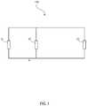
- FIG. 1is an example circuit 100 that can be used to control the voltage on a load ZL, which may be the circuit/system load.
- the load ZLmay be a capacitor, a capacitor in series with a resistor, a capacitor in series with an inductor, a dielectric barrier discharge, a plasma load, a semiconductor wafer processing load, and any arbitrary arrangement of capacitors, inductors, resistors, and/or other active and/or passive components, etc.
- the load ZLmay include any load that when voltage is applied, and charge is delivered, the charge/voltage may remain present for longer than desired (e.g., longer than the designed or desired fall time). For instance, this may often occur in high voltage switching applications.
- the switch S 1may be a single switch, a series stack of switches, a switching power supply, a pulser, a microsecond pulser, an arbitrary pulse generator, or any system that may be used to apply a high voltage, time varying power to the load ZL with the parameters noted above.
- the switch S 1can deliver pulses to the load (e.g., charge or power to the load ZL and/or establish a voltage on the load ZL) at high pulse voltage (e.g., voltages greater than 1 kV, 10 kV, 20 kV, 50 kV, 100 kV, etc.), high frequencies (e.g., frequencies greater than 1 kHz, 10 kHz, 100 kHz, 200 kHz, 500 kHz, 1 MHz, etc.), fast rise times (e.g., rise times less than about 1 ns, 10 ns, 50 ns, 100 ns, 250 ns, 500 ns, 1,000 ns, etc.), fast fall times (e.g., fall times less than about 1 ns, 10 ns, 50 ns, 100 ns, 250 ns, 500 ns, 1,000 ns, etc.) and/or short pulse widths (e.g., pulse widths less than about 1,000 ns
- the switch S 2may be a single switch, a series stack of switches, or any other arrangement of active elements that can be used to remove charge from the load ZL and/or reduce the voltage across the load ZL. In some embodiments, the switch S 2 may be used to remove charge from the load ZL when the switch S 1 is open. In some embodiments, the switch S 2 may be coupled with a resistor.
- FIG. 2is another example circuit 200 according to some embodiments.
- the switch S 1may be in series with a DC power supply P and/or may include a transformer or other circuit elements.
- the switch S 1can include a solid-state switch such as, for example, an IGBT, GaN, MOSFET, etc. switch.
- the switch S 2may be a switch (e.g., a high voltage switch), and the load ZL may be represented as a capacitive load CL.
- Pulses from the switch S 1 and the power supply Pmay be delivered in the following manner.
- switch S 1When the switch S 1 is closed and switch S 2 is open, charge is delivered to capacitive load CL and the voltage on the capacitive load CL increases to some value V, set by the power supply P.
- the switch S 1When the switch S 1 is opened, the charge/voltage will remain on capacitive load CL until the switch S 2 is closed and the voltage/charge is discharged from the capacitive load CL.
- the pulses from the switch S 1 and the power supply Pmay include high pulse voltage (e.g., voltages greater than 1 kV, 10 kV, 20 kV, 50 kV, 100 kV, etc.), high frequencies (e.g., frequencies greater than 1 kHz, 10 kHz, 100 kHz, 200 kHz, 500 kHz, 1 MHz, etc.), fast rise times (e.g., rise times less than about 1 ns, 10 ns, 50 ns, 100 ns, 250 ns, 500 ns, 1,000 ns, etc.), fast fall times (e.g., fall times less than about 1 ns, 10 ns, 50 ns, 100 ns, 250 ns, 500 ns, 1,000 ns, etc.) and/or short pulse widths (e.g., pulse widths less than about 1,000 ns, 500 ns, 250 ns, 100 ns, 20 ns, etc.).
- the switch S 1there may be an asymmetry between the switch S 1 and the switch S 2 .
- many different topologiescan be used to create a voltage source (the switch S 1 ) that has a high voltage output compared to the voltage hold off rating of the actual switches used.
- the switch S 1may include a 600 V switch combined with a 10:1 Step up transformer that together produces an output voltage of 6 kV.
- the switch S 2would need to be a 6 kV rated switch. While a 600 V switch may be common, a 6 kV switch is uncommon. In this example, the switch S 2 must hold off 6 kV until it is closed and removes the charge/voltage from the load CL.
- This asymmetry between the switch S 1 and the switch S 2may be especially problematic with solid-state switches, for example IGBTs, GaN switches, MOSFETs, etc. It can be even more problematic when fast switching transition times are required, and/or high frequency operation is required, and/or high voltage operation is required, since often switches with the required propertied do not exist.
- solid-state switchesfor example IGBTs, GaN switches, MOSFETs, etc. It can be even more problematic when fast switching transition times are required, and/or high frequency operation is required, and/or high voltage operation is required, since often switches with the required propertied do not exist.
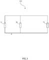
- FIG. 3is a circuit 300 , for example, that can be used to overcome the asymmetry between the switch S 1 and the switch S 2 , and/or the challenges of operating the switch S 2 at high frequency, high voltage, and/or with fast rise/fall times.
- the switch S 1may be a switch in series with a DC power supply (e.g., as shown in FIG. 2 ) and/or may include a transformer.
- the switch S 1for example, can include a solid-state switch such as, for example, an IGBT, GaN, MOSFET, etc. switch.
- the circuit element Zpmay comprise a resistive output stage that may include a combination of resistors, capacitors, diodes, and/or inductors.
- the circuit element Zpmay include a series and/or parallel arrangement of passive elements (i.e. resistors, capacitors, inductors, diodes, etc.). In some embodiments, Zp may be purely resistive in nature. In some embodiments, the circuit element Zp may replace the functionality of the switch S 2 . For example, the circuit element Zp may allow charge and/or voltage to be removed from the load ZL at high frequency, high voltage, fast rise times, and/or fast fall times. In terms of voltage, frequency, rise time, and fall time, passive elements may have fewer constraints compared with solid state switches.
- FIG. 4is an example circuit 400 where circuit element Zp is represented as a resistor R.
- the switch S 1closes and establishes a voltage V across capacitive load CL that is set by the power supply P. While the switch S 1 is closed, power supply P may maintain the voltage V across resistor R and load CL. Once the switch S 1 opens, the charge/voltage on the capacitive load CL can be removed by the resistor R, on a timescale set by the product of (R) and (CL) which is commonly simply known as an RC timescale. If R was 100 Ohms and C was 1 nF than the characteristic voltage fall time given by RC would be 100 ns.
- the resistor Rcan operate in a high voltage, high frequency, fast rise time, and/or fast fall time parameter space within which few to no switches can operate.
- resistor Rcan remove charge/voltage from capacitive load CL at 6 kV, 100 kHz, and/or with a 100 ns fall time.
- Resistor Rcould be selected to remove charge at high pulse voltage (e.g., voltages greater than 1 kV, 10 kV, 20 kV, 50 kV, 100 kV, etc.), high frequencies (e.g., frequencies greater than 1 kHz, 10 kHz, 100 kHz, 200 kHz, 500 kHz, 1 MHz, etc.), fast rise times (e.g., rise times less than about 1 ns, 10 ns, 50 ns, 100 ns, 250 ns, 500 ns, 1,000 ns, etc.), fast fall times (e.g., fall times less than about 1 ns, 10 ns, 50 ns, 100 ns, 250 ns, 500 ns, 1,000 ns, etc.) and/or short pulse widths (e.
- a resistive output stagecan be useful for pulses with voltages greater than about 1.5 kV, frequencies greater than about 10 kHz, pulses widths less than about 100 ⁇ s, and/or rise and fall times shorter than about 1 ⁇ s.
- a resistive output stagecan be useful, for example, where the load ZL contains capacitances (e.g., including stray, equivalent, effective, etc., or things that would be modeled as capacitances) with values smaller than 1 ⁇ F.
- a resistive output stagecan be used with a high voltage pulser for the production of plasmas (which will typically have the plasma and/or electrode/grid scale size less than 1 m or an electrode grid scale less than about 1 square meter) or involve grids and plates with scale sizes less than 1 m.
- FIG. 5is another example circuit 500 .
- circuit element Zpincludes resistor R in series with inductor L.
- Inductor Lfor example, can be selected to create a faster fall time and/or faster rise time than could be achieved for a given value of R.
- circuit element Zpcan be used to remove voltage/charge from a load ZL in a parameter space not readily accessible to solid-state switches.
- This parameter spacemay include pulses with high pulse voltage (e.g., voltages greater than 1 kV, 10 kV, 20 kV, 50 kV, 100 kV, etc.), high frequencies (e.g., frequencies greater than 1 kHz, 10 kHz, 100 kHz, 200 kHz, 500 kHz, 1 MHz, etc.), fast rise times (e.g., rise times less than about 1 ns, 10 ns, 50 ns, 100 ns, 250 ns, 500 ns, 1,000 ns, etc.), fast fall times (e.g., fall times less than about 1 ns, 10 ns, 50 ns, 100 ns, 250 ns, 500 ns, 1,000 ns, etc.) and/or short pulse widths (e.g., pulse widths less than
- voltage waveformscan be produced with a single switch (or single group of switches) when other topologies might require two-switches (or two groups of switches) to achieve a similar result.
- a single switch (or single group of switches) on the inputcan provide a solution to a problem that generally requires two-switches to solve.
- the set of loads ZL where the circuit element Zp may be applicablemay include loads that generally have a sufficiently high impedance that the load holds charge/voltage for a longer timescale than desired (e.g., where desired time scales are on the order of 1 ns, 10 ns, 50 ns, 100 ns, 250 ns, 500 ns, 1,000 ns, etc.).
- circuit element Zpmay allow for rapid removal of this charge/voltage to achieve fast fall times, high frequencies, and/or short pulses.
- a loadmay include capacitive loads, electrodes, plasma loads, dielectric barriers, semiconductor fabrication plasmas, semiconductor loads, grids, medical loads, etc.
- Such loadsmay, for example, have a high impedance compared to the timescale on which charge/voltage needs to be removed from them, such that the load itself does not naturally produce the needed voltage/charge removal timescale.
- a loadmay have stray elements that have a high impedance compared to the timescale on which charge/voltage needs to be removed from them. For example, if the load ZL is non-capacitive, but the load ZL is associated with a parallel stray capacitance, then circuit element Zp can be used to remove charge/voltage from the stray capacitance, thus allowing the voltage on the load ZL to fall.
- a resistive output stagemay, for example, allow for the sinking of current from the load, and when used in combination with a high voltage pulser that sources current, allows the equivalent low voltage sourcing and sinking power supply to be realized, but at high voltage, high frequency with short pulse widths and/or fast rise times and/or fast fall times.
- the use of a resistive output stage to achieve high voltage pulses at high frequencies that have fast rise/fall times, and short pulse widthsmay constrain the selection of the circuit elements in the resistive output sage.
- the resistive output stagemay be selected to handle high average power, high peak power, fast rise times and/or fast fall times.
- the average power ratingmight be greater than about 0.5 kW, 1.0 kW, 10 kW, 25 kW, etc.
- the peak power ratingmight be greater than about 1 kW, 10 kW, 100 kW, 1 MW, etc.
- the rise and fall timesmight be less than 1000 ns, 100 ns, 10 ns, or 1 ns.
- the high average power and/or peak power requirementmay arise both from the need to dissipate stored energy in the load rapidly, and/or the need to do so at high frequency.
- the loadis capacitive in nature, with a 1 nF capacitance that needs discharging in 20 ns, and if the resistive output stage may be purely resistive, the resistive output stage may have a resistance value of about 20 Ohms.
- the total per pulse energy dissipation of 2.2 Jmay result in an average power dissipation of 22 kW into the resistive output stage.
- Standard pulldown resistorsthat are used in TTL type electrical circuits and/or data acquisition type circuits (e.g., around 5 volts) usually operate far below 1 W for both average and peak power dissipation.
- the ratio of the power the resistive output stage dissipates compared to the total power dissipated by the loadmay be 10%, 20% 30% or greater, for example.
- pull down resistorsdissipate less than 1% of the power consumed, and typically much less.
- the fast rise time and/or fast fall time requirementsmay constrain both the allowable stray inductance and/or stray capacitance within the resistive output stage.
- the series stray inductance in the resistive output stagemay be less than around 300 nH.
- the resistive output stagemay not waste significant additional energy due to its stray capacitance, for example, less than 10% of the capacitive energy stored in the load capacitance, then the stray capacitance of the resistive output stage may be less than 100 pF.
- the designgenerally requires significant parallel and series operation using numerous discrete components (e.g., resistors), with the components tightly grouped together, and/or spaced far from any grounded surfaces that could significantly increase the stray capacitance.
- a resistive output stage circuitcan be used in a dielectric barrier discharge device being driven with a high voltage pulser.
- the load in a dielectric barrier dischargecan be dominantly capacitive.
- the loadmay be modeled as a purely capacitive load CL, for example, like a dielectric barrier discharge. For example, when the power supply P is switched on, capacitive load CL may be charged, when power supply P is not switched on, the charge on capacitive load CL may be drained through resistor R.
- a resistive output stagemay need to discharge a significant amount of charge from the capacitive load CL quickly, which may not be the case with low voltage applications (e.g., standard 5 V logic levels and or low voltage data pulsers).
- a typical dielectric barrier discharge devicemight have a capacitance of about 10 pF and/or may be driven to about 20 kV with about a 20 ns rise time and/or about a 20 ns fall time.
- the desired pulse widthmight be 80 ns long.
- a circuit element Zpof about 2 kOhms can be used to create the desired fall time.
- Various other values for the circuit element Zpmay be used depending on the load and/or the other circuit elements and/or the requirements rise time, fall time, and/or pulse width, etc.
- the characteristic pulse fall timecan be designated as t f and the pulse rise time can be designated by t r .
- the rise time t rcan be set by the specifics of the driving power supply.
- the circuit element Zpcan be specifically selected to provide a specific relation between the pulse rise time t r and the pulse fall time t f . This is different from the concept of a pull down resistor, where in general, a pull down resistor is selected to carry/dissipate voltage/charge on some longer time scale, and at much lower power levels. Circuit element Zp, in some embodiments, can be specifically used as an alternative to a pull down switch, to establish a specific relation between the pulse rise time t r and the pulse fall time t f .
- circuit element Zpis a resistor R
- circuit element Zpmay be designed to ensure the proper fall time t f yet be capable of handling high power such as, for example, power greater than about 1.0 kW, or 100 kW.
- the resistormay handle the average power requirements as well as peak power requirements.
- the need for fast fall time t f resulting in low resistance values and the resulting high power dissipationare challenges that can make resistive output stages undesirable as a way to quickly remove charge from a capacitive load CL.
- a resistor Rcan include a resistor with low resistance and yet have a high average power rating and peak power rating.
- the resistor Rmay include a parallel stack of resistors that collectively have the required resistance and power rating.
- the resistor Rmay include a resistor have a resistance less than about 2000 ohms, 500 ohms, 250 ohms, 100 ohms, 50 ohms, 25 ohms, 10 ohms, 1 ohm, 0.5 ohms, 0.25 ohms, etc., and have an average power rating greater than about 0.5 kW, 1.0 kW, 10 kW, 25 kW, etc., and have a peak power rating greater than about 1 kW, 10 kW, 100 kW, 1 MW, etc.
- each pulse applied to the loadmay dissipate 16 mJ once the capacitance in the load is fully charged. Once the pulse is turned off, charge from the load is dissipated by Zp. If operated at 100 kHz, then circuit element Zp may dissipate 1.6 kW. If circuit element Zp had been selected to create a 10 ns t f , then the power dissipated in circuit element Zp would be 3.2 kW.
- the power dissipated in the circuit element Zpcan be considered large if it exceeds 10% or 20% of the power consumed by the load ZL.
- circuit element Zpfor example, includes a resistor R in series with an inductor L
- inductor Lcan, for example, reduce the power flow into the resistor R while the voltage V is present and/or hasten the fall time beyond that set by an RC decay.
- the time constant L/Rcan be set to approximately the pulse width t p , for example, L/R ⁇ t p . This, for example, may reduce energy dissipation and/or shorten the fall time t f , (e.g., decreases t f ).
- R ⁇ C/t f ⁇ C/t rassuming one wanted to match t f to t r .
- the symbol “ ⁇ ”means within a factor of ten.—
- a load ZLcan include a circuit that controls the ion energy in a plasma chamber of a semiconductor wafer fabrication device.
- FIG. 6 , FIG. 7 , FIG. 9 , and FIG. 11 and FIG. 13each represent introducing high voltage pulses into a plasma.
- Some of these example circuitsapply high voltage pulses in a manner that controls the ion energy within the plasma, and specifically that controls the energy the ions have as they exit the plasma and impact, for example, a wafer or other substrate that bounds the plasma.
- FIG. 6is one example of a circuit 600 representing a circuit used to set the ion energy in a plasma chamber of a semiconductor wafer fabrication device.
- the driving waveformmay include high voltage and high frequency short pulses with a high duty cycle and fast rise times and fall times. The pulses create a negative bias within the plasma that accelerates ions to the desired potential, prior to their impact with a wafer.
- An example of such a waveformis shown as waveform 810 in FIG. 8 .
- waveform 810a steady negative bias of approximately ⁇ 4 kV is realized, through the use of short positive going pulses shown by waveform 805 .
- the driving waveform to the plasmamay include any circuit described in this document where the plasma is the load.
- the capacitor C 2represents the capacitance of the dielectric material upon which a semiconductor wafer sits during fabrication.
- the capacitor C 3represents the sheath capacitance between a semiconductor surface and a plasma.
- the current source I 1represents the current of positive ions moving from the plasma toward the surface of the wafer. In this example, a portion of the plasma is electrically connected to ground. Thus, a negative electric potential in the plasma between ground and the surface of the wafer will induce positive ions to flow and impact the surface of the wafer.
- the capacitor C 1represents the capacitance of leads running into the chamber, as well as other stray capacitive elements.
- capacitor C 1may have a capacitance of about 40-4,000 pF (e.g., 400 pF), capacitor C 2 may have a capacitance of about 0.7-70 nF (e.g., 7 nF), capacitor C 3 may have a capacitance of about 10-1,000 pF (e.g., 100 pF), and current source I 1 may produce current of about 300 mA-30 A (e.g., 3 A).
- Various other valuesmay be used. Component values within an order of magnitude or so of these element values given may also be used.
- the capacitance of the capacitor C 1is almost the same size as the capacitance of the capacitor C 3 ; and the capacitance of the capacitor C 2 is large in comparison with the capacitance of the capacitor C 3 .
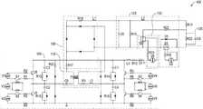
- FIG. 7is a circuit diagram of circuit 700 that includes a pulser 705 , a resistive output stage 710 , that produces high voltage pluses in a plasma represented by circuit 600 .
- the resistive output stage 710includes inductor L 1 and resistor R 1 .
- the circuit elements to the left of inductor L 1 and resistor R 1comprise one representation of a high voltage pulser 705 .
- the high voltage pulser 705can produce a plurality of high voltage pulses with a high frequency and fast rise times and fall times.
- the high voltage pulsermay comprise a nanosecond pulser.
- the various values of the circuit elements in circuit 700 and/or the circuit 600may vary.
- the value of capacitor C 3may be about 150 pF
- the value of capacitor C 1may be about 400 pF
- the value of capacitor C 2may be about 8 nF
- the value of inductor L 2may be about 300 nH
- the value of resistor R 1may be about 150 Ohms
- the value of inductor L 1may be about 6 uH
- the value of DC power supply V 1may be about 5 kV
- the value of current source I 1may be about 2 A. Values within an order of magnitude or so of these values may also be used.
- FIG. 8shows example waveforms produced in circuit 700 .
- the pulse waveform 805may represent the voltage provided by the pulser stage 705 .
- the pulse waveform 805produces a pulse with the following qualities: high voltage (e.g., greater than about 4 kV as shown in the waveform), a fast rise time (e.g., less than about 200 ns as shown in the waveform), a fast fall time (e.g., less than about 200 ns as shown in the waveform), and short pulse width (e.g., less than about 300 ns as shown in the waveform).
- high voltagee.g., greater than about 4 kV as shown in the waveform
- a fast rise timee.g., less than about 200 ns as shown in the waveform
- a fast fall timee.g., less than about 200 ns as shown in the waveform
- short pulse widthe.g., less than about 300 ns as shown in the waveform.
- the waveform 810may represent the voltage at the surface of a wafer represented in circuit 700 by the point between capacitor C 2 and capacitor C 3 or the voltage across capacitor C 3 .
- the pulse waveform 815represent the current flowing from the pulser 705 to the plasma.
- the circuit 700may or may not include either or both diodes D 1 or D 2 .
- the high voltage pulses from the pulser 705charge the capacitor C 2 . Because the capacitance of capacitor C 2 is large compared to the capacitance of capacitor C 3 and/or capacitor C 1 , and and/or because of the short pulse widths of the pulses, the capacitor C 2 may take a number of pulses from the high voltage pulser to fully charge. Once the capacitor C 2 is charged the circuit reaches a steady state, as shown by the waveforms in FIG. 8 .
- the capacitor C 2In steady state and when the switch S 1 is open, the capacitor C 2 is charged and slowly dissipates through the resistive output stage 710 , as shown by the slightly rising slope of waveform 810 .
- the voltage at the surface of the waver(the point between capacitor C 2 and capacitor C 3 ) is negative. This negative voltage may be the negative value of the voltage of the pulses provided by the pulser 705 .
- the voltage of each pulseis about 4 kV; and the steady state voltage at the wafer is about ⁇ 4 kV.
- the voltage across the capacitor C 2may flip (the pulse from the pulser is high as shown in waveform 805 ) as the capacitor C 2 is charged.
- the voltage at the point between capacitor C 2 and capacitor C 3e.g., at the surface of the wafer
- the pulses from the high voltage pulserproduce a plasma potential (e.g., a potential in a plasma) that rise from a negative high voltage to zero and returns to the negative high voltage at high frequencies, with fast rise times, fast fall times, and/or short pulse widths.
- the action of the resistive output stagemay rapidly discharge the stray capacitance C 1 , and may allow the voltage at the point between capacitor C 2 and capacitor C 3 to rapidly return to its steady negative value of about ⁇ 4 kV as shown by waveform 810 .
- the resistive output stagemay allow the voltage at the point between capacitor C 2 and capacitor C 3 to exists for about 90% of the time, and thus maximizes the time which ions are accelerated into the wafer.
- the components contained within the resistive output stagemay be specifically selected to optimize the time during which the ions are accelerated into the wafer, and to hold the voltage during this time approximately constant. Thus, for example, a short pulse with fast rise time and a fast fall time may be useful, so there can be a long period of fairly uniform negative potential.
- FIG. 9shows another example circuit 900 according to some embodiments.
- the circuit 900can be generalized into three stages (these stages could be broken down into other stages or generalized into fewer stages).
- the circuit 900includes pulser stage 905 , a lead stage 910 , and a load stage 915 .
- the pulser stage 905may include pulser and transformer stage 906 and a resistive output stage 907 .
- the load stage 915may include a capacitive load C 12 .
- the capacitance of the capacitive load C 12may be on the order of about 10 pF.
- Some examples of a capacitive loadmay include a dielectric barrier discharge, a semiconductor fabrication device, a capacitive device, a photoconductive switch, a dielectric barrier discharge device, etc.
- C 12may be a high voltage grid for ion beams, neutral beams, or any other accelerator or grid for producing rapidly changing electric fields.
- the capacitor C 12may be a stripline kicker.
- the pulser stage 905may include a pulser and transformer stage 906 .
- the pulser and transformer stage 906may produce pulses with high pulse voltage (e.g., voltages greater than 1 kV, 10 kV, 20 kV, 50 kV, 100 kV, etc.), high frequencies (e.g., frequencies greater than 1 kHz, 10 kHz, 100 kHz, 200 kHz, 500 kHz, 1 MHz, etc.), fast rise times (e.g., rise times less than about 1 ns, 10 ns, 50 ns, 100 ns, 250 ns, 500 ns, 1,000 ns, etc.), fast fall times (e.g., fall times less than about 1 ns, 10 ns, 50 ns, 100 ns, 250 ns, 500 ns, 1,000 ns, etc.) and/or short pulse widths (e.g., pulse widths less than about 1,000 ns, 500 ns, 250 n
- the resistive output stage 907includes three resistors: resistor R 1 , resistor R 2 , and resistor R 4 .
- resistor R 1 and resistor R 2may have the same resistance values.
- resistor R 1 and resistor R 2can be selected for a number of purposes.
- resistor R 1 and resistor R 2can have resistance levels selected to limit the current flowing from the pulser stage 905 to the load stage 915 .
- resistor R 1 and resistor R 2can have resistance levels selected to determine the rise time t r and the fall time t f , which may also depend on the inductance in the lead stage 910 (e.g., inductor L 2 and inductor L 6 ) and/or the capacitance of the load stage (e.g., capacitance C 12 ).
- the resistance values of resistor R 1 and resistor R 2can be set based on a specific application.
- resistor R 1 and resistor R 2can be used to protect against load shorts such that all the current from the pulse and transformer circuit 906 can be dissipated in resistor R 1 and resistor R 2 .
- resistor R 2 and/or inductor L 6may be set to approximately zero, such that their side of C 12 can be ground referenced.
- a pulse from the pulser and transformer stage 905may charge the capacitive load C 12 in the load stage 915 . While the pulse is charging the capacitive load C 12 , most of the current may charge the capacitive load C 12 , and some current may flow through resistor R 4 . Once the capacitive load C 12 is fully charged, most if not all the current flows through resistor R 4 . Because of the high voltages applied by the pulser and transformer stage 905 and noting that the power dissipated through resistor R 4 is inversely proportional to the resistance of resistor R 4 , resistor R 4 may have a high power rating (e.g., both average power and peak power).
- the resistance value of R 4can be selected in conjunction with the value of the load capacitance C 12 so that the fall time t f can be fast e.g., less than 1 ns, 10 ns, 50 ns, 100 ns, 250 ns, 500 ns, 1,000 ns, etc.
- FIG. 10is another example circuit 1000 according to some embodiments.
- the circuit 1000can be generalized into five stages (these stages could be broken down into other stages or generalized into fewer stages).
- the circuit 1000includes pulser and transformer stage 906 , a resistive output stage 1007 , a lead stage 910 , load crowbar stage 1010 , and a load stage 1015 .
- the pulser and transformer stage 906are as described in FIG. 9 .
- the resistive output stage 1007may include a blocking diode D 1 that can ensure that current from the load stage 1015 (or from anywhere else) does not flow back into the pulser and transformer stage 906 .
- the capacitor C 4may represent the stray capacitance of the blocking diode D 1 .
- the resistive output stage 1007may include one or more inductive elements represented by inductor L 1 , inductor L 2 , inductor L 8 , and/or inductor L 10 . These inductive elements may, for example, limit current flow from the capacitive load in the load stage 1015 .
- the resistor R 2may dissipate charge from the capacitive load C 1 in the load stage 1015 , for example, on fast time scales (e.g., 1 ns, 10 ns, 50 ns, 100 ns, 250 ns, 500 ns, 1,000 ns, etc. time scales).
- the resistance of resistor R 2may be low to ensure the pulse across the load stage 1015 has a fast fall time t, for example a fall time less than 1 ns, 10 ns, 100 ns, or 1000 ns.
- the inductive elements, for example, inductor L 2may limit the current flow through resistor R 2 , and may increase the overall circuit efficiency.
- the load crowbar stage 1010includes a diode D 5 which may ensure that the current to the load stage 1015 does not reverse polarity.
- the stray inductance of the crowbar stage 1010is represented by L 7 and the stray capacitance of the diode D 5 is represented by C 9 .
- stray resistance of the crowbar stage 1010may be represented by resistor R 4 . Resistance R 4 may be intentionally added to create voltage waveforms of a particular desired shape across load 1015 .
- the load stage 1015may include either or both resistive and capacitance elements represented by resistor R 1 and capacitor C 1 .
- the capacitance of capacitor C 1may, for example, be on the order of about 10 nF.
- Some examples of a capacitive and resistive loadmay include a charging a capacitor for energy storage purposes in a photoconductive switch which may be used to produce high power microwaves. In such circuits, it is important that the load capacitance only be charged for short periods of time, and the resistive output stage provides a path to rapidly remove (sink) charge from the load should it not otherwise be removed by the action of other circuit elements that are not shown in this figure.
- the resistive output stagemay also ensure that the voltage across C 1 is constant at the start of every charge cycle, assuming the charge repetition rate is slow compared to the discharge rate of C 1 through the resistive output stage. In this example, the resistive output stage rapidly returns the potential across C 1 to zero.
- FIG. 11shows another example circuit 1100 according to some embodiments.
- the circuit 1100can be generalized into five stages (these stages could be broken down into other stages or generalized into fewer stages).
- the circuit 1100includes pulser and transformer stage 906 , a resistive output stage 1107 , a lead stage 910 , a DC bias power supply stage 1110 , and a load stage 1115 .
- the load stage 1115may represent an effective circuit for a plasma deposition system, plasma etch system, or plasma sputtering system.
- the capacitance C 2may represent the capacitance of the dielectric material upon which a wafer may sit.
- the capacitor C 3may represent the sheath capacitance of the plasma to the wafer.
- the capacitor C 9may represent capacitance within the plasma between a chamber wall and the top surface of the wafer.
- the current source I 2 and the current source I 1may represent the ion current through the sheath.
- the resistive output stage 1107may include one or more inductive elements represented by inductor L 1 and/or inductor L 5 .
- the inductor L 5may represent the stray inductance of the leads in the resistive output stage 1107 .
- Inductor L 1may be set to minimize the power that flows directly from the high voltage supply 906 into resistor R 1 .
- the resistor R 1may dissipate charge from the load stage 1115 , for example, on fast time scales (e.g., 1 ns, 10 ns, 50 ns, 100 ns, 250 ns, 500 ns, 1,000 ns, etc. time scales).
- the resistance of resistor R 1may be low to ensure the pulse across the load stage 1115 has a fast fall time t f .
- the resistor R 1may include a plurality of resistors arranged in series and/or parallel.
- the capacitor C 11may represent the stray capacitance of the resistor R 1 including the capacitance of the arrangement series and/or parallel resistors.
- the capacitance of stray capacitance C 11may be less than 500 pF, 250 pF, 100 pF, 50 pF, 10 pF, 1 pF, etc.
- the capacitance of stray capacitance C 11may be less than the load capacitance such as, for example, less than the capacitance of C 2 , C 3 , and/or C 9 .
- a plurality of pulser and transformer stages 906can be ganged up in parallel and coupled with the resistive output stage 1107 across the inductor L 1 and/or the resistor R 1 .
- Each of the plurality of pulser and transformer stages 906may each also include diode D 1 and/or diode D 6 .
- the capacitor C 8may represent the stray capacitance of the blocking diode D 1 . In some embodiments, the capacitor C 4 may represent the stray capacitance of the diode D 6 .
- the DC bias power supply stage 1110may include DC a voltage source V 1 that can be used to bias the output voltage either positively or negatively.
- the capacitor C 12isolates/separates the DC bias voltage from the resistive output stage and other circuit elements. It allows for a potential shift from one portion of the circuit to another. In some applications the potential shift it establishes is used to hold a wafer in place.
- Resistance R 2may protect/isolate the DC bias supply from the high voltage pulsed output from circuit component group 906
- FIG. 12shows another example circuit 1200 according to some embodiments.
- Circuit 1200is similar to circuit 900 shown in FIG. 9 .
- Resistive output stage 1207includes switch S 2 , which may open and close based on a signal from voltage supply V 1 .
- the switch S 2may be open while the load stage 915 is being charged by a signal from the pulser and transformer stage 906 such as, for example, when the switch(s) S 1 in pulser and transformer stage 906 is closed.
- the switch S 2may be closed to discharge any charge in the load stage 915 such as, for example, when the switch(s) S 1 in pulser and transformer stage 906 is open.
- Resistor R 1 and resistor R 2may be small, and may represent stray resistance contained within conductors and cables. Resistor R 4 may be selected to set a particular fall time for the energy/voltage dissipation from the load.
- resistor R 2 and inductor L 6may be about zero. This may allow the low side to be ground referenced, and may effectively create a single sided circuit topology instead of the differential output topology shown.
- FIG. 13shows another example circuit 1300 .
- Circuit 1300is similar to circuit 1100 shown in FIG. 11 .
- Resistive output stage 1307includes switch S 2 , which may open and close based on a signal from voltage supply V 1 .
- the switch S 2may be open while the load stage 1115 is being charged by a signal from the pulser and transformer stage 906 such as, for example, when the switch(s) S 1 in pulser and transformer stage 906 is closed.
- the switch S 2may be closed to discharge any charge in the load stage 1115 such as, for example, when the switch(s) S 1 in pulser and transformer stage 906 is open.
- the switch S 2may be required to switch quickly.
- the resistor R 1may be selected to realize particular circuit rise times and/or fall times.
- the switch S 2 described in FIG. 12 and/or FIG. 13may include a high voltage switch.
- a high voltage switchmay include a plurality of solid-state switches arranged in series.
- Some embodimentsinclude a high voltage switching power supply (e.g., switch S 1 in FIG. 1 and FIG. 3 , switch S 1 and power supply P 1 in FIG. 2 , FIG. 4 , and FIG. 5 , FIG. 7 , FIG., switch S 2 and power supply V 2 in FIGS. 9-13 ).
- a high voltage switching power supplye.g., switch S 1 in FIG. 1 and FIG. 3 , switch S 1 and power supply P 1 in FIG. 2 , FIG. 4 , and FIG. 5 , FIG. 7 , FIG., switch S 2 and power supply V 2 in FIGS. 9-13 ).
- Any type of high voltage switching power supplymay be used that can produce high voltages at high frequencies with fast rise times and fast fall times.
- One example of a high voltage switching power supplyincludes nanosecond pulsers described in U.S. patent application Ser. Nos. 14/542,487, 14/635,991, and 14/798,154, which are incorporated into this document in their entirety for all purposes. Other examples
- a systemcan include a pulse generator that is galvanically isolated.
- a high voltage pulse generatormay also smooth a high frequency input signal to generate a high voltage output signal that has a voltage higher than the input signal.
- the input signalmay include at least one of a high frequency, fast rise times, and fast fall times.
- the high frequency of the input signalmay be five to ten times greater than the output signal.
- the higher the input frequency of the input signalthe smoother the output signal.
- the pulse generatormay generate high voltage pulses with fast rise times of various types such as, for example, square waves, sinusoidal waves, triangular waves, arbitrary waves, long single pulses, multiple pulses, etc.
- a pulse generatormay generate high voltage pulses having an arbitrary waveform that has a fast rise time (e.g., less than 1 ⁇ s). In some embodiments, a pulse generator may generate a high voltage pulses that have a variable duty cycle or user controlled duty cycle.
- a pulse generatorcan output high voltage greater than 0.5 kV, 1.0 kV, 2.0 kV, 5.0 kV, 10 kV, 15 kV, 20 kV, 25 kV, 50 kV, 100 kV, or 1,000 kV.
- the input signalmay be greater than about 50 kHz or 100 kHz.
- Embodiments described within this documentdo not include, for example, DC-DC converters, despite that some embodiments may be capable of generating a DC output.
- a pulse generatordoes not simply convert a source of direct current (DC) from one voltage level to another.
- embodiments described within this documentare different than other pulse generators and/or different than DC-DC converters.
- embodiments described within this documentare not optimized for converting direct current from one voltage to another level.
- a pulse generatormay produce pulses with long pulse widths, fast rise times, and/or fast fall times, but does not in general produce a DC output signal. Instead, some embodiments described within this document may produce high voltage pulses with fast rise times and/or fast fall times.
- Some embodiments described within this documentmay produce high voltage pulses having a long high voltage pulse or with a long pulse width that have a fast rise time and/or a fast fall time. Some embodiments described within this document may produce high frequency and high voltage pulses with any waveform shape. As another example, embodiments described within this document may produce one or more waveforms and/or signals with specifically designated very low frequency components as well as waveforms with specifically designated very high frequency components. Moreover, in some embodiments, a pulse generator may produce waveforms that are galvanically isolated from a reference potential (e.g., ground).
- a reference potentiale.g., ground
- FIG. 14is an example block diagram of a pulse generator 100 according to some embodiments.
- the pulse generator 100may include one or more stages or blocks as shown in the figure. One or more of these stages may be removed, replaced with another stage, and/or combined with another stage.
- a driver stage 105that includes any components or devices that may push or pull current.
- the driver stage 105is coupled with a balance stage 110 .
- the balance stage 110can be used, for example, to keep a transformer stage 115 from saturating due to imbalanced current.
- the driver stagemay include one or more energy sources, switches, bridges, etc.
- the one or more switchesmay include, for example, one or more IGBTs, switches, solid state switches, MOSFET, may be used to switch the energy source.
- the driver stagemay include a waveform generator that may be used to produce an input waveform.
- a waveform that is to be amplifiedmay be provided to the driver from an external source.
- an IGBT circuit(s)may be used with the driver stage 105 such as, for example, the IGBT circuit discussed in U.S. patent application Ser. No. 13/345,906, entitled Efficient IGBT Switching the entirety of which is incorporated by reference in its entirety.
- the driver stage 105may include an H-bridge, a half bridge, or a full bridge.
- An example of a full bridge configurationis shown in FIG. 17 .
- Any number of configurations of input sourcesmay be used without limitation.
- Various other configurations or circuitsmay be included such as, for example, resonant topologies and push-pull topologies.
- the driver stage 105may have a low total inductance.
- the driver stage 105may have a total inductance below 1,000 nH.
- the inductance of all components, circuits, elements, etc. prior to a transformer or transformers of a transformer stagemay have a total inductance less than 1,000 nH.
- the inductance of all components, circuits, elements, etc. including the primary winding of one of more transformers of the transformer stage 115may have an inductance less than 1,000 nH.
- the inductance of all components, circuits, elements, etc. om the driver stage 105 and the balance stage 110may have a total inductance less than 1,000 nH.
- the driver stage 105may have a total inductance below 1,000 nH. In some specific embodiments, the inductance of all components, circuits, elements, etc. prior to a transformer or transformers of a transformer stage may have a total inductance less than 1,000 nH. In some specific embodiments, the inductance of all components, circuits, elements, etc. including the primary winding of one of more transformers of the transformer stage 115 may have an inductance less than 1,000 nH. In some specific embodiments, the inductance of all components, circuits, elements, etc. om the driver stage 105 and the balance stage 110 may have a total inductance less than 1,000 nH.
- the balance stage 110may also be coupled with the transformer stage 115 that may include one or more transformers each having any number of coils.
- the transformer stage 115may also increase the voltage from the driver stage 105 and/or the balance stage 110 depending on the number of winds on either side of the transformer stage 115 .
- the transformer stage 115may provide, for example, galvanic isolation between the driver stage 105 and the output stage 135 .
- the transformer stage 115may also provide, for example, step up from the input voltage provided by the driver stage 105 to an increased voltage output.
- the transformer stage 115may be coupled with a rectifier stage 120 .
- the filter stage 125may be coupled with the rectifier stage 120 .
- the filter stage 125may include any number of components such as, for example, active components (e.g., switches, diodes, etc.) and/or passive components (e.g., inductors, capacitors, resistors, etc.)
- the transformer stagemay include a transformer that transforms an input signal into a high voltage output signal.
- the high voltage output signalmay have a voltage of 500 volts, 1,000 volts, 2000 volts, 10,000 volts and/or 100,000 volts, or higher.
- the sink stage 130may be placed after the filter stage 125 as shown in FIG. 14 or placed before the filter stage 125 .
- the sink stage 130may, for example, dump energy, sink current, and/or rapidly reverse current flow of any energy stored in the filter stage 125 and/or the output stage 135 .
- the output stage 135may be coupled with the sink stage 130 as shown in FIG. 14 or may be coupled with the filter stage 125 and/or the rectifier stage 120 .
- the output stage 135may include the load and/or the device to which the output signal is sent.
- the output stage 135may be galvanically isolated form a reference signal, from ground, and/or from the driver stage 105 .
- the output stagecan be floating or biased to any potential desired (e.g., with the DC bias stage 140 ).
- the output stage 135may output a signal with a rise time of less than 100 ns and/or a fall time of less than 100 ns.
- the DC bias stage 140may be coupled with the output stage 135 and may include any voltage source and/or power source.
- the DC bias stage 140may be connected with a reference signal, ground, and/or the driver stage. In some embodiments, the DC bias stage 140 may reference the potential of the output stage 135 to the potential of the driver stage 105 of the pulse generator 100 .
- the DC bias stage 140may be coupled to the rectifier stage 120 , the filter stage 125 , the sink stage 130 , and/or the output stage 135 .
- the DC bias stage 140for example, may be of any polarity and/or may include any voltage.
- the DC bias stage 140may provide a DC bias signal, for example, having a voltage greater than 0.01 kV, 0.1 kV, 1 kV, 3 kV, 10 kV, 30 kV, or 100 kV. In some specific embodiments, the DC bias voltage may be greater than 0.1 kV or 1 kV.
- FIG. 15Ais an example driver stage 105 according to some embodiments described in this document.
- the driver stage 105may include any device or components that may push or pull current in the pulse generator 100 .
- the driver stage 105may include one or more high voltage power supplies or voltage sources that may provide an input voltage of 50 volts, 100 volts, 200 volts, 300 volts, 400 volts, 500 volts, 600 volts, 700 volts, 800 volts, 900 volts, etc. to over 4500 volts.
- the driver stage 105may include one or more solid state switches such as, for example, one or more IGBTs and/or one or more MOSFETs that can be used to the switch the high voltage power supply.
- the solid state switchesmay operate at voltages up to 2 kV or up to 4.5 kV.
- the driver stage 105may include one or more H-bridge circuits and/or half-bridge circuits operated in parallel.
- Each H-bridge circuitmay include, for example, one or more solid state switches.
- the driver stage 105may or may not be coupled with a reference signal and/or with ground potential.
- the one or more solid state switchesmay switch at a frequency of 0.1 kHz, 1 kHz, 10 kHz, 100 kHz, 1,000 kHz, 10,000 kHz, etc.
- the stray inductance, L 1 and L 2 , of the driver stage 105 singularly or in combinationmay be less than 1 nH, 10 nH, 100 nH, 1,000 nH, 10,000 nH, etc.
- the stray inductance L 1 and/or L 2may be less than 100 nH or 1,000 nH.
- the stray inductance, L 1 and L 2may represent and/or include all inductance such as, for example, stray inductance in the circuit, inductors, inductance in components, etc.
- the driver stage 105may include one or more power sources that may provide voltage at 50 volts, 100 volts, 200 volts, 300 volts, 400 volts, 500 volts, 600 volts, 700 volts, 800 volts, 900 volts, etc. to over 4500 volts.
- the voltage provided by the one or more power sources in the driver stage 105may be greater than 100 V or 500 V.
- FIG. 15Bis an example balance stage 110 according to some embodiments described in this document.
- the balance stage 110is not used and/or may not include, for example, any active or passive components except, possibly, a connection between the driver stage 105 and the transformer stage.
- FIG. 15Cis another example balance stage 110 according to some embodiments described in this document.
- the balance stage 110includes blocking capacitor C 1 , which may keep the transformer stage 115 from saturating due to imbalanced current from the driver stage 105 .
- the blocking capacitor C 1may have a capacitance value of greater than 1 ⁇ F, 10 ⁇ F, 100 ⁇ F, 1,000 ⁇ F, 10,000 ⁇ F, etc.
- FIG. 15Dis another example balance stage 110 according to some embodiments described in this document.
- the balance stage 110includes blocking capacitor C 2 and blocking capacitor C 3 , which may keep the transformer stage 115 from saturating due to imbalanced current from the driver stage 105 .
- the blocking capacitor C 2may have a capacitance value of greater than 1 ⁇ F, 10 ⁇ F, 100 ⁇ F, 1,000 ⁇ F, 10,000 ⁇ F, etc.
- the blocking capacitor C 3may have a capacitance value of greater than 1 ⁇ F, 10 ⁇ F, 100 ⁇ F, 1,000 ⁇ F, 10,000 ⁇ F, etc.
- FIG. 15Eis an example transformer stage 115 according to some embodiments described in this document.
- the transformer stage 115may include one or more transformers.
- a transformer of the transformer stage 115may step up the voltage provided by the driver stage 105 to a higher voltage such as for example, over 500 volts, 1500 volts, 2500 volts, 50,000 volts, 250,000 volts, etc.
- the transformermay include a primary side 116 and a secondary side 117 .
- the primary side 116may have a total effective series stray inductance L 3 and L 4 that may have an inductance singularly or in combination of less than 10 nH, 100 nH, 1,000 nH, or 10,000 nH. In some specific embodiments, the total effective series stray inductance L 3 and L 4 may be less than 1,000 nH.
- the secondary side 117may have a total effective parallel stray capacitance C 4 of less than 1 pF, 10 pF, 100 pF, 1,000 pF, 10,000 pF, etc. In some specific embodiments, the total effective parallel stray capacitance C 4 may be less than 100 pF or 1,000 pF.
- the transformer stage 115may comprise any type of transformer.
- the transformermay include primary windings on the primary side 116 and secondary windings on the secondary side 117 that are both wrapped around a magnetic core such as, for example, a ferrite core.
- the ratio (N s /N p ) of the number secondary windings (N s ) to the number of primary windings (N p )may be greater than 2, 4, 5, 5.5, 8, 10, 150, 600, etc.
- the transformer stage 115may include one or more transformers arranged in parallel with each other.
- the transformer stage 115may output a voltage greater than 1 kV, 2 kV, 5 kV, 10 kV, 30 kV, 100 kV, 300 kV, or 1,000 kV.
- FIG. 15Fis an example rectifier stage 120 according to some embodiments described in this document.
- the rectifier stage 120may include, for example, total effective series stray inductance L 5 and L 6 singularly or in combination of less than 10 nH, 100 nH, 1,000 nH, 10,000 nH, etc.
- the effective series stray inductance L 5 and L 6 singularly or in combinationmay be less than 1,000 nH.
- the effective series stray inductance L 5 and L 6 singularly or in combinationmay be less than 100 nH.
- the rectifier stage 120may include total effective parallel stray capacitance C 5 of less than 1 pF, 10 pF, 100 pF, 1,000 pF, 10,000 pF, etc. In some specific embodiments, the capacitance of the total effective parallel stray capacitance C 5 may be less than 1,000 pF. In some specific embodiments, the capacitance of the total effective parallel stray capacitance C 5 may be less than 200 pF.
- the rectifier stage 120may also include a plurality of diodes, that may be used in series and/or parallel configurations that are designed and have specifications sufficient for high voltage and/or high power applications.
- the rectifier stage 120may include any type of rectifier such as, for example, a single phase rectifier, a single phase half wave rectifier, a single phase full wave rectifier, a full wave rectifier, a three-phase rectifier, a three-phase half wave circuit, a three-phase bridge rectifier, a two pulse bridge, a twelve pulse bridge, etc. In some embodiments, more than one rectifier may be used in series and/or parallel.
- the filter stage 125may include a number of different configurations depending on the type of specification and/or application. Three examples are shown in FIG. 16A , FIG. 16B , and FIG. 16C .
- the filtermay include only passive elements such as, for example, inductors, capacitors, resistors, etc. Various other configurations may be used.
- FIG. 16Ais an example filter stage 125 according to some embodiments described in this document.
- the filter stage 125does not include any components.
- the output of the rectifier stage 120may be tied directly with the output stage 135 and/or the load.
- This filter stagemay be used to produce an output signal that includes at least one of fast rise times, fast fall times, and high frequencies, etc.
- FIG. 16Bis an example filter stage 125 according to some embodiments described in this document.
- the filter stage 125may include total effective series inductance L 7 and L 8 singularly or in combination of less than 0.1 ⁇ H, 1 ⁇ H, 10 ⁇ H, 100 ⁇ H, 1,000 ⁇ H, 10,000 ⁇ H, etc. In some specific embodiments, the total effective series inductance L 7 and L 8 singularly or in combination may be less than 30 ⁇ H.
- the filter stage 125may include total effective parallel capacitance C 6 of less than 0.01 nF, 0.1 nF, 1 nF, 10 nF, 100 nF, 1,000 nF, etc. In some specific embodiments, the total effective parallel capacitance C 6 may be less than 300 ⁇ F or 30 ⁇ F. This configuration, for example, may be used to smooth an input waveform provided by the driver stage 105 and/or allow for an arbitrary waveform.
- FIG. 16Cis an example filter stage 125 according to some embodiments described in this document.
- the filter stage 125may include total effective series inductance L 9 and L 10 singularly or in combination of less than 0.1 ⁇ H, 1 ⁇ H, 10 ⁇ H, 100 ⁇ H, 1,000 ⁇ H, 10,000 ⁇ H, etc.
- the total effective series inductance L 9 and L 10 singularly or in combinationmay be less than 30 ⁇ H.
- the filter stage 125may include total effective parallel capacitance C 7 of less than 0.01 nF, 0.1 nF, 1 nF, 10 nF, 100 nF, 1,000 nF, etc. In some specific embodiments, the total effective parallel capacitance C 7 may be less than 300 ⁇ H or 30 ⁇ H.
- the filter stage 125may include, for example, total effective parallel resistance R 1 and R 2 singularly or in combination of less than 0.1 Ohms, 1 Ohms, 10 Ohms, or 100 Ohms. In some specific embodiments, the total effective parallel resistance R 1 and R 2 singularly or in combination may be less than 10 Ohms or less than 1 Ohm. This configuration, for example, may be used to smooth an input waveform provided by the driver stage 105 and/or allow for an arbitrary waveform.
- filter stage 125may be used.
- FIG. 16Dis an example sink stage 130 according to some embodiments described in this document.
- Sink stage 130may include a switch S 1 and a resistance R 3 .
- the resistance R 3may include stray resistance and/or a resistor that may be used to limit the current flowing through switch S 1 .
- the sink stage 130may rapidly dump energy that may be stored in the filter stage 125 and/or the output stage 135 such as, for example, any energy stored in a capacitor in the filter stage 125 and/or the output stage 135 .
- the sink stage 130may be located between the filter stage 125 and the rectifier stage 120 . In other embodiments the sink stage 130 may be disposed between the filter stage 125 and the output stage 135 .
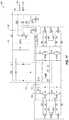
- FIG. 17is an example circuit diagram 400 that may comprise all or part of a pulse generator according to some embodiments described in this document.
- the circuit diagram 400includes driver stage 105 , transformer stage 115 , rectifier stage 120 , filter stage 125 , sink stage 130 , and output stage 135 .
- the output stage 135can be galvanically isolated from ground, from the driver stage, and/or from any reference potential.
- the filter stage 125includes a switch S 5 .
- the output of the rectifier stage 120can then be directly switched by the switch S 5 .
- the sink stage 130may include switch S 6 .
- switch S 5 and switch S 6may be fast switches that open and close within 1 ⁇ s or faster.
- the switch S 5 and/or the switch S 6are switches that may operate at high frequencies.
- DC powercan be sourced to the output stage 135 (or the load R 22 and/or R 11 ).
- a graph of the voltage over time at the output stage 135is shown in FIG. 18A . If switch S 5 is switched on and off, then a pulsed waveform can be sourced to the output stage 135 as shown in FIG. 18B and FIG. 18C .
- Switch S 6can be opened when switch S 5 closes and closed when switch S 5 opens. When switch S 6 is closed, capacitance can be drained from the load capacitance represented as C 8 .
- the switches used by switch S 5 and/or switch S 6may operate at high power, high frequency, with variable duty cycle, at variable pulse widths, etc.
- Switch S 5 and/or switch S 6may include one or more solid state switches such as, for example, one or more MOSFETs and/or one or more IGBTs. Moreover, in some embodiments, switch S 5 and/or switch S 6 may also include one or more switches stacked, arranged in parallel, and/or arranged in series.
- a controllermay be included that controls the operation and/or timing of switch S 5 and/or switch S 6 as the duty cycle, pulse width, and/or frequency are changed and to ensure that switch S 5 is closed when switch S 6 is open and vice-versa.
- These switchesmay include solid state switches and/or IGBT circuits discussed in U.S. patent application Ser. No. 13/345,906, entitled Efficient IGBT Switching the entirety of which is incorporated into this document by reference in its entirety.
- the emitter of switch S 5 and/or switch S 6may not be referenced back to ground. That is, the emitter of switch S 5 and/or switch S 6 may be galvanically isolated from all or part of the circuit. Moreover, the gate of switch S 5 and/or switch S 6 may be isolated using a fiber optic receiver and/or a fiber optic device.
- the size, shape, frequency, and/or duty cycle of pulses produced by the pulse generatormay be controllable (or varied by user input).
- the pulsescan vary from a DC output to a 10 MHz output with duty cycles from 0% to 100%.
- the galvanic isolationallows the output waveform potential to be set to arbitrary potential levels with respect to other system potentials.
- galvanic isolationmay be 500 V, 1 kV, 2 kV, 3 kV, 5 kV, 10 kV, 20 kV, 100 kV, etc. with respect to other potentials.
- Some embodimentsinclude a combination of two or more output stages to both provide and to sink high power and/or currents to and from the load. The combination of output stages may allow for precise control of arbitrary pulses to be delivered to both resistive and capacitive loads.
- FIGS. 18A, 18B and 18Cillustrate the variability of the output from a pulse generator.
- FIG. 18Ais an example graph of a DC output pulse of over 2 kV.
- FIG. 18Bis an example graph of an output pulse of over 2 kV pulsing at 100 kHz.
- FIG. 18Cis an example graph of an output pulse of over 2 kV pulsing at 5 kHz.
- Various other frequencies and/or amplitudesmay be output using embodiments described in this document.
- FIG. 19is an example pulse generator according to some embodiments described in this document.
- the pulse generatorincludes an output stage 135 , a rectifier stage 120 , a transformer stage 115 , and a driver stage 105 .
- FIG. 20Ais an example circuit diagram 700 of a portion of a pulse generator according to some embodiments described in this document.
- the circuit diagram 700shows a transformer stage 115 that includes a 1:5.5 transformer.
- the circuit diagram 700also shows a rectifier stage 120 , a filter stage 125 , and an output stage 135 .
- the filter stage 125 in this exampleincludes circuit elements that include two 125 ⁇ H inductors and two 10 ohm resistors. While this example shows specific circuit elements with specific values, various other elements may be included.
- the output stage 135includes a 250 Ohm load with 2 nF capacitance.
- FIG. 20Bis an example of an output waveform produced from the portion of a pulse generator shown in FIG. 20A .
- the input waveformmay include a low voltage (e.g., less than 200 V) input square waveform that may be provided via V CH and/or the driver stage 105 .
- the input square waveform in this examplewas square wave with 5 ⁇ s pulse widths such as, for example, the waveform shown in FIG. 24A .
- the output waveformhas an approximately 2 ⁇ s rise time and/or a very clean pulse.
- FIG. 21Ais an example circuit diagram 800 of a portion of a pulse generator according to some embodiments described in this document.
- the circuit diagram 800shows a transformer stage 115 that includes a 1:5.5 transformer.
- the circuit diagram 800also shows a rectifier stage 120 , a filter stage 125 , and an output stage 135 .
- the filter stage 125 in this exampleincludes circuit elements that include two 480 ⁇ H inductors and two 10 ohm resistors. While this example shows specific circuit elements with specific values, various other elements may be included.
- the output stage 135includes a 1 kOhm load with 470 pF capacitance.
- FIG. 21Bis an example of an output waveform produced from the pulse generator shown in FIG. 21A .
- the input waveformmay include a low voltage (e.g., less than 200 V) input square waveform that may be provided via V CH and/or the driver stage 105 .
- the input square waveform in this examplewas square wave with 5 ⁇ s pulse widths such as, for example, the waveform shown in FIG. 24A .
- the output waveformhas an approximately 2 ⁇ s rise time and/or a relatively clean pulse.
- FIG. 22Ais an example circuit diagram 900 of a portion of a pulse generator according to some embodiments described in this document.
- the circuit diagram 900shows a transformer stage 115 that includes a 1:5.5 transformer.
- the circuit diagram 900also shows a rectifier stage 120 and an output stage 135 , but no filter stage 125 .
- the output stage 135includes a 250 Ohm load.
- FIG. 22Bis an example of an output waveform produced from the pulse generator shown in FIG. 22A compared with the input waveform.
- a 200 V input square wave (dashed)was provided via V CH .
- the output waveform (solid)has a very sharp rise time and maintains a relatively clean flat top with some slight ripple.
- FIG. 22Cis an example of an output waveform produced from the pulse generator shown in FIG. 22A compared with the input waveform into the transformer stage 115 .
- the input waveformmay include a low voltage (e.g., less than 200 V) input square waveform that may be provided via V CH .
- the output waveformhas a very sharp rise time and maintains a relatively clean flat top with some slight ripple.
- FIG. 23Ais an example circuit diagram 1 , 000 of a portion of a pulse generator according to some embodiments described in this document.
- the circuit diagram 1 , 000shows a transformer stage 115 that includes a 1:5.5 transformer.
- the circuit diagram 1 , 000also shows a rectifier stage 120 , a filter stage 125 , and an output stage 135 .
- the filter stage 125 in this exampleincludes circuit elements that include two 450 ⁇ H inductors. While this example shows specific circuit elements with specific values, various other elements may be included.
- the output stage 135includes a 250 Ohm load.
- FIG. 23Bis an example of an output waveform produced from the pulse generator shown in FIG. 23A compared with the input waveform.
- a 200 V input square wave (dashed)was provided via V CH .
- the output waveform (solid)has a sharp rise time and maintains a clean flat top with some slight ripple.
- FIG. 23Cis an example of an output waveform produced from the pulse generator shown in FIG. 23A compared with the input waveform.
- a 200 V input wave (dashed) with an arbitrary shapewas provided via V CH .
- the output waveformhas a very sharp rise time and maintains a relatively clean flat top with some slight ripple.
- FIG. 24Ais an example circuit diagram 1100 of a portion of a pulse generator according to some embodiments described in this document.
- the circuit diagram 1100shows a transformer stage 115 that includes a 1:5.5 transformer.
- the circuit diagram 1100also shows a rectifier stage 120 , a filter stage 125 , and an output stage 135 .
- the filter stage 125 in this exampleincludes circuit elements that include two 125 ⁇ H inductors and two 10 ohm resistors. While this example shows specific circuit elements with specific values, various other elements may be included.
- the output stage 135includes a 250 Ohm load with 2 nF capacitance.
- FIG. 24Bis an example of an output waveform produced from the pulse generator shown in FIG. 24A compared with the input waveform.
- a 200 V input square wave (dashed)was provided via V CH .
- the output waveform (solid)has a sharp rise time and maintains a clean flat top with very little ripple.
- FIG. 24Cis an example of an output waveform produced from the pulse generator shown in FIG. 24A compared with the input waveform with the load resistor, R L , replaced with a 1 kOhm resistor.
- the output waveformis substantially similar yet with the waveform in FIG. 24B but with a higher overshoot and with more ringing.
- FIG. 25Ais an example circuit diagram 1200 of a portion of a pulse generator according to some embodiments described in this document.
- the circuit diagram 1200shows a transformer stage 115 that includes a 1:5.5 transformer.
- the circuit diagram 1200also shows a rectifier stage 120 , a filter stage 125 , and an output stage 135 .
- the filter stage 125 in this exampleincludes circuit elements that include a single 125 ⁇ H inductor and a single 10 ohm resistor. While this example shows specific circuit elements with specific values, various other elements may be included.
- the output stage 135includes a 250 Ohm load with 2 nF capacitance.
- FIG. 25Bis an example of an output waveform produced from the pulse generator shown in FIG. 25A compared with the output waveform produced from the pulse generator shown in FIG. 24A .
- the removal of one inductor and one resistorcan provide for a faster rise time and/or a higher output voltage.
- Some embodimentsinclude a pulse generator that produces a square wave with one or more of the following waveform specifications: a frequency range of 0.1 Hz to 10 MHz, a pulse width range of 10 ns to 10 ⁇ s, a rise time (and/or a fall time) of 1 ns to 100 ⁇ s, a duty cycle between 0 and 100%, a flat top ripple range between 0 and 200%, and an output voltage of more than 1 kV, 2 kV, 5 kV, 10 kV, 30 kV, 100 kV, 300 kV, 1,000 kV.
- Embodiments described within this documentmay include a pulse generator that produces an arbitrary and/or variable waveform with one or more of the following waveform specifications: a frequency range of 0.1 Hz to 10 MHz, a pulse width range of 10 ns to 10 ⁇ s, a rise time and/or a fall time of 1 ns to 100 ⁇ s, a duty cycle between 0 and 100%, a dI/dt between 10 A/s to 1,000 kA/ ⁇ s and an output voltage of more than 1 kV, 2 kV, 5 kV, 10 kV, 30 kV, 100 kV, 300 kV, 1,000 kV.
- Embodiments described within this documentmay include a pulse generator that produces both high frequency pulses (e.g., pulses with a frequency greater than 10 kHz) and low frequency pulses (e.g., pulses with a frequency less than 1 Hz or a DC pulse). Such a pulse generator may also output voltages above 2 kV.
- high frequency pulsese.g., pulses with a frequency greater than 10 kHz
- low frequency pulsese.g., pulses with a frequency less than 1 Hz or a DC pulse.
- Such a pulse generatormay also output voltages above 2 kV.
- Embodiments described within this documentmay include a pulse generator that produces a high voltage DC pulse with a rise time of less than 10 ⁇ s (or a rise time less than 1 ⁇ s), an output voltage greater than 1 kV, and/or a ripple between 2% and 50%.
- FIG. 26Ais an example circuit diagram 1300 of a portion of a pulse generator according to some embodiments described in this document.
- the circuit diagram 1300shows a transformer stage 115 that includes a 1:5.5 transformer.
- the circuit diagram 1300also shows a rectifier stage 120 and an output stage 135 , but no filter stage 125 .
- the output stage 135includes a 250 Ohm load.
- FIG. 26Bis an example of an output waveform compared with the input waveform.
- a 50 V input square wave(dashed) was provided via V CH .
- the output waveform(solid) has a very sharp rise time (e.g., about 50 ns) and has a high duty cycle (e.g., about 70%).
- Various other duty cyclesmay be used such as, for example, duty cycles of any percentage between 0% and 100%. In some embodiments, the duty cycle may change over time.
- FIG. 27Ais an example circuit diagram 1400 of a portion of a pulse generator according to some embodiments described in this document.
- the circuit diagram 1400shows a transformer stage 115 that includes a 1:5.5 transformer.
- the circuit diagram 1400also shows a rectifier stage 120 and an output stage 145 , but no filter stage 125 .
- the output stage 145includes a 250 Ohm load.
- FIG. 27Bis an example of an output triangular wave waveform compared with the square wave input waveform.
- a 200 V input square wave(dashed) was provided via V CH .
- the triangular wave output waveform(solid) has a gradual rise time (e.g., about 4 ⁇ s) and a gradual fall time, which creates the triangular wave shape.
- the output waveformhas an amplitude of 1,000 volts.
- a pulse generatormay produce a plurality of pulses at high frequency (e.g., greater than 2 kHz) and high voltage (e.g., greater than 2 kV) for a period of time, pause for a period of time, and then begin pulsing at another frequency or the same frequency and high voltage for another period of time.
- the pulse generatormay repeat this process over and over again.
- the frequency and/or voltage of each set of pulsesmay vary.
- the various pulse generators described in this documentmay generate high voltage pulses (greater than 2 kV), with fast rise times (e.g., less than 100 ns) as well as with long and/or variable pulse widths and/or variable duty cycles. Pulse generators often cannot generate pulses that are a combination of fast features (e.g., fast rise times) and slow features (e.g., long pulses). Some embodiments described in this document can combine fast features with slow features.
- FIG. 28is a flowchart of a process 1500 for producing an arbitrary pulse width output signal according to some embodiments described in this document.
- Process 1500begins at block 1505 where a first input waveform is generated that has a first input frequency, a first input duration, and a first input voltage.
- the first input waveformmay be generated from the driver stage 105 .
- the first input waveformmay have a voltage of 200 volts to 2,000 volts and/or has a frequency greater than 10 kHz.
- the first durationmay include any period of time.
- the first durationmay be longer than two periods of the first input frequency.
- the first durationmay be between 10 ⁇ s and 10 seconds.
- a first output waveformis generated from the first output waveform having at least one of a first output voltage, a fast rise time, and/or a pulse width substantially equal to the first input duration.
- the first output voltagemay be directly proportional with the first input voltage.
- the first output voltagemay be greater than 2 kV.
- the fast rise timemay include a rise time less than about 5 ⁇ s or less than about 100 ns. Various other fast rise times and/or output voltages may be used.
- the first input waveformmay be turned off for a second input duration.
- the first input waveformmay be considered turned off when the waveform produces zero volts or a voltage at a DC bias voltage level.
- the second input durationmay include any period of time.
- the second input durationmay be longer than the rise time and/or the first input duration.
- the second input durationmay be less than one period of the first input frequency.
- the second input durationmay include any period of time.
- At block 1520at least one of the first input frequency, the first input duration, the first input voltage, and the second input duration may be modified so a subsequent pulse may have a different output voltage, a different output duration, and/or a different period of time when the pulse produces zero volts or a voltage at a DC bias level.
- the process 1500may be repeated any number of times without limitation.
- none of the first input duration, the first input voltage, and the second input durationmay be modified in block 1520 .
- the fast switching found in the driver stage 105 and the low inductance in various stages of a pulse generatormay allow for fast rise times and/or variable pulse widths.
- Embodiments described within this documentmay also produce, for example, high voltage pulses with variable duty cycle and/or variable frequency.
- more than one pulse generatormay be combined in any combination such as, for example, in serial and/or in parallel.
- two pulse generatorsmay be used with opposite polarities and configured substantially identically to create a square wave.
Landscapes
- Physics & Mathematics (AREA)
- Engineering & Computer Science (AREA)
- Plasma & Fusion (AREA)
- Chemical & Material Sciences (AREA)
- Analytical Chemistry (AREA)
- Plasma Technology (AREA)
Abstract
Description
Claims (25)
Priority Applications (2)
| Application Number | Priority Date | Filing Date | Title |
|---|---|---|---|
| US16/599,318US10847346B2 (en) | 2014-02-28 | 2019-10-11 | High voltage resistive output stage circuit |
| US17/098,207US11631573B2 (en) | 2014-02-28 | 2020-11-13 | High voltage resistive output stage circuit |
Applications Claiming Priority (8)
| Application Number | Priority Date | Filing Date | Title |
|---|---|---|---|
| US201461946457P | 2014-02-28 | 2014-02-28 | |
| US14/635,991US9706630B2 (en) | 2014-02-28 | 2015-03-02 | Galvanically isolated output variable pulse generator disclosure |
| US201762480115P | 2017-03-31 | 2017-03-31 | |
| US15/623,464US10224822B2 (en) | 2014-02-28 | 2017-06-15 | Nanosecond pulser |
| US15/941,731US10460910B2 (en) | 2017-03-31 | 2018-03-30 | High voltage resistive output stage circuit |
| US16/178,538US10460911B2 (en) | 2017-03-31 | 2018-11-01 | High voltage resistive output stage circuit |
| US16/250,765US10483089B2 (en) | 2014-02-28 | 2019-01-17 | High voltage resistive output stage circuit |
| US16/599,318US10847346B2 (en) | 2014-02-28 | 2019-10-11 | High voltage resistive output stage circuit |
Related Parent Applications (1)
| Application Number | Title | Priority Date | Filing Date |
|---|---|---|---|
| US16/250,765ContinuationUS10483089B2 (en) | 2014-02-28 | 2019-01-17 | High voltage resistive output stage circuit |
Related Child Applications (1)
| Application Number | Title | Priority Date | Filing Date |
|---|---|---|---|
| US17/098,207ContinuationUS11631573B2 (en) | 2014-02-28 | 2020-11-13 | High voltage resistive output stage circuit |
Publications (2)
| Publication Number | Publication Date |
|---|---|
| US20200043702A1 US20200043702A1 (en) | 2020-02-06 |
| US10847346B2true US10847346B2 (en) | 2020-11-24 |
Family
ID=66532554
Family Applications (3)
| Application Number | Title | Priority Date | Filing Date |
|---|---|---|---|
| US16/250,765ActiveUS10483089B2 (en) | 2014-02-28 | 2019-01-17 | High voltage resistive output stage circuit |
| US16/599,318ActiveUS10847346B2 (en) | 2014-02-28 | 2019-10-11 | High voltage resistive output stage circuit |
| US17/098,207Active2036-02-22US11631573B2 (en) | 2014-02-28 | 2020-11-13 | High voltage resistive output stage circuit |
Family Applications Before (1)
| Application Number | Title | Priority Date | Filing Date |
|---|---|---|---|
| US16/250,765ActiveUS10483089B2 (en) | 2014-02-28 | 2019-01-17 | High voltage resistive output stage circuit |
Family Applications After (1)
| Application Number | Title | Priority Date | Filing Date |
|---|---|---|---|
| US17/098,207Active2036-02-22US11631573B2 (en) | 2014-02-28 | 2020-11-13 | High voltage resistive output stage circuit |
Country Status (1)
| Country | Link |
|---|---|
| US (3) | US10483089B2 (en) |
Cited By (21)
| Publication number | Priority date | Publication date | Assignee | Title |
|---|---|---|---|---|
| US11284500B2 (en) | 2018-05-10 | 2022-03-22 | Applied Materials, Inc. | Method of controlling ion energy distribution using a pulse generator |
| US11462388B2 (en) | 2020-07-31 | 2022-10-04 | Applied Materials, Inc. | Plasma processing assembly using pulsed-voltage and radio-frequency power |
| US11476090B1 (en) | 2021-08-24 | 2022-10-18 | Applied Materials, Inc. | Voltage pulse time-domain multiplexing |
| US11476145B2 (en) | 2018-11-20 | 2022-10-18 | Applied Materials, Inc. | Automatic ESC bias compensation when using pulsed DC bias |
| US11495470B1 (en) | 2021-04-16 | 2022-11-08 | Applied Materials, Inc. | Method of enhancing etching selectivity using a pulsed plasma |
| US11508554B2 (en) | 2019-01-24 | 2022-11-22 | Applied Materials, Inc. | High voltage filter assembly |
| US11569066B2 (en) | 2021-06-23 | 2023-01-31 | Applied Materials, Inc. | Pulsed voltage source for plasma processing applications |
| US11699572B2 (en) | 2019-01-22 | 2023-07-11 | Applied Materials, Inc. | Feedback loop for controlling a pulsed voltage waveform |
| US11776788B2 (en) | 2021-06-28 | 2023-10-03 | Applied Materials, Inc. | Pulsed voltage boost for substrate processing |
| US11791138B2 (en) | 2021-05-12 | 2023-10-17 | Applied Materials, Inc. | Automatic electrostatic chuck bias compensation during plasma processing |
| US11798790B2 (en) | 2020-11-16 | 2023-10-24 | Applied Materials, Inc. | Apparatus and methods for controlling ion energy distribution |
| US11810760B2 (en) | 2021-06-16 | 2023-11-07 | Applied Materials, Inc. | Apparatus and method of ion current compensation |
| US11901157B2 (en) | 2020-11-16 | 2024-02-13 | Applied Materials, Inc. | Apparatus and methods for controlling ion energy distribution |
| US11948780B2 (en) | 2021-05-12 | 2024-04-02 | Applied Materials, Inc. | Automatic electrostatic chuck bias compensation during plasma processing |
| US11967483B2 (en) | 2021-06-02 | 2024-04-23 | Applied Materials, Inc. | Plasma excitation with ion energy control |
| US11972924B2 (en) | 2022-06-08 | 2024-04-30 | Applied Materials, Inc. | Pulsed voltage source for plasma processing applications |
| US12106938B2 (en) | 2021-09-14 | 2024-10-01 | Applied Materials, Inc. | Distortion current mitigation in a radio frequency plasma processing chamber |
| US12111341B2 (en) | 2022-10-05 | 2024-10-08 | Applied Materials, Inc. | In-situ electric field detection method and apparatus |
| US12198966B2 (en) | 2017-09-20 | 2025-01-14 | Applied Materials, Inc. | Substrate support with multiple embedded electrodes |
| US12272524B2 (en) | 2022-09-19 | 2025-04-08 | Applied Materials, Inc. | Wideband variable impedance load for high volume manufacturing qualification and on-site diagnostics |
| US12315732B2 (en) | 2022-06-10 | 2025-05-27 | Applied Materials, Inc. | Method and apparatus for etching a semiconductor substrate in a plasma etch chamber |
Families Citing this family (34)
| Publication number | Priority date | Publication date | Assignee | Title |
|---|---|---|---|---|
| US10892140B2 (en) | 2018-07-27 | 2021-01-12 | Eagle Harbor Technologies, Inc. | Nanosecond pulser bias compensation |
| US11171568B2 (en) | 2017-02-07 | 2021-11-09 | Eagle Harbor Technologies, Inc. | Transformer resonant converter |
| EP4210223A1 (en) | 2013-11-14 | 2023-07-12 | Eagle Harbor Technologies, Inc. | High voltage nanosecond pulser |
| US11539352B2 (en) | 2013-11-14 | 2022-12-27 | Eagle Harbor Technologies, Inc. | Transformer resonant converter |
| US10978955B2 (en) | 2014-02-28 | 2021-04-13 | Eagle Harbor Technologies, Inc. | Nanosecond pulser bias compensation |
| US10020800B2 (en) | 2013-11-14 | 2018-07-10 | Eagle Harbor Technologies, Inc. | High voltage nanosecond pulser with variable pulse width and pulse repetition frequency |
| US10483089B2 (en)* | 2014-02-28 | 2019-11-19 | Eagle Harbor Technologies, Inc. | High voltage resistive output stage circuit |
| US10903047B2 (en)* | 2018-07-27 | 2021-01-26 | Eagle Harbor Technologies, Inc. | Precise plasma control system |
| US11430635B2 (en) | 2018-07-27 | 2022-08-30 | Eagle Harbor Technologies, Inc. | Precise plasma control system |
| US11824454B2 (en)* | 2016-06-21 | 2023-11-21 | Eagle Harbor Technologies, Inc. | Wafer biasing in a plasma chamber |
| US11004660B2 (en)* | 2018-11-30 | 2021-05-11 | Eagle Harbor Technologies, Inc. | Variable output impedance RF generator |
| KR102757507B1 (en)* | 2017-02-13 | 2025-01-20 | 삼성전자주식회사 | Reverse voltage monitoring circuit capable of reducing power consumption and Semiconductor device having the same |
| CN117200759A (en)* | 2017-03-31 | 2023-12-08 | 鹰港科技有限公司 | High voltage resistive output stage circuit |
| JP6902167B2 (en) | 2017-08-25 | 2021-07-14 | イーグル ハーバー テクノロジーズ, インク.Eagle Harbor Technologies, Inc. | Generation of arbitrary waveforms using nanosecond pulses |
| CN110504149B (en)* | 2018-05-17 | 2022-04-22 | 北京北方华创微电子装备有限公司 | Pulse modulation system and method of radio frequency power supply |
| US11810761B2 (en) | 2018-07-27 | 2023-11-07 | Eagle Harbor Technologies, Inc. | Nanosecond pulser ADC system |
| US11532457B2 (en) | 2018-07-27 | 2022-12-20 | Eagle Harbor Technologies, Inc. | Precise plasma control system |
| US11222767B2 (en) | 2018-07-27 | 2022-01-11 | Eagle Harbor Technologies, Inc. | Nanosecond pulser bias compensation |
| US11302518B2 (en) | 2018-07-27 | 2022-04-12 | Eagle Harbor Technologies, Inc. | Efficient energy recovery in a nanosecond pulser circuit |
| JP7038901B2 (en) | 2018-08-10 | 2022-03-18 | イーグル ハーバー テクノロジーズ,インク. | Plasma sheath control for RF plasma reactor |
| KR20210111841A (en) | 2019-01-08 | 2021-09-13 | 이글 하버 테크놀로지스, 인코포레이티드 | Efficient Energy Recovery in Nanosecond Pulser Circuits |
| US20210029815A1 (en) | 2019-07-02 | 2021-01-28 | Eagle Harbor Technologies, Inc. | Nanosecond pulser rf isolation |
| TWI778449B (en) | 2019-11-15 | 2022-09-21 | 美商鷹港科技股份有限公司 | High voltage pulsing circuit |
| EP4082036B1 (en)* | 2019-12-24 | 2025-01-22 | Eagle Harbor Technologies, Inc. | Nanosecond pulser rf isolation for plasma systems |
| JP7439302B2 (en) | 2020-05-12 | 2024-02-27 | イーグル ハーバー テクノロジーズ,インク. | High frequency RF generator and DC pulsing |
| US11967484B2 (en) | 2020-07-09 | 2024-04-23 | Eagle Harbor Technologies, Inc. | Ion current droop compensation |
| US20220399185A1 (en) | 2021-06-09 | 2022-12-15 | Applied Materials, Inc. | Plasma chamber and chamber component cleaning methods |
| US12394596B2 (en) | 2021-06-09 | 2025-08-19 | Applied Materials, Inc. | Plasma uniformity control in pulsed DC plasma chamber |
| DE102021124377A1 (en)* | 2021-09-21 | 2023-03-23 | Cinogy Gmbh | Electrode arrangement for a plasma discharge |
| US20230132339A1 (en)* | 2021-10-21 | 2023-04-27 | Applied Materials, Inc. | Plasma processing chambers configured for tunable substrate and edge sheath control |
| US11824542B1 (en) | 2022-06-29 | 2023-11-21 | Eagle Harbor Technologies, Inc. | Bipolar high voltage pulser |
| EP4336541A1 (en)* | 2022-09-12 | 2024-03-13 | TRUMPF Huettinger Sp. Z o. o. | Energy refeeding module, switching circuit and embodiment, plasma processing system, and a method of producing rectangular voltage output pulses for a plasma processing load |
| KR20250084155A (en) | 2022-09-29 | 2025-06-10 | 이글 하버 테크놀로지스, 인코포레이티드 | High voltage plasma control |
| US20250046576A1 (en)* | 2023-08-04 | 2025-02-06 | Applied Materials, Inc. | Plasma processing assembly for rf and pvt integration |
Citations (104)
| Publication number | Priority date | Publication date | Assignee | Title |
|---|---|---|---|---|
| US4070589A (en) | 1976-10-29 | 1978-01-24 | The Singer Company | High speed-high voltage switching with low power consumption |
| US4504895A (en) | 1982-11-03 | 1985-03-12 | General Electric Company | Regulated dc-dc converter using a resonating transformer |
| EP0174164A2 (en) | 1984-09-01 | 1986-03-12 | GEC-Marconi Limited | A pulse generator |
| US4992919A (en) | 1989-12-29 | 1991-02-12 | Lee Chu Quon | Parallel resonant converter with zero voltage switching |
| US5140510A (en) | 1991-03-04 | 1992-08-18 | Motorola, Inc. | Constant frequency power converter |
| US5313481A (en) | 1993-09-29 | 1994-05-17 | The United States Of America As Represented By The United States Department Of Energy | Copper laser modulator driving assembly including a magnetic compression laser |
| US5321597A (en) | 1991-03-22 | 1994-06-14 | Gec Alsthom Sa | Galvanic isolation device for direct current electrical signals or electrical signals likely to include a direct current component |
| US5392043A (en) | 1993-10-04 | 1995-02-21 | General Electric Company | Double-rate sampled signal integrator |
| US5451846A (en) | 1993-12-14 | 1995-09-19 | Aeg Automation Systems Corporation | Low current compensation control for thyristor armature power supply |
| US5488552A (en) | 1992-10-07 | 1996-01-30 | Hiroshi Sakamoto | Inverter power supply |
| US5610452A (en) | 1992-04-13 | 1997-03-11 | The United States Of America As Represented By The United States Department Of Energy | E-beam high voltage switching power supply |
| US5796598A (en) | 1996-01-26 | 1998-08-18 | W. Schlafhorst Ag & Co. | Voltage-converting circuit for the power supply of an electrical consumer of high output, particularly a bobbin winding machine |
| US5808504A (en) | 1995-08-25 | 1998-09-15 | Mitsubishi Denki Kabushiki Kaisha | Insulated gate transistor drive circuit |
| US5905646A (en) | 1996-12-20 | 1999-05-18 | Scanditronix Medical Ab | Power modulator |
| US5930125A (en) | 1996-08-28 | 1999-07-27 | Siemens Medical Systems, Inc. | Compact solid state klystron power supply |
| US5968377A (en) | 1996-05-24 | 1999-10-19 | Sekisui Chemical Co., Ltd. | Treatment method in glow-discharge plasma and apparatus thereof |
| CA2292526A1 (en) | 1998-06-03 | 1999-12-09 | Neurocontrol Corporation | Percutaneous intramuscular stimulation system |
| US6233161B1 (en) | 2000-03-02 | 2001-05-15 | Power Integrations, Inc. | Switched mode power supply responsive to voltage across energy transfer element |
| US20010008552A1 (en) | 2000-01-17 | 2001-07-19 | Toyoshige Harada | X-ray computer tomography apparatus |
| EP1128557A2 (en) | 2000-02-21 | 2001-08-29 | Ngk Insulators, Ltd. | Switching circuit for generating pulsed power |
| WO2001093419A1 (en) | 2000-05-30 | 2001-12-06 | Bumjong Ko | Output stage protection circuit for power amplifier |
| US6359542B1 (en) | 2000-08-25 | 2002-03-19 | Motorola, Inc. | Securement for transformer core utilized in a transformer power supply module and method to assemble same |
| US6392187B1 (en) | 1997-10-15 | 2002-05-21 | Tokyo Electron Limited | Apparatus and method for utilizing a plasma density gradient to produce a flow of particles |
| US6480399B2 (en) | 2000-03-02 | 2002-11-12 | Power Integrations, Inc. | Switched mode power supply responsive to current derived from voltage across energy transfer element input |
| US6483731B1 (en) | 2000-07-31 | 2002-11-19 | Vanner, Inc. | Alexander topology resonance energy conversion and inversion circuit utilizing a series capacitance multi-voltage resonance section |
| US20020186577A1 (en) | 2001-06-06 | 2002-12-12 | Siemens Medical Systems, Inc. | Unified power architecture |
| US6496047B1 (en) | 1998-06-23 | 2002-12-17 | Eev Liimited | Solid state switch with pulsed control |
| US6577135B1 (en) | 1992-07-08 | 2003-06-10 | Texas Instruments Incorporated | Battery pack with monitoring function utilizing association with a battery charging system |
| US20030137791A1 (en) | 2002-01-18 | 2003-07-24 | Arnet Beat J. | Contactor feedback and precharge/discharge circuit |
| US20030169107A1 (en) | 2001-10-19 | 2003-09-11 | Lechevalier Robert | Method and system for proportional plus integral loop compensation using a hybrid of switched capacitor and linear amplifiers |
| US6741120B1 (en) | 2001-08-07 | 2004-05-25 | Globespanvirata, Inc. | Low power active filter and method |
| US6831377B2 (en) | 2000-05-03 | 2004-12-14 | University Of Southern California | Repetitive power pulse generator with fast rising pulse |
| EP1515430A1 (en) | 2003-09-15 | 2005-03-16 | IEE INTERNATIONAL ELECTRONICS & ENGINEERING S.A. | Mixer for the conversion of radio frequency signals into baseband signals |
| US6897574B2 (en) | 2002-12-13 | 2005-05-24 | International Rectifier Corporation | Gate driver ASIC for an automotive starter/alternator |
| US20050152159A1 (en)* | 2004-01-14 | 2005-07-14 | Alexander Isurin | High-frequency DC-DC converter control |
| US6947300B2 (en)* | 2001-10-23 | 2005-09-20 | Delta Electronics, Inc. | Parallel DC-to-AC power inverter system with current sharing technique and method thereof |
| US7061230B2 (en) | 2001-09-19 | 2006-06-13 | Micro-Epsilon Messtechnik Gmbh & Co. Kg | Circuit and method for measuring distances |
| US20060210020A1 (en) | 2003-05-15 | 2006-09-21 | Jun Takahashi | X-ray generation device |
| US20060274887A1 (en) | 2003-05-23 | 2006-12-07 | Kazuhiko Sakamoto | X-ray high voltage device |
| US20070018504A1 (en) | 2003-10-14 | 2007-01-25 | Wiener Scott A | Short duration variable amplitude high voltage pulse generator |
| US7180082B1 (en) | 2004-02-19 | 2007-02-20 | The United States Of America As Represented By The United States Department Of Energy | Method for plasma formation for extreme ultraviolet lithography-theta pinch |
| US20070114981A1 (en) | 2005-11-21 | 2007-05-24 | Square D Company | Switching power supply system with pre-regulator for circuit or personnel protection devices |
| US20070115705A1 (en) | 2003-02-18 | 2007-05-24 | Martin Gotzenberger | Operation of a half-bridge, in particular a field-effect transistor half-bridge |
| US7307375B2 (en) | 2004-07-09 | 2007-12-11 | Energetiq Technology Inc. | Inductively-driven plasma light source |
| US7319579B2 (en) | 2004-07-22 | 2008-01-15 | Kabushiki Kaisha Toshiba | Snubber circuit |
| US20080062733A1 (en) | 2006-09-12 | 2008-03-13 | Michael John Gay | Dc-dc converter and method |
| US20080143260A1 (en) | 2005-03-24 | 2008-06-19 | Oerlikon Trading As, Trubbach | Vacuum Plasma Generator |
| US20080198634A1 (en) | 2005-04-26 | 2008-08-21 | Koninklijke Philips Electronics N. V. | Resonant Dc/Dc Converter With Zero Current Switching |
| US20080252225A1 (en) | 2005-05-13 | 2008-10-16 | Toshiaki Kurachi | Dielectric Barrier Discharge Lamp Lighting Device |
| US20080272706A1 (en) | 2005-02-02 | 2008-11-06 | Oh-Young Kwon | Hybrid Power Supply System |
| US20090016549A1 (en) | 2006-01-23 | 2009-01-15 | French John B | Power supply for limited power sources and audio amplifier using power supply |
| US7492138B2 (en) | 2004-04-06 | 2009-02-17 | International Rectifier Corporation | Synchronous rectifier circuits and method for utilizing common source inductance of the synchronous FET |
| US7605385B2 (en) | 2004-07-28 | 2009-10-20 | Board of Regents of the University and Community College System of Nevada, on behlaf of the University of Nevada | Electro-less discharge extreme ultraviolet light source |
| US20100007358A1 (en) | 2008-07-11 | 2010-01-14 | Liaisons Electroniques-Mecaniques Lem Sa | Sensor for high voltage environment |
| US20100284208A1 (en) | 2009-05-05 | 2010-11-11 | Nguyen Vietson M | Power-conversion control system including sliding mode controller and cycloconverter |
| US20110001438A1 (en) | 2008-04-14 | 2011-01-06 | Digital Lumens, Inc. | Power Management Unit with Temperature Protection |
| US7901930B2 (en) | 2005-04-22 | 2011-03-08 | University Of Southern California | High voltage nanosecond pulse generator using fast recovery diodes for cell electro-manipulation |
| US7936544B2 (en) | 1999-11-10 | 2011-05-03 | Emd Technologies Inc. | High-voltage X-ray generator |
| US7948185B2 (en) | 2004-07-09 | 2011-05-24 | Energetiq Technology Inc. | Inductively-driven plasma light source |
| US8093979B2 (en) | 2003-12-09 | 2012-01-10 | Nujira Limited | Transformer based voltage supply |
| US20120016282A1 (en) | 2002-11-15 | 2012-01-19 | Van Brunt Nicholas P | High frequency chest wall oscillation system |
| US8115343B2 (en) | 2008-05-23 | 2012-02-14 | University Of Southern California | Nanosecond pulse generator |
| US8129653B2 (en)* | 2007-07-23 | 2012-03-06 | Huettinger Elektronik Gmbh + Co. Kg | Plasma supply device |
| US20120081350A1 (en) | 2000-09-29 | 2012-04-05 | Fujitsu Hitachi Plasma Display Limited | Capacitive-load driving circuit and plasma display apparatus using the same |
| US20120155613A1 (en) | 2010-12-17 | 2012-06-21 | General Electric Company | Method and system for active resonant voltage switching |
| US20130027848A1 (en) | 2011-07-29 | 2013-01-31 | Said Waleed M | Cooling and controlling electronics |
| US20130113650A1 (en) | 2011-05-04 | 2013-05-09 | Sabertek Inc. | Methods and apparatus for suppression of low-frequency noise and drift in wireless sensors or receivers |
| US20130175575A1 (en)* | 2012-01-09 | 2013-07-11 | Eagle Harbor Technologies, Inc. | Efficient igbt switching |
| US20140077611A1 (en) | 2012-09-14 | 2014-03-20 | Henry Todd Young | Capacitor bank, laminated bus, and power supply apparatus |
| US20140109886A1 (en) | 2012-10-22 | 2014-04-24 | Transient Plasma Systems, Inc. | Pulsed power systems and methods |
| US20140118414A1 (en) | 2012-10-30 | 2014-05-01 | Samsung Display Co., Ltd. | Dc-dc converter and organic light emitting display device using the same |
| US8723591B2 (en) | 2011-07-22 | 2014-05-13 | Lsis Co., Ltd. | Method for driving IGBT |
| US20140146571A1 (en) | 2012-11-26 | 2014-05-29 | Korea Electrotechnology Research Institute | Pulsed power generator |
| US8773184B1 (en) | 2013-03-13 | 2014-07-08 | Futurewei Technologies, Inc. | Fully integrated differential LC PLL with switched capacitor loop filter |
| US20140268968A1 (en) | 2011-07-08 | 2014-09-18 | E2V Technologies (Uk) Limited | Transformer for an inverter system and an inverter system comprising the transformer |
| US20140354343A1 (en) | 2013-06-04 | 2014-12-04 | Eagle Harbor Technologies, Inc. | Analog integrator system and method |
| US20150076372A1 (en) | 2013-08-19 | 2015-03-19 | Eagle Harbor Technologies, Inc. | High frequency, repetitive, compact toroid-generation for radiation production |
| US20150084509A1 (en)* | 2012-06-18 | 2015-03-26 | Kyosan Electric Mfg. Co., Ltd. | High-frequency power supply device and reflected wave power control method |
| US20150130525A1 (en) | 2013-11-14 | 2015-05-14 | Eagle Harbor Technologies, Inc. | High voltage nanosecond pulser |
| US20150155086A1 (en) | 2013-12-04 | 2015-06-04 | Tdk Corporation | Electronic circuit device |
| US9067788B1 (en) | 2012-11-01 | 2015-06-30 | Rick B. Spielman | Apparatus for highly efficient cold-plasma ozone production |
| US20150256086A1 (en)* | 2014-02-28 | 2015-09-10 | Eagle Harbor Technologies, Inc. | Galvanically isolated output variable pulse generator disclosure |
| US20150303914A1 (en) | 2014-01-27 | 2015-10-22 | Eagle Harbor Technologies, Inc. | Solid-state replacement for tube-based modulators |
| US20150318846A1 (en)* | 2013-11-14 | 2015-11-05 | Eagle Harbor Technologies, Inc. | High voltage nanosecond pulser with variable pulse width and pulse repetition frequency |
| US20160020072A1 (en)* | 2012-08-28 | 2016-01-21 | Advanced Energy Industries, Inc. | Ion energy bias control apparatus |
| US9287086B2 (en) | 2010-04-26 | 2016-03-15 | Advanced Energy Industries, Inc. | System, method and apparatus for controlling ion energy distribution |
| US9287092B2 (en) | 2009-05-01 | 2016-03-15 | Advanced Energy Industries, Inc. | Method and apparatus for controlling ion energy distribution |
| US9306533B1 (en)* | 2015-02-20 | 2016-04-05 | Reno Technologies, Inc. | RF impedance matching network |
| US9329256B2 (en) | 2010-02-17 | 2016-05-03 | Accuflux Inc. | Shadow band pyranometer with shadow band support |
| US20160241234A1 (en)* | 2015-02-18 | 2016-08-18 | Reno Technologies, Inc. | Switching circuit |
| US9435029B2 (en) | 2010-08-29 | 2016-09-06 | Advanced Energy Industries, Inc. | Wafer chucking system for advanced plasma ion energy processing systems |
| US20160327029A1 (en)* | 2015-05-04 | 2016-11-10 | Eagle Harbor Technologies, Inc. | Low pressure dielectric barrier discharge plasma thruster |
| US20170126049A1 (en) | 2015-10-30 | 2017-05-04 | Shenzhen Yichong Wireless Power Technology Co. Ltd | System, apparatus and method for adaptive tuning for wireless power transfer |
| US9767988B2 (en) | 2010-08-29 | 2017-09-19 | Advanced Energy Industries, Inc. | Method of controlling the switched mode ion energy distribution system |
| US20170311431A1 (en)* | 2013-03-15 | 2017-10-26 | Plasmanano Corporation | Method and apparatus for generating highly repetitive pulsed plasmas |
| US20170359886A1 (en) | 2014-10-30 | 2017-12-14 | Tri Alpha Energy, Inc. | Systems and methods for forming and maintaining a high performance frc |
| US10027314B2 (en)* | 2016-10-11 | 2018-07-17 | Eagle Harbor Technologies, Inc. | Nonlinear transmission line high voltage pulse sharpening |
| US20180286636A1 (en)* | 2017-03-31 | 2018-10-04 | Eagle Harbor Technologies, Inc. | High voltage resistive output stage circuit |
| US20190157044A1 (en) | 2014-02-28 | 2019-05-23 | Eagle Harbor Technologies, Inc. | High voltage resistive output stage circuit |
| US20190172685A1 (en) | 2017-11-17 | 2019-06-06 | Advanced Energy Industries, Inc. | Synchronization with a bias supply in a plasma processing system |
| US20190180982A1 (en) | 2009-05-01 | 2019-06-13 | Advanced Energy Industries, Inc. | System, method, and apparatus for controlling ion energy distribution in plasma processing systems |
| US10373804B2 (en) | 2017-02-03 | 2019-08-06 | Applied Materials, Inc. | System for tunable workpiece biasing in a plasma reactor |
| US20190393791A1 (en) | 2014-02-28 | 2019-12-26 | Eagle Harbor Technologies, Inc. | Nanosecond pulser bias compensation |
| US20200035458A1 (en) | 2018-07-27 | 2020-01-30 | Eagle Harbor Technologies, Inc. | Nanosecond pulser pulse generation |
Family Cites Families (91)
| Publication number | Priority date | Publication date | Assignee | Title |
|---|---|---|---|---|
| US4438331A (en) | 1981-12-02 | 1984-03-20 | Power Spectra, Inc. | Bulk semiconductor switch |
| US4885074A (en) | 1987-02-24 | 1989-12-05 | International Business Machines Corporation | Plasma reactor having segmented electrodes |
| JPH0316189A (en) | 1989-03-30 | 1991-01-24 | Hitachi Metals Ltd | High voltage pulse generator circuit, discharge pumping laser using same and accelerator |
| US4924191A (en) | 1989-04-18 | 1990-05-08 | Erbtec Engineering, Inc. | Amplifier having digital bias control apparatus |
| DE69020076T2 (en) | 1989-09-14 | 1996-03-14 | Hitachi Metals Ltd | High voltage pulse generator circuit and electrostatic precipitator with this circuit. |
| US5118969A (en) | 1990-02-09 | 1992-06-02 | General Atomics | Multiple pulse generator using saturable inductor |
| US5325021A (en) | 1992-04-09 | 1994-06-28 | Clemson University | Radio-frequency powered glow discharge device and method with high voltage interface |
| AU4768596A (en) | 1995-02-17 | 1996-09-04 | Advanced Pulse Power Technologies, Inc. | Pulse power generating circuit with energy recovery |
| US5656123A (en) | 1995-06-07 | 1997-08-12 | Varian Associates, Inc. | Dual-frequency capacitively-coupled plasma reactor for materials processing |
| EP0801809A2 (en) | 1995-06-19 | 1997-10-22 | The University Of Tennessee Research Corporation | Discharge methods and electrodes for generating plasmas at one atmosphere of pressure, and materials treated therewith |
| JPH09129621A (en) | 1995-09-28 | 1997-05-16 | Applied Materials Inc | Pulse waveform bias power |
| US6253704B1 (en) | 1995-10-13 | 2001-07-03 | Mattson Technology, Inc. | Apparatus and method for pulsed plasma processing of a semiconductor substrate |
| WO1997018630A1 (en) | 1995-11-15 | 1997-05-22 | Kardo Syssoev Alexei F | Pulse generating circuits using drift step recovery devices |
| US6865423B2 (en) | 1996-06-13 | 2005-03-08 | The Victoria University Of Manchester | Stimulation of muscles |
| US5836943A (en) | 1996-08-23 | 1998-11-17 | Team Medical, L.L.C. | Electrosurgical generator |
| WO1998028845A1 (en) | 1996-12-20 | 1998-07-02 | Scanditronix Medical Ab | Power modulator |
| US6416638B1 (en) | 1997-02-20 | 2002-07-09 | Shibaura Mechatronics Corporation | Power supply unit for sputtering device |
| US6066901A (en) | 1998-09-17 | 2000-05-23 | First Point Scientific, Inc. | Modulator for generating high voltage pulses |
| US6362604B1 (en) | 1998-09-28 | 2002-03-26 | Alpha-Omega Power Technologies, L.L.C. | Electrostatic precipitator slow pulse generating circuit |
| US6205074B1 (en) | 2000-02-29 | 2001-03-20 | Advanced Micro Devices, Inc. | Temperature-compensated bias generator |
| US6939434B2 (en) | 2000-08-11 | 2005-09-06 | Applied Materials, Inc. | Externally excited torroidal plasma source with magnetic control of ion distribution |
| US7223676B2 (en) | 2002-06-05 | 2007-05-29 | Applied Materials, Inc. | Very low temperature CVD process with independently variable conformality, stress and composition of the CVD layer |
| US7037813B2 (en) | 2000-08-11 | 2006-05-02 | Applied Materials, Inc. | Plasma immersion ion implantation process using a capacitively coupled plasma source having low dissociation and low minimum plasma voltage |
| JP4565773B2 (en) | 2001-05-31 | 2010-10-20 | 日本碍子株式会社 | High voltage pulse generator |
| GB2378065B (en) | 2001-06-15 | 2004-09-15 | Marconi Applied Technologies | High voltage switching apparatus |
| DE60141822D1 (en) | 2001-07-16 | 2010-05-27 | Cpautomation S A | An electrical power supply that is particularly applicable for DC plasma treatment |
| US6855906B2 (en) | 2001-10-16 | 2005-02-15 | Adam Alexander Brailove | Induction plasma reactor |
| US6741484B2 (en) | 2002-01-04 | 2004-05-25 | Scandinova Ab | Power modulator having at least one pulse generating module; multiple cores; and primary windings parallel-connected such that each pulse generating module drives all cores |
| US6975098B2 (en) | 2002-01-31 | 2005-12-13 | Vlt, Inc. | Factorized power architecture with point of load sine amplitude converters |
| US7354501B2 (en) | 2002-05-17 | 2008-04-08 | Applied Materials, Inc. | Upper chamber for high density plasma CVD |
| US7477529B2 (en) | 2002-11-01 | 2009-01-13 | Honeywell International Inc. | High-voltage power supply |
| JP2004222485A (en) | 2002-12-27 | 2004-08-05 | Sony Corp | Switching power supply circuit |
| KR100547265B1 (en) | 2003-03-31 | 2006-01-26 | 모승기 | Pulse magnetic stimulation generating device and method having modulation function |
| US7247218B2 (en) | 2003-05-16 | 2007-07-24 | Applied Materials, Inc. | Plasma density, energy and etch rate measurements at bias power input and real time feedback control of plasma source and bias power |
| US7062310B2 (en) | 2003-10-06 | 2006-06-13 | Tyco Electronics Corporation | Catheter tip electrode assembly and method for fabricating same |
| JP2005303099A (en) | 2004-04-14 | 2005-10-27 | Hitachi High-Technologies Corp | Plasma processing apparatus and plasma processing method |
| US7396746B2 (en) | 2004-05-24 | 2008-07-08 | Varian Semiconductor Equipment Associates, Inc. | Methods for stable and repeatable ion implantation |
| US7243706B2 (en) | 2004-05-28 | 2007-07-17 | Ixys Corporation | Heatsink for power devices |
| WO2006107044A1 (en) | 2005-04-04 | 2006-10-12 | Matsushita Electric Industrial Co., Ltd. | Plasma processing method and system |
| US7989987B2 (en) | 2005-06-08 | 2011-08-02 | Mcdonald Kenneth Fox | Photon initiated marxed modulators |
| DE102006024938B3 (en) | 2006-05-23 | 2007-08-30 | Ltb Lasertechnik Berlin Gmbh | High power switching module for direct pulse energy supply of load, has control network that contains delay unit for adjusting offset voltage at switch, and auxiliary diode and capacitance for extraction and storage of auxiliary energy |
| KR100820171B1 (en) | 2006-11-02 | 2008-04-07 | 한국전기연구원 | Pulse power supply using semiconductor switch |
| US9493765B2 (en) | 2007-03-23 | 2016-11-15 | University Of Southern California | Compact subnanosecond high voltage pulse generation system for cell electro-manipulation |
| US7817396B2 (en) | 2007-10-25 | 2010-10-19 | General Electric Company | High efficiency and high bandwidth plasma generator system for flow control and noise reduction |
| WO2009146439A1 (en) | 2008-05-30 | 2009-12-03 | Colorado State University Research Foundation | System, method and apparatus for generating plasma |
| JP4561886B2 (en) | 2008-06-27 | 2010-10-13 | ソニー株式会社 | Power transmission device, power feeding device, and power receiving device |
| US8259476B2 (en) | 2008-07-29 | 2012-09-04 | Shmuel Ben-Yaakov | Self-adjusting switched-capacitor converter with multiple target voltages and target voltage ratios |
| US8436602B2 (en) | 2008-08-15 | 2013-05-07 | Technology Reasearch Corporation | Voltage compensation circuit |
| EP2376188A1 (en) | 2008-12-19 | 2011-10-19 | Neurodan A/S | Bursts of electrical pulses in the treatment of pelvic disorders by electrical nerve stimulation |
| CN101534071B (en) | 2009-04-09 | 2012-10-24 | 复旦大学 | All solid state high voltage nanosecond pulse power supply |
| CN102460357B (en) | 2009-05-29 | 2016-04-27 | 3M创新有限公司 | High-speed multi-touch touch device and its controller |
| US8222936B2 (en) | 2009-09-13 | 2012-07-17 | International Business Machines Corporation | Phase and frequency detector with output proportional to frequency difference |
| US8450985B2 (en) | 2009-09-16 | 2013-05-28 | Solarbridge Technologies, Inc. | Energy recovery circuit |
| US8847433B2 (en) | 2009-11-16 | 2014-09-30 | Dh Technologies Development Pte. Ltd. | Apparatus for providing power to a multipole in a mass spectrometer |
| TWI581304B (en)* | 2011-07-27 | 2017-05-01 | 日立全球先端科技股份有限公司 | Plasma etching apparatus and dry etching method |
| US8879190B1 (en) | 2011-08-08 | 2014-11-04 | Marvell International Ltd. | Method and apparatus for initial self-servo writing |
| JP2013069602A (en) | 2011-09-26 | 2013-04-18 | Tokyo Electron Ltd | Microwave processor and workpiece processing method |
| EP2587518B1 (en) | 2011-10-31 | 2018-12-19 | IHI Hauzer Techno Coating B.V. | Apparatus and Method for depositing Hydrogen-free ta C Layers on Workpieces and Workpiece |
| GB2496163B (en) | 2011-11-03 | 2015-11-11 | Enecsys Ltd | Transformer construction |
| WO2013125004A1 (en) | 2012-02-23 | 2013-08-29 | 株式会社京三製作所 | Current source inverter device, and method for controlling current source inverter device |
| TWI579751B (en) | 2012-03-16 | 2017-04-21 | 原相科技股份有限公司 | Optical touch apparatus capable of detecting displacement and optical touch method thereof |
| US9088207B2 (en) | 2012-06-04 | 2015-07-21 | Stangenes Industries, Inc. | Long pulse droop compensator |
| US10112251B2 (en) | 2012-07-23 | 2018-10-30 | Illinois Tool Works Inc. | Method and apparatus for providing welding type power |
| CN103458600B (en) | 2013-07-31 | 2016-07-13 | 华中科技大学 | A system for generating atmospheric pressure diffuse discharge non-equilibrium plasma |
| EP2866354B1 (en) | 2013-10-25 | 2019-06-26 | VITO NV (Vlaamse Instelling voor Technologisch Onderzoek NV) | Method and system for providing pulsed power and data on a bus |
| US11171568B2 (en) | 2017-02-07 | 2021-11-09 | Eagle Harbor Technologies, Inc. | Transformer resonant converter |
| US11539352B2 (en) | 2013-11-14 | 2022-12-27 | Eagle Harbor Technologies, Inc. | Transformer resonant converter |
| US20160220670A1 (en) | 2013-12-04 | 2016-08-04 | EP Technologies LLC | Boosting the efficacy of dna-based vaccines with non-thermal dbd plasma |
| DE102013227188A1 (en) | 2013-12-27 | 2015-07-02 | Federal-Mogul Wiesbaden Gmbh | Self-lubricating thermoplastic layers with addition of PTFE with polymodal molecular weight |
| US9525274B2 (en) | 2014-04-29 | 2016-12-20 | Federal-Mogul Ignition Company | Distribution of corona igniter power signal |
| CN106068605B (en) | 2014-05-15 | 2019-03-26 | 三菱电机株式会社 | Power-converting device |
| CN104065253B (en) | 2014-06-25 | 2017-12-19 | 台达电子企业管理(上海)有限公司 | Power-converting device, drive device and driving method |
| EP3528386B1 (en) | 2014-07-11 | 2022-12-21 | Eagle Harbor Technologies, Inc. | High voltage nanosecond pulser with variable pulse width and pulse repetition frequency |
| US9084334B1 (en) | 2014-11-10 | 2015-07-14 | Illinois Tool Works Inc. | Balanced barrier discharge neutralization in variable pressure environments |
| RU2589240C1 (en) | 2015-04-20 | 2016-07-10 | Михаил Владимирович Ефанов | Pulse generator |
| US10650308B2 (en) | 2015-09-23 | 2020-05-12 | Politecnico Di Milano | Electronic neuromorphic system, synaptic circuit with resistive switching memory and method of performing spike-timing dependent plasticity |
| US10373755B2 (en) | 2015-11-30 | 2019-08-06 | Eagle Harbor Technologies, Inc. | High voltage transformer |
| WO2018186901A1 (en) | 2017-04-07 | 2018-10-11 | IonQuest LLC | High power resonance pulse ac hedp sputtering source and method for material processing |
| US11482404B2 (en) | 2015-12-21 | 2022-10-25 | Ionquest Corp. | Electrically and magnetically enhanced ionized physical vapor deposition unbalanced sputtering source |
| WO2017126662A1 (en) | 2016-01-22 | 2017-07-27 | Sppテクノロジーズ株式会社 | Plasma control device |
| US11004660B2 (en) | 2018-11-30 | 2021-05-11 | Eagle Harbor Technologies, Inc. | Variable output impedance RF generator |
| US9947517B1 (en) | 2016-12-16 | 2018-04-17 | Applied Materials, Inc. | Adjustable extended electrode for edge uniformity control |
| US11493207B2 (en) | 2017-04-30 | 2022-11-08 | King Abdullah University Of Science And Technology | Auto-driven plasma actuator for transition from deflagration to detonation combustion regime and method |
| JP6902167B2 (en)* | 2017-08-25 | 2021-07-14 | イーグル ハーバー テクノロジーズ, インク.Eagle Harbor Technologies, Inc. | Generation of arbitrary waveforms using nanosecond pulses |
| US20190088518A1 (en) | 2017-09-20 | 2019-03-21 | Applied Materials, Inc. | Substrate support with cooled and conducting pins |
| NL2020126B1 (en) | 2017-12-19 | 2019-06-26 | Plasmacure B V | EMC control for pulsed high voltage source of a plasma device for medical treatment |
| JP2020532884A (en) | 2018-01-22 | 2020-11-12 | アプライド マテリアルズ インコーポレイテッドApplied Materials,Incorporated | Processing using a power supply type edge ring |
| JP7061918B2 (en) | 2018-04-23 | 2022-05-02 | 東京エレクトロン株式会社 | Plasma etching method and plasma processing equipment |
| US10555412B2 (en)* | 2018-05-10 | 2020-02-04 | Applied Materials, Inc. | Method of controlling ion energy distribution using a pulse generator with a current-return output stage |
| US10607814B2 (en) | 2018-08-10 | 2020-03-31 | Eagle Harbor Technologies, Inc. | High voltage switch with isolated power |
| KR20210111841A (en) | 2019-01-08 | 2021-09-13 | 이글 하버 테크놀로지스, 인코포레이티드 | Efficient Energy Recovery in Nanosecond Pulser Circuits |
- 2019
- 2019-01-17USUS16/250,765patent/US10483089B2/enactiveActive
- 2019-10-11USUS16/599,318patent/US10847346B2/enactiveActive
- 2020
- 2020-11-13USUS17/098,207patent/US11631573B2/enactiveActive
Patent Citations (119)
| Publication number | Priority date | Publication date | Assignee | Title |
|---|---|---|---|---|
| US4070589A (en) | 1976-10-29 | 1978-01-24 | The Singer Company | High speed-high voltage switching with low power consumption |
| US4504895A (en) | 1982-11-03 | 1985-03-12 | General Electric Company | Regulated dc-dc converter using a resonating transformer |
| EP0174164A2 (en) | 1984-09-01 | 1986-03-12 | GEC-Marconi Limited | A pulse generator |
| US4992919A (en) | 1989-12-29 | 1991-02-12 | Lee Chu Quon | Parallel resonant converter with zero voltage switching |
| US5140510A (en) | 1991-03-04 | 1992-08-18 | Motorola, Inc. | Constant frequency power converter |
| US5321597A (en) | 1991-03-22 | 1994-06-14 | Gec Alsthom Sa | Galvanic isolation device for direct current electrical signals or electrical signals likely to include a direct current component |
| US5610452A (en) | 1992-04-13 | 1997-03-11 | The United States Of America As Represented By The United States Department Of Energy | E-beam high voltage switching power supply |
| US6577135B1 (en) | 1992-07-08 | 2003-06-10 | Texas Instruments Incorporated | Battery pack with monitoring function utilizing association with a battery charging system |
| US5488552A (en) | 1992-10-07 | 1996-01-30 | Hiroshi Sakamoto | Inverter power supply |
| US5313481A (en) | 1993-09-29 | 1994-05-17 | The United States Of America As Represented By The United States Department Of Energy | Copper laser modulator driving assembly including a magnetic compression laser |
| US5392043A (en) | 1993-10-04 | 1995-02-21 | General Electric Company | Double-rate sampled signal integrator |
| US5451846A (en) | 1993-12-14 | 1995-09-19 | Aeg Automation Systems Corporation | Low current compensation control for thyristor armature power supply |
| US5808504A (en) | 1995-08-25 | 1998-09-15 | Mitsubishi Denki Kabushiki Kaisha | Insulated gate transistor drive circuit |
| US5796598A (en) | 1996-01-26 | 1998-08-18 | W. Schlafhorst Ag & Co. | Voltage-converting circuit for the power supply of an electrical consumer of high output, particularly a bobbin winding machine |
| US5968377A (en) | 1996-05-24 | 1999-10-19 | Sekisui Chemical Co., Ltd. | Treatment method in glow-discharge plasma and apparatus thereof |
| US5930125A (en) | 1996-08-28 | 1999-07-27 | Siemens Medical Systems, Inc. | Compact solid state klystron power supply |
| US5933335A (en) | 1996-08-28 | 1999-08-03 | Siemens Medical Systems, Inc. | Compact solid state klystron power supply |
| US5905646A (en) | 1996-12-20 | 1999-05-18 | Scanditronix Medical Ab | Power modulator |
| US6392187B1 (en) | 1997-10-15 | 2002-05-21 | Tokyo Electron Limited | Apparatus and method for utilizing a plasma density gradient to produce a flow of particles |
| CA2292526A1 (en) | 1998-06-03 | 1999-12-09 | Neurocontrol Corporation | Percutaneous intramuscular stimulation system |
| US6496047B1 (en) | 1998-06-23 | 2002-12-17 | Eev Liimited | Solid state switch with pulsed control |
| US7936544B2 (en) | 1999-11-10 | 2011-05-03 | Emd Technologies Inc. | High-voltage X-ray generator |
| US20010008552A1 (en) | 2000-01-17 | 2001-07-19 | Toyoshige Harada | X-ray computer tomography apparatus |
| EP1128557A2 (en) | 2000-02-21 | 2001-08-29 | Ngk Insulators, Ltd. | Switching circuit for generating pulsed power |
| US6480399B2 (en) | 2000-03-02 | 2002-11-12 | Power Integrations, Inc. | Switched mode power supply responsive to current derived from voltage across energy transfer element input |
| US6233161B1 (en) | 2000-03-02 | 2001-05-15 | Power Integrations, Inc. | Switched mode power supply responsive to voltage across energy transfer element |
| US6831377B2 (en) | 2000-05-03 | 2004-12-14 | University Of Southern California | Repetitive power pulse generator with fast rising pulse |
| WO2001093419A1 (en) | 2000-05-30 | 2001-12-06 | Bumjong Ko | Output stage protection circuit for power amplifier |
| US6483731B1 (en) | 2000-07-31 | 2002-11-19 | Vanner, Inc. | Alexander topology resonance energy conversion and inversion circuit utilizing a series capacitance multi-voltage resonance section |
| US6359542B1 (en) | 2000-08-25 | 2002-03-19 | Motorola, Inc. | Securement for transformer core utilized in a transformer power supply module and method to assemble same |
| US20120081350A1 (en) | 2000-09-29 | 2012-04-05 | Fujitsu Hitachi Plasma Display Limited | Capacitive-load driving circuit and plasma display apparatus using the same |
| US20020186577A1 (en) | 2001-06-06 | 2002-12-12 | Siemens Medical Systems, Inc. | Unified power architecture |
| US6741120B1 (en) | 2001-08-07 | 2004-05-25 | Globespanvirata, Inc. | Low power active filter and method |
| US7061230B2 (en) | 2001-09-19 | 2006-06-13 | Micro-Epsilon Messtechnik Gmbh & Co. Kg | Circuit and method for measuring distances |
| US20030169107A1 (en) | 2001-10-19 | 2003-09-11 | Lechevalier Robert | Method and system for proportional plus integral loop compensation using a hybrid of switched capacitor and linear amplifiers |
| US6947300B2 (en)* | 2001-10-23 | 2005-09-20 | Delta Electronics, Inc. | Parallel DC-to-AC power inverter system with current sharing technique and method thereof |
| US20030137791A1 (en) | 2002-01-18 | 2003-07-24 | Arnet Beat J. | Contactor feedback and precharge/discharge circuit |
| US20120016282A1 (en) | 2002-11-15 | 2012-01-19 | Van Brunt Nicholas P | High frequency chest wall oscillation system |
| US6897574B2 (en) | 2002-12-13 | 2005-05-24 | International Rectifier Corporation | Gate driver ASIC for an automotive starter/alternator |
| US20070115705A1 (en) | 2003-02-18 | 2007-05-24 | Martin Gotzenberger | Operation of a half-bridge, in particular a field-effect transistor half-bridge |
| US20060210020A1 (en) | 2003-05-15 | 2006-09-21 | Jun Takahashi | X-ray generation device |
| US20060274887A1 (en) | 2003-05-23 | 2006-12-07 | Kazuhiko Sakamoto | X-ray high voltage device |
| EP1515430A1 (en) | 2003-09-15 | 2005-03-16 | IEE INTERNATIONAL ELECTRONICS & ENGINEERING S.A. | Mixer for the conversion of radio frequency signals into baseband signals |
| US20070018504A1 (en) | 2003-10-14 | 2007-01-25 | Wiener Scott A | Short duration variable amplitude high voltage pulse generator |
| US8093979B2 (en) | 2003-12-09 | 2012-01-10 | Nujira Limited | Transformer based voltage supply |
| US20050152159A1 (en)* | 2004-01-14 | 2005-07-14 | Alexander Isurin | High-frequency DC-DC converter control |
| US7180082B1 (en) | 2004-02-19 | 2007-02-20 | The United States Of America As Represented By The United States Department Of Energy | Method for plasma formation for extreme ultraviolet lithography-theta pinch |
| US7492138B2 (en) | 2004-04-06 | 2009-02-17 | International Rectifier Corporation | Synchronous rectifier circuits and method for utilizing common source inductance of the synchronous FET |
| US7948185B2 (en) | 2004-07-09 | 2011-05-24 | Energetiq Technology Inc. | Inductively-driven plasma light source |
| US8143790B2 (en) | 2004-07-09 | 2012-03-27 | Energetiq Technology, Inc. | Method for inductively-driven plasma light source |
| US7307375B2 (en) | 2004-07-09 | 2007-12-11 | Energetiq Technology Inc. | Inductively-driven plasma light source |
| US7319579B2 (en) | 2004-07-22 | 2008-01-15 | Kabushiki Kaisha Toshiba | Snubber circuit |
| US7605385B2 (en) | 2004-07-28 | 2009-10-20 | Board of Regents of the University and Community College System of Nevada, on behlaf of the University of Nevada | Electro-less discharge extreme ultraviolet light source |
| US20080272706A1 (en) | 2005-02-02 | 2008-11-06 | Oh-Young Kwon | Hybrid Power Supply System |
| US20080143260A1 (en) | 2005-03-24 | 2008-06-19 | Oerlikon Trading As, Trubbach | Vacuum Plasma Generator |
| US7901930B2 (en) | 2005-04-22 | 2011-03-08 | University Of Southern California | High voltage nanosecond pulse generator using fast recovery diodes for cell electro-manipulation |
| US20080198634A1 (en) | 2005-04-26 | 2008-08-21 | Koninklijke Philips Electronics N. V. | Resonant Dc/Dc Converter With Zero Current Switching |
| US20080252225A1 (en) | 2005-05-13 | 2008-10-16 | Toshiaki Kurachi | Dielectric Barrier Discharge Lamp Lighting Device |
| US20070114981A1 (en) | 2005-11-21 | 2007-05-24 | Square D Company | Switching power supply system with pre-regulator for circuit or personnel protection devices |
| US20090016549A1 (en) | 2006-01-23 | 2009-01-15 | French John B | Power supply for limited power sources and audio amplifier using power supply |
| US20080062733A1 (en) | 2006-09-12 | 2008-03-13 | Michael John Gay | Dc-dc converter and method |
| US8129653B2 (en)* | 2007-07-23 | 2012-03-06 | Huettinger Elektronik Gmbh + Co. Kg | Plasma supply device |
| US20110001438A1 (en) | 2008-04-14 | 2011-01-06 | Digital Lumens, Inc. | Power Management Unit with Temperature Protection |
| US8115343B2 (en) | 2008-05-23 | 2012-02-14 | University Of Southern California | Nanosecond pulse generator |
| US20100007358A1 (en) | 2008-07-11 | 2010-01-14 | Liaisons Electroniques-Mecaniques Lem Sa | Sensor for high voltage environment |
| US9287092B2 (en) | 2009-05-01 | 2016-03-15 | Advanced Energy Industries, Inc. | Method and apparatus for controlling ion energy distribution |
| US20190180982A1 (en) | 2009-05-01 | 2019-06-13 | Advanced Energy Industries, Inc. | System, method, and apparatus for controlling ion energy distribution in plasma processing systems |
| US20100284208A1 (en) | 2009-05-05 | 2010-11-11 | Nguyen Vietson M | Power-conversion control system including sliding mode controller and cycloconverter |
| US9329256B2 (en) | 2010-02-17 | 2016-05-03 | Accuflux Inc. | Shadow band pyranometer with shadow band support |
| US9287086B2 (en) | 2010-04-26 | 2016-03-15 | Advanced Energy Industries, Inc. | System, method and apparatus for controlling ion energy distribution |
| US9435029B2 (en) | 2010-08-29 | 2016-09-06 | Advanced Energy Industries, Inc. | Wafer chucking system for advanced plasma ion energy processing systems |
| US9767988B2 (en) | 2010-08-29 | 2017-09-19 | Advanced Energy Industries, Inc. | Method of controlling the switched mode ion energy distribution system |
| US20120155613A1 (en) | 2010-12-17 | 2012-06-21 | General Electric Company | Method and system for active resonant voltage switching |
| US20130113650A1 (en) | 2011-05-04 | 2013-05-09 | Sabertek Inc. | Methods and apparatus for suppression of low-frequency noise and drift in wireless sensors or receivers |
| US20140268968A1 (en) | 2011-07-08 | 2014-09-18 | E2V Technologies (Uk) Limited | Transformer for an inverter system and an inverter system comprising the transformer |
| US8723591B2 (en) | 2011-07-22 | 2014-05-13 | Lsis Co., Ltd. | Method for driving IGBT |
| US20130027848A1 (en) | 2011-07-29 | 2013-01-31 | Said Waleed M | Cooling and controlling electronics |
| US20130175575A1 (en)* | 2012-01-09 | 2013-07-11 | Eagle Harbor Technologies, Inc. | Efficient igbt switching |
| US9601283B2 (en) | 2012-01-09 | 2017-03-21 | Eagle Harbor Technologies Inc. | Efficient IGBT switching |
| US8963377B2 (en) | 2012-01-09 | 2015-02-24 | Eagle Harbor Technologies Inc. | Efficient IGBT switching |
| US20150028932A1 (en) | 2012-01-09 | 2015-01-29 | Eagle Harbor Technologies, Inc. | Efficient igbt switching |
| US20150084509A1 (en)* | 2012-06-18 | 2015-03-26 | Kyosan Electric Mfg. Co., Ltd. | High-frequency power supply device and reflected wave power control method |
| US20160020072A1 (en)* | 2012-08-28 | 2016-01-21 | Advanced Energy Industries, Inc. | Ion energy bias control apparatus |
| US20140077611A1 (en) | 2012-09-14 | 2014-03-20 | Henry Todd Young | Capacitor bank, laminated bus, and power supply apparatus |
| US20140109886A1 (en) | 2012-10-22 | 2014-04-24 | Transient Plasma Systems, Inc. | Pulsed power systems and methods |
| US20140118414A1 (en) | 2012-10-30 | 2014-05-01 | Samsung Display Co., Ltd. | Dc-dc converter and organic light emitting display device using the same |
| US9067788B1 (en) | 2012-11-01 | 2015-06-30 | Rick B. Spielman | Apparatus for highly efficient cold-plasma ozone production |
| US20140146571A1 (en) | 2012-11-26 | 2014-05-29 | Korea Electrotechnology Research Institute | Pulsed power generator |
| US8773184B1 (en) | 2013-03-13 | 2014-07-08 | Futurewei Technologies, Inc. | Fully integrated differential LC PLL with switched capacitor loop filter |
| US20170311431A1 (en)* | 2013-03-15 | 2017-10-26 | Plasmanano Corporation | Method and apparatus for generating highly repetitive pulsed plasmas |
| US20140354343A1 (en) | 2013-06-04 | 2014-12-04 | Eagle Harbor Technologies, Inc. | Analog integrator system and method |
| US20170243731A1 (en)* | 2013-08-19 | 2017-08-24 | Eagle Harbor Technologies, Inc. | High frequency, repetitive, compact toroid-generation for radiation production |
| US20150076372A1 (en) | 2013-08-19 | 2015-03-19 | Eagle Harbor Technologies, Inc. | High frequency, repetitive, compact toroid-generation for radiation production |
| US10382022B2 (en) | 2013-11-14 | 2019-08-13 | Eagle Harbor Technologies, Inc. | High voltage nanosecond pulser with variable pulse width and pulse repetition frequency |
| US20150318846A1 (en)* | 2013-11-14 | 2015-11-05 | Eagle Harbor Technologies, Inc. | High voltage nanosecond pulser with variable pulse width and pulse repetition frequency |
| US9960763B2 (en) | 2013-11-14 | 2018-05-01 | Eagle Harbor Technologies, Inc. | High voltage nanosecond pulser |
| US20150130525A1 (en) | 2013-11-14 | 2015-05-14 | Eagle Harbor Technologies, Inc. | High voltage nanosecond pulser |
| US20150155086A1 (en) | 2013-12-04 | 2015-06-04 | Tdk Corporation | Electronic circuit device |
| US20150303914A1 (en) | 2014-01-27 | 2015-10-22 | Eagle Harbor Technologies, Inc. | Solid-state replacement for tube-based modulators |
| US9706630B2 (en)* | 2014-02-28 | 2017-07-11 | Eagle Harbor Technologies, Inc. | Galvanically isolated output variable pulse generator disclosure |
| US20150256086A1 (en)* | 2014-02-28 | 2015-09-10 | Eagle Harbor Technologies, Inc. | Galvanically isolated output variable pulse generator disclosure |
| US20170294842A1 (en)* | 2014-02-28 | 2017-10-12 | Eagle Harbor Technologies, Inc. | Nanosecond pulser |
| US20190393791A1 (en) | 2014-02-28 | 2019-12-26 | Eagle Harbor Technologies, Inc. | Nanosecond pulser bias compensation |
| US10224822B2 (en)* | 2014-02-28 | 2019-03-05 | Eagle Harbor Technologies, Inc. | Nanosecond pulser |
| US10483089B2 (en)* | 2014-02-28 | 2019-11-19 | Eagle Harbor Technologies, Inc. | High voltage resistive output stage circuit |
| US20190157044A1 (en) | 2014-02-28 | 2019-05-23 | Eagle Harbor Technologies, Inc. | High voltage resistive output stage circuit |
| US20170359886A1 (en) | 2014-10-30 | 2017-12-14 | Tri Alpha Energy, Inc. | Systems and methods for forming and maintaining a high performance frc |
| US20160241234A1 (en)* | 2015-02-18 | 2016-08-18 | Reno Technologies, Inc. | Switching circuit |
| US9306533B1 (en)* | 2015-02-20 | 2016-04-05 | Reno Technologies, Inc. | RF impedance matching network |
| US20160327029A1 (en)* | 2015-05-04 | 2016-11-10 | Eagle Harbor Technologies, Inc. | Low pressure dielectric barrier discharge plasma thruster |
| US20170126049A1 (en) | 2015-10-30 | 2017-05-04 | Shenzhen Yichong Wireless Power Technology Co. Ltd | System, apparatus and method for adaptive tuning for wireless power transfer |
| US10027314B2 (en)* | 2016-10-11 | 2018-07-17 | Eagle Harbor Technologies, Inc. | Nonlinear transmission line high voltage pulse sharpening |
| US10373804B2 (en) | 2017-02-03 | 2019-08-06 | Applied Materials, Inc. | System for tunable workpiece biasing in a plasma reactor |
| US20190348258A1 (en) | 2017-02-03 | 2019-11-14 | Applied Materials, Inc. | System for tunable workpiece biasing in a plasma reactor |
| US10460910B2 (en) | 2017-03-31 | 2019-10-29 | Eagle Harbor Technologies, Inc. | High voltage resistive output stage circuit |
| US20190080884A1 (en)* | 2017-03-31 | 2019-03-14 | Eagle Harbor Technologies, Inc. | High voltage resistive output stage circuit |
| US20180286636A1 (en)* | 2017-03-31 | 2018-10-04 | Eagle Harbor Technologies, Inc. | High voltage resistive output stage circuit |
| US20190172685A1 (en) | 2017-11-17 | 2019-06-06 | Advanced Energy Industries, Inc. | Synchronization with a bias supply in a plasma processing system |
| US20200035458A1 (en) | 2018-07-27 | 2020-01-30 | Eagle Harbor Technologies, Inc. | Nanosecond pulser pulse generation |
Non-Patent Citations (56)
| Title |
|---|
| Bland, M.J., et al., "A High Power RF Power Supply for High Energy Physics Applications," Proceedings of 2005 Particle Accelerator Conference, IEEE, pp. 4018-4020 (May 16-20, 2005). |
| Dammertz, G., et al., "Development of Multimegawatt Gyrotrons for Fusion Plasma Heating and current Drive," IEEE Transactions on Electron Devices, vol. 52, No. 5, pp. 808-817 (Apr. 2005). |
| Garwin, R., "Pulsed Power Peer Review Committee Report," Sandia National Laboratories Report, SAND2000-2515, pp. 3-38 (Oct. 2000). |
| Gaudet, J.A., et al, "Research issues in Developing Compact Pulsed Power for High Peak Power Applications on Mobile Platforms," Proceedings of the IEEE, vol. 92, No. 7, pp. 1144-1165 (Jul. 2004). |
| In, Y., et al., "On the roles of direct feedback and error field correction in stabilizing resistive-wall modes," Nuclear Fusion, vol. 50, No. 4, pp. 1-5 (2010). |
| International Search Report and Written Opinion as issued in connection with International Patent Application No. PCT/US2014/040929, dated Sep. 15, 2014, 10 pages. |
| International Search Report and Written Opinion as issued in connection with International Patent Application No. PCT/US2014/065832, dated Feb. 20, 2015, 13 pages. |
| International Search Report and Written Opinion as issued in connection with International Patent Application No. PCT/US2015/018349, dated Jul. 14, 2015, 15 pages. |
| International Search Report and Written Opinion as issued in connection with International Patent Application No. PCT/US2015/040204, dated Oct. 6, 2015, 12 pages. |
| International Search Report and Written Opinion as issued in connection with International Patent Application No. PCT/US2018/016993, dated Apr. 18, 2018, 11 pages. |
| International Search Report and Written Opinion as issued in connection with International Patent Application No. PCT/US2018/025440, dated Jun. 25, 2018, 24 pages. |
| International Search Report and Written Opinion as issued in connection with International Patent Application No. PCT/US2019/043933, dated Oct. 25, 2019, 9 pages. |
| International Search Report and Written Opinion as issued in connection with International Patent Application No. PCT/US2019/043988, dated Dec. 10, 2019, 13 pages. |
| Kim, J.H., et al., "High Voltage Pulsed Power Supply Using IGBT Stacks," IEEE Transactions on Dielectrics and Electrical insulation, vol. 14, No. 4, pp. 921-926 (Aug. 2007). |
| Locher, R., "Introduction to Power MOSFETs and their Applications {Application Note 558)," Fairchild Semiconductor, 15 pages (Oct. 1998). |
| Locher, R.E., and Pathak, A.D., "Use of BiMOSFETs in Modem Radar Transmitters," IEEE International Conference on Power Electronics and Drive Systems, pp. 776-782 (2001). |
| Partial Supplementary European Search Report received Jul. 28, 2017 in related foreign application No. 14861818.4, 12 Pages. |
| Pokryvailo, A., et al., "A 1kW Pulsed Corona System for Pollution Control Applications," 14th IEEE International Pulsed Power Conferenee, Dallas, TX, USA, pp. 1-7 (Jun. 15-18, 2003). |
| Pokryvailo, A., et al., "High-Power Pulsed Corona for Treatment of Pollutants in Heterogeneous Media," IEEE Transactions on Plasma Science, vol. 34, No. 5, pp. 1731-1743 (Oct. 2006). |
| Quinley, M., et al., "High Voltage Nanosecond Pulser Operating at 30 kW and 400 kHz" APS-GEC-2018, 1 page (2018). |
| Rao, X., et al., "Combustion Dynamics of Plasma-Enhanced Premixed and Nonpremixed Flames," IEEE Transactions on Plasma Science, vol. 38, No. 12, pp. 3265-3271 (Dec. 2010). |
| Reass, W.A., et al., "Progress Towards a 20 KV, 2 KA Plasma Source Ion Implantation Modulator for Automotive Production of Diamond Film on Aluminum," Submitted to 22nd International Power Symposium, Boca Raton, FL, 6 pages 1-6 (Jun. 24-27, 1996). |
| Sanders, J.M., et al, "Scalable, compact, nanosecond pulse generator with a high repetition rate for biomedical applications requiring intense electric fields," 2009 IEEE Pulsed Power Conference, Washington, DC, 2 pages (Jun. 28, 2009-Jul. 2, 2009). |
| Schamiloglu, E., et al., "Scanning the Technology: Modem Pulsed Power: Charlie Martin and Beyond," Proceedings of the IEEE, vol. 92, No. 7 , pp. 1014-1020 (Jul. 2004). |
| Scoville, J.T., et al., "The Resistive Wall Mode Feedback Control System on DIII-D," IEEE/NPSS 18th Symposium on rusion Engineering, Albuquerque, NM, Oct. 25-29, 1999, General Atomics Report GAA23256, 7 pages (Nov. 1999). |
| Singleton, D.R., et al. "Compact Pulsed-Power System for Transient Plasma Ignition," IEEE Transactions on Plasma Science, vol. 37, No. 12, pp. 2275-2279 (2009). |
| Singleton, D.R., et al., "Low Energy Compact Power Modulators for Transient Plasma Ignition," IEEE Transactions on Dielectrics and Electrical Insulation, vol. 18, No. 4, pp. 1084-1090 (Aug. 2011). |
| Starikovskiy, A. and Aleksandrov, N., "Plasma-assisted ignition and combustion," Progress in Energy and Combustion Science, vol. 39, No. 1, pp. 61-110 (Feb. 2013). |
| U.S. Final Office Action in U.S. Appl. No. 14/542,487 dated Dec. 12, 2016, 13 pages. |
| U.S. Final Office Action in U.S. Appl. No. 14/542,487 dated Dec. 19, 2017, 07 pages. |
| U.S. Final Office Action in U.S. Appl. No. 14/542,487 dated Feb. 12, 2016, 11 pages. |
| U.S. Final Office Action in U.S. Appl. No. 14/635,991, dated Jan. 23, 2017, 22 pages. |
| U.S. Final Office Action in U.S. Appl. No. 14/798,154 dated Dec. 28, 2017, 06 pages. |
| U.S. Final Office Action in U.S. Appl. No. 14/798,154 dated Oct. 6, 2016, 14 pages. |
| U.S. Final Office Action in U.S. Appl. No. 15/623,464, dated Mar. 27, 2018, 18 pages. |
| U.S. Non Final Office Action in U.S. Appl. No. 14/635,991, dated Jul. 29, 2016, 17 pages. |
| U.S. Non Final Office Action in U.S. Appl. No. 15/623,464, dated Nov. 7, 2017, 18 pages. |
| U.S. Non Final Office Action in U.S. Appl. No. 15/941,731, dated Nov. 16, 2018, 17 pages. |
| U.S. Non Final Office Action in U.S. Appl. No. 16/178,538, dated Jan. 11, 2019, 27 pages. |
| U.S. Non Final Office Action in U.S. Appl. No. 16/250,157 dated Dec. 19, 2019, 6 pages. |
| U.S. Non Final Office Action in U.S. Appl. No. 16/250,765, dated Mar. 29, 2019, 11 pages. |
| U.S. Non-Final Office Action in U.S. Appl. No. 14/542,487 dated Apr. 8, 2016, 12 pages. |
| U.S. Non-Final Office Action in U.S. Appl. No. 14/542,487 dated Jun. 5, 2017, 12 pages. |
| U.S. Non-Final Office Action in U.S. Appl. No. 14/542,487 dated Nov. 23, 2015, 11 pages. |
| U.S. Non-Final Office Action in U.S. Appl. No. 14/798,154 dated Jan. 5, 2016, 13 pages. |
| U.S. Non-Final Office Action in U.S. Appl. No. 14/798,154 dated May 26, 2017, 16 pages. |
| U.S. Non-Final Office Action in U.S. Appl. No. 15/921,650 dated Nov. 28, 2018, 11 pages. |
| U.S. Notice of Allowance in U.S. Appl. No. 14/542,487 dated Mar. 21, 2018, 05 pages. |
| U.S. Notice of Allowance in U.S. Appl. No. 14/635,991, dated May 4, 2017, 07 pages. |
| U.S. Notice of Allowance in U.S. Appl. No. 14/798,154 dated Jun. 1, 2018, 05 pages. |
| U.S. Notice of Allowance in U.S. Appl. No. 15/623,464, dated Oct. 17, 2018, 7 pages. |
| U.S. Notice of Allowance in U.S. Appl. No. 15/921,650 dated Apr. 4, 2019, 7 pages. |
| U.S. Notice of Allowance in U.S. Appl. No. 16/250,157 dated Apr. 13, 2020, 8 pages. |
| Wang, F., et al., "Compact High Repetition Rate Pseudospark Pulse Generator," IEEE Transactions on Plasma Science, vol. 33, No. 4, pp. 1177-1181 (Aug. 2005). |
| Zavadtsev, D.A., et al., "Compact Electron Linear Accelerator RELUS-5 for Radiation Technology Application," 10th European Particle Accelerator Conference, Edinburgh, UK, pp. 2385-2387 (Jun. 26-30, 2006). |
| Zhu, Z. et al., "High Voltage pulser with a fast fall-time for plasma immersion ion implantation," Review of Scientific Instruments, vol. 82, No. 4, pp. 045102-1-045102-4 (Apr. 2011). |
Cited By (32)
| Publication number | Priority date | Publication date | Assignee | Title |
|---|---|---|---|---|
| US12198966B2 (en) | 2017-09-20 | 2025-01-14 | Applied Materials, Inc. | Substrate support with multiple embedded electrodes |
| US11284500B2 (en) | 2018-05-10 | 2022-03-22 | Applied Materials, Inc. | Method of controlling ion energy distribution using a pulse generator |
| US11476145B2 (en) | 2018-11-20 | 2022-10-18 | Applied Materials, Inc. | Automatic ESC bias compensation when using pulsed DC bias |
| US12057292B2 (en) | 2019-01-22 | 2024-08-06 | Applied Materials, Inc. | Feedback loop for controlling a pulsed voltage waveform |
| US11699572B2 (en) | 2019-01-22 | 2023-07-11 | Applied Materials, Inc. | Feedback loop for controlling a pulsed voltage waveform |
| US11508554B2 (en) | 2019-01-24 | 2022-11-22 | Applied Materials, Inc. | High voltage filter assembly |
| US11848176B2 (en) | 2020-07-31 | 2023-12-19 | Applied Materials, Inc. | Plasma processing using pulsed-voltage and radio-frequency power |
| US11462388B2 (en) | 2020-07-31 | 2022-10-04 | Applied Materials, Inc. | Plasma processing assembly using pulsed-voltage and radio-frequency power |
| US11462389B2 (en) | 2020-07-31 | 2022-10-04 | Applied Materials, Inc. | Pulsed-voltage hardware assembly for use in a plasma processing system |
| US12237148B2 (en) | 2020-07-31 | 2025-02-25 | Applied Materials, Inc. | Plasma processing assembly using pulsed-voltage and radio-frequency power |
| US11776789B2 (en) | 2020-07-31 | 2023-10-03 | Applied Materials, Inc. | Plasma processing assembly using pulsed-voltage and radio-frequency power |
| US11901157B2 (en) | 2020-11-16 | 2024-02-13 | Applied Materials, Inc. | Apparatus and methods for controlling ion energy distribution |
| US12183557B2 (en) | 2020-11-16 | 2024-12-31 | Applied Materials, Inc. | Apparatus and methods for controlling ion energy distribution |
| US11798790B2 (en) | 2020-11-16 | 2023-10-24 | Applied Materials, Inc. | Apparatus and methods for controlling ion energy distribution |
| US11495470B1 (en) | 2021-04-16 | 2022-11-08 | Applied Materials, Inc. | Method of enhancing etching selectivity using a pulsed plasma |
| US11791138B2 (en) | 2021-05-12 | 2023-10-17 | Applied Materials, Inc. | Automatic electrostatic chuck bias compensation during plasma processing |
| US11948780B2 (en) | 2021-05-12 | 2024-04-02 | Applied Materials, Inc. | Automatic electrostatic chuck bias compensation during plasma processing |
| US11967483B2 (en) | 2021-06-02 | 2024-04-23 | Applied Materials, Inc. | Plasma excitation with ion energy control |
| US12347647B2 (en) | 2021-06-02 | 2025-07-01 | Applied Materials, Inc. | Plasma excitation with ion energy control |
| US11810760B2 (en) | 2021-06-16 | 2023-11-07 | Applied Materials, Inc. | Apparatus and method of ion current compensation |
| US11887813B2 (en) | 2021-06-23 | 2024-01-30 | Applied Materials, Inc. | Pulsed voltage source for plasma processing |
| US11569066B2 (en) | 2021-06-23 | 2023-01-31 | Applied Materials, Inc. | Pulsed voltage source for plasma processing applications |
| US12125673B2 (en) | 2021-06-23 | 2024-10-22 | Applied Materials, Inc. | Pulsed voltage source for plasma processing applications |
| US11776788B2 (en) | 2021-06-28 | 2023-10-03 | Applied Materials, Inc. | Pulsed voltage boost for substrate processing |
| US12261019B2 (en) | 2021-08-24 | 2025-03-25 | Applied Materials, Inc. | Voltage pulse time-domain multiplexing |
| US11476090B1 (en) | 2021-08-24 | 2022-10-18 | Applied Materials, Inc. | Voltage pulse time-domain multiplexing |
| US12106938B2 (en) | 2021-09-14 | 2024-10-01 | Applied Materials, Inc. | Distortion current mitigation in a radio frequency plasma processing chamber |
| US11972924B2 (en) | 2022-06-08 | 2024-04-30 | Applied Materials, Inc. | Pulsed voltage source for plasma processing applications |
| US12368020B2 (en) | 2022-06-08 | 2025-07-22 | Applied Materials, Inc. | Pulsed voltage source for plasma processing applications |
| US12315732B2 (en) | 2022-06-10 | 2025-05-27 | Applied Materials, Inc. | Method and apparatus for etching a semiconductor substrate in a plasma etch chamber |
| US12272524B2 (en) | 2022-09-19 | 2025-04-08 | Applied Materials, Inc. | Wideband variable impedance load for high volume manufacturing qualification and on-site diagnostics |
| US12111341B2 (en) | 2022-10-05 | 2024-10-08 | Applied Materials, Inc. | In-situ electric field detection method and apparatus |
Also Published As
| Publication number | Publication date |
|---|---|
| US20190157044A1 (en) | 2019-05-23 |
| US10483089B2 (en) | 2019-11-19 |
| US20210066042A1 (en) | 2021-03-04 |
| US11631573B2 (en) | 2023-04-18 |
| US20200043702A1 (en) | 2020-02-06 |
Similar Documents
| Publication | Publication Date | Title |
|---|---|---|
| US10847346B2 (en) | High voltage resistive output stage circuit | |
| US10460911B2 (en) | High voltage resistive output stage circuit | |
| US11689107B2 (en) | Nanosecond pulser bias compensation | |
| US10796887B2 (en) | Efficient nanosecond pulser with source and sink capability for plasma control applications | |
| US10734906B2 (en) | Nanosecond pulser | |
| EP3830859B1 (en) | High voltage power system with bias compensation | |
| US11456155B2 (en) | High voltage switch with isolated power | |
| US11222767B2 (en) | Nanosecond pulser bias compensation | |
| US20210408917A1 (en) | Wafer biasing in a plasma chamber | |
| US20240048056A1 (en) | Wafer biasing in a plasma chamber | |
| Bhosale et al. | Performance analysis of solid state Marx generator—A comparative study of self-driven gate driver circuit with conventional driver |
Legal Events
| Date | Code | Title | Description |
|---|---|---|---|
| FEPP | Fee payment procedure | Free format text:ENTITY STATUS SET TO UNDISCOUNTED (ORIGINAL EVENT CODE: BIG.); ENTITY STATUS OF PATENT OWNER: LARGE ENTITY Free format text:ENTITY STATUS SET TO UNDISCOUNTED (ORIGINAL EVENT CODE: BIG.); ENTITY STATUS OF PATENT OWNER: SMALL ENTITY | |
| AS | Assignment | Owner name:EAGLE HARBOR TECHNOLOGIES, INC., WASHINGTON Free format text:ASSIGNMENT OF ASSIGNORS INTEREST;ASSIGNORS:ZIEMBA, TIMOTHY M.;CARSCADDEN, JOHN G.;PRAGER, JAMES R.;AND OTHERS;SIGNING DATES FROM 20180507 TO 20180508;REEL/FRAME:050720/0308 | |
| FEPP | Fee payment procedure | Free format text:ENTITY STATUS SET TO SMALL (ORIGINAL EVENT CODE: SMAL); ENTITY STATUS OF PATENT OWNER: LARGE ENTITY Free format text:ENTITY STATUS SET TO SMALL (ORIGINAL EVENT CODE: SMAL); ENTITY STATUS OF PATENT OWNER: SMALL ENTITY | |
| STPP | Information on status: patent application and granting procedure in general | Free format text:NON FINAL ACTION MAILED | |
| STPP | Information on status: patent application and granting procedure in general | Free format text:RESPONSE TO NON-FINAL OFFICE ACTION ENTERED AND FORWARDED TO EXAMINER | |
| STPP | Information on status: patent application and granting procedure in general | Free format text:RESPONSE AFTER FINAL ACTION FORWARDED TO EXAMINER | |
| STPP | Information on status: patent application and granting procedure in general | Free format text:PUBLICATIONS -- ISSUE FEE PAYMENT VERIFIED | |
| STCF | Information on status: patent grant | Free format text:PATENTED CASE | |
| FEPP | Fee payment procedure | Free format text:ENTITY STATUS SET TO UNDISCOUNTED (ORIGINAL EVENT CODE: BIG.); ENTITY STATUS OF PATENT OWNER: LARGE ENTITY | |
| FEPP | Fee payment procedure | Free format text:PETITION RELATED TO MAINTENANCE FEES GRANTED (ORIGINAL EVENT CODE: PTGR); ENTITY STATUS OF PATENT OWNER: LARGE ENTITY | |
| AS | Assignment | Owner name:EHT VENTURES LLC, WASHINGTON Free format text:ASSIGNMENT OF ASSIGNORS INTEREST;ASSIGNOR:EAGLE HARBOR TECHNOLOGIES, INC.;REEL/FRAME:065259/0258 Effective date:20230918 | |
| MAFP | Maintenance fee payment | Free format text:PAYMENT OF MAINTENANCE FEE, 4TH YEAR, LARGE ENTITY (ORIGINAL EVENT CODE: M1551); ENTITY STATUS OF PATENT OWNER: LARGE ENTITY Year of fee payment:4 | |
| FEPP | Fee payment procedure | Free format text:ENTITY STATUS SET TO SMALL (ORIGINAL EVENT CODE: SMAL); ENTITY STATUS OF PATENT OWNER: SMALL ENTITY |