US10840239B2 - 3D semiconductor device and structure - Google Patents
3D semiconductor device and structureDownload PDFInfo
- Publication number
- US10840239B2 US10840239B2US15/482,787US201715482787AUS10840239B2US 10840239 B2US10840239 B2US 10840239B2US 201715482787 AUS201715482787 AUS 201715482787AUS 10840239 B2US10840239 B2US 10840239B2
- Authority
- US
- United States
- Prior art keywords
- layer
- transistors
- wafer
- layers
- shield
- Prior art date
- Legal status (The legal status is an assumption and is not a legal conclusion. Google has not performed a legal analysis and makes no representation as to the accuracy of the status listed.)
- Expired - Fee Related
Links
- 239000004065semiconductorSubstances0.000titledescription47
- 230000015654memoryEffects0.000claimsdescription82
- RYGMFSIKBFXOCR-UHFFFAOYSA-NCopperChemical compound[Cu]RYGMFSIKBFXOCR-UHFFFAOYSA-N0.000claimsdescription41
- 229910052802copperInorganic materials0.000claimsdescription41
- 239000010949copperSubstances0.000claimsdescription41
- 239000013078crystalSubstances0.000claimsdescription20
- 229910000577Silicon-germaniumInorganic materials0.000claimsdescription12
- 238000001459lithographyMethods0.000claimsdescription5
- 230000003068static effectEffects0.000claimsdescription3
- 239000010410layerSubstances0.000description1359
- 235000012431wafersNutrition0.000description492
- 238000000034methodMethods0.000description335
- 239000000758substrateSubstances0.000description246
- 230000008569processEffects0.000description163
- 229910052751metalInorganic materials0.000description146
- 239000002184metalSubstances0.000description146
- 238000002955isolationMethods0.000description132
- 238000012546transferMethods0.000description114
- 239000010703siliconSubstances0.000description111
- 239000000463materialSubstances0.000description110
- 229910052710siliconInorganic materials0.000description110
- XUIMIQQOPSSXEZ-UHFFFAOYSA-NSiliconChemical compound[Si]XUIMIQQOPSSXEZ-UHFFFAOYSA-N0.000description103
- 230000015572biosynthetic processEffects0.000description91
- 238000012545processingMethods0.000description90
- 230000006378damageEffects0.000description72
- 230000003287optical effectEffects0.000description72
- 238000001465metallisationMethods0.000description62
- 238000000137annealingMethods0.000description59
- 230000009977dual effectEffects0.000description57
- VYPSYNLAJGMNEJ-UHFFFAOYSA-NSilicium dioxideChemical compoundO=[Si]=OVYPSYNLAJGMNEJ-UHFFFAOYSA-N0.000description46
- 239000002019doping agentSubstances0.000description46
- 238000013461designMethods0.000description43
- OKTJSMMVPCPJKN-UHFFFAOYSA-NCarbonChemical compound[C]OKTJSMMVPCPJKN-UHFFFAOYSA-N0.000description39
- 238000000151depositionMethods0.000description38
- 229910021420polycrystalline siliconInorganic materials0.000description38
- 239000003990capacitorSubstances0.000description36
- 230000007547defectEffects0.000description36
- 230000008021depositionEffects0.000description36
- 229910052782aluminiumInorganic materials0.000description35
- XAGFODPZIPBFFR-UHFFFAOYSA-NaluminiumChemical compound[Al]XAGFODPZIPBFFR-UHFFFAOYSA-N0.000description34
- 239000003989dielectric materialSubstances0.000description34
- 239000012212insulatorSubstances0.000description33
- 239000000126substanceSubstances0.000description32
- 238000005516engineering processMethods0.000description30
- 239000007943implantSubstances0.000description29
- 238000005468ion implantationMethods0.000description28
- 229910021421monocrystalline siliconInorganic materials0.000description28
- 238000009826distributionMethods0.000description27
- 238000005530etchingMethods0.000description26
- WFKWXMTUELFFGS-UHFFFAOYSA-NtungstenChemical compound[W]WFKWXMTUELFFGS-UHFFFAOYSA-N0.000description26
- 239000010937tungstenSubstances0.000description26
- 125000004429atomChemical group0.000description25
- 238000002513implantationMethods0.000description25
- 230000035882stressEffects0.000description25
- 229910052721tungstenInorganic materials0.000description25
- 229910021417amorphous siliconInorganic materials0.000description23
- 229910052814silicon oxideInorganic materials0.000description23
- 230000006870functionEffects0.000description22
- 229910052732germaniumInorganic materials0.000description21
- GNPVGFCGXDBREM-UHFFFAOYSA-Ngermanium atomChemical compound[Ge]GNPVGFCGXDBREM-UHFFFAOYSA-N0.000description21
- 238000004519manufacturing processMethods0.000description21
- 229910052799carbonInorganic materials0.000description20
- 239000004020conductorSubstances0.000description20
- -1for exampleInorganic materials0.000description20
- 238000001994activationMethods0.000description18
- 238000012360testing methodMethods0.000description18
- 210000004027cellAnatomy0.000description17
- 230000003647oxidationEffects0.000description17
- 238000007254oxidation reactionMethods0.000description17
- 230000004913activationEffects0.000description16
- 239000001257hydrogenSubstances0.000description16
- 229910052739hydrogenInorganic materials0.000description16
- 150000002500ionsChemical class0.000description16
- UFHFLCQGNIYNRP-UHFFFAOYSA-NHydrogenChemical compound[H][H]UFHFLCQGNIYNRP-UHFFFAOYSA-N0.000description15
- 230000008901benefitEffects0.000description15
- 239000002178crystalline materialSubstances0.000description15
- 238000009499grossingMethods0.000description15
- 238000001816coolingMethods0.000description14
- 239000000377silicon dioxideSubstances0.000description14
- 238000005286illuminationMethods0.000description13
- 229920005591polysiliconPolymers0.000description13
- 230000008439repair processEffects0.000description13
- KRHYYFGTRYWZRS-UHFFFAOYSA-Nhydrofluoric acidSubstancesFKRHYYFGTRYWZRS-UHFFFAOYSA-N0.000description12
- 239000011229interlayerSubstances0.000description12
- 238000002844meltingMethods0.000description12
- 230000008018meltingEffects0.000description12
- 239000012071phaseSubstances0.000description12
- 239000003870refractory metalSubstances0.000description12
- 238000000231atomic layer depositionMethods0.000description11
- 229910003460diamondInorganic materials0.000description11
- 239000010432diamondSubstances0.000description11
- 238000005728strengtheningMethods0.000description11
- 230000004888barrier functionEffects0.000description10
- 230000001976improved effectEffects0.000description10
- 238000001020plasma etchingMethods0.000description10
- 229920000642polymerPolymers0.000description10
- 229910021332silicideInorganic materials0.000description10
- 238000013459approachMethods0.000description9
- 229910021389grapheneInorganic materials0.000description9
- 238000005224laser annealingMethods0.000description9
- 150000002739metalsChemical class0.000description9
- 230000004048modificationEffects0.000description9
- 238000012986modificationMethods0.000description9
- 238000000623plasma-assisted chemical vapour depositionMethods0.000description9
- 230000004224protectionEffects0.000description9
- 235000012239silicon dioxideNutrition0.000description9
- 230000007480spreadingEffects0.000description9
- 238000003892spreadingMethods0.000description9
- 229910052581Si3N4Inorganic materials0.000description8
- QVGXLLKOCUKJST-UHFFFAOYSA-Natomic oxygenChemical compound[O]QVGXLLKOCUKJST-UHFFFAOYSA-N0.000description8
- 239000002041carbon nanotubeSubstances0.000description8
- 229910021393carbon nanotubeInorganic materials0.000description8
- 229910052681coesiteInorganic materials0.000description8
- 238000004891communicationMethods0.000description8
- 229920001577copolymerPolymers0.000description8
- 229910052906cristobaliteInorganic materials0.000description8
- 239000000203mixtureSubstances0.000description8
- QPJSUIGXIBEQAC-UHFFFAOYSA-Nn-(2,4-dichloro-5-propan-2-yloxyphenyl)acetamideChemical compoundCC(C)OC1=CC(NC(C)=O)=C(Cl)C=C1ClQPJSUIGXIBEQAC-UHFFFAOYSA-N0.000description8
- 239000001301oxygenSubstances0.000description8
- 229910052760oxygenInorganic materials0.000description8
- 230000002829reductive effectEffects0.000description8
- 239000000243solutionSubstances0.000description8
- 229910052682stishoviteInorganic materials0.000description8
- 229910052905tridymiteInorganic materials0.000description8
- 229910003481amorphous carbonInorganic materials0.000description7
- 230000000694effectsEffects0.000description7
- 230000010354integrationEffects0.000description7
- 230000003993interactionEffects0.000description7
- 239000007788liquidSubstances0.000description7
- 238000002360preparation methodMethods0.000description7
- HQVNEWCFYHHQES-UHFFFAOYSA-Nsilicon nitrideChemical compoundN12[Si]34N5[Si]62N3[Si]51N64HQVNEWCFYHHQES-UHFFFAOYSA-N0.000description7
- 230000001052transient effectEffects0.000description7
- XKRFYHLGVUSROY-UHFFFAOYSA-NArgonChemical compound[Ar]XKRFYHLGVUSROY-UHFFFAOYSA-N0.000description6
- IJGRMHOSHXDMSA-UHFFFAOYSA-NAtomic nitrogenChemical compoundN#NIJGRMHOSHXDMSA-UHFFFAOYSA-N0.000description6
- 239000004964aerogelSubstances0.000description6
- 238000000637aluminium metallisationMethods0.000description6
- 238000010276constructionMethods0.000description6
- 238000011065in-situ storageMethods0.000description6
- 239000002070nanowireSubstances0.000description6
- 239000006096absorbing agentSubstances0.000description5
- 229910017052cobaltInorganic materials0.000description5
- 239000010941cobaltSubstances0.000description5
- 238000007667floatingMethods0.000description5
- 239000007789gasSubstances0.000description5
- 230000001939inductive effectEffects0.000description5
- 229910052757nitrogenInorganic materials0.000description5
- 238000005498polishingMethods0.000description5
- LIVNPJMFVYWSIS-UHFFFAOYSA-Nsilicon monoxideChemical class[Si-]#[O+]LIVNPJMFVYWSIS-UHFFFAOYSA-N0.000description5
- 230000008646thermal stressEffects0.000description5
- GUTLYIVDDKVIGB-UHFFFAOYSA-Ncobalt atomChemical compound[Co]GUTLYIVDDKVIGB-UHFFFAOYSA-N0.000description4
- 230000000295complement effectEffects0.000description4
- 230000008878couplingEffects0.000description4
- 238000010168coupling processMethods0.000description4
- 238000005859coupling reactionMethods0.000description4
- 238000002425crystallisationMethods0.000description4
- 230000008025crystallizationEffects0.000description4
- 238000000407epitaxyMethods0.000description4
- 230000020169heat generationEffects0.000description4
- 238000010438heat treatmentMethods0.000description4
- 230000006872improvementEffects0.000description4
- 238000002347injectionMethods0.000description4
- 239000007924injectionSubstances0.000description4
- 238000005259measurementMethods0.000description4
- 238000000059patterningMethods0.000description4
- 230000001681protective effectEffects0.000description4
- 238000005204segregationMethods0.000description4
- 238000000926separation methodMethods0.000description4
- 238000000638solvent extractionMethods0.000description4
- 238000007669thermal treatmentMethods0.000description4
- 229910001218Gallium arsenideInorganic materials0.000description3
- ATJFFYVFTNAWJD-UHFFFAOYSA-NTinChemical compound[Sn]ATJFFYVFTNAWJD-UHFFFAOYSA-N0.000description3
- 238000010521absorption reactionMethods0.000description3
- 229910052786argonInorganic materials0.000description3
- 239000000872bufferSubstances0.000description3
- 238000006243chemical reactionMethods0.000description3
- 238000005336crackingMethods0.000description3
- 229910021419crystalline siliconInorganic materials0.000description3
- 238000009792diffusion processMethods0.000description3
- 230000001965increasing effectEffects0.000description3
- 238000004518low pressure chemical vapour depositionMethods0.000description3
- 239000002086nanomaterialSubstances0.000description3
- 230000002093peripheral effectEffects0.000description3
- 239000000047productSubstances0.000description3
- 230000004044responseEffects0.000description3
- 238000011282treatmentMethods0.000description3
- 230000005641tunnelingEffects0.000description3
- XLYOFNOQVPJJNP-UHFFFAOYSA-NwaterSubstancesOXLYOFNOQVPJJNP-UHFFFAOYSA-N0.000description3
- TVZRAEYQIKYCPH-UHFFFAOYSA-N3-(trimethylsilyl)propane-1-sulfonic acidChemical compoundC[Si](C)(C)CCCS(O)(=O)=OTVZRAEYQIKYCPH-UHFFFAOYSA-N0.000description2
- 229910012990NiSi2Inorganic materials0.000description2
- 230000001133accelerationEffects0.000description2
- 229910001423beryllium ionInorganic materials0.000description2
- 230000000903blocking effectEffects0.000description2
- 239000003610charcoalSubstances0.000description2
- 239000002800charge carrierSubstances0.000description2
- 239000007795chemical reaction productSubstances0.000description2
- 238000004140cleaningMethods0.000description2
- 150000001875compoundsChemical class0.000description2
- 230000003750conditioning effectEffects0.000description2
- 238000011161developmentMethods0.000description2
- QDOXWKRWXJOMAK-UHFFFAOYSA-Ndichromium trioxideChemical compoundO=[Cr]O[Cr]=OQDOXWKRWXJOMAK-UHFFFAOYSA-N0.000description2
- 230000005684electric fieldEffects0.000description2
- 230000002708enhancing effectEffects0.000description2
- 230000005669field effectEffects0.000description2
- 238000011049fillingMethods0.000description2
- 229910000449hafnium oxideInorganic materials0.000description2
- WIHZLLGSGQNAGK-UHFFFAOYSA-Nhafnium(4+);oxygen(2-)Chemical compound[O-2].[O-2].[Hf+4]WIHZLLGSGQNAGK-UHFFFAOYSA-N0.000description2
- 125000005843halogen groupChemical group0.000description2
- 125000005842heteroatomChemical group0.000description2
- GPRLSGONYQIRFK-UHFFFAOYSA-NhydronChemical compound[H+]GPRLSGONYQIRFK-UHFFFAOYSA-N0.000description2
- 238000007654immersionMethods0.000description2
- 208000037909invasive meningococcal diseaseDiseases0.000description2
- 230000031700light absorptionEffects0.000description2
- 230000000873masking effectEffects0.000description2
- 239000007769metal materialSubstances0.000description2
- 230000000116mitigating effectEffects0.000description2
- 238000002156mixingMethods0.000description2
- 238000010943off-gassingMethods0.000description2
- 230000001590oxidative effectEffects0.000description2
- 230000036961partial effectEffects0.000description2
- 229910052698phosphorusInorganic materials0.000description2
- 229910021426porous siliconInorganic materials0.000description2
- 230000009467reductionEffects0.000description2
- 238000012958reprocessingMethods0.000description2
- 239000002356single layerSubstances0.000description2
- 125000006850spacer groupChemical group0.000description2
- 241000894007speciesSpecies0.000description2
- 239000007921spraySubstances0.000description2
- 238000004544sputter depositionMethods0.000description2
- WGTYBPLFGIVFAS-UHFFFAOYSA-Mtetramethylammonium hydroxideChemical compound[OH-].C[N+](C)(C)CWGTYBPLFGIVFAS-UHFFFAOYSA-M0.000description2
- 238000009210therapy by ultrasoundMethods0.000description2
- 238000003949trap density measurementMethods0.000description2
- 239000012808vapor phaseSubstances0.000description2
- 101100207343Antirrhinum majus 1e20 geneProteins0.000description1
- 206010003402Arthropod stingDiseases0.000description1
- 229910000530Gallium indium arsenideInorganic materials0.000description1
- 241000534431Hygrocybe pratensisSpecies0.000description1
- 241000142710Isla Vista hantavirusSpecies0.000description1
- 238000012356Product developmentMethods0.000description1
- 229910006990Si1-xGexInorganic materials0.000description1
- 229910007020Si1−xGexInorganic materials0.000description1
- RTAQQCXQSZGOHL-UHFFFAOYSA-NTitaniumChemical compound[Ti]RTAQQCXQSZGOHL-UHFFFAOYSA-N0.000description1
- 101150013568US16 geneProteins0.000description1
- 229910003090WSe2Inorganic materials0.000description1
- 239000002250absorbentSubstances0.000description1
- 230000002745absorbentEffects0.000description1
- 230000009471actionEffects0.000description1
- 230000003213activating effectEffects0.000description1
- PNEYBMLMFCGWSK-UHFFFAOYSA-Naluminium oxideInorganic materials[O-2].[O-2].[O-2].[Al+3].[Al+3]PNEYBMLMFCGWSK-UHFFFAOYSA-N0.000description1
- 238000004458analytical methodMethods0.000description1
- 238000010420art techniqueMethods0.000description1
- 230000009286beneficial effectEffects0.000description1
- 230000005540biological transmissionEffects0.000description1
- 238000004364calculation methodMethods0.000description1
- 230000008859changeEffects0.000description1
- 238000012512characterization methodMethods0.000description1
- VJTAZCKMHINUKO-UHFFFAOYSA-Mchloro(2-methoxyethyl)mercuryChemical compound[Cl-].COCC[Hg+]VJTAZCKMHINUKO-UHFFFAOYSA-M0.000description1
- 238000000576coating methodMethods0.000description1
- 210000001520combAnatomy0.000description1
- 230000006835compressionEffects0.000description1
- 238000007906compressionMethods0.000description1
- 238000011109contaminationMethods0.000description1
- 239000002826coolantSubstances0.000description1
- 229910052593corundumInorganic materials0.000description1
- 238000005520cutting processMethods0.000description1
- 238000000708deep reactive-ion etchingMethods0.000description1
- 230000002950deficientEffects0.000description1
- 238000000280densificationMethods0.000description1
- 238000005137deposition processMethods0.000description1
- 229920005994diacetyl cellulosePolymers0.000description1
- 238000006073displacement reactionMethods0.000description1
- 230000005685electric field effectEffects0.000description1
- 239000012777electrically insulating materialSubstances0.000description1
- 238000005538encapsulationMethods0.000description1
- 230000005284excitationEffects0.000description1
- 238000001914filtrationMethods0.000description1
- 239000012634fragmentSubstances0.000description1
- 230000004927fusionEffects0.000description1
- 239000011521glassSubstances0.000description1
- CJNBYAVZURUTKZ-UHFFFAOYSA-Nhafnium(IV) oxideInorganic materialsO=[Hf]=OCJNBYAVZURUTKZ-UHFFFAOYSA-N0.000description1
- 238000003306harvestingMethods0.000description1
- 230000017525heat dissipationEffects0.000description1
- 150000002431hydrogenChemical class0.000description1
- 230000000977initiatory effectEffects0.000description1
- 238000010849ion bombardmentMethods0.000description1
- 238000010329laser etchingMethods0.000description1
- 239000007791liquid phaseSubstances0.000description1
- 238000011068loading methodMethods0.000description1
- 230000007774longtermEffects0.000description1
- 238000007726management methodMethods0.000description1
- 230000007246mechanismEffects0.000description1
- 230000005055memory storageEffects0.000description1
- 229910044991metal oxideInorganic materials0.000description1
- 150000004706metal oxidesChemical class0.000description1
- 238000002488metal-organic chemical vapour depositionMethods0.000description1
- 238000004377microelectronicMethods0.000description1
- 230000007935neutral effectEffects0.000description1
- 229910052759nickelInorganic materials0.000description1
- 150000004767nitridesChemical class0.000description1
- 238000010899nucleationMethods0.000description1
- 238000004806packaging method and processMethods0.000description1
- 230000003071parasitic effectEffects0.000description1
- 238000002161passivationMethods0.000description1
- 230000000737periodic effectEffects0.000description1
- 238000000206photolithographyMethods0.000description1
- 230000002028prematureEffects0.000description1
- 239000010453quartzSubstances0.000description1
- 230000002441reversible effectEffects0.000description1
- 239000000523sampleSubstances0.000description1
- 238000012216screeningMethods0.000description1
- 230000035939shockEffects0.000description1
- 239000002210silicon-based materialSubstances0.000description1
- 229910000679solderInorganic materials0.000description1
- 239000007790solid phaseSubstances0.000description1
- 230000001429stepping effectEffects0.000description1
- 238000003860storageMethods0.000description1
- 230000008093supporting effectEffects0.000description1
- 230000003746surface roughnessEffects0.000description1
- 230000002459sustained effectEffects0.000description1
- 210000000225synapseAnatomy0.000description1
- 230000001360synchronised effectEffects0.000description1
- 229910052715tantalumInorganic materials0.000description1
- GUVRBAGPIYLISA-UHFFFAOYSA-Ntantalum atomChemical compound[Ta]GUVRBAGPIYLISA-UHFFFAOYSA-N0.000description1
- MZLGASXMSKOWSE-UHFFFAOYSA-Ntantalum nitrideChemical compound[Ta]#NMZLGASXMSKOWSE-UHFFFAOYSA-N0.000description1
- 238000007725thermal activationMethods0.000description1
- 239000010936titaniumSubstances0.000description1
- 229910052719titaniumInorganic materials0.000description1
- DZKDPOPGYFUOGI-UHFFFAOYSA-Ntungsten dioxideInorganic materialsO=[W]=ODZKDPOPGYFUOGI-UHFFFAOYSA-N0.000description1
- IGELFKKMDLGCJO-UHFFFAOYSA-Nxenon difluorideChemical compoundF[Xe]FIGELFKKMDLGCJO-UHFFFAOYSA-N0.000description1
- 229910001845yogo sapphireInorganic materials0.000description1
Images


Classifications
- H01L27/0688—
- H—ELECTRICITY
- H10—SEMICONDUCTOR DEVICES; ELECTRIC SOLID-STATE DEVICES NOT OTHERWISE PROVIDED FOR
- H10D—INORGANIC ELECTRIC SEMICONDUCTOR DEVICES
- H10D88/00—Three-dimensional [3D] integrated devices
- G—PHYSICS
- G11—INFORMATION STORAGE
- G11C—STATIC STORES
- G11C5/00—Details of stores covered by group G11C11/00
- G11C5/02—Disposition of storage elements, e.g. in the form of a matrix array
- G—PHYSICS
- G11—INFORMATION STORAGE
- G11C—STATIC STORES
- G11C5/00—Details of stores covered by group G11C11/00
- G11C5/14—Power supply arrangements, e.g. power down, chip selection or deselection, layout of wirings or power grids, or multiple supply levels
- G11C5/145—Applications of charge pumps; Boosted voltage circuits; Clamp circuits therefor
- G—PHYSICS
- G11—INFORMATION STORAGE
- G11C—STATIC STORES
- G11C5/00—Details of stores covered by group G11C11/00
- G11C5/14—Power supply arrangements, e.g. power down, chip selection or deselection, layout of wirings or power grids, or multiple supply levels
- G11C5/147—Voltage reference generators, voltage or current regulators; Internally lowered supply levels; Compensation for voltage drops
- H—ELECTRICITY
- H01—ELECTRIC ELEMENTS
- H01L—SEMICONDUCTOR DEVICES NOT COVERED BY CLASS H10
- H01L21/00—Processes or apparatus adapted for the manufacture or treatment of semiconductor or solid state devices or of parts thereof
- H01L21/02—Manufacture or treatment of semiconductor devices or of parts thereof
- H01L21/04—Manufacture or treatment of semiconductor devices or of parts thereof the devices having potential barriers, e.g. a PN junction, depletion layer or carrier concentration layer
- H01L21/48—Manufacture or treatment of parts, e.g. containers, prior to assembly of the devices, using processes not provided for in a single one of the groups H01L21/18 - H01L21/326 or H10D48/04 - H10D48/07
- H—ELECTRICITY
- H01—ELECTRIC ELEMENTS
- H01L—SEMICONDUCTOR DEVICES NOT COVERED BY CLASS H10
- H01L21/00—Processes or apparatus adapted for the manufacture or treatment of semiconductor or solid state devices or of parts thereof
- H01L21/67—Apparatus specially adapted for handling semiconductor or electric solid state devices during manufacture or treatment thereof; Apparatus specially adapted for handling wafers during manufacture or treatment of semiconductor or electric solid state devices or components ; Apparatus not specifically provided for elsewhere
- H01L21/683—Apparatus specially adapted for handling semiconductor or electric solid state devices during manufacture or treatment thereof; Apparatus specially adapted for handling wafers during manufacture or treatment of semiconductor or electric solid state devices or components ; Apparatus not specifically provided for elsewhere for supporting or gripping
- H01L21/6835—Apparatus specially adapted for handling semiconductor or electric solid state devices during manufacture or treatment thereof; Apparatus specially adapted for handling wafers during manufacture or treatment of semiconductor or electric solid state devices or components ; Apparatus not specifically provided for elsewhere for supporting or gripping using temporarily an auxiliary support
- H—ELECTRICITY
- H01—ELECTRIC ELEMENTS
- H01L—SEMICONDUCTOR DEVICES NOT COVERED BY CLASS H10
- H01L21/00—Processes or apparatus adapted for the manufacture or treatment of semiconductor or solid state devices or of parts thereof
- H01L21/70—Manufacture or treatment of devices consisting of a plurality of solid state components formed in or on a common substrate or of parts thereof; Manufacture of integrated circuit devices or of parts thereof
- H01L21/71—Manufacture of specific parts of devices defined in group H01L21/70
- H01L21/76—Making of isolation regions between components
- H01L21/762—Dielectric regions, e.g. EPIC dielectric isolation, LOCOS; Trench refilling techniques, SOI technology, use of channel stoppers
- H01L21/7624—Dielectric regions, e.g. EPIC dielectric isolation, LOCOS; Trench refilling techniques, SOI technology, use of channel stoppers using semiconductor on insulator [SOI] technology
- H01L21/76251—Dielectric regions, e.g. EPIC dielectric isolation, LOCOS; Trench refilling techniques, SOI technology, use of channel stoppers using semiconductor on insulator [SOI] technology using bonding techniques
- H01L21/76254—Dielectric regions, e.g. EPIC dielectric isolation, LOCOS; Trench refilling techniques, SOI technology, use of channel stoppers using semiconductor on insulator [SOI] technology using bonding techniques with separation/delamination along an ion implanted layer, e.g. Smart-cut, Unibond
- H01L21/823475—
- H—ELECTRICITY
- H01—ELECTRIC ELEMENTS
- H01L—SEMICONDUCTOR DEVICES NOT COVERED BY CLASS H10
- H01L23/00—Details of semiconductor or other solid state devices
- H01L23/34—Arrangements for cooling, heating, ventilating or temperature compensation ; Temperature sensing arrangements
- H01L23/36—Selection of materials, or shaping, to facilitate cooling or heating, e.g. heatsinks
- H01L23/367—Cooling facilitated by shape of device
- H—ELECTRICITY
- H01—ELECTRIC ELEMENTS
- H01L—SEMICONDUCTOR DEVICES NOT COVERED BY CLASS H10
- H01L23/00—Details of semiconductor or other solid state devices
- H01L23/48—Arrangements for conducting electric current to or from the solid state body in operation, e.g. leads, terminal arrangements ; Selection of materials therefor
- H01L23/488—Arrangements for conducting electric current to or from the solid state body in operation, e.g. leads, terminal arrangements ; Selection of materials therefor consisting of soldered or bonded constructions
- H01L23/498—Leads, i.e. metallisations or lead-frames on insulating substrates, e.g. chip carriers
- H01L23/49827—Via connections through the substrates, e.g. pins going through the substrate, coaxial cables
- H—ELECTRICITY
- H01—ELECTRIC ELEMENTS
- H01L—SEMICONDUCTOR DEVICES NOT COVERED BY CLASS H10
- H01L23/00—Details of semiconductor or other solid state devices
- H01L23/48—Arrangements for conducting electric current to or from the solid state body in operation, e.g. leads, terminal arrangements ; Selection of materials therefor
- H01L23/50—Arrangements for conducting electric current to or from the solid state body in operation, e.g. leads, terminal arrangements ; Selection of materials therefor for integrated circuit devices, e.g. power bus, number of leads
- H—ELECTRICITY
- H01—ELECTRIC ELEMENTS
- H01L—SEMICONDUCTOR DEVICES NOT COVERED BY CLASS H10
- H01L23/00—Details of semiconductor or other solid state devices
- H01L23/552—Protection against radiation, e.g. light or electromagnetic waves
- H01L27/0694—
- H01L27/092—
- H01L27/0924—
- H—ELECTRICITY
- H10—SEMICONDUCTOR DEVICES; ELECTRIC SOLID-STATE DEVICES NOT OTHERWISE PROVIDED FOR
- H10D—INORGANIC ELECTRIC SEMICONDUCTOR DEVICES
- H10D84/00—Integrated devices formed in or on semiconductor substrates that comprise only semiconducting layers, e.g. on Si wafers or on GaAs-on-Si wafers
- H10D84/01—Manufacture or treatment
- H10D84/0123—Integrating together multiple components covered by H10D12/00 or H10D30/00, e.g. integrating multiple IGBTs
- H10D84/0126—Integrating together multiple components covered by H10D12/00 or H10D30/00, e.g. integrating multiple IGBTs the components including insulated gates, e.g. IGFETs
- H10D84/0149—Manufacturing their interconnections or electrodes, e.g. source or drain electrodes
- H—ELECTRICITY
- H10—SEMICONDUCTOR DEVICES; ELECTRIC SOLID-STATE DEVICES NOT OTHERWISE PROVIDED FOR
- H10D—INORGANIC ELECTRIC SEMICONDUCTOR DEVICES
- H10D84/00—Integrated devices formed in or on semiconductor substrates that comprise only semiconducting layers, e.g. on Si wafers or on GaAs-on-Si wafers
- H10D84/01—Manufacture or treatment
- H10D84/02—Manufacture or treatment characterised by using material-based technologies
- H10D84/03—Manufacture or treatment characterised by using material-based technologies using Group IV technology, e.g. silicon technology or silicon-carbide [SiC] technology
- H10D84/038—Manufacture or treatment characterised by using material-based technologies using Group IV technology, e.g. silicon technology or silicon-carbide [SiC] technology using silicon technology, e.g. SiGe
- H—ELECTRICITY
- H10—SEMICONDUCTOR DEVICES; ELECTRIC SOLID-STATE DEVICES NOT OTHERWISE PROVIDED FOR
- H10D—INORGANIC ELECTRIC SEMICONDUCTOR DEVICES
- H10D84/00—Integrated devices formed in or on semiconductor substrates that comprise only semiconducting layers, e.g. on Si wafers or on GaAs-on-Si wafers
- H10D84/80—Integrated devices formed in or on semiconductor substrates that comprise only semiconducting layers, e.g. on Si wafers or on GaAs-on-Si wafers characterised by the integration of at least one component covered by groups H10D12/00 or H10D30/00, e.g. integration of IGFETs
- H10D84/82—Integrated devices formed in or on semiconductor substrates that comprise only semiconducting layers, e.g. on Si wafers or on GaAs-on-Si wafers characterised by the integration of at least one component covered by groups H10D12/00 or H10D30/00, e.g. integration of IGFETs of only field-effect components
- H10D84/83—Integrated devices formed in or on semiconductor substrates that comprise only semiconducting layers, e.g. on Si wafers or on GaAs-on-Si wafers characterised by the integration of at least one component covered by groups H10D12/00 or H10D30/00, e.g. integration of IGFETs of only field-effect components of only insulated-gate FETs [IGFET]
- H10D84/85—Complementary IGFETs, e.g. CMOS
- H10D84/853—Complementary IGFETs, e.g. CMOS comprising FinFETs
- H—ELECTRICITY
- H10—SEMICONDUCTOR DEVICES; ELECTRIC SOLID-STATE DEVICES NOT OTHERWISE PROVIDED FOR
- H10D—INORGANIC ELECTRIC SEMICONDUCTOR DEVICES
- H10D88/00—Three-dimensional [3D] integrated devices
- H10D88/101—Three-dimensional [3D] integrated devices comprising components on opposite major surfaces of semiconductor substrates
- H01L21/8221—
- H01L21/823871—
- H—ELECTRICITY
- H01—ELECTRIC ELEMENTS
- H01L—SEMICONDUCTOR DEVICES NOT COVERED BY CLASS H10
- H01L2221/00—Processes or apparatus adapted for the manufacture or treatment of semiconductor or solid state devices or of parts thereof covered by H01L21/00
- H01L2221/67—Apparatus for handling semiconductor or electric solid state devices during manufacture or treatment thereof; Apparatus for handling wafers during manufacture or treatment of semiconductor or electric solid state devices or components; Apparatus not specifically provided for elsewhere
- H01L2221/683—Apparatus for handling semiconductor or electric solid state devices during manufacture or treatment thereof; Apparatus for handling wafers during manufacture or treatment of semiconductor or electric solid state devices or components; Apparatus not specifically provided for elsewhere for supporting or gripping
- H01L2221/68304—Apparatus for handling semiconductor or electric solid state devices during manufacture or treatment thereof; Apparatus for handling wafers during manufacture or treatment of semiconductor or electric solid state devices or components; Apparatus not specifically provided for elsewhere for supporting or gripping using temporarily an auxiliary support
- H01L2221/68345—Apparatus for handling semiconductor or electric solid state devices during manufacture or treatment thereof; Apparatus for handling wafers during manufacture or treatment of semiconductor or electric solid state devices or components; Apparatus not specifically provided for elsewhere for supporting or gripping using temporarily an auxiliary support used as a support during the manufacture of self supporting substrates
- H—ELECTRICITY
- H01—ELECTRIC ELEMENTS
- H01L—SEMICONDUCTOR DEVICES NOT COVERED BY CLASS H10
- H01L2221/00—Processes or apparatus adapted for the manufacture or treatment of semiconductor or solid state devices or of parts thereof covered by H01L21/00
- H01L2221/67—Apparatus for handling semiconductor or electric solid state devices during manufacture or treatment thereof; Apparatus for handling wafers during manufacture or treatment of semiconductor or electric solid state devices or components; Apparatus not specifically provided for elsewhere
- H01L2221/683—Apparatus for handling semiconductor or electric solid state devices during manufacture or treatment thereof; Apparatus for handling wafers during manufacture or treatment of semiconductor or electric solid state devices or components; Apparatus not specifically provided for elsewhere for supporting or gripping
- H01L2221/68304—Apparatus for handling semiconductor or electric solid state devices during manufacture or treatment thereof; Apparatus for handling wafers during manufacture or treatment of semiconductor or electric solid state devices or components; Apparatus not specifically provided for elsewhere for supporting or gripping using temporarily an auxiliary support
- H01L2221/68363—Apparatus for handling semiconductor or electric solid state devices during manufacture or treatment thereof; Apparatus for handling wafers during manufacture or treatment of semiconductor or electric solid state devices or components; Apparatus not specifically provided for elsewhere for supporting or gripping using temporarily an auxiliary support used in a transfer process involving transfer directly from an origin substrate to a target substrate without use of an intermediate handle substrate
- H—ELECTRICITY
- H01—ELECTRIC ELEMENTS
- H01L—SEMICONDUCTOR DEVICES NOT COVERED BY CLASS H10
- H01L2224/00—Indexing scheme for arrangements for connecting or disconnecting semiconductor or solid-state bodies and methods related thereto as covered by H01L24/00
- H01L2224/01—Means for bonding being attached to, or being formed on, the surface to be connected, e.g. chip-to-package, die-attach, "first-level" interconnects; Manufacturing methods related thereto
- H01L2224/02—Bonding areas; Manufacturing methods related thereto
- H01L2224/04—Structure, shape, material or disposition of the bonding areas prior to the connecting process
- H01L2224/04042—Bonding areas specifically adapted for wire connectors, e.g. wirebond pads
- H—ELECTRICITY
- H01—ELECTRIC ELEMENTS
- H01L—SEMICONDUCTOR DEVICES NOT COVERED BY CLASS H10
- H01L2224/00—Indexing scheme for arrangements for connecting or disconnecting semiconductor or solid-state bodies and methods related thereto as covered by H01L24/00
- H01L2224/01—Means for bonding being attached to, or being formed on, the surface to be connected, e.g. chip-to-package, die-attach, "first-level" interconnects; Manufacturing methods related thereto
- H01L2224/02—Bonding areas; Manufacturing methods related thereto
- H01L2224/04—Structure, shape, material or disposition of the bonding areas prior to the connecting process
- H01L2224/05—Structure, shape, material or disposition of the bonding areas prior to the connecting process of an individual bonding area
- H01L2224/0554—External layer
- H01L2224/05599—Material
- H—ELECTRICITY
- H01—ELECTRIC ELEMENTS
- H01L—SEMICONDUCTOR DEVICES NOT COVERED BY CLASS H10
- H01L2224/00—Indexing scheme for arrangements for connecting or disconnecting semiconductor or solid-state bodies and methods related thereto as covered by H01L24/00
- H01L2224/01—Means for bonding being attached to, or being formed on, the surface to be connected, e.g. chip-to-package, die-attach, "first-level" interconnects; Manufacturing methods related thereto
- H01L2224/42—Wire connectors; Manufacturing methods related thereto
- H01L2224/44—Structure, shape, material or disposition of the wire connectors prior to the connecting process
- H01L2224/45—Structure, shape, material or disposition of the wire connectors prior to the connecting process of an individual wire connector
- H01L2224/45001—Core members of the connector
- H01L2224/45099—Material
- H—ELECTRICITY
- H01—ELECTRIC ELEMENTS
- H01L—SEMICONDUCTOR DEVICES NOT COVERED BY CLASS H10
- H01L2224/00—Indexing scheme for arrangements for connecting or disconnecting semiconductor or solid-state bodies and methods related thereto as covered by H01L24/00
- H01L2224/01—Means for bonding being attached to, or being formed on, the surface to be connected, e.g. chip-to-package, die-attach, "first-level" interconnects; Manufacturing methods related thereto
- H01L2224/42—Wire connectors; Manufacturing methods related thereto
- H01L2224/47—Structure, shape, material or disposition of the wire connectors after the connecting process
- H01L2224/48—Structure, shape, material or disposition of the wire connectors after the connecting process of an individual wire connector
- H01L2224/4805—Shape
- H01L2224/4809—Loop shape
- H01L2224/48091—Arched
- H—ELECTRICITY
- H01—ELECTRIC ELEMENTS
- H01L—SEMICONDUCTOR DEVICES NOT COVERED BY CLASS H10
- H01L23/00—Details of semiconductor or other solid state devices
- H01L23/48—Arrangements for conducting electric current to or from the solid state body in operation, e.g. leads, terminal arrangements ; Selection of materials therefor
- H01L23/481—Internal lead connections, e.g. via connections, feedthrough structures
- H—ELECTRICITY
- H01—ELECTRIC ELEMENTS
- H01L—SEMICONDUCTOR DEVICES NOT COVERED BY CLASS H10
- H01L24/00—Arrangements for connecting or disconnecting semiconductor or solid-state bodies; Methods or apparatus related thereto
- H01L24/01—Means for bonding being attached to, or being formed on, the surface to be connected, e.g. chip-to-package, die-attach, "first-level" interconnects; Manufacturing methods related thereto
- H01L24/02—Bonding areas ; Manufacturing methods related thereto
- H01L24/04—Structure, shape, material or disposition of the bonding areas prior to the connecting process
- H01L24/05—Structure, shape, material or disposition of the bonding areas prior to the connecting process of an individual bonding area
- H—ELECTRICITY
- H01—ELECTRIC ELEMENTS
- H01L—SEMICONDUCTOR DEVICES NOT COVERED BY CLASS H10
- H01L24/00—Arrangements for connecting or disconnecting semiconductor or solid-state bodies; Methods or apparatus related thereto
- H01L24/01—Means for bonding being attached to, or being formed on, the surface to be connected, e.g. chip-to-package, die-attach, "first-level" interconnects; Manufacturing methods related thereto
- H01L24/42—Wire connectors; Manufacturing methods related thereto
- H01L24/47—Structure, shape, material or disposition of the wire connectors after the connecting process
- H01L24/48—Structure, shape, material or disposition of the wire connectors after the connecting process of an individual wire connector
- H01L27/0222—
- H01L27/0251—
- H01L27/088—
- H01L27/10823—
- H01L29/66545—
- H01L29/66628—
- H—ELECTRICITY
- H01—ELECTRIC ELEMENTS
- H01L—SEMICONDUCTOR DEVICES NOT COVERED BY CLASS H10
- H01L2924/00—Indexing scheme for arrangements or methods for connecting or disconnecting semiconductor or solid-state bodies as covered by H01L24/00
- H—ELECTRICITY
- H01—ELECTRIC ELEMENTS
- H01L—SEMICONDUCTOR DEVICES NOT COVERED BY CLASS H10
- H01L2924/00—Indexing scheme for arrangements or methods for connecting or disconnecting semiconductor or solid-state bodies as covered by H01L24/00
- H01L2924/0001—Technical content checked by a classifier
- H01L2924/00014—Technical content checked by a classifier the subject-matter covered by the group, the symbol of which is combined with the symbol of this group, being disclosed without further technical details
- H—ELECTRICITY
- H01—ELECTRIC ELEMENTS
- H01L—SEMICONDUCTOR DEVICES NOT COVERED BY CLASS H10
- H01L2924/00—Indexing scheme for arrangements or methods for connecting or disconnecting semiconductor or solid-state bodies as covered by H01L24/00
- H01L2924/10—Details of semiconductor or other solid state devices to be connected
- H01L2924/11—Device type
- H01L2924/13—Discrete devices, e.g. 3 terminal devices
- H01L2924/1304—Transistor
- H01L2924/1306—Field-effect transistor [FET]
- H01L2924/13091—Metal-Oxide-Semiconductor Field-Effect Transistor [MOSFET]
- H—ELECTRICITY
- H01—ELECTRIC ELEMENTS
- H01L—SEMICONDUCTOR DEVICES NOT COVERED BY CLASS H10
- H01L2924/00—Indexing scheme for arrangements or methods for connecting or disconnecting semiconductor or solid-state bodies as covered by H01L24/00
- H01L2924/10—Details of semiconductor or other solid state devices to be connected
- H01L2924/11—Device type
- H01L2924/14—Integrated circuits
- H—ELECTRICITY
- H01—ELECTRIC ELEMENTS
- H01L—SEMICONDUCTOR DEVICES NOT COVERED BY CLASS H10
- H01L2924/00—Indexing scheme for arrangements or methods for connecting or disconnecting semiconductor or solid-state bodies as covered by H01L24/00
- H01L2924/30—Technical effects
- H01L2924/301—Electrical effects
- H01L2924/3025—Electromagnetic shielding
- H—ELECTRICITY
- H10—SEMICONDUCTOR DEVICES; ELECTRIC SOLID-STATE DEVICES NOT OTHERWISE PROVIDED FOR
- H10B—ELECTRONIC MEMORY DEVICES
- H10B12/00—Dynamic random access memory [DRAM] devices
- H10B12/30—DRAM devices comprising one-transistor - one-capacitor [1T-1C] memory cells
- H10B12/34—DRAM devices comprising one-transistor - one-capacitor [1T-1C] memory cells the transistor being at least partially in a trench in the substrate
- H—ELECTRICITY
- H10—SEMICONDUCTOR DEVICES; ELECTRIC SOLID-STATE DEVICES NOT OTHERWISE PROVIDED FOR
- H10D—INORGANIC ELECTRIC SEMICONDUCTOR DEVICES
- H10D30/00—Field-effect transistors [FET]
- H10D30/01—Manufacture or treatment
- H10D30/021—Manufacture or treatment of FETs having insulated gates [IGFET]
- H10D30/027—Manufacture or treatment of FETs having insulated gates [IGFET] of lateral single-gate IGFETs
- H10D30/0275—Manufacture or treatment of FETs having insulated gates [IGFET] of lateral single-gate IGFETs forming single crystalline semiconductor source or drain regions resulting in recessed gates, e.g. forming raised source or drain regions
- H—ELECTRICITY
- H10—SEMICONDUCTOR DEVICES; ELECTRIC SOLID-STATE DEVICES NOT OTHERWISE PROVIDED FOR
- H10D—INORGANIC ELECTRIC SEMICONDUCTOR DEVICES
- H10D64/00—Electrodes of devices having potential barriers
- H10D64/01—Manufacture or treatment
- H10D64/017—Manufacture or treatment using dummy gates in processes wherein at least parts of the final gates are self-aligned to the dummy gates, i.e. replacement gate processes
- H—ELECTRICITY
- H10—SEMICONDUCTOR DEVICES; ELECTRIC SOLID-STATE DEVICES NOT OTHERWISE PROVIDED FOR
- H10D—INORGANIC ELECTRIC SEMICONDUCTOR DEVICES
- H10D84/00—Integrated devices formed in or on semiconductor substrates that comprise only semiconducting layers, e.g. on Si wafers or on GaAs-on-Si wafers
- H10D84/01—Manufacture or treatment
- H10D84/0123—Integrating together multiple components covered by H10D12/00 or H10D30/00, e.g. integrating multiple IGBTs
- H10D84/0126—Integrating together multiple components covered by H10D12/00 or H10D30/00, e.g. integrating multiple IGBTs the components including insulated gates, e.g. IGFETs
- H10D84/0165—Integrating together multiple components covered by H10D12/00 or H10D30/00, e.g. integrating multiple IGBTs the components including insulated gates, e.g. IGFETs the components including complementary IGFETs, e.g. CMOS devices
- H10D84/0172—Manufacturing their gate conductors
- H10D84/0177—Manufacturing their gate conductors the gate conductors having different materials or different implants
- H—ELECTRICITY
- H10—SEMICONDUCTOR DEVICES; ELECTRIC SOLID-STATE DEVICES NOT OTHERWISE PROVIDED FOR
- H10D—INORGANIC ELECTRIC SEMICONDUCTOR DEVICES
- H10D84/00—Integrated devices formed in or on semiconductor substrates that comprise only semiconducting layers, e.g. on Si wafers or on GaAs-on-Si wafers
- H10D84/01—Manufacture or treatment
- H10D84/0123—Integrating together multiple components covered by H10D12/00 or H10D30/00, e.g. integrating multiple IGBTs
- H10D84/0126—Integrating together multiple components covered by H10D12/00 or H10D30/00, e.g. integrating multiple IGBTs the components including insulated gates, e.g. IGFETs
- H10D84/0165—Integrating together multiple components covered by H10D12/00 or H10D30/00, e.g. integrating multiple IGBTs the components including insulated gates, e.g. IGFETs the components including complementary IGFETs, e.g. CMOS devices
- H10D84/0186—Manufacturing their interconnections or electrodes, e.g. source or drain electrodes
- H—ELECTRICITY
- H10—SEMICONDUCTOR DEVICES; ELECTRIC SOLID-STATE DEVICES NOT OTHERWISE PROVIDED FOR
- H10D—INORGANIC ELECTRIC SEMICONDUCTOR DEVICES
- H10D84/00—Integrated devices formed in or on semiconductor substrates that comprise only semiconducting layers, e.g. on Si wafers or on GaAs-on-Si wafers
- H10D84/80—Integrated devices formed in or on semiconductor substrates that comprise only semiconducting layers, e.g. on Si wafers or on GaAs-on-Si wafers characterised by the integration of at least one component covered by groups H10D12/00 or H10D30/00, e.g. integration of IGFETs
- H10D84/82—Integrated devices formed in or on semiconductor substrates that comprise only semiconducting layers, e.g. on Si wafers or on GaAs-on-Si wafers characterised by the integration of at least one component covered by groups H10D12/00 or H10D30/00, e.g. integration of IGFETs of only field-effect components
- H10D84/83—Integrated devices formed in or on semiconductor substrates that comprise only semiconducting layers, e.g. on Si wafers or on GaAs-on-Si wafers characterised by the integration of at least one component covered by groups H10D12/00 or H10D30/00, e.g. integration of IGFETs of only field-effect components of only insulated-gate FETs [IGFET]
- H10D84/85—Complementary IGFETs, e.g. CMOS
- H10D84/856—Complementary IGFETs, e.g. CMOS the complementary IGFETs having different architectures than each other, e.g. high-voltage and low-voltage CMOS
- H—ELECTRICITY
- H10—SEMICONDUCTOR DEVICES; ELECTRIC SOLID-STATE DEVICES NOT OTHERWISE PROVIDED FOR
- H10D—INORGANIC ELECTRIC SEMICONDUCTOR DEVICES
- H10D88/00—Three-dimensional [3D] integrated devices
- H10D88/01—Manufacture or treatment
- H—ELECTRICITY
- H10—SEMICONDUCTOR DEVICES; ELECTRIC SOLID-STATE DEVICES NOT OTHERWISE PROVIDED FOR
- H10D—INORGANIC ELECTRIC SEMICONDUCTOR DEVICES
- H10D89/00—Aspects of integrated devices not covered by groups H10D84/00 - H10D88/00
- H10D89/211—Design considerations for internal polarisation
- H10D89/213—Design considerations for internal polarisation in field-effect devices
- H10D89/215—Design considerations for internal polarisation in field-effect devices comprising arrangements for charge pumping or biasing substrates
- H—ELECTRICITY
- H10—SEMICONDUCTOR DEVICES; ELECTRIC SOLID-STATE DEVICES NOT OTHERWISE PROVIDED FOR
- H10D—INORGANIC ELECTRIC SEMICONDUCTOR DEVICES
- H10D89/00—Aspects of integrated devices not covered by groups H10D84/00 - H10D88/00
- H10D89/60—Integrated devices comprising arrangements for electrical or thermal protection, e.g. protection circuits against electrostatic discharge [ESD]
- H10D89/601—Integrated devices comprising arrangements for electrical or thermal protection, e.g. protection circuits against electrostatic discharge [ESD] for devices having insulated gate electrodes, e.g. for IGFETs or IGBTs
Definitions
- This applicationrelates to the general field of Integrated Circuit (IC) devices and fabrication methods, and more particularly to multilayer or Three Dimensional Integrated Circuit (3D-IC) devices and fabrication methods.
- ICIntegrated Circuit
- 3D-ICThree Dimensional Integrated Circuit
- CMOSComplementary Metal Oxide Semiconductor
- 3D stacking of semiconductor devices or chipsis one avenue to tackle the wire issues.
- the transistors in ICscan be placed closer to each other. This reduces wire lengths and keeps wiring delay low.
- Electro-OpticsThere is also work done for integrated monolithic 3D including layers of different crystals, such as U.S. Pat. Nos. 8,283,215, 8,163,581, 8,753,913, 8,823,122, 9,197,804, 9,419,031; and U.S. patent application publication 2016/0064439. The entire contents of the foregoing patents, publications, and applications are incorporated herein by reference.
- the detaching layer 207one technology is called as exfoliating implant in which gas phase ions such as hydrogen is implanted to form the detaching layer, but in this technology, the crystal lattice structure of the multiple doped layers 201 , 203 , 205 can be damaged. In order to recover the crystal lattice damage, a thermal treatment under very high temperature and longtime should be performed, and this can strongly damage the cell devices underneath.” In fact the Inventor had posted a video infomercial on his corporate website, and was up-loaded on YouTube on Jun.
- the wafer bonding and detaching methodis well-known SOI or Semiconductor-On-Insulator technology. Compared to conventional bulk semiconductor substrates, SOI has been introduced to increase transistor performance. However, it is not designed for 3D IC either. Let me explain the reasons . . . . The dose of hydrogen is too high and, therefore, semiconductor crystalline lattices are demolished by the hydrogen ion bombardment during the hydrogen ion implantation. Therefore, typically annealing at more than 1,100 Celsius is required for curing the lattice damage after wafer detaching. Such high temperature processing certainly destroys underlying devices and interconnect layers.
- the transferred layershould be the same as a highly defective amorphous layer. It seems that there is no way to cure the lattice damage at low temperatures. BeSang has disruptive 3D layer formation technology and it enables formation of defect-free single crystalline semiconductor layer at low temperatures . . . .”
- heat removalis a serious issue for this technology.
- the net power densityis 2P. Removing the heat produced due to this power density is a significant challenge.
- many heat producing regions in 3D stacked integrated circuits or chipshave a high thermal resistance to the heat sink, and this makes heat removal even more difficult.
- Thermal viashave been suggested as techniques to transfer heat from stacked device layers to the heat sink. Use of power and ground vias for thermal conduction in 3D-ICs has also been suggested. These techniques are described in “Allocating Power Ground Vias in 3D ICs for Simultaneous Power and Thermal Integrity” ACM Transactions on Design Automation of Electronic Systems (TODAES), May 2009 by Hao Yu, Joanna Ho and Lei He.
- the semiconductor and microelectronic processing techniques to form transistors, circuits, and devicesfor example to form some silicon oxides or nitrides, repair damages from processes such as etching and ion-implantation, annealing and activation of ion implanted species, and epitaxial regrow techniques, have processing temperatures (for example, greater than 400° C.) and times at temperature that would damage and harm the underlying metallization and/or device layers and structures.
- These processesmay involve transient (short timescales, such as less than 500 ns short wavelength laser pulses) heat exposures to the wafer being processed, or steady state applications (such as RTA, RTO, spike, flash, CVD, ALD) of heat and/or heated material or gases that may have processing times of seconds, minutes, or hours.
- transientshort timescales, such as less than 500 ns short wavelength laser pulses
- steady state applicationssuch as RTA, RTO, spike, flash, CVD, ALD
- 3D technologymay enable some very innovative IC devices alternatives with reduced development costs, novel and simpler process flows, increased yield, and other illustrative benefits.
- the inventionmay be directed to multilayer or Three Dimensional Integrated Circuit (3D IC) devices and fabrication methods.
- 3D ICThree Dimensional Integrated Circuit
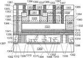
- a 3D integrated circuit devicecomprising: a first layer comprising first transistors, overlaid by a second layer comprising second transistors, overlaid by a third layer comprising third transistors, wherein said first layer, said second layer and said third layer are each thinner than 2 microns, wherein said first layer comprises first circuits comprising at least one of said first transistors, wherein said second layer comprises second circuits comprising at least one of said second transistors, and wherein said third layer comprises a charge pump circuit and control circuits to control said first circuits and said second circuits.
- a 3D integrated circuit devicecomprising: a first layer comprising first transistors, overlaid by a second layer comprising second transistors, overlaid by a third layer comprising third transistors, wherein said first layer, said second layer and said third layer are each thinner than 2 microns, wherein said first layer comprises first circuits comprising at least one of said first transistors, wherein said second layer comprises second circuits comprising at least one of said second transistors, and wherein said third layer comprises a power regulator circuit and control circuits to control said first circuits and said second circuits.
- a 3D integrated circuit devicecomprising: a first layer comprising first transistors, overlaid by a second layer comprising second transistors, overlaid by a third layer comprising third transistors, wherein said first layer, said second layer and said third layer are each thinner than 2 microns, wherein said first layer comprises first circuits comprising at least one of said first transistors, wherein said second layer comprises second circuits comprising at least one of said second transistors, and wherein said third layer comprises a temperature compensated oscillator circuit and control circuits to control said first circuits and said second circuits.
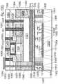
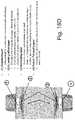
- FIG. 1is an exemplary illustration of a laser annealing machine's output that may form a large rectangular window of uniform laser energy
- FIGS. 2A-2Bare exemplary drawing illustrations of a process flow for manufacturing a crystallized layer suitable for forming transistors
- FIG. 3is an exemplary illustration of a layered shield/heat sink layer that may be constructed wherein the horizontal heat conductivity or heat spreading capability may be substantially greater in the horizontal direction than in the vertical direction;
- FIG. 4is an exemplary illustration of a partially processed 3D device with substrate being processed with topside illumination and including thermally conductive paths;
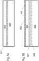
- FIGS. 5A-5Fare exemplary drawing illustrations of an additional process flow for manufacturing fully depleted MOSFET (FD-MOSFET) with an integrated shield/heat sink layer;
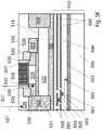
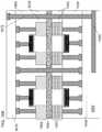
- FIG. 6is an exemplary illustration of some additional embodiments and combinations of devices, circuits, paths, and connections of a 3D device
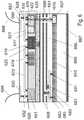
- FIG. 7is an exemplary illustration of a 3D platform
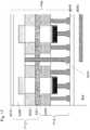
- FIG. 8is an exemplary illustration of a cross-section picture of a device that includes trench capacitors
- FIG. 9is an exemplary illustration of a 3D device power distribution structure
- FIG. 10is an exemplary illustration of a flowchart of a system that uses a processor and at least one bus;
- FIG. 11Aillustrates an exemplary partitioned 3D system/device
- FIG. 11Bis an exemplary illustration of a flowchart of partitioning logic units onto at least two stratums
- FIG. 12Ais an exemplary illustration of different Clock distribution network styles
- FIGS. 12B and 12Cillustrate exemplary 3D system/device clock distribution networks
- FIGS. 13A-13Gare exemplary illustrations of an n-channel FD-MOSFET with integrated TRL (Trap Rich Layer) device and process flow;
- FIGS. 14A-14Eare exemplary illustrations of an additional n-channel FD-MOSFET with integrated TRL (Trap Rich Layer) device and process flow;
- FIGS. 15A-15Gare exemplary illustrations of a MEMS oscillator integrated in a 3DIC stack system and process flow
- FIGS. 16A-16Kare exemplary illustrations of 3DIC process flow with carrier wafer
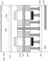
- FIG. 17is an exemplary illustration of a stratum-3 and a stratum-2 in a dual strata configuration overlaying a target/base wafer or device;
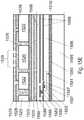
- FIG. 18Ais an exemplary illustration of back to back memory cells in a stratum-3 and a stratum-2 in a dual strata configuration utilizing a unified back-bias;
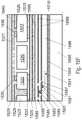
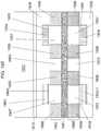
- FIG. 18Bis an exemplary illustration of N-channel and P-channel transistors each in a stratum-3 and a stratum-2 with its own back bias or a shared back-bias in a dual strata configuration;
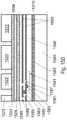
- FIG. 18Cis an exemplary illustration of Finfet transistors each in a stratum-3 and a stratum-2 in a dual strata configuration
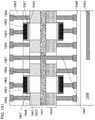
- FIG. 18Dis an exemplary illustration of four doping-layer transistor structures in a stratum-3 and a stratum-2 in a dual strata configuration
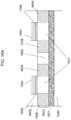
- FIGS. 19A-19Kare exemplary illustrations of a process flow for the formation of stratum-2 and stratum-3 devices (thus forming a dual strata), which may be layer transferred and connected to a target wafer/substrate;
- FIG. 20is an exemplary illustration of a 3DIC device.
- FIG. 21is an exemplary illustration of a 3DIC device formation flow utilizing a detachable donor substrate and a detachable carrier substrate.
- Some drawing figuresmay describe process flows for building devices.
- the process flowswhich may be a sequence of steps for building a device, may have many structures, numerals and labels that may be common between two or more adjacent steps. In such cases, some labels, numerals and structures used for a certain step's figure may have been described in the previous steps' figures.
- Defect annealingsuch as furnace thermal or optical annealing, of thin layers of the crystalline materials generally included in 3D-ICs to the temperatures that may lead to substantial dopant activation or defect anneal, for example above 600° C., may damage or melt the underlying metal interconnect layers of the stacked 3D-IC, such as copper or aluminum interconnect layers.
- An embodiment of the inventionis to form 3D-IC structures and devices wherein a heat spreading, heat conducting and/or optically reflecting or absorbent material layer or layers (which may be called a shield) is incorporated between the sensitive metal interconnect layers and the layer or regions being optically irradiated and annealed, or annealed from the top of the 3D-IC stack using other methods.
- FIGS. 33A-FAn exemplary generalized process flow is shown in FIGS. 33A-F of incorporated patent reference U.S. Pat. No. 8,574,929.
- An exemplary process flow for an FD-RCAT with an optional integrated heat shield/spreaderis shown in FIGS. 34A-G of incorporated patent reference U.S. Pat. No. 8,574,929.
- An exemplary process flow for a FD-MOSFET with an optional integrated heat shield/spreaderis shown in FIGS. 45A-G of incorporated patent reference U.S. Pat. No. 8,574,929.
- FIGS. 46A-GAn exemplary process flow for a planar fully depleted n-channel MOSFET (FD-MOSFET) with an optional integrated heat shield/spreader and back planes and body bias taps is shown in FIGS. 46A-G of incorporated patent reference U.S. Pat. No. 8,574,929.
- FIGS. 47A-GAn exemplary process flow for a horizontally oriented JFET or JLT with an optional integrated heat shield/spreader is shown in FIGS. 47A-G of incorporated patent reference U.S. Pat. No. 8,574,929.
- FIGS. 5A-5FAn alternate method to construct a planar fully depleted undoped channel MOSFET (FD-MOSFET) with an optional integrated heat shield/spreader and back planes and body bias taps suitable for a monolithic 3D IC is shown in FIGS. 5A-5F herein.
- the 3D-ICsmay be constructed in a 3D stacked layer using procedures outlined herein and such as, for example, FIGS. 39, 40, 41 of incorporated patent reference U.S. Pat. No. 8,574,929 and in other incorporated references.
- the topside defect annealmay include optical annealing to repair defects in the crystalline 3D-IC layers and regions (which may be caused by the ion-cut implantation process), and may be utilized to activate semiconductor dopants in the crystalline layers or regions of a 3D-IC, such as, for example, LDD, halo, source/drain implants.
- the 3D-ICmay include, for example, stacks formed in a monolithic manner with thin layers or stacks and vertical connection such as TLVs, and stacks formed in an assembly manner with thick (>2 um) layers or stacks and vertical connections such as TSVs.
- Optical annealing beams or systemssuch as, for example, a laser-spike anneal beam from a commercial semiconductor material oriented single or dual-beam continuous wave (CW) laser spike anneal DB-LSA system of Ultratech Inc., San Jose, Calif., USA (10.6 um laser wavelength), or a short pulse laser (such as 160 ns), with 308 nm wavelength, and large area (die or step-field sized, including 1 cm 2 ) irradiation such as offered by Excico of Gennevilliers, France, may be utilized (for example, see Huet, K., “Ultra Low Thermal Budget Laser Thermal Annealing for 3D Semiconductor and Photovoltaic Applications,” NCCAVS 2012 Junction Technology Group, Semicon West, San Francisco, Jul.
- CWcontinuous wave
- NCCAVS 2012 Junction Technology GroupSemicon West, San Francisco, Jul.
- the defect annealmay include, for example, laser anneals (such as suggested in Rajendran, B., “Sequential 3D IC Fabrication: Challenges and Prospects”, Proceedings of VLSI Multi Level Interconnect Conference 2006, pp. 57-64), Ultrasound Treatments (UST), megasonic treatments, and/or microwave treatments.
- the topside defect anneal ambientmay include, for example, vacuum, high pressure (greater than about 760 torr), oxidizing atmospheres (such as oxygen or partial pressure oxygen), and/or neutral/reducing atmospheres (such as nitrogen or argon or hydrogen).
- the topside defect annealmay include temperatures of the layer being annealed above about 400° C.
- a high temperature thermal annealincluding, for example, 600° C., 800° C., 900° C., 1000° C., 1050° C., 1100° C. and/or 1120° C.
- the sensitive metal interconnectfor example, may be copper or aluminum containing
- the annealing processfor example, which may include sustained temperatures that do not exceed 200° C., exceed 300° C., exceed 370° C., or exceed 400° C.
- short-timescale (nanosceonds to miliseconds) temperatures above 400° C.may also be acceptable for damage avoidance, depending on the acceptor layer interconnect metal systems used.
- the topside defect annealmay include activation of semiconductor dopants, such as, for example, ion implanted dopants or PLAD applied dopants.
- semiconductor dopantssuch as, for example, ion implanted dopants or PLAD applied dopants.
- the methodssuch as the heat sink/shield layer and/or use of short pulse and short wavelength optical anneals, may allow almost any type of transistor, for example, such as FinFets, bipolar, nanowire transistors, to be constructed in a monolithic 3D fashion as the thermal limit of damage to the underlying metal interconnect systems is overcome.
- multiple pulses of the laser, other optical annealing techniques, or other anneal treatments such as microwavemay be utilized to improve the anneal, activation, and yield of the process.
- the transistors formed as described hereinmay include many types of materials; for example, the channel and/or source and drain may include single crystal materials such as silicon, germanium, or compound semiconductors such as GaAs, InP, GaN, SiGe, and although the structures may be doped with the tailored dopants and concentrations, they may still be substantially crystalline or mono-crystalline.
- the transistors in a first layer of transistorsmay include a substantially different channel and/or source/drain material than the second layer of transistors.
- the first layer of transistorsmay include silicon-based transistor channels and the second layer of transistors may include a germanium based transistor channels.
- This optical systemforms a large rectangular window of uniform laser energy with less than 10% variation over the surface to be annealed, and with sharp edges of less than 100 micron between the uniform energy and almost no energy as illustrated in FIG. 1 . Accordingly a whole die or even reticle could be exposed in one shot.
- the laser annealing processBy setting the window size and aligning the laser to the wafer properly, it could allow the laser annealing process to have the stitching of optical energy, such as pulsed laser exposures, at a desired area, such as the scribe street, such as for example lines 104 , potential dicing line 104 - 1 , potential dicing lines 104 - 2 , in FIG.
- the laser stichmay be placed between dies, thereby reducing the risk from uneven exposure at the stitching area affecting any of the desired circuit transistors or elements.
- the window sizemay be set to cover a multiplicity of dice or tiles, such as end-device 3611 of FIG. 36 of incorporated patent reference U.S. Pat. No. 8,273,610 to Or-Bach, et al., which may also have potential dice lines, such as potential dice lines 3602 and/or actual dice lines, such as actual dice lines 3612 .
- the optical annealingcould be done sequentially across the wafer or in steppings that substantially cover the entire wafer area but spread the heat generation/absorption to allow better heat dissipation and removal.
- Such spreading of heat generationcould be done, for example, by scanning the wafer surface like a checkerboard, first exposing rectangles or areas such as the blacks' of the checkerboard, and then the ‘white’ locations.
- the damage of the to be transferred crystalline layer caused by the ion-cut implantation traversing the layermay be thermally annealed, as described in at least FIG. 44 and associated specification of incorporated patent reference U.S. Pat. No. 8,574,929, or may be optically annealed, as described in at least FIGS. 33, 34, 45, 46 and 47 and associated specification of incorporated patent reference U.S. Pat. No. 8,574,929, or may be annealed by other methods such as ultrasonic or megasonic energy, as described in incorporated patent references U.S. Pat. Nos. 8,574,929, 8,273,610 and 8,557,632. These techniques repair the ion-implantation and layer transfer damage that is within the transferred crystalline layer or layers.
- An embodiment of the inventionis to perform the layer transfer of the ion-cut crystalline silicon layer, clean the surface of the transferred crystalline layer, then deposit a thin layer of amorphous silicon, and utilize optical annealing to form a layer or layer of substantially monocrystalline silicon in which the devices may be made with high quality, or the crystalized a-Si layer may be utilized as a raised source drain of high dopant concentration.
- the use of layer transfer techniques that do not use an ion-cut, and hence avoid the damage issues,are disclosed later herein.
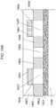
- an doped or undoped substrate donor wafer 200may be processed to in preparation for layer transfer by ion-cut of a layer of monocrystalline silicon.
- the structuremay include a wafer sized layer of doping across the wafer, N ⁇ doped layer 202 .
- the N ⁇ doped layer 202may be formed by ion implantation and thermal anneal as described elsewhere in the incorporated references and may include a crystalline material, for example, mono-crystalline (single crystal) silicon.
- N ⁇ doped layer 202may be very lightly doped (less than 1e15 atoms/cm 3 ) or lightly doped (less than 1e16 atoms/cm 3 ) or nominally un-doped (less than 1e14 atoms/cm 3 ).
- N ⁇ doped layer 202may have additional ion implantation and anneal processing to provide a different dopant level than N ⁇ substrate donor wafer 200 and may have graded or various layers of doping concentration.
- the layer stackmay alternatively be formed by epitaxially deposited doped or undoped silicon layers, or by a combination of epitaxy and implantation, or by layer transfer.
- Annealing of implants and dopingmay include, for example, conductive/inductive thermal, optical annealing techniques or types of Rapid Thermal Anneal (RTA or spike).
- the top surface of N ⁇ substrate donor wafer 200 layer stackmay be prepared for oxide wafer bonding with a deposition of an oxide or by thermal oxidation of N ⁇ doped layer 202 to form oxide layer 280 .
- a layer transfer demarcation plane (shown as dashed line) 299may be formed by hydrogen implantation or other methods as described in the incorporated references.
- the N ⁇ substrate donor wafer 200such as surface 282 , and acceptor wafer 210 may be prepared for wafer bonding as previously described and low temperature (less than approximately 400° C.) bonded.
- Acceptor wafer 210may include, for example, transistors, circuitry, and metal, such as, for example, aluminum or copper, interconnect wiring, a metal shield/heat sink layer or layers, and thru layer via metal interconnect strips or pads.
- Acceptor wafer 210may be substantially comprised of a crystalline material, for example mono-crystalline silicon or germanium, or may be an engineered substrate/wafer such as, for example, an SOI (Silicon on Insulator) wafer or GeOI (Germanium on Insulator) substrate.
- SOISilicon on Insulator
- GeOIGermanium on Insulator
- Acceptor wafer 210may include transistors such as, for example, MOSFETS, FD-MOSFETS, FinFets, FD-RCATs, BJTs, HEMTs, and/or HBTs.
- the portion of the N ⁇ doped layer 202 and the N ⁇ substrate donor wafer 200 that may be above (when the layer stack is flipped over and bonded to the acceptor wafer 210 ) the layer transfer demarcation plane 299may be removed by cleaving or other low temperature processes as described in the incorporated references, such as, for example, ion-cut with mechanical or thermal cleave, thus forming remaining N ⁇ layer 203 .
- oxide layer 280 and remaining N ⁇ layer 203have been layer transferred to acceptor wafer 210 .
- the top surface of remaining N ⁇ layer 203may be chemically or mechanically polished, and/or may be thinned by low temperature oxidation and strip processes, such as the TEL SPA tool radical oxidation and HF:H 2 O solutions as described herein and in referenced patents and patent applications.
- the wafer sized layer remaining N ⁇ layer 203could be thinned from its original total thickness, and its final total thickness could be in the range of about 3 nm to about 30 nm, for example, about 3 nm, about 5 nm, about 7 nm, about 10 nm, about 15 nm, about 20 nm, or about 30 nm.
- Remaining N ⁇ layer 203may have a thickness that may allow full gate control of channel operation when the transistor, for example a JFET (or JLT) or FD-MOSFET, is substantially completely formed.
- Acceptor wafer 210may include one or more (two are shown in this example) shield/heat sink layers 288 , which may include materials such as, for example, Aluminum, Tungsten (a refractory metal), Copper, silicon or cobalt based silicides, or forms of carbon such as carbon nanotubes, and may be layered itself as described herein FIG. 3 .
- Each shield/heat sink layer 288may have a thickness range of about 50 nm to about 1 mm, for example, about 50 nm, about 100 nm, about 200 nm, about 300 nm, about 500 nm, about 0.1 um, about 1 um, about 2 um, and about 10 um.
- Shield/heat sink layer 288may include isolation openings 287 , and alignment mark openings (not shown), which may be utilized for short wavelength alignment of top layer (donor) processing to the acceptor wafer alignment marks (not shown).
- Shield/heat sink layer 288may include one or more shield path connects 285 and shield path vias 283 .
- Shield path via 283may thermally and/or electrically couple and connect shield path connect 285 to acceptor wafer 210 interconnect metallization layers such as, for example, exemplary acceptor metal interconnect 281 (shown).
- Shield path connect 285may also thermally and/or electrically couple and connect each shield/heat sink layer 288 to the other and to acceptor wafer 210 interconnect metallization layers such as, for example, acceptor metal interconnect 281 , thereby creating a heat conduction path from the shield/heat sink layer 288 to the acceptor substrate 295 , and a heat sink (not shown, see incorp. Refs.).
- Isolation openings 287may include dielectric materials, similar to those of BEOL isolation 296 .
- Acceptor wafer 210may include first (acceptor) layer metal interconnect 291 , acceptor wafer transistors and devices 293 , and acceptor substrate 295 .
- a layer of amorphous silicon 266may be deposited.
- Amorphous silicon layer 266may have a thickness that could be in the range of about 3 nm to about 300 nm, for example, about 3 nm, about 5 nm, about 7 nm, about 10 nm, about 15 nm, about 20 nm, about 30 nm, about 50 nm, about 100 nm, about 200 nm or about 300 nm.
- amorphous silicon layer 266may be crystallized in an epitaxial fashion by exposure to an optical beam, for example, to short wavelength pulse lasers as described elsewhere herein and in incorporated references.
- Amorphous silicon layer 266may be doped in-situ during deposition, or may be ion-implanted after deposition and dopants activated during the optical exposure. Further, amorphous silicon layer 266 may be first crystalized and then ion-implanted with dopants, and then those dopants may be activated with an additional anneal, for example, an optical beam anneal.
- Optical anneal beamssuch as exemplary crystallization/annealing ray 265 , may be optimized to focus light absorption and heat generation within or at the surface of amorphous silicon layer 266 to promote the epitaxial regrow into a layer of doped single crystal silicon.
- the laser assisted crystallization/annealing with the absorbed heat generated by exemplary crystallization/annealing ray 265may also include a pre-heat of the bonded stack to, for example, about 100° C. to about 400° C., and/or a rapid thermal spike to temperatures above about 200° C. to about 600° C. Additionally, absorber layers or regions, for example, including amorphous carbon, amorphous silicon, and phase changing materials (see U.S. Pat. Nos. 6,635,588 and 6,479,821 to Hawryluk et al. for example), may be utilized to increase the efficiency of the optical energy capture in conversion to heat for the desired annealing or activation processes.
- Reflected ray 263may be reflected and/or absorbed by shield/heat sink layer 288 regions thus blocking the optical absorption of ray blocked metal interconnect 281 .
- Heat generated by absorbed photons from, for example, crystallization/annealing ray 265may also be absorbed by shield/heat sink layer 288 regions and dissipated laterally and may keep the temperature of underlying metal layers, such as metal interconnect 281 , and other metal layers below it, cooler and prevent damage.
- Shield/heat sink layer 288 and associated dielectricsmay laterally spread and conduct the heat generated by the topside defect anneal, and in conjunction with the dielectric materials (low heat conductivity) above and below shield/heat sink layer 288 , keep the interconnect metals and low-k dielectrics of the acceptor wafer interconnect layers cooler than a damage temperature, such as, for example, 400° C. or 370° C., or 300° C.
- a second layer of shield/heat sink layer 288may be constructed (shown) with a low heat conductive material sandwiched between the two heat sink layers, such as silicon oxide or carbon doped ‘low-k’ silicon oxides, for improved thermal protection of the acceptor wafer interconnect layers, metal and dielectrics.
- Shield/heat sink layer 288may act as a heat spreader and/or absorber. Electrically conductive materials may be used for the two layers of shield/heat sink layer 288 and thus may provide, for example, a Vss and a Vdd plane and/or grid that may be connected to the donor layer transistors above, as well may be connected to the acceptor wafer transistors below, and/or may provide below transferred layer device interconnection.
- Shield/heat sink layer 288may include materials with a high thermal conductivity greater than 10 W/m-K, for example, copper (about 400 W/m-K), aluminum (about 237 W/m-K), Tungsten (about 173 W/m-K), Plasma Enhanced Chemical Vapor Deposited Diamond Like Carbon-PECVD DLC (about 1000 W/m-K), and Chemical Vapor Deposited (CVD) graphene (about 5000 W/m-K).
- Shield/heat sink layer 288may be sandwiched and/or substantially enclosed by materials with a low thermal conductivity (less than 10 W/m-K), for example, silicon dioxide (about 1.4 W/m-K).
- the heat conducting layer closest to the second crystalline layer or oxide layer 280may be constructed with a different material, for example a high melting point material, for example a refractory metal such as tungsten, than the other heat conducting layer or layers, which may be constructed with, for example, a lower melting point material, for example such as aluminum or copper.
- transistorsmay be formed with low effective temperature (less than approximately 400° C. exposure to the acceptor wafer 210 sensitive layers, such as interconnect and device layers) processing, and may be aligned to the acceptor wafer alignment marks (not shown) as described in the incorporated references. This may include further optical defect annealing or dopant activation steps.
- the N ⁇ donor wafer 200may now also be processed, such as smoothing and annealing, and reused for additional layer transfers.
- the insulator layersuch as deposited bonding oxides (for example oxide layer 280 ) and/or before bonding preparation existing oxides (for example the BEOL isolation 296 on top of the topmost metal layer of shield/heat sink layer 288 ), between the donor wafer transferred monocrystalline layer and the acceptor wafer topmost metal layer, may include thicknesses of less than about 1 um, less than about 500 nm, less than about 400 nm, less than about 300 nm, less than about 200 nm, or less than about 100 nm.
- Transistors and other devicesmay be constructed utilizing regions of the crystallized amorphous silicon layer 266 as a portions of the transistor or device; for example, as a transistor channel for an FD-MOSFET or JFET, or as raised source and drain for an FDMOSFET or JLT.
- the shield layerfor example, shield/heat sink layer 288 described herein, could be constructed so it may have a substantially larger or better heat conductivity to the sides of the device in the horizontal orientation than the heat conductivity of the shield layer in the vertical direction toward the underlying layers or back to the top surface of the device.
- Such shield layerwherein the horizontal heat conductivity or heat spreading capability is substantially greater in the horizontal direction than in the vertical direction, could include a ‘sandwich’ of heat conductive thin layer, such as a metal (for example copper), overlaid by a thin lower-thermally-conducting layer, for example SiO2, and may repeat the two layer stack multiple times.
- Vertical electrical continuitymay be maintained by etching vertical vias and filling the vias with an electrically conductive material.
- Overlapping shorting vias or linesmay also perform the same function.
- a shield layercould be designed to support various types of optical annealing. Such shielding can block even non laser optical annealing or a CO 2 laser that tends to penetrate very deeply. In some cases it might be desired to have the top layer of the shielding layer as non-reflective or as a defusing reflector to reduce damage to the laser annealing machine from the reflected light.
- a layered shield/heat sink layermay be constructed wherein the horizontal heat conductivity or heat spreading capability may be substantially greater in the horizontal direction than in the vertical direction.
- the horizontal directionis indicated by horizontal arrow 350 and the vertical direction is indicated by vertical arrow 352 .
- a portion of FIG. 47G of incorporated reference U.S. Pat. No. 8,574,929is repeated in FIG.
- FIG. 3showing the portion of a 3D device with shield/heat sink & spreading structure below the second crystalline device layer, which may include oxide layer 4780 , a portion of thru layer vias (TLVs) 4760 , shield path connects 4785 , shield path via 4783 , BEOL isolation 4796 , shield path via 4783 , acceptor metal interconnect 4781 , first (acceptor) layer metal interconnect 4791 , acceptor wafer transistors and devices 4793 , acceptor substrate 4795 , and acceptor wafer heat sink 4797 (which may have an external surface or connection to one as described earlier herein), of acceptor wafer 4710 .
- the external surfacemay be at the top, bottom or sides of the finished device.
- the devicemay include an external surface from which heat transfer may take place by methods such as air cooling, liquid cooling, or attachment to another heat sink or heat spreader structure. As indicated in FIG. 3 , the area within the circle is blown up to enable clarity of detail for the illustration.
- Layered shield/heat sink region 385may include layers or regions of heat conductive material and heat isolative material, for example heat conducting regions 370 and heat isolative regions 372 .
- Heat conducting regions 370may include materials with a high thermal conductivity greater than 10 W/m-K, such as, for example, (about 400 W/m-K), aluminum (about 237 W/m-K), Tungsten (about 173 W/m-K), Plasma Enhanced Chemical Vapor Deposited Diamond Like Carbon-PECVD DLC (about 1000 W/m-K), and Chemical Vapor Deposited (CVD) graphene (about 5000 W/m-K), barrier metals such as TiN and TaN, and may be deposited in layers interspersed with heat isolative layers.
- 10 W/m-Ksuch as, for example, (about 400 W/m-K), aluminum (about 237 W/m-K), Tungsten (about 173 W/m-K), Plasma Enhanced Chemical Vapor Deposited Diamond Like Carbon-PECVD DLC (about 1000 W/m-K), and Chemical Vapor Deposited (CVD) graphene (about 5000 W/m-K), barrier metals such as TiN and Ta
- Heat isolative regions 372may include materials with a low thermal conductivity (less than 10 W/m-K), or substantially less thermally conductive than the material included in heat conducting regions 370 , materials such as, for example, silicon oxide (about 1.4 W/m-K), aerogels, carbon doped oxides. Accordingly, depending on material choices and construction (such as number of cond/iso layers and their thickness), layered shield/heat sink region 385 may have a heat conductivity in the horizontal direction that is 2 times, or 4 times, or ten times greater than the heat conductivity in the vertical direction. Either or both of heat conducting regions 370 and heat isolative regions 372 may be electrically conductive.
- Heat conducting regions 370 and heat isolative regions 372may be formed by lithographically defining and then etching the conductive and isolative layer stack using subtractive formation techniques known by those skilled in the art, and may also be formed in a damascene method. Electrical connection between the various heat conducting regions 370 may be made by forming the deep TLV 360 , patterned after thru layer vias (TLVs) 4760 , to short the various heat conduction regions 370 . Deep TLV 360 may be formed by etching substantially to, within, or thru the bottom heat conducting region 370 of layered shield/heat sink region 385 .
- layered shield/heat sink region 385may be formed wherein the horizontal heat conductivity or heat spreading capability may be substantially greater in the horizontal direction (indicated by horizontal arrow 350 ) than in the vertical direction (indicated by vertical arrow 352 ).
- Shield path connect 383may be similar to shield path connects 4785 and additional shield/heat sink region 388 may be layered such as, for example, layered shield/heat sink region 385 or shield/heat sink layers 4788 of FIG. 47G of incorporated reference U.S. Pat. No. 8,574,929.
- Layered shield/heat sink region 385may be utilized as part of a thermal conduction path, emf shield, back-bias circuits for second layer transistors, and other uses as described herein in relation to FIG. 47 of incorporated reference U.S. Pat. No. 8,574,929, and any other descriptions employing a shield/heat sink layer or region.
- FIG. 3are exemplary and are not drawn to scale.
- subtractive region formation techniquesmay be preferred over damascene for forming layered shield/heat sink region 385 as the shield regions may comprise the majority of the device area at that formation step, and CMP processes within the damascene techniques may be difficult without breaking the shield into small regions, which may affect the heat shielding capability.
- Two or more layered shield/heat sink layers, properly designed and layed out with overlapping regions,may be useful for the damascene technique.
- the layered shield/heat sink region 385is formed by a damascene process flow, then electrical connection between the various heat conducting regions 370 may be made at the top surface of the damascene ‘metal’ line trench by just a slight over-etch (CMP smearing may not be enough to couple the conductive regions) during deep TLV 360 formation, as many of the various heat conducting regions 370 and heat isolative regions 372 may truncate at the top surface of the trench that is forming layered shield/heat sink region 385 .
- deep TLV 360may be formed to be fully or partially on the outside edge of the layered shield/heat sink region 385 in order to couple the various heat conducting regions 370 .
- An embodiment of the inventionmay include an exemplary partially processed 3D device with substrate being processed with topside illumination as illustrated in FIG. 4 .
- the topside illumination 499may be an optical anneal for purposes, such as, for example, dopant annealing, STI densification and annealing, silicidation, and/or ion-cut damage repair, which have been described herein and in incorporated patents and patent publications and applications.
- topside illumination 499may be an optical anneal that is die sized, or reticle sized, or other size and shape as has been described herein and in incorporated patents and patent publications and applications.
- a transferred layer 403which may be a transferred layer or layers as described herein and in incorporated patents and patent publications and applications, may have been transferred and bonded to an acceptor wafer or substrate, and may include bonding at the interface between donor bonding oxide 480 and acceptor bonding oxide 481 .
- Transferred layer 403may have a protect layer 466 (or region) atop it, which may function as a optical absorber, reflector, or energy spreader as described in herein and in incorporated patents and patent publications and applications, and may remain a part of the device at the end of device processing or be sacrificial (removed).
- Transferred layer 403may include its entirety or portions, isotopically enriched silicon (such as, for example, >99% 28 Si) or germanium to enable a greater heat conductivity.
- isotopically enriched siliconsuch as, for example, >99% 28 Si
- germaniumto enable a greater heat conductivity.
- the relatively higher cost of the isotopically enriched layer or regionscan be mitigated by the reuse of a donor wafer comprised wholly or partially with the material.
- the acceptor wafer at the time of bonding to the donor wafer and at exposure to topside illumination 499may include acceptor bonding oxide 481 , top shield layer 485 , inter-shield insulator layer 498 , bottom shield layer 488 , second inter-shield insulator layer 496 , eight ‘2 ⁇ ’ interconnect layers 483 that may be interspersed with four ‘2 ⁇ ’ insulator layers 494 , a ‘1 ⁇ ’ interconnect layer 487 , a ‘1 ⁇ ’ insulator layer 492 , device die thermal conduction paths 445 , device scribe-lane thermal conduction paths 446 , second device die thermal conduction paths 444 , second device scribe-lane thermal conduction paths 447 , and a base wafer with transistors and circuits 495 .
- the acceptor wafermay have another combination of these layers and regions as would be clear to one skilled in the art.
- the elements of the exemplary acceptor wafermay include the materials, process flows, construction, use, etc. as has been described herein and in incorporated patents and patent publications and applications, for example, transferred layer 403 may be doped or undoped silicon, and may have regions of STI or other transistor elements within it or on it, and may include multiple layers or regions of doping. Moreover, transferred layer 403 may include layers or regions that have materials with melting points higher than 900° C.
- Top shield layer 485may have layered shield regions wherein the horizontal thermal conduction is substantially greater than the vertical heat conduction.
- the bonded stack of the acceptor wafer and transferred layersmay include scribe regions 465 ; either preformed and/or predetermined scribelanes and/or dicelines, or may include custom function definition and etching, or a combination of both.
- Scribe regions 465may be constructed with device scribe-lane thermal conduction paths 446 that may provide a thermal conduction path from the top shield layer 485 to the base wafer with transistors and circuits 495 , which could then conduct heat that may be generated from topside illumination 499 to the illumination machine heat sink/chuck 440 and thus help prevent damage from the topside illumination 499 of the acceptor interconnect layers, such as, for example, the eight ‘2 ⁇ ’ interconnect layers 483 , four ‘2 ⁇ ’ insulator layers 494 , 1 ⁇ ′ interconnect layer 487 , ‘1 ⁇ ’ insulator layer 492 , and the transistors and circuits of base wafer with transistors and circuits 495 .
- Second device scribe-lane thermal conduction paths 447may thermally conduct from bottom shield layer 488 to the base wafer with transistors and circuits 495 and the illumination machine heat sink/chuck 440 .
- Device die thermal conduction paths 445 within the device diemay provide a thermal conduction path from the top shield layer 485 to the base wafer with transistors and circuits 495 , which could then conduct heat that may be generated from topside illumination 499 to the illumination machine heat sink/chuck 440 and thus help prevent damage from the topside illumination 499 of the acceptor interconnect layers, such as, for example, the eight ‘2 ⁇ ’ interconnect layers 483 , four ‘2 ⁇ ’ insulator layers 494 , 1 ⁇ ′ interconnect layer 487 , ‘1 ⁇ ’ insulator layer 492 , and the transistors and circuits of base wafer with transistors and circuits 495 , and has been described herein and in incorporated patents and patent publications.
- Second device die thermal conduction paths 444may thermally conduct from bottom shield layer 488 to the base wafer with transistors and circuits 495 and the illumination machine heat sink/chuck 440 .
- Device scribe-lane thermal conduction paths 446may be removed in the later dice singulation processes whereas the device die thermal conduction paths 445 may remain in the finished device and provide cooling of the second layer and above transistor and circuit layers when the device is in operation and generating heat from the device operation.
- the density of device die thermal conduction paths 445 , device scribe-lane thermal conduction paths 446 , second device die thermal conduction paths 444 , and second device scribe-lane thermal conduction paths 447is a device design and thermal architecture calculation, but may be on the order of 1 every 100 um 2 (Wei H., et al., “Cooling Three-Dimensional Integrated Circuits Using Power Delivery Networks”, IEDM 2012, 14.2, December 2012. incorporated by reference in entirety). Scribelanes (or dicelanes), such as scribe regions 465 , may be about 10 um wide, about 20 um wide, about 50 um wide, about 100 um wide, or greater than about 100 um wide depending on design choice and die singulation process capability.
- bottom shield layer 488may also be formed as a layered shield/heat sink layer or region.
- bottom shield layer 488may also be formed as a layered shield/heat sink layer or region.
- many of the elements in the FIG. 4may be called layers, they main include within them regions.
- device scribe-lane thermal conduction paths 446 and device die thermal conduction paths 445may be formed so that there is no electrical connection to bottom shield layer 488 , unless they are designed to do so as the same circuit node.
- the choice of eight ‘2 ⁇ ’ interconnect layers 483 that may be interspersed with four ‘2 ⁇ ’ insulator layers 494 , a ‘1 ⁇ ’ interconnect layer 487 , a ‘1 ⁇ ’ insulator layer 492is a design choice and may be different according to the design considerations, both device functionally and thermally.
- the various semiconductor layers within the 3D devicemay have various circuitry, functions and connection, for example, as described herein (such as FIG. 6 ) or in incorporated patent references. Thus the invention is to be limited only by the appended claims.
- FD-MOSFETplanar fully depleted undoped channel MOSFET
- the FD-MOSFETmay provide an improved transistor variability control and conduction channel electrostatic control, as well as the ability to utilize an updoped channel, thereby improving carrier mobility.
- the FD-MOSFETdoes not demand doping or pocket implants in the channel to control the electrostatic characteristics and tune the threshold voltages.
- a ground planeis constructed that may provide improved electrostatics and/or Vt adjustment and/or back-bias of the FD-MOSFET.
- selective regionsmay be constructed to provide body bias and/or partially depleted/bulk-like transistors.
- a heat spreading, heat conducting and/or optically reflecting material layer or layersmay be incorporated between the sensitive metal interconnect layers below and the layer or regions being optically irradiated and annealed to repair defects in the crystalline 3D-IC layers and regions, crystallize an undoped transistor channel, and to activate semiconductor dopants in the crystalline layers or regions of a 3D-IC without harm to the sensitive metal interconnect and associated dielectrics.
- FIGS. 5A-Fillustrate an exemplary undoped-channel FD-MOSFET which may be constructed in a 3D stacked layer using procedures outlined below and in the incorporated references.
- SOI donor wafer substrate 500may include back channel layer 502 above Buried Oxide BOX layer 501 .
- Back channel layer 502may be doped by ion implantation and thermal anneal, may include a crystalline material, for example, mono-crystalline (single crystal) silicon and may be heavily doped (greater than 1e16 atoms/cm 3 ), lightly doped (less than 1e16 atoms/cm 3 ) or nominally un-doped (less than 1e14 atoms/cm 3 ).
- SOI donor wafer substrate 500may include a crystalline material, for example, mono-crystalline (single crystal) silicon and at least the upper layer near BOX layer 501 may be very heavily doped (greater than 1e20 atoms/cm 3 ).
- Back channel layer 502may have additional ion implantation and anneal processing to provide a different dopant level than SOI donor wafer substrate 500 and may have graded and/or various layers of doping concentration.
- SOI donor wafer substrate 500may have additional ion implantation and anneal processing to provide a different dopant level than back channel layer 502 and may have graded and/or various layers of doping concentration.
- the layer stackmay alternatively be formed by epitaxially deposited doped or undoped silicon layers, or by a combination of epitaxy and implantation, or by layer transfer.
- Annealing of implants and dopingmay include, for example, conductive/inductive thermal, optical annealing techniques or types of Rapid Thermal Anneal (RTA or spike).
- SOI donor wafermay be constructed by layer transfer techniques described herein or elsewhere as known in the art, or by laser annealed SIMOX at a post donor layer transfer to acceptor wafer step.
- BOX layer 501may be thin enough to provide for effective back and/or body bias, for example, about 25 nm, or about 20 nm, or about 10 nm, or about 35 nm.
- the top surface of the SOI donor wafer substrate 500 layer stackmay be prepared for oxide wafer bonding with a deposition of an oxide or by thermal oxidation of back channel layer 502 to form oxide layer 580 .
- a layer transfer demarcation plane (shown as dashed line) 599may be formed by hydrogen implantation or other methods as described in the incorporated references, and may reside within the SOI donor wafer substrate 500 .
- the SOI donor wafer substrate 500 stack, such as surface 582 , and acceptor wafer 510may be prepared for wafer bonding as previously described and low temperature (less than approximately 400° C.) bonded.
- Acceptor wafer 510may include, for example, transistors, circuitry, and metal, such as, for example, aluminum or copper, interconnect wiring, a metal shield/heat sink layer or layers, and thru layer via metal interconnect strips or pads.
- Acceptor wafer 510may be substantially comprised of a crystalline material, for example mono-crystalline silicon or germanium, or may be an engineered substrate/wafer such as, for example, an SOI (Silicon on Insulator) wafer or GeOI (Germanium on Insulator) substrate.
- SOISilicon on Insulator
- GeOIGermanium on Insulator
- Acceptor wafer 510may include transistors such as, for example, MOSFETS, FD-MOSFETS, FinFets, FD-RCATs, BJTs, HEMTs, and/or HBTs.
- the portion of the SOI donor wafer substrate 500 that may be above (when the layer stack is flipped over and bonded to the acceptor wafer 510 ) the layer transfer demarcation plane 599may be removed by cleaving or other low temperature processes as described in the incorporated references, such as, for example, ion-cut with mechanical or thermal cleave or other layer transfer methods, thus forming remaining S/D layer 503 .
- Damage/defects to crystalline structure of back channel layer 502may be annealed by some of the annealing methods described, for example the short wavelength pulsed laser techniques, wherein the back channel layer 502 and/or portions of the SOI donor wafer substrate 500 may be heated to defect annealing temperatures, but the layer transfer demarcation plane 599 may be kept below the temperature for cleaving and/or significant hydrogen diffusion.
- the optical energymay be deposited in the upper layer of the stack, for example near surface 582 , and annealing of back channel layer 502 and/or portions of the SOI donor wafer substrate 500 may take place via heat diffusion.
- multiple pulses of the lasermay be utilized to improve the anneal, activation, and yield of the process and/or to control the maximum temperature of various structures in the stack.
- oxide layer 580 , back channel layer 502 , BOX layer 501 and S/D layer 503may be layer transferred to acceptor wafer 510 .
- the top surface of S/D layer 503may be chemically or mechanically polished, and/or may be thinned by low temperature oxidation and strip processes, such as the TEL SPA tool radical oxidation and HF:H 2 O solutions as described in referenced patents and patent applications.
- the wafer sized layer S/D layer 503could be thinned from its original total thickness, and its final total thickness could be in the range of about 5 nm to about 20 nm, for example, about 5 nm, about 7 nm, about 10 nm, about 12 nm, about 15 nm, or about 20 nm.
- S/D layer 503may have a thickness and/or doping that may allow a minimum Rext and maximum electron injection velocities when the FD-MOSFET transistor is substantially completely formed.
- Acceptor wafer 510may include one or more (two are shown in this example) shield/heat sink layers 588 , which may include materials such as, for example, Aluminum, Tungsten (a refractory metal), Copper, silicon or cobalt based silicides, or forms of carbon such as carbon nanotubes, and may be layered itself as described herein FIG. 3 .
- Each shield/heat sink layer 588may have a thickness range of about 50 nm to about 1 mm, for example, about 50 nm, about 100 nm, about 200 nm, about 300 nm, about 500 nm, about 0.1 um, about 1 um, about 2 um, and about 10 um.
- Shield/heat sink layer 588may include isolation openings 587 , and alignment mark openings (not shown), which may be utilized for short wavelength alignment of top layer (donor) processing to the acceptor wafer alignment marks (not shown).
- Shield/heat sink layer 588may include one or more shield path connects 585 and shield path vias 583 .
- Shield path via 583may thermally and/or electrically couple and connect shield path connect 585 to acceptor wafer 510 interconnect metallization layers such as, for example, exemplary acceptor metal interconnect 581 (shown).
- Shield path connect 585may also thermally and/or electrically couple and connect each shield/heat sink layer 588 to the other and to acceptor wafer 510 interconnect metallization layers such as, for example, acceptor metal interconnect 581 , thereby creating a heat conduction path from the shield/heat sink layer 588 to the acceptor substrate 595 , and a heat sink (not shown).
- Isolation openings 587may include dielectric materials, similar to those of BEOL isolation 596 .
- Acceptor wafer 510may include first (acceptor) layer metal interconnect 591 , acceptor wafer transistors and devices 593 , and acceptor substrate 595 .
- Various topside defect annealsmay be utilized.
- an optical beamsuch as the laser annealing previously described is used.
- Optical anneal beamsmay be optimized to focus light absorption and heat generation within or at the surface of S/D layer 503 and provide surface smoothing and/or defect annealing (defects may be from the cleave and/or the ion-cut implantation) with exemplary smoothing/annealing ray 566 .
- the laser assisted smoothing/annealing with the absorbed heat generated by exemplary smoothing/annealing ray 566may also include a pre-heat of the bonded stack to, for example, about 100° C. to about 400° C., and/or a rapid thermal spike to temperatures above about 200° C. to about 600° C.
- absorber layers or regionsfor example, including amorphous carbon, amorphous silicon, and phase changing materials (see U.S. Pat. Nos. 6,635,588 and 6,479,821 to Hawiyluk et al. for example), may be utilized to increase the efficiency of the optical energy capture in conversion to heat for the desired annealing or activation processes.
- multiple pulses of the lasermay be utilized to improve the anneal, activation, and yield of the process.
- Reflected ray 563may be reflected and/or absorbed by shield/heat sink layer 588 regions thus blocking the optical absorption of ray blocked metal interconnect 581 .
- Annealing of dopants or annealing of damage in back channel layer 502 and/or BOX 510 and/or S/D layer 503may be also accomplished by a set of rays such as repair ray 565 , illustrated is focused on back channel layer 502 .
- Heat generated by absorbed photons from, for example, smoothing/annealing ray 566 , reflected ray 563 , and/or repair ray 565may also be absorbed by shield/heat sink layer 588 regions and dissipated laterally and may keep the temperature of underlying metal layers, such as metal interconnect 581 , and other metal layers below it, cooler and prevent damage.
- Shield/heat sink layer 588 and associated dielectricsmay laterally spread and conduct the heat generated by the topside defect anneal, and in conjunction with the dielectric materials (low heat conductivity) above and below shield/heat sink layer 588 , keep the interconnect metals and low-k dielectrics of the acceptor wafer interconnect layers cooler than a damage temperature, such as, for example, about 400° C.
- a second layer of shield/heat sink layer 588may be constructed (shown) with a low heat conductive material sandwiched between the two heat sink layers, such as silicon oxide or carbon doped ‘low-k’ silicon oxides, for improved thermal protection of the acceptor wafer interconnect layers, metal and dielectrics.
- Shield/heat sink layer 588may act as a heat spreader.
- Electrically conductive materialsmay be used for the two layers of shield/heat sink layer 588 and thus may provide, for example, a Vss and a Vdd plane and/or grid that may be connected to the donor layer transistors above, as well may be connected to the acceptor wafer transistors below, and/or may provide below transferred layer device interconnection. Noise on the power grids, such as the Vss and Vdd plane power conducting lines/wires, may be mitigated by attaching/connecting decoupling capacitors onto the power conducting lines of the grids.
- the decoupling capswhich may be within the second layer (donor, for example, donor wafer device structures) or first layer (acceptor, for example acceptor wafer transistors and devices 593 ), may include, for example, trench capacitors such as described by Pei, C., et al., “A novel, low-cost deep trench decoupling capacitor for high-performance, low-power bulk CMOS applications,” ICSICT (9 th International Conference on Solid-State and Integrated-Circuit Technology) 2008, October 2008, pp. 1146-1149, of IBM.
- the decoupling capacitorsmay include, for example, planar capacitors, such as poly to substrate or poly to poly, or MiM capacitors (Metal-Insulator-Metal).
- Shield/heat sink layer 588may include materials with a high thermal conductivity greater than 10 W/m-K, for example, copper (about 400 W/m-K), aluminum (about 237 W/m-K), Tungsten (about 173 W/m-K), Plasma Enhanced Chemical Vapor Deposited Diamond Like Carbon-PECVD DLC (about 1000 W/m-K), and Chemical Vapor Deposited (CVD) graphene (about 5000 W/m-K).
- Shield/heat sink layer 588may be sandwiched and/or substantially enclosed by materials with a low thermal conductivity (less than about 10 W/m-K), for example, silicon dioxide (about 1.4 W/m-K).
- the sandwiching of high and low thermal conductivity materials in layersspreads the localized heat/light energy of the topside anneal laterally and protects the underlying layers of interconnect metallization & dielectrics, such as in the acceptor wafer 510 , from harmful temperatures or damage.
- the heat conducting layer closest to the second crystalline layer or oxide layer 580may be constructed with a different material, for example a high melting point material, for example a refractory metal such as tungsten, than the other heat conducting layer or layers, which may be constructed with, for example, a lower melting point material, for example such as aluminum or copper.
- transistorsmay be formed with low effective temperature (less than approximately 400° C. exposure to the acceptor wafer 510 sensitive layers, such as interconnect and device layers) processing, and may be aligned to the acceptor wafer alignment marks (not shown) as described in the incorporated references. This may include further optical defect annealing or dopant activation steps.
- the remaining SOI donor wafer substrate 500may now also be processed, such as smoothing and annealing, and reused for additional layer transfers.
- the insulator layersuch as deposited bonding oxides (for example oxide layer 580 ) and/or before bonding preparation existing oxides (for example the BEOL isolation 596 on top of the topmost metal layer of shield/heat sink layer 588 ), between the donor wafer transferred monocrystalline layer and the acceptor wafer topmost metal layer, may include thicknesses of less than about 1 um, less than about 500 nm, less than about 400 nm, less than about 300 nm, less than about 200 nm, or less than about 100 nm.
- transistor and back channel isolation regions 505 and/or transistor isolation regions 586may be formed.
- Transistor isolation region 586may be formed by mask defining and plasma/RIE etching S/D layer 503 , substantially to the top of BOX layer 501 (not shown), substantially into BOX layer 501 , or back channel layer 502 (not shown).
- Transistor and back channel isolation regions 505may be formed by mask defining and plasma/RIE etching channel layer 503 , BOX layer 501 and back channel layer 502 , substantially to the top of oxide layer 580 (not shown), substantially into oxide layer 580 , or further into the top BEOL dielectric layer in acceptor wafer 510 (not shown).
- intermediate S/D region 523may be formed, which may substantially form the transistor body
- back-channel region 522may be formed, which may provide a back bias and/or Vt of the eventual transistor channel.
- Back-channel region 522may be ion implanted for Vt control and/or body bias efficiency.
- a low-temperature gap fill dielectricsuch as SACVD oxide, may be deposited and chemically mechanically polished, the oxide remaining in transistor and back channel isolation regions 505 and transistor isolation regions 586 .
- An optical stepsuch as illustrated by exemplary STI ray 567 , may be performed to anneal etch damage and densify the STI oxide in transistor and back channel isolation regions 505 .
- the doping concentration of intermediate S/D region 523may include vertical or horizontal gradients of concentration or layers of differing doping concentrations.
- the doping concentration of back-channel region 522may include vertical or horizontal gradients of concentration or layers of differing doping concentrations.
- the optical annealsuch as exemplary STI ray 567 , and/or exemplary implant ray 569 may be performed at separate times and processing parameters (such as laser energy, frequency, etc.) or may be done in combination or as one optical anneal.
- Optical absorber and or reflective layers or regionsmay be employed to enhance the anneal and/or protect the underlying sensitive structures.
- multiple pulses of the lasermay be utilized to improve the anneal, activation, and yield of the process.
- BOX region 531may be a relatively thin dielectric, including the thickness range of about 5 nm to about 100 nm, at least a portion of which being between the back-channel region 522 and intermediate S/D region 523 .
- Back-channel region 522could be constructed from a material that would not be damaged by the optical anneal process. Such could be a refractory metal or doped silicon in crystallized form, poly or amorphous, or other conductive material that are acceptable for semiconductor processing and can withstand high temperature of about 700° C. or higher.
- an undoped transistor channelmay be formed within the intermediate S/D region 523 .
- Regions of intermediate S/D region 523may be lithographically defined and etched away, clearing the eventual channel region of substantially any silicon material and may etch slightly into BOX region 531 .
- Undoped amorphous silicon or poly siliconmay be deposited to fill the eventual channel region.
- a CMP processmay be utilized to remove substantially all of the deposited amorphous silicon or polysilicon not in the etched regions, thus forming undoped channel region 534 and S/D & LDD regions 535 .
- the CMP processmay be performed to overpolish and remove a small portion of the tops of S/D & LDD regions 535 , back channel isolation regions 505 , and transistor isolation regions 586 , and any smeared doping material from the S/D & LDD regions 535 may be removed by ⁇ 400 C oxidation and strip utilizing a process such as the TEL SPA tool described herein and in incorporated patent references.
- the amorphous silicon or polysilicon in undoped channel region 534may be crystallized to a near mono-crystalline state by optical annealing such as illustrated by exemplary channel smoothing ray 568 , by nano epitaxial ordering from the sidewalls of the mono-crystalline S/D & LDD regions 535 . Remaining damages and surface roughness may also be repaired and smoothed respectively by optical annealing, such as illustrated by exemplary channel smoothing ray 568 .
- a transistor forming processsuch as a conventional HKMG with raised source and drains (S/D) may be performed.
- a dummy gate stack(not shown), utilizing oxide and polysilicon, may be formed, gate spacers 530 may be formed, raised S/D regions 532 and channel stressors may be formed by etch and epitaxial deposition, for example, of SiGe and/or SiC depending on P or N channel (and may be doped in-situ or ion-implantation and optical anneal activation), LDD, halo, and S/D ion-implantations may be performed, and first ILD 536 may be deposited and CMP'd to expose the tops of the dummy gates.
- transistor channel region 534 and S/D & LDD regions 535may be formed.
- the dummy gate stackmay be removed and a gate dielectric 507 may be formed and a gate metal material gate electrode 508 , including a layer of proper work function metal (Ti x Al y ,N z for example) and a conductive fill, such as aluminum, and may be deposited and CMP'd.
- the gate dielectric 507may be an atomic layer deposited (ALD) gate dielectric that may be paired with a work function specific gate metal in the industry standard high k metal gate process schemes, for example, as described in the incorporated references.
- the gate dielectric 507may be formed with a low temperature processes including, for example, LPCVD SiO 2 oxide deposition (see Ahn, J., et al., “High-quality MOSFET's with ultrathin LPCVD gate SiO2,” IEEE Electron Device Lett., vol. 13, no. 4, pp. 186-188, April 1992) or low temperature microwave plasma oxidation of the silicon surfaces (see Kim, J. Y., et al., “The excellent scalability of the RCAT (recess-channel-array-transistor) technology for sub-70 nm DRAM feature size and beyond,” 2005 IEEE VLSI-TSA International Symposium, pp. 33-5, 25-27 Apr.
- LPCVD SiO 2 oxide depositionsee Ahn, J., et al., “High-quality MOSFET's with ultrathin LPCVD gate SiO2,” IEEE Electron Device Lett., vol. 13, no. 4, pp. 186-188, April 1992
- the gate dielectric on transistorsmay have different dielectric permittivities than silicon dioxde.
- the gate dielectric permittivity of the second layer transistorsmay be different than the gate dielectric permittivity of the first layer transistors.
- An optical stepsuch as represented by exemplary anneal ray 521 , may be performed to densify and/or remove defects from gate dielectric 507 , anneal defects and activate dopants such as LDD and S/D implants, densify the first ILD 536 , form DSS junctions (Dopant Segregated Schottky such as NiSi 2 ), and/or form contact and S/D silicides (not shown).
- the optical annealmay be performed at each sub-step as desired, or may be done at prior to the HKMG deposition (such as after the dummy gate but before the HKMG formation), or various combinations.
- transistor isolation region 586 and BOX region 531may be lithographically defined and etched away, thus forming second transistor isolation regions 576 and PD transistor area 518 .
- Partially depleted transistorsmay be constructed in a similar manner as the FD-MOSFETs constructed on transistor channel region 534 herein, but now with the thicker back-channel region 522 silicon as its channel body.
- PD transistor area 518may also be utilized to later form a direct connection thru a contact to the back-channel region 522 for back bias and Vt control of the transistor with transistor channel region 534 .
- Raised S/D regions 532may be formed by low temperature (less than about 400° C.) deposition of in-situ doped polysilicon or amorphous silicon into the S/D openings, an optical anneal to further crystallize and dopant activate the raised S/D material, and removal of excess raised S/D material. Further processing to connect the transistors and make vertical connections may follow the processing described in at least FIGS. 46F and 46G of incorporated reference U.S. Pat. No. 8,574,929.
- the various layers of a 3D devicemay include many types of circuitry, which may be formed by regions of transistors and other semiconductor device elements within that layer or in combination with other layers of the 3D device, and connections between the transistors within the same region, region to region and vertically (layer to layer. stratum to stratum) may be provided by layers of interconnect metallization and vertical connections such as TLVs and TSVs.
- power routing within the 3D devicemay utilize thicker and/or wider (more conductive) interconnect metallization than another layer, especially if the layer is closest to the source of external power and/or has a greater current load/supply requirement.
- a substrate layerwhich may have a thicker body than other semiconductor layers above or within the 3D device, such as acceptor 610 , may be formed and may include heat sink 697 , acceptor substrate 695 , acceptor wafer transistors and circuits 693 , first (acceptor) layer metal interconnect 681 which may include first layer contacts 691 , first layer vias 683 , at least one shield layer/region 688 (two layers and many regions, such as lower level shield layer region 685 , shown), interconnect insulator regions 696 and ESD diode structures 607 .
- a second semiconductor layermay be transferred and constructed on top of the first layer with isolation layer 680 in-between and vertical layer to layer interconnections may be provided by TLV/TSV 635 , only one is shown.
- a layer of transistors and circuits 622may include second layer input device structures 676 , FD ESD structures 617 , Phase Lock Loop circuits PLL 618 , SERDES circuitry 619 , and output device structure 651 .
- Second interconnections layer 630may include at least one layer/regions of metallization and associated contacts and via, for example, second layer metallization M1 segments 628 , 621 , 623 , 625 , second layer contacts 626 , second layer vias 652 , and conductive pads 690 .
- the 3D devicemay be connected to external devices utilizing many structures known to those of ordinary skill in the art, for example, bond wires 699 .
- Input device structures 676 and output device structure 651may be connected to external devices through, for example, second layer contacts 626 , second layer metallization M1 segments 628 , second layer vias 652 , conductive pads 690 , and bond wires 699 .
- a portion of the transistors within input device structures 676 and output device structure 651may be larger in either or both width and length than most transistors within acceptor wafer transistors and circuits 693 , and may have a different gate oxide, in thickness and/or composition.
- Input device structures 676may be subjected to voltage and/or current transients from external devices or generated externally and traveling to the 3D device along bond wires 699 .
- Input device structures 676 (and output device structure 651 )may be protected by dissipating the transient energy in diode structures, such as ESD diode structures 607 on the relatively thicker (than for example, the second semiconductor layer) acceptor substrate 695 , which may be connected by a multiplicity of connection stacks such as first (acceptor) layer metal interconnect 681 which may include first layer contacts 691 , first layer vias 683 , at least one shield layer/region 688 , TLV/TSV 635 , and second layer metallization M1 segments 628 .
- first (acceptor) layer metal interconnect 681which may include first layer contacts 691 , first layer vias 683 , at least one shield layer/region 688 , TLV/TSV 635 , and second layer metallization M1 segments 628 .
- Input device structures 676may be protected by dissipating the transient energy in a transient filtering circuitry such as for example, FD ESD structures 617 , which may reside on a relatively thin semiconductor layer in the 3D device and may effectively utilize fully depleted transistors in the filter circuitry.
- FD ESD structures 617may be coupled to input device structures 676 (and output device structure 651 ) by second layer interconnections (not shown).
- Input device structures 676may be connected to PLL 618 , for example, thru second layer metallization M1 segment 621 and second layer contacts 626 .
- Input device structures 676may be connected to SERDES circuitry 619 , for example, thru second layer metallization (not shown).
- a monolithic 3D stackwherein at least one of the layers in the stack is very thin (less than about 200 nm), may provide an unexpected benefit.
- the thicker substratemay be used for energy dissipating diodes to handle large energy transients and the thin (‘second’ or ‘third’ etc.) layer may be used for a high frequency switching capability to protect against a high frequency transient on the input lines. This may be done simultaneously on an I/O. Furthermore, one style could be chosen for specific I/Os as well.
- the monolithic 3D structure(thin/thick) also provides a low capacitance drive output and very fast input device structure (‘fully depleted’ transistors), yet still be protected from high energy transients that could be dissipated in the bulk (first layer).
- This ‘two-tier’ ESD structure inventioncould also provide cost effective I/Os anywhere throughout the area of the device, as the larger sized (area-wise) diodes could be placed underneath the second layer input transistors. This would also provide a closer than 2D layout coupling of the I/O to the other chip circuitry, as the large energy dissipating diodes are not on the same level as the circuitry proper, and would not interfere with the data circuitry operation (noise).
- Output device structures 651may be connected to SERDES circuitry 619 , for example, thru second layer metallization M1 segment 623 and second layer contacts 626 . Output device structures 651 may drive signals thru the connection to conductive pads 690 and then out to external devices thru bond wires 699 .
- Transistors within a lower layermay be connected (not shown) to the output device structure 651 and drive a signal to the output device structure 651 , and a portion of the transistors of output device structure 651 may have a larger width and/or length than the transistors within acceptor wafer transistors and circuits 693 .
- Power from external sourcesmay be routed thru bond wires 699 to conductive pads 690 to the 3D device, wherein at least a portion of the second interconnections layer 630 may be constructed with thicker and/or wider metallization wiring (for example 4 ⁇ wiring as described in incorporated patent references) so to provide the higher current carrying capability required for the second layer power distribution grid/network than that of the lower layer, in this example, first layer metallization wiring (for example 1 ⁇ or 2 ⁇ wiring as described in incorporated patent references).
- thicker and/or wider metallization wiringfor example 4 ⁇ wiring as described in incorporated patent references
- the width and/or length of the transistors of the second layer of transistors and circuits 622may be substantially larger than the width and/or length of transistors in acceptor wafer transistors and circuits 693 .
- Local ESD clamps or triggering elementsmay be constructed with the bulk or FD devices, and the FD (UTBB) devices may be band-modulation devices such as the FED (Field Effect Diode), Z 2 -FET (Zero impact ionization and Zero sub-threshold swing) or BBCT (SOI-BackBiasControlled-Thyristor).
- the back-gate/bias planemay be accomplished with an integrated device, for example, a back-channel region 522 or by a base layer (or layer below) top metal plate/line (for example, such as the topmost shield layer/region 688 ) in a monolithic 3D configuration.
- the layers above the base/substrate layerare naturally constructed SOI, wherein the above techniques to create the back gate controlled ESD structures may be accomplished without the complexity of 2D processing of the buried layers and connections.
- Design of the ESD protection for, for example, a single-pole multiple throw (SPMT) Tx/Rx switch for multi-mode smart phonesmay include a series shunt topology where each path has a series branch to the antenna and a shunt branch to ground (one example in 2D may be found in X. S. Wang, et al.
- Feed-forward capacitorsmay be used to keep an even distribution of AC voltage drops across the shunt branches.
- the FFCsmay be constructed in the same layer as the shunts (preferably an RF optimized layer), the layer below or the layer above. This allows flexibility in type, value, and/or the ability to adjust (hard wired, electrically programmable, or top-layer laser/e-fuse programmable) each of the shunts effective FFC value.
- Conductive pads 690 and associated I/O circuits and any redistribution layersmay be arranged and lay-ed out in many configurations.
- conductive pads 690may be designed and lay-ed out as a perimeter bond pad grouping or as an array I/O wherein the conductive bond pads may be arrayed throughout the area of the die when viewed from above or below.
- Conductive pads 690may include the associated I/O and/or ESD circuitry positioned vertically below (or above for ‘backside pads’) the conductive pads and on the same layer/stratum, vertically below (or above for ‘backside pads’) on a layer/stratum not the same as the conductive pad layer/stratum, or not vertically below (or above for ‘backside pads’) the conductive pad, yet on the same layer/stratum as the conductive pads 690 or on a layer/stratum not the same layer/stratum.
- Array packagesmay include the PGA, BGA, FBGA, Fan-in QFN, and Fan-out WLPs and may utilize attachments such as solder balls or columns.
- conductive bond pad 690may be replicated in full or in part down one or more layers/stratum directly below, and this ‘stack of bond pads’ may extend to the substrate 695 .
- Bonding stressesmay be mitigated by forming a relatively soft layer or region underneath conductive bond pads 690 , for example a low-k dielectric and/or an aero-gel.
- a region or layer of a conductive aerogelmay be formed underneath conductive pad 690 that would allow at least a one-time crush and still maintain conductivity and reliability.
- a combination of a hard layer and then a soft layermay also be employed below conductive pads 690 . Young's modulus may be a measure of soft and hard.
- a MEMS structurefor example a torsion spring assembly, may be formed directly underneath the bonding area of conductive pad 690 .
- FIG. 6is exemplary and are not drawn to scale. Such skilled persons will further appreciate that many variations may be possible such as, for example, a thick enough semiconductor layer to enable ESD diode style protection circuitry to be constructed need not only be on the base or substrate layer, but may reside elsewhere in the 3D device stack. Moreover, the output circuitry including output device structures 651 may wholly or partially reside on a semiconductor transistor layer that is not on top, and vertical connections including TLVs/TSV may be utilized to connect the output device structures 651 to conductive pads 690 .
- the input circuitry including input device structures 676may wholly or partially reside on a semiconductor transistor layer that is not on top, and vertical connections including TLVs/TSV may be utilized to connect the input device structures 676 to conductive pads 690 .
- SERDES circuitry and 619 PLL 618may wholly or partially reside on a semiconductor transistor layer that is not on top, these choices being one of design choice and device characteristics driven.
- connection to external devicesmay be made on the backside of acceptor substrate 695 .
- connection to external devices form the 3D devicemay utilize many types of structures other than bond wires 699 shown in the illustration, for example, flipchip and bumps, and/or wireless circuitry.
- a 3D systemsuch as has been described herein and in relation to at least FIG. 11 and FIG. 12 of incorporated reference U.S. Pat. No. 8,378,715, is not limited to a configurable system and could be used in other types of platform configurations.
- the strata of such a 3D systemcould be connected by TSV and might use an interposer or be directly placed one on top of the other.
- the stratamight be connected by what has been called in this application and the patents, publications, and applications that are incorporated by reference, through layer via (“TLV”) where the layer carrying the transistor may be thin (below about 2 micron or below about 100 nm in thickness or below about 30 nm in thickness).
- FIG. 7illustrates a 3D platform constructed accordingly.
- Platform base 701could be the same type of stratum, for example, a Phone Processor, which may be overlaid by and connected to a second stratum 712 , for example, a memory stratum.
- This platformcould be produced in high volume and could be stocked in wafer form or die form.
- a market specific 3D systemcould be constructed by overlaying and connecting to the platform (formed by platform base 701 and second stratum 712 ), a third stratum which maybe designed and manufactured for a specific market, for example, a Radio for US 702 , a Radio for Europe 704 or a Radio for China 706 .
- the systemcould be constructed of stratum on top of a stratum interconnected by TSV or TLV or side by side wiring using, what is now called by the industry, interposers.
- interposersThere are many advantages for such a 3D platform, including reduced cost of the common element design, reduced cost of volume manufacturing, and shorter time to market and to volume for any new specific market that need only few, and ideally only one, customized stratum and the remainder of the system a similar set of stratums.
- Additional embodiment for a 3D platformis to use a variation of strata which might include in some platforms a single stratum of memory and in another platform two strata of memory offering a larger memory.
- Another variationcould use a different amount of programmable logic ranging from no programmable logic to multiple strata of programmable logic.
- Another variationcould add special system input/output resources ranging from no SERDES to one or more strata of I/O (Input Output) that may include various amounts of SERDES enabled I/O.
- FIG. 8illustrates a cross-section picture of a device that includes trench capacitor 802 .
- the trench capacitoris a known technique for constructing DRAM (Dynamic Random Access Memory) or embedded DRAM memory.
- the trenchmight be few tenths of a micron deep to a couple of microns, and forming the trench on the bottom most layer can be very effective.
- Another type of memory that could benefit from being formed on the bulk silicon or substrateare two-state stable floating body memory as described in U.S. Pat. No. 8,206,302 which is incorporated herein by reference.
- a deep implant of n+ layer in the bulkmay be used to provide a back bias to the floating body, so to form a two-state stable memory.
- a similar structurecould be formed on layers other than the bottom-most layer, yet it might be preferred to use the bulk of the bottom layer for such a memory layer.
- trench capacitor 802Another alternative is to use the trench capacitor 802 to help stabilize the power lines. It is well known technique in the art to use capacitors to stabilize power lines in electronic circuits. In a 3D system a trench capacitors in the bulk could help stabilize power lines and not just for the bottom-most layer but also for the upper layers of circuits.
- FIG. 9is a drawing illustration of a 3D device power distribution or power delivery structure.
- the bottom-most transistor layer 916may include the bulk silicon which sometimes might be called the base layer.
- the upper most transistor layer 914may be the second layer, as shown (there may be more than two layers or stratum).
- the main system power distribution sub-structures 910may be connected to the external source of power and provide the first horizontal power distributions.
- the per-layer power distributionis illustrated by second layer power distribution 908 and first layer power distribution 906 .
- the power distributionmay include the two main power sources often called Vss and Vdd, or power and ground.
- the power distributionmay include additional power lines for voltages other than Vss and Vdd as sometime might be required.
- at least one layer/stratummay use a different voltage than the other layers or stratum, as often will be the case when Flash types of memory or some analog circuitry is used. It might be preferred to place the special voltages on dedicated layers and form most layers with just one power and one ground. It might be preferred to keep the multiple voltages layer as the upper-most layer, and drive power to lower layers having a lower number of different power types/voltages.
- the 3D integrated circuitcould have a similarly designed and laid-out distribution networks, such as for ground and other supply voltages, as well.
- the power gridmay be designed and constructed such that each layer or strata of transistors and devices may be supplied with a different value Vdd.
- bottom-most transistor layer 916may be supplied by its power grid to have a Vdd value of 1.0 volts and upper most transistor layer 914 a Vdd value of 0.8 volts (or, for example, about 10 v to program a NV memory).
- the global power grid 0910 wiresmay be constructed with substantially higher current conduction, for example 30% higher, 50% higher, 2 ⁇ higher, than local power grids, for example, such as first local power grid 0906 wires and second local power grid 0908 wires.
- the thickness, linewidth, and material composition for the global power grid 0910 wiresmay provide for the higher current conduction, for example, the thickness of the global power grid 0910 wires may be twice that of the local power grid wires and/or the linewidth of the global power grid 0910 wires may be 2 ⁇ that of the local power grid wires.
- the global power grid 0910may be optimally located in the top strata or layer of transistors and devices. Noise on the power grids, such as the Vss and/or Vdd supply grids, may be mitigated by attaching/connecting decoupling capacitors onto the power conducting lines of the grid(s), such as global power grid 0910 , first local power grid 0906 wires and second local power grid 0908 wires.
- the decoupling capsmay include, for example, trench capacitors such as described by Pei, C., et al., “A novel, low-cost deep trench decoupling capacitor for high-performance, low-power bulk CMOS applications,” ICSICT (9 th International Conference on Solid-State and Integrated-Circuit Technology) 2008, October 2008, pp. 1146-1149, of IBM.
- the decoupling capacitorsmay include, for example, planar capacitors, such as poly to substrate or poly to poly, or MiM capacitors (Metal-Insulator-Metal).
- FIG. 9illustrates the connection of the power between layers (such as upper most transistor layer 914 and bottom-most transistor layer 916 ) utilizing first vertical connection 902 and second vertical connection 904 .
- first vertical connection 902 and second vertical connection 904may be advantageous to design the power connection, such as for example TLVs or TSV, or a multiplicity of TLVs or TSVs, between layers aligned one on top of the other as illustrated in FIG. 9 by first vertical connection 902 and second vertical connection 904 .
- Such aligned power connectioncould be connected to trench capacitors, such as for example trench capacitors 802 , which may reside in the bulk silicon of bottom-most transistor layer 916 .
- Second layer vias 0918 and first layer vias 0912such as the TSV or TLV, could be used to transfer the supply voltage from the global power grid 0910 to second local power grid 0908 and first local power grid 0906 .
- aligned power distribution structures between layerscould efficiently channel the heat generated at the various layers down to the bulk silicon and from there to the device heat-sink 936 and/or to an external surface of the device (not shown).
- thermal contactsmay provide mechanical stability and structural strength to low-k Back End Of Line (BEOL) structures, which may need to accommodate shear forces, such as from CMP and/or cleaving processes.
- BEOLBack End Of Line
- the heat transfer capability enhancement techniquesmay be useful and applied to different methodologies and implementations of 3D-ICs, including monolithic 3D-ICs and TSV-based 3D-ICs.
- the heat removal apparatus employedwhich may include heat sinks and heat spreaders, may include an external surface from which heat transfer may take place by methods such as air cooling, liquid cooling, or attachment to another heat sink or heat spreader structure
- the memory layercould include various type of memory such SRAM, DRAM, Floating Body RAM, R-RAM and Flash types.
- the memory layermight include the memory control circuits and memory peripheral circuits or those could be in a layer above or below the memory layer.
- the memorycould be constructed on a single layer or might include two or more layers.
- An effective optioncould be to use two or more layers of memories utilizing an architecture such as have been presented in the incorporated by reference patents, publications, and applications, wherein a lithography step may be used to pattern two or more layers together, thus reducing the overall cost by sharing the costly step of lithography across two or more layers.
- Some memory layerscould be dedicated to a single type of memory or to mix of various types of memory.
- a compute layermay be supported by multiple layers of memory processed with lithography that is shared across these multiple layers, and where these layers may include non-volatile memory to hold the program and volatile memory to hold data.
- An attractive advantage of having the memory decoders and logic above the memory layer wherein the memory layer may be an array of bit cellsrelates to an option of pre-patterning the transferred layer prior to the layer transfer.
- many high temperature stepscould be performed on that layer before the layer transfer, such as forming trench isolation or even full transistors as has been presented in at least U.S. Pat. No. 8,273,610 and before in relation to FIG. 19 of incorporated reference U.S. Pat. No. 8,378,715.
- a transferred layer misalignmentcould be reduced when the transfer layer is patterned with a repeating pattern.
- the same conceptcould be inverted, with a non-repeating layer transferred on top of a repeating one.
- the alignment errorcould be reduced to about the size of the repeating element, the bit cell.
- This approachis similar to the method presented in relation to FIG. 19 of incorporated reference U.S. Pat. No. 8,378,715, except that in this case the shift to compensate for the misalignment may be done in respect to the bit-cell array.
- This approachwill require a relatively larger window to be etched so the required memory could be sized through the overlaying transferred layer and then a connection to the bit lines and word lines could be made by including large enough landing zones/strips to connect to them.
- FIG. 10is a drawing illustration of an exemplary system that uses a processor such as, for example, ARM processor 1001 that is connected directly with cache memory 1003 and using a bus 1002 to connect to at least two sub-systems, such as, for example, Hardware Acceleration 1004 and graphic controller 1006 .
- Bus 1002could be used by a second processing unit such as DSP 1008 to connect to other elements in the overall system.
- DSP 1008could also include additional secondary bus 1012 to manage the connection of peripheral units such as, for example, USB Controller 1014 and Digitizer 1016 .
- a design objectivemay be to achieve a higher speed of processor operation or to reduce power by making the lines constructing the bus shorter.
- such objectivemight be achieved, for example, by properly splitting/partitioning the subsystems connecting to the bus 1002 between the stratum the processor 1001 is on and another stratum that is either above it or below it. (See, for example, FIG.
- an exemplary 3D system/device 1100 with exemplary elementssuch as, a processor such as, for example, ARM processor 1001 , cache memory 1003 , a portion of bus 1002 located on the first stratum, Hardware Acceleration 1004 , DSP 1008 , on-chip memory, graphic controller 1006 , and a portion of bus 1002 located on the second stratum which may be connected to the portion of bus 1002 located on the first stratum utilizing TLVs 1190 ).
- a processorsuch as, for example, ARM processor 1001 , cache memory 1003 , a portion of bus 1002 located on the first stratum, Hardware Acceleration 1004 , DSP 1008 , on-chip memory, graphic controller 1006 , and a portion of bus 1002 located on the second stratum which may be connected to the portion of bus 1002 located on the first stratum utilizing TLVs 1190 ).
- Another objective related to such splitting/partitioningrelates to the fact that some of the units, for example, graphic controller 1006 , USB Controller 1014 and Digitizer 1016 , have at least one (typically many) connection to external devices, and it may be desired to place those particular logic units on the strata closer to the connection to the external devices, which in some cases might be the top-most stratum.
- Many types of busesmay be utilized in a 3D system, such as, for example, an Advanced Microcontroller Bus Architecture (AMBA) bus, a CoreConnect bus, a STBus, a Wishbone bus, an Open Core Protocol (OCP) bus, or a Virtual Component Interface (VCI) bus.
- one such splitting/partitioning approachcould suggest first placing the logic units that are connected to the bus and have an external connection on the upper stratum. Then, if the total area of these units is less than half of the total area of all the units connected to that bus, start assigning units to the lower stratum from the bigger units to the smaller until the area of those assigned to the lower stratum just exceeds the area of those logic units assigned to the upper stratum. Then assign the biggest un-assigned unit to the upper tier and repeat.
- FIG. 12Ais a drawing illustration of different Clock distribution network styles. Many logic circuits or logic units may use a clock tree to distribute a clock signal to the Flip-Flops.
- a common style of clock treeis the H-Clock Tree 1202 .
- the origin point of the clock signal 1212is driving a first H-Tree from the center of the H. Subsequently, each end-point of the H is an origin of the next H 1216 , and so forth.
- the final edge 1224drives the individual Flip-Flop cluster 1218 .
- a 3D deviceit might be desired to split logic circuits between at least two strata including circuits that share the same clock domain
- a clock treesuch as, for example, H tree, or grid and tree combination or other clock distribution scheme used in the art.
- Some circuitscould have an interaction between strata wherein a signal may be generated in one stratum and that signal is used and latched on another stratum, and accordingly the skew between Flip-Flop on one stratum and the other would be reduced.
- a cross-link 1222could be used between stratum, such as, for example, a TLV or TSV.
- a grid 1224could be constructed spanning multiple stratum reducing the clock skew between them.
- the origin of the clockmay be either driven by a signal coming from outside of the 3D device or generated by a circuit on the 3D device such as for example, a Phase-Lock-Loop, which may be synchronized to a signal from outside of the 3D device (a clock source may rather be provide on-chip in the 3DIC stack as suggested later herein). Accordingly it might be desired to first process the clock signal at the upper-most stratum and then drive it down to the origins of the clock distribution structures at the desired stratum or stratums.
- the clock origin of the clock distribution structure and circuits on one stratummay be connected to the origin of the clock distribution structure and circuits of a second stratum, with one feeding the other.
- Distribution of a clock signal from one stratum to the nextmay be accomplished with electrically conductive vertical connections, for example, TLVs, or may be accomplished by an RF/capacitive or optical device and connection between stratums.
- a clock signal generated in a device layer above the substrate layermay be electrically coupled to various points on the substrate layer below (supplying a second layer generated clock signal to a portion or substantially all of the substrate based transistors) utilizing a TLV connection or connections, or an RF/capacitive or optical connection or connections.
- Utilizing an only RF/capacitive or optical connection or connections between stratumsmay be advantageous when it is desirable to isolate a noisy device type to a single layer, yet bring out the intended signals and not the noise.
- analog or RF device layer in a 3DIC stackcould be emf shielded top and bottom (and sides if necessary), with only openings for a vertical RF/capacitive or optical connection where desired, thus minimizing the disturb effects of the analog or RF device layer on any of the other device layers in the 3DIC stack.
- TFETtunnel FET
- the primary injection mechanism in a TFETis interband tunneling whereby charge carriers transfer from one energy band into another at a heavily doped p+-n+ junction.
- Ioffthe off current of the TFET, is quite low due to this injection barrier and an inherently very steep subthreshold slope.
- High barrier transparencyis vital and strong modulation by the gate of the channel bands is critical.
- TFETscan be formed with a horizontally oriented channel or a vertically oriented channel. Many types of TFETs have been developed for 2D applications, for example, double gate heterojunction TFET, nanowire TFET, Resonant TFET, synthetic electric field TFET, III-V based TFETs, and carbon based TFETs.
- the gate dielectric on transistorsmay have different dielectric permittivities than silicon dioxde.
- the gate dielectric permittivity of the second layer transistorsmay be different than the gate dielectric permittivity of the first layer transistors.
- the 2D strained Si nanowire (SiNW) TFETs of L. Knoll, et al., “Demonstration of Improved Transient Response of Inverters with Steep Slope Strained Si NW TFETs by Reduction of TAT with Pulsed I-V and NW Scaling,” IEEE IEDM 2013, paper 4.4, the contents incorporated herein by reference,may be constructed utilizing the monolithic 3D techniques and methods disclosed in the incorporated references.
- nanowiresmay be formed by patterning and etching either an amorphous-Si or a layer transferred monocrystalline silicon (may be strained Si as well) thin layer on top of metallization layers that are on top of a substrate of devices and circuits.
- HKMG gate stacksmay be formed and then very thin Ni and Al layers may be deposited to form self-aligned source/drain silicides into which angled implants are shadow implanted to form p+ and n+ pockets on opposite sides of the gates and steep sloped abmpt junctions can be formed with dopant segregation techniques.
- RTP and/or pulsed laser techniques with or without shieldingmay be employed for the thermal steps.
- GAA (Gate All Around) or frigate structuresmay be formed as disclosed in the incorporated references.
- Back gatesmay be formed in-situ above the bonding oxides or may be from topmost metal layers of the layer below's shields and/or interconnect layers, as disclosed in the incorporated references and herein (the back-gate/bias plane may be accomplished with an integrated device, for example, a back-channel region 522 or by a base layer (or layer below) top metal plate/line (for example, such as the topmost shield layer/region 688 ) in a monolithic 3D configuration).
- the synthetic electric field tunnel FETsof Y. Morita, et al., “Synthetic electric filed tunnel FETs: drain current multiplication demonstrated by wrapped gate electrode around thin epitaxial channel,” IEEE VLSI Symposium 2013, paper 16.1, T236, the contents incorporated herein by reference, may be constructed utilizing the monolithic 3D techniques and methods disclosed in the incorporated references.
- highly doped source and drainsmay be formed on a substantially undoped monocrystalline donor substrate with ion-implantation and activated as strips and then layer transferred as a monocrystalline silicon thin layer on top of metallization layers that are on top of a substrate of devices and circuits.
- the source and drainsmay also be formed directly on a layer transferred substantially undoped monocrystalline thin layer with masking and ion-implantation/PLAD techniques, and then activated with the optical and/or thermal annealing with or without shields as disclosed in the incorporated references.
- a thin (about 5 nm to about 20 nm) undoped channel layermay be formed with low temperature, for example, such as MOCVD or SP-ALD techniques, to preserve the abrupt vertical junction profile.
- a HKMG gate stackmay be formed, for example, an about 5 nm HfO 2 insulator and an about 40 nm TiN gate electrode deposition, and subsequent patterning and etching. Interconnect formation may then ensue.
- Narrow channel widths and thicknessesincrease electric field effects and thus may substantially improve the Ion.
- Backgatesfor example, as described herein and in the incorporate references, may also be utilized to increase Ion and decrease Ioff.
- Layer transfer of the source, channel and drainprovide a monolithic 3D formation advantage to TFETs: for example, not just the addition of a natural integrated backgate, but also the ability to use a higher carrier mobility transferred layer such as, for example, Si 1-x Ge x or Ge, and InGaAs.
- VTFETcomplementary hetero junction vertical TFETs
- R. Rooyackers, et al., “A New Complementary Hetero-Junction Vertical Tunnel-FET Integration Scheme,” IEEE IEDM 2013, paper 4.21, pp. 92-94, the contents incorporated herein by reference,may be constructed utilizing the monolithic 3D techniques and methods disclosed in the incorporated references.
- N+Si/intrinsic Si stackmay be formed on a donor wafer, flipped, bonded and layer transferred to a pre-processed acceptor substrate (of completed transistors, etc.).
- the vertical nanowiresmay be masked and etch utilizing a hard mask, the drain and gate isolated, gate stacks (may be complementary) formed, and the gates and dummy source may be isolated.
- the sourcecan then be selectively etched out and replaced by a low-band-gap material to form the hetero junction on top of a silicon channel enable a sharp junction.
- ALDatomic layer Deposition
- Spatial ALDSpatial separation of the half-reactions
- the stacking of layers to eventually form a memory stackmay be formed by ALD/S-ALD exclusively or in combination with other deposition techniques such as low temp CVD.
- ALD/S-ALDmay be utilized, for example, as described in at least incorporated reference U.S. Pat. No. 8,273,610 to form the p-Si 9906/oxide layers in FIG. 99C for FB-DRAM formation and devices, the RRAM stack of FIGS. 101D, 102D, 103F, 109D, 110D, 192D, charge trap stacks such as FIG. 106F, and FIGS. 100D and 200D for DRAM.
- ALD layersmay be doped in-situ with no need for thermal activation to form doped layers (and ultimately regions with masking and etch processing), and may be used to form both or one of the layers of semiconductor/dielectric stacks or semiconductor/semiconductor stacks, for example, Si & SiO 2 , Ge & GeO, Si & Si of differing vertical dopant concentrations and/or dopant types, etc.
- the ALD/S-ALD formed layersmay also be conventionally doped with ion-implantation and activated with techniques such as described in the incorporated references, for example, with an optical anneal.
- ALD/S-ALDmay be utilized, for example, as described in at least incorporated reference U.S. Pat. No. 8,273,610 to form an N+/N ⁇ /P+ stack such as shown in FIG. 26A to ultimately form horizontal transistors; may be utilized top form the N+/P ⁇ /N+ layer stack of FIG. 39C to ultimately form vertical transistors; and may be utilized to form the layers 6802 and 6803 of FIG. 68C to ultimately form RCAT transistors.
- ALD/S-ALDmay be utilized, for example, as described in at least incorporated reference U.S. Pat. No. 8,273,610 to form the N+/P ⁇ stack of FIG. 137C to ultimately form an NVM FPGA configuration cell.
- meta-material layers for thermal isolation layerssuch as disclosed in incorporated reference U.S. Patent Application 61/889,500 may be formed with ALD/S-ALD techniques; disordered nanostructured materials such as WSe2 and the nanoscale layered oxides such as SiO 2 /Y 2 O 3 , SiO 2 /Cr 2 O 3 , and SiO 2 /Al 2 O 3 for TIL 140.
- ALD/S-ALDmay be utilized, for example, for low temperature formation of oxide layers, such as SiO 2 , nearly crystalline silicon layers, and silicon nitride layers such as Si 3 N 4 and SiN. The formation of these layers would not damage the underlying temperature sensitive layers and regions, for example, including copper, aluminum, low-k dielectrics.
- P-channel Ge transistorssuch as, for example, an RCAT or MOSFET
- n-channel Si transistorssuch as, for example, an RCAT or MOSFET
- a transistorsuch as, for example, an RCAT, may be formed on the transferred layer utilizing the methods of at least FIGS. 66-68 and associated specification sections of incorporated reference U.S. Pat. No. 8,273,610.
- the Ge regionsmay be crystallized prior to the formation of the silicon transistors and some common formation steps may be taken advantage of, or the silicon based and Ge based transistors may be formed in separate steps of the process flow.
- Si based MOSFETsmay be formed, for example, by the gate replacement methods of at least FIGS. 70, 81, 82 and associated specification sections of incorporated reference U.S. Pat. No. 8,273,610. Regions of the silicon may be etched out (leaving appropriate crystallized silicon edges, regions, spaces for the graphioepitaxy and/or seeding) and crystallized Ge regions may be formed, and Ge based transistors made.
- Si based MOSFETsmay be formed, for example, by the implant and optical anneal methods of at least FIGS.
- the Ge (or GaAs, InP, etc.) formed by LPE into subcritical vias of the transferred silicon layer with engineered layer such as Ge—see at least FIGS. 27-28 and associated specification sections of incorporated reference U.S. Pat. No. 8,574,929) transistormay be utilized for optical I/Os on the top layer (or lower layers with optical passthrus above or below) of the monolithic 3D stack.
- FIGS. 13A-13Gillustrate an exemplary n-channel FD-MOSFET with integrated TRL (Trap Rich Layer) and an exemplary process flow.
- Integrated TPSThermal Protective Structure
- TILThermal Isolation Layer
- TESThermally Enhanced Substrate
- TPS, TIL and TES formation and composition detailsmay be found in some of the incorporated references, for example, at least U.S. Patent Applications 61/889,500 and Ser. No. 14/298,917.
- An exemplary n-channel FD-MOSFET with integrated TRLmay be constructed in a 3D stacked layer utilizing procedures outlined herein and in incorporated references. Forming the TRL on a donor wafer as part of the transferred layer may provide a greater process window for TRL formation, especially for temperature exposures, than forming the TRL on the acceptor wafer, which may be limited to temperatures less than about 400° C. due to the presence of copper or aluminum metallization and low k IMDs on the layer or layers below the layer being processed.
- Reasons for forming and utilizing a TRL layer and/or regionsmay include RF applications, for example horizontal and/or vertical emf shielding.
- RF transistor and circuit performance on any layer of a 3DIC, such as a strata layer or base substratemay be limited in terms of transmission line losses by the presence of parasitic surface conduction (PSC).
- PSCparasitic surface conduction
- a TRL layerwould be considered effective if the presence of the TRL provides an effective resistivity, the true electrical resistivity sensed by a co-planar waveguide (CPW) line, higher than about 1 kohm-cm, or higher than about 3 k-ohm-cm.
- CPWco-planar waveguide
- a TRLmay accomplish this thru material or materials and processing that creates and/or incorporates defects in the material.
- a TRLmay be formed with temperature exposures and processes above about 400° C. when formed on a donor substrate prior to layer transfer, and may be formed by temperature exposures and process of less than about 400° C. when formed on the acceptor wafer that may include copper or aluminum metallization and/or low-k dielectrics, for example, prior to a monolithic 3D layer transfer or a TSV stack bonding step.
- An integrated TRLmay provide a higher performance for transistors and circuits built on the layers/strata of a 3DIC system stack; for example, a radio frequency (RF) receiver/transmitter circuit may operate at greater than about 1 gigahertz, a phase lock loop (PLL) circuit may operate at greater than about 1 megahertz, a Serializer/Deserializer (SerDes) circuit may operate at greater than about 1 gigahertz, an oscillator may have a frequency stability of better than 100 ppm/° C., an RF circuit may exhibit ‘substrate’ losses when placed in a second (or third, etc.) layer/stratum of a monolithic 3DIC device which are, for example, less than 0.15 dB/mm at 2 GHz, less than 0.20 dB/mm at 4 GHz.
- the integrated TRLmay provide a shielding effectiveness of vertically adjacent layers/strata devices of, for example, more than 60 dB, more than 50 dB, or more than 70 d
- SOI donor wafer substrate 1301may include back channel layer 1305 above Buried Oxide BOX layer 1303 .
- Back channel layer 1305may be doped by ion implantation and thermal anneal, may include a crystalline material, for example, mono-crystalline (single crystal) silicon and may be heavily doped (greater than about 1e16 atoms/cm 3 ), lightly doped (less than about 1e16 atoms/cm 3 ) or nominally un-doped (less than about 1e14 atoms/cm 3 ).
- SOI donor wafer substrate 1301may include a crystalline material, for example, mono-crystalline (single crystal) silicon and at least the upper layer near BOX layer 1303 may be very lightly doped (less than about 1e15 atoms/cm 3 ) or nominally un-doped (less than about 1e14 atoms/cm 3 ).
- Back channel layer 1305may have additional ion implantation and anneal processing to provide a different dopant level than SOI donor wafer substrate 1301 and may have graded or various layers of doping concentration.
- SOI donor wafer substrate 1301may have additional ion implantation and anneal processing to provide a different dopant level than back channel layer 1305 and may have graded or various layers of doping concentration.
- the donor wafer layer stackmay alternatively be formed by epitaxially deposited doped or undoped silicon layers, or by a combination of epitaxy and implantation, or by layer transfer.
- Annealing of implants and dopingmay include, for example, conductive/inductive thermal, optical annealing techniques or types of Rapid Thermal Anneal (RTA or spike).
- RTARapid Thermal Anneal
- the preferred at least top of SOI donor wafer substrate 1301 dopingwill be undoped to eventually create an FD-MOSFET transistor with an undoped conduction channel.
- SOI donor wafermay be constructed by layer transfer techniques described herein and/or incorporated references or elsewhere as known in the art, or by laser annealed SIMOX at a post donor layer transfer to acceptor wafer step.
- BOX layer 1303may be thin enough to provide for effective DC or RF back and/or device/transistor body bias, for example, about 25 nm, or about 20 nm, or about 10 nm, or about 5 nm thick.
- Upper isolation layer 1332may be formed by deposition of a dielectric such as, for example, silicon oxide, and/or by thermal/RTO oxidation of back channel layer 1305 .
- Upper isolation layer 1332may include, or may have below it, a layer (not shown) that may serve as a heat shield and/or conductive back plane, for example, a layer of tungsten (similar to the description in FIGS. 39, 40, 41, 42, 43 of U.S. Pat. No. 8,574,929 and U.S. patent application Ser.
- the thin layer of refractory metal with a high melting pointmay be formed on top of the isolation layer and then patterned after layer transfer, thus forming metalized back-bias regions for the second layer of transistors, the back-bias region will not be harmed by the thermal cycles of the processing on the layer being processed.
- back channel layer 1305 and Buried Oxide BOX layer 1303may be not formed and the transistor formation may proceed from a bulk donor substrate rather than an SOI based substrate.
- TRL 1340may be formed on top of upper isolation layer 1332 .
- Upper isolation layer 1332may be etched (partially or fully) to form TRL regions (not shown).
- TRL 1340 formationmay include deposition of an amorphous silicon or a polysilicon film, or a combination of the two.
- the depositionmay utilize an LPCVD technique wherein the polycrystalline film may be deposited at about 625° C. and the amorphous silicon film may be deposited at about 525° C. Other techniques, such as sputtering, PECVD, etc., may be utilized.
- the deposited filmmay be partially crystallized with a rapid thermal anneal (RTA) exposure, for example about 100 seconds at about 900° C.
- RTArapid thermal anneal
- TRL 1340may have a thickness that would accomplish the effective resistivity metric at the frequency(ies) of interest for the circuit design discussed previously herein, and may be, for example, about 5 nm, about 10 nm, about 20 nm, about 30 nm, about 50 nm about 100 nm, about 200 nm, or about 500 nm thick.
- TRL 1340 formationmay include damaging the surface and/or a top layer of, for example, back channel layer 1305 (or of the substrate in the case of a bulk donor layer transfer method), thus creating a damage layer (or regions if masked or etched). Damage may be caused by ion implantation, for example, such as an Argon ion-implant of about 10 15 atoms/cm 2 . Plasma sheath, or plasma source ion implantation may be utilized. Preferably the implantation is configured to damage and not dope the layer, the objective being to provide as high an effective resistivity as possible. The dose and energy may be set to bring the damaged layer close to or completely amorphize the crystalline structure of the damaged layer or region.
- ion implantationfor example, such as an Argon ion-implant of about 10 15 atoms/cm 2 .
- Plasma sheath, or plasma source ion implantationmay be utilized.
- the implantationis configured to damage and not dope the layer, the objective being to provide as
- TRL 1340 formationmay include deposition of a silicon rich silicon oxide, a silicon rich silicon nitride, and may include deposition of a siliconoxynitride film.
- TRL 1340 formationmay include deposition of a carbon or carbon rich film, for example, amorphous carbon, disordered grapheme, DLC (Diamond Like Carbon), disordered carbon nanotube mats, or SiCO.
- TRL 1340 formationmay include some of the materials formed in creation of the TIL layer of incorporated U.S. Patent Application 61/889,500 that have a high trap density, for example, forming nanoscale layered oxides or layers of disordered nanostructured materials.
- Electron DevicesIEEE Transactions on, 19(12), 1280-1288; and Thermal and plasma nitridation of silicon and silicon dioxide for ultrathin gate insulators of MOS VLSI. Ph.D. dissertation by Moslehi, Mehrdad Mahmud, Stanford University, 1986; Roda Neve, C., and Raskin, J. P. (2012). RF harmonic distortion of CPW lines on HR—Si and trap-rich HR—Si substrates. Electron Devices, IEEE Transactions on, 59(4), 924-932; and Sarafis, P., Hourdakis, E., Nassiopoulou, A. G., Roda Neve, C., Ben Ali, K., & Raskin, J. P. (2013).
- Advanced Si-based substrates for RF passive integrationComparison between local porous Si layer technology and trap-rich high resistivity Si. Solid-State Electronics, 87, 27-33; the following in their entirety are incorporated by reference. These references, esp. Moslehi's thesis, discuss various processes, outside of ion implantation, which may be used to create an embedded layer of trapped charge, and characterize the trapped charge per unit area as a function of various processing conditions.
- TRL 1340may be formed thicker than the desired end thickness, and then thinned by, for example, CMP processing or etching, to the desired end thickness, or for the purposes of smoothing the surface to enable improved bonding.
- a pre-layer-transfer annealmay be performed as part of the TRL 1340 formation process or after the formation of TRL 1340 , and may include a thermal anneal equal to or greater than the maximum temperature that the TRL 1340 would see during subsequent processing, for example, during the 3D IC stack processing, including layer transfer/bonding, transistor/device formation, activation anneals, and so on.
- the pre-layer-transfer anneal temperaturemay be about 10° C. greater than the process exposure maximum, or about 20° C. greater than the process exposure maximum, or about 30° C. greater than the process exposure maximum, or about 40° C. greater than the process exposure maximum.
- the pre-layer-transfer anneal temperaturemay be limited by the effect/damage it may have on the doping gradients elsewhere in the donor stack, or the damage repair/stress/outgassing effects on TRL 1340 , as examples.
- the time of the pre-layer-transfer anneal at maximum temperaturemay be less than about 130 minutes, or less than about 1 hour, or less than about 2 hours.
- the formation of TRL 1340 and/or the anneal of TRL 1340 and the donor stackmay be at a temperature and time greater than allowed by a metallized acceptor structure, for example, above about 400° C., above about 600° C., above about 800° C., above about 1000° C.
- the top surface of the donor wafer stackthat may include SOI donor wafer substrate 1301 , may be prepared for oxide wafer bonding with a deposition of an oxide to form capping layer 1329 .
- a layer transfer demarcation plane (shown as dashed line) 1399may be formed by hydrogen implantation or other methods (such as a preformed SiGe layer) as described in the incorporated references, and may reside within the SOI donor wafer substrate 1301 .
- the SOI donor wafer substrate 1301 stack surface 1382 , and acceptor wafer 1397(first shown in FIG. 13C ) may be prepared for wafer bonding as previously described in the incorporated references and may be low temperature (less than approximately 400° C.) bonded.
- capping layer 1329 , back channel layer 1305 , BOX layer 1303 and remaining channel layer 1307may be layer transferred to acceptor wafer 1397 .
- Capping layer 1329 and acceptor wafer 1397 top bonding oxide(not shown) may be oxide to oxide bonded, thus forming lower isolation layer 1330 .
- Acceptor wafer 1397may include, for example, transistors, circuitry, and metal, such as, for example, aluminum or copper, interconnect wiring, a metal shield/heat sink layer or layers, and thru layer via metal interconnect strips or pads.
- Acceptor wafer 1397may be substantially comprised of a crystalline material, for example mono-crystalline silicon or germanium, or may be an engineered substrate/wafer such as, for example, an SOI (Silicon on Insulator) wafer or GeOI (Germanium on Insulator) substrate. Acceptor wafer 1397 may include transistors such as, for example, MOSFETS, FD-MOSFETS, FinFets, FD-RCATs, BJTs, HEMTs, and/or HBTs.
- the portion of the SOI donor wafer substrate 1301 that may be above (when the layer stack is flipped over and bonded to the acceptor wafer 1397 ) the layer transfer demarcation plane 1399may be removed by cleaving or other low temperature processes as described in the incorporated references, such as, for example, ion-cut with mechanical or thermal cleave or other layer transfer methods, thus forming remaining channel layer 1307 .
- transistors and devices on the layer being processed 1360 without harming the underlying structures of acceptor wafer 1397may proceed with a variety of methods. For example, as disclosed in at least FIGS. 33 and 46 and related specification sections of incorporated by reference U.S. Pat. No. 8,574,929, transistors may be formed with an integrated heat shields and optical annealing. For example, formation of CMOS in one transferred layer and the orthogonal connect strip methodology may be found as illustrated in at least FIGS. 30-33, 73-80, and 94 and related specification sections of U.S. Pat. No. 8,273,610, and may be applied. Low temperature and/or heat shielded 3D stacking transistor formation techniques may help preserve the effectiveness of the trap rich layer by not significantly annealing the defects and traps.
- FIG. 13is utilizing a similar transistor formation technique as described in incorporated U.S. Patent Application 61/889,500, and may utilize a TIL, which may be integrated with TRL 1340 , on the top or bottom face of the TRL 1340 , or both. Or may be one in the same—the TIL may also have trap properties of a TRL.
- Many conventional semiconductor processing stepsmay now be utilized to form transistors and devices on the layer being processed 1360 without harming the underlying structures of acceptor wafer 1397 , for example, a deposition or anneal may be performed at 800° C. on layer being processed 1360 . Heat removal from the substrate, for example, such as via a cooled chuck, is described in incorporated U.S. Patent Application 61/889,500.
- Damage/defects to a crystalline structure of back channel layer 1305 and remaining channel layer 1307may be annealed by conventional thermal anneals with appropriate cold chuck equipment and/or some of the annealing methods as described in the incorporated references, for example the short wavelength pulsed laser techniques, wherein the layer being processed 1360 (which may include back channel layer 1305 , BOX layer 1303 and remaining channel layer 1307 ) may be heated to defect annealing temperatures, but the underlying structures of acceptor wafer 1397 may be kept below the damage temperature of acceptor wafer 1397 , for example, less than about 400° C.
- the top surface of remaining channel layer 1307may be chemically mechanically polished, and/or heat treated, to bring the surface quality to conventional defect levels and/or may be thinned by low temperature oxidation and strip processes, such as the TEL SPA tool radical oxidation and HF:H 2 O solutions as described in referenced patents and patent applications.
- the wafer sized layer channel layer 1307could be thinned from its original total thickness, and its final total thickness could be in the range of about 5 nm to about 20 nm, for example, 5 nm, 7 nm, 10 nm, 12 nm, 15 nm, or 20 nm.
- Channel layer 1307may have a thickness and/or doping that may allow fully-depleted channel operation when the FD-MOSFET transistor is substantially completely formed.
- Acceptor wafer 1397may include one or more shield/heat sink layers 1318 , which may include materials such as, for example, Aluminum, Tungsten (a refractory metal), copper, silicon or cobalt based silicides, or forms of carbon such as carbon nanotubes or graphene, and may be layered itself as described herein FIG. 3 and in at least incorporated U.S. Patent Application 61/889,500.
- Each shield/heat sink layer 1318may have a thickness range of about 50 nm to about 1 mm, for example, 50 nm, 100 nm, 200 nm, 1300 nm, 500 nm, 0.1 um, 1 um, 2 um, and 10 um.
- Shield/heat sink layer 1318may include isolation openings alignment mark openings (not shown), which may be utilized for short wavelength alignment of top layer (donor) processing to the acceptor wafer alignment marks (not shown).
- Shield/heat sink layer 1318may act as a heat spreader.
- Electrically conductive materialsmay be used for the two layers of shield/heat sink layer 1318 and thus may provide, for example, a Vss and a Vdd plane and/or grid that may be connected to the donor layer transistors above, as well may be connected to the acceptor wafer transistors below, and/or may provide below transferred layer device interconnection.
- Noise on the power grids, such as the Vss and Vdd plane power conducting lines/wires,may be mitigated by attaching/connecting decoupling capacitors onto the power conducting lines of the grids.
- the decoupling capswhich may be within the second layer (donor, for example, donor wafer device structures) or first layer (acceptor, for example acceptor wafer transistors and devices 1302 ), may include, for example, trench capacitors such as described by Pei, C., et al., “A novel, low-cost deep trench decoupling capacitor for high-performance, low-power bulk CMOS applications,” ICSICT (9 th International Conference on Solid-State and Integrated-Circuit Technology) 2008, October 2008, pp. 1146-1149, of IBM.
- the decoupling capacitorsmay include, for example, planar capacitors, such as poly to substrate or poly to poly, or MiM capacitors (Metal-Insulator-Metal).
- Shield/heat sink layer 1318may include materials with a high thermal conductivity greater than 10 W/m-K, for example, copper (about 400 W/m-K), aluminum (about 237 W/m-K), Tungsten (about 173 W/m-K), Plasma Enhanced Chemical Vapor Deposited Diamond Like Carbon-PECVD DLC (about 1000 W/m-K), and Chemical Vapor Deposited (CVD) graphene (about 5000 W/m-K).
- Shield/heat sink layer 1318may be sandwiched and/or substantially enclosed by materials with a low thermal conductivity (less than 10 W/m-K), for example, silicon dioxide (about 1.4 W/m-K).
- the heat conducting layer closest to the TRL 1340may be constructed with a different material, for example a high melting point material, for example a refractory metal such as tungsten, than the other heat conducting layer or layers, which may be constructed with, for example, a lower melting point material, for example such as aluminum or copper.
- the remaining SOI donor wafer substrate 1301may now also be processed, such as smoothing and annealing, and reused for additional layer transfers.
- Upper isolation layer 1332 and/or lower isolation layer 1330may include thicknesses of less than about 1 um, less than about 500 nm, less than about 400 nm, less than about 300 nm, less than about 200 nm, or less than about 100 nm.
- Transistor isolation region 1387may be formed by mask defining and plasma/RIE etching channel layer 1307 , substantially to the top of BOX layer 1303 (not shown), substantially into BOX layer 1303 , or back channel layer 1305 (not shown).
- Transistor and back channel isolation regions 1385 and transistor-backchannel-TRL isolation regions 1386may be formed by mask defining and plasma/RIE etching channel layer 1307 , BOX layer 1303 and back channel layer 1305 , substantially to the top of upper isolation layer 1332 (not shown) or substantially into upper isolation layer 1332 for transistor and back channel isolation regions 1385 and substantially to lower isolation layer 1330 for transistor-backchannel-TRL isolation regions 1386 .
- transistor-backchannel-TRL isolation regions 1386are utilized when the electrical conductivity of the TRL 1340 is undesirably high and may cause undesired leakage paths between the eventual TLVs.
- channel region 1323may be formed, which may substantially form the transistor body
- back-channel region 1321may be formed, which may provide a back bias and/or Vt control by doping or bias to one or more channel regions 1323 , and BOX region 1331 .
- TRL regions 1341may also be thusly formed.
- Back-channel region 1321may be ion implanted for Vt control and/or body bias efficiency.
- a conventional or low-temperature gap fill dielectric, such as SACVD oxidemay be deposited and chemically mechanically polished, the oxide remaining in transistor and back channel isolation regions 1385 and transistor isolation regions 1387 .
- An optical or a conventional thermal and/or oxidizing annealmay be performed to anneal etch damage in back-channel region 1321 and channel region 1323 , and densify the STI oxide in transistor and back channel isolation regions 1385 and transistor isolation regions 1387 .
- the doping concentration of channel region 1323may include vertical or horizontal gradients of concentration or layers of differing doping concentrations.
- the doping concentration of back-channel region 1321may include vertical or horizontal gradients of concentration or layers of differing doping concentrations. Any additional doping, such as ion-implanted channel implants, may be activated and annealed with optical annealing, or conventionally.
- BOX region 1331may be a relatively thin dielectric, including the thickness range of about 5 nm to about 100 nm, at least a portion of which being between the back-channel region 1321 and channel region 1323 .
- Back-channel region 1321could be constructed from a material other than crystalline silicon, for example, a refractory metal or doped silicon in crystallized form, poly or amorphous, or other conductive materials that are acceptable for semiconductor processing and can withstand high temperatures.
- a transistor forming processsuch as a conventional HKMG with raised source and drains (S/D) may be performed.
- a dummy gate stack(not shown), utilizing oxide and polysilicon, may be formed, gate spacers 1351 may be formed, raised S/D regions 1353 and channel stressors may be formed by etch and epitaxial deposition, for example, of SiGe and/or SiC/P depending on P or N channel (and may be doped in-situ or ion-implantation and anneal activation), LDD and S/D ion-implantations may be performed, and first ILD 1355 may be deposited and CMP'd to expose the tops of the dummy gates.
- transistor channel region 1325 and S/D & LDD regions 1357may be formed.
- the dummy gate stackmay be removed and a gate dielectric 1359 may be formed and a gate metal material gate electrode 1361 , including a layer of proper work function metal (Ti x Al y ,N z for example) and a conductive fill, such as aluminum, and may be deposited and CMP'd.
- the gate dielectric 1359may be an atomic layer deposited (ALD) gate dielectric that may be paired with a work function specific gate metal in the industry standard high k metal gate process schemes, for example, as described in the incorporated references.
- the gate dielectric on transistorsmay have different dielectric permittivities than silicon dioxde.
- the gate dielectric permittivity of the second layer transistorsmay be different than the gate dielectric permittivity of the first layer transistors.
- An optical annealmay be performed to densify and/or remove defects from gate dielectric 1359 , anneal defects and activate dopants such as LDD and S/D implants, densify the first ILD 1355 , form DSS junctions (Dopant Segregated Schottky such as NiSi 2 ), and/or form contact and S/D silicides (not shown).
- portions of transistor isolation region 1387 and BOX region 1331may be lithographically defined and etched away, thus forming second transistor isolation regions 1389 and PD transistor area 1363 .
- Partially depleted transistorsmay be constructed in a similar manner as the FD-MOSFETs constructed on transistor channel region 1325 herein, but now with the thicker back-channel region 1321 silicon as its channel body.
- PD transistor area 1363may also be utilized to later form a direct connection thru a contact to the back-channel region 1321 for back bias and Vt control of the transistor with transistor channel region 1325 . This may also be utilized for RF transistors. If no PD devices are desired, then it may be more efficient to later form a direct connection thru a contact to the back-channel region 1321 for back bias and Vt control of the transistor with transistor channel region 1325 by etching a contact thru transistor isolation region 1387 .
- a thick oxide 1363may be deposited and planarized.
- Source, gate, drain, two types of back contact openingsmay be masked, etched, and filled with electrically conductive materials preparing the transistors to be connected via metallization.
- gate contact 1365connects to gate electrode 1361
- source & drain contacts 1366connect to raised S/D regions 1353
- back channel contact 1368may connect to back-channel region 1321
- direct back contact 1367may connect to back-channel region 1321 .
- Back channel contact 1368 and direct back contact 1367may be formed to connect to shield/heat sink layer 1318 by further etching, and may be useful for hard wiring a back bias that may be controlled by, for example, the second layer or first layer transistors and circuitry into the FD MOSFET.
- thru layer vias (TLVs) 1380may be formed by etching thick oxide 1363 , first ILD 1355 , transistor-backchannel-TRL isolation regions 1386 , upper isolation layer 1332 , lower isolation layer 1330 , and filling with an electrically and thermally conducting material (such as tungsten or cooper) or an electrically non-conducting but thermally conducting material (such as described herein and in the incorporated references).
- Second device layer metal interconnect 1381may be formed by conventional processing.
- TLVs 1380may be constructed of thermally conductive but not electrically conductive materials, for example, DLC (Diamond Like Carbon), and may connect the FD-MOSFET transistor device and other devices on the top (second) crystalline layer thermally to shield/heat sink layer 1318 .
- TLVs 1380may be constructed out of electrically and thermally conductive materials, such as Tungsten, Copper, or aluminum, and may provide a thermal and electrical connection path from the FD-MOSFET transistor device and other devices on the top (second) crystalline layer to shield/heat sink layer 1318 , which may be a ground or Vdd plane in the design/layout.
- TLVs 1380may be also constructed in the device scribelanes (pre-designed in base layers or potential dicelines) to provide thermal conduction to the heat sink, and may be sawed/diced off when the wafer is diced for packaging, not shown).
- Shield/heat sink layer 1318may be configured to act (or adapted to act) as an emf (electro-motive force) shield to prevent direct layer to layer cross-talk between transistors in the donor wafer layer and transistors in the acceptor wafer.
- emfelectro-motive force
- shield/heat sink layer 1318may be actively biased with an anti-interference signal from circuitry residing on, for example, a layer of the 3D-IC or off chip.
- the formed FD-MOSFET transistor devicemay include semiconductor regions wherein the dopant concentration of neighboring regions of the transistor in the horizontal plane, such as traversed by exemplary dopant plane 1384 , may have regions, for example, transistor channel region 1325 and S/D & LDD regions 1357 , that differ substantially in dopant concentration, for example, a 10 times greater doping concentration in S/D & LDD regions 1357 than in transistor channel region 1325 , and/or may have a different dopant type, such as, for example p-type or n-type dopant, and/or may be doped and substantially undoped in the neighboring regions.
- transistor channel region 1325may be very lightly doped (less than about 1e15 atoms/cm 3 ) or nominally un-doped (less than about 1e14 atoms/cm 3 ) and S/D & LDD regions 1357 may be doped at greater than about 1e15 atoms/cm 3 or greater than about 1e16 atoms/cm 3 .
- transistor channel region 1325may be doped with p-type dopant and S/D & LDD regions 1357 may be doped with n-type dopant.
- An operations thermal conduction pathmay be constructed from the devices in the upper layer, the transferred donor layer and formed transistors, to the acceptor wafer substrate and an associated heat sink.
- the thermal conduction path from the FD-MOSFET transistor device and other devices on the top (second) crystalline layer, for example, raised S/D regions 1353 , to the acceptor wafer heat sink (not shown, but may be placed on the backside of substrate 1300 ,may include source & drain contacts 1366 , second device layer metal interconnect 1381 , TLV 1380 , a portion of heat sink/shield 1318 , 1308 , 1312 , 1314 , and acceptor substrate 1300 .
- the elements of the thermal conduction pathmay include materials that have a thermal conductivity greater than 10 W/m-K, for example, copper (about 400 W/m-K), aluminum (about 237 W/m-K), and Tungsten (about 173 W/m-K), and may include material with thermal conductivity lower than 10 W/m-K but have a high heat transfer capacity due to the wide area available for heat transfer and thickness of the structure (Fourier's Law), such as, for example, acceptor substrate 1300 .
- the elements of the thermal conduction pathmay include materials that are thermally conductive but may not be substantially electrically conductive, for example, Plasma Enhanced Chemical Vapor Deposited Diamond Like Carbon-PECVD DLC (about 1000 W/m-K), and Chemical Vapor Deposited (CVD) graphene (about 5000 W/m-K).
- the acceptor wafer interconnectsmay be substantially surrounded by BEOL isolation 1310 , which may be a dielectric such as, for example, carbon doped silicon oxides.
- the heat removal apparatuswhich may include acceptor wafer heat sink (not shown), may include an external surface from which heat transfer may take place by methods such as air cooling, liquid cooling, or attachment to another heat sink or heat spreader structure.
- shield/heat sink layer 1318may be driven by a portion of the second layer transistors and circuits (within the transferred donor wafer layer or layers) or the acceptor wafer transistors and circuits, to provide a programmable back-bias to at least a portion of the second layer transistors.
- the programmable back biasmay utilize a circuit to do so, for example, such as shown in FIG. 17B of U.S. Pat. No.
- the ‘Primary’ layermay be the second layer of transistors for which the back-bias is being provided
- the ‘Foundation’ layercould be either the second layer transistors (donor) or first layer transistors (acceptor), and the routing metal lines connections 1723 and 1724 may include portions of the shield/heat sink layer 1318 layer or layers.
- some or all of the layers utilized as shield/heat sink layer 1318which may include strips or fingers as illustrated in FIG. 33B and related specification of U.S. Pat. No.
- 8,450,804may be driven by a portion of the second layer transistors and circuits (within the transferred donor wafer layer or layers) or the acceptor wafer transistors and circuits to provide a programmable power supply to at least a portion of the second layer transistors.
- the programmable power supplymay utilize a circuit to do so, for example, such as shown in FIG. 17C of U.S. Pat. No.
- the ‘Primary’ layermay be the second layer of transistors for which the programmable power supplies are being provided to
- the ‘Foundation’ layercould be either the second layer transistors (donor) or first layer transistors (acceptor), and the routing metal line connections from Vout to the various second layer transistors may include portions of the shield/heat sink layer 1318 layer or layers.
- the Vsupply on line 17 C 12 and the control signals on control line 17 C 16may be controlled by and/or generated in the second layer transistors (for example donor wafer device structures such as the FD-MOSFETs formed as described in relation to FIG.
- shield/heat sink layer 1318may be utilized to distribute independent power supplies to various portions of the second layer transistors or first layer transistors (acceptor, for example acceptor wafer transistors and devices 1302 ) and circuits; for example, one power supply and/or voltage may be routed to the sequential logic circuits of the second layer and a different power supply and/or voltage routed to the combinatorial logic circuits of the second layer.
- the power distribution circuits/gridmay be designed so that Vdd may have a different value for each stack layer.
- Patterning of shield/heat sink layer 1318 or layerscan impact their heat-shielding capacity. This impact may be mitigated, for example, by enhancing the top shield/heat sink layer 1318 areal density, creating more of the secondary shield/heat sink layers 1318 , or attending to special CAD rules regarding their metal density, similar to CAD rules that are required to accommodate Chemical-Mechanical Planarization (CMP). These constraints would be integrated into a design and layout EDA tool.
- the second layer of circuits and transistorsfor example, for example donor wafer device structures such as the FD-MOSFETs formed as described in relation to FIG.
- I/O logic devicessuch as SerDes (Serialiser/Deserialiser), and conductive bond pads (not shown).
- the output or input conductive pads of the I/O circuitsmay be coupled, for example by bonded wires, to external devices.
- the output or input conductive padsmay also act as a contact port for the 3D device output to connect to external devices.
- the emf generated by the I/O circuitscould be shielded from the other layers in the stack by use of, for example, the shield/heat sink layer 1318 . Placement of the I/O circuits on the same stack layer as the conductive bond pad may enable close coupling of the desired I/O energy and lower signal loss.
- the second layer of circuits and transistorsmay include RF (Radio Frequency) circuits and/or at least one antenna.
- the second layer of circuits and transistorsmay include RF circuits to enable an off-chip communication capability to external devices, for example, a wireless communication circuit or circuits such as a Bluetooth protocol or capacitive coupling.
- the emf generated by the RF circuitscould be shielded from the other layers in the stack by use of, for example, the TRL 1340 and/or shield/heat sink layer 1318 .
- TLVs 1380may be formed through the transferred layers.
- the transferred layersmay be thin, on the order of about 1 um or less in thickness, the TLVs may be easily manufactured as a typical metal to metal via may be, and said TLV may have state of the art diameters such as nanometers or tens to a few hundreds of nanometers, such as, for example about 250 nm or about 100 nm or about 50 nm.
- the thickness of the layer or layers transferred according to some embodiments of the inventionmay be designed as such to match and enable the most suitable obtainable lithographic resolution (and enable the use of conventional state of the art lithographic tools), such as, for example, less than about 10 nm, 14 nm, 22 nm or 28 nm linewidth resolution and alignment capability, such as, for example, less than about 5 nm, 10 nm, 20 nm, or 40 nm alignment accuracy/precision/error, of the manufacturing process employed to create the thru layer vias or any other structures on the transferred layer or layers. Design choices may determine if TLVs are formed thru transistor and back channel isolation regions 1385 and/or thru transistor-backchannel-TRL isolation regions 1386 .
- CMOS in one transferred layer and the orthogonal connect strip methodologymay be found as illustrated in at least FIGS. 30-33, 73-80, and 94 and related specification sections of U.S. Pat. No. 8,273,610, and may be applied to at least the FIG. 13 formation techniques herein.
- Transferred layer or layersmay have regions of STI or other transistor elements within it or on it when transferred, but would then use alignment and connection schemes for layer transfer of patterned layers as described in incorporated patent references.
- FIGS. 13A through 13Gare exemplary only and are not drawn to scale. Such skilled persons will further appreciate that many variations are possible such as, for example, a p-channel FD-MOSFET may be formed with changing the types of dopings appropriately.
- the SOI donor wafer substrate 1301may be n type or un-doped.
- transistor and back channel isolation regions 1385 and transistor isolation region 1387may be formed by a hard mask defined process flow, wherein a hard mask stack, such as, for example, silicon oxide and silicon nitride layers, or silicon oxide and amorphous carbon layers, may be utilized.
- CMOS FD MOSFETsmay be constructed with n-MOSFETs in a first mono-crystalline silicon layer and p-MOSFETs in a second mono-crystalline layer, which may include different crystalline orientations of the mono-crystalline silicon layers, such as for example, ⁇ 100>, ⁇ 111> or ⁇ 551>, and may include different contact silicides for optimum contact resistance to p or n type source, drains, and gates.
- dopant segregation techniquesDST may be utilized to efficiently modulate the source and drain Schottky barrier height for both p and n type junctions formed.
- raised source and drain contact structuressuch as etch and epi SiGe and SiC, may be utilized for strain and contact resistance improvements and the damage from the processes may be optically annealed. Strain on a transistor channel to enhance carrier mobility may be accomplished by a stressor layer or layers as well. Moreover, a process could be done on bulk donor wafer rather than an SOI wafer as well to form other types of transistors without integrated body/back-channel layer/regions. Additionally, the layer transfer process may utilize a method other than ion-cut, for example, a porous layer or selectively etchable layer, detach layer method.
- a donor waferthat may include a pre-made TRL and other layers, for example, the structure as illustrated in FIG. 13B , may be manufactured for/by and supplied by a wafer vendor such as MEMC/SunEdison, SEH, Soitec, etc.
- a donor waferthat may include a pre-made TRL and other layers, for example, the structure as illustrated in FIG. 13B , may be layer transferred utilized the perforated carrier wafer methods as described in at least FIGS. 184, 185, 186, and 187 and related specification sections of U.S. Pat. No. 8,273,610.
- a debond/release etchant protect layermay be included in the transfer layer stack to protect the TRL 1340 and other layers from the debond/release etchant utilized in the perforated carrier wafer methodology.
- a TRLmay be formed directly on the acceptor wafer prior to a layer transfer of the material to form the next layer of devices and circuits. Structures and devices similar to those described and illustrated with respect to at least FIG. 13 may be formed, but the TRL formation may be limited to temperatures less than about 400° C. due to the presence of copper or aluminum metallization and low k IMDs on the layer or layers below the layer being processed.
- An exemplary process flowis described with respect to FIGS. 14A-14E .
- FIG. 14Eillustrates an exemplary n-channel FD-MOSFET with integrated TRL (Trap Rich Layer).
- Integrated TPSThermal Protective Structure
- TILThermal Isolation Layer
- TESThermally Enhanced Substrate
- Integrated TPSThermal Protective Structure
- TILThermal Isolation Layer
- TESThermally Enhanced Substrate
- Formation and composition detailsmay be found in at least some of the incorporated references, for example, U.S. Patent Applications 61/889,500 and Ser. No. 14/298,917.
- An exemplary n-channel FD-MOSFET with integrated TRLmay be constructed in a 3D stacked layer utilizing procedures outlined herein and in incorporated references.
- SOI donor wafer substrate 1401may include back channel layer 1405 above Buried Oxide BOX layer 1403 .
- Back channel layer 1405may be doped by ion implantation and thermal anneal, may include a crystalline material, for example, mono-crystalline (single crystal) silicon and may be heavily doped (greater than about 1e16 atoms/cm 3 ), lightly doped (less than about 1e16 atoms/cm 3 ) or nominally un-doped (less than about 1e14 atoms/cm 3 ).
- SOI donor wafer substrate 1401may include a crystalline material, for example, mono-crystalline (single crystal) silicon and at least the upper layer near BOX layer 1403 may be very lightly doped (less than about 1e15 atoms/cm 3 ) or nominally un-doped (less than about 1e14 atoms/cm 3 ).
- Back channel layer 1405may have additional ion implantation and anneal processing to provide a different dopant level than SOI donor wafer substrate 1401 and may have graded or various layers of doping concentration.
- SOI donor wafer substrate 1401may have additional ion implantation and anneal processing to provide a different dopant level than back channel layer 1405 and may have graded or various layers of doping concentration.
- the donor wafer layer stackmay alternatively be formed by epitaxially deposited doped or undoped silicon layers, or by a combination of epitaxy and implantation, or by layer transfer.
- Annealing of implants and dopingmay include, for example, conductive/inductive thermal, optical annealing techniques or types of Rapid Thermal Anneal (RTA or spike).
- RTARapid Thermal Anneal
- the preferred at least top of SOI donor wafer substrate 1401 dopingwill be undoped to eventually create an FD-MOSFET transistor with an updoped conduction channel.
- SOI donor wafermay be constructed by layer transfer techniques described herein or elsewhere as known in the art, or by laser annealed SIMOX at a post donor layer transfer to acceptor wafer step.
- BOX layer 1403may be thin enough to provide for effective DC or RF back and/or device/transistor body bias, for example, about 25 nm, or about 20 nm, or about 10 nm, or about 5 nm thick. Furthermore, back channel layer 1405 and Buried Oxide BOX layer 1403 may be not formed and the transistor formation may proceed from a bulk donor substrate rather than an SOI based substrate.
- the top surface of the donor wafer stackthat may include SOI donor wafer substrate 1401 , may be prepared for wafer bonding with a deposition of an oxide on or by thermal/RTO oxidation of back channel layer 1405 to form bonding oxide layer 1471 .
- Bonding oxide layer 1471may include, or may have below it, a layer (not shown) that may serve as a heat shield and/or conductive back plane, for example, a layer of tungsten (a layer of tungsten (similar to the description in FIGS. 39, 40, 41, 42, 43 of U.S. Pat. No. 8,574,929 and U.S. patent application Ser. No. 13/803,437).
- the thin layer of refractory metal with a high melting pointmay be formed on top of the isolation layer and then patterned after layer transfer, thus forming metalized back-bias regions for the second layer of transistors, the back-bias region will not be harmed by the thermal cycles of the processing on the layer being processed.
- a layer transfer demarcation plane (shown as dashed line) 1499may be formed by hydrogen implantation or other methods as described in the incorporated references, and may reside within the SOI donor wafer substrate 1401 .
- acceptor substrate 1497may be prepared and a TRL 1440 may be formed including a capping/bonding layer 1431 .
- Acceptor substrate 1497may be prepared in a similar manner as at least as the structures and devices described in FIGS. 1A-1E of incorporated U.S. Patent Application 61/889,500, up to and including lower isolation layer 1300 (lower isolation layer 1430 in FIG. 14C ), and using known in the art techniques.
- Acceptor wafer 1497as described in the incorporated references and herein, may include, for example, transistors, circuitry, and metal, such as, for example, aluminum or copper, interconnect wiring, a metal shield/heat sink layer or layers, and thru layer via metal interconnect strips or pads.
- Acceptor wafer 1497may be substantially comprised of a crystalline material, for example mono-crystalline silicon or germanium, or may be an engineered substrate/wafer such as, for example, an SOI (Silicon on Insulator) wafer or GeOI (Germanium on Insulator) substrate. Acceptor wafer 1497 may include transistors such as, for example, MOSFETS, FD-MOSFETS, FinFets, FD-RCATs, BJTs, HEMTs, and/or HBTs.
- TPS protective structures to protect the desired regions of substrate devicesmay be constructed. These protective structures may be constructed using conventional and known in the art processing techniques.
- a substrate 1400for example, a monocrystalline silicon wafer which may be thermally enhanced (a Thermally Enhanced Substrate—TES—as described in incorporated U.S. Patent Application 61/889,500), of which a portion is shown in FIG. 14 , may have substrate device regions 1402 including devices, such as, for example, transistors, capacitors, and resistors. These substrate device regions 1402 could be formed as eventual product dice with surrounding scribelanes and die edge seals. The devices within the regions of substrate devices could be wholly or partially within the substrate 1400 material.
- the scribelanesmay also be called dicing streets or scribelines.
- the substrate 1400may also have a backside surface 1404 that may be utilized to conduct processing heat (the heat source may be the layer being processed 1460 during device formation steps or portions of the equipment performing the processing such as IR lamps) from the substrate 1400 to a processing equipment cooling chuck or other thermal conduction/heat removal device, generally within the processing equipment.
- processing heatthe heat source may be the layer being processed 1460 during device formation steps or portions of the equipment performing the processing such as IR lamps
- a processing equipment cooling chuck or other thermal conduction/heat removal devicegenerally within the processing equipment.
- the substrate device regions 1402may have corresponding regions of substrate metallization 1408 and BEOL isolation 1410 interconnect layers, which may include copper or aluminum metallization materials and low-k dielectric inter-metal dielectrics (IMD) respectively. These may be constructed with known in the art BEOL processing.
- substrate metallization 1408 and BEOL isolation 1410 interconnect layerswhich may include copper or aluminum metallization materials and low-k dielectric inter-metal dielectrics (IMD) respectively. These may be constructed with known in the art BEOL processing.
- one or more shield layer or regions 1418 of metallization and isolationmay be constructed. Details are in referenced applications.
- the shield layer or regions 1418 metallizationmay include materials such as tungsten, copper, aluminum, grapheme, diamond, carbon, materials with a high thermal conductivity (>10 W/m-K) and an appropriate melting/softening point.
- the shield layer or regions 1418may be constructed as a continuous slab across substantially the entire extant of the substrate area, or may be formed as regions.
- the shield layer or regions 1418may have terminations within the device die scribelanes.
- the shield layer or regions 1418may include TLV landing pads wherein signals from the second layer of devices may connect either to a lower shield layer (for example shield layer or regions 1418 ) or to the interconnect layers or regions of substrate metallization 1408 and BEOL isolation 1410 interconnect or lower layer devices and circuits.
- the shield layer or regions 1418may be thermally but not electrically connected or may be thermally and electrically connected to the substrate 1400 in a variety of ways.
- the scribelanesmay be substantially populated with thermal via stacks, which may be formed as thermal via stacks with via landing pads 1412 as each metallization and via layer of the regions of substrate metallization 1408 and BEOL isolation 1410 interconnect layers are formed, or the thermal vias in the scribelane 1414 may be formed as an etched and filled deep-via prior to the formation of the shield layer or regions 1418 .
- Forming the thermal via stack after the regions of substrate metallization 1408 and BEOL isolation 1410 interconnect layers are formedmay provide the use of a different BEOL isolation material, material that may be more thermally isolative and/or thermally stable, for the thermal via stacks than for the devices.
- the thermal vias in the scribelane 1414may also be formed as one or a few to substantially fill (with appropriate stress relief structures) the scribelane with metal (thermally conductive) material (as much as practical given CMP dishing design rules) that may be part of the shield layer formation, or may be formed in a separate metal deposition and planarization step and may provide use of a more thermally conductive material than copper or aluminum to form the thermal vias in the scribelane 1414 , for example, carbon nanotubes, Plasma Enhanced Chemical Vapor Deposited Diamond Like Carbon-PECVD DLC (about 1000 W/m-K), and Chemical Vapor Deposited (CVD) graphene (about 5000 W/m-K).
- metalthermally conductive
- the thermal viasmay truncate in a dielectrically isolated or reverse biased junction electrically isolated connection to the substrate, or the thermal vias may truncate as a conventional forward biased junction or no junction substrate contact that may be thermally and electrical connected to the substrate. Processing, structure, and operational details are in referenced applications.
- In-die thermal via stacks 1416may also be called in-die thermal via paths
- Via connection 1419may be connected at a later step to electrically couple to the second layer devices (such as a TLV), or may primarily enable (as part of a thermal path) a thermal connection from substrate 1400 to shield layer or regions 1418 . Details of this formation have been described in referenced applications.
- fill-in thermal paths 1417may be added to a chip die design/layout to maximize local and die average thermal conductivity.
- the fill-in thermal paths 1417may be formed anywhere on the die and from any level of the regions of substrate metallization 1408 and BEOL isolation 1410 interconnect layers to the substrate 1400 , for example, metal 4 to substrate, metal 3 to substrate, and so on).
- Fill-in thermal paths 1417may be added to a power or ground line as extra thermal connections to the substrate 1400 , which may be electrically conductive or non-conductive due to design constraints.
- Fill-in thermal paths 1417may be additional connections beyond what a conventional design or EDA tool may provide/construct.
- Fill-in thermal paths 1417may be added to/formed in so called ‘white space’ within the device die, where there may be a path vertically and horizontally thru the regions of substrate metallization 1408 and BEOL isolation 1410 interconnect layers to the substrate 1400 . Moreover, fill-in thermal paths 1417 may be formed from the CMP fill structures of one or more of the regions of substrate metallization 1408 and BEOL isolation 1410 interconnect layers.
- die seal 1406(or die seal-ring) may be utilized as a thermal connection from either interconnect metal layers of the ring itself or the shield layer or regions 1418 to the substrate 1400 .
- Lower isolation layer 1430may be deposited on top of shield layer or regions 1418 to protect and electrically and partially thermally isolate above and below and may include the bonding oxides for an ion-cut layer transfer process (for the case wherein TRL 1440 is formed on a donor wafer or substrate).
- Lower isolation layer 1430may include designed-in voids (not shown), for example, by etch removal of portions of lower isolation layer 1430 , thus forming regions of vacuum and/or gas and regions of the remaining material (for example, silicon oxide) of lower isolation layer 1430 .
- the voidsmay be formed such that they extend fully or partially thru the entire thickness lower isolation layer 1430 . The presence of the voids may reduce the average thermal conductivity of lower isolation layer 1430 .
- the voidsmay include greater than about 5%, greater than about 10%, greater than about 20%, or greater than about 50% of the area and/or volume of lower isolation layer 1430 , thus affecting the total average lower isolation layer 1430 thermal conductivity by greater than about 5%, or greater than about 50%.
- TRL 1440may be formed on top of lower isolation layer 1430 .
- TRL 1440may be etched (partially or fully) to form TRL regions (not shown).
- TRL 1440 formationmay include deposition of an amorphous silicon or a polysilicon film, or a combination of the two.
- the depositionmay utilize deposition techniques and processes that will not thermally harm the underlying metallization and/or dielectric BEOL isolation materials and structure, which for copper and/or aluminum metallization and low-k dielectrics are generally less than 400° C. temperature exposures. Techniques, such as sputtering, PECVD, etc., may be utilized.
- TRL 1440may have a thickness that would accomplish the effective resistivity metric at the frequency(ies) of interest for the circuit design as discussed previously herein, and may be, for example, about 5 nm, about 10 nm, about 20 nm, about 30 nm, about 50 nm about 100 nm, about 200 nm, or about 500 nm thick.
- TRL 1440 formationmay include damaging the surface and a top layer of, for example, a deposited layer of silicon or a layer transferred silicon layer, or of lower isolation layer 1430 , thus creating a damage layer (or regions if masked or etched) Damage may be caused by ion implantation, for example, such as an Argon ion-implant of about 10 15 atoms/cm 2 . Plasma sheath, or plasma source ion implantation may be utilized. Preferably the implantation is configured to damage and not dope the layer, the objective being to provide as high an effective resistivity as possible. The dose and energy may be set to bring the damaged layer close to or completely amorphize the crystalline structure of the damaged layer or region.
- ion implantationfor example, such as an Argon ion-implant of about 10 15 atoms/cm 2 .
- Plasma sheath, or plasma source ion implantationmay be utilized.
- the implantationis configured to damage and not dope the layer, the objective being to provide as
- TRL 1440 formationmay include deposition of a silicon rich silicon oxide, a silicon rich silicon nitride, and may include deposition of a siliconoxynitride film.
- TRL 1440 formationmay include deposition of a carbon or carbon rich film, for example, amorphous carbon, disordered grapheme, DLC (Diamond Like Carbon), disordered carbon nanotube mats, or SiCO.
- TRL 1440 formationmay include some of the materials formed in creation of the TIL layer of incorporated U.S. Patent Application 61/889,500 that have a high trap density, for example, forming nanoscale layered oxides or layers of disordered nanostructured materials.
- TRL 1440may be formed thicker than the desired end thickness, and then thinned by, for example, CMP processing or etching, to the desired end thickness, or for the purposes of smoothing the surface to enable improved bonding.
- a pre-layer-transfer annealmay be performed as part of the TRL 1440 formation process or after the formation of TRL 1440 , and may include a thermal anneal equal to or greater than the maximum temperature that the TRL 1440 would see during subsequent processing, for example, during the 3D IC stack processing, including layer transfer/bonding, transistor/device formation, activation anneals, and so on as long as the TRL formation temperature does not exceed the damage temperature of underlying structures, which may be less than about 400° C., or less than about 350° C., for copper and low-k BEOL materials and structures.
- TRL 1440may be formed using higher temperature metals and dielectrics. If higher temperature metals and dielectrics are utilized in the construction of the acceptor substrate 1497 , for example, tungsten and silicon dioxide, greater temperatures to form the TRL 1440 may be available. The ramp up and cool down rates may be carefully controlled depending on the type and condition of material in TRL 1440 to minimize cracking, outgassing effects, and other stress effects on the stack. The time of the pre-layer-transfer anneal at maximum temperature (the process exposure maximum) may be less than about 30 minutes, or less than about 1 hour, or less than about 2 hours.
- the top surface of the donor wafer stackthat may include acceptor substrate 1497 , may be prepared for oxide wafer bonding with a deposition of a low temperature oxide to form capping/bonding layer 1431 .
- the SOI donor wafer substrate 1401 stacksuch as surface 1482 (shown in FIG. 14B ), and acceptor wafer 1497 (first shown in FIG. 14C ) may be prepared for wafer bonding as previously described in the incorporated references and low temperature (less than about 400° C.) bonded.
- bonding oxide layer 1471 , back channel layer 1405 , BOX layer 1403 and remaining channel layer 1407may be layer transferred to acceptor wafer 1497 .
- Donor wafer bonding oxide layer 1471 and acceptor wafer 1497 capping/bonding layer 1431may be oxide to oxide bonded, thus forming upper isolation layer 1432 .
- the portion of the SOI donor wafer substrate 1401 that may be above (when the layer stack is flipped over and bonded to the acceptor wafer 1497 ) the layer transfer demarcation plane 1499may be removed by cleaving or other low temperature processes as described in the incorporated references, such as, for example, ion-cut with mechanical or thermal cleave or other layer transfer methods, thus forming remaining channel layer 1407 .
- transistors and devices on the layer being processed 1460 without harming the underlying structures of acceptor wafer 1497may proceed with a variety of methods. For example, as disclosed in at least FIGS. 33 and 46 and related specification sections of incorporated by reference U.S. Pat. No. 8,574,929, transistors may be formed with an integrated heat shields and optical annealing. For example, formation of CMOS in one transferred layer and the orthogonal connect strip methodology may be found as illustrated in at least FIGS. 30-33, 73-80, and 94 and related specification sections of U.S. Pat. No. 8,273,610, and may be applied. Low temperature and/or heat shielded 3D stacking transistor formation techniques may help preserve the effectiveness of the trap rich layer by not significantly annealing the defects and traps.
- FIG. 14is utilizing a similar transistor formation technique as described in incorporated U.S. Patent Applications 61/889,500 and Ser. No. 14/298,917, by utilizing a TIL, which may be integrated with TRL 1440 /TRL regions 1441 , on the top or bottom face, or both. Or may be one in the same (shown).
- TILwhich may be integrated with TRL 1440 /TRL regions 1441 , on the top or bottom face, or both. Or may be one in the same (shown).
- Many conventional semiconductor processing stepsmay now be utilized to form transistors and devices on the layer being processed 1460 without harming the underlying structures of acceptor wafer 1497 , for example, a deposition or anneal may be performed at 800° C. on layer being processed 1460 .
- Heat removal from the substratefor example, such as via a cooled chuck, is described in incorporated U.S. Patent Application 61/889,500.
- FIGS. 13D to 13G and described in related specification sections herein, or many other semiconductor processes and steps,may be performed.
- FIG. 14Ean exemplary FD-MOSFET structure may be formed.
- the structures, numerals and labelsmay be common between FIGS. 13A-13G and FIGS. 14A-14E with just the first number adjusted to match the present figure.
- CMOS in one transferred layer and the orthogonal connect strip methodologymay be found as illustrated in at least FIGS. 30-33, 73-80, and 94 and related specification sections of U.S. Pat. No. 8,273,610, and may be applied to at least the FIG. 14 formation techniques herein.
- Transferred layer or layersmay have regions of STI or other transistor elements within it or on it when transferred, but would then use alignment and connection schemes for layer transfer of patterned layers as described in incorporated patent references.
- FIGS. 14A through 14Eare exemplary only and are not drawn to scale. Such skilled persons will further appreciate that many variations are possible such as, for example, a p-channel FD-MOSFET may be formed with changing the types of dopings appropriately.
- the SOI donor wafer substrate 1401may be n type or un-doped.
- transistor and back channel isolation regions 1485 and transistor isolation region 1487may be formed by a hard mask defined process flow, wherein a hard mask stack, such as, for example, silicon oxide and silicon nitride layers, or silicon oxide and amorphous carbon layers, may be utilized.
- CMOS FD MOSFETsmay be constructed with n-MOSFETs in a first mono-crystalline silicon layer and p-MOSFETs in a second mono-crystalline layer, which may include different crystalline orientations of the mono-crystalline silicon layers, such as for example, ⁇ 100>, ⁇ 111> or ⁇ 551>, and may include different contact silicides for optimum contact resistance to p or n type source, drains, and gates.
- dopant segregation techniquesDST may be utilized to efficiently modulate the source and drain Schottky barrier height for both p and n type junctions formed.
- raised source and drain contact structuressuch as etch and epi SiGe and SiC, may be utilized for strain and contact resistance improvements and the damage from the processes may be optically annealed.
- a processcould be done on bulk donor wafer rather than an SOI wafer as well to form other types of transistors without integrated body/back-channel layer/regions.
- the layer transfer processmay utilize a method other than ion-cut, for example, a porous layer or selectively etchable layer, detach layer method.
- a processcould be done to form other types of transistors on the layer to be processed 1460 , for example, FinFets or TFETs.
- the acceptor wafer herein or in the incorporated referencesmay include a top or near top low-k dielectric layer or layers, as part of the BEOL processing and formation.
- the low-k dielectrics utilizedmay have a lower physical strength, for example as represented by its Young's Modulus, than desired to enable a defect free bond and/or cleave of a transferred layer.
- Use of a TRL and/or a TILmay also provide a weaker structure than desired.
- Preparation for bonding and/or cleavingmay include structures and/or materials which include the purpose of enhancing the physical strength and/or cracking resistance of the stack structure, especially the bond plane and the acceptor wafer BEOL layers.
- the top BEOL layer or layers dielectricsmay utilize a stronger dielectric material, for example fluorinated oxides or undoped oxides.
- strengthening regionsmay be placed within the BEOL, TIL, TRL and/or acceptor wafer to stiffen and/or mechanically strengthen the 3DIC structure. Strengthening regions may provide smaller regions of the softer and weaker low-dielectrics and may mitigate cracking and fracture initiation and/or propagation. Strengthening regions may include materials that have a higher Young's modulus than the majority of the material within acceptor wafer BEOL, or any TIL or TRL.
- strengthening regionsmay include, for example, silicon oxide, which has a higher mechanical strength than, for example, most low-k dielectrics, such as SiCO, aerogels and silsesquioxanes.
- Strengthening regionsmay include less than about 0.5%, less than about 1%, less than about 2%, less than about 5% or less than about 10% of the area and/or volume of BEOL, or any TIL or TRL.
- Strengthening regionsmay include the scribelanes of the wafer, the scribelanes may be processed with stiffer material during its formation as part of the process flow, or the material within the scribelane may be removed and replaced with a stiffer material before layer transfer of a layer above.
- strengthening regionsmay be designed to be aligned to the scribelanes and may underlap the full extent of the scribelanes by an underlap, which may be the layout distance between the acceptor die seal and the edge of the closest strengthening regions.
- the underlapmay have the dimension of 0 or at least about 1 um, at least about Sum, at least about 10 um, at least about 20 um, at least about 50 um.
- a similar strengthening strategymay be employed on a second layer of device and circuits when bonding and cleaving a ‘third’ layer on top of the second layer. A portion of the strengthening regions may be replaced after the layer transfer. More teaching on strengthening regions may be found in at least incorporated reference U.S. patent application Ser. No. 14/298,917.
- Oscillators formed from resonant structuresmay be integrated as a layer of layers into a 3DIC system or device.
- the resonant structuremay include a silicon based MEMS device and structure, or a piezoelectric formed oscillator, or a hybrid of silicon and piezo material.
- the MEMS oscillator structuremay be integrated in the 3DIC system or device on the substrate layer, or on a layer/stratum above or below the substrate layer.
- Other layers or stratum in the 3DIC system stackmay provide the control/conditioning circuitry for the MEMS oscillator, for example, circuits such as a PLL, temperature compensation, test and calibration circuits, signal conditioning, and/or programmable circuits.
- the MEMS oscillatormay supply at least one clock for a portion or substantially all of the 3DIC system or stack device, and may include more than one MEMS oscillator within a layer/stratum, and may include multiple layers/stratum of MEMS oscillators.
- MEMS-based circuitssuch as switches, filters, resonators, oscillators, microphones, loudspeakers, and/or VCOs, for mobile handsets, for example, may be integrated into a 3DIC system utilizing techniques described herein and in incorporated references.
- FIGS. 15A-15Gillustrate an integrated MEMS oscillator as a layer within a 3DIC system stack, and an exemplary process flow.
- a donor wafer substrate 1501may include etchstop layer 1505 above buried oxide layer 1503 .
- Etchstop layer 1505may include materials that have substantially zero etchrate or very slow etchrate in an oxide removal etchant, for example, vapor hydrofluoric acid (HF).
- Etchstop layer 1505may include, for example, amorphous silicon, polycrystalline silicon, mono-crystalline (single crystal) silicon, amorphous carbon, silicon nitride.
- Etchstop layer 1505may provide for an effective etchstop during the eventual resonator body release step and may have a thickness of, for example, about 25 nm, or about 20 nm, or about 10 nm, or about 35 nm.
- Etchstop layer 1505may be an electrically insulating material (preferred for a simpler process flow) or a conductive one.
- the top surface of the donor wafer substrate 1501 layer stackmay be prepared for oxide wafer bonding with a deposition of an oxide or, if of the proper material for oxidation, by thermal oxidation of etchstop layer 1505 to form oxide layer 1571 .
- a layer transfer demarcation plane (shown as dashed line) 1599may be formed by hydrogen implantation or other methods as described in the incorporated references, and may reside within the donor wafer substrate 1501 .
- the depth of the layer transfer demarcation plane 1599may be set to provide the desired thickness of the eventual resonator body, which may be a thickness of about 20 nm, about 50 nm about 100 nm, about 500 nm, about 1000 nm, about 1 um, or about 10 um.
- the donor wafer substrate 1501 stack, such as surface 1582 , and acceptor wafer 1510may be prepared for wafer bonding as previously described and may be low temperature (less than approximately 400° C.) bonded.
- Acceptor wafer 1510may include, for example, transistors, circuitry, and metal, such as, for example, aluminum or copper, interconnect wiring, a metal shield/heat sink layer or layers, and thru layer via metal interconnect strips or pads.
- Acceptor wafer 1510 substratemay be substantially comprised of a crystalline material, for example mono-crystalline silicon or germanium, or may be an engineered substrate/wafer such as, for example, an SOI (Silicon on Insulator) wafer or GeOI (Germanium on Insulator) substrate.
- SOISilicon on Insulator
- GeOIGermanium on Insulator
- Acceptor wafer 1510may include transistors such as, for example, MOSFETS, FD-MOSFETS, FinFets, FD-RCATs, BJTs, HEMTs, and/or HBTs.
- the portion of the donor wafer substrate 1501 that may be above (when the layer stack is flipped over and bonded to the acceptor wafer 1510 ) the layer transfer demarcation plane 1599may be removed above the layer transfer demarcation plane 1599 by cleaving or other low temperature processes as described in the incorporated references, such as, for example, ion-cut with mechanical or thermal cleave or other layer transfer methods, thus forming remaining resonator layer 1507 .
- oxide layer 1571 , etchstop layer 1505 , buried oxide layer 1503 and remaining resonator layer 1507may be layer transferred to acceptor wafer 1510 .
- Oxide layer 1571 and any bonding oxides on acceptor wafer 1510are now illustrated as bottom oxide layer 1580 .
- the top surface of remaining resonator layer 1507may be chemically or mechanically polished, and/or may be thinned by low temperature oxidation and strip processes, such as the TEL SPA tool radical oxidation and HF:H 2 O solutions as described in referenced patents and patent applications.
- Acceptor wafer 1510may include one or more (two are shown in this example) shield/heat sink layers 1588 , which may include materials such as, for example, Aluminum, Tungsten (a refractory metal), copper, silicon or cobalt based silicides, or forms of carbon such as carbon nanotubes, and may be layered itself, for example, as described herein FIG. 3 .
- Each shield/heat sink layer 1588may have a thickness range of about 150 nm to about 1 mm, for example, about 150 nm, about 100 nm, about 200 nm, about 300 nm, about 1500 nm, about 0.1 um, about 1 um, about 2 um, and about 10 um.
- Shield/heat sink layer 1588may include isolation openings 1587 , and alignment mark openings (not shown), which may be utilized for short wavelength alignment of top layer (donor) processing to the acceptor wafer alignment marks (not shown).
- Shield/heat sink layer 1588may include one or more shield path connects 1585 and shield path vias 1583 .
- Shield path via 1583may thermally and/or electrically couple and connect shield path connect 1585 to acceptor wafer 1510 interconnect metallization layers such as, for example, exemplary acceptor metal interconnect 1581 (shown). Shield path connect 1585 may also thermally and/or electrically couple and connect each shield/heat sink layer 1588 to the other and to acceptor wafer 1510 interconnect metallization layers such as, for example, acceptor metal interconnect 1581 , thereby creating a heat conduction path from the shield/heat sink layer 1588 to the acceptor substrate 1595 , and a heat sink (not shown). Isolation openings 1587 may include dielectric materials, similar to those of BEOL isolation 1596 .
- Acceptor wafer 1510may include first (acceptor) layer metal interconnect 1591 , acceptor wafer transistors and devices 1593 , and acceptor substrate 1595 .
- Various topside defect annealsmay be utilized at this step or later in the process flow, for example, during the resonator body evacuation and seal step.
- an optical beamsuch as the laser annealing previously described may be utilized, as described elsewhere herein and in incorporated references. Heat generated by the optical anneal may be absorbed by shield/heat sink layer 1588 regions and dissipated internally and/or laterally and may keep the temperature of underlying metal layers, such as metal interconnect 1581 , and other metal layers and BEOL dielectrics below it, cooler and prevent damage.
- Shield/heat sink layer 1588 and associated dielectricsmay laterally spread and conduct the heat generated by the topside defect anneal, and in conjunction with the dielectric materials (low heat conductivity) above and below shield/heat sink layer 1588 , keep the interconnect metals and low-k dielectrics of the acceptor wafer interconnect layers cooler than a damage temperature, such as, for example, about 400° C.
- a second layer of shield/heat sink layer 1588may be constructed (shown) with a low heat conductive material sandwiched between the two heat sink layers, such as silicon oxide or carbon doped ‘low-k’ silicon oxides, for improved thermal protection of the acceptor wafer interconnect layers, metal and dielectrics.
- Shield/heat sink layer 1588may act as a heat spreader.
- Electrically conductive materialsmay be used for the two layers of shield/heat sink layer 1588 and thus may provide, for example, a Vss and a Vdd plane and/or grid that may be connected to the donor layer transistors above, as well may be connected to the acceptor wafer transistors below, and/or may provide below transferred layer device interconnection. Noise on the power grids, such as the Vss and Vdd plane power conducting lines/wires, may be mitigated by attaching/connecting decoupling capacitors onto the power conducting lines of the grids.
- the decoupling capswhich may be within the second layer (donor, for example, donor wafer device structures) or first layer (acceptor, for example acceptor wafer transistors and devices 1593 ), may include, for example, trench capacitors such as described by Pei, C., et al., “A novel, low-cost deep trench decoupling capacitor for high-performance, low-power bulk CMOS applications,” ICSICT (9 th International Conference on Solid-State and Integrated-Circuit Technology) 2008, October 2008, pp. 1146-1149, of IBM.
- the decoupling capacitorsmay include, for example, planar capacitors, such as poly to substrate or poly to poly, or MiM capacitors (Metal-Insulator-Metal).
- Shield/heat sink layer 1588may include materials with a high thermal conductivity greater than 10 W/m-K, for example, copper (about 400 W/m-K), aluminum (about 237 W/m-K), Tungsten (about 173 W/m-K), Plasma Enhanced Chemical Vapor Deposited Diamond Like Carbon-PECVD DLC (about 1000 W/m-K), and Chemical Vapor Deposited (CVD) graphene (about 15000 W/m-K).
- Shield/heat sink layer 1588may be sandwiched and/or substantially enclosed by materials with a low thermal conductivity (less than about 10 W/m-K), for example, silicon dioxide (about 1.4 W/m-K).
- the sandwiching of high and low thermal conductivity materials in layers, such as shield/heat sink layer 1588 and under & overlying dielectric layers,may spread and/or absorb the localized heat/light energy of the topside anneal laterally and protects the underlying layers of interconnect metallization & dielectrics, such as in the acceptor wafer 1510 , from harmful temperatures or damage.
- the heat conducting layer closest to the second crystalline layer or bottom oxide layer 1580may be constructed with a different material, for example a high melting point material, for example a refractory metal such as tungsten, than the other heat conducting layer or layers, which may be constructed with, for example, a lower melting point material, for example such as aluminum or copper.
- transistorsmay be formed with low effective temperature (less than approximately 400° C. exposure to the acceptor wafer 1510 sensitive layers, such as interconnect and device layers) processing, and may be aligned, for example to a less than about 40 nm alignment tolerance, to the acceptor wafer alignment marks (not shown) as described in the incorporated references. This may include further optical defect annealing or dopant activation steps.
- the remaining donor wafer substrate 1501may now be processed, such as smoothing and annealing, and reused for additional layer transfers.
- etchstop layer 1505may be deposited directly onto acceptor wafer 1510 (bottom oxide layer 1580 may or may not be necessary), and then remaining resonator layer 1507 may be transferred to acceptor wafer 1510 with etchstop layer 1505 (and any bonding oxide if wafer bonding is utilized) thus forming the structure in FIG. 15C .
- portions of remaining resonator layer 1507may be removed from various regions utilizing photolithography and etch techniques, which may include a hard mask, thus forming resonator body 1520 , resonator drive/sense electrodes 1522 and dummy regions 1523 .
- the etching of remaining resonator layer 1507may include overetching into a portion of buried oxide layer 1503 , to ensure a full release of resonator body 1520 at a later step.
- a deeper etch in only the regions where a stratum to stratum connection is to eventually be made, for example, between dummy region 1523 and resonator body 1520 in the illustration,may be performed, wherein the etch may extend substantially thru the etchstop layer 1505 .
- This optional mask and etchmay be done before or after the mask and etch of the resonator body 1520 , and may lower the TLV to TLV leakage depending on the conductivity of the material used for etchstop layer 1505 and may provide preparation for a liner-less vertical conductive connection.
- an oxidemay be deposited and patterned to cover selected parts of the resonator while providing openings for electrical contact to the drive/sense electrodes 1522 .
- resonator oxide regions 1526may be formed.
- Resonator etchcap 1528may be deposited, which may be preceded by a surface clean to provide good connection to the open topside contact regions of the drive/sense electrodes 1522 .
- Resonator etchcap 1528may include a material that is substantially impervious to the eventual oxide etch resonator release chemistry, for example, amorphous silicon or poly silicon layer may be deposited, and may provide electrical contact/connection to the drive/sense electrodes 1522 .
- Vent openings 1529may then be formed to access the resonator oxide regions 1526 , and may include a mask and etch of regions of resonator etchcap 1528 .
- Resonator body 1520may include complex shapes, for example, combs, beam webs, discs, and may be surrounded by driving and sensing electrodes, such as drive/sense electrodes 1522 , with transducer gaps. Generally the bulk of the resonator body motion may be induced by electrostatic dynamics.
- a hybrid resonator bodymay include a piezoelectric material deposited onto the silicon resonator body, for example, AlN or ZnO, and the hybrid resonator body motion may be induced by piezoelectric excitation.
- portions of resonator oxide regions 1526 and oxide layer 1503may be removed to release resonator body 1520 .
- the removalmay utilize a vapor phase etchant, for example, vapor hydrofluoric acid (HF), to remove substantially all the oxide surrounding resonator body 1520 , thus forming resonator chamber 1521 .
- a plasma based etch processmay be utilized, especially as the gaps and dimensions become very small and surface effects dominate.
- upper oxide regions 1526 , upper interior oxide regions 1536 , and lower oxide regions 1533may be formed and remain, providing strength and electrical isolation to various structures within the resonator layer.
- the resonator body 1520may now be cleaned and then contemporaneously sealed in a vacuum to minimize water and other contaminates on or close to resonator body 1520 which may cause frequency drift due to mass loading of resonator body 1520 .
- various methods of cleaningmay be utilized. As illustrated herein FIG. 15 with a shield, an optical heating of the resonator layer silicon in the presence of gases such as HCl or H 2 +Cl 2 , and/or O 2 , may clean up residues on resonator body 1520 and in resonator chamber 1521 .
- the spacesmay be evacuated to about 10 mT and the vent openings 1529 may be sealed whilst under vacuum with seal layer 1540 .
- Seal layer 1540may include, for example, polycrystalline silicon, amorphous silicon.
- seal layer 1540may be CMP'd flat and trench isolation regions 1560 may be formed by conventional 3DIC stack (effective low temperature exposure of underlying BEOL materials) etch and fill techniques.
- TLVs 1570 and resonator layer interconnect metallization 1572may be formed to electrically and/or thermally connect the resonator layer/stratum with the underlying (or overlying if required) acceptor substrate 1510 interconnect, transistors and circuits, as well as providing heat conduction paths to heat sinks as described herein and incorporated references.
- one or more MEMS oscillatorsmay be formed on the substrate, such as acceptor wafer 1510 , and then CMOS transistors and circuits may be formed on top utilizing many of the stacking and 3DIC device formation techniques herein and incorporated references.
- Temperature limitationsmay be imposed on processing steps above acceptor wafer 1510 depending on the mitigation techniques utilized, such as TIL, TES, etc. Even shield/heat sink layers 1588 may not be necessary depending on the topside optical heat treatment chosen as part of the detailed process flow design choices.
- the MEMS oscillator taught in at least FIG. 15 hereinmay be combined with an RF coil having an air- or vacuum-isolated character, which is afforded by the same processing which leads to the MEMS oscillator.
- references related to MEMS devices, particularly encapsulated oscillators (for use in clocks), accelerometers, and pressure sensorsmay include Partridge, Aaron, Markus Lutz, Bongsang Kim, Matthew Hoperoft, Rob N. Candler, Thomas W. Kenny, Kurt Petersen, and Masayoshi Esashi. “MEMS resonators: getting the packaging right.” Semicon Japan (2005); Candler, Rob N., Matthew A. Hoperoft, Bongsang Kim, Woo-Tae Park, Renata Melamud, Manu Agarwal, Gary Yama, Aaron Partridge, Markus Lutz, and Thomas W. Kenny.
- FIGS. 15A through 15Gare exemplary only and are not drawn to scale. Such skilled persons will further appreciate that many variations are possible such as, for example, barrier metals may be chosen to facilitate good electrical contact between resonator layer interconnect metallization 1572 and drive/sense electrodes 1522 .
- trench isolation regions 1560 formationmay include the areas for resonator drive/sense electrode connections, etching out seal layer 1540 and may etch out resonator etchcap 1528 , to provide an improved connection to drive/sense electrodes 1522 .
- additional layer or layers of transistors and other devicesmay be formed on top of the resonator layer as part of the 3DIC system stack.
- etchstop layer 1505may be formed thicker than about 35 nm and may affect the density of vertical interconnects and TLV to TLV leakage.
- FIGS. 16A to 16Kdescribe an exemplary process flow utilizing a carrier wafer or a holder wafer or substrate wherein CMOS transistors may be processed on two sides of a donor wafer.
- PMOS and NMOS transistorsmay be formed on each of the two sides or NMOS on one side and PMOS on the other, and then the two sided structure (NMOS on top of PMOS or CMOS on top of CMOS, or a combination thereof) donor wafer may be transferred to an target or acceptor substrate with pre-processed circuitry.
- CMOS transistors and compact 3D library cellsmay be constructed with methods that may be suitable for 3D IC manufacturing.
- CMOS on one side or both sides of the donor wafermay employ the techniques in referenced and incorporated documents; for example, in at least FIGS. 70-80 and associated specification of U.S. Pat. No. 8,273,610.
- a Silicon On Oxide (SOI) donor wafer substrate 1600may be processed in the typical state of the art HKMG gate-last manner up to the step prior to where CMP exposure of the poly-crystalline silicon dummy gates takes place, but forming only NMOS transistors (in this exemplary case).
- SOISilicon On Oxide
- SOI donor wafer substrate 1600the buried oxide (i.e., BOX) 1601 , the thin silicon layer 1602 of the SOI wafer, the shallow trench isolation (STI) 1603 among NMOS transistors, the ‘dummy’ poly-crystalline silicon 1604 and gate dielectric 1605 of the NMOS dummy gates, NMOS source and drains 1606 , NMOS transistor channel 1607 , and NMOS interlayer dielectric (ILD) 1608 are shown in the cross-section illustration.
- These structures of FIG. 16Aillustrate the substantial completion of the first phase of NMOS transistor formation. The thermal cycles of the NMOS HKMG process up to this point in the flow may be adjusted to compensate for later thermal processing.
- a layer transfer demarcation plane (shown as dashed line) 1699may be formed in SOI donor wafer substrate 1600 by hydrogen implantation 1610 or other methods as previously described in at least the incorporated documents.
- oxide 1616may be deposited onto carrier or holder wafer 1620 and then both the SOI donor wafer substrate 1600 and carrier or holder wafer 1620 may be prepared for wafer bonding as previously described, and then may be oxide to oxide bonded together at interface 1614 .
- Carrier or holder wafer 1620may also be called a carrier or holder substrate, and may be composed of mono-crystalline silicon, or other materials.
- the portion of the SOI donor wafer substrate 1600 that may be below the layer transfer demarcation plane 1699may be removed by cleaving or other processes as previously described in at least the incorporated documents, such as, for example, ion-cut or other methods.
- the remaining donor wafer layer 1600 ′may be thinned by chemical mechanical polishing (CMP) and surface 1622 may be prepared for transistor formation. Damages from the ion-cut processing may be repaired by at least methods disclosed herein and in the incorporated documents; for example, short wavelength laser annealing.
- donor wafer layer 1600 ′ at surface 1622may be processed in the typical state of the art HKMG gate last processing manner up to the step prior to where CMP exposure of the poly-crystalline silicon dummy gates takes place to form the PMOS transistors with dummy gates.
- the PMOS transistorsmay be precisely aligned at state of the art tolerances to the NMOS transistors as a result of the shared substrate possessing the same alignment marks.
- STIshallow trench isolation
- a high temperature annealmay be performed to activate both the NMOS and the PMOS transistor dopants.
- the PMOS ILD 1638may be chemical mechanically polished to expose the top of the PMOS poly-crystalline silicon dummy gates, composed of poly-crystalline silicon 1634 and gate dielectric 1635 , and the dummy gates may then be removed by etching.
- a hi-k gate dielectric 1640 and the PMOS specific work function metal gate 1641may be deposited.
- An aluminum fill 1642may be performed and the metal chemical mechanically polished.
- a low temperature dielectric layer 1639may be deposited and the typical gate 1643 and source/drain 1644 contact formation and metallization may now be performed to connect to and among the PMOS transistors.
- Partially formed PMOS inter layer via (ILV) 1647may be lithographically defined, plasma/RIE etched, and metallization formed.
- Oxide layer 1648may be deposited to prepare for bonding. Furthermore, the gate dielectric on transistors may have different dielectric permittivities than silicon dioxde. The gate dielectric permittivity of the second layer transistors may be different than the gate dielectric permittivity of the first layer transistors.
- a damage plane or layer (shown as dashed line) 1698may be formed in carrier or holder wafer 1620 by optical means 1671 , for example a two-phonon exposure with lasers, wherein the depth of the two-phonon interaction may be controlled with optics. Silicon to silicon bonds may be broken in a 2-phonon interaction, forming a layer or plane of silicon vacancies and silicon interstitial atoms (sometimes called interstitial vacancy pairs). Optical means 1671 may be employed thru carrier or holder wafer 1620 to minimize 1-phonon interactions with doped regions and metal layers, or may be employed thru the processed layers (from ‘below in the FIG. 16G context, not shown), or a combination of both.
- the donor wafer surface at oxide layer 1648 and top oxide surface of acceptor or target substrate 1688 with acceptor wafer metal connect strip 1650may be prepared for wafer bonding as previously described and then low temperature (less than approximately 300° C.) aligned and oxide to oxide bonded at interface 1651 .
- the process temperatureis preferred as low as possible to mitigate reconstitution of the interstitial vacancy pairs of damage plane or layer 1698 .
- the acceptor metal strip and donor metal strip methodologydescribed in at least FIGS. 71, 72-80 and associated specification of incorporated U.S. Pat. No. 8,273,610, and may employ a machine such as the EV Group Gemini FB XT, which may provide alignment of thick substrates to within 200 nm. Small acceptor squares of maximum misalignment dimensions, may also be utilized, to connect the donor wafer metal TLV to the acceptor wafer metallization, such as described in at least FIG. 75 of the above patent.
- the portion of the carrier or holder wafer 1620 that may be above damage plane or layer 1698may be removed by controlled stress methods.
- a polymer or co-polymer layer 1673may be deposited on carrier or holder wafer 1620 (shown in FIG. 16H for clarity). Polymer or co-polymer layer 1673 may also be deposited on the backside acceptor or target substrate 1688 (not shown). The thickness(es) of polymer or co-polymer layer 1673 on either side of the entire structure may be tuned to provide the proper stress levels to cleave at damage plane or layer 1698 when exposed to a thermal stress. Polymer or co-polymer layer 1673 may incorporate a release layer to facilitate an easy release from whichever surface it was applied to.
- a thermal stressfor example, immersion or spray of LN2 (Liquid Nitrogen) may be used as a stress for cleaving.
- LN2Liquid Nitrogen
- Details and demonstration of the polymer stress and optical vacancy creation cleaving methods for silicon wafering of an ingotmay be found with Siltectra GmbH at www.siltectra.com and patent disclosures of Lukas Lichtensteiger, such as US Patent Application Publication 2011/0259936 and international publication WO2014005726.
- These stress techniquesmay be applied to other process flows within the incorporated references; for example, at least FIGS. 81 and 82 and associated specification of U.S. Pat. No. 8,273,610.
- the remaining layer of the carrier or holder wafer 1620 remaining on the structure attached to oxide layer 1616may be removed by chemical mechanical polishing (CMP) to or into oxide layer 1616 .
- CMPchemical mechanical polishing
- chemical meansmay also be employed, for example, warm KOH, to remove remaining layer of the carrier or holder wafer 1620 .
- the remaining bulk of carrier or holder wafer 1620may be recycle or reclaimed for additional uses, such as reuse as a carrier wafer.
- the NMOS transistorsmay be now ready for typical state of the art gate-last transistor formation completion.
- oxide 1616 and the NMOS ILD 1608may be chemical mechanically polished to expose the top of the NMOS dummy gates composed of poly-crystalline silicon 1604 and gate dielectric 1605 , and the dummy gates may then be removed by etching.
- a hi-k gate dielectric 1660 and an NMOS specific work function metal gate 1661may be deposited.
- An aluminum fill 1662may be performed and the metal chemical mechanically polished.
- a low temperature dielectric layer 1669may be deposited and the typical gate 1663 and source/drain 1664 contact formation and metallization may now be performed to connect to and among the NMOS transistors.
- Partially formed NMOS inter layer via (ILV) 1667may be lithographically defined, plasma/RIE etched, and metallization formed, thus electrically connecting NMOS ILV 1667 to PMOS ILV 1647 .
- ILVNMOS inter layer via
- oxide 1670may be deposited and planarized.
- Thru layer via (TLV) 1672may be lithographically defined, plasma/RIE etched, and metallization formed. TLV 1672 electrically couples the NMOS transistor layer metallization to the acceptor or target substrate 1688 at acceptor wafer metal connect strip 1650 .
- a topmost metal layer, at or above oxide 1670 , of the layer stack illustratedmay be formed to act as the acceptor wafer metal connect strips for a repeat of the above process flow to stack another preprocessed thin mono-crystalline silicon layer of NMOS on top of PMOS transistors.
- FIGS. 16A through 16Kare exemplary only and are not drawn to scale. Such skilled persons will further appreciate that many variations are possible such as, for example, the transistor layers on each side of BOX 1601 may include full CMOS, or one side may be CMOS and the other n-type MOSFET transistors, or other combinations and types of semiconductor devices. Additionally, the above process flow may also be utilized to construct gates of other types, such as, for example, doped poly-crystalline silicon on thermal oxide, doped poly-crystalline silicon on oxynitride, or other metal gate configurations, as ‘dummy gates,’ perform a layer transfer of the thin mono-crystalline layer, replace the gate electrode and gate oxide, and then proceed with low temperature interconnect processing.
- the transistor layers on each side of BOX 1601may include full CMOS, or one side may be CMOS and the other n-type MOSFET transistors, or other combinations and types of semiconductor devices.
- the above process flowmay also be utilized to construct gates of other types, such as, for example, doped poly-crystalline
- the donor wafer layer 1600 ′ in FIG. 16Dmay be formed from a bulk mono-crystalline silicon wafer with CMP to the NMOS junctions and oxide deposition in place of the SOI wafer discussed.
- the SOI donor wafer substrate 1600may start as a bulk silicon wafer and utilize an oxygen implantation and thermal anneal to form a buried oxide layer, such as, for example, the SIMOX process (i.e., separation by implantation of oxygen), or SOI donor wafer substrate 1600 may be a Germanium on Insulator (GeOI) wafer.
- SIMOXi.e., separation by implantation of oxygen
- SOI donor wafer substrate 1600may be a Germanium on Insulator (GeOI) wafer.
- 16F-16Imay be effected by forming a layer demarcation plane in carrier or holder wafer 1620 by hydrogen implantation. Stress layers, embedded & raised source/drains, and other conventional HKMG related techniques may be utilized in the exemplary process flow within the temperature constraints of each step. Many other modifications within the scope of the invention will suggest themselves to such skilled persons after reading this specification. Thus the scope of the invention is to be limited only by the appended claims.
- An embodiment of the inventionmay include various modification of the process flows described in U.S. Pat. No. 8,273,610 in relation to at least FIGS. 70A-70F, 81A-81F, 82A-82G, 83A-83L. These flows may start with a donor wafer which may go through a normal process flow to form a circuit layer which we could call stratum-3.
- the described flowsuggests the use of a ‘gate-replacement’ flow, also called ‘gate-last’ flow for transistor formation, although other structures/techniques may be utilized.
- the stratum-3 layerwould be first transferred, for example, using ion-cut, to a carrier wafer/substrate and then transferred on top of a target wafer (also called base or acceptor wafer/substrate in some circumstances).
- a target waferalso called base or acceptor wafer/substrate in some circumstances.
- the dummy oxide and the dummy gatecould be replaced with the gate last gate stack of, for example, hafnium oxide and metal gate.
- This flowprovides the advantage that any damage caused by the ion-cut would be removed by the replacement step.
- the replacement oxide and gatecould be made with silicon oxide and poly gate which are in most cases cheaper and easier to process. So the repair of the ion-cut potential damage is not a condition of having high-K metal gate process.
- the temperature limitationgenerally restricted to less than 400° C., due to the underlying structure does exist. Therefore, a process should be used for the deposition of a high quality gate oxide at the metallization compatible temperatures.
- the dummy gate stackmay be replaced after the ion-cut by other types of gate stacks; for example, such as a grown or deposited oxide/dielectric with a polysilicon/polycide electrode, or a grown or deposited oxide/dielectric with a tungsten electrode.
- Such processeshave been presented in at least U.S. Pat. No. 8,273,610.
- ion-cutis a good option for cutting a less than a micron thick layer from the donor wafer transferring it to the carrier wafer, other layer transfer options do exist. It also should be noted that the transferred layer could had been fully processed first to include transistors and isolation, or alternatively the transferred layer might be just a mono-crystal layer, giving up stratum-3 in the layer transfer.
- an additional process or processescould be used to thin the transferred layer further to about one of the following device thickness targets: about 20 nm, or about 50 nm, or about 100 nm, or about 200 nm or about 400 nm.
- Alternatives for such additional processingcould include the following:
- CMPChemical Mechanical Polishing
- an etch stop or other types of a detach layerand then processing an epitaxial layer on which the donor transistors are constructed.
- an ion implantation and annealmay be utilized to form an etch stop layer, either on the donor surface or buried, and then a device epitaxial layer may be formed on top.
- a diffusion processmay be utilized to form a doped etch-stop layer, and then a device epitaxial layer may be formed on top.
- An etch-stop layermay include, for example, heavily doped p+ or doped n+ silicon, depending on the chemistries used for selectivity of the etch-stop etching.
- Etch stop layermay include a material such as SiGe.
- a single epitaxial processmay start with a light doping, then switch to a heavy doping (or change type) and then back to a light or undoped epitaxial deposition, thus forming two or more layers of differing dopant concentration and/or type.
- An ‘etch-stop’may mean a significant (usually greater than a 5-10 ⁇ etch rate) slowing of the etch removal rate so that control of the endpoint layer and planarity with respect to the desired device surface may be achieved.
- Many etch stop techniques for layer transfermay be described in at least FIGS. 14, 139-140, and 230-232 of incorporated U.S. Pat. No. 8,273,610. C.
- annealmight also be used to further treat the transferred layer for future step.
- the donor wafercould be treated after the layer transfer to repair the top layer surface and prepare the donor wafer for additional steps of layer transfer.
- the secondary ion-cutcould be tuned to overcome some limitation of the first cut techniques such as un-even thickness of the transferred layer.
- a measurement toolcould be used to create a depth profile of the wafer surface. The depth profile could be then transfer to an ion implanter tool which will adjust the ion (H+) implant depth accordingly.
- a precise and well controlled ion-cut damage layer, or layer transfer demarcation layermay be formed in the transferred layer.
- This combination of cut techniquescould allow for high quality thin (20 nm-200 nm) layer transfer. This could be done to a layer that has gone through process of complete or partial front end process of stratum-3 without damaging the sensitive transistor formation of stratum-3.
- the bonding layerscould be specially engineered to enhance the accuracy of such depth profile measurement.
- An example for suchcould be layering silicon oxide and silicon nitride to form a reflective layer tuned to reflect a laser wavelength of the measurement tool. Or including a metal layer if the reflective layer is on the target wafer.
- a metal layerif the reflective layer is on the target wafer.
- the donor wafer/substrate with a detach and/or etchstop layer or structuremay be processed in the manufacturing flow and facility of the device stack manufacturer, or may be constructed at a wafer supplier and bought by the wafer stack manufacturer as a ‘pre-made’ substrate.
- the wafer stack manufacturermay perform reclaim or recycle processing on the used donor wafer/substrate or may deliver it back to the wafer supplier for reclaim and/or recycle—reprocessing may include a fresh detach and/or etchstop layer or structure in the donor wafer/substrate.
- a wafer suppliersuch as, for example, SunEdison
- Si-dDSa silicon topped detachable donor substrate.
- the wafer stack manufacturerfor example Intel or Samsung, utilizes the Si-dDS in a stack process flow with a detach step, and then returns the used Si-dDS to SunEdison for recycle or reclaim.
- FIG. 81(A to F) transferring a full process stratum-3 is described— 7032 , 7028 , 7026 , 7030 , 7008 , from a donor wafer 8100 to a target wafer 808 .
- FIG. 82 of U.S. Pat. No. 8,273,610transferring the stratum-3 layer— 8202 off a donor wafer 8206 A, first to a carrier wafer 8226 and then from the donor wafer using a second ion-cut 8218 to the target wafer 808 , is described.
- FIG. 83(A to K) the transfer of a stratum-3 layer— 8302 + from a donor wafer 8300 A first to a carrier wafer 8320 , then process stratum-2— 8300 + on the other side of the transferred layer while it is on the carrier wafer 8320 is described.
- the layer comprising stratum-2 and stratum-3(as dual strata 400 ) is transferred on to the target wafer 808 using a second ion cut 8321 .
- the ion-cutmay be associated with defects caused by the ion implant process.
- the defectsmay be repaired with high temperature processing, such as previously described at least herein and in incorporated references, for example, thermal treatments such as RTA, RTO, furnace annealing, laser annealing.
- Ion-cut damage to sensitive areasmay be avoided by backside ion-cut, by screening the H+(and any co-implant) from the sensitive device areas (gate, source rain junctions, etc.) such as described in at least FIG. 70B-1 of incorporated reference U.S. Pat. No. 8,273,610.
- the gate stackmay be replaced after the ion-cut ion-implant, such as described herein and in incorporated references.
- the dummy gate stackmay be replaced by HKMG stack or by an oxide dielectric and poly/polycide gate electrode.
- the ion-cut ion implantmay also be performed prior to the gate formation if the subsequent thermal cycles allow such, to avoid premature cleave/release.
- the carrier waferis not the one contributing the device layer and therefore does not have to have a top layer of high quality to support transistor formation accordingly:
- the release from the carrier wafermay depend on the choice of process and may include any of steps such as: anneal step, mechanical pulling or force application from top and/or mechanical side stress, water jet to form side stress, laser side stress, knife edge side stress, etching or cooling step (thermal shock or thermal exposure), perforated carrier and selective etchant release as described and referenced herein.
- the release proceduremay include providing release ports in the transfer layer scribelanes and/or interior to each die.
- the release proceduremay utilize a frontside release, may include providing frontside release ports in the transfer layer scribelanes and/or interior to each die.
- Release utilizing an oxide layermay include a wet HF, vapor-phase HF, a MEMS style Bosch DRIE etch (alternating SF 6 and C 4 F 4 plasma etches). Silicon release etches on the porous silicon may include KOH, XeF 2 and/or EDP or TMAH. Substances such as supersaturated CO 2 may help with a stiction free release as well as precise design and spacing of the release etchant ports.
- the carrier wafer/substratemay include etch stop indicators pre-defined (LTDP-Layer Transfer Demarcation Plugs) as is been described in relation to FIG. 150 of incorporated U.S. Pat. No. 8,273,610.
- Thismay be used in combination with other release techniques; for example, the Siltectra stress or Solexel laser damage layer.
- the LTDPsmay assist a ‘rough’ cleave technique (such as the Solexel stress cleave) to have an endpoint that may form a precisely defined, flat and parallel to the device surface cleave or allow a cleanup CMP/etch after a ‘rough’ cleave to have the same.
- the carrier wafer/substrate with a detach and/or etchstop layer or structuremay be processed in the manufacturing flow and facility of the device stack manufacturer, or may be constructed at a wafer supplier and bought by the wafer stack manufacturer as a ‘pre-made’ substrate. After use in the stack formation flow, the wafer stack manufacturer may perform reclaim or recycle processing on the used carrier wafer/substrate or may deliver it back to the wafer supplier for reclaim and/or recycle—reprocessing may include a fresh detach and/or etchstop layer or structure in the carrier wafer/substrate.
- a wafer suppliersuch as, for example, SunEdison
- an Ox-dCSan oxide topped detachable carrier substrate.
- the wafer stack manufacturerfor example Intel or Samsung, utilizes the Ox-dCS in a stack process flow with a detach step, and then may return the used Ox-dCS to SunEdison for recycle or reclaim.
- FIG. 83uses oxide as isolation between stratum-2 1710 and stratum-3 1712 .
- FIG. 17includes isolation layer 8301 for vertical electrical isolation, as well as 1602 of FIG. 16K .
- FIG. 1A of the patentis an exemplary illustration the basic bit-cell of the memory.
- the memoryutilizes a back bias 12 to keep two stable memory states with one transistor bit cell.
- FIG. 18Aa back to back memory cells utilizing a unified back-bias are illustrated, this allows an efficient use of stratum-2 1710 and stratum-3 1712 when formed in dual strata 1700 configuration.
- FIG. 18Bprovides an exemplary illustration of N-channel and P-channel transistors each with its own back bias and these could be on dual strata 1700 as each transistor is isolated with its own back bias while the deep N well and or the p-substrate could be shared.
- Fin-Fetalso called Tri-Gate transistor
- Tri-Gate transistorgenerally are designed to be fully depleted transistors. These transistors could be used on both stratum-2 1710 and stratum-3 1712 and may be formed as a dual strata 1700 —see FIG. 18C , as their structure prevents any link to the substrate and accordingly they could share the substrate.
- SuVoltaa start-up corporation proposes a four doping-layer transistor structure to reduce power with-out the use of Fin-Fet.
- multi-layer of doping the transistoris designed to avoid leakage to the substrate.
- These transistorscould be processed on both stratum-2 1710 and stratum-3 1712 and may be formed as a dual strata 1700 —see FIG. 18D , as their structure prevents any link to the substrate and accordingly they could share the substrate.
- An oxide layer and/or regionsmay provide some isolation between stratum-2 devices from stratum-3 devices, and may include process that may include, for example, an SOI donor wafer/substrate, the donor wafer/substrate may start as a bulk silicon wafer and utilize an oxygen implantation and thermal anneal to form a buried oxide layer, such as, for example, the SIMOX process (i.e., separation by implantation of oxygen) or an MLD-SIMOX (modified low dose SIMOX) approach such as DK Sandana, or a double layer transfer with oxide deposition in between to form dual strata layer.
- SIMOX processi.e., separation by implantation of oxygen
- MLD-SIMOXmodified low dose SIMOX
- a pn junctionmay be formed between the vertically stacked transistors and may be biased.
- a silicon-on-replacement-insulator techniquemay be utilized for the first formed dummy transistors wherein a buried SiGe layer may be selectively etched out and refilled with oxide, thereby creating islands of electrically isolated silicon, similar to the 2D process known as SioN—‘Silicon on None’.
- Vertical isolationmay be obtained somewhat naturally from a structure in one or more of a stratum-2 or stratum-3 device, for example, the buried back-bias layer/regions of a Zeno Semiconductor NVM cell, a deep implanted layer or region, biased or un-biased as required between stratum-2 and stratum-3. Vertical isolation may occur due to placement of stratum-2 and stratum-3 devices, for example, a layout rule could require no high speed logic over another high speed logic cell or region, but may allow a memory to be over the logic cell or region.
- Additional embodimentsare device structures that leverage this front and back layer processing to enable effective device structures including vertical device options.
- Vertical devicesmay include, for example, memory (V-NAND, V-RRAM, Bi-ristor) as well as devices such as Gate All Around transistors, vertical junction-less transistors, nano-wire, CNT, vertical bipolar, and so on. Some vertical structures and devices may be found in at least incorporated reference U.S. Pat. No. 8,273,610.
- non-volatile memory architectures for 3D NAND utilizing poly silicon and floating gate or charge trap (nitride—SONOS) structureThose could modified to be built utilizing monocrystalline channel and benefiting with process flows allowing access to both sides of the vertical structure, such as found in the use of stratum-2 1710 and stratum-3 1712 and formed as a dual strata 1700 .
- ion cutcould be used for the layer transfer from the donor wafer. Accordingly there are device choices for stratum-3 1712 that would be less sensitive to the potential ion cut damage and potential exposure to Stratum-2 processing. Such could be:
- RRAMResistive Random Access Memory
- Non-volatile memoryfor example, such as Zeno Semiconductor's non-volatile RAM cell and technology, found in at least U.S. Pat. Nos. 8,130,547 and 8,514,623.
- Programming and/or select and/or load transistors and/or load devices for memory and/or programmable interconnectfor example, RRAM, anti-fuses, SRAM, flash.
- testing circuitryfor example, scan chains and overhead such as JTAG
- connecting dual strata 1700 to the underlying circuit of the base wafer 880could use the two connection strips (generally orthogonal) described and a via that is aligned in one direction according to the alignment mark in the underlying target wafer 880 and in the other direction according to the alignment mark of the transferred layer carrying dual strata 1700 , as has been described in at least U.S. Pat. No. 8,273,610 in reference to at least FIG. 80.
- connection stripsgenerally orthogonal
- Debug structureThis structure would be used for development and yield ramp up of new designs. In these cases there might be a need to collect and test many device internal nodes while operating the device. These extra scan detect capture and analyze circuits need rich/dense connections to the target wafer and would only be needed at the early phase of product development and ramp up. It would be desired to have such extra circuits at this early phase but then remove it at the high volume production phase to keep the cost of the end device low. Such has been described in U.S. Pat. No. 8,273,610 in reference to at least FIG. 235 to FIG. 238. 2. Yield repair. A redundancy stratum could be built as has been described in U.S. Pat. No. 8,273,610 in reference to at least FIG. 119 to FIG. 125.
- Adding layers of stratum-2 1710 and/or stratum-3 1712 (if both then dual strata 1700 ) which comprise configurable logiccould add flexibility to overcome some limitation of the underlying system or allow to add an enhancement including customized enhancement.
- Add programmable interconnect above a target waferthat may include a continuous logic terrain to construct a 3D FPGA.
- Stratum-2 and stratum-3may include programming, isolation, select switch devices and a memory storage such as RRAM, or stratum-2 and stratum-3 may include a direct switch programmable interconnect such as anti-fuses with programming and isolation transistors.
- the image sensormay include one or many wavelengths (for example, as disclosed in at least U.S. Pat. Nos. 8,283,215 and 8,163,581, incorporated herein by reference), and may be placed on stratum-3 with supporting circuitry on stratum-2 and in the target wafer. 10.
- Ultra-scale integrationmay be achieved by combining some of the above options.
- a dual strata of redundant logicmay be stacked with one or more dual strata of memory (may mix volatile dual strata with non-volatile dual strata), and may be combined with dual strata or stratum of sensors, analog, I/O (electrical and/or optical), and so forth.
- testing in the 3DIC stack flowmay be performed at various stages within the flow, not just at the end, and may also test for different types or locations of defects at different points/steps in the overall flow. Defects may also be repaired at different points/steps in the overall flow.
- connection testmay be performed to find any connection faults, for example, dual-strata-to-target wafer connection faults.
- a special probe connectionmay be designed and formed, for example, on the stratum-3 interconnect or a stacked bond pad from the target wafer up thru the dual strata, or test wafer backside connections may be formed and utilized. These special connections may also provide power to one or more portions of the stack being tested.
- Wireless connectionssuch as inductive coupling or NFC, may also be employed.
- connection faultsWhen connection faults are found, they can be location logged and then the stack may be returned to processing in a rework of the faulty connection(s). For example, e-Beam and/or laser etching and deposition may be employed to correct the connection faults.
- Bond oxide to oxide and etch viawhich could be called through layer via (TLV) or through silicon via (TSV), through the transferred layer of stratum-2 1710 and/or stratum-3 1712 (if both then dual strata 1700 ) to land on a landing strip as described in at least U.S. Pat. No. 8,273,610 in reference to at least FIG. 80, then process at least one overlying interconnection layer which will include the strip to connect the via to the stratum-2 1710 and/or stratum-3 1712 (if both then dual strata 1700 ) circuits. 2.
- TLVthrough layer via
- TSVthrough silicon via
- Bond metal to metaland have a connection path through the transferred layer of stratum-2 1710 and/or stratum-3 1712 (if both then dual strata 1700 ) to the top as described in at least U.S. Pat. No. 8,273,610 in reference to at least FIG. 94 (A-C). At the top proper alignment would then complete the connection to the stratum-2 1710 and/or stratum-3 1712 (if both then dual strata 1700 ) circuits. 3. Bond metal to metal (or hybrid bonding) and have a connection path through the transferred layer of stratum-2 1710 and/or stratum-3 1712 (if both then dual strata 1700 ) as described in at least U.S. Pat. No. 8,273,610 in reference to at least FIG. 155 (A-C).
- the stratum-2 1710 and/or stratum-3 1712 (if both then dual strata 1700 ) circuitscould comprise the additional support structures to help remove the internal accumulated heat. This could comprise the heat removal paths leveraging the copper connection providing power to the stratum-2 1710 and/or stratum-3 1712 (if both then dual strata 1700 ) circuits, an embedded heat spreader for the stratum-2 1710 and/or stratum-3 1712 (if both then dual strata 1700 ) circuits and thermal contacts that may be electrically non-conducting to transistors which may have a poor thermal path.
- an exemplary stackmay be constructed by the methods herein to have 2 dual strata formed on top and connected to a target wafer, thus forming Stack A.
- a second exemplary stackmay be constructed by the methods herein to have 2 dual strata formed on top and connected to a second target wafer, thus forming Stack B.
- Stack A and Stack Bmay have similar or differing compositions of functions and strata.
- Stack A and Stack Bmay be connected to each other forming a super system.
- connections between Stack A and Stackmay be formed by back to back hybrid bonding, or other well-known methods such as TSV. They may be placed on an interposer and connected to each other and perhaps ancillary devices. They may be back-back bonded with no thru the backside electrical connections other than a common body (or not if ox-ox bonded) and wired bonded connections may be made between the stacks, such as an I/O of Stack B being connected to an I/O of Stack A. This approach may be useful for constructing memories and for redundancy (memory, logic, and system).
- FIGS. 19A to 19Kdescribe an exemplary process flow utilizing a carrier wafer or a holder wafer or substrate wherein CMOS transistors may be processed on two sides of a donor wafer.
- PMOS and NMOS transistorsmay be formed on each of the two sides or NMOS on one side and PMOS on the other, and then the two sided structure (NMOS on top of PMOS or CMOS on top of CMOS, or a combination thereof) donor wafer may be transferred to an target or acceptor wafer/substrate with pre-processed circuitry.
- thismay be the formation of stratum-2 1710 and stratum-3 1712 devices (thus forming a dual strata 1700 ), which may be layer transferred and connected to a target wafer/substrate 808 .
- Description of target wafer/substrate 808may be found in at least referenced U.S. Pat. No. 8,273,610.
- State of the art CMOS transistors and compact 3D library cellsmay be constructed with methods that may be suitable for 3D IC manufacturing.
- the exemplary process flow of FIGS. 19A to 19Kdescribes CMOS on one side and CMOS on the other, as well as the commonly employed gate-last HKMG approach, and depicts an oxide-based vertical isolation, for simplicity.
- ion-cutis utilized for the layer transfer out of a donor wafer/substrate and damage/stress splitting technique for layer transfer out of a carrier wafer/substrate.
- many types of devices as mentioned hereinmay be formed on one side or both sides of the donor wafer and many types of layer transfer techniques as mentioned herein may be applied, according to manufacturing and technical choices.
- a Silicon On Oxide (SOI) donor wafer substrate 1900may be processed in the typical state of the art CMOS HKMG gate-last manner up to the step prior to where CMP exposure of the poly-crystalline silicon dummy gates takes place.
- SOISilicon On Oxide
- SOI donor wafer substrate 1900the buried oxide (i.e., BOX) 1901 , the thin silicon layer 1902 of the SOI wafer, the stratum-3 shallow trench isolation (STI) 1903 among stratum-3 CMOS transistors, the ‘dummy’ poly-crystalline silicon 1904 and gate dielectric 1905 of the stratum-3 NMOS dummy gates, stratum-3 NMOS source and drains 1906 , stratum-3 NMOS transistor channel 1907 , the ‘dummy’ poly-crystalline silicon 1954 and gate dielectric 1955 of the stratum-3 PMOS dummy gates, stratum-3 PMOS source and drains 1956 , stratum-3 PMOS transistor channel 1957 , and stratum-3 CMOS interlayer dielectric (ILD) 1908 are shown in the cross-section illustration.
- FIG. 19Aillustrate the substantial completion of the first phase of stratum-3 CMOS transistor formation.
- the thermal cycles of the stratum-3 CMOS HKMG process up to this point in the flowmay be adjusted to compensate for later thermal processing.
- a layer transfer demarcation plane/layer1999 may be formed in SOI donor wafer substrate 1900 by hydrogen implantation 1910 or other methods as previously described (for example, porous layer or layers) in at least herein and the incorporated documents.
- oxide 1916may be deposited onto carrier wafer/substrate 1920 and then both the SOI donor wafer substrate 1900 and carrier wafer/substrate 1920 may be prepared for wafer bonding as previously described in incorporated references, and then may be oxide to oxide bonded together at interface 1914 .
- Carrier wafer/substrate 1920may also be called a carrier or holder substrate, and may be composed of mono-crystalline silicon, or other materials suitable for the thermal stresses and contamination requirements of the process flow.
- the portion of the SOI donor wafer substrate 1900 that may be below the layer transfer demarcation plane 1999may be removed by cleaving or other processes as previously described herein and in at least the incorporated documents, such as, for example, ion-cut or other methods.
- the remaining donor wafer layer 1900 ′may be thinned by chemical mechanical polishing (CMP) and surface 1922 may be prepared for stratum-2 transistor formation. Damages from the ion-cut processing may be repaired by at least methods disclosed herein and in the incorporated documents; for example, laser annealing, thermal annealing, SiGen Corporation's epi-smoothing, etc., depending on the thermal budget of the thin silicon layer 1902 partially formed transistors and devices.
- CMPchemical mechanical polishing
- donor wafer layer 1900 ′may be processed in the typical state of the art CMOS HKMG gate last processing manner up to the step prior to where CMP exposure of the poly-crystalline silicon dummy gates takes place to form the stratum-2 CMOS transistors with dummy gates.
- the stratum-2 CMOS transistorsmay be precisely aligned at state of the art tolerances to the stratum-3 CMOS transistors as a result of the shared substrate possessing the same alignment marks. For example, an alignment error of less than about 40 nm, less than about 20 nm, less than about 10 nm, less than about 5 nm.
- a high temperature annealmay be performed to activate both the stratum-2 and stratum 3 transistor dopants.
- FIG. 19Eillustrate substantial completion of the first phase of stratum-2 CMOS transistor formation.
- the stratum-2 CMOS transistorsmay now be ready for typical state of the art gate-last transistor formation completion.
- the stratum-2 CMOS ILD 1938may be chemical mechanically polished to expose the top of the stratum-2 CMOS poly-crystalline silicon dummy gates, and the dummy gates may then be removed by etching.
- the stratum-2 PMOS devicesmay be hard masked-off and stratum-2 hi-k NMOS gate dielectric 1940 and the stratum-2 NMOS specific work function metal gate 1941 may be deposited.
- the stratum-2 NMOS devicesmay be hard masked off and stratum-2 hi-k PMOS gate dielectric 1970 and the stratum-2 PMOS specific work function metal gate 1971 may be deposited.
- An aluminum fill 1942may be performed and the metal chemical mechanically polished.
- a low temperature stratum-2 dielectric layer 1939may be deposited and the typical gate 1943 and source/drain 1944 contact formation and metallization may now be performed to connect to and among the stratum-2 CMOS transistors.
- Partially formed stratum-2 inter layer via (ILV) 1947may be lithographically defined, plasma/RIE etched, and metallization formed.
- Oxide layer 1948may be deposited to prepare for ox-ox bonding.
- the gate dielectric on transistorsmay have different dielectric permittivities than silicon dioxde.
- the gate dielectric permittivity of the second layer transistorssuch as Stratum-2 and/or Stratum-3 transistors/devices, may be different than the gate dielectric permittivity of the first layer (base/substrate/or lower in the stack) transistors.
- a damage plane or layer(shown as dashed line) 1998 may be formed in carrier wafer/substrate 1920 by optical means 1971 , for example a two-phonon exposure with lasers, wherein the depth of the two-phonon interaction may be controlled with optics. Silicon to silicon bonds may be broken in a 2-phonon interaction, forming a layer or plane of silicon vacancies and silicon interstitial atoms (sometimes called interstitial vacancy pairs).
- Optical means 1971may be employed thru carrier wafer/substrate 1920 to minimize 1-phonon interactions with doped regions and metal layers, or may be employed thru the processed layers (from ‘below in the FIG. 19G context, not shown), or a combination of both.
- Other layer transfer techniquessuch as the porous layer such as ELTRAN, etc. described at least herein, may be utilized for the carrier wafer/substrate 1920 and/or damage plane or layer 1998 .
- the donor wafer surface at oxide layer 1948 and top oxide surface of acceptor or target wafer/substrate 1988 with acceptor wafer metal connect strip 1950may be prepared for wafer bonding as previously described and then low temperature (less than approximately 300° C.) aligned and oxide to oxide bonded at interface 1951 .
- the process temperatureis preferred as low as possible to mitigate reconstitution of the interstitial vacancy pairs of damage plane or layer 1998 If the 2-phonon method is utilized).
- the acceptor metal strip and donor metal strip methodologydescribed in at least FIGS. 71, 72-80 and associated specification of incorporated U.S. Pat. No.
- EV Group Gemini FB XTwhich may provide alignment of thick substrates to within 200 nm.
- Small acceptor squares of maximum misalignment dimensionsmay also be utilized to connect the donor wafer/substrate metal TLV to the acceptor wafer metallization, such as described in at least FIG. 75 of the above patent.
- the portion of the carrier or holder wafer 1920 that may be above damage plane or layer 1998may be removed by controlled stress methods.
- a polymer or co-polymer layer 1973may be deposited on carrier or holder wafer 1920 (shown in FIG. 19H for clarity). Polymer or co-polymer layer 1973 may also be deposited on the backside acceptor or target substrate 1988 (not shown). The thickness(es) of polymer or co-polymer layer 1973 on either side of the entire structure may be tuned to provide the proper stress levels to cleave at damage plane or layer 1998 when exposed to a thermal stress. Polymer or co-polymer layer 1973 may incorporate a release layer to facilitate an easy release from whichever surface it was applied to.
- a thermal stressfor example, immersion or spray of LN2 (Liquid Nitrogen) may be used as a stress for cleaving.
- LN2Liquid Nitrogen
- Details and demonstration of the polymer stress and optical vacancy creation cleaving methods for silicon wafering of an ingotmay be found with Siltectra GmbH at www.siltectra.com and patent disclosures of Lukas Lichtensteiger, such as US Patent Application Publication 2011/0259936 and international publication WO2014005726.
- These stress techniquesmay be applied to other process flows within the incorporated references; for example, at least FIGS. 81 and 82 and associated specification of U.S. Pat. No. 8,273,610.
- the remaining layer of the canier or holder wafer 1920 remaining on the structure attached to oxide layer 1916may be removed by chemical mechanical polishing (CMP) to or into oxide layer 1916 .
- CMPchemical mechanical polishing
- chemical meansmay also be employed, for example, warm KOH, to remove remaining portions of the carrier wafer/substrate 1920 .
- the remaining bulk of carrier wafer/substrate 1920may be recycle or reclaimed for additional uses, such as reuse as a carrier wafer.
- the dual stratais transferred and bonded to the target wafer and the stratum-3 CMOS transistors may be now ready for typical state of the art gate-last transistor formation completion.
- oxide 1916 and the stratum-3 CMOS ILD 1908may be chemical mechanically polished to expose the top of the stratum-3 CMOS dummy gates.
- the stratum-3 PMOS areasmay be hard masked off and the stratum-3 NMOS dummy gates may then be removed by etching.
- a stratum-3 hi-k gate dielectric 1960 and a stratum-3 NMOS specific work function metal gate 1961may be deposited.
- the stratum-3 NMOS areasmay then be hard masked off (after PMOS hard mask removed) and the stratum-3 PMOS dummy gates may then be removed by etching.
- a stratum-3 hi-k gate dielectric 1950 and a stratum-3 PMOS specific work function metal gate 1951may be deposited.
- stratum-3 CMOS inter layer via (ILV) 1967may be lithographically defined, plasma/RIE etched, and metallization formed, thus electrically connecting stratum-3 CMOS ILV 1967 to stratum-2 CMOS ILV 1947 .
- dual strata oxide 1970may be deposited and planarized.
- Thru layer via (TLV) 1972may be lithographically defined, plasma/RIE etched, and metallization formed. Alignment of TLV 1972 may be based on both the target wafer alignment marks and the dual strata alignment marks (not shown).
- TLV 1972electrically couples the NMOS transistor layer metallization to the acceptor or target substrate 1988 at acceptor wafer metal connect strip 1950 .
- a topmost metal layer, at or above oxide 1970 , of the layer stack illustratedmay be formed to act as the acceptor wafer metal connect strips for a repeat of the above process flow to stack another preprocessed thin mono-crystalline silicon layer of CMOS on top of CMOS transistors.
- FIGS. 19A through 19Kare exemplary only and are not drawn to scale. Such skilled persons will further appreciate that many variations are possible such as, for example, the transistor layers on each side of BOX 1901 may include many combinations and types of semiconductor devices. Additionally, the above process flow may also be utilized to construct gates of other types, such as, for example, doped poly-crystalline silicon on thermal oxide, doped poly-crystalline silicon on oxynitride, or other metal gate configurations, as ‘dummy gates,’ perform a layer transfer of the thin mono-crystalline layer, replace the gate electrode and gate oxide, and then proceed with low temperature interconnect processing. Moreover, that other transistor types may be possible, such as, for example, RCAT, FinFet, and junction-less.
- the donor wafer layer 1900 ′ in FIG. 19Dmay be formed from a bulk mono-crystalline silicon wafer with CMP to the NMOS junctions and oxide deposition in place of the SOI wafer discussed. Additionally, the SOI donor wafer substrate 1900 may start as a bulk silicon wafer and utilize an oxygen implantation and thermal anneal to form a buried oxide layer, such as, for example, the SIMOX process (i.e., separation by implantation of oxygen), or SOI donor wafer substrate 1900 may be a Germanium on Insulator (GeOI) wafer.
- the layer transfer of FIG. 19F-19Imay be effected by forming a layer demarcation plane in carrier or holder wafer 1920 by hydrogen implantation.
- exemplary 3DIC device 2000may be constructed with many of the process flow options and sub-devices described at least herein and in the incorporated references. Exemplary 3DIC device 2000 may also be called a 3DIC system, or a 3D semiconductor device, or a 3D stacked device, or a monolithic 3D device. 3DIC device 2000 may include target wafer/substrate 2088 , and at least one dual strata 2090 , which may include target wafer to dual strata bond layer 2082 and 3DIC device protect layer 2076 . Dual strata 2090 may overlay target wafer/substrate 2088 .
- 3DIC device protect layer 2076may include passivation materials to protect the device and may include bond pad openings (not shown) for connection to external devices. 3DIC device protect layer 2076 may include oxide or other bonding materials, in preparation for bonding with another layer or 3DIC device/stack or another dual strata or stratum.
- Target wafer/substrate 2088may include device layer 2084 and metal interconnect layer or layers.
- Device layer 2084may include devices such as transistors, diodes, junctions, and so on and may include the definitions with respect to acceptor or target or base wafer/substrate found herein and in the incorporated references.
- Device layer 2084 metal interconnect layer or layersmay include target wafer landing strip 2086 , which may be called acceptor wafer metal connect strip.
- Dual strata 2090may include stratum-3 2030 and stratum-2 2020 , and may include, depending on design, layout, device and manufacturing engineering choices, vertical isolation regions 2008 .
- Vertical isolation regions 2008may cover most of the area between stratum-3 2030 and stratum-2 2020 and as such, may be a called a layer.
- Stratum-2 2020may include stratum-2 device layer 2024 and stratum-2 metal interconnect layer 2026 .
- Stratum-2 device layer 2024may include stratum-2 device regions 2022 and stratum-2 STI (Shallow Trench Isolation) regions 2028 .
- Stratum-2 device regions 2022may include transistors, such as CMOS MOSFETs or FinFets, and other device types as found herein and known by one of ordinary skill in the art.
- Stratum-2 2020may contribute/share structure, connection, electrical bias/signals, and so on to vertical isolation regions 2008 as dictated by engineering and design choices.
- Stratum-2 metal interconnect layer 2026may include multiple layers of metal interconnect, vias, and isolation dielectric regions.
- Stratum-3 2030may include stratum-3 device layer 2034 and stratum-3 metal interconnect layer 2036 .
- Stratum-3 device layer 2034may include stratum-3 device regions 2032 and stratum-3 STI regions 2038 .
- Stratum-3 device regions 2032may include transistors, such as CMOS MOSFETs or FinFets, and other device types as found herein and known by one of ordinary skill in the art.
- Stratum-3 2030may contribute/share structure, connection, electrical bias/signals, and so on to vertical isolation regions 2008 as dictated by engineering and design choices.
- Stratum-3 metal interconnect layer 2036may include multiple layers of metal interconnect, vias, and isolation dielectric regions.
- Stratum-3 2030 devicesfor example transistors, may be electrically and/or thermally connected to stratum-2 2020 devices, for example transistors, thru the respective stratum metal interconnect and dual strata inter layer via (ILV) 2092 .
- IMVstratum metal interconnect and dual strata inter layer via
- Devices residing on or connected to dual strata 2090may be electrically and/or thermally connected to target wafer/substrate 2088 devices, for example transistors, thru the respective stratum metal interconnect and thru layer via (TLV) 2094 .
- TLVstratum metal interconnect and thru layer via
- Stratum-2 STI regions 2028 and stratum-3 STI regions 2038may be designed to physically connect to provide a fully isolating vertical opening thru any conductive layers for conductive vertical connections such as ILV 2092 and TLV 2094 . If vertical isolation regions 2008 are electrically isolating, this full connection may not be necessary.
- FIG. 21a flowchart of the major steps in a 3DIC device formation flow utilizing a detachable donor substrate and a detachable carrier substrate is presented.
- 3DIC device 2000 of FIG. 20 herein, for example,may be formed with this process flow.
- a Si-dDSa silicon topped detachable donor substrate, is provided and stratum-3 devices such as transistors may be processed thru the FEOL (Front End Of Line) in a conventional manner (potentially with compensation for future thermal exposure during stratum-2 device processing) [step 2100 ].
- a Si-dDSmay be a prime silicon wafer with a porous detach layer covered on one side by an epitaxial layer of silicon as described herein.
- the processed Si-dDSmay be prepared for bonding and an Ox-dCS may be prepared for bonding, an oxide topped detachable carrier substrate. [step 2110 ].
- An Ox-dCSmay be a test or prime silicon wafer with a porous detach layer covered on one side by a thin epitaxial layer of silicon and a thick layer of oxide, ready for ox-ox bonding.
- the processed and bonding prepared Si-dDSmay be bonded to the bonding prepared an Ox-dCS.
- the alignment error between Si-dDS and the Ox-dCSmay be about 2 microns or less [step 2120 ].
- the bondingmay be oxide to oxide, but must be a type of bond strong enough to reliably survive subsequent thermal processing and sheer forces, generally >1 J/cm 2 .
- the processed Si-dDSmay be cleaved at or near the porous detach layer by methods described herein, and the remainder removed, thus leaving a transferred donor layer (TDL) attached to the Ox-dCS [step 2130 ].
- the TDLmay include the FEOL processed stratum-3 devices, a vertical isolation layer if required, and an additional portion of donor wafer material.
- the Ox-dCS porous detach layer edgemay be protected from the Si-dDS cleaving process (for example, wax coatings, etc. if water jet cleave action).
- the exposed surface of the TDLmay be prepared for stratum-2 device processing [step 2140 ].
- Processingmay include CMP, laser anneals, oxidation, epi-smoothing and other processing as described herein as dictated by the engineering and device constraints of the FEOL stratum-3 devices, and the needs of the desired stratum-2 devices.
- Stratum-2 devicesmay be conventionally processed and formed, both FEOL and BEOL (Back End Of Line—contacts, metal interconnect, vias, and so on) thus forming a dual strata layer (DSL) attached to Ox-dCS [step 2150 ].
- DSLstrata layer
- stratum-2 to stratum-3 ILVsmay be partially formed at this point, or formed later.
- the DSL top surface(stratum-3 side of DSL) may be prepared for bonding and the target wafer may be prepared for bonding [step 2160 ].
- Target wafer/substratemay include devices, transistors, metal interconnect, TLV landing strips or zones, and so on, as describe herein.
- the DSL+Ox-dCS structure(DSL prepped surface) may be permanently bonded to the target wafer utilizing precision wafer bonding technology [step 2170 ].
- the DSL structure to target wafer/substrate structure alignment errormay be less than about 200 nm, less than about 200 nm, less than about 500 nm. Smart alignment techniques, disclosed herein and in incorporated references, may be utilized.
- the Ox-dCSmay be cleaved at or near the porous detach layer by methods described herein, and the remainder removed, thus leaving the DSL attached to the target wafer. [step 2180 ].
- the fragments of Ox-dCS remaining attached to the DSLmay be removed, and the stratum-3 replacement gate FEOL steps, if required, may be processed and formed.
- Interconnectsincluding stratum-3 to stratum-3 (stratum-3 BEOL), stratum-3 to stratum-2 (ILV), stratum-3 or stratum-2 to target wafer (TLV), target wafer to prep for above Stratum-3 (for example, for bond pads or connect to another DSL or stack) [step 2190 ].
- stratum-3 BEOLstratum-3 to stratum-3
- ILVstratum-3 to stratum-2
- TLVstratum-3 or stratum-2 to target wafer
- target wafer to prep for above Stratum-3for example, for bond pads or connect to another DSL or stack
- An embodiment of the inventionmay include various modification of the process flows described in at least U.S. Pat. No. 8,273,610 in relation to at least FIGS. 70A-70F, 81A-81F, 82A-82G, 83A-83L. These flows may start with a donor wafer which may go through a normal process flow to form a circuit layer which we could call stratum-3. The described flow suggests the use of a ‘gate-replacement’ flow, also called ‘gate-last’ flow for transistor formation, although other structures/techniques may be utilized.
- the stratum-3 layerwould be first transferred using ion-cut to a carrier wafer/substrate and then transferred on top of a target wafer (also called base or acceptor wafer/substrate in some circumstances).
- a target waferalso called base or acceptor wafer/substrate in some circumstances.
- the dummy oxide and the dummy gatecould be replaced with the gate last gate stack of, for example, hafnium oxide and metal gate.
- This flowprovides the advantage that any damage caused by the ion-cut would be removed by the replacement step.
- the replacement oxide and gatecould be made with silicon oxide and poly gate which are in most cases cheaper and easier to process. So the repair of the ion-cut potential damage is not a condition of having high-K metal gate process.
- the temperature limitationgenerally restricted to less than 400° C., due to the underlying structure does exist. Therefore, a special process should be used for the deposition of a high quality gate oxide.
- the dummy gate stackmay be replaced after the ion-cut by other types of gate stacks; for example, such as a grown or deposited oxide/dielectric with a polysilicon/polycide electrode, or a grown or deposited oxide/dielectric with a tungsten electrode.
- Such processeshave been presented in at least U.S. Pat. No. 8,273,610.
- the challenge of aligning preformed or partially preformed planar transistors to the underlying layers and substratesmay be overcome by the use of repeating structures on the donor wafer or substrate and the use of metal connect landing strips either on the acceptor wafer only or on both the donor and acceptor wafers.
- the metal connect landing stripsmay be formed with metals, such as, for example, copper or aluminum, and may include barrier metals, such as, for example, TiN or WCo. Repeating patterns in one direction, for example, North to South repeats of preformed structures may be accomplished with the alignment scheme and metal landing strips as described previously with reference to the FIG. 33 of incorporated reference U.S. Pat. No. 8,273,610.
- the gate last HKMG processmay be utilized to create a pre-processed donor wafer that builds not just one transistor type but both types by utilizing alternating parallel strips or rows that may be the die width plus maximum donor wafer to acceptor wafer misalignment in length.
- Some embodiments of the inventionmay include alternative techniques to build IC (Integrated Circuit) devices including techniques and methods to construct 3D IC systems. Some embodiments of the invention may enable device solutions with far less power consumption than prior art. The device solutions could be very useful for the growing application of mobile electronic devices and mobile systems such as, for example, mobile phones, smart phone, and cameras, those mobile systems may also connect to the internet. For example, incorporating the 3D IC semiconductor devices according to some embodiments of the invention within the mobile electronic devices and mobile systems could provide superior mobile units that could operate much more efficiently and for a much longer time than with prior art technology.
- Smart mobile systemsmay be greatly enhanced by complex electronics at a limited power budget.
- the 3D technology described in the multiple embodiments of the inventionwould allow the construction of low power high complexity mobile electronic systems. For example, it would be possible to integrate into a small form function a complex logic circuit with high density high speed memory utilizing some of the 3D DRAM embodiments of the invention and add some non-volatile 3D NAND charge trap or RRAM described in some embodiments of the invention.
- Mobile system applications of the 3DIC technology described hereinmay be found at least in FIG. 156 of U.S. Pat. No. 8,273,610, the contents of which are incorporated by reference.
- some embodiments of the inventionmay include alternative techniques to build systems based on integrated 3D devices including techniques and methods to construct 3D IC based systems that communicate with other 3DIC based systems.
- Some embodiments of the inventionmay enable system solutions with far less power consumption and intercommunication abilities at lower power than prior art. These systems may be called ‘Internet of Things”, or IoT, systems, wherein the system enabler is a 3DIC device which may provide at least three functions: a sensing capability, a digital and signal processing capability, and communication capability.
- the sensing capabilitymay include a region or regions, layer or layers within the 3DIC device which may include, for example, a MEMS accelerometer (single or multi-axis), gas sensor, electric or magnetic field sensor, microphone or sound sensing (air pressure changes), image sensor of one or many wavelengths (for example, as disclosed in at least U.S. Pat. Nos. 8,283,215 and 8,163,581, incorporated herein by reference), chemical sensing, gyroscopes, resonant structures, cantilever structures, ultrasonic transducers (capacitive & piezoelectric).
- MEMS accelerometersingle or multi-axis
- gas sensorgas sensor
- electric or magnetic field sensormicrophone or sound sensing (air pressure changes)
- image sensor of one or many wavelengthsfor example, as disclosed in at least U.S. Pat. Nos. 8,283,215 and 8,163,581, incorporated herein by reference
- chemical sensingfor example, as disclosed in at least U.S. Pat. Nos. 8,283,215 and 8,
- Digital and signal processing capabilitymay include a region or regions, layer or layers within the 3DIC device which may include, for example, a microprocessor, digital signal processor, micro-controller, FPGA, and other digital land/or analog logic circuits, devices, and subsystems.
- Communication capabilitysuch as communication from at least one 3DIC of IoT system to another, or to a host controller/nexus node, may include a region or regions, layer or layers within the 3DIC device which may include, for example, an RF circuit and antenna or antennas for wireless communication which might utilize standard wireless communication protocols such as G4, WiFi or Bluetooth, I/O buffers and either mechanical bond pads/wires and/or optical devices/transistors for optical communication, transmitters, receivers, codecs, DACs, digital or analog filters, modulators.
- the 3DIC inventions disclosed herein and in the incorporated referenced documentsenable the IoT system to closely integrate different crystal devices, for example a layer or layers of devices/transistors formed on and/or within mono or poly crystalline silicon combined with a layer or layers of devices/transistors formed on and/or within Ge, or a layer of layers of GaAs, InP, differing silicon crystal orientations, and so on.
- incorporating the 3D IC semiconductor devices according to some embodiments of the invention as or within the IoT systems and mobile systemscould provide superior IoT or mobile systems that could operate much more efficiently and for a much longer time than with prior art technology.
- the 3D IC technology herein disclosedprovides a most efficient path for heterogeneous integration with very effective integration reducing cost and operating power with the ability to support redundancy for long field life and other advantages which could make such an IoT System commercially successful.
- Alignmentis a basic step in semiconductor processing. For most cases it is part of the overall process flow that every successive layer is patterned when it is aligned to the layer below it. These alignments could all be done to one common alignment mark, or to some other alignment mark or marks that are embedded in a layer underneath. In today's equipment such alignment would be precise to below a few nanometers and better than 40 nm or better than 20 nm and even better than 10 nm. In general such alignment could be observed by comparing two devices processed using the same mask set. If two layers in one device maintain their relative relationship in both devices—to few nanometers—it is clear indication that these layers are one aligned each to the other.
- connection made between layers of, generally single crystal, transistorswhich may be variously named for example as thermal contacts and vias, Thru Layer Via (TLV), TSV (Thru Silicon Via), may be made and include electrically and thermally conducting material or may be made and include an electrically non-conducting but thermally conducting material or materials.
- a device or methodmay include formation of both of these types of connections, or just one type.
- the coefficient of thermal expansion exhibited by a layer or layersmay be tailored to a desired value.
- the coefficient of thermal expansion of the second layer of transistorsmay be tailored to substantially match the coefficient of thermal expansion of the first layer, or base layer of transistors, which may include its (first layer) interconnect layers.
- Base wafers or substrates, or acceptor wafers or substrates, or target wafers substrates hereinmay be substantially comprised of a crystalline material, for example, mono-crystalline silicon or germanium, or may be an engineered substrate/wafer such as, for example, an SOI (Silicon on Insulator) wafer or GeOI (Germanium on Insulator) substrate.
- donor wafers hereinmay be substantially comprised of a crystalline material and may include, for example, mono-crystalline silicon or germanium, or may be an engineered substrate/wafer such as, for example, an SOI (Silicon on Insulator) wafer or GeOI (Germanium on Insulator) substrate, depending on design and process flow choices.
- thermal contacts and viasmay not be stacked in a vertical line through multiple stacks, layers, strata of circuits.
- Thermal contacts and viasmay include materials such as sp2 carbon as conducting and sp3 carbon as non-conducting of electrical current.
- Thermal contacts and viasmay include materials such as carbon nano-tubes.
- Thermal contacts and viasmay include materials such as, for example, copper, aluminum, tungsten, titanium, tantalum, cobalt metals and/or silicides of the metals.
- First silicon layers or transistor channels and second silicon layers or transistor channelsmay be may be substantially absent of semiconductor dopants to form an undoped silicon region or layer, or doped, such as, for example, with elemental or compound species that form a p+, or p, or p ⁇ , or n+, or n, or n ⁇ silicon layer or region.
- a heat removal apparatusmay include an external surface from which heat transfer may take place by methods such as air cooling, liquid cooling, or attachment to another heat sink or heat spreader structure.
- raised source and drain contact structuressuch as etch and epi SiGe and SiC, and implanted S/Ds (such as C) may be utilized for strain on a transistor channel to enhance carrier mobility and may provide contact resistance improvements Damage from the processes may be optically annealed. Strain on a transistor channel to enhance carrier mobility may be accomplished by a stressor layer or layers as well.
- stratum, tier or layermight be used for the same structure and they may refer to transistors or other device structures (such as capacitors, resistors, inductors) that may lie substantially in a plane format and in most cases such stratum, tier or layer may include the interconnection layers used to interconnect the transistors on each. In a 3D device as herein described there may at least two such planes called tier, or stratum or layer.
- each layer/stratummay include a different operating voltage than other layers/stratum, for example, one stratum may have Vcc of 1.0 v and another may have a Vcc of 0.7 v.
- one stratummay be designed for logic and have the appropriate Vcc for that process/device node, and another stratum in the stack may be designed for analog devices, and have a different Vcc, likely substantially higher in value—for example, greater than 3 volts, greater than 5 volts, greater than 8 volts, greater than 10 volts.
- each layer/stratummay include a different gate dielectric thickness than other layers/stratum.
- one stratummay include a gate dielectric thickness of 2 nm and another 10 nm.
- the definition of dielectric thicknessmay include both a physical definition of material thickness and an electrically ‘effective’ thickness of the material, given differing permittivity of the materials.
- each layer/stratummay include different gate stack materials than other layers/stratum.
- one stratummay include a HKMG (High k metal gate) stack and another stratum may include a polycide/silicon oxide gate stack.
- each layer/stratummay include a different junction depth than other layers/stratum.
- the depth of the junctionsmay include a FET transistor source or drain, bipolar emitter and contact junctions, vertical device junctions, resistor or capacitor junctions, and so on.
- one stratummay include junctions of a fully depleted MOSFET, thus its junction depth may be defined by the thickness of the stratum device silicon to the vertical isolation, and the other stratum may also be fully depleted devices with a junction depth defined similarly, but one stratum has a thicker silicon layer than the other with respect to the respective edges of the vertical isolation.
- each layer/stratummay include a different junction composition and/or structure than other layers/stratum.
- one stratummay include raised source drains that may be constructed from an etch and epitaxial deposition processing, another stratum in the stack may have implanted and annealed junctions or may employ dopant segregation techniques, such as those utilized to form DSS Schottky transistors.
- one of the design requirements for a monolithic 3D IC designmay be that substantially all of the stacked layers and the base or substrate would have their respective dice lines (may be called scribelines) aligned.
- the overall devicemay be designed wherein each overlaying layer would have its respective dice lines overlying the dice lines of the layer underneath, thus at the end of processing the entire layer stacked wafer/substrate could be diced in a dicing step.
- These scribelanes or dicelanesmay be 10 um wide, 20 um wide, 50 um wide 100 um wide, or greater than 100 um wide depending on design choice and die singulation process capability.
- the scribelanes or dicelanesmay include guard-ring structures and/or other die border structures.
- each layer test structurecould be connected through each of the overlying layers and then to the top surface to allow access to these ‘buried’ test structure before dicing the wafer. Accordingly the design may include these vertical connections and may offset the layer test structures to enable such connection.
- the die borderscomprise a protection structure, such as, for example, a guard-ring structure, die seal structure, ESD structure, and others elements.
- these structuressuch as guard rings, would be designed to overlay each other and may be aligned to each other during the course of processing.
- the die edgesmay be sealed by a process and structure such as, for example, described in relation to FIG. 183C of incorporated U.S. Pat. No. 8,273,610, and may include aspects as described in relation to FIG. 183A and 183B of same reference.
- the die sealcan be passive or electrically active.
- the electronic circuits within one diethat may be circumscribed by a dicelane, may not be connected to the electronic circuits of a second die on that same wafer, that second die also may be circumscribed by a dicelane.
- the dicelane/scribelane of one stratum in the 3D stackmay be aligned to the dicelane/scribelane of another stratum in the 3D stack, thus providing a direct die singulation vector for the 3D stack of stratums/layers.
- transistor channels illustrated or discussed hereinmay include doped semiconductors, but may instead include undoped semiconductor material.
- any transferred layer or donor substrate or wafer preparation illustrated or discussed hereinmay include one or more undoped regions or layers of semiconductor material.
- epitaxial regrow of source and drainsmay utilize processes such as liquid phase epitaxial regrowth or solid phase epitaxial regrowth, and may utilize flash or laser processes to freeze dopant profiles in place and may also permit non-equilibrium enhanced activation (superactivation).
- transferred layer or layersmay have regions of STI or other transistor elements within it or on it when transferred.
- scope of the inventionincludes combinations and sub-combinations of the various features described hereinabove as well as modifications and variations which would occur to such skilled persons upon reading the foregoing description.
- the inventionis to be limited only by the appended claims.
Landscapes
- Engineering & Computer Science (AREA)
- Power Engineering (AREA)
- Physics & Mathematics (AREA)
- Microelectronics & Electronic Packaging (AREA)
- Computer Hardware Design (AREA)
- General Physics & Mathematics (AREA)
- Condensed Matter Physics & Semiconductors (AREA)
- Manufacturing & Machinery (AREA)
- Health & Medical Sciences (AREA)
- Electromagnetism (AREA)
- Toxicology (AREA)
- Chemical & Material Sciences (AREA)
- Materials Engineering (AREA)
- Metal-Oxide And Bipolar Metal-Oxide Semiconductor Integrated Circuits (AREA)
- Geometry (AREA)
Abstract
Description
- Through-silicon via (TSV) technology: Multiple layers of transistors (with or without wiring levels) can be constructed separately. Following this, they can be bonded to each other and connected to each other with through-silicon vias (TSVs).
- Monolithic 3D technology: With this approach, multiple layers of transistors and wires can be monolithically constructed. Some monolithic 3D and 3DIC approaches are described in U.S. Pat. Nos. 8,273,610, 8,557,632, 8,298,875, 8,642,416, 8,362,482, 8,378,715, 8,379,458, 8,450,804, 8,476,145, 8,536,023, 8,574,929, 8,581,349, 8,642,416, 8,687,399, 8,742,476, 8,674,470, 8,803,206, 8,836,073, 8,902,663, 8,994,404, 9,021,414, 9,023,688, 9,030,858, 9,117,749, 9,142,553, 9,219,005, 9,385,088, 9,406,670, 9,460,978, 9,509,313; U.S. patent application publications 2011/0092030, 2016/0218046; and pending U.S. patent application Ser. Nos. 14/607,077, 14/642,724, 62/307,568, 62/297,857, 15/095,187, 15/150,395, 15/173,686, 62/383,463, 62/440,720, 62/443,751, 15/243,941, PCT/US16/52726, 62/406,376, 62/432,575, 62/440,720, 62/297,857, Ser. Nos. 15/333,138, 15/344,562, and 15/351,389. The entire contents of the foregoing patents, publications, and applications are incorporated herein by reference.
- 1) Pre-cut by laser, as described in at least US patent application US 2014/0038392—this patent publication is hereby incorporated by reference in this application;
- 2) Use an SOI wafer or construct an SOI wafer;
- 3) Use an ELTRAN treated wafer with a porous layer before the top high quality layer, or construct an ELTRAN wafer;
- 4) Use a wafer with etch stop indicators pre-defined (LTDP-Layer Transfer Demarcation Plugs) as is been described in relation to FIG. 150 of incorporated U.S. Pat. No. 8,273,610.
B. Use a laser, as described in US patent application 2014/0038392, to cut the desired transfer layer off the donor wafer after high (over 400° C.) processes for stratum-3 are completed.
C. Use ‘Cold Split’ technology, for example, as developed and offered by commercial company called Siltectra (http://www.siltectra.com) and been described in at least US Patent Applications 2011/0259936—this patent publication is hereby incorporated by reference in this application.
C. Use of a secondary ion-cut of the bonded layer to trim the transferred layer down to a precisely controlled thickness and thickness variation across the wafer/substrate. This does avoid the ion damage from the thin layer as the ion implant is done from the back of the transfer layer. Following the ion cut some etch or CMP should be used to further treat the surface.
- 1) The carrier wafer may be built from low cost test wafers, which could be ground and/or etched away, or other alternatives in some flows (depending on for example thermal and/or sheer stresses of post attach processing), for example, glass substrates;
- 2) The carrier wafer may have a top layer which is designed for detach such as:
- a) Porous layer (variation of the ELTRAN technique), which may be buried by, for example, epitaxial silicon and oxide, thereby providing an ox-ox bond from carrier to transfer layer, and may include release ports in the transfer layer scribelanes and/or interior to each die;
- b) Other porous structures such as Aerogel materials, and may include release ports in the transfer layer scribelanes and/or interior to each die (may include aerogels and techniques described in U.S. patent application Ser. No. 14/298,917, incorporated by reference;
- c) Photo-resist;
- 3) The carrier wafer could be designed for layer release as described in U.S. Pat. No. 8,273,610 in relation to at least FIG. 184, and/or to FIGS. 185, 186, 187, 188, 189.
- 4) The carrier wafer may include a top layer which is designed for detach such as a buried layer of laser damaged silicon, for example, such as described in at least FIG. 5A of U.S. Patent Publication No. 2014/0038392 to Yonehera, et al., of Solexel Corporation.
Note: The carrier wafer could be covered with oxide to support good bonding to the transfer layer. Other bonding layers could also be used.
B. There is a natural barrier between the carrier wafer and the transferred layer carrying stratum-2 and stratum-3 (dual strata400)—the bonding layer. The bonding layer could be an oxide and would provide an etch stop. Accordingly the whole carrier wafer could be ground or etched away to that oxide layer after the bonding to the target wafer. Alternatively if any of the other techniques is used to cut the transferred layer from the carrier wafer and if such might leave some portion still attached, then it could be easily etched away. For example, forming a thin buried etch-stop layer within the carrier wafer, either buried or at the surface (and then coat with oxide for an ox-ox bond) may be utilized. In most cases this will be cheaper than the use of a secondary ion-cut as presented before in respect to the flow with the donor wafer.
2. Yield repair. A redundancy stratum could be built as has been described in U.S. Pat. No. 8,273,610 in reference to at least FIG. 119 to FIG. 125. These could be used, for example, for wafers that show low yield, for applications that need redundancy, or for transient random error mitigation.
3. Power reduction. There are known techniques to produce a circuit function performing the same function at lower power. A good example is replacing a processor based implementation with direct circuit implementations. Prof. Bob Brodersen of the U.C. Berkeley Wireless Research Center has published multiple papers on the subject. The target wafer in many cases would carry the processor based implantation to meet the time to market requirement. The direct implementation could be built on a stratum-21710 and/or a stratum-31712 (if both then a dual strata1700) and bonded on the target wafer to provide device options with reduced power (due to the direct design impletmentation).
4. Extended memory options. In some devices there might be a value in offering options for extended memories. Those could be built on stratum-21710 and/or stratum-31712 (if both then a dual strata1700) and connected to the base/target device to extend memory. A customizable embedded memory terrain may also be included.
5. Extended compute options. In some computer systems it might be desirable to offer alternatives with more cores or more synapses. Adding layers of stratum-21710 and/or stratum-31712 (if both then dual strata1700) could be an effective in forming and offering scalable compute systems.
6. Add configurable logic terrain. Adding layers of stratum-21710 and/or stratum-31712 (if both then dual strata1700) which comprise configurable logic could add flexibility to overcome some limitation of the underlying system or allow to add an enhancement including customized enhancement.
7. Add Inputs, Outputs and/or Memories to an underlying configurable device such as an FPGA or Gate Array as described in at least U.S. Pat. No. 8,273,610 in reference to at least FIG. 11 (A to F).
8. Add programmable interconnect above a target wafer that may include a continuous logic terrain to construct a 3D FPGA. Stratum-2 and stratum-3 may include programming, isolation, select switch devices and a memory storage such as RRAM, or stratum-2 and stratum-3 may include a direct switch programmable interconnect such as anti-fuses with programming and isolation transistors.
9. Add an image sensor with integrated pixel electronics, compression circuitry, fast memory, signal amplifier, and other processing/control circuits. The image sensor may include one or many wavelengths (for example, as disclosed in at least U.S. Pat. Nos. 8,283,215 and 8,163,581, incorporated herein by reference), and may be placed on stratum-3 with supporting circuitry on stratum-2 and in the target wafer.
10. Ultra-scale integration may be achieved by combining some of the above options. For example, a dual strata of redundant logic may be stacked with one or more dual strata of memory (may mix volatile dual strata with non-volatile dual strata), and may be combined with dual strata or stratum of sensors, analog, I/O (electrical and/or optical), and so forth.
2. Bond metal to metal (or hybrid bonding) and have a connection path through the transferred layer of stratum-21710 and/or stratum-31712 (if both then dual strata1700) to the top as described in at least U.S. Pat. No. 8,273,610 in reference to at least FIG. 94 (A-C). At the top proper alignment would then complete the connection to the stratum-21710 and/or stratum-31712 (if both then dual strata1700) circuits.
3. Bond metal to metal (or hybrid bonding) and have a connection path through the transferred layer of stratum-21710 and/or stratum-31712 (if both then dual strata1700) as described in at least U.S. Pat. No. 8,273,610 in reference to at least FIG. 155 (A-C).
Claims (20)
Priority Applications (18)
| Application Number | Priority Date | Filing Date | Title |
|---|---|---|---|
| US15/482,787US10840239B2 (en) | 2014-08-26 | 2017-04-09 | 3D semiconductor device and structure |
| US17/064,504US10950599B1 (en) | 2014-01-28 | 2020-10-06 | 3D semiconductor device and structure |
| US17/065,424US10950581B2 (en) | 2014-01-28 | 2020-10-07 | 3D semiconductor device and structure |
| US17/169,432US11088130B2 (en) | 2014-01-28 | 2021-02-06 | 3D semiconductor device and structure |
| US17/169,511US11031394B1 (en) | 2014-01-28 | 2021-02-07 | 3D semiconductor device and structure |
| US17/246,612US11107808B1 (en) | 2014-01-28 | 2021-05-01 | 3D semiconductor device and structure |
| US17/367,386US11145657B1 (en) | 2014-01-28 | 2021-07-04 | 3D semiconductor device and structure |
| US17/384,796US12094829B2 (en) | 2014-01-28 | 2021-07-25 | 3D semiconductor device and structure |
| US17/472,667US11276687B2 (en) | 2013-03-12 | 2021-09-12 | 3D semiconductor device and structure |
| US17/586,730US11398569B2 (en) | 2013-03-12 | 2022-01-27 | 3D semiconductor device and structure |
| US17/843,957US11482494B1 (en) | 2013-03-12 | 2022-06-18 | 3D semiconductor device and structure |
| US17/900,073US11631667B2 (en) | 2013-03-12 | 2022-08-31 | 3D semiconductor device and structure |
| US18/111,300US11791222B2 (en) | 2013-03-12 | 2023-02-17 | 3D semiconductor device and structure |
| US18/234,784US11923374B2 (en) | 2013-03-12 | 2023-08-16 | 3D semiconductor device and structure with metal layers |
| US18/384,883US11990462B2 (en) | 2013-03-12 | 2023-10-29 | 3D semiconductor device and structure with metal layers |
| US18/623,525US12100646B2 (en) | 2013-03-12 | 2024-04-01 | 3D semiconductor device and structure with metal layers |
| US18/779,059US12362330B2 (en) | 2014-01-28 | 2024-07-21 | 3D semiconductor device and structure with connection paths |
| US18/783,965US12400961B2 (en) | 2013-03-12 | 2024-07-25 | 3D semiconductor device and structure with metal layers |
Applications Claiming Priority (3)
| Application Number | Priority Date | Filing Date | Title |
|---|---|---|---|
| US201462042229P | 2014-08-26 | 2014-08-26 | |
| US14/607,077US9640531B1 (en) | 2014-01-28 | 2015-01-28 | Semiconductor device, structure and methods |
| US15/482,787US10840239B2 (en) | 2014-08-26 | 2017-04-09 | 3D semiconductor device and structure |
Related Parent Applications (2)
| Application Number | Title | Priority Date | Filing Date |
|---|---|---|---|
| US14/607,077Continuation-In-PartUS9640531B1 (en) | 2013-03-12 | 2015-01-28 | Semiconductor device, structure and methods |
| US15/477,106Continuation-In-PartUS10014292B2 (en) | 2014-01-28 | 2017-04-02 | 3D semiconductor device and structure |
Related Child Applications (4)
| Application Number | Title | Priority Date | Filing Date |
|---|---|---|---|
| US201514642724AContinuation-In-Part | 2014-01-28 | 2015-03-09 | |
| US15/990,626Continuation-In-PartUS10297586B2 (en) | 2014-01-28 | 2018-05-26 | Methods for processing a 3D semiconductor device |
| US17/064,504Continuation-In-PartUS10950599B1 (en) | 2014-01-28 | 2020-10-06 | 3D semiconductor device and structure |
| US17/065,424Continuation-In-PartUS10950581B2 (en) | 2013-03-12 | 2020-10-07 | 3D semiconductor device and structure |
Publications (2)
| Publication Number | Publication Date |
|---|---|
| US20170213821A1 US20170213821A1 (en) | 2017-07-27 |
| US10840239B2true US10840239B2 (en) | 2020-11-17 |
Family
ID=59359154
Family Applications (1)
| Application Number | Title | Priority Date | Filing Date |
|---|---|---|---|
| US15/482,787Expired - Fee RelatedUS10840239B2 (en) | 2013-03-12 | 2017-04-09 | 3D semiconductor device and structure |
Country Status (1)
| Country | Link |
|---|---|
| US (1) | US10840239B2 (en) |
Cited By (7)
| Publication number | Priority date | Publication date | Assignee | Title |
|---|---|---|---|---|
| US20230184907A1 (en)* | 2015-11-06 | 2023-06-15 | Artilux, Inc. | High-speed light sensing apparatus |
| US20230291377A1 (en)* | 2020-03-24 | 2023-09-14 | Soitec | Process for manufacturing a piezoelectric structure for a radiofrequency device which structure can be used to transfer a piezoelectric layer, and process for transferring such a piezoelectric layer |
| US11777049B2 (en) | 2019-08-28 | 2023-10-03 | Artilux, Inc. | Photo-detecting apparatus with low dark current |
| US12013463B2 (en) | 2018-02-23 | 2024-06-18 | Artilux, Inc. | Light-sensing apparatus and light-sensing method thereof |
| US12243901B2 (en) | 2015-11-06 | 2025-03-04 | Artilux, Inc. | High-speed light sensing apparatus III |
| US12278252B2 (en) | 2019-08-28 | 2025-04-15 | Artilux, Inc. | Photo-detecting apparatus with low dark current |
| US20250123319A1 (en)* | 2023-10-17 | 2025-04-17 | Teradyne, Inc. | Probe head for led test system |
Families Citing this family (72)
| Publication number | Priority date | Publication date | Assignee | Title |
|---|---|---|---|---|
| US9853133B2 (en)* | 2014-09-04 | 2017-12-26 | Sunedison Semiconductor Limited (Uen201334164H) | Method of manufacturing high resistivity silicon-on-insulator substrate |
| CN106158804B (en)* | 2015-04-02 | 2018-11-16 | 台达电子工业股份有限公司 | Semiconductor packaging structure and semiconductor power device thereof |
| US11120884B2 (en) | 2015-09-30 | 2021-09-14 | Sunrise Memory Corporation | Implementing logic function and generating analog signals using NOR memory strings |
| US9842651B2 (en) | 2015-11-25 | 2017-12-12 | Sunrise Memory Corporation | Three-dimensional vertical NOR flash thin film transistor strings |
| US9892800B2 (en) | 2015-09-30 | 2018-02-13 | Sunrise Memory Corporation | Multi-gate NOR flash thin-film transistor strings arranged in stacked horizontal active strips with vertical control gates |
| JP6634302B2 (en)* | 2016-02-02 | 2020-01-22 | 株式会社ジャパンディスプレイ | Display device |
| TWI620356B (en)* | 2016-10-07 | 2018-04-01 | 欣興電子股份有限公司 | Package structure and manufacturing method thereof |
| US12402330B2 (en)* | 2016-10-10 | 2025-08-26 | Monolithic 3D Inc. | 3D memory devices and structures with memory arrays and metal layers |
| US12225704B2 (en)* | 2016-10-10 | 2025-02-11 | Monolithic 3D Inc. | 3D memory devices and structures with memory arrays and metal layers |
| US11869591B2 (en)* | 2016-10-10 | 2024-01-09 | Monolithic 3D Inc. | 3D memory devices and structures with control circuits |
| US12041791B2 (en)* | 2016-10-10 | 2024-07-16 | Monolithic 3D Inc. | 3D memory devices and structures with memory arrays and metal layers |
| US11812620B2 (en)* | 2016-10-10 | 2023-11-07 | Monolithic 3D Inc. | 3D DRAM memory devices and structures with control circuits |
| US11930648B1 (en)* | 2016-10-10 | 2024-03-12 | Monolithic 3D Inc. | 3D memory devices and structures with metal layers |
| US10074567B2 (en)* | 2016-10-21 | 2018-09-11 | QROMIS, Inc. | Method and system for vertical integration of elemental and compound semiconductors |
| TWI610078B (en)* | 2016-11-15 | 2018-01-01 | 國立中山大學 | Gas detection module and gas sensor |
| US10424574B2 (en)* | 2017-01-23 | 2019-09-24 | International Business Machines Corporation | Standard cell architecture with at least one gate contact over an active area |
| US10608008B2 (en) | 2017-06-20 | 2020-03-31 | Sunrise Memory Corporation | 3-dimensional nor strings with segmented shared source regions |
| KR102719982B1 (en) | 2017-06-20 | 2024-10-22 | 선라이즈 메모리 코포레이션 | 3D NOR memory array architecture and its manufacturing method |
| US10692874B2 (en) | 2017-06-20 | 2020-06-23 | Sunrise Memory Corporation | 3-dimensional NOR string arrays in segmented stacks |
| WO2019066768A1 (en) | 2017-09-26 | 2019-04-04 | Intel Corporation | Directional spacer removal for integrated circuit structures |
| US11328992B2 (en) | 2017-09-27 | 2022-05-10 | Intel Corporation | Integrated circuit components with dummy structures |
| KR102156624B1 (en)* | 2017-10-25 | 2020-09-16 | 한국과학기술원 | The neuromorphic synapse device based on semiconductor channel including a trap-rich layer |
| US10355104B2 (en) | 2017-10-27 | 2019-07-16 | Globalfoundries Inc. | Single-curvature cavity for semiconductor epitaxy |
| US10297675B1 (en) | 2017-10-27 | 2019-05-21 | Globalfoundries Inc. | Dual-curvature cavity for epitaxial semiconductor growth |
| US10580770B2 (en)* | 2017-11-14 | 2020-03-03 | International Business Machines Corporation | Vertical transistors with different gate lengths |
| US10326028B1 (en)* | 2018-01-08 | 2019-06-18 | Qualcomm Incorporated | Complementary metal-oxide-semiconductor (CMOS) voltage-controlled resistor |
| US11201130B2 (en)* | 2018-01-25 | 2021-12-14 | Sumitomo Electric Industries, Ltd. | Semiconductor device |
| DE102018204751A1 (en)* | 2018-03-28 | 2019-10-02 | Robert Bosch Gmbh | Micromechanical sensor device and corresponding manufacturing method |
| TWI713195B (en) | 2018-09-24 | 2020-12-11 | 美商森恩萊斯記憶體公司 | Wafer bonding in fabrication of 3-dimensional nor memory circuits and integrated circuit formed therefrom |
| US11489061B2 (en)* | 2018-09-24 | 2022-11-01 | Intel Corporation | Integrated programmable gate radio frequency (RF) switch |
| US10971420B2 (en) | 2018-12-21 | 2021-04-06 | Samsung Electronics Co., Ltd. | Method of forming a thermal shield in a monolithic 3-D integrated circuit |
| WO2020160169A1 (en) | 2019-01-30 | 2020-08-06 | Sunrise Memory Corporation | Device with embedded high-bandwidth, high-capacity memory using wafer bonding |
| TWI683370B (en)* | 2019-03-12 | 2020-01-21 | 環球晶圓股份有限公司 | Semiconductor device and manufacturng method thereof |
| US10873024B2 (en)* | 2019-04-23 | 2020-12-22 | Tetramem Inc. | Providing thermal shield to RRAM cells |
| WO2020258209A1 (en)* | 2019-06-28 | 2020-12-30 | Yangtze Memory Technologies Co., Ltd. | Computation-in-memory in three-dimensional memory device |
| CN110476209B (en) | 2019-06-28 | 2020-11-17 | 长江存储科技有限责任公司 | In-memory computation in three-dimensional memory devices |
| CN110416078A (en)* | 2019-08-02 | 2019-11-05 | 武汉新芯集成电路制造有限公司 | Determination method, device and device manufacturing method for expansion compensation of photolithography process |
| US10944541B2 (en)* | 2019-08-30 | 2021-03-09 | Intel Corporation | LO frequency generation using resonator |
| US11508667B1 (en)* | 2019-12-17 | 2022-11-22 | Xilinx, Inc. | Embedded shield for protection of memory cells |
| US11824116B2 (en)* | 2019-12-18 | 2023-11-21 | Intel Corporation | Gate-all-around integrated circuit structures having devices with channel-to-substrate electrical contact |
| WO2021127218A1 (en) | 2019-12-19 | 2021-06-24 | Sunrise Memory Corporation | Process for preparing a channel region of a thin-film transistor |
| TWI767512B (en) | 2020-01-22 | 2022-06-11 | 美商森恩萊斯記憶體公司 | Cool electron erasing in thin-film storage transistors |
| WO2021158994A1 (en) | 2020-02-07 | 2021-08-12 | Sunrise Memory Corporation | Quasi-volatile system-level memory |
| TWI836184B (en) | 2020-02-07 | 2024-03-21 | 美商森恩萊斯記憶體公司 | High capacity memory circuit with low effective latency |
| US11508693B2 (en) | 2020-02-24 | 2022-11-22 | Sunrise Memory Corporation | High capacity memory module including wafer-section memory circuit |
| WO2021205895A1 (en)* | 2020-04-09 | 2021-10-14 | ソニーセミコンダクタソリューションズ株式会社 | Signal processing device and sensing module |
| US12150237B2 (en)* | 2020-05-06 | 2024-11-19 | Veea Inc. | Method and procedure for miniaturing a multi-layer PCB |
| US11495613B2 (en) | 2020-08-04 | 2022-11-08 | Sandisk Technologies Llc | Three-dimensional memory device with high mobility channels and nickel aluminum silicide or germanide drain contacts and method of making the same |
| WO2022031354A1 (en)* | 2020-08-04 | 2022-02-10 | Sandisk Technologies Llc | Three-dimensional memory device with high mobility channels and nickel aluminum silicide or germanide drain contacts and method of making the same |
| US11538828B2 (en) | 2020-08-04 | 2022-12-27 | Sandisk Technologies Llc | Three-dimensional memory device with high mobility channels and nickel aluminum silicide or germanide drain contacts and method of making the same |
| US11380384B2 (en)* | 2020-08-28 | 2022-07-05 | Arm Limited | Buried power rail structure for providing multi-domain power supply for memory device |
| US11270991B1 (en)* | 2020-09-02 | 2022-03-08 | Qualcomm Incorporated | Integrated circuits (ICs) employing front side (FS) back end-of-line (BEOL) (FS-BEOL) input/output (I/O) routing and back side (BS) BEOL (BS-BEOL) power routing for current flow organization, and related methods |
| KR102801448B1 (en)* | 2020-10-21 | 2025-04-29 | 에스케이하이닉스 주식회사 | Memory device having vertical structure |
| WO2022108848A1 (en) | 2020-11-17 | 2022-05-27 | Sunrise Memory Corporation | Methods for reducing disturb errors by refreshing data alongside programming or erase operations |
| US11810918B2 (en) | 2020-12-07 | 2023-11-07 | International Business Machines Corporation | Stacked vertical transport field-effect transistor logic gate structures with shared epitaxial layers |
| US11848056B2 (en) | 2020-12-08 | 2023-12-19 | Sunrise Memory Corporation | Quasi-volatile memory with enhanced sense amplifier operation |
| WO2022159141A1 (en)* | 2021-01-22 | 2022-07-28 | Mononlithic 3D Inc. | 3d semiconductor device and structure |
| US11646306B2 (en) | 2021-03-24 | 2023-05-09 | International Business Machines Corporation | Co-integration of gate-all-around FET, FINFET and passive devices on bulk substrate |
| US11827969B1 (en) | 2021-03-24 | 2023-11-28 | Waymo Llc | Durable, optically transparent, and superhydrophobic coating |
| US20220359208A1 (en)* | 2021-05-07 | 2022-11-10 | Applied Materials, Inc. | Process integration to reduce contact resistance in semiconductor device |
| TW202310429A (en) | 2021-07-16 | 2023-03-01 | 美商日升存儲公司 | 3-dimensional memory string array of thin-film ferroelectric transistors |
| US20230069107A1 (en)* | 2021-08-25 | 2023-03-02 | Intel Corporation | Techniques for protecting integrated circuitry from plasma-induced electrostatic discharge using a carrier substrate with junction features |
| WO2023028869A1 (en) | 2021-08-31 | 2023-03-09 | Yangtze Memory Technologies Co., Ltd. | Memory devices having vertical transistors and methods for forming the same |
| WO2023028853A1 (en) | 2021-08-31 | 2023-03-09 | Yangtze Memory Technologies Co., Ltd. | Memory devices having vertical transistors and methods for forming the same |
| CN116097915A (en)* | 2021-08-31 | 2023-05-09 | 长江存储科技有限责任公司 | Memory device with vertical transistors and method of forming the same |
| CN116075928A (en) | 2021-08-31 | 2023-05-05 | 长江存储科技有限责任公司 | Memory device with vertical transistor and method of forming the same |
| CN116097917A (en) | 2021-08-31 | 2023-05-09 | 长江存储科技有限责任公司 | Memory device with vertical transistor and method of forming the same |
| US12402319B2 (en) | 2021-09-14 | 2025-08-26 | Sunrise Memory Corporation | Three-dimensional memory string array of thin-film ferroelectric transistors formed with an oxide semiconductor channel |
| US20230112094A1 (en)* | 2021-10-11 | 2023-04-13 | Globalwafers Co., Ltd. | Modeling thermal donor formation and target resistivity for single crystal silicon ingot production |
| EP4199056A1 (en)* | 2021-12-15 | 2023-06-21 | IMEC vzw | Vertically stacked transistor structures |
| CN115472707A (en)* | 2022-09-14 | 2022-12-13 | 中国科学院宁波材料技术与工程研究所 | A kind of photosensitive neural synapse thin film transistor and its preparation method |
| TWI858637B (en)* | 2023-03-31 | 2024-10-11 | 力晶積成電子製造股份有限公司 | Semiconductor structure and manufacturing method thereof |
Citations (800)
| Publication number | Priority date | Publication date | Assignee | Title |
|---|---|---|---|---|
| US3007090A (en) | 1957-09-04 | 1961-10-31 | Ibm | Back resistance control for junction semiconductor devices |
| US3819959A (en) | 1970-12-04 | 1974-06-25 | Ibm | Two phase charge-coupled semiconductor device |
| US4009483A (en) | 1974-04-04 | 1977-02-22 | Motorola, Inc. | Implementation of surface sensitive semiconductor devices |
| US4197555A (en) | 1975-12-29 | 1980-04-08 | Fujitsu Limited | Semiconductor device |
| US4213139A (en) | 1978-05-18 | 1980-07-15 | Texas Instruments Incorporated | Double level polysilicon series transistor cell |
| US4400715A (en) | 1980-11-19 | 1983-08-23 | International Business Machines Corporation | Thin film semiconductor device and method for manufacture |
| US4487635A (en) | 1982-03-25 | 1984-12-11 | Director-General Of The Agency Of Industrial Science & Technology | Method of fabricating a multi-layer type semiconductor device including crystal growth by spirally directing energy beam |
| US4510670A (en) | 1982-03-30 | 1985-04-16 | Siemens Aktiengesellschaft | Method for the manufacture of integrated MOS-field effect transistor circuits silicon gate technology having diffusion zones coated with silicide as low-impedance printed conductors |
| US4522657A (en) | 1983-10-20 | 1985-06-11 | Westinghouse Electric Corp. | Low temperature process for annealing shallow implanted N+/P junctions |
| US4612083A (en) | 1984-07-20 | 1986-09-16 | Nec Corporation | Process of fabricating three-dimensional semiconductor device |
| US4643950A (en) | 1985-05-09 | 1987-02-17 | Agency Of Industrial Science And Technology | Semiconductor device |
| US4704785A (en) | 1986-08-01 | 1987-11-10 | Texas Instruments Incorporated | Process for making a buried conductor by fusing two wafers |
| US4711858A (en) | 1985-07-12 | 1987-12-08 | International Business Machines Corporation | Method of fabricating a self-aligned metal-semiconductor FET having an insulator spacer |
| US4721885A (en) | 1987-02-11 | 1988-01-26 | Sri International | Very high speed integrated microelectronic tubes |
| US4733288A (en) | 1982-06-30 | 1988-03-22 | Fujitsu Limited | Gate-array chip |
| US4732312A (en) | 1986-11-10 | 1988-03-22 | Grumman Aerospace Corporation | Method for diffusion bonding of alloys having low solubility oxides |
| US4829018A (en) | 1986-06-27 | 1989-05-09 | Wahlstrom Sven E | Multilevel integrated circuits employing fused oxide layers |
| US4854986A (en) | 1987-05-13 | 1989-08-08 | Harris Corporation | Bonding technique to join two or more silicon wafers |
| US4866304A (en) | 1988-05-23 | 1989-09-12 | Motorola, Inc. | BICMOS NAND gate |
| US4939568A (en) | 1986-03-20 | 1990-07-03 | Fujitsu Limited | Three-dimensional integrated circuit and manufacturing method thereof |
| US4956307A (en) | 1988-11-10 | 1990-09-11 | Texas Instruments, Incorporated | Thin oxide sidewall insulators for silicon-over-insulator transistors |
| US5012153A (en) | 1989-12-22 | 1991-04-30 | Atkinson Gary M | Split collector vacuum field effect transistor |
| US5032007A (en) | 1988-04-07 | 1991-07-16 | Honeywell, Inc. | Apparatus and method for an electronically controlled color filter for use in information display applications |
| US5047979A (en) | 1990-06-15 | 1991-09-10 | Integrated Device Technology, Inc. | High density SRAM circuit with ratio independent memory cells |
| US5087585A (en) | 1989-07-11 | 1992-02-11 | Nec Corporation | Method of stacking semiconductor substrates for fabrication of three-dimensional integrated circuit |
| US5093704A (en) | 1986-09-26 | 1992-03-03 | Canon Kabushiki Kaisha | Semiconductor device having a semiconductor region in which a band gap being continuously graded |
| US5106775A (en) | 1987-12-10 | 1992-04-21 | Hitachi, Ltd. | Process for manufacturing vertical dynamic random access memories |
| US5152857A (en) | 1990-03-29 | 1992-10-06 | Shin-Etsu Handotai Co., Ltd. | Method for preparing a substrate for semiconductor devices |
| US5162879A (en) | 1990-04-06 | 1992-11-10 | Texas Instruments Incorporated | Diffusionless conductor/oxide semiconductor field effect transistor and methods for making and using the same |
| US5189500A (en) | 1989-09-22 | 1993-02-23 | Mitsubishi Denki Kabushiki Kaisha | Multi-layer type semiconductor device with semiconductor element layers stacked in opposite directions and manufacturing method thereof |
| US5217916A (en) | 1989-10-03 | 1993-06-08 | Trw Inc. | Method of making an adaptive configurable gate array |
| US5250460A (en) | 1991-10-11 | 1993-10-05 | Canon Kabushiki Kaisha | Method of producing semiconductor substrate |
| US5258643A (en) | 1991-07-25 | 1993-11-02 | Massachusetts Institute Of Technology | Electrically programmable link structures and methods of making same |
| US5265047A (en) | 1992-03-09 | 1993-11-23 | Monolithic System Technology | High density SRAM circuit with single-ended memory cells |
| US5266511A (en) | 1991-10-02 | 1993-11-30 | Fujitsu Limited | Process for manufacturing three dimensional IC's |
| US5277748A (en) | 1992-01-31 | 1994-01-11 | Canon Kabushiki Kaisha | Semiconductor device substrate and process for preparing the same |
| US5286670A (en) | 1991-05-08 | 1994-02-15 | Korea Electronics And Telecommunications Research Institute | Method of manufacturing a semiconductor device having buried elements with electrical characteristic |
| US5294556A (en) | 1990-07-20 | 1994-03-15 | Fujitsu Limited | Method for fabricating an SOI device in alignment with a device region formed in a semiconductor substrate |
| US5308782A (en) | 1992-03-02 | 1994-05-03 | Motorola | Semiconductor memory device and method of formation |
| US5312771A (en) | 1990-03-24 | 1994-05-17 | Canon Kabushiki Kaisha | Optical annealing method for semiconductor layer and method for producing semiconductor device employing the same semiconductor layer |
| US5317236A (en) | 1990-12-31 | 1994-05-31 | Kopin Corporation | Single crystal silicon arrayed devices for display panels |
| US5355022A (en) | 1991-09-10 | 1994-10-11 | Mitsubishi Denki Kabushiki Kaisha | Stacked-type semiconductor device |
| US5371037A (en) | 1990-08-03 | 1994-12-06 | Canon Kabushiki Kaisha | Semiconductor member and process for preparing semiconductor member |
| US5374564A (en) | 1991-09-18 | 1994-12-20 | Commissariat A L'energie Atomique | Process for the production of thin semiconductor material films |
| US5374581A (en) | 1991-07-31 | 1994-12-20 | Canon Kabushiki Kaisha | Method for preparing semiconductor member |
| US5424560A (en) | 1994-05-31 | 1995-06-13 | Motorola, Inc. | Integrated multicolor organic led array |
| US5475280A (en) | 1992-03-04 | 1995-12-12 | Mcnc | Vertical microelectronic field emission devices |
| US5478762A (en) | 1995-03-16 | 1995-12-26 | Taiwan Semiconductor Manufacturing Company | Method for producing patterning alignment marks in oxide |
| US5485031A (en) | 1993-11-22 | 1996-01-16 | Actel Corporation | Antifuse structure suitable for VLSI application |
| US5498978A (en) | 1993-05-07 | 1996-03-12 | Kabushiki Kaisha Toshiba | Field programmable gate array |
| US5527423A (en) | 1994-10-06 | 1996-06-18 | Cabot Corporation | Chemical mechanical polishing slurry for metal layers |
| US5535342A (en) | 1992-11-05 | 1996-07-09 | Giga Operations Corporation | Pld connector for module having configuration of either first PLD or second PLD and reconfigurable bus for communication of two different bus protocols |
| US5554870A (en) | 1994-02-04 | 1996-09-10 | Motorola, Inc. | Integrated circuit having both vertical and horizontal devices and process for making the same |
| US5563084A (en) | 1994-09-22 | 1996-10-08 | Fraunhofer-Gesellschaft zur F orderung der angewandten Forschung e.V. | Method of making a three-dimensional integrated circuit |
| US5583349A (en) | 1995-11-02 | 1996-12-10 | Motorola | Full color light emitting diode display |
| US5583350A (en) | 1995-11-02 | 1996-12-10 | Motorola | Full color light emitting diode display assembly |
| US5586291A (en) | 1994-12-23 | 1996-12-17 | Emc Corporation | Disk controller with volatile and non-volatile cache memories |
| US5594563A (en) | 1994-05-31 | 1997-01-14 | Honeywell Inc. | High resolution subtractive color projection system |
| US5604137A (en) | 1991-09-25 | 1997-02-18 | Semiconductor Energy Laboratory Co., Ltd. | Method for forming a multilayer integrated circuit |
| US5617991A (en) | 1995-12-01 | 1997-04-08 | Advanced Micro Devices, Inc. | Method for electrically conductive metal-to-metal bonding |
| US5627106A (en) | 1994-05-06 | 1997-05-06 | United Microelectronics Corporation | Trench method for three dimensional chip connecting during IC fabrication |
| US5656553A (en) | 1994-08-22 | 1997-08-12 | International Business Machines Corporation | Method for forming a monolithic electronic module by dicing wafer stacks |
| US5656548A (en) | 1993-09-30 | 1997-08-12 | Kopin Corporation | Method for forming three dimensional processor using transferred thin film circuits |
| US5659194A (en) | 1994-01-28 | 1997-08-19 | Mitsubishi Denki Kabushiki Kaisha | Semiconductor device having metal silicide film |
| US5670411A (en) | 1992-01-31 | 1997-09-23 | Canon Kabushiki Kaisha | Process of making semiconductor-on-insulator substrate |
| US5695557A (en) | 1993-12-28 | 1997-12-09 | Canon Kabushiki Kaisha | Process for producing a semiconductor substrate |
| US5701027A (en) | 1991-04-26 | 1997-12-23 | Quicklogic Corporation | Programmable interconnect structures and programmable integrated circuits |
| US5707745A (en) | 1994-12-13 | 1998-01-13 | The Trustees Of Princeton University | Multicolor organic light emitting devices |
| US5714395A (en) | 1995-09-13 | 1998-02-03 | Commissariat A L'energie Atomique | Process for the manufacture of thin films of semiconductor material |
| US5737748A (en) | 1995-03-15 | 1998-04-07 | Texas Instruments Incorporated | Microprocessor unit having a first level write-through cache memory and a smaller second-level write-back cache memory |
| US5739552A (en) | 1994-10-24 | 1998-04-14 | Mitsubishi Denki Kabushiki Kaisha | Semiconductor light emitting diode producing visible light |
| US5744979A (en) | 1992-07-23 | 1998-04-28 | Xilinx, Inc. | FPGA having logic cells configured by SRAM memory cells and interconnect configured by antifuses |
| US5748161A (en) | 1996-03-04 | 1998-05-05 | Motorola, Inc. | Integrated electro-optical package with independent menu bar |
| US5770881A (en) | 1996-09-12 | 1998-06-23 | International Business Machines Coproration | SOI FET design to reduce transient bipolar current |
| US5770483A (en) | 1996-10-08 | 1998-06-23 | Advanced Micro Devices, Inc. | Multi-level transistor fabrication method with high performance drain-to-gate connection |
| US5781031A (en) | 1995-11-21 | 1998-07-14 | International Business Machines Corporation | Programmable logic array |
| US5817574A (en) | 1993-12-29 | 1998-10-06 | Intel Corporation | Method of forming a high surface area interconnection structure |
| US5829026A (en) | 1994-11-22 | 1998-10-27 | Monolithic System Technology, Inc. | Method and structure for implementing a cache memory using a DRAM array |
| US5835396A (en) | 1996-10-17 | 1998-11-10 | Zhang; Guobiao | Three-dimensional read-only memory |
| US5854123A (en) | 1995-10-06 | 1998-12-29 | Canon Kabushiki Kaisha | Method for producing semiconductor substrate |
| US5861929A (en) | 1990-12-31 | 1999-01-19 | Kopin Corporation | Active matrix color display with multiple cells and connection through substrate |
| US5877070A (en) | 1997-05-31 | 1999-03-02 | Max-Planck Society | Method for the transfer of thin layers of monocrystalline material to a desirable substrate |
| US5877034A (en) | 1994-09-22 | 1999-03-02 | Fraunhofer Gesellschaft Zur Foerderung Der Angwandten Forschung E.V. | Method of making a three-dimensional integrated circuit |
| US5882987A (en) | 1997-08-26 | 1999-03-16 | International Business Machines Corporation | Smart-cut process for the production of thin semiconductor material films |
| US5883525A (en) | 1994-04-01 | 1999-03-16 | Xilinx, Inc. | FPGA architecture with repeatable titles including routing matrices and logic matrices |
| US5889903A (en) | 1996-12-31 | 1999-03-30 | Intel Corporation | Method and apparatus for distributing an optical clock in an integrated circuit |
| US5893721A (en) | 1997-03-24 | 1999-04-13 | Motorola, Inc. | Method of manufacture of active matrix LED array |
| US5915167A (en) | 1997-04-04 | 1999-06-22 | Elm Technology Corporation | Three dimensional structure memory |
| US5920788A (en) | 1995-06-07 | 1999-07-06 | Micron Technology, Inc. | Chalcogenide memory cell with a plurality of chalcogenide electrodes |
| US5937312A (en) | 1995-03-23 | 1999-08-10 | Sibond L.L.C. | Single-etch stop process for the manufacture of silicon-on-insulator wafers |
| US5943574A (en) | 1998-02-23 | 1999-08-24 | Motorola, Inc. | Method of fabricating 3D multilayer semiconductor circuits |
| US5952681A (en) | 1997-11-24 | 1999-09-14 | Chen; Hsing | Light emitting diode emitting red, green and blue light |
| US5952680A (en) | 1994-10-11 | 1999-09-14 | International Business Machines Corporation | Monolithic array of light emitting diodes for the generation of light at multiple wavelengths and its use for multicolor display applications |
| US5965875A (en) | 1998-04-24 | 1999-10-12 | Foveon, Inc. | Color separation in an active pixel cell imaging array using a triple-well structure |
| US5977579A (en) | 1998-12-03 | 1999-11-02 | Micron Technology, Inc. | Trench dram cell with vertical device and buried word lines |
| US5977961A (en) | 1996-06-19 | 1999-11-02 | Sun Microsystems, Inc. | Method and apparatus for amplitude band enabled addressing arrayed elements |
| US5985742A (en) | 1997-05-12 | 1999-11-16 | Silicon Genesis Corporation | Controlled cleavage process and device for patterned films |
| US5994746A (en) | 1998-01-15 | 1999-11-30 | Siemens Aktiengesellschaft | Memory cell configuration and method for its fabrication |
| US5998808A (en) | 1997-06-27 | 1999-12-07 | Sony Corporation | Three-dimensional integrated circuit device and its manufacturing method |
| US6001693A (en) | 1994-10-06 | 1999-12-14 | Yeouchung; Yen | Method of making a metal to metal antifuse |
| US6009496A (en) | 1997-10-30 | 1999-12-28 | Winbond Electronics Corp. | Microcontroller with programmable embedded flash memory |
| US6020252A (en) | 1996-05-15 | 2000-02-01 | Commissariat A L'energie Atomique | Method of producing a thin layer of semiconductor material |
| US6020263A (en) | 1996-10-31 | 2000-02-01 | Taiwan Semiconductor Manufacturing Company, Ltd. | Method of recovering alignment marks after chemical mechanical polishing of tungsten |
| US6027958A (en) | 1996-07-11 | 2000-02-22 | Kopin Corporation | Transferred flexible integrated circuit |
| US6052498A (en) | 1997-12-19 | 2000-04-18 | Intel Corporation | Method and apparatus providing an optical input/output bus through the back side of an integrated circuit die |
| US6054370A (en) | 1998-06-30 | 2000-04-25 | Intel Corporation | Method of delaminating a pre-fabricated transistor layer from a substrate for placement on another wafer |
| US6057212A (en) | 1998-05-04 | 2000-05-02 | International Business Machines Corporation | Method for making bonded metal back-plane substrates |
| US6071795A (en) | 1998-01-23 | 2000-06-06 | The Regents Of The University Of California | Separation of thin films from transparent substrates by selective optical processing |
| US6075268A (en) | 1996-11-07 | 2000-06-13 | Advanced Micro Devices, Inc. | Ultra high density inverter using a stacked transistor arrangement |
| US6103597A (en) | 1996-04-11 | 2000-08-15 | Commissariat A L'energie Atomique | Method of obtaining a thin film of semiconductor material |
| US6111260A (en) | 1997-06-10 | 2000-08-29 | Advanced Micro Devices, Inc. | Method and apparatus for in situ anneal during ion implant |
| US6125217A (en) | 1998-06-26 | 2000-09-26 | Intel Corporation | Clock distribution network |
| US6153495A (en) | 1998-03-09 | 2000-11-28 | Intersil Corporation | Advanced methods for making semiconductor devices by low temperature direct bonding |
| US6191007B1 (en) | 1997-04-28 | 2001-02-20 | Denso Corporation | Method for manufacturing a semiconductor substrate |
| US6200878B1 (en) | 1997-12-26 | 2001-03-13 | Canon Kabushiki Kaisha | SOI substrate processing method |
| US20010000005A1 (en) | 1994-12-13 | 2001-03-15 | Forrest Stephen R. | Transparent contacts for organic devices |
| US6222203B1 (en) | 1996-06-18 | 2001-04-24 | Sony Corporation | Selfluminous display device having light emission sources having substantially non-overlapping spectra levels |
| US6226197B1 (en) | 1998-10-23 | 2001-05-01 | Canon Kabushiki Kaisha | Magnetic thin film memory, method of writing information in it, and me |
| US6229161B1 (en) | 1998-06-05 | 2001-05-08 | Stanford University | Semiconductor capacitively-coupled NDR device and its applications in high-density high-speed memories and in power switches |
| US6242778B1 (en) | 1998-09-22 | 2001-06-05 | International Business Machines Corporation | Cooling method for silicon on insulator devices |
| US6242324B1 (en) | 1999-08-10 | 2001-06-05 | The United States Of America As Represented By The Secretary Of The Navy | Method for fabricating singe crystal materials over CMOS devices |
| US6252465B1 (en) | 1999-06-25 | 2001-06-26 | Mitsubishi Denki Kabushiki Kaisha | Data phase locked loop circuit |
| US6259623B1 (en) | 1999-06-17 | 2001-07-10 | Nec Corporation | Static random access memory (SRAM) circuit |
| US6261935B1 (en) | 1999-12-13 | 2001-07-17 | Chartered Semiconductor Manufacturing Ltd. | Method of forming contact to polysilicon gate for MOS devices |
| US6264805B1 (en) | 1994-12-13 | 2001-07-24 | The Trustees Of Princeton University | Method of fabricating transparent contacts for organic devices |
| US6281102B1 (en) | 2000-01-13 | 2001-08-28 | Integrated Device Technology, Inc. | Cobalt silicide structure for improving gate oxide integrity and method for fabricating same |
| US6294018B1 (en) | 1999-09-15 | 2001-09-25 | Lucent Technologies | Alignment techniques for epitaxial growth processes |
| US20010028059A1 (en) | 1997-12-08 | 2001-10-11 | Emma Philip George | Merged logic and memory combining thin film and bulk Si transistors |
| US6306705B1 (en) | 1997-07-03 | 2001-10-23 | Micron Technology, Inc. | Methods of forming capacitors, DRAM arrays, and monolithic integrated circuits |
| US20010040281A1 (en)* | 1998-11-12 | 2001-11-15 | Butler Douglas B. | Multi-chip memory apparatus and associated method |
| US6321134B1 (en) | 1997-07-29 | 2001-11-20 | Silicon Genesis Corporation | Clustertool system software using plasma immersion ion implantation |
| US6322903B1 (en) | 1999-12-06 | 2001-11-27 | Tru-Si Technologies, Inc. | Package of integrated circuits and vertical integration |
| US6331468B1 (en) | 1998-05-11 | 2001-12-18 | Lsi Logic Corporation | Formation of integrated circuit structure using one or more silicon layers for implantation and out-diffusion in formation of defect-free source/drain regions and also for subsequent formation of silicon nitride spacers |
| US6331943B1 (en) | 2000-08-28 | 2001-12-18 | Motorola, Inc. | MTJ MRAM series-parallel architecture |
| US6331790B1 (en) | 2000-03-10 | 2001-12-18 | Easic Corporation | Customizable and programmable cell array |
| US20020024140A1 (en) | 2000-03-31 | 2002-02-28 | Takashi Nakajima | Semiconductor device |
| US20020025604A1 (en) | 2000-08-30 | 2002-02-28 | Sandip Tiwari | Low temperature semiconductor layering and three-dimensional electronic circuits using the layering |
| US6353492B2 (en) | 1997-08-27 | 2002-03-05 | The Microoptical Corporation | Method of fabrication of a torsional micro-mechanical mirror system |
| US6355976B1 (en) | 1992-05-14 | 2002-03-12 | Reveo, Inc | Three-dimensional packaging technology for multi-layered integrated circuits |
| US6355501B1 (en) | 2000-09-21 | 2002-03-12 | International Business Machines Corporation | Three-dimensional chip stacking assembly |
| US6358631B1 (en) | 1994-12-13 | 2002-03-19 | The Trustees Of Princeton University | Mixed vapor deposited films for electroluminescent devices |
| US20020033526A1 (en)* | 2000-09-21 | 2002-03-21 | Hiroyuki Tsuda | Multichip module |
| US6376337B1 (en) | 1997-11-10 | 2002-04-23 | Nanodynamics, Inc. | Epitaxial SiOx barrier/insulation layer |
| US6377504B1 (en) | 2000-12-12 | 2002-04-23 | Tachuon Semiconductor Corp | High-density memory utilizing multiplexers to reduce bit line pitch constraints |
| US6380046B1 (en) | 1998-06-22 | 2002-04-30 | Semiconductor Energy Laboratory Co., Ltd. | Method of manufacturing a semiconductor device |
| US6392253B1 (en) | 1998-08-10 | 2002-05-21 | Arjun J. Saxena | Semiconductor device with single crystal films grown on arrayed nucleation sites on amorphous and/or non-single crystal surfaces |
| US6404043B1 (en) | 2000-06-21 | 2002-06-11 | Dense-Pac Microsystems, Inc. | Panel stacking of BGA devices to form three-dimensional modules |
| US20020074668A1 (en) | 2000-12-14 | 2002-06-20 | International Business Machines Corporation | Multi-chip integrated circuit module |
| US6417108B1 (en) | 1998-02-04 | 2002-07-09 | Canon Kabushiki Kaisha | Semiconductor substrate and method of manufacturing the same |
| US20020090758A1 (en) | 2000-09-19 | 2002-07-11 | Silicon Genesis Corporation | Method and resulting device for manufacturing for double gated transistors |
| US6420215B1 (en) | 2000-04-28 | 2002-07-16 | Matrix Semiconductor, Inc. | Three-dimensional memory array and method of fabrication |
| US6423614B1 (en) | 1998-06-30 | 2002-07-23 | Intel Corporation | Method of delaminating a thin film using non-thermal techniques |
| US20020096681A1 (en) | 1997-12-15 | 2002-07-25 | Semiconductor Energy Laboratory Co., Ltd. | Semiconductor device and method of manufacturing the semiconductor device |
| US6429484B1 (en) | 2000-08-07 | 2002-08-06 | Advanced Micro Devices, Inc. | Multiple active layer structure and a method of making such a structure |
| US6429481B1 (en) | 1997-11-14 | 2002-08-06 | Fairchild Semiconductor Corporation | Field effect transistor and method of its manufacture |
| US6430734B1 (en) | 1999-04-15 | 2002-08-06 | Sycon Design, Inc. | Method for determining bus line routing for components of an integrated circuit |
| US20020113289A1 (en) | 2000-02-04 | 2002-08-22 | Cordes Michael James | Method and apparatus for thermal management of integrated circuits |
| US6448615B1 (en) | 1998-02-26 | 2002-09-10 | Micron Technology, Inc. | Methods, structures, and circuits for transistors with gate-to-body capacitive coupling |
| US20020132465A1 (en) | 1997-04-04 | 2002-09-19 | Elm Technology Corporation | Reconfigurable integrated circuit memory |
| US20020140091A1 (en) | 1999-07-15 | 2002-10-03 | Callahan John M. | Dual die memory |
| US20020141233A1 (en) | 2001-03-29 | 2002-10-03 | Keiji Hosotani | Semiconductor memory device including memory cell portion and peripheral circuit portion |
| US20020153569A1 (en) | 2001-03-23 | 2002-10-24 | Seiko Epson Corporation | Electrooptical substrate device and manufacturing method for same, electrooptical apparatus, electronic apparatus and manufacturing method for a substrate device |
| US6476493B2 (en) | 1999-08-10 | 2002-11-05 | Easic Corp | Semiconductor device |
| US6475869B1 (en) | 2001-02-26 | 2002-11-05 | Advanced Micro Devices, Inc. | Method of forming a double gate transistor having an epitaxial silicon/germanium channel region |
| US6479821B1 (en) | 2000-09-11 | 2002-11-12 | Ultratech Stepper, Inc. | Thermally induced phase switch for laser thermal processing |
| US6483707B1 (en) | 2001-06-07 | 2002-11-19 | Loctite Corporation | Heat sink and thermal interface having shielding to attenuate electromagnetic interference |
| US20020175401A1 (en) | 2001-05-25 | 2002-11-28 | Siliconware Precision Industries Co., Ltd. | Semiconductor package with stacked chips |
| US20020180069A1 (en) | 1996-05-24 | 2002-12-05 | Houston Theodore W. | SOI DRAM having P-doped poly gate for a memory pass transistor |
| EP1267594A2 (en) | 2000-02-09 | 2002-12-18 | Matsushita Electric Industrial Co., Ltd. | Transfer material, method for producing the same and wiring substrate produced by using the same |
| US20020190232A1 (en) | 2001-06-18 | 2002-12-19 | Motorola, Inc. | Structure and method for fabricating semiconductor structures and devices for detecting smoke |
| US20020199110A1 (en) | 2001-06-13 | 2002-12-26 | Algotronix Ltd. | Method of protecting intellectual property cores on field programmable gate array |
| US20030015713A1 (en) | 2001-07-17 | 2003-01-23 | Yoo Myung Cheol | Diode having high brightness and method thereof |
| US6515334B2 (en) | 1997-01-18 | 2003-02-04 | Semiconductor Energy Laboratory Co., Ltd. | Hybrid circuit and electronic device using same |
| US6515511B2 (en) | 2000-02-17 | 2003-02-04 | Nec Corporation | Semiconductor integrated circuit and semiconductor integrated circuit device |
| US20030032262A1 (en) | 2000-08-29 | 2003-02-13 | Dennison Charles H. | Silicon on insulator DRAM process utilizing both fully and partially depleted devices |
| US6526559B2 (en) | 2001-04-13 | 2003-02-25 | Interface & Control Systems, Inc. | Method for creating circuit redundancy in programmable logic devices |
| US6534352B1 (en) | 2000-06-21 | 2003-03-18 | Hynix Semiconductor Inc. | Method for fabricating a MOSFET device |
| US6534382B1 (en) | 1996-12-18 | 2003-03-18 | Canon Kabushiki Kaisha | Process for producing semiconductor article |
| US20030060034A1 (en) | 1999-04-02 | 2003-03-27 | Imec Vzw, A Research Center In The Country Of Belgium | Method of transferring ultra-thin substrates and application of the method to the manufacture of a multi-layer thin film device |
| US20030059999A1 (en) | 2000-06-12 | 2003-03-27 | Fernando Gonzalez | Methods of forming semiconductor constructions |
| US20030061555A1 (en) | 2001-09-25 | 2003-03-27 | Kabushiki Kaisha Toshiba | Semiconductor integrated circuit |
| US6544837B1 (en) | 2000-03-17 | 2003-04-08 | International Business Machines Corporation | SOI stacked DRAM logic |
| US6545314B2 (en) | 1997-11-13 | 2003-04-08 | Micron Technology, Inc. | Memory using insulator traps |
| US20030067043A1 (en) | 2001-10-07 | 2003-04-10 | Guobiao Zhang | Three-dimensional memory |
| US20030076706A1 (en) | 2001-10-22 | 2003-04-24 | Nec Corporation | Semiconductor device |
| US6555901B1 (en) | 1996-10-04 | 2003-04-29 | Denso Corporation | Semiconductor device including eutectic bonding portion and method for manufacturing the same |
| US6563139B2 (en) | 2001-09-11 | 2003-05-13 | Chang Hsiu Hen | Package structure of full color LED form by overlap cascaded die bonding |
| US20030102079A1 (en) | 2000-01-17 | 2003-06-05 | Edvard Kalvesten | Method of joining components |
| US20030107117A1 (en) | 2000-08-21 | 2003-06-12 | Agere Systems Inc. | Semiconductor manufacturing using modular substrates |
| US6580289B2 (en) | 2001-06-08 | 2003-06-17 | Viasic, Inc. | Cell architecture to reduce customization in a semiconductor device |
| US6580124B1 (en) | 2000-08-14 | 2003-06-17 | Matrix Semiconductor Inc. | Multigate semiconductor device with vertical channel current and method of fabrication |
| US20030113963A1 (en) | 2001-07-24 | 2003-06-19 | Helmut Wurzer | Method for fabricating an integrated semiconductor circuit |
| US20030119279A1 (en) | 2000-03-22 | 2003-06-26 | Ziptronix | Three dimensional device integration method and integrated device |
| US20030153163A1 (en) | 2001-12-21 | 2003-08-14 | Fabrice Letertre | Support-integrated donor wafers for repeated thin donor layer separation |
| US20030157748A1 (en) | 2002-02-20 | 2003-08-21 | Kim Sarah E. | Process of vertically stacking multiple wafers supporting different active integrated circuit (IC) devices |
| US20030160888A1 (en) | 2002-02-26 | 2003-08-28 | Kazuo Yoshikawa | Autofocus adapter |
| US6617694B2 (en) | 2000-09-08 | 2003-09-09 | Seiko Epson Corporation | Semiconductor chip, semiconductor device, methods of fabricating thereof, circuit board and electronic device |
| US20030173631A1 (en) | 2000-06-30 | 2003-09-18 | Tadamasa Murakami | Semiconductor device for providing a noise shield |
| US6627518B1 (en) | 1998-02-27 | 2003-09-30 | Seiko Epson Corporation | Method for making three-dimensional device |
| US6627985B2 (en) | 2001-12-05 | 2003-09-30 | Arbor Company Llp | Reconfigurable processor module comprising hybrid stacked integrated circuit die elements |
| US6630713B2 (en) | 1998-11-10 | 2003-10-07 | Micron Technology, Inc. | Low temperature silicon wafer bond process with bulk material bond strength |
| US6635588B1 (en) | 2000-06-12 | 2003-10-21 | Ultratech Stepper, Inc. | Method for laser thermal processing using thermally induced reflectivity switch |
| US20030206036A1 (en) | 2000-03-10 | 2003-11-06 | Easic Corporation | Customizable and programmable cell array |
| US6653712B2 (en) | 2000-04-28 | 2003-11-25 | Matrix Semiconductor, Inc. | Three-dimensional memory array and method of fabrication |
| US6653209B1 (en) | 1999-09-30 | 2003-11-25 | Canon Kabushiki Kaisha | Method of producing silicon thin film, method of constructing SOI substrate and semiconductor device |
| US20030224582A1 (en) | 1996-08-27 | 2003-12-04 | Seiko Epson Corporation | Exfoliating method, transferring method of thin film device, and thin film device, thin film integrated circuit device, and liquid crystal display device produced by the same |
| US20030224596A1 (en) | 2002-05-29 | 2003-12-04 | Gerd Marxsen | Method and system for improving the manufacturing of metal damascene structures |
| US6661085B2 (en) | 2002-02-06 | 2003-12-09 | Intel Corporation | Barrier structure against corrosion and contamination in three-dimensional (3-D) wafer-to-wafer vertical stack |
| US20030227041A1 (en)* | 2002-06-11 | 2003-12-11 | Bryan Atwood | Semiconductor memories |
| US20040007376A1 (en) | 2002-07-09 | 2004-01-15 | Eric Urdahl | Integrated thermal vias |
| US20040014299A1 (en) | 2000-11-06 | 2004-01-22 | Hubert Moriceau | Method for making a stacked structure comprising a thin film adhering to a target substrate |
| US6686253B2 (en) | 1999-10-28 | 2004-02-03 | Easic Corporation | Method for design and manufacture of semiconductors |
| US6689660B1 (en) | 1997-07-08 | 2004-02-10 | Micron Technology, Inc. | 4 F2 folded bit line DRAM cell structure having buried bit and word lines |
| US20040033676A1 (en) | 2002-04-23 | 2004-02-19 | Stmicroelectronics S.A. | Electronic components and method of fabricating the same |
| US20040036126A1 (en) | 2002-08-23 | 2004-02-26 | Chau Robert S. | Tri-gate devices and methods of fabrication |
| US6701071B2 (en) | 2000-01-11 | 2004-03-02 | Minolta Co., Ltd. | Lens barrel with built-in blur correction mechanism |
| US6703328B2 (en) | 2001-01-31 | 2004-03-09 | Renesas Technology Corporation | Semiconductor device manufacturing method |
| US20040047539A1 (en) | 1998-10-27 | 2004-03-11 | Akihiko Okubora | Optical waveguide and method for producing same |
| US20040061176A1 (en) | 2002-09-25 | 2004-04-01 | Yutaka Takafuji | Single-crystal silicon substrate, SOI substrate, semiconductor device, display device, and manufacturing method of semiconductor device |
| US20040113207A1 (en) | 2002-12-11 | 2004-06-17 | International Business Machines Corporation | Vertical MOSFET SRAM cell |
| US6756633B2 (en) | 2001-12-27 | 2004-06-29 | Silicon Storage Technology, Inc. | Semiconductor memory array of floating gate memory cells with horizontally oriented floating gate edges |
| US6759282B2 (en) | 2001-06-12 | 2004-07-06 | International Business Machines Corporation | Method and structure for buried circuits and devices |
| US20040143797A1 (en) | 2003-01-17 | 2004-07-22 | Infineon Technologies North America Corp. | 7-Tracks standard cell library |
| US20040150070A1 (en) | 2003-02-03 | 2004-08-05 | Nec Electronics Corporation | Semiconductor device and method for manufacturing the same |
| US20040152272A1 (en) | 2001-03-23 | 2004-08-05 | Denis Fladre | Fabrication method of so1 semiconductor devices |
| US20040150068A1 (en) | 1992-04-08 | 2004-08-05 | Elm Technology Corporation | Membrane 3D IC fabrication |
| US6774010B2 (en) | 2001-01-25 | 2004-08-10 | International Business Machines Corporation | Transferable device-containing layer for silicon-on-insulator applications |
| US20040156233A1 (en) | 2003-02-10 | 2004-08-12 | Arup Bhattacharyya | TFT-based random access memory cells comprising thyristors |
| US20040156172A1 (en) | 2003-02-07 | 2004-08-12 | Siliconware Precision Industries, Ltd., Taiwan | Thermally enhanced semicoductor package with emi shielding |
| US20040164425A1 (en) | 2001-07-10 | 2004-08-26 | Yukihiro Urakawa | Memory chip and semiconductor device using the memory chip and manufacturing method of those |
| US20040166649A1 (en) | 2003-01-24 | 2004-08-26 | Soitec & Cea | Layer transfer method |
| US20040175902A1 (en) | 2001-08-14 | 2004-09-09 | Olivier Rayssac | Method of obtaining a self-supported thin semiconductor layer for electronic circuits |
| US20040174732A1 (en) | 2003-03-06 | 2004-09-09 | Sharp Kabushiki Kaisha | Non-volatile semiconductor memory device |
| US20040178819A1 (en) | 2003-03-12 | 2004-09-16 | Xilinx, Inc. | Multi-chip programmable logic device having configurable logic circuitry and configuration data storage on different dice |
| US20040195572A1 (en) | 2003-02-12 | 2004-10-07 | Kiyoshi Kato | Semiconductor device |
| US6805979B2 (en) | 2001-05-18 | 2004-10-19 | Sharp Kabushiki Kaisha | Transfer film and process for producing organic electroluminescent device using the same |
| US6806171B1 (en) | 2001-08-24 | 2004-10-19 | Silicon Wafer Technologies, Inc. | Method of producing a thin layer of crystalline material |
| US20040219765A1 (en) | 2002-12-31 | 2004-11-04 | Rafael Reif | Method of forming a multi-layer semiconductor structure incorporating a processing handle member |
| US6815781B2 (en) | 2001-09-25 | 2004-11-09 | Matrix Semiconductor, Inc. | Inverted staggered thin film transistor with salicided source/drain structures and method of making same |
| US20040229444A1 (en) | 2003-02-18 | 2004-11-18 | Couillard James G. | Glass-based SOI structures |
| US6821826B1 (en) | 2003-09-30 | 2004-11-23 | International Business Machines Corporation | Three dimensional CMOS integrated circuits having device layers built on different crystal oriented wafers |
| US20040259312A1 (en) | 2001-05-29 | 2004-12-23 | Till Schlosser | DRAM cell arrangement with vertical MOS transistors, and method for its fabrication |
| US20040262635A1 (en) | 2003-06-24 | 2004-12-30 | Sang-Yun Lee | Three-dimensional integrated circuit structure and method of making same |
| US20040262772A1 (en) | 2003-06-30 | 2004-12-30 | Shriram Ramanathan | Methods for bonding wafers using a metal interlayer |
| US20050003592A1 (en) | 2003-06-18 | 2005-01-06 | Jones A. Brooke | All-around MOSFET gate and methods of manufacture thereof |
| US6841813B2 (en) | 2001-08-13 | 2005-01-11 | Matrix Semiconductor, Inc. | TFT mask ROM and method for making same |
| US20050010725A1 (en) | 2003-07-07 | 2005-01-13 | Eilert Sean E. | Method and apparatus for generating a device ID for stacked devices |
| US20050023656A1 (en) | 2002-08-08 | 2005-02-03 | Leedy Glenn J. | Vertical system integration |
| US20050045919A1 (en) | 2003-08-27 | 2005-03-03 | Nec Corporation | Semiconductor device |
| US6864534B2 (en) | 2000-10-25 | 2005-03-08 | Renesas Technology Corp. | Semiconductor wafer |
| US20050067625A1 (en) | 2003-09-29 | 2005-03-31 | Sanyo Electric Co., Ltd. | Semiconductor light-emitting device |
| US6875671B2 (en) | 2001-09-12 | 2005-04-05 | Reveo, Inc. | Method of fabricating vertical integrated circuits |
| US20050073060A1 (en) | 2003-10-02 | 2005-04-07 | Suman Datta | Method and apparatus for improving stability of a 6T CMOS SRAM cell |
| US20050082526A1 (en) | 2003-10-15 | 2005-04-21 | International Business Machines Corporation | Techniques for layer transfer processing |
| US6888375B2 (en) | 2000-09-02 | 2005-05-03 | Actel Corporation | Tileable field-programmable gate array architecture |
| US20050098822A1 (en) | 2003-11-10 | 2005-05-12 | Leo Mathew | Transistor having three electrically isolated electrodes and method of formation |
| US20050110041A1 (en) | 2001-05-08 | 2005-05-26 | Boutros Karim S. | Integrated semiconductor circuits on photo-active Germanium substrates |
| US20050121676A1 (en) | 2001-12-04 | 2005-06-09 | Fried David M. | FinFET SRAM cell using low mobility plane for cell stability and method for forming |
| US20050121789A1 (en) | 2003-12-04 | 2005-06-09 | Madurawe Raminda U. | Programmable structured arrays |
| US20050130429A1 (en) | 2003-12-10 | 2005-06-16 | Soitec | Surface treatment for multi-layer wafers formed from layers of materials chosen from among semiconducting materials |
| US20050130351A1 (en) | 1992-04-08 | 2005-06-16 | Elm Technology Corporation | Methods for maskless lithography |
| US20050148137A1 (en) | 2003-12-30 | 2005-07-07 | Brask Justin K. | Nonplanar transistors with metal gate electrodes |
| US6927431B2 (en) | 2001-02-28 | 2005-08-09 | Micron Technology, Inc. | Semiconductor circuit constructions |
| US6943067B2 (en) | 2002-01-08 | 2005-09-13 | Advanced Micro Devices, Inc. | Three-dimensional integrated semiconductor devices |
| US6943407B2 (en) | 2003-06-17 | 2005-09-13 | International Business Machines Corporation | Low leakage heterojunction vertical transistors and high performance devices thereof |
| US6949421B1 (en) | 2002-11-06 | 2005-09-27 | National Semiconductor Corporation | Method of forming a vertical MOS transistor |
| US20050218521A1 (en) | 2004-06-21 | 2005-10-06 | Sang-Yun Lee | Electronic circuit with embedded memory |
| US6953956B2 (en) | 2002-12-18 | 2005-10-11 | Easic Corporation | Semiconductor device having borderless logic array and flexible I/O |
| US20050225237A1 (en) | 2004-04-08 | 2005-10-13 | Eastman Kodak Company | Oled microcavity subpixels and color filter elements |
| US6967149B2 (en) | 2003-11-20 | 2005-11-22 | Hewlett-Packard Development Company, L.P. | Storage structure with cleaved layer |
| US20050266659A1 (en) | 2002-01-23 | 2005-12-01 | S.O.I.Tec Silicon On Insulator Technologies S.A. | Methods for transferring a useful layer of silicon carbide to a receiving substrate |
| US20050273749A1 (en) | 2004-06-04 | 2005-12-08 | Kirk Robert S | Structured ASIC device with configurable die size and selectable embedded functions |
| US20050280156A1 (en) | 2004-06-21 | 2005-12-22 | Sang-Yun Lee | Semiconductor device with base support structure |
| US20050280090A1 (en) | 2003-11-05 | 2005-12-22 | Anderson Brent A | Method of fabricating a FinFET |
| US20050280061A1 (en) | 2004-06-21 | 2005-12-22 | Sang-Yun Lee | Vertical memory device structures |
| US20050282019A1 (en) | 2004-06-18 | 2005-12-22 | Sharp Kabushiki Kaisha | Method for manufacturing semiconductor substrate and semiconductor substrate |
| US20050280154A1 (en) | 2004-06-21 | 2005-12-22 | Sang-Yun Lee | Semiconductor memory device |
| US20050280155A1 (en) | 2004-06-21 | 2005-12-22 | Sang-Yun Lee | Semiconductor bonding and layer transfer method |
| US20060014331A1 (en) | 2004-06-30 | 2006-01-19 | Intel Corporation | Floating-body DRAM in tri-gate technology |
| US20060024923A1 (en) | 2004-08-02 | 2006-02-02 | Chandrasekhar Sarma | Deep alignment marks on edge chips for subsequent alignment of opaque layers |
| US6995430B2 (en) | 2002-06-07 | 2006-02-07 | Amberwave Systems Corporation | Strained-semiconductor-on-insulator device structures |
| US6995456B2 (en) | 2004-03-12 | 2006-02-07 | International Business Machines Corporation | High-performance CMOS SOI devices on hybrid crystal-oriented substrates |
| US20060033110A1 (en) | 2004-08-16 | 2006-02-16 | Alam Syed M | Three dimensional integrated circuit and method of design |
| US20060043367A1 (en) | 2004-09-01 | 2006-03-02 | Mao-Yi Chang | Semiconductor device and method of fabricating a low temperature poly-silicon layer |
| US20060049449A1 (en) | 2004-09-06 | 2006-03-09 | Kabushiki Kaisha Toshiba | Non-volatile semiconductor memory and method for fabricating a non-volatile semiconductor memory |
| US7015719B1 (en) | 2000-09-02 | 2006-03-21 | Actel Corporation | Tileable field-programmable gate array architecture |
| US7016569B2 (en) | 2002-07-31 | 2006-03-21 | Georgia Tech Research Corporation | Back-side-of-die, through-wafer guided-wave optical clock distribution networks, method of fabrication thereof, and uses thereof |
| US7018875B2 (en) | 2002-07-08 | 2006-03-28 | Viciciv Technology | Insulated-gate field-effect thin film transistors |
| US7019557B2 (en) | 2003-12-24 | 2006-03-28 | Viciciv Technology | Look-up table based logic macro-cells |
| US20060065953A1 (en) | 2004-09-30 | 2006-03-30 | Sun-Joon Kim | Semiconductor die with protective layer and related method of processing a semiconductor wafer |
| US20060067122A1 (en) | 2004-09-29 | 2006-03-30 | Martin Verhoeven | Charge-trapping memory cell |
| US20060071322A1 (en) | 2004-10-05 | 2006-04-06 | Tamotsu Kitamura | Automatic trace determination method and apparatus for automatically determining optimal trace positions on substrate using computation |
| US20060071332A1 (en) | 2004-09-29 | 2006-04-06 | Actel Corporation | Face-to-face bonded I/O circuit die and functional logic circuit die system |
| US20060083280A1 (en) | 2004-10-19 | 2006-04-20 | Commissariat A L'energie Atomique | Method for producing multilayers on a substrate |
| US7043106B2 (en) | 2002-07-22 | 2006-05-09 | Applied Materials, Inc. | Optical ready wafers |
| US20060108613A1 (en) | 2004-11-25 | 2006-05-25 | Young Joo Song | CMOS image sensor |
| US20060108627A1 (en) | 2004-11-24 | 2006-05-25 | Samsung Electronics Co., Ltd. | NAND flash memory devices including multi-layer memory cell transistor structures and methods of fabricating the same |
| US20060113522A1 (en) | 2003-06-23 | 2006-06-01 | Sharp Laboratories Of America, Inc. | Strained silicon fin structure |
| US20060121690A1 (en) | 2002-12-20 | 2006-06-08 | Pogge H B | Three-dimensional device fabrication method |
| US20060118935A1 (en) | 2003-04-02 | 2006-06-08 | Eiji Kamiyama | Laminated semiconductor substrate process for producing the same |
| US7064579B2 (en) | 2002-07-08 | 2006-06-20 | Viciciv Technology | Alterable application specific integrated circuit (ASIC) |
| US7068072B2 (en) | 2003-06-30 | 2006-06-27 | Xilinx, Inc. | Integrated circuit with interface tile for coupling to a stacked-die second integrated circuit |
| US20060150137A1 (en) | 2002-07-08 | 2006-07-06 | Madurawe Raminda U | Three dimensional integrated circuits |
| US7078739B1 (en) | 2003-11-12 | 2006-07-18 | T-Ram Semiconductor, Inc. | Thyristor-based memory and its method of operation |
| US20060158511A1 (en) | 2003-07-10 | 2006-07-20 | Ocuity Limited | Alignment of elements of a display apparatus |
| US20060170046A1 (en) | 2005-01-31 | 2006-08-03 | Fujitsu Limited | Semiconductor device and manufacturing method thereof |
| US20060181202A1 (en) | 2004-02-06 | 2006-08-17 | Liang-Sheng Liao | Color organic OLED device |
| US7094667B1 (en) | 2000-12-28 | 2006-08-22 | Bower Robert W | Smooth thin film layers produced by low temperature hydrogen ion cut |
| US20060189095A1 (en) | 2000-11-27 | 2006-08-24 | S.O.I.Tec Silicon on Insulator Technologies S.A., a French company | Semiconductor substrates having useful and transfer layers |
| US7098691B2 (en) | 2004-07-27 | 2006-08-29 | Easic Corporation | Structured integrated circuit device |
| US20060195729A1 (en) | 2001-12-05 | 2006-08-31 | Arbor Company Llp | Reconfigurable processor module comprising hybrid stacked integrated circuit die elements |
| US20060194401A1 (en) | 2005-02-28 | 2006-08-31 | Texas Instruments, Incorporated | Method for manufacturing a semiconductor device having an alignment feature formed using an N-type dopant and a wet oxidation process |
| US7110629B2 (en) | 2002-07-22 | 2006-09-19 | Applied Materials, Inc. | Optical ready substrates |
| US7109092B2 (en) | 2003-05-19 | 2006-09-19 | Ziptronix, Inc. | Method of room temperature covalent bonding |
| US20060207087A1 (en) | 2005-03-21 | 2006-09-21 | Honeywell International, Inc. | Method of manufacturing vibrating micromechanical structures |
| US7112815B2 (en) | 2004-02-25 | 2006-09-26 | Micron Technology, Inc. | Multi-layer memory arrays |
| US7115966B2 (en) | 2002-10-29 | 2006-10-03 | Renesas Technology Corp. | Semiconductor device |
| US20060224814A1 (en) | 2005-02-28 | 2006-10-05 | Sung-Hoon Kim | Semiconductor memory devices having controllable input/output bit architectures and related methods |
| US20060237777A1 (en) | 2005-04-22 | 2006-10-26 | Yang-Kyu Choi | Multi-bit non-volatile memory device having a dual-gate and method of manufacturing the same, and method of multi-bit cell operation |
| US20060249859A1 (en) | 2005-05-05 | 2006-11-09 | Eiles Travis M | Metrology system and method for stacked wafer alignment |
| US7148119B1 (en) | 1994-03-10 | 2006-12-12 | Canon Kabushiki Kaisha | Process for production of semiconductor substrate |
| US20070004150A1 (en) | 2005-07-04 | 2007-01-04 | System General Corp. | Electrostatic discharge protection semiconductor structure |
| US20070014508A1 (en) | 2005-07-13 | 2007-01-18 | Young-Kai Chen | Monlithically coupled waveguide and phototransistor |
| US7166520B1 (en) | 2005-08-08 | 2007-01-23 | Silicon Genesis Corporation | Thin handle substrate method and structure for fabricating devices using one or more films provided by a layer transfer process |
| US7170807B2 (en) | 2002-04-18 | 2007-01-30 | Innovative Silicon S.A. | Data storage device and refreshing method for use with such device |
| US7180091B2 (en) | 2001-08-01 | 2007-02-20 | Semiconductor Energy Laboratory Co., Ltd. | Semiconductor device and manufacturing method thereof |
| US7180379B1 (en) | 2004-05-03 | 2007-02-20 | National Semiconductor Corporation | Laser powered clock circuit with a substantially reduced clock skew |
| US7183611B2 (en) | 2003-06-03 | 2007-02-27 | Micron Technology, Inc. | SRAM constructions, and electronic systems comprising SRAM constructions |
| US7189489B2 (en) | 2001-06-11 | 2007-03-13 | Ciba Specialty Chemicals Corporation | Oxime ester photoiniators having a combined structure |
| US20070063259A1 (en) | 2004-09-02 | 2007-03-22 | Micron Technology, Inc. | Floating-gate memory cell |
| US20070072391A1 (en) | 2003-12-23 | 2007-03-29 | Commissariat A L'energie Atomique | Method of sealing two plates with the formation of an ohmic contact therebetween |
| US20070076509A1 (en) | 2002-08-28 | 2007-04-05 | Guobiao Zhang | Three-Dimensional Mask-Programmable Read-Only Memory |
| US20070077743A1 (en) | 2005-09-30 | 2007-04-05 | Rao Rajesh A | Multiple fin formation |
| US20070077694A1 (en) | 2003-06-24 | 2007-04-05 | Sang-Yun Lee | Three-dimensional integrated circuit structure |
| US7205204B2 (en) | 2003-10-22 | 2007-04-17 | Sharp Kabushiki Kaisha | Semiconductor device and fabrication method for the same |
| US7209384B1 (en) | 2005-12-08 | 2007-04-24 | Juhan Kim | Planar capacitor memory cell and its applications |
| US20070090416A1 (en) | 2005-09-28 | 2007-04-26 | Doyle Brian S | CMOS devices with a single work function gate electrode and method of fabrication |
| US20070103191A1 (en) | 2002-04-03 | 2007-05-10 | Sony Corporation | Semiconductor-integrated circuit utilizing magnetoresistive effect elements |
| US20070102737A1 (en) | 2003-09-19 | 2007-05-10 | Mitsuhiro Kashiwabara | Display unit, method of manufacturing same, organic light emitting unit, and method of manufacturing same |
| US7217636B1 (en) | 2005-02-09 | 2007-05-15 | Translucent Inc. | Semiconductor-on-insulator silicon wafer |
| US20070111406A1 (en) | 2003-07-21 | 2007-05-17 | Joshi Rajiv V | FET Channel Having a Strained Lattice Structure Along Multiple Surfaces |
| US20070109831A1 (en) | 2005-11-15 | 2007-05-17 | Siva Raghuram | Semiconductor product and method for forming a semiconductor product |
| US7223612B2 (en) | 2004-07-26 | 2007-05-29 | Infineon Technologies Ag | Alignment of MTJ stack to conductive lines in the absence of topography |
| US20070132049A1 (en) | 2005-12-12 | 2007-06-14 | Stipe Barry C | Unipolar resistance random access memory (RRAM) device and vertically stacked architecture |
| US20070135013A1 (en) | 2001-09-12 | 2007-06-14 | Faris Sadeg M | Microchannel plate and method of manufacturing microchannel plate |
| US20070141781A1 (en) | 2005-12-20 | 2007-06-21 | Samsung Electronics Co., Ltd. | Multi-bit non-volatile memory devices and methods of fabricating the same |
| US20070158659A1 (en) | 2004-01-29 | 2007-07-12 | Rwe Space Solar Power Gmbh | Semiconductor Structure Comprising Active Zones |
| US20070158831A1 (en) | 2006-01-10 | 2007-07-12 | Samsung Electronics Co., Ltd. | Methods of manufacturing a three-dimensional semiconductor device and semiconductor devices fabricated thereby |
| US20070176214A1 (en) | 2006-01-27 | 2007-08-02 | Wook-Hyun Kwon | Multilevel integrated circuit devices and methods of forming the same |
| US7256104B2 (en) | 2003-05-21 | 2007-08-14 | Canon Kabushiki Kaisha | Substrate manufacturing method and substrate processing apparatus |
| US20070187775A1 (en) | 2006-02-16 | 2007-08-16 | Serguei Okhonin | Multi-bit memory cell having electrically floating body transistor, and method of programming and reading same |
| US7259091B2 (en) | 2004-07-30 | 2007-08-21 | Advanced Micro Devices, Inc. | Technique for forming a passivation layer prior to depositing a barrier layer in a copper metallization layer |
| US20070194453A1 (en) | 2006-01-27 | 2007-08-23 | Kanad Chakraborty | Integrated circuit architecture for reducing interconnect parasitics |
| US20070206408A1 (en) | 2006-03-02 | 2007-09-06 | Schwerin Ulrike G | Phase change memory fabricated using self-aligned processing |
| US20070210336A1 (en) | 2002-07-08 | 2007-09-13 | Madurawe Raminda U | Semiconductor devices fabricated with different processing options |
| US7271420B2 (en) | 2004-07-07 | 2007-09-18 | Cao Group, Inc. | Monolitholic LED chip to emit multiple colors |
| US20070218622A1 (en) | 2006-03-15 | 2007-09-20 | Sharp Laboratories Of America, Inc. | Method of fabricating local interconnects on a silicon-germanium 3D CMOS |
| US20070215903A1 (en) | 2006-03-15 | 2007-09-20 | Kozo Sakamoto | Power semiconductor device |
| US20070228383A1 (en) | 2006-03-31 | 2007-10-04 | Kerry Bernstein | 3-dimensional integrated circuit architecture, structure and method for fabrication thereof |
| US7284226B1 (en) | 2004-10-01 | 2007-10-16 | Xilinx, Inc. | Methods and structures of providing modular integrated circuits |
| US20070252203A1 (en) | 2004-09-30 | 2007-11-01 | International Business Machines Corporation | Structure and method for manufacturing mosfet with super-steep retrograded island |
| US20070252201A1 (en) | 2006-03-27 | 2007-11-01 | Masaru Kito | Nonvolatile semiconductor memory device and manufacturing method thereof |
| US7296201B2 (en) | 2005-10-29 | 2007-11-13 | Dafca, Inc. | Method to locate logic errors and defects in digital circuits |
| US20070262457A1 (en) | 1998-12-21 | 2007-11-15 | Mou-Shiung Lin | Top layers of metal for high performance IC's |
| US20070275520A1 (en) | 2006-05-25 | 2007-11-29 | Elpida Memory, Inc. | Method of manufacturing semiconductor device |
| US20070283298A1 (en) | 2006-03-31 | 2007-12-06 | Kerry Bernstein | Structure comprising 3-dimensional integrated circuit architecture, circuit structure, and instructions for fabrication thereof |
| US7312109B2 (en) | 2002-07-08 | 2007-12-25 | Viciciv, Inc. | Methods for fabricating fuse programmable three dimensional integrated circuits |
| US20070296073A1 (en) | 2006-06-27 | 2007-12-27 | Taiwan Semiconductor Manufacturing Co., Ltd. | Three dimensional integrated circuit and method of making the same |
| US20070297232A1 (en) | 2006-06-22 | 2007-12-27 | Kabushiki Kaisha Toshiba | Nonvolatile semiconductor memory |
| US7314788B2 (en) | 2003-09-04 | 2008-01-01 | Taiwan Semiconductor Manufacturing Company, Ltd. | Standard cell back bias architecture |
| US20080001204A1 (en) | 2006-06-29 | 2008-01-03 | Samsung Electronics Co., Ltd. | Non-volatile memory device and method for fabricating the same |
| US20080003818A1 (en) | 2006-06-30 | 2008-01-03 | Robert Seidel | Nano imprint technique with increased flexibility with respect to alignment and feature shaping |
| US20080030228A1 (en) | 2006-08-03 | 2008-02-07 | Lior Amarilio | Cells of a customizable logic array device having independently accessible circuit elements |
| US7335573B2 (en) | 2001-11-30 | 2008-02-26 | Semiconductor Energy Laboratory Co., Ltd. | Vehicle, display device and manufacturing method for a semiconductor device |
| US20080048239A1 (en) | 2006-08-23 | 2008-02-28 | Zong-Liang Huo | Semiconductor memory device having DRAM cell mode and non-volatile memory cell mode and operation method thereof |
| US7338884B2 (en) | 2001-09-03 | 2008-03-04 | Nec Corporation | Interconnecting substrate for carrying semiconductor device, method of producing thereof and package of semiconductor device |
| US20080054359A1 (en) | 2006-08-31 | 2008-03-06 | International Business Machines Corporation | Three-dimensional semiconductor structure and method for fabrication thereof |
| US7342415B2 (en) | 2004-11-08 | 2008-03-11 | Tabula, Inc. | Configurable IC with interconnect circuits that also perform storage operations |
| US20080072182A1 (en) | 2006-09-19 | 2008-03-20 | The Regents Of The University Of California | Structured and parameterized model order reduction |
| US20080067573A1 (en) | 2006-09-14 | 2008-03-20 | Young-Chul Jang | Stacked memory and method for forming the same |
| US20080070340A1 (en) | 2006-09-14 | 2008-03-20 | Nicholas Francis Borrelli | Image sensor using thin-film SOI |
| US20080099780A1 (en) | 2006-10-26 | 2008-05-01 | Anh Chuong Tran | Method for producing group iii - group v vertical light-emitting diodes |
| US20080099819A1 (en) | 2006-10-17 | 2008-05-01 | Kabushiki Kaisha Toshiba | Nonvolatile semiconductor storage apparatus and method for manufacturing the same |
| US7369435B2 (en) | 2002-06-21 | 2008-05-06 | Micron Technology, Inc. | Write once read only memory employing floating gates |
| US20080108171A1 (en) | 2006-09-20 | 2008-05-08 | Rogers John A | Release strategies for making transferable semiconductor structures, devices and device components |
| US20080124845A1 (en) | 2006-11-28 | 2008-05-29 | Taiwan Semiconductor Manufacturing Co., Ltd. | Stacked structures and methods of fabricating stacked structures |
| US20080123418A1 (en) | 2006-11-29 | 2008-05-29 | Yuniarto Widjaja | Semiconductor memory having both volatile and non-volatile functionality and method of operating |
| US7381989B2 (en) | 2005-03-07 | 2008-06-03 | Samsung Electronics Co., Ltd. | Semiconductor device including upper and lower transistors and interconnection between upper and lower transistors |
| US20080128745A1 (en) | 2006-12-04 | 2008-06-05 | Mastro Michael A | Group iii-nitride growth on silicon or silicon germanium substrates and method and devices therefor |
| US20080128780A1 (en) | 2006-11-30 | 2008-06-05 | Kiyohito Nishihara | Non-volatile semiconductor storage device |
| US20080136455A1 (en) | 2005-01-21 | 2008-06-12 | Novatrans Group Sa | Electronic Device and Method and Performing Logic Functions |
| US20080135949A1 (en) | 2006-12-08 | 2008-06-12 | Agency For Science, Technology And Research | Stacked silicon-germanium nanowire structure and method of forming the same |
| US20080143379A1 (en) | 2006-12-15 | 2008-06-19 | Richard Norman | Reprogrammable circuit board with alignment-insensitive support for multiple component contact types |
| US20080142959A1 (en) | 2005-10-11 | 2008-06-19 | Demulder Edward M | Method and Structure for Optimizing Yield of 3-D Chip Manufacture |
| US20080142937A1 (en) | 2006-12-18 | 2008-06-19 | Mediatek Inc. | Leadframe on heat sink (lohs) semiconductor packages and fabrication methods thereof |
| US7393722B1 (en) | 2001-10-02 | 2008-07-01 | Actel Corporation | Reprogrammable metal-to-metal antifuse employing carbon-containing antifuse material |
| US20080160726A1 (en) | 2006-12-27 | 2008-07-03 | Samsung Electronics Co., Ltd. | Methods of fabricating semiconductor devices including channel layers having improved defect density and surface roughness characteristics |
| US20080160431A1 (en) | 2006-11-22 | 2008-07-03 | Jeffrey Scott | Apparatus and method for conformal mask manufacturing |
| US20080165521A1 (en) | 2007-01-09 | 2008-07-10 | Kerry Bernstein | Three-dimensional architecture for self-checking and self-repairing integrated circuits |
| US7402483B2 (en) | 2004-07-30 | 2008-07-22 | Samsung Electronics Co., Ltd. | Methods of forming a multi-bridge-channel MOSFET |
| US20080175032A1 (en) | 2007-01-23 | 2008-07-24 | Kabushiki Kaisha Toshiba | Semiconductor memory and method for manufacturing the same |
| US20080179678A1 (en) | 2007-01-26 | 2008-07-31 | International Business Machines Corporation | Two-sided semiconductor-on-insulator structures and methods of manufacturing the same |
| US20080180132A1 (en) | 2007-01-25 | 2008-07-31 | Nec Electronics Corporation | Semiconductor device and method of fabricating the same |
| US20080185648A1 (en) | 2007-02-02 | 2008-08-07 | Samsung Electronics Co., Ltd. | One Transistor DRAM Device and Method of Forming the Same |
| US20080191247A1 (en) | 2007-02-12 | 2008-08-14 | Samsung Electronics Co., Ltd. | Nonvolatile memory transistor having poly-silicon fin, stacked nonvolatile memory device having the transistor, method of fabricating the transistor, and method of fabricating the device |
| US20080194068A1 (en) | 2007-02-13 | 2008-08-14 | Qimonda Ag | Method of manufacturing a 3-d channel field-effect transistor and an integrated circuit |
| US20080191312A1 (en) | 2003-06-24 | 2008-08-14 | Oh Choonsik | Semiconductor circuit |
| US20080203452A1 (en) | 2007-02-26 | 2008-08-28 | Samsung Electronics Co., Ltd. | Cmos image sensors including backside illumination structure and method of manufacturing image sensor |
| US7419844B2 (en) | 2006-03-17 | 2008-09-02 | Sharp Laboratories Of America, Inc. | Real-time CMOS imager having stacked photodiodes fabricated on SOI wafer |
| US20080213982A1 (en) | 2007-03-02 | 2008-09-04 | Samsung Electronics Co., Ltd. | Method of fabricating semiconductor wafer |
| US20080220565A1 (en) | 2007-03-09 | 2008-09-11 | Chao-Shun Hsu | Design techniques for stacking identical memory dies |
| US20080220558A1 (en) | 2007-03-08 | 2008-09-11 | Integrated Photovoltaics, Inc. | Plasma spraying for semiconductor grade silicon |
| US20080224260A1 (en) | 2007-03-13 | 2008-09-18 | Easic Corporation | Programmable Vias for Structured ASICs |
| US20080242028A1 (en) | 2007-03-27 | 2008-10-02 | Sandisk 3D Llc | Method of making three dimensional nand memory |
| US20080239818A1 (en) | 2007-03-27 | 2008-10-02 | Sandisk 3D Llc | Three dimensional nand memory |
| US7432185B2 (en) | 2005-04-18 | 2008-10-07 | Samsung Electronics Co., Ltd. | Method of forming semiconductor device having stacked transistors |
| US20080248618A1 (en) | 2005-02-10 | 2008-10-09 | Micron Technology, Inc. | ATOMIC LAYER DEPOSITION OF CeO2/Al2O3 FILMS AS GATE DIELECTRICS |
| US20080254561A2 (en) | 2003-06-04 | 2008-10-16 | Myung Yoo | Method of fabricating vertical structure compound semiconductor devices |
| US20080254623A1 (en) | 2001-05-22 | 2008-10-16 | Novellus Systems, Inc. | Methods for growing low-resistivity tungsten for high aspect ratio and small features |
| US20080251862A1 (en) | 2007-04-12 | 2008-10-16 | Fonash Stephen J | Accumulation field effect microelectronic device and process for the formation thereof |
| US7439773B2 (en) | 2005-10-11 | 2008-10-21 | Casic Corporation | Integrated circuit communication techniques |
| US20080261378A1 (en) | 2005-04-04 | 2008-10-23 | Tohoku Techno Arch Co., Ltd. | Method for Growth of Gan Single Crystal, Method for Preparation of Gan Substrate, Process for Producing Gan-Based Element, and Gan-Based Element |
| US20080266960A1 (en) | 2007-04-30 | 2008-10-30 | Macronix International Co., Ltd. | Non-volatile memory and manufacturing method and operating method thereof and circuit system including the non-volatile memory |
| US20080272492A1 (en) | 2007-05-01 | 2008-11-06 | Freescale Semiconductor, Inc. | Method of blocking a void during contact formation process and device having the same |
| US20080277778A1 (en) | 2007-05-10 | 2008-11-13 | Furman Bruce K | Layer Transfer Process and Functionally Enhanced Integrated Circuits Products Thereby |
| US20080283875A1 (en) | 2005-06-14 | 2008-11-20 | Koichi Mukasa | Field effect transistor, biosensor provided with it, and detecting method |
| US20080283873A1 (en) | 2007-05-14 | 2008-11-20 | Samsung Electronics Co., Ltd. | Semiconductor device and method of manufacturing the same |
| US7459752B2 (en) | 2004-06-30 | 2008-12-02 | International Business Machines Corporation | Ultra thin body fully-depleted SOI MOSFETs |
| US20080296681A1 (en) | 2007-05-30 | 2008-12-04 | Infineon Technologies Agam Campeon | Contact structure for finfet device |
| US7463502B2 (en) | 2003-06-03 | 2008-12-09 | Hitachi Global Storage Technologies Netherlands B.V. | Ultra low-cost solid-state memory |
| US7463062B2 (en) | 2004-07-27 | 2008-12-09 | Easic Corporation | Structured integrated circuit device |
| US20080315351A1 (en) | 2007-06-20 | 2008-12-25 | Semiconductor Energy Laboratory Co., Ltd. | Semiconductor substrate and maehtod for manufacturing the same |
| US20080315253A1 (en) | 2006-02-13 | 2008-12-25 | Wisconsin Alumni Research Foundation | Front and backside processed thin film electronic devices |
| US7470598B2 (en) | 2004-06-21 | 2008-12-30 | Sang-Yun Lee | Semiconductor layer structure and method of making the same |
| US7470142B2 (en) | 2004-06-21 | 2008-12-30 | Sang-Yun Lee | Wafer bonding method |
| US20090001469A1 (en) | 2007-06-29 | 2009-01-01 | Yasunori Yoshida | Display device and method for manufacturing the same |
| US20090001504A1 (en) | 2006-03-28 | 2009-01-01 | Michiko Takei | Method for Transferring Semiconductor Element, Method for Manufacturing Semiconductor Device, and Semiconductor Device |
| US7476939B2 (en) | 2004-11-04 | 2009-01-13 | Innovative Silicon Isi Sa | Memory cell having an electrically floating body transistor and programming technique therefor |
| US7477540B2 (en) | 2004-12-22 | 2009-01-13 | Innovative Silicon Isi Sa | Bipolar reading technique for a memory cell having an electrically floating body transistor |
| US20090016716A1 (en) | 2007-07-12 | 2009-01-15 | Aidi Corporation | Fiber array unit with integrated optical power monitor |
| US20090026618A1 (en) | 2007-07-25 | 2009-01-29 | Samsung Electronics Co., Ltd. | Semiconductor device including interlayer interconnecting structures and methods of forming the same |
| US20090026541A1 (en) | 2007-07-27 | 2009-01-29 | Hynix Semiconductor Inc. | Vertical floating body cell of a semiconductor device and method for fabricating the same |
| US7485968B2 (en) | 2005-08-11 | 2009-02-03 | Ziptronix, Inc. | 3D IC method and device |
| US7486563B2 (en) | 2004-12-13 | 2009-02-03 | Innovative Silicon Isi Sa | Sense amplifier circuitry and architecture to write data into and/or read from memory cells |
| US20090032899A1 (en) | 2007-07-31 | 2009-02-05 | Nec Electronics Corporation | Integrated circuit design based on scan design technology |
| US20090032951A1 (en) | 2007-08-02 | 2009-02-05 | International Business Machines Corporation | Small Area, Robust Silicon Via Structure and Process |
| US7488980B2 (en) | 2003-09-18 | 2009-02-10 | Sharp Kabushiki Kaisha | Thin film semiconductor device and fabrication method therefor |
| US7492632B2 (en) | 2006-04-07 | 2009-02-17 | Innovative Silicon Isi Sa | Memory array having a programmable word length, and method of operating same |
| US7495473B2 (en) | 2004-12-29 | 2009-02-24 | Actel Corporation | Non-volatile look-up table for an FPGA |
| US20090055789A1 (en) | 2005-07-26 | 2009-02-26 | Mcilrath Lisa G | Methods and systems for computer aided design of 3d integrated circuits |
| US20090052827A1 (en) | 2006-10-09 | 2009-02-26 | Colorado School Of Mines | Silicon-Compatible Surface Plasmon Optical Elements |
| US7499352B2 (en) | 2006-05-19 | 2009-03-03 | Innovative Silicon Isi Sa | Integrated circuit having memory array including row redundancy, and method of programming, controlling and/or operating same |
| US7498675B2 (en) | 2003-03-31 | 2009-03-03 | Micron Technology, Inc. | Semiconductor component having plate, stacked dice and conductive vias |
| US7499358B2 (en) | 2005-09-19 | 2009-03-03 | Innovative Silicon Isi Sa | Method and circuitry to generate a reference current for reading a memory cell, and device implementing same |
| US20090061572A1 (en) | 2003-06-27 | 2009-03-05 | Intel Corporation | Nonplanar semiconductor device with partially or fully wrapped around gate electrode and methods of fabrication |
| US20090057879A1 (en) | 2007-08-28 | 2009-03-05 | Reseach Triangle Institute | Structure and process for electrical interconnect and thermal management |
| US20090070727A1 (en) | 2007-09-12 | 2009-03-12 | Solomon Research Llc | Three dimensional integrated circuits and methods of fabrication |
| US20090070721A1 (en) | 2007-09-12 | 2009-03-12 | Solomon Research Llc | Three dimensional memory in a system on a chip |
| US20090066366A1 (en) | 2007-09-12 | 2009-03-12 | Solomon Research Llc | Reprogrammable three dimensional intelligent system on a chip |
| US20090065827A1 (en) | 2007-09-07 | 2009-03-12 | Joon Hwang | Image Sensor and Manufacturing Method Thereof |
| US20090066365A1 (en) | 2007-09-12 | 2009-03-12 | Solomon Research Llc | Reprogrammable three dimensional field programmable gate arrays |
| US20090081848A1 (en) | 2007-09-21 | 2009-03-26 | Varian Semiconductor Equipment Associates, Inc. | Wafer bonding activated by ion implantation |
| US20090078970A1 (en) | 2007-09-21 | 2009-03-26 | Semiconductor Energy Laboratory Co., Ltd | Semiconductor device |
| US20090079000A1 (en) | 2007-09-21 | 2009-03-26 | Semiconductor Energy Laboratory Co., Ltd. | Semiconductor device |
| US20090087759A1 (en) | 2005-12-01 | 2009-04-02 | Akira Matsumoto | Oxime Ester Photoinitiators |
| US7514748B2 (en) | 2002-04-18 | 2009-04-07 | Innovative Silicon Isi Sa | Semiconductor device |
| US20090096009A1 (en) | 2007-10-16 | 2009-04-16 | Promos Technologies Pte. Ltd. | Nonvolatile memories which combine a dielectric, charge-trapping layer with a floating gate |
| US20090096024A1 (en) | 2007-10-16 | 2009-04-16 | Semiconductor Energy Laboratory Co., Ltd. | Semiconductor device and manufacturing method thereof |
| US7521806B2 (en) | 2005-06-14 | 2009-04-21 | John Trezza | Chip spanning connection |
| US7525186B2 (en) | 2006-09-30 | 2009-04-28 | Hynix Semiconductor Inc. | Stack package having guard ring which insulates through-via interconnection plug and method for manufacturing the same |
| US20090108318A1 (en) | 2007-10-24 | 2009-04-30 | Samsung Electronics Co., Ltd. | Integrated Circuit Semiconductor Device Including Stacked Level Transistors and Fabrication Method Thereof |
| US20090115042A1 (en) | 2004-06-04 | 2009-05-07 | Zycube Co., Ltd. | Semiconductor device having three-dimensional stacked structure and method of fabricating the same |
| US7535089B2 (en) | 2005-11-01 | 2009-05-19 | Massachusetts Institute Of Technology | Monolithically integrated light emitting devices |
| US20090128189A1 (en) | 2007-11-19 | 2009-05-21 | Raminda Udaya Madurawe | Three dimensional programmable devices |
| US20090134397A1 (en) | 2007-11-27 | 2009-05-28 | Semiconductor Energy Laboratory Co., Ltd. | Method for manufacturing semiconductor device, semiconductor device and electronic appliance |
| US7541616B2 (en) | 2001-06-18 | 2009-06-02 | Innovative Silicon Isi Sa | Semiconductor device |
| US20090144678A1 (en) | 2007-11-30 | 2009-06-04 | International Business Machines Corporation | Method and on-chip control apparatus for enhancing process reliability and process variability through 3d integration |
| US20090144669A1 (en) | 2007-11-29 | 2009-06-04 | International Business Machines Corporation | Method and arrangement for enhancing process variability and lifetime reliability through 3d integration |
| US20090146172A1 (en) | 2007-12-05 | 2009-06-11 | Luminus Devices, Inc. | Component Attach Methods and Related Device Structures |
| US7547589B2 (en) | 2003-05-15 | 2009-06-16 | Seiko Epson Corporation | Method for fabricating semiconductor device, and electro-optical device, integrated circuit and electronic apparatus including the semiconductor device |
| US20090160482A1 (en) | 2007-12-20 | 2009-06-25 | Xilinx, Inc. | Formation of a hybrid integrated circuit device |
| US20090162993A1 (en) | 2005-11-24 | 2009-06-25 | Hajime Yui | Method for fabricating semiconductor device |
| US20090159870A1 (en) | 2007-12-20 | 2009-06-25 | Hung-Cheng Lin | Light emitting diode element and method for fabricating the same |
| US20090161401A1 (en) | 2007-12-24 | 2009-06-25 | Christoph Bilger | Multi-die Memory, Apparatus and Multi-die Memory Stack |
| US7553745B2 (en) | 2005-01-27 | 2009-06-30 | Infineon Technologies Ag | Integrated circuit package, panel and methods of manufacturing the same |
| US20090166627A1 (en) | 2007-12-27 | 2009-07-02 | Chang-Hun Han | Image sensor and method for manufacturing the same |
| US7557367B2 (en) | 2004-06-04 | 2009-07-07 | The Board Of Trustees Of The University Of Illinois | Stretchable semiconductor elements and stretchable electrical circuits |
| US7558141B2 (en) | 2007-01-05 | 2009-07-07 | Kabushiki Kaisha Toshiba | Memory system, semiconductor memory device and method of driving same |
| US20090174018A1 (en) | 2008-01-09 | 2009-07-09 | Micron Technology, Inc. | Construction methods for backside illuminated image sensors |
| US20090179268A1 (en) | 2008-01-11 | 2009-07-16 | International Business Machines Corporation | Design structures for high-voltage integrated circuits |
| US7563659B2 (en) | 2003-12-06 | 2009-07-21 | Samsung Electronics Co., Ltd. | Method of fabricating poly-crystalline silicon thin film and method of fabricating transistor using the same |
| US20090185407A1 (en) | 2005-07-28 | 2009-07-23 | Samsung Electronics Co., Ltd. | Semiconductor Memory Device Having Transistors of Stacked Structure |
| US7566855B2 (en) | 2005-08-25 | 2009-07-28 | Richard Ian Olsen | Digital camera with integrated infrared (IR) response |
| US7566974B2 (en) | 2004-09-29 | 2009-07-28 | Sandisk 3D, Llc | Doped polysilicon via connecting polysilicon layers |
| US20090194829A1 (en) | 2008-01-31 | 2009-08-06 | Shine Chung | MEMS Packaging Including Integrated Circuit Dies |
| US20090194152A1 (en) | 2008-02-04 | 2009-08-06 | National Taiwan University | Thin-film solar cell having hetero-junction of semiconductor and method for fabricating the same |
| US20090194836A1 (en) | 2007-12-27 | 2009-08-06 | Kim Jong-Man | Image sensor and method for manufacturing the same |
| US20090204933A1 (en) | 2008-01-28 | 2009-08-13 | Actel Corporation | Single event transient mitigation and measurement in integrated circuits |
| US20090212317A1 (en) | 2008-02-27 | 2009-08-27 | Lumination Llc | Circuit board for direct flip chip attachment |
| US20090218627A1 (en) | 2008-02-28 | 2009-09-03 | International Business Machines Corporation | Field effect device structure including self-aligned spacer shaped contact |
| US20090221110A1 (en) | 2006-10-23 | 2009-09-03 | Samsung Electro-Mechanics Co., Ltd. | Vertical light emitting diode and method of manufacturing the same |
| US7586778B2 (en) | 2006-10-24 | 2009-09-08 | Macronix International Co., Ltd. | Methods of operating a bistable resistance random access memory with multiple memory layers and multilevel memory states |
| US20090224330A1 (en) | 2005-07-28 | 2009-09-10 | Hong Chang Min | Semiconductor Memory Device and Method for Arranging and Manufacturing the Same |
| US20090224364A1 (en) | 2003-06-24 | 2009-09-10 | Oh Choonsik | Semiconductor circuit and method of fabricating the same |
| US7589375B2 (en) | 2005-03-22 | 2009-09-15 | Samsung Electronics Co., Ltd. | Non-volatile memory devices including etching protection layers and methods of forming the same |
| US20090234331A1 (en) | 2004-11-29 | 2009-09-17 | Koninklijke Philips Electronics, N.V. | Electronically controlled pill and system having at least one sensor for delivering at least one medicament |
| US20090230462A1 (en) | 2008-03-17 | 2009-09-17 | Kabushiki Kaisha Toshiba | Non-volatile semiconductor storage device and method of manufacturing the same |
| US20090236749A1 (en) | 2008-03-18 | 2009-09-24 | Infineon Technologies Ag | Electronic device and manufacturing thereof |
| US20090242893A1 (en) | 2005-09-05 | 2009-10-01 | Kazuhide Tomiyasu | Semiconductor device, production method thereof, and display device |
| US20090250686A1 (en) | 2008-04-04 | 2009-10-08 | The Regents Of The University Of California | METHOD FOR FABRICATION OF SEMIPOLAR (Al, In, Ga, B)N BASED LIGHT EMITTING DIODES |
| US20090262572A1 (en) | 2008-04-22 | 2009-10-22 | International Business Machines Corporation | Multilayer storage class memory using externally heated phase change material |
| US20090262583A1 (en) | 2008-04-18 | 2009-10-22 | Macronix International Co., Ltd. | Floating gate memory device with interpoly charge trapping structure |
| US20090263942A1 (en) | 2008-04-18 | 2009-10-22 | Semiconductor Energy Laboratory Co., Ltd. | Semiconductor device and method for manufacturing the same |
| US7608848B2 (en) | 2006-05-09 | 2009-10-27 | Macronix International Co., Ltd. | Bridge resistance random access memory device with a singular contact structure |
| US20090268983A1 (en) | 2005-07-25 | 2009-10-29 | The Regents Of The University Of California | Digital imaging system and method using multiple digital image sensors to produce large high-resolution gapless mosaic images |
| US20090267233A1 (en) | 1996-11-04 | 2009-10-29 | Sang-Yun Lee | Bonded semiconductor structure and method of making the same |
| US7612411B2 (en) | 2005-08-03 | 2009-11-03 | Walker Andrew J | Dual-gate device and method |
| US20090272989A1 (en) | 2008-05-01 | 2009-11-05 | Frank Shum | Light emitting device having stacked multiple leds |
| US7615462B2 (en) | 2002-02-20 | 2009-11-10 | Intel Corporation | Etch stop layer for silicon (Si) via etch in three-dimensional (3-D) wafer-to-wafer vertical stack |
| US20090290434A1 (en) | 2006-12-22 | 2009-11-26 | Sidense Corp. | Dual function data register |
| US20090294861A1 (en) | 2008-06-02 | 2009-12-03 | Commissariat A L'energie Atomique | Sram memory cell having transistors integrated at several levels and the threshold voltage vt of which is dynamically adjustable |
| US20090294836A1 (en) | 2008-06-03 | 2009-12-03 | Kabushiki Kaisha Toshiba | Nonvolatile semiconductor storage device and method for manufacturing same |
| US20090294990A1 (en)* | 2005-06-30 | 2009-12-03 | Elpida Memory, Inc. | Semiconductor memory device and manufacturing method thereof |
| US20090294822A1 (en) | 2008-06-02 | 2009-12-03 | Commissariat A L'energie Atomique | Circuit with transistors integrated in three dimensions and having a dynamically adjustable threshold voltage vt |
| US20090302294A1 (en) | 2008-06-05 | 2009-12-10 | Kim Hyoung-Joon | Multi-bit phase-change memory device |
| US20090302394A1 (en) | 2008-06-10 | 2009-12-10 | Toshiba America Research, Inc. | Cmos integrated circuits with bonded layers containing functional electronic devices |
| US20090302387A1 (en) | 2006-04-07 | 2009-12-10 | International Business Machines Corporation | Integrated circuit chip with fets having mixed body thicknesses and method of manufacture thereof |
| US7632738B2 (en) | 2003-06-24 | 2009-12-15 | Sang-Yun Lee | Wafer bonding method |
| US20090309152A1 (en) | 2008-06-11 | 2009-12-17 | Roman Knoefler | Integrated Circuits Having a Contact Region and Methods for Manufacturing the Same |
| US20090317950A1 (en) | 2008-06-24 | 2009-12-24 | Oki Semiconductor Co., Ltd. | Method of manufacturing semiconductor device |
| US20090315095A1 (en) | 2008-06-20 | 2009-12-24 | Samsung Electronics Co., Ltd. | Multiple-layer non-volatile memory devices, memory systems employing such devices, and methods of fabrication thereof |
| US20090325343A1 (en) | 2003-06-24 | 2009-12-31 | Sang-Yun Lee | Bonded semiconductor structure and method of fabricating the same |
| US20090321830A1 (en) | 2006-05-15 | 2009-12-31 | Carnegie Mellon University | Integrated circuit device, system, and method of fabrication |
| US20090321948A1 (en) | 2008-06-27 | 2009-12-31 | Taiwan Semiconductor Manufacturing Company, Ltd. | Method for stacking devices |
| US20090321853A1 (en) | 2007-06-27 | 2009-12-31 | International Business Machines Corporation | HIGH-k/METAL GATE MOSFET WITH REDUCED PARASITIC CAPACITANCE |
| US20100001282A1 (en) | 2008-07-03 | 2010-01-07 | Semiconductor Manufacturing International (Shanghai) Corporation | Tft floating gate memory cell structures |
| US20100013049A1 (en) | 2008-07-18 | 2010-01-21 | Kabushiki Kaisha Toshiba | Semiconductor memory device and method for manufacturing same |
| US20100025825A1 (en) | 2008-08-04 | 2010-02-04 | Degraw Danielle L | Metal adhesion by induced surface roughness |
| US20100031217A1 (en) | 2008-07-30 | 2010-02-04 | Synopsys, Inc. | Method and system for facilitating floorplanning for 3d ic |
| US20100025766A1 (en) | 2006-12-15 | 2010-02-04 | Nxp, B.V. | Transistor device and method of manufacturing such a transistor device |
| US20100032635A1 (en) | 2008-08-08 | 2010-02-11 | Qimonda Ag | Array of low resistive vertical diodes and method of production |
| US20100038743A1 (en) | 2003-06-24 | 2010-02-18 | Sang-Yun Lee | Information storage system which includes a bonded semiconductor structure |
| US20100038699A1 (en) | 2008-08-18 | 2010-02-18 | Kabushiki Kaisha Toshiba | Nonvolatile semiconductor memory device and method for manufacturing same |
| US7666723B2 (en) | 2007-02-22 | 2010-02-23 | International Business Machines Corporation | Methods of forming wiring to transistor and related transistor |
| US20100045849A1 (en) | 2008-08-25 | 2010-02-25 | Canon Kabushiki Kaisha | Image sensing apparatus, image sensing system and focus detection method |
| US7670912B2 (en) | 2003-05-15 | 2010-03-02 | Samsung Electronics Co., Ltd. | Methods of fabricating multichannel metal oxide semiconductor (MOS) transistors |
| US7671460B2 (en) | 2006-01-25 | 2010-03-02 | Teledyne Licensing, Llc | Buried via technology for three dimensional integrated circuits |
| US20100052134A1 (en) | 2008-08-29 | 2010-03-04 | Thomas Werner | 3-d integrated semiconductor device comprising intermediate heat spreading capabilities |
| US7674687B2 (en) | 2005-07-27 | 2010-03-09 | Silicon Genesis Corporation | Method and structure for fabricating multiple tiled regions onto a plate using a controlled cleaving process |
| US20100059796A1 (en) | 2008-09-09 | 2010-03-11 | Sandisk 3D Llc | Shared masks for x-lines and shared masks for y-lines for fabrication of 3D memory arrays |
| US20100058580A1 (en) | 2008-09-06 | 2010-03-11 | Farhang Yazdani | Stacking Integrated Circuits containing Serializer and Deserializer Blocks using Through Silicon Via |
| US20100059864A1 (en) | 2008-09-09 | 2010-03-11 | Infineon Technologies Ag | Method of manufacturing a semiconductor device including etching to etch stop regions |
| US7687872B2 (en) | 2006-07-24 | 2010-03-30 | Stmicroelectronics (Crolles) 2 Sas | Back-lit image sensor with a uniform substrate temperature |
| US7687372B2 (en) | 2005-04-08 | 2010-03-30 | Versatilis Llc | System and method for manufacturing thick and thin film devices using a donee layer cleaved from a crystalline donor |
| US7688619B2 (en) | 2005-11-28 | 2010-03-30 | Macronix International Co., Ltd. | Phase change memory cell and manufacturing method |
| US20100078770A1 (en) | 2008-09-26 | 2010-04-01 | International Business Machines Corporation | Lock and Key Through-Via Method for Wafer Level 3 D Integration and Structures Produced |
| US7697316B2 (en) | 2006-12-07 | 2010-04-13 | Macronix International Co., Ltd. | Multi-level cell resistance random access memory with metal oxides |
| US20100089627A1 (en) | 2008-10-13 | 2010-04-15 | Unimicron Technology Corp. | Multilayer three-dimensional circuit structure and manufacturing method thereof |
| US20100090188A1 (en) | 2008-10-15 | 2010-04-15 | Takuya Futatsuyama | Semiconductor device |
| US7709932B2 (en) | 2003-07-01 | 2010-05-04 | Renesas Technology Corp. | Semiconductor wafer having a separation portion on a peripheral area |
| US20100112810A1 (en) | 2007-09-13 | 2010-05-06 | Macronix International Co., Ltd. | Resistive random access memory and method for manufacturing the same |
| US20100112753A1 (en) | 2003-06-24 | 2010-05-06 | Sang-Yun Lee | Semiconductor memory device |
| US20100117048A1 (en) | 2008-11-07 | 2010-05-13 | Macronix International Co., Ltd. | Memory cell access device having a pn-junction with polycrystalline and single-crystal semiconductor regions |
| US7719876B2 (en) | 2008-07-31 | 2010-05-18 | Unity Semiconductor Corporation | Preservation circuit and methods to maintain values representing data in one or more layers of memory |
| US20100123202A1 (en) | 2008-11-14 | 2010-05-20 | Qimonda Ag | Integrated circuit with stacked devices |
| US20100123480A1 (en) | 2006-12-20 | 2010-05-20 | Fujitsu Limited | Semiconductor device, method of manufacturing same, and apparatus for designing same |
| US7728326B2 (en) | 2001-06-20 | 2010-06-01 | Semiconductor Energy Laboratory Co., Ltd. | Light emitting device and electronic apparatus |
| US20100133704A1 (en) | 2008-12-01 | 2010-06-03 | Stats Chippac, Ltd. | Semiconductor Device and Method of Forming an Interposer Package with Through Silicon Vias |
| US20100137143A1 (en) | 2008-10-22 | 2010-06-03 | Ion Torrent Systems Incorporated | Methods and apparatus for measuring analytes |
| US20100133695A1 (en) | 2003-01-12 | 2010-06-03 | Sang-Yun Lee | Electronic circuit with embedded memory |
| US7732301B1 (en) | 2007-04-20 | 2010-06-08 | Pinnington Thomas Henry | Bonded intermediate substrate and method of making same |
| US20100140790A1 (en) | 2008-12-05 | 2010-06-10 | Seagate Technology Llc | Chip having thermal vias and spreaders of cvd diamond |
| US20100139836A1 (en) | 2007-08-10 | 2010-06-10 | Takahiro Horikoshi | Substrate Bonding Apparatus and Substrate Bonding Method |
| US7742331B2 (en) | 2007-03-29 | 2010-06-22 | Kabushiki Kaisha Toshiba | Nonvolatile semiconductor memory device and data erase/write method thereof |
| US7741673B2 (en) | 2006-12-13 | 2010-06-22 | Samsung Electronics Co., Ltd. | Floating body memory and method of fabricating the same |
| US20100155932A1 (en) | 2008-12-24 | 2010-06-24 | International Business Machines Corporation | Bonded semiconductor substrate including a cooling mechanism |
| US20100157117A1 (en) | 2008-12-18 | 2010-06-24 | Yu Wang | Vertical stack of image sensors with cutoff color filters |
| US20100159650A1 (en) | 2008-12-18 | 2010-06-24 | Song Ho-Ju | Methods of fabricating semiconductor device having capacitorless one-transistor memory cell |
| US7745250B2 (en) | 2006-12-27 | 2010-06-29 | Dongbu Hitek Co., Ltd. | Image sensor and method for manufacturing the same |
| US7750669B2 (en) | 2005-01-06 | 2010-07-06 | Justin Martin Spangaro | Reprogrammable integrated circuit |
| US7749884B2 (en) | 2008-05-06 | 2010-07-06 | Astrowatt, Inc. | Method of forming an electronic device using a separation-enhancing species |
| US7755622B2 (en) | 2005-12-16 | 2010-07-13 | Jean-Mark Yvon | Flattening a three-dimensional wire harness representation to two dimensions |
| US7759043B2 (en) | 2004-08-18 | 2010-07-20 | Ciba Specialty Chemicals Corp. | Oxime ester photoinitiators |
| US20100181600A1 (en) | 2009-01-22 | 2010-07-22 | Law Oscar M K | Programmable Transistor Array Design Methodology |
| US20100190334A1 (en) | 2003-06-24 | 2010-07-29 | Sang-Yun Lee | Three-dimensional semiconductor structure and method of manufacturing the same |
| US7768115B2 (en) | 2006-01-26 | 2010-08-03 | Samsung Electronics Co., Ltd. | Stack chip and stack chip package having the same |
| US20100193884A1 (en) | 2009-02-02 | 2010-08-05 | Woo Tae Park | Method of Fabricating High Aspect Ratio Transducer Using Metal Compression Bonding |
| US20100193964A1 (en) | 2009-02-03 | 2010-08-05 | International Business Machines Corporation | method of making 3d integrated circuits and structures formed thereby |
| US7772039B2 (en) | 2004-06-04 | 2010-08-10 | Infineon Technologies Ag | Procedure for arranging chips of a first substrate on a second substrate |
| US7774735B1 (en) | 2007-03-07 | 2010-08-10 | Cadence Design Systems, Inc | Integrated circuit netlist migration |
| US7772096B2 (en) | 2008-07-10 | 2010-08-10 | International Machines Corporation | Formation of SOI by oxidation of silicon with engineered porosity gradient |
| US7776715B2 (en) | 2005-07-26 | 2010-08-17 | Micron Technology, Inc. | Reverse construction memory cell |
| US7777330B2 (en) | 2008-02-05 | 2010-08-17 | Freescale Semiconductor, Inc. | High bandwidth cache-to-processing unit communication in a multiple processor/cache system |
| US7786460B2 (en) | 2005-11-15 | 2010-08-31 | Macronix International Co., Ltd. | Phase change memory device and manufacturing method |
| US20100219392A1 (en) | 2009-02-27 | 2010-09-02 | Nobuyoshi Awaya | Nonvolatile semiconductor memory device and manufacturing method for same |
| US20100221867A1 (en) | 2009-05-06 | 2010-09-02 | International Business Machines Corporation | Low cost soi substrates for monolithic solar cells |
| US7790524B2 (en) | 2008-01-11 | 2010-09-07 | International Business Machines Corporation | Device and design structures for memory cells in a non-volatile random access memory and methods of fabricating such device structures |
| US20100224876A1 (en) | 2009-03-05 | 2010-09-09 | International Business Machines Corporation | Two-Sided Semiconductor Structure |
| US20100224915A1 (en) | 2006-01-16 | 2010-09-09 | Matsushita Electric Industrial Co., Ltd. | Method for producing semiconductor chip, and field effect transistor and method for manufacturing same |
| US20100225002A1 (en) | 2009-03-06 | 2010-09-09 | Taiwan Semiconductor Manufacturing Company, Ltd. | Three-Dimensional System-in-Package Architecture |
| US20100232200A1 (en) | 2009-03-10 | 2010-09-16 | Shepard Daniel R | Vertical switch three-dimensional memory array |
| US7800099B2 (en) | 2001-10-01 | 2010-09-21 | Semiconductor Energy Laboratory Co., Ltd. | Light emitting device, electronic equipment, and organic polarizing film |
| US7800163B2 (en) | 2007-10-05 | 2010-09-21 | Kabushiki Kaisha Toshiba | Non-volatile semiconductor storage device |
| US20100252934A1 (en) | 2009-04-07 | 2010-10-07 | Taiwan Semiconductor Manufacturing Company, Ltd. | Three-Dimensional Semiconductor Architecture |
| US7816721B2 (en) | 2004-11-11 | 2010-10-19 | Semiconductor Energy Laboratory Co., Ltd. | Transmission/reception semiconductor device with memory element and antenna on same side of conductive adhesive |
| US20100264551A1 (en) | 2009-04-20 | 2010-10-21 | International Business Machines Corporation | Three dimensional integrated circuit integration using dielectric bonding first and through via formation last |
| US20100276662A1 (en) | 2008-09-05 | 2010-11-04 | University College Cork, National University Of Ireland | Junctionless metal-oxide-semiconductor transistor |
| US20100289144A1 (en) | 2009-05-14 | 2010-11-18 | International Business Machines Corporation | 3d integration structure and method using bonded metal planes |
| US20100297844A1 (en) | 2009-05-21 | 2010-11-25 | Chartered Semiconductor Manufacturing Ltd. | Integrated circuit system with through silicon via and method of manufacture thereof |
| US7843718B2 (en) | 2007-07-26 | 2010-11-30 | Samsung Electronics Co., Ltd. | Non-volatile memory devices including stacked NAND-type resistive memory cell strings and methods of fabricating the same |
| US20100308863A1 (en) | 2004-03-24 | 2010-12-09 | Gliese Joerg | Architecture of Function Blocks and Wirings in a Structured ASIC and Configurable Driver Cell of a Logic Cell Zone |
| US20100307572A1 (en) | 2009-06-09 | 2010-12-09 | International Business Machines Corporation | Heterojunction III-V Photovoltaic Cell Fabrication |
| US20100308211A1 (en) | 2009-06-04 | 2010-12-09 | Samsung Electronics Co., Ltd. | Optoelectronic shutter, method of operating the same and optical apparatus including the optoelectronic shutter |
| US20100320514A1 (en) | 2009-06-19 | 2010-12-23 | Tredwell Timothy J | Digital radiography imager with buried interconnect layer in silicon-on-glass and method of fabricating same |
| US20100320526A1 (en) | 2009-06-22 | 2010-12-23 | Kabushiki Kaisha Toshiba | Nonvolatile semiconductor memory device and method for manufacturing same |
| US20100330728A1 (en) | 2009-06-26 | 2010-12-30 | Mccarten John P | Method of aligning elements in a back-illuminated image sensor |
| US7864568B2 (en) | 2006-12-07 | 2011-01-04 | Renesas Electronics Corporation | Semiconductor storage device |
| US7863095B2 (en) | 2008-06-30 | 2011-01-04 | Headway Technologies, Inc. | Method of manufacturing layered chip package |
| US20110001172A1 (en) | 2005-03-29 | 2011-01-06 | Sang-Yun Lee | Three-dimensional integrated circuit structure |
| US20110003438A1 (en) | 2005-03-29 | 2011-01-06 | Sang-Yun Lee | Three-dimensional integrated circuit structure |
| US20110024724A1 (en) | 2008-02-21 | 2011-02-03 | Sunlight Photonics Inc. | Multi-layered electro-optic devices |
| US20110027967A1 (en) | 2009-07-08 | 2011-02-03 | Imec | Method for insertion bonding and device thus obtained |
| US20110026263A1 (en) | 2008-06-27 | 2011-02-03 | Bridgelux, Inc. | Surface-textured encapsulations for use with light emitting diodes |
| US20110037052A1 (en) | 2006-12-11 | 2011-02-17 | The Regents Of The University Of California | Metalorganic chemical vapor deposition (mocvd) growth of high performance non-polar iii-nitride optical devices |
| US20110042696A1 (en) | 2004-08-04 | 2011-02-24 | Cambridge Display Technology Limited | Organic Electroluminescent Device |
| US20110053332A1 (en) | 2003-06-24 | 2011-03-03 | Sang-Yun Lee | Semiconductor circuit |
| US20110050125A1 (en) | 2005-01-10 | 2011-03-03 | Cree, Inc. | Multi-chip light emitting device lamps for providing high-cri warm white light and light fixtures including the same |
| US20110049336A1 (en) | 2009-08-28 | 2011-03-03 | Sony Corporation | Solid-state imaging device, manufacturing method therefor, and electronic device |
| US20110101537A1 (en) | 2009-10-29 | 2011-05-05 | International Business Machines Corporation | Hybrid bonding interface for 3-dimensional chip integration |
| US20110111560A1 (en) | 2008-09-26 | 2011-05-12 | International Business Machines Corporation | Lock and Key Through-Via Method for Wafer Level 3D Integration and Structures Produced Thereby |
| US20110115023A1 (en) | 2009-11-18 | 2011-05-19 | International Business Machines Corporation | HYBRID FinFET/PLANAR SOI FETs |
| US20110128777A1 (en) | 2009-11-27 | 2011-06-02 | Semiconductor Energy Laboratory Co., Ltd. | Semiconductor device |
| US20110134683A1 (en) | 2009-11-06 | 2011-06-09 | Semiconductor Energy Laboratory Co., Ltd. | Semiconductor device |
| US20110143506A1 (en) | 2009-12-10 | 2011-06-16 | Sang-Yun Lee | Method for fabricating a semiconductor memory device |
| US7965102B1 (en) | 2006-10-02 | 2011-06-21 | Xilinx, Inc. | Formation of columnar application specific circuitry using a columnar programmable device |
| US20110147909A1 (en)* | 2009-12-18 | 2011-06-23 | John Hsuan | Semicondcutor chip stack and manufacturing method thereof |
| US20110147849A1 (en) | 2009-09-07 | 2011-06-23 | Commiss. A L'energie Atom. Et Aux Energ. Alterna. | Integrated circuit with electrostatically coupled mos transistors and method for producing such an integrated circuit |
| US20110147791A1 (en) | 2009-12-21 | 2011-06-23 | Alliance For Sustainable Energy, Llc | Growth of coincident site lattice matched semiconductor layers and devices on crystalline substrates |
| US7969193B1 (en) | 2010-07-06 | 2011-06-28 | National Tsing Hua University | Differential sensing and TSV timing control scheme for 3D-IC |
| US7968965B2 (en) | 2007-12-21 | 2011-06-28 | Dongbu Hitek Co., Ltd. | Semiconductor device and method for fabricating the same |
| US20110159635A1 (en) | 2009-12-30 | 2011-06-30 | Doan Hung Q | Method for forming deep isolation in imagers |
| US20110170331A1 (en) | 2010-01-08 | 2011-07-14 | Jeong-Hoon Oh | Semiconductor devices and methods of driving the same |
| US7983065B2 (en) | 2009-04-08 | 2011-07-19 | Sandisk 3D Llc | Three-dimensional array of re-programmable non-volatile memory elements having vertical bit lines |
| US20110204917A1 (en) | 2010-02-25 | 2011-08-25 | Avago Technologies Enterprise IP (Singapore) Pte. Ltd. | Configurable memory sheet and package assembly |
| US8008732B2 (en) | 2006-09-21 | 2011-08-30 | Kabushiki Kaisha Toshiba | Semiconductor memory and method of manufacturing the same |
| US8014195B2 (en) | 2008-02-06 | 2011-09-06 | Micron Technology, Inc. | Single transistor memory cell |
| US20110222356A1 (en) | 2010-03-15 | 2011-09-15 | Innovative Silicon Isi Sa | Techniques for providing a semiconductor memory device |
| US20110221022A1 (en) | 2007-06-04 | 2011-09-15 | Sony Corporation | Optical member, solid-state imaging device, and manufacturing method |
| US8022493B2 (en) | 2007-09-27 | 2011-09-20 | Dongbu Hitek Co., Ltd. | Image sensor and manufacturing method thereof |
| US20110227158A1 (en) | 2009-12-04 | 2011-09-22 | Institute of Microelectronics, Chinese Academy of Sciences | 3d integrated circuit structure, semiconductor device and method of manufacturing same |
| US8030780B2 (en) | 2008-10-16 | 2011-10-04 | Micron Technology, Inc. | Semiconductor substrates with unitary vias and via terminals, and associated systems and methods |
| US8031544B2 (en) | 2008-01-15 | 2011-10-04 | Samsung Electronics Co., Ltd. | Semiconductor memory device with three-dimensional array and repair method thereof |
| US20110241082A1 (en) | 2006-05-16 | 2011-10-06 | International Business Machines Corporation | Double-sided integrated circuit chips |
| US8044448B2 (en) | 2008-07-25 | 2011-10-25 | Kabushiki Kaisha Toshiba | Nonvolatile semiconductor memory device |
| US20110284992A1 (en) | 2010-05-24 | 2011-11-24 | Institute of Microelectronics, Chinese Academy of Sciences | 3d integrated circuit and method of manufacturing the same |
| US20110284946A1 (en) | 2008-03-26 | 2011-11-24 | Kabushiki Kaisha Toshiba | Semiconductor memory and method for manufacturing same |
| US20110286283A1 (en) | 2010-05-21 | 2011-11-24 | Macronix International Co., Ltd. | 3d two-bit-per-cell nand flash memory |
| US8068364B2 (en) | 2008-04-23 | 2011-11-29 | Kabushiki Kaisha Toshiba | Three dimensional stacked nonvolatile semiconductor memory |
| US20110304765A1 (en) | 2009-02-18 | 2011-12-15 | Yogo Takanori | Imaging apparatus |
| US20110309432A1 (en) | 2010-06-22 | 2011-12-22 | Kabushiki Kaisha Toshiba | Nonvolatile semiconductor memory device and method for manufacturing the same |
| US20120001184A1 (en) | 2010-07-02 | 2012-01-05 | Jae-Heung Ha | Organic light-emitting display device |
| US20120003815A1 (en) | 2010-07-02 | 2012-01-05 | Besang Inc. | Semiconductor structure and method of fabricating the same |
| US20120013013A1 (en) | 2010-07-19 | 2012-01-19 | Mariam Sadaka | Temporary semiconductor structure bonding methods and related bonded semiconductor structures |
| US8107276B2 (en) | 2009-12-04 | 2012-01-31 | International Business Machines Corporation | Resistive memory devices having a not-and (NAND) structure |
| US8106520B2 (en) | 2008-09-11 | 2012-01-31 | Micron Technology, Inc. | Signal delivery in stacked device |
| US20120025388A1 (en) | 2010-07-29 | 2012-02-02 | Taiwan Semiconductor Manufacturing Company, Ltd. | Three-dimensional integrated circuit structure having improved power and thermal management |
| US20120034759A1 (en) | 2009-04-06 | 2012-02-09 | Canon Kabushiki Kaisha | Method of manufacturing semiconductor device |
| US20120032250A1 (en) | 2010-07-13 | 2012-02-09 | Samsung Electronics Co., Ltd. | Semiconductor devices |
| US8129258B2 (en) | 2009-12-23 | 2012-03-06 | Xerox Corporation | Method for dicing a semiconductor wafer, a chip diced from a semiconductor wafer, and an array of chips diced from a semiconductor wafer |
| US8130547B2 (en) | 2007-11-29 | 2012-03-06 | Zeno Semiconductor, Inc. | Method of maintaining the state of semiconductor memory having electrically floating body transistor |
| US8129256B2 (en) | 2008-08-19 | 2012-03-06 | International Business Machines Corporation | 3D integrated circuit device fabrication with precisely controllable substrate removal |
| US20120063090A1 (en) | 2010-09-09 | 2012-03-15 | Taiwan Semiconductor Manufacturing Company, Ltd. | Cooling mechanism for stacked die package and method of manufacturing the same |
| US8138502B2 (en) | 2005-08-05 | 2012-03-20 | Semiconductor Energy Laboratory Co., Ltd. | Light-emitting device and manufacturing method thereof |
| US20120074466A1 (en) | 2010-09-28 | 2012-03-29 | Seagate Technology Llc | 3d memory array with vertical transistor |
| US8153520B1 (en) | 2009-08-03 | 2012-04-10 | Novellus Systems, Inc. | Thinning tungsten layer after through silicon via filling |
| US20120086100A1 (en) | 2010-10-06 | 2012-04-12 | International Business Machines Corporation | Cmos structure and method of manufacture |
| US8178919B2 (en) | 2009-07-21 | 2012-05-15 | Kabushiki Kaisha Toshiba | Nonvolatile semiconductor memory device and method for manufacturing same |
| US8185685B2 (en) | 2007-12-14 | 2012-05-22 | Hitachi Global Storage Technologies Netherlands B.V. | NAND flash module replacement for DRAM module |
| US8184463B2 (en) | 2008-12-18 | 2012-05-22 | Hitachi, Ltd. | Semiconductor apparatus |
| US20120126197A1 (en) | 2010-11-19 | 2012-05-24 | National Chiao Tung University | Structure and process of basic complementary logic gate made by junctionless transistors |
| US20120146193A1 (en) | 2010-12-13 | 2012-06-14 | Io Semiconductor, Inc. | Thermal Conduction Paths for Semiconductor Structures |
| US8203187B2 (en) | 2009-03-03 | 2012-06-19 | Macronix International Co., Ltd. | 3D memory array arranged for FN tunneling program and erase |
| US8208279B2 (en) | 2009-03-03 | 2012-06-26 | Macronix International Co., Ltd. | Integrated circuit self aligned 3D memory array and manufacturing method |
| US20120161229A1 (en)* | 2009-09-08 | 2012-06-28 | The Regents Of The University Of California | Dram cell utilizing a doubly gated vertical channel |
| US20120161310A1 (en) | 2010-12-24 | 2012-06-28 | Io Semiconductor, Inc. | Trap Rich Layer for Semiconductor Devices |
| US20120169319A1 (en) | 2009-04-13 | 2012-07-05 | International Business Machines Corporation | Voltage conversion and integrated circuits with stacked voltage domains |
| US20120178211A1 (en) | 2008-12-23 | 2012-07-12 | Intersil Americas Inc. | Co-packaging approach for power converters based on planar devices, structure and method |
| US20120181654A1 (en) | 2011-01-19 | 2012-07-19 | Macronix International Co., Ltd. | Multi-Layer Single Crystal 3D Stackable Memory |
| US20120182801A1 (en) | 2011-01-19 | 2012-07-19 | Macronix International Co., Ltd. | Memory Architecture of 3D NOR Array |
| US8228684B2 (en) | 2007-05-08 | 2012-07-24 | Stmicroelectronics S.R.L. | Multi chip electronic system |
| US20120187444A1 (en) | 2011-01-04 | 2012-07-26 | Semimaterials Co., Ltd. | Template, method for manufacturing the template and method for manufacturing vertical type nitride-based semiconductor light emitting device using the template |
| US20120193785A1 (en)* | 2011-02-01 | 2012-08-02 | Megica Corporation | Multichip Packages |
| US8264065B2 (en) | 2009-10-23 | 2012-09-11 | Synopsys, Inc. | ESD/antenna diodes for through-silicon vias |
| US20120241919A1 (en) | 2009-12-11 | 2012-09-27 | Sharp Kabushiki Kaisha | Method for manufacturing semiconductor device, and semiconductor device |
| US8288816B2 (en) | 2010-03-05 | 2012-10-16 | Kabushiki Kaisha Toshiba | Semiconductor memory device and method for manufacturing same |
| US8294199B2 (en) | 2010-07-22 | 2012-10-23 | Kabushiki Kaisha Toshiba | Nonvolatile semiconductor memory device and method for manufacturing the same |
| US20120286822A1 (en) | 2008-09-14 | 2012-11-15 | Raminda Udaya Madurawe | Automated metal pattern generation for integrated cirucits |
| US20120304142A1 (en) | 2010-12-09 | 2012-11-29 | Panasonic Corporation | Design support device of three-dimensional integrated circuit and method thereof |
| US8338882B2 (en) | 2010-03-10 | 2012-12-25 | Kabushiki Kaisha Toshiba | Semiconductor memory device and method for manufacturing same |
| US8343851B2 (en) | 2008-09-18 | 2013-01-01 | Samsung Electronics Co., Ltd. | Wafer temporary bonding method using silicon direct bonding |
| US8355273B2 (en) | 2007-09-19 | 2013-01-15 | Micron Technology, Inc. | Variable-resistance material memories, processes of forming same, and methods of using same |
| US8354308B2 (en) | 2010-08-30 | 2013-01-15 | Samsung Electronics Co., Ltd. | Conductive layer buried-type substrate, method of forming the conductive layer buried-type substrate, and method of fabricating semiconductor device using the conductive layer buried-type substrate |
| US20130026663A1 (en) | 2011-07-28 | 2013-01-31 | Soitec | Method for curing defects in a semiconductor layer |
| US8374033B2 (en) | 2009-07-06 | 2013-02-12 | Kabushiki Kaisha Toshiba | Nonvolatile semiconductor memory device |
| US20130037802A1 (en) | 2011-08-08 | 2013-02-14 | Micron Technology, Inc. | Semiconductor die assemblies, semiconductor devices including same, and methods of fabrication |
| US20130049796A1 (en) | 2011-08-25 | 2013-02-28 | International Business Machines Corporation | Programming the behavior of individual chips or strata in a 3d stack of integrated circuits |
| US20130070506A1 (en) | 2011-09-15 | 2013-03-21 | Elpida Memory Inc. | Semiconductor device having stacked layers |
| US20130082235A1 (en) | 2011-10-04 | 2013-04-04 | Qualcomm Incorporated | Monolithic 3-d integration using graphene |
| US20130097574A1 (en) | 2011-10-18 | 2013-04-18 | National Taiwan University | Method of analytical placement with weighted-average wirelength model |
| US20130100743A1 (en) | 2011-05-02 | 2013-04-25 | Macronix International Co., Ltd. | Method for operating a semiconductor structure |
| US8432751B2 (en) | 2010-12-22 | 2013-04-30 | Intel Corporation | Memory cell using BTI effects in high-k metal gate MOS |
| US8432719B2 (en) | 2011-01-18 | 2013-04-30 | Macronix International Co., Ltd. | Three-dimensional stacked and-type flash memory structure and methods of manufacturing and operating the same hydride |
| US20130128666A1 (en) | 2011-11-21 | 2013-05-23 | Chris Avila | Scrub Techniques for Use with Dynamic Read |
| US8470689B2 (en) | 2010-11-10 | 2013-06-25 | Commissariat A L'energie Atomique Et Aux Energies Alternatives | Method for forming a multilayer structure |
| US20130187720A1 (en) | 2012-01-23 | 2013-07-25 | Nihon Dempa Kogyo Co., Ltd. | Temperature compensation type oscillator |
| US20130193550A1 (en) | 2012-02-01 | 2013-08-01 | Commissariat A L'energie Atomique Et Aux Energies Alternatives | 3d integrated circuit |
| US20130196500A1 (en) | 2012-01-31 | 2013-08-01 | Commissariat A L'energie Atomique Et Aux Energies Alternatives | Method for forming a via contacting several levels of semiconductor layers |
| US8501564B2 (en) | 2009-12-04 | 2013-08-06 | Semiconductor Energy Laboratory Co., Ltd. | Semiconductor element, semiconductor device, and method for manufacturing the same |
| US20130203248A1 (en) | 2010-06-07 | 2013-08-08 | Commissariat A L'energie Atomique Et Aux Energies Alternatives | Integrated circuit having a junctionless depletion-mode fet device |
| US8508994B2 (en) | 2009-04-30 | 2013-08-13 | Micron Technology, Inc. | Semiconductor device with floating gate and electrically floating body |
| US8507972B2 (en) | 2009-06-25 | 2013-08-13 | Kabushiki Kaisha Toshiba | Nonvolatile semiconductor memory device |
| US20130207243A1 (en) | 2012-02-15 | 2013-08-15 | Infineon Technologies Ag | Method of Manufacturing a Semiconductor Device |
| US8516408B2 (en) | 2009-05-26 | 2013-08-20 | Lsi Corporation | Optimization of circuits having repeatable circuit instances |
| US8513725B2 (en) | 2010-09-21 | 2013-08-20 | Kabushiki Kaisha Toshiba | Nonvolatile semiconductor memory device and method of manufacturing the same |
| US8525342B2 (en) | 2010-04-12 | 2013-09-03 | Qualcomm Incorporated | Dual-side interconnected CMOS for stacked integrated circuits |
| US8546956B2 (en) | 2011-11-03 | 2013-10-01 | International Business Machines Corporation | Three-dimensional (3D) integrated circuit with enhanced copper-to-copper bonding |
| US20130263393A1 (en) | 2010-12-07 | 2013-10-10 | Trustees Of Boston University | Self-cleaning solar panels and concentrators with transparent electrodynamic screens |
| US20130264719A1 (en)* | 2012-04-10 | 2013-10-10 | Macronix International Co., Ltd. | Semiconductor structure and method for manufacturing the same |
| US8566762B2 (en) | 2011-03-09 | 2013-10-22 | Panasonic Corportion | Three-dimensional integrated circuit design device, three-dimensional integrated circuit design, method, and program |
| US20130337601A1 (en) | 2012-02-29 | 2013-12-19 | Solexel, Inc. | Structures and methods for high efficiency compound semiconductor solar cells |
| US8619490B2 (en) | 2010-06-10 | 2013-12-31 | Samsung Electronics Co., Ltd. | Semiconductor memory devices |
| US20140015136A1 (en) | 2012-07-12 | 2014-01-16 | Zhenghao Gan | Ic device including package structure and method of forming the same |
| US20140030871A1 (en) | 2010-12-24 | 2014-01-30 | Io Semiconductor, Inc. | Trap Rich Layer with Through-Silicon-Vias in Semiconductor Devices |
| US8643162B2 (en) | 2007-11-19 | 2014-02-04 | Raminda Udaya Madurawe | Pads and pin-outs in three dimensional integrated circuits |
| US20140035616A1 (en) | 2012-07-31 | 2014-02-06 | Kabushiki Kaisha Toshiba | Reconfigurable integrated circuit device and writing method thereof |
| US8654584B2 (en) | 2010-05-25 | 2014-02-18 | Samsung Electronics Co., Ltd. | Three-dimensional non-volatile memory devices having highly integrated string selection and sense amplifier circuits therein |
| US20140048867A1 (en) | 2012-08-20 | 2014-02-20 | Globalfoundries Singapore Pte. Ltd. | Multi-time programmable memory |
| US8679861B2 (en) | 2007-11-29 | 2014-03-25 | International Business Machines Corporation | Semiconductor chip repair by stacking of a base semiconductor chip and a repair semiconductor chip |
| US20140099761A1 (en) | 2010-12-15 | 2014-04-10 | Samsung Electronics Co., Ltd. | Three dimensional semiconductor memory devices and methods of forming the same |
| US20140103959A1 (en) | 2012-10-11 | 2014-04-17 | Easic Corporation | Architectural Floorplan for a Structured ASIC Manufactured on a 28 NM CMOS Process Lithographic Node or Smaller |
| US20140120695A1 (en) | 2011-05-11 | 2014-05-01 | Shin-Etsu Handotai Co., Ltd. | Method for manufacturing bonded substrate having an insulator layer in part of bonded substrate |
| US20140131885A1 (en) | 2012-11-14 | 2014-05-15 | Qualcomm Incorporated | Hard macro having blockage sites, integrated circuit including same and method of routing through a hard macro |
| US20140149958A1 (en) | 2012-11-28 | 2014-05-29 | Qualcomm Incorporated | 3d floorplanning using 2d and 3d blocks |
| US20140146630A1 (en) | 2012-11-28 | 2014-05-29 | Qualcomm Incorporated | Data transfer across power domains |
| US20140151774A1 (en) | 2012-12-04 | 2014-06-05 | Mosaid Technologies Incorporated | Nand flash memory with vertical cell stack structure and method for manufacturing same |
| US8773562B1 (en) | 2013-01-31 | 2014-07-08 | Apple Inc. | Vertically stacked image sensor |
| US20140191357A1 (en) | 2011-08-08 | 2014-07-10 | Siliconfile Technologies Inc. | Multi-substrate image sensor having a dual detection function |
| US20140225235A1 (en) | 2013-02-12 | 2014-08-14 | Qualcomm Incorporated | Three-dimensional (3-d) integrated circuits (3dics) with graphene shield, and related components and methods |
| US20140225218A1 (en) | 2013-02-12 | 2014-08-14 | Qualcomm Incorporated | Ion reduced, ion cut-formed three-dimensional (3d) integrated circuits (ic) (3dics), and related methods and systems |
| US8824183B2 (en) | 2010-12-14 | 2014-09-02 | Sandisk 3D Llc | Non-volatile memory having 3D array of read/write elements with vertical bit lines and select devices and methods thereof |
| US20140252306A1 (en) | 2013-03-07 | 2014-09-11 | Qualcomm Incorporated | Monolithic three dimensional integration of semiconductor integrated circuits |
| US20140253196A1 (en) | 2013-03-05 | 2014-09-11 | Qualcomm Incorporated | Flip-flops in a monolithic three-dimensional (3d) integrated circuit (ic) (3dic) and related methods |
| US20140264228A1 (en) | 2013-03-12 | 2014-09-18 | Globalfoundries Singapore Pte. Ltd. | Fin selector with gated rram |
| US8841777B2 (en) | 2010-01-12 | 2014-09-23 | International Business Machines Corporation | Bonded structure employing metal semiconductor alloy bonding |
| US20150021785A1 (en) | 2013-07-16 | 2015-01-22 | Taiwan Semiconductor Manufacturing Co., Ltd | Hybrid bonding with through substrate via (tsv) |
| US20150034898A1 (en) | 2013-03-14 | 2015-02-05 | Intermolecular Inc. | Confined Defect Profiling within Resistive Random Memory Access Cells |
| US8971114B2 (en) | 2011-02-09 | 2015-03-03 | Samsung Electronics Co., Ltd. | Nonvolatile memory devices and driving methods thereof |
| US9105689B1 (en) | 2014-03-24 | 2015-08-11 | Silanna Semiconductor U.S.A., Inc. | Bonded semiconductor structure with SiGeC layer as etch stop |
| US20150243887A1 (en) | 2014-02-25 | 2015-08-27 | Kabushiki Kaisha Toshiba | Semiconductor memory device and a method of manufacturing the same |
| US20150255418A1 (en) | 2014-03-04 | 2015-09-10 | General Electric Company | Ultra-thin embedded semiconductor device package and method of manufacturing thereof |
| US20150279829A1 (en) | 2014-03-26 | 2015-10-01 | United Microelectronics Corp. | Wafer package process |
| US9172008B2 (en) | 2013-01-24 | 2015-10-27 | Samsung Electronics Co., Ltd. | Semiconductor light emitting device |
| US20150340369A1 (en) | 2014-05-21 | 2015-11-26 | Macronix International Co., Ltd. | 3d independent double gate flash memory |
| US9227456B2 (en) | 2010-12-14 | 2016-01-05 | Sandisk 3D Llc | Memories with cylindrical read/write stacks |
| US9230973B2 (en) | 2013-09-17 | 2016-01-05 | Sandisk Technologies Inc. | Methods of fabricating a three-dimensional non-volatile memory device |
| US20160049201A1 (en) | 2014-08-12 | 2016-02-18 | Macronix International Co., Ltd. | Sub-block erase |
| US9269608B2 (en) | 2014-03-24 | 2016-02-23 | Qualcomm Switch Corp. | Bonded semiconductor structure with SiGeC/SiGeBC layer as etch stop |
| US20160104780A1 (en) | 2010-09-30 | 2016-04-14 | Infineon Technologies Ag | Semiconductor Devices and Methods of Manufacturing Thereof |
| US9334582B2 (en) | 2014-02-17 | 2016-05-10 | Samsung Electronics Co., Ltd. | Apparatus for evaluating quality of crystal, and method and apparatus for manufacturing semiconductor light-emitting device including the apparatus |
| US20160133603A1 (en) | 2013-05-15 | 2016-05-12 | Siliconfile Technologies Inc. | Stack memory |
| US20160141299A1 (en) | 2014-11-19 | 2016-05-19 | Macronix International Co., Ltd. | Vertical and 3d memory devices and methods of manufacturing the same |
| US20160141334A1 (en) | 2014-11-14 | 2016-05-19 | Sandisk 3D Llc | Monolithic three dimensional memory arrays with staggered vertical bit line select transistors and methods therfor |
| US9391090B2 (en) | 2014-08-21 | 2016-07-12 | Samsung Electronics Co., Ltd. | Integrated circuit device including polycrystalline semiconductor film and method of manufacturing the same |
| US9472568B2 (en) | 2013-10-10 | 2016-10-18 | Samsung Electronics Co., Ltd. | Semiconductor device and method of fabricating the same |
| US20160307952A1 (en) | 2015-04-17 | 2016-10-20 | Taiwan Semiconductor Manufacturing Company Ltd. | Image sensing device and manufacturing method thereof |
| US20160343687A1 (en) | 2015-05-19 | 2016-11-24 | Micron Technology, Inc. | Semiconductor device assembly with heat transfer structure formed from semiconductor material |
| US9570683B1 (en) | 2011-06-30 | 2017-02-14 | Crossbar, Inc. | Three-dimensional two-terminal memory with enhanced electric field and segmented interconnects |
| US9589982B1 (en) | 2015-09-15 | 2017-03-07 | Macronix International Co., Ltd. | Structure and method of operation for improved gate capacity for 3D NOR flash memory |
| US20170069601A1 (en) | 2015-09-09 | 2017-03-09 | Samsung Electronics Co., Ltd. | Memory device with separated capacitors |
| US9595530B1 (en) | 2016-07-07 | 2017-03-14 | Sandisk Technologies Llc | Methods and apparatus for vertical bit line structures in three-dimensional nonvolatile memory |
| US20170092371A1 (en) | 2015-09-30 | 2017-03-30 | Eli Harari | Capacitive-coupled non-volatile thin-film transistor strings in three dimensional arrays |
| US20170098596A1 (en) | 2013-11-12 | 2017-04-06 | Taiwan Semiconductor Manufacturing Co., Ltd. | Apparatus and method of three dimensional conductive lines |
| US9627287B2 (en) | 2013-10-18 | 2017-04-18 | Infineon Technologies Ag | Thinning in package using separation structure as stop |
| US20170148517A1 (en) | 2015-11-25 | 2017-05-25 | Eli Harari | Three-dimensional vertical nor flash thin film transistor strings |
| US9673257B1 (en) | 2016-06-03 | 2017-06-06 | Sandisk Technologies Llc | Vertical thin film transistors with surround gates |
| US20170179146A1 (en) | 2013-11-15 | 2017-06-22 | Samsung Electronics Co., Ltd. | Three-dimensional semiconductor devices and fabricating methods thereof |
| US20170278858A1 (en) | 2016-03-22 | 2017-09-28 | Schiltron Corporation | Monolithic 3-d dynamic memory and method |
| US20180090368A1 (en) | 2015-12-23 | 2018-03-29 | SK Hynix Inc. | Isolation structure and method for manufacturing the same |
| US20180090219A1 (en) | 2015-09-30 | 2018-03-29 | Sunrise Memory Corporation | Multi-gate nor flash thin-film transistor strings arranged in stacked horizontal active strips with vertical control gates |
| US9997530B2 (en) | 2014-06-23 | 2018-06-12 | Samsung Electronics Co., Ltd. | Three-dimensional semiconductor memory device and method of fabricating the same |
| US20180294284A1 (en) | 2017-04-11 | 2018-10-11 | Ahmad Tarakji | Approach to the manufacturing of monolithic 3-dimensional high-rise integrated-circuits with vertically-stacked double-sided fully-depleted silicon-on-insulator transistors |
| US10199354B2 (en) | 2016-12-20 | 2019-02-05 | Intel Corporation | Die sidewall interconnects for 3D chip assemblies |
| US20190043836A1 (en) | 2018-06-18 | 2019-02-07 | Intel Corporation | Three-dimensional (3d) memory with shared control circuitry using wafer-to-wafer bonding |
| US20190067327A1 (en) | 2017-08-28 | 2019-02-28 | Sunrise Memory Corporation | Staggered Word Line Architecture for Reduced Disturb in 3-Dimensional NOR Memory Arrays |
| US20190157296A1 (en) | 2017-11-17 | 2019-05-23 | Sunrise Memory Corporation | Reverse memory cell |
| US20200020718A1 (en) | 2018-07-12 | 2020-01-16 | Sunrise Memory Corporation | Fabrication Method for a 3-Dimensional NOR Memory Array |
| US20200051990A1 (en) | 2018-07-12 | 2020-02-13 | Sunrise Memory Corporation | Device Structure for a 3-Dimensional NOR Memory Array and Methods for Improved Erase Operations Applied Thereto |
| US20200105773A1 (en) | 2018-09-28 | 2020-04-02 | Intel Corporation | Three-Dimensional Ferroelectric NOR-Type Memory |
| US20200227123A1 (en) | 2015-09-30 | 2020-07-16 | Sunrise Memory Corporation | Implementing logic function and generating analog signals using nor memory strings |
| US20200243486A1 (en) | 2019-01-30 | 2020-07-30 | Sunrise Memory Corporation | Device with embedded high-bandwidth, high-capacity memory using wafer bonding |
- 2017
- 2017-04-09USUS15/482,787patent/US10840239B2/ennot_activeExpired - Fee Related
Patent Citations (944)
| Publication number | Priority date | Publication date | Assignee | Title |
|---|---|---|---|---|
| US3007090A (en) | 1957-09-04 | 1961-10-31 | Ibm | Back resistance control for junction semiconductor devices |
| US3819959A (en) | 1970-12-04 | 1974-06-25 | Ibm | Two phase charge-coupled semiconductor device |
| US4009483A (en) | 1974-04-04 | 1977-02-22 | Motorola, Inc. | Implementation of surface sensitive semiconductor devices |
| US4197555A (en) | 1975-12-29 | 1980-04-08 | Fujitsu Limited | Semiconductor device |
| US4213139A (en) | 1978-05-18 | 1980-07-15 | Texas Instruments Incorporated | Double level polysilicon series transistor cell |
| US4400715A (en) | 1980-11-19 | 1983-08-23 | International Business Machines Corporation | Thin film semiconductor device and method for manufacture |
| US4487635A (en) | 1982-03-25 | 1984-12-11 | Director-General Of The Agency Of Industrial Science & Technology | Method of fabricating a multi-layer type semiconductor device including crystal growth by spirally directing energy beam |
| US4510670A (en) | 1982-03-30 | 1985-04-16 | Siemens Aktiengesellschaft | Method for the manufacture of integrated MOS-field effect transistor circuits silicon gate technology having diffusion zones coated with silicide as low-impedance printed conductors |
| US4733288A (en) | 1982-06-30 | 1988-03-22 | Fujitsu Limited | Gate-array chip |
| US4522657A (en) | 1983-10-20 | 1985-06-11 | Westinghouse Electric Corp. | Low temperature process for annealing shallow implanted N+/P junctions |
| US4612083A (en) | 1984-07-20 | 1986-09-16 | Nec Corporation | Process of fabricating three-dimensional semiconductor device |
| US4643950A (en) | 1985-05-09 | 1987-02-17 | Agency Of Industrial Science And Technology | Semiconductor device |
| US4711858A (en) | 1985-07-12 | 1987-12-08 | International Business Machines Corporation | Method of fabricating a self-aligned metal-semiconductor FET having an insulator spacer |
| US4939568A (en) | 1986-03-20 | 1990-07-03 | Fujitsu Limited | Three-dimensional integrated circuit and manufacturing method thereof |
| US4829018A (en) | 1986-06-27 | 1989-05-09 | Wahlstrom Sven E | Multilevel integrated circuits employing fused oxide layers |
| US4704785A (en) | 1986-08-01 | 1987-11-10 | Texas Instruments Incorporated | Process for making a buried conductor by fusing two wafers |
| US5093704A (en) | 1986-09-26 | 1992-03-03 | Canon Kabushiki Kaisha | Semiconductor device having a semiconductor region in which a band gap being continuously graded |
| US4732312A (en) | 1986-11-10 | 1988-03-22 | Grumman Aerospace Corporation | Method for diffusion bonding of alloys having low solubility oxides |
| US4721885A (en) | 1987-02-11 | 1988-01-26 | Sri International | Very high speed integrated microelectronic tubes |
| US4854986A (en) | 1987-05-13 | 1989-08-08 | Harris Corporation | Bonding technique to join two or more silicon wafers |
| US5106775A (en) | 1987-12-10 | 1992-04-21 | Hitachi, Ltd. | Process for manufacturing vertical dynamic random access memories |
| US5032007A (en) | 1988-04-07 | 1991-07-16 | Honeywell, Inc. | Apparatus and method for an electronically controlled color filter for use in information display applications |
| US4866304A (en) | 1988-05-23 | 1989-09-12 | Motorola, Inc. | BICMOS NAND gate |
| US4956307A (en) | 1988-11-10 | 1990-09-11 | Texas Instruments, Incorporated | Thin oxide sidewall insulators for silicon-over-insulator transistors |
| US5087585A (en) | 1989-07-11 | 1992-02-11 | Nec Corporation | Method of stacking semiconductor substrates for fabrication of three-dimensional integrated circuit |
| US5324980A (en) | 1989-09-22 | 1994-06-28 | Mitsubishi Denki Kabushiki Kaisha | Multi-layer type semiconductor device with semiconductor element layers stacked in opposite direction and manufacturing method thereof |
| US5189500A (en) | 1989-09-22 | 1993-02-23 | Mitsubishi Denki Kabushiki Kaisha | Multi-layer type semiconductor device with semiconductor element layers stacked in opposite directions and manufacturing method thereof |
| US5217916A (en) | 1989-10-03 | 1993-06-08 | Trw Inc. | Method of making an adaptive configurable gate array |
| US5012153A (en) | 1989-12-22 | 1991-04-30 | Atkinson Gary M | Split collector vacuum field effect transistor |
| US5312771A (en) | 1990-03-24 | 1994-05-17 | Canon Kabushiki Kaisha | Optical annealing method for semiconductor layer and method for producing semiconductor device employing the same semiconductor layer |
| US5152857A (en) | 1990-03-29 | 1992-10-06 | Shin-Etsu Handotai Co., Ltd. | Method for preparing a substrate for semiconductor devices |
| US5162879A (en) | 1990-04-06 | 1992-11-10 | Texas Instruments Incorporated | Diffusionless conductor/oxide semiconductor field effect transistor and methods for making and using the same |
| US5047979A (en) | 1990-06-15 | 1991-09-10 | Integrated Device Technology, Inc. | High density SRAM circuit with ratio independent memory cells |
| US5294556A (en) | 1990-07-20 | 1994-03-15 | Fujitsu Limited | Method for fabricating an SOI device in alignment with a device region formed in a semiconductor substrate |
| US5371037A (en) | 1990-08-03 | 1994-12-06 | Canon Kabushiki Kaisha | Semiconductor member and process for preparing semiconductor member |
| US5861929A (en) | 1990-12-31 | 1999-01-19 | Kopin Corporation | Active matrix color display with multiple cells and connection through substrate |
| US5317236A (en) | 1990-12-31 | 1994-05-31 | Kopin Corporation | Single crystal silicon arrayed devices for display panels |
| US5701027A (en) | 1991-04-26 | 1997-12-23 | Quicklogic Corporation | Programmable interconnect structures and programmable integrated circuits |
| US5286670A (en) | 1991-05-08 | 1994-02-15 | Korea Electronics And Telecommunications Research Institute | Method of manufacturing a semiconductor device having buried elements with electrical characteristic |
| US5258643A (en) | 1991-07-25 | 1993-11-02 | Massachusetts Institute Of Technology | Electrically programmable link structures and methods of making same |
| US5374581A (en) | 1991-07-31 | 1994-12-20 | Canon Kabushiki Kaisha | Method for preparing semiconductor member |
| US5355022A (en) | 1991-09-10 | 1994-10-11 | Mitsubishi Denki Kabushiki Kaisha | Stacked-type semiconductor device |
| US5374564A (en) | 1991-09-18 | 1994-12-20 | Commissariat A L'energie Atomique | Process for the production of thin semiconductor material films |
| US5604137A (en) | 1991-09-25 | 1997-02-18 | Semiconductor Energy Laboratory Co., Ltd. | Method for forming a multilayer integrated circuit |
| US5266511A (en) | 1991-10-02 | 1993-11-30 | Fujitsu Limited | Process for manufacturing three dimensional IC's |
| US5250460A (en) | 1991-10-11 | 1993-10-05 | Canon Kabushiki Kaisha | Method of producing semiconductor substrate |
| US5277748A (en) | 1992-01-31 | 1994-01-11 | Canon Kabushiki Kaisha | Semiconductor device substrate and process for preparing the same |
| US5670411A (en) | 1992-01-31 | 1997-09-23 | Canon Kabushiki Kaisha | Process of making semiconductor-on-insulator substrate |
| US5308782A (en) | 1992-03-02 | 1994-05-03 | Motorola | Semiconductor memory device and method of formation |
| US5475280A (en) | 1992-03-04 | 1995-12-12 | Mcnc | Vertical microelectronic field emission devices |
| US5265047A (en) | 1992-03-09 | 1993-11-23 | Monolithic System Technology | High density SRAM circuit with single-ended memory cells |
| US7242012B2 (en) | 1992-04-08 | 2007-07-10 | Elm Technology Corporation | Lithography device for semiconductor circuit pattern generator |
| US20050176174A1 (en) | 1992-04-08 | 2005-08-11 | Elm Technology Corporation | Methodof making an integrated circuit |
| US20050130351A1 (en) | 1992-04-08 | 2005-06-16 | Elm Technology Corporation | Methods for maskless lithography |
| US20040150068A1 (en) | 1992-04-08 | 2004-08-05 | Elm Technology Corporation | Membrane 3D IC fabrication |
| US6355976B1 (en) | 1992-05-14 | 2002-03-12 | Reveo, Inc | Three-dimensional packaging technology for multi-layered integrated circuits |
| US5744979A (en) | 1992-07-23 | 1998-04-28 | Xilinx, Inc. | FPGA having logic cells configured by SRAM memory cells and interconnect configured by antifuses |
| US5535342A (en) | 1992-11-05 | 1996-07-09 | Giga Operations Corporation | Pld connector for module having configuration of either first PLD or second PLD and reconfigurable bus for communication of two different bus protocols |
| US5498978A (en) | 1993-05-07 | 1996-03-12 | Kabushiki Kaisha Toshiba | Field programmable gate array |
| US5656548A (en) | 1993-09-30 | 1997-08-12 | Kopin Corporation | Method for forming three dimensional processor using transferred thin film circuits |
| US6624046B1 (en) | 1993-09-30 | 2003-09-23 | Kopin Corporation | Three dimensional processor using transferred thin film circuits |
| US5485031A (en) | 1993-11-22 | 1996-01-16 | Actel Corporation | Antifuse structure suitable for VLSI application |
| US5695557A (en) | 1993-12-28 | 1997-12-09 | Canon Kabushiki Kaisha | Process for producing a semiconductor substrate |
| US5980633A (en) | 1993-12-28 | 1999-11-09 | Canon Kabushiki Kaisha | Process for producing a semiconductor substrate |
| US5817574A (en) | 1993-12-29 | 1998-10-06 | Intel Corporation | Method of forming a high surface area interconnection structure |
| US5659194A (en) | 1994-01-28 | 1997-08-19 | Mitsubishi Denki Kabushiki Kaisha | Semiconductor device having metal silicide film |
| US5554870A (en) | 1994-02-04 | 1996-09-10 | Motorola, Inc. | Integrated circuit having both vertical and horizontal devices and process for making the same |
| US7148119B1 (en) | 1994-03-10 | 2006-12-12 | Canon Kabushiki Kaisha | Process for production of semiconductor substrate |
| US5883525A (en) | 1994-04-01 | 1999-03-16 | Xilinx, Inc. | FPGA architecture with repeatable titles including routing matrices and logic matrices |
| US5627106A (en) | 1994-05-06 | 1997-05-06 | United Microelectronics Corporation | Trench method for three dimensional chip connecting during IC fabrication |
| US5681756A (en) | 1994-05-31 | 1997-10-28 | Motorola | Method of fabricating an integrated multicolor organic led array |
| US5594563A (en) | 1994-05-31 | 1997-01-14 | Honeywell Inc. | High resolution subtractive color projection system |
| US5424560A (en) | 1994-05-31 | 1995-06-13 | Motorola, Inc. | Integrated multicolor organic led array |
| US5656553A (en) | 1994-08-22 | 1997-08-12 | International Business Machines Corporation | Method for forming a monolithic electronic module by dicing wafer stacks |
| US5563084A (en) | 1994-09-22 | 1996-10-08 | Fraunhofer-Gesellschaft zur F orderung der angewandten Forschung e.V. | Method of making a three-dimensional integrated circuit |
| US5877034A (en) | 1994-09-22 | 1999-03-02 | Fraunhofer Gesellschaft Zur Foerderung Der Angwandten Forschung E.V. | Method of making a three-dimensional integrated circuit |
| US6001693A (en) | 1994-10-06 | 1999-12-14 | Yeouchung; Yen | Method of making a metal to metal antifuse |
| US5527423A (en) | 1994-10-06 | 1996-06-18 | Cabot Corporation | Chemical mechanical polishing slurry for metal layers |
| US5952680A (en) | 1994-10-11 | 1999-09-14 | International Business Machines Corporation | Monolithic array of light emitting diodes for the generation of light at multiple wavelengths and its use for multicolor display applications |
| US5739552A (en) | 1994-10-24 | 1998-04-14 | Mitsubishi Denki Kabushiki Kaisha | Semiconductor light emitting diode producing visible light |
| US5829026A (en) | 1994-11-22 | 1998-10-27 | Monolithic System Technology, Inc. | Method and structure for implementing a cache memory using a DRAM array |
| US20030213967A1 (en) | 1994-12-13 | 2003-11-20 | Forrest Stephen R. | Transparent contacts for organic devices |
| US6365270B2 (en) | 1994-12-13 | 2002-04-02 | The Trustees Of Princeton University | Organic light emitting devices |
| US5707745A (en) | 1994-12-13 | 1998-01-13 | The Trustees Of Princeton University | Multicolor organic light emitting devices |
| US6030700A (en) | 1994-12-13 | 2000-02-29 | The Trustees Of Princeton University | Organic light emitting devices |
| US5757026A (en) | 1994-12-13 | 1998-05-26 | The Trustees Of Princeton University | Multicolor organic light emitting devices |
| US6264805B1 (en) | 1994-12-13 | 2001-07-24 | The Trustees Of Princeton University | Method of fabricating transparent contacts for organic devices |
| US20070132369A1 (en) | 1994-12-13 | 2007-06-14 | Forrest Stephen R | Transparent contacts for organic devices |
| US5721160A (en) | 1994-12-13 | 1998-02-24 | The Trustees Of Princeton University | Multicolor organic light emitting devices |
| US6358631B1 (en) | 1994-12-13 | 2002-03-19 | The Trustees Of Princeton University | Mixed vapor deposited films for electroluminescent devices |
| US20010000005A1 (en) | 1994-12-13 | 2001-03-15 | Forrest Stephen R. | Transparent contacts for organic devices |
| US20010014391A1 (en) | 1994-12-13 | 2001-08-16 | Stephen Ross Forrest | Organic light emitting devices |
| US20020153243A1 (en) | 1994-12-13 | 2002-10-24 | Stephen R Forrest | Method of fabricating transparent contacts for organic devices |
| US7173369B2 (en) | 1994-12-13 | 2007-02-06 | The Trustees Of Princeton University | Transparent contacts for organic devices |
| US5586291A (en) | 1994-12-23 | 1996-12-17 | Emc Corporation | Disk controller with volatile and non-volatile cache memories |
| US5737748A (en) | 1995-03-15 | 1998-04-07 | Texas Instruments Incorporated | Microprocessor unit having a first level write-through cache memory and a smaller second-level write-back cache memory |
| US5478762A (en) | 1995-03-16 | 1995-12-26 | Taiwan Semiconductor Manufacturing Company | Method for producing patterning alignment marks in oxide |
| US5937312A (en) | 1995-03-23 | 1999-08-10 | Sibond L.L.C. | Single-etch stop process for the manufacture of silicon-on-insulator wafers |
| US5920788A (en) | 1995-06-07 | 1999-07-06 | Micron Technology, Inc. | Chalcogenide memory cell with a plurality of chalcogenide electrodes |
| US5714395A (en) | 1995-09-13 | 1998-02-03 | Commissariat A L'energie Atomique | Process for the manufacture of thin films of semiconductor material |
| US5854123A (en) | 1995-10-06 | 1998-12-29 | Canon Kabushiki Kaisha | Method for producing semiconductor substrate |
| US5583349A (en) | 1995-11-02 | 1996-12-10 | Motorola | Full color light emitting diode display |
| US5583350A (en) | 1995-11-02 | 1996-12-10 | Motorola | Full color light emitting diode display assembly |
| US5781031A (en) | 1995-11-21 | 1998-07-14 | International Business Machines Corporation | Programmable logic array |
| US5617991A (en) | 1995-12-01 | 1997-04-08 | Advanced Micro Devices, Inc. | Method for electrically conductive metal-to-metal bonding |
| US5748161A (en) | 1996-03-04 | 1998-05-05 | Motorola, Inc. | Integrated electro-optical package with independent menu bar |
| US6103597A (en) | 1996-04-11 | 2000-08-15 | Commissariat A L'energie Atomique | Method of obtaining a thin film of semiconductor material |
| US6809009B2 (en) | 1996-05-15 | 2004-10-26 | Commissariat A L'energie Atomique | Method of producing a thin layer of semiconductor material |
| US6020252A (en) | 1996-05-15 | 2000-02-01 | Commissariat A L'energie Atomique | Method of producing a thin layer of semiconductor material |
| US7067396B2 (en) | 1996-05-15 | 2006-06-27 | Commissariat A L'energie Atomique | Method of producing a thin layer of semiconductor material |
| US20020180069A1 (en) | 1996-05-24 | 2002-12-05 | Houston Theodore W. | SOI DRAM having P-doped poly gate for a memory pass transistor |
| US6222203B1 (en) | 1996-06-18 | 2001-04-24 | Sony Corporation | Selfluminous display device having light emission sources having substantially non-overlapping spectra levels |
| US5977961A (en) | 1996-06-19 | 1999-11-02 | Sun Microsystems, Inc. | Method and apparatus for amplitude band enabled addressing arrayed elements |
| US6027958A (en) | 1996-07-11 | 2000-02-22 | Kopin Corporation | Transferred flexible integrated circuit |
| US20030224582A1 (en) | 1996-08-27 | 2003-12-04 | Seiko Epson Corporation | Exfoliating method, transferring method of thin film device, and thin film device, thin film integrated circuit device, and liquid crystal display device produced by the same |
| US5770881A (en) | 1996-09-12 | 1998-06-23 | International Business Machines Coproration | SOI FET design to reduce transient bipolar current |
| US6555901B1 (en) | 1996-10-04 | 2003-04-29 | Denso Corporation | Semiconductor device including eutectic bonding portion and method for manufacturing the same |
| US5770483A (en) | 1996-10-08 | 1998-06-23 | Advanced Micro Devices, Inc. | Multi-level transistor fabrication method with high performance drain-to-gate connection |
| US5835396A (en) | 1996-10-17 | 1998-11-10 | Zhang; Guobiao | Three-dimensional read-only memory |
| US6020263A (en) | 1996-10-31 | 2000-02-01 | Taiwan Semiconductor Manufacturing Company, Ltd. | Method of recovering alignment marks after chemical mechanical polishing of tungsten |
| US20090267233A1 (en) | 1996-11-04 | 2009-10-29 | Sang-Yun Lee | Bonded semiconductor structure and method of making the same |
| US6075268A (en) | 1996-11-07 | 2000-06-13 | Advanced Micro Devices, Inc. | Ultra high density inverter using a stacked transistor arrangement |
| US6534382B1 (en) | 1996-12-18 | 2003-03-18 | Canon Kabushiki Kaisha | Process for producing semiconductor article |
| US5889903A (en) | 1996-12-31 | 1999-03-30 | Intel Corporation | Method and apparatus for distributing an optical clock in an integrated circuit |
| US6515334B2 (en) | 1997-01-18 | 2003-02-04 | Semiconductor Energy Laboratory Co., Ltd. | Hybrid circuit and electronic device using same |
| US5893721A (en) | 1997-03-24 | 1999-04-13 | Motorola, Inc. | Method of manufacture of active matrix LED array |
| US5915167A (en) | 1997-04-04 | 1999-06-22 | Elm Technology Corporation | Three dimensional structure memory |
| US8928119B2 (en) | 1997-04-04 | 2015-01-06 | Glenn J. Leedy | Three dimensional structure memory |
| US20020132465A1 (en) | 1997-04-04 | 2002-09-19 | Elm Technology Corporation | Reconfigurable integrated circuit memory |
| US6191007B1 (en) | 1997-04-28 | 2001-02-20 | Denso Corporation | Method for manufacturing a semiconductor substrate |
| US20020081823A1 (en) | 1997-05-12 | 2002-06-27 | Silicon Genesis Corporation | Generic layer transfer methodology by controlled cleavage process |
| US5985742A (en) | 1997-05-12 | 1999-11-16 | Silicon Genesis Corporation | Controlled cleavage process and device for patterned films |
| US7371660B2 (en) | 1997-05-12 | 2008-05-13 | Silicon Genesis Corporation | Controlled cleaving process |
| US6528391B1 (en) | 1997-05-12 | 2003-03-04 | Silicon Genesis, Corporation | Controlled cleavage process and device for patterned films |
| US5877070A (en) | 1997-05-31 | 1999-03-02 | Max-Planck Society | Method for the transfer of thin layers of monocrystalline material to a desirable substrate |
| US6111260A (en) | 1997-06-10 | 2000-08-29 | Advanced Micro Devices, Inc. | Method and apparatus for in situ anneal during ion implant |
| US5998808A (en) | 1997-06-27 | 1999-12-07 | Sony Corporation | Three-dimensional integrated circuit device and its manufacturing method |
| US6306705B1 (en) | 1997-07-03 | 2001-10-23 | Micron Technology, Inc. | Methods of forming capacitors, DRAM arrays, and monolithic integrated circuits |
| US6689660B1 (en) | 1997-07-08 | 2004-02-10 | Micron Technology, Inc. | 4 F2 folded bit line DRAM cell structure having buried bit and word lines |
| US6321134B1 (en) | 1997-07-29 | 2001-11-20 | Silicon Genesis Corporation | Clustertool system software using plasma immersion ion implantation |
| US5882987A (en) | 1997-08-26 | 1999-03-16 | International Business Machines Corporation | Smart-cut process for the production of thin semiconductor material films |
| US6353492B2 (en) | 1997-08-27 | 2002-03-05 | The Microoptical Corporation | Method of fabrication of a torsional micro-mechanical mirror system |
| US6009496A (en) | 1997-10-30 | 1999-12-28 | Winbond Electronics Corp. | Microcontroller with programmable embedded flash memory |
| US6376337B1 (en) | 1997-11-10 | 2002-04-23 | Nanodynamics, Inc. | Epitaxial SiOx barrier/insulation layer |
| US6545314B2 (en) | 1997-11-13 | 2003-04-08 | Micron Technology, Inc. | Memory using insulator traps |
| US6429481B1 (en) | 1997-11-14 | 2002-08-06 | Fairchild Semiconductor Corporation | Field effect transistor and method of its manufacture |
| US5952681A (en) | 1997-11-24 | 1999-09-14 | Chen; Hsing | Light emitting diode emitting red, green and blue light |
| US6620659B2 (en) | 1997-12-08 | 2003-09-16 | International Business Machines Corporation | Merged logic and memory combining thin film and bulk Si transistors |
| US20010028059A1 (en) | 1997-12-08 | 2001-10-11 | Emma Philip George | Merged logic and memory combining thin film and bulk Si transistors |
| US20020096681A1 (en) | 1997-12-15 | 2002-07-25 | Semiconductor Energy Laboratory Co., Ltd. | Semiconductor device and method of manufacturing the semiconductor device |
| US6052498A (en) | 1997-12-19 | 2000-04-18 | Intel Corporation | Method and apparatus providing an optical input/output bus through the back side of an integrated circuit die |
| US6200878B1 (en) | 1997-12-26 | 2001-03-13 | Canon Kabushiki Kaisha | SOI substrate processing method |
| US5994746A (en) | 1998-01-15 | 1999-11-30 | Siemens Aktiengesellschaft | Memory cell configuration and method for its fabrication |
| US6071795A (en) | 1998-01-23 | 2000-06-06 | The Regents Of The University Of California | Separation of thin films from transparent substrates by selective optical processing |
| US7245002B2 (en) | 1998-02-04 | 2007-07-17 | Canon Kabushiki Kaisha | Semiconductor substrate having a stepped profile |
| US6417108B1 (en) | 1998-02-04 | 2002-07-09 | Canon Kabushiki Kaisha | Semiconductor substrate and method of manufacturing the same |
| US5943574A (en) | 1998-02-23 | 1999-08-24 | Motorola, Inc. | Method of fabricating 3D multilayer semiconductor circuits |
| US6448615B1 (en) | 1998-02-26 | 2002-09-10 | Micron Technology, Inc. | Methods, structures, and circuits for transistors with gate-to-body capacitive coupling |
| US6627518B1 (en) | 1998-02-27 | 2003-09-30 | Seiko Epson Corporation | Method for making three-dimensional device |
| US6153495A (en) | 1998-03-09 | 2000-11-28 | Intersil Corporation | Advanced methods for making semiconductor devices by low temperature direct bonding |
| US5965875A (en) | 1998-04-24 | 1999-10-12 | Foveon, Inc. | Color separation in an active pixel cell imaging array using a triple-well structure |
| US6057212A (en) | 1998-05-04 | 2000-05-02 | International Business Machines Corporation | Method for making bonded metal back-plane substrates |
| US6331468B1 (en) | 1998-05-11 | 2001-12-18 | Lsi Logic Corporation | Formation of integrated circuit structure using one or more silicon layers for implantation and out-diffusion in formation of defect-free source/drain regions and also for subsequent formation of silicon nitride spacers |
| US6229161B1 (en) | 1998-06-05 | 2001-05-08 | Stanford University | Semiconductor capacitively-coupled NDR device and its applications in high-density high-speed memories and in power switches |
| US6380046B1 (en) | 1998-06-22 | 2002-04-30 | Semiconductor Energy Laboratory Co., Ltd. | Method of manufacturing a semiconductor device |
| US6125217A (en) | 1998-06-26 | 2000-09-26 | Intel Corporation | Clock distribution network |
| US6423614B1 (en) | 1998-06-30 | 2002-07-23 | Intel Corporation | Method of delaminating a thin film using non-thermal techniques |
| US6054370A (en) | 1998-06-30 | 2000-04-25 | Intel Corporation | Method of delaminating a pre-fabricated transistor layer from a substrate for placement on another wafer |
| US6392253B1 (en) | 1998-08-10 | 2002-05-21 | Arjun J. Saxena | Semiconductor device with single crystal films grown on arrayed nucleation sites on amorphous and/or non-single crystal surfaces |
| US6242778B1 (en) | 1998-09-22 | 2001-06-05 | International Business Machines Corporation | Cooling method for silicon on insulator devices |
| US6226197B1 (en) | 1998-10-23 | 2001-05-01 | Canon Kabushiki Kaisha | Magnetic thin film memory, method of writing information in it, and me |
| US20040047539A1 (en) | 1998-10-27 | 2004-03-11 | Akihiko Okubora | Optical waveguide and method for producing same |
| US6630713B2 (en) | 1998-11-10 | 2003-10-07 | Micron Technology, Inc. | Low temperature silicon wafer bond process with bulk material bond strength |
| US20010040281A1 (en)* | 1998-11-12 | 2001-11-15 | Butler Douglas B. | Multi-chip memory apparatus and associated method |
| US5977579A (en) | 1998-12-03 | 1999-11-02 | Micron Technology, Inc. | Trench dram cell with vertical device and buried word lines |
| US20070262457A1 (en) | 1998-12-21 | 2007-11-15 | Mou-Shiung Lin | Top layers of metal for high performance IC's |
| US20030060034A1 (en) | 1999-04-02 | 2003-03-27 | Imec Vzw, A Research Center In The Country Of Belgium | Method of transferring ultra-thin substrates and application of the method to the manufacture of a multi-layer thin film device |
| US6430734B1 (en) | 1999-04-15 | 2002-08-06 | Sycon Design, Inc. | Method for determining bus line routing for components of an integrated circuit |
| US6259623B1 (en) | 1999-06-17 | 2001-07-10 | Nec Corporation | Static random access memory (SRAM) circuit |
| US6252465B1 (en) | 1999-06-25 | 2001-06-26 | Mitsubishi Denki Kabushiki Kaisha | Data phase locked loop circuit |
| US20020140091A1 (en) | 1999-07-15 | 2002-10-03 | Callahan John M. | Dual die memory |
| US6242324B1 (en) | 1999-08-10 | 2001-06-05 | The United States Of America As Represented By The Secretary Of The Navy | Method for fabricating singe crystal materials over CMOS devices |
| US6476493B2 (en) | 1999-08-10 | 2002-11-05 | Easic Corp | Semiconductor device |
| US6294018B1 (en) | 1999-09-15 | 2001-09-25 | Lucent Technologies | Alignment techniques for epitaxial growth processes |
| US6653209B1 (en) | 1999-09-30 | 2003-11-25 | Canon Kabushiki Kaisha | Method of producing silicon thin film, method of constructing SOI substrate and semiconductor device |
| US6686253B2 (en) | 1999-10-28 | 2004-02-03 | Easic Corporation | Method for design and manufacture of semiconductors |
| US6322903B1 (en) | 1999-12-06 | 2001-11-27 | Tru-Si Technologies, Inc. | Package of integrated circuits and vertical integration |
| US6261935B1 (en) | 1999-12-13 | 2001-07-17 | Chartered Semiconductor Manufacturing Ltd. | Method of forming contact to polysilicon gate for MOS devices |
| US6701071B2 (en) | 2000-01-11 | 2004-03-02 | Minolta Co., Ltd. | Lens barrel with built-in blur correction mechanism |
| US6281102B1 (en) | 2000-01-13 | 2001-08-28 | Integrated Device Technology, Inc. | Cobalt silicide structure for improving gate oxide integrity and method for fabricating same |
| US20030102079A1 (en) | 2000-01-17 | 2003-06-05 | Edvard Kalvesten | Method of joining components |
| US20020113289A1 (en) | 2000-02-04 | 2002-08-22 | Cordes Michael James | Method and apparatus for thermal management of integrated circuits |
| EP1267594A2 (en) | 2000-02-09 | 2002-12-18 | Matsushita Electric Industrial Co., Ltd. | Transfer material, method for producing the same and wiring substrate produced by using the same |
| US6515511B2 (en) | 2000-02-17 | 2003-02-04 | Nec Corporation | Semiconductor integrated circuit and semiconductor integrated circuit device |
| US6756811B2 (en) | 2000-03-10 | 2004-06-29 | Easic Corporation | Customizable and programmable cell array |
| US6989687B2 (en) | 2000-03-10 | 2006-01-24 | Easic Corporation | Customizable and programmable cell array |
| US6985012B2 (en) | 2000-03-10 | 2006-01-10 | Easic Corporation | Customizable and programmable cell array |
| US7068070B2 (en) | 2000-03-10 | 2006-06-27 | Easic Corporation | Customizable and programmable cell array |
| US6930511B2 (en) | 2000-03-10 | 2005-08-16 | Easic Corporation | Array of programmable cells with customized interconnections |
| US6331790B1 (en) | 2000-03-10 | 2001-12-18 | Easic Corporation | Customizable and programmable cell array |
| US6819136B2 (en) | 2000-03-10 | 2004-11-16 | Easic Corporation | Customizable and programmable cell array |
| US6642744B2 (en) | 2000-03-10 | 2003-11-04 | Easic Corporation | Customizable and programmable cell array |
| US20030206036A1 (en) | 2000-03-10 | 2003-11-06 | Easic Corporation | Customizable and programmable cell array |
| US6544837B1 (en) | 2000-03-17 | 2003-04-08 | International Business Machines Corporation | SOI stacked DRAM logic |
| US20030119279A1 (en) | 2000-03-22 | 2003-06-26 | Ziptronix | Three dimensional device integration method and integrated device |
| US20020024140A1 (en) | 2000-03-31 | 2002-02-28 | Takashi Nakajima | Semiconductor device |
| US6420215B1 (en) | 2000-04-28 | 2002-07-16 | Matrix Semiconductor, Inc. | Three-dimensional memory array and method of fabrication |
| US6653712B2 (en) | 2000-04-28 | 2003-11-25 | Matrix Semiconductor, Inc. | Three-dimensional memory array and method of fabrication |
| US6635588B1 (en) | 2000-06-12 | 2003-10-21 | Ultratech Stepper, Inc. | Method for laser thermal processing using thermally induced reflectivity switch |
| US6635552B1 (en) | 2000-06-12 | 2003-10-21 | Micron Technology, Inc. | Methods of forming semiconductor constructions |
| US20030059999A1 (en) | 2000-06-12 | 2003-03-27 | Fernando Gonzalez | Methods of forming semiconductor constructions |
| US6844243B1 (en) | 2000-06-12 | 2005-01-18 | Micron Technology, Inc. | Methods of forming semiconductor constructions |
| US6638834B2 (en) | 2000-06-12 | 2003-10-28 | Micron Technology, Inc. | Methods of forming semiconductor constructions |
| US6404043B1 (en) | 2000-06-21 | 2002-06-11 | Dense-Pac Microsystems, Inc. | Panel stacking of BGA devices to form three-dimensional modules |
| US6534352B1 (en) | 2000-06-21 | 2003-03-18 | Hynix Semiconductor Inc. | Method for fabricating a MOSFET device |
| US20030173631A1 (en) | 2000-06-30 | 2003-09-18 | Tadamasa Murakami | Semiconductor device for providing a noise shield |
| US6429484B1 (en) | 2000-08-07 | 2002-08-06 | Advanced Micro Devices, Inc. | Multiple active layer structure and a method of making such a structure |
| US6580124B1 (en) | 2000-08-14 | 2003-06-17 | Matrix Semiconductor Inc. | Multigate semiconductor device with vertical channel current and method of fabrication |
| US20030139011A1 (en) | 2000-08-14 | 2003-07-24 | Matrix Semiconductor, Inc. | Multigate semiconductor device with vertical channel current and method of fabrication |
| US6677204B2 (en) | 2000-08-14 | 2004-01-13 | Matrix Semiconductor, Inc. | Multigate semiconductor device with vertical channel current and method of fabrication |
| US20030107117A1 (en) | 2000-08-21 | 2003-06-12 | Agere Systems Inc. | Semiconductor manufacturing using modular substrates |
| US6331943B1 (en) | 2000-08-28 | 2001-12-18 | Motorola, Inc. | MTJ MRAM series-parallel architecture |
| US20030032262A1 (en) | 2000-08-29 | 2003-02-13 | Dennison Charles H. | Silicon on insulator DRAM process utilizing both fully and partially depleted devices |
| US6600173B2 (en) | 2000-08-30 | 2003-07-29 | Cornell Research Foundation, Inc. | Low temperature semiconductor layering and three-dimensional electronic circuits using the layering |
| US20020025604A1 (en) | 2000-08-30 | 2002-02-28 | Sandip Tiwari | Low temperature semiconductor layering and three-dimensional electronic circuits using the layering |
| US7015719B1 (en) | 2000-09-02 | 2006-03-21 | Actel Corporation | Tileable field-programmable gate array architecture |
| US6888375B2 (en) | 2000-09-02 | 2005-05-03 | Actel Corporation | Tileable field-programmable gate array architecture |
| US6617694B2 (en) | 2000-09-08 | 2003-09-09 | Seiko Epson Corporation | Semiconductor chip, semiconductor device, methods of fabricating thereof, circuit board and electronic device |
| US6479821B1 (en) | 2000-09-11 | 2002-11-12 | Ultratech Stepper, Inc. | Thermally induced phase switch for laser thermal processing |
| US20020090758A1 (en) | 2000-09-19 | 2002-07-11 | Silicon Genesis Corporation | Method and resulting device for manufacturing for double gated transistors |
| US20020033526A1 (en)* | 2000-09-21 | 2002-03-21 | Hiroyuki Tsuda | Multichip module |
| US6355501B1 (en) | 2000-09-21 | 2002-03-12 | International Business Machines Corporation | Three-dimensional chip stacking assembly |
| US6864534B2 (en) | 2000-10-25 | 2005-03-08 | Renesas Technology Corp. | Semiconductor wafer |
| US20040014299A1 (en) | 2000-11-06 | 2004-01-22 | Hubert Moriceau | Method for making a stacked structure comprising a thin film adhering to a target substrate |
| US20060189095A1 (en) | 2000-11-27 | 2006-08-24 | S.O.I.Tec Silicon on Insulator Technologies S.A., a French company | Semiconductor substrates having useful and transfer layers |
| US6377504B1 (en) | 2000-12-12 | 2002-04-23 | Tachuon Semiconductor Corp | High-density memory utilizing multiplexers to reduce bit line pitch constraints |
| US6507115B2 (en) | 2000-12-14 | 2003-01-14 | International Business Machines Corporation | Multi-chip integrated circuit module |
| US20020074668A1 (en) | 2000-12-14 | 2002-06-20 | International Business Machines Corporation | Multi-chip integrated circuit module |
| US7094667B1 (en) | 2000-12-28 | 2006-08-22 | Bower Robert W | Smooth thin film layers produced by low temperature hydrogen ion cut |
| US6774010B2 (en) | 2001-01-25 | 2004-08-10 | International Business Machines Corporation | Transferable device-containing layer for silicon-on-insulator applications |
| US6703328B2 (en) | 2001-01-31 | 2004-03-09 | Renesas Technology Corporation | Semiconductor device manufacturing method |
| US6475869B1 (en) | 2001-02-26 | 2002-11-05 | Advanced Micro Devices, Inc. | Method of forming a double gate transistor having an epitaxial silicon/germanium channel region |
| US6927431B2 (en) | 2001-02-28 | 2005-08-09 | Micron Technology, Inc. | Semiconductor circuit constructions |
| US20020153569A1 (en) | 2001-03-23 | 2002-10-24 | Seiko Epson Corporation | Electrooptical substrate device and manufacturing method for same, electrooptical apparatus, electronic apparatus and manufacturing method for a substrate device |
| US20040152272A1 (en) | 2001-03-23 | 2004-08-05 | Denis Fladre | Fabrication method of so1 semiconductor devices |
| US20020141233A1 (en) | 2001-03-29 | 2002-10-03 | Keiji Hosotani | Semiconductor memory device including memory cell portion and peripheral circuit portion |
| US6526559B2 (en) | 2001-04-13 | 2003-02-25 | Interface & Control Systems, Inc. | Method for creating circuit redundancy in programmable logic devices |
| US20050110041A1 (en) | 2001-05-08 | 2005-05-26 | Boutros Karim S. | Integrated semiconductor circuits on photo-active Germanium substrates |
| US6805979B2 (en) | 2001-05-18 | 2004-10-19 | Sharp Kabushiki Kaisha | Transfer film and process for producing organic electroluminescent device using the same |
| US20080254623A1 (en) | 2001-05-22 | 2008-10-16 | Novellus Systems, Inc. | Methods for growing low-resistivity tungsten for high aspect ratio and small features |
| US20020175401A1 (en) | 2001-05-25 | 2002-11-28 | Siliconware Precision Industries Co., Ltd. | Semiconductor package with stacked chips |
| US20040259312A1 (en) | 2001-05-29 | 2004-12-23 | Till Schlosser | DRAM cell arrangement with vertical MOS transistors, and method for its fabrication |
| US6483707B1 (en) | 2001-06-07 | 2002-11-19 | Loctite Corporation | Heat sink and thermal interface having shielding to attenuate electromagnetic interference |
| US6580289B2 (en) | 2001-06-08 | 2003-06-17 | Viasic, Inc. | Cell architecture to reduce customization in a semiconductor device |
| US7189489B2 (en) | 2001-06-11 | 2007-03-13 | Ciba Specialty Chemicals Corporation | Oxime ester photoiniators having a combined structure |
| US6759282B2 (en) | 2001-06-12 | 2004-07-06 | International Business Machines Corporation | Method and structure for buried circuits and devices |
| US7141853B2 (en) | 2001-06-12 | 2006-11-28 | International Business Machines Corporation | Method and structure for buried circuits and devices |
| US20020199110A1 (en) | 2001-06-13 | 2002-12-26 | Algotronix Ltd. | Method of protecting intellectual property cores on field programmable gate array |
| US7541616B2 (en) | 2001-06-18 | 2009-06-02 | Innovative Silicon Isi Sa | Semiconductor device |
| US20020190232A1 (en) | 2001-06-18 | 2002-12-19 | Motorola, Inc. | Structure and method for fabricating semiconductor structures and devices for detecting smoke |
| US7728326B2 (en) | 2001-06-20 | 2010-06-01 | Semiconductor Energy Laboratory Co., Ltd. | Light emitting device and electronic apparatus |
| US20040164425A1 (en) | 2001-07-10 | 2004-08-26 | Yukihiro Urakawa | Memory chip and semiconductor device using the memory chip and manufacturing method of those |
| US20030015713A1 (en) | 2001-07-17 | 2003-01-23 | Yoo Myung Cheol | Diode having high brightness and method thereof |
| US20030113963A1 (en) | 2001-07-24 | 2003-06-19 | Helmut Wurzer | Method for fabricating an integrated semiconductor circuit |
| US7180091B2 (en) | 2001-08-01 | 2007-02-20 | Semiconductor Energy Laboratory Co., Ltd. | Semiconductor device and manufacturing method thereof |
| US6841813B2 (en) | 2001-08-13 | 2005-01-11 | Matrix Semiconductor, Inc. | TFT mask ROM and method for making same |
| US20040175902A1 (en) | 2001-08-14 | 2004-09-09 | Olivier Rayssac | Method of obtaining a self-supported thin semiconductor layer for electronic circuits |
| US6806171B1 (en) | 2001-08-24 | 2004-10-19 | Silicon Wafer Technologies, Inc. | Method of producing a thin layer of crystalline material |
| US7338884B2 (en) | 2001-09-03 | 2008-03-04 | Nec Corporation | Interconnecting substrate for carrying semiconductor device, method of producing thereof and package of semiconductor device |
| US6563139B2 (en) | 2001-09-11 | 2003-05-13 | Chang Hsiu Hen | Package structure of full color LED form by overlap cascaded die bonding |
| US20070135013A1 (en) | 2001-09-12 | 2007-06-14 | Faris Sadeg M | Microchannel plate and method of manufacturing microchannel plate |
| US6875671B2 (en) | 2001-09-12 | 2005-04-05 | Reveo, Inc. | Method of fabricating vertical integrated circuits |
| US6815781B2 (en) | 2001-09-25 | 2004-11-09 | Matrix Semiconductor, Inc. | Inverted staggered thin film transistor with salicided source/drain structures and method of making same |
| US20030061555A1 (en) | 2001-09-25 | 2003-03-27 | Kabushiki Kaisha Toshiba | Semiconductor integrated circuit |
| US7800099B2 (en) | 2001-10-01 | 2010-09-21 | Semiconductor Energy Laboratory Co., Ltd. | Light emitting device, electronic equipment, and organic polarizing film |
| US7393722B1 (en) | 2001-10-02 | 2008-07-01 | Actel Corporation | Reprogrammable metal-to-metal antifuse employing carbon-containing antifuse material |
| US7459763B1 (en) | 2001-10-02 | 2008-12-02 | Actel Corporation | Reprogrammable metal-to-metal antifuse employing carbon-containing antifuse material |
| US7304355B2 (en) | 2001-10-07 | 2007-12-04 | Guobiao Zhang | Three-dimensional-memory-based self-test integrated circuits and methods |
| US20040155301A1 (en) | 2001-10-07 | 2004-08-12 | Guobiao Zhang | Three-dimensional-memory-based self-test integrated circuits and methods |
| US20030067043A1 (en) | 2001-10-07 | 2003-04-10 | Guobiao Zhang | Three-dimensional memory |
| US20030076706A1 (en) | 2001-10-22 | 2003-04-24 | Nec Corporation | Semiconductor device |
| US7335573B2 (en) | 2001-11-30 | 2008-02-26 | Semiconductor Energy Laboratory Co., Ltd. | Vehicle, display device and manufacturing method for a semiconductor device |
| US20050121676A1 (en) | 2001-12-04 | 2005-06-09 | Fried David M. | FinFET SRAM cell using low mobility plane for cell stability and method for forming |
| US20060195729A1 (en) | 2001-12-05 | 2006-08-31 | Arbor Company Llp | Reconfigurable processor module comprising hybrid stacked integrated circuit die elements |
| US7282951B2 (en) | 2001-12-05 | 2007-10-16 | Arbor Company Llp | Reconfigurable processor module comprising hybrid stacked integrated circuit die elements |
| US6627985B2 (en) | 2001-12-05 | 2003-09-30 | Arbor Company Llp | Reconfigurable processor module comprising hybrid stacked integrated circuit die elements |
| US20030153163A1 (en) | 2001-12-21 | 2003-08-14 | Fabrice Letertre | Support-integrated donor wafers for repeated thin donor layer separation |
| US6882572B2 (en) | 2001-12-27 | 2005-04-19 | Silicon Storage Technology, Inc. | Method of operating a semiconductor memory array of floating gate memory cells with horizontally oriented edges |
| US6756633B2 (en) | 2001-12-27 | 2004-06-29 | Silicon Storage Technology, Inc. | Semiconductor memory array of floating gate memory cells with horizontally oriented floating gate edges |
| US6943067B2 (en) | 2002-01-08 | 2005-09-13 | Advanced Micro Devices, Inc. | Three-dimensional integrated semiconductor devices |
| US20050266659A1 (en) | 2002-01-23 | 2005-12-01 | S.O.I.Tec Silicon On Insulator Technologies S.A. | Methods for transferring a useful layer of silicon carbide to a receiving substrate |
| US6661085B2 (en) | 2002-02-06 | 2003-12-09 | Intel Corporation | Barrier structure against corrosion and contamination in three-dimensional (3-D) wafer-to-wafer vertical stack |
| US6762076B2 (en) | 2002-02-20 | 2004-07-13 | Intel Corporation | Process of vertically stacking multiple wafers supporting different active integrated circuit (IC) devices |
| US7615462B2 (en) | 2002-02-20 | 2009-11-10 | Intel Corporation | Etch stop layer for silicon (Si) via etch in three-dimensional (3-D) wafer-to-wafer vertical stack |
| US7157787B2 (en) | 2002-02-20 | 2007-01-02 | Intel Corporation | Process of vertically stacking multiple wafers supporting different active integrated circuit (IC) devices |
| US20030157748A1 (en) | 2002-02-20 | 2003-08-21 | Kim Sarah E. | Process of vertically stacking multiple wafers supporting different active integrated circuit (IC) devices |
| US20070111386A1 (en) | 2002-02-20 | 2007-05-17 | Kim Sarah E | Process of vertically stacking multiple wafers supporting different active integrated circuit (IC) devices |
| US20030160888A1 (en) | 2002-02-26 | 2003-08-28 | Kazuo Yoshikawa | Autofocus adapter |
| US20070103191A1 (en) | 2002-04-03 | 2007-05-10 | Sony Corporation | Semiconductor-integrated circuit utilizing magnetoresistive effect elements |
| US7274207B2 (en) | 2002-04-03 | 2007-09-25 | Sony Corporation | Semiconductor-integrated circuit utilizing magnetoresistive effect elements |
| US7514748B2 (en) | 2002-04-18 | 2009-04-07 | Innovative Silicon Isi Sa | Semiconductor device |
| US7170807B2 (en) | 2002-04-18 | 2007-01-30 | Innovative Silicon S.A. | Data storage device and refreshing method for use with such device |
| US20040033676A1 (en) | 2002-04-23 | 2004-02-19 | Stmicroelectronics S.A. | Electronic components and method of fabricating the same |
| US20030224596A1 (en) | 2002-05-29 | 2003-12-04 | Gerd Marxsen | Method and system for improving the manufacturing of metal damascene structures |
| US6995430B2 (en) | 2002-06-07 | 2006-02-07 | Amberwave Systems Corporation | Strained-semiconductor-on-insulator device structures |
| US20030227041A1 (en)* | 2002-06-11 | 2003-12-11 | Bryan Atwood | Semiconductor memories |
| US7369435B2 (en) | 2002-06-21 | 2008-05-06 | Micron Technology, Inc. | Write once read only memory employing floating gates |
| US20070210336A1 (en) | 2002-07-08 | 2007-09-13 | Madurawe Raminda U | Semiconductor devices fabricated with different processing options |
| US7362133B2 (en) | 2002-07-08 | 2008-04-22 | Viciciv Technology, Inc. | Three dimensional integrated circuits |
| US20110102014A1 (en) | 2002-07-08 | 2011-05-05 | Raminda Udaya Madurawe | Three dimensional integrated circuits |
| US20060150137A1 (en) | 2002-07-08 | 2006-07-06 | Madurawe Raminda U | Three dimensional integrated circuits |
| US7312109B2 (en) | 2002-07-08 | 2007-12-25 | Viciciv, Inc. | Methods for fabricating fuse programmable three dimensional integrated circuits |
| US7265421B2 (en) | 2002-07-08 | 2007-09-04 | Viciciv Technology | Insulated-gate field-effect thin film transistors |
| US7446563B2 (en) | 2002-07-08 | 2008-11-04 | Tier Logic | Three dimensional integrated circuits |
| US7018875B2 (en) | 2002-07-08 | 2006-03-28 | Viciciv Technology | Insulated-gate field-effect thin film transistors |
| US20060179417A1 (en) | 2002-07-08 | 2006-08-10 | Madurawe Raminda U | Alterable application specific integrated circuit (ASIC) |
| US20080150579A1 (en) | 2002-07-08 | 2008-06-26 | Raminda Udaya Madurawe | Alterable Application Specific Integrated Circuit (ASIC) |
| US7064579B2 (en) | 2002-07-08 | 2006-06-20 | Viciciv Technology | Alterable application specific integrated circuit (ASIC) |
| US20090039918A1 (en) | 2002-07-08 | 2009-02-12 | Raminda Udaya Madurawe | Three dimensional integrated circuits |
| US20040007376A1 (en) | 2002-07-09 | 2004-01-15 | Eric Urdahl | Integrated thermal vias |
| US7043106B2 (en) | 2002-07-22 | 2006-05-09 | Applied Materials, Inc. | Optical ready wafers |
| US7110629B2 (en) | 2002-07-22 | 2006-09-19 | Applied Materials, Inc. | Optical ready substrates |
| US7016569B2 (en) | 2002-07-31 | 2006-03-21 | Georgia Tech Research Corporation | Back-side-of-die, through-wafer guided-wave optical clock distribution networks, method of fabrication thereof, and uses thereof |
| US20090194768A1 (en) | 2002-08-08 | 2009-08-06 | Leedy Glenn J | Vertical system integration |
| US7402897B2 (en) | 2002-08-08 | 2008-07-22 | Elm Technology Corporation | Vertical system integration |
| US20080284611A1 (en) | 2002-08-08 | 2008-11-20 | Elm Technology Corporation | Vertical system integration |
| US20080237591A1 (en) | 2002-08-08 | 2008-10-02 | Elm Technology Corporation | Vertical system integration |
| US20080254572A1 (en) | 2002-08-08 | 2008-10-16 | Elm Technology Corporation | Vertical system integration |
| US20050023656A1 (en) | 2002-08-08 | 2005-02-03 | Leedy Glenn J. | Vertical system integration |
| US20040036126A1 (en) | 2002-08-23 | 2004-02-26 | Chau Robert S. | Tri-gate devices and methods of fabrication |
| US20070076509A1 (en) | 2002-08-28 | 2007-04-05 | Guobiao Zhang | Three-Dimensional Mask-Programmable Read-Only Memory |
| US7508034B2 (en) | 2002-09-25 | 2009-03-24 | Sharp Kabushiki Kaisha | Single-crystal silicon substrate, SOI substrate, semiconductor device, display device, and manufacturing method of semiconductor device |
| US20040061176A1 (en) | 2002-09-25 | 2004-04-01 | Yutaka Takafuji | Single-crystal silicon substrate, SOI substrate, semiconductor device, display device, and manufacturing method of semiconductor device |
| US20140117413A1 (en) | 2002-10-08 | 2014-05-01 | Yakimishu Co. Ltd. L.L.C. | Pads and pin-outs in three dimensional integrated circuits |
| US7115966B2 (en) | 2002-10-29 | 2006-10-03 | Renesas Technology Corp. | Semiconductor device |
| US6949421B1 (en) | 2002-11-06 | 2005-09-27 | National Semiconductor Corporation | Method of forming a vertical MOS transistor |
| US20040113207A1 (en) | 2002-12-11 | 2004-06-17 | International Business Machines Corporation | Vertical MOSFET SRAM cell |
| US20060033124A1 (en) | 2002-12-18 | 2006-02-16 | Easic Corporation | Method for fabrication of semiconductor device |
| US6953956B2 (en) | 2002-12-18 | 2005-10-11 | Easic Corporation | Semiconductor device having borderless logic array and flexible I/O |
| US7105871B2 (en) | 2002-12-18 | 2006-09-12 | Easic Corporation | Semiconductor device |
| US20060121690A1 (en) | 2002-12-20 | 2006-06-08 | Pogge H B | Three-dimensional device fabrication method |
| US7067909B2 (en) | 2002-12-31 | 2006-06-27 | Massachusetts Institute Of Technology | Multi-layer integrated semiconductor structure having an electrical shielding portion |
| US20040219765A1 (en) | 2002-12-31 | 2004-11-04 | Rafael Reif | Method of forming a multi-layer semiconductor structure incorporating a processing handle member |
| US20100133695A1 (en) | 2003-01-12 | 2010-06-03 | Sang-Yun Lee | Electronic circuit with embedded memory |
| US20040143797A1 (en) | 2003-01-17 | 2004-07-22 | Infineon Technologies North America Corp. | 7-Tracks standard cell library |
| US20040166649A1 (en) | 2003-01-24 | 2004-08-26 | Soitec & Cea | Layer transfer method |
| US20040150070A1 (en) | 2003-02-03 | 2004-08-05 | Nec Electronics Corporation | Semiconductor device and method for manufacturing the same |
| US20040156172A1 (en) | 2003-02-07 | 2004-08-12 | Siliconware Precision Industries, Ltd., Taiwan | Thermally enhanced semicoductor package with emi shielding |
| US20040156233A1 (en) | 2003-02-10 | 2004-08-12 | Arup Bhattacharyya | TFT-based random access memory cells comprising thyristors |
| US20040195572A1 (en) | 2003-02-12 | 2004-10-07 | Kiyoshi Kato | Semiconductor device |
| US20040229444A1 (en) | 2003-02-18 | 2004-11-18 | Couillard James G. | Glass-based SOI structures |
| US20040174732A1 (en) | 2003-03-06 | 2004-09-09 | Sharp Kabushiki Kaisha | Non-volatile semiconductor memory device |
| US6917219B2 (en) | 2003-03-12 | 2005-07-12 | Xilinx, Inc. | Multi-chip programmable logic device having configurable logic circuitry and configuration data storage on different dice |
| US20040178819A1 (en) | 2003-03-12 | 2004-09-16 | Xilinx, Inc. | Multi-chip programmable logic device having configurable logic circuitry and configuration data storage on different dice |
| US7498675B2 (en) | 2003-03-31 | 2009-03-03 | Micron Technology, Inc. | Semiconductor component having plate, stacked dice and conductive vias |
| US20060118935A1 (en) | 2003-04-02 | 2006-06-08 | Eiji Kamiyama | Laminated semiconductor substrate process for producing the same |
| US7670912B2 (en) | 2003-05-15 | 2010-03-02 | Samsung Electronics Co., Ltd. | Methods of fabricating multichannel metal oxide semiconductor (MOS) transistors |
| US7547589B2 (en) | 2003-05-15 | 2009-06-16 | Seiko Epson Corporation | Method for fabricating semiconductor device, and electro-optical device, integrated circuit and electronic apparatus including the semiconductor device |
| US7109092B2 (en) | 2003-05-19 | 2006-09-19 | Ziptronix, Inc. | Method of room temperature covalent bonding |
| US20070190746A1 (en) | 2003-05-21 | 2007-08-16 | Canon Kabushiki Kaisha | Substrate processing apparatus |
| US7256104B2 (en) | 2003-05-21 | 2007-08-14 | Canon Kabushiki Kaisha | Substrate manufacturing method and substrate processing apparatus |
| US7463502B2 (en) | 2003-06-03 | 2008-12-09 | Hitachi Global Storage Technologies Netherlands B.V. | Ultra low-cost solid-state memory |
| US7183611B2 (en) | 2003-06-03 | 2007-02-27 | Micron Technology, Inc. | SRAM constructions, and electronic systems comprising SRAM constructions |
| US20080254561A2 (en) | 2003-06-04 | 2008-10-16 | Myung Yoo | Method of fabricating vertical structure compound semiconductor devices |
| US6943407B2 (en) | 2003-06-17 | 2005-09-13 | International Business Machines Corporation | Low leakage heterojunction vertical transistors and high performance devices thereof |
| US20050003592A1 (en) | 2003-06-18 | 2005-01-06 | Jones A. Brooke | All-around MOSFET gate and methods of manufacture thereof |
| US7115945B2 (en) | 2003-06-23 | 2006-10-03 | Sharp Laboratories Of America, Inc. | Strained silicon fin structure |
| US20060113522A1 (en) | 2003-06-23 | 2006-06-01 | Sharp Laboratories Of America, Inc. | Strained silicon fin structure |
| US20100190334A1 (en) | 2003-06-24 | 2010-07-29 | Sang-Yun Lee | Three-dimensional semiconductor structure and method of manufacturing the same |
| US20070077694A1 (en) | 2003-06-24 | 2007-04-05 | Sang-Yun Lee | Three-dimensional integrated circuit structure |
| US20110053332A1 (en) | 2003-06-24 | 2011-03-03 | Sang-Yun Lee | Semiconductor circuit |
| US7800199B2 (en) | 2003-06-24 | 2010-09-21 | Oh Choonsik | Semiconductor circuit |
| US20090224364A1 (en) | 2003-06-24 | 2009-09-10 | Oh Choonsik | Semiconductor circuit and method of fabricating the same |
| US7632738B2 (en) | 2003-06-24 | 2009-12-15 | Sang-Yun Lee | Wafer bonding method |
| US20100112753A1 (en) | 2003-06-24 | 2010-05-06 | Sang-Yun Lee | Semiconductor memory device |
| US7052941B2 (en) | 2003-06-24 | 2006-05-30 | Sang-Yun Lee | Method for making a three-dimensional integrated circuit structure |
| US20090325343A1 (en) | 2003-06-24 | 2009-12-31 | Sang-Yun Lee | Bonded semiconductor structure and method of fabricating the same |
| US20060275962A1 (en) | 2003-06-24 | 2006-12-07 | Sang-Yun Lee | Three-dimensional integrated circuit structure and method of making same |
| US7799675B2 (en) | 2003-06-24 | 2010-09-21 | Sang-Yun Lee | Bonded semiconductor structure and method of fabricating the same |
| US7888764B2 (en) | 2003-06-24 | 2011-02-15 | Sang-Yun Lee | Three-dimensional integrated circuit structure |
| US7867822B2 (en) | 2003-06-24 | 2011-01-11 | Sang-Yun Lee | Semiconductor memory device |
| US20040262635A1 (en) | 2003-06-24 | 2004-12-30 | Sang-Yun Lee | Three-dimensional integrated circuit structure and method of making same |
| US20100038743A1 (en) | 2003-06-24 | 2010-02-18 | Sang-Yun Lee | Information storage system which includes a bonded semiconductor structure |
| US20080191312A1 (en) | 2003-06-24 | 2008-08-14 | Oh Choonsik | Semiconductor circuit |
| US20090061572A1 (en) | 2003-06-27 | 2009-03-05 | Intel Corporation | Nonplanar semiconductor device with partially or fully wrapped around gate electrode and methods of fabrication |
| US7068072B2 (en) | 2003-06-30 | 2006-06-27 | Xilinx, Inc. | Integrated circuit with interface tile for coupling to a stacked-die second integrated circuit |
| US20040262772A1 (en) | 2003-06-30 | 2004-12-30 | Shriram Ramanathan | Methods for bonding wafers using a metal interlayer |
| US7709932B2 (en) | 2003-07-01 | 2010-05-04 | Renesas Technology Corp. | Semiconductor wafer having a separation portion on a peripheral area |
| US20050010725A1 (en) | 2003-07-07 | 2005-01-13 | Eilert Sean E. | Method and apparatus for generating a device ID for stacked devices |
| US7111149B2 (en) | 2003-07-07 | 2006-09-19 | Intel Corporation | Method and apparatus for generating a device ID for stacked devices |
| US20060158511A1 (en) | 2003-07-10 | 2006-07-20 | Ocuity Limited | Alignment of elements of a display apparatus |
| US20070111406A1 (en) | 2003-07-21 | 2007-05-17 | Joshi Rajiv V | FET Channel Having a Strained Lattice Structure Along Multiple Surfaces |
| US20050045919A1 (en) | 2003-08-27 | 2005-03-03 | Nec Corporation | Semiconductor device |
| US7314788B2 (en) | 2003-09-04 | 2008-01-01 | Taiwan Semiconductor Manufacturing Company, Ltd. | Standard cell back bias architecture |
| US7488980B2 (en) | 2003-09-18 | 2009-02-10 | Sharp Kabushiki Kaisha | Thin film semiconductor device and fabrication method therefor |
| US20070102737A1 (en) | 2003-09-19 | 2007-05-10 | Mitsuhiro Kashiwabara | Display unit, method of manufacturing same, organic light emitting unit, and method of manufacturing same |
| US20050067625A1 (en) | 2003-09-29 | 2005-03-31 | Sanyo Electric Co., Ltd. | Semiconductor light-emitting device |
| US6821826B1 (en) | 2003-09-30 | 2004-11-23 | International Business Machines Corporation | Three dimensional CMOS integrated circuits having device layers built on different crystal oriented wafers |
| US20050067620A1 (en) | 2003-09-30 | 2005-03-31 | International Business Machines Corporation | Three dimensional CMOS integrated circuits having device layers built on different crystal oriented wafers |
| US20050073060A1 (en) | 2003-10-02 | 2005-04-07 | Suman Datta | Method and apparatus for improving stability of a 6T CMOS SRAM cell |
| US20050082526A1 (en) | 2003-10-15 | 2005-04-21 | International Business Machines Corporation | Techniques for layer transfer processing |
| US20070281439A1 (en) | 2003-10-15 | 2007-12-06 | International Business Machines Corporation | Techniques for Layer Transfer Processing |
| US7436027B2 (en) | 2003-10-22 | 2008-10-14 | Sharp Kabushiki Kaisha | Semiconductor device and fabrication method for the same |
| US20070108523A1 (en) | 2003-10-22 | 2007-05-17 | Sharp Kabushiki Kaisha | Semiconductor device and fabrication method for the same |
| US7205204B2 (en) | 2003-10-22 | 2007-04-17 | Sharp Kabushiki Kaisha | Semiconductor device and fabrication method for the same |
| US20050280090A1 (en) | 2003-11-05 | 2005-12-22 | Anderson Brent A | Method of fabricating a FinFET |
| US20050098822A1 (en) | 2003-11-10 | 2005-05-12 | Leo Mathew | Transistor having three electrically isolated electrodes and method of formation |
| US7078739B1 (en) | 2003-11-12 | 2006-07-18 | T-Ram Semiconductor, Inc. | Thyristor-based memory and its method of operation |
| US6967149B2 (en) | 2003-11-20 | 2005-11-22 | Hewlett-Packard Development Company, L.P. | Storage structure with cleaved layer |
| US20120319728A1 (en) | 2003-12-04 | 2012-12-20 | Raminda Udaya Madurawe | Programmable structured arrays |
| US20050121789A1 (en) | 2003-12-04 | 2005-06-09 | Madurawe Raminda U. | Programmable structured arrays |
| US7563659B2 (en) | 2003-12-06 | 2009-07-21 | Samsung Electronics Co., Ltd. | Method of fabricating poly-crystalline silicon thin film and method of fabricating transistor using the same |
| US20050130429A1 (en) | 2003-12-10 | 2005-06-16 | Soitec | Surface treatment for multi-layer wafers formed from layers of materials chosen from among semiconducting materials |
| US20070072391A1 (en) | 2003-12-23 | 2007-03-29 | Commissariat A L'energie Atomique | Method of sealing two plates with the formation of an ohmic contact therebetween |
| US20070035329A1 (en) | 2003-12-24 | 2007-02-15 | Madurawe Raminda U | Look-up table based logic macro-cells |
| US7019557B2 (en) | 2003-12-24 | 2006-03-28 | Viciciv Technology | Look-up table based logic macro-cells |
| US7105390B2 (en) | 2003-12-30 | 2006-09-12 | Intel Corporation | Nonplanar transistors with metal gate electrodes |
| US20050148137A1 (en) | 2003-12-30 | 2005-07-07 | Brask Justin K. | Nonplanar transistors with metal gate electrodes |
| US7692202B2 (en) | 2004-01-29 | 2010-04-06 | Azur Space Solar Power Gmbh | Semiconductor structure comprising active zones |
| US20070158659A1 (en) | 2004-01-29 | 2007-07-12 | Rwe Space Solar Power Gmbh | Semiconductor Structure Comprising Active Zones |
| US20060181202A1 (en) | 2004-02-06 | 2006-08-17 | Liang-Sheng Liao | Color organic OLED device |
| US7112815B2 (en) | 2004-02-25 | 2006-09-26 | Micron Technology, Inc. | Multi-layer memory arrays |
| US6995456B2 (en) | 2004-03-12 | 2006-02-07 | International Business Machines Corporation | High-performance CMOS SOI devices on hybrid crystal-oriented substrates |
| US20100308863A1 (en) | 2004-03-24 | 2010-12-09 | Gliese Joerg | Architecture of Function Blocks and Wirings in a Structured ASIC and Configurable Driver Cell of a Logic Cell Zone |
| US20050225237A1 (en) | 2004-04-08 | 2005-10-13 | Eastman Kodak Company | Oled microcavity subpixels and color filter elements |
| US7180379B1 (en) | 2004-05-03 | 2007-02-20 | National Semiconductor Corporation | Laser powered clock circuit with a substantially reduced clock skew |
| US7557367B2 (en) | 2004-06-04 | 2009-07-07 | The Board Of Trustees Of The University Of Illinois | Stretchable semiconductor elements and stretchable electrical circuits |
| US20050273749A1 (en) | 2004-06-04 | 2005-12-08 | Kirk Robert S | Structured ASIC device with configurable die size and selectable embedded functions |
| US20090115042A1 (en) | 2004-06-04 | 2009-05-07 | Zycube Co., Ltd. | Semiconductor device having three-dimensional stacked structure and method of fabricating the same |
| US7772039B2 (en) | 2004-06-04 | 2010-08-10 | Infineon Technologies Ag | Procedure for arranging chips of a first substrate on a second substrate |
| US7337425B2 (en) | 2004-06-04 | 2008-02-26 | Ami Semiconductor, Inc. | Structured ASIC device with configurable die size and selectable embedded functions |
| US7622367B1 (en) | 2004-06-04 | 2009-11-24 | The Board Of Trustees Of The University Of Illinois | Methods and devices for fabricating and assembling printable semiconductor elements |
| US20050282019A1 (en) | 2004-06-18 | 2005-12-22 | Sharp Kabushiki Kaisha | Method for manufacturing semiconductor substrate and semiconductor substrate |
| US7378702B2 (en) | 2004-06-21 | 2008-05-27 | Sang-Yun Lee | Vertical memory device structures |
| US20080048327A1 (en) | 2004-06-21 | 2008-02-28 | Sang-Yun Lee | Electronic circuit with embedded memory |
| US20050218521A1 (en) | 2004-06-21 | 2005-10-06 | Sang-Yun Lee | Electronic circuit with embedded memory |
| US20080032463A1 (en) | 2004-06-21 | 2008-02-07 | Sang-Yun Lee | Semiconductor memory device |
| US20050280156A1 (en) | 2004-06-21 | 2005-12-22 | Sang-Yun Lee | Semiconductor device with base support structure |
| US20080038902A1 (en) | 2004-06-21 | 2008-02-14 | Sang-Yun Lee | Semiconductor bonding and layer transfer method |
| US20050280061A1 (en) | 2004-06-21 | 2005-12-22 | Sang-Yun Lee | Vertical memory device structures |
| US7470142B2 (en) | 2004-06-21 | 2008-12-30 | Sang-Yun Lee | Wafer bonding method |
| US20050280154A1 (en) | 2004-06-21 | 2005-12-22 | Sang-Yun Lee | Semiconductor memory device |
| US7846814B2 (en) | 2004-06-21 | 2010-12-07 | Sang-Yun Lee | Semiconductor layer structure and method of making the same |
| US7718508B2 (en) | 2004-06-21 | 2010-05-18 | Sang-Yun Lee | Semiconductor bonding and layer transfer method |
| US20050280155A1 (en) | 2004-06-21 | 2005-12-22 | Sang-Yun Lee | Semiconductor bonding and layer transfer method |
| US7633162B2 (en) | 2004-06-21 | 2009-12-15 | Sang-Yun Lee | Electronic circuit with embedded memory |
| US7671371B2 (en) | 2004-06-21 | 2010-03-02 | Sang-Yun Lee | Semiconductor layer structure and method of making the same |
| US7470598B2 (en) | 2004-06-21 | 2008-12-30 | Sang-Yun Lee | Semiconductor layer structure and method of making the same |
| US20060014331A1 (en) | 2004-06-30 | 2006-01-19 | Intel Corporation | Floating-body DRAM in tri-gate technology |
| US7459752B2 (en) | 2004-06-30 | 2008-12-02 | International Business Machines Corporation | Ultra thin body fully-depleted SOI MOSFETs |
| US7271420B2 (en) | 2004-07-07 | 2007-09-18 | Cao Group, Inc. | Monolitholic LED chip to emit multiple colors |
| US7223612B2 (en) | 2004-07-26 | 2007-05-29 | Infineon Technologies Ag | Alignment of MTJ stack to conductive lines in the absence of topography |
| US7098691B2 (en) | 2004-07-27 | 2006-08-29 | Easic Corporation | Structured integrated circuit device |
| US7463062B2 (en) | 2004-07-27 | 2008-12-09 | Easic Corporation | Structured integrated circuit device |
| US7157937B2 (en) | 2004-07-27 | 2007-01-02 | Easic Corporation | Structured integrated circuit device |
| US7259091B2 (en) | 2004-07-30 | 2007-08-21 | Advanced Micro Devices, Inc. | Technique for forming a passivation layer prior to depositing a barrier layer in a copper metallization layer |
| US7402483B2 (en) | 2004-07-30 | 2008-07-22 | Samsung Electronics Co., Ltd. | Methods of forming a multi-bridge-channel MOSFET |
| US20060024923A1 (en) | 2004-08-02 | 2006-02-02 | Chandrasekhar Sarma | Deep alignment marks on edge chips for subsequent alignment of opaque layers |
| US20110042696A1 (en) | 2004-08-04 | 2011-02-24 | Cambridge Display Technology Limited | Organic Electroluminescent Device |
| US20070287224A1 (en) | 2004-08-16 | 2007-12-13 | International Business Machines Corperation | Three dimensional integrated circuit and method of design |
| US7723207B2 (en) | 2004-08-16 | 2010-05-25 | International Business Machines Corporation | Three dimensional integrated circuit and method of design |
| US20060033110A1 (en) | 2004-08-16 | 2006-02-16 | Alam Syed M | Three dimensional integrated circuit and method of design |
| US7312487B2 (en) | 2004-08-16 | 2007-12-25 | International Business Machines Corporation | Three dimensional integrated circuit |
| US7759043B2 (en) | 2004-08-18 | 2010-07-20 | Ciba Specialty Chemicals Corp. | Oxime ester photoinitiators |
| US20060043367A1 (en) | 2004-09-01 | 2006-03-02 | Mao-Yi Chang | Semiconductor device and method of fabricating a low temperature poly-silicon layer |
| US20070063259A1 (en) | 2004-09-02 | 2007-03-22 | Micron Technology, Inc. | Floating-gate memory cell |
| US20060049449A1 (en) | 2004-09-06 | 2006-03-09 | Kabushiki Kaisha Toshiba | Non-volatile semiconductor memory and method for fabricating a non-volatile semiconductor memory |
| US7915164B2 (en) | 2004-09-29 | 2011-03-29 | Sandisk 3D Llc | Method for forming doped polysilicon via connecting polysilicon layers |
| US20060071332A1 (en) | 2004-09-29 | 2006-04-06 | Actel Corporation | Face-to-face bonded I/O circuit die and functional logic circuit die system |
| US20060067122A1 (en) | 2004-09-29 | 2006-03-30 | Martin Verhoeven | Charge-trapping memory cell |
| US7566974B2 (en) | 2004-09-29 | 2009-07-28 | Sandisk 3D, Llc | Doped polysilicon via connecting polysilicon layers |
| US7358601B1 (en) | 2004-09-29 | 2008-04-15 | Actel Corporation | Architecture for face-to-face bonding between substrate and multiple daughter chips |
| US7459772B2 (en) | 2004-09-29 | 2008-12-02 | Actel Corporation | Face-to-face bonded I/O circuit die and functional logic circuit die system |
| US20070252203A1 (en) | 2004-09-30 | 2007-11-01 | International Business Machines Corporation | Structure and method for manufacturing mosfet with super-steep retrograded island |
| US20060065953A1 (en) | 2004-09-30 | 2006-03-30 | Sun-Joon Kim | Semiconductor die with protective layer and related method of processing a semiconductor wafer |
| US7284226B1 (en) | 2004-10-01 | 2007-10-16 | Xilinx, Inc. | Methods and structures of providing modular integrated circuits |
| US20060071322A1 (en) | 2004-10-05 | 2006-04-06 | Tamotsu Kitamura | Automatic trace determination method and apparatus for automatically determining optimal trace positions on substrate using computation |
| US20060083280A1 (en) | 2004-10-19 | 2006-04-20 | Commissariat A L'energie Atomique | Method for producing multilayers on a substrate |
| US7476939B2 (en) | 2004-11-04 | 2009-01-13 | Innovative Silicon Isi Sa | Memory cell having an electrically floating body transistor and programming technique therefor |
| US7342415B2 (en) | 2004-11-08 | 2008-03-11 | Tabula, Inc. | Configurable IC with interconnect circuits that also perform storage operations |
| US7816721B2 (en) | 2004-11-11 | 2010-10-19 | Semiconductor Energy Laboratory Co., Ltd. | Transmission/reception semiconductor device with memory element and antenna on same side of conductive adhesive |
| US20060108627A1 (en) | 2004-11-24 | 2006-05-25 | Samsung Electronics Co., Ltd. | NAND flash memory devices including multi-layer memory cell transistor structures and methods of fabricating the same |
| US20060108613A1 (en) | 2004-11-25 | 2006-05-25 | Young Joo Song | CMOS image sensor |
| US20090234331A1 (en) | 2004-11-29 | 2009-09-17 | Koninklijke Philips Electronics, N.V. | Electronically controlled pill and system having at least one sensor for delivering at least one medicament |
| US7486563B2 (en) | 2004-12-13 | 2009-02-03 | Innovative Silicon Isi Sa | Sense amplifier circuitry and architecture to write data into and/or read from memory cells |
| US7477540B2 (en) | 2004-12-22 | 2009-01-13 | Innovative Silicon Isi Sa | Bipolar reading technique for a memory cell having an electrically floating body transistor |
| US7495473B2 (en) | 2004-12-29 | 2009-02-24 | Actel Corporation | Non-volatile look-up table for an FPGA |
| US7750669B2 (en) | 2005-01-06 | 2010-07-06 | Justin Martin Spangaro | Reprogrammable integrated circuit |
| US20110050125A1 (en) | 2005-01-10 | 2011-03-03 | Cree, Inc. | Multi-chip light emitting device lamps for providing high-cri warm white light and light fixtures including the same |
| US20080136455A1 (en) | 2005-01-21 | 2008-06-12 | Novatrans Group Sa | Electronic Device and Method and Performing Logic Functions |
| US7553745B2 (en) | 2005-01-27 | 2009-06-30 | Infineon Technologies Ag | Integrated circuit package, panel and methods of manufacturing the same |
| US20060170046A1 (en) | 2005-01-31 | 2006-08-03 | Fujitsu Limited | Semiconductor device and manufacturing method thereof |
| US7795619B2 (en) | 2005-01-31 | 2010-09-14 | Fujitsu Semiconductor Limited | Semiconductor device |
| US7217636B1 (en) | 2005-02-09 | 2007-05-15 | Translucent Inc. | Semiconductor-on-insulator silicon wafer |
| US20080248618A1 (en) | 2005-02-10 | 2008-10-09 | Micron Technology, Inc. | ATOMIC LAYER DEPOSITION OF CeO2/Al2O3 FILMS AS GATE DIELECTRICS |
| US20060194401A1 (en) | 2005-02-28 | 2006-08-31 | Texas Instruments, Incorporated | Method for manufacturing a semiconductor device having an alignment feature formed using an N-type dopant and a wet oxidation process |
| US20060224814A1 (en) | 2005-02-28 | 2006-10-05 | Sung-Hoon Kim | Semiconductor memory devices having controllable input/output bit architectures and related methods |
| US7381989B2 (en) | 2005-03-07 | 2008-06-03 | Samsung Electronics Co., Ltd. | Semiconductor device including upper and lower transistors and interconnection between upper and lower transistors |
| US20060207087A1 (en) | 2005-03-21 | 2006-09-21 | Honeywell International, Inc. | Method of manufacturing vibrating micromechanical structures |
| US7589375B2 (en) | 2005-03-22 | 2009-09-15 | Samsung Electronics Co., Ltd. | Non-volatile memory devices including etching protection layers and methods of forming the same |
| US20110001172A1 (en) | 2005-03-29 | 2011-01-06 | Sang-Yun Lee | Three-dimensional integrated circuit structure |
| US20110003438A1 (en) | 2005-03-29 | 2011-01-06 | Sang-Yun Lee | Three-dimensional integrated circuit structure |
| US20080261378A1 (en) | 2005-04-04 | 2008-10-23 | Tohoku Techno Arch Co., Ltd. | Method for Growth of Gan Single Crystal, Method for Preparation of Gan Substrate, Process for Producing Gan-Based Element, and Gan-Based Element |
| US7687372B2 (en) | 2005-04-08 | 2010-03-30 | Versatilis Llc | System and method for manufacturing thick and thin film devices using a donee layer cleaved from a crystalline donor |
| US7432185B2 (en) | 2005-04-18 | 2008-10-07 | Samsung Electronics Co., Ltd. | Method of forming semiconductor device having stacked transistors |
| US20060237777A1 (en) | 2005-04-22 | 2006-10-26 | Yang-Kyu Choi | Multi-bit non-volatile memory device having a dual-gate and method of manufacturing the same, and method of multi-bit cell operation |
| US20060249859A1 (en) | 2005-05-05 | 2006-11-09 | Eiles Travis M | Metrology system and method for stacked wafer alignment |
| US20080283875A1 (en) | 2005-06-14 | 2008-11-20 | Koichi Mukasa | Field effect transistor, biosensor provided with it, and detecting method |
| US7521806B2 (en) | 2005-06-14 | 2009-04-21 | John Trezza | Chip spanning connection |
| US20090294990A1 (en)* | 2005-06-30 | 2009-12-03 | Elpida Memory, Inc. | Semiconductor memory device and manufacturing method thereof |
| US20070004150A1 (en) | 2005-07-04 | 2007-01-04 | System General Corp. | Electrostatic discharge protection semiconductor structure |
| US20070014508A1 (en) | 2005-07-13 | 2007-01-18 | Young-Kai Chen | Monlithically coupled waveguide and phototransistor |
| US20090268983A1 (en) | 2005-07-25 | 2009-10-29 | The Regents Of The University Of California | Digital imaging system and method using multiple digital image sensors to produce large high-resolution gapless mosaic images |
| US8209649B2 (en) | 2005-07-26 | 2012-06-26 | R3 Logic, Inc | Methods and systems for computer aided design of 3D integrated circuits |
| US20090064058A1 (en) | 2005-07-26 | 2009-03-05 | Mcilrath Lisa G | Methods and systems for computer aided design of 3d integrated circuits |
| US7776715B2 (en) | 2005-07-26 | 2010-08-17 | Micron Technology, Inc. | Reverse construction memory cell |
| US20090055789A1 (en) | 2005-07-26 | 2009-02-26 | Mcilrath Lisa G | Methods and systems for computer aided design of 3d integrated circuits |
| US8032857B2 (en) | 2005-07-26 | 2011-10-04 | R3 Logic, Inc. | Methods and systems for computer aided design of 3D integrated circuits |
| US20140137061A1 (en) | 2005-07-26 | 2014-05-15 | R3 Logic, Inc. | Methods and systems for computer aided design of 3d integrated circuits |
| US20120317528A1 (en) | 2005-07-26 | 2012-12-13 | R3 Logic, Inc. | Methods and systems for computer aided design of 3d integrated circuits |
| US20110314437A1 (en) | 2005-07-26 | 2011-12-22 | R3 Logic, Inc. | Methods and systems for computer aided design of 3d integrated circuits |
| US8650516B2 (en) | 2005-07-26 | 2014-02-11 | Lisa G. McIlrath | Methods and systems for computer aided design of 3D integrated circuits |
| US8266560B2 (en) | 2005-07-26 | 2012-09-11 | R3 Logic, Inc. | Methods and systems for computer aided design of 3D integrated circuits |
| US7674687B2 (en) | 2005-07-27 | 2010-03-09 | Silicon Genesis Corporation | Method and structure for fabricating multiple tiled regions onto a plate using a controlled cleaving process |
| US20090185407A1 (en) | 2005-07-28 | 2009-07-23 | Samsung Electronics Co., Ltd. | Semiconductor Memory Device Having Transistors of Stacked Structure |
| US20090224330A1 (en) | 2005-07-28 | 2009-09-10 | Hong Chang Min | Semiconductor Memory Device and Method for Arranging and Manufacturing the Same |
| US7612411B2 (en) | 2005-08-03 | 2009-11-03 | Walker Andrew J | Dual-gate device and method |
| US8138502B2 (en) | 2005-08-05 | 2012-03-20 | Semiconductor Energy Laboratory Co., Ltd. | Light-emitting device and manufacturing method thereof |
| US8497512B2 (en) | 2005-08-05 | 2013-07-30 | Semiconductor Energy Laboratory Co., Ltd. | Light-emitting device and manufacturing method thereof |
| US7166520B1 (en) | 2005-08-08 | 2007-01-23 | Silicon Genesis Corporation | Thin handle substrate method and structure for fabricating devices using one or more films provided by a layer transfer process |
| US7351644B2 (en) | 2005-08-08 | 2008-04-01 | Silicon Genesis Corporation | Thin handle substrate method and structure for fabricating devices using one or more films provided by a layer transfer process |
| US7485968B2 (en) | 2005-08-11 | 2009-02-03 | Ziptronix, Inc. | 3D IC method and device |
| US7566855B2 (en) | 2005-08-25 | 2009-07-28 | Richard Ian Olsen | Digital camera with integrated infrared (IR) response |
| US20090242893A1 (en) | 2005-09-05 | 2009-10-01 | Kazuhide Tomiyasu | Semiconductor device, production method thereof, and display device |
| US7499358B2 (en) | 2005-09-19 | 2009-03-03 | Innovative Silicon Isi Sa | Method and circuitry to generate a reference current for reading a memory cell, and device implementing same |
| US20070090416A1 (en) | 2005-09-28 | 2007-04-26 | Doyle Brian S | CMOS devices with a single work function gate electrode and method of fabrication |
| US20070077743A1 (en) | 2005-09-30 | 2007-04-05 | Rao Rajesh A | Multiple fin formation |
| US7439773B2 (en) | 2005-10-11 | 2008-10-21 | Casic Corporation | Integrated circuit communication techniques |
| US20080142959A1 (en) | 2005-10-11 | 2008-06-19 | Demulder Edward M | Method and Structure for Optimizing Yield of 3-D Chip Manufacture |
| US7296201B2 (en) | 2005-10-29 | 2007-11-13 | Dafca, Inc. | Method to locate logic errors and defects in digital circuits |
| US7535089B2 (en) | 2005-11-01 | 2009-05-19 | Massachusetts Institute Of Technology | Monolithically integrated light emitting devices |
| US20090242935A1 (en) | 2005-11-01 | 2009-10-01 | Massachusetts Institute Of Technology | Monolithically integrated photodetectors |
| US7786460B2 (en) | 2005-11-15 | 2010-08-31 | Macronix International Co., Ltd. | Phase change memory device and manufacturing method |
| US20070109831A1 (en) | 2005-11-15 | 2007-05-17 | Siva Raghuram | Semiconductor product and method for forming a semiconductor product |
| US20090162993A1 (en) | 2005-11-24 | 2009-06-25 | Hajime Yui | Method for fabricating semiconductor device |
| US7688619B2 (en) | 2005-11-28 | 2010-03-30 | Macronix International Co., Ltd. | Phase change memory cell and manufacturing method |
| US20090087759A1 (en) | 2005-12-01 | 2009-04-02 | Akira Matsumoto | Oxime Ester Photoinitiators |
| US7209384B1 (en) | 2005-12-08 | 2007-04-24 | Juhan Kim | Planar capacitor memory cell and its applications |
| US20070211535A1 (en) | 2005-12-08 | 2007-09-13 | Juhan Kim | Dynamic random access memory |
| US20070132049A1 (en) | 2005-12-12 | 2007-06-14 | Stipe Barry C | Unipolar resistance random access memory (RRAM) device and vertically stacked architecture |
| US7755622B2 (en) | 2005-12-16 | 2010-07-13 | Jean-Mark Yvon | Flattening a three-dimensional wire harness representation to two dimensions |
| US20070141781A1 (en) | 2005-12-20 | 2007-06-21 | Samsung Electronics Co., Ltd. | Multi-bit non-volatile memory devices and methods of fabricating the same |
| US20070158831A1 (en) | 2006-01-10 | 2007-07-12 | Samsung Electronics Co., Ltd. | Methods of manufacturing a three-dimensional semiconductor device and semiconductor devices fabricated thereby |
| US20100224915A1 (en) | 2006-01-16 | 2010-09-09 | Matsushita Electric Industrial Co., Ltd. | Method for producing semiconductor chip, and field effect transistor and method for manufacturing same |
| US7671460B2 (en) | 2006-01-25 | 2010-03-02 | Teledyne Licensing, Llc | Buried via technology for three dimensional integrated circuits |
| US7768115B2 (en) | 2006-01-26 | 2010-08-03 | Samsung Electronics Co., Ltd. | Stack chip and stack chip package having the same |
| US20070176214A1 (en) | 2006-01-27 | 2007-08-02 | Wook-Hyun Kwon | Multilevel integrated circuit devices and methods of forming the same |
| US20070194453A1 (en) | 2006-01-27 | 2007-08-23 | Kanad Chakraborty | Integrated circuit architecture for reducing interconnect parasitics |
| US20080315253A1 (en) | 2006-02-13 | 2008-12-25 | Wisconsin Alumni Research Foundation | Front and backside processed thin film electronic devices |
| US20070187775A1 (en) | 2006-02-16 | 2007-08-16 | Serguei Okhonin | Multi-bit memory cell having electrically floating body transistor, and method of programming and reading same |
| US20070206408A1 (en) | 2006-03-02 | 2007-09-06 | Schwerin Ulrike G | Phase change memory fabricated using self-aligned processing |
| US20070215903A1 (en) | 2006-03-15 | 2007-09-20 | Kozo Sakamoto | Power semiconductor device |
| US20070218622A1 (en) | 2006-03-15 | 2007-09-20 | Sharp Laboratories Of America, Inc. | Method of fabricating local interconnects on a silicon-germanium 3D CMOS |
| US7800148B2 (en) | 2006-03-17 | 2010-09-21 | Sharp Laboratories Of America, Inc. | CMOS active pixel sensor |
| US7419844B2 (en) | 2006-03-17 | 2008-09-02 | Sharp Laboratories Of America, Inc. | Real-time CMOS imager having stacked photodiodes fabricated on SOI wafer |
| US20070252201A1 (en) | 2006-03-27 | 2007-11-01 | Masaru Kito | Nonvolatile semiconductor memory device and manufacturing method thereof |
| US20090001504A1 (en) | 2006-03-28 | 2009-01-01 | Michiko Takei | Method for Transferring Semiconductor Element, Method for Manufacturing Semiconductor Device, and Semiconductor Device |
| US20070283298A1 (en) | 2006-03-31 | 2007-12-06 | Kerry Bernstein | Structure comprising 3-dimensional integrated circuit architecture, circuit structure, and instructions for fabrication thereof |
| US20070228383A1 (en) | 2006-03-31 | 2007-10-04 | Kerry Bernstein | 3-dimensional integrated circuit architecture, structure and method for fabrication thereof |
| US7692944B2 (en) | 2006-03-31 | 2010-04-06 | International Business Machines Corporation | 3-dimensional integrated circuit architecture, structure and method for fabrication thereof |
| US7492632B2 (en) | 2006-04-07 | 2009-02-17 | Innovative Silicon Isi Sa | Memory array having a programmable word length, and method of operating same |
| US20090302387A1 (en) | 2006-04-07 | 2009-12-10 | International Business Machines Corporation | Integrated circuit chip with fets having mixed body thicknesses and method of manufacture thereof |
| US7608848B2 (en) | 2006-05-09 | 2009-10-27 | Macronix International Co., Ltd. | Bridge resistance random access memory device with a singular contact structure |
| US20090321830A1 (en) | 2006-05-15 | 2009-12-31 | Carnegie Mellon University | Integrated circuit device, system, and method of fabrication |
| US20110241082A1 (en) | 2006-05-16 | 2011-10-06 | International Business Machines Corporation | Double-sided integrated circuit chips |
| US7499352B2 (en) | 2006-05-19 | 2009-03-03 | Innovative Silicon Isi Sa | Integrated circuit having memory array including row redundancy, and method of programming, controlling and/or operating same |
| US20070275520A1 (en) | 2006-05-25 | 2007-11-29 | Elpida Memory, Inc. | Method of manufacturing semiconductor device |
| US20070297232A1 (en) | 2006-06-22 | 2007-12-27 | Kabushiki Kaisha Toshiba | Nonvolatile semiconductor memory |
| US20070296073A1 (en) | 2006-06-27 | 2007-12-27 | Taiwan Semiconductor Manufacturing Co., Ltd. | Three dimensional integrated circuit and method of making the same |
| US7385283B2 (en) | 2006-06-27 | 2008-06-10 | Taiwan Semiconductor Manufacturing Co., Ltd. | Three dimensional integrated circuit and method of making the same |
| US20080001204A1 (en) | 2006-06-29 | 2008-01-03 | Samsung Electronics Co., Ltd. | Non-volatile memory device and method for fabricating the same |
| US20080003818A1 (en) | 2006-06-30 | 2008-01-03 | Robert Seidel | Nano imprint technique with increased flexibility with respect to alignment and feature shaping |
| US7687872B2 (en) | 2006-07-24 | 2010-03-30 | Stmicroelectronics (Crolles) 2 Sas | Back-lit image sensor with a uniform substrate temperature |
| US20080030228A1 (en) | 2006-08-03 | 2008-02-07 | Lior Amarilio | Cells of a customizable logic array device having independently accessible circuit elements |
| US20080048239A1 (en) | 2006-08-23 | 2008-02-28 | Zong-Liang Huo | Semiconductor memory device having DRAM cell mode and non-volatile memory cell mode and operation method thereof |
| US20080054359A1 (en) | 2006-08-31 | 2008-03-06 | International Business Machines Corporation | Three-dimensional semiconductor structure and method for fabrication thereof |
| US20080070340A1 (en) | 2006-09-14 | 2008-03-20 | Nicholas Francis Borrelli | Image sensor using thin-film SOI |
| US20080067573A1 (en) | 2006-09-14 | 2008-03-20 | Young-Chul Jang | Stacked memory and method for forming the same |
| US20080072182A1 (en) | 2006-09-19 | 2008-03-20 | The Regents Of The University Of California | Structured and parameterized model order reduction |
| US20080108171A1 (en) | 2006-09-20 | 2008-05-08 | Rogers John A | Release strategies for making transferable semiconductor structures, devices and device components |
| US8008732B2 (en) | 2006-09-21 | 2011-08-30 | Kabushiki Kaisha Toshiba | Semiconductor memory and method of manufacturing the same |
| US7525186B2 (en) | 2006-09-30 | 2009-04-28 | Hynix Semiconductor Inc. | Stack package having guard ring which insulates through-via interconnection plug and method for manufacturing the same |
| US7965102B1 (en) | 2006-10-02 | 2011-06-21 | Xilinx, Inc. | Formation of columnar application specific circuitry using a columnar programmable device |
| US20090052827A1 (en) | 2006-10-09 | 2009-02-26 | Colorado School Of Mines | Silicon-Compatible Surface Plasmon Optical Elements |
| US20080099819A1 (en) | 2006-10-17 | 2008-05-01 | Kabushiki Kaisha Toshiba | Nonvolatile semiconductor storage apparatus and method for manufacturing the same |
| US20090221110A1 (en) | 2006-10-23 | 2009-09-03 | Samsung Electro-Mechanics Co., Ltd. | Vertical light emitting diode and method of manufacturing the same |
| US7586778B2 (en) | 2006-10-24 | 2009-09-08 | Macronix International Co., Ltd. | Methods of operating a bistable resistance random access memory with multiple memory layers and multilevel memory states |
| US20080099780A1 (en) | 2006-10-26 | 2008-05-01 | Anh Chuong Tran | Method for producing group iii - group v vertical light-emitting diodes |
| US20080160431A1 (en) | 2006-11-22 | 2008-07-03 | Jeffrey Scott | Apparatus and method for conformal mask manufacturing |
| US20080124845A1 (en) | 2006-11-28 | 2008-05-29 | Taiwan Semiconductor Manufacturing Co., Ltd. | Stacked structures and methods of fabricating stacked structures |
| US20080123418A1 (en) | 2006-11-29 | 2008-05-29 | Yuniarto Widjaja | Semiconductor memory having both volatile and non-volatile functionality and method of operating |
| US20080128780A1 (en) | 2006-11-30 | 2008-06-05 | Kiyohito Nishihara | Non-volatile semiconductor storage device |
| US20080128745A1 (en) | 2006-12-04 | 2008-06-05 | Mastro Michael A | Group iii-nitride growth on silicon or silicon germanium substrates and method and devices therefor |
| US7864568B2 (en) | 2006-12-07 | 2011-01-04 | Renesas Electronics Corporation | Semiconductor storage device |
| US7697316B2 (en) | 2006-12-07 | 2010-04-13 | Macronix International Co., Ltd. | Multi-level cell resistance random access memory with metal oxides |
| US20080135949A1 (en) | 2006-12-08 | 2008-06-12 | Agency For Science, Technology And Research | Stacked silicon-germanium nanowire structure and method of forming the same |
| US20110037052A1 (en) | 2006-12-11 | 2011-02-17 | The Regents Of The University Of California | Metalorganic chemical vapor deposition (mocvd) growth of high performance non-polar iii-nitride optical devices |
| US7741673B2 (en) | 2006-12-13 | 2010-06-22 | Samsung Electronics Co., Ltd. | Floating body memory and method of fabricating the same |
| US20100025766A1 (en) | 2006-12-15 | 2010-02-04 | Nxp, B.V. | Transistor device and method of manufacturing such a transistor device |
| US20080143379A1 (en) | 2006-12-15 | 2008-06-19 | Richard Norman | Reprogrammable circuit board with alignment-insensitive support for multiple component contact types |
| US20080142937A1 (en) | 2006-12-18 | 2008-06-19 | Mediatek Inc. | Leadframe on heat sink (lohs) semiconductor packages and fabrication methods thereof |
| US20100123480A1 (en) | 2006-12-20 | 2010-05-20 | Fujitsu Limited | Semiconductor device, method of manufacturing same, and apparatus for designing same |
| US20090290434A1 (en) | 2006-12-22 | 2009-11-26 | Sidense Corp. | Dual function data register |
| US20080160726A1 (en) | 2006-12-27 | 2008-07-03 | Samsung Electronics Co., Ltd. | Methods of fabricating semiconductor devices including channel layers having improved defect density and surface roughness characteristics |
| US7745250B2 (en) | 2006-12-27 | 2010-06-29 | Dongbu Hitek Co., Ltd. | Image sensor and method for manufacturing the same |
| US7558141B2 (en) | 2007-01-05 | 2009-07-07 | Kabushiki Kaisha Toshiba | Memory system, semiconductor memory device and method of driving same |
| US20080165521A1 (en) | 2007-01-09 | 2008-07-10 | Kerry Bernstein | Three-dimensional architecture for self-checking and self-repairing integrated circuits |
| US20080175032A1 (en) | 2007-01-23 | 2008-07-24 | Kabushiki Kaisha Toshiba | Semiconductor memory and method for manufacturing the same |
| US20080180132A1 (en) | 2007-01-25 | 2008-07-31 | Nec Electronics Corporation | Semiconductor device and method of fabricating the same |
| US20080179678A1 (en) | 2007-01-26 | 2008-07-31 | International Business Machines Corporation | Two-sided semiconductor-on-insulator structures and methods of manufacturing the same |
| US20080185648A1 (en) | 2007-02-02 | 2008-08-07 | Samsung Electronics Co., Ltd. | One Transistor DRAM Device and Method of Forming the Same |
| US20100330752A1 (en) | 2007-02-02 | 2010-12-30 | Jae-Hun Jeong | Methods of Forming One Transistor DRAM Devices |
| US20080191247A1 (en) | 2007-02-12 | 2008-08-14 | Samsung Electronics Co., Ltd. | Nonvolatile memory transistor having poly-silicon fin, stacked nonvolatile memory device having the transistor, method of fabricating the transistor, and method of fabricating the device |
| US20080194068A1 (en) | 2007-02-13 | 2008-08-14 | Qimonda Ag | Method of manufacturing a 3-d channel field-effect transistor and an integrated circuit |
| US7666723B2 (en) | 2007-02-22 | 2010-02-23 | International Business Machines Corporation | Methods of forming wiring to transistor and related transistor |
| US20080203452A1 (en) | 2007-02-26 | 2008-08-28 | Samsung Electronics Co., Ltd. | Cmos image sensors including backside illumination structure and method of manufacturing image sensor |
| US20080213982A1 (en) | 2007-03-02 | 2008-09-04 | Samsung Electronics Co., Ltd. | Method of fabricating semiconductor wafer |
| US7774735B1 (en) | 2007-03-07 | 2010-08-10 | Cadence Design Systems, Inc | Integrated circuit netlist migration |
| US20080220558A1 (en) | 2007-03-08 | 2008-09-11 | Integrated Photovoltaics, Inc. | Plasma spraying for semiconductor grade silicon |
| US20080220565A1 (en) | 2007-03-09 | 2008-09-11 | Chao-Shun Hsu | Design techniques for stacking identical memory dies |
| US20080224260A1 (en) | 2007-03-13 | 2008-09-18 | Easic Corporation | Programmable Vias for Structured ASICs |
| US20080242028A1 (en) | 2007-03-27 | 2008-10-02 | Sandisk 3D Llc | Method of making three dimensional nand memory |
| US20080239818A1 (en) | 2007-03-27 | 2008-10-02 | Sandisk 3D Llc | Three dimensional nand memory |
| US7742331B2 (en) | 2007-03-29 | 2010-06-22 | Kabushiki Kaisha Toshiba | Nonvolatile semiconductor memory device and data erase/write method thereof |
| US20080251862A1 (en) | 2007-04-12 | 2008-10-16 | Fonash Stephen J | Accumulation field effect microelectronic device and process for the formation thereof |
| US7732301B1 (en) | 2007-04-20 | 2010-06-08 | Pinnington Thomas Henry | Bonded intermediate substrate and method of making same |
| US20080266960A1 (en) | 2007-04-30 | 2008-10-30 | Macronix International Co., Ltd. | Non-volatile memory and manufacturing method and operating method thereof and circuit system including the non-volatile memory |
| US20080272492A1 (en) | 2007-05-01 | 2008-11-06 | Freescale Semiconductor, Inc. | Method of blocking a void during contact formation process and device having the same |
| US8228684B2 (en) | 2007-05-08 | 2012-07-24 | Stmicroelectronics S.R.L. | Multi chip electronic system |
| US20080277778A1 (en) | 2007-05-10 | 2008-11-13 | Furman Bruce K | Layer Transfer Process and Functionally Enhanced Integrated Circuits Products Thereby |
| US20100081232A1 (en) | 2007-05-10 | 2010-04-01 | International Business Machines Corporation | Layer transfer process and functionally enhanced integrated circuits produced thereby |
| US7973314B2 (en) | 2007-05-14 | 2011-07-05 | Samsung Electronics Co., Ltd. | Semiconductor device and method of manufacturing the same |
| US20080283873A1 (en) | 2007-05-14 | 2008-11-20 | Samsung Electronics Co., Ltd. | Semiconductor device and method of manufacturing the same |
| US20080296681A1 (en) | 2007-05-30 | 2008-12-04 | Infineon Technologies Agam Campeon | Contact structure for finfet device |
| US20110221022A1 (en) | 2007-06-04 | 2011-09-15 | Sony Corporation | Optical member, solid-state imaging device, and manufacturing method |
| US20080315351A1 (en) | 2007-06-20 | 2008-12-25 | Semiconductor Energy Laboratory Co., Ltd. | Semiconductor substrate and maehtod for manufacturing the same |
| US20090321853A1 (en) | 2007-06-27 | 2009-12-31 | International Business Machines Corporation | HIGH-k/METAL GATE MOSFET WITH REDUCED PARASITIC CAPACITANCE |
| US20090001469A1 (en) | 2007-06-29 | 2009-01-01 | Yasunori Yoshida | Display device and method for manufacturing the same |
| US20090016716A1 (en) | 2007-07-12 | 2009-01-15 | Aidi Corporation | Fiber array unit with integrated optical power monitor |
| US20090026618A1 (en) | 2007-07-25 | 2009-01-29 | Samsung Electronics Co., Ltd. | Semiconductor device including interlayer interconnecting structures and methods of forming the same |
| US7843718B2 (en) | 2007-07-26 | 2010-11-30 | Samsung Electronics Co., Ltd. | Non-volatile memory devices including stacked NAND-type resistive memory cell strings and methods of fabricating the same |
| US20090026541A1 (en) | 2007-07-27 | 2009-01-29 | Hynix Semiconductor Inc. | Vertical floating body cell of a semiconductor device and method for fabricating the same |
| US20090032899A1 (en) | 2007-07-31 | 2009-02-05 | Nec Electronics Corporation | Integrated circuit design based on scan design technology |
| US20090032951A1 (en) | 2007-08-02 | 2009-02-05 | International Business Machines Corporation | Small Area, Robust Silicon Via Structure and Process |
| US20100139836A1 (en) | 2007-08-10 | 2010-06-10 | Takahiro Horikoshi | Substrate Bonding Apparatus and Substrate Bonding Method |
| US20090057879A1 (en) | 2007-08-28 | 2009-03-05 | Reseach Triangle Institute | Structure and process for electrical interconnect and thermal management |
| US20090065827A1 (en) | 2007-09-07 | 2009-03-12 | Joon Hwang | Image Sensor and Manufacturing Method Thereof |
| US20090066366A1 (en) | 2007-09-12 | 2009-03-12 | Solomon Research Llc | Reprogrammable three dimensional intelligent system on a chip |
| US20090070727A1 (en) | 2007-09-12 | 2009-03-12 | Solomon Research Llc | Three dimensional integrated circuits and methods of fabrication |
| US20090070721A1 (en) | 2007-09-12 | 2009-03-12 | Solomon Research Llc | Three dimensional memory in a system on a chip |
| US20090066365A1 (en) | 2007-09-12 | 2009-03-12 | Solomon Research Llc | Reprogrammable three dimensional field programmable gate arrays |
| US8136071B2 (en) | 2007-09-12 | 2012-03-13 | Neal Solomon | Three dimensional integrated circuits and methods of fabrication |
| US7692448B2 (en) | 2007-09-12 | 2010-04-06 | Neal Solomon | Reprogrammable three dimensional field programmable gate arrays |
| US20100112810A1 (en) | 2007-09-13 | 2010-05-06 | Macronix International Co., Ltd. | Resistive random access memory and method for manufacturing the same |
| US8355273B2 (en) | 2007-09-19 | 2013-01-15 | Micron Technology, Inc. | Variable-resistance material memories, processes of forming same, and methods of using same |
| US8603888B2 (en) | 2007-09-19 | 2013-12-10 | Micron Technology, Inc. | Variable-resistance material memories, processes of forming same, and methods of using same |
| US20090078970A1 (en) | 2007-09-21 | 2009-03-26 | Semiconductor Energy Laboratory Co., Ltd | Semiconductor device |
| US20090081848A1 (en) | 2007-09-21 | 2009-03-26 | Varian Semiconductor Equipment Associates, Inc. | Wafer bonding activated by ion implantation |
| US20090079000A1 (en) | 2007-09-21 | 2009-03-26 | Semiconductor Energy Laboratory Co., Ltd. | Semiconductor device |
| US7982250B2 (en) | 2007-09-21 | 2011-07-19 | Semiconductor Energy Laboratory Co., Ltd. | Semiconductor device |
| US8044464B2 (en) | 2007-09-21 | 2011-10-25 | Semiconductor Energy Laboratory Co., Ltd. | Semiconductor device |
| US8022493B2 (en) | 2007-09-27 | 2011-09-20 | Dongbu Hitek Co., Ltd. | Image sensor and manufacturing method thereof |
| US8324680B2 (en) | 2007-10-05 | 2012-12-04 | Kabushiki Kaisha Toshiba | Non-volatile semiconductor storage device with laminated vertical memory cell and select transistors |
| US7800163B2 (en) | 2007-10-05 | 2010-09-21 | Kabushiki Kaisha Toshiba | Non-volatile semiconductor storage device |
| US20090096024A1 (en) | 2007-10-16 | 2009-04-16 | Semiconductor Energy Laboratory Co., Ltd. | Semiconductor device and manufacturing method thereof |
| US20090096009A1 (en) | 2007-10-16 | 2009-04-16 | Promos Technologies Pte. Ltd. | Nonvolatile memories which combine a dielectric, charge-trapping layer with a floating gate |
| US20090108318A1 (en) | 2007-10-24 | 2009-04-30 | Samsung Electronics Co., Ltd. | Integrated Circuit Semiconductor Device Including Stacked Level Transistors and Fabrication Method Thereof |
| US20090128189A1 (en) | 2007-11-19 | 2009-05-21 | Raminda Udaya Madurawe | Three dimensional programmable devices |
| US8643162B2 (en) | 2007-11-19 | 2014-02-04 | Raminda Udaya Madurawe | Pads and pin-outs in three dimensional integrated circuits |
| US20090134397A1 (en) | 2007-11-27 | 2009-05-28 | Semiconductor Energy Laboratory Co., Ltd. | Method for manufacturing semiconductor device, semiconductor device and electronic appliance |
| US20090144669A1 (en) | 2007-11-29 | 2009-06-04 | International Business Machines Corporation | Method and arrangement for enhancing process variability and lifetime reliability through 3d integration |
| US8679861B2 (en) | 2007-11-29 | 2014-03-25 | International Business Machines Corporation | Semiconductor chip repair by stacking of a base semiconductor chip and a repair semiconductor chip |
| US8130547B2 (en) | 2007-11-29 | 2012-03-06 | Zeno Semiconductor, Inc. | Method of maintaining the state of semiconductor memory having electrically floating body transistor |
| US20170221900A1 (en) | 2007-11-29 | 2017-08-03 | Zeno Semiconductor, Inc. | Method of Maintaining the State of Semiconductor Memory Having Electrically Floating Body Transistor |
| US8514623B2 (en) | 2007-11-29 | 2013-08-20 | Zeno Semiconductor, Inc. | Method of maintaining the state of semiconductor memory having electrically floating body transistor |
| US20090144678A1 (en) | 2007-11-30 | 2009-06-04 | International Business Machines Corporation | Method and on-chip control apparatus for enhancing process reliability and process variability through 3d integration |
| US20090146172A1 (en) | 2007-12-05 | 2009-06-11 | Luminus Devices, Inc. | Component Attach Methods and Related Device Structures |
| US8185685B2 (en) | 2007-12-14 | 2012-05-22 | Hitachi Global Storage Technologies Netherlands B.V. | NAND flash module replacement for DRAM module |
| US20090159870A1 (en) | 2007-12-20 | 2009-06-25 | Hung-Cheng Lin | Light emitting diode element and method for fabricating the same |
| US7919845B2 (en) | 2007-12-20 | 2011-04-05 | Xilinx, Inc. | Formation of a hybrid integrated circuit device |
| US20090160482A1 (en) | 2007-12-20 | 2009-06-25 | Xilinx, Inc. | Formation of a hybrid integrated circuit device |
| US7968965B2 (en) | 2007-12-21 | 2011-06-28 | Dongbu Hitek Co., Ltd. | Semiconductor device and method for fabricating the same |
| US20090161401A1 (en) | 2007-12-24 | 2009-06-25 | Christoph Bilger | Multi-die Memory, Apparatus and Multi-die Memory Stack |
| US20090194836A1 (en) | 2007-12-27 | 2009-08-06 | Kim Jong-Man | Image sensor and method for manufacturing the same |
| US20090166627A1 (en) | 2007-12-27 | 2009-07-02 | Chang-Hun Han | Image sensor and method for manufacturing the same |
| US20090174018A1 (en) | 2008-01-09 | 2009-07-09 | Micron Technology, Inc. | Construction methods for backside illuminated image sensors |
| US7790524B2 (en) | 2008-01-11 | 2010-09-07 | International Business Machines Corporation | Device and design structures for memory cells in a non-volatile random access memory and methods of fabricating such device structures |
| US7786535B2 (en) | 2008-01-11 | 2010-08-31 | International Business Machines Corporation | Design structures for high-voltage integrated circuits |
| US20090179268A1 (en) | 2008-01-11 | 2009-07-16 | International Business Machines Corporation | Design structures for high-voltage integrated circuits |
| US8031544B2 (en) | 2008-01-15 | 2011-10-04 | Samsung Electronics Co., Ltd. | Semiconductor memory device with three-dimensional array and repair method thereof |
| US20090204933A1 (en) | 2008-01-28 | 2009-08-13 | Actel Corporation | Single event transient mitigation and measurement in integrated circuits |
| US20090194829A1 (en) | 2008-01-31 | 2009-08-06 | Shine Chung | MEMS Packaging Including Integrated Circuit Dies |
| US20090194152A1 (en) | 2008-02-04 | 2009-08-06 | National Taiwan University | Thin-film solar cell having hetero-junction of semiconductor and method for fabricating the same |
| US7777330B2 (en) | 2008-02-05 | 2010-08-17 | Freescale Semiconductor, Inc. | High bandwidth cache-to-processing unit communication in a multiple processor/cache system |
| US8014195B2 (en) | 2008-02-06 | 2011-09-06 | Micron Technology, Inc. | Single transistor memory cell |
| US20110024724A1 (en) | 2008-02-21 | 2011-02-03 | Sunlight Photonics Inc. | Multi-layered electro-optic devices |
| US20090212317A1 (en) | 2008-02-27 | 2009-08-27 | Lumination Llc | Circuit board for direct flip chip attachment |
| US20090218627A1 (en) | 2008-02-28 | 2009-09-03 | International Business Machines Corporation | Field effect device structure including self-aligned spacer shaped contact |
| US7910432B2 (en) | 2008-03-17 | 2011-03-22 | Kabushiki Kaisha Toshiba | Non-volatile semiconductor storage device and method of manufacturing the same |
| US20090230462A1 (en) | 2008-03-17 | 2009-09-17 | Kabushiki Kaisha Toshiba | Non-volatile semiconductor storage device and method of manufacturing the same |
| US20090236749A1 (en) | 2008-03-18 | 2009-09-24 | Infineon Technologies Ag | Electronic device and manufacturing thereof |
| US20110284946A1 (en) | 2008-03-26 | 2011-11-24 | Kabushiki Kaisha Toshiba | Semiconductor memory and method for manufacturing same |
| US20090250686A1 (en) | 2008-04-04 | 2009-10-08 | The Regents Of The University Of California | METHOD FOR FABRICATION OF SEMIPOLAR (Al, In, Ga, B)N BASED LIGHT EMITTING DIODES |
| US20090263942A1 (en) | 2008-04-18 | 2009-10-22 | Semiconductor Energy Laboratory Co., Ltd. | Semiconductor device and method for manufacturing the same |
| US20090262583A1 (en) | 2008-04-18 | 2009-10-22 | Macronix International Co., Ltd. | Floating gate memory device with interpoly charge trapping structure |
| US20090262572A1 (en) | 2008-04-22 | 2009-10-22 | International Business Machines Corporation | Multilayer storage class memory using externally heated phase change material |
| US8068364B2 (en) | 2008-04-23 | 2011-11-29 | Kabushiki Kaisha Toshiba | Three dimensional stacked nonvolatile semiconductor memory |
| US20090272989A1 (en) | 2008-05-01 | 2009-11-05 | Frank Shum | Light emitting device having stacked multiple leds |
| US7749884B2 (en) | 2008-05-06 | 2010-07-06 | Astrowatt, Inc. | Method of forming an electronic device using a separation-enhancing species |
| US20090294861A1 (en) | 2008-06-02 | 2009-12-03 | Commissariat A L'energie Atomique | Sram memory cell having transistors integrated at several levels and the threshold voltage vt of which is dynamically adjustable |
| US20090294822A1 (en) | 2008-06-02 | 2009-12-03 | Commissariat A L'energie Atomique | Circuit with transistors integrated in three dimensions and having a dynamically adjustable threshold voltage vt |
| US8013399B2 (en) | 2008-06-02 | 2011-09-06 | Commissariat A L'energie Atomique | SRAM memory cell having transistors integrated at several levels and the threshold voltage VT of which is dynamically adjustable |
| US8183630B2 (en) | 2008-06-02 | 2012-05-22 | Commissariat A L'energie Atomique | Circuit with transistors integrated in three dimensions and having a dynamically adjustable threshold voltage VT |
| US20090294836A1 (en) | 2008-06-03 | 2009-12-03 | Kabushiki Kaisha Toshiba | Nonvolatile semiconductor storage device and method for manufacturing same |
| US20090302294A1 (en) | 2008-06-05 | 2009-12-10 | Kim Hyoung-Joon | Multi-bit phase-change memory device |
| US20090302394A1 (en) | 2008-06-10 | 2009-12-10 | Toshiba America Research, Inc. | Cmos integrated circuits with bonded layers containing functional electronic devices |
| US20090309152A1 (en) | 2008-06-11 | 2009-12-17 | Roman Knoefler | Integrated Circuits Having a Contact Region and Methods for Manufacturing the Same |
| US20090315095A1 (en) | 2008-06-20 | 2009-12-24 | Samsung Electronics Co., Ltd. | Multiple-layer non-volatile memory devices, memory systems employing such devices, and methods of fabrication thereof |
| US20090317950A1 (en) | 2008-06-24 | 2009-12-24 | Oki Semiconductor Co., Ltd. | Method of manufacturing semiconductor device |
| US20110026263A1 (en) | 2008-06-27 | 2011-02-03 | Bridgelux, Inc. | Surface-textured encapsulations for use with light emitting diodes |
| US20090321948A1 (en) | 2008-06-27 | 2009-12-31 | Taiwan Semiconductor Manufacturing Company, Ltd. | Method for stacking devices |
| US7863095B2 (en) | 2008-06-30 | 2011-01-04 | Headway Technologies, Inc. | Method of manufacturing layered chip package |
| US20100001282A1 (en) | 2008-07-03 | 2010-01-07 | Semiconductor Manufacturing International (Shanghai) Corporation | Tft floating gate memory cell structures |
| US7772096B2 (en) | 2008-07-10 | 2010-08-10 | International Machines Corporation | Formation of SOI by oxidation of silicon with engineered porosity gradient |
| US20100013049A1 (en) | 2008-07-18 | 2010-01-21 | Kabushiki Kaisha Toshiba | Semiconductor memory device and method for manufacturing same |
| US8044448B2 (en) | 2008-07-25 | 2011-10-25 | Kabushiki Kaisha Toshiba | Nonvolatile semiconductor memory device |
| US20100031217A1 (en) | 2008-07-30 | 2010-02-04 | Synopsys, Inc. | Method and system for facilitating floorplanning for 3d ic |
| US7719876B2 (en) | 2008-07-31 | 2010-05-18 | Unity Semiconductor Corporation | Preservation circuit and methods to maintain values representing data in one or more layers of memory |
| US20100025825A1 (en) | 2008-08-04 | 2010-02-04 | Degraw Danielle L | Metal adhesion by induced surface roughness |
| US20100032635A1 (en) | 2008-08-08 | 2010-02-11 | Qimonda Ag | Array of low resistive vertical diodes and method of production |
| US20100038699A1 (en) | 2008-08-18 | 2010-02-18 | Kabushiki Kaisha Toshiba | Nonvolatile semiconductor memory device and method for manufacturing same |
| US8129256B2 (en) | 2008-08-19 | 2012-03-06 | International Business Machines Corporation | 3D integrated circuit device fabrication with precisely controllable substrate removal |
| US20100045849A1 (en) | 2008-08-25 | 2010-02-25 | Canon Kabushiki Kaisha | Image sensing apparatus, image sensing system and focus detection method |
| US20100052134A1 (en) | 2008-08-29 | 2010-03-04 | Thomas Werner | 3-d integrated semiconductor device comprising intermediate heat spreading capabilities |
| US20100276662A1 (en) | 2008-09-05 | 2010-11-04 | University College Cork, National University Of Ireland | Junctionless metal-oxide-semiconductor transistor |
| US8014166B2 (en) | 2008-09-06 | 2011-09-06 | Broadpak Corporation | Stacking integrated circuits containing serializer and deserializer blocks using through silicon via |
| US20100058580A1 (en) | 2008-09-06 | 2010-03-11 | Farhang Yazdani | Stacking Integrated Circuits containing Serializer and Deserializer Blocks using Through Silicon Via |
| US20100059796A1 (en) | 2008-09-09 | 2010-03-11 | Sandisk 3D Llc | Shared masks for x-lines and shared masks for y-lines for fabrication of 3D memory arrays |
| US20100059864A1 (en) | 2008-09-09 | 2010-03-11 | Infineon Technologies Ag | Method of manufacturing a semiconductor device including etching to etch stop regions |
| US8106520B2 (en) | 2008-09-11 | 2012-01-31 | Micron Technology, Inc. | Signal delivery in stacked device |
| US20120286822A1 (en) | 2008-09-14 | 2012-11-15 | Raminda Udaya Madurawe | Automated metal pattern generation for integrated cirucits |
| US8343851B2 (en) | 2008-09-18 | 2013-01-01 | Samsung Electronics Co., Ltd. | Wafer temporary bonding method using silicon direct bonding |
| US20100078770A1 (en) | 2008-09-26 | 2010-04-01 | International Business Machines Corporation | Lock and Key Through-Via Method for Wafer Level 3 D Integration and Structures Produced |
| US20110111560A1 (en) | 2008-09-26 | 2011-05-12 | International Business Machines Corporation | Lock and Key Through-Via Method for Wafer Level 3D Integration and Structures Produced Thereby |
| US20100089627A1 (en) | 2008-10-13 | 2010-04-15 | Unimicron Technology Corp. | Multilayer three-dimensional circuit structure and manufacturing method thereof |
| US20100090188A1 (en) | 2008-10-15 | 2010-04-15 | Takuya Futatsuyama | Semiconductor device |
| US8030780B2 (en) | 2008-10-16 | 2011-10-04 | Micron Technology, Inc. | Semiconductor substrates with unitary vias and via terminals, and associated systems and methods |
| US20100137143A1 (en) | 2008-10-22 | 2010-06-03 | Ion Torrent Systems Incorporated | Methods and apparatus for measuring analytes |
| US20100117048A1 (en) | 2008-11-07 | 2010-05-13 | Macronix International Co., Ltd. | Memory cell access device having a pn-junction with polycrystalline and single-crystal semiconductor regions |
| US20100123202A1 (en) | 2008-11-14 | 2010-05-20 | Qimonda Ag | Integrated circuit with stacked devices |
| US20100133704A1 (en) | 2008-12-01 | 2010-06-03 | Stats Chippac, Ltd. | Semiconductor Device and Method of Forming an Interposer Package with Through Silicon Vias |
| US20100140790A1 (en) | 2008-12-05 | 2010-06-10 | Seagate Technology Llc | Chip having thermal vias and spreaders of cvd diamond |
| US20100159650A1 (en) | 2008-12-18 | 2010-06-24 | Song Ho-Ju | Methods of fabricating semiconductor device having capacitorless one-transistor memory cell |
| US8184463B2 (en) | 2008-12-18 | 2012-05-22 | Hitachi, Ltd. | Semiconductor apparatus |
| US20100157117A1 (en) | 2008-12-18 | 2010-06-24 | Yu Wang | Vertical stack of image sensors with cutoff color filters |
| US20120178211A1 (en) | 2008-12-23 | 2012-07-12 | Intersil Americas Inc. | Co-packaging approach for power converters based on planar devices, structure and method |
| US20100155932A1 (en) | 2008-12-24 | 2010-06-24 | International Business Machines Corporation | Bonded semiconductor substrate including a cooling mechanism |
| US20100181600A1 (en) | 2009-01-22 | 2010-07-22 | Law Oscar M K | Programmable Transistor Array Design Methodology |
| US20100193884A1 (en) | 2009-02-02 | 2010-08-05 | Woo Tae Park | Method of Fabricating High Aspect Ratio Transducer Using Metal Compression Bonding |
| US20100193964A1 (en) | 2009-02-03 | 2010-08-05 | International Business Machines Corporation | method of making 3d integrated circuits and structures formed thereby |
| US8158515B2 (en) | 2009-02-03 | 2012-04-17 | International Business Machines Corporation | Method of making 3D integrated circuits |
| US20110304765A1 (en) | 2009-02-18 | 2011-12-15 | Yogo Takanori | Imaging apparatus |
| US20100219392A1 (en) | 2009-02-27 | 2010-09-02 | Nobuyoshi Awaya | Nonvolatile semiconductor memory device and manufacturing method for same |
| US8203187B2 (en) | 2009-03-03 | 2012-06-19 | Macronix International Co., Ltd. | 3D memory array arranged for FN tunneling program and erase |
| US8426294B2 (en) | 2009-03-03 | 2013-04-23 | Macronix International Co., Ltd. | 3D memory array arranged for FN tunneling program and erase |
| US8208279B2 (en) | 2009-03-03 | 2012-06-26 | Macronix International Co., Ltd. | Integrated circuit self aligned 3D memory array and manufacturing method |
| US20100224876A1 (en) | 2009-03-05 | 2010-09-09 | International Business Machines Corporation | Two-Sided Semiconductor Structure |
| US20100225002A1 (en) | 2009-03-06 | 2010-09-09 | Taiwan Semiconductor Manufacturing Company, Ltd. | Three-Dimensional System-in-Package Architecture |
| US20100232200A1 (en) | 2009-03-10 | 2010-09-16 | Shepard Daniel R | Vertical switch three-dimensional memory array |
| US20120034759A1 (en) | 2009-04-06 | 2012-02-09 | Canon Kabushiki Kaisha | Method of manufacturing semiconductor device |
| US20100252934A1 (en) | 2009-04-07 | 2010-10-07 | Taiwan Semiconductor Manufacturing Company, Ltd. | Three-Dimensional Semiconductor Architecture |
| US7983065B2 (en) | 2009-04-08 | 2011-07-19 | Sandisk 3D Llc | Three-dimensional array of re-programmable non-volatile memory elements having vertical bit lines |
| US20120169319A1 (en) | 2009-04-13 | 2012-07-05 | International Business Machines Corporation | Voltage conversion and integrated circuits with stacked voltage domains |
| US20100264551A1 (en) | 2009-04-20 | 2010-10-21 | International Business Machines Corporation | Three dimensional integrated circuit integration using dielectric bonding first and through via formation last |
| US8508994B2 (en) | 2009-04-30 | 2013-08-13 | Micron Technology, Inc. | Semiconductor device with floating gate and electrically floating body |
| US20100221867A1 (en) | 2009-05-06 | 2010-09-02 | International Business Machines Corporation | Low cost soi substrates for monolithic solar cells |
| US20100289144A1 (en) | 2009-05-14 | 2010-11-18 | International Business Machines Corporation | 3d integration structure and method using bonded metal planes |
| US20100297844A1 (en) | 2009-05-21 | 2010-11-25 | Chartered Semiconductor Manufacturing Ltd. | Integrated circuit system with through silicon via and method of manufacture thereof |
| US8516408B2 (en) | 2009-05-26 | 2013-08-20 | Lsi Corporation | Optimization of circuits having repeatable circuit instances |
| US20100308211A1 (en) | 2009-06-04 | 2010-12-09 | Samsung Electronics Co., Ltd. | Optoelectronic shutter, method of operating the same and optical apparatus including the optoelectronic shutter |
| US20100307572A1 (en) | 2009-06-09 | 2010-12-09 | International Business Machines Corporation | Heterojunction III-V Photovoltaic Cell Fabrication |
| US20100320514A1 (en) | 2009-06-19 | 2010-12-23 | Tredwell Timothy J | Digital radiography imager with buried interconnect layer in silicon-on-glass and method of fabricating same |
| US20100320526A1 (en) | 2009-06-22 | 2010-12-23 | Kabushiki Kaisha Toshiba | Nonvolatile semiconductor memory device and method for manufacturing same |
| US8507972B2 (en) | 2009-06-25 | 2013-08-13 | Kabushiki Kaisha Toshiba | Nonvolatile semiconductor memory device |
| US20100330728A1 (en) | 2009-06-26 | 2010-12-30 | Mccarten John P | Method of aligning elements in a back-illuminated image sensor |
| US8374033B2 (en) | 2009-07-06 | 2013-02-12 | Kabushiki Kaisha Toshiba | Nonvolatile semiconductor memory device |
| US20110027967A1 (en) | 2009-07-08 | 2011-02-03 | Imec | Method for insertion bonding and device thus obtained |
| US8178919B2 (en) | 2009-07-21 | 2012-05-15 | Kabushiki Kaisha Toshiba | Nonvolatile semiconductor memory device and method for manufacturing same |
| US8153520B1 (en) | 2009-08-03 | 2012-04-10 | Novellus Systems, Inc. | Thinning tungsten layer after through silicon via filling |
| US20110049336A1 (en) | 2009-08-28 | 2011-03-03 | Sony Corporation | Solid-state imaging device, manufacturing method therefor, and electronic device |
| US8853785B2 (en) | 2009-09-07 | 2014-10-07 | Commissariat A L'energie Atomique Et Aux Energies Alternatives | Integrated circuit with electrostatically coupled MOS transistors and method for producing such an integrated circuit |
| US20110147849A1 (en) | 2009-09-07 | 2011-06-23 | Commiss. A L'energie Atom. Et Aux Energ. Alterna. | Integrated circuit with electrostatically coupled mos transistors and method for producing such an integrated circuit |
| US20120161229A1 (en)* | 2009-09-08 | 2012-06-28 | The Regents Of The University Of California | Dram cell utilizing a doubly gated vertical channel |
| US8264065B2 (en) | 2009-10-23 | 2012-09-11 | Synopsys, Inc. | ESD/antenna diodes for through-silicon vias |
| US20110101537A1 (en) | 2009-10-29 | 2011-05-05 | International Business Machines Corporation | Hybrid bonding interface for 3-dimensional chip integration |
| US20110134683A1 (en) | 2009-11-06 | 2011-06-09 | Semiconductor Energy Laboratory Co., Ltd. | Semiconductor device |
| US20110115023A1 (en) | 2009-11-18 | 2011-05-19 | International Business Machines Corporation | HYBRID FinFET/PLANAR SOI FETs |
| US20110128777A1 (en) | 2009-11-27 | 2011-06-02 | Semiconductor Energy Laboratory Co., Ltd. | Semiconductor device |
| US8107276B2 (en) | 2009-12-04 | 2012-01-31 | International Business Machines Corporation | Resistive memory devices having a not-and (NAND) structure |
| US8501564B2 (en) | 2009-12-04 | 2013-08-06 | Semiconductor Energy Laboratory Co., Ltd. | Semiconductor element, semiconductor device, and method for manufacturing the same |
| US20110227158A1 (en) | 2009-12-04 | 2011-09-22 | Institute of Microelectronics, Chinese Academy of Sciences | 3d integrated circuit structure, semiconductor device and method of manufacturing same |
| US20110143506A1 (en) | 2009-12-10 | 2011-06-16 | Sang-Yun Lee | Method for fabricating a semiconductor memory device |
| US20120241919A1 (en) | 2009-12-11 | 2012-09-27 | Sharp Kabushiki Kaisha | Method for manufacturing semiconductor device, and semiconductor device |
| US20110147909A1 (en)* | 2009-12-18 | 2011-06-23 | John Hsuan | Semicondcutor chip stack and manufacturing method thereof |
| US20110147791A1 (en) | 2009-12-21 | 2011-06-23 | Alliance For Sustainable Energy, Llc | Growth of coincident site lattice matched semiconductor layers and devices on crystalline substrates |
| US8129258B2 (en) | 2009-12-23 | 2012-03-06 | Xerox Corporation | Method for dicing a semiconductor wafer, a chip diced from a semiconductor wafer, and an array of chips diced from a semiconductor wafer |
| US20110159635A1 (en) | 2009-12-30 | 2011-06-30 | Doan Hung Q | Method for forming deep isolation in imagers |
| US20110170331A1 (en) | 2010-01-08 | 2011-07-14 | Jeong-Hoon Oh | Semiconductor devices and methods of driving the same |
| US8841777B2 (en) | 2010-01-12 | 2014-09-23 | International Business Machines Corporation | Bonded structure employing metal semiconductor alloy bonding |
| US20110204917A1 (en) | 2010-02-25 | 2011-08-25 | Avago Technologies Enterprise IP (Singapore) Pte. Ltd. | Configurable memory sheet and package assembly |
| US8288816B2 (en) | 2010-03-05 | 2012-10-16 | Kabushiki Kaisha Toshiba | Semiconductor memory device and method for manufacturing same |
| US8338882B2 (en) | 2010-03-10 | 2012-12-25 | Kabushiki Kaisha Toshiba | Semiconductor memory device and method for manufacturing same |
| US20110222356A1 (en) | 2010-03-15 | 2011-09-15 | Innovative Silicon Isi Sa | Techniques for providing a semiconductor memory device |
| US8525342B2 (en) | 2010-04-12 | 2013-09-03 | Qualcomm Incorporated | Dual-side interconnected CMOS for stacked integrated circuits |
| US20110286283A1 (en) | 2010-05-21 | 2011-11-24 | Macronix International Co., Ltd. | 3d two-bit-per-cell nand flash memory |
| US20110284992A1 (en) | 2010-05-24 | 2011-11-24 | Institute of Microelectronics, Chinese Academy of Sciences | 3d integrated circuit and method of manufacturing the same |
| US8654584B2 (en) | 2010-05-25 | 2014-02-18 | Samsung Electronics Co., Ltd. | Three-dimensional non-volatile memory devices having highly integrated string selection and sense amplifier circuits therein |
| US20130203248A1 (en) | 2010-06-07 | 2013-08-08 | Commissariat A L'energie Atomique Et Aux Energies Alternatives | Integrated circuit having a junctionless depletion-mode fet device |
| US8619490B2 (en) | 2010-06-10 | 2013-12-31 | Samsung Electronics Co., Ltd. | Semiconductor memory devices |
| US20110309432A1 (en) | 2010-06-22 | 2011-12-22 | Kabushiki Kaisha Toshiba | Nonvolatile semiconductor memory device and method for manufacturing the same |
| US8455941B2 (en) | 2010-06-22 | 2013-06-04 | Kabushiki Kaisha Toshiba | Nonvolatile semiconductor memory device and method for manufacturing the same |
| US20120003815A1 (en) | 2010-07-02 | 2012-01-05 | Besang Inc. | Semiconductor structure and method of fabricating the same |
| US20120001184A1 (en) | 2010-07-02 | 2012-01-05 | Jae-Heung Ha | Organic light-emitting display device |
| US7969193B1 (en) | 2010-07-06 | 2011-06-28 | National Tsing Hua University | Differential sensing and TSV timing control scheme for 3D-IC |
| US20120032250A1 (en) | 2010-07-13 | 2012-02-09 | Samsung Electronics Co., Ltd. | Semiconductor devices |
| US20140357054A1 (en) | 2010-07-13 | 2014-12-04 | Samsung Electronics Co., Ltd. | Methods for fabricating semiconductor devices |
| US20120013013A1 (en) | 2010-07-19 | 2012-01-19 | Mariam Sadaka | Temporary semiconductor structure bonding methods and related bonded semiconductor structures |
| US8294199B2 (en) | 2010-07-22 | 2012-10-23 | Kabushiki Kaisha Toshiba | Nonvolatile semiconductor memory device and method for manufacturing the same |
| US20120025388A1 (en) | 2010-07-29 | 2012-02-02 | Taiwan Semiconductor Manufacturing Company, Ltd. | Three-dimensional integrated circuit structure having improved power and thermal management |
| US8354308B2 (en) | 2010-08-30 | 2013-01-15 | Samsung Electronics Co., Ltd. | Conductive layer buried-type substrate, method of forming the conductive layer buried-type substrate, and method of fabricating semiconductor device using the conductive layer buried-type substrate |
| US20120063090A1 (en) | 2010-09-09 | 2012-03-15 | Taiwan Semiconductor Manufacturing Company, Ltd. | Cooling mechanism for stacked die package and method of manufacturing the same |
| US8896054B2 (en) | 2010-09-21 | 2014-11-25 | Kabushiki Kaisha Toshiba | Nonvolatile semiconductor memory device and method of manufacturing the same |
| US8513725B2 (en) | 2010-09-21 | 2013-08-20 | Kabushiki Kaisha Toshiba | Nonvolatile semiconductor memory device and method of manufacturing the same |
| US9564450B2 (en) | 2010-09-21 | 2017-02-07 | Kabushiki Kaisha Toshiba | Nonvolatile semiconductor memory device and method of manufacturing the same |
| US20120074466A1 (en) | 2010-09-28 | 2012-03-29 | Seagate Technology Llc | 3d memory array with vertical transistor |
| US20160104780A1 (en) | 2010-09-30 | 2016-04-14 | Infineon Technologies Ag | Semiconductor Devices and Methods of Manufacturing Thereof |
| US20120086100A1 (en) | 2010-10-06 | 2012-04-12 | International Business Machines Corporation | Cmos structure and method of manufacture |
| US8470689B2 (en) | 2010-11-10 | 2013-06-25 | Commissariat A L'energie Atomique Et Aux Energies Alternatives | Method for forming a multilayer structure |
| US20120126197A1 (en) | 2010-11-19 | 2012-05-24 | National Chiao Tung University | Structure and process of basic complementary logic gate made by junctionless transistors |
| US20130263393A1 (en) | 2010-12-07 | 2013-10-10 | Trustees Of Boston University | Self-cleaning solar panels and concentrators with transparent electrodynamic screens |
| US20120304142A1 (en) | 2010-12-09 | 2012-11-29 | Panasonic Corporation | Design support device of three-dimensional integrated circuit and method thereof |
| US8775998B2 (en) | 2010-12-09 | 2014-07-08 | Panasonic Corporation | Support device of three-dimensional integrated circuit and method thereof |
| US20120146193A1 (en) | 2010-12-13 | 2012-06-14 | Io Semiconductor, Inc. | Thermal Conduction Paths for Semiconductor Structures |
| US9227456B2 (en) | 2010-12-14 | 2016-01-05 | Sandisk 3D Llc | Memories with cylindrical read/write stacks |
| US8824183B2 (en) | 2010-12-14 | 2014-09-02 | Sandisk 3D Llc | Non-volatile memory having 3D array of read/write elements with vertical bit lines and select devices and methods thereof |
| US20140099761A1 (en) | 2010-12-15 | 2014-04-10 | Samsung Electronics Co., Ltd. | Three dimensional semiconductor memory devices and methods of forming the same |
| US8432751B2 (en) | 2010-12-22 | 2013-04-30 | Intel Corporation | Memory cell using BTI effects in high-k metal gate MOS |
| US20120161310A1 (en) | 2010-12-24 | 2012-06-28 | Io Semiconductor, Inc. | Trap Rich Layer for Semiconductor Devices |
| US20140030871A1 (en) | 2010-12-24 | 2014-01-30 | Io Semiconductor, Inc. | Trap Rich Layer with Through-Silicon-Vias in Semiconductor Devices |
| US20120187444A1 (en) | 2011-01-04 | 2012-07-26 | Semimaterials Co., Ltd. | Template, method for manufacturing the template and method for manufacturing vertical type nitride-based semiconductor light emitting device using the template |
| US8432719B2 (en) | 2011-01-18 | 2013-04-30 | Macronix International Co., Ltd. | Three-dimensional stacked and-type flash memory structure and methods of manufacturing and operating the same hydride |
| US20120182801A1 (en) | 2011-01-19 | 2012-07-19 | Macronix International Co., Ltd. | Memory Architecture of 3D NOR Array |
| US20120181654A1 (en) | 2011-01-19 | 2012-07-19 | Macronix International Co., Ltd. | Multi-Layer Single Crystal 3D Stackable Memory |
| US20120193785A1 (en)* | 2011-02-01 | 2012-08-02 | Megica Corporation | Multichip Packages |
| US8971114B2 (en) | 2011-02-09 | 2015-03-03 | Samsung Electronics Co., Ltd. | Nonvolatile memory devices and driving methods thereof |
| US8566762B2 (en) | 2011-03-09 | 2013-10-22 | Panasonic Corportion | Three-dimensional integrated circuit design device, three-dimensional integrated circuit design, method, and program |
| US20130100743A1 (en) | 2011-05-02 | 2013-04-25 | Macronix International Co., Ltd. | Method for operating a semiconductor structure |
| US20140120695A1 (en) | 2011-05-11 | 2014-05-01 | Shin-Etsu Handotai Co., Ltd. | Method for manufacturing bonded substrate having an insulator layer in part of bonded substrate |
| US9570683B1 (en) | 2011-06-30 | 2017-02-14 | Crossbar, Inc. | Three-dimensional two-terminal memory with enhanced electric field and segmented interconnects |
| US20130026663A1 (en) | 2011-07-28 | 2013-01-31 | Soitec | Method for curing defects in a semiconductor layer |
| US20140191357A1 (en) | 2011-08-08 | 2014-07-10 | Siliconfile Technologies Inc. | Multi-substrate image sensor having a dual detection function |
| US20130037802A1 (en) | 2011-08-08 | 2013-02-14 | Micron Technology, Inc. | Semiconductor die assemblies, semiconductor devices including same, and methods of fabrication |
| US20130049796A1 (en) | 2011-08-25 | 2013-02-28 | International Business Machines Corporation | Programming the behavior of individual chips or strata in a 3d stack of integrated circuits |
| US20130070506A1 (en) | 2011-09-15 | 2013-03-21 | Elpida Memory Inc. | Semiconductor device having stacked layers |
| US20130082235A1 (en) | 2011-10-04 | 2013-04-04 | Qualcomm Incorporated | Monolithic 3-d integration using graphene |
| US20130097574A1 (en) | 2011-10-18 | 2013-04-18 | National Taiwan University | Method of analytical placement with weighted-average wirelength model |
| US8546956B2 (en) | 2011-11-03 | 2013-10-01 | International Business Machines Corporation | Three-dimensional (3D) integrated circuit with enhanced copper-to-copper bonding |
| US20130128666A1 (en) | 2011-11-21 | 2013-05-23 | Chris Avila | Scrub Techniques for Use with Dynamic Read |
| US20130187720A1 (en) | 2012-01-23 | 2013-07-25 | Nihon Dempa Kogyo Co., Ltd. | Temperature compensation type oscillator |
| US20130196500A1 (en) | 2012-01-31 | 2013-08-01 | Commissariat A L'energie Atomique Et Aux Energies Alternatives | Method for forming a via contacting several levels of semiconductor layers |
| US20130193550A1 (en) | 2012-02-01 | 2013-08-01 | Commissariat A L'energie Atomique Et Aux Energies Alternatives | 3d integrated circuit |
| US20130207243A1 (en) | 2012-02-15 | 2013-08-15 | Infineon Technologies Ag | Method of Manufacturing a Semiconductor Device |
| US20130337601A1 (en) | 2012-02-29 | 2013-12-19 | Solexel, Inc. | Structures and methods for high efficiency compound semiconductor solar cells |
| US20130264719A1 (en)* | 2012-04-10 | 2013-10-10 | Macronix International Co., Ltd. | Semiconductor structure and method for manufacturing the same |
| US20140015136A1 (en) | 2012-07-12 | 2014-01-16 | Zhenghao Gan | Ic device including package structure and method of forming the same |
| US20140035616A1 (en) | 2012-07-31 | 2014-02-06 | Kabushiki Kaisha Toshiba | Reconfigurable integrated circuit device and writing method thereof |
| US20140048867A1 (en) | 2012-08-20 | 2014-02-20 | Globalfoundries Singapore Pte. Ltd. | Multi-time programmable memory |
| US20140103959A1 (en) | 2012-10-11 | 2014-04-17 | Easic Corporation | Architectural Floorplan for a Structured ASIC Manufactured on a 28 NM CMOS Process Lithographic Node or Smaller |
| US20140131885A1 (en) | 2012-11-14 | 2014-05-15 | Qualcomm Incorporated | Hard macro having blockage sites, integrated circuit including same and method of routing through a hard macro |
| US20140149958A1 (en) | 2012-11-28 | 2014-05-29 | Qualcomm Incorporated | 3d floorplanning using 2d and 3d blocks |
| US20140145347A1 (en) | 2012-11-28 | 2014-05-29 | Qualcomm Incorporated | Clock distribution network for 3d integrated circuit |
| US20140146630A1 (en) | 2012-11-28 | 2014-05-29 | Qualcomm Incorporated | Data transfer across power domains |
| US20140151774A1 (en) | 2012-12-04 | 2014-06-05 | Mosaid Technologies Incorporated | Nand flash memory with vertical cell stack structure and method for manufacturing same |
| US9172008B2 (en) | 2013-01-24 | 2015-10-27 | Samsung Electronics Co., Ltd. | Semiconductor light emitting device |
| US8773562B1 (en) | 2013-01-31 | 2014-07-08 | Apple Inc. | Vertically stacked image sensor |
| US20140225235A1 (en) | 2013-02-12 | 2014-08-14 | Qualcomm Incorporated | Three-dimensional (3-d) integrated circuits (3dics) with graphene shield, and related components and methods |
| US20140225218A1 (en) | 2013-02-12 | 2014-08-14 | Qualcomm Incorporated | Ion reduced, ion cut-formed three-dimensional (3d) integrated circuits (ic) (3dics), and related methods and systems |
| US20140253196A1 (en) | 2013-03-05 | 2014-09-11 | Qualcomm Incorporated | Flip-flops in a monolithic three-dimensional (3d) integrated circuit (ic) (3dic) and related methods |
| US20140252306A1 (en) | 2013-03-07 | 2014-09-11 | Qualcomm Incorporated | Monolithic three dimensional integration of semiconductor integrated circuits |
| US20140264228A1 (en) | 2013-03-12 | 2014-09-18 | Globalfoundries Singapore Pte. Ltd. | Fin selector with gated rram |
| US20150034898A1 (en) | 2013-03-14 | 2015-02-05 | Intermolecular Inc. | Confined Defect Profiling within Resistive Random Memory Access Cells |
| US20160133603A1 (en) | 2013-05-15 | 2016-05-12 | Siliconfile Technologies Inc. | Stack memory |
| US20150021785A1 (en) | 2013-07-16 | 2015-01-22 | Taiwan Semiconductor Manufacturing Co., Ltd | Hybrid bonding with through substrate via (tsv) |
| US9230973B2 (en) | 2013-09-17 | 2016-01-05 | Sandisk Technologies Inc. | Methods of fabricating a three-dimensional non-volatile memory device |
| US9472568B2 (en) | 2013-10-10 | 2016-10-18 | Samsung Electronics Co., Ltd. | Semiconductor device and method of fabricating the same |
| US9627287B2 (en) | 2013-10-18 | 2017-04-18 | Infineon Technologies Ag | Thinning in package using separation structure as stop |
| US20170098596A1 (en) | 2013-11-12 | 2017-04-06 | Taiwan Semiconductor Manufacturing Co., Ltd. | Apparatus and method of three dimensional conductive lines |
| US20170179146A1 (en) | 2013-11-15 | 2017-06-22 | Samsung Electronics Co., Ltd. | Three-dimensional semiconductor devices and fabricating methods thereof |
| US9334582B2 (en) | 2014-02-17 | 2016-05-10 | Samsung Electronics Co., Ltd. | Apparatus for evaluating quality of crystal, and method and apparatus for manufacturing semiconductor light-emitting device including the apparatus |
| US20150243887A1 (en) | 2014-02-25 | 2015-08-27 | Kabushiki Kaisha Toshiba | Semiconductor memory device and a method of manufacturing the same |
| US20150255418A1 (en) | 2014-03-04 | 2015-09-10 | General Electric Company | Ultra-thin embedded semiconductor device package and method of manufacturing thereof |
| US9269608B2 (en) | 2014-03-24 | 2016-02-23 | Qualcomm Switch Corp. | Bonded semiconductor structure with SiGeC/SiGeBC layer as etch stop |
| US9105689B1 (en) | 2014-03-24 | 2015-08-11 | Silanna Semiconductor U.S.A., Inc. | Bonded semiconductor structure with SiGeC layer as etch stop |
| US20150279829A1 (en) | 2014-03-26 | 2015-10-01 | United Microelectronics Corp. | Wafer package process |
| US20150340369A1 (en) | 2014-05-21 | 2015-11-26 | Macronix International Co., Ltd. | 3d independent double gate flash memory |
| US9997530B2 (en) | 2014-06-23 | 2018-06-12 | Samsung Electronics Co., Ltd. | Three-dimensional semiconductor memory device and method of fabricating the same |
| US20160049201A1 (en) | 2014-08-12 | 2016-02-18 | Macronix International Co., Ltd. | Sub-block erase |
| US9391090B2 (en) | 2014-08-21 | 2016-07-12 | Samsung Electronics Co., Ltd. | Integrated circuit device including polycrystalline semiconductor film and method of manufacturing the same |
| US20160141334A1 (en) | 2014-11-14 | 2016-05-19 | Sandisk 3D Llc | Monolithic three dimensional memory arrays with staggered vertical bit line select transistors and methods therfor |
| US20160141299A1 (en) | 2014-11-19 | 2016-05-19 | Macronix International Co., Ltd. | Vertical and 3d memory devices and methods of manufacturing the same |
| US20160307952A1 (en) | 2015-04-17 | 2016-10-20 | Taiwan Semiconductor Manufacturing Company Ltd. | Image sensing device and manufacturing method thereof |
| US20160343687A1 (en) | 2015-05-19 | 2016-11-24 | Micron Technology, Inc. | Semiconductor device assembly with heat transfer structure formed from semiconductor material |
| US20170069601A1 (en) | 2015-09-09 | 2017-03-09 | Samsung Electronics Co., Ltd. | Memory device with separated capacitors |
| US9589982B1 (en) | 2015-09-15 | 2017-03-07 | Macronix International Co., Ltd. | Structure and method of operation for improved gate capacity for 3D NOR flash memory |
| US20170092371A1 (en) | 2015-09-30 | 2017-03-30 | Eli Harari | Capacitive-coupled non-volatile thin-film transistor strings in three dimensional arrays |
| US20200020408A1 (en) | 2015-09-30 | 2020-01-16 | Sunrise Memory Corporation | Memory circuit, system and method for rapid retrieval of data sets |
| US20190006009A1 (en) | 2015-09-30 | 2019-01-03 | Sunrise Memory Corporation | Three-dimensional Vertical NOR Flash Thin-Film Transistor Strings |
| US20200227123A1 (en) | 2015-09-30 | 2020-07-16 | Sunrise Memory Corporation | Implementing logic function and generating analog signals using nor memory strings |
| US20180090219A1 (en) | 2015-09-30 | 2018-03-29 | Sunrise Memory Corporation | Multi-gate nor flash thin-film transistor strings arranged in stacked horizontal active strips with vertical control gates |
| US20180108416A1 (en) | 2015-09-30 | 2018-04-19 | Sunrise Memory Corporation | Three-dimensional vertical nor flash thin-film transistor strings |
| US20170148517A1 (en) | 2015-11-25 | 2017-05-25 | Eli Harari | Three-dimensional vertical nor flash thin film transistor strings |
| US20180090368A1 (en) | 2015-12-23 | 2018-03-29 | SK Hynix Inc. | Isolation structure and method for manufacturing the same |
| US20170278858A1 (en) | 2016-03-22 | 2017-09-28 | Schiltron Corporation | Monolithic 3-d dynamic memory and method |
| US9673257B1 (en) | 2016-06-03 | 2017-06-06 | Sandisk Technologies Llc | Vertical thin film transistors with surround gates |
| US9595530B1 (en) | 2016-07-07 | 2017-03-14 | Sandisk Technologies Llc | Methods and apparatus for vertical bit line structures in three-dimensional nonvolatile memory |
| US10199354B2 (en) | 2016-12-20 | 2019-02-05 | Intel Corporation | Die sidewall interconnects for 3D chip assemblies |
| US20180294284A1 (en) | 2017-04-11 | 2018-10-11 | Ahmad Tarakji | Approach to the manufacturing of monolithic 3-dimensional high-rise integrated-circuits with vertically-stacked double-sided fully-depleted silicon-on-insulator transistors |
| US20190067327A1 (en) | 2017-08-28 | 2019-02-28 | Sunrise Memory Corporation | Staggered Word Line Architecture for Reduced Disturb in 3-Dimensional NOR Memory Arrays |
| US20190157296A1 (en) | 2017-11-17 | 2019-05-23 | Sunrise Memory Corporation | Reverse memory cell |
| US20190043836A1 (en) | 2018-06-18 | 2019-02-07 | Intel Corporation | Three-dimensional (3d) memory with shared control circuitry using wafer-to-wafer bonding |
| US20200020718A1 (en) | 2018-07-12 | 2020-01-16 | Sunrise Memory Corporation | Fabrication Method for a 3-Dimensional NOR Memory Array |
| US20200051990A1 (en) | 2018-07-12 | 2020-02-13 | Sunrise Memory Corporation | Device Structure for a 3-Dimensional NOR Memory Array and Methods for Improved Erase Operations Applied Thereto |
| US20200105773A1 (en) | 2018-09-28 | 2020-04-02 | Intel Corporation | Three-Dimensional Ferroelectric NOR-Type Memory |
| US20200243486A1 (en) | 2019-01-30 | 2020-07-30 | Sunrise Memory Corporation | Device with embedded high-bandwidth, high-capacity memory using wafer bonding |
Non-Patent Citations (288)
| Title |
|---|
| "Jung, S.-M., et al., ""Three Dimensionally Stacked NAND Flash Memory Technology Using Stacking Single Crystal Si Layers on ILD and TANOS Structure for Beyond 30nm Node", IEDM 2006, Dec. 11-13, 2006. |
| Ababei, C., et al., "Exploring Potential Benefits of 3D FPGA Integration", in book by Becker, J.et al. Eds., "Field Programmable Logic 2004", LNCS 3203, pp. 874-880, 2004, Springer-Verlag Berlin Heidelberg. |
| Abramovici, Breuer and Friedman, Digital Systems Testing and Testable Design, Computer Science Press, 1990, pp. 432-447. |
| Abramovici, M., "In-system silicon validation and debug", (2008) IEEE Design and Test of Computers, 25 (3), pp. 216-223. |
| Abrmovici, M., et al., A reconfigurable design-for-debug infrastructure for SoCs, (2006) Proceedings-Design Automation Conference, pp. 7-12. |
| Abrmovici, M., et al., A reconfigurable design-for-debug infrastructure for SoCs, (2006) Proceedings—Design Automation Conference, pp. 7-12. |
| Agarwal, A., et al., "Efficient production of silicon-on-insulator films by co-implantation of He+ with H+" Applied Physics Letters, vol. 72, No. 9, Mar. 1998, pp. 1086-1088. |
| Agoura Technologies white paper, "Wire Grid Polarizers: a New High Contrast Polarizer Technology for Liquid Crystal Displays", 2008, pp. 1-12. |
| Ahn, J., et al., "High-quality MOSFET's with ultrathin LPCVD gate SiO2," IEEE Electron Device Lett., vol. 13, No. 4, pp. 186-188, Apr. 1992. |
| Ahn, S.W., "Fabrication of a 50 nm half-pitch wire grid polarizer using nanoimprint lithography," Nanotechnology, 2005, pp. 1874-1877, vol. 16, No. 9. |
| Akasaka, Y., "Three Dimensional IC Trends," Proceedings of the IEEE, vol. 24, No. 12, Dec. 1986. |
| Anis, E., et al., "Low cost debug architecture using lossy compression for silicon debug", (2007) Proceedings of the IEEE/ACM Design, pp. 225-230. |
| Anis, E., et al., "On using lossless compression of debug data in embedded logic analysis", (2007) Proceedings of the IEEE International Test Conference, paper 18.3, pp. 1-10. |
| Aspar, B., et al., "Transfer of structured and patterned thin silicon films using the Smart-Cut process", Electronics Letters, Oct. 10, 1996, vol. 32, No. 21, pp. 1985-1986. |
| Austin, T., et al., "Reliable Systems on Unreliable Fabrics", IEEE Design & Test of Computers, Jul./Aug. 2008, vol. 25, issue 4, pp. 322-332. |
| Auth, C., et al., "45nm High-k + Metal Gate Strain-Enchanced Transistors," Symposium on VLSI Technology Digest of Technical Papers, 2008, pp. 128-129. |
| Awano, M., et al., "Advanced DSS MOSFET Technology for Ultrahigh Performance Applications", 2008 Symposium on VLSI Technology Digest of Technical Papers, pp. 24-25. |
| Azevedo, I. L., et al., "The Transition to Solid-State Lighting", Proc. IEEE, vol. 97, No. 3, Mar. 2009, pp. 481-510. |
| Bae, Y.-D., "A Single-Chip Programmable Platform Based on a Multithreaded Processor and Configurable Logic Clusters," 2002 IEEE International Solid-State Circuits Conference, Feb. 3-7, 2002, Digest of Technical Papers, ISSCC, vol. 1, pp. 336-337. |
| Bakir and Meindl, "Integrated Interconnect Technologies for 3D Nanoelectronic Systems", Artech House, 2009, Chapter 13, pp. 389-419. |
| Bakir M., et al., "3D Device-Stacking Technology for Memory," Chptr. 13.4, pp. 407-410, in "Integrated Interconnect Technologies for 3D Nano Electronic Systems", 2009, Artech House. |
| Bangsaruntip, S., et al., "Gate-all-around Silicon Nanowire 25-Stage CMOS Ring Oscillators with Diameter Down to 3 nm", 2010 Symposium on VLSI Technology Digest of papers, pp. 21-22. |
| Bangsaruntip, S., et al., "High performance and highly uniform gate-all-around silicon nanowire MOSFETs with wire size dependent scaling," Electron Devices Meeting (IEDM), 2009 IEEE International, pp. 297-300, Dec. 7-9, 2009. |
| Batude, P., et al., "3D Monolithic Integration," ISCAS 2011 pp. 2233-2236. |
| Batude, P., et al., "3D Sequential Integration: A Key Enabling Technology for Heterogeneous C-Integration of New Function With CMOS," IEEE Journal on Emerging and Selected Topics in Circuits and Systems (JETCAS), vol. 2, No. 4, Dec. 2012, pp. 714-722. |
| Batude, P., et al., "Advances in 3D CMOS Sequential Integration," 2009 IEEE International Electron Devices Meeting (Baltimore, Maryland), Dec. 7-9, 2009, pp. 345-348. |
| Batude, P., et al., "Advances, Challenges and Opportunties in 3D CMOS Sequential Integration," 2011 IEEE International Electron Devices Meeting, paper 7.3, Dec. 2011, pp. 151-154. |
| Batude, P., et al., "Demonstration of low temperature 3D sequential FDSOI integration down to 50nm gate length," 2011 Symposium on VLSI Technology Digest of Technical Papers, pp. 158-159. |
| Bernard, E., et al., "Novel integration process and performances analysis of Low STandby Power (LSTP) 3D Multi-Channel CMOSFET (MCFET) on SOI with Metal / High-K Gate stack", 2008 Symposium on VLSI Technology Digest of Technical Papers, pp. 16-17. |
| Bernstein, K., et al., "Interconnects in the Third Dimension: Design Challenges for 3DICs," Design Automation Conference, 2007, DAC'07, 44th ACM/IEEE, vol., No., pp. 562-567, Jun. 4-8, 2007. |
| Bez, R., et al., "Introduction to Flash memory," Proceedings IEEE, 91(4), 489-502 (2003). |
| Bobba, S. et al., "CELONCEL: Effective Design Technique for 3-D Monolithic Integration targeting High Performance Integrated Circuits", Asia pacific DAC 2011, paper 4A-4. |
| Bobba, S., et al., "Performance Analysis of 3-D Monolithic Integrated Circuits," 2010 IEEE International 3D Systems Integration Conference (3DIC), Nov. 2010, Munich, pp. 1-4. |
| Borkar, S., "Designing Reliable Systems from Unreliable Components: The Challenges of Transistor Variability and Degradation", IEEE Micro, IEEE Computer Society, Nov.-Dec. 2005, pp. 10-16. |
| Borland, J.O., "Low Temperature Activation of Ion Implanted Dopants: A Review", International Workshop on Junction technology 2002, S7-3, Japan Society of Applied Physics, pp. 85-88. |
| Boule, M., et al., "Adding debug enhancements to assertion checkers for hardware emulation and silicon debug", (2006) Proceedings of the IEEE International Conference on Computer Design, pp. 294-299. |
| Boule, M., et al., "Assertion checkers in verification, silicon debug and in-field diagnosis", (2007) Proceedings-Eighth International Symposium on Quality Electronic Design, ISQED 2007, pp. 613-618. |
| Boule, M., et al., "Assertion checkers in verification, silicon debug and in-field diagnosis", (2007) Proceedings—Eighth International Symposium on Quality Electronic Design, ISQED 2007, pp. 613-618. |
| Brebner, G., "Tooling up for Reconfigurable System Design," IEE Colloquium on Reconfigurable Systems, 1999, Ref. No. 1999/061, pp. 2/1-2/4. |
| Brillouet, M., "Emerging Technologies on Silicon", IEDM 2004, pp. 17-24. |
| Brumfiel, G., "Solar cells sliced and diced", May 19, 2010, Nature News. |
| Brunschweiler, T., et al., "Forced Convective Interlayer Cooling in Vertically Integrated Packages," Proc. Intersoc. Conference on Thermal Management (ITHERM), 2008, pp. 1114-1125. |
| Burr, G. W., et al., "Overview of candidate device technologies for storage-class memory," IBM Journal of Research and Development , vol. 52, No. 4.5, pp. 449-464, Jul. 2008. |
| Burtscher, M., et al., "The VPC trace-compression algorithms", (2005) IEEE Transactions on Computers, 54 (11), Nov. 2005, pp. 1329-1344. |
| Celler, G.K. et al., "Frontiers of silicon-on-insulator," J. App. Phys., May 1, 2003, pp. 4955-4978, vol. 93, No. 9. |
| Chan, M., et al., "3-Dimensional Integration for Interconnect Reduction in for Nano-CMOS Technologies", IEEE Tencon, Nov. 23, 2006, Hong Kong. |
| Chang, Wei, et al., "Drain-induced Schottky barrier source-side hot carriers and its application to program local bits of nanowire charge-trapping memories," Japanese Journal of Applied Physics 53, 094001 (2014) pp. 094001-1 to 094001-5. |
| Chen, H. Y., et al., "HfOx Based Vertical Resistive Random Access Memory for Cost Effective 3D Cross-Point Architecture without Cell Selector," Proceedings IEDM 2012, pp. 497-499. |
| Chen, P., et al., "Effects of Hydrogen Implantation Damage on the Performance of InP/InGaAs/InP p-i-n. Photodiodes, Transferred on Silicon," Applied Physics Letters, vol. 94, No. 1, Jan. 2009, pp. 012101-1 to 012101-3. |
| Chen, W., et al., "InP Layer Transfer with Masked Implantation," Electrochemical and Solid-State Letters, Issue 12, No. 4, Apr. 2009, H149-150. |
| Chin, Y.K., et al., "Excimer Laser-Annealed Dopant Segregated Schottky (ELA-DSS) Si Nanowire Gate-All-Around (GAA) pFET with Near Zero Effective Schottky Barrier Height (SBH)", IEDM 2009, pp. 935-938. |
| Choi, S.-J., "A Novel TFT with a Laterally Engineered Bandgap for of 3D Logic and Flash Memory", 2010 Symposium of VLSI Technology Digest, pp. 111-112. |
| Choi, S.-J., et al., "High Speed Flash Memory and 1T-DRAM on Dopant Segregated Schottky Barrier (DSSB) FinFET SONOS Device for Multi-functional SoC Applications", 2008 IEDM, pp. 223-226. |
| Choi, S.-J., et al., "Performance Breakthrough in NOR Flash Memory with Dopant-Segregated Schottky-Barrier (DSSB) SONOS Devices", 2009 Symposium of VLSI Technology Digest, pp. 222-223. |
| Choi, Sung-Jin, et al., "Performance Breakthrough in NOR Flash Memory with Dopant-Segregated Schottky-Barrier (DSSB) SONOS Devices," paper 11B-3, 2009 Symposium on VLSI Technology, Digest of Technical Papers, pp. 222-223. |
| Choudhury, D., "3D Integration Technologies for Emerging Microsystems", IEEE Proceedings of the IMS 2010, pp. 1-4. |
| Chuai, D. X., et al., "A Trichromatic Phosphor-Free White Light-Emitting Diode by Using Adhesive Bonding Scheme," Proc. SPIE, 2009, vol. 7635. |
| Chung, S.-W., et al., "Highly Scalable Saddle-Fin (S-Fin) Transistor for Sub-50nm DRAM Technology," 2006 Symposium on VLSI Technology Digest of Technical Papers, pp. 32-33. |
| Clavelier, L., et al., "Engineered Substrates for Future More Moore and More Than Moore Integrated Devices", IEDM 2010, paper 2.6.1, pp. 42-45. |
| Colinge, J. P., et al., "Nanowire transistors without Junctions", Nature Nanotechnology, Feb. 21, 2010, pp. 1-5. |
| Cong, J., et al., "Quantitative Studies of Impact of 3D IC Design on Repeater Usage", Proceedings of International VLSI/ULSI Multilevel Interconnection Conference, pp. 344-348, 2008. |
| Cook III, G. O., et al., "Overview of transient liquid phase and partial transient liquid phase bonding," Journal of Material Science, vol. 46, 2011, pp. 5305-5323. |
| Coudrain, P. et al., "Setting up 3D Sequential Integration for Back-Illuminated CMOS Image Sensors with Highly Miniaturized Pixels with Low Temperature Fully-Depleted SOI Transistors," IEDM, 2008, pp. 1-4. |
| Crawford, M.H., "LEDs for Solid-State Lighting: Performance Challenges and Recent Advances", IEEE Journal of Selected Topics in Quantum Electronics, vol. 15, No. 4, Jul./Aug. 2009, pp. 1028-1040. |
| Crnogorac, F., et al., "Nano-graphoepitaxy of semiconductors for 3D integration", Microelectronic Engineering 84 (2007) 891-894. |
| Crnogorac, F., et al., "Semiconductor crystal islands for three-dimensional integration", J. Vac. Sci. Technol. B 28(6), Nov./Dec. 2010, pp. C6P53-58. |
| Davis, J.A., et.al., "Interconnect Limits on Gigascale Integration(GSI) in the 21st Century", Proc. IEEE, vol. 89, No. 3, pp. 305-324, Mar. 2001. |
| Davis, W.R., et al., "Demystifying 3D Ics: Pros and Cons of Going Vertical", IEEE Design and Test of Computers, Nov.-Dec. 2005, pp. 498-510. |
| Delhougne, R., et al., "First Demonstration of Monocrystalline Silicon Macaroni Channel for 3-D NAND Memory Devices" IEEE VLSI Tech Digest, 2018, pp. 203-204. |
| Demeester, P. et al., "Epitaxial lift-off and its applications," Semicond. Sci. Technol., 1993, pp. 1124-1135, vol. 8. |
| Derakhshandeh, J., et al., "A Study of the CMP Effect on the Quality of Thin Silicon Films Crystallized by Using the u-Czochralski Process," Journal of the Korean Physical Society, vol. 54, No. 1, 2009, pp. 432-436. |
| Diamant, G., et al., "Integrated Circuits based on Nanoscale Vacuum Phototubes", Applied Physics Letters 92, 262903-1 to 262903-3 (2008). |
| Dicioccio, L., et. al., "Direct bonding for wafer level 3D integration", ICICDT 2010, pp. 110-113. |
| Dong, C. et al., "Reconfigurable Circuit Design with Nanomaterials," Design, Automation & Test in Europe Conference & Exhibition, Apr. 20-24, 2009, pp. 442-447. |
| Dong, C., et al., "3-D nFPGA: A Reconfigurable Architecture for 3-D CMOS/Nanomaterial Hybrid Digital Circuits", IEEE Transactions on Circuits and Systems, vol. 54, No. 11, Nov. 2007, pp. 2489-2501. |
| Dong, C., et al., "Performance and Power Evaluation of a 3D CMOS/Nanomaterial Reconfigurable Architecture", ICCAD 2007, pp. 758-764. |
| Dong, X., et al., "Chapter 10: System-Level 3D IC Cost Analysis and Design Exploration", in Xie, Y., et al., "Three-Dimensional Integrated Circuit Design", book in series "Integrated Circuits and Systems" ed. A. Andrakasan, Springer 2010. |
| Doucette, P., "Integrating Photonics: Hitachi, Oki Put LEDs on Silicon," Solid State Technology, Jan. 2007, p. 22, vol. 50, No. 1. |
| Dragoi, et al., "Plasma-activated wafer bonding: the new low-temperature tool for MEMS fabrication", Proc. SPIE, vol. 6589, 65890T (2007). |
| El-Gamal, A., "Trends in CMOS Image Sensor Technology and Design," International Electron Devices Meeting Digest of Technical Papers, Dec. 2002. |
| El-Maleh, A. H., et al., "Transistor-Level Defect Tolerant Digital System Design at the Nanoscale", Research Proposal Submitted to Internal Track Research Grant Programs, 2007. Internal Track Research Grant Programs. |
| En, W. G., et al., "The Genesis Process": A New SOI wafer fabrication method, Proceedings 1998 IEEE International SOI Conference, Oct. 1998, pp. 163-164. |
| Faynot, O. et al., "Planar Fully depleted SOI technology: A Powerful architecture for the 20nm node and beyond," Electron Devices Meeting (IEDM), 2010 IEEE International, vol., No., pp. 3.2.1, 3.2.4, Dec. 6-8, 2010. |
| Feng, J., et al., "Integration of Germanium-on-Insulator and Silicon MOSFETs on a Silicon Substrate," IEEE Electron Device Letters, vol. 27, No. 11, Nov. 2006, pp. 911-913. |
| Flamand, G. et al., "Towards Highly Efficient 4-Terminal Mechanical Photovoltaic Stacks," III-Vs Review, Sep.-Oct. 2006, pp. 24-27, vol. 19, Issue 7. |
| Franzon, P.D. et al., "Design and CAD for 3D Integrated Circuits," 45th ACM/IEEE Design, Automation Conference (DAC), Jun. 8-13, 2008, pp. 668-673. |
| Frieden, B., "Trace port on powerPC 405 cores", (2007) Electronic Product Design, 28 (6), pp. 12-14. |
| Froment, B., et.al., "Nickel vs. Cobalt Silicide integration for sub-50nm CMOS", IMEC ESS Circuits, 2003. pp. 215-219. |
| Gaillardon, P-E., et al., "Can We Go Towards True 3-D Architectures?," DAC 2011, paper 58, pp. 282-283. |
| Gaudin, G., et al., "Low temperature direct wafer to wafer bonding for 3D integration", 3D Systems Integration Conference (3DIC), IEEE, 2010, Munich, Nov. 16-18, 2010, pp. 1-4. |
| Gawlik, G., et al., "GaAs on Si: towards a low-temperature "smart-cut" technology", Vacuum, vol. 70, pp. 103-107 (2003). |
| Gojman, B., et al., "3D Nanowire-Based Programmable Logic", International Conference on Nano-Networks (Nanonets 2006), Sep. 14-16, 2006. |
| Golshani, N., et al., "Monolithic 3D Integration of SRAM and Image Sensor Using Two Layers of Single Grain Silicon", 2010 IEEE International 3D Systems Integration Conference (3DIC), Nov. 16-18, 2010, pp. 1-4. |
| Goplen, B., et al., "Thermal Via Placement in 3DICs," Proceedings of the International Symposium on Physical Design, Apr. 3-6, 2005, San Francisco. |
| Gosele, U., et al., "Semiconductor Wafer Bonding," Annual Review of Materials Science, Aug. 1998, pp. 215-241, vol. 28. |
| Guarini, K. W., et al., "Electrical Integrity of State-of-the-Art 0.13um SOI Device and Circuits Transferred for Three-Dimensional (3D) Integrated Circuit (IC) Fabrication," IEDM 2002, paper 16.6, pp. 943-945. |
| Guo, X. et al., "Cascade single-chip phosphor-free white light emitting diodes," Applied Physics Letters, 2008, pp. 013507-1-013507-3, vol. 92. |
| Guseynov, N. A., et al., "Ultrasonic Treatment Restores the Photoelectric Parameters of Silicon Solar Cells Degraded under the Action of 60Cobalt Gamma Radiation," Technical Physics Letters, vol. 33, No. 1, pp. 18-21 (2007). |
| Gutmann, R.J., et al., "Wafer-Level Three-Dimensional Monolithic Integration for Intelligent Wireless Terminals", Journal of Semiconductor Technology and Science, vol. 4, No. 3, Sep. 2004, pp. 196-203. |
| Hamamoto, T., et al., "Overview and future challenges of floating body RAM (FBRAM) technology for 32 nm technology node and beyond", Solid-State Electronics, vol. 53, Issue 7, Papers Selected from the 38th European Solid-State Device Research Conference-ESSDERC'08, Jul. 2009, pp. 676-683. |
| Hamamoto, T., et al., "Overview and future challenges of floating body RAM (FBRAM) technology for 32 nm technology node and beyond", Solid-State Electronics, vol. 53, Issue 7, Papers Selected from the 38th European Solid-State Device Research Conference—ESSDERC'08, Jul. 2009, pp. 676-683. |
| Hayashi, Y., et al., "A New Three Dimensional IC Fabrication Technology Stacking Thin Film Dual-CMOS Layers", IEDM 1991, paper 25.6.1, pp. 657-660. |
| Hayashi, Y., et al., "Fabrication of Three Dimensional IC Using "Cumulatively Bonded IC" (CUBIC) Technology", 1990 Symposium on VLSI Technology, pp. 95-96. |
| He, M., et al., "Large Polycrystalline Silicon Grains Prepared by Excimer Laser Crystallization of Sputtered Amorphous Silicon Film with Process Temperature at 100 C," Japanese Journal of Applied Physics, vol. 46, No. 3B, 2007, pp. 1245-1249. |
| He, T., et al., "Controllable Molecular Modulation of Conductivity in Silicon-Based Devices", J. Am. Chem. Soc. 2009, 131, 10023-10030. |
| Henley, F., "Engineered Substrates Using the Nanocleave Process", SemiconWest, TechXPOT Conference-Challenges in Device Scaling, Jul. 19, 2006, San Francisco. |
| Henley, F., "Engineered Substrates Using the Nanocleave Process", SemiconWest, TechXPOT Conference—Challenges in Device Scaling, Jul. 19, 2006, San Francisco. |
| Henttinen, K. et al., "Cold ion-cutting of hydrogen implanted Si," J. Nucl. Instr. and Meth. in Phys. Res. B, 2002, pp. 761-766, vol. 190. |
| Henttinen, K. et al., "Mechanically Induced Si Layer Transfer in Hydrogen-Implanted Si Wafers," Applied Physics Letters, Apr. 24, 2000, p. 2370-2372, vol. 76, No. 17. |
| Hoechbauer, T., et al., "Comparison of thermally and mechanically induced Si layer transfer in hydrogen-implanted Si wafers", Nuclear Instruments and Methods in Physics Research B, vol. 216 (2004), pp. 257-263. |
| Hopkins, A.B.T., et al., "Debug support for complex systems on-chip: A review", (2006) IEEE Proceedings: Computers and Digital Techniques, 153 (4), Jul. 2006, pp. 197-207. |
| Hsieh, P-Y, et al.,"Monolithic 3D BEOL FinFET switch arrays using location-controlled-grain technique in voltage regulator with better FOM than 2D regulators", IEDM paper 3.1, pp. IEDM19-46 to -49. |
| Hsu, Y.-C., et al., "Visibility enhancement for silicon debug", (2006) Proceedings-Design Automation Conference, Jul. 24-28, 2006, San Francisco, pp. 13-18. |
| Hsu, Y.-C., et al., "Visibility enhancement for silicon debug", (2006) Proceedings—Design Automation Conference, Jul. 24-28, 2006, San Francisco, pp. 13-18. |
| Hubert, A., et al., "A Stacked SONOS Technology, Up to 4 Levels and 6nm Crystalline Nanowires, with Gate-All-Around or Independent Gates (ΦFlash), Suitable for Full 3D Integration", International Electron Devices Meeting, 2009, pp. 637-640. |
| Huet, K., "Ultra Low Thermal Budget Laser Thermal Annealing for 3D Semiconductor and Photovoltaic Applications," NCCAVS 2012 Junction Technology Group, Semicon West, San Francisco, Jul. 12, 2012. |
| Huet, K., et al., "Ultra Low Thermal Budget Anneals for 3D Memories: Access Device Formation," Ion Implantation Technology 2012, AIP Conf Proceedings 1496, 135-138 (2012). |
| Hui, K. N., et al., "Design of vertically-stacked polychromatic light-emitting diodes," Optics Express, Jun. 8, 2009, pp. 9873-9878, vol. 17, No. 12. |
| Ishihara, R., et al., "Monolithic 3D-ICs with single grain Si thin film transistors," Solid-State Electronics 71 (2012) pp. 80-87. |
| Iwai, H., et.al., "NiSi Salicide Technology for Scaled CMOS," Microelectronic Engineering, 60 (2002), pp. 157-169. |
| James, D., "65 and 45-nm Devices-an Overview", Semicon West, Jul. 2008, paper No. ctr_024377. |
| James, D., "65 and 45-nm Devices—an Overview", Semicon West, Jul. 2008, paper No. ctr_024377. |
| Jan, C. H., et al., "A 32nm SoC Platform Technology with 2nd Generation High-k/Metal Gate Transistors Optimized for Ultra Low Power, High Performance, and High Density Product Applications," IEEE International Electronic Devices Meeting (IEDM), Dec. 7-9, 2009, pp. 1-4. |
| Johnson, R.C., "Switching LEDs on and off to enlighten wireless communications," EE Times, Jun. 2010, last accessed Oct. 11, 2010, <http://www.embeddedinternetdesign.com/design/225402094>. |
| Josephson, D., et al., "The crazy mixed up world of silicon debug", (2004) Proceedings of the Custom Integrated Circuits Conference, paper 30-1, pp. 665-670. |
| Josephson, D.D., "The manic depression of microprocessor debug", (2002) IEEE International Test Conference (TC), paper 23.4, pp. 657-663. |
| Joyner, J.W., "Opportunities and Limitations of Three-dimensional Integration for Interconnect Design", PhD Thesis, Georgia Institute of Technology, Jul. 2003. |
| Jung, S.-M., et al., "Highly Area Efficient and Cost Effective Double Stacked S3( Stacked Single-crystal Si ) Peripheral CMOS SSTFT and SRAM Cell Technology for 512M bit density SRAM", IEDM 2003, pp. 265-268. |
| Jung, S.-M., et al., "Highly Cost Effective and High Performance 65nm S3( Stacked Single-crystal Si ) SRAM Technology with 25F2, 0.16um2 cell and doubly Stacked SSTFT Cell Transistors for Ultra High Density and High Speed Applications", 2005 Symposium on VLSI Technology Digest of Technical papers, pp. 220-221. |
| Jung, S.-M., et al., "Soft Error Immune 0.46pm2 SRAM Cell with MIM Node Capacitor by 65nm CMOS Technology for Ultra High Speed SRAM", IEDM 2003, pp. 289-292. |
| Jung, S.-M., et al., "The revolutionary and truly 3-dimensional 25F2 SRAM technology with the smallest S3 (stacked single-crystal Si) cell, 0.16um2, and SSTFT (stacked single-crystal thin film transistor) for ultra high density SRAM," VLSI Technology, 2004. Digest of Technical Papers, pp. 228-229, Jun. 15-17, 2004. |
| Kada, M., "Development of functionally innovative 3D-integrated circuit (dream chip) technology / high-density 3D-integration technology for multifunctional devices", (2009) IEEE International Conference on 3D System Integration, 3DIC 2009. |
| Kada, M., "Updated results of R&D on functionally innovative 3D-integrated circuit (dream chip) technology in FY2009", (2010) International Microsystems Packaging Assembly and Circuits Technology Conference, IMPACT 2010 and International 3D IC Conference, Proceedings. |
| Kaneko, A., et al., "High-Performance FinFET with Dopant-Segregated Schottky Source/Drain", IEDM 2006. |
| Kawaguchi, N., et al., "Pulsed Green-Laser Annealing for Single-Crystalline Silicon Film Transferred onto Silicon wafer and Non-alkaline Glass by Hydrogen-Induced Exfoliation," Japanese Journal of Appl,ied Physics, vol. 46, No. 1, 2007, pp. 21-23. |
| Khakifirooz, A., "ETSOI Technology for 20nm and Beyond", SOI Consortium Workshop: Fully Depleted SOI, Apr. 28, 2011, Hsinchu Taiwan. |
| Khater, M.H., et al., "High-k/Metal-Gate Fully Depleted SOI CMOS With Single-Silicide Schottky Source/Drain With Sub-30-nm Gate Length", IEEE Electron Device Letters, vol. 31, No. 4, Apr. 2010, pp. 275-277. |
| Kim, G.-S., et al., "A 25-mV-sensitivity 2-Gb/s optimum-logic-threshold capacitive-coupling receiver for wireless wafer probing systems", (2009) IEEE Transactions on Circuits and Systems II: Express Briefs, 56 (9), pp. 709-713. |
| Kim, I.-K., et al.,"Advanced Integration Technology for a Highly Scalable SOI DRAM with SOC (Silicon-On-Capacitors)", IEDM 1996, pp. 96-605-608, 22.5.4. |
| Kim, J., et al., "A Stacked Memory Device on Logic 3D Technology for Ultra-high-density Data Storage," Nanotechnology, vol. 22, 254006 (2011). |
| Kim, J., et al.; "A stacked memory device on logic 3D technology for ultra-high-density data storage"; Nanotechnology 22 (2011) 254006 (7pp). |
| Kim, J.Y., et al., "S-RCAT (sphere-shaped-recess-channel-array transistor) technology for 70nm DRAM feature size and beyond," 2005 Symposium on VLSI Technology Digest of Technical Papers, 2005 pp. 34-35, Jun. 14-16, 2005. |
| Kim, J.Y., et al., "The breakthrough in data retention time of DRAM using Recess-Channel-Array Transistor (RCAT) for 88 nm feature size and beyond," 2003 Symposium on VLSI Technology Digest of Technical Papers, pp. 11- 12, Jun. 10-12, 2003. |
| Kim, J.Y., et al., "The excellent scalability of the RCAT (recess-channel-array-transistor) technology for sub-70nm DRAM feature size and beyond," 2005 IEEE VLSI-TSA International Symposium, pp. 33-34, Apr. 25-27, 2005. |
| Kim, K., "From The Future Si Technology Perspective: Challenges and Opportunities", IEDM 2010, pp. 1.1.1-1.1.9. |
| Kim, S.D., et al., "Advanced source/drain engineering for box-shaped ultra shallow junction formation using laser annealing and pre-amorphization implantation in sub-100-nm SOI CMOS," IEEE Trans. Electron Devices, vol. 49, No. 10, pp. 1748-1754, Oct. 2002. |
| Kim, W., et al., "Multi-layered Vertical Gate NAND Flash overcoming stacking limit for terabit density storage", Symposium on VLSI Technology Digest of Technical Papers, 2009, pp. 188-189. |
| Kim, W., et al., "Multi-Layered Vertical Gate NAND Flash Overcoming Stacking Limit for Terabit Density Storage," Symposium on VLSI Technology, 2009, pp. 188-189. |
| Kim, Y., et al., "Three-Dimensional NAND Flash Architecture Design Based on Single-Crystalline Stacked Array," IEEE Transactions on Electron Devices, vol. 59, No. 1, Jan. 2012, pp. 35-45. |
| Kinoshita, A., et al., "Comprehensive Study on Injection Velocity Enhancement in Dopant-Segregated Schottky MOSFETs", IEDM 2006. |
| Kinoshita, A., et al., "High-performance 50-nm-Gate-Length Schottky-Source/Drain MOSFETs with Dopant-Segregation Junctions", 2005 Symposium on VLSI Technology Digest of Technical Papers, pp. 158-159. |
| Kinoshita, A., et al., "Solution for High-Performance Schottky-Source/Drain MOSFETs: Schottky Barrier Height Engineering with Dopant Segregation Technique", 2004 Symposium on VLSI Technology Digest of Technical Papers, pp. 168-169. |
| Kinoshita, A., et al., "Ultra Low Voltage Operations in Bulk CMOS Logic Circuits with Dopant Segregated Schottky Source/Drain Transistors", IEDM 2006. |
| Ko, C.H., et al., "NiSi Schottky Barrier Process-Strained Si (SB-PSS) CMOS Technology for High Performance Applications", 2006 Symposium on VLSI Technology Digest of Technical Papers. |
| Ko, H.F., et al., "Algorithms for state restoration and trace-signal selection for data acquisition in silicon debug", (2009) IEEE Transactions on Computer-Aided Design of Integrated Circuits and Systems, 28 (2), pp. 285-297. |
| Ko, H.F., et al., "Distributed embedded logic analysis for post-silicon validation of SOCs", (2008) Proceedings of the IEEE International Test Conference, paper 16.3, pp. 755-763. |
| Ko, H.F., et al., "Functional scan chain design at RTL for skewed-load delay fault testing", (2004) Proceedings of the Asian Test Symposium, pp. 454-459. |
| Ko, H.F., et al., "Resource-efficient programmable trigger units for post-silicon validation", (2009) Proceedings of the 14th IEEE European Test Symposium, ETS 2009, pp. 17-22. |
| Koyanagi, M, "Different Approaches to 3D Chips", 3D IC Review, Stanford University, May 2005. |
| Koyanagi, M, "Three-Dimensional Integration Technology and Integrated Systems", ASPDAC 2009 presentation. |
| Koyanagi, M., et al., "Three-Dimensional Integration Technology and Integrated Systems", ASPDAC 2009, paper 4D-1, pp. 409-415. |
| Kunio, T., et al., "Three Dimensional Ics, Having Four Stacked Active Device Layers," IEDM 1989, paper 34.6, pp. 837-840. |
| Kuroda, T., "ThruChip Interface for Heterogeneous Chip Stacking," ElectroChemicalSociety Transactions, 50 (14) 63-68 (2012). |
| Kuroda, T., "Wireless Proximity Communications for 3D System Integration," Future Directions in IC and Package Design Workshop, Oct. 29, 2007. |
| Lajevardi, P., "Design of a 3-Dimension FPGA," Thesis paper, University of British Columbia, Submitted to Dept. of Electrical Engineering and Computer Science, Massachusetts Institute of Technology, Jul. 2005, pp. 1-71. |
| Landesberger, C., et al., "Carrier techniques for thin wafer processing", CS MANTECH Conference, May 14-17, 2007 Austin, Texas, pp. 33-36. |
| Larrieu, G., et al., "Arsenic-Segregated Rare-Earth Silicide Junctions: Reduction of Schottky Barrier and Integration in Metallic n-MOSFETs on SOI", IEEE Electron Device Letters, vol. 30, No. 12, Dec. 2009, pp. 1266-1268. |
| Larrieu, G., et al., "Low Temperature Implementation of Dopant-Segregated Band-edger Metallic S/D junctions in Thin-Body SOI p-MOSFETs", Proceedings IEDM, 2007, pp. 147-150. |
| Lee, B.H., et al., "A Novel CMP Method for cost-effective Bonded SOI Wafer Fabrication," Proceedings 1995 IEEE International SOI Conference, Oct. 1995, pp. 60-61. |
| Lee, B.H., et al., "A Novel Pattern Transfer Process for Bonded SOI Giga-bit DRAMs," Proceedings 1996 IEEE International SOI Conference, Oct. 1996, pp. 114-115. |
| Lee, C.-W., et al., "Junctionless multigate field-effect transistor," Applied Physics Letters, vol. 94, pp. 053511-1 to 053511-2, 2009. |
| Lee, D., et al., "Single-Crystalline Silicon Micromirrors Actuated by Self-Aligned Vertical Electrostatic Combdrives with Piston-Motion and Rotation Capability," Sensors and Actuators A114, 2004, pp. 423-428. |
| Lee, K. W., et al., "Three-dimensional shared memory fabricated using wafer stacking technology," IEDM Tech. Dig., 2000, pp. 165-168. |
| Lee, M. J., et al., "A Proposal on an Optimized Device Structure With Experimental Studies on Recent Devices for the DRAM Cell Transistor," IEEE Transactions on Electron Devices, vol. 54, No. 12, pp. 3325-3335, Dec. 2007. |
| Lee, R. T.P., et al., "Novel Epitaxial Nickel Aluminide-Silicide with Low Schottky-Barrier and Series Resistance for Enhanced Performance of Dopant-Segregated Source/Drain N-channel MuGFETs", 2007 Symposium on VLSI Technology Digest of Technical Papers, pp. 108-109. |
| Lee, S. Y., et al., "3D IC Architecture for High Density Memories," IEEE International Memory Workshop, p. 1-6, May 2010. |
| Lee, S. Y., et al., "Architecture of 3D Memory Cell Array on 3D IC," IEEE International Memory Workshop, May 20, 2012, Monterey, CA. |
| Lee, Y.-J., et. al, "3D 65nm CMOS with 320° C. Microwave Dopant Activation", IEDM 2010, pp. 1-4. |
| Li, Y. A., et al., "Surface Roughness of Hydrogen Ion Cut Low Temperature Bonded Thin Film Layers", Japan Journal of Applied Physics, vol. 39 (2000), Part 1, No. 1, pp. 275-276. |
| Lin, M., et al., "Performance Benefits of Monolithically Stacked 3DFPGA", FPGA06, Feb. 22-24, 2006, Monterey, California, pp. 113-122. |
| Lin, X., et al., "Local Clustering 3-D Stacked CMOS Technology for Interconnect Loading Reduction", IEEE Transactions on electron Devices, vol. 53, No. 6, Jun. 2006, pp. 1405-1410. |
| Liu, X., et al., "On reusing test access mechanisms for debug data transfer in SoC post-silicon validation", (2008) Proceedings of the Asian Test Symposium, pp. 303-308. |
| Liu, X., et al., "Trace signal selection for visibility enhancement in post-silicon validation", (2009) Proceedings Date, pp. 1338-1343. |
| Lu, N.C.C., et al., "A Buried-Trench DRAM Cell Using a Self-aligned Epitaxy Over Trench Technology," Electron Devices Meeting, IEDM '88 Technical Digest, International, 1988, pp. 588-591. |
| Lue, H.-T., et al., "A Highly Scalable 8-Layer 3D Vertical-Gate (VG) TFT NAND Flash Using Junction-Free Buried Channel BE-SONOS Device," Symposium on VLSI Technology, 2010, pp. 131-132. |
| Luo, Z.S. et al., "Enhancement of (In, Ga)N Light-emitting Diode Performance by Laser Liftoff and Transfer from Sapphire to Silicon," Photonics Technology Letters, Oct. 2002, pp. 1400-1402, vol. 14, No. 10. |
| Ma, X., et al., "A high-quality SOI structure fabricated by low-temperature technology with B+/H+ co-implantation and plasma bonding", Semiconductor Science and Technology, vol. 21, 2006, pp. 959-963. |
| Madan, N., et al., "Leveraging 3D Technology for Improved Reliability," Proceedings of the 40th Annual IEEE/ACM International Symposium on Microarchitecture (MICRO 2007), IEEE Computer Society. |
| Maeda, N., et al., "Development of Sub 10-μm Ultra-Thinning Technology using Device Wafers for 3D Manufacturing of Terabit Memory", 2010 Symposium on VLSI Technology Digest of Technical Papers, pp. 106 105. |
| Marchal, P., et al., "3-D technology assessment: Path-finding the technology/design sweet-spot", (2009) Proceedings of the IEEE, 97 (1), pp. 96-107. |
| McLaughlin, R., et al., "Automated debug of speed path failures using functional tests", (2009) Proceedings of the IEEE VLSI Test Symposium, pp. 91-96. |
| Meindl, J. D., "Beyond Moore's Law: The Interconnect Era", IEEE Computing in Science & Engineering, Jan./Feb. 2003, pp. 20-24. |
| Miller, D.A.B., "Optical interconnects to electronic chips," Applied Optics, vol. 49, No. 25, Sep. 1, 2010, pp. F59-F70. |
| Mistry, K., "A 45nm Logic Technology With High-K+Metal Gate Transistors, Strained Silicon, 9 Cu Interconnect Layers, 193nm Dry Patterning, and 100% Pb-Free Packaging," Electron Devices Meeting, 2007, IEDM 2007, IEEE International, Dec. 10-12, 2007, p. 247. |
| Miura, N., et al., "A Scalable 3D Heterogeneous Multi-Core Processor with Inductive-Coupling ThruChip Interface," IEEE Micro Cool Chips XVI, Yokohama, Apr. 17-19, 2013, pp. 1-3(2013). |
| Moore, B., et al., "High Throughput Non-contact SiP Testing", (2007) Proceedings-International Test Conference, paper 12.3. |
| Moore, B., et al., "High Throughput Non-contact SiP Testing", (2007) Proceedings—International Test Conference, paper 12.3. |
| Morris, K., "On-Chip Debugging-Built-in Logic Analyzers on your FPGA", (2004) Journal of FPGA and Structured ASIC, 2 (3). |
| Morris, K., "On-Chip Debugging—Built-in Logic Analyzers on your FPGA", (2004) Journal of FPGA and Structured ASIC, 2 (3). |
| Motoyoshi, M., "3D-IC Integration," 3rd Stanford and Tohoku University Joint Open Workshop, Dec. 4, 2009, pp. 1-52. |
| Moustris, G. P., et al., "Evolution of autonomous and semi-autonomous robotic surgical systems: a review of the literature," International Journal of Medical Robotics and Computer Assisted Surgery, Wiley Online Library, 2011, DOI: 10.10002/rcs.408. |
| Naito, T., et al., "World's first monolithic 3D-FPGA with TFT SRAM over 90nm 9 layer Cu CMOS", 2010 Symposium on VLSI Technology Digest of Technical Papers, pp. 219-220. |
| Nguyen, P., et al., "Systematic study of the splitting kinetic of H/He co-implanted substrate", SOI Conference, 2003, pp. 132-134. |
| Nicolici, N., et al., "Design-for-debug for post-silicon validation: Can high-level descriptions help?", (2009) Proceedings-IEEE International High-Level Design Validation and Test Workshop, HLDVT, pp. 172-175. |
| Nicolici, N., et al., "Design-for-debug for post-silicon validation: Can high-level descriptions help?", (2009) Proceedings—IEEE International High-Level Design Validation and Test Workshop, HLDVT, pp. 172-175. |
| Oh, H.J., et al., "High-density low-power-operating DRAM device adopting 6F2 cell scheme with novel S-RCAT structure on 80nm feature size and beyond," Solid-State Device Research Conference, ESSDERC 2005. Proceedings of 35th European , pp. 177- 180, Sep. 12-16, 2005. |
| Ohsawa, et al., "Autonomous Refresh of Floating Body Cell (FBC)", International Electron Device Meeting, 2008, pp. 801-804. |
| Okhonin, S., et al., "New Generation of Z-RAM", Electron Devices Meeting, 2007. IEDM 2007. IEEE International, pp. 925-928, Dec. 10-12, 2007. |
| Park, J.-H., et al., "N-Channel Germanium MOSFET Fabricated Below 360° C. by Cobalt-Induced Dopant Activation for Monolithic Three-Dimensional-ICs", IEEE Electron Device Letters, vol. 32, No. 3, Mar. 2011, pp. 234-236. |
| Park, S. G., et al., "Implementation of HfSiON gate dielectric for sub-60nm DRAM dual gate oxide with recess channel array transistor (RCAT) and tungsten gate," International Electron Devices Meeting, IEDM 2004, pp. 515-518, Dec. 13-15, 2004. |
| Park, S.-B., et al., "IFRA: Instruction Footprint Recording and Analysis for Post-Silicon Bug Localization", (2008) Design Automation Conference (DAC08), Jun. 8-13, 2008, Anaheim, CA, USA, pp. 373-378. |
| Park, S.-B., et al., "Post-silicon bug localization in processors using instruction footprint recording and analysis (IFRA)", (2009) IEEE Transactions on Computer-Aided Design of Integrated Circuits and Systems, 28 (10), pp. 1545-1558. |
| Qiang, J-Q, "3-D Hyperintegration and Packaging Technologies for Micro-Nano Systems," Proceedings of the IEEE, 97.1 (2009) pp. 18-30. |
| Qui, Z., et al., "A Comparative Study of Two Different Schemes to Dopant Segregation at NiSi/Si and PtSi/Si Interfaces for Schottky Barrier Height Lowering", IEEE Transactions on Electron Devices, vol. 55, No. 1, Jan. 2008, pp. 396-403. |
| Rachmady, W., et al.,"300mm Heterogeneous 3D Integration of Record Performance Layer Transfer Germanium PMOS with Silicon NMOS for Low Power High Performance Logic Applications", IEDM 2019, paper 29.7, pp. IEDM19-697 to 700. |
| Radu, I., et al., "Recent Developments of Cu-Cu non-thermo compression bonding for wafer-to-wafer 3D stacking", IEEE 3D Systems Integration Conference (3DIC), Nov. 16-18, 2010. |
| Ragnarsson, L., et al., "Ultralow-EOT (5 Å) Gate-First and Gate-Last High Performance CMOS Achieved by Gate-Electrode Optimization," IEDM Tech. Dig., pp. 663-666, 2009. |
| Rajendran, B., "Sequential 3D IC Fabrication: Challenges and Prospects", Proceedings of VLSI Multi Level Interconnect Conference 2006, pp. 57-64. |
| Rajendran, B., et al., "CMOS transistor processing compatible with monolithic 3-D Integration," Proceedings VMIC 2005. |
| Rajendran, B., et al., "Electrical Integrity of MOS Devices in Laser Annealed 3D IC Structures", proceedings VLSI Multi Level Interconnect Conference 2004, pp. 73-74. |
| Rajendran, B., et al., "Thermal Simulation of laser Annealing for 3D Integration", Proceedings VMIC 2003. |
| Ramaswami, S., "3D TSV IC Processing", 3DIC Technology Forum Semicon Taiwan 2010, Sep. 9, 2010. |
| Razavi, S.A., et al., "A Tileable Switch Module Architecture for Homogeneous 3D FPGAs," IEEE International Conference on 3D System Integration (3DIC), Sep. 28-30, 2009, 4 pages. |
| Riley, M.W., et al., "Cell broadband engine debugging for unknown events", (2007) IEEE Design and Test of Computers, 24 (5), pp. 486-493. |
| Sadaka, M., et al., "Building Blocks for wafer level 3D integration",www.electroiq.com, Aug. 18, 2010, last accessed Aug. 18, 2010. |
| Saxena, P., et al., "Repeater Scaling and Its Impact on CAD", IEEE Transactions on Computer-Aided Design of Integrated Circuits and Systems, vol. 23, No. 4, Apr. 2004. |
| Sekar, D. C., et al., "A 3D-IC Technology with Integrated Microchannel Cooling", Proc. Intl. Interconnect Technology Conference, 2008, pp. 13-15. |
| Sellathamby, C.V., et al., "Non-contact wafer probe using wireless probe cards", (2005) Proceedings-International Test Conference, 2005, pp. 447-452. |
| Sellathamby, C.V., et al., "Non-contact wafer probe using wireless probe cards", (2005) Proceedings—International Test Conference, 2005, pp. 447-452. |
| Sen, P & Kim, C.J., "A Fast Liquid-Metal Droplet Microswitch Using EWOD-Driven Contact-Line Sliding", Journal of Microelectromechanical Systems, vol. 18, No. 1, Feb. 2009, pp. 174-185. |
| Shen, W., et al., "Mercury Droplet Micro switch for Re-configurable Circuit Interconnect", The 12th International Conference on Solid State Sensors, Actuators and Microsystems. Boston, Jun. 8-12, 2003, pp. 464-467. |
| Shi, X., et al., "Characterization of Low-Temperature Processed Single-Crystalline Silicon Thin-Film Transistor on Glass," IEEE Electron Device Letters, vol. 24, No. 9, Sep. 2003, pp. 574-576. |
| Shino, T., et al., "Floating Body RAM Technology and its Scalability to 32nm Node and Beyond," Electron Devices Meeting, 2006, IEDM '06, International, pp. 1-4, Dec. 11-13, 2006. |
| Souri, S. J., "Interconnect Performance in 3-Dimensional Integrated Circuits", PhD Thesis, Stanford, Jul. 2003. |
| Souri, S., et al., "Multiple Si layers ICs: motivation, performance analysis, and design Implications", (2000) Proceedings-Design Automation Conference, pp. 213-220. |
| Souri, S., et al., "Multiple Si layers ICs: motivation, performance analysis, and design Implications", (2000) Proceedings—Design Automation Conference, pp. 213-220. |
| Spangler, L.J. et al., "A Technology for High Performance Single-Crystal Silicon-on-Insulator Transistors," IEEE Electron Device Letters, Apr. 1987, pp. 137-139, vol. 8, No. 4. |
| Srivastava, P. et al., "Silicon Substrate Removal of GaN DHFETs for enhanced (>1100V) Breakdown Voltage," Aug. 2010, IEEE Electron Device Letters, vol. 31, No. 8, pp. 851-852. |
| Steen, S.E., et al., "Overlay as the key to drive wafer scale 3D integration", Microelectronic Engineering 84 (2007) 1412-1415. |
| Subbarao, M., et al., "Depth from Defocus: A Spatial Domain Approach," International Journal of Computer Vision, vol. 13, No. 3, pp. 271-294 (1994). |
| Subbarao, M., et al., "Focused Image Recovery from Two Defocused Images Recorded with Different Camera Settings," IEEE Transactions on Image Processing, vol. 4, No. 12, Dec. 1995, pp. 1613-1628. |
| Suk, S. D., et al., "High performance 5 nm radius twin silicon nanowire MOSFET(TSNWFET): Fabrication on bulk Si wafer, characteristics, and reliability," in Proc. IEDM Tech. Dig., 2005, pp. 717-720. |
| Suntharalingam, V. et al., "Megapixel CMOS Image Sensor Fabricated in Three-Dimensional Integrated Circuit Technology," Solid-State Circuits Conference, Digest of Technical Papers, ISSCC, Aug. 29, 2005, pp. 356-357, vol. 1. |
| Takafuji, Y. et al., "Integration of Single Crystal Si TFTs and Circuits on a Large Glass Substrate," IEEE International Electron Devices Meeting (IEDM), Dec. 7-9, 2009, pp. 1-4. |
| Tan, C.S., et al., "Wafer Level 3-D ICs Process Technology," ISBN-10: 0387765328, Springer, 1st Ed., Sep. 19, 2008, pp. v-xii, 34, 58, and 59. |
| Tanaka, H., et al., "Bit Cost Scalable Technology with Punch and Plug Process for Ultra High Density Flash Memory," VLSI Technology, 2007 IEEE Symposium on , vol., No., pp. 14-15, Jun. 12-14, 2007. |
| Then, Han Wui, et al., "3D heterogeneous integration of high performance high-K metal gate GaN NMOS and Si PMOS transistors on 300mm high resistivity Si substrate for energy-efficient and compact power delivery, RF (5G and beyond) and SoC applications", IEDM 2019, paper 17.3, pp. IEDM19-402 to 405. |
| Tong, Q.-Y., et al., "A "smarter-cut" approach to low temperature silicon layer transfer", Applied Physics Letters, vol. 72, No. 1, Jan. 5, 1998, pp. 49-51. |
| Tong, Q.-Y., et al., "Low Temperature Si Layer Splitting", Proceedings 1997 IEEE International SOI Conference, Oct. 1997, pp. 126-127. |
| Topol, A.W., et al., "Enabling SOI-Based Assembly Technology for Three-Dimensional (3D) Integrated Circuits (ICs)," IEDM Tech. Digest, Dec. 5, 2005, pp. 363-366. |
| Uchikoga, S., et al., "Low temperature poly-Si TFT-LCD by excimer laser anneal," Thin Solid Films, vol. 383 (2001), pp. 19-24. |
| Uemoto, Y., et al., "A High-Performance Stacked-CMOS SRAM Cell by Solid Phase Growth Technique", Symposium on VLSI Technology, 2010, pp. 21-22. |
| UNIPIXEL Displays, Inc. white paper, "Time Multi-plexed Optical Shutter (TMOS) Displays", Jun. 2007, pp. 1-49. |
| Valsamakis, E.A., "Generator for a Custom Statistical Bipolar Transistor Model," IEEE Journal of Solid-State Circuits, Apr. 1985, pp. 586-589, vol. SC-20, No. 2. |
| Vanrootselaar, G. J., et al., "Silicon debug: scan chains alone are not enough", (1999) IEEE International Test Conference (TC), pp. 892-902. |
| Vengurlekar, A., et al., "Hydrogen Plasma Enhancement of Boron Activation in Shallow Junctions", Applied Physics Letters, vol. 85, No. 18, Nov. 1, 2004, pp. 4052-4054. |
| Vengurlekar, A., et al., "Mechanism of Dopant Activation Enhancement in Shallow Junctions by Hydrogen", Proceedings of the Materials Research Society, vol. 864, Spring 2005, E9.28.1-6. |
| Vermeulen, B., "Functional debug techniques for embedded systems", (2008) IEEE Design and Test of Computers, 25 (3), pp. 208-215. |
| Vermeulen, B., et al., "Automatic Generation of Breakpoint Hardware for Silicon Debug", Proceeding of the 41st Design Automation Conference, Jun. 7-11, 2004, p. 514-517. |
| Vermeulen, B., et al., "Core-based scan architecture for silicon debug", (2002) IEEE International Test Conference (TC), pp. 638-647. |
| Vermeulen, B., et al., "Design for debug: Catching design errors in digital chips", (2002) IEEE Design and Test of Computers, 19 (3), pp. 37-45. |
| Vinet, M., et.al., "3D monolithic integration: Technological challenges and electrical results", Microelectronic Engineering Apr. 2011 vol. 88, Issue 4, pp. 331-335. |
| Vinet, M., et.al., "Germanium on Insulator and new 3D architectures opportunities for integration", International Journal of Nanotechnology, vol. 7, No. 4, (Aug. 2010) pp. 304-319. |
| Walker, A. J., "Sub-50nm Dual-Gate Thin-Film Transistors for Monolithic 3-D Flash", IEEE Trans. Elect. Dev., vol. 56, No. 11, pp. 2703-2710, Nov. 2009. |
| Weis, M. et al., "Stacked 3-Dimensional 6T SRAM Cell with Independent Double Gate Transistors," IC Design and Technology, May 18-20, 2009. |
| Weldon, M. K., et al., "Mechanism of Silicon Exfoliation Induced by Hydrogen/Helium Co-implantation," Applied Physics Letters, vol. 73, No. 25, pp. 3721-3723 (1998). |
| Wierer, J.J. et al., "High-power AlGaInN flip-chip light-emitting diodes," Applied Physics Letters, May 28, 2001, pp. 3379-3381, vol. 78, No. 22. |
| Wong, S., et al., "Monolithic 3D Integrated Circuits," VLSI Technology, Systems and Applications, 2007, International Symposium on VLSI-TSA 2007, pp. 1-4. |
| Woo, H.-J., et al., "Hydrogen Ion Implantation Mechanism in GaAs-on-insulator Wafer Formation by Ion-cut Process", Journal of Semiconductor Technology and Science, vol. 6, No. 2, Jun. 2006, pp. 95-100. |
| Wu, B., et al., "Extreme ultraviolet lithography and three dimensional circuits," Applied Phyisics Reviews, 1, 011104 (2014). |
| Xie, Y., et al., "Design space exploration for 3D architectures", (2006) ACM Journal on Emerging Technologies in Computing Systems, 2 (2), Apr. 2006, pp. 65-103. |
| Yamada, M. et al., "Phosphor Free High-Luminous-Efficiency White Light-Emitting Diodes Composed of InGaN Multi-Quantum Well," Japanese Journal of Applied Physics, 2002, pp. L246-L248, vol. 41. |
| Yang, M., et al., "High Performance CMOS Fabricated on Hybrid Substrate with Different Crystal Orientation," Proceedings IEDM 2003. |
| Yin, H., et al., "Scalable 3-D finlike poly-Si TFT and its nonvolatile memory application," IEEE Trans. Electron Devices, vol. 55, No. 2, pp. 578-584, Feb. 2008. |
| Yonehara, T. et al., "Elton®, Novel SOI Wafer Technology," JSAP International, Jul. 2001, pp. 10-16, No. 4. |
| Yonehara, T., et al., "ELTRAN: SOI-Epi Wafer by Epitaxial Layer transfer from porous Silicon", the 198th Electrochemical Society Meeting, abstract No. 438 (2000). |
| Yoon, J., et al., "GaAs Photovoltaics and optoelectronics using releasable multilayer epitaxial assemblies", Nature, vol. 465, May 20, 2010, pp. 329-334. |
| Yoon, S.W. et al., "Fabrication and Packaging of Microbump Interconnections for 3D TSV," IEEE International Conference on 3D System Integration (3DIC), Sep. 28-30, 2009, pp. 1-5. |
| Yu, C.Y., et al., "Low-temperature fabrication and characterization of Ge-on-insulator structures", Applied Physics Letters, vol. 89, 101913-1 to 101913-2 (2006). |
| Yu, H., et al., "Allocating Power Ground Vias in 3D ICs for Simultaneous Power and Thermal Integrity" ACM Transactions on Design Automation of Electronic Systems (TODAES), vol. 14, No. 3, Article 41, May 2009, pp. 41.1-41.31. |
| Yun, C. H., et al., "Transfer of patterned ion-cut silicon layers", Applied Physics Letters, vol. 73, No. 19, Nov. 1998, pp. 2772-2774. |
| Yun, J-G., et al., "Single-Crystalline Si Stacked Array (STAR) NAND Flash Memory," IEEE Transactions on Electron Devices, vol. 58, No. 4, Apr. 2011, pp. 1006-1014. |
| Zahler, J.M. et al., "Wafer Bonding and Layer Transfer Processes for High Efficiency Solar Cells," NCPV and Solar Program Review Meeting, 2003, pp. 723-726. |
| Zahler, J.M. et al., "Wafer Bonding and Layer Transfer Processes for High Efficiency Solar Cells," Photovoltaic Specialists Conference, Conference Record of the Twenty-Ninth IEEE, May 19-24, 2002, pp. 1039-1042. |
| Zhang, M., et al., "Schottky barrier height modulation using dopant segregation in Schottky-barrier SOI-MOSFETs", Proceeding of ESSDERC, Grenoble, France, 2005, pp. 457-460. |
| Zhang, S., et al., "Stacked CMOS Technology on SOI Substrate," IEEE Electron Device Letters, vol. 25, No. 9, Sep. 2004, pp. 661-663. |
| Zhang, Z., et al., "Sharp Reduction of Contact Resistivities by Effective Schottky Barrier Lowering With Silicides as Diffusion Sources," IEEE Electron Device Letters, vol. 31, No. 7, Jul. 2010, pp. 731-733. |
| Zhu, S., et al., "N-Type Schottky Barrier Source/Drain MOSFET Using Ytterbium Silicide", IEEE Electron Device Letters, vol. 25, No. 8, Aug. 2004, pp. 565-567. |
Cited By (9)
| Publication number | Priority date | Publication date | Assignee | Title |
|---|---|---|---|---|
| US20230184907A1 (en)* | 2015-11-06 | 2023-06-15 | Artilux, Inc. | High-speed light sensing apparatus |
| US11747450B2 (en)* | 2015-11-06 | 2023-09-05 | Artilux, Inc. | High-speed light sensing apparatus |
| US12072448B2 (en) | 2015-11-06 | 2024-08-27 | Artilux, Inc. | High-speed light sensing apparatus |
| US12243901B2 (en) | 2015-11-06 | 2025-03-04 | Artilux, Inc. | High-speed light sensing apparatus III |
| US12013463B2 (en) | 2018-02-23 | 2024-06-18 | Artilux, Inc. | Light-sensing apparatus and light-sensing method thereof |
| US11777049B2 (en) | 2019-08-28 | 2023-10-03 | Artilux, Inc. | Photo-detecting apparatus with low dark current |
| US12278252B2 (en) | 2019-08-28 | 2025-04-15 | Artilux, Inc. | Photo-detecting apparatus with low dark current |
| US20230291377A1 (en)* | 2020-03-24 | 2023-09-14 | Soitec | Process for manufacturing a piezoelectric structure for a radiofrequency device which structure can be used to transfer a piezoelectric layer, and process for transferring such a piezoelectric layer |
| US20250123319A1 (en)* | 2023-10-17 | 2025-04-17 | Teradyne, Inc. | Probe head for led test system |
Also Published As
| Publication number | Publication date |
|---|---|
| US20170213821A1 (en) | 2017-07-27 |
Similar Documents
| Publication | Publication Date | Title |
|---|---|---|
| US11482494B1 (en) | 3D semiconductor device and structure | |
| US10840239B2 (en) | 3D semiconductor device and structure | |
| US9640531B1 (en) | Semiconductor device, structure and methods | |
| US10014292B2 (en) | 3D semiconductor device and structure | |
| US10658358B2 (en) | 3D semiconductor wafer, devices, and structure | |
| US11145657B1 (en) | 3D semiconductor device and structure | |
| US10297586B2 (en) | Methods for processing a 3D semiconductor device | |
| US11031394B1 (en) | 3D semiconductor device and structure | |
| US10840222B2 (en) | 3D semiconductor device and structure | |
| US11276687B2 (en) | 3D semiconductor device and structure | |
| US11088130B2 (en) | 3D semiconductor device and structure | |
| US10950599B1 (en) | 3D semiconductor device and structure | |
| US11990462B2 (en) | 3D semiconductor device and structure with metal layers | |
| US11398569B2 (en) | 3D semiconductor device and structure | |
| US10950581B2 (en) | 3D semiconductor device and structure | |
| US12094829B2 (en) | 3D semiconductor device and structure | |
| US12100646B2 (en) | 3D semiconductor device and structure with metal layers | |
| US11791222B2 (en) | 3D semiconductor device and structure | |
| US11923374B2 (en) | 3D semiconductor device and structure with metal layers | |
| US11631667B2 (en) | 3D semiconductor device and structure | |
| US11004694B1 (en) | 3D semiconductor device and structure | |
| US12400961B2 (en) | 3D semiconductor device and structure with metal layers | |
| US11107808B1 (en) | 3D semiconductor device and structure | |
| US11756822B2 (en) | 3D semiconductor device and structure including power distribution grids | |
| US12362330B2 (en) | 3D semiconductor device and structure with connection paths |
Legal Events
| Date | Code | Title | Description |
|---|---|---|---|
| AS | Assignment | Owner name:MONOLITHIC 3D INC., CALIFORNIA Free format text:ASSIGNMENT OF ASSIGNORS INTEREST;ASSIGNORS:OR-BACH, ZVI;CRONQUIST, BRIAN;REEL/FRAME:044055/0944 Effective date:20170524 | |
| STPP | Information on status: patent application and granting procedure in general | Free format text:NON FINAL ACTION MAILED | |
| STPP | Information on status: patent application and granting procedure in general | Free format text:RESPONSE TO NON-FINAL OFFICE ACTION ENTERED AND FORWARDED TO EXAMINER | |
| STPP | Information on status: patent application and granting procedure in general | Free format text:NON FINAL ACTION MAILED | |
| STPP | Information on status: patent application and granting procedure in general | Free format text:NON FINAL ACTION MAILED | |
| STPP | Information on status: patent application and granting procedure in general | Free format text:RESPONSE TO NON-FINAL OFFICE ACTION ENTERED AND FORWARDED TO EXAMINER | |
| STPP | Information on status: patent application and granting procedure in general | Free format text:FINAL REJECTION MAILED | |
| STPP | Information on status: patent application and granting procedure in general | Free format text:DOCKETED NEW CASE - READY FOR EXAMINATION | |
| STPP | Information on status: patent application and granting procedure in general | Free format text:PUBLICATIONS -- ISSUE FEE PAYMENT RECEIVED | |
| STPP | Information on status: patent application and granting procedure in general | Free format text:PUBLICATIONS -- ISSUE FEE PAYMENT VERIFIED | |
| STCF | Information on status: patent grant | Free format text:PATENTED CASE | |
| LAPS | Lapse for failure to pay maintenance fees | Free format text:PATENT EXPIRED FOR FAILURE TO PAY MAINTENANCE FEES (ORIGINAL EVENT CODE: EXP.); ENTITY STATUS OF PATENT OWNER: SMALL ENTITY | |
| STCH | Information on status: patent discontinuation | Free format text:PATENT EXPIRED DUE TO NONPAYMENT OF MAINTENANCE FEES UNDER 37 CFR 1.362 | |
| FP | Lapsed due to failure to pay maintenance fee | Effective date:20241117 |