US10840068B2 - Plasma spreading apparatus and method of spreading plasma in process ovens - Google Patents
Plasma spreading apparatus and method of spreading plasma in process ovensDownload PDFInfo
- Publication number
- US10840068B2 US10840068B2US15/898,178US201815898178AUS10840068B2US 10840068 B2US10840068 B2US 10840068B2US 201815898178 AUS201815898178 AUS 201815898178AUS 10840068 B2US10840068 B2US 10840068B2
- Authority
- US
- United States
- Prior art keywords
- plasma
- disc
- spreading
- constricting
- plasma source
- Prior art date
- Legal status (The legal status is an assumption and is not a legal conclusion. Google has not performed a legal analysis and makes no representation as to the accuracy of the status listed.)
- Active
Links
- 238000000034methodMethods0.000titleclaimsabstractdescription40
- 230000007480spreadingEffects0.000titleclaimsabstractdescription28
- 230000008569processEffects0.000titleclaimsabstractdescription26
- 239000000758substrateSubstances0.000claimsabstractdescription28
- 238000012545processingMethods0.000claimsdescription7
- 239000007787solidSubstances0.000claims2
- 230000001939inductive effectEffects0.000abstractdescription6
- 238000005530etchingMethods0.000abstractdescription4
- 238000010438heat treatmentMethods0.000abstractdescription4
- 238000001020plasma etchingMethods0.000abstractdescription4
- 235000012431wafersNutrition0.000description13
- 238000010304firingMethods0.000description8
- 230000008901benefitEffects0.000description3
- 239000004065semiconductorSubstances0.000description3
- XUIMIQQOPSSXEZ-UHFFFAOYSA-NSiliconChemical compound[Si]XUIMIQQOPSSXEZ-UHFFFAOYSA-N0.000description2
- 229910052710siliconInorganic materials0.000description2
- 239000010703siliconSubstances0.000description2
- 125000006850spacer groupChemical group0.000description2
- 238000009530blood pressure measurementMethods0.000description1
- 229910010293ceramic materialInorganic materials0.000description1
- 230000008878couplingEffects0.000description1
- 238000010168coupling processMethods0.000description1
- 238000005859coupling reactionMethods0.000description1
- 230000007812deficiencyEffects0.000description1
- 230000000694effectsEffects0.000description1
- 238000009616inductively coupled plasmaMethods0.000description1
- 238000003780insertionMethods0.000description1
- 230000037431insertionEffects0.000description1
- 238000012986modificationMethods0.000description1
- 230000004048modificationEffects0.000description1
- 229910001220stainless steelInorganic materials0.000description1
- 239000010935stainless steelSubstances0.000description1
Images


Classifications
- H—ELECTRICITY
- H01—ELECTRIC ELEMENTS
- H01J—ELECTRIC DISCHARGE TUBES OR DISCHARGE LAMPS
- H01J37/00—Discharge tubes with provision for introducing objects or material to be exposed to the discharge, e.g. for the purpose of examination or processing thereof
- H01J37/32—Gas-filled discharge tubes
- H01J37/32431—Constructional details of the reactor
- H01J37/32623—Mechanical discharge control means
- H—ELECTRICITY
- H01—ELECTRIC ELEMENTS
- H01J—ELECTRIC DISCHARGE TUBES OR DISCHARGE LAMPS
- H01J37/00—Discharge tubes with provision for introducing objects or material to be exposed to the discharge, e.g. for the purpose of examination or processing thereof
- H01J37/32—Gas-filled discharge tubes
- H01J37/32009—Arrangements for generation of plasma specially adapted for examination or treatment of objects, e.g. plasma sources
- H01J37/32082—Radio frequency generated discharge
- H01J37/321—Radio frequency generated discharge the radio frequency energy being inductively coupled to the plasma
- H—ELECTRICITY
- H01—ELECTRIC ELEMENTS
- H01J—ELECTRIC DISCHARGE TUBES OR DISCHARGE LAMPS
- H01J37/00—Discharge tubes with provision for introducing objects or material to be exposed to the discharge, e.g. for the purpose of examination or processing thereof
- H01J37/32—Gas-filled discharge tubes
- H01J37/32009—Arrangements for generation of plasma specially adapted for examination or treatment of objects, e.g. plasma sources
- H01J37/32357—Generation remote from the workpiece, e.g. down-stream
- H—ELECTRICITY
- H01—ELECTRIC ELEMENTS
- H01J—ELECTRIC DISCHARGE TUBES OR DISCHARGE LAMPS
- H01J37/00—Discharge tubes with provision for introducing objects or material to be exposed to the discharge, e.g. for the purpose of examination or processing thereof
- H01J37/32—Gas-filled discharge tubes
- H01J37/32431—Constructional details of the reactor
- H01J37/3244—Gas supply means
- H—ELECTRICITY
- H01—ELECTRIC ELEMENTS
- H01J—ELECTRIC DISCHARGE TUBES OR DISCHARGE LAMPS
- H01J37/00—Discharge tubes with provision for introducing objects or material to be exposed to the discharge, e.g. for the purpose of examination or processing thereof
- H01J37/32—Gas-filled discharge tubes
- H01J37/32431—Constructional details of the reactor
- H01J37/32715—Workpiece holder
- H—ELECTRICITY
- H01—ELECTRIC ELEMENTS
- H01J—ELECTRIC DISCHARGE TUBES OR DISCHARGE LAMPS
- H01J37/00—Discharge tubes with provision for introducing objects or material to be exposed to the discharge, e.g. for the purpose of examination or processing thereof
- H01J37/32—Gas-filled discharge tubes
- H01J37/32431—Constructional details of the reactor
- H01J37/32798—Further details of plasma apparatus not provided for in groups H01J37/3244 - H01J37/32788; special provisions for cleaning or maintenance of the apparatus
- H01J37/32816—Pressure
- H01J37/32834—Exhausting
- H—ELECTRICITY
- H01—ELECTRIC ELEMENTS
- H01L—SEMICONDUCTOR DEVICES NOT COVERED BY CLASS H10
- H01L21/00—Processes or apparatus adapted for the manufacture or treatment of semiconductor or solid state devices or of parts thereof
- H01L21/02—Manufacture or treatment of semiconductor devices or of parts thereof
- H01L21/02104—Forming layers
- H01L21/02107—Forming insulating materials on a substrate
- H01L21/02225—Forming insulating materials on a substrate characterised by the process for the formation of the insulating layer
- H01L21/0226—Forming insulating materials on a substrate characterised by the process for the formation of the insulating layer formation by a deposition process
- H01L21/02263—Forming insulating materials on a substrate characterised by the process for the formation of the insulating layer formation by a deposition process deposition from the gas or vapour phase
- H01L21/02271—Forming insulating materials on a substrate characterised by the process for the formation of the insulating layer formation by a deposition process deposition from the gas or vapour phase deposition by decomposition or reaction of gaseous or vapour phase compounds, i.e. chemical vapour deposition
- H01L21/02274—Forming insulating materials on a substrate characterised by the process for the formation of the insulating layer formation by a deposition process deposition from the gas or vapour phase deposition by decomposition or reaction of gaseous or vapour phase compounds, i.e. chemical vapour deposition in the presence of a plasma [PECVD]
- H—ELECTRICITY
- H01—ELECTRIC ELEMENTS
- H01L—SEMICONDUCTOR DEVICES NOT COVERED BY CLASS H10
- H01L21/00—Processes or apparatus adapted for the manufacture or treatment of semiconductor or solid state devices or of parts thereof
- H01L21/02—Manufacture or treatment of semiconductor devices or of parts thereof
- H01L21/04—Manufacture or treatment of semiconductor devices or of parts thereof the devices having potential barriers, e.g. a PN junction, depletion layer or carrier concentration layer
- H01L21/18—Manufacture or treatment of semiconductor devices or of parts thereof the devices having potential barriers, e.g. a PN junction, depletion layer or carrier concentration layer the devices having semiconductor bodies comprising elements of Group IV of the Periodic Table or AIIIBV compounds with or without impurities, e.g. doping materials
- H01L21/30—Treatment of semiconductor bodies using processes or apparatus not provided for in groups H01L21/20 - H01L21/26
- H01L21/302—Treatment of semiconductor bodies using processes or apparatus not provided for in groups H01L21/20 - H01L21/26 to change their surface-physical characteristics or shape, e.g. etching, polishing, cutting
- H01L21/306—Chemical or electrical treatment, e.g. electrolytic etching
- H01L21/3065—Plasma etching; Reactive-ion etching
- H—ELECTRICITY
- H01—ELECTRIC ELEMENTS
- H01J—ELECTRIC DISCHARGE TUBES OR DISCHARGE LAMPS
- H01J2237/00—Discharge tubes exposing object to beam, e.g. for analysis treatment, etching, imaging
- H01J2237/32—Processing objects by plasma generation
- H01J2237/327—Arrangements for generating the plasma
- H—ELECTRICITY
- H01—ELECTRIC ELEMENTS
- H01J—ELECTRIC DISCHARGE TUBES OR DISCHARGE LAMPS
- H01J2237/00—Discharge tubes exposing object to beam, e.g. for analysis treatment, etching, imaging
- H01J2237/32—Processing objects by plasma generation
- H01J2237/33—Processing objects by plasma generation characterised by the type of processing
- H01J2237/334—Etching
- H01J2237/3342—Resist stripping
- H—ELECTRICITY
- H01—ELECTRIC ELEMENTS
- H01J—ELECTRIC DISCHARGE TUBES OR DISCHARGE LAMPS
- H01J2237/00—Discharge tubes exposing object to beam, e.g. for analysis treatment, etching, imaging
- H01J2237/32—Processing objects by plasma generation
- H01J2237/33—Processing objects by plasma generation characterised by the type of processing
- H01J2237/334—Etching
- H01J2237/3343—Problems associated with etching
- H—ELECTRICITY
- H01—ELECTRIC ELEMENTS
- H01J—ELECTRIC DISCHARGE TUBES OR DISCHARGE LAMPS
- H01J2237/00—Discharge tubes exposing object to beam, e.g. for analysis treatment, etching, imaging
- H01J2237/32—Processing objects by plasma generation
- H01J2237/33—Processing objects by plasma generation characterised by the type of processing
- H01J2237/335—Cleaning
Definitions
- This inventionrelates to plasma etching, namely a device and method for even distribution of plasma across a surface.
- FIG. 1Ais a front view with partial cross section of a system according to some embodiments of the present invention.
- FIG. 1Bis a side view of a system according to some embodiments of the present invention.
- FIG. 1Cis a raised perspective view of a system according to some embodiments of the present invention.
- FIG. 1Dis a cross sectional view of the process chamber portion of a system according to some embodiments of the present invention.
- FIG. 1Eis a cross sectional view of the process chamber portion of a system according to some embodiments of the present invention.
- FIG. 2Ais a view of the plasma source and beam spreading portion according to some embodiments of the present invention.
- FIG. 2Bis a cross sectional view of the plasma source and beam spreading portion according to some embodiments of the present invention.
- a device and method of spreading plasmawhich allows for plasma etching over a larger range of process chamber pressures.
- a plasma sourcesuch as a linear inductive plasma source, may be choked to alter back pressure within the plasma source.
- the plasmamay then be spread around a deflecting disc which spreads the plasma under a dome which then allows for very even plasma etch rates across the surface of a substrate.
- the apparatusmay include a linear inductive plasma source above a plasma spreading portion which spreads plasma across a horizontally configured wafer or other substrate.
- the substrate supportmay include heating elements adapted to enhance the etching.
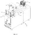
- the plasma etching system 200is comprised of plasma source 101 mounted above a process chamber 205 .
- a main housing 204includes the associated equipment and electronics to support the system.
- a wafer stack housing 202contains substrates 203 , which may be semiconductor wafers undergoing processing to become semiconductor products.
- a wafer moving robot 201is adapted to insert and remove substrates 203 to and from the process chamber 205 .
- the plasma source 101may be a linear-inductive plasma source.
- This linear-inductive plasma sourcemay be an inductively coupled plasma source with an integrated power delivery system, producing a high density plasma that dissociates inert process gas into reactive species which flow out of the unit and perform work on substrates placed downstream.
- the performance of such a plasma sourcemay be constrained in prior industrial uses, such that the chamber pressure may need to be constrained within a narrow range, or that the plasma etch rates on substrates downstream from such a source may be overly variable across a substrate.
- a linear-inductive plasma sourcemay be utilized in such a way to overcome prior deficiencies, as seen in embodiments of the present invention.
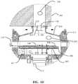
- a plasma source 101is mounted atop a lower process chamber 205 .
- the plasma source 101may be a linear inductive plasma source which has a cylindrical chamber within it along a vertical axis.
- a first zone 114 within the cylindrical chamber within the plasma sourceis representative of the environment within the plasma source cylindrical chamber.
- At the bottom of the cylindrical chamber within the plasma sourceis a constrictor 102 which may be a circular disc.
- the constrictor 102may have an opening 116 which may be a circular opening.
- a spreading disc 103resides below the opening 116 in the constrictor 102 .
- Standoffs 104are used to locate the spreading disc 103 below constrictor 102 and to facilitate attachment of the spreading disc 103 .
- the bottom surface of the spreading disc 103may be flat and the upper surface of the spreading disc 103 may be rounded.
- the target of a plasma processis a substrate 108 , which may be a silicon wafer undergoing processing for semiconductor applications.
- the wafermay reside on a substrate support 106 within the lower process chamber 205 .
- the substrate supportmay have an upper plate layer and a layer plate layer and have a heater element 107 routed in recesses between the two plate layers of the substrate support 106 .
- Lift pins 109may be used to support wafer removal.
- the heater element 107may be a stainless steel clad element with electrical connection routed out of the process chamber with a heater coupling 111 .
- a vacuum line 112resides below the substrate support 106 allowing for chamber exhaust at the bottom of the chamber.
- the lower process chamber 205has a chamber door 110 which allows for insertion and removal of the wafer 108 into the chamber housing 113 .
- a chamber roof 105is adapted to facilitate the flow of the plasma around the spreading disc 103 and down onto the top surface of the wafer 108 .
- the chamber roof 105maybe begin as a vertically aligned cylinder and then fan out as a cone to facilitate radial distribution of the plasma flow.
- a second zone 115is illustrative of the environment within the process chamber 205 above the wafer 108 .
- the plasma source 101has an interior space cylindrical diameter of 3 inches, narrowed by the constrictor 102 with a circular opening of 3 ⁇ 4 inches diameter.
- the spreading disc 103resides below spacers 104 which are 3 ⁇ 4 inch high.
- the outside diameter of the spreading disc 103is 1 and 3 ⁇ 8 inches and is nominally 1 ⁇ 8 inch thick, with a domed top surface with a 0.78 inch radius.
- the bottom surface of the constrictor 102is 3 and 15/16 above the surface of the substrate support 106 .
- the constrictor 102 , the spacers 104 , and the spreading disc 103may be of a ceramic material.
- An exemplary substrate 108is a silicon wafer 8 inches in diameter and 0.030 inches thick.
- a back pressurecan develop in the plasma source central opening which allows the plasma to properly develop, even with the lower process chamber 205 at a different or lower pressure.
- a process chamber pressure of 250 mTorr to 1.2 Torrmay be used during an etching process.
- the spreading disc 103then spreads the plasma such that the surface of the wafer is very evenly etched during processing.
- the substrate support 106 with its heating element 107allows for heating of the wafer, for example to 250° C., allowing for enhancement of the etching in some applications.
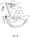
- FIG. 1Efurther illustrates gas flow and pressure regions in some embodiments of systems and methods of the present invention.
- An inductive plasma source 101has a cylindrical chamber 313 and a constrictor plate 102 .
- the constrictor plate 102has an opening 116 .
- the plasma source 101may be a Litmas® Remote Plasma Source 3001 by Advanced Energy of Fort Collins, Colo.
- gas input 312flows into the plasma chamber 313 as a combination of O2 and N2.
- the O2may flow in at a rate of 1200 sccm and N2 may also flow in concurrently at a rate of 120 sccm.
- the inflow gasflows into the plasma chamber 313 and may occupy a space 301 where plasma firing may occur.
- there is continuous flow during a plasma processbeginning with the gas input 312 at the upper end of the plasma source 101 , and ending with exit flow 310 through the vacuum exit line 112 , there will be differing pressures along this flow path.
- the process efficiency, and process uniformitymay be negatively impacted due to pressure variations in the process chamber. These pressure variations may be due to a variety of factors, such as vacuum pump stability, aspects of the vacuum throttle valve, the gas distribution itself, accuracies of sensors, and other factors.
- the chamber pressure point 311may be needed to be kept within a 100 mTorr range, which may be 800-900 mTorr.
- a 100 mTorr rangewhich may be 800-900 mTorr.
- the factors listed above which may lead to pressure variationsmay make it difficult to remain within such a tight pressure range.
- Excursions outside the pressure rangemay lead to incomplete plasma firing, or the cessation of firing. Process efficiency may be significantly lower when suffering from these effects.
- full firing in the firing space 301may occur over a range of pressure difference an order of magnitude higher, from 250 mTorr to 1.2 Torr, for example. Without a constrictor there may not be full, or any, plasma firing in such a configuration. With too much of a constriction, plasma efficiency may also be impacted.
- the interior diameter of the plasma chamber 313is 3 inches. In some aspects, the interior diameter 116 of the constrictor 102 is 3 ⁇ 4 inch. In some aspects, the interior diameter 116 of the constrictor 102 is in the range of 3 ⁇ 8 inch to 1 inch. In some aspects, the interior diameter 116 of the constrictor 102 is in the range of 3 ⁇ 8 inch to 1.25 inches. In some aspects, the interior diameter 116 of the constrictor 102 is in the range of 1 ⁇ 8 of the diameter of the interior diameter of the plasma chamber 313 to 1 ⁇ 3 of the interior diameter of the plasma chamber. In some aspects, the interior diameter of the plasma chamber 313 is in the range of 2 to 4 inches.
- the flowis moderated by the spreading disc 103 .
- the flowis routed 303 outwards around the spreading disc 103 .
- the plasmathen resides within a central zone 304 within the chamber 205 constrained from above by the chamber roof 105 .
- the plasmaworks downward 305 on the top surface of the substrate 108 .
- Another advantage of systems according to embodiments of the present inventionis that there is more even plasma distribution onto the top surface of the substrate 108 .
- the etch rate uniformityis within 6%. In some aspects, the uniformity is within 10%. Exemplary data is seen in Table 1.
- the use of a constrictor plate and the beam spreaderresults in processing with the combined advantages of maintaining plasma, and plasma efficiency, over a wider range of chamber pressure variations and also results in a more uniform processing of the substrate.
- the systemis also moderated by a gas input showerhead 351 .
- a gas inlet line 350may supply the process gasses, which may O2 and N2, for example, as discussed above.
- the gasroutes into a gas input showerhead 351 , which spreads the gas flow over the circular area at the upper end of the plasma chamber 313 of the plasma source 101 .
- the gas input showerhead 351may have a disc 352 with gas exit holes 353 arranged around the bottom surface of the disc 352 .
- the gas exit holes 353may be sized such that there is some flow resistance within the gas flow as it exits through the gas exit holes 353 , evening out the gas flow through the different gas exit holes.
- the systemWith the moderated, even, gas input at the input end of the plasma source 101 , which may be a linear-inductive plasma source, and the moderated gas exit through the interior 116 of the constrictor 102 , very high plasma efficiency may be obtained. Coupled with the gas spreading disc 103 under the conical chamber top 105 , the system then facilitates extremely even plasma processing on a substrate, as discussed above, and as seen in Table 1.
Landscapes
- Engineering & Computer Science (AREA)
- Physics & Mathematics (AREA)
- Plasma & Fusion (AREA)
- Chemical & Material Sciences (AREA)
- Analytical Chemistry (AREA)
- Condensed Matter Physics & Semiconductors (AREA)
- General Physics & Mathematics (AREA)
- Manufacturing & Machinery (AREA)
- Computer Hardware Design (AREA)
- Microelectronics & Electronic Packaging (AREA)
- Power Engineering (AREA)
- Chemical Kinetics & Catalysis (AREA)
- Drying Of Semiconductors (AREA)
Abstract
Description
| TABLE 1 | |||||||||
| Resist | Wafer | RF | Total | ||||||
| Thickness | Size | Temp | Pressure | Power | O2 Flow | N2 Flow | Time | Rate | *Unif |
| 4μ | 150 | 200 C. | 370 mTorr | 3 kW | 1200 sccm | 120 sscm | 30 sec | 5.03 μ/min | 4.50% |
| 4μ | 150 | 200 C. | 370 mTorr | 3 kW | 1200 sccm | 120 sccm | 30 sec | 5.18 μ/min | 5.90% |
| 4μ | 150 | 200 C. | 370 mTorr | 3 kW | 1200 sccm | 120 sccm | 30 sec | 5.22 μ/min | 3.60% |
| 4μ | 150 | 200 C. | 370 mTorr | 3 kW | 1200 sccm | 120 sccm | 30 sec | 5.29 μ/min | 4.30% |
| 4μ | 150 | 200 C. | 370 mTorr | 3 kW | 1200 sccm | 120 sccm | 30 sec | 5.28 μ/min | 3.90% |
| *Unif. = (Max − Min.)/2 Mean × 100 | |||||||||
Claims (8)
Priority Applications (6)
| Application Number | Priority Date | Filing Date | Title |
|---|---|---|---|
| US15/898,178US10840068B2 (en) | 2017-02-15 | 2018-02-15 | Plasma spreading apparatus and method of spreading plasma in process ovens |
| US16/276,040US20200013591A1 (en) | 2018-02-15 | 2019-02-14 | Plasma Spreading Apparatus And System, And Method Of Spreading Plasma In Process Ovens |
| PCT/US2019/018081WO2019161109A1 (en) | 2017-02-15 | 2019-02-14 | Plasma spreading apparatus and system, and method for spreading plasma in process ovens |
| CN201980025769.XACN112368797A (en) | 2017-02-15 | 2019-02-14 | Plasma diffusion apparatus and system and method of diffusing plasma in a processing furnace |
| TW108105189ATWI769366B (en) | 2017-02-15 | 2019-02-15 | Plasma spreading apparatus and system, and method for spreading plasma in process ovens |
| US16/888,732US20210013013A1 (en) | 2017-02-15 | 2020-05-31 | Plasma Spreading Apparatus And System |
Applications Claiming Priority (2)
| Application Number | Priority Date | Filing Date | Title |
|---|---|---|---|
| US201762459210P | 2017-02-15 | 2017-02-15 | |
| US15/898,178US10840068B2 (en) | 2017-02-15 | 2018-02-15 | Plasma spreading apparatus and method of spreading plasma in process ovens |
Related Child Applications (2)
| Application Number | Title | Priority Date | Filing Date |
|---|---|---|---|
| US16/276,040Continuation-In-PartUS20200013591A1 (en) | 2018-02-15 | 2019-02-14 | Plasma Spreading Apparatus And System, And Method Of Spreading Plasma In Process Ovens |
| US16/888,732DivisionUS20210013013A1 (en) | 2017-02-15 | 2020-05-31 | Plasma Spreading Apparatus And System |
Publications (2)
| Publication Number | Publication Date |
|---|---|
| US20180308668A1 US20180308668A1 (en) | 2018-10-25 |
| US10840068B2true US10840068B2 (en) | 2020-11-17 |
Family
ID=63854118
Family Applications (2)
| Application Number | Title | Priority Date | Filing Date |
|---|---|---|---|
| US15/898,178ActiveUS10840068B2 (en) | 2017-02-15 | 2018-02-15 | Plasma spreading apparatus and method of spreading plasma in process ovens |
| US16/888,732AbandonedUS20210013013A1 (en) | 2017-02-15 | 2020-05-31 | Plasma Spreading Apparatus And System |
Family Applications After (1)
| Application Number | Title | Priority Date | Filing Date |
|---|---|---|---|
| US16/888,732AbandonedUS20210013013A1 (en) | 2017-02-15 | 2020-05-31 | Plasma Spreading Apparatus And System |
Country Status (4)
| Country | Link |
|---|---|
| US (2) | US10840068B2 (en) |
| CN (1) | CN112368797A (en) |
| TW (1) | TWI769366B (en) |
| WO (1) | WO2019161109A1 (en) |
Families Citing this family (6)
| Publication number | Priority date | Publication date | Assignee | Title |
|---|---|---|---|---|
| US10840068B2 (en)* | 2017-02-15 | 2020-11-17 | Yield Engineering Systems, Inc. | Plasma spreading apparatus and method of spreading plasma in process ovens |
| US11444053B2 (en) | 2020-02-25 | 2022-09-13 | Yield Engineering Systems, Inc. | Batch processing oven and method |
| US11688621B2 (en) | 2020-12-10 | 2023-06-27 | Yield Engineering Systems, Inc. | Batch processing oven and operating methods |
| US12374569B2 (en) | 2021-10-20 | 2025-07-29 | Yield Engineering Systems, Inc. | Batch processing oven for magnetic anneal |
| CN117276057A (en)* | 2023-11-20 | 2023-12-22 | 江苏微导纳米科技股份有限公司 | Diffusion method and diffusion equipment |
| US20250233571A1 (en)* | 2024-01-17 | 2025-07-17 | Applied Materials, Inc. | Rf filter topology for substrate support assembly |
Citations (6)
| Publication number | Priority date | Publication date | Assignee | Title |
|---|---|---|---|---|
| US5580385A (en)* | 1994-06-30 | 1996-12-03 | Texas Instruments, Incorporated | Structure and method for incorporating an inductively coupled plasma source in a plasma processing chamber |
| US20100101603A1 (en)* | 2008-10-23 | 2010-04-29 | Lam Research Corporation | Method and apparatus for removing photoresist |
| US20110073564A1 (en)* | 2009-09-25 | 2011-03-31 | Applied Materials, Inc. | Method and apparatus for high efficiency gas dissociation in inductive couple plasma reactor |
| US20110115378A1 (en)* | 2009-11-18 | 2011-05-19 | Applied Materials, Inc. | Plasma source design |
| US20150221479A1 (en)* | 2014-01-31 | 2015-08-06 | Applied Materials, Inc. | Rps assisted rf plasma source for semiconductor processing |
| US10083817B1 (en)* | 2006-08-22 | 2018-09-25 | Valery Godyak | Linear remote plasma source |
Family Cites Families (19)
| Publication number | Priority date | Publication date | Assignee | Title |
|---|---|---|---|---|
| US4718976A (en)* | 1982-03-31 | 1988-01-12 | Fujitsu Limited | Process and apparatus for plasma treatment |
| US4951601A (en)* | 1986-12-19 | 1990-08-28 | Applied Materials, Inc. | Multi-chamber integrated process system |
| JP3165938B2 (en)* | 1993-06-24 | 2001-05-14 | 東京エレクトロン株式会社 | Gas treatment equipment |
| US6039834A (en)* | 1997-03-05 | 2000-03-21 | Applied Materials, Inc. | Apparatus and methods for upgraded substrate processing system with microwave plasma source |
| JP2000026975A (en)* | 1998-07-09 | 2000-01-25 | Komatsu Ltd | Surface treatment equipment |
| US6287643B1 (en)* | 1999-09-30 | 2001-09-11 | Novellus Systems, Inc. | Apparatus and method for injecting and modifying gas concentration of a meta-stable or atomic species in a downstream plasma reactor |
| US20030230385A1 (en)* | 2002-06-13 | 2003-12-18 | Applied Materials, Inc. | Electro-magnetic configuration for uniformity enhancement in a dual chamber plasma processing system |
| GB0323001D0 (en)* | 2003-10-01 | 2003-11-05 | Oxford Instr Plasma Technology | Apparatus and method for plasma treating a substrate |
| US8349128B2 (en)* | 2004-06-30 | 2013-01-08 | Applied Materials, Inc. | Method and apparatus for stable plasma processing |
| US7829471B2 (en)* | 2005-07-29 | 2010-11-09 | Applied Materials, Inc. | Cluster tool and method for process integration in manufacturing of a photomask |
| CN100365790C (en)* | 2005-12-28 | 2008-01-30 | 良率国际贸易(上海)有限公司 | Semiconductor fault signal detecting and statistic system and its method |
| US7655571B2 (en)* | 2006-10-26 | 2010-02-02 | Applied Materials, Inc. | Integrated method and apparatus for efficient removal of halogen residues from etched substrates |
| CN101789354B (en)* | 2010-02-11 | 2012-07-04 | 中微半导体设备(上海)有限公司 | Plasma treatment device with diffused dissociation |
| US8524004B2 (en)* | 2010-06-16 | 2013-09-03 | Applied Materials, Inc. | Loadlock batch ozone cure |
| US9666414B2 (en)* | 2011-10-27 | 2017-05-30 | Applied Materials, Inc. | Process chamber for etching low k and other dielectric films |
| US10113236B2 (en)* | 2014-05-14 | 2018-10-30 | Applied Materials, Inc. | Batch curing chamber with gas distribution and individual pumping |
| US10699878B2 (en)* | 2016-02-12 | 2020-06-30 | Lam Research Corporation | Chamber member of a plasma source and pedestal with radially outward positioned lift pins for translation of a substrate c-ring |
| US20170241019A1 (en)* | 2016-02-22 | 2017-08-24 | Ultratech, Inc. | Pe-ald methods with reduced quartz-based contamination |
| US10840068B2 (en)* | 2017-02-15 | 2020-11-17 | Yield Engineering Systems, Inc. | Plasma spreading apparatus and method of spreading plasma in process ovens |
- 2018
- 2018-02-15USUS15/898,178patent/US10840068B2/enactiveActive
- 2019
- 2019-02-14WOPCT/US2019/018081patent/WO2019161109A1/ennot_activeCeased
- 2019-02-14CNCN201980025769.XApatent/CN112368797A/enactivePending
- 2019-02-15TWTW108105189Apatent/TWI769366B/enactive
- 2020
- 2020-05-31USUS16/888,732patent/US20210013013A1/ennot_activeAbandoned
Patent Citations (6)
| Publication number | Priority date | Publication date | Assignee | Title |
|---|---|---|---|---|
| US5580385A (en)* | 1994-06-30 | 1996-12-03 | Texas Instruments, Incorporated | Structure and method for incorporating an inductively coupled plasma source in a plasma processing chamber |
| US10083817B1 (en)* | 2006-08-22 | 2018-09-25 | Valery Godyak | Linear remote plasma source |
| US20100101603A1 (en)* | 2008-10-23 | 2010-04-29 | Lam Research Corporation | Method and apparatus for removing photoresist |
| US20110073564A1 (en)* | 2009-09-25 | 2011-03-31 | Applied Materials, Inc. | Method and apparatus for high efficiency gas dissociation in inductive couple plasma reactor |
| US20110115378A1 (en)* | 2009-11-18 | 2011-05-19 | Applied Materials, Inc. | Plasma source design |
| US20150221479A1 (en)* | 2014-01-31 | 2015-08-06 | Applied Materials, Inc. | Rps assisted rf plasma source for semiconductor processing |
Also Published As
| Publication number | Publication date |
|---|---|
| WO2019161109A1 (en) | 2019-08-22 |
| TW201941299A (en) | 2019-10-16 |
| TWI769366B (en) | 2022-07-01 |
| CN112368797A (en) | 2021-02-12 |
| US20180308668A1 (en) | 2018-10-25 |
| US20210013013A1 (en) | 2021-01-14 |
Similar Documents
| Publication | Publication Date | Title |
|---|---|---|
| US10840068B2 (en) | Plasma spreading apparatus and method of spreading plasma in process ovens | |
| KR102535931B1 (en) | Collar, conical showerheads and/or top plates for reducing recirculation in a substrate processing system | |
| KR102156389B1 (en) | Gas distribution showerhead for semiconductor processing | |
| TWI761337B (en) | Substrate processing system | |
| KR102640272B1 (en) | Lids and lid kits for atomic layer deposition chambers | |
| US9423042B2 (en) | Slit valve having increased flow uniformity | |
| US9219006B2 (en) | Flowable carbon film by FCVD hardware using remote plasma PECVD | |
| KR102155395B1 (en) | Plasma etching device and plasma etching method | |
| CN110724938B (en) | Spray head design | |
| KR20170074755A (en) | Showerhead assembly | |
| TWI871205B (en) | Thermal process chamber lid with backside pumping | |
| CN110047775A (en) | Semiconductor device manufacturing equipment and manufacturing method | |
| CN104046961B (en) | Substrate holder and comprise the substrate-treating apparatus of described substrate holder | |
| KR102256154B1 (en) | Baking device for a wafer coated with a coating containing a solvent | |
| US20200013591A1 (en) | Plasma Spreading Apparatus And System, And Method Of Spreading Plasma In Process Ovens | |
| US10780447B2 (en) | Apparatus for controlling temperature uniformity of a showerhead | |
| TWI700388B (en) | Integration of dual remote plasmas sources for flowable cvd | |
| CN112074624A (en) | Pressure skew system for controlling center-to-edge pressure changes | |
| US20210032753A1 (en) | Methods and apparatus for dual channel showerheads | |
| US20180258531A1 (en) | Diffuser design for flowable cvd | |
| KR102215639B1 (en) | Gas distribution apparatus and substrate processing apparatus having the same | |
| KR102538276B1 (en) | Pe-cvd apparatus and method |
Legal Events
| Date | Code | Title | Description |
|---|---|---|---|
| FEPP | Fee payment procedure | Free format text:ENTITY STATUS SET TO UNDISCOUNTED (ORIGINAL EVENT CODE: BIG.); ENTITY STATUS OF PATENT OWNER: SMALL ENTITY | |
| FEPP | Fee payment procedure | Free format text:ENTITY STATUS SET TO SMALL (ORIGINAL EVENT CODE: SMAL); ENTITY STATUS OF PATENT OWNER: SMALL ENTITY | |
| STPP | Information on status: patent application and granting procedure in general | Free format text:NON FINAL ACTION MAILED | |
| STPP | Information on status: patent application and granting procedure in general | Free format text:RESPONSE TO NON-FINAL OFFICE ACTION ENTERED AND FORWARDED TO EXAMINER | |
| STPP | Information on status: patent application and granting procedure in general | Free format text:FINAL REJECTION MAILED | |
| STPP | Information on status: patent application and granting procedure in general | Free format text:AWAITING RESPONSE FOR INFORMALITY, FEE DEFICIENCY OR CRF ACTION | |
| STPP | Information on status: patent application and granting procedure in general | Free format text:DOCKETED NEW CASE - READY FOR EXAMINATION | |
| STPP | Information on status: patent application and granting procedure in general | Free format text:RESPONSE TO NON-FINAL OFFICE ACTION ENTERED AND FORWARDED TO EXAMINER | |
| STPP | Information on status: patent application and granting procedure in general | Free format text:NOTICE OF ALLOWANCE MAILED -- APPLICATION RECEIVED IN OFFICE OF PUBLICATIONS | |
| AS | Assignment | Owner name:YIELD ENGINEERING SYSTEMS, INC., CALIFORNIA Free format text:ASSIGNMENT OF ASSIGNORS INTEREST;ASSIGNOR:MCCOY, CRAIG WALTER;REEL/FRAME:053644/0055 Effective date:20200825 Owner name:YIELD ENGINEERING SYSTEMS, INC., CALIFORNIA Free format text:ASSIGNMENT OF ASSIGNORS INTEREST;ASSIGNOR:MOFFAT, WILLIAM;REEL/FRAME:053647/0998 Effective date:20200828 | |
| STCB | Information on status: application discontinuation | Free format text:ABANDONMENT FOR FAILURE TO CORRECT DRAWINGS/OATH/NONPUB REQUEST | |
| STPP | Information on status: patent application and granting procedure in general | Free format text:PUBLICATIONS -- ISSUE FEE PAYMENT VERIFIED | |
| STCF | Information on status: patent grant | Free format text:PATENTED CASE | |
| AS | Assignment | Owner name:YIELD ENGINEERING SPV LLC, CALIFORNIA Free format text:ASSIGNMENT OF ASSIGNORS INTEREST;ASSIGNOR:YIELD ENGINEERING SYSTEMS, INC.;REEL/FRAME:063584/0553 Effective date:20230505 Owner name:AON IP ADVANTAGE FUND LP, ILLINOIS Free format text:SECURITY INTEREST;ASSIGNOR:YIELD ENGINEERING SPV LLC;REEL/FRAME:063585/0001 Effective date:20230505 | |
| MAFP | Maintenance fee payment | Free format text:PAYMENT OF MAINTENANCE FEE, 4TH YR, SMALL ENTITY (ORIGINAL EVENT CODE: M2551); ENTITY STATUS OF PATENT OWNER: SMALL ENTITY Year of fee payment:4 |