US10825659B2 - Substrate processing chamber including multiple gas injection points and dual injector - Google Patents
Substrate processing chamber including multiple gas injection points and dual injectorDownload PDFInfo
- Publication number
- US10825659B2 US10825659B2US15/399,692US201715399692AUS10825659B2US 10825659 B2US10825659 B2US 10825659B2US 201715399692 AUS201715399692 AUS 201715399692AUS 10825659 B2US10825659 B2US 10825659B2
- Authority
- US
- United States
- Prior art keywords
- gas
- gas flow
- substrate processing
- cavity
- holes
- Prior art date
- Legal status (The legal status is an assumption and is not a legal conclusion. Google has not performed a legal analysis and makes no representation as to the accuracy of the status listed.)
- Active, expires
Links
Images


Classifications
- H—ELECTRICITY
- H01—ELECTRIC ELEMENTS
- H01J—ELECTRIC DISCHARGE TUBES OR DISCHARGE LAMPS
- H01J37/00—Discharge tubes with provision for introducing objects or material to be exposed to the discharge, e.g. for the purpose of examination or processing thereof
- H01J37/32—Gas-filled discharge tubes
- H01J37/32431—Constructional details of the reactor
- H01J37/3244—Gas supply means
- H01J37/32449—Gas control, e.g. control of the gas flow
- C—CHEMISTRY; METALLURGY
- C23—COATING METALLIC MATERIAL; COATING MATERIAL WITH METALLIC MATERIAL; CHEMICAL SURFACE TREATMENT; DIFFUSION TREATMENT OF METALLIC MATERIAL; COATING BY VACUUM EVAPORATION, BY SPUTTERING, BY ION IMPLANTATION OR BY CHEMICAL VAPOUR DEPOSITION, IN GENERAL; INHIBITING CORROSION OF METALLIC MATERIAL OR INCRUSTATION IN GENERAL
- C23C—COATING METALLIC MATERIAL; COATING MATERIAL WITH METALLIC MATERIAL; SURFACE TREATMENT OF METALLIC MATERIAL BY DIFFUSION INTO THE SURFACE, BY CHEMICAL CONVERSION OR SUBSTITUTION; COATING BY VACUUM EVAPORATION, BY SPUTTERING, BY ION IMPLANTATION OR BY CHEMICAL VAPOUR DEPOSITION, IN GENERAL
- C23C16/00—Chemical coating by decomposition of gaseous compounds, without leaving reaction products of surface material in the coating, i.e. chemical vapour deposition [CVD] processes
- C23C16/44—Chemical coating by decomposition of gaseous compounds, without leaving reaction products of surface material in the coating, i.e. chemical vapour deposition [CVD] processes characterised by the method of coating
- C23C16/455—Chemical coating by decomposition of gaseous compounds, without leaving reaction products of surface material in the coating, i.e. chemical vapour deposition [CVD] processes characterised by the method of coating characterised by the method used for introducing gases into reaction chamber or for modifying gas flows in reaction chamber
- C23C16/45502—Flow conditions in reaction chamber
- C23C16/45508—Radial flow
- C—CHEMISTRY; METALLURGY
- C23—COATING METALLIC MATERIAL; COATING MATERIAL WITH METALLIC MATERIAL; CHEMICAL SURFACE TREATMENT; DIFFUSION TREATMENT OF METALLIC MATERIAL; COATING BY VACUUM EVAPORATION, BY SPUTTERING, BY ION IMPLANTATION OR BY CHEMICAL VAPOUR DEPOSITION, IN GENERAL; INHIBITING CORROSION OF METALLIC MATERIAL OR INCRUSTATION IN GENERAL
- C23C—COATING METALLIC MATERIAL; COATING MATERIAL WITH METALLIC MATERIAL; SURFACE TREATMENT OF METALLIC MATERIAL BY DIFFUSION INTO THE SURFACE, BY CHEMICAL CONVERSION OR SUBSTITUTION; COATING BY VACUUM EVAPORATION, BY SPUTTERING, BY ION IMPLANTATION OR BY CHEMICAL VAPOUR DEPOSITION, IN GENERAL
- C23C16/00—Chemical coating by decomposition of gaseous compounds, without leaving reaction products of surface material in the coating, i.e. chemical vapour deposition [CVD] processes
- C23C16/44—Chemical coating by decomposition of gaseous compounds, without leaving reaction products of surface material in the coating, i.e. chemical vapour deposition [CVD] processes characterised by the method of coating
- C23C16/455—Chemical coating by decomposition of gaseous compounds, without leaving reaction products of surface material in the coating, i.e. chemical vapour deposition [CVD] processes characterised by the method of coating characterised by the method used for introducing gases into reaction chamber or for modifying gas flows in reaction chamber
- C23C16/45563—Gas nozzles
- C23C16/4558—Perforated rings
- H—ELECTRICITY
- H01—ELECTRIC ELEMENTS
- H01J—ELECTRIC DISCHARGE TUBES OR DISCHARGE LAMPS
- H01J37/00—Discharge tubes with provision for introducing objects or material to be exposed to the discharge, e.g. for the purpose of examination or processing thereof
- H01J37/32—Gas-filled discharge tubes
- H01J37/32009—Arrangements for generation of plasma specially adapted for examination or treatment of objects, e.g. plasma sources
- H01J37/32082—Radio frequency generated discharge
- H01J37/32174—Circuits specially adapted for controlling the RF discharge
- H—ELECTRICITY
- H01—ELECTRIC ELEMENTS
- H01J—ELECTRIC DISCHARGE TUBES OR DISCHARGE LAMPS
- H01J37/00—Discharge tubes with provision for introducing objects or material to be exposed to the discharge, e.g. for the purpose of examination or processing thereof
- H01J37/32—Gas-filled discharge tubes
- H01J37/32009—Arrangements for generation of plasma specially adapted for examination or treatment of objects, e.g. plasma sources
- H01J37/32357—Generation remote from the workpiece, e.g. down-stream
- H—ELECTRICITY
- H01—ELECTRIC ELEMENTS
- H01J—ELECTRIC DISCHARGE TUBES OR DISCHARGE LAMPS
- H01J37/00—Discharge tubes with provision for introducing objects or material to be exposed to the discharge, e.g. for the purpose of examination or processing thereof
- H01J37/32—Gas-filled discharge tubes
- H01J37/32009—Arrangements for generation of plasma specially adapted for examination or treatment of objects, e.g. plasma sources
- H01J37/32422—Arrangement for selecting ions or species in the plasma
- H—ELECTRICITY
- H01—ELECTRIC ELEMENTS
- H01J—ELECTRIC DISCHARGE TUBES OR DISCHARGE LAMPS
- H01J37/00—Discharge tubes with provision for introducing objects or material to be exposed to the discharge, e.g. for the purpose of examination or processing thereof
- H01J37/32—Gas-filled discharge tubes
- H01J37/32431—Constructional details of the reactor
- H01J37/32458—Vessel
- H01J37/32513—Sealing means, e.g. sealing between different parts of the vessel
- H—ELECTRICITY
- H01—ELECTRIC ELEMENTS
- H01J—ELECTRIC DISCHARGE TUBES OR DISCHARGE LAMPS
- H01J37/00—Discharge tubes with provision for introducing objects or material to be exposed to the discharge, e.g. for the purpose of examination or processing thereof
- H01J37/32—Gas-filled discharge tubes
- H01J37/32431—Constructional details of the reactor
- H01J37/32715—Workpiece holder
- H—ELECTRICITY
- H01—ELECTRIC ELEMENTS
- H01L—SEMICONDUCTOR DEVICES NOT COVERED BY CLASS H10
- H01L21/00—Processes or apparatus adapted for the manufacture or treatment of semiconductor or solid state devices or of parts thereof
- H01L21/67—Apparatus specially adapted for handling semiconductor or electric solid state devices during manufacture or treatment thereof; Apparatus specially adapted for handling wafers during manufacture or treatment of semiconductor or electric solid state devices or components ; Apparatus not specifically provided for elsewhere
- H01L21/67005—Apparatus not specifically provided for elsewhere
- H01L21/67011—Apparatus for manufacture or treatment
- H01L21/67017—Apparatus for fluid treatment
- H01L21/67063—Apparatus for fluid treatment for etching
- H01L21/67069—Apparatus for fluid treatment for etching for drying etching
- H—ELECTRICITY
- H01—ELECTRIC ELEMENTS
- H01L—SEMICONDUCTOR DEVICES NOT COVERED BY CLASS H10
- H01L21/00—Processes or apparatus adapted for the manufacture or treatment of semiconductor or solid state devices or of parts thereof
- H01L21/67—Apparatus specially adapted for handling semiconductor or electric solid state devices during manufacture or treatment thereof; Apparatus specially adapted for handling wafers during manufacture or treatment of semiconductor or electric solid state devices or components ; Apparatus not specifically provided for elsewhere
- H01L21/683—Apparatus specially adapted for handling semiconductor or electric solid state devices during manufacture or treatment thereof; Apparatus specially adapted for handling wafers during manufacture or treatment of semiconductor or electric solid state devices or components ; Apparatus not specifically provided for elsewhere for supporting or gripping
- H01L21/6831—Apparatus specially adapted for handling semiconductor or electric solid state devices during manufacture or treatment thereof; Apparatus specially adapted for handling wafers during manufacture or treatment of semiconductor or electric solid state devices or components ; Apparatus not specifically provided for elsewhere for supporting or gripping using electrostatic chucks
- H—ELECTRICITY
- H01—ELECTRIC ELEMENTS
- H01J—ELECTRIC DISCHARGE TUBES OR DISCHARGE LAMPS
- H01J2237/00—Discharge tubes exposing object to beam, e.g. for analysis treatment, etching, imaging
- H01J2237/32—Processing objects by plasma generation
- H01J2237/33—Processing objects by plasma generation characterised by the type of processing
- H01J2237/334—Etching
Definitions
- the present disclosurerelates to substrate processing systems and methods, and more particularly to substrate processing systems and methods for etching and ashing substrates.
- Substrate processing systemsmay be used to etch or ash film on a substrate such as a semiconductor wafer.
- the substrate processing systemstypically include a processing chamber, a gas distribution device such as a showerhead and a substrate support. During processing, the substrate is arranged on the substrate support. Different gas mixtures may be introduced into the processing chamber and radio frequency (RF) plasma may be used to activate chemical reactions.
- RFradio frequency
- Substrate processing systemstypically use single points of gas injection. These systems also typically require gases to be mixed into a gas mixture before the gas mixture is delivered by the same gas lines to the substrate processing chamber. Problems encountered when using this approach include the inability to use incompatible gases (such as pyrophoric and oxidizing gases) due to chemical reactions in the gas lines before the gases reach the substrate processing chamber. Gas flow direction and reaction locations in the substrate processing chamber are usually optimized for a single process and generally require hardware changes to optimize performance for each additional process to be performed. In many applications, the gases enter through an RF source. These gases are typically ionized before travelling through the showerhead.
- gasesenter through an RF source. These gases are typically ionized before travelling through the showerhead.
- a substrate processing systemincludes an upper chamber and a coil arranged around the upper chamber.
- An RF generating systemsupplies RF power to the coil to create plasma in the upper chamber.
- a first supportsupports a lower portion of the upper chamber and includes a first plurality of gas flow channels to deliver a first tuning gas flow in an upward and radially inward direction into the upper chamber.
- a gas injectoris arranged in an upper portion of the upper chamber to deliver a plasma gas mixture in at least one of a downward or a downward and radially outward direction.
- a second supportis arranged between the first support and the lower chamber and includes a second plurality of gas flow channels to deliver second tuning gas flow in a downward and radially inward direction into the lower chamber.
- a substrate supportsupports a substrate and is arranged in the lower chamber.
- a gas distribution deviceincludes a plurality of gas through holes and is arranged between the upper chamber and the lower chamber.
- a gas delivery systemsupplies the first tuning gas flow to the first plurality of gas flow channels, the plasma gas mixture to the gas injector, and the second tuning gas flow to the second plurality of gas flow channels.
- the gas distribution deviceis grounded.
- the gas delivery systemsupplies a first gas flow and a second gas flow to the gas injector.
- the gas injectorindependently delivers the first gas flow and the second gas flow to the upper chamber without mixing in the gas injector.
- the gas injectorincludes a first injector housing including a base portion including a first gas flow channel to receive the first gas flow; a projecting portion extending from the base portion; and a second gas flow channel to receive the second gas flow and extending through the base portion and the projecting portion.
- the gas injectorincludes a second injector housing including a first cavity including a first opening, a second opening and a first plurality of gas through holes arranged around the second opening and extending from the first cavity through the second injector housing; and a second cavity that includes a second plurality of gas through holes extending from the second cavity though through the second injector housing and that extends from the second opening of the first cavity.
- the base portionsealingly sealing engages with the first opening of the first cavity.
- the projecting portionsealingly engages with the second cavity.
- the first cavityhas a first diameter and the second cavity has a second diameter that is smaller than the first diameter.
- the projecting portionincludes a groove.
- An O-ringis arranged in the groove to sealingly engage with an inner surface of the second cavity.
- the base portionhas a “T”-shaped cross section. At least two of the first plurality of gas through holes is arranged at an acute outward angle relative to a downward direction. At least two of the second plurality of gas through holes is arranged at an acute outward angle relative to a downward direction.
- At least one of the second plurality of gas through holesis arranged in a downward direction and at least two of the second plurality of gas through holes are arranged at an acute outward angle relative to the downward direction.
- the first gas flowis supplied at a first flow rate and the second gas flow is supplied at a second flow rate that is different than the first flow rate.
- the first gas flowincludes a first gas mixture and the second gas flow includes a second gas mixture that is different than the first gas mixture.
- a gas injector for a substrate processing systemincludes a first injector housing including a base portion defining a first gas flow channel; a projecting portion extending from the base portion; and a second gas flow channel extending through the base portion and the projecting portion.
- the gas injectorincludes a second injector housing including a first cavity including a first opening, a second opening and a first plurality of gas through holes arranged around the second opening.
- the first gas flow channelis in fluid communication with the first plurality of gas through holes.
- the second injector housingincludes a second cavity that includes a second plurality of gas through holes and that extends from the second opening of the first cavity.
- the second gas flow channelis in fluid communication with the second plurality of gas through holes.
- the base portionsealingly engages with the first opening of the first cavity
- the projecting portionsealingly engages with the second cavity, and gas flows through the first gas flow channel into a processing chamber of the substrate processing system without mixing in the gas injector with gas flowing through the second gas flow channel.
- the first cavityhas a first diameter and the second cavity has a second diameter that is smaller than the first diameter.
- the projecting portionincludes a groove and further comprising an O-ring arranged in the groove to sealingly engage with an inner surface of the second cavity.
- the base portionhas a “T”-shaped cross section.
- At least two of the first plurality of gas through holesis arranged at an acute outward angle relative to a downward direction. At least two of the second plurality of gas through holes is arranged at an acute outward angle relative to a downward direction.
- At least one of the second plurality of gas through holesis arranged in the downward direction and at least two of the second plurality of gas through holes are arranged at an acute outward angle relative to the downward direction.
- a substrate processing systemincludes the gas injector, an upper chamber, a lower chamber and a substrate support that supports a substrate and that is arranged in the lower chamber.
- a gas delivery systemsupplies a first gas flow to the first gas flow channel and a second gas flow to the second gas flow channel.
- a gas distribution deviceincludes a plurality of gas through holes and is arranged between the upper chamber and the lower chamber. The gas injector supplies gas to the upper chamber.
- a coilis arranged around the upper chamber.
- An RF generating systemsupplies RF power to the coil to create plasma in the upper chamber.
- the first gas flowis supplied at a first flow rate and the second gas flow is supplied at a second flow rate that is different than the first flow rate.
- the first gas flowincludes a first gas mixture and the second gas flow includes a second gas mixture that is different than the first gas mixture.
- FIG. 1is a functional block diagram of an example of a substrate processing system according to the present disclosure
- FIG. 2is a functional block diagram of an example of a gas delivery system according to the present disclosure
- FIG. 3is a functional block diagram of another example of a gas delivery system according to the present disclosure.
- FIG. 4is partial perspective and side cross-sectional view of an example of a dual gas injector according to the present disclosure
- FIG. 5is partial perspective and side cross-sectional view of another example of a dual gas injector according to the present disclosure.
- FIG. 6is a side cross-sectional view of an example of a lower support including a gas plenum and one or more holes for directing gas upwardly into the upper chamber region.
- Systems and methods according to the present disclosureallow tuning of gas species and gas delivery paths in a substrate processing system.
- the substrate processing systemperforms etching or ashing.
- Multiple gas injection locationsare provided and each gas injection location is supplied by a gas delivery system or a gas metering system. Tuning of gas delivery at each of the gas injection locations may be used to adjust etch or ash rate uniformity and/or selectivity on the substrate.
- the multiple injection locationsallow gas delivery to be adjusted such that the volume of ionized species can be moved simply by adjusting a flow rate to a particular injection location.
- incompatible gasesflow through different injection locations to prevent mixing before the gases reach the substrate processing chamber. This also allows for separate injection of shielding or carrier gases without mixing with main process gases before delivery to the substrate processing chamber.
- a gas injectorincludes multiple injector locations to reduce hardware complexity and potential leak locations.
- the gas injectorincludes two or more separate gas delivery paths that do not allow the gases to mix until the gases enter the substrate processing chamber.
- the gas delivery pathsare pointed in the same or different directions to help tune wafer uniformity.
- FIG. 1a substrate processing chamber 100 for etching or ashing a substrate according to the present disclosure is shown. While a specific type of substrate processing chamber is shown and described, the improvements described herein may be applied to a variety of other substrate processing chambers.
- the substrate processing chamber 100includes a lower chamber region 102 and an upper chamber region 104 .
- the lower chamber region 102is defined by chamber sidewall surfaces 108 , a chamber bottom surface 110 and a lower surface of a gas distribution device 114 .
- the upper chamber region 104is defined by an upper surface of the gas distribution device 114 and an inner surface 118 of the upper chamber region 104 .
- the upper chamber region 104may have a dome shape, although other shapes can be used.
- the upper chamber region 104rests on a first support 121 .
- the first support 121has an annular shape.
- the first support 121includes one or more gas flow channels 123 for delivering process gas to the upper chamber region 104 , as will be described further below.
- the process gasis delivered by the one or more gas flow channels 123 in an upward direction at an acute angle relative to a plane including the gas distribution device 114 , although other angles/directions may be used.
- the gas flow channels 123are uniformly spaced around the first support 121 .
- the first support 121may rest on a second support 125 .
- the second supporthas an annular shape.
- the second support 125defines one or more gas flow channels 127 for delivering process gas to the lower chamber region 102 .
- the gas flow channelsare uniformly spaced around the second support 125 .
- gas through holes 131 in the gas distribution device 114align with the gas flow channels 127 .
- the gas distribution device 114has a smaller diameter and the gas through holes 131 are not needed.
- the process gasis delivered by the one or more gas flow channels 127 in a downward direction towards the substrate at an acute angle relative to the plane including the gas distribution device 114 , although other angles/directions may be used.
- the upper chamber region 104is cylindrical with a flat top surface and a flat inductive coil may be used.
- a single chambermay be used with a spacer located between a showerhead and the substrate support.
- a substrate support 122is arranged in the lower chamber region 102 .
- the substrate support 122includes an electrostatic chuck (ESC), although other types of substrate supports can be used.
- a substrate 126is arranged on an upper surface of the substrate support 122 during etching.
- a temperature of the substrate 126may be controlled by a heater plate, an optional cooling plate with fluid channels and one or more sensors (all not shown); although any other suitable substrate support temperature control system may be used.
- the gas distribution device 114includes a showerhead (for example, a plate 128 having a plurality of through holes 129 ).
- the plurality of through holes 129extend from the upper surface of the plate 128 to the lower surface of the plate 128 .
- the through holes 129have a diameter in a range from 0.4′′ to 0.75′′ and the showerhead is made of a conducting material such as aluminum or a non-conductive material such as ceramic with an embedded electrode made of a conducting material.
- One or more inductive coils 140are arranged around an outer portion of the upper chamber region 104 . When energized, the one or more inductive coils 140 create an electromagnetic field inside of the upper chamber region 104 .
- a gas injector 142injects one or more gas mixtures from a gas delivery system 150 .
- the gas injector 142includes a center injection location that directs gas in a downward direction and one or more side injection locations that inject gas at an angle with respect to the downward direction.
- the gas delivery system 150delivers a first portion of the gas mixture at a first flow rate to the center injection location and a second portion of the gas mixture at a second flow rate to the side injection location(s) of the gas injector 142 .
- different gas mixturesare delivered by the gas injector 142 .
- the gas delivery system 150delivers tuning gas to the gas flow channels 123 and 127 and/or to other locations in the processing chamber as will be described below.
- the tuning gasis varied to adjust etch or ash rates and/or selectivity by varying a location of the volume of ionized species.
- a plasma generator 170may be used to generate RF power that is output to the one or more inductive coils 140 .
- Plasmais generated in the upper chamber region 104 .
- the plasma generator 170includes an RF generator 172 and a matching network 174 .
- the matching network 174matches an impedance of the RF generator 172 to the impedance of the one or more inductive coils 140 .
- the gas distribution device 114is connected to a reference potential such as ground.
- a valve 178 and a pump 180may be used to control pressure inside of the lower and upper chamber regions 102 , 104 and to evacuate reactants from the lower and upper chamber regions 102 , 104 , respectively.
- a controller 176communicates with the gas delivery system 150 , the valve 178 , the pump 180 , and/or the plasma generator 170 to control flow of process gas, purge gas, RF plasma and chamber pressure.
- plasmais sustained inside the upper chamber region 104 by the one or more inductive coils 140 .
- One or more gas mixturesare introduced from a top portion of the chamber using the gas injector 142 and plasma is confined within the upper chamber region 104 using the gas distribution device 114 , which may be grounded.
- Confining the plasma in the upper chamber region 104allows volume recombination of plasma species and effusing desired etchant species through the gas distribution device 114 .
- Some amount of ionswill diffuse out of the plasma region through the gas distribution device 114 .
- the amount of plasma that diffusesis an order of magnitude lower than the plasma located inside the upper chamber region 104 .
- Most of ions in the plasmaare lost by volume recombination at high pressures. Surface recombination loss at the upper surface of the gas distribution device 114 also lowers ion density below the gas distribution device 114 .
- an RF bias generator 184is provided and includes an RF generator 186 and a matching network 188 .
- the RF biascan be used to create plasma between the gas distribution device 114 and the substrate support or to create a self-bias on the substrate 126 to attract ions.
- the controller 176may be used to control the RF bias.
- a first example of the gas delivery system 150provides two or more gas mixtures via two or more gas channels 208 - 1 , . . . , and 208 -Q (collectively gas channels 208 ).
- the gas channel 208 - 1includes one or more gas sources 210 - 1 , . . . , and 210 -N (collectively gas sources 210 ), one or more valves 212 - 1 , . . . , and 212 -N (collectively valves 212 ), one or more mass flow controllers (MFCs) 214 - 1 , . . .
- Another gas channel 208 -Qincludes one or more gas sources 230 - 1 , . . . , and 230 -P (collectively gas sources 230 ), one or more valves 232 - 1 , . . . , and 232 -P (collectively valves 232 ), one or more mass flow controllers (MFCs) 234 - 1 , . . . , and 234 -P (collectively MFCs 234 ), and a mixing manifold 236 .
- N, P and Qare integers greater than or equal to one.
- Each of the gas channels 208can supply a different gas mixture to the gas injector 142 or other injection zones in the substrate processing chamber. The different gas mixtures are supplied to various zones of the substrate processing chamber described herein.
- Each gas channel in the gas delivery system 150includes one or more gas sources 270 - 1 , . . . , and 270 -N (collectively gas sources 270 ), one or more valves 272 - 1 , . . . , and 272 -N (collectively valves 272 ), one or more mass flow controllers (MFCs) 274 - 1 , . . . , and 274 -N (collectively MFCs 274 ), and a mixing manifold 276 .
- gas sources 270 - 1 , . . . , and 270 -Ncollectively gas sources 270
- valves 272 - 1 , . . . , and 272 -Ncollectively valves 272
- MFCsmass flow controllers
- the gas mixture output by the mixing manifold 276may be split by a gas splitter 280 into two or more gas flows each having the same gas mixture and a different flow rate.
- the gas splitter 280may include one or more channels each including a valve and a restricted orifice. Sizes of the restricted orifices may be selected using the valves to provide various desired flow rates. The different portions of the gas mixtures are supplied at the different flow rates to various zones of the substrate processing chamber.
- FIGS. 2 and 3are combined to provide one gas mixture at one flow rate (or one or more different flow rates) and one or more other gas mixtures at one flow rate (or at one or more different flow rates).
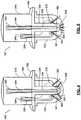
- the gas injector 142includes an upper or first injector housing 310 and a lower or second injector housing 312 .
- the lower injector housing 312defines a first cavity 316 and a second cavity 318 extending downwardly from one end of the first cavity 316 .
- the second cavity 318has a smaller diameter than the first cavity 316 .
- One or more gas through holes 320 in the second cavity 318are in fluid communication with the substrate processing chamber.
- the one or more gas through holes 320is arranged in a generally circular pattern about a lower surface of the second cavity 318 .
- One or more gas through holes 321 in the first cavity 316are in fluid communication with the substrate processing chamber.
- the one or more gas through holes 321is arranged in a generally circular pattern about a lower surface of the first cavity 316 .
- An upper portion 330 of the gas injector 142includes a base portion 332 that extends radially outwardly relative to an outer surface of the lower injector housing and a projecting portion 334 that projects downwardly from a center of the base portion 332 .
- the base portion 332has a generally “T”-shaped cross section.
- the projecting portion 334has an outer diameter that is substantially equal to an inner diameter of the second cavity 318 . An abutting relationship is created when the end of the projecting portion 334 is inserted in the second cavity 318 .
- a sealformed between the outer diameter of the projecting portion 334 and the inner diameter of the second cavity 318 .
- the sealincludes an “O”-ring 360 that is arranged in a groove 362 formed on an outer diameter of the projecting portion 334 .
- the grooveis formed on the surface defining the second cavity 318 .
- the projecting portion 334defines a gas flow channel 338 that extends from one end of the projecting portion 334 to an opposite end of the projecting portion 334 .
- a conduit carrying a first gas mixtureis connected to gas fittings 342 .
- the first gas mixtureflows through a flow channel defined by a conduit 344 and the gas flow channel 338 into the second cavity 318 .
- the first gas mixtureflows through the gas through holes 320 into the upper chamber region 104 .
- a conduit carrying a second gas mixtureis connected to fittings 348 .
- the second gas mixtureflows through a flow channel defined by conduit 350 into the first cavity 316 .
- the second gas mixtureflows through the gas through holes 321 into the upper chamber region 104 .
- Elements 350 and 338may be respectively called first and second gas flow channels.
- the gas through holes 320 and 321may be arranged in other locations, at other angles, and/or at other relative angles to effectuate different gas mixing characteristics.
- the one or more gas flow channels 123are in fluid communication with the gas flow channel 420 and direct gas from the gas flow channel 420 into the upper chamber region 104 . In some examples, the one or more gas flow channels 123 are arranged in a spaced relationship around the processing chamber. In some examples, the one or more gas flow channels 123 direct gas flow from the gas flow channel 420 at an acute radially-inward angle relative to the upper surface of the gas distribution device 114 .
- Advantages of the systems and methods described hereininclude tunability of process gas flow direction, the ability to keep incompatible gases separate until they enter the process cavity, the ability to flow gases above and below the showerhead, and the ability to flow two or more separate gases through one injector.
- Spatial and functional relationships between elementsare described using various terms, including “connected,” “engaged,” “coupled,” “adjacent,” “next to,” “on top of,” “above,” “below,” and “disposed.” Unless explicitly described as being “direct,” when a relationship between first and second elements is described in the above disclosure, that relationship can be a direct relationship where no other intervening elements are present between the first and second elements, but can also be an indirect relationship where one or more intervening elements are present (either spatially or functionally) between the first and second elements.
- the phrase at least one of A, B, and Cshould be construed to mean a logical (A OR B OR C), using a non-exclusive logical OR, and should not be construed to mean “at least one of A, at least one of B, and at least one of C.”
- a controlleris part of a system, which may be part of the above-described examples.
- Such systemscan comprise semiconductor processing equipment, including a processing tool or tools, chamber or chambers, a platform or platforms for processing, and/or specific processing components (a wafer pedestal, a gas flow system, etc.).
- These systemsmay be integrated with electronics for controlling their operation before, during, and after processing of a semiconductor wafer or substrate.
- the electronicsmay be referred to as the “controller,” which may control various components or subparts of the system or systems.
- the controllermay be programmed to control any of the processes disclosed herein, including the delivery of processing gases, temperature settings (e.g., heating and/or cooling), pressure settings, vacuum settings, power settings, radio frequency (RF) generator settings, RF matching circuit settings, frequency settings, flow rate settings, fluid delivery settings, positional and operation settings, wafer transfers into and out of a tool and other transfer tools and/or load locks connected to or interfaced with a specific system.
- temperature settingse.g., heating and/or cooling
- RFradio frequency
- the controllermay be defined as electronics having various integrated circuits, logic, memory, and/or software that receive instructions, issue instructions, control operation, enable cleaning operations, enable endpoint measurements, and the like.
- the integrated circuitsmay include chips in the form of firmware that store program instructions, digital signal processors (DSPs), chips defined as application specific integrated circuits (ASICs), and/or one or more microprocessors, or microcontrollers that execute program instructions (e.g., software).
- Program instructionsmay be instructions communicated to the controller in the form of various individual settings (or program files), defining operational parameters for carrying out a particular process on or for a semiconductor wafer or to a system.
- the operational parametersmay, in some embodiments, be part of a recipe defined by process engineers to accomplish one or more processing steps during the fabrication of one or more layers, materials, metals, oxides, silicon, silicon dioxide, surfaces, circuits, and/or dies of a wafer.
- the controllermay be a part of or coupled to a computer that is integrated with the system, coupled to the system, otherwise networked to the system, or a combination thereof.
- the controllermay be in the “cloud” or all or a part of a fab host computer system, which can allow for remote access of the wafer processing.
- the computermay enable remote access to the system to monitor current progress of fabrication operations, examine a history of past fabrication operations, examine trends or performance metrics from a plurality of fabrication operations, to change parameters of current processing, to set processing steps to follow a current processing, or to start a new process.
- a remote computere.g. a server
- the remote computermay include a user interface that enables entry or programming of parameters and/or settings, which are then communicated to the system from the remote computer.
- the controllerreceives instructions in the form of data, which specify parameters for each of the processing steps to be performed during one or more operations. It should be understood that the parameters may be specific to the type of process to be performed and the type of tool that the controller is configured to interface with or control.
- the controllermay be distributed, such as by comprising one or more discrete controllers that are networked together and working towards a common purpose, such as the processes and controls described herein.
- An example of a distributed controller for such purposeswould be one or more integrated circuits on a chamber in communication with one or more integrated circuits located remotely (such as at the platform level or as part of a remote computer) that combine to control a process on the chamber.
- example systemsmay include a plasma etch chamber or module, a deposition chamber or module, a spin-rinse chamber or module, a metal plating chamber or module, a clean chamber or module, a bevel edge etch chamber or module, a physical vapor deposition (PVD) chamber or module, a chemical vapor deposition (CVD) chamber or module, an atomic layer deposition (ALD) chamber or module, an atomic layer etch (ALE) chamber or module, an ion implantation chamber or module, a track chamber or module, and any other semiconductor processing systems that may be associated or used in the fabrication and/or manufacturing of semiconductor wafers.
- PVDphysical vapor deposition
- CVDchemical vapor deposition
- ALDatomic layer deposition
- ALEatomic layer etch
- the controllermight communicate with one or more of other tool circuits or modules, other tool components, cluster tools, other tool interfaces, adjacent tools, neighboring tools, tools located throughout a factory, a main computer, another controller, or tools used in material transport that bring containers of wafers to and from tool locations and/or load ports in a semiconductor manufacturing factory.
Landscapes
- Chemical & Material Sciences (AREA)
- Engineering & Computer Science (AREA)
- Physics & Mathematics (AREA)
- Plasma & Fusion (AREA)
- Analytical Chemistry (AREA)
- Organic Chemistry (AREA)
- General Physics & Mathematics (AREA)
- Materials Engineering (AREA)
- Mechanical Engineering (AREA)
- Metallurgy (AREA)
- General Chemical & Material Sciences (AREA)
- Condensed Matter Physics & Semiconductors (AREA)
- Chemical Kinetics & Catalysis (AREA)
- Manufacturing & Machinery (AREA)
- Computer Hardware Design (AREA)
- Microelectronics & Electronic Packaging (AREA)
- Power Engineering (AREA)
- Drying Of Semiconductors (AREA)
- Electromagnetism (AREA)
- Spectroscopy & Molecular Physics (AREA)
- Plasma Technology (AREA)
Abstract
Description
- Referring now to
FIG. 6 , thefirst support 121 defines afirst portion 410 including agas flow channel 420 that may extend fully or partially around the periphery of the substrate processing chamber. In some examples, thegas flow channel 420 has an annular shape. Thegas flow channel 420 is in fluid communication with a source of process gas. For example, thegas flow channel 420 may be connected by conduit(s)430 to one or more gas sources, gas mixture sources, manifolds and/or outputs of gas splitters.
- Referring now to
Claims (13)
Priority Applications (5)
| Application Number | Priority Date | Filing Date | Title |
|---|---|---|---|
| US15/399,692US10825659B2 (en) | 2016-01-07 | 2017-01-05 | Substrate processing chamber including multiple gas injection points and dual injector |
| KR1020170002200AKR102774227B1 (en) | 2016-01-07 | 2017-01-06 | Substrate processing chamber including multiple gas injection points and dual injector |
| TW106100384ATWI734726B (en) | 2016-01-07 | 2017-01-06 | Substrate processing chamber including multiple gas injection points and dual injector |
| CN201710013856.6ACN107017147B (en) | 2016-01-07 | 2017-01-09 | Substrate processing chamber including multiple gas injection points and dual injectors |
| KR1020250023614AKR20250029847A (en) | 2016-01-07 | 2025-02-24 | Substrate processing chamber including multiple gas injection points and dual injector |
Applications Claiming Priority (2)
| Application Number | Priority Date | Filing Date | Title |
|---|---|---|---|
| US201662275837P | 2016-01-07 | 2016-01-07 | |
| US15/399,692US10825659B2 (en) | 2016-01-07 | 2017-01-05 | Substrate processing chamber including multiple gas injection points and dual injector |
Publications (2)
| Publication Number | Publication Date |
|---|---|
| US20170200586A1 US20170200586A1 (en) | 2017-07-13 |
| US10825659B2true US10825659B2 (en) | 2020-11-03 |
Family
ID=59275816
Family Applications (1)
| Application Number | Title | Priority Date | Filing Date |
|---|---|---|---|
| US15/399,692Active2038-06-03US10825659B2 (en) | 2016-01-07 | 2017-01-05 | Substrate processing chamber including multiple gas injection points and dual injector |
Country Status (4)
| Country | Link |
|---|---|
| US (1) | US10825659B2 (en) |
| KR (2) | KR102774227B1 (en) |
| CN (1) | CN107017147B (en) |
| TW (1) | TWI734726B (en) |
Cited By (5)
| Publication number | Priority date | Publication date | Assignee | Title |
|---|---|---|---|---|
| US11424103B2 (en)* | 2016-08-19 | 2022-08-23 | Lam Research Corporation | Control of on-wafer cd uniformity with movable edge ring and gas injection adjustment |
| US11488831B2 (en) | 2018-06-13 | 2022-11-01 | Lam Research Corporation | Efficient cleaning and etching of high aspect ratio structures |
| US11967486B2 (en) | 2019-01-23 | 2024-04-23 | Lam Research Corporation | Substrate processing system including dual ion filter for downstream plasma |
| US12183554B2 (en) | 2017-11-21 | 2024-12-31 | Lam Research Corporation | Bottom and middle edge rings |
| US12444579B2 (en) | 2020-03-23 | 2025-10-14 | Lam Research Corporation | Mid-ring erosion compensation in substrate processing systems |
Families Citing this family (16)
| Publication number | Priority date | Publication date | Assignee | Title |
|---|---|---|---|---|
| US10658222B2 (en) | 2015-01-16 | 2020-05-19 | Lam Research Corporation | Moveable edge coupling ring for edge process control during semiconductor wafer processing |
| US10957561B2 (en) | 2015-07-30 | 2021-03-23 | Lam Research Corporation | Gas delivery system |
| US10192751B2 (en) | 2015-10-15 | 2019-01-29 | Lam Research Corporation | Systems and methods for ultrahigh selective nitride etch |
| CN106876299B (en)* | 2015-12-11 | 2019-08-23 | 北京北方华创微电子装备有限公司 | Semiconductor processing equipment |
| US10825659B2 (en) | 2016-01-07 | 2020-11-03 | Lam Research Corporation | Substrate processing chamber including multiple gas injection points and dual injector |
| US10699878B2 (en) | 2016-02-12 | 2020-06-30 | Lam Research Corporation | Chamber member of a plasma source and pedestal with radially outward positioned lift pins for translation of a substrate c-ring |
| US10147588B2 (en) | 2016-02-12 | 2018-12-04 | Lam Research Corporation | System and method for increasing electron density levels in a plasma of a substrate processing system |
| US10651015B2 (en) | 2016-02-12 | 2020-05-12 | Lam Research Corporation | Variable depth edge ring for etch uniformity control |
| US10727089B2 (en) | 2016-02-12 | 2020-07-28 | Lam Research Corporation | Systems and methods for selectively etching film |
| US10438833B2 (en) | 2016-02-16 | 2019-10-08 | Lam Research Corporation | Wafer lift ring system for wafer transfer |
| US10267728B2 (en)* | 2016-09-28 | 2019-04-23 | Lam Research Corporation | Systems and methods for detecting oxygen in-situ in a substrate area of a substrate processing system |
| US11469079B2 (en) | 2017-03-14 | 2022-10-11 | Lam Research Corporation | Ultrahigh selective nitride etch to form FinFET devices |
| KR102610827B1 (en)* | 2018-12-20 | 2023-12-07 | 어플라이드 머티어리얼스, 인코포레이티드 | Method and apparatus for providing improved gas flow to the processing volume of a processing chamber |
| CN112117176B (en)* | 2019-06-20 | 2023-03-07 | 中微半导体设备(上海)股份有限公司 | Plasma processing apparatus and plasma processing system |
| CN111599717B (en)* | 2020-05-09 | 2024-03-26 | 北京北方华创微电子装备有限公司 | Semiconductor reaction chamber and atomic layer plasma etching machine |
| US20240297022A1 (en)* | 2023-03-03 | 2024-09-05 | Applied Materials, Inc. | Indpendent dilution inject for remote plasma oxidation |
Citations (240)
| Publication number | Priority date | Publication date | Assignee | Title |
|---|---|---|---|---|
| US4262686A (en) | 1978-07-20 | 1981-04-21 | Dragerwerk Aktiengesellschaft | Apparatus for the electrically controlled proportioning and mixing of gases |
| US4374698A (en) | 1980-07-11 | 1983-02-22 | U.S. Philips Corporation | Method of manufacturing a semiconductor device |
| US4431477A (en) | 1983-07-05 | 1984-02-14 | Matheson Gas Products, Inc. | Plasma etching with nitrous oxide and fluoro compound gas mixture |
| US4793897A (en) | 1987-03-20 | 1988-12-27 | Applied Materials, Inc. | Selective thin film etch process |
| EP0424299A2 (en) | 1989-10-20 | 1991-04-24 | International Business Machines Corporation | Selective silicon nitride plasma etching |
| US5329965A (en) | 1993-07-30 | 1994-07-19 | The Perkin-Elmer Corporation | Hybrid valving system for varying fluid flow rate |
| US5346578A (en) | 1992-11-04 | 1994-09-13 | Novellus Systems, Inc. | Induction plasma source |
| US5605179A (en) | 1995-03-17 | 1997-02-25 | Insync Systems, Inc. | Integrated gas panel |
| US5660673A (en) | 1993-08-31 | 1997-08-26 | Nec Corporation | Apparatus for dry etching |
| US5662143A (en) | 1996-05-16 | 1997-09-02 | Gasonics International | Modular gas box system |
| US5744695A (en) | 1997-01-10 | 1998-04-28 | Sony Corporation | Apparatus to check calibration of mass flow controllers |
| EP0838842A2 (en) | 1996-10-23 | 1998-04-29 | Applied Materials, Inc. | Plasma reactor with heated source of a polymer-hardening precursor material |
| US5762714A (en) | 1994-10-18 | 1998-06-09 | Applied Materials, Inc. | Plasma guard for chamber equipped with electrostatic chuck |
| CN1189859A (en) | 1995-07-10 | 1998-08-05 | 沃特金斯·约翰逊公司 | Plasma enhanced chemical processing reactor and method |
| US5907221A (en) | 1995-08-16 | 1999-05-25 | Applied Materials, Inc. | Inductively coupled plasma reactor with an inductive coil antenna having independent loops |
| US6022809A (en) | 1998-12-03 | 2000-02-08 | Taiwan Semiconductor Manufacturing Company, Ltd. | Composite shadow ring for an etch chamber and method of using |
| US6042687A (en) | 1997-06-30 | 2000-03-28 | Lam Research Corporation | Method and apparatus for improving etch and deposition uniformity in plasma semiconductor processing |
| US6044534A (en) | 1995-12-07 | 2000-04-04 | Nec Corporation | Semiconductor device manufacturing machine and method for manufacturing a semiconductor device by using the same manufacturing machine |
| US6050283A (en) | 1995-07-07 | 2000-04-18 | Air Liquide America Corporation | System and method for on-site mixing of ultra-high-purity chemicals for semiconductor processing |
| US6060400A (en) | 1998-03-26 | 2000-05-09 | The Research Foundation Of State University Of New York | Highly selective chemical dry etching of silicon nitride over silicon and silicon dioxide |
| US6074959A (en) | 1997-09-19 | 2000-06-13 | Applied Materials, Inc. | Method manifesting a wide process window and using hexafluoropropane or other hydrofluoropropanes to selectively etch oxide |
| WO2000040776A1 (en) | 1999-01-05 | 2000-07-13 | Ronal Systems Corporation | In situ chemical generator and method |
| US6143078A (en)* | 1998-11-13 | 2000-11-07 | Applied Materials, Inc. | Gas distribution system for a CVD processing chamber |
| US6152168A (en) | 1997-08-15 | 2000-11-28 | Fujikin Incorporated | Pressure-type flow rate control apparatus |
| US6206976B1 (en) | 1999-08-27 | 2001-03-27 | Lucent Technologies Inc. | Deposition apparatus and related method with controllable edge exclusion |
| US6210593B1 (en) | 1997-02-06 | 2001-04-03 | Matsushita Electric Industrial Co., Ltd. | Etching method and etching apparatus |
| US6217937B1 (en) | 1998-07-15 | 2001-04-17 | Cornell Research Foundation, Inc. | High throughput OMVPE apparatus |
| US20010002581A1 (en) | 1998-09-03 | 2001-06-07 | Kazuyasu Nishikawa | System for manufacturing a semiconductor device |
| US20010004903A1 (en) | 1999-04-16 | 2001-06-28 | Tadahiro Ohmi | Parallel divided flow-type fluid supply apparatus, and fluid-switchable pressure-type flow control method and fluid-switchable pressure-type flow control system for the same fluid supply apparatus |
| US20010013363A1 (en) | 1999-04-22 | 2001-08-16 | Hirofumi Kitayama | Apparatus and method for feeding gases for use in semiconductor manufacturing |
| JP2001230239A (en) | 2000-02-15 | 2001-08-24 | Tokyo Electron Ltd | Apparatus and method for treating |
| US6286451B1 (en)* | 1997-05-29 | 2001-09-11 | Applied Materials, Inc. | Dome: shape and temperature controlled surfaces |
| US20010035530A1 (en) | 2000-04-26 | 2001-11-01 | Takashi Udagawa | Vapor phase deposition system |
| US6328808B1 (en) | 1997-08-19 | 2001-12-11 | Applied Materials, Inc. | Apparatus and method for aligning and controlling edge deposition on a substrate |
| US20020038669A1 (en) | 2000-10-04 | 2002-04-04 | Takayuki Yamagishi | Gas-line system for semiconductor-manufacturing apparatus |
| US20020042205A1 (en) | 2000-10-06 | 2002-04-11 | Mcmillin Brian K. | Gas distribution apparatus for semiconductor processing |
| US20020045265A1 (en) | 2000-03-07 | 2002-04-18 | Bergh H. Sam | Parallel flow reactor having variable composition |
| US6376386B1 (en) | 1997-02-25 | 2002-04-23 | Fujitsu Limited | Method of etching silicon nitride by a mixture of CH2 F2, CH3F or CHF3 and an inert gas |
| US20020048536A1 (en) | 1999-03-03 | 2002-04-25 | Bergh H. Sam | Parallel flow process optimization reactors |
| US20020046991A1 (en) | 1997-06-26 | 2002-04-25 | Smith Donald K. | Toroidal low-field reactive gas source |
| US20020072240A1 (en) | 2000-12-07 | 2002-06-13 | Semiconductor Leading Edge Technologies, Inc. | Plasma etching apparatus with focus ring and plasma etching method |
| US20020078893A1 (en)* | 2000-05-18 | 2002-06-27 | Applied Materials , Inc. | Plasma enhanced chemical processing reactor and method |
| US20020088542A1 (en) | 1999-07-07 | 2002-07-11 | Kazuyasu Nishikawa | Plasma processing apparatus |
| TW506234B (en) | 2000-09-18 | 2002-10-11 | Tokyo Electron Ltd | Tunable focus ring for plasma processing |
| US20020160125A1 (en) | 1999-08-17 | 2002-10-31 | Johnson Wayne L. | Pulsed plasma processing method and apparatus |
| US20020174905A1 (en) | 2001-04-20 | 2002-11-28 | Festo Corporation | Stackable valve manifold arrangement |
| US20020175144A1 (en) | 1999-03-25 | 2002-11-28 | Hoiman(Raymond) Hung | Enhancement of silicon oxide etch rate and nitride selectivity using hexafluorobutadiene or other heavy perfluorocarbon |
| US6492774B1 (en) | 2000-10-04 | 2002-12-10 | Lam Research Corporation | Wafer area pressure control for plasma confinement |
| US6589352B1 (en) | 1999-12-10 | 2003-07-08 | Applied Materials, Inc. | Self aligning non contact shadow ring process kit |
| US20030236643A1 (en) | 2002-06-24 | 2003-12-25 | Ali Shajii | Apparatus and method for calibration of mass flow controller |
| US20030236638A1 (en) | 2002-06-24 | 2003-12-25 | Ali Shajii | Apparatus and method for displaying mass flow controller pressure |
| US20030236592A1 (en) | 2002-06-24 | 2003-12-25 | Ali Shajii | Apparatus and method for mass flow controller with network access to diagnostics |
| US20040053428A1 (en) | 2002-09-18 | 2004-03-18 | Steger Robert J. | Method and apparatus for the compensation of edge ring wear in a plasma processing chamber |
| US20040089240A1 (en) | 2002-04-24 | 2004-05-13 | Dando Ross S. | Chemical vapor deposition apparatus |
| US6736931B2 (en) | 1991-06-27 | 2004-05-18 | Kenneth S. Collins | Inductively coupled RF plasma reactor and plasma chamber enclosure structure therefor |
| US20040094206A1 (en) | 2002-11-15 | 2004-05-20 | Renesas Technology Corp. | Semiconductor manufacturing apparatus enabling inspection of mass flow controller maintaining connection thereto |
| US6744212B2 (en) | 2002-02-14 | 2004-06-01 | Lam Research Corporation | Plasma processing apparatus and method for confining an RF plasma under very high gas flow and RF power density conditions |
| KR20040050080A (en) | 2002-12-09 | 2004-06-16 | 주식회사 하이닉스반도체 | Apparatus for driving focus ring of plasma etch chamber |
| US20040112540A1 (en) | 2002-12-13 | 2004-06-17 | Lam Research Corporation | Uniform etch system |
| US20040112539A1 (en) | 2002-12-13 | 2004-06-17 | Lam Research Corporation | Uniform etch system |
| US20040118678A1 (en)* | 2002-12-18 | 2004-06-24 | Klaus Hartig | Magnetron sputtering systems including anodic gas distribution systems |
| US20040149389A1 (en) | 2002-11-26 | 2004-08-05 | Tokyo Electron Limited | Plasma processing device |
| US20040163601A1 (en) | 2003-02-26 | 2004-08-26 | Masanori Kadotani | Plasma processing apparatus |
| US20040168719A1 (en) | 2003-02-28 | 2004-09-02 | Masahiro Nambu | System for dividing gas flow |
| US20040173270A1 (en) | 2003-03-03 | 2004-09-09 | Harris James M. | Fluid delivery system and mounting panel therefor |
| US20040200529A1 (en) | 2001-05-24 | 2004-10-14 | Celerity Group, Inc. | Method and apparatus for providing a determined ratio of process fluids |
| US6818560B1 (en) | 1999-09-22 | 2004-11-16 | Tokyo Electron Limited | Plasma processing apparatus and plasma processing method |
| US6841943B2 (en) | 2002-06-27 | 2005-01-11 | Lam Research Corp. | Plasma processor with electrode simultaneously responsive to plural frequencies |
| US20050005994A1 (en) | 2002-06-03 | 2005-01-13 | Kazuhiko Sugiyama | Method for supplying gas while dividing to chamber from gas supply facility equipped with flow controller |
| KR20050008792A (en) | 2002-06-03 | 2005-01-21 | 어플라이드 머티어리얼스, 인코포레이티드 | A cathode pedestal for a plasma etch reactor |
| US20050067021A1 (en) | 2003-09-30 | 2005-03-31 | Bevers William Daniel | Bypass loop gas flow calibration |
| US20050082007A1 (en) | 2003-10-21 | 2005-04-21 | Applied Materials, Inc. | Mask etch processing apparatus |
| US6898558B2 (en) | 2002-12-31 | 2005-05-24 | Tokyo Electron Limited | Method and apparatus for monitoring a material processing system |
| US6920312B1 (en)* | 2001-05-31 | 2005-07-19 | Lam Research Corporation | RF generating system with fast loop control |
| US20050155625A1 (en) | 2004-01-20 | 2005-07-21 | Taiwan Semiconductor Manufacturing Co., Ltd. | Chamber cleaning method |
| US20050194475A1 (en)* | 2004-03-04 | 2005-09-08 | Han-Ki Kim | Inductively coupled plasma chemical vapor deposition apparatus |
| US20050199342A1 (en) | 2004-03-09 | 2005-09-15 | Ali Shajii | Semiconductor manufacturing gas flow divider system and method |
| US20050241763A1 (en) | 2004-04-30 | 2005-11-03 | Zhisong Huang | Gas distribution system having fast gas switching capabilities |
| US6962879B2 (en) | 2001-03-30 | 2005-11-08 | Lam Research Corporation | Method of plasma etching silicon nitride |
| US20060011237A1 (en) | 2004-07-09 | 2006-01-19 | Tison Stuart A | Method and system for flow measurement and validation of a mass flow controller |
| US20060060141A1 (en) | 2003-05-02 | 2006-03-23 | Tokyo Electron Limited | Process gas introducing mechanism and plasma processing device |
| US20060097644A1 (en) | 2003-06-09 | 2006-05-11 | Ckd Corporation | Relative pressure control system and relative flow control system |
| US20060124169A1 (en) | 2004-12-09 | 2006-06-15 | Tokyo Electron Limited | Gas supply unit, substrate processing apparatus, and supply gas setting method |
| US20060207595A1 (en) | 2003-10-06 | 2006-09-21 | Tadahiro Ohmi | Internal pressure controller of chamber and internal pressure subject -to- control type chamber |
| US20060237063A1 (en) | 2005-04-21 | 2006-10-26 | Junhua Ding | Gas delivery method and system including a flow ratio controller using antisymmetric optimal control |
| US7129171B2 (en) | 2003-10-14 | 2006-10-31 | Lam Research Corporation | Selective oxygen-free etching process for barrier materials |
| WO2007008509A2 (en) | 2005-07-12 | 2007-01-18 | Lam Research Corporation | Methods for verifying gas flow rates from a gas supply system into a plasma processing chamber |
| US20070026684A1 (en) | 2005-08-01 | 2007-02-01 | Stefano Parascandola | Method of producing pitch fractionizations in semiconductor technology |
| US20070066038A1 (en) | 2004-04-30 | 2007-03-22 | Lam Research Corporation | Fast gas switching plasma processing apparatus |
| US20070158025A1 (en) | 2006-01-11 | 2007-07-12 | Lam Research Corporation | Gas switching section including valves having different flow coefficients for gas distribution system |
| US20070175391A1 (en) | 2006-01-31 | 2007-08-02 | Tokyo Electron Limited | Gas supply system, substrate processing apparatus and gas supply method |
| US20070187363A1 (en)* | 2006-02-13 | 2007-08-16 | Tokyo Electron Limited | Substrate processing apparatus and substrate processing method |
| US20070204797A1 (en) | 2006-03-03 | 2007-09-06 | Andreas Fischer | Methods and apparatus for selective pre-coating of a plasma processing chamber |
| US20070204914A1 (en) | 2006-03-01 | 2007-09-06 | Asahi Organic Chemicals Industry Co., Ltd. | Fluid mixing system |
| US20070233412A1 (en) | 2006-03-20 | 2007-10-04 | Hitachi Metals, Ltd. | Mass flow rate control apparatus, its calibration method and semiconductor-producing apparatus |
| US20070240778A1 (en) | 2006-04-14 | 2007-10-18 | Mks Instruments, Inc. | Multiple-Channel Flow Ratio Controller |
| US7288482B2 (en) | 2005-05-04 | 2007-10-30 | International Business Machines Corporation | Silicon nitride etching methods |
| US20070256785A1 (en) | 2006-05-03 | 2007-11-08 | Sharma Pamarthy | Apparatus for etching high aspect ratio features |
| US20070259112A1 (en) | 2006-04-07 | 2007-11-08 | Applied Materials, Inc. | Gas manifolds for use during epitaxial film formation |
| US20070256786A1 (en) | 2006-05-03 | 2007-11-08 | Xiaoping Zhou | Apparatus for etching high aspect ratio features |
| US7309646B1 (en) | 2006-10-10 | 2007-12-18 | Lam Research Corporation | De-fluoridation process |
| KR20080013552A (en)* | 2006-08-09 | 2008-02-13 | 주식회사 에이디피엔지니어링 | Plasma processing equipment |
| US7338907B2 (en) | 2004-10-04 | 2008-03-04 | Sharp Laboratories Of America, Inc. | Selective etching processes of silicon nitride and indium oxide thin films for FeRAM device applications |
| KR20080023569A (en) | 2006-09-11 | 2008-03-14 | 주식회사 하이닉스반도체 | Plasma Etching Device to Prevent Etch Profile Deformation |
| US20080115834A1 (en) | 2006-11-20 | 2008-05-22 | Applied Materials, Inc. | System and method to divide fluid flow in a predetermined ratio |
| US20080121178A1 (en) | 2006-11-28 | 2008-05-29 | Applied Materials, Inc. | Dual top gas feed through distributor for high density plasma chamber |
| US20080202588A1 (en) | 2007-02-26 | 2008-08-28 | Ezra Robert Gold | Method and apparatus for controlling gas flow to a processing chamber |
| US20080202609A1 (en) | 2007-02-26 | 2008-08-28 | Ezra Robert Gold | Method and apparatus for controlling gas flow to a processing chamber |
| US20080202610A1 (en)* | 2007-02-26 | 2008-08-28 | Ezra Robert Gold | Method and apparatus for controlling gas flow to a processing chamber |
| US20080223873A1 (en) | 2007-03-12 | 2008-09-18 | Tokyo Electron Limited | Dynamic control of process chemistry for improved within-substrate process uniformity |
| US20080236749A1 (en) | 2007-03-28 | 2008-10-02 | Tokyo Electron Limited | Plasma processing apparatus |
| US20090061644A1 (en) | 2007-09-05 | 2009-03-05 | Chiang Tony P | Vapor based combinatorial processing |
| US20090061640A1 (en) | 2007-08-29 | 2009-03-05 | Lam Research Corporation | Alternate gas delivery and evacuation system for plasma processing apparatuses |
| US20090056629A1 (en) | 2007-09-05 | 2009-03-05 | Applied Materials, Inc. | Cathode liner with wafer edge gas injection in a plasma reactor chamber |
| US20090067954A1 (en) | 2007-09-07 | 2009-03-12 | Khamsidi Lanee | Automated systems and methods for adapting semiconductor fabrication tools to process wafers of different diameters |
| US20090090174A1 (en) | 2001-06-13 | 2009-04-09 | Paul Phillip H | Precision Flow Control System |
| US20090095364A1 (en) | 2007-10-15 | 2009-04-16 | Ckd Corporation | Fluid flow distribution and supply unit and flow distribution control program |
| US20090183548A1 (en) | 2008-01-18 | 2009-07-23 | Pivotal Systems Corporation | Method and apparatus for in situ testing of gas flow controllers |
| US20090197423A1 (en) | 2008-02-06 | 2009-08-06 | Tokyo Electron Limited | Substrate processing method and substrate processing apparatus |
| US20090221117A1 (en) | 2008-02-29 | 2009-09-03 | Chartered Semiconductor Manufacturing Ltd. | Integrated circuit system employing resistance altering techniques |
| US20090236313A1 (en) | 2008-03-20 | 2009-09-24 | Novellus Systems, Inc. | Gas flow distribution receptacles, plasma generator systems, and methods for performing plasma stripping processes |
| US20090272717A1 (en)* | 2008-03-21 | 2009-11-05 | Applied Materials, Inc. | Method and apparatus of a substrate etching system and process |
| US20090320754A1 (en) | 2006-08-23 | 2009-12-31 | Horiba Stec, Co., Ltd. | Integrated gas panel apparatus |
| US20100012310A1 (en) | 2006-12-19 | 2010-01-21 | Alfa Laval Corporation Ab | Sectioned flow device |
| US20100030390A1 (en) | 2006-12-12 | 2010-02-04 | Horiba Stec, Co., Ltd. | Flow rate ratio control device |
| US20100025369A1 (en) | 2008-07-30 | 2010-02-04 | Hitachi High-Technologies Corporation | Plasma processing apparatus and plasma processing method |
| US20100071438A1 (en) | 2008-09-19 | 2010-03-25 | Applied Materials, Inc. | Method and apparatus for calibrating mass flow controllers |
| US20100122655A1 (en) | 2008-11-14 | 2010-05-20 | Tiner Robin L | Ball supported shadow frame |
| US20100144539A1 (en) | 2006-10-26 | 2010-06-10 | Symyx Technologies, Inc. | High pressure parallel fixed bed reactor and method |
| US20100145633A1 (en) | 2006-12-05 | 2010-06-10 | Horiba Stec, Co., Ltd | Flow controller, flow measuring device testing method, flow controller testing system, and semiconductor manufacturing apparatus |
| US20100178770A1 (en) | 2009-01-14 | 2010-07-15 | Tokyo Electron Limited | Method of etching a thin film using pressure modulation |
| US7757541B1 (en) | 2006-09-13 | 2010-07-20 | Pivotal Systems Corporation | Techniques for calibration of gas flows |
| US20100216313A1 (en) | 2007-10-12 | 2010-08-26 | Panasonic Corproation | Plasma processing apparatus |
| US20100229976A1 (en) | 2006-06-27 | 2010-09-16 | Fujikin Incorporated | Flow rate ratio variable type fluid supply apparatus |
| US20100264117A1 (en) | 2007-10-31 | 2010-10-21 | Tohoku University | Plasma processing system and plasma processing method |
| US20100269924A1 (en) | 2007-12-27 | 2010-10-28 | Horiba Stec, Co., Ltd. | Flow rate ratio controlling apparatus |
| US20100330301A1 (en)* | 2008-02-22 | 2010-12-30 | Eugene Technology Co., Ltd. | Apparatus and method for processing substrate |
| US20110019332A1 (en) | 2004-02-22 | 2011-01-27 | Zond, Inc. | Methods And Apparatus For Generating Strongly-Ionized Plasmas With Ionizational Instabilities |
| US20110031111A1 (en) | 2009-08-07 | 2011-02-10 | Tokyo Electron Limited | Substrate processing apparatus, positioning method and focus ring installation method |
| US20110094596A1 (en) | 2003-06-20 | 2011-04-28 | Fujikin Incorporated | Apparatus and method of dividing and supplying gas to a chamber from a gas supply apparatus equipped with flow-rate control system |
| WO2011051251A1 (en) | 2009-10-26 | 2011-05-05 | Solvay Fluor Gmbh | Etching process for producing a tft matrix |
| US20110135821A1 (en) | 2009-12-07 | 2011-06-09 | Junhua Ding | Methods of and apparatus for controlling pressure in multiple zones of a process tool |
| US7968469B2 (en) | 2007-01-30 | 2011-06-28 | Applied Materials, Inc. | Method of processing a workpiece in a plasma reactor with variable height ground return path to control plasma ion density uniformity |
| US20110253225A1 (en) | 2008-08-13 | 2011-10-20 | Clive Beeby | Method for controlling a gas flow between a plurality of gas streams |
| US20110265883A1 (en) | 2010-04-30 | 2011-11-03 | Applied Materials, Inc. | Methods and apparatus for reducing flow splitting errors using orifice ratio conductance control |
| CN102243977A (en) | 2010-05-12 | 2011-11-16 | 东京毅力科创株式会社 | Plasma processing apparatus and method of manufacturing semiconductor device |
| US20110303696A1 (en) | 2007-12-27 | 2011-12-15 | Intermolecular, Inc. | Maintaining flow rate of a fluid |
| CN102315150A (en) | 2010-06-30 | 2012-01-11 | 朗姆研究公司 | The removable basic ring that is used for plasma processing chamber |
| US20120031500A1 (en) | 2009-03-03 | 2012-02-09 | Jun Hirose | Fluid control apparatus |
| US20120034786A1 (en) | 2010-08-04 | 2012-02-09 | Lam Research Corporation | Plasma Processing Chamber with Dual Axial Gas Injection and Exhaust |
| US8137463B2 (en) | 2007-12-19 | 2012-03-20 | Applied Materials, Inc. | Dual zone gas injection nozzle |
| US20120097266A1 (en) | 2010-10-22 | 2012-04-26 | Applied Materials, Inc. | Apparatus for controlling gas distribution using orifice ratio conductance control |
| US20120149213A1 (en) | 2010-12-09 | 2012-06-14 | Lakshminarayana Nittala | Bottom up fill in high aspect ratio trenches |
| US20120156363A1 (en) | 2010-12-17 | 2012-06-21 | Veeco Instruments Inc. | Gas Injection System for Chemical Vapor Deposition Using Sequenced Valves |
| US20120152364A1 (en) | 2010-12-17 | 2012-06-21 | Horiba Stec, Co., Ltd. | Gas concentration controller system |
| US20120190208A1 (en) | 2009-08-20 | 2012-07-26 | Tokyo Electron Limited | Plasma treatment device and plasma treatment method |
| US20120238102A1 (en) | 2011-03-14 | 2012-09-20 | Applied Materials, Inc. | Methods for etch of sin films |
| US20120238103A1 (en) | 2011-03-14 | 2012-09-20 | Applied Materials, Inc. | Methods for etch of metal and metal-oxide films |
| US20120244715A1 (en) | 2009-12-02 | 2012-09-27 | Xactix, Inc. | High-selectivity etching system and method |
| US20120247386A1 (en) | 2011-03-28 | 2012-10-04 | Applied Materials, Inc. | Method and apparatus for the selective deposition of epitaxial germanium stressor alloys |
| US20120289057A1 (en) | 2011-05-11 | 2012-11-15 | Intermolecular, Inc. | Apparatus and method for multiple symmetrical divisional gas distribution |
| US20120298221A1 (en) | 2009-12-25 | 2012-11-29 | Horiba Stec, Co., Ltd. | Mass flow controller system |
| US20120305184A1 (en) | 2011-05-31 | 2012-12-06 | Applied Materials, Inc. | Dynamic ion radical sieve and ion radical aperture for an inductively coupled plasma (icp) reactor |
| US20120328780A1 (en) | 2011-06-27 | 2012-12-27 | Asm Japan K.K. | Dual Section Module Having Shared and Unshared Mass Flow Controllers |
| US20130008607A1 (en) | 2011-07-06 | 2013-01-10 | Tokyo Electron Limited | Antenna, dielectric window, plasma processing apparatus and plasma processing method |
| US20130029494A1 (en) | 2010-03-04 | 2013-01-31 | Tokyo Electron Limited | Plasma etching method, method for producing semiconductor device, and plasma etching device |
| US20130029496A1 (en) | 2011-07-29 | 2013-01-31 | Asm America, Inc. | Methods and Apparatus for a Gas Panel with Constant Gas Flow |
| US20130025715A1 (en) | 2011-07-28 | 2013-01-31 | Horiba Stec, Co., Ltd. | Gas supply system |
| US20130045605A1 (en) | 2011-08-18 | 2013-02-21 | Applied Materials, Inc. | Dry-etch for silicon-and-nitrogen-containing films |
| US20130085618A1 (en) | 2011-10-04 | 2013-04-04 | Mks Instruments, Inc. | Method of and Apparatus for Multiple Channel Flow Ratio Controller System |
| US20130104996A1 (en) | 2011-10-26 | 2013-05-02 | Applied Materials, Inc. | Method for balancing gas flow supplying multiple cvd reactors |
| US20130106286A1 (en) | 2011-10-28 | 2013-05-02 | Applied Materials, Inc. | Inductively coupled plasma soure with phase control |
| US20130131300A1 (en) | 2010-08-02 | 2013-05-23 | Basell Polyolefine Gmbh | Process and apparatus for mixing and splitting fluid streams |
| US20130145816A1 (en) | 2011-12-13 | 2013-06-13 | Intermolecular, Inc. | Calibration Procedure Considering Gas Solubility |
| TW201324653A (en) | 2011-08-17 | 2013-06-16 | Tokyo Electron Ltd | Semiconductor manufacturing device and processing method |
| US20130157388A1 (en) | 2011-12-19 | 2013-06-20 | Applied Materials, Inc. | Etch rate detection for anti-reflective coating layer and absorber layer etching |
| WO2013123617A1 (en) | 2012-02-22 | 2013-08-29 | Agilent Technologies, Inc. | Mass flow controllers and methods for auto-zeroing flow sensor without shutting off a mass flow controller |
| US20130220433A1 (en) | 2012-02-29 | 2013-08-29 | Fujikin Incorporated | Apparatus for dividing and supplying gas and method for dividing and supplying gas by use of this apparatus |
| US20130255784A1 (en) | 2012-03-30 | 2013-10-03 | Applied Materials, Inc. | Gas delivery systems and methods of use thereof |
| US8552334B2 (en) | 2008-02-08 | 2013-10-08 | Lam Research Corporation | Adjustable gap capacitively coupled RF plasma reactor including lateral bellows and non-contact particle seal |
| US20130270997A1 (en) | 2012-03-30 | 2013-10-17 | Tokyo Electron Limited | Low electron temperature, edge-density enhanced, surface wave plasma (swp) processing method and apparatus |
| US20130288477A1 (en) | 2010-12-08 | 2013-10-31 | Oc Oerlikon Balzers Ag | Apparatus and method for depositing a layer onto a substrate |
| US20130284093A1 (en)* | 2012-04-30 | 2013-10-31 | Semes Co., Ltd. | Substrate treating apparatus |
| US8592328B2 (en) | 2012-01-20 | 2013-11-26 | Novellus Systems, Inc. | Method for depositing a chlorine-free conformal sin film |
| KR20130137962A (en) | 2012-06-08 | 2013-12-18 | 세메스 주식회사 | Apparatus for treating substrate |
| KR20140001540A (en) | 2012-06-27 | 2014-01-07 | 세메스 주식회사 | Apparatus for treating substrate |
| US20140080308A1 (en) | 2012-09-18 | 2014-03-20 | Applied Materials, Inc. | Radical-component oxide etch |
| CN103730318A (en) | 2013-11-15 | 2014-04-16 | 中微半导体设备(上海)有限公司 | Wafer edge protection ring and method for reducing particles at wafer edge |
| US20140120737A1 (en) | 2012-10-23 | 2014-05-01 | Lam Research Corporation | Sub-saturated atomic layer deposition and conformal film deposition |
| WO2014068886A1 (en) | 2012-11-02 | 2014-05-08 | 株式会社フジキン | Accumulation-type gas supply device |
| US20140141621A1 (en) | 2012-11-20 | 2014-05-22 | Applied Materials, Inc. | Dry-etch selectivity |
| US20140144471A1 (en) | 2012-11-28 | 2014-05-29 | Intermolecular, Inc. | Contamination Control, Rinsing, and Purging Methods to Extend the Life of Components within Combinatorial Processing Systems |
| US20140182689A1 (en) | 2012-12-31 | 2014-07-03 | Lam Research Corporation | Gas supply systems for substrate processing chambers and methods therefor |
| US20140235069A1 (en)* | 2013-02-15 | 2014-08-21 | Novellus Systems, Inc. | Multi-plenum showerhead with temperature control |
| US20140248780A1 (en) | 2013-03-01 | 2014-09-04 | Applied Materials, Inc. | Enhanced etching processes using remote plasma sources |
| TW201436089A (en) | 2013-03-15 | 2014-09-16 | Taiwan Semiconductor Mfg | Apparatus for processing semiconductor substrates |
| US20140262038A1 (en) | 2013-03-15 | 2014-09-18 | Applied Materials, Inc. | Processing systems and methods for halide scavenging |
| US20140273460A1 (en) | 2013-03-13 | 2014-09-18 | Applied Materials, Inc. | Passive control for through silicon via tilt in icp chamber |
| WO2014163742A1 (en) | 2013-03-12 | 2014-10-09 | Applied Materials, Inc. | Multi-zone gas injection assembly with azimuthal and radial distribution control |
| US8889024B2 (en) | 2011-10-31 | 2014-11-18 | Hitachi High-Technologies Corporation | Plasma etching method |
| US20150010381A1 (en) | 2013-07-08 | 2015-01-08 | United Microelectronics Corp. | Wafer processing chamber and method for transferring wafer in the same |
| US20150017810A1 (en) | 2013-07-11 | 2015-01-15 | Lam Research Corporation | Dual chamber plasma etcher with ion accelerator |
| CN104299929A (en) | 2013-07-19 | 2015-01-21 | 朗姆研究公司 | Systems and methods for in-situ wafer edge and backside plasma cleaning |
| US8956980B1 (en) | 2013-09-16 | 2015-02-17 | Applied Materials, Inc. | Selective etch of silicon nitride |
| US20150059859A1 (en) | 2013-08-30 | 2015-03-05 | Fujikin Incorporated | Apparatus for dividing and supplying gas and method for dividing and supplying gas |
| US8999106B2 (en) | 2007-12-19 | 2015-04-07 | Applied Materials, Inc. | Apparatus and method for controlling edge performance in an inductively coupled plasma chamber |
| US9051647B2 (en) | 2001-10-15 | 2015-06-09 | Lam Research Corporation | Tunable multi-zone gas injection system |
| US9059678B2 (en) | 2011-04-28 | 2015-06-16 | Lam Research Corporation | TCCT match circuit for plasma etch chambers |
| US20150181684A1 (en) | 2013-12-23 | 2015-06-25 | Applied Materials, Inc. | Extreme edge and skew control in icp plasma reactor |
| CN104752141A (en) | 2013-12-31 | 2015-07-01 | 中微半导体设备(上海)有限公司 | Plasma processing device and operating method thereof |
| US20150184287A1 (en) | 2013-12-26 | 2015-07-02 | Intermolecular, Inc. | Systems and Methods for Parallel Combinatorial Vapor Deposition Processing |
| CN104851832A (en) | 2014-02-18 | 2015-08-19 | 北京北方微电子基地设备工艺研究中心有限责任公司 | Fixing device, reaction cavity and plasma processing device |
| US20150287572A1 (en) | 2014-04-07 | 2015-10-08 | Lam Research Corporation | Monolithic ceramic component of gas delivery system and method of making and use thereof |
| JP2015201552A (en) | 2014-04-09 | 2015-11-12 | 東京エレクトロン株式会社 | Plasma processing apparatus and plasma processing method |
| US20150340209A1 (en) | 2014-05-20 | 2015-11-26 | Micron Technology, Inc. | Focus ring replacement method for a plasma reactor, and associated systems and methods |
| US20150354061A1 (en)* | 2014-06-10 | 2015-12-10 | Lam Research Corporation | Defect control and stability of dc bias in rf plasma-based substrate processing systems using molecular reactive purge gas |
| CN105336561A (en) | 2014-07-18 | 2016-02-17 | 中微半导体设备(上海)有限公司 | Plasma etching device |
| US9318343B2 (en) | 2014-06-11 | 2016-04-19 | Tokyo Electron Limited | Method to improve etch selectivity during silicon nitride spacer etch |
| US20160111258A1 (en) | 2014-10-17 | 2016-04-21 | Lam Research Corporation | Gas supply delivery arrangement including a gas splitter for tunable gas flow control |
| US20160181116A1 (en) | 2014-12-18 | 2016-06-23 | Lam Research Corporation | Selective nitride etch |
| US20160211166A1 (en) | 2015-01-16 | 2016-07-21 | Lam Research Corporation | Moveable edge coupling ring for edge process control during semiconductor wafer processing |
| US20160211165A1 (en) | 2015-01-16 | 2016-07-21 | Lam Research Corporation | Moveable edge coupling ring for edge process control during semiconductor wafer processing |
| US20160215392A1 (en) | 2015-01-22 | 2016-07-28 | Applied Materials, Inc. | Injector For Spatially Separated Atomic Layer Deposition Chamber |
| US20160247688A1 (en) | 2015-02-23 | 2016-08-25 | Lam Research Corporation | Method for achieving ultra-high selectivity while etching silicon nitride |
| US20160293431A1 (en) | 2015-03-31 | 2016-10-06 | Lam Research Corporation | Gas reaction trajectory control through tunable plasma dissociation for wafer by-product distribution and etch feature profile uniformity |
| US20170032982A1 (en) | 2015-07-30 | 2017-02-02 | Lam Research Corporation | Gas delivery system |
| US20170069511A1 (en) | 2015-09-04 | 2017-03-09 | Lam Research Corporation | Systems and methods for selectively etching tungsten in a downstream reactor |
| US20170110335A1 (en) | 2015-10-15 | 2017-04-20 | Lam Research Corporation | Systems and methods for ultrahigh selective nitride etch |
| US9640409B1 (en) | 2016-02-02 | 2017-05-02 | Lam Research Corporation | Self-limited planarization of hardmask |
| US20170200586A1 (en) | 2016-01-07 | 2017-07-13 | Lam Research Corporation | Substrate processing chamber including multiple gas injection points and dual injector |
| US20170213758A1 (en) | 2016-01-26 | 2017-07-27 | Applied Materials, Inc. | Wafer edge ring lifting solution |
| US20170236741A1 (en) | 2016-02-12 | 2017-08-17 | Lam Research Corporation | Variable depth edge ring for etch uniformity control |
| US20170236688A1 (en) | 2016-02-12 | 2017-08-17 | Lam Research Corporation | Chamber memeber of a plasma source and pedestal with radially outward positioned lift pins for translation of a substrate c-ring |
| US20170236694A1 (en) | 2016-02-12 | 2017-08-17 | Lam Research Corporation | System and method for increasing electron density levels in a plasma of a substrate processing system |
| US20170236743A1 (en) | 2016-02-16 | 2017-08-17 | Lam Research Corporation | Wafer lift ring system for wafer transfer |
| CN107093569A (en) | 2016-02-18 | 2017-08-25 | 北京北方微电子基地设备工艺研究中心有限责任公司 | A kind of wafer locating device and reaction chamber |
| US20170278679A1 (en) | 2016-03-24 | 2017-09-28 | Lam Research Corporation | Method and apparatus for controlling process within wafer uniformity |
| US20170287682A1 (en) | 2016-03-29 | 2017-10-05 | Lam Research Corporation | Systems and methods for performing edge ring characterization |
| US20170287753A1 (en) | 2016-03-29 | 2017-10-05 | Lam Research Corporation | Systems and methods for aligning measurement device in substrate processing systems |
| US20180053629A1 (en) | 2016-08-19 | 2018-02-22 | Lam Research Corporation | Control of on-wafer cd uniformity with movable edge ring and gas injection adjustment |
Family Cites Families (3)
| Publication number | Priority date | Publication date | Assignee | Title |
|---|---|---|---|---|
| US20130034666A1 (en)* | 2011-08-01 | 2013-02-07 | Applied Materials, Inc. | Inductive plasma sources for wafer processing and chamber cleaning |
| KR101398625B1 (en)* | 2012-04-30 | 2014-06-27 | 세메스 주식회사 | Substrate treating apparatus |
| CN103993293B (en)* | 2013-02-15 | 2018-06-26 | 诺发系统公司 | Multi-chamber sprinklers with temperature control |
- 2017
- 2017-01-05USUS15/399,692patent/US10825659B2/enactiveActive
- 2017-01-06KRKR1020170002200Apatent/KR102774227B1/enactiveActive
- 2017-01-06TWTW106100384Apatent/TWI734726B/enactive
- 2017-01-09CNCN201710013856.6Apatent/CN107017147B/enactiveActive
- 2025
- 2025-02-24KRKR1020250023614Apatent/KR20250029847A/enactivePending
Patent Citations (262)
| Publication number | Priority date | Publication date | Assignee | Title |
|---|---|---|---|---|
| US4262686A (en) | 1978-07-20 | 1981-04-21 | Dragerwerk Aktiengesellschaft | Apparatus for the electrically controlled proportioning and mixing of gases |
| US4374698A (en) | 1980-07-11 | 1983-02-22 | U.S. Philips Corporation | Method of manufacturing a semiconductor device |
| US4431477A (en) | 1983-07-05 | 1984-02-14 | Matheson Gas Products, Inc. | Plasma etching with nitrous oxide and fluoro compound gas mixture |
| US4793897A (en) | 1987-03-20 | 1988-12-27 | Applied Materials, Inc. | Selective thin film etch process |
| EP0424299A2 (en) | 1989-10-20 | 1991-04-24 | International Business Machines Corporation | Selective silicon nitride plasma etching |
| EP0424299A3 (en) | 1989-10-20 | 1991-08-28 | International Business Machines Corporation | Selective silicon nitride plasma etching |
| US6736931B2 (en) | 1991-06-27 | 2004-05-18 | Kenneth S. Collins | Inductively coupled RF plasma reactor and plasma chamber enclosure structure therefor |
| US5346578A (en) | 1992-11-04 | 1994-09-13 | Novellus Systems, Inc. | Induction plasma source |
| US5329965A (en) | 1993-07-30 | 1994-07-19 | The Perkin-Elmer Corporation | Hybrid valving system for varying fluid flow rate |
| US5660673A (en) | 1993-08-31 | 1997-08-26 | Nec Corporation | Apparatus for dry etching |
| US5762714A (en) | 1994-10-18 | 1998-06-09 | Applied Materials, Inc. | Plasma guard for chamber equipped with electrostatic chuck |
| US5605179A (en) | 1995-03-17 | 1997-02-25 | Insync Systems, Inc. | Integrated gas panel |
| US6050283A (en) | 1995-07-07 | 2000-04-18 | Air Liquide America Corporation | System and method for on-site mixing of ultra-high-purity chemicals for semiconductor processing |
| CN1189859A (en) | 1995-07-10 | 1998-08-05 | 沃特金斯·约翰逊公司 | Plasma enhanced chemical processing reactor and method |
| US5792272A (en) | 1995-07-10 | 1998-08-11 | Watkins-Johnson Company | Plasma enhanced chemical processing reactor and method |
| US5907221A (en) | 1995-08-16 | 1999-05-25 | Applied Materials, Inc. | Inductively coupled plasma reactor with an inductive coil antenna having independent loops |
| US6044534A (en) | 1995-12-07 | 2000-04-04 | Nec Corporation | Semiconductor device manufacturing machine and method for manufacturing a semiconductor device by using the same manufacturing machine |
| US5662143A (en) | 1996-05-16 | 1997-09-02 | Gasonics International | Modular gas box system |
| EP0838842A2 (en) | 1996-10-23 | 1998-04-29 | Applied Materials, Inc. | Plasma reactor with heated source of a polymer-hardening precursor material |
| US5744695A (en) | 1997-01-10 | 1998-04-28 | Sony Corporation | Apparatus to check calibration of mass flow controllers |
| US6210593B1 (en) | 1997-02-06 | 2001-04-03 | Matsushita Electric Industrial Co., Ltd. | Etching method and etching apparatus |
| US6376386B1 (en) | 1997-02-25 | 2002-04-23 | Fujitsu Limited | Method of etching silicon nitride by a mixture of CH2 F2, CH3F or CHF3 and an inert gas |
| US6286451B1 (en)* | 1997-05-29 | 2001-09-11 | Applied Materials, Inc. | Dome: shape and temperature controlled surfaces |
| US20020046991A1 (en) | 1997-06-26 | 2002-04-25 | Smith Donald K. | Toroidal low-field reactive gas source |
| US6042687A (en) | 1997-06-30 | 2000-03-28 | Lam Research Corporation | Method and apparatus for improving etch and deposition uniformity in plasma semiconductor processing |
| US6152168A (en) | 1997-08-15 | 2000-11-28 | Fujikin Incorporated | Pressure-type flow rate control apparatus |
| US6328808B1 (en) | 1997-08-19 | 2001-12-11 | Applied Materials, Inc. | Apparatus and method for aligning and controlling edge deposition on a substrate |
| US6074959A (en) | 1997-09-19 | 2000-06-13 | Applied Materials, Inc. | Method manifesting a wide process window and using hexafluoropropane or other hydrofluoropropanes to selectively etch oxide |
| US6060400A (en) | 1998-03-26 | 2000-05-09 | The Research Foundation Of State University Of New York | Highly selective chemical dry etching of silicon nitride over silicon and silicon dioxide |
| US6217937B1 (en) | 1998-07-15 | 2001-04-17 | Cornell Research Foundation, Inc. | High throughput OMVPE apparatus |
| US20010002581A1 (en) | 1998-09-03 | 2001-06-07 | Kazuyasu Nishikawa | System for manufacturing a semiconductor device |
| US6143078A (en)* | 1998-11-13 | 2000-11-07 | Applied Materials, Inc. | Gas distribution system for a CVD processing chamber |
| US6022809A (en) | 1998-12-03 | 2000-02-08 | Taiwan Semiconductor Manufacturing Company, Ltd. | Composite shadow ring for an etch chamber and method of using |
| WO2000040776A1 (en) | 1999-01-05 | 2000-07-13 | Ronal Systems Corporation | In situ chemical generator and method |
| US20020048536A1 (en) | 1999-03-03 | 2002-04-25 | Bergh H. Sam | Parallel flow process optimization reactors |
| US20020175144A1 (en) | 1999-03-25 | 2002-11-28 | Hoiman(Raymond) Hung | Enhancement of silicon oxide etch rate and nitride selectivity using hexafluorobutadiene or other heavy perfluorocarbon |
| US20010004903A1 (en) | 1999-04-16 | 2001-06-28 | Tadahiro Ohmi | Parallel divided flow-type fluid supply apparatus, and fluid-switchable pressure-type flow control method and fluid-switchable pressure-type flow control system for the same fluid supply apparatus |
| US20010013363A1 (en) | 1999-04-22 | 2001-08-16 | Hirofumi Kitayama | Apparatus and method for feeding gases for use in semiconductor manufacturing |
| US20020088542A1 (en) | 1999-07-07 | 2002-07-11 | Kazuyasu Nishikawa | Plasma processing apparatus |
| US20020160125A1 (en) | 1999-08-17 | 2002-10-31 | Johnson Wayne L. | Pulsed plasma processing method and apparatus |
| US6206976B1 (en) | 1999-08-27 | 2001-03-27 | Lucent Technologies Inc. | Deposition apparatus and related method with controllable edge exclusion |
| US6818560B1 (en) | 1999-09-22 | 2004-11-16 | Tokyo Electron Limited | Plasma processing apparatus and plasma processing method |
| US6589352B1 (en) | 1999-12-10 | 2003-07-08 | Applied Materials, Inc. | Self aligning non contact shadow ring process kit |
| JP2001230239A (en) | 2000-02-15 | 2001-08-24 | Tokyo Electron Ltd | Apparatus and method for treating |
| US20020045265A1 (en) | 2000-03-07 | 2002-04-18 | Bergh H. Sam | Parallel flow reactor having variable composition |
| US20010035530A1 (en) | 2000-04-26 | 2001-11-01 | Takashi Udagawa | Vapor phase deposition system |
| US20020078893A1 (en)* | 2000-05-18 | 2002-06-27 | Applied Materials , Inc. | Plasma enhanced chemical processing reactor and method |
| US20030201069A1 (en) | 2000-09-18 | 2003-10-30 | Johnson Wayne L. | Tunable focus ring for plasma processing |
| TW506234B (en) | 2000-09-18 | 2002-10-11 | Tokyo Electron Ltd | Tunable focus ring for plasma processing |
| US20020038669A1 (en) | 2000-10-04 | 2002-04-04 | Takayuki Yamagishi | Gas-line system for semiconductor-manufacturing apparatus |
| US6492774B1 (en) | 2000-10-04 | 2002-12-10 | Lam Research Corporation | Wafer area pressure control for plasma confinement |
| US20020042205A1 (en) | 2000-10-06 | 2002-04-11 | Mcmillin Brian K. | Gas distribution apparatus for semiconductor processing |
| US20020072240A1 (en) | 2000-12-07 | 2002-06-13 | Semiconductor Leading Edge Technologies, Inc. | Plasma etching apparatus with focus ring and plasma etching method |
| US6962879B2 (en) | 2001-03-30 | 2005-11-08 | Lam Research Corporation | Method of plasma etching silicon nitride |
| US20020174905A1 (en) | 2001-04-20 | 2002-11-28 | Festo Corporation | Stackable valve manifold arrangement |
| US20040200529A1 (en) | 2001-05-24 | 2004-10-14 | Celerity Group, Inc. | Method and apparatus for providing a determined ratio of process fluids |
| US6920312B1 (en)* | 2001-05-31 | 2005-07-19 | Lam Research Corporation | RF generating system with fast loop control |
| US20090090174A1 (en) | 2001-06-13 | 2009-04-09 | Paul Phillip H | Precision Flow Control System |
| US9051647B2 (en) | 2001-10-15 | 2015-06-09 | Lam Research Corporation | Tunable multi-zone gas injection system |
| US6744212B2 (en) | 2002-02-14 | 2004-06-01 | Lam Research Corporation | Plasma processing apparatus and method for confining an RF plasma under very high gas flow and RF power density conditions |
| US20040089240A1 (en) | 2002-04-24 | 2004-05-13 | Dando Ross S. | Chemical vapor deposition apparatus |
| KR20050008792A (en) | 2002-06-03 | 2005-01-21 | 어플라이드 머티어리얼스, 인코포레이티드 | A cathode pedestal for a plasma etch reactor |
| US20050005994A1 (en) | 2002-06-03 | 2005-01-13 | Kazuhiko Sugiyama | Method for supplying gas while dividing to chamber from gas supply facility equipped with flow controller |
| US20030236592A1 (en) | 2002-06-24 | 2003-12-25 | Ali Shajii | Apparatus and method for mass flow controller with network access to diagnostics |
| US20030236638A1 (en) | 2002-06-24 | 2003-12-25 | Ali Shajii | Apparatus and method for displaying mass flow controller pressure |
| US20030236643A1 (en) | 2002-06-24 | 2003-12-25 | Ali Shajii | Apparatus and method for calibration of mass flow controller |
| US6841943B2 (en) | 2002-06-27 | 2005-01-11 | Lam Research Corp. | Plasma processor with electrode simultaneously responsive to plural frequencies |
| US20040053428A1 (en) | 2002-09-18 | 2004-03-18 | Steger Robert J. | Method and apparatus for the compensation of edge ring wear in a plasma processing chamber |
| US6896765B2 (en) | 2002-09-18 | 2005-05-24 | Lam Research Corporation | Method and apparatus for the compensation of edge ring wear in a plasma processing chamber |
| US20040094206A1 (en) | 2002-11-15 | 2004-05-20 | Renesas Technology Corp. | Semiconductor manufacturing apparatus enabling inspection of mass flow controller maintaining connection thereto |
| US20040149389A1 (en) | 2002-11-26 | 2004-08-05 | Tokyo Electron Limited | Plasma processing device |
| KR20040050080A (en) | 2002-12-09 | 2004-06-16 | 주식회사 하이닉스반도체 | Apparatus for driving focus ring of plasma etch chamber |
| US20040112539A1 (en) | 2002-12-13 | 2004-06-17 | Lam Research Corporation | Uniform etch system |
| US20040112538A1 (en) | 2002-12-13 | 2004-06-17 | Lam Research Corporation | Gas distribution system with tuning gas |
| US20040112540A1 (en) | 2002-12-13 | 2004-06-17 | Lam Research Corporation | Uniform etch system |
| US20040118678A1 (en)* | 2002-12-18 | 2004-06-24 | Klaus Hartig | Magnetron sputtering systems including anodic gas distribution systems |
| US6898558B2 (en) | 2002-12-31 | 2005-05-24 | Tokyo Electron Limited | Method and apparatus for monitoring a material processing system |
| US20040163601A1 (en) | 2003-02-26 | 2004-08-26 | Masanori Kadotani | Plasma processing apparatus |
| US20040168719A1 (en) | 2003-02-28 | 2004-09-02 | Masahiro Nambu | System for dividing gas flow |
| US20040173270A1 (en) | 2003-03-03 | 2004-09-09 | Harris James M. | Fluid delivery system and mounting panel therefor |
| US20060060141A1 (en) | 2003-05-02 | 2006-03-23 | Tokyo Electron Limited | Process gas introducing mechanism and plasma processing device |
| US20060097644A1 (en) | 2003-06-09 | 2006-05-11 | Ckd Corporation | Relative pressure control system and relative flow control system |
| US20110094596A1 (en) | 2003-06-20 | 2011-04-28 | Fujikin Incorporated | Apparatus and method of dividing and supplying gas to a chamber from a gas supply apparatus equipped with flow-rate control system |
| US20050067021A1 (en) | 2003-09-30 | 2005-03-31 | Bevers William Daniel | Bypass loop gas flow calibration |
| US20060207595A1 (en) | 2003-10-06 | 2006-09-21 | Tadahiro Ohmi | Internal pressure controller of chamber and internal pressure subject -to- control type chamber |
| US7129171B2 (en) | 2003-10-14 | 2006-10-31 | Lam Research Corporation | Selective oxygen-free etching process for barrier materials |
| US20050082007A1 (en) | 2003-10-21 | 2005-04-21 | Applied Materials, Inc. | Mask etch processing apparatus |
| US20050155625A1 (en) | 2004-01-20 | 2005-07-21 | Taiwan Semiconductor Manufacturing Co., Ltd. | Chamber cleaning method |
| US20110019332A1 (en) | 2004-02-22 | 2011-01-27 | Zond, Inc. | Methods And Apparatus For Generating Strongly-Ionized Plasmas With Ionizational Instabilities |
| US20050194475A1 (en)* | 2004-03-04 | 2005-09-08 | Han-Ki Kim | Inductively coupled plasma chemical vapor deposition apparatus |
| US20050199342A1 (en) | 2004-03-09 | 2005-09-15 | Ali Shajii | Semiconductor manufacturing gas flow divider system and method |
| US20070066038A1 (en) | 2004-04-30 | 2007-03-22 | Lam Research Corporation | Fast gas switching plasma processing apparatus |
| US20050241763A1 (en) | 2004-04-30 | 2005-11-03 | Zhisong Huang | Gas distribution system having fast gas switching capabilities |
| US20060011237A1 (en) | 2004-07-09 | 2006-01-19 | Tison Stuart A | Method and system for flow measurement and validation of a mass flow controller |
| US7338907B2 (en) | 2004-10-04 | 2008-03-04 | Sharp Laboratories Of America, Inc. | Selective etching processes of silicon nitride and indium oxide thin films for FeRAM device applications |
| US20060124169A1 (en) | 2004-12-09 | 2006-06-15 | Tokyo Electron Limited | Gas supply unit, substrate processing apparatus, and supply gas setting method |
| US20060237063A1 (en) | 2005-04-21 | 2006-10-26 | Junhua Ding | Gas delivery method and system including a flow ratio controller using antisymmetric optimal control |
| US7288482B2 (en) | 2005-05-04 | 2007-10-30 | International Business Machines Corporation | Silicon nitride etching methods |
| WO2007008509A2 (en) | 2005-07-12 | 2007-01-18 | Lam Research Corporation | Methods for verifying gas flow rates from a gas supply system into a plasma processing chamber |
| US20140033828A1 (en) | 2005-07-12 | 2014-02-06 | Lam Research Corporation | Methods for verifying gas flow rates from a gas supply system into a plasma processing chamber |
| US20070026684A1 (en) | 2005-08-01 | 2007-02-01 | Stefano Parascandola | Method of producing pitch fractionizations in semiconductor technology |
| US20070158025A1 (en) | 2006-01-11 | 2007-07-12 | Lam Research Corporation | Gas switching section including valves having different flow coefficients for gas distribution system |
| US20070175391A1 (en) | 2006-01-31 | 2007-08-02 | Tokyo Electron Limited | Gas supply system, substrate processing apparatus and gas supply method |
| US20070187363A1 (en)* | 2006-02-13 | 2007-08-16 | Tokyo Electron Limited | Substrate processing apparatus and substrate processing method |
| US20070204914A1 (en) | 2006-03-01 | 2007-09-06 | Asahi Organic Chemicals Industry Co., Ltd. | Fluid mixing system |
| US20070204797A1 (en) | 2006-03-03 | 2007-09-06 | Andreas Fischer | Methods and apparatus for selective pre-coating of a plasma processing chamber |
| US20070233412A1 (en) | 2006-03-20 | 2007-10-04 | Hitachi Metals, Ltd. | Mass flow rate control apparatus, its calibration method and semiconductor-producing apparatus |
| US20070259112A1 (en) | 2006-04-07 | 2007-11-08 | Applied Materials, Inc. | Gas manifolds for use during epitaxial film formation |
| US20070240778A1 (en) | 2006-04-14 | 2007-10-18 | Mks Instruments, Inc. | Multiple-Channel Flow Ratio Controller |
| US20070256785A1 (en) | 2006-05-03 | 2007-11-08 | Sharma Pamarthy | Apparatus for etching high aspect ratio features |
| US20070256786A1 (en) | 2006-05-03 | 2007-11-08 | Xiaoping Zhou | Apparatus for etching high aspect ratio features |
| US20100229976A1 (en) | 2006-06-27 | 2010-09-16 | Fujikin Incorporated | Flow rate ratio variable type fluid supply apparatus |
| US8555920B2 (en) | 2006-06-27 | 2013-10-15 | Fujikin Incorporated | Flow rate ratio variable type fluid supply apparatus |
| KR20080013552A (en)* | 2006-08-09 | 2008-02-13 | 주식회사 에이디피엔지니어링 | Plasma processing equipment |
| US20090320754A1 (en) | 2006-08-23 | 2009-12-31 | Horiba Stec, Co., Ltd. | Integrated gas panel apparatus |
| KR20080023569A (en) | 2006-09-11 | 2008-03-14 | 주식회사 하이닉스반도체 | Plasma Etching Device to Prevent Etch Profile Deformation |
| US7757541B1 (en) | 2006-09-13 | 2010-07-20 | Pivotal Systems Corporation | Techniques for calibration of gas flows |
| US7309646B1 (en) | 2006-10-10 | 2007-12-18 | Lam Research Corporation | De-fluoridation process |
| US20100144539A1 (en) | 2006-10-26 | 2010-06-10 | Symyx Technologies, Inc. | High pressure parallel fixed bed reactor and method |
| US20080115834A1 (en) | 2006-11-20 | 2008-05-22 | Applied Materials, Inc. | System and method to divide fluid flow in a predetermined ratio |
| US20080121178A1 (en) | 2006-11-28 | 2008-05-29 | Applied Materials, Inc. | Dual top gas feed through distributor for high density plasma chamber |
| US7758698B2 (en) | 2006-11-28 | 2010-07-20 | Applied Materials, Inc. | Dual top gas feed through distributor for high density plasma chamber |
| US20100145633A1 (en) | 2006-12-05 | 2010-06-10 | Horiba Stec, Co., Ltd | Flow controller, flow measuring device testing method, flow controller testing system, and semiconductor manufacturing apparatus |
| US20100030390A1 (en) | 2006-12-12 | 2010-02-04 | Horiba Stec, Co., Ltd. | Flow rate ratio control device |
| US20100012310A1 (en) | 2006-12-19 | 2010-01-21 | Alfa Laval Corporation Ab | Sectioned flow device |
| US7968469B2 (en) | 2007-01-30 | 2011-06-28 | Applied Materials, Inc. | Method of processing a workpiece in a plasma reactor with variable height ground return path to control plasma ion density uniformity |
| US20080202588A1 (en) | 2007-02-26 | 2008-08-28 | Ezra Robert Gold | Method and apparatus for controlling gas flow to a processing chamber |
| US20080202610A1 (en)* | 2007-02-26 | 2008-08-28 | Ezra Robert Gold | Method and apparatus for controlling gas flow to a processing chamber |
| US20080202609A1 (en) | 2007-02-26 | 2008-08-28 | Ezra Robert Gold | Method and apparatus for controlling gas flow to a processing chamber |
| US20080223873A1 (en) | 2007-03-12 | 2008-09-18 | Tokyo Electron Limited | Dynamic control of process chemistry for improved within-substrate process uniformity |
| US20080236749A1 (en) | 2007-03-28 | 2008-10-02 | Tokyo Electron Limited | Plasma processing apparatus |
| US20090061640A1 (en) | 2007-08-29 | 2009-03-05 | Lam Research Corporation | Alternate gas delivery and evacuation system for plasma processing apparatuses |
| US20090061644A1 (en) | 2007-09-05 | 2009-03-05 | Chiang Tony P | Vapor based combinatorial processing |
| US20090056629A1 (en) | 2007-09-05 | 2009-03-05 | Applied Materials, Inc. | Cathode liner with wafer edge gas injection in a plasma reactor chamber |
| US20090061083A1 (en) | 2007-09-05 | 2009-03-05 | Chiang Tony P | Vapor based combinatorial processing |
| US20090067954A1 (en) | 2007-09-07 | 2009-03-12 | Khamsidi Lanee | Automated systems and methods for adapting semiconductor fabrication tools to process wafers of different diameters |
| US20100216313A1 (en) | 2007-10-12 | 2010-08-26 | Panasonic Corproation | Plasma processing apparatus |
| US20090095364A1 (en) | 2007-10-15 | 2009-04-16 | Ckd Corporation | Fluid flow distribution and supply unit and flow distribution control program |
| US20100264117A1 (en) | 2007-10-31 | 2010-10-21 | Tohoku University | Plasma processing system and plasma processing method |
| US8137463B2 (en) | 2007-12-19 | 2012-03-20 | Applied Materials, Inc. | Dual zone gas injection nozzle |
| US8999106B2 (en) | 2007-12-19 | 2015-04-07 | Applied Materials, Inc. | Apparatus and method for controlling edge performance in an inductively coupled plasma chamber |
| US20110303696A1 (en) | 2007-12-27 | 2011-12-15 | Intermolecular, Inc. | Maintaining flow rate of a fluid |
| US20100269924A1 (en) | 2007-12-27 | 2010-10-28 | Horiba Stec, Co., Ltd. | Flow rate ratio controlling apparatus |
| US20120174990A1 (en) | 2007-12-27 | 2012-07-12 | Horiba Stec, Co., Ltd. | Flow rate ratio controlling apparatus |
| US20090183548A1 (en) | 2008-01-18 | 2009-07-23 | Pivotal Systems Corporation | Method and apparatus for in situ testing of gas flow controllers |
| US20090183549A1 (en) | 2008-01-18 | 2009-07-23 | Pivotal Systems Corporation | Method and apparatus for in situ testing of gas flow controllers |
| US20090197423A1 (en) | 2008-02-06 | 2009-08-06 | Tokyo Electron Limited | Substrate processing method and substrate processing apparatus |
| US8552334B2 (en) | 2008-02-08 | 2013-10-08 | Lam Research Corporation | Adjustable gap capacitively coupled RF plasma reactor including lateral bellows and non-contact particle seal |
| US20100330301A1 (en)* | 2008-02-22 | 2010-12-30 | Eugene Technology Co., Ltd. | Apparatus and method for processing substrate |
| US20090221117A1 (en) | 2008-02-29 | 2009-09-03 | Chartered Semiconductor Manufacturing Ltd. | Integrated circuit system employing resistance altering techniques |
| US20090236313A1 (en) | 2008-03-20 | 2009-09-24 | Novellus Systems, Inc. | Gas flow distribution receptacles, plasma generator systems, and methods for performing plasma stripping processes |
| US20090272717A1 (en)* | 2008-03-21 | 2009-11-05 | Applied Materials, Inc. | Method and apparatus of a substrate etching system and process |
| US20100025369A1 (en) | 2008-07-30 | 2010-02-04 | Hitachi High-Technologies Corporation | Plasma processing apparatus and plasma processing method |
| US20110253225A1 (en) | 2008-08-13 | 2011-10-20 | Clive Beeby | Method for controlling a gas flow between a plurality of gas streams |
| US20100071438A1 (en) | 2008-09-19 | 2010-03-25 | Applied Materials, Inc. | Method and apparatus for calibrating mass flow controllers |
| US20100122655A1 (en) | 2008-11-14 | 2010-05-20 | Tiner Robin L | Ball supported shadow frame |
| US20100178770A1 (en) | 2009-01-14 | 2010-07-15 | Tokyo Electron Limited | Method of etching a thin film using pressure modulation |
| US20120031500A1 (en) | 2009-03-03 | 2012-02-09 | Jun Hirose | Fluid control apparatus |
| US20110031111A1 (en) | 2009-08-07 | 2011-02-10 | Tokyo Electron Limited | Substrate processing apparatus, positioning method and focus ring installation method |
| US20120190208A1 (en) | 2009-08-20 | 2012-07-26 | Tokyo Electron Limited | Plasma treatment device and plasma treatment method |
| WO2011051251A1 (en) | 2009-10-26 | 2011-05-05 | Solvay Fluor Gmbh | Etching process for producing a tft matrix |
| US20120244715A1 (en) | 2009-12-02 | 2012-09-27 | Xactix, Inc. | High-selectivity etching system and method |
| US20110135821A1 (en) | 2009-12-07 | 2011-06-09 | Junhua Ding | Methods of and apparatus for controlling pressure in multiple zones of a process tool |
| US20120298221A1 (en) | 2009-12-25 | 2012-11-29 | Horiba Stec, Co., Ltd. | Mass flow controller system |
| US20130029494A1 (en) | 2010-03-04 | 2013-01-31 | Tokyo Electron Limited | Plasma etching method, method for producing semiconductor device, and plasma etching device |
| US20110265883A1 (en) | 2010-04-30 | 2011-11-03 | Applied Materials, Inc. | Methods and apparatus for reducing flow splitting errors using orifice ratio conductance control |
| US9011637B2 (en) | 2010-05-12 | 2015-04-21 | Tokyo Electron Limited | Plasma processing apparatus and method of manufacturing semiconductor device |
| US20110287631A1 (en) | 2010-05-12 | 2011-11-24 | Tokyo Electron Limited | Plasma processing apparatus and method of manufacturing semiconductor device |
| CN102243977A (en) | 2010-05-12 | 2011-11-16 | 东京毅力科创株式会社 | Plasma processing apparatus and method of manufacturing semiconductor device |
| TW201207933A (en) | 2010-05-12 | 2012-02-16 | Tokyo Electron Ltd | Plasma processing apparatus and method of manufacturing semiconductor device |
| US9142391B2 (en) | 2010-05-12 | 2015-09-22 | Tokyo Electron Limited | Method of manufacturing semiconductor device |
| CN102315150A (en) | 2010-06-30 | 2012-01-11 | 朗姆研究公司 | The removable basic ring that is used for plasma processing chamber |
| US20130131300A1 (en) | 2010-08-02 | 2013-05-23 | Basell Polyolefine Gmbh | Process and apparatus for mixing and splitting fluid streams |
| US20120034786A1 (en) | 2010-08-04 | 2012-02-09 | Lam Research Corporation | Plasma Processing Chamber with Dual Axial Gas Injection and Exhaust |
| US20120097266A1 (en) | 2010-10-22 | 2012-04-26 | Applied Materials, Inc. | Apparatus for controlling gas distribution using orifice ratio conductance control |
| US20130288477A1 (en) | 2010-12-08 | 2013-10-31 | Oc Oerlikon Balzers Ag | Apparatus and method for depositing a layer onto a substrate |
| US20120149213A1 (en) | 2010-12-09 | 2012-06-14 | Lakshminarayana Nittala | Bottom up fill in high aspect ratio trenches |
| US20120152364A1 (en) | 2010-12-17 | 2012-06-21 | Horiba Stec, Co., Ltd. | Gas concentration controller system |
| US20120156363A1 (en) | 2010-12-17 | 2012-06-21 | Veeco Instruments Inc. | Gas Injection System for Chemical Vapor Deposition Using Sequenced Valves |
| US20120238102A1 (en) | 2011-03-14 | 2012-09-20 | Applied Materials, Inc. | Methods for etch of sin films |
| US20120238103A1 (en) | 2011-03-14 | 2012-09-20 | Applied Materials, Inc. | Methods for etch of metal and metal-oxide films |
| US20120247386A1 (en) | 2011-03-28 | 2012-10-04 | Applied Materials, Inc. | Method and apparatus for the selective deposition of epitaxial germanium stressor alloys |
| US9059678B2 (en) | 2011-04-28 | 2015-06-16 | Lam Research Corporation | TCCT match circuit for plasma etch chambers |
| US20120289057A1 (en) | 2011-05-11 | 2012-11-15 | Intermolecular, Inc. | Apparatus and method for multiple symmetrical divisional gas distribution |
| US20120305184A1 (en) | 2011-05-31 | 2012-12-06 | Applied Materials, Inc. | Dynamic ion radical sieve and ion radical aperture for an inductively coupled plasma (icp) reactor |
| US20120328780A1 (en) | 2011-06-27 | 2012-12-27 | Asm Japan K.K. | Dual Section Module Having Shared and Unshared Mass Flow Controllers |
| US20130008607A1 (en) | 2011-07-06 | 2013-01-10 | Tokyo Electron Limited | Antenna, dielectric window, plasma processing apparatus and plasma processing method |
| US20130025715A1 (en) | 2011-07-28 | 2013-01-31 | Horiba Stec, Co., Ltd. | Gas supply system |
| US20130029496A1 (en) | 2011-07-29 | 2013-01-31 | Asm America, Inc. | Methods and Apparatus for a Gas Panel with Constant Gas Flow |
| US20140213055A1 (en) | 2011-08-17 | 2014-07-31 | Tokyo Electron Limited | Semiconductor manufacturing device and processing method |
| TW201324653A (en) | 2011-08-17 | 2013-06-16 | Tokyo Electron Ltd | Semiconductor manufacturing device and processing method |
| US20130045605A1 (en) | 2011-08-18 | 2013-02-21 | Applied Materials, Inc. | Dry-etch for silicon-and-nitrogen-containing films |
| US20130085618A1 (en) | 2011-10-04 | 2013-04-04 | Mks Instruments, Inc. | Method of and Apparatus for Multiple Channel Flow Ratio Controller System |
| US20130104996A1 (en) | 2011-10-26 | 2013-05-02 | Applied Materials, Inc. | Method for balancing gas flow supplying multiple cvd reactors |
| US20130106286A1 (en) | 2011-10-28 | 2013-05-02 | Applied Materials, Inc. | Inductively coupled plasma soure with phase control |
| US8889024B2 (en) | 2011-10-31 | 2014-11-18 | Hitachi High-Technologies Corporation | Plasma etching method |
| US20130145816A1 (en) | 2011-12-13 | 2013-06-13 | Intermolecular, Inc. | Calibration Procedure Considering Gas Solubility |
| US20130157388A1 (en) | 2011-12-19 | 2013-06-20 | Applied Materials, Inc. | Etch rate detection for anti-reflective coating layer and absorber layer etching |
| US8592328B2 (en) | 2012-01-20 | 2013-11-26 | Novellus Systems, Inc. | Method for depositing a chlorine-free conformal sin film |
| WO2013123617A1 (en) | 2012-02-22 | 2013-08-29 | Agilent Technologies, Inc. | Mass flow controllers and methods for auto-zeroing flow sensor without shutting off a mass flow controller |
| US20130220433A1 (en) | 2012-02-29 | 2013-08-29 | Fujikin Incorporated | Apparatus for dividing and supplying gas and method for dividing and supplying gas by use of this apparatus |
| US20130270997A1 (en) | 2012-03-30 | 2013-10-17 | Tokyo Electron Limited | Low electron temperature, edge-density enhanced, surface wave plasma (swp) processing method and apparatus |
| US20130255784A1 (en) | 2012-03-30 | 2013-10-03 | Applied Materials, Inc. | Gas delivery systems and methods of use thereof |
| US20130284093A1 (en)* | 2012-04-30 | 2013-10-31 | Semes Co., Ltd. | Substrate treating apparatus |
| KR101974420B1 (en) | 2012-06-08 | 2019-05-02 | 세메스 주식회사 | Apparatus and Method for treating substrate |
| KR20130137962A (en) | 2012-06-08 | 2013-12-18 | 세메스 주식회사 | Apparatus for treating substrate |
| KR20140001540A (en) | 2012-06-27 | 2014-01-07 | 세메스 주식회사 | Apparatus for treating substrate |
| KR101974422B1 (en) | 2012-06-27 | 2019-05-02 | 세메스 주식회사 | Apparatus and Method for treating substrate |
| US20140080308A1 (en) | 2012-09-18 | 2014-03-20 | Applied Materials, Inc. | Radical-component oxide etch |
| US20140120737A1 (en) | 2012-10-23 | 2014-05-01 | Lam Research Corporation | Sub-saturated atomic layer deposition and conformal film deposition |
| WO2014068886A1 (en) | 2012-11-02 | 2014-05-08 | 株式会社フジキン | Accumulation-type gas supply device |
| US9471065B2 (en) | 2012-11-02 | 2016-10-18 | Fujikin Incorporated | Integrated type gas supplying apparatus |
| US20140141621A1 (en) | 2012-11-20 | 2014-05-22 | Applied Materials, Inc. | Dry-etch selectivity |
| US20140144471A1 (en) | 2012-11-28 | 2014-05-29 | Intermolecular, Inc. | Contamination Control, Rinsing, and Purging Methods to Extend the Life of Components within Combinatorial Processing Systems |
| US20140182689A1 (en) | 2012-12-31 | 2014-07-03 | Lam Research Corporation | Gas supply systems for substrate processing chambers and methods therefor |
| US20140235069A1 (en)* | 2013-02-15 | 2014-08-21 | Novellus Systems, Inc. | Multi-plenum showerhead with temperature control |
| US20140248780A1 (en) | 2013-03-01 | 2014-09-04 | Applied Materials, Inc. | Enhanced etching processes using remote plasma sources |
| WO2014163742A1 (en) | 2013-03-12 | 2014-10-09 | Applied Materials, Inc. | Multi-zone gas injection assembly with azimuthal and radial distribution control |
| US20150371831A1 (en) | 2013-03-12 | 2015-12-24 | Applied Materials, Inc. | Multi-zone gas injection assembly with azimuthal and radial distribution control |
| US20140273460A1 (en) | 2013-03-13 | 2014-09-18 | Applied Materials, Inc. | Passive control for through silicon via tilt in icp chamber |
| US20140262038A1 (en) | 2013-03-15 | 2014-09-18 | Applied Materials, Inc. | Processing systems and methods for halide scavenging |
| TW201436089A (en) | 2013-03-15 | 2014-09-16 | Taiwan Semiconductor Mfg | Apparatus for processing semiconductor substrates |
| US20150010381A1 (en) | 2013-07-08 | 2015-01-08 | United Microelectronics Corp. | Wafer processing chamber and method for transferring wafer in the same |
| US20150017810A1 (en) | 2013-07-11 | 2015-01-15 | Lam Research Corporation | Dual chamber plasma etcher with ion accelerator |
| CN104299929A (en) | 2013-07-19 | 2015-01-21 | 朗姆研究公司 | Systems and methods for in-situ wafer edge and backside plasma cleaning |
| US20150059859A1 (en) | 2013-08-30 | 2015-03-05 | Fujikin Incorporated | Apparatus for dividing and supplying gas and method for dividing and supplying gas |
| US8956980B1 (en) | 2013-09-16 | 2015-02-17 | Applied Materials, Inc. | Selective etch of silicon nitride |
| CN103730318A (en) | 2013-11-15 | 2014-04-16 | 中微半导体设备(上海)有限公司 | Wafer edge protection ring and method for reducing particles at wafer edge |
| US20150181684A1 (en) | 2013-12-23 | 2015-06-25 | Applied Materials, Inc. | Extreme edge and skew control in icp plasma reactor |
| US20150184287A1 (en) | 2013-12-26 | 2015-07-02 | Intermolecular, Inc. | Systems and Methods for Parallel Combinatorial Vapor Deposition Processing |
| CN104752141A (en) | 2013-12-31 | 2015-07-01 | 中微半导体设备(上海)有限公司 | Plasma processing device and operating method thereof |
| CN104851832A (en) | 2014-02-18 | 2015-08-19 | 北京北方微电子基地设备工艺研究中心有限责任公司 | Fixing device, reaction cavity and plasma processing device |
| US20150287572A1 (en) | 2014-04-07 | 2015-10-08 | Lam Research Corporation | Monolithic ceramic component of gas delivery system and method of making and use thereof |
| JP2015201552A (en) | 2014-04-09 | 2015-11-12 | 東京エレクトロン株式会社 | Plasma processing apparatus and plasma processing method |
| US20170018407A1 (en) | 2014-04-09 | 2017-01-19 | Tokyo Electron Limited | Plasma processing apparatus and plasma processing method |
| US20150340209A1 (en) | 2014-05-20 | 2015-11-26 | Micron Technology, Inc. | Focus ring replacement method for a plasma reactor, and associated systems and methods |
| US20150354061A1 (en)* | 2014-06-10 | 2015-12-10 | Lam Research Corporation | Defect control and stability of dc bias in rf plasma-based substrate processing systems using molecular reactive purge gas |
| US9318343B2 (en) | 2014-06-11 | 2016-04-19 | Tokyo Electron Limited | Method to improve etch selectivity during silicon nitride spacer etch |
| CN105336561A (en) | 2014-07-18 | 2016-02-17 | 中微半导体设备(上海)有限公司 | Plasma etching device |
| US20160111258A1 (en) | 2014-10-17 | 2016-04-21 | Lam Research Corporation | Gas supply delivery arrangement including a gas splitter for tunable gas flow control |
| US20160181116A1 (en) | 2014-12-18 | 2016-06-23 | Lam Research Corporation | Selective nitride etch |
| US20160211165A1 (en) | 2015-01-16 | 2016-07-21 | Lam Research Corporation | Moveable edge coupling ring for edge process control during semiconductor wafer processing |
| US20160211166A1 (en) | 2015-01-16 | 2016-07-21 | Lam Research Corporation | Moveable edge coupling ring for edge process control during semiconductor wafer processing |
| US20190013232A1 (en) | 2015-01-16 | 2019-01-10 | Lam Research Corporation | Moveable edge ring design |
| US20160215392A1 (en) | 2015-01-22 | 2016-07-28 | Applied Materials, Inc. | Injector For Spatially Separated Atomic Layer Deposition Chamber |
| US20160247688A1 (en) | 2015-02-23 | 2016-08-25 | Lam Research Corporation | Method for achieving ultra-high selectivity while etching silicon nitride |
| US20160293431A1 (en) | 2015-03-31 | 2016-10-06 | Lam Research Corporation | Gas reaction trajectory control through tunable plasma dissociation for wafer by-product distribution and etch feature profile uniformity |
| US20170032982A1 (en) | 2015-07-30 | 2017-02-02 | Lam Research Corporation | Gas delivery system |
| US20170069511A1 (en) | 2015-09-04 | 2017-03-09 | Lam Research Corporation | Systems and methods for selectively etching tungsten in a downstream reactor |
| US20170110335A1 (en) | 2015-10-15 | 2017-04-20 | Lam Research Corporation | Systems and methods for ultrahigh selective nitride etch |
| US20170200586A1 (en) | 2016-01-07 | 2017-07-13 | Lam Research Corporation | Substrate processing chamber including multiple gas injection points and dual injector |
| US20170213758A1 (en) | 2016-01-26 | 2017-07-27 | Applied Materials, Inc. | Wafer edge ring lifting solution |
| US9640409B1 (en) | 2016-02-02 | 2017-05-02 | Lam Research Corporation | Self-limited planarization of hardmask |
| US20170236741A1 (en) | 2016-02-12 | 2017-08-17 | Lam Research Corporation | Variable depth edge ring for etch uniformity control |
| US20170236688A1 (en) | 2016-02-12 | 2017-08-17 | Lam Research Corporation | Chamber memeber of a plasma source and pedestal with radially outward positioned lift pins for translation of a substrate c-ring |
| US20170236694A1 (en) | 2016-02-12 | 2017-08-17 | Lam Research Corporation | System and method for increasing electron density levels in a plasma of a substrate processing system |
| US20170236743A1 (en) | 2016-02-16 | 2017-08-17 | Lam Research Corporation | Wafer lift ring system for wafer transfer |
| CN107093569A (en) | 2016-02-18 | 2017-08-25 | 北京北方微电子基地设备工艺研究中心有限责任公司 | A kind of wafer locating device and reaction chamber |
| US20170278679A1 (en) | 2016-03-24 | 2017-09-28 | Lam Research Corporation | Method and apparatus for controlling process within wafer uniformity |
| US20170287753A1 (en) | 2016-03-29 | 2017-10-05 | Lam Research Corporation | Systems and methods for aligning measurement device in substrate processing systems |
| US20170287682A1 (en) | 2016-03-29 | 2017-10-05 | Lam Research Corporation | Systems and methods for performing edge ring characterization |
| US20180053629A1 (en) | 2016-08-19 | 2018-02-22 | Lam Research Corporation | Control of on-wafer cd uniformity with movable edge ring and gas injection adjustment |
Non-Patent Citations (20)
| Title |
|---|
| Blain (Mar./ Apr. 1999) "Mechanism of nitrogen removal from silicon nitride by nitric oxide," Journal of Vacuum Science & Technology A, 17(2):665-667. |
| Blain et al. (Jul./Aug. 1996) "Role of nitrogen in the downstream etching of silicon nitride," Journal of Vacuum Science & Technology A, 14(4):2151-2157. |
| Bohr, Mark, "The New Era of Scaling in an SoC World" Intel Logic Technology Development; ISSCC; 2009; 66 Pages. |
| Dusa, Mircean et al., "Pitch Doubling Through Dual Patterning Lithography Challenges in Integration and Litho Budgets," Optical Microlithography XX, vol. 6520, 65200G, (2007); 10 pages. |
| English Machine Translation of KR20080013552 Jeong retrieved from ESPACENET Apr. 14, 2020 (Year: 2020).* |
| European Extended Search Report dated May 30, 2016 issued in EP 15 199 363.1. |
| First Chinese Office Action for Chinese Application No. 201710013856.6 dated Oct. 21, 2019. |
| First Office Action dated Aug. 2, 2018 corresponding to Chinese Patent Application No. 201710036188.9, 7 pages. |
| First Office Action dated Dec. 29, 2017 corresponding to Chinese Patent Application No. 201610032252.1, 12 pages. |
| Kastenmeier et al. (Nov./Dec. 1999) "Highly selective etching of silicon nitride over silicon and silicon dioxide," J. Vac. Sci. Technol. A, American Vacuum Society, 17 (6):3179-3184. |
| Kastenmeier et al. (Sep./Oct. 1996) "Chemical dry etching of silicon nitride and silicon dioxide using CF4/02/N2 gas mixtures," J. Vac. Sci. Technol. A14(5):2802-2813. |
| MP125E N-470 Linear Drive User Manual; Version 1.1.0; Date Sep. 18, 2014; 54 Pages; Physik Instruments (PI) GmbH & Co. KG, Auf der Roemerstr. 1, 76228 Karlsruhe, Germany. |
| Oehrlein et al. (1996) "Study of plasma-surface interactions: chemical dry etching and high-density plasma etching," Plasma Sources Sci. Technol. 5:193-199. |
| Tajima et al. (2013) "Room-Temperature Si Etching in NO/F2 Gases and the Investigation of Surface Reaction Mechanisms," The Journal of Physical Chemistry C, 117:5118-5125. |
| U.S. Appl. No. 62/065,497, entitled "Gas Supply Delivery Arrangement Including a Gas Splitter for Tunable Gas Flow Control," filed Oct. 17, 2014, in the names of Mark Taskar et al. (Year: 2014). |
| U.S. Appl. No. 62/106,407, filed Jan. 22, 2015, in the names of Joseph Yudovsky et al., & entitled "Injector for Spatially Separated Atomic Layer Deposition Chamber" pp. 1-68. (Year: 2015). |
| U.S. Final Ofice Action dated Feb. 26, 2016 issued in U.S. Appl. No. 14/576,020 [LAMRP146]. |
| U.S. Office Action dated Oct. 5, 2015 issued in U.S. Appl. No. 14/576,020 [LAMRP146]. |
| U.S. Office Action dated Sep. 23, 2016 issued in U.S. Appl. No. 14/576,020 [LAMRP146]. |
| Yun et al. (2007) "Large Etch Rate Enhancement by NO-Induced Surface Chemical Reaction during Chemical Dry Etching of Silicon Oxide in F2 Remote Plasmas," Journal of the Electrochemical Society, 154(4):D267-D272. |
Cited By (7)
| Publication number | Priority date | Publication date | Assignee | Title |
|---|---|---|---|---|
| US11424103B2 (en)* | 2016-08-19 | 2022-08-23 | Lam Research Corporation | Control of on-wafer cd uniformity with movable edge ring and gas injection adjustment |
| US12183554B2 (en) | 2017-11-21 | 2024-12-31 | Lam Research Corporation | Bottom and middle edge rings |
| US11488831B2 (en) | 2018-06-13 | 2022-11-01 | Lam Research Corporation | Efficient cleaning and etching of high aspect ratio structures |
| US12040193B2 (en) | 2018-06-13 | 2024-07-16 | Lam Research Corporation | Efficient cleaning and etching of high aspect ratio structures |
| US11967486B2 (en) | 2019-01-23 | 2024-04-23 | Lam Research Corporation | Substrate processing system including dual ion filter for downstream plasma |
| US12347650B2 (en) | 2019-01-23 | 2025-07-01 | Lam Research Corporation | Substrate processing system including dual ion filter for downstream plasma |
| US12444579B2 (en) | 2020-03-23 | 2025-10-14 | Lam Research Corporation | Mid-ring erosion compensation in substrate processing systems |
Also Published As
| Publication number | Publication date |
|---|---|
| KR20250029847A (en) | 2025-03-05 |
| CN107017147A (en) | 2017-08-04 |
| TW201735136A (en) | 2017-10-01 |
| CN107017147B (en) | 2020-07-14 |
| KR20170082989A (en) | 2017-07-17 |
| US20170200586A1 (en) | 2017-07-13 |
| TWI734726B (en) | 2021-08-01 |
| KR102774227B1 (en) | 2025-02-26 |
Similar Documents
| Publication | Publication Date | Title |
|---|---|---|
| US10825659B2 (en) | Substrate processing chamber including multiple gas injection points and dual injector | |
| US10622189B2 (en) | Adjustable side gas plenum for edge rate control in a downstream reactor | |
| US10840061B2 (en) | Substrate processing chamber including conical surface for reducing recirculation | |
| US10604841B2 (en) | Integrated showerhead with thermal control for delivering radical and precursor gas to a downstream chamber to enable remote plasma film deposition | |
| EP3207558B1 (en) | Gas supply delivery arrangement including a gas splitter for tunable gas flow control and method using said gas supply delivery arrangement | |
| US20170278679A1 (en) | Method and apparatus for controlling process within wafer uniformity | |
| US10741425B2 (en) | Helium plug design to reduce arcing | |
| KR102762669B1 (en) | Rapid chamber clean using concurrent in-situ and remote plasma sources | |
| US11015247B2 (en) | Integrated showerhead with improved hole pattern for delivering radical and precursor gas to a downstream chamber to enable remote plasma film deposition | |
| US10460977B2 (en) | Lift pin holder with spring retention for substrate processing systems | |
| US10323323B2 (en) | Systems and methods enabling low defect processing via controlled separation and delivery of chemicals during atomic layer deposition | |
| US20240395513A1 (en) | Apparatus for cleaning plasma chambers | |
| KR102510611B1 (en) | Method for Depositing Thick Tetraethyl Orthosilicate Films with Low Compressive Stress, High Film Stability and Low Shrinkage at High Deposition Rates | |
| US12394603B2 (en) | Multizone gas distribution plate for trench profile optimization |
Legal Events
| Date | Code | Title | Description |
|---|---|---|---|
| AS | Assignment | Owner name:LAM RESEARCH CORPORATION, CALIFORNIA Free format text:ASSIGNMENT OF ASSIGNORS INTEREST;ASSIGNORS:TREADWELL, JASON LEE;ANGELOV, IVELIN;MARQUEZ, LINDA;AND OTHERS;REEL/FRAME:040894/0941 Effective date:20170106 | |
| STPP | Information on status: patent application and granting procedure in general | Free format text:DOCKETED NEW CASE - READY FOR EXAMINATION | |
| STPP | Information on status: patent application and granting procedure in general | Free format text:NON FINAL ACTION MAILED | |
| STPP | Information on status: patent application and granting procedure in general | Free format text:RESPONSE TO NON-FINAL OFFICE ACTION ENTERED AND FORWARDED TO EXAMINER | |
| STPP | Information on status: patent application and granting procedure in general | Free format text:FINAL REJECTION MAILED | |
| STPP | Information on status: patent application and granting procedure in general | Free format text:DOCKETED NEW CASE - READY FOR EXAMINATION | |
| STPP | Information on status: patent application and granting procedure in general | Free format text:NOTICE OF ALLOWANCE MAILED -- APPLICATION RECEIVED IN OFFICE OF PUBLICATIONS | |
| STPP | Information on status: patent application and granting procedure in general | Free format text:PUBLICATIONS -- ISSUE FEE PAYMENT VERIFIED | |
| STCF | Information on status: patent grant | Free format text:PATENTED CASE | |
| MAFP | Maintenance fee payment | Free format text:PAYMENT OF MAINTENANCE FEE, 4TH YEAR, LARGE ENTITY (ORIGINAL EVENT CODE: M1551); ENTITY STATUS OF PATENT OWNER: LARGE ENTITY Year of fee payment:4 |