US10818551B2 - Plasma die singulation systems and related methods - Google Patents
Plasma die singulation systems and related methodsDownload PDFInfo
- Publication number
- US10818551B2 US10818551B2US16/243,353US201916243353AUS10818551B2US 10818551 B2US10818551 B2US 10818551B2US 201916243353 AUS201916243353 AUS 201916243353AUS 10818551 B2US10818551 B2US 10818551B2
- Authority
- US
- United States
- Prior art keywords
- substrate
- die
- street
- die street
- singulating
- Prior art date
- Legal status (The legal status is an assumption and is not a legal conclusion. Google has not performed a legal analysis and makes no representation as to the accuracy of the status listed.)
- Active
Links
Images


Classifications
- H—ELECTRICITY
- H01—ELECTRIC ELEMENTS
- H01L—SEMICONDUCTOR DEVICES NOT COVERED BY CLASS H10
- H01L21/00—Processes or apparatus adapted for the manufacture or treatment of semiconductor or solid state devices or of parts thereof
- H01L21/70—Manufacture or treatment of devices consisting of a plurality of solid state components formed in or on a common substrate or of parts thereof; Manufacture of integrated circuit devices or of parts thereof
- H01L21/77—Manufacture or treatment of devices consisting of a plurality of solid state components or integrated circuits formed in, or on, a common substrate
- H01L21/78—Manufacture or treatment of devices consisting of a plurality of solid state components or integrated circuits formed in, or on, a common substrate with subsequent division of the substrate into plural individual devices
- B—PERFORMING OPERATIONS; TRANSPORTING
- B28—WORKING CEMENT, CLAY, OR STONE
- B28D—WORKING STONE OR STONE-LIKE MATERIALS
- B28D5/00—Fine working of gems, jewels, crystals, e.g. of semiconductor material; apparatus or devices therefor
- B28D5/04—Fine working of gems, jewels, crystals, e.g. of semiconductor material; apparatus or devices therefor by tools other than rotary type, e.g. reciprocating tools
- H—ELECTRICITY
- H01—ELECTRIC ELEMENTS
- H01L—SEMICONDUCTOR DEVICES NOT COVERED BY CLASS H10
- H01L21/00—Processes or apparatus adapted for the manufacture or treatment of semiconductor or solid state devices or of parts thereof
- H01L21/02—Manufacture or treatment of semiconductor devices or of parts thereof
- H01L21/04—Manufacture or treatment of semiconductor devices or of parts thereof the devices having potential barriers, e.g. a PN junction, depletion layer or carrier concentration layer
- H01L21/18—Manufacture or treatment of semiconductor devices or of parts thereof the devices having potential barriers, e.g. a PN junction, depletion layer or carrier concentration layer the devices having semiconductor bodies comprising elements of Group IV of the Periodic Table or AIIIBV compounds with or without impurities, e.g. doping materials
- H01L21/30—Treatment of semiconductor bodies using processes or apparatus not provided for in groups H01L21/20 - H01L21/26
- H01L21/302—Treatment of semiconductor bodies using processes or apparatus not provided for in groups H01L21/20 - H01L21/26 to change their surface-physical characteristics or shape, e.g. etching, polishing, cutting
- H01L21/306—Chemical or electrical treatment, e.g. electrolytic etching
- H01L21/3065—Plasma etching; Reactive-ion etching
- H—ELECTRICITY
- H01—ELECTRIC ELEMENTS
- H01L—SEMICONDUCTOR DEVICES NOT COVERED BY CLASS H10
- H01L21/00—Processes or apparatus adapted for the manufacture or treatment of semiconductor or solid state devices or of parts thereof
- H01L21/02—Manufacture or treatment of semiconductor devices or of parts thereof
- H01L21/04—Manufacture or treatment of semiconductor devices or of parts thereof the devices having potential barriers, e.g. a PN junction, depletion layer or carrier concentration layer
- H01L21/18—Manufacture or treatment of semiconductor devices or of parts thereof the devices having potential barriers, e.g. a PN junction, depletion layer or carrier concentration layer the devices having semiconductor bodies comprising elements of Group IV of the Periodic Table or AIIIBV compounds with or without impurities, e.g. doping materials
- H01L21/30—Treatment of semiconductor bodies using processes or apparatus not provided for in groups H01L21/20 - H01L21/26
- H01L21/31—Treatment of semiconductor bodies using processes or apparatus not provided for in groups H01L21/20 - H01L21/26 to form insulating layers thereon, e.g. for masking or by using photolithographic techniques; After treatment of these layers; Selection of materials for these layers
- H01L21/3105—After-treatment
- H01L21/311—Etching the insulating layers by chemical or physical means
- H—ELECTRICITY
- H01—ELECTRIC ELEMENTS
- H01L—SEMICONDUCTOR DEVICES NOT COVERED BY CLASS H10
- H01L21/00—Processes or apparatus adapted for the manufacture or treatment of semiconductor or solid state devices or of parts thereof
- H01L21/02—Manufacture or treatment of semiconductor devices or of parts thereof
- H01L21/04—Manufacture or treatment of semiconductor devices or of parts thereof the devices having potential barriers, e.g. a PN junction, depletion layer or carrier concentration layer
- H01L21/18—Manufacture or treatment of semiconductor devices or of parts thereof the devices having potential barriers, e.g. a PN junction, depletion layer or carrier concentration layer the devices having semiconductor bodies comprising elements of Group IV of the Periodic Table or AIIIBV compounds with or without impurities, e.g. doping materials
- H01L21/30—Treatment of semiconductor bodies using processes or apparatus not provided for in groups H01L21/20 - H01L21/26
- H01L21/31—Treatment of semiconductor bodies using processes or apparatus not provided for in groups H01L21/20 - H01L21/26 to form insulating layers thereon, e.g. for masking or by using photolithographic techniques; After treatment of these layers; Selection of materials for these layers
- H01L21/3205—Deposition of non-insulating-, e.g. conductive- or resistive-, layers on insulating layers; After-treatment of these layers
- H01L21/321—After treatment
- H01L21/3213—Physical or chemical etching of the layers, e.g. to produce a patterned layer from a pre-deposited extensive layer
- H01L21/32131—Physical or chemical etching of the layers, e.g. to produce a patterned layer from a pre-deposited extensive layer by physical means only
Definitions
- aspects of this documentrelate generally to plasma die singulation systems and methods. More specific implementations involve methods of singulating semiconductor die from a substrate.
- Semiconductor devicesinclude integrated circuits found in common electrical and electronic devices, such as phones, desktops, tablets, other computing devices, and other electronic devices.
- the devicesare separated through singulating a wafer of semiconducting material into a plurality of semiconductor die. Singulation of the wafer is generally done with a saw. Upon singulation, the die can be mounted on a package and electrically integrated with the package which may then be used in the electrical or electronic device.
- Implementations of methods of singulating a plurality of die included in a substratemay include exposing a substrate material of a substrate in a die street through removing a metal layer in the die street coupled to the substrate, wherein only a portion of the substrate material in the die street is removed, and singulating a plurality of die included in the substrate through plasma etching the exposed substrate material of the substrate in the die street.
- Implementations of methods of singulating a plurality of die included in a substratemay include one, all, or any of the following:
- the substratemay be less than 50 micrometers thick.
- the substratemay be less than 30 micrometers thick.
- Removing the metal layer in the die streetmay further include removing through one of sawing, lasering, scribing, or jet ablating.
- the portion of the substrate material in the die street and the metal layermay be removed simultaneously.
- the portion of the substrate material removedmay extend between 5 to 15 micrometers into the substrate.
- the methods of singulating a plurality of die included in a substratemay include removing damage from a sidewall of the die street through the plasma etching.
- Exposing the substratemay further include removing a passivation layer coupled over the metal layer.
- Singulating the plurality of die included in the substrate through plasma etchingmay further include removing a portion of the substrate material of the substrate having a width less than a width of the die street.
- Implementations of methods of singulating a plurality of die included in a substratemay include exposing a substrate material of a substrate in a die street through removing a passivation layer in the die street coupled to the substrate, wherein only a portion of the substrate material in the die street is removed, and singulating a plurality of die included in the substrate through plasma etching the exposed substrate material of the substrate in the die street.
- Implementations of methods of singulating a plurality of die included in a substratemay include one, all, or any of the following:
- Removing the passivation layer in the die streetmay further include removing through one of sawing, lasering, scribing, or jet ablating.
- the portion of the substrate material in the die street and the passivation layermay be removed simultaneously.
- the portion of the substrate material removedmay extend between 5 to 15 micrometers into the substrate.
- the methods of singulating a plurality of die included in a substratemay include removing damage from a sidewall of the die street through the plasma etching.
- Implementations of methods of singulating a plurality of die included in a substratemay include exposing a substrate material of a substrate in a die street through removing a passivation layer and a metal layer in the die street coupled to the substrate, wherein only a portion of the substrate material in the die street is removed, and singulating a plurality of die included in the substrate through plasma etching the exposed substrate material of the substrate in the die street.
- Implementations of methods of singulating a plurality of die included in a substratemay include one, all, or any of the following:
- Removing the passivation layer and the metal layer in the die streetmay further include removing through one of sawing, lasering, scribing, or jet ablating.
- Singulating the plurality of die included in the substrate through plasma etchingmay further include removing a portion of the substrate material of the substrate having a width less than a width of the die street.
- the methods of singulating a plurality of die included in a substratemay include removing damage from a sidewall of the die street through the plasma etching.
- the portion of the substrate material in the die street, the passivation layer, and the metal layermay be removed simultaneously.
- the portion of the substrate material removedmay extend between 5 to 15 micrometers into the substrate.
- the portion of the substrate material in the die street, the passivation layer, and the metal layermay be removed simultaneously.
- the portion of the substrate material removedmay extend more than 15 micrometers into the substrate.
- the substratemay be less than 50 micrometers thick.
- the substratemay be less than 30 micrometers thick.
- Exposing the substratemay further include removing a passivation layer coupled over the metal layer.
- FIG. 1is a cross sectional side view of a substrate coupled to a plurality of layers
- FIG. 2is the cross sectional side view of the substrate of FIG. 1 with the plurality of layers in the die street removed;
- FIG. 3is a cross sectional side view of the substrate of FIG. 1 singulated into semiconductor die;
- FIG. 4is a cross sectional side view of a substrate coupled to a plurality of layers
- FIG. 5is the cross sectional side view of the substrate of FIG. 4 with the plurality of layers in the die street removed;
- FIG. 6is a cross sectional side view of the substrate of FIG. 4 singulated into semiconductor die
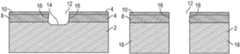
- FIG. 7is a top view of a substrate having one or more layers coupled over the substrate
- FIG. 8is the top view of the substrate of FIG. 7 with the material of the one or more layers in the die street removed;
- FIG. 9is a top view of the substrate of FIG. 7 singulated into semiconductor die.
- substraterefers to a semiconductor substrate as a semiconductor substrate is a common type of substrate, however, “substrate” is not an exclusive term that is used to refer to all semiconductor substrate types.
- substratemay refer to a wafer as a wafer is a common type of substrate, however, “substrate” is not an exclusive term that is used to refer to all wafers.
- the various semiconductor substrate types disclosed in this document that may be utilized in various implementationsmay be, by non-limiting example, round, rounded, square, rectangular, or any other closed shape.
- the substrate 2may include a substrate material such as, by non-limiting example, single crystal silicon, silicon dioxide, glass, gallium arsenide, sapphire, ruby, silicon on insulator, silicon carbide, polycrystalline or amorphous forms of any of the foregoing, and any other substrate material useful for constructing semiconductor devices.
- the substratemay be a silicon-on-insulator substrate.
- the substrate 2is thinned.
- the substrate 2may be less than 30 micrometers (um) thick, less than 50 um thick, and/or less than 100 um thick. In other implementations, the substrate may be more than 100 um thick and/or may not be thinned.
- a first side 6 of the substrate 2may be coupled to a metal layer 8 of the plurality of layers 4 .
- the metal layermay include, by non-limiting example, copper, aluminum, nickel, any other metal, any alloy thereof, and any combination thereof.
- the substrate 2may be directly coupled to the metal layer 8 .
- other layerssuch as a metal seed layer, may be coupled between the metal layer 8 and the substrate 2 .
- the metal layermay be the only layer coupled over the substrate 2 .
- a passivation layer 10may be included in the plurality of layers 4 .
- the passivation material 10may include, by non-limiting example, silicon nitride, oxides, metal electrical test structures, electrical test pads, silicon dioxide, polyimides, metal pads, residual underbump metallization (UBM), any combination thereof, and any other layer or material capable of facilitating electrical or thermal connection between the one or more semiconductor die and/or protecting the one or more semiconductor die from contaminants.
- passivation materialand “passivation layer,” as used herein, includes any of the aforementioned materials whether the material was deposited to act as a passivating material or whether the material merely forms a non-plasma etchable portion or layer in the die street region.
- the passivation layer 10may be coupled over the metal layer 8 .
- the passivation layermay include, by non-limiting example, a metal oxide, silicon dioxide, silicon nitride, polyimide, a polymer material, or any other passivation layer material type.
- multiple layers of passivating materialsmay be included in the plurality of layers 4 .
- the passivation layermay be the only layer in the plurality of layers. While the implementation illustrated by FIG.
- the metal layer 8 and the passivation layer 10 coupled over the substrate 2other implementations may include additional metal layers, additional passivation layers, additional other layers, layers without the metal layer 8 , layers without the passivation layer 10 , and any combination thereof.
- the layersmay fully cover the substrate 2 or may only partially cover the substrate.
- the substrate 2may include and/or be coupled to other elements not illustrated, such as a plurality of semiconductor devices.
- the plurality of semiconductor devicesmay include a power device or non-power semiconductor device.
- the power devicesmay include, by non-limiting example, a metal oxide field effect transistor (MOSFET), an insulated gate bipolar transistor (IGBT), a diode, a thyristor, a silicon controlled rectifier (SCR), or any other kind of power semiconductor device.
- MOSFETmetal oxide field effect transistor
- IGBTinsulated gate bipolar transistor
- SCRsilicon controlled rectifier
- the substrate 2 and the plurality of layers 4include a die street 12 therethrough. As illustrated by FIG. 1 , the metal layer 8 and the passivation layer 10 extend through the die street 12 . In various implementations, electrical testing devices and corresponding probe pads providing access to the electrical testing devices and structures may be included in at least one of the plurality of layers 4 and in the die street 12 .
- a method of singulating a plurality of die included in a substrateincludes exposing a substrate material of the substrate 2 in the die street 12 through removing the plurality of layers 4 in the die street 12 coupled to the substrate 2 .
- the methodmay include removing the metal layer in the die street 12 .
- the methodincludes removing the passivation layer (or some other layer) in the die street 12 .
- the methodmay also include removing a portion of the substrate material in the die street at substantially the same time the metal layer 8 and/or passivation layer 10 in the die street are removed.
- the portion of the substrate materialmay be removed substantially simultaneously with the removal of the metal layer and/or passivation layer as it is removed in the same cut or during the same removal process. The portion of the substrate material is not removed completely simultaneously with the metal layer and/or passivation layer as the cutting mechanism, such as a saw blade, must remove the outer layers coupled over the substrate before the substrate material is removed.
- the amount of the substrate material removed from the die street at the same time as the metal layer and/or passivation layer are removed from the die streetmay vary. Though the amounts may vary, in the various implementations disclosed herein, enough of the substrate material is removed in order to clear away any of the passivation layer or metal layer that may have migrated into/been formed into the substrate while removing the metal layer and/or the passivation layer from the die street. In this manner, the material of the substrate in the die street is exposed. In various implementations, removal of the metal layer and/or passivation layer is necessary to allow for singulation of the substrate through plasma etch.
- the metal layer, passivation layer, any other layer coupled over the substrate, and the removed portion of the substratemay be removed through, by non-limiting example, sawing, lasering, scribing, or jet ablating.
- the exposed surface of the substrate in the die streetmay be sloped. This may be a result of the method used to form the kerf, such as using a chamfered saw blade.
- the width of the kerf, or the removed portion of the metal layer 8 and/or passivation layer 10 in the die street 12may vary based upon the specific method used to form the kerf.
- the sidewalls of the kerf, or the sidewalls 16 of the die street 12may include damage.
- Using a saw, laser, water jet, or scribe to remove the portion of the substrateresults in the production of chips and cracks in the sidewalls 16 of the die street and layers adjacent to the die street.
- the presence of the cracks and chipshas the potential to compromise the reliability of the resulting semiconductor package (and reduce the die strength) if/when the cracks and chips propagate into the device portion of the semiconductor die.
- the saw (or other) processinvolves the rubbing of the rotating blade against the die surface, the chipping and cracking can only be managed through saw (or other) processing variables (substrate feed speed, blade kerf width, cut depth, multiple saw cuts, blade materials, etc.) but not eliminated.
- the method of singulating a plurality of die included in a substrateincludes singulating a plurality of die 18 included in the substrate 2 through plasma etching the exposed substrate material of the substrate in the die street 12 .
- a plasma etch processmarketed under the tradename BOSCH® by Robert Bosch GmbH, Stuttgart Germany (the “Bosch process”), may be used to singulate the substrate 2 into a plurality of die 18 .
- other plasma etch processesmay be used to singulate the plurality of die 18 from the substrate 2 .
- singulating the plurality of die included in the substrate through plasma etchingmay include removing a portion of the substrate material of the substrate having a width less than a width of the die street.
- the width of the removed portion from plasma etchingis less than the width of the die street as plasma die singulation is capable of creating a die street more narrow than the die street created through sawing, lasering, scribing, or jet ablating.
- the width of the portion of the removed substrate materialmay be the same or substantially the same as the width of the die street 12 by singulating the plurality of die 18 through removing through plasma etch all of the substrate material of the substrate 2 in the die street 12 .
- the method of singulating a plurality of die included in a substratemay include healing, or removing damage from, a sidewall of the die street 12 through plasma etching.
- the plasma(which may include charged ions) may penetrate the cracks and/or chips in the sidewalls 16 of the die street 12 within the substrate 2 formed when the metal layer 8 and/or passivation layer 10 were removed.
- the plasmamay also penetrate/facilitate reaction with the materials of the cracks and/or chips of the sidewalls of the die street or removed portion of the substrate 2 formed when the metal layer 8 and/or passivation layer 10 were removed.
- the damaged portion of the substratemay etch away and result in smoothed, or healed, sidewalls 16 of the substrate material (as illustrated by FIG. 3 ).
- the sidewalls 16 of the die street 12may be healed through the same plasma etch used to singulate the plurality of die 18 from the substrate 2 .
- the sidewalls 16 of the die street 12may be healed through a separate plasma etch from the plasma etch used to singulate the plurality of die 18 from the substrate 2 .
- this second plasma etchmay be more isotropic than the plasma etch used to singulate the plurality of die.
- FIGS. 4-6a method of singulating a plurality of die from a substrate similar to the method of FIGS. 1-3 is illustrated.
- FIG. 4a cross sectional side view of a substrate 26 coupled to one or more layers 28 is illustrated.
- the substrate 26may be the same as or similar to any substrate disclosed herein and the one or more layers 28 may include any type of layer disclosed herein.
- FIG. 5the cross sectional side view of the substrate of FIG. 4 with the plurality of layers in the die street removed is illustrated. Similar to the method illustrated by FIG.
- the method for singulating a plurality of die included in a substrateincludes exposing a substrate material of a substrate 26 in a die street 30 through removing the one or more layers 28 in the die street 30 coupled to the substrate 26 .
- a portion of the substrate 26 in the die streetis substantially simultaneously removed with the portion of the one or more layers 28 in the die street 30 .
- the portion of the substrate 26 and the one or more layers 28 in the die street 30may be removed through, by non-limiting example, sawing, lasering, jet ablating, or scribing.
- the difference between the method illustrated by FIG. 5 and the method illustrated by FIG. 2is that the method illustrated by FIG. 5 includes removing a greater portion of the substrate 26 when removing the one or more layers 28 in the die street 30 .
- the portion of the substrate material removed from the substrate 26 in the die street 30extends about 5 microns to about 15 microns into the substrate. In other implementations, the portion of the substrate 26 removed from the die street 30 may extend into the substrate 26 less than 5 um or more than 15 um.
- the method for singulating a plurality of die 32 included in the substrate 26may include singulating the plurality of die 32 using any method disclosed herein. As illustrated by FIG. 6 , the sidewalls 34 of the die street 30 formed when removing the portion of the substrate 26 may be healed through either the same plasma etch used to singulate the plurality of die 32 or through a separate plasma etch. In implementations having a thick substrate, the method of singulating the plurality of die may include removing a greater portion of the substrate in the die street in order to require plasma etching through less substrate.
- FIGS. 7-9a top view of a method of singulating a plurality of die from a substrate similar to or the same as the methods illustrated by FIGS. 1-6 is illustrated.
- FIG. 7a top view of a portion of a substrate having one or more layers 38 coupled over the substrate is illustrated.
- the portion of the substrate illustratedincludes intersecting die streets 40 .
- the substratemay be any type of substrate disclosed herein and the one or more layers may include any type of layer disclosed herein.
- FIG. 8a top view of the substrate of FIG. 7 with the material of the one or more layers 38 in the die street 40 removed is illustrated.
- the method for singulating a plurality of die included in a substrate 42includes exposing a substrate material of a substrate 42 in a die street 40 through removing the one or more layers 38 in the die street 40 coupled to the substrate 42 .
- a portion of the substrate 42 in the die street 40is substantially simultaneously removed with the portion of the one or more layers 38 in the die street 40 .
- the portion of the substrate 42 and the one or more layers 38 in the die street 40may be removed through, by non-limiting example, sawing, lasering, jet ablating, or scribing.
- the sidewalls 44 of the die street 40 along with the base 46 of the kerfmay be damaged and/or rough.
- the methodincludes singulating a plurality of die 48 from the substrate 42 . Any method disclosed herein may be used to singulate the plurality of die 48 .
- the plasma etchmay heal the damage to the sidewalls of the die streets 40 in the substrate 42 .
- the width of the portion of the substrate 42 removed through the plasma etchmay be less than the width of the die street 40 .
- the plurality of die singulated from the substrates disclosed hereinmay include any type of semiconductor die including any type disclosed herein.
- the reliability of the plurality of diemay be improved as less damage is induced into the die as compared to singulating the plurality of die through sawing, lasering, or other singulation methods.
- the diemay be strengthened as the plasma etch may heal the damaged portions of the substrate removed when the portion of the substrate was removed with the metal layer and/or passivation layer through the saw, laser, scribe, or jet.
- the improved reliability and strength of the diemay be especially important when the die are coupled to power semiconductor devices. Power semiconductor devices, such as an IGBT, may be coupled to a large lead frame and may include a large heat sink.
- the larger components of the semiconductor packagemay result in additional strain to the semiconductor die which may result in failure of the die (and especially of thinned die) if not sufficiently strong.
- the various methods disclosed hereinmay also permit the width of the die streets to be thinner/narrower than usual as a sawing or laser ablation process is not required to completely singulate the streets.
- the methods of singulating a plurality of die disclosed hereinmay be utilized with thinned (or non-thinned) substrates having one or more layers coupled thereto in a variety of designs. Because the substrate must be exposed in order for plasma singulation to occur, the method of removing the layers coupled over the substrate as disclosed herein is advantageous as these methods can allow for plasma die singulation of any thinned substrate rather than requiring plasma die singulation of a specifically designed substrate with a certain passivation or metal layer configuration which does not include the passivation layer, metal layer, or other layer coupled over the substrate in the die street.
- test structures/devices, alignment features, and probe padsmay be included within the portions of the metal (or other) layers coupled over the substrate. Because the test structures/devices, alignment features, and probe pads may be included within the die street (and later destroyed through removing the metal layer in the die street), the methods disclosed herein may eliminate the need for drop out dies within the substrate which are specifically placed and used to contain all the test structures/devices, alignment features, and probe pads used to manufacture and test the devices formed on the substrate.
- the substratemay be singulated into a greater number of die and there will be no drop out die to interfere with the process of picking and sorting the die following singulation.
- drop out dieare larger than neighboring good die and they may interfere with the uniform stretch of the picking tape.
- the tapemay be stretched different amounts when the die sizes are different, thus interfering with the alignment of the die, and in turn, the reliability of the die picking and sorting process.
Landscapes
- Engineering & Computer Science (AREA)
- Physics & Mathematics (AREA)
- Condensed Matter Physics & Semiconductors (AREA)
- General Physics & Mathematics (AREA)
- Manufacturing & Machinery (AREA)
- Computer Hardware Design (AREA)
- Microelectronics & Electronic Packaging (AREA)
- Power Engineering (AREA)
- Plasma & Fusion (AREA)
- Mechanical Engineering (AREA)
- Dicing (AREA)
Abstract
Description
Claims (14)
Priority Applications (3)
| Application Number | Priority Date | Filing Date | Title |
|---|---|---|---|
| US16/243,353US10818551B2 (en) | 2019-01-09 | 2019-01-09 | Plasma die singulation systems and related methods |
| CN201911390505.2ACN111430304A (en) | 2019-01-09 | 2019-12-30 | Plasma die dicing system and related method |
| US17/031,539US11651998B2 (en) | 2019-01-09 | 2020-09-24 | Plasma die singulation systems and related methods |
Applications Claiming Priority (1)
| Application Number | Priority Date | Filing Date | Title |
|---|---|---|---|
| US16/243,353US10818551B2 (en) | 2019-01-09 | 2019-01-09 | Plasma die singulation systems and related methods |
Related Child Applications (1)
| Application Number | Title | Priority Date | Filing Date |
|---|---|---|---|
| US17/031,539ContinuationUS11651998B2 (en) | 2019-01-09 | 2020-09-24 | Plasma die singulation systems and related methods |
Publications (2)
| Publication Number | Publication Date |
|---|---|
| US20200219769A1 US20200219769A1 (en) | 2020-07-09 |
| US10818551B2true US10818551B2 (en) | 2020-10-27 |
Family
ID=71403541
Family Applications (2)
| Application Number | Title | Priority Date | Filing Date |
|---|---|---|---|
| US16/243,353ActiveUS10818551B2 (en) | 2019-01-09 | 2019-01-09 | Plasma die singulation systems and related methods |
| US17/031,539Active2039-05-12US11651998B2 (en) | 2019-01-09 | 2020-09-24 | Plasma die singulation systems and related methods |
Family Applications After (1)
| Application Number | Title | Priority Date | Filing Date |
|---|---|---|---|
| US17/031,539Active2039-05-12US11651998B2 (en) | 2019-01-09 | 2020-09-24 | Plasma die singulation systems and related methods |
Country Status (2)
| Country | Link |
|---|---|
| US (2) | US10818551B2 (en) |
| CN (1) | CN111430304A (en) |
Cited By (1)
| Publication number | Priority date | Publication date | Assignee | Title |
|---|---|---|---|---|
| US11651998B2 (en)* | 2019-01-09 | 2023-05-16 | Semiconductor Components Industries, Llc | Plasma die singulation systems and related methods |
Citations (75)
| Publication number | Priority date | Publication date | Assignee | Title |
|---|---|---|---|---|
| US4820377A (en) | 1987-07-16 | 1989-04-11 | Texas Instruments Incorporated | Method for cleanup processing chamber and vacuum process module |
| US5075253A (en) | 1989-04-12 | 1991-12-24 | Advanced Micro Devices, Inc. | Method of coplanar integration of semiconductor IC devices |
| US5166097A (en) | 1990-11-26 | 1992-11-24 | The Boeing Company | Silicon wafers containing conductive feedthroughs |
| US5753418A (en) | 1996-09-03 | 1998-05-19 | Taiwan Semiconductor Manufacturing Company Ltd | 0.3 Micron aperture width patterning process |
| US5856705A (en) | 1993-01-25 | 1999-01-05 | Intel Corporation | Sealed semiconductor chip and process for fabricating sealed semiconductor chip |
| US5863813A (en) | 1997-08-20 | 1999-01-26 | Micron Communications, Inc. | Method of processing semiconductive material wafers and method of forming flip chips and semiconductor chips |
| US6030885A (en) | 1997-04-18 | 2000-02-29 | Vlsi Technology, Inc. | Hexagonal semiconductor die, semiconductor substrates, and methods of forming a semiconductor die |
| US6140151A (en) | 1998-05-22 | 2000-10-31 | Micron Technology, Inc. | Semiconductor wafer processing method |
| US6165814A (en) | 1997-05-23 | 2000-12-26 | Micron Technology, Inc. | Thin film capacitor coupons for memory modules and multi-chip modules |
| US6200851B1 (en) | 1996-12-20 | 2001-03-13 | Siemens Aktiengesellschaft | Memory cell that includes a vertical transistor and a trench capacitor |
| US6214703B1 (en) | 1999-04-15 | 2001-04-10 | Taiwan Semiconductor Manufacturing Company | Method to increase wafer utility by implementing deep trench in scribe line |
| WO2001056063A2 (en) | 2000-01-26 | 2001-08-02 | Tru-Si Technologies, Inc. | Thinning and dicing of semiconductor wafers using dry etch, and obtaining semiconductor chips with rounded bottom edges and corners |
| US6406979B2 (en) | 2000-06-27 | 2002-06-18 | Robert Bosch Gmbh | Method for sectioning a substrate wafer into a plurality of substrate chips |
| US6528864B1 (en) | 1999-11-19 | 2003-03-04 | Disco Corporation | Semiconductor wafer having regular or irregular chip pattern and dicing method for the same |
| US6563204B1 (en) | 1999-01-20 | 2003-05-13 | Amkor Technology, Inc. | Microcircuit die-sawing protector |
| US6642127B2 (en) | 2001-10-19 | 2003-11-04 | Applied Materials, Inc. | Method for dicing a semiconductor wafer |
| US20030207579A1 (en) | 2002-05-01 | 2003-11-06 | Michael Rattner | Method of etching a deep trench having a tapered profile in silicon |
| US6686225B2 (en) | 2001-07-27 | 2004-02-03 | Texas Instruments Incorporated | Method of separating semiconductor dies from a wafer |
| US20040087065A1 (en) | 2000-09-21 | 2004-05-06 | Cambridge Semiconductor Limited | Semiconductor device and method of forming a semiconductor device |
| US20040102025A1 (en) | 2002-11-20 | 2004-05-27 | Matsushita Electric Industrial Co., Ltd. | Method of manufacturing semiconductor device, plasma processing apparatus and plasma processing method |
| WO2004066382A1 (en) | 2003-01-23 | 2004-08-05 | Matsushita Electric Industrial Co., Ltd. | Method of manufacturing semiconductor device and cutting apparatus for cutting semiconductor wafer |
| US20040185580A1 (en) | 2003-03-22 | 2004-09-23 | Seok Goh | Method for dicing semiconductor wafer |
| US20050084996A1 (en) | 2001-12-21 | 2005-04-21 | Harper Ruth E. | Solid state plasma antenna |
| US20050104165A1 (en) | 2002-05-22 | 2005-05-19 | Sharp Kabushiki Kaisha | Semiconductor element, semiconductor device, and method for manufacturing semiconductor element |
| US20050142863A1 (en) | 2003-12-29 | 2005-06-30 | Stmicroelectronics S.R.I | Process for forming tapered trenches in a dielectric material |
| US20060001130A1 (en) | 2002-09-25 | 2006-01-05 | Shafidul Islam | Taped lead frames and methods of making and using the same in semiconductor packaging |
| US20060118515A1 (en) | 2004-08-20 | 2006-06-08 | Semitool, Inc. | Process For Thinning A Semiconductor Workpiece |
| US7060531B2 (en) | 2002-12-11 | 2006-06-13 | Matsushita Electric Industrial Co., Ltd. | Method of cutting semiconductor wafer and protective sheet used in the cutting method |
| US20060154401A1 (en) | 2005-01-10 | 2006-07-13 | University Of Warwick | Gas-sensing semiconductor devices |
| US7098077B2 (en) | 2004-01-20 | 2006-08-29 | Taiwan Semiconductor Manufacturing Company, Ltd. | Semiconductor chip singulation method |
| US20060205182A1 (en)* | 2005-03-10 | 2006-09-14 | Nec Electronics Corporation | Method for manufacturing semiconductor device |
| US7129114B2 (en) | 2004-03-10 | 2006-10-31 | Micron Technology, Inc. | Methods relating to singulating semiconductor wafers and wafer scale assemblies |
| US20060244096A1 (en) | 2005-04-27 | 2006-11-02 | Disco Corporation | Semiconductor wafer and processing method for same |
| US20060278956A1 (en) | 2003-03-13 | 2006-12-14 | Pdf Solutions, Inc. | Semiconductor wafer with non-rectangular shaped dice |
| WO2007007883A1 (en) | 2005-07-11 | 2007-01-18 | Matsushita Electric Industrial Co., Ltd. | Manufacturing method of semiconductor devices |
| US20070087524A1 (en) | 2005-10-18 | 2007-04-19 | Robert Montgomery | Wafer singulation process |
| US20070132034A1 (en) | 2005-12-14 | 2007-06-14 | Giuseppe Curello | Isolation body for semiconductor devices and method to form the same |
| US20070148807A1 (en) | 2005-08-22 | 2007-06-28 | Salman Akram | Microelectronic imagers with integrated optical devices and methods for manufacturing such microelectronic imagers |
| US7253477B2 (en) | 2005-02-15 | 2007-08-07 | Semiconductor Components Industries, L.L.C. | Semiconductor device edge termination structure |
| US20070249178A1 (en) | 2006-04-24 | 2007-10-25 | Oki Data Corporation | Semiconductor device, manufacturing method of semconductor device, manufacturing equipment of semiconductor device, light emitting diode head, and image forming apparatus |
| US7309623B2 (en) | 2002-01-09 | 2007-12-18 | Micron Technology, Inc. | Method of fabricating a stacked die in die BGA package |
| US7335576B2 (en) | 2004-10-08 | 2008-02-26 | Irvine Sensors Corp. | Method for precision integrated circuit die singulation using differential etch rates |
| WO2008023849A1 (en) | 2006-08-24 | 2008-02-28 | Panasonic Corporation | Method for manufacturing semiconductor chip and method for processing semiconductor wafer |
| US20080099900A1 (en) | 2006-10-31 | 2008-05-01 | Tessera Technologies Hungary Kft. | Wafer-level fabrication of lidded chips with electrodeposited dielectric coating |
| WO2008081968A1 (en) | 2006-12-26 | 2008-07-10 | Panasonic Corporation | Manufacturing method of semiconductor chip |
| US20090001609A1 (en) | 2005-02-28 | 2009-01-01 | Infineon Technologies Ag | Semiconductor Device and Method of Assembly |
| US7488668B2 (en) | 2004-07-23 | 2009-02-10 | Panasonic Corporation | Manufacturing method for semiconductor devices, arrangement determination method and apparatus for semiconductor device formation regions, and program for determining arrangement of semiconductor device formation regions |
| US20090057838A1 (en) | 2005-04-14 | 2009-03-05 | Panasonic Corporation | Manufacturing Method for Semiconductor Chips, and Semiconductor Chip |
| US20090065904A1 (en) | 2007-09-07 | 2009-03-12 | Freescale Semiconductor, Inc. | Substrate having through-wafer vias and method of forming |
| WO2009063620A1 (en) | 2007-11-16 | 2009-05-22 | Panasonic Corporation | Plasma dicing apparatus and semiconductor chip manufacturing method |
| US20090263927A1 (en) | 2007-01-04 | 2009-10-22 | Visera Technologies Company Limited | Isolation structures for cmos image sensor chip scale packages |
| US7629228B2 (en) | 2004-08-02 | 2009-12-08 | Panasonic Corporation | Manufacturing method for semiconductor devices, and formation apparatus for semiconductor wafer dicing masks |
| US7651925B2 (en) | 2007-03-01 | 2010-01-26 | Delphi Technologies, Inc. | Vacuum expansion of integrated circuits at sort |
| US7678670B2 (en) | 2004-12-24 | 2010-03-16 | Panasonic Corporation | TEG removing method in manufacturing method for semiconductor chips |
| US7705420B2 (en) | 2004-05-05 | 2010-04-27 | Atmel Automotive Gmbh | Method for producing a conductor path on a substrate, and a component having a conductor path fabricated in accordance with such a method |
| US20100173474A1 (en) | 2007-02-08 | 2010-07-08 | Matsushita Electric Industrial Co., Ltd. | Method of manufacturing semiconductor chip |
| US7767554B2 (en)* | 2007-03-09 | 2010-08-03 | Panasonic Corporation | Method of manufacturing semicondictor chip |
| US7767551B2 (en)* | 2006-10-06 | 2010-08-03 | Panasonic Corporation | Method for fabricating semiconductor chip |
| US7846848B2 (en) | 2005-01-08 | 2010-12-07 | Applied Materials, Inc. | Cluster tool with integrated metrology chamber for transparent substrates |
| US7883343B1 (en) | 2003-04-10 | 2011-02-08 | Sunpower Corporation | Method of manufacturing solar cell |
| US8178372B2 (en) | 2005-09-30 | 2012-05-15 | Osram Opto Semiconductors Gmbh | Method for production of a plurality of semiconductor chips, and a semiconductor component |
| US20130059428A1 (en)* | 2011-09-01 | 2013-03-07 | Disco Corporation | Wafer dividing method |
| US20130065378A1 (en)* | 2011-03-14 | 2013-03-14 | Chris Johnson | Method and Apparatus for Plasma Dicing a Semi-conductor Wafer |
| US20140273401A1 (en)* | 2013-03-14 | 2014-09-18 | Wei-Sheng Lei | Substrate laser dicing mask including laser energy absorbing water-soluble film |
| US20150011073A1 (en)* | 2013-07-02 | 2015-01-08 | Wei-Sheng Lei | Laser scribing and plasma etch for high die break strength and smooth sidewall |
| US8962452B2 (en) | 2007-08-07 | 2015-02-24 | Semiconductor Components Industries, Llc | Semiconductor die singulation apparatus and method |
| US20160365283A1 (en)* | 2015-06-12 | 2016-12-15 | Wei-Sheng Lei | Etch-resistant water soluble mask for hybrid wafer dicing using laser scribing and plasma etch |
| US20180286758A1 (en)* | 2017-04-04 | 2018-10-04 | Disco Corporation | Method of processing workpiece |
| US20180342424A1 (en)* | 2017-05-26 | 2018-11-29 | Panasonic Intellectual Property Management Co., Ltd. | Element chip manufacturing method |
| US20180342422A1 (en)* | 2017-05-26 | 2018-11-29 | Applied Materials, Inc. | Light-absorbing mask for hybrid laser scribing and plasma etch wafer singulation process |
| US20180350615A1 (en)* | 2017-06-05 | 2018-12-06 | Spts Technologies Limited | Methods of plasma etching and plasma dicing |
| US20190057891A1 (en)* | 2016-01-15 | 2019-02-21 | Uniqarta, Inc. | Placing Ultra-Small or Ultra-Thin Discrete Components |
| US20190157100A1 (en)* | 2017-11-22 | 2019-05-23 | Panasonic Intellectual Property Management Co., Ltd. | Manufacturing process of element chip |
| US10363629B2 (en)* | 2017-06-01 | 2019-07-30 | Applied Materials, Inc. | Mitigation of particle contamination for wafer dicing processes |
| US20190279902A1 (en)* | 2018-03-12 | 2019-09-12 | Applied Materials, Inc. | Hybrid wafer dicing approach using a multiple pass laser scribing process and plasma etch process |
Family Cites Families (11)
| Publication number | Priority date | Publication date | Assignee | Title |
|---|---|---|---|---|
| DE102005046479B4 (en)* | 2005-09-28 | 2008-12-18 | Infineon Technologies Austria Ag | Process for splitting brittle materials using trenching technology |
| JP2009176793A (en)* | 2008-01-22 | 2009-08-06 | Disco Abrasive Syst Ltd | Wafer division method |
| US8912077B2 (en)* | 2011-06-15 | 2014-12-16 | Applied Materials, Inc. | Hybrid laser and plasma etch wafer dicing using substrate carrier |
| US8703581B2 (en)* | 2011-06-15 | 2014-04-22 | Applied Materials, Inc. | Water soluble mask for substrate dicing by laser and plasma etch |
| US9368404B2 (en)* | 2012-09-28 | 2016-06-14 | Plasma-Therm Llc | Method for dicing a substrate with back metal |
| US9136173B2 (en)* | 2012-11-07 | 2015-09-15 | Semiconductor Components Industries, Llc | Singulation method for semiconductor die having a layer of material along one major surface |
| JP6166034B2 (en)* | 2012-11-22 | 2017-07-19 | 株式会社ディスコ | Wafer processing method |
| US8980726B2 (en)* | 2013-01-25 | 2015-03-17 | Applied Materials, Inc. | Substrate dicing by laser ablation and plasma etch damage removal for ultra-thin wafers |
| US9159624B1 (en)* | 2015-01-05 | 2015-10-13 | Applied Materials, Inc. | Vacuum lamination of polymeric dry films for wafer dicing using hybrid laser scribing and plasma etch approach |
| US9559007B1 (en)* | 2015-09-30 | 2017-01-31 | Semicondudtor Components Industries, Llc | Plasma etch singulated semiconductor packages and related methods |
| US10818551B2 (en)* | 2019-01-09 | 2020-10-27 | Semiconductor Components Industries, Llc | Plasma die singulation systems and related methods |
- 2019
- 2019-01-09USUS16/243,353patent/US10818551B2/enactiveActive
- 2019-12-30CNCN201911390505.2Apatent/CN111430304A/enactivePending
- 2020
- 2020-09-24USUS17/031,539patent/US11651998B2/enactiveActive
Patent Citations (83)
| Publication number | Priority date | Publication date | Assignee | Title |
|---|---|---|---|---|
| US4820377A (en) | 1987-07-16 | 1989-04-11 | Texas Instruments Incorporated | Method for cleanup processing chamber and vacuum process module |
| US5075253A (en) | 1989-04-12 | 1991-12-24 | Advanced Micro Devices, Inc. | Method of coplanar integration of semiconductor IC devices |
| US5166097A (en) | 1990-11-26 | 1992-11-24 | The Boeing Company | Silicon wafers containing conductive feedthroughs |
| US5510655A (en) | 1990-11-26 | 1996-04-23 | The Boeing Company | Silicon wafers containing conductive feedthroughs |
| US5856705A (en) | 1993-01-25 | 1999-01-05 | Intel Corporation | Sealed semiconductor chip and process for fabricating sealed semiconductor chip |
| US5753418A (en) | 1996-09-03 | 1998-05-19 | Taiwan Semiconductor Manufacturing Company Ltd | 0.3 Micron aperture width patterning process |
| US6200851B1 (en) | 1996-12-20 | 2001-03-13 | Siemens Aktiengesellschaft | Memory cell that includes a vertical transistor and a trench capacitor |
| US6030885A (en) | 1997-04-18 | 2000-02-29 | Vlsi Technology, Inc. | Hexagonal semiconductor die, semiconductor substrates, and methods of forming a semiconductor die |
| US6342724B1 (en) | 1997-05-23 | 2002-01-29 | Micron Technology, Inc. | Thin film capacitor coupons for memory modules and multi-chip modules |
| US6165814A (en) | 1997-05-23 | 2000-12-26 | Micron Technology, Inc. | Thin film capacitor coupons for memory modules and multi-chip modules |
| US5863813A (en) | 1997-08-20 | 1999-01-26 | Micron Communications, Inc. | Method of processing semiconductive material wafers and method of forming flip chips and semiconductor chips |
| US6140151A (en) | 1998-05-22 | 2000-10-31 | Micron Technology, Inc. | Semiconductor wafer processing method |
| US6563204B1 (en) | 1999-01-20 | 2003-05-13 | Amkor Technology, Inc. | Microcircuit die-sawing protector |
| US6214703B1 (en) | 1999-04-15 | 2001-04-10 | Taiwan Semiconductor Manufacturing Company | Method to increase wafer utility by implementing deep trench in scribe line |
| US6528864B1 (en) | 1999-11-19 | 2003-03-04 | Disco Corporation | Semiconductor wafer having regular or irregular chip pattern and dicing method for the same |
| WO2001056063A2 (en) | 2000-01-26 | 2001-08-02 | Tru-Si Technologies, Inc. | Thinning and dicing of semiconductor wafers using dry etch, and obtaining semiconductor chips with rounded bottom edges and corners |
| WO2001056063A3 (en) | 2000-01-26 | 2002-01-03 | Tru Si Technologies Inc | Thinning and dicing of semiconductor wafers using dry etch, and obtaining semiconductor chips with rounded bottom edges and corners |
| US6406979B2 (en) | 2000-06-27 | 2002-06-18 | Robert Bosch Gmbh | Method for sectioning a substrate wafer into a plurality of substrate chips |
| US20040087065A1 (en) | 2000-09-21 | 2004-05-06 | Cambridge Semiconductor Limited | Semiconductor device and method of forming a semiconductor device |
| US6686225B2 (en) | 2001-07-27 | 2004-02-03 | Texas Instruments Incorporated | Method of separating semiconductor dies from a wafer |
| US6642127B2 (en) | 2001-10-19 | 2003-11-04 | Applied Materials, Inc. | Method for dicing a semiconductor wafer |
| US20050084996A1 (en) | 2001-12-21 | 2005-04-21 | Harper Ruth E. | Solid state plasma antenna |
| US7309623B2 (en) | 2002-01-09 | 2007-12-18 | Micron Technology, Inc. | Method of fabricating a stacked die in die BGA package |
| US20030207579A1 (en) | 2002-05-01 | 2003-11-06 | Michael Rattner | Method of etching a deep trench having a tapered profile in silicon |
| US20050104165A1 (en) | 2002-05-22 | 2005-05-19 | Sharp Kabushiki Kaisha | Semiconductor element, semiconductor device, and method for manufacturing semiconductor element |
| US20060001130A1 (en) | 2002-09-25 | 2006-01-05 | Shafidul Islam | Taped lead frames and methods of making and using the same in semiconductor packaging |
| US6897128B2 (en) | 2002-11-20 | 2005-05-24 | Matsushita Electric Industrial Co., Ltd. | Method of manufacturing semiconductor device, plasma processing apparatus and plasma processing method |
| US20040102025A1 (en) | 2002-11-20 | 2004-05-27 | Matsushita Electric Industrial Co., Ltd. | Method of manufacturing semiconductor device, plasma processing apparatus and plasma processing method |
| US7060531B2 (en) | 2002-12-11 | 2006-06-13 | Matsushita Electric Industrial Co., Ltd. | Method of cutting semiconductor wafer and protective sheet used in the cutting method |
| US6969669B2 (en) | 2003-01-23 | 2005-11-29 | Matsushita Electric Industrial Co., Ltd. | Method of manufacturing semiconductor device and cutting apparatus for cutting semiconductor wafer |
| WO2004066382A1 (en) | 2003-01-23 | 2004-08-05 | Matsushita Electric Industrial Co., Ltd. | Method of manufacturing semiconductor device and cutting apparatus for cutting semiconductor wafer |
| US20060278956A1 (en) | 2003-03-13 | 2006-12-14 | Pdf Solutions, Inc. | Semiconductor wafer with non-rectangular shaped dice |
| US20040185580A1 (en) | 2003-03-22 | 2004-09-23 | Seok Goh | Method for dicing semiconductor wafer |
| US7883343B1 (en) | 2003-04-10 | 2011-02-08 | Sunpower Corporation | Method of manufacturing solar cell |
| US20050142863A1 (en) | 2003-12-29 | 2005-06-30 | Stmicroelectronics S.R.I | Process for forming tapered trenches in a dielectric material |
| US7098077B2 (en) | 2004-01-20 | 2006-08-29 | Taiwan Semiconductor Manufacturing Company, Ltd. | Semiconductor chip singulation method |
| US7129114B2 (en) | 2004-03-10 | 2006-10-31 | Micron Technology, Inc. | Methods relating to singulating semiconductor wafers and wafer scale assemblies |
| US7705420B2 (en) | 2004-05-05 | 2010-04-27 | Atmel Automotive Gmbh | Method for producing a conductor path on a substrate, and a component having a conductor path fabricated in accordance with such a method |
| US7488668B2 (en) | 2004-07-23 | 2009-02-10 | Panasonic Corporation | Manufacturing method for semiconductor devices, arrangement determination method and apparatus for semiconductor device formation regions, and program for determining arrangement of semiconductor device formation regions |
| US7629228B2 (en) | 2004-08-02 | 2009-12-08 | Panasonic Corporation | Manufacturing method for semiconductor devices, and formation apparatus for semiconductor wafer dicing masks |
| US20060118515A1 (en) | 2004-08-20 | 2006-06-08 | Semitool, Inc. | Process For Thinning A Semiconductor Workpiece |
| US7335576B2 (en) | 2004-10-08 | 2008-02-26 | Irvine Sensors Corp. | Method for precision integrated circuit die singulation using differential etch rates |
| US7678670B2 (en) | 2004-12-24 | 2010-03-16 | Panasonic Corporation | TEG removing method in manufacturing method for semiconductor chips |
| US7846848B2 (en) | 2005-01-08 | 2010-12-07 | Applied Materials, Inc. | Cluster tool with integrated metrology chamber for transparent substrates |
| US20060154401A1 (en) | 2005-01-10 | 2006-07-13 | University Of Warwick | Gas-sensing semiconductor devices |
| US7253477B2 (en) | 2005-02-15 | 2007-08-07 | Semiconductor Components Industries, L.L.C. | Semiconductor device edge termination structure |
| US20090001609A1 (en) | 2005-02-28 | 2009-01-01 | Infineon Technologies Ag | Semiconductor Device and Method of Assembly |
| US20060205182A1 (en)* | 2005-03-10 | 2006-09-14 | Nec Electronics Corporation | Method for manufacturing semiconductor device |
| US20090057838A1 (en) | 2005-04-14 | 2009-03-05 | Panasonic Corporation | Manufacturing Method for Semiconductor Chips, and Semiconductor Chip |
| US20060244096A1 (en) | 2005-04-27 | 2006-11-02 | Disco Corporation | Semiconductor wafer and processing method for same |
| WO2007007883A1 (en) | 2005-07-11 | 2007-01-18 | Matsushita Electric Industrial Co., Ltd. | Manufacturing method of semiconductor devices |
| US20070148807A1 (en) | 2005-08-22 | 2007-06-28 | Salman Akram | Microelectronic imagers with integrated optical devices and methods for manufacturing such microelectronic imagers |
| US8178372B2 (en) | 2005-09-30 | 2012-05-15 | Osram Opto Semiconductors Gmbh | Method for production of a plurality of semiconductor chips, and a semiconductor component |
| US20070087524A1 (en) | 2005-10-18 | 2007-04-19 | Robert Montgomery | Wafer singulation process |
| US20070132034A1 (en) | 2005-12-14 | 2007-06-14 | Giuseppe Curello | Isolation body for semiconductor devices and method to form the same |
| US20070249178A1 (en) | 2006-04-24 | 2007-10-25 | Oki Data Corporation | Semiconductor device, manufacturing method of semconductor device, manufacturing equipment of semiconductor device, light emitting diode head, and image forming apparatus |
| WO2008023849A1 (en) | 2006-08-24 | 2008-02-28 | Panasonic Corporation | Method for manufacturing semiconductor chip and method for processing semiconductor wafer |
| US20100055875A1 (en) | 2006-08-24 | 2010-03-04 | Panasonic Corporation | Method for manufacturing semiconductor chip and method for processing semiconductor wafer |
| US7767551B2 (en)* | 2006-10-06 | 2010-08-03 | Panasonic Corporation | Method for fabricating semiconductor chip |
| US20080099900A1 (en) | 2006-10-31 | 2008-05-01 | Tessera Technologies Hungary Kft. | Wafer-level fabrication of lidded chips with electrodeposited dielectric coating |
| WO2008081968A1 (en) | 2006-12-26 | 2008-07-10 | Panasonic Corporation | Manufacturing method of semiconductor chip |
| US20090263927A1 (en) | 2007-01-04 | 2009-10-22 | Visera Technologies Company Limited | Isolation structures for cmos image sensor chip scale packages |
| US7906410B2 (en) | 2007-02-08 | 2011-03-15 | Panasonic Corporation | Method of manufacturing semiconductor chip using laser light and plasma dicing |
| US20100173474A1 (en) | 2007-02-08 | 2010-07-08 | Matsushita Electric Industrial Co., Ltd. | Method of manufacturing semiconductor chip |
| US7651925B2 (en) | 2007-03-01 | 2010-01-26 | Delphi Technologies, Inc. | Vacuum expansion of integrated circuits at sort |
| US7767554B2 (en)* | 2007-03-09 | 2010-08-03 | Panasonic Corporation | Method of manufacturing semicondictor chip |
| US8962452B2 (en) | 2007-08-07 | 2015-02-24 | Semiconductor Components Industries, Llc | Semiconductor die singulation apparatus and method |
| US20090065904A1 (en) | 2007-09-07 | 2009-03-12 | Freescale Semiconductor, Inc. | Substrate having through-wafer vias and method of forming |
| US20100048001A1 (en) | 2007-11-16 | 2010-02-25 | Atsushi Harikai | Plasma dicing apparatus and method of manufacturing semiconductor chips |
| WO2009063620A1 (en) | 2007-11-16 | 2009-05-22 | Panasonic Corporation | Plasma dicing apparatus and semiconductor chip manufacturing method |
| US20130065378A1 (en)* | 2011-03-14 | 2013-03-14 | Chris Johnson | Method and Apparatus for Plasma Dicing a Semi-conductor Wafer |
| US20130059428A1 (en)* | 2011-09-01 | 2013-03-07 | Disco Corporation | Wafer dividing method |
| US20140273401A1 (en)* | 2013-03-14 | 2014-09-18 | Wei-Sheng Lei | Substrate laser dicing mask including laser energy absorbing water-soluble film |
| US20150011073A1 (en)* | 2013-07-02 | 2015-01-08 | Wei-Sheng Lei | Laser scribing and plasma etch for high die break strength and smooth sidewall |
| US20160365283A1 (en)* | 2015-06-12 | 2016-12-15 | Wei-Sheng Lei | Etch-resistant water soluble mask for hybrid wafer dicing using laser scribing and plasma etch |
| US20190057891A1 (en)* | 2016-01-15 | 2019-02-21 | Uniqarta, Inc. | Placing Ultra-Small or Ultra-Thin Discrete Components |
| US20180286758A1 (en)* | 2017-04-04 | 2018-10-04 | Disco Corporation | Method of processing workpiece |
| US20180342424A1 (en)* | 2017-05-26 | 2018-11-29 | Panasonic Intellectual Property Management Co., Ltd. | Element chip manufacturing method |
| US20180342422A1 (en)* | 2017-05-26 | 2018-11-29 | Applied Materials, Inc. | Light-absorbing mask for hybrid laser scribing and plasma etch wafer singulation process |
| US10363629B2 (en)* | 2017-06-01 | 2019-07-30 | Applied Materials, Inc. | Mitigation of particle contamination for wafer dicing processes |
| US20180350615A1 (en)* | 2017-06-05 | 2018-12-06 | Spts Technologies Limited | Methods of plasma etching and plasma dicing |
| US20190157100A1 (en)* | 2017-11-22 | 2019-05-23 | Panasonic Intellectual Property Management Co., Ltd. | Manufacturing process of element chip |
| US20190279902A1 (en)* | 2018-03-12 | 2019-09-12 | Applied Materials, Inc. | Hybrid wafer dicing approach using a multiple pass laser scribing process and plasma etch process |
Cited By (1)
| Publication number | Priority date | Publication date | Assignee | Title |
|---|---|---|---|---|
| US11651998B2 (en)* | 2019-01-09 | 2023-05-16 | Semiconductor Components Industries, Llc | Plasma die singulation systems and related methods |
Also Published As
| Publication number | Publication date |
|---|---|
| CN111430304A (en) | 2020-07-17 |
| US11651998B2 (en) | 2023-05-16 |
| US20200219769A1 (en) | 2020-07-09 |
| US20210082765A1 (en) | 2021-03-18 |
Similar Documents
| Publication | Publication Date | Title |
|---|---|---|
| EP3047517B1 (en) | Wafer dicing from wafer backside and front side | |
| TWI601242B (en) | Semiconductor die singulation method | |
| US11605561B2 (en) | Backside metal removal die singulation systems and related methods | |
| US12322632B2 (en) | Substrate alignment systems and related methods | |
| US20190244861A1 (en) | Method for Singulating Packaged Integrated Circuits and Resulting Structures | |
| US11114343B2 (en) | Partial backside metal removal singulation system and related methods | |
| US11289380B2 (en) | Backside metal patterning die singulation systems and related methods | |
| US20090261388A1 (en) | Dice by grind for back surface metallized dies | |
| US20250194209A1 (en) | Semiconductor device | |
| US11651998B2 (en) | Plasma die singulation systems and related methods | |
| US12396223B2 (en) | Semiconductor device and method of manufacturing the same | |
| US5736453A (en) | Method for dividing plural semiconductor devices formed on single wafer into individual semiconductor devices | |
| US11676863B2 (en) | Structures for aligning a semiconductor wafer for singulation | |
| US20200321236A1 (en) | Edge ring removal methods | |
| US20250191975A1 (en) | Etched die singulation systems and related methods | |
| US20220285217A1 (en) | Wafer thinning method | |
| JPH05326695A (en) | Semiconductor device | |
| JP2009158595A (en) | Manufacturing method of resin sealed semiconductor device | |
| JP2009295766A (en) | Method of manufacturing semiconductor device |
Legal Events
| Date | Code | Title | Description |
|---|---|---|---|
| AS | Assignment | Owner name:SEMICONDUCTOR COMPONENTS INDUSTRIES, LLC, ARIZONA Free format text:ASSIGNMENT OF ASSIGNORS INTEREST;ASSIGNOR:SEDDON, MICHAEL J.;REEL/FRAME:047941/0041 Effective date:20190109 | |
| FEPP | Fee payment procedure | Free format text:ENTITY STATUS SET TO UNDISCOUNTED (ORIGINAL EVENT CODE: BIG.); ENTITY STATUS OF PATENT OWNER: LARGE ENTITY | |
| AS | Assignment | Owner name:DEUTSCHE BANK AG NEW YORK BRANCH, AS COLLATERAL AGENT, NEW YORK Free format text:SECURITY INTEREST;ASSIGNORS:SEMICONDUCTOR COMPONENTS INDUSTRIES, LLC;FAIRCHILD SEMICONDUCTOR CORPORATION;REEL/FRAME:049473/0932 Effective date:20190422 | |
| STCF | Information on status: patent grant | Free format text:PATENTED CASE | |
| AS | Assignment | Owner name:FAIRCHILD SEMICONDUCTOR CORPORATION, ARIZONA Free format text:RELEASE OF SECURITY INTEREST IN PATENTS PREVIOUSLY RECORDED AT REEL 049473, FRAME 0932;ASSIGNOR:DEUTSCHE BANK AG NEW YORK BRANCH, AS COLLATERAL AGENT;REEL/FRAME:064618/0721 Effective date:20230816 Owner name:SEMICONDUCTOR COMPONENTS INDUSTRIES, LLC, ARIZONA Free format text:RELEASE OF SECURITY INTEREST IN PATENTS PREVIOUSLY RECORDED AT REEL 049473, FRAME 0932;ASSIGNOR:DEUTSCHE BANK AG NEW YORK BRANCH, AS COLLATERAL AGENT;REEL/FRAME:064618/0721 Effective date:20230816 | |
| MAFP | Maintenance fee payment | Free format text:PAYMENT OF MAINTENANCE FEE, 4TH YEAR, LARGE ENTITY (ORIGINAL EVENT CODE: M1551); ENTITY STATUS OF PATENT OWNER: LARGE ENTITY Year of fee payment:4 |