US10818449B2 - Apparatus and method of backlighting through a cover on the apparatus - Google Patents
Apparatus and method of backlighting through a cover on the apparatusDownload PDFInfo
- Publication number
- US10818449B2 US10818449B2US16/836,776US202016836776AUS10818449B2US 10818449 B2US10818449 B2US 10818449B2US 202016836776 AUS202016836776 AUS 202016836776AUS 10818449 B2US10818449 B2US 10818449B2
- Authority
- US
- United States
- Prior art keywords
- mask layer
- cover
- holes
- region
- key
- Prior art date
- Legal status (The legal status is an assumption and is not a legal conclusion. Google has not performed a legal analysis and makes no representation as to the accuracy of the status listed.)
- Active
Links
Images


Classifications
- G—PHYSICS
- G06—COMPUTING OR CALCULATING; COUNTING
- G06F—ELECTRIC DIGITAL DATA PROCESSING
- G06F3/00—Input arrangements for transferring data to be processed into a form capable of being handled by the computer; Output arrangements for transferring data from processing unit to output unit, e.g. interface arrangements
- G06F3/01—Input arrangements or combined input and output arrangements for interaction between user and computer
- G06F3/02—Input arrangements using manually operated switches, e.g. using keyboards or dials
- G06F3/0202—Constructional details or processes of manufacture of the input device
- H—ELECTRICITY
- H01—ELECTRIC ELEMENTS
- H01H—ELECTRIC SWITCHES; RELAYS; SELECTORS; EMERGENCY PROTECTIVE DEVICES
- H01H13/00—Switches having rectilinearly-movable operating part or parts adapted for pushing or pulling in one direction only, e.g. push-button switch
- H01H13/70—Switches having rectilinearly-movable operating part or parts adapted for pushing or pulling in one direction only, e.g. push-button switch having a plurality of operating members associated with different sets of contacts, e.g. keyboard
- H01H13/83—Switches having rectilinearly-movable operating part or parts adapted for pushing or pulling in one direction only, e.g. push-button switch having a plurality of operating members associated with different sets of contacts, e.g. keyboard characterised by legends, e.g. Braille, liquid crystal displays, light emitting or optical elements
- H—ELECTRICITY
- H01—ELECTRIC ELEMENTS
- H01H—ELECTRIC SWITCHES; RELAYS; SELECTORS; EMERGENCY PROTECTIVE DEVICES
- H01H2209/00—Layers
- H01H2209/068—Properties of the membrane
- H01H2209/082—Properties of the membrane transparent
- H—ELECTRICITY
- H01—ELECTRIC ELEMENTS
- H01H—ELECTRIC SWITCHES; RELAYS; SELECTORS; EMERGENCY PROTECTIVE DEVICES
- H01H2209/00—Layers
- H01H2209/068—Properties of the membrane
- H01H2209/086—Trellis; Lattice
- H—ELECTRICITY
- H01—ELECTRIC ELEMENTS
- H01H—ELECTRIC SWITCHES; RELAYS; SELECTORS; EMERGENCY PROTECTIVE DEVICES
- H01H2219/00—Legends
- H—ELECTRICITY
- H01—ELECTRIC ELEMENTS
- H01H—ELECTRIC SWITCHES; RELAYS; SELECTORS; EMERGENCY PROTECTIVE DEVICES
- H01H2219/00—Legends
- H01H2219/028—Printed information
- H—ELECTRICITY
- H01—ELECTRIC ELEMENTS
- H01H—ELECTRIC SWITCHES; RELAYS; SELECTORS; EMERGENCY PROTECTIVE DEVICES
- H01H2219/00—Legends
- H01H2219/036—Light emitting elements
- H01H2219/052—Phosphorescence
- H—ELECTRICITY
- H01—ELECTRIC ELEMENTS
- H01H—ELECTRIC SWITCHES; RELAYS; SELECTORS; EMERGENCY PROTECTIVE DEVICES
- H01H2219/00—Legends
- H01H2219/054—Optical elements
- H01H2219/056—Diffuser; Uneven surface
- H—ELECTRICITY
- H01—ELECTRIC ELEMENTS
- H01H—ELECTRIC SWITCHES; RELAYS; SELECTORS; EMERGENCY PROTECTIVE DEVICES
- H01H2223/00—Casings
- H01H2223/044—Protecting cover
- H—ELECTRICITY
- H01—ELECTRIC ELEMENTS
- H01H—ELECTRIC SWITCHES; RELAYS; SELECTORS; EMERGENCY PROTECTIVE DEVICES
- H01H2229/00—Manufacturing
- H01H2229/02—Laser
Definitions
- the following descriptionrelates to backlighting a device and particularly to backlighting keys of a keyboard having a fabric-based cover. Further, the principles herein may be applied to other devices having covers that are fabric or non-fabric based.
- Devices such as keyboardsmay have a fabric-based cover or a non-fabric based cover.
- Fabricse.g., natural fiber fabric such as cotton, wool, etc. or synthetic fiber fabric such as polyester, acrylic, rayon, carbon fiber, etc.
- backlighting a device having a fabric covermay be challenging to produce effect or desired results.
- similar challengesexist with other non-fabric materials as well.
- LEDsWith respect to the light sources used in backlighting devices, LEDs have been used.
- the LEDs currently implemented for backlightingare “packaged” LEDs.
- the “packaged” modifierrefers to the enclosure and protective features built into the final LED as well as the interface that enables the LED in the package to be incorporated into an ultimate circuit.
- the conventional fabrication process for LEDs, or other semiconductor devicesstarts with handling a semiconductor wafer. The wafer is diced into a multitude of “unpackaged” semiconductor devices.
- the “unpackaged” modifierrefers to an unenclosed semiconductor device without protective features.
- the “packaging” of an LEDmakes the LED substantially thicker than an unpackaged LED.
- the unpackaged LEDsmay be extremely small. Indeed, the height of the LEDs may range from 12.5 to 200 microns, or from 25 to 100 microns, or from 50 to 80 microns.
- FIG. 1illustrates an exploded perspective view of a keyboard key assembly according to an embodiment of the instant application.
- FIG. 2illustrates a cross-sectional view of a keyboard key assembly according to another embodiment of the instant application.
- FIG. 3illustrates an exploded cross-sectional view of a keyboard key assembly according to another embodiment of the instant application.
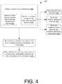
- FIG. 4illustrates a method of manufacturing an apparatus having a backlit cover.
- This disclosureis directed generally to backlit illumination of an image, symbol, character, or other design in a surface cover of an apparatus.
- a legende.g., an image, symbol, character, or other design
- the cover of the key(s)may be a fabric or a non-fabric material.
- backlightingmay be achieved via one or more unpackaged, micro-sized LEDs disposed behind the legend from a first-person perspective view, which means that the legend (e.g., symbol, character, design, etc.) is illuminated from a light source located behind the legend such that the light of the light source diffuses through the legend in a direction toward the individual looking at the legend.
- the light sources for lighting the keys on a keyboardare behind the cover of the keys from the perspective of an individual looking at the legend on the key(s) of the keyboard.
- the light sourceis similarly hidden from the direct view of the individual looking at the apparatus.
- the features described hereinmay be implemented in the illumination of legends on the cover of other apparatuses including apparel, displays, banners, flags, décor, signs, toys, keypads, electronics, etc.
- the concepts and designs of the features described herein as they relate to illumination of keys of a keyboard having a fabric-based covermay, in many instances, be similarly applied to the illumination of non-fabric-based materials.
- FIG. 1depicts an exploded view of at least some of the elements of an apparatus to illuminate a portion of a fabric material.
- an apparatus 100such as a key on a keyboard, for example, may include a cover 102 (e.g., keycap) having a legend 104 .
- the cover 102may be entirely formed of, or may at least partially include, a fabric material such as a polymer-based fabric.
- the fabric material of the cover 102may be a natural fiber, synthetic fiber, or blended type of material, such as a cotton, silk, or wool-based fabric, any of which may be used alone or blended with a polyester, acrylic, rayon, etc. or other material capable of a durable fabric-type of manufacture.
- FIG. 1depicts an exploded view of at least some of the elements of an apparatus to illuminate a portion of a fabric material.
- an apparatus 100such as a key on a keyboard, for example, may include a cover 102 (e.g., keycap) having a legend 104 .
- the apparatus 100is not limited to the configuration depicted and may be formed into a variety of shapes and dimensions for a desired purpose.
- the cover 102may take on shapes that are rippled, rounded, spherical, triangular, cylindrical, or otherwise curved and/or pointed.
- the legend 104may be indicative of a character or grouping of characters including individual letters, numbers, and/or whole words, phrases, or sequences of numbers. In some instances, the legend 104 may indicate a form of punctuation, a symbol including emoticons and/or cultural/universal symbols, an image, a design, a shape, or other graphic to indicate a function or convey a particular meaning. As an example, the legend 104 in FIG. 1 depicts a letter “L.”
- the legend 104 of cover 102may be formed in a multitude of ways.
- the legend 104may be created via an additive type of process where an element is added to the cover 102 , via a removal process where material is removed from the cover 102 , or a combination of material removal and an additive process.
- the legend 104may be formed via a molding process where the cover 102 is molded to include a legend 104 within the molded cover 102 .
- the end resultis that the cover 102 includes a first region that is a relatively opaque portion and a second region that is a relatively translucent portion.
- the translucent second regionincludes the legend 104 so that the legend 104 is illuminated in the midst of the opaque first region.
- Example embodiments of additive processes for creating the legend 104include adding a separate layer 104 a that is a layer of paint, a sticker, an ink graphic applied via a printing process, a coating of either a translucent or opaque substance, an adhesive, a film, an embedded element, etc.
- Printing processesthat may be used include inkjet, laser, dye sublimation, etc.
- FIG. 1 of the legend 104 a on the top side of the cover 102the above additive type processes may be used, as suitable, to create the legend 104 a on the underside of the cover as well.
- legend 104 ais depicted as the desired legend shape, the layer 104 a may be added as the complementary negative of the desired legend shape.
- material of the cover 102is removed to allow light to emit directly or diffuse more clearly through a predetermined portion the cover 102 .
- small amounts of materialmay be removed by creating a plurality of micro-sized holes 106 through the cover 102 .
- the holes 106may be closely spaced and arranged within a predetermined perimeter such that, collectively, the arrangement of the plurality of holes 106 corresponds in shape to the shape of a desired legend 104 b to be illuminated.
- the holes 106 in FIG. 1are arranged within a perimeter designating the predetermined shape of the letter “L” to form the legend 104 b .
- materialmay be removed by creating a plurality of cavities in either the top or bottom surface of the apparatus, which cavities are not cut completely through the cover 102 .
- a top or bottom surface of the cover 102may be etched such that at least a portion of the thickness of the cover 102 is removed to form a shape of the desired legend 104 b .
- a portion of the cover 102is thinned or cut out entirely to enhance the transmission of light therethrough.
- an entirety of the predetermined shape of the desired legendmay be cut out of the cover 102 .
- methods of material removalinclude punching, cutting, and/or the use of a laser.
- holes 106may be formed via a laser to extend through the cover 102 from a top side of the cover 102 to a bottom side of the cover 102 .
- the holes 106may range in diameter from 0.1 mm to 0.2 mm, for example, or may be even smaller or larger.
- the legend 104may be created via a combination of material removal and an additive process.
- the space from which material was removedmay be filled, covered, or coated by an added material that helps to diffuse and enhance the backlighting as it illuminates the portion of the cover from which material was removed.
- apparatus 100may include a stenciled mask layer 108 in addition to, or in place of, legend 104 a and/or legend 104 b .
- the mask layer 108may include a dark-colored/light-blocking substrate (e.g., a thin film, etc.), in which a portion of the substrate is removed, thereby creating an aperture 108 a in the substrate.
- the aperture 108 amay correspond directly in shape and dimensions with the perimeter of the shape of the legend 104 in the cover 102 , or the shape and dimensions of aperture 108 a may be larger or smaller than the perimeter of the shape of the legend 104 to increase or decrease the amount of illumination.
- the mask layer 108may be adhered or otherwise placed on the underside of the cover 102 .
- apparatus 100may further include a keycap stiffener 110 .
- the stiffener 110may be formed of a clear material, or alternatively, of a tinted or colored material, while maintaining translucent properties.
- the stiffener 110may further function as a light diffusion element. That is, the stiffener 110 may be textured, colored, formed, or shaped in a manner that enhances light diffusion.
- the stiffener 110may include phosphor and/or other elements that modify the light before it passes to the legend 104 . Additionally, the stiffener 110 may have a translucent center portion and opaque or not fully translucent side edges.
- the stiffener 110may be formed with two different colored materials, where the center portion is lighter than the edge portion, e.g., a white plastic planar center molded to a black plastic ring or perimeter.
- the stiffener 110may be formed from a single, translucent material, e.g., white plastic, and have the side edges thereof coated, painted, colored, or otherwise masked with a darker substance.
- Such embodiments of the stiffener 110may provide some light-blocking properties, which may assist in preventing leakage of the light from undesirable areas of the apparatus.
- Apparatus 100may further include a dome 112 , which is an electrically-connected, reflexive sensory contact terminal that connects with a circuit element (not shown) when force is applied to the cover 102 of apparatus 100 .
- the dome 112itself may include one or more flexible cross support members 114 that extend across the terminal from one side to the other forming a generally dome shaped profile. Note, for convenience, in this application, the dome 112 may be referred to herein as the “terminal” as well.
- the cross support members 114 of the dome 112flex elastically to make contact with the circuit element and a signal is relayed to output the intended function of the legend 104 .
- applied force on the cover 102would relay a signal to a connected computing device to output the letter “L.” Additional details regarding the functionality associated with a keyboard or other electronic circuitry are not provided herein.
- Illumination of the legend 104is achieved via selective placement of one or more light sources 116 .
- light sources 116may be placed within a perimeter or outside of the perimeter of the dome 112 .
- the light sources 116may include unpackaged LEDs powered via direct or indirect attachment to one or more circuit elements provided in the apparatus 100 .
- the unpackaged LEDsmay be placed by any suitable means, including via direct transfer according to the method and apparatus described in U.S. application Ser. No. 14/939,896. Additional details regarding position of placement of the light sources 116 are discussed further herein below with respect to FIG. 3 .
- FIG. 2a perspective view of a cross-section of a backlit keyboard 200 is depicted. Further, emphasis of a cross-sectional side view of a single key 202 of the keyboard 200 is provided.
- Specific elements of the structure of the key 202include a base 204 that may include electronic circuitry elements (not shown) to interact and power aspects of the keyboard 200 . Thus, the base 204 may serve as a foundation to support the structure of the key 202 thereon.
- the key 202may further include a dome 206 , a dome cage 208 , a dome cover sheet 210 , a key stiffener 212 , and a cover 214 .
- the dome 206functions as the sensory contact terminal, like terminal 112 described above.
- the dome 206may be surrounded, or fenced in, at the sides thereof by the framed dome cage 208 .
- the dome cage 208may have a rectangular shape, or circular shape, or other shape having a plurality of sides that are connected to form a closed shape so that the dome 206 is surrounded or enclosed on all lateral sides of the dome 206 .
- the dome cage 208may be a sturdy material that is structurally firm to provide protection from damage to the dome 206 .
- the dome cage 208may be formed as a shaped frame resting on short leg posts (see FIG. 3 ) and is open at the top side thereof to allow a force to be applied to the top of the dome 206 .
- sides of the dome cage 208may be consistent in height at a side and all the way around the dome 206 , so as to be like a solid wall.
- the dome cover sheet 210may be placed over the open top of the dome cage 208 so as to cover the dome 206 , and thereby prevent direct contact between the dome 206 and the key stiffener 212 .
- the key stiffener 212is covered by the cover 214 , and the barrier between key 202 and an adjacent key (K) may be supported by a frame 216 .
- the light sourcesmay be electrically powered and connected via a thin conductive trace disposed on the components of the apparatus.
- the use of the term “light source”may indicate one or more light sources.
- any one or a combination of more than one of the following descriptions of light source layoutsmay be implemented according to a desired strength of backlighting the apparatus.
- the descriptive statement of a layout where the base 204 of key 202 may have a light source 302 disposed thereon and positioned to be under the dome 206indicates that the block identified by reference numeral 302 may be a single light source or may represent a plurality of light sources, all of which are contained somewhere within a perimeter defined by an outer periphery of the dome 206 . Accordingly, while the light source 302 is depicted in the center of the dome, the light source(s) 302 may actually be off center and distributed beneath the dome where the light source(s) 302 will not interfere with the electrical contact between the dome 206 and electronic circuitry on the base 302 when force is applied to the cover 214 .
- Additional potential light source layoutsmay include the following: a light source 304 on the base 204 in between the dome 206 and the dome cage 208 ; a light source 306 on the base 304 around the outside of the dome cage 208 ; a light source 308 embedded in the dome cage 208 ; a light source 310 disposed on the dome cage 308 ; a light source 312 disposed on the dome cover sheet 210 ; a light source 314 disposed underneath the key stiffener 212 ; a light source 316 disposed on the key stiffener 212 ; and/or a light source 318 disposed directly on an underside of the cover 214 .
- a series of light sourcesmay be disposed directly aligned with the shape of the legend on or under the cover 214 . It is noted that while the above description of potential light source layouts describes the light sources ( 302 - 318 ) as being “under,” “in,” “around,” “on,” “embedded,” or “underneath” various components, it is further contemplated by the inventors that the light sources may be disposed in various other manners with respect to each of the individual components. That is, for example, where a light source is described as being “on” a component, the light source may alternatively, or additionally, be “embedded in,” “underneath,” “in,” etc. the component where possible.
- phosphor applicationfor light emission modification
- phosphormay be applied to modify the color and dispersion of the light emitted from the light sources.
- the phosphormay be applied in or on components, or portions of those components, through which light may shine.
- phosphormay be applied directly on the light source(s) 302 - 318 and/or on or mixed into the material of the dome cage 208 , the dome cover sheet 210 , the key stiffener 212 , or the cover 214 .
- phosphormay be applied (not shown explicitly) to an upper surface of one or more sides of the dome cage 208 , and a light source, such as one or more unpackaged LEDs, may be connected to a thin circuit on the base and aligned directly beneath the one or more sides of the dome cage 208 .
- a light sourcesuch as one or more unpackaged LEDs
- FIG. 4depicts a method 400 of creating an apparatus, such as key of a keyboard that is to be backlit.
- method 400may include forming a cover 402 for the apparatus.
- step 402may include forming a fabric key cover for a key of a keyboard device.
- the formation of the covermay include creating a first opaque region on the cover and a second translucent region on the cover 404 .
- the creation of the first and second regionsmay be performed in a single act or may involve two or more acts.
- the formation of the covermay further include creating a legend in one of the first region and the second region of the cover 406 . Note that the possibility remains that the legend may be formed partly in the first region and partly in the second region.
- the legendmay be formed via many methods as discussed above.
- the legendmay be formed via an additive process 408 such as dye sublimation, via a material removal process 410 using a laser or any suitable cutting or etching device, or via a combination of an additive process and a material removal process 412 .
- a plurality of light sourcesmay be electrically connected beneath or behind the cover of the apparatus.
- the plurality of light sourcesmay be electrically connected beneath the fabric key cover to illuminate the translucent region of the keys from underneath the covers.
- the light sourcesalso illuminate the translucent region of the covers.
- Method 400may further include a step 416 of applying a phosphor in or on a material of a structural component and/or the light sources of the apparatus.
- the application of phosphormay be executed in any order with respect to the other steps of method 400 , including prior to integrating the light sources into the apparatus.
- one or more of the components of the key(s) in FIGS. 2 and 3may include phosphor in the material composition or on the component(s) (i.e., deposited on a surface of the component(s) via spraying, printing, coating, dipping, thermal forming, etc.).
- a keyboard apparatuscomprising: a fabric key cover having a plurality of holes that extend through a thickness of the cover from a top side of the cover to a bottom side of the cover, the plurality of holes being arranged to collectively form a predetermined shape; a mask layer disposed at the bottom side of the cover, a first region of the mask layer being opaque and a second region of the mask layer allowing light to pass therethrough to the plurality of holes; a light source disposed beneath the mask layer and positioned such that light emitted from the light source passes through the second region of the mask layer to the plurality of holes; and a sensory contact terminal disposed beneath the mask layer, the terminal detecting a keystroke movement.
- NThe apparatus according to any of paragraphs A-M, wherein the light source includes LEDs arranged adjacent to the sensory contact terminal.
- TThe apparatus according to any of paragraphs A-S, wherein the mask layer is etched onto the back of the cover.
- VThe apparatus according to any of paragraphs A-U, further comprising a transparent film or substrate that covers at least a portion of the top side of the cover.
- An apparatuscomprising: a cover having a legend formed in a predetermined shape and being visible from a top side of the cover, a first region of the cover being opaque and a second region of the cover being translucent to be illuminated, the legend being located in one of the first and second regions; a light source disposed beneath the cover and positioned such that light emitted from the light source passes through the second region of the cover to show the legend; and a sensory contact terminal disposed beneath the cover, the light source being disposed within an inner perimeter of a footprint of the terminal.
- AAA method comprising: forming a fabric key cover for a key of a keyboard device, the forming including creating a first opaque region on the cover and a second translucent region on the cover, and creating a legend in one of the first region and the second region of the key cover; electrically connecting a plurality of light sources beneath the fabric key cover.
- ADThe method according to any of paragraphs AA-AC, wherein the creating the legend includes removing material from the key cover.
- AEThe method according to any of paragraphs AA-AD, wherein the removing material from the key cover includes applying a laser to the key cover to etch or cut through the key cover.
Landscapes
- Engineering & Computer Science (AREA)
- General Engineering & Computer Science (AREA)
- Theoretical Computer Science (AREA)
- Human Computer Interaction (AREA)
- Physics & Mathematics (AREA)
- General Physics & Mathematics (AREA)
- Input From Keyboards Or The Like (AREA)
- Push-Button Switches (AREA)
- Switch Cases, Indication, And Locking (AREA)
Abstract
Description
Claims (20)
Priority Applications (1)
| Application Number | Priority Date | Filing Date | Title |
|---|---|---|---|
| US16/836,776US10818449B2 (en) | 2016-01-15 | 2020-03-31 | Apparatus and method of backlighting through a cover on the apparatus |
Applications Claiming Priority (4)
| Application Number | Priority Date | Filing Date | Title |
|---|---|---|---|
| US201662279461P | 2016-01-15 | 2016-01-15 | |
| PCT/US2017/013817WO2017124109A1 (en) | 2016-01-15 | 2017-01-17 | Apparatus and method of backlighting through a cover on the apparatus |
| US201816069871A | 2018-07-12 | 2018-07-12 | |
| US16/836,776US10818449B2 (en) | 2016-01-15 | 2020-03-31 | Apparatus and method of backlighting through a cover on the apparatus |
Related Parent Applications (2)
| Application Number | Title | Priority Date | Filing Date |
|---|---|---|---|
| US16/069,871ContinuationUS10629393B2 (en) | 2016-01-15 | 2017-01-17 | Apparatus and method of backlighting through a cover on the apparatus |
| PCT/US2017/013817ContinuationWO2017124109A1 (en) | 2016-01-15 | 2017-01-17 | Apparatus and method of backlighting through a cover on the apparatus |
Publications (2)
| Publication Number | Publication Date |
|---|---|
| US20200227217A1 US20200227217A1 (en) | 2020-07-16 |
| US10818449B2true US10818449B2 (en) | 2020-10-27 |
Family
ID=59311485
Family Applications (2)
| Application Number | Title | Priority Date | Filing Date |
|---|---|---|---|
| US16/069,871ActiveUS10629393B2 (en) | 2016-01-15 | 2017-01-17 | Apparatus and method of backlighting through a cover on the apparatus |
| US16/836,776ActiveUS10818449B2 (en) | 2016-01-15 | 2020-03-31 | Apparatus and method of backlighting through a cover on the apparatus |
Family Applications Before (1)
| Application Number | Title | Priority Date | Filing Date |
|---|---|---|---|
| US16/069,871ActiveUS10629393B2 (en) | 2016-01-15 | 2017-01-17 | Apparatus and method of backlighting through a cover on the apparatus |
Country Status (6)
| Country | Link |
|---|---|
| US (2) | US10629393B2 (en) |
| EP (1) | EP3408728A4 (en) |
| JP (1) | JP6959697B2 (en) |
| KR (1) | KR102298484B1 (en) |
| CN (1) | CN108770368B (en) |
| WO (1) | WO2017124109A1 (en) |
Families Citing this family (8)
| Publication number | Priority date | Publication date | Assignee | Title |
|---|---|---|---|---|
| JP6959697B2 (en) | 2016-01-15 | 2021-11-05 | ロヒンニ リミテッド ライアビリティ カンパニー | Devices and methods that are backlit through a cover on the device |
| US10788936B1 (en)* | 2017-07-17 | 2020-09-29 | Apple Inc. | Absorption correction for fabric touch sensing layer |
| US10732743B2 (en)* | 2017-07-18 | 2020-08-04 | Apple Inc. | Concealable input region for an electronic device having microperforations |
| US11416082B1 (en)* | 2017-09-05 | 2022-08-16 | Apple Inc. | Input devices with glyphs having a semitransparent mirror layer |
| US10795452B2 (en)* | 2018-02-07 | 2020-10-06 | Microsoft Technology Licensing, Llc | Multi-stage cure bare die light emitting diode |
| WO2020018470A1 (en) | 2018-07-18 | 2020-01-23 | Shanghai Yanfeng Jinqiao Automotive Trim Systems Co. Ltd. | Vehicle interior component |
| US11672096B2 (en)* | 2020-04-24 | 2023-06-06 | Microsoft Technology Licensing, Llc | Seamless textile covered enclosure |
| KR102518335B1 (en)* | 2022-12-01 | 2023-04-05 | 몬스타 주식회사 | custom keyboard |
Citations (339)
| Publication number | Priority date | Publication date | Assignee | Title |
|---|---|---|---|---|
| US2344136A (en) | 1943-02-22 | 1944-03-14 | Harold V Dressen | Wrist watch protector |
| US3717743A (en) | 1970-12-07 | 1973-02-20 | Argus Eng Co | Method and apparatus for heat-bonding in a local area using combined heating techniques |
| US3935986A (en) | 1975-03-03 | 1976-02-03 | Texas Instruments Incorporated | Solid state bonding process employing the isothermal solidification of a liquid interface |
| US4060185A (en) | 1974-10-25 | 1977-11-29 | Citizen Watch Co., Ltd. | Band for wrist-watch |
| US4093973A (en) | 1976-06-22 | 1978-06-06 | Ronald Vaagenes | Illuminated costume jewelry |
| US4997196A (en) | 1989-10-30 | 1991-03-05 | Wood John L | Illuminated skateboard |
| US5110752A (en) | 1991-07-10 | 1992-05-05 | Industrial Technology Research Institute | Roughened polysilicon surface capacitor electrode plate for high denity dram |
| US5131582A (en) | 1989-06-30 | 1992-07-21 | Trustees Of Boston University | Adhesive metallic alloys and methods of their use |
| USD334543S (en) | 1990-10-09 | 1993-04-06 | Thomas Falcone | Watch guard |
| US5266514A (en) | 1992-12-21 | 1993-11-30 | Industrial Technology Research Institute | Method for producing a roughened surface capacitor |
| US5378926A (en) | 1991-09-30 | 1995-01-03 | Hughes Aircraft Company | Bonding of integrated circuit chip to carrier using gold/tin eutectic alloy and refractory metal nitride barrier layer to block migration of tin through via holes |
| US5408060A (en) | 1991-01-29 | 1995-04-18 | Nokia Mobile Phones Ltd. | Illuminated pushbutton keyboard |
| US5426558A (en) | 1991-11-07 | 1995-06-20 | Varian Associates, Inc. | Anti-stick electrostatic chuck for a low pressure environment |
| US5435857A (en) | 1994-01-06 | 1995-07-25 | Qualitek International, Inc. | Soldering composition |
| US5442254A (en) | 1993-05-04 | 1995-08-15 | Motorola, Inc. | Fluorescent device with quantum contained particle screen |
| US5493470A (en) | 1989-01-13 | 1996-02-20 | Kopin Corporation | SOI diaphragm sensor |
| US5592358A (en) | 1994-07-18 | 1997-01-07 | Applied Materials, Inc. | Electrostatic chuck for magnetic flux processing |
| US5640133A (en) | 1995-06-23 | 1997-06-17 | Cornell Research Foundation, Inc. | Capacitance based tunable micromechanical resonators |
| US5740956A (en) | 1995-09-04 | 1998-04-21 | Anam Industrial Co., Ltd | Bonding method for semiconductor chips |
| US5745331A (en) | 1994-01-31 | 1998-04-28 | Applied Materials, Inc. | Electrostatic chuck with conformal insulator film |
| US5746493A (en) | 1996-03-08 | 1998-05-05 | Ericsson Inc. | Light guide for a display or keyboard |
| USD394391S (en) | 1996-12-30 | 1998-05-19 | Nike, Inc. | Watch housing |
| US5771253A (en) | 1995-10-13 | 1998-06-23 | The Board Of Trustees Of The Leland Stanford Junior University | High performance micromechanical tunable verticle cavity surface emitting laser |
| US5839187A (en) | 1995-08-24 | 1998-11-24 | Matsushita Electric Industrial Co., Ltd. | Apparatus and method for mounting a chip |
| US5851664A (en) | 1995-07-11 | 1998-12-22 | Minnesota Mining And Manufacturing Company | Semiconductor wafer processing adhesives and tapes |
| US5888847A (en) | 1995-12-08 | 1999-03-30 | Lsi Logic Corporation | Technique for mounting a semiconductor die |
| US5903428A (en) | 1997-09-25 | 1999-05-11 | Applied Materials, Inc. | Hybrid Johnsen-Rahbek electrostatic chuck having highly resistive mesas separating the chuck from a wafer supported thereupon and method of fabricating same |
| JPH11194874A (en) | 1997-12-26 | 1999-07-21 | Mitsumi Electric Co Ltd | Keyboard with back light |
| US5993019A (en) | 1997-10-03 | 1999-11-30 | Delco Electronics Corporation | Molded two part button with illuminated graphic |
| US6071795A (en) | 1998-01-23 | 2000-06-06 | The Regents Of The University Of California | Separation of thin films from transparent substrates by selective optical processing |
| US6080650A (en) | 1998-02-04 | 2000-06-27 | Texas Instruments Incorporated | Method and apparatus for attaching particles to a substrate |
| US6081414A (en) | 1998-05-01 | 2000-06-27 | Applied Materials, Inc. | Apparatus for improved biasing and retaining of a workpiece in a workpiece processing system |
| US6130445A (en) | 1998-12-02 | 2000-10-10 | Arima Optoelectronics Corporation | LED with AlGaInP Bragg layer |
| WO2000067543A1 (en) | 1999-04-30 | 2000-11-09 | Siemens Aktiengesellschaft | Method and device for placing components on substrates |
| US6158867A (en) | 1996-01-16 | 2000-12-12 | Lumitex, Inc. | Light emitting panel assemblies for use in automotive applications and the like |
| US20010029088A1 (en) | 1999-03-03 | 2001-10-11 | Hitoshi Odajima | Method and apparatus for separating semiconductor elements, and mounting method of semiconductor elements |
| US6319778B1 (en) | 2000-08-10 | 2001-11-20 | United Epitaxy Company, Inc. | Method of making light emitting diode |
| US6335263B1 (en) | 2000-03-22 | 2002-01-01 | The Regents Of The University Of California | Method of forming a low temperature metal bond for use in the transfer of bulk and thin film materials |
| US20020022308A1 (en) | 2000-08-17 | 2002-02-21 | Samsung Electronics Co., Ltd. | Method of preventing semiconductor layers from bending and seminconductor device formed thereby |
| US20020036471A1 (en) | 2000-01-25 | 2002-03-28 | Silvestre Guenole Claude Michel | Electroluminescent element |
| USD456724S1 (en) | 2001-11-09 | 2002-05-07 | Nike, Inc. | Watch |
| US20020056740A1 (en) | 2000-11-16 | 2002-05-16 | Mitsubishi Denki Kabushiki Kaisha | Flip chip bonding method |
| US6403985B1 (en) | 1991-01-18 | 2002-06-11 | Kopin Corporation | Method of making light emitting diode displays |
| US20020076848A1 (en) | 2000-12-05 | 2002-06-20 | Spooner Timothy R. | Method and device for protecting micro electromechanical systems structures during dicing of a wafer |
| US6410942B1 (en) | 1999-12-03 | 2002-06-25 | Cree Lighting Company | Enhanced light extraction through the use of micro-LED arrays |
| US6416196B1 (en) | 1998-08-18 | 2002-07-09 | Qwertec | Command key with integrated illumination and process for the manufacture of said key |
| US6427901B2 (en) | 1999-06-30 | 2002-08-06 | Lucent Technologies Inc. | System and method for forming stable solder bonds |
| USD463987S1 (en) | 2001-11-09 | 2002-10-08 | Nike, Inc. | Portion of a watch |
| US20020171518A1 (en) | 2002-03-12 | 2002-11-21 | Tsung-Yuan Hsu | Torsion spring for electro-mechanical switches and a cantilever-type RF micro-electromechanical switch incorporating the torsion spring |
| US20020196618A1 (en) | 2001-06-05 | 2002-12-26 | Shigetaka Douzono | Illumination type keyboard |
| US20030010975A1 (en) | 2001-07-05 | 2003-01-16 | Gelcore Llc | GaN LED with solderable backside metal |
| US20030017360A1 (en) | 2001-07-20 | 2003-01-23 | Elizabeth Tai | Structure-defining material for OLEDs |
| WO2003012884A1 (en) | 2001-08-01 | 2003-02-13 | Nam-Young Kim | Display system |
| US6521511B1 (en) | 1997-07-03 | 2003-02-18 | Seiko Epson Corporation | Thin film device transfer method, thin film device, thin film integrated circuit device, active matrix board, liquid crystal display, and electronic apparatus |
| US20030040142A1 (en) | 2001-08-27 | 2003-02-27 | Chung-Hung Lin | Substrate-on-chip packaging process |
| US6558109B2 (en) | 2000-05-26 | 2003-05-06 | Automation Technology, Inc. | Method and apparatus for separating wafers |
| USD474984S1 (en) | 2002-08-15 | 2003-05-27 | Nike, Inc. | Portion of a watch |
| US20030151908A1 (en) | 2002-02-08 | 2003-08-14 | Brian Fried | Glow in the dark keyboard members for illuminating a keyboard |
| US6613610B2 (en) | 2000-07-18 | 2003-09-02 | Sony Corporation | Image display unit and method of producing image display unit |
| US20030169786A1 (en) | 2001-03-15 | 2003-09-11 | Elyahou Kapon | Micro-electromechanically tunable vertical cavity photonic device and a method of fabrication thereof |
| US6629553B2 (en) | 1997-09-04 | 2003-10-07 | Hitachi, Ltd. | Method and system for mounting semiconductor device, semiconductor device separating system, and method for fabricating IC card |
| US6664489B2 (en) | 2001-05-09 | 2003-12-16 | E.G.O. Elektro-Geraetebau Gmbh | Touch switch with illuminated sensor element surface and light guides |
| US6670038B2 (en) | 1996-04-09 | 2003-12-30 | Delsys Pharmaceutical | Method of depositing particles with an electrostatic chuck |
| US6683368B1 (en) | 2000-06-09 | 2004-01-27 | National Semiconductor Corporation | Lead frame design for chip scale package |
| WO2004032247A2 (en) | 2002-09-30 | 2004-04-15 | Osram Opto Semiconductors Gmbh | Radiation-emitting semiconductor component and production method |
| US20040110027A1 (en) | 2002-12-04 | 2004-06-10 | Canon Kabushiki Kaisha | Organic light-emitting device using paracyclophane |
| US20040124490A1 (en) | 2002-12-26 | 2004-07-01 | Mark Bohr | Locos isolation for fully-depleted SOI devices |
| US6762069B2 (en) | 2002-11-19 | 2004-07-13 | United Epitaxy Company, Ltd. | Method for manufacturing light-emitting element on non-transparent substrate |
| US6765503B1 (en) | 1998-11-13 | 2004-07-20 | Lightpath Technologies, Inc. | Backlighting for computer keyboard |
| JP2004213924A (en) | 2002-12-27 | 2004-07-29 | Shin Etsu Polymer Co Ltd | Member for illuminated push-button switch, and the same for portable phone |
| US20040161943A1 (en) | 2002-04-17 | 2004-08-19 | Daxing Ren | Silicon parts having reduced metallic impurity concentration for plasma reaction chambers |
| US6786390B2 (en) | 2003-02-04 | 2004-09-07 | United Epitaxy Company Ltd. | LED stack manufacturing method and its structure thereof |
| US6813291B2 (en) | 1998-06-26 | 2004-11-02 | Coretek Inc | Tunable fabry-perot filter and tunable vertical cavity surface emitting laser |
| US20040227704A1 (en) | 2003-05-14 | 2004-11-18 | Wen-Chun Wang | Apparatus for improving yields and uniformity of active matrix oled panels |
| US6825105B2 (en) | 2001-07-24 | 2004-11-30 | Koninklijke Philips Electronics N.V. | Manufacture of semiconductor devices with Schottky barriers |
| US20040266048A1 (en) | 2002-02-27 | 2004-12-30 | Honeywell International Inc. | Bonding for a micro-electro-mechanical system (MEMS) and MEMS based devices |
| US20050051782A1 (en) | 2003-09-09 | 2005-03-10 | Negley Gerald H. | Transmissive optical elements including transparent plastic shell having a phosphor dispersed therein, and methods of fabricating same |
| US20050104530A1 (en) | 2003-11-19 | 2005-05-19 | Bo-Yong Chung | Electroluminescent display |
| US6911666B2 (en) | 2002-07-11 | 2005-06-28 | Sharp Laboratories Of America, Inc. | Flexible metal foil substrate display and method for forming same |
| US6946322B2 (en) | 2002-07-25 | 2005-09-20 | Hrl Laboratories, Llc | Large area printing method for integrating device and circuit components |
| US20050210988A1 (en) | 2004-03-05 | 2005-09-29 | Jun Amano | Method of making piezoelectric cantilever pressure sensor array |
| WO2005099310A2 (en) | 2004-03-29 | 2005-10-20 | Articulated Technologies, Llc | Roll-to-roll fabricated light sheet and encapsulated semiconductor circuit devices |
| US20050232728A1 (en) | 2004-03-31 | 2005-10-20 | Rice Michael R | Methods and apparatus for transferring conductive pieces during semiconductor device fabrication |
| US20050274959A1 (en) | 2004-06-10 | 2005-12-15 | Geun-Ho Kim | High power LED package |
| USD513997S1 (en) | 2004-05-03 | 2006-01-31 | Nike, Inc. | Watch |
| EP1628459A1 (en) | 2004-08-17 | 2006-02-22 | Nec Corporation | Keyboard comprising different characters which can be individually illuminated, and portable terminal device therewith |
| US20060055035A1 (en) | 2004-09-13 | 2006-03-16 | Tzu-Han Lin | Bump structure |
| US7033842B2 (en) | 2002-03-25 | 2006-04-25 | Matsushita Electric Industrial Co., Ltd. | Electronic component mounting apparatus and electronic component mounting method |
| US20060154390A1 (en) | 2005-01-11 | 2006-07-13 | Tran Chuong A | Systems and methods for producing light emitting diode array |
| US20060157721A1 (en) | 2005-01-11 | 2006-07-20 | Tran Chuong A | Systems and methods for producing white-light light emitting diodes |
| US20060160276A1 (en) | 2002-12-14 | 2006-07-20 | Brown Thomas M | Electronic devices |
| US20060169993A1 (en) | 2005-02-03 | 2006-08-03 | Zhaoyang Fan | Micro-LED based high voltage AC/DC indicator lamp |
| US20060202210A1 (en) | 2005-03-08 | 2006-09-14 | Mok Thye L | LED mounting having increased heat dissipation |
| US20060208271A1 (en) | 2005-03-21 | 2006-09-21 | Lg Electronics Inc. | Light source apparatus and fabrication method thereof |
| US20060214299A1 (en) | 2005-03-23 | 2006-09-28 | Fairchild M Ray | Electronic assembly including multiple substrates |
| US20060238463A1 (en) | 2005-04-26 | 2006-10-26 | Lg Electronics Inc. | Electro luminescence display device |
| US7148127B2 (en) | 2001-06-12 | 2006-12-12 | Sony Corporation | Device mounting substrate and method of repairing defective device |
| US20070014920A1 (en) | 2005-05-27 | 2007-01-18 | Richard Syms | Micro-contact-printing engine |
| US7165711B2 (en) | 2002-01-31 | 2007-01-23 | Texas Instruments Incorporated | Substrate alignment method and apparatus |
| US20070048902A1 (en) | 2005-08-31 | 2007-03-01 | Micron Technology, Inc. | Microfeature workpieces, carriers, and associated methods |
| US7199397B2 (en) | 2004-05-05 | 2007-04-03 | Au Optronics Corporation | AMOLED circuit layout |
| EP1780798A1 (en) | 2005-10-27 | 2007-05-02 | Barco, naamloze vennootschap. | Integrated led devices with increased pixel fill factor for achieving improved image quality of led display panels |
| USD543122S1 (en) | 2006-05-10 | 2007-05-22 | Ronald Lafever | Combined flexible band and clip-on watch |
| US20070115263A1 (en) | 2001-06-06 | 2007-05-24 | Brian Taylor | System for disposing a proximity sensitive touchpad behind a mobile phone keymat |
| US20070152965A1 (en) | 2005-11-10 | 2007-07-05 | Openpeak Inc. | Multi-functional control interface |
| US20070166851A1 (en) | 2005-01-11 | 2007-07-19 | Tran Chuong A | LIGHT EMITTING DIODES (LEDs) WITH IMPROVED LIGHT EXTRACTION BY ROUGHENING |
| US20070194330A1 (en) | 2006-02-23 | 2007-08-23 | Cree, Inc. | High efficiency LEDs with tunnel junctions |
| US20070235306A1 (en) | 2006-04-07 | 2007-10-11 | Oki Electric Industry Co., Ltd. | Key switch structure |
| US20080001787A1 (en) | 2006-06-15 | 2008-01-03 | Apple Inc. | Dynamically controlled keyboard |
| US7335527B2 (en) | 2001-01-02 | 2008-02-26 | Sawyer William D | Method for microfabricating structures using silicon-on-insulator material |
| US20080048206A1 (en) | 2006-08-23 | 2008-02-28 | Samsung Electro-Mechanics Co., Ltd. | Vertical gallium nitride-based light emitting diode and method of manufacturing the same |
| US20080048520A1 (en) | 2006-08-28 | 2008-02-28 | Xerox Corporation | Electrostatic actuator device and method of making the device |
| US7353596B2 (en) | 2003-03-20 | 2008-04-08 | Matsushita Electric Industrial Co., Ltd. | Component mounting method |
| US7358158B2 (en) | 2000-11-22 | 2008-04-15 | Mitsui Chemicals, Inc. | Wafer machining adhesive tape, and its manufacturing method and using method |
| US20080194054A1 (en) | 2007-02-08 | 2008-08-14 | Hung-Yi Lin | Led array package structure having silicon substrate and method of making the same |
| US20080196237A1 (en) | 2007-02-21 | 2008-08-21 | Denso Corporation | Method and apparatus for manufacturing honeycomb compact-body molding die |
| US7439549B2 (en) | 2000-10-16 | 2008-10-21 | Osram Gmbh | LED module |
| WO2008143635A1 (en) | 2007-01-17 | 2008-11-27 | The Board Of Trustees Of The University Of Illinois | Optical systems fabricated by printing-based assembly |
| US20080303038A1 (en) | 2005-02-28 | 2008-12-11 | Stefan Grotsch | Module Comprising Radiation-Emitting Semiconductor Bodies |
| US20080315236A1 (en) | 2005-01-18 | 2008-12-25 | Epistar Corporation | Optoelectronic semiconductor device and manufacturing method thereof |
| US20090014749A1 (en) | 2007-07-12 | 2009-01-15 | Sharp Kabushiki Kaisha | Chip-type led and method of manufacturing the same |
| US7482696B2 (en) | 2003-12-11 | 2009-01-27 | South Epitaxy Corporation | Light-emitting diode package structure |
| US7482059B2 (en) | 2004-05-10 | 2009-01-27 | Evident Technologies | Semiconductor nanocrystal complexes comprising a metal coating and methods of making same |
| US20090068774A1 (en) | 2004-04-28 | 2009-03-12 | Slater Jr David Beardsley | LED Bonding Structures and Methods of Fabricating LED Bonding Structures |
| US20090072382A1 (en) | 2007-09-18 | 2009-03-19 | Guzek John S | Microelectronic package and method of forming same |
| US7510889B2 (en) | 2006-10-24 | 2009-03-31 | Chipmos Technologies Inc. | Light emitting chip package and manufacturing method thereof |
| EP2043120A1 (en) | 2006-07-14 | 2009-04-01 | Sunarrow Limited | Keytop and method for manufacturing the same |
| US20090140282A1 (en) | 2005-06-21 | 2009-06-04 | Unit Light Technology Inc. | Led structure for flip-chip package and method thereof |
| US20090146303A1 (en) | 2007-09-28 | 2009-06-11 | Tessera, Inc. | Flip Chip Interconnection with double post |
| US20090173610A1 (en) | 2008-01-04 | 2009-07-09 | Apple Inc. | System and methods for electronic device keyboard illumination |
| US7560738B2 (en) | 2003-07-04 | 2009-07-14 | Epistar Corporation | Light-emitting diode array having an adhesive layer |
| US7585703B2 (en) | 2002-11-19 | 2009-09-08 | Ishikawa Seisakusho, Ltd. | Pixel control element selection transfer method, pixel control device mounting device used for pixel control element selection transfer method, wiring formation method after pixel control element transfer, and planar display substrate |
| US20090224947A1 (en) | 2008-03-05 | 2009-09-10 | Microsoft Corporation | Illuminating primary and alternate keyboard symbols |
| US20090231857A1 (en) | 2006-11-22 | 2009-09-17 | Alps Electric Co., Ltd. | Illuminating device |
| US20090284501A1 (en) | 2001-02-16 | 2009-11-19 | Ignis Innovation Inc. | Pixel driver circuit and pixel circuit having the pixel driver circuit |
| US7628309B1 (en) | 2005-05-03 | 2009-12-08 | Rosemount Aerospace Inc. | Transient liquid phase eutectic bonding |
| US20090303713A1 (en) | 2008-06-10 | 2009-12-10 | Advanced Optoelectronic Technology, Inc. | Light source device |
| US20090301176A1 (en) | 2005-12-15 | 2009-12-10 | Ecole Polytechnique | Microelectromechanical System Comprising a Deformable Portion and a Stress Sensor |
| US20090314991A1 (en) | 2008-01-14 | 2009-12-24 | Samsung Electronics Co., Ltd. | Quantum dot ink composition for inkjet printing and electronic device using the same |
| US7642710B2 (en) | 2006-01-02 | 2010-01-05 | Au Optronics Corporation | Pixel structure for an OLED provided with a redundant active device connected to a pixel electrode and a current control unit |
| US20100039747A1 (en) | 2008-08-12 | 2010-02-18 | Applied Materials, Inc. | Electrostatic chuck assembly |
| US7669210B2 (en) | 2005-09-29 | 2010-02-23 | Toshiba Samsung Storage Technology Corporation | Optical pickup device and optical disk device using the same |
| US20100046134A1 (en) | 2002-06-18 | 2010-02-25 | Canon Anelva Corporation | Electrostatic chuck device |
| US20100051910A1 (en) | 2008-08-26 | 2010-03-04 | Lg Display Co., Ltd. | Organic light emitting diode display and fabricating method thereof |
| JP2010511239A (en) | 2006-12-01 | 2010-04-08 | ダンマークス テクニスク ユニバーシテット | keyboard |
| US20100097738A1 (en) | 2008-10-20 | 2010-04-22 | Samsung Electro-Mechanics Co., Ltd. | Electrostatic chuck and substrate bonding device using the same |
| US20100097246A1 (en) | 2008-10-16 | 2010-04-22 | Alps Electric Co., Ltd. | Input device and keyboard device having illumination function |
| US7714336B2 (en) | 2007-05-16 | 2010-05-11 | Ushiodenki Kabushiki Kaisha | LED device and method by which it is produced |
| US7719187B2 (en) | 2004-12-27 | 2010-05-18 | Nthdegree Technologies Worldwide Inc. | Static and addressable emissive displays |
| US20100123164A1 (en) | 2008-11-20 | 2010-05-20 | Toyoda Gosei Co., Ltd. | Light emiting device and method of making same |
| US20100142114A1 (en) | 2008-12-10 | 2010-06-10 | Axcelis Technologies, Inc. | Electrostatic chuck with compliant coat |
| US20100149720A1 (en) | 2004-03-19 | 2010-06-17 | Hiroshi Fujisawa | Bipolar electrostatic chuck |
| US20100178139A1 (en) | 2009-01-11 | 2010-07-15 | Applied Materials, Inc. | Electrostatic end effector apparatus, systems and methods |
| US20100188794A1 (en) | 2009-01-23 | 2010-07-29 | Samsung Mobile Display Co., Ltd. | Electrostatic chuck and device of manufacturing organic light emitting diode having the same |
| US20100200884A1 (en) | 2009-02-10 | 2010-08-12 | Sang Youl Lee | Light emitting device and light emitting device package |
| US20100203661A1 (en) | 2007-06-29 | 2010-08-12 | Showa Denko K.K. | Method for producing light-emitting diode |
| US20100203659A1 (en) | 2009-02-10 | 2010-08-12 | Kabushiki Kaisha Toshiba | Method for manufacturing light emitting device |
| US20100214777A1 (en) | 2009-02-24 | 2010-08-26 | Toyoda Gosei Co., Ltd. | Light-emitting device and method of manufacturing the same |
| US20100213471A1 (en) | 2009-02-24 | 2010-08-26 | Sony Corporation | Light-emitting device and method of manufacturing the same |
| US7785481B2 (en) | 2007-10-05 | 2010-08-31 | Pixart Imaging Inc. | Method for fabricating micromachined structures |
| US7795804B2 (en) | 2005-12-23 | 2010-09-14 | Lg Display Co., Ltd. | Organic light emitting display |
| US7795629B2 (en) | 2008-05-12 | 2010-09-14 | Sony Corporation | Light-emitting diode display and method for manufacturing the same |
| US20100238120A1 (en) | 2009-03-23 | 2010-09-23 | Yu-Chun Hsieh | Control method for generating varying colored lights in keyboard and self-luminous keyboard for realizing the same method |
| US20100244077A1 (en) | 2009-03-31 | 2010-09-30 | Chiu-Lin Yao | Photoelectronic element and the manufacturing method thereof |
| US20100276726A1 (en) | 2009-05-04 | 2010-11-04 | Hyun Kyong Cho | Light emitting device, package, and system |
| US7829366B2 (en) | 2008-02-29 | 2010-11-09 | Freescale Semiconductor, Inc. | Microelectromechanical systems component and method of making same |
| US20100288607A1 (en) | 2007-11-16 | 2010-11-18 | Dell Products L.P. | Illuminated indicator on an input device |
| US7838410B2 (en) | 2007-07-11 | 2010-11-23 | Sony Corporation | Method of electrically connecting element to wiring, method of producing light-emitting element assembly, and light-emitting element assembly |
| US20100302169A1 (en) | 2009-06-01 | 2010-12-02 | Apple Inc. | Keyboard with increased control of backlit keys |
| US20100309100A1 (en) | 2009-06-09 | 2010-12-09 | Cok Ronald S | Display device with parallel data distribution |
| US7854365B2 (en) | 2008-10-27 | 2010-12-21 | Asm Assembly Automation Ltd | Direct die attach utilizing heated bond head |
| US20110003410A1 (en) | 2009-07-05 | 2011-01-06 | Industrial Technology Research Institute | Method of manufacturing a light emitting diode element |
| US7884543B2 (en) | 2006-10-12 | 2011-02-08 | Sony Corporation | Method of forming wiring of light emitting device, substrate for mounting light emitting device, display, back light, illuminating apparatus and electronic appliance |
| US20110049540A1 (en) | 2008-03-26 | 2011-03-03 | Lattice Power (Jiangxi) Corporation | Method for fabricating robust light-emitting diodes |
| US20110057866A1 (en) | 2006-05-01 | 2011-03-10 | Konicek Jeffrey C | Active Matrix Emissive Display and Optical Scanner System |
| US7906787B2 (en) | 2003-08-08 | 2011-03-15 | Sang-Kyu Kang | Nitride micro light emitting diode with high brightness and method for manufacturing the same |
| US7910945B2 (en) | 2006-06-30 | 2011-03-22 | Cree, Inc. | Nickel tin bonding system with barrier layer for semiconductor wafers and devices |
| US7927976B2 (en) | 2008-07-23 | 2011-04-19 | Semprius, Inc. | Reinforced composite stamp for dry transfer printing of semiconductor elements |
| US7928465B2 (en) | 2002-04-09 | 2011-04-19 | Lg Electronics Inc. | Method of fabricating vertical structure LEDs |
| US7929195B2 (en) | 2004-11-19 | 2011-04-19 | Trustees Of Boston University | MEMS based retroreflector |
| US20110089464A1 (en) | 2009-10-15 | 2011-04-21 | Advanced Optoelectronic Technology Inc. | Light emitting diode package and method of fabricating the same |
| USD636686S1 (en) | 2011-01-04 | 2011-04-26 | Nike, Inc. | Watch |
| USD637094S1 (en) | 2011-01-04 | 2011-05-03 | Nike, Inc. | Watch |
| US7943497B2 (en) | 2005-11-18 | 2011-05-17 | Sumco Corporation | Method for manufacturing an SOI substrate |
| US7947915B2 (en) | 2007-03-29 | 2011-05-24 | Samsung Electronics Co., Ltd. | Keypad assembly |
| USD638327S1 (en) | 2011-01-04 | 2011-05-24 | Nike, Inc. | Watch |
| US20110121462A1 (en) | 2009-11-20 | 2011-05-26 | Hynix Semiconductor Inc. | Semiconductor chip and semiconductor package including the same |
| USD638736S1 (en) | 2011-01-04 | 2011-05-31 | Nike, Inc. | Watch |
| US7952043B2 (en) | 2008-12-11 | 2011-05-31 | Changshu Sunrex Technology Co., Ltd. | Keyboard with backlighting functionality |
| US7953134B2 (en) | 2008-12-31 | 2011-05-31 | Epistar Corporation | Semiconductor light-emitting device |
| US20110132656A1 (en) | 2008-08-21 | 2011-06-09 | Murata Manufacturing, Co., Ltd. | Electronic Component Device and Method for Manufacturing the Same |
| US20110132655A1 (en) | 2008-08-21 | 2011-06-09 | Murata Manufacturing Co., Ltd. | Electronic Component Device and Method for Manufacturing the Same |
| US20110136324A1 (en) | 2009-12-09 | 2011-06-09 | Cooledge Lighting, Inc. | Semiconductor dice transfer-enabling apparatus and method for manufacturing transfer-enabling apparatus |
| US20110143467A1 (en) | 2008-08-22 | 2011-06-16 | Lattice Power (Jiangxi) Corporation | Method for fabricating ingaain light emitting device on a combined substrate |
| US20110151602A1 (en) | 2009-12-18 | 2011-06-23 | Cooledge Lighting, Inc. | Method of manufacturing transferable elements incorporating radiation enabled lift off for allowing transfer from host substrate |
| WO2011072372A1 (en) | 2009-12-17 | 2011-06-23 | Cooledge Lighting Inc. | Method and electrostatic transfer stamp for transferring semiconductor dice using electrostatic transfer printing techniques |
| US20110159615A1 (en) | 2009-12-28 | 2011-06-30 | Hon Hai Precision Industry Co., Ltd. | Led units fabrication method |
| US7972031B2 (en) | 2007-05-31 | 2011-07-05 | Nthdegree Technologies Worldwide Inc | Addressable or static light emitting or electronic apparatus |
| US20110165707A1 (en) | 2008-05-22 | 2011-07-07 | Connector Optics Llc | Method for attaching optical components onto silicon-based integrated circuits |
| US7989266B2 (en) | 2009-06-18 | 2011-08-02 | Aptina Imaging Corporation | Methods for separating individual semiconductor devices from a carrier |
| US7992332B2 (en) | 2008-05-13 | 2011-08-09 | Nthdegree Technologies Worldwide Inc. | Apparatuses for providing power for illumination of a display object |
| US7999454B2 (en) | 2008-08-14 | 2011-08-16 | Global Oled Technology Llc | OLED device with embedded chip driving |
| US20110198598A1 (en) | 2010-02-16 | 2011-08-18 | Young-Il Kim | Organic light emitting display apparatus and method of manufacturing the same |
| WO2011102030A1 (en) | 2010-02-18 | 2011-08-25 | シャープ株式会社 | Active matrix substrate, glass substrate, liquid crystal panel and liquid crystal display device |
| US20110210357A1 (en) | 2008-06-06 | 2011-09-01 | Osram Opto Semiconductors Gmbh | Optoelectronic Component and Method for the Production Thereof |
| US8023248B2 (en) | 2009-03-02 | 2011-09-20 | Shinko Electric Industries Co., Ltd. | Electrostatic chuck |
| WO2011123285A1 (en) | 2010-03-29 | 2011-10-06 | Semprius, Inc. | Selective transfer of active components |
| US20110249423A1 (en) | 2010-04-07 | 2011-10-13 | Darfon Electronics Corp. | Lighting Keyboard |
| US20110247925A1 (en) | 2010-04-07 | 2011-10-13 | Chin-Hung Lin | Keyswitch module and keyboard |
| JP3171486U (en) | 2011-08-22 | 2011-11-04 | 科嘉(開曼)股▲ふん▼有限公司Ko Ja(Cayamn)Co.,Ltd. | Thin-film touch keyboard structure for notebook computers |
| US20110284867A1 (en) | 2005-01-11 | 2011-11-24 | Chuong Anh Tran | Light-emitting diode with increased light extraction |
| US20110291134A1 (en) | 2010-05-25 | 2011-12-01 | Lg Innotek Co., Ltd. | Light emitting device, method for fabricating the light emitting device, light emitting device package, and lighting unit |
| US20110291572A1 (en) | 2008-10-23 | 2011-12-01 | Cambridge Display Technology Limited | Display Drivers |
| US20110297914A1 (en) | 2010-06-07 | 2011-12-08 | Xiamen Sanan Optoelectronics Technology Co., Ltd. | Gallium nitride-based flip-chip light-emitting diode with double reflective layers on its side and fabrication method thereof |
| US20110309382A1 (en) | 2010-06-18 | 2011-12-22 | Glo Ab | Nanowire led structure and method for manufacturing the same |
| US20110312131A1 (en) | 2007-06-29 | 2011-12-22 | Mukul Renavikar | Forming A Semiconductor Package Including A Thermal Interface Material |
| US20120012448A1 (en) | 2010-07-19 | 2012-01-19 | Apple Inc. | Keyboard illumination |
| US20120013490A1 (en) | 2010-07-19 | 2012-01-19 | Apple Inc. | Illumination of input device |
| US20120032573A1 (en) | 2010-08-06 | 2012-02-09 | Foxsemicon Integrated Technology, Inc. | Light emitting diode |
| US20120048700A1 (en) | 2010-09-01 | 2012-03-01 | Sunrex Technology Corp. | Computer keys with inwardly tapered bottom |
| US20120048702A1 (en) | 2010-09-01 | 2012-03-01 | Sunrex Technology Corp. | Illuminated keyboard |
| US8133768B2 (en) | 2007-05-31 | 2012-03-13 | Nthdegree Technologies Worldwide Inc | Method of manufacturing a light emitting, photovoltaic or other electronic apparatus and system |
| US20120064642A1 (en) | 2010-09-14 | 2012-03-15 | Taiwan Semiconductor Manufacturing Company, Ltd. | Method to remove sapphire substrate |
| WO2012044262A1 (en) | 2010-09-30 | 2012-04-05 | The Thailand Research Fund | Embedded system design, programming, and simulation architecture |
| US8186568B2 (en) | 2007-02-22 | 2012-05-29 | Stmicroelectronics (Crolles 2) Sas | Assembly of two parts of an integrated electronic circuit |
| US20120134065A1 (en) | 2010-11-29 | 2012-05-31 | Sumitomo Electric Industries, Ltd. | Electrostatic chuck and method of manufacturing semiconductor device |
| US20120146030A1 (en) | 2010-12-14 | 2012-06-14 | Samsung Mobile Display Co., Ltd. | Organic Light-Emitting Display Device and Method of Manufacturing the Same |
| US20120161113A1 (en) | 2007-05-31 | 2012-06-28 | Nthdegree Technologies Worldwide Inc. | Diode for a Printable Composition |
| US20120164796A1 (en) | 2007-05-31 | 2012-06-28 | Nthdegree Technologies Worldwide Inc. | Method of Manufacturing a Printable Composition of a Liquid or Gel Suspension of Diodes |
| US20120168714A1 (en) | 2011-01-03 | 2012-07-05 | SemiLEDs Optoelectronics Co., Ltd. | Vertical light emitting diode (vled) die and method of fabrication |
| US20120199455A1 (en) | 2011-02-09 | 2012-08-09 | Apple Inc. | Keyboard design |
| US20120223875A1 (en) | 2009-12-09 | 2012-09-06 | Nano And Advanced Materials Institute Limited | Monolithic full-color led micro-display on an active matrix panel manufactured using flip-chip technology |
| US8264777B2 (en) | 2007-06-26 | 2012-09-11 | Qd Vision, Inc. | Portable electronic device having an electro wetting display illuminated by quantum dots |
| US20120234043A1 (en) | 2011-03-15 | 2012-09-20 | Pennybandz, LLC | Item holder |
| US20120248477A1 (en) | 2009-06-27 | 2012-10-04 | Tischler Michael A | High efficiency leds and led lamps |
| US8294168B2 (en) | 2010-06-04 | 2012-10-23 | Samsung Electronics Co., Ltd. | Light source module using quantum dots, backlight unit employing the light source module, display apparatus, and illumination apparatus |
| JP2012216164A (en) | 2011-04-01 | 2012-11-08 | Primax Electronics Ltd | Illuminated keyboard |
| US20120286208A1 (en) | 2011-05-09 | 2012-11-15 | Hong Kong Applied Science and Technology Research Institute Company Limited | Phosphor ink composition |
| US8329485B2 (en) | 2011-05-09 | 2012-12-11 | Hong Kong Applied Science and Technology Research Institute Company Limited | LED phosphor ink composition for ink-jet printing |
| US8333860B1 (en) | 2011-11-18 | 2012-12-18 | LuxVue Technology Corporation | Method of transferring a micro device |
| US20120326188A1 (en) | 2011-06-21 | 2012-12-27 | Han Chang | Reflective pockets in led mounting |
| US8349116B1 (en) | 2011-11-18 | 2013-01-08 | LuxVue Technology Corporation | Micro device transfer head heater assembly and method of transferring a micro device |
| US20130015985A1 (en) | 2007-07-06 | 2013-01-17 | Pacinian Corporation | Backlit Haptic Key |
| US20130019996A1 (en) | 2011-07-19 | 2013-01-24 | Rolls-Royce Plc. | Bonding of metal components |
| JP2013504861A (en) | 2009-09-15 | 2013-02-07 | エンスディグリー テクノロジーズ ワールドワイド インコーポレーテッド | LIGHT EMITTING DEVICE, PHOTOVOLTAIC DEVICE OR OTHER ELECTRONIC DEVICE AND SYSTEM, AND METHOD FOR MANUFACTURING THE SAME |
| US20130038416A1 (en) | 2011-08-09 | 2013-02-14 | Taiyo Yuden Co., Ltd. | Laminated inductor and manufacturing method thereof |
| US20130044215A1 (en) | 2011-08-17 | 2013-02-21 | Apple Inc. | Bi-stable spring with flexible display |
| US8383506B1 (en) | 2012-07-06 | 2013-02-26 | LuxVue Technology Corporation | Method of forming a compliant monopolar micro device transfer head with silicon electrode |
| US8381965B2 (en) | 2010-07-22 | 2013-02-26 | Taiwan Semiconductor Manufacturing Company, Ltd. | Thermal compress bonding |
| US8384630B2 (en) | 2007-05-31 | 2013-02-26 | Nthdegree Technologies Worldwide Inc | Light emitting, photovoltaic or other electronic apparatus and system |
| US8395312B2 (en) | 2010-04-19 | 2013-03-12 | Bridgelux, Inc. | Phosphor converted light source having an additional LED to provide long wavelength light |
| US8415767B1 (en) | 2012-07-06 | 2013-04-09 | LuxVue Technology Corporation | Compliant bipolar micro device transfer head with silicon electrodes |
| US8415768B1 (en) | 2012-07-06 | 2013-04-09 | LuxVue Technology Corporation | Compliant monopolar micro device transfer head with silicon electrode |
| US8415771B1 (en) | 2012-05-25 | 2013-04-09 | LuxVue Technology Corporation | Micro device transfer head with silicon electrode |
| US8426227B1 (en) | 2011-11-18 | 2013-04-23 | LuxVue Technology Corporation | Method of forming a micro light emitting diode array |
| US20130121017A1 (en) | 2011-11-16 | 2013-05-16 | Chicony Electronics Co., Ltd. | Illuminant keyboard device |
| WO2013074370A1 (en) | 2011-11-18 | 2013-05-23 | LuxVue Technology Corporation | Method of forming a micro led structure and array of micro led structures with an electrically insulating layer |
| US20130134591A1 (en) | 2010-08-05 | 2013-05-30 | Yoshitsugu Sakamoto | Bonding Material for Semiconductor Devices |
| US8454859B2 (en) | 2011-02-28 | 2013-06-04 | Nthdegree Technologies Worldwide Inc | Metallic nanofiber ink, substantially transparent conductor, and fabrication method |
| US20130161682A1 (en) | 2011-12-21 | 2013-06-27 | Stanley Electric Co., Ltd. | Semiconductor light-emitting element |
| CN203055745U (en) | 2012-12-19 | 2013-07-10 | 致伸科技股份有限公司 | Keyboard device with luminous keys |
| US20130187179A1 (en) | 2012-01-23 | 2013-07-25 | Sharp Kabushiki Kaisha | Light emitting diode with improved directionality |
| USD687736S1 (en) | 2012-02-16 | 2013-08-13 | Christopher D. Wycoff | Bracelet with removable chip |
| US8506867B2 (en) | 2008-11-19 | 2013-08-13 | Semprius, Inc. | Printing semiconductor elements by shear-assisted elastomeric stamp transfer |
| US20130210194A1 (en) | 2012-02-09 | 2013-08-15 | LuxVue Technology Corporation | Method of transferring and bonding an array of micro devices |
| USD688968S1 (en) | 2011-09-14 | 2013-09-03 | Pennybandz, LLC | Pressed coin bracelet |
| US8569115B1 (en) | 2012-07-06 | 2013-10-29 | LuxVue Technology Corporation | Method of forming a compliant bipolar micro device transfer head with silicon electrodes |
| US20130285086A1 (en) | 2012-04-27 | 2013-10-31 | Hsin-Hua Hu | Method of forming a micro led device with self-aligned metallization stack |
| US8573469B2 (en) | 2011-11-18 | 2013-11-05 | LuxVue Technology Corporation | Method of forming a micro LED structure and array of micro LED structures with an electrically insulating layer |
| US20130343053A1 (en) | 2012-06-21 | 2013-12-26 | Qualcomm Mems Technologies, Inc. | Efficient spatially modulated illumination system |
| US20140035960A1 (en) | 2012-07-31 | 2014-02-06 | Apple Inc. | Backlight dimming control for a display utilizing quantum dots |
| US8664699B2 (en) | 2004-06-04 | 2014-03-04 | The Board Of Trustees Of The University Of Illinois | Methods and devices for fabricating and assembling printable semiconductor elements |
| US8674593B2 (en) | 2007-05-31 | 2014-03-18 | Nthdegree Technologies Worldwide Inc | Diode for a printable composition |
| US20140104243A1 (en) | 2012-10-15 | 2014-04-17 | Kapil V. Sakariya | Content-Based Adaptive Refresh Schemes For Low-Power Displays |
| US20140132154A1 (en) | 2012-11-12 | 2014-05-15 | Adafruit Industries | Coordinated wearable lighting system |
| US8739440B2 (en) | 2008-05-13 | 2014-06-03 | Nthdegree Technologies Worldwide Inc. | Illuminating display systems |
| US20140159067A1 (en) | 2012-12-10 | 2014-06-12 | LuxVue Technology Corporation | Active matrix emissive micro led display |
| US20140159064A1 (en) | 2012-12-10 | 2014-06-12 | LuxVue Technology Corporation | Light emitting device reflective bank structure |
| US20140159065A1 (en) | 2012-12-11 | 2014-06-12 | LuxVue Technology Corporation | Stabilization structure including sacrificial release layer and staging cavity |
| US20140168037A1 (en) | 2012-12-17 | 2014-06-19 | LuxVue Technology Corporation | Smart pixel lighting and display microcontroller |
| US20140169927A1 (en) | 2012-12-14 | 2014-06-19 | LuxVue Technology Corporation | Micro pick up array with integrated pivot mount |
| US8772814B2 (en) | 2012-10-26 | 2014-07-08 | Nthdegree Technologies Worldwide Inc. | Phosphor layer containing transparent particles over blue LED |
| US8791474B1 (en) | 2013-03-15 | 2014-07-29 | LuxVue Technology Corporation | Light emitting diode display with redundancy scheme |
| US8791530B2 (en) | 2012-09-06 | 2014-07-29 | LuxVue Technology Corporation | Compliant micro device transfer head with integrated electrode leads |
| US8809126B2 (en) | 2007-05-31 | 2014-08-19 | Nthdegree Technologies Worldwide Inc | Printable composition of a liquid or gel suspension of diodes |
| US20140241844A1 (en) | 2013-02-25 | 2014-08-28 | LuxVue Technology Corporation | Micro Pick Up Array Mount With Integrated Displacement Sensor |
| WO2014130353A1 (en) | 2013-02-25 | 2014-08-28 | LuxVue Technology Corporation | Mass transfer tool manipulator assembly and micro pick up array mount with integrated displacement sensor |
| US8835940B2 (en) | 2012-09-24 | 2014-09-16 | LuxVue Technology Corporation | Micro device stabilization post |
| WO2014149864A1 (en) | 2013-03-15 | 2014-09-25 | LuxVue Technology Corporation | Light emitting diode display with redundancy scheme and method of fabricating a light emitting diode display with integrated defect detection test |
| US8846457B2 (en) | 2007-05-31 | 2014-09-30 | Nthdegree Technologies Worldwide Inc | Printable composition of a liquid or gel suspension of diodes |
| US8877101B2 (en) | 2007-05-31 | 2014-11-04 | Nthdegree Technologies Worldwide Inc | Method of manufacturing a light emitting, power generating or other electronic apparatus |
| US8877648B2 (en) | 2009-03-26 | 2014-11-04 | Semprius, Inc. | Methods of forming printable integrated circuit devices by selective etching to suspend the devices from a handling substrate and devices formed thereby |
| US8889216B2 (en) | 2007-05-31 | 2014-11-18 | Nthdegree Technologies Worldwide Inc | Method of manufacturing addressable and static electronic displays |
| US8889485B2 (en) | 2011-06-08 | 2014-11-18 | Semprius, Inc. | Methods for surface attachment of flipped active componenets |
| US8906713B2 (en) | 2012-03-30 | 2014-12-09 | Nthdegree Technologies Worldwide Inc. | LED lamp using blue and cyan LEDs and a phosphor |
| WO2014204695A1 (en) | 2013-06-17 | 2014-12-24 | LuxVue Technology Corporation | Reflective bank structure and method for integrating a light emitting device |
| WO2014204694A1 (en) | 2013-06-18 | 2014-12-24 | LuxVue Technology Corporation | Led display with wavelength conversion layer |
| US8921437B2 (en) | 2008-09-24 | 2014-12-30 | Evonik Goldschmidt Gmbh | Polymeric materials and also adhesive and coating compositions composed thereof and based on multi-alkoxysilyl-functional prepolymers |
| US8933433B2 (en) | 2012-07-30 | 2015-01-13 | LuxVue Technology Corporation | Method and structure for receiving a micro device |
| WO2015006000A1 (en) | 2013-07-08 | 2015-01-15 | LuxVue Technology Corporation | Micro light emitting diode device with post |
| US20150022995A1 (en) | 2013-06-12 | 2015-01-22 | Rohinni, LLC | Keyboard backlighting with deposited light-generating sources |
| US8940627B2 (en) | 2012-11-19 | 2015-01-27 | Nthdegree Technologies Worldwide Inc. | Conductive ink for filling vias |
| US8941215B2 (en) | 2012-09-24 | 2015-01-27 | LuxVue Technology Corporation | Micro device stabilization post |
| US8982446B2 (en) | 2013-01-17 | 2015-03-17 | Nthdegree Technologies Worldwide Inc. | Reflective color display |
| US20150083561A1 (en) | 2011-03-31 | 2015-03-26 | Google Inc. | Metal keycaps with backlighting |
| US8999742B1 (en) | 2013-12-10 | 2015-04-07 | Nthdegree Technologies Worldwide Inc. | Silicon microsphere fabrication |
| US9012945B2 (en) | 2013-01-21 | 2015-04-21 | Nthdegree Technologies Worldwide Inc. | Yellow phosphor layer containing colored beads for adjusting its perceived off-state color |
| US9018833B2 (en) | 2007-05-31 | 2015-04-28 | Nthdegree Technologies Worldwide Inc | Apparatus with light emitting or absorbing diodes |
| US9035174B2 (en) | 2011-12-19 | 2015-05-19 | Nthdegree Technologies Worldwide Inc. | Forming graded index lens in an all atmospheric pressure printing process to form photovoltaic panels |
| US9034754B2 (en) | 2012-05-25 | 2015-05-19 | LuxVue Technology Corporation | Method of forming a micro device transfer head with silicon electrode |
| US20150138096A1 (en) | 2013-06-12 | 2015-05-21 | Rohinni, LLC | Keyboard backlighting with deposited light-generating sources |
| US9047818B1 (en) | 2009-03-23 | 2015-06-02 | Iii-N Technology, Inc. | CMOS IC for micro-emitter based microdisplay |
| US9048031B2 (en) | 2010-02-19 | 2015-06-02 | Nthdegree Technologies Worldwide Inc. | Method of and printable compositions for manufacturing a multilayer carbon nanotube capacitor |
| WO2015094601A2 (en) | 2013-12-17 | 2015-06-25 | LuxVue Technology Corporation | Display module and system applications |
| WO2015094600A1 (en) | 2013-12-20 | 2015-06-25 | LuxVue Technology Corporation | Light-emitting diode with current injection confinement trench |
| WO2015099944A1 (en) | 2013-12-27 | 2015-07-02 | LuxVue Technology Corporation | Led with internally confined current injection area |
| US9074758B2 (en) | 2013-02-11 | 2015-07-07 | Nthdegree Technologies Worldwide Inc. | Interlocking light sheet tiles |
| US9083010B2 (en) | 2012-07-18 | 2015-07-14 | Nthdegree Technologies Worldwide Inc. | Diatomaceous energy storage devices |
| US9099568B2 (en) | 2013-03-14 | 2015-08-04 | Nthdegree Technologies Worldwide Inc. | Three-terminal printed devices interconnected as circuits |
| US9105714B2 (en) | 2012-12-11 | 2015-08-11 | LuxVue Technology Corporation | Stabilization structure including sacrificial release layer and staging bollards |
| US9105492B2 (en) | 2012-05-08 | 2015-08-11 | LuxVue Technology Corporation | Compliant micro device transfer head |
| US20150234108A1 (en) | 2014-02-17 | 2015-08-20 | Microsoft Corporation | Input Device Outer Layer and Backlighting |
| US9136065B2 (en) | 2012-07-18 | 2015-09-15 | Nthdegree Technologies Worldwide Inc. | Diatomaceous energy storage devices |
| USD738748S1 (en) | 2013-12-17 | 2015-09-15 | LuxVue Technology Corporation | Watch |
| US9136161B2 (en) | 2013-06-04 | 2015-09-15 | LuxVue Technology Corporation | Micro pick up array with compliant contact |
| USD738749S1 (en) | 2013-12-17 | 2015-09-15 | LuxVue Technology Corporation | Watch |
| US9142535B2 (en) | 2013-01-31 | 2015-09-22 | Nthdegree Technologies Worldwide Inc. | Vertically printing LEDs in series |
| US9153732B2 (en) | 2012-02-23 | 2015-10-06 | Nthdegree Technologies Worldwide Inc. | Active LED module |
| US9153548B2 (en) | 2013-09-16 | 2015-10-06 | Lux Vue Technology Corporation | Adhesive wafer bonding with sacrificial spacers for controlled thickness variation |
| US9177992B2 (en) | 2013-01-09 | 2015-11-03 | Nthdegree Technologies Worldwide Inc. | Active LED module with LED and transistor formed on same substrate |
| WO2015176044A1 (en) | 2014-05-15 | 2015-11-19 | Rohinni, Inc. | Light diffusion with light-generating sources |
| US9196606B2 (en) | 2013-01-09 | 2015-11-24 | Nthdegree Technologies Worldwide Inc. | Bonding transistor wafer to LED wafer to form active LED modules |
| US9217541B2 (en) | 2013-05-14 | 2015-12-22 | LuxVue Technology Corporation | Stabilization structure including shear release posts |
| US9236815B2 (en) | 2012-12-10 | 2016-01-12 | LuxVue Technology Corporation | Compliant micro device transfer head array with metal electrodes |
| US9255001B2 (en) | 2012-12-10 | 2016-02-09 | LuxVue Technology Corporation | Micro device transfer head array with metal electrodes |
| US20160055988A1 (en) | 2013-03-28 | 2016-02-25 | Zf Friedrichshafen Ag | A key module for a key of a keyboard and a method for manufacturing a key module for a key of a keyboard |
| US20160093452A1 (en) | 2014-09-30 | 2016-03-31 | Apple Inc. | Light-emitting assembly for keyboard |
| US20170060190A1 (en) | 2015-09-02 | 2017-03-02 | Apple Inc. | Fabric Electronic Device Housings |
| US20190051473A1 (en) | 2016-01-15 | 2019-02-14 | Rohinni, LLC | Apparatus and method of backlighting through a cover on the apparatus |
Family Cites Families (11)
| Publication number | Priority date | Publication date | Assignee | Title |
|---|---|---|---|---|
| CN1298349A (en)* | 1998-04-24 | 2001-06-06 | 法格电子公司 | Refractive overlaminate panel technique for the production of identification cards |
| US6652128B2 (en)* | 2001-01-31 | 2003-11-25 | Textron Automotive Company, Inc. | Backlighting method for an automotive trim panel |
| US20080080163A1 (en)* | 2006-09-29 | 2008-04-03 | Grote Industries, Inc. | Illuminated devices utilizing light active sheet material with integrated light emitting diode (LED), methods of producing illuminated devices, and kits therefor |
| CN101877285B (en)* | 2009-04-30 | 2012-11-21 | 深圳富泰宏精密工业有限公司 | Key and electronic device with same |
| US9182789B2 (en)* | 2011-03-01 | 2015-11-10 | Apple Inc. | Transparent electronic device components with opaque edge coverings |
| CN103681061A (en)* | 2012-09-11 | 2014-03-26 | 罗技欧洲公司 | Key frame module for flexible keyboard |
| US20140069792A1 (en)* | 2012-09-11 | 2014-03-13 | Logitech Europe S.A. | Protective Cover for a Tablet Computer |
| US8884174B2 (en)* | 2012-12-05 | 2014-11-11 | Zippy Technology Corp. | Locally illuminated keycap |
| WO2015047661A1 (en)* | 2013-09-30 | 2015-04-02 | Apple Inc. | Keycaps with reduced thickness |
| US20150107974A1 (en)* | 2013-10-22 | 2015-04-23 | Zippy Technology Corp. | Keyboard equipped with light emitting structure |
| KR101590145B1 (en)* | 2014-04-07 | 2016-02-01 | 리모트솔루션주식회사 | Remote control input device comprising poly dome sheet using lightguiding film |
- 2017
- 2017-01-17JPJP2018536802Apatent/JP6959697B2/ennot_activeExpired - Fee Related
- 2017-01-17CNCN201780006770.9Apatent/CN108770368B/enactiveActive
- 2017-01-17USUS16/069,871patent/US10629393B2/enactiveActive
- 2017-01-17EPEP17739164.6Apatent/EP3408728A4/ennot_activeWithdrawn
- 2017-01-17KRKR1020187019920Apatent/KR102298484B1/ennot_activeExpired - Fee Related
- 2017-01-17WOPCT/US2017/013817patent/WO2017124109A1/ennot_activeCeased
- 2020
- 2020-03-31USUS16/836,776patent/US10818449B2/enactiveActive
Patent Citations (396)
| Publication number | Priority date | Publication date | Assignee | Title |
|---|---|---|---|---|
| US2344136A (en) | 1943-02-22 | 1944-03-14 | Harold V Dressen | Wrist watch protector |
| US3717743A (en) | 1970-12-07 | 1973-02-20 | Argus Eng Co | Method and apparatus for heat-bonding in a local area using combined heating techniques |
| US4060185A (en) | 1974-10-25 | 1977-11-29 | Citizen Watch Co., Ltd. | Band for wrist-watch |
| US3935986A (en) | 1975-03-03 | 1976-02-03 | Texas Instruments Incorporated | Solid state bonding process employing the isothermal solidification of a liquid interface |
| US4093973A (en) | 1976-06-22 | 1978-06-06 | Ronald Vaagenes | Illuminated costume jewelry |
| US5493470A (en) | 1989-01-13 | 1996-02-20 | Kopin Corporation | SOI diaphragm sensor |
| US5131582A (en) | 1989-06-30 | 1992-07-21 | Trustees Of Boston University | Adhesive metallic alloys and methods of their use |
| US4997196A (en) | 1989-10-30 | 1991-03-05 | Wood John L | Illuminated skateboard |
| USD334543S (en) | 1990-10-09 | 1993-04-06 | Thomas Falcone | Watch guard |
| US6403985B1 (en) | 1991-01-18 | 2002-06-11 | Kopin Corporation | Method of making light emitting diode displays |
| US5408060A (en) | 1991-01-29 | 1995-04-18 | Nokia Mobile Phones Ltd. | Illuminated pushbutton keyboard |
| US5110752A (en) | 1991-07-10 | 1992-05-05 | Industrial Technology Research Institute | Roughened polysilicon surface capacitor electrode plate for high denity dram |
| US5378926A (en) | 1991-09-30 | 1995-01-03 | Hughes Aircraft Company | Bonding of integrated circuit chip to carrier using gold/tin eutectic alloy and refractory metal nitride barrier layer to block migration of tin through via holes |
| US5426558A (en) | 1991-11-07 | 1995-06-20 | Varian Associates, Inc. | Anti-stick electrostatic chuck for a low pressure environment |
| US5266514A (en) | 1992-12-21 | 1993-11-30 | Industrial Technology Research Institute | Method for producing a roughened surface capacitor |
| US5442254A (en) | 1993-05-04 | 1995-08-15 | Motorola, Inc. | Fluorescent device with quantum contained particle screen |
| US5435857A (en) | 1994-01-06 | 1995-07-25 | Qualitek International, Inc. | Soldering composition |
| US5745331A (en) | 1994-01-31 | 1998-04-28 | Applied Materials, Inc. | Electrostatic chuck with conformal insulator film |
| US5592358A (en) | 1994-07-18 | 1997-01-07 | Applied Materials, Inc. | Electrostatic chuck for magnetic flux processing |
| US5996218A (en) | 1994-07-18 | 1999-12-07 | Applied Materials Inc. | Method of forming an electrostatic chuck suitable for magnetic flux processing |
| US5640133A (en) | 1995-06-23 | 1997-06-17 | Cornell Research Foundation, Inc. | Capacitance based tunable micromechanical resonators |
| US5851664A (en) | 1995-07-11 | 1998-12-22 | Minnesota Mining And Manufacturing Company | Semiconductor wafer processing adhesives and tapes |
| US5839187A (en) | 1995-08-24 | 1998-11-24 | Matsushita Electric Industrial Co., Ltd. | Apparatus and method for mounting a chip |
| US5740956A (en) | 1995-09-04 | 1998-04-21 | Anam Industrial Co., Ltd | Bonding method for semiconductor chips |
| US5771253A (en) | 1995-10-13 | 1998-06-23 | The Board Of Trustees Of The Leland Stanford Junior University | High performance micromechanical tunable verticle cavity surface emitting laser |
| US5888847A (en) | 1995-12-08 | 1999-03-30 | Lsi Logic Corporation | Technique for mounting a semiconductor die |
| US6158867A (en) | 1996-01-16 | 2000-12-12 | Lumitex, Inc. | Light emitting panel assemblies for use in automotive applications and the like |
| US5746493A (en) | 1996-03-08 | 1998-05-05 | Ericsson Inc. | Light guide for a display or keyboard |
| US6670038B2 (en) | 1996-04-09 | 2003-12-30 | Delsys Pharmaceutical | Method of depositing particles with an electrostatic chuck |
| USD394391S (en) | 1996-12-30 | 1998-05-19 | Nike, Inc. | Watch housing |
| US6521511B1 (en) | 1997-07-03 | 2003-02-18 | Seiko Epson Corporation | Thin film device transfer method, thin film device, thin film integrated circuit device, active matrix board, liquid crystal display, and electronic apparatus |
| US6878607B2 (en) | 1997-07-03 | 2005-04-12 | Seiko Epson Corporation | Thin film device transfer method, thin film device, thin film integrated circuit device, active matrix board, liquid crystal display, and electronic apparatus |
| US6629553B2 (en) | 1997-09-04 | 2003-10-07 | Hitachi, Ltd. | Method and system for mounting semiconductor device, semiconductor device separating system, and method for fabricating IC card |
| US5903428A (en) | 1997-09-25 | 1999-05-11 | Applied Materials, Inc. | Hybrid Johnsen-Rahbek electrostatic chuck having highly resistive mesas separating the chuck from a wafer supported thereupon and method of fabricating same |
| US5993019A (en) | 1997-10-03 | 1999-11-30 | Delco Electronics Corporation | Molded two part button with illuminated graphic |
| JPH11194874A (en) | 1997-12-26 | 1999-07-21 | Mitsumi Electric Co Ltd | Keyboard with back light |
| US6420242B1 (en) | 1998-01-23 | 2002-07-16 | The Regents Of The University Of California | Separation of thin films from transparent substrates by selective optical processing |
| US6071795A (en) | 1998-01-23 | 2000-06-06 | The Regents Of The University Of California | Separation of thin films from transparent substrates by selective optical processing |
| US6080650A (en) | 1998-02-04 | 2000-06-27 | Texas Instruments Incorporated | Method and apparatus for attaching particles to a substrate |
| US6081414A (en) | 1998-05-01 | 2000-06-27 | Applied Materials, Inc. | Apparatus for improved biasing and retaining of a workpiece in a workpiece processing system |
| US6813291B2 (en) | 1998-06-26 | 2004-11-02 | Coretek Inc | Tunable fabry-perot filter and tunable vertical cavity surface emitting laser |
| US6416196B1 (en) | 1998-08-18 | 2002-07-09 | Qwertec | Command key with integrated illumination and process for the manufacture of said key |
| US6765503B1 (en) | 1998-11-13 | 2004-07-20 | Lightpath Technologies, Inc. | Backlighting for computer keyboard |
| US6130445A (en) | 1998-12-02 | 2000-10-10 | Arima Optoelectronics Corporation | LED with AlGaInP Bragg layer |
| US20010029088A1 (en) | 1999-03-03 | 2001-10-11 | Hitoshi Odajima | Method and apparatus for separating semiconductor elements, and mounting method of semiconductor elements |
| WO2000067543A1 (en) | 1999-04-30 | 2000-11-09 | Siemens Aktiengesellschaft | Method and device for placing components on substrates |
| US6427901B2 (en) | 1999-06-30 | 2002-08-06 | Lucent Technologies Inc. | System and method for forming stable solder bonds |
| US6410942B1 (en) | 1999-12-03 | 2002-06-25 | Cree Lighting Company | Enhanced light extraction through the use of micro-LED arrays |
| US20020036471A1 (en) | 2000-01-25 | 2002-03-28 | Silvestre Guenole Claude Michel | Electroluminescent element |
| US6335263B1 (en) | 2000-03-22 | 2002-01-01 | The Regents Of The University Of California | Method of forming a low temperature metal bond for use in the transfer of bulk and thin film materials |
| US6558109B2 (en) | 2000-05-26 | 2003-05-06 | Automation Technology, Inc. | Method and apparatus for separating wafers |
| US6683368B1 (en) | 2000-06-09 | 2004-01-27 | National Semiconductor Corporation | Lead frame design for chip scale package |
| US7888690B2 (en) | 2000-07-18 | 2011-02-15 | Sony Corporation | Image display unit with light emitting devices having a resin surrounding the light emitting devices |
| US6613610B2 (en) | 2000-07-18 | 2003-09-02 | Sony Corporation | Image display unit and method of producing image display unit |
| US7880184B2 (en) | 2000-07-18 | 2011-02-01 | Sony Corporation | Image display unit |
| US6586875B1 (en) | 2000-08-10 | 2003-07-01 | United Epitaxy Company, Inc. | Light emitting diode with low-temperature solder layer |
| US6319778B1 (en) | 2000-08-10 | 2001-11-20 | United Epitaxy Company, Inc. | Method of making light emitting diode |
| US20020022308A1 (en) | 2000-08-17 | 2002-02-21 | Samsung Electronics Co., Ltd. | Method of preventing semiconductor layers from bending and seminconductor device formed thereby |
| US7439549B2 (en) | 2000-10-16 | 2008-10-21 | Osram Gmbh | LED module |
| US20020056740A1 (en) | 2000-11-16 | 2002-05-16 | Mitsubishi Denki Kabushiki Kaisha | Flip chip bonding method |
| US7358158B2 (en) | 2000-11-22 | 2008-04-15 | Mitsui Chemicals, Inc. | Wafer machining adhesive tape, and its manufacturing method and using method |
| US20020076848A1 (en) | 2000-12-05 | 2002-06-20 | Spooner Timothy R. | Method and device for protecting micro electromechanical systems structures during dicing of a wafer |
| US7335527B2 (en) | 2001-01-02 | 2008-02-26 | Sawyer William D | Method for microfabricating structures using silicon-on-insulator material |
| US20090284501A1 (en) | 2001-02-16 | 2009-11-19 | Ignis Innovation Inc. | Pixel driver circuit and pixel circuit having the pixel driver circuit |
| US20030169786A1 (en) | 2001-03-15 | 2003-09-11 | Elyahou Kapon | Micro-electromechanically tunable vertical cavity photonic device and a method of fabrication thereof |
| US6664489B2 (en) | 2001-05-09 | 2003-12-16 | E.G.O. Elektro-Geraetebau Gmbh | Touch switch with illuminated sensor element surface and light guides |
| US20020196618A1 (en) | 2001-06-05 | 2002-12-26 | Shigetaka Douzono | Illumination type keyboard |
| US20070115263A1 (en) | 2001-06-06 | 2007-05-24 | Brian Taylor | System for disposing a proximity sensitive touchpad behind a mobile phone keymat |
| US7723764B2 (en) | 2001-06-12 | 2010-05-25 | Sony Corporation | Device mounting substrate and image display device |
| US7148127B2 (en) | 2001-06-12 | 2006-12-12 | Sony Corporation | Device mounting substrate and method of repairing defective device |
| US20030010975A1 (en) | 2001-07-05 | 2003-01-16 | Gelcore Llc | GaN LED with solderable backside metal |
| US20040232439A1 (en) | 2001-07-05 | 2004-11-25 | Gelcore Llc. | GaN LED with solderable backside metal |
| US7160633B2 (en) | 2001-07-20 | 2007-01-09 | Osram Opto Semiconductors Gmbh | Structure-defining materials for OLEDs |
| US20030017360A1 (en) | 2001-07-20 | 2003-01-23 | Elizabeth Tai | Structure-defining material for OLEDs |
| US6825105B2 (en) | 2001-07-24 | 2004-11-30 | Koninklijke Philips Electronics N.V. | Manufacture of semiconductor devices with Schottky barriers |
| WO2003012884A1 (en) | 2001-08-01 | 2003-02-13 | Nam-Young Kim | Display system |
| US20030040142A1 (en) | 2001-08-27 | 2003-02-27 | Chung-Hung Lin | Substrate-on-chip packaging process |
| USD456724S1 (en) | 2001-11-09 | 2002-05-07 | Nike, Inc. | Watch |
| USD463987S1 (en) | 2001-11-09 | 2002-10-08 | Nike, Inc. | Portion of a watch |
| US7165711B2 (en) | 2002-01-31 | 2007-01-23 | Texas Instruments Incorporated | Substrate alignment method and apparatus |
| US20030151908A1 (en) | 2002-02-08 | 2003-08-14 | Brian Fried | Glow in the dark keyboard members for illuminating a keyboard |
| US20040266048A1 (en) | 2002-02-27 | 2004-12-30 | Honeywell International Inc. | Bonding for a micro-electro-mechanical system (MEMS) and MEMS based devices |
| US20020171518A1 (en) | 2002-03-12 | 2002-11-21 | Tsung-Yuan Hsu | Torsion spring for electro-mechanical switches and a cantilever-type RF micro-electromechanical switch incorporating the torsion spring |
| US7033842B2 (en) | 2002-03-25 | 2006-04-25 | Matsushita Electric Industrial Co., Ltd. | Electronic component mounting apparatus and electronic component mounting method |
| US7928465B2 (en) | 2002-04-09 | 2011-04-19 | Lg Electronics Inc. | Method of fabricating vertical structure LEDs |
| US20040161943A1 (en) | 2002-04-17 | 2004-08-19 | Daxing Ren | Silicon parts having reduced metallic impurity concentration for plasma reaction chambers |
| US20100046134A1 (en) | 2002-06-18 | 2010-02-25 | Canon Anelva Corporation | Electrostatic chuck device |
| US6911666B2 (en) | 2002-07-11 | 2005-06-28 | Sharp Laboratories Of America, Inc. | Flexible metal foil substrate display and method for forming same |
| US6946322B2 (en) | 2002-07-25 | 2005-09-20 | Hrl Laboratories, Llc | Large area printing method for integrating device and circuit components |
| USD474984S1 (en) | 2002-08-15 | 2003-05-27 | Nike, Inc. | Portion of a watch |
| US7208337B2 (en) | 2002-09-30 | 2007-04-24 | Osram Opto Semiconductors Gmbh | Method of forming light emitting devices including forming mesas and singulating |
| WO2004032247A2 (en) | 2002-09-30 | 2004-04-15 | Osram Opto Semiconductors Gmbh | Radiation-emitting semiconductor component and production method |
| US7585703B2 (en) | 2002-11-19 | 2009-09-08 | Ishikawa Seisakusho, Ltd. | Pixel control element selection transfer method, pixel control device mounting device used for pixel control element selection transfer method, wiring formation method after pixel control element transfer, and planar display substrate |
| US6762069B2 (en) | 2002-11-19 | 2004-07-13 | United Epitaxy Company, Ltd. | Method for manufacturing light-emitting element on non-transparent substrate |
| US20040110027A1 (en) | 2002-12-04 | 2004-06-10 | Canon Kabushiki Kaisha | Organic light-emitting device using paracyclophane |
| US20060160276A1 (en) | 2002-12-14 | 2006-07-20 | Brown Thomas M | Electronic devices |
| US20040124490A1 (en) | 2002-12-26 | 2004-07-01 | Mark Bohr | Locos isolation for fully-depleted SOI devices |
| JP2004213924A (en) | 2002-12-27 | 2004-07-29 | Shin Etsu Polymer Co Ltd | Member for illuminated push-button switch, and the same for portable phone |
| US6786390B2 (en) | 2003-02-04 | 2004-09-07 | United Epitaxy Company Ltd. | LED stack manufacturing method and its structure thereof |
| US7797820B2 (en) | 2003-03-20 | 2010-09-21 | Panasonic Corporation | Component mounting apparatus |
| US7353596B2 (en) | 2003-03-20 | 2008-04-08 | Matsushita Electric Industrial Co., Ltd. | Component mounting method |
| US20040227704A1 (en) | 2003-05-14 | 2004-11-18 | Wen-Chun Wang | Apparatus for improving yields and uniformity of active matrix oled panels |
| US7560738B2 (en) | 2003-07-04 | 2009-07-14 | Epistar Corporation | Light-emitting diode array having an adhesive layer |
| US7906787B2 (en) | 2003-08-08 | 2011-03-15 | Sang-Kyu Kang | Nitride micro light emitting diode with high brightness and method for manufacturing the same |
| US20050051782A1 (en) | 2003-09-09 | 2005-03-10 | Negley Gerald H. | Transmissive optical elements including transparent plastic shell having a phosphor dispersed therein, and methods of fabricating same |
| US20050104530A1 (en) | 2003-11-19 | 2005-05-19 | Bo-Yong Chung | Electroluminescent display |
| US7482696B2 (en) | 2003-12-11 | 2009-01-27 | South Epitaxy Corporation | Light-emitting diode package structure |
| US20050210988A1 (en) | 2004-03-05 | 2005-09-29 | Jun Amano | Method of making piezoelectric cantilever pressure sensor array |
| US20100149720A1 (en) | 2004-03-19 | 2010-06-17 | Hiroshi Fujisawa | Bipolar electrostatic chuck |
| WO2005099310A2 (en) | 2004-03-29 | 2005-10-20 | Articulated Technologies, Llc | Roll-to-roll fabricated light sheet and encapsulated semiconductor circuit devices |
| US20050232728A1 (en) | 2004-03-31 | 2005-10-20 | Rice Michael R | Methods and apparatus for transferring conductive pieces during semiconductor device fabrication |
| US20090068774A1 (en) | 2004-04-28 | 2009-03-12 | Slater Jr David Beardsley | LED Bonding Structures and Methods of Fabricating LED Bonding Structures |
| US8076670B2 (en) | 2004-04-28 | 2011-12-13 | Cree, Inc. | LED with conductively joined bonding structure |
| USD513997S1 (en) | 2004-05-03 | 2006-01-31 | Nike, Inc. | Watch |
| US7199397B2 (en) | 2004-05-05 | 2007-04-03 | Au Optronics Corporation | AMOLED circuit layout |
| US7482059B2 (en) | 2004-05-10 | 2009-01-27 | Evident Technologies | Semiconductor nanocrystal complexes comprising a metal coating and methods of making same |
| US8664699B2 (en) | 2004-06-04 | 2014-03-04 | The Board Of Trustees Of The University Of Illinois | Methods and devices for fabricating and assembling printable semiconductor elements |
| US20050274959A1 (en) | 2004-06-10 | 2005-12-15 | Geun-Ho Kim | High power LED package |
| US20060037848A1 (en) | 2004-08-17 | 2006-02-23 | Nec Corporation | Key button structure and portable terminal device therewith |
| JP2006060334A (en) | 2004-08-17 | 2006-03-02 | Nec Saitama Ltd | Key button structure and mobile terminal equipment with the same |
| EP1628459A1 (en) | 2004-08-17 | 2006-02-22 | Nec Corporation | Keyboard comprising different characters which can be individually illuminated, and portable terminal device therewith |
| US20060055035A1 (en) | 2004-09-13 | 2006-03-16 | Tzu-Han Lin | Bump structure |
| US7929195B2 (en) | 2004-11-19 | 2011-04-19 | Trustees Of Boston University | MEMS based retroreflector |
| US7719187B2 (en) | 2004-12-27 | 2010-05-18 | Nthdegree Technologies Worldwide Inc. | Static and addressable emissive displays |
| US8182303B2 (en) | 2004-12-27 | 2012-05-22 | Nthdegree Technologies Worldwide Inc | Method of fabricating static and addressable emissive displays |
| US8183772B2 (en) | 2004-12-27 | 2012-05-22 | Nthdegree Technologies Worldwide Inc | Static and addressable emissive displays |
| US8853939B2 (en) | 2004-12-27 | 2014-10-07 | Nthdegree Technologies Worldwide Inc | Static and addressable emissive displays |
| US20060157721A1 (en) | 2005-01-11 | 2006-07-20 | Tran Chuong A | Systems and methods for producing white-light light emitting diodes |
| US20060154390A1 (en) | 2005-01-11 | 2006-07-13 | Tran Chuong A | Systems and methods for producing light emitting diode array |
| US20110284867A1 (en) | 2005-01-11 | 2011-11-24 | Chuong Anh Tran | Light-emitting diode with increased light extraction |
| US20070166851A1 (en) | 2005-01-11 | 2007-07-19 | Tran Chuong A | LIGHT EMITTING DIODES (LEDs) WITH IMPROVED LIGHT EXTRACTION BY ROUGHENING |
| US20080315236A1 (en) | 2005-01-18 | 2008-12-25 | Epistar Corporation | Optoelectronic semiconductor device and manufacturing method thereof |
| US20060169993A1 (en) | 2005-02-03 | 2006-08-03 | Zhaoyang Fan | Micro-LED based high voltage AC/DC indicator lamp |
| US20080303038A1 (en) | 2005-02-28 | 2008-12-11 | Stefan Grotsch | Module Comprising Radiation-Emitting Semiconductor Bodies |
| US20060202210A1 (en) | 2005-03-08 | 2006-09-14 | Mok Thye L | LED mounting having increased heat dissipation |
| US20060208271A1 (en) | 2005-03-21 | 2006-09-21 | Lg Electronics Inc. | Light source apparatus and fabrication method thereof |
| US20060214299A1 (en) | 2005-03-23 | 2006-09-28 | Fairchild M Ray | Electronic assembly including multiple substrates |
| US20060238463A1 (en) | 2005-04-26 | 2006-10-26 | Lg Electronics Inc. | Electro luminescence display device |
| US7628309B1 (en) | 2005-05-03 | 2009-12-08 | Rosemount Aerospace Inc. | Transient liquid phase eutectic bonding |
| US20070014920A1 (en) | 2005-05-27 | 2007-01-18 | Richard Syms | Micro-contact-printing engine |
| US20090140282A1 (en) | 2005-06-21 | 2009-06-04 | Unit Light Technology Inc. | Led structure for flip-chip package and method thereof |
| US20070048902A1 (en) | 2005-08-31 | 2007-03-01 | Micron Technology, Inc. | Microfeature workpieces, carriers, and associated methods |
| US7669210B2 (en) | 2005-09-29 | 2010-02-23 | Toshiba Samsung Storage Technology Corporation | Optical pickup device and optical disk device using the same |
| EP1780798A1 (en) | 2005-10-27 | 2007-05-02 | Barco, naamloze vennootschap. | Integrated led devices with increased pixel fill factor for achieving improved image quality of led display panels |
| US20070152965A1 (en) | 2005-11-10 | 2007-07-05 | Openpeak Inc. | Multi-functional control interface |
| US7943497B2 (en) | 2005-11-18 | 2011-05-17 | Sumco Corporation | Method for manufacturing an SOI substrate |
| US20090301176A1 (en) | 2005-12-15 | 2009-12-10 | Ecole Polytechnique | Microelectromechanical System Comprising a Deformable Portion and a Stress Sensor |
| US7795804B2 (en) | 2005-12-23 | 2010-09-14 | Lg Display Co., Ltd. | Organic light emitting display |
| US7642710B2 (en) | 2006-01-02 | 2010-01-05 | Au Optronics Corporation | Pixel structure for an OLED provided with a redundant active device connected to a pixel electrode and a current control unit |
| US20070194330A1 (en) | 2006-02-23 | 2007-08-23 | Cree, Inc. | High efficiency LEDs with tunnel junctions |
| US20070235306A1 (en) | 2006-04-07 | 2007-10-11 | Oki Electric Industry Co., Ltd. | Key switch structure |
| JP2007280810A (en) | 2006-04-07 | 2007-10-25 | Oki Electric Ind Co Ltd | Key switch structure |
| US20110057866A1 (en) | 2006-05-01 | 2011-03-10 | Konicek Jeffrey C | Active Matrix Emissive Display and Optical Scanner System |
| USD543122S1 (en) | 2006-05-10 | 2007-05-22 | Ronald Lafever | Combined flexible band and clip-on watch |
| US20080001787A1 (en) | 2006-06-15 | 2008-01-03 | Apple Inc. | Dynamically controlled keyboard |
| US7910945B2 (en) | 2006-06-30 | 2011-03-22 | Cree, Inc. | Nickel tin bonding system with barrier layer for semiconductor wafers and devices |
| EP2043120A1 (en) | 2006-07-14 | 2009-04-01 | Sunarrow Limited | Keytop and method for manufacturing the same |
| US20080048206A1 (en) | 2006-08-23 | 2008-02-28 | Samsung Electro-Mechanics Co., Ltd. | Vertical gallium nitride-based light emitting diode and method of manufacturing the same |
| US20080048520A1 (en) | 2006-08-28 | 2008-02-28 | Xerox Corporation | Electrostatic actuator device and method of making the device |
| US7884543B2 (en) | 2006-10-12 | 2011-02-08 | Sony Corporation | Method of forming wiring of light emitting device, substrate for mounting light emitting device, display, back light, illuminating apparatus and electronic appliance |
| US7510889B2 (en) | 2006-10-24 | 2009-03-31 | Chipmos Technologies Inc. | Light emitting chip package and manufacturing method thereof |
| US20090231857A1 (en) | 2006-11-22 | 2009-09-17 | Alps Electric Co., Ltd. | Illuminating device |
| JP2010511239A (en) | 2006-12-01 | 2010-04-08 | ダンマークス テクニスク ユニバーシテット | keyboard |
| US7972875B2 (en) | 2007-01-17 | 2011-07-05 | The Board Of Trustees Of The University Of Illinois | Optical systems fabricated by printing-based assembly |
| WO2008143635A1 (en) | 2007-01-17 | 2008-11-27 | The Board Of Trustees Of The University Of Illinois | Optical systems fabricated by printing-based assembly |
| US20080194054A1 (en) | 2007-02-08 | 2008-08-14 | Hung-Yi Lin | Led array package structure having silicon substrate and method of making the same |
| US20080196237A1 (en) | 2007-02-21 | 2008-08-21 | Denso Corporation | Method and apparatus for manufacturing honeycomb compact-body molding die |
| US8186568B2 (en) | 2007-02-22 | 2012-05-29 | Stmicroelectronics (Crolles 2) Sas | Assembly of two parts of an integrated electronic circuit |
| US7947915B2 (en) | 2007-03-29 | 2011-05-24 | Samsung Electronics Co., Ltd. | Keypad assembly |
| US7714336B2 (en) | 2007-05-16 | 2010-05-11 | Ushiodenki Kabushiki Kaisha | LED device and method by which it is produced |
| US8877101B2 (en) | 2007-05-31 | 2014-11-04 | Nthdegree Technologies Worldwide Inc | Method of manufacturing a light emitting, power generating or other electronic apparatus |
| US8384630B2 (en) | 2007-05-31 | 2013-02-26 | Nthdegree Technologies Worldwide Inc | Light emitting, photovoltaic or other electronic apparatus and system |
| US8846457B2 (en) | 2007-05-31 | 2014-09-30 | Nthdegree Technologies Worldwide Inc | Printable composition of a liquid or gel suspension of diodes |
| US8415879B2 (en) | 2007-05-31 | 2013-04-09 | Nthdegree Technologies Worldwide Inc | Diode for a printable composition |
| US9236527B2 (en) | 2007-05-31 | 2016-01-12 | Nthdegree Technologies Worldwide Inc | Light emitting, photovoltaic or other electronic apparatus and system |
| US8456392B2 (en) | 2007-05-31 | 2013-06-04 | Nthdegree Technologies Worldwide Inc | Method of manufacturing a light emitting, photovoltaic or other electronic apparatus and system |
| US8456393B2 (en) | 2007-05-31 | 2013-06-04 | Nthdegree Technologies Worldwide Inc | Method of manufacturing a light emitting, photovoltaic or other electronic apparatus and system |
| US9018833B2 (en) | 2007-05-31 | 2015-04-28 | Nthdegree Technologies Worldwide Inc | Apparatus with light emitting or absorbing diodes |
| US8889216B2 (en) | 2007-05-31 | 2014-11-18 | Nthdegree Technologies Worldwide Inc | Method of manufacturing addressable and static electronic displays |
| US9236528B2 (en) | 2007-05-31 | 2016-01-12 | Nthdegree Technologies Worldwide Inc | Light emitting, photovoltaic or other electronic apparatus and system |
| US7972031B2 (en) | 2007-05-31 | 2011-07-05 | Nthdegree Technologies Worldwide Inc | Addressable or static light emitting or electronic apparatus |
| US8674593B2 (en) | 2007-05-31 | 2014-03-18 | Nthdegree Technologies Worldwide Inc | Diode for a printable composition |
| US8395568B2 (en) | 2007-05-31 | 2013-03-12 | Nthdegree Technologies Worldwide Inc | Light emitting, photovoltaic or other electronic apparatus and system |
| US8133768B2 (en) | 2007-05-31 | 2012-03-13 | Nthdegree Technologies Worldwide Inc | Method of manufacturing a light emitting, photovoltaic or other electronic apparatus and system |
| US20120161113A1 (en) | 2007-05-31 | 2012-06-28 | Nthdegree Technologies Worldwide Inc. | Diode for a Printable Composition |
| US8753947B2 (en) | 2007-05-31 | 2014-06-17 | Nthdegree Technologies Worldwide Inc | Method of manufacturing a light emitting, photovoltaic or other electronic apparatus and system |
| US9200758B2 (en) | 2007-05-31 | 2015-12-01 | Nthdegree Technologies Worldwide Inc | LED lighting apparatus formed by a printable composition of a liquid or gel suspension of diodes and methods of using same |
| US9130124B2 (en) | 2007-05-31 | 2015-09-08 | Nthdegree Technologies Worldwide Inc | Diode for a printable composition |
| US8753946B2 (en) | 2007-05-31 | 2014-06-17 | Nthdegree Technologies Worldwide Inc | Method of manufacturing a light emitting, photovoltaic or other electronic apparatus and system |
| US8809126B2 (en) | 2007-05-31 | 2014-08-19 | Nthdegree Technologies Worldwide Inc | Printable composition of a liquid or gel suspension of diodes |
| US20120164796A1 (en) | 2007-05-31 | 2012-06-28 | Nthdegree Technologies Worldwide Inc. | Method of Manufacturing a Printable Composition of a Liquid or Gel Suspension of Diodes |
| US8852467B2 (en) | 2007-05-31 | 2014-10-07 | Nthdegree Technologies Worldwide Inc | Method of manufacturing a printable composition of a liquid or gel suspension of diodes |
| US9105812B2 (en) | 2007-05-31 | 2015-08-11 | Nthdegree Technologies Worldwide Inc | Diode for a printable composition |
| US8264777B2 (en) | 2007-06-26 | 2012-09-11 | Qd Vision, Inc. | Portable electronic device having an electro wetting display illuminated by quantum dots |
| US20100203661A1 (en) | 2007-06-29 | 2010-08-12 | Showa Denko K.K. | Method for producing light-emitting diode |
| US20110312131A1 (en) | 2007-06-29 | 2011-12-22 | Mukul Renavikar | Forming A Semiconductor Package Including A Thermal Interface Material |
| US20130015985A1 (en) | 2007-07-06 | 2013-01-17 | Pacinian Corporation | Backlit Haptic Key |
| US7838410B2 (en) | 2007-07-11 | 2010-11-23 | Sony Corporation | Method of electrically connecting element to wiring, method of producing light-emitting element assembly, and light-emitting element assembly |
| US20090014749A1 (en) | 2007-07-12 | 2009-01-15 | Sharp Kabushiki Kaisha | Chip-type led and method of manufacturing the same |
| US20090072382A1 (en) | 2007-09-18 | 2009-03-19 | Guzek John S | Microelectronic package and method of forming same |
| US20090146303A1 (en) | 2007-09-28 | 2009-06-11 | Tessera, Inc. | Flip Chip Interconnection with double post |
| US7785481B2 (en) | 2007-10-05 | 2010-08-31 | Pixart Imaging Inc. | Method for fabricating micromachined structures |
| US20100288607A1 (en) | 2007-11-16 | 2010-11-18 | Dell Products L.P. | Illuminated indicator on an input device |
| US20090173610A1 (en) | 2008-01-04 | 2009-07-09 | Apple Inc. | System and methods for electronic device keyboard illumination |
| US20090314991A1 (en) | 2008-01-14 | 2009-12-24 | Samsung Electronics Co., Ltd. | Quantum dot ink composition for inkjet printing and electronic device using the same |
| US7829366B2 (en) | 2008-02-29 | 2010-11-09 | Freescale Semiconductor, Inc. | Microelectromechanical systems component and method of making same |
| US20090224947A1 (en) | 2008-03-05 | 2009-09-10 | Microsoft Corporation | Illuminating primary and alternate keyboard symbols |
| US20110049540A1 (en) | 2008-03-26 | 2011-03-03 | Lattice Power (Jiangxi) Corporation | Method for fabricating robust light-emitting diodes |
| US7795629B2 (en) | 2008-05-12 | 2010-09-14 | Sony Corporation | Light-emitting diode display and method for manufacturing the same |
| US9119244B2 (en) | 2008-05-13 | 2015-08-25 | Nthdegree Technologies Worldwide Inc | Illuminating display systems |
| US8739440B2 (en) | 2008-05-13 | 2014-06-03 | Nthdegree Technologies Worldwide Inc. | Illuminating display systems |
| US8739441B2 (en) | 2008-05-13 | 2014-06-03 | Nthdegree Technologies Worldwide Inc | Apparatuses for providing power for illumination of a display object |
| US7992332B2 (en) | 2008-05-13 | 2011-08-09 | Nthdegree Technologies Worldwide Inc. | Apparatuses for providing power for illumination of a display object |
| US20110165707A1 (en) | 2008-05-22 | 2011-07-07 | Connector Optics Llc | Method for attaching optical components onto silicon-based integrated circuits |
| US20110210357A1 (en) | 2008-06-06 | 2011-09-01 | Osram Opto Semiconductors Gmbh | Optoelectronic Component and Method for the Production Thereof |
| US20090303713A1 (en) | 2008-06-10 | 2009-12-10 | Advanced Optoelectronic Technology, Inc. | Light source device |
| US7927976B2 (en) | 2008-07-23 | 2011-04-19 | Semprius, Inc. | Reinforced composite stamp for dry transfer printing of semiconductor elements |
| US20100039747A1 (en) | 2008-08-12 | 2010-02-18 | Applied Materials, Inc. | Electrostatic chuck assembly |
| US7999454B2 (en) | 2008-08-14 | 2011-08-16 | Global Oled Technology Llc | OLED device with embedded chip driving |
| US20110132655A1 (en) | 2008-08-21 | 2011-06-09 | Murata Manufacturing Co., Ltd. | Electronic Component Device and Method for Manufacturing the Same |
| US20110132656A1 (en) | 2008-08-21 | 2011-06-09 | Murata Manufacturing, Co., Ltd. | Electronic Component Device and Method for Manufacturing the Same |
| US20110143467A1 (en) | 2008-08-22 | 2011-06-16 | Lattice Power (Jiangxi) Corporation | Method for fabricating ingaain light emitting device on a combined substrate |
| US20100051910A1 (en) | 2008-08-26 | 2010-03-04 | Lg Display Co., Ltd. | Organic light emitting diode display and fabricating method thereof |
| US8921437B2 (en) | 2008-09-24 | 2014-12-30 | Evonik Goldschmidt Gmbh | Polymeric materials and also adhesive and coating compositions composed thereof and based on multi-alkoxysilyl-functional prepolymers |
| US20100097246A1 (en) | 2008-10-16 | 2010-04-22 | Alps Electric Co., Ltd. | Input device and keyboard device having illumination function |
| US20100097738A1 (en) | 2008-10-20 | 2010-04-22 | Samsung Electro-Mechanics Co., Ltd. | Electrostatic chuck and substrate bonding device using the same |
| US20110291572A1 (en) | 2008-10-23 | 2011-12-01 | Cambridge Display Technology Limited | Display Drivers |
| US7854365B2 (en) | 2008-10-27 | 2010-12-21 | Asm Assembly Automation Ltd | Direct die attach utilizing heated bond head |
| US8506867B2 (en) | 2008-11-19 | 2013-08-13 | Semprius, Inc. | Printing semiconductor elements by shear-assisted elastomeric stamp transfer |
| US20100123164A1 (en) | 2008-11-20 | 2010-05-20 | Toyoda Gosei Co., Ltd. | Light emiting device and method of making same |
| US20100142114A1 (en) | 2008-12-10 | 2010-06-10 | Axcelis Technologies, Inc. | Electrostatic chuck with compliant coat |
| US7952043B2 (en) | 2008-12-11 | 2011-05-31 | Changshu Sunrex Technology Co., Ltd. | Keyboard with backlighting functionality |
| US7953134B2 (en) | 2008-12-31 | 2011-05-31 | Epistar Corporation | Semiconductor light-emitting device |
| US20100178139A1 (en) | 2009-01-11 | 2010-07-15 | Applied Materials, Inc. | Electrostatic end effector apparatus, systems and methods |
| US20100188794A1 (en) | 2009-01-23 | 2010-07-29 | Samsung Mobile Display Co., Ltd. | Electrostatic chuck and device of manufacturing organic light emitting diode having the same |
| US20100203659A1 (en) | 2009-02-10 | 2010-08-12 | Kabushiki Kaisha Toshiba | Method for manufacturing light emitting device |
| US20100200884A1 (en) | 2009-02-10 | 2010-08-12 | Sang Youl Lee | Light emitting device and light emitting device package |
| US20100213471A1 (en) | 2009-02-24 | 2010-08-26 | Sony Corporation | Light-emitting device and method of manufacturing the same |
| US20100214777A1 (en) | 2009-02-24 | 2010-08-26 | Toyoda Gosei Co., Ltd. | Light-emitting device and method of manufacturing the same |
| US8023248B2 (en) | 2009-03-02 | 2011-09-20 | Shinko Electric Industries Co., Ltd. | Electrostatic chuck |
| US20100238120A1 (en) | 2009-03-23 | 2010-09-23 | Yu-Chun Hsieh | Control method for generating varying colored lights in keyboard and self-luminous keyboard for realizing the same method |
| US9047818B1 (en) | 2009-03-23 | 2015-06-02 | Iii-N Technology, Inc. | CMOS IC for micro-emitter based microdisplay |
| US8877648B2 (en) | 2009-03-26 | 2014-11-04 | Semprius, Inc. | Methods of forming printable integrated circuit devices by selective etching to suspend the devices from a handling substrate and devices formed thereby |
| US20100244077A1 (en) | 2009-03-31 | 2010-09-30 | Chiu-Lin Yao | Photoelectronic element and the manufacturing method thereof |
| US20100276726A1 (en) | 2009-05-04 | 2010-11-04 | Hyun Kyong Cho | Light emitting device, package, and system |
| US20100302169A1 (en) | 2009-06-01 | 2010-12-02 | Apple Inc. | Keyboard with increased control of backlit keys |
| US20100309100A1 (en) | 2009-06-09 | 2010-12-09 | Cok Ronald S | Display device with parallel data distribution |
| US7989266B2 (en) | 2009-06-18 | 2011-08-02 | Aptina Imaging Corporation | Methods for separating individual semiconductor devices from a carrier |
| US20120248477A1 (en) | 2009-06-27 | 2012-10-04 | Tischler Michael A | High efficiency leds and led lamps |
| US20110003410A1 (en) | 2009-07-05 | 2011-01-06 | Industrial Technology Research Institute | Method of manufacturing a light emitting diode element |
| JP2013504861A (en) | 2009-09-15 | 2013-02-07 | エンスディグリー テクノロジーズ ワールドワイド インコーポレーテッド | LIGHT EMITTING DEVICE, PHOTOVOLTAIC DEVICE OR OTHER ELECTRONIC DEVICE AND SYSTEM, AND METHOD FOR MANUFACTURING THE SAME |
| US20110089464A1 (en) | 2009-10-15 | 2011-04-21 | Advanced Optoelectronic Technology Inc. | Light emitting diode package and method of fabricating the same |
| US20110121462A1 (en) | 2009-11-20 | 2011-05-26 | Hynix Semiconductor Inc. | Semiconductor chip and semiconductor package including the same |
| US20110136324A1 (en) | 2009-12-09 | 2011-06-09 | Cooledge Lighting, Inc. | Semiconductor dice transfer-enabling apparatus and method for manufacturing transfer-enabling apparatus |
| US20120223875A1 (en) | 2009-12-09 | 2012-09-06 | Nano And Advanced Materials Institute Limited | Monolithic full-color led micro-display on an active matrix panel manufactured using flip-chip technology |
| US20120027557A1 (en) | 2009-12-17 | 2012-02-02 | Cooledge Lighting, Inc. | Method and electrostatic transfer stamp for transferring semiconductor dice using electrostatic transfer printing techniques |
| WO2011072372A1 (en) | 2009-12-17 | 2011-06-23 | Cooledge Lighting Inc. | Method and electrostatic transfer stamp for transferring semiconductor dice using electrostatic transfer printing techniques |
| US20110151602A1 (en) | 2009-12-18 | 2011-06-23 | Cooledge Lighting, Inc. | Method of manufacturing transferable elements incorporating radiation enabled lift off for allowing transfer from host substrate |
| US20110159615A1 (en) | 2009-12-28 | 2011-06-30 | Hon Hai Precision Industry Co., Ltd. | Led units fabrication method |
| US20110198598A1 (en) | 2010-02-16 | 2011-08-18 | Young-Il Kim | Organic light emitting display apparatus and method of manufacturing the same |
| WO2011102030A1 (en) | 2010-02-18 | 2011-08-25 | シャープ株式会社 | Active matrix substrate, glass substrate, liquid crystal panel and liquid crystal display device |
| US9048031B2 (en) | 2010-02-19 | 2015-06-02 | Nthdegree Technologies Worldwide Inc. | Method of and printable compositions for manufacturing a multilayer carbon nanotube capacitor |
| WO2011123285A1 (en) | 2010-03-29 | 2011-10-06 | Semprius, Inc. | Selective transfer of active components |
| US20110247925A1 (en) | 2010-04-07 | 2011-10-13 | Chin-Hung Lin | Keyswitch module and keyboard |
| US20110249423A1 (en) | 2010-04-07 | 2011-10-13 | Darfon Electronics Corp. | Lighting Keyboard |
| US8395312B2 (en) | 2010-04-19 | 2013-03-12 | Bridgelux, Inc. | Phosphor converted light source having an additional LED to provide long wavelength light |
| US20110291134A1 (en) | 2010-05-25 | 2011-12-01 | Lg Innotek Co., Ltd. | Light emitting device, method for fabricating the light emitting device, light emitting device package, and lighting unit |
| US8294168B2 (en) | 2010-06-04 | 2012-10-23 | Samsung Electronics Co., Ltd. | Light source module using quantum dots, backlight unit employing the light source module, display apparatus, and illumination apparatus |
| US20110297914A1 (en) | 2010-06-07 | 2011-12-08 | Xiamen Sanan Optoelectronics Technology Co., Ltd. | Gallium nitride-based flip-chip light-emitting diode with double reflective layers on its side and fabrication method thereof |
| US20110309382A1 (en) | 2010-06-18 | 2011-12-22 | Glo Ab | Nanowire led structure and method for manufacturing the same |
| US20120013490A1 (en) | 2010-07-19 | 2012-01-19 | Apple Inc. | Illumination of input device |
| US20120012448A1 (en) | 2010-07-19 | 2012-01-19 | Apple Inc. | Keyboard illumination |
| US8381965B2 (en) | 2010-07-22 | 2013-02-26 | Taiwan Semiconductor Manufacturing Company, Ltd. | Thermal compress bonding |
| US20130134591A1 (en) | 2010-08-05 | 2013-05-30 | Yoshitsugu Sakamoto | Bonding Material for Semiconductor Devices |
| US20120032573A1 (en) | 2010-08-06 | 2012-02-09 | Foxsemicon Integrated Technology, Inc. | Light emitting diode |
| US20120048702A1 (en) | 2010-09-01 | 2012-03-01 | Sunrex Technology Corp. | Illuminated keyboard |
| US20120048700A1 (en) | 2010-09-01 | 2012-03-01 | Sunrex Technology Corp. | Computer keys with inwardly tapered bottom |
| US20120064642A1 (en) | 2010-09-14 | 2012-03-15 | Taiwan Semiconductor Manufacturing Company, Ltd. | Method to remove sapphire substrate |
| WO2012044262A1 (en) | 2010-09-30 | 2012-04-05 | The Thailand Research Fund | Embedded system design, programming, and simulation architecture |
| US20120134065A1 (en) | 2010-11-29 | 2012-05-31 | Sumitomo Electric Industries, Ltd. | Electrostatic chuck and method of manufacturing semiconductor device |
| US20120146030A1 (en) | 2010-12-14 | 2012-06-14 | Samsung Mobile Display Co., Ltd. | Organic Light-Emitting Display Device and Method of Manufacturing the Same |
| US20120168714A1 (en) | 2011-01-03 | 2012-07-05 | SemiLEDs Optoelectronics Co., Ltd. | Vertical light emitting diode (vled) die and method of fabrication |
| USD638327S1 (en) | 2011-01-04 | 2011-05-24 | Nike, Inc. | Watch |
| USD638736S1 (en) | 2011-01-04 | 2011-05-31 | Nike, Inc. | Watch |
| USD637094S1 (en) | 2011-01-04 | 2011-05-03 | Nike, Inc. | Watch |
| USD636686S1 (en) | 2011-01-04 | 2011-04-26 | Nike, Inc. | Watch |
| US20120199455A1 (en) | 2011-02-09 | 2012-08-09 | Apple Inc. | Keyboard design |
| US8454859B2 (en) | 2011-02-28 | 2013-06-04 | Nthdegree Technologies Worldwide Inc | Metallic nanofiber ink, substantially transparent conductor, and fabrication method |
| US20120234043A1 (en) | 2011-03-15 | 2012-09-20 | Pennybandz, LLC | Item holder |
| US20150083561A1 (en) | 2011-03-31 | 2015-03-26 | Google Inc. | Metal keycaps with backlighting |
| JP2012216164A (en) | 2011-04-01 | 2012-11-08 | Primax Electronics Ltd | Illuminated keyboard |
| US20120286208A1 (en) | 2011-05-09 | 2012-11-15 | Hong Kong Applied Science and Technology Research Institute Company Limited | Phosphor ink composition |
| US8329485B2 (en) | 2011-05-09 | 2012-12-11 | Hong Kong Applied Science and Technology Research Institute Company Limited | LED phosphor ink composition for ink-jet printing |
| US8889485B2 (en) | 2011-06-08 | 2014-11-18 | Semprius, Inc. | Methods for surface attachment of flipped active componenets |
| US8934259B2 (en) | 2011-06-08 | 2015-01-13 | Semprius, Inc. | Substrates with transferable chiplets |
| US20120326188A1 (en) | 2011-06-21 | 2012-12-27 | Han Chang | Reflective pockets in led mounting |
| US20130019996A1 (en) | 2011-07-19 | 2013-01-24 | Rolls-Royce Plc. | Bonding of metal components |
| US20130038416A1 (en) | 2011-08-09 | 2013-02-14 | Taiyo Yuden Co., Ltd. | Laminated inductor and manufacturing method thereof |
| US20130044215A1 (en) | 2011-08-17 | 2013-02-21 | Apple Inc. | Bi-stable spring with flexible display |
| JP3171486U (en) | 2011-08-22 | 2011-11-04 | 科嘉(開曼)股▲ふん▼有限公司Ko Ja(Cayamn)Co.,Ltd. | Thin-film touch keyboard structure for notebook computers |
| USD688968S1 (en) | 2011-09-14 | 2013-09-03 | Pennybandz, LLC | Pressed coin bracelet |
| US20130121017A1 (en) | 2011-11-16 | 2013-05-16 | Chicony Electronics Co., Ltd. | Illuminant keyboard device |
| US8794501B2 (en) | 2011-11-18 | 2014-08-05 | LuxVue Technology Corporation | Method of transferring a light emitting diode |
| US8333860B1 (en) | 2011-11-18 | 2012-12-18 | LuxVue Technology Corporation | Method of transferring a micro device |
| US8789573B2 (en) | 2011-11-18 | 2014-07-29 | LuxVue Technology Corporation | Micro device transfer head heater assembly and method of transferring a micro device |
| US8552436B2 (en) | 2011-11-18 | 2013-10-08 | LuxVue Technology Corporation | Light emitting diode structure |
| US8558243B2 (en) | 2011-11-18 | 2013-10-15 | LuxVue Technology Corporation | Micro device array for transfer to a receiving substrate |
| US8349116B1 (en) | 2011-11-18 | 2013-01-08 | LuxVue Technology Corporation | Micro device transfer head heater assembly and method of transferring a micro device |
| US20140061687A1 (en) | 2011-11-18 | 2014-03-06 | LuxVue Technology Corporation | Led array |
| WO2013074370A1 (en) | 2011-11-18 | 2013-05-23 | LuxVue Technology Corporation | Method of forming a micro led structure and array of micro led structures with an electrically insulating layer |
| WO2013074357A1 (en) | 2011-11-18 | 2013-05-23 | LuxVue Technology Corporation | Method of transferring a micro device |
| US8809875B2 (en) | 2011-11-18 | 2014-08-19 | LuxVue Technology Corporation | Micro light emitting diode |
| US8573469B2 (en) | 2011-11-18 | 2013-11-05 | LuxVue Technology Corporation | Method of forming a micro LED structure and array of micro LED structures with an electrically insulating layer |
| US8426227B1 (en) | 2011-11-18 | 2013-04-23 | LuxVue Technology Corporation | Method of forming a micro light emitting diode array |
| US8646505B2 (en) | 2011-11-18 | 2014-02-11 | LuxVue Technology Corporation | Micro device transfer head |
| US9035174B2 (en) | 2011-12-19 | 2015-05-19 | Nthdegree Technologies Worldwide Inc. | Forming graded index lens in an all atmospheric pressure printing process to form photovoltaic panels |
| US20130161682A1 (en) | 2011-12-21 | 2013-06-27 | Stanley Electric Co., Ltd. | Semiconductor light-emitting element |
| US20130187179A1 (en) | 2012-01-23 | 2013-07-25 | Sharp Kabushiki Kaisha | Light emitting diode with improved directionality |
| US20130210194A1 (en) | 2012-02-09 | 2013-08-15 | LuxVue Technology Corporation | Method of transferring and bonding an array of micro devices |
| USD687736S1 (en) | 2012-02-16 | 2013-08-13 | Christopher D. Wycoff | Bracelet with removable chip |
| US9153732B2 (en) | 2012-02-23 | 2015-10-06 | Nthdegree Technologies Worldwide Inc. | Active LED module |
| US8963168B1 (en) | 2012-03-30 | 2015-02-24 | Nthdegree Technologies Worldwide Inc. | LED lamp using blue and cyan LEDs and a phosphor |
| US8906713B2 (en) | 2012-03-30 | 2014-12-09 | Nthdegree Technologies Worldwide Inc. | LED lamp using blue and cyan LEDs and a phosphor |
| US20130285086A1 (en) | 2012-04-27 | 2013-10-31 | Hsin-Hua Hu | Method of forming a micro led device with self-aligned metallization stack |
| US9105492B2 (en) | 2012-05-08 | 2015-08-11 | LuxVue Technology Corporation | Compliant micro device transfer head |
| US9034754B2 (en) | 2012-05-25 | 2015-05-19 | LuxVue Technology Corporation | Method of forming a micro device transfer head with silicon electrode |
| US8415771B1 (en) | 2012-05-25 | 2013-04-09 | LuxVue Technology Corporation | Micro device transfer head with silicon electrode |
| US20130343053A1 (en) | 2012-06-21 | 2013-12-26 | Qualcomm Mems Technologies, Inc. | Efficient spatially modulated illumination system |
| US8415767B1 (en) | 2012-07-06 | 2013-04-09 | LuxVue Technology Corporation | Compliant bipolar micro device transfer head with silicon electrodes |
| US8686542B2 (en) | 2012-07-06 | 2014-04-01 | LuxVue Technology Corporation | Compliant monopolar micro device transfer head with silicon electrode |
| US8415768B1 (en) | 2012-07-06 | 2013-04-09 | LuxVue Technology Corporation | Compliant monopolar micro device transfer head with silicon electrode |
| US9044926B2 (en) | 2012-07-06 | 2015-06-02 | LuxVue Technology Corporation | Compliant bipolar micro device transfer head with silicon electrodes |
| US8716767B2 (en) | 2012-07-06 | 2014-05-06 | LuxVue Technology Corporation | Compliant bipolar micro device transfer head |
| US8383506B1 (en) | 2012-07-06 | 2013-02-26 | LuxVue Technology Corporation | Method of forming a compliant monopolar micro device transfer head with silicon electrode |
| US8569115B1 (en) | 2012-07-06 | 2013-10-29 | LuxVue Technology Corporation | Method of forming a compliant bipolar micro device transfer head with silicon electrodes |
| US9224629B2 (en) | 2012-07-06 | 2015-12-29 | LuxVue Technology Corporation | Compliant bipolar micro device transfer head with silicon electrodes |
| US9000566B2 (en) | 2012-07-06 | 2015-04-07 | LuxVue Technology Corporation | Compliant micro device transfer head |
| US9136065B2 (en) | 2012-07-18 | 2015-09-15 | Nthdegree Technologies Worldwide Inc. | Diatomaceous energy storage devices |
| US9083010B2 (en) | 2012-07-18 | 2015-07-14 | Nthdegree Technologies Worldwide Inc. | Diatomaceous energy storage devices |
| US8933433B2 (en) | 2012-07-30 | 2015-01-13 | LuxVue Technology Corporation | Method and structure for receiving a micro device |
| US20140035960A1 (en) | 2012-07-31 | 2014-02-06 | Apple Inc. | Backlight dimming control for a display utilizing quantum dots |
| US8945968B2 (en) | 2012-09-06 | 2015-02-03 | LuxVue Technology Corporation | Compliant micro device transfer head with integrated electrode leads |
| US8791530B2 (en) | 2012-09-06 | 2014-07-29 | LuxVue Technology Corporation | Compliant micro device transfer head with integrated electrode leads |
| US8835940B2 (en) | 2012-09-24 | 2014-09-16 | LuxVue Technology Corporation | Micro device stabilization post |
| US8941215B2 (en) | 2012-09-24 | 2015-01-27 | LuxVue Technology Corporation | Micro device stabilization post |
| US20140104243A1 (en) | 2012-10-15 | 2014-04-17 | Kapil V. Sakariya | Content-Based Adaptive Refresh Schemes For Low-Power Displays |
| US8772814B2 (en) | 2012-10-26 | 2014-07-08 | Nthdegree Technologies Worldwide Inc. | Phosphor layer containing transparent particles over blue LED |
| US20140132154A1 (en) | 2012-11-12 | 2014-05-15 | Adafruit Industries | Coordinated wearable lighting system |
| US8940627B2 (en) | 2012-11-19 | 2015-01-27 | Nthdegree Technologies Worldwide Inc. | Conductive ink for filling vias |
| US9236815B2 (en) | 2012-12-10 | 2016-01-12 | LuxVue Technology Corporation | Compliant micro device transfer head array with metal electrodes |
| US20140159064A1 (en) | 2012-12-10 | 2014-06-12 | LuxVue Technology Corporation | Light emitting device reflective bank structure |
| US9255001B2 (en) | 2012-12-10 | 2016-02-09 | LuxVue Technology Corporation | Micro device transfer head array with metal electrodes |
| US20140159067A1 (en) | 2012-12-10 | 2014-06-12 | LuxVue Technology Corporation | Active matrix emissive micro led display |
| US9105714B2 (en) | 2012-12-11 | 2015-08-11 | LuxVue Technology Corporation | Stabilization structure including sacrificial release layer and staging bollards |
| US20140159065A1 (en) | 2012-12-11 | 2014-06-12 | LuxVue Technology Corporation | Stabilization structure including sacrificial release layer and staging cavity |
| US20140169927A1 (en) | 2012-12-14 | 2014-06-19 | LuxVue Technology Corporation | Micro pick up array with integrated pivot mount |
| US20140168037A1 (en) | 2012-12-17 | 2014-06-19 | LuxVue Technology Corporation | Smart pixel lighting and display microcontroller |
| CN203055745U (en) | 2012-12-19 | 2013-07-10 | 致伸科技股份有限公司 | Keyboard device with luminous keys |
| US20140166456A1 (en) | 2012-12-19 | 2014-06-19 | Primax Electronics Ltd. | Keyboard device with luminous key |
| US9177992B2 (en) | 2013-01-09 | 2015-11-03 | Nthdegree Technologies Worldwide Inc. | Active LED module with LED and transistor formed on same substrate |
| US9196606B2 (en) | 2013-01-09 | 2015-11-24 | Nthdegree Technologies Worldwide Inc. | Bonding transistor wafer to LED wafer to form active LED modules |
| US8982446B2 (en) | 2013-01-17 | 2015-03-17 | Nthdegree Technologies Worldwide Inc. | Reflective color display |
| US9012945B2 (en) | 2013-01-21 | 2015-04-21 | Nthdegree Technologies Worldwide Inc. | Yellow phosphor layer containing colored beads for adjusting its perceived off-state color |
| US9142535B2 (en) | 2013-01-31 | 2015-09-22 | Nthdegree Technologies Worldwide Inc. | Vertically printing LEDs in series |
| US9074758B2 (en) | 2013-02-11 | 2015-07-07 | Nthdegree Technologies Worldwide Inc. | Interlocking light sheet tiles |
| US20140241844A1 (en) | 2013-02-25 | 2014-08-28 | LuxVue Technology Corporation | Micro Pick Up Array Mount With Integrated Displacement Sensor |
| WO2014130353A1 (en) | 2013-02-25 | 2014-08-28 | LuxVue Technology Corporation | Mass transfer tool manipulator assembly and micro pick up array mount with integrated displacement sensor |
| US9099568B2 (en) | 2013-03-14 | 2015-08-04 | Nthdegree Technologies Worldwide Inc. | Three-terminal printed devices interconnected as circuits |
| WO2014149864A1 (en) | 2013-03-15 | 2014-09-25 | LuxVue Technology Corporation | Light emitting diode display with redundancy scheme and method of fabricating a light emitting diode display with integrated defect detection test |
| US8791474B1 (en) | 2013-03-15 | 2014-07-29 | LuxVue Technology Corporation | Light emitting diode display with redundancy scheme |
| US20160055988A1 (en) | 2013-03-28 | 2016-02-25 | Zf Friedrichshafen Ag | A key module for a key of a keyboard and a method for manufacturing a key module for a key of a keyboard |
| US9217541B2 (en) | 2013-05-14 | 2015-12-22 | LuxVue Technology Corporation | Stabilization structure including shear release posts |
| US9136161B2 (en) | 2013-06-04 | 2015-09-15 | LuxVue Technology Corporation | Micro pick up array with compliant contact |
| US20150136573A1 (en) | 2013-06-12 | 2015-05-21 | Rohinni, LLC | Keyboard backlighting with deposited light-generating sources |
| US20150138096A1 (en) | 2013-06-12 | 2015-05-21 | Rohinni, LLC | Keyboard backlighting with deposited light-generating sources |
| US20160329173A1 (en) | 2013-06-12 | 2016-11-10 | Rohinni, LLC | Keyboard backlighting with deposited light-generating sources |
| US20150022995A1 (en) | 2013-06-12 | 2015-01-22 | Rohinni, LLC | Keyboard backlighting with deposited light-generating sources |
| US9240397B2 (en) | 2013-06-17 | 2016-01-19 | LuxVue Technology Corporation | Method for integrating a light emitting device |
| WO2014204695A1 (en) | 2013-06-17 | 2014-12-24 | LuxVue Technology Corporation | Reflective bank structure and method for integrating a light emitting device |
| US8987765B2 (en) | 2013-06-17 | 2015-03-24 | LuxVue Technology Corporation | Reflective bank structure and method for integrating a light emitting device |
| WO2014204694A1 (en) | 2013-06-18 | 2014-12-24 | LuxVue Technology Corporation | Led display with wavelength conversion layer |
| US9035279B2 (en) | 2013-07-08 | 2015-05-19 | LuxVue Technology Corporation | Micro device with stabilization post |
| US9209348B2 (en) | 2013-07-08 | 2015-12-08 | LuxVue Technology Corporation | Micro device with stabilization post |
| WO2015006000A1 (en) | 2013-07-08 | 2015-01-15 | LuxVue Technology Corporation | Micro light emitting diode device with post |
| US9153548B2 (en) | 2013-09-16 | 2015-10-06 | Lux Vue Technology Corporation | Adhesive wafer bonding with sacrificial spacers for controlled thickness variation |
| US8999742B1 (en) | 2013-12-10 | 2015-04-07 | Nthdegree Technologies Worldwide Inc. | Silicon microsphere fabrication |
| USD738748S1 (en) | 2013-12-17 | 2015-09-15 | LuxVue Technology Corporation | Watch |
| USD738749S1 (en) | 2013-12-17 | 2015-09-15 | LuxVue Technology Corporation | Watch |
| WO2015094601A2 (en) | 2013-12-17 | 2015-06-25 | LuxVue Technology Corporation | Display module and system applications |
| WO2015094600A1 (en) | 2013-12-20 | 2015-06-25 | LuxVue Technology Corporation | Light-emitting diode with current injection confinement trench |
| WO2015099944A1 (en) | 2013-12-27 | 2015-07-02 | LuxVue Technology Corporation | Led with internally confined current injection area |
| US20150234108A1 (en) | 2014-02-17 | 2015-08-20 | Microsoft Corporation | Input Device Outer Layer and Backlighting |
| WO2015176044A1 (en) | 2014-05-15 | 2015-11-19 | Rohinni, Inc. | Light diffusion with light-generating sources |
| US20160093452A1 (en) | 2014-09-30 | 2016-03-31 | Apple Inc. | Light-emitting assembly for keyboard |
| US20170060190A1 (en) | 2015-09-02 | 2017-03-02 | Apple Inc. | Fabric Electronic Device Housings |
| US20190051473A1 (en) | 2016-01-15 | 2019-02-14 | Rohinni, LLC | Apparatus and method of backlighting through a cover on the apparatus |
Non-Patent Citations (31)
| Title |
|---|
| "Innovate Keypad Design With Light Guides and LEDs," Nov. 17, 2009, Avago Technologies, pp. 1-14. |
| "Keyboard Backlight Uses Less Power, Fewer LEDs," retrieved on Jun. 14, 2013 at «www.designworldonlin.com/keyboard-backlight-uses-less-power-fewer-leds/#_», Design World, Jun. 9, 2008, pp. 1-3. |
| Chinese Office Action dated Apr. 29, 2019 for Chinese Patent Application No. 201480043264.3, a counterpart of U.S. Appl. No. 14/390,393, 3 pages. |
| Chinese Office Action dated Jan. 18, 2018 for Chinese Patent Application No. 201480043264.3, a counterpart foreign application of U.S. Appl. No. 14/390,393. |
| Chinese Office Action dated Sep. 30, 2018, for Chinese Patent Application No. 201480043264.3, a counterpart foreign patent application of U.S. Appl. No. 14/390,393, 4 pages. |
| Choi et al., "Flexible InGaN LEDs on a Polyimide Substrate Fabricated Using a Simple Direct-Transfer Method," IEEE Photonics Technology Letters., vol. 26, No. 21, Nov. 1, 2014, pp. 2115-2117. |
| Coleglove, "Flexible LED Lighting at 2013 FlexTech," retrieved on Apr. 4, 2019 at «https//touchdisplayreserch.com/? Touch Display Research Inc, Feb. 5, 2013, 2 pages. |
| European Office Action dated Apr. 29, 2020 for European Patent Application No. 14811725.2, a counterpart foreign application of the U.S. Appl. No. 14/390,393, 4 pages. |
| European Office Action dated Jun. 5, 2020, for European Patent Application No. 17739164.6, a counterpart foreign application of the U.S. Pat. No. 10,629,393, 6 pages. |
| European Office Action dated Oct. 18, 2018 for European Patetn Application No. 14811725.2, a counterpart foreign application of the U.S. Appl. No. 14/390,393, 7 pages. |
| Extended European Search Report dated Feb. 11, 2019 for European Patent Application No. 17739164.6, 10 pages. |
| Extended European Search Report dated Mar. 1, 2017 for European Patent Application No. 14811725.2, 8 pages. |
| Final Office Action dated Feb. 11, 2019 for U.S. Appl. No. 14/507,713 "Keyboard Backlighting With Deposited Light-Generating Sources," Peterson, 28 pages. |
| Japanese Office Action dated Aug. 4, 2020 for Japanese Patent Application No. 2019-003503, a counterpart foreign application of the U.S. Appl. No. 14/390,393, 14 pages. |
| Japanese Office Action dated Mar. 27, 2018 for Japanese patent application No. 2016-519634, a counterpart foreign application of U.S. Appl. No. 14/390,393, 6 pages. |
| Japanese Office Action dated Nov. 13, 2018 for Japanese patent application No. 2016-519634, a counterpart foreign application of U.S. Appl. No. 14/390,393, 7 pages. |
| Japanese Reconsideration Report mailed on Apr. 23, 2019 for Japanese Patent Application No. 2016-519634, a counterpart of U.S. Appl. No. 14/390,393, 5 pages. |
| Non Final Office Action dated Mar. 21, 2019 for U.S. Appl. No. 16/069,871 "Apparatus and Method of Backlighting Through a Cover on the Apparatus," Peterson, 10 pages. |
| NthDegree, "In the Media," retrieved on Apr. 4, 2019 at «https://www.ndeg.com/about», NthDegree Technologies Inc., 3 pages. |
| Office action for U.S. Appl. No. 14/390,393, dated Jan. 18, 2017, Peterson et al., "Keyboard Backlighting With Deposited Light-Generating Sources," 9 pages. |
| Office action for U.S. Appl. No. 14/390,393, dated Oct. 12, 2016, Peterson et al., "Keyboard Backlighting With Deposited Light-Generating Sources," 9 pages. |
| Office action for U.S. Appl. No. 14/507,308, dated Feb. 7, 2017, Peterson et al., "Keyboard Backlighting With Deposited Light-Generating Sources," 30 pages. |
| Office action for U.S. Appl. No. 14/507,308, dated Oct. 3, 2016, Peterson et al., "Keyboard Backlighting With Deposited Light-Generating Sources," 22 pages. |
| Office Action for U.S. Appl. No. 14/507,713, dated Nov. 30, 2015, Peterson et al, pp. 1-10. |
| Office action for U.S. Appl. No. 14/507,713, dated Sep. 16, 2016, Peterson et al., "Keyboard Backlighting With Deposited Light-Generating Sources," 16 pages. |
| Office Action for U.S. Appl. No. 14/507,713, dated Sep. 6, 2018, Peterson et al, "Keyboard Backlighting With Deposited Light-Generating Sources," 32 pages. |
| Office action for U.S. Appl. No. 14/507,729, dated Jan. 11, 2017, Peterson et al., "Keyboard Backlighting with Deposited Light-Generating Sources," 30 pages. |
| Office action for U.S. Appl. No. 14/507,729, dated Jul. 29, 2016, Peterson et al., "Keyboard Backlighting Deposited Light-Generating Sources," 19 pages. |
| Office action for U.S. Appl. No. 14/507,729, dated Mar. 11, 2016, Peterson et al., "Keyboard Backlighting with Deposited Light-Generating Sources," 18 pages. |
| Office Action for U.S. Appl. No. 16/069,871, dated Aug. 23, 2019, Peterson, "Apparatus and Method of Backlighting Through a Cover on the Apparatus," 8 pages. |
| PCT Search Report and Written Opinion dated Jun. 29, 2017 for PCT Application No. PCT/US17/13817, 7 pages. |
Also Published As
| Publication number | Publication date |
|---|---|
| JP6959697B2 (en) | 2021-11-05 |
| WO2017124109A1 (en) | 2017-07-20 |
| KR20180102093A (en) | 2018-09-14 |
| US10629393B2 (en) | 2020-04-21 |
| US20200227217A1 (en) | 2020-07-16 |
| CN108770368A (en) | 2018-11-06 |
| EP3408728A4 (en) | 2019-03-13 |
| KR102298484B1 (en) | 2021-09-03 |
| CN108770368B (en) | 2022-04-12 |
| US20190051473A1 (en) | 2019-02-14 |
| EP3408728A1 (en) | 2018-12-05 |
| JP2019503543A (en) | 2019-02-07 |
Similar Documents
| Publication | Publication Date | Title |
|---|---|---|
| US10818449B2 (en) | Apparatus and method of backlighting through a cover on the apparatus | |
| US11699558B2 (en) | Keycaps having reduced thickness | |
| US10359860B2 (en) | Backlighting color temperature control apparatus | |
| US10002727B2 (en) | Keycaps with reduced thickness | |
| US10796863B2 (en) | Fabric keyboard | |
| CN101482631B (en) | Light guide plate and movable contact body and switch using it | |
| US20120145522A1 (en) | Illuminating key cap structure and method for making the same | |
| US20100156801A1 (en) | Lighting and usability features for key structures and keypads on computing devices | |
| US8022846B2 (en) | Lighting and usability features for key structures and keypads on computing devices | |
| CN109478386A (en) | Multifunctional lighting equipment | |
| EP3488456B1 (en) | Equipment with keys having trim and illumination | |
| US20230108859A1 (en) | Keyboard and keycap thereof | |
| KR20070081513A (en) | Keypad of portable terminal with key elasticity by film elasticity and manufacturing method thereof | |
| WO2012059620A1 (en) | Apparatus and method for a user input element in an electronic device | |
| TW201037560A (en) | An electrical device with PLEDs and method for making same | |
| JP2011059294A (en) | Surface-emitting body with electric wiring formed by ink jet printing, and inside-illluminating type sign incorporating the same | |
| JP2011238498A (en) | Light guide sheet and movable contact body using it | |
| TWM555980U (en) | Key structure | |
| CN101193141A (en) | Thin light guide structure and electronic device using same | |
| JP2010027325A (en) | Movable contact and switch using the same | |
| JP2009295525A (en) | Illuminating structure of light guide layer |
Legal Events
| Date | Code | Title | Description |
|---|---|---|---|
| AS | Assignment | Owner name:ROHINNI, LLC, IDAHO Free format text:ASSIGNMENT OF ASSIGNORS INTEREST;ASSIGNORS:PETERSON, CODY;HUSKA, ANDREW;HUSCHKE, LARS;AND OTHERS;SIGNING DATES FROM 20180629 TO 20180703;REEL/FRAME:052278/0413 | |
| FEPP | Fee payment procedure | Free format text:ENTITY STATUS SET TO UNDISCOUNTED (ORIGINAL EVENT CODE: BIG.); ENTITY STATUS OF PATENT OWNER: SMALL ENTITY | |
| FEPP | Fee payment procedure | Free format text:ENTITY STATUS SET TO SMALL (ORIGINAL EVENT CODE: SMAL); ENTITY STATUS OF PATENT OWNER: SMALL ENTITY | |
| STPP | Information on status: patent application and granting procedure in general | Free format text:DOCKETED NEW CASE - READY FOR EXAMINATION | |
| STPP | Information on status: patent application and granting procedure in general | Free format text:NOTICE OF ALLOWANCE MAILED -- APPLICATION RECEIVED IN OFFICE OF PUBLICATIONS | |
| STCF | Information on status: patent grant | Free format text:PATENTED CASE | |
| AS | Assignment | Owner name:MAGNA ELECTRONICS, INC., CANADA Free format text:LICENSE;ASSIGNOR:ROHINNI INC.;REEL/FRAME:066286/0270 Effective date:20220921 | |
| MAFP | Maintenance fee payment | Free format text:PAYMENT OF MAINTENANCE FEE, 4TH YR, SMALL ENTITY (ORIGINAL EVENT CODE: M2551); ENTITY STATUS OF PATENT OWNER: SMALL ENTITY Year of fee payment:4 | |
| AS | Assignment | Owner name:COWLES SEMI, LLC, WASHINGTON Free format text:COURT ORDER;ASSIGNOR:ROHINNI, INC.;REEL/FRAME:067428/0189 Effective date:20240507 |