US10804193B2 - Semiconductor interconnect structure with double conductors - Google Patents
Semiconductor interconnect structure with double conductorsDownload PDFInfo
- Publication number
- US10804193B2 US10804193B2US15/609,672US201715609672AUS10804193B2US 10804193 B2US10804193 B2US 10804193B2US 201715609672 AUS201715609672 AUS 201715609672AUS 10804193 B2US10804193 B2US 10804193B2
- Authority
- US
- United States
- Prior art keywords
- conductive layer
- layer
- dielectric
- cobalt
- interconnect structure
- Prior art date
- Legal status (The legal status is an assumption and is not a legal conclusion. Google has not performed a legal analysis and makes no representation as to the accuracy of the status listed.)
- Active, expires
Links
- 239000004065semiconductorSubstances0.000titleclaimsabstractdescription38
- 239000004020conductorSubstances0.000titledescription16
- 230000004888barrier functionEffects0.000claimsabstractdescription51
- 239000010949copperSubstances0.000claimsabstractdescription31
- RYGMFSIKBFXOCR-UHFFFAOYSA-NCopperChemical group[Cu]RYGMFSIKBFXOCR-UHFFFAOYSA-N0.000claimsabstractdescription30
- 229910052802copperInorganic materials0.000claimsabstractdescription28
- 229910017052cobaltInorganic materials0.000claimsabstractdescription19
- 239000010941cobaltSubstances0.000claimsabstractdescription19
- GUTLYIVDDKVIGB-UHFFFAOYSA-Ncobalt atomChemical group[Co]GUTLYIVDDKVIGB-UHFFFAOYSA-N0.000claimsabstractdescription19
- MZLGASXMSKOWSE-UHFFFAOYSA-Ntantalum nitrideChemical group[Ta]#NMZLGASXMSKOWSE-UHFFFAOYSA-N0.000claimsabstractdescription13
- 229910045601alloyInorganic materials0.000claimsdescription10
- 239000000956alloySubstances0.000claimsdescription10
- 239000010931goldSubstances0.000claimsdescription10
- 229910052782aluminiumInorganic materials0.000claimsdescription7
- XAGFODPZIPBFFR-UHFFFAOYSA-NaluminiumChemical compound[Al]XAGFODPZIPBFFR-UHFFFAOYSA-N0.000claimsdescription7
- 229910052709silverInorganic materials0.000claimsdescription7
- 229910052721tungstenInorganic materials0.000claimsdescription7
- NRTOMJZYCJJWKI-UHFFFAOYSA-NTitanium nitrideChemical compound[Ti]#NNRTOMJZYCJJWKI-UHFFFAOYSA-N0.000claimsdescription6
- 229910052707rutheniumInorganic materials0.000claimsdescription6
- WFKWXMTUELFFGS-UHFFFAOYSA-NtungstenChemical compound[W]WFKWXMTUELFFGS-UHFFFAOYSA-N0.000claimsdescription6
- 239000010937tungstenSubstances0.000claimsdescription6
- 238000009736wettingMethods0.000claimsdescription6
- ZOKXTWBITQBERF-UHFFFAOYSA-NMolybdenumChemical compound[Mo]ZOKXTWBITQBERF-UHFFFAOYSA-N0.000claimsdescription5
- KJTLSVCANCCWHF-UHFFFAOYSA-NRutheniumChemical compound[Ru]KJTLSVCANCCWHF-UHFFFAOYSA-N0.000claimsdescription5
- BQCADISMDOOEFD-UHFFFAOYSA-NSilverChemical compound[Ag]BQCADISMDOOEFD-UHFFFAOYSA-N0.000claimsdescription5
- PCHJSUWPFVWCPO-UHFFFAOYSA-NgoldChemical compound[Au]PCHJSUWPFVWCPO-UHFFFAOYSA-N0.000claimsdescription5
- 229910052737goldInorganic materials0.000claimsdescription5
- 229910052750molybdenumInorganic materials0.000claimsdescription5
- 239000011733molybdenumSubstances0.000claimsdescription5
- 239000004332silverSubstances0.000claimsdescription5
- JPNWDVUTVSTKMV-UHFFFAOYSA-Ncobalt tungstenChemical compound[Co].[W]JPNWDVUTVSTKMV-UHFFFAOYSA-N0.000claimsdescription4
- 239000010944silver (metal)Substances0.000claims2
- 239000010410layerSubstances0.000abstract8
- 239000002355dual-layerSubstances0.000abstract1
- 238000000034methodMethods0.000description23
- 229910052751metalInorganic materials0.000description19
- 239000002184metalSubstances0.000description19
- 230000015572biosynthetic processEffects0.000description16
- 230000008569processEffects0.000description13
- 239000000463materialSubstances0.000description12
- 230000000903blocking effectEffects0.000description10
- 239000000758substrateSubstances0.000description10
- 238000004519manufacturing processMethods0.000description9
- 238000009792diffusion processMethods0.000description7
- 238000005240physical vapour depositionMethods0.000description7
- 238000000231atomic layer depositionMethods0.000description6
- 238000000151depositionMethods0.000description5
- 235000012431wafersNutrition0.000description5
- 238000005229chemical vapour depositionMethods0.000description4
- 230000008021depositionEffects0.000description4
- 238000001459lithographyMethods0.000description4
- 239000003989dielectric materialSubstances0.000description3
- 238000009713electroplatingMethods0.000description3
- 238000005516engineering processMethods0.000description3
- 230000004048modificationEffects0.000description3
- 238000012986modificationMethods0.000description3
- 238000012546transferMethods0.000description3
- PXHVJJICTQNCMI-UHFFFAOYSA-NNickelChemical compound[Ni]PXHVJJICTQNCMI-UHFFFAOYSA-N0.000description2
- VYPSYNLAJGMNEJ-UHFFFAOYSA-NSilicium dioxideChemical compoundO=[Si]=OVYPSYNLAJGMNEJ-UHFFFAOYSA-N0.000description2
- SHFWSLOEHVJRJV-UHFFFAOYSA-N[O-2].[Mn+2].[Ta+5]Chemical compound[O-2].[Mn+2].[Ta+5]SHFWSLOEHVJRJV-UHFFFAOYSA-N0.000description2
- 238000000137annealingMethods0.000description2
- 230000000694effectsEffects0.000description2
- 238000004070electrodepositionMethods0.000description2
- 238000005530etchingMethods0.000description2
- 239000012212insulatorSubstances0.000description2
- 238000004377microelectronicMethods0.000description2
- 238000000059patterningMethods0.000description2
- 238000004151rapid thermal annealingMethods0.000description2
- 229910052883rhodoniteInorganic materials0.000description2
- 239000000126substanceSubstances0.000description2
- 229910000881Cu alloyInorganic materials0.000description1
- 229910052581Si3N4Inorganic materials0.000description1
- RTAQQCXQSZGOHL-UHFFFAOYSA-NTitaniumChemical compound[Ti]RTAQQCXQSZGOHL-UHFFFAOYSA-N0.000description1
- 230000002411adverseEffects0.000description1
- 239000003990capacitorSubstances0.000description1
- 238000001311chemical methods and processMethods0.000description1
- 238000010276constructionMethods0.000description1
- 238000007796conventional methodMethods0.000description1
- HPDFFVBPXCTEDN-UHFFFAOYSA-Ncopper manganeseChemical compound[Mn].[Cu]HPDFFVBPXCTEDN-UHFFFAOYSA-N0.000description1
- 230000008878couplingEffects0.000description1
- 238000010168coupling processMethods0.000description1
- 238000005859coupling reactionMethods0.000description1
- 238000006073displacement reactionMethods0.000description1
- 239000002019doping agentSubstances0.000description1
- 238000007772electroless platingMethods0.000description1
- 238000005468ion implantationMethods0.000description1
- 150000002739metalsChemical class0.000description1
- 230000005012migrationEffects0.000description1
- 238000013508migrationMethods0.000description1
- 239000000203mixtureSubstances0.000description1
- 238000001451molecular beam epitaxyMethods0.000description1
- 229910052759nickelInorganic materials0.000description1
- 229910021420polycrystalline siliconInorganic materials0.000description1
- 229920000642polymerPolymers0.000description1
- 238000012545processingMethods0.000description1
- 238000005389semiconductor device fabricationMethods0.000description1
- 230000008054signal transmissionEffects0.000description1
- 229910052710siliconInorganic materials0.000description1
- 239000010703siliconSubstances0.000description1
- 235000012239silicon dioxideNutrition0.000description1
- 239000000377silicon dioxideSubstances0.000description1
- HQVNEWCFYHHQES-UHFFFAOYSA-Nsilicon nitrideChemical compoundN12[Si]34N5[Si]62N3[Si]51N64HQVNEWCFYHHQES-UHFFFAOYSA-N0.000description1
- 229910000679solderInorganic materials0.000description1
- 229910052715tantalumInorganic materials0.000description1
- GUVRBAGPIYLISA-UHFFFAOYSA-Ntantalum atomChemical compound[Ta]GUVRBAGPIYLISA-UHFFFAOYSA-N0.000description1
- 239000010936titaniumSubstances0.000description1
- 229910052719titaniumInorganic materials0.000description1
Images


Classifications
- H—ELECTRICITY
- H01—ELECTRIC ELEMENTS
- H01L—SEMICONDUCTOR DEVICES NOT COVERED BY CLASS H10
- H01L23/00—Details of semiconductor or other solid state devices
- H01L23/52—Arrangements for conducting electric current within the device in operation from one component to another, i.e. interconnections, e.g. wires, lead frames
- H01L23/522—Arrangements for conducting electric current within the device in operation from one component to another, i.e. interconnections, e.g. wires, lead frames including external interconnections consisting of a multilayer structure of conductive and insulating layers inseparably formed on the semiconductor body
- H01L23/5226—Via connections in a multilevel interconnection structure
- H—ELECTRICITY
- H01—ELECTRIC ELEMENTS
- H01L—SEMICONDUCTOR DEVICES NOT COVERED BY CLASS H10
- H01L21/00—Processes or apparatus adapted for the manufacture or treatment of semiconductor or solid state devices or of parts thereof
- H01L21/70—Manufacture or treatment of devices consisting of a plurality of solid state components formed in or on a common substrate or of parts thereof; Manufacture of integrated circuit devices or of parts thereof
- H01L21/71—Manufacture of specific parts of devices defined in group H01L21/70
- H01L21/768—Applying interconnections to be used for carrying current between separate components within a device comprising conductors and dielectrics
- H01L21/76838—Applying interconnections to be used for carrying current between separate components within a device comprising conductors and dielectrics characterised by the formation and the after-treatment of the conductors
- H01L21/76841—Barrier, adhesion or liner layers
- H01L21/76843—Barrier, adhesion or liner layers formed in openings in a dielectric
- H01L21/76847—Barrier, adhesion or liner layers formed in openings in a dielectric the layer being positioned within the main fill metal
- H—ELECTRICITY
- H01—ELECTRIC ELEMENTS
- H01L—SEMICONDUCTOR DEVICES NOT COVERED BY CLASS H10
- H01L21/00—Processes or apparatus adapted for the manufacture or treatment of semiconductor or solid state devices or of parts thereof
- H01L21/70—Manufacture or treatment of devices consisting of a plurality of solid state components formed in or on a common substrate or of parts thereof; Manufacture of integrated circuit devices or of parts thereof
- H01L21/71—Manufacture of specific parts of devices defined in group H01L21/70
- H01L21/768—Applying interconnections to be used for carrying current between separate components within a device comprising conductors and dielectrics
- H01L21/76838—Applying interconnections to be used for carrying current between separate components within a device comprising conductors and dielectrics characterised by the formation and the after-treatment of the conductors
- H01L21/76877—Filling of holes, grooves or trenches, e.g. vias, with conductive material
- H—ELECTRICITY
- H01—ELECTRIC ELEMENTS
- H01L—SEMICONDUCTOR DEVICES NOT COVERED BY CLASS H10
- H01L23/00—Details of semiconductor or other solid state devices
- H01L23/52—Arrangements for conducting electric current within the device in operation from one component to another, i.e. interconnections, e.g. wires, lead frames
- H01L23/522—Arrangements for conducting electric current within the device in operation from one component to another, i.e. interconnections, e.g. wires, lead frames including external interconnections consisting of a multilayer structure of conductive and insulating layers inseparably formed on the semiconductor body
- H01L23/532—Arrangements for conducting electric current within the device in operation from one component to another, i.e. interconnections, e.g. wires, lead frames including external interconnections consisting of a multilayer structure of conductive and insulating layers inseparably formed on the semiconductor body characterised by the materials
- H01L23/53204—Conductive materials
- H01L23/53209—Conductive materials based on metals, e.g. alloys, metal silicides
- H01L23/53228—Conductive materials based on metals, e.g. alloys, metal silicides the principal metal being copper
- H01L23/53238—Additional layers associated with copper layers, e.g. adhesion, barrier, cladding layers
- H—ELECTRICITY
- H01—ELECTRIC ELEMENTS
- H01L—SEMICONDUCTOR DEVICES NOT COVERED BY CLASS H10
- H01L23/00—Details of semiconductor or other solid state devices
- H01L23/52—Arrangements for conducting electric current within the device in operation from one component to another, i.e. interconnections, e.g. wires, lead frames
- H01L23/522—Arrangements for conducting electric current within the device in operation from one component to another, i.e. interconnections, e.g. wires, lead frames including external interconnections consisting of a multilayer structure of conductive and insulating layers inseparably formed on the semiconductor body
- H01L23/532—Arrangements for conducting electric current within the device in operation from one component to another, i.e. interconnections, e.g. wires, lead frames including external interconnections consisting of a multilayer structure of conductive and insulating layers inseparably formed on the semiconductor body characterised by the materials
- H01L23/53204—Conductive materials
- H01L23/53209—Conductive materials based on metals, e.g. alloys, metal silicides
- H01L23/53242—Conductive materials based on metals, e.g. alloys, metal silicides the principal metal being a noble metal, e.g. gold
- H01L23/53252—Additional layers associated with noble-metal layers, e.g. adhesion, barrier, cladding layers
- H—ELECTRICITY
- H01—ELECTRIC ELEMENTS
- H01L—SEMICONDUCTOR DEVICES NOT COVERED BY CLASS H10
- H01L23/00—Details of semiconductor or other solid state devices
- H01L23/52—Arrangements for conducting electric current within the device in operation from one component to another, i.e. interconnections, e.g. wires, lead frames
- H01L23/522—Arrangements for conducting electric current within the device in operation from one component to another, i.e. interconnections, e.g. wires, lead frames including external interconnections consisting of a multilayer structure of conductive and insulating layers inseparably formed on the semiconductor body
- H01L23/532—Arrangements for conducting electric current within the device in operation from one component to another, i.e. interconnections, e.g. wires, lead frames including external interconnections consisting of a multilayer structure of conductive and insulating layers inseparably formed on the semiconductor body characterised by the materials
- H01L23/53204—Conductive materials
- H01L23/53209—Conductive materials based on metals, e.g. alloys, metal silicides
- H01L23/53257—Conductive materials based on metals, e.g. alloys, metal silicides the principal metal being a refractory metal
- H01L23/53266—Additional layers associated with refractory-metal layers, e.g. adhesion, barrier, cladding layers
Definitions
- the present disclosurerelates in general to the field of semiconductor fabrication methodologies and resulting device structures. More specifically, the present disclosure relates to fabrication methodologies and resulting structures for a semiconductor device having a double layered copper interconnect structure.
- Semiconductor devicesinclude a plurality of circuit components (e.g., transistors, resistors, diodes, capacitors, etc.) connected together to form an integrated circuit formed on a semiconductor substrate.
- a complex network of semiconductor integrated circuit interconnectsare routed to connect the circuit components distributed on the surface of the substrate. Efficient routing of these interconnects across semiconductor devices requires the formation of multi-level or multi-layered patterning schemes.
- An interconnect structureincludes metal vias that run perpendicular to the semiconductor substrate.
- the metal viasare disposed in trench areas.
- an interconnect structureincludes metal lines that are disposed in the trench areas, wherein the trench areas are formed in a dielectric material. The metal vias are connected to the metal lines, and the metal lines run parallel to the semiconductor substrate.
- an interconnect structure that is copper (Cu) basedwhen compared with an aluminum (Al) based interconnect structure, might provide higher speed signal transmission between large numbers of transistors on a complex semiconductor chip.
- copperi.e., a metal conductor
- Resistivityis the measure of how much a material opposes electric current caused by a voltage being placed across the material.
- electromigrationmay occur. Electromigration is the gradual displacement of atoms of a metal conductor due to the high density of current passing through the metal conductor.
- the resistance of a viashould be low.
- the ability to block electromigrationshould be high.
- a materialsuch as Tantalum Nitride (TaN) can be used as a barrier layer at the bottom of a via.
- TaN barrier layerWhen the TaN barrier layer is thinned down at the via bottom, the via resistance becomes low.
- that adversely affects the electromigration performanceThis is due to no longer having what is called the “short length effect” or “blech length effect.”
- This is when a copper line with electromigration blocking boundariesis of a sufficiently short length (between 1 to 10 micrometers) that the migrating copper atoms impinge on the blocking boundary creating a stress gradient backwards that prevents further migration of copper. It is desirable to have a blocking boundary layer that provides both low resistance and a high ability to block electromigration.
- Embodimentsare directed to a semiconductor interconnect structure.
- the structurecomprises a first conductive layer coupled to a dielectric, a second conductive layer, and a barrier layer disposed between the first conductive layer.
- Embodimentsare further directed to a method for forming a semiconductor interconnect structure.
- the methodcan comprise forming a first conductive layer in a recess of a dielectric layer and forming a second conductive layer disposed on the first conductive layer.
- FIG. 1depicts an exemplary double-layer interconnect with a barrier layer of an embodiment
- FIG. 2is a pictorial representation that illustrates the formation of a trench area and an interconnect disposed therein according to various embodiments;
- FIG. 3is a pictorial representation that continues the illustration of the formation of a trench area and an interconnect disposed therein according to various embodiments;
- FIG. 4is a pictorial representation that continues the illustration of the formation of a trench area and an interconnect disposed therein according to various embodiments;
- FIG. 5is a pictorial representation that continues the illustration of the formation of a trench area and an interconnect disposed therein according to various embodiments;
- FIG. 6is a pictorial representation that continues the illustration of the formation of a trench area and an interconnect disposed therein according to various embodiments;
- FIG. 7is a pictorial representation that continues the illustration of the formation of a trench area and an interconnect disposed therein according to various embodiments.
- FIG. 8is a pictorial representation that continues the illustration of the formation of a trench area and an interconnect disposed therein according to various embodiments.
- Depositionis any process that grows, coats, or otherwise transfers a material onto the wafer.
- Available technologiesinclude physical vapor deposition (PVD), chemical vapor deposition (CVD), electrochemical deposition (ECD), molecular beam epitaxy (MBE) and more recently, atomic layer deposition (ALD) among others.
- Removal/etchingis any process that removes material from the wafer. Examples include etch processes (either wet or dry), and chemical-mechanical planarization (CMP), and the like.
- Semiconductor dopingis the modification of electrical properties by doping, for example, transistor sources and drains, generally by diffusion and/or by ion implantation. These doping processes are followed by furnace annealing or by rapid thermal annealing (RTA). Annealing serves to activate the implanted dopants. Films of both conductors (e.g., poly-silicon, aluminum, copper, etc.) and insulators (e.g., various forms of silicon dioxide, silicon nitride, etc.) are used to connect and isolate transistors and their components. Selective doping of various regions of the semiconductor substrate allows the conductivity of the substrate to be changed with the application of voltage. By creating structures of these various components, millions or even billions of transistors can be built and wired together to form the complex circuitry of a modern microelectronic device.
- RTArapid thermal annealing
- semiconductor lithographyi.e., the formation of three-dimensional relief images or patterns on the semiconductor substrate for subsequent transfer of the pattern to the substrate.
- the patternsare on a light sensitive polymer called a photo-resist.
- lithography and etch pattern transfer stepsare repeated multiple times. Each pattern being printed on the wafer is aligned to the previously formed patterns and slowly the conductors, insulators and selectively doped regions are built up to form the final device.
- metal layersare used, for example, to electrically interconnect various devices of the integrated circuit.
- These metal layersmay be, for example, nickel, tungsten, solder, and copper.
- These metalscan be deposited using various different techniques such as, for example, chemical vapor deposition (CVD), physical vapor deposition (PVD), atomic layer deposition, electroplating, and electroless plating, and the like.
- a barrier layermight be formed in patterned structures such as, for example, vias, trenches or other features.
- the barrier layeris used to prevent movement of materials between the circuit patterns into an adjacent dielectric layer.
- the barrier layeris typically tantalum, or tantalum nitride, deposited into the vias and trenches by PVD or ALD processes.
- a copper seed layerfor example, is deposited over the barrier layer and, thereafter, an electroplating process forms the copper interconnect layer.
- An exemplary electromigration blocking boundary of the prior arthad a barrier layer between a via and a metal layer.
- the thickness of the barrier layerpresents a dilemma for semiconductor manufacturers.
- the via resistancemight be high because of the presence of a TaN barrier at the bottom of a via.
- the resistance of the viacan be made lower by removing or thinning the TaN barrier layer.
- the TaN barrier layershould be thick enough such that it works as an electromigration blocking boundary.
- the flow of copper atoms, such as from a metal layer and viacan be blocked by an electromigration blocking boundary.
- the lower level (and upper level, since the blocking boundary works in both directions) metalcan have a much longer electromigration lifetime than prior technology. So semiconductor manufacturers have to balance the thickness of the barrier layer between being thick enough to perform well as an electromigration blocking boundary while being thin enough to present a low via resistance
- a double-layered copper interconnect structureare used, with a variety of different formation methods.
- the copper interconnectsmight comprise two different conductive materials, a first of which is copper in some embodiments, and a second of which is not.
- the second conductive (non-copper) layer materialcan function as a barrier layer, which obviates the need for a barrier layer between two conductive materials.
- the second conductive layeris cobalt (Co).
- Other materials that can be used for the second conductive layerinclude ruthenium (Ru), tungsten (W), molybdenum (Mo), gold (Au), silver (Ag), aluminum (Al), and various alloys thereof.
- the first conductive materialIn addition to copper (Cu), other materials can be used for the first conductive material, including copper alloys, cobalt (Co), ruthenium (Ru), tungsten (W), molybdenum (Mo), gold (Au), silver (Ag), aluminum (Al), and various alloys thereof.
- copper alloyscobalt (Co), ruthenium (Ru), tungsten (W), molybdenum (Mo), gold (Au), silver (Ag), aluminum (Al), and various alloys thereof.
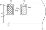
- Exemplary semiconductor structure 200includes a first conductive layer 210 , a diffusion barrier layer 215 , a second conductive layer 220 and via 225 .
- first conductive layer 210 and via 225are constructed from copper.
- second conductive layer 220is constructed from cobalt.
- the second conductive layercan operate as a diffusion barrier layer, obviating the need for a separate diffusion barrier layer 215 .
- various alloyscan be used as diffusion barrier layer 215 , including the following: tantalum nitride (TaN), titanium nitride (TiN), and cobalt tungsten phosphide (CoWP).
- a second barrier layerthat can be one of a variety of different materials, including: tantalum nitride (TaN), titanium nitride (TiN), pyroxmangite (MnSiO 3 ), and tantalum manganese oxide (TaMnO).
- FIGS. 2 through 8pictorial representations that illustrate the formation of trench area and via holes according to various embodiments are presented.
- FIG. 2shows a dielectric material 310 .
- trench 320 and via 330are also shown.
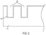
- the process of forming a double layer barrier layerwill be shown in trench 350 .
- FIG. 3illustrates the formation of a layer on top of dielectric material 310 , within trench 350 .
- FIG. 3is a continuation of FIG. 2 , with the exception that the right-hand portion of FIG. 2 is not shown in FIG. 3 .
- trench 350 or other similar recessmight need to be formed in dielectric 310 .
- trench 350is previously formed in dielectric 310 .
- a layer 452is disposed on dielectric 310 , within trench 350 .
- layer 452might be 5 angstroms to 40 angstroms in thickness.
- layer 452is comprised of TaN and disposed via physical vapor deposition (PVD) or atomic layer deposition (ALD).
- layer 452can comprise titanium nitriade (TiN), pyroxmangite (MnSiO 3 ), or tantalum manganese oxide (TaMnO). In some embodiments, layer 452 might be referred to as a diffusion layer.
- FIG. 4illustrates the formation of a next layer.
- a layer 554 of cobaltis disposed on layer 452 .
- layer 554might serve as a wetting layer.
- cobalt layer 554might be between 5 and 40 angstroms in thickness.
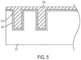
- FIG. 5illustrates the formation of a next layer.
- a first conductive layer 656has been added to the construction of FIG. 4 .
- a copper-manganese seed and electroplatingcan be used for the deposition of first conductive layer 656 .
- first conductive layer 656can be referred to as a copper gap fill layer.
- a variety of different methodscan be used to depose first conductive layer 656 .
- a vacuum continuous depositioncan be used.
- a copper reflowcan be used.
- CMPchemical mechanical planarization
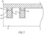
- a barrier layer 860has deposited in recess 758 .
- Atop barrier layer 860is a second conductor layer 862 .
- second conductor layer 862can comprise cobalt.
- other conductorscan be used for second conductor layer 862 . These other conductors can include ruthenium (Ru), tungsten (W), molybdenum (Mo), gold (Au), silver (Ag), aluminum (Al), and various alloys thereof.
- barrier layer 860can comprise tantalum nitride (TaN), titanium nitride (TiN), and cobalt tungsten phosphide (CoWP). As described above, in some embodiments, barrier metal layer 860 might not be needed, depending on the composition of second conductor layer 862 . Thereafter, a chemical mechanical planarization can be performed to finish the processing. The result is illustrated in FIG. 8 .
- the resulting structurehas a relatively low via resistance while also providing a sufficient electromigration barrier.
- the via resistanceis low because there is no high resistance layer at the bottom of the via.
- Electronsflow from another layer through the via to second conductor layer 862 . Then the electron flow disperses in the second conductive layer into the first conductive layer 656 through barrier layer 860 .
- Barrier layer 860works as an electromigration blocking boundary to prevent copper atoms from the upper metal layer from flowing to first conductive layer 656 (and below).
- Barrier layer 860is not at the bottom of the via, but is instead on the top surface of first conductive layer 656 .
- the electronshave a large area the barrier level through which it can travel, lowering the resistance of the via compared to older technologies, while still providing a blocking of electromigration.
- Barrier layer 860also serves as an electromigration redundancy layer. When a copper interconnect causes disconnection due to electromigration, there is a bypass line which can still maintain the electron conductivity. The bypass line is sometimes called the electromigration redundancy layer.
- second conductive layer 862can serve as the electromigration redundancy layer. Barrier layer 860 also serves to prevent cobalt diffusion (from second conductive layer 862 into copper (from first conductive layer 656 ).
Landscapes
- Engineering & Computer Science (AREA)
- Physics & Mathematics (AREA)
- Condensed Matter Physics & Semiconductors (AREA)
- General Physics & Mathematics (AREA)
- Computer Hardware Design (AREA)
- Microelectronics & Electronic Packaging (AREA)
- Power Engineering (AREA)
- Manufacturing & Machinery (AREA)
- Internal Circuitry In Semiconductor Integrated Circuit Devices (AREA)
Abstract
Description
Claims (8)
Priority Applications (3)
| Application Number | Priority Date | Filing Date | Title |
|---|---|---|---|
| US15/609,672US10804193B2 (en) | 2016-04-12 | 2017-05-31 | Semiconductor interconnect structure with double conductors |
| US17/068,230US12087685B2 (en) | 2016-04-12 | 2020-10-12 | Semiconductor interconnect structure with double conductors |
| US18/793,294US20240395702A1 (en) | 2016-04-12 | 2024-08-02 | Semiconductor interconnect structure with double conductors |
Applications Claiming Priority (2)
| Application Number | Priority Date | Filing Date | Title |
|---|---|---|---|
| US15/097,033US9837350B2 (en) | 2016-04-12 | 2016-04-12 | Semiconductor interconnect structure with double conductors |
| US15/609,672US10804193B2 (en) | 2016-04-12 | 2017-05-31 | Semiconductor interconnect structure with double conductors |
Related Parent Applications (1)
| Application Number | Title | Priority Date | Filing Date |
|---|---|---|---|
| US15/097,033DivisionUS9837350B2 (en) | 2016-04-12 | 2016-04-12 | Semiconductor interconnect structure with double conductors |
Related Child Applications (1)
| Application Number | Title | Priority Date | Filing Date |
|---|---|---|---|
| US17/068,230ContinuationUS12087685B2 (en) | 2016-04-12 | 2020-10-12 | Semiconductor interconnect structure with double conductors |
Publications (2)
| Publication Number | Publication Date |
|---|---|
| US20170294382A1 US20170294382A1 (en) | 2017-10-12 |
| US10804193B2true US10804193B2 (en) | 2020-10-13 |
Family
ID=59998849
Family Applications (4)
| Application Number | Title | Priority Date | Filing Date |
|---|---|---|---|
| US15/097,033ActiveUS9837350B2 (en) | 2016-04-12 | 2016-04-12 | Semiconductor interconnect structure with double conductors |
| US15/609,672Active2036-05-17US10804193B2 (en) | 2016-04-12 | 2017-05-31 | Semiconductor interconnect structure with double conductors |
| US17/068,230Active2036-07-17US12087685B2 (en) | 2016-04-12 | 2020-10-12 | Semiconductor interconnect structure with double conductors |
| US18/793,294PendingUS20240395702A1 (en) | 2016-04-12 | 2024-08-02 | Semiconductor interconnect structure with double conductors |
Family Applications Before (1)
| Application Number | Title | Priority Date | Filing Date |
|---|---|---|---|
| US15/097,033ActiveUS9837350B2 (en) | 2016-04-12 | 2016-04-12 | Semiconductor interconnect structure with double conductors |
Family Applications After (2)
| Application Number | Title | Priority Date | Filing Date |
|---|---|---|---|
| US17/068,230Active2036-07-17US12087685B2 (en) | 2016-04-12 | 2020-10-12 | Semiconductor interconnect structure with double conductors |
| US18/793,294PendingUS20240395702A1 (en) | 2016-04-12 | 2024-08-02 | Semiconductor interconnect structure with double conductors |
Country Status (1)
| Country | Link |
|---|---|
| US (4) | US9837350B2 (en) |
Families Citing this family (12)
| Publication number | Priority date | Publication date | Assignee | Title |
|---|---|---|---|---|
| US10573522B2 (en) | 2016-08-16 | 2020-02-25 | Lam Research Corporation | Method for preventing line bending during metal fill process |
| TWI700799B (en)* | 2016-10-04 | 2020-08-01 | 聯華電子股份有限公司 | Conductive structure, layout structure including conductive structure, and method for manufacturing conductive structure |
| US10679936B2 (en)* | 2017-09-28 | 2020-06-09 | Taiwan Semiconductor Manufacturing Co., Ltd. | MIM structure |
| US12148623B2 (en) | 2018-11-19 | 2024-11-19 | Lam Research Corporation | Deposition of tungsten on molybdenum templates |
| CN113366144B (en) | 2019-01-28 | 2023-07-07 | 朗姆研究公司 | Deposition of metal films |
| WO2021046058A1 (en) | 2019-09-03 | 2021-03-11 | Lam Research Corporation | Molybdenum deposition |
| US12327762B2 (en) | 2019-10-15 | 2025-06-10 | Lam Research Corporation | Molybdenum fill |
| US11100986B2 (en)* | 2019-12-17 | 2021-08-24 | Micron Technology, Inc. | Discharge current mitigation in a memory array |
| US11417375B2 (en) | 2019-12-17 | 2022-08-16 | Micron Technology, Inc. | Discharge current mitigation in a memory array |
| US11817389B2 (en) | 2020-03-24 | 2023-11-14 | International Business Machines Corporation | Multi-metal interconnects for semiconductor device structures |
| JP2023550331A (en)* | 2020-11-19 | 2023-12-01 | ラム リサーチ コーポレーション | Low resistivity contacts and interconnects |
| US20230197510A1 (en)* | 2021-12-20 | 2023-06-22 | International Business Machines Corporation | Hybrid metal interconnects |
Citations (16)
| Publication number | Priority date | Publication date | Assignee | Title |
|---|---|---|---|---|
| US4833519A (en)* | 1986-05-30 | 1989-05-23 | Fujitsu Limited | Semiconductor device with a wiring layer having good step coverage for contact holes |
| US5592023A (en)* | 1992-05-22 | 1997-01-07 | Nec Corporation | Semiconductor device |
| US6147404A (en)* | 1999-05-24 | 2000-11-14 | Advanced Micro Devices, Inc. | Dual barrier and conductor deposition in a dual damascene process for semiconductors |
| US20030194857A1 (en) | 2002-04-11 | 2003-10-16 | Stefan Hau-Riege | Method of making a semiconductor device that has copper damascene interconnects with enhanced electromigration reliability |
| US6887353B1 (en) | 1997-12-19 | 2005-05-03 | Applied Materials, Inc. | Tailored barrier layer which provides improved copper interconnect electromigration resistance |
| US20070077761A1 (en) | 2005-09-30 | 2007-04-05 | Matthias Lehr | Technique for forming a copper-based metallization layer including a conductive capping layer |
| US7339271B2 (en) | 2002-09-25 | 2008-03-04 | Intel Corporation | Metal-metal oxide etch stop/barrier for integrated circuit interconnects |
| US20080157380A1 (en) | 2006-12-27 | 2008-07-03 | Dongbu Hitek Co., Ltd. | Method for forming metal interconnection of semiconductor device |
| US20090269507A1 (en) | 2008-04-29 | 2009-10-29 | Sang-Ho Yu | Selective cobalt deposition on copper surfaces |
| US7666781B2 (en) | 2006-11-22 | 2010-02-23 | International Business Machines Corporation | Interconnect structures with improved electromigration resistance and methods for forming such interconnect structures |
| US8138083B2 (en) | 2006-11-15 | 2012-03-20 | International Business Machines Corporation | Interconnect structure having enhanced electromigration reliability and a method of fabricating same |
| US20120252207A1 (en)* | 2011-03-31 | 2012-10-04 | Applied Materials, Inc. | Post deposition treatments for cvd cobalt films |
| US8288276B2 (en) | 2008-12-30 | 2012-10-16 | International Business Machines Corporation | Method of forming an interconnect structure including a metallic interfacial layer located at a bottom via portion |
| US20150179579A1 (en)* | 2013-12-20 | 2015-06-25 | Christopher J. Jezewski | Cobalt based interconnects and methods of fabrication thereof |
| US20170278746A1 (en)* | 2016-03-23 | 2017-09-28 | Samsung Electronics Co., Ltd. | Methods of manufacturing a semiconductor device |
| US20180337056A1 (en)* | 2014-02-07 | 2018-11-22 | Taiwan Semiconductor Manufacturing Company | Interconnect Structure and Method of Forming the Same |
Family Cites Families (2)
| Publication number | Priority date | Publication date | Assignee | Title |
|---|---|---|---|---|
| US6528409B1 (en)* | 2002-04-29 | 2003-03-04 | Advanced Micro Devices, Inc. | Interconnect structure formed in porous dielectric material with minimized degradation and electromigration |
| US9735051B2 (en)* | 2015-12-14 | 2017-08-15 | International Business Machines Corporation | Semiconductor device interconnect structures formed by metal reflow process |
- 2016
- 2016-04-12USUS15/097,033patent/US9837350B2/enactiveActive
- 2017
- 2017-05-31USUS15/609,672patent/US10804193B2/enactiveActive
- 2020
- 2020-10-12USUS17/068,230patent/US12087685B2/enactiveActive
- 2024
- 2024-08-02USUS18/793,294patent/US20240395702A1/enactivePending
Patent Citations (16)
| Publication number | Priority date | Publication date | Assignee | Title |
|---|---|---|---|---|
| US4833519A (en)* | 1986-05-30 | 1989-05-23 | Fujitsu Limited | Semiconductor device with a wiring layer having good step coverage for contact holes |
| US5592023A (en)* | 1992-05-22 | 1997-01-07 | Nec Corporation | Semiconductor device |
| US6887353B1 (en) | 1997-12-19 | 2005-05-03 | Applied Materials, Inc. | Tailored barrier layer which provides improved copper interconnect electromigration resistance |
| US6147404A (en)* | 1999-05-24 | 2000-11-14 | Advanced Micro Devices, Inc. | Dual barrier and conductor deposition in a dual damascene process for semiconductors |
| US20030194857A1 (en) | 2002-04-11 | 2003-10-16 | Stefan Hau-Riege | Method of making a semiconductor device that has copper damascene interconnects with enhanced electromigration reliability |
| US7339271B2 (en) | 2002-09-25 | 2008-03-04 | Intel Corporation | Metal-metal oxide etch stop/barrier for integrated circuit interconnects |
| US20070077761A1 (en) | 2005-09-30 | 2007-04-05 | Matthias Lehr | Technique for forming a copper-based metallization layer including a conductive capping layer |
| US8138083B2 (en) | 2006-11-15 | 2012-03-20 | International Business Machines Corporation | Interconnect structure having enhanced electromigration reliability and a method of fabricating same |
| US7666781B2 (en) | 2006-11-22 | 2010-02-23 | International Business Machines Corporation | Interconnect structures with improved electromigration resistance and methods for forming such interconnect structures |
| US20080157380A1 (en) | 2006-12-27 | 2008-07-03 | Dongbu Hitek Co., Ltd. | Method for forming metal interconnection of semiconductor device |
| US20090269507A1 (en) | 2008-04-29 | 2009-10-29 | Sang-Ho Yu | Selective cobalt deposition on copper surfaces |
| US8288276B2 (en) | 2008-12-30 | 2012-10-16 | International Business Machines Corporation | Method of forming an interconnect structure including a metallic interfacial layer located at a bottom via portion |
| US20120252207A1 (en)* | 2011-03-31 | 2012-10-04 | Applied Materials, Inc. | Post deposition treatments for cvd cobalt films |
| US20150179579A1 (en)* | 2013-12-20 | 2015-06-25 | Christopher J. Jezewski | Cobalt based interconnects and methods of fabrication thereof |
| US20180337056A1 (en)* | 2014-02-07 | 2018-11-22 | Taiwan Semiconductor Manufacturing Company | Interconnect Structure and Method of Forming the Same |
| US20170278746A1 (en)* | 2016-03-23 | 2017-09-28 | Samsung Electronics Co., Ltd. | Methods of manufacturing a semiconductor device |
Non-Patent Citations (2)
| Title |
|---|
| List of IBM Patents or Patent Applications Treated as Related, U.S. Appl. No. 15/609,672, filed May 31, 2017, 2 Pages. |
| U.S. Appl. No. 15/097,033, filed Apr. 12, 2016, "Semicondcutor Interconnect Structure With Double Connectors". |
Also Published As
| Publication number | Publication date |
|---|---|
| US9837350B2 (en) | 2017-12-05 |
| US20210043563A1 (en) | 2021-02-11 |
| US20170294381A1 (en) | 2017-10-12 |
| US20170294382A1 (en) | 2017-10-12 |
| US12087685B2 (en) | 2024-09-10 |
| US20240395702A1 (en) | 2024-11-28 |
Similar Documents
| Publication | Publication Date | Title |
|---|---|---|
| US12087685B2 (en) | Semiconductor interconnect structure with double conductors | |
| US11488862B2 (en) | Semiconductor device with reduced via resistance | |
| US10256186B2 (en) | Interconnect structure having subtractive etch feature and damascene feature | |
| US7666787B2 (en) | Grain growth promotion layer for semiconductor interconnect structures | |
| TWI497673B (en) | Large grain size conductive structure for narrow interconnect openings | |
| US10475742B2 (en) | Method for forming semiconductor device structure having conductive structure with twin boundaries | |
| US9793206B1 (en) | Heterogeneous metallization using solid diffusion removal of metal interconnects | |
| US8492274B2 (en) | Metal alloy cap integration | |
| WO2013126199A1 (en) | Metallic capped interconnect structure with high electromigration resistance and low resistivity | |
| US11881433B2 (en) | Advanced copper interconnects with hybrid microstructure | |
| US20130112462A1 (en) | Metal Alloy Cap Integration | |
| US20060228934A1 (en) | Conductive materials for low resistance interconnects and methods of forming the same | |
| US11201112B2 (en) | Fully-aligned skip-vias | |
| US20230197506A1 (en) | Decoupled interconnects | |
| JP2024543595A (en) | Top via interconnect structure with texture suppression layer - Patents.com | |
| US20170148741A1 (en) | Advanced metallization for damage repair |
Legal Events
| Date | Code | Title | Description |
|---|---|---|---|
| AS | Assignment | Owner name:INTERNATIONAL BUSINESS MACHINES CORPORATION, NEW YORK Free format text:ASSIGNMENT OF ASSIGNORS INTEREST;ASSIGNORS:BRIGGS, BENJAMIN D.;NOGAMI, TAKESHI;PATLOLLA, RAGHUVEER R.;REEL/FRAME:042547/0245 Effective date:20160411 Owner name:INTERNATIONAL BUSINESS MACHINES CORPORATION, NEW Y Free format text:ASSIGNMENT OF ASSIGNORS INTEREST;ASSIGNORS:BRIGGS, BENJAMIN D.;NOGAMI, TAKESHI;PATLOLLA, RAGHUVEER R.;REEL/FRAME:042547/0245 Effective date:20160411 | |
| STPP | Information on status: patent application and granting procedure in general | Free format text:FINAL REJECTION MAILED | |
| STPP | Information on status: patent application and granting procedure in general | Free format text:RESPONSE AFTER FINAL ACTION FORWARDED TO EXAMINER | |
| STPP | Information on status: patent application and granting procedure in general | Free format text:ADVISORY ACTION MAILED | |
| STPP | Information on status: patent application and granting procedure in general | Free format text:DOCKETED NEW CASE - READY FOR EXAMINATION | |
| STPP | Information on status: patent application and granting procedure in general | Free format text:NON FINAL ACTION MAILED | |
| STPP | Information on status: patent application and granting procedure in general | Free format text:RESPONSE TO NON-FINAL OFFICE ACTION ENTERED AND FORWARDED TO EXAMINER | |
| STPP | Information on status: patent application and granting procedure in general | Free format text:FINAL REJECTION MAILED | |
| STPP | Information on status: patent application and granting procedure in general | Free format text:RESPONSE AFTER FINAL ACTION FORWARDED TO EXAMINER | |
| STPP | Information on status: patent application and granting procedure in general | Free format text:ADVISORY ACTION MAILED | |
| AS | Assignment | Owner name:TESSERA, INC., CALIFORNIA Free format text:ASSIGNMENT OF ASSIGNORS INTEREST;ASSIGNOR:INTERNATIONAL BUSINESS MACHINES CORPORATION;REEL/FRAME:051489/0324 Effective date:20191227 | |
| STPP | Information on status: patent application and granting procedure in general | Free format text:DOCKETED NEW CASE - READY FOR EXAMINATION | |
| STPP | Information on status: patent application and granting procedure in general | Free format text:NON FINAL ACTION MAILED | |
| AS | Assignment | Owner name:BANK OF AMERICA, N.A., NORTH CAROLINA Free format text:SECURITY INTEREST;ASSIGNORS:ROVI SOLUTIONS CORPORATION;ROVI TECHNOLOGIES CORPORATION;ROVI GUIDES, INC.;AND OTHERS;REEL/FRAME:053468/0001 Effective date:20200601 | |
| STPP | Information on status: patent application and granting procedure in general | Free format text:NOTICE OF ALLOWANCE MAILED -- APPLICATION RECEIVED IN OFFICE OF PUBLICATIONS | |
| AS | Assignment | Owner name:TESSERA, INC., CALIFORNIA Free format text:CORRECTIVE ASSIGNMENT TO CORRECT THE 16/161,111 PREVIOUSLY RECORDED ON REEL 051489 FRAME 0324. ASSIGNOR(S) HEREBY CONFIRMS THE ASSIGNMENT;ASSIGNOR:INTERNATIONAL BUSINESS MACHINES CORPORATION;REEL/FRAME:053389/0252 Effective date:20191227 | |
| STPP | Information on status: patent application and granting procedure in general | Free format text:PUBLICATIONS -- ISSUE FEE PAYMENT VERIFIED | |
| STCF | Information on status: patent grant | Free format text:PATENTED CASE | |
| AS | Assignment | Owner name:TESSERA LLC, CALIFORNIA Free format text:CERTIFICATE OF CONVERSION & CHANGE OF NAME;ASSIGNOR:TESSERA, INC.;REEL/FRAME:061388/0199 Effective date:20211001 | |
| MAFP | Maintenance fee payment | Free format text:PAYMENT OF MAINTENANCE FEE, 4TH YEAR, LARGE ENTITY (ORIGINAL EVENT CODE: M1551); ENTITY STATUS OF PATENT OWNER: LARGE ENTITY Year of fee payment:4 | |
| AS | Assignment | Owner name:ADEIA SEMICONDUCTOR SOLUTIONS LLC, CALIFORNIA Free format text:CHANGE OF NAME;ASSIGNOR:TESSERA LLC;REEL/FRAME:069067/0448 Effective date:20220815 |