US10797129B2 - Field effect transistor structure having notched mesa - Google Patents
Field effect transistor structure having notched mesaDownload PDFInfo
- Publication number
- US10797129B2 US10797129B2US16/001,410US201816001410AUS10797129B2US 10797129 B2US10797129 B2US 10797129B2US 201816001410 AUS201816001410 AUS 201816001410AUS 10797129 B2US10797129 B2US 10797129B2
- Authority
- US
- United States
- Prior art keywords
- group iii
- mesa
- gate
- field effect
- effect transistor
- Prior art date
- Legal status (The legal status is an assumption and is not a legal conclusion. Google has not performed a legal analysis and makes no representation as to the accuracy of the status listed.)
- Active
Links
Images


Classifications
- H01L29/0657—
- H—ELECTRICITY
- H10—SEMICONDUCTOR DEVICES; ELECTRIC SOLID-STATE DEVICES NOT OTHERWISE PROVIDED FOR
- H10D—INORGANIC ELECTRIC SEMICONDUCTOR DEVICES
- H10D62/00—Semiconductor bodies, or regions thereof, of devices having potential barriers
- H10D62/10—Shapes, relative sizes or dispositions of the regions of the semiconductor bodies; Shapes of the semiconductor bodies
- H10D62/117—Shapes of semiconductor bodies
- H01L29/812—
- H—ELECTRICITY
- H10—SEMICONDUCTOR DEVICES; ELECTRIC SOLID-STATE DEVICES NOT OTHERWISE PROVIDED FOR
- H10D—INORGANIC ELECTRIC SEMICONDUCTOR DEVICES
- H10D30/00—Field-effect transistors [FET]
- H10D30/80—FETs having rectifying junction gate electrodes
- H10D30/87—FETs having Schottky gate electrodes, e.g. metal-semiconductor FETs [MESFET]
- H01L29/2003—
- H01L29/4175—
- H01L29/41758—
- H—ELECTRICITY
- H10—SEMICONDUCTOR DEVICES; ELECTRIC SOLID-STATE DEVICES NOT OTHERWISE PROVIDED FOR
- H10D—INORGANIC ELECTRIC SEMICONDUCTOR DEVICES
- H10D62/00—Semiconductor bodies, or regions thereof, of devices having potential barriers
- H10D62/80—Semiconductor bodies, or regions thereof, of devices having potential barriers characterised by the materials
- H10D62/85—Semiconductor bodies, or regions thereof, of devices having potential barriers characterised by the materials being Group III-V materials, e.g. GaAs
- H10D62/8503—Nitride Group III-V materials, e.g. AlN or GaN
- H—ELECTRICITY
- H10—SEMICONDUCTOR DEVICES; ELECTRIC SOLID-STATE DEVICES NOT OTHERWISE PROVIDED FOR
- H10D—INORGANIC ELECTRIC SEMICONDUCTOR DEVICES
- H10D64/00—Electrodes of devices having potential barriers
- H10D64/20—Electrodes characterised by their shapes, relative sizes or dispositions
- H10D64/23—Electrodes carrying the current to be rectified, amplified, oscillated or switched, e.g. sources, drains, anodes or cathodes
- H10D64/251—Source or drain electrodes for field-effect devices
- H10D64/254—Source or drain electrodes for field-effect devices for lateral devices wherein the source or drain electrodes extend entirely through the semiconductor bodies, e.g. via-holes for back side contacts
- H—ELECTRICITY
- H10—SEMICONDUCTOR DEVICES; ELECTRIC SOLID-STATE DEVICES NOT OTHERWISE PROVIDED FOR
- H10D—INORGANIC ELECTRIC SEMICONDUCTOR DEVICES
- H10D64/00—Electrodes of devices having potential barriers
- H10D64/20—Electrodes characterised by their shapes, relative sizes or dispositions
- H10D64/23—Electrodes carrying the current to be rectified, amplified, oscillated or switched, e.g. sources, drains, anodes or cathodes
- H10D64/251—Source or drain electrodes for field-effect devices
- H10D64/257—Source or drain electrodes for field-effect devices for lateral devices wherein the source or drain electrodes are characterised by top-view geometrical layouts, e.g. interdigitated, semi-circular, annular or L-shaped electrodes
Definitions
- This disclosurerelates generally to Field Effect Transistor (FET) Structures and more particularly to FET structures having reduced gate parasitics.
- a FET according to the PRIOR ARTis shown in FIGS. 1A-1C .
- a semi-insulating, highly resistive, substratesuch as SiC
- III-V based structuressuch as GaN-based transistors use electrons formed between two different bandgap materials, for example, AlGaN and GaN.
- Source and drain electrodesFormed in ohmic contact with source and drain regions of the upper surface of the mesa are source and drain electrodes, as shown.
- a gate electrodeDisposed between the source and drain electrodes is a gate electrode in Schottky contact with an upper surface of the mesa (a gate region) disposed between the source and drain regions.
- the gate electrodeis used to control a flow of carriers (holes and electrons) in an active region of the mesa though the active region (sometimes herein referred to as the gate channel region) between the source and drain regions. It is noted that the regions outside of the mesa area, called ‘off mesa area’.
- the off mesa areais semi-insulating highly resistive area.
- the Effective gate width(the active region) is the length of the gate electrode is the region closest to the source and drain regions (the gate channel region) and it is this gate channel region that contributes to the conduction of transistor.
- the contribution of the carriers in the gate channel regiongets stronger. From the prior art it is noted that the total gate length extends beyond the gate channel length even though the most of carrier conduction occurs along the gate channel length; however, the portions of the gate electrode extending beyond the gate channel region generate parasitic gate resistance, inductance, and capacitance and thereby contribute negatively for high frequency operation.
- the source electrodeis disposed within opposing sidewalls of the mesa structure
- the drain electrodeis disposed within the opposing sidewalls in ohmic contact with a drain region of the mesa
- the gate electrodeis disposed within opposing walls of the gate region of the mesa and that the mesa is rectangular shape.
- the source electrodehas an inner edge extending between ends SOURCE EDGE 1 , SOURCE EDGE 2 ( FIG. 1A ) thereof proximate the gate electrode that extends along a direction parallel to the gate electrode; and, likewise the drain electrode has an inner edge extending between ends DRAIN EDGE 1 , DRAIN EDGE 2 ( FIG.
- the gate electrodeextends beyond the ends of SOURCE EDGE 1 , SOURCE EDGE 2 of the inner edge of the source electrode and thus also beyond the ends of DRAIN EDGE 1 , DRAIN EDGE 2 of the inner edge of the drain electrode.
- the active regionextends between ends DRAIN EDGE 1 (or SOURCE EDGE 1 ) and DRAIN EDGE 2 (or SOURCE EDGE 2 ) ( FIG. 1A ).
- the total gate electrode lengthextends beyond the active region (gate channel length), even though the most of carrier conduction occurs along the gate channel length, generates unwanted parasitic gate resistance, inductance, and capacitance and thereby contributes negatively for high frequency operation of the FET.
- a Field Effect Transistor structurehaving: a semi-insulating substrate; a semiconductor mesa structure disposed on the substrate and having a notch in an outer sidewall of the mesa structure; a source electrode disposed within the opposing sidewalls in ohmic contact with a source region of the mesa structure; a drain electrode disposed within the opposing sidewalls in ohmic contact with a drain region of the mesa structure; and a gate electrode, having an inner portion disposed between, and laterally of the source electrode and the drain electrode and in Schottky contact with the mesa structure, extending longitudinally towards the notch and having outer portions extending beyond the mesa structure and over portions of the substrate outside of the mesa structure.
- the mesa structureincludes a pair of notches project inwardly towards each other and the inner portion of the gate extends longitudinally between the pair of notches.
- the gate parasitics of the prior artare reduced by the formation of the notches in the mesa structure because extra gate length on top of the active region of the mesa structure is eliminated and the gate tab (or pad) disposed on the substrate off of the mesa structure is able to be positioned closer to active inner portion of the gate.
- the parasitic componentsare multiplied and therefore the disclosed FET structure significantly improves the performance of FETs with multiple gate fingers at high operating frequency.
- FIGS. 1A-1Care plan, and cross sectional views of a Field Effect Transistor structure according to the PRIOR ART, where the cross sectional views in FIGS. 1B and 1C are taken along lines 1 B- 1 B and 1 C- 1 C, respectively, in FIG. 1A ;
- FIGS. 2A-2Care plan, and cross sectional views of a Field Effect Transistor structure according to the disclosure, where the cross sectional views in FIGS. 2B and 2C are taken along lines 2 B- 2 B and 2 C- 2 C, respectively, in FIG. 2A ;
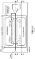
- FIG. 3is a plan view of the Field Effect Transistor structure of FIG. 1A disposed in a side-by-side relationship with the Field Effect Transistor structure of FIG. 2B to compare the two Field Effect Transistor structures;
- FIG. 4is a plan view of a multi-gate embodiment of a Field Effect Transistor structure according to the disclosure.
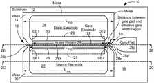
- a Field Effect Transistor structure 10having: a semi-insulating substrate 12 , here for example, a semi-insulating, highly resistive, substrate, such as SiC, GaAs, and InP; a semiconductor mesa structure 14 , here for example, a Group III-V structure such as a GaN structure, disposed on the upper surface 16 of the substrate 12 and having a pair of notches 18 in opposing outer sidewalls 20 of the mesa structure 14 ; a source electrode 22 disposed within the opposing sidewalls 20 in ohmic contact with a source region 24 ( FIG.
- the mesa structure 14includes a pair of notches 18 which project inwardly towards each other and the inner portion 28 a of the gate 28 extends longitudinally between the pair of notches 18 .
- the notches 18are v-shaped notches. It should be understood, however, that the notches 18 may be of a different shapes and includes, for example, any shaped indentation or groove in the sidewalls 20 of the mesa structure 14 , including, for example, a rounded indentation, a square or rectangular indentation.
- the source electrode 22has an inner edge 23 extending between ends SE 1 and SE 2 ( FIG. 2A ) thereof proximate the inner portion 28 a of gate electrode 28 ; and, likewise the drain electrode 26 has an inner edge 27 extending between ends DE 1 , DE 2 ( FIG. 2A ) thereof proximate the inner portion 28 a of gate electrode 28 .
- the lengths of the inner edges 23 , 27 of the source and drain electrodes 22 , 26are equal.
- the gate electrode 28extends beyond the ends SE 1 , SE 2 of the inner edge 23 of the source electrode 22 and thus also beyond the ends DE 1 , DE 2 of the inner edge 27 of the drain electrode 26 .
- the active region (gate channel) 29in under the inner portion 28 a of the gate electrode 28 and extends between ends DE 1 (or SE 1 ) and DE 2 (or SE 2 ) ( FIG. 2A ).
- the inner portion 28 a of the gate electrode 28is elongated and the source electrode 22 and the drain electrode 26 are here also elongated along directions parallel to the direction of the elongated inner portion 28 a of the gate electrode 28 .
- the source electrode 22is within opposing outer portions of the sidewalls 20 of the mesa structure 14 separated a length L ms measured along the top surface of the mesa;
- the drain electrodeis within opposing portions of the sidewalls 20 separated a length L md measured along the top surface of the mesa;
- the inner portion 28 a of the gate electrode 28is within the pair of notches 18 , the notches being separated a length L s measured along the top surface of the mesa; where L mg is less than either one of the lengths L md or L ms ; it here being noted that length L md equals length L ms .
- all three lengthsare measured along directions parallel to the direction of the elongated inner portion 28 a of the gate electrode 28 .
- One end of the inner portion 28 a of the gate electrode 28terminates in a gate pad 28 p and a portion 28 p ′ of the gate pad 28 p is disposed within a portion of one of the pair of notches 18 , here the notch 28 on the right hand side of mesa structure 14 in FIG. 2A .
- the gate pad 28 pis wider than the inner region 28 a of the gate electrode 28 .
- FIG. 3a comparison is shown between the plan view of a mesa structure with a pair of opposing notches (the upper portion of FIG. 3 ) and a mesa structure without a pair of opposing notches (the lower portion of FIG. 3 ). It is noted that the length of the gate electrode between the end of the active gate region and the gate pad on the right hand side of FIG. 3 with the notch is less than the length of the gate electrode between the end of the active gate region and the gate pad without the notch by a difference in length DIFF 1 .
- the length of the gate electrode between the end of the active gate region and the left hand end of the gate electrode with the notchis less than the length of the gate electrode between the end of the active gate region and the left hand end of the gate electrode without the notch by a difference in length DIFF 2 .
- the gate parasiticsare reduced by the formation of the notches in the mesa structure because extra gate length on top of the active region of the mesa structure is eliminated and the gate tab (or pad) disposed on the substrate off of the mesa structure is able to be positioned closer to active inner portion of the gate.
- FIG. 4a multi-fingered gate structure, here having two gate fingers, it being understood that more than two gate fingers may be used, of the FET of FIGS. 2A-2C is shown.
- the source electrodeis connected to a ground plane on the bottom surface of the substrate with a conductive via passing vertically through the mesa structure and the underlying portion of the substrate. It is noted that as the number of gate fingers increases, the parasitic components are multiplied and therefore the disclosed FET structure significantly improves the performance of FETs with multiple gate fingers.
Landscapes
- Junction Field-Effect Transistors (AREA)
- Electrodes Of Semiconductors (AREA)
Abstract
Description
Claims (16)
Priority Applications (1)
| Application Number | Priority Date | Filing Date | Title |
|---|---|---|---|
| US16/001,410US10797129B2 (en) | 2015-05-08 | 2018-06-06 | Field effect transistor structure having notched mesa |
Applications Claiming Priority (2)
| Application Number | Priority Date | Filing Date | Title |
|---|---|---|---|
| US14/707,435US10134839B2 (en) | 2015-05-08 | 2015-05-08 | Field effect transistor structure having notched mesa |
| US16/001,410US10797129B2 (en) | 2015-05-08 | 2018-06-06 | Field effect transistor structure having notched mesa |
Related Parent Applications (1)
| Application Number | Title | Priority Date | Filing Date |
|---|---|---|---|
| US14/707,435DivisionUS10134839B2 (en) | 2015-05-08 | 2015-05-08 | Field effect transistor structure having notched mesa |
Publications (2)
| Publication Number | Publication Date |
|---|---|
| US20180286947A1 US20180286947A1 (en) | 2018-10-04 |
| US10797129B2true US10797129B2 (en) | 2020-10-06 |
Family
ID=56027202
Family Applications (2)
| Application Number | Title | Priority Date | Filing Date |
|---|---|---|---|
| US14/707,435ActiveUS10134839B2 (en) | 2015-05-08 | 2015-05-08 | Field effect transistor structure having notched mesa |
| US16/001,410ActiveUS10797129B2 (en) | 2015-05-08 | 2018-06-06 | Field effect transistor structure having notched mesa |
Family Applications Before (1)
| Application Number | Title | Priority Date | Filing Date |
|---|---|---|---|
| US14/707,435ActiveUS10134839B2 (en) | 2015-05-08 | 2015-05-08 | Field effect transistor structure having notched mesa |
Country Status (5)
| Country | Link |
|---|---|
| US (2) | US10134839B2 (en) |
| EP (1) | EP3295487B1 (en) |
| JP (1) | JP6750002B2 (en) |
| CN (1) | CN107787524B (en) |
| WO (1) | WO2016182825A1 (en) |
Families Citing this family (2)
| Publication number | Priority date | Publication date | Assignee | Title |
|---|---|---|---|---|
| US10134839B2 (en) | 2015-05-08 | 2018-11-20 | Raytheon Company | Field effect transistor structure having notched mesa |
| CN112614886B (en)* | 2020-12-16 | 2022-11-22 | 广东省科学院半导体研究所 | HEMT device and manufacturing method thereof |
Citations (23)
| Publication number | Priority date | Publication date | Assignee | Title |
|---|---|---|---|---|
| US3813585A (en)* | 1970-04-28 | 1974-05-28 | Agency Ind Science Techn | Compound semiconductor device having undercut oriented groove |
| JPS54133080A (en) | 1978-04-06 | 1979-10-16 | Nec Corp | Semiconductor device |
| US4219835A (en)* | 1978-02-17 | 1980-08-26 | Siliconix, Inc. | VMOS Mesa structure and manufacturing process |
| US4317125A (en)* | 1978-05-31 | 1982-02-23 | The Secretary Of State For Defence In Her Britannic Majesty's Government Of The United Kingdom Of Great Britain And Northern Ireland | Field effect devices and their fabrication |
| US4321613A (en)* | 1978-05-31 | 1982-03-23 | The Secretary Of State For Defence In Her Britannic Majesty's Government Of The United Kingdom Of Great Britain And Northern Ireland | Field effect devices and their fabrication |
| JPS6049676A (en) | 1983-08-29 | 1985-03-18 | Fujitsu Ltd | Semiconductor device |
| US4632710A (en)* | 1983-05-10 | 1986-12-30 | Raytheon Company | Vapor phase epitaxial growth of carbon doped layers of Group III-V materials |
| US4974039A (en) | 1989-08-14 | 1990-11-27 | Raytheon Company | Field effect transistor having an integrated capacitor |
| US5025296A (en)* | 1988-02-29 | 1991-06-18 | Motorola, Inc. | Center tapped FET |
| US5270554A (en)* | 1991-06-14 | 1993-12-14 | Cree Research, Inc. | High power high frequency metal-semiconductor field-effect transistor formed in silicon carbide |
| US5358878A (en)* | 1991-03-15 | 1994-10-25 | U.S. Philips Corporation | Method of manufacturing an integrated high electron mobility transistor having a surrounding insulating layer |
| US5364816A (en)* | 1993-01-29 | 1994-11-15 | The United States Of America As Represented By The Secretary Of The Navy | Fabrication method for III-V heterostructure field-effect transistors |
| US5483089A (en)* | 1992-08-11 | 1996-01-09 | Mitsubishi Denki Kabushiki Kaisha | Electrically isolated MESFET |
| US5689124A (en)* | 1994-05-31 | 1997-11-18 | Nippon Steel Corporation | Semiconductor device |
| EP0837510A2 (en) | 1996-10-16 | 1998-04-22 | Sanyo Electric Co. Ltd | Field effect transistor and manufacturing method thereof |
| JPH10261651A (en) | 1997-03-17 | 1998-09-29 | Toyota Motor Corp | Compound semiconductor device and method of manufacturing the same |
| US6081006A (en)* | 1998-08-13 | 2000-06-27 | Cisco Systems, Inc. | Reduced size field effect transistor |
| US20020014670A1 (en)* | 2000-05-17 | 2002-02-07 | Andrej Litwin | Power transistors for radio frequencies |
| US6545543B2 (en)* | 2001-07-06 | 2003-04-08 | Remec, Inc. | Small aspect ratio MMIC power amplifier layout |
| US6774416B2 (en)* | 2001-07-16 | 2004-08-10 | Nanowave, Inc | Small area cascode FET structure operating at mm-wave frequencies |
| US20060084232A1 (en)* | 2002-08-12 | 2006-04-20 | Grupp Daniel E | Process for fabricating a self-aligned deposited source/drain insulated gate field-effect transistor |
| US20090090934A1 (en)* | 2007-10-05 | 2009-04-09 | Tsutomu Tezuka | Field Effect Transistor and Method for Manufacturing the Same |
| US20160329420A1 (en) | 2015-05-08 | 2016-11-10 | Raytheon Company | Field Effect Transistor Structure Having Notched Mesa |
Family Cites Families (8)
| Publication number | Priority date | Publication date | Assignee | Title |
|---|---|---|---|---|
| JPS6155961A (en)* | 1984-08-27 | 1986-03-20 | Nec Corp | Electrode structure of semiconductor devices |
| JPH01201966A (en)* | 1988-02-05 | 1989-08-14 | Sharp Corp | Electrode structure of semiconductor devices |
| JPH02188930A (en)* | 1989-01-17 | 1990-07-25 | Sumitomo Electric Ind Ltd | Field-effect transistor and manufacture thereof |
| JPH04321237A (en)* | 1991-04-19 | 1992-11-11 | Sony Corp | Manufacture of field-effect transistor |
| JPH05308082A (en)* | 1992-04-30 | 1993-11-19 | Sumitomo Electric Ind Ltd | Semiconductor device and its manufacture |
| US6833556B2 (en) | 2002-08-12 | 2004-12-21 | Acorn Technologies, Inc. | Insulated gate field effect transistor having passivated schottky barriers to the channel |
| KR100653711B1 (en) | 2005-11-14 | 2006-12-05 | 삼성전자주식회사 | Schottky Barrier Fin Pet Devices and Manufacturing Method Thereof |
| JP2010238975A (en)* | 2009-03-31 | 2010-10-21 | Asahi Kasei Electronics Co Ltd | Semiconductor device, and method of manufacturing the same |
- 2015
- 2015-05-08USUS14/707,435patent/US10134839B2/enactiveActive
- 2016
- 2016-05-05WOPCT/US2016/030868patent/WO2016182825A1/ennot_activeCeased
- 2016-05-05EPEP16724198.3Apatent/EP3295487B1/enactiveActive
- 2016-05-05JPJP2018510318Apatent/JP6750002B2/enactiveActive
- 2016-05-05CNCN201680035251.0Apatent/CN107787524B/enactiveActive
- 2018
- 2018-06-06USUS16/001,410patent/US10797129B2/enactiveActive
Patent Citations (25)
| Publication number | Priority date | Publication date | Assignee | Title |
|---|---|---|---|---|
| US3813585A (en)* | 1970-04-28 | 1974-05-28 | Agency Ind Science Techn | Compound semiconductor device having undercut oriented groove |
| US4219835A (en)* | 1978-02-17 | 1980-08-26 | Siliconix, Inc. | VMOS Mesa structure and manufacturing process |
| JPS54133080A (en) | 1978-04-06 | 1979-10-16 | Nec Corp | Semiconductor device |
| US4317125A (en)* | 1978-05-31 | 1982-02-23 | The Secretary Of State For Defence In Her Britannic Majesty's Government Of The United Kingdom Of Great Britain And Northern Ireland | Field effect devices and their fabrication |
| US4321613A (en)* | 1978-05-31 | 1982-03-23 | The Secretary Of State For Defence In Her Britannic Majesty's Government Of The United Kingdom Of Great Britain And Northern Ireland | Field effect devices and their fabrication |
| US4632710A (en)* | 1983-05-10 | 1986-12-30 | Raytheon Company | Vapor phase epitaxial growth of carbon doped layers of Group III-V materials |
| JPS6049676A (en) | 1983-08-29 | 1985-03-18 | Fujitsu Ltd | Semiconductor device |
| US5025296A (en)* | 1988-02-29 | 1991-06-18 | Motorola, Inc. | Center tapped FET |
| US4974039A (en) | 1989-08-14 | 1990-11-27 | Raytheon Company | Field effect transistor having an integrated capacitor |
| US5358878A (en)* | 1991-03-15 | 1994-10-25 | U.S. Philips Corporation | Method of manufacturing an integrated high electron mobility transistor having a surrounding insulating layer |
| US5270554A (en)* | 1991-06-14 | 1993-12-14 | Cree Research, Inc. | High power high frequency metal-semiconductor field-effect transistor formed in silicon carbide |
| US5483089A (en)* | 1992-08-11 | 1996-01-09 | Mitsubishi Denki Kabushiki Kaisha | Electrically isolated MESFET |
| US5364816A (en)* | 1993-01-29 | 1994-11-15 | The United States Of America As Represented By The Secretary Of The Navy | Fabrication method for III-V heterostructure field-effect transistors |
| US5689124A (en)* | 1994-05-31 | 1997-11-18 | Nippon Steel Corporation | Semiconductor device |
| EP0837510A2 (en) | 1996-10-16 | 1998-04-22 | Sanyo Electric Co. Ltd | Field effect transistor and manufacturing method thereof |
| JPH10125695A (en) | 1996-10-16 | 1998-05-15 | Sanyo Electric Co Ltd | Semiconductor device and manufacturing method thereof |
| EP0837510A3 (en) | 1996-10-16 | 1999-07-21 | Sanyo Electric Co. Ltd | Field effect transistor and manufacturing method thereof |
| JPH10261651A (en) | 1997-03-17 | 1998-09-29 | Toyota Motor Corp | Compound semiconductor device and method of manufacturing the same |
| US6081006A (en)* | 1998-08-13 | 2000-06-27 | Cisco Systems, Inc. | Reduced size field effect transistor |
| US20020014670A1 (en)* | 2000-05-17 | 2002-02-07 | Andrej Litwin | Power transistors for radio frequencies |
| US6545543B2 (en)* | 2001-07-06 | 2003-04-08 | Remec, Inc. | Small aspect ratio MMIC power amplifier layout |
| US6774416B2 (en)* | 2001-07-16 | 2004-08-10 | Nanowave, Inc | Small area cascode FET structure operating at mm-wave frequencies |
| US20060084232A1 (en)* | 2002-08-12 | 2006-04-20 | Grupp Daniel E | Process for fabricating a self-aligned deposited source/drain insulated gate field-effect transistor |
| US20090090934A1 (en)* | 2007-10-05 | 2009-04-09 | Tsutomu Tezuka | Field Effect Transistor and Method for Manufacturing the Same |
| US20160329420A1 (en) | 2015-05-08 | 2016-11-10 | Raytheon Company | Field Effect Transistor Structure Having Notched Mesa |
Non-Patent Citations (20)
| Title |
|---|
| Final Office Action dated Jun. 7, 2017 for U.S. Appl. No. 14/707,435; 29 Pages. |
| Final Office Action dated Sep. 13, 2016 for U.S. Appl. No. 14/707,435; 19 Pages. |
| International Preliminary Report on Patentability, PCT/US2016/030868, dated Nov. 23, 2017, 1 page. |
| International Search report, PCT/US2016/030868, dated Jul. 15, 2016, 4 pages. |
| Notice of Allowance dated Aug. 6, 2018 for U.S. Appl. No. 14/707,435; 22 Pages. |
| Notification Concerning Transmittal of International Preliminary Report on Patentability (Chapter I of the Patent Cooperation Treaty), PCT/US2016/030868, dated Nov. 23, 2017, 1 page. |
| Notification of First Office Action for Chinese Patent Application No. 201680035251.0, with English Translation, dated Jun. 8, 2020, 15 pages. |
| Notification of Transmittal of the International Search Report and The Written Opinion of the International Searching Authority, or the Declaration, PCT/US2016/030868, dated Jul. 15, 2016, 1 page. |
| Office Action dated Feb. 2, 2018 for U.S. Appl. No. 14/707,435; 44 Pages. |
| Office Action dated Jan. 4, 2017 for U.S. Appl. No. 14/707,435; 20 Pages. |
| Office Action dated May 17, 2016 for U.S. Appl. No. 14/707,435; 14 Pages. |
| RCE and Response to Final Office Action dated Jun. 7, 2017 as filed on Sep. 6, 2017 for U.S. Appl. No. 14/707,435; 28 Pages. |
| RCE and Second Response to Final Office Action dated Sep. 13, 2016 as filed on Nov. 14, 2016 for U.S. Appl. No. 14/707,435; 20 Pages. |
| Response to Final Office Action dated Sep. 13, 2016 as filed on Nov. 1, 2016 for U.S. Appl. No. 14/707,435; 17 Pages. |
| Response to Office Action dated Jan. 4, 2017 as filed on Mar. 22, 2017 for U.S. Appl. No. 14/707,435; 29 Pages. |
| Response to Office Action dated May 17, 2016 as filed on Aug. 4, 2016 for U.S. Appl. No. 14/707,435; 15 Pages. |
| Response to Restriction Requirement dated Mar. 16, 2016 as filed on Mar. 30, 2016 for U.S. Appl. No. 14/707,435; 1 Page. |
| Restriction Requirement dated Mar. 16, 2016 for U.S. Appl. No. 14/707,435; 6 Pages. |
| Written Opinion of the International Searching Authority, PCT/US2016/030868, dated Jul. 15, 2016, 6 pages. |
| Written Opinion of the International Searching Authority, PCT/US2016/030868, dated Nov. 23, 2017, 6 pages. |
Also Published As
| Publication number | Publication date |
|---|---|
| CN107787524B (en) | 2021-10-29 |
| JP2018514954A (en) | 2018-06-07 |
| US10134839B2 (en) | 2018-11-20 |
| EP3295487B1 (en) | 2025-01-15 |
| EP3295487A1 (en) | 2018-03-21 |
| US20160329420A1 (en) | 2016-11-10 |
| US20180286947A1 (en) | 2018-10-04 |
| JP6750002B2 (en) | 2020-09-02 |
| CN107787524A (en) | 2018-03-09 |
| WO2016182825A1 (en) | 2016-11-17 |
Similar Documents
| Publication | Publication Date | Title |
|---|---|---|
| CN107359196B (en) | Semiconductor device with a plurality of semiconductor chips | |
| KR102303377B1 (en) | FET with buried gate structure | |
| US10529843B2 (en) | Semiconductor device | |
| US7135747B2 (en) | Semiconductor devices having thermal spacers | |
| CN108735812B (en) | Semiconductor device with a plurality of semiconductor chips | |
| US8431963B2 (en) | Field-effect transistor | |
| US8664716B2 (en) | Semiconductor device, method of manufacturing the same and power-supply device using the same | |
| US20100025737A1 (en) | Field-effect transistor | |
| US20130228788A1 (en) | Semiconductor device | |
| US6559513B1 (en) | Field-plate MESFET | |
| CN105247680B (en) | multi-channel transistor | |
| US9391187B2 (en) | Semiconductor heterojunction device | |
| US10797129B2 (en) | Field effect transistor structure having notched mesa | |
| KR102024290B1 (en) | Power semiconductor device | |
| US7423325B2 (en) | Lateral field-effect-controllable semiconductor component for RF applications | |
| US20160079403A1 (en) | Field effect transistor | |
| KR20140054585A (en) | Power semiconductor device |
Legal Events
| Date | Code | Title | Description |
|---|---|---|---|
| FEPP | Fee payment procedure | Free format text:ENTITY STATUS SET TO UNDISCOUNTED (ORIGINAL EVENT CODE: BIG.); ENTITY STATUS OF PATENT OWNER: LARGE ENTITY | |
| AS | Assignment | Owner name:RAYTHEON COMPANY, MASSACHUSETTS Free format text:ASSIGNMENT OF ASSIGNORS INTEREST;ASSIGNOR:HWANG, KIUCHUL;REEL/FRAME:046056/0547 Effective date:20150427 | |
| STPP | Information on status: patent application and granting procedure in general | Free format text:RESPONSE TO NON-FINAL OFFICE ACTION ENTERED AND FORWARDED TO EXAMINER | |
| STPP | Information on status: patent application and granting procedure in general | Free format text:NON FINAL ACTION MAILED | |
| STPP | Information on status: patent application and granting procedure in general | Free format text:RESPONSE TO NON-FINAL OFFICE ACTION ENTERED AND FORWARDED TO EXAMINER | |
| STPP | Information on status: patent application and granting procedure in general | Free format text:FINAL REJECTION MAILED | |
| STPP | Information on status: patent application and granting procedure in general | Free format text:ADVISORY ACTION MAILED | |
| STPP | Information on status: patent application and granting procedure in general | Free format text:DOCKETED NEW CASE - READY FOR EXAMINATION | |
| STPP | Information on status: patent application and granting procedure in general | Free format text:NOTICE OF ALLOWANCE MAILED -- APPLICATION RECEIVED IN OFFICE OF PUBLICATIONS | |
| STPP | Information on status: patent application and granting procedure in general | Free format text:PUBLICATIONS -- ISSUE FEE PAYMENT VERIFIED | |
| STCF | Information on status: patent grant | Free format text:PATENTED CASE | |
| MAFP | Maintenance fee payment | Free format text:PAYMENT OF MAINTENANCE FEE, 4TH YEAR, LARGE ENTITY (ORIGINAL EVENT CODE: M1551); ENTITY STATUS OF PATENT OWNER: LARGE ENTITY Year of fee payment:4 |