US10796959B2 - Laser processing method and laser processing apparatus - Google Patents
Laser processing method and laser processing apparatusDownload PDFInfo
- Publication number
- US10796959B2 US10796959B2US15/808,211US201715808211AUS10796959B2US 10796959 B2US10796959 B2US 10796959B2US 201715808211 AUS201715808211 AUS 201715808211AUS 10796959 B2US10796959 B2US 10796959B2
- Authority
- US
- United States
- Prior art keywords
- laser light
- light
- processed
- cut
- along
- Prior art date
- Legal status (The legal status is an assumption and is not a legal conclusion. Google has not performed a legal analysis and makes no representation as to the accuracy of the status listed.)
- Expired - Fee Related, expires
Links
- 238000012545processingMethods0.000titleclaimsdescription271
- 238000003672processing methodMethods0.000titledescription146
- 238000005520cutting processMethods0.000claimsabstractdescription175
- 238000000034methodMethods0.000claimsabstractdescription51
- 230000001678irradiating effectEffects0.000claimsdescription76
- 239000004065semiconductorSubstances0.000claimsdescription56
- XUIMIQQOPSSXEZ-UHFFFAOYSA-NSiliconChemical compound[Si]XUIMIQQOPSSXEZ-UHFFFAOYSA-N0.000claimsdescription48
- 229910052710siliconInorganic materials0.000claimsdescription39
- 239000010703siliconSubstances0.000claimsdescription39
- 239000000758substrateSubstances0.000claimsdescription37
- 238000002844meltingMethods0.000claimsdescription12
- 230000008018meltingEffects0.000claimsdescription12
- 238000002834transmittanceMethods0.000claimsdescription9
- 238000012986modificationMethods0.000claimsdescription3
- 230000004048modificationEffects0.000claimsdescription3
- 238000004519manufacturing processMethods0.000claims1
- 238000010521absorption reactionMethods0.000abstractdescription83
- 238000005336crackingMethods0.000abstract2
- 238000003754machiningMethods0.000abstract2
- 239000000463materialSubstances0.000description225
- 235000012431wafersNutrition0.000description115
- 230000003287optical effectEffects0.000description91
- 230000010287polarizationEffects0.000description80
- 230000035882stressEffects0.000description50
- 230000008859changeEffects0.000description42
- 230000001105regulatory effectEffects0.000description31
- 238000010586diagramMethods0.000description30
- 238000003384imaging methodMethods0.000description30
- 230000006378damageEffects0.000description23
- 239000011521glassSubstances0.000description23
- 230000005684electric fieldEffects0.000description17
- 230000007246mechanismEffects0.000description16
- 229910003460diamondInorganic materials0.000description13
- 239000010432diamondSubstances0.000description13
- 239000004973liquid crystal related substanceSubstances0.000description13
- 230000000694effectsEffects0.000description10
- 239000000843powderSubstances0.000description10
- 238000005086pumpingMethods0.000description10
- 238000002474experimental methodMethods0.000description9
- 230000008646thermal stressEffects0.000description8
- 239000000853adhesiveSubstances0.000description7
- 230000001070adhesive effectEffects0.000description7
- 230000015556catabolic processEffects0.000description7
- 230000001276controlling effectEffects0.000description7
- 230000003247decreasing effectEffects0.000description7
- 239000000428dustSubstances0.000description7
- 238000010438heat treatmentMethods0.000description7
- 150000002500ionsChemical class0.000description7
- 238000004140cleaningMethods0.000description6
- 239000000470constituentSubstances0.000description6
- 230000014509gene expressionEffects0.000description6
- 230000031700light absorptionEffects0.000description6
- 238000003825pressingMethods0.000description6
- 238000006073displacement reactionMethods0.000description5
- 230000001050lubricating effectEffects0.000description5
- 238000005259measurementMethods0.000description5
- XLYOFNOQVPJJNP-UHFFFAOYSA-NwaterSubstancesOXLYOFNOQVPJJNP-UHFFFAOYSA-N0.000description5
- 101100008049Caenorhabditis elegans cut-5 geneProteins0.000description4
- 230000015572biosynthetic processEffects0.000description4
- 230000007423decreaseEffects0.000description4
- 238000003698laser cuttingMethods0.000description4
- 230000008569processEffects0.000description4
- 238000000926separation methodMethods0.000description4
- RZVAJINKPMORJF-UHFFFAOYSA-NAcetaminophenChemical compoundCC(=O)NC1=CC=C(O)C=C1RZVAJINKPMORJF-UHFFFAOYSA-N0.000description3
- 229910012463LiTaO3Inorganic materials0.000description3
- 238000005452bendingMethods0.000description3
- 239000013078crystalSubstances0.000description3
- 238000002425crystallisationMethods0.000description3
- 230000008025crystallizationEffects0.000description3
- 238000009826distributionMethods0.000description3
- 230000007613environmental effectEffects0.000description3
- 230000002349favourable effectEffects0.000description3
- 230000010355oscillationEffects0.000description3
- 239000005297pyrexSubstances0.000description3
- 238000010008shearingMethods0.000description3
- 238000009751slip formingMethods0.000description3
- 230000000007visual effectEffects0.000description3
- DJQYKWDYUQPOOE-OGRLCSSISA-N(2s,3s)-2-[4-[(1s)-1-amino-3-methylbutyl]triazol-1-yl]-1-[4-[4-[4-[(2s,3s)-2-[4-[(1s)-1-amino-3-methylbutyl]triazol-1-yl]-3-methylpentanoyl]piperazin-1-yl]-6-[2-[2-(2-prop-2-ynoxyethoxy)ethoxy]ethylamino]-1,3,5-triazin-2-yl]piperazin-1-yl]-3-methylpentan-Chemical compoundCl.N1([C@@H]([C@@H](C)CC)C(=O)N2CCN(CC2)C=2N=C(NCCOCCOCCOCC#C)N=C(N=2)N2CCN(CC2)C(=O)[C@H]([C@@H](C)CC)N2N=NC(=C2)[C@@H](N)CC(C)C)C=C([C@@H](N)CC(C)C)N=N1DJQYKWDYUQPOOE-OGRLCSSISA-N0.000description2
- 240000001973Ficus microcarpaSpecies0.000description2
- 229910017502Nd:YVO4Inorganic materials0.000description2
- RTAQQCXQSZGOHL-UHFFFAOYSA-NTitaniumChemical compound[Ti]RTAQQCXQSZGOHL-UHFFFAOYSA-N0.000description2
- 230000008033biological extinctionEffects0.000description2
- 238000007796conventional methodMethods0.000description2
- 230000002542deteriorative effectEffects0.000description2
- 238000003913materials processingMethods0.000description2
- 230000035939shockEffects0.000description2
- 229910052719titaniumInorganic materials0.000description2
- 239000010936titaniumSubstances0.000description2
- 239000004840adhesive resinSubstances0.000description1
- 229920006223adhesive resinPolymers0.000description1
- 229910021417amorphous siliconInorganic materials0.000description1
- 238000013459approachMethods0.000description1
- 230000000052comparative effectEffects0.000description1
- 239000012141concentrateSubstances0.000description1
- 239000013256coordination polymerSubstances0.000description1
- 238000011156evaluationMethods0.000description1
- 239000000155meltSubstances0.000description1
- 230000007935neutral effectEffects0.000description1
- 230000002093peripheral effectEffects0.000description1
- 230000003595spectral effectEffects0.000description1
- 238000003860storageMethods0.000description1
- 230000003685thermal hair damageEffects0.000description1
- 238000003466weldingMethods0.000description1
Images


Classifications
- B—PERFORMING OPERATIONS; TRANSPORTING
- B23—MACHINE TOOLS; METAL-WORKING NOT OTHERWISE PROVIDED FOR
- B23K—SOLDERING OR UNSOLDERING; WELDING; CLADDING OR PLATING BY SOLDERING OR WELDING; CUTTING BY APPLYING HEAT LOCALLY, e.g. FLAME CUTTING; WORKING BY LASER BEAM
- B23K26/00—Working by laser beam, e.g. welding, cutting or boring
- B23K26/36—Removing material
- B23K26/38—Removing material by boring or cutting
- H—ELECTRICITY
- H01—ELECTRIC ELEMENTS
- H01L—SEMICONDUCTOR DEVICES NOT COVERED BY CLASS H10
- H01L21/00—Processes or apparatus adapted for the manufacture or treatment of semiconductor or solid state devices or of parts thereof
- H01L21/70—Manufacture or treatment of devices consisting of a plurality of solid state components formed in or on a common substrate or of parts thereof; Manufacture of integrated circuit devices or of parts thereof
- H01L21/77—Manufacture or treatment of devices consisting of a plurality of solid state components or integrated circuits formed in, or on, a common substrate
- H01L21/78—Manufacture or treatment of devices consisting of a plurality of solid state components or integrated circuits formed in, or on, a common substrate with subsequent division of the substrate into plural individual devices
- B—PERFORMING OPERATIONS; TRANSPORTING
- B23—MACHINE TOOLS; METAL-WORKING NOT OTHERWISE PROVIDED FOR
- B23K—SOLDERING OR UNSOLDERING; WELDING; CLADDING OR PLATING BY SOLDERING OR WELDING; CUTTING BY APPLYING HEAT LOCALLY, e.g. FLAME CUTTING; WORKING BY LASER BEAM
- B23K26/00—Working by laser beam, e.g. welding, cutting or boring
- B23K26/36—Removing material
- B—PERFORMING OPERATIONS; TRANSPORTING
- B23—MACHINE TOOLS; METAL-WORKING NOT OTHERWISE PROVIDED FOR
- B23K—SOLDERING OR UNSOLDERING; WELDING; CLADDING OR PLATING BY SOLDERING OR WELDING; CUTTING BY APPLYING HEAT LOCALLY, e.g. FLAME CUTTING; WORKING BY LASER BEAM
- B23K20/00—Non-electric welding by applying impact or other pressure, with or without the application of heat, e.g. cladding or plating
- B23K20/02—Non-electric welding by applying impact or other pressure, with or without the application of heat, e.g. cladding or plating by means of a press ; Diffusion bonding
- B23K20/023—Thermo-compression bonding
- B—PERFORMING OPERATIONS; TRANSPORTING
- B23—MACHINE TOOLS; METAL-WORKING NOT OTHERWISE PROVIDED FOR
- B23K—SOLDERING OR UNSOLDERING; WELDING; CLADDING OR PLATING BY SOLDERING OR WELDING; CUTTING BY APPLYING HEAT LOCALLY, e.g. FLAME CUTTING; WORKING BY LASER BEAM
- B23K20/00—Non-electric welding by applying impact or other pressure, with or without the application of heat, e.g. cladding or plating
- B23K20/16—Non-electric welding by applying impact or other pressure, with or without the application of heat, e.g. cladding or plating with interposition of special material to facilitate connection of the parts, e.g. material for absorbing or producing gas
- B—PERFORMING OPERATIONS; TRANSPORTING
- B23—MACHINE TOOLS; METAL-WORKING NOT OTHERWISE PROVIDED FOR
- B23K—SOLDERING OR UNSOLDERING; WELDING; CLADDING OR PLATING BY SOLDERING OR WELDING; CUTTING BY APPLYING HEAT LOCALLY, e.g. FLAME CUTTING; WORKING BY LASER BEAM
- B23K20/00—Non-electric welding by applying impact or other pressure, with or without the application of heat, e.g. cladding or plating
- B23K20/22—Non-electric welding by applying impact or other pressure, with or without the application of heat, e.g. cladding or plating taking account of the properties of the materials to be welded
- B23K20/233—Non-electric welding by applying impact or other pressure, with or without the application of heat, e.g. cladding or plating taking account of the properties of the materials to be welded without ferrous layer
- B—PERFORMING OPERATIONS; TRANSPORTING
- B23—MACHINE TOOLS; METAL-WORKING NOT OTHERWISE PROVIDED FOR
- B23K—SOLDERING OR UNSOLDERING; WELDING; CLADDING OR PLATING BY SOLDERING OR WELDING; CUTTING BY APPLYING HEAT LOCALLY, e.g. FLAME CUTTING; WORKING BY LASER BEAM
- B23K20/00—Non-electric welding by applying impact or other pressure, with or without the application of heat, e.g. cladding or plating
- B23K20/26—Auxiliary equipment
- B—PERFORMING OPERATIONS; TRANSPORTING
- B23—MACHINE TOOLS; METAL-WORKING NOT OTHERWISE PROVIDED FOR
- B23K—SOLDERING OR UNSOLDERING; WELDING; CLADDING OR PLATING BY SOLDERING OR WELDING; CUTTING BY APPLYING HEAT LOCALLY, e.g. FLAME CUTTING; WORKING BY LASER BEAM
- B23K26/00—Working by laser beam, e.g. welding, cutting or boring
- B23K26/02—Positioning or observing the workpiece, e.g. with respect to the point of impact; Aligning, aiming or focusing the laser beam
- B23K26/03—Observing, e.g. monitoring, the workpiece
- B23K26/032—Observing, e.g. monitoring, the workpiece using optical means
- B—PERFORMING OPERATIONS; TRANSPORTING
- B23—MACHINE TOOLS; METAL-WORKING NOT OTHERWISE PROVIDED FOR
- B23K—SOLDERING OR UNSOLDERING; WELDING; CLADDING OR PLATING BY SOLDERING OR WELDING; CUTTING BY APPLYING HEAT LOCALLY, e.g. FLAME CUTTING; WORKING BY LASER BEAM
- B23K26/00—Working by laser beam, e.g. welding, cutting or boring
- B23K26/02—Positioning or observing the workpiece, e.g. with respect to the point of impact; Aligning, aiming or focusing the laser beam
- B23K26/03—Observing, e.g. monitoring, the workpiece
- B23K26/034—Observing the temperature of the workpiece
- B—PERFORMING OPERATIONS; TRANSPORTING
- B23—MACHINE TOOLS; METAL-WORKING NOT OTHERWISE PROVIDED FOR
- B23K—SOLDERING OR UNSOLDERING; WELDING; CLADDING OR PLATING BY SOLDERING OR WELDING; CUTTING BY APPLYING HEAT LOCALLY, e.g. FLAME CUTTING; WORKING BY LASER BEAM
- B23K26/00—Working by laser beam, e.g. welding, cutting or boring
- B23K26/02—Positioning or observing the workpiece, e.g. with respect to the point of impact; Aligning, aiming or focusing the laser beam
- B23K26/04—Automatically aligning, aiming or focusing the laser beam, e.g. using the back-scattered light
- B23K26/046—Automatically focusing the laser beam
- B—PERFORMING OPERATIONS; TRANSPORTING
- B23—MACHINE TOOLS; METAL-WORKING NOT OTHERWISE PROVIDED FOR
- B23K—SOLDERING OR UNSOLDERING; WELDING; CLADDING OR PLATING BY SOLDERING OR WELDING; CUTTING BY APPLYING HEAT LOCALLY, e.g. FLAME CUTTING; WORKING BY LASER BEAM
- B23K26/00—Working by laser beam, e.g. welding, cutting or boring
- B23K26/02—Positioning or observing the workpiece, e.g. with respect to the point of impact; Aligning, aiming or focusing the laser beam
- B23K26/06—Shaping the laser beam, e.g. by masks or multi-focusing
- B23K26/062—Shaping the laser beam, e.g. by masks or multi-focusing by direct control of the laser beam
- B23K26/0622—Shaping the laser beam, e.g. by masks or multi-focusing by direct control of the laser beam by shaping pulses
- B23K26/0624—Shaping the laser beam, e.g. by masks or multi-focusing by direct control of the laser beam by shaping pulses using ultrashort pulses, i.e. pulses of 1ns or less
- B—PERFORMING OPERATIONS; TRANSPORTING
- B23—MACHINE TOOLS; METAL-WORKING NOT OTHERWISE PROVIDED FOR
- B23K—SOLDERING OR UNSOLDERING; WELDING; CLADDING OR PLATING BY SOLDERING OR WELDING; CUTTING BY APPLYING HEAT LOCALLY, e.g. FLAME CUTTING; WORKING BY LASER BEAM
- B23K26/00—Working by laser beam, e.g. welding, cutting or boring
- B23K26/02—Positioning or observing the workpiece, e.g. with respect to the point of impact; Aligning, aiming or focusing the laser beam
- B23K26/06—Shaping the laser beam, e.g. by masks or multi-focusing
- B23K26/064—Shaping the laser beam, e.g. by masks or multi-focusing by means of optical elements, e.g. lenses, mirrors or prisms
- B23K26/066—Shaping the laser beam, e.g. by masks or multi-focusing by means of optical elements, e.g. lenses, mirrors or prisms by using masks
- B—PERFORMING OPERATIONS; TRANSPORTING
- B23—MACHINE TOOLS; METAL-WORKING NOT OTHERWISE PROVIDED FOR
- B23K—SOLDERING OR UNSOLDERING; WELDING; CLADDING OR PLATING BY SOLDERING OR WELDING; CUTTING BY APPLYING HEAT LOCALLY, e.g. FLAME CUTTING; WORKING BY LASER BEAM
- B23K26/00—Working by laser beam, e.g. welding, cutting or boring
- B23K26/02—Positioning or observing the workpiece, e.g. with respect to the point of impact; Aligning, aiming or focusing the laser beam
- B23K26/06—Shaping the laser beam, e.g. by masks or multi-focusing
- B23K26/073—Shaping the laser spot
- B—PERFORMING OPERATIONS; TRANSPORTING
- B23—MACHINE TOOLS; METAL-WORKING NOT OTHERWISE PROVIDED FOR
- B23K—SOLDERING OR UNSOLDERING; WELDING; CLADDING OR PLATING BY SOLDERING OR WELDING; CUTTING BY APPLYING HEAT LOCALLY, e.g. FLAME CUTTING; WORKING BY LASER BEAM
- B23K26/00—Working by laser beam, e.g. welding, cutting or boring
- B23K26/08—Devices involving relative movement between laser beam and workpiece
- B23K26/083—Devices involving movement of the workpiece in at least one axial direction
- B23K26/0853—Devices involving movement of the workpiece in at least in two axial directions, e.g. in a plane
- B—PERFORMING OPERATIONS; TRANSPORTING
- B23—MACHINE TOOLS; METAL-WORKING NOT OTHERWISE PROVIDED FOR
- B23K—SOLDERING OR UNSOLDERING; WELDING; CLADDING OR PLATING BY SOLDERING OR WELDING; CUTTING BY APPLYING HEAT LOCALLY, e.g. FLAME CUTTING; WORKING BY LASER BEAM
- B23K26/00—Working by laser beam, e.g. welding, cutting or boring
- B23K26/16—Removal of by-products, e.g. particles or vapours produced during treatment of a workpiece
- B—PERFORMING OPERATIONS; TRANSPORTING
- B23—MACHINE TOOLS; METAL-WORKING NOT OTHERWISE PROVIDED FOR
- B23K—SOLDERING OR UNSOLDERING; WELDING; CLADDING OR PLATING BY SOLDERING OR WELDING; CUTTING BY APPLYING HEAT LOCALLY, e.g. FLAME CUTTING; WORKING BY LASER BEAM
- B23K26/00—Working by laser beam, e.g. welding, cutting or boring
- B23K26/36—Removing material
- B23K26/362—Laser etching
- B23K26/364—Laser etching for making a groove or trench, e.g. for scribing a break initiation groove
- B—PERFORMING OPERATIONS; TRANSPORTING
- B23—MACHINE TOOLS; METAL-WORKING NOT OTHERWISE PROVIDED FOR
- B23K—SOLDERING OR UNSOLDERING; WELDING; CLADDING OR PLATING BY SOLDERING OR WELDING; CUTTING BY APPLYING HEAT LOCALLY, e.g. FLAME CUTTING; WORKING BY LASER BEAM
- B23K26/00—Working by laser beam, e.g. welding, cutting or boring
- B23K26/36—Removing material
- B23K26/40—Removing material taking account of the properties of the material involved
- B—PERFORMING OPERATIONS; TRANSPORTING
- B23—MACHINE TOOLS; METAL-WORKING NOT OTHERWISE PROVIDED FOR
- B23K—SOLDERING OR UNSOLDERING; WELDING; CLADDING OR PLATING BY SOLDERING OR WELDING; CUTTING BY APPLYING HEAT LOCALLY, e.g. FLAME CUTTING; WORKING BY LASER BEAM
- B23K26/00—Working by laser beam, e.g. welding, cutting or boring
- B23K26/50—Working by transmitting the laser beam through or within the workpiece
- B23K26/53—Working by transmitting the laser beam through or within the workpiece for modifying or reforming the material inside the workpiece, e.g. for producing break initiation cracks
- B—PERFORMING OPERATIONS; TRANSPORTING
- B23—MACHINE TOOLS; METAL-WORKING NOT OTHERWISE PROVIDED FOR
- B23K—SOLDERING OR UNSOLDERING; WELDING; CLADDING OR PLATING BY SOLDERING OR WELDING; CUTTING BY APPLYING HEAT LOCALLY, e.g. FLAME CUTTING; WORKING BY LASER BEAM
- B23K26/00—Working by laser beam, e.g. welding, cutting or boring
- B23K26/70—Auxiliary operations or equipment
- B23K26/702—Auxiliary equipment
- B—PERFORMING OPERATIONS; TRANSPORTING
- B28—WORKING CEMENT, CLAY, OR STONE
- B28D—WORKING STONE OR STONE-LIKE MATERIALS
- B28D5/00—Fine working of gems, jewels, crystals, e.g. of semiconductor material; apparatus or devices therefor
- B28D5/0005—Fine working of gems, jewels, crystals, e.g. of semiconductor material; apparatus or devices therefor by breaking, e.g. dicing
- B28D5/0011—Fine working of gems, jewels, crystals, e.g. of semiconductor material; apparatus or devices therefor by breaking, e.g. dicing with preliminary treatment, e.g. weakening by scoring
- C—CHEMISTRY; METALLURGY
- C03—GLASS; MINERAL OR SLAG WOOL
- C03B—MANUFACTURE, SHAPING, OR SUPPLEMENTARY PROCESSES
- C03B33/00—Severing cooled glass
- C03B33/02—Cutting or splitting sheet glass or ribbons; Apparatus or machines therefor
- C03B33/0222—Scoring using a focussed radiation beam, e.g. laser
- C—CHEMISTRY; METALLURGY
- C03—GLASS; MINERAL OR SLAG WOOL
- C03B—MANUFACTURE, SHAPING, OR SUPPLEMENTARY PROCESSES
- C03B33/00—Severing cooled glass
- C03B33/02—Cutting or splitting sheet glass or ribbons; Apparatus or machines therefor
- C03B33/023—Cutting or splitting sheet glass or ribbons; Apparatus or machines therefor the sheet or ribbon being in a horizontal position
- C—CHEMISTRY; METALLURGY
- C03—GLASS; MINERAL OR SLAG WOOL
- C03B—MANUFACTURE, SHAPING, OR SUPPLEMENTARY PROCESSES
- C03B33/00—Severing cooled glass
- C03B33/08—Severing cooled glass by fusing, i.e. by melting through the glass
- C03B33/082—Severing cooled glass by fusing, i.e. by melting through the glass using a focussed radiation beam, e.g. laser
- C—CHEMISTRY; METALLURGY
- C03—GLASS; MINERAL OR SLAG WOOL
- C03B—MANUFACTURE, SHAPING, OR SUPPLEMENTARY PROCESSES
- C03B33/00—Severing cooled glass
- C03B33/09—Severing cooled glass by thermal shock
- C03B33/091—Severing cooled glass by thermal shock using at least one focussed radiation beam, e.g. laser beam
- C—CHEMISTRY; METALLURGY
- C03—GLASS; MINERAL OR SLAG WOOL
- C03B—MANUFACTURE, SHAPING, OR SUPPLEMENTARY PROCESSES
- C03B33/00—Severing cooled glass
- C03B33/10—Glass-cutting tools, e.g. scoring tools
- C03B33/102—Glass-cutting tools, e.g. scoring tools involving a focussed radiation beam, e.g. lasers
- C—CHEMISTRY; METALLURGY
- C03—GLASS; MINERAL OR SLAG WOOL
- C03C—CHEMICAL COMPOSITION OF GLASSES, GLAZES OR VITREOUS ENAMELS; SURFACE TREATMENT OF GLASS; SURFACE TREATMENT OF FIBRES OR FILAMENTS MADE FROM GLASS, MINERALS OR SLAGS; JOINING GLASS TO GLASS OR OTHER MATERIALS
- C03C23/00—Other surface treatment of glass not in the form of fibres or filaments
- C03C23/0005—Other surface treatment of glass not in the form of fibres or filaments by irradiation
- C03C23/0025—Other surface treatment of glass not in the form of fibres or filaments by irradiation by a laser beam
- B—PERFORMING OPERATIONS; TRANSPORTING
- B23—MACHINE TOOLS; METAL-WORKING NOT OTHERWISE PROVIDED FOR
- B23K—SOLDERING OR UNSOLDERING; WELDING; CLADDING OR PLATING BY SOLDERING OR WELDING; CUTTING BY APPLYING HEAT LOCALLY, e.g. FLAME CUTTING; WORKING BY LASER BEAM
- B23K2101/00—Articles made by soldering, welding or cutting
- B23K2101/36—Electric or electronic devices
- B23K2101/40—Semiconductor devices
- B—PERFORMING OPERATIONS; TRANSPORTING
- B23—MACHINE TOOLS; METAL-WORKING NOT OTHERWISE PROVIDED FOR
- B23K—SOLDERING OR UNSOLDERING; WELDING; CLADDING OR PLATING BY SOLDERING OR WELDING; CUTTING BY APPLYING HEAT LOCALLY, e.g. FLAME CUTTING; WORKING BY LASER BEAM
- B23K2103/00—Materials to be soldered, welded or cut
- B23K2103/50—Inorganic material, e.g. metals, not provided for in B23K2103/02 – B23K2103/26
- B—PERFORMING OPERATIONS; TRANSPORTING
- B65—CONVEYING; PACKING; STORING; HANDLING THIN OR FILAMENTARY MATERIAL
- B65G—TRANSPORT OR STORAGE DEVICES, e.g. CONVEYORS FOR LOADING OR TIPPING, SHOP CONVEYOR SYSTEMS OR PNEUMATIC TUBE CONVEYORS
- B65G2249/00—Aspects relating to conveying systems for the manufacture of fragile sheets
- B65G2249/04—Arrangements of vacuum systems or suction cups
- G—PHYSICS
- G02—OPTICS
- G02F—OPTICAL DEVICES OR ARRANGEMENTS FOR THE CONTROL OF LIGHT BY MODIFICATION OF THE OPTICAL PROPERTIES OF THE MEDIA OF THE ELEMENTS INVOLVED THEREIN; NON-LINEAR OPTICS; FREQUENCY-CHANGING OF LIGHT; OPTICAL LOGIC ELEMENTS; OPTICAL ANALOGUE/DIGITAL CONVERTERS
- G02F1/00—Devices or arrangements for the control of the intensity, colour, phase, polarisation or direction of light arriving from an independent light source, e.g. switching, gating or modulating; Non-linear optics
- G02F1/01—Devices or arrangements for the control of the intensity, colour, phase, polarisation or direction of light arriving from an independent light source, e.g. switching, gating or modulating; Non-linear optics for the control of the intensity, phase, polarisation or colour
- G02F1/13—Devices or arrangements for the control of the intensity, colour, phase, polarisation or direction of light arriving from an independent light source, e.g. switching, gating or modulating; Non-linear optics for the control of the intensity, phase, polarisation or colour based on liquid crystals, e.g. single liquid crystal display cells
- G02F1/133—Constructional arrangements; Operation of liquid crystal cells; Circuit arrangements
- G02F1/136—Liquid crystal cells structurally associated with a semi-conducting layer or substrate, e.g. cells forming part of an integrated circuit
- G02F1/1362—Active matrix addressed cells
- G02F1/1368—Active matrix addressed cells in which the switching element is a three-electrode device
- H—ELECTRICITY
- H01—ELECTRIC ELEMENTS
- H01L—SEMICONDUCTOR DEVICES NOT COVERED BY CLASS H10
- H01L21/00—Processes or apparatus adapted for the manufacture or treatment of semiconductor or solid state devices or of parts thereof
- H01L21/67—Apparatus specially adapted for handling semiconductor or electric solid state devices during manufacture or treatment thereof; Apparatus specially adapted for handling wafers during manufacture or treatment of semiconductor or electric solid state devices or components ; Apparatus not specifically provided for elsewhere
- H01L21/683—Apparatus specially adapted for handling semiconductor or electric solid state devices during manufacture or treatment thereof; Apparatus specially adapted for handling wafers during manufacture or treatment of semiconductor or electric solid state devices or components ; Apparatus not specifically provided for elsewhere for supporting or gripping
- H01L21/6835—Apparatus specially adapted for handling semiconductor or electric solid state devices during manufacture or treatment thereof; Apparatus specially adapted for handling wafers during manufacture or treatment of semiconductor or electric solid state devices or components ; Apparatus not specifically provided for elsewhere for supporting or gripping using temporarily an auxiliary support
- H01L21/6836—Wafer tapes, e.g. grinding or dicing support tapes
- H—ELECTRICITY
- H01—ELECTRIC ELEMENTS
- H01L—SEMICONDUCTOR DEVICES NOT COVERED BY CLASS H10
- H01L2221/00—Processes or apparatus adapted for the manufacture or treatment of semiconductor or solid state devices or of parts thereof covered by H01L21/00
- H01L2221/67—Apparatus for handling semiconductor or electric solid state devices during manufacture or treatment thereof; Apparatus for handling wafers during manufacture or treatment of semiconductor or electric solid state devices or components; Apparatus not specifically provided for elsewhere
- H01L2221/683—Apparatus for handling semiconductor or electric solid state devices during manufacture or treatment thereof; Apparatus for handling wafers during manufacture or treatment of semiconductor or electric solid state devices or components; Apparatus not specifically provided for elsewhere for supporting or gripping
- H01L2221/68304—Apparatus for handling semiconductor or electric solid state devices during manufacture or treatment thereof; Apparatus for handling wafers during manufacture or treatment of semiconductor or electric solid state devices or components; Apparatus not specifically provided for elsewhere for supporting or gripping using temporarily an auxiliary support
- H01L2221/68327—Apparatus for handling semiconductor or electric solid state devices during manufacture or treatment thereof; Apparatus for handling wafers during manufacture or treatment of semiconductor or electric solid state devices or components; Apparatus not specifically provided for elsewhere for supporting or gripping using temporarily an auxiliary support used during dicing or grinding
- Y—GENERAL TAGGING OF NEW TECHNOLOGICAL DEVELOPMENTS; GENERAL TAGGING OF CROSS-SECTIONAL TECHNOLOGIES SPANNING OVER SEVERAL SECTIONS OF THE IPC; TECHNICAL SUBJECTS COVERED BY FORMER USPC CROSS-REFERENCE ART COLLECTIONS [XRACs] AND DIGESTS
- Y02—TECHNOLOGIES OR APPLICATIONS FOR MITIGATION OR ADAPTATION AGAINST CLIMATE CHANGE
- Y02P—CLIMATE CHANGE MITIGATION TECHNOLOGIES IN THE PRODUCTION OR PROCESSING OF GOODS
- Y02P40/00—Technologies relating to the processing of minerals
- Y02P40/50—Glass production, e.g. reusing waste heat during processing or shaping
- Y02P40/57—Improving the yield, e-g- reduction of reject rates
- Y—GENERAL TAGGING OF NEW TECHNOLOGICAL DEVELOPMENTS; GENERAL TAGGING OF CROSS-SECTIONAL TECHNOLOGIES SPANNING OVER SEVERAL SECTIONS OF THE IPC; TECHNICAL SUBJECTS COVERED BY FORMER USPC CROSS-REFERENCE ART COLLECTIONS [XRACs] AND DIGESTS
- Y10—TECHNICAL SUBJECTS COVERED BY FORMER USPC
- Y10T—TECHNICAL SUBJECTS COVERED BY FORMER US CLASSIFICATION
- Y10T29/00—Metal working
- Y10T29/49—Method of mechanical manufacture
- Y10T29/49002—Electrical device making
- Y10T29/49117—Conductor or circuit manufacturing
- Y10T29/49124—On flat or curved insulated base, e.g., printed circuit, etc.
- Y10T29/4913—Assembling to base an electrical component, e.g., capacitor, etc.
- Y10T29/49144—Assembling to base an electrical component, e.g., capacitor, etc. by metal fusion
- Y—GENERAL TAGGING OF NEW TECHNOLOGICAL DEVELOPMENTS; GENERAL TAGGING OF CROSS-SECTIONAL TECHNOLOGIES SPANNING OVER SEVERAL SECTIONS OF THE IPC; TECHNICAL SUBJECTS COVERED BY FORMER USPC CROSS-REFERENCE ART COLLECTIONS [XRACs] AND DIGESTS
- Y10—TECHNICAL SUBJECTS COVERED BY FORMER USPC
- Y10T—TECHNICAL SUBJECTS COVERED BY FORMER US CLASSIFICATION
- Y10T83/00—Cutting
- Y10T83/02—Other than completely through work thickness
- Y10T83/0333—Scoring
- Y10T83/0341—Processes
Definitions
- the present inventionrelates to laser processing methods and laser processing apparatus used for cutting objects to be processed such as semiconductor material substrates, piezoelectric material substrates, and glass substrates.
- a optical cutting process effected by laseris as follows: For embodiment, a part to be cut in an object to be processed such as a semiconductor wafer or glass substrate is irradiated with laser light having a wavelength absorbed by the object, so that melting upon heating proceeds due to the laser light absorption from the surface to rear face of the object to be processed at the part to be cut, whereby the object to be processed is cut.
- this methodalso melts surroundings of the region to become the cutting part in the surface of the object to be cut. Therefore, in the case where the object to be processed is a semiconductor wafer, semiconductor devices located near the above-mentioned region among those formed in the surface of the semiconductor wafer might melt.
- wafer shapemeans a shape similar to a semiconductor wafer made of silicon of which thickness is about 100 ⁇ m, for example, a thin circular shape having a orientation flat therein.
- the laser processing method in accordance with an aspect of the present inventioncomprises a step of irradiating an object to be processed with laser light with a light-converging point located therewithin, so as to form a modified region caused by multiphoton absorption within the object along a cutting line along which the object should be cut. If there is a certain start region in the part to be cut in the object to be processed, the object to be processed can be broken by a relatively small force so as to be cut. In the laser processing method in accordance with this aspect of the present invention, the object to be processed is broken along the line along which the object is intended to be cut using the modified region as the starting point, whereby the object can be cut. Hence, the object to be processed can be cut with a relatively small force, whereby the object can be cut without generating unnecessary fractures deviating from the line along which the object is intended to be cut in the surface of the object.
- the laser processing method in accordance with this aspect of the present inventionlocally generates multiphoton absorption within the object to be processed, thereby forming a modified region. Therefore, laser light is hardly absorbed by the surface of the object to be processed, whereby the surface of the object will not melt.
- the light-converging pointrefers to the position where the laser light is converged.
- the line along which the object is intended to be cutmay be a line actually drawn on the surface or inside of the object to be cut or a virtual line.
- the laser processing method in accordance with an aspect the present inventioncomprises a step of irradiating an object to be processed with laser light with a light-converging point located therewithin under a condition with a peak power density of at least 1 ⁇ 10 8 (W/cm 2 ) and a pulse width of 1 ⁇ s or less at the light-converging point, so as to form a modified region caused by multiphoton absorption within the object along a line along which the object is intended to be cut in the object.
- the laser processing method in accordance with this aspect of the present inventionirradiates an object to be processed with laser light with a light-converging point located therewithin under a condition with a peak power density of at least 1 ⁇ 10 8 (W/cm 2 ) and a pulse width of 1 ⁇ s or less at the light-converging point. Therefore, a phenomenon known as optical damage caused by multiphoton absorption occurs within the object to be processed. This optical damage induces thermal distortion within the object to be processed, thereby forming a crack region within the object to be processed.
- the crack regionis an embodiment of the above-mentioned modified region, whereby the laser processing method in accordance with this aspect of the present invention enables laser processing without generating melt or unnecessary fractures deviating from the line along which the object is intended to be cut in the surface of the object.
- An embodiment of the object to be processed in this laser processing methodis a member including glass.
- the peak power densityrefers to the electric field intensity of pulse laser light at the light-converging point.
- the laser processing method in accordance with an aspect the present inventioncomprises a step of irradiating an object to be processed with laser light with a light-converging point located therewithin under a condition with a peak power density of at least 1 ⁇ 10 8 (W/cm 2 ) and a pulse width of 1 ⁇ s or less at the light-converging point, so as to form a modified region including a molten processed region within the object along a line along which the object is intended to be cut in the object.
- the laser processing method in accordance with this aspect of the present inventionirradiates an object to be processed with laser light with a light-converging point located therewithin under a condition with a peak power density of at least 1 ⁇ 10 8 (W/cm 2 ) and a pulse width of 1 ⁇ s or less at the light-converging point. Therefore, the inside of the object to be processed is locally heated by multiphoton absorption. This heating forms a molten processed region within the object to be processed.
- the molten processed regionis an embodiment of the above-mentioned modified region, whereby the laser processing method in accordance with this aspect of the present invention enables laser processing without generating melt or unnecessary fractures deviating from the line along which the object is intended to be cut in the surface of the object.
- An embodiment of the object to be processed in this laser processing methodis a member including a semiconductor material.
- the laser processing method in accordance with an aspect of the present inventioncomprises a step of irradiating an object to be processed with laser light with a light-converging point located therewithin under a condition with a peak power density of at least 1 ⁇ 10 8 (W/cm 2 ) and a pulse width of 1 ns or less at the light-converging point, so as to form a modified region including a refractive index change region which is a region with a changed refractive index within the object along a line along which the object is intended to be cut in the object.
- the laser processing method in accordance with this aspect of the present inventionirradiates an object to be processed with laser light with a light-converging point located therewithin under a condition with a peak power density of at least 1 ⁇ 10 8 (W/cm 2 ) and a pulse width of 1 ns or less at the light-converging point.
- a peak power densityof at least 1 ⁇ 10 8 (W/cm 2 )
- a pulse widthof 1 ns or less at the light-converging point.
- This refractive index change regionis an embodiment of the above-mentioned modified region, whereby the laser processing method in accordance with this aspect of the present invention enables laser processing without generating melt or unnecessary fractures deviating from the line along which the object is intended to be cut in the surface of the object.
- An embodiment of the object to be processed in this laser processing methodis a member including glass.
- Laser light emitted from a laser light sourcecan include pulse laser light.
- the pulse laser lightcan concentrate the energy of laser spatially and temporally, whereby even a single laser light source allows the electric field intensity (peak power density) at the light-converging point of laser light to have such a magnitude that multiphoton absorption can occur.
- Irradiating the object to be processed with a light-converging point located therewithincan encompass a case where laser light emitted from one laser light source is converged and then the object is irradiated with thus converged laser light with a light-converging point located therewithin, for embodiment.
- Thisconverges laser light, thereby allowing the electric field intensity of laser light at the light-converging point to have such a magnitude that multiphoton absorption can occur.
- Irradiating the object to be processed with a light-converging point located therewithincan encompass a case where the object to be processed is irradiated with respective laser light beams emitted from a plurality of laser light sources from directions different from each other with a light-converging point located therewithin. Since a plurality of laser light sources are used, this allows the electric field intensity of laser light at the light-converging point to have such a magnitude that multiphoton absorption can occur. Hence, even continuous wave laser light having an instantaneous power lower than that of pulse laser light can form a modified region.
- the respective laser light beams emitted from a plurality of laser light sourcesmay enter the object to be processed from the surface thereof.
- a plurality of laser light sourcesmay include a laser light source for emitting laser light entering the object to be processed from the surface thereof, and a laser light source for emitting laser light entering the object to be processed from the rear face thereof.
- a plurality of laser light sourcesmay include a light source section in which laser light sources are arranged in an array along a line along which the object is intended to be cut. This can form a plurality of light-converging points along the line along which the object is intended to be cut at the same time, thus being able to improve the processing speed.
- the modified regionis formed by moving the object to be processed relative to the light-converging point of laser light located within the object.
- the above-mentioned relative movementforms the modified region within the object to be processed along a line along which the object is intended to be cut on the surface of the object.
- the methodmay further comprise a cutting step of cutting the object to be processed along the line along which the object is intended to be cut.
- the cutting stepcuts the object.
- the cutting stepbreaks the object to be processed using the modified region as a starting point, thus being able to cut the object with a relatively small force. This can cut the object to be processed without generating unnecessary fractures deviating from the line along which the object is intended to be cut in the surface of the object.
- Embodiments of the object to be processedare members including glass, piezoelectric material, and semiconductor material. Another embodiment of the object to be processed is a member transparent to laser light emitted. This laser processing method is also applicable to an object to be processed having a surface formed with an electronic device or electrode pattern.
- the electronic devicerefers to a semiconductor device, a display device such as liquid crystal, a piezoelectric device, or the like.
- the laser processing method in accordance with an aspect of the present inventioncomprises a step of irradiating a semiconductor material with laser light with a light-converging point located therewithin under a condition with a peak power density of at least 1 ⁇ 10 8 (W/cm 2 ) and a pulse width of 1 ⁇ s or less at the light-converging point, so as to form a modified region within the semiconductor material along a line along which the object is intended to be cut in the semiconductor material.
- the laser processing method in accordance with an aspect of the present inventioncomprises a step of irradiating a piezoelectric material with laser light with a light-converging point located therewithin under a condition with a peak power density of at least 1 ⁇ 10 8 (W/cm 2 ) and a pulse width of 1 ⁇ s or less at the light-converging point, so as to form a modified region within the piezoelectric material along a line along which the object is intended to be cut in the piezoelectric material.
- These methodsenable laser cutting without generating melt or unnecessary fractures deviating from the line along which the object is intended to be cut in the surface of the object to be processed for the same reason as that in the laser processing methods in accordance with the foregoing aspects of the present invention.
- the object to be processedmay have a surface formed with a plurality of circuit sections, while a light-converging point of laser light is located in the inside of the object to be processed facing a gap formed between adjacent circuit sections in the plurality of circuit sections. This can reliably cut the object to be processed at the posit ion of the gap formed between adjacent circuit sections.
- the laser processing method in accordance with an aspect of the present inventioncan converge laser light at an angle by which a plurality of circuit sections are not irradiated with the laser light. This can prevent the laser light from entering the circuit sections and protect the circuit sections against the laser light.
- the laser processing method in accordance with an aspect the present inventioncomprises a step of irradiating a semiconductor material with laser light with a light-converging point located within the semiconductor material, so as to form a molten processed region only within the semiconductor material along a line along which the object is intended to be cut in the semiconductor material.
- the laser processing method in accordance with this aspect of the present inventionenables laser processing without generating unnecessary fractures in the surface of the object to be processed and without melting the surface due to the same reasons as mentioned above.
- the molten processed regionmay be caused by multiphoton absorption or other reasons.
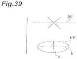
- the laser processing method in accordance with an aspect of the present inventioncomprises a step of irradiating an object to be processed with laser light such that a light-converging point of laser light elliptically polarized with an ellipticity of other than 1 is located within the object to be processed while the major axis of an ellipse indicative of the elliptical polarization of the laser light extends along a line along which the object is intended to be cut, so as to form a modified region caused by multiphoton absorption along the line along which the object is intended to be cut within the object to be processed.
- the laser processing method in accordance with this aspect of the present inventionforms a modified region by irradiating the object to be processed with laser light such that the major axis of an ellipse indicative of the elliptical polarization of laser light extends along the line along which the object is intended to be cut in the object to be processed.
- the inventorhas found that, when elliptically polarized laser light is used, the forming of a modified region is accelerated in the major axis direction of an ellipse indicative of the elliptical polarization (i.e., the direction in which the deviation in polarization is strong).
- the laser processing method in accordance with this aspect of the present inventioncan improve the processing speed of the object to be processed.
- the laser processing method in accordance with the present inventionrestrains the modified region from being formed except in the direction extending along the line along which the object is intended to be cut, thus making it possible to cut the object to be processed precisely along the line along which the object is intended to be cut.
- the ellipticityrefers to half the length of the minor axis/half the length of major axis of the ellipse. As the ellipticity of laser light is smaller, the forming of modified region is accelerated in the direction extending along the line along which the object is intended to be cut but suppressed in the other directions.
- the ellipticitycan be determined in view of the thickness, material, and the like of the object to be processed.
- Linear polarizationis elliptical polarization with an ellipticity of zero.
- the laser processing method in accordance with an aspect of the present inventioncomprises a step of irradiating an object to be processed with laser light such that a light-converging point of laser light elliptically polarized with an ellipticity of other than 1 is located within the object to be processed while the major axis of an ellipse indicative of the elliptical polarization of the laser light extends along a line along which the object is intended to be cut under a condition with a peak power density of at least 1 ⁇ 10 8 (W/cm 2 ) and a pulse width of 1 ⁇ s or less at the light-converging point, so as to form a modified region including a crack region along the line along which the object is intended to be cut within the object to be processed.
- the laser processing method in accordance with this aspect of the present inventionirradiates the object to be processed with laser light such that the major axis of the ellipse indicative of the elliptical polarization of laser light extends along the line along which the object is intended to be cut in the object to be processed, thus making it possible to form the modified region efficiently and cut the object precisely along the line along which the object is intended to be cut as in the laser processing method in accordance with the above-mentioned aspect of the present invention.
- the laser processing method in accordance with an aspect of the present inventioncomprises a step of irradiating an object to be processed with laser light such that a light-converging point of laser light elliptically polarized with an ellipticity of other than 1 is located within the object to be processed while the major axis of an ellipse indicative of the elliptical polarization of the laser light extends along the line along which the object is intended to be cut under a condition with a peak power density of at least 1 ⁇ 10 8 (W/cm 2 ) and a pulse width of 1 ⁇ s or less at the light-converging point, so as to form a modified region including a molten processed region along the line along which the object is intended to be cut within the object to be processed.
- the laser processing method in accordance with this aspect of the present inventionirradiates the object to be processed with laser light such that the major axis of the ellipse indicative of the elliptical polarization of laser light extends along the line along which the object is intended to be cut in the object to be processed, thus making it possible to form the modified region efficiently and cut the object precisely along the line along which the object is intended to be cut as in the laser processing method in accordance with the above-mentioned aspect of the present invention.
- the laser processing method in accordance with an aspect of the present inventioncomprises a step of irradiating an object to be processed with laser light such that a light-converging point of laser light elliptically polarized with an ellipticity of other than 1 is located within the object to be processed while the major axis of an ellipse indicative of the elliptical polarization of the laser light extends along a line along which the object is intended to be cut under a condition with a peak power density of at least 1 ⁇ 10 8 (W/cm 2 ) and a pulse width of 1 ns or less at the light-converging point, so as to form a modified region including a refractive index change region which is a region with a changed refractive index within the object along a line along which the object is intended to be cut in the object.
- the laser processing method in accordance with this aspect of the present inventionirradiates the object to be processed with laser light such that the major axis of the ellipse indicative of the elliptical polarization of laser light extends along the line along which the object is intended to be cut in the object to be processed, thus making it possible to form the modified region efficiently and cut the object precisely along the line along which the object is intended to be cut as in the laser processing method in accordance with the above-mentioned aspect of the present invention.
- Laser light having elliptical polarization with an ellipticity of zerocan be used.
- Linearly polarized lightis obtained when the ellipticity is zero.
- Linearly polarized lightcan maximize the size of the modified region extending along the line along which the object is intended to be cut and minimize the sizes in the other directions.
- the ellipticity of elliptically polarized lightcan be adjusted by the angle of direction of a quarter-wave plate. When a quarter-wave plate is used, the ellipticity can be adjusted by changing the angle of direction alone.
- the object to be processedmay be irradiated with laser light while the polarization of laser light is rotated by about 90° by a half-wave plate. Also, after the step of forming the modified region, the object to be processed may be irradiated with laser light while the object to be processed is rotated by about 90° about the thickness direction of the object to be processed.
- Thesecan form another modified region extending in a direction along the surface of the object to be processed and intersecting the former modified region. Therefore, for embodiment, respective modified regions extending along lines along which the object is intended to be cut in X- and Y-axis directions can be formed efficiently.
- the laser processing method in accordance with an aspect of the present inventioncomprises a step of irradiating an object to be processed with laser light such that a light-converging point of laser light elliptically polarized with an ellipticity of other than 1 is located within the object to be processed while the major axis of an ellipse indicative of the elliptical polarization of the laser light extends along a line along which the object is intended to be cut, so as to cut the object to be processed along the line along which the object is intended to be cut.
- the laser processing method in accordance with this aspect of the present inventionirradiates the object to be processed with laser light such that the major axis of the ellipse indicative of the elliptical polarization of laser light extends along the line along which the object is intended to be cut in the object to be processed. Therefore, the object to be processed can be cut along the line along which the object is intended to be cut.
- the laser processing method in accordance with this aspect of the present inventioncan cut the object to be processed by making the object absorb laser light so as to melt the object upon heating.
- the laser processing method in accordance with this aspect of the present inventionmay generate multiphoton absorption by irradiating the object to be processed with laser light, thereby forming a modified region within the object, and cut the object while using the modified region as a starting point.
- the laser processing apparatusin accordance with an aspect of the present invention comprises a laser light source for emitting pulse laser light having a pulse width of 1 ⁇ s or less; ellipticity adjusting means for making the pulse laser light emitted from the laser light source attain elliptical polarization with an ellipticity of other than 1; major axis adjusting means for making a major axis of an ellipse indicative of the elliptical polarization of the pulse laser light adjusted by the ellipticity adjusting means extend along a line along which the object is intended to be cut in an object to be processed; light-converging means for converging the pulse laser light adjusted by the major axis adjusting means such that the pulse laser light attains a peak power density of at least 1 ⁇ 10 (W/cm 2 ) at a light-converging point; means for locating the light-converging point of the pulse laser light converged by the light-converging point within the object to be processed; and moving means for relatively moving the
- the laser processing apparatus in accordance with this aspect of the present inventionenables laser cutting without generating melt or unnecessary fractures deviating from the line along which the object is intended to be cut in the surface of the object to be processed for the same reason as that in the laser processing methods in accordance with the above-mentioned aspects of the present invention. Also, it irradiates the object to be processed with laser light such that the major axis of the ellipse indicative of the elliptical polarization of laser light extends along the line along which the object is intended to be cut in the object to be processed, thus making it possible to form the modified region efficiently and cut the object precisely along the line along which the object is intended to be cut with the laser processing methods in accordance with the above-mentioned aspects of the present invention.
- 90° rotation adjusting meansadapted to rotate the polarization of the pulse laser light adjusted by the ellipticity adjusting means by about 90°.
- the laser processing apparatusin accordance with an aspect of the present invention comprises a laser light source for emitting pulse laser light having a pulse width of 1 ⁇ s or less and linear polarization; linear polarization adjusting means for making the direction of linear polarization of the pulse laser light emitted from the laser light source align with a line along which the object is intended to be cut in an object to be processed; light-converging means for converging the pulse laser light adjusted by the linear polarization adjusting means such that the pulse laser light attains a peak power density of at least 1 ⁇ 10 8 (W/cm 2 ) at a light-converging point; means for locating the light-converging point of the pulse laser light converged by the light-converging point within the object to be processed; and moving means for relatively moving the light-converging point of pulse laser light along the line along which the object is intended to be cut.
- a laser light sourcefor emitting pulse laser light having a pulse width of 1 ⁇ s or less and linear polarization
- the laser processing apparatus in accordance with this aspect of the present inventionenables laser cutting without generating melt or unnecessary fractures deviating from the line along which the object is intended to be cut in the surface of the object to be processed for the same reason as that in the laser processing methods in accordance with the above-mentioned aspects of the present invention. Also, as with the laser processing methods in accordance with the above-mentioned aspects of the present invention, the laser processing apparatus in accordance with this aspect of the present invention makes it possible to form the modified region efficiently and cut the object precisely along the line along which the object is intended to be cut.
- the laser processing apparatusin accordance with an aspect of the present invention comprises a laser light source for emitting pulse laser light having a pulse width of 1 ⁇ s or less; power adjusting means for adjusting the magnitude of power of the pulse laser light emitted from the laser light source according to an input of the magnitude of power of pulse laser light; light-converging means for converging the pulse laser light adjusted by the linear polarization adjusting means such that the pulse laser light attains a peak power density of at least 1 ⁇ 10 8 (W/cm 2 ) at a light-converging point; means for locating the light-converging point of the pulse laser light converged by the light-converging means within an object to be processed; and moving means for relatively moving the light-converging point of pulse laser light along a line along which the object is intended to be cut in the object to be processed; wherein one modified spot is formed within the object to be processed by irradiating the object to be processed with one pulse of pulse laser light while locating the light-converging point within the object
- the modified spotcan be controlled so as to become smaller and larger when the power of pulse laser light is made lower and higher, respectively.
- the modified spotis a modified part formed by one pulse of pulse laser light, whereas an assembly of modified spots forms a modified region.
- Control of the modified spot sizeaffects cutting of the object to be processed. Namely, the accuracy in cutting the object to be processed along the line along which the object is intended to be cut and the flatness of the cross section deteriorate when the modified spot is too large.
- the modified spotis too small for the object to be processed having a large thickness, on the other hand, the object is hard to cut.
- the laser processing apparatus in accordance with this aspect of the present inventioncan control the size of modified spot by adjusting the magnitude of power of pulse laser light. Therefore, it can cut the object to be processed precisely along the line along which the object is intended to be cut, and can obtain a flat cross section.
- the laser processing apparatus in accordance with this aspect of the present inventionalso comprises correlation storing means having stored therein a correlation between the magnitude of power of pulse laser adjusted by the power adjusting means and the size of modified spot.
- correlation storing meanshaving stored therein a correlation between the magnitude of power of pulse laser adjusted by the power adjusting means and the size of modified spot.
- the size of modified spot formed at this magnitude of poweris chosen from the correlation storing means, and thus chosen size of modified spot is displayed. Therefore, the size of modified spot formed at the magnitude of power of pulse laser light fed into the laser processing apparatus can be seen before laser processing.
- the laser processing apparatusin accordance with an aspect of the present invention comprises a laser light source for emitting pulse laser light having a pulse width of 1 ⁇ s or less; a light-converging lens for converging the pulse laser light emitted from the laser light source such that the pulse laser light attains a peak power density of at least 1 ⁇ 10 8 (W/cm 2 ) at a light-converging point; numerical aperture adjusting means for adjusting the size of numerical aperture of an optical system including the light-converging lens according to an inputted size of numerical aperture; means for locating the light-converging point of the pulse laser light converged by the light-converging lens within an object to be processed; and moving means for relatively moving the light-converging point of pulse laser light along a line along which the object is intended to be cut in the object to be processed; wherein one modified spot is formed within the object to be processed by irradiating the object to be processed with one pulse of pulse laser light while locating the light-converging point within the object; the laser
- the laser processing apparatusin accordance with this aspect of the present invention can control the size of modified spot by adjusting the size of numerical aperture of the optical system including the light-converging lens.
- the laser processing apparatus in accordance with this aspect of the present inventionalso comprises correlation storing means having stored therein a correlation between the size of numerical aperture and the size of modified spot. According to an inputted size of numerical aperture, the size of modified spot formed at this magnitude of power is chosen from the correlation storing means, and thus chosen size of modified spot is displayed. Therefore, the size of modified spot formed at the size of numerical aperture fed into the laser processing apparatus can be seen before laser processing.
- the laser processing apparatusin accordance with an aspect of the present invention comprises a laser light source for emitting pulse laser light having a pulse width of 1 ⁇ s or less; and lens selecting means including a plurality of light-converging lenses for converging the pulse laser light emitted from the laser light source such that the pulse laser light attains a peak power density of at least 1 ⁇ 10 8 (W/cm 2 ) at a light-converging point, the lens selecting means being adapted to select among a plurality of light-converging lenses, a plurality of optical systems including the light-converging lenses having respective numerical apertures different from each other; means for locating the light-converging point of the pulse laser light converged by a light-converging lens chosen by the lens selecting means within an object to be processed; and moving means for relatively moving the light-converging point of pulse laser light along a line along which the object is intended to be cut in the object to be processed; wherein one modified spot is formed within the object to be processed by irradiating the
- the laser processing apparatus in accordance with the present inventioncan control the size of modified spot. Also, the size of modified spot formed at the size of numerical aperture of the optical system including the chosen light-converging lens can be seen before laser processing.
- the laser processing apparatusin accordance with an aspect of the present invention comprises a laser light source for emitting pulse laser light having a pulse width of 1 ⁇ s or less; power adjusting means for adjusting the magnitude of power of pulse laser light emitted from the laser light source according to an inputted magnitude of power of pulse laser light; a light-converging lens for converging the pulse laser light emitted from the laser light source such that the pulse laser light attains a peak power density of at least 1 ⁇ 10 8 (W/cm 2 ) at a light-converging point; numerical aperture adjusting means for adjusting the size of numerical aperture of an optical system including the light-converging lens according to an inputted size of numerical aperture; means for locating the light-converging point of the pulse laser light converged by the light-converging lens within an object to be processed; and moving means for relatively moving the light-converging point of pulse laser light along a line along which the object is intended to be cut in the object to be processed; wherein one modified spot is formed within the object to
- the laser processing apparatus in accordance with this aspect of the present inventioncan combine power adjustment with numerical aperture adjustment, thus being able to increase the number of kinds of controllable dimensions of modified spots. Also, for the same reason as that of the laser processing apparatus in accordance with the present invention, the size of modified spot can be seen before laser processing.
- the laser processing apparatusin accordance with an aspect of the present invention comprises a laser light source for emitting pulse laser light having a pulse width of 1 ⁇ s or less; power adjusting means for adjusting the magnitude of power of pulse laser light emitted from the laser light source according to an inputted magnitude of power of pulse laser light; lens selecting means including a plurality of light-converging lenses for converging the pulse laser light emitted from the laser light source such that the pulse laser light attains a peak power density of at least 1 ⁇ 10 8 (W/cm 2 ) at a light-converging point, the lens selecting means being adapted to select among a plurality of light-converging lenses, a plurality of optical systems including the light-converging lenses having respective numerical apertures different from each other; means for locating the light-converging point of the pulse laser light converged by a light-converging lens chosen by the lens selecting means within an object to be processed; and moving means for relatively moving the light-converging point of pulse laser light along a line along
- the laser processing apparatus in accordance with this aspect of the present inventioncan increase the number of kinds of controllable dimensions of modified spots and can see the size of modified spots before laser processing.
- the laser processing apparatus explained in the foregoingmay comprise image preparing means for preparing an image of modified spot having the size selected by the size selecting means, and image display means for displaying the image prepared by the image preparing means. This allows the formed modified spot to be grasped visually before laser processing.
- the laser processing apparatusin accordance with an aspect of the present invention comprises a laser light source for emitting pulse laser light having a pulse width of 1 ⁇ s or less; power adjusting means for adjusting the magnitude of power of pulse laser light emitted from the laser light source; light-converging means for converging the pulse laser light emitted from the laser light source such that the pulse laser light attains a peak power density of at least 1 ⁇ 10 8 (W/cm 2 ) at a light-converging point; means for locating the light-converging point of the pulse laser light converged by the light-converging means within an object to be processed; and moving means for relatively moving the light-converging point of pulse laser light along a line along which the object is intended to be cut in the object to be processed; wherein one modified spot is formed within the object to be processed by irradiating the object to be processed with one pulse of pulse laser light while locating the light-converging point within the object; the laser processing apparatus further comprising correlation storing means having stored therein
- the laser processing apparatusin accordance with this aspect of the present invention comprises correlation storing means having stored therein the magnitude of power of pulse laser light and the size of modified spot. According to an inputted size of the modified spot, the magnitude of power of pulse laser light adapted to form this size is chosen from the correlation storing means.
- the power adjusting meansadjusts the magnitude of power of pulse laser light emitted from the laser light source so as to make it become the magnitude of power chosen by the power selecting means. Therefore, a modified spot having a desirable size can be formed.
- the laser processing apparatusin accordance with an aspect of the present invention comprises a laser light source for emitting pulse laser light having a pulse width of 1 ⁇ s or less; a light-converging lens for converging the pulse laser light emitted from the laser light source such that the pulse laser light attains a peak power density of at least 1 ⁇ 10 8 (W/cm 2 ) at a light-converging point; numerical aperture adjusting means for adjusting the size of numerical aperture of an optical system including the light-converging lens according to an inputted size of numerical aperture; means for locating the light-converging point of the pulse laser light converged by the light-converging lens within an object to be processed; and moving means for relatively moving the light-converging point of pulse laser light along a line along which the object is intended to be cut in the object to be processed; wherein one modified spot is formed within the object to be processed by irradiating the object to be processed with one pulse of pulse laser light while locating the light-converging point within the object; the laser
- the laser processing apparatusin accordance with this aspect of the present invent ion comprises correlation storing means having stored therein the size of numerical aperture and the size of modified spot. According to an inputted size of modified spot, the size of numerical aperture adapted to form thus inputted size is chosen from the correlation storing means.
- the numerical aperture adjusting meansadjusts the size of numerical aperture of the optical system including the light-converging lens such that the size of numerical aperture chosen by the numerical aperture selecting means is attained. Therefore, modified spots having a desirable size can be formed.
- the laser processing apparatusin accordance with an aspect of the present invention comprises a laser light source for emitting pulse laser light having a pulse width of 1 ⁇ s or less; lens selecting means including a plurality of light-converging lenses for converging the pulse laser light emitted from the laser light source such that the pulse laser light attains a peak power density of at least 1 ⁇ 10 8 (W/cm 2 ) at a light-converging point, the lens selecting means being adapted to select among a plurality of light-converging lenses, a plurality of optical systems including the light-converging lenses having respective numerical apertures different from each other; means for locating the light-converging point of the pulse laser light converged by a light-converging lens chosen by the lens selecting means within an object to be processed; and moving means for relatively moving the light-converging point of pulse laser light along a line along which the object is intended to be cut in the object to be processed; wherein one modified spot is formed within the object to be processed by irradiating the object
- the laser processing apparatuschooses the size of numerical aperture adapted to form thus inputted size.
- the lens selecting meansselects among a plurality of light-converging lenses such that the size of numerical aperture chosen by the numerical aperture selecting means is attained. Therefore, modified spots having a desirable spots can be formed.
- the laser processing apparatusin accordance with an aspect of the present invention comprises a laser light source for emitting pulse laser light having a pulse width of 1 ⁇ s or less; power adjusting means for adjusting the magnitude of power of pulse laser light emitted from the laser light source; a light-converging lens for converging the pulse laser light emitted from the laser light source such that the pulse laser light attains a peak power density of at least 1 ⁇ 10 8 (W/cm 2 ) at a light-converging point; numerical aperture adjusting means for adjusting the size of numerical aperture of an optical system including the light-converging lens; means for locating the light-converging point of the pulse laser light converged by the light-converging lens within an object to be processed; and moving means for relatively moving the light-converging point of pulse laser light along a line along which the object is intended to be cut in the object to be processed; wherein one modified spot is formed within the object to be processed by irradiating the object to be processed with one pulse of pulse laser light while
- the laser processing apparatuschooses a combination of the magnitude of power and size of numerical aperture adapted to form thus inputted size from the correlation storing means. Then, it adjusts the magnitude of power of pulse laser light and the size of numerical aperture of the optical system including the light-converging lens so as to attain the chosen magnitude of power and size of numerical aperture. Therefore, modified spots having a desirable size can be formed. Also, since the magnitude of power and the size of numerical aperture are combined together, the number of kinds of controllable dimensions of modified spots can be increased.
- the laser processing apparatusin accordance with an aspect of the present invention comprises a laser light source for emitting pulse laser light having a pulse width of 1 ⁇ s or less; power adjusting means for adjusting the magnitude of power of pulse laser light emitted from the laser light source; lens selecting means including a plurality of light-converging lenses for converging the pulse laser light emitted from the laser light source such that the pulse laser light attains a peak power density of at least 1 ⁇ 10 8 (W/cm 2 ) at a light-converging point, the lens selecting means being adapted to select among a plurality of light-converging lenses, a plurality of optical systems including the light-converging lenses having respective numerical apertures different from each other; means for locating the light-converging point of the pulse laser light converged by a light-converging lens chosen by the lens selecting means within an object to be processed; and moving means for relatively moving the light-converging point of pulse laser light along a line along which the object is intended to be cut in the object to
- the laser processing apparatuschooses a combination of the magnitude of power and size of numerical aperture adapted to form thus inputted size from the correlation storing means. It adjusts the magnitude of power of pulse laser light emitted from the laser light source and selects among a plurality of light-converging lenses so as to attain the chosen magnitude of power and size of numerical aperture, respectively. Therefore, modified spots having a desirable size can be formed. Also, since the magnitude of power and the size of numerical aperture are combined together, the number of kinds of controllable dimensions of modified spots can be increased.
- the laser processing apparatus in accordance with this aspect of the present inventionmay further comprise display means for displaying the magnitude of power chosen by the power selecting means, display means for displaying the size of numerical aperture chosen by the numerical aperture selecting means, and display means for displaying the magnitude of power and size of numerical aperture of the set chosen by the set selecting means. This makes it possible to see the power and numerical aperture when the laser processing apparatus operates according to an inputted size of modified spot.
- the laser processing apparatuscan form a plurality of modified spots along a line along which the object is intended to be cut within the object to be processed. These modified spots define a modified region.
- the modified regionincludes at least one of a crack region where a crack is generated within the object to be processed, a molten processed region which is melted within the object to be processed, and a refractive index change region where refractive index is changed within the object to be processed.
- An embodiment of modes of power adjusting meansis one including at least one of an ND filter and a polarization filter.
- the laser light sourceincludes a pumping laser whereas the laser processing apparatus comprises driving current controlling means for controlling the driving current of the pumping laser. These can adjust the magnitude of power of pulse laser light.
- An embodiment of modes of numerical aperture adjusting meansincludes at least one of a beam expander and an iris diaphragm.
- the laser processing method in accordance with an aspect of the present inventioncomprises a first step of irradiating an object to be processed with pulse laser light while locating a light-converging point of the pulse laser light within the object, so as to form a first modified region caused by multiphoton absorption within the object along a first line along which the object is intended to be cut in the object; and a second step of irradiating the object with pulse laser light while making the pulse laser light attain a power higher or lower than that in the first step and locating the light-converging point of the pulse laser light within the object, so as to form a second modified region caused by multiphoton absorption within the object along a second line along which the object is intended to be cut in the object.
- the laser processing method in accordance with an aspect of the present inventioncomprises a first step of irradiating an object to be processed with pulse laser light while locating a light-converging point of the pulse laser light within the object, so as to form a first modified region caused by multiphoton absorption within the object along a first line along which the object is intended to be cut in the object; and a second step of irradiating the object with pulse laser light while making an optical system including a light-converging lens for converging the pulse laser light attain a numerical aperture greater or smaller than that in the first step and locating the light-converging point of the pulse laser light within the object, so as to form a second modified region caused by multiphoton absorption within the object along a second line along which the object is intended to be cut in the object.
- the laser processing methods in accordance with these aspects of the present inventiondecreases the size of modified spot constituting a modified region formed in the easy-to-cut direction and increases the size of modified spot constituting another modified region formed in the hard-to-cut direction. This can attain a flat cross section in the easy-to-cut direction and enables cutting in the hard-to-cut direction as well.
- the laser processing apparatusin accordance with an aspect of the present invention comprises a laser light source for emitting pulse laser light having a pulse width of 1 ⁇ s or less; frequency adjusting means for adjusting the magnitude of a repetition frequency of the pulse laser light emitted from the laser light source according to an inputted magnitude of frequency; light-converging means for converging the pulse laser light emitted from the laser light source such that the pulse laser light attains a peak power density of at least 1 ⁇ 10 8 (W/cm 2 ) at a light-converging point; means for locating the light-converging point of the pulse laser light converged by the light-converging means within an object to be processed; and moving means for relatively moving the light-converging point of pulse laser light along a line along which the object is intended to be cut in the object to be processed; wherein one modified spot is formed within the object to be processed by irradiating the object to be processed with one pulse of pulse laser light while locating the light-converging point within the object; and wherein
- the inventorhas found that, when the light-converging point of pulse laser light has a fixed relative moving speed, the distance between a modified part (referred to as modified spot) formed by one pulse of pulse laser light and a modified spot formed by the next one pulse of laser light can be made greater by lowering the repetition frequency. It has been found that, by contrast, the distance can be made shorter by increasing the repetition frequency of pulse laser light. In the present specification, this distance is expressed as the distance or pitch between adjacent modified spots.
- the distance between the adjacent modified spotscan be controlled by carrying out adjustment for increasing or decreasing the repetition frequency of pulse laser light.
- Changing the distance according to the kind, thickness, and the like of the object to be processedenables cutting in conformity to the object to be processed.
- Forming a plurality of modified spots along a line along which the object is intended to be cut within the object to be processeddefines a modified region.
- the laser processing apparatusin accordance with this aspect of the present invention calculates the distance between adjacent modified spots according to the inputted magnitude of frequency, and displays thus calculated distance. Therefore, with respect to modified spots formed according to the magnitude of frequency fed into the laser processing apparatus, the distance between adjacent spots can be seen before laser processing.
- the laser processing apparatusin accordance with an aspect of the present invention comprises a laser light source for emitting pulse laser light having a pulse width of 1 ⁇ s or less; light-converging means for converging the pulse laser light emitted from the laser light source such that the pulse laser light attains a peak power density of at least 1 ⁇ 10 8 (W/cm 2 ) at a light-converging point; means for locating the light-converging point of the pulse laser light converged by the light-converging means within an object to be processed; moving means for relatively moving the light-converging point of pulse laser light along a line along which the object is intended to be cut in the object to be processed; and speed adjusting means for adjusting the magnitude of relative moving speed of the light-converging point of pulse laser light caused by the moving means according to an inputted magnitude of speed; wherein one modified spot is formed within the object to be processed by irradiating the object to be processed with one pulse of pulse laser light while locating the light-converging point within the object;
- the inventorhas found that, when the light-converging point of pulse laser light has a fixed relative moving speed, the distance between adjacent modified spots can be made shorter and longer by decreasing and increasing the relative moving speed of the light-converging point of pulse laser light, respectively. Therefore, the distance between adjacent modified spots can be controlled by increasing or decreasing the relative moving speed of the light-converging point of pulse laser light. As a consequence, a cutting process suitable for an object to be processed is possible by changing the distance according to the kind, thickness, and the like of the object to be processed.
- the relative movement of the light-converging point of pulse laser lightmay be achieved by moving the object to be processed while fixing the light-converging point of pulse laser light, by moving the light-converging point of pulse laser light while fixing the object to be processed, or by moving both.
- the laser processing apparatusin accordance with this aspect of the present invention calculates the distance between adjacent modified spots according to the inputted magnitude of speed, and displays thus calculated distance. Therefore, with respect to modified spots formed according to the magnitude of speed fed into the laser processing apparatus, the distance between adjacent spots can be seen before laser processing.
- the laser processing apparatusin accordance with an aspect of the present invention comprises a laser light source for emitting pulse laser light having a pulse width of 1 ⁇ s or less; frequency adjusting means for adjusting the magnitude of a repetition frequency of the pulse laser light emitted from the laser light source according to an inputted magnitude of frequency; light-converging means for converging the pulse laser light emitted from the laser light source such that the pulse laser light attains a peak power density of at least 1 ⁇ 10 8 (W/cm 2 ) at a light-converging point; means for locating the light-converging point of the pulse laser light converged by the light-converging means within an object to be processed; moving means for relatively moving the light-converging point of pulse laser light along a line along which the object is intended to be cut in the object to be processed; and speed adjusting means for adjusting the magnitude of relative moving speed of the light-converging point of pulse laser light caused by the moving means according to an inputted magnitude of speed; wherein one modified spot is formed within the
- the laser processing apparatus in accordance with this aspect of the present inventionadjusts both the magnitude of a repetition frequency of pulse laser light and the magnitude of relative moving speed of the light-converging point, thereby being able to control the distance between adjacent modified spots. Combining these adjustments makes it possible to increase the number of kinds of controllable dimensions concerning the distance. Also, the laser processing apparatus in accordance with this aspect of the present invention allows the distance between adjacent modified spots to be seen before laser processing.
- These laser processing apparatusmay further comprise size storing means having stored therein the size of a modified spot formed by the laser processing apparatus; image preparing means for preparing an image of a plurality of modified spots formed along a line along which the object is intended to be cut according to the size stored in the size storing means and the distance calculated by the distance calculating means; and image display means for displaying the image prepared by the image preparing means.
- size storing meanshaving stored therein the size of a modified spot formed by the laser processing apparatus
- image preparing meansfor preparing an image of a plurality of modified spots formed along a line along which the object is intended to be cut according to the size stored in the size storing means and the distance calculated by the distance calculating means
- image display meansfor displaying the image prepared by the image preparing means. This allows a plurality of modified spots, i.e., modified region, to be grasped visually before laser processing.
- the laser processing apparatusin accordance with an aspect of the present invention comprises a laser light source for emitting pulse laser light having a pulse width of 1 ⁇ s or less; frequency adjusting means for adjusting the magnitude of a repetition frequency of the pulse laser light emitted from the laser light source according to an inputted magnitude of frequency; light-converging means for converging the pulse laser light emitted from the laser light source such that the pulse laser light attains a peak power density of at least 1 ⁇ 10 8 (W/cm 2 ) at a light-converging point; means for locating the light-converging point of the pulse laser light converged by the light-converging means within an object to be processed; and moving means for relatively moving the light-converging point of pulse laser light along a line along which the object is intended to be cut in the object to be processed; wherein one modified spot is formed within the object to be processed by irradiating the object to be processed with one pulse of pulse laser light while locating the light-converging point within the object; and wherein
- the laser processing apparatuscalculates the magnitude of a repetition frequency of the pulse laser light emitted from the laser light source such that this magnitude of distance is attained between the adjacent modified spots.
- the frequency adjusting meansadjusts the magnitude of repetition frequency of the pulse laser light emitted from the laser light source such that the magnitude of frequency calculated by the frequency calculating means is attained. Therefore, a desirable magnitude of distance can be attained between adjacent modified spots.
- the laser processing apparatus in accordance with this aspect of the present inventionmay further comprise frequency display means for displaying the magnitude of frequency calculated by the frequency calculating means.
- frequency display meansfor displaying the magnitude of frequency calculated by the frequency calculating means.
- the laser processing apparatusin accordance with an aspect of the present invention comprises a laser light source for emitting pulse laser light having a pulse width of 1 ⁇ s or less; light-converging means for converging the pulse laser light emitted from the laser light source such that the pulse laser light attains a peak power density of at least 1 ⁇ 10 8 (W/cm 2 ) at a light-converging point; means for locating the light-converging point of the pulse laser light converged by the light-converging means within an object to be processed; moving means for relatively moving the light-converging point of pulse laser light along a line along which the object is intended to be cut in the object to be processed; and speed adjusting means for adjusting the magnitude of relative moving speed of the light-converging point caused by the moving means; wherein one modified spot is formed within the object to be processed by irradiating the object to be processed with one pulse of pulse laser light while locating the light-converging point within the object; and wherein a plurality of modified spots are formed
- the laser processing apparatuscalculates the magnitude of relative moving speed of the light-converging point of pulse laser light caused by the moving means.
- the speed adjusting meansadjusts the magnitude of relative moving speed of the light-converging point of pulse laser light caused by the moving means such that the magnitude of relative moving speed calculated by the frequency calculating means is attained. Therefore, a desirable magnitude of distance can be attained between adjacent modified spots.
- the laser processing apparatus in accordance with this aspect of the present inventionmay further comprise speed display means for displaying the magnitude of relative moving speed calculated by the speed calculating means.
- speed display meansfor displaying the magnitude of relative moving speed calculated by the speed calculating means.
- the laser processing apparatusin accordance with an aspect of the present invention comprises a laser light source for emitting pulse laser light having a pulse width of 1 ⁇ s or less; frequency adjusting means for adjusting the magnitude of a repetition frequency of the pulse laser light emitted from the laser light source; light-converging means for converging the pulse laser light emitted from the laser light source such that the pulse laser light attains a peak power density of at least 1 ⁇ 10 8 (W/cm 2 ) at a light-converging point; means for locating the light-converging point of the pulse laser light converged by the light-converging means within an object to be processed; moving means for relatively moving the light-converging point of pulse laser light along a line along which the object is intended to be cut in the object to be processed; and speed adjusting means for adjusting the magnitude of relative moving speed of the light-converging point caused by the moving means; wherein one modified spot is formed within the object to be processed by irradiating the object to be processed with one pulse of pulse
- the laser processing apparatuscalculates, according to an inputted magnitude of distance between adjacent modified spots, a combination of the magnitude of repetition frequency of pulse laser light and the relative moving speed of the light-converging point of pulse laser light such that thus inputted magnitude of distance is attained between the adjacent modified spots.
- the frequency adjusting means and speed adjusting meansadjust the magnitude of repetition frequency and the magnitude of relative moving speed of the light-converging point of pulse laser light so as to attain the values of calculated combination. Therefore, a desirable magnitude of distance can be attained between adjacent modified spots.
- the laser processing apparatus in accordance with the present inventionmay comprise display means for displaying the magnitude of frequency and magnitude of relative moving speed calculated by the combination calculating means.
- display meansfor displaying the magnitude of frequency and magnitude of relative moving speed calculated by the combination calculating means.
- the laser processing apparatusin accordance with all the foregoing aspects of the present invention can form a plurality of modified spots along a line along which the object is intended to be cut within the object to be processed. These modified spots define a modified region.
- the modified regionincludes at least one of a crack region where a crack is generated within the object to be processed, a molten processed region which is melted within the object to be processed, and a refractive index change region where refractive index is changed within the object to be processed.
- the laser processing apparatusin accordance with all the foregoing aspects of the present invention can adjust the distance between adjacent modified spots, thereby being able to form a modified region continuously or discontinuously along a line along which the object is intended to be cut.
- Forming the modified region continuouslymakes it easier to cut the object to be processed while using the modified region as compared with the case where it is not formed continuously.
- the modified regionis formed discontinuously, the modified region is discontinuous along the line along which the object is intended to be cut, whereby the part of the line along which the object is intended to be cut keeps a strength to a certain extent.
- the laser processing method in accordance with an aspect of the present inventioncomprises a step of irradiating an object to be processed with laser light while locating a light-converging point of laser light within the object to be processed, so as to form a modified region caused by multiphoton absorption within the object along a line along which the object is intended to be cut in the object, and changing the position of the light-converging point of laser light in the direction of incidence of the laser light irradiating the object to be processed with respect to the object to be processed, so as to form a plurality of modified regions aligning with each other along the direction of incidence.
- the laser processing methodIn accordance with this aspect of the present invention forms a plurality of modified regions aligning with each other along the direction of incidence. This can increase the number of positions to become starting points when cutting the object to be processed. Therefore, the object to be processed can be cut even in the case where the object to be processed has a relatively large thickness and the like.
- Embodiments of the direction of incidenceinclude the thickness direction of the object to be processed and directions orthogonal to the thickness direction.
- the laser processing method in accordance with an aspect of the present inventioncomprises a step of irradiating an object to be processed with laser light while locating a light-converging point of laser light within the object to be processed, so as to form a modified region within the object along a line along which the object is intended to be cut in the object, and changing the position of the light-converging point of laser light in the direction of incidence of the laser light irradiating the object to be processed with respect to the object to be processed, so as to form a plurality of modified regions aligning with each other along the direction of incidence.
- the laser processing method in accordance with an aspect of the present inventioncomprises a step of irradiating an object to be processed with laser light while locating a light-converging point of laser light within the object to be processed under a condition with a peak power density of at least 1 ⁇ 10 8 (W/cm 2 ) and a pulse width of 1 ⁇ s or less at the light-converging point, so as to form a modified region within the object to be processed along a line along which the object is intended to be cut in the object, and changing the position of the light-converging point of laser light in the direction of incidence of the laser light irradiating the object to be processed with respect to the object to be processed, so as to form a plurality of modified regions aligning with each other along the direction of incidence.
- the laser processing methods in accordance with these aspects of the present inventionenable laser cutting without generating melt or unnecessary fractures deviating from the line along which the object is intended to be cut in the surface of the object to be processed, and can increase the number of positions to become starting points when cutting the object to be processed.
- the modified regionmay be caused by multiphoton absorption or other reasons.
- the laser processing methods in accordance with these aspects of the present inventioninclude the following modes:
- a plurality of modified regionsmay be formed successively from the side farther from an entrance face of the object to be processed on which laser light irradiating the object to be processed is incident. This can form a plurality of modified regions while in a state where no modified region exists between the entrance face and the light-converging point of laser light. Therefore, the laser light will not be scattered by modified regions which have already been formed, whereby each modified region can be formed uniformly.
- the modified regionincludes at least one of a crack region where a crack is generated within the object to be processed, a molten processed region which is melted within the object to be processed, and a refractive index change region where refractive index is changed within the object to be processed.
- the laser processing method in accordance with an aspect of the present inventioncomprises a step of irradiating an object to be processed with laser light while locating a light-converging point of laser light within the object to be processed through a light entrance face of the laser light with respect to the object to be processed and locating the light-converging point at a position closer to or farther from the entrance face than is a half thickness position in the thickness direction of the object to be processed, so as to form a modified region within the object along a line along which the object is intended to be cut in the object.
- the modified regionis formed on the entrance face (e.g., surface) and on the side of the face (e.g., rear face) opposing the entrance face within the object to be processed within the object to be processed when the light-converging point of laser light is located at a position closer to and farther from the entrance face than is a half thickness position in the thickness direction, respectively.
- the objectcan be cut easily.
- the laser processing method in accordance with this aspect of the present inventioncan form a modified region on the surface or rear face side within the object to be processed.
- the laser processing method in accordance with this aspect of the present Inventionenables efficient cutting.
- the laser processing method in accordance with this aspect of the present inventionmay be configured such that the entrance face is formed with at least one of an electronic device and an electrode pattern, whereas the light-converging point of laser light irradiating the object to be processed is located at a position closer to the entrance face than is the half thickness position in the thickness direction.
- the laser processing method in accordance with this aspect of the present inventiongrows a crack from the modified region toward the entrance face (e.g., surface) and its opposing face (e.g., rear face), thereby cutting the object to be processed.
- the modified regionis formed on the entrance face side, the distance between the modified region and the entrance face is relatively short, so that the deviation in the growth direction of crack can be made smaller.
- the electronic devicerefers to a semiconductor device, a display device such as liquid crystal, a piezoelectric device, or the like.
- the laser processing method in accordance with an aspect of the present inventioncomprises a first step of irradiating an object to be processed with pulse laser light while locating a light-converging point of the pulse laser light within the object, so as to form a first modified region caused by multiphoton absorption within the object along a first line along which the object is intended to be cut in the object; and a second step of irradiating, after the first step, the object with pulse laser light while locating the light-converging point of laser light at a position different from the light-converging point of laser light in the first step in the thickness direction of the object to be processed within the object, so as to form a second modified region caused by multiphoton absorption extending along a second line along which the object is intended to be cut and three-dimensionally crossing the first modified region within the object.
- the laser processing method in accordance with this aspect of the present inventioncan form the second modified region closer to the entrance face of the object to be processed with respect to the laser light than is the first modified region. This keeps the laser light irradiated at the time of forming the second modified region at the location to become the crossing position from being scattered by the first modified region, whereby the second modified region can be formed uniformly.
- a modified region including a crack regioncan be formed within the object to be processed.
- Thisgenerates a phenomenon of an optical damage caused by multiphoton absorption within the object to be processed.
- This optical damageinduces a thermal distortion within the object to be processed, thereby forming a crack region within the object to be processed.
- This crack regionis an embodiment of the above-mentioned modified region.
- An embodiment of the object to be processed in this laser processing methodis a member including glass.
- the peak power densityrefers to the electric field intensity of pulse laser light at the light-converging point.
- a modified region including a molten processed regioncan be formed within the object to be processed.
- the inside of the object to be processedis locally heated by multiphoton absorption. This heating forms a molten processed region within the object to be processed.
- This molten processed regionis an embodiment of the above-mentioned modified region.
- An embodiment of the object to be processed in this laser processing methodis a member including a semiconductor material.
- a modified region including a refractive index change regionwhich is a region with a changed refractive index can also be formed within the object to be processed.
- a refractive index change regionis an embodiment of the above-mentioned modified region.
- An embodiment of the object to be processed in this laser processing methodis a member including glass.
- Adjustment of the position of the light-converging point of laser light irradiating the object to be processed in the thickness directioncan include a first calculating step of defining a desirable position in the thickness direction of the light-converging point of laser light irradiating the object to be processed as a distance from the entrance face to the inside and dividing the distance by the refractive index of the object to be processed with respect to the laser light irradiating the object, so as to calculate data of a first relative movement amount of the object in the thickness direction; a second calculating step of calculating data of a second relative movement amount of the object in the thickness direction required for positioning the light-converging point of laser light irradiating the object to be processed at the entrance face; a first moving step of relatively moving the object in the thickness direction according to the data of second relative movement amount; and a second moving step of relatively moving the object in the thickness direction according to the data of first relative movement amount after the first moving step.
- the laser processing apparatusin accordance with an aspect of the present invention comprises a laser light source for emitting pulse laser light having a pulse width of 1 ⁇ s or less; light-converging means for converging the pulse laser light emitted from the laser light source such that the pulse laser light attains a peak power density of at least 1 ⁇ 10 8 (W/cm 2 ) at a light-converging point; first moving means for relatively moving the light-converging point converged by the light-converging means along a line along which the object is intended to be cut in an object to be processed; storing means for storing data of a first relative movement amount of the object to be processed in the thickness direction for locating the light-converging position of pulse laser light converged by the light-converging means at a desirable position within the object to be processed, the data of first relative movement amount being obtained by defining the desirable position as a distance from the entrance face where the pulse laser light emitted from the laser light source enters the object to be processed to the inside thereof and dividing
- the laser processing apparatusin accordance with an aspect of the present invent ion comprises a laser light source for emitting pulse laser light having a pulse width of 1 ⁇ s or less; light-converging means for converging the pulse laser light emitted from the laser light source such that the pulse laser light attains a peak power density of at least 1 ⁇ 10 8 (W/cm 2 ) at a light-converging point; means for locating the light-converging point of the pulse laser light emitted from the laser light source within an object to be processed; means for adjusting the position of the pulse laser light converged by the light-converging means within the thickness of the object to be processed; and moving means for relatively moving the light-converging point of pulse laser light along a line along which the object is intended to be cut in the object to be processed.
- the laser processing apparatus in accordance with these aspects of the present inventionenable laser processing without generating melt or unnecessary fractures deviating from the line along which the object is intended to be cut in the surface of the object to be processed, and laser processing in which the position of the light-converging point of pulse laser light is regulated in the thickness direction of the object to be processed within the object.
- FIG. 1is a plan view of an object to be processed during laser processing by the laser processing method in accordance with an embodiment
- FIG. 2is a sectional view of the object to be processed shown in FIG. 1 taken along the line II-II;
- FIG. 3is a plan view of the object to be processed after laser processing effected by the laser processing method in accordance with the embodiment
- FIG. 4is a sectional view of the object to be processed shown in FIG. 3 taken along the line IV-IV;
- FIG. 5is a sectional view of the object to be processed shown in FIG. 3 taken along the line V-V;
- FIG. 6is a plan view of the object to be processed cut by the laser processing method in accordance with the embodiment.
- FIG. 7is a graph showing relationships between the electric field intensity and the magnitude of crack in the laser processing method in accordance with the embodiment.
- FIG. 8is a sectional view of the object to be processed in a first step of the laser processing method in accordance with the embodiment
- FIG. 9is a sectional view of the object to be processed in a second step of the laser processing method in accordance with the embodiment.
- FIG. 10is a sectional view of the object to be processed in a third step of the laser processing method in accordance with the embodiment.
- FIG. 11is a sectional view of the object to be processed in a fourth step of the laser processing method in accordance with the embodiment.
- FIG. 12is a view showing a photograph of a cross section in a part of a silicon wafer cut by the laser processing method in accordance with the embodiment
- FIG. 13is a graph showing relationships between the laser light wavelength and the transmittance within a silicon substrate in the laser processing method in accordance with the embodiment
- FIG. 14is a schematic diagram of a laser processing apparatus usable in the laser processing method in accordance with a first embodiment of the embodiment
- FIG. 15is a flowchart for explaining the laser processing method in accordance with the first embodiment of the present invention.
- FIG. 16is a plan view of an object to be processed for explaining a pattern which can be cut by the laser processing method in accordance with the first embodiment of the embodiment;
- FIG. 17is a schematic view for explaining the laser processing method in accordance with the first embodiment of the embodiment with a plurality of laser light sources;
- FIG. 18is a schematic view for explaining another laser processing method in accordance with the first embodiment of the embodiment with a plurality of laser light sources;
- FIG. 19is a schematic plan view showing a piezoelectric device wafer in a state held by a wafer sheet in the second embodiment of the embodiment.
- FIG. 20is a schematic sectional view showing a piezoelectric device wafer in a state held by the wafer sheet in the second embodiment of the embodiment;
- FIG. 21is a flowchart for explaining the cutting method in accordance with the second embodiment of the embodiment.
- FIG. 22is a sectional view of a light-transmitting material irradiated with laser light by the cutting method in accordance with the second embodiment of the embodiment;
- FIG. 23is a plan view of the light-transmitting material irradiated with laser light by the cutting method in accordance with the second embodiment of the embodiment;
- FIG. 24is a sectional view of the light-transmitting material shown in FIG. 23 taken along the line XXIV-XXIV;
- FIG. 25is a sectional view of the light-transmitting material shown in FIG. 23 taken along the line XXV-XXV;
- FIG. 26is a sectional view of the light-transmitting material shown in FIG. 23 taken along the line XXV-XXV when the light-converging point moving speed is made lower;
- FIG. 27is a sectional view of the light-transmitting material shown in FIG. 23 taken along the line XXV-XXV when the light-converging point moving speed is made further lower;
- FIG. 28is a sectional view of a piezoelectric device wafer or the like showing a first step of the cutting method in accordance with the second embodiment of the embodiment;
- FIG. 29is a sectional view of the piezoelectric device wafer or the like showing a second step of the cutting method in accordance with the second embodiment of the embodiment;
- FIG. 30is a sectional view of the piezoelectric device wafer or the like showing a third step of the cutting method in accordance with the second embodiment of the embodiment;
- FIG. 31is a sectional view of the piezoelectric device wafer or the like showing a fourth step of the cutting method in accordance with the second embodiment of the embodiment;
- FIG. 32is a sectional view of the piezoelectric device wafer or the like showing a fifth step of the cutting method in accordance with the second embodiment of the embodiment;
- FIG. 33is a view showing a photograph of a plane of a sample within which a crack region is formed upon irradiation with linearly polarized pulse laser light;
- FIG. 34is a view showing a photograph of a plane of a sample within which a crack region is formed upon irradiation with circularly polarized pulse laser light;
- FIG. 35is a sectional view of the sample shown in FIG. 33 taken along the line XXXV-XXXV;
- FIG. 36is a sectional view of the sample shown in FIG. 34 taken along the line XXXVI-XXXVI;
- FIG. 37is a plan view of the part of object to be processed extending along a line along which the object is intended to be cut, in which a crack region is formed by the laser processing method in accordance with a third embodiment of the embodiment;
- FIG. 38is a plan view of the part of object to be processed extending along a line along which the object is intended to be cut, in which a crack region is formed by a comparative laser processing method;
- FIG. 39is a view showing elliptically polarized laser light in accordance with the third embodiment of the embodiment, and a crack region formed thereby;
- FIG. 40is a schematic diagram of the laser processing apparatus in accordance with the third embodiment of the embodiment.
- FIG. 41is a perspective view of a quarter-wave plate included in an ellipticity regulator in accordance with the third embodiment of the embodiment.
- FIG. 42is a perspective view of a half-wave plate included in a 90° rotation regulator part in accordance with the third embodiment of the embodiment.
- FIG. 43is a flowchart for explaining the laser processing method in accordance with the third embodiment of the embodiment.
- FIG. 44is a plan view of a silicon wafer irradiated with elliptically polarized laser light by the laser processing method in accordance with the third embodiment of the embodiment;
- FIG. 45is a plan view of a silicon wafer irradiated with linearly polarized laser light by the laser processing method in accordance with the third embodiment of the embodiment;
- FIG. 46is a plan view of a silicon wafer in which the silicon wafer shown in FIG. 44 is irradiated with elliptically polarized laser light by the laser processing method in accordance with the third embodiment of the embodiment;
- FIG. 47is a plan view of a silicon wafer in which the silicon wafer shown in FIG. 45 is irradiated with linearly polarized laser light by the laser processing method in accordance with the third embodiment of the embodiment;
- FIG. 48is a schematic diagram of the laser processing apparatus in accordance with a fourth embodiment of the embodiment.
- FIG. 49is a plan view of a silicon wafer in which the silicon wafer shown in FIG. 44 is irradiated with elliptically polarized laser light by the laser processing method in accordance with the fourth embodiment of the embodiment;
- FIG. 50is a plan view of the object to be processed in the case where a crack spot is formed relatively large by using the laser processing method in accordance with a fifth embodiment of the embodiment;
- FIG. 51is a sectional view taken along LI-LI on the line along which the object is Intended to be cut shown in FIG. 50 ;
- FIG. 52is a sectional view taken along LII-LII orthogonal to the line along which the object is intended to be cut shown in FIG. 50 ;
- FIG. 53is a sectional view taken along LIII-LIII orthogonal to the line along which the object is intended to be cut shown in FIG. 50 ;
- FIG. 54is a sectional view taken along LIV-LIV orthogonal to the line along which the object is intended to be cut shown in FIG. 50 ;
- FIG. 55is a plan view of the object to be processed shown in FIG. 50 cut along the line along which the object is intended to be cut;
- FIG. 56is a sectional view of the object to be processed taken along the line along which the object is intended to be cut in the case where a crack spot is formed relatively small by using the laser processing method in accordance with the fifth embodiment of the embodiment;
- FIG. 57is a plan view of the object to be processed shown in FIG. 56 cut along the line along which the object is intended to be cut;
- FIG. 58is a sectional view of the object to be processed showing a state where pulse laser light is converged within the object by using a light-converging lens having a predetermined numerical aperture;
- FIG. 59is a sectional view of the object to be processed including a crack spot formed due to the multiphoton absorption caused by irradiation with laser light shown in FIG. 58 ;
- FIG. 60is a sectional view of the object to be processed in the case where a light-converging lens having a numerical aperture greater than that of the embodiment shown in FIG. 58 is used;
- FIG. 61is a sectional view of the object to be processed including a crack spot formed due to the multiphoton absorption caused by irradiation with laser light shown in FIG. 60 ;
- FIG. 62is a sectional view of the object to be processed in the case where pulse laser light having a power lower than that of the embodiment shown in FIG. 58 is used;
- FIG. 63is a sectional view of the object to be processed including a crack spot formed due to the multiphoton absorption caused by irradiation with laser light shown in FIG. 62 ;
- FIG. 64is a sectional view of the object to be processed in the case where pulse laser light having a power lower than that of the embodiment shown in FIG. 60 is used;
- FIG. 65is a sectional view of the object to be processed including a crack spot formed due to the multiphoton absorption caused by irradiation with laser light shown in FIG. 64 ;
- FIG. 66is a sectional view taken along LXVI-LXVI orthogonal to the line along which the object is intended to be cut shown in FIG. 57 ;
- FIG. 67is a schematic diagram showing the laser processing apparatus in accordance with the fifth embodiment of the embodiment.
- FIG. 68is a block diagram showing a part of an embodiment of overall controller provided in the laser processing apparatus in accordance with the fifth embodiment of the embodiment;
- FIG. 69is a view showing an embodiment of table of a correlation storing section included in the overall controller of the laser processing apparatus in accordance with the fifth embodiment of the embodiment;
- FIG. 70is a view showing another embodiment of the table of the correlation storing section included in the overall controller of the laser processing apparatus in accordance with the fifth embodiment of the embodiment;
- FIG. 71is a view showing still another embodiment of the table of the correlation storing section included in the overall controller of the laser processing apparatus in accordance with the fifth embodiment of the embodiment;
- FIG. 72is a schematic diagram of the laser processing apparatus in accordance with a sixth embodiment of the embodiment.
- FIG. 73is a view showing the convergence of laser light caused by a light-converging lens in the case where no beam expander is disposed;
- FIG. 74is a view showing the convergence of laser light caused by the light-converging lens in the case where a beam expander is disposed;
- FIG. 75is a schematic diagram of the laser processing apparatus in accordance with a seventh embodiment of the embodiment.
- FIG. 76is a view showing the convergence of laser light caused by the light-converging lens in the case where no iris diaphragm is disposed;
- FIG. 77is a view showing the convergence of laser light caused by the light-converging lens in the case where an iris diaphragm is disposed;
- FIG. 78is a block diagram showing an embodiment of overall controller provided in a modified embodiment of the laser processing apparatus in accordance with the embodiment.
- FIG. 79is a block diagram of another embodiment of overall controller provided in the modified embodiment of the laser processing apparatus in accordance with the embodiment.
- FIG. 80is a block diagram of still another embodiment of overall controller provided in the modified embodiment of the laser processing apparatus in accordance with the embodiment.
- FIG. 81is a plan view of an embodiment of the part of object to be processed extending along a line along which the object in intended to be cut, in which a crack region is formed by the laser processing method in accordance with an eighth embodiment of the embodiment;
- FIG. 82is a plan view of another embodiment of the part of object to be processed extending along the line along which the object is intended to be cut, in which a crack region is formed by the laser processing method in accordance with the eighth embodiment of the embodiment;
- FIG. 83is a plan view of still another embodiment of the part of object to be processed extending along the line along which the object is intended to be cut, in which a crack region is formed by the laser processing method in accordance with the eighth embodiment of the embodiment;
- FIG. 84is a schematic diagram of a Q-switch laser provided in a laser light source of the laser processing apparatus in accordance with the eighth embodiment of the embodiment.
- FIG. 85is a block diagram showing a part of an embodiment of overall controller of the laser processing apparatus in accordance with the eighth embodiment of the embodiment.
- FIG. 86is a block diagram showing a part of another embodiment of overall controller of the laser processing apparatus in accordance with the eighth embodiment of the embodiment.
- FIG. 87is a block diagram showing a part of still another embodiment of overall controller of the laser processing apparatus in accordance with the eighth embodiment of the embodiment.
- FIG. 88is a block diagram showing a part of still another embodiment of overall controller of the laser processing apparatus in accordance with the eighth embodiment of the embodiment.
- FIG. 89is a perspective view of an embodiment of the object to be processed within which a crack region is formed by using the laser processing method in accordance with a ninth embodiment of the embodiment;
- FIG. 90is a perspective view of the object to be processed formed with a crack extending from the crack region shown in FIG. 89 ;
- FIG. 91is a perspective view of another embodiment of the object to be processed within which a crack region is formed by using the laser processing method in accordance with the ninth embodiment of the embodiment;
- FIG. 92is a perspective view of still another embodiment of the object to be processed within which a crack region is formed by using the laser processing method in accordance with the ninth embodiment of the embodiment;
- FIG. 93is a view showing the state where a light-converging point of laser light is positioned on the surface of the object to be processed;
- FIG. 94is a view showing the state where a light-converging point of laser light is positioned within the object to be processed
- FIG. 95is a flowchart for explaining the laser processing method In accordance with the ninth embodiment of the embodiment.
- FIG. 96is a perspective view of an embodiment of the object to be processed within which a crack region is formed by using the laser processing method in accordance with a tenth embodiment of the embodiment;
- FIG. 97is a partly sectional view of the object to be processed shown In FIG. 96 ;
- FIG. 98is a perspective view of another embodiment of the object to be processed within which a crack region is formed by using the laser processing method in accordance with the tenth embodiment of the embodiment;
- FIG. 99is a partly sectional view of the object to be processed shown in FIG. 98 ;
- FIG. 100is a perspective view of still another embodiment of the object to be processed within which a crack region is formed by using the laser processing method in accordance with the tenth embodiment of the embodiment.
- FIG. 101is a flowchart for explaining the laser processing method in accordance with the eleventh embodiment of the present invention.
- FIG. 102is a sectional view of the object including a crack region during laser processing in the modified region forming step in accordance with the eleventh and twelfth embodiments.
- FIG. 103is a sectional view of the object including a crack region during laser processing in the stress step In accordance with the eleventh embodiment.
- FIG. 104is a flowchart for explaining the laser processing method in accordance with the twelfth embodiment of the present invention.
- FIG. 105is a sectional view of the object including a crack region during laser processing in the stress step in accordance with the twelfth embodiment.
- FIG. 106shows an film expansion apparatus used in the thirteenth embodiments.
- FIG. 107is for explanation of the expansion status of the adhesive and expansive sheet in the thirteenth embodiment.
- the laser processing method and laser processing apparatus of an embodiment in accordance with the present inventionis embodiment form a modified region by multiphoton absorption.
- the multiphoton absorptionis a phenomenon occurring when the intensity of laser light is made very high.
- the multiphoton absorptionwill be explained in brief.
- a material becomes optically transparent when the energy hv of a photon is lower than the band gap E G of absorption of the material. Therefore, the condition under which absorption occurs in the material is hv>E G . Even when optically transparent, however, absorption occurs in the material under the condition of nhv>E G (n2, 3, 4, . . . ) when the intensity of laser light is made very high. This phenomenon is known as multiphoton absorption. In the case of pulse wave, the intensity of laser light is determined by the peak power density (W/cm 2 ) of laser light at the light-converging point, whereas the multiphoton absorption occurs under the condition with a peak power density of at least 1 ⁇ 10 8 (W/cm 2 ), for embodiment.
- the peak power densityis determined by (energy of laser light at the light-converging point per pulse)/(beam spot cross-sectional area of laser light ⁇ pulse width).
- the intensity of laser lightis determined by the electric field intensity (W/cm 2 ) of laser light at the light-converging point.
- FIG. 1is a plan view of an object to be processed 1 during laser processing.
- FIG. 2is a sectional view of the object 1 shown in FIG. 1 taken along the line II-II.
- FIG. 3is a plan view of the object 1 after laser processing.
- FIG. 4is a sectional view of the object 1 shown in FIG. 3 taken along the line IV-IV.
- FIG. 5is a sectional view of the object 1 shown in FIG. 3 taken along the line V-V.
- FIG. 6is a plan view of the cut object 1 .
- the object 1has a surface 3 with a line 5 along which the object is intended to be cut.
- the line 5 along which the object is intended to be cutis a linearly extending virtual line.
- the object 1is irradiated with laser light L while locating a light-converging point P within the object 1 under a condition generating multiphoton absorption, so as to form a modified region 7 .
- the light-converging pointrefers to a location at which the laser light L is converged.
- the light-converging point Pis moved along the line 5 along which the object is intended to be cut.
- the modified region 7is not formed by heating the object 1 due to the absorption of laser light L therein.
- the laser light Lis transmitted through the object 1 , so as to generate multiphoton absorption therewithin, thereby forming the modified region 7 . Therefore, the laser light L is hardly absorbed at the surface 3 of the object 1 , whereby the surface 3 of the object 1 will not melt.
- the object 1will break from the starting point, whereby the object 1 can be cut with a relatively small force as shown in FIG. 6 . Hence, the object 1 can be cut without generating unnecessary fractures in the surface 3 of the object 1 .
- the following two cases seen to exist in the cutting of the object to be processed using the modified region as a starting pointThe first case is where, after the modified region is formed, an artificial force is applied to the object, whereby the object breaks while using the modified region as a starting point, and thus is cut. This is cutting in the case where the object to be processed has a large thickness, for embodiment.
- Applying an artificial forceincludes, for embodiment, applying a bending stress or shearing stress to the object along the line along which the object is intended to be cut in the object to be processed or imparting a temperature difference to the object so as to generate a thermal stress.
- Another caseis where a modified region is formed, so that the object naturally breaks in the cross-sectional direction (thickness direction) of the object while using the modified region as a starting point, whereby the object is cut.
- Thiscan be achieved by a single modified region when the thickness of the object is small, and by a plurality of modified regions formed in the thickness direction when the thickness of the object to be processed is large. Breaking and cutting can be carried out with favorable control even in this naturally breaking case, since breaks will not reach the part formed with no modified region on the surface in the part to be cut, so that only the part formed with the modified region can be broken and cut.
- Such a breaking and cutting method with favorable controllabilityis quite effective, since semiconductor wafers such as silicon wafers have recently been prone to decrease their thickness.
- the modified region formed by multiphoton absorption in the embodimentincludes the following (1) to (3):
- Modified Regionis a Crack Region Including One or a Plurality of Cracks
- An object to be processed(e.g., glass or a piezoelectric material made of LiTaO 3 ) is irradiated with laser light while the light-converging point is located therewithin under a condition with a peak power density of at least 1 ⁇ 10 8 (W/cm 2 ) and a pulse width of 1 ⁇ s or less at the light-converging point.
- This magnitude of pulse widthis a condition under which a crack region can be formed only within the object to be processed while generating multiphoton absorption without causing unnecessary damages to the surface of the object.
- the upper limit of electric field intensityis 1 ⁇ 10 12 (W/cm 2 ), for embodiment.
- the pulse widthis preferably 1 ns to 200 ns, for embodiment.
- the forming of a crack region caused by multiphoton absorptionis described, for embodiment, in “Internal Marking of Glass Substrate by Solid-state Laser Harmonics”, Proceedings of 45 th Laser Materials Processing Conference (December 1998), pp. 23-28.
- the inventordetermined relationships between the electric field intensity and the magnitude of crack by an experiment. Conditions for the experiment are as follows:
- the laser light quality of TEM 00indicates that the light convergence is so high that light can be converged up to about the wavelength of laser light.
- FIG. 7is a graph showing the results of the above-mentioned experiment.
- the abscissaindicates peak power density. Since laser light is pulse laser light, its electric field intensity is represented by the peak power density.
- the ordinateindicates the size of a crack part (crack spot) formed within the object to be processed by one pulse of laser light. An assembly of crack spots forms a crack region.
- the size of a crack spotrefers to that of the part of dimensions of the crack spot yielding the maximum length.
- the data indicated by black circles in the graphrefers to a case where the light-converging glass (C) has a magnification of ⁇ 100 and a numerical aperture (NA) of 0.80.
- the data indicated by white circles in the graphrefers to a case where the light-converging glass (C) has a magnification of ⁇ 50 and a numerical aperture (NA) of 0.55. It is seen that crack spots begin to occur within the object to be processed when the peak power density reaches 10 11 (W/cm 2 ), and become greater as the peak power density increases.
- FIGS. 8 to 11A mechanism by which the object to be processed is cut upon formation of a crack region in the laser processing in accordance with the embodiment will now be explained with reference to FIGS. 8 to 11 .
- the object to be processed 1is irradiated with laser light L while locating the light-converging point P within the object 1 under a condition where multiphoton absorption occurs, so as to form a crack region 9 therewithin.
- the crack region 9is a region including one or a plurality of cracks.
- the crackfurther grows while using the crack region 9 as a starting point.
- FIG. 10the crack reaches the surface 3 and rear face 21 of the object 1 .
- the object 1breaks, so as to be cut.
- the crack reaching the surface and rear face of the object to be processedmay grow naturally or grow as a force is applied to the object.
- An object to be processede.g., a semiconductor material such as silicon
- a semiconductor materialsuch as silicon
- the light-converging pointis located therewithin under a condition with a peak power density of at least 1 ⁇ 10 8 (W/cm 2 ) and a pulse width of 1 ⁇ s or less at the light-converging point.
- the inside of the object to be processedis locally heated by multiphoton absorption. This heating forms a molten processed region within the object to be processed.
- the molten processed regionrefers to at least one of a region once melted and then re-solidified, a region in a melted state, and a region in the process of re-solidifying from its melted state.
- the molten processed regionmay also be defined as a phase-changed region or a region having changed its crystal structure.
- the molten processed regionmay also be regarded as a region in which a certain structure has changed into another structure in monocrystal, amorphous, and polycrystal structures. Namely, it refers to a region in which a monocrystal structure has changed into an amorphous structure, a region in which a monocrystal structure has changed into a polycrystal structure, and a region in which a monocrystal structure has changed into a structure including an amorphous structure and a polycrystal structure, for embodiment.
- the molten processed regionis an amorphous silicon structure, for embodiment.
- the upper limit of electric field intensityis 1 ⁇ 10 12 (W/cm 2 ), for embodiment.
- the pulse widthis preferably 1 ns to 200 ns, for embodiment.
- (A) Object to be processedsilicon wafer (having a thickness of 350 ⁇ m and an outer diameter of 4 inches)
- FIG. 12is a view showing a photograph of a cross section in a part of a silicon wafer cut by laser processing under the above-mentioned conditions.
- a molten processed region 13is formed within a silicon wafer 11 .
- the size of the molten processed region formed under the above-mentioned conditionsis about 100 ⁇ m in the thickness direction.
- FIG. 13is a graph showing relationships between the wavelength of laser light and the transmittance within the silicon substrate.
- respective reflecting components on the surface and rear face sides of the silicon substrateare eliminated, whereby only the transmittance therewithin is represented.
- the above-mentioned relationshipsare shown in the cases where the thickness t of the silicon substrate is 50 ⁇ m, 100 ⁇ m, 200 ⁇ m, 500 ⁇ m, and 1000 ⁇ m, respectively.
- laser lighttransmits through the silicon substrate by at least 80% at 1064 nm, which is the wavelength of Nd:YAG laser, when the silicon substrate has a thickness of 500 ⁇ m or less. Since the silicon wafer 11 shown in FIG. 12 has a thickness of 350 ⁇ m, the molten processed region caused by multiphoton absorption is formed near the center of the silicon wafer, i.e., at a part separated from the surface by 175 ⁇ m. The transmittance in this case is 90% or greater with reference to a silicon wafer having a thickness of 200 ⁇ m, whereby the laser light is absorbed within the silicon wafer 11 only slightly and is substantially transmitted therethrough.
- the molten processed regionis not formed by laser light absorption within the silicon wafer 11 (i.e., not formed upon usual heating with laser light), but by multiphoton absorption.
- the forming of a molten processed region by multiphoton absorptionis described, for embodiment, in “Processing Characteristic evaluation of Silicon by Picosecond Pulse Laser”, Preprints of the National Meeting of Japan Welding Society , No. 66 (April 2000), pp. 72-73.
- a fractureis generated in the cross-sectional direction while using the molten processed region as a starting point, whereby the silicon wafer is cut when the fracture reaches the surface and rear face of the silicon wafer.
- the fracture reaching the surface and rear face of the object to be processedmay grow naturally or grow as a force is applied to the object.
- the fracturenaturally grows from the molten processed region to the surface and rear face of the silicon wafer in one of the cases where the fracture grows from a region once melted and then re-solidified, where the fracture grows from a region in a melted state, and where the fracture grows from a region in the process of re-solidifying from a melted state.
- the molten processed regionis formed only within the cross section after cutting as shown in FIG. 12 .
- unnecessary fractures deviating from a line along which the object is intended to be cutare hard to occur at the time of breaking and cutting, which makes it easier to control the breaking and cutting.
- An object to be processede.g., glass
- An object to be processedis irradiated with laser light while the light-converging point is located therewithin under a condition with a peak power density of at least 1 ⁇ 10 8 (W/cm 2 ) and a pulse width of 1 ns or less at the light-converging point.
- W/cm 2peak power density
- pulse width1 ns or less at the light-converging point.
- the pulse widthis preferably 1 ns or less, more preferably 1 ps or less, for embodiment.
- the forming of a refractive index change region by multiphoton absorptionis described, for embodiment, in “Formation of Photoinduced Structure within Glass by Femtosecond Laser Irradiation”, Proceedings of 42 th Laser Materials Processing Conference (November 1997), pp. 105-111.
- FIG. 14is a schematic diagram of a laser processing apparatus 100 usable in this method.
- the laser processing apparatus 100comprises a laser light source 101 for generating laser light L; a laser light source controller 102 for controlling the laser light source 101 so as to regulate the output and pulse width of laser light L and the like; a dichroic mirror 103 , arranged so as to change the orientation of the optical axis of laser light L by 90°, having a function of reflecting the laser light L; a light-converging lens 105 for converging the laser light L reflected by the dichroic mirror 103 ; a mounting table 107 for mounting an object to be processed 1 irradiated with the laser light L converged by the light-converging lens 105 ; an X-axis stage 109 for moving the mounting table 107 in the X-axis direction; a Y-axis stage 111 for moving the mounting table 107 in the Y-axis direction ortho
- the Z-axis directionis a direction orthogonal to the surface 3 of the object to be processed 1 , thus becoming the direction of focal depth of laser light L incident on the object 1 . Therefore, moving the Z-axis stage 113 in the Z-axis direction can locate the light-converging point P of laser light L within the object 1 .
- This movement of light-converging point P in X(Y)-axis directionis effected by moving the object 1 in the X(Y)-axis direction by the X(Y)-axis stage 109 ( 111 ).
- the X(Y)-axis stage 109 ( 111 )is an embodiment of moving means.
- the laser light source 101is an Nd:YAG laser generating pulse laser light.
- Known as other kinds of laser usable as the laser light source 101include Nd:YVO 4 laser, Nd:YLF laser, and titanium sapphire laser.
- Nd:YAG laser, Nd:YVO 4 laser, and Nd:YLF laserare used preferably.
- titanium sapphire laseris used preferably.
- laser lightmeans to include laser beams.
- the light-converging lens 105is an embodiment of light-converging means.
- the Z-axis stage 113is an embodiment of means for locating the light-converging point within the object to be processed.
- the light-converging point of laser lightcan be located within the object to be processed by relatively moving the light-converging lens 105 in the Z-axis direction.
- the laser processing apparatus 100further comprises an observation light source 117 for generating a visible light beam for irradiating the object to be processed 1 mounted on the mounting table 107 ; and a visible light beam splitter 119 disposed on the same optical axis as that of the dichroic mirror 103 and light-converging lens 105 .
- the dichroic mirror 103is disposed between the beam splitter 119 and light-converging lens 105 .
- the beam splitter 119has a function of reflecting about a half of a visual light beam and transmitting the remaining half therethrough, and is arranged so as to change the orientation of the optical axis of the visual light beam by 90°.
- a half of the visible light beam generated by the observation light source 117is reflected by the beam splitter 119 , and thus reflected visible light beam is transmitted through the dichroic mirror 103 and light-converging lens 105 , so as to illuminate the surf ace 3 of the object 1 including the line 5 along which the object is intended to be cut and the like.
- the laser processing apparatus 100further comprises an image pickup device 121 and an imaging lens 123 disposed on the same optical axis as that of the beam splitter 119 , dichroic mirror 103 , and light-converging lens 105 .
- An embodiment of the image pickup device 121is a CCD (charge-coupled device) camera.
- the reflected light of the visual light beam having illuminated the surface 3 including the line 5 along which the object is intended to be cut and the likeis transmitted through the light-converging lens 105 , dichroic mirror 103 , and beam splitter 119 and forms an image by way of the imaging lens 123 , whereas thus formed image is captured by the imaging device 121 , so as to yield imaging data.
- the laser processing apparatus 100further comprises an imaging data processor 125 for inputting the imaging data outputted from the imaging device 121 , an overall controller 127 for controlling the laser processing apparatus 100 as a whole, and a monitor 129 .
- the imaging data processor 125calculates foal point data for locating the focal point of the visible light generated in the observation light source 117 onto the surface 3 .
- the stage controller 115controls the movement of the Z-axis stage 113 , so that the focal point of visible light is located on the surface 3 .
- the imaging data processor 125functions as an auto focus unit.
- the imaging data processor 125calculates image data such as an enlarged image of the surface 3 .
- the image datais sent to the overall controller 127 , subjected to various kinds of processing, and then sent to the monitor 129 . As a consequence, an enlarged image or the like is displayed on the monitor 129 .
- the overall controller 127regulates the laser light source controller 102 , observation light source 117 , and stage controller 115 , thereby controlling the laser processing apparatus 100 as a whole.
- the overall controller 127functions as a computer unit.
- FIG. 15is a flowchart for explaining this laser processing method.
- the object to be processed 1is a silicon wafer.
- a light absorption characteristic of the object 1is determined by a spectrophotometer or the like which is not depicted. According to the results of measurement, a laser light source 101 generating laser light L having a wavelength to which the object 1 is transparent or exhibits a low absorption is chosen (S 101 ). Next, the thickness of the object 1 is measured. According to the result of measurement of thickness and the refractive index of the object 1 , the amount of movement of the object 1 in the Z-axis direction is determined (S 103 ).
- This amount of movementis fed into the overall controller 127 .
- the object 1is mounted on the mounting table 107 of the laser processing apparatus 100 . Then, visible light is generated from the observation light source 117 , so as to illuminate the object 1 (S 105 ). The illuminated surface 3 of the object 1 including the line 5 along which the object is intended to be cut is captured by the image pickup device 121 . Thus obtained imaging data is sent to the imaging data processor 125 . According to the imaging data, the imaging data processor 125 calculates such focal point data that the focal point of visible light from the observation light source 117 is positioned at the surface 3 (S 107 ).
- the focal point datais sent to the stage controller 115 .
- the stage controller 115moves the Z-axis stage 113 in the Z-axis direction (S 109 ).
- the focal point of visible light from the observation light source 117is positioned at the surface 3 .
- the imaging data processor 125calculates enlarged image data of the surface 3 of the object including the line 5 along which the object is intended to be cut.
- the enlarged image datais sent to the monitor 129 byway of the overall controller 127 , whereby an enlarged image of the line 5 along which the object is intended to be cut and its vicinity is displayed on the monitor 129 .
- Movement amount data determined at step S 103has been fed into the overall controller 127 beforehand, and is sent to the stage controller 115 .
- the stage controller 115causes the Z-axis stage 113 to move the object 1 in the Z-axis direction at a position where the light-converging point P of laser light L is located within the object 1 (S 111 ).
- the line 5 along which the object is intended to be cutis irradiated with the pulse laser light L under a condition causing multiphoton absorption while locating the light-converging point P within the object 1 .
- the X-axis stage 109 and Y-axis stage 111are moved, so as to move the light-converging point P along the line 5 along which the object is intended to be cut.
- a modified regione.g., crack region, molten processed region, or refractive index change region
- the objectWhen a certain starting point exists at a part to be cut in the object to be processed, the object can be cut by breaking it with a relatively small force. Therefore, breaking the object 1 along the line 5 along which the object is intended to be cut while using a modified region as a starting point can cut the object 1 with a relatively small force. This can cut the object 1 without generating unnecessary fractures deviating from the line 5 along which the object is intended to be cut in the surface 3 of the object 1 .
- the object 1is irradiated with the pulse laser light L at the line 5 along which the object is intended to be cut under a condition generating multiphoton absorption in the object 1 while locating the light-converging point P within the object 1 . Therefore, the pulse laser light h is transmitted through the object 1 without substantially being absorbed at the surface 3 of the object 1 , whereby the surface 3 will not incur damages such as melting due to the forming of a modified region.
- the first embodimentcan cut the object 1 without generating unnecessary fractures deviating from the line 5 along which the object is intended to be cut and melt in the surface 3 of the object. Therefore, when the object is a semiconductor wafer, for embodiment, a semiconductor chip can be cut out from the semiconductor wafer without generating unnecessary fractures deviating from the line along which the object is intended to be cut and melt in the semiconductor chip.
- the first embodimentcan improve the yield of products (e.g., semiconductor chips, piezoelectric device chips, and display devices such as liquid crystal) prepared by cutting the object to be processed.
- the first embodimentcan decrease the width of the line 5 along which the object is intended to be cut (the width being the interval between regions to become semiconductor chips in the case of a semiconductor wafer, for embodiment). This increases the number of products prepared from a s ingle object to be processed 1 , whereby the productivity of products can be improved.
- the first embodimentenables processing more complicated than that obtained by dicing with a diamond cutter. For embodiment, even when the line 5 along which the object is intended to be cut has a complicated form as shown in FIG. 16 , the first embodiment allows cutting. These effects are similarly obtained in embodiments which will be explained later.
- FIG. 17is a schematic view for explaining the laser processing method in the first embodiment of the embodiment in which a plurality of laser light sources are provided.
- the object 1is irradiated with three laser beams emitted from respective laser light sources 15 , 17 , 19 from different directions while the light-converging point P is located within the object 1 .
- the respective laser beams from the laser light sources 15 , 17are made incident on the object 1 from the surface 3 thereof.
- the laser beam from the laser light source 19is made incident on the object 1 from the rear face 21 thereof.
- the light-converging point Pis formed by the three laser light sources 15 , 17 , 19 , the present invention is not restricted thereto as long as a plurality of laser light sources exist therein.
- FIG. 18is a schematic view for explaining another laser processing method in accordance with the first embodiment of the embodiment in which a plurality of laser light sources are provided.
- This embodimentcomprises three array light source sections 25 , 27 , 29 each having a plurality of laser light sources 23 aligning along the line 5 along which the object is intended to be cut.
- laser beams emitted from laser light sources 23 arranged In the same rowform a single light-converging point (e.g., light-converging point P 1 ).
- This embodimentcan form a plurality of light-converging points P 1 , P 2 , . . . along the line 5 along which the object is intended to be cut, whereby the processing speed can be improved.
- a plurality of rows of modified regionscan be formed at the same time upon laser-scanning on the surface 3 in a direction orthogonal to the line 5 along which the object is intended to be cut.
- the light-transmitting materialis an embodiment of the objects to be processed.
- a piezoelectric device wafer (substrate) having a thickness of about 400 ⁇ m made of LiTaO 3is used as a light-transmitting material.
- the cutting apparatus in accordance with the second embodimentis constituted by the laser processing apparatus 100 shown in FIG. 14 and the apparatus shown in FIGS. 19 and 20 .
- the apparatus shown in FIGS. 19 and 20will be explained.
- the piezoelectric device wafer 31is held by a wafer sheet (film) 33 acting as holding means.
- the face on the side holding the piezoelectric device wafer 31is made of an adhesive resin tape or the like, and has an elasticity.
- the wafer sheet 33is set on a mounting table 107 while being held with a sample holder 35 .
- the piezoelectric device wafer 31includes a number of piezoelectric device chips 37 which will be cut and separated later.
- Each piezoelectric device chip 37has a circuit section 39 .
- the circuit section 39is formed on the surface of the piezoelectric device wafer 31 for each piezoelectric device chip 37 , whereas a predetermined gap ⁇ (about 80 ⁇ m) is formed between adjacent circuit sections 39 .
- FIG. 20shows a state where minute crack regions 9 as modified parts are formed within the piezoelectric device wafer 31 .
- a light absorption characteristic of the light-transmitting material (piezoelectric device wafer 31 made of LiTaO 3 in the second embodiment) to become a material to be cutis determined (S 201 ).
- the light absorption characteristiccan be measured by using a spectrophotometer or the like.
- a laser light source 101 generating laser light L having a wavelength to which the material to be cut is transparent or exhibits a low absorptionis chosen according to the result of determination (S 203 ).
- a YAG laser of pulse wave (PW) type having a fundamental wave wavelength of 1064 nmis chosen.
- This YAG laserhas a pulse repetition frequency of 20 Hz, a pulse width of 6 ns, and a pulse energy of 300 ⁇ J.
- the spot diameter of laser light L emitted from the YAG laseris about 20 ⁇ m.
- the thickness of the material to be cutis measured (S 205 ).
- the amount of displacement (amount of movement) of the light-converging point of laser light L from the surface (entrance face for laser light L) of the material to be cut in the optical axis direction of laser light Lis determined so as to position the light-converging point of laser light L within the material to be cut according to the result of measurement (S 207 ).
- the amount of displacement (amount of movement) of the light-converging point of laser light Lis set to 1 ⁇ 2 of the thickness of the material to be cut.
- the actual position of the light-converging point P of laser lightis located deeper than the position of the light-converging point Q of laser light L converged by the light-converging lens 105 from the surface of the material to be cut (piezoelectric device wafer 31 ).
- the amount of displacement (amount of movement) of the light-converging point of laser light Lis set in view of the above-mentioned relationship (between the thickness and refractive index of the material to be cut).
- the material to be cut held by the wafer sheet 33is mounted on the mounting table 107 placed on the X-Y-Z-axis stage (constituted by the X-axis stage 109 , Y-axis stage 111 , and Z-axis stage 113 in this embodiment) (S 209 ).
- the mounting of the material to be cutis completed, light is emitted from the observation light source 117 , so as to irradiate the material to be cut with thus emitted light.
- focus adjustmentis carried out by moving the Z-axis stage 113 so as to position the light-converging point of laser light L onto the surface of the material to be cut (S 211 ).
- the surface observation image of piezoelectric device wafer 31 obtained by the observation light source 117is captured by the image pickup device 121 , whereas the imaging data processor 125 determines the moving position of the Z-axis stage 113 according to the result of imaging such that the light emitted from the observation light source 117 forms a focal point on the surface of the material to be cut, and outputs thus determined position to the stage controller 115 .
- the stage controller 115controls the Z-axis stage 113 such that the moving position of the Z-axis stage 113 is located at a position for making the light emitted from the observation light source 117 form a focal point on the material to be cut, i.e., for positioning the focal point of laser light L onto the surface of the material to be cut.
- the light-converging point of laser light Lis moved to a light-converging point corresponding to the thickness and refractive index of the material to be cut (S 213 ).
- the overall controller 127sends an output signal to the stage controller 115 so as to move the Z-axis stage 113 in the optical axis direction of laser light L by the amount of displacement of the light-converging point of laser light determined in conformity to the thickness and refractive index of the material to be cut, whereby the stage controller 115 having received the output signal regulates the moving position of the Z-axis stage 113 .
- the placement of the light-converging point of laser light L within the material to be cutis completed by moving the Z-axis stage 113 in the optical axis direction of laser light L by the amount of displacement of the light-converging point of laser light L determined in conformity to the thickness and refractive index of the material to be cut (S 215 ).
- the material to be cutis irradiated with laser light L, and the X-axis stage 109 and the Y-axis stage 111 are moved in conformity to a desirable cutting pattern (S 217 ).
- the laser light L emitted from the laser light source 101is converged by the light-converging lens 105 such that the light-converging point P is positioned within the piezoelectric device wafer 31 facing a predetermined gap (80 ⁇ m as mentioned above) formed between adjacent circuit sections 39 .
- the above-mentioned desirable cutting patternis set such that the gap formed between the adjacent circuit sections 39 in order to separate a plurality of piezoelectric device chips 37 from the piezoelectric device wafer 31 is irradiated with the laser light L, whereas the laser light L is irradiated while the state of irradiation of laser light L is seen through the monitor 129 .
- the laser light L irradiating the material to be cutis converged by the light-converging lens 105 by an angle at which the circuit sections 39 formed on the surface of the piezoelectric device wafer 31 (the surface on which the laser light L is incident) are not irradiated with the laser light L.
- Converging the laser light L by an angle at which the circuit sections 39 are not irradiated with the laser light Lcan prevent the laser light L from entering the circuit sections 33 and protect the circuit sections 39 against the laser light L.
- minute crack regions 9are formed only at the light-converging point P within the piezoelectric device wafer 31 acting as a material to be cut and its vicinity.
- the surface and rear face of the material to be cutwill not be damaged.
- the material to be cut 32(light-transmitting material) having a substantially rectangular parallelepiped form shown in FIG. 23 is irradiated with laser light L such that the light-converging point of laser light L is positioned within the material to be cut 32 , whereby minute crack regions 9 are formed only at the light-converging point within the material to be cut 32 and Its vicinity as shown in FIGS. 24 and 25 .
- the scanning of laser light L or movement of the material to be cut 32is regulated so as to move the light-converging point of laser light L in the longitudinal direction D of material to be cut 32 Intersecting the optical axis of laser light L.
- a plurality of crack regions 9are formed with a gap therebetween corresponding to the scanning speed of laser light L or the moving speed of the material to be cut 32 along the longitudinal direction D of the material to be cut 32 when the laser light L is scanned or the material to be cut 32 is moved.
- the scanning speed of laser light L or the moving speed of material to be cut 32may be slowed down, so as to shorten the gap between the crack regions 9 , thereby increasing the number of thus formed crack regions 9 as shown in FIG. 26 .
- the scanning speed of laser light L or the moving speed of material to be cutmay further be slowed down, so that the crack region 9 is continuously formed in the scanning direction of laser light L or the moving direction of material to be cut 32 , i.e., the moving direction of the light-converging point of laser light L as shown in FIG. 27 .
- Adjustment of the gap between the crack regions 9can also be realized by changing the relationship between the repetition frequency of laser light L and the moving speed of the material to be cut 32 (X-axis stage or Y-axis stage). Also, throughput can be improved when the repetition frequency of laser light L and the moving speed of material to be cut 32 are increased.
- the cutting of the material to be cut upon physical external force applicationwill be explained.
- the material to be cutpieoelectric device wafer 31
- the cutting apparatushas a suction chuck 34 , which will be explained later, a suction pump (not depicted) connected to the suction chuck 34 , a pressure needle 36 (pressing member), pressure needle driving means (not depicted) for moving the pressure needle 36 , and the like.
- the pressure needle driving meansis an actuator of electric, hydraulic, or other types.
- FIGS. 28 to 32do not depict the circuit sections 33 .
- the suction chuck 34approaches the position corresponding to the piezoelectric device chip 37 to be isolated as shown in FIG. 28 .
- a suction pump apparatusis actuated while in a state where the suction chuck 34 is located closer to or abuts against the piezoelectric device chip 37 to be isolated, whereby the suction chuck 34 attracts the piezoelectric device chip 37 (piezoelectric device wafer 31 ) to be isolated as shown in FIG. 29 .
- the pressure needle 36is moved to the position corresponding to the piezoelectric device chip 37 to be isolated from the rear face of wafer sheet 33 (rear face of the surface held with the piezoelectric device wafer 31 ) as shown in FIG. 30 .
- the wafer sheet 33deforms, while the pressure needle 36 applies a stress to the piezoelectric device wafer 31 from the outside, whereby a stress is generated in the wafer part formed with the crack regions 9 , which grows the crack regions 9 .
- the piezoelectric device wafer 31is cut at an end part of the piezoelectric device chip 37 to be isolated as shown in FIG. 31 , whereby the piezoelectric device chip 37 is isolated from the piezoelectric device wafer 31 .
- the wafer sheet 33has an adhesiveness as mentioned above, thereby being able to prevent cut and separated piezoelectric device chips 37 from flying away.
- the suction chuck 34 and pressure needle 36are moved away from the wafer sheet 33 .
- the isolated piezoelectric device chip 37is released from the wafer sheet 33 as shown in FIG. 32 , since the former is attracted to the suction chuck 34 .
- an ion air blow apparatuswhich is not depicted, is used for sending an ion air in the direction of arrows B in FIG. 32 , whereby the piezoelectric device chip 37 isolated and attracted to the suction chuck 34 , and the piezoelectric device wafer 31 (surface) held by the wafer sheet 32 are cleaned with the ion air.
- a suction apparatusmay be provided in place of the ion air cleaning, such that the cut and separated piezoelectric device chips 37 and piezoelectric device wafer 31 are cleaned as dust and the like are aspirated.
- a method of cutting the material to be cut due to environmental changesis one imparting a temperature change to the material to be cut having the crack regions 9 only therewithin. When a temperature change is imparted to the material to be cut as such, a thermal distortion can occur in the material part formed with the crack regions 9 , so that the crack regions grow, whereby the material to be cut can be cut.
- the light-converging lens 105converges the laser light L emitted from the laser light source 101 such that its light-converging point is positioned within the light-transmitting material (piezoelectric device wafer 31 ), whereby the energy density of laser light at the light-converging point exceeds the threshold of optical damage or optical dielectric breakdown, which forms the minute cracks 9 only at the light-converging point within the light-transmitting material and its vicinity. Since the light-transmitting material is cut at the positions of thus formed crack regions 9 , the amount of dust emission is very small, whereby the possibility of dicing damages, chipping, cracks on the material surface, and the like occurring also becomes very low.
- the dicing widthcan be made smaller than that attained in the dicing with a diamond cutter, whereby the number of light-transmitting materials cut out from one light-transmitting material can be increased. As a result of these, the second embodiment can cut the light-transmitting material quite easily and appropriately.
- a stressis generated within the material to be cut due to physical external force application, environmental changes, and the like, so as to grow the formed crack regions 9 to cut the light-transmitting material (piezoelectric device wafer 31 ), whereby the light-transmitting material can reliably be cut at the positions of formed crack regions 9 .
- the pressure needle 36is used for applying a stress to the light-transmitting material (piezoelectric device wafer 31 ), so as to grow the formed crack regions 9 to cut the light-transmitting material (piezoelectric device wafer 31 ), whereby the light-transmitting material can further reliably be cut at the positions of formed crack regions 9 .
- the piezoelectric device wafer 31(light-transmitting material) formed with a plurality of circuit sections 39 is cut and separated into individual piezoelectric device chips 37 , the light-converging lens 105 converges the laser light L such that the light-converging point is positioned within the wafer part facing the gap formed between adjacent circuit sections 39 , and forms the crack regions 9 , whereby the piezoelectric device wafer 31 can reliably be cut at the position of the gap formed between adjacent circuit sections 39 .
- the crack region 9is continuously formed along the moving direction of the light-converging point, so that the directional stability of cutting further improves, which makes it possible to control the cutting direction more easily.
- dust-emitting powdershardly exist, so that no lubricating/cleaning water for preventing the dust-emitting powders from flying away is necessary, whereby dry processing can be realized in the cutting step.
- the second embodimentsince the forming of a modified part (crack region 9 ) is realized by non-contact processing with the laser light L, problems of durability of blades, their replacement frequency, and the like in the dicing caused by diamond cutters will not occur. Also, since the forming of a modified part (crack region 9 ) is realized by non-contact processing with the laser light L, the second embodiment can cut the light-transmitting material along a cutting pattern which cuts out the light-transmitting material without completely cutting the same.
- the light-transmitting materialmay be a semiconductor wafer, a glass substrate, or the like without being restricted to the piezoelectric device wafer 31 .
- the laser light source 101can appropriately be selected in conformity to an optical absorption characteristic of the light-transmitting material to be cut.
- the minute regions 9are formed as a modified part upon irradiation with the laser light L in the second embodiment, it is not restrictive.
- using an ultra short pulse laser light sourcee.g., femto second (fs) laser
- fsfemto second
- the focus adjustment of laser light Lis carried out by moving the Z-axis stage 113 in the laser processing apparatus 100 , it may be effected by moving the light-converging lens 105 in the optical axis direction of laser light L without being restricted thereto.
- the X-axis stage 109 and Y-axis stage 111are moved in conformity to a desirable cutting pattern in the laser processing apparatus 100 , it is not restrictive, whereby the laser light L may be scanned in conformity to a desirable cutting pattern.
- the piezoelectric device wafer 31is cut by the pressure needle 36 after being attracted to the suction chuck 34 , it is not restrictive, whereby the piezoelectric device wafer 31 may be cut by the pressure needle 36 , and then the cut and isolated piezoelectric device chip 37 may be attracted to the suction chuck 34 .
- the piezoelectric device wafer 31is cut by the pressure needle 36 after the piezoelectric device wafer 31 is attracted to the suction chuck 34 , the surface of the cut and isolated piezoelectric device chip 37 is covered with the suction chuck 34 , which can prevent dust and the like from adhering to the surface of the piezoelectric device chip 37 .
- focus adjustmentcan be carried out by utilizing reflected light of laser light L.
- a half mirrorbe used instead of the dichroic mirror 103 , while disposing an optical device between the half mirror and the laser light source 101 , which suppresses the return light to the laser light source 101 .
- the output of laser light L emitted from the laser light source 101 at the time of focus adjustmentbe set to an energy level lower than that of the output for forming cracks, such that the laser light L for carrying out focus adjustment does not damage the material to be cut.
- the method of cutting a light-transmitting material in accordance with an aspect of the present inventioncomprises a modified part forming step of converging laser light emitted from a laser light source such that its light-converging point is positioned within the light-transmitting material, so as to form a modified part only at the light-converging point within the light-transmitting material and its vicinity; and a cutting step of cutting the light-transmitting material at the position of thus formed modified part.
- the laser lightis converged such that the light-converging point of laser light is positioned within the light-transmitting material in the modified part forming step, whereby the modified part is formed only at the light-converging point within the light-transmitting material and its vicinity.
- the light-transmitting materialis cut at the position of thus formed modified part, so that the amount of dust emission is very small, whereby the possibility of dicing damages, chipping, cracks on the material surface, and the like occurring also becomes very low. Since the light-transmitting material is cut at the position of thus formed modified part, the directional stability of cutting improves, so that cutting direction can be controlled easily.
- the dicing widthcan be made smaller than that attained in the dicing with a diamond cutter, whereby the number of light-transmitting materials cut out from one light-transmitting material can be increased.
- the present inventioncan cut the light-transmitting material quite easily and appropriately.
- the method of cutting a light-transmitting material in accordance with this aspect of the present inventionsince the forming of a modified part is realized by non-contact processing with laser light, problems of durability of blades, their replacement frequency, and the like in the dicing caused by diamond cutters will not occur. Also, since the forming of a modified part is realized by non-contact processing with the laser light, the method of cutting a light-transmitting material in accordance with this aspect of the present invention can cut the light-transmitting material along a cutting pattern which cuts out the light-transmitting material without completely cutting the same.
- the light-transmitting materialis formed with a plurality of circuit sections, whereas laser light is converged such that the light-converging point is positioned within the light-transmitting material part facing the gap formed between adjacent circuit sections in the modified part forming step, so as to form the modified part.
- the light-transmitting materialcan reliably be cut at the position of the gap formed between adjacent circuit sections.
- the laser lightbe converged by an angle at which the circuit sections are not irradiated with the laser light. Converging the laser light by an angle at which the circuit sections are not irradiated with the laser light when irradiating the light-transmitting material with the laser light in the modified part forming step as such can prevent the laser light from entering the circuit sections and protect the circuit sections against the laser light.
- the light-converging pointis moved in a direction intersecting the optical axis of laser light, so as to form a modified part continuously along the moving direction of the light-converging point.
- the directional stability of cuttingfurther improves, which makes it further easier to control the cutting direction.
- the method of cutting a light-transmitting material in accordance with an aspect of the present inventioncomprises a crack forming step of converging laser light emitted from a laser light source such that its light-converging point is positioned within the light-transmitting material, so as to form a crack only at the light-converging point within the light-transmitting material and its vicinity; and a cutting step of cutting the light-transmitting material at the position of thus formed crack.
- laser lightis converged such that the light-converging point of laser light is positioned within the light-transmitting material, so that the energy density of laser light at the light-converging point exceeds a threshold of optical damage or optical dielectric breakdown of the light-transmitting material, whereby a crack is formed only at the light-converging point within the light-transmitting material and its vicinity.
- the light-transmitting materialis cut at the position of thus formed crack, so that the amount of dust emission is very small, whereby the possibility of dicing damages, chipping, cracks on the material surface, and the like occurring also becomes very low.
- the dicing widthcan be made smaller than that attained in the dicing with a diamond cutter, whereby the number of light-transmitting materials cut out from one light-transmitting material can be increased. As a result of these, the present invention can cut the light-transmitting material quite easily and appropriately.
- the method of cutting a light-transmitting material in accordance with this aspect of the present inventionsince the forming of a crack is realized by non-contact processing with laser light, problems of durability of blades, their replacement frequency, and the like in the dicing caused by diamond cutters will not occur. Also, since the forming of a crack is realized by non-contact processing with the laser light, the method of cutting a light-transmitting material in accordance with this aspect of the present invention can cut the light-transmitting material along a cutting pattern which cuts out the light-transmitting material without completely cutting the same.
- the light-transmitting materialis cut by growing the formed crack. Cutting the light-transmitting material by growing the formed crack in the cutting step as such can reliably cut the light-transmitting material at the position of the formed crack.
- a stressis applied to the light-transmitting material by using a pressing member, so as to grow a crack, thereby cutting the light-transmitting material.
- a stressis applied to the light-transmitting material in the cutting step by using a pressing member as such, so as to grow a crack, thereby cutting the light-transmitting material, the light-transmitting material can further reliably be cut at the position of the crack.
- the apparatus for cutting a light-transmitting materialin accordance with an aspect of the present invention comprises a laser light source; holding means for holding the light-transmitting material; an optical device for converging the laser light emitted from the laser light source such that a light-converging point thereof is positioned within the light-transmitting material; and cutting means for cutting the light-transmitting material at the position of a modified part formed only at the light-converging point of laser light within the light-transmitting material and its vicinity.
- the optical deviceconverges laser light such that the light-converging point of laser light is positioned within the light-transmitting material, whereby a modified part is formed only at the light-converging point within the light-transmitting material and its vicinity.
- the cutting meanscuts the light-transmitting material at the position of the modified part formed only at the light-converging point within the light-transmitting material and its vicinity, whereby the light-transmitting material is reliably cut along thus formed modified part.
- the amount of dust emissionis very small, whereas the possibility of dicing damages, chipping, cracks on the material surface, and the like occurring also becomes very low.
- the present inventioncan cut the light-transmitting material quite easily and appropriately.
- the apparatus for cutting a light-transmitting material in accordance with this aspect of the present inventionsince the modified part is formed by non-contact processing with laser light, problems of durability of blades, their replacement frequency, and the like in the dicing caused by diamond cutters will not occur as in the conventional techniques. Also, since the modified part is formed by non-contact processing with the laser light as mentioned above, the apparatus for cutting a light-transmitting material in accordance with this aspect of the present invention can cut the light-transmitting material along a cutting pattern which cuts out the light-transmitting material without completely cutting the same.
- the apparatus for cutting a light-transmitting materialin accordance with an aspect of the present invention comprises a laser light source; holding means for holding the light-transmitting material; an optical device for converging laser light emitted from the laser light source such that a light-converging point thereof is positioned within the light-transmitting material; and cutting means for cutting the light-transmitting material by growing a crack formed only at the light-converging point of laser light within the light-transmitting material and its vicinity.
- the optical deviceconverges laser light such that the light-converging point of laser light is positioned within the light-transmitting material, so that the energy density of laser light at the light-converging point exceeds a threshold of optical damage or optical dielectric breakdown of the light-transmitting material, whereby a crack is formed only at the light-converging point within the light-transmitting material and its vicinity.
- the cutting meanscuts the light-transmitting material by growing the crack formed only at the light-converging point within the light-transmitting material and its vicinity, whereby the light-transmitting material is reliably cut along the crack formed by an optical damage or optical dielectric breakdown of the light-transmitting material.
- the amount of dust emissionis very small, whereas the possibility of dicing damages, chipping, cracks on the material surface, and the like occurring also becomes very low. Since the light-transmitting material is cut along the crack, the directional stability of cutting improves, so that cutting direction can be controlled easily.
- the dicing widthcan be made smaller than that attained in the dicing with a diamond cutter, whereby the number of light-transmitting materials cut out from one light-transmitting material can be increased.
- the present inventioncan cut the light-transmitting material quite easily and appropriately.
- the method of cutting a light-transmitting material in accordance with this aspect of the present inventioncan cut the light-transmitting material along a cutting pattern which cuts out the light-transmitting material without completely cutting the same.
- the cutting meanshas a pressing member for applying a stress to the light-transmitting material.
- a stresscan be applied to the light-transmitting material by using the pressing member, so as to grow a crack, whereby the light-transmitting material can further reliably be cut at the position of the crack formed.
- the light-transmitting materialis one whose surface is formed with a plurality of circuit sections, whereas the optical device converges the laser light such that the light-converging point is positioned within the light-transmitting material part facing the gap formed between adjacent circuit sections.
- the light-transmitting materialcan reliably be cut at the position of the gap formed between adjacent circuit sections.
- the optical deviceconverges laser light by an angle at which the circuit sections are not irradiated with the laser light.
- the optical deviceconverges the laser light by an angle at which the circuit sections are not irradiated with the laser light as such, it can prevent the laser light from entering the circuit sections and protect the circuit sections against the laser light.
- the apparatusfurther comprises light-converging point moving means for moving the light-converging point in a direction intersecting the optical axis of laser light.
- the apparatusfurther comprises light-converging point moving means for moving the light-converging point in a direction intersecting the optical axis of laser light as such, a crack can continuously be formed along the moving direction of the light-converging point, so that the directional stability of cutting further improves, whereby the direction of cutting can be controlled further easily.
- an object to be processedis irradiated with laser light such that the direction of linear polarization of linearly polarized laser light extends along a line along which the object is intended to be cut in the object to be processed, whereby a modified region is formed in the object to be processed.
- the modified spot formed with a single pulse of shoti.e., a single pulse of laser irradiation
- the size in the direction extending along the line along which the object is intended to be cutcan be made relatively large when the laser light is pulse laser light.
- the inventorhas confirmed it by an experiment. Conditions for the experiment are as follows:
- (A) Object to be processedPyrex glass wafer (having a thickness of 700 ⁇ m and an outer diameter of 4 inches)
- Samples 1 , 2which was an object to be processed, was exposed to a single pulse shot of pulse laser light while the light-converging point is located within the object to be processed, whereby a crack region caused by multiphoton absorption is formed within the object to be processed.
- Sample 1was irradiated with linearly polarized pulse laser light
- Sample 2was irradiated with circularly polarized pulse laser light.
- FIG. 33is a view showing a photograph of Sample 1 in plan
- FIG. 34is a view showing a photograph of Sample 2 in plan.
- These planesare an entrance face 209 of pulse laser light.
- Letters LP and CPschematically indicate linear polarization and circular polarization, respectively.
- FIG. 35is a view schematically showing a cross section of Sample 1 shown in FIG. 33 taken along the line XXXV-XXXV.
- FIG. 36is a view schematically showing a cross section of Sample 1 shown in FIG. 34 taken along the line XXXVI-XXXVI.
- a crack spot 90is formed within a glass wafer 211 which is the object to be processed.
- the size of crack spot 90 formed by a single pulse shotis relatively large in the direction aligning with the direction of linear polarization. This indicates that the forming of the crack spot 90 is accelerated in this direction.
- the pulse laser lightis circularly polarized light
- the size of the crack spot 90 formed by a single pulse shotwill not become greater in any specific direction as shown in FIG. 36 .
- the size of the crack spot 90 in the direction yielding the maximum lengthis greater in Sample 1 than in Sample 2 .
- FIGS. 37 and 38are plan views of crack regions each formed along a line along which the object is intended to be cut in an object to be processed.
- a number of crack spots 90are formed along a line 5 along which the object is intended to be cut, whereby a crack region 9 extending along the line 5 along which the object is intended to be cut is formed.
- FIG. 37shows the crack region 9 formed upon irradiation with pulse laser light such that the direction of linear polarization of pulse laser light aligns with the line 5 along which the object is intended to be cut.
- FIG. 36shows the crack region 9 formed upon irradiation with pulse laser light such that the direction of linear polarization of pulse laser light is orthogonal to the line 5 along which the object is intended to be cut. Since the size of crack spot 90 in the direction of the line 5 along which the object is intended to be cut is relatively small, the number of shots required for forming the crack region 9 becomes greater than that in the case of FIG. 37 . Therefore, the method of forming a crack region in accordance with this embodiment shown in FIG. 37 can form the crack region more efficiently than the method shown in FIG. 38 does.
- the forming of the crack spot 90 formed at the shotis accelerated in the width direction of the line 5 along which the object is intended to be cut. Therefore, when the crack spot 90 extends in the width direction of the line 5 along which the object is intended to be cut too much, the object to be processed cannot precisely be cut along the line 5 along which the object is intended to be cut.
- the crack spot 90 formed at the shotdoes not extend much in directions other than the direction aligning with the line 5 along which the object is intended to be cut in the method in accordance with this embodiment shown in FIG. 37 , whereby the object to be processed can be cut precisely.
- FIG. 40is a schematic diagram of this laser processing apparatus.
- the laser processing apparatus 200will be explained mainly in terms of its differences from the laser processing apparatus 100 in accordance with the first embodiment shown in FIG. 14 .
- the laser processing apparatus 200comprises an ellipticity regulator 201 for adjusting the ellipticity of polarization of laser light L emitted from a laser light source 101 , and a 90° rotation regulator 203 for adjusting the rotation of polarization of the laser light L emitted from the ellipticity regulator 201 by about 90°.
- the ellipticity regulator 201includes a quarter wave plate 207 shown in FIG. 41 .
- the quarter wave plate 207can adjust the ellipticity of elliptically polarized light by changing the angle of direction ⁇ . Namely, when light with linear polarization LP is made incident on the quarter wave plate 207 , the transmitted light attains elliptical polarization EP with a predetermined ellipticity.
- the angle of directionis an angle formed between the major axis of the ellipse and the X axis. As mentioned above, a number other than 1 is employed as the ellipticity in this embodiment.
- the ellipticity regulator 201can make the polarization of laser light L become elliptically polarized light EP having a desirable ellipticity.
- the ellipticityis adjusted in view of the thickness and material of the object to be processed 1 , and the like.
- the laser light L emitted from the laser light source 101is linearly polarized light LP, whereby the ellipticity regulator 201 adjusts the angle of direction ⁇ of the quarter wave plate 207 such that the laser light L passes through the quarter wave plate while being the linearly polarized light LP. Also, the laser light source 101 emits linearly polarized laser light L, whereby the ellipticity regulator 201 is unnecessary when only laser light of linear polarization LP is utilized for irradiating the object to be processed with laser.
- the 90° rotation regulator 203Includes a half wave plate 205 as shown in FIG. 42 .
- the half wave plate 205is a wavelength plate for making polarization orthogonal to linearly polarized incident light. Namely, when linearly polarized light LP 1 with an angle of direction of 45° is incident on the half wave plate 205 , for embodiment, transmitted light becomes linearly polarized light LP 2 rotated by 90° with respect to the incident light LP 1 .
- the 90° rotation regulator 203operates so as to place the half wave plate 205 onto the optical axis of laser light L.
- the 90° rotation regulator 203When not rotating the polarization of laser light L emitted from the ellipticity regulator 201 , the 90° rotation regulator 203 operates so as to place the half wave plate 205 outside the optical path of laser light L (i.e., at a site where the laser light L does not pass through the half wave plate 205 ).
- the dichroic mirror 103is disposed such that the laser light L whose rotation of polarization is regulated by 90° or not by the 90° rotation regulator 203 is incident thereon and that the direction of optical axis of laser light L is changed by 90°.
- the laser processing apparatus 200comprises a ⁇ -axis stage 213 for rotating the X-Y plane of the mounting table 107 about the thickness direction of the object to be processed 1 .
- the stage controller 115regulates not only the movement of stages 109 , 111 , 113 , but also the movement of stage 213 .
- FIG. 43is a flowchart for explaining this laser processing method.
- the object to be processed 1is a silicon wafer. Steps S 101 to S 111 are the same as those of the first embodiment shown in FIG. 15 .
- the ellipticity regulator 201adjusts the ellipticity of laser light L having linear polarization LP emitted from the laser light source 101 (S 121 ).
- the laser light L having elliptical polarization EP with a desirable ellipticitycan be obtained when the angle of direction ⁇ of the quarter wave plate is changed in the ellipticity regulator 201 .
- the major axis of an ellipse indicative of the elliptical polarization EP of laser light Lis adjusted so as to coincide with the direction of the line 5 along which the object is intended to be cut extending in the Y-axis direction of the object to be processed 1 (S 123 ). This is achieved by rotating the ⁇ -axis stage 213 . Therefore, the ⁇ -axis stage 213 functions as major axis adjusting means or linear polarization adjusting means.
- the 90° rotation regulator 203For processing the object 1 along the Y-axis direction, the 90° rotation regulator 203 carries out adjustment which does not rotate the polarization of laser light L (S 125 ). Namely, it operates so as to place the half wave plate to the outside of the optical path of laser light L.
- the laser light source 101generates laser light L, whereas the line 5 along which the object is intended to be cut extending in the Y-axis direction in the surface 3 of the object to be processed 1 is irradiated with the laser light L.
- FIG. 44is a plan view of the object 1 .
- the object 1is irradiated with the laser light L such that the major axis indicative of the ellipse of elliptical polarization EP of laser light extends along the rightmost line 5 along which the object is intended to be cut in the object 1 . Since the light-converging point P of laser light L is positioned within the object 1 , molten processed regions are formed only within the object 1 .
- the Y-axis stage 111is moved along the line 5 along which the object is intended to be cut, so as to form a molten processed region within the object to be processed 1 along the line 5 along which the object is intended to be cut.
- FIG. 45shows the case where the object 1 is irradiated with the laser light L having linear polarization. Namely, the object 1 is irradiated with laser light such that the direction of linear polarization LP of laser light extends along the line 5 along which the object is intended to be cut in the object 1 .
- the 90° rotation regulator 203operates so as to place the half wave plate 205 ( FIG. 42 ) onto the optical axis of laser light L. This carries out adjustment for rotating the polarization of laser light emitted from the ellipticity regulator 219 by 90° (S 219 ).
- FIG. 46is a plan view of the object 1 .
- the object 1is irradiated with the laser light L such that the direction of the major axis of an ellipse indicative of the elliptical polarization EP of laser light L extends along the lowest line 5 along which the object is intended to be cut extending in the X-axis direction of the object 1 . Since the light-converging point P of laser light L is positioned within the object 1 , molten processed regions are formed only within the object 1 .
- the X-axis stage 109is moved along the line 5 along which the object is intended to be cut, so as to form a molten processed region within the object 1 extending along the line 5 along which the object is intended to be cut.
- FIG. 47shows the case where the object 1 is irradiated with the laser light L having linear polarization LP.
- the object 1is bent along the lines along which the object is intended to be cut 5 , whereby the object 1 is cut (S 133 ). This divides the object 1 into silicon chips.
- the object 1is irradiated with pulse laser light L such that the direction of the major axis of an ellipse indicative of the elliptical polarization EP of pulse laser light L extends along the line 5 along which the object is intended to be cut as shown in FIGS. 44 and 46 .
- the size of crack spots in the direction of line 5 along which the object is intended to be cutbecomes relatively large, whereby crack regions extending along lines along which the object is intended to be cut can be formed by a smaller number of shots.
- the third embodimentcan efficiently form crack regions as such, thus being able to improve the processing speed of the object 1 .
- the crack spot formed at the shotdoes not extend in directions other than the direction aligning with the line 5 along which the object is intended to be cut, whereby the object 1 can be cut precisely along the line 5 along which the object is intended to be cut.
- FIG. 48is a schematic diagram of this laser processing apparatus 300 .
- constituents of the laser processing apparatus 300those identical to constituents of the laser processing apparatus 200 in accordance with the third embodiment shown in FIG. 40 will be referred to with numerals identical thereto without repeating their overlapping explanations.
- the laser processing apparatus 300is not equipped with the 90° rotation regulator 203 of the third embodiment.
- a ⁇ -axis stage 213can rotate the X-Y plane of a mounting table 107 about the thickness direction of the object to be processed 1 . This makes the polarization of laser light L emitted from the ellipticity regulator 201 relatively rotate by 90°.
- step S 101 to step S 123 in the laser processing method in accordance with the third embodiment shown in FIG. 43are carried out in the fourth embodiment as well.
- step S 125is not carried out since the fourth embodiment is not equipped with the 90° rotation regulator 203 .
- step S 123the operation of step S 127 is carried out.
- the operations carried outso far process the object 1 as shown in FIG. 44 in a manner similar to that in the third embodiment.
- the stage controller 115regulates the ⁇ -axis stage 213 so as to rotate it by 90°.
- the rotation of the ⁇ -axis stage 213rotates the object 1 by 90° in the X-Y plane. Consequently, as shown in FIG. 49 , the major axis of elliptical polarization EP can be caused to align with a line along which the object is intended to be cut intersecting the line 5 along which the object is intended to be cut having already completed the modified region forming step.
- step S 127the object 1 is irradiated with the laser light, whereby molten processed regions are formed within the object to be processed 1 along line 5 along which the object is intended to be cut successively from the right side.
- step S 133the object 1 is cut, whereby the object 1 is divided into silicon chips.
- the third and fourth embodiments of the present invention explained in the foregoingrelate to the forming of modified regions by multiphoton absorption.
- the present inventionmay cut the object to be processed by irradiating it with laser light while locating its light-converging point within the object so as to make the major axis direction of an ellipse indicative of elliptical polarization extend along a line along which the object is intended to be cut in the object without forming modified regions caused by multiphoton absorption. This can also cut the object along the line along which the object is intended to be cut efficiently.
- sizes of modified spotsare controlled by regulating the magnitude of power of pulse laser light and the size of numerical aperture of an optical system including a light-converging lens.
- the modified spotrefers to a modified part formed by a single pulse shot of pulse laser light (i.e., one pulse laser irradiation), whereas an assembly of modified spots forms a modified region. The necessity to control the sizes of modified spots will be explained with respect to crack spots by way of embodiment.
- FIG. 50is a plan view of an object to be processed 1 in the case where crack spots are formed relatively large by using the laser processing method in accordance with this embodiment.
- FIG. 51is a sectional view taken along LI-LI on the line 5 along which the object is intended to be cut in FIG. 50 .
- FIGS. 52, 53, and 54are sectional views taken along lines LII-LII, LIII-LIII, and LIV-LIV orthogonal to the line 5 along which the object is intended to be cut in FIG. 50 , respectively.
- the deviation in sizes of crack spots 9becomes greater when the crack spots 90 are too large. Therefore, as shown in FIG. 55 , the accuracy of cutting the object 1 along the line 5 along which the object is intended to be cut becomes lower. Also, irregularities of cross sections 43 in the object 1 become so large that the flatness of the cross section 43 deteriorates.
- crack spots 90are formed relatively small (e.g., 20 ⁇ m or less) by using the laser processing apparatus in accordance with this embodiment, by contrast, crack spots 90 can be formed uniformly and can be restrained from widening in directions deviating from that of the line along which the object is intended to be cut as shown in FIG. 56 . Therefore, as shown in FIG. 57 , the accuracy of cutting the object 1 along the line 5 along which the object is intended to be cut and the flatness of cross sections 43 can be improved as shown in FIG. 57 .
- crack spotsare too large as such, precise cutting along a line along which the object is intended to be cut and cutting for yielding a flat cross section cannot be carried out. If crack spots are extremely small with respect to an object to be processed having a large thickness, however, the object will be hard to cut.
- this embodimentcan control sizes of crack spots.
- the size of a crack spot in the case where the light-converging lens has a magnification of ⁇ 10 and an NA of 0.8is smaller than that of a crack spot in the case where the light-converging lens has a magnification of ⁇ 50 and an NA of 0.55.
- the peak power densityis proportional to the energy of laser light per pulse, i.e., the power of pulse laser light, as explained above, whereby the same peak power density means the same laser light power.
- sizes of crack spotscan be regulated so as to become smaller (greater) as the numerical aperture of a light-converging lens is greater (smaller).
- sizes of crack spotscan be regulated so as to become smaller when the numerical aperture of a light-converging lens is made greater or the laser light power is made lower.
- sizes of crack spotscan be regulated so as to become greater when the numerical aperture of a light-converging lens is made smaller or when the laser light power is made higher.
- FIG. 58is a sectional view of an object to be processed 1 within which pulse laser light L is converged by use of a light-converging lens having a predetermined numerical aperture. Regions 41 are those having yielded an electric field intensity at a threshold for causing multiphoton absorption or higher by this laser irradiation.
- FIG. 59is a sectional view of a crack spot 90 formed due to the multiphoton absorption caused by irradiation with the laser light L.
- FIG. 59is a sectional view of a crack spot 90 formed due to the multiphoton absorption caused by irradiation with the laser light L.
- FIG. 60is a sectional view of an object to be processed 1 within which pulse laser light L is converged by use of a light-converging lens having a numerical aperture greater than that in the embodiment shown in FIG. 58 .
- FIG. 61is a sectional view of a crack spot 90 formed due to the multiphoton absorption caused by irradiation with the laser light L.
- the height h of crack spot 90depends on the size of regions 41 in the thickness direction of the object 1
- the width w of crack spot 90depends on the size of regions 41 in a direction orthogonal to the thickness direction of the object 1 . Namely, when these sizes of regions 41 are made smaller and greater, the height h and width w of crack spot 90 can be made smaller and greater, respectively.
- the sizes of height h and width w of crack spot 90can be regulated so as to become smaller (greater) when the numerical aperture of a light-converging lens is made greater (smaller).
- FIG. 62is a sectional view of an object to be processed 1 within which pulse laser light L having a power lower than that in the embodiment shown in FIG. 58 is converged.
- the area of regions 41is smaller than that of regions 41 shown in FIG. 58 .
- FIG. 63is a sectional view of a crack spot 90 formed due to the multiphoton absorption caused by irradiation with the laser light L. As can be seen when FIGS.
- the sizes of height h and width w of crack spot 90can be regulated so as to become smaller (greater) when the laser light power is made lower (higher).
- FIG. 64is a sectional view of an object to be processed 1 within which pulse laser light L having a power lower than that in the embodiment shown in FIG. 60 is converged.
- FIG. 65is a sectional view of a crack spot 90 formed due to the multiphoton absorption caused by irradiation with the laser light L.
- the sizes of height h and width w of crack spot 90can be regulated so as to become smaller (greater) when the numerical aperture of the light-converging lens is made greater (smaller) while the laser light power is made lower (higher).
- the regions 41 indicative of those yielding an electric field intensity at a threshold for electric field intensity capable of forming a crack spot or higherare restricted to the light-converging point P and its vicinity due to the following reason: Since a laser light source with a high beam quality is utilized, this embodiment achieves a high convergence of laser light and can converge light up to about the wavelength of laser light. As a consequence, the beam profile of this laser light attains a Gaussian distribution, whereby the electric field intensity is distributed so as to become the highest at the center of the beam and gradually lowers as the distance from the center increases.
- the laser lightis basically converged in the state of a Gaussian distribution in the process of being converged by a light-converging lens in practice as well. Therefore, the regions 41 are restricted to the light-converging point P and its vicinity.
- this embodimentcan control sizes of crack spots. Sizes of crack spots are determined in view of a requirement for a degree of precise cutting, a requirement for a degree of flatness in cross sections, and the magnitude of thickness of the object to be processed. Sizes of crack spots can be determined in view of the material of an object to be processed as well.
- This embodimentcan control sizes of modified spots, thus making it possible to carry out precise cutting along a line along which the object is intended to be cut and yield a favorable flatness in cross sections by making modified spots smaller for objects to be processed having a relatively small thickness. Also, by making modified spots greater, it enables cutting of objects to be processed having a relatively large thickness.
- FIGS. 56 and 57there are cases where an object to be processed has respective directions easy and hard to cut due to the crystal orientation of the object, for embodiment.
- the size of crack spots 90 formed in the easy-to-cut directionis made greater as shown in FIGS. 56 and 57 , for embodiment.
- the direction of a line along which the object is intended to be cut orthogonal to the line 5 along which the object is intended to be cutis a hard-to-cut direction
- FIGS. 57 and 66is a sectional view of the object 1 shown in FIG. 57 taken along LXVI-LXVI.
- the power of pulse laser lightcan be expressed by energy per pulse (J), or average output (W) which is a value obtained by multiplying the energy per pulse by the frequency of laser light.
- FIG. 67is a schematic diagram of this laser processing apparatus 400 .
- the laser processing apparatus 400will be explained mainly in terms of its differences from the laser processing apparatus 100 in accordance with the first embodiment shown in FIG. 14 .
- the laser processing apparatus 400comprises a power regulator 401 for adjusting the power of laser light L emitted from a laser light source 101 .
- the power regulator 401comprises, for embodiment, a plurality of ND (neutral density) filters, and a mechanism for moving the individual ND filters to positions perpendicular to the optical axis of the laser light L and to the outside of the optical path of laser light L.
- An ND filteris a filter which reduces the intensity of light without changing the relative spectral distribution of energy.
- a plurality of ND filtershave respective extinction factors different from each other. By using one of a plurality of ND filters or combining some of them, the power regulator 401 adjusts the power of laser light L emitted from the laser light source 101 .
- a plurality of ND filtersmay have the same extinction factor, and the power regulator 401 may change the number of ND filters to be moved to positions perpendicular to the optical axis of laser light L, so as to adjust the power of laser light L emitted from the laser light source 101 .
- the power regulator 401may comprise a polarization filter disposed perpendicular to the optical axis of linearly polarized laser light L, and a mechanism for rotating the polarization filter about the optical axis of laser light L by a desirable angle. Rotating the polarization filter about the optical axis by a desirable angle in the power regulator 401 adjusts the power of laser light L emitted from the laser light source 101 .
- the driving current for a pumping semiconductor laser in the laser light source 101can be regulated by a laser light source controller 102 which is an embodiment of driving current control means, so as to regulate the power of laser light L emitted from the laser light source 101 . Therefore, the power of laser light L can be adjusted by at least one of the power regulator 401 and laser light source controller 102 . If the sire of a modified region can attain a desirable value due to the adjustment of power of laser light L by the laser light source controller 102 alone, the power regulator 401 is unnecessary.
- the power adjustment explained in the foregoingis effected when an operator of the laser processing apparatus inputs the magnitude of power into an overall controller 127 , which will be explained later, by using a keyboard or the like.
- the laser processing apparatus 400further comprises a dichroic mirror 103 disposed such that the laser light L whose power is adjusted by the power regulator 401 is incident thereon whereas the orientation of the optical axis of laser light L is changed by 90°; a lens selecting mechanism 403 including a plurality of light-converging lenses for converging the laser light L reflected by the dichroic mirror 103 ; and a lens selecting mechanism controller 405 for controlling the lens selecting mechanism 403 .
- the lens selecting mechanism 403comprises light-converging lenses 105 a , 105 b , 105 c , and a support plate 407 for supporting them.
- the numerical apertures of respective optical systems including the light-converging lenses 105 a , 105 b , 105 cdiffer from each other.
- the lens selecting mechanism 403rotates the support plate 407 , thereby causing a desirable light-converging lens among the light-converging lenses 105 a , 105 b , 105 c to be placed onto the optical axis of laser light L.
- the lens selecting mechanism 403is of revolver type.
- the number of light-converging lenses attached to the lens selecting mechanism 403is not restricted to 3 but may be other numbers.
- the operator of the laser processing apparatusinputs a size of numerical aperture or an instruction for choosing one of the light-converging lenses 105 a , 105 b , 105 c into the overall controller 127 , which will be explained later, by using a keyboard or the like, the light-converging lens is chosen, namely, the numerical aperture is chosen.
- Mounted on the mounting table 107 of the laser processing apparatus 400is an object to be processed 1 irradiated with the laser light L converged by one of the light-converging lenses 105 a to 105 c which is disposed on the optical axis of laser light L.
- the overall controller 127is electrically connected to the power regulator 401 .
- FIG. 67does not depict it.
- the overall controller 127controls the power regulator 401 , thereby adjusting the power.
- FIG. 68is a block diagram showing a part of an embodiment of the overall controller 127 .
- the overall controller 127comprises a size selector 411 , a correlation storing section 413 , and an image preparing section 415 .
- the operator of the laser processing apparatusinputs the magnitude of power of pulse laser light or the size of numerical aperture of the optical system including the light-converging lens to the size selector 411 by using a keyboard or the like. In this embodiment, the input may choose one of the light-converging lenses 105 a , 105 b , 105 c instead of the numerical aperture size being directly inputted.
- the respective numerical apertures of the light-converging lenses 105 a , 105 b , 105 care registered in the overall controller 127 beforehand, and data of the numerical aperture of the optical system including the chosen light-converging lens is automatically fed into the size selector 411 .
- the correlation storing section 413has stored the correlation between the set of pulse laser power magnitude and numerical aperture size and the size of modified spot beforehand.
- FIG. 69is an embodiment of table showing this correlation.
- respective numerical apertures of the optical systems including the light-converging lenses 105 a , 105 b , 105 care registered in the column for numerical aperture.
- magnitudes of power attained by the power regulator 401are registered in the column for power.
- sizes of modified spots formed by combinations of powers of their corresponding sets and numerical aperturesare registered.
- the data of this correlationcan be obtained by carrying out experiments explained in FIGS. 58 to 65 before laser processing, for embodiment.
- the size selector 411When the magnitude of power and numerical aperture size are fed into the size selector 411 , the latter chooses the set having their corresponding values from the correlation storing section 413 , and sends data of size corresponding to this set to the monitor 129 . As a consequence, the size of a modified spot formed at thus inputted magnitude of power and numerical aperture size is displayed on the monitor 129 . If there is no set corresponding to these values, size data corresponding to a set having the closest values is sent to the monitor 129 .
- the data of size corresponding to the set chosen by the size selector 411is sent from the size selector 411 to the image preparing section 415 .
- the image preparing section 415prepares image data of a modified spot in this size, and sends thus prepared data to the monitor 129 .
- an image of the modified spotis also displayed on the monitor 129 .
- the size and form of modified spotcan be seen before laser processing.
- the size of numerical aperturemay be made variable while the magnitude of power is fixed.
- the table in this casewill be as shown in FIG. 70 .
- the modified spot formed when the numerical aperture is 0.55 while the power is fixed at 1.49 ⁇ 10 11 (W/cm 2 )has a size of 150 ⁇ m.
- the magnitude of powermay be made variable while the size of numerical aperture is fixed.
- the table in this casewill be as shown in FIG. 71 .
- the modified spot formed when the power is fixed at 1.19 ⁇ 10 11 (W/cm 2 ) while the numerical aperture is fixed at 0.8has a size of 30 ⁇ m.
- the laser processing method in accordance with the fifth embodiment of the present inventionwill now be explained with reference to FIG. 67 .
- the object to be processed 1is a silicon wafer.
- operations of steps S 101 to S 111are carried out as in the laser processing method in accordance with the first embodiment shown in FIG. 15 .
- step S 111the magnitude of power and numerical aperture size are fed into the overall controller 127 as explained above.
- the power of laser light Lis adjusted by the power regulator 401 .
- the lens selecting mechanism 403chooses a light-converging lens by way of the lens selecting mechanism controller 405 , thereby adjusting the numerical aperture.
- These dataare also fed into the size selector 411 of the overall controller 127 ( FIG. 68 ). As a consequence, the size and form of a melting spot formed within the object 1 upon irradiation of one pulse of laser light L are displayed on the monitor 129 .
- steps S 113 to S 115are carried out as in the laser processing method in accordance with the first embodiment shown in FIG. 15 . This divides the object 1 into silicon chips.
- FIG. 72is a schematic diagram of this laser processing apparatus 500 .
- constituents of the laser processing apparatus 500those identical to constituents of the laser processing apparatus 400 in accordance with the fifth embodiment shown in FIG. 67 are referred to with numerals identical thereto without repeating their overlapping explanations.
- a beam expander 501is disposed on the optical axis of laser light L between a power regulator 401 and a dichroic mirror 103 .
- the beam expander 501has a variable magnification, and is regulated by the beam expander 501 so as to increase the beam diameter of laser light L.
- the beam expander 501is an embodiment of numerical aperture regulating means.
- the laser processing apparatus 500is equipped with a single light-converging lens 105 instead of the lens selecting mechanism 403 .
- the operations of the laser processing apparatus 500differ from those of the laser processing apparatus of the fifth embodiment in the adjustment of numerical aperture based on the magnitude of numerical aperture fed into the overall controller 127 .
- the overall controller 127is electrically connected to the beam expander 501 .
- FIG. 72does not depict this.
- the overall controller 127carries out control for changing the magnitude of beam expander 501 .
- FIG. 73is a view showing the convergence of laser light L effected by the light-converging lens 105 when the beam expander 501 is not provided.
- FIG. 74is a view showing the convergence of laser light L effected by the light-converging lens 105 when the beam expander 501 is provided.
- the sixth embodimentcan achieve adjustment so as to increase the numerical aperture with reference to the numerical aperture of the optical system including the light-converging lens 105 in the case where the beam expander 501 is not provided.
- FIG. 75is a schematic diagram of this laser processing apparatus 600 .
- constituents of the laser processing apparatus 600those identical to constituents of the laser processing apparatus in accordance with the fifth and sixth embodiments are referred to with numerals identical thereto without repeating their overlapping explanations.
- an iris diaphragm 601is disposed on the optical axis of laser light L instead of the beam expander 501 between a dichroic mirror 103 and a light-converging lens 105 .
- Changing the aperture size of the iris diaphragm 601adjusts the effective diameter of the light-converging lens 105 .
- the iris diaphragm 601is an embodiment of numerical aperture regulating means.
- the laser processing apparatus 600further comprises an iris diaphragm controller 603 for changing the aperture size of the iris diaphragm 601 .
- the iris diaphragm controller 603is controlled by an overall controller 127 .
- the operations of the laser processing apparatus 600differ from those of the laser processing apparatus of the fifth and sixth embodiments in the adjustment of numerical aperture based on the size of numerical aperture fed into the overall controller 127 .
- the laser processing apparatus 600changes the size of aperture of the iris diaphragm 601 , thereby carrying out adjustment for decreasing the effective diameter of the light-converging lens 105 . Therefore, with only one light-converging lens 105 , adjustment for decreasing the numerical aperture of the optical system including the light-converging lens 105 is possible. This will be explained with reference to FIGS. 76 and 77 .
- FIG. 76is a view showing the convergence of laser light L effected by the light-converging lens 105 when no iris diaphragm is provided.
- FIG. 77is a view showing the convergence of laser light L effected by the light-converging lens 105 when the iris diaphragm 601 is provided.
- the seventh embodimentcan achieve adjustment so as to Increase the numerical aperture with reference to the numerical aperture of the optical system including the light-converging lens 105 in the case where the iris diaphragm is not provided.
- FIG. 78is a block diagram of the overall controller 127 provided in a modified embodiment of the laser processing apparatus in accordance with this embodiment.
- the overall controller 127comprises a power selector 417 and a correlation storing section 413 .
- the correlation storing section 413has already stored the correlation data shown in FIG. 71 .
- An operator of the laser processing apparatusinputs a desirable sire of a modified spot to the power selector 417 by a keyboard or the like.
- the size of modified spotis determined in view of the thickness and material of the object to be modified and the like.
- the power selector 417chooses a power corresponding to the value of size identical to thus inputted size from the correlation storing section 413 , and sends it to the power regulator 401 . Therefore, when the laser processing apparatus regulated to this magnitude of power is used for laser processing, a modified spot having a desirable size can be formed. The data concerning this magnitude of power is also sent to the monitor 129 , whereby the magnitude of power is displayed. In this embodiment, the numerical aperture is fixed while power is variable. If no size at the value identical to that of thus inputted value is stored in the correlation storing section 413 , power data corresponding to a size having the closest value is sent to the power regulator 401 and the monitor 129 . This is the same in the modified embodiments explained in the following.
- FIG. 79is a block diagram of the overall controller 127 provided in another modified embodiment of the laser processing apparatus in accordance with this embodiment.
- the overall controller 127comprises a numerical aperture selector 419 and a correlation storing section 413 . It differs from the modified embodiment of FIG. 78 in that the numerical aperture is chosen instead of the power.
- the correlation storing section 413has already stored the data shown in FIG. 70 .
- An operator of the laser processing apparatusinputs a desirable size of a modified spot to the numerical aperture selector 419 by using a keyboard or the like.
- the numerical aperture selector 419chooses a numerical aperture corresponding to a size having a value identical to that of the inputted size from the correlation storing section 413 , and sends data of this numerical aperture to the lens selecting mechanism controller 405 , beam expander 501 , or iris diaphragm controller 603 . Therefore, when the laser processing apparatus regulated to this size of numerical aperture is used for laser processing, a modified spot having a desirable size can be formed. The data concerning this numerical aperture is also sent to the monitor 129 , whereby the size of numerical aperture is displayed. In this embodiment, the power is fixed while numerical aperture is variable.
- FIG. 80is a block diagram of the overall controller 127 provided in still another modified embodiment of the laser processing apparatus in accordance with this embodiment.
- the overall controller 127comprises a set selector 421 and a correlation storing section 413 . It differs from the embodiments of FIGS. 78 and 79 in that both power and numerical aperture are chosen.
- the correlation storing section 413has stored the correlation between the set of power and numerical aperture and the size in FIG. 69 beforehand.
- An operator of the laser processing apparatusinputs a desirable size of a modified spot to the set selector 421 by using a keyboard or the like.
- the set selector 421chooses a set of power and numerical aperture corresponding to thus inputted size from the correlation storing section 413 .
- Data of power in thus chosen setis sent to the power regulator 401 .
- data of numerical aperture in the chosen setis sent to the lens selecting mechanism controller 405 , beam expander 501 , or iris diaphragm controller 603 . Therefore, when the laser processing apparatus regulated to the power and numerical aperture of this set is used for laser processing, a modified spot having a desirable size can be formed.
- the data concerning the magnitude of power and size of numerical apertureis also sent to the monitor 129 , whereby the magnitude of power and size of numerical aperture is displayed.
- modified embodimentscan control sizes of modified spots. Therefore, when the size of a modified spot is made smaller, the object to be processed can precisely be cut along a line along which the object is intended to be cut therein, and a flat cross section can be obtained, when the object to be cut has a large thickness, the size of modified spot can be enhanced, whereby the object can be cut.
- An eighth embodiment of the present inventioncontrols the distance between a modified spot formed by one pulse of laser light and a modified spot formed by the next one pulse of pulse laser light by regulating the magnitude of a repetition frequency of pulse laser light and the magnitude of relative moving speed of the light-converging point of pulse laser light. Namely, it controls the distance between adjacent modified spots.
- the distanceis assumed to be a pitch p.
- the control of pitch pwill be explained in terms of a crack region by way of embodiment.
- f (Hz)be the repetition frequency of pulse laser light
- v (mm/sec)be the moving speed of the X-axis stage or Y-axis stage of the object to be processed.
- the moving speeds of these stagesare embodiments of relative moving speed of the light-converging point of pulse laser light.
- the pitch pcan be controlled when at least one of the magnitude of repetition frequency of pulse laser light and the magnitude of relative moving speed of the light-converging point is regulated. Namely, the pitch p can be controlled so as to become smaller when the repetition frequency f (Hz) is increased or when the stage moving speed v (mm/sec) is decreased. By contrast, the pitch p can be controlled so as to become greater when the repetition frequency f (Hz) is decreased or when the stage moving speed v (mm/sec) is increased.
- FIGS. 81 to 83are plan views of an object to be processed along the line 5 along which the object is intended to be cut, which is formed with a crack region by the laser processing in accordance with this embodiment.
- a crack spot 90is formed by one pulse of pulse laser light. Forming a plurality of crack spots 90 aligning each other along the line 5 along which the object is intended to be cut yields a crack region 9 .
- FIG. 81shows a case where the pitch p is greater than the size d.
- the crack region 9is formed discontinuously along the line 5 along which the object is intended to be cut within the object to be processed.
- FIG. 82shows a case where the pitch p substantially equals the size d.
- the crack region 9is formed continuously along the line 5 along which the object is intended to be cut within the object to be processed.
- FIG. 83shows a case where the pitch p is smaller than the size d.
- the crack region 9is formed continuously along the line 5 along which the object is intended to be cut within the object to be processed.
- the crack region 9is not continuous along the line 5 along which the object is intended to be cut, whereby the part of line 5 along which the object is intended to be cut keeps a strength to some extent. Therefore, when carrying out a step of cutting the object to be processed after laser processing, handling of the object becomes easier.
- the crack region 9is continuously formed along the line 5 along which the object is intended to be cut, which makes it easy to cut the object while using the crack region 9 as a starting point.
- the pitch pis made greater than the size d in FIG. 81 , and substantially equals the size d in FIG. 62 , whereby regions generating multiphoton absorption upon irradiation with pulse laser light can be prevented from being superposed on crack spots 90 which have already been formed. As a result, deviations in sizes of crack spots 90 can be made smaller. Namely, the inventor has found that, when a region generating multiphoton absorption upon irradiation with pulse laser light is superposed on crack spots 90 which have already been formed, deviations in sizes of crack spots 90 formed in this region become greater.
- deviations in sizes of crack spots 90become greater, it becomes harder to cut the object along a line along which the object is intended to be cut precisely, and the flatness of cross section deteriorates.
- deviations in sizes of crack spotscan be made smaller, whereby the object to be processed can be cut along the line along which the object is intended to be cut precisely, while cross sections can be made flat.
- the eighth embodiment of the present inventioncan control the pitch p by regulating the magnitude of repetition frequency of pulse laser light or magnitude of relative moving speed of the light-converging point of pulse laser light. This enables laser processing in conformity to the object to be processed by changing the pitch p in view of the thickness and material of the object and the like.
- the relative movement of the light-converging point of pulse laser lightmay be realized by a case where the object to be processed is moved while the light-converging point of pulse laser light is fixed, a case where the light-converging point of pulse laser light is moved while the object is fixed, a case where the object and the light-converging point of pulse laser light are moved in directions opposite from each other, and a case where the object and the light-converging point of pulse laser light are moved in the same direction with their respective speeds different from each other.
- the laser processing apparatus in accordance with the eighth embodiment of the present inventionwill be explained mainly in terms of its differences from the laser processing apparatus 100 in accordance with the first embodiment shown in FIG. 14 .
- the laser light source 101is a Q-switch laser.
- FIG. 84is a schematic diagram of the Q-switch laser provided in a laser light source 101 .
- the Q-switch lasercomprises mirrors 51 , 53 which are disposed with a predetermined gap therebetween, a laser medium 55 disposed between the mirrors 51 and 53 , a pumping source 57 for applying a pumping input to the laser medium 55 , and a Q-switch 59 disposed between the laser medium 55 and the mirror 51 .
- the material of the laser medium 55is Nd:YAG, for embodiment.
- a pumping inputis applied from the pumping source 57 to the laser medium 55 in a state where the loss in a resonator is made high by utilizing the Q-switch 59 , whereby the population inversion of the laser medium 55 is raised to a predetermined value. Thereafter, the Q-switch 59 is utilized for placing the resonator into a state with a low loss, so as to oscillate the accumulated energy instantaneously and generate pulse laser light L.
- a signal Se.g., a change in a repetition frequency of an ultrasonic pulse
- the signal S from the laser light source controller 102can regulate the repetition frequency of pulse laser light L emitted from the laser light source 101 .
- the laser light source controller 102is an embodiment of frequency adjusting means.
- the repetition frequencyis regulated when an operator of the laser processing apparatus inputs the magnitude of repetition frequency to an overall controller 127 , which will be explained later, by using a keyboard or the like.
- the foregoingare details of the laser light source 101 .
- the object to be processed 1is moved in the X- or Y-axis direction, so as to form a modified region along a line along which the object is intended to be cut. Therefore, when forming a modified region in the X-axis direction, the speed of relative movement of the light-converging point of laser light can be adjusted by regulating the moving speed of the X-axis stage 109 . When forming a modified region in the Y-axis direction, on the other hand, the speed of relative movement of the light-converging point of laser light can be adjusted by regulating the moving speed of the Y-axis stage 111 . The adjustment of the respective moving speeds of these stages is controlled by the stage controller 115 .
- the stage controller 115is an embodiment of speed adjusting means.
- the speedis regulated when the operator of laser processing apparatus inputs the magnitude of speed to the overall controller 127 , which will be explained later, by using a keyboard or the like.
- the speed of relative movement of the light-converging point of pulse laser lightcan be adjusted when, while the light-converging point P is made movable, its moving speed is regulated.
- the overall controller 127 of the laser processing apparatus in accordance with the eighth embodimentfurther adds other functions to the overall controller 127 of the laser processing apparatus in accordance with the first embodiment.
- FIG. 85is a block diagram showing a part of an embodiment of the overall controller 127 of the laser processing apparatus in accordance with the eighth embodiment.
- the overall controller 127comprises a distance calculating section 141 , a size storing section 143 , and an image preparing section 145 .
- To the distance calculating section 141the magnitude of repetition frequency of pulse laser light and respective magnitudes of moving speeds of the stages 109 , 111 are inputted. These inputs are effected by the operator of laser processing apparatus using a keyboard or the like.
- the distance datais also sent to the image preparing section 145 .
- the size storing section 143has already stored therein sizes of modified spots formed in this laser processing apparatus. According to the distance data and the size data stored in the size storing section 143 , the image preparing section 145 prepares image data of a modified region formed by the distance and size, and sends thus prepared image data to the monitor 129 . As a consequence, an image of the modified region is also displayed on the monitor 129 . Hence, the distance between adjacent modified spots and the form of modified region can be seen before laser processing.
- the magnitudes of stage moving speedsmay be made variable while the magnitude of repetition frequency is fixed.
- the magnitude of repetition frequencymay be made variable while the magnitudes of stage moving speeds are fixed.
- the above-mentioned expressions and tableare used in the distance calculating section 141 for carrying out processing for causing the monitor 129 to display the distance between modified spots and an Image of the modified region.
- the overall controller 127 shown in FIG. 85inputs the magnitude of repetition frequency and the stage moving speeds, thereby calculating the distance between adjacent modified spots.
- a desirable distance between adjacent modified spotsmay be inputted, and the magnitude of repetition frequency and magnitudes of stage moving speeds may be controlled. This procedure will be explained in the following.
- FIG. 86is a block diagram showing a part of another embodiment of the overall controller 127 provided in the eighth embodiment.
- the overall controller 127comprises a frequency calculating section 147 .
- the operator of laser processing apparatusinputs the magnitude of distance between adjacent modified spots to the frequency calculating section 147 by using a keyboard or the like. The magnitude of distance is determined in view of the thickness and material of the object to be processed and the like.
- the frequency calculating section 147calculates a frequency for attaining this magnitude of distance according to the above-mentioned expressions and tables. In this embodiment, the stage moving speeds are fixed.
- the frequency calculating section 147sends thus calculated data to the laser light source controller 102 .
- the distance between adjacent modified spotscan attain a desirable magnitude.
- Data of this magnitude of frequencyis also sent to the monitor 129 , whereby this magnitude of frequency is displayed.
- FIG. 87is a block diagram showing a part of still another embodiment the overall controller 127 provided in the eighth embodiment.
- the overall controller 127comprises a speed calculating section 149 .
- the speed calculating section 149calculates a stage moving speed for attaining this magnitude of distance according to the above-mentioned expressions and tables.
- the repetition frequencyis fixed.
- the speed calculating section 149sends thus calculated data to the stage controller 115 .
- the distance between adjacent modified spotscan attain a desirable magnitude.
- Data of this magnitude of stage moving speedis also sent to the monitor 129 , whereby this magnitude of stage moving speed is displayed.
- FIG. 88is a block diagram showing a part of still another embodiment of the overall controller 127 provided in the eighth embodiment.
- the overall controller 127comprises a combination calculating section 151 . It differs from the cases of FIGS. 86 and 87 in that both repetition frequency and stage moving speed are calculated. In a manner similar to that mentioned above, the distance between adjacent modified spots is fed into the combination calculating section 151 . According to the above-mentioned expressions and tables, the combination calculating section 151 calculates a repetition frequency and a stage moving speed for attaining this magnitude of distance.
- the combination calculating section 151sends thus calculated data to the stage controller 115 .
- the laser light source controller 102adjusts the laser light source 101 so as to attain the calculated magnitude of repetition frequency.
- the stage controller 115adjusts the stages 109 , 111 so as to attain the calculated magnitude of stage moving speed.
- Data of thus calculated magnitude of repetition frequency and magnitude of stage moving speedare also sent to the monitor 129 , whereby thus calculated values are displayed.
- the laser processing method in accordance with the eighth embodiment of the present inventionwill now be explained.
- the object to be processed 1is a silicon wafer.
- operations from steps S 101 to S 111are carried out in a manner similar to that of the laser processing method in accordance with the first embodiment shown in FIG. 15 .
- step S 111the distance between adjacent melting spots in the melting spots formed by one pulse of pulse laser, i.e., the magnitude of pitch p, is determined.
- the pitch pis determined in view of the thickness and material of the object 1 and the like.
- the magnitude of pitch pis fed into the overall controller 127 shown in FIG. 86 .
- step S 113 to S 115are carried out. This divides the object 1 into silicon chips.
- the eighth embodimentcan control the distance between adjacent melting spots by regulating the magnitude of repetition frequency of pulse laser light, and regulating the magnitudes of moving speeds of X-axis stage 109 and Y-axis stage 111 . Changing the magnitude of distance in view of the thickness and material of the object 1 and the like enables processing in conformity to the aimed purpose.
- a ninth embodiment of the present inventionchanges the position of the light-converging point of laser light irradiating the object to be processed in the direction of incidence to the object, thereby forming a plurality of modified regions aligning in the direction of incidence.
- FIG. 89is a perspective view of an object to be processed 1 formed with two crack regions 9 within the object 1 by using the laser processing method in accordance with the ninth embodiment of the present invention.
- the object 1is irradiated with pulse laser light L, while the light-converging point of pulse laser light L is located within the object 1 near its rear face 21 and is moved along a line 5 along which the object is intended to be cut.
- the object 1is irradiated with the pulse laser light L, while the light-converging point of pulse laser light L is located within the object 1 near its surface 3 and is moved along the line 5 along which the object is intended to be cut.
- cracks 91naturally grow from the crack regions 9 A, 9 B. Specifically, the cracks 91 naturally grow from the crack region 9 A toward the rear face 21 , from the crack region 9 A ( 9 B) toward the crack region 9 B ( 9 A), and from the crack region 9 B toward the surface 3 .
- Thiscan form cracks 9 elongated in the thickness direction of the object in the surface of object 1 extending along the line 5 along which the object is intended to be cut, i.e., the surface to become a cross section.
- the object 1can be cut along the line 5 along which the object is intended to be cut by artificially applying a relatively small force thereto or naturally without applying such a force.
- the ninth embodimentforms a plurality of crack regions 9 , thereby increasing the number of locations to become starting point s when cutting the object 1 .
- the ninth embodimentmakes it possible to cut the object 1 even in the cases where the object 1 has a relatively large thickness, the object 1 is made of a material in which cracks 91 are hard to grow after forming the crack regions 9 , and so forth.
- a crack region 9 Cis formed between the crack region 9 A and crack region 9 B.
- Cuttingcan also be achieved in a direction orthogonal to the thickness direction of the object 1 as long as it is the direction of incidence of laser light as shown in FIG. 92 .
- a plurality of crack regions 9are successively formed from the side farther from the entrance face (e.g., surface 3 ) of the object to be processed on which the pulse laser light L is incident.
- the crack region 9 Ais formed first, and then the crack region 9 B is formed. If the crack regions 9 are formed successively from the side closer to the entrance face, the pulse laser L irradiated at the time of forming the crack region 9 to be formed later will be scattered by the crack region 9 formed earlier. As a consequence, deviations occur in sizes of the crack part (crack spot) formed by one shot of pulse laser light L constituting the crack region 9 formed later. Hence, the crack region 9 formed later cannot be formed uniformly. Forming the crack regions 9 successively from the side farther from the entrance face does not generate the above-mentioned scattering, whereby the crack region 9 formed later can be formed uniformly.
- the order of forming a plurality of crack regions 9 in the ninth embodiment of the present inventionis not restricted to that mentioned above. They may be formed successively from the side closer to the entrance face of the object to be processed, or formed randomly. In the random forming, for embodiment in FIG. 91 , the crack region 9 C is formed first, then the crack region 9 B, and finally the crack region 9 A is formed by reversing the direction of incidence of laser light.
- the laser processing apparatus in accordance with the ninth embodiment of the present inventionhas a configuration similar to that of the laser processing apparatus 100 in accordance with the first embodiment shown in FIG. 14 .
- the position of light-converging point P in the thickness direction of the object to be processed 1is adjusted by the Z-axis stage 113 . This can adjust the light-converging point P so as to locate it at a position closer to or farther from the entrance face (surface 3 ) than is a half thickness position in the thickness direction of the object to be processed 1 , and at a substantially half thickness position.
- FIG. 93shows the state where the light-converging point P of laser light L is positioned at the surface 3 of the object 1 .
- the amount of movement of light-converging point P within the object 1is Nz (where N is the refractive index of the object 1 with respect to the laser light L).
- Nis the refractive index of the object 1 with respect to the laser light L.
- a desirable position of the light-converging point P in the thickness direction of the object 1is defined as the distance (Nz) from the surface 3 to the inside of the object 1 .
- the object 1is moved in the thickness direction by the amount of movement (z) obtained by dividing the distance (Nz) by the above-mentioned refractive index (N). This can locate the light-converging point P at the desirable position.
- the stage controller 115controls the movement of the Z-axis stage 113 according to focal point data, such that the focal point of visible light is located at the surface 3 .
- the laser processing apparatus 1is adjusted ouch that the light-converging point P of laser light L is positioned at the surface 3 at the position of Z-axis stage 113 where the focal point of visible light is located at the surface 3 .
- Data of the amount of movement (z) explained in FIGS. 93 and 94is fed into and stored in the overall controller 127 .
- FIG. 95is a flowchart for explaining this laser processing method.
- the object to be processed 1is a silicon wafer.
- Step S 101is the same as step S 101 of the first embodiment shown in FIG. 15 .
- the thickness of the object 1is measured.
- the amount of movement (z) of object 1 in the Z-axis directionis determined (S 103 ). This is the amount of movement of object 1 in the Z-axis direction with reference to the light-converging point of laser light L positioned at the surface 3 of object 1 in order for the light-converging point P of laser light L to be located within the object 1 .
- the position of light-converging point P in the thickness direction of object 1is determined.
- the position of light-converging point Pis determined in view of the thickness and material of object 1 and the like.
- data of a first movement amount for positioning the light-converging point P near the rear face within the object 1 and data of a second movement amount for positioning the light-converging point P near the surface 3 within the object 1are used.
- a first molten processed region to be formedis formed by using the data of first movement amount.
- a second molten processed region to be formedis formed by using the data of second movement amount. Data of these movement amounts are fed into the overall controller 127 .
- Steps S 105 and S 107are the same as steps S 105 and S 107 in the first embodiment shown in FIG. 15 .
- the focal point data calculated by step S 107is sent to the stage controller 115 .
- the stage controller 115moves the Z-axis stage 113 in the Z-axis direction (S 109 ). This positions the focal point of visible light of the observation light source 117 at the surface 3 .
- the focal point P of pulse laser light Lis positioned at the surface 3 .
- the imaging data processor 125calculates enlarged image data of the surface of object 1 including the line 5 along which the object is intended to be cut.
- the enlarged image datais sent to the monitor 129 by way of the overall controller 127 , whereby an enlarged image in the vicinity of the line 5 along which the object is intended to be cut is displayed on the monitor 129 .
- the data of first movement amount determined by step S 103has already been inputted to the overall controller 127 , and is sent to the stage controller 115 .
- the stage controller 115moves the object 1 in the Z-axis direction by using the Z-axis stage 113 to a position where the light-converging point P of laser light L is located within the object 1 (S 111 ). This Inside position is near the rear face of the object 1 .
- a molten processed regionis formed within the object 1 so as to extend along the line 5 along which the object is intended to be cut (S 113 ).
- the molten processed regionis formed near the rear face within the object 1 .
- step S 111the object 1 is moved in the Z-axis direction by the Z-axis stage 113 to a position where the light-converging point P of laser light L is located within the object 1 (S 115 ).
- step S 113a molten processed region is formed within the object 1 (S 117 ). In this step, the molten processed region is formed near the surface 3 within the object 1 .
- the object 1is bent along the line 5 along which the object is intended to be cut, and thus is cut (S 119 ). This divides the object 1 into silicon chips.
- the ninth embodimentforms a plurality of modified regions aligning in the direction of incidence, thereby increasing the number of locations to become starting points when cutting the object 1 .
- the object 1is hard to cut when only one modified region exists along the line 5 along which the object is intended to be cut. In such a case, forming a plurality of modified regions as in this embodiment can easily cut the object 1 .
- a tenth embodiment of the present inventioncontrols the position of a modified region in the thickness direction of an object to be processed by adjusting the light-converging point of laser light in the thickness direction of the object.
- FIG. 96is a perspective view of an object to be processed 1 in which a crack region 9 is formed within the object 1 by using the laser processing method in accordance with the tenth embodiment of the present invention.
- the light-converging point of pulse laser Lis located within the object 1 through the surface (entrance face) 3 of the object with respect to the pulse laser light L.
- the light-converging pointis adjusted so as to be located at a substantially half thickness position in the thickness direction of the object 1 .
- a crack region 9is formed along a line 5 along which the object is intended to be cut at a half thickness position of the object 1 and its vicinity.
- FIG. 97is a partly sectional view of the object 1 shown in FIG. 96 .
- the crack region 9is formed at the half thickness position and its vicinity in the thickness direction of the object 1 .
- the distance between the naturally growing crack 91 and the surface 3 (rear face 21 )can be made relatively long, for embodiment, in the case where the object 1 has a relatively large thickness. Therefore, a part to be cut extending along the line 5 along which the object is intended to be cut in the object 1 maintains a strength to a certain extent. Therefore, when carrying out the step of cutting the object 1 after terminating the laser processing, handling the object becomes easier.
- FIG. 98is a perspective view of an object to be processed 1 including a crack region 9 formed by using the laser processing method in accordance with the tenth embodiment of the present invention as with FIG. 96 .
- the crack region 9 shown in FIG. 98is formed when the light-converging point of pulse laser light L is adjusted so as to be located at a position closer to the surface (entrance face) 3 than is a half thickness position in the thickness direction of the object 1 .
- the crack region 9is formed on the surface 3 side within the object 1 .
- FIG. 99is a partly sectional view of the object 1 shown in FIG. 98 . Since the crack region 9 is formed on the surface 3 side, naturally growing cracks 91 reach the surface 3 or its vicinity. Hence, fractures extending along the line 5 along which the object is intended to be cut are likely to occur in the surface 3 , whereby the object 1 can be cut easily.
- the surface 3 of the object 1is formed with electronic devices and electrode patterns in particular, forming the crack region 9 near the surface 3 can prevent the electronic devices and the like from being damaged when cutting the object 1 .
- growing cracks 91 from the crack region 9 toward the surface 3 and rear face 21 of the object 1cuts the object 1 .
- Cuttingmay be achieved by the natural growth of cracks 91 alone or by artificially growing cracks 91 in addition to the natural growth of crack 91 .
- the distance between the crack region 9 and the surface 3is relatively long, the deviation in the growing direction of cracks 91 on the surface 3 side becomes greater. As a consequence, the cracks 91 may reach regions formed with electronic devices and the like, thereby damaging the electronic devices and the like.
- the crack region 9When the crack region 9 is formed near the surface 3 , the distance between the crack region 9 and the surface 3 is relatively short, whereby the deviation ingrowing direction of cracks 91 can be made smaller. Therefore, cutting can be effected without damaging the electronic devices and the like.
- the crack region 9is formed at a location too close to the surface 3 , the crack region 9 is formed at the surface 3 . As a consequence, the random form of the crack region 9 itself appears at the surface 3 , which causes chipping, thereby deteriorating the accuracy in breaking and cutting.
- the crack region 9can also be formed while the light-converging point of pulse laser light L is adjusted so as to be located at a position farther from the surface 3 than is a half thickness position in the thickness direction of the object 1 .
- the crack region 9is formed on the rear face 21 side within the object 1 .
- FIG. 100is a perspective view of the object 1 including crack regions formed by using the laser processing method in accordance with the tenth embodiment of the present invention.
- the crack region 9 in the X-axis direction shown in FIG. 100is formed when the light-converging point of pulse laser light L is adjusted so as to be located at a position farther from the surface (entrance face) 3 than is a half thickness position in the thickness direction of the object 1 .
- the crack region 9 in the Y-axis directionis formed when the light-converging point of pulse laser light L is adjusted so as to be located at a position closer to the surface 3 than is the half thickness position in the thickness direction of the object 1 .
- the crack region 9 in the X-axis direction and the crack region 9 in the Y-axis directioncross each other three-dimensionally.
- a plurality of crack regions 9are formed in parallel in each of the X- and Y-axis directions. This forms the crack regions 9 like a lattice in the semiconductor wafer, whereas the latter is divided into individual chips while using the lattice-like crack regions as starting points.
- the crack region 9 in the X-axis direction and the crack region 9 in the Y-axis directionare located at the same position in the thickness direction of the object 1 , there occurs a location where the crack region 9 in the X-axis direction and the crack region 9 in the Y-axis direction intersect each other at right angles.
- the crack region 9 in the X-axis direction and the position of the crack region 9 in the Y-axis directioncan be prevented from being superposed on each other. This enables precise cutting of the object 1 .
- the crack region 9 to be formed lateris preferably formed closer to the surface (entrance face) 3 than is the crack region 9 formed earlier. If the crack region 9 to be formed later is formed closer to the rear face 21 than is the crack region 9 formed earlier, the pulse laser light L irradiated when forming the crack region 9 to be formed later is scattered by the crack region 9 formed earlier at the location where the cross section in the X-axis direction and the cross section in the Y-axis direction intersect each other at right angles.
- the tenth embodiment of the present inventionadjusts the position of light-converging point of laser light in the thickness direction of an object to be processed, thereby being able to control the position of a modified region in the thickness direction of the object. Changing the position of light-converging point in view of the thickness and material of the object to be processed and the like enables laser processing in conformity to the object.
- the laser processing apparatus in accordance with the tenth embodiment of the present inventionhas a configuration similar to the laser processing apparatus 100 in accordance with the first embodiment shown in FIG. 14 .
- the Z-axis stage 113adjusts the position of light-converging point P in the thickness direction of object 1 . This can adjust the light-converging point P so as to locate it at a position closer to or farther from the entrance face (surface 3 ) than is a half thickness position in the thickness direction of the object 1 or at a substantially half thickness position, for embodiment.
- These adjustment operations and the placement of the light-converging point of laser light within the objectcan also be achieved by moving the light-converging lens 105 in the Z-axis direction.
- the amount of movement of the object 1 in the thickness direction of the object 1is defined as a first relative movement amount or a second relative movement amount.
- the adjustment of light-converging point P in the thickness direction of the object to be processed caused by the Z-axis stageis the same as that in the ninth embodiment explained with reference to FIG. 93 and FIG. 94 .
- the imaging data processor 125calculates focal point data for locating the focal point of visible light generated by the observation light source 117 on the surface 3 according to the imaging data in the tenth embodiment as well. According to this focal point data, the stage controller 115 controls the movement of the Z-axis stage 113 , so as to locate the focal point of visible light at the surface 3 .
- the laser processing apparatus 1is adjusted such that the light-converging point P of laser light L is located at the surface 3 at the position of Z-axis stage 113 where the focal point of visible light is located at the surface 3 .
- the focal point datais an embodiment of second relative movement amount of the object 1 in the thickness direction thereof required for locating the light-converging point P at the surface (entrance face) 3 .
- the imaging data processor 125has a function of calculating the second relative movement amount.
- the overall controller 127has a function of storing data of the relative movement amount of the object to be processed 1 in the thickness direction of the object 1 .
- the overall controller 127 , stage controller 115 , and Z-axis stage 113adjust the position of light-converging point of pulse laser light converged by the light-converging lens within the range of thickness of the object 1 .
- the laser processing method in accordance with the tenth embodimentwill be explained with reference to the laser processing apparatus in accordance with the first embodiment shown in FIG. 14 and the flowchart for the laser processing method in accordance with the first embodiment shown in FIG. 15 .
- the object to be processed 1is a silicon wafer.
- Step S 101is the same as step S 101 of the first embodiment shown in FIG. 15 .
- step S 103 of the first embodiment shown in FIG. 15the thickness of object 1 is measured.
- the amount of movement (z) in the Z-axis direction of object 1is determined (S 103 ). This is the amount of movement of object 1 in the Z-axis direction with reference to the light-converging point of laser light L positioned at the surface 3 of object 1 required for positioning the light-converging point P of laser light L within the object 1 . Namely, the position of light-converging point P in the thickness direction of object 1 is determined.
- the amount of movement (z) in the Z-axis directionis one embodiment of data of relative movement of the object 1 in the thickness direction thereof.
- the position of light-converging point Pis determined in view of the thickness and material of the object 1 , effects of processing (e.g., easiness to handle and cut the object), and the like.
- This data of movement amountis fed into the overall controller 127 .
- Steps S 105 and S 107are similar to steps S 105 and S 107 of the first embodiment shown in FIG. 15 .
- the focal point data calculated by step S 107is data of a second movement amount in the Z-axis direction of object 1 .
- This focal point datais sent to the stage controller 115 .
- the stage controller 115moves the Z-axis stage 113 in the Z-axis direction (S 109 ). This positions the focal point of visible light of the observation light source 117 at the surface 3 .
- the light-converging point P of pulse laser light Lis positioned at the surface 3 .
- the imaging data processor 125calculates enlarged image data of the surface of object 1 including the line 5 along which the object is intended to be cut.
- This enlarged image datais sent to the monitor 129 by way of the overall controller 127 , whereby an enlarged image near the line 5 along which the object is intended to be cut is displayed on the monitor 127 .
- step S 103Data of the relative movement amount determined by step S 103 has already been inputted to the overall controller 127 , and is sent to the stage controller 115 .
- the stage controller 115causes the Z-axis stage 113 to move the object 1 in the Z-axis direction at a position where the light-converging point P of laser light is located within the object 1 (S 111 ).
- Steps S 113 and S 115are similar to steps S 113 and S 115 shown in FIG. 15 .
- the foregoingdivides the object 1 into silicon chips.
- the tenth embodimentirradiates the object to be processed 1 with pulse laser light L while adjusting the position of light-converging point P in the thickness direction of object 1 , thereby forming a modified region.
- Thiscan control the position of a modified region in the thickness direction of object 1 . Therefore, changing the position of a modified region in the thickness direction of object 1 according to the material and thickness of object 1 , effects of processing, and the like enables cutting in conformity to the object 1 .
- the laser processing method in accordance with the eleventh embodimentcomprises a modified region forming step (first step) of forming a modified region caused by multiphoton absorption within an object to be processed, and a stress step (second step) of generating a stress at a part where the object is cut.
- first stepof forming a modified region caused by multiphoton absorption within an object to be processed
- second stepof generating a stress at a part where the object is cut.
- the same laser light irradiationis carried out in the modified region forming step and stress step. Therefore, a laser processing apparatus, which was explained above, emits laser light twice under the same condition in the modified region forming step and stress step, respectively.
- FIG. 101is a flowchart for explaining the laser processing method.
- Steps S 101 , S 103 , S 105 , S 107 , S 109 and S 111 shown in FIG. 101are the same as theses shown in FIG. 15 , and therefore, the detailed explanations of the Steps S 101 , S 103 , S 105 , S 107 , S 109 and S 111 are omitted.
- FIG. 102is a sectional view of the object 1 including a crack region 9 during laser processing in the modified region forming step. Since the light-converging point P of laser light L is positioned within the object 1 as depicted, the crack region 9 is formed only within the object 1 . Subsequently, the X-axis stage 109 and Y-axis stage 111 are moved along the line to be cut 5 , so as to form the crack region 9 within the object 1 along the line 5 along which the object is intended to be cut (S 1113 ).
- the crack region 9is irradiated with the laser light L having for example, wavelength of 1064 nm (YAG laser) along the line 5 along which the object is intended to be cut in the surface 3 of the object 1 again under the same condition (i.e., the light-converging point P is located in the crack region 9 that is a modified region).
- the laser light Lhas a transparent characteristics to non-molten processed region of the object, that is, except for the molten processed region of the object, and a high absorption characteristics to the molten processed region comparing with the non-molten processed region.
- FIG. 103is a sectional view of the object 1 including the crack region 9 during laser processing in the stress step.
- the crackis further grown by the stress step while using the crack region 9 as a start point, so as to reach the surface 3 and rear face 21 of the object 1 , thus forming a cut section 10 in the object 1 , whereby the object 1 is cut (S 1115 ).
- the object 1is divided into chips.
- the eleventh embodimentcarries out the same laser light irradiation as that of the modified region forming step in the stress step, it will be sufficient if laser light transmittable through an unmodified region which is a region not formed with a crack region in the object to be processed but more absorbable by the crack region than by the unmodified region is emitted. This is because of the fact that the laser light is hardly absorbed at the surface of the object, whereas the object is heated along the crack region, whereby a stress such as a thermal stress due to a temperature difference occurs in this case as well.
- the eleventh embodimentrelates to a case where a crack region is formed as the modified region, the same applies to cases where the above-mentioned molten processed region and refractive index change region are formed as the modified region, whereby a stress can occur upon irradiation with laser light in the stress step, so as to generate and grow a crack while using the molten processed region and refractive index change region as a start point and thereby cut the object.
- the objectcan be broken and cut by applying an artificial force such as a bending stress or shearing stress thereto.
- This artificial forcecan be kept smaller, whereby unnecessary fractures deviating from the line to be cut can be prevented from occurring in the surface of the object.
- the line 5 along which the object is intended to be cutis irradiated with pulse laser light L while locating the light-converging point P within the object to be processed 1 under a condition causing multiphoton absorption.
- the X-axis stage 109 and Y-axis stage 111are moved, so as to shift the light-converging point P along the line 5 along which the object is intended to be cut.
- This forms a modified regione.g., crack region, molten processed region, or refractive index change region
- the objectWhen an object to be processed has a start point in a part to be cut, the object can be broken and cut with a relatively small force.
- the same laser light irradiation as that of the modified region forming stepis carried out in the stress step, so as to generate a stress such as a thermal stress due to a temperature difference.
- the object 1can be cut by a relatively small force, e.g., a stress such as a thermal stress due to a temperature difference. Therefore, the object 1 can be cut without generating unnecessary fractures deviating from the line 5 along which the object is intended to be cut in the surface 3 of the object 1 .
- the pulse laser light Lis transmitted there through and is hardly absorbed at the surface 3 of the object 1 in the eleventh embodiment.
- the same laser light irradiation as that of the modified region forming stepis carried out. Therefore, the surface 3 does not incur damages such as melt caused by irradiation with laser light.
- the eleventh embodimentcan cut the object 1 without generating unnecessary fractures deviating from the line 5 along which the object is intended to be cut or melt in the surface 3 of the object 1 . Therefore, in the case where the object 1 is a semiconductor wafer, for embodiment, semiconductor chips can be cut out from the semiconductor wafer without generating unnecessary fractures deviating from lines along which the object is intended to be cut or melt in the semiconductor chips.
- semiconductor chipscan be cut out from the semiconductor wafer without generating unnecessary fractures deviating from lines along which the object is intended to be cut or melt in the semiconductor chips.
- objects to be processedhaving a surface formed with electrode patterns
- those having a surface formed with electronic devicessuch as piezoelectric device wafers and glass substrates formed with display devices such as liquid crystals.
- this embodimentcan improve the yield of products (e.g., semiconductor chips, piezoelectric device chips, display devices such as liquid crystals) made by cutting objects to be processed.
- the line 5 along which the object is intended to be cut in the surface 3 of the object 1does not melt, whereby the width of the line 5 along which the object is intended to be cut (which is the gap between regions to become semiconductor chips in the case of a semiconductor wafer, for embodiment) can be reduced.
- Thiscan increase the number of products prepared from a single object to be processed 1 , and improve the productivity of products.
- the eleventh embodimentenables processing more complicated than that in dicing with a diamond cutter.
- cutting and processingcan be carried out even when lines 5 along which the object 1 is intended to be cut 5 have a complex form as shown in FIG. 16 also.
- the laser processing method in accordance with the eleventh embodiment according to the present inventioncan cut an object to be processed without generating melt or unnecessary fractures deviating from the line to be cut in the surface of the object. Therefore, the yield and productivity of products (e.g., semiconductor chips, piezoelectric device chips, and display devices such as liquid crystals) manufactured by cutting objects to be processed can be improved.
- productse.g., semiconductor chips, piezoelectric device chips, and display devices such as liquid crystals
- the crack which is grown from the crack region 9 in the stress stepreaches the surface 3 and rear face 21 of the object 1 , but the crack which is grown from the crack region 9 in the stress step the laser light L may be grown so as not to reach the surface 3 and rear face 21 of the object.
- the twelve embodiment according to the present inventionwill now be explained.
- the laser processing method in accordance with the twelfth embodimentcomprises a modified region forming step of forming a modified region caused by multiphoton absorption within an object to be processed, and a stress step of generating a stress at a part where the object is cut, as similar to the eleventh embodiment.
- a laser processing apparatus for the twelfth embodimentis the same as that of the first embodiment as shown in FIG. 14 , and the detailed explanation of the laser processing apparatus is omitted.
- An absorbable laser irradiating apparatus used in the stress step of the twelfth embodimentemploys the same configuration as that of the above-mentioned laser processing apparatus 100 as shown in FIG. 14 except for the laser light source and diachronic mirror.
- the laser light source in the absorbable laser irradiating apparatususes CO 2 laser with a wavelength of 10.6 ⁇ m for generating continuous wave laser light. This is because of the fact that it is absorbable by the object 1 to be processed, which is a Pyrex glass wafer.
- the laser diodemay be used as a light source for generating the absorbable laser light with a wavelength of 808 nm, 14 W as output power and beam size of about 200 ⁇ m.
- the laser light generated by such laser light sourcehas a absorption characteristics to the object 1 and will hereinafter be referred to as “absorbable laser light”.
- absorption characteristicsto the object 1 and will hereinafter be referred to as “absorbable laser light”.
- its team qualityis TEM 00
- its polarization characteristicis that of linear polarization.
- This laser light sourcehas an output of 10 W or less in order to attain such an intensity that the object to be processed 1 is heated but not melted thereby.
- the diachronic mirror of the absorbable laser irradiating apparatushas a function of reflecting the absorbable laser light, and is arranged so as to change the orientation of the optical axis of absorbable laser light by 90°.
- FIG. 104is a flowchart for explaining the laser processing method.
- Steps S 101 , S 103 , S 105 , S 107 , S 109 and S 111 shown in FIG. 104are the same as theses shown in FIG. 15 , and therefore, the detailed explanations of the Steps S 101 , S 103 , S 105 , S 107 , S 109 and S 111 are omitted.
- steps S 101 and S 103are executed and next step S 104 is executed.
- the object 1is mounted on the mounting table 107 of the laser processing apparatus 100 (S 104 ).
- steps S 105 , S 107 , S 109 , and S 111are executed.
- laser light Lis generated from the laser light source 101 , so as to irradiate the line 5 along which the object is intended to be cut in the surface 3 of the object 1 therewith.
- FIG. 102is a sectional view of the object 1 including a crack region 9 during laser processing in the modified region forming step.
- the crack region 9is formed only within the object 1 . Subsequently, the X-axis stage 109 and Y-axis stage 111 are moved along the line 5 along which the object is intended to be cut, so as to form the crack region 9 within the object 1 along the line 5 along which the object is intended to be cut (S 1213 ).
- the object 1is transferred to the mounting table 107 of the absorbable laser irradiating apparatus, so as to be mounted thereon (S 1215 ).
- the object 1does not break into pieces, since the crack region 9 in the modified region forming step is formed only therewithin, and thus can easily be transferred.
- the object 1is illuminated in step 1217 , focal point data for positioning the focal point of visible light from the observation light source at the surface 3 of the object 1 is calculated in step 1219 , and the object 1 is moved in the Z-axis direction so as to position the focal point at the surface 3 of the object 1 in step 1221 , thereby locating the light-converging point of absorbable laser light L 2 at the surface 3 of the object.
- details of operations in the steps 1217 , 1219 , and 1221are similar to those of steps 105 , 107 , and 109 in the above-mentioned laser processing apparatus 100 .
- absorbable laser light L 2is generated from the laser light source of the absorbable laser irradiating apparatus, so as to irradiate the line 5 along which the object is intended to be cut in the surface 3 of the object 1 therewith.
- the vicinity of the line 5 along which the object is intended to be cutmay be irradiated as well.
- the X-axis stage and Y-axis stage of the absorbable laser irradiating apparatusare moved along the line 5 along which the object is intended to be cut, so as to heat the object 1 along the line 5 along which the object is intended to be cut, thereby generating a stress such as thermal stress caused by a temperature difference at a part where the object 1 is cut along the line 5 along which the object is intended to be cut (S 1223 ).
- the absorbable laserhas such an intensity that the object 1 is heated but not melted thereby, the surface of the object does not melt.
- FIG. 105is a sectional view of the object 1 including the crack region 9 during laser processing in the stress step.
- the crackupon irradiation with absorbable laser light, the crack further grows while using the crack region 9 as a start point, so as to reach the surface 3 and rear face 21 of the object 1 , thus forming a cut section 10 in the object 1 , whereby the object 1 is cut (S 1225 ).
- the object 1is divided into silicon chips.
- the twelfth embodimentrelates to a case where a crack region is formed as the modified region, the same applies to cases where the above-mentioned molten processed region and refractive index change region are formed as the modified region, whereby a stress can occur upon irradiation with absorbable laser light, so as to generate and grow a crack while using the molten processed region and refractive index change region as a start point and thereby cut the object.
- the objectcan be broken and cut by applying an artificial force such as a bending stress or shearing stress thereto.
- This artificial forcecan be kept smaller, whereby unnecessary fractures deviating from the line to be cut can be prevented from occurring In the surface of the object.
- the line 5 along which the object is intended to be cutis irradiated with pulse laser light L while locating the light-converging point P within the object to be processed 1 under a condition causing multiphoton absorption.
- the X-axis stage 109 and Y-axis stage 111are moved, so as to shift the light-converging point P along the line 5 along which the object is intended to be cut.
- This forms a modified regione.g., crack region, molten processed region, or refractive index change region
- the objectWhen an object to be processed has a start point in a part to be cut, the object can be broken and cut with a relatively small force.
- the object 1is irradiated with absorbable laser light along the line 5 along which the object is intended to be cut, so as to generate a stress such as a thermal stress due to a temperature difference.
- the object 1can be cut by a relatively small force, e.g., a stress such as a thermal stress due to a temperature difference. Therefore, the object 1 can be cut without generating unnecessary fractures deviating from the line 5 along which the object is intended to be cut in the surface 3 of the object 1 .
- the pulse laser light LSince the object 1 is irradiated with the pulse laser light L while locating the light-converging point P within the object 1 under a condition causing multiphoton absorption in the modified region forming step, the pulse laser light L is transmitted there through and is hardly absorbed at the surface 3 of the object 1 in this embodiment.
- the absorbable laser lighthas such an intensity that the object 1 is heated but not melted thereby. Therefore, the surface 3 does not incur damages such as melt caused by irradiation with laser light.
- this embodimentcan cut the object 1 without generating unnecessary fractures deviating from the line 5 along which the object is intended to be cut or melt in the surface 3 of the object 1 . Therefore, in the case where the object 1 is a semiconductor wafer, for embodiment, semiconductor chips can be cut out from the semiconductor wafer without generating unnecessary fractures deviating from lines along which the object is intended to be cut or melt in the semiconductor chips.
- semiconductor chipscan be cut out from the semiconductor wafer without generating unnecessary fractures deviating from lines along which the object is intended to be cut or melt in the semiconductor chips.
- objects to be processedhaving a surface formed with electrode patterns
- those having a surface formed with electronic devicessuch as piezoelectric device wafers and glass substrates formed with display devices such as liquid crystals.
- this embodimentcan improve the yield of products (e.g., semiconductor chips, piezoelectric device chips, display devices such as liquid crystals) made by cutting objects to be processed.
- the line 5 along which the object is intended to be cut in the surface 3 of the object 1does not melt, whereby the width of the line 5 along which the object is intended to be cut (which is the gap between regions to become semiconductor chips in the case of a semiconductor wafer, for embodiment) can be reduced.
- Thiscan increase the number of products prepared from a single object to be processed 1 , and improve the productivity of products.
- this embodimentenables processing more complicated than that in dicing with a diamond cutter.
- cutting and processingcan be carried out even when line 5 along which the object is intended to be cut have a complex form as shown in FIG. 16 .
- the laser processing method of the twelfth embodiment according to the present inventioncan cut an object to be processed without generating melt or unnecessary fractures deviating from the line to be cut in the surface of the object. Therefore, the yield and productivity of products (e.g., semiconductor chips, piezoelectric device chips, and display devices such as liquid crystals) manufactured by cutting objects to be processed can be improved.
- productse.g., semiconductor chips, piezoelectric device chips, and display devices such as liquid crystals
- the crack which is grown from the crack region 9 in the stress stepreaches the surface 3 and rear face 21 of the object 1 , but the crack which is grown from the crack region 9 in the stress step the laser light L may be grown so as not to reach the surface 3 and rear face 21 of the object.
- the thirteenth embodiment according to the present inventioncomprises attaching step of adhesively attaching an object to be processed to an adhesive and expansive sheet, a modified region forming step of forming a modified region in the object, and cutting/separation step of cutting the object at the modified region thereof and separating the cut parts of the object so as to make the space there between.
- the above modified region forming step of the thirteenth embodimentsmay be any one of the first to twelfth embodiments stated above.
- the objectin the modified region forming step, the object may be cut at the modified region.
- the cut parts of the objectare spaced to each other by a predetermined distance by expansion of the adhesive and expansion sheet.
- the modified region forming stepalthough the modified region is formed in the body as a molten processed region, the object is not cut, in the separation step, the object is cut and the cut parts of the object are separated to each other with a predetermined space therebetween.
- FIG. 106shows a film expansion apparatus 200 and the apparatus 200 has a ring shape holder 201 and a column like expander 203 .
- the adhesive and expansive sheet on which the object to be cut is attachedis set to the ring shape holder 201 .
- the modified regionis formed in the object along a line along which the object is intended to be cut.
- the column like expander 203is moved up against the adhesive and expansive sheet 204 so that a part of the sheet is pushed upward as shown in FIG. 107 .
- the movement of the part of the sheet 204causes the expansion of the sheet along a lateral direction thereof so that the sheet 204 is expanded as shown in FIG. 107 .
- the parts of the object which is cut in the modified region forming stepare separated to each other with a predetermined space therebetween. So, the pick up of the parts of the object from the adhesive and expansive sheet 204 is performed easily and surely.
- the expansion of the sheet 204 caused by the upward movement of the expander 203causes the separation of the object into parts of the object in the modified region and thereafter the cut parts of the object are separated to each other with a predetermined space therebetween.
- the laser processing method and apparatus in accordance with the present inventioncan cut an object to be processed without generating melt or fractures deviating from lines along which the object is intended to be cut on a surface of the object. Therefore, the yield and productivity of products (e.g., semiconductor chips, piezoelectric device chips, and display devices such as liquid crystal) prepared by cutting objects to be processed can be improved.
- productse.g., semiconductor chips, piezoelectric device chips, and display devices such as liquid crystal
Landscapes
- Engineering & Computer Science (AREA)
- Physics & Mathematics (AREA)
- Optics & Photonics (AREA)
- Mechanical Engineering (AREA)
- Plasma & Fusion (AREA)
- Chemical & Material Sciences (AREA)
- Organic Chemistry (AREA)
- Materials Engineering (AREA)
- Health & Medical Sciences (AREA)
- Toxicology (AREA)
- General Chemical & Material Sciences (AREA)
- Chemical Kinetics & Catalysis (AREA)
- Geochemistry & Mineralogy (AREA)
- Life Sciences & Earth Sciences (AREA)
- Oil, Petroleum & Natural Gas (AREA)
- Computer Hardware Design (AREA)
- Condensed Matter Physics & Semiconductors (AREA)
- General Physics & Mathematics (AREA)
- Manufacturing & Machinery (AREA)
- Microelectronics & Electronic Packaging (AREA)
- Power Engineering (AREA)
- Thermal Sciences (AREA)
- Inorganic Chemistry (AREA)
- Laser Beam Processing (AREA)
- Re-Forming, After-Treatment, Cutting And Transporting Of Glass Products (AREA)
- Dicing (AREA)
- Processing Of Stones Or Stones Resemblance Materials (AREA)
Abstract
Description
- Light source: semiconductor laser pumping Nd:YAG laser
- Wavelength: 1064 nm
- Laser light spot cross-sectional area: 3.14×10⁻⁸cm2
- Oscillation mode: Q-switch pulse
- Repetition frequency: 100 kHz
- Pulse width: 30 ns
- Output: output <1 mJ/pulse
- Laser light quality: TEM00
- Polarization characteristic: linear polarization
- Transmittance with respect to laser light wavelength: 60%
- Light source: semiconductor laser pumping Nd:YAG laser
- Wavelength: 1064 nm
- Laser light spot cross-sectional area: 3.14×10⁻⁸cm2
- Oscillation node: Q-switch pulse
- Repetition frequency: 100 kHz
- Pulse width: 30 ns
- Output: 20 μJ/pulse
- Laser light quality: TEM00
- Polarization characteristic: linear polarization
- Magnification: ×50
- NA: 0.55
- Transmittance with respect to laser light wavelength: 60%
- Light source: semiconductor laser pumping Nd:YAG laser
- Wavelength: 1064 nm
- Laser light spot cross-sectional area: 3.14×10⁻⁸cm2
- Oscillation mode: Q-switch pulse
- Repetition frequency: 100 kHz
- Pulse width: 30 ns
- Output: output <1 mJ/pulse
- Laser light quality: TEM00
- Polarization characteristic: linear polarization
- Magnification: ×50
- NA: 0.55
- Transmittance with respect to laser light wavelength: 60%
n=f/v.
p=1/n.
Claims (7)
Priority Applications (1)
| Application Number | Priority Date | Filing Date | Title |
|---|---|---|---|
| US15/808,211US10796959B2 (en) | 2000-09-13 | 2017-11-09 | Laser processing method and laser processing apparatus |
Applications Claiming Priority (8)
| Application Number | Priority Date | Filing Date | Title |
|---|---|---|---|
| JP2000278306 | 2000-09-13 | ||
| JP2000-278306 | 2000-09-13 | ||
| PCT/JP2001/007954WO2002022301A1 (en) | 2000-09-13 | 2001-09-13 | Laser beam machining method and laser beam machining device |
| US10/385,696US6992026B2 (en) | 2000-09-13 | 2003-03-12 | Laser processing method and laser processing apparatus |
| US11/101,543US7825350B2 (en) | 2000-09-13 | 2005-04-08 | Laser processing method and laser processing apparatus |
| US12/912,427US8969761B2 (en) | 2000-09-13 | 2010-10-26 | Method of cutting a wafer-like object and semiconductor chip |
| US14/587,677US9837315B2 (en) | 2000-09-13 | 2014-12-31 | Laser processing method and laser processing apparatus |
| US15/808,211US10796959B2 (en) | 2000-09-13 | 2017-11-09 | Laser processing method and laser processing apparatus |
Related Parent Applications (1)
| Application Number | Title | Priority Date | Filing Date |
|---|---|---|---|
| US14/587,677ContinuationUS9837315B2 (en) | 2000-09-13 | 2014-12-31 | Laser processing method and laser processing apparatus |
Publications (2)
| Publication Number | Publication Date |
|---|---|
| US20180068897A1 US20180068897A1 (en) | 2018-03-08 |
| US10796959B2true US10796959B2 (en) | 2020-10-06 |
Family
ID=18763489
Family Applications (21)
| Application Number | Title | Priority Date | Filing Date |
|---|---|---|---|
| US10/385,696Expired - LifetimeUS6992026B2 (en) | 2000-09-13 | 2003-03-12 | Laser processing method and laser processing apparatus |
| US11/101,543Expired - Fee RelatedUS7825350B2 (en) | 2000-09-13 | 2005-04-08 | Laser processing method and laser processing apparatus |
| US11/106,657Expired - LifetimeUS7547613B2 (en) | 2000-09-13 | 2005-04-15 | Laser processing method and laser processing apparatus |
| US11/106,648Expired - LifetimeUS7592238B2 (en) | 2000-09-13 | 2005-04-15 | Laser processing method and laser processing apparatus |
| US11/106,644Expired - LifetimeUS7626137B2 (en) | 2000-09-13 | 2005-04-15 | Laser cutting by forming a modified region within an object and generating fractures |
| US11/106,643Expired - Fee RelatedUS7732730B2 (en) | 2000-09-13 | 2005-04-15 | Laser processing method and laser processing apparatus |
| US11/106,645Expired - LifetimeUS7396742B2 (en) | 2000-09-13 | 2005-04-15 | Laser processing method for cutting a wafer-like object by using a laser to form modified regions within the object |
| US11/250,404Expired - LifetimeUS7615721B2 (en) | 2000-09-13 | 2005-10-17 | Laser processing method and laser processing apparatus |
| US12/461,969Expired - Fee RelatedUS8283595B2 (en) | 2000-09-13 | 2009-08-31 | Laser processing method and laser processing apparatus |
| US12/686,039Expired - Fee RelatedUS8227724B2 (en) | 2000-09-13 | 2010-01-12 | Laser processing method and laser processing apparatus |
| US12/896,296Expired - Fee RelatedUS8946589B2 (en) | 2000-09-13 | 2010-10-01 | Method of cutting a substrate, method of cutting a wafer-like object, and method of manufacturing a semiconductor device |
| US12/900,754Expired - Fee RelatedUS8933369B2 (en) | 2000-09-13 | 2010-10-08 | Method of cutting a substrate and method of manufacturing a semiconductor device |
| US12/906,534Expired - Fee RelatedUS8927900B2 (en) | 2000-09-13 | 2010-10-18 | Method of cutting a substrate, method of processing a wafer-like object, and method of manufacturing a semiconductor device |
| US12/912,427Expired - Fee RelatedUS8969761B2 (en) | 2000-09-13 | 2010-10-26 | Method of cutting a wafer-like object and semiconductor chip |
| US13/428,336Expired - Fee RelatedUS8946591B2 (en) | 2000-09-13 | 2012-03-23 | Method of manufacturing a semiconductor device formed using a substrate cutting method |
| US13/432,833Expired - Fee RelatedUS8946592B2 (en) | 2000-09-13 | 2012-03-28 | Laser processing method and laser processing apparatus |
| US13/432,949Expired - Fee RelatedUS8937264B2 (en) | 2000-09-13 | 2012-03-28 | Laser processing method and laser processing apparatus |
| US13/529,525AbandonedUS20120279947A1 (en) | 2000-09-13 | 2012-06-21 | Laser processing method and laser processing apparatus |
| US13/596,781Expired - Fee RelatedUS8716110B2 (en) | 2000-09-13 | 2012-08-28 | Laser processing method and laser processing apparatus |
| US14/587,677Expired - LifetimeUS9837315B2 (en) | 2000-09-13 | 2014-12-31 | Laser processing method and laser processing apparatus |
| US15/808,211Expired - Fee RelatedUS10796959B2 (en) | 2000-09-13 | 2017-11-09 | Laser processing method and laser processing apparatus |
Family Applications Before (20)
| Application Number | Title | Priority Date | Filing Date |
|---|---|---|---|
| US10/385,696Expired - LifetimeUS6992026B2 (en) | 2000-09-13 | 2003-03-12 | Laser processing method and laser processing apparatus |
| US11/101,543Expired - Fee RelatedUS7825350B2 (en) | 2000-09-13 | 2005-04-08 | Laser processing method and laser processing apparatus |
| US11/106,657Expired - LifetimeUS7547613B2 (en) | 2000-09-13 | 2005-04-15 | Laser processing method and laser processing apparatus |
| US11/106,648Expired - LifetimeUS7592238B2 (en) | 2000-09-13 | 2005-04-15 | Laser processing method and laser processing apparatus |
| US11/106,644Expired - LifetimeUS7626137B2 (en) | 2000-09-13 | 2005-04-15 | Laser cutting by forming a modified region within an object and generating fractures |
| US11/106,643Expired - Fee RelatedUS7732730B2 (en) | 2000-09-13 | 2005-04-15 | Laser processing method and laser processing apparatus |
| US11/106,645Expired - LifetimeUS7396742B2 (en) | 2000-09-13 | 2005-04-15 | Laser processing method for cutting a wafer-like object by using a laser to form modified regions within the object |
| US11/250,404Expired - LifetimeUS7615721B2 (en) | 2000-09-13 | 2005-10-17 | Laser processing method and laser processing apparatus |
| US12/461,969Expired - Fee RelatedUS8283595B2 (en) | 2000-09-13 | 2009-08-31 | Laser processing method and laser processing apparatus |
| US12/686,039Expired - Fee RelatedUS8227724B2 (en) | 2000-09-13 | 2010-01-12 | Laser processing method and laser processing apparatus |
| US12/896,296Expired - Fee RelatedUS8946589B2 (en) | 2000-09-13 | 2010-10-01 | Method of cutting a substrate, method of cutting a wafer-like object, and method of manufacturing a semiconductor device |
| US12/900,754Expired - Fee RelatedUS8933369B2 (en) | 2000-09-13 | 2010-10-08 | Method of cutting a substrate and method of manufacturing a semiconductor device |
| US12/906,534Expired - Fee RelatedUS8927900B2 (en) | 2000-09-13 | 2010-10-18 | Method of cutting a substrate, method of processing a wafer-like object, and method of manufacturing a semiconductor device |
| US12/912,427Expired - Fee RelatedUS8969761B2 (en) | 2000-09-13 | 2010-10-26 | Method of cutting a wafer-like object and semiconductor chip |
| US13/428,336Expired - Fee RelatedUS8946591B2 (en) | 2000-09-13 | 2012-03-23 | Method of manufacturing a semiconductor device formed using a substrate cutting method |
| US13/432,833Expired - Fee RelatedUS8946592B2 (en) | 2000-09-13 | 2012-03-28 | Laser processing method and laser processing apparatus |
| US13/432,949Expired - Fee RelatedUS8937264B2 (en) | 2000-09-13 | 2012-03-28 | Laser processing method and laser processing apparatus |
| US13/529,525AbandonedUS20120279947A1 (en) | 2000-09-13 | 2012-06-21 | Laser processing method and laser processing apparatus |
| US13/596,781Expired - Fee RelatedUS8716110B2 (en) | 2000-09-13 | 2012-08-28 | Laser processing method and laser processing apparatus |
| US14/587,677Expired - LifetimeUS9837315B2 (en) | 2000-09-13 | 2014-12-31 | Laser processing method and laser processing apparatus |
Country Status (12)
| Country | Link |
|---|---|
| US (21) | US6992026B2 (en) |
| EP (13) | EP2204255B1 (en) |
| JP (4) | JP4659300B2 (en) |
| KR (18) | KR101506429B1 (en) |
| CN (27) | CN101195190B (en) |
| AT (1) | ATE552064T1 (en) |
| AU (1) | AU2001286227A1 (en) |
| ES (5) | ES2526418T3 (en) |
| IL (1) | IL154910A0 (en) |
| SG (3) | SG2009061698A (en) |
| TW (2) | TWI250060B (en) |
| WO (1) | WO2002022301A1 (en) |
Cited By (2)
| Publication number | Priority date | Publication date | Assignee | Title |
|---|---|---|---|---|
| US20220009028A1 (en)* | 2018-11-26 | 2022-01-13 | University Of Southampton | Method for fabricating nanostructured optical elements using polarised light |
| KR20230145778A (en)* | 2022-04-11 | 2023-10-18 | 주식회사 시스템알앤디 | Apparatus and method for picking ultra-thin glass products that preserve cutting edge strength |
Families Citing this family (607)
| Publication number | Priority date | Publication date | Assignee | Title |
|---|---|---|---|---|
| JP2000167681A (en)* | 1998-12-04 | 2000-06-20 | Samsung Electronics Co Ltd | Laser cutting substrate, liquid crystal display panel, and method of manufacturing liquid crystal display panel |
| US6548370B1 (en)* | 1999-08-18 | 2003-04-15 | Semiconductor Energy Laboratory Co., Ltd. | Method of crystallizing a semiconductor layer by applying laser irradiation that vary in energy to its top and bottom surfaces |
| JP4659300B2 (en) | 2000-09-13 | 2011-03-30 | 浜松ホトニクス株式会社 | Laser processing method and semiconductor chip manufacturing method |
| US8204618B2 (en)* | 2008-03-24 | 2012-06-19 | Hypertherm, Inc. | Method and apparatus for operating an automated high temperature thermal cutting system |
| KR100509651B1 (en) | 2001-10-31 | 2005-08-23 | 미쓰보시 다이야몬도 고교 가부시키가이샤 | Method of forming scribe line on semiconductor wafer, and scribe line forming device |
| EP2400539B1 (en) | 2002-03-12 | 2017-07-26 | Hamamatsu Photonics K.K. | Substrate dividing method |
| WO2003076119A1 (en)* | 2002-03-12 | 2003-09-18 | Hamamatsu Photonics K.K. | Method of cutting processed object |
| TWI326626B (en) | 2002-03-12 | 2010-07-01 | Hamamatsu Photonics Kk | Laser processing method |
| JP2004022936A (en)* | 2002-06-19 | 2004-01-22 | Disco Abrasive Syst Ltd | Semiconductor wafer dividing method and apparatus |
| JP2004066293A (en)* | 2002-08-06 | 2004-03-04 | Namiki Precision Jewel Co Ltd | Laser processing method |
| JP4459514B2 (en) | 2002-09-05 | 2010-04-28 | 株式会社半導体エネルギー研究所 | Laser marking device |
| US7294454B1 (en)* | 2002-09-30 | 2007-11-13 | Translume, Inc. | Waveguide fabrication methods and devices |
| TWI520269B (en) | 2002-12-03 | 2016-02-01 | Hamamatsu Photonics Kk | Cutting method of semiconductor substrate |
| EP1588793B1 (en)* | 2002-12-05 | 2012-03-21 | Hamamatsu Photonics K.K. | Laser processing devices |
| JP2004188422A (en)* | 2002-12-06 | 2004-07-08 | Hamamatsu Photonics Kk | Device and method for machining laser beam |
| US6756562B1 (en)* | 2003-01-10 | 2004-06-29 | Kabushiki Kaisha Toshiba | Semiconductor wafer dividing apparatus and semiconductor device manufacturing method |
| JP3825753B2 (en) | 2003-01-14 | 2006-09-27 | 株式会社東芝 | Manufacturing method of semiconductor device |
| FR2852250B1 (en) | 2003-03-11 | 2009-07-24 | Jean Luc Jouvin | PROTECTIVE SHEATH FOR CANNULA, AN INJECTION KIT COMPRISING SUCH ANKLE AND NEEDLE EQUIPPED WITH SUCH ANKLE |
| DE60315515T2 (en)* | 2003-03-12 | 2007-12-13 | Hamamatsu Photonics K.K., Hamamatsu | LASER PROCESSING PROCEDURES |
| EP1609558B1 (en)* | 2003-03-12 | 2016-03-09 | Hamamatsu Photonics K.K. | Laser beam machining method |
| US20060246279A1 (en)* | 2003-04-25 | 2006-11-02 | Masakatsu Urairi | Method of producing laser-processed product and adhesive sheet, for laser processing used therefor |
| US7410831B2 (en) | 2003-05-12 | 2008-08-12 | Tokyo Seimitsu Co., Ltd. | Method and device for dividing plate-like member |
| JP2004343008A (en)* | 2003-05-19 | 2004-12-02 | Disco Abrasive Syst Ltd | Workpiece division method using laser beam |
| DE112004000769B4 (en)* | 2003-05-22 | 2015-06-25 | Tokyo Seimitsu Co., Ltd. | Laser dicing device |
| WO2004105109A1 (en)* | 2003-05-22 | 2004-12-02 | Tokyo Seimitsu Co., Ltd. | Dicing device |
| JP4494728B2 (en) | 2003-05-26 | 2010-06-30 | 株式会社ディスコ | Non-metallic substrate division method |
| KR101177251B1 (en)* | 2003-06-06 | 2012-08-24 | 히다치 가세고교 가부시끼가이샤 | Adhesive sheet, dicing tape integrated type, adhesive sheet, and semiconductor device producing method |
| JP2005019667A (en)* | 2003-06-26 | 2005-01-20 | Disco Abrasive Syst Ltd | Semiconductor wafer division method using laser beam |
| JP4256214B2 (en) | 2003-06-27 | 2009-04-22 | 株式会社ディスコ | Plate-shaped material dividing device |
| JP2005028423A (en)* | 2003-07-09 | 2005-02-03 | Disco Abrasive Syst Ltd | Laser processing method and laser processing apparatus |
| JP2005032903A (en)* | 2003-07-10 | 2005-02-03 | Oki Electric Ind Co Ltd | Semiconductor device and manufacturing method thereof |
| CN101862907B (en)* | 2003-07-18 | 2014-01-22 | 浜松光子学株式会社 | Laser beam machining method, laser beam machining apparatus, and laser machined product |
| JP4703983B2 (en)* | 2003-07-18 | 2011-06-15 | 浜松ホトニクス株式会社 | Cutting method |
| JP4554901B2 (en)* | 2003-08-12 | 2010-09-29 | 株式会社ディスコ | Wafer processing method |
| JP4563097B2 (en)* | 2003-09-10 | 2010-10-13 | 浜松ホトニクス株式会社 | Semiconductor substrate cutting method |
| JP2005086175A (en)* | 2003-09-11 | 2005-03-31 | Hamamatsu Photonics Kk | Method of manufacturing semiconductor thin film, semiconductor thin film, semiconductor thin-film chip, electron tube and light detector |
| JP4398686B2 (en)* | 2003-09-11 | 2010-01-13 | 株式会社ディスコ | Wafer processing method |
| JP4590174B2 (en) | 2003-09-11 | 2010-12-01 | 株式会社ディスコ | Wafer processing method |
| EP1518634A1 (en)* | 2003-09-23 | 2005-03-30 | Advanced Laser Separation International (ALSI) B.V. | A method of and a device for separating semiconductor elements formed in a wafer of semiconductor material |
| JP4408361B2 (en) | 2003-09-26 | 2010-02-03 | 株式会社ディスコ | Wafer division method |
| JP4251054B2 (en)* | 2003-10-01 | 2009-04-08 | 株式会社デンソー | Manufacturing method of semiconductor device |
| JP2005129607A (en)* | 2003-10-22 | 2005-05-19 | Disco Abrasive Syst Ltd | Wafer division method |
| JP2005142303A (en) | 2003-11-05 | 2005-06-02 | Disco Abrasive Syst Ltd | Silicon wafer dividing method and apparatus |
| JP2005138143A (en)* | 2003-11-06 | 2005-06-02 | Disco Abrasive Syst Ltd | Machining apparatus using laser beam |
| JP2005144487A (en)* | 2003-11-13 | 2005-06-09 | Seiko Epson Corp | Laser processing apparatus and laser processing method |
| JP4598407B2 (en)* | 2004-01-09 | 2010-12-15 | 浜松ホトニクス株式会社 | Laser processing method and laser processing apparatus |
| JP4509578B2 (en)* | 2004-01-09 | 2010-07-21 | 浜松ホトニクス株式会社 | Laser processing method and laser processing apparatus |
| JP4601965B2 (en) | 2004-01-09 | 2010-12-22 | 浜松ホトニクス株式会社 | Laser processing method and laser processing apparatus |
| JP2005203541A (en) | 2004-01-15 | 2005-07-28 | Disco Abrasive Syst Ltd | Wafer laser processing method |
| US7179722B2 (en)* | 2004-02-03 | 2007-02-20 | Disco Corporation | Wafer dividing method |
| JP2005222989A (en)* | 2004-02-03 | 2005-08-18 | Disco Abrasive Syst Ltd | Wafer division method |
| CN100428418C (en)* | 2004-02-09 | 2008-10-22 | 株式会社迪斯科 | Wafer Separation Method |
| JP2005268752A (en)* | 2004-02-19 | 2005-09-29 | Canon Inc | Laser cleaving method, member to be cleaved, and semiconductor element chip |
| JP2005236082A (en)* | 2004-02-20 | 2005-09-02 | Nitto Denko Corp | Laser dicing adhesive sheet and method for producing the same |
| EP1721695A4 (en)* | 2004-03-05 | 2009-04-01 | Olympus Corp | Laser processing equipment |
| JP2005252126A (en)* | 2004-03-08 | 2005-09-15 | Disco Abrasive Syst Ltd | Wafer processing method |
| JP2005252196A (en)* | 2004-03-08 | 2005-09-15 | Toshiba Corp | Semiconductor device and manufacturing method thereof |
| JP4453407B2 (en)* | 2004-03-15 | 2010-04-21 | 三菱電機株式会社 | Laser processing equipment |
| FI120082B (en)* | 2004-03-18 | 2009-06-30 | Antti Salminen | Process for processing materials with high power frequency electromagnetic radiation |
| US7511247B2 (en)* | 2004-03-22 | 2009-03-31 | Panasonic Corporation | Method of controlling hole shape during ultrafast laser machining by manipulating beam polarization |
| JP4514490B2 (en)* | 2004-03-29 | 2010-07-28 | 日東電工株式会社 | Semiconductor wafer fragmentation method |
| KR101336402B1 (en) | 2004-03-30 | 2013-12-04 | 하마마츠 포토닉스 가부시키가이샤 | Laser processing method and semiconductor chip |
| EP1742253B1 (en)* | 2004-03-30 | 2012-05-09 | Hamamatsu Photonics K.K. | Laser processing method |
| JP4536407B2 (en)* | 2004-03-30 | 2010-09-01 | 浜松ホトニクス株式会社 | Laser processing method and object to be processed |
| WO2011123205A1 (en) | 2010-03-30 | 2011-10-06 | Imra America, Inc. | Laser-based material processing apparatus and methods |
| DE102004024475A1 (en)* | 2004-05-14 | 2005-12-01 | Lzh Laserzentrum Hannover E.V. | Method and device for separating semiconductor materials |
| JP4694795B2 (en)* | 2004-05-18 | 2011-06-08 | 株式会社ディスコ | Wafer division method |
| JP4631044B2 (en)* | 2004-05-26 | 2011-02-16 | 国立大学法人北海道大学 | Laser processing method and apparatus |
| JP4938998B2 (en)* | 2004-06-07 | 2012-05-23 | 富士通株式会社 | Substrate and laminate cutting method, and laminate production method |
| US7491288B2 (en)* | 2004-06-07 | 2009-02-17 | Fujitsu Limited | Method of cutting laminate with laser and laminate |
| US7935941B2 (en)* | 2004-06-18 | 2011-05-03 | Electro Scientific Industries, Inc. | Semiconductor structure processing using multiple laser beam spots spaced on-axis on non-adjacent structures |
| US7923306B2 (en)* | 2004-06-18 | 2011-04-12 | Electro Scientific Industries, Inc. | Semiconductor structure processing using multiple laser beam spots |
| US8383982B2 (en)* | 2004-06-18 | 2013-02-26 | Electro Scientific Industries, Inc. | Methods and systems for semiconductor structure processing using multiple laser beam spots |
| US8148211B2 (en)* | 2004-06-18 | 2012-04-03 | Electro Scientific Industries, Inc. | Semiconductor structure processing using multiple laser beam spots spaced on-axis delivered simultaneously |
| EP1614499A1 (en)* | 2004-07-09 | 2006-01-11 | Advanced Laser Separation International (ALSI) B.V. | Laser cutting method and arrangement for performing said method |
| JP4634089B2 (en) | 2004-07-30 | 2011-02-16 | 浜松ホトニクス株式会社 | Laser processing method |
| KR101109860B1 (en) | 2004-08-06 | 2012-02-21 | 하마마츠 포토닉스 가부시키가이샤 | Laser processing method, cutting method for work and semiconductor device |
| US7550367B2 (en)* | 2004-08-17 | 2009-06-23 | Denso Corporation | Method for separating semiconductor substrate |
| JP2006108459A (en)* | 2004-10-07 | 2006-04-20 | Disco Abrasive Syst Ltd | Laser processing method and laser processing apparatus for silicon wafer |
| JP4754801B2 (en)* | 2004-10-13 | 2011-08-24 | 浜松ホトニクス株式会社 | Laser processing method |
| JP2006114691A (en)* | 2004-10-14 | 2006-04-27 | Disco Abrasive Syst Ltd | Wafer division method |
| WO2006043690A1 (en)* | 2004-10-20 | 2006-04-27 | Semiconductor Energy Laboratory Co., Ltd. | Laser irradiation method, laser irradiation apparatus and method for manufacturing semiconductor device |
| JP2006123228A (en)* | 2004-10-27 | 2006-05-18 | Disco Abrasive Syst Ltd | Laser processing method and laser processing apparatus |
| KR101074408B1 (en)* | 2004-11-05 | 2011-10-17 | 엘지디스플레이 주식회사 | apparatus for generating femtosecond laser and method for cutting of substrate using the same |
| KR20060040277A (en)* | 2004-11-05 | 2006-05-10 | 엘지.필립스 엘시디 주식회사 | Cutting Method of Substrate Using Femtosecond Laser |
| JP4781661B2 (en) | 2004-11-12 | 2011-09-28 | 浜松ホトニクス株式会社 | Laser processing method |
| JP4917257B2 (en) | 2004-11-12 | 2012-04-18 | 浜松ホトニクス株式会社 | Laser processing method |
| JP2006145810A (en)* | 2004-11-19 | 2006-06-08 | Canon Inc | Automatic focusing device, laser processing device and laser cleaving device |
| US8093530B2 (en) | 2004-11-19 | 2012-01-10 | Canon Kabushiki Kaisha | Laser cutting apparatus and laser cutting method |
| JP4776911B2 (en)* | 2004-11-19 | 2011-09-21 | キヤノン株式会社 | Laser processing apparatus and laser processing method |
| JP2006150385A (en) | 2004-11-26 | 2006-06-15 | Canon Inc | Laser cleaving method |
| TWI237322B (en)* | 2004-12-14 | 2005-08-01 | Cleavage Entpr Co Ltd | Method and device by using a laser beam to cut Gallium arsenide (GaAs) epitaxy wafer |
| JP2006173428A (en) | 2004-12-17 | 2006-06-29 | Seiko Epson Corp | Substrate processing method and element manufacturing method |
| JP4873863B2 (en)* | 2005-01-14 | 2012-02-08 | 日東電工株式会社 | Manufacturing method of laser processed product and pressure-sensitive adhesive sheet for laser processing |
| JP4854061B2 (en)* | 2005-01-14 | 2012-01-11 | 日東電工株式会社 | Manufacturing method of laser processed product and protective sheet for laser processing |
| JP4471852B2 (en)* | 2005-01-21 | 2010-06-02 | パナソニック株式会社 | Semiconductor wafer, manufacturing method using the same, and semiconductor device |
| JP4198123B2 (en)* | 2005-03-22 | 2008-12-17 | 浜松ホトニクス株式会社 | Laser processing method |
| JP2006286727A (en)* | 2005-03-31 | 2006-10-19 | Denso Corp | Semiconductor wafer provided with plurality of semiconductor devices and its dicing method |
| JP2006315017A (en)* | 2005-05-11 | 2006-11-24 | Canon Inc | Laser cutting method and member to be cut |
| JP4809632B2 (en)* | 2005-06-01 | 2011-11-09 | ルネサスエレクトロニクス株式会社 | Manufacturing method of semiconductor device |
| JP4776994B2 (en)* | 2005-07-04 | 2011-09-21 | 浜松ホトニクス株式会社 | Processing object cutting method |
| JP4749799B2 (en)* | 2005-08-12 | 2011-08-17 | 浜松ホトニクス株式会社 | Laser processing method |
| KR100813351B1 (en)* | 2005-08-19 | 2008-03-12 | 하마마츠 포토닉스 가부시키가이샤 | Laser processing method |
| KR100766727B1 (en)* | 2005-08-19 | 2007-10-15 | 하마마츠 포토닉스 가부시키가이샤 | Laser processing method |
| US8221400B2 (en)* | 2005-08-22 | 2012-07-17 | Sie Surgical Instruments Engineering Ag | Apparatus for and method of refractive surgery with laser pulses |
| DE102005039833A1 (en)* | 2005-08-22 | 2007-03-01 | Rowiak Gmbh | Device and method for material separation with laser pulses |
| US9138913B2 (en)* | 2005-09-08 | 2015-09-22 | Imra America, Inc. | Transparent material processing with an ultrashort pulse laser |
| US7626138B2 (en)* | 2005-09-08 | 2009-12-01 | Imra America, Inc. | Transparent material processing with an ultrashort pulse laser |
| JP2007087973A (en)* | 2005-09-16 | 2007-04-05 | Rohm Co Ltd | Nitride semiconductor device manufacturing method and nitride semiconductor light emitting device obtained by the method |
| JP4762653B2 (en)* | 2005-09-16 | 2011-08-31 | 浜松ホトニクス株式会社 | Laser processing method and laser processing apparatus |
| JP2007095952A (en)* | 2005-09-28 | 2007-04-12 | Tokyo Seimitsu Co Ltd | Laser dicing equipment and laser dicing method |
| DE102005046479B4 (en)* | 2005-09-28 | 2008-12-18 | Infineon Technologies Austria Ag | Process for splitting brittle materials using trenching technology |
| JP2007118207A (en)* | 2005-10-25 | 2007-05-17 | Seiko Epson Corp | Laminate processing method |
| WO2007055010A1 (en) | 2005-11-10 | 2007-05-18 | Renesas Technology Corp. | Semiconductor device manufacturing method and semiconductor device |
| JP2013080972A (en)* | 2005-11-10 | 2013-05-02 | Renesas Electronics Corp | Method of manufacturing semiconductor device |
| US7662668B2 (en)* | 2005-11-16 | 2010-02-16 | Denso Corporation | Method for separating a semiconductor substrate into a plurality of chips along with a cutting line on the semiconductor substrate |
| KR100858983B1 (en)* | 2005-11-16 | 2008-09-17 | 가부시키가이샤 덴소 | Semiconductor device and dicing method for semiconductor substrate |
| US20070111480A1 (en)* | 2005-11-16 | 2007-05-17 | Denso Corporation | Wafer product and processing method therefor |
| JP2007165850A (en) | 2005-11-16 | 2007-06-28 | Denso Corp | Wafer, and dividing method thereof |
| JP4830740B2 (en)* | 2005-11-16 | 2011-12-07 | 株式会社デンソー | Manufacturing method of semiconductor chip |
| JP2007165851A (en)* | 2005-11-16 | 2007-06-28 | Denso Corp | Dicing sheet frame |
| JP2007142001A (en)* | 2005-11-16 | 2007-06-07 | Denso Corp | Laser beam machine and laser beam machining method |
| US7838331B2 (en)* | 2005-11-16 | 2010-11-23 | Denso Corporation | Method for dicing semiconductor substrate |
| JP4678281B2 (en)* | 2005-11-16 | 2011-04-27 | 株式会社デンソー | Semiconductor substrate cutting device |
| JP4736738B2 (en)* | 2005-11-17 | 2011-07-27 | 株式会社デンソー | Laser dicing method and laser dicing apparatus |
| JP4237745B2 (en)* | 2005-11-18 | 2009-03-11 | 浜松ホトニクス株式会社 | Laser processing method |
| JP4907965B2 (en)* | 2005-11-25 | 2012-04-04 | 浜松ホトニクス株式会社 | Laser processing method |
| US20070155131A1 (en)* | 2005-12-21 | 2007-07-05 | Intel Corporation | Method of singulating a microelectronic wafer |
| JP4804911B2 (en)* | 2005-12-22 | 2011-11-02 | 浜松ホトニクス株式会社 | Laser processing equipment |
| JP4907984B2 (en)* | 2005-12-27 | 2012-04-04 | 浜松ホトニクス株式会社 | Laser processing method and semiconductor chip |
| JP4711185B2 (en) | 2006-02-27 | 2011-06-29 | 株式会社デンソー | Foreign matter removing apparatus and foreign matter removing method for semiconductor device |
| JP2007235068A (en) | 2006-03-03 | 2007-09-13 | Tokyo Seimitsu Co Ltd | Wafer machining method |
| JP2007235008A (en)* | 2006-03-03 | 2007-09-13 | Denso Corp | Dividing method for wafer, and chip |
| JP2007235069A (en) | 2006-03-03 | 2007-09-13 | Tokyo Seimitsu Co Ltd | Wafer machining method |
| JP4322881B2 (en)* | 2006-03-14 | 2009-09-02 | 浜松ホトニクス株式会社 | Laser processing method and laser processing apparatus |
| JP2007275962A (en)* | 2006-04-10 | 2007-10-25 | Disco Abrasive Syst Ltd | Laser processing equipment |
| JP2007305687A (en)* | 2006-05-09 | 2007-11-22 | Disco Abrasive Syst Ltd | Wafer dividing method and dividing apparatus |
| JP2007317747A (en)* | 2006-05-23 | 2007-12-06 | Seiko Epson Corp | Substrate dividing method and liquid jet head manufacturing method |
| US20070298529A1 (en)* | 2006-05-31 | 2007-12-27 | Toyoda Gosei, Co., Ltd. | Semiconductor light-emitting device and method for separating semiconductor light-emitting devices |
| JP4480728B2 (en)* | 2006-06-09 | 2010-06-16 | パナソニック株式会社 | Method for manufacturing MEMS microphone |
| EP1875983B1 (en)* | 2006-07-03 | 2013-09-11 | Hamamatsu Photonics K.K. | Laser processing method and chip |
| JP5183892B2 (en) | 2006-07-03 | 2013-04-17 | 浜松ホトニクス株式会社 | Laser processing method |
| JP5048978B2 (en) | 2006-07-14 | 2012-10-17 | 株式会社ディスコ | Laser processing equipment |
| JP2008028347A (en)* | 2006-07-25 | 2008-02-07 | Disco Abrasive Syst Ltd | Embrittlement zone formation method |
| JP5145673B2 (en)* | 2006-08-30 | 2013-02-20 | 住友電気工業株式会社 | Laser processing method and laser processing apparatus |
| JP4954653B2 (en)* | 2006-09-19 | 2012-06-20 | 浜松ホトニクス株式会社 | Laser processing method |
| CN101516566B (en)* | 2006-09-19 | 2012-05-09 | 浜松光子学株式会社 | Laser processing method and laser processing apparatus |
| JP5101073B2 (en)* | 2006-10-02 | 2012-12-19 | 浜松ホトニクス株式会社 | Laser processing equipment |
| JP5037082B2 (en)* | 2006-10-02 | 2012-09-26 | 浜松ホトニクス株式会社 | Laser processing method and laser processing apparatus |
| JP5132911B2 (en) | 2006-10-03 | 2013-01-30 | 浜松ホトニクス株式会社 | Laser processing method |
| JP4964554B2 (en)* | 2006-10-03 | 2012-07-04 | 浜松ホトニクス株式会社 | Laser processing method |
| WO2008041604A1 (en) | 2006-10-04 | 2008-04-10 | Hamamatsu Photonics K.K. | Laser processing method |
| JP5029804B2 (en)* | 2006-11-02 | 2012-09-19 | 澁谷工業株式会社 | Cleaving method for brittle materials |
| DE102006051556A1 (en)* | 2006-11-02 | 2008-05-08 | Manz Automation Ag | Process for structuring solar modules and structuring device |
| WO2008057578A1 (en)* | 2006-11-08 | 2008-05-15 | T2 Biosystems, Inc. | Nmr systems for in vivo detection of analytes |
| JP4306717B2 (en)* | 2006-11-09 | 2009-08-05 | セイコーエプソン株式会社 | Method for manufacturing silicon device and method for manufacturing liquid jet head |
| US20080142475A1 (en)* | 2006-12-15 | 2008-06-19 | Knowles Electronics, Llc | Method of creating solid object from a material and apparatus thereof |
| CN101553926B (en)* | 2007-01-05 | 2011-07-13 | 日本电气硝子株式会社 | Cover glass for solid state imaging device and method for manufacturing the cover glass |
| US8530784B2 (en)* | 2007-02-01 | 2013-09-10 | Orbotech Ltd. | Method and system of machining using a beam of photons |
| JP2008277414A (en)* | 2007-04-26 | 2008-11-13 | Disco Abrasive Syst Ltd | Wafer division method |
| JP5162163B2 (en)* | 2007-06-27 | 2013-03-13 | 株式会社ディスコ | Wafer laser processing method |
| JP5336054B2 (en)* | 2007-07-18 | 2013-11-06 | 浜松ホトニクス株式会社 | Processing information supply system provided with processing information supply device |
| JP2009032970A (en)* | 2007-07-27 | 2009-02-12 | Rohm Co Ltd | Method of manufacturing nitride semiconductor device |
| JP4402708B2 (en) | 2007-08-03 | 2010-01-20 | 浜松ホトニクス株式会社 | Laser processing method, laser processing apparatus and manufacturing method thereof |
| US20090040640A1 (en)* | 2007-08-07 | 2009-02-12 | Jinnam Kim | Glass cutting method, glass for flat panel display thereof and flat panel display device using it |
| JP2009044600A (en)* | 2007-08-10 | 2009-02-26 | Panasonic Corp | Microphone device and manufacturing method thereof |
| JP5225639B2 (en)* | 2007-09-06 | 2013-07-03 | 浜松ホトニクス株式会社 | Manufacturing method of semiconductor laser device |
| JP5342772B2 (en)* | 2007-10-12 | 2013-11-13 | 浜松ホトニクス株式会社 | Processing object cutting method |
| JP5449665B2 (en)* | 2007-10-30 | 2014-03-19 | 浜松ホトニクス株式会社 | Laser processing method |
| JP5134928B2 (en)* | 2007-11-30 | 2013-01-30 | 浜松ホトニクス株式会社 | Workpiece grinding method |
| JP5054496B2 (en)* | 2007-11-30 | 2012-10-24 | 浜松ホトニクス株式会社 | Processing object cutting method |
| KR20100105673A (en) | 2007-12-14 | 2010-09-29 | 이 아이 듀폰 디 네모아 앤드 캄파니 | Backplane structures for electronic devices |
| US9010225B2 (en) | 2007-12-21 | 2015-04-21 | Tokyo Seimitsu Co., Ltd. | Dicing apparatus and dicing method |
| WO2009117451A1 (en)* | 2008-03-21 | 2009-09-24 | Imra America, Inc. | Laser-based material processing methods and systems |
| US20090242526A1 (en)* | 2008-03-26 | 2009-10-01 | Electro Scientific Industries, Inc. | Laser micromachining through a protective member |
| JP5345334B2 (en)* | 2008-04-08 | 2013-11-20 | 株式会社レミ | Thermal stress cleaving method for brittle materials |
| US8900715B2 (en)* | 2008-06-11 | 2014-12-02 | Infineon Technologies Ag | Semiconductor device |
| JP5108661B2 (en) | 2008-07-03 | 2012-12-26 | 浜松ホトニクス株式会社 | Laser processing apparatus and laser processing method |
| JP2010029930A (en)* | 2008-07-31 | 2010-02-12 | Disco Abrasive Syst Ltd | Laser beam machining apparatus and laser beam machining method |
| JP5243139B2 (en)* | 2008-07-31 | 2013-07-24 | 株式会社ディスコ | Laser processing apparatus and laser processing method |
| JP2010029927A (en)* | 2008-07-31 | 2010-02-12 | Disco Abrasive Syst Ltd | Laser beam machining apparatus and laser beam machining method |
| JP5117954B2 (en)* | 2008-07-31 | 2013-01-16 | 株式会社ディスコ | Laser processing apparatus and laser processing method |
| JP5692969B2 (en) | 2008-09-01 | 2015-04-01 | 浜松ホトニクス株式会社 | Aberration correction method, laser processing method using this aberration correction method, laser irradiation method using this aberration correction method, aberration correction apparatus, and aberration correction program |
| EP2328712B1 (en)* | 2008-09-17 | 2017-02-22 | TRUMPF Laser GmbH | Laser cutting method without cutting gas |
| DE102008052006B4 (en) | 2008-10-10 | 2018-12-20 | 3D-Micromac Ag | Method and device for the production of samples for transmission electron microscopy |
| US8895892B2 (en)* | 2008-10-23 | 2014-11-25 | Corning Incorporated | Non-contact glass shearing device and method for scribing or cutting a moving glass sheet |
| KR100918432B1 (en)* | 2008-10-23 | 2009-09-24 | 홍동희 | Ampoule bottle and cutting groove formation method for easy cutting |
| US20110300692A1 (en)* | 2008-10-29 | 2011-12-08 | Oerlikon Solar Ag, Trubbach | Method for dividing a semiconductor film formed on a substrate into plural regions by multiple laser beam irradiation |
| JP5127669B2 (en)* | 2008-10-31 | 2013-01-23 | パナソニック株式会社 | Semiconductor wafer |
| KR101539246B1 (en)* | 2008-11-10 | 2015-07-24 | 삼성전자 주식회사 | Fabricating method of the light emitting device for improving light extraction efficiency and light emitting device fabricated by the method |
| JP5254761B2 (en) | 2008-11-28 | 2013-08-07 | 浜松ホトニクス株式会社 | Laser processing equipment |
| US9346130B2 (en) | 2008-12-17 | 2016-05-24 | Electro Scientific Industries, Inc. | Method for laser processing glass with a chamfered edge |
| JP5241527B2 (en) | 2009-01-09 | 2013-07-17 | 浜松ホトニクス株式会社 | Laser processing equipment |
| JP5241525B2 (en) | 2009-01-09 | 2013-07-17 | 浜松ホトニクス株式会社 | Laser processing equipment |
| DE102009005303A1 (en)* | 2009-01-16 | 2010-07-22 | BIAS - Bremer Institut für angewandte Strahltechnik GmbH | A method for separating a semiconductor wafer from a semiconductor crystal |
| JP2010177277A (en)* | 2009-01-27 | 2010-08-12 | Tokyo Seimitsu Co Ltd | Laser dicing method and laser dicing device |
| KR101757937B1 (en) | 2009-02-09 | 2017-07-13 | 하마마츠 포토닉스 가부시키가이샤 | Workpiece cutting method |
| US8347651B2 (en)* | 2009-02-19 | 2013-01-08 | Corning Incorporated | Method of separating strengthened glass |
| US8327666B2 (en) | 2009-02-19 | 2012-12-11 | Corning Incorporated | Method of separating strengthened glass |
| US8341976B2 (en) | 2009-02-19 | 2013-01-01 | Corning Incorporated | Method of separating strengthened glass |
| US8245540B2 (en)* | 2009-02-24 | 2012-08-21 | Corning Incorporated | Method for scoring a sheet of brittle material |
| EP2402984B1 (en) | 2009-02-25 | 2018-01-10 | Nichia Corporation | Method of manufacturing a semiconductor element, and corresponding semicondutor element |
| US8609512B2 (en)* | 2009-03-27 | 2013-12-17 | Electro Scientific Industries, Inc. | Method for laser singulation of chip scale packages on glass substrates |
| US20100252959A1 (en)* | 2009-03-27 | 2010-10-07 | Electro Scientific Industries, Inc. | Method for improved brittle materials processing |
| JP5639997B2 (en) | 2009-04-07 | 2014-12-10 | 浜松ホトニクス株式会社 | Laser processing equipment |
| JP5491761B2 (en) | 2009-04-20 | 2014-05-14 | 浜松ホトニクス株式会社 | Laser processing equipment |
| US8455332B2 (en)* | 2009-05-01 | 2013-06-04 | Bridgelux, Inc. | Method and apparatus for manufacturing LED devices using laser scribing |
| US8706288B2 (en)* | 2009-05-21 | 2014-04-22 | Electro Scientific Industries, Inc. | Apparatus and method for non-contact sensing of transparent articles |
| US8269138B2 (en)* | 2009-05-21 | 2012-09-18 | Corning Incorporated | Method for separating a sheet of brittle material |
| JP5340808B2 (en)* | 2009-05-21 | 2013-11-13 | 株式会社ディスコ | Laser processing method of semiconductor wafer |
| US8133763B2 (en)* | 2009-05-22 | 2012-03-13 | Texas Instruments Incorporated | Method for semiconductor leadframes in low volume and rapid turnaround |
| US9701581B2 (en) | 2009-06-04 | 2017-07-11 | Corelase Oy | Method and apparatus for processing substrates using a laser |
| US8216867B2 (en) | 2009-06-10 | 2012-07-10 | Cree, Inc. | Front end scribing of light emitting diode (LED) wafers and resulting devices |
| WO2010144778A2 (en)* | 2009-06-12 | 2010-12-16 | Applied Materials, Inc. | Methods and systems for laser-scribed line alignment |
| JP5609870B2 (en)* | 2009-07-03 | 2014-10-22 | 旭硝子株式会社 | Cleaving method and cleaving apparatus for brittle material substrate, and vehicle window glass obtained by the cleaving method |
| JP5537081B2 (en) | 2009-07-28 | 2014-07-02 | 浜松ホトニクス株式会社 | Processing object cutting method |
| JP5476063B2 (en)* | 2009-07-28 | 2014-04-23 | 浜松ホトニクス株式会社 | Processing object cutting method |
| JP4915440B2 (en)* | 2009-08-07 | 2012-04-11 | 株式会社デンソー | Manufacturing method of semiconductor device |
| US20120061356A1 (en)* | 2009-08-11 | 2012-03-15 | Hamamatsu Photonics K.K. | Laser machining device and laser machining method |
| JP5379604B2 (en) | 2009-08-21 | 2013-12-25 | 浜松ホトニクス株式会社 | Laser processing method and chip |
| KR20120073249A (en) | 2009-08-28 | 2012-07-04 | 코닝 인코포레이티드 | Methods for laser cutting articles from chemically strengthened glass substrates |
| US8932510B2 (en)* | 2009-08-28 | 2015-01-13 | Corning Incorporated | Methods for laser cutting glass substrates |
| JP2011060848A (en)* | 2009-09-07 | 2011-03-24 | Nitto Denko Corp | Thermosetting type die bond film, dicing-die bond film and semiconductor device |
| US20110058770A1 (en)* | 2009-09-10 | 2011-03-10 | E. I. Du Pont De Nemours And Company | Sub-surface engraving of oled substrates for improved optical outcoupling |
| JP5446631B2 (en)* | 2009-09-10 | 2014-03-19 | アイシン精機株式会社 | Laser processing method and laser processing apparatus |
| JP2011077429A (en)* | 2009-10-01 | 2011-04-14 | Disco Abrasive Syst Ltd | Workpiece dividing method |
| KR101124509B1 (en) | 2009-10-13 | 2012-03-16 | 주식회사 엘티에스 | Laser processing apparatus |
| JP5620669B2 (en)* | 2009-10-26 | 2014-11-05 | 東芝機械株式会社 | Laser dicing method and laser dicing apparatus |
| JP5414467B2 (en)* | 2009-11-09 | 2014-02-12 | キヤノン株式会社 | Laser processing method |
| US20110127242A1 (en)* | 2009-11-30 | 2011-06-02 | Xinghua Li | Methods for laser scribing and separating glass substrates |
| US8946590B2 (en) | 2009-11-30 | 2015-02-03 | Corning Incorporated | Methods for laser scribing and separating glass substrates |
| US20130256286A1 (en)* | 2009-12-07 | 2013-10-03 | Ipg Microsystems Llc | Laser processing using an astigmatic elongated beam spot and using ultrashort pulses and/or longer wavelengths |
| CN104722928A (en)* | 2009-12-07 | 2015-06-24 | Ipg微系统有限公司 | Laser machining and scribing systems and methods |
| EP2511942A1 (en) | 2009-12-11 | 2012-10-17 | Sharp Kabushiki Kaisha | Method for manufacturing semiconductor device, and semiconductor device |
| JP5056839B2 (en)* | 2009-12-25 | 2012-10-24 | 三星ダイヤモンド工業株式会社 | Workpiece processing method and workpiece division method |
| JP5452247B2 (en)* | 2010-01-21 | 2014-03-26 | 東芝機械株式会社 | Laser dicing equipment |
| JP5479924B2 (en) | 2010-01-27 | 2014-04-23 | 浜松ホトニクス株式会社 | Laser processing method |
| JP2011165766A (en)* | 2010-02-05 | 2011-08-25 | Disco Abrasive Syst Ltd | Method of processing optical device wafer |
| DE102010009015A1 (en)* | 2010-02-24 | 2011-08-25 | OSRAM Opto Semiconductors GmbH, 93055 | Method for producing a plurality of optoelectronic semiconductor chips |
| JP2011201759A (en)* | 2010-03-05 | 2011-10-13 | Namiki Precision Jewel Co Ltd | Single crystal substrate with multilayer film, production method for single crystal substrate with multilayer film, and device production method |
| WO2011115243A1 (en)* | 2010-03-16 | 2011-09-22 | アイシン精機株式会社 | Pulse laser device, transparent member welding method, and transparent member welding device |
| US8519298B2 (en)* | 2010-03-25 | 2013-08-27 | Veeco Instruments, Inc. | Split laser scribe |
| JP2011200926A (en)* | 2010-03-26 | 2011-10-13 | Mitsuboshi Diamond Industrial Co Ltd | Laser beam machining method and brittle material substrate |
| KR101230616B1 (en)* | 2010-03-26 | 2013-02-06 | 디앤에이 주식회사 | Laser processing apparatus and laser processing method |
| US8383984B2 (en) | 2010-04-02 | 2013-02-26 | Electro Scientific Industries, Inc. | Method and apparatus for laser singulation of brittle materials |
| US20110240644A1 (en)* | 2010-04-05 | 2011-10-06 | Steven Donald Kimmell | Thermoplastic containers with easy access defined by laser-induced rupturable areas |
| KR100984727B1 (en)* | 2010-04-30 | 2010-10-01 | 유병소 | Method and apparatus for processing workpiece |
| JP5670647B2 (en) | 2010-05-14 | 2015-02-18 | 浜松ホトニクス株式会社 | Processing object cutting method |
| US8950217B2 (en) | 2010-05-14 | 2015-02-10 | Hamamatsu Photonics K.K. | Method of cutting object to be processed, method of cutting strengthened glass sheet and method of manufacturing strengthened glass member |
| DE102010029791A1 (en) | 2010-06-08 | 2011-12-08 | Trumpf Werkzeugmaschinen Gmbh + Co. Kg | Method for laser material processing of a workpiece |
| CN102510788B (en)* | 2010-06-14 | 2014-12-24 | 三菱电机株式会社 | Laser processing device and laser processing method |
| KR101247571B1 (en)* | 2010-06-14 | 2013-03-26 | 미쓰보시 다이야몬도 고교 가부시키가이샤 | Method for scribing brittle material substrate |
| WO2011158672A1 (en) | 2010-06-16 | 2011-12-22 | 昭和電工株式会社 | Laser processing method |
| JP5981094B2 (en) | 2010-06-24 | 2016-08-31 | 東芝機械株式会社 | Dicing method |
| JP5104911B2 (en)* | 2010-06-28 | 2012-12-19 | 三星ダイヤモンド工業株式会社 | Workpiece processing method, workpiece dividing method, and laser processing apparatus |
| JP5104910B2 (en)* | 2010-06-28 | 2012-12-19 | 三星ダイヤモンド工業株式会社 | Workpiece processing method and workpiece division method |
| TWI446984B (en)* | 2010-06-28 | 2014-08-01 | Mitsuboshi Diamond Ind Co Ltd | Processing method for a workpiece, dividing method for a workpiece, and laser processing apparatus |
| JP5104912B2 (en)* | 2010-06-28 | 2012-12-19 | 三星ダイヤモンド工業株式会社 | Laser processing equipment |
| JP5391158B2 (en)* | 2010-06-30 | 2014-01-15 | 古河電気工業株式会社 | Wafer sticking adhesive sheet and wafer processing method using the same |
| JP6121901B2 (en) | 2010-07-12 | 2017-04-26 | ロフィン−シナー テクノロジーズ インコーポレーテッド | Material processing by laser filament formation |
| DE102010032029B4 (en)* | 2010-07-21 | 2012-09-13 | Jenoptik Automatisierungstechnik Gmbh | Method for separating a round flat plate made of brittle material into several rectangular individual plates by means of laser |
| JP5597051B2 (en)* | 2010-07-21 | 2014-10-01 | 浜松ホトニクス株式会社 | Laser processing method |
| JP5104919B2 (en)* | 2010-07-23 | 2012-12-19 | 三星ダイヤモンド工業株式会社 | Laser processing apparatus, workpiece processing method, and workpiece dividing method |
| JP5104920B2 (en)* | 2010-07-23 | 2012-12-19 | 三星ダイヤモンド工業株式会社 | Laser processing apparatus, workpiece processing method, and workpiece dividing method |
| CN103025474B (en) | 2010-07-26 | 2015-04-01 | 浜松光子学株式会社 | Laser processing method |
| WO2012014723A1 (en) | 2010-07-26 | 2012-02-02 | 浜松ホトニクス株式会社 | Method for manufacturing light-absorbing substrate and method for manufacturing die for manufacturing light-absorbing substrate |
| KR20130106770A (en) | 2010-07-26 | 2013-09-30 | 하마마츠 포토닉스 가부시키가이샤 | Method for manufacturing semiconductor device |
| EP2600397B1 (en) | 2010-07-26 | 2019-08-21 | Hamamatsu Photonics K.K. | Method for manufacturing interposer |
| JP5702556B2 (en) | 2010-07-26 | 2015-04-15 | 浜松ホトニクス株式会社 | Laser processing method |
| US8828260B2 (en) | 2010-07-26 | 2014-09-09 | Hamamatsu Photonics K.K. | Substrate processing method |
| JP5574866B2 (en) | 2010-07-26 | 2014-08-20 | 浜松ホトニクス株式会社 | Laser processing method |
| JP5693074B2 (en) | 2010-07-26 | 2015-04-01 | 浜松ホトニクス株式会社 | Laser processing method |
| JP5653110B2 (en) | 2010-07-26 | 2015-01-14 | 浜松ホトニクス株式会社 | Chip manufacturing method |
| WO2012014710A1 (en) | 2010-07-26 | 2012-02-02 | 浜松ホトニクス株式会社 | Laser processing method |
| WO2012014724A1 (en)* | 2010-07-26 | 2012-02-02 | 浜松ホトニクス株式会社 | Substrate processing method |
| WO2012014720A1 (en) | 2010-07-26 | 2012-02-02 | 浜松ホトニクス株式会社 | Laser processing method |
| KR101146642B1 (en) | 2010-08-04 | 2012-05-16 | (주)큐엠씨 | Apparatus for Breaking Processed Object Using Curved Surface Close-adhesion |
| KR101217698B1 (en)* | 2010-08-16 | 2013-01-02 | 주식회사 이오테크닉스 | Laser processing method and laser processing apparatus using sequential multi-focusing |
| KR101211104B1 (en)* | 2010-08-18 | 2012-12-18 | 유병소 | Laser processing method and laser processing device |
| TWI513670B (en) | 2010-08-31 | 2015-12-21 | Corning Inc | Methods of separating strengthened glass substrates |
| CN101976796B (en)* | 2010-09-06 | 2011-11-16 | 中国科学院上海光学精密机械研究所 | Method for inhibiting amplified spontaneous radiation of large-size sheet laser neodymium glass |
| GB201016046D0 (en)* | 2010-09-24 | 2010-11-10 | Renishaw Plc | A method of forming an optical device |
| US8722516B2 (en) | 2010-09-28 | 2014-05-13 | Hamamatsu Photonics K.K. | Laser processing method and method for manufacturing light-emitting device |
| JP2012079936A (en) | 2010-10-01 | 2012-04-19 | Nitto Denko Corp | Dicing, die-bonding film and method for manufacturing semiconductor device |
| JP4911239B2 (en)* | 2010-10-15 | 2012-04-04 | セイコーエプソン株式会社 | Multilayer structure substrate, droplet discharge head substrate, and method for manufacturing multilayer structure |
| JP5240272B2 (en)* | 2010-10-15 | 2013-07-17 | 三星ダイヤモンド工業株式会社 | Laser processing apparatus, workpiece processing method, and workpiece dividing method |
| JP2012089709A (en)* | 2010-10-20 | 2012-05-10 | Disco Abrasive Syst Ltd | Method for dividing workpiece |
| US8399808B2 (en)* | 2010-10-22 | 2013-03-19 | Ultratech, Inc. | Systems and methods for forming a time-averaged line image |
| CN102456625A (en)* | 2010-10-26 | 2012-05-16 | 苏州天弘激光股份有限公司 | Laser cutting manufacturing method of special-shaped wafer |
| US8703517B2 (en)* | 2010-10-29 | 2014-04-22 | Denso Corporation | Method of Manufacturing a Semiconductor Device Including Removing a Reformed Layer |
| JP4976576B2 (en)* | 2010-11-01 | 2012-07-18 | 住友電気工業株式会社 | Cutting tool, manufacturing method thereof and manufacturing apparatus |
| JP2012096274A (en)* | 2010-11-04 | 2012-05-24 | Disco Corp | Laser processing apparatus |
| EP2657958B1 (en)* | 2010-11-10 | 2016-02-10 | Toyota Jidosha Kabushiki Kaisha | Method of manufacturing semiconductor device |
| WO2012063348A1 (en)* | 2010-11-11 | 2012-05-18 | パイオニア株式会社 | Laser processing method and device |
| RU2459691C2 (en)* | 2010-11-29 | 2012-08-27 | Юрий Георгиевич Шретер | Method of separating surface layer of semiconductor chip (versions) |
| US20120132629A1 (en)* | 2010-11-30 | 2012-05-31 | Electro Scientific Industries, Inc. | Method and apparatus for reducing taper of laser scribes |
| JP5480169B2 (en) | 2011-01-13 | 2014-04-23 | 浜松ホトニクス株式会社 | Laser processing method |
| JP5548143B2 (en)* | 2011-01-25 | 2014-07-16 | 三星ダイヤモンド工業株式会社 | LED chip manufacturing method |
| TWI457191B (en)* | 2011-02-04 | 2014-10-21 | Mitsuboshi Diamond Ind Co Ltd | Laser scribing method and laser processing apparatus |
| JP5906198B2 (en)* | 2011-02-08 | 2016-04-20 | 株式会社フジクラ | Manufacturing method of substrate having micropores, and substrate |
| US8584490B2 (en) | 2011-02-18 | 2013-11-19 | Corning Incorporated | Laser cutting method |
| US8735772B2 (en) | 2011-02-20 | 2014-05-27 | Electro Scientific Industries, Inc. | Method and apparatus for improved laser scribing of opto-electric devices |
| JP5860217B2 (en)* | 2011-03-04 | 2016-02-16 | 株式会社ディスコ | Laser processing equipment |
| JP5860219B2 (en)* | 2011-03-10 | 2016-02-16 | 株式会社ディスコ | Laser processing equipment |
| JP5860221B2 (en)* | 2011-03-17 | 2016-02-16 | 株式会社ディスコ | Laser processing method for nonlinear crystal substrate |
| US8538576B2 (en)* | 2011-04-05 | 2013-09-17 | Asm Technology Singapore Pte. Ltd. | Method of configuring a dicing device, and a dicing apparatus for dicing a workpiece |
| JP5589942B2 (en) | 2011-04-15 | 2014-09-17 | 豊田合成株式会社 | Manufacturing method of semiconductor light emitting chip |
| CN102765876A (en)* | 2011-05-05 | 2012-11-07 | 上海镭立激光科技有限公司 | Glass cutting method by laser self-focusing and wire feeding |
| JP2012238746A (en)* | 2011-05-12 | 2012-12-06 | Disco Abrasive Syst Ltd | Division method of optical device wafer |
| JP5912287B2 (en)* | 2011-05-19 | 2016-04-27 | 株式会社ディスコ | Laser processing method and laser processing apparatus |
| US9034458B2 (en) | 2011-05-27 | 2015-05-19 | Corning Incorporated | Edge-protected product and finishing method |
| JP5840875B2 (en)* | 2011-06-21 | 2016-01-06 | 株式会社ディスコ | Processing method of optical device wafer |
| US9095414B2 (en) | 2011-06-24 | 2015-08-04 | The Regents Of The University Of California | Nonlinear optical photodynamic therapy (NLO-PDT) of the cornea |
| RU2469433C1 (en)* | 2011-07-13 | 2012-12-10 | Юрий Георгиевич Шретер | Method for laser separation of epitaxial film or layer of epitaxial film from growth substrate of epitaxial semiconductor structure (versions) |
| JP2013027887A (en) | 2011-07-27 | 2013-02-07 | Toshiba Mach Co Ltd | Laser dicing method |
| JP2013046924A (en) | 2011-07-27 | 2013-03-07 | Toshiba Mach Co Ltd | Laser dicing method |
| JP5140198B1 (en) | 2011-07-27 | 2013-02-06 | 東芝機械株式会社 | Laser dicing method |
| JP2013055160A (en)* | 2011-09-01 | 2013-03-21 | Canon Inc | Light transmissive member, optical device, and manufacturing method of them |
| JP5939752B2 (en)* | 2011-09-01 | 2016-06-22 | 株式会社ディスコ | Wafer dividing method |
| JP5894754B2 (en)* | 2011-09-16 | 2016-03-30 | 浜松ホトニクス株式会社 | Laser processing method |
| JP2013063454A (en)* | 2011-09-16 | 2013-04-11 | Hamamatsu Photonics Kk | Laser machining method and laser machining device |
| US10239160B2 (en)* | 2011-09-21 | 2019-03-26 | Coherent, Inc. | Systems and processes that singulate materials |
| JP2013144312A (en)* | 2011-10-07 | 2013-07-25 | Canon Inc | Method and apparatus for laser-beam processing and method for manufacturing inkjet head |
| JP5923765B2 (en)* | 2011-10-07 | 2016-05-25 | 株式会社ブイ・テクノロジー | Laser processing equipment for glass substrates |
| US20130095581A1 (en)* | 2011-10-18 | 2013-04-18 | Taiwan Semiconductor Manufacturing Company, Ltd. | Thick window layer led manufacture |
| JP5938416B2 (en)* | 2011-11-04 | 2016-06-22 | 株式会社フジクラ | Method for manufacturing a substrate with fine holes |
| US10105918B2 (en)* | 2011-11-10 | 2018-10-23 | Conavi Medical Inc. | Internal optical elements produced by irradiation-induced refractive index changes |
| US8697463B2 (en)* | 2012-01-26 | 2014-04-15 | Epistar Corporation | Manufacturing method of a light-emitting device |
| KR20140138134A (en) | 2012-02-28 | 2014-12-03 | 일렉트로 싸이언티픽 인더스트리이즈 인코포레이티드 | Method and apparatus for separation of strengthened glass and articles produced thereby |
| WO2013130581A1 (en)* | 2012-02-28 | 2013-09-06 | Electro Scientific Industries, Inc. | Method and apparatus for separation of strengthened glass and articles produced thereby |
| US10357850B2 (en)* | 2012-09-24 | 2019-07-23 | Electro Scientific Industries, Inc. | Method and apparatus for machining a workpiece |
| US9828278B2 (en) | 2012-02-28 | 2017-11-28 | Electro Scientific Industries, Inc. | Method and apparatus for separation of strengthened glass and articles produced thereby |
| WO2013130608A1 (en) | 2012-02-29 | 2013-09-06 | Electro Scientific Industries, Inc. | Methods and apparatus for machining strengthened glass and articles produced thereby |
| JP6011002B2 (en)* | 2012-04-23 | 2016-10-19 | セイコーエプソン株式会社 | Manufacturing method of liquid ejecting head and manufacturing method of liquid ejecting apparatus |
| JP5982172B2 (en)* | 2012-05-15 | 2016-08-31 | 株式会社ディスコ | Wafer laser processing method |
| JP6009225B2 (en)* | 2012-05-29 | 2016-10-19 | 浜松ホトニクス株式会社 | Cutting method of tempered glass sheet |
| KR20130134703A (en)* | 2012-05-31 | 2013-12-10 | 참엔지니어링(주) | Laser processing system and method |
| US9938180B2 (en)* | 2012-06-05 | 2018-04-10 | Corning Incorporated | Methods of cutting glass using a laser |
| JP5646549B2 (en)* | 2012-06-15 | 2014-12-24 | 三星ダイヤモンド工業株式会社 | Laser processing equipment |
| JP5646550B2 (en)* | 2012-06-15 | 2014-12-24 | 三星ダイヤモンド工業株式会社 | Workpiece processing method, workpiece dividing method, and laser processing apparatus |
| JP5360266B2 (en)* | 2012-06-15 | 2013-12-04 | 三星ダイヤモンド工業株式会社 | Laser processing apparatus, workpiece processing method, and workpiece dividing method |
| JP5360267B2 (en)* | 2012-06-15 | 2013-12-04 | 三星ダイヤモンド工業株式会社 | Workpiece processing method and workpiece division method |
| US20130344684A1 (en)* | 2012-06-20 | 2013-12-26 | Stuart Bowden | Methods and systems for using subsurface laser engraving (ssle) to create one or more wafers from a material |
| CN102749746B (en)* | 2012-06-21 | 2015-02-18 | 深圳市华星光电技术有限公司 | Liquid crystal substrate cutting device and liquid crystal substrate cutting method |
| JP5918044B2 (en)* | 2012-06-25 | 2016-05-18 | 株式会社ディスコ | Processing method and processing apparatus |
| JP2014011358A (en) | 2012-06-29 | 2014-01-20 | Toshiba Mach Co Ltd | Laser dicing method |
| JP5421475B2 (en) | 2012-07-04 | 2014-02-19 | 誠 雫石 | Imaging device, semiconductor integrated circuit, and imaging apparatus |
| US8709916B2 (en)* | 2012-07-05 | 2014-04-29 | Asm Technology Singapore Pte Ltd | Laser processing method and apparatus |
| TW201417928A (en)* | 2012-07-30 | 2014-05-16 | Raydiance Inc | Cutting of brittle materials with tailored edge shape and roughness |
| US8842358B2 (en) | 2012-08-01 | 2014-09-23 | Gentex Corporation | Apparatus, method, and process with laser induced channel edge |
| KR101358672B1 (en)* | 2012-08-13 | 2014-02-11 | 한국과학기술원 | Transparent material cutting method using ultrafast pulse laser and dicing apparatus for thereof |
| JP6068882B2 (en)* | 2012-09-05 | 2017-01-25 | 株式会社ディスコ | Laser processing equipment |
| JP2014053510A (en)* | 2012-09-07 | 2014-03-20 | Toshiba Corp | End face processing method and end face processing device |
| US9610653B2 (en) | 2012-09-21 | 2017-04-04 | Electro Scientific Industries, Inc. | Method and apparatus for separation of workpieces and articles produced thereby |
| JP6013858B2 (en)* | 2012-10-01 | 2016-10-25 | 株式会社ディスコ | Wafer processing method |
| JP6003496B2 (en)* | 2012-10-02 | 2016-10-05 | 三星ダイヤモンド工業株式会社 | Patterned substrate processing method |
| JP6124547B2 (en)* | 2012-10-16 | 2017-05-10 | 株式会社ディスコ | Processing method |
| JP6127526B2 (en)* | 2012-10-29 | 2017-05-17 | 三星ダイヤモンド工業株式会社 | Laser processing apparatus and processing condition setting method for patterned substrate |
| WO2014079478A1 (en) | 2012-11-20 | 2014-05-30 | Light In Light Srl | High speed laser processing of transparent materials |
| US9701564B2 (en) | 2013-01-15 | 2017-07-11 | Corning Incorporated | Systems and methods of glass cutting by inducing pulsed laser perforations into glass articles |
| EP2754524B1 (en) | 2013-01-15 | 2015-11-25 | Corning Laser Technologies GmbH | Method of and apparatus for laser based processing of flat substrates being wafer or glass element using a laser beam line |
| TWI598174B (en)* | 2013-01-25 | 2017-09-11 | 鴻海精密工業股份有限公司 | Sapphire dicing device |
| JP6208430B2 (en)* | 2013-01-25 | 2017-10-04 | 株式会社ディスコ | Laser processing method |
| EP2950968A4 (en)* | 2013-02-04 | 2016-10-19 | Newport Corp | Method and apparatus for laser cutting transparent and semitransparent substrates |
| JP6137202B2 (en)* | 2013-02-04 | 2017-05-31 | 旭硝子株式会社 | Glass substrate cutting method, glass substrate, near infrared cut filter glass, glass substrate manufacturing method |
| JP6062287B2 (en)* | 2013-03-01 | 2017-01-18 | 株式会社ディスコ | Wafer processing method |
| JP6113529B2 (en) | 2013-03-05 | 2017-04-12 | 株式会社ディスコ | Wafer processing method |
| US9878399B2 (en)* | 2013-03-15 | 2018-01-30 | Jian Liu | Method and apparatus for welding dissimilar material with a high energy high power ultrafast laser |
| EP2781296B1 (en)* | 2013-03-21 | 2020-10-21 | Corning Laser Technologies GmbH | Device and method for cutting out contours from flat substrates using a laser |
| JP6189066B2 (en)* | 2013-03-27 | 2017-08-30 | 株式会社ディスコ | Wafer processing method |
| CN105189024B (en)* | 2013-04-04 | 2018-01-30 | Lpkf激光电子股份公司 | Method and apparatus for separating substrates |
| JP6054234B2 (en)* | 2013-04-22 | 2016-12-27 | 株式会社ディスコ | Wafer processing method |
| DE102013207480A1 (en) | 2013-04-24 | 2014-10-30 | Smartrac Technology Gmbh | Method of separating a wafer into chips |
| JP6062315B2 (en)* | 2013-04-24 | 2017-01-18 | 株式会社ディスコ | Wafer processing method |
| KR102065370B1 (en)* | 2013-05-03 | 2020-02-12 | 삼성디스플레이 주식회사 | Method of peeling substrate and substrate peeling device |
| FR3006068B1 (en)* | 2013-05-24 | 2015-04-24 | Saint Gobain | PROCESS FOR OBTAINING A SUBSTRATE |
| JP6101569B2 (en)* | 2013-05-31 | 2017-03-22 | 株式会社ディスコ | Laser processing equipment |
| KR101996244B1 (en) | 2013-06-27 | 2019-07-05 | 삼성전자 주식회사 | Method for fabricating semiconductor device |
| DE102013212577A1 (en)* | 2013-06-28 | 2014-12-31 | Trumpf Laser- Und Systemtechnik Gmbh | Method for cutting off a workpiece by means of a pulsed laser beam |
| WO2015010706A1 (en)* | 2013-07-23 | 2015-01-29 | Fraunhofer-Gesellschaft zur Förderung der angewandten Forschung e.V. | Method and device for separating a flat workpiece into multiple parts |
| CN103466930A (en)* | 2013-07-25 | 2013-12-25 | 武汉帝尔激光科技有限公司 | Cutting system and cutting method for glass panel |
| JP6121281B2 (en)* | 2013-08-06 | 2017-04-26 | 株式会社ディスコ | Wafer processing method |
| JP6406263B2 (en) | 2013-09-25 | 2018-10-17 | Agc株式会社 | Optical glass |
| DE102014013107A1 (en) | 2013-10-08 | 2015-04-09 | Siltectra Gmbh | Novel wafer manufacturing process |
| DE102013016693A1 (en)* | 2013-10-08 | 2015-04-09 | Siltectra Gmbh | Production method for solid state elements by means of laser treatment and temperature-induced stresses |
| JP6246561B2 (en)* | 2013-11-01 | 2017-12-13 | 株式会社ディスコ | Laser processing method and laser processing apparatus |
| CN103739192B (en)* | 2013-11-14 | 2016-02-17 | 上海和辉光电有限公司 | Cutting unit and cutting method |
| JP6032182B2 (en)* | 2013-11-18 | 2016-11-24 | トヨタ自動車株式会社 | Laser processing method and laser processing apparatus |
| DE102013223637B4 (en)* | 2013-11-20 | 2018-02-01 | Trumpf Laser- Und Systemtechnik Gmbh | A method of treating a laser transparent substrate for subsequently separating the substrate |
| JP5607847B1 (en) | 2013-11-29 | 2014-10-15 | 古河電気工業株式会社 | Adhesive tape for semiconductor processing |
| US10144088B2 (en) | 2013-12-03 | 2018-12-04 | Rofin-Sinar Technologies Llc | Method and apparatus for laser processing of silicon by filamentation of burst ultrafast laser pulses |
| ITAN20130232A1 (en)* | 2013-12-05 | 2015-06-06 | Munoz David Callejo | METHOD TO OBTAIN A PLURALITY OF LAMINS FROM A MATERIAL LINE WITH A MONOCHRISTALLINE STRUCTURE |
| JP6223801B2 (en)* | 2013-12-05 | 2017-11-01 | 株式会社ディスコ | Optical device wafer processing method |
| JP6223804B2 (en)* | 2013-12-09 | 2017-11-01 | 株式会社ディスコ | Wafer processing equipment |
| US20150165560A1 (en) | 2013-12-17 | 2015-06-18 | Corning Incorporated | Laser processing of slots and holes |
| US9815730B2 (en) | 2013-12-17 | 2017-11-14 | Corning Incorporated | Processing 3D shaped transparent brittle substrate |
| US10293436B2 (en) | 2013-12-17 | 2019-05-21 | Corning Incorporated | Method for rapid laser drilling of holes in glass and products made therefrom |
| US9687936B2 (en) | 2013-12-17 | 2017-06-27 | Corning Incorporated | Transparent material cutting with ultrafast laser and beam optics |
| US9701563B2 (en) | 2013-12-17 | 2017-07-11 | Corning Incorporated | Laser cut composite glass article and method of cutting |
| US9676167B2 (en) | 2013-12-17 | 2017-06-13 | Corning Incorporated | Laser processing of sapphire substrate and related applications |
| US11556039B2 (en) | 2013-12-17 | 2023-01-17 | Corning Incorporated | Electrochromic coated glass articles and methods for laser processing the same |
| US10442719B2 (en) | 2013-12-17 | 2019-10-15 | Corning Incorporated | Edge chamfering methods |
| US9850160B2 (en) | 2013-12-17 | 2017-12-26 | Corning Incorporated | Laser cutting of display glass compositions |
| US10471546B1 (en)* | 2013-12-20 | 2019-11-12 | Gentex Corporation | Distribution of damage volumes in laser-induced channels |
| US10106880B2 (en) | 2013-12-31 | 2018-10-23 | The United States Of America, As Represented By The Secretary Of The Navy | Modifying the surface chemistry of a material |
| US10189117B2 (en) | 2013-12-31 | 2019-01-29 | The United States Of America, As Represented By The Secretary Of The Navy | Adhesion improvement via material nanostructuring or texturizing |
| WO2015119459A1 (en) | 2014-02-07 | 2015-08-13 | 한국기계연구원 | Device and method for forming counterfeiting preventing pattern, and device and method for detecting counterfeiting preventing pattern |
| SG11201607716PA (en) | 2014-03-24 | 2016-11-29 | Lintec Corp | Protection membrane forming film, protection membrane forming utilization sheet, production method and inspection method for workpiece or processed product, workpiece determined as adequate product, and processed product determined as adequate product |
| US9776906B2 (en) | 2014-03-28 | 2017-10-03 | Electro Scientific Industries, Inc. | Laser machining strengthened glass |
| US9719776B2 (en)* | 2014-04-01 | 2017-08-01 | TeraDiode, Inc. | Feature and depth measurement using multiple beam sources and interferometry |
| JP6530481B2 (en)* | 2014-04-04 | 2019-06-12 | ロレックス・ソシエテ・アノニムRolex Sa | Method of manufacturing watch parts having inserts made of composite material, watch parts, and watch |
| WO2015159687A1 (en)* | 2014-04-14 | 2015-10-22 | 三菱電機株式会社 | Control device and laser processing device |
| US9636783B2 (en) | 2014-04-30 | 2017-05-02 | International Business Machines Corporation | Method and apparatus for laser dicing of wafers |
| US10369663B1 (en)* | 2014-05-30 | 2019-08-06 | Gentex Corporation | Laser process with controlled polarization |
| JP6301203B2 (en)* | 2014-06-02 | 2018-03-28 | 株式会社ディスコ | Chip manufacturing method |
| US9165832B1 (en) | 2014-06-30 | 2015-10-20 | Applied Materials, Inc. | Method of die singulation using laser ablation and induction of internal defects with a laser |
| CN106687419A (en) | 2014-07-08 | 2017-05-17 | 康宁股份有限公司 | Methods and apparatuses for laser processing materials |
| LT2965853T (en) | 2014-07-09 | 2016-11-25 | High Q Laser Gmbh | Processing of material using elongated laser beams |
| JP6788571B2 (en) | 2014-07-14 | 2020-11-25 | コーニング インコーポレイテッド | Interface blocks, systems and methods for cutting transparent substrates within a wavelength range using such interface blocks. |
| US9617180B2 (en) | 2014-07-14 | 2017-04-11 | Corning Incorporated | Methods and apparatuses for fabricating glass articles |
| KR20170028943A (en) | 2014-07-14 | 2017-03-14 | 코닝 인코포레이티드 | System for and method of processing transparent materials using laser beam focal lines adjustable in length and diameter |
| EP3169479B1 (en) | 2014-07-14 | 2019-10-02 | Corning Incorporated | Method of and system for arresting incident crack propagation in a transparent material |
| CN208586209U (en) | 2014-07-14 | 2019-03-08 | 康宁股份有限公司 | A system for forming contoured multiple defects in a workpiece |
| DE102014213775B4 (en) | 2014-07-15 | 2018-02-15 | Innolas Solutions Gmbh | Method and device for laser-based processing of flat, crystalline substrates, in particular of semiconductor substrates |
| US9859162B2 (en) | 2014-09-11 | 2018-01-02 | Alta Devices, Inc. | Perforation of films for separation |
| CN104367481A (en)* | 2014-09-21 | 2015-02-25 | 四川制药制剂有限公司 | Processing technology for cefcapene pivoxil hydrochloride |
| JP6347714B2 (en)* | 2014-10-02 | 2018-06-27 | 株式会社ディスコ | Wafer processing method |
| JP6360411B2 (en)* | 2014-10-09 | 2018-07-18 | 株式会社ディスコ | Wafer processing method |
| EP3206829B1 (en)* | 2014-10-13 | 2019-01-09 | Evana Technologies, UAB | Method of laser processing for substrate cleaving or dicing through forming "spike-like" shaped damage structures |
| US10457595B2 (en) | 2014-10-31 | 2019-10-29 | Corning Incorporated | Laser welded glass packages |
| US10017411B2 (en) | 2014-11-19 | 2018-07-10 | Corning Incorporated | Methods of separating a glass web |
| US10047001B2 (en) | 2014-12-04 | 2018-08-14 | Corning Incorporated | Glass cutting systems and methods using non-diffracting laser beams |
| US10083843B2 (en) | 2014-12-17 | 2018-09-25 | Ultratech, Inc. | Laser annealing systems and methods with ultra-short dwell times |
| CN104625433A (en)* | 2014-12-31 | 2015-05-20 | 武汉华工激光工程有限责任公司 | Method for cutting LED lamp filament transparent material support |
| CN107406293A (en) | 2015-01-12 | 2017-11-28 | 康宁股份有限公司 | The substrate through heat tempering is cut by laser using Multiphoton Absorbtion method |
| CN104630899B (en)* | 2015-01-17 | 2017-09-22 | 王宏兴 | The separation method of diamond layer |
| EP3250728A1 (en)* | 2015-01-28 | 2017-12-06 | Siltectra GmbH | Transparent and highly stable display protection |
| GB201502149D0 (en)* | 2015-02-09 | 2015-03-25 | Spi Lasers Uk Ltd | Apparatus and method for laser welding |
| JP6395633B2 (en) | 2015-02-09 | 2018-09-26 | 株式会社ディスコ | Wafer generation method |
| JP6395632B2 (en) | 2015-02-09 | 2018-09-26 | 株式会社ディスコ | Wafer generation method |
| JP6495056B2 (en)* | 2015-03-06 | 2019-04-03 | 株式会社ディスコ | Single crystal substrate processing method |
| JP2016171214A (en) | 2015-03-12 | 2016-09-23 | 株式会社ディスコ | Single crystal substrate processing method |
| HUE055461T2 (en) | 2015-03-24 | 2021-11-29 | Corning Inc | Laser cutting and processing of display glass compositions |
| JP2018516215A (en) | 2015-03-27 | 2018-06-21 | コーニング インコーポレイテッド | Gas permeable window and manufacturing method thereof |
| JP6429715B2 (en)* | 2015-04-06 | 2018-11-28 | 株式会社ディスコ | Wafer generation method |
| JP6494382B2 (en) | 2015-04-06 | 2019-04-03 | 株式会社ディスコ | Wafer generation method |
| JP6425606B2 (en) | 2015-04-06 | 2018-11-21 | 株式会社ディスコ | Wafer production method |
| DE102015004603A1 (en) | 2015-04-09 | 2016-10-13 | Siltectra Gmbh | Combined wafer fabrication process with laser treatment and temperature-induced stresses |
| JP6456766B2 (en)* | 2015-05-08 | 2019-01-23 | 株式会社ディスコ | Wafer processing method |
| CN104827191A (en)* | 2015-05-12 | 2015-08-12 | 大族激光科技产业集团股份有限公司 | Laser cutting method for sapphire |
| CN106197262B (en)* | 2015-05-29 | 2019-02-05 | 宝山钢铁股份有限公司 | A kind of rectangular piece position and angle measurement method |
| JP6472333B2 (en)* | 2015-06-02 | 2019-02-20 | 株式会社ディスコ | Wafer generation method |
| JP6478821B2 (en)* | 2015-06-05 | 2019-03-06 | 株式会社ディスコ | Wafer generation method |
| CN105098098B (en)* | 2015-06-11 | 2017-06-09 | 京东方科技集团股份有限公司 | A kind of sealed in unit and its application method |
| WO2016208522A1 (en) | 2015-06-23 | 2016-12-29 | 三菱電機株式会社 | Method and device for manufacturing semiconductor element |
| JP6700581B2 (en)* | 2015-06-25 | 2020-05-27 | 日本電気硝子株式会社 | Method and apparatus for cutting tube glass, and method for manufacturing tube glass product |
| TWI533024B (en) | 2015-06-26 | 2016-05-11 | 閤康生物科技股份有限公司 | Sample collection device and sample collection device array |
| DE102015110422A1 (en) | 2015-06-29 | 2016-12-29 | Schott Ag | Laser processing of a multiphase transparent material, as well as multiphase composite material |
| JP7082042B2 (en) | 2015-07-10 | 2022-06-07 | コーニング インコーポレイテッド | A method for continuously forming holes in a flexible substrate sheet and related products. |
| JP6482423B2 (en) | 2015-07-16 | 2019-03-13 | 株式会社ディスコ | Wafer generation method |
| JP6472347B2 (en) | 2015-07-21 | 2019-02-20 | 株式会社ディスコ | Thinning method of wafer |
| JP6482425B2 (en) | 2015-07-21 | 2019-03-13 | 株式会社ディスコ | Thinning method of wafer |
| JP6260601B2 (en) | 2015-10-02 | 2018-01-17 | 日亜化学工業株式会社 | Manufacturing method of semiconductor device |
| DE102015116846A1 (en)* | 2015-10-05 | 2017-04-06 | Schott Ag | Process for filamentizing a workpiece with a shape deviating from the nominal contour and workpiece produced by filamentation |
| DE102015116848A1 (en) | 2015-10-05 | 2017-04-06 | Schott Ag | Dielectric workpiece with a zone of defined strength and method for its production and its use |
| JP6625854B2 (en)* | 2015-10-06 | 2019-12-25 | 株式会社ディスコ | Optical device wafer processing method |
| KR101716369B1 (en)* | 2015-10-19 | 2017-03-27 | 주식회사 이오테크닉스 | Auto inspection apparatus and method of laser processing apparatus |
| JP6757491B2 (en)* | 2015-10-20 | 2020-09-23 | 日本電気硝子株式会社 | Tube glass cutting method and cutting device, and tube glass product manufacturing method |
| JP6576211B2 (en)* | 2015-11-05 | 2019-09-18 | 株式会社ディスコ | Wafer processing method |
| JP6521837B2 (en)* | 2015-11-05 | 2019-05-29 | 株式会社ディスコ | Wafer processing method |
| JP6562819B2 (en)* | 2015-11-12 | 2019-08-21 | 株式会社ディスコ | Method for separating SiC substrate |
| CN105365061A (en)* | 2015-11-18 | 2016-03-02 | 无锡科诺达电子有限公司 | Precise cutting instrument for sapphires |
| JP2017107903A (en)* | 2015-12-07 | 2017-06-15 | 株式会社ディスコ | Wafer processing method |
| CN106881531A (en)* | 2015-12-10 | 2017-06-23 | 彭翔 | Method and system for cutting crisp and hard material |
| CN105397236A (en)* | 2015-12-26 | 2016-03-16 | 浙江一比邻焊割机械股份有限公司 | Efficient and energy-saving welding torch |
| CN105436710B (en)* | 2015-12-30 | 2019-03-05 | 大族激光科技产业集团股份有限公司 | A kind of laser-stripping method of Silicon Wafer |
| DE102016000051A1 (en)* | 2016-01-05 | 2017-07-06 | Siltectra Gmbh | Method and apparatus for planar generation of modifications in solids |
| JP6608713B2 (en)* | 2016-01-19 | 2019-11-20 | 株式会社ディスコ | Wafer processing method |
| US10518358B1 (en) | 2016-01-28 | 2019-12-31 | AdlOptica Optical Systems GmbH | Multi-focus optics |
| US10466288B2 (en)* | 2016-02-10 | 2019-11-05 | Roger Smith | Fiber optic pulsed polarimetry |
| US10249506B2 (en) | 2016-03-03 | 2019-04-02 | Gan Systems Inc. | GaN-on-si semiconductor device structures for high current/ high voltage lateral GaN transistors and methods of fabrication thereof |
| US10283501B2 (en) | 2016-03-03 | 2019-05-07 | Gan Systems Inc. | GaN-on-Si semiconductor device structures for high current/ high voltage lateral GaN transistors and methods of fabrication thereof |
| JP6666173B2 (en)* | 2016-03-09 | 2020-03-13 | 株式会社ディスコ | Laser processing equipment |
| JP6690983B2 (en) | 2016-04-11 | 2020-04-28 | 株式会社ディスコ | Wafer generation method and actual second orientation flat detection method |
| JP6633447B2 (en)* | 2016-04-27 | 2020-01-22 | 株式会社ディスコ | Wafer processing method |
| SG11201809797PA (en) | 2016-05-06 | 2018-12-28 | Corning Inc | Laser cutting and removal of contoured shapes from transparent substrates |
| JP6755705B2 (en)* | 2016-05-09 | 2020-09-16 | 株式会社ディスコ | Laser processing equipment |
| US10410883B2 (en) | 2016-06-01 | 2019-09-10 | Corning Incorporated | Articles and methods of forming vias in substrates |
| CN105945422B (en)* | 2016-06-12 | 2018-01-05 | 西安中科微精光子制造科技有限公司 | A kind of ultrafast laser microfabrication system |
| EP3468742B1 (en) | 2016-06-14 | 2022-08-31 | Evana Technologies, UAB | A multi-segment focusing lens and the laser processing system for wafer dicing or cutting |
| US10794679B2 (en) | 2016-06-29 | 2020-10-06 | Corning Incorporated | Method and system for measuring geometric parameters of through holes |
| WO2018011618A1 (en) | 2016-07-13 | 2018-01-18 | Evana Technologies, Uab | Method and system for cleaving a substrate with a focused converging ring-shaped laser beam |
| KR20190035805A (en) | 2016-07-29 | 2019-04-03 | 코닝 인코포레이티드 | Apparatus and method for laser processing |
| JP6698468B2 (en)* | 2016-08-10 | 2020-05-27 | 株式会社ディスコ | Wafer generation method |
| EP3507057A1 (en) | 2016-08-30 | 2019-07-10 | Corning Incorporated | Laser processing of transparent materials |
| US10730783B2 (en) | 2016-09-30 | 2020-08-04 | Corning Incorporated | Apparatuses and methods for laser processing transparent workpieces using non-axisymmetric beam spots |
| JP6821245B2 (en)* | 2016-10-11 | 2021-01-27 | 株式会社ディスコ | Wafer processing method |
| WO2018071617A1 (en)* | 2016-10-13 | 2018-04-19 | Corning Incorporated | Creation of holes and slots in glass substrates |
| CN107456629A (en)* | 2016-10-20 | 2017-12-12 | 广州市健之堂医疗器械有限公司 | A kind of speed governing re-entrant part |
| EP3529214B1 (en) | 2016-10-24 | 2020-12-23 | Corning Incorporated | Substrate processing station for laser-based machining of sheet-like glass substrates |
| US10752534B2 (en) | 2016-11-01 | 2020-08-25 | Corning Incorporated | Apparatuses and methods for laser processing laminate workpiece stacks |
| TW201831414A (en)* | 2016-12-13 | 2018-09-01 | 美商康寧公司 | Methods for laser processing transparent workpieces by forming score lines |
| US10505072B2 (en) | 2016-12-16 | 2019-12-10 | Nichia Corporation | Method for manufacturing light emitting element |
| JP6669144B2 (en) | 2016-12-16 | 2020-03-18 | 日亜化学工業株式会社 | Light emitting device manufacturing method |
| US10502550B2 (en)* | 2016-12-21 | 2019-12-10 | Kennametal Inc. | Method of non-destructive testing a cutting insert to determine coating thickness |
| JP6857669B2 (en)* | 2017-01-17 | 2021-04-14 | ギガフォトン株式会社 | Laser machining system and laser machining method |
| TWI612621B (en)* | 2017-01-25 | 2018-01-21 | 矽品精密工業股份有限公司 | Electronic components and their methods |
| US10688599B2 (en) | 2017-02-09 | 2020-06-23 | Corning Incorporated | Apparatus and methods for laser processing transparent workpieces using phase shifted focal lines |
| CN106981457A (en)* | 2017-02-13 | 2017-07-25 | 武汉澳谱激光科技有限公司 | For shielding integrated circuit high-density packages electromagnetic interference method and laser process equipment |
| JP6858587B2 (en) | 2017-02-16 | 2021-04-14 | 株式会社ディスコ | Wafer generation method |
| JP6620825B2 (en) | 2017-02-27 | 2019-12-18 | 日亜化学工業株式会社 | Manufacturing method of semiconductor device |
| CN110678423B (en) | 2017-03-22 | 2022-05-13 | 康宁股份有限公司 | Method for separating glass ribbon |
| TWI722172B (en)* | 2017-04-20 | 2021-03-21 | 矽品精密工業股份有限公司 | Cutting method |
| JP6334074B1 (en)* | 2017-05-23 | 2018-05-30 | 堺ディスプレイプロダクト株式会社 | Element substrate manufacturing method and laser cleaning apparatus |
| JP6991475B2 (en)* | 2017-05-24 | 2022-01-12 | 協立化学産業株式会社 | How to cut the object to be processed |
| US10580725B2 (en) | 2017-05-25 | 2020-03-03 | Corning Incorporated | Articles having vias with geometry attributes and methods for fabricating the same |
| US11078112B2 (en) | 2017-05-25 | 2021-08-03 | Corning Incorporated | Silica-containing substrates with vias having an axially variable sidewall taper and methods for forming the same |
| US10626040B2 (en) | 2017-06-15 | 2020-04-21 | Corning Incorporated | Articles capable of individual singulation |
| JP2019024038A (en)* | 2017-07-24 | 2019-02-14 | 株式会社ディスコ | Wafer processing method |
| JP2019029560A (en)* | 2017-08-01 | 2019-02-21 | 株式会社ディスコ | Laser processing equipment |
| EP3672755A1 (en)* | 2017-08-25 | 2020-07-01 | Corning Incorporated | Apparatus and method for laser processing transparent workpieces using an afocal beam adjustment assembly |
| DE102017121140A1 (en)* | 2017-09-01 | 2019-03-07 | Fraunhofer-Gesellschaft zur Förderung der angewandten Forschung e.V. | Laser processing of a transparent workpiece |
| US10347534B2 (en)* | 2017-09-12 | 2019-07-09 | Nxp B.V. | Variable stealth laser dicing process |
| JP6903532B2 (en)* | 2017-09-20 | 2021-07-14 | キオクシア株式会社 | Semiconductor devices and their manufacturing methods |
| JP6896344B2 (en)* | 2017-09-22 | 2021-06-30 | 株式会社ディスコ | Chip manufacturing method |
| CN107745188A (en)* | 2017-09-30 | 2018-03-02 | 深圳信息职业技术学院 | A kind of picosecond laser process equipment |
| JP6943388B2 (en)* | 2017-10-06 | 2021-09-29 | 国立大学法人埼玉大学 | Substrate manufacturing method |
| CN111263679B (en)* | 2017-10-25 | 2023-02-28 | 株式会社尼康 | Processing device and method of manufacturing mobile body |
| US20200353563A1 (en)* | 2017-11-27 | 2020-11-12 | Nitto Denko Corporation | Laser processing method for plastic film, and plastic film |
| CN109904296A (en)* | 2017-12-08 | 2019-06-18 | 昱鑫制造股份有限公司 | Cutting method of semiconductor packaging module and semiconductor packaging unit |
| US12180108B2 (en) | 2017-12-19 | 2024-12-31 | Corning Incorporated | Methods for etching vias in glass-based articles employing positive charge organic molecules |
| JP6677706B2 (en)* | 2017-12-27 | 2020-04-08 | ファナック株式会社 | Link information generation device, link information generation method, and link information generation program |
| JP2019125688A (en)* | 2018-01-16 | 2019-07-25 | 株式会社ディスコ | Laser processing method of workpiece |
| MY204661A (en)* | 2018-01-31 | 2024-09-07 | Hoya Corp | Method for producing glass substrate for magnetic disk |
| US20190232433A1 (en)* | 2018-02-01 | 2019-08-01 | Panasonic Corporation | Slicing method and slicing apparatus |
| US11554984B2 (en) | 2018-02-22 | 2023-01-17 | Corning Incorporated | Alkali-free borosilicate glasses with low post-HF etch roughness |
| CN108526711B (en)* | 2018-03-29 | 2020-01-10 | 歌尔股份有限公司 | Method for improving nanosecond pulse width ultraviolet laser cutting |
| CN110418513B (en)* | 2018-04-28 | 2020-12-04 | 深圳市大族数控科技有限公司 | Laser uncapping method and device, storage medium and laser uncapping equipment |
| AU2019203404B2 (en) | 2018-05-15 | 2024-11-07 | Howmedica Osteonics Corp. | Fabrication of components using shaped energy beam profiles |
| WO2019226534A2 (en)* | 2018-05-22 | 2019-11-28 | Corning Incorporated | Methods and apparatus for forming and polishing glass, glass-ceramic and ceramic preforms to form shaped plates for liquid lenses |
| CN108789886B (en)* | 2018-05-31 | 2019-11-15 | 中国科学院西安光学精密机械研究所 | A kind of cutting and splitting method of transparent hard and brittle material |
| CN108581189B (en)* | 2018-06-01 | 2020-04-17 | 业成科技(成都)有限公司 | Laser cutting method |
| US11059131B2 (en) | 2018-06-22 | 2021-07-13 | Corning Incorporated | Methods for laser processing a substrate stack having one or more transparent workpieces and a black matrix layer |
| KR102617346B1 (en)* | 2018-06-28 | 2023-12-26 | 삼성전자주식회사 | Laser dicing device for suppressing scattering |
| US11075496B2 (en) | 2018-06-28 | 2021-07-27 | Samsung Electronics Co., Ltd. | Laser dicing device, method of laser beam modulation, and method of dicing a substrate |
| JP7140576B2 (en) | 2018-07-12 | 2022-09-21 | 株式会社ディスコ | Wafer division method |
| US10940611B2 (en)* | 2018-07-26 | 2021-03-09 | Halo Industries, Inc. | Incident radiation induced subsurface damage for controlled crack propagation in material cleavage |
| JP6904927B2 (en)* | 2018-07-30 | 2021-07-21 | ファナック株式会社 | Robot system and calibration method |
| JP7118804B2 (en)* | 2018-08-17 | 2022-08-16 | キオクシア株式会社 | Semiconductor device manufacturing method |
| CN109014677A (en)* | 2018-08-23 | 2018-12-18 | 苏州新代数控设备有限公司 | Welding robot bond pad locations teaching method based on laser ranging |
| US10589445B1 (en)* | 2018-10-29 | 2020-03-17 | Semivation, LLC | Method of cleaving a single crystal substrate parallel to its active planar surface and method of using the cleaved daughter substrate |
| WO2020090893A1 (en)* | 2018-10-30 | 2020-05-07 | 浜松ホトニクス株式会社 | Laser processing method |
| KR102697974B1 (en)* | 2018-11-21 | 2024-08-22 | 서울바이오시스 주식회사 | Light emitting device and light emitting module including the same |
| US11664276B2 (en)* | 2018-11-30 | 2023-05-30 | Texas Instruments Incorporated | Front side laser-based wafer dicing |
| KR102806085B1 (en)* | 2018-12-03 | 2025-05-12 | 삼성전자주식회사 | LiDAR device and method of driving the same |
| JP7560055B2 (en) | 2018-12-21 | 2024-10-02 | 国立大学法人東海国立大学機構 | Laser processing method, semiconductor component manufacturing method, and laser processing device |
| JP7200670B2 (en) | 2018-12-27 | 2023-01-10 | 富士通オプティカルコンポーネンツ株式会社 | Optical module and its manufacturing method |
| US10562130B1 (en) | 2018-12-29 | 2020-02-18 | Cree, Inc. | Laser-assisted method for parting crystalline material |
| US10576585B1 (en) | 2018-12-29 | 2020-03-03 | Cree, Inc. | Laser-assisted method for parting crystalline material |
| US11024501B2 (en) | 2018-12-29 | 2021-06-01 | Cree, Inc. | Carrier-assisted method for parting crystalline material along laser damage region |
| DE102019201438B4 (en) | 2019-02-05 | 2024-05-02 | Disco Corporation | Method for producing a substrate and system for producing a substrate |
| JP7286238B2 (en) | 2019-02-20 | 2023-06-05 | 株式会社ディスコ | How to make multiple chips |
| DE102019205847B4 (en)* | 2019-04-24 | 2025-06-18 | Infineon Technologies Ag | Method and device for producing at least one modification in a solid |
| US11054574B2 (en) | 2019-05-16 | 2021-07-06 | Corning Research & Development Corporation | Methods of singulating optical waveguide sheets to form optical waveguide substrates |
| US10611052B1 (en) | 2019-05-17 | 2020-04-07 | Cree, Inc. | Silicon carbide wafers with relaxed positive bow and related methods |
| JP2020194918A (en)* | 2019-05-29 | 2020-12-03 | パナソニックIpマネジメント株式会社 | Method for manufacturing element chip |
| DE102019207990B4 (en)* | 2019-05-31 | 2024-03-21 | Disco Corporation | Method for machining a workpiece and system for machining a workpiece |
| TWI857095B (en)* | 2019-07-18 | 2024-10-01 | 日商東京威力科創股份有限公司 | Processing device and processing method |
| TWI857094B (en)* | 2019-07-18 | 2024-10-01 | 日商東京威力科創股份有限公司 | Processing device and processing method |
| KR102772310B1 (en)* | 2019-09-09 | 2025-02-26 | 삼성디스플레이 주식회사 | Laser annealing device and system for monitorting laser beam |
| JP7303080B2 (en)* | 2019-09-11 | 2023-07-04 | 浜松ホトニクス株式会社 | LASER PROCESSING APPARATUS AND LASER PROCESSING METHOD |
| CN110653488A (en)* | 2019-10-16 | 2020-01-07 | 东南大学 | A cross-scale high-resolution three-dimensional laser direct writing processing method |
| CN110732790A (en)* | 2019-10-28 | 2020-01-31 | 东莞记忆存储科技有限公司 | A kind of processing technology method of package substrate cutting |
| US11081393B2 (en) | 2019-12-09 | 2021-08-03 | Infineon Technologies Ag | Method for splitting semiconductor wafers |
| EP3839676A1 (en)* | 2019-12-16 | 2021-06-23 | Bystronic Laser AG | Thickness compensation in a cutting and bending process |
| JP7385504B2 (en) | 2020-03-06 | 2023-11-22 | 浜松ホトニクス株式会社 | Inspection equipment and processing system |
| JP7493967B2 (en)* | 2020-03-06 | 2024-06-03 | 浜松ホトニクス株式会社 | Inspection device and inspection method |
| JP7512053B2 (en)* | 2020-03-10 | 2024-07-08 | 浜松ホトニクス株式会社 | Laser processing device and laser processing method |
| JP7467208B2 (en)* | 2020-04-06 | 2024-04-15 | 浜松ホトニクス株式会社 | Laser processing device and laser processing method |
| TWI733604B (en)* | 2020-06-10 | 2021-07-11 | 財團法人工業技術研究院 | Laser processing system and method for glass workpiece |
| CN111785814B (en)* | 2020-07-13 | 2021-10-26 | 福建晶安光电有限公司 | Substrate and processing method thereof, light-emitting diode and manufacturing method thereof |
| JP7519846B2 (en)* | 2020-08-31 | 2024-07-22 | 株式会社ディスコ | Laser processing device and method for correcting focal point position |
| DE102020123790A1 (en)* | 2020-09-11 | 2022-03-17 | Trumpf Laser- Und Systemtechnik Gmbh | Process for cutting a workpiece |
| WO2022066435A1 (en) | 2020-09-28 | 2022-03-31 | Corning Incorporated | Methods for adjusting beam properties for laser processing coated substrates |
| DE102020213776A1 (en) | 2020-11-03 | 2022-05-05 | Q.ant GmbH | Method of cleaving a crystal |
| CN112539698B (en)* | 2020-11-09 | 2021-12-31 | 北京工业大学 | Method for on-line tracking and real-time feedback of laser beam acting material interior |
| CN112536535A (en)* | 2020-12-09 | 2021-03-23 | 苏州工业园区纳米产业技术研究院有限公司 | Cutting method of silicon wafer of insulator and chip |
| JP2022116631A (en)* | 2021-01-29 | 2022-08-10 | 株式会社ディスコ | CHIP MANUFACTURING METHOD AND TAPE APPLICATION DEVICE |
| JP7098211B1 (en)* | 2021-02-26 | 2022-07-11 | 国立大学法人 名古屋工業大学 | Laser machining equipment, thickness detection method and thickness detection equipment |
| EP4084054A1 (en)* | 2021-04-27 | 2022-11-02 | Infineon Technologies AG | Methods of splitting a semiconductor work piece |
| GB2607713B (en)* | 2021-05-26 | 2023-09-20 | Thermo Fisher Scient Bremen Gmbh | Systems and methods for imaging and ablating a sample |
| CN113371989A (en)* | 2021-05-26 | 2021-09-10 | 苏州镭明激光科技有限公司 | Splitting method and splitting device for semiconductor chip |
| JP7641519B2 (en)* | 2021-05-31 | 2025-03-07 | パナソニックIpマネジメント株式会社 | Manufacturing method of element chip and substrate processing method |
| DE102021117530A1 (en) | 2021-07-07 | 2023-01-12 | Trumpf Laser- Und Systemtechnik Gmbh | Process for joining at least two joining partners |
| CN118176080A (en)* | 2021-09-13 | 2024-06-11 | 美国杰莫洛吉克尔研究所有限公司 (Gia) | Laser marking for gemstones |
| JP2023047440A (en)* | 2021-09-27 | 2023-04-06 | 株式会社ディスコ | Processing method for plate-shaped object |
| KR20230060340A (en) | 2021-10-27 | 2023-05-04 | 삼성전자주식회사 | Method of processing substrate |
| EP4419183A1 (en)* | 2021-11-16 | 2024-08-28 | Theodosios Alexander | Collapsing mechanical circulatory support device for temporary use |
| US20230207390A1 (en)* | 2021-12-23 | 2023-06-29 | Texas Instruments Incorporated | Method of controlled propagation of laser induced silicon cracks through a balanced compressive and retractive cyclical force for laser dicing |
| EP4457049A4 (en) | 2021-12-29 | 2025-10-01 | Plasmatex Llc | PULSED LASER PROCESSING OF MEDICAL DEVICES |
| US20230253251A1 (en)* | 2022-02-10 | 2023-08-10 | Texas Instruments Incorporated | Singulating semiconductor wafers |
| CN115598090B (en)* | 2022-09-27 | 2025-09-19 | 深圳泰德激光技术股份有限公司 | Laser spherical aberration observation method, device, equipment and storage medium |
| US20240120284A1 (en)* | 2022-10-06 | 2024-04-11 | Thinsic Inc | Carbon Assisted Semiconductor Dicing And Method |
| CN119328910B (en)* | 2023-08-14 | 2025-07-01 | 西湖仪器(杭州)技术有限公司 | A method for producing a semiconductor wafer |
| CN119785947B (en)* | 2025-03-11 | 2025-06-13 | 合肥沛顿存储科技有限公司 | Wafer cutting parameter optimization method and system |
| CN119839426A (en)* | 2025-03-17 | 2025-04-18 | 吉林大学 | Differential time synchronous continuous cutting device and method for light-transmitting hard and brittle material wafer |
| CN119910781B (en)* | 2025-04-02 | 2025-07-29 | 浙江晶盛机电股份有限公司 | Wafer cutting line tension adjusting method and slicing machine |
Citations (410)
| Publication number | Priority date | Publication date | Assignee | Title |
|---|---|---|---|---|
| US3448510A (en) | 1966-05-20 | 1969-06-10 | Western Electric Co | Methods and apparatus for separating articles initially in a compact array,and composite assemblies so formed |
| US3543979A (en) | 1968-03-29 | 1970-12-01 | Pilkington Brothers Ltd | Cutting of glass with a laser beam |
| US3610871A (en) | 1970-02-19 | 1971-10-05 | Western Electric Co | Initiation of a controlled fracture |
| US3613974A (en) | 1969-03-10 | 1971-10-19 | Saint Gobain | Apparatus for cutting glass |
| US3626141A (en) | 1970-04-30 | 1971-12-07 | Quantronix Corp | Laser scribing apparatus |
| US3629545A (en) | 1967-12-19 | 1971-12-21 | Western Electric Co | Laser substrate parting |
| JPS4812599Y1 (en) | 1969-03-24 | 1973-04-05 | ||
| US3790051A (en) | 1971-09-07 | 1974-02-05 | Radiant Energy Systems | Semiconductor wafer fracturing technique employing a pressure controlled roller |
| US3790744A (en) | 1971-07-19 | 1974-02-05 | American Can Co | Method of forming a line of weakness in a multilayer laminate |
| US3800991A (en) | 1972-04-10 | 1974-04-02 | Ppg Industries Inc | Method of and an apparatus for cutting glass |
| US3824678A (en) | 1970-08-31 | 1974-07-23 | North American Rockwell | Process for laser scribing beam lead semiconductor wafers |
| US3909582A (en) | 1971-07-19 | 1975-09-30 | American Can Co | Method of forming a line of weakness in a multilayer laminate |
| US3932726A (en) | 1972-10-12 | 1976-01-13 | Glaverbel-Mecaniver S.A. | Glass cutting |
| US3970819A (en) | 1974-11-25 | 1976-07-20 | International Business Machines Corporation | Backside laser dicing system |
| US3991296A (en) | 1974-11-15 | 1976-11-09 | Nippon Electric Company, Ltd. | Apparatus for forming grooves on a wafer by use of a laser |
| US4027137A (en) | 1975-09-17 | 1977-05-31 | International Business Machines Corporation | Laser drilling nozzle |
| US4046985A (en) | 1974-11-25 | 1977-09-06 | International Business Machines Corporation | Semiconductor wafer alignment apparatus |
| JPS5333050A (en) | 1976-09-08 | 1978-03-28 | Hitachi Ltd | Production of semiconductor element |
| US4092518A (en) | 1976-12-07 | 1978-05-30 | Laser Technique S.A. | Method of decorating a transparent plastics material article by means of a laser beam |
| JPS53141573A (en) | 1977-05-16 | 1978-12-09 | Toshiba Corp | Pellet dividing method of semiconductor wafer |
| JPS54161349A (en) | 1978-06-10 | 1979-12-20 | Nippon Telegr & Teleph Corp <Ntt> | Three-dimensional cross type waveguide passage |
| US4190759A (en) | 1975-08-27 | 1980-02-26 | Hitachi, Ltd. | Processing of photomask |
| US4224101A (en) | 1976-09-03 | 1980-09-23 | U.S. Philips Corporation | Method of manufacturing semiconductor devices using laser beam cutting |
| US4242152A (en) | 1979-05-14 | 1980-12-30 | National Semiconductor Corporation | Method for adjusting the focus and power of a trimming laser |
| JPS5628630A (en) | 1979-08-16 | 1981-03-20 | Kawasaki Steel Corp | Temperature controlling method of high temperature high pressure reacting cylinder |
| JPS5676522A (en) | 1979-11-29 | 1981-06-24 | Toshiba Corp | Formation of semiconductor thin film |
| JPS56128691A (en) | 1980-03-12 | 1981-10-08 | Matsushita Electric Ind Co Ltd | Laser working method |
| US4306351A (en) | 1979-09-10 | 1981-12-22 | Fujitsu Limited | Method for producing a semiconductor laser element |
| US4336439A (en) | 1980-10-02 | 1982-06-22 | Coherent, Inc. | Method and apparatus for laser scribing and cutting |
| JPS5836939A (en) | 1981-08-26 | 1983-03-04 | Toshiba Corp | Cutting method for glass wafer |
| JPS5857767A (en) | 1981-10-01 | 1983-04-06 | Matsushita Electric Ind Co Ltd | Laser device |
| US4392476A (en) | 1980-12-23 | 1983-07-12 | Lazare Kaplan & Sons, Inc. | Method and apparatus for placing identifying indicia on the surface of precious stones including diamonds |
| US4403134A (en) | 1981-03-17 | 1983-09-06 | Trumpf Gmbh & Co. | Method and apparatus for cutting by means of a laser beam |
| JPS58171783A (en) | 1982-04-02 | 1983-10-08 | Hitachi Ltd | magnetic bubble memory chip |
| JPS58181492A (en) | 1982-04-02 | 1983-10-24 | グレタ−ク・アクチエンゲゼルシヤフト | Method and device for focussing optical beam having coherence |
| JPS5976687A (en) | 1982-10-22 | 1984-05-01 | Toshiba Corp | Laser cutting method |
| JPS59130438A (en) | 1983-11-28 | 1984-07-27 | Hitachi Ltd | Method for separating plates |
| JPS59141233A (en) | 1983-02-02 | 1984-08-13 | Nec Corp | Manufacture of semiconductor device |
| JPS59150691A (en) | 1983-02-15 | 1984-08-28 | Matsushita Electric Ind Co Ltd | Laser working machine |
| US4475027A (en) | 1981-11-17 | 1984-10-02 | Allied Corporation | Optical beam homogenizer |
| JPS6055640A (en) | 1983-09-07 | 1985-03-30 | Sanyo Electric Co Ltd | Splitting method for compound semiconductor substrate |
| US4531060A (en) | 1981-09-28 | 1985-07-23 | Nippon Kogaku K. K. | Positioning method |
| JPS60144985A (en) | 1983-12-30 | 1985-07-31 | Fujitsu Ltd | Manufacturing method of semiconductor light emitting device |
| JPS60167351A (en) | 1984-02-09 | 1985-08-30 | Mitsubishi Electric Corp | Manufacture of hybrid integrated circuit device |
| US4543464A (en) | 1982-07-19 | 1985-09-24 | Tokyo Shibaura Denki Kabushiki Kaisha | Apparatus for scribing semiconductor wafer with laser beam |
| US4546231A (en) | 1983-11-14 | 1985-10-08 | Group Ii Manufacturing Ltd. | Creation of a parting zone in a crystal structure |
| US4562333A (en) | 1984-09-04 | 1985-12-31 | General Electric Company | Stress assisted cutting of high temperature embrittled materials |
| JPS6196439A (en) | 1984-10-17 | 1986-05-15 | Toray Ind Inc | Lens defect inspecting instrument |
| JPS61112345A (en) | 1984-11-07 | 1986-05-30 | Toshiba Corp | Manufacturing method of semiconductor device |
| JPS61121453A (en) | 1984-11-19 | 1986-06-09 | Matsushita Electric Ind Co Ltd | Breaking and expanding method of brittle thin plate |
| JPS61220339A (en) | 1985-03-26 | 1986-09-30 | Nippon Telegr & Teleph Corp <Ntt> | Control of characteristics of semiconductor material |
| JPS624341A (en) | 1985-06-29 | 1987-01-10 | Toshiba Corp | Manufacture of semiconductor device |
| EP0213546A2 (en) | 1985-08-20 | 1987-03-11 | Fuji Electric Corporate Research And Development Ltd. | Laser-processing method |
| US4650619A (en) | 1983-12-29 | 1987-03-17 | Toshiba Ceramics Co., Ltd. | Method of machining a ceramic member |
| JPS6298684A (en) | 1985-10-25 | 1987-05-08 | Hitachi Ltd | Cleavage device and method |
| US4682003A (en) | 1985-04-03 | 1987-07-21 | Sasaki Glass Co., Ltd. | Laser beam glass cutting |
| US4689491A (en) | 1985-04-19 | 1987-08-25 | Datasonics Corp. | Semiconductor wafer scanning system |
| US4689467A (en) | 1982-12-17 | 1987-08-25 | Inoue-Japax Research Incorporated | Laser machining apparatus |
| US4691093A (en) | 1986-04-22 | 1987-09-01 | United Technologies Corporation | Twin spot laser welding |
| JPS62296580A (en) | 1986-06-17 | 1987-12-23 | Matsushita Electric Ind Co Ltd | Semiconductor laser cleavage method |
| CN87106576A (en) | 1986-09-26 | 1988-05-18 | 株式会社半导体能源研究所 | Laser scribe apparatus and method |
| US4769310A (en) | 1986-01-31 | 1988-09-06 | Ciba-Geigy Corporation | Laser marking of ceramic materials, glazes, glass ceramics and glasses |
| JPS63215390A (en) | 1987-03-04 | 1988-09-07 | Semiconductor Energy Lab Co Ltd | Light machining method |
| US4775967A (en) | 1984-10-11 | 1988-10-04 | Hitachi, Ltd. | Beam spot control device using a thin micro lens with an actuator |
| JPS63278692A (en) | 1987-05-07 | 1988-11-16 | D S Sukiyanaa:Kk | Automatic focusing mechanism in laser beam machine |
| JPS63293939A (en) | 1987-05-27 | 1988-11-30 | Hitachi Ltd | Method for manufacturing semiconductor integrated circuit device |
| JPS6438209A (en) | 1987-08-04 | 1989-02-08 | Nec Corp | Preparation of semiconductor device |
| US4814575A (en) | 1986-10-16 | 1989-03-21 | Compagnie Generale D'electricite | Method of surface-treating ceramic workpieces using a laser |
| US4815854A (en) | 1987-01-19 | 1989-03-28 | Nec Corporation | Method of alignment between mask and semiconductor wafer |
| JPH01112130A (en) | 1987-10-26 | 1989-04-28 | Matsushita Electric Ind Co Ltd | Evaluation method of infrared optical fiber |
| JPH01225509A (en) | 1988-03-04 | 1989-09-08 | Sumitomo Electric Ind Ltd | Dividing method for semiconductor base |
| JPH01225510A (en) | 1988-03-04 | 1989-09-08 | Sumitomo Electric Ind Ltd | How to cut and divide semiconductor substrates |
| EP0345752A2 (en) | 1988-06-08 | 1989-12-13 | Hitachi, Ltd. | Optical information recording method and apparatus and recording medium used therefor |
| US4899126A (en) | 1988-03-07 | 1990-02-06 | Sharp Kabushiki Kaisha | Thick film resistor type printed circuit board |
| US4908493A (en) | 1988-05-31 | 1990-03-13 | Midwest Research Institute | Method and apparatus for optimizing the efficiency and quality of laser material processing |
| US4914815A (en) | 1988-02-23 | 1990-04-10 | Mitsubishi Denki Kabushiki Kaisha | Method for manufacturing hybrid integrated circuits |
| US4942284A (en) | 1988-02-24 | 1990-07-17 | Lectra Systemes | Laser cutting apparatus provided with a gas evacuation device |
| US4982166A (en) | 1989-03-01 | 1991-01-01 | Morrow Clifford E | Method and apparatus for combining two lower power laser beams to produce a combined higher power beam |
| US4981525A (en) | 1988-02-19 | 1991-01-01 | Sanyo Electric Co., Ltd. | Photovoltaic device |
| US5017755A (en)* | 1988-10-26 | 1991-05-21 | Kabushiki Kaisha Toshiba | Method of repairing liquid crystal display and apparatus using the method |
| JPH03124486A (en) | 1989-10-07 | 1991-05-28 | Hoya Corp | Laser marking |
| US5023877A (en) | 1990-06-29 | 1991-06-11 | The United States Of America As Represented By The Secretary Of The Air Force | Miniature, optically pumped narrow line solid state laser |
| EP0437676A1 (en) | 1989-12-08 | 1991-07-24 | Mitsubishi Denki Kabushiki Kaisha | Laser cutting machine |
| JPH03177051A (en) | 1989-12-05 | 1991-08-01 | Kawasaki Steel Corp | Method and device for cutting semiconductor wafer |
| JPH03234043A (en) | 1990-02-09 | 1991-10-18 | Rohm Co Ltd | Manufacture of semiconductor device |
| JPH03276662A (en) | 1990-03-26 | 1991-12-06 | Nippon Steel Corp | Wafer cutting method |
| US5084604A (en) | 1989-05-08 | 1992-01-28 | U.S. Philips Corporation | Method of severing a plate of brittle material |
| JPH0429352A (en) | 1990-05-24 | 1992-01-31 | Sanken Electric Co Ltd | Manufacture of semiconductor device |
| US5096449A (en) | 1989-05-09 | 1992-03-17 | Kabushiki Kaisha Toshiba | Method for manufacturing metal cylinder members of electron tubes and method for manufacturing magnetron anodes |
| JPH04111800A (en) | 1990-08-31 | 1992-04-13 | Nippon Sekiei Glass Kk | Cutting work process of transparent material |
| JPH04143645A (en) | 1990-10-05 | 1992-05-18 | Nuclear Fuel Ind Ltd | Melting point measuring method |
| JPH04167985A (en) | 1990-10-31 | 1992-06-16 | Nagasaki Pref Gov | Method for cutting off wafer |
| US5124927A (en) | 1990-03-02 | 1992-06-23 | International Business Machines Corp. | Latent-image control of lithography tools |
| JPH04188847A (en) | 1990-11-22 | 1992-07-07 | Mitsubishi Electric Corp | Adhesive tape |
| US5132505A (en) | 1990-03-21 | 1992-07-21 | U.S. Philips Corporation | Method of cleaving a brittle plate and device for carrying out the method |
| US5151135A (en) | 1989-09-15 | 1992-09-29 | Amoco Corporation | Method for cleaning surfaces using UV lasers |
| JPH04300084A (en) | 1991-03-28 | 1992-10-23 | Toshiba Corp | laser processing machine |
| JPH04339586A (en) | 1991-05-13 | 1992-11-26 | Mitsubishi Electric Corp | Laser beam machine |
| JPH04356942A (en) | 1991-03-28 | 1992-12-10 | Toshiba Corp | Manufacture of semiconductor integrated circuit device |
| US5211805A (en) | 1990-12-19 | 1993-05-18 | Rangaswamy Srinivasan | Cutting of organic solids by continuous wave ultraviolet irradiation |
| US5230184A (en) | 1991-07-05 | 1993-07-27 | Motorola, Inc. | Distributed polishing head |
| JPH05194080A (en) | 1992-01-17 | 1993-08-03 | Komatsu Denshi Kinzoku Kk | Apparatus for controlling molten liquid level in cz process and controlling method |
| US5254149A (en) | 1992-04-06 | 1993-10-19 | Ford Motor Company | Process for determining the quality of temper of a glass sheet using a laser beam |
| US5254833A (en) | 1991-01-11 | 1993-10-19 | Soei Tsusho Company, Ltd. | Brittle material cleavage-cutting apparatus |
| US5265114A (en)* | 1992-09-10 | 1993-11-23 | Electro Scientific Industries, Inc. | System and method for selectively laser processing a target structure of one or more materials of a multimaterial, multilayer device |
| JPH05335726A (en) | 1992-05-29 | 1993-12-17 | Fujitsu Ltd | Manufacture of reshaped metal pattern |
| TW219906B (en) | 1992-12-28 | 1994-02-01 | Mitsubishi Electric Corp | Laser machining apparatus and method |
| US5293389A (en) | 1990-09-19 | 1994-03-08 | Hitachi, Ltd. | Multi-pulse laser beam generation method and device and laser beam machining method and apparatus using multi-pulse laser beam |
| US5298719A (en) | 1991-03-08 | 1994-03-29 | Aaron Shafir | Laser beam heating method and apparatus |
| US5300942A (en) | 1987-12-31 | 1994-04-05 | Projectavision Incorporated | High efficiency light valve projection system with decreased perception of spaces between pixels and/or hines |
| US5304357A (en) | 1991-05-15 | 1994-04-19 | Ricoh Co. Ltd. | Apparatus for zone melting recrystallization of thin semiconductor film |
| US5321717A (en) | 1993-04-05 | 1994-06-14 | Yoshifumi Adachi | Diode laser having minimal beam diameter and optics |
| JPH06188310A (en) | 1992-12-22 | 1994-07-08 | Lintec Corp | Waver dicing method, radiation irradiation apparatus used for this method and adhesive sheet for wafer pasting |
| US5359176A (en) | 1993-04-02 | 1994-10-25 | International Business Machines Corporation | Optics and environmental protection device for laser processing applications |
| US5376793A (en) | 1993-09-15 | 1994-12-27 | Stress Photonics, Inc. | Forced-diffusion thermal imaging apparatus and method |
| US5382770A (en) | 1993-01-14 | 1995-01-17 | Reliant Laser Corporation | Mirror-based laser-processing system with visual tracking and position control of a moving laser spot |
| JPH0729855A (en) | 1993-07-12 | 1995-01-31 | Sumitomo Electric Ind Ltd | Method for expanding semiconductor wafer |
| JPH0732281A (en) | 1993-07-19 | 1995-02-03 | Toyoda Mach Works Ltd | Robot controller |
| JPH0737840A (en) | 1993-07-24 | 1995-02-07 | Nec Corp | Semiconductor device and manufacture thereof |
| JPH0740336A (en) | 1993-07-30 | 1995-02-10 | Sumitomo Electric Ind Ltd | Diamond processing method |
| DE4331262A1 (en) | 1993-09-15 | 1995-03-16 | Wissner Rolf | Laser machine for working (machining) a workpiece and method for controlling a laser machine |
| JPH0775955A (en) | 1993-06-17 | 1995-03-20 | Disco Abrasive Syst Ltd | Precision cutting equipment |
| US5424548A (en) | 1993-09-21 | 1995-06-13 | International Business Machines Corp. | Pattern specific calibration for E-beam lithography |
| JPH07263382A (en) | 1994-03-24 | 1995-10-13 | Kawasaki Steel Corp | Wafer fixing tape |
| JPH07308791A (en) | 1993-12-28 | 1995-11-28 | Nec Corp | Via hole forming method and film cutting method |
| US5504772A (en) | 1994-09-09 | 1996-04-02 | Deacon Research | Laser with electrically-controlled grating reflector |
| US5508489A (en) | 1993-10-20 | 1996-04-16 | United Technologies Corporation | Apparatus for multiple beam laser sintering |
| US5521999A (en) | 1994-03-17 | 1996-05-28 | Eastman Kodak Company | Optical system for a laser printer |
| JPH08148692A (en) | 1994-11-24 | 1996-06-07 | Sony Corp | Manufacture of thin-film semiconductor device |
| US5534102A (en) | 1992-01-08 | 1996-07-09 | Murata Manufacturing Co., Ltd. | Component supply method |
| JPH08197271A (en) | 1995-01-27 | 1996-08-06 | Ricoh Co Ltd | Brittle material cleaving method and brittle material cleaving apparatus |
| US5543365A (en) | 1994-12-02 | 1996-08-06 | Texas Instruments Incorporated | Wafer scribe technique using laser by forming polysilicon |
| JP3027768U (en) | 1996-02-08 | 1996-08-13 | 株式会社アールイシダ | Health slippers |
| JPH08264491A (en) | 1995-03-24 | 1996-10-11 | Mitsubishi Electric Corp | Method for separating chips of semiconductor device and expanded sheet for fixing semiconductor device |
| JPH08264488A (en) | 1995-03-22 | 1996-10-11 | Nec Corp | Wafer scribing apparatus and method |
| US5575936A (en) | 1992-12-18 | 1996-11-19 | Firebird Traders Ltd. | Process and apparatus for etching an image within a solid article |
| US5580473A (en) | 1993-06-21 | 1996-12-03 | Sanyo Electric Co. Ltd. | Methods of removing semiconductor film with energy beams |
| CN1137430A (en) | 1995-05-24 | 1996-12-11 | 三菱电机株式会社 | Laser processing device |
| JPH0917831A (en) | 1995-04-26 | 1997-01-17 | Nec Corp | Wafer probing device |
| JPH0917756A (en) | 1995-06-28 | 1997-01-17 | Toshiba Corp | Protective tape for semiconductor and method of using the same |
| JPH0929472A (en) | 1995-07-14 | 1997-02-04 | Hitachi Ltd | Cleaving method, cleaving device and chip material |
| JPH0938958A (en) | 1995-07-28 | 1997-02-10 | Nec Kansai Ltd | Wafer dividing method |
| CN1142743A (en) | 1995-08-07 | 1997-02-12 | 三菱电机株式会社 | Circuit board laser processing method and processing device thereof, and carbon dioxide laser oscillator |
| WO1997007927A1 (en) | 1995-08-31 | 1997-03-06 | Corning Incorporated | Method and apparatus for breaking brittle materials |
| US5609284A (en) | 1992-04-02 | 1997-03-11 | Fonon Technology Limited | Method of splitting non-metallic materials |
| US5622540A (en) | 1994-09-19 | 1997-04-22 | Corning Incorporated | Method for breaking a glass sheet |
| WO1997015417A1 (en) | 1995-10-27 | 1997-05-01 | E.I. Du Pont De Nemours And Company | Method and apparatus for laser cutting materials |
| US5635976A (en) | 1991-07-17 | 1997-06-03 | Micronic Laser Systems Ab | Method and apparatus for the production of a structure by focused laser radiation on a photosensitively coated substrate |
| JPH09150286A (en) | 1995-06-26 | 1997-06-10 | Corning Inc | Method and apparatus for cutting brittle material |
| US5637244A (en) | 1993-05-13 | 1997-06-10 | Podarok International, Inc. | Method and apparatus for creating an image by a pulsed laser beam inside a transparent material |
| US5641416A (en) | 1995-10-25 | 1997-06-24 | Micron Display Technology, Inc. | Method for particulate-free energy beam cutting of a wafer of die assemblies |
| US5656186A (en) | 1994-04-08 | 1997-08-12 | The Regents Of The University Of Michigan | Method for controlling configuration of laser induced breakdown and ablation |
| JPH09213662A (en) | 1996-01-31 | 1997-08-15 | Toshiba Corp | Wafer dividing method and semiconductor device manufacturing method |
| JPH09216085A (en) | 1996-02-07 | 1997-08-19 | Canon Inc | Substrate cutting method and cutting device |
| US5663980A (en) | 1995-05-22 | 1997-09-02 | Adachi; Yoshi | Semiconductor laser device having changeable wavelength, polarization mode, and beam shape image |
| CN1159378A (en) | 1996-01-30 | 1997-09-17 | 三菱电机株式会社 | Laser processing method and laser processing device |
| CN1160228A (en) | 1995-12-08 | 1997-09-24 | 现代电子产业株式会社 | Illumination method and apparatus for formation of micro patterns |
| JPH09260310A (en) | 1996-03-22 | 1997-10-03 | Hitachi Ltd | Manufacturing method of electronic circuit device |
| JPH09263734A (en) | 1996-01-22 | 1997-10-07 | Texas Instr Japan Ltd | Polyimide adhesive sheet and process film for polyimide |
| JPH09306839A (en) | 1996-03-12 | 1997-11-28 | Sharp Corp | Method for melt crystallization of semiconductor and method for activating impurities |
| JPH1034359A (en) | 1996-07-24 | 1998-02-10 | Miyachi Technos Corp | Method and equipment for scanning type laser beam marking |
| JPH1071483A (en) | 1996-08-29 | 1998-03-17 | Hitachi Constr Mach Co Ltd | How to cut brittle materials |
| US5736709A (en) | 1996-08-12 | 1998-04-07 | Armco Inc. | Descaling metal with a laser having a very short pulse width and high average power |
| US5747769A (en) | 1995-11-13 | 1998-05-05 | General Electric Company | Method of laser forming a slot |
| DE19646332A1 (en) | 1996-11-09 | 1998-05-14 | Fraunhofer Ges Forschung | Laser beam alteration of workpiece optical properties |
| US5762744A (en) | 1991-12-27 | 1998-06-09 | Rohm Co., Ltd. | Method of producing a semiconductor device using an expand tape |
| US5767483A (en) | 1993-08-19 | 1998-06-16 | United Distillers Plc | Method of laser marking a body of material having a thermal conductivity approximately equal to that of glass |
| JPH10163780A (en) | 1996-12-04 | 1998-06-19 | Ngk Insulators Ltd | Manufacturing method of vibrator made of piezoelectric single crystal |
| US5774222A (en) | 1994-10-07 | 1998-06-30 | Hitachi, Ltd. | Manufacturing method of semiconductor substrative and method and apparatus for inspecting defects of patterns on an object to be inspected |
| US5776220A (en) | 1994-09-19 | 1998-07-07 | Corning Incorporated | Method and apparatus for breaking brittle materials |
| US5786560A (en) | 1995-03-31 | 1998-07-28 | Panasonic Technologies, Inc. | 3-dimensional micromachining with femtosecond laser pulses |
| JPH10214997A (en) | 1997-01-30 | 1998-08-11 | Sanyo Electric Co Ltd | Diving method for wafer |
| GB2322006A (en) | 1997-02-10 | 1998-08-12 | Lintec Corp | Pressure sensitive adhesive sheet for dicing objects |
| US5795795A (en) | 1994-11-18 | 1998-08-18 | Semiconductor Energy Laboratory Co., Ltd. | Method of processing semiconductor device with laser |
| JPH10233373A (en) | 1996-12-19 | 1998-09-02 | Lintec Corp | Manufacture of chip body and adhesive sheet used in the manufacture |
| EP0863231A1 (en) | 1997-03-04 | 1998-09-09 | Ngk Insulators, Ltd. | A process for dicing a preform made of an oxide single crystal, and a process for producing functional devices |
| US5807380A (en) | 1996-04-26 | 1998-09-15 | Dishler; Jon G. | Optical guide and method for use in corrective laser eye surgery |
| US5814532A (en) | 1996-04-30 | 1998-09-29 | Rohm Co., Ltd. | Method of manufacturing semiconductor laser |
| WO1998052257A1 (en) | 1997-05-12 | 1998-11-19 | Dahm Jonathan S | Improved laser cutting apparatus |
| US5841543A (en) | 1995-03-09 | 1998-11-24 | Texas Instruments Incorporated | Method and apparatus for verifying the presence of a material applied to a substrate |
| JPH10321908A (en) | 1997-05-19 | 1998-12-04 | Nichia Chem Ind Ltd | Method for manufacturing nitride compound semiconductor device and semiconductor light emitting device |
| DE19728766C1 (en) | 1997-07-07 | 1998-12-17 | Schott Rohrglas Gmbh | Use of a method for producing a predetermined breaking point in a vitreous body |
| JPH1110376A (en) | 1997-06-25 | 1999-01-19 | Souei Tsusho Kk | Cutting method |
| CN1205663A (en) | 1996-01-05 | 1999-01-20 | 拉扎尔·卡普兰国际公司 | Laser scratching system and scratch identification method for gemstones |
| JPH1128586A (en) | 1997-07-08 | 1999-02-02 | Keyence Corp | Laser beam marking device |
| US5867324A (en) | 1997-01-28 | 1999-02-02 | Lightwave Electronics Corp. | Side-pumped laser with shaped laser beam |
| US5870133A (en) | 1995-04-28 | 1999-02-09 | Minolta Co., Ltd. | Laser scanning device and light source thereof having temperature correction capability |
| US5882956A (en) | 1996-01-22 | 1999-03-16 | Texas Instruments Japan Ltd. | Process for producing semiconductor device |
| US5886319A (en) | 1992-08-05 | 1999-03-23 | Loughborough University Innovations Limited | Automatic operations on materials |
| US5886318A (en) | 1995-11-03 | 1999-03-23 | Vasiliev; Anatoly Valentinovich | Method for laser-assisted image formation in transparent objects |
| JPH11121517A (en) | 1997-10-09 | 1999-04-30 | Hitachi Ltd | Semiconductor element mounting apparatus and mounting method |
| US5900582A (en) | 1992-06-05 | 1999-05-04 | Mitsubishi Denki Kabushiki Kaisha | Lead frame including frame-cutting slit for lead-on-chip (LOC) semiconductor device and semiconductor device incorporating the lead frame |
| JPH11138896A (en) | 1997-11-07 | 1999-05-25 | Sumitomo Heavy Ind Ltd | Laser marker and marking method, mark viewer and viewing method |
| JPH11156568A (en) | 1997-09-26 | 1999-06-15 | Sumitomo Heavy Ind Ltd | Marking method of transparent material |
| JPH11156564A (en) | 1997-11-28 | 1999-06-15 | Toshiba Ceramics Co Ltd | Heat resistant transparent member and manufacture |
| JPH11160667A (en) | 1997-09-25 | 1999-06-18 | Sharp Corp | Substrate cutting method and display panel manufacturing method |
| JPH11163403A (en) | 1997-11-28 | 1999-06-18 | Nichia Chem Ind Ltd | Method for manufacturing nitride semiconductor device |
| JPH11162889A (en) | 1997-11-25 | 1999-06-18 | Sony Corp | Equipment and method for breaking/stretching wafer |
| JPH11163097A (en) | 1997-11-28 | 1999-06-18 | Nec Yamagata Ltd | Method and apparatus for picking up semiconductor chip |
| US5916460A (en) | 1995-07-07 | 1999-06-29 | Hitachi Cable, Ltd. | Method and apparatus for dicing a substrate |
| CN1220934A (en) | 1997-12-18 | 1999-06-30 | 通用电气公司 | Laser Shock Peening Method to Stop Cracks |
| JPH11177137A (en) | 1997-12-16 | 1999-07-02 | Nichia Chem Ind Ltd | Method for manufacturing nitride semiconductor device |
| JPH11177176A (en) | 1997-12-10 | 1999-07-02 | Hitachi Cable Ltd | Semiconductor laser |
| US5922224A (en) | 1996-02-09 | 1999-07-13 | U.S. Philips Corporation | Laser separation of semiconductor elements formed in a wafer of semiconductor material |
| US5925024A (en) | 1996-02-16 | 1999-07-20 | Joffe; Michael A | Suction device with jet boost |
| US5925271A (en) | 1994-02-09 | 1999-07-20 | Fraunhofer-Gesellschaft Zur Forderung Der Angewandten Forschung E.V. | Laser beam shaping device and process including a rotating mirror |
| JPH11204551A (en) | 1998-01-19 | 1999-07-30 | Sony Corp | Manufacture of semiconductor device |
| JPH11207479A (en) | 1998-01-21 | 1999-08-03 | Rikagaku Kenkyusho | High intensity ultrashort pulse laser processing method and apparatus |
| CN1225502A (en) | 1998-02-06 | 1999-08-11 | 三菱电机株式会社 | Method for separating chips from semiconductor wafers |
| JPH11224866A (en) | 1997-12-03 | 1999-08-17 | Ngk Insulators Ltd | Laser dividing and cutting method |
| JPH11221684A (en) | 1998-02-06 | 1999-08-17 | Hamamatsu Photonics Kk | Pulse laser beam machine |
| KR19990072974A (en) | 1998-02-27 | 1999-09-27 | 가네꼬 히사시 | Method of cleaving a brittle material |
| JPH11267881A (en) | 1998-01-20 | 1999-10-05 | Mitsubishi Heavy Ind Ltd | Welding material for high cromium steel |
| US5976392A (en) | 1997-03-07 | 1999-11-02 | Yageo Corporation | Method for fabrication of thin film resistor |
| JP2000009991A (en) | 1998-06-19 | 2000-01-14 | Nec Corp | Device and method of automatic focusing |
| JP2000015467A (en) | 1998-07-01 | 2000-01-18 | Shin Meiwa Ind Co Ltd | Method and apparatus for processing workpiece by light |
| US6023039A (en) | 1996-10-30 | 2000-02-08 | Nec Corporation | Method of cleaving a brittle material using a point heat source for providing a thermal stress |
| JP2000042764A (en) | 1998-07-29 | 2000-02-15 | Ntn Corp | Pattern correcting device and its method |
| US6031201A (en) | 1993-06-04 | 2000-02-29 | Seiko Epson Corporation | Laser machining apparatus with rotatable phase grating |
| JP2000061677A (en) | 1998-08-26 | 2000-02-29 | Samsung Electronics Co Ltd | Laser cutting device and cutting method |
| JP2000104040A (en) | 1998-09-30 | 2000-04-11 | Hitachi Chem Co Ltd | Adhesive for die bonding and preparation of semiconductor device |
| JP2000124537A (en) | 1998-10-21 | 2000-04-28 | Sharp Corp | Semiconductor laser chip manufacturing method and manufacturing apparatus used in the method |
| US6057525A (en) | 1995-09-05 | 2000-05-02 | United States Enrichment Corporation | Method and apparatus for precision laser micromachining |
| JP2000133859A (en) | 1998-10-27 | 2000-05-12 | Sumitomo Heavy Ind Ltd | Laser marking method and device using laser |
| WO2000032349A1 (en) | 1998-12-03 | 2000-06-08 | Universal Crystal Ltd. | Material processing applications of lasers using optical breakdown |
| JP2000158156A (en) | 1998-11-26 | 2000-06-13 | Sumitomo Heavy Ind Ltd | Method and device for laser marking, and marked member |
| US6081330A (en) | 1992-07-08 | 2000-06-27 | Active Impulse Systems, Inc. | Method and device for measuring the thickness of opaque and transparent films |
| US6087617A (en) | 1996-05-07 | 2000-07-11 | Troitski; Igor Nikolaevich | Computer graphics system for generating an image reproducible inside optically transparent material |
| JP2000195828A (en) | 1998-12-25 | 2000-07-14 | Denso Corp | Method and device for cutting/separating wafer |
| EP1022778A1 (en) | 1999-01-22 | 2000-07-26 | Kabushiki Kaisha Toshiba | Method of dividing a wafer and method of manufacturing a semiconductor device |
| JP2000210785A (en) | 1999-01-26 | 2000-08-02 | Mitsubishi Heavy Ind Ltd | Laser beam machine with plural beams |
| JP2000216114A (en) | 1999-01-26 | 2000-08-04 | Matsushita Electronics Industry Corp | Method for cutting board |
| JP2000219528A (en) | 1999-01-18 | 2000-08-08 | Samsung Sdi Co Ltd | Glass substrate cutting method and apparatus |
| EP1026735A2 (en) | 1999-02-03 | 2000-08-09 | Kabushiki Kaisha Toshiba | Method of dividing a wafer and method of manufacturing a semiconductor device |
| JP2000237885A (en) | 1999-02-19 | 2000-09-05 | Koike Sanso Kogyo Co Ltd | Laser cutting method |
| JP2000237886A (en) | 1999-02-19 | 2000-09-05 | Koike Sanso Kogyo Co Ltd | Laser piercing method |
| TW404871B (en) | 1999-08-02 | 2000-09-11 | Lg Electronics Inc | Device and method for machining transparent medium by laser |
| JP2000247671A (en) | 1999-03-04 | 2000-09-12 | Takatori Corp | Method for cutting glass |
| JP2000249859A (en) | 1999-02-26 | 2000-09-14 | Japan Science & Technology Corp | Manufacturing method of optical waveguide with grating |
| US6121118A (en) | 1998-11-30 | 2000-09-19 | Samsung Electronics Co., Ltd. | Chip separation device and method |
| US6127005A (en) | 1999-01-08 | 2000-10-03 | Rutgers University | Method of thermally glazing an article |
| JP2000278306A (en) | 1999-03-26 | 2000-10-06 | Mitsubishi Electric Corp | ATM ring network |
| US6133986A (en) | 1996-02-28 | 2000-10-17 | Johnson; Kenneth C. | Microlens scanner for microlithography and wide-field confocal microscopy |
| JP2000294522A (en) | 1999-02-03 | 2000-10-20 | Toshiba Corp | Method of dividing wafer and method of manufacturing semiconductor device |
| US6141096A (en) | 1994-02-10 | 2000-10-31 | Affymetrix, Inc. | Method and apparatus for detection of fluorescently labeled materials |
| JP2000323441A (en) | 1999-05-10 | 2000-11-24 | Hitachi Cable Ltd | Cutting method of optical waveguide circuit chip formed on ceramic substrate |
| US6156030A (en) | 1997-06-04 | 2000-12-05 | Y-Beam Technologies, Inc. | Method and apparatus for high precision variable rate material removal and modification |
| JP2000349107A (en) | 1999-06-09 | 2000-12-15 | Nitto Denko Corp | Method for manufacturing semiconductor encapsulated chip module and fixing sheet thereof |
| US6172329B1 (en) | 1998-11-23 | 2001-01-09 | Minnesota Mining And Manufacturing Company | Ablated laser feature shape reproduction control |
| US6172757B1 (en) | 1996-09-25 | 2001-01-09 | Vanguard International Semiconductor Corporation | Lever sensor for stepper field-by-field focus and leveling system |
| US6175096B1 (en) | 1996-09-30 | 2001-01-16 | Force Instituttet | Method of processing a material by means of a laser beam |
| US6181728B1 (en) | 1998-07-02 | 2001-01-30 | General Scanning, Inc. | Controlling laser polarization |
| US6183092B1 (en) | 1998-05-01 | 2001-02-06 | Diane Troyer | Laser projection apparatus with liquid-crystal light valves and scanning reading beam |
| US6187088B1 (en) | 1998-08-03 | 2001-02-13 | Nec Corporation | Laser irradiation process |
| JP2001047264A (en) | 1999-08-04 | 2001-02-20 | Seiko Epson Corp | Electro-optical device, method of manufacturing the same, and electronic apparatus |
| KR20010017690A (en) | 1999-08-13 | 2001-03-05 | 윤종용 | Apparatus for cutting glass with laser and method for cutting glass using the same |
| JP2001085736A (en) | 1999-09-10 | 2001-03-30 | Sharp Corp | Method for manufacturing nitride semiconductor chip |
| TW428295B (en) | 1999-02-24 | 2001-04-01 | Matsushita Electronics Corp | Resin-sealing semiconductor device, the manufacturing method and the lead frame thereof |
| US6211488B1 (en) | 1998-12-01 | 2001-04-03 | Accudyne Display And Semiconductor Systems, Inc. | Method and apparatus for separating non-metallic substrates utilizing a laser initiated scribe |
| TW429629B (en) | 1998-07-17 | 2001-04-11 | Sony Corp | Method for fabricating thin film semiconductor apparatus |
| US6229114B1 (en) | 1999-09-30 | 2001-05-08 | Xerox Corporation | Precision laser cutting of adhesive members |
| US6228114B1 (en) | 1997-04-01 | 2001-05-08 | Joseph Y. Lee | Adjustable corneal ring |
| US6229113B1 (en) | 1999-07-19 | 2001-05-08 | United Technologies Corporation | Method and apparatus for producing a laser drilled hole in a structure |
| JP2001127015A (en) | 2000-11-15 | 2001-05-11 | Nec Machinery Corp | Expander for wafer sheet |
| JP2001135654A (en) | 1999-11-08 | 2001-05-18 | Denso Corp | Method of manufacturing pressure-welded semiconductor device |
| JP2001144140A (en) | 1999-11-12 | 2001-05-25 | Lintec Corp | Method of manufacturing semiconductor device |
| TW440551B (en) | 1996-03-25 | 2001-06-16 | Nippon Sheet Glass Co Ltd | A laser processing method for a silver containing glass substrate, and a diffraction grating and a microlens array obtained therefrom |
| TW443581U (en) | 2000-05-20 | 2001-06-23 | Chipmos Technologies Inc | Wafer-sized semiconductor package structure |
| US6252197B1 (en) | 1998-12-01 | 2001-06-26 | Accudyne Display And Semiconductor Systems, Inc. | Method and apparatus for separating non-metallic substrates utilizing a supplemental mechanical force applicator |
| US6259058B1 (en) | 1998-12-01 | 2001-07-10 | Accudyne Display And Semiconductor Systems, Inc. | Apparatus for separating non-metallic substrates |
| US6259511B1 (en) | 1993-07-14 | 2001-07-10 | Nikon Corporation | Scanning type exposure apparatus |
| TW445684B (en) | 1998-06-05 | 2001-07-11 | Electro Scient Ind Inc | Method of severing electrically conductive links with ultraviolet laser output |
| TW445545B (en) | 1999-03-10 | 2001-07-11 | Mitsubishi Electric Corp | Laser heat treatment method, laser heat treatment apparatus and semiconductor device |
| JP2001196282A (en) | 2000-01-13 | 2001-07-19 | Hitachi Ltd | Semiconductor device and manufacturing method thereof |
| US6277067B1 (en) | 1997-04-04 | 2001-08-21 | Kerry L. Blair | Method and portable colposcope useful in cervical cancer detection |
| US6285002B1 (en) | 1999-05-10 | 2001-09-04 | Bryan Kok Ann Ngoi | Three dimensional micro machining with a modulated ultra-short laser pulse |
| JP2001250798A (en) | 2000-03-06 | 2001-09-14 | Sony Corp | Method and apparatus for dividing material along scribing line |
| TW455914B (en) | 1999-03-18 | 2001-09-21 | Toshiba Corp | Semiconductor device |
| US6294439B1 (en) | 1997-07-23 | 2001-09-25 | Kabushiki Kaisha Toshiba | Method of dividing a wafer and method of manufacturing a semiconductor device |
| EP1138516A2 (en) | 2000-03-29 | 2001-10-04 | Vitro Laser GmbH | Method for forming an internal engraved image in a flat body and apparatus for performing the method |
| US20010028390A1 (en) | 1997-09-26 | 2001-10-11 | Sumitomo Heavy Industries, Ltd., A Japanese Corporation | Method for making marks in a transparent material by using a laser |
| JP2001284292A (en) | 2000-03-31 | 2001-10-12 | Toyoda Gosei Co Ltd | Chip division method for semiconductor wafer |
| US20010029673A1 (en) | 2000-01-05 | 2001-10-18 | Brown Patrick H. | Drywall cutting tool |
| US20010035401A1 (en) | 1999-06-08 | 2001-11-01 | Ran Manor | Dual laser cutting of wafers |
| US6320641B1 (en) | 1997-04-01 | 2001-11-20 | Agris-Schoen Vision Systems, Inc. | High-precision-resolution image acquisition apparatus and method |
| JP2001326194A (en) | 2000-05-16 | 2001-11-22 | Disco Abrasive Syst Ltd | Method of dividing brittle substrate |
| WO2001090709A1 (en) | 2000-05-26 | 2001-11-29 | Hamamatsu Photonics K.K. | Streak camera apparatus |
| US6327090B1 (en) | 1997-07-03 | 2001-12-04 | Levelite Technology, Inc. | Multiple laser beam generation |
| US6325855B1 (en) | 2000-08-09 | 2001-12-04 | Itt Manufacturing Enterprises, Inc. | Gas collector for epitaxial reactors |
| JP2001345252A (en) | 2000-05-30 | 2001-12-14 | Hyper Photon Systens Inc | Laser cutter |
| US6333486B1 (en) | 2000-04-25 | 2001-12-25 | Igor Troitski | Method and laser system for creation of laser-induced damages to produce high quality images |
| US20020006765A1 (en) | 2000-05-11 | 2002-01-17 | Thomas Michel | System for cutting brittle materials |
| TW473896B (en) | 2001-03-20 | 2002-01-21 | Chipmos Technologies Inc | A manufacturing process of semiconductor devices |
| JP2002026443A (en) | 2000-07-04 | 2002-01-25 | Sanyo Electric Co Ltd | Nitride based semiconductor device and method of manufacturing |
| WO2002007927A1 (en) | 2000-07-26 | 2002-01-31 | Ase Americas, Inc. | Laser cutting of semiconductor materials |
| US6344402B1 (en) | 1999-07-28 | 2002-02-05 | Disco Corporation | Method of dicing workpiece |
| JP2002047025A (en) | 2000-07-31 | 2002-02-12 | Seiko Epson Corp | Substrate cutting method, electro-optical device manufacturing method using the same, laser cutting device, electro-optical device, and electronic equipment used in the method |
| JP2002050589A (en) | 2000-08-03 | 2002-02-15 | Sony Corp | Method and device for stretching and separating semiconductor wafer |
| US6359254B1 (en) | 1999-09-30 | 2002-03-19 | United Technologies Corporation | Method for producing shaped hole in a structure |
| WO2002022301A1 (en) | 2000-09-13 | 2002-03-21 | Hamamatsu Photonics K.K. | Laser beam machining method and laser beam machining device |
| TW488001B (en) | 2001-03-30 | 2002-05-21 | Fujitsu Ltd | Semiconductor device, manufacturing method thereof, and semiconductor substrate |
| JP2002158276A (en) | 2000-11-20 | 2002-05-31 | Hitachi Chem Co Ltd | Adhesive sheet for sticking wafer and semiconductor device |
| US6399914B1 (en) | 2000-07-10 | 2002-06-04 | Igor Troitski | Method and laser system for production of high quality laser-induced damage images by using material processing made before and during image creation |
| US6402004B1 (en) | 1998-09-16 | 2002-06-11 | Hoya Corporation | Cutting method for plate glass mother material |
| US6407363B2 (en) | 2000-03-30 | 2002-06-18 | Electro Scientific Industries, Inc. | Laser system and method for single press micromachining of multilayer workpieces |
| US6413839B1 (en) | 1998-10-23 | 2002-07-02 | Emcore Corporation | Semiconductor device separation using a patterned laser projection |
| JP2002192369A (en) | 2000-09-13 | 2002-07-10 | Hamamatsu Photonics Kk | Laser beam machining method and laser beam machining device |
| JP2002192371A (en) | 2000-09-13 | 2002-07-10 | Hamamatsu Photonics Kk | Laser beam machining method and laser beam machining device |
| JP2002192368A (en) | 2000-09-13 | 2002-07-10 | Hamamatsu Photonics Kk | Laser beam machining device |
| JP2002192370A (en) | 2000-09-13 | 2002-07-10 | Hamamatsu Photonics Kk | Laser beam machining method |
| US6420678B1 (en) | 1998-12-01 | 2002-07-16 | Brian L. Hoekstra | Method for separating non-metallic substrates |
| JP2002205180A (en) | 2000-09-13 | 2002-07-23 | Hamamatsu Photonics Kk | Method for laser beam machining |
| JP2002205181A (en) | 2000-09-13 | 2002-07-23 | Hamamatsu Photonics Kk | Device and method for laser beam machining |
| US6423930B1 (en) | 1999-06-18 | 2002-07-23 | Mitsuboshi Diamond Industrial Co., Ltd. | Scribing with laser |
| JP2002224878A (en) | 2000-10-26 | 2002-08-13 | Toshiba Corp | Laser processing method, laser processing apparatus, and semiconductor device manufacturing method |
| JP2002226796A (en) | 2001-01-29 | 2002-08-14 | Hitachi Chem Co Ltd | Adhesive sheet for attaching wafer and semiconductor device |
| US20020115235A1 (en) | 2001-02-21 | 2002-08-22 | Hiroshi Sawada | Substrate cutting method |
| US6438996B1 (en) | 1997-06-11 | 2002-08-27 | Georges Cuvelier | Method for cracking off glassware |
| US20020139769A1 (en) | 2001-03-30 | 2002-10-03 | The Aerospace Corporation | Ultraviolet method of embedding structures in photocerams |
| TW505813B (en) | 1999-12-28 | 2002-10-11 | Nec Corp | Active matrix substrate plate and manufacturing method therefor |
| TW512451B (en) | 2001-04-30 | 2002-12-01 | Kulicke & Amp Soffa Investment | Apparatus and method for singulating semiconductor wafers |
| US6489588B1 (en) | 1999-11-24 | 2002-12-03 | Applied Photonics, Inc. | Method and apparatus for separating non-metallic materials |
| US6489992B2 (en) | 1996-04-15 | 2002-12-03 | Massachusetts Institute Of Technology | Large field of view CCD imaging system |
| JP2003001458A (en) | 2000-09-13 | 2003-01-08 | Hamamatsu Photonics Kk | Laser beam machining method |
| JP2003017790A (en) | 2001-07-03 | 2003-01-17 | Matsushita Electric Ind Co Ltd | Nitride-based semiconductor device and manufacturing method |
| JP2003039184A (en) | 2000-09-13 | 2003-02-12 | Hamamatsu Photonics Kk | Laser beam machining method |
| JP2003046177A (en) | 2001-07-31 | 2003-02-14 | Matsushita Electric Ind Co Ltd | Manufacturing method of semiconductor laser |
| TW521310B (en) | 2001-02-08 | 2003-02-21 | Toshiba Corp | Laser processing method and apparatus |
| US6529362B2 (en) | 1997-03-06 | 2003-03-04 | Applied Materials Inc. | Monocrystalline ceramic electrostatic chuck |
| US6527965B1 (en) | 2001-02-09 | 2003-03-04 | Nayna Networks, Inc. | Method for fabricating improved mirror arrays for physical separation |
| US6545339B2 (en) | 2001-01-12 | 2003-04-08 | International Business Machines Corporation | Semiconductor device incorporating elements formed of refractory metal-silicon-nitrogen and method for fabrication |
| US6555781B2 (en) | 1999-05-10 | 2003-04-29 | Nanyang Technological University | Ultrashort pulsed laser micromachining/submicromachining using an acoustooptic scanning device with dispersion compensation |
| JP2003154517A (en) | 2001-11-21 | 2003-05-27 | Seiko Epson Corp | Method and apparatus for cleaving brittle material, and method for manufacturing electronic component |
| US6608370B1 (en) | 2002-01-28 | 2003-08-19 | Motorola, Inc. | Semiconductor wafer having a thin die and tethers and methods of making the same |
| US6613610B2 (en) | 2000-07-18 | 2003-09-02 | Sony Corporation | Image display unit and method of producing image display unit |
| WO2003076118A1 (en) | 2002-03-12 | 2003-09-18 | Hamamatsu Photonics K.K. | Semiconductor substrate, semiconductor chip, and semiconductor device manufacturing method |
| US20030215973A1 (en) | 2001-12-11 | 2003-11-20 | Semiconductor Energy | Manufacturing method of semiconductor device |
| JP2003334812A (en) | 2002-03-12 | 2003-11-25 | Hamamatsu Photonics Kk | Method for laser beam processing |
| US6653210B2 (en) | 2001-05-21 | 2003-11-25 | Samsung Electronics Co., Ltd. | Method and apparatus for cutting a non-metallic substrate using a laser beam |
| JP2003338467A (en) | 2002-03-12 | 2003-11-28 | Hamamatsu Photonics Kk | Method for cutting semiconductor substrate |
| JP2003338636A (en) | 2002-03-12 | 2003-11-28 | Hamamatsu Photonics Kk | Manufacturing method of light-emitting device, light emitting diode, and semiconductor laser element |
| JP2003338468A (en) | 2002-03-12 | 2003-11-28 | Hamamatsu Photonics Kk | Manufacturing method of light-emitting element, light- emitting diode, and semiconductor laser element |
| US6657260B2 (en) | 2001-02-28 | 2003-12-02 | Semiconductor Energy Laboratory Co., Ltd. | Thin film transistors having source wiring and terminal portion made of the same material as the gate electrodes |
| US6678304B2 (en) | 2000-08-22 | 2004-01-13 | Nec Corporation | Laser correction method and apparatus |
| US6720522B2 (en) | 2000-10-26 | 2004-04-13 | Kabushiki Kaisha Toshiba | Apparatus and method for laser beam machining, and method for manufacturing semiconductor devices using laser beam machining |
| US6726631B2 (en) | 2000-08-08 | 2004-04-27 | Ge Parallel Designs, Inc. | Frequency and amplitude apodization of transducers |
| US6744009B1 (en) | 2002-04-02 | 2004-06-01 | Seagate Technology Llc | Combined laser-scribing and laser-breaking for shaping of brittle substrates |
| US6772514B2 (en) | 2000-06-12 | 2004-08-10 | Matsushita Electric Industrial Co., Ltd. | Method of machining glass substrate and method fabricating high-frequency circuit |
| US6777645B2 (en) | 2001-03-29 | 2004-08-17 | Gsi Lumonics Corporation | High-speed, precision, laser-based method and system for processing material of one or more targets within a field |
| US6787732B1 (en) | 2002-04-02 | 2004-09-07 | Seagate Technology Llc | Method for laser-scribing brittle substrates and apparatus therefor |
| WO2004082006A1 (en) | 2003-03-12 | 2004-09-23 | Hamamatsu Photonics K.K. | Laser beam machining method |
| JP2005001001A (en) | 2002-03-12 | 2005-01-06 | Hamamatsu Photonics Kk | Laser beam machining method |
| EP1498216A1 (en) | 2002-03-12 | 2005-01-19 | Hamamatsu Photonics K.K. | Method of cutting processed object |
| JP2005047290A (en) | 2000-09-13 | 2005-02-24 | Hamamatsu Photonics Kk | Laser machining device |
| US6875379B2 (en) | 2000-12-29 | 2005-04-05 | Amkor Technology, Inc. | Tool and method for forming an integrated optical circuit |
| JP2005159378A (en) | 2000-09-13 | 2005-06-16 | Hamamatsu Photonics Kk | Laser beam machining method |
| JP2005159379A (en) | 2000-09-13 | 2005-06-16 | Hamamatsu Photonics Kk | Laser beam machining method |
| US6908784B1 (en) | 2002-03-06 | 2005-06-21 | Micron Technology, Inc. | Method for fabricating encapsulated semiconductor components |
| EP1580800A1 (en) | 2002-12-03 | 2005-09-28 | Hamamatsu Photonics K. K. | Method for cutting semiconductor substrate |
| US6951799B2 (en) | 2000-04-14 | 2005-10-04 | S.O.I. Tec Silicon On Insulator Technologies S.A. | Cutting thin layer(s) from semiconductor material(s) |
| JP2005313237A (en) | 2000-09-13 | 2005-11-10 | Hamamatsu Photonics Kk | Laser beam machining method and laser beam machining device |
| US20050272223A1 (en) | 2002-03-12 | 2005-12-08 | Yoshimaro Fujii | Method for dicing substrate |
| JP2006128723A (en) | 2002-03-12 | 2006-05-18 | Hamamatsu Photonics Kk | Method of cutting semiconductor substrate |
| JP2006135355A (en) | 2002-03-12 | 2006-05-25 | Hamamatsu Photonics Kk | Cutting method of semiconductor substrate |
| US20060144828A1 (en) | 2002-12-06 | 2006-07-06 | Kenshi Fukumitsu | Device and method for laser processing |
| US7174620B2 (en) | 2002-12-27 | 2007-02-13 | Nihon Dempa Kogyo Co., Ltd. | Method of manufacturing thin quartz crystal wafer |
| US20070085099A1 (en) | 2003-09-10 | 2007-04-19 | Kenshi Fukumitsu | Semiconductor substrate cutting method |
| US20070252154A1 (en) | 2003-09-11 | 2007-11-01 | Shoichi Uchiyama | Semiconductor Chip Manufacturing Method, Semiconductor Chip, Semiconductor Thin Film Chip, Electron Tube and Photo-Detecting Device |
| US20080035611A1 (en) | 2004-08-06 | 2008-02-14 | Koji Kuno | Laser Processing Method And Semiconductor Device |
| US20080037003A1 (en) | 2004-01-09 | 2008-02-14 | Kazuhiro Atsumi | Laser Processing Method And Device |
| US20080251506A1 (en) | 2004-01-09 | 2008-10-16 | Kazuhiro Atsumi | Laser Processing Method and Device |
| US20090008373A1 (en) | 2005-11-25 | 2009-01-08 | Hamamatsu Photonics K.K. | Laser Processing Method |
| US20090032509A1 (en) | 2005-03-22 | 2009-02-05 | Koji Kuno | Laser Machining Method |
| US7489454B2 (en) | 2002-12-05 | 2009-02-10 | Hamamatsu Photonics K.K. | Laser processing device |
| US20090098713A1 (en) | 2007-10-12 | 2009-04-16 | Hamamatsu Photonics K.K. | Object cutting method |
| US20090107967A1 (en) | 2005-07-04 | 2009-04-30 | Hamamatsu Photonics K.K. | Method for cutting workpiece |
| US20090117712A1 (en) | 2005-08-12 | 2009-05-07 | Takeshi Sakamoto | Laser processing method |
| US20090166342A1 (en) | 2005-12-22 | 2009-07-02 | Hamamatsu Photonics K.K. | Laser Material Processing System |
| US20090166808A1 (en) | 2004-03-30 | 2009-07-02 | Takeshi Sakamoto | Laser processing method and semiconductor chip |
| US7592237B2 (en) | 2004-03-30 | 2009-09-22 | Hamamatsu Photonics K.K. | Laser processing method and object to be processed |
| US20090250446A1 (en) | 2006-09-19 | 2009-10-08 | Hamamatsu Photonics K.K. | Laser processing method and laser processing apparatus |
| US7605344B2 (en) | 2003-07-18 | 2009-10-20 | Hamamatsu Photonics K.K. | Laser beam machining method, laser beam machining apparatus, and laser beam machining product |
| US20090261083A1 (en) | 2005-09-16 | 2009-10-22 | Hamamatsu Photonics K.K. | Laser processing method and laser processing device |
| US7608214B2 (en) | 2004-10-13 | 2009-10-27 | Hamamatsu Photonics K.K. | Laser beam machining method |
| US20090302428A1 (en) | 2005-12-27 | 2009-12-10 | Hamamatsu Photonics K.K. | Laser beam machining method and semiconductor chip |
| US20100006548A1 (en) | 2006-10-03 | 2010-01-14 | Kazuhiro Atsumi | Laser working method |
| US20100009547A1 (en) | 2006-07-03 | 2010-01-14 | Hamamatsu Photonics K.K. | Laser working method |
| US20100012633A1 (en) | 2006-10-03 | 2010-01-21 | Kazuhiro Atsumi | Laser processing method |
| US20100012632A1 (en) | 2006-09-19 | 2010-01-21 | Hamamatsu Photonics K.K. | Laser processing method |
| US20100025386A1 (en) | 2006-10-02 | 2010-02-04 | Hammamatsu Photonics K.K. | Laser processing device |
| US20100032418A1 (en) | 2006-10-04 | 2010-02-11 | Hamamatsu Photonics K.K. | Laser processing method |
| US7682858B2 (en) | 2004-06-22 | 2010-03-23 | Disco Corporation | Wafer processing method including formation of a deteriorated layer |
| US7709767B2 (en) | 2004-07-30 | 2010-05-04 | Hamamatsu Photonics K.K. | Laser processing method |
| US7719017B2 (en) | 2004-01-07 | 2010-05-18 | Hamamatsu Photonics K.K. | Semiconductor light-emitting device and its manufacturing method |
| US7718510B2 (en) | 2004-03-30 | 2010-05-18 | Hamamatsu Photonics K.K. | Laser processing method and semiconductor chip |
| US7754583B2 (en) | 2005-11-18 | 2010-07-13 | Hamamatsu Photonics K.K. | Laser processing method |
| US20100184271A1 (en) | 2006-07-03 | 2010-07-22 | Hamamatsu Photonics K.K. | Laser processing method and chip |
| US20100200550A1 (en) | 2007-10-30 | 2010-08-12 | Hamamatsu Photonics K.K. | Laser processing method |
| US20100240159A1 (en) | 2007-09-06 | 2010-09-23 | Hamamatsu Photonics K.K. | Manufacturing method of semiconductor laser element |
| US20100258539A1 (en) | 2007-07-18 | 2010-10-14 | Hamamatsu Photonics K.K. | Machining information supply equipment and supply system |
| US20110000897A1 (en) | 2007-08-03 | 2011-01-06 | Hamamatsu Photonics K.K. | Laser working method, laser working apparatus, and its manufacturing method |
| US20110001220A1 (en) | 2004-11-12 | 2011-01-06 | Hamamatsu Photonics K.K. | Laser beam machining method and semiconductor chip |
| US7939430B2 (en) | 2004-11-12 | 2011-05-10 | Hamamatsu Photonics K.K. | Laser processing method |
| US7989320B2 (en) | 2003-07-03 | 2011-08-02 | Electro Scientific Industries, Inc. | Die bonding |
| US8247734B2 (en) | 2003-03-11 | 2012-08-21 | Hamamatsu Photonics K.K. | Laser beam machining method |
| US8523636B2 (en) | 2007-11-30 | 2013-09-03 | Hamamatsu Photonics K.K. | Working object grinding method |
| US8624153B2 (en) | 2004-01-09 | 2014-01-07 | Hamamatsu Photonics K.K. | Laser processing method and device |
| US8685838B2 (en) | 2003-03-12 | 2014-04-01 | Hamamatsu Photonics K.K. | Laser beam machining method |
| US8828306B2 (en) | 2007-11-30 | 2014-09-09 | Hamamatsu Photonics K.K. | Working object cutting method |
| US8841580B2 (en) | 2009-01-09 | 2014-09-23 | Hamamatsu Photonics K.K. | Laser beam working machine |
Family Cites Families (83)
| Publication number | Priority date | Publication date | Assignee | Title |
|---|---|---|---|---|
| US2005A (en)* | 1841-03-16 | Improvement in the manner of constructing molds for casting butt-hinges | ||
| US2002A (en)* | 1841-03-12 | Tor and planter for plowing | ||
| GB125120A (en) | 1900-01-01 | |||
| US411800A (en)* | 1889-10-01 | Watch-case spring | ||
| JPS4624989Y1 (en) | 1967-08-31 | 1971-08-28 | ||
| JPS4812599B1 (en) | 1969-07-09 | 1973-04-21 | ||
| JPS5133952Y2 (en) | 1971-06-22 | 1976-08-23 | ||
| JPS5628630B2 (en) | 1973-05-30 | 1981-07-03 | ||
| JPS5628630Y2 (en) | 1974-10-30 | 1981-07-07 | ||
| JPS5333050Y2 (en) | 1975-01-17 | 1978-08-15 | ||
| JPS5836939Y2 (en) | 1975-11-11 | 1983-08-19 | トヨオキコウギヨウ カブシキガイシヤ | Yuatsu Houkou Kirikaeben |
| JPS53141573U (en) | 1977-04-15 | 1978-11-08 | ||
| JPS5857767B2 (en) | 1979-03-08 | 1983-12-21 | 東京大学総長 | Automatic pressure control device |
| JPS5676522U (en) | 1979-11-17 | 1981-06-22 | ||
| JPH0219839Y2 (en) | 1980-02-29 | 1990-05-31 | ||
| JPS57106618A (en)* | 1980-12-24 | 1982-07-02 | Eisai Co Ltd | Anticancer agent consisting of polyprenyl compound |
| JPS6055640B2 (en) | 1980-12-29 | 1985-12-05 | 松下電工株式会社 | Leakage slurry recovery device from paper making machine |
| JPS5844784A (en)* | 1981-09-11 | 1983-03-15 | Nippon Sekigaisen Kogyo Kk | Laser device |
| JPS5857767U (en) | 1981-10-06 | 1983-04-19 | 三菱電機株式会社 | Potentiometer disconnection detection device |
| JPS58171783U (en) | 1982-05-14 | 1983-11-16 | 有限会社河島農具製作所 | Crawler tensioning device |
| JPS58181492U (en) | 1982-05-25 | 1983-12-03 | 新明和工業株式会社 | Warning device for industrial robots |
| JPS5976687U (en) | 1982-11-17 | 1984-05-24 | プレスコンクリ−ト工業株式会社 | precast gutter |
| DE8304141U1 (en)* | 1983-02-15 | 1983-07-07 | Rofin-Sinar Laser GmbH, 2000 Hamburg | LASER DEVICE FOR MATERIAL MACHINING |
| JPS59130438U (en) | 1983-02-22 | 1984-09-01 | 株式会社クボタ | Structure of combine harvester with grain tank |
| JPS59141233U (en) | 1983-03-11 | 1984-09-20 | 東京部品工業株式会社 | Caliper in disc brake |
| JPS59150691U (en) | 1983-03-29 | 1984-10-08 | 日立造船株式会社 | Anti-freezing device for tanks on ships in ice seas |
| JPS5985627U (en) | 1983-07-08 | 1984-06-09 | 相生精機株式会社 | die lifter for press machine |
| JPS6055640U (en) | 1983-09-26 | 1985-04-18 | 株式会社パイロット | wall panels |
| JPS60144985U (en) | 1984-03-07 | 1985-09-26 | 十文字 邦治 | Bathtub water surface floating object removal device |
| JPS60167351U (en) | 1984-04-17 | 1985-11-06 | ソニー株式会社 | Display element holder |
| JPS6188878A (en) | 1984-06-16 | 1986-05-07 | Agency Of Ind Science & Technol | Construction of expression plasmid pamc1 for expression of rat hepatic cytochrome p-450mc gene in yeast |
| JPS6196439U (en) | 1984-11-30 | 1986-06-20 | ||
| JPS61112345U (en) | 1984-12-25 | 1986-07-16 | ||
| JPS61121453U (en) | 1985-01-18 | 1986-07-31 | ||
| ZA862386B (en) | 1985-04-16 | 1987-11-25 | Colgate Palmolive Co | Compositions to counter breath odor |
| JPS6298684U (en) | 1985-12-11 | 1987-06-23 | ||
| JPH0429352Y2 (en) | 1986-02-17 | 1992-07-16 | ||
| JPH0639572Y2 (en) | 1987-02-27 | 1994-10-19 | 株式会社クボタ | Multi-membrane perforator for transplanter |
| JPS6438209U (en) | 1987-08-29 | 1989-03-07 | ||
| JPH0617637Y2 (en) | 1987-09-24 | 1994-05-11 | 小島プレス工業株式会社 | Vehicle storage device |
| US5014207A (en)* | 1989-04-21 | 1991-05-07 | E. I. Du Pont De Nemours And Company | Solid imaging system |
| JPH0737840Y2 (en) | 1989-07-05 | 1995-08-30 | 東洋刃物株式会社 | Perforated paper cutter |
| JPH03124489A (en)* | 1989-10-06 | 1991-05-28 | Teijin Ltd | Optical recording medium |
| JPH0729855Y2 (en) | 1989-10-25 | 1995-07-12 | 旭光学工業株式会社 | Camera case |
| JP2765746B2 (en) | 1990-03-27 | 1998-06-18 | 科学技術振興事業団 | Fine modification and processing method |
| JPH03124486U (en) | 1990-03-29 | 1991-12-17 | ||
| JPH04110944A (en)* | 1990-08-31 | 1992-04-13 | Nippon Sekiei Glass Kk | Marking method for transparent material |
| JPH0740336Y2 (en) | 1990-11-07 | 1995-09-20 | 株式会社クボタ | Rice storage device for commercial rice cooker |
| FR2669427B1 (en) | 1990-11-16 | 1993-01-22 | Thomson Csf | DEVICE FOR CONTROLLING ALIGNMENT OF TWO OPTICAL CHANNELS AND LASER DESIGNATION SYSTEM PROVIDED WITH SUCH A CONTROL DEVICE. |
| JPH04111800U (en) | 1991-03-16 | 1992-09-29 | テイーデイーケイ株式会社 | Lead wire insertion detection mechanism in lead wire cutting and bending equipment |
| US5171249A (en) | 1991-04-04 | 1992-12-15 | Ethicon, Inc. | Endoscopic multiple ligating clip applier |
| DE4113714A1 (en)* | 1991-04-26 | 1992-10-29 | Hoechst Ag | DRAWN PACKAGING WITH INTEGRATED TARGET BREAKAGE POINTS AND METHOD FOR THEIR PRODUCTION |
| JPH0776167A (en)* | 1993-09-08 | 1995-03-20 | Miyachi Technos Kk | Laser marking method |
| JP3162255B2 (en)* | 1994-02-24 | 2001-04-25 | 三菱電機株式会社 | Laser processing method and apparatus |
| JP3374880B2 (en) | 1994-10-26 | 2003-02-10 | 三菱電機株式会社 | Semiconductor device manufacturing method and semiconductor device |
| CN1161475A (en)* | 1995-01-26 | 1997-10-08 | 浜松光子学株式会社 | Image-forming apparatus |
| KR0174773B1 (en)* | 1995-03-31 | 1999-04-01 | 모리시다 요이치 | Inspection method of semiconductor device |
| WO1997000792A1 (en) | 1995-06-23 | 1997-01-09 | Andreas Peiker | Telephone set with a handset having a mouthpiece and/or an earpiece |
| JPH09253877A (en)* | 1996-03-25 | 1997-09-30 | Sumitomo Electric Ind Ltd | Excimer laser processing method and processed substrate |
| US5829448A (en)* | 1996-10-30 | 1998-11-03 | Photogen, Inc. | Method for improved selectivity in photo-activation of molecular agents |
| CA2199355A1 (en)* | 1997-03-06 | 1998-09-06 | Bob Bishop | Multiple beam laser welding apparatus |
| JPH115185A (en)* | 1997-06-11 | 1999-01-12 | Nikon Corp | Laser processing equipment |
| US20030083461A1 (en)* | 1997-06-16 | 2003-05-01 | Genentech, Inc. | Secreted and transmembrane polypeptides and nucleic acids encoding the same |
| US5863813A (en)* | 1997-08-20 | 1999-01-26 | Micron Communications, Inc. | Method of processing semiconductive material wafers and method of forming flip chips and semiconductor chips |
| JP3208730B2 (en)* | 1998-01-16 | 2001-09-17 | 住友重機械工業株式会社 | Marking method of light transmissive material |
| US6641662B2 (en) | 1998-02-17 | 2003-11-04 | The Trustees Of Columbia University In The City Of New York | Method for fabricating ultra thin single-crystal metal oxide wave retarder plates and waveguide polarization mode converter using the same |
| US6257244B1 (en)* | 1998-07-13 | 2001-07-10 | Raymond F. Williams | Uniformly size adjustable hair-enhancing cap and methods of manufacture and of custom fitting |
| KR20000015467A (en) | 1998-08-29 | 2000-03-15 | 윤종용 | Solid-state imaging device structure |
| US6472295B1 (en)* | 1999-08-27 | 2002-10-29 | Jmar Research, Inc. | Method and apparatus for laser ablation of a target material |
| JP2001064029A (en) | 1999-08-27 | 2001-03-13 | Toyo Commun Equip Co Ltd | Multilayered glass substrate and its cutting method |
| US6367175B2 (en)* | 2000-04-22 | 2002-04-09 | S&S Trust | Low turbulence air blast system |
| JP3746412B2 (en) | 2000-05-15 | 2006-02-15 | 日立造船株式会社 | Plastic sorting equipment |
| JP2002019268A (en) | 2000-07-03 | 2002-01-23 | Nippon Aerosil Co Ltd | Ultrafine ceramic powder aggregate dispersion water for forming ink absorbing layer of ink jet recording medium |
| US6847003B2 (en) | 2000-10-13 | 2005-01-25 | Tokyo Electron Limited | Plasma processing apparatus |
| JP2002219528A (en) | 2001-01-23 | 2002-08-06 | Toyota Industries Corp | Press die |
| US20020198567A1 (en)* | 2001-06-07 | 2002-12-26 | Yona Keisari | Electro-endocytotic therapy as a treatment modality of cancer |
| NL1021421C2 (en)* | 2002-09-10 | 2004-03-11 | Fountain Patents B V | Device and method for manufacturing products from a warm plastic mass. |
| US7341007B2 (en) | 2003-03-05 | 2008-03-11 | Joel Vatsky | Balancing damper |
| US20050018037A1 (en)* | 2003-07-22 | 2005-01-27 | Lee Tae-Kyoung | Multi-beam laser scanning unit and laser-beam deflection compensating method |
| JP4300084B2 (en) | 2003-09-19 | 2009-07-22 | 株式会社リコー | Image forming apparatus |
| US20050177288A1 (en) | 2004-02-06 | 2005-08-11 | Sullivan James D. | Interdependent control of aftermarket vehicle accessories without invasive control connections |
| KR101067042B1 (en) | 2004-12-13 | 2011-09-22 | 엘지디스플레이 주식회사 | Display device driving device |
| JP5333050B2 (en) | 2009-08-25 | 2013-11-06 | ソニー株式会社 | 3D image display device and 3D image display device manufacturing method |
- 2001
- 2001-09-12JPJP2001277163Apatent/JP4659300B2/ennot_activeExpired - Lifetime
- 2001-09-13CNCN2007101491180Apatent/CN101195190B/ennot_activeExpired - Lifetime
- 2001-09-13ESES10182671.7Tpatent/ES2526418T3/ennot_activeExpired - Lifetime
- 2001-09-13EPEP10158733.5Apatent/EP2204255B1/ennot_activeExpired - Lifetime
- 2001-09-13CNCNB2005100720747Apatent/CN100471609C/ennot_activeExpired - Lifetime
- 2001-09-13CNCN201310462942.7Apatent/CN103612338B/ennot_activeExpired - Lifetime
- 2001-09-13KRKR1020147005486Apatent/KR101506429B1/ennot_activeExpired - Lifetime
- 2001-09-13CNCN201310465314.4Apatent/CN103537796B/ennot_activeExpired - Lifetime
- 2001-09-13CNCN201310465296.XApatent/CN103537809B/ennot_activeExpired - Lifetime
- 2001-09-13ESES01965620Tpatent/ES2383956T3/ennot_activeExpired - Lifetime
- 2001-09-13CNCN2009100094099Apatent/CN101502913B/ennot_activeExpired - Lifetime
- 2001-09-13CNCN2009101710825Apatent/CN101670494B/ennot_activeExpired - Lifetime
- 2001-09-13KRKR1020077021206Apatent/KR100945980B1/ennot_activeExpired - Lifetime
- 2001-09-13KRKR1020037003647Apatent/KR100667460B1/ennot_activeExpired - Lifetime
- 2001-09-13KRKR1020057009904Apatent/KR100685528B1/ennot_activeExpired - Lifetime
- 2001-09-13KRKR1020117001306Apatent/KR101158657B1/ennot_activeExpired - Lifetime
- 2001-09-13ATAT01965620Tpatent/ATE552064T1/enactive
- 2001-09-13ESES10171522.5Tpatent/ES2527922T3/ennot_activeExpired - Lifetime
- 2001-09-13KRKR1020087008363Apatent/KR100853055B1/ennot_activeExpired - Lifetime
- 2001-09-13KRKR1020097019903Apatent/KR101046840B1/ennot_activeExpired - Lifetime
- 2001-09-13ESES10167921.5Tpatent/ES2528600T3/ennot_activeExpired - Lifetime
- 2001-09-13EPEP10158730.1Apatent/EP2204254B1/ennot_activeExpired - Lifetime
- 2001-09-13EPEP10164389.8Apatent/EP2228164B1/ennot_activeExpired - Lifetime
- 2001-09-13AUAU2001286227Apatent/AU2001286227A1/ennot_activeAbandoned
- 2001-09-13CNCN200910171081.0Apatent/CN101670485B/ennot_activeExpired - Lifetime
- 2001-09-13EPEP20100182671patent/EP2324948B1/ennot_activeExpired - Lifetime
- 2001-09-13EPEP10004564.0Apatent/EP2213403B1/ennot_activeExpired - Lifetime
- 2001-09-13EPEP01965620Apatent/EP1338371B1/ennot_activeExpired - Lifetime
- 2001-09-13CNCN2007101477465Apatent/CN101110392B/ennot_activeExpired - Lifetime
- 2001-09-13CNCN201310463625.7Apatent/CN103551747B/ennot_activeExpired - Lifetime
- 2001-09-13CNCN201310465186.3Apatent/CN103551746B/ennot_activeExpired - Lifetime
- 2001-09-13CNCN201310465259.9Apatent/CN103551748B/ennot_activeExpired - Lifetime
- 2001-09-13CNCN201510440110.4Apatent/CN105108348B/ennot_activeExpired - Lifetime
- 2001-09-13CNCNB018182259Apatent/CN100553852C/ennot_activeCeased
- 2001-09-13CNCN200910171079.3Apatent/CN101670484B/ennot_activeExpired - Lifetime
- 2001-09-13KRKR1020187007759Apatent/KR102002740B1/ennot_activeExpired - Lifetime
- 2001-09-13KRKR1020167001648Apatent/KR101881549B1/ennot_activeExpired - Lifetime
- 2001-09-13KRKR1020127020595Apatent/KR101348509B1/ennot_activeExpired - Lifetime
- 2001-09-13EPEP10167918.1Apatent/EP2228163B1/ennot_activeExpired - Lifetime
- 2001-09-13ESES10164391.4Tpatent/ES2529201T3/ennot_activeExpired - Lifetime
- 2001-09-13EPEP20100004562patent/EP2218539A1/ennot_activeWithdrawn
- 2001-09-13WOPCT/JP2001/007954patent/WO2002022301A1/enactiveApplication Filing
- 2001-09-13KRKR1020097016851Apatent/KR100934300B1/ennot_activeExpired - Lifetime
- 2001-09-13KRKR1020117023598Apatent/KR101248280B1/ennot_activeExpired - Lifetime
- 2001-09-13CNCN201310463652.4Apatent/CN103551745B/ennot_activeExpired - Lifetime
- 2001-09-13SGSG2009061698Apatent/SG2009061698A/enunknown
- 2001-09-13SGSG10201406382YApatent/SG10201406382YA/enunknown
- 2001-09-13EPEP10171518.3Apatent/EP2251134B1/ennot_activeExpired - Lifetime
- 2001-09-13CNCN201611139280.XApatent/CN106825940B/ennot_activeExpired - Lifetime
- 2001-09-13KRKR1020147031721Apatent/KR101881548B1/ennot_activeExpired - Lifetime
- 2001-09-13CNCN201510441207.7Apatent/CN105108349B/ennot_activeExpired - Lifetime
- 2001-09-13ILIL15491001Apatent/IL154910A0/enactiveIP Right Grant
- 2001-09-13EPEP20100164391patent/EP2228165B1/ennot_activeExpired - Lifetime
- 2001-09-13TWTW90122732Apatent/TWI250060B/ennot_activeIP Right Cessation
- 2001-09-13CNCN200910171080.6Apatent/CN101670493B/ennot_activeExpired - Lifetime
- 2001-09-13CNCN202010459610.3Apatent/CN111633349A/enactivePending
- 2001-09-13CNCN2007101477499Apatent/CN101134265B/ennot_activeExpired - Lifetime
- 2001-09-13CNCN201510441721.0Apatent/CN105108350B/ennot_activeExpired - Lifetime
- 2001-09-13EPEP20100167921patent/EP2228166B1/ennot_activeExpired - Lifetime
- 2001-09-13KRKR1020157013827Apatent/KR101871557B1/ennot_activeExpired - Lifetime
- 2001-09-13KRKR1020067019145Apatent/KR100781845B1/ennot_activeExpired - Lifetime
- 2001-09-13KRKR1020107014793Apatent/KR101081656B1/ennot_activeExpired - Lifetime
- 2001-09-13TWTW94120588Apatent/TWI271251B/ennot_activeIP Right Cessation
- 2001-09-13CNCN201310462595.8Apatent/CN103551736B/ennot_activeExpired - Lifetime
- 2001-09-13KRKR1020187010932Apatent/KR102226678B1/ennot_activeExpired - Lifetime
- 2001-09-13EPEP20100171522patent/EP2251135B1/ennot_activeExpired - Lifetime
- 2001-09-13SGSG200501677-9Apatent/SG146432A1/enunknown
- 2001-09-13CNCN201310464847.0Apatent/CN103551737B/ennot_activeExpired - Lifetime
- 2001-09-13CNCN201310464871.4Apatent/CN103551738B/ennot_activeExpired - Lifetime
- 2001-09-13EPEP10182664.2Apatent/EP2359976B1/ennot_activeExpired - Lifetime
- 2001-09-13CNCN201310462591.XApatent/CN103551744B/ennot_activeExpired - Lifetime
- 2001-09-13CNCN2007101477484Apatent/CN101136361B/ennot_activeExpired - Lifetime
- 2001-09-13KRKR1020137014250Apatent/KR101432955B1/ennot_activeExpired - Lifetime
- 2003
- 2003-03-12USUS10/385,696patent/US6992026B2/ennot_activeExpired - Lifetime
- 2005
- 2005-04-08USUS11/101,543patent/US7825350B2/ennot_activeExpired - Fee Related
- 2005-04-15USUS11/106,657patent/US7547613B2/ennot_activeExpired - Lifetime
- 2005-04-15USUS11/106,648patent/US7592238B2/ennot_activeExpired - Lifetime
- 2005-04-15USUS11/106,644patent/US7626137B2/ennot_activeExpired - Lifetime
- 2005-04-15USUS11/106,643patent/US7732730B2/ennot_activeExpired - Fee Related
- 2005-04-15USUS11/106,645patent/US7396742B2/ennot_activeExpired - Lifetime
- 2005-10-17USUS11/250,404patent/US7615721B2/ennot_activeExpired - Lifetime
- 2009
- 2009-06-19JPJP2009146690Apatent/JP4880722B2/ennot_activeExpired - Lifetime
- 2009-06-19JPJP2009146682Apatent/JP4890594B2/ennot_activeExpired - Lifetime
- 2009-08-31USUS12/461,969patent/US8283595B2/ennot_activeExpired - Fee Related
- 2010
- 2010-01-12USUS12/686,039patent/US8227724B2/ennot_activeExpired - Fee Related
- 2010-10-01USUS12/896,296patent/US8946589B2/ennot_activeExpired - Fee Related
- 2010-10-08USUS12/900,754patent/US8933369B2/ennot_activeExpired - Fee Related
- 2010-10-18USUS12/906,534patent/US8927900B2/ennot_activeExpired - Fee Related
- 2010-10-26USUS12/912,427patent/US8969761B2/ennot_activeExpired - Fee Related
- 2011
- 2011-07-19JPJP2011158040Apatent/JP5138800B2/ennot_activeExpired - Lifetime
- 2012
- 2012-03-23USUS13/428,336patent/US8946591B2/ennot_activeExpired - Fee Related
- 2012-03-28USUS13/432,833patent/US8946592B2/ennot_activeExpired - Fee Related
- 2012-03-28USUS13/432,949patent/US8937264B2/ennot_activeExpired - Fee Related
- 2012-06-21USUS13/529,525patent/US20120279947A1/ennot_activeAbandoned
- 2012-08-28USUS13/596,781patent/US8716110B2/ennot_activeExpired - Fee Related
- 2014
- 2014-12-31USUS14/587,677patent/US9837315B2/ennot_activeExpired - Lifetime
- 2017
- 2017-11-09USUS15/808,211patent/US10796959B2/ennot_activeExpired - Fee Related
Patent Citations (466)
| Publication number | Priority date | Publication date | Assignee | Title |
|---|---|---|---|---|
| US3448510A (en) | 1966-05-20 | 1969-06-10 | Western Electric Co | Methods and apparatus for separating articles initially in a compact array,and composite assemblies so formed |
| US3629545A (en) | 1967-12-19 | 1971-12-21 | Western Electric Co | Laser substrate parting |
| US3543979A (en) | 1968-03-29 | 1970-12-01 | Pilkington Brothers Ltd | Cutting of glass with a laser beam |
| US3613974A (en) | 1969-03-10 | 1971-10-19 | Saint Gobain | Apparatus for cutting glass |
| JPS4812599Y1 (en) | 1969-03-24 | 1973-04-05 | ||
| US3610871A (en) | 1970-02-19 | 1971-10-05 | Western Electric Co | Initiation of a controlled fracture |
| US3626141A (en) | 1970-04-30 | 1971-12-07 | Quantronix Corp | Laser scribing apparatus |
| US3824678A (en) | 1970-08-31 | 1974-07-23 | North American Rockwell | Process for laser scribing beam lead semiconductor wafers |
| US3790744A (en) | 1971-07-19 | 1974-02-05 | American Can Co | Method of forming a line of weakness in a multilayer laminate |
| US3909582A (en) | 1971-07-19 | 1975-09-30 | American Can Co | Method of forming a line of weakness in a multilayer laminate |
| US3790051A (en) | 1971-09-07 | 1974-02-05 | Radiant Energy Systems | Semiconductor wafer fracturing technique employing a pressure controlled roller |
| US3800991A (en) | 1972-04-10 | 1974-04-02 | Ppg Industries Inc | Method of and an apparatus for cutting glass |
| US3932726A (en) | 1972-10-12 | 1976-01-13 | Glaverbel-Mecaniver S.A. | Glass cutting |
| US3991296A (en) | 1974-11-15 | 1976-11-09 | Nippon Electric Company, Ltd. | Apparatus for forming grooves on a wafer by use of a laser |
| US3970819A (en) | 1974-11-25 | 1976-07-20 | International Business Machines Corporation | Backside laser dicing system |
| US4046985A (en) | 1974-11-25 | 1977-09-06 | International Business Machines Corporation | Semiconductor wafer alignment apparatus |
| US4190759A (en) | 1975-08-27 | 1980-02-26 | Hitachi, Ltd. | Processing of photomask |
| US4027137A (en) | 1975-09-17 | 1977-05-31 | International Business Machines Corporation | Laser drilling nozzle |
| US4224101A (en) | 1976-09-03 | 1980-09-23 | U.S. Philips Corporation | Method of manufacturing semiconductor devices using laser beam cutting |
| JPS5333050A (en) | 1976-09-08 | 1978-03-28 | Hitachi Ltd | Production of semiconductor element |
| US4092518A (en) | 1976-12-07 | 1978-05-30 | Laser Technique S.A. | Method of decorating a transparent plastics material article by means of a laser beam |
| JPS53141573A (en) | 1977-05-16 | 1978-12-09 | Toshiba Corp | Pellet dividing method of semiconductor wafer |
| JPS54161349A (en) | 1978-06-10 | 1979-12-20 | Nippon Telegr & Teleph Corp <Ntt> | Three-dimensional cross type waveguide passage |
| US4242152A (en) | 1979-05-14 | 1980-12-30 | National Semiconductor Corporation | Method for adjusting the focus and power of a trimming laser |
| JPS5628630A (en) | 1979-08-16 | 1981-03-20 | Kawasaki Steel Corp | Temperature controlling method of high temperature high pressure reacting cylinder |
| US4306351A (en) | 1979-09-10 | 1981-12-22 | Fujitsu Limited | Method for producing a semiconductor laser element |
| JPS5676522A (en) | 1979-11-29 | 1981-06-24 | Toshiba Corp | Formation of semiconductor thin film |
| JPS56128691A (en) | 1980-03-12 | 1981-10-08 | Matsushita Electric Ind Co Ltd | Laser working method |
| US4336439A (en) | 1980-10-02 | 1982-06-22 | Coherent, Inc. | Method and apparatus for laser scribing and cutting |
| US4392476A (en) | 1980-12-23 | 1983-07-12 | Lazare Kaplan & Sons, Inc. | Method and apparatus for placing identifying indicia on the surface of precious stones including diamonds |
| US4403134A (en) | 1981-03-17 | 1983-09-06 | Trumpf Gmbh & Co. | Method and apparatus for cutting by means of a laser beam |
| JPS5836939A (en) | 1981-08-26 | 1983-03-04 | Toshiba Corp | Cutting method for glass wafer |
| US4531060A (en) | 1981-09-28 | 1985-07-23 | Nippon Kogaku K. K. | Positioning method |
| JPS5857767A (en) | 1981-10-01 | 1983-04-06 | Matsushita Electric Ind Co Ltd | Laser device |
| US4475027A (en) | 1981-11-17 | 1984-10-02 | Allied Corporation | Optical beam homogenizer |
| JPS58171783A (en) | 1982-04-02 | 1983-10-08 | Hitachi Ltd | magnetic bubble memory chip |
| JPS58181492A (en) | 1982-04-02 | 1983-10-24 | グレタ−ク・アクチエンゲゼルシヤフト | Method and device for focussing optical beam having coherence |
| US4543464A (en) | 1982-07-19 | 1985-09-24 | Tokyo Shibaura Denki Kabushiki Kaisha | Apparatus for scribing semiconductor wafer with laser beam |
| JPS5976687A (en) | 1982-10-22 | 1984-05-01 | Toshiba Corp | Laser cutting method |
| US4689467A (en) | 1982-12-17 | 1987-08-25 | Inoue-Japax Research Incorporated | Laser machining apparatus |
| JPS59141233A (en) | 1983-02-02 | 1984-08-13 | Nec Corp | Manufacture of semiconductor device |
| JPS59150691A (en) | 1983-02-15 | 1984-08-28 | Matsushita Electric Ind Co Ltd | Laser working machine |
| JPS6055640A (en) | 1983-09-07 | 1985-03-30 | Sanyo Electric Co Ltd | Splitting method for compound semiconductor substrate |
| US4546231A (en) | 1983-11-14 | 1985-10-08 | Group Ii Manufacturing Ltd. | Creation of a parting zone in a crystal structure |
| JPS59130438A (en) | 1983-11-28 | 1984-07-27 | Hitachi Ltd | Method for separating plates |
| US4650619A (en) | 1983-12-29 | 1987-03-17 | Toshiba Ceramics Co., Ltd. | Method of machining a ceramic member |
| JPS60144985A (en) | 1983-12-30 | 1985-07-31 | Fujitsu Ltd | Manufacturing method of semiconductor light emitting device |
| JPS60167351A (en) | 1984-02-09 | 1985-08-30 | Mitsubishi Electric Corp | Manufacture of hybrid integrated circuit device |
| US4562333A (en) | 1984-09-04 | 1985-12-31 | General Electric Company | Stress assisted cutting of high temperature embrittled materials |
| US4775967A (en) | 1984-10-11 | 1988-10-04 | Hitachi, Ltd. | Beam spot control device using a thin micro lens with an actuator |
| JPS6196439A (en) | 1984-10-17 | 1986-05-15 | Toray Ind Inc | Lens defect inspecting instrument |
| JPS61112345A (en) | 1984-11-07 | 1986-05-30 | Toshiba Corp | Manufacturing method of semiconductor device |
| JPS61121453A (en) | 1984-11-19 | 1986-06-09 | Matsushita Electric Ind Co Ltd | Breaking and expanding method of brittle thin plate |
| JPS61220339A (en) | 1985-03-26 | 1986-09-30 | Nippon Telegr & Teleph Corp <Ntt> | Control of characteristics of semiconductor material |
| US4682003A (en) | 1985-04-03 | 1987-07-21 | Sasaki Glass Co., Ltd. | Laser beam glass cutting |
| US4689491A (en) | 1985-04-19 | 1987-08-25 | Datasonics Corp. | Semiconductor wafer scanning system |
| JPS624341A (en) | 1985-06-29 | 1987-01-10 | Toshiba Corp | Manufacture of semiconductor device |
| EP0213546A2 (en) | 1985-08-20 | 1987-03-11 | Fuji Electric Corporate Research And Development Ltd. | Laser-processing method |
| JPS6298684A (en) | 1985-10-25 | 1987-05-08 | Hitachi Ltd | Cleavage device and method |
| US4769310A (en) | 1986-01-31 | 1988-09-06 | Ciba-Geigy Corporation | Laser marking of ceramic materials, glazes, glass ceramics and glasses |
| US4691093A (en) | 1986-04-22 | 1987-09-01 | United Technologies Corporation | Twin spot laser welding |
| JPS62296580A (en) | 1986-06-17 | 1987-12-23 | Matsushita Electric Ind Co Ltd | Semiconductor laser cleavage method |
| CN87106576A (en) | 1986-09-26 | 1988-05-18 | 株式会社半导体能源研究所 | Laser scribe apparatus and method |
| US4814575A (en) | 1986-10-16 | 1989-03-21 | Compagnie Generale D'electricite | Method of surface-treating ceramic workpieces using a laser |
| US4815854A (en) | 1987-01-19 | 1989-03-28 | Nec Corporation | Method of alignment between mask and semiconductor wafer |
| JPS63215390A (en) | 1987-03-04 | 1988-09-07 | Semiconductor Energy Lab Co Ltd | Light machining method |
| JPS63278692A (en) | 1987-05-07 | 1988-11-16 | D S Sukiyanaa:Kk | Automatic focusing mechanism in laser beam machine |
| JPS63293939A (en) | 1987-05-27 | 1988-11-30 | Hitachi Ltd | Method for manufacturing semiconductor integrated circuit device |
| JPS6438209A (en) | 1987-08-04 | 1989-02-08 | Nec Corp | Preparation of semiconductor device |
| JPH01112130A (en) | 1987-10-26 | 1989-04-28 | Matsushita Electric Ind Co Ltd | Evaluation method of infrared optical fiber |
| US5300942A (en) | 1987-12-31 | 1994-04-05 | Projectavision Incorporated | High efficiency light valve projection system with decreased perception of spaces between pixels and/or hines |
| US4981525A (en) | 1988-02-19 | 1991-01-01 | Sanyo Electric Co., Ltd. | Photovoltaic device |
| US4914815A (en) | 1988-02-23 | 1990-04-10 | Mitsubishi Denki Kabushiki Kaisha | Method for manufacturing hybrid integrated circuits |
| US4942284A (en) | 1988-02-24 | 1990-07-17 | Lectra Systemes | Laser cutting apparatus provided with a gas evacuation device |
| JPH01225509A (en) | 1988-03-04 | 1989-09-08 | Sumitomo Electric Ind Ltd | Dividing method for semiconductor base |
| JPH01225510A (en) | 1988-03-04 | 1989-09-08 | Sumitomo Electric Ind Ltd | How to cut and divide semiconductor substrates |
| US4899126A (en) | 1988-03-07 | 1990-02-06 | Sharp Kabushiki Kaisha | Thick film resistor type printed circuit board |
| US4908493A (en) | 1988-05-31 | 1990-03-13 | Midwest Research Institute | Method and apparatus for optimizing the efficiency and quality of laser material processing |
| EP0345752A2 (en) | 1988-06-08 | 1989-12-13 | Hitachi, Ltd. | Optical information recording method and apparatus and recording medium used therefor |
| US5017755A (en)* | 1988-10-26 | 1991-05-21 | Kabushiki Kaisha Toshiba | Method of repairing liquid crystal display and apparatus using the method |
| US4982166A (en) | 1989-03-01 | 1991-01-01 | Morrow Clifford E | Method and apparatus for combining two lower power laser beams to produce a combined higher power beam |
| US5084604A (en) | 1989-05-08 | 1992-01-28 | U.S. Philips Corporation | Method of severing a plate of brittle material |
| US5096449A (en) | 1989-05-09 | 1992-03-17 | Kabushiki Kaisha Toshiba | Method for manufacturing metal cylinder members of electron tubes and method for manufacturing magnetron anodes |
| US5151135A (en) | 1989-09-15 | 1992-09-29 | Amoco Corporation | Method for cleaning surfaces using UV lasers |
| JPH03124486A (en) | 1989-10-07 | 1991-05-28 | Hoya Corp | Laser marking |
| JPH03177051A (en) | 1989-12-05 | 1991-08-01 | Kawasaki Steel Corp | Method and device for cutting semiconductor wafer |
| EP0437676A1 (en) | 1989-12-08 | 1991-07-24 | Mitsubishi Denki Kabushiki Kaisha | Laser cutting machine |
| JPH03234043A (en) | 1990-02-09 | 1991-10-18 | Rohm Co Ltd | Manufacture of semiconductor device |
| US5124927A (en) | 1990-03-02 | 1992-06-23 | International Business Machines Corp. | Latent-image control of lithography tools |
| US5132505A (en) | 1990-03-21 | 1992-07-21 | U.S. Philips Corporation | Method of cleaving a brittle plate and device for carrying out the method |
| JPH03276662A (en) | 1990-03-26 | 1991-12-06 | Nippon Steel Corp | Wafer cutting method |
| JPH0429352A (en) | 1990-05-24 | 1992-01-31 | Sanken Electric Co Ltd | Manufacture of semiconductor device |
| US5023877A (en) | 1990-06-29 | 1991-06-11 | The United States Of America As Represented By The Secretary Of The Air Force | Miniature, optically pumped narrow line solid state laser |
| JPH04111800A (en) | 1990-08-31 | 1992-04-13 | Nippon Sekiei Glass Kk | Cutting work process of transparent material |
| JP3024990B2 (en) | 1990-08-31 | 2000-03-27 | 日本石英硝子株式会社 | Cutting method of quartz glass material |
| US5293389A (en) | 1990-09-19 | 1994-03-08 | Hitachi, Ltd. | Multi-pulse laser beam generation method and device and laser beam machining method and apparatus using multi-pulse laser beam |
| JPH04143645A (en) | 1990-10-05 | 1992-05-18 | Nuclear Fuel Ind Ltd | Melting point measuring method |
| JPH04167985A (en) | 1990-10-31 | 1992-06-16 | Nagasaki Pref Gov | Method for cutting off wafer |
| JPH04188847A (en) | 1990-11-22 | 1992-07-07 | Mitsubishi Electric Corp | Adhesive tape |
| US5211805A (en) | 1990-12-19 | 1993-05-18 | Rangaswamy Srinivasan | Cutting of organic solids by continuous wave ultraviolet irradiation |
| US5254833A (en) | 1991-01-11 | 1993-10-19 | Soei Tsusho Company, Ltd. | Brittle material cleavage-cutting apparatus |
| JPH0639572A (en) | 1991-01-11 | 1994-02-15 | Souei Tsusho Kk | Wafer cutting device |
| US5298719A (en) | 1991-03-08 | 1994-03-29 | Aaron Shafir | Laser beam heating method and apparatus |
| JPH04300084A (en) | 1991-03-28 | 1992-10-23 | Toshiba Corp | laser processing machine |
| JPH04356942A (en) | 1991-03-28 | 1992-12-10 | Toshiba Corp | Manufacture of semiconductor integrated circuit device |
| JPH04339586A (en) | 1991-05-13 | 1992-11-26 | Mitsubishi Electric Corp | Laser beam machine |
| US5304357A (en) | 1991-05-15 | 1994-04-19 | Ricoh Co. Ltd. | Apparatus for zone melting recrystallization of thin semiconductor film |
| US5230184A (en) | 1991-07-05 | 1993-07-27 | Motorola, Inc. | Distributed polishing head |
| US5635976A (en) | 1991-07-17 | 1997-06-03 | Micronic Laser Systems Ab | Method and apparatus for the production of a structure by focused laser radiation on a photosensitively coated substrate |
| US5762744A (en) | 1991-12-27 | 1998-06-09 | Rohm Co., Ltd. | Method of producing a semiconductor device using an expand tape |
| US5534102A (en) | 1992-01-08 | 1996-07-09 | Murata Manufacturing Co., Ltd. | Component supply method |
| JPH05194080A (en) | 1992-01-17 | 1993-08-03 | Komatsu Denshi Kinzoku Kk | Apparatus for controlling molten liquid level in cz process and controlling method |
| US5609284A (en) | 1992-04-02 | 1997-03-11 | Fonon Technology Limited | Method of splitting non-metallic materials |
| US5254149A (en) | 1992-04-06 | 1993-10-19 | Ford Motor Company | Process for determining the quality of temper of a glass sheet using a laser beam |
| JPH05335726A (en) | 1992-05-29 | 1993-12-17 | Fujitsu Ltd | Manufacture of reshaped metal pattern |
| US5900582A (en) | 1992-06-05 | 1999-05-04 | Mitsubishi Denki Kabushiki Kaisha | Lead frame including frame-cutting slit for lead-on-chip (LOC) semiconductor device and semiconductor device incorporating the lead frame |
| US6081330A (en) | 1992-07-08 | 2000-06-27 | Active Impulse Systems, Inc. | Method and device for measuring the thickness of opaque and transparent films |
| US5886319A (en) | 1992-08-05 | 1999-03-23 | Loughborough University Innovations Limited | Automatic operations on materials |
| US5265114A (en)* | 1992-09-10 | 1993-11-23 | Electro Scientific Industries, Inc. | System and method for selectively laser processing a target structure of one or more materials of a multimaterial, multilayer device |
| US5265114C1 (en)* | 1992-09-10 | 2001-08-21 | Electro Scient Ind Inc | System and method for selectively laser processing a target structure of one or more materials of a multimaterial multilayer device |
| US5575936A (en) | 1992-12-18 | 1996-11-19 | Firebird Traders Ltd. | Process and apparatus for etching an image within a solid article |
| JPH06188310A (en) | 1992-12-22 | 1994-07-08 | Lintec Corp | Waver dicing method, radiation irradiation apparatus used for this method and adhesive sheet for wafer pasting |
| TW219906B (en) | 1992-12-28 | 1994-02-01 | Mitsubishi Electric Corp | Laser machining apparatus and method |
| US5382770A (en) | 1993-01-14 | 1995-01-17 | Reliant Laser Corporation | Mirror-based laser-processing system with visual tracking and position control of a moving laser spot |
| US5359176A (en) | 1993-04-02 | 1994-10-25 | International Business Machines Corporation | Optics and environmental protection device for laser processing applications |
| US5321717A (en) | 1993-04-05 | 1994-06-14 | Yoshifumi Adachi | Diode laser having minimal beam diameter and optics |
| US5637244A (en) | 1993-05-13 | 1997-06-10 | Podarok International, Inc. | Method and apparatus for creating an image by a pulsed laser beam inside a transparent material |
| US6031201A (en) | 1993-06-04 | 2000-02-29 | Seiko Epson Corporation | Laser machining apparatus with rotatable phase grating |
| JPH0775955A (en) | 1993-06-17 | 1995-03-20 | Disco Abrasive Syst Ltd | Precision cutting equipment |
| US5580473A (en) | 1993-06-21 | 1996-12-03 | Sanyo Electric Co. Ltd. | Methods of removing semiconductor film with energy beams |
| JPH0729855A (en) | 1993-07-12 | 1995-01-31 | Sumitomo Electric Ind Ltd | Method for expanding semiconductor wafer |
| US6259511B1 (en) | 1993-07-14 | 2001-07-10 | Nikon Corporation | Scanning type exposure apparatus |
| JPH0732281A (en) | 1993-07-19 | 1995-02-03 | Toyoda Mach Works Ltd | Robot controller |
| JPH0737840A (en) | 1993-07-24 | 1995-02-07 | Nec Corp | Semiconductor device and manufacture thereof |
| JPH0740336A (en) | 1993-07-30 | 1995-02-10 | Sumitomo Electric Ind Ltd | Diamond processing method |
| US5767483A (en) | 1993-08-19 | 1998-06-16 | United Distillers Plc | Method of laser marking a body of material having a thermal conductivity approximately equal to that of glass |
| US5376793A (en) | 1993-09-15 | 1994-12-27 | Stress Photonics, Inc. | Forced-diffusion thermal imaging apparatus and method |
| DE4331262A1 (en) | 1993-09-15 | 1995-03-16 | Wissner Rolf | Laser machine for working (machining) a workpiece and method for controlling a laser machine |
| US5424548A (en) | 1993-09-21 | 1995-06-13 | International Business Machines Corp. | Pattern specific calibration for E-beam lithography |
| US5508489A (en) | 1993-10-20 | 1996-04-16 | United Technologies Corporation | Apparatus for multiple beam laser sintering |
| JPH07308791A (en) | 1993-12-28 | 1995-11-28 | Nec Corp | Via hole forming method and film cutting method |
| US5925271A (en) | 1994-02-09 | 1999-07-20 | Fraunhofer-Gesellschaft Zur Forderung Der Angewandten Forschung E.V. | Laser beam shaping device and process including a rotating mirror |
| US6141096A (en) | 1994-02-10 | 2000-10-31 | Affymetrix, Inc. | Method and apparatus for detection of fluorescently labeled materials |
| US5521999A (en) | 1994-03-17 | 1996-05-28 | Eastman Kodak Company | Optical system for a laser printer |
| JPH07263382A (en) | 1994-03-24 | 1995-10-13 | Kawasaki Steel Corp | Wafer fixing tape |
| US5656186A (en) | 1994-04-08 | 1997-08-12 | The Regents Of The University Of Michigan | Method for controlling configuration of laser induced breakdown and ablation |
| USRE37809E1 (en) | 1994-09-09 | 2002-07-30 | Gemfire Corporation | Laser with electrically-controlled grating reflector |
| US5504772A (en) | 1994-09-09 | 1996-04-02 | Deacon Research | Laser with electrically-controlled grating reflector |
| US5622540A (en) | 1994-09-19 | 1997-04-22 | Corning Incorporated | Method for breaking a glass sheet |
| US5776220A (en) | 1994-09-19 | 1998-07-07 | Corning Incorporated | Method and apparatus for breaking brittle materials |
| US5774222A (en) | 1994-10-07 | 1998-06-30 | Hitachi, Ltd. | Manufacturing method of semiconductor substrative and method and apparatus for inspecting defects of patterns on an object to be inspected |
| US5795795A (en) | 1994-11-18 | 1998-08-18 | Semiconductor Energy Laboratory Co., Ltd. | Method of processing semiconductor device with laser |
| JPH08148692A (en) | 1994-11-24 | 1996-06-07 | Sony Corp | Manufacture of thin-film semiconductor device |
| US5543365A (en) | 1994-12-02 | 1996-08-06 | Texas Instruments Incorporated | Wafer scribe technique using laser by forming polysilicon |
| JPH08197271A (en) | 1995-01-27 | 1996-08-06 | Ricoh Co Ltd | Brittle material cleaving method and brittle material cleaving apparatus |
| US5841543A (en) | 1995-03-09 | 1998-11-24 | Texas Instruments Incorporated | Method and apparatus for verifying the presence of a material applied to a substrate |
| JPH08264488A (en) | 1995-03-22 | 1996-10-11 | Nec Corp | Wafer scribing apparatus and method |
| JPH08264491A (en) | 1995-03-24 | 1996-10-11 | Mitsubishi Electric Corp | Method for separating chips of semiconductor device and expanded sheet for fixing semiconductor device |
| US5786560A (en) | 1995-03-31 | 1998-07-28 | Panasonic Technologies, Inc. | 3-dimensional micromachining with femtosecond laser pulses |
| JPH0917831A (en) | 1995-04-26 | 1997-01-17 | Nec Corp | Wafer probing device |
| US5870133A (en) | 1995-04-28 | 1999-02-09 | Minolta Co., Ltd. | Laser scanning device and light source thereof having temperature correction capability |
| US5663980A (en) | 1995-05-22 | 1997-09-02 | Adachi; Yoshi | Semiconductor laser device having changeable wavelength, polarization mode, and beam shape image |
| CN1137430A (en) | 1995-05-24 | 1996-12-11 | 三菱电机株式会社 | Laser processing device |
| JPH09150286A (en) | 1995-06-26 | 1997-06-10 | Corning Inc | Method and apparatus for cutting brittle material |
| JPH0917756A (en) | 1995-06-28 | 1997-01-17 | Toshiba Corp | Protective tape for semiconductor and method of using the same |
| US5916460A (en) | 1995-07-07 | 1999-06-29 | Hitachi Cable, Ltd. | Method and apparatus for dicing a substrate |
| JPH0929472A (en) | 1995-07-14 | 1997-02-04 | Hitachi Ltd | Cleaving method, cleaving device and chip material |
| US5968382A (en) | 1995-07-14 | 1999-10-19 | Hitachi, Ltd. | Laser cleavage cutting method and system |
| JPH0938958A (en) | 1995-07-28 | 1997-02-10 | Nec Kansai Ltd | Wafer dividing method |
| CN1142743A (en) | 1995-08-07 | 1997-02-12 | 三菱电机株式会社 | Circuit board laser processing method and processing device thereof, and carbon dioxide laser oscillator |
| US5826772A (en) | 1995-08-31 | 1998-10-27 | Corning Incorporated | Method and apparatus for breaking brittle materials |
| WO1997007927A1 (en) | 1995-08-31 | 1997-03-06 | Corning Incorporated | Method and apparatus for breaking brittle materials |
| US6057525A (en) | 1995-09-05 | 2000-05-02 | United States Enrichment Corporation | Method and apparatus for precision laser micromachining |
| US5641416A (en) | 1995-10-25 | 1997-06-24 | Micron Display Technology, Inc. | Method for particulate-free energy beam cutting of a wafer of die assemblies |
| WO1997015417A1 (en) | 1995-10-27 | 1997-05-01 | E.I. Du Pont De Nemours And Company | Method and apparatus for laser cutting materials |
| US5886318A (en) | 1995-11-03 | 1999-03-23 | Vasiliev; Anatoly Valentinovich | Method for laser-assisted image formation in transparent objects |
| US5747769A (en) | 1995-11-13 | 1998-05-05 | General Electric Company | Method of laser forming a slot |
| CN1160228A (en) | 1995-12-08 | 1997-09-24 | 现代电子产业株式会社 | Illumination method and apparatus for formation of micro patterns |
| CN1205663A (en) | 1996-01-05 | 1999-01-20 | 拉扎尔·卡普兰国际公司 | Laser scratching system and scratch identification method for gemstones |
| US5882956A (en) | 1996-01-22 | 1999-03-16 | Texas Instruments Japan Ltd. | Process for producing semiconductor device |
| JPH09263734A (en) | 1996-01-22 | 1997-10-07 | Texas Instr Japan Ltd | Polyimide adhesive sheet and process film for polyimide |
| CN1159378A (en) | 1996-01-30 | 1997-09-17 | 三菱电机株式会社 | Laser processing method and laser processing device |
| JPH09213662A (en) | 1996-01-31 | 1997-08-15 | Toshiba Corp | Wafer dividing method and semiconductor device manufacturing method |
| JPH09216085A (en) | 1996-02-07 | 1997-08-19 | Canon Inc | Substrate cutting method and cutting device |
| JP3027768U (en) | 1996-02-08 | 1996-08-13 | 株式会社アールイシダ | Health slippers |
| US5922224A (en) | 1996-02-09 | 1999-07-13 | U.S. Philips Corporation | Laser separation of semiconductor elements formed in a wafer of semiconductor material |
| US5925024A (en) | 1996-02-16 | 1999-07-20 | Joffe; Michael A | Suction device with jet boost |
| US6133986A (en) | 1996-02-28 | 2000-10-17 | Johnson; Kenneth C. | Microlens scanner for microlithography and wide-field confocal microscopy |
| JPH09306839A (en) | 1996-03-12 | 1997-11-28 | Sharp Corp | Method for melt crystallization of semiconductor and method for activating impurities |
| JPH09260310A (en) | 1996-03-22 | 1997-10-03 | Hitachi Ltd | Manufacturing method of electronic circuit device |
| TW440551B (en) | 1996-03-25 | 2001-06-16 | Nippon Sheet Glass Co Ltd | A laser processing method for a silver containing glass substrate, and a diffraction grating and a microlens array obtained therefrom |
| US6489992B2 (en) | 1996-04-15 | 2002-12-03 | Massachusetts Institute Of Technology | Large field of view CCD imaging system |
| US5807380A (en) | 1996-04-26 | 1998-09-15 | Dishler; Jon G. | Optical guide and method for use in corrective laser eye surgery |
| US5814532A (en) | 1996-04-30 | 1998-09-29 | Rohm Co., Ltd. | Method of manufacturing semiconductor laser |
| US6087617A (en) | 1996-05-07 | 2000-07-11 | Troitski; Igor Nikolaevich | Computer graphics system for generating an image reproducible inside optically transparent material |
| JPH1034359A (en) | 1996-07-24 | 1998-02-10 | Miyachi Technos Corp | Method and equipment for scanning type laser beam marking |
| US5736709A (en) | 1996-08-12 | 1998-04-07 | Armco Inc. | Descaling metal with a laser having a very short pulse width and high average power |
| JPH1071483A (en) | 1996-08-29 | 1998-03-17 | Hitachi Constr Mach Co Ltd | How to cut brittle materials |
| US6172757B1 (en) | 1996-09-25 | 2001-01-09 | Vanguard International Semiconductor Corporation | Lever sensor for stepper field-by-field focus and leveling system |
| US6175096B1 (en) | 1996-09-30 | 2001-01-16 | Force Instituttet | Method of processing a material by means of a laser beam |
| US6023039A (en) | 1996-10-30 | 2000-02-08 | Nec Corporation | Method of cleaving a brittle material using a point heat source for providing a thermal stress |
| DE19646332A1 (en) | 1996-11-09 | 1998-05-14 | Fraunhofer Ges Forschung | Laser beam alteration of workpiece optical properties |
| JPH10163780A (en) | 1996-12-04 | 1998-06-19 | Ngk Insulators Ltd | Manufacturing method of vibrator made of piezoelectric single crystal |
| JPH10233373A (en) | 1996-12-19 | 1998-09-02 | Lintec Corp | Manufacture of chip body and adhesive sheet used in the manufacture |
| US5867324A (en) | 1997-01-28 | 1999-02-02 | Lightwave Electronics Corp. | Side-pumped laser with shaped laser beam |
| JPH10214997A (en) | 1997-01-30 | 1998-08-11 | Sanyo Electric Co Ltd | Diving method for wafer |
| US20020025432A1 (en) | 1997-02-10 | 2002-02-28 | Hayato Noguchi | Process for producing a chip |
| GB2322006A (en) | 1997-02-10 | 1998-08-12 | Lintec Corp | Pressure sensitive adhesive sheet for dicing objects |
| EP0863231A1 (en) | 1997-03-04 | 1998-09-09 | Ngk Insulators, Ltd. | A process for dicing a preform made of an oxide single crystal, and a process for producing functional devices |
| JPH10305420A (en) | 1997-03-04 | 1998-11-17 | Ngk Insulators Ltd | Processing method of base material composed of oxide single crystal and method of manufacturing functional device |
| US6257224B1 (en) | 1997-03-04 | 2001-07-10 | Ngk Insulators, Ltd. | Process for working a preform made of an oxide single crystal, and a process for producing functional devices |
| US6529362B2 (en) | 1997-03-06 | 2003-03-04 | Applied Materials Inc. | Monocrystalline ceramic electrostatic chuck |
| US5976392A (en) | 1997-03-07 | 1999-11-02 | Yageo Corporation | Method for fabrication of thin film resistor |
| US6228114B1 (en) | 1997-04-01 | 2001-05-08 | Joseph Y. Lee | Adjustable corneal ring |
| US6320641B1 (en) | 1997-04-01 | 2001-11-20 | Agris-Schoen Vision Systems, Inc. | High-precision-resolution image acquisition apparatus and method |
| US6277067B1 (en) | 1997-04-04 | 2001-08-21 | Kerry L. Blair | Method and portable colposcope useful in cervical cancer detection |
| WO1998052257A1 (en) | 1997-05-12 | 1998-11-19 | Dahm Jonathan S | Improved laser cutting apparatus |
| JPH10321908A (en) | 1997-05-19 | 1998-12-04 | Nichia Chem Ind Ltd | Method for manufacturing nitride compound semiconductor device and semiconductor light emitting device |
| US6156030A (en) | 1997-06-04 | 2000-12-05 | Y-Beam Technologies, Inc. | Method and apparatus for high precision variable rate material removal and modification |
| US6438996B1 (en) | 1997-06-11 | 2002-08-27 | Georges Cuvelier | Method for cracking off glassware |
| JPH1110376A (en) | 1997-06-25 | 1999-01-19 | Souei Tsusho Kk | Cutting method |
| US6327090B1 (en) | 1997-07-03 | 2001-12-04 | Levelite Technology, Inc. | Multiple laser beam generation |
| JPH1171124A (en) | 1997-07-07 | 1999-03-16 | Schott Ruhrglas Gmbh | Production of breaking point in glass article |
| DE19728766C1 (en) | 1997-07-07 | 1998-12-17 | Schott Rohrglas Gmbh | Use of a method for producing a predetermined breaking point in a vitreous body |
| US6055829A (en) | 1997-07-07 | 2000-05-02 | Schott Glas | Process for producing a desired breaking point on a glass body |
| JPH1128586A (en) | 1997-07-08 | 1999-02-02 | Keyence Corp | Laser beam marking device |
| US6294439B1 (en) | 1997-07-23 | 2001-09-25 | Kabushiki Kaisha Toshiba | Method of dividing a wafer and method of manufacturing a semiconductor device |
| JPH11160667A (en) | 1997-09-25 | 1999-06-18 | Sharp Corp | Substrate cutting method and display panel manufacturing method |
| US6236446B1 (en) | 1997-09-25 | 2001-05-22 | Sharp Kabushiki Kaisha | Methods for cutting electric circuit carrying substrates and for using cut substrates in display panel fabrication |
| JPH11156568A (en) | 1997-09-26 | 1999-06-15 | Sumitomo Heavy Ind Ltd | Marking method of transparent material |
| US20010028390A1 (en) | 1997-09-26 | 2001-10-11 | Sumitomo Heavy Industries, Ltd., A Japanese Corporation | Method for making marks in a transparent material by using a laser |
| JPH11121517A (en) | 1997-10-09 | 1999-04-30 | Hitachi Ltd | Semiconductor element mounting apparatus and mounting method |
| JPH11138896A (en) | 1997-11-07 | 1999-05-25 | Sumitomo Heavy Ind Ltd | Laser marker and marking method, mark viewer and viewing method |
| JPH11162889A (en) | 1997-11-25 | 1999-06-18 | Sony Corp | Equipment and method for breaking/stretching wafer |
| JPH11163097A (en) | 1997-11-28 | 1999-06-18 | Nec Yamagata Ltd | Method and apparatus for picking up semiconductor chip |
| JPH11163403A (en) | 1997-11-28 | 1999-06-18 | Nichia Chem Ind Ltd | Method for manufacturing nitride semiconductor device |
| JPH11156564A (en) | 1997-11-28 | 1999-06-15 | Toshiba Ceramics Co Ltd | Heat resistant transparent member and manufacture |
| JPH11224866A (en) | 1997-12-03 | 1999-08-17 | Ngk Insulators Ltd | Laser dividing and cutting method |
| JPH11177176A (en) | 1997-12-10 | 1999-07-02 | Hitachi Cable Ltd | Semiconductor laser |
| JPH11177137A (en) | 1997-12-16 | 1999-07-02 | Nichia Chem Ind Ltd | Method for manufacturing nitride semiconductor device |
| CN1220934A (en) | 1997-12-18 | 1999-06-30 | 通用电气公司 | Laser Shock Peening Method to Stop Cracks |
| JPH11204551A (en) | 1998-01-19 | 1999-07-30 | Sony Corp | Manufacture of semiconductor device |
| JPH11267881A (en) | 1998-01-20 | 1999-10-05 | Mitsubishi Heavy Ind Ltd | Welding material for high cromium steel |
| JPH11207479A (en) | 1998-01-21 | 1999-08-03 | Rikagaku Kenkyusho | High intensity ultrashort pulse laser processing method and apparatus |
| JPH11221684A (en) | 1998-02-06 | 1999-08-17 | Hamamatsu Photonics Kk | Pulse laser beam machine |
| CN1225502A (en) | 1998-02-06 | 1999-08-11 | 三菱电机株式会社 | Method for separating chips from semiconductor wafers |
| KR19990072974A (en) | 1998-02-27 | 1999-09-27 | 가네꼬 히사시 | Method of cleaving a brittle material |
| US6183092B1 (en) | 1998-05-01 | 2001-02-06 | Diane Troyer | Laser projection apparatus with liquid-crystal light valves and scanning reading beam |
| TW445684B (en) | 1998-06-05 | 2001-07-11 | Electro Scient Ind Inc | Method of severing electrically conductive links with ultraviolet laser output |
| JP2000009991A (en) | 1998-06-19 | 2000-01-14 | Nec Corp | Device and method of automatic focusing |
| JP2000015467A (en) | 1998-07-01 | 2000-01-18 | Shin Meiwa Ind Co Ltd | Method and apparatus for processing workpiece by light |
| US6181728B1 (en) | 1998-07-02 | 2001-01-30 | General Scanning, Inc. | Controlling laser polarization |
| TW429629B (en) | 1998-07-17 | 2001-04-11 | Sony Corp | Method for fabricating thin film semiconductor apparatus |
| JP2000042764A (en) | 1998-07-29 | 2000-02-15 | Ntn Corp | Pattern correcting device and its method |
| US6187088B1 (en) | 1998-08-03 | 2001-02-13 | Nec Corporation | Laser irradiation process |
| JP2000061677A (en) | 1998-08-26 | 2000-02-29 | Samsung Electronics Co Ltd | Laser cutting device and cutting method |
| US6590181B2 (en) | 1998-08-26 | 2003-07-08 | Samsung Electronics Co., Ltd. | Laser cutter apparatus using two laser beams of different wavelengths |
| US6402004B1 (en) | 1998-09-16 | 2002-06-11 | Hoya Corporation | Cutting method for plate glass mother material |
| JP2000104040A (en) | 1998-09-30 | 2000-04-11 | Hitachi Chem Co Ltd | Adhesive for die bonding and preparation of semiconductor device |
| JP2000124537A (en) | 1998-10-21 | 2000-04-28 | Sharp Corp | Semiconductor laser chip manufacturing method and manufacturing apparatus used in the method |
| US6413839B1 (en) | 1998-10-23 | 2002-07-02 | Emcore Corporation | Semiconductor device separation using a patterned laser projection |
| US6902990B2 (en) | 1998-10-23 | 2005-06-07 | Emcore Corporation | Semiconductor device separation using a patterned laser projection |
| JP2000133859A (en) | 1998-10-27 | 2000-05-12 | Sumitomo Heavy Ind Ltd | Laser marking method and device using laser |
| US6172329B1 (en) | 1998-11-23 | 2001-01-09 | Minnesota Mining And Manufacturing Company | Ablated laser feature shape reproduction control |
| JP2000158156A (en) | 1998-11-26 | 2000-06-13 | Sumitomo Heavy Ind Ltd | Method and device for laser marking, and marked member |
| US6322958B1 (en) | 1998-11-26 | 2001-11-27 | Sumitomo Heavy Industries Ltd. | Laser marking method and apparatus, and marked member |
| US6121118A (en) | 1998-11-30 | 2000-09-19 | Samsung Electronics Co., Ltd. | Chip separation device and method |
| TW415036B (en) | 1998-11-30 | 2000-12-11 | Samsung Electronics Co Ltd | Wafer separation device and wafer separation method using the same |
| US6252197B1 (en) | 1998-12-01 | 2001-06-26 | Accudyne Display And Semiconductor Systems, Inc. | Method and apparatus for separating non-metallic substrates utilizing a supplemental mechanical force applicator |
| US6211488B1 (en) | 1998-12-01 | 2001-04-03 | Accudyne Display And Semiconductor Systems, Inc. | Method and apparatus for separating non-metallic substrates utilizing a laser initiated scribe |
| US6420678B1 (en) | 1998-12-01 | 2002-07-16 | Brian L. Hoekstra | Method for separating non-metallic substrates |
| US6259058B1 (en) | 1998-12-01 | 2001-07-10 | Accudyne Display And Semiconductor Systems, Inc. | Apparatus for separating non-metallic substrates |
| WO2000032349A1 (en) | 1998-12-03 | 2000-06-08 | Universal Crystal Ltd. | Material processing applications of lasers using optical breakdown |
| JP2000195828A (en) | 1998-12-25 | 2000-07-14 | Denso Corp | Method and device for cutting/separating wafer |
| US6127005A (en) | 1999-01-08 | 2000-10-03 | Rutgers University | Method of thermally glazing an article |
| JP2000219528A (en) | 1999-01-18 | 2000-08-08 | Samsung Sdi Co Ltd | Glass substrate cutting method and apparatus |
| EP1022778A1 (en) | 1999-01-22 | 2000-07-26 | Kabushiki Kaisha Toshiba | Method of dividing a wafer and method of manufacturing a semiconductor device |
| JP2000216114A (en) | 1999-01-26 | 2000-08-04 | Matsushita Electronics Industry Corp | Method for cutting board |
| JP2000210785A (en) | 1999-01-26 | 2000-08-02 | Mitsubishi Heavy Ind Ltd | Laser beam machine with plural beams |
| JP2000294522A (en) | 1999-02-03 | 2000-10-20 | Toshiba Corp | Method of dividing wafer and method of manufacturing semiconductor device |
| EP1026735A2 (en) | 1999-02-03 | 2000-08-09 | Kabushiki Kaisha Toshiba | Method of dividing a wafer and method of manufacturing a semiconductor device |
| JP2000237886A (en) | 1999-02-19 | 2000-09-05 | Koike Sanso Kogyo Co Ltd | Laser piercing method |
| JP2000237885A (en) | 1999-02-19 | 2000-09-05 | Koike Sanso Kogyo Co Ltd | Laser cutting method |
| TW428295B (en) | 1999-02-24 | 2001-04-01 | Matsushita Electronics Corp | Resin-sealing semiconductor device, the manufacturing method and the lead frame thereof |
| JP2000249859A (en) | 1999-02-26 | 2000-09-14 | Japan Science & Technology Corp | Manufacturing method of optical waveguide with grating |
| JP2000247671A (en) | 1999-03-04 | 2000-09-12 | Takatori Corp | Method for cutting glass |
| US6566683B1 (en) | 1999-03-10 | 2003-05-20 | Mitsubishi Denki Kabushiki Kaisha | Laser heat treatment method, laser heat treatment apparatus, and semiconductor device |
| TW445545B (en) | 1999-03-10 | 2001-07-11 | Mitsubishi Electric Corp | Laser heat treatment method, laser heat treatment apparatus and semiconductor device |
| TW455914B (en) | 1999-03-18 | 2001-09-21 | Toshiba Corp | Semiconductor device |
| JP2000278306A (en) | 1999-03-26 | 2000-10-06 | Mitsubishi Electric Corp | ATM ring network |
| US6555781B2 (en) | 1999-05-10 | 2003-04-29 | Nanyang Technological University | Ultrashort pulsed laser micromachining/submicromachining using an acoustooptic scanning device with dispersion compensation |
| JP2000323441A (en) | 1999-05-10 | 2000-11-24 | Hitachi Cable Ltd | Cutting method of optical waveguide circuit chip formed on ceramic substrate |
| US6285002B1 (en) | 1999-05-10 | 2001-09-04 | Bryan Kok Ann Ngoi | Three dimensional micro machining with a modulated ultra-short laser pulse |
| US6562698B2 (en) | 1999-06-08 | 2003-05-13 | Kulicke & Soffa Investments, Inc. | Dual laser cutting of wafers |
| US20010035401A1 (en) | 1999-06-08 | 2001-11-01 | Ran Manor | Dual laser cutting of wafers |
| JP2000349107A (en) | 1999-06-09 | 2000-12-15 | Nitto Denko Corp | Method for manufacturing semiconductor encapsulated chip module and fixing sheet thereof |
| US6423930B1 (en) | 1999-06-18 | 2002-07-23 | Mitsuboshi Diamond Industrial Co., Ltd. | Scribing with laser |
| US6229113B1 (en) | 1999-07-19 | 2001-05-08 | United Technologies Corporation | Method and apparatus for producing a laser drilled hole in a structure |
| US6344402B1 (en) | 1999-07-28 | 2002-02-05 | Disco Corporation | Method of dicing workpiece |
| TW404871B (en) | 1999-08-02 | 2000-09-11 | Lg Electronics Inc | Device and method for machining transparent medium by laser |
| JP2001047264A (en) | 1999-08-04 | 2001-02-20 | Seiko Epson Corp | Electro-optical device, method of manufacturing the same, and electronic apparatus |
| KR20010017690A (en) | 1999-08-13 | 2001-03-05 | 윤종용 | Apparatus for cutting glass with laser and method for cutting glass using the same |
| JP2001085736A (en) | 1999-09-10 | 2001-03-30 | Sharp Corp | Method for manufacturing nitride semiconductor chip |
| US6229114B1 (en) | 1999-09-30 | 2001-05-08 | Xerox Corporation | Precision laser cutting of adhesive members |
| US6359254B1 (en) | 1999-09-30 | 2002-03-19 | United Technologies Corporation | Method for producing shaped hole in a structure |
| JP2001135654A (en) | 1999-11-08 | 2001-05-18 | Denso Corp | Method of manufacturing pressure-welded semiconductor device |
| JP2001144140A (en) | 1999-11-12 | 2001-05-25 | Lintec Corp | Method of manufacturing semiconductor device |
| US6489588B1 (en) | 1999-11-24 | 2002-12-03 | Applied Photonics, Inc. | Method and apparatus for separating non-metallic materials |
| US6660963B2 (en) | 1999-11-24 | 2003-12-09 | Applied Photonics, Inc. | Method and apparatus for separating non-metallic materials |
| TW505813B (en) | 1999-12-28 | 2002-10-11 | Nec Corp | Active matrix substrate plate and manufacturing method therefor |
| US6612035B2 (en) | 2000-01-05 | 2003-09-02 | Patrick H. Brown | Drywall cutting tool |
| US20010029673A1 (en) | 2000-01-05 | 2001-10-18 | Brown Patrick H. | Drywall cutting tool |
| JP2001196282A (en) | 2000-01-13 | 2001-07-19 | Hitachi Ltd | Semiconductor device and manufacturing method thereof |
| JP2001250798A (en) | 2000-03-06 | 2001-09-14 | Sony Corp | Method and apparatus for dividing material along scribing line |
| EP1138516A2 (en) | 2000-03-29 | 2001-10-04 | Vitro Laser GmbH | Method for forming an internal engraved image in a flat body and apparatus for performing the method |
| US6407363B2 (en) | 2000-03-30 | 2002-06-18 | Electro Scientific Industries, Inc. | Laser system and method for single press micromachining of multilayer workpieces |
| JP2001284292A (en) | 2000-03-31 | 2001-10-12 | Toyoda Gosei Co Ltd | Chip division method for semiconductor wafer |
| US6951799B2 (en) | 2000-04-14 | 2005-10-04 | S.O.I. Tec Silicon On Insulator Technologies S.A. | Cutting thin layer(s) from semiconductor material(s) |
| US6333486B1 (en) | 2000-04-25 | 2001-12-25 | Igor Troitski | Method and laser system for creation of laser-induced damages to produce high quality images |
| US20020006765A1 (en) | 2000-05-11 | 2002-01-17 | Thomas Michel | System for cutting brittle materials |
| JP2001326194A (en) | 2000-05-16 | 2001-11-22 | Disco Abrasive Syst Ltd | Method of dividing brittle substrate |
| TW443581U (en) | 2000-05-20 | 2001-06-23 | Chipmos Technologies Inc | Wafer-sized semiconductor package structure |
| WO2001090709A1 (en) | 2000-05-26 | 2001-11-29 | Hamamatsu Photonics K.K. | Streak camera apparatus |
| JP2001345252A (en) | 2000-05-30 | 2001-12-14 | Hyper Photon Systens Inc | Laser cutter |
| US6772514B2 (en) | 2000-06-12 | 2004-08-10 | Matsushita Electric Industrial Co., Ltd. | Method of machining glass substrate and method fabricating high-frequency circuit |
| JP2002026443A (en) | 2000-07-04 | 2002-01-25 | Sanyo Electric Co Ltd | Nitride based semiconductor device and method of manufacturing |
| US6399914B1 (en) | 2000-07-10 | 2002-06-04 | Igor Troitski | Method and laser system for production of high quality laser-induced damage images by using material processing made before and during image creation |
| US6613610B2 (en) | 2000-07-18 | 2003-09-02 | Sony Corporation | Image display unit and method of producing image display unit |
| US6376797B1 (en) | 2000-07-26 | 2002-04-23 | Ase Americas, Inc. | Laser cutting of semiconductor materials |
| WO2002007927A1 (en) | 2000-07-26 | 2002-01-31 | Ase Americas, Inc. | Laser cutting of semiconductor materials |
| JP2002047025A (en) | 2000-07-31 | 2002-02-12 | Seiko Epson Corp | Substrate cutting method, electro-optical device manufacturing method using the same, laser cutting device, electro-optical device, and electronic equipment used in the method |
| JP2002050589A (en) | 2000-08-03 | 2002-02-15 | Sony Corp | Method and device for stretching and separating semiconductor wafer |
| US6726631B2 (en) | 2000-08-08 | 2004-04-27 | Ge Parallel Designs, Inc. | Frequency and amplitude apodization of transducers |
| US6325855B1 (en) | 2000-08-09 | 2001-12-04 | Itt Manufacturing Enterprises, Inc. | Gas collector for epitaxial reactors |
| US6678304B2 (en) | 2000-08-22 | 2004-01-13 | Nec Corporation | Laser correction method and apparatus |
| US7626137B2 (en) | 2000-09-13 | 2009-12-01 | Hamamatsu Photonics K.K. | Laser cutting by forming a modified region within an object and generating fractures |
| US8283595B2 (en) | 2000-09-13 | 2012-10-09 | Hamamatsu Photonics K.K. | Laser processing method and laser processing apparatus |
| US20110021004A1 (en) | 2000-09-13 | 2011-01-27 | Hamamatsu Photonics K.K. | Method of cutting a substrate, method of cutting a wafer-like object, and method of manufacturing a semiconductor device |
| US6992026B2 (en) | 2000-09-13 | 2006-01-31 | Hamamatsu Photonics K.K. | Laser processing method and laser processing apparatus |
| JP2003001458A (en) | 2000-09-13 | 2003-01-08 | Hamamatsu Photonics Kk | Laser beam machining method |
| US9837315B2 (en)* | 2000-09-13 | 2017-12-05 | Hamamatsu Photonics K.K. | Laser processing method and laser processing apparatus |
| JP2003039184A (en) | 2000-09-13 | 2003-02-12 | Hamamatsu Photonics Kk | Laser beam machining method |
| JP2005313237A (en) | 2000-09-13 | 2005-11-10 | Hamamatsu Photonics Kk | Laser beam machining method and laser beam machining device |
| US8969761B2 (en) | 2000-09-13 | 2015-03-03 | Hamamatsu Photonics K.K. | Method of cutting a wafer-like object and semiconductor chip |
| JP2005159379A (en) | 2000-09-13 | 2005-06-16 | Hamamatsu Photonics Kk | Laser beam machining method |
| JP2005159378A (en) | 2000-09-13 | 2005-06-16 | Hamamatsu Photonics Kk | Laser beam machining method |
| WO2002022301A1 (en) | 2000-09-13 | 2002-03-21 | Hamamatsu Photonics K.K. | Laser beam machining method and laser beam machining device |
| JP2005047290A (en) | 2000-09-13 | 2005-02-24 | Hamamatsu Photonics Kk | Laser machining device |
| JP2002205181A (en) | 2000-09-13 | 2002-07-23 | Hamamatsu Photonics Kk | Device and method for laser beam machining |
| JP2002205180A (en) | 2000-09-13 | 2002-07-23 | Hamamatsu Photonics Kk | Method for laser beam machining |
| US8927900B2 (en) | 2000-09-13 | 2015-01-06 | Hamamatsu Photonics K.K. | Method of cutting a substrate, method of processing a wafer-like object, and method of manufacturing a semiconductor device |
| JP2002192370A (en) | 2000-09-13 | 2002-07-10 | Hamamatsu Photonics Kk | Laser beam machining method |
| US7547613B2 (en) | 2000-09-13 | 2009-06-16 | Hamamatsu Photonics K.K. | Laser processing method and laser processing apparatus |
| EP1338371A1 (en) | 2000-09-13 | 2003-08-27 | Hamamatsu Photonics K. K. | Laser beam machining method and laser beam machining device |
| JP2002192368A (en) | 2000-09-13 | 2002-07-10 | Hamamatsu Photonics Kk | Laser beam machining device |
| JP2002192367A (en) | 2000-09-13 | 2002-07-10 | Hamamatsu Photonics Kk | Laser beam machining method |
| US20110027972A1 (en) | 2000-09-13 | 2011-02-03 | Hamamatsu Photonics K.K. | Method of cutting a substrate and method of manufacturing a semiconductor device |
| US7592238B2 (en) | 2000-09-13 | 2009-09-22 | Hamamatsu Photonics K.K. | Laser processing method and laser processing apparatus |
| US7825350B2 (en) | 2000-09-13 | 2010-11-02 | Hamamatsu Photonics K.K. | Laser processing method and laser processing apparatus |
| US7615721B2 (en) | 2000-09-13 | 2009-11-10 | Hamamatsu Photonics K.K. | Laser processing method and laser processing apparatus |
| US7732730B2 (en) | 2000-09-13 | 2010-06-08 | Hamamatsu Photonics K.K. | Laser processing method and laser processing apparatus |
| US8227724B2 (en) | 2000-09-13 | 2012-07-24 | Hamamatsu Photonics K.K. | Laser processing method and laser processing apparatus |
| US7396742B2 (en) | 2000-09-13 | 2008-07-08 | Hamamatsu Photonics K.K. | Laser processing method for cutting a wafer-like object by using a laser to form modified regions within the object |
| JP2002192369A (en) | 2000-09-13 | 2002-07-10 | Hamamatsu Photonics Kk | Laser beam machining method and laser beam machining device |
| JP2002192371A (en) | 2000-09-13 | 2002-07-10 | Hamamatsu Photonics Kk | Laser beam machining method and laser beam machining device |
| US6720522B2 (en) | 2000-10-26 | 2004-04-13 | Kabushiki Kaisha Toshiba | Apparatus and method for laser beam machining, and method for manufacturing semiconductor devices using laser beam machining |
| JP2002224878A (en) | 2000-10-26 | 2002-08-13 | Toshiba Corp | Laser processing method, laser processing apparatus, and semiconductor device manufacturing method |
| JP2001127015A (en) | 2000-11-15 | 2001-05-11 | Nec Machinery Corp | Expander for wafer sheet |
| JP2002158276A (en) | 2000-11-20 | 2002-05-31 | Hitachi Chem Co Ltd | Adhesive sheet for sticking wafer and semiconductor device |
| US6875379B2 (en) | 2000-12-29 | 2005-04-05 | Amkor Technology, Inc. | Tool and method for forming an integrated optical circuit |
| US6545339B2 (en) | 2001-01-12 | 2003-04-08 | International Business Machines Corporation | Semiconductor device incorporating elements formed of refractory metal-silicon-nitrogen and method for fabrication |
| JP2002226796A (en) | 2001-01-29 | 2002-08-14 | Hitachi Chem Co Ltd | Adhesive sheet for attaching wafer and semiconductor device |
| TW521310B (en) | 2001-02-08 | 2003-02-21 | Toshiba Corp | Laser processing method and apparatus |
| US6527965B1 (en) | 2001-02-09 | 2003-03-04 | Nayna Networks, Inc. | Method for fabricating improved mirror arrays for physical separation |
| US20020115235A1 (en) | 2001-02-21 | 2002-08-22 | Hiroshi Sawada | Substrate cutting method |
| US6770544B2 (en) | 2001-02-21 | 2004-08-03 | Nec Machinery Corporation | Substrate cutting method |
| US6657260B2 (en) | 2001-02-28 | 2003-12-02 | Semiconductor Energy Laboratory Co., Ltd. | Thin film transistors having source wiring and terminal portion made of the same material as the gate electrodes |
| TW473896B (en) | 2001-03-20 | 2002-01-21 | Chipmos Technologies Inc | A manufacturing process of semiconductor devices |
| US6777645B2 (en) | 2001-03-29 | 2004-08-17 | Gsi Lumonics Corporation | High-speed, precision, laser-based method and system for processing material of one or more targets within a field |
| TW488001B (en) | 2001-03-30 | 2002-05-21 | Fujitsu Ltd | Semiconductor device, manufacturing method thereof, and semiconductor substrate |
| US20020139769A1 (en) | 2001-03-30 | 2002-10-03 | The Aerospace Corporation | Ultraviolet method of embedding structures in photocerams |
| TW512451B (en) | 2001-04-30 | 2002-12-01 | Kulicke & Amp Soffa Investment | Apparatus and method for singulating semiconductor wafers |
| US6653210B2 (en) | 2001-05-21 | 2003-11-25 | Samsung Electronics Co., Ltd. | Method and apparatus for cutting a non-metallic substrate using a laser beam |
| JP2003017790A (en) | 2001-07-03 | 2003-01-17 | Matsushita Electric Ind Co Ltd | Nitride-based semiconductor device and manufacturing method |
| JP2003046177A (en) | 2001-07-31 | 2003-02-14 | Matsushita Electric Ind Co Ltd | Manufacturing method of semiconductor laser |
| JP2003154517A (en) | 2001-11-21 | 2003-05-27 | Seiko Epson Corp | Method and apparatus for cleaving brittle material, and method for manufacturing electronic component |
| US20030215973A1 (en) | 2001-12-11 | 2003-11-20 | Semiconductor Energy | Manufacturing method of semiconductor device |
| US6608370B1 (en) | 2002-01-28 | 2003-08-19 | Motorola, Inc. | Semiconductor wafer having a thin die and tethers and methods of making the same |
| US6908784B1 (en) | 2002-03-06 | 2005-06-21 | Micron Technology, Inc. | Method for fabricating encapsulated semiconductor components |
| JP2006128723A (en) | 2002-03-12 | 2006-05-18 | Hamamatsu Photonics Kk | Method of cutting semiconductor substrate |
| US7566635B2 (en) | 2002-03-12 | 2009-07-28 | Hamamatsu Photonics K.K. | Substrate dividing method |
| JP2003338467A (en) | 2002-03-12 | 2003-11-28 | Hamamatsu Photonics Kk | Method for cutting semiconductor substrate |
| US7749867B2 (en) | 2002-03-12 | 2010-07-06 | Hamamatsu Photonics K.K. | Method of cutting processed object |
| JP2003338636A (en) | 2002-03-12 | 2003-11-28 | Hamamatsu Photonics Kk | Manufacturing method of light-emitting device, light emitting diode, and semiconductor laser element |
| US8268704B2 (en) | 2002-03-12 | 2012-09-18 | Hamamatsu Photonics K.K. | Method for dicing substrate |
| WO2003076118A1 (en) | 2002-03-12 | 2003-09-18 | Hamamatsu Photonics K.K. | Semiconductor substrate, semiconductor chip, and semiconductor device manufacturing method |
| JP2003338468A (en) | 2002-03-12 | 2003-11-28 | Hamamatsu Photonics Kk | Manufacturing method of light-emitting element, light- emitting diode, and semiconductor laser element |
| JP2006135355A (en) | 2002-03-12 | 2006-05-25 | Hamamatsu Photonics Kk | Cutting method of semiconductor substrate |
| JP2003334812A (en) | 2002-03-12 | 2003-11-25 | Hamamatsu Photonics Kk | Method for laser beam processing |
| US20050272223A1 (en) | 2002-03-12 | 2005-12-08 | Yoshimaro Fujii | Method for dicing substrate |
| US8304325B2 (en) | 2002-03-12 | 2012-11-06 | Hamamatsu-Photonics K.K. | Substrate dividing method |
| US8314013B2 (en) | 2002-03-12 | 2012-11-20 | Hamamatsu Photonics K.K. | Semiconductor chip manufacturing method |
| US9543207B2 (en) | 2002-03-12 | 2017-01-10 | Hamamatsu Photonics K.K. | Substrate dividing method |
| US20050202596A1 (en) | 2002-03-12 | 2005-09-15 | Fumitsugu Fukuyo | Laser processing method |
| EP1498216A1 (en) | 2002-03-12 | 2005-01-19 | Hamamatsu Photonics K.K. | Method of cutting processed object |
| JP2005001001A (en) | 2002-03-12 | 2005-01-06 | Hamamatsu Photonics Kk | Laser beam machining method |
| US8183131B2 (en) | 2002-03-12 | 2012-05-22 | Hamamatsu Photonics K. K. | Method of cutting an object to be processed |
| US6787732B1 (en) | 2002-04-02 | 2004-09-07 | Seagate Technology Llc | Method for laser-scribing brittle substrates and apparatus therefor |
| US6744009B1 (en) | 2002-04-02 | 2004-06-01 | Seagate Technology Llc | Combined laser-scribing and laser-breaking for shaping of brittle substrates |
| US8263479B2 (en) | 2002-12-03 | 2012-09-11 | Hamamatsu Photonics K.K. | Method for cutting semiconductor substrate |
| EP1580800A1 (en) | 2002-12-03 | 2005-09-28 | Hamamatsu Photonics K. K. | Method for cutting semiconductor substrate |
| US7489454B2 (en) | 2002-12-05 | 2009-02-10 | Hamamatsu Photonics K.K. | Laser processing device |
| US20060144828A1 (en) | 2002-12-06 | 2006-07-06 | Kenshi Fukumitsu | Device and method for laser processing |
| US7174620B2 (en) | 2002-12-27 | 2007-02-13 | Nihon Dempa Kogyo Co., Ltd. | Method of manufacturing thin quartz crystal wafer |
| US8247734B2 (en) | 2003-03-11 | 2012-08-21 | Hamamatsu Photonics K.K. | Laser beam machining method |
| US8685838B2 (en) | 2003-03-12 | 2014-04-01 | Hamamatsu Photonics K.K. | Laser beam machining method |
| WO2004082006A1 (en) | 2003-03-12 | 2004-09-23 | Hamamatsu Photonics K.K. | Laser beam machining method |
| US20070158314A1 (en) | 2003-03-12 | 2007-07-12 | Kenshi Fukumitsu | Laser processing method |
| US7989320B2 (en) | 2003-07-03 | 2011-08-02 | Electro Scientific Industries, Inc. | Die bonding |
| US8852698B2 (en) | 2003-07-18 | 2014-10-07 | Hamamatsu Photonics K.K. | Laser beam machining method, laser beam machining apparatus, and laser beam machining product |
| US7605344B2 (en) | 2003-07-18 | 2009-10-20 | Hamamatsu Photonics K.K. | Laser beam machining method, laser beam machining apparatus, and laser beam machining product |
| US20100327416A1 (en) | 2003-07-18 | 2010-12-30 | Hamamatsu Photonics K.K. | Laser beam machining method, laser beam machining apparatus, and laser beam machining product |
| US8058103B2 (en) | 2003-09-10 | 2011-11-15 | Hamamatsu Photonics K.K. | Semiconductor substrate cutting method |
| US20070085099A1 (en) | 2003-09-10 | 2007-04-19 | Kenshi Fukumitsu | Semiconductor substrate cutting method |
| US20070252154A1 (en) | 2003-09-11 | 2007-11-01 | Shoichi Uchiyama | Semiconductor Chip Manufacturing Method, Semiconductor Chip, Semiconductor Thin Film Chip, Electron Tube and Photo-Detecting Device |
| US7719017B2 (en) | 2004-01-07 | 2010-05-18 | Hamamatsu Photonics K.K. | Semiconductor light-emitting device and its manufacturing method |
| US8624153B2 (en) | 2004-01-09 | 2014-01-07 | Hamamatsu Photonics K.K. | Laser processing method and device |
| US20080251506A1 (en) | 2004-01-09 | 2008-10-16 | Kazuhiro Atsumi | Laser Processing Method and Device |
| US20080037003A1 (en) | 2004-01-09 | 2008-02-14 | Kazuhiro Atsumi | Laser Processing Method And Device |
| US7947574B2 (en) | 2004-03-30 | 2011-05-24 | Hamamatsu Photonics K.K. | Laser processing method and semiconductor chip |
| US7592237B2 (en) | 2004-03-30 | 2009-09-22 | Hamamatsu Photonics K.K. | Laser processing method and object to be processed |
| US20090166808A1 (en) | 2004-03-30 | 2009-07-02 | Takeshi Sakamoto | Laser processing method and semiconductor chip |
| US7718510B2 (en) | 2004-03-30 | 2010-05-18 | Hamamatsu Photonics K.K. | Laser processing method and semiconductor chip |
| US7682858B2 (en) | 2004-06-22 | 2010-03-23 | Disco Corporation | Wafer processing method including formation of a deteriorated layer |
| US7709767B2 (en) | 2004-07-30 | 2010-05-04 | Hamamatsu Photonics K.K. | Laser processing method |
| US20080035611A1 (en) | 2004-08-06 | 2008-02-14 | Koji Kuno | Laser Processing Method And Semiconductor Device |
| US7608214B2 (en) | 2004-10-13 | 2009-10-27 | Hamamatsu Photonics K.K. | Laser beam machining method |
| US7939430B2 (en) | 2004-11-12 | 2011-05-10 | Hamamatsu Photonics K.K. | Laser processing method |
| US7902636B2 (en) | 2004-11-12 | 2011-03-08 | Hamamatsu Photonics K.K. | Semiconductor chip including a substrate and multilayer part |
| US20110001220A1 (en) | 2004-11-12 | 2011-01-06 | Hamamatsu Photonics K.K. | Laser beam machining method and semiconductor chip |
| US20090032509A1 (en) | 2005-03-22 | 2009-02-05 | Koji Kuno | Laser Machining Method |
| US20090107967A1 (en) | 2005-07-04 | 2009-04-30 | Hamamatsu Photonics K.K. | Method for cutting workpiece |
| US20090117712A1 (en) | 2005-08-12 | 2009-05-07 | Takeshi Sakamoto | Laser processing method |
| US20090261083A1 (en) | 2005-09-16 | 2009-10-22 | Hamamatsu Photonics K.K. | Laser processing method and laser processing device |
| US20100227453A1 (en) | 2005-11-18 | 2010-09-09 | Hamamatsu Photonics K.K. | Laser processing method |
| US7754583B2 (en) | 2005-11-18 | 2010-07-13 | Hamamatsu Photonics K.K. | Laser processing method |
| US20090008373A1 (en) | 2005-11-25 | 2009-01-08 | Hamamatsu Photonics K.K. | Laser Processing Method |
| US20090166342A1 (en) | 2005-12-22 | 2009-07-02 | Hamamatsu Photonics K.K. | Laser Material Processing System |
| US20090302428A1 (en) | 2005-12-27 | 2009-12-10 | Hamamatsu Photonics K.K. | Laser beam machining method and semiconductor chip |
| US20100009547A1 (en) | 2006-07-03 | 2010-01-14 | Hamamatsu Photonics K.K. | Laser working method |
| US20100184271A1 (en) | 2006-07-03 | 2010-07-22 | Hamamatsu Photonics K.K. | Laser processing method and chip |
| US7897487B2 (en) | 2006-07-03 | 2011-03-01 | Hamamatsu Photonics K.K. | Laser processing method and chip |
| US20100012632A1 (en) | 2006-09-19 | 2010-01-21 | Hamamatsu Photonics K.K. | Laser processing method |
| US20090250446A1 (en) | 2006-09-19 | 2009-10-08 | Hamamatsu Photonics K.K. | Laser processing method and laser processing apparatus |
| US20100025386A1 (en) | 2006-10-02 | 2010-02-04 | Hammamatsu Photonics K.K. | Laser processing device |
| US20100006548A1 (en) | 2006-10-03 | 2010-01-14 | Kazuhiro Atsumi | Laser working method |
| US20100012633A1 (en) | 2006-10-03 | 2010-01-21 | Kazuhiro Atsumi | Laser processing method |
| US20100032418A1 (en) | 2006-10-04 | 2010-02-11 | Hamamatsu Photonics K.K. | Laser processing method |
| US20100258539A1 (en) | 2007-07-18 | 2010-10-14 | Hamamatsu Photonics K.K. | Machining information supply equipment and supply system |
| US20110000897A1 (en) | 2007-08-03 | 2011-01-06 | Hamamatsu Photonics K.K. | Laser working method, laser working apparatus, and its manufacturing method |
| US20100240159A1 (en) | 2007-09-06 | 2010-09-23 | Hamamatsu Photonics K.K. | Manufacturing method of semiconductor laser element |
| US20090098713A1 (en) | 2007-10-12 | 2009-04-16 | Hamamatsu Photonics K.K. | Object cutting method |
| US20100200550A1 (en) | 2007-10-30 | 2010-08-12 | Hamamatsu Photonics K.K. | Laser processing method |
| US8523636B2 (en) | 2007-11-30 | 2013-09-03 | Hamamatsu Photonics K.K. | Working object grinding method |
| US8828306B2 (en) | 2007-11-30 | 2014-09-09 | Hamamatsu Photonics K.K. | Working object cutting method |
| US8841580B2 (en) | 2009-01-09 | 2014-09-23 | Hamamatsu Photonics K.K. | Laser beam working machine |
Non-Patent Citations (36)
| Title |
|---|
| A. Ishii et al., CO2 Laser Processing Technology, Nikkan Kogyo Publishing Production, Dec. 21, 1992, pp. 63-65 (with partial English translation). |
| Electronic Material, No. 9, on 2002, published by Kogyo Chousakai, pp. 17-21 (with full English translation). |
| F. Fukuyo et al., "Stealth Dicing Technology for Ultra Thin Wafer," presented at 2003 ICEP (International Conference on Electronics Packaging), Apr. 16-18, 2003, Tokyo, Japan. |
| H. Hirao, K. Miura, "Writing waveguides and gratings in silica and related materials by a femtosecond laser," Journal of non-crystalline solids, vol. 239, Issues 1-3, Oct. 1998, pp. 91-95. |
| Journal of Japan Laser Processing Society, vol. 12, No. 1, Feb. 2005, pp. 15-23 (w/English language translation). |
| Journal of the Japan Society of Griding Engineers, vol. 47, No. 5, May 2003, pp. 229-231 (including English language translation). |
| K. Hayashi, "Inner Glass Marking by Harmonics of Solid-state Laser," Proceedings of 45th Laser Materials Processing Conference, Dec. 1998, pp. 23-28. |
| K. Hirao, K. Miura, "Writing waveguides and gratings in silica and related materials by a femtosecond laser," Journal of non-crystalline solids, vol. 239, Issues 1-3, Oct. 31, 1998, pp. 91-95. |
| K. Midorikawa, "Recent Progress of Femtosecond Lasers and Their Applications to Materials Processing," Dec. 31, 1998, pp. 29-38, ISBN: 4-947684-21-6, including English Language Abstract. |
| K. Miura et al., "Formation of Photo-induced Structures in Glasses with Femtosecond Laser," Proceedings of 42nd Laser Materials Processing Conference, Nov. 1997, pp. 105-111. |
| Notice of Allowance from related (not counterpart) Japanese Patent Application P2009-292574 dated May 8, 2012 (1 page). |
| Office Action dated Apr. 8, 2015 in related U.S. Appl. No. 13/529,525. |
| Office Action dated Aug. 21, 2012 in JP Patent Application No. 2011-024162. |
| Office Communication dated May 6, 2015 is U.S. Appl. No. 13/529,525. |
| Proceedings of the 63rd Laser Materials Processing Conference, May 2005, pp. 115-123. |
| T. Miyazaki, "Laser Beam Machining Technology," published by Sangyo-Tosho Inc. on May 31, 1991, First Edition, pp. 9-10. |
| T. Sano et al., "Evaluation of Processing Characteristics of Silicon with Picosecond Pulse Laser," Preprints of the National Meeting of Japan Welding Society, No. 66, Apr. 2000, pp. 72-73. |
| T. Yajima et al., New Version Laser Handbook, published by Asakura Shoten, Jun. 15, 1989, pp. 666-669. |
| The 6th International Symposium on Laser Precision Microfabrication, Apr. 2005. |
| Tooling Machine Series, Laser Machining, published by Taiga Shuppan, Inc., Sep. 10, 1990, pp. 91-96. |
| U.S. Appl. No. 12/461,969 to Fukuyo et al., filed Aug. 31, 2009. |
| U.S. Appl. No. 13/061,438, filed Apr. 26, 2011. |
| U.S. Appl. No. 13/107,056, filed May 13, 2011. |
| U.S. Appl. No. 13/131,429, filed Jun. 28, 2011. |
| U.S. Appl. No. 13/143,636, filed Sep. 21, 2011. |
| U.S. Appl. No. 13/148,097, filed Aug. 26, 2011. |
| U.S. Appl. No. 13/151,877, filed Jun. 2, 2011. |
| U.S. Appl. No. 13/206,181, filed Aug. 9, 2011. |
| U.S. Appl. No. 13/213,175, filed Aug. 19, 2011. |
| U.S. Appl. No. 13/233,662, filed Sep. 15, 2011. |
| U.S. Appl. No. 13/236,936, filed Sep. 19, 2011. |
| U.S. Appl. No. 13/262,995, filed Oct. 5, 2011. |
| U.S. Appl. No. 13/265,027, filed Oct. 18, 2011. |
| U.S. Appl. No. 13/269,274, filed Oct. 7, 2011. |
| U.S. Office Action dated May 16, 2019 issued in U.S. Appl. No. 16/050,640. |
| X. Liu et al., "Laser Ablation and Micromachining with Ultrashort Laser Pulses," IEEE Journal of Quantum Electronics, vol. 33, No. 10, Oct. 1997, pp. 1706-1716. |
Cited By (3)
| Publication number | Priority date | Publication date | Assignee | Title |
|---|---|---|---|---|
| US20220009028A1 (en)* | 2018-11-26 | 2022-01-13 | University Of Southampton | Method for fabricating nanostructured optical elements using polarised light |
| KR20230145778A (en)* | 2022-04-11 | 2023-10-18 | 주식회사 시스템알앤디 | Apparatus and method for picking ultra-thin glass products that preserve cutting edge strength |
| KR102650505B1 (en) | 2022-04-11 | 2024-03-22 | 주식회사 시스템알앤디 | Apparatus and method for picking ultra-thin glass products that preserve cutting edge strength |
Also Published As
Similar Documents
| Publication | Publication Date | Title |
|---|---|---|
| US10796959B2 (en) | Laser processing method and laser processing apparatus |
Legal Events
| Date | Code | Title | Description |
|---|---|---|---|
| AS | Assignment | Owner name:HAMAMATSU PHOTONICS K.K., JAPAN Free format text:ASSIGNMENT OF ASSIGNORS INTEREST;ASSIGNORS:FUKUYO, FUMITSUGU;FUKUMITSU, KENSHI;UCHIYAMA, NAOKI;AND OTHERS;REEL/FRAME:044083/0691 Effective date:20030616 | |
| FEPP | Fee payment procedure | Free format text:ENTITY STATUS SET TO UNDISCOUNTED (ORIGINAL EVENT CODE: BIG.); ENTITY STATUS OF PATENT OWNER: LARGE ENTITY | |
| STPP | Information on status: patent application and granting procedure in general | Free format text:DOCKETED NEW CASE - READY FOR EXAMINATION | |
| AS | Assignment | Owner name:HAMAMATSU PHOTONICS K.K., JAPAN Free format text:CORRECTIVE ASSIGNMENT TO CORRECT THE ASSIGNOR NAMES PREVIOUSLY RECORDED AT REEL: 044083 FRAME: 0691. ASSIGNOR(S) HEREBY CONFIRMS THE ASSIGNMENT;ASSIGNORS:FUKUYO, FUMITSUGU;FUKUMITSU, KENSHI;UCHIYAMA, NAOKI;AND OTHERS;REEL/FRAME:045994/0680 Effective date:20030616 | |
| STPP | Information on status: patent application and granting procedure in general | Free format text:NON FINAL ACTION MAILED | |
| STPP | Information on status: patent application and granting procedure in general | Free format text:RESPONSE TO NON-FINAL OFFICE ACTION ENTERED AND FORWARDED TO EXAMINER | |
| STPP | Information on status: patent application and granting procedure in general | Free format text:PUBLICATIONS -- ISSUE FEE PAYMENT VERIFIED | |
| STCF | Information on status: patent grant | Free format text:PATENTED CASE | |
| FEPP | Fee payment procedure | Free format text:MAINTENANCE FEE REMINDER MAILED (ORIGINAL EVENT CODE: REM.); ENTITY STATUS OF PATENT OWNER: LARGE ENTITY | |
| LAPS | Lapse for failure to pay maintenance fees | Free format text:PATENT EXPIRED FOR FAILURE TO PAY MAINTENANCE FEES (ORIGINAL EVENT CODE: EXP.); ENTITY STATUS OF PATENT OWNER: LARGE ENTITY | |
| STCH | Information on status: patent discontinuation | Free format text:PATENT EXPIRED DUE TO NONPAYMENT OF MAINTENANCE FEES UNDER 37 CFR 1.362 | |
| FP | Lapsed due to failure to pay maintenance fee | Effective date:20241006 |