US10789011B2 - Performance enhancement of a storage device using an integrated controller-buffer - Google Patents
Performance enhancement of a storage device using an integrated controller-bufferDownload PDFInfo
- Publication number
- US10789011B2 US10789011B2US15/717,100US201715717100AUS10789011B2US 10789011 B2US10789011 B2US 10789011B2US 201715717100 AUS201715717100 AUS 201715717100AUS 10789011 B2US10789011 B2US 10789011B2
- Authority
- US
- United States
- Prior art keywords
- block
- data
- storage device
- page
- accumulation buffer
- Prior art date
- Legal status (The legal status is an assumption and is not a legal conclusion. Google has not performed a legal analysis and makes no representation as to the accuracy of the status listed.)
- Active
Links
Images


Classifications
- G—PHYSICS
- G06—COMPUTING OR CALCULATING; COUNTING
- G06F—ELECTRIC DIGITAL DATA PROCESSING
- G06F3/00—Input arrangements for transferring data to be processed into a form capable of being handled by the computer; Output arrangements for transferring data from processing unit to output unit, e.g. interface arrangements
- G06F3/06—Digital input from, or digital output to, record carriers, e.g. RAID, emulated record carriers or networked record carriers
- G06F3/0601—Interfaces specially adapted for storage systems
- G06F3/0628—Interfaces specially adapted for storage systems making use of a particular technique
- G06F3/0655—Vertical data movement, i.e. input-output transfer; data movement between one or more hosts and one or more storage devices
- G06F3/0659—Command handling arrangements, e.g. command buffers, queues, command scheduling
- G—PHYSICS
- G06—COMPUTING OR CALCULATING; COUNTING
- G06F—ELECTRIC DIGITAL DATA PROCESSING
- G06F11/00—Error detection; Error correction; Monitoring
- G06F11/07—Responding to the occurrence of a fault, e.g. fault tolerance
- G06F11/08—Error detection or correction by redundancy in data representation, e.g. by using checking codes
- G06F11/10—Adding special bits or symbols to the coded information, e.g. parity check, casting out 9's or 11's
- G06F11/1004—Adding special bits or symbols to the coded information, e.g. parity check, casting out 9's or 11's to protect a block of data words, e.g. CRC or checksum
- G—PHYSICS
- G06—COMPUTING OR CALCULATING; COUNTING
- G06F—ELECTRIC DIGITAL DATA PROCESSING
- G06F11/00—Error detection; Error correction; Monitoring
- G06F11/07—Responding to the occurrence of a fault, e.g. fault tolerance
- G06F11/08—Error detection or correction by redundancy in data representation, e.g. by using checking codes
- G06F11/10—Adding special bits or symbols to the coded information, e.g. parity check, casting out 9's or 11's
- G06F11/1008—Adding special bits or symbols to the coded information, e.g. parity check, casting out 9's or 11's in individual solid state devices
- G06F11/1012—Adding special bits or symbols to the coded information, e.g. parity check, casting out 9's or 11's in individual solid state devices using codes or arrangements adapted for a specific type of error
- G—PHYSICS
- G06—COMPUTING OR CALCULATING; COUNTING
- G06F—ELECTRIC DIGITAL DATA PROCESSING
- G06F3/00—Input arrangements for transferring data to be processed into a form capable of being handled by the computer; Output arrangements for transferring data from processing unit to output unit, e.g. interface arrangements
- G06F3/06—Digital input from, or digital output to, record carriers, e.g. RAID, emulated record carriers or networked record carriers
- G06F3/0601—Interfaces specially adapted for storage systems
- G06F3/0602—Interfaces specially adapted for storage systems specifically adapted to achieve a particular effect
- G06F3/0604—Improving or facilitating administration, e.g. storage management
- G—PHYSICS
- G06—COMPUTING OR CALCULATING; COUNTING
- G06F—ELECTRIC DIGITAL DATA PROCESSING
- G06F3/00—Input arrangements for transferring data to be processed into a form capable of being handled by the computer; Output arrangements for transferring data from processing unit to output unit, e.g. interface arrangements
- G06F3/06—Digital input from, or digital output to, record carriers, e.g. RAID, emulated record carriers or networked record carriers
- G06F3/0601—Interfaces specially adapted for storage systems
- G06F3/0602—Interfaces specially adapted for storage systems specifically adapted to achieve a particular effect
- G06F3/061—Improving I/O performance
- G—PHYSICS
- G06—COMPUTING OR CALCULATING; COUNTING
- G06F—ELECTRIC DIGITAL DATA PROCESSING
- G06F3/00—Input arrangements for transferring data to be processed into a form capable of being handled by the computer; Output arrangements for transferring data from processing unit to output unit, e.g. interface arrangements
- G06F3/06—Digital input from, or digital output to, record carriers, e.g. RAID, emulated record carriers or networked record carriers
- G06F3/0601—Interfaces specially adapted for storage systems
- G06F3/0628—Interfaces specially adapted for storage systems making use of a particular technique
- G06F3/0655—Vertical data movement, i.e. input-output transfer; data movement between one or more hosts and one or more storage devices
- G06F3/0656—Data buffering arrangements
- G—PHYSICS
- G06—COMPUTING OR CALCULATING; COUNTING
- G06F—ELECTRIC DIGITAL DATA PROCESSING
- G06F3/00—Input arrangements for transferring data to be processed into a form capable of being handled by the computer; Output arrangements for transferring data from processing unit to output unit, e.g. interface arrangements
- G06F3/06—Digital input from, or digital output to, record carriers, e.g. RAID, emulated record carriers or networked record carriers
- G06F3/0601—Interfaces specially adapted for storage systems
- G06F3/0668—Interfaces specially adapted for storage systems adopting a particular infrastructure
- G06F3/0671—In-line storage system
- G06F3/0673—Single storage device
- G06F3/0679—Non-volatile semiconductor memory device, e.g. flash memory, one time programmable memory [OTP]
- G—PHYSICS
- G06—COMPUTING OR CALCULATING; COUNTING
- G06F—ELECTRIC DIGITAL DATA PROCESSING
- G06F11/00—Error detection; Error correction; Monitoring
- G06F11/07—Responding to the occurrence of a fault, e.g. fault tolerance
- G06F11/08—Error detection or correction by redundancy in data representation, e.g. by using checking codes
- G06F11/10—Adding special bits or symbols to the coded information, e.g. parity check, casting out 9's or 11's
- G06F11/1008—Adding special bits or symbols to the coded information, e.g. parity check, casting out 9's or 11's in individual solid state devices
- G06F11/1068—Adding special bits or symbols to the coded information, e.g. parity check, casting out 9's or 11's in individual solid state devices in sector programmable memories, e.g. flash disk
- G—PHYSICS
- G11—INFORMATION STORAGE
- G11C—STATIC STORES
- G11C29/00—Checking stores for correct operation ; Subsequent repair; Testing stores during standby or offline operation
- G11C29/52—Protection of memory contents; Detection of errors in memory contents
Definitions
- This disclosureis generally related to the field of data storage. More specifically, this disclosure is related to a system and method for facilitating accumulation-buffer-based performance enhancement of a storage device.
- a high-performance storage devicesuch as a solid state drive (SSD)
- SSDsolid state drive
- the storage devicecan physically erase data with a unit of a block, which can include a plurality of pages.
- the storage devicemay not support in-place overwrite for a page. Therefore, when a page is updated, the storage device rewrites the corresponding data in a new page and marks the original page as invalid. Since other valid pages can exist in the block, this invalid page may not be physically erased immediately and released as a free space for future write.
- a large number of blockscan be used in the storage device, and many such blocks can include both valid pages and invalid pages.
- the garbage collection processis triggered to collect the valid pages from a block and write those valid pages into the free blocks.
- the garbage collectionmarks the moved pages in the old block as invalid.
- the old blocks with invalid pagesare erased to get a free block to supply the free block pool.
- Embodiments described hereinprovide a system for facilitating performance enhancement of a storage device.
- the systemobtains a write request for storing a data page in the storage device.
- the systemthen stores the page in a non-volatile accumulation buffer integrated with the storage device and determines whether the accumulation buffer has accumulated at least one block of data.
- the block of datacan indicate a unit of an erasure operation on the storage device. If the accumulation buffer has accumulated the one block of data, the system transfers the block of data to a first block in the storage device from the accumulation buffer.
- the systemtransfers the block of data. To do so, the system identifies the first block in a free block pool in the storage device, transfers a respective data page in the block of data to a page buffer of a flash die comprising the first block, and programs the flash die to store the data page in the first block.
- the accumulation bufferis based on a resistive random-access memory (ReRAM) and the flash die is based on a Not AND (NAND) die.
- ReRAMresistive random-access memory
- NANDNot AND
- the accumulation bufferincludes a plurality of zones.
- a respective zonecorresponds to a flash die via a channel in the storage device and is configured to accumulate a block of data.
- the systemobtains a read request for retrieving the data page and determines whether the data page is in the accumulation buffer. If the data page is in the accumulation buffer, the system transfers the data page from the accumulation buffer to a read buffer integrated with the storage device.
- the systemtransfers the data page from the first block to the read buffer integrated with the storage device.
- the systemrepresents the first block as a logical file.
- the systemthen maintains a first mapping that maps a filename of the logical file and a corresponding logical index to a first physical index identifying the block of data in the storage device.
- the systemalso maintains a second mapping that maps an offset from the logical index to a second physical index identifying a subpage in the block of data in the storage device.
- the systemdetermines whether data in a second block in the storage device can be safely retained. If the data in the second block cannot be safely retained, the system refreshes the second block by transferring the data in the second block to a third block via the accumulation buffer.
- the systemdetermines whether data in a second block in the storage device has been updated. If the data in the second block has been updated, the system stores the updated data. To do so, the system transfers the data in the second block to the accumulation buffer, updates the transferred data in the accumulation buffer, and transfers the updated data in the accumulation buffer to a third block in a free block pool of the storage device.
- the systemenables a lock on a flash die that includes a second block comprising expired data in the storage device, thereby blocking read/write operation on the flash die.
- the systemthen performs an erasure operation that removes the expired data from the second block, releases the lock on the flash die, and adds the second block to a free block pool of the storage device.
- FIG. 1Aillustrates an exemplary distributed storage system facilitating enhanced data storage management, in accordance with an embodiment of the present application.
- FIG. 1Billustrates an exemplary storage device facilitating enhanced data storage management, in accordance with an embodiment of the present application.
- FIG. 2Aillustrates an exemplary enhanced storage device facilitating efficient data storage and retrieval, in accordance with an embodiment of the present application.
- FIG. 2Billustrates an exemplary data storage and retrieval process for an enhanced storage device, in accordance with an embodiment of the present application.
- FIG. 3illustrates an exemplary multi-level mapping for identifying data in an enhanced storage device, in accordance with an embodiment of the present application.
- FIG. 4Aillustrates exemplary operations in an enhanced storage device based on a unit of a block, in accordance with an embodiment of the present application.
- FIG. 4Billustrates an exemplary data refresh process for an enhanced storage device based on a unit of a block, in accordance with an embodiment of the present application.
- FIG. 5Apresents a flowchart illustrating a method of a storage controller storing data in an enhanced storage device, in accordance with an embodiment of the present application.
- FIG. 5Bpresents a flowchart illustrating a method of a storage controller generating a multi-level mapping for storing data in an enhanced storage device, in accordance with an embodiment of the present application.
- FIG. 5Cpresents a flowchart illustrating a method of a storage controller retrieving data from an enhanced storage device, in accordance with an embodiment of the present application.
- FIG. 6Apresents a flowchart illustrating a method of a storage controller erasing a block in an enhanced storage device, in accordance with an embodiment of the present application.
- FIG. 6Bpresents a flowchart illustrating a method of a storage controller refreshing a block in an enhanced storage device, in accordance with an embodiment of the present application.
- FIG. 7illustrates an exemplary computer system that facilitates a storage management system for managing data in an enhanced storage device, in accordance with an embodiment of the present application.
- FIG. 8illustrates an exemplary apparatus that facilitates a storage management system for managing data in an enhanced storage device, in accordance with an embodiment of the present application.
- the embodiments described hereinsolve the problem of internal performance bottleneck of a storage device by integrating an accumulation buffer with the storage device.
- the accumulation buffercan be integrated with the controller of the storage device. When the accumulation buffer collects sufficient pages to fill one block, the controller transfers the block from the accumulation buffer to the storage device, thereby reducing the internal background read and write operations in the storage device.
- a storage devicecan read and/or write data with the unit of a page (e.g., a 16 kilobyte, or KB, data segment), and physically erases data with the unit of a block (e.g., a 4 megabyte, or MB, data segment).
- a pagee.g., a 16 kilobyte, or KB, data segment
- a blocke.g., a 4 megabyte, or MB, data segment.
- NAND-based storagemay not support in-place overwrite for a page, if a page is updated in a block, the controller rewrites the updated data in a new page and marks the original page as invalid. Since other valid pages can exist in the block, the block remains operational and continues to store valid data. The invalid page may remain in the block and may not be physically erased and released as a free space for future write.
- the controllercan trigger a garbage collector, which collects a respective valid page in the block, and write the page to another block.
- the garbage collectormarks the page in the block as invalid.
- the blockbecomes a free block.
- the controllerthen adds the block to the free block pool.
- This processcan lead to background read/write operations in the storage device.
- the background read/write operationsshare the total bandwidth and storage management capacity of the storage with the external operations. This can cause performance bottleneck, such as write amplification, the throughput degradation, accelerated wearing out, etc.
- the controller of the storage devicecan include a high-performance accumulation buffer that can operate at the rate of the storage device.
- the accumulation buffercan be a resistive random-access memory (RRAM or ReRAM). If the controller receives a page from the host of an application for writing in the storage device, the controller stores the page in the accumulation buffer. When the buffer accumulates sufficient pages to complete one block, the controller transfers that block to the storage device (e.g., to the NAND flash).
- the accumulation buffercan be non-volatile, the data stored in the accumulation buffer does not disappear in case of a power loss. Therefore, when the data is written into the accumulation buffer, the controller can consider the data as safely stored and send an acknowledgment to the host indicating that the data storage has been completed. In this way, the incoming data is organized in the unit of a block instead of a page. As a result, the incoming data segment size can become one block and its multiples for the storage device even when the host continues to provide read/write instructions based on the unit of page. This symmetry in data storage and erasure unit reduces the internal read/write operation and improves the performance of the storage device.
- distributed storage systemrefers to a set of storage servers reachable via a network, such as a data center network.
- a respective such storage servercan include one or more storage devices.
- a “host” or a user associated with a hostrefers to an entity which communicates with a distributed storage system via a network, such as the Ethernet.
- the term “application”refers to an application running on a host, which can issue an Input/Output (I/O) request to a distributed storage system.
- I/OInput/Output
- storage clusterrefers to a group of storage servers.
- storage serverrefers to a server in a distributed storage system.
- a storage servercan have multiple disks, where data may be written on to a disk for persistent storage.
- a diskcan receive data directly from a client server (or a client-serving machine).
- a diskcan also include a storage, storage medium, or other storage means associated with the disk.
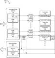
- FIG. 1Aillustrates an exemplary distributed storage system facilitating enhanced data storage management, in accordance with an embodiment of the present application.
- a computing device 102which is associated with a user 104 , relies on distributed storage system 100 for storing data.
- Examples of computing device 102can include, but are not limited to, a tablet, a mobile phone, an electronic reader, a laptop computer, a desktop computer, and any other computing device.
- Computing device 102can communicate via a network 110 with servers 112 , 114 , and 116 , which can be part of distributed storage system 100 .
- Servers 112 , 114 , and 116can be storage servers, each of which can include a CPU, an interface card, and storage devices or modules.
- server 116can include a central processing unit (CPU) 122 , a memory 124 , a network interface card (NIC) 126 , and a number of high-performance storage devices 132 , 136 , and 140 .
- a storage devicecan be an SSD.
- Storage devices 132 , 136 , and 140can have controllers 134 , 138 , and 142 , respectively.
- An SSDcan include non-volatile memory, including multiple non-volatile memory dies.
- a non-volatile memory diecan be a NAND die.
- a storage devicesuch as storage device 140
- controller 142can physically erase data with the unit of a block (e.g., 4 MB). Since NAND-based storage may not support in-place overwrite for a page, if a page 172 is updated in a block 152 , controller 142 rewrites the updated data in a new page and marks page 172 as an invalid page. Since block 152 still includes valid pages, such as page 174 , block 152 remains operational and continues to store valid data. As a result, controller 142 may continue to maintain invalid page 172 and valid page 174 in block 152 , and may not physically erase and release page 172 as a free page for future write operations.
- controller 142can trigger a garbage collector, which collects a respective valid page, such as page 174 , in block 152 and writes page 174 to another block, such as block 156 . The garbage collector then marks page 174 in block 152 as invalid.
- controller 142determines block 152 to be a free block and adds block 152 to the free block pool of storage device 140 .
- Controller 142can include buffer 150 that can operate at the rate of storage device 140 .
- buffer 150can be a ReRAM-based buffer.
- controller 142receives a page 170 in a write request from device 102 for writing in storage device 140 .
- Controller 142stores page 170 in buffer 150 . Since buffer 150 can be non-volatile, the data stored in buffer 150 does not disappear in case of a power loss. Therefore, when page 170 is written into buffer 150 , controller 142 can consider page 170 to be safely stored and send an acknowledgment to the host indicating that the write operation for page 170 has been completed.
- controller 142transfers block 130 to data block 158 in storage device 140 .
- controller 142organizes the incoming data in the unit of a block 130 .
- the incoming data segment sizecan become one block and its multiples for storage device 140 even when a host continues to provide read/write instructions based on the unit of a page.
- Controller 142thus utilizes this symmetry in data storage unit and erasure unit for storage device 140 to reduce the internal read/write operations for storage device 140 , thereby improving the performance of storage device 140 .
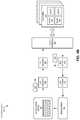
- FIG. 1Billustrates an exemplary storage device facilitating enhanced data storage management, in accordance with an embodiment of the present application.
- storage device 140can include one or more flash dies 170 (e.g., NAND dies).
- a diecan be a small block of semiconducting material on which a given functional circuit is fabricated.
- storage device 140can include a number of channels, each of which can communicate with a corresponding flash die.
- storage device 140can include 8 flash dies 162 , 163 , 164 , 165 , 166 , 167 , 168 , and 169 .
- Data blocks 152 , 154 , 156 , and 158can be in flash dies 162 , 164 , 166 , and 168 , respectively.
- storage device 140can include 8 channels to the dies from controller 142 .
- controller 142can store data segment 180 in buffer 150 .
- buffer 150can include at least 8 blocks (e.g., 32 MB) 182 , 183 , 184 , 185 , 186 , 187 , 188 , and 189 .
- controller 142transfers blocks 182 , 183 , 184 , 185 , 186 , 187 , 188 , and 189 via the 8 channels to flash dies 162 , 163 , 164 , 165 , 166 , 167 , 168 , and 169 , respectively.
- Controller 142thus utilizes the multiple channels in storage device 140 to increase the internal throughput for storage device 140 .
- FIG. 2Aillustrates an exemplary enhanced storage device facilitating efficient data storage and retrieval, in accordance with an embodiment of the present application.
- Buffer 150can mostly operate as a write buffer, which is used for accumulating data pages arriving at storage device 140 for writing.
- buffer 150which can be a ReRAM, can be integrated with controller 142 during the application-specific integrated circuit (ASIC) design (e.g., as a non-volatile module in the system-on-chip (SoC)). Since storage device 140 can include multiple channels, buffer 150 can include multiple zones 202 , 204 , 206 , and 206 to accommodate multiple blocks, each zone corresponding to a channel.
- ASICapplication-specific integrated circuit
- a respective channelcorresponds to a flash die in storage device 140 .
- each zone of buffer 150corresponds to a flash die.
- controller 142stores the data segment in a zone, such as zone 202 , and acknowledges to the host that the segment has been successfully written.
- controller 142can store subsequent data segments in the same zone 202 until at least one block of data is accumulated, or can distribute the data across zones 202 , 204 , 206 , and 208 .
- This storage policycan allow controller 142 to accumulate data in a single zone, or spread data across the zones. The storage policy ensures that the sequential data in the data segment are sequentially stored in storage device 140 .
- controller 142transfers data from zone 202 to flash die 162 .
- flash die 162includes a page buffer 232 that stores an incoming page. Controller 142 then transfers data from zone 202 to page buffer 232 of flash die 162 one page at a time. Controller 142 then transfers the page from the flash buffer to flash die 162 . This includes programming flash die 162 to store the page in a free block in flash die 162 . For example, controller 142 transfers page 210 from zone 202 to page buffer 232 . The transferred data is programmed in flash die 162 with an order of arrival in page by page as well.
- flash dies 164 , 166 , and 168include page buffers 234 , 236 , and 238 , respectively.
- controller 142transfers data from zones 204 , 206 , and 208 to page buffers 234 , 236 , and 238 , respectively, one page at a time.
- ReRAMsupports in-place overwrite with low latency.
- controller 142successfully writes page 210 in flash die 162
- the corresponding physical cells 212 in buffer 150can accommodate any new data arriving at storage device 140 .
- buffer 150supports direct in-place update and does not need a separate erase operation to clear its contents.
- the throughput for the write operationsdepends on the capacity of the channels between zones 202 , 204 , 206 , and 208 , and flash dies 162 , 164 , 166 , and 168 , respectively.
- the throughput of the write operationsdepends on the performance of the PCIe interfaces, and buffer 150 is not the bottleneck.
- buffer 150when buffer 150 is full, all channels can be active for writing data into the flash dies, and the throughput of the write operations depends on the flash dies' inherent processing capability. Therefore, for either scenario, buffer 150 can maintain high throughput that is not lower than a conventional storage device.
- PCIePeripheral Component Interconnect Express
- controller 142can include dedicated read buffers 250 for read operations.
- Read buffers 250can be implemented using static random-access memory (SRAM) or flip-flops.
- Read buffers 250can include a number of buffers 252 and 254 . Since the host can continue to issue read requests in the unit of a page, controller 142 can obtain a page from the flash dies. For example, in response to receiving a request for a page 214 , which is stored in flash die 168 , controller 142 can obtain page 214 from page buffer 238 and stores page 214 in buffer 252 . Controller 142 then provides page 214 to the host requesting page 214 .
- SRAMstatic random-access memory
- controller 142can facilitate page 214 in a format supported by the file system (e.g., EXT4, XFS, etc.) of the requesting host, and in the unit of a page. It should be noted that read buffers 250 are used for holding read results temporarily, which does not conflict with the data write operations in buffer 150 .
- the file systeme.g., EXT4, XFS, etc.
- controller 142Since controller 142 does not need to erase data from buffer 150 separately and facilitate in-place updates in buffer 150 , a data page 216 can remain in buffer 150 after it has been written into flash die 166 . Controller 142 may only update the corresponding location in buffer 150 by overwriting page 216 when a new data page arrives. Therefore, if a host requests page 216 , which has not been overwritten yet, a valid copy of page 216 can be in buffer 150 as well as flash die 166 . Since the read latency of buffer 150 can be lower than that of flash die 166 , controller 142 can obtain page 216 from buffer 150 instead of flash die 166 (denoted with dashed lines) and store page 216 in buffer 252 (or 254 ).
- FIG. 2Billustrates an exemplary data storage and retrieval process for an enhanced storage device, in accordance with an embodiment of the present application.
- controller 142receives a wire request for a data page from computing device 102 (operation 262 ). Since buffer 150 is non-volatile, controller 142 writes the data page in buffer 150 (operation 264 ) and sends an acknowledgment for the write request to computing device 102 (operation 266 ). Controller 142 can continue to accumulate pages in buffer 150 (operation 268 ). However, upon receiving the acknowledgment, computing device 102 can consider the data page to be successfully written.
- Controller 142continues to accumulate pages (operation 268 ) until the buffer gathers sufficient pages to reach a data block (operation 270 ). Controller 142 then writes the data block from buffer 150 to flash die 162 (operation 272 ). However, until some new data arrives, the data remains in buffer 150 .
- controller 142receives a read request for the page that has been stored in buffer 150 from computing device 102 (operation 274 )
- controller 142finds the data page in buffer 150 (operation 276 ).
- Controller 142fetches the data page from buffer 150 into read buffers 250 (operation 278 ), fetches the data page from read buffers 250 (operation 280 ), and provides the data page to computing device 102 from read buffer 250 (operation 282 ).
- controller 142replaces the data page in buffer 150 (operation 284 ). Hence, the only copy of the data page is in flash die 162 .
- controller 142receives another read request for the page from computing device 102 (operation 286 )
- controller 142finds the data page in flash die 162 (e.g., based on a mapping to the page) (operation 288 ).
- Controller 142fetches the data page from flash die 162 into read buffers 250 (operation 290 ), fetches the data page from read buffers 250 (operation 292 ), and provides the data page to computing device 102 from read buffer 250 (operation 294 ).
- FIG. 3illustrates an exemplary multi-level mapping for identifying data in an enhanced storage device, in accordance with an embodiment of the present application.
- the blockmay include pages from different applications.
- a two-level mappingis maintained with offset calculation.
- the first level mappingis a block mapping 300 , which facilitates the mapping at the block level (e.g., 4 MB).
- the second level mappingis a subpage mapping 310 , which facilitates mapping within a block with the smallest unit in which a piece of data can be stored or retrieved.
- the smallest unitcan be a subpage (e.g., a data segment of 4 KB).
- a pagecan include a number of subpages. For example, one 16 KB page can include 4 subpages.
- controller 142represents a respective block of data stored in the storage device as a logical file with a filename and presents the block as the logical file to the corresponding application(s). Controller 142 also generates a logical index for that data block and maps the filename and the logical index to the physical block index in the flash dies storing the block. For example, controller 142 can map a logical index 0 and a corresponding filename “AAA” to a physical block index 2. Similarly, controller 142 can map logical indices 1, 2, . . . , N ⁇ 1 and corresponding filenames “BBB,” “CCC,” . . . , “DDD” to physical block indices 1, N ⁇ 1, . . .
- a block indexuniquely identifies a block in a storage device. As a result, if a block index k is the final block index in one flash die, block index k+1 can be the first block index in the next flash die.
- Controller 142can also maintain subpage mapping 310 to facilitate data read within a block.
- mapping 300filename “BBB” is associated with logical index 1.
- the data content of “BBB”can be stored into the physical block corresponding to index 1.
- filename “CCC”is associated with logical index 2.
- the data content of “CCC”can be stored into the physical block corresponding to index N ⁇ 1. Therefore, the order of the logical indices and the physical indices can be different. Here, the order of the logical indices can be based on the arrival of data.
- the physical block indicescan correspond to the available data blocks.
- Controller 142can also maintain subpage mapping 310 to facilitate data read within a block.
- a filecan include a number of sectors, each of which can correspond to the smallest unit accessible via a read instruction. If the unit is a subpage, each sector corresponds to a subpage.
- logical file “BBB”includes m logical sectors “BBB/0,” “BBB/1,” “BBB/2,” . . . , “BBB/m ⁇ 1.”
- the logical index associated with each sectorcan be referred to as a logical offset, and expressed based on the logical index 1 of file “BBB.” For example, sectors “BBB/0,” “BBB/1,” “BBB/2,” . . .
- mapping 310maps a respective sector of logical file “BBB” to a corresponding physical index storing the subpage.
- Mapping 310maps logical offsets 1:0, 1:1, 1:2, . . . , 1:m ⁇ 1 to subpage indices 0, M ⁇ 1, i, . . . , j, respectively.
- the subpage indicesindicate the data placement locations at the subpage-level.
- a read requestcan access a data segment at the sub-page level.
- controller 142can determine the corresponding block index from mapping 300 .
- Controller 142then can locate a respective sector based on the logical offset from mapping 310 . For example, to access sector “BBB/2,” controller 142 can obtain filename “BBB” and retrieve logical index 1 and corresponding block index 1 from mapping 300 .
- Controller 142then retrieves logical offset 1:2 and block index i associated with “BBB/2” from mapping 310 .
- Controller 142can then obtain the ith subpage stored in the block associated with index 1.
- FIG. 4Aillustrates exemplary operations in an enhanced storage device based on a unit of a block, in accordance with an embodiment of the present application.
- storage device 140initializes (e.g., powers up)
- a respective block in storage device 140is in a free block pool 406 and ready to store data.
- controller 142obtains a free block.
- Controller 142allocates block 412 to the free block based on the two-level mapping described in conjunction with FIG. 3 .
- Controller 142then executes a write operation 424 that writes data block 412 into the free block.
- the blockis allocated to a stored block pool 402 , which represents the set of blocks storing valid data.
- controller 142continues to move more blocks from free block pool 406 to stored block pool 402 .
- data blocks in storage device 140e.g., the NAND cells
- a respective block in stored block pool 402can face data degradation.
- NAND cellsare configured to have 90 days of data retention. Therefore, a respective block in stored block pool 402 needs to be refreshed after the block reaches an alarm zone (e.g., retains data close to 90 days without refreshing).
- controller 142periodically evaluates the data for the blocks in stored block pool 402 . Upon determining that block 414 in stored block pool 402 is in the alarm zone, controller 142 initiates an internal transfer request 436 to refresh block 414 . Controller 142 reads block 414 from stored block pool 402 . Controller 142 obtains a free block from free block pool 406 and executes a write operation 424 that writes data block 414 (denoted with dashed lines) into the free block. In this way, controller 142 refreshes the entire block. Upon completing the refresh operation, controller 142 adds the refreshed block, which was the free block, to stored block pool 402 . Controller 142 then considers old block 414 as an invalid block, which can be erased to generate a free block.
- the content of a block in stored block pool 402may become expired because the block can be updated or deleted. For example, if the subpages of a block 416 in stored block pool 402 expire because the subpages are deleted, controller 142 considers block 416 as an invalid block, which can also be erased to generate a free block.
- controller 142receives an update request for a block 418 , controller 142 initiates an internal transfer request 436 to update block 418 . Controller 142 reads block 418 from stored block pool 402 and transfers the data to buffer 150 . Controller 142 then updates the data in buffer 150 based on the update request. Controller 142 obtains a free block from free block pool 406 and executes a write operation 424 that writes data block 418 (denoted with dashed lines) into the free block. Upon completing the update operation, controller 142 adds the updated block, which was the free block, to stored block pool 402 . Controller 142 then considers old block 418 as an invalid block, which can be erased to generate a free block.
- controller 142can update the corresponding two-level mapping, as described in conjunction with FIG. 3 . Controller 142 then adds blocks 414 , 416 , and 418 to an invalid block pool 404 , which stores the blocks that are invalid but have not been erased yet. To erase a block from invalid block pool 404 , controller 142 can enable a lock 432 on the flash die that includes the block. The locked die cannot service any incoming read and/or write operation until the erase operation is completed. If a read and/or write operation arrives for the block, that operation can be redirected to another replica of the data stored in another storage device in the distributed storage system. In the example in FIG.
- any corresponding read and/or write operationcan be redirected to another server 112 / 114 that stores another replica of the data associated with the operation.
- controller 142Upon erasing the block, controller 142 releases lock 432 and adds the block to free block pool 406 . The erasure operation on the block removes the invalid and expired data from the block.
- storage device 140may not include any power loss protection. Regardless of a write or a refresh operation, controller 142 does not commit data until controller 142 writes the data into buffer 150 . Hence, storage device 140 no longer needs to have the power loss protection, which reduces the corresponding overhead associated with circuitry, testing, firmware development, etc. This, in turn, can lower the cost and the reliability of storage device 140 .
- FIG. 4Billustrates an exemplary data refresh process for an enhanced storage device based on a unit of a block, in accordance with an embodiment of the present application.
- controller 142sequentially reads out a respective page from block 414 using a flash interface 460 .
- flash interface 460allows controller 142 to access a respective page.
- Controller 142obtains page 470 from block 414 and decodes page 470 using an error-correcting code (ECC) decoder 454 to recover the correct data by fixing any error in page 470 .
- Controller 142then applies a cyclic redundancy check (CRC) using a CRC decoder 452 to check the data consistency of page 470 .
- CRC decoder 452can also ensure that ECC decoder 454 does not converge onto a wrong codeword, thereby ensuring that ECC decoder 454 does not yield an incorrect page.
- CRC decoder 452can also ensure that ECC decoder 454 does not converge onto a wrong
- Controller 142transfers page 470 from CRC decoder 452 to read buffers 250 . Controller 142 then transfers that page 470 to buffer 150 . Controller 142 shortcuts page 470 through buffer 150 without waiting for accumulation of an entire block. Controller 142 obtains page 470 from buffer 150 and applies CRC using a CRC encoder 462 to check the data consistency of page 470 obtained from buffer 150 . Controller 142 then encodes page 470 using an ECC encoder 464 to recover the correct data by fixing any error in page 470 . Controller 142 then writes page 470 into a new free block 420 in flash dies 170 . In this way, controller 142 refreshes the data in block 414 by sequentially repeating this read/write process page by page for each page within block 414 .
- storage device 140with the on-chip buffer 150 integrated in controller 142 .
- Storage device 140allows block-by-block write operations, and simplifies the mapping between logical and physical entities.
- Controller 142can efficiently operate storage device 140 without a separate garbage collector.
- storage device 140may not require additional power loss protection.
- controller 142can refresh data in storage device 140 at the block level, thereby significantly reducing the write amplification.
- the performance of storage device 140can remain stable because the background operations rarely occur and occupy limited resources.
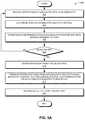
- FIG. 5Apresents a flowchart illustrating a method 500 of a storage controller storing data in an enhanced storage device, in accordance with an embodiment of the present application.
- the controllerreceives a write request associated with a page from a host (operation 502 ) and determines a zone in the accumulation buffer for the page (operation 504 ). The controller can determine the zone to ensure that the sequential data is sequentially written. The controller then stores the page in the determined zone in the accumulation buffer and sends an acknowledgment to the host (operation 506 ). The controller checks whether the block has been filled (operation 508 ). If the block is not filled, the controller continues to receive a write request associated with a page from a host (operation 502 ).
- the controllerobtains a new block from the free block pool (operation 510 ).
- the controllertransfers a respective page from the accumulation buffer to the page buffer of the flash die that includes the new block, and transfers the page from the accumulation buffer to the new block (operation 512 ).
- the controllerthen adds the new block to the stored block pool (operation 514 ).
- FIG. 5Bpresents a flowchart illustrating a method 530 of a storage controller generating a multi-level mapping for storing data in an enhanced storage device, in accordance with an embodiment of the present application.
- the controllergenerates a filename of the logical file and a corresponding logical index for a block (operation 532 ).
- the controllermaps the filename and the logical index to the corresponding physical block index, and stores the mapping in a local persistent storage (operation 534 ).
- the persistent storagecan be a non-volatile storage.
- the controllergenerates a sector name and a corresponding logical offset based on the logical index for a respective sector in the block (operation 536 ).
- the controllermaps a respective sector name and the logical offset to the corresponding flash subpage in the block, and stores the mapping in the local persistent storage (operation 538 ).
- the controllerthen provides the file to the host (operation 540 ).
- the controllercan also provide the sector names associated with the filename to the host.
- FIG. 5Cpresents a flowchart illustrating a method 550 of a storage controller retrieving data from an enhanced storage device, in accordance with an embodiment of the present application.
- the controllerreceives a read request associated with a filename (operation 552 ).
- the read requestcan also include one or more sectors.
- the controllerdetermines a logical index associated with the filename (operation 554 ).
- the controllercan also include the logical offsets associated with one or more sectors.
- the controllercan determine the block address associated with the logical index (operation 556 ).
- the controllercan also determine the subpage addresses associated with the logical offsets).
- the controllerchecks whether the data associated with the read request is in the accumulation buffer (operation 558 ). If the accumulation buffer includes the data, the controller identifies the subpages in the accumulation buffer and obtains the corresponding subpages (operation 560 ). Otherwise, the controller identifies the subpages associated with the block address and subpage addresses, and obtains the corresponding subpages (operation 562 ). Upon obtaining the corresponding subpages (operation 560 or 562 ), the controller provide the subpages to the host (operation 564 ).
- FIG. 6Apresents a flowchart illustrating a method 600 of a storage controller erasing a block in an enhanced storage device, in accordance with an embodiment of the present application.
- the controlleridentifies an expired block (operation 602 ) and allocates the identified block to an invalid block pool (operation 604 ).
- the controllerselects a block from the invalid block pool and enables a lock on the flash die that includes the selected block (operation 606 ).
- the controllerthen erases the selected block and releases the lock (operation 608 ).
- the controllerallocates the selected block to the free block pool (operation 610 ).
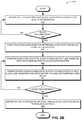
- FIG. 6Bpresents a flowchart illustrating a method 650 of a storage controller refreshing a block in an enhanced storage device, in accordance with an embodiment of the present application.
- the controllerperiodically scans a respective block in the stored block pool for the quality of retention (operation 652 ) and checks whether any block is in the alarm zone (operation 654 ). If a block is not in the alarm zone, the controller continues to scan a respective block in the stored block pool for the quality of retention (operation 652 ). On the other hand, if a block is in the alarm zone, the controller selects the block in the alarm zone for refreshing and obtains a new block from the free block pool (operation 656 ).
- the controllertransfers a page from the selected block to a read buffer, and transfers the page from the read buffer to the accumulation buffer (operation 658 ).
- the controllerthen transfers the page from the accumulation buffer to the page buffer of the new block, and transfers the page from the page buffer to the flash die that includes the new block (operation 660 ).
- the controllerthen checks whether all pages in the selected block have been transferred (operation 662 ). If all pages have not been transferred, the controller continues to transfer a page from the selected block to a read buffer, and transfers the page from the read buffer to the accumulation buffer (operation 658 ). Otherwise, the controller adds the new block to the stored block pool, and allocates the selected block to the invalid block pool (operation 664 ).
- FIG. 7illustrates an exemplary computer system that facilitates a storage management system for managing data in an enhanced storage device, in accordance with an embodiment of the present application.
- Computer system 700includes a processor 702 , a memory 704 , and a storage device 708 .
- Computer system 700can also include a storage device 750 (e.g., an SSD), and an accumulation buffer 752 .
- Memory 704can include a volatile memory (e.g., DIMM) that serves as a managed memory, and can be used to store one or more memory pools.
- computer system 700can be coupled to a display device 710 , a keyboard 712 , and a pointing device 714 .
- Storage device 708can store an operating system 716 , a storage management system 718 , and data 736 .
- Storage management system 718can include instructions, which when executed by computer system 700 , can cause computer system 700 to perform methods and/or processes described in this disclosure. Specifically, storage management system 718 can include instructions for processing read and/or write requests for storage device 752 (buffer management module 720 ). Storage management system 718 can also include instructions for accumulating data in accumulation buffer 752 to facilitate write operations at the unit of a block (buffer management module 720 ). Furthermore, storage management system 718 can include instructions for generating the two-level mappings (mapping module 722 ).
- storage management system 718includes instructions for reading a page or a subpage from accumulation buffer 752 or storage device 750 at the unit of a page or subpage based on the multi-level mapping (reading module 724 ).
- Storage management system 718can also include instructions for writing into the flash dies of storage device 750 from accumulation buffer 752 (writing module 726 ).
- Storage management system 718can further include instructions for erasing the data at the unit of a block (erasure module 728 ).
- Storage management system 718can also include instructions for refreshing a block to ensure safe data retention (refreshing module 730 ).
- Storage management system 718can include instructions for updating a block in response to receiving an update request for one or more pages in the block (updating module 732 ).
- Storage management system 718can also include instructions for sending and receiving packets for read/write operations (communication module 734 ).
- Data 736can include any data that is required as input or that is generated as output by the methods and/or processes described in this disclosure. Specifically, data 736 can store at least: the two-level mapping, the read buffer, and the page buffer for a respective flash die.
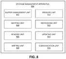
- FIG. 8illustrates an exemplary apparatus that facilitates a storage management system for managing data in an enhanced storage device, in accordance with an embodiment of the present application.
- Apparatus 800can comprise a plurality of units or apparatuses which may communicate with one another via a wired, wireless, quantum light, or electrical communication channel.
- Apparatus 800may be realized using one or more integrated circuits, and may include fewer or more units or apparatuses than those shown in FIG. 8 .
- apparatus 800may be integrated in a computer system, or realized as a separate device which is capable of communicating with other computer systems and/or devices.
- apparatus 800can comprise units 802 - 816 , which perform functions or operations similar to modules 720 - 734 of computer system 700 of FIG.
- a buffer management unit 802including: a buffer management unit 802 ; a mapping unit 804 ; a reading unit 806 ; a writing unit 808 ; an erasure unit 810 ; a refreshing unit 812 , an updating unit 814 , and a communication unit 816 .
- the data structures and code described in this detailed descriptionare typically stored on a computer-readable storage medium, which may be any device or medium that can store code and/or data for use by a computer system.
- the computer-readable storage mediumincludes, but is not limited to, volatile memory, non-volatile memory, magnetic and optical storage devices such as disks, magnetic tape, CDs (compact discs), DVDs (digital versatile discs or digital video discs), or other media capable of storing computer-readable media now known or later developed.
- the methods and processes described in the detailed description sectioncan be embodied as code and/or data, which can be stored in a computer-readable storage medium as described above.
- a computer systemreads and executes the code and/or data stored on the computer-readable storage medium, the computer system performs the methods and processes embodied as data structures and code and stored within the computer-readable storage medium.
- the methods and processes described abovecan be included in hardware modules.
- the hardware modulescan include, but are not limited to, application-specific integrated circuit (ASIC) chips, field-programmable gate arrays (FPGAs), and other programmable-logic devices now known or later developed.
- ASICapplication-specific integrated circuit
- FPGAfield-programmable gate arrays
- the hardware modulesWhen the hardware modules are activated, the hardware modules perform the methods and processes included within the hardware modules.
Landscapes
- Engineering & Computer Science (AREA)
- Theoretical Computer Science (AREA)
- General Engineering & Computer Science (AREA)
- Physics & Mathematics (AREA)
- General Physics & Mathematics (AREA)
- Human Computer Interaction (AREA)
- Quality & Reliability (AREA)
- Computer Security & Cryptography (AREA)
- Information Retrieval, Db Structures And Fs Structures Therefor (AREA)
- Techniques For Improving Reliability Of Storages (AREA)
Abstract
Description
Claims (20)
Priority Applications (1)
| Application Number | Priority Date | Filing Date | Title |
|---|---|---|---|
| US15/717,100US10789011B2 (en) | 2017-09-27 | 2017-09-27 | Performance enhancement of a storage device using an integrated controller-buffer |
Applications Claiming Priority (1)
| Application Number | Priority Date | Filing Date | Title |
|---|---|---|---|
| US15/717,100US10789011B2 (en) | 2017-09-27 | 2017-09-27 | Performance enhancement of a storage device using an integrated controller-buffer |
Publications (2)
| Publication Number | Publication Date |
|---|---|
| US20190095134A1 US20190095134A1 (en) | 2019-03-28 |
| US10789011B2true US10789011B2 (en) | 2020-09-29 |
Family
ID=65809055
Family Applications (1)
| Application Number | Title | Priority Date | Filing Date |
|---|---|---|---|
| US15/717,100ActiveUS10789011B2 (en) | 2017-09-27 | 2017-09-27 | Performance enhancement of a storage device using an integrated controller-buffer |
Country Status (1)
| Country | Link |
|---|---|
| US (1) | US10789011B2 (en) |
Families Citing this family (8)
| Publication number | Priority date | Publication date | Assignee | Title |
|---|---|---|---|---|
| US10802766B2 (en)* | 2017-09-29 | 2020-10-13 | Oracle International Corporation | Database with NVDIMM as persistent storage |
| CN113728598A (en) | 2019-05-23 | 2021-11-30 | 慧与发展有限责任合伙企业 | System and method for a reduction engine to facilitate self-management |
| US20200409601A1 (en)* | 2019-06-28 | 2020-12-31 | Western Digital Technologies, Inc. | Hold of Write Commands in Zoned Namespaces |
| KR102818456B1 (en)* | 2019-09-23 | 2025-06-10 | 삼성전자주식회사 | Solid state drive device and method for fabricating the same |
| JP7413108B2 (en) | 2020-03-23 | 2024-01-15 | キオクシア株式会社 | semiconductor equipment |
| CN111208953A (en)* | 2020-04-16 | 2020-05-29 | 广东睿江云计算股份有限公司 | Distributed storage method and device |
| JP2024000825A (en)* | 2022-06-21 | 2024-01-09 | キオクシア株式会社 | Semiconductor storage device and memory system |
| US11934657B2 (en)* | 2022-08-16 | 2024-03-19 | Micron Technology, Inc. | Open block management in memory devices |
Citations (118)
| Publication number | Priority date | Publication date | Assignee | Title |
|---|---|---|---|---|
| US4775932A (en)* | 1984-07-31 | 1988-10-04 | Texas Instruments Incorporated | Computer memory system with parallel garbage collection independent from an associated user processor |
| WO1994018634A1 (en) | 1993-02-01 | 1994-08-18 | Lsc, Inc. | Archiving file system for data servers in a distributed network environment |
| US6226650B1 (en) | 1998-09-17 | 2001-05-01 | Synchrologic, Inc. | Database synchronization and organization system and method |
| US20020010783A1 (en) | 1999-12-06 | 2002-01-24 | Leonard Primak | System and method for enhancing operation of a web server cluster |
| US20020073358A1 (en) | 2000-12-07 | 2002-06-13 | Atkinson Lee. W. | Method for redundant suspend to RAM |
| US20020161890A1 (en) | 2000-12-22 | 2002-10-31 | Kailai Chen | System and method for intelligently distributing content over a communicatons network |
| US20030163594A1 (en) | 2002-02-27 | 2003-08-28 | Aasheim Jered Donald | Open-architecture file system |
| US20030163633A1 (en) | 2002-02-27 | 2003-08-28 | Aasheim Jered Donald | System and method for achieving uniform wear levels in a flash memory device |
| US20040010545A1 (en) | 2002-06-11 | 2004-01-15 | Pandya Ashish A. | Data processing system using internet protocols and RDMA |
| US20040255171A1 (en) | 2003-06-13 | 2004-12-16 | Zimmer Vincent J. | Power management for clustered computing platforms |
| US20040268278A1 (en) | 2003-05-07 | 2004-12-30 | Hoberman Barry Alan | Managing power on integrated circuits using power islands |
| US20050038954A1 (en) | 2003-06-04 | 2005-02-17 | Quantum Corporation | Storage drive having universal format across media types |
| US20050097126A1 (en) | 2000-08-24 | 2005-05-05 | Microsoft Corporation | Partial migration of an object to another storage location in a computer system |
| US20050177755A1 (en) | 2000-09-27 | 2005-08-11 | Amphus, Inc. | Multi-server and multi-CPU power management system and method |
| US20050195635A1 (en) | 2004-03-08 | 2005-09-08 | Conley Kevin M. | Flash controller cache architecture |
| US20050235067A1 (en) | 2004-04-20 | 2005-10-20 | Intel Corporation | Write combining protocol between processors and chipsets |
| US20050235171A1 (en) | 2003-09-02 | 2005-10-20 | Kabushiki Kaisha Toshiba | Electronic device with serial ATA interface and power saving method for serial ATA buses |
| US20060156012A1 (en) | 2005-01-07 | 2006-07-13 | Beeson Curtis L | Facilitating digital signature based on ephemeral private key |
| US20070033323A1 (en)* | 2005-08-03 | 2007-02-08 | Gorobets Sergey A | Interfacing systems operating through a logical address space and on a direct data file basis |
| US20070101096A1 (en) | 2005-10-27 | 2007-05-03 | Sandisk Corporation | Non-volatile memory with adaptive handling of data writes |
| US20080034154A1 (en) | 1999-08-04 | 2008-02-07 | Super Talent Electronics Inc. | Multi-Channel Flash Module with Plane-Interleaved Sequential ECC Writes and Background Recycling to Restricted-Write Flash Chips |
| US20090113219A1 (en) | 2007-10-30 | 2009-04-30 | Sandisk Il Ltd. | Optimized hierarchical integrity protection for stored data |
| US7565454B2 (en) | 2003-07-18 | 2009-07-21 | Microsoft Corporation | State migration in multiple NIC RDMA enabled devices |
| US20090282275A1 (en) | 2006-06-27 | 2009-11-12 | Koninklijke Philips Electronics N.V. | Device and a method for managing power consumption of a plurality of data processing units |
| US20090307249A1 (en) | 2006-05-31 | 2009-12-10 | Storwize Ltd. | Method and system for transformation of logical data objects for storage |
| US20090310412A1 (en) | 2008-06-17 | 2009-12-17 | Jun-Ho Jang | Methods of data management in non-volatile memory devices and related non-volatile memory systems |
| US20100169470A1 (en) | 2008-12-25 | 2010-07-01 | Hitachi, Ltd. | System and method for operational management of computer system |
| US20100229224A1 (en) | 2009-02-10 | 2010-09-09 | Uniloc Usa, Inc. | Web Content Access Using a Client Device Identifier |
| US20100325367A1 (en) | 2009-06-19 | 2010-12-23 | International Business Machines Corporation | Write-Back Coherency Data Cache for Resolving Read/Write Conflicts |
| US20110055458A1 (en)* | 2009-09-03 | 2011-03-03 | 248 Solid State, Inc. | Page based management of flash storage |
| US20110153903A1 (en) | 2009-12-21 | 2011-06-23 | Sanmina-Sci Corporation | Method and apparatus for supporting storage modules in standard memory and/or hybrid memory bus architectures |
| US20110218969A1 (en) | 2010-03-08 | 2011-09-08 | International Business Machines Corporation | Approach for optimizing restores of deduplicated data |
| US20110231598A1 (en)* | 2010-03-19 | 2011-09-22 | Kabushiki Kaisha Toshiba | Memory system and controller |
| US20110292538A1 (en) | 2010-05-31 | 2011-12-01 | Kabushiki Kaisha Toshiba | Recording medium controller and method thereof |
| US20110302353A1 (en)* | 2008-12-30 | 2011-12-08 | Emanuele Confalonieri | Non-volatile memory with extended operating temperature range |
| US20120084523A1 (en) | 2010-09-30 | 2012-04-05 | Littlefield Duncan A | Data recovery operations, such as recovery from modified network data management protocol data |
| US20120117399A1 (en) | 2010-11-04 | 2012-05-10 | International Business Machines Corporation | Saving power by managing the state of inactive computing devices |
| US20120147021A1 (en) | 2010-12-13 | 2012-06-14 | Advanced Micro Devices, Inc. | Graphics compute process scheduling |
| US20120159289A1 (en) | 2010-12-20 | 2012-06-21 | Piccirillo Gary J | Data signatures to determine sucessful completion of memory backup |
| US20120210095A1 (en) | 2011-02-11 | 2012-08-16 | Fusion-Io, Inc. | Apparatus, system, and method for application direct virtual memory management |
| US8260924B2 (en) | 2006-05-03 | 2012-09-04 | Bluetie, Inc. | User load balancing systems and methods thereof |
| US20120246392A1 (en)* | 2011-03-23 | 2012-09-27 | Samsung Electronics Co., Ltd. | Storage device with buffer memory including non-volatile ram and volatile ram |
| US20120278579A1 (en) | 2011-04-29 | 2012-11-01 | Seagate Technology Llc | Self-Initiated Secure Erasure Responsive to an Unauthorized Power Down Event |
| US20120284587A1 (en) | 2008-06-18 | 2012-11-08 | Super Talent Electronics, Inc. | Super-Endurance Solid-State Drive with Endurance Translation Layer (ETL) and Diversion of Temp Files for Reduced Flash Wear |
| US20130061029A1 (en) | 2011-09-02 | 2013-03-07 | Lsi Corporation | Method and apparatus for consolidating boot drives and improving reliability/availability/serviceability in high density server environments |
| US20130073798A1 (en) | 2011-09-20 | 2013-03-21 | Samsung Electronics Co., Ltd. | Flash memory device and data management method |
| US8452819B1 (en) | 2011-03-22 | 2013-05-28 | Amazon Technologies, Inc. | Methods and apparatus for optimizing resource utilization in distributed storage systems |
| US20130145085A1 (en) | 2008-06-18 | 2013-06-06 | Super Talent Technology Corp. | Virtual Memory Device (VMD) Application/Driver with Dual-Level Interception for Data-Type Splitting, Meta-Page Grouping, and Diversion of Temp Files to Ramdisks for Enhanced Flash Endurance |
| US20130145089A1 (en) | 2010-05-28 | 2013-06-06 | International Business Machines Corporation | Cache memory management in a flash cache architecture |
| US20130151759A1 (en) | 2011-12-08 | 2013-06-13 | Samsung Electronics Co., Ltd. | Storage device and operating method eliminating duplicate data storage |
| US20130159251A1 (en) | 2009-06-19 | 2013-06-20 | Rich Skrenta | Dedicating Disks to Reading or Writing |
| US20130166820A1 (en) | 2011-12-22 | 2013-06-27 | Fusion-Io, Inc. | Methods and appratuses for atomic storage operations |
| US20130173845A1 (en) | 2011-12-29 | 2013-07-04 | Ameen Aslam | Command Aware Partial Page Programming |
| US20130219131A1 (en) | 2012-02-20 | 2013-08-22 | Nimrod Alexandron | Low access time indirect memory accesses |
| US20130318283A1 (en)* | 2012-05-22 | 2013-11-28 | Netapp, Inc. | Specializing i/0 access patterns for flash storage |
| US20140108414A1 (en) | 2012-10-12 | 2014-04-17 | Architecture Technology Corporation | Scalable distributed processing of rdf data |
| US8751763B1 (en) | 2013-03-13 | 2014-06-10 | Nimbus Data Systems, Inc. | Low-overhead deduplication within a block-based data storage |
| US20140181532A1 (en) | 2010-12-31 | 2014-06-26 | International Business Machines Corporation | Encrypted flash-based data storage system with confidentiality mode |
| US20140233950A1 (en) | 2013-02-15 | 2014-08-21 | Futurewei Technologies, Inc. | Downstream Burst Transmission In Passive Optical Networks |
| US8825937B2 (en) | 2011-02-25 | 2014-09-02 | Fusion-Io, Inc. | Writing cached data forward on read |
| US20140250259A1 (en)* | 2013-03-01 | 2014-09-04 | Silicon Motion, Inc. | Data storage device and flash memory control method |
| US20140304452A1 (en) | 2013-04-03 | 2014-10-09 | Violin Memory Inc. | Method for increasing storage media performance |
| US20140310574A1 (en) | 2012-12-28 | 2014-10-16 | Super Talent Technology, Corp. | Green eMMC Device (GeD) Controller with DRAM Data Persistence, Data-Type Splitting, Meta-Page Grouping, and Diversion of Temp Files for Enhanced Flash Endurance |
| US20140359229A1 (en) | 2013-05-31 | 2014-12-04 | Vmware, Inc. | Lightweight Remote Replication of a Local Write-Back Cache |
| US20140365707A1 (en) | 2010-12-13 | 2014-12-11 | Fusion-Io, Inc. | Memory device with volatile and non-volatile media |
| US20150019798A1 (en) | 2013-07-15 | 2015-01-15 | CNEXLABS, Inc. | Method and Apparatus for Providing Dual Memory Access to Non-Volatile Memory |
| US20150082317A1 (en) | 2013-09-19 | 2015-03-19 | Liang You | Techniques for distributed processing task portion assignment |
| US20150106556A1 (en) | 2008-06-18 | 2015-04-16 | Super Talent Electronics, Inc. | Endurance Translation Layer (ETL) and Diversion of Temp Files for Reduced Flash Wear of a Super-Endurance Solid-State Drive |
| US20150106559A1 (en) | 2013-03-15 | 2015-04-16 | Samsung Electronics Co., Ltd. | Nonvolatile storage device and operating system (os) image program method thereof |
| US20150142752A1 (en) | 2013-11-15 | 2015-05-21 | International Business Machines Corporation | Priority based reliability mechanism for archived data |
| US9043545B2 (en) | 2012-01-06 | 2015-05-26 | Netapp, Inc. | Distributing capacity slices across storage system nodes |
| US9088300B1 (en) | 2011-12-15 | 2015-07-21 | Marvell International Ltd. | Cyclic redundancy check for out-of-order codewords |
| US9092223B1 (en) | 2012-05-31 | 2015-07-28 | Google Inc. | Systems and methods to save power in data-center networks |
| US20150227316A1 (en) | 2014-02-07 | 2015-08-13 | Coho Data, Inc. | Methods, systems and devices relating to data storage interfaces for managing data address spaces in data storage devices |
| US20150277937A1 (en) | 2014-03-26 | 2015-10-01 | Robert C. Swanson | Boot image discovery and delivery |
| US20150304108A1 (en) | 2010-09-15 | 2015-10-22 | Seagate Technology Llc | Encryption Key Destruction For Secure Data Erasure |
| US20150309924A1 (en)* | 2012-12-07 | 2015-10-29 | Norel Systems Limited | Control apparatus and control method with multiple flash memory card channels |
| US20150363271A1 (en) | 2014-06-16 | 2015-12-17 | International Business Machines Corporation | Restoring data in a hierarchical storage management system |
| US20150372597A1 (en) | 2014-06-19 | 2015-12-24 | Shiguo Luo | Methods and systems for improving light load efficiency for power stages of multi-phase voltage regulator circuits |
| US20160014039A1 (en) | 2014-07-11 | 2016-01-14 | Vmware, Inc. | Methods and apparatus to provision a workload in a virtual server rack deployment |
| US9280472B1 (en) | 2013-03-13 | 2016-03-08 | Western Digital Technologies, Inc. | Caching data in a high performance zone of a data storage system |
| US9280487B2 (en) | 2013-01-18 | 2016-03-08 | Cisco Technology, Inc. | Methods and apparatus for data processing using data compression, linked lists and de-duplication techniques |
| US20160098344A1 (en) | 2014-10-03 | 2016-04-07 | Sandisk Technologies Inc. | Hardware automation for memory management |
| US20160110254A1 (en) | 2014-10-15 | 2016-04-21 | Empire Technology Development Llc | Partial Cloud Data Storage |
| US20160232103A1 (en) | 2013-09-26 | 2016-08-11 | Mark A. Schmisseur | Block storage apertures to persistent memory |
| US20160239074A1 (en) | 2015-02-13 | 2016-08-18 | Victor W. Lee | Performing power management in a multicore processor |
| US20160239380A1 (en) | 2015-02-16 | 2016-08-18 | Quantum Corporation | Garbage Collection And Defragmentation For Solid State Drives (SSD) and Shingled Magnetic Recording (SMR) Drives |
| US20160274636A1 (en) | 2015-03-16 | 2016-09-22 | Electronics And Telecommunications Research Institute | Gpu power measuring method of heterogeneous multi-core system |
| US20160306853A1 (en) | 2010-06-09 | 2016-10-20 | Brocade Communications Systems, Inc. | Inline Wire Speed Deduplication System |
| US20160343429A1 (en) | 2015-05-19 | 2016-11-24 | Emc Corporation | Method and system for storing and recovering data from flash memory |
| US20160350002A1 (en) | 2015-05-29 | 2016-12-01 | Intel Corporation | Memory device specific self refresh entry and exit |
| US9529601B1 (en) | 2015-07-15 | 2016-12-27 | Dell Products L.P. | Multi-processor startup system |
| US9588977B1 (en) | 2014-09-30 | 2017-03-07 | EMC IP Holding Company LLC | Data and metadata structures for use in tiering data to cloud storage |
| US9588698B1 (en) | 2013-03-15 | 2017-03-07 | Virident Systems Inc. | Managing the write performance of an asymmetric memory system |
| US20170075583A1 (en) | 2015-09-14 | 2017-03-16 | Microsoft Technology Licensing, Llc. | Exposing and managing disparate read, write, and erase sizes in data storage devices |
| US20170109232A1 (en) | 2015-10-20 | 2017-04-20 | Samsung Electronics Co., Ltd. | Methods operating semiconductor memory devices with selective write-back of data for error scrubbing and related devices |
| US20170162235A1 (en) | 2015-12-02 | 2017-06-08 | Qualcomm Incorporated | System and method for memory management using dynamic partial channel interleaving |
| US20170168986A1 (en) | 2015-12-10 | 2017-06-15 | Cisco Technology, Inc. | Adaptive coalescing of remote direct memory access acknowledgements based on i/o characteristics |
| US20170212708A1 (en) | 2016-01-25 | 2017-07-27 | Samsung Electronics Co., Ltd. | Dynamic garbage collection p/e policies for redundant storage blocks and distributed software stacks |
| US20170228157A1 (en) | 2015-07-13 | 2017-08-10 | Samsung Electronics Co., Ltd. | Automatic stream detection & assignment algorithm |
| US20170249162A1 (en) | 2016-02-25 | 2017-08-31 | Red Hat Israel, Ltd. | Safe transmit packet processing for network function virtualization applications |
| US20170262178A1 (en) | 2016-03-09 | 2017-09-14 | Kabushiki Kaisha Toshiba | Storage system having a host that manages physical data locations of a storage device |
| US20170285976A1 (en) | 2016-04-01 | 2017-10-05 | David M. Durham | Convolutional memory integrity |
| US20170286311A1 (en) | 2016-04-01 | 2017-10-05 | Dale J. Juenemann | Repetitive address indirection in a memory |
| US20170344470A1 (en) | 2016-05-25 | 2017-11-30 | Samsung Electronics Co., Ltd. | Range based stream detection for flash memory device |
| US20170344491A1 (en) | 2016-05-25 | 2017-11-30 | Samsung Electronics Co., Ltd. | Access parameter based multi-stream storage device access |
| US20170353576A1 (en) | 2016-06-01 | 2017-12-07 | Intel Corporation | Method and apparatus for remote prefetches of variable size |
| US20180024772A1 (en) | 2016-07-21 | 2018-01-25 | Micron Technology, Inc. | Memory device including concurrent suspend states for different operations |
| US20180088867A1 (en)* | 2016-09-28 | 2018-03-29 | Winbond Electronics Corp. | Semiconductor memory device and continuous reading method for the same |
| US20180143780A1 (en) | 2016-11-23 | 2018-05-24 | Samsung Electronics Co., Ltd. | Storage system performing data deduplication, method of operating storage system, and method of operating data processing system |
| US20180167268A1 (en) | 2016-12-13 | 2018-06-14 | Amazon Technologies, Inc. | Reconfigurable server |
| US10013169B2 (en) | 2014-12-19 | 2018-07-03 | International Business Machines Corporation | Cooperative data deduplication in a solid state storage array |
| US20180189182A1 (en) | 2016-12-29 | 2018-07-05 | Intel Corporation | Aggregated write back in a direct mapped two level memory |
| US20180270110A1 (en) | 2017-03-17 | 2018-09-20 | Verizon Patent And Licensing Inc. | Automatic bootstrapping and dynamic configuration of data center nodes |
| US20180329776A1 (en) | 2017-05-12 | 2018-11-15 | Via Technologies, Inc. | Non-volatile memory apparatus and reading method thereof |
| US20180373428A1 (en) | 2017-06-23 | 2018-12-27 | Dell Products L.P. | Methods and systems for managing data migration in solid state non-volatile memory |
| US20190012111A1 (en) | 2017-07-06 | 2019-01-10 | Alibaba Group Holding Limited | Method and system for mitigating write amplification in a phase change memory-based storage device |
| US20190073262A1 (en) | 2017-09-04 | 2019-03-07 | Via Technologies, Inc. | Error checking and correcting decoding method and apparatus |
- 2017
- 2017-09-27USUS15/717,100patent/US10789011B2/enactiveActive
Patent Citations (120)
| Publication number | Priority date | Publication date | Assignee | Title |
|---|---|---|---|---|
| US4775932A (en)* | 1984-07-31 | 1988-10-04 | Texas Instruments Incorporated | Computer memory system with parallel garbage collection independent from an associated user processor |
| WO1994018634A1 (en) | 1993-02-01 | 1994-08-18 | Lsc, Inc. | Archiving file system for data servers in a distributed network environment |
| US6226650B1 (en) | 1998-09-17 | 2001-05-01 | Synchrologic, Inc. | Database synchronization and organization system and method |
| US20080034154A1 (en) | 1999-08-04 | 2008-02-07 | Super Talent Electronics Inc. | Multi-Channel Flash Module with Plane-Interleaved Sequential ECC Writes and Background Recycling to Restricted-Write Flash Chips |
| US20020010783A1 (en) | 1999-12-06 | 2002-01-24 | Leonard Primak | System and method for enhancing operation of a web server cluster |
| US20050097126A1 (en) | 2000-08-24 | 2005-05-05 | Microsoft Corporation | Partial migration of an object to another storage location in a computer system |
| US20050177755A1 (en) | 2000-09-27 | 2005-08-11 | Amphus, Inc. | Multi-server and multi-CPU power management system and method |
| US20020073358A1 (en) | 2000-12-07 | 2002-06-13 | Atkinson Lee. W. | Method for redundant suspend to RAM |
| US20020161890A1 (en) | 2000-12-22 | 2002-10-31 | Kailai Chen | System and method for intelligently distributing content over a communicatons network |
| US20030163594A1 (en) | 2002-02-27 | 2003-08-28 | Aasheim Jered Donald | Open-architecture file system |
| US20030163633A1 (en) | 2002-02-27 | 2003-08-28 | Aasheim Jered Donald | System and method for achieving uniform wear levels in a flash memory device |
| US20040010545A1 (en) | 2002-06-11 | 2004-01-15 | Pandya Ashish A. | Data processing system using internet protocols and RDMA |
| US20040268278A1 (en) | 2003-05-07 | 2004-12-30 | Hoberman Barry Alan | Managing power on integrated circuits using power islands |
| US20050038954A1 (en) | 2003-06-04 | 2005-02-17 | Quantum Corporation | Storage drive having universal format across media types |
| US20040255171A1 (en) | 2003-06-13 | 2004-12-16 | Zimmer Vincent J. | Power management for clustered computing platforms |
| US7565454B2 (en) | 2003-07-18 | 2009-07-21 | Microsoft Corporation | State migration in multiple NIC RDMA enabled devices |
| US20050235171A1 (en) | 2003-09-02 | 2005-10-20 | Kabushiki Kaisha Toshiba | Electronic device with serial ATA interface and power saving method for serial ATA buses |
| US20050195635A1 (en) | 2004-03-08 | 2005-09-08 | Conley Kevin M. | Flash controller cache architecture |
| US20050235067A1 (en) | 2004-04-20 | 2005-10-20 | Intel Corporation | Write combining protocol between processors and chipsets |
| US20060156012A1 (en) | 2005-01-07 | 2006-07-13 | Beeson Curtis L | Facilitating digital signature based on ephemeral private key |
| US20070033323A1 (en)* | 2005-08-03 | 2007-02-08 | Gorobets Sergey A | Interfacing systems operating through a logical address space and on a direct data file basis |
| US20070101096A1 (en) | 2005-10-27 | 2007-05-03 | Sandisk Corporation | Non-volatile memory with adaptive handling of data writes |
| US8260924B2 (en) | 2006-05-03 | 2012-09-04 | Bluetie, Inc. | User load balancing systems and methods thereof |
| US20090307249A1 (en) | 2006-05-31 | 2009-12-10 | Storwize Ltd. | Method and system for transformation of logical data objects for storage |
| US20090282275A1 (en) | 2006-06-27 | 2009-11-12 | Koninklijke Philips Electronics N.V. | Device and a method for managing power consumption of a plurality of data processing units |
| US20090113219A1 (en) | 2007-10-30 | 2009-04-30 | Sandisk Il Ltd. | Optimized hierarchical integrity protection for stored data |
| US20090310412A1 (en) | 2008-06-17 | 2009-12-17 | Jun-Ho Jang | Methods of data management in non-volatile memory devices and related non-volatile memory systems |
| US20150106556A1 (en) | 2008-06-18 | 2015-04-16 | Super Talent Electronics, Inc. | Endurance Translation Layer (ETL) and Diversion of Temp Files for Reduced Flash Wear of a Super-Endurance Solid-State Drive |
| US20120284587A1 (en) | 2008-06-18 | 2012-11-08 | Super Talent Electronics, Inc. | Super-Endurance Solid-State Drive with Endurance Translation Layer (ETL) and Diversion of Temp Files for Reduced Flash Wear |
| US20130145085A1 (en) | 2008-06-18 | 2013-06-06 | Super Talent Technology Corp. | Virtual Memory Device (VMD) Application/Driver with Dual-Level Interception for Data-Type Splitting, Meta-Page Grouping, and Diversion of Temp Files to Ramdisks for Enhanced Flash Endurance |
| US20100169470A1 (en) | 2008-12-25 | 2010-07-01 | Hitachi, Ltd. | System and method for operational management of computer system |
| US20110302353A1 (en)* | 2008-12-30 | 2011-12-08 | Emanuele Confalonieri | Non-volatile memory with extended operating temperature range |
| US20100229224A1 (en) | 2009-02-10 | 2010-09-09 | Uniloc Usa, Inc. | Web Content Access Using a Client Device Identifier |
| US20130159251A1 (en) | 2009-06-19 | 2013-06-20 | Rich Skrenta | Dedicating Disks to Reading or Writing |
| US20100325367A1 (en) | 2009-06-19 | 2010-12-23 | International Business Machines Corporation | Write-Back Coherency Data Cache for Resolving Read/Write Conflicts |
| US20110055458A1 (en)* | 2009-09-03 | 2011-03-03 | 248 Solid State, Inc. | Page based management of flash storage |
| US20110153903A1 (en) | 2009-12-21 | 2011-06-23 | Sanmina-Sci Corporation | Method and apparatus for supporting storage modules in standard memory and/or hybrid memory bus architectures |
| US20110218969A1 (en) | 2010-03-08 | 2011-09-08 | International Business Machines Corporation | Approach for optimizing restores of deduplicated data |
| US20110231598A1 (en)* | 2010-03-19 | 2011-09-22 | Kabushiki Kaisha Toshiba | Memory system and controller |
| US20130145089A1 (en) | 2010-05-28 | 2013-06-06 | International Business Machines Corporation | Cache memory management in a flash cache architecture |
| US20110292538A1 (en) | 2010-05-31 | 2011-12-01 | Kabushiki Kaisha Toshiba | Recording medium controller and method thereof |
| US20160306853A1 (en) | 2010-06-09 | 2016-10-20 | Brocade Communications Systems, Inc. | Inline Wire Speed Deduplication System |
| US20150304108A1 (en) | 2010-09-15 | 2015-10-22 | Seagate Technology Llc | Encryption Key Destruction For Secure Data Erasure |
| US20120084523A1 (en) | 2010-09-30 | 2012-04-05 | Littlefield Duncan A | Data recovery operations, such as recovery from modified network data management protocol data |
| US8516284B2 (en) | 2010-11-04 | 2013-08-20 | International Business Machines Corporation | Saving power by placing inactive computing devices in optimized configuration corresponding to a specific constraint |
| US20120117399A1 (en) | 2010-11-04 | 2012-05-10 | International Business Machines Corporation | Saving power by managing the state of inactive computing devices |
| US20120147021A1 (en) | 2010-12-13 | 2012-06-14 | Advanced Micro Devices, Inc. | Graphics compute process scheduling |
| US20140365707A1 (en) | 2010-12-13 | 2014-12-11 | Fusion-Io, Inc. | Memory device with volatile and non-volatile media |
| US20120159289A1 (en) | 2010-12-20 | 2012-06-21 | Piccirillo Gary J | Data signatures to determine sucessful completion of memory backup |
| US20140181532A1 (en) | 2010-12-31 | 2014-06-26 | International Business Machines Corporation | Encrypted flash-based data storage system with confidentiality mode |
| US20120210095A1 (en) | 2011-02-11 | 2012-08-16 | Fusion-Io, Inc. | Apparatus, system, and method for application direct virtual memory management |
| US8825937B2 (en) | 2011-02-25 | 2014-09-02 | Fusion-Io, Inc. | Writing cached data forward on read |
| US8452819B1 (en) | 2011-03-22 | 2013-05-28 | Amazon Technologies, Inc. | Methods and apparatus for optimizing resource utilization in distributed storage systems |
| US20120246392A1 (en)* | 2011-03-23 | 2012-09-27 | Samsung Electronics Co., Ltd. | Storage device with buffer memory including non-volatile ram and volatile ram |
| US20120278579A1 (en) | 2011-04-29 | 2012-11-01 | Seagate Technology Llc | Self-Initiated Secure Erasure Responsive to an Unauthorized Power Down Event |
| US20130061029A1 (en) | 2011-09-02 | 2013-03-07 | Lsi Corporation | Method and apparatus for consolidating boot drives and improving reliability/availability/serviceability in high density server environments |
| US20130073798A1 (en) | 2011-09-20 | 2013-03-21 | Samsung Electronics Co., Ltd. | Flash memory device and data management method |
| US20130151759A1 (en) | 2011-12-08 | 2013-06-13 | Samsung Electronics Co., Ltd. | Storage device and operating method eliminating duplicate data storage |
| US9088300B1 (en) | 2011-12-15 | 2015-07-21 | Marvell International Ltd. | Cyclic redundancy check for out-of-order codewords |
| US20130166820A1 (en) | 2011-12-22 | 2013-06-27 | Fusion-Io, Inc. | Methods and appratuses for atomic storage operations |
| US20130173845A1 (en) | 2011-12-29 | 2013-07-04 | Ameen Aslam | Command Aware Partial Page Programming |
| US9043545B2 (en) | 2012-01-06 | 2015-05-26 | Netapp, Inc. | Distributing capacity slices across storage system nodes |
| US20130219131A1 (en) | 2012-02-20 | 2013-08-22 | Nimrod Alexandron | Low access time indirect memory accesses |
| US20130318283A1 (en)* | 2012-05-22 | 2013-11-28 | Netapp, Inc. | Specializing i/0 access patterns for flash storage |
| US9092223B1 (en) | 2012-05-31 | 2015-07-28 | Google Inc. | Systems and methods to save power in data-center networks |
| US20140108414A1 (en) | 2012-10-12 | 2014-04-17 | Architecture Technology Corporation | Scalable distributed processing of rdf data |
| US20150309924A1 (en)* | 2012-12-07 | 2015-10-29 | Norel Systems Limited | Control apparatus and control method with multiple flash memory card channels |
| US20140310574A1 (en) | 2012-12-28 | 2014-10-16 | Super Talent Technology, Corp. | Green eMMC Device (GeD) Controller with DRAM Data Persistence, Data-Type Splitting, Meta-Page Grouping, and Diversion of Temp Files for Enhanced Flash Endurance |
| US9280487B2 (en) | 2013-01-18 | 2016-03-08 | Cisco Technology, Inc. | Methods and apparatus for data processing using data compression, linked lists and de-duplication techniques |
| US20140233950A1 (en) | 2013-02-15 | 2014-08-21 | Futurewei Technologies, Inc. | Downstream Burst Transmission In Passive Optical Networks |
| US20140250259A1 (en)* | 2013-03-01 | 2014-09-04 | Silicon Motion, Inc. | Data storage device and flash memory control method |
| US9280472B1 (en) | 2013-03-13 | 2016-03-08 | Western Digital Technologies, Inc. | Caching data in a high performance zone of a data storage system |
| US8751763B1 (en) | 2013-03-13 | 2014-06-10 | Nimbus Data Systems, Inc. | Low-overhead deduplication within a block-based data storage |
| US20150106559A1 (en) | 2013-03-15 | 2015-04-16 | Samsung Electronics Co., Ltd. | Nonvolatile storage device and operating system (os) image program method thereof |
| US9588698B1 (en) | 2013-03-15 | 2017-03-07 | Virident Systems Inc. | Managing the write performance of an asymmetric memory system |
| US20140304452A1 (en) | 2013-04-03 | 2014-10-09 | Violin Memory Inc. | Method for increasing storage media performance |
| US20140359229A1 (en) | 2013-05-31 | 2014-12-04 | Vmware, Inc. | Lightweight Remote Replication of a Local Write-Back Cache |
| US20150019798A1 (en) | 2013-07-15 | 2015-01-15 | CNEXLABS, Inc. | Method and Apparatus for Providing Dual Memory Access to Non-Volatile Memory |
| US20150082317A1 (en) | 2013-09-19 | 2015-03-19 | Liang You | Techniques for distributed processing task portion assignment |
| US20160232103A1 (en) | 2013-09-26 | 2016-08-11 | Mark A. Schmisseur | Block storage apertures to persistent memory |
| US20150142752A1 (en) | 2013-11-15 | 2015-05-21 | International Business Machines Corporation | Priority based reliability mechanism for archived data |
| US20150227316A1 (en) | 2014-02-07 | 2015-08-13 | Coho Data, Inc. | Methods, systems and devices relating to data storage interfaces for managing data address spaces in data storage devices |
| US20150277937A1 (en) | 2014-03-26 | 2015-10-01 | Robert C. Swanson | Boot image discovery and delivery |
| US20150363271A1 (en) | 2014-06-16 | 2015-12-17 | International Business Machines Corporation | Restoring data in a hierarchical storage management system |
| US20150372597A1 (en) | 2014-06-19 | 2015-12-24 | Shiguo Luo | Methods and systems for improving light load efficiency for power stages of multi-phase voltage regulator circuits |
| US20160014039A1 (en) | 2014-07-11 | 2016-01-14 | Vmware, Inc. | Methods and apparatus to provision a workload in a virtual server rack deployment |
| US9588977B1 (en) | 2014-09-30 | 2017-03-07 | EMC IP Holding Company LLC | Data and metadata structures for use in tiering data to cloud storage |
| US20160098344A1 (en) | 2014-10-03 | 2016-04-07 | Sandisk Technologies Inc. | Hardware automation for memory management |
| US20160110254A1 (en) | 2014-10-15 | 2016-04-21 | Empire Technology Development Llc | Partial Cloud Data Storage |
| US10013169B2 (en) | 2014-12-19 | 2018-07-03 | International Business Machines Corporation | Cooperative data deduplication in a solid state storage array |
| US20160239074A1 (en) | 2015-02-13 | 2016-08-18 | Victor W. Lee | Performing power management in a multicore processor |
| US20160239380A1 (en) | 2015-02-16 | 2016-08-18 | Quantum Corporation | Garbage Collection And Defragmentation For Solid State Drives (SSD) and Shingled Magnetic Recording (SMR) Drives |
| US20160274636A1 (en) | 2015-03-16 | 2016-09-22 | Electronics And Telecommunications Research Institute | Gpu power measuring method of heterogeneous multi-core system |
| US20160343429A1 (en) | 2015-05-19 | 2016-11-24 | Emc Corporation | Method and system for storing and recovering data from flash memory |
| US20160350002A1 (en) | 2015-05-29 | 2016-12-01 | Intel Corporation | Memory device specific self refresh entry and exit |
| US20170228157A1 (en) | 2015-07-13 | 2017-08-10 | Samsung Electronics Co., Ltd. | Automatic stream detection & assignment algorithm |
| US9529601B1 (en) | 2015-07-15 | 2016-12-27 | Dell Products L.P. | Multi-processor startup system |
| US20170075583A1 (en) | 2015-09-14 | 2017-03-16 | Microsoft Technology Licensing, Llc. | Exposing and managing disparate read, write, and erase sizes in data storage devices |
| US20170075594A1 (en) | 2015-09-14 | 2017-03-16 | Microsoft Technology Licensing, Llc. | Storage stack architecture for many-log structured media |
| US20170109232A1 (en) | 2015-10-20 | 2017-04-20 | Samsung Electronics Co., Ltd. | Methods operating semiconductor memory devices with selective write-back of data for error scrubbing and related devices |
| US20170162235A1 (en) | 2015-12-02 | 2017-06-08 | Qualcomm Incorporated | System and method for memory management using dynamic partial channel interleaving |
| US20170168986A1 (en) | 2015-12-10 | 2017-06-15 | Cisco Technology, Inc. | Adaptive coalescing of remote direct memory access acknowledgements based on i/o characteristics |
| US20170212708A1 (en) | 2016-01-25 | 2017-07-27 | Samsung Electronics Co., Ltd. | Dynamic garbage collection p/e policies for redundant storage blocks and distributed software stacks |
| US20170249162A1 (en) | 2016-02-25 | 2017-08-31 | Red Hat Israel, Ltd. | Safe transmit packet processing for network function virtualization applications |
| US20170262178A1 (en) | 2016-03-09 | 2017-09-14 | Kabushiki Kaisha Toshiba | Storage system having a host that manages physical data locations of a storage device |
| US20170285976A1 (en) | 2016-04-01 | 2017-10-05 | David M. Durham | Convolutional memory integrity |
| US20170286311A1 (en) | 2016-04-01 | 2017-10-05 | Dale J. Juenemann | Repetitive address indirection in a memory |
| US20170344470A1 (en) | 2016-05-25 | 2017-11-30 | Samsung Electronics Co., Ltd. | Range based stream detection for flash memory device |
| US20170344491A1 (en) | 2016-05-25 | 2017-11-30 | Samsung Electronics Co., Ltd. | Access parameter based multi-stream storage device access |
| US20170353576A1 (en) | 2016-06-01 | 2017-12-07 | Intel Corporation | Method and apparatus for remote prefetches of variable size |
| US20180024772A1 (en) | 2016-07-21 | 2018-01-25 | Micron Technology, Inc. | Memory device including concurrent suspend states for different operations |
| US20180088867A1 (en)* | 2016-09-28 | 2018-03-29 | Winbond Electronics Corp. | Semiconductor memory device and continuous reading method for the same |
| US20180143780A1 (en) | 2016-11-23 | 2018-05-24 | Samsung Electronics Co., Ltd. | Storage system performing data deduplication, method of operating storage system, and method of operating data processing system |
| US20180167268A1 (en) | 2016-12-13 | 2018-06-14 | Amazon Technologies, Inc. | Reconfigurable server |
| US20180189182A1 (en) | 2016-12-29 | 2018-07-05 | Intel Corporation | Aggregated write back in a direct mapped two level memory |
| US20180270110A1 (en) | 2017-03-17 | 2018-09-20 | Verizon Patent And Licensing Inc. | Automatic bootstrapping and dynamic configuration of data center nodes |
| US20180329776A1 (en) | 2017-05-12 | 2018-11-15 | Via Technologies, Inc. | Non-volatile memory apparatus and reading method thereof |
| US20180373428A1 (en) | 2017-06-23 | 2018-12-27 | Dell Products L.P. | Methods and systems for managing data migration in solid state non-volatile memory |
| US20190012111A1 (en) | 2017-07-06 | 2019-01-10 | Alibaba Group Holding Limited | Method and system for mitigating write amplification in a phase change memory-based storage device |
| US20190073262A1 (en) | 2017-09-04 | 2019-03-07 | Via Technologies, Inc. | Error checking and correcting decoding method and apparatus |
Non-Patent Citations (9)
| Title |
|---|
| Chen Feng, et al. "CAFTL: A Content-Aware Flash Translation Layer Enhancing the Lifespan of Flash Memory based Solid State Devices" < FAST '11, San Jose, CA Feb. 15-17, 2011, pp. 1-14. |
| EMC Powerpath Load Balancing and Failover Comparison with native MPIO operating system solutions. Feb. 2011. |
| Helen H. W. Chan et al. "HashKV: Enabling Efficient Updated in KV Storage via Hashing", https://www.usenix.org/conference/atc18/presentation/chan, (Year: 2018). |
| https://web.archive.org/web/20071130235034/http://en.wikipedia.org:80/wiki/logical_block_addressing wikipedia screen shot retriefed on wayback Nov. 20, 2007 showing both physical and logical addressing used historically to access data on storage devices (Year: 2007). |
| Ivan Picoli, Carla Pasco, Bjorn Jonsson, Luc Bouganim, Philippe Bonnet. "uFLIP-OC: Understanding Flash I/O Patterns on Open-Channel Solid-State Drives." APSys'17, Sep. 2017, Mumbai, India. pp. 1-7, 2017, <10.1145/3124680.3124741>. <hal-01654985>. |
| Tsuchiya, Yoshihiro et al. "DBLK: Deduplication for Primary Block Storage", MSST 2011, Denver, CO, May 23-27, 2011 pp. 1-5. |
| WOW: Wise Ordering for Writes-Combining Spatial and Temporal Locality in Non-Volatile Caches by Gill (Year: 2005). |
| WOW: Wise Ordering for Writes—Combining Spatial and Temporal Locality in Non-Volatile Caches by Gill (Year: 2005). |
| Wu, Huijun et al. "HPDedup: A Hybrid Prioritized Data Deduplication Mechanism for Primary Storage in the Cloud", Cornell Univ. arXiv: 1702.08153v2[cs.DC], Apr. 16, 2017, pp. 1-14. |
Also Published As
| Publication number | Publication date |
|---|---|
| US20190095134A1 (en) | 2019-03-28 |
Similar Documents
| Publication | Publication Date | Title |
|---|---|---|
| US10789011B2 (en) | Performance enhancement of a storage device using an integrated controller-buffer | |
| US11086774B2 (en) | Address translation for storage device | |
| US10795586B2 (en) | System and method for optimization of global data placement to mitigate wear-out of write cache and NAND flash | |
| US11126562B2 (en) | Method and apparatus for managing map data in a memory system | |
| US11126561B2 (en) | Method and system for organizing NAND blocks and placing data to facilitate high-throughput for random writes in a solid state drive | |
| CN110832590A (en) | Method and system for mitigating write amplification in a phase change memory-based memory device | |
| US20200225882A1 (en) | System and method for compaction-less key-value store for improving storage capacity, write amplification, and i/o performance | |
| US20200264973A1 (en) | Method and apparatus for managing map data in memory system | |
| US10296250B2 (en) | Method and apparatus for improving performance of sequential logging in a storage device | |
| US11200159B2 (en) | System and method for facilitating efficient utilization of NAND flash memory | |
| US11379155B2 (en) | System and method for flash storage management using multiple open page stripes | |
| JP2020502606A (en) | Store operation queue | |
| US20180364915A1 (en) | Method and system for distributed storage using client-side global persistent cache | |
| KR20210011216A (en) | Apparatus and method for managing map data in memory system | |
| US12216943B2 (en) | Integrated pivot table in a logical-to-physical mapping | |
| US20240303087A1 (en) | Data caching for fast system boot-up | |
| US20250028468A1 (en) | Reading a master boot record for a namespace after reformatting the namespace | |
| US11263132B2 (en) | Method and system for facilitating log-structure data organization | |
| US12112066B2 (en) | Techniques for firmware enhancement in memory devices | |
| US12366969B2 (en) | Storage device including memory controller and operating method of the same | |
| US20250173275A1 (en) | Storage controller, storage device, and storage system | |
| CN118820127A (en) | Techniques for logical to physical information compression |
Legal Events
| Date | Code | Title | Description |
|---|---|---|---|
| FEPP | Fee payment procedure | Free format text:ENTITY STATUS SET TO UNDISCOUNTED (ORIGINAL EVENT CODE: BIG.); ENTITY STATUS OF PATENT OWNER: LARGE ENTITY | |
| AS | Assignment | Owner name:ALIBABA GROUP HOLDING LIMITED, CAYMAN ISLANDS Free format text:ASSIGNMENT OF ASSIGNORS INTEREST;ASSIGNOR:LI, SHU;REEL/FRAME:043727/0219 Effective date:20170917 | |
| STPP | Information on status: patent application and granting procedure in general | Free format text:RESPONSE TO NON-FINAL OFFICE ACTION ENTERED AND FORWARDED TO EXAMINER | |
| STPP | Information on status: patent application and granting procedure in general | Free format text:FINAL REJECTION MAILED | |
| STPP | Information on status: patent application and granting procedure in general | Free format text:DOCKETED NEW CASE - READY FOR EXAMINATION | |
| STPP | Information on status: patent application and granting procedure in general | Free format text:NON FINAL ACTION MAILED | |
| STCV | Information on status: appeal procedure | Free format text:NOTICE OF APPEAL FILED | |
| STCV | Information on status: appeal procedure | Free format text:APPEAL BRIEF (OR SUPPLEMENTAL BRIEF) ENTERED AND FORWARDED TO EXAMINER | |
| STCF | Information on status: patent grant | Free format text:PATENTED CASE | |
| MAFP | Maintenance fee payment | Free format text:PAYMENT OF MAINTENANCE FEE, 4TH YEAR, LARGE ENTITY (ORIGINAL EVENT CODE: M1551); ENTITY STATUS OF PATENT OWNER: LARGE ENTITY Year of fee payment:4 |