US10781529B2 - Anodized films with pigment coloring - Google Patents
Anodized films with pigment coloringDownload PDFInfo
- Publication number
- US10781529B2 US10781529B2US15/333,058US201615333058AUS10781529B2US 10781529 B2US10781529 B2US 10781529B2US 201615333058 AUS201615333058 AUS 201615333058AUS 10781529 B2US10781529 B2US 10781529B2
- Authority
- US
- United States
- Prior art keywords
- anodic
- anodic film
- barrier layer
- film
- pigment
- Prior art date
- Legal status (The legal status is an assumption and is not a legal conclusion. Google has not performed a legal analysis and makes no representation as to the accuracy of the status listed.)
- Active, expires
Links
Images


Classifications
- C—CHEMISTRY; METALLURGY
- C25—ELECTROLYTIC OR ELECTROPHORETIC PROCESSES; APPARATUS THEREFOR
- C25D—PROCESSES FOR THE ELECTROLYTIC OR ELECTROPHORETIC PRODUCTION OF COATINGS; ELECTROFORMING; APPARATUS THEREFOR
- C25D11/00—Electrolytic coating by surface reaction, i.e. forming conversion layers
- C25D11/02—Anodisation
- C25D11/04—Anodisation of aluminium or alloys based thereon
- C25D11/18—After-treatment, e.g. pore-sealing
- C25D11/20—Electrolytic after-treatment
- C25D11/22—Electrolytic after-treatment for colouring layers
- C—CHEMISTRY; METALLURGY
- C25—ELECTROLYTIC OR ELECTROPHORETIC PROCESSES; APPARATUS THEREFOR
- C25D—PROCESSES FOR THE ELECTROLYTIC OR ELECTROPHORETIC PRODUCTION OF COATINGS; ELECTROFORMING; APPARATUS THEREFOR
- C25D11/00—Electrolytic coating by surface reaction, i.e. forming conversion layers
- C25D11/02—Anodisation
- C25D11/04—Anodisation of aluminium or alloys based thereon
- C25D11/06—Anodisation of aluminium or alloys based thereon characterised by the electrolytes used
- C25D11/08—Anodisation of aluminium or alloys based thereon characterised by the electrolytes used containing inorganic acids
- C—CHEMISTRY; METALLURGY
- C25—ELECTROLYTIC OR ELECTROPHORETIC PROCESSES; APPARATUS THEREFOR
- C25D—PROCESSES FOR THE ELECTROLYTIC OR ELECTROPHORETIC PRODUCTION OF COATINGS; ELECTROFORMING; APPARATUS THEREFOR
- C25D11/00—Electrolytic coating by surface reaction, i.e. forming conversion layers
- C25D11/02—Anodisation
- C25D11/04—Anodisation of aluminium or alloys based thereon
- C25D11/06—Anodisation of aluminium or alloys based thereon characterised by the electrolytes used
- C25D11/10—Anodisation of aluminium or alloys based thereon characterised by the electrolytes used containing organic acids
- C—CHEMISTRY; METALLURGY
- C25—ELECTROLYTIC OR ELECTROPHORETIC PROCESSES; APPARATUS THEREFOR
- C25D—PROCESSES FOR THE ELECTROLYTIC OR ELECTROPHORETIC PRODUCTION OF COATINGS; ELECTROFORMING; APPARATUS THEREFOR
- C25D11/00—Electrolytic coating by surface reaction, i.e. forming conversion layers
- C25D11/02—Anodisation
- C25D11/04—Anodisation of aluminium or alloys based thereon
- C25D11/12—Anodising more than once, e.g. in different baths
- C—CHEMISTRY; METALLURGY
- C25—ELECTROLYTIC OR ELECTROPHORETIC PROCESSES; APPARATUS THEREFOR
- C25D—PROCESSES FOR THE ELECTROLYTIC OR ELECTROPHORETIC PRODUCTION OF COATINGS; ELECTROFORMING; APPARATUS THEREFOR
- C25D11/00—Electrolytic coating by surface reaction, i.e. forming conversion layers
- C25D11/02—Anodisation
- C25D11/04—Anodisation of aluminium or alloys based thereon
- C25D11/16—Pretreatment, e.g. desmutting
- C—CHEMISTRY; METALLURGY
- C25—ELECTROLYTIC OR ELECTROPHORETIC PROCESSES; APPARATUS THEREFOR
- C25D—PROCESSES FOR THE ELECTROLYTIC OR ELECTROPHORETIC PRODUCTION OF COATINGS; ELECTROFORMING; APPARATUS THEREFOR
- C25D11/00—Electrolytic coating by surface reaction, i.e. forming conversion layers
- C25D11/02—Anodisation
- C25D11/04—Anodisation of aluminium or alloys based thereon
- C25D11/18—After-treatment, e.g. pore-sealing
- C25D11/24—Chemical after-treatment
- C—CHEMISTRY; METALLURGY
- C25—ELECTROLYTIC OR ELECTROPHORETIC PROCESSES; APPARATUS THEREFOR
- C25F—PROCESSES FOR THE ELECTROLYTIC REMOVAL OF MATERIALS FROM OBJECTS; APPARATUS THEREFOR
- C25F3/00—Electrolytic etching or polishing
- C25F3/16—Polishing
- C25F3/18—Polishing of light metals
- C25F3/20—Polishing of light metals of aluminium
- H—ELECTRICITY
- H05—ELECTRIC TECHNIQUES NOT OTHERWISE PROVIDED FOR
- H05K—PRINTED CIRCUITS; CASINGS OR CONSTRUCTIONAL DETAILS OF ELECTRIC APPARATUS; MANUFACTURE OF ASSEMBLAGES OF ELECTRICAL COMPONENTS
- H05K5/00—Casings, cabinets or drawers for electric apparatus
- H05K5/02—Details
- H05K5/0217—Mechanical details of casings
- H05K5/0243—Mechanical details of casings for decorative purposes
- H—ELECTRICITY
- H05—ELECTRIC TECHNIQUES NOT OTHERWISE PROVIDED FOR
- H05K—PRINTED CIRCUITS; CASINGS OR CONSTRUCTIONAL DETAILS OF ELECTRIC APPARATUS; MANUFACTURE OF ASSEMBLAGES OF ELECTRICAL COMPONENTS
- H05K5/00—Casings, cabinets or drawers for electric apparatus
- H05K5/04—Metal casings
- C—CHEMISTRY; METALLURGY
- C25—ELECTROLYTIC OR ELECTROPHORETIC PROCESSES; APPARATUS THEREFOR
- C25D—PROCESSES FOR THE ELECTROLYTIC OR ELECTROPHORETIC PRODUCTION OF COATINGS; ELECTROFORMING; APPARATUS THEREFOR
- C25D11/00—Electrolytic coating by surface reaction, i.e. forming conversion layers
- C25D11/02—Anodisation
- C25D11/04—Anodisation of aluminium or alloys based thereon
- C25D11/06—Anodisation of aluminium or alloys based thereon characterised by the electrolytes used
- G—PHYSICS
- G06—COMPUTING OR CALCULATING; COUNTING
- G06F—ELECTRIC DIGITAL DATA PROCESSING
- G06F1/00—Details not covered by groups G06F3/00 - G06F13/00 and G06F21/00
- G06F1/16—Constructional details or arrangements
- G06F1/1613—Constructional details or arrangements for portable computers
- G06F1/1633—Constructional details or arrangements of portable computers not specific to the type of enclosures covered by groups G06F1/1615 - G06F1/1626
- Y—GENERAL TAGGING OF NEW TECHNOLOGICAL DEVELOPMENTS; GENERAL TAGGING OF CROSS-SECTIONAL TECHNOLOGIES SPANNING OVER SEVERAL SECTIONS OF THE IPC; TECHNICAL SUBJECTS COVERED BY FORMER USPC CROSS-REFERENCE ART COLLECTIONS [XRACs] AND DIGESTS
- Y10—TECHNICAL SUBJECTS COVERED BY FORMER USPC
- Y10T—TECHNICAL SUBJECTS COVERED BY FORMER US CLASSIFICATION
- Y10T428/00—Stock material or miscellaneous articles
- Y10T428/13—Hollow or container type article [e.g., tube, vase, etc.]
- Y10T428/131—Glass, ceramic, or sintered, fused, fired, or calcined metal oxide or metal carbide containing [e.g., porcelain, brick, cement, etc.]
Definitions
- Anodizingis an electrochemical process that thickens a naturally occurring protective oxide on a metal surface.
- An anodizing processinvolves converting part of a metal surface to an anodic film.
- an anodic filmbecomes an integral part of the metal surface. Due to its hardness, an anodic film can provide corrosion resistance and wear protection for an underlying metal.
- an anodic filmcan enhance a cosmetic appearance of a metal surface.
- anodic filmshave a porous microstructure that can be infused with dyes to impart a desired color to the anodic films.
- FIGS. 5A and 5Bshow SEM images of cross sections of an anodized part before and after a barrier layer smoothing process in accordance with some embodiments.
- the colorantis a pigment having a relatively large particle diameter compared to the particle sizes of conventional dyes.
- the pigment particleseach have a particle diameter of about 20 nanometers or greater.
- each of the pigment particleshas a particle diameter of 50 nanometers or greater.
- the larger pigment particlescan absorb and reflect more incident light and provide a more saturated color to the anodic film compared to dyes having smaller diameters.
- the constitution of the pigmentwill depend on a desired color for the anodic film.
- titanium oxide (TiO 2 ) pigmentis used to provide a white appearance to the anodic film.
- a carbon black colorantis used to provide a black appearance to the anodic film.
- the pores of the anodic filmare widened prior to infusion of pigment particles in order to accommodate the larger pigment particle sizes.
- the resultant colored anodic filmcan have about 1 weight % of colorant or greater—in some cases up to about 30 weight %.
- the methods described hereininvolve smoothing out the interface surface such that the interface surface reflects incident light onto the colorant.
- the smoothing processcan also smooth out pore terminuses (bottoms of pores) of the porous layer.
- the smoothingcan be accomplished by electrolyzing the anodic film in a solution that does not substantially dissolve the anodic film, but instead promotes smoothing and, in some cases, some growth of the barrier layer.
- the resultant anodic filmcan have a richer and more saturated color.
- the present papermakes reference to anodizing of aluminum and aluminum alloy substrates. It should be understood, however, that the methods described herein may be applicable to any of a number of other suitable anodizable metal substrates, such as suitable alloys of titanium, zinc, magnesium, niobium, zirconium, hafnium, and tantalum, or suitable combinations thereof.
- suitable anodizable metal substratessuch as suitable alloys of titanium, zinc, magnesium, niobium, zirconium, hafnium, and tantalum, or suitable combinations thereof.
- the terms anodized film, anodized coating, anodic oxide, anodic oxide coating, anodic film, anodic layer, anodic coating, oxide film, oxide layer, oxide coating, etc.can be used interchangeably and can refer to suitable metal oxide materials, unless otherwise specified.
- Methods described hereinare well suited for providing cosmetically appealing surface finishes to consumer products.
- the methods described hereincan be used to form durable and cosmetically appealing finishes for housing for computers, portable electronic devices, wearable electronic devices, and electronic device accessories, such as those manufactured by Apple Inc., based in Cupertino, Calif.
- FIG. 1shows consumer products that can be manufactured using methods described herein.
- FIG. 1includes portable phone 102 , tablet computer 104 , smart watch 106 and portable computer 108 , which can each include housings that are made of metal or have metal sections.
- Aluminum alloysare often a choice metal material due to their light weight and ability to anodize and form a protective anodic oxide coating that protects the metal surfaces from scratches.
- the anodic oxide coatingscan be colorized to impart a desired color to the metal housing or metal sections, adding numerous cosmetic options for product lines.
- anodic oxide coloring techniquesinvolve infusing dyes, such as organic dyes, within the pores of the anodic oxide.
- dyessuch as organic dyes
- Conventional anodic oxide coloring techniquesresult in adding a colored finish to the metallic surfaces, the colored finish retains a metallic look. This is because the underlying metal substrate is still observable through the anodic oxide such that the anodic oxide finish has a silver or grey hue. It is difficult or impossible to create a pure colored anodic oxide finish that is not affected by the color of the underlying metal substrate using conventional dyeing techniques.
- coloring techniquesthat can provide anodic oxide finishes to metal substrate, such as those on housing of devices 102 , 104 , 106 and 108 , having more rich and saturated colors compared to conventional dyeing techniques.
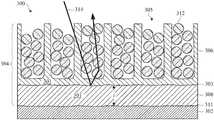
- FIG. 2illustrates a cross section view of a surface portion of anodized part 200 , showing how light can become trapped within a standard colored anodized film 204 .
- Part 200includes metal substrate 202 and anodic film 204 .
- Anodic film 204can be formed by an anodizing process, whereby surface portions of metal substrate 202 are converted to corresponding metal oxide material 201 .
- Anodic film 204includes porous layer 206 and barrier layer 208 .
- Porous layer 206includes pores 205 that are formed during the anodizing process.
- Barrier layer 208corresponds to a non-porous layer positioned between substrate 202 and porous layer 206 .
- Barrier layer 208is made of metal oxide material 201 but does not include pores 205 .
- Interface surface 203 of barrier layer 208has a shape that is partially defined by pore terminuses 207 of pores 205 .
- the curved shaped pore terminuses 207can cause interface surface 203 to have a scalloped geometry or shape.
- interface surface 203can be characterized as having a series of curved, hemispherical, cup-like features.
- pores 205will depend, in part, on the process conditions of the anodizing process. For type II anodizing processes, which involves anodizing in sulfuric acid solution, a typical diameter of pores 205 is on the scale of tens of nanometers—typically less than about 20 nanometers. Pores 205 can be filled with dye particles 209 , typically organic dye particles to impart a particular color to anodic film 204 and provide a colored finish to part 200 . Dye particles 209 have smaller diameters than the diameters of pores 205 so that dye particles 209 can fit within pores 205 .
- dye particles 209typically organic dye particles to impart a particular color to anodic film 204 and provide a colored finish to part 200 .
- Dye particles 209have smaller diameters than the diameters of pores 205 so that dye particles 209 can fit within pores 205 .
- One of the challenges associated with coloring anodic film 204is that it can be difficult to accomplish a visibly saturated, rich, highly opaque color. This is because metal oxide material 201 of anodic film 204 can be partially transparent to visible light. Thus, underlying metal substrate 202 can be visible through anodic film 204 . This can result in part 200 appearing a particular color from infused dye particles 209 as well as a having a metallic appearance from underlying substrate 202 , as viewed from surface 212 . This can give part 200 a silver or grey hue, which can be more apparent for lighter shades of dye particles 209 .
- light incident anodic film 204can become trapped within anodic film 204 due to the scalloped shaped interface surface 203 of barrier layer 208 .
- light ray 210 that is incident on anodic film 204can enter porous layer 206 and be locally scattered by the scalloped features of interface surface 203 . This means that light ray 210 cannot not reach and reflect off dye particles 209 , and therefore does not contribute to providing a desired color to anodic film 204 . That is, light ray 210 becomes trapped within anodic film 204 by the scalloped topology of interface surface 203 , thereby darkening the appearance of anodic film 204 .
- the methods described hereininvolved using different types of colorant and/or modifying features of anodic film 204 to increase the effectiveness of a colorant that is deposited within pores 205 .
- the methodsinvolve using a pigment as a colorant instead of a conventional organic or inorganic dye.
- the pigmentscan have a larger particle diameter than that of dye particles 209 and provide better coverage of the anodic film.
- the methodsinvolve smoothing interface surface 203 of barrier layer 208 to increase the amount of light that reaches dye particles 209 or other type of colorant.
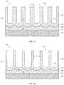
- FIGS. 3A-3Dillustrate cross section views of a surface portion of part 300 undergoing an anodic film coloration process in accordance with some embodiments.
- FIG. 3Ashows part 300 after an anodizing process, in which a portion of metal substrate 302 is converted to anodic film 304 that includes a corresponding metal oxide material 301 .
- Metal substrate 302can include an alloy, such as an aluminum alloy, to provide good strength and structural durability. If metal substrate 302 is aluminum or aluminum alloy, metal oxide material 301 includes aluminum oxide.
- the anodizing processis performed in phosphoric acid and/or oxalic acid solution, which can result in anodic film 304 having a wider pores 305 compared to anodizing in sulfuric acid solution (e.g., type II anodizing).
- Wider porescan accommodate more colorant and larger sized colorant particles, the advantages of which will be described in detail below.
- Wider porescan also be accomplished by using higher anodizing voltages compared to standard type II anodizing processes. The voltage will vary depending on the type of anodizing solution and other process parameters. In particular embodiments, an applied voltage of greater than 50 volts is used. In one embodiment, a phosphoric acid solution is used and a voltage of about 150 volts is used. It should be noted that anodic film 304 that pores 305 that are too wide, or that have too many pores, could impact the structural integrity of anodic film 304 . Thus, these considerations should be balanced when choosing the anodizing process parameters.
- a surface treatmentcan be applied to metal substrate 302 .
- a polishing operationcan be used to create a highly reflective surface on metal substrate 302 such that, once anodized, surface 311 of metal substrate 302 retains the highly reflective surface property.
- an etchinge.g., acidic or alkaline etching
- a textured surface on metal substrate 302which can also be retained by surface 311 .
- Anodic film 304includes porous layer 306 and barrier layer 308 .
- Porous layerincludes pores 305 while barrier layer 308 is substantially free of pores 305 .
- a target thickness of the porous layeris between about 6 and 20 micrometers.
- Barrier layer 308is positioned between porous layer 306 and metal substrate 302 , with interface surface 303 of barrier layer 308 defining the junction region between porous layer 306 and barrier layer 308 .
- Interface surface 303is defined in part by the shape of pore terminuses 307 .
- curved pore terminuses 307can cause interface surface 303 to have a series of scalloped-shaped features, which in three dimensions corresponds to a series of cup-like features. As described above with reference to FIG. 2 , this scalloped shaped interface surface 303 can trap incoming light.
- FIG. 3Bshows part 300 after an optional pore widening process, in which pores 305 are widened to accept more colorant.
- the pore widening processincludes exposing anodic film 304 to an electrolytic process in an acidic bath (e.g., phosphoric acid, sulfuric acid, sulfamic acid, oxalic acid) with a relatively weak voltage, which removes some of the metal oxide material 301 around pores 305 .
- an acidic bathe.g., phosphoric acid, sulfuric acid, sulfamic acid, oxalic acid
- a relatively weak voltagewhich removes some of the metal oxide material 301 around pores 305 .
- a phosphoric acid solutionhaving a concentration of between about 2% and 30% is used.
- ultrasonic wavesare applied while the voltage is applied. It should be noted, however, that other types of solutions and techniques can also cause widening of pores 305 .
- the resultant anodic film 304is characterized as having a pore diameter D that is greater than the pore diameter d prior to the pore widening process.
- a number of factorsshould be considered as to the extent of widening pores 305 . That is, it may be desirable to widen pores 305 as much as possible to accommodate more colorant and thereby increase the relative amount of colorant within anodic film 304 .
- widening pores 305 to a very large extentcan negatively affect the structural integrity of anodic film 304 .
- the process conditions of the anodizing processcould depend on whether a pore widening process is performed.
- the anodizing processis performed in an oxalic acid solution (e.g., about 30 g/L to about 50 g/L concentration held at about 20 degrees C. to about 40 degrees C.) using a voltage of about 30V to about 80V.
- This oxalic acid anodizing processcan result in a pore diameter d that is smaller than that using a similar process with a phosphoric acid solution.
- pore widening performed after such an oxalic acid anodizing processcan result in the same or wider pore diameter D compared to that of a phosphoric acid anodizing process without a pore widening process.
- the oxalic acid anodizing and pore widening processcan result in a more structurally sound anodic film 304 compared to that of a phosphoric acid anodizing process without a pore widening process.
- FIG. 3Cshows part 300 after a barrier layer smoothing process is performed, in which interface surface 303 of barrier layer 308 is smoothed.
- the shape of pore terminuses 307can be smoothed and flattened compared to the curved shape prior to the smoothing process.
- the smoothing processinvolves exposing part 300 to an electrolytic process where part 300 acts as an anode in a solution that promotes anodic film growth without substantially promoting anodic film dissolution, i.e., a non-pore-forming electrolyte.
- the solutioncontains one or more of sodium borate (borax), boric acid and tartaric acid solution.
- borateborate
- boric acidtartaric acid solution
- the solutioncontains between about 10 to 20 g/L of sodium borate and has a pH of about 9. In some embodiments, the solution contains between about 10 and 20 g/L of boric acid and has a pH of about 6.
- the temperature of the solutioncan vary. In some embodiments, the solution is held at about 25 degrees Celsius.
- an alternating current (AC)of between about 100 and 400 volts is applied.
- a direct current (DC)of between about 100 and 200 volts is applied.
- the voltagecan vary depending on other process parameters—in some embodiments the voltage is between about 50 and 400 volts. The result is a flattening or partial flattening of the scalloped projections of interface surface 303 .
- part 300acts as the anode and a further portion of metal substrate 302 is converted to metal oxide material 301 .
- the barrier layer smoothing processcan be coupled with thickening of barrier layer 308 .
- the amount of smoothing of interface surface 303can be proportion to the amount of thickening of barrier layer 308 .
- the thickness t of barrier layer 308can be measured using scanning electron microscopy (SEM) images of cross sections samples, which are described below with reference to FIGS. 5A and 5B .
- barrier layer 308prior to the barrier layer smoothing process, barrier layer 308 has a thickness t of about 110 nanometers or less, and after the barrier layer smoothing process barrier layer 308 has a thickness t of greater than about 150 nanometers. In some embodiments, barrier layer 308 is grown to a thickness t of between about 150 and 500 nanometers. It should be noted that the smoothing process ( FIG. 3C ) can be performed before or after the pore widening process ( FIG. 3B ). In some cases, however, the smoothing process is performed after the pore widening process since doing so can result in a smoother barrier layer 308 .
- the thickening of barrier layer 308can also be used to some advantage with regard to a final perceived color of anodic film 304 and part 300 .
- the thickness of barrier layer 308can be tuned to create an interference effect with incoming light, adding a predetermined perceived hue to anodic film 304 .
- interference coloration effectsare described in detail in application Ser. No. 14/312,502, which is incorporated by reference herein in its entirety. It should be noted that it may be beneficial to use generally higher voltages during electrolytic process when optimizing for smoothness of interface surface 303 compared to the voltages used for tuning a thickness of barrier layer 308 for a particular interference coloring effect described in application Ser. No. 14/312,502.
- FIG. 3Dshows part 300 after colorant particles 312 are deposited within pores 305 . Since the scalloped or cup-shaped geometry of interface surface 303 has been attenuated and flattened, incident light, which would previously have been trapped within anodic film 304 , reflects off interface surface 303 and onto colorant particles 312 . To illustrate, light ray 314 that is incident on anodic film 304 can enter porous layer 306 , reflect off interface surface 303 onto colorant particle 312 , and a portion of light ray 314 that is not absorbed by colorant particle 312 is reflected out of anodic film 304 where it is perceived as color. That is, smoothed interface surface 303 is sufficiently smooth to direct light ray 314 toward colorant particles 312 .
- colorant particles 312primarily reflect visible wavelengths of light corresponding to a blue color, colorant particles 312 will appear a blue color. If colorant particles 312 absorb substantially all visible wavelengths of light, colorant particles 312 will appear black. Similarly, if colorant particles 312 reflect substantially all visible wavelengths of light, colorant particles 312 will appear white. In some cases, colorant particles 312 include a mixture of different particles that reflect different wavelengths of light, resulting a unique perceived color resulting from a blend of different colored colorant particles 312 .
- substrate surface 311it could be beneficial for substrate surface 311 to have a particular surface geometry in order to enhance the light absorption and reflection qualities of colorant particles 312 .
- substrate surface 311 having a smooth and highly reflective geometrycan efficiently reflect incoming light to colorant particles 312 , thereby increasing an apparent color saturation, similar to as described above with respect to a smooth interface surface 303 . This may be important for bright colors such as white and brighter shades of red, blue, yellow, etc. However, for darker colors such as black or dark brown, a textured substrate surface 311 that traps light may be more desirable. In these cases, substrate surface 311 can be textured, such as by a chemical etch process prior to anodizing.
- Colorant particles 312can be made of any suitable color-imparting material or combination of materials, including organic or inorganic dyes, metals or combinations of dyes and metals.
- colorant particles 312are pigment particles that are generally larger than organic dye particles.
- titanium oxide (TiO 2 ) pigmentwhich can be used to create a white appearing anodic film 304 , can be available in particle sizes having a diameter of about 50 to 60 nanometers. This can be compared to many organic dyes that have a particle diameter of less than about 10 nanometers.
- Carbon black pigmentwhich can be used to create a black appearing anodic film 304 , can be available in particle sizes having a diameter of about 70 to 80 nanometers.
- Other pigments, such as blue, red and yellow pigmentscan have a particle diameter of about 50 to 100 nanometers.
- Colorant particles 312can be deposited within pores 305 using any suitable technique, and can depend on the type of colorant particles 312 .
- Pigmentsare a typically suspended in a solution and infused within pores 305 by immersing or dipping part 300 within the pigment suspension.
- the pigment particlesare suspended in an aqueous solution.
- the concentration of pigment and the pH of the pigment suspensioncan vary depending upon the type of pigment used. In some embodiments, the concentration is between about 5% and 40% by weight.
- the pH of the pigment suspensionis about 2.
- carbon black particlesthe pH of the pigment suspension is about 6.
- the pH of the pigment suspensionis between about 2 and 11.
- the larger pigment particlescan result in a richer, more saturated appearance.
- the optional pore widening process described above with reference to FIG. 3Bmay be necessary in order to fit and adequate amount of the larger pigment particles within pores 305 .
- the amount of pigment, or any colorant particles 312 , incorporated within anodic film 304is measured by weight % relative to the anodic film 304 . Since the weight % of colorant particles 312 can be proportional to an amount of perceived color saturation, this measurement can be used to predict how saturated and opaque anodic film 304 will appear.
- pigment particlese.g., titanium oxide and carbon black
- organic dyescan be susceptible to fading when exposed to ultraviolet (UV) light.
- pigmentssuch as titanium oxide and carbon black are generally resistant to UV fading.
- thickness t of barrier layercan be tuned to create light interference effects that can add a particular hue to anodic film 304 .
- thickness t of barrier layer 308can be tuned to have a thickness sufficient to reflect blue wavelengths of light by interference coloring effects.
- the interference coloringdoes not generally provide a strong coloring effect, but rather a hue or tint to the overall appearance of anodic film 304 .
- barrier layer 308 that provides a blue huecan counterbalance a yellow hue of metal oxide material 301 , resulting in a more color neutral appearance. In this way, a pure white appearance for anodic film 304 can be achieved.
- a final color of anodic film 304is measured and characterized using a CIE 1976 L*a*b* color space model measurements, which is described in detail in application Ser. No. 14/312,502.
- FIG. 4shows flowchart 400 indicating a process for forming and coloring an anodic film in accordance with some embodiments.
- a surface pretreatmentis optionally performed on a metal substrate.
- the surface treatmentcan be a polishing process that creates a mirror polished substrate surface, corresponding to a very uniform surface profile.
- the surface treatmentis an etching process that creates a textured surface that can have a matte appearance.
- Suitable etching processesinclude an alkaline etch, where the substrate is exposed to an alkaline solution (e.g., NaOH) for a predetermined time period for creating a desired texture.
- Acidic etching solutionse.g., NH 4 HF 2
- Polishing techniquescan include chemical polishing, which involves exposing the metal substrate to sulfuric acid and/or phosphoric acid solutions.
- the polishingincludes one or more mechanical polishing processes.
- the substrateis preferably polished rather than etched in order to create an underlying light reflective substrate surface.
- the substratecan be etched in order to purposely create an underlying light trap that traps incoming light.
- the substrateis anodized.
- the anodizingis performed in a phosphoric acid or oxalic acid solution, which can generally form wider pores than sulfuric anodizing processes.
- a phosphoric acid anodizing process using a voltage of between about 80 and 100is used to form an anodic film having a target thickness of about 10 micrometers.
- an oxalic acid anodizing process using a voltage of between about 20 and 120is used.
- an anodic film having a porous layer and a barrier layeris formed.
- the pores of the porous layerare optionally widened in order to accommodate more colorant in a subsequent colorant infusing process.
- the processcan include an electrolytic process within an acidic bath with a relatively weak applied voltage.
- the resultant anodic filmhas a pore diameter that is greater than the pore diameter prior to the pore widening process.
- the pore widening processmay be more beneficial for those coloring process that include larger pigment particles.
- one or more of the following chemicalsare be used in solution for the barrier layer smoothing electrolytic process: Na 2 B 4 O 5 (OH) 4 .8H 2 O (borax), H 3 BO 3 (boric acid), NH 4 ) 2 O.5B 2 O 3 .8H 2 O (Ammonium pentaborate octahydrate), (NH 4 ) 2 B 4 O 7 .4H 2 O (ammonium tetraborate tetrahydrate), C 6 H 10 O 4 (hexanedioic acid), C 6 H 16 N 2 O 4 (ammonium adipate), (NH 4 ) 2 C 4 H 4 O 6 (ammonium tartrate), C 6 H 8 O 7 (citric acid), C 4 H 4 O 4 (maleic acid), C 2 H 4 O 3 (glycolic acid), C 6 H 4 (COOH) 2 (phthalic acid), Na 2 CO 3 (sodium carbonate), [SiO x (OH) 4-2x ] n (siliconium salt),
- the applied voltage of the barrier layer electrolyzing processcan vary depending on a desired amount of smoothing and/or a desired final thickness of the barrier layer. In some embodiments, the applied voltage is greater than about 50 volts. In some embodiments, the applied voltage is between about 50 and 400 volts. In some embodiments, a final thickness of the barrier layer is chosen to create a predetermined color hue by light interference effects.
- a colorantis deposited within the pores of the anodic film.
- the colorantimparts a color to the anodic film by absorbing certain wavelengths of visible light and reflecting other wavelengths of visible light.
- the colorantincludes an organic dye or metal.
- the colorantincludes pigment particles having a particle diameter greater than about 50 nanometers.
- the colorantincludes a combination of pigment, dye and/or metal colorant.
- the chemical composition of the colorantwill depend, in part, on a desired final color of the anodic film.
- the smoothed interface surface of the barrier layer that underlies the porous layer of the anodic filmacts to reflect light onto the colorant, thereby enhancing the coloring effect of the colorant. In particular, more the more reflective interface surface can cause more light to be absorbed and reflected by the colorant.
- a carbon black colorantis used to impart a black color to the anodic film with a target L* value of about 30 or less, where L* corresponds to an amount of lightness measured using CIE D65 color space standards.
- L*corresponds to an amount of lightness measured using CIE D65 color space standards.
- measurement using standard CIE D65 color space techniquesmay effective to some extent but may be limited in other aspects.
- an L* valuecan be used to determine an amount of lightness of the anodic film (i.e., the amount of light reflected by the anodic film and underlying substrate).
- L* value alonemay not be an accurate indication of an amount of white color saturation. That is, high L* values can also be attributed by a highly reflective underlying substrate surface, but the part will appear to have some silver or greyness from the underlying substrate and may not appear as a saturated white color.
- Another method of measuring whiteness of an anodized partis using ASTM E313 standard practice, which is used to calculate yellowness and whiteness indices.
- a further way to measure whitenessis by using human visual inspection, where colorized anodized parts are visually compared to one another for perceived whiteness and color saturation.
- the pores of the anodic filmare optionally sealed using a sealing process.
- the sealing processcan lock in the colorant and provide a more durable anodic film. Any suitable sealing process can be used.
- a sealing solution containing Okuno Chemical H298manufactured by Okuno Chemical Industries Co., Ltd., based in Japan).
- FIGS. 5A and 5Bshow SEM images of cross sections of anodic film samples prior to and after exposure to a barrier smoothing process in accordance with some embodiments.
- FIG. 5Ashows anodic film 502 , positioned on substrate 504 , after an anodizing process but prior to a barrier layer smoothing process.
- Anodic film 502includes porous layer 506 and barrier layer 508 .
- interface surface 510 of barrier layer 508 and pore terminuses 512have scalloped shapes, with each scallop feature corresponding to a hemispherical cup-like feature in three-dimensions. This scalloped geometry can cause incident light to become trapped within anodic film 502 .
- Barrier layer 508has a thickness of about 106 nanometers, as measured by the SEM image.
- FIG. 5Bshows anodic film 522 , positioned on substrate 524 , after a barrier layer smoothing process.
- Anodic film 522includes porous layer 526 and barrier layer 528 .
- interface surface 530 of barrier layer 528 and pore terminuses 532are smooth and relatively flat compared to the curved, scalloped geometry prior to the smoothing process ( FIG. 5A ).
- Barrier layer 528has a thickness of about 484 nanometers, indicating that the smoothing process is associated with a thickening of barrier layer 508 .
Landscapes
- Chemical & Material Sciences (AREA)
- Engineering & Computer Science (AREA)
- Chemical Kinetics & Catalysis (AREA)
- Electrochemistry (AREA)
- Materials Engineering (AREA)
- Metallurgy (AREA)
- Organic Chemistry (AREA)
- Microelectronics & Electronic Packaging (AREA)
- General Chemical & Material Sciences (AREA)
- Inorganic Chemistry (AREA)
- Other Surface Treatments For Metallic Materials (AREA)
- Laminated Bodies (AREA)
Abstract
Description
Claims (7)
Priority Applications (1)
| Application Number | Priority Date | Filing Date | Title |
|---|---|---|---|
| US15/333,058US10781529B2 (en) | 2015-10-30 | 2016-10-24 | Anodized films with pigment coloring |
Applications Claiming Priority (2)
| Application Number | Priority Date | Filing Date | Title |
|---|---|---|---|
| US201562249079P | 2015-10-30 | 2015-10-30 | |
| US15/333,058US10781529B2 (en) | 2015-10-30 | 2016-10-24 | Anodized films with pigment coloring |
Publications (2)
| Publication Number | Publication Date |
|---|---|
| US20170121838A1 US20170121838A1 (en) | 2017-05-04 |
| US10781529B2true US10781529B2 (en) | 2020-09-22 |
Family
ID=58456159
Family Applications (3)
| Application Number | Title | Priority Date | Filing Date |
|---|---|---|---|
| US15/333,070Active2037-07-03US10760175B2 (en) | 2015-10-30 | 2016-10-24 | White anodic films with multiple layers |
| US15/333,058Active2037-03-19US10781529B2 (en) | 2015-10-30 | 2016-10-24 | Anodized films with pigment coloring |
| US15/333,072AbandonedUS20170121837A1 (en) | 2015-10-30 | 2016-10-24 | Anodic films for high performance aluminum alloys |
Family Applications Before (1)
| Application Number | Title | Priority Date | Filing Date |
|---|---|---|---|
| US15/333,070Active2037-07-03US10760175B2 (en) | 2015-10-30 | 2016-10-24 | White anodic films with multiple layers |
Family Applications After (1)
| Application Number | Title | Priority Date | Filing Date |
|---|---|---|---|
| US15/333,072AbandonedUS20170121837A1 (en) | 2015-10-30 | 2016-10-24 | Anodic films for high performance aluminum alloys |
Country Status (6)
| Country | Link |
|---|---|
| US (3) | US10760175B2 (en) |
| JP (3) | JP6697077B2 (en) |
| CN (1) | CN108350598B (en) |
| DE (1) | DE202016006606U1 (en) |
| TW (1) | TWM554103U (en) |
| WO (1) | WO2017074877A2 (en) |
Cited By (2)
| Publication number | Priority date | Publication date | Assignee | Title |
|---|---|---|---|---|
| US11549190B2 (en) | 2018-07-31 | 2023-01-10 | Uacj Corporation | Aluminum member and method of manufacturing aluminum member |
| US12150263B2 (en) | 2021-03-23 | 2024-11-19 | Samsung Electronics Co., Ltd. | Electronic device including metal housing |
Families Citing this family (42)
| Publication number | Priority date | Publication date | Assignee | Title |
|---|---|---|---|---|
| US9512536B2 (en) | 2013-09-27 | 2016-12-06 | Apple Inc. | Methods for forming white anodized films by metal complex infusion |
| JP5738374B2 (en) | 2013-09-27 | 2015-06-24 | 住友理工株式会社 | Glass fiber reinforced thermoplastic resin molded article and method for producing the same |
| WO2016111693A1 (en) | 2015-01-09 | 2016-07-14 | Apple Inc. | Processes to reduce interfacial enrichment of alloying elements under anodic oxide films and improve anodized appearance of heat treatable alloys |
| JP6067767B2 (en)* | 2015-03-26 | 2017-01-25 | 住友理工株式会社 | Glass fiber reinforced thermoplastic resin molded article and method for producing the same |
| US10760175B2 (en) | 2015-10-30 | 2020-09-01 | Apple Inc. | White anodic films with multiple layers |
| US10174436B2 (en)* | 2016-04-06 | 2019-01-08 | Apple Inc. | Process for enhanced corrosion protection of anodized aluminum |
| US11352708B2 (en) | 2016-08-10 | 2022-06-07 | Apple Inc. | Colored multilayer oxide coatings |
| US11242614B2 (en) | 2017-02-17 | 2022-02-08 | Apple Inc. | Oxide coatings for providing corrosion resistance on parts with edges and convex features |
| EP3428955A1 (en)* | 2017-07-10 | 2019-01-16 | Murata Manufacturing Co., Ltd. | Substrates employing surface-area amplification, for use in fabricating capacitive elements and other devices |
| WO2019022924A2 (en)* | 2017-07-26 | 2019-01-31 | Pacific Light & Hologram, Inc. | Low reflection articles and related systems and methods |
| US10669642B2 (en) | 2017-09-25 | 2020-06-02 | Apple Inc. | Using dispersion agents to chemically stabilize dyeing of metal parts |
| JP6474878B1 (en)* | 2017-11-28 | 2019-02-27 | 株式会社Uacj | Aluminum member and manufacturing method thereof |
| JP6991480B2 (en)* | 2017-12-20 | 2022-02-03 | 兵庫県公立大学法人 | White structure and its manufacturing method |
| US11389903B2 (en)* | 2018-03-30 | 2022-07-19 | Apple Inc. | Electronic device marked using laser-formed pixels of metal oxides |
| US11795564B2 (en)* | 2018-08-17 | 2023-10-24 | Apple Inc. | Dye solution alternatives for reduced dye uptake in anodized layers |
| US11549191B2 (en) | 2018-09-10 | 2023-01-10 | Apple Inc. | Corrosion resistance for anodized parts having convex surface features |
| US11312107B2 (en)* | 2018-09-27 | 2022-04-26 | Apple Inc. | Plugging anodic oxides for increased corrosion resistance |
| KR20200048769A (en)* | 2018-10-30 | 2020-05-08 | 엘지전자 주식회사 | Laundry Treating Apparatus |
| US11371157B2 (en)* | 2018-11-30 | 2022-06-28 | Apple Inc. | Process for incorporating zinc into a dyed anodized layer for protecting dye colorants from light exposure |
| JP6584626B1 (en)* | 2018-11-30 | 2019-10-02 | 株式会社Uacj | Aluminum member and manufacturing method thereof |
| WO2020160690A1 (en)* | 2019-02-08 | 2020-08-13 | Hewlett-Packard Development Company, L.P. | Surface treatments |
| WO2020205839A1 (en)* | 2019-04-01 | 2020-10-08 | Technology Applications Group, Inc. | Anodized coating for magnesium |
| US11268188B2 (en)* | 2019-05-02 | 2022-03-08 | Apple Inc. | Aluminum physical vapor deposition for the cosmetic finishing of recycled aluminum alloys |
| KR102204255B1 (en)* | 2019-08-12 | 2021-01-18 | 동의대학교 산학협력단 | Manufacturing method of superhydrophobic 6000 aluminum alloy for engines and automobile wheels |
| CN110528045A (en)* | 2019-08-21 | 2019-12-03 | 歌尔股份有限公司 | The surface treatment method of metal material |
| WO2021048932A1 (en)* | 2019-09-10 | 2021-03-18 | 株式会社エイエムジー | Cosmetic container and method for producing cosmetic container |
| CN112492782A (en)* | 2019-09-12 | 2021-03-12 | 北京小米移动软件有限公司 | Metal shell and surface treatment method thereof |
| CN110528043B (en)* | 2019-09-17 | 2021-05-07 | 蓝思精密(东莞)有限公司 | Sweat-proof liquid treatment process for metal sheet, metal shell and electronic equipment |
| JP7532132B2 (en) | 2019-09-30 | 2024-08-13 | キヤノン株式会社 | Optical member, optical device, imaging device, and method for manufacturing optical member |
| TWI729590B (en)* | 2019-11-27 | 2021-06-01 | 友達光電股份有限公司 | Low light reflecting device chip package structure and manufacturing method thereof |
| EP4592428A2 (en) | 2020-08-27 | 2025-07-30 | Carrier Corporation | Methods of anodizing the internal surface of heat transfer tubes |
| JP7588031B2 (en)* | 2021-05-19 | 2024-11-21 | 日立Astemo株式会社 | Electronic Control Unit |
| DE102021119472A1 (en) | 2021-07-27 | 2023-02-02 | Martin Fiedler | Method of making an anodized aluminum article |
| CN113602035B (en)* | 2021-07-29 | 2022-08-09 | Oppo广东移动通信有限公司 | Ceramic decorative film, preparation method thereof, shell assembly and electronic equipment |
| KR102748306B1 (en)* | 2021-10-05 | 2024-12-31 | 주식회사 영광와이케이엠씨 | Photonic crystal composites with variable structural color and Manufacturing method thereof |
| WO2023089824A1 (en)* | 2021-11-22 | 2023-05-25 | 日本軽金属株式会社 | Aluminum member and method for producing same |
| JP2023158363A (en)* | 2022-04-18 | 2023-10-30 | 日本軽金属株式会社 | Aluminum member and its manufacturing method |
| WO2023211032A1 (en)* | 2022-04-25 | 2023-11-02 | 삼성전자 주식회사 | Method for implementing structural color, and electronic device comprising structural color |
| FR3150213B3 (en) | 2023-06-20 | 2025-06-06 | Vacheron Frederic | Method for treating a part made of aluminum or aluminum alloy, part obtained by implementing such a method, and anodizing bath for implementing such a method |
| WO2025033666A1 (en)* | 2023-08-07 | 2025-02-13 | 삼성전자주식회사 | Electronic device including housing having oxide layer, and manufacturing method therefor |
| WO2025079994A1 (en)* | 2023-10-12 | 2025-04-17 | 삼성전자 주식회사 | Electronic device comprising housing |
| WO2025182328A1 (en)* | 2024-02-27 | 2025-09-04 | 株式会社豊田中央研究所 | Electric wiring member and method for manufacturing same |
Citations (83)
| Publication number | Priority date | Publication date | Assignee | Title |
|---|---|---|---|---|
| US2231373A (en) | 1935-01-08 | 1941-02-11 | Firm Ematal Electrochemical Co | Coating of articles of aluminum or aluminum alloys |
| CH221939A (en) | 1937-11-24 | 1942-06-30 | Max Dr Schenk | Process for the production of opaque, almost white and colorable layers on objects made of aluminum and aluminum alloys. |
| US3382160A (en) | 1960-03-31 | 1968-05-07 | Asada Tahei | Process for inorganically coloring aluminum |
| AT262714B (en) | 1964-12-29 | 1968-06-25 | Gen Electric | Process for producing a durable, scratch-resistant surface on a metallic workpiece |
| US3524799A (en) | 1969-06-13 | 1970-08-18 | Reynolds Metals Co | Anodizing aluminum |
| DE2262426A1 (en) | 1971-12-24 | 1973-07-12 | Dainichiseika Color Chem | METHOD OF COLORING ALUMINUM OR ALUMINUM ALLOYS |
| US3798193A (en)* | 1972-09-28 | 1974-03-19 | American Cyanamid Co | Process for preparing an electrocoating composition |
| US3962049A (en) | 1971-05-13 | 1976-06-08 | Kabushiki Kaisha Aiden | Process for coloring aluminum anodic oxide film |
| JPS5287364A (en) | 1976-01-14 | 1977-07-21 | Sankyo Aruminiumu Kougiyou Kk | Method of forming opaque white positive pole oxide layer of aluminum |
| US4066816A (en) | 1975-07-16 | 1978-01-03 | Alcan Research And Development Limited | Electrolytic coloring of anodized aluminium by means of optical interference effects |
| US4251330A (en) | 1978-01-17 | 1981-02-17 | Alcan Research And Development Limited | Electrolytic coloring of anodized aluminium by means of optical interference effects |
| AT365245B (en) | 1978-01-17 | 1981-12-28 | Alcan Res & Dev | ALUMINUM OBJECT AND METHOD FOR THE PRODUCTION THEREOF |
| JPS5792194A (en) | 1980-12-01 | 1982-06-08 | Nippon Light Metal Co Ltd | Formation of opaque white film on aluminum |
| US4526671A (en) | 1982-09-24 | 1985-07-02 | Pilot Man-Nen-Hitsu Kabushiki Kaisha | Surface treatment of aluminum or aluminum alloys |
| US4606796A (en) | 1983-01-24 | 1986-08-19 | Asahi Malleable Iron Co., Ltd. | Colored, anodized aluminum-base article and method of preparing same |
| JPS6220896A (en) | 1985-07-18 | 1987-01-29 | Nippon Light Metal Co Ltd | Anti-corrosion bright surface treatment method for aluminum castings |
| US4687551A (en) | 1984-10-17 | 1987-08-18 | Alcan International Limited | Porous films and method of forming them |
| US4702955A (en) | 1985-07-24 | 1987-10-27 | Ovonic Synthetic Materials Company, Inc. | Multilayer decorative coating |
| JPS62263996A (en) | 1986-05-12 | 1987-11-16 | Nippon Alum Mfg Co Ltd:The | Dyed film on aluminum and aluminum alloy |
| US4773717A (en) | 1986-11-03 | 1988-09-27 | Ovonic Synthetic Materials Co. | Transparency having a second surface multilayer decorative coating |
| WO1991002830A1 (en) | 1989-08-17 | 1991-03-07 | Wolf, David | Improved electrolytic method for coloring anodized aluminum |
| US5066368A (en) | 1990-08-17 | 1991-11-19 | Olin Corporation | Process for producing black integrally colored anodized aluminum components |
| US5124172A (en) | 1989-04-28 | 1992-06-23 | Alcan International Limited | Thin film diagnostic device |
| WO1992019795A1 (en) | 1991-05-07 | 1992-11-12 | Alcan International Limited | Process for producing articles comprising anodized films exhibiting areas of different colour and the articles thus produced |
| US5167793A (en)* | 1991-05-07 | 1992-12-01 | Alcan International Limited | Process for producing anodic films exhibiting colored patterns and structures incorporating such films |
| US5218472A (en) | 1989-03-22 | 1993-06-08 | Alcan International Limited | Optical interference structures incorporating porous films |
| US5250173A (en) | 1991-05-07 | 1993-10-05 | Alcan International Limited | Process for producing anodic films exhibiting colored patterns and structures incorporating such films |
| JPH06200399A (en) | 1992-12-28 | 1994-07-19 | Agency Of Ind Science & Technol | Aluminum or aluminum alloy functional material |
| US5472788A (en) | 1994-07-14 | 1995-12-05 | Benitez-Garriga; Eliseo | Colored anodized aluminum and electrolytic method for the manufacture of same |
| US5510015A (en) | 1992-12-31 | 1996-04-23 | Novamax Technologies Holdings, Inc. | Process for obtaining a range of colors of the visible spectrum using electrolysis on anodized aluminium |
| JPH09143795A (en) | 1995-11-14 | 1997-06-03 | Nippon Light Metal Co Ltd | Electrolytic coloring method of aluminum material |
| US5800693A (en) | 1995-12-21 | 1998-09-01 | Sony Corporation | Method for surface-treating substrate and substrate surface-treated by the method |
| JPH111797A (en) | 1997-06-09 | 1999-01-06 | Kobe Steel Ltd | Vacuum chamber member made of al or al alloy |
| US5904989A (en) | 1996-04-18 | 1999-05-18 | Alusuisse Technology & Management Ltd. | Aluminum surface with interference colors |
| US6027629A (en) | 1994-11-16 | 2000-02-22 | Kabushiki Kaisha Kobe Seiko Sho | Vacuum chamber made of aluminum or its alloys, and surface treatment and material for the vacuum chamber |
| WO2001018281A1 (en) | 1999-09-07 | 2001-03-15 | Alcan International Limited | Rapid colouring process for aluminum products |
| US6379523B1 (en) | 1998-07-07 | 2002-04-30 | Izumi Techno Inc. | Method of treating surface of aluminum blank |
| US20020182538A1 (en) | 2000-12-20 | 2002-12-05 | Tadabumi Tomita | Lithographic printing plate precursor |
| EP0975827B9 (en) | 1997-04-25 | 2004-07-14 | Alcan International Limited | Aluminium workpiece |
| US20050029115A1 (en)* | 2003-08-06 | 2005-02-10 | Hong-Hsiang Kuo | Method for producing hard surface, colored, anodized aluminum parts |
| JP2005060720A (en) | 2003-08-08 | 2005-03-10 | Toyota Central Res & Dev Lab Inc | Aluminum-based member, method for manufacturing the same, and surface treatment method for aluminum-based member |
| US20050221712A1 (en) | 2000-09-20 | 2005-10-06 | Canon Kabushiki Kaisha | Structures, electron-emitting devices, image-forming apparatus, and methods of producing them |
| US20060019035A1 (en) | 2003-03-31 | 2006-01-26 | Sheffield Hallam University | Base for decorative layer |
| JP2006057493A (en) | 2004-08-18 | 2006-03-02 | Nissan Motor Co Ltd | Exhaust purification device |
| US7173276B2 (en) | 2003-09-08 | 2007-02-06 | Lg Chem, Ltd. | Highly efficient organic light emitting device using substrate having nanosized hemispherical recesses and method for preparing the same |
| JP2007314840A (en) | 2006-05-26 | 2007-12-06 | Aisin Keikinzoku Co Ltd | Surface treatment method for imparting aluminum alloy superior hydrophilicity |
| JP2007325995A (en) | 2006-06-06 | 2007-12-20 | Univ Kinki | Photocatalyst film and method for producing the same |
| US20080213618A1 (en) | 2005-01-10 | 2008-09-04 | Short Brothers Plc | Anodising Aluminum Alloy |
| DE102008011298A1 (en) | 2007-03-16 | 2008-09-18 | Süddeutsche Aluminium Manufaktur GmbH | Partial pigmentation of a cover layer to avoid interference with aluminum components or aluminum-containing components |
| JP2008223073A (en) | 2007-03-12 | 2008-09-25 | Osaka Industrial Promotion Organization | Porous nano-structure and manufacturing method therefor |
| US20080274375A1 (en) | 2007-05-04 | 2008-11-06 | Duracouche International Limited | Anodizing Aluminum and Alloys Thereof |
| US20090247668A1 (en)* | 2006-07-12 | 2009-10-01 | Kotaro Sumitomo | Process for production of black crayon |
| JP2009248485A (en) | 2008-04-08 | 2009-10-29 | Corona Kogyo Co Ltd | Method for manufacturing aluminum-based member, aluminum-based member, and cover of mobile telephone |
| JP2009256778A (en) | 2008-03-27 | 2009-11-05 | Aisin Seiki Co Ltd | Method for forming alumite film and alumite film |
| US7715086B2 (en) | 2005-06-03 | 2010-05-11 | Fuji Xerox Co., Ltd. | Display method, and display medium and display device using the method thereof |
| US20100276288A1 (en) | 2007-10-10 | 2010-11-04 | Nederlandse Organisatie Voor Toegepast-Natuurweten Schappelijk Onderzoek Tno | Corrosion protective layer |
| US20100328201A1 (en) | 2004-03-23 | 2010-12-30 | Fujitsu Limited | Gesture Based User Interface Supporting Preexisting Symbols |
| US20110060652A1 (en) | 2009-09-10 | 2011-03-10 | Morton Timothy B | System and method for the service of advertising content to a consumer based on the detection of zone events in a retail environment |
| US20120073973A1 (en) | 2010-09-24 | 2012-03-29 | Fujifilm Corporation | Anisotropically conductive member |
| WO2012119306A1 (en) | 2011-03-08 | 2012-09-13 | Nano And Advanced Materials Institute Limited | Method for Producing White Anodized Aluminum Oxide |
| US20130078399A1 (en) | 2011-09-26 | 2013-03-28 | Fih (Hong Kong) Limited | Method for making housing and housing made by same |
| US20130081952A1 (en) | 2011-09-29 | 2013-04-04 | Denkahimakukougyou Co., Ltd. | Method for manufacturing colored aluminum product or colored aluminum alloy product, pigment composition for coloration, and colored aluminum product or colored aluminum alloy product |
| US20130153429A1 (en) | 2009-07-24 | 2013-06-20 | Apple Inc. | Dual anodization surface treatment |
| US20130153428A1 (en) | 2011-12-20 | 2013-06-20 | Apple Inc. | Metal Surface and Process for Treating a Metal Surface |
| US20130168253A1 (en) | 2010-10-21 | 2013-07-04 | Peter Mardilovich | Nano-structure and method of making the same |
| US20130192588A1 (en) | 2010-03-23 | 2013-08-01 | Odb-Tec Gmbh & Co. Kg | Method and Device for Producing a Highly Selectively Absorbing Coating on a Solar Absorber Component and Solar Absorber Having Such Coating |
| US20130328762A1 (en) | 2012-06-12 | 2013-12-12 | Daniel J. McCulloch | Controlling a virtual object with a real controller device |
| US8665075B2 (en) | 2009-10-26 | 2014-03-04 | At&T Intellectual Property I, L.P. | Gesture-initiated remote control programming |
| US20140076600A1 (en) | 2012-09-14 | 2014-03-20 | Apple Inc. | Changing colors of materials |
| US20140193607A1 (en) | 2012-06-22 | 2014-07-10 | Apple Inc. | White appearing anodized films and methods for forming the same |
| US20140262790A1 (en) | 2013-03-12 | 2014-09-18 | Thomas Levendusky | Colored, corrosion-resistant aluminum alloy substrates and methods for producing same |
| US20150016030A1 (en) | 2013-07-12 | 2015-01-15 | Apple Inc. | Reducing appearance of physical damage on cosmetic surfaces |
| WO2015047635A1 (en) | 2013-09-27 | 2015-04-02 | Apple Inc. | Methods for forming white anodized films by metal complex infusion |
| WO2015047634A1 (en) | 2013-09-27 | 2015-04-02 | Apple Inc. | Methods for forming white anodized films by forming branched pore structures |
| TWI496955B (en) | 2012-03-22 | 2015-08-21 | Hon Hai Prec Ind Co Ltd | Anodic oxidation method for colouring metallic workpiece |
| JP2015161012A (en) | 2014-02-28 | 2015-09-07 | 株式会社サクラクレパス | Colored aluminum molding and production method thereof |
| US20150277097A1 (en) | 2014-03-28 | 2015-10-01 | Qualcomm Mems Technologies, Inc. | Flexible ems device using organic materials |
| US20150368823A1 (en) | 2014-06-23 | 2015-12-24 | Apple Inc. | Interference coloring of thick, porous, oxide films |
| WO2016005649A1 (en) | 2014-07-09 | 2016-01-14 | Nokia Technologies Oy | Device control |
| EP2649224B1 (en) | 2010-12-06 | 2016-03-23 | Bang & Olufsen A/S | A method to obtain a radiation scattering surface finish on an object |
| EP1432849B1 (en) | 2001-10-02 | 2016-05-11 | Henkel AG & Co. KGaA | Light metal anodization |
| US20160312374A1 (en) | 2013-12-20 | 2016-10-27 | Dublin Institute Of Technology | Method for forming a multi-layer anodic coating |
| US20170121836A1 (en) | 2015-10-30 | 2017-05-04 | Apple Inc. | White anodic films with multiple layers |
Family Cites Families (5)
| Publication number | Priority date | Publication date | Assignee | Title |
|---|---|---|---|---|
| JP2706681B2 (en)* | 1992-05-29 | 1998-01-28 | 新日軽株式会社 | Electrolytic coloring method of aluminum material |
| JP2931177B2 (en)* | 1993-03-18 | 1999-08-09 | 日本軽金属株式会社 | Highly transparent colored film and electrolytic coloring method |
| JP3410548B2 (en)* | 1994-06-02 | 2003-05-26 | 株式会社サクラクレパス | Pigment dispersion for coloring aluminum or aluminum alloy oxide film |
| FR2967563B1 (en)* | 2010-11-19 | 2013-08-23 | Seb Sa | PROCESS FOR OBTAINING A COOKING CONTAINER COMPRISING A HARD-COLORED ANODIZED EXTERIOR |
| CN103635611A (en)* | 2011-07-04 | 2014-03-12 | 富士胶片株式会社 | Insulating reflective substrate and method for producing same |
- 2016
- 2016-10-24USUS15/333,070patent/US10760175B2/enactiveActive
- 2016-10-24WOPCT/US2016/058529patent/WO2017074877A2/ennot_activeCeased
- 2016-10-24USUS15/333,058patent/US10781529B2/enactiveActive
- 2016-10-24JPJP2018521261Apatent/JP6697077B2/enactiveActive
- 2016-10-24CNCN201680064003.9Apatent/CN108350598B/enactiveActive
- 2016-10-24USUS15/333,072patent/US20170121837A1/ennot_activeAbandoned
- 2016-10-26DEDE202016006606.5Upatent/DE202016006606U1/enactiveActive
- 2016-10-28TWTW105216517Upatent/TWM554103U/ennot_activeIP Right Cessation
- 2016-10-31JPJP2016005257Upatent/JP3209960U/ennot_activeExpired - Fee Related
- 2020
- 2020-02-19JPJP2020026395Apatent/JP7044817B2/enactiveActive
Patent Citations (103)
| Publication number | Priority date | Publication date | Assignee | Title |
|---|---|---|---|---|
| US2231373A (en) | 1935-01-08 | 1941-02-11 | Firm Ematal Electrochemical Co | Coating of articles of aluminum or aluminum alloys |
| CH221939A (en) | 1937-11-24 | 1942-06-30 | Max Dr Schenk | Process for the production of opaque, almost white and colorable layers on objects made of aluminum and aluminum alloys. |
| US3382160A (en) | 1960-03-31 | 1968-05-07 | Asada Tahei | Process for inorganically coloring aluminum |
| AT262714B (en) | 1964-12-29 | 1968-06-25 | Gen Electric | Process for producing a durable, scratch-resistant surface on a metallic workpiece |
| US3524799A (en) | 1969-06-13 | 1970-08-18 | Reynolds Metals Co | Anodizing aluminum |
| US3962049A (en) | 1971-05-13 | 1976-06-08 | Kabushiki Kaisha Aiden | Process for coloring aluminum anodic oxide film |
| DE2262426A1 (en) | 1971-12-24 | 1973-07-12 | Dainichiseika Color Chem | METHOD OF COLORING ALUMINUM OR ALUMINUM ALLOYS |
| US3844908A (en) | 1971-12-24 | 1974-10-29 | Dainichiseika Color Chem | Process for coloring aluminum and aluminum alloys |
| US3798193A (en)* | 1972-09-28 | 1974-03-19 | American Cyanamid Co | Process for preparing an electrocoating composition |
| US4066816A (en) | 1975-07-16 | 1978-01-03 | Alcan Research And Development Limited | Electrolytic coloring of anodized aluminium by means of optical interference effects |
| JPS5287364A (en) | 1976-01-14 | 1977-07-21 | Sankyo Aruminiumu Kougiyou Kk | Method of forming opaque white positive pole oxide layer of aluminum |
| AT365245B (en) | 1978-01-17 | 1981-12-28 | Alcan Res & Dev | ALUMINUM OBJECT AND METHOD FOR THE PRODUCTION THEREOF |
| US4251330A (en) | 1978-01-17 | 1981-02-17 | Alcan Research And Development Limited | Electrolytic coloring of anodized aluminium by means of optical interference effects |
| US4310586A (en) | 1978-01-17 | 1982-01-12 | Alcan Research And Development Limited | Aluminium articles having anodic oxide coatings and methods of coloring them by means of optical interference effects |
| JPS5792194A (en) | 1980-12-01 | 1982-06-08 | Nippon Light Metal Co Ltd | Formation of opaque white film on aluminum |
| US4526671A (en) | 1982-09-24 | 1985-07-02 | Pilot Man-Nen-Hitsu Kabushiki Kaisha | Surface treatment of aluminum or aluminum alloys |
| US4606796A (en) | 1983-01-24 | 1986-08-19 | Asahi Malleable Iron Co., Ltd. | Colored, anodized aluminum-base article and method of preparing same |
| US4687551A (en) | 1984-10-17 | 1987-08-18 | Alcan International Limited | Porous films and method of forming them |
| JPS6220896A (en) | 1985-07-18 | 1987-01-29 | Nippon Light Metal Co Ltd | Anti-corrosion bright surface treatment method for aluminum castings |
| US4702955A (en) | 1985-07-24 | 1987-10-27 | Ovonic Synthetic Materials Company, Inc. | Multilayer decorative coating |
| JPS62263996A (en) | 1986-05-12 | 1987-11-16 | Nippon Alum Mfg Co Ltd:The | Dyed film on aluminum and aluminum alloy |
| US4773717A (en) | 1986-11-03 | 1988-09-27 | Ovonic Synthetic Materials Co. | Transparency having a second surface multilayer decorative coating |
| US5218472A (en) | 1989-03-22 | 1993-06-08 | Alcan International Limited | Optical interference structures incorporating porous films |
| US5124172A (en) | 1989-04-28 | 1992-06-23 | Alcan International Limited | Thin film diagnostic device |
| WO1991002830A1 (en) | 1989-08-17 | 1991-03-07 | Wolf, David | Improved electrolytic method for coloring anodized aluminum |
| US5066368A (en) | 1990-08-17 | 1991-11-19 | Olin Corporation | Process for producing black integrally colored anodized aluminum components |
| WO1992019795A1 (en) | 1991-05-07 | 1992-11-12 | Alcan International Limited | Process for producing articles comprising anodized films exhibiting areas of different colour and the articles thus produced |
| US5167793A (en)* | 1991-05-07 | 1992-12-01 | Alcan International Limited | Process for producing anodic films exhibiting colored patterns and structures incorporating such films |
| US5250173A (en) | 1991-05-07 | 1993-10-05 | Alcan International Limited | Process for producing anodic films exhibiting colored patterns and structures incorporating such films |
| US5277982A (en) | 1991-05-07 | 1994-01-11 | Alcan International Limited | Process for producing anodic films exhibiting colored patterns and structures incorporating such films |
| JPH06200399A (en) | 1992-12-28 | 1994-07-19 | Agency Of Ind Science & Technol | Aluminum or aluminum alloy functional material |
| US5510015A (en) | 1992-12-31 | 1996-04-23 | Novamax Technologies Holdings, Inc. | Process for obtaining a range of colors of the visible spectrum using electrolysis on anodized aluminium |
| US5472788A (en) | 1994-07-14 | 1995-12-05 | Benitez-Garriga; Eliseo | Colored anodized aluminum and electrolytic method for the manufacture of same |
| US6027629A (en) | 1994-11-16 | 2000-02-22 | Kabushiki Kaisha Kobe Seiko Sho | Vacuum chamber made of aluminum or its alloys, and surface treatment and material for the vacuum chamber |
| JPH09143795A (en) | 1995-11-14 | 1997-06-03 | Nippon Light Metal Co Ltd | Electrolytic coloring method of aluminum material |
| US5800693A (en) | 1995-12-21 | 1998-09-01 | Sony Corporation | Method for surface-treating substrate and substrate surface-treated by the method |
| US5904989A (en) | 1996-04-18 | 1999-05-18 | Alusuisse Technology & Management Ltd. | Aluminum surface with interference colors |
| EP0975827B9 (en) | 1997-04-25 | 2004-07-14 | Alcan International Limited | Aluminium workpiece |
| JPH111797A (en) | 1997-06-09 | 1999-01-06 | Kobe Steel Ltd | Vacuum chamber member made of al or al alloy |
| US6379523B1 (en) | 1998-07-07 | 2002-04-30 | Izumi Techno Inc. | Method of treating surface of aluminum blank |
| WO2001018281A1 (en) | 1999-09-07 | 2001-03-15 | Alcan International Limited | Rapid colouring process for aluminum products |
| US20050221712A1 (en) | 2000-09-20 | 2005-10-06 | Canon Kabushiki Kaisha | Structures, electron-emitting devices, image-forming apparatus, and methods of producing them |
| US20020182538A1 (en) | 2000-12-20 | 2002-12-05 | Tadabumi Tomita | Lithographic printing plate precursor |
| EP1432849B1 (en) | 2001-10-02 | 2016-05-11 | Henkel AG & Co. KGaA | Light metal anodization |
| US20060019035A1 (en) | 2003-03-31 | 2006-01-26 | Sheffield Hallam University | Base for decorative layer |
| US20050029115A1 (en)* | 2003-08-06 | 2005-02-10 | Hong-Hsiang Kuo | Method for producing hard surface, colored, anodized aluminum parts |
| JP2005060720A (en) | 2003-08-08 | 2005-03-10 | Toyota Central Res & Dev Lab Inc | Aluminum-based member, method for manufacturing the same, and surface treatment method for aluminum-based member |
| US7173276B2 (en) | 2003-09-08 | 2007-02-06 | Lg Chem, Ltd. | Highly efficient organic light emitting device using substrate having nanosized hemispherical recesses and method for preparing the same |
| US20100328201A1 (en) | 2004-03-23 | 2010-12-30 | Fujitsu Limited | Gesture Based User Interface Supporting Preexisting Symbols |
| JP2006057493A (en) | 2004-08-18 | 2006-03-02 | Nissan Motor Co Ltd | Exhaust purification device |
| US20080213618A1 (en) | 2005-01-10 | 2008-09-04 | Short Brothers Plc | Anodising Aluminum Alloy |
| US7922889B2 (en) | 2005-01-10 | 2011-04-12 | Short Brothers Plc | Anodising aluminum alloy |
| US7715086B2 (en) | 2005-06-03 | 2010-05-11 | Fuji Xerox Co., Ltd. | Display method, and display medium and display device using the method thereof |
| JP2007314840A (en) | 2006-05-26 | 2007-12-06 | Aisin Keikinzoku Co Ltd | Surface treatment method for imparting aluminum alloy superior hydrophilicity |
| JP2007325995A (en) | 2006-06-06 | 2007-12-20 | Univ Kinki | Photocatalyst film and method for producing the same |
| US20090247668A1 (en)* | 2006-07-12 | 2009-10-01 | Kotaro Sumitomo | Process for production of black crayon |
| JP2008223073A (en) | 2007-03-12 | 2008-09-25 | Osaka Industrial Promotion Organization | Porous nano-structure and manufacturing method therefor |
| US8377561B2 (en) | 2007-03-16 | 2013-02-19 | Suddeutsche Aluminium Manufaktur Gmbh | Motor vehicle component comprising sol-gel coating |
| DE102008011298A1 (en) | 2007-03-16 | 2008-09-18 | Süddeutsche Aluminium Manufaktur GmbH | Partial pigmentation of a cover layer to avoid interference with aluminum components or aluminum-containing components |
| US20080274375A1 (en) | 2007-05-04 | 2008-11-06 | Duracouche International Limited | Anodizing Aluminum and Alloys Thereof |
| US20100276288A1 (en) | 2007-10-10 | 2010-11-04 | Nederlandse Organisatie Voor Toegepast-Natuurweten Schappelijk Onderzoek Tno | Corrosion protective layer |
| JP2009256778A (en) | 2008-03-27 | 2009-11-05 | Aisin Seiki Co Ltd | Method for forming alumite film and alumite film |
| JP2009248485A (en) | 2008-04-08 | 2009-10-29 | Corona Kogyo Co Ltd | Method for manufacturing aluminum-based member, aluminum-based member, and cover of mobile telephone |
| US8828553B2 (en) | 2009-07-24 | 2014-09-09 | Apple Inc. | Dual anodization surface treatment |
| US20130153429A1 (en) | 2009-07-24 | 2013-06-20 | Apple Inc. | Dual anodization surface treatment |
| US20110060652A1 (en) | 2009-09-10 | 2011-03-10 | Morton Timothy B | System and method for the service of advertising content to a consumer based on the detection of zone events in a retail environment |
| US8665075B2 (en) | 2009-10-26 | 2014-03-04 | At&T Intellectual Property I, L.P. | Gesture-initiated remote control programming |
| US20130192588A1 (en) | 2010-03-23 | 2013-08-01 | Odb-Tec Gmbh & Co. Kg | Method and Device for Producing a Highly Selectively Absorbing Coating on a Solar Absorber Component and Solar Absorber Having Such Coating |
| US20120073973A1 (en) | 2010-09-24 | 2012-03-29 | Fujifilm Corporation | Anisotropically conductive member |
| US20130168253A1 (en) | 2010-10-21 | 2013-07-04 | Peter Mardilovich | Nano-structure and method of making the same |
| EP2649224B1 (en) | 2010-12-06 | 2016-03-23 | Bang & Olufsen A/S | A method to obtain a radiation scattering surface finish on an object |
| CN102834551A (en) | 2011-03-08 | 2012-12-19 | 纳米及先进材料研发院有限公司 | Method of making white anodized aluminum |
| WO2012119306A1 (en) | 2011-03-08 | 2012-09-13 | Nano And Advanced Materials Institute Limited | Method for Producing White Anodized Aluminum Oxide |
| US20140209467A1 (en) | 2011-03-08 | 2014-07-31 | Nano And Advanced Materials Institute Limited | Method For Producing White Anodized Aluminum Oxide |
| US20130078399A1 (en) | 2011-09-26 | 2013-03-28 | Fih (Hong Kong) Limited | Method for making housing and housing made by same |
| US20130081952A1 (en) | 2011-09-29 | 2013-04-04 | Denkahimakukougyou Co., Ltd. | Method for manufacturing colored aluminum product or colored aluminum alloy product, pigment composition for coloration, and colored aluminum product or colored aluminum alloy product |
| EP2589686A1 (en) | 2011-09-29 | 2013-05-08 | Denkahimakukougyou Co., Ltd. | Method of manufacturing colored aluminium product or colored aluminium alloy product, pigment composition for coloration, and colored aluminium product or colored aluminium alloy product |
| US20130153428A1 (en) | 2011-12-20 | 2013-06-20 | Apple Inc. | Metal Surface and Process for Treating a Metal Surface |
| US9353454B2 (en) | 2012-03-22 | 2016-05-31 | Fu Tai Hua Industry (Shenzhen) Co., Ltd. | Method for anodizing and dyeing metallic article |
| TWI496955B (en) | 2012-03-22 | 2015-08-21 | Hon Hai Prec Ind Co Ltd | Anodic oxidation method for colouring metallic workpiece |
| US20130328762A1 (en) | 2012-06-12 | 2013-12-12 | Daniel J. McCulloch | Controlling a virtual object with a real controller device |
| US20140193607A1 (en) | 2012-06-22 | 2014-07-10 | Apple Inc. | White appearing anodized films and methods for forming the same |
| US20150176146A1 (en) | 2012-06-22 | 2015-06-25 | Apple Inc. | White appearing anodized films |
| US20140076600A1 (en) | 2012-09-14 | 2014-03-20 | Apple Inc. | Changing colors of materials |
| US20140262790A1 (en) | 2013-03-12 | 2014-09-18 | Thomas Levendusky | Colored, corrosion-resistant aluminum alloy substrates and methods for producing same |
| US20150016030A1 (en) | 2013-07-12 | 2015-01-15 | Apple Inc. | Reducing appearance of physical damage on cosmetic surfaces |
| EP3017093A1 (en) | 2013-09-27 | 2016-05-11 | Apple Inc. | Methods for forming white anodized films by forming branched pore structures |
| US20150090598A1 (en) | 2013-09-27 | 2015-04-02 | Apple Inc. | Methods for forming white anodized films by metal complex infusion |
| US20170044684A1 (en) | 2013-09-27 | 2017-02-16 | Apple Inc. | Cosmetic anodic oxide coatings |
| US9512536B2 (en) | 2013-09-27 | 2016-12-06 | Apple Inc. | Methods for forming white anodized films by metal complex infusion |
| WO2015047635A1 (en) | 2013-09-27 | 2015-04-02 | Apple Inc. | Methods for forming white anodized films by metal complex infusion |
| EP3017094A1 (en) | 2013-09-27 | 2016-05-11 | Apple Inc. | Methods for forming white anodized films by metal complex infusion |
| WO2015047634A1 (en) | 2013-09-27 | 2015-04-02 | Apple Inc. | Methods for forming white anodized films by forming branched pore structures |
| US20160312374A1 (en) | 2013-12-20 | 2016-10-27 | Dublin Institute Of Technology | Method for forming a multi-layer anodic coating |
| JP2015161012A (en) | 2014-02-28 | 2015-09-07 | 株式会社サクラクレパス | Colored aluminum molding and production method thereof |
| US20170016136A1 (en) | 2014-02-28 | 2017-01-19 | Sakura Color Products Corporation | Colored shaped aluminum article and method for manufacturing same |
| US20150277097A1 (en) | 2014-03-28 | 2015-10-01 | Qualcomm Mems Technologies, Inc. | Flexible ems device using organic materials |
| WO2015199639A1 (en) | 2014-06-23 | 2015-12-30 | Apple Inc. | Interference coloring of thick, porous, oxide films |
| US9512537B2 (en) | 2014-06-23 | 2016-12-06 | Apple Inc. | Interference coloring of thick, porous, oxide films |
| US20150368823A1 (en) | 2014-06-23 | 2015-12-24 | Apple Inc. | Interference coloring of thick, porous, oxide films |
| WO2016005649A1 (en) | 2014-07-09 | 2016-01-14 | Nokia Technologies Oy | Device control |
| US20170121836A1 (en) | 2015-10-30 | 2017-05-04 | Apple Inc. | White anodic films with multiple layers |
| US20170121837A1 (en) | 2015-10-30 | 2017-05-04 | Apple Inc. | Anodic films for high performance aluminum alloys |
Non-Patent Citations (43)
| Title |
|---|
| ASTM, Designation: B117-18 Standard Practice for Operating Salt Spray (Fog) Apparatus, 2018, p. 1-12. |
| ASTM, Designation: D 1141-98 (Re-approved 2003) Standard Practice for the Preparation of Substitute Ocean Water, 2003, p. 1-3. |
| Australian innovation patent no 2016101931-Examination Report No. 1, dated Dec. 14, 2016. |
| Australian innovation patent no 2016101931—Examination Report No. 1, dated Dec. 14, 2016. |
| Chinese Application for Invention No. 201480047233.5-Second Office Action dated Dec. 13, 2017. |
| Chinese Application for Invention No. 201480047233.5—Second Office Action dated Dec. 13, 2017. |
| Chinese Application for Invention No. 201480047233.5-Third Office Action dated Jun 21, 2018. |
| Chinese Application for Invention No. 201480047233.5—Third Office Action dated Jun 21, 2018. |
| Chinese Application Patent Application No. 201480047233.5-Office Action dated Mar. 27, 2017. |
| Chinese Application Patent Application No. 201480047233.5—Office Action dated Mar. 27, 2017. |
| Chinese Patent Application No. 201680064003.9-First Office Action dated May 13, 2019. |
| Chinese Patent Application No. 201680064003.9—First Office Action dated May 13, 2019. |
| Database WPI, Week 198228 Thomson Scientific, London, GB; AN 1982-58655E-& JP S57 92194 A (Nippon Light Metal Co) Jun. 8, 1982. |
| EasyRGB "Convert color data into different standards and color spaces", p. 1-2; Accessed on Feb. 6, 2019 at https://www.easyrgb.com/en/convert.php#i nputFORM. |
| European Patent Application No. 14848872.9-Extended European Search Report dated Apr. 19, 2017. |
| European Patent Application No. 14848872.9—Extended European Search Report dated Apr. 19, 2017. |
| F. Ostermann: Application Technology Aluminum. Berlin Heidelberg: Springer-Verlag, 1998.-ISBN 978-3-662-05789-6, pp. 113-114, chapter 5.2.1 1, 2, 6, and table 5.2.1 and pp. 9, 10, 14 526-528, chapter 19.4.1. (Concise explanation provided in English, from pp. 1-6.). |
| F. Ostermann: Application Technology Aluminum. Berlin Heidelberg: Springer-Verlag, 1998.—ISBN 978-3-662-05789-6, pp. 113-114, chapter 5.2.1 1, 2, 6, and table 5.2.1 and pp. 9, 10, 14 526-528, chapter 19.4.1. (Concise explanation provided in English, from pp. 1-6.). |
| German utility model application 20 2016 006 606.5-Extended Search Report dated Mar. 7, 2017. |
| German utility model application 20 2016 006 606.5—Extended Search Report dated Mar. 7, 2017. |
| Gils. S. V. et al., "Colour properties of barrier anodic oxide films on aluminum and titanium studied with total reftextance and spectroscopic ellipsometry." Surface & Coatings Technology, vol. 185, pp. 303-310 (2004). |
| Grubbs, Charles A., "Anodizing of Aluminum" Houghton Metal Finishing, Alpharetta, GA. Jan. 2001, p. 476-493. |
| International Search Report & Written Opinion-Application No. PCT/US2014/043601 dated Apr. 29, 2015. |
| International Search Report & Written Opinion—Application No. PCT/US2014/043601 dated Apr. 29, 2015. |
| International Search Report & Written Opinion-Application No. PCT/US2014/052843, dated Dec. 11, 2014. |
| International Search Report & Written Opinion—Application No. PCT/US2014/052843, dated Dec. 11, 2014. |
| Japanese Patent Application No. 2016-544340-Office Action dated Jan. 27, 2017. |
| Japanese Patent Application No. 2016-544340—Office Action dated Jan. 27, 2017. |
| Japanese Patent Application No. 2018-521261-Office Action dated Mar. 11, 2019. |
| Japanese Patent Application No. 2018-521261—Office Action dated Mar. 11, 2019. |
| Nissa, J .; "Fabrication of a Porous Alumina Membrane", 2013, Master's Thesis submitted to Lund University, p. 13-19. |
| Parkhutik et al. Theoretical Modelling of Porous Oxide Growth on Aluminum J. Phys. D: Appl. Phys. 25, pp. 1258-1263 (1992). |
| Parkhutik et al.; "Theoretical modeling of porous oxide growth on aluminum", Minsk Radioengineering Institute, P. Brovki 6, 220600 Minsk, Belorussia, pp. 1258 to 1263, Mar. 2, 1992. |
| PCT Patent Application No. PCT/US2016/058529-International Search Report and Written Opinion dated Aug. 30, 2017. |
| PCT Patent Application No. PCT/US2016/058529—International Search Report and Written Opinion dated Aug. 30, 2017. |
| PCT Patent Application No. PCT/US2017/016478-International Search Report and Written Opinion dated May 12, 2017. |
| PCT Patent Application No. PCT/US2017/016478—International Search Report and Written Opinion dated May 12, 2017. |
| Product Data Sheet on titanium dilactate ammonium salt accessed from http://www.sigma-aldrich.com on Jun. 10, 2015. |
| Shin, T. S. et al., "Optical properties of anodic aluminum oxide films on A11050 alloys," Surface & Coatings Technology, vol. 202, pp. 3298 3305 (2008). |
| Taiwanese Patent Application. No. 103129614-Office Action dated Jun. 22, 2015. |
| Taiwanese Patent Application. No. 103129614—Office Action dated Jun. 22, 2015. |
| Taiwanese Patent Application. No. 105216517-Technical Evaluation Report dated May 8, 2018. |
| Taiwanese Patent Application. No. 105216517—Technical Evaluation Report dated May 8, 2018. |
Cited By (2)
| Publication number | Priority date | Publication date | Assignee | Title |
|---|---|---|---|---|
| US11549190B2 (en) | 2018-07-31 | 2023-01-10 | Uacj Corporation | Aluminum member and method of manufacturing aluminum member |
| US12150263B2 (en) | 2021-03-23 | 2024-11-19 | Samsung Electronics Co., Ltd. | Electronic device including metal housing |
Also Published As
| Publication number | Publication date |
|---|---|
| US20170121836A1 (en) | 2017-05-04 |
| JP3209960U (en) | 2017-04-20 |
| US20170121838A1 (en) | 2017-05-04 |
| CN108350598A (en) | 2018-07-31 |
| JP2018531325A (en) | 2018-10-25 |
| JP6697077B2 (en) | 2020-05-20 |
| US20170121837A1 (en) | 2017-05-04 |
| US10760175B2 (en) | 2020-09-01 |
| DE202016006606U1 (en) | 2017-03-10 |
| WO2017074877A3 (en) | 2017-10-12 |
| JP7044817B2 (en) | 2022-03-30 |
| CN108350598B (en) | 2021-03-30 |
| JP2020097794A (en) | 2020-06-25 |
| TWM554103U (en) | 2018-01-11 |
| WO2017074877A2 (en) | 2017-05-04 |
Similar Documents
| Publication | Publication Date | Title |
|---|---|---|
| US10781529B2 (en) | Anodized films with pigment coloring | |
| JP2018531325A6 (en) | Anode coating with improved characteristics | |
| US9512537B2 (en) | Interference coloring of thick, porous, oxide films | |
| US9487879B2 (en) | Anodized films with branched pore structures | |
| US11131036B2 (en) | Cosmetic anodic oxide coatings | |
| US9644281B2 (en) | Cosmetic and protective metal surface treatments | |
| US20060260947A1 (en) | Color Stabilization of Anodized Aluminum Alloys | |
| US11214886B2 (en) | Zinc-based seal for anodized parts | |
| US20180049337A1 (en) | Colored multilayer oxide coatings | |
| US11614778B2 (en) | Anodized part having low reflectance of visible and near-infrared light | |
| CN105506704A (en) | Anodization and polish surface treatment | |
| US20200173050A1 (en) | Process for incorporating zinc into a dyed anodized layer for protecting dye colorants from light exposure | |
| US20180073159A1 (en) | Interference colored titanium with protective oxide film | |
| US11549191B2 (en) | Corrosion resistance for anodized parts having convex surface features | |
| US11242614B2 (en) | Oxide coatings for providing corrosion resistance on parts with edges and convex features | |
| US20180080138A1 (en) | Processes for reducing surface concentration of dyes in anodic oxides | |
| US11312107B2 (en) | Plugging anodic oxides for increased corrosion resistance | |
| JP2002212788A (en) | Aluminum material and aluminum alloy material having gray color composite coating and method for producing the same |
Legal Events
| Date | Code | Title | Description |
|---|---|---|---|
| AS | Assignment | Owner name:APPLE INC., CALIFORNIA Free format text:ASSIGNMENT OF ASSIGNORS INTEREST;ASSIGNOR:OKUNO CHEMICAL INDUSTRIES CO., LTD.;REEL/FRAME:040106/0872 Effective date:20161018 Owner name:APPLE INC., CALIFORNIA Free format text:ASSIGNMENT OF ASSIGNORS INTEREST;ASSIGNORS:TATEBE, MASASHIGE;OSHIMA, TAKAHIRO;AKANA, JODY R.;AND OTHERS;SIGNING DATES FROM 20151203 TO 20151215;REEL/FRAME:040106/0823 Owner name:OKUNO CHEMICAL INDUSTRIES CO., LTD., JAPAN Free format text:ASSIGNMENT OF ASSIGNORS INTEREST;ASSIGNORS:NAKAGISHI, YUTAKA;KATAYAMA, JUNICHI;HARA, KENJI;AND OTHERS;SIGNING DATES FROM 20151210 TO 20151215;REEL/FRAME:040540/0695 | |
| STPP | Information on status: patent application and granting procedure in general | Free format text:RESPONSE TO NON-FINAL OFFICE ACTION ENTERED AND FORWARDED TO EXAMINER | |
| STPP | Information on status: patent application and granting procedure in general | Free format text:NON FINAL ACTION MAILED | |
| STPP | Information on status: patent application and granting procedure in general | Free format text:RESPONSE TO NON-FINAL OFFICE ACTION ENTERED AND FORWARDED TO EXAMINER | |
| STPP | Information on status: patent application and granting procedure in general | Free format text:FINAL REJECTION MAILED | |
| STPP | Information on status: patent application and granting procedure in general | Free format text:ADVISORY ACTION MAILED | |
| STPP | Information on status: patent application and granting procedure in general | Free format text:DOCKETED NEW CASE - READY FOR EXAMINATION | |
| STPP | Information on status: patent application and granting procedure in general | Free format text:NON FINAL ACTION MAILED | |
| STPP | Information on status: patent application and granting procedure in general | Free format text:RESPONSE TO NON-FINAL OFFICE ACTION ENTERED AND FORWARDED TO EXAMINER | |
| STPP | Information on status: patent application and granting procedure in general | Free format text:NOTICE OF ALLOWANCE MAILED -- APPLICATION RECEIVED IN OFFICE OF PUBLICATIONS | |
| STPP | Information on status: patent application and granting procedure in general | Free format text:PUBLICATIONS -- ISSUE FEE PAYMENT VERIFIED | |
| STCF | Information on status: patent grant | Free format text:PATENTED CASE | |
| MAFP | Maintenance fee payment | Free format text:PAYMENT OF MAINTENANCE FEE, 4TH YEAR, LARGE ENTITY (ORIGINAL EVENT CODE: M1551); ENTITY STATUS OF PATENT OWNER: LARGE ENTITY Year of fee payment:4 |