US10779147B2 - Wireless memory interface - Google Patents
Wireless memory interfaceDownload PDFInfo
- Publication number
- US10779147B2 US10779147B2US14/547,011US201414547011AUS10779147B2US 10779147 B2US10779147 B2US 10779147B2US 201414547011 AUS201414547011 AUS 201414547011AUS 10779147 B2US10779147 B2US 10779147B2
- Authority
- US
- United States
- Prior art keywords
- wireless memory
- based interface
- register
- request frame
- memory tag
- Prior art date
- Legal status (The legal status is an assumption and is not a legal conclusion. Google has not performed a legal analysis and makes no representation as to the accuracy of the status listed.)
- Active, expires
Links
Images


Classifications
- H—ELECTRICITY
- H04—ELECTRIC COMMUNICATION TECHNIQUE
- H04W—WIRELESS COMMUNICATION NETWORKS
- H04W4/00—Services specially adapted for wireless communication networks; Facilities therefor
- H04W4/80—Services using short range communication, e.g. near-field communication [NFC], radio-frequency identification [RFID] or low energy communication
- G—PHYSICS
- G06—COMPUTING OR CALCULATING; COUNTING
- G06F—ELECTRIC DIGITAL DATA PROCESSING
- G06F12/00—Accessing, addressing or allocating within memory systems or architectures
- G06F12/02—Addressing or allocation; Relocation
- G06F12/08—Addressing or allocation; Relocation in hierarchically structured memory systems, e.g. virtual memory systems
- G06F12/10—Address translation
- G06F12/1027—Address translation using associative or pseudo-associative address translation means, e.g. translation look-aside buffer [TLB]
- H—ELECTRICITY
- H04—ELECTRIC COMMUNICATION TECHNIQUE
- H04L—TRANSMISSION OF DIGITAL INFORMATION, e.g. TELEGRAPHIC COMMUNICATION
- H04L41/00—Arrangements for maintenance, administration or management of data switching networks, e.g. of packet switching networks
- H04L41/08—Configuration management of networks or network elements
- H04L41/085—Retrieval of network configuration; Tracking network configuration history
- H04L41/0853—Retrieval of network configuration; Tracking network configuration history by actively collecting configuration information or by backing up configuration information
- H—ELECTRICITY
- H04—ELECTRIC COMMUNICATION TECHNIQUE
- H04L—TRANSMISSION OF DIGITAL INFORMATION, e.g. TELEGRAPHIC COMMUNICATION
- H04L45/00—Routing or path finding of packets in data switching networks
- H04L45/74—Address processing for routing
- H—ELECTRICITY
- H04—ELECTRIC COMMUNICATION TECHNIQUE
- H04W—WIRELESS COMMUNICATION NETWORKS
- H04W4/00—Services specially adapted for wireless communication networks; Facilities therefor
Definitions
- Embodiments of the present inventionrelate generally to the field of wireless memory devices and more particularly, to systems and methods of interfacing with wireless memory devices.
- Wireless memoryis an emerging close proximity wireless connectivity technology facilitating close proximity data transfer to/from non-volatile memory using wireless power.
- NFCNear Field Communications
- JEDECJoint Electron Device Engineering Council
- a host devicemay be required to interface with a first wireless memory technology of a first manufacturer in a different manner than with a second wireless memory technology of a second manufacturer.
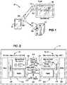
- FIG. 1is a block diagram depicting a wireless memory system having multiple wireless memory tags communicating with a wireless memory host via a common register-based interface, in accordance with an embodiment
- FIG. 2is a block diagram providing a more detailed view of components of the wireless memory host and wireless memory tag, in accordance with an embodiment
- FIG. 3is a flowchart illustrating a process for using a register-based interface to access non-volatile memory of a wireless memory tag via a wireless memory host, in accordance with an embodiment
- FIG. 4is a schematic view of a table definition of a register-based interface of a wireless memory tag, in accordance with an embodiment
- FIG. 5is a schematic diagram illustrating a definition of a request frame with a put-long command (e.g., also referenced herein as a put-long request frame) useful for accessing the register-based interface of FIG. 4 , in accordance with an embodiment;
- a put-long commande.g., also referenced herein as a put-long request frame
- FIG. 6is a schematic diagram illustrating a definition of a request frame with a put-short command (e.g., also referenced herein as a put-short request frame) useful for accessing the register-based interface of FIG. 4 , in accordance with an embodiment;
- a put-short commande.g., also referenced herein as a put-short request frame
- FIG. 7is a schematic diagram illustrating a definition of a request frame with a get-long command (e.g., also referenced herein as a get-long request frame) useful for accessing the register-based interface of FIG. 4 , in accordance with an embodiment;
- a get-long commande.g., also referenced herein as a get-long request frame
- FIG. 8is a schematic diagram illustrating a definition of a request frame with a get-short command (e.g., also referenced herein as a get-short request frame) useful for accessing the register-based interface of FIG. 4 , in accordance with an embodiment;
- a get-short commande.g., also referenced herein as a get-short request frame
- FIG. 9is a schematic drawing illustrating the use of request frames and corresponding response frames in the register-based interface for a read operation, in accordance with an embodiment.
- FIG. 10is a schematic drawing illustrating the use of request frames and corresponding response frames in the register-based interface for a write operation, in accordance with an embodiment.
- FIG. 1is a block diagram depicting a wireless memory system 10 having multiple wireless memory tags 12 communicating with a host 14 via a common register-based interface, in accordance with an embodiment.
- FIG. 1illustrates a television 16 that includes a high speed wireless memory tag 18 capable of transmitting data to/from the host 14 (e.g., a smartphone).
- the high speed wireless memory tag 18may be embedded within a device, as illustrated by the dashed lines of the tag 18 .
- NFCnear-field communications
- the wireless memory tags 12may be accessed via proprietary communications methods and/or hardware.
- the memory tags 12 illustrated in FIG. 1may be equipped with a standardized register-based interface 24 , which may allow for communication through an interface that is agnostic with regard to the host and/or structure of the wireless memory.
- the host 14may communicate with the wireless memory tags 12 via one or more transmitters/receivers 26 and/or 26 ′, which communicate with one or more transmitters/receivers 28 and/or 28 ′ of the television 16 and/or one or more transmitters/receivers 30 of the NFC tag 20 . Accordingly, by standardizing the communication interface among a multitude of wireless memory tags 12 , communications may be provided regardless of the wireless memory tag 12 structure and/or specific parameters of the host 14 .
- FIG. 2is a block diagram providing a more detailed view of components of the wireless memory host (WMH) 14 and wireless memory tag (WMT) 12 (e.g., a high speed memory tag 18 ), in accordance with an embodiment.
- FIG. 3is a flowchart illustrating a process 60 for using a register-based interface to access non-volatile memory of a wireless memory tag 12 via a wireless memory host 14 , in accordance with an embodiment.
- FIGS. 2 and 3will be discussed together.
- the process 60may begin by a wireless memory host 14 detecting and/or initializing communications with a wireless memory tag 12 (block 62 ).
- the wireless memory host 14may include a controller/processor 40 that may poll (e.g., scan) via a transmitter 26 (e.g., a narrow-band transmitter).
- the transmitter 26may provide a wireless power transfer (WPT) signal 42 to the tag 12 , which provides power 44 to the tag 12 .
- the tag 12includes power extraction circuitry 45 , which may extract power 44 from the WPT signal 42 .
- the power 44may be used to activate functionality of the tag 12 .
- the host 14may determine whether the tag 12 meets communication requirements of the host 14 . For example, the host 14 may determine if the tags 12 are equipped with the register-based interface 24 , such that request frames 46 A with commands may be provided to the tags 12 . Additionally, when no errors are detected by the tag, acknowledgement response frames 46 B, and eventually response frames 46 B with information from the tags 12 may be provided to the host 14 . In some embodiments (e.g., the embodiment illustrated in FIG. 2 ) the wireless memory tag 12 may be equipped with high-power/high-speed transfers.
- the host 14may begin communicating via a high-power/high-speed transmitter/receiver 26 ′ (e.g., via one or more wireless data transfer (WDT) signal 48 (e.g., ultra wide band (UWB) or 57-64 GHz communications)).
- WDTwireless data transfer
- UWBultra wide band
- 57-64 GHz communicationse.g., 57-64 GHz communications
- response frames 46 B with acknowledgementmay be provided via the WDT signal 48 (e.g., UWB (or 57-64 GHz) communications) from the tags 12 to the host 14 (e.g., a command-response protocol).
- WDT signal 48e.g., UWB (or 57-64 GHz) communications
- the host 14e.g., a command-response protocol
- a request frame 46 A with a commandmay be provided from the host 14 to the tag 12 (block 64 ).
- a radio 52 of the host 14may provide the request frame 46 A with a command to a radio 54 of the tag 12 .
- the request frame 46 A with a commandmay trigger access (e.g., read and/or write operations) to non-volatile memory 50 of the tag 12 (e.g., via the register-based interface 24 ).
- the tag 12may receive the request frame 46 A (block 66 ).
- the request frame 46 A with a commandmay be processed (block 68 ) to obtain and/or store data in the non-volatile memory 50 (block 68 ).
- the tag 12may provide one or more response messages to the host 14 .
- a response frame 46 B with an acknowledgment response indicating that the request frame 46 A has been received and/or processedmay be provided from the radio 54 to the radio 52 .
- the response frame 46 Bmay be received by the host 14 (block 72 ), which results in awareness by the host 14 of the status of the access of the non-volatile memory 50 .
- FIG. 4is a schematic view of a table definition 80 of a register-based interface 24 of a wireless memory tag, in accordance with an embodiment.
- the interface 24may be made up of multiple sections of data.
- the interface 24may include an initialization information section 82 , a controller management section 84 , and/or a non-volatile memory access section 86 .
- the initialization information section 82may hold data that is used for communication initialization between the host 14 and the tag 12 .
- the initialization information section 82includes an NFC information section 88 , a wireless memory tag/data buffer information section 90 , and a vendor-specific information section 92 .
- the NFC information section 88may contain information related to NFC/high-power communications capabilities of the tag 12 .
- data stored in this section 88may provide an indication of whether the tag 12 is equipped to handle high-power communications (e.g., includes a high-power/high-speed/wide-band radio 54 ) or if the tag 12 is equipped to handle only low-speed communications (e.g., only has a low-power transmitter/receiver 28 ).
- the address for the NFC information section 88may be in the range of 0x00-00 (hex-based most significant byte (MSB)) to 0x00-5F (hex-based least significant byte (LSB)) and may be allocated 96 bytes of data. Addresses 0x00-60-0x00-7F may be reserved for future expansion.
- the wireless memory tag/data buffer information section 90may include information related to the structure of the wireless memory tag 12 , such as a number of data buffers, and a size and/or location offset for each buffer. Thus, the host 14 may become aware of the available data buffers, their size, and their location, by accessing data in section 90 .
- section 90may reside in 2048 bytes of data, with the actual amount of used data being dependent on the number of data buffers in the tag 12 . For example, a tag 12 having fewer data buffers would use relatively less data to describe the data buffers than a tag 12 having more data buffers.
- the section 90may be located within an address of 0x00-80 (hex-based MSB) to 0x08-7F (hex-based LSB).
- a vendor-specific data section 92may include data defining particular vendor-provided information, such as a particular file system of the non-volatile memory 50 , specific sets of command types supported by the tag 12 (e.g., Open NAND Flash Interface Commands (ONFI) and/or Universal Flash Storage (UFS) commands), etc.
- OFIOpen NAND Flash Interface Commands
- UFSUniversal Flash Storage
- the controller management section 84may include a set of direct access registers 94 that can be read or written to.
- the controller management section 84includes 256 bytes of registers, which may be located in the address range of 0x10-00 (hex-based MSB) to 0x1F-FF (hex-based LSB).
- the NVM access section 86is useful for executing NVM commands and monitoring execution status of the NVM commands. This section 86 may occupy 56 kilobytes and be addressed in the range of 0x20-00 (hex-based MSB) to 0xFF-FF (hex-based LSB).
- the NVM access section 86may include a command parameters section 96 , a command execute section 98 , a status section 100 , and/or a data buffer section 102 .
- the command parameters section 96takes up 256 bytes and may store command parameters, such as non-volatile memory locations where a read and/or write is to occur, a command code representative of the access operation to be performed on the NVM 50 , etc.
- the command execute section 98may occupy one byte of data of the NVM access section 86 .
- a particular valuee.g., a flag
- the NVM access commandmay be executed. Accordingly, certain written values to the command execute section 98 may act as a trigger for the execution of an access command.
- the command execution section 98may not be necessary.
- a commandmay be executed automatically upon the occurrence of particular data written to the command parameters section 96 .
- execution of an access commandcould automatically trigger when a command code representative of a particular command is written to the command parameters section 96 .
- the status section 100may occupy 16 bytes, where 1 byte is used for each data buffer in the wireless memory tag 12 . Accordingly, a tag 12 having 4 data buffers may utilize 4 bytes of the 16 available bytes. Each status byte may be used to provide a status of a corresponding data buffer. For example, the status byte for a corresponding data buffer may indicate whether the data buffer is in use (and thus unavailable for new operations) or is not in use (and thus may be used in new operations).
- the commandsmay be executed using the data buffers.
- the data buffersare stored in the data buffer section, which may vary based upon a tag 12 vendor's specification. For example, a tag 12 may have any number of data buffers. Further, the data buffers may vary in size. Accordingly, the data buffer section 102 size is vendor specific and may occupy the address range of 0x20-00 (hex-based MSB) to 0xFF-FF (hex-based LSB) in some embodiments.
- the register-based interfacemay enable vendor-agnostic hosts 14 to access tags 12 , by providing request frames 46 A with commands and receiving response frames 46 B in accordance with the structure illustrated in FIG. 4 .
- NVMnon-volatile memory
- FIG. 5is a schematic diagram illustrating a definition of a put-long request frame 120 that may be sent by a host 14 in order to access the register-based interface 24 having the definition 80 of FIG. 4 .
- FIG. 6is a schematic diagram illustrating a definition of a put-short request frame 150 useful for accessing the register-based interface of FIG. 4 , in accordance with an embodiment.
- a “put” request framemay be used to put something in the interface 24 of the tag 12 .
- a “long” request framemay provide access to the Register-Based Interface 24 at the byte level, while a “short” request frame may provide access to the Register-Based Interface 24 at the kilobyte level. Accordingly, more granularity may be achieved using “long” request frames, when desired.
- the put-long request frame 120begins with a start of frame byte 122 that provides an indication to the tag 12 of the start of a new command.
- the put-long request frame 120also includes a put long command code byte 124 that provides an indication that the request frame 46 A includes a put long command (e.g., is a put-long request frame 120 ).
- the put-long request frame 120also includes a most-significant-byte (MSB) start address byte 126 , which may be used to coarsely specify a register range (e.g., 1 kilobyte out of 64 kilobytes of the Register-Based Interface 24 ).
- MSBmost-significant-byte
- the registermay be finely addressed by using the least-significant-byte (LSB) start address byte 128 .
- the LSB start address byte 128may be used to pinpoint an address of 1 byte out of 1 kilobyte (e.g., the kilobyte specified by the MSB start address byte 126 ) of the Register-Based Interface 24 . Accordingly, by providing an indication of these addresses, the system may properly read from and/or write data to the proper addressed register of the Register-Based Interface 24 .
- a payloadis transmitted within the put-long request frame 120 , by the host 14 .
- the payloadis data to be “put” into the interface 24 .
- One byte 130is used to provide the size of the payload (e.g., a payload size of 1 byte to 256 bytes).
- the payload 132consumes a number of bytes equaling the payload size (e.g., 1 byte to 256 bytes).
- two bytes of data 134are used for a CRC-16 cyclical redundancy check, which may be used to detect errors in the data provided in the put-long request frame 120 .
- specified payload datawill be put into the interface 24 at the specified addresses (e.g., as defined by the starting addresses of the MSB and the LSB).
- FIG. 6is a schematic diagram illustrating a definition of a put-short request frame 150 useful for accessing the register-based interface of FIG. 4 using coarse addressing.
- the put-short request frame 150is very similar to the put-long request frame 120 , except that a put-short command code 152 is used instead of the put-long command code 124 and no start address LSB byte 128 is present (because the put short provides coarse addressing).
- the put-short request frame 150begins with a start of frame byte 122 that provides an indication to the tag 12 of the start of a new request frame 46 A.
- the request frame 46 Aalso includes a put-short command code byte 152 that provides an indication that the request frame 46 A is a put short request frame 150 .
- the put-short request frame 150also includes a most-significant-byte (MSB) start address byte 126 , which may be used to coarsely specify a register range (e.g., 1 kilobyte out of 64 kilobytes of the Register-Based Interface 24 ).
- MSBmost-significant-byte
- a payloadis transmitted within the put-short request frame, by the host 14 .
- the payloadis data to be “put” into the interface 24 .
- One byte 130is used to provide the size of the payload (e.g., a payload size of 1 byte to 256 bytes).
- the payload 132consumes a number of bytes equaling the payload size (e.g., 1 byte to 256 bytes).
- two bytes of data 134are used for a CRC-16 cyclical redundancy check, which may be used to detect errors in the data provided in the put-short request frame 150 .
- specified payload datawill be put into the interface 24 at the specified address (e.g., as defined by the starting addresses of the MSB).
- FIG. 7is a schematic diagram illustrating a definition of a get-long request frame 170 useful for accessing the register-based interface 24 of FIG. 4 , in accordance with an embodiment.
- the long request framesprovide a byte of data indicative of the start address of a least significant byte to retrieve data from, in order to provide addressing with fine granularity.
- the get-long request frames 170begin with a start of frame byte 122 that provides an indication to the tag 12 of the start of a new request frame 46 A.
- the get-long request frame 170also includes a get-long command code byte 172 that provides an indication that the request frame 170 is a get-long request frame 170 .
- the get-long request frame 170also includes a most-significant-byte (MSB) start address byte 126 , which may be used to coarsely specify a register range (e.g., 1 kilobyte out of 64 kilobytes of the Register-Based Interface 24 ) where data should be read from.
- MSBmost-significant-byte
- the registermay be finely addressed by using the least-significant-byte (LSB) start address byte 128 .
- the LSB start address byte 128may be used to pinpoint an address of 1 byte out of 1 kilobyte (e.g., the kilobyte specified by the MSB start address byte 126 ) of the Register-Based Interface 24 .
- the tag 12in response to the get-long request frame 170 , transmits a payload.
- One byte 130is used to provide a specification of the size of the payload (e.g., a payload size of 1 byte to 256 bytes) to retrieve.
- two bytes of data 134are used for a CRC-16 cyclical redundancy check, which may be used to detect errors in the data provided in the get-long request frame 170 .
- FIG. 8is a schematic diagram illustrating a definition of a get-short request frame 190 useful for accessing the Register-Based Interface 24 of FIG. 4 , in accordance with an embodiment.
- the get-short request frame 190begins with a start of frame byte 122 that provides an indication to the tag 12 of the start of a new request frame 46 A.
- the get-short request frame 190also includes a get-short command code byte 192 that provides an indication that the request frame 46 A is a get-short request frame 190 .
- the get-short request frame 190also includes a most-significant-byte (MSB) start address byte 126 , which may be used to coarsely specify a register range (e.g., 1 kilobyte out of 64 kilobytes of the Register-Based Interface 24 ) where data should be read. Because the get-short request frame 190 is addressed at a more granular level, a LSB start address byte is not provided.
- MSBmost-significant-byte
- the tag 12transmits a payload in response to the get-short request frame 190 .
- One byte 130is used to provide a specification of the size of the payload (e.g., a payload size of 1 byte to 256 bytes) to retrieve.
- two bytes of data 134are used for a CRC-16 cyclical redundancy check, which may be used to detect errors in the data provided in the get-short request frame 190 .
- Tables 1 and 2 belowsummarize the format of the request frames 46 A and the response frames 46 B.
- Table 1illustrates a format of the request frames 46 A and Table 2 illustrates the format of the response frames 46 B.
- NArepresents data that is not applicable (e.g., is not transmitted)
- Nrepresents the number of payload bytes
- OKrepresents positive response data.
- the response frames 46 Beach include an acknowledgement byte indicating that a request frame was received. Additionally, when the response frames 46 B responding to “Get” commands includes a payload of 1-256 bytes of data corresponding to the “Get” command provided in a corresponding request frame 46 A.
- FIG. 9is a sequence diagram illustrating a read operation 210 between the host 14 and the tag 12 using the request frames 46 A and response frames 46 B.
- the interaction 210results in a read operation, where the host 14 reads data 12 from the non-volatile memory 50 of the tag 12 , in accordance with an embodiment.
- the host 14generates a fill request 212 by providing a “put” request frame 46 A (e.g., the put-long request frame 120 and/or the put-short request frame 150 ) to fill a particular portion of the register-based interface with data from the non-volatile memory 50 of the tag 12 (arrow 214 ).
- the “put” request frame 46 Amay include a payload 132 that includes: non-volatile memory read command code, an address of a data buffer in the register-based interface 24 where data read from the non-volatile memory 50 should be stored, and/or a trigger to initiate the start of the read and store operation.
- multiple “put” request frames 46 Amay be used to fill each field of the Register-Based Interface 24 with this data.
- the tag 12Upon receiving the fill request 212 , the tag 12 provides an acknowledgment response with a response frame 46 B that may inform the host 14 whether the “put” request frame 46 A was properly accepted (arrow 216 ). Further, the tag 12 begins processing the “put” request frame 46 A, resulting in data from the non-volatile memory 50 being read and stored in the register-based interface (e.g., at an address of the data buffer area provided in the payload of the “put” request frame 46 A).
- the host 14Upon receiving the acknowledgement response with a response frame 46 B, the host 14 will provide a status query 218 to the tag 12 to determine the status of the data buffer being filled (e.g., whether the fill is complete, such that the data may be obtained by the host 14 ). This may be done using the get-long request frame 170 and/or the get-short request frame 190 (arrow 220 ). The status 222 of the data buffer is provided by the tag 12 (arrow 224 ). This status inquiry process continues until the status indicates that the data buffer is ready for use (e.g., the data buffer is filled with the non-volatile memory data).
- the host 14provides a request 226 to get the filled data. This may be done by providing a get-long request frame 170 and/or a get-short request frame 190 to the tag 12 to get the information filled in the Register-Based Interface 24 (arrow 228 ).
- the get-long request frame 170 and/or get-short request frame 190includes the address where the data buffer holding the filled data is located as well as a payload size.
- the tag 12Upon receiving this request 226 , the tag 12 provides a response frame 46 B including the data 230 (arrow 232 ). Accordingly, these interactions between the host 14 and the tag 12 result in non-volatile memory 50 of the tag 12 being provided to host 14 (i.e., a read operation).
- FIG. 10is a sequence diagram illustrating a write operation 250 using the request frames 46 A and the response frames 46 B of the Register-Based Interface 24 , in accordance with an embodiment.
- the host 14To perform the write operation 250 , the host 14 generates a write request 252 , by providing a put-long request frame 120 and/or a put-short request frame 150 to the tag 12 (arrow 254 ).
- the write request 252may include the start address of the Register-Based Interface 24 , a payload size, and a payload.
- the payloadmay include non-volatile memory write command code, a start address of where to write to, the data to be written, and/or a start of execution indication.
- the tag 12may provide an acknowledgment response 256 with a response frame 46 B, providing an indication of whether or not the write request 252 was properly received (arrow 258 ). Further, the tag 12 may interpret the payload to store the data in the non-volatile memory 50 , as indicated by the tag 12 busy time 260 .
- wireless tag communicationsmay become vendor agnostic. For example, communications between a host 14 and a tag 12 may share a common scheme between multiple different vendor-specific tag designs. Thus, development costs of tag communications protocols may be reduced. Further, cross-communication between these vendor-specific tag designs may be more efficient.
Landscapes
- Engineering & Computer Science (AREA)
- Theoretical Computer Science (AREA)
- Computer Networks & Wireless Communication (AREA)
- Signal Processing (AREA)
- Physics & Mathematics (AREA)
- General Engineering & Computer Science (AREA)
- General Physics & Mathematics (AREA)
- Mobile Radio Communication Systems (AREA)
- Communication Control (AREA)
Abstract
Description
| TABLE 1 |
| Request Frame Format |
| RBIF Command Set and Protocol |
| Body of Request Frame |
| COMMAND | INFORMATION |
| Total | First | Second | ||||||
| Command | # of | Address | Address | Payload | Total # of | |||
| Name | Bytes | Byte | Byte | Size Byte | Payload Bytes | Bytes | ||
| Start Of | 1 | MSB | NA | N | Payload (1-256) | ≤258 | CRC-16 | |
| SHORT | ||||||||
| GET | ||||||||
| 1 | MSB | NA | N | NA | 2 | |||
| PUT | ||||||||
| 1 | MSB | LSB | N | Payload (1-256) | ≤259 | |||
| GET | ||||||||
| 1 | MSB | LSB | N | NA | 3 | |||
| LONG | ||||||||
| TABLE 2 |
| Response Frame Format |
| RBIF Command Set and Protocol |
| Body of Response Frame |
| ACKNOWLEDGEMENT | INFORMATION |
| Command | Acknowledgement | Total # | Information | Total # of | ||
| Name | Byte | of Bytes | Bytes | Bytes | ||
| PUT | Start Of Frame | OK | 1 | NA | NA | CRC-16 |
| SHORT | ||||||
| GET | OK | 1 | Payload (1-256) | ≤256 | ||
| SHORT | ||||||
| PUT | OK | 1 | NA | NA | ||
| LONG | ||||||
| GET | OK | 1 | Payload (1-256) | ≤256 | ||
| LONG | ||||||
Claims (26)
Priority Applications (2)
| Application Number | Priority Date | Filing Date | Title |
|---|---|---|---|
| US14/547,011US10779147B2 (en) | 2014-11-18 | 2014-11-18 | Wireless memory interface |
| US17/002,501US11523264B2 (en) | 2014-11-18 | 2020-08-25 | Wireless memory interface |
Applications Claiming Priority (1)
| Application Number | Priority Date | Filing Date | Title |
|---|---|---|---|
| US14/547,011US10779147B2 (en) | 2014-11-18 | 2014-11-18 | Wireless memory interface |
Related Child Applications (1)
| Application Number | Title | Priority Date | Filing Date |
|---|---|---|---|
| US17/002,501ContinuationUS11523264B2 (en) | 2014-11-18 | 2020-08-25 | Wireless memory interface |
Publications (2)
| Publication Number | Publication Date |
|---|---|
| US20160140049A1 US20160140049A1 (en) | 2016-05-19 |
| US10779147B2true US10779147B2 (en) | 2020-09-15 |
Family
ID=55961808
Family Applications (2)
| Application Number | Title | Priority Date | Filing Date |
|---|---|---|---|
| US14/547,011Active2037-10-26US10779147B2 (en) | 2014-11-18 | 2014-11-18 | Wireless memory interface |
| US17/002,501Active2035-04-14US11523264B2 (en) | 2014-11-18 | 2020-08-25 | Wireless memory interface |
Family Applications After (1)
| Application Number | Title | Priority Date | Filing Date |
|---|---|---|---|
| US17/002,501Active2035-04-14US11523264B2 (en) | 2014-11-18 | 2020-08-25 | Wireless memory interface |
Country Status (1)
| Country | Link |
|---|---|
| US (2) | US10779147B2 (en) |
Citations (31)
| Publication number | Priority date | Publication date | Assignee | Title |
|---|---|---|---|---|
| US20030017857A1 (en)* | 2001-07-20 | 2003-01-23 | Kitson Frederick Lee | Wireless device local access system |
| US20030103521A1 (en)* | 2001-06-18 | 2003-06-05 | Itran Communications Ltd. | Channel access method for powerline carrier based media access control protocol |
| US20040100834A1 (en)* | 2002-11-21 | 2004-05-27 | Hewlett-Packard Development Company, L.P. | Memory tag, read/write device and method of operating a memory tag |
| US20050160316A1 (en)* | 2002-12-02 | 2005-07-21 | Silverbrook Research Pty Ltd | Mechanism for reducing write problems by controlling charge pumps for flash memory |
| US20060062244A1 (en)* | 2004-09-20 | 2006-03-23 | Vladimir Oksman | Data packet encapsulation protocol |
| US20060069814A1 (en)* | 2004-09-28 | 2006-03-30 | Abraham Dalen M | Mass storage device with near field communications |
| US20060164213A1 (en)* | 2005-01-26 | 2006-07-27 | Battelle Memorial Institute | Method for autonomous establishment and utilization of an active-RF tag network |
| US20060179391A1 (en)* | 2005-01-13 | 2006-08-10 | Xerox Corporation | Wireless identification protocol with confirmation of successful transmission |
| US20060274747A1 (en)* | 2005-06-05 | 2006-12-07 | Rob Duchscher | Communication system for wireless audio devices |
| US20070073935A1 (en)* | 2005-09-15 | 2007-03-29 | Jong Won Kim | Wireless USB host apparatus supporting UWB |
| US20080175072A1 (en)* | 2007-01-19 | 2008-07-24 | Robert Norman | Fast data access through page manipulation |
| US20090049222A1 (en)* | 2004-03-17 | 2009-02-19 | Super Talent Electronics, Inc. | PCI Express-Compatible Controller And Interface For Flash Memory |
| US20090327239A1 (en)* | 2008-06-30 | 2009-12-31 | Sibeam, Inc. | Bitmap device identification in a wireless communication system |
| US20090327467A1 (en)* | 2008-06-30 | 2009-12-31 | In Sung Cho | Device discovery in a wireless communication system |
| US20090327544A1 (en)* | 2008-06-30 | 2009-12-31 | In Sung Cho | Dispatch capability using a single physical interface |
| US20100060422A1 (en)* | 2008-09-09 | 2010-03-11 | Sensormatic Electronics Corporation | Rfid enhanced operating system (eos) framework |
| US20100315965A1 (en)* | 2009-06-10 | 2010-12-16 | Microchip Technology Incorporated | Packet Based Data Transmission |
| US20100329232A1 (en)* | 2009-05-08 | 2010-12-30 | Icontrol, Inc. | Methods and Systems for Communication Protocol for Distributed Asset Management |
| US20100328043A1 (en)* | 2008-02-29 | 2010-12-30 | Nokia Corporation | Interrogation of rfid communication units |
| US20120099566A1 (en)* | 2010-10-20 | 2012-04-26 | Nokia Corporation | Wireless docking with out-of-band initiation |
| US20120210046A1 (en)* | 2011-02-16 | 2012-08-16 | Kuniaki Ito | Memory system allowing host to easily transmit and receive data |
| US20130235796A1 (en)* | 2012-03-02 | 2013-09-12 | Futurewei Technologies, Inc. | System and Method for Uplink Transmission in a Wireless Network |
| US20140047141A1 (en)* | 2012-03-29 | 2014-02-13 | Bahareh Sadeghi | Buffer-related usb communication |
| US20140067617A1 (en)* | 2012-09-06 | 2014-03-06 | Sortimo International Gmbh | System and Method for Ordering Items at a Work Site |
| US20140154975A1 (en)* | 2012-11-30 | 2014-06-05 | Certicom Corp. | Verifying a Wireless Device |
| US20140204822A1 (en)* | 2011-08-27 | 2014-07-24 | Lg Electronics Inc. | Method and apparatus of transmitting paging frame and wakeup frame |
| US20140285033A1 (en)* | 2013-03-20 | 2014-09-25 | Nokia Corporation | Method, apparatus, and computer program product for powering electronics in smart covers |
| US20140287681A1 (en)* | 2013-03-20 | 2014-09-25 | Nokia Corporation | Method, apparatus, and computer program product for powering electronic devices |
| US20140351457A1 (en)* | 2010-04-26 | 2014-11-27 | Cleversafe, Inc. | Storing data in a dispersed storage network |
| US20150098459A1 (en)* | 2012-05-08 | 2015-04-09 | Electronics And Telecommunications Research Institute | Scanning method in wireless lan system and supporting device therefor |
| US20150146568A1 (en)* | 2012-06-07 | 2015-05-28 | Kt Corporation | Method of active scanning and associating based on configuration information |
Family Cites Families (7)
| Publication number | Priority date | Publication date | Assignee | Title |
|---|---|---|---|---|
| US4384288A (en)* | 1980-12-31 | 1983-05-17 | Walton Charles A | Portable radio frequency emitting identifier |
| US6812852B1 (en)* | 1994-09-09 | 2004-11-02 | Intermac Ip Corp. | System and method for selecting a subset of autonomous and independent slave entities |
| US8766773B2 (en)* | 2001-03-20 | 2014-07-01 | Lightwaves Systems, Inc. | Ultra wideband radio frequency identification system, method, and apparatus |
| US20090243813A1 (en)* | 2008-03-25 | 2009-10-01 | Smith Joshua R | Wireless programming of non-volatile memory with near-field uhf coupling |
| US8332606B2 (en)* | 2009-06-15 | 2012-12-11 | Boldyrev Sergey | System and method for distributed persistent computing platform |
| US9204398B2 (en)* | 2011-03-21 | 2015-12-01 | Nokia Technologies Oy | Method and apparatus for battery with secure element |
| US20120297147A1 (en)* | 2011-05-20 | 2012-11-22 | Nokia Corporation | Caching Operations for a Non-Volatile Memory Array |
- 2014
- 2014-11-18USUS14/547,011patent/US10779147B2/enactiveActive
- 2020
- 2020-08-25USUS17/002,501patent/US11523264B2/enactiveActive
Patent Citations (31)
| Publication number | Priority date | Publication date | Assignee | Title |
|---|---|---|---|---|
| US20030103521A1 (en)* | 2001-06-18 | 2003-06-05 | Itran Communications Ltd. | Channel access method for powerline carrier based media access control protocol |
| US20030017857A1 (en)* | 2001-07-20 | 2003-01-23 | Kitson Frederick Lee | Wireless device local access system |
| US20040100834A1 (en)* | 2002-11-21 | 2004-05-27 | Hewlett-Packard Development Company, L.P. | Memory tag, read/write device and method of operating a memory tag |
| US20050160316A1 (en)* | 2002-12-02 | 2005-07-21 | Silverbrook Research Pty Ltd | Mechanism for reducing write problems by controlling charge pumps for flash memory |
| US20090049222A1 (en)* | 2004-03-17 | 2009-02-19 | Super Talent Electronics, Inc. | PCI Express-Compatible Controller And Interface For Flash Memory |
| US20060062244A1 (en)* | 2004-09-20 | 2006-03-23 | Vladimir Oksman | Data packet encapsulation protocol |
| US20060069814A1 (en)* | 2004-09-28 | 2006-03-30 | Abraham Dalen M | Mass storage device with near field communications |
| US20060179391A1 (en)* | 2005-01-13 | 2006-08-10 | Xerox Corporation | Wireless identification protocol with confirmation of successful transmission |
| US20060164213A1 (en)* | 2005-01-26 | 2006-07-27 | Battelle Memorial Institute | Method for autonomous establishment and utilization of an active-RF tag network |
| US20060274747A1 (en)* | 2005-06-05 | 2006-12-07 | Rob Duchscher | Communication system for wireless audio devices |
| US20070073935A1 (en)* | 2005-09-15 | 2007-03-29 | Jong Won Kim | Wireless USB host apparatus supporting UWB |
| US20080175072A1 (en)* | 2007-01-19 | 2008-07-24 | Robert Norman | Fast data access through page manipulation |
| US20100328043A1 (en)* | 2008-02-29 | 2010-12-30 | Nokia Corporation | Interrogation of rfid communication units |
| US20090327544A1 (en)* | 2008-06-30 | 2009-12-31 | In Sung Cho | Dispatch capability using a single physical interface |
| US20090327239A1 (en)* | 2008-06-30 | 2009-12-31 | Sibeam, Inc. | Bitmap device identification in a wireless communication system |
| US20090327467A1 (en)* | 2008-06-30 | 2009-12-31 | In Sung Cho | Device discovery in a wireless communication system |
| US20100060422A1 (en)* | 2008-09-09 | 2010-03-11 | Sensormatic Electronics Corporation | Rfid enhanced operating system (eos) framework |
| US20100329232A1 (en)* | 2009-05-08 | 2010-12-30 | Icontrol, Inc. | Methods and Systems for Communication Protocol for Distributed Asset Management |
| US20100315965A1 (en)* | 2009-06-10 | 2010-12-16 | Microchip Technology Incorporated | Packet Based Data Transmission |
| US20140351457A1 (en)* | 2010-04-26 | 2014-11-27 | Cleversafe, Inc. | Storing data in a dispersed storage network |
| US20120099566A1 (en)* | 2010-10-20 | 2012-04-26 | Nokia Corporation | Wireless docking with out-of-band initiation |
| US20120210046A1 (en)* | 2011-02-16 | 2012-08-16 | Kuniaki Ito | Memory system allowing host to easily transmit and receive data |
| US20140204822A1 (en)* | 2011-08-27 | 2014-07-24 | Lg Electronics Inc. | Method and apparatus of transmitting paging frame and wakeup frame |
| US20130235796A1 (en)* | 2012-03-02 | 2013-09-12 | Futurewei Technologies, Inc. | System and Method for Uplink Transmission in a Wireless Network |
| US20140047141A1 (en)* | 2012-03-29 | 2014-02-13 | Bahareh Sadeghi | Buffer-related usb communication |
| US20150098459A1 (en)* | 2012-05-08 | 2015-04-09 | Electronics And Telecommunications Research Institute | Scanning method in wireless lan system and supporting device therefor |
| US20150146568A1 (en)* | 2012-06-07 | 2015-05-28 | Kt Corporation | Method of active scanning and associating based on configuration information |
| US20140067617A1 (en)* | 2012-09-06 | 2014-03-06 | Sortimo International Gmbh | System and Method for Ordering Items at a Work Site |
| US20140154975A1 (en)* | 2012-11-30 | 2014-06-05 | Certicom Corp. | Verifying a Wireless Device |
| US20140285033A1 (en)* | 2013-03-20 | 2014-09-25 | Nokia Corporation | Method, apparatus, and computer program product for powering electronics in smart covers |
| US20140287681A1 (en)* | 2013-03-20 | 2014-09-25 | Nokia Corporation | Method, apparatus, and computer program product for powering electronic devices |
Non-Patent Citations (1)
| Title |
|---|
| JEDEC Standard, Low Power Double Data Rate 2 (LPDDR2), Jun. 2013, JEDEC Solid State Technology Association 2013. |
Also Published As
| Publication number | Publication date |
|---|---|
| US20200389778A1 (en) | 2020-12-10 |
| US11523264B2 (en) | 2022-12-06 |
| US20160140049A1 (en) | 2016-05-19 |
Similar Documents
| Publication | Publication Date | Title |
|---|---|---|
| US11301175B2 (en) | Method for controlling storage device | |
| CN105703883B (en) | Apparatus, method and system for exchanging error information in unified protocol communication | |
| KR101555325B1 (en) | Information processing apparatus information processing system method of processing information and computer program | |
| US9904651B2 (en) | Operating method of controller for setting link between interfaces of electronic devices, and storage device including controller | |
| EP2704021B1 (en) | SRAM handshake | |
| US20160378582A1 (en) | Operation method of storage device, operation metho of host device, and operation method of user system including storage device and host device | |
| US20120151294A1 (en) | Method and apparatus for correcting errors in memory device | |
| KR20180082579A (en) | Method for accessing stored data, and related controllers, devices, hosts and systems | |
| US8364872B2 (en) | Slave and communicating method between a master and the same | |
| CN112148629B (en) | Method for addressing integrated circuits on a bus and corresponding device | |
| US11249893B2 (en) | Flash memory controller, SD card device, method used in flash memory controller, and host device coupled to SD card device | |
| CN113875162B (en) | Data exchange device between NFC reader and double-NFC interface responder | |
| US8001292B2 (en) | Data transfer controlling device and IC card | |
| US9984746B2 (en) | Nonvolatile memory device that stores data from completed write requests on a power abnormality | |
| US20130275652A1 (en) | Methods and structure for transferring additional parameters through a communication interface with limited parameter passing features | |
| US20190179561A1 (en) | Data storage device, operating method thereof, and storage system having the same | |
| US20160378384A1 (en) | Data accessing method and system and memory storage apparatus | |
| US20110072168A1 (en) | Data transfer system with different operating modes | |
| US11523264B2 (en) | Wireless memory interface | |
| EP2911066B1 (en) | Method of transferring data, computer program product and tag | |
| US9313651B2 (en) | Memory system and method of controlling memory system | |
| US12321297B2 (en) | Bridge device and method for transferring command and data between a host device and a data storage device | |
| US11663065B2 (en) | SCSI command set for error history logging in a memory system and operating method thereof | |
| US9069486B2 (en) | Data transfer control device and data storage device | |
| CN104809487A (en) | Electronic device and method for accessing electronic device |
Legal Events
| Date | Code | Title | Description |
|---|---|---|---|
| AS | Assignment | Owner name:MICRON TECHNOLOGY, INC., IDAHO Free format text:ASSIGNMENT OF ASSIGNORS INTEREST;ASSIGNORS:MIRICHIGNI, GRAZIANO;CARACCIO, DANILO;REEL/FRAME:034202/0471 Effective date:20141118 | |
| AS | Assignment | Owner name:U.S. BANK NATIONAL ASSOCIATION, AS COLLATERAL AGENT, CALIFORNIA Free format text:SECURITY INTEREST;ASSIGNOR:MICRON TECHNOLOGY, INC.;REEL/FRAME:038669/0001 Effective date:20160426 Owner name:U.S. BANK NATIONAL ASSOCIATION, AS COLLATERAL AGEN Free format text:SECURITY INTEREST;ASSIGNOR:MICRON TECHNOLOGY, INC.;REEL/FRAME:038669/0001 Effective date:20160426 | |
| AS | Assignment | Owner name:MORGAN STANLEY SENIOR FUNDING, INC., AS COLLATERAL AGENT, MARYLAND Free format text:PATENT SECURITY AGREEMENT;ASSIGNOR:MICRON TECHNOLOGY, INC.;REEL/FRAME:038954/0001 Effective date:20160426 Owner name:MORGAN STANLEY SENIOR FUNDING, INC., AS COLLATERAL Free format text:PATENT SECURITY AGREEMENT;ASSIGNOR:MICRON TECHNOLOGY, INC.;REEL/FRAME:038954/0001 Effective date:20160426 | |
| AS | Assignment | Owner name:U.S. BANK NATIONAL ASSOCIATION, AS COLLATERAL AGENT, CALIFORNIA Free format text:CORRECTIVE ASSIGNMENT TO CORRECT THE REPLACE ERRONEOUSLY FILED PATENT #7358718 WITH THE CORRECT PATENT #7358178 PREVIOUSLY RECORDED ON REEL 038669 FRAME 0001. ASSIGNOR(S) HEREBY CONFIRMS THE SECURITY INTEREST;ASSIGNOR:MICRON TECHNOLOGY, INC.;REEL/FRAME:043079/0001 Effective date:20160426 Owner name:U.S. BANK NATIONAL ASSOCIATION, AS COLLATERAL AGEN Free format text:CORRECTIVE ASSIGNMENT TO CORRECT THE REPLACE ERRONEOUSLY FILED PATENT #7358718 WITH THE CORRECT PATENT #7358178 PREVIOUSLY RECORDED ON REEL 038669 FRAME 0001. ASSIGNOR(S) HEREBY CONFIRMS THE SECURITY INTEREST;ASSIGNOR:MICRON TECHNOLOGY, INC.;REEL/FRAME:043079/0001 Effective date:20160426 | |
| STCV | Information on status: appeal procedure | Free format text:ON APPEAL -- AWAITING DECISION BY THE BOARD OF APPEALS | |
| AS | Assignment | Owner name:JPMORGAN CHASE BANK, N.A., AS COLLATERAL AGENT, ILLINOIS Free format text:SECURITY INTEREST;ASSIGNORS:MICRON TECHNOLOGY, INC.;MICRON SEMICONDUCTOR PRODUCTS, INC.;REEL/FRAME:047540/0001 Effective date:20180703 Owner name:JPMORGAN CHASE BANK, N.A., AS COLLATERAL AGENT, IL Free format text:SECURITY INTEREST;ASSIGNORS:MICRON TECHNOLOGY, INC.;MICRON SEMICONDUCTOR PRODUCTS, INC.;REEL/FRAME:047540/0001 Effective date:20180703 | |
| AS | Assignment | Owner name:MICRON TECHNOLOGY, INC., IDAHO Free format text:RELEASE BY SECURED PARTY;ASSIGNOR:U.S. BANK NATIONAL ASSOCIATION, AS COLLATERAL AGENT;REEL/FRAME:047243/0001 Effective date:20180629 | |
| AS | Assignment | Owner name:MICRON TECHNOLOGY, INC., IDAHO Free format text:RELEASE BY SECURED PARTY;ASSIGNOR:MORGAN STANLEY SENIOR FUNDING, INC., AS COLLATERAL AGENT;REEL/FRAME:050937/0001 Effective date:20190731 | |
| AS | Assignment | Owner name:MICRON SEMICONDUCTOR PRODUCTS, INC., IDAHO Free format text:RELEASE BY SECURED PARTY;ASSIGNOR:JPMORGAN CHASE BANK, N.A., AS COLLATERAL AGENT;REEL/FRAME:051028/0001 Effective date:20190731 Owner name:MICRON TECHNOLOGY, INC., IDAHO Free format text:RELEASE BY SECURED PARTY;ASSIGNOR:JPMORGAN CHASE BANK, N.A., AS COLLATERAL AGENT;REEL/FRAME:051028/0001 Effective date:20190731 | |
| STPP | Information on status: patent application and granting procedure in general | Free format text:AMENDMENT / ARGUMENT AFTER BOARD OF APPEALS DECISION | |
| STPP | Information on status: patent application and granting procedure in general | Free format text:NOTICE OF ALLOWANCE MAILED -- APPLICATION RECEIVED IN OFFICE OF PUBLICATIONS | |
| STPP | Information on status: patent application and granting procedure in general | Free format text:PUBLICATIONS -- ISSUE FEE PAYMENT VERIFIED | |
| STCF | Information on status: patent grant | Free format text:PATENTED CASE | |
| MAFP | Maintenance fee payment | Free format text:PAYMENT OF MAINTENANCE FEE, 4TH YEAR, LARGE ENTITY (ORIGINAL EVENT CODE: M1551); ENTITY STATUS OF PATENT OWNER: LARGE ENTITY Year of fee payment:4 |