US10769099B2 - Devices for time division multiplexing of state machine engine signals - Google Patents
Devices for time division multiplexing of state machine engine signalsDownload PDFInfo
- Publication number
- US10769099B2 US10769099B2US15/534,994US201515534994AUS10769099B2US 10769099 B2US10769099 B2US 10769099B2US 201515534994 AUS201515534994 AUS 201515534994AUS 10769099 B2US10769099 B2US 10769099B2
- Authority
- US
- United States
- Prior art keywords
- row
- configurable
- block
- output
- coupled
- Prior art date
- Legal status (The legal status is an assumption and is not a legal conclusion. Google has not performed a legal analysis and makes no representation as to the accuracy of the status listed.)
- Active
Links
Images


Classifications
- G—PHYSICS
- G06—COMPUTING OR CALCULATING; COUNTING
- G06F—ELECTRIC DIGITAL DATA PROCESSING
- G06F15/00—Digital computers in general; Data processing equipment in general
- G06F15/76—Architectures of general purpose stored program computers
- G06F15/78—Architectures of general purpose stored program computers comprising a single central processing unit
- G06F15/7867—Architectures of general purpose stored program computers comprising a single central processing unit with reconfigurable architecture
- G—PHYSICS
- G06—COMPUTING OR CALCULATING; COUNTING
- G06F—ELECTRIC DIGITAL DATA PROCESSING
- G06F1/00—Details not covered by groups G06F3/00 - G06F13/00 and G06F21/00
- G06F1/26—Power supply means, e.g. regulation thereof
- G06F1/32—Means for saving power
- G06F1/3203—Power management, i.e. event-based initiation of a power-saving mode
- G06F1/3206—Monitoring of events, devices or parameters that trigger a change in power modality
- G06F1/3215—Monitoring of peripheral devices
- G06F1/3225—Monitoring of peripheral devices of memory devices
- G—PHYSICS
- G06—COMPUTING OR CALCULATING; COUNTING
- G06F—ELECTRIC DIGITAL DATA PROCESSING
- G06F13/00—Interconnection of, or transfer of information or other signals between, memories, input/output devices or central processing units
- G06F13/38—Information transfer, e.g. on bus
- G06F13/42—Bus transfer protocol, e.g. handshake; Synchronisation
- G06F13/4204—Bus transfer protocol, e.g. handshake; Synchronisation on a parallel bus
- G06F13/4221—Bus transfer protocol, e.g. handshake; Synchronisation on a parallel bus being an input/output bus, e.g. ISA bus, EISA bus, PCI bus, SCSI bus
- G06F13/423—Bus transfer protocol, e.g. handshake; Synchronisation on a parallel bus being an input/output bus, e.g. ISA bus, EISA bus, PCI bus, SCSI bus with synchronous protocol
- G—PHYSICS
- G06—COMPUTING OR CALCULATING; COUNTING
- G06F—ELECTRIC DIGITAL DATA PROCESSING
- G06F15/00—Digital computers in general; Data processing equipment in general
- G06F15/76—Architectures of general purpose stored program computers
- G06F15/78—Architectures of general purpose stored program computers comprising a single central processing unit
- G06F15/7839—Architectures of general purpose stored program computers comprising a single central processing unit with memory
- G06F15/7842—Architectures of general purpose stored program computers comprising a single central processing unit with memory on one IC chip (single chip microcontrollers)
- G06F15/7857—Architectures of general purpose stored program computers comprising a single central processing unit with memory on one IC chip (single chip microcontrollers) using interleaved memory
- G—PHYSICS
- G06—COMPUTING OR CALCULATING; COUNTING
- G06F—ELECTRIC DIGITAL DATA PROCESSING
- G06F9/00—Arrangements for program control, e.g. control units
- G06F9/06—Arrangements for program control, e.g. control units using stored programs, i.e. using an internal store of processing equipment to receive or retain programs
- G06F9/44—Arrangements for executing specific programs
- G06F9/448—Execution paradigms, e.g. implementations of programming paradigms
- G06F9/4498—Finite state machines
- G—PHYSICS
- G06—COMPUTING OR CALCULATING; COUNTING
- G06N—COMPUTING ARRANGEMENTS BASED ON SPECIFIC COMPUTATIONAL MODELS
- G06N20/00—Machine learning
- G—PHYSICS
- G05—CONTROLLING; REGULATING
- G05B—CONTROL OR REGULATING SYSTEMS IN GENERAL; FUNCTIONAL ELEMENTS OF SUCH SYSTEMS; MONITORING OR TESTING ARRANGEMENTS FOR SUCH SYSTEMS OR ELEMENTS
- G05B19/00—Programme-control systems
- G05B19/02—Programme-control systems electric
- G05B19/04—Programme control other than numerical control, i.e. in sequence controllers or logic controllers
- G05B19/045—Programme control other than numerical control, i.e. in sequence controllers or logic controllers using logic state machines, consisting only of a memory or a programmable logic device containing the logic for the controlled machine and in which the state of its outputs is dependent on the state of its inputs or part of its own output states, e.g. binary decision controllers, finite state controllers
- G—PHYSICS
- G06—COMPUTING OR CALCULATING; COUNTING
- G06F—ELECTRIC DIGITAL DATA PROCESSING
- G06F3/00—Input arrangements for transferring data to be processed into a form capable of being handled by the computer; Output arrangements for transferring data from processing unit to output unit, e.g. interface arrangements
- G06F3/06—Digital input from, or digital output to, record carriers, e.g. RAID, emulated record carriers or networked record carriers
- G06F3/0601—Interfaces specially adapted for storage systems
- G06F3/0602—Interfaces specially adapted for storage systems specifically adapted to achieve a particular effect
- G06F3/0604—Improving or facilitating administration, e.g. storage management
Definitions
- Embodiments of the inventionrelate generally to electronic devices and, more specifically, in certain embodiments, to electronic devices with parallel devices for data analysis.
- Complex pattern recognitioncan be inefficient to perform on a conventional von Neumann based computer.
- a biological brainin particular a human brain, however, is adept at performing pattern recognition.
- Current researchsuggests that a human brain performs pattern recognition using a series of hierarchically organized neuron layers in the neocortex. Neurons in the lower layers of the hierarchy analyze “raw signals” from, for example, sensory organs, while neurons in higher layers analyze signal outputs from neurons in the lower levels.
- This hierarchical system in the neocortexpossibly in combination with other areas of the brain, accomplishes the complex pattern recognition that enables humans to perform high level functions such as spatial reasoning, conscious thought, and complex language.
- pattern recognition tasksare increasingly challenging. Ever larger volumes of data are transmitted between computers, and the number of patterns that users wish to identify is increasing. For example, spam or malware are often detected by searching for patterns in a data stream, e.g., particular phrases or pieces of code. The number of patterns increases with the variety of spam and malware, as new patterns may be implemented to search for new variants. Searching a data stream for each of these patterns can form a computing bottleneck. Often, as the data stream is received, it is searched for each pattern, one at a time. The delay before the system is ready to search the next portion of the data stream increases with the number of patterns. Thus, pattern recognition may slow the receipt of data.
- Hardwarehas been designed to search a data stream for patterns, but this hardware often is unable to process adequate amounts of data in an amount of time given.
- Some devices configured to search a data streamdo so by distributing the data stream among a plurality of circuits.
- the circuitseach determine whether the data stream matches a portion of a pattern.
- a large number of circuitsoperate in parallel, each searching the data stream at generally the same time.
- the systemmay then further process the results from these circuits, to arrive at the final results.
- These “intermediate results”, however,can be larger than the original input data, which may pose issues for the system.
- the ability to use a cascaded circuits approach, similar to the human brainoffers one potential solution to this problem.
- FIG. 1illustrates an example of system having a state machine engine, according to various embodiments.
- FIG. 2illustrates an example of an FSM lattice of the state machine engine of FIG. 1 , according to various embodiments.
- FIG. 3illustrates an example of a block of the FSM lattice of FIG. 2 , according to various embodiments.
- FIG. 4illustrates an example of a row of the block of FIG. 3 , according to various embodiments.
- FIG. 4Aillustrates a block as in FIG. 3 having counters in rows of the block, according to various embodiments of the invention.
- FIG. 5illustrates an example of a Group of Two of the row of FIG. 4 , according to embodiments.
- FIG. 6illustrates an example of a finite state machine graph, according to various embodiments.
- FIG. 7illustrates an example of two-level hierarchy implemented with FSM lattices, according to various embodiments.
- FIG. 7Aillustrates a second example of two-level hierarchy implemented with FSM lattices, according to various embodiments.
- FIG. 8illustrates an example of a method for a compiler to convert source code into a binary file for programming of the FSM lattice of FIG. 2 , according to various embodiments.
- FIG. 9illustrates a state machine engine, according to various embodiments.
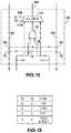
- FIG. 10illustrates a second example of a row of the block of FIG. 3 , according to various embodiments of the invention.
- FIG. 11illustrates the intra-block switch of FIG. 10 , according to various embodiments of the invention.
- FIG. 12illustrates the intra-group circuitry of FIG. 10 , according to various embodiments of the invention.
- FIG. 13illustrates a truth table for the multiplexer of FIG. 12 , according to various embodiments of the invention.
- FIG. 14illustrates a third example of a row of the block of FIG. 3 , according to various embodiments of the invention.
- FIG. 15illustrates a fourth example of a row of the block of FIG. 3 , according to various embodiments of the invention.
- FIG. 16illustrates a fifth example of a row of the block of FIG. 3 , according to various embodiments of the invention.
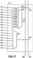
- FIG. 17illustrates a second example of the intra-block switch of FIG. 10 , according to various embodiments of the invention.
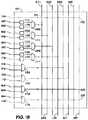
- FIG. 18illustrates a third example of the intra-block switch of FIG. 10 , according to various embodiments of the invention.
- FIG. 19illustrates a third example of the intra-block switch of FIG. 10 , according to various embodiments of the invention.
- FIG. 1illustrates an embodiment of a processor-based system, generally designated by reference numeral 10 .
- the system 10may be any of a variety of types such as a desktop computer, laptop computer, pager, cellular phone, personal organizer, portable audio player, control circuit, camera, etc.
- the system 10may also be a network node, such as a router, a server, or a client (e.g., one of the previously-described types of computers).
- the system 10may be some other sort of electronic device, such as a copier, a scanner, a printer, a game console, a television, a set-top video distribution or recording system, a cable box, a personal digital media player, a factory automation system, an automotive computer system, or a medical device.
- a copiera scanner
- a printera game console
- televisiona set-top video distribution or recording system
- cable boxa personal digital media player
- factory automation systeman automotive computer system
- automotive computer systemor a medical device.
- a processor 12such as a microprocessor, controls the processing of system functions and requests in the system 10 .
- the processor 12may comprise a plurality of processors that share system control.
- the processor 12may be coupled directly or indirectly to each of the elements in the system 10 , such that the processor 12 controls the system 10 by executing instructions that may be stored within the system 10 or external to the system 10 .
- the system 10includes a state machine engine 14 , which may operate under control of the processor 12 .
- the state machine engine 14may employ any one of a number of state machine architectures, including, but not limited to Mealy architectures, Moore architectures, Finite State Machines (FSMs), Deterministic FSMs (DFSMs), Bit-Parallel State Machines (BPSMs), etc. Though a variety of architectures may be used, for discussion purposes, the application refers to FSMs. However, those skilled in the art will appreciate that the described techniques may be employed using any one of a variety of state machine architectures.
- the state machine engine 14may include a number of (e.g., one or more) finite state machine (FSM) lattices (e.g., core of a chip).
- FSMfinite state machine
- latticese.g., core of a chip.
- the term “lattice”refers to an organized framework (e.g., routing matrix, routing network, frame) of elements (e.g., Boolean cells, counter cells, state machine elements, state transition elements).
- the “lattice”may have any suitable shape, structure, or hierarchical organization (e.g., grid, cube, spherical, cascading).
- Each FSM latticemay implement multiple FSMs that each receive and analyze the same data in parallel.
- the FSM latticesmay be arranged in groups (e.g., clusters), such that clusters of FSM lattices may analyze the same input data in parallel.
- clusters of FSM lattices of the state machine engine 14may be arranged in a hierarchical structure wherein outputs from state machine lattices on a lower level of the hierarchical structure may be used as inputs to state machine lattices on a higher level.
- the state machine engine 14can be employed for complex data analysis (e.g., pattern recognition or other processing) in systems that utilize high processing speeds. For instance, embodiments described herein may be incorporated in systems with processing speeds of 1 GByte/sec. Accordingly, utilizing the state machine engine 14 , data from high speed memory devices or other external devices may be rapidly analyzed. The state machine engine 14 may analyze a data stream according to several criteria (e.g., search terms), at about the same time, e.g., during a single device cycle.
- criteriae.g., search terms
- Each of the FSM lattices within a cluster of FSMs on a level of the state machine engine 14may each receive the same search term from the data stream at about the same time, and each of the parallel FSM lattices may determine whether the term advances the state machine engine 14 to the next state in the processing criterion.
- the state machine engine 14may analyze terms according to a relatively large number of criteria, e.g., more than 100, more than 110, or more than 10,000. Because they operate in parallel, they may apply the criteria to a data stream having a relatively high bandwidth, e.g., a data stream of greater than or generally equal to 1 GByte/sec, without slowing the data stream.
- the state machine engine 14may be configured to recognize (e.g., detect) a great number of patterns in a data stream. For instance, the state machine engine 14 may be utilized to detect a pattern in one or more of a variety of types of data streams that a user or other entity might wish to analyze. For example, the state machine engine 14 may be configured to analyze a stream of data received over a network, such as packets received over the Internet or voice or data received over a cellular network. In one example, the state machine engine 14 may be configured to analyze a data stream for spam or malware. The data stream may be received as a serial data stream, in which the data is received in an order that has meaning, such as in a temporally, lexically, or semantically significant order.
- the data streammay be received in parallel or out of order and, then, converted into a serial data stream, e.g., by reordering packets received over the Internet.
- the data streammay present terms serially, but the bits expressing each of the terms may be received in parallel.
- the data streammay be received from a source external to the system 10 , or may be formed by interrogating a memory device, such as the memory 16 , and forming the data stream from data stored in the memory 16 .
- the state machine engine 14may be configured to recognize a sequence of characters that spell a certain word, a sequence of genetic base pairs that specify a gene, a sequence of bits in a picture or video file that form a portion of an image, a sequence of bits in an executable file that form a part of a program, or a sequence of bits in an audio file that form a part of a song or a spoken phrase.
- the stream of data to be analyzedmay include multiple bits of data in a binary format or other formats, e.g., base ten, ASCII, etc.
- the streammay encode the data with a single digit or multiple digits, e.g., several binary digits.
- the system 10may include memory 16 .
- the memory 16may include volatile memory, such as Dynamic Random Access Memory (DRAM), Static Random Access Memory (SRAM), Synchronous DRAM (SDRAM), Double Data Rate DRAM (DDR SDRAM), DDR2 SDRAM, DDR3 SDRAM, etc.
- the memory 16may also include non-volatile memory, such as read-only memory (ROM), PC-RAM, silicon-oxide-nitride-oxide-silicon (SONOS) memory, metal-oxide-nitride-oxide-silicon (MONOS) memory, polysilicon floating gate based memory, and/or other types of flash memory of various architectures (e.g., NAND memory, NOR memory, etc.) to be used in conjunction with the volatile memory.
- ROMread-only memory
- PC-RAMsilicon-oxide-nitride-oxide-silicon
- SONOSsilicon-oxide-nitride-oxide-silicon
- MONOSmetal-oxide-nitride-
- the memory 16may include one or more memory devices, such as DRAM devices, that may provide data to be analyzed by the state machine engine 14 .
- DRAM devicessuch as DRAM devices
- the term “provide”may generically refer to direct, input, insert, issue, route, send, transfer, transmit, generate, give, make available, move, output, pass, place, read out, write, etc.
- Such devicesmay be referred to as or include solid state drives (SSD's), MultimediaMediaCards (MMC's), SecureDigital (SD) cards, CompactFlash (CF) cards, or any other suitable device.
- the system 10may couple to the system 10 via any suitable interface, such as Universal Serial Bus (USB), Peripheral Component Interconnect (PCI), PCI Express (PCI-E), Small Computer System Interface (SCSI), IEEE 1394 (Firewire), or any other suitable interface.
- USBUniversal Serial Bus
- PCIPeripheral Component Interconnect
- PCI-EPCI Express
- SCSISmall Computer System Interface
- IEEE 1394IEEE 1394
- the system 10may include a memory controller (not illustrated).
- the memory controllermay be an independent device or it may be integral with the processor 12 .
- the system 10may include an external storage 18 , such as a magnetic storage device. The external storage may also provide input data to the state machine engine 14 .
- the system 10may include a number of additional elements.
- a compiler 20may be used to configure (e.g., program) the state machine engine 14 , as described in more detail with regard to FIG. 8 .
- An input device 22may also be coupled to the processor 12 to allow a user to input data into the system 10 .
- an input device 22may be used to input data into the memory 16 for later analysis by the state machine engine 14 .
- the input device 22may include buttons, switching elements, a keyboard, a light pen, a stylus, a mouse, and/or a voice recognition system, for instance.
- An output device 24such as a display may also be coupled to the processor 12 .
- the display 24may include an LCD, a CRT, LEDs, and/or an audio display, for example. They system may also include a network interface device 26 , such as a Network Interface Card (NIC), for interfacing with a network, such as the Internet. As will be appreciated, the system 10 may include many other components, depending on the application of the system 10 .
- NICNetwork Interface Card
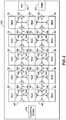
- FIGS. 2-5illustrate an example of a FSM lattice 30 .
- the FSM lattice 30comprises an array of blocks 32 .
- each block 32may include a plurality of selectively couple-able hardware elements (e.g., configurable elements and/or special purpose elements) that correspond to a plurality of states in a FSM. Similar to a state in a FSM, a hardware element can analyze an input stream and activate a downstream hardware element, based on the input stream.
- a hardware elementcan analyze an input stream and activate a downstream hardware element, based on the input stream.
- the configurable elementscan be configured (e.g., programmed) to implement many different functions.
- the configurable elementsmay include state transition elements (STEs) 34 , 36 (shown in FIG. 5 ) that function as data analysis elements and are hierarchically organized into rows 38 (shown in FIGS. 3 and 4 ) and blocks 32 (shown in FIGS. 2 and 3 ).
- the STEseach may be considered an automaton, e.g., a machine or control mechanism designed to follow automatically a predetermined sequence of operations or respond to encoded instructions. Taken together, the STEs form an automata processor as state machine engine 14 .
- a hierarchy of configurable switching elementscan be used, including inter-block switching elements 40 (shown in FIGS. 2 and 3 ), intra-block switching elements 42 (shown in FIGS. 3 and 4 ) and intra-row switching elements 44 (shown in FIG. 4 ).
- the switching elementsmay include routing structures and buffers.
- a STE 34 , 36can correspond to a state of a FSM implemented by the FSM lattice 30 .
- the STEs 34 , 36can be coupled together by using the configurable switching elements as described below. Accordingly, a FSM can be implemented on the FSM lattice 30 by configuring the STEs 34 , 36 to correspond to the functions of states and by selectively coupling together the STEs 34 , 36 to correspond to the transitions between states in the FSM.
- FIG. 2illustrates an overall view of an example of a FSM lattice 30 .
- the FSM lattice 30includes a plurality of blocks 32 that can be selectively coupled together with configurable inter-block switching elements 40 .
- the inter-block switching elements 40may include conductors 46 (e.g., wires, traces, etc.) and buffers 48 , 50 .
- buffers 48 and 50are included to control the connection and timing of signals to/from the inter-block switching elements 40 .
- the buffers 48may be provided to buffer data being sent between blocks 32
- the buffers 50may be provided to buffer data being sent between inter-block switching elements 40 .
- the blocks 32can be selectively coupled to an input block 52 (e.g., a data input port) for receiving signals (e.g., data) and providing the data to the blocks 32 .
- the blocks 32can also be selectively coupled to an output block 54 (e.g., an output port) for providing signals from the blocks 32 to an external device (e.g., another FSM lattice 30 ).
- the FSM lattice 30can also include a programming interface 56 to configure (e.g., via an image, program) the FSM lattice 30 .
- the imagecan configure (e.g., set) the state of the STEs 34 , 36 .
- the imagecan configure the STEs 34 , 36 to react in a certain way to a given input at the input block 52 .
- a STE 34 , 36can be set to output a high signal when the character ‘a’ is received at the input block 52 .
- the input block 52 , the output block 54 , and/or the programming interface 56can be implemented as registers such that writing to or reading from the registers provides data to or from the respective elements. Accordingly, bits from the image stored in the registers corresponding to the programming interface 56 can be loaded on the STEs 34 , 36 .
- FIG. 2illustrates a certain number of conductors (e.g., wire, trace) between a block 32 , input block 52 , output block 54 , and an inter-block switching element 40 , it should be understood that in other examples, fewer or more conductors may be used.
- FIG. 3illustrates an example of a block 32 .
- a block 32can include a plurality of rows 38 that can be selectively coupled together with configurable intra-block switching elements 42 . Additionally, a row 38 can be selectively coupled to another row 38 within another block 32 with the inter-block switching elements 40 .
- a row 38includes a plurality of STEs 34 , 36 organized into pairs of configurable elements that are referred to herein as groups of two (GOTs) 60 .
- a block 32comprises sixteen (16) rows 38 .
- FIG. 4illustrates an example of a row 38 .
- a GOT 60can be selectively coupled to other GOTs 60 and any other elements (e.g., a special purpose element 58 ) within the row 38 by configurable intra-row switching elements 44 .
- a GOT 60can also be coupled to other GOTs 60 in other rows 38 with the intra-block switching element 42 , or other GOTs 60 in other blocks 32 with an inter-block switching element 40 .
- a GOT 60has a first and second input 62 , 64 , and an output 66 .
- the first input 62is coupled to a first STE 34 of the GOT 60 and the second input 64 is coupled to a second STE 36 of the GOT 60 , as will be further illustrated with reference to FIG. 5 .
- the row 38includes a first and second plurality of row interconnection conductors 68 , 70 .
- an input 62 , 64 of a GOT 60can be coupled to one or more row interconnection conductors 68 , 70
- an output 66can be coupled to one or more row interconnection conductor 68 , 70 .
- a first plurality of the row interconnection conductors 68can be coupled to each STE 34 , 36 of each GOT 60 within the row 38 .
- a second plurality of the row interconnection conductors 70can be coupled to only one STE 34 , 36 of each GOT 60 within the row 38 , but cannot be coupled to the other STE 34 , 36 of the GOT 60 .
- a first half of the second plurality of row interconnection conductors 70can couple to first half of the STEs 34 , 36 within a row 38 (one STE 34 from each GOT 60 ) and a second half of the second plurality of row interconnection conductors 70 can couple to a second half of the STEs 34 , 36 within a row 38 (the other STE 34 , 36 from each GOT 60 ), as will be better illustrated with respect to FIG. 5 .
- the limited connectivity between the second plurality of row interconnection conductors 70 and the STEs 34 , 36is referred to herein as “parity”.
- the row 38can also include a special purpose element 58 such as a counter, a configurable Boolean logic element, look-up table, RAM, a field configurable gate array (FPGA), an application specific integrated circuit (ASIC), a configurable processor (e.g., a microprocessor), or other element for performing a special purpose function.
- a special purpose element 58such as a counter, a configurable Boolean logic element, look-up table, RAM, a field configurable gate array (FPGA), an application specific integrated circuit (ASIC), a configurable processor (e.g., a microprocessor), or other element for performing a special purpose function.
- the special purpose element 58comprises a counter (also referred to herein as counter 58 ).
- the counter 58comprises a 12-bit configurable down counter.
- the 12-bit configurable counter 58has a counting input, a reset input, and zero-count output.
- the counting inputwhen asserted, decrements the value of the counter 58 by one.
- the reset inputwhen asserted, causes the counter 58 to load an initial value from an associated register.
- up to a 12-bit numbercan be loaded in as the initial value.
- the zero-count outputis asserted.
- the counter 58also has at least two modes, pulse and hold.
- the zero-count outputis asserted when the counter 58 reaches zero. For example, the zero-count output is asserted during the processing of an immediately subsequent next data byte, which results in the counter 58 being offset in time with respect to the input character cycle. After the next character cycle, the zero-count output is no longer asserted. In this manner, for example, in the pulse mode, the zero-count output is asserted for one input character processing cycle.
- the counter 58is set to hold mode the zero-count output is asserted during the clock cycle when the counter 58 decrements to zero, and stays asserted until the counter 58 is reset by the reset input being asserted.
- the special purpose element 58comprises Boolean logic.
- the Boolean logicmay be used to perform logical functions, such as AND, OR, NAND, NOR, Sum of Products (SoP), Negated-Output Sum of Products (NSoP), Negated-Output Product of Sume (NPoS), and Product of Sums (PoS) functions.
- This Boolean logiccan be used to extract data from terminal state STEs (corresponding to terminal nodes of a FSM, as discussed later herein) in FSM lattice 30 .
- the data extractedcan be used to provide state data to other FSM lattices 30 and/or to provide configuring data used to reconfigure FSM lattice 30 , or to reconfigure another FSM lattice 30 .
- FIG. 4Ais an illustration of an example of a block 32 having rows 38 which each include the special purpose element 58 .
- the special purpose elements 58 in the block 32may include counter cells 58 A and Boolean logic cells 58 B. While only the rows 38 in row positions 0 through 4 are illustrated in FIG. 4A (e.g., labeled 38 A through 38 E), each block 32 may have any number of rows 38 (e.g., 16 rows 38 ), and one or more special purpose elements 58 may be configured in each of the rows 38 .
- counter cells 58 Amay be configured in certain rows 38 (e.g., in row positions 0 , 4 , 8 , and 12 ), while the Boolean logic cells 58 B may be configured in the remaining of the 16 rows 38 (e.g., in row positions 1 , 2 , 3 , 5 , 6 , 7 , 9 , 10 , 11 , 13 , 14 , 15 , and 16 ).
- the GOT 60 and the special purpose elements 58may be selectively coupled (e.g., selectively connected) in each row 38 through intra-row switching elements 44 , where each row 38 of the block 32 may be selectively coupled with any of the other rows 38 of the block 32 through intra-block switching elements 42 .
- each active GOT 60 in each row 38may output a signal indicating whether one or more conditions are detected (e.g., a search result is detected), and the special purpose element 58 in the row 38 may receive the GOT 60 output to determine whether certain quantifiers of the one or more conditions are met and/or count a number of times a condition is detected.
- quantifiers of a count operationmay include determining whether a condition was detected at least a certain number of times, determining whether a condition was detected no more than a certain number of times, determining whether a condition was detected exactly a certain number of times, and determining whether a condition was detected within a certain range of times.
- Outputs from the counter 58 A and/or the Boolean logic cell 58 Bmay be communicated through the intra-row switching elements 44 and the intra-block switching elements 42 to perform counting or logic with greater complexity.
- counters 58 Amay be configured to implement the quantifiers, such as asserting an output only when a condition is detected an exact number of times.
- Counters 58 A in a block 32may also be used concurrently, thereby increasing the total bit count of the combined counters to count higher numbers of a detected condition.
- different special purpose elements 58such as counters 58 A and Boolean logic cells 58 B may be used together. For example, an output of one or more Boolean logic cells 58 B may be counted by one or more counters 58 A in a block 32 .
- FIG. 5illustrates an example of a GOT 60 .
- the GOT 60includes a first STE 34 , a second STE 36 , and intra-group circuitry 37 coupled to the first STE 34 and the second STE 36 .
- the first STE 34 and the second STE 36may have inputs 62 , 64 and outputs 72 , 74 coupled to an OR gate 76 and a 3-to-1 multiplexer 78 of the intra-group circuitry 37 .
- the 3-to-1 multiplexer 78can be set to couple the output 66 of the GOT 60 to either the first STE 34 , the second STE 36 , or the OR gate 76 .
- the OR gate 76can be used to couple together both outputs 72 , 74 to form the common output 66 of the GOT 60 .
- the first and second STE 34 , 36exhibit parity, as discussed above, where the input 62 of the first STE 34 can be coupled to some of the row interconnection conductors 68 and the input 64 of the second STE 36 can be coupled to other row interconnection conductors 70 the common output 66 may be produced which may overcome parity problems.
- the two STEs 34 , 36 within a GOT 60can be cascaded and/or looped back to themselves by setting either or both of switching elements 79 .
- the STEs 34 , 36can be cascaded by coupling the output 72 , 74 of the STEs 34 , 36 to the input 62 , 64 of the other STE 34 , 36 .
- the STEs 34 , 36can be looped back to themselves by coupling the output 72 , 74 to their own input 62 , 64 . Accordingly, the output 72 of the first STE 34 can be coupled to neither, one, or both of the input 62 of the first STE 34 and the input 64 of the second STE 36 .
- each of the inputs 62 , 64may be coupled to a plurality of row routing lines
- an OR gatemay be utilized to select any of the inputs from these row routing lines along inputs 62 , 64 , as well as the outputs 72 , 74 .
- each state transition element 34 , 36comprises a plurality of memory cells 80 , such as those often used in dynamic random access memory (DRAM), coupled in parallel to a detect line 82 .
- One such memory cell 80comprises a memory cell that can be set to a data state, such as one that corresponds to either a high or a low value (e.g., a 1 or 0).
- the output of the memory cell 80is coupled to the detect line 82 and the input to the memory cell 80 receives signals based on data on the data stream line 84 .
- an input at the input block 52is decoded to select one or more of the memory cells 80 .
- the selected memory cell 80provides its stored data state as an output onto the detect line 82 .
- the data received at the input block 52can be provided to a decoder (not shown) and the decoder can select one or more of the data stream lines 84 .
- the decodercan convert an 8-bit ACSII character to the corresponding 1 of 256 data stream lines 84 .
- a memory cell 80therefore, outputs a high signal to the detect line 82 when the memory cell 80 is set to a high value and the data on the data stream line 84 selects the memory cell 80 .
- the memory cell 80outputs a low signal to the detect line 82 .
- the outputs from the memory cells 80 on the detect line 82are sensed by a detection cell 86 .
- the signal on an input line 62 , 64sets the respective detection cell 86 to either an active or inactive state.
- the detection cell 86When set to the inactive state, the detection cell 86 outputs a low signal on the respective output 72 , 74 regardless of the signal on the respective detect line 82 .
- the detection cell 86When set to an active state, the detection cell 86 outputs a high signal on the respective output line 72 , 74 when a high signal is detected from one of the memory cells 82 of the respective STE 34 , 36 .
- the detection cell 86When in the active state, the detection cell 86 outputs a low signal on the respective output line 72 , 74 when the signals from all of the memory cells 82 of the respective STE 34 , 36 are low.
- an STE 34 , 36includes 256 memory cells 80 and each memory cell 80 is coupled to a different data stream line 84 .
- an STE 34 , 36can be programmed to output a high signal when a selected one or more of the data stream lines 84 have a high signal thereon.
- the STE 34can have a first memory cell 80 (e.g., bit 0 ) set high and all other memory cells 80 (e.g., bits 1 - 255 ) set low.
- the respective detection cell 86is in the active state, the STE 34 outputs a high signal on the output 72 when the data stream line 84 corresponding to bit 0 has a high signal thereon.
- the STE 34can be set to output a high signal when one of multiple data stream lines 84 have a high signal thereon by setting the appropriate memory cells 80 to a high value.
- a memory cell 80can be set to a high or low value by reading bits from an associated register.
- the STEs 34can be configured by storing an image created by the compiler 20 into the registers and loading the bits in the registers into associated memory cells 80 .
- the image created by the compiler 20includes a binary image of high and low (e.g., 1 and 0 ) bits.
- the imagecan configure the FSM lattice 30 to implement a FSM by cascading the STEs 34 , 36 .
- a first STE 34can be set to an active state by setting the detection cell 86 to the active state.
- the first STE 34can be set to output a high signal when the data stream line 84 corresponding to bit 0 has a high signal thereon.
- the second STE 36can be initially set to an inactive state, but can be set to, when active, output a high signal when the data stream line 84 corresponding to bit 1 has a high signal thereon.
- the first STE 34 and the second STE 36can be cascaded by setting the output 72 of the first STE 34 to couple to the input 64 of the second STE 36 .
- the first STE 34outputs a high signal on the output 72 and sets the detection cell 86 of the second STE 36 to an active state.
- the second STE 36outputs a high signal on the output 74 to activate another STE 36 or for output from the FSM lattice 30 .
- a single FSM lattice 30is implemented on a single physical device, however, in other examples two or more FSM lattices 30 can be implemented on a single physical device (e.g., physical chip).
- each FSM lattice 30can include a distinct data input block 52 , a distinct output block 54 , a distinct programming interface 56 , and a distinct set of configurable elements.
- each set of configurable elementscan react (e.g., output a high or low signal) to data at their corresponding data input block 52 .
- a first set of configurable elements corresponding to a first FSM lattice 30can react to the data at a first data input block 52 corresponding to the first FSM lattice 30 .
- a second set of configurable elements corresponding to a second FSM lattice 30can react to a second data input block 52 corresponding to the second FSM lattice 30 .
- each FSM lattice 30includes a set of configurable elements, wherein different sets of configurable elements can react to different input data.
- each FSM lattice 30 , and each corresponding set of configurable elementscan provide a distinct output.
- an output block 54 from a first FSM lattice 30can be coupled to an input block 52 of a second FSM lattice 30 , such that input data for the second FSM lattice 30 can include the output data from the first FSM lattice 30 in a hierarchical arrangement of a series of FSM lattices 30 .
- an image for loading onto the FSM lattice 30comprises a plurality of bits of data for configuring the configurable elements, the configurable switching elements, and the special purpose elements within the FSM lattice 30 .
- the imagecan be loaded onto the FSM lattice 30 to configure the FSM lattice 30 to provide a desired output based on certain inputs.
- the output block 54can provide outputs from the FSM lattice 30 based on the reaction of the configurable elements to data at the data input block 52 .
- An output from the output block 54can include a single bit indicating a search result of a given pattern, a word comprising a plurality of bits indicating search results and non-search results to a plurality of patterns, and a state vector corresponding to the state of all or certain configurable elements at a given moment.
- a number of FSM lattices 30may be included in a state machine engine, such as state machine engine 14 , to perform data analysis, such as pattern-recognition (e.g., speech recognition, image recognition, etc.) signal processing, imaging, computer vision, cryptography, and others.
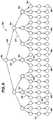
- FIG. 6illustrates an example model of a finite state machine (FSM) that can be implemented by the FSM lattice 30 .
- the FSM lattice 30can be configured (e.g., programmed) as a physical implementation of a FSM.
- a FSMcan be represented as a diagram 90 , (e.g., directed graph, undirected graph, pseudograph), which contains one or more root nodes 92 .
- the FSMcan be made up of several standard nodes 94 and terminal nodes 96 that are connected to the root nodes 92 and other standard nodes 94 through one or more edges 98 .
- a node 92 , 94 , 96corresponds to a state in the FSM.
- the edges 98correspond to the transitions between the states.
- Each of the nodes 92 , 94 , 96can be in either an active or an inactive state. When in the inactive state, a node 92 , 94 , 96 does not react (e.g., respond) to input data. When in an active state, a node 92 , 94 , 96 can react to input data. An upstream node 92 , 94 can react to the input data by activating a node 94 , 96 that is downstream from the node when the input data matches criteria specified by an edge 98 between the upstream node 92 , 94 and the downstream node 94 , 96 .
- a first node 94 that specifies the character ‘b’will activate a second node 94 connected to the first node 94 by an edge 98 when the first node 94 is active and the character ‘b’ is received as input data.
- upstreamrefers to a relationship between one or more nodes, where a first node that is upstream of one or more other nodes (or upstream of itself in the case of a loop or feedback configuration) refers to the situation in which the first node can activate the one or more other nodes (or can activate itself in the case of a loop).
- downstreamrefers to a relationship where a first node that is downstream of one or more other nodes (or downstream of itself in the case of a loop) can be activated by the one or more other nodes (or can be activated by itself in the case of a loop). Accordingly, the terms “upstream” and “downstream” are used herein to refer to relationships between one or more nodes, but these terms do not preclude the use of loops or other non-linear paths among the nodes.
- the root node 92can be initially activated and can activate downstream nodes 94 when the input data matches an edge 98 from the root node 92 .
- Nodes 94can activate nodes 96 when the input data matches an edge 98 from the node 94 .
- Nodes 94 , 96 throughout the diagram 90can be activated in this manner as the input data is received.
- a terminal node 96corresponds to a search result of a sequence of interest in the input data. Accordingly, activation of a terminal node 96 indicates that a sequence of interest has been received as the input data.
- arriving at a terminal node 96can indicate that a specific pattern of interest has been detected in the input data.
- each root node 92 , standard node 94 , and terminal node 96can correspond to a configurable element in the FSM lattice 30 .
- Each edge 98can correspond to connections between the configurable elements.
- a standard node 94 that transitions to (e.g., has an edge 98 connecting to) another standard node 94 or a terminal node 96corresponds to a configurable element that transitions to (e.g., provides an output to) another configurable element.
- the root node 92does not have a corresponding configurable element.
- node 92is described as a root node and nodes 96 are described as terminal nodes, there may not necessarily be a particular “start” or root node and there may not necessarily be a particular “end” or output node. In other words, any node may be a starting point and any node may provide output.
- each of the configurable elementscan also be in either an active or inactive state.
- a given configurable elementwhen inactive, does not react to the input data at a corresponding data input block 52 .
- An active configurable elementcan react to the input data at the data input block 52 , and can activate a downstream configurable element when the input data matches the setting of the configurable element.
- the configurable elementcan be coupled to the output block 54 to provide an indication of a search result to an external device.
- An image loaded onto the FSM lattice 30 via the programming interface 56can configure the configurable elements and special purpose elements, as well as the connections between the configurable elements and special purpose elements, such that a desired FSM is implemented through the sequential activation of nodes based on reactions to the data at the data input block 52 .
- a configurable elementremains active for a single data cycle (e.g., a single character, a set of characters, a single clock cycle) and then becomes inactive unless re-activated by an upstream configurable element.
- a terminal node 96can be considered to store a compressed history of past search results.
- the one or more patterns of input data required to reach a terminal node 96can be represented by the activation of that terminal node 96 .
- the output provided by a terminal node 96is binary, for example, the output indicates whether a search result for a pattern of interest has been generated or not.
- the ratio of terminal nodes 96 to standard nodes 94 in a diagram 90may be quite small. In other words, although there may be a high complexity in the FSM, the output of the FSM may be small by comparison.
- the output of the FSM lattice 30can comprise a state vector.
- the state vectorcomprises the state (e.g., activated or not activated) of configurable elements of the FSM lattice 30 .
- the state vectorcan include the state of all or a subset of the configurable elements whether or not the configurable elements corresponds to a terminal node 96 .
- the state vectorincludes the states for the configurable elements corresponding to terminal nodes 96 .
- the outputcan include a collection of the indications provided by all terminal nodes 96 of a diagram 90 .
- the state vectorcan be represented as a word, where the binary indication provided by each terminal node 96 comprises one bit of the word. This encoding of the terminal nodes 96 can provide an effective indication of the detection state (e.g., whether and what sequences of interest have been detected) for the FSM lattice 30 .
- the FSM lattice 30can be programmed to implement a pattern recognition function.
- the FSM lattice 30can be configured to recognize one or more data sequences (e.g., signatures, patterns) in the input data.
- data sequencese.g., signatures, patterns
- an indication of that recognitioncan be provided at the output block 54 .
- the pattern recognitioncan recognize a string of symbols (e.g., ASCII characters) to, for example, identify malware or other data in network data.
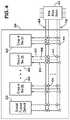
- FIG. 7illustrates an example of hierarchical structure 100 , wherein two levels of FSM lattices 30 are coupled in series and used to analyze data.
- the hierarchical structure 100includes a first FSM lattice 30 A and a second FSM lattice 30 B arranged in series.
- Each FSM lattice 30includes a respective data input block 52 to receive data input, a programming interface block 56 to receive configuring signals and an output block 54 .
- the first FSM lattice 30 Ais configured to receive input data, for example, raw data at a data input block.
- the first FSM lattice 30 Areacts to the input data as described above and provides an output at an output block.
- the output from the first FSM lattice 30 Ais sent to a data input block of the second FSM lattice 30 B.
- the second FSM lattice 30 Bcan then react based on the output provided by the first FSM lattice 30 A and provide a corresponding output signal 102 of the hierarchical structure 100 .
- This hierarchical coupling of two FSM lattices 30 A and 30 B in seriesprovides a means to provide data regarding past search results in a compressed word from a first FSM lattice 30 A to a second FSM lattice 30 B.
- the data providedcan effectively be a summary of complex matches (e.g., sequences of interest) that were recorded by the first FSM lattice 30 A.
- FIG. 7Aillustrates a second two-level hierarchy 100 of FSM lattices 30 A, 30 B, 30 C, and 30 D, which allows the overall FSM 100 (inclusive of all or some of FSM lattices 30 A, 30 B, 30 C, and 30 D) to perform two independent levels of analysis of the input data.
- the first levele.g., FSM lattice 30 A, FSM lattice 30 B, and/or FSM lattice 30 C
- the outputs of the first level(e.g., FSM lattice 30 A, FSM lattice 30 B, and/or FSM lattice 30 C) become the inputs to the second level, (e.g., FSM lattice 30 D).
- FSM lattice 30 Dperforms further analysis of the combination the analysis already performed by the first level (e.g., FSM lattice 30 A, FSM lattice 30 B, and/or FSM lattice 30 C). By connecting multiple FSM lattices 30 A, 30 B, and 30 C together, increased knowledge about the data stream input may be obtained by FSM lattice 30 D.
- the first level of the hierarchy(implemented by one or more of FSM lattice 30 A, FSM lattice 30 B, and FSM lattice 30 C) can, for example, perform processing directly on a raw data stream.
- a raw data streamcan be received at an input block 52 of the first level FSM lattices 30 A, 30 B, and/or 30 C and the configurable elements of the first level FSM lattices 30 A, 30 B, and/or 30 C can react to the raw data stream.
- the second level (implemented by the FSM lattice 30 D) of the hierarchycan process the output from the first level.
- the second level FSM lattice 30 Dreceives the output from an output block 54 of the first level FSM lattices 30 A, 30 B, and/or 30 C at an input block 52 of the second level FSM lattice 30 D and the configurable elements of the second level FSM lattice 30 D can react to the output of the first level FSM lattices 30 A, 30 B, and/or 30 C. Accordingly, in this example, the second level FSM lattice 30 D does not receive the raw data stream as an input, but rather receives the indications of search results for patterns of interest that are generated from the raw data stream as determined by one or more of the first level FSM lattices 30 A, 30 B, and/or 30 C.
- the second level FSM lattice 30 Dcan implement a FSM 100 that recognizes patterns in the output data stream from the one or more of the first level FSM lattices 30 A, 30 B, and/or 30 C.
- the second level FSM lattice 30 Dcan additionally receive the raw data stream as an input, for example, in conjunction with the indications of search results for patterns of interest that are generated from the raw data stream as determined by one or more of the first level FSM lattices 30 A, 30 B, and/or 30 C.
- the second level FSM lattice 30 Dmay receive inputs from multiple other FSM lattices in addition to receiving output from the one or more of the first level FSM lattices 30 A, 30 B, and/or 30 C. Likewise, the second level FSM lattice 30 D may receive inputs from other devices. The second level FSM lattice 30 D may combine these multiple inputs to produce outputs. Finally, while only two levels of FSM lattices 30 A, 30 B, 30 C, and 30 D are illustrated, it is envisioned that additional levels of FSM lattices may be stacked such that there are, for example, three, four, 10, 100, or more levels of FSM lattices.
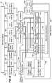
- FIG. 8illustrates an example of a method 110 for a compiler to convert source code into an image used to configure a FSM lattice, such as lattice 30 , to implement a FSM.
- Method 110includes parsing the source code into a syntax tree (block 112 ), converting the syntax tree into an automaton (block 114 ), optimizing the automaton (block 116 ), converting the automaton into a netlist (block 118 ), placing the netlist on hardware (block 120 ), routing the netlist (block 122 ), and publishing the resulting image (block 124 ).
- the compiler 20includes an application programming interface (API) that allows software developers to create images for implementing FSMs on the FSM lattice 30 .
- the compiler 20provides methods to convert an input set of regular expressions in the source code into an image that is configured to configure the FSM lattice 30 .
- the compiler 20can be implemented by instructions for a computer having a von Neumann architecture. These instructions can cause a processor 12 on the computer to implement the functions of the compiler 20 .
- the instructionswhen executed by the processor 12 , can cause the processor 12 to perform actions as described in blocks 112 , 114 , 116 , 118 , 120 , 122 , and 124 on source code that is accessible to the processor 12 .
- the source codedescribes search strings for identifying patterns of symbols within a group of symbols.
- the source codecan include a plurality of regular expressions (regexes).
- a regexcan be a string for describing a symbol search pattern. Regexes are widely used in various computer domains, such as programming languages, text editors, network security, and others.
- the regular expressions supported by the compilerinclude criteria for the analysis of unstructured data. Unstructured data can include data that is free form and has no indexing applied to words within the data. Words can include any combination of bytes, printable and non-printable, within the data.
- the compilercan support multiple different source code languages for implementing regexs including Perl, (e.g., Perl compatible regular expressions (PCRE)), PHP, Java, and .NET languages.
- PCEPerl compatible regular expressions
- the compiler 20can parse the source code to form an arrangement of relationally connected operators, where different types of operators correspond to different functions implemented by the source code (e.g., different functions implemented by regexes in the source code). Parsing source code can create a generic representation of the source code.
- the generic representationcomprises an encoded representation of the regexs in the source code in the form of a tree graph known as a syntax tree.
- the examples described hereinrefer to the arrangement as a syntax tree (also known as an “abstract syntax tree”) in other examples, however, a concrete syntax tree as part of the abstract syntax tree, a concrete syntax tree in place of the abstract syntax tree, or other arrangement can be used.
- the compiler 20can support multiple languages of source code, parsing converts the source code, regardless of the language, into a non-language specific representation, e.g., a syntax tree. Thus, further processing (blocks 114 , 116 , 118 , 120 ) by the compiler 20 can work from a common input structure regardless of the language of the source code.
- syntax treeincludes a plurality of operators that are relationally connected.
- a syntax treecan include multiple different types of operators. For example, different operators can correspond to different functions implemented by the regexes in the source code.
- the syntax treeis converted into an automaton.
- An automatoncomprises a software model of a FSM which may, for example, comprise a plurality of states.
- the operators and relationships between the operators in the syntax treeare converted into states with transitions between the states.
- conversion of the automatonis accomplished based on the hardware of the FSM lattice 30 .
- input symbols for the automatoninclude the symbols of the alphabet, the numerals 0-9, and other printable characters.
- the input symbolsare represented by the byte values 0 through 255 inclusive.
- an automatoncan be represented as a directed graph where the nodes of the graph correspond to the set of states.
- a transition from state p to state q on an input symbol ⁇ , i.e. ⁇ (p, ⁇ )is shown by a directed connection from node p to node q.
- a reversal of an automatonproduces a new automaton where each transition p ⁇ q on some symbol ⁇ is reversed q ⁇ p on the same symbol.
- start statesbecome final states and the final states become start states.
- the language recognized (e.g., matched) by an automatonis the set of all possible character strings which when input sequentially into the automaton will reach a final state. Each string in the language recognized by the automaton traces a path from the start state to one or more final states.
- the automatonis optimized to reduce its complexity and size, among other things.
- the automatoncan be optimized by combining redundant states.
- the optimized automatonis converted into a netlist. Converting the automaton into a netlist maps each state of the automaton to a hardware element (e.g., STEs 34 , 36 , other elements) on the FSM lattice 30 , and determines the connections between the hardware elements.
- a hardware elemente.g., STEs 34 , 36 , other elements
- the netlistis placed to select a specific hardware element of the target device (e.g., STEs 34 , 36 , special purpose elements 58 ) corresponding to each node of the netlist.
- placingselects each specific hardware element based on general input and output constraints for of the FSM lattice 30 .
- the placed netlistis routed to determine the settings for the configurable switching elements (e.g., inter-block switching elements 40 , intra-block switching elements 42 , and intra-row switching elements 44 ) in order to couple the selected hardware elements together to achieve the connections describe by the netlist.
- the settings for the configurable switching elementsare determined by determining specific conductors of the FSM lattice 30 that will be used to connect the selected hardware elements, and the settings for the configurable switching elements. Routing can take into account more specific limitations of the connections between the hardware elements than can be accounted for via the placement at block 120 . Accordingly, routing may adjust the location of some of the hardware elements as determined by the global placement in order to make appropriate connections given the actual limitations of the conductors on the FSM lattice 30 .
- the placed and routed netlistcan be converted into a plurality of bits for configuring a FSM lattice 30 .
- the plurality of bitsare referred to herein as an image (e.g., binary image).
- an imageis published by the compiler 20 .
- the imagecomprises a plurality of bits for configuring specific hardware elements of the FSM lattice 30 .
- the bitscan be loaded onto the FSM lattice 30 to configure the state of STEs 34 , 36 , the special purpose elements 58 , and the configurable switching elements such that the programmed FSM lattice 30 implements a FSM having the functionality described by the source code.
- Placement (block 120 ) and routing (block 122 )can map specific hardware elements at specific locations in the FSM lattice 30 to specific states in the automaton. Accordingly, the bits in the image can configure the specific hardware elements to implement the desired function(s).
- the imagecan be published by saving the machine code to a computer readable medium.
- the imagecan be published by displaying the image on a display device.
- the imagecan be published by sending the image to another device, such as a configuring device for loading the image onto the FSM lattice 30 .
- the imagecan be published by loading the image onto a FSM lattice (e.g., the FSM lattice 30 ).
- an imagecan be loaded onto the FSM lattice 30 by either directly loading the bit values from the image to the STEs 34 , 36 and other hardware elements or by loading the image into one or more registers and then writing the bit values from the registers to the STEs 34 , 36 and other hardware elements.
- the hardware elementse.g., STEs 34 , 36 , special purpose elements 58 , configurable switching elements 40 , 42 , 44
- the FSM lattice 30are memory mapped such that a configuring device and/or computer can load the image onto the FSM lattice 30 by writing the image to one or more memory addresses.
- Method examples described hereincan be machine or computer-implemented at least in part. Some examples can include a computer-readable medium or machine-readable medium encoded with instructions operable to configure an electronic device to perform methods as described in the above examples.
- An implementation of such methodscan include code, such as microcode, assembly language code, a higher-level language code, or the like. Such code can include computer readable instructions for performing various methods. The code may form portions of computer program products. Further, the code may be tangibly stored on one or more volatile or non-volatile computer-readable media during execution or at other times.
- These computer-readable mediamay include, but are not limited to, hard disks, removable magnetic disks, removable optical disks (e.g., compact disks and digital video disks), magnetic cassettes, memory cards or sticks, random access memories (RAMs), read only memories (ROMs), and the like.
- the state machine engine 14is configured to receive data from a source, such as the memory 16 over a data bus.
- datamay be sent to the state machine engine 14 through a bus interface, such as a double data rate three (DDR3) bus interface 130 .
- the DDR3 bus interface 130may be capable of exchanging (e.g., providing and receiving) data at a rate greater than or equal to 1 GByte/sec. Such a data exchange rate may be greater than a rate that data is analyzed by the state machine engine 14 .
- the bus interface 130may be any suitable bus interface for exchanging data to and from a data source to the state machine engine 14 , such as a NAND Flash interface, peripheral component interconnect (PCI) interface, gigabit media independent interface (GMMI), etc.
- the state machine engine 14includes one or more FSM lattices 30 configured to analyze data.
- Each FSM lattice 30may be divided into two half-lattices.
- each half latticemay include 24K STEs (e.g., STEs 34 , 36 ), such that the lattice 30 includes 48K STEs.
- the lattice 30may comprise any desirable number of STEs, arranged as previously described with regard to FIGS. 2-5 . Further, while only one FSM lattice 30 is illustrated, the state machine engine 14 may include multiple FSM lattices 30 , as previously described.
- Data to be analyzedmay be received at the bus interface 130 and provided to the FSM lattice 30 through a number of buffers and buffer interfaces.
- the data pathincludes input buffers 132 , an instruction buffer 133 , process buffers 134 , and an inter-rank (IR) bus and process buffer interface 136 .
- the input buffers 132are configured to receive and temporarily store data to be analyzed.
- there are two input buffers 132(input buffer A and input buffer B). Data may be stored in one of the two data input 132 , while data is being emptied from the other input buffer 132 , for analysis by the FSM lattice 30 .
- the bus interface 130may be configured to provide data to be analyzed to the input buffers 132 until the input buffers 132 are full. After the input buffers 132 are full, the bus interface 130 may be configured to be free to be used for other purpose (e.g., to provide other data from a data stream until the input buffers 132 are available to receive additional data to be analyzed). In the illustrated embodiment, the input buffers 132 may be 32 KBytes each.
- the instruction buffer 133is configured to receive instructions from the processor 12 via the bus interface 130 , such as instructions that correspond to the data to be analyzed and instructions that correspond to configuring the state machine engine 14 .
- the IR bus and process buffer interface 136may facilitate providing data to the process buffer 134 .
- the IR bus and process buffer interface 136can be used to ensure that data is processed by the FSM lattice 30 in order.
- the IR bus and process buffer interface 136may coordinate the exchange of data, timing data, packing instructions, etc. such that data is received and analyzed correctly.
- the IR bus and process buffer interface 136allows the analyzing of multiple data sets in parallel through a logical rank of FSM lattices 30 .
- multiple physical devicese.g., state machine engines 14 , chips, separate devices
- the term “rank”refers to a set of state machine engines 14 connected to the same chip select.
- the IR bus and process buffer interface 136may include a 32 bit data bus.
- the IR bus and process buffer interface 136may include any suitable data bus, such as a 128 bit data bus.
- the state machine engine 14also includes a de-compressor 138 and a compressor 140 to aid in providing state vector data through the state machine engine 14 .
- the compressor 140 and de-compressor 138work in conjunction such that the state vector data can be compressed to minimize the data providing times. By compressing the state vector data, the bus utilization time may be minimized.
- the compressor 140 and de-compressor 138can also be configured to handle state vector data of varying burst lengths. By padding compressed state vector data and including an indicator as to when each compressed region ends, the compressor 140 may improve the overall processing speed through the state machine engine 14 .
- the compressor 140may be used to compress results data after analysis by the FSM lattice 30 .
- the compressor 140 and de-compressor 138may also be used to compress and decompress configuration data.
- the compressor 140 and de-compressor 138may be disabled (e.g., turned off) such that data flowing to and/or from the compressor 140 and de-compressor 138 is not modified.
- an output of the FSM lattice 30can comprise a state vector.
- the state vectorcomprises the state (e.g., activated or not activated) of the STEs 34 , 36 of the FSM lattice 30 and the dynamic (e.g., current) count of the counter 58 .
- the state machine engine 14includes a state vector system 141 having a state vector cache memory 142 , a state vector memory buffer 144 , a state vector intermediate input buffer 146 , and a state vector intermediate output buffer 148 .
- the state vector system 141may be used to store multiple state vectors of the FSM lattice 30 and to provide a state vector to the FSM lattice 30 to restore the FSM lattice 30 to a state corresponding to the provided state vector.
- each state vectormay be temporarily stored in the state vector cache memory 142 .
- the state of each STE 34 , 36may be stored, such that the state may be restored and used in further analysis at a later time, while freeing the STEs 34 , 36 for further analysis of a new data set (e.g., search terms).
- the state vector cache memory 142allows storage of state vectors for quick retrieval and use, here by the FSM lattice 30 , for instance.
- the state vector cache memory 142may store up to 512 state vectors.
- the state vector datamay be exchanged between different state machine engines 14 (e.g., chips) in a rank.
- the state vector datamay be exchanged between the different state machine engines 14 for various purposes such as: to synchronize the state of the STEs 34 , 36 of the FSM lattices 30 of the state machine engines 14 , to perform the same functions across multiple state machine engines 14 , to reproduce results across multiple state machine engines 14 , to cascade results across multiple state machine engines 14 , to store a history of states of the STEs 34 , 36 used to analyze data that is cascaded through multiple state machine engines 14 , and so forth.
- the state vector datamay be used to quickly configure the STEs 34 , 36 of the FSM lattice 30 .
- the state vector datamay be used to restore the state of the STEs 34 , 36 to an initialized state (e.g., to prepare for a new input data set), or to restore the state of the STEs 34 , 36 to prior state (e.g., to continue searching of an interrupted or “split” input data set).
- the state vector datamay be provided to the bus interface 130 so that the state vector data may be provided to the processor 12 (e.g., for analysis of the state vector data, reconfiguring the state vector data to apply modifications, reconfiguring the state vector data to improve efficiency of the STEs 34 , 36 , and so forth).
- the state machine engine 14may provide cached state vector data (e.g., data stored by the state vector system 141 ) from the FSM lattice 30 to an external device.
- the external devicemay receive the state vector data, modify the state vector data, and provide the modified state vector data to the state machine engine 14 for configuring the FSM lattice 30 .
- the external devicemay modify the state vector data so that the state machine engine 14 may skip states (e.g., jump around) as desired.
- the state vector cache memory 142may receive state vector data from any suitable device.
- the state vector cache memory 142may receive a state vector from the FSM lattice 30 , another FSM lattice 30 (e.g., via the IR bus and process buffer interface 136 ), the de-compressor 138 , and so forth.
- the state vector cache memory 142may receive state vectors from other devices via the state vector memory buffer 144 .
- the state vector cache memory 142may provide state vector data to any suitable device.
- the state vector cache memory 142may provide state vector data to the state vector memory buffer 144 , the state vector intermediate input buffer 146 , and the state vector intermediate output buffer 148 .
- Additional bufferssuch as the state vector memory buffer 144 , state vector intermediate input buffer 146 , and state vector intermediate output buffer 148 , may be utilized in conjunction with the state vector cache memory 142 to accommodate rapid retrieval and storage of state vectors, while processing separate data sets with interleaved packets through the state machine engine 14 .
- each of the state vector memory buffer 144 , the state vector intermediate input buffer 146 , and the state vector intermediate output buffer 148may be configured to temporarily store one state vector.
- the state vector memory buffer 144may be used to receive state vector data from any suitable device and to provide state vector data to any suitable device.
- the state vector memory buffer 144may be used to receive a state vector from the FSM lattice 30 , another FSM lattice 30 (e.g., via the IR bus and process buffer interface 136 ), the de-compressor 138 , and the state vector cache memory 142 .
- the state vector memory buffer 144may be used to provide state vector data to the IR bus and process buffer interface 136 (e.g., for other FSM lattices 30 ), the compressor 140 , and the state vector cache memory 142 .
- the state vector intermediate input buffer 146may be used to receive state vector data from any suitable device and to provide state vector data to any suitable device.
- the state vector intermediate input buffer 146may be used to receive a state vector from an FSM lattice 30 (e.g., via the IR bus and process buffer interface 136 ), the de-compressor 138 , and the state vector cache memory 142 .
- the state vector intermediate input buffer 146may be used to provide a state vector to the FSM lattice 30 .
- the state vector intermediate output buffer 148may be used to receive a state vector from any suitable device and to provide a state vector to any suitable device.
- the state vector intermediate output buffer 148may be used to receive a state vector from the FSM lattice 30 and the state vector cache memory 142 .
- the state vector intermediate output buffer 148may be used to provide a state vector to an FSM lattice 30 (e.g., via the IR bus and process buffer interface 136 ) and the compressor 140 .
- an event vectormay be stored in a event vector memory 150 , whereby, for example, the event vector indicates at least one search result (e.g., detection of a pattern of interest).
- the event vectorcan then be sent to an event buffer 152 for transmission over the bus interface 130 to the processor 12 , for example.
- the resultsmay be compressed.
- the event vector memory 150may include two memory elements, memory element A and memory element B, each of which contains the results obtained by processing the input data in the corresponding input buffers 132 (e.g., input buffer A and input buffer B).
- each of the memory elementsmay be DRAM memory elements or any other suitable storage devices.
- the memory elementsmay operate as initial buffers to buffer the event vectors received from the FSM lattice 30 , along results bus 151 .
- memory element Amay receive event vectors, generated by processing the input data from input buffer A, along results bus 151 from the FSM lattice 30 .
- memory element Bmay receive event vectors, generated by processing the input data from input buffer B, along results bus 151 from the FSM lattice 30 .
- the event vectors provided to the results memory 150may indicate that a final result has been found by the FSM lattice 30 .
- the event vectorsmay indicate that an entire pattern has been detected.
- the event vectors provided to the results memory 150may indicate, for example, that a particular state of the FSM lattice 30 has been reached.
- the event vectors provided to the results memory 150may indicate that one state (i.e., one portion of a pattern search) has been reached, so that a next state may be initiated. In this way, the event vector 150 may store a variety of types of results.
- IR bus and process buffer interface 136may provide data to multiple FSM lattices 30 for analysis. This data may be time multiplexed. For example, if there are eight FSM lattices 30 , data for each of the eight FSM lattices 30 may be provided to all of eight IR bus and process buffer interfaces 136 that correspond to the eight FSM lattices 30 . Each of the eight IR bus and process buffer interfaces 136 may receive an entire data set to be analyzed. Each of the eight IR bus and process buffer interfaces 136 may then select portions of the entire data set relevant to the FSM lattice 30 associated with the respective IR bus and process buffer interface 136 . This relevant data for each of the eight FSM lattices 30 may then be provided from the respective IR bus and process buffer interfaces 136 to the respective FSM lattice 30 associated therewith.
- the event vector 150may operate to correlate each received result with a data input that generated the result. To accomplish this, a respective result indicator may be stored corresponding to, and in some embodiments, in conjunction with, each event vector received from the results bus 151 .
- the result indicatorsmay be a single bit flag. In another embodiment, the result indicators may be a multiple bit flag. If the result indicators may include a multiple bit flag, the bit positions of the flag may indicate, for example, a count of the position of the input data stream that corresponds to the event vector, the lattice that the event vectors correspond to, a position in set of event vectors, or other identifying information.
- results indicatorsmay include one or more bits that identify each particular event vector and allow for proper grouping and transmission of event vectors, for example, to compressor 140 .
- the ability to identify particular event vectors by their respective results indicatorsmay allow for selective output of desired event vectors from the event vector memory 150 .
- only particular event vectors generated by the FSM lattice 30may be selectively latched as an output.
- These result indicatorsmay allow for proper grouping and provision of results, for example, to compressor 140 .
- the ability to identify particular event vectors by their respective result indicatorsallow for selective output of desired event vectors from the result memory 150 .
- only particular event vectors provided by the FSM lattice 30may be selectively provided to compressor 140 .
- a buffermay store information related to more than one process whereas a register may store information related to a single process.
- the state machine engine 14may include control and status registers 154 .
- a program buffer systeme.g., restore buffers 156
- initial (e.g., starting) state vector datamay be provided from the program buffer system to the FSM lattice 30 (e.g., via the de-compressor 138 ).
- the de-compressor 138may be used to decompress configuration data (e.g., state vector data, routing switch data, STE 34 , 36 states, Boolean function data, counter data, match MUX data) provided to program the FSM lattice 30 .
- configuration datae.g., state vector data, routing switch data, STE 34 , 36 states, Boolean function data, counter data, match MUX data
- a repair map buffer system(e.g., save buffers 158 ) may also be provided for storage of data (e.g., save maps) for setup and usage.
- the data stored by the repair map buffer systemmay include data that corresponds to repaired hardware elements, such as data identifying which STEs 34 , 36 were repaired.
- the repair map buffer systemmay receive data via any suitable manner. For example, data may be provided from a “fuse map” memory, which provides the mapping of repairs done on a device during final manufacturing testing, to the save buffers 158 .
- the repair map buffer systemmay include data used to modify (e.g., customize) a standard programming file so that the standard programming file may operate in a FSM lattice 30 with a repaired architecture (e.g., bad STEs 34 , 36 in a FSM lattice 30 may be bypassed so they are not used).
- the compressor 140may be used to compress data provided to the save buffers 158 from the fuse map memory.
- the bus interface 130may be used to provide data to the restore buffers 156 and to provide data from the save buffers 158 .
- the data provided to the restore buffers 156 and/or provided from the save buffers 158may be compressed.
- datais provided to the bus interface 130 and/or received from the bus interface 130 via a device external to the state machine engine 14 (e.g., the processor 12 , the memory 16 , the compiler 20 , and so forth).
- the device external to the state machine engine 14may be configured to receive data provided from the save buffers 158 , to store the data, to analyze the data, to modify the data, and/or to provide new or modified data to the restore buffers 156 .
- the state machine engine 14includes a lattice programming and instruction control system 159 used to configure (e.g., program) the FSM lattice 30 as well as provide inserted instructions, as will be described in greater detail below.
- the lattice programming and instruction control system 159may receive data (e.g., configuration instructions) from the instruction buffer 133 .
- the lattice programming and instruction control system 159may receive data (e.g., configuration data) from the restore buffers 156 .
- the lattice programming and instruction control system 159may use the configuration instructions and the configuration data to configure the FSM lattice 30 (e.g., to configure routing switches, STEs 34 , 36 , Boolean cells, counters, match MUX) and may use the inserted instructions to correct errors during the operation of the state machine engine 14 .
- the lattice programming and instruction control system 159may also use the de-compressor 138 to de-compress data and the compressor 140 to compress data (e.g., for data exchanged with the restore buffers 156 and the save buffers 158 ).
- the row 38may include configurable intra-row switching elements 44 and row interconnection/interconnect conductors 68 , 70 (which can also be referred to as “row routing lines”, as described below).
- Row 38 of FIG. 10may include eight GOTS 60 , a special purpose element 58 , inputs 62 , inputs 64 , outputs 66 , a match element 160 , a plurality of row routing lines 162 , 164 , 166 , 168 , 170 , 172 , 174 , 176 , 178 , 180 , 182 , 184 , 186 , 188 , 190 , and 192 (collectively referred to hereafter as “row routing lines 162 - 192 ”), a special purpose element routing line 194 , and a plurality of junction points 196 .
- row routing lines 162 - 192illustrate a more detailed example of the row interconnection conductors 68 , 70 of, for example, FIG. 4 . Additionally, the row routing lines 162 - 192 , the special purpose element routing line 194 , and the plurality of junction points 196 may be collectively referred to as a local routing matrix 195 . Thus, the local routing matrix 195 may be coupled to all pairs of SMEs 34 , 36 for the GOTs 60 in a particular row 38 .
- each GOT 60receives an input 62 , which may be a unified enable input, to operate as an enable signal for a detection cell 86 of a SME 34 .
- each GOT 60also receives an input 64 , which may also be a unified enable input, to operate as an enable signal for a detection cell 86 of a SME 36 .
- unified enable inputs 62 , 64may activate the detection cells 86 of the SMEs 34 , 36 to output a respective result of an analysis performed by the respective SME, for example, at least one search result in an analyzed data stream from a single SME 34 , which may be utilized in conjunction with results from other SMEs 34 , 36 to, for example, search for a pattern in a data stream.
- unified enable input 62 and unified enable input 64allow for selective activation of the SMEs 34 , 36 so that results generated by each of the active SMEs 34 , 36 may be utilized as part of an overall broader analysis of a data stream.
- the result generated by an SME 34 , 36 of a GOT 60may be selectively provided from the GOT on output 66 .
- the possible outputs of the GOT 60may include no output, an output of the first SME 34 , i.e., output 72 , an output of the second SME 36 , i.e., output 74 , or the output of the first SME 34 or the output of the second SME 36 , i.e., output 72 or output 74 .
- a GOT 60may be programmed to output a selected result from a GOT 60 . This programming may be accomplished, for example, based on a loaded image performed during an initial programming stage of the FSM lattice 30 .
- Results from the GOTs 60may be provided to a match element 160 , which may operate to output a selected result generated from the row 38 for a given data stream search or a portion of a data stream search.
- row 38may include row routing lines 162 - 192 (which may also be referred to as row interconnection/interconnect conductors).
- row routing lines 162 - 192which may also be referred to as row interconnection/interconnect conductors.
- fewer or more row routing linesmay be utilized in conjunction with the row 38 .
- Each of the row routing lines 162 - 192may be utilized to provide enable signals for any of the SMEs 34 , 36 of one or more GOTS 60 along inputs 62 , 64 . Accordingly, through use of these row routing lines 162 - 192 , any particular detection cell 86 for any particular SME (e.g., SME 34 ) may be activated. This may be accomplished by selectively coupling (e.g., in accordance with a loaded image) the row routing lines 162 - 192 to unified enable inputs 62 , 64 of the SMEs 34 , 36 .
- the row routing lines 162 - 192may be divided up amongst two SMEs 34 , 36 of a given GOT 60 .
- row routing lines 162 , 164 , 166 , 168 , 170 , 172 , 174 , and 176may be utilized to activate any of the SMEs 34 , 36 in the row 38 .
- a GOT 60may transmit an output 66 to the row routing line coupled thereto, for example, row routing line 162 . This signal may be transmitted into the intra-block switch, where it may be routed, for example, on row routing line 164 to an additional GOT 60 in the row 38 .
- row routing lines 178 , 182 , 186 , and 190may activate SMEs 34 in row 38 , for example, by receiving signals from intra-block switch 42 , while row routing lines 180 , 184 , 188 , and 192 may activate SMEs 36 in row 38 via, for example, signals received from the intra-block switch 42 .
- the overall number of row routing lines 162 - 192may be reduced, while still allowing for overall flexibility and the ability to activate any detection cell 86 of any of the SMEs 34 , 36 in a row 38 .
- each of the row routing lines 162 - 192includes a plurality of junction points 196 .
- These junction points 196may include all routing line crossings illustrated with a solid circle in FIG. 10 and may, for example, include the intra-row switching elements 44 of FIG. 3 , since the junction points 196 may be utilized to selectively couple any GOT 60 to any other GOT 60 , or any GOT 60 to any other element (e.g., a special purpose element 58 ) within the row 38 (or, for that matter, within another row and/or another block).
- these connectionsmay be limited by available junction points 196 .
- each of row routing lines 162 , 164 , 166 , 168 , 170 , 172 , 174 , and 176may be utilized to activate any of the SMEs 34 , 36 in the row 38 .
- each of row routing lines 162 , 164 , 166 , 168 , 170 , 172 , 174 , and 176also are selectively able to be coupled to the output of a respective different one of the GOTs 60 .
- an output from any one of the GOTs 60may only be provided from that GOT 60 on a respective one of the row routing lines 162 , 164 , 166 , 168 , 170 , 172 , 174 , and 176 able to be coupled thereto.
- the row routing lines 162 , 164 , 166 , 168 , 170 , 172 , 174 , and 176are able to be coupled to the outputs 66 of the GOTs 60 , the row routing lines 162 , 164 , 166 , 168 , 170 , 172 , 174 , and 176 may provide (e.g., drive-out) signals to the intra-block switch 42 .
- row routing lines 178 , 180 , 182 , 184 , 186 , 188 , 190 , and 192may receive (e.g. be driven by) signals from the intra-block switch 42 that may be received from, for example, other rows 38 or blocks 32 .
- the row 38may include a special purpose element routing line 194 coupled to a special purpose element 58 . Similar to row routing lines 162 , 164 , 166 , 168 , 170 , 172 , 174 , and 176 , the special purpose routing line 194 may provide (e.g., drive-out) signals to the intra-block switch 42 . In one embodiment, the special purpose element routing line 194 may also be able to be coupled to the match element 160 . For example, if the special purpose element 58 comprises a counter, an output of the counter may be provided along the special purpose routing line 194 .
- the special purpose element 58includes a Boolean logic element, such as a Boolean cell
- an output of the Boolean logic elementmay be provided along the special purpose routing line 194 .
- repetitive searchese.g., find an element ten times
- cascaded searchese.g., find elements x, y, and z
- cascaded searchese.g., find elements x, y, and z
- the intra-block switch 42may receive the row routing lines 162 - 192 as well as the special purpose element routing line 194 , and these lines may intersect various block routing lines 197 , 198 , 199 , 200 , 201 , 202 , 203 , 204 , 205 , 206 , 207 , 208 , 209 , 210 , 211 , and 212 (collectively referred to hereafter as “block routing lines 197 - 212 ”) at a plurality of junction points 213 .
- junction points 213may, for example, may be utilized to selectively couple row routing lines 162 - 192 to block routing lines 197 - 212 .
- each of row routing lines 162 , 164 , 166 , 168 , 170 , 172 , 174 , and 176may provide (e.g., drive-out, send, transmit, transfer, pass, etc.) signals to the intra-block switch 42
- row routing lines 178 , 180 , 182 , 184 , 186 , 188 , 190 , and 192may receive (e.g., drive-in) signals from the intra-block switch 42 .
- row routing lines 162 , 164 , 166 , 168 , 170 , 172 , 174 , and 176may be utilized to provide signals from the row 38 coupled to the intra-block switch 42 in FIG. 10 to adjacent rows 38 , such as those illustrated in FIG. 3 . Additionally or alternatively, row routing lines 162 , 164 , 166 , 168 , 170 , 172 , 174 , and 176 may be utilized to provide signals from the row 38 coupled to the intra-block switch 42 in FIG. 10 to other rows 38 in the block 32 and/or to the block routing buffer 48 .
- each of the row routing lines 178 , 180 , 182 , 184 , 186 , 188 , 190 , and 192may receive (e.g., drive-in) signals from the intra-block switch 42 . Accordingly, row routing lines 178 , 180 , 182 , 184 , 186 , 188 , 190 , and 192 may be utilized to provide signals to the row 38 coupled to the intra-block switch 42 in FIG. 10 from adjacent rows 38 , such as those illustrated in FIG. 3 .
- row routing lines 178 , 180 , 182 , 184 , 186 , 188 , 190 , and 192may be utilized to provide signals from the row 38 coupled to the intra-block switch 42 in FIG. 10 from the block routing buffer 48 . This may be accomplished by receiving signals generated in external blocks 32 or in adjacent rows 38 from one of the block routing lines 197 - 212 of FIG. 11 , since the block routing lines 197 - 212 are coupled to the various intra-block switches 42 and the block routing buffer 48 of FIG. 3 . This may allow row 38 to receive any results generated in adjacent rows 38 or even other blocks 32 along row routing lines 178 , 180 , 182 , 184 , 186 , 188 , 190 , and 192 .
- the intra-block switch 42may couple row 38 with adjacent rows 38 and other blocks 32 . Moreover, as discussed above, results from any particular row 38 may be passed from one block 32 to another block 32 .
- the block routing buffer 48may facilitate this transfer of information between blocks.
- the row routing lines 162 - 192 and/or the block routing lines 197 - 212may take up a substantial amount of area of the overall FSM lattice 30 . Indeed, in SMEs 34 , 36 may occupy as little as approximately 20%, approximately 15%, approximately 10%, approximately 5% or less of the area of a FSM lattice 30 with the remaining area taken up primarily by control circuitry and routing lines (e.g., row routing lines 162 - 192 and block routing lines 197 - 212 ). Accordingly, it may be desirable to reduce the overall amount of space dedicated to the routing lines of the FSM lattice 30 to allow for, for example, greater component density and/or overall reduction of the size of the FSM lattice 30 . Techniques for reducing the amount of routing lines will be discussed in greater detail below.
- the intra-group circuitry 37 of FIG. 12may include elements of the GOT 60 previously discussed with respect to FIG. 5 .
- the particular functionality and interconnection of these elements in the intra-group circuitry 37will be discussed in greater detail with respect to FIG. 12 .
- the intra-group circuitry 37 in FIG. 12includes inputs 62 , 64 and outputs 72 , 74 , which have been previously shown to be coupled to SMEs 34 , 36 . It should be noted that the inputs 62 , 64 and outputs 72 , 74 are referred to with respect to their respective relationship to the SMEs 34 , 36 and not necessarily their function in the intra-group circuitry 206 . Additionally, the intra-group circuitry 37 includes an OR gate 76 , a 3-to-1 multiplexer 78 , and switching elements 79 coupled to outputs 72 , 74 , respectively.
- the switching element 79 coupled to output 72may allow for the output 72 of SME 34 to be transmitted to the unified enable input 64 of the SME 36 , for example, to allow for cascading searches to occur. Additionally or alternatively, the switching element 79 coupled to output 72 may allow for the unified enable input 62 of SME 34 to be transmitted to the unified enable input 64 of the SME 36 and/or the output 72 of the SME 34 to be transmitted to the OR gate 76 . As previously discussed, allowing the unified enable input 62 of SME 34 to be transmitted to the unified enable input 64 of the SME 36 may allow for full addressing of all detection cell elements 86 in the SMEs 36 of a given row 38 via sharing of the row routing lines 174 - 204 .
- the switching element 79 coupled to output 74may allow for the output 74 of SME 36 to be transmitted to the unified enable input 62 of the SME 34 , for example, to allow for cascading searches to occur. Additionally or alternatively, the switching element 79 coupled to output 74 may allow for the unified enable input 64 of SME 36 to be transmitted to the unified enable input 62 of the SME 34 and/or the output 74 of the SME 36 to be transmitted to the OR gate 76 . Again, allowing the unified enable input 64 of SME 36 to be transmitted to the unified enable input 62 of the SME 34 may allow for full addressing of all detection cell elements 86 in the SMEs 34 of a given row 38 via sharing of the row routing lines 174 - 204 .
- the outputs 72 , 74can be looped back to the SMEs 34 , 36 that generated the outputs 72 , 74 by coupling the output 72 to input 62 via the illustrated switching elements 79 and coupling the output 77 to input 64 via the illustrated switching elements 79 .
- the 3-to-1 multiplexer 78 of the intra-group circuitry 206can be set to couple the output 66 of the GOT 60 to either a first SME 34 , a second SME 36 , or the OR gate 76 , which may be used to couple together both outputs 72 , 74 of the SMEs 34 , 36 to form the common output 66 of the GOT 60 .
- the 3-to-1 multiplexer 78may include a first output select input 208 and a second output select input 210 .
- these output select inputs 208 , 210may programmably select what output is transmitted on output 66 . This programming may be accomplished, for example, based on a loaded image performed during an initial programming stage of the FSM lattice 30 .
- the programming of the output select inputs 208 , 210may be accomplished, for example, based on dynamic programming instructions received during operation of the state machine engine 14 from the programming and instruction control system 159 .
- FIG. 13illustrates a truth table that sets forth an example of how the output select inputs 208 , 210 may programmably select the output 66 of the GOT 60 .
- the output 66 of the GOT 60will be the output of the OR gate 76 , i.e., output 72 logically ORed with output 74 .
- the 3-to-1 multiplexer 78programmably select no output, output 72 , output 74 , or output 72 logically ORed with output 74 as the output 66 of the GOT 60 .
- the 3-to-1 multiplexermay operate in other configurable configurations.
- the output select inputs 208 , 210may programmably select the output 66 of the GOT 60 in conjunction with a time-division multiplexing feature of the state machine engine 14 .
- the output select inputs 208 , 210may actively control when an output is transmitted for each of the GOTs 60 within the row 38 .
- the output 66 of each of the GOTs 60 of a row 38may share a single (common) row routing line (e.g., row routing line 162 ) by transmitting, in turn, outputs from output 66 to the common row routing line.
- each of the GOTs 60may utilize the routing line coupled thereto (e.g., row routing line 162 ) for a respective time period.
- the respective time periodsmay be equal for each GOT 60 coupled to the common routing line.
- the respective time periodsmay different for each GOT 60 coupled to the common routing line and may be based, for example, on the size and/or determined importance of a result being transmitted from output 66 .
- the number of row routing lines coupled to outputs 66 of the GOTs 60is reduced from eight row routing lines (e.g., row routing lines 162 - 176 ), as illustrated in FIG. 10 , to one row routing line (e.g., row routing line 162 ), as illustrated in FIG. 14 , with a corresponding reduction in an amount of space (e.g. footprint) utilized by the reduced number of row routing lines.
- more than one GOT 60is directly coupled to a row routing line (e.g., row routing line 162 ).
- two subgroups each including four GOTs 60may each share a respective common row routing line (e.g., one of row routing line 162 , 164 ) such that the number of row routing lines coupled to outputs 66 of the GOTs 60 is reduced from eight row routing lines (e.g., row routing lines 162 - 176 ), as illustrated in FIG. 10 , to two row routing lines (e.g., row routing lines 162 , 164 ), as illustrated in FIG. 15 .
- a respective common row routing linee.g., one of row routing line 162 , 164
- four subgroups each including two GOTs 60may each share a respective common row routing line (e.g., one of row routing line 162 , 164 , 166 , and 168 ) such that the number of row routing lines coupled to outputs 66 of the GOTs 60 is reduced from eight row routing lines (e.g., row routing lines 162 - 176 ), as illustrated in FIG. 10 , to four row routing lines (e.g., row routing lines 162 , 164 , 166 , and 168 )), as illustrated in FIG. 16 .
- the GOTsmay be divided into different numbers of subgroups than those discussed above as well, with accompanying savings in routing layout space being saved.
- operational speeds and/or chip density of the FSM lattice 30may be higher when more subgroups are utilized and the overall footprint of routing lines is reduced.
- the individual GOTs 60 in the subgroups discussed abovemay each utilize a respective routing line for a respective time period.
- each of the GOTs 60 of a subgroupmay utilize the routing line coupled thereto for a respective time period.
- time division multiplexing of the routing lines coupled to the GOTs 60may be implemented.
- the respective time periodsmay be equal for each GOT 60 of the subgroup or the respective time periods may different for each GOT 60 of the subgroup and may be based, for example, on the size and/or determined importance of a result being transmitted from output 66 .
- the control of the outputs 66 of the GOTs 60 of the subgroupsmay be controlled in a manner similar to that described above.
- the programming of the respective 3-to-1 multiplexers 78 of each of the GOTs 60 of a subgroupmay be accomplished, for example, based on a loaded image performed during an initial programming stage of the FSM lattice 30 .
- the programming of the output select inputs 208 , 210 of the respective 3-to-1 multiplexers 78 of each of the GOTs 60 of a subgroupmay be accomplished, for example, based on dynamic programming instructions received during operation of the state machine engine 14 from the programming and instruction control system 159 .
- FIG. 14illustrates the use of a common row routing line 214 for the outputs 66 of the GOTs 60 of a row 38 . More specifically, a single row routing line 214 is coupled to outputs 66 of the GOTs 60 , with a corresponding reduction in an amount of space (e.g. footprint) for routing lines. Additionally, row 38 may include row routing lines 216 , 218 that may be coupled to inputs 62 , 64 , respectively, of the GOTs 60 . Additionally, as illustrated in FIG. 14 , each of the row routing lines 214 , 216 , and 218 includes a plurality of junction points 196 , which may include all routing line crossings illustrated with a solid circle. As previously noted with respect to FIG.
- junction points 196may, for example, include the intra-row switching elements 44 of FIG. 3 , since the junction points 196 may be utilized to selectively couple a GOT 60 to another GOT 60 , or a GOT 60 to an additional element (e.g., a special purpose element 58 ) within the row 38 (or within another row and/or another block).
- additional elemente.g., a special purpose element 58
- row routing line 214may be coupled to a switching element 220 .
- the switching element 220may be a demultiplexer, for example, a 1 to 8 demultiplexer.
- the switching element 220may be coupled to row lines 162 - 176 .
- the switching element 220may operate to transmit individual signals received from row routing line 214 to intra-block switch 42 via one of the selected row lines 162 - 176 .
- the signals received from row routing line 214may include, for example, time division multiplexed signals from the GOTs 60 so that each of the GOTs 60 of row 38 may share row routing line 214 .
- each of the individual GOTs 60may utilize row routing line 214 for a respective portion of a time period to transmit their outputs 66 .
- the control of the outputs 66 of the GOTs 60may be controlled via programming of the respective 3-to-1 multiplexers 78 of each of the GOTs 60 .
- this programmingmay be based on a loaded image performed during an initial programming stage of the FSM lattice 30 or based on dynamic programming instructions received during operation of the state machine engine 14 from the programming and instruction control system 159 . In this manner, the GOTs 60 may share the row routing line 214 .
- the switching element 220may be used to route received signals, for example outputs 66 of the GOTs 60 , to one or more desired block routing lines coupled to routing lines 162 - 176 .
- FIG. 14also includes row routing lines 216 , 218 that may be coupled to inputs 62 , 64 , respectively, of the GOTs 60 .
- row routing lines 216 , 218may also transmit time division multiplexed signals.
- switching element 222may be coupled to row routing line 216 .
- Switching element 222may be, for example, a multiplexer (e.g., a 4 to 1 multiplexer) and may operate to transmit signals from any one of row line 178 , 182 , 186 , or 190 to an input 62 of one of the GOTs 60 coupled to row routing line 216 based on a time division routine in which row lines 178 , 182 , 186 , and 190 share, over a period of time, row routing line 216 .
- switching element 224may be coupled to row routing line 218 .
- Switching element 224may be, for example, a multiplexer (e.g., a 4 to 1 multiplexer) and may operate to transmit signals from any one of row line 180 , 184 , 188 , or 192 to an input 64 of one of the GOTs 60 coupled to row routing line 216 based on a time division routine in which row lines 180 , 184 , 188 , and 192 share, over a period of time, row routing line 218 . In this manner, through the use of switching elements 222 , 224 , the overall footprint related to routing lines of the row 38 may be further reduced.
- a multiplexere.g., a 4 to 1 multiplexer
- one of the inputs the inputs 62 , 64 of the GOTsmay be coupled to a respective storage element 226 .
- These storage elements 226may operate to hold and/or accumulate values for transmission to the inputs 62 , 64 . For example, if only portion of an input value to a GOT 60 is received in a given period of time (e.g., due to the time division multiplexing of signals along row routing lines 214 , 216 , and 218 ), that portion of the input value may be held until the remaining portions(s) of the input value has been received.
- This techniquemay also be utilized to transmit input values to the special purpose element 58 , which also may be coupled to a storage element 226 .
- Additional configurations of the routing matrix of row 38may include, for example, removal of one or both of switching elements 222 , 224 in conjunction with removal of the corresponding routing line ( 216 , 218 , as well as removal of the respective storage elements 226 coupled thereto). In this manner, only row routing line 228 may transmit time division multiplexed signals, while the remainder of the routing matrix of the row 38 operates as described in FIG. 10 .
- FIG. 15illustrates a row 38 that includes a common row routing line 228 for the outputs 66 of four of the GOTs 60 of the row 38 and a common row routing line 230 for the outputs 66 of the other four GOTs 60 of the row 38 . More specifically, two row routing lines 228 , 230 are coupled to outputs 66 of two subgroups 232 , 234 of the GOTs 60 , with a corresponding reduction in an amount of space (e.g. footprint) for routing lines.
- spacee.g. footprint
- row 38may include row routing lines 216 , 218 that may be coupled to inputs 62 , 64 , respectively, of the GOTs 60 and a plurality of junction points 196 , which may include all routing line crossings illustrated with a solid circle.
- row routing line 228may be coupled to a switching element 236 .
- the switching element 236may be a demultiplexer, for example, a 1 to 4 demultiplexer.
- the switching element 236may be coupled to row lines 162 - 168 .
- the switching element 236may operate to transmit individual signals received from row routing line 228 to intra-block switch 42 via one of the selected row lines 162 - 168 .
- the signals received from row routing line 228may include, for example, time division multiplexed signals from the GOTs 60 of subgroup 232 so that each of the GOTs 60 of subgroup 232 may share row routing line 228 .
- each of the individual GOTs 60 of subgroup 232may utilize row routing line 228 for a respective portion of a time period to transmit their outputs 66 .
- the control of the outputs 66 of the GOTs 60 of subgroup 232may be controlled via programming of the respective 3-to-1 multiplexers 78 of each of the GOTs 60 of subgroup 232 .
- this programmingmay be based on a loaded image performed during an initial programming stage of the FSM lattice 30 or based on dynamic programming instructions received during operation of the state machine engine 14 from the programming and instruction control system 159 . In this manner, the GOTs 60 of subgroup 232 may share the row routing line 228 .
- row routing line 230may be coupled to a switching element 238 .
- the switching element 238may be a demultiplexer, for example, a 1 to 4 demultiplexer.
- the switching element 238may be coupled to row lines 170 - 176 .
- the switching element 238may operate to transmit individual signals received from row routing line 230 to intra-block switch 42 via one of the selected row lines 170 - 176 .
- the signals received from row routing line 230may include, for example, time division multiplexed signals from the GOTs 60 of subgroup 234 so that each of the GOTs 60 of subgroup 234 may share row routing line 230 .
- each of the individual GOTs 60 of subgroup 234may utilize row routing line 230 for a respective portion of a time period to transmit their outputs 66 .
- the control of the outputs 66 of the GOTs 60 of subgroup 234may be controlled via programming of the respective 3-to-1 multiplexers 78 of each of the GOTs 60 of subgroup 234 .
- this programmingmay be based on a loaded image performed during an initial programming stage of the FSM lattice 30 or based on dynamic programming instructions received during operation of the state machine engine 14 from the programming and instruction control system 159 . In this manner, the GOTs 60 of subgroup 234 may share the row routing line 230 .
- the switching elements 236 , 238may be used to route received signals, for example outputs 66 of the GOTs 60 , to one or more desired block routing lines coupled to routing lines 162 - 176 .
- special purpose element 58is illustrated as being coupled to row routing line 230 .
- special purpose elementmay be coupled only to row routing line 230 , only coupled to row routing line 228 , or may be coupled to both row routing line 228 and row routing line 230 .
- additional configurations of the routing matrix of row 38may include, for example, removal of one or both of switching elements 222 , 224 in conjunction with removal of the corresponding routing line ( 216 , 218 , as well as removal of the respective storage elements 226 coupled thereto). In this manner, only row routing lines 228 , 230 may transmit time division multiplexed signals, while the remainder of the routing matrix of the row 38 operates as described in FIG. 10 .
- Other configurations of the routing matrix of row 38are illustrated in conjunction with FIG. 16 .
- FIG. 16illustrates a row 38 that includes a common row routing line 240 for the outputs 66 of two of the GOTs 60 of the row 38 , a common row routing line 242 for the outputs 66 of two additional GOTs 60 of the row 38 , a common row routing line 244 for the outputs 66 of two additional GOTs 60 of the row 38 , and a common row routing line 246 for the outputs 66 of the other additional GOTs 60 of the row 38 .
- row routing lines 240 , 242 , 244 , and 246are coupled to outputs 66 of four subgroups 248 , 250 , 252 , and 254 of the GOTs 60 , with a corresponding reduction in an amount of space (e.g. footprint) for routing lines.
- row 38may include row routing lines 216 , 218 that may be coupled to inputs 62 , 64 , respectively, of the GOTs 60 and a plurality of junction points 196 , which may include all routing line crossings illustrated with a solid circle.
- row routing line 240may be coupled to a switching element 256 .
- the switching element 256may be a demultiplexer, for example, a 1 to 2 demultiplexer.
- the switching element 256may be coupled to row lines 162 , 164 .
- the switching element 256may operate to transmit individual signals received from row routing line 240 to intra-block switch 42 via one of the selected row lines 162 or 164 .
- the signals received from row routing line 240may include, for example, time division multiplexed signals from the GOTs 60 of subgroup 248 so that each of the GOTs 60 of subgroup 248 may share row routing line 240 .
- each of the individual GOTs 60 of subgroup 248may utilize row routing line 240 for a respective portion of a time period to transmit their outputs 66 .
- the control of the outputs 66 of the GOTs 60 of subgroup 248may be controlled via programming of the respective 3-to-1 multiplexers 78 of each of the GOTs 60 of subgroup 248 .
- this programmingmay be based on a loaded image performed during an initial programming stage of the FSM lattice 30 or based on dynamic programming instructions received during operation of the state machine engine 14 from the programming and instruction control system 159 . In this manner, the GOTs 60 of subgroup 248 may share the row routing line 240 .
- row routing line 242may be coupled to a switching element 258 .
- the switching element 258may be a demultiplexer, for example, a 1 to 2 demultiplexer.
- the switching element 258may be coupled to row lines 166 , 168 .
- the switching element 258may operate to transmit individual signals received from row routing line 242 to intra-block switch 42 via one of the selected row lines 166 or 168 .
- the signals received from row routing line 242may include, for example, time division multiplexed signals from the GOTs 60 of subgroup 250 so that each of the GOTs 60 of subgroup 250 may share row routing line 242 .
- each of the individual GOTs 60 of subgroup 250may utilize row routing line 242 for a respective portion of a time period to transmit their outputs 66 .
- the control of the outputs 66 of the GOTs 60 of subgroup 250may be controlled via programming of the respective 3-to-1 multiplexers 78 of each of the GOTs 60 of subgroup 250 .
- this programmingmay be based on a loaded image performed during an initial programming stage of the FSM lattice 30 or based on dynamic programming instructions received during operation of the state machine engine 14 from the programming and instruction control system 159 . In this manner, the GOTs 60 of subgroup 250 may share the row routing line 242 .
- row routing line 244may be coupled to a switching element 260 .
- the switching element 260may be a demultiplexer, for example, a 1 to 2 demultiplexer.
- the switching element 260may be coupled to row lines 170 , 172 .
- the switching element 260may operate to transmit individual signals received from row routing line 244 to intra-block switch 42 via one of the selected row lines 170 or 172 .
- the signals received from row routing line 244may include, for example, time division multiplexed signals from the GOTs 60 of subgroup 252 so that each of the GOTs 60 of subgroup 252 may share row routing line 244 .
- each of the individual GOTs 60 of subgroup 252may utilize row routing line 244 for a respective portion of a time period to transmit their outputs 66 .
- the control of the outputs 66 of the GOTs 60 of subgroup 252may be controlled via programming of the respective 3-to-1 multiplexers 78 of each of the GOTs 60 of subgroup 252 .
- this programmingmay be based on a loaded image performed during an initial programming stage of the FSM lattice 30 or based on dynamic programming instructions received during operation of the state machine engine 14 from the programming and instruction control system 159 . In this manner, the GOTs 60 of subgroup 252 may share the row routing line 244 .
- row routing line 246may be coupled to a switching element 262 .
- the switching element 262may be a demultiplexer, for example, a 1 to 2 demultiplexer.
- the switching element 262may be coupled to row lines 174 , 176 .
- the switching element 262may operate to transmit individual signals received from row routing line 246 to intra-block switch 42 via one of the selected row lines 174 or 176 .
- the signals received from row routing line 246may include, for example, time division multiplexed signals from the GOTs 60 of subgroup 254 so that each of the GOTs 60 of subgroup 254 may share row routing line 246 .
- each of the individual GOTs 60 of subgroup 254may utilize row routing line 246 for a respective portion of a time period to transmit their outputs 66 .
- the control of the outputs 66 of the GOTs 60 of subgroup 254may be controlled via programming of the respective 3-to-1 multiplexers 78 of each of the GOTs 60 of subgroup 254 .
- this programmingmay be based on a loaded image performed during an initial programming stage of the FSM lattice 30 or based on dynamic programming instructions received during operation of the state machine engine 14 from the programming and instruction control system 159 . In this manner, the GOTs 60 of subgroup 254 may share the row routing line 246 .
- the switching elements 256 - 262may be used to route received signals, for example outputs 66 of the GOTs 60 , to one or more desired block routing lines coupled to routing lines 162 - 176 .
- special purpose element 58is illustrated as being coupled to row routing line 246 .
- special purpose elementmay be coupled only to row routing line 240 or 242 or 244 or 246 and/or any combination thereof.
- additional configurations of the routing matrix of row 38may include, for example, removal of one or more of switching elements 222 , 224 in conjunction with removal of the corresponding routing line ( 216 , 218 , as well as removal of the respective storage elements 226 coupled thereto). In this manner, only row routing lines 240 - 246 may transmit time division multiplexed signals, while the remainder of the routing matrix of the row 38 operates as described in FIG. 10 .
- FIG. 17shows one example of an embodiment which could reduce the block routing lines 197 , 198 compared to the structure of FIG. 11 , by using transferring data in time divisional manner on the block routing lines.
- the reduced block routing lines 197 , 198may be coupled to coupled to inter-block switching elements 40 of FIG. 3 , which may be coupled to the input block 52 and the output block 54 of FIG. 2 .
- corresponding demultiplexersmay be provided in the output block 54 (or may be provided between the inter-block switching elements 40 and the output block 54 ) to allow for demultiplexing of the signals received by the output block 54 from the inter-block switching elements 40 prior to their transfer to, for example, processor 12 .
- corresponding multiplexersmay be provided in the input block 52 (or may be provided between the inter-block switching elements 40 and the input block 52 ) to allow for multiplexing of the signals transmitted to the inter-block switching elements 40 from the input block 52 subsequent to their transfer from, for example, processor 12 .
- the processor 12may be configured to allow for multiplexed signals to be transmitted to the input block 52 and received from the output block 54 such that processor 12 can perform a transfer with the state machine engine 14 in a time divisional fashion.
- the intra-block switch 42may be coupled to row routing lines 162 - 192 as well as the special purpose element routing line 194 .
- each of row routing lines 162 , 164 , 166 , 168 , 170 , 172 , 174 , and 176may provide (e.g., drive-out, send, transmit, transfer, pass, etc.) signals to the intra-block switch 42
- row routing lines 178 , 180 , 182 , 184 , 186 , 188 , 190 , and 192may receive (e.g., drive-in) signals from the intra-block switch 42 .
- row routing lines 162 , 164 , 166 , 168 , 170 , 172 , 174 , and 176may be utilized to provide signals from the row 38 coupled to the intra-block switch 42 in FIGS. 10 and 14 - 16 to adjacent rows 38 , such as those illustrated in FIG. 3 . Additionally or alternatively, row routing lines 162 , 164 , 166 , 168 , 170 , 172 , 174 , and 176 may be utilized to provide signals from the row 38 coupled to the intra-block switch 42 in FIGS. 10 and 14-16 to other rows 38 in the block 32 and/or to the block routing buffer 48 .
- row routing lines 162 - 176may be coupled to a switching element 264 .
- the switching element 264may be a multiplexer, for example, an 8 to 1 multiplexer.
- the switching element 264may be coupled to row lines 162 - 176 and to block routing line 197 to transmit signals from the row 38 coupled to the intra-block switch 42 in FIGS. 10 and 14-16 to other rows 38 in the block 32 and/or to the block routing buffer 48 .
- the switching element 264may be omitted and block routing line 197 may be directly coupled to, for example, row routing line 214 (e.g., also allowing for the omission of switching element 220 ).
- block routing line 197may carry signals related to the operation of multiple GOTs 60 of row 38 .
- the sharing of block routing line 197may be accomplished via time division multiplexing, similar to that previously discussed, whereby multiple signals are individually transmitted during a set portion of a total time period allotted for signal transmission along block routing line 197 .
- individual GOTs 60may have results transmitted along block routing line 197 for a respective portion of a time period.
- the control of the outputs 66 of the GOTs 60 are transmittedmay be controlled via programming of the respective 3-to-1 multiplexers 78 of each of the GOTs 60 as well as preset and/or dynamic control of the switching element 264 (e.g., from the programming and instruction control system 159 ).
- the overall footprint of the routing matrix for the intra-block switchmay be reduced.
- row routing lines 178 - 192may be coupled to a switching element 266 .
- the switching element 266may be a demultiplexer, for example, a 1 to 8 demultiplexer.
- the switching element 266may be coupled to row lines 178 - 192 and to block routing line 198 to transmit signals from other rows 38 in the block 32 and/or to the block routing buffer 48 to the row 38 directly coupled to the intra-block switch 42 of FIG. 17 .
- storage elements 226may be present to accumulate or buffer input values for transmission to row 38 via row lines 178 - 192 .
- the switching element 264 and the storage elements 226may be omitted and block routing line 198 may be directly coupled to, for example, row routing lines 216 , 218 (e.g., also allowing for the omission of switching elements 222 , 224 ).
- block routing line 198may carry signals related to the operation of multiple GOTs 60 of additional rows 38 .
- the sharing of block routing line 198may be accomplished via time division multiplexing, similar to that previously discussed, whereby multiple signals are individually transmitted during a set portion of a total time period allotted for signal transmission along block routing line 198 , such that individual results may be transmitted along block routing line 198 for a respective portion of a time period.
- Control of the transmission of the results along 198 as well as control of the switching element 266may be preset and/or dynamic (e.g., from the programming and instruction control system 159 ).
- the overall footprint of the routing matrix for the intra-block switch 42may be reduced.
- FIG. 18illustrates an intra-block switch 42 that includes switching elements 268 , 270 that may be coupled to row routing lines 162 - 168 and 170 - 176 , respectively, to provide (e.g., drive-out, send, transmit, transfer, pass, etc.) signals to the intra-block switch 42 .
- intra-block switch 42includes switching elements 272 , 274 that may be coupled to row routing lines 178 - 184 and 186 - 192 , respectively, to receive (e.g., drive-in) signals to the row 38 coupled to the intra-block switch 42 .
- the switching elements 268 and 270may be multiplexers, for example, 4 to 1 multiplexers while switching elements 272 and 274 may be demultiplexers, for example, 1 to 4 demultiplexers.
- the switching elements 268 , 270may transmit signals from the row 38 coupled to the intra-block switch 42 in FIGS. 10 and 14-16 to other rows 38 in the block 32 and/or to the block routing buffer 48 .
- the switching elements 268 , 270may be omitted and block routing lines 197 , 198 may be directly coupled to, for example, row routing lines 228 , 230 (e.g., also allowing for the omission of switching elements 236 , 238 ).
- block routing lines 197 , 198may carry signals related to the operation of multiple GOTs 60 of row 38 .
- the sharing of block routing lines 197 , 198may be accomplished via time division multiplexing, similar to that previously discussed, whereby multiple signals are individually transmitted during a set portion of a total time period allotted for signal transmission along block routing lines 197 , 198 .
- individual GOTs 60may have results transmitted along block routing lines 197 , 198 for a respective portion of a time period.
- the control of the outputs 66 of the GOTs 60 are transmittedmay be controlled via programming of the respective 3-to-1 multiplexers 78 of each of the GOTs 60 as well as preset and/or dynamic control of the switching elements 268 , 270 (e.g., from the programming and instruction control system 159 ).
- the control of the outputs 66 of the GOTs 60 are transmittedmay be controlled via programming of the respective 3-to-1 multiplexers 78 of each of the GOTs 60 as well as preset and/or dynamic control of the switching elements 268 , 270 (e.g., from the programming and instruction control system 159 ).
- Through the sharing of block routing lines 197 , 198 the overall footprint of the routing matrix for the intra-block switch 42may be reduced.
- row routing lines 178 - 192may be coupled to switching elements 272 , 274 .
- the switching element 272may be coupled to row lines 178 - 184 and to block routing line 199 to transmit signals from other rows 38 in the block 32 and/or to the block routing buffer 48 to the row 38 directly coupled to the intra-block switch 42 of FIG. 18 .
- switching element 274may be coupled to row lines 186 - 192 and to block routing line 200 to transmit signals from other rows 38 in the block 32 and/or to the block routing buffer 48 to the row 38 directly coupled to the intra-block switch 42 of FIG. 18 .
- storage elements 226may be present to accumulate or buffer input values for transmission to row 38 via row lines 178 - 192 .
- the switching elements 272 , 274 and the storage elements 226may be omitted and block routing lines 199 , 200 may be directly coupled to, for example, row routing lines 216 , 218 (e.g., also allowing for the omission of switching elements 222 , 224 ).
- block routing lines 199 , 200may carry signals related to the operation of multiple GOTs 60 of additional rows 38 .
- the sharing of block routing lines 199 , 200may be accomplished via time division multiplexing, similar to that previously discussed, whereby multiple signals are individually transmitted during a set portion of a total time period allotted for signal transmission along block routing line 199 , 200 , such that individual results may be transmitted along block routing lines 199 , 200 for a respective portion of a time period.
- Control of the transmission of the results along lines 199 , 200 as well as control of the switching elements 272 , 274may be preset and/or dynamic (e.g., from the programming and instruction control system 159 ). Through the sharing of block routing lines 199 , 200 , the overall footprint of the routing matrix for the intra-block switch may be reduced.
- FIG. 19illustrates an intra-block switch 42 that includes switching elements 276 - 282 that may be coupled to sets of two row routing lines 162 - 176 , respectively, to provide (e.g., drive-out, send, transmit, transfer, pass, etc.) signals to the intra-block switch 42 .
- intra-block switch 42includes switching elements 284 - 290 that may be coupled to sets of row routing lines 178 - 192 , respectively, to receive (e.g., drive-in) signals to the row 38 coupled to the intra-block switch 42 .
- the switching elements 276 - 282may be multiplexers, for example, 2 to 1 multiplexers, while switching elements 284 - 290 may be demultiplexers, for example, 1 to 2 demultiplexers.
- the switching elements 276 - 282may transmit signals from the row 38 coupled to the intra-block switch 42 in FIGS. 10 and 14-16 to other rows 38 in the block 32 and/or to the block routing buffer 48 .
- the switching elements 276 - 282may be omitted and block routing lines 197 - 200 may be directly coupled to, for example, row routing lines 240 - 246 (e.g., also allowing for the omission of switching elements 256 - 262 ).
- block routing lines 197 - 200may carry signals related to the operation of multiple GOTs 60 of row 38 .
- the sharing of block routing lines 197 - 200may be accomplished via time division multiplexing, similar to that previously discussed, whereby multiple signals are individually transmitted during a set portion of a total time period allotted for signal transmission along block routing lines 197 - 200 .
- individual GOTs 60may have results transmitted along block routing lines 197 - 200 for a respective portion of a time period.
- the control of the outputs 66 of the GOTs 60 are transmittedmay be controlled via programming of the respective 3-to-1 multiplexers 78 of each of the GOTs 60 as well as preset and/or dynamic control of the switching elements 276 - 282 (e.g., from the programming and instruction control system 159 ).
- the control of the outputs 66 of the GOTs 60 are transmittedmay be controlled via programming of the respective 3-to-1 multiplexers 78 of each of the GOTs 60 as well as preset and/or dynamic control of the switching elements 276 - 282 (e.g., from the programming and instruction control system 159 ).
- Through the sharing of block routing lines 197 - 201 the overall footprint of the routing matrix for the intra-block switch 42may be reduced.
- row routing lines 178 - 192may be coupled to switching elements 284 - 290 , respectively, in groups of two.
- storage elements 226may be present to accumulate or buffer input values for transmission to row 38 via row lines 178 - 192 .
- the switching elements 284 - 290 and the storage elements 226may be omitted and block routing lines 201 - 204 may be directly coupled to, for example, row routing lines 216 , 218 (e.g., also allowing for the omission of switching elements 222 , 224 ).
- block routing lines 201 - 204may carry signals related to the operation of multiple GOTs 60 of additional rows 38 .
- the sharing of block routing lines 201 - 204may be accomplished via time division multiplexing, similar to that previously discussed, whereby multiple signals are individually transmitted during a set portion of a total time period allotted for signal transmission along block routing lines 201 - 204 , such that individual results may be transmitted along block routing lines 201 - 204 for a respective portion of a time period.
- Control of the transmission of the results along lines 201 - 204 , as well as control of the switching elements 284 - 290may be preset and/or dynamic (e.g., from the programming and instruction control system 159 ). Through the sharing of block routing lines 201 - 204 , the overall footprint of the routing matrix for the intra-block switch may be reduced.
- inter-block routing matricesmay utilize the time division multiplexing techniques laid out with respect to FIGS. 14-19 to reduce inter-block routing lines of the FSM lattice 30 .
- any other routing areas of the FSM lattice 30may have the time division multiplexing techniques discussed above applied to a particular portion of the FSM lattice 30 to, for example, allow for increased chip density of the state machine engine 14 .
Landscapes
- Engineering & Computer Science (AREA)
- Theoretical Computer Science (AREA)
- Physics & Mathematics (AREA)
- General Engineering & Computer Science (AREA)
- General Physics & Mathematics (AREA)
- Software Systems (AREA)
- Computer Hardware Design (AREA)
- Artificial Intelligence (AREA)
- Computer Vision & Pattern Recognition (AREA)
- Data Mining & Analysis (AREA)
- Evolutionary Computation (AREA)
- Medical Informatics (AREA)
- Computing Systems (AREA)
- Mathematical Physics (AREA)
- Logic Circuits (AREA)
Abstract
Description
Claims (24)
Priority Applications (1)
| Application Number | Priority Date | Filing Date | Title |
|---|---|---|---|
| US15/534,994US10769099B2 (en) | 2014-12-30 | 2015-12-29 | Devices for time division multiplexing of state machine engine signals |
Applications Claiming Priority (3)
| Application Number | Priority Date | Filing Date | Title |
|---|---|---|---|
| US201462098171P | 2014-12-30 | 2014-12-30 | |
| US15/534,994US10769099B2 (en) | 2014-12-30 | 2015-12-29 | Devices for time division multiplexing of state machine engine signals |
| PCT/US2015/067915WO2016109571A1 (en) | 2014-12-30 | 2015-12-29 | Devices for time division multiplexing of state machine engine signals |
Related Parent Applications (1)
| Application Number | Title | Priority Date | Filing Date |
|---|---|---|---|
| PCT/US2015/067915A-371-Of-InternationalWO2016109571A1 (en) | 2014-12-30 | 2015-12-29 | Devices for time division multiplexing of state machine engine signals |
Related Child Applications (1)
| Application Number | Title | Priority Date | Filing Date |
|---|---|---|---|
| US17/007,636ContinuationUS11580055B2 (en) | 2014-12-30 | 2020-08-31 | Devices for time division multiplexing of state machine engine signals |
Publications (2)
| Publication Number | Publication Date |
|---|---|
| US20170364474A1 US20170364474A1 (en) | 2017-12-21 |
| US10769099B2true US10769099B2 (en) | 2020-09-08 |
Family
ID=56285006
Family Applications (3)
| Application Number | Title | Priority Date | Filing Date |
|---|---|---|---|
| US15/534,994ActiveUS10769099B2 (en) | 2014-12-30 | 2015-12-29 | Devices for time division multiplexing of state machine engine signals |
| US17/007,636Active2036-04-14US11580055B2 (en) | 2014-12-30 | 2020-08-31 | Devices for time division multiplexing of state machine engine signals |
| US18/103,957ActiveUS12130774B2 (en) | 2014-12-30 | 2023-01-31 | Devices for time division multiplexing of state machine engine signals |
Family Applications After (2)
| Application Number | Title | Priority Date | Filing Date |
|---|---|---|---|
| US17/007,636Active2036-04-14US11580055B2 (en) | 2014-12-30 | 2020-08-31 | Devices for time division multiplexing of state machine engine signals |
| US18/103,957ActiveUS12130774B2 (en) | 2014-12-30 | 2023-01-31 | Devices for time division multiplexing of state machine engine signals |
Country Status (2)
| Country | Link |
|---|---|
| US (3) | US10769099B2 (en) |
| WO (1) | WO2016109571A1 (en) |
Families Citing this family (3)
| Publication number | Priority date | Publication date | Assignee | Title |
|---|---|---|---|---|
| US10768856B1 (en)* | 2018-03-12 | 2020-09-08 | Amazon Technologies, Inc. | Memory access for multiple circuit components |
| US10802719B2 (en)* | 2018-06-11 | 2020-10-13 | Wipro Limited | Method and system for data compression and data storage optimization |
| EP3754809B1 (en)* | 2019-06-18 | 2022-03-16 | Nxp B.V. | Power management |
Citations (176)
| Publication number | Priority date | Publication date | Assignee | Title |
|---|---|---|---|---|
| US3849762A (en) | 1972-03-08 | 1974-11-19 | Hitachi Ltd | Digital information processing apparatus for pattern recognition |
| US3921136A (en) | 1972-01-21 | 1975-11-18 | Bar Lev Hillel | Automatic pattern recognition method and apparatus particularly for optically recognizing characters |
| US4011547A (en) | 1972-07-17 | 1977-03-08 | International Business Machines Corporation | Data processor for pattern recognition and the like |
| US4014000A (en) | 1975-03-28 | 1977-03-22 | Hitachi, Ltd. | Pattern recognition system utilizing a plurality of partial standard patterns |
| US4123695A (en) | 1974-10-04 | 1978-10-31 | U.S. Philips Corporation | Pattern recognition system |
| US4153897A (en) | 1976-07-23 | 1979-05-08 | Hitachi, Ltd. | Method and device for detecting the similarity between standard and unknown patterns |
| US4204193A (en) | 1978-11-03 | 1980-05-20 | International Business Machines Corporation | Adaptive alignment for pattern recognition system |
| US4414685A (en) | 1979-09-10 | 1983-11-08 | Sternberg Stanley R | Method and apparatus for pattern recognition and detection |
| US4667321A (en)* | 1983-11-14 | 1987-05-19 | Tandem Computers Incorporated | Input-output multiplexer-demultiplexer communications channel |
| US4748674A (en) | 1986-10-07 | 1988-05-31 | The Regents Of The University Of Calif. | Pattern learning and recognition device |
| US4819226A (en)* | 1987-11-10 | 1989-04-04 | Bell Communications Research, Inc. | Framer circuit for use in a DTDM network |
| US5014327A (en) | 1987-06-15 | 1991-05-07 | Digital Equipment Corporation | Parallel associative memory having improved selection and decision mechanisms for recognizing and sorting relevant patterns |
| US5028821A (en) | 1990-03-01 | 1991-07-02 | Plus Logic, Inc. | Programmable logic device with programmable inverters at input/output pads |
| EP0476159A1 (en) | 1990-09-15 | 1992-03-25 | International Business Machines Corporation | Programmable neural logic device |
| US5216748A (en) | 1988-11-30 | 1993-06-01 | Bull, S.A. | Integrated dynamic programming circuit |
| US5257361A (en) | 1989-10-30 | 1993-10-26 | Hitachi, Ltd. | Method and apparatus for controlling one or more hierarchical memories using a virtual storage scheme and physical to virtual address translation |
| US5287523A (en) | 1990-10-09 | 1994-02-15 | Motorola, Inc. | Method for servicing a peripheral interrupt request in a microcontroller |
| US5291482A (en) | 1992-07-24 | 1994-03-01 | At&T Bell Laboratories | High bandwidth packet switch |
| US5300830A (en) | 1992-05-15 | 1994-04-05 | Micron Semiconductor, Inc. | Programmable logic device macrocell with an exclusive feedback and exclusive external input lines for registered and combinatorial modes using a dedicated product term for control |
| US5331227A (en) | 1992-05-15 | 1994-07-19 | Micron Semiconductor, Inc. | Programmable logic device macrocell with an exclusive feedback line and an exclusive external input line |
| US5357512A (en) | 1992-12-30 | 1994-10-18 | Intel Corporation | Conditional carry scheduler for round robin scheduling |
| US5371878A (en) | 1990-12-24 | 1994-12-06 | Ball Corporation | System for analysis of embedded computer systems |
| US5377129A (en) | 1990-07-12 | 1994-12-27 | Massachusetts Institute Of Technology | Particle interaction processing system |
| US5459798A (en) | 1993-03-19 | 1995-10-17 | Intel Corporation | System and method of pattern recognition employing a multiprocessing pipelined apparatus with private pattern memory |
| JPH0887462A (en) | 1994-09-20 | 1996-04-02 | Fujitsu Ltd | State machine and communication control method |
| US5615237A (en) | 1994-09-16 | 1997-03-25 | Transwitch Corp. | Telecommunications framer utilizing state machine |
| US5659551A (en) | 1995-05-31 | 1997-08-19 | International Business Machines Corporation | Programmable computer system element with built-in self test method and apparatus for repair during power-on |
| US5723984A (en) | 1996-06-07 | 1998-03-03 | Advanced Micro Devices, Inc. | Field programmable gate array (FPGA) with interconnect encoding |
| JPH1069459A (en) | 1996-08-29 | 1998-03-10 | Hitachi Ltd | Serial interface control device and control method therefor |
| JPH10111862A (en) | 1996-08-13 | 1998-04-28 | Fujitsu Ltd | Time series analysis apparatus and method based on recursive neural network |
| US5754878A (en) | 1996-03-18 | 1998-05-19 | Advanced Micro Devices, Inc. | CPU with DSP function preprocessor having pattern recognition detector that uses table for translating instruction sequences intended to perform DSP function into DSP macros |
| US5790531A (en) | 1994-12-23 | 1998-08-04 | Applied Digital Access, Inc. | Method and apparatus for determining the origin of a remote alarm indication signal |
| US5881312A (en) | 1993-03-19 | 1999-03-09 | Intel Corporation | Memory transfer apparatus and method useful within a pattern recognition system |
| US5896548A (en) | 1995-09-01 | 1999-04-20 | Emc Corporation | Data transferring system having foreground and background modes and upon detecting significant pattern of access in foreground mode to change background mode control parameters |
| US5956741A (en) | 1994-03-24 | 1999-09-21 | Discovision Associates | Interface for connecting a bus to a random access memory using a swing buffer and a buffer manager |
| EP0943995A2 (en) | 1998-03-20 | 1999-09-22 | Texas Instruments Incorporated | Processor having real-time external instruction insertion for debug functions without a debug monitor |
| US6011407A (en) | 1997-06-13 | 2000-01-04 | Xilinx, Inc. | Field programmable gate array with dedicated computer bus interface and method for configuring both |
| US6016361A (en) | 1996-11-05 | 2000-01-18 | Nec Corporation | Method and apparatus for compressing binary data using pattern matching encoding |
| US6034963A (en) | 1996-10-31 | 2000-03-07 | Iready Corporation | Multiple network protocol encoder/decoder and data processor |
| US6041405A (en) | 1997-12-18 | 2000-03-21 | Advanced Micro Devices, Inc. | Instruction length prediction using an instruction length pattern detector |
| US6052766A (en) | 1998-07-07 | 2000-04-18 | Lucent Technologies Inc. | Pointer register indirectly addressing a second register in the processor core of a digital processor |
| US6058469A (en) | 1995-04-17 | 2000-05-02 | Ricoh Corporation | System and method for dynamically reconfigurable computing using a processing unit having changeable internal hardware organization |
| JP2000231549A (en) | 1999-02-08 | 2000-08-22 | Toshiba Corp | Microprocessor |
| WO2000065425A1 (en) | 1999-04-28 | 2000-11-02 | Intel Corporation | Method and apparatus for controlling available capabilities of a device |
| US6151644A (en) | 1998-04-17 | 2000-11-21 | I-Cube, Inc. | Dynamically configurable buffer for a computer network |
| JP2000347708A (en) | 1999-06-02 | 2000-12-15 | Nippon Telegr & Teleph Corp <Ntt> | Method and apparatus for controlling dynamic system using neural network and storage medium storing control program for dynamic system using neural network |
| US6208163B1 (en)* | 1999-02-25 | 2001-03-27 | Xilinx, Inc. | FPGA configurable logic block with multi-purpose logic/memory circuit |
| US6240003B1 (en) | 2000-05-01 | 2001-05-29 | Micron Technology, Inc. | DRAM content addressable memory using part of the content as an address |
| WO2001038978A1 (en) | 1999-11-24 | 2001-05-31 | Z-Force Corporation | Configurable state machine driver and methods of use |
| US6279128B1 (en) | 1994-12-29 | 2001-08-21 | International Business Machines Corporation | Autonomous system for recognition of patterns formed by stored data during computer memory scrubbing |
| US6317427B1 (en) | 1997-04-24 | 2001-11-13 | Cabletron Systems, Inc. | Method and apparatus for adaptive port buffering |
| US6362868B1 (en) | 1997-07-15 | 2002-03-26 | Silverbrook Research Pty Ltd. | Print media roll and ink replaceable cartridge |
| US6400996B1 (en) | 1999-02-01 | 2002-06-04 | Steven M. Hoffberg | Adaptive pattern recognition based control system and method |
| US20020112141A1 (en)* | 2001-01-08 | 2002-08-15 | Claire Greenwood | Time division finite state machine |
| US20020186044A1 (en) | 1997-10-09 | 2002-12-12 | Vantis Corporation | Variable grain architecture for FPGA integrated circuits |
| WO2003039001A1 (en) | 2001-10-29 | 2003-05-08 | Leopard Logic, Inc. | Programmable interface for field programmable gate array cores |
| US20030107996A1 (en) | 1998-11-19 | 2003-06-12 | Black Alistair D. | Fibre channel arbitrated loop bufferless switch circuitry to increase bandwidth without significant increase in cost |
| US20030142698A1 (en) | 2002-01-28 | 2003-07-31 | Broadcom Corporation | Pipelined parallel processing of feedback loops in a digital circuit |
| US6606699B2 (en) | 1998-03-10 | 2003-08-12 | Bops, Inc. | Merged control/process element processor for executing VLIW simplex instructions with SISD control/SIMD process mode bit |
| US20030163615A1 (en) | 2002-02-22 | 2003-08-28 | Kuo-Hwa Yu | Peripheral or memory device having a combined ISA bus and LPC bus |
| US6614703B2 (en) | 2000-01-13 | 2003-09-02 | Texas Instruments Incorporated | Method and system for configuring integrated systems on a chip |
| US6625740B1 (en) | 2000-01-13 | 2003-09-23 | Cirrus Logic, Inc. | Dynamically activating and deactivating selected circuit blocks of a data processing integrated circuit during execution of instructions according to power code bits appended to selected instructions |
| US6633443B1 (en) | 1994-08-31 | 2003-10-14 | Aiwa Co., Ltd. | Peak shift correction circuit and magnetic storage medium playback apparatus |
| US6636483B1 (en) | 1999-02-25 | 2003-10-21 | Fairchild Semiconductor Corporation | Network switch with zero latency flow control |
| US6640262B1 (en) | 1999-12-20 | 2003-10-28 | 3Com Corporation | Method and apparatus for automatically configuring a configurable integrated circuit |
| US20030226002A1 (en) | 1989-05-04 | 2003-12-04 | Frederic Boutaud | Devices, systems and methods for conditional instructions notice |
| US6697979B1 (en) | 1997-12-22 | 2004-02-24 | Pact Xpp Technologies Ag | Method of repairing integrated circuits |
| US6700404B1 (en) | 2000-09-02 | 2004-03-02 | Actel Corporation | Tileable field-programmable gate array architecture |
| US20040100980A1 (en) | 2002-11-26 | 2004-05-27 | Jacobs Mick R. | Apparatus and method for distributing buffer status information in a switching fabric |
| US20040125807A1 (en) | 2002-12-11 | 2004-07-01 | Lsi Logic Corporation | Multi-level register bank based configurable etherner frame parser |
| US20040151211A1 (en) | 2003-01-31 | 2004-08-05 | Greg Snider | Molecular-wire-based restorative multiplexer, and method for constructing a multiplexer based on a configurable, molecular-junction-nanowire crossbar |
| US20040184662A1 (en) | 2003-03-20 | 2004-09-23 | International Business Machines Corporation | Method and apparatus for performing fast closest match in pattern recognition |
| US20050025138A1 (en)* | 2003-07-29 | 2005-02-03 | Zarlink Semiconductor Inc. | Programmable bit rates in a constant bandwidth TDM switch |
| US6880087B1 (en) | 1999-10-08 | 2005-04-12 | Cisco Technology, Inc. | Binary state machine system and method for REGEX processing of a data stream in an intrusion detection system |
| WO2005036750A1 (en) | 2003-10-08 | 2005-04-21 | Siemens Aktiengesellschaft | Configurable logic circuit arrangement |
| US6906938B2 (en) | 2003-08-15 | 2005-06-14 | Micron Technology, Inc. | CAM memory architecture and a method of forming and operating a device according to a CAM memory architecture |
| US20050154916A1 (en) | 2004-01-14 | 2005-07-14 | International Business Machine Corporation | Intrusion detection using a network processor and a parallel pattern detection engine |
| US6944710B2 (en) | 2002-12-30 | 2005-09-13 | Micron Technology, Inc. | Multiple category CAM |
| US20050251638A1 (en) | 1994-08-19 | 2005-11-10 | Frederic Boutaud | Devices, systems and methods for conditional instructions |
| US6977897B1 (en) | 2000-05-08 | 2005-12-20 | Crossroads Systems, Inc. | System and method for jitter compensation in data transfers |
| US7010639B2 (en) | 2003-06-12 | 2006-03-07 | Hewlett-Packard Development Company, L.P. | Inter integrated circuit bus router for preventing communication to an unauthorized port |
| US20060158219A1 (en) | 2005-01-14 | 2006-07-20 | Flexlogics, Inc. | Programmable logic and routing blocks with dedicated lines |
| US7089352B2 (en) | 2002-12-23 | 2006-08-08 | Micron Technology, Inc. | CAM modified to be used for statistic calculation in network switches and routers |
| US20060195496A1 (en) | 2003-12-29 | 2006-08-31 | Xilinx, Inc. | Digital signal processing circuit having a pattern detector circuit |
| US20060206875A1 (en) | 2000-02-03 | 2006-09-14 | Lorin Ullmann | Stack unique signatures for program procedures and methods |
| US20060257043A1 (en) | 2005-05-10 | 2006-11-16 | Yi-Jen Chiu | Techniques to detect gaussian noise |
| US7146643B2 (en) | 2002-10-29 | 2006-12-05 | Lockheed Martin Corporation | Intrusion detection accelerator |
| US20060274001A1 (en) | 2003-05-20 | 2006-12-07 | Kagutech, Ltd. | Bit Serial Control of Light Modulating Elements |
| US20060288070A1 (en) | 2003-12-29 | 2006-12-21 | Xilinx, Inc. | Digital signal processing circuit having a pattern circuit for determining termination conditions |
| US20070005869A1 (en) | 2005-06-29 | 2007-01-04 | Jasper Balraj | Index/data register pair for indirect register access |
| US20070075878A1 (en) | 2005-09-21 | 2007-04-05 | Stmicroelectronics Sa | Memory circuit for aho-corasick type character recognition automaton and method of storing data in such a circuit |
| US20070115024A1 (en)* | 2004-04-30 | 2007-05-24 | Xilinx, Inc. | System monitor in a programmable logic device |
| US20070127482A1 (en) | 2005-02-12 | 2007-06-07 | Curtis L. Harris | General Purpose Set Theoretic Processor |
| US20070150623A1 (en) | 2004-01-14 | 2007-06-28 | Kravec Kerry A | Parallel Pattern Detection Engine |
| US7268581B1 (en)* | 2005-04-21 | 2007-09-11 | Xilinx, Inc. | FPGA with time-multiplexed interconnect |
| US7276934B1 (en) | 2005-06-14 | 2007-10-02 | Xilinx, Inc. | Integrated circuit with programmable routing structure including diagonal interconnect lines |
| US7305047B1 (en) | 2003-03-12 | 2007-12-04 | Lattice Semiconductor Corporation | Automatic lane assignment for a receiver |
| US20070282833A1 (en) | 2006-06-05 | 2007-12-06 | Mcmillen Robert J | Systems and methods for processing regular expressions |
| US20070283108A1 (en) | 2004-07-15 | 2007-12-06 | Isherwood Robert G | Memory Management System |
| US7358761B1 (en) | 2005-01-21 | 2008-04-15 | Csitch Corporation | Versatile multiplexer-structures in programmable logic using serial chaining and novel selection schemes |
| US20080126690A1 (en) | 2006-02-09 | 2008-05-29 | Rajan Suresh N | Memory module with memory stack |
| US20080133874A1 (en) | 2006-03-02 | 2008-06-05 | International Business Machines Corporation | Method, system and program product for simd-oriented management of register maps for map-based indirect register-file access |
| US20080140661A1 (en) | 2006-12-08 | 2008-06-12 | Pandya Ashish A | Embedded Programmable Intelligent Search Memory |
| US20080178031A1 (en) | 2007-01-23 | 2008-07-24 | Dong-Han Kim | Power control apparatus and method thereof |
| US20080256347A1 (en) | 2007-04-12 | 2008-10-16 | International Business Machines Corporation | Method, system, and computer program product for path-correlated indirect address predictions |
| KR20080097573A (en) | 2007-05-02 | 2008-11-06 | 삼성전자주식회사 | Virtual memory approach |
| US20080320053A1 (en) | 2007-06-21 | 2008-12-25 | Michio Iijima | Data management method for accessing data storage area based on characteristic of stored data |
| US7499464B2 (en) | 2005-04-06 | 2009-03-03 | Robert Ayrapetian | Buffered crossbar switch with a linear buffer to port relationship that supports cells and packets of variable size |
| US20090198952A1 (en) | 2008-02-04 | 2009-08-06 | Apple Inc | Memory Mapping Architecture |
| US20090204734A1 (en) | 2008-02-13 | 2009-08-13 | International Business Machines Corporation | Method, system and computer program product for enhanced shared store buffer management scheme with limited resources for optimized performance |
| US7635989B1 (en)* | 2008-07-17 | 2009-12-22 | Xilinx, Inc. | Integrated circuits with bus-based programmable interconnect structures |
| US20100100691A1 (en) | 2008-10-18 | 2010-04-22 | Micron Technology, Inc. | Indirect Register Access Method and System |
| US20100100714A1 (en) | 2008-10-18 | 2010-04-22 | Micron Technology, Inc. | System and Method of Indirect Register Access |
| US20100115173A1 (en) | 2008-11-05 | 2010-05-06 | Micron Technology, Inc. | Bus Translator |
| US20100115347A1 (en) | 2008-11-05 | 2010-05-06 | Micron Technology, Inc. | Pattern-Recognition Processor with Results Buffer |
| US20100118425A1 (en) | 2008-11-11 | 2010-05-13 | Menachem Rafaelof | Disturbance rejection in a servo control loop using pressure-based disc mode sensor |
| US7725510B2 (en) | 2006-08-01 | 2010-05-25 | Alcatel-Lucent Usa Inc. | Method and system for multi-character multi-pattern pattern matching |
| US20100138635A1 (en) | 2008-12-01 | 2010-06-03 | Micron Technology, Inc. | Systems and Methods for Managing Endian Mode of a Device |
| US20100138575A1 (en) | 2008-12-01 | 2010-06-03 | Micron Technology, Inc. | Devices, systems, and methods to synchronize simultaneous dma parallel processing of a single data stream by multiple devices |
| US20100138634A1 (en) | 2008-12-01 | 2010-06-03 | Micron Technology, Inc. | Devices, systems, and methods to synchronize parallel processing of a single data stream |
| US20100138432A1 (en) | 2008-12-01 | 2010-06-03 | Micron Technology, Inc. | Systems and Methods to Enable Identification of Different Data Sets |
| US20100145182A1 (en) | 2008-12-05 | 2010-06-10 | Michaela Schmidt | Method to control the acquisition operation of a magnetic resonance device in the acquisition of magnetic resonance data of a patient, and associated magnetic resonance device |
| US20100174887A1 (en) | 2009-01-07 | 2010-07-08 | Micron Technology Inc. | Buses for Pattern-Recognition Processors |
| US20100174929A1 (en) | 2009-01-07 | 2010-07-08 | Micron Technology, Inc. | Method and Systems for Power Consumption Management of a Pattern-Recognition Processor |
| US20100175130A1 (en) | 2009-01-07 | 2010-07-08 | Micron Technology, Inc. | Pattern-Recognition Processor with Matching-Data Reporting Module |
| US20100185647A1 (en) | 2009-01-12 | 2010-07-22 | Micron Technology, Inc. | Devices, systems, and methods for communicating pattern matching results of a parallel pattern search engine |
| US7774286B1 (en) | 2006-10-24 | 2010-08-10 | Harris Curtis L | GPSTP with multiple thread functionality |
| US7804719B1 (en) | 2005-06-14 | 2010-09-28 | Xilinx, Inc. | Programmable logic block having reduced output delay during RAM write processes when programmed to function in RAM mode |
| US20100325352A1 (en) | 2009-06-19 | 2010-12-23 | Ocz Technology Group, Inc. | Hierarchically structured mass storage device and method |
| US20100332809A1 (en) | 2009-06-26 | 2010-12-30 | Micron Technology Inc. | Methods and Devices for Saving and/or Restoring a State of a Pattern-Recognition Processor |
| US20110004578A1 (en) | 2008-02-22 | 2011-01-06 | Michinari Momma | Active metric learning device, active metric learning method, and program |
| US7890923B2 (en) | 2006-12-01 | 2011-02-15 | International Business Machines Corporation | Configurable pattern detection method and apparatus |
| US7899052B1 (en) | 1999-01-27 | 2011-03-01 | Broadcom Corporation | Memory structure for resolving addresses in a packet-based network switch |
| US20110145182A1 (en) | 2009-12-15 | 2011-06-16 | Micron Technology, Inc. | Adaptive content inspection |
| US20110145544A1 (en) | 2009-12-15 | 2011-06-16 | Micron Technology, Inc. | Multi-level hierarchical routing matrices for pattern-recognition processors |
| US20110145271A1 (en) | 2009-12-15 | 2011-06-16 | Micron Technology, Inc. | Methods and apparatuses for reducing power consumption in a pattern recognition processor |
| US7970964B2 (en) | 2008-11-05 | 2011-06-28 | Micron Technology, Inc. | Methods and systems to accomplish variable width data input |
| US20110161620A1 (en) | 2009-12-29 | 2011-06-30 | Advanced Micro Devices, Inc. | Systems and methods implementing shared page tables for sharing memory resources managed by a main operating system with accelerator devices |
| US20110208900A1 (en) | 2010-02-23 | 2011-08-25 | Ocz Technology Group, Inc. | Methods and systems utilizing nonvolatile memory in a computer system main memory |
| US8015530B1 (en) | 2008-08-05 | 2011-09-06 | Xilinx, Inc. | Method of enabling the generation of reset signals in an integrated circuit |
| US8020131B1 (en) | 2008-03-12 | 2011-09-13 | Xilinx, Inc. | Method and apparatus for mapping flip-flop logic onto shift register logic |
| WO2011114120A1 (en) | 2010-03-15 | 2011-09-22 | Arm Limited | Hierarchical translation tables control |
| US8065249B1 (en) | 2006-10-13 | 2011-11-22 | Harris Curtis L | GPSTP with enhanced aggregation functionality |
| US20110307433A1 (en)* | 2010-06-10 | 2011-12-15 | Paul Dlugosch | Programmable device, heirarchical parallel machines, methods for providing state information |
| US20110307503A1 (en)* | 2010-06-10 | 2011-12-15 | Paul Dlugosch | Analyzing data using a hierarchical structure |
| US20110307233A1 (en) | 1998-08-31 | 2011-12-15 | Tseng Ping-Sheng | Common shared memory in a verification system |
| US20110320759A1 (en) | 2010-06-23 | 2011-12-29 | International Business Machines Corporation | Multiple address spaces per adapter |
| US8140780B2 (en) | 2008-12-31 | 2012-03-20 | Micron Technology, Inc. | Systems, methods, and devices for configuring a device |
| US8146040B1 (en) | 2009-06-11 | 2012-03-27 | Xilinx, Inc. | Method of evaluating an architecture for an integrated circuit device |
| US8159900B2 (en) | 2009-08-06 | 2012-04-17 | Unisyn Medical Technologies, Inc. | Acoustic system quality assurance and testing |
| US20120192166A1 (en)* | 2011-01-25 | 2012-07-26 | Junjuan Xu | State grouping for element utilization |
| US20120192163A1 (en)* | 2011-01-25 | 2012-07-26 | Paul Glendenning | Method and apparatus for compiling regular expressions |
| US20120192164A1 (en)* | 2011-01-25 | 2012-07-26 | Junjuan Xu | Utilizing special purpose elements to implement a fsm |
| US20120192165A1 (en)* | 2011-01-25 | 2012-07-26 | Junjuan Xu | Unrolling quantifications to control in-degree and/or out-degree of automaton |
| US8239660B2 (en) | 2004-12-03 | 2012-08-07 | Stmicroelectronics Inc. | Processor with automatic scheduling of operations |
| US8254378B2 (en)* | 2009-07-23 | 2012-08-28 | Altera Canada Co. | Strict-sense minimal spanning switch non-blocking architecture |
| US8294490B1 (en) | 2010-10-01 | 2012-10-23 | Xilinx, Inc. | Integrated circuit and method of asynchronously routing data in an integrated circuit |
| US8358148B1 (en)* | 2010-10-01 | 2013-01-22 | Xilinx, Inc. | Programmable integrated circuit and method of asynchronously routing data in an integrated circuit |
| US20130022136A1 (en)* | 2011-07-19 | 2013-01-24 | Xilinx, Inc. | Integrated circuit enabling the communication of data and a method of communicating data in an integrated circuit |
| US8402188B2 (en) | 2008-11-10 | 2013-03-19 | Micron Technology, Inc. | Methods and systems for devices with a self-selecting bus decoder |
| US20130156043A1 (en)* | 2011-12-15 | 2013-06-20 | Micron Technology, Inc. | Methods and systems for routing in a state machine |
| US20130159671A1 (en)* | 2011-12-15 | 2013-06-20 | Micron Technology, Inc. | Methods and systems for detection in a state machine |
| US20130154685A1 (en)* | 2011-12-15 | 2013-06-20 | Micron Technology, Inc. | Boolean logic in a state machine lattice |
| US20130159239A1 (en)* | 2011-12-15 | 2013-06-20 | Micron Technology, Inc. | Methods and systems for data analysis in a state machine |
| US20130159670A1 (en)* | 2011-12-15 | 2013-06-20 | Micron Technology, Inc. | Counter operation in a state machine lattice |
| US8536896B1 (en) | 2012-05-31 | 2013-09-17 | Xilinx, Inc. | Programmable interconnect element and method of implementing a programmable interconnect element |
| US20130275709A1 (en) | 2012-04-12 | 2013-10-17 | Micron Technology, Inc. | Methods for reading data from a storage buffer including delaying activation of a column select |
| US20140025614A1 (en) | 2012-07-18 | 2014-01-23 | Micron Technology, Inc. | Methods and devices for programming a state machine engine |
| US20140025923A1 (en) | 2012-07-18 | 2014-01-23 | Micron Technology, Inc. | Memory management for a hierarchical memory system |
| US20140067736A1 (en) | 2012-08-31 | 2014-03-06 | Micron Technology, Inc. | Methods and systems for power management in a pattern recognition processing system |
| US20140068234A1 (en)* | 2012-08-31 | 2014-03-06 | Micron Technology, Inc. | Instruction insertion in state machine engines |
| US20140068167A1 (en)* | 2012-08-31 | 2014-03-06 | Micron Technology, Inc. | Results generation for state machine engines |
| US20140225889A1 (en) | 2013-02-08 | 2014-08-14 | Samsung Electronics Co., Ltd. | Method and apparatus for high-dimensional data visualization |
| US20140279776A1 (en)* | 2013-03-15 | 2014-09-18 | Micron Technology, Inc. | Methods and apparatuses for providing data received by a state machine engine |
| US20140277590A1 (en)* | 2013-03-15 | 2014-09-18 | Micron Technology, Inc. | Overflow detection and correction in state machine engines |
| US9235798B2 (en) | 2012-07-18 | 2016-01-12 | Micron Technology, Inc. | Methods and systems for handling data received by a state machine engine |
Family Cites Families (7)
| Publication number | Priority date | Publication date | Assignee | Title |
|---|---|---|---|---|
| DE10349933B4 (en)* | 2003-10-24 | 2008-03-27 | Infineon Technologies Ag | Evaluation circuit and method for detecting and / or locating erroneous data words in a data stream |
| DE102004038211A1 (en)* | 2004-08-05 | 2006-03-16 | Robert Bosch Gmbh | Message manager and method for controlling the access to data of a message memory of a communication module |
| DE102005048581B4 (en)* | 2005-10-06 | 2022-06-09 | Robert Bosch Gmbh | Subscriber interface between a FlexRay communication module and a FlexRay subscriber and method for transmitting messages via such an interface |
| DE102005048595A1 (en)* | 2005-10-06 | 2007-04-12 | Robert Bosch Gmbh | Method for connecting a FlexRay subscriber with a microcontroller to a FlexRay communication connection via a FlexRay communication control device, and FlexRay communication control device, FlexRay subscriber and FlexRay communication system for implementing this method |
| US8067955B2 (en)* | 2008-08-21 | 2011-11-29 | Texas Instruments Incorporated | Preventing erroneous operation in a system where synchronized operation is required |
| US8384420B2 (en)* | 2008-08-21 | 2013-02-26 | Texas Instruments Incorporated | Preventing hangs in a system with synchronized operation using stalls |
| US9203397B1 (en)* | 2011-12-16 | 2015-12-01 | Altera Corporation | Delaying start of user design execution |
- 2015
- 2015-12-29WOPCT/US2015/067915patent/WO2016109571A1/ennot_activeCeased
- 2015-12-29USUS15/534,994patent/US10769099B2/enactiveActive
- 2020
- 2020-08-31USUS17/007,636patent/US11580055B2/enactiveActive
- 2023
- 2023-01-31USUS18/103,957patent/US12130774B2/enactiveActive
Patent Citations (201)
| Publication number | Priority date | Publication date | Assignee | Title |
|---|---|---|---|---|
| US3921136A (en) | 1972-01-21 | 1975-11-18 | Bar Lev Hillel | Automatic pattern recognition method and apparatus particularly for optically recognizing characters |
| US3849762A (en) | 1972-03-08 | 1974-11-19 | Hitachi Ltd | Digital information processing apparatus for pattern recognition |
| US4011547A (en) | 1972-07-17 | 1977-03-08 | International Business Machines Corporation | Data processor for pattern recognition and the like |
| US4123695A (en) | 1974-10-04 | 1978-10-31 | U.S. Philips Corporation | Pattern recognition system |
| US4014000A (en) | 1975-03-28 | 1977-03-22 | Hitachi, Ltd. | Pattern recognition system utilizing a plurality of partial standard patterns |
| US4153897A (en) | 1976-07-23 | 1979-05-08 | Hitachi, Ltd. | Method and device for detecting the similarity between standard and unknown patterns |
| US4204193A (en) | 1978-11-03 | 1980-05-20 | International Business Machines Corporation | Adaptive alignment for pattern recognition system |
| US4414685A (en) | 1979-09-10 | 1983-11-08 | Sternberg Stanley R | Method and apparatus for pattern recognition and detection |
| US4667321A (en)* | 1983-11-14 | 1987-05-19 | Tandem Computers Incorporated | Input-output multiplexer-demultiplexer communications channel |
| US4748674A (en) | 1986-10-07 | 1988-05-31 | The Regents Of The University Of Calif. | Pattern learning and recognition device |
| US5014327A (en) | 1987-06-15 | 1991-05-07 | Digital Equipment Corporation | Parallel associative memory having improved selection and decision mechanisms for recognizing and sorting relevant patterns |
| US4819226A (en)* | 1987-11-10 | 1989-04-04 | Bell Communications Research, Inc. | Framer circuit for use in a DTDM network |
| US5216748A (en) | 1988-11-30 | 1993-06-01 | Bull, S.A. | Integrated dynamic programming circuit |
| US20030226002A1 (en) | 1989-05-04 | 2003-12-04 | Frederic Boutaud | Devices, systems and methods for conditional instructions notice |
| US5257361A (en) | 1989-10-30 | 1993-10-26 | Hitachi, Ltd. | Method and apparatus for controlling one or more hierarchical memories using a virtual storage scheme and physical to virtual address translation |
| US5028821A (en) | 1990-03-01 | 1991-07-02 | Plus Logic, Inc. | Programmable logic device with programmable inverters at input/output pads |
| US5377129A (en) | 1990-07-12 | 1994-12-27 | Massachusetts Institute Of Technology | Particle interaction processing system |
| EP0476159A1 (en) | 1990-09-15 | 1992-03-25 | International Business Machines Corporation | Programmable neural logic device |
| US5287523A (en) | 1990-10-09 | 1994-02-15 | Motorola, Inc. | Method for servicing a peripheral interrupt request in a microcontroller |
| US5371878A (en) | 1990-12-24 | 1994-12-06 | Ball Corporation | System for analysis of embedded computer systems |
| US5300830A (en) | 1992-05-15 | 1994-04-05 | Micron Semiconductor, Inc. | Programmable logic device macrocell with an exclusive feedback and exclusive external input lines for registered and combinatorial modes using a dedicated product term for control |
| US5331227A (en) | 1992-05-15 | 1994-07-19 | Micron Semiconductor, Inc. | Programmable logic device macrocell with an exclusive feedback line and an exclusive external input line |
| US5291482A (en) | 1992-07-24 | 1994-03-01 | At&T Bell Laboratories | High bandwidth packet switch |
| US5357512A (en) | 1992-12-30 | 1994-10-18 | Intel Corporation | Conditional carry scheduler for round robin scheduling |
| US5459798A (en) | 1993-03-19 | 1995-10-17 | Intel Corporation | System and method of pattern recognition employing a multiprocessing pipelined apparatus with private pattern memory |
| US5881312A (en) | 1993-03-19 | 1999-03-09 | Intel Corporation | Memory transfer apparatus and method useful within a pattern recognition system |
| US5956741A (en) | 1994-03-24 | 1999-09-21 | Discovision Associates | Interface for connecting a bus to a random access memory using a swing buffer and a buffer manager |
| US20050251638A1 (en) | 1994-08-19 | 2005-11-10 | Frederic Boutaud | Devices, systems and methods for conditional instructions |
| US6633443B1 (en) | 1994-08-31 | 2003-10-14 | Aiwa Co., Ltd. | Peak shift correction circuit and magnetic storage medium playback apparatus |
| US5615237A (en) | 1994-09-16 | 1997-03-25 | Transwitch Corp. | Telecommunications framer utilizing state machine |
| JPH0887462A (en) | 1994-09-20 | 1996-04-02 | Fujitsu Ltd | State machine and communication control method |
| US5790531A (en) | 1994-12-23 | 1998-08-04 | Applied Digital Access, Inc. | Method and apparatus for determining the origin of a remote alarm indication signal |
| US6279128B1 (en) | 1994-12-29 | 2001-08-21 | International Business Machines Corporation | Autonomous system for recognition of patterns formed by stored data during computer memory scrubbing |
| US6058469A (en) | 1995-04-17 | 2000-05-02 | Ricoh Corporation | System and method for dynamically reconfigurable computing using a processing unit having changeable internal hardware organization |
| US5659551A (en) | 1995-05-31 | 1997-08-19 | International Business Machines Corporation | Programmable computer system element with built-in self test method and apparatus for repair during power-on |
| US5896548A (en) | 1995-09-01 | 1999-04-20 | Emc Corporation | Data transferring system having foreground and background modes and upon detecting significant pattern of access in foreground mode to change background mode control parameters |
| US5754878A (en) | 1996-03-18 | 1998-05-19 | Advanced Micro Devices, Inc. | CPU with DSP function preprocessor having pattern recognition detector that uses table for translating instruction sequences intended to perform DSP function into DSP macros |
| US5723984A (en) | 1996-06-07 | 1998-03-03 | Advanced Micro Devices, Inc. | Field programmable gate array (FPGA) with interconnect encoding |
| JPH10111862A (en) | 1996-08-13 | 1998-04-28 | Fujitsu Ltd | Time series analysis apparatus and method based on recursive neural network |
| JPH1069459A (en) | 1996-08-29 | 1998-03-10 | Hitachi Ltd | Serial interface control device and control method therefor |
| US6034963A (en) | 1996-10-31 | 2000-03-07 | Iready Corporation | Multiple network protocol encoder/decoder and data processor |
| US6016361A (en) | 1996-11-05 | 2000-01-18 | Nec Corporation | Method and apparatus for compressing binary data using pattern matching encoding |
| US6317427B1 (en) | 1997-04-24 | 2001-11-13 | Cabletron Systems, Inc. | Method and apparatus for adaptive port buffering |
| US6011407A (en) | 1997-06-13 | 2000-01-04 | Xilinx, Inc. | Field programmable gate array with dedicated computer bus interface and method for configuring both |
| US6362868B1 (en) | 1997-07-15 | 2002-03-26 | Silverbrook Research Pty Ltd. | Print media roll and ink replaceable cartridge |
| US20020186044A1 (en) | 1997-10-09 | 2002-12-12 | Vantis Corporation | Variable grain architecture for FPGA integrated circuits |
| US6041405A (en) | 1997-12-18 | 2000-03-21 | Advanced Micro Devices, Inc. | Instruction length prediction using an instruction length pattern detector |
| US6697979B1 (en) | 1997-12-22 | 2004-02-24 | Pact Xpp Technologies Ag | Method of repairing integrated circuits |
| US6606699B2 (en) | 1998-03-10 | 2003-08-12 | Bops, Inc. | Merged control/process element processor for executing VLIW simplex instructions with SISD control/SIMD process mode bit |
| EP0943995A2 (en) | 1998-03-20 | 1999-09-22 | Texas Instruments Incorporated | Processor having real-time external instruction insertion for debug functions without a debug monitor |
| US6151644A (en) | 1998-04-17 | 2000-11-21 | I-Cube, Inc. | Dynamically configurable buffer for a computer network |
| US6052766A (en) | 1998-07-07 | 2000-04-18 | Lucent Technologies Inc. | Pointer register indirectly addressing a second register in the processor core of a digital processor |
| US20110307233A1 (en) | 1998-08-31 | 2011-12-15 | Tseng Ping-Sheng | Common shared memory in a verification system |
| US20030107996A1 (en) | 1998-11-19 | 2003-06-12 | Black Alistair D. | Fibre channel arbitrated loop bufferless switch circuitry to increase bandwidth without significant increase in cost |
| US7899052B1 (en) | 1999-01-27 | 2011-03-01 | Broadcom Corporation | Memory structure for resolving addresses in a packet-based network switch |
| US6400996B1 (en) | 1999-02-01 | 2002-06-04 | Steven M. Hoffberg | Adaptive pattern recognition based control system and method |
| JP2000231549A (en) | 1999-02-08 | 2000-08-22 | Toshiba Corp | Microprocessor |
| US6501296B2 (en)* | 1999-02-25 | 2002-12-31 | Xilinx, Inc. | Logic/memory circuit having a plurality of operating modes |
| US6208163B1 (en)* | 1999-02-25 | 2001-03-27 | Xilinx, Inc. | FPGA configurable logic block with multi-purpose logic/memory circuit |
| US6636483B1 (en) | 1999-02-25 | 2003-10-21 | Fairchild Semiconductor Corporation | Network switch with zero latency flow control |
| WO2000065425A1 (en) | 1999-04-28 | 2000-11-02 | Intel Corporation | Method and apparatus for controlling available capabilities of a device |
| JP2000347708A (en) | 1999-06-02 | 2000-12-15 | Nippon Telegr & Teleph Corp <Ntt> | Method and apparatus for controlling dynamic system using neural network and storage medium storing control program for dynamic system using neural network |
| US6880087B1 (en) | 1999-10-08 | 2005-04-12 | Cisco Technology, Inc. | Binary state machine system and method for REGEX processing of a data stream in an intrusion detection system |
| WO2001038978A1 (en) | 1999-11-24 | 2001-05-31 | Z-Force Corporation | Configurable state machine driver and methods of use |
| US6640262B1 (en) | 1999-12-20 | 2003-10-28 | 3Com Corporation | Method and apparatus for automatically configuring a configurable integrated circuit |
| US6625740B1 (en) | 2000-01-13 | 2003-09-23 | Cirrus Logic, Inc. | Dynamically activating and deactivating selected circuit blocks of a data processing integrated circuit during execution of instructions according to power code bits appended to selected instructions |
| US6614703B2 (en) | 2000-01-13 | 2003-09-02 | Texas Instruments Incorporated | Method and system for configuring integrated systems on a chip |
| US20060206875A1 (en) | 2000-02-03 | 2006-09-14 | Lorin Ullmann | Stack unique signatures for program procedures and methods |
| US6240003B1 (en) | 2000-05-01 | 2001-05-29 | Micron Technology, Inc. | DRAM content addressable memory using part of the content as an address |
| US6977897B1 (en) | 2000-05-08 | 2005-12-20 | Crossroads Systems, Inc. | System and method for jitter compensation in data transfers |
| US6700404B1 (en) | 2000-09-02 | 2004-03-02 | Actel Corporation | Tileable field-programmable gate array architecture |
| US20020112141A1 (en)* | 2001-01-08 | 2002-08-15 | Claire Greenwood | Time division finite state machine |
| WO2003039001A1 (en) | 2001-10-29 | 2003-05-08 | Leopard Logic, Inc. | Programmable interface for field programmable gate array cores |
| US20030142698A1 (en) | 2002-01-28 | 2003-07-31 | Broadcom Corporation | Pipelined parallel processing of feedback loops in a digital circuit |
| US20030163615A1 (en) | 2002-02-22 | 2003-08-28 | Kuo-Hwa Yu | Peripheral or memory device having a combined ISA bus and LPC bus |
| US7146643B2 (en) | 2002-10-29 | 2006-12-05 | Lockheed Martin Corporation | Intrusion detection accelerator |
| US20040100980A1 (en) | 2002-11-26 | 2004-05-27 | Jacobs Mick R. | Apparatus and method for distributing buffer status information in a switching fabric |
| US20040125807A1 (en) | 2002-12-11 | 2004-07-01 | Lsi Logic Corporation | Multi-level register bank based configurable etherner frame parser |
| US7089352B2 (en) | 2002-12-23 | 2006-08-08 | Micron Technology, Inc. | CAM modified to be used for statistic calculation in network switches and routers |
| US6944710B2 (en) | 2002-12-30 | 2005-09-13 | Micron Technology, Inc. | Multiple category CAM |
| US20040151211A1 (en) | 2003-01-31 | 2004-08-05 | Greg Snider | Molecular-wire-based restorative multiplexer, and method for constructing a multiplexer based on a configurable, molecular-junction-nanowire crossbar |
| US7305047B1 (en) | 2003-03-12 | 2007-12-04 | Lattice Semiconductor Corporation | Automatic lane assignment for a receiver |
| US20040184662A1 (en) | 2003-03-20 | 2004-09-23 | International Business Machines Corporation | Method and apparatus for performing fast closest match in pattern recognition |
| US7366352B2 (en) | 2003-03-20 | 2008-04-29 | International Business Machines Corporation | Method and apparatus for performing fast closest match in pattern recognition |
| US20060274001A1 (en) | 2003-05-20 | 2006-12-07 | Kagutech, Ltd. | Bit Serial Control of Light Modulating Elements |
| US7010639B2 (en) | 2003-06-12 | 2006-03-07 | Hewlett-Packard Development Company, L.P. | Inter integrated circuit bus router for preventing communication to an unauthorized port |
| US20050025138A1 (en)* | 2003-07-29 | 2005-02-03 | Zarlink Semiconductor Inc. | Programmable bit rates in a constant bandwidth TDM switch |
| US6906938B2 (en) | 2003-08-15 | 2005-06-14 | Micron Technology, Inc. | CAM memory architecture and a method of forming and operating a device according to a CAM memory architecture |
| WO2005036750A1 (en) | 2003-10-08 | 2005-04-21 | Siemens Aktiengesellschaft | Configurable logic circuit arrangement |
| US20060195496A1 (en) | 2003-12-29 | 2006-08-31 | Xilinx, Inc. | Digital signal processing circuit having a pattern detector circuit |
| US20060288070A1 (en) | 2003-12-29 | 2006-12-21 | Xilinx, Inc. | Digital signal processing circuit having a pattern circuit for determining termination conditions |
| US20070150623A1 (en) | 2004-01-14 | 2007-06-28 | Kravec Kerry A | Parallel Pattern Detection Engine |
| US7487542B2 (en) | 2004-01-14 | 2009-02-03 | International Business Machines Corporation | Intrusion detection using a network processor and a parallel pattern detection engine |
| US20050154916A1 (en) | 2004-01-14 | 2005-07-14 | International Business Machine Corporation | Intrusion detection using a network processor and a parallel pattern detection engine |
| US20070115024A1 (en)* | 2004-04-30 | 2007-05-24 | Xilinx, Inc. | System monitor in a programmable logic device |
| US20070283108A1 (en) | 2004-07-15 | 2007-12-06 | Isherwood Robert G | Memory Management System |
| US8239660B2 (en) | 2004-12-03 | 2012-08-07 | Stmicroelectronics Inc. | Processor with automatic scheduling of operations |
| US20060158219A1 (en) | 2005-01-14 | 2006-07-20 | Flexlogics, Inc. | Programmable logic and routing blocks with dedicated lines |
| US7176717B2 (en) | 2005-01-14 | 2007-02-13 | Velogix, Inc. | Programmable logic and routing blocks with dedicated lines |
| US7358761B1 (en) | 2005-01-21 | 2008-04-15 | Csitch Corporation | Versatile multiplexer-structures in programmable logic using serial chaining and novel selection schemes |
| US20080129334A1 (en) | 2005-01-21 | 2008-06-05 | Cswitch Corporation | Versatile multiplexer-structures in programmable logic using serial chaining and novel selection schemes |
| US7428722B2 (en) | 2005-01-21 | 2008-09-23 | Cswitch Corporation | Versatile multiplexer-structures in programmable logic using serial chaining and novel selection schemes |
| US7487131B2 (en) | 2005-02-12 | 2009-02-03 | Curtis L. Harris | General Purpose set theoretic processor |
| US20070127482A1 (en) | 2005-02-12 | 2007-06-07 | Curtis L. Harris | General Purpose Set Theoretic Processor |
| US7392229B2 (en) | 2005-02-12 | 2008-06-24 | Curtis L. Harris | General purpose set theoretic processor |
| US7499464B2 (en) | 2005-04-06 | 2009-03-03 | Robert Ayrapetian | Buffered crossbar switch with a linear buffer to port relationship that supports cells and packets of variable size |
| US7268581B1 (en)* | 2005-04-21 | 2007-09-11 | Xilinx, Inc. | FPGA with time-multiplexed interconnect |
| US20060257043A1 (en) | 2005-05-10 | 2006-11-16 | Yi-Jen Chiu | Techniques to detect gaussian noise |
| US7804719B1 (en) | 2005-06-14 | 2010-09-28 | Xilinx, Inc. | Programmable logic block having reduced output delay during RAM write processes when programmed to function in RAM mode |
| US7276934B1 (en) | 2005-06-14 | 2007-10-02 | Xilinx, Inc. | Integrated circuit with programmable routing structure including diagonal interconnect lines |
| US20070005869A1 (en) | 2005-06-29 | 2007-01-04 | Jasper Balraj | Index/data register pair for indirect register access |
| US20070075878A1 (en) | 2005-09-21 | 2007-04-05 | Stmicroelectronics Sa | Memory circuit for aho-corasick type character recognition automaton and method of storing data in such a circuit |
| US20080126690A1 (en) | 2006-02-09 | 2008-05-29 | Rajan Suresh N | Memory module with memory stack |
| US20080133874A1 (en) | 2006-03-02 | 2008-06-05 | International Business Machines Corporation | Method, system and program product for simd-oriented management of register maps for map-based indirect register-file access |
| US20070282833A1 (en) | 2006-06-05 | 2007-12-06 | Mcmillen Robert J | Systems and methods for processing regular expressions |
| US7725510B2 (en) | 2006-08-01 | 2010-05-25 | Alcatel-Lucent Usa Inc. | Method and system for multi-character multi-pattern pattern matching |
| US8065249B1 (en) | 2006-10-13 | 2011-11-22 | Harris Curtis L | GPSTP with enhanced aggregation functionality |
| US7774286B1 (en) | 2006-10-24 | 2010-08-10 | Harris Curtis L | GPSTP with multiple thread functionality |
| US7890923B2 (en) | 2006-12-01 | 2011-02-15 | International Business Machines Corporation | Configurable pattern detection method and apparatus |
| US20080140661A1 (en) | 2006-12-08 | 2008-06-12 | Pandya Ashish A | Embedded Programmable Intelligent Search Memory |
| US20080178031A1 (en) | 2007-01-23 | 2008-07-24 | Dong-Han Kim | Power control apparatus and method thereof |
| US20080256347A1 (en) | 2007-04-12 | 2008-10-16 | International Business Machines Corporation | Method, system, and computer program product for path-correlated indirect address predictions |
| KR20080097573A (en) | 2007-05-02 | 2008-11-06 | 삼성전자주식회사 | Virtual memory approach |
| US20080320053A1 (en) | 2007-06-21 | 2008-12-25 | Michio Iijima | Data management method for accessing data storage area based on characteristic of stored data |
| US20090198952A1 (en) | 2008-02-04 | 2009-08-06 | Apple Inc | Memory Mapping Architecture |
| US20090204734A1 (en) | 2008-02-13 | 2009-08-13 | International Business Machines Corporation | Method, system and computer program product for enhanced shared store buffer management scheme with limited resources for optimized performance |
| US20110004578A1 (en) | 2008-02-22 | 2011-01-06 | Michinari Momma | Active metric learning device, active metric learning method, and program |
| US8020131B1 (en) | 2008-03-12 | 2011-09-13 | Xilinx, Inc. | Method and apparatus for mapping flip-flop logic onto shift register logic |
| US7635989B1 (en)* | 2008-07-17 | 2009-12-22 | Xilinx, Inc. | Integrated circuits with bus-based programmable interconnect structures |
| US8015530B1 (en) | 2008-08-05 | 2011-09-06 | Xilinx, Inc. | Method of enabling the generation of reset signals in an integrated circuit |
| US8209521B2 (en) | 2008-10-18 | 2012-06-26 | Micron Technology, Inc. | Methods of indirect register access including automatic modification of a directly accessible address register |
| US20100100691A1 (en) | 2008-10-18 | 2010-04-22 | Micron Technology, Inc. | Indirect Register Access Method and System |
| US8938590B2 (en) | 2008-10-18 | 2015-01-20 | Micron Technology, Inc. | Indirect register access method and system |
| US20100100714A1 (en) | 2008-10-18 | 2010-04-22 | Micron Technology, Inc. | System and Method of Indirect Register Access |
| US20100115347A1 (en) | 2008-11-05 | 2010-05-06 | Micron Technology, Inc. | Pattern-Recognition Processor with Results Buffer |
| US20110258360A1 (en) | 2008-11-05 | 2011-10-20 | Micron Technology, Inc. | Methods and Systems to Accomplish Variable Width Data Input |
| US7970964B2 (en) | 2008-11-05 | 2011-06-28 | Micron Technology, Inc. | Methods and systems to accomplish variable width data input |
| US20100115173A1 (en) | 2008-11-05 | 2010-05-06 | Micron Technology, Inc. | Bus Translator |
| US7917684B2 (en) | 2008-11-05 | 2011-03-29 | Micron Technology, Inc. | Bus translator |
| US8402188B2 (en) | 2008-11-10 | 2013-03-19 | Micron Technology, Inc. | Methods and systems for devices with a self-selecting bus decoder |
| US20100118425A1 (en) | 2008-11-11 | 2010-05-13 | Menachem Rafaelof | Disturbance rejection in a servo control loop using pressure-based disc mode sensor |
| US20100138635A1 (en) | 2008-12-01 | 2010-06-03 | Micron Technology, Inc. | Systems and Methods for Managing Endian Mode of a Device |
| US20100138432A1 (en) | 2008-12-01 | 2010-06-03 | Micron Technology, Inc. | Systems and Methods to Enable Identification of Different Data Sets |
| US20100138634A1 (en) | 2008-12-01 | 2010-06-03 | Micron Technology, Inc. | Devices, systems, and methods to synchronize parallel processing of a single data stream |
| US20100138575A1 (en) | 2008-12-01 | 2010-06-03 | Micron Technology, Inc. | Devices, systems, and methods to synchronize simultaneous dma parallel processing of a single data stream by multiple devices |
| US20100145182A1 (en) | 2008-12-05 | 2010-06-10 | Michaela Schmidt | Method to control the acquisition operation of a magnetic resonance device in the acquisition of magnetic resonance data of a patient, and associated magnetic resonance device |
| US8725961B2 (en) | 2008-12-31 | 2014-05-13 | Micron Technology Inc. | Systems, methods, and devices for configuring a device |
| US20120179854A1 (en) | 2008-12-31 | 2012-07-12 | Micron Technology, Inc. | Systems, Methods, and Devices for Configuring a Device |
| US8140780B2 (en) | 2008-12-31 | 2012-03-20 | Micron Technology, Inc. | Systems, methods, and devices for configuring a device |
| US8281395B2 (en) | 2009-01-07 | 2012-10-02 | Micron Technology, Inc. | Pattern-recognition processor with matching-data reporting module |
| US20100175130A1 (en) | 2009-01-07 | 2010-07-08 | Micron Technology, Inc. | Pattern-Recognition Processor with Matching-Data Reporting Module |
| US20100174929A1 (en) | 2009-01-07 | 2010-07-08 | Micron Technology, Inc. | Method and Systems for Power Consumption Management of a Pattern-Recognition Processor |
| US20100174887A1 (en) | 2009-01-07 | 2010-07-08 | Micron Technology Inc. | Buses for Pattern-Recognition Processors |
| US20100185647A1 (en) | 2009-01-12 | 2010-07-22 | Micron Technology, Inc. | Devices, systems, and methods for communicating pattern matching results of a parallel pattern search engine |
| US8146040B1 (en) | 2009-06-11 | 2012-03-27 | Xilinx, Inc. | Method of evaluating an architecture for an integrated circuit device |
| US20100325352A1 (en) | 2009-06-19 | 2010-12-23 | Ocz Technology Group, Inc. | Hierarchically structured mass storage device and method |
| US20100332809A1 (en) | 2009-06-26 | 2010-12-30 | Micron Technology Inc. | Methods and Devices for Saving and/or Restoring a State of a Pattern-Recognition Processor |
| US8254378B2 (en)* | 2009-07-23 | 2012-08-28 | Altera Canada Co. | Strict-sense minimal spanning switch non-blocking architecture |
| US8159900B2 (en) | 2009-08-06 | 2012-04-17 | Unisyn Medical Technologies, Inc. | Acoustic system quality assurance and testing |
| US20110145271A1 (en) | 2009-12-15 | 2011-06-16 | Micron Technology, Inc. | Methods and apparatuses for reducing power consumption in a pattern recognition processor |
| US20110145182A1 (en) | 2009-12-15 | 2011-06-16 | Micron Technology, Inc. | Adaptive content inspection |
| US20110145544A1 (en) | 2009-12-15 | 2011-06-16 | Micron Technology, Inc. | Multi-level hierarchical routing matrices for pattern-recognition processors |
| US20110161620A1 (en) | 2009-12-29 | 2011-06-30 | Advanced Micro Devices, Inc. | Systems and methods implementing shared page tables for sharing memory resources managed by a main operating system with accelerator devices |
| US20110208900A1 (en) | 2010-02-23 | 2011-08-25 | Ocz Technology Group, Inc. | Methods and systems utilizing nonvolatile memory in a computer system main memory |
| WO2011114120A1 (en) | 2010-03-15 | 2011-09-22 | Arm Limited | Hierarchical translation tables control |
| US20110307503A1 (en)* | 2010-06-10 | 2011-12-15 | Paul Dlugosch | Analyzing data using a hierarchical structure |
| US20110307433A1 (en)* | 2010-06-10 | 2011-12-15 | Paul Dlugosch | Programmable device, heirarchical parallel machines, methods for providing state information |
| US20110320759A1 (en) | 2010-06-23 | 2011-12-29 | International Business Machines Corporation | Multiple address spaces per adapter |
| US8358148B1 (en)* | 2010-10-01 | 2013-01-22 | Xilinx, Inc. | Programmable integrated circuit and method of asynchronously routing data in an integrated circuit |
| US8294490B1 (en) | 2010-10-01 | 2012-10-23 | Xilinx, Inc. | Integrated circuit and method of asynchronously routing data in an integrated circuit |
| US20120192165A1 (en)* | 2011-01-25 | 2012-07-26 | Junjuan Xu | Unrolling quantifications to control in-degree and/or out-degree of automaton |
| US20120192164A1 (en)* | 2011-01-25 | 2012-07-26 | Junjuan Xu | Utilizing special purpose elements to implement a fsm |
| US20120192166A1 (en)* | 2011-01-25 | 2012-07-26 | Junjuan Xu | State grouping for element utilization |
| US20120192163A1 (en)* | 2011-01-25 | 2012-07-26 | Paul Glendenning | Method and apparatus for compiling regular expressions |
| US20130022136A1 (en)* | 2011-07-19 | 2013-01-24 | Xilinx, Inc. | Integrated circuit enabling the communication of data and a method of communicating data in an integrated circuit |
| US8680888B2 (en) | 2011-12-15 | 2014-03-25 | Micron Technologies, Inc. | Methods and systems for routing in a state machine |
| US20130159671A1 (en)* | 2011-12-15 | 2013-06-20 | Micron Technology, Inc. | Methods and systems for detection in a state machine |
| US20130159670A1 (en)* | 2011-12-15 | 2013-06-20 | Micron Technology, Inc. | Counter operation in a state machine lattice |
| US20130156043A1 (en)* | 2011-12-15 | 2013-06-20 | Micron Technology, Inc. | Methods and systems for routing in a state machine |
| US9058465B2 (en) | 2011-12-15 | 2015-06-16 | Micron Technology, Inc. | Counter operation in a state machine lattice |
| US8593175B2 (en) | 2011-12-15 | 2013-11-26 | Micron Technology, Inc. | Boolean logic in a state machine lattice |
| US20140204956A1 (en) | 2011-12-15 | 2014-07-24 | Micron Technology, Inc. | Methods and systems for routing in a state machine |
| US8782624B2 (en) | 2011-12-15 | 2014-07-15 | Micron Technology, Inc. | Methods and systems for detection in a state machine |
| US8648621B2 (en) | 2011-12-15 | 2014-02-11 | Micron Technology, Inc. | Counter operation in a state machine lattice |
| US20130159239A1 (en)* | 2011-12-15 | 2013-06-20 | Micron Technology, Inc. | Methods and systems for data analysis in a state machine |
| US20130154685A1 (en)* | 2011-12-15 | 2013-06-20 | Micron Technology, Inc. | Boolean logic in a state machine lattice |
| US9118327B2 (en) | 2011-12-15 | 2015-08-25 | Micron Technology, Inc. | Boolean logic in a state machine lattice |
| US20140325494A1 (en) | 2011-12-15 | 2014-10-30 | Micron Technology, Inc. | Methods and systems for detection in a state machine |
| US20130275709A1 (en) | 2012-04-12 | 2013-10-17 | Micron Technology, Inc. | Methods for reading data from a storage buffer including delaying activation of a column select |
| US8536896B1 (en) | 2012-05-31 | 2013-09-17 | Xilinx, Inc. | Programmable interconnect element and method of implementing a programmable interconnect element |
| US9235798B2 (en) | 2012-07-18 | 2016-01-12 | Micron Technology, Inc. | Methods and systems for handling data received by a state machine engine |
| US20140025923A1 (en) | 2012-07-18 | 2014-01-23 | Micron Technology, Inc. | Memory management for a hierarchical memory system |
| US20140025614A1 (en) | 2012-07-18 | 2014-01-23 | Micron Technology, Inc. | Methods and devices for programming a state machine engine |
| US20140068234A1 (en)* | 2012-08-31 | 2014-03-06 | Micron Technology, Inc. | Instruction insertion in state machine engines |
| US9063532B2 (en) | 2012-08-31 | 2015-06-23 | Micron Technology, Inc. | Instruction insertion in state machine engines |
| US9075428B2 (en) | 2012-08-31 | 2015-07-07 | Micron Technology, Inc. | Results generation for state machine engines |
| US20140068167A1 (en)* | 2012-08-31 | 2014-03-06 | Micron Technology, Inc. | Results generation for state machine engines |
| US20140067736A1 (en) | 2012-08-31 | 2014-03-06 | Micron Technology, Inc. | Methods and systems for power management in a pattern recognition processing system |
| US20140225889A1 (en) | 2013-02-08 | 2014-08-14 | Samsung Electronics Co., Ltd. | Method and apparatus for high-dimensional data visualization |
| US20140277590A1 (en)* | 2013-03-15 | 2014-09-18 | Micron Technology, Inc. | Overflow detection and correction in state machine engines |
| US20140279776A1 (en)* | 2013-03-15 | 2014-09-18 | Micron Technology, Inc. | Methods and apparatuses for providing data received by a state machine engine |
Non-Patent Citations (49)
| Title |
|---|
| Beesley, K. R.; Arabic Morphology Using Only Finite-State Operations; Xerox Research Centre Europe; pp. 50-57; 1998. |
| Bird, S. et al.; One-Level Phonology: Autosegmental Representations and Rules as Finite Automata; Association for Computational Linguistics; University of Edinburgh; vol. 20; No. 1; pp. 55-90; 1994. |
| Bispo, J. et al.; Regular Expression Matching for Reconfigurable Packet Inspection; IEEE International Conference on Field Programmable Technology; 2006. |
| Bispo, J. et al.; Synthesis of Regular Expressions Targeting FPGAs: Current Status and Open Issues; IST/INESC-ID, Libson, Portugal; pp. 1-12; 2007. |
| Brodie, B. et al.; A scalable Architecture for High-Throughput Regular-Expression Pattern Matching; Exegy Inc.; pp. 1-12; 2006. |
| Carpenter et al., "A Massively Parallel Architecture for a Self-Organizing Neural Pattern Recognition Machine", Academic Press, Inc.; 1987. |
| Clark, C. et al.; A Unified Model of Pattern-Matching Circuit Architectures; Tech Report GIT-CERCS-05-20;Georgia Institute of Technology; pp. 1-17; 2005. |
| Clark, C. et al.; Scalable Pattern Matching for High Speed Networks; Proceedings of the 12th Annual IEEE symposium on Field-Programmable Custom Computing Machines (FCCM'04);Georgia Institute of Technology; pp. 1-9; 2004. |
| Clark, C.; A Unified Model of Pattern-Matching Circuits for Field-Programmable Gate Arrays [Doctoral Dissertation]; Georgia Institute of Technology; pp. 1-177; 2006. |
| Clark, C.; Design of Efficient FPGA Circuits for Matching Complex Patterns in Network Intrusion Detection Systems (Master of Science Thesis); Georgia Institute of Technology; pp. 1-56; Dec. 2003. |
| Cong et al., "Application-Specific Instruction Generation for Configurable Processor Architectures", Computer Science Department, University of California, ACM; 2004. |
| Fide, S.; String Processing in Hardware; Scalable Parallel and Distributed Systems Lab; Proceedings of the 12thAnnual IEEE symposium on Field-Programmable Custom Computing Machines (FCCM'04); School of Electrical and Computer Engineering; Georgia Institute of Technology; pp. 1-9; 2004. |
| Fisk, M. et al.; Applying Fast String Matching to Intrusion Detection; Los Alamos National Laboratory; University of California San Diego; pp. 1-21; 2002. |
| Freescale and Kaspersky ® Accelerated Antivirus Solution Platform for OEM Vendors; Freescale Semiconductors Document; pp. 1-16; 2007. |
| Glette et al., "An Online EHW Pattern Recognition System Applied to Face Image Recognition", University of Oslo, Norway; 2007. |
| Hurson A. R.; A VLSI Design for the Parallel Finite State Automation and Its Performance Evaluation as a Hardware Scanner; International Journal of Computer and Information Sciences, vol. 13, No. 6; 1984. |
| Kawai et al., "An Adaptive Pattern Recognition Hardware with On-chip Shift Register-based Partial Reconfiguration", IEEE; 2008. |
| Korenek, J.; Traffic Scanner-Hardware Accelerated Intrusion Detection System; http://www.liberouter.org/ ; 2006. |
| Kumar, S. et al.; Curing Regular Expressions matching Algorithms from Insomnia, Amnesia, and Acaluia; Department of Computer Science and Engineering; Washington University in St. Louis; pp. 1-17; Apr. 27, 2007. |
| Kutrib et al., "Massively Parallel Pattern Recognition with Link Features", IFIG Research Report 0003; 2000. |
| Lin, C. et al.; Optimization of Pattern Matching Circuits for Regular Expression on FPGA; IEEE Transactions on Very Large Scale Integrations Systems; vol. 15, No. 12, pp. 1-6; Dec. 2007. |
| Lipovski, G.; Dynamic Systolic Associative Memory Chip; IEEE; Department of Electrical and Computer Engineering; University of Texas at Austin; pp. 481-492; 1990. |
| Marculescu et al., Power Management of Multi-Core Systems: Challenges, Approaches, and Recent Developments Tutorial At ASPLOS, London, UK [online]; Mar. 4, 2012. |
| PCT/US2009/061649 International Search Report dated Feb. 15, 2010. |
| PCT/US2009/067534 International Search Report and Written Opinion dated Apr. 26, 2010. |
| PCT/US2012/067988 International Search Report (Partial) dated Jun. 24, 2014. |
| PCT/US2012/067992 International Search Report dated Mar. 28, 2013. |
| PCT/US2012/067995 International Search Report dated May 17, 2013. |
| PCT/US2012/067999 International Search Report dated May 14, 2013. |
| PCT/US2012/068011 International Search Report dated Apr. 15, 2013. |
| PCT/US2013/049744 International Search Report and Written Opinion dated Oct. 22, 2013. |
| PCT/US2013/049748 International Search Report and Written Opinion dated Oct. 22, 2013. |
| PCT/US2013/049753 International Search Report and Written Opinion dated Nov. 7, 2013. |
| PCT/US2013/049755 International Search Report and Written Opinion dated Oct. 24, 2013. |
| PCT/US2013/055434 International Search Report and Written Opinion dated Nov. 29, 2013. |
| PCT/US2013/055436 International Search Report and Written Opinion dated Dec. 9, 2013. |
| PCT/US2013/055438 International Search Report and Written Opinion dated Nov. 29, 2013. |
| PCT/US2014/023589 International Search Report and Written Opinion dated Jul. 24, 2014. |
| Schultz, K. et al.; Fully Parallel Integrated CAM/RAM Using Preclassification to Enable Large Capacities; IEEE Journal on Solid-State Circuits; vol. 31; No. 5; pp. 689-699; May 1996. |
| Shafai, F. et al.; Fully Parallel 30-MHz, 2.5-Mb CAM; IEEE Journal of Solid-State Circuits, vol. 33; No. 11; pp. 1690-1696; Nov. 1998. |
| Sidhu, R. et al.; Fast Regular Expression Pattern Matching using FPGAs; Department of EE-Systems; University of Southern California; pp. 1-12; 2001. |
| Soewito et al., "Self-Addressable Memory-Based FSM: A scalable Intrusion Detection Engine", IEEE Network, pp. 14-21; Feb. 2009. |
| Taiwan Application No. 098144804 Office Action dated Nov. 4, 2013. |
| U.S. Appl. No. 60/652,738, filed Feb. 12, 2005, Harris. |
| U.S. Appl. No. 61/788,364, filed Mar. 15, 2013, Brown. |
| Vitanen et al.; Image Pattern Recognition Using Configurable Logic Cell Array; New Advances in Computer Graphics; pp. 355-368; 1989. |
| Wada, T.; Multiobject Behavior Recognition Event Driven Selective Attention Method; IEEE; pp. 1-16; 2000. |
| Yasunaga et al., "Kernel-based Pattern Recognition Hardware: Its Design Methodology Using Evolved Truth Tables", IEEE, 2000. |
| Yu, F.; High Speed Deep Packet Inspection with Hardware Support; Electrical Engineering and Computer Sciences; University of California at Berkeley; pp. 1-217; Nov. 22, 2006. |
Also Published As
| Publication number | Publication date |
|---|---|
| US11580055B2 (en) | 2023-02-14 |
| US20200401553A1 (en) | 2020-12-24 |
| US20230176999A1 (en) | 2023-06-08 |
| US12130774B2 (en) | 2024-10-29 |
| WO2016109571A1 (en) | 2016-07-07 |
| US20170364474A1 (en) | 2017-12-21 |
Similar Documents
| Publication | Publication Date | Title |
|---|---|---|
| US12346790B2 (en) | Methods and devices for programming a state machine engine | |
| US10733508B2 (en) | Methods and systems for data analysis in a state machine | |
| US9454322B2 (en) | Results generation for state machine engines | |
| US9535861B2 (en) | Methods and systems for routing in a state machine | |
| US10671295B2 (en) | Methods and systems for using state vector data in a state machine engine | |
| US10789182B2 (en) | System and method for individual addressing | |
| US12130774B2 (en) | Devices for time division multiplexing of state machine engine signals | |
| US20170193351A1 (en) | Methods and systems for vector length management |
Legal Events
| Date | Code | Title | Description |
|---|---|---|---|
| AS | Assignment | Owner name:MORGAN STANLEY SENIOR FUNDING, INC., MARYLAND Free format text:SUPPLEMENT NO. 5 TO PATENT SECURITY AGREEMENT;ASSIGNOR:MICRON TECHNOLOGY, INC.;REEL/FRAME:043482/0776 Effective date:20170721 Owner name:U.S. BANK NATIONAL ASSOCIATION, MINNESOTA Free format text:SUPPLEMENT NO. 5 TO PATENT SECURITY AGREEMENT;ASSIGNOR:MICRON TECHNOLOGY, INC.;REEL/FRAME:043483/0686 Effective date:20170721 | |
| AS | Assignment | Owner name:MICRON TECHNOLOGY, INC., IDAHO Free format text:ASSIGNMENT OF ASSIGNORS INTEREST;ASSIGNORS:NOYES, HAROLD B;BROWN, DAVID R.;GLENDENNING, PAUL;AND OTHERS;SIGNING DATES FROM 20110207 TO 20160108;REEL/FRAME:043665/0588 | |
| AS | Assignment | Owner name:JPMORGAN CHASE BANK, N.A., AS COLLATERAL AGENT, ILLINOIS Free format text:SECURITY INTEREST;ASSIGNORS:MICRON TECHNOLOGY, INC.;MICRON SEMICONDUCTOR PRODUCTS, INC.;REEL/FRAME:047540/0001 Effective date:20180703 Owner name:JPMORGAN CHASE BANK, N.A., AS COLLATERAL AGENT, IL Free format text:SECURITY INTEREST;ASSIGNORS:MICRON TECHNOLOGY, INC.;MICRON SEMICONDUCTOR PRODUCTS, INC.;REEL/FRAME:047540/0001 Effective date:20180703 | |
| AS | Assignment | Owner name:MICRON TECHNOLOGY, INC., IDAHO Free format text:RELEASE BY SECURED PARTY;ASSIGNOR:U.S. BANK NATIONAL ASSOCIATION, AS AGENT;REEL/FRAME:046597/0393 Effective date:20180629 | |
| STPP | Information on status: patent application and granting procedure in general | Free format text:FINAL REJECTION MAILED | |
| STPP | Information on status: patent application and granting procedure in general | Free format text:RESPONSE AFTER FINAL ACTION FORWARDED TO EXAMINER | |
| STPP | Information on status: patent application and granting procedure in general | Free format text:DOCKETED NEW CASE - READY FOR EXAMINATION | |
| STPP | Information on status: patent application and granting procedure in general | Free format text:NON FINAL ACTION MAILED | |
| AS | Assignment | Owner name:MICRON TECHNOLOGY, INC., IDAHO Free format text:RELEASE BY SECURED PARTY;ASSIGNOR:MORGAN STANLEY SENIOR FUNDING, INC., AS COLLATERAL AGENT;REEL/FRAME:050937/0001 Effective date:20190731 | |
| AS | Assignment | Owner name:MICRON TECHNOLOGY, INC., IDAHO Free format text:RELEASE BY SECURED PARTY;ASSIGNOR:MORGAN STANLEY SENIOR FUNDING, INC., AS COLLATERAL AGENT;REEL/FRAME:050700/0535 Effective date:20190731 | |
| AS | Assignment | Owner name:MICRON TECHNOLOGY, INC., IDAHO Free format text:RELEASE BY SECURED PARTY;ASSIGNOR:JPMORGAN CHASE BANK, N.A., AS COLLATERAL AGENT;REEL/FRAME:051028/0001 Effective date:20190731 Owner name:MICRON SEMICONDUCTOR PRODUCTS, INC., IDAHO Free format text:RELEASE BY SECURED PARTY;ASSIGNOR:JPMORGAN CHASE BANK, N.A., AS COLLATERAL AGENT;REEL/FRAME:051028/0001 Effective date:20190731 | |
| STPP | Information on status: patent application and granting procedure in general | Free format text:RESPONSE TO NON-FINAL OFFICE ACTION ENTERED AND FORWARDED TO EXAMINER | |
| STPP | Information on status: patent application and granting procedure in general | Free format text:FINAL REJECTION MAILED | |
| STPP | Information on status: patent application and granting procedure in general | Free format text:NOTICE OF ALLOWANCE MAILED -- APPLICATION RECEIVED IN OFFICE OF PUBLICATIONS | |
| STCF | Information on status: patent grant | Free format text:PATENTED CASE | |
| MAFP | Maintenance fee payment | Free format text:PAYMENT OF MAINTENANCE FEE, 4TH YEAR, LARGE ENTITY (ORIGINAL EVENT CODE: M1551); ENTITY STATUS OF PATENT OWNER: LARGE ENTITY Year of fee payment:4 |