US10763861B2 - Processor comprising three-dimensional memory (3D-M) array - Google Patents
Processor comprising three-dimensional memory (3D-M) arrayDownload PDFInfo
- Publication number
- US10763861B2 US10763861B2US15/487,366US201715487366AUS10763861B2US 10763861 B2US10763861 B2US 10763861B2US 201715487366 AUS201715487366 AUS 201715487366AUS 10763861 B2US10763861 B2US 10763861B2
- Authority
- US
- United States
- Prior art keywords
- lut
- alc
- semiconductor substrate
- array
- peripheral circuits
- Prior art date
- Legal status (The legal status is an assumption and is not a legal conclusion. Google has not performed a legal analysis and makes no representation as to the accuracy of the status listed.)
- Expired - Fee Related, expires
Links
Images


Classifications
- H—ELECTRICITY
- H03—ELECTRONIC CIRCUITRY
- H03K—PULSE TECHNIQUE
- H03K19/00—Logic circuits, i.e. having at least two inputs acting on one output; Inverting circuits
- H03K19/02—Logic circuits, i.e. having at least two inputs acting on one output; Inverting circuits using specified components
- H03K19/173—Logic circuits, i.e. having at least two inputs acting on one output; Inverting circuits using specified components using elementary logic circuits as components
- H03K19/177—Logic circuits, i.e. having at least two inputs acting on one output; Inverting circuits using specified components using elementary logic circuits as components arranged in matrix form
- H03K19/17724—Structural details of logic blocks
- H03K19/17728—Reconfigurable logic blocks, e.g. lookup tables
- G—PHYSICS
- G06—COMPUTING OR CALCULATING; COUNTING
- G06F—ELECTRIC DIGITAL DATA PROCESSING
- G06F15/00—Digital computers in general; Data processing equipment in general
- G06F15/76—Architectures of general purpose stored program computers
- G06F15/78—Architectures of general purpose stored program computers comprising a single central processing unit
- G06F15/7839—Architectures of general purpose stored program computers comprising a single central processing unit with memory
- G06F15/7842—Architectures of general purpose stored program computers comprising a single central processing unit with memory on one IC chip (single chip microcontrollers)
- G—PHYSICS
- G06—COMPUTING OR CALCULATING; COUNTING
- G06F—ELECTRIC DIGITAL DATA PROCESSING
- G06F15/00—Digital computers in general; Data processing equipment in general
- G06F15/76—Architectures of general purpose stored program computers
- G06F15/78—Architectures of general purpose stored program computers comprising a single central processing unit
- G06F15/7867—Architectures of general purpose stored program computers comprising a single central processing unit with reconfigurable architecture
- G—PHYSICS
- G06—COMPUTING OR CALCULATING; COUNTING
- G06F—ELECTRIC DIGITAL DATA PROCESSING
- G06F7/00—Methods or arrangements for processing data by operating upon the order or content of the data handled
- G06F7/38—Methods or arrangements for performing computations using exclusively denominational number representation, e.g. using binary, ternary, decimal representation
- G06F7/48—Methods or arrangements for performing computations using exclusively denominational number representation, e.g. using binary, ternary, decimal representation using non-contact-making devices, e.g. tube, solid state device; using unspecified devices
- G06F7/483—Computations with numbers represented by a non-linear combination of denominational numbers, e.g. rational numbers, logarithmic number system or floating-point numbers
- G06F7/487—Multiplying; Dividing
- G06F7/4876—Multiplying
Definitions
- the present inventionrelates to the field of integrated circuit, and more particularly to processors.
- LBClogic-based computation
- Logic circuitsare suitable for arithmetic operations (i.e. addition, subtraction and multiplication), but not for non-arithmetic functions, i.e. mathematical functions whose operations are more than the arithmetic operations performable by the conventional logic circuits (e.g. elementary functions, special functions).
- Non-arithmetic functionsare computationally hard. Rapid and efficient realization thereof has been a major challenge.
- a conventional processor 300generally comprises a logic circuit 380 and a memory circuit 370 .
- the logic circuit 380comprises an arithmetic logic unit (ALU) for performing arithmetic operations, while the memory circuit 370 stores an LUT for the built-in function.
- ALUarithmetic logic unit
- the built-in functionis approximated to a polynomial of a sufficiently high order.
- the LUT 370stores the coefficients of the polynomial; and the ALU 380 calculates the polynomial. Because the ALU 380 and the LUT 370 are formed side-by-side on a semiconductor substrate 0 , this type of horizontal integration is referred to as two-dimensional (2-D) integration.
- the computational densityis a figure of merit for parallel computation and it refers to the computational power (e.g. the number of floating-point operations per second) per die area.
- the computational complexityis a figure of merit for scientific computation and it refers to the total number of built-in functions supported by a processor.
- the 2-D integrationseverely limits computational density and computational complexity.
- FIG. 1Blists all built-in transcendental functions supported by an Intel Itanium (IA-64) processor (referring to Harrison et al. “The Computation of Transcendental Functions on the IA-64 Architecture”, Intel Technical journal, Q4 1999, hereinafter Harrison).
- the IA-64 processorsupports a total of 7 built-in transcendental functions, each using a relatively small LUT (from 0 to 24 kb) in conjunction with a relatively high-degree Taylor-series calculation (from 5 to 22).
- the prevailing framework of scientific computationcomprises three layers: a foundation layer, a function layer and a modeling layer.
- the foundation layerincludes built-in functions that can be implemented by hardware.
- the function layerincludes mathematical functions that cannot be implemented by hardware (e.g. non-basic non-arithmetic functions).
- the modeling layerincludes mathematical models, which are the mathematical descriptions of the input-output characteristics of a system component.
- the mathematical functions in the function layer and the mathematical models in the modeling layerare implemented by software.
- the function layerinvolves one software-decomposition step: mathematical functions are decomposed into combinations of built-in functions by software, before these built-in functions and the associated arithmetic operations are calculated by hardware.
- the modeling layerinvolves two software-decomposition steps: the mathematical models are first decomposed into combinations of mathematical functions; then the mathematical functions are further decomposed into combinations of built-in functions.
- the software-implemented functionse.g. mathematical functions, mathematical models
- extra software-decomposition stepse.g. for mathematical models
- FIGS. 2A-2Bdisclose a simple example—the simulation of an amplifier circuit 20 .
- the amplifier circuit 20comprises a transistor 24 and a resistor 22 ( FIG. 2A ).
- All transistor modelse.g. MOS3, BSIM3 V3.2, BSIM4 V3.0, PSP of FIG. 2B ) model the transistor behaviors based on the small set of built-in functions provided by the conventional processor 300 .
- the present inventiondiscloses a processor comprising three-dimensional memory (3D-M) arrays (3D-processor). Instead of logic-based computation (LBC), the 3D-processor uses memory-based computation (MBC).
- 3D-Mthree-dimensional memory
- MPCmemory-based computation
- the present inventiondiscloses a processor comprising three-dimensional memory (3D-M) array (3D-processor). It comprises an array of computing elements formed on a semiconductor substrate, with each computing element comprising an arithmetic logic circuit (ALC) and a look-up table (LUT) based on 3D-M (3DM-LUT).
- the ALCis formed on the substrate and it performs arithmetic operations on the 3DM-LUT data.
- the 3DM-LUTis stored in at least a 3D-M array.
- the 3D-M arrayis stacked above the ALC and at least partially covers the ALC.
- the 3D-M arrayis further communicatively coupled with the ALC with the contact vias. These contact vias are collectively referred to as 3-D interconnects.
- the present inventionfurther discloses a memory-based computation (MBC), which carries out computation primarily with the 3DM-LUT.
- MBCmemory-based computation
- the 3DM-LUT used by the MBChas a much larger capacity than the conventional LUT.
- arithmetic operationsare still performed for most MBCs, using a larger LUT as a starting point, the MBC only needs to calculate a polynomial to a smaller order.
- the fraction of computation done by the 3DM-LUTcould be more than the ALC.
- 3-D integrationBecause the 3DM-LUT is stacked above the ALC, this type of vertical integration is referred to as three-dimensional (3-D) integration.
- the 3-D integrationhas a profound effect on the computational density. Because the 3D-M array does not occupy any substrate area, the footprint of the computing element is roughly equal to that of the ALC. However, the footprint of a conventional processor is roughly equal to the sum of the footprints of the LUT and the ALU. By moving the LUT from aside to above, the computing element becomes smaller. The 3D-processor would contain more computing elements, become more computationally powerful and support massive parallelism.
- the 3-D integrationalso has a profound effect on the computational complexity of the 3D-processor.
- the total LUT capacityis less than 100 kb.
- the total 3DM-LUT capacity for a 3D-processorcould reach 100 Gb (for example, a 3D-XPoint die has a storage capacity of 128 Gb). Consequently, a single 3D-processor die could support as many as 10,000 built-in functions, which are three orders of magnitude more than the conventional processor.
- the present inventiondiscloses a three-dimensional processor (3D-processor), comprising: a semiconductor substrate including transistors thereon; at least a computing element formed on said semiconductor substrate, said computing element comprising an arithmetic logic circuit (ALC) and a three-dimensional memory (3D-M)-based look-up table (3DM-LUT), wherein said ALC is formed on said semiconductor substrate and configured to perform at least one arithmetic operation on data from said 3DM-LUT; said 3DM-LUT is stored in at least a 3D-M array, said 3D-M array being stacked above said ALC; said 3D-M array and said ALC are communicatively coupled by a plurality of contact vias.
- ALCarithmetic logic circuit
- 3DM-LUTthree-dimensional memory
- said ALCis formed on said semiconductor substrate and configured to perform at least one arithmetic operation on data from said 3DM-LUT
- said 3DM-LUTis stored in at least a 3D-M array, said 3
- FIG. 1Ais a schematic view of a conventional processor (prior art);
- FIG. 1Blists all transcendental functions supported by an Intel Itanium (IA-64) processor (prior art);
- FIG. 2Ais a circuit block diagram of an amplifier circuit
- FIG. 2Blists number of operations to calculate a current-voltage (I-V) point for various transistor models (prior art);
- FIG. 3Ais a block diagram of a preferred 3D-processor
- FIG. 3Bis a block diagram of a preferred computing element
- FIGS. 4A-4Care the block diagrams of three preferred ALC
- FIG. 5Ais a cross-sectional view of a preferred computing element comprising at least a three-dimensional writable memory (3D-W) array
- FIG. 5Bis a cross-sectional view of a preferred computing element comprising at least a three-dimensional printed memory (3D-P) array
- FIG. 5Cis a perspective view of a preferred computing element
- FIG. 6Ais a schematic view of a 3D-M cell comprising a diode or a diode-like device
- FIG. 6Bis a schematic view of a 3D-M cell comprising a transistor or a transistor-like device
- FIGS. 7A-7Care the substrate layout views of three preferred 3D-processors
- FIG. 8Ais a block diagram of a first preferred computing element
- FIG. 8Bis its substrate layout view
- FIG. 8Cis a detailed circuit diagram of the first preferred computing element
- FIG. 9Ais a block diagram of a second preferred computing element;
- FIG. 9Bis its substrate-circuit layout view;
- FIG. 10Ais a block diagram of a third preferred computing element; FIG. 10B is its substrate-circuit layout view.
- the phrase “memory”is used in its broadest sense to mean any semiconductor-based holding place for information, either permanent or temporary; the phrase “permanent” is used in its broadest sense to mean any long-term storage; the phrase “communicatively coupled” is used in its broadest sense to mean any coupling whereby information may be passed from one element to another element;
- the phrase “on the substrate”means the active elements of a circuit (e.g. transistors) are formed on the surface of the substrate, although the interconnects between these active elements are formed above the substrate and do not touch the substrate;
- the phrase “above the substrate”means the active elements (e.g. memory cells) are formed above the substrate and do not touch the substrate.
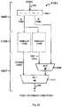
- a preferred processor 100comprising a three-dimensional memory (3D-M) array (3D-processor) is disclosed.
- the preferred 3D-processor 100comprises an array of computing elements 110 - 1 , 110 - 2 . . . 110 - i . . . 110 -N ( FIG. 3A ).
- the computing elements 110 - 1 . . . 110 -Ncould realize a same function or different functions.
- Each computing element 110 - icould have one or more input variables 150 , and one or more output variables 190 ( FIG. 3B ).
- Each computing element 110 - icomprises an arithmetic logic circuit (ALC) 180 and a look-up table (LUT) based on 3D-M (3DM-LTU) 170 .
- the ALC 180performs arithmetic operations on the 3DM-LUT data, while the 3DM-LUT 170 is stored in at least a 3D-M array.
- the 3DM-LUTmay possess a two-dimensional structure (e.g. the function represented by the 3DM-LUT has one input variable and one output value), or a multi-dimensional structure (e.g. the function represented by the 3DM-LUT has two input variables and one output value).
- the ALC 180 and the 3DM-LUT 170are communicatively coupled by 3D-interconnects 160 . Because the 3D-M array 170 is formed on a different level than the ALC 180 (shown in FIGS. 5A-5C ), it is represented by dotted line in this and following figures.
- the 3D-processor 100uses memory-based computation (MBC), which carries out computation primarily with the 3DM-LUT 170 .
- MBCmemory-based computation
- LBClogic-based computation
- the 3DM-LUT 170 used by the MBChas a much larger capacity than the conventional LUT 370 .
- arithmetic operationsare still performed for most MBCs, using a larger LUT as a starting point, the MBC only needs to calculate a polynomial to a smaller order.
- the fraction of computation done by the 3DM-LUT 170could be more than the ALC 180 .
- FIGS. 4A-4Care the block diagrams of three preferred ALC 180 .
- the first preferred ALC 180comprises an adder 180 A
- the second preferred ALC 180comprises a multiplier 180 M
- the third preferred ALC 180comprising a multiplier-accumulator (MAC), which includes an adder 180 A and a multiplier 180 M.
- the preferred ALC 180could perform integer arithmetic operations, fixed-point arithmetic operations, or floating-point arithmetic operations.
- the preferred ALC 180may also comprise memory circuits, e.g. registers, flip-flops, buffer RAMs.
- the computing element 110 - icomprising different types of 3D-M are disclosed.
- 3D-Mwas disclosed in U.S. Pat. No. 5,835,396 issued to Zhang on Nov. 10, 1998. It comprises a plurality of vertically stacked memory levels formed on a semiconductor substrate, with each memory level comprising a plurality of 3D-M arrays. Each 3D-M array is a collection of 3D-M cells in a memory level that share at least one address-line.
- 3D-Mcan be categorized into 3D-RAM (random access memory) and 3D-ROM (read-only memory).
- RAMrandom access memory
- ROMread-only memory
- Most common 3D-Mis 3D-ROM.
- the 3D-ROMis further categorized into 3-D writable memory (3D-W) and 3-D printed memory (3D-P).
- 3D-Wdata can be electrically written (or, programmable). Based on the number of programmings allowed, a 3D-W can be categorized into three-dimensional one-time-programmable memory (3D-OTP) and three-dimensional multiple-time-programmable memory (3D-MTP). The 3D-OTP can be written once, while the 3D-MTP is electrically re-programmable.
- An exemplary 3D-MTPis 3D-XPoint.
- Other types of 3D-MTPinclude memristor, resistive random-access memory (RRAM or ReRAM), phase-change memory, programmable metallization cell (PMC), conductive-bridging random-access memory (CBRAM), and the like.
- the 3DM-LUT 170can be configured in the field. This becomes even better when the 3D-MTP is used, as the 3DM-LUT 170 would become re-configured.
- 3D-Pdata are recorded thereto using a printing method during manufacturing. These data are fixedly recorded and cannot be changed after manufacturing.
- the printing methodsinclude photo-lithography, nano-imprint, e-beam lithography, DUV lithography, and laser-programming, etc.
- An exemplary 3D-Pis three-dimensional mask-programmed read-only memory (3D-MPROM), whose data are recorded by photo-lithography. Because electrical programming is not required, a memory cell in the 3D-P can be biased at a larger voltage during read than the 3D-W and therefore, the 3D-P is faster than the 3D-W.
- FIG. 5Adiscloses a preferred computing element 110 - i comprising at least a 3D-W array. It comprises a substrate circuit 0 K formed on the substrate 0 .
- the ALC 180is a portion of the substrate circuit 0 K.
- a first memory level 16 Ais stacked above the substrate circuit 0 K, with a second memory level 16 B stacked above the first memory level 16 A.
- the substrate circuit 0 Kincludes the peripheral circuits of the memory levels 16 A, 16 B. It comprises transistors 0 t and the associated interconnect 0 M.
- Each of the memory levels(e.g. 16 A, 16 B) comprises a plurality of first address-lines (i.e. y-lines, e.g.
- the first and second memory levels 16 A, 16 Bare coupled to the ALC 180 through contact vias 1 av , 3 av , respectively.
- the LUTs stored in all 3D-M arrays coupled to the ALC 180are collectively referred to as the 3DM-LUT 170 .
- the contact vias 1 av , 3 avare collectively referred to as 3D-interconnects 160 .
- the 3D-W cell 5 aacomprises a programmable layer 12 and a diode layer 14 .
- the programmable layer 12could be an antifuse layer (which can be programmed once and is used for the 3D-OTP) or a re-programmable layer (which is used for the 3D-MTP).
- the diode layer 14is broadly interpreted as any layer whose resistance at the read voltage is substantially lower than when the applied voltage has a magnitude smaller than or polarity opposite to that of the read voltage.
- the diodecould be a semiconductor diode (e.g. p-i-n silicon diode), or a metal-oxide (e.g. TiO 2 ) diode.
- FIG. 5Bdiscloses a preferred computing element 110 - i comprising at least a 3D-P array. It has a structure similar to that of FIG. 5A except for the memory cells.
- 3D-Phas at least two types of memory cells: a high-resistance 3D-P cell 5 aa , and a low-resistance 3D-P cell 5 ac .
- the low-resistance 3D-P cell 5 accomprises a diode layer 14
- the high-resistance 3D-P cell 5 aacomprises at least a high-resistance layer 13 .
- the diode layer 14is similar to that in the 3D-W.
- the high-resistance layer 13could simply be a layer of insulating dielectric (e.g. silicon oxide, or silicon nitride). It is physically removed at the location of the low-resistance 3D-P cell 5 ac during manufacturing.
- insulating dielectrice.g. silicon oxide, or silicon nitride
- FIG. 5Cis a perspective view of the preferred computing element 110 - i .
- the ALC 180is formed on the substrate 0 .
- the 3DM-LUT 170is vertically stacked above and at least partially covers the ALC 180 .
- the 3-D integrationmoves the 3DM-LUT 170 physically close to the ALC 180 . Because the contact vias 1 av , 3 av coupling them are short (on the order of an um in length) and numerous (thousands at least), the 3D-interconnects 160 have a much larger bandwidth than the conventional processor 300 .
- the interconnects coupling themare much longer (hundreds of ums in length) and fewer (hundreds at most).
- FIGS. 6A-6Bshow two types of the preferred 3D-M cell 5 ab .
- the 3D-M cell 5 abcomprises a variable resistor 12 and a diode (or a diode-like device) 14 .
- the variable resistor 12is realized by the programmable layer of FIG. 5A . It can be varied during manufacturing or after manufacturing.
- the diode (or diode-like device) 14is realized by the diode layer of FIG. 5A . It is broadly interpreted as any two-terminal device whose resistance at the read voltage is substantially lower than when the applied voltage has a magnitude smaller than or polarity opposite to that of the read voltage.
- the 3D-M cell 5 abcomprises a transistor or a transistor-like device 16 .
- the transistor or transistor-like device 16is broadly interpreted as any three- (or, more-) terminal device whose resistance between the first and second terminals can be modulated by an electrical signal on a third terminal.
- the device 16further comprises a floating gate 18 for storing electrical charge which represents the digital information stored in the 3D-M cell 5 ab .
- the devices 16can be organized into NOR-arrays or NAND-arrays.
- the 3D-Mcould be categorized into horizontal 3D-M (e.g. 3D-XPoint) and vertical 3D-M (e.g. 3D-NAND).
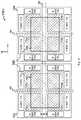
- FIGS. 7A-7Cthe substrate layout views of three preferred computing elements 110 - i are shown.
- the ALC 180is only coupled with a single 3D-M array 170 o and processes the 3DM-LUT data therefrom.
- the 3DM-LUT 170is stored in the 3D-M array 170 o .
- the ALC 180is covered by the 3D-M array 170 .
- the 3D-M array 170 ohas four peripheral circuits, including X-decoders 15 o , 15 o ′ and Y-decoders 17 o , 17 o ′.
- the ALC 180is bound by these four peripheral circuits.
- As the 3D-M arrayis stacked above the substrate circuit 0 K and does not occupy any substrate area, its projection on the substrate 0 is shown by dotted lines in this and following figures.
- the ALC 180is coupled with four 3D-M arrays 170 a - 170 d and processes the 3DM-LUT data therefrom.
- the 3DM-LUT 170is stored in four 3D-M arrays 170 a - 170 d .
- each 3D-M arraye.g. 170 a
- has two peripheral circuitse.g. X-decoder 15 a and Y-decoder 17 a ).
- the ALC 180is bound by eight peripheral circuits (including X-decoders 15 a - 15 d and Y-decoders 17 a - 17 d ) and located below four 3D-M arrays 170 a - 170 d . Hence, the ALC 180 of FIG. 7B could be four times as large as that of FIG. 7A .
- the ALC 180is coupled with eight 3D-M arrays 170 a - 170 d , 170 w - 170 z and processes the 3DM-LUT data therefrom.
- the 3DM-LUT 170is stored in eight 3D-M arrays 170 a - 170 d , 170 w - 170 z .
- These 3D-M arraysare divided into two sets: a first set 150 a includes four 3D-M arrays 170 a - 170 d , and a second set 150 b includes four 3D-M arrays 170 w - 170 z .
- a first component 180 a of the ALC 180is formed below the four 3D-M arrays 170 a - 170 d of the first set 150 a .
- a second component 180 b of the ALC 180is formed below the four 3D-M array 170 w - 170 z of the second set 150 b .
- adjacent peripheral circuitse.g. adjacent x-decoders 15 a , 15 c , or, adjacent y-decoders 17 a , 17 b ) are separated by physical gaps G.
- routing channel 182 , 184 , 186which provide coupling between different components 180 a , 180 b , or between different ALCs 180 a , 180 b .
- the ALC 180 of FIG. 7Ccould be eight times as large as that of FIG. 7A .
- 3DM-LUT 170is stacked above the ALC 180 , this type of vertical integration is referred to as three-dimensional (3-D) integration.
- the 3-D integrationhas a profound effect on the computational density of the 3D-processor 100 .
- the 3DM-LUT 170does not occupy any substrate area 0 , the footprint of the computing element 110 - i is roughly equal to that of the ALC 180 .
- Thisis much smaller than a conventional processor 300 , whose footprint is roughly equal to the sum of the footprints of the LUT 370 and the ALC 380 .
- the 3D-processor 100would contain more computing elements 110 - l , become more computationally powerful and support massive parallelism.
- the 3-D integrationalso has a profound effect on the computational complexity of the 3D-processor 100 .
- the total LUT capacityis less than 100 kb.
- the total 3DM-LUT capacity for a 3D-processor 100could reach 100 Gb (for example, a 3D-XPoint die has a storage capacity of 128 Gb). Consequently, a single 3D-processor die 100 could support as many as 10,000 built-in functions, which are three orders of magnitude more than the conventional processor 300 .
- FIG. 8Ais its circuit block diagram.
- the ALC 180comprises a pre-processing circuit 180 R, a 3DM-LUT 170 P, and a post-processing circuit 180 T.
- the pre-processing circuit 180 Rconverts the input variable (X) 150 into an address (A) of the 3DM-LUT 170 P.
- the post-processing circuit 180 Tconverts it into the function value (Y) 190 .
- a residue (R) of the input variable (X)is fed into the post-processing circuit 180 T to improve the calculation precision.
- FIG. 8Bis its substrate-circuit layout view.
- the 3D-M storing the 3DM-LUT 170 Pcomprises at least a 3D-M array 170 p , as well as its X-decoder 15 p and Y-decoder 17 p .
- the 3D-M array 170 pcovers the pre-processing circuit 180 R and the post-processing circuit 180 T. Although a single 3D-M array 170 p is shown in this figure, the preferred embodiment could use multiple 3D-M arrays, as those shown in FIGS. 7B-7C .
- the 3DM-LUT 170does not occupy any substrate area, the 3-D integration between the 3DM-LUT 170 and the ALC 180 (including the pre-processing circuit 180 R and the post-processing circuit 180 T) leads to a smaller footprint for the computing element 110 - i.
- the input variable X 150has 32 bits (x 31 . . . x 0 ).
- the pre-processing circuit 180 Rextracts the higher 16 bits (x 31 . . . x 16 ) thereof and sends it as a 16-bit address A to the 3DM-LUT 170 P.
- the pre-processing circuit 180 Rfurther extracts the lower 16 bits (x 15 . . . x 0 ) and sends it as a 16-bit residue R to the post-processing circuit 180 T.
- the 3DM-LUT 170 Pcomprises two 3DM-LUTs 170 Q, 170 R.
- the post-processing circuit 180 Tcomprises a multiplier 180 M and an adder 180 A.
- the output value (Y) 190has 32 bits and is calculated from polynomial interpolation.
- higher-order polynomial interpolatione.g. higher-order Taylor series
- higher-order polynomial interpolationcan be used to improve the calculation precision.
- a single-precision functioncan be realized using a total of 4 Mb LUT (2 Mb for function values, and 2 Mb for first-derivative values) in conjunction with a first-order Taylor series calculation. This is significantly less than the LUT-only approach (4 Mb vs. 128 Gb).
- FIG. 8Ccan be used to implement non-elementary functions such as special functions.
- Special functionscan be defined by means of power series, generating functions, infinite products, repeated differentiation, integral representation, differential difference, integral, and functional equations, trigonometric series, or other series in orthogonal functions.
- special functionsare gamma function, beta function, hyper-geometric functions, confluent hyper-geometric functions, Bessel functions, Legender functions, parabolic cylinder functions, integral sine, integral cosine, incomplete gamma function, incomplete beta function, probability integrals, various classes of orthogonal polynomials, elliptic functions, elliptic integrals, Lame functions, Mathieu functions, Riemann zeta function, automorphic functions, and others.
- the 3D-processorwill simplify the calculation of special functions and promote their applications in scientific computation.
- FIG. 9Ais its schematic circuit block diagram.
- the preferred computing element 110 - icomprises two 3DM-LUTs 170 S, 170 T and a multiplier 180 M.
- the 3DM-LUT 170 Sstores the Log( ) values, while the 3DM-LUT 170 T stores the Exp( ) values.
- the input variable Xis used as an address 150 for the 3DM-LUT 170 S.
- the output Log(X) 160 a from the 3DM-LUT 170 Sis multiplied by an exponent parameter K at the multiplier 180 M.
- FIG. 9Bis its substrate-circuit layout view.
- the substrate circuit 0 Kcomprises the X-decoders 15 s , 15 t and the Y-decoders 17 s , 17 t for the 3D-M arrays 170 s , 170 t , as well as a multiplier 180 M. Placed side-by-side, both 3D-M arrays 170 s , 170 t partially cover the multiplier 180 M.
- both embodiments in FIG. 8C and FIG. 9Acomprise two 3DM-LUTs. These 3DM-LUTs could be stored in a single 3D-M array 170 p (as in FIG.
- the 3DM-LUTcan be stored in more 3D-M arrays.
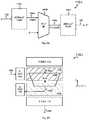
- FIGS. 10A-10Ba third preferred computing element 110 - i to simulate the amplifier circuit 20 of FIG. 2A is disclosed. It uses the model-by-LUT method.
- FIG. 10Ais its schematic circuit block diagram.
- the preferred computing element 110 - icomprises a 3DM-LUT 170 U, an adder 180 A and a multiplier 180 M.
- the 3DM-LUT 170 Ustores the data associated with the behaviors (e.g. input-output characteristics) of the transistor 24 .
- V INinput voltage value
- the readout 160 of the 3DM-LUT 170 Uis the drain-current value (I D ).
- the multiplication result ( ⁇ R*I D )is added to the V DD value by the adder 180 A to generate the output voltage value (V OUT ) 190 .
- the 3DM-LUT 170 Ustores different forms of mathematical models.
- the mathematical model data stored in the 3DM-LUT 170 Uis raw measurement data, i.e. the measured input-output characteristics of the transistor 24 .
- One exampleis the measured drain current vs. the applied gate-source voltage (I D -V GS ) characteristics.
- the mathematical model data stored in the 3DM-LUT 170 Uis the smoothed measurement data.
- the raw measurement datacould be smoothed using a purely mathematical method (e.g. a best-fit model). Or, this smoothing process can be aided by a physical transistor model (e.g. a BSIM4 V3.0 transistor model).
- the mathematical data stored in the 3DM-LUTinclude not only the measured data, but also its derivative values.
- the 3DM-LUT datainclude not only the drain-current values of the transistor 24 (e.g. the I D -V GS characteristics), but also its transconductance values (e.g. the G m -V GS characteristics).
- polynomial interpolationcan be used to improve the modeling precision using a reasonable-size 3DM-LUT, as in the case of FIG. 8C .
- FIG. 10Bis its substrate-circuit layout view.
- the substrate circuit 0 Kcomprises the X-decoder 15 u and the Y-decoder 17 u for the 3D-M array 170 u , as well as the multiplier 180 M and the adder 180 A.
- the 3D-M array 170 ucovers the multiplier 180 M and the adder 180 A.
- a single 3D-M array 170 uis shown in this figure, the preferred embodiment could use multiple 3D-M arrays 170 u , as those shown in FIGS. 7B-7C .
- Model-by-LUToffers many advantages. By skipping two software-decomposition steps (from mathematical models to mathematical functions, and from mathematical functions to built-in functions), it saves substantial modeling time and energy. Model-by-LUT may need less LUT than function-by-LUT. Because a transistor model (e.g. BSIM4 V3.0) has hundreds of model parameters, calculating the intermediate functions of the transistor model requires extremely large LUTs. However, if we skip function-by-LUT (namely, skipping the transistor models and the associated intermediate functions), the transistor behaviors can be described using only three parameters (including the gate-source voltage V GS , the drain-source voltage V DS , and the body-source voltage V BS ). Describing the mathematical models of the transistor 24 requires relatively small LUTs.
- a transistor modele.g. BSIM4 V3.0
- calculating the intermediate functions of the transistor modelrequires extremely large LUTs.
- the transistor behaviorscan be described using only three parameters (including the gate-source voltage V GS , the
- the processorcould be a micro-controller, a central processing unit (CPU), a digital signal processor (DSP), a graphic processing unit (GPU), a network-security processor, an encryption/decryption processor, an encoding/decoding processor, a neural-network processor, or an artificial intelligence (AI) processor.
- CPUcentral processing unit
- DSPdigital signal processor
- GPUgraphic processing unit
- AIartificial intelligence
- processorscan be found in consumer electronic devices (e.g. personal computers, video game machines, smart phones) as well as engineering and scientific workstations and server machines. The invention, therefore, is not to be limited except in the spirit of the appended claims.
Landscapes
- Engineering & Computer Science (AREA)
- Physics & Mathematics (AREA)
- Theoretical Computer Science (AREA)
- Computer Hardware Design (AREA)
- General Physics & Mathematics (AREA)
- General Engineering & Computer Science (AREA)
- Computing Systems (AREA)
- Mathematical Physics (AREA)
- Computational Mathematics (AREA)
- Mathematical Analysis (AREA)
- Mathematical Optimization (AREA)
- Pure & Applied Mathematics (AREA)
- Nonlinear Science (AREA)
- Semiconductor Integrated Circuits (AREA)
- Semiconductor Memories (AREA)
- Complex Calculations (AREA)
Abstract
Description
Claims (20)
Priority Applications (10)
| Application Number | Priority Date | Filing Date | Title |
|---|---|---|---|
| US16/188,265US20190114170A1 (en) | 2016-02-13 | 2018-11-12 | Processor Using Memory-Based Computation |
| US16/200,630US20190115922A1 (en) | 2016-02-13 | 2018-11-26 | Processor For Implementing Mathematical Functions or Models |
| US16/207,189US20190115923A1 (en) | 2016-02-13 | 2018-12-03 | Processor for Implementing Non-Arithmetic Functions |
| US16/458,187US11080229B2 (en) | 2016-02-13 | 2019-06-30 | Processor for calculating mathematical functions in parallel |
| US16/595,462US20200050565A1 (en) | 2016-03-07 | 2019-10-07 | Pattern Processor |
| US16/693,370US10848158B2 (en) | 2016-02-13 | 2019-11-24 | Configurable processor |
| US16/939,048US11966715B2 (en) | 2016-02-13 | 2020-07-26 | Three-dimensional processor for parallel computing |
| US17/065,604US11128302B2 (en) | 2016-02-13 | 2020-10-08 | Configurable processor doublet based on three-dimensional memory (3D-M) |
| US17/065,632US11128303B2 (en) | 2016-02-13 | 2020-10-08 | Three-dimensional memory (3D-M)-based configurable processor singlet |
| US17/227,323US20210232892A1 (en) | 2016-03-21 | 2021-04-11 | Neuro-Processing Circuit Using Three-Dimensional Memory to Store Look-Up Table of Activation Function |
Applications Claiming Priority (12)
| Application Number | Priority Date | Filing Date | Title |
|---|---|---|---|
| CN201610083747.7ACN107085452B (en) | 2016-02-13 | 2016-02-13 | Three-dimensional printed memory (3D-P) based processor |
| CN201610083747 | 2016-02-13 | ||
| CN201610083747.7 | 2016-02-13 | ||
| CN201610260845 | 2016-04-22 | ||
| CN201610260845 | 2016-04-22 | ||
| CN201610260845.3 | 2016-04-22 | ||
| CN201610289592 | 2016-05-02 | ||
| CN201610289592.2 | 2016-05-02 | ||
| CN201610289592 | 2016-05-02 | ||
| CN201710237780.5 | 2017-04-12 | ||
| CN201710237780 | 2017-04-12 | ||
| CN201710237780 | 2017-04-12 |
Related Parent Applications (3)
| Application Number | Title | Priority Date | Filing Date |
|---|---|---|---|
| US15/587,359Continuation-In-PartUS20170322906A1 (en) | 2016-02-13 | 2017-05-04 | Processor with In-Package Look-Up Table |
| US16/249,021Continuation-In-PartUS11527523B2 (en) | 2016-02-13 | 2019-01-16 | Discrete three-dimensional processor |
| US16/458,187Continuation-In-PartUS11080229B2 (en) | 2016-02-13 | 2019-06-30 | Processor for calculating mathematical functions in parallel |
Related Child Applications (8)
| Application Number | Title | Priority Date | Filing Date |
|---|---|---|---|
| US15/450,017Continuation-In-PartUS9948306B2 (en) | 2016-02-13 | 2017-03-05 | Configurable gate array based on three-dimensional printed memory |
| US16/188,265Continuation-In-PartUS20190114170A1 (en) | 2016-02-13 | 2018-11-12 | Processor Using Memory-Based Computation |
| US16/200,630ContinuationUS20190115922A1 (en) | 2016-02-13 | 2018-11-26 | Processor For Implementing Mathematical Functions or Models |
| US16/207,189ContinuationUS20190115923A1 (en) | 2016-02-13 | 2018-12-03 | Processor for Implementing Non-Arithmetic Functions |
| US16/249,021Continuation-In-PartUS11527523B2 (en) | 2016-02-13 | 2019-01-16 | Discrete three-dimensional processor |
| US16/458,187Continuation-In-PartUS11080229B2 (en) | 2016-02-13 | 2019-06-30 | Processor for calculating mathematical functions in parallel |
| US16/693,370Continuation-In-PartUS10848158B2 (en) | 2016-02-13 | 2019-11-24 | Configurable processor |
| US16/939,048Continuation-In-PartUS11966715B2 (en) | 2016-02-13 | 2020-07-26 | Three-dimensional processor for parallel computing |
Publications (2)
| Publication Number | Publication Date |
|---|---|
| US20170237440A1 US20170237440A1 (en) | 2017-08-17 |
| US10763861B2true US10763861B2 (en) | 2020-09-01 |
Family
ID=59561801
Family Applications (3)
| Application Number | Title | Priority Date | Filing Date |
|---|---|---|---|
| US15/487,366Expired - Fee RelatedUS10763861B2 (en) | 2016-02-13 | 2017-04-13 | Processor comprising three-dimensional memory (3D-M) array |
| US16/200,630AbandonedUS20190115922A1 (en) | 2016-02-13 | 2018-11-26 | Processor For Implementing Mathematical Functions or Models |
| US16/207,189AbandonedUS20190115923A1 (en) | 2016-02-13 | 2018-12-03 | Processor for Implementing Non-Arithmetic Functions |
Family Applications After (2)
| Application Number | Title | Priority Date | Filing Date |
|---|---|---|---|
| US16/200,630AbandonedUS20190115922A1 (en) | 2016-02-13 | 2018-11-26 | Processor For Implementing Mathematical Functions or Models |
| US16/207,189AbandonedUS20190115923A1 (en) | 2016-02-13 | 2018-12-03 | Processor for Implementing Non-Arithmetic Functions |
Country Status (2)
| Country | Link |
|---|---|
| US (3) | US10763861B2 (en) |
| WO (1) | WO2017137015A2 (en) |
Cited By (2)
| Publication number | Priority date | Publication date | Assignee | Title |
|---|---|---|---|---|
| US11296068B2 (en)* | 2018-12-10 | 2022-04-05 | HangZhou HaiCun Information Technology Co., Ltd. | Discrete three-dimensional processor |
| US12265904B2 (en) | 2019-12-24 | 2025-04-01 | Industrial Technology Research Institute | Apparatus and method for neural network computation |
Families Citing this family (11)
| Publication number | Priority date | Publication date | Assignee | Title |
|---|---|---|---|---|
| US11527523B2 (en)* | 2018-12-10 | 2022-12-13 | HangZhou HaiCun Information Technology Co., Ltd. | Discrete three-dimensional processor |
| US10445067B2 (en)* | 2016-05-06 | 2019-10-15 | HangZhou HaiCun Information Technology Co., Ltd. | Configurable processor with in-package look-up table |
| KR102408858B1 (en) | 2017-12-19 | 2022-06-14 | 삼성전자주식회사 | A nonvolatile memory device, a memory system including the same and a method of operating a nonvolatile memory device |
| US10628295B2 (en) | 2017-12-26 | 2020-04-21 | Samsung Electronics Co., Ltd. | Computing mechanisms using lookup tables stored on memory |
| US11398453B2 (en)* | 2018-01-09 | 2022-07-26 | Samsung Electronics Co., Ltd. | HBM silicon photonic TSV architecture for lookup computing AI accelerator |
| CN108599849B (en)* | 2018-04-14 | 2021-01-01 | 上海交通大学 | Photon processing system and processing method for intelligent decision |
| CN120429266A (en)* | 2018-12-10 | 2025-08-05 | 杭州海存信息技术有限公司 | Separate 3D processor |
| US10901694B2 (en) | 2018-12-31 | 2021-01-26 | Micron Technology, Inc. | Binary parallel adder and multiplier |
| CN112287632A (en)* | 2020-10-26 | 2021-01-29 | 成都华微电子科技有限公司 | Method for prejudging wiring of integrated circuit |
| KR20220077738A (en) | 2020-12-02 | 2022-06-09 | 삼성전자주식회사 | Integrated circuit for constant multiplication and device including the same |
| US11709790B2 (en)* | 2021-02-24 | 2023-07-25 | Xilinx, Inc. | Spatial distribution in a 3D data processing unit |
Citations (30)
| Publication number | Priority date | Publication date | Assignee | Title |
|---|---|---|---|---|
| US4870302A (en) | 1984-03-12 | 1989-09-26 | Xilinx, Inc. | Configurable electrical circuit having configurable logic elements and configurable interconnects |
| US5046038A (en) | 1989-07-07 | 1991-09-03 | Cyrix Corporation | Method and apparatus for performing division using a rectangular aspect ratio multiplier |
| US5060182A (en) | 1989-09-05 | 1991-10-22 | Cyrix Corporation | Method and apparatus for performing the square root function using a rectangular aspect ratio multiplier |
| US5604499A (en) | 1993-12-28 | 1997-02-18 | Matsushita Electric Industrial Co., Ltd. | Variable-length decoding apparatus |
| US5835396A (en) | 1996-10-17 | 1998-11-10 | Zhang; Guobiao | Three-dimensional read-only memory |
| US5901274A (en) | 1994-04-30 | 1999-05-04 | Samsung Electronics Co. Ltd. | Method for enlargement/reduction of image data in digital image processing system and circuit adopting the same |
| US5954787A (en) | 1996-12-26 | 1999-09-21 | Daewoo Electronics Co., Ltd. | Method of generating sine/cosine function and apparatus using the same for use in digital signal processor |
| US6181355B1 (en) | 1998-07-17 | 2001-01-30 | 3Dlabs Inc. Ltd. | Graphics processing with transcendental function generator |
| US6263470B1 (en) | 1998-02-03 | 2001-07-17 | Texas Instruments Incorporated | Efficient look-up table methods for Reed-Solomon decoding |
| US20040044710A1 (en) | 2002-08-28 | 2004-03-04 | Harrison John R. | Converting mathematical functions to power series |
| US7028247B2 (en) | 2002-12-25 | 2006-04-11 | Faraday Technology Corp. | Error correction code circuit with reduced hardware complexity |
| US20060106905A1 (en) | 2004-11-17 | 2006-05-18 | Chren William A Jr | Method for reducing memory size in logarithmic number system arithmetic units |
| US7206410B2 (en) | 2001-10-10 | 2007-04-17 | Stmicroelectronics S.R.L. | Circuit for the inner or scalar product computation in Galois fields |
| US7366748B1 (en) | 2000-06-30 | 2008-04-29 | Intel Corporation | Methods and apparatus for fast argument reduction in a computing system |
| US7472149B2 (en) | 2004-01-21 | 2008-12-30 | Kabushiki Kaisha Toshiba | Arithmetic unit for approximating function |
| US7512647B2 (en) | 2004-11-22 | 2009-03-31 | Analog Devices, Inc. | Condensed Galois field computing system |
| US7539927B2 (en) | 2005-04-14 | 2009-05-26 | Industrial Technology Research Institute | High speed hardware implementation of modified Reed-Solomon decoder |
| US7574468B1 (en) | 2005-03-18 | 2009-08-11 | Verisilicon Holdings (Cayman Islands) Co. Ltd. | Digital signal processor having inverse discrete cosine transform engine for video decoding and partitioned distributed arithmetic multiply/accumulate unit therefor |
| US7634524B2 (en) | 2003-12-12 | 2009-12-15 | Fujitsu Limited | Arithmetic method and function arithmetic circuit for a fast fourier transform |
| US7962543B2 (en) | 2007-06-01 | 2011-06-14 | Advanced Micro Devices, Inc. | Division with rectangular multiplier supporting multiple precisions and operand types |
| US8203564B2 (en) | 2007-02-16 | 2012-06-19 | Qualcomm Incorporated | Efficient 2-D and 3-D graphics processing |
| US20120248595A1 (en)* | 2010-11-18 | 2012-10-04 | MonolithlC 3D Inc. | System comprising a semiconductor device and structure |
| US8487948B2 (en) | 2007-05-01 | 2013-07-16 | Vivante Corporation | Apparatus and method for texture level of detail computation |
| US20140067889A1 (en) | 2012-09-04 | 2014-03-06 | Analog Devices A/S | Datapath circuit for digital signal processors |
| US8803206B1 (en)* | 2012-12-29 | 2014-08-12 | Monolithic 3D Inc. | 3D semiconductor device and structure |
| US9015452B2 (en) | 2009-02-18 | 2015-04-21 | Texas Instruments Incorporated | Vector math instruction execution by DSP processor approximating division and complex number magnitude |
| US9207910B2 (en) | 2009-01-30 | 2015-12-08 | Intel Corporation | Digital signal processor having instruction set with an xK function using reduced look-up table |
| US9225501B2 (en) | 2013-04-17 | 2015-12-29 | Intel Corporation | Non-linear modeling of a physical system using look-up table with polynomial interpolation |
| US9465580B2 (en) | 2011-12-21 | 2016-10-11 | Intel Corporation | Math circuit for estimating a transcendental function |
| US9606796B2 (en) | 2013-10-30 | 2017-03-28 | Texas Instruments Incorporated | Computer and methods for solving math functions |
Family Cites Families (6)
| Publication number | Priority date | Publication date | Assignee | Title |
|---|---|---|---|---|
| US20100140750A1 (en)* | 2008-12-10 | 2010-06-10 | Qualcomm Incorporated | Parallel Plane Memory and Processor Coupling in a 3-D Micro-Architectural System |
| KR101728068B1 (en)* | 2010-06-01 | 2017-04-19 | 삼성전자 주식회사 | Stacked semiconductor memory device, memory system including the same, and method of repairing defects of through silicon vias |
| WO2013147841A1 (en)* | 2012-03-30 | 2013-10-03 | Intel Corporation | Generic address scrambler for memory circuit test engine |
| CN103633048B (en)* | 2012-08-22 | 2016-08-24 | 成都海存艾匹科技有限公司 | Three-dimensional storage containing read/write voltage generator chip |
| US8737108B2 (en)* | 2012-09-25 | 2014-05-27 | Intel Corporation | 3D memory configurable for performance and power |
| US9287196B2 (en)* | 2012-12-28 | 2016-03-15 | Intel Corporation | Resonant clocking for three-dimensional stacked devices |
- 2017
- 2017-04-13USUS15/487,366patent/US10763861B2/ennot_activeExpired - Fee Related
- 2017-04-13WOPCT/CN2017/080462patent/WO2017137015A2/ennot_activeCeased
- 2018
- 2018-11-26USUS16/200,630patent/US20190115922A1/ennot_activeAbandoned
- 2018-12-03USUS16/207,189patent/US20190115923A1/ennot_activeAbandoned
Patent Citations (30)
| Publication number | Priority date | Publication date | Assignee | Title |
|---|---|---|---|---|
| US4870302A (en) | 1984-03-12 | 1989-09-26 | Xilinx, Inc. | Configurable electrical circuit having configurable logic elements and configurable interconnects |
| US5046038A (en) | 1989-07-07 | 1991-09-03 | Cyrix Corporation | Method and apparatus for performing division using a rectangular aspect ratio multiplier |
| US5060182A (en) | 1989-09-05 | 1991-10-22 | Cyrix Corporation | Method and apparatus for performing the square root function using a rectangular aspect ratio multiplier |
| US5604499A (en) | 1993-12-28 | 1997-02-18 | Matsushita Electric Industrial Co., Ltd. | Variable-length decoding apparatus |
| US5901274A (en) | 1994-04-30 | 1999-05-04 | Samsung Electronics Co. Ltd. | Method for enlargement/reduction of image data in digital image processing system and circuit adopting the same |
| US5835396A (en) | 1996-10-17 | 1998-11-10 | Zhang; Guobiao | Three-dimensional read-only memory |
| US5954787A (en) | 1996-12-26 | 1999-09-21 | Daewoo Electronics Co., Ltd. | Method of generating sine/cosine function and apparatus using the same for use in digital signal processor |
| US6263470B1 (en) | 1998-02-03 | 2001-07-17 | Texas Instruments Incorporated | Efficient look-up table methods for Reed-Solomon decoding |
| US6181355B1 (en) | 1998-07-17 | 2001-01-30 | 3Dlabs Inc. Ltd. | Graphics processing with transcendental function generator |
| US7366748B1 (en) | 2000-06-30 | 2008-04-29 | Intel Corporation | Methods and apparatus for fast argument reduction in a computing system |
| US7206410B2 (en) | 2001-10-10 | 2007-04-17 | Stmicroelectronics S.R.L. | Circuit for the inner or scalar product computation in Galois fields |
| US20040044710A1 (en) | 2002-08-28 | 2004-03-04 | Harrison John R. | Converting mathematical functions to power series |
| US7028247B2 (en) | 2002-12-25 | 2006-04-11 | Faraday Technology Corp. | Error correction code circuit with reduced hardware complexity |
| US7634524B2 (en) | 2003-12-12 | 2009-12-15 | Fujitsu Limited | Arithmetic method and function arithmetic circuit for a fast fourier transform |
| US7472149B2 (en) | 2004-01-21 | 2008-12-30 | Kabushiki Kaisha Toshiba | Arithmetic unit for approximating function |
| US20060106905A1 (en) | 2004-11-17 | 2006-05-18 | Chren William A Jr | Method for reducing memory size in logarithmic number system arithmetic units |
| US7512647B2 (en) | 2004-11-22 | 2009-03-31 | Analog Devices, Inc. | Condensed Galois field computing system |
| US7574468B1 (en) | 2005-03-18 | 2009-08-11 | Verisilicon Holdings (Cayman Islands) Co. Ltd. | Digital signal processor having inverse discrete cosine transform engine for video decoding and partitioned distributed arithmetic multiply/accumulate unit therefor |
| US7539927B2 (en) | 2005-04-14 | 2009-05-26 | Industrial Technology Research Institute | High speed hardware implementation of modified Reed-Solomon decoder |
| US8203564B2 (en) | 2007-02-16 | 2012-06-19 | Qualcomm Incorporated | Efficient 2-D and 3-D graphics processing |
| US8487948B2 (en) | 2007-05-01 | 2013-07-16 | Vivante Corporation | Apparatus and method for texture level of detail computation |
| US7962543B2 (en) | 2007-06-01 | 2011-06-14 | Advanced Micro Devices, Inc. | Division with rectangular multiplier supporting multiple precisions and operand types |
| US9207910B2 (en) | 2009-01-30 | 2015-12-08 | Intel Corporation | Digital signal processor having instruction set with an xK function using reduced look-up table |
| US9015452B2 (en) | 2009-02-18 | 2015-04-21 | Texas Instruments Incorporated | Vector math instruction execution by DSP processor approximating division and complex number magnitude |
| US20120248595A1 (en)* | 2010-11-18 | 2012-10-04 | MonolithlC 3D Inc. | System comprising a semiconductor device and structure |
| US9465580B2 (en) | 2011-12-21 | 2016-10-11 | Intel Corporation | Math circuit for estimating a transcendental function |
| US20140067889A1 (en) | 2012-09-04 | 2014-03-06 | Analog Devices A/S | Datapath circuit for digital signal processors |
| US8803206B1 (en)* | 2012-12-29 | 2014-08-12 | Monolithic 3D Inc. | 3D semiconductor device and structure |
| US9225501B2 (en) | 2013-04-17 | 2015-12-29 | Intel Corporation | Non-linear modeling of a physical system using look-up table with polynomial interpolation |
| US9606796B2 (en) | 2013-10-30 | 2017-03-28 | Texas Instruments Incorporated | Computer and methods for solving math functions |
Non-Patent Citations (5)
| Title |
|---|
| "Arithmetic", Wikipedia, https://en.wikipedia.org/wiki/Arithmetic. |
| "Operation (Mathematics)", Wikipedia, https://en.wikipedia.org/wiki/Operation_(mathematics). |
| Harrison et al., "The Computation of Transcendental Functions on the IA-64 Architecture", Intel Technical Journal, Q4, 1999. |
| Karam et al, "Emerging Trends in Design and Applications of Memory-Based Computing and Content-Addressable Memories", Proceedings of the IEEE, vol. 103, issue 8, pp. 1311-1330, 2015. |
| Kim et al; "Design and Analysis of 3D-MAPS (3D Massively Parallel Processor with Stacked Memory)", pp. 112-125 (Year: 2015).* |
Cited By (2)
| Publication number | Priority date | Publication date | Assignee | Title |
|---|---|---|---|---|
| US11296068B2 (en)* | 2018-12-10 | 2022-04-05 | HangZhou HaiCun Information Technology Co., Ltd. | Discrete three-dimensional processor |
| US12265904B2 (en) | 2019-12-24 | 2025-04-01 | Industrial Technology Research Institute | Apparatus and method for neural network computation |
Also Published As
| Publication number | Publication date |
|---|---|
| WO2017137015A2 (en) | 2017-08-17 |
| US20190115922A1 (en) | 2019-04-18 |
| US20170237440A1 (en) | 2017-08-17 |
| WO2017137015A3 (en) | 2017-10-05 |
| US20190115923A1 (en) | 2019-04-18 |
Similar Documents
| Publication | Publication Date | Title |
|---|---|---|
| US10763861B2 (en) | Processor comprising three-dimensional memory (3D-M) array | |
| Li et al. | Analogue signal and image processing with large memristor crossbars | |
| US20190114170A1 (en) | Processor Using Memory-Based Computation | |
| US20170323042A1 (en) | Simulation Processor with Backside Look-Up Table | |
| US11527523B2 (en) | Discrete three-dimensional processor | |
| US11960987B2 (en) | Discrete three-dimensional processor | |
| US20170323041A1 (en) | Simulation Processor with In-Package Look-Up Table | |
| US20190114139A1 (en) | Configurable Processor with Backside Look-Up Table | |
| US11128303B2 (en) | Three-dimensional memory (3D-M)-based configurable processor singlet | |
| CN107305594B (en) | A processor with a three-dimensional storage array | |
| US20230207547A1 (en) | Discrete Three-Dimensional Processor | |
| Liu et al. | Cellular automata imbedded memristor-based recirculated logic in-memory computing | |
| US20250239580A1 (en) | Discrete Three-Dimensional Processor | |
| US10445067B2 (en) | Configurable processor with in-package look-up table | |
| US11080229B2 (en) | Processor for calculating mathematical functions in parallel | |
| US11966715B2 (en) | Three-dimensional processor for parallel computing | |
| CN112328535B (en) | Processor containing three-dimensional memory array | |
| US20250266412A1 (en) | Discrete Three-Dimensional Processor | |
| US20250266413A1 (en) | Discrete Three-Dimensional Processor | |
| US20250266414A1 (en) | Discrete Three-Dimensional Processor | |
| CN116303224A (en) | Separated three-dimensional processor |
Legal Events
| Date | Code | Title | Description |
|---|---|---|---|
| STPP | Information on status: patent application and granting procedure in general | Free format text:FINAL REJECTION MAILED | |
| STPP | Information on status: patent application and granting procedure in general | Free format text:DOCKETED NEW CASE - READY FOR EXAMINATION | |
| STPP | Information on status: patent application and granting procedure in general | Free format text:NON FINAL ACTION MAILED | |
| STPP | Information on status: patent application and granting procedure in general | Free format text:RESPONSE TO NON-FINAL OFFICE ACTION ENTERED AND FORWARDED TO EXAMINER | |
| STPP | Information on status: patent application and granting procedure in general | Free format text:FINAL REJECTION MAILED | |
| ZAAA | Notice of allowance and fees due | Free format text:ORIGINAL CODE: NOA | |
| ZAAB | Notice of allowance mailed | Free format text:ORIGINAL CODE: MN/=. | |
| STPP | Information on status: patent application and granting procedure in general | Free format text:PUBLICATIONS -- ISSUE FEE PAYMENT RECEIVED | |
| STCF | Information on status: patent grant | Free format text:PATENTED CASE | |
| FEPP | Fee payment procedure | Free format text:MAINTENANCE FEE REMINDER MAILED (ORIGINAL EVENT CODE: REM.); ENTITY STATUS OF PATENT OWNER: SMALL ENTITY | |
| LAPS | Lapse for failure to pay maintenance fees | Free format text:PATENT EXPIRED FOR FAILURE TO PAY MAINTENANCE FEES (ORIGINAL EVENT CODE: EXP.); ENTITY STATUS OF PATENT OWNER: SMALL ENTITY | |
| STCH | Information on status: patent discontinuation | Free format text:PATENT EXPIRED DUE TO NONPAYMENT OF MAINTENANCE FEES UNDER 37 CFR 1.362 | |
| FP | Lapsed due to failure to pay maintenance fee | Effective date:20240901 | |
| AS | Assignment | Owner name:HANGZHOU HAICUN INFORMATION TECHNOLOGY CO., LTD., CHINA Free format text:ASSIGNMENT OF ASSIGNORS INTEREST;ASSIGNORS:ZHANG, GUOBIAO, DR.;SHEN, CHEN, DR.;REEL/FRAME:070747/0789 Effective date:20250406 |