US10763139B2 - Vacuum transfer module and substrate processing apparatus - Google Patents
Vacuum transfer module and substrate processing apparatusDownload PDFInfo
- Publication number
- US10763139B2 US10763139B2US15/987,519US201815987519AUS10763139B2US 10763139 B2US10763139 B2US 10763139B2US 201815987519 AUS201815987519 AUS 201815987519AUS 10763139 B2US10763139 B2US 10763139B2
- Authority
- US
- United States
- Prior art keywords
- module
- transfer
- adaptor
- substrate
- load
- Prior art date
- Legal status (The legal status is an assumption and is not a legal conclusion. Google has not performed a legal analysis and makes no representation as to the accuracy of the status listed.)
- Active, expires
Links
- 239000000758substrateSubstances0.000titleclaimsabstractdescription170
- 238000001514detection methodMethods0.000claimsdescription11
- 230000000903blocking effectEffects0.000claimsdescription4
- 235000012431wafersNutrition0.000description242
- 239000007789gasSubstances0.000description56
- 230000001965increasing effectEffects0.000description16
- 238000000034methodMethods0.000description14
- 230000003028elevating effectEffects0.000description11
- 239000011159matrix materialSubstances0.000description11
- 230000007246mechanismEffects0.000description9
- 230000003287optical effectEffects0.000description7
- XJDNKRIXUMDJCW-UHFFFAOYSA-Jtitanium tetrachlorideChemical compoundCl[Ti](Cl)(Cl)ClXJDNKRIXUMDJCW-UHFFFAOYSA-J0.000description6
- NRTOMJZYCJJWKI-UHFFFAOYSA-NTitanium nitrideChemical compound[Ti]#NNRTOMJZYCJJWKI-UHFFFAOYSA-N0.000description5
- 230000015572biosynthetic processEffects0.000description5
- 239000010936titaniumSubstances0.000description5
- QGZKDVFQNNGYKY-UHFFFAOYSA-NAmmoniaChemical compoundNQGZKDVFQNNGYKY-UHFFFAOYSA-N0.000description4
- 238000000231atomic layer depositionMethods0.000description4
- 239000004065semiconductorSubstances0.000description4
- IJGRMHOSHXDMSA-UHFFFAOYSA-NAtomic nitrogenChemical compoundN#NIJGRMHOSHXDMSA-UHFFFAOYSA-N0.000description3
- 239000000969carrierSubstances0.000description3
- 238000002347injectionMethods0.000description3
- 239000007924injectionSubstances0.000description3
- XKRFYHLGVUSROY-UHFFFAOYSA-NArgonChemical compound[Ar]XKRFYHLGVUSROY-UHFFFAOYSA-N0.000description2
- 238000005229chemical vapour depositionMethods0.000description2
- 230000012447hatchingEffects0.000description2
- 238000009434installationMethods0.000description2
- 229910000069nitrogen hydrideInorganic materials0.000description2
- 238000003860storageMethods0.000description2
- RTAQQCXQSZGOHL-UHFFFAOYSA-NTitaniumChemical compound[Ti]RTAQQCXQSZGOHL-UHFFFAOYSA-N0.000description1
- 229910021529ammoniaInorganic materials0.000description1
- 238000000137annealingMethods0.000description1
- 229910052786argonInorganic materials0.000description1
- 230000005540biological transmissionEffects0.000description1
- 238000010586diagramMethods0.000description1
- 229910001873dinitrogenInorganic materials0.000description1
- 238000001312dry etchingMethods0.000description1
- 238000005530etchingMethods0.000description1
- 238000010438heat treatmentMethods0.000description1
- 239000001257hydrogenSubstances0.000description1
- 229910052739hydrogenInorganic materials0.000description1
- 125000004435hydrogen atomChemical class[H]*0.000description1
- 230000001678irradiating effectEffects0.000description1
- 238000004519manufacturing processMethods0.000description1
- 238000012986modificationMethods0.000description1
- 230000004048modificationEffects0.000description1
- 238000005121nitridingMethods0.000description1
- 238000005192partitionMethods0.000description1
- 230000002123temporal effectEffects0.000description1
- 229910052719titaniumInorganic materials0.000description1
Images


Classifications
- H—ELECTRICITY
- H01—ELECTRIC ELEMENTS
- H01L—SEMICONDUCTOR DEVICES NOT COVERED BY CLASS H10
- H01L21/00—Processes or apparatus adapted for the manufacture or treatment of semiconductor or solid state devices or of parts thereof
- H01L21/67—Apparatus specially adapted for handling semiconductor or electric solid state devices during manufacture or treatment thereof; Apparatus specially adapted for handling wafers during manufacture or treatment of semiconductor or electric solid state devices or components ; Apparatus not specifically provided for elsewhere
- H01L21/677—Apparatus specially adapted for handling semiconductor or electric solid state devices during manufacture or treatment thereof; Apparatus specially adapted for handling wafers during manufacture or treatment of semiconductor or electric solid state devices or components ; Apparatus not specifically provided for elsewhere for conveying, e.g. between different workstations
- H01L21/67763—Apparatus specially adapted for handling semiconductor or electric solid state devices during manufacture or treatment thereof; Apparatus specially adapted for handling wafers during manufacture or treatment of semiconductor or electric solid state devices or components ; Apparatus not specifically provided for elsewhere for conveying, e.g. between different workstations the wafers being stored in a carrier, involving loading and unloading
- H01L21/67775—Docking arrangements
- H—ELECTRICITY
- H01—ELECTRIC ELEMENTS
- H01L—SEMICONDUCTOR DEVICES NOT COVERED BY CLASS H10
- H01L21/00—Processes or apparatus adapted for the manufacture or treatment of semiconductor or solid state devices or of parts thereof
- H01L21/67—Apparatus specially adapted for handling semiconductor or electric solid state devices during manufacture or treatment thereof; Apparatus specially adapted for handling wafers during manufacture or treatment of semiconductor or electric solid state devices or components ; Apparatus not specifically provided for elsewhere
- H01L21/67005—Apparatus not specifically provided for elsewhere
- H01L21/67011—Apparatus for manufacture or treatment
- H01L21/67155—Apparatus for manufacturing or treating in a plurality of work-stations
- H01L21/67196—Apparatus for manufacturing or treating in a plurality of work-stations characterized by the construction of the transfer chamber
- H—ELECTRICITY
- H01—ELECTRIC ELEMENTS
- H01L—SEMICONDUCTOR DEVICES NOT COVERED BY CLASS H10
- H01L21/00—Processes or apparatus adapted for the manufacture or treatment of semiconductor or solid state devices or of parts thereof
- H01L21/67—Apparatus specially adapted for handling semiconductor or electric solid state devices during manufacture or treatment thereof; Apparatus specially adapted for handling wafers during manufacture or treatment of semiconductor or electric solid state devices or components ; Apparatus not specifically provided for elsewhere
- H01L21/67005—Apparatus not specifically provided for elsewhere
- H01L21/67011—Apparatus for manufacture or treatment
- H01L21/67155—Apparatus for manufacturing or treating in a plurality of work-stations
- H01L21/67161—Apparatus for manufacturing or treating in a plurality of work-stations characterized by the layout of the process chambers
- H01L21/67167—Apparatus for manufacturing or treating in a plurality of work-stations characterized by the layout of the process chambers surrounding a central transfer chamber
- H—ELECTRICITY
- H01—ELECTRIC ELEMENTS
- H01L—SEMICONDUCTOR DEVICES NOT COVERED BY CLASS H10
- H01L21/00—Processes or apparatus adapted for the manufacture or treatment of semiconductor or solid state devices or of parts thereof
- H01L21/67—Apparatus specially adapted for handling semiconductor or electric solid state devices during manufacture or treatment thereof; Apparatus specially adapted for handling wafers during manufacture or treatment of semiconductor or electric solid state devices or components ; Apparatus not specifically provided for elsewhere
- H01L21/67005—Apparatus not specifically provided for elsewhere
- H01L21/67011—Apparatus for manufacture or treatment
- H01L21/67155—Apparatus for manufacturing or treating in a plurality of work-stations
- H01L21/67184—Apparatus for manufacturing or treating in a plurality of work-stations characterized by the presence of more than one transfer chamber
- H—ELECTRICITY
- H01—ELECTRIC ELEMENTS
- H01L—SEMICONDUCTOR DEVICES NOT COVERED BY CLASS H10
- H01L21/00—Processes or apparatus adapted for the manufacture or treatment of semiconductor or solid state devices or of parts thereof
- H01L21/67—Apparatus specially adapted for handling semiconductor or electric solid state devices during manufacture or treatment thereof; Apparatus specially adapted for handling wafers during manufacture or treatment of semiconductor or electric solid state devices or components ; Apparatus not specifically provided for elsewhere
- H01L21/67005—Apparatus not specifically provided for elsewhere
- H01L21/67011—Apparatus for manufacture or treatment
- H01L21/67155—Apparatus for manufacturing or treating in a plurality of work-stations
- H01L21/67201—Apparatus for manufacturing or treating in a plurality of work-stations characterized by the construction of the load-lock chamber
- H—ELECTRICITY
- H01—ELECTRIC ELEMENTS
- H01L—SEMICONDUCTOR DEVICES NOT COVERED BY CLASS H10
- H01L21/00—Processes or apparatus adapted for the manufacture or treatment of semiconductor or solid state devices or of parts thereof
- H01L21/67—Apparatus specially adapted for handling semiconductor or electric solid state devices during manufacture or treatment thereof; Apparatus specially adapted for handling wafers during manufacture or treatment of semiconductor or electric solid state devices or components ; Apparatus not specifically provided for elsewhere
- H01L21/677—Apparatus specially adapted for handling semiconductor or electric solid state devices during manufacture or treatment thereof; Apparatus specially adapted for handling wafers during manufacture or treatment of semiconductor or electric solid state devices or components ; Apparatus not specifically provided for elsewhere for conveying, e.g. between different workstations
- H01L21/67739—Apparatus specially adapted for handling semiconductor or electric solid state devices during manufacture or treatment thereof; Apparatus specially adapted for handling wafers during manufacture or treatment of semiconductor or electric solid state devices or components ; Apparatus not specifically provided for elsewhere for conveying, e.g. between different workstations into and out of processing chamber
- H01L21/67742—Mechanical parts of transfer devices
- H—ELECTRICITY
- H01—ELECTRIC ELEMENTS
- H01L—SEMICONDUCTOR DEVICES NOT COVERED BY CLASS H10
- H01L21/00—Processes or apparatus adapted for the manufacture or treatment of semiconductor or solid state devices or of parts thereof
- H01L21/67—Apparatus specially adapted for handling semiconductor or electric solid state devices during manufacture or treatment thereof; Apparatus specially adapted for handling wafers during manufacture or treatment of semiconductor or electric solid state devices or components ; Apparatus not specifically provided for elsewhere
- H01L21/677—Apparatus specially adapted for handling semiconductor or electric solid state devices during manufacture or treatment thereof; Apparatus specially adapted for handling wafers during manufacture or treatment of semiconductor or electric solid state devices or components ; Apparatus not specifically provided for elsewhere for conveying, e.g. between different workstations
- H01L21/67739—Apparatus specially adapted for handling semiconductor or electric solid state devices during manufacture or treatment thereof; Apparatus specially adapted for handling wafers during manufacture or treatment of semiconductor or electric solid state devices or components ; Apparatus not specifically provided for elsewhere for conveying, e.g. between different workstations into and out of processing chamber
- H01L21/67745—Apparatus specially adapted for handling semiconductor or electric solid state devices during manufacture or treatment thereof; Apparatus specially adapted for handling wafers during manufacture or treatment of semiconductor or electric solid state devices or components ; Apparatus not specifically provided for elsewhere for conveying, e.g. between different workstations into and out of processing chamber characterized by movements or sequence of movements of transfer devices
- H—ELECTRICITY
- H01—ELECTRIC ELEMENTS
- H01L—SEMICONDUCTOR DEVICES NOT COVERED BY CLASS H10
- H01L21/00—Processes or apparatus adapted for the manufacture or treatment of semiconductor or solid state devices or of parts thereof
- H01L21/67—Apparatus specially adapted for handling semiconductor or electric solid state devices during manufacture or treatment thereof; Apparatus specially adapted for handling wafers during manufacture or treatment of semiconductor or electric solid state devices or components ; Apparatus not specifically provided for elsewhere
- H01L21/677—Apparatus specially adapted for handling semiconductor or electric solid state devices during manufacture or treatment thereof; Apparatus specially adapted for handling wafers during manufacture or treatment of semiconductor or electric solid state devices or components ; Apparatus not specifically provided for elsewhere for conveying, e.g. between different workstations
- H01L21/67739—Apparatus specially adapted for handling semiconductor or electric solid state devices during manufacture or treatment thereof; Apparatus specially adapted for handling wafers during manufacture or treatment of semiconductor or electric solid state devices or components ; Apparatus not specifically provided for elsewhere for conveying, e.g. between different workstations into and out of processing chamber
- H01L21/67754—Apparatus specially adapted for handling semiconductor or electric solid state devices during manufacture or treatment thereof; Apparatus specially adapted for handling wafers during manufacture or treatment of semiconductor or electric solid state devices or components ; Apparatus not specifically provided for elsewhere for conveying, e.g. between different workstations into and out of processing chamber horizontal transfer of a batch of workpieces
- H—ELECTRICITY
- H01—ELECTRIC ELEMENTS
- H01L—SEMICONDUCTOR DEVICES NOT COVERED BY CLASS H10
- H01L21/00—Processes or apparatus adapted for the manufacture or treatment of semiconductor or solid state devices or of parts thereof
- H01L21/67—Apparatus specially adapted for handling semiconductor or electric solid state devices during manufacture or treatment thereof; Apparatus specially adapted for handling wafers during manufacture or treatment of semiconductor or electric solid state devices or components ; Apparatus not specifically provided for elsewhere
- H01L21/677—Apparatus specially adapted for handling semiconductor or electric solid state devices during manufacture or treatment thereof; Apparatus specially adapted for handling wafers during manufacture or treatment of semiconductor or electric solid state devices or components ; Apparatus not specifically provided for elsewhere for conveying, e.g. between different workstations
- H01L21/67763—Apparatus specially adapted for handling semiconductor or electric solid state devices during manufacture or treatment thereof; Apparatus specially adapted for handling wafers during manufacture or treatment of semiconductor or electric solid state devices or components ; Apparatus not specifically provided for elsewhere for conveying, e.g. between different workstations the wafers being stored in a carrier, involving loading and unloading
- H01L21/67769—Storage means
- H—ELECTRICITY
- H01—ELECTRIC ELEMENTS
- H01L—SEMICONDUCTOR DEVICES NOT COVERED BY CLASS H10
- H01L21/00—Processes or apparatus adapted for the manufacture or treatment of semiconductor or solid state devices or of parts thereof
- H01L21/67—Apparatus specially adapted for handling semiconductor or electric solid state devices during manufacture or treatment thereof; Apparatus specially adapted for handling wafers during manufacture or treatment of semiconductor or electric solid state devices or components ; Apparatus not specifically provided for elsewhere
- H01L21/677—Apparatus specially adapted for handling semiconductor or electric solid state devices during manufacture or treatment thereof; Apparatus specially adapted for handling wafers during manufacture or treatment of semiconductor or electric solid state devices or components ; Apparatus not specifically provided for elsewhere for conveying, e.g. between different workstations
- H01L21/67763—Apparatus specially adapted for handling semiconductor or electric solid state devices during manufacture or treatment thereof; Apparatus specially adapted for handling wafers during manufacture or treatment of semiconductor or electric solid state devices or components ; Apparatus not specifically provided for elsewhere for conveying, e.g. between different workstations the wafers being stored in a carrier, involving loading and unloading
- H01L21/67778—Apparatus specially adapted for handling semiconductor or electric solid state devices during manufacture or treatment thereof; Apparatus specially adapted for handling wafers during manufacture or treatment of semiconductor or electric solid state devices or components ; Apparatus not specifically provided for elsewhere for conveying, e.g. between different workstations the wafers being stored in a carrier, involving loading and unloading involving loading and unloading of wafers
- H01L21/67781—Batch transfer of wafers
- H—ELECTRICITY
- H01—ELECTRIC ELEMENTS
- H01L—SEMICONDUCTOR DEVICES NOT COVERED BY CLASS H10
- H01L21/00—Processes or apparatus adapted for the manufacture or treatment of semiconductor or solid state devices or of parts thereof
- H01L21/67—Apparatus specially adapted for handling semiconductor or electric solid state devices during manufacture or treatment thereof; Apparatus specially adapted for handling wafers during manufacture or treatment of semiconductor or electric solid state devices or components ; Apparatus not specifically provided for elsewhere
- H01L21/68—Apparatus specially adapted for handling semiconductor or electric solid state devices during manufacture or treatment thereof; Apparatus specially adapted for handling wafers during manufacture or treatment of semiconductor or electric solid state devices or components ; Apparatus not specifically provided for elsewhere for positioning, orientation or alignment
- H01L21/681—Apparatus specially adapted for handling semiconductor or electric solid state devices during manufacture or treatment thereof; Apparatus specially adapted for handling wafers during manufacture or treatment of semiconductor or electric solid state devices or components ; Apparatus not specifically provided for elsewhere for positioning, orientation or alignment using optical controlling means
Definitions
- the present disclosurerelates to a technique for transferring a substrate in a vacuum atmosphere to process the substrate.
- a substrate processing apparatus for performing such processes on the substrateincludes a processing module for generating a vacuum atmosphere and performing gas processing on the wafer and a load-lock module whose inner pressure can be changed to transfer the wafer between carrier of the wafer in a normal pressure atmosphere and the processing module.
- a vacuum transfer modulefor generating a vacuum atmosphere and transferring the wafer is provided between the load-lock module and the processing module.
- a plurality of processing modulesmay be connected to the vacuum transfer module.
- Japanese Patent Application Publication No. 2013-171872discloses a substrate processing apparatus including the vacuum processing module and having an improved throughput by processing two wafers by a single processing module.
- Japanese Patent Application Publication No. 2013-171872does not disclose a measure for solving the problem of the degree of freedom in the arrangement.
- Japanese Patent Application Publication No. 2003-179120discloses a substrate processing apparatus in which a desired number of processing modules and transfer modules can be connected throng relay unit. However, as the number of processing modules is increased, the number of transfer modules is also increased and, thus, it is difficult to sufficiently reduce the footprint of the apparatus.
- the present disclosureprovides a technique for increasing a degree of freedom in the arrangement of load-lock modules connected to a vacuum transfer module for transferring a substrate in a vacuum atmosphere and a plurality of processing modules for processing the substrate in the vacuum atmosphere.
- a vacuum transfer moduleto which a load-lock module and a plurality of processing modules for processing a substrate in a vacuum atmosphere are connected, having therein a substrate transfer unit for transferring the substrate between the load-lock module and the plurality of processing modules.
- the vacuum transfer moduleincludes: a housing in which a vacuum atmosphere is generated; and a plurality of adaptor attaching portions, to which one of a first adaptor for connecting the load-lock module and a second adaptor for connecting the plurality of processing modules is attached, provided at a sidewall of the housing, the plurality or adaptor attaching portions being common for the first adaptor and the second adaptor.
- a substrate processing apparatusincluding: the vacuum transfer module described above; the load-lock module; the plurality of processing modules; the first adapter and the second adapter; and a loader module, to which a transfer container where the substrate is stored is mounted, configured to transfer the substrate between the transfer container and the load-lock module.
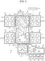
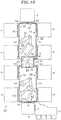
- FIG. 1is a horizontal top view showing a substrate processing apparatus according to a first embodiment
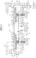
- FIG. 2is a vertical sectional view showing load-lock modules and a vacuum transfer module constituting the substrate processing apparatus;
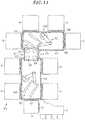
- FIG. 3is an exploded perspective view showing the vacuum transfer module
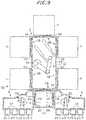
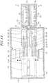
- FIG. 4is a vertical sectional view showing processing module constituting the substrate processing apparatus
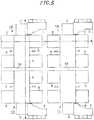
- FIG. 5is a top view showing an arrangement example of the substrate processing apparatus according to the first embodiment
- FIG. 6is a horizontal toe view showing a substrate processing apparatus according to a second embodiment
- FIG. 7is a top view showing an arrangement example of the substrate processing apparatus according to the second embodiment.
- FIG. 8is a top view showing an arrangement example of a substrate processing apparatus according to a third embodiment
- FIG. 9is a horizontal top view showing a substrate processing apparatus according to a fourth embodiment.
- FIG. 10is a horizontal top view showing a substrate processing apparatus according to a fifth embodiment
- FIG. 11a horizontal top view showing a substrate processing apparatus according to a sixth embodiment
- FIG. 12is a vertical sectional view showing another exemplary configuration of the vacuum transfer module
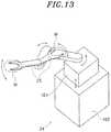
- FIG. 13shows a transfer unit provided at the loader module constituting the substrate processing apparatus
- FIG. 14is a perspective view showing alignment units provided at the loader module
- FIG. 15is a schematic side view showing the alignment units
- FIGS. 16 to 28are process diagrams showing transfer of wafers W in the loader module
- FIG. 29is a timing chart showing an access destination of the transfer unit.
- FIG. 30schematically shows another configuration of the alignment unit.
- the substrate processing apparatus 1includes a loader module 2 , a load-lock module 3 , a vacuum transfer module 4 , and processing modules 6 .
- the loader module 2 and the load-lock module 3are connected to each other in a horizontal direction.
- the load-lock module 3 and the vacuum transfer module 4are connected to each other in the horizontal direction.
- the vacuum transfer module 4 and the processing modules 6are connected to each other in the horizontal direction. Since FIG. 1 is the top view, the load-lock module 3 and the vacuum transfer module 4 are arranged in the up down direction in the drawing.
- the loader module 2is used for taking, out a wafer W that is a circular substrate having a diameter of, e.g., 300 mm, from a carrier C that is a transfer container where the wafer W is stored in a normal pressure atmosphere.
- There are four processing modules 6and each of the processing modules 6 perform film formation on four wafers W in a vacuum atmosphere by performing gas processing at the same time.
- the vacuum transfer module 4forms a vacuum atmosphere and transfers the four wafers W at one time between the processing modules 6 and the load-lock module 3 in the vacuum atmosphere.
- There are two load-lock modules 3(only one is shown in FIG. 1 ). In order to transfer the wafer W between the loader module 2 and the vacuum transfer module 4 , and an atmosphere in the load-lock module 3 where the wafer W is positioned is switched between the normal pressure atmosphere and the vacuum atmosphere.
- a notation D in the drawingsdenotes a door interposed between the loader module 2 and the load-lock module 3 .
- the dooropens and closes transfer ports for the wafer W which are provided at the respective modules.
- Notations G 1 and G 2 in the drawingdenote gate valves interposed between the load-lock module 3 and the vacuum transfer module 4 and between the vacuum transfer module 4 and the processing modules 6 , respectively.
- the gate valvesopen and close transfer ports for the wafer W which are provided at the modules connected to each other.
- the gate valves G 1 and G 2 and the door D which are connected to the modulescan be separated. In other words, the respective modules can be separated from each other.
- the vacuum transfer module 4is configured to change positions for connecting the load-lock modules and positions for connecting the processing modules 6 .
- an example of the arrangement of the load-lock modules 3 and the four processing modules 6 with respect to the vacuum transfer moduleis described.
- other examples different from the arrangement example in the first embodimentwill be described.
- the loader module 2includes a housing 21 and four carrier mounts 22 on which the carriers C are mounted at the outside of the housing 21 .
- the inside of the housing 21is set to a normal pressure atmosphere supplying a dry gas, e.g., dry air, or nitrogen gas.
- a dry gase.g., dry air, or nitrogen gas.
- the inside of the housing 21serves as a normal pressure transfer chamber.
- the four carrier mounts 22are horizontally arranged linearly along a sidewall of the housing 21 convenience of explanation, the arrangement direction of the carrier mounts 22 is referred to as a right-left direction, and the carrier mounts 22 side and the housing 21 side are referred to as a front side and a rear side, respectively, in a horizontal direction perpendicular to the carrier mounts 22 .
- the sidewall of the housing 21 where the carrier mounts 22 are providedis referred to as a front wall of the housing 21 .
- the right side and the left side when viewed from the front side to the rear sideare referred to as a right side and a left side, respectively.
- a reference numeral 23 in the drawingsdenotes doors that open and close opening (not shown) formed in the front wall of the housing 21 and also open and close the carriers C while holding lids of the carriers C.
- Four doors 23are provided at positions corresponding to the carrier mounts 22 .
- a transfer unit 24 for a wafer Wwhich is a multi-joint arm, is provided in the housing 21 .
- An upper and a lower holding portion 25 forming a leading end portion of the transfer unit 24are provided in a vertical direction with a gap therebetween such that the positions thereof are overlapped with each other when seen from the top.
- the wafer Wis held on each of the holding portions 25 . Therefore, the transfer unit 24 can transfer two wafers W at one time.
- the housing 21has a substantially rectangular shape elongated in the right-left direction when viewed from the top.
- a left rear portionprotrudes toward a rear side, and an alignment unit 26 is provided at the left rear portion inside the housing 21 .
- the alignment unit 26includes a mounting portion for mounting and rotating the wafer W and an optical sensor to optically detect a notch that is a cutout at the edge of the wafer W and the center of the wafer W.
- a reference numeral 27 in the drawingsdenotes a transfer port for the wafer W which is opened on a left sidewall of the normal pressure transfer chamber. The transfer port is opened and closed by the door D.
- load-lock modules 3will be described with reference to FIGS. 1 and 2 .
- one of the two load-lock modules 3is used for transferring the wafer W to the vacuum transfer module 4 and the other one the two load-lock modules 3 used for transferring the wafer W to the loader module 2 .
- the two load-lock modules 3are arranged vertically at the left side of the loader module 2 such that the positions thereof are overlapped with each other when seen from the top.
- Each of the load-lock modules 3has a flat rectangular parallelepiped housing 31 .
- the sidewalls of the housing 31face the back-and-forth direction and the right-left direction.
- Reference numerals 32 and 33 in the drawingdenote transfer ports for the wafers W which are opened right sidewall and a rear sidewall of the housing 31 , respectively.
- the transfer ports 32 and 33are opened and closed by the door D and the gate valve G 1 , respectively. Since the load-lock modules are provided in upper and lower two s ages, the gate valves G 1 and the doors D are also provided in upper and lower two stages. In the upper load-lock module 3 and the lower load-lock module 3 , the transfer ports 32 and 33 can be individually opened and closed, and the wafers W can be transferred independently.
- a gas exhaust port and a gas supply portare provided on an inner wall of the housing 31 .
- the inside of the housing 31can be set to a vacuum atmosphere.
- a gase.g., nitrogen (N 2 ) gas
- N 2nitrogen
- the inside of the housing 31serves as a load-lock chamber in which the normal pressure atmosphere and the vacuum atmosphere are switched.
- four supporting portions 34 for supporting a backside of the wafer Ware arranged in, e.g., a 2 ⁇ 2 matrix shape when viewed from the top.
- each of the supporting portions 34has three (only two are shown in FIG. 2 ) vertical pins for supporting the backside of the wafer W.
- the wafer Wtransferred between the supporting portions 34 and the transfer unit 24 of the loader module 2 and between the supporting portions 34 and a transfer unit 51 of the vacuum transfer module 4 which will be described later, by vertical movement of the transfer units 51 and 24 .
- the wafer Wmay be transferred by vertical movement of the supporting portions 34 .
- the supporting portions 34may, have, e.g., a plurality of horizontal rods without being limited to the above-described vertical pins.
- the vacuum transfer module 4will be described with reference to FIGS. 1 to 3 .
- FIG. 3other modules connected to the vacuum transfer module 4 also illustrated, the gate valves G 1 and G 2 interposed between the modules are not illustrated.
- the vacuum transfer module 4is provided at the rear side of the load-lock modules 3 .
- the vacuum transfer module 4includes a housing 41 forming a vacuum transfer chamber.
- the housing 41is formed in a rectangular parallelepiped shape and has a rectangular shape whose long side extends along the back-and-forth direction when seen from the top.
- first sidewalls 42two sidewalls forming short sides of the rectangle are referred to as first sidewalls 42 and two sidewalls forming long sides of the rectangle are referred to as second sidewalls 42 .
- a rectangular opening 44is formed at the center of each first sidewall 42 .
- Two rectangular openings 44are formed on each second sidewall 43 along a longitudinal direction thereof. In a plane view, the sides of the openings 44 extend along the sides of the surfaces of the housings 41 on which the openings 44 are formed.
- the six openings 44have the same shape and the same size and are provided at the same height.
- interface plates 45 and 46 and a blind plate 47which are rectangular plates having the same outer shape and the same size, can be attached to each opening 44 to block the corresponding opening 44 .
- the interface plates 45 and 46 and the blind plate 47are detachably attached to the openings 44 .
- the load-lock module 3Since the load-lock module 3 are provided in upper and lower two stages as described above, it is required to provide transfer ports for the wafers W at positions of the vacuum transfer module 4 which correspond to the height portions of the two load-lock modules 3 .
- Through-holes defining transfer ports 45 A corresponding to the respective load-lock modules 3are formed in upper and lower two stages in the interface plate 45 .
- the height dimension of the processing module 6is greater than that of the load-lock module 3 . Because of the limitation of the height of the module installation space, only one processing module 6 is provided in the vertical direction unlike the load-lock modules 3 . Therefore, one transfer port for the wafer W is provided at the position of the vacuum transfer module 4 which corresponds to the height of the processing module 6 , and one through-hole defining a transfer port 46 A corresponding to the processing module 6 is formed in the interface plate 46 .
- the interface plate 45forms a transfer path for the wafer W at a position of the vacuum transfer module 4 which corresponds to the height of the load-lock module 3 and serves as a first adaptor for the load-lock module 3 which connects the load-lock module 3 and the vacuum transfer module 4 .
- the interface plate 45is provided at the opening 44 of the first sidewall 42 on the front side to correspond to the arrangement of the load-lock modules 3 .
- the two transfer ports 45 A of the interface plate 45are individually opened and closed by the two gate valves G 1 .
- the interface plate 46serves as a second adaptor for the processing module 6 and connects the processing module 6 and the vacuum transfer module 4 forming a transfer path for the wafer W at a position of the vacuum transfer module 4 which corresponds to the height of the processing module 6 .
- interface plate 46is provided for each of the openings 44 formed at the second sidewalls 43 .
- the transfer ports 46 A of the interface plates 46are opened and closed by the gate valves G 2 provided for the processing modules 6 , respectively.
- Each of the openings 44 of the housing 41serves as an adapter attaching portions which is common for the interface plates 45 and 46 and to which any one of the interface plates 45 and 46 serving as an adapter is attached.
- the transfer port 45 A or 46 A of the interface plate 45 or 46 shown in the drawingsis partitioned in the horizontal direction by a partition provided at the center in the horizontal direction. However, they may not be partitioned.
- the blind plate 47is a blocking member for blocking the opening 44 to airtightly seal the housing 41 . Unlike the interface plates 45 and 46 , the blind plate 47 does not have the transfer port for the wafer.
- the moduleis not connected to the rear side of the vacuum transfer module 4 and, thus, the blind plate 47 is attached to the first sidewall 42 on the rear side.
- a gas exhaust port(not shown) is provided on the inner wall of the housing 41 , and the inside f the hour 31 is evacuated to a vacuum atmosphere by exhausting a gas through the gas exhaust port.
- the transfer unit 51 for a wafer Wwhich is a multi-joint arm, is provided in the housing 41 .
- the transfer unit 51accesses each module connected to the vacuum transfer module and transfers the wafer W between the modules.
- the transfer unit 51includes a base 52 , a horizontally extending first arm 53 , a horizontally extending second arm 54 , and a wafer supporting unit 55 .
- the base 52is offset to the left side from a bottom central portion of the housing 41 and configured to be movable vertically.
- a base portion of the first arm 53is provided on the base 52 and rotates about a vertical rotation axis on the base 52 .
- a base portion of the second arm 54is provided on the leading end portion of the first arm 53 and rotates about a vertical rotation axis on the leading end portion of the first arm 53 .
- the wafer supporting unit 55has two thin and long spatula-shaped supporting bodies 56 extending horizontally in parallel to each other and a connecting portion 57 for connecting base ends of these two supporting bodies 56 .
- the connecting portion 57extends in a horizontal direction perpendicular to the extension direction of the supporting bodies 56 .
- a central portion in the longitudinal direction of the connecting portion 57is provided on the leading end portion of the second arm 54 and rotates about a vertical rotation axis on the leading end portion of the second arm 54 .
- the wafers Ware supported at the backsides thereof by a leading end portion and a base end of one supporting body 56 while being spaced apart from each other. Therefore, the wafer support unit 55 of the transfer unit 51 can transfer four wafers W at one time.
- the supporting body 56supports a diametrically extending region of the backside of the wafer W.
- a width of the supporting body 56is smaller than the diameter of the wafer W, so that both edge portions of the wafers W supported by the supporting body 56 when viewed in the extension direction of the supporting body 56 , are not overlapped with the supporting body 56 .
- the central portion of the wafer W supported by the leading end side of the supporting body 56is supported by the leading end of the supporting body 56 and the edge of the wafer W is positioned in a region extended from the leading end of the supporting body 56 in the extension direction.
- the wafers W supported by the leading end portion and the base portion of the supporting bodies 56have regions that are not overlapped with the supporting bodies 56 . Therefore, the wafers W can be transferred between the wafer supporting unit 55 and the supporting portions 34 by vertically moving the wafer supporting unit 55 having the supporting bodies 56 with respect to the supporting portions 34 of the load-lock module 3 . Also, the wafers W can be transferred between elevating pins 75 provided at mounting tables 67 A and 67 B of the processing module 6 which will be described later and the wafer supporting unit 55 by vertically moving the elevating pins 75 .
- the wafer supporting unit 55transfers the wafers W to the supporting portions 34 of the load-lock module 3 and the mounting tables 67 A and 67 B
- the arrangement of the four wafers W supported by the wafer supporting unit 55corresponds to the arrangement of the supporting portions 34 and the arrangement of the mounting tables 67 A and 67 B.
- processing modules 6are film forming modules for forming a film on the wafer W by plasma ALD (Atomic Layer Deposition).
- the four processing modules 6have the same configuration and can process the wafers W in parallel.
- Each of the processing modules 6has a rectangular vacuum chamber (processing chamber) 61 when seen from the top (see FIG. 1 ) and a transfer port 62 for the wafer W which is opened and closed by the gate valve G 2 is opened on the sidewall of the vacuum container 61 .
- a reference numeral 63 in the drawingdenotes a gas exhaust port that is opened on the bottom surface of the vacuum container 61 and connected to a vacuum pump 65 through a gas exhaust line 64 .
- a reference numeral 66 in the drawingdenotes a pressure control unit provided in the gas exhaust line 64 .
- the pressure control unit 66controls the amount of gas exhausted from the gas exhaust port 63 by the vacuum pump 65 so that an atmosphere in the vacuum container 61 becomes a vacuum atmosphere of a desired pressure.
- the mounting tables 67 A and the mounting tables 67 B for mounting thereon the wafer Ware arranged in two rows from the front side toward the rear side when seen from the transfer port 62 .
- the rows of the mounting tables 67 A and 67 Bare arranged side by side in the right-left direction when seen from the transfer port 62 . Therefore, when seen from the top, four wafers W are mounted in a 2 ⁇ 2 matrix shape in the vacuum container 61 .
- the mounting tables 67 A and 67 Bhave the same configuration and are formed in a flat circular shape.
- a reference numeral 70 in the drawingdenotes heaters buried in the respective mounting tables 67 A and 67 B. The heater 70 heats the wafer W mounted on each of the mounting tables 67 A and 67 B to 300° C. to 450° C.
- the mounting tables 67 A and 67 Bform electrodes and are connected to the ground potential via matching units (not shown).
- a reference numeral 68 in the drawingdenotes a column passing through the central portion of the bottom surface of the vacuum container 61 .
- Four supporting arms 69extend horizontally and radially from the upper end of the column and support the mounting tables 67 A and 67 B from the bottom side.
- the lower end of the column 68is connected to an elevating mechanism 71 at the outside of the bottom portion of the vacuum container 61 .
- the mounting tables 67 A and 67 Bare vertically moved by the elevating mechanism 71 through the column 68 and the supporting arms 69 between positions indicated by solid lines and positions indicated by dashed dotted lines in FIG. 4 .
- the positions indicated by the solid linesare processing positions for processing the wafers W.
- a reference numeral 72 in the drawingdenotes a seal member for maintaining the inside of the vacuum container 61 in an airtight state.
- Three through-holes 73are formed in each of the mounting tables 67 A and 67 B (only two are shown in FIG. 4 ).
- an elevating pin 75that is vertically moved to transfer the wafer W with respect to the transfer unit 51 is provided.
- a reference numeral 74 in the drawingdenotes elevating mechanisms 74 for vertically moving the elevating pins 75 .
- the elevating mechanisms 74are provided at the outside of the bottom portion of the vacuum container 61 .
- a reference numeral 76 in the drawingdenotes bellows for ensuring airtightness in the vacuum container 61 .
- Gas shower heads 77 serving as electrodesare provided at the ceiling of the vacuum container 61 through insulating member 77 A and positioned above the mounting tables 67 A and 67 B.
- the bottom surfaces of the gas shower heads 77face the mounting tables 67 A and 67 B.
- a plurality of gas injection holes 78is distributed on the bottom surfaces thereof.
- High frequency power supplies 59are connected to the gas shower heads 77 via matching units 58 , respectively.
- the processing module 6is configured as a parallel plate type plasma processing apparatus.
- a reference numeral 79 in the drawingdenotes gas supply units.
- the gas supply unitsare configured to supply titanium tetrachloride (TiCl 4 ), hydrogen (H 2 ) gas, ammonia (NH 3 ) gas, argon (Ar) gas and nitrogen (N 2 ) gas independently to the gas shower heads 77 . These gases are injected through the gas injection holes 78 .
- the process of forming a film on the wafer W by the processing module 6will be described.
- the wafers Ware mounted on the two mounting tables 67 A and the two mounting tables 67 B located at the transfer positions, the wafers W are heated by the heaters 70 and the mounting tables 67 A and 67 B are raised to the processing positions.
- the high frequency power supplies 59are switched to supply the high frequency powers to between each of the gas shower heads 77 and each of the mounting tables 67 A and 67 B and the gases supplied from the gas shower head 77 are converted into plasma.
- the TiCl 4 gas and the H 2 gas which have been turned into the plasmareact with each other, thereby forming a layer of Ti (titanium) on the surfaces of the wafers W.
- the supply of the TiCl 4 gas, the Ar gas, and the H 2 gas from the gas shower heads 77 and the supply of the high frequency powers from the high frequency power supplies 59are stopped.
- the vacuum container 61is exhausted, and the TiCl 4 gas, the Ar gas and the H 2 gas are removed.
- NH 3 gas, Ar gas and H 2 gasare supplied from the gas shower heads 77 into the vacuum container 61 , and the surface of the Ti layer is nitrided to form a TiN (titanium nitride) layer.
- the formation of the Ti layer and the nitriding of the Ti layerare alternately repeated and, thus, the TiN layer is laminated to form a TiN film having a desired film thickness.
- the substrate processing apparatus 1includes a controller 10 including a computer.
- the controller 10has a program.
- This programhas a group of steps (commands) so that the operations such as the transfer of the wafer by the transfer unit, opening/closing of the door D and the gate valves G 1 and G 2 , the control of the pressure in the processing modules 6 , the start/stop of gas supply, the vertical movement of the elevating pins 75 , the on/off of the high frequency power supplies 59 and the like controlled by outputting control signals to the respective modules and the wafer W can be processed in the substrate processing apparatus 1 as will be described later.
- This programis stored in a storage medium such as a hard disk, a compact disk, a DVD, memory card and the like, and is installed in the computer from the storage medium.
- the carrier Cis mounted on the carrier mount 22 of the loader module 2 , and two wafers W are transferred to the alignment unit 26 by the transfer unit 24 .
- the transfer unit 24receives the wafers W from the alignment unit 26 such that the wafers W are oriented in predetermined orientations and the centers of the wafers W are located at predetermined positions, and transfers the wafers W to two supporting portions 34 among the four supporting portions 34 in, e.g., the upper load-lock module 3 in a normal pressure atmosphere.
- the transfer unit 24transfers two wafers W from the carrier C to the alignment unit 26 and receives two wafers a from the alignment unit 26 such that the wafers W are oriented in predetermined orientations and the centers of the wafers W are located at predetermined positions. These two wafers W are transferred to two supporting portions 34 on which the wafers W are not supported in the upper load-lock module 3 .
- the transfer unit 24is retreated from the upper load-lock module 3 .
- the gate valve G 1is opened.
- the wafer supporting unit 55 of the transfer unit 51enters the load-lock module 3 , and four wafers W are transferred from the supporting portions 34 to the wafer supporting unit 55 at one time by upward movement of the wafer supporting unit 55 .
- the gate valve G 2 connected to the processing module 6 where no wafer W is being processed among the four processing modules 6is opened and the wafer supporting unit 55 enters the corresponding processing module 6 .
- the four wafers W supported by the wafer supporting unit 55are transferred to the two mounting tables 67 A and the two mounting tables 67 B by the vertical movement of the lifting pins 75 .
- the wafer supporting unit 55is retreated from the processing module 6 and the gate valve G 2 is closed.
- the gate valve G 2is opened again and the four wafers W that have been subjected to the film formation are transferred to the wafer supporting unit 55 by the vertical movement of the elevating pins 75 in the processing module 6 .
- the wafer supporting unit 55 retreated from the processing module 6 and the gate valve G 2is closed. Then, the gate vale G 1 connected to the lower load-lock module 3 in a vacuum atmosphere is opened. The wafer supporting unit enters the corresponding load-lock module and is lowered to transfer the four wafers N to the supporting portions 34 . Then, the wafer supporting unit 55 is retreated from the load-lock module 3 and the gate valve G 1 is closed. After the inside of the lower load-lock module 3 becomes a normal pressure atmosphere and the door D connected to the lower load-lock module 3 is opened, the wafers W are transferred from the supporting portions 34 to the carrier C by the transfer unit 24 .
- FIG. 5shows an example in which four substrate processing apparatuses 1 are arranged in a 2 ⁇ 2 matrix shape when seen from the top.
- reference numerals 1 A to 1 Dwill be given to the substrate processing apparatuses.
- reference numeral 1 Adenotes a substrate processing apparatus 1 positioned in the first row and the first column
- reference numeral 1 Bdenotes a substrate processing apparatus 1 positioned in the first row and the second column
- reference numeral 1 Cdenotes a substrate processing apparatus 1 positioned in the second row and the first column
- reference numeral 1 Ddenotes a substrate processing apparatus 1 positioned in the second row and the second column.
- the loader modules 2 of the substrate processing apparatuses 1 A and 1 Bare connected to sides of the load-lock modules 3 which are opposite to the sides in the example shown in FIG. 1 .
- the back-and-forth direction of the substrate processing apparatuses 1 A to 1 Dcoincides with the column direction of the matrix.
- the first sidewalls 42 of the vacuum transfer modules 4 having the blind plates 47face each other between the substrate processing apparatuses 1 A and 1 C and between the substrate processing apparatuses 1 B and 1 D. Since the modules are not connected to these first sidewalls 42 facing each other, a gap between the substrate processing apparatuses 1 in the same column can be reduced.
- a length occupied by two substrate processing apparatuses 1 in the same column in the matrixi.e., a length L 1 from the loader module 2 of one substrate processing apparatus 1 to the loader module 2 of the other substrate processing apparatus 1 . Accordingly, the footprint of the four substrate processing apparatuses 1 can be reduced.
- the load-lock module 3 and the loader module 2are connected to each other in the right-left direction.
- the loader module 2 and the processing modules 6form a row in the back-and-forth direction.
- the length occupied by one substrate processing apparatus 1is reduced compared to the case in which the loader module 2 is arranged in front of the load-lock module 3 and, also, a region facing both of the load-lock module 3 and the processing module 6 can be prevented from becoming a dead space.
- the footprint of the substrate processing apparatus 1is reduced.
- the loader modules 2 of the substrate processing apparatuses 1 A and 1 Cproject toward the regions facing both of the load-lock modules 3 and the left front processing modules 6 of the substrate processing apparatuses 1 B and 1 D.
- the loader module 2 of one substrate processing apparatus 1does not interfere with any module of the other substrate processing apparatus 1 . Therefore, by connecting the loader module 2 and the load-lock module 3 in the right-left direction, it is possible to reduce a width L 2 occupied by two columns in the matrix. Accordingly, the footprint of the four substrate processing apparatuses 1 is reduced.
- a substrate processing apparatus 81 according to a second embodimentwill be described with reference to FIG. 6 .
- a vacuum transfer module 4 of the substrate processing apparatus 81is provided such that long sides thereof extend along the right-left direction when seen from the top.
- a processing module 6is attached to each of two first sidewalls 42 of the vacuum transfer module 4 through an interface plate 46 .
- Two processing modules 6are attached to second sidewall 43 on the rear side through interface plates 46 .
- a blind plate 47is attached to a right opening 44
- a load-lock module 3is attached to a left opening 44 through an interface plate 45 .
- FIG. 7snows an example in which four substrate processing apparatuses 81 are arranged in a 2 ⁇ 2 matrix shape as in the first embodiment.
- the second sidewalls 43 to which two processing, modules 6 are connectedface each other.
- the loader modules 2 of the substrate processing apparatuses 81 A and 81 Bare connected to sides of the load-lock modules 3 which are opposite to the sides in the example shown in FIG. 6 .
- a length L 3 in the back-and-forth direction which is occupied by two substrate processing apparatuses 81 the same columncan be smaller than the length L 1 in the back-and-forth direction which occupied by two substrate processing apparatuses in the same column shown in FIG. 5 .
- the load-lock module 3 and the loader module 2 of the substrate processing apparatus 81are also connected to each other in the right-left direction. Therefore, the loader module 2 is overlapped with the vacuum transfer module 4 when viewed in the back-and-forth direction. Accordingly, the length in the back-and-forth direction which is occupied by one substrate processing apparatus 81 is reduced compared to the case in which the loader module 2 is provided in front of the load-lock module 3 , and the region facing both of the load-lock module 3 and the vacuum transfer module 4 is prevented from becoming a dead space. In other words, in the substrate processing apparatus 81 as well, the increase in the footprint of the apparatus is suppressed by connecting the load-lock module 3 and the loader module 2 to each other the right-left direction.
- FIG. 8shows an example in which the apparatuses are arranged in a 2 ⁇ 2 matrix shape as in the case of the substrate processing apparatuses 1 shown in FIG. 5 and the substrate processing apparatuses 81 shown in FIG. 7 .
- Reference numerals 82 A to 82 Dare given to the apparatuses in the above-described manner.
- the processing module 6also connected to the first sidewall 42 on the rear side. Further, one processing module 6 and a blind plate 47 are attached to one of the two second sidewalls 43 .
- the second sidewalls 43 to each of which one processing module 6 is connectedface each other, and the positions of the second sidewalls 42 to which the processing modules 6 are connected are different in the back-and-forth direction between the substrate processing apparatuses 82 A and 82 B.
- the substrate processing apparatuses 82 C and 82 D, the second sidewalls 43 to each of which one processing module 6 connectedface each other, and the positions of the second walls 42 to which the processing modules 6 are connected are different in the back-and-forth direction between the substrate processing apparatuses 82 A and 82 B.
- the load-lock module 3 and the processing modules 6can be selectively attached to the openings 44 provided at the sidewalls of the housing 41 and, thus, the degree of freedom in the arrangement of the load-lock module 3 and the processing modules 6 increased. Therefore, the selectivity of the planar shape of the substrate processing apparatus is increased, and the substrate processing apparatus can be configured by connecting the load-lock modules 3 and the processing modules 6 to the vacuum transfer chamber 4 based on the size of the space in which the substrate processing apparatus is installed, the shape of the space, the transfer path of the transfer mechanism for transferring the carrier C to the substrate processing apparatus, and the like. Accordingly, it is possible to prevent the number of processing modules 6 or the number of substrate processing apparatuses from being limited by restrictions in the installation space of the apparatus, the transfer path of the transfer mechanism or the like. As a result, the productivity of the semiconductor product can be increased.
- the housing 41 of the vacuum trans tier module 4has a rectangular shape when seen from the top.
- the openings 44are formed at the first sidewalls 42 and the second sidewalls 43 .
- the number of openings 44 formed at the second sidewalls 43 forming the long sides of the rectangleis greater than the number of openings 44 formed the first sidewalls 42 forming the short sides of the rectangle.
- the vacuum transfer module 4is configured so that the selectivity of the planar shape of the substrate processing apparatus can be further increased.
- the transfer unit 51 of the vacuum transfer module 4transfers four wafers W at one time to a plurality of processing modules 6 connected to the vacuum transfer module 4 and, thus, a high throughput can be obtained. Further, in each of the processing modules 6 , the four wafers W are processed at one time and, thus, a higher throughput can be obtained.
- a processing module 6instead of a blind plate 47 , is connected to the first sidewall 42 on the rear side of the vacuum transfer module 4 of the substrate processing apparatus 83 .
- the substrate processing apparatus 83includes five processing modules 6 .
- a loader module 2is connected to both sides of the load-lock module 3 in the right-left direction through respective doors D. Therefore, the substrate processing apparatus 83 includes two loader modules 2 .
- the loader module 2 provided at the left side of the load-lock module 3is configured to be mirror-symmetrical with the loader module 2 provided at the right side of the loader module when seen from top.
- a transfer port 32is formed at a right sidewall and a left sidewall of the load-lock module 3 to correspond to the two loader modules 2 .
- this substrate processing apparatus 83since two loader modules are provided, loading and unloading of the wafers W to and from the load-lock module 3 is quickly performed. Further, since five processing modules 6 are provided, the number of wafers W that can be processed at one time is greater than that in the substrate processing apparatus 1 . Therefore, a throughput in the substrate processing apparatus 83 can be further increased compared to that in the substrate processing apparatus 1 .
- the substrate processing apparatus 84includes two vacuum transfer modules 4 and a mounting module 9 for connecting the two vacuum transfer modules 4 .
- the mounting module 9mounts thereon wafers W to be transferred between itself and the vacuum transfer modules 4 .
- the vacuum transfer modules 4are arranged side by side in the back-and-forth direction so that the long sides of the rectangular shape of the vacuum transfer modules 4 extend along the back-and-forth direction.
- a reference numeral 4 Adenotes a vacuum transfer module on the front side
- a reference numeral 4 Bdenotes a vacuum n transfer module on the rear side.
- the load-lock module 3 and the processing modules 6are attached to the vacuum transfer module 4 A, as in the case of the vacuum transfer module 4 of the first embodiment.
- a blind plate 47is not attached to the first sidewall 42 on the rear side of the vacuum transfer module 4 A.
- a processing module 6is attached to the first sidewall 42 on the rear side and two processing modules 6 are attached to each of two second sidewalls 43 .
- the mounting module 9includes a housing 91 having a rectangular shape when seen from the top. By fitting the housing 91 into the opening 44 of the vacuum transfer module 4 , the mounting module 9 and the vacuum transfer module 4 are connected. The mounting module 9 and the vacuum transfer module 4 are detachable from each other. A transfer port 92 for the wafer W is formed through two sidewalls facing each other among four sidewalls of the housing 91 . Four mounting portions 93 for mounting thereon wafers W are provided in the housing 91 .
- each of the mounting portions 93is provided with, e.g., three vertical pins for supporting the backside of the wafer W, similarly to the supporting portions 34 of the load-lock module 3 .
- the mounting module 9is attached to the first sidewall 42 on the rear side of the vacuum transfer module 4 A and the first sidewall 42 on the front side of the vacuum transfer module 4 B so that the transfer ports 92 are opened into the housings 41 of the vacuum transfer modules 4 A and 4 B.
- the wafer W transferred from the load-lock module 3is transferred to any one of nine processing modules 6 connected to the vacuum transfer modules 4 A and 4 B to be processed therein.
- this substrate processing apparatus 84since the vacuum transfer modules 4 A and 4 B are connected to each other, it is possible to transfer the wafers W to the nine processing modules 6 connected to the vacuum transfer modules 4 A and 4 B from the leader module 2 and the load-lock module 3 which are common for the vacuum transfer modules 4 A and 4 B. Therefore, the number of the processing modules 6 with respect to the number of the loader module 2 and the load-lock module 3 can be i-creased. Accordingly, the throughput can be increased while reducing the footprint of the apparatus.
- a substrate processing apparatus 85 according to a sixth embodimentwill be described with reference to FIG. 11 .
- the differences between the substrate processing apparatus 85 and the substrate processing apparatus 84will be described mainly.
- vacuum transfer modules 4 A and 4 Bare connected through a mounting module 9 .
- Various modulesare connected to the vacuum transfer module 4 A of the substrate processing apparatus 85 , as in the case of the vacuum transfer module 4 A of the vacuum processing apparatus 84 .
- the vacuum transfer module 4 Blong sides of the rectangular shape when seen from the are arranged along the right-left direction as in the case of the vacuum transfer module 4 of the substrate processing apparatus 81 shown in FIG. 6 .
- the positions of the vacuum transfer module 4 B to which the processing modules 6 and the blind plate 47 are connectedare the same as those of the vacuum transfer module to which the processing modules 6 and the blind plate 47 are connected.
- the mounting module 9is fitted to an opening 44 of a first sidewall 42 on the rear side of the vacuum transfer module 4 A and an opening 44 of a second sidewall 43 on the front side of the vacuum transfer module 4 B.
- the number of the processing modules 6 with respect to the number of the loader modules 2 and the load-lock module 3can be increased, as in the case the substrate processing apparatus 84 . Further, since the vacuum transfer modules 4 A and 4 B are connected to each other through the mounting module 9 in the above-described direction, it is possible to reduce the width in the back-and-forth direction of the apparatus compared to that in the substrate processing apparatus 84 . Accordingly the footprint of the apparatus can be reduced.
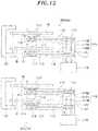
- FIG. 12shows another configuration example of the vacuum transfer module 4 .
- the vacuum transfer module 4 shown in FIG. 12includes an upper and a lower transfer unit 51 for individually transferring the wafer W.
- a reference numeral 51 Adenotes the lower transfer unit and a reference numeral 51 B denotes the upper transfer unit.
- the transfer unit 51 Ais the same as the transfer unit 51 shown in FIG. 2 .
- the transfer unit 51 Bhas an upside-down shape of the transfer unit 51 A.
- a base 52 of the transfer unit 51 Bis provided at the ceiling of the housing 41 of the vacuum transfer module 4 .
- the transfer unit 513transfers the wafer W between the upper load-lock module 3 and the processing module 6 .
- the transfer unit 52 Atransfers the wafer W between the lower load-lock module 3 and the processing module 6 .
- the transfer unit 513transfers the wafer W in an upper region 94 in the housing 41 and the transfer unit 51 A transfers the wafer W in a lower region 95 in the housing 41 . Since both of the transfer units 51 A and 51 B transfer the wafers W to the processing modules 6 , the lower portion of the upper region 94 and the upper portion of the lower region 95 are overlapped with each other.
- the vacuum transfer modules 4 of the respective embodimentsmay include the transfer units 51 A and 51 B.
- the processing module 6is not limited to a module for forming a film by ALD, and may also be, e.g., a module for forming a film by CVD (Chemical Vapor Deposition) or a module for performing dry etching. When such processes are performed, plasma may not be generated.
- the processing modules 6perform the same process. However, the processing modules 6 for performing different processes may be connected to the vacuum transfer module 4 . In that case, a wafer W may be transferred to one of the processing modules 6 and processed, and then transferred to another processing module 6 and processed, and then returned to the carrier C.
- one of the processing modules 6may be a module for forming a film by ALD, and another processing module 6 may be an annealing module for heating the wafer W in a vacuum atmosphere. Further, one of the processing modules and a other processing module 6 may be, e.g., modules for forming different films on the wafer W.
- the supporting body 56 of the transfer unit 51may be shorter than that shown in the drawing, and one wafer W may be supported by one supporting body 56 .
- the transfer unit 51may transfer two wafers W at one time.
- the transfer unit 51may have one supporting body 56 and transfer two wafers W at one time.
- the transfer of four wafers W to the mounting tables 67 A and 67 B in one processing module 6may be performed in two steps.
- the transfer unit 51does not necessarily transfer a plurality of wafers W, and may transfer only one wafer W.
- the processing module 6does not necessarily process four wafers W one time, and may process only one wafer or a plurality of wafers other than four wafers.
- the adapters for connecting the load-lock module 3 and the processing modules 6 to the vacuum transfer module 4do not necessarily have a plate shape, and may have, e.g., a block shape. Further, three or more vacuum transfer modules 4 may connected through plurality of mounting modules 9 . In the mounting module 9 , the transfer ports 92 for the wafer W of the housing can be opened and closed by the gate valves and the pressure in the housing 91 can be changed, as in the case of the load-lock module 3 . In that case, even if the pressures in the vacuum transfer modules 4 connected to each other are different, the wafer W can be transferred between these vacuum transfer modules 4 .
- the number of the load-lock modules 3is not limited to two, and may be one. Further, three or more load-lock modules 3 may be provided side by side in the vertical direction. In that case, three or more transfer ports 45 A are provided at the interface plate 45 to correspond to the heights of the load-lock modules 3 .
- the processing modules 6may be provided in multiple stages, as in the case of the load-lock modules 3 .
- the transfer ports 46 Amay be provided in multiple stages at the interface plate 46 .
- the housing 41 of the vacuum transfer module 4may be greater than that in the above example, and two or more openings 44 may be formed side by side in the horizontal direction at the first sidewall 42 . Three or more openings 44 may be formed side by side in the horizontal direction at the second sidewall 43 . In order to increase a degree of freedom in the layout of the substrate processing apparatus, it is preferable to set the number of the openings 44 formed at the second sidewall 43 to be greater than the number of the openings 44 formed at the first sidewall 42 .
- the substrate processing apparatuses 83 to 85may be arranged in a matrix shape.
- the illustrated matrix-shaped arrangement of the substrate processing apparatusesis merely an example, and the number of substrate processing apparatuses and the arrangement of the substrate processing apparatuses may vary.
- the present disclosureis not limited to the above embodiments, and respective embodiments may be appropriately modified or combined with each other.
- the loader module 2is configured to quickly transfer the wafer W.
- the loader module 2will be described in detail.
- FIG. 13is a perspective view showing the transfer unit 24 described with reference to FIG. 1 and the like.
- the transfer unit 24which is a substrate transfer unit for the loader module, has a multi-joint arm as described above. Two holding portions 25 forming the leading end portions of the multi-joint arm are arranged in the vertical direction. The two holding portions 25 are independently rotatable and can hold the wafers W as described above.
- the transfer unit 24includes a supporting table 101 for supporting the base portion of the multi-joint arm.
- the supporting table 101is vertically movable by an elevating mechanism 102 .
- the holding portions 25are movable horizontally and vertically. By cooperation of the horizontal movement and the vertical movement, the wafer W can be transferred to the respective components of the apparatus.
- FIG. 14is a perspective view of the alignment units 26 .
- FIG. 15is a simplified side view showing the configuration of the alignment units 26 .
- the alignment units 26are provided in upper and lower two stages.
- the alignment units 26constitute a substrate position detection mechanism.
- a reference numeral 26 Adenotes the lower alignment unit and a reference numeral 26 B denotes the upper alignment unit.
- the alignment units 26 A and 26 Bhave the same configuration and, thus, the alignment unit 26 A will be described representatively.
- the alignment unit 26 Aincludes flat circular mounting portions 111 and 112 for a wafer W.
- the mounting portions 111 and 112are spaced apart from each other in a vertical direction and overlapped with each other when seen from the top.
- the reference numeral 111denotes the lower mounting portion and the reference numeral 112 denotes the upper mounting portion.
- a shaft 113extends vertically downward from the center portion of each of the mounting portions 111 and 112 .
- a reference numeral 114 in the drawingdenotes a pulley. The pulley 114 is provided at a lower portion of the shaft 113 and rotates together with the shaft 113 .
- a shaft 115 extending verticallyis, provided at one side of the mounting portions 111 and 112 .
- a lower end of the shaft 115is connected to a motor 116 that is a rotation mechanism for rotating the shaft 115 .
- a reference numeral 117 in the drawingdenotes pulleys provided at an upper and a lower portion of the shaft 115 . The pulleys 117 rotate together with the shaft 115 .
- Timing belts 118are wound around the upper pulleys 114 and 117 and around the lower pulleys 114 and 117 . With this configuration, when the shaft 115 rotated by the motor 116 , power is transferred by the timing belts 118 , and both of mounting portions 111 and 112 rotate about the central axes thereof.
- a reference numeral 119denotes a housing.
- the housing 119includes a vertical portion 119 A extending to surround the shaft 115 and the pulley 117 , a horizontal portion 119 B extending horizontally in upper and lower two stages from the vertical portion 119 A and surrounding the timing belts 118 , the shaft 113 and the pulley 114 .
- the motor 116is shared by the mounting portions 111 and 112 and provided at one side of the mounting portions 111 and 112 .
- the distance between the mounting portions 111 and 112can be reduced compared to a configuration in which two motors 116 are respectively provided below the mounting portions 111 and 112 to rotate the mounting portions 111 and 112 . Therefore, it is possible to avoid an increase in a required moving distance for the transfer unit 24 to access the mounting portions 111 and 112 . Accordingly, the transfer of the wafer W in the loader module 2 which will be described later can be quickly performed.
- a reference numeral 121denotes a light detection unit.
- the edges of the wafers W mounted on the mounting portions 111 and 112are positioned between two protruding parts of the light detection unit 121 which protrude laterally. These two protruding parts are configured as a pair of transmission type optical sensor.
- the upper protruding partserves as a light transmitting portion and the lower protruding part serves as a light receiving portion.
- the lightis irradiated vertically downward from the light transmitting portion to the light receiving portion.
- the dotted arrows in FIG. 15indicate the optical path between the light transmitting portion and the light receiving portion.
- the lightis irradiated during the rotation of the wafer W by the mounting portions 111 and 112 .
- the light receiving portiontransmits to the controller 10 a detection signal depending on the intensity of the received light.
- the controller 10detects the position of the wafer W.
- the position of the wafer Wincludes, e.g., the position of a cutout (notch) formed at the edge of the wafer W and the position of the edge of the wafer W.
- the position of the wafer Wis detected in a state in which the wafer W is mounted on only one of the mounting portions 111 and 112 in the alignment unit 26 A. In the alignment unit 26 B as well, the position of the wafer W is detected in a state where the wafer W is mounted on only one of the mounting portions 111 and 112 .
- the wafers W whose position has been detectedare transferred to a predetermined position on the holding, portions 25 in a state where the notches are oriented in a predetermined orientation by the rotation of the mounting portions 111 and 112 .
- the mounting portions 111 and 112 of the alignment unit 26 A and the mounting portions 111 and 112 of the alignment unit 26 Bare overlapped each other when seen from the top.
- the shaft 115 and the motor 116 of the alignment unit 26 A and the shaft 115 and the motor 116 of alignment unit 26 Bare displaced from each other in the rotation direction of the wafer W.
- FIGS. 16 to 28showing the operation of the transfer unit 24 .
- the wafer W whose position has been detected in the alignment units 26 A and 26 B and has not yet been processed by the processing module 6is indicated by dots, and the wafer W that has been processed in the processing module 6 is indicated by hatching. Dots and hatching are not given to wafers W whose positions have not been detected in the alignment units 26 A and 26 B.
- a reference numeral 3 Adenotes the lower load-lock module and a reference numeral 3 B denotes the upper load-lock module.
- the load-lock module 3 Atransfers the wafer W to the vacuum transfer module 4
- the load-lock module 3 Btransfers the wafer W to the loader module 2 .
- the four supporting portions 34 provided in the load-lock modules 3 A and 3 Bare arranged side by side in the horizontal direction to transfer the wafers W to the vacuum transfer module 4 .
- the supporting 34are arranged side by side in the vertical direction, for convenience of illustration.
- the timing chart of FIG. 29will be appropriately referred to.
- the timing chartshows temporal changes of the target accessed by the transfer unit 24 .
- the explanationwill be started from the stage where wafers W are newly taken out from the carrier C after wafers W have been taken out from the carrier C multiple times.
- two wafers W(referred to as wafers W 1 and W 2 , for convenience of explanation) are taken out at one time from the carrier C by the transfer unit 24 ( FIG. 16 , time t 1 ).
- the wafer W whose position has been detected(referred to as wafer W 3 for convenience of explanation) is mounted only on the mounting portion 111 between the mounting portions 111 and 112 .
- the wafer W whose position has not been detected(referred to as wafer W 4 for convenience of explanation) is mounted only on the mounting portion 111 between the mounting portions 111 and 112 ( FIG. 17 ).
- the wafer W 1is transferred to the mounting portion 112 of the alignment unit 26 A; one of the holding portions 25 of the transfer unit 24 becomes empty (a state in which the wafer W is not held); and in the alignment unit 26 B, the position of the wafer W 4 is detected ( FIG. 18 , time t 2 in the chart).
- the wafer W 3 whose position has been detected in the alignment unit 26 Ais received by the empty holding portion 25 ( FIG. 19 ).
- the wafer W 2is transferred to the mounting portion 112 of the alignment unit 26 B by the transfer unit 24 ; one of the holding portions 25 of the transfer unit 24 becomes empty; and the position of the wafer W 1 is detected in the alignment unit 26 A ( FIG. 20 , time t 3 in chart). After the position of the wafer W 1 is detected, the wafer W 4 whose position has been detected in the alignment unit 26 B is received by the empty holding portion 25 ( FIG. 21 ).
- the transfer unit 24transfers the wafers W 3 and W 4 to two supporting portions among the four supporting portions 34 of the load-lock module 3 A, and the two holding portions 25 of the transfer unit 24 become empty ( FIGS. 22 and 23 , time t 4 ).
- the position of the wafer W 2is detected in the alignment unit 26 B.
- two wafers W among the processed wafers(referred to as wafers W 5 ) held on the four supporting portions 34 in the load-lock module 3 B are held on the empty holding portions 25 ( FIGS. 24 and 25 ) and transferred to the carrier C by the transfer unit 24 ( FIG. 26 , time t 5 )
- the transfer of the wafer W by the transfer unit 24 in the order of the carrier C ⁇ the alignment unit 26 A ⁇ the alignment unit 26 B ⁇ the load-lock module 3 A she load-lock module 3 B ⁇ the carrier C which corresponds to a series of operations from the time t 1 to the time t 5is performed again.
- a next transfer cycle of the above transfer cycle of the wafer W from the time t 1 to the time t 5will be described briefly.
- two wafers N(referred to as wafers W 6 and W 7 in FIG. 26 ) are taken out from the carrier C and transferred at one time by the transfer unit 24 .
- the transfer unit 24transfers the wafer W 6 to the mounting portion 111 of the alignment unit 26 A (time t 6 ) and the wafer W 1 whose position has been detected in the alignment unit 26 A is received by the empty holding portion 25 .
- the same operations as those described with reference to FIGS. 17 to 19are performed except that the wafer W is transferred to the mounting portion 111 and the wafer W is received from the mounting portion 112 .
- the transfer unit 24transfers the wafer W 7 to the mounting portion 111 of the alignment unit 26 B (time t 7 ) and the wafer W 2 whose position has been detected in the alignment unit 26 B is received by the empty holding portion 25 .
- the same operations as those described with reference to FIGS. 20 and 21are performed except that the wafer W is transferred to the mounting portion 111 and the wafer W is received from the mounting portion 112 .
- the position of the wafers W 6 and W 7are detected.
- the transfer unit 24transfers the received wafers W 1 and W 2 to the load-lock module 3 A at one time and delivers them to two empty supporting portions 34 ( FIGS. 27 and 28 , time t 8 ).
- the transfer unit 51 of the vacuum transfer module 4accesses the load-lock module 3 A as described above and transfers the wafers W 1 to W 4 to the vacuum transfer module 4 at one time.
- the transfer unit 24 that has transferred the wafers W 1 and W 2 to the load-lock module 3 Areceives the other two wafers W 5 (see FIG. 25 ) held on the supporting portions 34 of the load-lock module 3 B and transfers them to the carrier C at one time.
- the loader module 2is provided with the alignment units 26 A and 26 B, each having the mounting portions 111 and 112 , and the positions of the wafers W mounted on the mounting portions 111 and 112 can be detected in each of the alignment units 26 A and 26 B.
- the transfer of the wafers Wis controlled such that one of the mounting portions 111 and 112 of the same alignment unit allows the wafer W whose position has been detected to stand by and the other mounting portion becomes empty so that the wafer W taken out from the carrier C can be mounted thereon. More specifically, the wafer W is mounted on one of the mounting portions 111 and 112 during one transfer cycle.
- the wafer Wis mounted on the other one of the mounting portions 111 and 112 , and the wafer W mounted on the mounting portion 111 or 112 in the previous transfer cycle is transferred to the load-lock module 3 A.
- the wafers Ware alternately sequentially transferred to the mounting portions 111 and 112 of the same alignment unit and alternately sequentially transferred to the load-lock module 3 A.
- the wafers Wcan be exchanged between the alignment unit 26 A or 26 B and the transfer unit 24 by using the empty mounting portion between the mounting portions 111 and 112 even if the holding port on 25 of the transfer unit 24 is not empty. Therefore, the transfer unit 24 can take out two wafers W from the carrier C and transfer them to the alignment units 26 A and 26 B at one time. Accordingly, the frequency of accesses to the carrier C by the transfer unit 24 to take out wafers W can be reduced, which makes it possible to improve the throughput of the substrate processing apparatus 1 .
- the wafer W 5is transferred from the load-lock module 3 to the carrier C between the transfer of the wafers and W 4 from the alignment units 26 A and 26 B to the load-lock module 3 A and the transfer of the wafers W 1 and W 2 to the load-lock module 3 A.
- the operation of the transfer unit 24may be controlled such that the transfer of four wafers W to the load-lock module 3 A through the alignment units 26 A and 26 B and the transfer of four wafers W from the load-lock module 3 B to the carrier C can be alternately performed.
- the mounting portions 111 and 112 of the alignment unit 26 A or 26 Bare arranged in the horizontal direction and the light detection unit 121 has a comparatively long width along the arrangement direction of the mounting portions 111 and 112 .
- the positions of the wafers W mounted on the mounting portions 111 and 112may be detected by irradiating light downward to form an optical path passing through the gap between the mounting portions 111 and 112 .
- Dashed arrows in FIG. 30indicate the optical path.
- the transfer unit 24may have three or more holding portions 25 and take out three or more wafers W from the carrier C and transfer them at one time.
- the transfer unit 24has three holding portions (for convenience, referred to as holding portions 25 A to 25 C) and transfer wafers W whose positions have not been detected to the alignment units 26 A and 26 B.
- the wafers Ware exchanged between the alignment unit 26 A and the holding unit 25 A so that the alignment unit 26 A holds the wafer W whose position has not been detected and starts the position detection thereof and the holding portion 25 A holds the wafer W whose position has been detected.
- the wafers Ware exchanged between the alignment unit 26 B and the holding portion 25 B so that the alignment unit 26 B holds the wafer W whose position has not been detected and the holding port on 25 B holds the wafer W whose position has been detected. Further, the wafers W are exchanged between the alignment unit 26 A and the holding portion 25 C so that the alignment unit 26 A holds the wafer W whose position has not been detected and the holding portion 25 C holds the wafer W whose position has been detected.
- the wafer W held by the holding portion 25 Cwas held the holding portion 25 A before the position detection.
- the holding portions 25 A to 25 Ctransfer the wafers W whose position have been detected to the load-lock module 3 A. Therefore, the number of the holding portions 25 of the transfer unit and the number of the alignment units may be the same or may be different. The number of the alignment units may be three or more.
- the loader modules 2 of the substrate processing apparatus 1can also transfer the wafer W in the same manner.
- the transfer method of the wafer W or the configuration of the loader module 2is not limited to the above example and may be changed appropriately.
Landscapes
- Engineering & Computer Science (AREA)
- Physics & Mathematics (AREA)
- Condensed Matter Physics & Semiconductors (AREA)
- General Physics & Mathematics (AREA)
- Manufacturing & Machinery (AREA)
- Computer Hardware Design (AREA)
- Microelectronics & Electronic Packaging (AREA)
- Power Engineering (AREA)
- Robotics (AREA)
- Container, Conveyance, Adherence, Positioning, Of Wafer (AREA)
Abstract
Description
Claims (15)
Applications Claiming Priority (4)
| Application Number | Priority Date | Filing Date | Title |
|---|---|---|---|
| JP2017-102016 | 2017-05-23 | ||
| JP2017102016 | 2017-05-23 | ||
| JP2017-188627 | 2017-09-28 | ||
| JP2017188627AJP6972852B2 (en) | 2017-05-23 | 2017-09-28 | Vacuum transfer module and substrate processing equipment |
Publications (2)
| Publication Number | Publication Date |
|---|---|
| US20180342409A1 US20180342409A1 (en) | 2018-11-29 |
| US10763139B2true US10763139B2 (en) | 2020-09-01 |
Family
ID=64401488
Family Applications (1)
| Application Number | Title | Priority Date | Filing Date |
|---|---|---|---|
| US15/987,519Active2038-07-22US10763139B2 (en) | 2017-05-23 | 2018-05-23 | Vacuum transfer module and substrate processing apparatus |
Country Status (2)
| Country | Link |
|---|---|
| US (1) | US10763139B2 (en) |
| CN (1) | CN108933097B (en) |
Cited By (273)
| Publication number | Priority date | Publication date | Assignee | Title |
|---|---|---|---|---|
| US11004977B2 (en) | 2017-07-19 | 2021-05-11 | Asm Ip Holding B.V. | Method for depositing a group IV semiconductor and related semiconductor device structures |
| US11001925B2 (en) | 2016-12-19 | 2021-05-11 | Asm Ip Holding B.V. | Substrate processing apparatus |
| US11018002B2 (en) | 2017-07-19 | 2021-05-25 | Asm Ip Holding B.V. | Method for selectively depositing a Group IV semiconductor and related semiconductor device structures |
| US11015245B2 (en) | 2014-03-19 | 2021-05-25 | Asm Ip Holding B.V. | Gas-phase reactor and system having exhaust plenum and components thereof |
| US11022879B2 (en) | 2017-11-24 | 2021-06-01 | Asm Ip Holding B.V. | Method of forming an enhanced unexposed photoresist layer |
| US11031242B2 (en) | 2018-11-07 | 2021-06-08 | Asm Ip Holding B.V. | Methods for depositing a boron doped silicon germanium film |
| USD922229S1 (en) | 2019-06-05 | 2021-06-15 | Asm Ip Holding B.V. | Device for controlling a temperature of a gas supply unit |
| US11049751B2 (en) | 2018-09-14 | 2021-06-29 | Asm Ip Holding B.V. | Cassette supply system to store and handle cassettes and processing apparatus equipped therewith |
| US11056344B2 (en) | 2017-08-30 | 2021-07-06 | Asm Ip Holding B.V. | Layer forming method |
| US11053591B2 (en) | 2018-08-06 | 2021-07-06 | Asm Ip Holding B.V. | Multi-port gas injection system and reactor system including same |
| US11069510B2 (en) | 2017-08-30 | 2021-07-20 | Asm Ip Holding B.V. | Substrate processing apparatus |
| US11081345B2 (en) | 2018-02-06 | 2021-08-03 | Asm Ip Holding B.V. | Method of post-deposition treatment for silicon oxide film |
| US11087997B2 (en) | 2018-10-31 | 2021-08-10 | Asm Ip Holding B.V. | Substrate processing apparatus for processing substrates |
| US11088002B2 (en) | 2018-03-29 | 2021-08-10 | Asm Ip Holding B.V. | Substrate rack and a substrate processing system and method |
| US11094582B2 (en) | 2016-07-08 | 2021-08-17 | Asm Ip Holding B.V. | Selective deposition method to form air gaps |
| US11094546B2 (en) | 2017-10-05 | 2021-08-17 | Asm Ip Holding B.V. | Method for selectively depositing a metallic film on a substrate |
| US11101370B2 (en) | 2016-05-02 | 2021-08-24 | Asm Ip Holding B.V. | Method of forming a germanium oxynitride film |
| US11107676B2 (en) | 2016-07-28 | 2021-08-31 | Asm Ip Holding B.V. | Method and apparatus for filling a gap |
| US11114283B2 (en) | 2018-03-16 | 2021-09-07 | Asm Ip Holding B.V. | Reactor, system including the reactor, and methods of manufacturing and using same |
| US11114294B2 (en) | 2019-03-08 | 2021-09-07 | Asm Ip Holding B.V. | Structure including SiOC layer and method of forming same |
| USD930782S1 (en) | 2019-08-22 | 2021-09-14 | Asm Ip Holding B.V. | Gas distributor |
| US11127617B2 (en) | 2017-11-27 | 2021-09-21 | Asm Ip Holding B.V. | Storage device for storing wafer cassettes for use with a batch furnace |
| US11127589B2 (en) | 2019-02-01 | 2021-09-21 | Asm Ip Holding B.V. | Method of topology-selective film formation of silicon oxide |
| USD931978S1 (en) | 2019-06-27 | 2021-09-28 | Asm Ip Holding B.V. | Showerhead vacuum transport |
| US11139191B2 (en) | 2017-08-09 | 2021-10-05 | Asm Ip Holding B.V. | Storage apparatus for storing cassettes for substrates and processing apparatus equipped therewith |
| US11139308B2 (en) | 2015-12-29 | 2021-10-05 | Asm Ip Holding B.V. | Atomic layer deposition of III-V compounds to form V-NAND devices |
| US11158513B2 (en) | 2018-12-13 | 2021-10-26 | Asm Ip Holding B.V. | Methods for forming a rhenium-containing film on a substrate by a cyclical deposition process and related semiconductor device structures |
| US11164955B2 (en) | 2017-07-18 | 2021-11-02 | Asm Ip Holding B.V. | Methods for forming a semiconductor device structure and related semiconductor device structures |
| US11171025B2 (en) | 2019-01-22 | 2021-11-09 | Asm Ip Holding B.V. | Substrate processing device |
| US11168395B2 (en) | 2018-06-29 | 2021-11-09 | Asm Ip Holding B.V. | Temperature-controlled flange and reactor system including same |
| USD935572S1 (en) | 2019-05-24 | 2021-11-09 | Asm Ip Holding B.V. | Gas channel plate |
| US11205585B2 (en) | 2016-07-28 | 2021-12-21 | Asm Ip Holding B.V. | Substrate processing apparatus and method of operating the same |
| US11217444B2 (en) | 2018-11-30 | 2022-01-04 | Asm Ip Holding B.V. | Method for forming an ultraviolet radiation responsive metal oxide-containing film |
| USD940837S1 (en) | 2019-08-22 | 2022-01-11 | Asm Ip Holding B.V. | Electrode |
| US11222772B2 (en) | 2016-12-14 | 2022-01-11 | Asm Ip Holding B.V. | Substrate processing apparatus |
| US11227789B2 (en) | 2019-02-20 | 2022-01-18 | Asm Ip Holding B.V. | Method and apparatus for filling a recess formed within a substrate surface |
| US11227782B2 (en) | 2019-07-31 | 2022-01-18 | Asm Ip Holding B.V. | Vertical batch furnace assembly |
| US11233133B2 (en) | 2015-10-21 | 2022-01-25 | Asm Ip Holding B.V. | NbMC layers |
| US11230766B2 (en) | 2018-03-29 | 2022-01-25 | Asm Ip Holding B.V. | Substrate processing apparatus and method |
| US11232963B2 (en) | 2018-10-03 | 2022-01-25 | Asm Ip Holding B.V. | Substrate processing apparatus and method |
| US11244825B2 (en) | 2018-11-16 | 2022-02-08 | Asm Ip Holding B.V. | Methods for depositing a transition metal chalcogenide film on a substrate by a cyclical deposition process |
| US11242598B2 (en) | 2015-06-26 | 2022-02-08 | Asm Ip Holding B.V. | Structures including metal carbide material, devices including the structures, and methods of forming same |
| US11251068B2 (en) | 2018-10-19 | 2022-02-15 | Asm Ip Holding B.V. | Substrate processing apparatus and substrate processing method |
| US11251035B2 (en) | 2016-12-22 | 2022-02-15 | Asm Ip Holding B.V. | Method of forming a structure on a substrate |
| US11251040B2 (en) | 2019-02-20 | 2022-02-15 | Asm Ip Holding B.V. | Cyclical deposition method including treatment step and apparatus for same |
| USD944946S1 (en) | 2019-06-14 | 2022-03-01 | Asm Ip Holding B.V. | Shower plate |
| US11270899B2 (en) | 2018-06-04 | 2022-03-08 | Asm Ip Holding B.V. | Wafer handling chamber with moisture reduction |
| US11274369B2 (en) | 2018-09-11 | 2022-03-15 | Asm Ip Holding B.V. | Thin film deposition method |
| US11282698B2 (en) | 2019-07-19 | 2022-03-22 | Asm Ip Holding B.V. | Method of forming topology-controlled amorphous carbon polymer film |
| US11286558B2 (en) | 2019-08-23 | 2022-03-29 | Asm Ip Holding B.V. | Methods for depositing a molybdenum nitride film on a surface of a substrate by a cyclical deposition process and related semiconductor device structures including a molybdenum nitride film |
| US11286562B2 (en) | 2018-06-08 | 2022-03-29 | Asm Ip Holding B.V. | Gas-phase chemical reactor and method of using same |
| US11289326B2 (en) | 2019-05-07 | 2022-03-29 | Asm Ip Holding B.V. | Method for reforming amorphous carbon polymer film |
| US11296189B2 (en) | 2018-06-21 | 2022-04-05 | Asm Ip Holding B.V. | Method for depositing a phosphorus doped silicon arsenide film and related semiconductor device structures |
| US11295980B2 (en) | 2017-08-30 | 2022-04-05 | Asm Ip Holding B.V. | Methods for depositing a molybdenum metal film over a dielectric surface of a substrate by a cyclical deposition process and related semiconductor device structures |
| USD947913S1 (en) | 2019-05-17 | 2022-04-05 | Asm Ip Holding B.V. | Susceptor shaft |
| USD948463S1 (en) | 2018-10-24 | 2022-04-12 | Asm Ip Holding B.V. | Susceptor for semiconductor substrate supporting apparatus |
| USD949319S1 (en) | 2019-08-22 | 2022-04-19 | Asm Ip Holding B.V. | Exhaust duct |
| US11306395B2 (en) | 2017-06-28 | 2022-04-19 | Asm Ip Holding B.V. | Methods for depositing a transition metal nitride film on a substrate by atomic layer deposition and related deposition apparatus |
| US11315794B2 (en) | 2019-10-21 | 2022-04-26 | Asm Ip Holding B.V. | Apparatus and methods for selectively etching films |
| US11339476B2 (en) | 2019-10-08 | 2022-05-24 | Asm Ip Holding B.V. | Substrate processing device having connection plates, substrate processing method |
| US11342216B2 (en) | 2019-02-20 | 2022-05-24 | Asm Ip Holding B.V. | Cyclical deposition method and apparatus for filling a recess formed within a substrate surface |
| US11345999B2 (en) | 2019-06-06 | 2022-05-31 | Asm Ip Holding B.V. | Method of using a gas-phase reactor system including analyzing exhausted gas |
| US11355338B2 (en) | 2019-05-10 | 2022-06-07 | Asm Ip Holding B.V. | Method of depositing material onto a surface and structure formed according to the method |
| US11361990B2 (en) | 2018-05-28 | 2022-06-14 | Asm Ip Holding B.V. | Substrate processing method and device manufactured by using the same |
| US11374112B2 (en) | 2017-07-19 | 2022-06-28 | Asm Ip Holding B.V. | Method for depositing a group IV semiconductor and related semiconductor device structures |
| US11378337B2 (en) | 2019-03-28 | 2022-07-05 | Asm Ip Holding B.V. | Door opener and substrate processing apparatus provided therewith |
| US11387106B2 (en) | 2018-02-14 | 2022-07-12 | Asm Ip Holding B.V. | Method for depositing a ruthenium-containing film on a substrate by a cyclical deposition process |
| US11387120B2 (en) | 2017-09-28 | 2022-07-12 | Asm Ip Holding B.V. | Chemical dispensing apparatus and methods for dispensing a chemical to a reaction chamber |
| US11390946B2 (en) | 2019-01-17 | 2022-07-19 | Asm Ip Holding B.V. | Methods of forming a transition metal containing film on a substrate by a cyclical deposition process |
| US11390950B2 (en) | 2017-01-10 | 2022-07-19 | Asm Ip Holding B.V. | Reactor system and method to reduce residue buildup during a film deposition process |
| US11390945B2 (en) | 2019-07-03 | 2022-07-19 | Asm Ip Holding B.V. | Temperature control assembly for substrate processing apparatus and method of using same |
| US11393690B2 (en) | 2018-01-19 | 2022-07-19 | Asm Ip Holding B.V. | Deposition method |
| US11398382B2 (en) | 2018-03-27 | 2022-07-26 | Asm Ip Holding B.V. | Method of forming an electrode on a substrate and a semiconductor device structure including an electrode |
| US11396702B2 (en) | 2016-11-15 | 2022-07-26 | Asm Ip Holding B.V. | Gas supply unit and substrate processing apparatus including the gas supply unit |
| US11401605B2 (en) | 2019-11-26 | 2022-08-02 | Asm Ip Holding B.V. | Substrate processing apparatus |
| US11411088B2 (en) | 2018-11-16 | 2022-08-09 | Asm Ip Holding B.V. | Methods for forming a metal silicate film on a substrate in a reaction chamber and related semiconductor device structures |
| US11410851B2 (en) | 2017-02-15 | 2022-08-09 | Asm Ip Holding B.V. | Methods for forming a metallic film on a substrate by cyclical deposition and related semiconductor device structures |
| US11417545B2 (en) | 2017-08-08 | 2022-08-16 | Asm Ip Holding B.V. | Radiation shield |
| US11414760B2 (en) | 2018-10-08 | 2022-08-16 | Asm Ip Holding B.V. | Substrate support unit, thin film deposition apparatus including the same, and substrate processing apparatus including the same |
| US11424119B2 (en) | 2019-03-08 | 2022-08-23 | Asm Ip Holding B.V. | Method for selective deposition of silicon nitride layer and structure including selectively-deposited silicon nitride layer |
| US11430674B2 (en) | 2018-08-22 | 2022-08-30 | Asm Ip Holding B.V. | Sensor array, apparatus for dispensing a vapor phase reactant to a reaction chamber and related methods |
| US11430640B2 (en) | 2019-07-30 | 2022-08-30 | Asm Ip Holding B.V. | Substrate processing apparatus |
| US11437241B2 (en) | 2020-04-08 | 2022-09-06 | Asm Ip Holding B.V. | Apparatus and methods for selectively etching silicon oxide films |
| US11443926B2 (en) | 2019-07-30 | 2022-09-13 | Asm Ip Holding B.V. | Substrate processing apparatus |
| US11447864B2 (en) | 2019-04-19 | 2022-09-20 | Asm Ip Holding B.V. | Layer forming method and apparatus |
| US11447861B2 (en) | 2016-12-15 | 2022-09-20 | Asm Ip Holding B.V. | Sequential infiltration synthesis apparatus and a method of forming a patterned structure |
| USD965044S1 (en) | 2019-08-19 | 2022-09-27 | Asm Ip Holding B.V. | Susceptor shaft |
| US11453943B2 (en) | 2016-05-25 | 2022-09-27 | Asm Ip Holding B.V. | Method for forming carbon-containing silicon/metal oxide or nitride film by ALD using silicon precursor and hydrocarbon precursor |
| USD965524S1 (en) | 2019-08-19 | 2022-10-04 | Asm Ip Holding B.V. | Susceptor support |
| US11469098B2 (en) | 2018-05-08 | 2022-10-11 | Asm Ip Holding B.V. | Methods for depositing an oxide film on a substrate by a cyclical deposition process and related device structures |
| US11476109B2 (en) | 2019-06-11 | 2022-10-18 | Asm Ip Holding B.V. | Method of forming an electronic structure using reforming gas, system for performing the method, and structure formed using the method |
| US11473195B2 (en) | 2018-03-01 | 2022-10-18 | Asm Ip Holding B.V. | Semiconductor processing apparatus and a method for processing a substrate |
| US11482533B2 (en) | 2019-02-20 | 2022-10-25 | Asm Ip Holding B.V. | Apparatus and methods for plug fill deposition in 3-D NAND applications |
| US11482412B2 (en) | 2018-01-19 | 2022-10-25 | Asm Ip Holding B.V. | Method for depositing a gap-fill layer by plasma-assisted deposition |
| US11482418B2 (en) | 2018-02-20 | 2022-10-25 | Asm Ip Holding B.V. | Substrate processing method and apparatus |
| US11488854B2 (en) | 2020-03-11 | 2022-11-01 | Asm Ip Holding B.V. | Substrate handling device with adjustable joints |
| US11488819B2 (en) | 2018-12-04 | 2022-11-01 | Asm Ip Holding B.V. | Method of cleaning substrate processing apparatus |
| US11495459B2 (en) | 2019-09-04 | 2022-11-08 | Asm Ip Holding B.V. | Methods for selective deposition using a sacrificial capping layer |
| US11492703B2 (en) | 2018-06-27 | 2022-11-08 | Asm Ip Holding B.V. | Cyclic deposition methods for forming metal-containing material and films and structures including the metal-containing material |
| US11501956B2 (en) | 2012-10-12 | 2022-11-15 | Asm Ip Holding B.V. | Semiconductor reaction chamber showerhead |
| US11501973B2 (en) | 2018-01-16 | 2022-11-15 | Asm Ip Holding B.V. | Method for depositing a material film on a substrate within a reaction chamber by a cyclical deposition process and related device structures |
| US11501968B2 (en) | 2019-11-15 | 2022-11-15 | Asm Ip Holding B.V. | Method for providing a semiconductor device with silicon filled gaps |
| US11499222B2 (en) | 2018-06-27 | 2022-11-15 | Asm Ip Holding B.V. | Cyclic deposition methods for forming metal-containing material and films and structures including the metal-containing material |
| US11499226B2 (en) | 2018-11-02 | 2022-11-15 | Asm Ip Holding B.V. | Substrate supporting unit and a substrate processing device including the same |
| US11515188B2 (en) | 2019-05-16 | 2022-11-29 | Asm Ip Holding B.V. | Wafer boat handling device, vertical batch furnace and method |
| US11515187B2 (en) | 2020-05-01 | 2022-11-29 | Asm Ip Holding B.V. | Fast FOUP swapping with a FOUP handler |
| US11521851B2 (en) | 2020-02-03 | 2022-12-06 | Asm Ip Holding B.V. | Method of forming structures including a vanadium or indium layer |
| US11527400B2 (en) | 2019-08-23 | 2022-12-13 | Asm Ip Holding B.V. | Method for depositing silicon oxide film having improved quality by peald using bis(diethylamino)silane |
| US11527403B2 (en) | 2019-12-19 | 2022-12-13 | Asm Ip Holding B.V. | Methods for filling a gap feature on a substrate surface and related semiconductor structures |
| US11532757B2 (en) | 2016-10-27 | 2022-12-20 | Asm Ip Holding B.V. | Deposition of charge trapping layers |
| US11530876B2 (en) | 2020-04-24 | 2022-12-20 | Asm Ip Holding B.V. | Vertical batch furnace assembly comprising a cooling gas supply |
| US11530483B2 (en) | 2018-06-21 | 2022-12-20 | Asm Ip Holding B.V. | Substrate processing system |
| US11551912B2 (en) | 2020-01-20 | 2023-01-10 | Asm Ip Holding B.V. | Method of forming thin film and method of modifying surface of thin film |
| US11551925B2 (en) | 2019-04-01 | 2023-01-10 | Asm Ip Holding B.V. | Method for manufacturing a semiconductor device |
| USD975665S1 (en) | 2019-05-17 | 2023-01-17 | Asm Ip Holding B.V. | Susceptor shaft |
| US11557474B2 (en) | 2019-07-29 | 2023-01-17 | Asm Ip Holding B.V. | Methods for selective deposition utilizing n-type dopants and/or alternative dopants to achieve high dopant incorporation |
| US11562901B2 (en) | 2019-09-25 | 2023-01-24 | Asm Ip Holding B.V. | Substrate processing method |
| US11572620B2 (en) | 2018-11-06 | 2023-02-07 | Asm Ip Holding B.V. | Methods for selectively depositing an amorphous silicon film on a substrate |
| US11581186B2 (en) | 2016-12-15 | 2023-02-14 | Asm Ip Holding B.V. | Sequential infiltration synthesis apparatus |
| US11587821B2 (en) | 2017-08-08 | 2023-02-21 | Asm Ip Holding B.V. | Substrate lift mechanism and reactor including same |
| US11587815B2 (en) | 2019-07-31 | 2023-02-21 | Asm Ip Holding B.V. | Vertical batch furnace assembly |
| US11587814B2 (en) | 2019-07-31 | 2023-02-21 | Asm Ip Holding B.V. | Vertical batch furnace assembly |
| USD979506S1 (en) | 2019-08-22 | 2023-02-28 | Asm Ip Holding B.V. | Insulator |
| US11594600B2 (en) | 2019-11-05 | 2023-02-28 | Asm Ip Holding B.V. | Structures with doped semiconductor layers and methods and systems for forming same |
| US11594450B2 (en) | 2019-08-22 | 2023-02-28 | Asm Ip Holding B.V. | Method for forming a structure with a hole |
| USD980814S1 (en) | 2021-05-11 | 2023-03-14 | Asm Ip Holding B.V. | Gas distributor for substrate processing apparatus |
| USD980813S1 (en) | 2021-05-11 | 2023-03-14 | Asm Ip Holding B.V. | Gas flow control plate for substrate processing apparatus |
| US11605528B2 (en) | 2019-07-09 | 2023-03-14 | Asm Ip Holding B.V. | Plasma device using coaxial waveguide, and substrate treatment method |
| US11610775B2 (en) | 2016-07-28 | 2023-03-21 | Asm Ip Holding B.V. | Method and apparatus for filling a gap |
| US11610774B2 (en) | 2019-10-02 | 2023-03-21 | Asm Ip Holding B.V. | Methods for forming a topographically selective silicon oxide film by a cyclical plasma-enhanced deposition process |
| USD981973S1 (en) | 2021-05-11 | 2023-03-28 | Asm Ip Holding B.V. | Reactor wall for substrate processing apparatus |
| US11615970B2 (en) | 2019-07-17 | 2023-03-28 | Asm Ip Holding B.V. | Radical assist ignition plasma system and method |
| US11626316B2 (en) | 2019-11-20 | 2023-04-11 | Asm Ip Holding B.V. | Method of depositing carbon-containing material on a surface of a substrate, structure formed using the method, and system for forming the structure |
| US11626308B2 (en) | 2020-05-13 | 2023-04-11 | Asm Ip Holding B.V. | Laser alignment fixture for a reactor system |
| US11629407B2 (en) | 2019-02-22 | 2023-04-18 | Asm Ip Holding B.V. | Substrate processing apparatus and method for processing substrates |
| US11629406B2 (en)* | 2018-03-09 | 2023-04-18 | Asm Ip Holding B.V. | Semiconductor processing apparatus comprising one or more pyrometers for measuring a temperature of a substrate during transfer of the substrate |
| US11637011B2 (en) | 2019-10-16 | 2023-04-25 | Asm Ip Holding B.V. | Method of topology-selective film formation of silicon oxide |
| US11637014B2 (en) | 2019-10-17 | 2023-04-25 | Asm Ip Holding B.V. | Methods for selective deposition of doped semiconductor material |
| US11639548B2 (en) | 2019-08-21 | 2023-05-02 | Asm Ip Holding B.V. | Film-forming material mixed-gas forming device and film forming device |
| US11639811B2 (en) | 2017-11-27 | 2023-05-02 | Asm Ip Holding B.V. | Apparatus including a clean mini environment |
| US11646197B2 (en) | 2018-07-03 | 2023-05-09 | Asm Ip Holding B.V. | Method for depositing silicon-free carbon-containing film as gap-fill layer by pulse plasma-assisted deposition |
| US11643724B2 (en) | 2019-07-18 | 2023-05-09 | Asm Ip Holding B.V. | Method of forming structures using a neutral beam |
| US11646205B2 (en) | 2019-10-29 | 2023-05-09 | Asm Ip Holding B.V. | Methods of selectively forming n-type doped material on a surface, systems for selectively forming n-type doped material, and structures formed using same |
| US11644758B2 (en) | 2020-07-17 | 2023-05-09 | Asm Ip Holding B.V. | Structures and methods for use in photolithography |
| US11646204B2 (en) | 2020-06-24 | 2023-05-09 | Asm Ip Holding B.V. | Method for forming a layer provided with silicon |
| US11646184B2 (en) | 2019-11-29 | 2023-05-09 | Asm Ip Holding B.V. | Substrate processing apparatus |
| US11649546B2 (en) | 2016-07-08 | 2023-05-16 | Asm Ip Holding B.V. | Organic reactants for atomic layer deposition |
| US11658035B2 (en) | 2020-06-30 | 2023-05-23 | Asm Ip Holding B.V. | Substrate processing method |
| US11658030B2 (en) | 2017-03-29 | 2023-05-23 | Asm Ip Holding B.V. | Method for forming doped metal oxide films on a substrate by cyclical deposition and related semiconductor device structures |
| US11658029B2 (en) | 2018-12-14 | 2023-05-23 | Asm Ip Holding B.V. | Method of forming a device structure using selective deposition of gallium nitride and system for same |
| US11664199B2 (en) | 2018-10-19 | 2023-05-30 | Asm Ip Holding B.V. | Substrate processing apparatus and substrate processing method |
| US11664267B2 (en) | 2019-07-10 | 2023-05-30 | Asm Ip Holding B.V. | Substrate support assembly and substrate processing device including the same |
| US11664245B2 (en) | 2019-07-16 | 2023-05-30 | Asm Ip Holding B.V. | Substrate processing device |
| US11676812B2 (en) | 2016-02-19 | 2023-06-13 | Asm Ip Holding B.V. | Method for forming silicon nitride film selectively on top/bottom portions |
| US11674220B2 (en) | 2020-07-20 | 2023-06-13 | Asm Ip Holding B.V. | Method for depositing molybdenum layers using an underlayer |
| US11680839B2 (en) | 2019-08-05 | 2023-06-20 | Asm Ip Holding B.V. | Liquid level sensor for a chemical source vessel |
| USD990441S1 (en) | 2021-09-07 | 2023-06-27 | Asm Ip Holding B.V. | Gas flow control plate |
| US11688603B2 (en) | 2019-07-17 | 2023-06-27 | Asm Ip Holding B.V. | Methods of forming silicon germanium structures |
| US11685991B2 (en) | 2018-02-14 | 2023-06-27 | Asm Ip Holding B.V. | Method for depositing a ruthenium-containing film on a substrate by a cyclical deposition process |
| USD990534S1 (en) | 2020-09-11 | 2023-06-27 | Asm Ip Holding B.V. | Weighted lift pin |
| US11705333B2 (en) | 2020-05-21 | 2023-07-18 | Asm Ip Holding B.V. | Structures including multiple carbon layers and methods of forming and using same |
| US11718913B2 (en) | 2018-06-04 | 2023-08-08 | Asm Ip Holding B.V. | Gas distribution system and reactor system including same |
| US11725277B2 (en) | 2011-07-20 | 2023-08-15 | Asm Ip Holding B.V. | Pressure transmitter for a semiconductor processing environment |
| US11725280B2 (en) | 2020-08-26 | 2023-08-15 | Asm Ip Holding B.V. | Method for forming metal silicon oxide and metal silicon oxynitride layers |
| US11735422B2 (en) | 2019-10-10 | 2023-08-22 | Asm Ip Holding B.V. | Method of forming a photoresist underlayer and structure including same |
| US11742189B2 (en) | 2015-03-12 | 2023-08-29 | Asm Ip Holding B.V. | Multi-zone reactor, system including the reactor, and method of using the same |
| US11742198B2 (en) | 2019-03-08 | 2023-08-29 | Asm Ip Holding B.V. | Structure including SiOCN layer and method of forming same |
| US11769682B2 (en) | 2017-08-09 | 2023-09-26 | Asm Ip Holding B.V. | Storage apparatus for storing cassettes for substrates and processing apparatus equipped therewith |
| US11767589B2 (en) | 2020-05-29 | 2023-09-26 | Asm Ip Holding B.V. | Substrate processing device |
| US11776846B2 (en) | 2020-02-07 | 2023-10-03 | Asm Ip Holding B.V. | Methods for depositing gap filling fluids and related systems and devices |
| US11781243B2 (en) | 2020-02-17 | 2023-10-10 | Asm Ip Holding B.V. | Method for depositing low temperature phosphorous-doped silicon |
| US11781221B2 (en) | 2019-05-07 | 2023-10-10 | Asm Ip Holding B.V. | Chemical source vessel with dip tube |
| US11795545B2 (en) | 2014-10-07 | 2023-10-24 | Asm Ip Holding B.V. | Multiple temperature range susceptor, assembly, reactor and system including the susceptor, and methods of using the same |
| US11804388B2 (en) | 2018-09-11 | 2023-10-31 | Asm Ip Holding B.V. | Substrate processing apparatus and method |
| US11802338B2 (en) | 2017-07-26 | 2023-10-31 | Asm Ip Holding B.V. | Chemical treatment, deposition and/or infiltration apparatus and method for using the same |
| US11804364B2 (en) | 2020-05-19 | 2023-10-31 | Asm Ip Holding B.V. | Substrate processing apparatus |
| US11810788B2 (en) | 2016-11-01 | 2023-11-07 | Asm Ip Holding B.V. | Methods for forming a transition metal niobium nitride film on a substrate by atomic layer deposition and related semiconductor device structures |
| US11814747B2 (en) | 2019-04-24 | 2023-11-14 | Asm Ip Holding B.V. | Gas-phase reactor system-with a reaction chamber, a solid precursor source vessel, a gas distribution system, and a flange assembly |
| US11823876B2 (en) | 2019-09-05 | 2023-11-21 | Asm Ip Holding B.V. | Substrate processing apparatus |
| US11821078B2 (en) | 2020-04-15 | 2023-11-21 | Asm Ip Holding B.V. | Method for forming precoat film and method for forming silicon-containing film |
| US11823866B2 (en) | 2020-04-02 | 2023-11-21 | Asm Ip Holding B.V. | Thin film forming method |
| US11827981B2 (en) | 2020-10-14 | 2023-11-28 | Asm Ip Holding B.V. | Method of depositing material on stepped structure |
| US11830730B2 (en) | 2017-08-29 | 2023-11-28 | Asm Ip Holding B.V. | Layer forming method and apparatus |
| US11830738B2 (en) | 2020-04-03 | 2023-11-28 | Asm Ip Holding B.V. | Method for forming barrier layer and method for manufacturing semiconductor device |
| US11828707B2 (en) | 2020-02-04 | 2023-11-28 | Asm Ip Holding B.V. | Method and apparatus for transmittance measurements of large articles |
| US11840761B2 (en) | 2019-12-04 | 2023-12-12 | Asm Ip Holding B.V. | Substrate processing apparatus |
| US11848200B2 (en) | 2017-05-08 | 2023-12-19 | Asm Ip Holding B.V. | Methods for selectively forming a silicon nitride film on a substrate and related semiconductor device structures |
| US11873557B2 (en) | 2020-10-22 | 2024-01-16 | Asm Ip Holding B.V. | Method of depositing vanadium metal |
| US11876356B2 (en) | 2020-03-11 | 2024-01-16 | Asm Ip Holding B.V. | Lockout tagout assembly and system and method of using same |
| USD1012873S1 (en) | 2020-09-24 | 2024-01-30 | Asm Ip Holding B.V. | Electrode for semiconductor processing apparatus |
| US11885023B2 (en) | 2018-10-01 | 2024-01-30 | Asm Ip Holding B.V. | Substrate retaining apparatus, system including the apparatus, and method of using same |
| US11887857B2 (en) | 2020-04-24 | 2024-01-30 | Asm Ip Holding B.V. | Methods and systems for depositing a layer comprising vanadium, nitrogen, and a further element |
| US11885013B2 (en) | 2019-12-17 | 2024-01-30 | Asm Ip Holding B.V. | Method of forming vanadium nitride layer and structure including the vanadium nitride layer |
| US11885020B2 (en) | 2020-12-22 | 2024-01-30 | Asm Ip Holding B.V. | Transition metal deposition method |
| US11891696B2 (en) | 2020-11-30 | 2024-02-06 | Asm Ip Holding B.V. | Injector configured for arrangement within a reaction chamber of a substrate processing apparatus |
| US11898243B2 (en) | 2020-04-24 | 2024-02-13 | Asm Ip Holding B.V. | Method of forming vanadium nitride-containing layer |
| US11901179B2 (en) | 2020-10-28 | 2024-02-13 | Asm Ip Holding B.V. | Method and device for depositing silicon onto substrates |
| US11915929B2 (en) | 2019-11-26 | 2024-02-27 | Asm Ip Holding B.V. | Methods for selectively forming a target film on a substrate comprising a first dielectric surface and a second metallic surface |
| US11923181B2 (en) | 2019-11-29 | 2024-03-05 | Asm Ip Holding B.V. | Substrate processing apparatus for minimizing the effect of a filling gas during substrate processing |
| US11923190B2 (en) | 2018-07-03 | 2024-03-05 | Asm Ip Holding B.V. | Method for depositing silicon-free carbon-containing film as gap-fill layer by pulse plasma-assisted deposition |
| US11929251B2 (en) | 2019-12-02 | 2024-03-12 | Asm Ip Holding B.V. | Substrate processing apparatus having electrostatic chuck and substrate processing method |
| US11939673B2 (en) | 2018-02-23 | 2024-03-26 | Asm Ip Holding B.V. | Apparatus for detecting or monitoring for a chemical precursor in a high temperature environment |
| US11946137B2 (en) | 2020-12-16 | 2024-04-02 | Asm Ip Holding B.V. | Runout and wobble measurement fixtures |
| US11959168B2 (en) | 2020-04-29 | 2024-04-16 | Asm Ip Holding B.V. | Solid source precursor vessel |
| US11961741B2 (en) | 2020-03-12 | 2024-04-16 | Asm Ip Holding B.V. | Method for fabricating layer structure having target topological profile |
| US11967488B2 (en) | 2013-02-01 | 2024-04-23 | Asm Ip Holding B.V. | Method for treatment of deposition reactor |
| USD1023959S1 (en) | 2021-05-11 | 2024-04-23 | Asm Ip Holding B.V. | Electrode for substrate processing apparatus |
| US11976359B2 (en) | 2020-01-06 | 2024-05-07 | Asm Ip Holding B.V. | Gas supply assembly, components thereof, and reactor system including same |
| US11987881B2 (en) | 2020-05-22 | 2024-05-21 | Asm Ip Holding B.V. | Apparatus for depositing thin films using hydrogen peroxide |
| US11986868B2 (en) | 2020-02-28 | 2024-05-21 | Asm Ip Holding B.V. | System dedicated for parts cleaning |
| US11996292B2 (en) | 2019-10-25 | 2024-05-28 | Asm Ip Holding B.V. | Methods for filling a gap feature on a substrate surface and related semiconductor structures |
| US11996309B2 (en) | 2019-05-16 | 2024-05-28 | Asm Ip Holding B.V. | Wafer boat handling device, vertical batch furnace and method |
| US11993847B2 (en) | 2020-01-08 | 2024-05-28 | Asm Ip Holding B.V. | Injector |
| US11996289B2 (en) | 2020-04-16 | 2024-05-28 | Asm Ip Holding B.V. | Methods of forming structures including silicon germanium and silicon layers, devices formed using the methods, and systems for performing the methods |
| US12009224B2 (en) | 2020-09-29 | 2024-06-11 | Asm Ip Holding B.V. | Apparatus and method for etching metal nitrides |
| US12006572B2 (en) | 2019-10-08 | 2024-06-11 | Asm Ip Holding B.V. | Reactor system including a gas distribution assembly for use with activated species and method of using same |
| US12009241B2 (en) | 2019-10-14 | 2024-06-11 | Asm Ip Holding B.V. | Vertical batch furnace assembly with detector to detect cassette |
| US12020934B2 (en) | 2020-07-08 | 2024-06-25 | Asm Ip Holding B.V. | Substrate processing method |
| US12027365B2 (en) | 2020-11-24 | 2024-07-02 | Asm Ip Holding B.V. | Methods for filling a gap and related systems and devices |
| US12025484B2 (en) | 2018-05-08 | 2024-07-02 | Asm Ip Holding B.V. | Thin film forming method |
| US12033885B2 (en) | 2020-01-06 | 2024-07-09 | Asm Ip Holding B.V. | Channeled lift pin |
| US12040200B2 (en) | 2017-06-20 | 2024-07-16 | Asm Ip Holding B.V. | Semiconductor processing apparatus and methods for calibrating a semiconductor processing apparatus |
| US12040184B2 (en) | 2017-10-30 | 2024-07-16 | Asm Ip Holding B.V. | Methods for forming a semiconductor structure and related semiconductor structures |
| US12040199B2 (en) | 2018-11-28 | 2024-07-16 | Asm Ip Holding B.V. | Substrate processing apparatus for processing substrates |
| US12040177B2 (en) | 2020-08-18 | 2024-07-16 | Asm Ip Holding B.V. | Methods for forming a laminate film by cyclical plasma-enhanced deposition processes |
| US12051602B2 (en) | 2020-05-04 | 2024-07-30 | Asm Ip Holding B.V. | Substrate processing system for processing substrates with an electronics module located behind a door in a front wall of the substrate processing system |
| US12051567B2 (en) | 2020-10-07 | 2024-07-30 | Asm Ip Holding B.V. | Gas supply unit and substrate processing apparatus including gas supply unit |
| US12057314B2 (en) | 2020-05-15 | 2024-08-06 | Asm Ip Holding B.V. | Methods for silicon germanium uniformity control using multiple precursors |
| US12074022B2 (en) | 2020-08-27 | 2024-08-27 | Asm Ip Holding B.V. | Method and system for forming patterned structures using multiple patterning process |
| US12087586B2 (en) | 2020-04-15 | 2024-09-10 | Asm Ip Holding B.V. | Method of forming chromium nitride layer and structure including the chromium nitride layer |
| US12106944B2 (en) | 2020-06-02 | 2024-10-01 | Asm Ip Holding B.V. | Rotating substrate support |
| US12107005B2 (en) | 2020-10-06 | 2024-10-01 | Asm Ip Holding B.V. | Deposition method and an apparatus for depositing a silicon-containing material |
| US12112940B2 (en) | 2019-07-19 | 2024-10-08 | Asm Ip Holding B.V. | Method of forming topology-controlled amorphous carbon polymer film |
| US12125700B2 (en) | 2020-01-16 | 2024-10-22 | Asm Ip Holding B.V. | Method of forming high aspect ratio features |
| US12129545B2 (en) | 2020-12-22 | 2024-10-29 | Asm Ip Holding B.V. | Precursor capsule, a vessel and a method |
| US12131885B2 (en) | 2020-12-22 | 2024-10-29 | Asm Ip Holding B.V. | Plasma treatment device having matching box |
| US12148609B2 (en) | 2020-09-16 | 2024-11-19 | Asm Ip Holding B.V. | Silicon oxide deposition method |
| US12154824B2 (en) | 2020-08-14 | 2024-11-26 | Asm Ip Holding B.V. | Substrate processing method |
| US12159788B2 (en) | 2020-12-14 | 2024-12-03 | Asm Ip Holding B.V. | Method of forming structures for threshold voltage control |
| US12169361B2 (en) | 2019-07-30 | 2024-12-17 | Asm Ip Holding B.V. | Substrate processing apparatus and method |
| US12173402B2 (en) | 2018-02-15 | 2024-12-24 | Asm Ip Holding B.V. | Method of forming a transition metal containing film on a substrate by a cyclical deposition process, a method for supplying a transition metal halide compound to a reaction chamber, and related vapor deposition apparatus |
| US12173404B2 (en) | 2020-03-17 | 2024-12-24 | Asm Ip Holding B.V. | Method of depositing epitaxial material, structure formed using the method, and system for performing the method |
| US12195852B2 (en) | 2020-11-23 | 2025-01-14 | Asm Ip Holding B.V. | Substrate processing apparatus with an injector |
| US12211742B2 (en) | 2020-09-10 | 2025-01-28 | Asm Ip Holding B.V. | Methods for depositing gap filling fluid |
| US12209308B2 (en) | 2020-11-12 | 2025-01-28 | Asm Ip Holding B.V. | Reactor and related methods |
| US12217946B2 (en) | 2020-10-15 | 2025-02-04 | Asm Ip Holding B.V. | Method of manufacturing semiconductor device, and substrate treatment apparatus using ether-CAT |
| US12217954B2 (en) | 2020-08-25 | 2025-02-04 | Asm Ip Holding B.V. | Method of cleaning a surface |
| US12218269B2 (en) | 2020-02-13 | 2025-02-04 | Asm Ip Holding B.V. | Substrate processing apparatus including light receiving device and calibration method of light receiving device |
| US12218000B2 (en) | 2020-09-25 | 2025-02-04 | Asm Ip Holding B.V. | Semiconductor processing method |
| USD1060598S1 (en) | 2021-12-03 | 2025-02-04 | Asm Ip Holding B.V. | Split showerhead cover |
| US12221357B2 (en) | 2020-04-24 | 2025-02-11 | Asm Ip Holding B.V. | Methods and apparatus for stabilizing vanadium compounds |
| US12230531B2 (en) | 2018-04-09 | 2025-02-18 | Asm Ip Holding B.V. | Substrate supporting apparatus, substrate processing apparatus including the same, and substrate processing method |
| US12243757B2 (en) | 2020-05-21 | 2025-03-04 | Asm Ip Holding B.V. | Flange and apparatus for processing substrates |
| US12240760B2 (en) | 2016-03-18 | 2025-03-04 | Asm Ip Holding B.V. | Aligned carbon nanotubes |
| US12243747B2 (en) | 2020-04-24 | 2025-03-04 | Asm Ip Holding B.V. | Methods of forming structures including vanadium boride and vanadium phosphide layers |
| US12241158B2 (en) | 2020-07-20 | 2025-03-04 | Asm Ip Holding B.V. | Method for forming structures including transition metal layers |
| US12243742B2 (en) | 2020-04-21 | 2025-03-04 | Asm Ip Holding B.V. | Method for processing a substrate |
| US12247286B2 (en) | 2019-08-09 | 2025-03-11 | Asm Ip Holding B.V. | Heater assembly including cooling apparatus and method of using same |
| US12252785B2 (en) | 2019-06-10 | 2025-03-18 | Asm Ip Holding B.V. | Method for cleaning quartz epitaxial chambers |
| US12255053B2 (en) | 2020-12-10 | 2025-03-18 | Asm Ip Holding B.V. | Methods and systems for depositing a layer |
| US12266524B2 (en) | 2020-06-16 | 2025-04-01 | Asm Ip Holding B.V. | Method for depositing boron containing silicon germanium layers |
| US12272527B2 (en) | 2018-05-09 | 2025-04-08 | Asm Ip Holding B.V. | Apparatus for use with hydrogen radicals and method of using same |
| US12278129B2 (en) | 2020-03-04 | 2025-04-15 | Asm Ip Holding B.V. | Alignment fixture for a reactor system |
| US12276023B2 (en) | 2017-08-04 | 2025-04-15 | Asm Ip Holding B.V. | Showerhead assembly for distributing a gas within a reaction chamber |
| US12288710B2 (en) | 2020-12-18 | 2025-04-29 | Asm Ip Holding B.V. | Wafer processing apparatus with a rotatable table |
| US12322591B2 (en) | 2020-07-27 | 2025-06-03 | Asm Ip Holding B.V. | Thin film deposition process |
| US12378665B2 (en) | 2018-10-26 | 2025-08-05 | Asm Ip Holding B.V. | High temperature coatings for a preclean and etch apparatus and related methods |
| US12406846B2 (en) | 2020-05-26 | 2025-09-02 | Asm Ip Holding B.V. | Method for depositing boron and gallium containing silicon germanium layers |
| US12410515B2 (en) | 2020-01-29 | 2025-09-09 | Asm Ip Holding B.V. | Contaminant trap system for a reactor system |
| US12428726B2 (en) | 2019-10-08 | 2025-09-30 | Asm Ip Holding B.V. | Gas injection system and reactor system including same |
| US12431354B2 (en) | 2020-07-01 | 2025-09-30 | Asm Ip Holding B.V. | Silicon nitride and silicon oxide deposition methods using fluorine inhibitor |
| US12431334B2 (en) | 2020-02-13 | 2025-09-30 | Asm Ip Holding B.V. | Gas distribution assembly |
| US12442082B2 (en) | 2021-05-04 | 2025-10-14 | Asm Ip Holding B.V. | Reactor system comprising a tuning circuit |
Families Citing this family (9)
| Publication number | Priority date | Publication date | Assignee | Title |
|---|---|---|---|---|
| JP7183635B2 (en)* | 2018-08-31 | 2022-12-06 | 東京エレクトロン株式会社 | SUBSTRATE TRANSFER MECHANISM, SUBSTRATE PROCESSING APPARATUS AND SUBSTRATE TRANSFER METHOD |
| JP6896682B2 (en)* | 2018-09-04 | 2021-06-30 | 株式会社Kokusai Electric | Manufacturing method of substrate processing equipment and semiconductor equipment |
| US11049740B1 (en)* | 2019-12-05 | 2021-06-29 | Applied Materials, Inc. | Reconfigurable mainframe with replaceable interface plate |
| CN112928043B (en)* | 2019-12-05 | 2022-07-22 | 应用材料公司 | Rebuildable mainframe with replaceable interface board |
| KR20220131906A (en)* | 2019-12-18 | 2022-09-29 | 브룩스 오토메이션 (저머니) 게엠베하 | Core modules for semiconductor production equipment machines |
| JP7458212B2 (en)* | 2020-03-11 | 2024-03-29 | 東京エレクトロン株式会社 | Board transport system and board transport method |
| JP7445509B2 (en)* | 2020-04-27 | 2024-03-07 | 東京エレクトロン株式会社 | Substrate processing equipment and substrate transport method |
| US11682567B2 (en) | 2020-06-30 | 2023-06-20 | Applied Materials, Inc. | Cleaning system with in-line SPM processing |
| JP2024526102A (en)* | 2021-06-16 | 2024-07-17 | ラム リサーチ コーポレーション | Delivery of high concentrations of molecular hydrogen and other gases to substrate processing systems |
Citations (12)
| Publication number | Priority date | Publication date | Assignee | Title |
|---|---|---|---|---|
| US5695564A (en) | 1994-08-19 | 1997-12-09 | Tokyo Electron Limited | Semiconductor processing system |
| US6251232B1 (en)* | 1999-03-26 | 2001-06-26 | Anelva Corporation | Method of removing accumulated films from the surface of substrate holders in film deposition apparatus, and film deposition apparatus |
| JP2001509647A (en) | 1997-07-11 | 2001-07-24 | アプライド マテリアルズ インコーポレイテッド | Two-piece slit valve insert in vacuum processing system |
| JP2003179120A (en) | 1994-08-19 | 2003-06-27 | Tokyo Electron Ltd | Processing apparatus |
| US7258768B2 (en)* | 1999-07-23 | 2007-08-21 | Semiconductor Energy Laboratory Co., Ltd. | Method of fabricating an EL display device, and apparatus for forming a thin film |
| JP2008300609A (en) | 2007-05-31 | 2008-12-11 | Yaskawa Electric Corp | Wafer alignment apparatus, transfer apparatus including the same, and semiconductor manufacturing apparatus |
| JP2010135495A (en) | 2008-12-03 | 2010-06-17 | Advanced Display Process Engineering Co Ltd | Substrate processing apparatus |
| US8092139B2 (en)* | 2007-11-09 | 2012-01-10 | Canon Anelva Corporation | Inline-type wafer conveyance device |
| US8398355B2 (en)* | 2006-05-26 | 2013-03-19 | Brooks Automation, Inc. | Linearly distributed semiconductor workpiece processing tool |
| US8430620B1 (en)* | 2008-03-24 | 2013-04-30 | Novellus Systems, Inc. | Dedicated hot and cold end effectors for improved throughput |
| JP2013171872A (en) | 2012-02-17 | 2013-09-02 | Tokyo Electron Ltd | Substrate processing device and substrate processing method |
| US9002514B2 (en)* | 2007-11-30 | 2015-04-07 | Novellus Systems, Inc. | Wafer position correction with a dual, side-by-side wafer transfer robot |
Family Cites Families (3)
| Publication number | Priority date | Publication date | Assignee | Title |
|---|---|---|---|---|
| US5751003A (en)* | 1996-02-16 | 1998-05-12 | Eaton Corporation | Loadlock assembly for an ion implantation system |
| KR100441875B1 (en)* | 2003-06-02 | 2004-07-27 | 주성엔지니어링(주) | Separable type transfer chamber |
| JP6003011B2 (en)* | 2011-03-31 | 2016-10-05 | 東京エレクトロン株式会社 | Substrate processing equipment |
- 2018
- 2018-05-23USUS15/987,519patent/US10763139B2/enactiveActive
- 2018-05-23CNCN201810503290.XApatent/CN108933097B/enactiveActive
Patent Citations (12)
| Publication number | Priority date | Publication date | Assignee | Title |
|---|---|---|---|---|
| US5695564A (en) | 1994-08-19 | 1997-12-09 | Tokyo Electron Limited | Semiconductor processing system |
| JP2003179120A (en) | 1994-08-19 | 2003-06-27 | Tokyo Electron Ltd | Processing apparatus |
| JP2001509647A (en) | 1997-07-11 | 2001-07-24 | アプライド マテリアルズ インコーポレイテッド | Two-piece slit valve insert in vacuum processing system |
| US6251232B1 (en)* | 1999-03-26 | 2001-06-26 | Anelva Corporation | Method of removing accumulated films from the surface of substrate holders in film deposition apparatus, and film deposition apparatus |
| US7258768B2 (en)* | 1999-07-23 | 2007-08-21 | Semiconductor Energy Laboratory Co., Ltd. | Method of fabricating an EL display device, and apparatus for forming a thin film |
| US8398355B2 (en)* | 2006-05-26 | 2013-03-19 | Brooks Automation, Inc. | Linearly distributed semiconductor workpiece processing tool |
| JP2008300609A (en) | 2007-05-31 | 2008-12-11 | Yaskawa Electric Corp | Wafer alignment apparatus, transfer apparatus including the same, and semiconductor manufacturing apparatus |
| US8092139B2 (en)* | 2007-11-09 | 2012-01-10 | Canon Anelva Corporation | Inline-type wafer conveyance device |
| US9002514B2 (en)* | 2007-11-30 | 2015-04-07 | Novellus Systems, Inc. | Wafer position correction with a dual, side-by-side wafer transfer robot |
| US8430620B1 (en)* | 2008-03-24 | 2013-04-30 | Novellus Systems, Inc. | Dedicated hot and cold end effectors for improved throughput |
| JP2010135495A (en) | 2008-12-03 | 2010-06-17 | Advanced Display Process Engineering Co Ltd | Substrate processing apparatus |
| JP2013171872A (en) | 2012-02-17 | 2013-09-02 | Tokyo Electron Ltd | Substrate processing device and substrate processing method |
Cited By (325)
| Publication number | Priority date | Publication date | Assignee | Title |
|---|---|---|---|---|
| US11725277B2 (en) | 2011-07-20 | 2023-08-15 | Asm Ip Holding B.V. | Pressure transmitter for a semiconductor processing environment |
| US11501956B2 (en) | 2012-10-12 | 2022-11-15 | Asm Ip Holding B.V. | Semiconductor reaction chamber showerhead |
| US11967488B2 (en) | 2013-02-01 | 2024-04-23 | Asm Ip Holding B.V. | Method for treatment of deposition reactor |
| US11015245B2 (en) | 2014-03-19 | 2021-05-25 | Asm Ip Holding B.V. | Gas-phase reactor and system having exhaust plenum and components thereof |
| US11795545B2 (en) | 2014-10-07 | 2023-10-24 | Asm Ip Holding B.V. | Multiple temperature range susceptor, assembly, reactor and system including the susceptor, and methods of using the same |
| US11742189B2 (en) | 2015-03-12 | 2023-08-29 | Asm Ip Holding B.V. | Multi-zone reactor, system including the reactor, and method of using the same |
| US11242598B2 (en) | 2015-06-26 | 2022-02-08 | Asm Ip Holding B.V. | Structures including metal carbide material, devices including the structures, and methods of forming same |
| US11233133B2 (en) | 2015-10-21 | 2022-01-25 | Asm Ip Holding B.V. | NbMC layers |
| US11956977B2 (en) | 2015-12-29 | 2024-04-09 | Asm Ip Holding B.V. | Atomic layer deposition of III-V compounds to form V-NAND devices |
| US11139308B2 (en) | 2015-12-29 | 2021-10-05 | Asm Ip Holding B.V. | Atomic layer deposition of III-V compounds to form V-NAND devices |
| US11676812B2 (en) | 2016-02-19 | 2023-06-13 | Asm Ip Holding B.V. | Method for forming silicon nitride film selectively on top/bottom portions |
| US12240760B2 (en) | 2016-03-18 | 2025-03-04 | Asm Ip Holding B.V. | Aligned carbon nanotubes |
| US11101370B2 (en) | 2016-05-02 | 2021-08-24 | Asm Ip Holding B.V. | Method of forming a germanium oxynitride film |
| US11453943B2 (en) | 2016-05-25 | 2022-09-27 | Asm Ip Holding B.V. | Method for forming carbon-containing silicon/metal oxide or nitride film by ALD using silicon precursor and hydrocarbon precursor |
| US11749562B2 (en) | 2016-07-08 | 2023-09-05 | Asm Ip Holding B.V. | Selective deposition method to form air gaps |
| US11094582B2 (en) | 2016-07-08 | 2021-08-17 | Asm Ip Holding B.V. | Selective deposition method to form air gaps |
| US11649546B2 (en) | 2016-07-08 | 2023-05-16 | Asm Ip Holding B.V. | Organic reactants for atomic layer deposition |
| US11610775B2 (en) | 2016-07-28 | 2023-03-21 | Asm Ip Holding B.V. | Method and apparatus for filling a gap |
| US11107676B2 (en) | 2016-07-28 | 2021-08-31 | Asm Ip Holding B.V. | Method and apparatus for filling a gap |
| US11205585B2 (en) | 2016-07-28 | 2021-12-21 | Asm Ip Holding B.V. | Substrate processing apparatus and method of operating the same |
| US11694892B2 (en) | 2016-07-28 | 2023-07-04 | Asm Ip Holding B.V. | Method and apparatus for filling a gap |
| US11532757B2 (en) | 2016-10-27 | 2022-12-20 | Asm Ip Holding B.V. | Deposition of charge trapping layers |
| US11810788B2 (en) | 2016-11-01 | 2023-11-07 | Asm Ip Holding B.V. | Methods for forming a transition metal niobium nitride film on a substrate by atomic layer deposition and related semiconductor device structures |
| US11396702B2 (en) | 2016-11-15 | 2022-07-26 | Asm Ip Holding B.V. | Gas supply unit and substrate processing apparatus including the gas supply unit |
| US11222772B2 (en) | 2016-12-14 | 2022-01-11 | Asm Ip Holding B.V. | Substrate processing apparatus |
| US11970766B2 (en) | 2016-12-15 | 2024-04-30 | Asm Ip Holding B.V. | Sequential infiltration synthesis apparatus |
| US11851755B2 (en) | 2016-12-15 | 2023-12-26 | Asm Ip Holding B.V. | Sequential infiltration synthesis apparatus and a method of forming a patterned structure |
| US11581186B2 (en) | 2016-12-15 | 2023-02-14 | Asm Ip Holding B.V. | Sequential infiltration synthesis apparatus |
| US12000042B2 (en) | 2016-12-15 | 2024-06-04 | Asm Ip Holding B.V. | Sequential infiltration synthesis apparatus and a method of forming a patterned structure |
| US11447861B2 (en) | 2016-12-15 | 2022-09-20 | Asm Ip Holding B.V. | Sequential infiltration synthesis apparatus and a method of forming a patterned structure |
| US11001925B2 (en) | 2016-12-19 | 2021-05-11 | Asm Ip Holding B.V. | Substrate processing apparatus |
| US11251035B2 (en) | 2016-12-22 | 2022-02-15 | Asm Ip Holding B.V. | Method of forming a structure on a substrate |
| US11390950B2 (en) | 2017-01-10 | 2022-07-19 | Asm Ip Holding B.V. | Reactor system and method to reduce residue buildup during a film deposition process |
| US12043899B2 (en) | 2017-01-10 | 2024-07-23 | Asm Ip Holding B.V. | Reactor system and method to reduce residue buildup during a film deposition process |
| US12106965B2 (en) | 2017-02-15 | 2024-10-01 | Asm Ip Holding B.V. | Methods for forming a metallic film on a substrate by cyclical deposition and related semiconductor device structures |
| US11410851B2 (en) | 2017-02-15 | 2022-08-09 | Asm Ip Holding B.V. | Methods for forming a metallic film on a substrate by cyclical deposition and related semiconductor device structures |
| US11658030B2 (en) | 2017-03-29 | 2023-05-23 | Asm Ip Holding B.V. | Method for forming doped metal oxide films on a substrate by cyclical deposition and related semiconductor device structures |
| US11848200B2 (en) | 2017-05-08 | 2023-12-19 | Asm Ip Holding B.V. | Methods for selectively forming a silicon nitride film on a substrate and related semiconductor device structures |
| US12040200B2 (en) | 2017-06-20 | 2024-07-16 | Asm Ip Holding B.V. | Semiconductor processing apparatus and methods for calibrating a semiconductor processing apparatus |
| US11306395B2 (en) | 2017-06-28 | 2022-04-19 | Asm Ip Holding B.V. | Methods for depositing a transition metal nitride film on a substrate by atomic layer deposition and related deposition apparatus |
| US11976361B2 (en) | 2017-06-28 | 2024-05-07 | Asm Ip Holding B.V. | Methods for depositing a transition metal nitride film on a substrate by atomic layer deposition and related deposition apparatus |
| US11164955B2 (en) | 2017-07-18 | 2021-11-02 | Asm Ip Holding B.V. | Methods for forming a semiconductor device structure and related semiconductor device structures |
| US11695054B2 (en) | 2017-07-18 | 2023-07-04 | Asm Ip Holding B.V. | Methods for forming a semiconductor device structure and related semiconductor device structures |
| US11004977B2 (en) | 2017-07-19 | 2021-05-11 | Asm Ip Holding B.V. | Method for depositing a group IV semiconductor and related semiconductor device structures |
| US12363960B2 (en) | 2017-07-19 | 2025-07-15 | Asm Ip Holding B.V. | Method for depositing a Group IV semiconductor and related semiconductor device structures |
| US11018002B2 (en) | 2017-07-19 | 2021-05-25 | Asm Ip Holding B.V. | Method for selectively depositing a Group IV semiconductor and related semiconductor device structures |
| US11374112B2 (en) | 2017-07-19 | 2022-06-28 | Asm Ip Holding B.V. | Method for depositing a group IV semiconductor and related semiconductor device structures |
| US11802338B2 (en) | 2017-07-26 | 2023-10-31 | Asm Ip Holding B.V. | Chemical treatment, deposition and/or infiltration apparatus and method for using the same |
| US12276023B2 (en) | 2017-08-04 | 2025-04-15 | Asm Ip Holding B.V. | Showerhead assembly for distributing a gas within a reaction chamber |
| US11587821B2 (en) | 2017-08-08 | 2023-02-21 | Asm Ip Holding B.V. | Substrate lift mechanism and reactor including same |
| US11417545B2 (en) | 2017-08-08 | 2022-08-16 | Asm Ip Holding B.V. | Radiation shield |
| US11139191B2 (en) | 2017-08-09 | 2021-10-05 | Asm Ip Holding B.V. | Storage apparatus for storing cassettes for substrates and processing apparatus equipped therewith |
| US11769682B2 (en) | 2017-08-09 | 2023-09-26 | Asm Ip Holding B.V. | Storage apparatus for storing cassettes for substrates and processing apparatus equipped therewith |
| US11830730B2 (en) | 2017-08-29 | 2023-11-28 | Asm Ip Holding B.V. | Layer forming method and apparatus |
| US11581220B2 (en) | 2017-08-30 | 2023-02-14 | Asm Ip Holding B.V. | Methods for depositing a molybdenum metal film over a dielectric surface of a substrate by a cyclical deposition process and related semiconductor device structures |
| US11069510B2 (en) | 2017-08-30 | 2021-07-20 | Asm Ip Holding B.V. | Substrate processing apparatus |
| US11295980B2 (en) | 2017-08-30 | 2022-04-05 | Asm Ip Holding B.V. | Methods for depositing a molybdenum metal film over a dielectric surface of a substrate by a cyclical deposition process and related semiconductor device structures |
| US11056344B2 (en) | 2017-08-30 | 2021-07-06 | Asm Ip Holding B.V. | Layer forming method |
| US11387120B2 (en) | 2017-09-28 | 2022-07-12 | Asm Ip Holding B.V. | Chemical dispensing apparatus and methods for dispensing a chemical to a reaction chamber |
| US12033861B2 (en) | 2017-10-05 | 2024-07-09 | Asm Ip Holding B.V. | Method for selectively depositing a metallic film on a substrate |
| US11094546B2 (en) | 2017-10-05 | 2021-08-17 | Asm Ip Holding B.V. | Method for selectively depositing a metallic film on a substrate |
| US12040184B2 (en) | 2017-10-30 | 2024-07-16 | Asm Ip Holding B.V. | Methods for forming a semiconductor structure and related semiconductor structures |
| US11022879B2 (en) | 2017-11-24 | 2021-06-01 | Asm Ip Holding B.V. | Method of forming an enhanced unexposed photoresist layer |
| US11682572B2 (en) | 2017-11-27 | 2023-06-20 | Asm Ip Holdings B.V. | Storage device for storing wafer cassettes for use with a batch furnace |
| US11639811B2 (en) | 2017-11-27 | 2023-05-02 | Asm Ip Holding B.V. | Apparatus including a clean mini environment |
| US11127617B2 (en) | 2017-11-27 | 2021-09-21 | Asm Ip Holding B.V. | Storage device for storing wafer cassettes for use with a batch furnace |
| US11501973B2 (en) | 2018-01-16 | 2022-11-15 | Asm Ip Holding B.V. | Method for depositing a material film on a substrate within a reaction chamber by a cyclical deposition process and related device structures |
| US12119228B2 (en) | 2018-01-19 | 2024-10-15 | Asm Ip Holding B.V. | Deposition method |
| US11482412B2 (en) | 2018-01-19 | 2022-10-25 | Asm Ip Holding B.V. | Method for depositing a gap-fill layer by plasma-assisted deposition |
| US11393690B2 (en) | 2018-01-19 | 2022-07-19 | Asm Ip Holding B.V. | Deposition method |
| US11972944B2 (en) | 2018-01-19 | 2024-04-30 | Asm Ip Holding B.V. | Method for depositing a gap-fill layer by plasma-assisted deposition |
| US11081345B2 (en) | 2018-02-06 | 2021-08-03 | Asm Ip Holding B.V. | Method of post-deposition treatment for silicon oxide film |
| US11735414B2 (en) | 2018-02-06 | 2023-08-22 | Asm Ip Holding B.V. | Method of post-deposition treatment for silicon oxide film |
| US11685991B2 (en) | 2018-02-14 | 2023-06-27 | Asm Ip Holding B.V. | Method for depositing a ruthenium-containing film on a substrate by a cyclical deposition process |
| US11387106B2 (en) | 2018-02-14 | 2022-07-12 | Asm Ip Holding B.V. | Method for depositing a ruthenium-containing film on a substrate by a cyclical deposition process |
| US12173402B2 (en) | 2018-02-15 | 2024-12-24 | Asm Ip Holding B.V. | Method of forming a transition metal containing film on a substrate by a cyclical deposition process, a method for supplying a transition metal halide compound to a reaction chamber, and related vapor deposition apparatus |
| US11482418B2 (en) | 2018-02-20 | 2022-10-25 | Asm Ip Holding B.V. | Substrate processing method and apparatus |
| US11939673B2 (en) | 2018-02-23 | 2024-03-26 | Asm Ip Holding B.V. | Apparatus for detecting or monitoring for a chemical precursor in a high temperature environment |
| US11473195B2 (en) | 2018-03-01 | 2022-10-18 | Asm Ip Holding B.V. | Semiconductor processing apparatus and a method for processing a substrate |
| US11629406B2 (en)* | 2018-03-09 | 2023-04-18 | Asm Ip Holding B.V. | Semiconductor processing apparatus comprising one or more pyrometers for measuring a temperature of a substrate during transfer of the substrate |
| US11114283B2 (en) | 2018-03-16 | 2021-09-07 | Asm Ip Holding B.V. | Reactor, system including the reactor, and methods of manufacturing and using same |
| US11398382B2 (en) | 2018-03-27 | 2022-07-26 | Asm Ip Holding B.V. | Method of forming an electrode on a substrate and a semiconductor device structure including an electrode |
| US12020938B2 (en) | 2018-03-27 | 2024-06-25 | Asm Ip Holding B.V. | Method of forming an electrode on a substrate and a semiconductor device structure including an electrode |
| US11088002B2 (en) | 2018-03-29 | 2021-08-10 | Asm Ip Holding B.V. | Substrate rack and a substrate processing system and method |
| US11230766B2 (en) | 2018-03-29 | 2022-01-25 | Asm Ip Holding B.V. | Substrate processing apparatus and method |
| US12230531B2 (en) | 2018-04-09 | 2025-02-18 | Asm Ip Holding B.V. | Substrate supporting apparatus, substrate processing apparatus including the same, and substrate processing method |
| US11469098B2 (en) | 2018-05-08 | 2022-10-11 | Asm Ip Holding B.V. | Methods for depositing an oxide film on a substrate by a cyclical deposition process and related device structures |
| US12025484B2 (en) | 2018-05-08 | 2024-07-02 | Asm Ip Holding B.V. | Thin film forming method |
| US12272527B2 (en) | 2018-05-09 | 2025-04-08 | Asm Ip Holding B.V. | Apparatus for use with hydrogen radicals and method of using same |
| US11908733B2 (en) | 2018-05-28 | 2024-02-20 | Asm Ip Holding B.V. | Substrate processing method and device manufactured by using the same |
| US11361990B2 (en) | 2018-05-28 | 2022-06-14 | Asm Ip Holding B.V. | Substrate processing method and device manufactured by using the same |
| US11270899B2 (en) | 2018-06-04 | 2022-03-08 | Asm Ip Holding B.V. | Wafer handling chamber with moisture reduction |
| US11718913B2 (en) | 2018-06-04 | 2023-08-08 | Asm Ip Holding B.V. | Gas distribution system and reactor system including same |
| US11837483B2 (en) | 2018-06-04 | 2023-12-05 | Asm Ip Holding B.V. | Wafer handling chamber with moisture reduction |
| US11286562B2 (en) | 2018-06-08 | 2022-03-29 | Asm Ip Holding B.V. | Gas-phase chemical reactor and method of using same |
| US11296189B2 (en) | 2018-06-21 | 2022-04-05 | Asm Ip Holding B.V. | Method for depositing a phosphorus doped silicon arsenide film and related semiconductor device structures |
| US11530483B2 (en) | 2018-06-21 | 2022-12-20 | Asm Ip Holding B.V. | Substrate processing system |
| US11814715B2 (en) | 2018-06-27 | 2023-11-14 | Asm Ip Holding B.V. | Cyclic deposition methods for forming metal-containing material and films and structures including the metal-containing material |
| US11499222B2 (en) | 2018-06-27 | 2022-11-15 | Asm Ip Holding B.V. | Cyclic deposition methods for forming metal-containing material and films and structures including the metal-containing material |
| US11492703B2 (en) | 2018-06-27 | 2022-11-08 | Asm Ip Holding B.V. | Cyclic deposition methods for forming metal-containing material and films and structures including the metal-containing material |
| US11952658B2 (en) | 2018-06-27 | 2024-04-09 | Asm Ip Holding B.V. | Cyclic deposition methods for forming metal-containing material and films and structures including the metal-containing material |
| US11168395B2 (en) | 2018-06-29 | 2021-11-09 | Asm Ip Holding B.V. | Temperature-controlled flange and reactor system including same |
| US11923190B2 (en) | 2018-07-03 | 2024-03-05 | Asm Ip Holding B.V. | Method for depositing silicon-free carbon-containing film as gap-fill layer by pulse plasma-assisted deposition |
| US11646197B2 (en) | 2018-07-03 | 2023-05-09 | Asm Ip Holding B.V. | Method for depositing silicon-free carbon-containing film as gap-fill layer by pulse plasma-assisted deposition |
| US11053591B2 (en) | 2018-08-06 | 2021-07-06 | Asm Ip Holding B.V. | Multi-port gas injection system and reactor system including same |
| US11430674B2 (en) | 2018-08-22 | 2022-08-30 | Asm Ip Holding B.V. | Sensor array, apparatus for dispensing a vapor phase reactant to a reaction chamber and related methods |
| US11274369B2 (en) | 2018-09-11 | 2022-03-15 | Asm Ip Holding B.V. | Thin film deposition method |
| US11804388B2 (en) | 2018-09-11 | 2023-10-31 | Asm Ip Holding B.V. | Substrate processing apparatus and method |
| US11049751B2 (en) | 2018-09-14 | 2021-06-29 | Asm Ip Holding B.V. | Cassette supply system to store and handle cassettes and processing apparatus equipped therewith |
| US11885023B2 (en) | 2018-10-01 | 2024-01-30 | Asm Ip Holding B.V. | Substrate retaining apparatus, system including the apparatus, and method of using same |
| US11232963B2 (en) | 2018-10-03 | 2022-01-25 | Asm Ip Holding B.V. | Substrate processing apparatus and method |
| US11414760B2 (en) | 2018-10-08 | 2022-08-16 | Asm Ip Holding B.V. | Substrate support unit, thin film deposition apparatus including the same, and substrate processing apparatus including the same |
| US11664199B2 (en) | 2018-10-19 | 2023-05-30 | Asm Ip Holding B.V. | Substrate processing apparatus and substrate processing method |
| US11251068B2 (en) | 2018-10-19 | 2022-02-15 | Asm Ip Holding B.V. | Substrate processing apparatus and substrate processing method |
| USD948463S1 (en) | 2018-10-24 | 2022-04-12 | Asm Ip Holding B.V. | Susceptor for semiconductor substrate supporting apparatus |
| US12378665B2 (en) | 2018-10-26 | 2025-08-05 | Asm Ip Holding B.V. | High temperature coatings for a preclean and etch apparatus and related methods |
| US11087997B2 (en) | 2018-10-31 | 2021-08-10 | Asm Ip Holding B.V. | Substrate processing apparatus for processing substrates |
| US11735445B2 (en) | 2018-10-31 | 2023-08-22 | Asm Ip Holding B.V. | Substrate processing apparatus for processing substrates |
| US11866823B2 (en) | 2018-11-02 | 2024-01-09 | Asm Ip Holding B.V. | Substrate supporting unit and a substrate processing device including the same |
| US11499226B2 (en) | 2018-11-02 | 2022-11-15 | Asm Ip Holding B.V. | Substrate supporting unit and a substrate processing device including the same |
| US11572620B2 (en) | 2018-11-06 | 2023-02-07 | Asm Ip Holding B.V. | Methods for selectively depositing an amorphous silicon film on a substrate |
| US11031242B2 (en) | 2018-11-07 | 2021-06-08 | Asm Ip Holding B.V. | Methods for depositing a boron doped silicon germanium film |
| US11411088B2 (en) | 2018-11-16 | 2022-08-09 | Asm Ip Holding B.V. | Methods for forming a metal silicate film on a substrate in a reaction chamber and related semiconductor device structures |
| US11798999B2 (en) | 2018-11-16 | 2023-10-24 | Asm Ip Holding B.V. | Methods for forming a metal silicate film on a substrate in a reaction chamber and related semiconductor device structures |
| US11244825B2 (en) | 2018-11-16 | 2022-02-08 | Asm Ip Holding B.V. | Methods for depositing a transition metal chalcogenide film on a substrate by a cyclical deposition process |
| US12040199B2 (en) | 2018-11-28 | 2024-07-16 | Asm Ip Holding B.V. | Substrate processing apparatus for processing substrates |
| US11217444B2 (en) | 2018-11-30 | 2022-01-04 | Asm Ip Holding B.V. | Method for forming an ultraviolet radiation responsive metal oxide-containing film |
| US11488819B2 (en) | 2018-12-04 | 2022-11-01 | Asm Ip Holding B.V. | Method of cleaning substrate processing apparatus |
| US11769670B2 (en) | 2018-12-13 | 2023-09-26 | Asm Ip Holding B.V. | Methods for forming a rhenium-containing film on a substrate by a cyclical deposition process and related semiconductor device structures |
| US11158513B2 (en) | 2018-12-13 | 2021-10-26 | Asm Ip Holding B.V. | Methods for forming a rhenium-containing film on a substrate by a cyclical deposition process and related semiconductor device structures |
| US11658029B2 (en) | 2018-12-14 | 2023-05-23 | Asm Ip Holding B.V. | Method of forming a device structure using selective deposition of gallium nitride and system for same |
| US11390946B2 (en) | 2019-01-17 | 2022-07-19 | Asm Ip Holding B.V. | Methods of forming a transition metal containing film on a substrate by a cyclical deposition process |
| US11959171B2 (en) | 2019-01-17 | 2024-04-16 | Asm Ip Holding B.V. | Methods of forming a transition metal containing film on a substrate by a cyclical deposition process |
| US11171025B2 (en) | 2019-01-22 | 2021-11-09 | Asm Ip Holding B.V. | Substrate processing device |
| US11127589B2 (en) | 2019-02-01 | 2021-09-21 | Asm Ip Holding B.V. | Method of topology-selective film formation of silicon oxide |
| US11798834B2 (en) | 2019-02-20 | 2023-10-24 | Asm Ip Holding B.V. | Cyclical deposition method and apparatus for filling a recess formed within a substrate surface |
| US11251040B2 (en) | 2019-02-20 | 2022-02-15 | Asm Ip Holding B.V. | Cyclical deposition method including treatment step and apparatus for same |
| US12176243B2 (en) | 2019-02-20 | 2024-12-24 | Asm Ip Holding B.V. | Method and apparatus for filling a recess formed within a substrate surface |
| US11615980B2 (en) | 2019-02-20 | 2023-03-28 | Asm Ip Holding B.V. | Method and apparatus for filling a recess formed within a substrate surface |
| US11342216B2 (en) | 2019-02-20 | 2022-05-24 | Asm Ip Holding B.V. | Cyclical deposition method and apparatus for filling a recess formed within a substrate surface |
| US11227789B2 (en) | 2019-02-20 | 2022-01-18 | Asm Ip Holding B.V. | Method and apparatus for filling a recess formed within a substrate surface |
| US11482533B2 (en) | 2019-02-20 | 2022-10-25 | Asm Ip Holding B.V. | Apparatus and methods for plug fill deposition in 3-D NAND applications |
| US12410522B2 (en) | 2019-02-22 | 2025-09-09 | Asm Ip Holding B.V. | Substrate processing apparatus and method for processing substrates |
| US11629407B2 (en) | 2019-02-22 | 2023-04-18 | Asm Ip Holding B.V. | Substrate processing apparatus and method for processing substrates |
| US11114294B2 (en) | 2019-03-08 | 2021-09-07 | Asm Ip Holding B.V. | Structure including SiOC layer and method of forming same |
| US11742198B2 (en) | 2019-03-08 | 2023-08-29 | Asm Ip Holding B.V. | Structure including SiOCN layer and method of forming same |
| US11424119B2 (en) | 2019-03-08 | 2022-08-23 | Asm Ip Holding B.V. | Method for selective deposition of silicon nitride layer and structure including selectively-deposited silicon nitride layer |
| US11901175B2 (en) | 2019-03-08 | 2024-02-13 | Asm Ip Holding B.V. | Method for selective deposition of silicon nitride layer and structure including selectively-deposited silicon nitride layer |
| US11378337B2 (en) | 2019-03-28 | 2022-07-05 | Asm Ip Holding B.V. | Door opener and substrate processing apparatus provided therewith |
| US11551925B2 (en) | 2019-04-01 | 2023-01-10 | Asm Ip Holding B.V. | Method for manufacturing a semiconductor device |
| US11447864B2 (en) | 2019-04-19 | 2022-09-20 | Asm Ip Holding B.V. | Layer forming method and apparatus |
| US11814747B2 (en) | 2019-04-24 | 2023-11-14 | Asm Ip Holding B.V. | Gas-phase reactor system-with a reaction chamber, a solid precursor source vessel, a gas distribution system, and a flange assembly |
| US11781221B2 (en) | 2019-05-07 | 2023-10-10 | Asm Ip Holding B.V. | Chemical source vessel with dip tube |
| US11289326B2 (en) | 2019-05-07 | 2022-03-29 | Asm Ip Holding B.V. | Method for reforming amorphous carbon polymer film |
| US11355338B2 (en) | 2019-05-10 | 2022-06-07 | Asm Ip Holding B.V. | Method of depositing material onto a surface and structure formed according to the method |
| US11996309B2 (en) | 2019-05-16 | 2024-05-28 | Asm Ip Holding B.V. | Wafer boat handling device, vertical batch furnace and method |
| US11515188B2 (en) | 2019-05-16 | 2022-11-29 | Asm Ip Holding B.V. | Wafer boat handling device, vertical batch furnace and method |
| USD947913S1 (en) | 2019-05-17 | 2022-04-05 | Asm Ip Holding B.V. | Susceptor shaft |
| USD975665S1 (en) | 2019-05-17 | 2023-01-17 | Asm Ip Holding B.V. | Susceptor shaft |
| USD935572S1 (en) | 2019-05-24 | 2021-11-09 | Asm Ip Holding B.V. | Gas channel plate |
| USD922229S1 (en) | 2019-06-05 | 2021-06-15 | Asm Ip Holding B.V. | Device for controlling a temperature of a gas supply unit |
| US11453946B2 (en) | 2019-06-06 | 2022-09-27 | Asm Ip Holding B.V. | Gas-phase reactor system including a gas detector |
| US12195855B2 (en) | 2019-06-06 | 2025-01-14 | Asm Ip Holding B.V. | Gas-phase reactor system including a gas detector |
| US11345999B2 (en) | 2019-06-06 | 2022-05-31 | Asm Ip Holding B.V. | Method of using a gas-phase reactor system including analyzing exhausted gas |
| US12252785B2 (en) | 2019-06-10 | 2025-03-18 | Asm Ip Holding B.V. | Method for cleaning quartz epitaxial chambers |
| US11476109B2 (en) | 2019-06-11 | 2022-10-18 | Asm Ip Holding B.V. | Method of forming an electronic structure using reforming gas, system for performing the method, and structure formed using the method |
| US11908684B2 (en) | 2019-06-11 | 2024-02-20 | Asm Ip Holding B.V. | Method of forming an electronic structure using reforming gas, system for performing the method, and structure formed using the method |
| USD944946S1 (en) | 2019-06-14 | 2022-03-01 | Asm Ip Holding B.V. | Shower plate |
| USD931978S1 (en) | 2019-06-27 | 2021-09-28 | Asm Ip Holding B.V. | Showerhead vacuum transport |
| US11390945B2 (en) | 2019-07-03 | 2022-07-19 | Asm Ip Holding B.V. | Temperature control assembly for substrate processing apparatus and method of using same |
| US11746414B2 (en) | 2019-07-03 | 2023-09-05 | Asm Ip Holding B.V. | Temperature control assembly for substrate processing apparatus and method of using same |
| US11605528B2 (en) | 2019-07-09 | 2023-03-14 | Asm Ip Holding B.V. | Plasma device using coaxial waveguide, and substrate treatment method |
| US12107000B2 (en) | 2019-07-10 | 2024-10-01 | Asm Ip Holding B.V. | Substrate support assembly and substrate processing device including the same |
| US11664267B2 (en) | 2019-07-10 | 2023-05-30 | Asm Ip Holding B.V. | Substrate support assembly and substrate processing device including the same |
| US11996304B2 (en) | 2019-07-16 | 2024-05-28 | Asm Ip Holding B.V. | Substrate processing device |
| US11664245B2 (en) | 2019-07-16 | 2023-05-30 | Asm Ip Holding B.V. | Substrate processing device |
| US11688603B2 (en) | 2019-07-17 | 2023-06-27 | Asm Ip Holding B.V. | Methods of forming silicon germanium structures |
| US11615970B2 (en) | 2019-07-17 | 2023-03-28 | Asm Ip Holding B.V. | Radical assist ignition plasma system and method |
| US11643724B2 (en) | 2019-07-18 | 2023-05-09 | Asm Ip Holding B.V. | Method of forming structures using a neutral beam |
| US12129548B2 (en) | 2019-07-18 | 2024-10-29 | Asm Ip Holding B.V. | Method of forming structures using a neutral beam |
| US11282698B2 (en) | 2019-07-19 | 2022-03-22 | Asm Ip Holding B.V. | Method of forming topology-controlled amorphous carbon polymer film |
| US12112940B2 (en) | 2019-07-19 | 2024-10-08 | Asm Ip Holding B.V. | Method of forming topology-controlled amorphous carbon polymer film |
| US11557474B2 (en) | 2019-07-29 | 2023-01-17 | Asm Ip Holding B.V. | Methods for selective deposition utilizing n-type dopants and/or alternative dopants to achieve high dopant incorporation |
| US11443926B2 (en) | 2019-07-30 | 2022-09-13 | Asm Ip Holding B.V. | Substrate processing apparatus |
| US12169361B2 (en) | 2019-07-30 | 2024-12-17 | Asm Ip Holding B.V. | Substrate processing apparatus and method |
| US11430640B2 (en) | 2019-07-30 | 2022-08-30 | Asm Ip Holding B.V. | Substrate processing apparatus |
| US11587814B2 (en) | 2019-07-31 | 2023-02-21 | Asm Ip Holding B.V. | Vertical batch furnace assembly |
| US11587815B2 (en) | 2019-07-31 | 2023-02-21 | Asm Ip Holding B.V. | Vertical batch furnace assembly |
| US11227782B2 (en) | 2019-07-31 | 2022-01-18 | Asm Ip Holding B.V. | Vertical batch furnace assembly |
| US11876008B2 (en) | 2019-07-31 | 2024-01-16 | Asm Ip Holding B.V. | Vertical batch furnace assembly |
| US11680839B2 (en) | 2019-08-05 | 2023-06-20 | Asm Ip Holding B.V. | Liquid level sensor for a chemical source vessel |
| US12247286B2 (en) | 2019-08-09 | 2025-03-11 | Asm Ip Holding B.V. | Heater assembly including cooling apparatus and method of using same |
| USD965524S1 (en) | 2019-08-19 | 2022-10-04 | Asm Ip Holding B.V. | Susceptor support |
| USD965044S1 (en) | 2019-08-19 | 2022-09-27 | Asm Ip Holding B.V. | Susceptor shaft |
| US11639548B2 (en) | 2019-08-21 | 2023-05-02 | Asm Ip Holding B.V. | Film-forming material mixed-gas forming device and film forming device |
| USD940837S1 (en) | 2019-08-22 | 2022-01-11 | Asm Ip Holding B.V. | Electrode |
| US11594450B2 (en) | 2019-08-22 | 2023-02-28 | Asm Ip Holding B.V. | Method for forming a structure with a hole |
| USD949319S1 (en) | 2019-08-22 | 2022-04-19 | Asm Ip Holding B.V. | Exhaust duct |
| USD979506S1 (en) | 2019-08-22 | 2023-02-28 | Asm Ip Holding B.V. | Insulator |
| USD930782S1 (en) | 2019-08-22 | 2021-09-14 | Asm Ip Holding B.V. | Gas distributor |
| US12040229B2 (en) | 2019-08-22 | 2024-07-16 | Asm Ip Holding B.V. | Method for forming a structure with a hole |
| US11527400B2 (en) | 2019-08-23 | 2022-12-13 | Asm Ip Holding B.V. | Method for depositing silicon oxide film having improved quality by peald using bis(diethylamino)silane |
| US11827978B2 (en) | 2019-08-23 | 2023-11-28 | Asm Ip Holding B.V. | Methods for depositing a molybdenum nitride film on a surface of a substrate by a cyclical deposition process and related semiconductor device structures including a molybdenum nitride film |
| US11286558B2 (en) | 2019-08-23 | 2022-03-29 | Asm Ip Holding B.V. | Methods for depositing a molybdenum nitride film on a surface of a substrate by a cyclical deposition process and related semiconductor device structures including a molybdenum nitride film |
| US12033849B2 (en) | 2019-08-23 | 2024-07-09 | Asm Ip Holding B.V. | Method for depositing silicon oxide film having improved quality by PEALD using bis(diethylamino)silane |
| US11898242B2 (en) | 2019-08-23 | 2024-02-13 | Asm Ip Holding B.V. | Methods for forming a polycrystalline molybdenum film over a surface of a substrate and related structures including a polycrystalline molybdenum film |
| US11495459B2 (en) | 2019-09-04 | 2022-11-08 | Asm Ip Holding B.V. | Methods for selective deposition using a sacrificial capping layer |
| US11823876B2 (en) | 2019-09-05 | 2023-11-21 | Asm Ip Holding B.V. | Substrate processing apparatus |
| US11562901B2 (en) | 2019-09-25 | 2023-01-24 | Asm Ip Holding B.V. | Substrate processing method |
| US11610774B2 (en) | 2019-10-02 | 2023-03-21 | Asm Ip Holding B.V. | Methods for forming a topographically selective silicon oxide film by a cyclical plasma-enhanced deposition process |
| US12230497B2 (en) | 2019-10-02 | 2025-02-18 | Asm Ip Holding B.V. | Methods for forming a topographically selective silicon oxide film by a cyclical plasma-enhanced deposition process |
| US12428726B2 (en) | 2019-10-08 | 2025-09-30 | Asm Ip Holding B.V. | Gas injection system and reactor system including same |
| US11339476B2 (en) | 2019-10-08 | 2022-05-24 | Asm Ip Holding B.V. | Substrate processing device having connection plates, substrate processing method |
| US12006572B2 (en) | 2019-10-08 | 2024-06-11 | Asm Ip Holding B.V. | Reactor system including a gas distribution assembly for use with activated species and method of using same |
| US11735422B2 (en) | 2019-10-10 | 2023-08-22 | Asm Ip Holding B.V. | Method of forming a photoresist underlayer and structure including same |
| US12009241B2 (en) | 2019-10-14 | 2024-06-11 | Asm Ip Holding B.V. | Vertical batch furnace assembly with detector to detect cassette |
| US11637011B2 (en) | 2019-10-16 | 2023-04-25 | Asm Ip Holding B.V. | Method of topology-selective film formation of silicon oxide |
| US11637014B2 (en) | 2019-10-17 | 2023-04-25 | Asm Ip Holding B.V. | Methods for selective deposition of doped semiconductor material |
| US11315794B2 (en) | 2019-10-21 | 2022-04-26 | Asm Ip Holding B.V. | Apparatus and methods for selectively etching films |
| US11996292B2 (en) | 2019-10-25 | 2024-05-28 | Asm Ip Holding B.V. | Methods for filling a gap feature on a substrate surface and related semiconductor structures |
| US11646205B2 (en) | 2019-10-29 | 2023-05-09 | Asm Ip Holding B.V. | Methods of selectively forming n-type doped material on a surface, systems for selectively forming n-type doped material, and structures formed using same |
| US11594600B2 (en) | 2019-11-05 | 2023-02-28 | Asm Ip Holding B.V. | Structures with doped semiconductor layers and methods and systems for forming same |
| US12266695B2 (en) | 2019-11-05 | 2025-04-01 | Asm Ip Holding B.V. | Structures with doped semiconductor layers and methods and systems for forming same |
| US11501968B2 (en) | 2019-11-15 | 2022-11-15 | Asm Ip Holding B.V. | Method for providing a semiconductor device with silicon filled gaps |
| US11626316B2 (en) | 2019-11-20 | 2023-04-11 | Asm Ip Holding B.V. | Method of depositing carbon-containing material on a surface of a substrate, structure formed using the method, and system for forming the structure |
| US11915929B2 (en) | 2019-11-26 | 2024-02-27 | Asm Ip Holding B.V. | Methods for selectively forming a target film on a substrate comprising a first dielectric surface and a second metallic surface |
| US11401605B2 (en) | 2019-11-26 | 2022-08-02 | Asm Ip Holding B.V. | Substrate processing apparatus |
| US11923181B2 (en) | 2019-11-29 | 2024-03-05 | Asm Ip Holding B.V. | Substrate processing apparatus for minimizing the effect of a filling gas during substrate processing |
| US11646184B2 (en) | 2019-11-29 | 2023-05-09 | Asm Ip Holding B.V. | Substrate processing apparatus |
| US11929251B2 (en) | 2019-12-02 | 2024-03-12 | Asm Ip Holding B.V. | Substrate processing apparatus having electrostatic chuck and substrate processing method |
| US11840761B2 (en) | 2019-12-04 | 2023-12-12 | Asm Ip Holding B.V. | Substrate processing apparatus |
| US11885013B2 (en) | 2019-12-17 | 2024-01-30 | Asm Ip Holding B.V. | Method of forming vanadium nitride layer and structure including the vanadium nitride layer |
| US11527403B2 (en) | 2019-12-19 | 2022-12-13 | Asm Ip Holding B.V. | Methods for filling a gap feature on a substrate surface and related semiconductor structures |
| US12119220B2 (en) | 2019-12-19 | 2024-10-15 | Asm Ip Holding B.V. | Methods for filling a gap feature on a substrate surface and related semiconductor structures |
| US12033885B2 (en) | 2020-01-06 | 2024-07-09 | Asm Ip Holding B.V. | Channeled lift pin |
| US11976359B2 (en) | 2020-01-06 | 2024-05-07 | Asm Ip Holding B.V. | Gas supply assembly, components thereof, and reactor system including same |
| US11993847B2 (en) | 2020-01-08 | 2024-05-28 | Asm Ip Holding B.V. | Injector |
| US12125700B2 (en) | 2020-01-16 | 2024-10-22 | Asm Ip Holding B.V. | Method of forming high aspect ratio features |
| US11551912B2 (en) | 2020-01-20 | 2023-01-10 | Asm Ip Holding B.V. | Method of forming thin film and method of modifying surface of thin film |
| US12410515B2 (en) | 2020-01-29 | 2025-09-09 | Asm Ip Holding B.V. | Contaminant trap system for a reactor system |
| US11521851B2 (en) | 2020-02-03 | 2022-12-06 | Asm Ip Holding B.V. | Method of forming structures including a vanadium or indium layer |
| US11828707B2 (en) | 2020-02-04 | 2023-11-28 | Asm Ip Holding B.V. | Method and apparatus for transmittance measurements of large articles |
| US11776846B2 (en) | 2020-02-07 | 2023-10-03 | Asm Ip Holding B.V. | Methods for depositing gap filling fluids and related systems and devices |
| US12431334B2 (en) | 2020-02-13 | 2025-09-30 | Asm Ip Holding B.V. | Gas distribution assembly |
| US12218269B2 (en) | 2020-02-13 | 2025-02-04 | Asm Ip Holding B.V. | Substrate processing apparatus including light receiving device and calibration method of light receiving device |
| US11781243B2 (en) | 2020-02-17 | 2023-10-10 | Asm Ip Holding B.V. | Method for depositing low temperature phosphorous-doped silicon |
| US11986868B2 (en) | 2020-02-28 | 2024-05-21 | Asm Ip Holding B.V. | System dedicated for parts cleaning |
| US12278129B2 (en) | 2020-03-04 | 2025-04-15 | Asm Ip Holding B.V. | Alignment fixture for a reactor system |
| US11488854B2 (en) | 2020-03-11 | 2022-11-01 | Asm Ip Holding B.V. | Substrate handling device with adjustable joints |
| US11837494B2 (en) | 2020-03-11 | 2023-12-05 | Asm Ip Holding B.V. | Substrate handling device with adjustable joints |
| US11876356B2 (en) | 2020-03-11 | 2024-01-16 | Asm Ip Holding B.V. | Lockout tagout assembly and system and method of using same |
| US11961741B2 (en) | 2020-03-12 | 2024-04-16 | Asm Ip Holding B.V. | Method for fabricating layer structure having target topological profile |
| US12173404B2 (en) | 2020-03-17 | 2024-12-24 | Asm Ip Holding B.V. | Method of depositing epitaxial material, structure formed using the method, and system for performing the method |
| US11823866B2 (en) | 2020-04-02 | 2023-11-21 | Asm Ip Holding B.V. | Thin film forming method |
| US11830738B2 (en) | 2020-04-03 | 2023-11-28 | Asm Ip Holding B.V. | Method for forming barrier layer and method for manufacturing semiconductor device |
| US11437241B2 (en) | 2020-04-08 | 2022-09-06 | Asm Ip Holding B.V. | Apparatus and methods for selectively etching silicon oxide films |
| US11821078B2 (en) | 2020-04-15 | 2023-11-21 | Asm Ip Holding B.V. | Method for forming precoat film and method for forming silicon-containing film |
| US12087586B2 (en) | 2020-04-15 | 2024-09-10 | Asm Ip Holding B.V. | Method of forming chromium nitride layer and structure including the chromium nitride layer |
| US11996289B2 (en) | 2020-04-16 | 2024-05-28 | Asm Ip Holding B.V. | Methods of forming structures including silicon germanium and silicon layers, devices formed using the methods, and systems for performing the methods |
| US12243742B2 (en) | 2020-04-21 | 2025-03-04 | Asm Ip Holding B.V. | Method for processing a substrate |
| US11898243B2 (en) | 2020-04-24 | 2024-02-13 | Asm Ip Holding B.V. | Method of forming vanadium nitride-containing layer |
| US12130084B2 (en) | 2020-04-24 | 2024-10-29 | Asm Ip Holding B.V. | Vertical batch furnace assembly comprising a cooling gas supply |
| US12243747B2 (en) | 2020-04-24 | 2025-03-04 | Asm Ip Holding B.V. | Methods of forming structures including vanadium boride and vanadium phosphide layers |
| US11887857B2 (en) | 2020-04-24 | 2024-01-30 | Asm Ip Holding B.V. | Methods and systems for depositing a layer comprising vanadium, nitrogen, and a further element |
| US12221357B2 (en) | 2020-04-24 | 2025-02-11 | Asm Ip Holding B.V. | Methods and apparatus for stabilizing vanadium compounds |
| US11530876B2 (en) | 2020-04-24 | 2022-12-20 | Asm Ip Holding B.V. | Vertical batch furnace assembly comprising a cooling gas supply |
| US11959168B2 (en) | 2020-04-29 | 2024-04-16 | Asm Ip Holding B.V. | Solid source precursor vessel |
| US11515187B2 (en) | 2020-05-01 | 2022-11-29 | Asm Ip Holding B.V. | Fast FOUP swapping with a FOUP handler |
| US11798830B2 (en) | 2020-05-01 | 2023-10-24 | Asm Ip Holding B.V. | Fast FOUP swapping with a FOUP handler |
| US12051602B2 (en) | 2020-05-04 | 2024-07-30 | Asm Ip Holding B.V. | Substrate processing system for processing substrates with an electronics module located behind a door in a front wall of the substrate processing system |
| US11626308B2 (en) | 2020-05-13 | 2023-04-11 | Asm Ip Holding B.V. | Laser alignment fixture for a reactor system |
| US12057314B2 (en) | 2020-05-15 | 2024-08-06 | Asm Ip Holding B.V. | Methods for silicon germanium uniformity control using multiple precursors |
| US11804364B2 (en) | 2020-05-19 | 2023-10-31 | Asm Ip Holding B.V. | Substrate processing apparatus |
| US11705333B2 (en) | 2020-05-21 | 2023-07-18 | Asm Ip Holding B.V. | Structures including multiple carbon layers and methods of forming and using same |
| US12243757B2 (en) | 2020-05-21 | 2025-03-04 | Asm Ip Holding B.V. | Flange and apparatus for processing substrates |
| US11987881B2 (en) | 2020-05-22 | 2024-05-21 | Asm Ip Holding B.V. | Apparatus for depositing thin films using hydrogen peroxide |
| US12406846B2 (en) | 2020-05-26 | 2025-09-02 | Asm Ip Holding B.V. | Method for depositing boron and gallium containing silicon germanium layers |
| US11767589B2 (en) | 2020-05-29 | 2023-09-26 | Asm Ip Holding B.V. | Substrate processing device |
| US12106944B2 (en) | 2020-06-02 | 2024-10-01 | Asm Ip Holding B.V. | Rotating substrate support |
| US12266524B2 (en) | 2020-06-16 | 2025-04-01 | Asm Ip Holding B.V. | Method for depositing boron containing silicon germanium layers |
| US11646204B2 (en) | 2020-06-24 | 2023-05-09 | Asm Ip Holding B.V. | Method for forming a layer provided with silicon |
| US11658035B2 (en) | 2020-06-30 | 2023-05-23 | Asm Ip Holding B.V. | Substrate processing method |
| US12431354B2 (en) | 2020-07-01 | 2025-09-30 | Asm Ip Holding B.V. | Silicon nitride and silicon oxide deposition methods using fluorine inhibitor |
| US12020934B2 (en) | 2020-07-08 | 2024-06-25 | Asm Ip Holding B.V. | Substrate processing method |
| US12055863B2 (en) | 2020-07-17 | 2024-08-06 | Asm Ip Holding B.V. | Structures and methods for use in photolithography |
| US11644758B2 (en) | 2020-07-17 | 2023-05-09 | Asm Ip Holding B.V. | Structures and methods for use in photolithography |
| US12241158B2 (en) | 2020-07-20 | 2025-03-04 | Asm Ip Holding B.V. | Method for forming structures including transition metal layers |
| US11674220B2 (en) | 2020-07-20 | 2023-06-13 | Asm Ip Holding B.V. | Method for depositing molybdenum layers using an underlayer |
| US12322591B2 (en) | 2020-07-27 | 2025-06-03 | Asm Ip Holding B.V. | Thin film deposition process |
| US12154824B2 (en) | 2020-08-14 | 2024-11-26 | Asm Ip Holding B.V. | Substrate processing method |
| US12040177B2 (en) | 2020-08-18 | 2024-07-16 | Asm Ip Holding B.V. | Methods for forming a laminate film by cyclical plasma-enhanced deposition processes |
| US12217954B2 (en) | 2020-08-25 | 2025-02-04 | Asm Ip Holding B.V. | Method of cleaning a surface |
| US11725280B2 (en) | 2020-08-26 | 2023-08-15 | Asm Ip Holding B.V. | Method for forming metal silicon oxide and metal silicon oxynitride layers |
| US12074022B2 (en) | 2020-08-27 | 2024-08-27 | Asm Ip Holding B.V. | Method and system for forming patterned structures using multiple patterning process |
| US12211742B2 (en) | 2020-09-10 | 2025-01-28 | Asm Ip Holding B.V. | Methods for depositing gap filling fluid |
| USD990534S1 (en) | 2020-09-11 | 2023-06-27 | Asm Ip Holding B.V. | Weighted lift pin |
| US12148609B2 (en) | 2020-09-16 | 2024-11-19 | Asm Ip Holding B.V. | Silicon oxide deposition method |
| USD1012873S1 (en) | 2020-09-24 | 2024-01-30 | Asm Ip Holding B.V. | Electrode for semiconductor processing apparatus |
| US12218000B2 (en) | 2020-09-25 | 2025-02-04 | Asm Ip Holding B.V. | Semiconductor processing method |
| US12009224B2 (en) | 2020-09-29 | 2024-06-11 | Asm Ip Holding B.V. | Apparatus and method for etching metal nitrides |
| US12107005B2 (en) | 2020-10-06 | 2024-10-01 | Asm Ip Holding B.V. | Deposition method and an apparatus for depositing a silicon-containing material |
| US12051567B2 (en) | 2020-10-07 | 2024-07-30 | Asm Ip Holding B.V. | Gas supply unit and substrate processing apparatus including gas supply unit |
| US11827981B2 (en) | 2020-10-14 | 2023-11-28 | Asm Ip Holding B.V. | Method of depositing material on stepped structure |
| US12217946B2 (en) | 2020-10-15 | 2025-02-04 | Asm Ip Holding B.V. | Method of manufacturing semiconductor device, and substrate treatment apparatus using ether-CAT |
| US11873557B2 (en) | 2020-10-22 | 2024-01-16 | Asm Ip Holding B.V. | Method of depositing vanadium metal |
| US11901179B2 (en) | 2020-10-28 | 2024-02-13 | Asm Ip Holding B.V. | Method and device for depositing silicon onto substrates |
| US12209308B2 (en) | 2020-11-12 | 2025-01-28 | Asm Ip Holding B.V. | Reactor and related methods |
| US12195852B2 (en) | 2020-11-23 | 2025-01-14 | Asm Ip Holding B.V. | Substrate processing apparatus with an injector |
| US12027365B2 (en) | 2020-11-24 | 2024-07-02 | Asm Ip Holding B.V. | Methods for filling a gap and related systems and devices |
| US11891696B2 (en) | 2020-11-30 | 2024-02-06 | Asm Ip Holding B.V. | Injector configured for arrangement within a reaction chamber of a substrate processing apparatus |
| US12255053B2 (en) | 2020-12-10 | 2025-03-18 | Asm Ip Holding B.V. | Methods and systems for depositing a layer |
| US12159788B2 (en) | 2020-12-14 | 2024-12-03 | Asm Ip Holding B.V. | Method of forming structures for threshold voltage control |
| US11946137B2 (en) | 2020-12-16 | 2024-04-02 | Asm Ip Holding B.V. | Runout and wobble measurement fixtures |
| US12288710B2 (en) | 2020-12-18 | 2025-04-29 | Asm Ip Holding B.V. | Wafer processing apparatus with a rotatable table |
| US12129545B2 (en) | 2020-12-22 | 2024-10-29 | Asm Ip Holding B.V. | Precursor capsule, a vessel and a method |
| US11885020B2 (en) | 2020-12-22 | 2024-01-30 | Asm Ip Holding B.V. | Transition metal deposition method |
| US12131885B2 (en) | 2020-12-22 | 2024-10-29 | Asm Ip Holding B.V. | Plasma treatment device having matching box |
| US12442082B2 (en) | 2021-05-04 | 2025-10-14 | Asm Ip Holding B.V. | Reactor system comprising a tuning circuit |
| USD980814S1 (en) | 2021-05-11 | 2023-03-14 | Asm Ip Holding B.V. | Gas distributor for substrate processing apparatus |
| USD1023959S1 (en) | 2021-05-11 | 2024-04-23 | Asm Ip Holding B.V. | Electrode for substrate processing apparatus |
| USD981973S1 (en) | 2021-05-11 | 2023-03-28 | Asm Ip Holding B.V. | Reactor wall for substrate processing apparatus |
| USD980813S1 (en) | 2021-05-11 | 2023-03-14 | Asm Ip Holding B.V. | Gas flow control plate for substrate processing apparatus |
| USD990441S1 (en) | 2021-09-07 | 2023-06-27 | Asm Ip Holding B.V. | Gas flow control plate |
| USD1060598S1 (en) | 2021-12-03 | 2025-02-04 | Asm Ip Holding B.V. | Split showerhead cover |
| US12444599B2 (en) | 2021-12-08 | 2025-10-14 | Asm Ip Holding B.V. | Method for forming an ultraviolet radiation responsive metal oxide-containing film |
Also Published As
| Publication number | Publication date |
|---|---|
| US20180342409A1 (en) | 2018-11-29 |
| CN108933097A (en) | 2018-12-04 |
| CN108933097B (en) | 2023-06-23 |
Similar Documents
| Publication | Publication Date | Title |
|---|---|---|
| US10763139B2 (en) | Vacuum transfer module and substrate processing apparatus | |
| KR102433472B1 (en) | Vacuum transfer module and substrate processing apparatus | |
| US10134619B2 (en) | Connecting mechanism and connecting method of substrate container | |
| US10867819B2 (en) | Vacuum processing apparatus, vacuum processing system and vacuum processing method | |
| KR102491212B1 (en) | Vacuum processing device and substrate transfer method | |
| US11776828B2 (en) | Vacuum processing device | |
| US20120170999A1 (en) | Load lock device and processing system | |
| US20100022093A1 (en) | Vacuum processing apparatus, method of operating same and storage medium | |
| US10872798B2 (en) | Substrate transfer mechanism, substrate processing apparatus, and substrate transfer method | |
| US20070065581A1 (en) | Substrate processing system and method | |
| US10906756B2 (en) | Substrate processing device | |
| JP2005286211A (en) | Vacuum processing device and method | |
| KR20200026745A (en) | Substrate transfer mechanism, substrate processing apparatus, and substrate processing method | |
| US20170352562A1 (en) | Dodecadon transfer chamber and processing system having the same | |
| US20030155076A1 (en) | Semiconductor processing system | |
| US20220213594A1 (en) | Process module, substrate processing system, and processing method | |
| US10896835B2 (en) | Processing system | |
| KR19990076901A (en) | Heat treatment device | |
| KR20130074244A (en) | Load lock chamber and substrate treatment system having the same | |
| JP2004006665A (en) | Vacuum processing device | |
| JP7402658B2 (en) | Maintenance method for vacuum transfer unit in substrate storage unit and substrate transfer device | |
| US12018373B2 (en) | Substrate processing apparatus |
Legal Events
| Date | Code | Title | Description |
|---|---|---|---|
| FEPP | Fee payment procedure | Free format text:ENTITY STATUS SET TO UNDISCOUNTED (ORIGINAL EVENT CODE: BIG.); ENTITY STATUS OF PATENT OWNER: LARGE ENTITY | |
| AS | Assignment | Owner name:TOKYO ELECTRON LIMITED, JAPAN Free format text:ASSIGNMENT OF ASSIGNORS INTEREST;ASSIGNOR:SHINDO, TAKEHIRO;REEL/FRAME:045940/0529 Effective date:20180525 | |
| STPP | Information on status: patent application and granting procedure in general | Free format text:DOCKETED NEW CASE - READY FOR EXAMINATION | |
| STPP | Information on status: patent application and granting procedure in general | Free format text:NON FINAL ACTION MAILED | |
| STPP | Information on status: patent application and granting procedure in general | Free format text:RESPONSE TO NON-FINAL OFFICE ACTION ENTERED AND FORWARDED TO EXAMINER | |
| STPP | Information on status: patent application and granting procedure in general | Free format text:FINAL REJECTION MAILED | |
| STPP | Information on status: patent application and granting procedure in general | Free format text:DOCKETED NEW CASE - READY FOR EXAMINATION | |
| STPP | Information on status: patent application and granting procedure in general | Free format text:AWAITING TC RESP., ISSUE FEE NOT PAID | |
| STPP | Information on status: patent application and granting procedure in general | Free format text:NOTICE OF ALLOWANCE MAILED -- APPLICATION RECEIVED IN OFFICE OF PUBLICATIONS | |
| STPP | Information on status: patent application and granting procedure in general | Free format text:PUBLICATIONS -- ISSUE FEE PAYMENT RECEIVED | |
| STCF | Information on status: patent grant | Free format text:PATENTED CASE | |
| MAFP | Maintenance fee payment | Free format text:PAYMENT OF MAINTENANCE FEE, 4TH YEAR, LARGE ENTITY (ORIGINAL EVENT CODE: M1551); ENTITY STATUS OF PATENT OWNER: LARGE ENTITY Year of fee payment:4 |