US10756186B2 - Three-dimensional memory device including germanium-containing vertical channels and method of making the same - Google Patents
Three-dimensional memory device including germanium-containing vertical channels and method of making the sameDownload PDFInfo
- Publication number
- US10756186B2 US10756186B2US15/951,916US201815951916AUS10756186B2US 10756186 B2US10756186 B2US 10756186B2US 201815951916 AUS201815951916 AUS 201815951916AUS 10756186 B2US10756186 B2US 10756186B2
- Authority
- US
- United States
- Prior art keywords
- layer
- silicon
- germanium
- semiconductor
- memory
- Prior art date
- Legal status (The legal status is an assumption and is not a legal conclusion. Google has not performed a legal analysis and makes no representation as to the accuracy of the status listed.)
- Active, expires
Links
Images


Classifications
- H01L29/1037—
- H—ELECTRICITY
- H10—SEMICONDUCTOR DEVICES; ELECTRIC SOLID-STATE DEVICES NOT OTHERWISE PROVIDED FOR
- H10D—INORGANIC ELECTRIC SEMICONDUCTOR DEVICES
- H10D30/00—Field-effect transistors [FET]
- H10D30/60—Insulated-gate field-effect transistors [IGFET]
- H10D30/69—IGFETs having charge trapping gate insulators, e.g. MNOS transistors
- H10D30/693—Vertical IGFETs having charge trapping gate insulators
- H—ELECTRICITY
- H10—SEMICONDUCTOR DEVICES; ELECTRIC SOLID-STATE DEVICES NOT OTHERWISE PROVIDED FOR
- H10D—INORGANIC ELECTRIC SEMICONDUCTOR DEVICES
- H10D62/00—Semiconductor bodies, or regions thereof, of devices having potential barriers
- H10D62/10—Shapes, relative sizes or dispositions of the regions of the semiconductor bodies; Shapes of the semiconductor bodies
- H10D62/17—Semiconductor regions connected to electrodes not carrying current to be rectified, amplified or switched, e.g. channel regions
- H10D62/213—Channel regions of field-effect devices
- H10D62/221—Channel regions of field-effect devices of FETs
- H10D62/235—Channel regions of field-effect devices of FETs of IGFETs
- H10D62/292—Non-planar channels of IGFETs
- H—ELECTRICITY
- H01—ELECTRIC ELEMENTS
- H01L—SEMICONDUCTOR DEVICES NOT COVERED BY CLASS H10
- H01L21/00—Processes or apparatus adapted for the manufacture or treatment of semiconductor or solid state devices or of parts thereof
- H01L21/02—Manufacture or treatment of semiconductor devices or of parts thereof
- H01L21/02104—Forming layers
- H01L21/02107—Forming insulating materials on a substrate
- H01L21/02225—Forming insulating materials on a substrate characterised by the process for the formation of the insulating layer
- H01L21/02227—Forming insulating materials on a substrate characterised by the process for the formation of the insulating layer formation by a process other than a deposition process
- H01L21/0223—Forming insulating materials on a substrate characterised by the process for the formation of the insulating layer formation by a process other than a deposition process formation by oxidation, e.g. oxidation of the substrate
- H01L21/02233—Forming insulating materials on a substrate characterised by the process for the formation of the insulating layer formation by a process other than a deposition process formation by oxidation, e.g. oxidation of the substrate of the semiconductor substrate or a semiconductor layer
- H01L21/02236—Forming insulating materials on a substrate characterised by the process for the formation of the insulating layer formation by a process other than a deposition process formation by oxidation, e.g. oxidation of the substrate of the semiconductor substrate or a semiconductor layer group IV semiconductor
- H—ELECTRICITY
- H01—ELECTRIC ELEMENTS
- H01L—SEMICONDUCTOR DEVICES NOT COVERED BY CLASS H10
- H01L21/00—Processes or apparatus adapted for the manufacture or treatment of semiconductor or solid state devices or of parts thereof
- H01L21/02—Manufacture or treatment of semiconductor devices or of parts thereof
- H01L21/02104—Forming layers
- H01L21/02365—Forming inorganic semiconducting materials on a substrate
- H01L21/02518—Deposited layers
- H01L21/02521—Materials
- H01L21/02524—Group 14 semiconducting materials
- H01L21/02532—Silicon, silicon germanium, germanium
- H01L27/11524—
- H01L27/11556—
- H01L27/1157—
- H01L27/11582—
- H01L29/0657—
- H01L29/161—
- H01L29/36—
- H—ELECTRICITY
- H10—SEMICONDUCTOR DEVICES; ELECTRIC SOLID-STATE DEVICES NOT OTHERWISE PROVIDED FOR
- H10B—ELECTRONIC MEMORY DEVICES
- H10B41/00—Electrically erasable-and-programmable ROM [EEPROM] devices comprising floating gates
- H10B41/20—Electrically erasable-and-programmable ROM [EEPROM] devices comprising floating gates characterised by three-dimensional arrangements, e.g. with cells on different height levels
- H10B41/23—Electrically erasable-and-programmable ROM [EEPROM] devices comprising floating gates characterised by three-dimensional arrangements, e.g. with cells on different height levels with source and drain on different levels, e.g. with sloping channels
- H10B41/27—Electrically erasable-and-programmable ROM [EEPROM] devices comprising floating gates characterised by three-dimensional arrangements, e.g. with cells on different height levels with source and drain on different levels, e.g. with sloping channels the channels comprising vertical portions, e.g. U-shaped channels
- H—ELECTRICITY
- H10—SEMICONDUCTOR DEVICES; ELECTRIC SOLID-STATE DEVICES NOT OTHERWISE PROVIDED FOR
- H10B—ELECTRONIC MEMORY DEVICES
- H10B41/00—Electrically erasable-and-programmable ROM [EEPROM] devices comprising floating gates
- H10B41/30—Electrically erasable-and-programmable ROM [EEPROM] devices comprising floating gates characterised by the memory core region
- H10B41/35—Electrically erasable-and-programmable ROM [EEPROM] devices comprising floating gates characterised by the memory core region with a cell select transistor, e.g. NAND
- H—ELECTRICITY
- H10—SEMICONDUCTOR DEVICES; ELECTRIC SOLID-STATE DEVICES NOT OTHERWISE PROVIDED FOR
- H10B—ELECTRONIC MEMORY DEVICES
- H10B43/00—EEPROM devices comprising charge-trapping gate insulators
- H10B43/20—EEPROM devices comprising charge-trapping gate insulators characterised by three-dimensional arrangements, e.g. with cells on different height levels
- H10B43/23—EEPROM devices comprising charge-trapping gate insulators characterised by three-dimensional arrangements, e.g. with cells on different height levels with source and drain on different levels, e.g. with sloping channels
- H10B43/27—EEPROM devices comprising charge-trapping gate insulators characterised by three-dimensional arrangements, e.g. with cells on different height levels with source and drain on different levels, e.g. with sloping channels the channels comprising vertical portions, e.g. U-shaped channels
- H—ELECTRICITY
- H10—SEMICONDUCTOR DEVICES; ELECTRIC SOLID-STATE DEVICES NOT OTHERWISE PROVIDED FOR
- H10B—ELECTRONIC MEMORY DEVICES
- H10B43/00—EEPROM devices comprising charge-trapping gate insulators
- H10B43/30—EEPROM devices comprising charge-trapping gate insulators characterised by the memory core region
- H10B43/35—EEPROM devices comprising charge-trapping gate insulators characterised by the memory core region with cell select transistors, e.g. NAND
- H—ELECTRICITY
- H10—SEMICONDUCTOR DEVICES; ELECTRIC SOLID-STATE DEVICES NOT OTHERWISE PROVIDED FOR
- H10D—INORGANIC ELECTRIC SEMICONDUCTOR DEVICES
- H10D62/00—Semiconductor bodies, or regions thereof, of devices having potential barriers
- H10D62/10—Shapes, relative sizes or dispositions of the regions of the semiconductor bodies; Shapes of the semiconductor bodies
- H10D62/117—Shapes of semiconductor bodies
- H—ELECTRICITY
- H10—SEMICONDUCTOR DEVICES; ELECTRIC SOLID-STATE DEVICES NOT OTHERWISE PROVIDED FOR
- H10D—INORGANIC ELECTRIC SEMICONDUCTOR DEVICES
- H10D62/00—Semiconductor bodies, or regions thereof, of devices having potential barriers
- H10D62/60—Impurity distributions or concentrations
- H—ELECTRICITY
- H10—SEMICONDUCTOR DEVICES; ELECTRIC SOLID-STATE DEVICES NOT OTHERWISE PROVIDED FOR
- H10D—INORGANIC ELECTRIC SEMICONDUCTOR DEVICES
- H10D62/00—Semiconductor bodies, or regions thereof, of devices having potential barriers
- H10D62/80—Semiconductor bodies, or regions thereof, of devices having potential barriers characterised by the materials
- H10D62/83—Semiconductor bodies, or regions thereof, of devices having potential barriers characterised by the materials being Group IV materials, e.g. B-doped Si or undoped Ge
- H10D62/832—Semiconductor bodies, or regions thereof, of devices having potential barriers characterised by the materials being Group IV materials, e.g. B-doped Si or undoped Ge being Group IV materials comprising two or more elements, e.g. SiGe
- H—ELECTRICITY
- H01—ELECTRIC ELEMENTS
- H01L—SEMICONDUCTOR DEVICES NOT COVERED BY CLASS H10
- H01L21/00—Processes or apparatus adapted for the manufacture or treatment of semiconductor or solid state devices or of parts thereof
- H01L21/02—Manufacture or treatment of semiconductor devices or of parts thereof
- H01L21/04—Manufacture or treatment of semiconductor devices or of parts thereof the devices having potential barriers, e.g. a PN junction, depletion layer or carrier concentration layer
- H01L21/18—Manufacture or treatment of semiconductor devices or of parts thereof the devices having potential barriers, e.g. a PN junction, depletion layer or carrier concentration layer the devices having semiconductor bodies comprising elements of Group IV of the Periodic Table or AIIIBV compounds with or without impurities, e.g. doping materials
- H01L21/30—Treatment of semiconductor bodies using processes or apparatus not provided for in groups H01L21/20 - H01L21/26
- H01L21/31—Treatment of semiconductor bodies using processes or apparatus not provided for in groups H01L21/20 - H01L21/26 to form insulating layers thereon, e.g. for masking or by using photolithographic techniques; After treatment of these layers; Selection of materials for these layers
- H01L21/3205—Deposition of non-insulating-, e.g. conductive- or resistive-, layers on insulating layers; After-treatment of these layers
- H01L21/321—After treatment
- H01L21/32105—Oxidation of silicon-containing layers
- H—ELECTRICITY
- H10—SEMICONDUCTOR DEVICES; ELECTRIC SOLID-STATE DEVICES NOT OTHERWISE PROVIDED FOR
- H10B—ELECTRONIC MEMORY DEVICES
- H10B43/00—EEPROM devices comprising charge-trapping gate insulators
- H10B43/10—EEPROM devices comprising charge-trapping gate insulators characterised by the top-view layout
- H—ELECTRICITY
- H10—SEMICONDUCTOR DEVICES; ELECTRIC SOLID-STATE DEVICES NOT OTHERWISE PROVIDED FOR
- H10B—ELECTRONIC MEMORY DEVICES
- H10B43/00—EEPROM devices comprising charge-trapping gate insulators
- H10B43/40—EEPROM devices comprising charge-trapping gate insulators characterised by the peripheral circuit region
- H—ELECTRICITY
- H10—SEMICONDUCTOR DEVICES; ELECTRIC SOLID-STATE DEVICES NOT OTHERWISE PROVIDED FOR
- H10B—ELECTRONIC MEMORY DEVICES
- H10B43/00—EEPROM devices comprising charge-trapping gate insulators
- H10B43/50—EEPROM devices comprising charge-trapping gate insulators characterised by the boundary region between the core and peripheral circuit regions
Definitions
- the present disclosurerelates generally to the field of semiconductor devices, and particular to a three-dimensional memory device employing germanium-containing vertical channels and methods of manufacturing the same.
- a method of forming a three-dimensional memory devicecomprises forming an alternating stack of insulating layers and sacrificial material layers over a substrate, wherein the sacrificial material layers are formed as, or are subsequently replaced with, electrically conductive layers, forming a memory opening through the alternating stack and forming a memory film in the memory opening.
- the methodfurther comprises depositing a silicon-germanium alloy layer including germanium at an atomic concentration less than 25% within the memory opening over the tunneling dielectric layer, and performing an oxidation process on the silicon-germanium alloy layer to form a vertical semiconductor channel in an unoxidized remaining material portion of the silicon-germanium alloy layer.
- the vertical semiconductor channelcomprises germanium at an atomic concentration greater than 50%.
- a three-dimensional memory devicewhich comprises: an alternating stack of insulating layers and electrically conductive layers located over a substrate; and a memory stack structure extending through the alternating stack, wherein the memory stack structure comprises a memory film and a vertical semiconductor channel contacting an inner sidewall of the memory film and comprising germanium at an atomic concentration greater than 50%, and a semiconductor oxide core laterally surrounded by the vertical semiconductor channel, wherein the semiconductor oxide core comprises a silicon-germanium oxide material having a radial concentration gradient of atomic concentration of silicon.
- a three-dimensional memory devicewhich comprises: an alternating stack of insulating layers and electrically conductive layers located over a substrate; and a memory stack structure extending through the alternating stack, wherein the memory stack structure comprises a memory film and a vertical semiconductor channel contacting an inner sidewall of the memory film and comprising germanium at an atomic concentration greater than 50%, and a silicon-germanium alloy region located below the memory film, wherein the silicon-germanium alloy region has a vertical germanium concentration gradient such that a germanium concentration increases with a vertical distance from an interface with the memory film.
- FIG. 1is a schematic vertical cross-sectional view of an exemplary structure after formation of at least one peripheral device, a semiconductor material layer, and a gate dielectric layer according to an embodiment of the present disclosure.
- FIG. 2is a schematic vertical cross-sectional view of the exemplary structure after formation of an alternating stack of insulating layers and sacrificial material layers according to an embodiment of the present disclosure.
- FIG. 3Ais a schematic vertical cross-sectional view of the exemplary structure after formation of stepped terraces and a retro-stepped dielectric material portion according to an embodiment of the present disclosure.
- FIG. 3Bis a top-down view of the exemplary structure of FIG. 3A .
- the vertical plane A-A′is the plane of the cross-section for FIG. 3A .
- FIG. 4Ais a schematic vertical cross-sectional view of the exemplary structure after formation of memory openings and support openings according to an embodiment of the present disclosure.
- FIG. 4Bis a top-down view of the exemplary structure of FIG. 4A .
- the vertical plane A-A′is the plane of the cross-section for FIG. 4A .
- FIGS. 5A-5Jare sequential schematic vertical cross-sectional views of a memory opening within the exemplary structure during formation of a memory stack structure, an optional semiconductor oxide core, and a drain region therein according to an embodiment of the present disclosure.
- FIGS. 6A-6Hare sequential schematic vertical cross-sectional views of an alternative configuration of a memory opening within the exemplary structure during formation of a memory stack structure, an optional semiconductor oxide core, and a drain region therein according to an embodiment of the present disclosure.
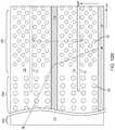
- FIG. 7is a schematic vertical cross-sectional view of the exemplary structure after formation of memory stack structures and support pillar structures according to an embodiment of the present disclosure.
- FIG. 8Ais a schematic vertical cross-sectional view of the exemplary structure after formation of backside trenches according to an embodiment of the present disclosure.
- FIG. 8Bis a partial see-through top-down view of the exemplary structure of FIG. 8A .
- the vertical plane A-A′is the plane of the schematic vertical cross-sectional view of FIG. 8A .
- FIG. 9is a schematic vertical cross-sectional view of the exemplary structure after formation of backside recesses according to an embodiment of the present disclosure.
- FIGS. 10A-10Dare sequential vertical cross-sectional views of a region of the exemplary structure during formation of electrically conductive layers according to an embodiment of the present disclosure.
- FIG. 11is a schematic vertical cross-sectional view of the exemplary structure at the processing step of FIG. 10D .
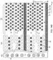
- FIGS. 12A and 12Care schematic vertical cross-sectional views of the exemplary structure after removal of a deposited conductive material from within the backside trench according to an embodiment of the present disclosure.
- FIG. 12Bis a top-down view of the exemplary structure of FIGS. 12A and 12C .
- the vertical planes A-A′ and C-C′are the planes of the schematic vertical cross-sectional views of FIGS. 12A and 12C , respectively.
- FIG. 13Ais a schematic vertical cross-sectional view of the exemplary structure after formation of an insulating spacer and a backside contact structure according to an embodiment of the present disclosure.
- FIG. 13Bis a magnified view of a region of the exemplary structure of FIG. 13A .
- FIG. 14Ais a schematic vertical cross-sectional view of the exemplary structure after formation of additional contact via structures according to an embodiment of the present disclosure.
- FIG. 14Bis a top-down view of the exemplary structure of FIG. 14A .
- the vertical plane A-A′is the plane of the schematic vertical cross-sectional view of FIG. 14A .
- the present disclosureis directed to a three-dimensional memory device employing germanium-containing vertical channels and methods of manufacturing the same, the various aspects of which are described below.
- the embodiments of the disclosurecan be employed to form various structures including a multilevel memory structure, non-limiting examples of which include semiconductor devices such as three-dimensional monolithic memory array devices comprising a plurality of NAND memory strings.
- a first element located “on” a second elementcan be located on the exterior side of a surface of the second element or on the interior side of the second element.
- a first elementis located “directly on” a second element if there exist a physical contact between a surface of the first element and a surface of the second element.
- a “prototype” structure or an “in-process” structurerefers to a transient structure that is subsequently modified in the shape or composition of at least one component therein.
- a “layer”refers to a material portion including a region having a thickness.
- a layermay extend over the entirety of an underlying or overlying structure, or may have an extent less than the extent of an underlying or overlying structure. Further, a layer may be a region of a homogeneous or inhomogeneous continuous structure that has a thickness less than the thickness of the continuous structure. For example, a layer may be located between any pair of horizontal planes between, or at, a top surface and a bottom surface of the continuous structure. A layer may extend horizontally, vertically, and/or along a tapered surface.
- a substratemay be a layer, may include one or more layers therein, or may have one or more layer thereupon, thereabove, and/or therebelow.
- a monolithic three-dimensional memory arrayis one in which multiple memory levels are formed above a single substrate, such as a semiconductor wafer, with no intervening substrates.
- the term “monolithic”means that layers of each level of the array are directly deposited on the layers of each underlying level of the array.
- two dimensional arraysmay be formed separately and then packaged together to form a non-monolithic memory device.
- non-monolithic stacked memorieshave been constructed by forming memory levels on separate substrates and vertically stacking the memory levels, as described in U.S. Pat. No.
- the substratesmay be thinned or removed from the memory levels before bonding, but as the memory levels are initially formed over separate substrates, such memories are not true monolithic three-dimensional memory arrays.
- the various three-dimensional memory devices of the present disclosurecan include a monolithic three-dimensional NAND string memory device, and can be fabricated employing the various embodiments described herein.
- a semiconductor die, or a semiconductor packagecan include a memory chip.
- Each semiconductor packagecontains one or more dies (for example one, two, or four). The die is the smallest unit that can independently execute commands or report status.
- Each diecontains one or more planes (typically one or two). Identical, concurrent operations can take place on each plane, although with some restrictions.
- Each planecontains a number of blocks, which are the smallest unit that can be erased by in a single erase operation.
- Each blockcontains a number of pages, which are the smallest unit that can be programmed, i.e., a smallest unit on which a read operation can be performed.
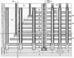
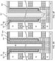
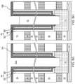
- the exemplary structureincludes a substrate ( 9 , 10 ), which can be a semiconductor substrate.
- the substratecan include a substrate semiconductor layer 9 and an optional semiconductor material layer 10 .
- the substrate semiconductor layer 9maybe a semiconductor wafer or a semiconductor material layer, and can include at least one elemental semiconductor material (e.g., single crystal silicon wafer or layer), at least one III-V compound semiconductor material, at least one II-VI compound semiconductor material, at least one organic semiconductor material, or other semiconductor materials known in the art.
- the substratecan have a major surface 7 , which can be, for example, a topmost surface of the substrate semiconductor layer 9 .
- the major surface 7can be a semiconductor surface.
- the major surface 7can be a single crystalline semiconductor surface, such as a single crystalline semiconductor surface.
- a “semiconducting material”refers to a material having electrical conductivity in the range from 1.0 ⁇ 10 ⁇ 6 S/cm to 1.0 ⁇ 10 5 S/cm.
- a “semiconductor material”refers to a material having electrical conductivity in the range from 1.0 ⁇ 10 ⁇ 6 S/cm to 1.0 ⁇ 10 5 S/cm in the absence of electrical dopants therein, and is capable of producing a doped material having electrical conductivity in a range from 1.0 S/cm to 1.0 ⁇ 10 5 S/cm upon suitable doping with an electrical dopant.
- an “electrical dopant”refers to a p-type dopant that adds a hole to a valence band within a band structure, or an n-type dopant that adds an electron to a conduction band within a band structure.
- a “conductive material”refers to a material having electrical conductivity greater than 1.0 ⁇ 10 5 S/cm.
- an “insulator material” or a “dielectric material”refers to a material having electrical conductivity less than 1.0 ⁇ 10 ⁇ 6 S/cm.
- a “heavily doped semiconductor material”refers to a semiconductor material that is doped with electrical dopant at a sufficiently high atomic concentration to become a conductive material either as formed as a crystalline material or if converted into a crystalline material through an anneal process (for example, from an initial amorphous state), i.e., to have electrical conductivity greater than 1.0 ⁇ 10 5 S/cm.
- a “doped semiconductor material”may be a heavily doped semiconductor material, or may be a semiconductor material that includes electrical dopants (i.e., p-type dopants and/or n-type dopants) at a concentration that provides electrical conductivity in the range from 1.0 ⁇ 10 ⁇ 6 S/cm to 1.0 ⁇ 10 5 S/cm.
- An “intrinsic semiconductor material”refers to a semiconductor material that is not doped with electrical dopants.
- a semiconductor materialmay be semiconducting or conductive, and may be an intrinsic semiconductor material or a doped semiconductor material.
- a doped semiconductor materialcan be semiconducting or conductive depending on the atomic concentration of electrical dopants therein.
- a “metallic material”refers to a conductive material including at least one metallic element therein. All measurements for electrical conductivities are made at the standard condition.
- At least one semiconductor device 700 for a peripheral circuitrycan be formed on a portion of the substrate semiconductor layer 9 .
- the at least one semiconductor devicecan include, for example, field effect transistors.
- at least one shallow trench isolation structure 720can be formed by etching portions of the substrate semiconductor layer 9 and depositing a dielectric material therein.
- a gate dielectric layer, at least one gate conductor layer, and a gate cap dielectric layercan be formed over the substrate semiconductor layer 9 , and can be subsequently patterned to form at least one gate structure ( 750 , 752 , 754 , 758 ), each of which can include a gate dielectric 750 , a gate electrode ( 752 , 754 ), and a gate cap dielectric 758 .
- the gate electrode ( 752 , 754 )may include a stack of a first gate electrode portion 752 and a second gate electrode portion 754 .
- At least one gate spacer 756can be formed around the at least one gate structure ( 750 , 752 , 754 , 758 ) by depositing and anisotropically etching a dielectric liner.
- Active regions 730can be formed in upper portions of the substrate semiconductor layer 9 , for example, by introducing electrical dopants employing the at least one gate structure ( 750 , 752 , 754 , 758 ) as masking structures. Additional masks may be employed as needed.
- the active region 730can include source regions and drain regions of field effect transistors.
- a first dielectric liner 761 and a second dielectric liner 762can be optionally formed.
- Each of the first and second dielectric liners ( 761 , 762 )can comprise a silicon oxide layer, a silicon nitride layer, and/or a dielectric metal oxide layer.
- silicon oxideincludes silicon dioxide as well as non-stoichiometric silicon oxides having more or less than two oxygen atoms for each silicon atoms. Silicon dioxide is preferred.
- the first dielectric liner 761can be a silicon oxide layer
- the second dielectric liner 762can be a silicon nitride layer.
- the least one semiconductor device for the peripheral circuitrycan contain a driver circuit for memory devices to be subsequently formed, which can include at least one NAND device.
- a dielectric material such as silicon oxidecan be deposited over the at least one semiconductor device, and can be subsequently planarized to form a planarization dielectric layer 770 .
- the planarized top surface of the planarization dielectric layer 770can be coplanar with a top surface of the dielectric liners ( 761 , 762 ).
- the planarization dielectric layer 770 and the dielectric liners ( 761 , 762 )can be removed from an area to physically expose a top surface of the substrate semiconductor layer 9 .
- a surfaceis “physically exposed” if the surface is in physical contact with vacuum, or a gas phase material (such as air).
- the optional semiconductor material layer 10can be formed on the top surface of the substrate semiconductor layer 9 prior to, or after, formation of the at least one semiconductor device 700 by deposition of a single crystalline semiconductor material, for example, by selective epitaxy.
- the deposited semiconductor materialcan be the same as, or can be different from, the semiconductor material of the substrate semiconductor layer 9 .
- the deposited semiconductor materialcan be any material that can be employed for the substrate semiconductor layer 9 as described above.
- the single crystalline semiconductor material of the semiconductor material layer 10can be in epitaxial alignment with the single crystalline structure of the substrate semiconductor layer 9 .
- Portions of the deposited semiconductor material located above the top surface of the planarization dielectric layer 170can be removed, for example, by chemical mechanical planarization (CMP).
- CMPchemical mechanical planarization
- the semiconductor material layer 10can have a top surface that is coplanar with the top surface of the planarization dielectric layer 770 .
- the region (i.e., area) of the at least one semiconductor device 700is herein referred to as a peripheral device region 200 .
- the region in which a memory array is subsequently formedis herein referred to as a memory array region 100 .
- a contact region 300 for subsequently forming stepped terraces of electrically conductive layerscan be provided between the memory array region 100 and the peripheral device region 200 .
- a stack of an alternating plurality of first material layers (which can be insulating layers 32 ) and second material layers (which can be sacrificial material layer 42 )is formed over the top surface of the substrate ( 9 , 10 ).
- a “material layer”refers to a layer including a material throughout the entirety thereof.
- an alternating plurality of first elements and second elementsrefers to a structure in which instances of the first elements and instances of the second elements alternate.
- first elementsmay have the same thickness thereamongst, or may have different thicknesses.
- the second elementsmay have the same thickness thereamongst, or may have different thicknesses.
- the alternating plurality of first material layers and second material layersmay begin with an instance of the first material layers or with an instance of the second material layers, and may end with an instance of the first material layers or with an instance of the second material layers.
- an instance of the first elements and an instance of the second elementsmay form a unit that is repeated with periodicity within the alternating plurality.
- Each first material layerincludes a first material
- each second material layerincludes a second material that is different from the first material.
- each first material layercan be an insulating layer 32
- each second material layercan be a sacrificial material layer.
- the stackincludes an alternating plurality of insulating layers 32 and sacrificial material layers 42 , and constitutes a prototype stack of alternating layers comprising insulating layers 32 and sacrificial material layers 42 .
- the stack of the alternating pluralityis herein referred to as an alternating stack ( 32 , 42 ).
- the alternating stack ( 32 , 42 )can include insulating layers 32 composed of the first material, and sacrificial material layers 42 composed of a second material different from that of insulating layers 32 .
- the first material of the insulating layers 32can be at least one insulating material.
- each insulating layer 32can be an insulating material layer.
- Insulating materials that can be employed for the insulating layers 32include, but are not limited to, silicon oxide (including doped or undoped silicate glass), silicon nitride, silicon oxynitride, organosilicate glass (OSG), spin-on dielectric materials, dielectric metal oxides that are commonly known as high dielectric constant (high-k) dielectric oxides (e.g., aluminum oxide, hafnium oxide, etc.) and silicates thereof, dielectric metal oxynitrides and silicates thereof, and organic insulating materials.
- the first material of the insulating layers 32can be silicon oxide.
- the second material of the sacrificial material layers 42is a sacrificial material that can be removed selective to the first material of the insulating layers 32 .
- a removal of a first materialis “selective to” a second material if the removal process removes the first material at a rate that is at least twice the rate of removal of the second material.
- the ratio of the rate of removal of the first material to the rate of removal of the second materialis herein referred to as a “selectivity” of the removal process for the first material with respect to the second material.
- the sacrificial material layers 42may comprise an insulating material, a semiconductor material, or a conductive material.
- the second material of the sacrificial material layers 42can be subsequently replaced with electrically conductive electrodes which can function, for example, as control gate electrodes of a vertical NAND device.
- Non-limiting examples of the second materialinclude silicon nitride, an amorphous semiconductor material (such as amorphous silicon), and a polycrystalline semiconductor material (such as polysilicon).
- the sacrificial material layers 42can be spacer material layers that comprise silicon nitride or a semiconductor material including at least one of silicon and germanium.
- the insulating layers 32can include silicon oxide, and sacrificial material layers can include silicon nitride sacrificial material layers.
- the first material of the insulating layers 32can be deposited, for example, by chemical vapor deposition (CVD).
- CVDchemical vapor deposition
- TEOStetraethyl orthosilicate
- the second material of the sacrificial material layers 42can be formed, for example, CVD or atomic layer deposition (ALD).
- the sacrificial material layers 42can be suitably patterned so that conductive material portions to be subsequently formed by replacement of the sacrificial material layers 42 can function as electrically conductive electrodes, such as the control gate electrodes of the monolithic three-dimensional NAND string memory devices to be subsequently formed.
- the sacrificial material layers 42may comprise a portion having a strip shape extending substantially parallel to the major surface 7 of the substrate.
- the thicknesses of the insulating layers 32 and the sacrificial material layers 42can be in a range from 20 nm to 50 nm, although lesser and greater thicknesses can be employed for each insulating layer 32 and for each sacrificial material layer 42 .
- the number of repetitions of the pairs of an insulating layer 32 and a sacrificial material layer (e.g., a control gate electrode or a sacrificial material layer) 42can be in a range from 2 to 1,024, and typically from 8 to 256, although a greater number of repetitions can also be employed.
- the top and bottom gate electrodes in the stackmay function as the select gate electrodes.
- each sacrificial material layer 42 in the alternating stack ( 32 , 42 )can have a uniform thickness that is substantially invariant within each respective sacrificial material layer 42 .
- spacer material layersare sacrificial material layers 42 that are subsequently replaced with electrically conductive layers
- embodimentsare expressly contemplated herein in which the sacrificial material layers are formed as electrically conductive layers. In this case, steps for replacing the spacer material layers with electrically conductive layers can be omitted.
- an insulating cap layer 70can be formed over the alternating stack ( 32 , 42 ).
- the insulating cap layer 70includes a dielectric material that is different from the material of the sacrificial material layers 42 .
- the insulating cap layer 70can include a dielectric material that can be employed for the insulating layers 32 as described above.
- the insulating cap layer 70can have a greater thickness than each of the insulating layers 32 .
- the insulating cap layer 70can be deposited, for example, by chemical vapor deposition.
- the insulating cap layer 70can be a silicon oxide layer.
- stepped surfacesare formed at a peripheral region of the alternating stack ( 32 , 42 ), which is herein referred to as a terrace region.
- stepped surfacesrefer to a set of surfaces that include at least two horizontal surfaces and at least two vertical surfaces such that each horizontal surface is adjoined to a first vertical surface that extends upward from a first edge of the horizontal surface, and is adjoined to a second vertical surface that extends downward from a second edge of the horizontal surface.
- a stepped cavityis formed within the volume from which portions of the alternating stack ( 32 , 42 ) are removed through formation of the stepped surfaces.
- a “stepped cavity”refers to a cavity having stepped surfaces.
- the terrace regionis formed in the contact region 300 , which is located between the memory array region 100 and the peripheral device region 200 containing the at least one semiconductor device for the peripheral circuitry.
- the stepped cavitycan have various stepped surfaces such that the horizontal cross-sectional shape of the stepped cavity changes in steps as a function of the vertical distance from the top surface of the substrate ( 9 , 10 ).
- the stepped cavitycan be formed by repetitively performing a set of processing steps.
- the set of processing stepscan include, for example, an etch process of a first type that vertically increases the depth of a cavity by one or more levels, and an etch process of a second type that laterally expands the area to be vertically etched in a subsequent etch process of the first type.
- a “level” of a structure including alternating pluralityis defined as the relative position of a pair of a first material layer and a second material layer within the structure.
- the terrace regionincludes stepped surfaces of the alternating stack ( 32 , 42 ) that continuously extend from a bottommost layer within the alternating stack ( 32 , 42 ) to a topmost layer within the alternating stack ( 32 , 42 ).
- Each vertical step of the stepped surfacescan have the height of one or more pairs of an insulating layer 32 and a sacrificial material layer.
- each vertical stepcan have the height of a single pair of an insulating layer 32 and a sacrificial material layer 42 .
- multiple “columns” of staircasescan be formed along a first horizontal direction hd 1 such that each vertical step has the height of a plurality of pairs of an insulating layer 32 and a sacrificial material layer 42 , and the number of columns can be at least the number of the plurality of pairs.
- Each column of staircasecan be vertically offset among one another such that each of the sacrificial material layers 42 has a physically exposed top surface in a respective column of staircases.
- two columns of staircasesare formed for each block of memory stack structures to be subsequently formed such that one column of staircases provide physically exposed top surfaces for odd-numbered sacrificial material layers 42 (as counted from the bottom) and another column of staircases provide physically exposed top surfaces for even-numbered sacrificial material layers (as counted from the bottom).
- Configurations employing three, four, or more columns of staircases with a respective set of vertical offsets among the physically exposed surfaces of the sacrificial material layers 42may also be employed.
- Each sacrificial material layer 42has a greater lateral extent, at least along one direction, than any overlying sacrificial material layers 42 such that each physically exposed surface of any sacrificial material layer 42 does not have an overhang.
- the vertical steps within each column of staircasesmay be arranged along the first horizontal direction hd 1
- the columns of staircasesmay be arranged along a second horizontal direction hd 2 that is perpendicular to the first horizontal direction hd 1 .
- the first horizontal direction hd 1may be perpendicular to the boundary between the memory array region 100 and the contact region 300 .
- a retro-stepped dielectric material portion 65(i.e., an insulating fill material portion) can be formed in the stepped cavity by deposition of a dielectric material therein.
- a dielectric materialsuch as silicon oxide can be deposited in the stepped cavity. Excess portions of the deposited dielectric material can be removed from above the top surface of the insulating cap layer 70 , for example, by chemical mechanical planarization (CMP). The remaining portion of the deposited dielectric material filling the stepped cavity constitutes the retro-stepped dielectric material portion 65 .
- a “retro-stepped” elementrefers to an element that has stepped surfaces and a horizontal cross-sectional area that increases monotonically as a function of a vertical distance from a top surface of a substrate on which the element is present. If silicon oxide is employed for the retro-stepped dielectric material portion 65 , the silicon oxide of the retro-stepped dielectric material portion 65 may, or may not, be doped with dopants such as B, P, and/or F.
- drain select level isolation structures 72can be formed through the insulating cap layer 70 and a subset of the sacrificial material layers 42 located at drain select levels.
- the drain select level isolation structures 72can be formed, for example, by forming drain select level isolation trenches and filling the drain select level isolation trenches with a dielectric material such as silicon oxide. Excess portions of the dielectric material can be removed from above the top surface of the insulating cap layer 70 .
- a lithographic material stackincluding at least a photoresist layer can be formed over the insulating cap layer 70 and the retro-stepped dielectric material portion 65 , and can be lithographically patterned to form openings therein.
- the openingsinclude a first set of openings formed over the memory array region 100 and a second set of openings formed over the contact region 300 .
- the pattern in the lithographic material stackcan be transferred through the insulating cap layer 70 or the retro-stepped dielectric material portion 65 , and through the alternating stack ( 32 , 42 ) by at least one anisotropic etch that employs the patterned lithographic material stack as an etch mask.
- a “memory opening”refers to a structure in which memory elements, such as a memory stack structure, is subsequently formed.
- a “support opening”refers to a structure in which a support structure (such as a support pillar structure) that mechanically supports other elements is subsequently formed.
- the memory openings 49are formed through the insulating cap layer 70 and the entirety of the alternating stack ( 32 , 42 ) in the memory array region 100 .
- the support openings 19are formed through the retro-stepped dielectric material portion 65 and the portion of the alternating stack ( 32 , 42 ) that underlie the stepped surfaces in the contact region 300 .
- the memory openings 49extend through the entirety of the alternating stack ( 32 , 42 ).
- the support openings 19extend through a subset of layers within the alternating stack ( 32 , 42 ).
- the chemistry of the anisotropic etch process employed to etch through the materials of the alternating stack ( 32 , 42 )can alternate to optimize etching of the first and second materials in the alternating stack ( 32 , 42 ).
- the anisotropic etchcan be, for example, a series of reactive ion etches.
- the sidewalls of the memory openings 49 and the support openings 19can be substantially vertical, or can be tapered.
- the patterned lithographic material stackcan be subsequently removed, for example, by ashing.
- the memory openings 49 and the support openings 19can extend from the top surface of the alternating stack ( 32 , 42 ) to at least the horizontal plane including the topmost surface of the semiconductor material layer 10 .
- an overetch into the semiconductor material layer 10may be optionally performed after the top surface of the semiconductor material layer 10 is physically exposed at a bottom of each memory opening 49 and each support opening 19 .
- the overetchmay be performed prior to, or after, removal of the lithographic material stack.
- the recessed surfaces of the semiconductor material layer 10may be vertically offset from the un-recessed top surfaces of the semiconductor material layer 10 by a recess depth.
- the recess depthcan be, for example, in a range from 1 nm to 50 nm, although lesser and greater recess depths can also be employed.
- the overetchis optional, and may be omitted. If the overetch is not performed, the bottom surfaces of the memory openings 49 and the support openings 19 can be coplanar with the topmost surface of the semiconductor material layer 10 .
- Each of the memory openings 49 and the support openings 19may include a sidewall (or a plurality of sidewalls) that extends substantially perpendicular to the topmost surface of the substrate.
- a two-dimensional array of memory openings 49can be formed in the memory array region 100 .
- a two-dimensional array of support openings 19can be formed in the contact region 300 .
- the substrate semiconductor layer 9 and the semiconductor material layer 10collectively constitutes a substrate ( 9 , 10 ), which can be a semiconductor substrate. Alternatively, the semiconductor material layer 10 may be omitted, and the memory openings 49 and the support openings 19 can be extend to a top surface of the substrate semiconductor layer 9 .
- FIGS. 5A-5Jillustrate structural changes in a memory opening 49 during formation of a memory opening fill structure of a first configuration.
- the memory opening 49 illustrated in FIGS. 5A-5Jcan be one of the memory openings 49 in the exemplary structure of FIGS. 4A and 4B .
- the same structural changeoccurs simultaneously in each of the other memory openings 49 and in each support opening 19 .
- a memory opening 49 in the exemplary device structure of FIGS. 4A and 4Bis illustrated.
- the memory opening 49extends through the insulating cap layer 70 , the alternating stack ( 32 , 42 ), and optionally into an upper portion of the semiconductor material layer 10 .
- the semiconductor material layer 10may be provided over a substrate semiconductor layer 9 with at least one intervening dielectric material layer and optional intervening metal interconnect structures connected to semiconductor devices (not shown) on the substrate semiconductor layer 9 .
- the semiconductor material layer 10can be a topmost layer of the substrate ( 9 , 10 ) that includes a stack of a substrate semiconductor layer 9 and the semiconductor material layer 10 (which can be a doped well in the substrate semiconductor layer 9 ).
- each support opening 19can extend through the retro-stepped dielectric material portion 65 , a subset of layers in the alternating stack ( 32 , 42 ), and optionally through the upper portion of the semiconductor material layer 10 .
- the recess depth of the bottom surface of each memory opening with respect to the top surface of the semiconductor material layer 10can be in a range from 0 nm to 30 nm, although greater recess depths can also be employed.
- an optional pedestal channel portion 11can be formed at the bottom portion of each memory opening 49 and each support openings 19 , for example, by a selective semiconductor deposition process.
- each pedestal channel portion 11can include a single crystalline semiconductor material deposited by a selective epitaxy process and in epitaxial alignment with the single crystalline semiconductor material of the semiconductor material layer 10 .
- each pedestal channel portion 11can include an amorphous or polycrystalline semiconductor material.
- the pedestal channel portion 11can include single crystalline silicon, polysilicon, or amorphous silicon.
- the pedestal channel portion 11can include doped silicon consisting essentially of silicon and at least one electrical dopant (such as a p-type dopant or an n-type dopants) not exceeding 2% in atomic concentration.
- the pedestal channel portion 11can be doped with electrical dopants of the same conductivity type as the semiconductor material layer 10 .
- the semiconductor material layer 10may include a source layer and the pedestal channel portion 11 can have a doping of an opposite conductivity type of the conductivity type of the semiconductor material layer 10 .
- the top surface of each pedestal channel portion 11can be formed above a horizontal plane including the top surface of a sacrificial material layer 42 .
- at least one source select gate electrodecan be subsequently formed by replacing each sacrificial material layer 42 located below the horizontal plane including the top surfaces of the pedestal channel portions 11 with a respective conductive material layer.
- the pedestal channel portion 11can be a portion of a transistor channel that extends between a source region to be subsequently formed in the substrate ( 9 , 10 ) and a drain region to be subsequently formed in an upper portion of the memory opening 49 .
- a memory cavity 49 ′is present in the unfilled portion of the memory opening 49 above the pedestal channel portion 11 .
- the pedestal channel portion 11can comprise single crystalline silicon.
- the pedestal channel portion 11can comprise amorphous silicon or polysilicon.
- the pedestal channel portion 11can be substantially free of germanium upon formation.
- a structural elementis “substantially free of” an atomic element if the atomic concentration of the atomic element within the structural element is less than 1 parts per million (1 p.p.m.).
- the atomic concentration of germanium in the pedestal channel portion 11may be less than 0.1 p.p.m. and/or less than 0.01 p.p.m. upon formation of the pedestal channel portion 11 .
- the pedestal channel portion 11can be formed directly on the substrate semiconductor layer 9 , which can have a doping of the first conductivity type.
- a stack of layers including a blocking dielectric layer 52 , a charge storage layer 54 , a tunneling dielectric layer 56 , and an optional silicon-containing seed layer 601can be sequentially deposited in the memory openings 49 .
- the stack of layers ( 52 , 54 , 56 )constitute a memory film that includes material portions that stores data for the memory device to be formed.
- the blocking dielectric layer 52can include a single dielectric material layer or a stack of a plurality of dielectric material layers.
- the blocking dielectric layercan include a dielectric metal oxide layer consisting essentially of a dielectric metal oxide.
- a dielectric metal oxiderefers to a dielectric material that includes at least one metallic element and at least oxygen.
- the dielectric metal oxidemay consist essentially of the at least one metallic element and oxygen, or may consist essentially of the at least one metallic element, oxygen, and at least one non-metallic element such as nitrogen.
- the blocking dielectric layer 52can include a dielectric metal oxide having a dielectric constant greater than 7.9, i.e., having a dielectric constant greater than the dielectric constant of silicon nitride.
- Non-limiting examples of dielectric metal oxidesinclude aluminum oxide (Al 2 O 3 ), hafnium oxide (HfO 2 ), lanthanum oxide (LaO 2 ), yttrium oxide (Y 2 O 3 ), tantalum oxide (Ta 2 O 5 ), silicates thereof, nitrogen-doped compounds thereof, alloys thereof, and stacks thereof.
- the dielectric metal oxide layercan be deposited, for example, by chemical vapor deposition (CVD), atomic layer deposition (ALD), pulsed laser deposition (PLD), liquid source misted chemical deposition, or a combination thereof.
- the thickness of the dielectric metal oxide layercan be in a range from 1 nm to 20 nm, although lesser and greater thicknesses can also be employed.
- the dielectric metal oxide layercan subsequently function as a dielectric material portion that blocks leakage of stored electrical charges to control gate electrodes.
- the blocking dielectric layer 52includes aluminum oxide.
- the blocking dielectric layer 52can include multiple dielectric metal oxide layers having different material compositions.
- the blocking dielectric layer 52can include a dielectric semiconductor compound such as silicon oxide, silicon oxynitride, silicon nitride, or a combination thereof.
- the blocking dielectric layer 52can include silicon oxide.
- the dielectric semiconductor compound of the blocking dielectric layer 52can be formed by a conformal deposition method such as low pressure chemical vapor deposition, atomic layer deposition, or a combination thereof.
- the thickness of the dielectric semiconductor compoundcan be in a range from 1 nm to 20 nm, although lesser and greater thicknesses can also be employed.
- the blocking dielectric layer 52can be omitted, and a backside blocking dielectric layer can be formed after formation of backside recesses on surfaces of memory films to be subsequently formed.
- the charge storage layer 54can be formed.
- the charge storage layer 54can be a continuous layer or patterned discrete portions of a charge trapping material including a dielectric charge trapping material, which can be, for example, silicon nitride.
- the charge storage layer 54can include a continuous layer or patterned discrete portions of a conductive material such as doped polysilicon or a metallic material that is patterned into multiple electrically isolated portions (e.g., floating gates), for example, by being formed within lateral recesses into sacrificial material layers 42 .
- the charge storage layer 54includes a silicon nitride layer.
- the sacrificial material layers 42 and the insulating layers 32can have vertically coincident sidewalls, and the charge storage layer 54 can be formed as a single continuous layer.
- a first surface and a second surfaceare vertically coincident with each other if the second surface overlies or underlies the first surface and if there exists a vertical plane including the first surface and the second surface.
- the sacrificial material layers 42can be laterally recessed with respect to the sidewalls of the insulating layers 32 , and a combination of a deposition process and an anisotropic etch process can be employed to form the charge storage layer 54 as a plurality of memory material portions that are vertically spaced apart. While the present disclosure is described employing an embodiment in which the charge storage layer 54 is a single continuous layer, embodiments are expressly contemplated herein in which the charge storage layer 54 is replaced with a plurality of memory material portions (which can be charge trapping material portions or electrically isolated conductive material portions) that are vertically spaced apart.
- the charge storage layer 54can be formed as a single charge storage layer of homogeneous composition, or can include a stack of multiple charge storage layers.
- the multiple charge storage layerscan comprise a plurality of spaced-apart floating gate material layers that contain conductive materials (e.g., metal such as tungsten, molybdenum, tantalum, titanium, platinum, ruthenium, and alloys thereof, or a metal silicide such as tungsten silicide, molybdenum silicide, tantalum silicide, titanium silicide, nickel silicide, cobalt silicide, or a combination thereof) and/or semiconductor materials (e.g., polycrystalline or amorphous semiconductor material including at least one elemental semiconductor element or at least one compound semiconductor material).
- conductive materialse.g., metal such as tungsten, molybdenum, tantalum, titanium, platinum, ruthenium, and alloys thereof, or a metal silicide such as tungsten silicide, molybdenum si
- the charge storage layer 54may comprise an insulating charge trapping material, such as one or more silicon nitride segments.
- the charge storage layer 54may comprise conductive nanoparticles such as metal nanoparticles, which can be, for example, ruthenium nanoparticles.
- the charge storage layer 54can be formed, for example, by chemical vapor deposition (CVD), atomic layer deposition (ALD), physical vapor deposition (PVD), or any suitable deposition technique for storing electrical charges therein.
- the thickness of the charge storage layer 54can be in a range from 2 nm to 20 nm, although lesser and greater thicknesses can also be employed.
- the tunneling dielectric layer 56includes a dielectric material through which charge tunneling can be performed under suitable electrical bias conditions.
- the charge tunnelingmay be performed through hot-carrier injection or by Fowler-Nordheim tunneling induced charge transfer depending on the mode of operation of the monolithic three-dimensional NAND string memory device to be formed.
- the tunneling dielectric layer 56can include silicon oxide, silicon nitride, silicon oxynitride, dielectric metal oxides (such as aluminum oxide and hafnium oxide), dielectric metal oxynitride, dielectric metal silicates, alloys thereof, and/or combinations thereof.
- the tunneling dielectric layer 56can include a stack of a first silicon oxide layer, a silicon oxynitride layer, and a second silicon oxide layer, which is commonly known as an ONO stack.
- the tunneling dielectric layer 56can include a silicon oxide layer that is substantially free of carbon or a silicon oxynitride layer that is substantially free of carbon.
- the thickness of the tunneling dielectric layer 56can be in a range from 2 nm to 20 nm, although lesser and greater thicknesses can also be employed.
- the optional silicon-containing seed layer 601includes amorphous silicon or polysilicon.
- the optional silicon-containing seed layer 601can include silicon atoms at an atomic concentration greater than 99%, and can be formed directly on an inner sidewall of the tunneling dielectric layer 56 .
- the silicon-containing seed layer 601can include silicon atoms at an atomic concentration greater than 99.9%, and may consist essentially of silicon.
- the silicon-containing seed layer 601can be formed by a conformal deposition method such as low pressure chemical vapor deposition (LPCVD).
- the thickness of the silicon-containing seed layer 601can be in a range from 1 nm to 6 nm, such as from 1.5 nm to 4 nm, although lesser and greater thicknesses can also be employed.
- a memory cavity 49 ′is formed in the volume of each memory opening 49 that is not filled with the deposited material layers ( 52 , 54 , 56 , 601 ).
- the optional silicon-containing seed layer 601if present, provides a substantially vertical cylindrical nucleation surface for a silicon-germanium alloy layer to be subsequently deposited.
- the optional silicon-containing seed layer 601can include a silicon-germanium alloy material including silicon at an atomic concentration greater than 75% and including germanium at an atomic concentration greater than 1%.
- the atomic concentration of germaniumcan be in a range from 1% to 20%, such as from 5% to 15%. In this case, limiting the atomic concentration of germanium atoms below 25%, and preferably below 20%, helps formation of a smooth inner sidewall for the optional silicon-containing seed layer 601 , and to avoid bumpiness of the surface of the optional silicon-containing seed layer 601 and formation of holes within the optional silicon-containing seed layer 601 .
- formation of a silicon seed layermay be circumvented and the amount of silicon atoms in the memory opening can be reduced compared to an embodiment in which the optional silicon-containing seed layer 601 consists essentially of silicon.
- the optional silicon-containing seed layer 601 , the tunneling dielectric layer 56 , the charge storage layer 54 , the blocking dielectric layer 52are sequentially anisotropically etched employing at least one anisotropic etch process.
- the portions of the silicon-containing seed layer 601 , the tunneling dielectric layer 56 , the charge storage layer 54 , and the blocking dielectric layer 52 located above the top surface of the insulating cap layer 70can be removed by the at least one anisotropic etch process.
- the horizontal portions of the silicon-containing seed layer 601 , the tunneling dielectric layer 56 , the charge storage layer 54 , and the blocking dielectric layer 52 at a bottom of each memory cavity 49 ′can be removed to form openings in remaining portions thereof.
- an opening through the layer stack of the silicon-containing seed layer 601 , the tunneling dielectric layer 56 , the charge storage layer 54 , and the blocking dielectric layer 52can be formed through a bottom portion of the memory film within each memory opening.
- Each of the silicon-containing seed layer 601 , the tunneling dielectric layer 56 , the charge storage layer 54 , and the blocking dielectric layer 52can be etched by a respective anisotropic etch process employing a respective etch chemistry, which may, or may not, be the same for the various material layers.
- the charge storage layer 54can comprise a charge trapping material or a floating gate material.
- each charge storage layer 54can include a vertical stack of charge storage regions that store electrical charges upon programming.
- the charge storage layer 54can be a charge storage layer in which each portion adjacent to the sacrificial material layers 42 constitutes a charge storage region.
- the optional silicon-containing seed layer 601if present, protects surfaces of the tunneling dielectric layer 56 during the anisotropic etch process. In other words, a predominant portion of reaction ion etch damage is sustained by the silicon-containing seed layer 601 if the silicon-containing seed layer 601 is present, and any reactive ion etch damage on the tunneling dielectric layer 56 is minimized.
- a surface of the pedestal channel portion 11(or a surface of the semiconductor material layer 10 in case the pedestal channel portions 11 are not employed) can be physically exposed underneath the opening through the silicon-containing seed layer 601 , the tunneling dielectric layer 56 , the charge storage layer 54 , and the blocking dielectric layer 52 .
- the physically exposed semiconductor surface at the bottom of each memory cavity 49 ′can be vertically recessed so that the recessed semiconductor surface underneath the memory cavity 49 ′ is vertically offset from the topmost surface of the pedestal channel portion 11 (or of the semiconductor material layer 10 in case pedestal channel portions 11 are not employed) by a recess distance.
- a tunneling dielectric layer 56is located over the charge storage layer 54 .
- a set of a blocking dielectric layer 52 , a charge storage layer 54 , and a tunneling dielectric layer 56 in a memory opening 49constitutes a memory film 50 , which includes a plurality of charge storage regions (as embodied as the charge storage layer 54 ) that are insulated from surrounding materials by the blocking dielectric layer 52 and the tunneling dielectric layer 56 .
- the silicon-containing seed layer 601 , the tunneling dielectric layer 56 , the charge storage layer 54 , and the blocking dielectric layer 52can have vertically coincident sidewalls.
- a silicon-germanium alloy layer 602can be deposited directly on the semiconductor surface of the pedestal channel portion 11 (or the semiconductor material layer 10 if the pedestal channel portion 11 is omitted), and directly on the silicon-containing seed layer 601 (or inner sidewalls of the tunneling dielectric layer 56 in case the silicon-containing seed layer 601 is omitted).
- the silicon-germanium alloy layer 602can be formed within each memory opening 49 and within each support opening 19 over a respective tunneling dielectric layer 56 .
- the silicon-germanium alloy layer 602includes a silicon-germanium alloy material, which includes germanium at an atomic concentration less than 25%, and preferably less than 20%, such as 5 to 15 atomic %.
- the balance of the material composition in the silicon-germanium alloy materialcan consist essentially of silicon and optionally at least one electrical dopant (such as a p-type dopant or an n-type dopant).
- the silicon-germanium alloy layerconsists essentially of silicon atoms, germanium atoms, and dopant atoms selected from n-type dopant atoms and p-type dopant atoms and having an atomic concentration less than 1.0%.
- the silicon-germanium alloy layer 602can be amorphous or polycrystalline.
- the silicon-germanium alloy layer 602can be formed by a conformal deposition method such as low pressure chemical vapor deposition (LPCVD).
- the conformal deposition methodcan employ a silicon precursor such as silane, disilane, or dichlorosilane and a germanium precursor such as germane or digermane.
- the thickness of the silicon-germanium alloy layer 602can be in a range from 2 nm to 20 nm, although lesser and greater thicknesses can also be employed.
- the silicon-containing seed layer 601by limiting the atomic percentage of germanium atoms below 25%, and preferably below 20%, within the silicon-germanium alloy layer 602 , bumpiness of the surface of the silicon-germanium alloy layer 602 can be avoided and inner sidewalls of the silicon-germanium alloy layer 602 can be formed as smooth vertical cylindrical surfaces.
- germanium deposition or a silicon-germanium alloy deposition with a high germanium atomic percentagesuch as an atomic percentage of germanium higher than 25% (for example, an atomic percentage in a range from 35% to 99%) is very challenging due to inherent film morphology that induces rough surfaces at such high level of germanium concentration. Consequently, a silicon-germanium alloy film having an atomic concentration of germanium greater than 25% has significant thickness non-uniformity.
- deposition of a silicon-germanium alloy film with an atomic concentration of germanium less than 25%, and preferably less than 20%tends to provide a flat growth surface and a uniform film thickness, which are advantageously employed according to an embodiment of the present disclosure to provide the silicon-germanium alloy layer 602 with a uniform thickness throughout.
- a silicon cap layer 603can be deposited over the silicon-germanium alloy layer 602 .
- the optional silicon cap layer 603can consist essentially of silicon and any residual dopant atoms, if any, that are unintentionally incorporated during a deposition process.
- the optional silicon cap layer 603can include silicon at an atomic concentration greater than 99.8%.
- the optional silicon cap layer 603can be formed by a conformal deposition process such as low pressure chemical vapor deposition process.
- the thickness of the optional silicon cap layer 603can be in a range from 1 nm to 3 nm, although lesser and greater thicknesses can also be employed.
- the optional silicon cap layer 603may be amorphous or polycrystalline.
- a memory cavity 49 ′ that vertically extend through each sacrificial material layer 42 other than one or more bottommost sacrificial material layers 42 of the alternating stack ( 32 , 42 )can be present within each memory opening 49 after deposition of the silicon-germanium alloy layer 602 and the optional silicon cap layer 603 .
- the silicon material of the optional silicon cap layer 603can subsequently function as an oxygen scavenger material during a subsequent germanium condensation process.
- an oxidation processis performed to convert portions of the optional silicon cap layer 603 , the silicon-germanium alloy layer 602 , and the silicon-containing seed layer 601 into a semiconductor oxide layer 621 .
- the oxidation process that forms the semiconductor oxide layer 621can include a thermal oxidation process.
- the exemplary structurecan be annealed in an oxidizing environment, i.e., within an ambient including at least one oxidizing gas such as oxygen and/or water vapor. Silicon atoms are preferentially incorporated into the silicon-germanium oxide material and germanium atoms are preferentially diffused into the unoxidized remaining material portion of the silicon-germanium alloy layer 602 in the oxidation process.
- silicon atoms in the optional silicon cap layer 603 , the silicon-germanium alloy layer 602 , and the silicon-containing seed layer 601are gradually oxidized to form a semiconductor oxide layer 621 , while germanium atoms in the silicon-germanium alloy layer 602 and the silicon-containing seed layer 601 , if any, migrate away from the semiconductor oxide layer to form a germanium rich silicon-germanium alloy layer 604 .
- Formation of silicon oxideproduces more reduction in thermodynamic enthalpy compared to formation of germanium oxide or maintaining a silicon-germanium bond.
- silicon atoms in the optional silicon cap layer 603 , the silicon-germanium alloy layer 602 , and the silicon-containing seed layer 601diffuse toward the semiconductor oxide layer 621 and incorporated into the semiconductor oxide layer 621 instead of maintaining a covalent bond with germanium atoms or forming a germanium oxide material.
- the phenomenon of preferential oxidation of silicon over germanium from a silicon-germanium alloyis known as germanium condensation, and is described, for example, in S. Nakaharai et al., “Formation process of high-purity Ge-on-insulator layers by Ge-condensation technique,” Journal of Applied Physics, 105, 024515 (2009).
- the initial silicon to germanium ratio in the semiconductor oxide layer 621can be greater than 10, and may be greater than 100 during an initial phase in which the silicon cap layer 603 is oxidized. In case the silicon cap layer 603 is not employed, the initial silicon to germanium ratio in the silicon oxide layer 621 can be greater than 4, and may be greater than 20 during an initial phase in which the silicon-germanium alloy layer 602 is oxidized. In one embodiment, the semiconductor oxide layer 621 can be a pure silicon oxide layer which contains no germanium or only a trace amount of germanium.
- the oxidation processcan proceed at a temperature or at temperatures that is lower than the melting point of the germanium rich silicon-germanium alloy layer 604 as its germanium concentration increases during the oxidation process.
- the thermal oxidation processis performed in multiple steps with different oxidation temperatures that decrease with progression of the thermal oxidation process as the germanium concentration increases in layer 604 during the oxidation process.
- alternating oxidation and annealing stepsare performed in which the annealing steps are conducted in an oxygen free ambient (e.g., in vacuum or inert gas ambient).
- the oxidation and optional annealing stepscan be performed at sequentially decreasing temperatures in a range from 1100 degrees Celsius to 800 degrees Celsius.
- the oxidation temperature of the last step of the thermal oxidation processcan be in a range from 800 degrees Celsius to 937 degrees Celsius, since the melting temperature of pure germanium is 938 degrees Celsius.
- the oxidation temperature of a single temperature oxidation processcan be in a range from 800 degrees Celsius to 937 degrees Celsius.
- the germanium concentration in unoxidized remaining materials from the optional silicon cap layer 603 , the silicon-germanium alloy layer 602 , and the silicon-containing seed layer 601increases due to preferential incorporation of silicon into the semiconductor oxide layer 621 .
- the silicon to germanium ratio at the interfacial regions of the semiconductor oxide layer 621gradually decreases as the oxidation process proceeds, and the semiconductor oxide layer 621 (which include oxidized portions of the silicon-germanium alloy layer 602 ) includes a silicon oxide or a silicon-germanium oxide material.
- germanium atomsmay diffuse from the silicon-germanium alloy layer 602 and from the silicon-containing seed layer 601 (in case the silicon-containing seed layer 601 includes a silicon-germanium alloy) into the pedestal channel portion 11 during the oxidation process.
- a graded silicon-germanium alloy region 11 Bcan be formed in a portion of the pedestal channel portion 11 that is proximal to the silicon-germanium alloy layer 602 .
- the graded silicon-germanium alloy region 11 Bcan include a graded silicon-germanium alloy material having a maximum atomic concentration of germanium that is less than the atomic concentration of germanium in the silicon-germanium alloy layer 602 as initially formed.
- the germanium concentrationdecreases within the graded silicon-germanium alloy region 11 B with a distance from the interface between the silicon-germanium oxide material of the silicon-germanium alloy layer 602 and the graded silicon-germanium alloy region 11 B.
- the remaining portion of the pedestal channel portion 11 that includes germanium at an atomic concentration less than 1.0%is herein referred to as a silicon-based pedestal channel portion 11 A.
- the oxidation processproceeds until a semiconductor channel layer 60 L including an unoxidized remaining portion of the germanium rich silicon-germanium alloy layer 604 includes germanium at an atomic concentration greater than 50%.
- the selective incorporation of silicon into the semiconductor oxide layer 621can proceed until the atomic concentration of germanium atoms in remaining germanium rich silicon-germanium alloy layer 604 is greater than 50%, and/or greater than 60%, and/or greater than 70%, and/or greater than 80%, and/or greater than 90%, and/or greater than 95%, and/or greater than 98%, and/or greater than 99%.
- the semiconductor channel layer 60 Lincludes germanium atoms at an atomic concentration greater than 99%, such as 99.1 to 99.9% (e.g., the semiconductor channel layer may be a pure germanium layer with unavoidable impurities and p-type or n-type dopants).
- the semiconductor oxide layer 621grows into a semiconductor oxide core layer 622 including a continuous horizontal portion overlying each of the memory openings 49 and support openings 19 and as many vertically extending portions as the total number of memory openings 49 and the support openings 19 .
- the semiconductor oxide core layer 622can completely fill the cavities in the memory openings 49 and the support openings 19 .
- the semiconductor oxide core layer 622is a silicon oxide layer and the semiconductor channel layer 60 L is a germanium layer with a sharp boundary located between them.
- the semiconductor oxide core layer 622is a silicon-germanium oxide layer and the semiconductor channel layer 60 L is a silicon-germanium layer.
- the concentration of germaniumcan increase with a radial distance from the geometrical center of each vertically-extending portion of the semiconductor oxide core layer 622 within each memory opening 49 .
- the graded silicon-germanium alloy region 11 Bcan continue to grow as germanium atoms continue to diffuse outward during the growth of the semiconductor oxide layer 621 and formation of the semiconductor oxide core layer 622 .
- the graded silicon-germanium alloy region 11 Bcan expand in volume until the graded silicon-germanium alloy region 11 B grows into the entire volume of the pedestal channel portion 11 .
- the pedestal channel portion 11 ′ after diffusion of germanium thereintocan be a silicon-germanium alloy pedestal channel portion with a germanium concentration gradient therein.
- the horizontal portion of the semiconductor oxide core layer 622 overlying the horizontal portion of the semiconductor channel layer 60 Lcan be removed, for example, by a recess etch.
- Each remaining portion of the semiconductor oxide core layer 622constitutes a semiconductor oxide core 62 (e.g., silicon oxide or silicon-germanium oxide core) located in a respective one of the memory openings 49 or in a respective one of the support openings 19 .
- the recess etchcan be prolonged to recess the top portion of each semiconductor oxide core 62 so that the recessed top surface of each semiconductor oxide core 62 is located between a horizontal plane including the bottom surface of the insulating cap layer 70 and a horizontal plane including the top surface of the insulating cap layer 70 .
- each vertical semiconductor channel 60can have a cylindrical configuration.
- the outer surface of each vertical semiconductor channel 60contacts a respective tunneling dielectric layer 56 at a smooth vertical interface.
- the inner surface of each vertical semiconductor channel 60contacts a respective semiconductor oxide core 62 at a smooth vertical interface.
- each vertical semiconductor channel 60can include a cylindrical region having a uniform thickness that is invariant with translation along the vertical direction and with an azimuthal rotation (i.e., a rotation around the vertical direction).
- a vertical semiconductor channel 60Electrical current can flow through a vertical semiconductor channel 60 when a vertical NAND device including the vertical semiconductor channel 60 is turned on.
- Each adjoining set of a blocking dielectric layer 52 , a charge storage layer 54 , and a tunneling dielectric layer 56collectively constitute a memory film 50 , which can store electrical charges with a macroscopic retention time.
- a tunneling dielectric layer 56is surrounded by a charge storage layer 54 , and laterally surrounds a portion of the vertical semiconductor channel 60 .
- a blocking dielectric layer 52may not be present in the memory film 50 at this step, and a blocking dielectric layer may be subsequently formed after formation of backside recesses.
- a macroscopic retention timerefers to a retention time suitable for operation of a memory device as a permanent memory device such as a retention time in excess of 24 hours.
- drain regions 63can be formed by depositing a doped semiconductor material within each recessed region above the semiconductor oxide cores 62 .
- the drain regions 63can have a doping of a second conductivity type that is the opposite of the first conductivity type. For example, if the first conductivity type is p-type, the second conductivity type is n-type, and vice versa.
- the dopant concentration in the drain regions 63can be in a range from 5.0 ⁇ 10 19 /cm 3 to 2.0 ⁇ 10 21 /cm 3 , although lesser and greater dopant concentrations can also be employed.
- the doped semiconductor materialcan be, for example, doped polysilicon. Excess portions of the deposited semiconductor material can be removed from above the top surface of the insulating cap layer 70 , for example, by chemical mechanical planarization (CMP) or a recess etch to form the drain regions 63 .
- CMPchemical mechanical planarization
- Each combination of a memory film 50 and a vertical semiconductor channel 60 within a memory opening 49constitutes a memory stack structure 55 .
- the memory stack structure 55is a combination of a vertical semiconductor channel 60 , a tunneling dielectric layer 56 , a plurality of memory elements comprising portions of the charge storage layer 54 , and an optional blocking dielectric layer 52 .
- Each combination of a pedestal channel portion 11 ′, a memory stack structure 55 , a semiconductor oxide core 62 , and a drain region 63 within a memory opening 49is herein referred to as a memory opening fill structure 58 .
- Each combination of a pedestal channel portion 11 ′, a memory film 50 , a vertical semiconductor channel 60 , a semiconductor oxide core 62 , and a drain region 63 within each support opening 19fills the respective support openings 19 , and constitutes a support pillar structure.
- the silicon oxide or silicon-germanium oxide material formed by oxidationforms a semiconductor oxide core 62 having a pillar shape with a vertical axis VA passing through a geometrical center GC of the semiconductor oxide core 62 .
- a geometrical center of a structural elementrefers to the center of mass of a hypothetical structural element that occupies an identical volume as the structural element and having a uniform density throughout. If the semiconductor oxide core 62 is a silicon-germanium oxide core, then in one embodiment the atomic concentration of silicon atoms decreases with a radial distance from the vertical axis VA.
- each memory opening 49can be filled with a combination of a pedestal channel portion 11 ′, a memory film 50 , a vertical semiconductor channel 60 , and a semiconductor oxide core 62 .
- the semiconductor oxide core 62has a pillar shape with a vertical axis VA passing through a geometrical center GC of the semiconductor oxide core 62 , and the atomic concentration of silicon atoms decreases with a radial distance from the vertical axis VA.
- the ratio of the atomic concentration of silicon to the atomic concentration of germaniumis greater than 10 at the geometrical center, and is less than 0.5 at an interface between the semiconductor oxide core 62 and the vertical semiconductor channel 60 .
- the semiconductor oxide core 62consists essentially of silicon atoms, germanium atoms, oxygen atoms, and dopant atoms selected from n-type dopant atoms and p-type dopant atoms and having an atomic concentration less than 0.5%.
- the lateral dimensions of the memory openings 49 and the thicknesses of the optional silicon-containing seed layer 601 , the silicon-germanium alloy layer 602 , and the optional silicon cap layer 603can be selected such that the semiconductor oxide core 62 completely fills the entire volume of the memory cavity located inside the vertical semiconductor channel 60 .
- FIGS. 6A-6Hillustrate structural changes in a memory opening 49 during formation of a memory opening fill structure of a second configuration.
- the memory opening 49 illustrated in FIGS. 6A-6Hcan be one of the memory openings 49 in the exemplary structure of FIGS. 4A and 4B .
- the same structural changeoccurs simultaneously in each of the other memory openings 49 and in each support opening 19 .
- a stack of layers including a blocking dielectric layer 52 , a charge storage layer 54 , a tunneling dielectric layer 56 , and an optional silicon-containing seed layer 601can be deposited in a memory opening 49 illustrated in FIG. 5A without forming a pedestal channel portion 11 .
- Each of the blocking dielectric layer 52 , the charge storage layer 54 , the tunneling dielectric layer 56 , and the optional silicon-containing seed layer 601can be structurally and compositionally the same as the corresponding layer in FIG. 5C .
- the blocking dielectric layer 52can be formed directly on a top surface of the semiconductor material layer 10 .
- the optional silicon-containing seed layer 601 , the tunneling dielectric layer 56 , the charge storage layer 54 , the blocking dielectric layer 52are sequentially anisotropically etched employing at least one anisotropic etch process, which can be the same as in the processing steps of FIG. 5D .
- Surfaces of the semiconductor material layer 10can be physically exposed after the at least one anisotropic etch process.
- the processing steps of FIG. 5Ecan be performed to deposit a silicon-germanium alloy layer 602 and an optional silicon cap layer 603 .
- Each of the silicon-germanium alloy layer 602 and the optional silicon cap layer 603can have the same thickness as, and the same composition as, in the silicon-germanium alloy layer 602 and the optional silicon cap layer 603 illustrated in FIG. 5E .
- the oxidation processconverts portions of the optional silicon cap layer 603 , the silicon-germanium alloy layer 602 , and the silicon-containing seed layer 601 into a semiconductor oxide layer 621 and the germanium rich silicon-germanium alloy layer 604 .
- the germanium concentration in unoxidized remaining portion of the germanium rich silicon-germanium alloy layer 604increases due to preferential incorporation of silicon into the semiconductor oxide layer 621 .
- the silicon to germanium ratio at the interfacial regions of the semiconductor oxide layer 621gradually decreases as the oxidation process proceeds, and the semiconductor oxide layer 621 (which include oxidized portions of the silicon-germanium alloy layer 602 ) includes a silicon-germanium oxide material.
- germanium atomscan diffuse from the silicon-germanium alloy layer 602 and from the silicon-containing seed layer 601 (in case the silicon-containing seed layer 601 includes a silicon-germanium alloy) into an underlying portion of the semiconductor material layer 10 during the oxidation process.
- a graded silicon-germanium alloy region 102can be formed in each region underlying a memory film 50 .
- the graded silicon-germanium alloy region 102can include a graded silicon-germanium alloy material having a maximum atomic concentration of germanium that is less than the atomic concentration of germanium in the silicon-germanium alloy layer 602 as initially formed.
- the germanium concentrationdecreases within the graded silicon-germanium alloy region 102 with a distance from the interface between the germanium rich silicon-germanium alloy layer 604 and the graded silicon-germanium alloy region 102 .
- the oxidation processproceeds until a semiconductor channel layer 60 L which includes germanium at an atomic concentration greater than 50% is formed.
- the selective incorporation of silicon into the semiconductor oxide layer 621can proceed until the atomic concentration of germanium atoms in remaining germanium rich silicon-germanium alloy layer 604 (i.e., in the semiconductor channel layer 60 L) is greater than 50%, and/or greater than 60%, and/or greater than 70%, and/or greater than 80%, and/or greater than 90%, and/or greater than 95%, and/or greater than 98%, and/or greater than 99%.
- the semiconductor channel layer 60 Lincludes germanium atoms at an atomic concentration greater than 99%.
- the semiconductor oxide layer 621grows into a semiconductor oxide core layer 622 including a continuous horizontal portion overlying each of the memory openings 49 and support openings 19 and as many vertically extending portions as the total number of memory openings 49 and the support openings 19 .
- the semiconductor oxide core layer 622can fill the cavities in the memory openings 49 and the support openings 19 .
- the graded silicon-germanium alloy region 102can continue to grow as germanium atoms continue to diffuse outward during the growth of the semiconductor oxide layer 621 and formation of the semiconductor oxide core layer 622 during the oxidation process, and can be terminated when the semiconductor channel layer 60 L has a target germanium concentration.
- the horizontal portion of the semiconductor oxide core layer 622 overlying the horizontal portion of the semiconductor channel layer 60 Lcan be removed, for example, by a recess etch.
- Each remaining portion of the semiconductor oxide core layer 622constitutes a semiconductor oxide core 62 located in a respective one of the memory openings 49 or in a respective one of the support openings 19 .
- the recess etchcan be prolonged to recess the top portion of each semiconductor oxide core 62 so that the recessed top surface of each semiconductor oxide core 62 is located between a horizontal plane including the bottom surface of the insulating cap layer 70 and a horizontal plane including the top surface of the insulating cap layer 70 .
- the processing steps of FIG. 5Ican be performed. At least a horizontal portion of the semiconductor channel layer 60 L overlying the insulating cap layer 70 can be removed by a recess etch, which may include an anisotropic etch process or an isotropic etch process. Each remaining portion of the semiconductor channel layer 60 L in a memory opening 49 or in a support opening 19 constitutes a vertical semiconductor channel 60 .
- Drain regions 63can be formed by depositing a doped semiconductor material within each recessed region above the semiconductor oxide cores 62 .
- the drain regions 63can have a doping of a second conductivity type that is the opposite of the first conductivity type.
- FIG. 7the exemplary structure is illustrated after formation of memory opening fill structures 58 and support pillar structures 20 within the memory openings 49 and the support openings 19 , respectively.
- An instance of a memory opening fill structure 58can be formed within each memory opening 49 of the structure of FIGS. 4A and 4B .
- An instance of the support pillar structure 20can be formed within each support opening 19 of the structure of FIGS. 4A and 4B .
- Each memory opening fill structure 58 and each support pillar structure 20can have the configuration of FIG. 5J or the configuration of FIG. 6H .
- Each memory stack structure 55includes a vertical semiconductor channel 60 and a memory film 50 .
- the memory film 50may comprise a tunneling dielectric layer 56 laterally surrounding the vertical semiconductor channel 60 and a vertical stack of charge storage regions laterally surrounding the tunneling dielectric layer 56 (as embodied as a memory material layer 54 ) and an optional blocking dielectric layer 52 . While the present disclosure is described employing the illustrated configuration for the memory stack structure, the methods of the present disclosure can be applied to alternative memory stack structures including different layer stacks or structures for the memory film 50 and/or for the vertical semiconductor channel 60 .
- a contact level dielectric layer 73can be formed over the alternating stack ( 32 , 42 ) of insulating layer 32 and sacrificial material layers 42 , and over the memory stack structures 55 and the support pillar structures 20 .
- the contact level dielectric layer 73includes a dielectric material that is different from the dielectric material of the sacrificial material layers 42 .
- the contact level dielectric layer 73can include silicon oxide.
- the contact level dielectric layer 73can have a thickness in a range from 50 nm to 500 nm, although lesser and greater thicknesses can also be employed.
- a photoresist layer(not shown) can be applied over the contact level dielectric layer 73 , and is lithographically patterned to form openings in areas between clusters of memory stack structures 55 .
- the pattern in the photoresist layercan be transferred through the contact level dielectric layer 73 , the alternating stack ( 32 , 42 ) and/or the retro-stepped dielectric material portion 65 employing an anisotropic etch to form backside trenches 79 , which vertically extend from the top surface of the contact level dielectric layer 73 at least to the top surface of the substrate ( 9 , 10 ), and laterally extend through the memory array region 100 and the contact region 300 .
- the backside trenches 79can laterally extend along a first horizontal direction hd 1 and can be laterally spaced apart among one another along a second horizontal direction hd 2 that is perpendicular to the first horizontal direction hd 1 .
- the memory stack structures 55can be arranged in rows that extend along the first horizontal direction hd 1 .
- the drain select level isolation structures 72can laterally extend along the first horizontal direction hd 1 .
- Each backside trench 79can have a uniform width that is invariant along the lengthwise direction (i.e., along the first horizontal direction hd 1 ).
- Each drain select level isolation structure 72can have a uniform vertical cross-sectional profile along vertical planes that are perpendicular to the first horizontal direction hd 1 that is invariant with translation along the first horizontal direction hd 1 .
- Multiple rows of memory stack structures 55can be located between a neighboring pair of a backside trench 79 and a drain select level isolation structure 72 , or between a neighboring pair of drain select level isolation structures 72 .
- the backside trenches 79can include a source contact opening in which a source contact via structure can be subsequently formed.
- the photoresist layercan be removed, for example, by ashing.
- an etchant that selectively etches the second material of the sacrificial material layers 42 with respect to the first material of the insulating layers 32can be introduced into the backside trenches 79 , for example, employing an etch process.
- FIG. 10Aillustrates a region of the exemplary structure of FIG. 9 .
- Backside recesses 43are formed in volumes from which the sacrificial material layers 42 are removed.
- the removal of the second material of the sacrificial material layers 42can be selective to the first material of the insulating layers 32 , the material of the retro-stepped dielectric material portion 65 , the semiconductor material of the semiconductor material layer 10 , and the material of the outermost layer of the memory films 50 .
- the sacrificial material layers 42can include silicon nitride, and the materials of the insulating layers 32 and the retro-stepped dielectric material portion 65 can be selected from silicon oxide and dielectric metal oxides.
- the etch process that removes the second material selective to the first material and the outermost layer of the memory films 50can be a wet etch process employing a wet etch solution, or can be a gas phase (dry) etch process in which the etchant is introduced in a vapor phase into the backside trenches 79 .
- the etch processcan be a wet etch process in which the exemplary structure is immersed within a wet etch tank including phosphoric acid, which etches silicon nitride selective to silicon oxide, silicon, and various other materials employed in the art.
- the support pillar structure 20 , the retro-stepped dielectric material portion 65 , and the memory stack structures 55provide structural support while the backside recesses 43 are present within volumes previously occupied by the sacrificial material layers 42 .
- Each backside recess 43can be a laterally extending cavity having a lateral dimension that is greater than the vertical extent of the cavity. In other words, the lateral dimension of each backside recess 43 can be greater than the height of the backside recess 43 .
- a plurality of backside recesses 43can be formed in the volumes from which the second material of the sacrificial material layers 42 is removed.
- the memory openings in which the memory stack structures 55 are formedare herein referred to as front side openings or front side cavities in contrast with the backside recesses 43 .
- the memory array region 100comprises an array of monolithic three-dimensional NAND strings having a plurality of device levels disposed above the substrate ( 9 , 10 ). In this case, each backside recess 43 can define a space for receiving a respective word line of the array of monolithic three-dimensional NAND strings.
- Each of the plurality of backside recesses 43can extend substantially parallel to the top surface of the substrate ( 9 , 10 ).
- a backside recess 43can be vertically bounded by a top surface of an underlying insulating layer 32 and a bottom surface of an overlying insulating layer 32 .
- each backside recess 43can have a uniform height throughout.
- Physically exposed surface portions of the optional pedestal channel portions 11 ′ and the semiconductor material layer 10can be converted into dielectric material portions by thermal conversion and/or plasma conversion of the semiconductor materials into dielectric materials.
- thermal conversion and/or plasma conversioncan be employed to convert a surface portion of each pedestal channel portion 11 ′ into a tubular dielectric spacer 116 , and to convert each physically exposed surface portion of the semiconductor material layer 10 into a planar dielectric portion 616 .
- each tubular dielectric spacer 116can be topologically homeomorphic to a torus, i.e., generally ring-shaped.
- an elementis topologically homeomorphic to a torus if the shape of the element can be continuously stretched without destroying a hole or forming a new hole into the shape of a torus.
- the tubular dielectric spacers 116include a dielectric material that includes the same semiconductor element as the pedestal channel portions 11 ′ and additionally includes at least one non-metallic element such as oxygen and/or nitrogen such that the material of the tubular dielectric spacers 116 is a dielectric material.
- the tubular dielectric spacers 116can include a dielectric oxide, a dielectric nitride, or a dielectric oxynitride of the semiconductor material of the pedestal channel portions 11 ′.
- each planar dielectric portion 616includes a dielectric material that includes the same semiconductor element as the semiconductor material layer and additionally includes at least one non-metallic element such as oxygen and/or nitrogen such that the material of the planar dielectric portions 616 is a dielectric material.
- the planar dielectric portions 616can include a dielectric oxide, a dielectric nitride, or a dielectric oxynitride of the semiconductor material of the semiconductor material layer 10 .
- a backside blocking dielectric layer 44can be optionally formed.
- the backside blocking dielectric layer 44if present, comprises a dielectric material that functions as a control gate dielectric for the control gates to be subsequently formed in the backside recesses 43 .
- the backside blocking dielectric layer 44is optional. In case the blocking dielectric layer 52 is omitted, the backside blocking dielectric layer 44 is present.
- the backside blocking dielectric layer 44can be formed in the backside recesses 43 and on a sidewall of the backside trench 79 .
- the backside blocking dielectric layer 44can be formed directly on horizontal surfaces of the insulating layers 32 and sidewalls of the memory stack structures 55 within the backside recesses 43 . If the backside blocking dielectric layer 44 is formed, formation of the tubular dielectric spacers 116 and the planar dielectric portion 616 prior to formation of the backside blocking dielectric layer 44 is optional.
- the backside blocking dielectric layer 44can be formed by a conformal deposition process such as atomic layer deposition (ALD).
- the backside blocking dielectric layer 44can consist essentially of aluminum oxide.
- the thickness of the backside blocking dielectric layer 44can be in a range from 1 nm to 15 nm, such as 2 to 6 nm, although lesser and greater thicknesses can also be employed.
- the dielectric material of the backside blocking dielectric layer 44can be a dielectric metal oxide such as aluminum oxide, a dielectric oxide of at least one transition metal element, a dielectric oxide of at least one Lanthanide element, a dielectric oxide of a combination of aluminum, at least one transition metal element, and/or at least one Lanthanide element.
- the backside blocking dielectric layer 44can include a silicon oxide layer.
- the backside blocking dielectric layer 44can be deposited by a conformal deposition method such as chemical vapor deposition or atomic layer deposition.
- the backside blocking dielectric layer 44is formed on the sidewalls of the backside trenches 79 , horizontal surfaces and sidewalls of the insulating layers 32 , the portions of the sidewall surfaces of the memory stack structures 55 that are physically exposed to the backside recesses 43 , and a top surface of the planar dielectric portion 616 .
- a backside cavity 79 ′is present within the portion of each backside trench 79 that is not filled with the backside blocking dielectric layer 44 .
- a metallic barrier layer 46 Acan be deposited in the backside recesses 43 .
- the metallic barrier layer 46 Aincludes an electrically conductive metallic material that can function as a diffusion barrier layer and/or adhesion promotion layer for a metallic fill material to be subsequently deposited.
- the metallic barrier layer 46 Acan include a conductive metallic nitride material such as TiN, TaN, WN, or a stack thereof, or can include a conductive metallic carbide material such as TiC, TaC, WC, or a stack thereof.
- the metallic barrier layer 46 Acan be deposited by a conformal deposition process such as chemical vapor deposition (CVD) or atomic layer deposition (ALD).
- the thickness of the metallic barrier layer 46 Acan be in a range from 2 nm to 8 nm, such as from 3 nm to 6 nm, although lesser and greater thicknesses can also be employed.
- the metallic barrier layer 46 Acan consist essentially of a conductive metal nitride such as TiN.
- a metal fill materialis deposited in the plurality of backside recesses 43 , on the sidewalls of the at least one the backside trench 79 , and over the top surface of the contact level dielectric layer 73 to form a metallic fill material layer 46 B.
- the metallic fill materialcan be deposited by a conformal deposition method, which can be, for example, chemical vapor deposition (CVD), atomic layer deposition (ALD), electroless plating, electroplating, or a combination thereof.
- the metallic fill material layer 46 Bcan consist essentially of at least one elemental metal.
- the at least one elemental metal of the metallic fill material layer 46 Bcan be selected, for example, from tungsten, cobalt, ruthenium, titanium, and tantalum.
- the metallic fill material layer 46 Bcan consist essentially of a single elemental metal.
- the metallic fill material layer 46 Bcan be deposited employing a fluorine-containing precursor gas such as WF 6 .
- the metallic fill material layer 46 Bcan be a tungsten layer including a residual level of fluorine atoms as impurities.
- the metallic fill material layer 46 Bis spaced from the insulating layers 32 and the memory stack structures 55 by the metallic barrier layer 46 A, which is a metallic barrier layer that blocks diffusion of fluorine atoms therethrough.
- a plurality of electrically conductive layers 46can be formed in the plurality of backside recesses 43 , and a continuous metallic material layer 46 L can be formed on the sidewalls of each backside trench 79 and over the contact level dielectric layer 73 .
- Each electrically conductive layer 46includes a portion of the metallic barrier layer 46 A and a portion of the metallic fill material layer 46 B that are located between a vertically neighboring pair of dielectric material layers such as a pair of insulating layers 32 .
- the continuous metallic material layer 46 Lincludes a continuous portion of the metallic barrier layer 46 A and a continuous portion of the metallic fill material layer 46 B that are located in the backside trenches 79 or above the contact level dielectric layer 73 .
- Each sacrificial material layer 42can be replaced with an electrically conductive layer 46 .
- a backside cavity 79 ′is present in the portion of each backside trench 79 that is not filled with the backside blocking dielectric layer 44 and the continuous metallic material layer 46 L.
- a tubular dielectric spacer 116laterally surrounds a pedestal channel portion 11 ′.
- a bottommost electrically conductive layer 46laterally surrounds each tubular dielectric spacer 116 upon formation of the electrically conductive layers 46 .
- the deposited metallic material of the continuous electrically conductive material layer 46 Lis etched back from the sidewalls of each backside trench 79 and from above the contact level dielectric layer 73 , for example, by an isotropic wet etch, an anisotropic dry etch, or a combination thereof.
- Each remaining portion of the deposited metallic material in the backside recesses 43constitutes an electrically conductive layer 46 .
- Each electrically conductive layer 46can be a conductive line structure.
- the sacrificial material layers 42are replaced with the electrically conductive layers 46 .
- Each electrically conductive layer 46can function as a combination of a plurality of control gate electrodes located at a same level and a word line electrically interconnecting, i.e., electrically shorting, the plurality of control gate electrodes located at the same level.
- the plurality of control gate electrodes within each electrically conductive layer 46are the control gate electrodes for the vertical memory devices including the memory stack structures 55 .
- each electrically conductive layer 46can be a word line that functions as a common control gate electrode for the plurality of vertical memory devices.
- the removal of the continuous electrically conductive material layer 46 Lcan be selective to the material of the backside blocking dielectric layer 44 .
- a horizontal portion of the backside blocking dielectric layer 44can be present at the bottom of each backside trench 79 .
- the removal of the continuous electrically conductive material layer 46 Lmay not be selective to the material of the backside blocking dielectric layer 44 or, the backside blocking dielectric layer 44 may not be employed.
- the planar dielectric portions 616can be removed during removal of the continuous electrically conductive material layer 46 L.
- a backside cavity 79 ′is present within each backside trench 79 .
- an insulating material layercan be formed in the backside trenches 79 and over the contact level dielectric layer 73 by a conformal deposition process.
- exemplary conformal deposition processesinclude, but are not limited to, chemical vapor deposition and atomic layer deposition.
- the insulating material layerincludes an insulating material such as silicon oxide, silicon nitride, a dielectric metal oxide, an organosilicate glass, or a combination thereof.
- the insulating material layercan include silicon oxide.
- the insulating material layercan be formed, for example, by low pressure chemical vapor deposition (LPCVD) or atomic layer deposition (ALD).
- the thickness of the insulating material layercan be in a range from 1.5 nm to 60 nm, although lesser and greater thicknesses can also be employed.
- the insulating material layercan be formed directly on surfaces of the backside blocking dielectric layer 44 and directly on the sidewalls of the electrically conductive layers 46 . If a backside blocking dielectric layer 44 is not employed, the insulating material layer can be formed directly on sidewalls of the insulating layers 32 and directly on sidewalls of the electrically conductive layers 46 .
- An anisotropic etchis performed to remove horizontal portions of the insulating material layer from above the contact level dielectric layer 73 and at the bottom of each backside trench 79 .
- Each remaining portion of the insulating material layerconstitutes an insulating spacer 74 .
- a backside cavity 79 ′is present within a volume surrounded by each insulating spacer 74 .
- a top surface of the semiconductor material layer 10can be physically exposed at the bottom of each backside trench 79 .
- a source region 61can be formed at a surface portion of the semiconductor material layer 10 under each backside cavity 79 ′ by implantation of electrical dopants into physically exposed surface portions of the semiconductor material layer 10 .
- Each source region 61is formed in a surface portion of the substrate ( 9 , 10 ) that underlies a respective opening through the insulating spacer 74 . Due to the straggle of the implanted dopant atoms during the implantation process and lateral diffusion of the implanted dopant atoms during a subsequent activation anneal process, each source region 61 can have a lateral extent greater than the lateral extent of the opening through the insulating spacer 74 .
- An upper portion of the semiconductor material layer 10 that extends between the source region 61 and the plurality of pedestal channel portions 11 ′constitutes a horizontal semiconductor channel 59 for a plurality of field effect transistors.
- the horizontal semiconductor channel 59is connected to multiple vertical semiconductor channels 60 through respective pedestal channel portions 11 ′.
- the horizontal semiconductor channel 59contacts the source region 61 and the plurality of pedestal channel portions 11 ′.
- a bottommost electrically conductive layer 46 provided upon formation of the electrically conductive layers 46 within the alternating stack ( 32 , 46 )can comprise a select gate electrode for the field effect transistors.
- Each source region 61is formed in an upper portion of the semiconductor substrate ( 9 , 10 ).
- Semiconductor channels ( 59 , 11 , 60 )extend between each source region 61 and a respective set of drain regions 63 .
- the semiconductor channels ( 59 , 11 , 60 )include the vertical semiconductor channels 60 of the memory stack structures 55 .
- a backside contact via structure 76can be formed within each backside cavity 79 ′. Each contact via structure 76 can fill a respective cavity 79 ′.
- the contact via structures 76can be formed by depositing at least one conductive material in the remaining unfilled volume (i.e., the backside cavity 79 ′) of the backside trench 79 .
- the at least one conductive materialcan include a conductive liner 76 A and a conductive fill material portion 76 B.
- the conductive liner 76 Acan include a conductive metallic liner such as TiN, TaN, WN, TiC, TaC, WC, an alloy thereof, or a stack thereof.
- the thickness of the conductive liner 76 Acan be in a range from 3 nm to 30 nm, although lesser and greater thicknesses can also be employed.
- the conductive fill material portion 76 Bcan include a metal or a metallic alloy.
- the conductive fill material portion 76 Bcan include W, Cu, Al, Co, Ru, Ni, an alloy thereof, or a stack thereof.
- the at least one conductive materialcan be planarized employing the contact level dielectric layer 73 overlying the alternating stack ( 32 , 46 ) as a stopping layer. If chemical mechanical planarization (CMP) process is employed, the contact level dielectric layer 73 can be employed as a CMP stopping layer. Each remaining continuous portion of the at least one conductive material in the backside trenches 79 constitutes a backside contact via structure 76 .
- CMPchemical mechanical planarization
- the backside contact via structure 76extends through the alternating stack ( 32 , 46 ), and contacts a top surface of the source region 61 . If a backside blocking dielectric layer 44 is employed, the backside contact via structure 76 can contact a sidewall of the backside blocking dielectric layer 44 .
- additional contact via structurescan be formed through the contact level dielectric layer 73 , and optionally through the retro-stepped dielectric material portion 65 .
- drain contact via structures 88can be formed through the contact level dielectric layer 73 on each drain region 63 .
- Word line contact via structures 86can be formed on the electrically conductive layers 46 through the contact level dielectric layer 73 , and through the retro-stepped dielectric material portion 65 .
- Peripheral device contact via structures 8 Pcan be formed through the retro-stepped dielectric material portion 65 directly on respective nodes of the peripheral devices.
- a three-dimensional memory devicewhich comprises: an alternating stack of insulating layers 32 and electrically conductive layers 46 located over a substrate ( 9 , 10 ), and a memory stack structure 55 extending through the alternating stack ( 32 , 46 ), wherein the memory stack structure 55 comprises a memory film 50 and a vertical semiconductor channel 60 contacting an inner sidewall of the memory film 50 and comprising germanium at an atomic concentration greater than 50%.
- the three-dimensional memory devicefurther comprises a semiconductor oxide core 62 laterally surrounded by the vertical semiconductor channel 60 , wherein the semiconductor oxide core 62 comprises a silicon-germanium oxide material having a radial concentration gradient of atomic concentration of silicon.
- the semiconductor oxide core 62has a pillar shape with a vertical axis VA passing through a geometrical center GC of the semiconductor oxide core 62 , and the atomic concentration of silicon atoms decreases with a radial distance from the vertical axis VA.
- the ratio of the atomic concentration of silicon to the atomic concentration of germaniumis greater than 10 at the geometrical center, and is less than 0.5 at an interface between the semiconductor oxide core 62 and the vertical semiconductor channel 60 .
- the semiconductor oxide core 62consists essentially of silicon atoms, germanium atoms, oxygen atoms, and dopant atoms selected from n-type dopant atoms and p-type dopant atoms and having an atomic concentration less than 0.5%.
- the three-dimensional memory devicefurther comprises a silicon-germanium alloy region ( 11 B, 102 ) located below the memory film 50 , wherein the silicon-germanium alloy region has a vertical germanium concentration gradient such that a germanium concentration increases with a vertical distance from an interface with the memory film.
- the pedestal channel portion 11 ′is omitted and the silicon-germanium alloy region 102 is located in the semiconductor material layer 10 .
- the three-dimensional memory devicecan comprise a semiconductor material layer 10 located within an upper portion of the substrate ( 9 , 10 ), and a pedestal channel portion 11 ′ underlying the memory film 50 and contacting a bottom end of the vertical semiconductor channel 60 and containing the silicon-germanium alloy region 11 B.
- the semiconductor material layer 10comprises an electrically doped silicon material and is substantially free of germanium, and a bottom portion of the vertical semiconductor channel 60 extends through an opening in an annular bottom portion of the memory film 50 and contacts the pedestal channel portion 11 ′.
- the semiconductor oxide core 62contacts the pedestal channel portion 11 ′, and an outer sidewall of the pedestal channel portion 11 ′ is vertically coincident with an outer sidewall of the memory film 50 .
- the three-dimensional memory devicefurther comprises a backside blocking dielectric layer 44 disposed between each neighboring pair of an electrically conductive layer 46 and an insulating layer 32 and laterally surrounding the memory film 50 at each level of the electrically conductive layers 46 , and a tubular dielectric spacer 116 laterally surrounding the pedestal channel portion 11 ′ at a level of a bottommost one of the electrically conductive layers 46 .
- the vertical semiconductor channel 60includes germanium atoms at an atomic concentration greater than 99%.
- the alternating stack ( 32 , 46 )comprises a terrace region in which each electrically conductive layer 46 other than a topmost electrically conductive layer 46 within the alternating stack ( 32 , 46 ) laterally extends farther than any overlying electrically conductive layer 46 within the alternating stack ( 32 , 46 ).
- the terrace regionincludes stepped surfaces of the alternating stack ( 32 , 46 ) that continuously extend from a bottommost layer within the alternating stack ( 32 , 46 ) to a topmost layer within the alternating stack ( 32 , 46 ).
- a retro-stepped dielectric material portion 65overlies the stepped surfaces in the terrace region. Support pillar structures 20 extend through the stepped surfaces and through the retro-stepped dielectric material portion 65 and portions of the alternating stack ( 32 , 46 ) that underlie the stepped surfaces.
- the three-dimensional memory devicecomprises a monolithic three-dimensional NAND memory device
- the electrically conductive layers 46comprise, or are electrically connected to, a respective word line of the monolithic three-dimensional NAND memory device
- the substrate ( 9 , 10 )comprises a silicon substrate.
- the monolithic three-dimensional NAND memory devicecomprises an array of monolithic three-dimensional NAND strings over the silicon substrate. At least one memory cell in a first device level of the array of monolithic three-dimensional NAND strings is located over another memory cell in a second device level of the array of monolithic three-dimensional NAND strings.
- the silicon substratecontains an integrated circuit comprising a driver circuit for the memory device located thereon.
- the electrically conductive layers 46comprise a plurality of control gate electrodes having a strip shape extending substantially parallel to the top surface of the substrate ( 9 , 10 ).
- the plurality of control gate electrodescomprise at least a first control gate electrode located in the first device level and a second control gate electrode located in the second device level.
- the array of monolithic three-dimensional NAND stringscomprises a plurality of semiconductor channels 60 , wherein at least one end portion of each of the plurality of semiconductor channels 60 extends substantially perpendicular to a top surface of the substrate ( 9 , 10 ), and one of the plurality of semiconductor channels includes the vertical semiconductor channel 60 , and comprises a plurality of charge storage elements, each charge storage element located adjacent to a respective one of the plurality of semiconductor channels 60 .
- the high germanium contentsuch as greater than 50% and/or greater than 99% in atomic concentration of germanium, in combination with smooth inner and outer surfaces thereof provides high mobility to charge carriers (which can be electrons or holes) in the vertical semiconductor channels 60 of the three-dimensional memory device, thereby increasing the operational speed or on-current of the vertical semiconductor channels of the three-dimensional memory device.
Landscapes
- Engineering & Computer Science (AREA)
- Physics & Mathematics (AREA)
- Condensed Matter Physics & Semiconductors (AREA)
- General Physics & Mathematics (AREA)
- Manufacturing & Machinery (AREA)
- Computer Hardware Design (AREA)
- Microelectronics & Electronic Packaging (AREA)
- Power Engineering (AREA)
- Semiconductor Memories (AREA)
- Non-Volatile Memory (AREA)
Abstract
Description
Claims (10)
Priority Applications (1)
| Application Number | Priority Date | Filing Date | Title |
|---|---|---|---|
| US15/951,916US10756186B2 (en) | 2018-04-12 | 2018-04-12 | Three-dimensional memory device including germanium-containing vertical channels and method of making the same |
Applications Claiming Priority (1)
| Application Number | Priority Date | Filing Date | Title |
|---|---|---|---|
| US15/951,916US10756186B2 (en) | 2018-04-12 | 2018-04-12 | Three-dimensional memory device including germanium-containing vertical channels and method of making the same |
Publications (2)
| Publication Number | Publication Date |
|---|---|
| US20190319100A1 US20190319100A1 (en) | 2019-10-17 |
| US10756186B2true US10756186B2 (en) | 2020-08-25 |
Family
ID=68161973
Family Applications (1)
| Application Number | Title | Priority Date | Filing Date |
|---|---|---|---|
| US15/951,916Active2038-07-11US10756186B2 (en) | 2018-04-12 | 2018-04-12 | Three-dimensional memory device including germanium-containing vertical channels and method of making the same |
Country Status (1)
| Country | Link |
|---|---|
| US (1) | US10756186B2 (en) |
Families Citing this family (274)
| Publication number | Priority date | Publication date | Assignee | Title |
|---|---|---|---|---|
| US20130023129A1 (en) | 2011-07-20 | 2013-01-24 | Asm America, Inc. | Pressure transmitter for a semiconductor processing environment |
| US10714315B2 (en) | 2012-10-12 | 2020-07-14 | Asm Ip Holdings B.V. | Semiconductor reaction chamber showerhead |
| US20160376700A1 (en) | 2013-02-01 | 2016-12-29 | Asm Ip Holding B.V. | System for treatment of deposition reactor |
| US10941490B2 (en) | 2014-10-07 | 2021-03-09 | Asm Ip Holding B.V. | Multiple temperature range susceptor, assembly, reactor and system including the susceptor, and methods of using the same |
| US10276355B2 (en) | 2015-03-12 | 2019-04-30 | Asm Ip Holding B.V. | Multi-zone reactor, system including the reactor, and method of using the same |
| US10458018B2 (en) | 2015-06-26 | 2019-10-29 | Asm Ip Holding B.V. | Structures including metal carbide material, devices including the structures, and methods of forming same |
| US10211308B2 (en) | 2015-10-21 | 2019-02-19 | Asm Ip Holding B.V. | NbMC layers |
| US11139308B2 (en) | 2015-12-29 | 2021-10-05 | Asm Ip Holding B.V. | Atomic layer deposition of III-V compounds to form V-NAND devices |
| US10529554B2 (en) | 2016-02-19 | 2020-01-07 | Asm Ip Holding B.V. | Method for forming silicon nitride film selectively on sidewalls or flat surfaces of trenches |
| US10343920B2 (en) | 2016-03-18 | 2019-07-09 | Asm Ip Holding B.V. | Aligned carbon nanotubes |
| US11453943B2 (en) | 2016-05-25 | 2022-09-27 | Asm Ip Holding B.V. | Method for forming carbon-containing silicon/metal oxide or nitride film by ALD using silicon precursor and hydrocarbon precursor |
| US10612137B2 (en) | 2016-07-08 | 2020-04-07 | Asm Ip Holdings B.V. | Organic reactants for atomic layer deposition |
| US9859151B1 (en) | 2016-07-08 | 2018-01-02 | Asm Ip Holding B.V. | Selective film deposition method to form air gaps |
| US9887082B1 (en) | 2016-07-28 | 2018-02-06 | Asm Ip Holding B.V. | Method and apparatus for filling a gap |
| US9812320B1 (en) | 2016-07-28 | 2017-11-07 | Asm Ip Holding B.V. | Method and apparatus for filling a gap |
| US11532757B2 (en) | 2016-10-27 | 2022-12-20 | Asm Ip Holding B.V. | Deposition of charge trapping layers |
| US10714350B2 (en) | 2016-11-01 | 2020-07-14 | ASM IP Holdings, B.V. | Methods for forming a transition metal niobium nitride film on a substrate by atomic layer deposition and related semiconductor device structures |
| KR102546317B1 (en) | 2016-11-15 | 2023-06-21 | 에이에스엠 아이피 홀딩 비.브이. | Gas supply unit and substrate processing apparatus including the same |
| KR102762543B1 (en) | 2016-12-14 | 2025-02-05 | 에이에스엠 아이피 홀딩 비.브이. | Substrate processing apparatus |
| US11447861B2 (en) | 2016-12-15 | 2022-09-20 | Asm Ip Holding B.V. | Sequential infiltration synthesis apparatus and a method of forming a patterned structure |
| US11581186B2 (en) | 2016-12-15 | 2023-02-14 | Asm Ip Holding B.V. | Sequential infiltration synthesis apparatus |
| US10269558B2 (en) | 2016-12-22 | 2019-04-23 | Asm Ip Holding B.V. | Method of forming a structure on a substrate |
| US11390950B2 (en) | 2017-01-10 | 2022-07-19 | Asm Ip Holding B.V. | Reactor system and method to reduce residue buildup during a film deposition process |
| US10468261B2 (en) | 2017-02-15 | 2019-11-05 | Asm Ip Holding B.V. | Methods for forming a metallic film on a substrate by cyclical deposition and related semiconductor device structures |
| US10770286B2 (en) | 2017-05-08 | 2020-09-08 | Asm Ip Holdings B.V. | Methods for selectively forming a silicon nitride film on a substrate and related semiconductor device structures |
| US12040200B2 (en) | 2017-06-20 | 2024-07-16 | Asm Ip Holding B.V. | Semiconductor processing apparatus and methods for calibrating a semiconductor processing apparatus |
| US11306395B2 (en) | 2017-06-28 | 2022-04-19 | Asm Ip Holding B.V. | Methods for depositing a transition metal nitride film on a substrate by atomic layer deposition and related deposition apparatus |
| KR20190009245A (en) | 2017-07-18 | 2019-01-28 | 에이에스엠 아이피 홀딩 비.브이. | Methods for forming a semiconductor device structure and related semiconductor device structures |
| US11374112B2 (en) | 2017-07-19 | 2022-06-28 | Asm Ip Holding B.V. | Method for depositing a group IV semiconductor and related semiconductor device structures |
| US10590535B2 (en) | 2017-07-26 | 2020-03-17 | Asm Ip Holdings B.V. | Chemical treatment, deposition and/or infiltration apparatus and method for using the same |
| TWI815813B (en) | 2017-08-04 | 2023-09-21 | 荷蘭商Asm智慧財產控股公司 | Showerhead assembly for distributing a gas within a reaction chamber |
| US10770336B2 (en) | 2017-08-08 | 2020-09-08 | Asm Ip Holding B.V. | Substrate lift mechanism and reactor including same |
| US10692741B2 (en) | 2017-08-08 | 2020-06-23 | Asm Ip Holdings B.V. | Radiation shield |
| US11769682B2 (en) | 2017-08-09 | 2023-09-26 | Asm Ip Holding B.V. | Storage apparatus for storing cassettes for substrates and processing apparatus equipped therewith |
| US11830730B2 (en) | 2017-08-29 | 2023-11-28 | Asm Ip Holding B.V. | Layer forming method and apparatus |
| US11295980B2 (en) | 2017-08-30 | 2022-04-05 | Asm Ip Holding B.V. | Methods for depositing a molybdenum metal film over a dielectric surface of a substrate by a cyclical deposition process and related semiconductor device structures |
| US10658205B2 (en) | 2017-09-28 | 2020-05-19 | Asm Ip Holdings B.V. | Chemical dispensing apparatus and methods for dispensing a chemical to a reaction chamber |
| US10403504B2 (en) | 2017-10-05 | 2019-09-03 | Asm Ip Holding B.V. | Method for selectively depositing a metallic film on a substrate |
| US10923344B2 (en) | 2017-10-30 | 2021-02-16 | Asm Ip Holding B.V. | Methods for forming a semiconductor structure and related semiconductor structures |
| CN111344522B (en) | 2017-11-27 | 2022-04-12 | 阿斯莫Ip控股公司 | Including clean mini-environment device |
| WO2019103613A1 (en) | 2017-11-27 | 2019-05-31 | Asm Ip Holding B.V. | A storage device for storing wafer cassettes for use with a batch furnace |
| US10872771B2 (en) | 2018-01-16 | 2020-12-22 | Asm Ip Holding B. V. | Method for depositing a material film on a substrate within a reaction chamber by a cyclical deposition process and related device structures |
| TWI799494B (en) | 2018-01-19 | 2023-04-21 | 荷蘭商Asm 智慧財產控股公司 | Deposition method |
| KR102695659B1 (en) | 2018-01-19 | 2024-08-14 | 에이에스엠 아이피 홀딩 비.브이. | Method for depositing a gap filling layer by plasma assisted deposition |
| US11081345B2 (en) | 2018-02-06 | 2021-08-03 | Asm Ip Holding B.V. | Method of post-deposition treatment for silicon oxide film |
| US10896820B2 (en) | 2018-02-14 | 2021-01-19 | Asm Ip Holding B.V. | Method for depositing a ruthenium-containing film on a substrate by a cyclical deposition process |
| WO2019158960A1 (en) | 2018-02-14 | 2019-08-22 | Asm Ip Holding B.V. | A method for depositing a ruthenium-containing film on a substrate by a cyclical deposition process |
| US10731249B2 (en) | 2018-02-15 | 2020-08-04 | Asm Ip Holding B.V. | Method of forming a transition metal containing film on a substrate by a cyclical deposition process, a method for supplying a transition metal halide compound to a reaction chamber, and related vapor deposition apparatus |
| KR102636427B1 (en) | 2018-02-20 | 2024-02-13 | 에이에스엠 아이피 홀딩 비.브이. | Substrate processing method and apparatus |
| US10975470B2 (en) | 2018-02-23 | 2021-04-13 | Asm Ip Holding B.V. | Apparatus for detecting or monitoring for a chemical precursor in a high temperature environment |
| US11473195B2 (en) | 2018-03-01 | 2022-10-18 | Asm Ip Holding B.V. | Semiconductor processing apparatus and a method for processing a substrate |
| US11629406B2 (en) | 2018-03-09 | 2023-04-18 | Asm Ip Holding B.V. | Semiconductor processing apparatus comprising one or more pyrometers for measuring a temperature of a substrate during transfer of the substrate |
| KR102646467B1 (en) | 2018-03-27 | 2024-03-11 | 에이에스엠 아이피 홀딩 비.브이. | Method of forming an electrode on a substrate and a semiconductor device structure including an electrode |
| US11230766B2 (en) | 2018-03-29 | 2022-01-25 | Asm Ip Holding B.V. | Substrate processing apparatus and method |
| KR102600229B1 (en) | 2018-04-09 | 2023-11-10 | 에이에스엠 아이피 홀딩 비.브이. | Substrate supporting device, substrate processing apparatus including the same and substrate processing method |
| TWI811348B (en) | 2018-05-08 | 2023-08-11 | 荷蘭商Asm 智慧財產控股公司 | Methods for depositing an oxide film on a substrate by a cyclical deposition process and related device structures |
| US12025484B2 (en) | 2018-05-08 | 2024-07-02 | Asm Ip Holding B.V. | Thin film forming method |
| US12272527B2 (en) | 2018-05-09 | 2025-04-08 | Asm Ip Holding B.V. | Apparatus for use with hydrogen radicals and method of using same |
| KR102596988B1 (en) | 2018-05-28 | 2023-10-31 | 에이에스엠 아이피 홀딩 비.브이. | Method of processing a substrate and a device manufactured by the same |
| TWI840362B (en) | 2018-06-04 | 2024-05-01 | 荷蘭商Asm Ip私人控股有限公司 | Wafer handling chamber with moisture reduction |
| US11718913B2 (en) | 2018-06-04 | 2023-08-08 | Asm Ip Holding B.V. | Gas distribution system and reactor system including same |
| US11286562B2 (en) | 2018-06-08 | 2022-03-29 | Asm Ip Holding B.V. | Gas-phase chemical reactor and method of using same |
| US10797133B2 (en) | 2018-06-21 | 2020-10-06 | Asm Ip Holding B.V. | Method for depositing a phosphorus doped silicon arsenide film and related semiconductor device structures |
| KR102568797B1 (en) | 2018-06-21 | 2023-08-21 | 에이에스엠 아이피 홀딩 비.브이. | Substrate processing system |
| TWI873894B (en) | 2018-06-27 | 2025-02-21 | 荷蘭商Asm Ip私人控股有限公司 | Cyclic deposition methods for forming metal-containing material and films and structures including the metal-containing material |
| KR102854019B1 (en) | 2018-06-27 | 2025-09-02 | 에이에스엠 아이피 홀딩 비.브이. | Periodic deposition method for forming a metal-containing material and films and structures comprising the metal-containing material |
| US10612136B2 (en) | 2018-06-29 | 2020-04-07 | ASM IP Holding, B.V. | Temperature-controlled flange and reactor system including same |
| US10388513B1 (en) | 2018-07-03 | 2019-08-20 | Asm Ip Holding B.V. | Method for depositing silicon-free carbon-containing film as gap-fill layer by pulse plasma-assisted deposition |
| US10755922B2 (en) | 2018-07-03 | 2020-08-25 | Asm Ip Holding B.V. | Method for depositing silicon-free carbon-containing film as gap-fill layer by pulse plasma-assisted deposition |
| US11430674B2 (en) | 2018-08-22 | 2022-08-30 | Asm Ip Holding B.V. | Sensor array, apparatus for dispensing a vapor phase reactant to a reaction chamber and related methods |
| JP2020038911A (en)* | 2018-09-05 | 2020-03-12 | キオクシア株式会社 | Semiconductor storage device and method of manufacturing semiconductor storage device |
| US11758716B2 (en)* | 2018-09-05 | 2023-09-12 | Micron Technology, Inc. | Electronic devices including vertical memory cells and related methods |
| US11024523B2 (en) | 2018-09-11 | 2021-06-01 | Asm Ip Holding B.V. | Substrate processing apparatus and method |
| KR102707956B1 (en) | 2018-09-11 | 2024-09-19 | 에이에스엠 아이피 홀딩 비.브이. | Method for deposition of a thin film |
| CN110970344B (en) | 2018-10-01 | 2024-10-25 | Asmip控股有限公司 | Substrate holding apparatus, system comprising the same and method of using the same |
| US11232963B2 (en) | 2018-10-03 | 2022-01-25 | Asm Ip Holding B.V. | Substrate processing apparatus and method |
| KR102592699B1 (en) | 2018-10-08 | 2023-10-23 | 에이에스엠 아이피 홀딩 비.브이. | Substrate support unit and apparatuses for depositing thin film and processing the substrate including the same |
| KR102546322B1 (en) | 2018-10-19 | 2023-06-21 | 에이에스엠 아이피 홀딩 비.브이. | Substrate processing apparatus and substrate processing method |
| KR102605121B1 (en) | 2018-10-19 | 2023-11-23 | 에이에스엠 아이피 홀딩 비.브이. | Substrate processing apparatus and substrate processing method |
| US12378665B2 (en) | 2018-10-26 | 2025-08-05 | Asm Ip Holding B.V. | High temperature coatings for a preclean and etch apparatus and related methods |
| US11087997B2 (en) | 2018-10-31 | 2021-08-10 | Asm Ip Holding B.V. | Substrate processing apparatus for processing substrates |
| KR102748291B1 (en) | 2018-11-02 | 2024-12-31 | 에이에스엠 아이피 홀딩 비.브이. | Substrate support unit and substrate processing apparatus including the same |
| US11572620B2 (en) | 2018-11-06 | 2023-02-07 | Asm Ip Holding B.V. | Methods for selectively depositing an amorphous silicon film on a substrate |
| US10818758B2 (en) | 2018-11-16 | 2020-10-27 | Asm Ip Holding B.V. | Methods for forming a metal silicate film on a substrate in a reaction chamber and related semiconductor device structures |
| US12040199B2 (en) | 2018-11-28 | 2024-07-16 | Asm Ip Holding B.V. | Substrate processing apparatus for processing substrates |
| US11217444B2 (en) | 2018-11-30 | 2022-01-04 | Asm Ip Holding B.V. | Method for forming an ultraviolet radiation responsive metal oxide-containing film |
| KR102636428B1 (en) | 2018-12-04 | 2024-02-13 | 에이에스엠 아이피 홀딩 비.브이. | A method for cleaning a substrate processing apparatus |
| US11158513B2 (en) | 2018-12-13 | 2021-10-26 | Asm Ip Holding B.V. | Methods for forming a rhenium-containing film on a substrate by a cyclical deposition process and related semiconductor device structures |
| TWI874340B (en) | 2018-12-14 | 2025-03-01 | 荷蘭商Asm Ip私人控股有限公司 | Method of forming device structure, structure formed by the method and system for performing the method |
| WO2020131170A1 (en) | 2018-12-17 | 2020-06-25 | Sandisk Technologies Llc | Three-dimensional memory device having stressed vertical semiconductor channels and method of making the same |
| US11721727B2 (en) | 2018-12-17 | 2023-08-08 | Sandisk Technologies Llc | Three-dimensional memory device including a silicon-germanium source contact layer and method of making the same |
| TWI866480B (en) | 2019-01-17 | 2024-12-11 | 荷蘭商Asm Ip 私人控股有限公司 | Methods of forming a transition metal containing film on a substrate by a cyclical deposition process |
| KR102727227B1 (en) | 2019-01-22 | 2024-11-07 | 에이에스엠 아이피 홀딩 비.브이. | Semiconductor processing device |
| US10943917B2 (en) | 2019-02-05 | 2021-03-09 | Sandisk Technologies Llc | Three-dimensional memory device with drain-select-level isolation structures and method of making the same |
| US10748927B1 (en) | 2019-02-05 | 2020-08-18 | Sandisk Technologies Llc | Three-dimensional memory device with drain-select-level isolation structures and method of making the same |
| US10685978B1 (en)* | 2019-02-05 | 2020-06-16 | Sandisk Technologies Llc | Three-dimensional memory device with drain-select-level isolation structures and method of making the same |
| US10685979B1 (en)* | 2019-02-05 | 2020-06-16 | Sandisk Technologies Llc | Three-dimensional memory device with drain-select-level isolation structures and method of making the same |
| TWI845607B (en) | 2019-02-20 | 2024-06-21 | 荷蘭商Asm Ip私人控股有限公司 | Cyclical deposition method and apparatus for filling a recess formed within a substrate surface |
| TWI873122B (en) | 2019-02-20 | 2025-02-21 | 荷蘭商Asm Ip私人控股有限公司 | Method of filling a recess formed within a surface of a substrate, semiconductor structure formed according to the method, and semiconductor processing apparatus |
| KR102626263B1 (en) | 2019-02-20 | 2024-01-16 | 에이에스엠 아이피 홀딩 비.브이. | Cyclical deposition method including treatment step and apparatus for same |
| TWI838458B (en)* | 2019-02-20 | 2024-04-11 | 荷蘭商Asm Ip私人控股有限公司 | Apparatus and methods for plug fill deposition in 3-d nand applications |
| TWI842826B (en) | 2019-02-22 | 2024-05-21 | 荷蘭商Asm Ip私人控股有限公司 | Substrate processing apparatus and method for processing substrate |
| US11742198B2 (en) | 2019-03-08 | 2023-08-29 | Asm Ip Holding B.V. | Structure including SiOCN layer and method of forming same |
| KR102858005B1 (en) | 2019-03-08 | 2025-09-09 | 에이에스엠 아이피 홀딩 비.브이. | Method for Selective Deposition of Silicon Nitride Layer and Structure Including Selectively-Deposited Silicon Nitride Layer |
| US10937801B2 (en)* | 2019-03-22 | 2021-03-02 | Sandisk Technologies Llc | Three-dimensional memory device containing a polygonal lattice of support pillar structures and contact via structures and methods of manufacturing the same |
| JP2020167398A (en) | 2019-03-28 | 2020-10-08 | エーエスエム・アイピー・ホールディング・ベー・フェー | Door openers and substrate processing equipment provided with door openers |
| KR102809999B1 (en) | 2019-04-01 | 2025-05-19 | 에이에스엠 아이피 홀딩 비.브이. | Method of manufacturing semiconductor device |
| KR20200123380A (en) | 2019-04-19 | 2020-10-29 | 에이에스엠 아이피 홀딩 비.브이. | Layer forming method and apparatus |
| KR20200125453A (en) | 2019-04-24 | 2020-11-04 | 에이에스엠 아이피 홀딩 비.브이. | Gas-phase reactor system and method of using same |
| KR20200130121A (en) | 2019-05-07 | 2020-11-18 | 에이에스엠 아이피 홀딩 비.브이. | Chemical source vessel with dip tube |
| US11289326B2 (en) | 2019-05-07 | 2022-03-29 | Asm Ip Holding B.V. | Method for reforming amorphous carbon polymer film |
| KR20200130652A (en) | 2019-05-10 | 2020-11-19 | 에이에스엠 아이피 홀딩 비.브이. | Method of depositing material onto a surface and structure formed according to the method |
| JP7612342B2 (en) | 2019-05-16 | 2025-01-14 | エーエスエム・アイピー・ホールディング・ベー・フェー | Wafer boat handling apparatus, vertical batch furnace and method |
| JP7598201B2 (en) | 2019-05-16 | 2024-12-11 | エーエスエム・アイピー・ホールディング・ベー・フェー | Wafer boat handling apparatus, vertical batch furnace and method |
| USD975665S1 (en) | 2019-05-17 | 2023-01-17 | Asm Ip Holding B.V. | Susceptor shaft |
| USD947913S1 (en) | 2019-05-17 | 2022-04-05 | Asm Ip Holding B.V. | Susceptor shaft |
| KR20200141002A (en) | 2019-06-06 | 2020-12-17 | 에이에스엠 아이피 홀딩 비.브이. | Method of using a gas-phase reactor system including analyzing exhausted gas |
| KR20200141931A (en) | 2019-06-10 | 2020-12-21 | 에이에스엠 아이피 홀딩 비.브이. | Method for cleaning quartz epitaxial chambers |
| KR20200143254A (en) | 2019-06-11 | 2020-12-23 | 에이에스엠 아이피 홀딩 비.브이. | Method of forming an electronic structure using an reforming gas, system for performing the method, and structure formed using the method |
| USD944946S1 (en) | 2019-06-14 | 2022-03-01 | Asm Ip Holding B.V. | Shower plate |
| KR20210005515A (en) | 2019-07-03 | 2021-01-14 | 에이에스엠 아이피 홀딩 비.브이. | Temperature control assembly for substrate processing apparatus and method of using same |
| JP7499079B2 (en) | 2019-07-09 | 2024-06-13 | エーエスエム・アイピー・ホールディング・ベー・フェー | Plasma device using coaxial waveguide and substrate processing method |
| CN112216646A (en) | 2019-07-10 | 2021-01-12 | Asm Ip私人控股有限公司 | Substrate supporting assembly and substrate processing device comprising same |
| KR20210010307A (en) | 2019-07-16 | 2021-01-27 | 에이에스엠 아이피 홀딩 비.브이. | Substrate processing apparatus |
| KR20210010816A (en) | 2019-07-17 | 2021-01-28 | 에이에스엠 아이피 홀딩 비.브이. | Radical assist ignition plasma system and method |
| KR102860110B1 (en) | 2019-07-17 | 2025-09-16 | 에이에스엠 아이피 홀딩 비.브이. | Methods of forming silicon germanium structures |
| US11643724B2 (en) | 2019-07-18 | 2023-05-09 | Asm Ip Holding B.V. | Method of forming structures using a neutral beam |
| TWI839544B (en) | 2019-07-19 | 2024-04-21 | 荷蘭商Asm Ip私人控股有限公司 | Method of forming topology-controlled amorphous carbon polymer film |
| KR20210010817A (en) | 2019-07-19 | 2021-01-28 | 에이에스엠 아이피 홀딩 비.브이. | Method of Forming Topology-Controlled Amorphous Carbon Polymer Film |
| TWI851767B (en) | 2019-07-29 | 2024-08-11 | 荷蘭商Asm Ip私人控股有限公司 | Methods for selective deposition utilizing n-type dopants and/or alternative dopants to achieve high dopant incorporation |
| CN112309899A (en) | 2019-07-30 | 2021-02-02 | Asm Ip私人控股有限公司 | Substrate processing apparatus |
| US12169361B2 (en) | 2019-07-30 | 2024-12-17 | Asm Ip Holding B.V. | Substrate processing apparatus and method |
| CN112309900A (en) | 2019-07-30 | 2021-02-02 | Asm Ip私人控股有限公司 | Substrate processing apparatus |
| US11587814B2 (en) | 2019-07-31 | 2023-02-21 | Asm Ip Holding B.V. | Vertical batch furnace assembly |
| US11587815B2 (en) | 2019-07-31 | 2023-02-21 | Asm Ip Holding B.V. | Vertical batch furnace assembly |
| US11227782B2 (en) | 2019-07-31 | 2022-01-18 | Asm Ip Holding B.V. | Vertical batch furnace assembly |
| US11239254B2 (en) | 2019-08-02 | 2022-02-01 | Sandisk Technologies Llc | Three-dimensional memory device containing epitaxial ferroelectric memory elements and methods for forming the same |
| CN112323048B (en) | 2019-08-05 | 2024-02-09 | Asm Ip私人控股有限公司 | Liquid level sensor for chemical source container |
| CN112342526A (en) | 2019-08-09 | 2021-02-09 | Asm Ip私人控股有限公司 | Heater assembly including cooling device and method of using same |
| US10950626B2 (en) | 2019-08-13 | 2021-03-16 | Sandisk Technologies Llc | Three-dimensional memory device containing alternating stack of source layers and drain layers and vertical gate electrodes |
| US11018153B2 (en)* | 2019-08-13 | 2021-05-25 | Sandisk Technologies Llc | Three-dimensional memory device containing alternating stack of source layers and drain layers and vertical gate electrodes |
| USD965524S1 (en) | 2019-08-19 | 2022-10-04 | Asm Ip Holding B.V. | Susceptor support |
| US11018154B2 (en)* | 2019-08-19 | 2021-05-25 | Macronix International Co., Ltd. | Memory device and method for fabricating the same |
| USD965044S1 (en) | 2019-08-19 | 2022-09-27 | Asm Ip Holding B.V. | Susceptor shaft |
| JP2021031769A (en) | 2019-08-21 | 2021-03-01 | エーエスエム アイピー ホールディング ビー.ブイ. | Production apparatus of mixed gas of film deposition raw material and film deposition apparatus |
| USD979506S1 (en) | 2019-08-22 | 2023-02-28 | Asm Ip Holding B.V. | Insulator |
| USD949319S1 (en) | 2019-08-22 | 2022-04-19 | Asm Ip Holding B.V. | Exhaust duct |
| KR20210024423A (en) | 2019-08-22 | 2021-03-05 | 에이에스엠 아이피 홀딩 비.브이. | Method for forming a structure with a hole |
| USD940837S1 (en) | 2019-08-22 | 2022-01-11 | Asm Ip Holding B.V. | Electrode |
| KR20210024420A (en) | 2019-08-23 | 2021-03-05 | 에이에스엠 아이피 홀딩 비.브이. | Method for depositing silicon oxide film having improved quality by peald using bis(diethylamino)silane |
| US11286558B2 (en) | 2019-08-23 | 2022-03-29 | Asm Ip Holding B.V. | Methods for depositing a molybdenum nitride film on a surface of a substrate by a cyclical deposition process and related semiconductor device structures including a molybdenum nitride film |
| KR102806450B1 (en) | 2019-09-04 | 2025-05-12 | 에이에스엠 아이피 홀딩 비.브이. | Methods for selective deposition using a sacrificial capping layer |
| KR102733104B1 (en) | 2019-09-05 | 2024-11-22 | 에이에스엠 아이피 홀딩 비.브이. | Substrate processing apparatus |
| US11562901B2 (en) | 2019-09-25 | 2023-01-24 | Asm Ip Holding B.V. | Substrate processing method |
| CN112593212B (en) | 2019-10-02 | 2023-12-22 | Asm Ip私人控股有限公司 | Method for forming topologically selective silicon oxide film by cyclic plasma enhanced deposition process |
| TW202128273A (en) | 2019-10-08 | 2021-08-01 | 荷蘭商Asm Ip私人控股有限公司 | Gas injection system, reactor system, and method of depositing material on surface of substratewithin reaction chamber |
| TWI846953B (en) | 2019-10-08 | 2024-07-01 | 荷蘭商Asm Ip私人控股有限公司 | Substrate processing device |
| KR20210042810A (en) | 2019-10-08 | 2021-04-20 | 에이에스엠 아이피 홀딩 비.브이. | Reactor system including a gas distribution assembly for use with activated species and method of using same |
| TWI846966B (en) | 2019-10-10 | 2024-07-01 | 荷蘭商Asm Ip私人控股有限公司 | Method of forming a photoresist underlayer and structure including same |
| US12009241B2 (en) | 2019-10-14 | 2024-06-11 | Asm Ip Holding B.V. | Vertical batch furnace assembly with detector to detect cassette |
| TWI834919B (en) | 2019-10-16 | 2024-03-11 | 荷蘭商Asm Ip私人控股有限公司 | Method of topology-selective film formation of silicon oxide |
| US11637014B2 (en) | 2019-10-17 | 2023-04-25 | Asm Ip Holding B.V. | Methods for selective deposition of doped semiconductor material |
| KR102845724B1 (en) | 2019-10-21 | 2025-08-13 | 에이에스엠 아이피 홀딩 비.브이. | Apparatus and methods for selectively etching films |
| KR20210050453A (en) | 2019-10-25 | 2021-05-07 | 에이에스엠 아이피 홀딩 비.브이. | Methods for filling a gap feature on a substrate surface and related semiconductor structures |
| US11646205B2 (en) | 2019-10-29 | 2023-05-09 | Asm Ip Holding B.V. | Methods of selectively forming n-type doped material on a surface, systems for selectively forming n-type doped material, and structures formed using same |
| KR20210054983A (en) | 2019-11-05 | 2021-05-14 | 에이에스엠 아이피 홀딩 비.브이. | Structures with doped semiconductor layers and methods and systems for forming same |
| US11501968B2 (en) | 2019-11-15 | 2022-11-15 | Asm Ip Holding B.V. | Method for providing a semiconductor device with silicon filled gaps |
| KR102861314B1 (en) | 2019-11-20 | 2025-09-17 | 에이에스엠 아이피 홀딩 비.브이. | Method of depositing carbon-containing material on a surface of a substrate, structure formed using the method, and system for forming the structure |
| CN112951697B (en) | 2019-11-26 | 2025-07-29 | Asmip私人控股有限公司 | Substrate processing apparatus |
| US11450529B2 (en) | 2019-11-26 | 2022-09-20 | Asm Ip Holding B.V. | Methods for selectively forming a target film on a substrate comprising a first dielectric surface and a second metallic surface |
| CN112885692B (en) | 2019-11-29 | 2025-08-15 | Asmip私人控股有限公司 | Substrate processing apparatus |
| CN120432376A (en) | 2019-11-29 | 2025-08-05 | Asm Ip私人控股有限公司 | Substrate processing apparatus |
| JP7527928B2 (en) | 2019-12-02 | 2024-08-05 | エーエスエム・アイピー・ホールディング・ベー・フェー | Substrate processing apparatus and substrate processing method |
| KR20210070898A (en) | 2019-12-04 | 2021-06-15 | 에이에스엠 아이피 홀딩 비.브이. | Substrate processing apparatus |
| KR20210078405A (en) | 2019-12-17 | 2021-06-28 | 에이에스엠 아이피 홀딩 비.브이. | Method of forming vanadium nitride layer and structure including the vanadium nitride layer |
| KR20210080214A (en) | 2019-12-19 | 2021-06-30 | 에이에스엠 아이피 홀딩 비.브이. | Methods for filling a gap feature on a substrate and related semiconductor structures |
| JP7636892B2 (en) | 2020-01-06 | 2025-02-27 | エーエスエム・アイピー・ホールディング・ベー・フェー | Channeled Lift Pins |
| JP7730637B2 (en) | 2020-01-06 | 2025-08-28 | エーエスエム・アイピー・ホールディング・ベー・フェー | Gas delivery assembly, components thereof, and reactor system including same |
| US11993847B2 (en) | 2020-01-08 | 2024-05-28 | Asm Ip Holding B.V. | Injector |
| KR20210093163A (en) | 2020-01-16 | 2021-07-27 | 에이에스엠 아이피 홀딩 비.브이. | Method of forming high aspect ratio features |
| CN111211048A (en)* | 2020-01-16 | 2020-05-29 | 长江存储科技有限责任公司 | 3D memory device and atomic layer deposition method of adhesion film |
| KR102675856B1 (en) | 2020-01-20 | 2024-06-17 | 에이에스엠 아이피 홀딩 비.브이. | Method of forming thin film and method of modifying surface of thin film |
| TWI889744B (en) | 2020-01-29 | 2025-07-11 | 荷蘭商Asm Ip私人控股有限公司 | Contaminant trap system, and baffle plate stack |
| TW202513845A (en) | 2020-02-03 | 2025-04-01 | 荷蘭商Asm Ip私人控股有限公司 | Semiconductor structures and methods for forming the same |
| KR20210100010A (en) | 2020-02-04 | 2021-08-13 | 에이에스엠 아이피 홀딩 비.브이. | Method and apparatus for transmittance measurements of large articles |
| US11776846B2 (en) | 2020-02-07 | 2023-10-03 | Asm Ip Holding B.V. | Methods for depositing gap filling fluids and related systems and devices |
| TW202146691A (en) | 2020-02-13 | 2021-12-16 | 荷蘭商Asm Ip私人控股有限公司 | Gas distribution assembly, shower plate assembly, and method of adjusting conductance of gas to reaction chamber |
| KR20210103956A (en) | 2020-02-13 | 2021-08-24 | 에이에스엠 아이피 홀딩 비.브이. | Substrate processing apparatus including light receiving device and calibration method of light receiving device |
| TWI855223B (en) | 2020-02-17 | 2024-09-11 | 荷蘭商Asm Ip私人控股有限公司 | Method for growing phosphorous-doped silicon layer |
| CN113410160A (en) | 2020-02-28 | 2021-09-17 | Asm Ip私人控股有限公司 | System specially used for cleaning parts |
| KR20210113043A (en) | 2020-03-04 | 2021-09-15 | 에이에스엠 아이피 홀딩 비.브이. | Alignment fixture for a reactor system |
| US11876356B2 (en) | 2020-03-11 | 2024-01-16 | Asm Ip Holding B.V. | Lockout tagout assembly and system and method of using same |
| KR20210116240A (en) | 2020-03-11 | 2021-09-27 | 에이에스엠 아이피 홀딩 비.브이. | Substrate handling device with adjustable joints |
| KR102775390B1 (en) | 2020-03-12 | 2025-02-28 | 에이에스엠 아이피 홀딩 비.브이. | Method for Fabricating Layer Structure Having Target Topological Profile |
| US12173404B2 (en) | 2020-03-17 | 2024-12-24 | Asm Ip Holding B.V. | Method of depositing epitaxial material, structure formed using the method, and system for performing the method |
| KR102755229B1 (en) | 2020-04-02 | 2025-01-14 | 에이에스엠 아이피 홀딩 비.브이. | Thin film forming method |
| TWI887376B (en) | 2020-04-03 | 2025-06-21 | 荷蘭商Asm Ip私人控股有限公司 | Method for manufacturing semiconductor device |
| TWI888525B (en) | 2020-04-08 | 2025-07-01 | 荷蘭商Asm Ip私人控股有限公司 | Apparatus and methods for selectively etching silcon oxide films |
| KR20210127620A (en) | 2020-04-13 | 2021-10-22 | 에이에스엠 아이피 홀딩 비.브이. | method of forming a nitrogen-containing carbon film and system for performing the method |
| US11821078B2 (en) | 2020-04-15 | 2023-11-21 | Asm Ip Holding B.V. | Method for forming precoat film and method for forming silicon-containing film |
| KR20210128343A (en) | 2020-04-15 | 2021-10-26 | 에이에스엠 아이피 홀딩 비.브이. | Method of forming chromium nitride layer and structure including the chromium nitride layer |
| US11996289B2 (en) | 2020-04-16 | 2024-05-28 | Asm Ip Holding B.V. | Methods of forming structures including silicon germanium and silicon layers, devices formed using the methods, and systems for performing the methods |
| CN111463219A (en)* | 2020-04-20 | 2020-07-28 | 长江存储科技有限责任公司 | A 3D NAND memory device and its manufacturing method |
| KR20210130646A (en) | 2020-04-21 | 2021-11-01 | 에이에스엠 아이피 홀딩 비.브이. | Method for processing a substrate |
| KR102866804B1 (en) | 2020-04-24 | 2025-09-30 | 에이에스엠 아이피 홀딩 비.브이. | Vertical batch furnace assembly comprising a cooling gas supply |
| KR20210132612A (en) | 2020-04-24 | 2021-11-04 | 에이에스엠 아이피 홀딩 비.브이. | Methods and apparatus for stabilizing vanadium compounds |
| CN113555279A (en) | 2020-04-24 | 2021-10-26 | Asm Ip私人控股有限公司 | Methods of forming vanadium nitride-containing layers and structures comprising the same |
| TW202208671A (en) | 2020-04-24 | 2022-03-01 | 荷蘭商Asm Ip私人控股有限公司 | Methods of forming structures including vanadium boride and vanadium phosphide layers |
| KR20210132600A (en) | 2020-04-24 | 2021-11-04 | 에이에스엠 아이피 홀딩 비.브이. | Methods and systems for depositing a layer comprising vanadium, nitrogen, and a further element |
| KR102783898B1 (en) | 2020-04-29 | 2025-03-18 | 에이에스엠 아이피 홀딩 비.브이. | Solid source precursor vessel |
| KR20210134869A (en) | 2020-05-01 | 2021-11-11 | 에이에스엠 아이피 홀딩 비.브이. | Fast FOUP swapping with a FOUP handler |
| JP7726664B2 (en) | 2020-05-04 | 2025-08-20 | エーエスエム・アイピー・ホールディング・ベー・フェー | Substrate processing system for processing a substrate |
| KR20210137395A (en) | 2020-05-07 | 2021-11-17 | 에이에스엠 아이피 홀딩 비.브이. | Apparatus and methods for performing an in-situ etch of reaction chambers with fluorine-based radicals |
| KR102788543B1 (en) | 2020-05-13 | 2025-03-27 | 에이에스엠 아이피 홀딩 비.브이. | Laser alignment fixture for a reactor system |
| TW202146699A (en) | 2020-05-15 | 2021-12-16 | 荷蘭商Asm Ip私人控股有限公司 | Method of forming a silicon germanium layer, semiconductor structure, semiconductor device, method of forming a deposition layer, and deposition system |
| KR20210143653A (en) | 2020-05-19 | 2021-11-29 | 에이에스엠 아이피 홀딩 비.브이. | Substrate processing apparatus |
| KR102795476B1 (en) | 2020-05-21 | 2025-04-11 | 에이에스엠 아이피 홀딩 비.브이. | Structures including multiple carbon layers and methods of forming and using same |
| KR20210145079A (en) | 2020-05-21 | 2021-12-01 | 에이에스엠 아이피 홀딩 비.브이. | Flange and apparatus for processing substrates |
| TWI873343B (en) | 2020-05-22 | 2025-02-21 | 荷蘭商Asm Ip私人控股有限公司 | Reaction system for forming thin film on substrate |
| KR20210146802A (en) | 2020-05-26 | 2021-12-06 | 에이에스엠 아이피 홀딩 비.브이. | Method for depositing boron and gallium containing silicon germanium layers |
| US11508748B2 (en)* | 2020-05-29 | 2022-11-22 | Sandisk Technologies Llc | Three-dimensional memory device containing III-V compound semiconductor channel and contacts and method of making the same |
| TWI876048B (en) | 2020-05-29 | 2025-03-11 | 荷蘭商Asm Ip私人控股有限公司 | Substrate processing device |
| US11282857B2 (en) | 2020-05-29 | 2022-03-22 | Sandisk Technologies Llc | Three-dimensional memory device containing III-V compound semiconductor channel and contacts and method of making the same |
| US11374020B2 (en) | 2020-05-29 | 2022-06-28 | Sandisk Technologies Llc | Three-dimensional memory device containing III-V compound semiconductor channel and contacts and method of making the same |
| TW202212620A (en) | 2020-06-02 | 2022-04-01 | 荷蘭商Asm Ip私人控股有限公司 | Apparatus for processing substrate, method of forming film, and method of controlling apparatus for processing substrate |
| TW202208659A (en) | 2020-06-16 | 2022-03-01 | 荷蘭商Asm Ip私人控股有限公司 | Method for depositing boron containing silicon germanium layers |
| US11329064B2 (en)* | 2020-06-16 | 2022-05-10 | Micron Technology, Inc. | Integrated assemblies and methods of forming integrated assemblies |
| TW202218133A (en) | 2020-06-24 | 2022-05-01 | 荷蘭商Asm Ip私人控股有限公司 | Method for forming a layer provided with silicon |
| TWI873359B (en) | 2020-06-30 | 2025-02-21 | 荷蘭商Asm Ip私人控股有限公司 | Substrate processing method |
| US12431354B2 (en) | 2020-07-01 | 2025-09-30 | Asm Ip Holding B.V. | Silicon nitride and silicon oxide deposition methods using fluorine inhibitor |
| TW202202649A (en) | 2020-07-08 | 2022-01-16 | 荷蘭商Asm Ip私人控股有限公司 | Substrate processing method |
| KR20220010438A (en) | 2020-07-17 | 2022-01-25 | 에이에스엠 아이피 홀딩 비.브이. | Structures and methods for use in photolithography |
| KR20220011092A (en) | 2020-07-20 | 2022-01-27 | 에이에스엠 아이피 홀딩 비.브이. | Method and system for forming structures including transition metal layers |
| TWI878570B (en) | 2020-07-20 | 2025-04-01 | 荷蘭商Asm Ip私人控股有限公司 | Method and system for depositing molybdenum layers |
| US12322591B2 (en) | 2020-07-27 | 2025-06-03 | Asm Ip Holding B.V. | Thin film deposition process |
| US11538828B2 (en) | 2020-08-04 | 2022-12-27 | Sandisk Technologies Llc | Three-dimensional memory device with high mobility channels and nickel aluminum silicide or germanide drain contacts and method of making the same |
| US11495613B2 (en) | 2020-08-04 | 2022-11-08 | Sandisk Technologies Llc | Three-dimensional memory device with high mobility channels and nickel aluminum silicide or germanide drain contacts and method of making the same |
| KR20220021863A (en) | 2020-08-14 | 2022-02-22 | 에이에스엠 아이피 홀딩 비.브이. | Method for processing a substrate |
| US12040177B2 (en) | 2020-08-18 | 2024-07-16 | Asm Ip Holding B.V. | Methods for forming a laminate film by cyclical plasma-enhanced deposition processes |
| TW202228863A (en) | 2020-08-25 | 2022-08-01 | 荷蘭商Asm Ip私人控股有限公司 | Method for cleaning a substrate, method for selectively depositing, and reaction system |
| US11725280B2 (en) | 2020-08-26 | 2023-08-15 | Asm Ip Holding B.V. | Method for forming metal silicon oxide and metal silicon oxynitride layers |
| TW202229601A (en) | 2020-08-27 | 2022-08-01 | 荷蘭商Asm Ip私人控股有限公司 | Method of forming patterned structures, method of manipulating mechanical property, device structure, and substrate processing system |
| CN112071858B (en)* | 2020-09-03 | 2024-05-24 | 长江存储科技有限责任公司 | Three-dimensional memory and preparation method thereof |
| TW202217045A (en) | 2020-09-10 | 2022-05-01 | 荷蘭商Asm Ip私人控股有限公司 | Methods for depositing gap filing fluids and related systems and devices |
| USD990534S1 (en) | 2020-09-11 | 2023-06-27 | Asm Ip Holding B.V. | Weighted lift pin |
| KR20220036866A (en) | 2020-09-16 | 2022-03-23 | 에이에스엠 아이피 홀딩 비.브이. | Silicon oxide deposition method |
| USD1012873S1 (en) | 2020-09-24 | 2024-01-30 | Asm Ip Holding B.V. | Electrode for semiconductor processing apparatus |
| TWI889903B (en) | 2020-09-25 | 2025-07-11 | 荷蘭商Asm Ip私人控股有限公司 | Semiconductor processing method |
| US12009224B2 (en) | 2020-09-29 | 2024-06-11 | Asm Ip Holding B.V. | Apparatus and method for etching metal nitrides |
| KR20220045900A (en) | 2020-10-06 | 2022-04-13 | 에이에스엠 아이피 홀딩 비.브이. | Deposition method and an apparatus for depositing a silicon-containing material |
| CN114293174A (en) | 2020-10-07 | 2022-04-08 | Asm Ip私人控股有限公司 | Gas supply unit and substrate processing apparatus including the same |
| TW202229613A (en) | 2020-10-14 | 2022-08-01 | 荷蘭商Asm Ip私人控股有限公司 | Method of depositing material on stepped structure |
| TW202232565A (en) | 2020-10-15 | 2022-08-16 | 荷蘭商Asm Ip私人控股有限公司 | Method of manufacturing semiconductor device, and substrate treatment apparatus using ether-cat |
| TW202217037A (en) | 2020-10-22 | 2022-05-01 | 荷蘭商Asm Ip私人控股有限公司 | Method of depositing vanadium metal, structure, device and a deposition assembly |
| TW202223136A (en) | 2020-10-28 | 2022-06-16 | 荷蘭商Asm Ip私人控股有限公司 | Method for forming layer on substrate, and semiconductor processing system |
| TW202229620A (en) | 2020-11-12 | 2022-08-01 | 特文特大學 | Deposition system, method for controlling reaction condition, method for depositing |
| TW202229795A (en) | 2020-11-23 | 2022-08-01 | 荷蘭商Asm Ip私人控股有限公司 | A substrate processing apparatus with an injector |
| TW202235649A (en) | 2020-11-24 | 2022-09-16 | 荷蘭商Asm Ip私人控股有限公司 | Methods for filling a gap and related systems and devices |
| TW202235675A (en) | 2020-11-30 | 2022-09-16 | 荷蘭商Asm Ip私人控股有限公司 | Injector, and substrate processing apparatus |
| US12255053B2 (en) | 2020-12-10 | 2025-03-18 | Asm Ip Holding B.V. | Methods and systems for depositing a layer |
| TW202233884A (en) | 2020-12-14 | 2022-09-01 | 荷蘭商Asm Ip私人控股有限公司 | Method of forming structures for threshold voltage control |
| US11946137B2 (en) | 2020-12-16 | 2024-04-02 | Asm Ip Holding B.V. | Runout and wobble measurement fixtures |
| TW202232639A (en) | 2020-12-18 | 2022-08-16 | 荷蘭商Asm Ip私人控股有限公司 | Wafer processing apparatus with a rotatable table |
| TW202226899A (en) | 2020-12-22 | 2022-07-01 | 荷蘭商Asm Ip私人控股有限公司 | Plasma treatment device having matching box |
| TW202242184A (en) | 2020-12-22 | 2022-11-01 | 荷蘭商Asm Ip私人控股有限公司 | Precursor capsule, precursor vessel, vapor deposition assembly, and method of loading solid precursor into precursor vessel |
| TW202231903A (en) | 2020-12-22 | 2022-08-16 | 荷蘭商Asm Ip私人控股有限公司 | Transition metal deposition method, transition metal layer, and deposition assembly for depositing transition metal on substrate |
| CN113013171A (en)* | 2021-03-01 | 2021-06-22 | 长江存储科技有限责任公司 | 3D NAND memory device, manufacturing method thereof and semiconductor machine |
| USD981973S1 (en) | 2021-05-11 | 2023-03-28 | Asm Ip Holding B.V. | Reactor wall for substrate processing apparatus |
| USD980813S1 (en) | 2021-05-11 | 2023-03-14 | Asm Ip Holding B.V. | Gas flow control plate for substrate processing apparatus |
| USD1023959S1 (en) | 2021-05-11 | 2024-04-23 | Asm Ip Holding B.V. | Electrode for substrate processing apparatus |
| USD980814S1 (en) | 2021-05-11 | 2023-03-14 | Asm Ip Holding B.V. | Gas distributor for substrate processing apparatus |
| USD990441S1 (en) | 2021-09-07 | 2023-06-27 | Asm Ip Holding B.V. | Gas flow control plate |
| USD1060598S1 (en) | 2021-12-03 | 2025-02-04 | Asm Ip Holding B.V. | Split showerhead cover |
| US20240363345A1 (en)* | 2023-04-27 | 2024-10-31 | Applied Materials, Inc. | Silicon channel for bonded 3d nand devices |
Citations (55)
| Publication number | Priority date | Publication date | Assignee | Title |
|---|---|---|---|---|
| US5915167A (en) | 1997-04-04 | 1999-06-22 | Elm Technology Corporation | Three dimensional structure memory |
| WO2002015277A2 (en) | 2000-08-14 | 2002-02-21 | Matrix Semiconductor, Inc. | Dense arrays and charge storage devices, and methods for making same |
| US6998305B2 (en) | 2003-01-24 | 2006-02-14 | Asm America, Inc. | Enhanced selectivity for epitaxial deposition |
| US7005350B2 (en) | 2002-12-31 | 2006-02-28 | Matrix Semiconductor, Inc. | Method for fabricating programmable memory array structures incorporating series-connected transistor strings |
| US7023739B2 (en) | 2003-12-05 | 2006-04-04 | Matrix Semiconductor, Inc. | NAND memory array incorporating multiple write pulse programming of individual memory cells and method for operation of same |
| US7177191B2 (en) | 2004-12-30 | 2007-02-13 | Sandisk 3D Llc | Integrated circuit including memory array incorporating multiple types of NAND string structures |
| US7221588B2 (en) | 2003-12-05 | 2007-05-22 | Sandisk 3D Llc | Memory array incorporating memory cells arranged in NAND strings |
| US7233522B2 (en) | 2002-12-31 | 2007-06-19 | Sandisk 3D Llc | NAND memory array incorporating capacitance boosting of channel regions in unselected memory cells and method for operation of same |
| US20070210338A1 (en) | 2006-03-08 | 2007-09-13 | Orlowski Marius K | Charge storage structure formation in transistor with vertical channel region |
| US20070252201A1 (en) | 2006-03-27 | 2007-11-01 | Masaru Kito | Nonvolatile semiconductor memory device and manufacturing method thereof |
| US7514321B2 (en) | 2007-03-27 | 2009-04-07 | Sandisk 3D Llc | Method of making three dimensional NAND memory |
| US20090101969A1 (en) | 2007-10-10 | 2009-04-23 | Kabushiki Kaisha Toshiba | Semiconductor device and method of manufacturing the same |
| US7575973B2 (en) | 2007-03-27 | 2009-08-18 | Sandisk 3D Llc | Method of making three dimensional NAND memory |
| US20090230449A1 (en) | 2008-03-17 | 2009-09-17 | Kabushiki Kaisha Toshiba | Semiconductor storage device |
| US20090242967A1 (en) | 2008-03-14 | 2009-10-01 | Kabushiki Kaisha Toshiba | Non-volatile semiconductor storage device and method of manufacturing the same |
| US20100044778A1 (en) | 2008-08-21 | 2010-02-25 | Kwang-Soo Seol | Non-volatile memory device and method of manufacturing same |
| US7696559B2 (en) | 2005-12-28 | 2010-04-13 | Kabushiki Kaisha Toshiba | Semiconductor memory device including pillar-shaped semiconductor layers and a method of fabricating the same |
| US20100112769A1 (en) | 2007-11-08 | 2010-05-06 | Samsung Electronics Co., Ltd. | Vertical-type non-volatile memory devices and methods of manufacturing the same |
| US20100120214A1 (en) | 2008-11-12 | 2010-05-13 | Samsung Electronics Co., Ltd. | Method of manufacturing nonvolatile memory device and nonvolatile memory device manufactured by the method |
| US20100140685A1 (en) | 2008-12-10 | 2010-06-10 | Pil-Kyu Kang | Nonvolatile Memory Devices |
| US20100155810A1 (en) | 2008-12-24 | 2010-06-24 | Samsung Electronics Co., Ltd. | Multi-layer nonvolatile memory devices having vertical charge storage regions |
| US20100155818A1 (en) | 2008-12-24 | 2010-06-24 | Heung-Jae Cho | Vertical channel type nonvolatile memory device and method for fabricating the same |
| US7745265B2 (en) | 2007-03-27 | 2010-06-29 | Sandisk 3D, Llc | Method of making three dimensional NAND memory |
| US20100181610A1 (en) | 2009-01-19 | 2010-07-22 | Samsung Electronics Co., Ltd. | Non-volatile memory device and method for fabricating non-volatile memory device |
| US20100207195A1 (en) | 2007-12-11 | 2010-08-19 | Kabushiki Kaisha Toshiba | Non-volatile semiconductor storage device and method of manufacturing the same |
| US7808038B2 (en) | 2007-03-27 | 2010-10-05 | Sandisk 3D Llc | Method of making three dimensional NAND memory |
| US20100258852A1 (en) | 2009-04-13 | 2010-10-14 | Se-Yun Lim | Non-volatile memory device and method for fabricating the same |
| US7848145B2 (en) | 2007-03-27 | 2010-12-07 | Sandisk 3D Llc | Three dimensional NAND memory |
| US7851851B2 (en) | 2007-03-27 | 2010-12-14 | Sandisk 3D Llc | Three dimensional NAND memory |
| US20100320528A1 (en) | 2009-06-22 | 2010-12-23 | Samsung Electronics Co., Ltd. | Three-dimensional semiconductor memory device |
| US20110076819A1 (en) | 2009-09-29 | 2011-03-31 | Jinho Kim | Three-dimensional semiconductor memory device and method of fabricating the same |
| US20110133606A1 (en) | 2008-08-01 | 2011-06-09 | Nikko Company | Apparatus for holding piezoelectric vibrator |
| US8008710B2 (en) | 2008-08-12 | 2011-08-30 | Kabushiki Kaisha Toshiba | Non-volatile semiconductor storage device |
| US20120001249A1 (en) | 2010-06-30 | 2012-01-05 | Sandisk Corporation | Ultrahigh density vertical nand memory device & method of making thereof |
| US20120001247A1 (en) | 2010-06-30 | 2012-01-05 | Sandisk Corporation | Ultrahigh density vertical nand memory device and method of making thereof |
| US20120001250A1 (en) | 2010-06-30 | 2012-01-05 | Sandisk Corporation | Ultrahigh density vertical nand memory device and method of making thereof |
| US20120012920A1 (en) | 2010-07-15 | 2012-01-19 | Seung-Mok Shin | Vertical non-volatile memory device |
| US8187936B2 (en) | 2010-06-30 | 2012-05-29 | SanDisk Technologies, Inc. | Ultrahigh density vertical NAND memory device and method of making thereof |
| US20120256247A1 (en) | 2011-04-11 | 2012-10-11 | Sandisk Corporation | 3D Vertical NAND and Method of Making Thereof by Front and Back Side Processing |
| US8394716B2 (en) | 2009-12-18 | 2013-03-12 | Samsung Electronics Co., Ltd. | Methods of manufacturing three-dimensional semiconductor devices and related devices |
| US8394681B2 (en) | 2008-08-12 | 2013-03-12 | Texas Instruments Incorporated | Transistor layout for manufacturing process control |
| US20130248974A1 (en) | 2012-03-21 | 2013-09-26 | SanDisk Technologies, Inc. | Compact three dimensional vertical nand and method of making thereof |
| US20130264631A1 (en) | 2012-04-10 | 2013-10-10 | SanDisk Technologies, Inc. | Vertical nand device with low capacitance and silicided word lines |
| US20130313627A1 (en) | 2012-05-23 | 2013-11-28 | SanDisk Technologies, Inc. | Multi-Level Contact to a 3D Memory Array and Method of Making |
| US8614126B1 (en) | 2012-08-15 | 2013-12-24 | Sandisk Technologies Inc. | Method of making a three-dimensional memory array with etch stop |
| US8658499B2 (en) | 2012-07-09 | 2014-02-25 | Sandisk Technologies Inc. | Three dimensional NAND device and method of charge trap layer separation and floating gate formation in the NAND device |
| US8946023B2 (en) | 2013-03-12 | 2015-02-03 | Sandisk Technologies Inc. | Method of making a vertical NAND device using sequential etching of multilayer stacks |
| US20150076584A1 (en) | 2013-09-17 | 2015-03-19 | Jayavel Pachamuthu | High aspect ratio memory hole channel contact formation |
| US20150076580A1 (en) | 2013-09-15 | 2015-03-19 | SanDisk Technologies, Inc. | Method of integrating select gate source and memory hole for three-dimensional non-volatile memory device |
| US9230980B2 (en) | 2013-09-15 | 2016-01-05 | Sandisk Technologies Inc. | Single-semiconductor-layer channel in a memory opening for a three-dimensional non-volatile memory device |
| US9331093B2 (en) | 2014-10-03 | 2016-05-03 | Sandisk Technologies Inc. | Three dimensional NAND device with silicon germanium heterostructure channel |
| US9397093B2 (en) | 2013-02-08 | 2016-07-19 | Sandisk Technologies Inc. | Three dimensional NAND device with semiconductor, metal or silicide floating gates and method of making thereof |
| US9449983B2 (en) | 2013-12-19 | 2016-09-20 | Sandisk Technologies Llc | Three dimensional NAND device with channel located on three sides of lower select gate and method of making thereof |
| US9478495B1 (en) | 2015-10-26 | 2016-10-25 | Sandisk Technologies Llc | Three dimensional memory device containing aluminum source contact via structure and method of making thereof |
| US20170365613A1 (en) | 2016-06-20 | 2017-12-21 | Sandisk Technologies Llc | Three-dimensional memory device having epitaxial germanium-containing vertical channel and method of making thereof |
- 2018
- 2018-04-12USUS15/951,916patent/US10756186B2/enactiveActive
Patent Citations (61)
| Publication number | Priority date | Publication date | Assignee | Title |
|---|---|---|---|---|
| US5915167A (en) | 1997-04-04 | 1999-06-22 | Elm Technology Corporation | Three dimensional structure memory |
| WO2002015277A2 (en) | 2000-08-14 | 2002-02-21 | Matrix Semiconductor, Inc. | Dense arrays and charge storage devices, and methods for making same |
| US7005350B2 (en) | 2002-12-31 | 2006-02-28 | Matrix Semiconductor, Inc. | Method for fabricating programmable memory array structures incorporating series-connected transistor strings |
| US7233522B2 (en) | 2002-12-31 | 2007-06-19 | Sandisk 3D Llc | NAND memory array incorporating capacitance boosting of channel regions in unselected memory cells and method for operation of same |
| US6998305B2 (en) | 2003-01-24 | 2006-02-14 | Asm America, Inc. | Enhanced selectivity for epitaxial deposition |
| US7023739B2 (en) | 2003-12-05 | 2006-04-04 | Matrix Semiconductor, Inc. | NAND memory array incorporating multiple write pulse programming of individual memory cells and method for operation of same |
| US7221588B2 (en) | 2003-12-05 | 2007-05-22 | Sandisk 3D Llc | Memory array incorporating memory cells arranged in NAND strings |
| US7177191B2 (en) | 2004-12-30 | 2007-02-13 | Sandisk 3D Llc | Integrated circuit including memory array incorporating multiple types of NAND string structures |
| US7696559B2 (en) | 2005-12-28 | 2010-04-13 | Kabushiki Kaisha Toshiba | Semiconductor memory device including pillar-shaped semiconductor layers and a method of fabricating the same |
| US20070210338A1 (en) | 2006-03-08 | 2007-09-13 | Orlowski Marius K | Charge storage structure formation in transistor with vertical channel region |
| US20070252201A1 (en) | 2006-03-27 | 2007-11-01 | Masaru Kito | Nonvolatile semiconductor memory device and manufacturing method thereof |
| US7745265B2 (en) | 2007-03-27 | 2010-06-29 | Sandisk 3D, Llc | Method of making three dimensional NAND memory |
| US7514321B2 (en) | 2007-03-27 | 2009-04-07 | Sandisk 3D Llc | Method of making three dimensional NAND memory |
| US7851851B2 (en) | 2007-03-27 | 2010-12-14 | Sandisk 3D Llc | Three dimensional NAND memory |
| US7848145B2 (en) | 2007-03-27 | 2010-12-07 | Sandisk 3D Llc | Three dimensional NAND memory |
| US7808038B2 (en) | 2007-03-27 | 2010-10-05 | Sandisk 3D Llc | Method of making three dimensional NAND memory |
| US7575973B2 (en) | 2007-03-27 | 2009-08-18 | Sandisk 3D Llc | Method of making three dimensional NAND memory |
| US20090101969A1 (en) | 2007-10-10 | 2009-04-23 | Kabushiki Kaisha Toshiba | Semiconductor device and method of manufacturing the same |
| US20100112769A1 (en) | 2007-11-08 | 2010-05-06 | Samsung Electronics Co., Ltd. | Vertical-type non-volatile memory devices and methods of manufacturing the same |
| US20100207195A1 (en) | 2007-12-11 | 2010-08-19 | Kabushiki Kaisha Toshiba | Non-volatile semiconductor storage device and method of manufacturing the same |
| US20090242967A1 (en) | 2008-03-14 | 2009-10-01 | Kabushiki Kaisha Toshiba | Non-volatile semiconductor storage device and method of manufacturing the same |
| US20090230449A1 (en) | 2008-03-17 | 2009-09-17 | Kabushiki Kaisha Toshiba | Semiconductor storage device |
| US20110133606A1 (en) | 2008-08-01 | 2011-06-09 | Nikko Company | Apparatus for holding piezoelectric vibrator |
| US8008710B2 (en) | 2008-08-12 | 2011-08-30 | Kabushiki Kaisha Toshiba | Non-volatile semiconductor storage device |
| US8394681B2 (en) | 2008-08-12 | 2013-03-12 | Texas Instruments Incorporated | Transistor layout for manufacturing process control |
| US20100044778A1 (en) | 2008-08-21 | 2010-02-25 | Kwang-Soo Seol | Non-volatile memory device and method of manufacturing same |
| US20100120214A1 (en) | 2008-11-12 | 2010-05-13 | Samsung Electronics Co., Ltd. | Method of manufacturing nonvolatile memory device and nonvolatile memory device manufactured by the method |
| US20110266606A1 (en) | 2008-11-12 | 2011-11-03 | Samsung Electronics Co., Ltd. | Method of manufacturing nonvolatile memory device and nonvolatile memory device manufactured by the method |
| US8053829B2 (en) | 2008-12-10 | 2011-11-08 | Samsung Electronics Co., Ltd. | Methods of fabricating nonvolatile memory devices |
| US20100140685A1 (en) | 2008-12-10 | 2010-06-10 | Pil-Kyu Kang | Nonvolatile Memory Devices |
| US20100155818A1 (en) | 2008-12-24 | 2010-06-24 | Heung-Jae Cho | Vertical channel type nonvolatile memory device and method for fabricating the same |
| US20100155810A1 (en) | 2008-12-24 | 2010-06-24 | Samsung Electronics Co., Ltd. | Multi-layer nonvolatile memory devices having vertical charge storage regions |
| US20100181610A1 (en) | 2009-01-19 | 2010-07-22 | Samsung Electronics Co., Ltd. | Non-volatile memory device and method for fabricating non-volatile memory device |
| US20100258852A1 (en) | 2009-04-13 | 2010-10-14 | Se-Yun Lim | Non-volatile memory device and method for fabricating the same |
| US20100320528A1 (en) | 2009-06-22 | 2010-12-23 | Samsung Electronics Co., Ltd. | Three-dimensional semiconductor memory device |
| US20110076819A1 (en) | 2009-09-29 | 2011-03-31 | Jinho Kim | Three-dimensional semiconductor memory device and method of fabricating the same |
| US8394716B2 (en) | 2009-12-18 | 2013-03-12 | Samsung Electronics Co., Ltd. | Methods of manufacturing three-dimensional semiconductor devices and related devices |
| US20120001249A1 (en) | 2010-06-30 | 2012-01-05 | Sandisk Corporation | Ultrahigh density vertical nand memory device & method of making thereof |
| US20120001247A1 (en) | 2010-06-30 | 2012-01-05 | Sandisk Corporation | Ultrahigh density vertical nand memory device and method of making thereof |
| US20120001250A1 (en) | 2010-06-30 | 2012-01-05 | Sandisk Corporation | Ultrahigh density vertical nand memory device and method of making thereof |
| US8187936B2 (en) | 2010-06-30 | 2012-05-29 | SanDisk Technologies, Inc. | Ultrahigh density vertical NAND memory device and method of making thereof |
| US8193054B2 (en) | 2010-06-30 | 2012-06-05 | SanDisk Technologies, Inc. | Ultrahigh density vertical NAND memory device and method of making thereof |
| US8198672B2 (en) | 2010-06-30 | 2012-06-12 | SanDisk Technologies, Inc. | Ultrahigh density vertical NAND memory device |
| US8349681B2 (en) | 2010-06-30 | 2013-01-08 | Sandisk Technologies Inc. | Ultrahigh density monolithic, three dimensional vertical NAND memory device |
| US20120012920A1 (en) | 2010-07-15 | 2012-01-19 | Seung-Mok Shin | Vertical non-volatile memory device |
| US20120256247A1 (en) | 2011-04-11 | 2012-10-11 | Sandisk Corporation | 3D Vertical NAND and Method of Making Thereof by Front and Back Side Processing |
| US20130248974A1 (en) | 2012-03-21 | 2013-09-26 | SanDisk Technologies, Inc. | Compact three dimensional vertical nand and method of making thereof |
| US20130264631A1 (en) | 2012-04-10 | 2013-10-10 | SanDisk Technologies, Inc. | Vertical nand device with low capacitance and silicided word lines |
| US20130313627A1 (en) | 2012-05-23 | 2013-11-28 | SanDisk Technologies, Inc. | Multi-Level Contact to a 3D Memory Array and Method of Making |
| US8658499B2 (en) | 2012-07-09 | 2014-02-25 | Sandisk Technologies Inc. | Three dimensional NAND device and method of charge trap layer separation and floating gate formation in the NAND device |
| US8614126B1 (en) | 2012-08-15 | 2013-12-24 | Sandisk Technologies Inc. | Method of making a three-dimensional memory array with etch stop |
| US9397093B2 (en) | 2013-02-08 | 2016-07-19 | Sandisk Technologies Inc. | Three dimensional NAND device with semiconductor, metal or silicide floating gates and method of making thereof |
| US8946023B2 (en) | 2013-03-12 | 2015-02-03 | Sandisk Technologies Inc. | Method of making a vertical NAND device using sequential etching of multilayer stacks |
| US20150076580A1 (en) | 2013-09-15 | 2015-03-19 | SanDisk Technologies, Inc. | Method of integrating select gate source and memory hole for three-dimensional non-volatile memory device |
| US9230980B2 (en) | 2013-09-15 | 2016-01-05 | Sandisk Technologies Inc. | Single-semiconductor-layer channel in a memory opening for a three-dimensional non-volatile memory device |
| US9023719B2 (en) | 2013-09-17 | 2015-05-05 | Sandisk Technologies Inc. | High aspect ratio memory hole channel contact formation |
| US20150076584A1 (en) | 2013-09-17 | 2015-03-19 | Jayavel Pachamuthu | High aspect ratio memory hole channel contact formation |
| US9449983B2 (en) | 2013-12-19 | 2016-09-20 | Sandisk Technologies Llc | Three dimensional NAND device with channel located on three sides of lower select gate and method of making thereof |
| US9331093B2 (en) | 2014-10-03 | 2016-05-03 | Sandisk Technologies Inc. | Three dimensional NAND device with silicon germanium heterostructure channel |
| US9478495B1 (en) | 2015-10-26 | 2016-10-25 | Sandisk Technologies Llc | Three dimensional memory device containing aluminum source contact via structure and method of making thereof |
| US20170365613A1 (en) | 2016-06-20 | 2017-12-21 | Sandisk Technologies Llc | Three-dimensional memory device having epitaxial germanium-containing vertical channel and method of making thereof |
Non-Patent Citations (30)
| Title |
|---|
| "First Demonstration of High-Ge-Content Strained-Si1−xGex (x=0.5) on Insulator PMOS FinFETs with High Hole Mobility and Aggressively Scaled Fin Dimensions and Gate Lengths for High-Performance Applications", Pouya Hashemi, Karthik Balakrishnan, Sebastian U. Engelmann, John A. Ott, Ali Khakifirooz, Ashish Baraskar, Marinus Hopstaken, Joseph S. Newbury, Kevin K. Chan, Effendi Leobandung, Renee T. Mo and Dae-Gyu Park, IEDM 2014, T16-01. |
| "Formation process of high-purity Ge-on-insulator layers by Ge-condensation technique", S. Nakaharai, T. Tezuka, N. Hirashita, E. Toyoda, Y. Moriyama, N. Sugiyama, and S. Takagi, Journal of Applied Physics 105, 024515, 2009. |
| "High Performance 4.5-nm-Thick Compressively-Strained Ge-on-Insulator pMOSFETs Fabricated by Ge Condensation with Optimized Temperature Control", W.-K. Kim, M. Takenaka, and S. Takagi, VLSI Tech. Symp., 2017, T9-3. |
| "High Performance and Record Subthreshold Swing Demonstration in Scaled RMG SiGe FinFETs with High-Ge-Content Channels Formed by 3D Condensation and a Novel Gate Stack Process", P. Hashemi, T. Ando, S. Koswatta, K.-L. Lee, E. Cartier, J. A. Ott, C.-H. Lee, J. Bruley,M. F. Lofaro, S. Dawes, K. K. Chan, S. U. Engelmann, E. Leobandung, V. Narayanan and R. T. Mo, VLSI Tech. Symp., T9-1, 2017. |
| "High-Mobility High-Ge-Content Si1−xGex-OI PMOS FinFETs with Fins Formed Using 3D Germanium Condensation with Ge Fraction up to x˜ 0.7, Scaled EOT˜8.5Å and ˜10nm Fin Width", P. Hashemi, T. Ando, K. Balakrishnan, J. Bruley, S. Engelmann, J. A. Ott, V. Narayanan, D.-G. Park, R.T. Mo, E. Leobandung, VLSI Tech. Symp., T2-3, 2015. |
| Chen et al., "Reliability Characteristics of NiSi Nanocrystals Embedded in Oxide and Nitride Layers for Nonvolatile Memory Application," Applied Physics Letters 92, 152114 (2008). |
| Datta et al., "Advanced Si and SiGe Strained Channel NMOS and PMOS Transistors with High-K/Metal-Gate Stack," IEEE BCTM 10.2, 2004. |
| Endoh et al., "Novel Ultra High Density Memory with a Stacked-Surrounding Gate Transistor (S-SGT) Structured Cell," IEDM Proc. (2001) 33-36. |
| Gleskova, H. et al., "Field-Effect Mobility of Amorphous Silicon Thin-Film Transistors Understand Strain," Journal of Non-Crystalline Solids, 4 pages, (2004). |
| International Search Report and Written Opinion received in connection with international application No. PCT/US2014/054246; dated Feb. 13, 2015. |
| Invitation to pay additional fees and partial international search report received in connection with international application No. PCT/US2014/054246; dated Dec. 3, 2014. |
| Irisawa, T. et al., "Ultrahigh Room-Temperature Hole Hall and Effective Mobility in Si0.3Ge0.7/Ge/Si0.3Ge0.7 Heterostructures," Applied Physics Letters, vol. 81, No. 5, pp. 847-849, (2002). |
| J. Ooshita, Toshiba Announces 32Gb 3D-Stacked Multi-Level NAND Flash, 3 pages, http://techon.nikkeibp.co.jp/english/NEWS_EN/20090619/171977/ Nikkei Microdevices, Tech-On, Jun. 19, 2009. |
| Jang et al., "Memory Properties of Nickel Silicide Nanocrystal Layer for Possible Application to Nonvolatile Memory Devices," IEEE Transactions on Electron Devices, vol. 56, No. 12, Dec. 2009. |
| Jang et al., "Vertical Cell Array Using TCAT (Terabit Cell Array Transistor) Technology for Ultra High Density NAND Flash Memory," 2009 Symposium on VLSI Technology Digest of Technical Papers, pp. 192-193. |
| Jin et al., "High-Performance Polycrystalline SiGe Thin-Film Transistors Using Al2O3 Gate Insulators," IEEE Electron Device Letters, vol. 19, No. 12, Dec. 1998. |
| Jung et al., "Implementation of Both High-Hole and Electron Mobility in Strained Si/Strained Si1−yGey Relaxed Si1−xGex (x<y) Virtual Substrate," IEEE Electron Device Letters, vol. 24, No. 7, Jul. 2003. |
| Katsumata et al., "Pipe-Shaped BiCS Flash Memory with 16 Stacked Layers and Multi-Level-Cell Operation for Ultra High Density Storage Devices," 2009 Symposium on VLSI Technology Digest of Technical Papers, pp. 136-137. |
| Kim, W. K. et al., "Properties of Ultrathin-Body Condensation Ge-On-Insulator Films Thinned by Additional Thermal Oxidation," Japanese Journal of Applied Physics, vol. 54, 7 pages, (2015). |
| Kimura, M. "3D Cells Make Terabit NAND Flash Possible," Nikkei Electronics Asia, Sep. 17, 2009, 6pgs. |
| Kuhn, K. J. et al., "Past, Present and Future: SiGe and CMOS Transistor Scaling," ECS Transactions, vol. 33, No. 6, 15 pages, (2010). |
| Li et al., "Sacrificial Polymers for Nanofluidic Channels in Biological Applications", Nanotechnology 14 (2003) 578-583. |
| Liu, Y. et al., "High-quality single-crystal Ge on insulator by liquid-phase epitaxy on Si substrates," Applied Physics Letters 84, No. 14, pp. 2563-2565 (2004). |
| Maeda et al., "Multi-Stacked 1G Cell/Layer Pipe-Shaped BiCS Flash Memory," 2009 Symposium on VLSI Technology Digest of Technical Papers, pp. 22-23. |
| Olesinski, R. W. et al., "The Ge-Si (Germanium-Silicon) System," Bulletin of Alloy Phase Diagrams, vol. 5, No. 2, 4 pages, (1984). |
| Olesinski, R. W. et al., "The Ge—Si (Germanium-Silicon) System," Bulletin of Alloy Phase Diagrams, vol. 5, No. 2, 4 pages, (1984). |
| Tanaka et al., "Bit-Cost Scalable Technology for Low-Cost and Ultrahigh-Density Flash Memory," Toshiba Review, vol. 63, No. 2, 2008, pp. 28-31. |
| Watakabe et al., "Electrical and Structural Properties of Poly-SiGe Film Formed by Pulsed-Laser Annealing," Journal of Applied Physics, vol. 95, No. 11, Jun. 2004. |
| Zhang, R. et al., "Al 2 O 3 / GeO x / Ge gate stacks with low interface trap density fabricated by electron cyclotron resonance plasma postoxidation," Applied Physics Letters, vol. 98, pp. 112902-1-112902-3, (2011). |
| Zhang, R. et al., Impact of Channel Orientation on Electrical Properties of Ge p- and n-MOSFETs With 1-nm EOT Al2O3/GeOx/Ge Gate-Stacks Fabricated by Plasma Postoxidation, IEEE Transactions on Electron Devices, vol. 61, No. 11, pp. 3668-3675, (2014). |
Also Published As
| Publication number | Publication date |
|---|---|
| US20190319100A1 (en) | 2019-10-17 |
Similar Documents
| Publication | Publication Date | Title |
|---|---|---|
| US10756186B2 (en) | Three-dimensional memory device including germanium-containing vertical channels and method of making the same | |
| US10651196B1 (en) | Three-dimensional multilevel device containing seamless unidirectional metal layer fill and method of making same | |
| EP3707749B1 (en) | Three-dimensional memory device with annular blocking dielectrics and method of making thereof | |
| US11121149B2 (en) | Three-dimensional memory device containing direct contact drain-select-level semiconductor channel portions and methods of making the same | |
| US10115735B2 (en) | Semiconductor device containing multilayer titanium nitride diffusion barrier and method of making thereof | |
| US10290648B1 (en) | Three-dimensional memory device containing air gap rails and method of making thereof | |
| US10290652B1 (en) | Three-dimensional memory device with graded word lines and methods of making the same | |
| US11049807B2 (en) | Three-dimensional memory device containing tubular blocking dielectric spacers | |
| US9922987B1 (en) | Three-dimensional memory device containing separately formed drain select transistors and method of making thereof | |
| US10121794B2 (en) | Three-dimensional memory device having epitaxial germanium-containing vertical channel and method of making thereof | |
| US10381229B2 (en) | Three-dimensional memory device with straddling drain select electrode lines and method of making thereof | |
| US10797061B2 (en) | Three-dimensional memory device having stressed vertical semiconductor channels and method of making the same | |
| US9853038B1 (en) | Three-dimensional memory device having integrated support and contact structures and method of making thereof | |
| US10115730B1 (en) | Three-dimensional memory device containing structurally reinforced pedestal channel portions and method of making thereof | |
| US9972641B1 (en) | Three-dimensional memory device having a multilevel drain select gate electrode and method of making thereof | |
| US10797060B2 (en) | Three-dimensional memory device having stressed vertical semiconductor channels and method of making the same | |
| US10290647B2 (en) | Three-dimensional memory device containing structurally reinforced pedestal channel portions and method of making the same | |
| US11094715B2 (en) | Three-dimensional memory device including different height memory stack structures and methods of making the same | |
| US11171150B2 (en) | Three-dimensional memory device containing a channel connection strap and method for making the same | |
| US20210351109A1 (en) | Three-dimensional memory device with a dielectric isolation spacer and methods of forming the same | |
| US10991718B2 (en) | Three-dimensional memory device containing a vertical semiconductor channel containing a connection strap and method of making the same | |
| US10991705B2 (en) | Three-dimensional memory device having enhanced contact between polycrystalline channel and epitaxial pedestal structure and method of making the same | |
| US20200286907A1 (en) | Three-dimensional memory device with mobility-enhanced vertical channels and methods of forming the same | |
| US10991706B2 (en) | Three-dimensional memory device having enhanced contact between polycrystalline channel and epitaxial pedestal structure and method of making the same |
Legal Events
| Date | Code | Title | Description |
|---|---|---|---|
| AS | Assignment | Owner name:SANDISK TECHNOLOGIES LLC, TEXAS Free format text:ASSIGNMENT OF ASSIGNORS INTEREST;ASSIGNORS:CHEN, YANGYIN;PETTI, CHRISTOPHER;SIGNING DATES FROM 20180411 TO 20180412;REEL/FRAME:045525/0078 | |
| FEPP | Fee payment procedure | Free format text:ENTITY STATUS SET TO UNDISCOUNTED (ORIGINAL EVENT CODE: BIG.); ENTITY STATUS OF PATENT OWNER: LARGE ENTITY | |
| STPP | Information on status: patent application and granting procedure in general | Free format text:NON FINAL ACTION MAILED | |
| STPP | Information on status: patent application and granting procedure in general | Free format text:RESPONSE TO NON-FINAL OFFICE ACTION ENTERED AND FORWARDED TO EXAMINER | |
| STPP | Information on status: patent application and granting procedure in general | Free format text:NOTICE OF ALLOWANCE MAILED -- APPLICATION RECEIVED IN OFFICE OF PUBLICATIONS | |
| STPP | Information on status: patent application and granting procedure in general | Free format text:PUBLICATIONS -- ISSUE FEE PAYMENT VERIFIED | |
| STCF | Information on status: patent grant | Free format text:PATENTED CASE | |
| FEPP | Fee payment procedure | Free format text:MAINTENANCE FEE REMINDER MAILED (ORIGINAL EVENT CODE: REM.); ENTITY STATUS OF PATENT OWNER: LARGE ENTITY | |
| AS | Assignment | Owner name:SANDISK TECHNOLOGIES, INC., CALIFORNIA Free format text:ASSIGNMENT OF ASSIGNORS INTEREST;ASSIGNOR:SANDISK TECHNOLOGIES LLC;REEL/FRAME:069796/0423 Effective date:20241227 | |
| AS | Assignment | Owner name:SANDISK TECHNOLOGIES, INC., CALIFORNIA Free format text:PARTIAL RELEASE OF SECURITY INTERESTS;ASSIGNOR:JPMORGAN CHASE BANK, N.A., AS AGENT;REEL/FRAME:071382/0001 Effective date:20250424 Owner name:JPMORGAN CHASE BANK, N.A., AS COLLATERAL AGENT, ILLINOIS Free format text:SECURITY AGREEMENT;ASSIGNOR:SANDISK TECHNOLOGIES, INC.;REEL/FRAME:071050/0001 Effective date:20250424 |