US10756006B2 - Leadless semiconductor packages, leadframes therefor, and methods of making - Google Patents
Leadless semiconductor packages, leadframes therefor, and methods of makingDownload PDFInfo
- Publication number
- US10756006B2 US10756006B2US16/230,494US201816230494AUS10756006B2US 10756006 B2US10756006 B2US 10756006B2US 201816230494 AUS201816230494 AUS 201816230494AUS 10756006 B2US10756006 B2US 10756006B2
- Authority
- US
- United States
- Prior art keywords
- contacts
- encapsulant
- leadframe
- die
- contact
- Prior art date
- Legal status (The legal status is an assumption and is not a legal conclusion. Google has not performed a legal analysis and makes no representation as to the accuracy of the status listed.)
- Active, expires
Links
Images


Classifications
- H—ELECTRICITY
- H01—ELECTRIC ELEMENTS
- H01L—SEMICONDUCTOR DEVICES NOT COVERED BY CLASS H10
- H01L23/00—Details of semiconductor or other solid state devices
- H01L23/48—Arrangements for conducting electric current to or from the solid state body in operation, e.g. leads, terminal arrangements ; Selection of materials therefor
- H01L23/488—Arrangements for conducting electric current to or from the solid state body in operation, e.g. leads, terminal arrangements ; Selection of materials therefor consisting of soldered or bonded constructions
- H01L23/495—Lead-frames or other flat leads
- H01L23/49541—Geometry of the lead-frame
- H—ELECTRICITY
- H01—ELECTRIC ELEMENTS
- H01L—SEMICONDUCTOR DEVICES NOT COVERED BY CLASS H10
- H01L21/00—Processes or apparatus adapted for the manufacture or treatment of semiconductor or solid state devices or of parts thereof
- H01L21/02—Manufacture or treatment of semiconductor devices or of parts thereof
- H01L21/04—Manufacture or treatment of semiconductor devices or of parts thereof the devices having potential barriers, e.g. a PN junction, depletion layer or carrier concentration layer
- H01L21/48—Manufacture or treatment of parts, e.g. containers, prior to assembly of the devices, using processes not provided for in a single one of the groups H01L21/18 - H01L21/326 or H10D48/04 - H10D48/07
- H01L21/4814—Conductive parts
- H01L21/4821—Flat leads, e.g. lead frames with or without insulating supports
- H01L21/4828—Etching
- H—ELECTRICITY
- H01—ELECTRIC ELEMENTS
- H01L—SEMICONDUCTOR DEVICES NOT COVERED BY CLASS H10
- H01L21/00—Processes or apparatus adapted for the manufacture or treatment of semiconductor or solid state devices or of parts thereof
- H01L21/02—Manufacture or treatment of semiconductor devices or of parts thereof
- H01L21/04—Manufacture or treatment of semiconductor devices or of parts thereof the devices having potential barriers, e.g. a PN junction, depletion layer or carrier concentration layer
- H01L21/50—Assembly of semiconductor devices using processes or apparatus not provided for in a single one of the groups H01L21/18 - H01L21/326 or H10D48/04 - H10D48/07 e.g. sealing of a cap to a base of a container
- H01L21/56—Encapsulations, e.g. encapsulation layers, coatings
- H01L21/561—Batch processing
- H—ELECTRICITY
- H01—ELECTRIC ELEMENTS
- H01L—SEMICONDUCTOR DEVICES NOT COVERED BY CLASS H10
- H01L23/00—Details of semiconductor or other solid state devices
- H01L23/48—Arrangements for conducting electric current to or from the solid state body in operation, e.g. leads, terminal arrangements ; Selection of materials therefor
- H01L23/488—Arrangements for conducting electric current to or from the solid state body in operation, e.g. leads, terminal arrangements ; Selection of materials therefor consisting of soldered or bonded constructions
- H01L23/495—Lead-frames or other flat leads
- H01L23/49541—Geometry of the lead-frame
- H01L23/49548—Cross section geometry
- H—ELECTRICITY
- H01—ELECTRIC ELEMENTS
- H01L—SEMICONDUCTOR DEVICES NOT COVERED BY CLASS H10
- H01L23/00—Details of semiconductor or other solid state devices
- H01L23/48—Arrangements for conducting electric current to or from the solid state body in operation, e.g. leads, terminal arrangements ; Selection of materials therefor
- H01L23/488—Arrangements for conducting electric current to or from the solid state body in operation, e.g. leads, terminal arrangements ; Selection of materials therefor consisting of soldered or bonded constructions
- H01L23/495—Lead-frames or other flat leads
- H01L23/49575—Assemblies of semiconductor devices on lead frames
- H—ELECTRICITY
- H01—ELECTRIC ELEMENTS
- H01L—SEMICONDUCTOR DEVICES NOT COVERED BY CLASS H10
- H01L23/00—Details of semiconductor or other solid state devices
- H01L23/48—Arrangements for conducting electric current to or from the solid state body in operation, e.g. leads, terminal arrangements ; Selection of materials therefor
- H01L23/488—Arrangements for conducting electric current to or from the solid state body in operation, e.g. leads, terminal arrangements ; Selection of materials therefor consisting of soldered or bonded constructions
- H01L23/495—Lead-frames or other flat leads
- H01L23/49579—Lead-frames or other flat leads characterised by the materials of the lead frames or layers thereon
- H01L23/49582—Metallic layers on lead frames
- H—ELECTRICITY
- H01—ELECTRIC ELEMENTS
- H01L—SEMICONDUCTOR DEVICES NOT COVERED BY CLASS H10
- H01L24/00—Arrangements for connecting or disconnecting semiconductor or solid-state bodies; Methods or apparatus related thereto
- H01L24/01—Means for bonding being attached to, or being formed on, the surface to be connected, e.g. chip-to-package, die-attach, "first-level" interconnects; Manufacturing methods related thereto
- H01L24/42—Wire connectors; Manufacturing methods related thereto
- H01L24/47—Structure, shape, material or disposition of the wire connectors after the connecting process
- H01L24/48—Structure, shape, material or disposition of the wire connectors after the connecting process of an individual wire connector
- H—ELECTRICITY
- H01—ELECTRIC ELEMENTS
- H01L—SEMICONDUCTOR DEVICES NOT COVERED BY CLASS H10
- H01L24/00—Arrangements for connecting or disconnecting semiconductor or solid-state bodies; Methods or apparatus related thereto
- H01L24/01—Means for bonding being attached to, or being formed on, the surface to be connected, e.g. chip-to-package, die-attach, "first-level" interconnects; Manufacturing methods related thereto
- H01L24/42—Wire connectors; Manufacturing methods related thereto
- H01L24/47—Structure, shape, material or disposition of the wire connectors after the connecting process
- H01L24/49—Structure, shape, material or disposition of the wire connectors after the connecting process of a plurality of wire connectors
- H—ELECTRICITY
- H01—ELECTRIC ELEMENTS
- H01L—SEMICONDUCTOR DEVICES NOT COVERED BY CLASS H10
- H01L24/00—Arrangements for connecting or disconnecting semiconductor or solid-state bodies; Methods or apparatus related thereto
- H01L24/93—Batch processes
- H01L24/95—Batch processes at chip-level, i.e. with connecting carried out on a plurality of singulated devices, i.e. on diced chips
- H01L24/97—Batch processes at chip-level, i.e. with connecting carried out on a plurality of singulated devices, i.e. on diced chips the devices being connected to a common substrate, e.g. interposer, said common substrate being separable into individual assemblies after connecting
- H—ELECTRICITY
- H01—ELECTRIC ELEMENTS
- H01L—SEMICONDUCTOR DEVICES NOT COVERED BY CLASS H10
- H01L21/00—Processes or apparatus adapted for the manufacture or treatment of semiconductor or solid state devices or of parts thereof
- H01L21/02—Manufacture or treatment of semiconductor devices or of parts thereof
- H01L21/04—Manufacture or treatment of semiconductor devices or of parts thereof the devices having potential barriers, e.g. a PN junction, depletion layer or carrier concentration layer
- H01L21/50—Assembly of semiconductor devices using processes or apparatus not provided for in a single one of the groups H01L21/18 - H01L21/326 or H10D48/04 - H10D48/07 e.g. sealing of a cap to a base of a container
- H01L21/56—Encapsulations, e.g. encapsulation layers, coatings
- H01L21/568—Temporary substrate used as encapsulation process aid
- H—ELECTRICITY
- H01—ELECTRIC ELEMENTS
- H01L—SEMICONDUCTOR DEVICES NOT COVERED BY CLASS H10
- H01L2224/00—Indexing scheme for arrangements for connecting or disconnecting semiconductor or solid-state bodies and methods related thereto as covered by H01L24/00
- H01L2224/01—Means for bonding being attached to, or being formed on, the surface to be connected, e.g. chip-to-package, die-attach, "first-level" interconnects; Manufacturing methods related thereto
- H01L2224/02—Bonding areas; Manufacturing methods related thereto
- H01L2224/04—Structure, shape, material or disposition of the bonding areas prior to the connecting process
- H01L2224/05—Structure, shape, material or disposition of the bonding areas prior to the connecting process of an individual bonding area
- H01L2224/05001—Internal layers
- H01L2224/0501—Shape
- H01L2224/05012—Shape in top view
- H01L2224/05014—Shape in top view being square
- H—ELECTRICITY
- H01—ELECTRIC ELEMENTS
- H01L—SEMICONDUCTOR DEVICES NOT COVERED BY CLASS H10
- H01L2224/00—Indexing scheme for arrangements for connecting or disconnecting semiconductor or solid-state bodies and methods related thereto as covered by H01L24/00
- H01L2224/01—Means for bonding being attached to, or being formed on, the surface to be connected, e.g. chip-to-package, die-attach, "first-level" interconnects; Manufacturing methods related thereto
- H01L2224/02—Bonding areas; Manufacturing methods related thereto
- H01L2224/04—Structure, shape, material or disposition of the bonding areas prior to the connecting process
- H01L2224/05—Structure, shape, material or disposition of the bonding areas prior to the connecting process of an individual bonding area
- H01L2224/0554—External layer
- H01L2224/0555—Shape
- H01L2224/05552—Shape in top view
- H01L2224/05553—Shape in top view being rectangular
- H—ELECTRICITY
- H01—ELECTRIC ELEMENTS
- H01L—SEMICONDUCTOR DEVICES NOT COVERED BY CLASS H10
- H01L2224/00—Indexing scheme for arrangements for connecting or disconnecting semiconductor or solid-state bodies and methods related thereto as covered by H01L24/00
- H01L2224/01—Means for bonding being attached to, or being formed on, the surface to be connected, e.g. chip-to-package, die-attach, "first-level" interconnects; Manufacturing methods related thereto
- H01L2224/02—Bonding areas; Manufacturing methods related thereto
- H01L2224/04—Structure, shape, material or disposition of the bonding areas prior to the connecting process
- H01L2224/05—Structure, shape, material or disposition of the bonding areas prior to the connecting process of an individual bonding area
- H01L2224/0554—External layer
- H01L2224/0555—Shape
- H01L2224/05552—Shape in top view
- H01L2224/05554—Shape in top view being square
- H—ELECTRICITY
- H01—ELECTRIC ELEMENTS
- H01L—SEMICONDUCTOR DEVICES NOT COVERED BY CLASS H10
- H01L2224/00—Indexing scheme for arrangements for connecting or disconnecting semiconductor or solid-state bodies and methods related thereto as covered by H01L24/00
- H01L2224/01—Means for bonding being attached to, or being formed on, the surface to be connected, e.g. chip-to-package, die-attach, "first-level" interconnects; Manufacturing methods related thereto
- H01L2224/02—Bonding areas; Manufacturing methods related thereto
- H01L2224/04—Structure, shape, material or disposition of the bonding areas prior to the connecting process
- H01L2224/05—Structure, shape, material or disposition of the bonding areas prior to the connecting process of an individual bonding area
- H01L2224/0554—External layer
- H01L2224/05599—Material
- H—ELECTRICITY
- H01—ELECTRIC ELEMENTS
- H01L—SEMICONDUCTOR DEVICES NOT COVERED BY CLASS H10
- H01L2224/00—Indexing scheme for arrangements for connecting or disconnecting semiconductor or solid-state bodies and methods related thereto as covered by H01L24/00
- H01L2224/01—Means for bonding being attached to, or being formed on, the surface to be connected, e.g. chip-to-package, die-attach, "first-level" interconnects; Manufacturing methods related thereto
- H01L2224/42—Wire connectors; Manufacturing methods related thereto
- H01L2224/44—Structure, shape, material or disposition of the wire connectors prior to the connecting process
- H01L2224/45—Structure, shape, material or disposition of the wire connectors prior to the connecting process of an individual wire connector
- H01L2224/45001—Core members of the connector
- H01L2224/45099—Material
- H01L2224/451—Material with a principal constituent of the material being a metal or a metalloid, e.g. boron (B), silicon (Si), germanium (Ge), arsenic (As), antimony (Sb), tellurium (Te) and polonium (Po), and alloys thereof
- H01L2224/45117—Material with a principal constituent of the material being a metal or a metalloid, e.g. boron (B), silicon (Si), germanium (Ge), arsenic (As), antimony (Sb), tellurium (Te) and polonium (Po), and alloys thereof the principal constituent melting at a temperature of greater than or equal to 400°C and less than 950°C
- H01L2224/45124—Aluminium (Al) as principal constituent
- H—ELECTRICITY
- H01—ELECTRIC ELEMENTS
- H01L—SEMICONDUCTOR DEVICES NOT COVERED BY CLASS H10
- H01L2224/00—Indexing scheme for arrangements for connecting or disconnecting semiconductor or solid-state bodies and methods related thereto as covered by H01L24/00
- H01L2224/01—Means for bonding being attached to, or being formed on, the surface to be connected, e.g. chip-to-package, die-attach, "first-level" interconnects; Manufacturing methods related thereto
- H01L2224/42—Wire connectors; Manufacturing methods related thereto
- H01L2224/44—Structure, shape, material or disposition of the wire connectors prior to the connecting process
- H01L2224/45—Structure, shape, material or disposition of the wire connectors prior to the connecting process of an individual wire connector
- H01L2224/45001—Core members of the connector
- H01L2224/45099—Material
- H01L2224/451—Material with a principal constituent of the material being a metal or a metalloid, e.g. boron (B), silicon (Si), germanium (Ge), arsenic (As), antimony (Sb), tellurium (Te) and polonium (Po), and alloys thereof
- H01L2224/45138—Material with a principal constituent of the material being a metal or a metalloid, e.g. boron (B), silicon (Si), germanium (Ge), arsenic (As), antimony (Sb), tellurium (Te) and polonium (Po), and alloys thereof the principal constituent melting at a temperature of greater than or equal to 950°C and less than 1550°C
- H01L2224/45139—Silver (Ag) as principal constituent
- H—ELECTRICITY
- H01—ELECTRIC ELEMENTS
- H01L—SEMICONDUCTOR DEVICES NOT COVERED BY CLASS H10
- H01L2224/00—Indexing scheme for arrangements for connecting or disconnecting semiconductor or solid-state bodies and methods related thereto as covered by H01L24/00
- H01L2224/01—Means for bonding being attached to, or being formed on, the surface to be connected, e.g. chip-to-package, die-attach, "first-level" interconnects; Manufacturing methods related thereto
- H01L2224/42—Wire connectors; Manufacturing methods related thereto
- H01L2224/44—Structure, shape, material or disposition of the wire connectors prior to the connecting process
- H01L2224/45—Structure, shape, material or disposition of the wire connectors prior to the connecting process of an individual wire connector
- H01L2224/45001—Core members of the connector
- H01L2224/45099—Material
- H01L2224/451—Material with a principal constituent of the material being a metal or a metalloid, e.g. boron (B), silicon (Si), germanium (Ge), arsenic (As), antimony (Sb), tellurium (Te) and polonium (Po), and alloys thereof
- H01L2224/45138—Material with a principal constituent of the material being a metal or a metalloid, e.g. boron (B), silicon (Si), germanium (Ge), arsenic (As), antimony (Sb), tellurium (Te) and polonium (Po), and alloys thereof the principal constituent melting at a temperature of greater than or equal to 950°C and less than 1550°C
- H01L2224/45144—Gold (Au) as principal constituent
- H—ELECTRICITY
- H01—ELECTRIC ELEMENTS
- H01L—SEMICONDUCTOR DEVICES NOT COVERED BY CLASS H10
- H01L2224/00—Indexing scheme for arrangements for connecting or disconnecting semiconductor or solid-state bodies and methods related thereto as covered by H01L24/00
- H01L2224/01—Means for bonding being attached to, or being formed on, the surface to be connected, e.g. chip-to-package, die-attach, "first-level" interconnects; Manufacturing methods related thereto
- H01L2224/42—Wire connectors; Manufacturing methods related thereto
- H01L2224/44—Structure, shape, material or disposition of the wire connectors prior to the connecting process
- H01L2224/45—Structure, shape, material or disposition of the wire connectors prior to the connecting process of an individual wire connector
- H01L2224/45001—Core members of the connector
- H01L2224/45099—Material
- H01L2224/451—Material with a principal constituent of the material being a metal or a metalloid, e.g. boron (B), silicon (Si), germanium (Ge), arsenic (As), antimony (Sb), tellurium (Te) and polonium (Po), and alloys thereof
- H01L2224/45138—Material with a principal constituent of the material being a metal or a metalloid, e.g. boron (B), silicon (Si), germanium (Ge), arsenic (As), antimony (Sb), tellurium (Te) and polonium (Po), and alloys thereof the principal constituent melting at a temperature of greater than or equal to 950°C and less than 1550°C
- H01L2224/45147—Copper (Cu) as principal constituent
- H—ELECTRICITY
- H01—ELECTRIC ELEMENTS
- H01L—SEMICONDUCTOR DEVICES NOT COVERED BY CLASS H10
- H01L2224/00—Indexing scheme for arrangements for connecting or disconnecting semiconductor or solid-state bodies and methods related thereto as covered by H01L24/00
- H01L2224/01—Means for bonding being attached to, or being formed on, the surface to be connected, e.g. chip-to-package, die-attach, "first-level" interconnects; Manufacturing methods related thereto
- H01L2224/42—Wire connectors; Manufacturing methods related thereto
- H01L2224/47—Structure, shape, material or disposition of the wire connectors after the connecting process
- H01L2224/48—Structure, shape, material or disposition of the wire connectors after the connecting process of an individual wire connector
- H01L2224/4805—Shape
- H01L2224/4809—Loop shape
- H01L2224/48091—Arched
- H—ELECTRICITY
- H01—ELECTRIC ELEMENTS
- H01L—SEMICONDUCTOR DEVICES NOT COVERED BY CLASS H10
- H01L2224/00—Indexing scheme for arrangements for connecting or disconnecting semiconductor or solid-state bodies and methods related thereto as covered by H01L24/00
- H01L2224/01—Means for bonding being attached to, or being formed on, the surface to be connected, e.g. chip-to-package, die-attach, "first-level" interconnects; Manufacturing methods related thereto
- H01L2224/42—Wire connectors; Manufacturing methods related thereto
- H01L2224/47—Structure, shape, material or disposition of the wire connectors after the connecting process
- H01L2224/48—Structure, shape, material or disposition of the wire connectors after the connecting process of an individual wire connector
- H01L2224/481—Disposition
- H01L2224/48105—Connecting bonding areas at different heights
- H01L2224/48106—Connecting bonding areas at different heights the connector being orthogonal to a side surface of the semiconductor or solid-state body, e.g. parallel layout
- H—ELECTRICITY
- H01—ELECTRIC ELEMENTS
- H01L—SEMICONDUCTOR DEVICES NOT COVERED BY CLASS H10
- H01L2224/00—Indexing scheme for arrangements for connecting or disconnecting semiconductor or solid-state bodies and methods related thereto as covered by H01L24/00
- H01L2224/01—Means for bonding being attached to, or being formed on, the surface to be connected, e.g. chip-to-package, die-attach, "first-level" interconnects; Manufacturing methods related thereto
- H01L2224/42—Wire connectors; Manufacturing methods related thereto
- H01L2224/47—Structure, shape, material or disposition of the wire connectors after the connecting process
- H01L2224/48—Structure, shape, material or disposition of the wire connectors after the connecting process of an individual wire connector
- H01L2224/481—Disposition
- H01L2224/48151—Connecting between a semiconductor or solid-state body and an item not being a semiconductor or solid-state body, e.g. chip-to-substrate, chip-to-passive
- H01L2224/48153—Connecting between a semiconductor or solid-state body and an item not being a semiconductor or solid-state body, e.g. chip-to-substrate, chip-to-passive the body and the item being arranged next to each other, e.g. on a common substrate
- H01L2224/48155—Connecting between a semiconductor or solid-state body and an item not being a semiconductor or solid-state body, e.g. chip-to-substrate, chip-to-passive the body and the item being arranged next to each other, e.g. on a common substrate the item being non-metallic, e.g. insulating substrate with or without metallisation
- H01L2224/48157—Connecting between a semiconductor or solid-state body and an item not being a semiconductor or solid-state body, e.g. chip-to-substrate, chip-to-passive the body and the item being arranged next to each other, e.g. on a common substrate the item being non-metallic, e.g. insulating substrate with or without metallisation connecting the wire to a bond pad of the item
- H—ELECTRICITY
- H01—ELECTRIC ELEMENTS
- H01L—SEMICONDUCTOR DEVICES NOT COVERED BY CLASS H10
- H01L2224/00—Indexing scheme for arrangements for connecting or disconnecting semiconductor or solid-state bodies and methods related thereto as covered by H01L24/00
- H01L2224/01—Means for bonding being attached to, or being formed on, the surface to be connected, e.g. chip-to-package, die-attach, "first-level" interconnects; Manufacturing methods related thereto
- H01L2224/42—Wire connectors; Manufacturing methods related thereto
- H01L2224/47—Structure, shape, material or disposition of the wire connectors after the connecting process
- H01L2224/48—Structure, shape, material or disposition of the wire connectors after the connecting process of an individual wire connector
- H01L2224/481—Disposition
- H01L2224/48151—Connecting between a semiconductor or solid-state body and an item not being a semiconductor or solid-state body, e.g. chip-to-substrate, chip-to-passive
- H01L2224/48221—Connecting between a semiconductor or solid-state body and an item not being a semiconductor or solid-state body, e.g. chip-to-substrate, chip-to-passive the body and the item being stacked
- H01L2224/48245—Connecting between a semiconductor or solid-state body and an item not being a semiconductor or solid-state body, e.g. chip-to-substrate, chip-to-passive the body and the item being stacked the item being metallic
- H01L2224/48247—Connecting between a semiconductor or solid-state body and an item not being a semiconductor or solid-state body, e.g. chip-to-substrate, chip-to-passive the body and the item being stacked the item being metallic connecting the wire to a bond pad of the item
- H—ELECTRICITY
- H01—ELECTRIC ELEMENTS
- H01L—SEMICONDUCTOR DEVICES NOT COVERED BY CLASS H10
- H01L2224/00—Indexing scheme for arrangements for connecting or disconnecting semiconductor or solid-state bodies and methods related thereto as covered by H01L24/00
- H01L2224/01—Means for bonding being attached to, or being formed on, the surface to be connected, e.g. chip-to-package, die-attach, "first-level" interconnects; Manufacturing methods related thereto
- H01L2224/42—Wire connectors; Manufacturing methods related thereto
- H01L2224/47—Structure, shape, material or disposition of the wire connectors after the connecting process
- H01L2224/48—Structure, shape, material or disposition of the wire connectors after the connecting process of an individual wire connector
- H01L2224/484—Connecting portions
- H01L2224/48463—Connecting portions the connecting portion on the bonding area of the semiconductor or solid-state body being a ball bond
- H01L2224/48464—Connecting portions the connecting portion on the bonding area of the semiconductor or solid-state body being a ball bond the other connecting portion not on the bonding area also being a ball bond, i.e. ball-to-ball
- H—ELECTRICITY
- H01—ELECTRIC ELEMENTS
- H01L—SEMICONDUCTOR DEVICES NOT COVERED BY CLASS H10
- H01L2224/00—Indexing scheme for arrangements for connecting or disconnecting semiconductor or solid-state bodies and methods related thereto as covered by H01L24/00
- H01L2224/01—Means for bonding being attached to, or being formed on, the surface to be connected, e.g. chip-to-package, die-attach, "first-level" interconnects; Manufacturing methods related thereto
- H01L2224/42—Wire connectors; Manufacturing methods related thereto
- H01L2224/47—Structure, shape, material or disposition of the wire connectors after the connecting process
- H01L2224/49—Structure, shape, material or disposition of the wire connectors after the connecting process of a plurality of wire connectors
- H01L2224/491—Disposition
- H01L2224/4912—Layout
- H01L2224/49171—Fan-out arrangements
- H—ELECTRICITY
- H01—ELECTRIC ELEMENTS
- H01L—SEMICONDUCTOR DEVICES NOT COVERED BY CLASS H10
- H01L2224/00—Indexing scheme for arrangements for connecting or disconnecting semiconductor or solid-state bodies and methods related thereto as covered by H01L24/00
- H01L2224/80—Methods for connecting semiconductor or other solid state bodies using means for bonding being attached to, or being formed on, the surface to be connected
- H01L2224/85—Methods for connecting semiconductor or other solid state bodies using means for bonding being attached to, or being formed on, the surface to be connected using a wire connector
- H01L2224/8538—Bonding interfaces outside the semiconductor or solid-state body
- H01L2224/85399—Material
- H—ELECTRICITY
- H01—ELECTRIC ELEMENTS
- H01L—SEMICONDUCTOR DEVICES NOT COVERED BY CLASS H10
- H01L2224/00—Indexing scheme for arrangements for connecting or disconnecting semiconductor or solid-state bodies and methods related thereto as covered by H01L24/00
- H01L2224/93—Batch processes
- H01L2224/95—Batch processes at chip-level, i.e. with connecting carried out on a plurality of singulated devices, i.e. on diced chips
- H01L2224/97—Batch processes at chip-level, i.e. with connecting carried out on a plurality of singulated devices, i.e. on diced chips the devices being connected to a common substrate, e.g. interposer, said common substrate being separable into individual assemblies after connecting
- H—ELECTRICITY
- H01—ELECTRIC ELEMENTS
- H01L—SEMICONDUCTOR DEVICES NOT COVERED BY CLASS H10
- H01L23/00—Details of semiconductor or other solid state devices
- H01L23/28—Encapsulations, e.g. encapsulating layers, coatings, e.g. for protection
- H01L23/31—Encapsulations, e.g. encapsulating layers, coatings, e.g. for protection characterised by the arrangement or shape
- H01L23/3107—Encapsulations, e.g. encapsulating layers, coatings, e.g. for protection characterised by the arrangement or shape the device being completely enclosed
- H—ELECTRICITY
- H01—ELECTRIC ELEMENTS
- H01L—SEMICONDUCTOR DEVICES NOT COVERED BY CLASS H10
- H01L24/00—Arrangements for connecting or disconnecting semiconductor or solid-state bodies; Methods or apparatus related thereto
- H01L24/80—Methods for connecting semiconductor or other solid state bodies using means for bonding being attached to, or being formed on, the surface to be connected
- H01L24/85—Methods for connecting semiconductor or other solid state bodies using means for bonding being attached to, or being formed on, the surface to be connected using a wire connector
- H—ELECTRICITY
- H01—ELECTRIC ELEMENTS
- H01L—SEMICONDUCTOR DEVICES NOT COVERED BY CLASS H10
- H01L2924/00—Indexing scheme for arrangements or methods for connecting or disconnecting semiconductor or solid-state bodies as covered by H01L24/00
- H—ELECTRICITY
- H01—ELECTRIC ELEMENTS
- H01L—SEMICONDUCTOR DEVICES NOT COVERED BY CLASS H10
- H01L2924/00—Indexing scheme for arrangements or methods for connecting or disconnecting semiconductor or solid-state bodies as covered by H01L24/00
- H01L2924/0001—Technical content checked by a classifier
- H01L2924/00012—Relevant to the scope of the group, the symbol of which is combined with the symbol of this group
- H—ELECTRICITY
- H01—ELECTRIC ELEMENTS
- H01L—SEMICONDUCTOR DEVICES NOT COVERED BY CLASS H10
- H01L2924/00—Indexing scheme for arrangements or methods for connecting or disconnecting semiconductor or solid-state bodies as covered by H01L24/00
- H01L2924/0001—Technical content checked by a classifier
- H01L2924/00014—Technical content checked by a classifier the subject-matter covered by the group, the symbol of which is combined with the symbol of this group, being disclosed without further technical details
- H—ELECTRICITY
- H01—ELECTRIC ELEMENTS
- H01L—SEMICONDUCTOR DEVICES NOT COVERED BY CLASS H10
- H01L2924/00—Indexing scheme for arrangements or methods for connecting or disconnecting semiconductor or solid-state bodies as covered by H01L24/00
- H01L2924/10—Details of semiconductor or other solid state devices to be connected
- H01L2924/11—Device type
- H01L2924/13—Discrete devices, e.g. 3 terminal devices
- H01L2924/1304—Transistor
- H01L2924/1306—Field-effect transistor [FET]
- H01L2924/13091—Metal-Oxide-Semiconductor Field-Effect Transistor [MOSFET]
- H—ELECTRICITY
- H01—ELECTRIC ELEMENTS
- H01L—SEMICONDUCTOR DEVICES NOT COVERED BY CLASS H10
- H01L2924/00—Indexing scheme for arrangements or methods for connecting or disconnecting semiconductor or solid-state bodies as covered by H01L24/00
- H01L2924/15—Details of package parts other than the semiconductor or other solid state devices to be connected
- H01L2924/171—Frame
- H01L2924/176—Material
- H01L2924/177—Material with a principal constituent of the material being a metal or a metalloid, e.g. boron [B], silicon [Si], germanium [Ge], arsenic [As], antimony [Sb], tellurium [Te] and polonium [Po], and alloys thereof
- H01L2924/17738—Material with a principal constituent of the material being a metal or a metalloid, e.g. boron [B], silicon [Si], germanium [Ge], arsenic [As], antimony [Sb], tellurium [Te] and polonium [Po], and alloys thereof the principal constituent melting at a temperature of greater than or equal to 950 C and less than 1550 C
- H01L2924/17747—Copper [Cu] as principal constituent
- H—ELECTRICITY
- H01—ELECTRIC ELEMENTS
- H01L—SEMICONDUCTOR DEVICES NOT COVERED BY CLASS H10
- H01L2924/00—Indexing scheme for arrangements or methods for connecting or disconnecting semiconductor or solid-state bodies as covered by H01L24/00
- H01L2924/15—Details of package parts other than the semiconductor or other solid state devices to be connected
- H01L2924/181—Encapsulation
- H—ELECTRICITY
- H01—ELECTRIC ELEMENTS
- H01L—SEMICONDUCTOR DEVICES NOT COVERED BY CLASS H10
- H01L2924/00—Indexing scheme for arrangements or methods for connecting or disconnecting semiconductor or solid-state bodies as covered by H01L24/00
- H01L2924/19—Details of hybrid assemblies other than the semiconductor or other solid state devices to be connected
- H01L2924/191—Disposition
- H01L2924/19101—Disposition of discrete passive components
- H01L2924/19107—Disposition of discrete passive components off-chip wires
Definitions
- Semiconductor devicesare commonly found in modern electronic products. Semiconductor devices vary in the number and density of electrical components. Semiconductor devices perform a wide range of functions such as analog and digital signal processing, sensors, transmitting and receiving electromagnetic signals, controlling electronic devices, power management, and audio/video signal processing. Discrete semiconductor devices generally contain one type of electrical component, e.g., light emitting diode (LED), small signal transistor, resistor, capacitor, inductor, diodes, rectifiers, thyristors, and power metal-oxide-semiconductor field-effect transistor (MOSFET). Integrated semiconductor devices typically contain hundreds to millions of electrical components. Examples of integrated semiconductor devices include microcontrollers, application specific integrated circuits (ASIC), power conversion, standard logic, amplifiers, clock management, memory, image sensors, interface circuits, and other signal processing circuits.
- LEDlight emitting diode
- MOSFETpower metal-oxide-semiconductor field-effect transistor
- Semiconductor devicesperform a wide range of functions such as signal processing, high-speed calculations, transmitting and receiving electromagnetic signals, controlling electronic devices, transforming sunlight to electricity, and creating visual images for television displays.
- Semiconductor devicesare found in the fields of entertainment, communications, power conversion, networks, computers, and consumer products. Semiconductor devices are also found in military applications, aviation, automotive, industrial controllers, and office equipment.
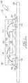
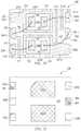
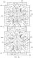
- FIG. 1illustrates a conventional leadless package 110 as a quad flat no-lead (QFN) or dual flat no-lead (DFN) package.
- Leadless package 110includes a semiconductor die 124 disposed on a leadframe 126 .
- Leadframe 126is formed from a metallic substrate with material of the substrate removed to create a plurality of leads 126 a surrounding a die pad 126 b .
- Semiconductor die 124is disposed on die pad 126 b and includes contact pads coupled to leads 126 a by bond wires 136 .
- An encapsulant or molding compound 140is disposed around semiconductor die 124 and leadframe 126 for electrical isolation, physical support, and protection from contaminants.
- Leadless package 110is mounted to a printed circuit board (PCB) or other substrate 120 .
- Solder 150is reflowed between leadframe contacts 126 a and contact pads 122 on PCB 120 to form a metallurgical and electrical connection between leadless package 110 and the PCB.
- Leadless package 110includes leads 126 a for external interconnection, which are simply portions of a metal leadframe exposed from the final package. Leads 126 a are used instead of leads that extend from the package laterally and/or vertically as in traditional semiconductor package types.
- the exposed wettable material of contacts 126 a on the lateral surfaces of package 110referred to as a wettable flank, allows solder 150 to form filleted surfaces 152 after leadless package 110 is mounted onto PCB 120 .
- Fillets 152are useful to manufacturers of electronic devices because proper interconnection between package 110 and PCB 120 can be verified visually by a human or by an automatic visual inspection device 156 including an image sensor and a computer programmed to analyze the images. If a visual inspection shows that a proper fillet 152 was not formed for one of the connections of a lead 126 a to a contact pad 122 , an error in the specific PCB 120 is recorded. The device with the faulty connection can be repaired or discarded. If visual inspection device 156 verifies that each connection between leadless package 110 and PCB 120 includes a proper fillet 152 , the manufacturer can have confidence that the package is properly connected to the system as a whole.
- Leadless package 110reduces the footprint required on PCB 120 over many prior art packages by not having leads that extend from the package, and instead having leads 126 a that remain within the footprint, and within the height, of the package body.
- forming fillets 152 for visual inspectionrelies on side surfaces of leads 126 a being wettable by solder 150 . That is, solder 150 should flow up the sides of leads 126 a to form a fillet 152 between side surfaces of contacts 126 a and contact pad 122 .
- a manufacture of package 110will commonly plate leads 126 a with a wettable material as part of the manufacturing process of the package.
- Metal platingis commonly done with various electroplating or electroless deposition methods. Electroplating is the more desirable plating method because a thicker and faster metal deposition occurs. The thicker metal layer provided by electroplating provides a more reliable solder fillet, especially after parts sit on a shelf for a significant period of time before being soldered.
- electroplating for the full thickness of contacts 126 acan be a challenge because a portion of the side surfaces may remain during electroplating to provide electrical current for the electroplating process.
- FIG. 1illustrates a leadless semiconductor package connected to a substrate by visually verifiable solder fillets
- FIGS. 2 a -2 millustrate forming a leadless package having a leadframe and plated leads
- FIGS. 3 a -3 iillustrate forming a leadless package with multiple die and individual tie bars for the leads
- FIGS. 4 a -4 jillustrate forming a leadless package with multiple die and shared tie bars
- FIGS. 5 a -5 jillustrate forming a quad flat non-leaded (QFN) package with individual tie bars for the leads using bond wires between devices;
- FIGS. 6 a -6 billustrate forming a QFN package with shared tie bars for the leads.
- FIGS. 7 a -7 fillustrate an alternative leadframe and process for forming a QFN package with shared tie bars.
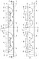
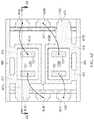
- FIG. 2 aillustrates a leadframe 200 in plan view, with FIG. 2 b illustrating a cross-sectional view of the leadframe through line 2 b - 2 b in FIG. 2 a .
- FIG. 2 aillustrates the bottom surface of leadframe 200 , which is defined herein as the major surface of a leadframe that is exposed from the final package for electrical connection.
- the top surface of leadframe 200is the side that semiconductor die 124 is disposed on in FIG. 2 b .
- the top surface of leadframe 200is hidden from view in FIG. 2 a .
- Side surfaces or flanks of leadframe 200are surfaces that extend between the top and bottom surfaces.
- Leadframe 200commonly begins with a solid sheet or plate of conductive material, commonly copper (Cu). Copper alloys, steel, or other conductive materials are used to form leadframe 200 in other embodiments. Masking layers are patterned over the top and bottom surfaces of leadframe 200 , and the leadframe is half-etched from each side. The figures follow a convention that the top half of leadframes are shaded with line hatching, while the bottom half of leadframes are shaded with square hatching. Even though the halves are shaded differently, leadframe 200 is normally a single uniform and continuous conductive material. Half-etching the original sheet of conductive material from the bottom exposes the line-hatched half of leadframe 200 through openings etched through the square-hatched half.
- Cucopper
- Half-etching from the topexposes the line-hatched half of leadframe 200 through the square-hatched half. Areas where leadframe 200 is half-etched from both the top and the bottom are not shaded because the combination of half-etching from both the top and the bottom fully removes leadframe 200 in those areas.
- Half-etchingrefers to etching into a sheet of metal or other conductive material for approximately half the thickness of the sheet.
- FIG. 2 ais a view of leadframe 200 from the bottom.
- the square-hatched bottom half of leadframe 200remains in those areas.
- the line-hatched areas visible in FIG. 2 aare regions that were half-etched from the bottom to remove the square-hatched material, but no half-etching occurs from the top so the line-hatched material remains.
- Areas with no hatching in FIG. 2 aare half-etched from both the top and the bottom to create openings or empty space in leadframe 200 .
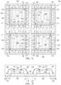
- Die paddles 202 and contacts 204are not etched, and remain at the full thickness of the original conductive sheet. Die paddles 202 and contacts 204 extend downward relative to the rest of leadframe 200 . In FIG. 2 a , die paddles 202 and contacts 204 are closer to the viewer than the rest of leadframe 200 . Die paddles 202 and contacts 204 remain thicker to be exposed from the subsequently applied encapsulant for mounting of the final device and electrical interconnection to a larger system.
- Leadframe 200includes four die paddles 202 . Each die paddle 202 is surrounded by eight contacts 204 , four contacts on two opposite sides of the die paddles. Each set of one die paddle 202 and eight contacts 204 constitutes a unit of leadframe 200 . Leadframe 200 allows for the formation of four devices at once. In other embodiments, leadframe 200 is much larger and allows many more than four devices to be formed at once by tessellating the units for any desired length and width. Similarly, while each die paddle 202 includes eight associated contacts 204 , any number of contacts are formed per unit in other embodiments as desired.
- the portions of leadframe 200 that are half-etched from the bottom but not the top, which are the portions in FIG. 2 a with line hatching,include die pad 206 , frame 208 , die pad tie bars 210 , contact tie bars 211 , and contact wings 212 .
- Die pad 206is a half-etched portion of leadframe 200 that surrounds die paddle 202 . Die paddle 202 is exposed from the final device, while die pad 206 includes a larger footprint that is embedded in the encapsulant. The larger footprint of die pad 206 increases mold lock of the die pad.
- FIG. 2 billustrates semiconductor die 124 disposed on die pad 206 opposite die paddle 202 .
- Frame 208surrounds each unit of leadframe 200 to structurally support die pad 206 and contacts 204 .
- Frame 208is optionally half-etched. In other embodiments, frame 208 remains at the full thickness of leadframe 200 such that the leadframe includes full thickness portions connecting each contact 204 of each unit.
- Die pad tie bars 210attach and electrically connect each die pad 206 and die paddle 202 to frame 208 at the sides of die pad 206 where contacts 204 do not exist.
- Contact tie bars 211attach each contact 204 to an associated die pad 206 .
- Each contact 204is also connected directly to frame 208 opposite tie bars 211 .
- Contact wings 212are a half-etched portion of leadframe 200 that extends out from the full-thickness portions of leads 204 to increase mold lock.
- Leadframe 200includes saw streets 220 and saw streets 224 .
- Saw streets 220are oriented perpendicularly to saw streets 224 .
- Saw streets 220 and 224extend over frame 208 between each of the individual units of leadframe 200 .
- saw streets 220separate contacts 204 of one unit from contacts 204 of an adjacent unit to expose the side surfaces or flanks of each contact.
- Saw streets 224separate die pads 206 of adjacent packages when sawn through by severing die pad tie bars 210 .
- frame 208 within the saw streetsare fully removed when the saw streets are sawn through to separate adjacent packages.
- leadframe 200is disposed on a carrier or temporary substrate 240 containing sacrificial base material such as silicon, polymer, beryllium oxide, glass, or other suitable low-cost, rigid material for structural support.
- sacrificial base materialsuch as silicon, polymer, beryllium oxide, glass, or other suitable low-cost, rigid material for structural support.
- An optional interface layer or double-sided tape 242is formed over carrier 240 as a temporary adhesive bonding film, etch-stop layer, or thermal release layer.
- Leadframe 200is disposed on carrier 240 with die paddles 202 and contacts 204 contacting the carrier or interface layer 242 .
- the half-etched nature of frame 208 , tie bars 211 , and die pads 206is illustrated by a separation that remains between frame 200 and carrier 240 in the half-etched regions.
- Semiconductor die 124are disposed on die pads 206 with active surface 130 oriented away from leadframe 200 .
- Active surface 130includes one or more active and passive components formed by semiconductor doping, metal deposition, and other front-end semiconductor manufacturing processes.
- Contact pads 132are formed on active surface 130 for electrical interconnection.
- Die paddles 202are exposed in the final product and provided electrical connection to the back surface of semiconductor die 124 for use in embodiments where a voltage applied to the back surface of semiconductor die 124 has a desired effect on the active functionality of the semiconductor die.
- semiconductor die 124has multiple active surfaces.
- a plurality of bond wires 246is formed between contacts 204 on leadframe 200 and contact pads 132 of semiconductor die 124 .
- Bond wires 246are mechanically and electrically coupled to contacts 204 and contact pads 132 by thermocompression bonding, ultrasonic bonding, wedge bonding, stitch bonding, ball bonding, or other suitable bonding technique.
- Bond wires 246include a conductive material such as Copper, Aluminum, Gold, Silver, a combination thereof, or another suitable conductive material.
- Bond wires 246represent one type of interconnect structure that electrically connects contacts 204 to contact pads 132 .
- conductive bumpsare formed on contact pads 132 , and semiconductor die 124 is flip-chip bonded onto contacts 204 without needing die paddle 202 and die pad 206 .
- an encapsulant or molding compound 250is deposited over semiconductor die 124 , bond wires 246 , and leadframe 200 using a paste printing, compressive molding, transfer molding, liquid encapsulant molding, vacuum lamination, spin coating, or other suitable applicator.
- Encapsulant 250covers the side surfaces and active surface 130 of semiconductor die 124 .
- Encapsulant 250can be polymer composite material, such as epoxy resin with filler, epoxy acrylate with filler, or polymer with proper filler.
- Encapsulant 250is non-conductive and environmentally protects the semiconductor device from external elements and contaminants. Encapsulant 250 also protects semiconductor die 124 from degradation due to exposure to light.
- Encapsulant 250 , semiconductor die 124 , leadframe 200 , and bond wires 246combine to form a reconstituted wafer or panel 252 .
- Panel 252may include any desired number of semiconductor die 124 in a two-dimensional grid by using a leadframe 200 of an appropriate size.
- Encapsulant 250flows between carrier 240 and the half-etched portions of leadframe 200 , i.e., die pad 206 , a frame 208 , die pad tie bars 210 , contact tie bars 211 , and contact wings 212 . Encapsulant 250 extending below die pad 206 and contact wings 212 helps lock die paddle 202 and contacts 204 into the encapsulant.
- panel 252is flipped and disposed on carrier 260 with optional interface layer 262 .
- Carrier 240is removed by chemical etching, mechanical peeling, chemical mechanical planarization (CMP), mechanical grinding, thermal bake, UV light, laser scanning, or wet stripping.
- Panel 252is disposed on carrier 260 with encapsulant 250 on the carrier and leadframe 200 oriented away from the carrier. Die paddles 202 and contacts 204 are exposed from the encapsulant opposite carrier 260 .
- carrier 240is reused as carrier 260 .
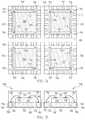
- a saw blade or laser cutting tool 264is used to singulate leadframe 200 through saw streets 220 .
- Saw 264forms a trench 265 that extends across substantially the entirety of frame 200 and completely removes frame 208 between adjacent contacts 204 to fully expose a flank 266 of each contact.
- Frame 208being half-thickness reduces wear on saw 264 and increases the speed at which trench 265 can be formed.
- the full thickness portions of leads 204extends into saw streets 220 to ensure that the exposed flank 266 is full thickness.
- the full thickness portions of leads 204extend completely across saw streets 220 to ensure that a full-thickness of leadframe 200 is exposed with use of any thickness of saw 264 .
- a laser cutting toolmay be used to separate adjacent contacts 204 and expose flanks 266 without fully removing frame 208 within saw streets 220 .
- trench 265is formed only partially through encapsulant 250 .
- Encapsulant 250remains between adjacent units to mechanically couple adjacent columns 270 of leadframe 200 to each other.
- trench 265extends completely through encapsulant 250 to physically separate adjacent units. Columns 270 of leadframe 200 remain aligned by each remaining on carrier 260 .
- trench 265extends into or through carrier 260 .
- each contact 204is a vertically oriented surface that extends for the full thickness of leadframe 200 .
- FIG. 2 eshows that each aligned unit within a column 270 remains electrically coupled to each other through die pad tie bars 210 and the remaining portions of frame 208 in saw streets 224 . Columns 270 remain physically coupled to each other by encapsulant 250 remaining under trench 265 .
- a conductive layer 280is plated onto die paddles 202 and leads 204 by electroplating.
- a voltage potentialis applied to frame 208 of leadframe 200 from the top and/or bottom ends of each column 270 .
- the voltage potentialtravels from frame 208 to each exposed die paddle 202 through die pads 206 and die pad tie bars 210 .
- the electrical potentialfurther flows to each contact 204 , including the exposed flank 266 of each contact, through contact tie bars 211 .
- Panel 252is disposed in a plating bath with electrical current flowing through leadframe 200 , and molecules of the desired metal to plate attach to exposed portions of leadframe 200 , i.e., die paddles 202 and leads 204 including flanks 266 .
- the plated conductive layer 280extends over a full height of leadframe 200 due to trench 265 exposing flanks 266 for the full thickness of the leadframe.
- saw blade or laser cutting tool 290is used to form trenches 292 through contact tie bars 211 .
- Trenches 292run the length of each column 270 of leadframe 200 in some embodiments.
- a laser cutting toolis used to selectively cut tie bars 211 without forming a trench extending fully across panel 252 .
- Some tie bars 211may remain electrically coupled to die pad 206 if a connection to the back surface of semiconductor die 124 is desired for some contacts 204 .
- Trenches 292electrically isolate contacts 204 from die pads 206 so that the contacts can be used to access the functionality of semiconductor die 124 , and not be electrically short circuited to each terminal of the semiconductor die through die pad 206 and the other contacts.
- saw blade or laser cutting tool 296is used to singulate panel 252 into individual packages 298 by cutting through saw streets 220 and 224 .
- Saw 296cuts completely through encapsulant 250 to physically separate each unit of leadframe 200 into a leadless package 298 . Remaining portions of frame 208 in saw streets 224 are removed.
- Plated conductive layer 280is illustrated with an exaggerated thickness, and would not generally extend noticeably outside of the footprint of the final package 298 .
- Flanks or side surfaces 266 of contacts 204would be substantially coplanar in one embodiment.
- an additional sawing stepis not required through saw streets 220 ; only saw streets 224 are cut through by saw 296 in FIG. 2 h.
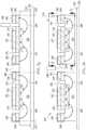
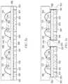
- FIGS. 2 i -2 lillustrate package 298 from various angles.
- FIG. 2 iillustrates package 298 from a top view without encapsulant 250 illustrated to reveal semiconductor die 124 and leadframe 200 .
- Contacts 204are separated from die pad 206 at tie bars 211 by trenches 292 .
- Exposed flanks 266are plated with conductive layer 280 for the full thickness of leadframe 200 to promote wetting of solder onto side surfaces of contacts 204 .
- FIG. 2 jillustrates a bottom view of package 298 with die paddle 202 and contacts 204 exposed from encapsulant 250 .
- Trenches 292extend into encapsulant 250 through tie bars 211 . Tie bars 211 are exposed within trenches 292 and would be visible in an angled view.
- trenches 292completely remove tie bars 211 , and contacts 204 are directly exposed within the trench.
- the term contact as used hereinencompasses a contact 204 by itself, and also may refer to a contact 204 in combination with any portion of tie bar 211 remaining attached to the contact after formation of trenches 292 . Therefore, while tie bars 211 are exposed within trenches 292 as illustrated, one having ordinary skill in the art would consider semiconductor device 298 to have contacts exposed within trenches 292 by virtue of the tie bars being exposed.
- FIG. 2 killustrates a side view of package 298 with plated flanks 266 of contacts 204 exposed.
- FIG. 2 lillustrates a side view of package 298 from a view perpendicular to FIG. 2 k to show that die pad tie bars 210 are exposed from the encapsulant after cutting through saw streets 224 .
- Package 298is a leadless semiconductor package with contacts 204 that are electroplated on the flanks of the contacts over the full thickness of leadframe 200 .
- Plating contacts 204 for the full height of leadframe 200provides a relatively large solder fillet when package 298 is mounted onto a PCB or other substrate. The larger solder fillet is more reliably detected by automatic verification machines.
- FIG. 2 millustrates an alternative leadframe design 200 ′.
- Leadframe 200 ′is similar to leadframe 200 , but includes contact tie bars 211 ′ to replace tie bars 211 .
- Tie bars 211 ′extend completely between two horizontal frame 208 sections. Tie bars 211 ′ electrically couple each lead 204 on a side to each other, and to frame 208 , for plating without coupling to die pad 206 other than indirectly through frame 208 .
- the manufacturing process of a semiconductor package with leadframe 200 ′proceeds similarly to with leadframe 200 in FIGS. 2 a -2 l .
- trenches 292are formed in FIG. 2 g , tie bars 211 ′ are fully removed to electrically isolate contacts 204 from each other.
- Contacts 204are exposed within trenches 292 where the contacts meet tie bar 211 ′, as with tie bars 211 in FIG. 2 g .
- die pad 206is not exposed within trenches 292 because tie bar 211 ′ does not extend to the die pad.
- Leadframe 200 ′ with tie bars 211 ′allows a package to be made without having die pad 206 and contacts 204 exposed in trench 292 directly across from each other, reducing the likelihood of a short circuit by errant conductive material within the trench.
- FIGS. 3 a -3 iillustrate forming a leadless package in an embodiment with two electrically isolated semiconductor die within the package.
- FIGS. 3 a and 3 billustrate plan views of a leadframe 300 .
- FIG. 3 aillustrates the bottom of leadframe 300 , i.e., the side that will ultimately be exposed from encapsulant for electrical interconnection to die paddles 302 and contacts 304 .
- Die paddles 302 and contacts 304are closer to the viewer than the rest of leadframe 300 , which is half-etched from the bottom.
- Die paddles 302 and contacts 304are shaded with squares to indicate that the viewer is seeing the bottom half of leadframe 300 .
- leadframe 300is shaded with lines to indicate that the bottom half of the leadframe was etched away, and the viewer is seeing the top half of the leadframe. Areas with no shading are half-etched from both the top and the bottom, so a viewer sees completely through leadframe 200 .
- Die paddles 302 and contacts 304are thicker to be exposed from the bottom surface of the leadless package. Two die paddles 302 a and 302 b are provided for two separate semiconductor die in each final package.
- a half-etched portion of leadframe 300extends around die paddles 302 as die pads 306 .
- Die pads 306have a larger footprint than die paddles 302 to increase mold lock.
- Die pad 306 aincludes half-etched extension 307 a that extends from die pad 306 a to contact 304 d .
- Contact 304 dprovides an external electrical connection to the surface of a semiconductor die in contact with die pad 306 a .
- extension 307 bextends from die pad 306 b to contact 304 c to provide external connection to the back of a semiconductor die disposed on die pad 306 b .
- Extension regions 307 coupling to contacts 304allow contacts at the lateral edges of the final device to be used to connect to the back side of semiconductor die. Connecting to a contact 304 provides the added benefit of an externally visible solder fillet when the package is installed over connecting via die paddles 302 .
- Frame 308surrounds each set of die pads 306 a and 306 b .
- Frame 308can be half-etched as illustrated, or can remain at the full thickness of leadframe 300 .
- Die pads 306are coupled to frame 308 by die pad tie bars 310 .
- Contacts 304are coupled directly to frame 308 at the flanks of the contacts that will be exposed in the final leadless package.
- contacts 304are electrically coupled to frame 308 by contact tie bars 311 and include half-etched wings 312 .
- Independent tie bars 311are provided to electrically couple individual contacts 304 to frame 308 . Having independent tie bars for individual contacts allows the contacts to be electrically isolated from each other by simply singulating through saw streets 320 and 324 .
- Extensions 307remain coupling respective die pads 306 to contacts 304 in the final package because trench 392 is not required.
- Trench 292if used in the embodiment of FIGS. 3 a -3 i , would cut through extensions 307 along with any tie bars that were desired to be severed.
- FIG. 3 billustrates leadframe 300 flipped left-right to view the leadframe from the top side.
- Semiconductor die 124are disposed on die pads 306 .
- Contact pads 132 of semiconductor die 124are coupled to contacts 304 by bond wires 346 .
- semiconductor die 124are discrete vertical power MOSFETs or other similar three-terminal devices.
- Semiconductor die 124 amight have a drain terminal directly electrically coupled to die pad 306 a via the bottom surface of the semiconductor die, while contact pads 132 represent source and gate terminals.
- the drain of the power MOSFETwould be coupled to terminal 304 d by extension 307 a , while the source and drain terminals would be coupled to contacts 304 a and 304 e by bond wires 346 .
- Other functionalityis provided by semiconductor die 124 in other embodiments.
- FIGS. 3 c and 3 dillustrate cross-sectional views of leadframe 300 through die paddles 302 a and 302 b , respectively, including encapsulant 350 deposited over leadframe 300 , semiconductor die 124 , and bond wires 346 .
- Leadframe 300is illustrated using different hatch patterns for the top and bottom halves of the leadframe to better illustrate half-etched portions. However, in most embodiments, the leadframe is a solid body of a uniform conductive material and no visible delineation would be seen. Tie bars 311 b , 311 c , and 311 e are shown in the particular cross-sections, and extend into and out of the page.
- Contacts 304 a , 304 c , 304 d , and 304 fare isolated in the illustrated cross-sections, but are electrically coupled together by their respective connections to frame 308 .
- Tie bars 311 b , 311 c , and 311 eare all electrically connected to each other through frame 308 as well, and each electrically couples a respective contact 304 to the other contacts 304 through frame 308 .
- Encapsulant 350is similar to encapsulant 250 , and extends under contact wings 312 and die pads 306 to increase mold lock of contacts 304 and die paddles 302 .
- trenches 365are formed through saw streets 320 in a similar manner to trenches 265 in FIG. 2 d .
- Trenches 365can be formed either partially through or completely through encapsulant 350 within saw streets 320 . Formation of trenches 365 exposes flanks 366 of each contact 304 for subsequent plating. In some embodiments, the full thickness portions of contacts 304 extend laterally into saw streets 320 and are partially removed in formation of trenches 365 .
- FIG. 3 fillustrates the same plan view from FIG. 3 a after trenches 365 are formed. Encapsulant 350 is not illustrated so that leadframe 300 is fully visible.
- Trenches 365create vertical columns 370 of leadframe 300 that are electrically isolated from each other by the removal of frame 308 within saw streets 320 . However, each unit within a common column 370 is electrically coupled together from top to bottom.
- a voltage potential applied at the bottom frame 308 portionflows to contact 304 e through tie bar 311 e and contact 304 f through tie bar 311 f .
- the voltage potentialflows to die pad 306 b through die pad tie bars 310 , and further to contact 304 c through extension 307 b .
- the voltage potentialflows from extension 307 b through tie bar 311 c to the next level horizontal frame 308 portion.
- the voltage potentialis applied through tie bar 311 a to contact 304 a and to contact 304 b through tie bar 311 b .
- the voltage potentialalso reaches contact 304 d through extension 307 a , die pad 306 a , and die pad tie bars 310 .
- Conductive layer 380is also plated onto the bottom surfaces of contacts 304 and die paddles 302 that are exposed from encapsulant 350 .
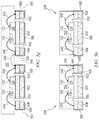
- FIG. 3 hillustrates a leadless package 398 in a top view without encapsulant 350
- FIG. 3 iillustrates a leadless package 398 from a bottom view with the encapsulant illustrated.
- Contacts 304 a - 304 fare each electrically isolated from each other by removal of frame 308 from around each package during singulation, and are only electrically connected per the functionality of semiconductor die 124 and an external system that incorporates package 398 .
- Die paddles 302 a and 302 bare exposed at the bottom of leadless package 398 .
- Contacts 304 c and 304 dare also electrically connected to respective die pads 306 by respective extension regions 307 .
- Contacts 304 c and 304 dprovide electrical connections to the bottoms of semiconductor die 124 at the flanks of leadless package 398 so that the connection forms a fillet and is more easily verifiable using a visual system.
- Contacts 304 a , 304 b , 304 e , and 304 fare electrically coupled to respective contact pads 132 of semiconductor die 124 .
- Each contact 304includes a wettable flank 366 that is plated for the full thickness of leadframe 300 , while also allowing multiple die paddles 302 to be coupled to leads 304 as desired.
- Leadframe 300provides a solution for multiple die pads coupled to contacts internally, but requires multiple tie bars 311 routed between contacts 304 and frame 308 .
- One potential routing configurationis shown in FIGS. 3 a -3 i for a six terminal device. As the number of terminals per package increases, more independent tie bars 311 will have to be routed to frame 308 . Eventually, the routing becomes problematic as the number of terminals grows.
- FIG. 4 aillustrates a leadframe 400 that provides for separate die paddles 402 coupled to separate contacts 404 with a shared tie bar 411 between any number of contacts on a side of a package.
- FIG. 4 ashows a bottom plan view of leadframe 400 for one package, while FIG. 4 b illustrates a top plan view.
- a plurality of packagesis formed at once by tessellating leadframe 400 across any desired length and width.
- FIG. 4 ashows a bottom view, with surfaces of die paddles 402 , contacts 404 , and tie bars 411 closer to the viewer than visible surfaces of the remaining portions of leadframe 400 .
- the bottom half of leadframe 400is illustrated with square hatching
- the top half of leadframe 400is illustrated with line hatching. Line hatching is visible in regions where leadframe 400 is half-etched from the bottom, but the top half of the leadframe is not etched.
- Die paddles 402 , contacts 404 , and tie bars 411will all be exposed at a bottom surface of a panel after depositing encapsulant.
- frame 408is full-thickness rather than being half-etched, and will be exposed at the bottom surface of encapsulant 450 between units of leadframe 400 .
- the rest of leadframe 400will have encapsulant deposited between the leadframe and the viewer in the angle of FIG. 4 a .
- tie bars 411are shown ending at frame 408 , tie bars 411 may extend uniformly across each aligned unit of the larger leadframe 400 when a larger leadframe is used to make multiple units at once.
- FIG. 4 bshows that tie bars 411 are half-etched from the top of leadframe 400 except for within extension regions 407 , which are not etched from the top side of the leadframe.
- the areas where extension regions 407 cross tie bars 411remain at the full thickness of leadframe 400 .
- the square hatching of tie bars 411indicates regions where leadframe 400 is half-etched from the top, and the bottom half of the leadframe remains.
- Contact tie bars 411extend across an individual unit of leadframe 400 to electrically couple an entire column of contacts 404 to frame 408 . Any number of contacts 404 can be added to a side of a package, and tie bar 411 is simply extended in length to reach the added contacts.
- a semiconductor die 124is disposed on each die pad 406 , and contact pads 132 are coupled to contacts 404 by bond wires 446 in FIG. 4 c .
- Encapsulant 450is deposited over leadframe 400 , semiconductor die 124 , and bond wires 446 to form a panel. Die paddle 402 , contact pads 404 , and tie bars 411 remain exposed from encapsulant 450 because leadframe 400 is on a carrier or other substrate while the encapsulant is deposited.
- trenches 465are formed in saw streets 420 to remove portions of frame 408 and expose flanks 466 of contacts 404 for plating. Trenches 465 extend partially through encapsulant 450 as illustrated, or extend completely through encapsulant 450 in other embodiments. Contacts 404 remain electrically coupled to each other through tie bars 411 and remaining portions of frame 408 . Vertically aligned units remain electrically coupled to each other through the remaining portions of frame 408 . Horizontally aligned units remain physically coupled to each other across saw streets 420 by encapsulant 450 in embodiments where trench 465 does not extend completely through the encapsulant. In embodiments where trench 465 extends completely through encapsulant 450 , horizontally aligned units remain physically coupled by being on a common carrier or substrate.
- FIG. 4 eillustrates plated conductive layer 480 over exposed surfaces of die paddle 402 and contacts 404 .
- Conductive layer 480forms on each contact 404 because an applied voltage potential reaches each contact through tie bars 411 .
- Conductive layer 480forms on flanks 466 for the entire vertical extent of leadframe 400 because trench 465 completely exposes the full thickness portions of contacts 404 .
- a saw blade or laser cutting toolis used to form trenches 492 , removing tie bars 411 .
- Trenches 492are formed only to the half-etched thickness of leadframe 400 to fully remove tie bars 411 without cutting completely through the leadframe.
- Extension regions 407remain electrically coupling die pad 406 a to contact 404 c and die pad 406 b to contact 404 b .
- Extension regions 407are not cut by trenches 492 because the trenches only extend through the bottom half of the leadframe 400 thickness, while extension regions 407 exist within the top vertical half of the leadframe.
- FIGS. 4 h -4 jillustrate leadless package 498 after full singulation through saw streets 420 and 424 using a saw blade or laser cutting tool. In embodiments where trenches 465 were formed completely through encapsulant 450 , only saw streets 424 are singulated after plating of conductive layer 480 .
- FIG. 4 his a cross-sectional view.
- FIG. 4 iis a top-down view without encapsulant 450 illustrated to show leadframe 400 and semiconductor die 124 .
- FIG. 4 jis a bottom-side view with die paddles 402 and contacts 404 exposed.
- FIG. 4 hillustrates plated conductive layer 480 extending over flanks 466 of contacts 404 for the entire vertical thickness of leadframe 400 .
- Conductive layer 480is also plated onto the bottom surfaces of die paddles 402 because the die pads are exposed and electrically coupled to contacts 404 during plating.
- Contact pads 132 of semiconductor die 124are coupled to contacts 404 by bond wires 446 .
- the back surfaces of semiconductor die 124are electrically coupled to other contacts 404 through die pads 406 and extension regions 407 .
- FIG. 4 jshows die paddles 402 and contacts 404 exposed at the bottom surface of leadless package 498 .
- Die paddle 402 aincludes a corner cut-out to indicate orientation.
- Trenches 492are illustrated where tie bars 411 were removed.
- Encapsulant 450is visible in the trenches because removal of tie bars 411 completely removes leadframe 400 except where extension regions 407 remain.
- Extension regions 407are visible in trenches 492 because leadframe 400 was full thickness in those areas, but the saw blade that created trenches 492 only cut into the package for half the thickness of the leadframe.
- Leadframe 400 with tie bars 411allowed a package 498 to be created having any number of contacts with flanks plated for the full thickness of the leadframe.
- FIGS. 5 a -5 jillustrate forming a quad flat non-leaded (QFN) package using similar concepts to the above embodiments.
- FIG. 5 aillustrates the bottom side of a leadframe 500 .
- Die paddles 502 and contacts 504extend closer to the viewer than the remainder of leadframe 500 , which is half-etched from the bottom.
- Die paddles 502are rectangular with a corner missing for orientation.
- Each unit of leadframe 500includes a die paddle 502 and contacts 504 adjacent to all four sides of the die paddles.
- Die pads 506surround die paddles 502 for increased mold lock
- frame 508surrounds each unit of leadframe 500 within saw streets 520 and 524 .
- frame 508can be half-etched or remain at the full thickness of leadframe 500 .
- Die pad tie bars 510extend from corners of die pads 506 to frame 508 to provide electrical and physical coupling for the die pads.
- Contact tie bars 511extend from contacts 504 to die pads 506 to provide electrical and physical coupling of the contacts.
- Contacts 504are also directly coupled to frame 508 opposite tie bars 511 .
- Contacts 504include half-etched wings 512 for mold lock.
- FIG. 5 billustrates leadframe 500 flipped to view the top side of the leadframe with semiconductor die 124 mounted on die pads 506 .
- Wire bonds 546electrically couple contacts 504 to contact pads 132 of semiconductor die 124 .
- Wire bonds 548electrically couple die pad tie bars 510 across saw streets 520 and 524 so that electrical current reaches each unit of leadframe 500 even after frame 508 is removed to expose flanks of contacts 504 for plating.
- FIG. 5 cillustrates a cross-sectional view of leadframe 500 and semiconductor die 124 with encapsulant 550 forming a panel. While bond wire 548 would not be visible in the illustrated cross-section, bond wire 548 is included as a dotted line to help illustrate its function.
- frame 508is removed by forming trenches 565 through leadframe 500 using a saw blade or laser cutting tool. Trenches 565 extend completely through leadframe 500 but do not extend fully through encapsulant 550 nor cut through bond wires 548 . Each contact 504 on each side of die pad 506 includes a flank 566 that is exposed for the full thickness of leadframe 500 . Contacts 504 within a common unit of leadframe 500 are electrically coupled to each other by contact tie bars 511 connecting each contact to die pad 506 . Each unit remains electrically coupled to adjacent units by bond wires 548 . Each unit remains physically coupled to adjacent units by encapsulant 550 remaining within saw streets 520 and 524 .
- Bond wires 548electrically couple units that are adjacent in the vertical direction as well as the horizontal direction. Having electrical continuity in each direction allows a voltage potential to be applied at a single point on leadframe 500 for plating, and the voltage potential will propagate across the entire leadframe. In cases where a voltage potential is applied by a track contacting each vertical column of units, the horizontal bond wires 548 are optional and provide a degree of redundancy. The electric potential reaching each die paddle 502 and contact 504 results in a plated conductive layer 580 that covers each exposed surface of the die paddles and contacts.
- FIGS. 5 f -5 gillustrate trenches 592 formed through tie bars 510 and 511 using a saw blade or laser cutting tool. Trenches 592 separate contacts 504 from die pad 506 so that the contacts can be used to electrically interact with semiconductor die 124 without being short-circuited to each other through the die pad.
- the design of leadframe 500allows trenches 592 to be formed extending across the entire leadframe while avoiding cutting through contacts 504 and die pads 506 .
- FIG. 5 hillustrates a cross-section two adjacent units after being singulated through saw streets 520 and 524 .
- FIG. 5 ishows the bottom side of a package 598 with die paddle 502 and contacts 504 exposed from encapsulant 550 .
- FIG. 5 jillustrates a top-down view without encapsulant 550 .
- the singulation of packages 598cuts through bond wires 548 to electrically isolate each adjacent unit of leadframe 500 .
- Each package 598includes leads on every side of the package plated to the full height of leadframe 500 .
- FIGS. 6 a -6 billustrate an embodiment similar to FIGS. 5 a -5 j , but with contact tie bars 511 replaced with contact tie bars 611 .
- Tie bars 611extend along each side of die pads 606 between adjacent die pad tie bars 610 without directly contacting the die pads. Formation of leadless packages using leadframe 600 proceeds similarly as with leadframe 500 above. Trenches 692 run parallel to tie bars 611 and completely remove the tie bars, whereas tie bars 511 ran perpendicular to trenches 592 and were cut through. Trench 692 does not expose die pad 606 when tie bars 611 are used.
- leadframe 600creates a leadless package with plating on each lead for the full height of leadframe.
- FIGS. 7 a -7 fillustrate QFN leadframe 700 with tie bars 711 that extend linearly between opposite portions of frame 708 .
- FIG. 7 ais a bottom view of leadframe 700 at the beginning of manufacturing a QFN package.
- die pad 702 and contacts 704are the full thickness of leadframe 700 while the other remaining portions are half-cut.
- Frame 708surrounds each individual unit. Each unit includes a die pad 702 and sixteen contacts 704 surrounding the die pad, four contacts to a side.
- Die pad tie bars 710attach die pad 702 to contact tie bars 711 , which are attached to frame 708 .
- FIG. 7 billustrates a cross-sectional view of leadframe 700 with semiconductor die 124 disposed on die pads 702 .
- Bond wires 746electrically couple contact pads 132 to contacts 704 .
- Die pads 702 and contacts 704are exposed from a bottom surface of encapsulant 750 .
- Leadframe 700is oriented on a carrier with tie bars 711 against the carrier, so the tie bars are exposed at the bottom surface of encapsulant 750 along with contacts 704 and die pad 702 . In other embodiments, leadframe 700 is oriented upside down relative to FIG. 7 b , so that encapsulant 750 flows under tie bars 711 .
- die pad 702includes a wider die pad and a narrower die paddle
- contacts 704include wings, as with the previous embodiments, to improve mold lock.
- Any of the previous embodimentscan be formed using simpler die pads and contacts, such as those shown in FIGS. 7 a -7 b .
- Any of the previous embodimentscan be formed with tie bars exposed from encapsulant as shown in FIG. 7 b .
- leadframesare not half etched, but each part of the leadframe remains the full leadframe thickness.
- Each tie bar 711extends in a substantially straight line across an entirety of leadframe 700 .
- Bond wiresare not used to connect adjacent units, such as with bond wires 548 in FIG. 5 d .
- FIG. 7 cshows trenches 765 formed by laser ablation or another process capable of selectively cutting through frame 708 . Trenches 765 partially remove frame 708 between units to expose flanks 766 of contacts 704 . Remaining portions of frame 708 remain electrically coupling tie bars 710 of adjacent units, so no additional wire bonds are required.
- conductive layer 780is plated onto die pads 702 and contacts 704 , including flanks 766 for the full height of leadframe 700 . Conductive layer 780 creates a wettable surface on flanks 766 that extends for the full height of leadframe 700 , resulting in a visually verifiable fillet when the final packages are mounted onto a substrate.
- FIGS. 7 e -7 fillustrate trenches 792 formed to remove tie bars 710 and electrically isolate contacts 704 from each other.
- the panel with leadframe 700is singulated through saw streets 720 and 724 to create individual leadless packages 798 .
- Leadless packages 798are QFN packages with plated conductive layer 780 formed on flanks 766 for the full thickness of leadframe 700 . Electroplating for the full thickness of leadframe 700 creates a larger solder fillet than other plating methods that only plate for a portion of the leadframe thickness. The larger solder fillet is easier to visually verify.
Landscapes
- Engineering & Computer Science (AREA)
- Computer Hardware Design (AREA)
- Microelectronics & Electronic Packaging (AREA)
- Power Engineering (AREA)
- Physics & Mathematics (AREA)
- Condensed Matter Physics & Semiconductors (AREA)
- General Physics & Mathematics (AREA)
- Manufacturing & Machinery (AREA)
- Geometry (AREA)
- Lead Frames For Integrated Circuits (AREA)
Abstract
Description
Claims (20)
Priority Applications (3)
| Application Number | Priority Date | Filing Date | Title |
|---|---|---|---|
| US16/230,494US10756006B2 (en) | 2009-01-29 | 2018-12-21 | Leadless semiconductor packages, leadframes therefor, and methods of making |
| US16/984,758US12424522B2 (en) | 2009-01-29 | 2020-08-04 | Leadless semiconductor packages, leadframes therefor, and methods of making |
| US19/020,459US20250149412A1 (en) | 2009-01-29 | 2025-01-14 | Leadless semiconductor packages, leadframes therefor, and methods of making |
Applications Claiming Priority (8)
| Application Number | Priority Date | Filing Date | Title |
|---|---|---|---|
| US12/362,142US8071427B2 (en) | 2009-01-29 | 2009-01-29 | Method for manufacturing a semiconductor component and structure therefor |
| US13/190,922US8324026B2 (en) | 2009-01-29 | 2011-07-26 | Method for manufacturing a semiconductor component |
| US13/692,514US20140151883A1 (en) | 2012-12-03 | 2012-12-03 | Method for manufacturing a semiconductor component and structure therefor |
| US14/168,850US20150035166A1 (en) | 2009-01-29 | 2014-01-30 | Method for manufacturing a semiconductor component and structure |
| US15/063,011US9899349B2 (en) | 2009-01-29 | 2016-03-07 | Semiconductor packages and related methods |
| US15/357,680US10163766B2 (en) | 2016-11-21 | 2016-11-21 | Methods of forming leadless semiconductor packages with plated leadframes and wettable flanks |
| US15/415,504US10199311B2 (en) | 2009-01-29 | 2017-01-25 | Leadless semiconductor packages, leadframes therefor, and methods of making |
| US16/230,494US10756006B2 (en) | 2009-01-29 | 2018-12-21 | Leadless semiconductor packages, leadframes therefor, and methods of making |
Related Parent Applications (2)
| Application Number | Title | Priority Date | Filing Date |
|---|---|---|---|
| US15/063,011Continuation-In-PartUS9899349B2 (en) | 2009-01-29 | 2016-03-07 | Semiconductor packages and related methods |
| US15/415,504ContinuationUS10199311B2 (en) | 2009-01-29 | 2017-01-25 | Leadless semiconductor packages, leadframes therefor, and methods of making |
Related Child Applications (2)
| Application Number | Title | Priority Date | Filing Date |
|---|---|---|---|
| US15/415,504Continuation-In-PartUS10199311B2 (en) | 2009-01-29 | 2017-01-25 | Leadless semiconductor packages, leadframes therefor, and methods of making |
| US16/984,758DivisionUS12424522B2 (en) | 2009-01-29 | 2020-08-04 | Leadless semiconductor packages, leadframes therefor, and methods of making |
Publications (2)
| Publication Number | Publication Date |
|---|---|
| US20190122967A1 US20190122967A1 (en) | 2019-04-25 |
| US10756006B2true US10756006B2 (en) | 2020-08-25 |
Family
ID=58664226
Family Applications (4)
| Application Number | Title | Priority Date | Filing Date |
|---|---|---|---|
| US15/415,504ActiveUS10199311B2 (en) | 2009-01-29 | 2017-01-25 | Leadless semiconductor packages, leadframes therefor, and methods of making |
| US16/230,494Active2029-03-26US10756006B2 (en) | 2009-01-29 | 2018-12-21 | Leadless semiconductor packages, leadframes therefor, and methods of making |
| US16/984,758Active2031-11-14US12424522B2 (en) | 2009-01-29 | 2020-08-04 | Leadless semiconductor packages, leadframes therefor, and methods of making |
| US19/020,459PendingUS20250149412A1 (en) | 2009-01-29 | 2025-01-14 | Leadless semiconductor packages, leadframes therefor, and methods of making |
Family Applications Before (1)
| Application Number | Title | Priority Date | Filing Date |
|---|---|---|---|
| US15/415,504ActiveUS10199311B2 (en) | 2009-01-29 | 2017-01-25 | Leadless semiconductor packages, leadframes therefor, and methods of making |
Family Applications After (2)
| Application Number | Title | Priority Date | Filing Date |
|---|---|---|---|
| US16/984,758Active2031-11-14US12424522B2 (en) | 2009-01-29 | 2020-08-04 | Leadless semiconductor packages, leadframes therefor, and methods of making |
| US19/020,459PendingUS20250149412A1 (en) | 2009-01-29 | 2025-01-14 | Leadless semiconductor packages, leadframes therefor, and methods of making |
Country Status (1)
| Country | Link |
|---|---|
| US (4) | US10199311B2 (en) |
Cited By (1)
| Publication number | Priority date | Publication date | Assignee | Title |
|---|---|---|---|---|
| US12176273B2 (en) | 2021-12-22 | 2024-12-24 | Semtech Corporation | Semiconductor device and method of forming substrate with 3-sided wettable flank |
Families Citing this family (17)
| Publication number | Priority date | Publication date | Assignee | Title |
|---|---|---|---|---|
| US9741642B1 (en)* | 2014-05-07 | 2017-08-22 | UTAC Headquarters Pte. Ltd. | Semiconductor package with partial plating on contact side surfaces |
| WO2017181399A1 (en)* | 2016-04-22 | 2017-10-26 | Texas Instruments Incorporated | Improved lead frame system |
| US10636729B2 (en)* | 2017-06-19 | 2020-04-28 | Texas Instruments Incorporated | Integrated circuit package with pre-wetted contact sidewall surfaces |
| DE102017129924B4 (en)* | 2017-12-14 | 2021-04-29 | Infineon Technologies Ag | ENCAPSULATED, TERMINAL LESS PACKAGE WITH AT LEAST PARTIALLY EXPOSED INSIDE WALL OF A CHIP CARRIER, ELECTRONIC DEVICE, METHOD FOR MANUFACTURING A PACKAGE WITHOUT TERMINAL LADIES AND PREPARING METHOD FOR ESTABLISHING A PACKAGE |
| US10873015B2 (en)* | 2018-03-01 | 2020-12-22 | Nichia Corporation | Light emitting device and method of manufacturing the light emitting device |
| US20190287881A1 (en) | 2018-03-19 | 2019-09-19 | Stmicroelectronics S.R.L. | Semiconductor package with die stacked on surface mounted devices |
| US10593612B2 (en) | 2018-03-19 | 2020-03-17 | Stmicroelectronics S.R.L. | SMDs integration on QFN by 3D stacked solution |
| US20200194347A1 (en)* | 2018-12-18 | 2020-06-18 | Alpha And Omega Semiconductor (Cayman) Ltd. | Semiconductor package and method of making the same |
| JP7384918B2 (en)* | 2019-03-08 | 2023-11-21 | シリコニックス インコーポレイテッド | Semiconductor package with sidewall plating layer |
| CN113614893A (en)* | 2019-03-08 | 2021-11-05 | 硅尼克斯公司 | Semiconductor package with side wall coating |
| CN114649222A (en)* | 2020-12-18 | 2022-06-21 | 意法半导体股份有限公司 | Method for manufacturing a semiconductor device and corresponding semiconductor device |
| US11887864B2 (en)* | 2021-04-26 | 2024-01-30 | Microchip Technology Incorporated | Method of forming a surface-mount integrated circuit package with solder enhanced leadframe terminals |
| CN113555326A (en)* | 2021-06-03 | 2021-10-26 | 珠海越亚半导体股份有限公司 | Packaging structure capable of wetting side face, manufacturing method thereof and vertical packaging module |
| IT202100017231A1 (en)* | 2021-06-30 | 2022-12-30 | St Microelectronics Srl | Method of manufacturing substrates for semiconductor devices, the corresponding substrate and semiconductor device |
| US12354918B2 (en)* | 2021-09-30 | 2025-07-08 | Texas Instruments Incorporated | Package geometries to enable visual inspection of solder fillets |
| US20230133029A1 (en)* | 2021-10-28 | 2023-05-04 | Texas Instruments Incorporated | Leadframe with pre-separated leads |
| US12424523B2 (en)* | 2021-12-20 | 2025-09-23 | Texas Instruments Incorporated | Leadframe strip with complimentary unit design |
Citations (65)
| Publication number | Priority date | Publication date | Assignee | Title |
|---|---|---|---|---|
| US5327008A (en) | 1993-03-22 | 1994-07-05 | Motorola Inc. | Semiconductor device having universal low-stress die support and method for making the same |
| US5866939A (en) | 1996-01-21 | 1999-02-02 | Anam Semiconductor Inc. | Lead end grid array semiconductor package |
| US5900676A (en) | 1996-08-19 | 1999-05-04 | Samsung Electronics Co., Ltd. | Semiconductor device package structure having column leads and a method for production thereof |
| US5969411A (en) | 1996-06-11 | 1999-10-19 | Yamaha Corporation | Lead frame with increased strength and manufacture of semiconductor device |
| US5976912A (en) | 1994-03-18 | 1999-11-02 | Hitachi Chemical Company, Ltd. | Fabrication process of semiconductor package and semiconductor package |
| US6001671A (en) | 1996-04-18 | 1999-12-14 | Tessera, Inc. | Methods for manufacturing a semiconductor package having a sacrificial layer |
| US6130473A (en) | 1998-04-02 | 2000-10-10 | National Semiconductor Corporation | Lead frame chip scale package |
| US6143981A (en) | 1998-06-24 | 2000-11-07 | Amkor Technology, Inc. | Plastic integrated circuit package and method and leadframe for making the package |
| US6193858B1 (en) | 1997-12-22 | 2001-02-27 | George Hradil | Spouted bed apparatus for contacting objects with a fluid |
| US6229200B1 (en) | 1998-06-10 | 2001-05-08 | Asat Limited | Saw-singulated leadless plastic chip carrier |
| US6255740B1 (en) | 1994-08-24 | 2001-07-03 | Fujitsu Limited | Semiconductor device having a lead portion with outer connecting terminals |
| US6294100B1 (en) | 1998-06-10 | 2001-09-25 | Asat Ltd | Exposed die leadless plastic chip carrier |
| US6338984B2 (en) | 1999-02-24 | 2002-01-15 | Matsushita Electric Industrial Co., Ltd. | Resin-molded semiconductor device, method for manufacturing the same, and leadframe |
| US20020067486A1 (en) | 2000-09-25 | 2002-06-06 | S. Forney Leroy | Solderability assessment |
| US6498099B1 (en) | 1998-06-10 | 2002-12-24 | Asat Ltd. | Leadless plastic chip carrier with etch back pad singulation |
| US20030006492A1 (en)* | 2001-07-09 | 2003-01-09 | Kazuto Ogasawara | Semiconductor device and method of manufacturing the same |
| US6545347B2 (en) | 2001-03-06 | 2003-04-08 | Asat, Limited | Enhanced leadless chip carrier |
| US6585905B1 (en) | 1998-06-10 | 2003-07-01 | Asat Ltd. | Leadless plastic chip carrier with partial etch die attach pad |
| US6593643B1 (en) | 1999-04-08 | 2003-07-15 | Shinko Electric Industries Co., Ltd. | Semiconductor device lead frame |
| US6608366B1 (en) | 2002-04-15 | 2003-08-19 | Harry J. Fogelson | Lead frame with plated end leads |
| US6638790B2 (en) | 1999-09-01 | 2003-10-28 | Matsushita Electric Industrial Co., Ltd. | Leadframe and method for manufacturing resin-molded semiconductor device |
| WO2003103038A1 (en) | 2002-04-29 | 2003-12-11 | Advanced Interconnect Technologies Limited | Partially patterned lead frames and methods of making and using the same in semiconductor packaging |
| US6664136B2 (en) | 2001-12-25 | 2003-12-16 | Kabushiki Kaisha Toshiba | Semiconductor device and manufacturing method thereof |
| US6734044B1 (en) | 2002-06-10 | 2004-05-11 | Asat Ltd. | Multiple leadframe laminated IC package |
| US20040142505A1 (en) | 2003-01-21 | 2004-07-22 | Siliconware Precision Industries Co., Ltd. | Semiconductor package free of substrate and fabrication method thereof |
| US20050003586A1 (en) | 2001-05-11 | 2005-01-06 | Renesas Technology Corporation | Manufacturing method of a semiconductor device |
| US6872599B1 (en) | 2002-12-10 | 2005-03-29 | National Semiconductor Corporation | Enhanced solder joint strength and ease of inspection of leadless leadframe package (LLP) |
| US20050093117A1 (en) | 2003-04-11 | 2005-05-05 | Dai Nippon Printing Co., Ltd. | Plastic package and method of fabricating the same |
| US20050139982A1 (en) | 2003-12-25 | 2005-06-30 | Renesas Technology Corp. | Method of manufacturing a semiconductor device |
| US6940154B2 (en) | 2002-06-24 | 2005-09-06 | Asat Limited | Integrated circuit package and method of manufacturing the integrated circuit package |
| US20050206010A1 (en) | 2004-03-18 | 2005-09-22 | Noquil Jonathan A | Multi-flip chip on lead frame on over molded IC package and method of assembly |
| US7071545B1 (en) | 2002-12-20 | 2006-07-04 | Asat Ltd. | Shielded integrated circuit package |
| US7091581B1 (en) | 2004-06-14 | 2006-08-15 | Asat Limited | Integrated circuit package and process for fabricating the same |
| WO2006105733A1 (en) | 2005-04-07 | 2006-10-12 | Jiangsu Changjiang Electronics Technology Co., Ltd. | Package structure with flat bumps for electronic device and method of manufacture the same |
| US20070126092A1 (en) | 2005-12-02 | 2007-06-07 | Advanced Interconnect Technologies Limited, A Corporation Of The Republic Of Mauritius | Leadless semiconductor package and method of manufacture |
| US7247526B1 (en) | 1998-06-10 | 2007-07-24 | Asat Ltd. | Process for fabricating an integrated circuit package |
| US20070176267A1 (en) | 2006-02-02 | 2007-08-02 | Abbott Donald C | Aluminum leadframes for semiconductor QFN/SON devices |
| US7262491B2 (en) | 2005-09-06 | 2007-08-28 | Advanced Interconnect Technologies Limited | Die pad for semiconductor packages and methods of making and using same |
| US20080001263A1 (en) | 2006-06-30 | 2008-01-03 | Stats Chippac Ltd. | Integrated circuit package system |
| US20080226976A1 (en) | 2006-11-01 | 2008-09-18 | Eveready Battery Company, Inc. | Alkaline Electrochemical Cell with Reduced Gassing |
| US7443043B2 (en) | 2002-12-20 | 2008-10-28 | Sanyo Electric Co., Ltd. | Circuit device and method of manufacture thereof |
| US20080290484A1 (en) | 2005-07-20 | 2008-11-27 | Infineon Technologies Ag | Leadframe Strip and Mold Apparatus for an Electronic Component and Method of Encapsulating an Electronic Component |
| US20090160037A1 (en) | 2007-12-21 | 2009-06-25 | National Semiconductor Corporation | Method of packaging integrated circuits |
| US20090289335A1 (en) | 2008-05-21 | 2009-11-26 | Zigmund Ramirez Camacho | Integrated circuit package system with shield and tie bar |
| US7635910B2 (en) | 2005-01-20 | 2009-12-22 | Infineon Technologies Ag | Semiconductor package and method |
| US7786557B2 (en) | 2008-05-19 | 2010-08-31 | Mediatek Inc. | QFN Semiconductor package |
| US7846774B2 (en) | 2006-06-05 | 2010-12-07 | Carsem (M) Sdn. Bhd. | Multiple row exposed leads for MLP high density packages |
| US7875963B1 (en) | 2008-11-21 | 2011-01-25 | Amkor Technology, Inc. | Semiconductor device including leadframe having power bars and increased I/O |
| US20110115061A1 (en) | 2009-11-13 | 2011-05-19 | Shutesh Krishnan | Electronic device including a packaging substrate having a trench |
| US20110244629A1 (en) | 2010-04-01 | 2011-10-06 | Zhiwei Gong | Packaging Process to Create Wettable Lead Flank During Board Assembly |
| US8071427B2 (en) | 2009-01-29 | 2011-12-06 | Semiconductor Components Industries, Llc | Method for manufacturing a semiconductor component and structure therefor |
| US8089166B2 (en) | 2006-12-30 | 2012-01-03 | Stats Chippac Ltd. | Integrated circuit package with top pad |
| US20120043660A1 (en) | 2010-08-17 | 2012-02-23 | National Semiconductor Corporation | Thin foil semiconductor package |
| US20120112333A1 (en) | 2010-11-05 | 2012-05-10 | Freescale Semiconductor, Inc | Semiconductor device with nested rows of contacts |
| US8444840B2 (en) | 2006-11-01 | 2013-05-21 | Eveready Battery Company, Inc. | Method of forming an electrode casing for an alkaline electrochemical cell with reduced gassing |
| US20130320527A1 (en) | 2011-02-08 | 2013-12-05 | Rohm Co., Ltd. | Semiconductor device and semiconductor device manufacturing method |
| US8641414B2 (en) | 2011-10-10 | 2014-02-04 | Align Technology, Inc. | Automatic placement of precision cuts |
| US8648474B2 (en) | 2006-04-28 | 2014-02-11 | Utac Thai Limited | Lead frame land grid array |
| US8994160B2 (en) | 2012-09-24 | 2015-03-31 | Seiko Instruments Inc. | Resin-encapsulated semiconductor device and method of manufacturing the same |
| US20160056097A1 (en) | 2014-08-20 | 2016-02-25 | Zhigang Bai | Semiconductor device with inspectable solder joints |
| US20160254217A1 (en) | 2015-02-26 | 2016-09-01 | Delta Electronics, Inc. | Package module of power conversion circuit and manufacturing method thereof |
| US20170263537A1 (en) | 2016-03-08 | 2017-09-14 | J-Devices Corporation | Semiconductor package and a method for manufacturing a semiconductor device |
| US9768091B2 (en)* | 2012-02-13 | 2017-09-19 | Semiconductor Components Industries, Llc | Method of forming an electronic package and structure |
| US20170365575A1 (en)* | 2015-12-03 | 2017-12-21 | Texas Instruments Incorporated | Packaged IC With Solderable Sidewalls |
| US20190006194A1 (en)* | 2017-06-30 | 2019-01-03 | Taiwan Semiconductor Manufacturing Company, Ltd. | Integrated Circuit Packages and Methods of Forming Same |
Family Cites Families (6)
| Publication number | Priority date | Publication date | Assignee | Title |
|---|---|---|---|---|
| JPH09260568A (en) | 1996-03-27 | 1997-10-03 | Mitsubishi Electric Corp | Semiconductor device and manufacturing method thereof |
| AU2003235967A1 (en) | 2002-04-30 | 2003-11-17 | Renesas Technology Corp. | Semiconductor device and electronic device |
| US6841414B1 (en) | 2002-06-19 | 2005-01-11 | Amkor Technology, Inc. | Saw and etch singulation method for a chip package |
| US7211879B1 (en)* | 2003-11-12 | 2007-05-01 | Amkor Technology, Inc. | Semiconductor package with chamfered corners and method of manufacturing the same |
| US8021907B2 (en) | 2008-06-09 | 2011-09-20 | Stats Chippac, Ltd. | Method and apparatus for thermally enhanced semiconductor package |
| US9576884B2 (en) | 2013-03-09 | 2017-02-21 | Adventive Ipbank | Low profile leaded semiconductor package |
- 2017
- 2017-01-25USUS15/415,504patent/US10199311B2/enactiveActive
- 2018
- 2018-12-21USUS16/230,494patent/US10756006B2/enactiveActive
- 2020
- 2020-08-04USUS16/984,758patent/US12424522B2/enactiveActive
- 2025
- 2025-01-14USUS19/020,459patent/US20250149412A1/enactivePending
Patent Citations (71)
| Publication number | Priority date | Publication date | Assignee | Title |
|---|---|---|---|---|
| US5327008A (en) | 1993-03-22 | 1994-07-05 | Motorola Inc. | Semiconductor device having universal low-stress die support and method for making the same |
| US5976912A (en) | 1994-03-18 | 1999-11-02 | Hitachi Chemical Company, Ltd. | Fabrication process of semiconductor package and semiconductor package |
| US6255740B1 (en) | 1994-08-24 | 2001-07-03 | Fujitsu Limited | Semiconductor device having a lead portion with outer connecting terminals |
| US5866939A (en) | 1996-01-21 | 1999-02-02 | Anam Semiconductor Inc. | Lead end grid array semiconductor package |
| US6001671A (en) | 1996-04-18 | 1999-12-14 | Tessera, Inc. | Methods for manufacturing a semiconductor package having a sacrificial layer |
| US5969411A (en) | 1996-06-11 | 1999-10-19 | Yamaha Corporation | Lead frame with increased strength and manufacture of semiconductor device |
| US5900676A (en) | 1996-08-19 | 1999-05-04 | Samsung Electronics Co., Ltd. | Semiconductor device package structure having column leads and a method for production thereof |
| US6193858B1 (en) | 1997-12-22 | 2001-02-27 | George Hradil | Spouted bed apparatus for contacting objects with a fluid |
| US6130473A (en) | 1998-04-02 | 2000-10-10 | National Semiconductor Corporation | Lead frame chip scale package |
| US6242281B1 (en) | 1998-06-10 | 2001-06-05 | Asat, Limited | Saw-singulated leadless plastic chip carrier |
| US6229200B1 (en) | 1998-06-10 | 2001-05-08 | Asat Limited | Saw-singulated leadless plastic chip carrier |
| US6294100B1 (en) | 1998-06-10 | 2001-09-25 | Asat Ltd | Exposed die leadless plastic chip carrier |
| US6498099B1 (en) | 1998-06-10 | 2002-12-24 | Asat Ltd. | Leadless plastic chip carrier with etch back pad singulation |
| US7247526B1 (en) | 1998-06-10 | 2007-07-24 | Asat Ltd. | Process for fabricating an integrated circuit package |
| US6585905B1 (en) | 1998-06-10 | 2003-07-01 | Asat Ltd. | Leadless plastic chip carrier with partial etch die attach pad |
| US20020144396A1 (en) | 1998-06-24 | 2002-10-10 | Amkor Technology | Method of making an integrated circuit package |
| US6143981A (en) | 1998-06-24 | 2000-11-07 | Amkor Technology, Inc. | Plastic integrated circuit package and method and leadframe for making the package |
| US6338984B2 (en) | 1999-02-24 | 2002-01-15 | Matsushita Electric Industrial Co., Ltd. | Resin-molded semiconductor device, method for manufacturing the same, and leadframe |
| US6593643B1 (en) | 1999-04-08 | 2003-07-15 | Shinko Electric Industries Co., Ltd. | Semiconductor device lead frame |
| US6638790B2 (en) | 1999-09-01 | 2003-10-28 | Matsushita Electric Industrial Co., Ltd. | Leadframe and method for manufacturing resin-molded semiconductor device |
| US20020067486A1 (en) | 2000-09-25 | 2002-06-06 | S. Forney Leroy | Solderability assessment |
| US6545347B2 (en) | 2001-03-06 | 2003-04-08 | Asat, Limited | Enhanced leadless chip carrier |
| US20050003586A1 (en) | 2001-05-11 | 2005-01-06 | Renesas Technology Corporation | Manufacturing method of a semiconductor device |
| US20030006492A1 (en)* | 2001-07-09 | 2003-01-09 | Kazuto Ogasawara | Semiconductor device and method of manufacturing the same |
| US6664136B2 (en) | 2001-12-25 | 2003-12-16 | Kabushiki Kaisha Toshiba | Semiconductor device and manufacturing method thereof |
| US6608366B1 (en) | 2002-04-15 | 2003-08-19 | Harry J. Fogelson | Lead frame with plated end leads |
| US7183630B1 (en) | 2002-04-15 | 2007-02-27 | Amkor Technology, Inc. | Lead frame with plated end leads |
| WO2003103038A1 (en) | 2002-04-29 | 2003-12-11 | Advanced Interconnect Technologies Limited | Partially patterned lead frames and methods of making and using the same in semiconductor packaging |
| US6734044B1 (en) | 2002-06-10 | 2004-05-11 | Asat Ltd. | Multiple leadframe laminated IC package |
| US6940154B2 (en) | 2002-06-24 | 2005-09-06 | Asat Limited | Integrated circuit package and method of manufacturing the integrated circuit package |
| US6872599B1 (en) | 2002-12-10 | 2005-03-29 | National Semiconductor Corporation | Enhanced solder joint strength and ease of inspection of leadless leadframe package (LLP) |
| US20050116321A1 (en) | 2002-12-10 | 2005-06-02 | National Semiconductor Corporation, A Delaware Corp. | Enhanced solder joint strength and ease of inspection of leadless leadframe package (LLP) |
| US7071545B1 (en) | 2002-12-20 | 2006-07-04 | Asat Ltd. | Shielded integrated circuit package |
| US7443043B2 (en) | 2002-12-20 | 2008-10-28 | Sanyo Electric Co., Ltd. | Circuit device and method of manufacture thereof |
| US20040142505A1 (en) | 2003-01-21 | 2004-07-22 | Siliconware Precision Industries Co., Ltd. | Semiconductor package free of substrate and fabrication method thereof |
| US20050093117A1 (en) | 2003-04-11 | 2005-05-05 | Dai Nippon Printing Co., Ltd. | Plastic package and method of fabricating the same |
| US20050139982A1 (en) | 2003-12-25 | 2005-06-30 | Renesas Technology Corp. | Method of manufacturing a semiconductor device |
| US20050206010A1 (en) | 2004-03-18 | 2005-09-22 | Noquil Jonathan A | Multi-flip chip on lead frame on over molded IC package and method of assembly |
| US7091581B1 (en) | 2004-06-14 | 2006-08-15 | Asat Limited | Integrated circuit package and process for fabricating the same |
| US7635910B2 (en) | 2005-01-20 | 2009-12-22 | Infineon Technologies Ag | Semiconductor package and method |
| WO2006105733A1 (en) | 2005-04-07 | 2006-10-12 | Jiangsu Changjiang Electronics Technology Co., Ltd. | Package structure with flat bumps for electronic device and method of manufacture the same |
| US20080258273A1 (en) | 2005-04-07 | 2008-10-23 | Jiangsu Changjiang Electronics Technology Co., Ltd | Package Structure With Flat Bumps For Electronic Device and Method of Manufacture the Same |
| US20080290484A1 (en) | 2005-07-20 | 2008-11-27 | Infineon Technologies Ag | Leadframe Strip and Mold Apparatus for an Electronic Component and Method of Encapsulating an Electronic Component |
| US7262491B2 (en) | 2005-09-06 | 2007-08-28 | Advanced Interconnect Technologies Limited | Die pad for semiconductor packages and methods of making and using same |
| US20070126092A1 (en) | 2005-12-02 | 2007-06-07 | Advanced Interconnect Technologies Limited, A Corporation Of The Republic Of Mauritius | Leadless semiconductor package and method of manufacture |
| US20070176267A1 (en) | 2006-02-02 | 2007-08-02 | Abbott Donald C | Aluminum leadframes for semiconductor QFN/SON devices |
| US8648474B2 (en) | 2006-04-28 | 2014-02-11 | Utac Thai Limited | Lead frame land grid array |
| US7846774B2 (en) | 2006-06-05 | 2010-12-07 | Carsem (M) Sdn. Bhd. | Multiple row exposed leads for MLP high density packages |
| US20080001263A1 (en) | 2006-06-30 | 2008-01-03 | Stats Chippac Ltd. | Integrated circuit package system |
| US8318340B2 (en) | 2006-11-01 | 2012-11-27 | Eveready Battery Company, Inc. | Alkaline electrochemical cell with reduced gassing |
| US8444840B2 (en) | 2006-11-01 | 2013-05-21 | Eveready Battery Company, Inc. | Method of forming an electrode casing for an alkaline electrochemical cell with reduced gassing |
| US20080226976A1 (en) | 2006-11-01 | 2008-09-18 | Eveready Battery Company, Inc. | Alkaline Electrochemical Cell with Reduced Gassing |
| US8089166B2 (en) | 2006-12-30 | 2012-01-03 | Stats Chippac Ltd. | Integrated circuit package with top pad |
| US20090160037A1 (en) | 2007-12-21 | 2009-06-25 | National Semiconductor Corporation | Method of packaging integrated circuits |
| US7786557B2 (en) | 2008-05-19 | 2010-08-31 | Mediatek Inc. | QFN Semiconductor package |
| US20090289335A1 (en) | 2008-05-21 | 2009-11-26 | Zigmund Ramirez Camacho | Integrated circuit package system with shield and tie bar |
| US7875963B1 (en) | 2008-11-21 | 2011-01-25 | Amkor Technology, Inc. | Semiconductor device including leadframe having power bars and increased I/O |
| US8071427B2 (en) | 2009-01-29 | 2011-12-06 | Semiconductor Components Industries, Llc | Method for manufacturing a semiconductor component and structure therefor |
| US20110115061A1 (en) | 2009-11-13 | 2011-05-19 | Shutesh Krishnan | Electronic device including a packaging substrate having a trench |
| US20110244629A1 (en) | 2010-04-01 | 2011-10-06 | Zhiwei Gong | Packaging Process to Create Wettable Lead Flank During Board Assembly |
| US20120043660A1 (en) | 2010-08-17 | 2012-02-23 | National Semiconductor Corporation | Thin foil semiconductor package |
| US20120112333A1 (en) | 2010-11-05 | 2012-05-10 | Freescale Semiconductor, Inc | Semiconductor device with nested rows of contacts |
| US20130320527A1 (en) | 2011-02-08 | 2013-12-05 | Rohm Co., Ltd. | Semiconductor device and semiconductor device manufacturing method |
| US8641414B2 (en) | 2011-10-10 | 2014-02-04 | Align Technology, Inc. | Automatic placement of precision cuts |
| US9768091B2 (en)* | 2012-02-13 | 2017-09-19 | Semiconductor Components Industries, Llc | Method of forming an electronic package and structure |
| US8994160B2 (en) | 2012-09-24 | 2015-03-31 | Seiko Instruments Inc. | Resin-encapsulated semiconductor device and method of manufacturing the same |
| US20160056097A1 (en) | 2014-08-20 | 2016-02-25 | Zhigang Bai | Semiconductor device with inspectable solder joints |
| US20160254217A1 (en) | 2015-02-26 | 2016-09-01 | Delta Electronics, Inc. | Package module of power conversion circuit and manufacturing method thereof |
| US20170365575A1 (en)* | 2015-12-03 | 2017-12-21 | Texas Instruments Incorporated | Packaged IC With Solderable Sidewalls |
| US20170263537A1 (en) | 2016-03-08 | 2017-09-14 | J-Devices Corporation | Semiconductor package and a method for manufacturing a semiconductor device |
| US20190006194A1 (en)* | 2017-06-30 | 2019-01-03 | Taiwan Semiconductor Manufacturing Company, Ltd. | Integrated Circuit Packages and Methods of Forming Same |
Non-Patent Citations (2)
| Title |
|---|
| Koschmieder, et al., "Soldering the QFN Stacked Die Sensors to a PC Board," Freescale Semiconductor Application Note AN 3111, Rev. 5, Apr. 2010, 9 pages. |
| Technic Inc, Equipment Division, "Vibratory Plating Units Combining Rack Plating Quality with Barrel Plating Production at Significant Savings," Bulletin 901, www.technic.com, downloaded Jan. 15, 2014, 2 pages. |
Cited By (1)
| Publication number | Priority date | Publication date | Assignee | Title |
|---|---|---|---|---|
| US12176273B2 (en) | 2021-12-22 | 2024-12-24 | Semtech Corporation | Semiconductor device and method of forming substrate with 3-sided wettable flank |
Also Published As
| Publication number | Publication date |
|---|---|
| US20170133302A1 (en) | 2017-05-11 |
| US12424522B2 (en) | 2025-09-23 |
| US20250149412A1 (en) | 2025-05-08 |
| US20190122967A1 (en) | 2019-04-25 |
| US20200365494A1 (en) | 2020-11-19 |
| US10199311B2 (en) | 2019-02-05 |
Similar Documents
| Publication | Publication Date | Title |
|---|---|---|
| US12424522B2 (en) | Leadless semiconductor packages, leadframes therefor, and methods of making | |
| US10861760B2 (en) | Method of manufacturing semiconductor devices and corresponding semiconductor device | |
| US8163601B2 (en) | Chip-exposed semiconductor device and its packaging method | |
| US6316287B1 (en) | Chip scale surface mount packages for semiconductor device and process of fabricating the same | |
| US11145581B2 (en) | Methods of forming leadless semiconductor packages with plated leadframes and wettable flanks | |
| EP3440697B1 (en) | Flat no-leads package with improved contact leads | |
| US20010016369A1 (en) | Chip scale surface mount package for semiconductor device and process of fabricating the same | |
| US8076181B1 (en) | Lead plating technique for singulated IC packages | |
| KR20010029402A (en) | Chip scale surface mount package for semiconductor device and process of fabricating the same | |
| US10109564B2 (en) | Wafer level chip scale semiconductor package | |
| US20080108182A1 (en) | Method for fabricating semiconductor package free of substrate | |
| US11984388B2 (en) | Semiconductor package structures and methods of manufacture | |
| US9190354B2 (en) | Semiconductor device and manufacturing method of the same | |
| US10930604B2 (en) | Ultra-thin multichip power devices | |
| US20070249101A1 (en) | Method for fabricating semiconductor package free of substrate | |
| US20130009294A1 (en) | Multi-chip package having leaderframe-type contact fingers | |
| US20200286844A1 (en) | Semiconductor device with electroplated copper structures | |
| US20240096725A1 (en) | Electronic devices and methods of manufacturing electronic devices | |
| US20240213202A1 (en) | Encapsulant-defined land grid array (lga) package and method for making the same | |
| CN120261405A (en) | Package having a carrier with plated bottom surface and sidewalls | |
| JP2000315700A (en) | Manufacture of semiconductor device |
Legal Events
| Date | Code | Title | Description |
|---|---|---|---|
| AS | Assignment | Owner name:SEMICONDUCTOR COMPONENTS INDUSTRIES, LLC, ARIZONA Free format text:ASSIGNMENT OF ASSIGNORS INTEREST;ASSIGNORS:TRUHITTE, DARRELL D.;WANG, SOON WEI;CHEW, CHEE HIONG;REEL/FRAME:047845/0599 Effective date:20170125 | |
| FEPP | Fee payment procedure | Free format text:ENTITY STATUS SET TO UNDISCOUNTED (ORIGINAL EVENT CODE: BIG.); ENTITY STATUS OF PATENT OWNER: LARGE ENTITY | |
| STPP | Information on status: patent application and granting procedure in general | Free format text:APPLICATION DISPATCHED FROM PREEXAM, NOT YET DOCKETED | |
| AS | Assignment | Owner name:DEUTSCHE BANK AG NEW YORK BRANCH, AS COLLATERAL AG Free format text:SECURITY INTEREST;ASSIGNORS:SEMICONDUCTOR COMPONENTS INDUSTRIES, LLC;FAIRCHILD SEMICONDUCTOR CORPORATION;REEL/FRAME:048327/0670 Effective date:20190122 Owner name:DEUTSCHE BANK AG NEW YORK BRANCH, AS COLLATERAL AGENT, NEW YORK Free format text:SECURITY INTEREST;ASSIGNORS:SEMICONDUCTOR COMPONENTS INDUSTRIES, LLC;FAIRCHILD SEMICONDUCTOR CORPORATION;REEL/FRAME:048327/0670 Effective date:20190122 | |
| STPP | Information on status: patent application and granting procedure in general | Free format text:DOCKETED NEW CASE - READY FOR EXAMINATION | |
| STPP | Information on status: patent application and granting procedure in general | Free format text:NOTICE OF ALLOWANCE MAILED -- APPLICATION RECEIVED IN OFFICE OF PUBLICATIONS | |
| STPP | Information on status: patent application and granting procedure in general | Free format text:PUBLICATIONS -- ISSUE FEE PAYMENT VERIFIED | |
| STCF | Information on status: patent grant | Free format text:PATENTED CASE | |
| AS | Assignment | Owner name:FAIRCHILD SEMICONDUCTOR CORPORATION, ARIZONA Free format text:RELEASE OF SECURITY INTEREST IN PATENTS RECORDED AT REEL 048327, FRAME 0670;ASSIGNOR:DEUTSCHE BANK AG NEW YORK BRANCH, AS COLLATERAL AGENT;REEL/FRAME:064079/0001 Effective date:20230622 Owner name:SEMICONDUCTOR COMPONENTS INDUSTRIES, LLC, ARIZONA Free format text:RELEASE OF SECURITY INTEREST IN PATENTS RECORDED AT REEL 048327, FRAME 0670;ASSIGNOR:DEUTSCHE BANK AG NEW YORK BRANCH, AS COLLATERAL AGENT;REEL/FRAME:064079/0001 Effective date:20230622 | |
| MAFP | Maintenance fee payment | Free format text:PAYMENT OF MAINTENANCE FEE, 4TH YEAR, LARGE ENTITY (ORIGINAL EVENT CODE: M1551); ENTITY STATUS OF PATENT OWNER: LARGE ENTITY Year of fee payment:4 | |
| FEPP | Fee payment procedure | Free format text:PETITION RELATED TO MAINTENANCE FEES GRANTED (ORIGINAL EVENT CODE: PTGR); ENTITY STATUS OF PATENT OWNER: LARGE ENTITY |