US10750097B2 - Varying exposure time of pixels in photo sensor using motion prediction - Google Patents
Varying exposure time of pixels in photo sensor using motion predictionDownload PDFInfo
- Publication number
- US10750097B2 US10750097B2US15/983,391US201815983391AUS10750097B2US 10750097 B2US10750097 B2US 10750097B2US 201815983391 AUS201815983391 AUS 201815983391AUS 10750097 B2US10750097 B2US 10750097B2
- Authority
- US
- United States
- Prior art keywords
- block
- pixels
- photo sensor
- light intensity
- exposure time
- Prior art date
- Legal status (The legal status is an assumption and is not a legal conclusion. Google has not performed a legal analysis and makes no representation as to the accuracy of the status listed.)
- Active, expires
Links
Images


Classifications
- H04N5/2353—
- H—ELECTRICITY
- H04—ELECTRIC COMMUNICATION TECHNIQUE
- H04N—PICTORIAL COMMUNICATION, e.g. TELEVISION
- H04N23/00—Cameras or camera modules comprising electronic image sensors; Control thereof
- H04N23/60—Control of cameras or camera modules
- H04N23/68—Control of cameras or camera modules for stable pick-up of the scene, e.g. compensating for camera body vibrations
- H04N23/681—Motion detection
- H04N23/6811—Motion detection based on the image signal
- H—ELECTRICITY
- H01—ELECTRIC ELEMENTS
- H01L—SEMICONDUCTOR DEVICES NOT COVERED BY CLASS H10
- H01L25/00—Assemblies consisting of a plurality of semiconductor or other solid state devices
- H01L25/16—Assemblies consisting of a plurality of semiconductor or other solid state devices the devices being of types provided for in two or more different subclasses of H10B, H10D, H10F, H10H, H10K or H10N, e.g. forming hybrid circuits
- H01L25/167—Assemblies consisting of a plurality of semiconductor or other solid state devices the devices being of types provided for in two or more different subclasses of H10B, H10D, H10F, H10H, H10K or H10N, e.g. forming hybrid circuits comprising optoelectronic devices, e.g. LED, photodiodes
- H—ELECTRICITY
- H04—ELECTRIC COMMUNICATION TECHNIQUE
- H04N—PICTORIAL COMMUNICATION, e.g. TELEVISION
- H04N23/00—Cameras or camera modules comprising electronic image sensors; Control thereof
- H04N23/60—Control of cameras or camera modules
- H04N23/68—Control of cameras or camera modules for stable pick-up of the scene, e.g. compensating for camera body vibrations
- H04N23/681—Motion detection
- H04N23/6812—Motion detection based on additional sensors, e.g. acceleration sensors
- H—ELECTRICITY
- H04—ELECTRIC COMMUNICATION TECHNIQUE
- H04N—PICTORIAL COMMUNICATION, e.g. TELEVISION
- H04N23/00—Cameras or camera modules comprising electronic image sensors; Control thereof
- H04N23/70—Circuitry for compensating brightness variation in the scene
- H04N23/73—Circuitry for compensating brightness variation in the scene by influencing the exposure time
- H—ELECTRICITY
- H04—ELECTRIC COMMUNICATION TECHNIQUE
- H04N—PICTORIAL COMMUNICATION, e.g. TELEVISION
- H04N25/00—Circuitry of solid-state image sensors [SSIS]; Control thereof
- H04N25/50—Control of the SSIS exposure
- H04N25/53—Control of the integration time
- H04N25/531—Control of the integration time by controlling rolling shutters in CMOS SSIS
- H—ELECTRICITY
- H04—ELECTRIC COMMUNICATION TECHNIQUE
- H04N—PICTORIAL COMMUNICATION, e.g. TELEVISION
- H04N25/00—Circuitry of solid-state image sensors [SSIS]; Control thereof
- H04N25/50—Control of the SSIS exposure
- H04N25/53—Control of the integration time
- H04N25/533—Control of the integration time by using differing integration times for different sensor regions
- H04N25/535—Control of the integration time by using differing integration times for different sensor regions by dynamic region selection
- H—ELECTRICITY
- H04—ELECTRIC COMMUNICATION TECHNIQUE
- H04N—PICTORIAL COMMUNICATION, e.g. TELEVISION
- H04N25/00—Circuitry of solid-state image sensors [SSIS]; Control thereof
- H04N25/70—SSIS architectures; Circuits associated therewith
- H04N25/79—Arrangements of circuitry being divided between different or multiple substrates, chips or circuit boards, e.g. stacked image sensors
- H04N5/23254—
- H04N5/23258—
- H04N5/3532—
- H04N5/3535—
- H04N5/379—
- G—PHYSICS
- G06—COMPUTING OR CALCULATING; COUNTING
- G06T—IMAGE DATA PROCESSING OR GENERATION, IN GENERAL
- G06T2207/00—Indexing scheme for image analysis or image enhancement
- G06T2207/20—Special algorithmic details
- H—ELECTRICITY
- H04—ELECTRIC COMMUNICATION TECHNIQUE
- H04N—PICTORIAL COMMUNICATION, e.g. TELEVISION
- H04N5/00—Details of television systems
- H04N5/14—Picture signal circuitry for video frequency region
- H04N5/144—Movement detection
Definitions
- This disclosurerelates generally to photo sensors, and more particularly, to using a predictive algorithm to adjust exposure times of photo sensors.
- Photo sensorsare electronic detectors that convert light into an electronic signal.
- a shutteris a device that allows light to pass for a determined period of time, exposing the optical sensors to the light in order to capture an image of a scene.
- Rolling shutteris a method of image capture in which a still picture or each frame of a video is captured by scanning across the scene rapidly in a horizontal or vertical direction. That is, every pixel is not captured at the same time; pixels from different rows are captured at different times. Rolling shutter is mostly used in cell phone sensors.
- Machine visionin contrast, uses global shutter where every pixel is captured at the same time.
- a back-illuminated sensoris a type of photo sensor that uses a particular arrangement of imaging elements to increase the amount of light captured, improving low-light performance.
- a traditional front-illuminated digital camerais constructed similar to the human eye, with a lens at the front and photodetectors at the back. This orientation of the sensor places the active matrix of the digital camera sensor, a matrix of individual picture elements, on its front surface and simplifies manufacturing. The matrix and its wiring, however, reflect some of the light, reducing the signal that is available to be captured.
- a back-illuminated sensorcontains the same elements, but arranges the wiring behind the photocathode layer by flipping the silicon wafer during manufacturing and then thinning its reverse side so that light can hit the photocathode layer without passing through the wiring layer, thereby improving the chance of an input photon being captured.
- photo sensor arraysuse global signals to control exposure time and therefore have the same exposure time regardless of lighting conditions. For example, a photo sensor in high light conditions will have the same exposure time as a photo sensor in low light conditions. The same exposure time for different photo sensors may result in over-exposure for some of the photo sensors and under-exposure for other photo sensors
- Embodimentsrelate to a photo sensor including pixels divided into a plurality of blocks where exposure time of each block is adjusted individually based on motion prediction performed on prior frames.
- the pixelsinclude photodiodes and transistors controlling an exposure duration of the photodiodes for a current frame.
- the photo sensoralso includes a memory receiving and storing exposure time information for each block indicating an exposure duration for pixels in each block to capture the current frame. The exposure time information is generated by performing motion prediction on prior frames captured by the pixels before capturing the current frame.
- the photo sensoralso includes a control circuit that generates, for each block, timing signals corresponding to the exposure time information for each block stored in the memory, the control circuit coupled to the transistors to provide the timing signals for controlling the exposure duration of each block of pixels.
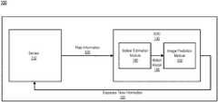
- FIG. 1is a diagram of a system environment in which a photo sensor and a system on a chip (SOC) operate, according to one embodiment.
- SOCsystem on a chip
- FIG. 2is a view illustrating photo sensor architecture, according to one embodiment.
- FIG. 3is a diagram illustrating a digital pixel array of FIG. 2 , according to one embodiment.
- FIG. 4is a cross-sectional view illustrating a photo sensor in a stacked assembly, according to one embodiment.
- FIG. 5is a diagram illustrating the digital pixel array of FIG. 3 and its associated block circuits, according to one embodiment.
- FIG. 6is a diagram illustrating the exposure time of a brighter pixel block and the exposure time of a darker pixel block, according to one embodiment.
- FIG. 7is a flowchart illustrating a method of exposure time variation using prediction, according to one embodiment.
- Embodimentsrelate to a photo sensor array divided up into multiple blocks that are operated with different exposure times.
- a prediction algorithmis used to predict the overall light brightness of each block and determine the exposure time of each block.
- Each blockmay also include memory to store the exposure time for the pixels in the block as well as analog-to-digital resolution for the block.
- FIG. 1is a diagram of a system environment 100 in which a sensor 110 and a system on a chip (SOC) 130 operate, according to one embodiment.
- the sensor 110is a circuit that measures intensity of light impinging on its photo sensor on a pixel-by-pixel basis using photoconversion. Measuring light intensity may involve detecting light by a photodiode in a pixel. In response, the pixel performs photoconversion on the detected light into a voltage or current signal. The voltage or current signal representing the intensity of light detected at each pixel may be digitized into pixel information 120 , and sent over to the SOC 130 .
- the sensor 110 and the SOC 130communicate bi-directionally via an interface circuit that provides communication path for the pixel information 120 and the exposure time information 160 .
- the interface circuitincludes an inter-integrated circuit (I2C) interface circuit for receiving pixel information 120 from the sensor 110 , and a Mobile Industry Processor Interface (MIPI) circuit for sending the pixel information 120 from the sensor 110 to the SOC 130 .
- I2C and MIPIare described below with reference to FIG. 2 in detail.
- the pixel information 120includes one or more prior frames provided to the SOC 130 for processing. In some embodiments, the pixel information 120 is streamed for different cycles of the sensor operation where a different frame information is sent over each cycle. Operation of the sensor 110 and its architecture are described below with reference to FIGS. 2 and 4 in detail.
- the SOC 130estimates brightness of pixels or a set of pixels for a current frame based on the pixel information 120 of prior frames.
- the SOC 130includes, among other components, a motion estimation module 140 and an image prediction module 150 .
- the motion estimation module 140uses a predictive algorithm on the one or more prior frames of the pixel information 120 to predict the next frame.
- the motion estimation modulecould also use information from a motion sensing device (e.g., IMU device).
- the predictive algorithmis a motion estimation or motion compensation based algorithm.
- Motion estimationis the process of describing motions between adjacent frames using motion vectors 145 .
- Motion vectors 145 determined by the motion estimation module 140are provided as an input to the image prediction module 150 .
- the image prediction module 150is a circuit, software, firmware or a combination thereof that predicts a highest light intensity and a lowest light intensity captured by the pixels in each block. In some embodiments, the image prediction module 150 further generates an exposure start time and an exposure stop time based on the predicted highest light intensity and the lowest light intensity of pixels in each block. The exposure start time and the exposure stop time are used for controlling the exposure time for a block of pixels. The highest light intensity and the lowest light intensity are used for dynamic resolution change of a block analog-to-digital converter (ADC).
- the exposure time information 160includes at least one of: the highest light intensity of pixels in each block, the lowest light intensity of pixels in each block, the exposure start time of a block of pixels, the exposure stop time of a block of pixels, or some combination thereof.
- FIG. 2is a view illustrating the photo sensor architecture, according to one embodiment.
- the sensor 110includes, among other components, a digital block 202 , a global counter 203 , a row drivers and global signal drivers module 204 , I2C 205 , counter buffers 206 , a digital pixel array 207 , sense amplifiers 208 , a line memory 209 , a power conditioner 210 , a ramp generation and buffers module 211 , a sense amplification biasing module 212 , and MIPI 213 .
- the digital block 202is a circuit that processes digital signals associated with the operation of the sensor 110 .
- at least part of the digital block 202may be provided as part of the digital pixel array 207 instead of being a circuit separate from the digital pixel array 207 .
- the global counter 203is a digital sequential logic circuit constructed of cascading flip-flops, and provides counter signals to various components of the sensor 110 .
- the row drivers and global signal drivers module 204is a circuit that provides signals to rows of pixels via scan lines (not shown).
- the signal provided to each row of pixelsindicates sensing of image signal and/or resetting operations at each row of pixels.
- I2C 205is a serial interface for transmitting the exposure time information 160 from the SOC 130 to the sensor 110 .
- An interface circuitcommunicates bi-directionally with the SOC 130 , as described above with reference to FIG. 1 .
- the interface circuitincludes the MIPI 213 .
- An MIPI interfacetypically has a single clock lane and two data lanes (not shown) that carry serial data. These three lanes carry signals on pairs of wires where the signals are often differential.
- the MIPI 213has four data lanes for carrying pixel data.
- the counter buffers 206is a circuit that receives counter signals from the global counter 203 , and sends signals to columns of pixels in the digital pixel array 207 to coordinate sensing and resetting operations.
- the digital pixel array 207includes a plurality of pixels.
- the digital pixel arrayis arranged in two dimensions, addressable by row and column.
- Each pixelis senses light and outputs a signal corresponding to the intensity of the input light.
- Each pixelmay include components as described below with reference to FIG. 3 .
- the line memory 209temporarily stores the sensed digital values of the light intensity detected at the digital pixel array 207 , as sensed by the sense amplifiers 208 and processed by digital block 202 before sending the digital values to the SOC 130 via MIPI 213 as the pixel information 120 .
- the power conditioner 210is a circuit that improves the quality of the power that is delivered to components of the sensor 110 .
- the power conditioner 210may maintain and deliver a constant voltage that allows the components of the sensor 110 to function properly.
- the power conditioner 210is a power line conditioner which takes in power and modifies it based on the requirements of the components connected to the power line conditioner.
- the ramp generator and buffers module 211comprises a ramp generator and buffers.
- the ramp generatoris a function generator that increases its voltage to a particular value.
- the ramp generatormay be used to avoid jolts when changing a load.
- the buffersprovide electrical impedance transformation from one circuit to another to prevent the ramp generator from being affected by the load.
- the sense amplification biasing module 212provides biasing voltage signal to the sense amplifiers 208 .
- the biasing voltage signalis a predetermined voltage for the purpose of establishing proper operating conditions of the sense amplifiers 208 such as a steady DC voltage.
- the I2C 205is a serial interface for transmitting the sensor configuration information between the sensor 110 and the SOC 130 .
- An interface circuitcommunicates bi-directionally with the SOC 130 , as described above with reference to FIG. 1 .
- the interface circuitincludes the MIPI 213 .
- FIG. 3is a diagram illustrating the digital pixel array 207 of FIG. 2 , according to one embodiment.
- the digital pixel array 207includes a plurality of pixels 320 arranged in a number of rows and columns. In the embodiment of FIG. 3 , the digital pixel array 207 has eight rows and eight columns, or 64 total pixels.
- each pixel block 310contains one or more pixels 320 .
- each pixel block 310contains four rows and four columns, or 16 total pixels, and four pixel blocks 310 (not shown in FIG. 3 ) comprise the entire digital pixel array 207 .
- the pixel blocks 310contain the same number of pixels 320 .
- the pixel blocks 310contain a different number of pixels 320 .
- the exposure start time and the exposure stop time of the exposure time information 160are used to control the exposure time for a pixel block 310 .
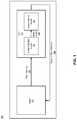
- FIG. 4is a cross-sectional view illustrating a photo sensor in a stacked assembly 400 , according to one embodiment.
- the stacked assembly 400includes a first substrate 410 coupled to a second substrate 440 .
- the first substrate 410may be a back-side illumination 402 sensor that is flipped over and includes, among other components, a first n+ diffusion well 412 , a photodiode 414 , a transistor AB 413 , a transistor TX 416 , and a second n+ diffusion well 420 .
- Each of transistor AB 413 and transistor TX 416includes an active layer, a drain electrode coupled to the active layer, a photodiode 414 that serves as a source of both transistor AB and transistor TX, an insulation layer over the active layer, and a gate electrode (not shown).
- the transistors AB 413 and the transistor TX 416can be turned on or off.
- the gates of these transistorsreceive signals from circuits external to the digital pixel array 207 .
- the first n+ diffusion well 412is an N doped implant region formed in the first substrate 410 .
- the first n+ diffusion well 412receives photoelectrons that are transferred from the photodiode 414 when transistor AB 413 is turned on during non-exposure times. This is equivalent to a closed shutter mode in a traditional film camera.
- the transfer of photoelectrons from the photodiode 414 to the first n+ diffusion well 412ensures that no photoelectrons are accumulated on the photodiode 414 , as the non-exposure times are periods when no signal is generated.
- the first n+ diffusion well 412is typically connected to a positive voltage source, for example VDD, so the photoelectrons are drained away.
- both transistor AB 413 and transistor TX 416are turned off and the photoelectrons are initially stored inside the photodiode 414 .
- transistor TX 416is turned on. As a result, the charge stored in the photodiode 414 is transferred to the second n+ diffusion well 420 .
- the photodiode 414is a semiconductor device that converts light into an electric current. Current is generated when photons are absorbed in the photodiode 414 .
- the photodiode 414may be a p-n junction or PIN structure. When the intensity of light through back-side illumination 402 is higher, the amount of charge accumulated on the photodiode 414 is high. Similarly, when the intensity of light through back-side illumination 402 is lower, the amount of charge accumulated on the photodiode 414 is low.
- the interconnect 450 Amay be a pixel level direct interconnect from the second n+ diffusion well 420 to a pixel circuit 442 in the second substrate 440 .
- the interconnect 450 Atransmits a voltage signal that reflects the amount of charge transferred from the photodiode 414 to the second n+ diffusion well 420 .
- the interconnect 450 Atransmits a current signal that reflects the amount of charge transferred from the photodiode 414 to the second n+ diffusion well 420 .
- the interconnect 450 Acarries the voltage signal to the pixel circuit 442 for further processing such as sampling and analog-to-digital conversion.
- the pixel circuit 442is described below with reference to FIG. 5 .
- the interconnects 450 B, 450 Ctransmit signals from the pixel circuit 442 of the second substrate 440 to the circuit of the first substrate 410 .
- the signalsare timing signals of the exposure time information 160 of FIG. 1 .
- the interconnect 450 Breceives a first timing signal that turns on or off a first transistor (e.g., transistor AB), and the interconnect 450 C receives a second timing signal that turns on or off a second transistor (e.g., transistor TX).
- Embodimentsmove various circuit components provided on the first substrate 410 in conventional photo sensors to the second substrate 440 , and connect the circuits of the second substrate 440 to the components in the first substrate 410 via the pixel level interconnect 450 .
- the various circuit components moved to the second substrate 440may include, among others, switches, amplifiers and current source. In this way, the area occupied by components in the first substrate 410 can be beneficially reduced so further components, such as a block ADC and a block memory as described below, can be added without impacting the fill factor.
- FIG. 5is a diagram illustrating the digital pixel array of FIG. 3 and its associated block circuits 500 , according to one embodiment.
- the photo sensorincludes an array of digital pixels 320 and a plurality of block circuits 500 .
- Each block circuit 500is provided for each pixel block 310 and includes, among other components, a plurality of pixel circuits 442 , a block ADC 508 , and a block memory 510 .
- the digital pixel arrayincludes pixels divided into a plurality of blocks 310
- the pixels 320include photodiodes and transistors controlling an exposure duration of the photodiodes for a current frame based on motion prediction.
- the block memory 510is a circuit that receives and stores exposure time information 160 for each block indicating an exposure duration for pixels in each block in the current frame.
- the exposure time information 160is generated by performing motion prediction on prior frames captured by the pixels before capturing the current frame, as described above with reference to FIG. 1 .
- the block analog-to-digital converter (ADC) 508 circuitconverts pixel signals from each block of pixels to digital pixel information.
- the quantization parameter of each of the block ADC 508 circuitis set according to the predicted light intensity information for each block.
- the quantization parametermay indicate, for example, the dynamic range of quantization at the ADC 508 . That is, the quantization parameter may indicate how the bits should be assigned to different ranges of pixel voltage based on the predicted light intensity information for each block. If the pixel voltage is likely to be low across the pixels in the block, then more bits can be assigned to low pixel voltage range. If the pixel voltage is likely to be high across the pixels in the block, then more bits can be assigned to high pixel voltage range. If the dynamic range of pixel values are likely to large, then the bits can be assigned relatively uniform across a low pixel voltage and a high pixel voltage.
- the quantization parametermay indicate resolution of the quantization for the ADC 508 .
- the resolution of the ADC 508may be increased for a block where the highest light intensity and the lowest light intensity of pixels in the block vary significantly, while the resolution of the ADC 508 may be decreased for a block where the light intensity is substantially consistent across the pixels in the block.
- Each of the block ADC 508 circuitmay be a single-sloped ADC with a slope of a reference voltage in the single-sloped ADC adjusted as the quantization parameter.
- the block ADC 508 circuitis a low-resolution ADC (e.g., 1-3 bits). It is advantageous to dynamically change the resolution of the block ADC 508 , among other reasons, because the overall bandwidth for sending the pixel information 120 can be reduced.
- each ADCchanges its dynamic range or resolution per each block or the subset of the pixel blocks.
- FIG. 6is a diagram illustrating the exposure time of a brighter pixel block and the exposure time of a darker pixel block, according to one embodiment. A higher intensity of light is incident on a brighter pixel block than a darker pixel block.
- the top diagramillustrates the exposure time of a brighter pixel block and the bottom diagram illustrates the exposure time of a darker pixel block.
- the intersection between the left arrow and the horizontal time axisrepresents the time at which the first timing signal is received via the interconnect 450 B (i.e., the exposure start time).
- Transistor ABis turned off responsive to receiving the first timing signal.
- Transistor ABis off for exposure period T EXPOSURE , which allows charge to accumulate in the photodiode.
- the intersection between the right arrow and the horizontal time axisrepresents the time at which the second timing signal is received via the interconnect 450 C (i.e., the exposure stop time).
- transistor TXis turned on responsive to receiving the second timing signal.
- the charge stored in the photodiodeis transferred to the second n+ diffusion well, as described above with reference to FIG. 4 .
- the intersection between the right arrow and the horizontal time axisrepresents a time at which the first timing signal is received via the interconnect 450 B (i.e., the exposure start time).
- the exposure period T EXPOSURE ′ of the darker pixel blockis longer than the exposure period T EXPOSURE of the brighter pixel block.
- Photo sensors in different lighting conditionsrequire longer or shorter exposure periods. Exposure time variation using prediction helps reduce over-exposure and under-exposure for some of the photo sensors, thereby providing correctly exposed images.
- center exposure timei.e., a middle point time between the exposure start time and the exposure end time
- line 604it is generally advantageous to align the center exposure time (i.e., a middle point time between the exposure start time and the exposure end time) represented by line 604 across all pixels when a global shutter mode is used or pixels in the same row when a rolling shutter is used. By doing so, motion artifacts in the captured image due to differing exposure start times and exposure end times of blocks can be reduced.
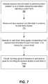
- FIG. 7is a flowchart illustrating a method of exposure time variation using prediction, according to one embodiment.
- a system on chip (SOC) including a motion estimation module and an image prediction modulegenerates 700 exposure time information by performing motion prediction on prior frames captured by pixels before capturing a current frame.
- SOCsystem on chip
- a block circuit associated with a block of pixelsreceives and stores 710 exposure time information in a block memory for each block of pixels.
- the exposure time informationincludes predicted light intensity information of the current frame for each block indicating a highest light intensity and a lowest light intensity predicted from pixels in each block.
- the exposure time informationalso includes an exposure start time and an exposure end time.
- the exposure time informationis provided to the sensor via a MIPI interface circuit with four data lanes.
- a pixel circuitgenerates 720 , for each block, timing signals corresponding to the exposure time information for each block stored in the block memory.
- the timing signalsinclude a first timing signal that turns off a first transistor and a second timing signal that turns on a second transistor.
- the pixel circuitprovides 730 the timing signals to transistors in each block of pixels for controlling the exposure duration of each block of pixels.
- Providing the timing signalsincludes turning off a first transistor between a diffusion well and a photodiode in a pixel responsive to the first transistor receiving one of the timing signals, and turning on a second transistor between the photodiode and another diffusion well in the pixel responsive to the second transistor receiving another of the timing signals.
Landscapes
- Engineering & Computer Science (AREA)
- Multimedia (AREA)
- Signal Processing (AREA)
- Microelectronics & Electronic Packaging (AREA)
- Physics & Mathematics (AREA)
- Condensed Matter Physics & Semiconductors (AREA)
- General Physics & Mathematics (AREA)
- Computer Hardware Design (AREA)
- Power Engineering (AREA)
- Solid State Image Pick-Up Elements (AREA)
- Transforming Light Signals Into Electric Signals (AREA)
Abstract
Description
Claims (22)
Priority Applications (4)
| Application Number | Priority Date | Filing Date | Title |
|---|---|---|---|
| US15/983,391US10750097B2 (en) | 2017-08-14 | 2018-05-18 | Varying exposure time of pixels in photo sensor using motion prediction |
| PCT/US2018/045666WO2019036238A1 (en) | 2017-08-14 | 2018-08-07 | Varying exposure time of pixels in photo sensor using motion prediction |
| EP18188684.7AEP3445037B1 (en) | 2017-08-14 | 2018-08-13 | Varying exposure time of pixels in photo sensor using motion prediction |
| TW107128292ATW201911857A (en) | 2017-08-14 | 2018-08-14 | Photo sensor, electronic device including the photo sensor and a method for varying exposure time of pixels in photo sensor using motion prediction |
Applications Claiming Priority (2)
| Application Number | Priority Date | Filing Date | Title |
|---|---|---|---|
| US201762545356P | 2017-08-14 | 2017-08-14 | |
| US15/983,391US10750097B2 (en) | 2017-08-14 | 2018-05-18 | Varying exposure time of pixels in photo sensor using motion prediction |
Publications (2)
| Publication Number | Publication Date |
|---|---|
| US20190052788A1 US20190052788A1 (en) | 2019-02-14 |
| US10750097B2true US10750097B2 (en) | 2020-08-18 |
Family
ID=65275762
Family Applications (1)
| Application Number | Title | Priority Date | Filing Date |
|---|---|---|---|
| US15/983,391Active2038-06-05US10750097B2 (en) | 2017-08-14 | 2018-05-18 | Varying exposure time of pixels in photo sensor using motion prediction |
Country Status (3)
| Country | Link |
|---|---|
| US (1) | US10750097B2 (en) |
| TW (1) | TW201911857A (en) |
| WO (1) | WO2019036238A1 (en) |
Cited By (16)
| Publication number | Priority date | Publication date | Assignee | Title |
|---|---|---|---|---|
| US10931884B2 (en) | 2018-08-20 | 2021-02-23 | Facebook Technologies, Llc | Pixel sensor having adaptive exposure time |
| US11233085B2 (en) | 2018-05-09 | 2022-01-25 | Facebook Technologies, Llc | Multi-photo pixel cell having vertical gate structure |
| US11393867B2 (en) | 2017-12-06 | 2022-07-19 | Facebook Technologies, Llc | Multi-photodiode pixel cell |
| US11463636B2 (en) | 2018-06-27 | 2022-10-04 | Facebook Technologies, Llc | Pixel sensor having multiple photodiodes |
| US11595598B2 (en) | 2018-06-28 | 2023-02-28 | Meta Platforms Technologies, Llc | Global shutter image sensor |
| US11595602B2 (en) | 2018-11-05 | 2023-02-28 | Meta Platforms Technologies, Llc | Image sensor post processing |
| US11902685B1 (en) | 2020-04-28 | 2024-02-13 | Meta Platforms Technologies, Llc | Pixel sensor having hierarchical memory |
| US11910114B2 (en) | 2020-07-17 | 2024-02-20 | Meta Platforms Technologies, Llc | Multi-mode image sensor |
| US11910119B2 (en) | 2017-06-26 | 2024-02-20 | Meta Platforms Technologies, Llc | Digital pixel with extended dynamic range |
| US11906353B2 (en) | 2018-06-11 | 2024-02-20 | Meta Platforms Technologies, Llc | Digital pixel with extended dynamic range |
| US11927475B2 (en) | 2017-08-17 | 2024-03-12 | Meta Platforms Technologies, Llc | Detecting high intensity light in photo sensor |
| US11936998B1 (en) | 2019-10-17 | 2024-03-19 | Meta Platforms Technologies, Llc | Digital pixel sensor having extended dynamic range |
| US11943561B2 (en) | 2019-06-13 | 2024-03-26 | Meta Platforms Technologies, Llc | Non-linear quantization at pixel sensor |
| US11956560B2 (en) | 2020-10-09 | 2024-04-09 | Meta Platforms Technologies, Llc | Digital pixel sensor having reduced quantization operation |
| US11956413B2 (en) | 2018-08-27 | 2024-04-09 | Meta Platforms Technologies, Llc | Pixel sensor having multiple photodiodes and shared comparator |
| US12022218B2 (en) | 2020-12-29 | 2024-06-25 | Meta Platforms Technologies, Llc | Digital image sensor using a single-input comparator based quantizer |
Families Citing this family (19)
| Publication number | Priority date | Publication date | Assignee | Title |
|---|---|---|---|---|
| EP3439287B1 (en) | 2016-03-30 | 2022-01-26 | Nikon Corporation | Image pickup element and image pickup device |
| US10419701B2 (en) | 2017-06-26 | 2019-09-17 | Facebook Technologies, Llc | Digital pixel image sensor |
| US10917589B2 (en) | 2017-06-26 | 2021-02-09 | Facebook Technologies, Llc | Digital pixel with extended dynamic range |
| US10825854B2 (en)* | 2017-08-16 | 2020-11-03 | Facebook Technologies, Llc | Stacked photo sensor assembly with pixel level interconnect |
| US10608101B2 (en)* | 2017-08-16 | 2020-03-31 | Facebook Technologies, Llc | Detection circuit for photo sensor with stacked substrates |
| US10969273B2 (en) | 2018-03-19 | 2021-04-06 | Facebook Technologies, Llc | Analog-to-digital converter having programmable quantization resolution |
| US11004881B2 (en) | 2018-04-03 | 2021-05-11 | Facebook Technologies, Llc | Global shutter image sensor |
| US10903260B2 (en) | 2018-06-11 | 2021-01-26 | Facebook Technologies, Llc | Multi-photodiode pixel cell |
| US11089241B2 (en) | 2018-06-11 | 2021-08-10 | Facebook Technologies, Llc | Pixel cell with multiple photodiodes |
| US11089210B2 (en) | 2018-06-11 | 2021-08-10 | Facebook Technologies, Llc | Configurable image sensor |
| US10812730B2 (en)* | 2018-07-23 | 2020-10-20 | Samsung Electronics Co., Ltd. | Sensor auto-configuration |
| US11102430B2 (en) | 2018-12-10 | 2021-08-24 | Facebook Technologies, Llc | Pixel sensor having multiple photodiodes |
| JP7281897B2 (en)* | 2018-12-12 | 2023-05-26 | キヤノン株式会社 | IMAGING DEVICE, CONTROL METHOD AND PROGRAM THEREOF |
| US11218660B1 (en) | 2019-03-26 | 2022-01-04 | Facebook Technologies, Llc | Pixel sensor having shared readout structure |
| US11265480B2 (en)* | 2019-06-11 | 2022-03-01 | Qualcomm Incorporated | Systems and methods for controlling exposure settings based on motion characteristics associated with an image sensor |
| CN112308783B (en)* | 2019-07-24 | 2024-06-28 | 株式会社理光 | Rolling shutter effect correction method, device and computer readable storage medium |
| CN110702099B (en)* | 2019-10-31 | 2022-05-27 | 中国科学院长春光学精密机械与物理研究所 | High dynamic range fixed star detection imaging method and star sensor |
| JP7458819B2 (en)* | 2020-02-21 | 2024-04-01 | キヤノン株式会社 | Imaging device, control method, program and storage medium |
| CN111885316B (en)* | 2020-07-09 | 2022-07-29 | 深圳奥辰光电科技有限公司 | Image sensor pixel circuit, image sensor and depth camera |
Citations (10)
| Publication number | Priority date | Publication date | Assignee | Title |
|---|---|---|---|---|
| US20070092244A1 (en) | 2005-10-25 | 2007-04-26 | Shimon Pertsel | Camera exposure optimization techniques that take camera and scene motion into account |
| US20090002528A1 (en) | 2007-06-29 | 2009-01-01 | Sohei Manabe | High dynamic range sensor with blooming drain |
| US20090091645A1 (en) | 2007-10-03 | 2009-04-09 | Nokia Corporation | Multi-exposure pattern for enhancing dynamic range of images |
| US20090128640A1 (en) | 2006-02-20 | 2009-05-21 | Matsushita Electric Industrial Co., Ltd | Image device and lens barrel |
| EP2063630A1 (en) | 2007-11-26 | 2009-05-27 | Thomson Licensing | Video capture device with variable shutter integration time |
| US20110149116A1 (en)* | 2009-12-17 | 2011-06-23 | Wang-Hyun Kim | Imaging device and method for sharing memory among chips |
| US20120039548A1 (en)* | 2010-08-16 | 2012-02-16 | Hynix Semiconductor Inc. | Frame-wise calibration of column-parallel adcs for image sensor array applications |
| US20130293752A1 (en)* | 2012-05-02 | 2013-11-07 | Aptina Imaging Corporation | Exposure time selection using stacked-chip image sensors |
| WO2017058488A1 (en) | 2015-10-01 | 2017-04-06 | Qualcomm Incorporated | High dynamic range solid state image sensor and camera system |
| US20170366766A1 (en)* | 2016-06-16 | 2017-12-21 | Semiconductor Components Industries, Llc | Image sensors having high dynamic range functionalities |
- 2018
- 2018-05-18USUS15/983,391patent/US10750097B2/enactiveActive
- 2018-08-07WOPCT/US2018/045666patent/WO2019036238A1/ennot_activeCeased
- 2018-08-14TWTW107128292Apatent/TW201911857A/enunknown
Patent Citations (10)
| Publication number | Priority date | Publication date | Assignee | Title |
|---|---|---|---|---|
| US20070092244A1 (en) | 2005-10-25 | 2007-04-26 | Shimon Pertsel | Camera exposure optimization techniques that take camera and scene motion into account |
| US20090128640A1 (en) | 2006-02-20 | 2009-05-21 | Matsushita Electric Industrial Co., Ltd | Image device and lens barrel |
| US20090002528A1 (en) | 2007-06-29 | 2009-01-01 | Sohei Manabe | High dynamic range sensor with blooming drain |
| US20090091645A1 (en) | 2007-10-03 | 2009-04-09 | Nokia Corporation | Multi-exposure pattern for enhancing dynamic range of images |
| EP2063630A1 (en) | 2007-11-26 | 2009-05-27 | Thomson Licensing | Video capture device with variable shutter integration time |
| US20110149116A1 (en)* | 2009-12-17 | 2011-06-23 | Wang-Hyun Kim | Imaging device and method for sharing memory among chips |
| US20120039548A1 (en)* | 2010-08-16 | 2012-02-16 | Hynix Semiconductor Inc. | Frame-wise calibration of column-parallel adcs for image sensor array applications |
| US20130293752A1 (en)* | 2012-05-02 | 2013-11-07 | Aptina Imaging Corporation | Exposure time selection using stacked-chip image sensors |
| WO2017058488A1 (en) | 2015-10-01 | 2017-04-06 | Qualcomm Incorporated | High dynamic range solid state image sensor and camera system |
| US20170366766A1 (en)* | 2016-06-16 | 2017-12-21 | Semiconductor Components Industries, Llc | Image sensors having high dynamic range functionalities |
Non-Patent Citations (3)
| Title |
|---|
| European Patent Application No. 18188684.7, Office Action dated Nov. 26, 2019, 9 pages. |
| Extended European Search Report, European Application No. 18188684.7, dated Jan. 16, 2019, 10 pages. |
| PCT International Search Report and Written Opinion, PCT Application No. PCT/US2018/045666, dated Dec. 3, 2018, 15 pages. |
Cited By (18)
| Publication number | Priority date | Publication date | Assignee | Title |
|---|---|---|---|---|
| US11910119B2 (en) | 2017-06-26 | 2024-02-20 | Meta Platforms Technologies, Llc | Digital pixel with extended dynamic range |
| US11927475B2 (en) | 2017-08-17 | 2024-03-12 | Meta Platforms Technologies, Llc | Detecting high intensity light in photo sensor |
| US11393867B2 (en) | 2017-12-06 | 2022-07-19 | Facebook Technologies, Llc | Multi-photodiode pixel cell |
| US11233085B2 (en) | 2018-05-09 | 2022-01-25 | Facebook Technologies, Llc | Multi-photo pixel cell having vertical gate structure |
| US11906353B2 (en) | 2018-06-11 | 2024-02-20 | Meta Platforms Technologies, Llc | Digital pixel with extended dynamic range |
| US11463636B2 (en) | 2018-06-27 | 2022-10-04 | Facebook Technologies, Llc | Pixel sensor having multiple photodiodes |
| US11863886B2 (en) | 2018-06-27 | 2024-01-02 | Meta Platforms Technologies, Llc | Pixel sensor having multiple photodiodes |
| US11595598B2 (en) | 2018-06-28 | 2023-02-28 | Meta Platforms Technologies, Llc | Global shutter image sensor |
| US11974044B2 (en) | 2018-08-20 | 2024-04-30 | Meta Platforms Technologies, Llc | Pixel sensor having adaptive exposure time |
| US10931884B2 (en) | 2018-08-20 | 2021-02-23 | Facebook Technologies, Llc | Pixel sensor having adaptive exposure time |
| US11956413B2 (en) | 2018-08-27 | 2024-04-09 | Meta Platforms Technologies, Llc | Pixel sensor having multiple photodiodes and shared comparator |
| US11595602B2 (en) | 2018-11-05 | 2023-02-28 | Meta Platforms Technologies, Llc | Image sensor post processing |
| US11943561B2 (en) | 2019-06-13 | 2024-03-26 | Meta Platforms Technologies, Llc | Non-linear quantization at pixel sensor |
| US11936998B1 (en) | 2019-10-17 | 2024-03-19 | Meta Platforms Technologies, Llc | Digital pixel sensor having extended dynamic range |
| US11902685B1 (en) | 2020-04-28 | 2024-02-13 | Meta Platforms Technologies, Llc | Pixel sensor having hierarchical memory |
| US11910114B2 (en) | 2020-07-17 | 2024-02-20 | Meta Platforms Technologies, Llc | Multi-mode image sensor |
| US11956560B2 (en) | 2020-10-09 | 2024-04-09 | Meta Platforms Technologies, Llc | Digital pixel sensor having reduced quantization operation |
| US12022218B2 (en) | 2020-12-29 | 2024-06-25 | Meta Platforms Technologies, Llc | Digital image sensor using a single-input comparator based quantizer |
Also Published As
| Publication number | Publication date |
|---|---|
| US20190052788A1 (en) | 2019-02-14 |
| WO2019036238A1 (en) | 2019-02-21 |
| TW201911857A (en) | 2019-03-16 |
Similar Documents
| Publication | Publication Date | Title |
|---|---|---|
| US10750097B2 (en) | Varying exposure time of pixels in photo sensor using motion prediction | |
| US10825854B2 (en) | Stacked photo sensor assembly with pixel level interconnect | |
| US11927475B2 (en) | Detecting high intensity light in photo sensor | |
| US10608101B2 (en) | Detection circuit for photo sensor with stacked substrates | |
| US11165982B1 (en) | Spatial derivative pixel array with adaptive quantization | |
| CN108270981B (en) | Pixel unit, imaging method and imaging device thereof | |
| CN102843527B (en) | Solid state image pickup device, the method and electronic system for driving solid state image pickup device | |
| US9819889B2 (en) | Method and system to implement a stacked chip high dynamic range image sensor | |
| KR100769407B1 (en) | Charge pumps for cmos imagers | |
| US11317038B2 (en) | Pixel unit with a design for half row reading, an imaging apparatus including the same, and an imaging method thereof | |
| KR20140136445A (en) | Solid state imaging element, driving method of solid state imaging element, and electronic apparatus | |
| CN103595930A (en) | Solid-state imaging device, driving method, and electronic device | |
| US20240107195A1 (en) | Image sensor and image processing device including the same | |
| US20090237541A1 (en) | Method and apparatus providing reduced metal routing in imagers | |
| EP3445037B1 (en) | Varying exposure time of pixels in photo sensor using motion prediction | |
| US8031247B2 (en) | Method and apparatus providing an imager with a shared power supply and readout line for pixels | |
| CN110830737B (en) | Pixel device, comparison device, and CMOS image sensor using the same | |
| EP3445039B1 (en) | Detection circuit for photo sensor with stacked substrates | |
| EP3445038A1 (en) | Stacked photo sensor assembly with pixel level interconnect | |
| CN110557587A (en) | Image sensor and method of operating the same | |
| EP3445040B1 (en) | Detecting high intensity light in photo sensor | |
| KR100771117B1 (en) | Image sensor and its control method | |
| WO2023080180A1 (en) | Imaging element and imaging device |
Legal Events
| Date | Code | Title | Description |
|---|---|---|---|
| FEPP | Fee payment procedure | Free format text:ENTITY STATUS SET TO UNDISCOUNTED (ORIGINAL EVENT CODE: BIG.); ENTITY STATUS OF PATENT OWNER: LARGE ENTITY | |
| AS | Assignment | Owner name:OCULUS VR, LLC, CALIFORNIA Free format text:ASSIGNMENT OF ASSIGNORS INTEREST;ASSIGNOR:LIU, XINQIAO;REEL/FRAME:045865/0617 Effective date:20180518 | |
| STPP | Information on status: patent application and granting procedure in general | Free format text:DOCKETED NEW CASE - READY FOR EXAMINATION | |
| AS | Assignment | Owner name:FACEBOOK TECHNOLOGIES, LLC, CALIFORNIA Free format text:CHANGE OF NAME;ASSIGNOR:OCULUS VR, LLC;REEL/FRAME:047178/0616 Effective date:20180903 | |
| STPP | Information on status: patent application and granting procedure in general | Free format text:NON FINAL ACTION MAILED | |
| STPP | Information on status: patent application and granting procedure in general | Free format text:NOTICE OF ALLOWANCE MAILED -- APPLICATION RECEIVED IN OFFICE OF PUBLICATIONS | |
| STPP | Information on status: patent application and granting procedure in general | Free format text:PUBLICATIONS -- ISSUE FEE PAYMENT VERIFIED | |
| STCF | Information on status: patent grant | Free format text:PATENTED CASE | |
| AS | Assignment | Owner name:META PLATFORMS TECHNOLOGIES, LLC, CALIFORNIA Free format text:CHANGE OF NAME;ASSIGNOR:FACEBOOK TECHNOLOGIES, LLC;REEL/FRAME:060990/0518 Effective date:20220318 | |
| MAFP | Maintenance fee payment | Free format text:PAYMENT OF MAINTENANCE FEE, 4TH YEAR, LARGE ENTITY (ORIGINAL EVENT CODE: M1551); ENTITY STATUS OF PATENT OWNER: LARGE ENTITY Year of fee payment:4 |