US10749033B2 - Semiconductor device and method for manufacturing semiconductor device - Google Patents
Semiconductor device and method for manufacturing semiconductor deviceDownload PDFInfo
- Publication number
- US10749033B2 US10749033B2US14/172,072US201414172072AUS10749033B2US 10749033 B2US10749033 B2US 10749033B2US 201414172072 AUS201414172072 AUS 201414172072AUS 10749033 B2US10749033 B2US 10749033B2
- Authority
- US
- United States
- Prior art keywords
- transistor
- insulating layer
- oxide semiconductor
- layer
- electrode
- Prior art date
- Legal status (The legal status is an assumption and is not a legal conclusion. Google has not performed a legal analysis and makes no representation as to the accuracy of the status listed.)
- Expired - Fee Related, expires
Links
Images


Classifications
- H—ELECTRICITY
- H10—SEMICONDUCTOR DEVICES; ELECTRIC SOLID-STATE DEVICES NOT OTHERWISE PROVIDED FOR
- H10D—INORGANIC ELECTRIC SEMICONDUCTOR DEVICES
- H10D30/00—Field-effect transistors [FET]
- H10D30/60—Insulated-gate field-effect transistors [IGFET]
- H10D30/67—Thin-film transistors [TFT]
- H10D30/674—Thin-film transistors [TFT] characterised by the active materials
- H10D30/6755—Oxide semiconductors, e.g. zinc oxide, copper aluminium oxide or cadmium stannate
- H01L29/78618—
- H01L27/1225—
- H01L29/4908—
- H01L29/66969—
- H01L29/78636—
- H01L29/7869—
- H—ELECTRICITY
- H10—SEMICONDUCTOR DEVICES; ELECTRIC SOLID-STATE DEVICES NOT OTHERWISE PROVIDED FOR
- H10D—INORGANIC ELECTRIC SEMICONDUCTOR DEVICES
- H10D30/00—Field-effect transistors [FET]
- H10D30/01—Manufacture or treatment
- H10D30/021—Manufacture or treatment of FETs having insulated gates [IGFET]
- H10D30/031—Manufacture or treatment of FETs having insulated gates [IGFET] of thin-film transistors [TFT]
- H—ELECTRICITY
- H10—SEMICONDUCTOR DEVICES; ELECTRIC SOLID-STATE DEVICES NOT OTHERWISE PROVIDED FOR
- H10D—INORGANIC ELECTRIC SEMICONDUCTOR DEVICES
- H10D30/00—Field-effect transistors [FET]
- H10D30/60—Insulated-gate field-effect transistors [IGFET]
- H10D30/67—Thin-film transistors [TFT]
- H10D30/6704—Thin-film transistors [TFT] having supplementary regions or layers in the thin films or in the insulated bulk substrates for controlling properties of the device
- H10D30/6713—Thin-film transistors [TFT] having supplementary regions or layers in the thin films or in the insulated bulk substrates for controlling properties of the device characterised by the properties of the source or drain regions, e.g. compositions or sectional shapes
- H—ELECTRICITY
- H10—SEMICONDUCTOR DEVICES; ELECTRIC SOLID-STATE DEVICES NOT OTHERWISE PROVIDED FOR
- H10D—INORGANIC ELECTRIC SEMICONDUCTOR DEVICES
- H10D30/00—Field-effect transistors [FET]
- H10D30/60—Insulated-gate field-effect transistors [IGFET]
- H10D30/67—Thin-film transistors [TFT]
- H10D30/6704—Thin-film transistors [TFT] having supplementary regions or layers in the thin films or in the insulated bulk substrates for controlling properties of the device
- H10D30/6725—Thin-film transistors [TFT] having supplementary regions or layers in the thin films or in the insulated bulk substrates for controlling properties of the device having supplementary regions or layers for improving the flatness of the device
- H—ELECTRICITY
- H10—SEMICONDUCTOR DEVICES; ELECTRIC SOLID-STATE DEVICES NOT OTHERWISE PROVIDED FOR
- H10D—INORGANIC ELECTRIC SEMICONDUCTOR DEVICES
- H10D30/00—Field-effect transistors [FET]
- H10D30/60—Insulated-gate field-effect transistors [IGFET]
- H10D30/67—Thin-film transistors [TFT]
- H10D30/6729—Thin-film transistors [TFT] characterised by the electrodes
- H10D30/6737—Thin-film transistors [TFT] characterised by the electrodes characterised by the electrode materials
- H10D30/6739—Conductor-insulator-semiconductor electrodes
- H—ELECTRICITY
- H10—SEMICONDUCTOR DEVICES; ELECTRIC SOLID-STATE DEVICES NOT OTHERWISE PROVIDED FOR
- H10D—INORGANIC ELECTRIC SEMICONDUCTOR DEVICES
- H10D30/00—Field-effect transistors [FET]
- H10D30/60—Insulated-gate field-effect transistors [IGFET]
- H10D30/67—Thin-film transistors [TFT]
- H10D30/6758—Thin-film transistors [TFT] characterised by the insulating substrates
- H—ELECTRICITY
- H10—SEMICONDUCTOR DEVICES; ELECTRIC SOLID-STATE DEVICES NOT OTHERWISE PROVIDED FOR
- H10D—INORGANIC ELECTRIC SEMICONDUCTOR DEVICES
- H10D86/00—Integrated devices formed in or on insulating or conducting substrates, e.g. formed in silicon-on-insulator [SOI] substrates or on stainless steel or glass substrates
- H10D86/40—Integrated devices formed in or on insulating or conducting substrates, e.g. formed in silicon-on-insulator [SOI] substrates or on stainless steel or glass substrates characterised by multiple TFTs
- H10D86/421—Integrated devices formed in or on insulating or conducting substrates, e.g. formed in silicon-on-insulator [SOI] substrates or on stainless steel or glass substrates characterised by multiple TFTs having a particular composition, shape or crystalline structure of the active layer
- H10D86/423—Integrated devices formed in or on insulating or conducting substrates, e.g. formed in silicon-on-insulator [SOI] substrates or on stainless steel or glass substrates characterised by multiple TFTs having a particular composition, shape or crystalline structure of the active layer comprising semiconductor materials not belonging to the Group IV, e.g. InGaZnO
- H—ELECTRICITY
- H10—SEMICONDUCTOR DEVICES; ELECTRIC SOLID-STATE DEVICES NOT OTHERWISE PROVIDED FOR
- H10D—INORGANIC ELECTRIC SEMICONDUCTOR DEVICES
- H10D86/00—Integrated devices formed in or on insulating or conducting substrates, e.g. formed in silicon-on-insulator [SOI] substrates or on stainless steel or glass substrates
- H10D86/40—Integrated devices formed in or on insulating or conducting substrates, e.g. formed in silicon-on-insulator [SOI] substrates or on stainless steel or glass substrates characterised by multiple TFTs
- H10D86/60—Integrated devices formed in or on insulating or conducting substrates, e.g. formed in silicon-on-insulator [SOI] substrates or on stainless steel or glass substrates characterised by multiple TFTs wherein the TFTs are in active matrices
- H—ELECTRICITY
- H10—SEMICONDUCTOR DEVICES; ELECTRIC SOLID-STATE DEVICES NOT OTHERWISE PROVIDED FOR
- H10D—INORGANIC ELECTRIC SEMICONDUCTOR DEVICES
- H10D99/00—Subject matter not provided for in other groups of this subclass
Definitions
- a technical field of the inventionrelates to a semiconductor device and a manufacturing method thereof.
- semiconductor devicesherein refer to general elements and devices which function by utilizing semiconductor characteristics.
- Indium oxideis a well-known material and is used as a material for transparent electrodes which are needed for liquid crystal display devices or the like.
- Some metal oxideshave semiconductor characteristics. Examples of such metal oxides having semiconductor characteristics include tungsten oxide, tin oxide, indium oxide, zinc oxide, and the like. A thin film transistor in which a channel formation region is formed using such a metal oxide has been already known (see, for example, Patent Documents 1 to 4, Non-Patent Document 1, and the like).
- metal oxidesinclude not only a single-component oxide but also a multi-component oxide.
- InGaO 3 (ZnO) m(m: natural number) having a homologous phase is known as a multi-component oxide semiconductor including In, Ga, and Zn (see, for example, Non-Patent Documents 2 to 4 and the like).
- an oxide semiconductor including such an In—Ga—Zn-based oxidecan also be applied to a channel formation region of a thin film transistor (see, for example, Patent Document 5, Non-Patent Documents 5 and 6, and the like).
- Patent Document 6a thin film transistor including an oxide semiconductor used for a channel layer with a thickness of about 10 nm or smaller is disclosed.
- Non-Patent Document 7a thin film transistor including an oxide semiconductor whose channel length is 2 ⁇ m to 100 ⁇ m is disclosed.
- a defect generated in the manufacturing processbecomes a major problem.
- the wiringhas a larger thickness than the semiconductor layer, which causes poor coverage with the semiconductor layer when the thickness of the semiconductor layer is reduced along with miniaturization.
- a break due to a step (disconnection), defective connection, or the likemay occur.
- the short-channel effectrefers to degradation of electrical characteristics which becomes obvious with miniaturization of a transistor (a reduction in channel length (L)).
- the short-channel effectresults from the effect of an electric field of a drain on a source.
- Specific examples of the short-channel effectare a decrease in threshold voltage, an increase in S value (subthreshold swing), an increase in leakage current, and the like.
- the short-channel effectis likely to occur in a transistor including an oxide semiconductor particularly because such a transistor cannot control threshold voltage by doping, unlike a transistor including silicon.
- An embodiment of the disclosed inventionis a semiconductor device including an insulating layer, a source electrode and a drain electrode embedded in the insulating layer, an oxide semiconductor layer in contact with a part of a surface of the insulating layer, a part of a surface of the source electrode, and a part of a surface of the drain electrode, a gate insulating layer covering the oxide semiconductor layer, and a gate electrode over the gate insulating layer.
- the part of the surface of the insulating layerwhich is in contact with the oxide semiconductor layer, has a root-mean-square (RMS) roughness of 1 nm or less.
- RMSroot-mean-square
- the root-mean-square (RMS) roughnessis obtained by three-dimensionally expanding the RMS roughness of a cross section curve so as to be able to apply it to the measurement surface.
- the RMS roughnessis represented by the square root of the mean value of the square of the deviation from the reference surface to the specific surface, and is obtained by the following formula.
- R ms1 S 0 ⁇ ⁇ Y 1 Y 2 ⁇ ⁇ X 1 X 2 ⁇ ⁇ F ⁇ ( X , Y ) - Z 0 ⁇ 2 ⁇ d ⁇ ⁇ X ⁇ ⁇ d ⁇ ⁇ Y [ Formula ⁇ ⁇ 1 ]
- the measurement surfaceis a surface which is shown by all the measurement data, and is represented by the following formula.
- ZF ( X,Y ) [Formula 2]
- the specific surfaceis a surface which is an object of roughness measurement, and is a rectangular region which is surrounded by four points represented by the coordinates (X 1 , Y 1 ), (X 1 , Y 2 ), (X 2 , Y 1 ), and (X 2 , Y 2 ).
- the area of the specific surface when the specific surface is flatideally is denoted by S 0 .
- S 0can be obtained by the following formula.
- S 0
- the reference surfacerefers to a surface parallel to an X-Y surface at the average height of the specific surface.
- Z 0the average value of the height of the specific surface
- Z 0the height of the reference surface
- the root-mean-square (RMS) roughnessis calculated in a region of 10 nm ⁇ 10 nm, preferably 100 nm ⁇ 100 nm, more preferably 1 ⁇ m ⁇ 1 ⁇ m from an AFM image obtained using an atomic force microscope (AFM).
- AFMatomic force microscope
- the first transistorincludes a first channel formation region, a first gate insulating layer provided over the first channel formation region, a first gate electrode provided over the first gate insulating layer so as to overlap with the first channel formation region, and a first source electrode and a first drain electrode electrically connected to the first channel formation region.
- the second transistorincludes a second source electrode and a second drain electrode embedded in an insulating layer, a second channel formation region in contact with a part of a surface of the insulating layer, a part of a surface of the second source electrode, and a part of a surface of the second drain electrode, a second gate insulating layer covering the second channel formation region, and a second gate electrode over the second gate insulating layer.
- the part of the surface of the insulating layerwhich is in contact with the second channel formation region, has a root-mean-square roughness of 1 nm or less.
- the difference in height between the part of the surface of the insulating layer and the surface of the second source electrode or the difference in height between the part of the surface of the insulating layer and the surface of the second drain electrodeis less than 5 nm.
- the oxide semiconductor layerpreferably has a flat cross-sectional shape. Namely, it is preferred that the whole of the upper surface of the oxide semiconductor layer is flat.
- Another embodimentis a method for manufacturing a semiconductor device, including the steps of: forming a source electrode and a drain electrode over a surface with a root-mean-square roughness of 1 nm or less; forming an insulating layer so as to cover the source electrode and the drain electrode; performing planarization treatment of a surface of the insulating layer, thereby forming a planarized insulating layer partly having a surface with a root-mean-square roughness of 1 nm or less and exposing the source electrode and the drain electrode; forming an oxide semiconductor layer in contact with the part of the surface of the planarized insulating layer, a part of the surface of the source electrode, and a part of the surface of the drain electrode; forming a gate insulating layer so as to cover the oxide semiconductor layer; and forming a gate electrode over the gate insulating layer.
- Another embodimentis a method for manufacturing a semiconductor device, including the steps of: forming a first transistor including a first channel formation region, a first gate insulating layer over the first channel formation region, a first gate electrode over the first gate insulating layer and the first channel formation region, and a first source electrode and a first drain electrode electrically connected to the first channel formation region; forming a first insulating layer having a surface with a root-mean-square roughness of 1 nm or less so as to cover the first transistor; forming a second source electrode and a second drain electrode over the surface of the first insulating layer; forming a second insulating layer so as to cover the second source electrode and the second drain electrode; performing planarization treatment of a surface of the second insulating layer, thereby forming a second insulating layer partly having a surface with a root-mean-square roughness of 1 nm or less and exposing the second source electrode and the second drain electrode; thinning the second source electrode and the second drain electrode so that the
- the channel length L of the second transistoris preferably less than 2 ⁇ m, further preferably, 10 nm to 350 nm (0.35 ⁇ m).
- the thickness of the oxide semiconductor layeris in the range of 1 nm to 50 nm, preferably, 2 nm to 20 nm, further preferably, 3 nm to 15 nm. With such a structure, a semiconductor device which operates at high speed and consumes less power can be achieved.
- a high dielectric constant materialsuch as hafnium oxide is used for the gate insulating layer.
- the relative permittivity of hafnium oxideis approximately 15, which is much higher than that of silicon oxide which is 3 to 4.
- a gate insulating layer where the equivalent oxide thickness is less than 15 nm, preferably 2 nm to 10 nm,can be easily formed.
- the semiconductor devicecan be easily miniaturized.
- the oxide semiconductor layeran intrinsic oxide semiconductor which is purified is used.
- the carrier density of the oxide semiconductor layercan be, for example, less than 1 ⁇ 10 12 /cm 3 or less than 1.45 ⁇ 10 10 /cm 3
- the off-state current of the transistorcan be 100 zA/ ⁇ m (1 zA (zeptoampere) is 1 ⁇ 10 ⁇ 21 A) or less, or 10 zA/ ⁇ m or less
- the S value of the transistorcan be 65 mV/dec or less or less than 63 mV/dec.
- the off-state current of the transistorcan be 1 ⁇ 10 ⁇ 24 A/ ⁇ m to 1 ⁇ 10 ⁇ 30 A/ ⁇ m in theory.
- the gate electrodemay be provided to overlap with the source electrode and the drain electrode, and alternatively, only an end portion of the gate electrode may be overlapped with an end portion of the source electrode and an end portion of the drain electrode.
- semiconductor devicesherein refer to general devices which function by utilizing semiconductor characteristics.
- a display devicea memory device, an integrated circuit, and the like are included in the category of the semiconductor device.
- a gate electrode over a gate insulating layerdoes not exclude the case where a component is placed between the gate insulating layer and the gate electrode.
- electrodeor “wiring” in this specification and the like does not limit a function of a component.
- an “electrode”can be used as part of a “wiring”, and the “wiring” can be used as part of the “electrode”.
- the term “electrode” or “wiring”can include the case where a plurality of “electrodes” or “wirings” is formed in an integrated manner.
- Source and drainFunctions of a “source” and a “drain” are sometimes interchanged with each other when a transistor of opposite polarity is used or when the direction of current flowing is changed in circuit operation, for example. Therefore, the terms “source” and “drain” can be used to denote the drain and the source, respectively, in this specification.
- an “electrically connected” in this specification and the likeincludes the case where components are connected through an “object having any electric function”.
- an object having any electric functionThere is no particular limitation on an object having any electric function as long as electric signals can be transmitted and received between components that are connected through the object.
- Examples of an “object having any electric function”are a switching element such as a transistor, a resistor, an inductor, a capacitor, and an element with a variety of functions, as well as an electrode and a wiring.
- a channel formation region of a transistoris provided over a highly flat region. This makes it possible to prevent a problem such as a short-channel effect even in a situation where the transistor is miniaturized and to provide the transistor with favorable characteristics.
- an oxide semiconductor layercan have a uniform thickness by improving the planarity of a surface where a transistor is formed, and the transistor can have improved characteristics. Furthermore, a decrease in coverage which may be caused by a large difference in height can be suppressed, and a break due to a step (a disconnection) or a defective connection of an oxide semiconductor layer can be prevented.
- FIG. 1is a cross-sectional view illustrating an example of a structure of a semiconductor device.
- FIGS. 2A to 2Fare cross-sectional views illustrating a manufacturing process of a semiconductor device.
- FIGS. 3A to 3Care a cross-sectional view, a plan view, and a circuit diagram illustrating an example of a structure of a semiconductor device.
- FIGS. 4A to 4Dare cross-sectional views illustrating a manufacturing process of a semiconductor device.
- FIGS. 5A to 5Care cross-sectional views illustrating a manufacturing process of a semiconductor device.
- FIGS. 6A-1, 6A-2, and 6Bare diagrams illustrating an example of application of a semiconductor device.
- FIGS. 7A and 7Bare diagrams illustrating an example of application of a semiconductor device.
- FIGS. 8A to 8Care diagrams illustrating an example of application of a semiconductor device.
- FIGS. 9A to 9Dare plan views and a circuit diagram of a semiconductor device.
- FIG. 10is a diagram illustrating an example of application of a semiconductor device.
- FIGS. 11A and 11Bare diagrams illustrating an example of application of a semiconductor device.
- FIGS. 12A to 12Fare diagrams each illustrating an electronic device including a semiconductor device.
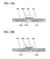
- FIGS. 13A and 13Bare diagrams each illustrating a model used for simulation.
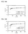
- FIGS. 14A and 14Bshow results of calculation of electrical characteristics of a transistor by simulation.
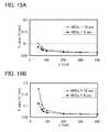
- FIGS. 15A and 15Bshow results of calculation of electrical characteristics of a transistor by simulation.
- FIG. 16shows results of calculation of electrical characteristics of a transistor by simulation.
- FIGS. 17A and 17Bshow results of calculation of electrical characteristics of a transistor by simulation.
- FIGS. 18A and 18Bshow results of calculation of electrical characteristics of a transistor by simulation.
- FIG. 19shows results of calculation of electrical characteristics of a transistor by simulation.
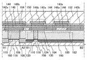
- FIG. 1a structure and a manufacturing method of a semiconductor device according to one embodiment of the disclosed invention will be described with reference to FIG. 1 and FIGS. 2A to 2F .
- FIG. 1illustrates an example of a structure of a semiconductor device.
- a transistor 162 in FIG. 1includes an insulating layer 143 a over a substrate 140 having a surface where components are formed, a source electrode 142 a and a drain electrode 142 b embedded in an insulating layer including the insulating layer 143 a , an oxide semiconductor layer 144 in contact with part of an upper surface of the insulating layer 143 a , an upper surface of the source electrode 142 a , and an upper surface of the drain electrode 142 b , a gate insulating layer 146 covering the oxide semiconductor layer 144 , and a gate electrode 148 a over the gate insulating layer 146 .
- the oxide semiconductor layer 144 used as a channel formation region of the transistor 162preferably has a flat cross-sectional shape. Therefore, the S value of the transistor can be 65 mV/dec or less or less than 63 mV/dec, for example.
- part of the upper surface of the insulating layer 143 a(particularly referring to a region parallel to the surface where components are formed), which is in contact with the oxide semiconductor layer 144 , has a root-mean-square (RMS) roughness of 1 nm or less.
- RMSroot-mean-square
- the difference in height between the part of the upper surface of the insulating layer 143 a and the upper surface of the source electrode 142 a or the difference in height between the part of the upper surface of the insulating layer 143 a and the upper surface of the drain electrode 142 bis less than 5 nm
- the upper surface of the insulating layer 143 a , the upper surface of the source electrode 142 a , and the upper surface of the drain electrode 142 bsubstantially exist coplanarly.
- a channel formation region of the transistor 162is provided over a highly flat region with a root-mean-square (RMS) roughness of 1 nm or less.
- RMSroot-mean-square
- the oxide semiconductor layer 144can have a uniform thickness by improving the planarity of the surface where the oxide semiconductor layer 144 is formed, and thus, the transistor 162 can have improved characteristics.
- the oxide semiconductor layer 144is preferably an oxide semiconductor layer which is purified by sufficiently removing an impurity such as hydrogen therefrom or by sufficiently supplying oxygen thereto.
- the hydrogen concentration of the oxide semiconductor layer 144is 5 ⁇ 10 19 atoms/cm 3 or less, preferably 5 ⁇ 10 18 atoms/cm 3 or less, more preferably 5 ⁇ 10 17 atoms/cm 3 or less, for example.
- SIMSsecondary ion mass spectrometry
- the density of carriers generated due to a donor such as hydrogen in the oxide semiconductor layer 144is less than 1 ⁇ 10 12 /cm 3 or less than 1 ⁇ 10 11 /cm 3 , or less than 1.45 ⁇ 10 10 /cm 3 .
- the off-state current (per unit channel width (1 ⁇ m), here) at room temperature (25° C.)is 100 zA (1 zA (zeptoampere) is 1 ⁇ 10 ⁇ 21 A) or less or 10 zA or less.
- Non-Patent Document 7a relatively large-size transistor whose channel length is 2 ⁇ m to 100 ⁇ m can be manufactured with use of an n-type oxide semiconductor having a high carrier density of 2 ⁇ 10 19 /cm 3 .
- the threshold voltagedrastically shifts negatively, and thus it is difficult to realize a normally-off transistor.
- the transistor which has a channel length of less than 2 ⁇ m and is manufactured using such a materialdoes not work in practice.
- an intrinsic or substantially intrinsic oxide semiconductor which is purifiedhas a carrier density of at most less than 1 ⁇ 10 14 /cm 3 , which does not cause a problem of normally on; thus, with use of such an intrinsic or substantially intrinsic oxide semiconductor, a transistor whose channel length is less than 2 ⁇ m can be easily realized.
- the source electrode 142 a and the drain electrode 142 bmay have a tapered shape.
- the taper anglecan be, for example, greater than or equal to 30° and less than or equal to 60°.
- the “taper angle”means an angle formed by the side surface and the bottom surface of a layer having a tapered shape (for example, the source electrode 142 a ) when observed from a direction perpendicular to a cross section thereof (a plane perpendicular to a surface of the substrate 140 ).
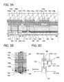
- FIGS. 2A to 2Fillustrate an example of a method for manufacturing the transistor 162 shown in FIG. 1 .
- FIGS. 2A to 2Fwill be described below.
- the source electrode 142 a and the drain electrode 142 bare formed over the substrate 140 having a surface where a transistor is formed (see FIG. 2A ).
- the substrate 140may be a glass substrate, a ceramic substrate, a quartz substrate, a sapphire substrate, or the like.
- the substratemay be a single crystal semiconductor substrate or a polycrystalline semiconductor substrate of silicon, silicon carbide, or the like, a compound semiconductor substrate of silicon germanium or the like, an SOI substrate, or the like as long as the substrate has an insulating surface.
- the substratemay be any of these substrates provided with a semiconductor element.
- the substrate 140may be provided with a base film.
- the preferred surface of the substrate 140is a sufficiently flat surface.
- the surface of the substrate 140preferably has a root-mean-square roughness (RMS) of 1 nm or less (preferably 0.5 nm or less).
- RMSroot-mean-square roughness
- the surface of the substrate 140has poor flatness, it is desirable that the surface be subjected to chemical mechanical polishing (CMP) treatment, etching treatment, or the like so as to have the above flatness.
- CMPchemical mechanical polishing
- the source electrode 142 a and the drain electrode 142 bcan be formed by forming a conductive layer over the substrate 140 and then selectively etching the conductive layer.
- the above conductive layercan be formed by a PVD method such as a sputtering method, or a CVD method such as a plasma CVD method.
- a material of the conductive layeran element selected from aluminum, chromium, copper, tantalum, titanium, molybdenum, and tungsten, an alloy including any of these elements as a component, or the like can be used.
- a material including one of manganese, magnesium, zirconium, beryllium, neodymium, or scandium or a combination of a plurality of these elementsmay be used.
- the conductive layermay have a single-layer structure or a stacked-layer structure including two or more layers.
- the conductive layermay have a single-layer structure of a titanium film or a titanium nitride film, a single-layer structure of an aluminum film including silicon, a two-layer structure in which a titanium film is stacked over an aluminum film, a two-layer structure in which a titanium film is stacked over a titanium nitride film, a three-layer structure in which a titanium film, an aluminum film, and a titanium film are stacked in this order, or the like.
- the conductive layer having a single-layer structure of a titanium film or a titanium nitride filmhas an advantage in that it can be easily processed into the source electrode 142 a and the drain electrode 142 b having a tapered shape.
- the conductive layermay be formed using a conductive metal oxide.
- a conductive metal oxideindium oxide (In 2 O 3 ), tin oxide (SnO 2 ), zinc oxide (ZnO), an indium oxide-tin oxide alloy (In 2 O 3 —SnO 2 , which is abbreviated to ITO in some cases), an indium oxide-zinc oxide alloy (In 2 O 3 —ZnO), or any of these metal oxide materials including silicon or silicon oxide can be used.
- dry etching or wet etchingmay be performed as the etching of the conductive layer, dry etching with high controllability is preferably used for miniaturization.
- the etchingmay be performed so that the source electrode 142 a and the drain electrode 142 b to be formed have a tapered shape.
- the taper anglecan be, for example, greater than or equal to 30° and less than or equal to 60°.
- the channel length (L) of the transistor 162is determined by a distance between upper edge portions of the source electrode 142 a and the drain electrode 142 b .
- light exposureis preferably performed with extreme ultraviolet light whose wavelength is several nanometers to several tens of nanometers, which is extremely short.
- the resolution of light exposure with extreme ultraviolet lightis high and the depth of focus is large.
- the channel length (L) of the transistor to be formed latercan be set to less than 2 ⁇ m, preferably in the range of 10 nm to 350 nm (0.35 ⁇ m), in which case the circuit can operate at higher speed.
- power consumption of the semiconductor devicecan be reduced by miniaturization.
- the insulating layer 143is formed so as to cover the source electrode 142 a and the drain electrode 142 b (see FIG. 2B ).
- the insulating layer 143can be formed using an inorganic insulating material such as silicon oxide, silicon oxynitride, silicon nitride, or aluminum oxide. It is particularly preferable that the insulating layer 143 be formed using silicon oxide because the oxide semiconductor layer 144 formed later is in contact with the insulating layer 143 .
- a method in which hydrogen is sufficiently reducedis preferably employed. Examples of such a method include a sputtering method and the like. Needless to say, another deposition method such as a plasma CVD method may be used.
- an insulating layer 143 ais formed by thinning the insulating layer 143 by chemical mechanical polishing (CMP) treatment (see FIG. 2C ).
- CMPchemical mechanical polishing
- the CMP treatmentis performed under such conditions that the surfaces of the source electrode 142 a and the drain electrode 142 b become exposed.
- the CMP treatmentis performed under such conditions that the root-mean-square (RMS) roughness of a surface of the insulating layer 143 a becomes 1 nm or less (preferably 0.5 nm or less).
- the CMP treatmentis a method for planarizing a surface of an object to be processed by a combination of chemical and mechanical actions. More specifically, the CMP treatment is a method in which a polishing cloth is attached to a polishing stage, the polishing stage and an object to be processed are each rotated or swung while a slurry (an abrasive) is supplied between the object to be processed and the polishing cloth, and the surface of the object to be processed is polished by a chemical reaction between the slurry and the surface of the object to be processed and by a mechanical polishing action of the polishing cloth on the object to be processed.
- a slurryan abrasive
- the CMP treatmentmay be performed only once or plural times.
- first polishingbe performed at a high polishing rate and final polishing be performed at a low polishing rate.
- the difference in height between the part of the upper surface of the insulating layer 143 a and the upper surface of the source electrode 142 a or the difference in height between the part of the upper surface of the insulating layer 143 a and the upper surface of the drain electrode 142 bcan be set to less than 5 nm.
- the oxide semiconductor layer 144 covering the above-described surfaceis formed in contact with part of the source electrode 142 a , the drain electrode 142 b , and the insulating layer 143 a ; then, the gate insulating layer 146 is formed so as to cover the oxide semiconductor layer 144 (see FIG. 2D ).
- the oxide semiconductor layer 144contains at least one element selected from In, Ga, Sn, and Zn.
- a four-component metal oxidesuch as an In—Sn—Ga—Zn—O-based oxide semiconductor, a three-component metal oxide such as an In—Ga—Zn—O-based oxide semiconductor, an In—Sn—Zn—O-based oxide semiconductor, an In—Al—Zn—O-based oxide semiconductor, a Sn—Ga—Zn—O-based oxide semiconductor, an Al—Ga—Zn—O-based oxide semiconductor, or a Sn—Al—Zn—O-based oxide semiconductor, a two-component metal oxide such as an In—Zn—O-based oxide semiconductor, a Sn—Zn—O-based oxide semiconductor, an Al—Zn—O-based oxide semiconductor, a Zn—Mg—O-based oxide semiconductor, a Sn—Mg—O-based oxide semiconductor, an In—Mg—O-based oxide semiconductor, or an In—Ga—
- an In—Ga—Zn—O-based oxide semiconductormeans an oxide film containing indium (In), gallium (Ga), and zinc (Zn), and there is no limitation on the composition ratio thereof.
- an In—Ga—Zn—O-based oxide semiconductor materialhas sufficiently high resistance when there is no electric field and thus off-state current can be sufficiently reduced.
- the In—Ga—Zn—O-based oxide semiconductor materialis suitable for a semiconductor material used in a semiconductor device.
- an oxide semiconductor material represented by InGaO 3 (ZnO), (m>0 and m is not an integer)is given.
- Mthere is an oxide semiconductor material represented by In MO 3 (ZnO) m (m>0 and m is not an integer).
- Mdenotes one or more metal elements selected from gallium (Ga), aluminum (Al), iron (Fe), nickel (Ni), manganese (Mn), cobalt (Co), or the like.
- Mmay be Ga, Ga and Al, Ga and Fe, Ga and Ni, Ga and Mn, Ga and Co, or the like. Note that the above-described compositions are derived from the crystal structures that the oxide semiconductor material can have, and are mere examples.
- the relation of Z>1.5X+Yis satisfied.
- the oxide semiconductor layer 144 having an amorphous structureis formed by a sputtering method with the use of an In—Ga—Zn—O-based metal oxide target.
- the thicknessranges from 1 nm to 50 nm, preferably from 2 nm to 20 nm, more preferably from 3 nm to 15 nm.
- the relative density of the metal oxide in the metal oxide targetis 80% or more, preferably 95% or more, and more preferably 99.9% or more.
- the use of the metal oxide target having high relative densitymakes it possible to form an oxide semiconductor layer having a dense structure.
- the atmosphere in which the oxide semiconductor layer 144 is formedis preferably a rare gas (typically, argon) atmosphere, an oxygen atmosphere, or a mixed atmosphere containing a rare gas (typically, argon) and oxygen.
- a high-purity gas atmospherefor example, from which an impurity such as hydrogen, water, a hydroxyl group, or hydride is removed to a concentration of 1 ppm or less (preferably, a concentration of 10 ppb or less).
- an object to be processedis held in a treatment chamber that is maintained under reduced pressure, and the object to be processed is heated to a temperature higher than or equal to 100° C. and lower than 550° C., preferably higher than or equal to 200° C. and lower than or equal to 400° C.
- the temperature of an object to be processed in forming the oxide semiconductor layer 144may be room temperature (25° C. ⁇ 10° C.). Then, moisture in the treatment chamber is removed, a sputtering gas from which hydrogen, water, or the like has been removed is introduced, and the above-described target is used; thus, the oxide semiconductor layer 144 is formed.
- an impurity in the oxide semiconductor layer 144can be reduced. Moreover, damage due to sputtering can be reduced.
- an entrapment vacuum pumpFor example, a cryopump, an ion pump, a titanium sublimation pump, or the like can be used.
- a turbo pump provided with a cold trapmay be used. Since hydrogen, water, or the like can be removed from the treatment chamber evacuated with a cryopump or the like, the concentration of an impurity in the oxide semiconductor layer can be reduced.
- conditions for forming the oxide semiconductor layer 144can be set as follows: the distance between the object to be processed and the target is 170 mm, the pressure is 0.4 Pa, the direct current (DC) power is 0.5 kW, and the atmosphere is an oxygen (100% oxygen) atmosphere, an argon (100% argon) atmosphere, or a mixed atmosphere of oxygen and argon.
- a pulsed direct current (DC) power sourceis preferably used because dust (powder or flake-like substances formed at the time of the film formation) can be reduced and the film thickness can be made uniform.
- the thickness of the oxide semiconductor layer 144is set in the range of 1 nm to 50 nm, preferably 2 nm to 20 nm, more preferably 3 nm to 15 nm.
- the oxide semiconductor layer 144By employing a structure according to the disclosed invention, a short-channel effect due to miniaturization can be suppressed even in the case of using the oxide semiconductor layer 144 having such a thickness.
- the appropriate thickness of the oxide semiconductor layerdiffers depending on the oxide semiconductor material used, the intended use of the semiconductor device, or the like; therefore, the thickness can be determined as appropriate in accordance with the material, the intended use, or the like.
- a surface where the oxide semiconductor layer 144 is formedis sufficiently planarized in one embodiment of the disclosed invention. Therefore, even an oxide semiconductor layer having a small thickness can be favorably formed.
- the oxide semiconductor layer 144preferably has a flat cross-sectional shape, as illustrated in FIG. 2D . In the case where the oxide semiconductor layer 144 has a flat cross-sectional shape, leakage current can be more reduced, as compared with the case where the oxide semiconductor layer 144 does not have a flat cross-sectional shape.
- the oxide semiconductor layer 144is formed by a sputtering method
- reverse sputteringin which plasma is generated with an argon gas introduced may be performed so that a material attached to a surface where the oxide semiconductor layer 144 is to be formed (e.g., a surface of the insulating layer 143 a ) is removed.
- the reverse sputteringis a method in which ions collide with a surface to be processed so that the surface is modified, in contrast to normal sputtering in which ions collide with a sputtering target.
- An example of a method for making ions collide with a surface to be processedis a method in which high-frequency voltage is applied to the surface side in an argon atmosphere so that plasma is generated near the object to be processed.
- an atmosphere of nitrogen, helium, oxygen, or the likemay be used instead of an argon atmosphere.
- heat treatmentis preferably performed on the oxide semiconductor layer 144 .
- first heat treatmentexcess hydrogen (including water or a hydroxyl group) in the oxide semiconductor layer 144 can be removed, the structure of the oxide semiconductor layer 144 can be ordered, and defect states in an energy gap can be reduced.
- the temperature of the first heat treatmentis set higher than or equal to 300° C. and lower than 550° C., or higher than or equal to 400° C. and lower than or equal to 500° C.
- the heat treatmentcan be performed at 450° C. for one hour in a nitrogen atmosphere.
- the oxide semiconductor layeris not exposed to the air during the heat treatment so that entry of water or hydrogen can be prevented.
- the heat treatment apparatusis not limited to the electric furnace and may be an apparatus for heating an object to be processed by thermal radiation or thermal conduction from a medium such as a heated gas.
- a rapid thermal annealing (RTA) apparatussuch as a gas rapid thermal annealing (GRTA) apparatus or a lamp rapid thermal annealing (LRTA) apparatus can be used.
- the GRTA apparatusis an apparatus for performing heat treatment using a high-temperature gas.
- the LRTA apparatusis an apparatus for heating an object to be processed by radiation of light (an electromagnetic wave) emitted from a lamp such as a halogen lamp, a metal halide lamp, a xenon arc lamp, a carbon arc lamp, a high pressure sodium lamp, or a high pressure mercury lamp.
- a lampsuch as a halogen lamp, a metal halide lamp, a xenon arc lamp, a carbon arc lamp, a high pressure sodium lamp, or a high pressure mercury lamp.
- an inert gasthat does not react with an object to be processed by heat treatment, for example, nitrogen or a rare gas such as argon, is used.
- heat treatment using the GRTA apparatusmay be performed as follows.
- the object to be processedis put in a heated inert gas atmosphere, heated for several minutes, and taken out of the inert gas atmosphere.
- the heat treatment using the GRTA apparatusenables high-temperature heat treatment in a short time.
- the GRTA treatmentcan be employed even when the temperature exceeds the upper temperature limit of the object to be processed.
- the inert gasmay be switched to a gas including oxygen during the treatment.
- defect states in an energy gap caused by oxygen vacanciescan be reduced by performing the first heat treatment in an atmosphere including oxygen.
- an atmosphere that contains nitrogen or a rare gas (e.g., helium, neon, or argon) as its main component and does not contain water, hydrogen, or the likeis preferably used.
- the purity of nitrogen or a rare gas such as helium, neon, or argon introduced into a heat treatment apparatusis set to 6N (99.9999%) or more, preferably 7N (99.99999%) or more (i.e., the impurity concentration is 1 ppm or less, preferably 0.1 ppm or less).
- a transistor with extremely excellent characteristicscan be obtained with the use of the oxide semiconductor layer which is an i-type (intrinsic) or substantially i-type oxide semiconductor layer obtained by reducing an impurity through the first heat treatment.
- the above heat treatment(the first heat treatment) can also be referred to as dehydration treatment, dehydrogenation treatment, or the like because it has the effect of removing hydrogen, water, or the like.
- the dehydration treatment or the dehydrogenation treatmentcan be performed after the gate insulating layer 146 is formed or after a gate electrode is formed. Such dehydration treatment or dehydrogenation treatment may be performed once or plural times.
- the oxide semiconductor layer 144may be processed into an island-shaped oxide semiconductor layer.
- the oxide semiconductor layer 144can be processed into an island-shaped oxide semiconductor layer by etching, for example.
- the etchingmay be performed either before the heat treatment or after the heat treatment. Dry etching is preferably used in terms of element miniaturization, but wet etching may be used.
- An etching gas or an etchantcan be selected as appropriate depending on a material to be etched.
- the gate insulating layer 146can be formed by a CVD method, a sputtering method, or the like.
- the gate insulating layer 146is preferably formed so as to contain silicon oxide, silicon nitride, silicon oxynitride, aluminum oxide, tantalum oxide, hafnium oxide, yttrium oxide, hafnium silicate (HfSi x O y (x>0, y>0)), hafnium silicate (HfSi x O y (x>0, y>0)) to which nitrogen is added, hafnium aluminate (HfAl x O y (x>0, y>0)) to which nitrogen is added, or the like.
- the gate insulating layer 146may have a single-layer structure or a stacked-layer structure. There is no particular limitation on the thickness of the gate insulating layer 146 ; the thickness is preferably small in order to ensure the operation of the transistor when the semiconductor device is miniaturized. For example, in the case of using silicon oxide, the thickness can be 1 nm to 100 nm, preferably 10 nm to 50 nm.
- the gate insulating layer 146may be formed using a high dielectric constant (high-k) material such as hafnium oxide, tantalum oxide, yttrium oxide, hafnium silicate (HfSi x O y (x>0, y>0)), hafnium silicate (HfSi x O y (x>0, y>0)) to which nitrogen is added, or hafnium aluminate (HfAl x O y (x>0, y>0)) to which nitrogen is added.
- high-khigh dielectric constant
- the use of a high-k material for the gate insulating layer 146makes it possible to increase the thickness in order to suppress gate leakage as well as ensuring electrical properties.
- the relative permittivity of hafnium oxideis approximately 15, which is much higher than that of silicon oxide which is 3 to 4.
- a gate insulating layer where the equivalent oxide thickness is less than 15 nm, preferably 2 nm to 10 nm,can be easily formed.
- a stacked-layer structure of a film including a high-k material and a film including any of silicon oxide, silicon nitride, silicon oxynitride, silicon nitride oxide, aluminum oxide, and the likemay also be employed.
- second heat treatmentis preferably performed in an inert gas atmosphere or an oxygen atmosphere.
- the temperature of the heat treatmentis set in the range of 200° C. to 450° C., preferably 250° C. to 350° C.
- the heat treatmentmay be performed at 250° C. for one hour in a nitrogen atmosphere.
- variation in electrical characteristics of the transistorcan be reduced.
- oxygencan be supplied to the oxide semiconductor layer 144 and oxygen vacancies in the oxide semiconductor layer 144 can be compensated; thus, the oxide semiconductor layer 144 which is i-type (intrinsic) or substantially i-type can also be formed.
- the second heat treatmentis performed in this embodiment after the gate insulating layer 146 is formed; there is no limitation on the timing of the second heat treatment.
- the second heat treatmentmay be performed after the gate electrode is formed.
- the first heat treatment and the second heat treatmentmay be performed in succession, or the first heat treatment may double as the second heat treatment, or the second heat treatment may double as the first heat treatment.
- the oxide semiconductor layer 144can be purified so as not to contain impurities other than main components as little as possible.
- the gate electrode 148 ais formed over the gate insulating layer 146 (see FIG. 2E ).
- the gate electrode 148 acan be formed by forming a conductive layer over the gate insulating layer 146 and then selectively etching the conductive layer.
- the conductive layer to be the gate electrode 148 acan be formed by a PVD method such as a sputtering method, or a CVD method such as a plasma CVD method.
- the detailsare similar to those in the case of the source electrode 142 a , the drain electrode 142 b , or the like; thus, the description thereof can be referred to. Note that although part of the gate electrode 148 a overlaps with the source electrode 142 a and the drain electrode 142 b in the structure employed here, the disclosed invention is not limited to this structure.
- an insulating layer 150 and an insulating layer 152are formed so as to cover the gate insulating layer 146 , the gate electrode 148 a , and the like (see FIG. 2F ).
- the insulating layer 150 and the insulating layer 152can be formed by a PVD method, a CVD method, or the like.
- the insulating layer 150 and the insulating layer 152can be formed using a material including an inorganic insulating material such as silicon oxide, silicon oxynitride, silicon nitride, hafnium oxide, or aluminum oxide.
- the insulating layer 150 and the insulating layer 152are preferably formed using a low dielectric constant material or a low dielectric constant structure (such as a porous structure). This is because when the insulating layer 150 and the insulating layer 152 have a low dielectric constant, capacitance generated between wirings, electrodes, or the like can be reduced and operation at higher speed can be achieved.
- a stacked-layer structure of the insulating layer 150 and the insulating layer 152is used in this embodiment, an embodiment of the disclosed invention is not limited to this example.
- a single-layer structure or a stacked-layer structure including three or more layerscan also be used.
- a structure in which the insulating layers are not providedis also possible.
- the insulating layer 152is desirably formed so as to have a flat surface. This is because when the insulating layer 152 has a flat surface, an electrode, a wiring, or the like can be favorably formed over the insulating layer 152 even in the case where the semiconductor device or the like is miniaturized. Note that the insulating layer 152 can be planarized using a method such as chemical mechanical polishing (CMP).
- CMPchemical mechanical polishing
- the transistor 162 including the oxide semiconductor layer 144 , which is purified,is completed (see FIG. 2F ).
- wirings, electrodes, or the likemay be formed after the above steps.
- the wirings or the electrodescan be formed by a method such as a so-called damascene method or dual damascene method.
- a channel formation region of the transistor 162is provided over a highly flat region with a root-mean-square (RMS) roughness of 1 nm or less (preferably 0.5 nm or less).
- RMSroot-mean-square
- the oxide semiconductor layer 144can have a uniform thickness by improving the planarity of the surface where the oxide semiconductor layer 144 is formed, and the transistor 162 can have improved characteristics. Furthermore, a decrease in coverage which may be caused by a large difference in height can be suppressed, and a break due to a step or a defective connection of the oxide semiconductor layer 144 can be prevented.
- the difference in height between the part of the upper surface of the insulating layer 143 a and the upper surface of the source electrode 142 a or the difference in height between the part of the upper surface of the insulating layer 143 a and the upper surface of the drain electrode 142 bis less than 5 nm as described above, leakage current can be reduced, and the transistor 162 with favorable characteristics can be provided.
- the oxide semiconductor layer 144is purified and thus contains hydrogen at a concentration of 5 ⁇ 10 19 atoms/cm 3 or less, 5 ⁇ 10 18 atoms/cm 3 or less, or 5 ⁇ 10 17 atoms/cm 3 or less.
- the density of carries generated due to a donor such as hydrogen in the oxide semiconductor layer 144is, for example, less than 1 ⁇ 10 12 /cm 3 or less than 1.45 ⁇ 10 10 /cm 3 , which is sufficiently lower than the carrier density of a general silicon wafer (approximately 1 ⁇ 10 14 /cm 3 ).
- the off-state current of the transistor 162is sufficiently small.
- the off-state current (per unit channel width (1 ⁇ m), here) of the transistor 162 at room temperature (25° C.)is 100 zA (1 zA (zeptoampere) is 1 ⁇ 10 ⁇ 21 A) or less, or 10 zA or less.
- the off-state current of the transistorcan be 1 ⁇ 10 ⁇ 24 A/ ⁇ m to 1 ⁇ 10 ⁇ 30 A/ ⁇ m in theory.
- the S value of the transistorcan be 65 mV/dec or less or less than 63 mV/dec.
- FIGS. 3A to 3Ca structure and a manufacturing method of a semiconductor device according to another embodiment of the disclosed invention will be described with reference to FIGS. 3A to 3C , FIGS. 4A to 4D , and FIGS. 5A to 5C .
- FIGS. 3A to 3Cillustrate an example of a structure of a semiconductor device.
- FIG. 3Ais a cross-sectional view of the semiconductor device;
- FIG. 3Bis a plan view of the semiconductor device;
- FIG. 3Cillustrates a circuit configuration of the semiconductor device.
- a structure of the semiconductor deviceis mainly described in this embodiment, and operation of the semiconductor device will be described in detail in an embodiment below.
- the semiconductor device illustrated in FIGS. 3A to 3Cis just an example having predetermined functions and does not represent all semiconductor devices according to the disclosed invention.
- the semiconductor device according to the disclosed inventioncan have another function by changing connection relationship of electrodes or the like as appropriate.
- FIG. 3Acorresponds to a cross-sectional view along line A 1 -A 2 and line B 1 -B 2 in FIG. 3B .
- the semiconductor device illustrated in FIGS. 3A and 3Bincludes the transistor 162 described in the above embodiment, a transistor 160 below the transistor 162 , and a capacitor 164 .
- a semiconductor material of the transistor 162 and a semiconductor material of the transistor 160are preferably different materials.
- the semiconductor material of the transistor 162may be an oxide semiconductor
- the semiconductor material of the transistor 160may be a semiconductor material (such as silicon) other than an oxide semiconductor.
- a transistor including an oxide semiconductorcan hold charge for a long time owing to its characteristics.
- a transistor including a material other than an oxide semiconductorcan operate at high speed easily.
- the transistor 160 in FIGS. 3A to 3Cincludes a channel formation region 116 provided in a substrate 100 including a semiconductor material (such as silicon), impurity regions 120 provided such that the channel formation region 116 is sandwiched therebetween, metal compound regions 124 in contact with the impurity regions 120 , a gate insulating layer 108 provided over the channel formation region 116 , and a gate electrode 110 provided over the gate insulating layer 108 .
- a transistor whose source electrode and drain electrode are not illustrated in a drawingmay also be referred to as a transistor for the sake of convenience.
- a source region and a source electrodemay be collectively referred to as a source electrode, and a drain region and a drain electrode may be collectively referred to as a drain electrode. That is, in this specification, the term “source electrode” may include a source region.
- an element isolation insulating layer 106is formed over the substrate 100 so as to surround the transistor 160 , and an insulating layer 130 is formed to cover the transistor 160 .
- the transistor 160preferably has a structure without a sidewall insulating layer as illustrated in FIGS. 3A and 3B .
- a sidewall insulating layermay be provided on a side surface of the gate electrode 110 , and the impurity regions 120 may include a region having a different impurity concentration.
- the structure of the transistor 162 in FIGS. 3A to 3Cis similar to the structure of the transistor 162 in the above embodiment. Note that in this embodiment, the source electrode 142 a (which may be the drain electrode) of the transistor 162 is connected to the gate electrode 110 of the transistor 160 .
- the capacitor 164 in FIGS. 3A to 3Cincludes the source electrode 142 a (which may be the drain electrode), the oxide semiconductor layer 144 , the gate insulating layer 146 , and an electrode 148 b .
- the source electrode 142 afunctions as one electrode of the capacitor 164
- the electrode 148 bfunctions as the other electrode of the capacitor 164 .
- the electrode 148 bis formed in a process similar to that of the gate electrode 148 a of the transistor 162 .
- the oxide semiconductor layer 144 and the gate insulating layer 146are stacked, whereby insulation between the source electrode 142 a and the electrode 148 b can be sufficiently secured. It is needless to say that the capacitor 164 without including the oxide semiconductor layer 144 may be employed in order to secure sufficient capacitance. In addition, in the case where no capacitor is needed, a structure in which the capacitor 164 is not provided is also possible.
- the transistor 162 and the capacitor 164are provided so as to overlap with the transistor 160 .
- the area occupied by the semiconductor devicecan be 15 F 2 to 25 F 2 .
- the structure of a semiconductor device according to the disclosed inventionis not limited to that illustrated in FIGS. 3A to 3C . Since the technical idea of the disclosed invention is to form a stacked-layer structure with an oxide semiconductor and a semiconductor material other than an oxide semiconductor, the details of connection relationship of electrodes or the like can be changed as appropriate.
- FIGS. 4A to 4D and FIGS. 5A to 5Ccorrespond to cross-sectional views along line A 1 -A 2 and line B 1 -B 2 of FIG. 3B .
- a method for manufacturing the transistor 162is similar to that in the above embodiment; thus, a method for manufacturing the transistor 160 will be mainly described here.
- the substrate 100 including a semiconductor materialis prepared (see FIG. 4A ).
- a single crystal semiconductor substrate or a polycrystalline semiconductor substrate of silicon, silicon carbide, or the like, a compound semiconductor substrate of silicon germanium or the like, an SOI substrate, or the likecan be used as the substrate 100 including a semiconductor material.
- SOI substrategenerally means a substrate where a silicon layer is provided over an insulating surface.
- SOI substratealso means a substrate where a semiconductor layer including a material other than silicon is provided over an insulating surface.
- a semiconductor layer included in the “SOI substrate”is not limited to a silicon layer.
- the SOI substratecan be a substrate having a structure where a semiconductor layer is provided over an insulating substrate such as a glass substrate with an insulating layer interposed therebetween.
- a single crystal semiconductor substrate of silicon or the likebe particularly used as the substrate 100 including a semiconductor material because the speed of reading operation of the semiconductor device can be increased.
- an impurity elementmay be added to a region which later functions as the channel formation region 116 of the transistor 160 , in order to control the threshold voltage of the transistor.
- an impurity element imparting conductivityis added so that the threshold voltage of the transistor 160 becomes positive.
- the impurity imparting conductivitymay be boron, aluminum, gallium, or the like. Note that it is preferable to perform heat treatment after adding an impurity element, in order to activate the impurity element or reduce defects which may be generated during addition of the impurity element.
- a protective layer 102 serving as a mask for forming an element isolation insulating layeris formed over the substrate 100 (see FIG. 4A ).
- an insulating layer formed using a material such as silicon oxide, silicon nitride, silicon oxynitride, or the likecan be used, for example.
- part of the substrate 100 in a region not covered with the protective layer 102is removed by etching using the protective layer 102 as a mask.
- a semiconductor region 104 isolated from other semiconductor regionsis formed (see FIG. 4B ).
- the etchingdry etching is preferably performed, but wet etching may be performed.
- An etching gas or an etchantcan be selected as appropriate depending on a material to be etched.
- an insulating layeris formed so as to cover the semiconductor region 104 , and the insulating layer in a region overlapping with the semiconductor region 104 is selectively removed; thus, the element isolation insulating layer 106 is formed (see FIG. 4C ).
- the insulating layeris formed using silicon oxide, silicon nitride, silicon oxynitride, or the like.
- any of etching treatment, polishing treatment such as chemical mechanical polishing (CMP) treatment, and the likecan be employed.
- CMPchemical mechanical polishing
- an insulating layeris formed over a surface of the semiconductor region 104 , and a layer including a conductive material is formed over the insulating layer.
- the insulating layeris processed into a gate insulating layer later and can be formed by heat treatment (thermal oxidation treatment, thermal nitridation treatment, or the like) of the surface of the semiconductor region 104 , for example.
- heat treatmentthermal oxidation treatment, thermal nitridation treatment, or the like
- high-density plasma treatmentmay be employed.
- the high-density plasma treatmentcan be performed using, for example, a mixed gas of any of a rare gas such as He, Ar, Kr, or Xe, oxygen, nitrogen oxide, ammonia, nitrogen, hydrogen, and the like. It is needless to say that the insulating layer may be formed by a CVD method, a sputtering method, or the like.
- the insulating layerpreferably has a single-layer structure or a stacked-layer structure with a film including silicon oxide, silicon oxynitride, silicon nitride, hafnium oxide, aluminum oxide, tantalum oxide, yttrium oxide, hafnium silicate (HfSi x O y (x>0, y>0)), hafnium silicate (HfSi x O y (x>0, y>0)) to which nitrogen is added, hafnium aluminate (HfAl x O y (x>0, y>0)) to which nitrogen is added, or the like.
- the insulating layercan have a thickness of 1 nm to 100 nm, preferably, 10 nm to 50 nm, for example.
- the layer including a conductive materialcan be formed using a metal material such as aluminum, copper, titanium, tantalum, or tungsten.
- the layer including a conductive materialmay be formed using a semiconductor material such as polycrystalline silicon.
- There is no particular limitation on the method for forming the layer including a conductive materialand a variety of film formation methods such as an evaporation method, a CVD method, a sputtering method, or a spin coating method can be employed. Note that this embodiment shows an example of the case where the layer including a conductive material is formed using a metal material.
- the insulating layer and the layer including a conductive materialare selectively etched; thus, the gate insulating layer 108 and the gate electrode 110 are formed (see FIG. 4C ).
- phosphorus (P), arsenic (As), or the likeis added to the semiconductor region 104 , whereby the channel formation region 116 and the impurity regions 120 are formed (see FIG. 4D ).
- phosphorus or arsenicis added here in order to form an n-type transistor; an impurity element such as boron (B) or aluminum (Al) may be added in the case of forming a p-type transistor.
- the concentration of the impurity addedcan be set as appropriate; the concentration is preferably set high when a semiconductor element is highly miniaturized.
- a sidewall insulating layermay be formed around the gate electrode 110 , and impurity regions to which the impurity element is added at a different concentration may be formed.
- a metal layer 122is formed so as to cover the gate electrode 110 , the impurity regions 120 , and the like (see FIG. 5A ).
- the metal layer 122can be formed by a variety of film formation methods such as a vacuum evaporation method, a sputtering method, and a spin coating method.
- the metal layer 122is preferably formed using a metal material which forms a low-resistance metal compound by reacting with the semiconductor material included in the semiconductor region 104 . Examples of such metal materials are titanium, tantalum, tungsten, nickel, cobalt, platinum, and the like.
- the metal compound regions 124 that are in contact with the impurity regions 120are formed (see FIG. 5A ). Note that when the gate electrode 110 is formed using polycrystalline silicon or the like, a metal compound region is also formed in a portion of the gate electrode 110 which is in contact with the metal layer 122 .
- the heat treatmentirradiation with a flash lamp can be employed, for example.
- a method by which heat treatment can be achieved in an extremely short timeis preferably used in order to improve the controllability of chemical reaction for formation of the metal compound.
- the metal compound regionsare formed by reaction of the metal material and the semiconductor material and have sufficiently high conductivity. The formation of the metal compound regions can properly reduce the electric resistance and improve element characteristics. Note that the metal layer 122 is removed after the metal compound regions 124 are formed.
- the insulating layer 130is formed so as to cover the components formed in the above steps (see FIG. 5B ).
- the insulating layer 130can be formed using an inorganic insulating material such as silicon oxide, silicon oxynitride, silicon nitride, or aluminum oxide. It is particularly preferable to use a low dielectric constant (low-k) material for the insulating layer 130 because capacitance due to overlap of electrodes or wirings can be sufficiently reduced. Note that a porous insulating layer with such a material may be employed as the insulating layer 130 .
- the porous insulating layerhas a lower dielectric constant than an insulating layer with high density and thus makes it possible to further reduce capacitance due to electrodes or wirings.
- the insulating layer 130can be formed using an organic insulating material such as a polyimide or an acrylic resin. Note that although a single-layer structure of the insulating layer 130 is used in this embodiment, an embodiment of the disclosed invention is not limited to this example. A stacked-layer structure with two or more layers may be employed.
- the transistor 160is formed with the use of the substrate 100 including a semiconductor material (see FIG. 5B ).
- a feature of the transistor 160is that it can operate at high speed. With the use of that transistor as a transistor for reading, data can be read at high speed.
- CMP treatment of the insulating layer 130is performed so that an upper surface of the gate electrode 110 is exposed (see FIG. 5C ).
- etching treatment or the likecan also be employed instead of CMP treatment; in order to improve characteristics of the transistor 162 , a surface of the insulating layer 130 is preferably made as flat as possible.
- the CMP treatmentis preferably performed under such conditions that the root-mean-square (RMS) roughness of the surface of the insulating layer 130 becomes 1 nm or less (preferably 0.5 nm or less).
- a step of forming an electrode, a wiring, a semiconductor layer, an insulating layer, or the likemay be further performed.
- the wiringhas a multi-layer structure of a stacked-layer structure including insulating layers and conductive layers, a highly integrated semiconductor device can be realized.
- the transistor 162 and the capacitor 164are formed; thus, the semiconductor device illustrated in FIGS. 3A to 3C is completed. Note that for a method for manufacturing the transistor 162 , the above embodiment can be referred to; the detailed description is omitted.
- the capacitor 164can be manufactured by forming the conductive layer over the gate insulating layer 146 and then selectively etching the conductive layer into the gate electrode 148 a and the electrode 148 b when forming the transistor 162 .
- the electrode 148 bis preferably formed so as to overlap with the gate electrode 110 of the transistor 160 and the source electrode 142 a of the transistor 162 . Accordingly, the area of the semiconductor device illustrated in FIGS. 3A to 3C can be decreased.
- the oxide semiconductor layer 144 formed over the insulating layer 130can have a uniform thickness by improving the planarity of a surface of the insulating layer 130 by CMP treatment or the like as described above, and the transistor 162 can have improved characteristics. In addition, a decrease in coverage which may be caused by a large difference in height can be suppressed, and a disconnection or a defective connection of the oxide semiconductor layer 144 can be prevented.
- FIGS. 6A-1, 6A-2, and 6Ban example of application of a semiconductor device according to one embodiment of the disclosed invention will be described with reference to FIGS. 6A-1, 6A-2, and 6B .
- a memory devicean example of a memory device is described. Note that in some circuit diagrams mentioned below, “OS” is written beside a transistor in order to indicate that the transistor includes an oxide semiconductor.
- a first wiring (1st Line)is electrically connected to a source electrode of a transistor 1000 .
- a second wiring (2nd Line)is electrically connected to a drain electrode of the transistor 1000 .
- a third wiring (3rd Line)is electrically connected to one of a source electrode and a drain electrode of a transistor 1010 .
- a fourth wiring (4th Line)is electrically connected to a gate electrode of the transistor 1010 .
- a gate electrode of the transistor 1000 and the other of the source electrode and the drain electrode of the transistor 1010are electrically connected to one electrode of a capacitor 1020 .
- a fifth wiring (5th Line)is electrically connected to the other electrode of the capacitor 1020 .
- a transistor including an oxide semiconductoris used as the transistor 1010 .
- the transistor 162 described in the above embodiment( FIGS. 3A to 3C ) can be used as the transistor including an oxide semiconductor.
- a transistor including an oxide semiconductorhas a characteristic of a significantly small off-state current. For that reason, a potential of the gate electrode of the transistor 1000 can be held for an extremely long period even if the transistor 1010 is turned off.
- the short-channel effect of the transistor 1010can be suppressed, and miniaturization can be achieved.
- the capacitor 1020holding of charge applied to the gate electrode of the transistor 1000 and reading of data held can be performed more easily.
- the capacitor described in the above embodimentcan be used as the capacitor 1020 , for example.
- a transistor including a semiconductor material other than an oxide semiconductoris used as the transistor 1000 .
- the semiconductor material other than an oxide semiconductorfor example, silicon, germanium, silicon germanium, silicon carbide, gallium arsenide, or the like can be used, and a single crystal semiconductor is preferably used. Alternatively, an organic semiconductor material or the like may be used. A transistor including such a semiconductor material can operate at high speed.
- the transistor 160 described in the above embodimentcan be used as the transistor including a semiconductor material other than an oxide semiconductor, for example.
- FIG. 6BAlternatively, a structure in which the capacitor 1020 is not provided is also possible as illustrated in FIG. 6B .
- the semiconductor device in FIG. 6A-1utilizes a characteristic in which the potential of the gate electrode of the transistor 1000 can be held for a long time, and can thus write, hold, and read data as follows.
- the potential of the fourth wiringis set to a potential at which the transistor 1010 is turned on, so that the transistor 1010 is turned on. Accordingly, the potential of the third wiring is supplied to the gate electrode of the transistor 1000 and to the capacitor 1020 . That is, predetermined charge is supplied to the gate electrode of the transistor 1000 (writing).
- one of two kinds of charges providing different potentialshereinafter, a charge providing a low potential is referred to as charge Q L and a charge providing a high potential is referred to as charge Q H
- charge Q Lcharge providing a low potential
- charge Q Hcharge providing a high potential
- three or more kinds of charges providing different potentialsmay be applied in order to improve storage capacity.
- the potential of the fourth wiringis set to a potential at which the transistor 1010 is turned off, so that the transistor 1010 is turned off.
- the charge supplied to the gate electrode of the transistor 1000is held (holding).
- the off-state current of the transistor 1010is significantly small, the charge of the gate electrode of the transistor 1000 is held for a long time.
- the potential of the second wiringvaries depending on the amount of charge held at the gate electrode of the transistor 1000 .
- an apparent threshold voltage V th _ H in the case where Q H is supplied to the gate electrode of the transistor 1000is lower than an apparent threshold voltage V th _ L , in the case where Q L is supplied to the gate electrode of the transistor 1000 .
- an apparent threshold voltagerefers to the potential of the fifth wiring, which is needed to turn on the transistor 1000 .
- the potential of the fifth wiringis set to a potential V 0 intermediate between V th _ H and V th _ L , whereby charge supplied to the gate electrode of the transistor 1000 can be determined.
- fifth wirings in memory cells that are not a target for readingare supplied with a potential at which the transistors 1000 are turned off regardless of the state of the gate electrodes, that is, a potential lower than V th _ H .
- fifth wiringsare supplied with a potential at which the transistors 1000 are turned on regardless of the state of the gate electrodes, that is, a potential higher than V th _ L .
- Rewriting of datais performed in a manner similar to that of the writing and holding of data. That is, the potential of the fourth wiring is set to a potential at which the transistor 1010 is turned on, so that the transistor 1010 is turned on. Accordingly, the potential of the third wiring (a potential for new data) is supplied to the gate electrode of the transistor 1000 and to the capacitor 1020 . After that, the potential of the fourth wiring is set to a potential at which the transistor 1010 is turned off, so that the transistor 1010 is turned off. Accordingly, charge for new data is supplied to the gate electrode of the transistor 1000 .
- datacan be directly rewritten by overwriting of data as described above. Therefore, extraction of charge from a floating gate with the use of a high voltage which is necessary for a flash memory or the like is not needed, and thus a decrease in operation speed due to erasing operation can be suppressed. In other words, high-speed operation of the semiconductor device can be realized.
- the source electrode or the drain electrode of the transistor 1010is electrically connected to the gate electrode of the transistor 1000 and therefore has a function similar to that of a floating gate of a floating gate transistor used for a nonvolatile memory element. Therefore, in drawings, a portion where the source electrode or the drain electrode of the transistor 1010 is electrically connected to the gate electrode of the transistor 1000 is called a floating gate portion FG in some cases.
- the floating gate portion FGWhen the transistor 1010 is turned off, the floating gate portion FG can be regarded as being embedded in an insulator and thus charge is held in the floating gate portion FG
- the off-state current of the transistor 1010 including an oxide semiconductoris smaller than or equal to 1/100000 of the off-state current of a transistor including a silicon or the like; thus, loss of the charge accumulated in the floating gate portion FG due to leakage of the transistor 1010 is negligible. That is, with the transistor 1010 including an oxide semiconductor, a nonvolatile memory device which can hold data without being supplied with power can be realized.
- the off-state current of the transistor 1010 at room temperatureis 10 zA (1 zA (zeptoampere) is 1 ⁇ 10 ⁇ 21 A) or less and the capacitance of the capacitor 1020 is approximately 10 fF
- datacan be held for 10 4 seconds or longer. It is needless to say that the holding time depends on transistor characteristics and capacitance.
- the problem of deterioration of a gate insulating filmwhich is a problem of a conventional floating gate transistor, does not exist. That is, the problem of deterioration of a gate insulating film due to injection of electrons into a floating gate, which is a conventional problem, can be solved. This means that there is no limit on the number of write cycles in principle. Furthermore, a high voltage needed for writing or erasing in a conventional floating gate transistor is not necessary.
- Components such as transistors in the semiconductor device in FIG. 6A-1can be regarded as including resistors and capacitors as illustrated in FIG. 6A-2 . That is, in FIG. 6A-2 , the transistor 1000 and the capacitor 1020 are each regarded as including a resistor and a capacitor.
- R 1 and C 1denote the resistance and the capacitance of the capacitor 1020 , respectively.
- the resistance R 1corresponds to the resistance of the insulating layer included in the capacitor 1020 .
- R 2 and C 2denote the resistance and the capacitance of the transistor 1000 , respectively.
- the resistance R 2corresponds to the resistance of the gate insulating layer at the time when the transistor 1000 is turned on.
- the capacitance C 2corresponds to a so-called gate capacitance (capacitance formed between the gate electrode and the source or drain electrode, and capacitance formed between the gate electrode and the channel formation region).
- a charge holding period(also referred to as a data holding period) is determined mainly by the off-state current of the transistor 1010 under the conditions where the gate leakage current of the transistor 1010 is sufficiently small and R 1 and R 2 satisfy R 1 ⁇ ROS and R 2 ⁇ ROS, where ROS is the resistance (also referred to as effective resistance) between the source electrode and the drain electrode in a state where the transistor 1010 is turned off.
- the semiconductor device disclosed in this embodimentpreferably satisfies the above relationships.
- C 1 and C 2satisfy C 1 ⁇ C 2 . This is because if C 1 is larger than or equal to C 2 , when the potential of the floating gate portion FG is controlled by the fifth wiring, the potential of the fifth wiring can be efficiently supplied to the floating gate portion FG and the difference between potentials supplied to the fifth wiring (e.g., a reading potential and a non-reading potential) can be kept small.
- R 1 and R 2depend on the gate insulating layer of the transistor 1000 and the insulating layer of the capacitor 1020 .
- the same dependenceapplies to C 1 and C 2 . Therefore, the material, the thickness, and the like of the gate insulating layer are preferably set as appropriate to satisfy the above relationships.
- the floating gate portion FGhas a function similar to a floating gate of a floating gate transistor of a flash memory or the like, but the floating gate portion FG of this embodiment has a feature which is essentially different from that of the floating gate of the flash memory or the like.
- a flash memorysince a high potential is applied to a control gate, it is necessary to keep a proper distance between cells in order to prevent the potential of the control gate from affecting a floating gate of an adjacent cell. This is one factor inhibiting higher integration of the semiconductor device. The factor is attributed to a basic principle of a flash memory, in which a tunneling current is generated by applying a high electric field.
- the semiconductor device according to the disclosed inventionis operated by switching of a transistor including an oxide semiconductor and does not use the above-described principle of charge injection by a tunneling current. That is, a high electric field for charge injection is not necessary, unlike a flash memory. Accordingly, it is not necessary to consider an influence of a high electric field from a control gate on an adjacent cell, and this facilitates higher integration.
- the semiconductor device according to the disclosed inventionhas higher durability and reliability than a flash memory.
- the semiconductor device according to the disclosed inventionis advantageous over a flash memory also in that a large peripheral circuit (such as a step-up circuit) is not necessary.
- a combination of such structuresenables further higher integration of the semiconductor device according to the disclosed invention.
- n-type transistorn-channel transistor
- p-type transistorp-channel transistor
- a semiconductor devicehas a nonvolatile memory cell including a writing transistor where a leakage current (off-state current) between a source and a drain in an off state is small, a reading transistor including a semiconductor material different from that of the writing transistor, and a capacitor.
- a transistor including an oxide semiconductoris preferably used as the writing transistor.
- a transistor including an oxide semiconductorhas a small subthreshold swing (S value), so that the switching speed can be sufficiently increased even if the mobility is relatively low. Therefore, by using the transistor as the writing transistor, rising of a writing pulse supplied to the floating gate portion FG can be made very sharp. Further, because of such a small off-state current, the amount of charge required to be held in the floating gate portion FG can be reduced. That is, by using a transistor including an oxide semiconductor as the writing transistor, rewriting of data can be performed at high speed.
- S valuesubthreshold swing
- the off-state current of the reading transistorthere is no strict limitation on the off-state current of the reading transistor; it is desirable to use a transistor which operates at high speed in order to increase the reading speed.
- a transistor with a switching speed of 1 nanosecond or lessis preferably used as the reading transistor.
- the short-channel effect of the writing transistorcan be suppressed, and miniaturization can be achieved. Accordingly, a semiconductor device which can be used as a memory device can have higher integration.
- FIGS. 7A and 7B and FIGS. 8A to 8Can example of application of a semiconductor device according to one embodiment of the disclosed invention will be described with reference to FIGS. 7A and 7B and FIGS. 8A to 8C .
- a memory devicean example of a memory device is described. Note that in some circuit diagrams mentioned below, “OS” is written beside a transistor in order to indicate that the transistor includes an oxide semiconductor.
- FIGS. 7A and 7Bare circuit diagrams of semiconductor devices, which can be used as memory devices, each including a plurality of semiconductor devices (hereinafter also referred to as memory cells 1050 ) illustrated in FIG. 6A-1 .
- FIG. 7Ais a circuit diagram of a so-called NAND semiconductor device in which the memory cells 1050 are connected in series
- FIG. 7Bis a circuit diagram of a so-called NOR semiconductor device in which the memory cells 1050 are connected in parallel.
- the semiconductor device in FIG. 7Aincludes a source line SL, a bit line BL, a first signal line S 1 , m second signal lines S 2 , m word lines WL, and m memory cells 1050 .
- one source line SL and one bit line BLare provided in the semiconductor device; however, an embodiment of the disclosed invention is not limited to this structure.
- a plurality of source lines SL and a plurality of bit lines BLmay be provided.
- the gate electrode of the transistor 1000 , one of the source electrode and the drain electrode of the transistor 1010 , and one electrode of the capacitor 1020are electrically connected to one another.
- the first signal line S 1 and the other of the source electrode and the drain electrode of the transistor 1010are electrically connected to each other, and the second signal line S 2 and the gate electrode of the transistor 1010 are electrically connected to each other.
- the word line WL and the other electrode of the capacitor 1020are electrically connected to each other.
- the source electrode of the transistor 1000 included in the memory cell 1050is electrically connected to the drain electrode of the transistor 1000 in the adjacent memory cell 1050 .
- the drain electrode of the transistor 1000 included in the memory cell 1050is electrically connected to the source electrode of the transistor 1000 in the adjacent memory cell 1050 .
- the drain electrode of the transistor 1000 included in the memory cell 1050 at one end of the plurality of memory cells connected in seriesis electrically connected to the bit line BL.
- the source electrode of the transistor 1000 included in the memory cell 1050 at the other end of the plurality of memory cells connected in seriesis electrically connected to the source line SL.
- writing operation and reading operationare performed for each row.
- the writing operationis performed as follows. A potential at which the transistor 1010 is turned on is supplied to the second signal line S 2 of a row where writing is to be performed, so that the transistor 1010 of the row where writing is to be performed is turned on. Accordingly, a potential of the first signal line S 1 is supplied to the gate electrode of the transistor 1000 of the specified row, so that predetermined charge is applied to the gate electrode. Thus, data can be written to the memory cell of the specified row.
- the reading operationis performed as follows. First, a potential at which the transistor 1000 is turned on regardless of charge of the gate electrode thereof is supplied to the word lines WL of the rows other than the row where reading is to be performed, so that the transistors 1000 of the rows other than the row where reading is to be performed are turned on. Then, a potential (reading potential) at which an on state or an off state of the transistor 1000 is determined depending on charge of the gate electrode of the transistor 1000 is supplied to the word line WL of the row where reading is to be performed. After that, a constant potential is supplied to the source line SL so that a reading circuit (not illustrated) connected to the bit line BL is operated.
- the plurality of transistors 1000 between the source line SL and the bit line BLare turned on except the transistor 1000 of the row where reading is to be performed; therefore, conductance between the source line SL and the bit line BL is determined by the state of the transistor 1000 (whether being turned on or off) of the row where reading is to be performed. Since the conductance of the transistor varies depending on the electric charge in the gate electrode of the transistor 1000 of the row where reading is to be performed, a potential of the bit line BL also varies accordingly. By reading the potential of the bit line BL with the reading circuit, data can be read from the memory cell of the specified row.
- the semiconductor device in FIG. 7Bincludes n source lines SL, n bit lines BL, n first signal lines S 1 , m second signal lines S 2 , m word lines WL, and m ⁇ n memory cells 1050 .
- a gate electrode of the transistor 1000 , one of the source electrode and the drain electrode of the transistor 1010 , and one electrode of the capacitor 1020are electrically connected to one another.
- the source line SL and the source electrode of the transistor 1000are electrically connected to each other.
- the bit line BL and the drain electrode of the transistor 1000are electrically connected to each other.
- the first signal line S 1 and the other of the source electrode and the drain electrode of the transistor 1010are electrically connected to each other, and the second signal line S 2 and the gate electrode of the transistor 1010 are electrically connected to each other.
- the word line WL and the other electrode of the capacitor 1020are electrically connected to each other.
- writing operation and reading operationare performed for each row.
- the writing operationis performed in a manner similar to that of the semiconductor device in FIG. 7A .
- the reading operationis performed as follows. First, a potential at which the transistor 1000 is turned off regardless of charge of the gate electrode thereof is supplied to the word lines WL of the rows other than the row where reading is to be performed, so that the transistors 1000 of the rows other than the row where reading is to be performed are turned off. Then, a potential (reading potential) at which an on state or an off state of the transistor 1000 is determined depending on charge of the gate electrode of the transistor 1000 is supplied to the word line WL of the row where reading is to be performed.
- a constant potentialis supplied to the source line SL so that a reading circuit (not illustrated) connected to the bit line BL is operated.
- conductance between the source line SL and the bit line BLis determined by the state of the transistor 1000 (whether being turned on or off) of the row where reading is to be performed. That is, a potential of the bit line BL depends on charge of the gate electrode of the transistor 1000 of the row where reading is to be performed.
- the amount of data which can be stored in each of the memory cells 1050is one bit in the above description, the structure of the semiconductor device of this embodiment is not limited to this example.
- the amount of data which is held in each of the memory cells 1050may be increased by preparing three or more kinds of potentials to be supplied to the gate electrode of the transistor 1000 . For example, in the case where four kinds of potentials are supplied to the gate electrode of the transistor 1000 , data of two bits can be held in each of the memory cells.
- FIGS. 7A and 7B and the likeNext, an example of a reading circuit which can be used for the semiconductor devices illustrated in FIGS. 7A and 7B and the like will be described with reference to FIGS. 8A to 8C .
- FIG. 8Aillustrates an outline of the reading circuit.
- the reading circuitincludes a transistor and a sense amplifier circuit.
- a terminal Ais connected to a bit line BL to which a memory cell from which data is to be read is connected. Further, a bias potential Vbias is applied to a gate electrode of the transistor so that a potential of the terminal A is controlled.
- the resistance of the memory cell 1050varies depending on data stored. Specifically, when the transistor 1000 of the memory cell 1050 selected is turned on, the memory cell 1050 has a low resistance, whereas when the transistor 1000 of the memory cell 1050 selected is turned off, the memory cell 1050 has a high resistance.
- the sense amplifier circuitWhen the memory cell has a high resistance, the potential of the terminal A is higher than a reference potential Vref and the sense amplifier circuit outputs a potential corresponding to the potential of the terminal A. On the other hand, when the memory cell has a low resistance, the potential of the terminal A is lower than the reference potential Vref and the sense amplifier circuit outputs a potential corresponding to the potential of the terminal A.
- the reading circuit of this embodimentis one example. Another circuit may be used.
- the reading circuitmay further include a precharge circuit. Instead of the reference potential Vref, a reference bit line may be connected to the sense amplifier circuit.
- FIG. 8Billustrates a differential sense amplifier which is an example of sense amplifier circuits.
- the differential sense amplifierhas input terminals Vin(+) and Vin( ⁇ ) and an output terminal Vout, and amplifies a difference between Vin(+) and Vin( ⁇ ). If Vin(+)>Vin( ⁇ ), the output from Vout is relatively high, whereas if Vin(+) ⁇ Vin( ⁇ ), the output from Vout is relatively low.
- Vin(+) and Vin( ⁇ )is connected to the terminal A, and the reference potential Vref is supplied to the other of Vin(+) and Vin( ⁇ ).
- FIG. 8Cillustrates a latch sense amplifier which is an example of sense amplifier circuits.
- the latch sense amplifierhas input/output terminals V 1 and V 2 and input terminals for control signals Sp and Sn.
- the signal Spis set high and the signal Sn is set low, and a power supply potential (Vdd) is interrupted.
- potentials to be comparedare supplied to V 1 and V 2 .
- the signal Spis set low and the signal Sn is set high, and the power supply potential (Vdd) is supplied.
- V 1 in and V 2 in to be comparedsatisfy V 1 in>V 2 in, the output from V 1 is high and the output from V 2 is low, whereas if the potentials satisfy V 1 in ⁇ V 2 in, the output from V 1 is low and the output from V 2 is high.
- the difference between V 1 in and V 2 incan be amplified.
- the latch sense amplifieris used for the reading circuit, one of V 1 and V 2 is connected to the terminal A and an output terminal through a switch, and the reference potential Vref is supplied to the other of V 1 and V 2 .
- the semiconductor device which can be used as a memory devicecan have higher integration.
- FIGS. 9A to 9Da structure of a semiconductor device according to one embodiment of the disclosed invention will be described with reference to FIGS. 9A to 9D .
- FIGS. 9A to 9Cillustrate specific examples of plan views of a memory cell included in any of the semiconductor devices described in the above embodiments.
- FIG. 9Dillustrates a circuit configuration of the memory cell.
- FIGS. 9A to 9Care plan views illustrating three stages in the order of manufacturing process.
- FIG. 9Aillustrates the metal compound regions 124 and the gate electrode 110 which are included in the transistor 160 . Note that a channel formation region and a gate insulating layer over the channel formation region are provided under the gate electrode 110 .
- the element isolation insulating layer 106is provided so as to surround the transistor 160 .
- the plan view of FIG. 9Billustrates the source electrode 142 a , the drain electrode 142 b , the oxide semiconductor layer 144 , and the gate electrode 148 a , which are included in the transistor 162 , a first signal line S 1 ( 142 b ), a second signal line S 2 ( 148 a ), a word line WL ( 148 b ), and the electrode 148 b which is included in the capacitor 164 , in addition to the components illustrated in the plan view of FIG. 9A .
- the source electrode 142 a and the drain electrode 142 b included in the transistor 162are formed using the same conductive layer as the first signal line S 1 .
- the gate electrode 148 a included in the transistor 162 , the electrode 148 b included in the capacitor 164 , the second signal line S 2 , and the word line WLare formed using the same conductive layer. Note that in the capacitor 164 , the source electrode 142 a functions as one electrode, and the electrode 148 b functions as the other electrode.
- FIG. 9Cillustrates a bit line BL, a source line SL, an opening 130 a formed between the bit line BL and the metal compound region 124 , and an opening 130 b formed between the source line SL and the metal compound region 124 , in addition to the components illustrated in the plan view of FIG. 9B .
- FIG. 3Acan be referred to for a cross-sectional structure along line C 1 -C 2 and line D 1 -D 2 in FIG. 9C .
- FIG. 9Dillustrates a circuit configuration of the memory cell, corresponding to the plan views of FIGS. 9A to 9C .
- the memory cell illustrated in FIG. 9Dincludes the bit line (BL), the first signal line (S 1 ), the source line (SL), the word line (WL), and the second signal line (S 2 ).
- a feature of an embodiment of the present inventionis that a conductive layer used for forming the source electrode and the drain electrode of the transistor 162 is planarized by a CMP process.
- the thickness of the conductive layercan be set freely because the surface condition (the planarity of a surface) is hardly influenced by the thickness of the conductive layer.
- the conductive layercan have lower resistance and can be used for a wiring.
- the transistor 162can be effectively miniaturized, and the wiring resistance can be reduced by increasing the thickness of the conductive layer.
- FIGS. 9A to 9Care an example in which the conductive layer used for forming the source electrode 142 a is also used to form the first signal line (S 1 ).
- an opening for connection between the first signal line (S 1 ) and the source electrode or the drain electrodeis unnecessary and the area of the memory cell can be reduced as compared to the case where the first signal line is formed using another conductive layer.
- the first signal line (S 1 ) and the bit line (BL)are formed using different conductive layers, whereby these wirings can overlap with each other and thus the area can be reduced. Accordingly, by employing such a planar layout, high integration of the semiconductor device is possible.
- FIG. 10an example of application of a semiconductor device according to one embodiment of the disclosed invention will be described with reference to FIG. 10 .
- a central processing unitCPU
- FIG. 10illustrates an example of a block diagram of a CPU.
- a CPU 1101 illustrated in FIG. 10includes a timing control circuit 1102 , an instruction decoder 1103 , a register array 1104 , an address logic and buffer circuit 1105 , a data bus interface 1106 , an arithmetic logic unit (ALU) 1107 , an instruction register 1108 , and the like.
- ALUarithmetic logic unit
- circuitsare manufactured using any of the transistors described in the above embodiments, an inverter circuit, a resistor, a capacitor, and the like. Because the transistors described in the above embodiments can achieve an extremely small off-state current, a reduction in power consumption of the CPU 1101 can be realized. Furthermore, with the use of any of the transistors described in the above embodiments, the short-channel effect of the transistor can be suppressed, and miniaturization can be achieved.
- the timing control circuit 1102receives instructions from the outside, converts the instructions into information for the inside, and transmits the information to another block. In addition, the timing control circuit 1102 gives directions such as reading and writing of memory data to the outside, according to internal operation.
- the instruction decoder 1103functions to convert instructions from the outside into instructions for the inside.
- the register array 1104functions to temporarily store data.
- the address logic and buffer circuit 1105functions to specify the address of an external memory.
- the data bus interface 1106functions to take data in and out of an external memory or a device such as a printer.
- the ALU 1107functions to perform an operation.
- the instruction register 1108functions to temporarily store instructions.
- the CPUincludes such a combination of circuits.
- the CPU 1101With the use of any of the transistors described in the above embodiments in at least part of the CPU 1101 , the short-channel effect of the transistor can be suppressed, and miniaturization can be achieved. Thus, the CPU 1101 can have higher integration.
- FIGS. 11A and 11Ban example of application of a semiconductor device according to one embodiment of the disclosed invention will be described with reference to FIGS. 11A and 11B .
- an example of a semiconductor device having an image sensor function for reading information of an objectwill be described. Note that in some circuit diagrams, “OS” is written beside a transistor in order to indicate that the transistor includes an oxide semiconductor.
- FIG. 11Aillustrates an example of a semiconductor device having an image sensor function.
- FIG. 11Ais an equivalent circuit diagram of a photosensor
- FIG. 11Bis a cross-sectional view of part of the photosensor.
- One electrode of a photodiode 1202is electrically connected to a photodiode reset signal line 1212 , and the other electrode of the photodiode 1202 is electrically connected to a gate of a transistor 1204 .
- One of a source electrode and a drain electrode of the transistor 1204is electrically connected to a photosensor reference signal line 1218 , and the other of the source electrode and the drain electrode of the transistor 1204 is electrically connected to one of a source electrode and a drain electrode of a transistor 1206 .
- a gate electrode of the transistor 1206is electrically connected to a gate signal line 1214 , and the other of the source electrode and the drain electrode of the transistor 1206 is electrically connected to a photosensor output signal line 1216 .
- transistors including an oxide semiconductorare used as the transistor 1204 and the transistor 1206 illustrated in FIG. 11A .
- any of the transistors described in the above embodimentscan be used as the transistors including an oxide semiconductor. Because the transistors described in the above embodiments can achieve an extremely small leakage current in an off state, the photodetection accuracy of the photosensor can be improved. Furthermore, with the use of any of the transistors described in the above embodiments, the short-channel effect of the transistor can be suppressed, and miniaturization can be achieved. Thus, the area of the photodiode can be increased, and the photodetection accuracy of the photosensor can be improved.
- FIG. 11Bis a cross-sectional view illustrating the photodiode 1202 and the transistor 1204 in the photosensor.
- the photodiode 1202 functioning as a sensor and the transistor 1204are provided over a substrate 1222 having an insulating surface (a TFT substrate).
- a substrate 1224is provided over the photodiode 1202 and the transistor 1204 using an adhesive layer 1228 .
- An insulating layer 1234 , an interlayer insulating layer 1236 , and an interlayer insulating layer 1238are provided over the transistor 1204 .
- a gate electrode layer 1240is provided in the same layer as the gate electrode of the transistor 1204 so as to be electrically connected to the gate electrode.
- the gate electrode layer 1240is electrically connected to an electrode layer 1242 provided over the interlayer insulating layer 1236 , through an opening formed in the insulating layer 1234 and the interlayer insulating layer 1236 . Because the photodiode 1202 is formed over the electrode layer 1242 , the photodiode 1202 and the transistor 1204 are electrically connected to each other through the gate electrode layer 1240 and the electrode layer 1242 .
- the photodiode 1202has a structure in which a first semiconductor layer 1226 a , a second semiconductor layer 1226 b , and a third semiconductor layer 1226 c are stacked in this order over the electrode layer 1242 .
- the first semiconductor layer 1226 a of the photodiode 1202is electrically connected to the electrode layer 1242 .
- the third semiconductor layer 1226 c of the photodiode 1202is electrically connected to an electrode layer 1244 provided over the interlayer insulating layer 1238 .
- a PIN photodiodeis given as an example, in which a semiconductor layer having n-type conductivity as the first semiconductor layer 1226 a , a high-resistance semiconductor layer (an i-type semiconductor layer) as the second semiconductor layer 1226 b , and a semiconductor layer having p-type conductivity as the third semiconductor layer 1226 c are stacked.
- the first semiconductor layer 1226 ais an n-type semiconductor layer and is formed with an amorphous silicon film containing an impurity element imparting n-type conductivity.
- the first semiconductor layer 1226 ais formed by a plasma CVD method with the use of a semiconductor source gas containing an impurity element belonging to Group 15 (such as phosphorus (P)).
- a semiconductor source gassuch as phosphorus (P)
- SiH 4silane
- Si 2 H 6 , SiH 2 Cl 2 , SiHCl 3 , SiCl 4 , SiF 4 , or the likemay be used.
- an amorphous silicon film which does not contain an impurity elementmay be formed, and then, an impurity element may be introduced into the amorphous silicon film by a diffusion method or an ion implantation method. After the impurity element is introduced by an ion implantation method or the like, heating or the like may be conducted in order to diffuse the impurity element.
- a method for forming the amorphous silicon filman LPCVD method, a vapor deposition method, a sputtering method, or the like may be used as a method for forming the amorphous silicon film.
- the first semiconductor layer 1226 ais preferably formed so as to have a thickness of 20 nm to 200 nm.
- the second semiconductor layer 1226 bis an i-type semiconductor layer (an intrinsic semiconductor layer) and is formed with an amorphous silicon film.
- an amorphous silicon filmis formed by a plasma CVD method with use of a semiconductor source gas.
- a semiconductor source gassilane (SiH 4 ) may be used.
- Si 2 H 6 , SiH 2 Cl 2 , SiHCl 3 , SiCl 4 , SiF 4 , or the likemay be used.
- the second semiconductor layer 1226 bmay alternatively be formed by an LPCVD method, a vapor deposition method, a sputtering method, or the like.
- the second semiconductor layer 1226 bis preferably formed so as to have a thickness of 200 nm to 1000 nm.
- the third semiconductor layer 1226 cis a p-type semiconductor layer and is formed with an amorphous silicon film containing an impurity element imparting p-type conductivity.
- the third semiconductor layer 1226 cis formed by a plasma CVD method with the use of a semiconductor source gas containing an impurity element belonging to Group 13 (such as boron (B)).
- a semiconductor source gassuch as boron (B)
- silaneSiH 4
- Si 2 H 6 , SiH 2 Cl 2 , SiHCl 3 , SiCl 4 , SiF 4 , or the likemay be used.
- an amorphous silicon film which does not contain an impurity elementmay be formed, and then, an impurity element may be introduced into the amorphous silicon film by a diffusion method or an ion implantation method. After the impurity element is introduced by an ion implantation method or the like, heating or the like may be performed in order to diffuse the impurity element.
- a method for forming the amorphous silicon filman LPCVD method, a vapor deposition method, a sputtering method, or the like may be used as a method for forming the amorphous silicon film.
- the third semiconductor layer 1226 cis preferably formed so as to have a thickness of 10 nm to 50 nm.
- the first semiconductor layer 1226 a , the second semiconductor layer 1226 b , and the third semiconductor layer 1226 care not necessarily formed using an amorphous semiconductor, and they may be formed using a polycrystalline semiconductor or a microcrystalline semiconductor (or a semi-amorphous semiconductor (SAS)).
- SASsemi-amorphous semiconductor
- the microcrystalline semiconductorbelongs to a metastable state which is an intermediate state between an amorphous state and a single crystal state according to Gibbs free energy. That is, the microcrystalline semiconductor is a semiconductor having a third state which is thermodynamically stable and has a short range order and lattice distortion.
- columnar or needle-like crystalsgrow in a normal direction with respect to a surface of a substrate.
- the Raman spectrum of microcrystalline siliconwhich is a typical example of the microcrystalline semiconductor, is shifted to a smaller wavenumber region than 520 cm ⁇ 1 which represents single crystal silicon. That is, the peak of the Raman spectrum of microcrystalline silicon exists between 520 cm ⁇ 1 which represents single crystal silicon and 480 cm ⁇ 1 which represents amorphous silicon.
- the microcrystalline semiconductorincludes at least 1 at. % of hydrogen or halogen to terminate a dangling bond.
- a rare gas elementsuch as helium, argon, krypton, or neon may be included to further promote lattice distortion, so that a favorable microcrystalline semiconductor film with enhanced stability can be obtained.
- This microcrystalline semiconductor filmcan be formed by a high-frequency plasma CVD method with a frequency of several tens to several hundreds of megahertz or a microwave plasma CVD method with a frequency of 1 GHz or more.
- the microcrystalline semiconductor filmcan be formed by using a gas obtained by diluting a silicon-containing gas, such as SiH 4 , Si 2 H 6 , SiH 2 Cl 2 , SiHCl 3 , SiCl 4 , or SiF 4 , with hydrogen.
- the microcrystalline semiconductor filmcan be formed by using a gas including hydrogen and a silicon-containing gas which is diluted with one or more rare gas elements selected from helium, argon, krypton, and neon.
- the flow rate of hydrogenis set 5 times to 200 times, preferably 50 times to 150 times, more preferably 100 times, as high as that of a silicon-containing gas.
- a gas including siliconmay be mixed with a hydrocarbon gas such as CH 4 or C 2 H 6 , a germanium-containing gas such as GeH 4 or GeF 4 , F 2 , or the like.
- a PIN photodiodehas better characteristics when a surface on the p-type semiconductor layer side is used as a light-receiving plane.
- the photodiode 1202receives incident light 1230 from the substrate 1224 side and converts it into electric signals is described. Further, light from a side on which the semiconductor layer having a conductivity type opposite to that of the semiconductor layer on the light-receiving plane side is disturbance light; therefore, the electrode layer 1242 is preferably formed using a light-blocking conductive film.
- the n-type semiconductor layer sidemay alternatively be a light-receiving plane.
- the oxide semiconductor layer of the transistor 1204can be shielded from the incident light 1230 by the gate electrode of the transistor 1204 .
- the insulating layer 1234 , the interlayer insulating layer 1236 , and the interlayer insulating layer 1238can be formed using an insulating material by a method such as a sputtering method, an SOG method, a spin coating method, a dip-coating method, a spray coating method, a screen printing method, an offset printing method or a droplet discharge method (e.g., an inkjet method), depending on the material.
- a methodsuch as a sputtering method, an SOG method, a spin coating method, a dip-coating method, a spray coating method, a screen printing method, an offset printing method or a droplet discharge method (e.g., an inkjet method), depending on the material.
- the insulating layer 1234may be a single layer or stacked layers of an inorganic insulating material, with any of oxide insulating layers or nitride insulating layers such as a silicon oxide layer, a silicon oxynitride layer, a silicon nitride layer, a silicon nitride oxide layer, an aluminum oxide layer, an aluminum oxynitride layer, an aluminum nitride layer, or an aluminum nitride oxide layer.
- a high-quality insulating layer which is dense and has high withstand voltagecan be formed by a high-density plasma CVD method using microwaves (2.45 GHz), which is preferable.
- an insulating layer functioning as a planarization insulating filmis preferably used as the interlayer insulating layers 1236 and 1238 .
- the interlayer insulating layers 1236 and 1238can be formed using an organic insulating material having heat resistance such as a polyimide, an acrylic resin, a benzocyclobutene-based resin, a polyamide, or an epoxy resin.
- organic insulating materialsit is possible to use a single layer or stacked layers of a low dielectric constant material (a low-k material), a siloxane-based resin, phosphosilicate glass (PSG), borophosphosilicate glass (BPSG), or the like.
- the photodiode 1202can read information of an object by detecting the incident light 1230 .
- a light sourcesuch as a backlight can be used at the time of reading information of an object.
- any of the transistors described in the above embodimentscan be used as the transistor including an oxide semiconductor. Because the transistors described in the above embodiments can achieve an extremely small leakage current in an off state, the photodetection accuracy of the photosensor can be improved. Furthermore, with the use of any of the transistors described in the above embodiments, the short-channel effect of the transistor can be suppressed, and miniaturization can be achieved. Thus, the area of the photodiode can be increased, and the photodetection accuracy of the photosensor can be improved.
- any of the semiconductor devices described in the above embodimentsis applied to electronic devices will be described with reference to FIGS. 12A to 12F .
- the cases where any of the above-described semiconductor devices is applied to electronic devicessuch as a computer, a mobile phone set (also referred to as a mobile phone or a mobile phone device), a portable information terminal (including a portable game machine, an audio reproducing device, and the like), a digital camera, a digital video camera, electronic paper, a television set (also referred to as a television or a television receiver), and the like are described in this embodiment.
- FIG. 12Aillustrates a notebook personal computer, which includes a housing 701 , a housing 702 , a display portion 703 , a keyboard 704 , and the like. At least one of the housings 701 and 702 is provided with any of the semiconductor devices described in the above embodiments. Thus, a notebook personal computer with sufficiently low power consumption, in which writing and reading of data can be performed at high speed and data can be stored for a long time, can be realized.
- FIG. 12Billustrates a personal digital assistant (PDA).
- a main body 711is provided with a display portion 713 , an external interface 715 , operation buttons 714 , and the like. Further, a stylus 712 for operation of the personal digital assistant, or the like is provided.
- the main body 711is provided with any of the semiconductor devices described in the above embodiments.
- FIG. 12Cillustrates an electronic book 720 incorporating electronic paper, which includes two housings, a housing 721 and a housing 723 .
- the housing 721 and the housing 723include a display portion 725 and a display portion 727 , respectively.
- the housing 721is connected to the housing 723 by a hinge 737 , so that the electronic book 720 can be opened and closed using the hinge 737 as an axis.
- the housing 721is provided with a power switch 731 , operation keys 733 , a speaker 735 , and the like.
- At least one of the housings 721 and 723is provided with any of the semiconductor devices described in the above embodiments.
- FIG. 12Dillustrates a mobile phone set, which includes two housings, a housing 740 and a housing 741 .
- the housings 740 and 741 in a state where they are developed as illustrated in FIG. 12Dcan be slid so that one is lapped over the other. Therefore, the size of the mobile phone set can be reduced, which makes the mobile phone set suitable for being carried around.
- the housing 741includes a display panel 742 , a speaker 743 , a microphone 744 , operation keys 745 , a pointing device 746 , a camera lens 747 , an external connection terminal 748 , and the like.
- the housing 740includes a solar cell 749 for charging the mobile phone set, an external memory slot 750 , and the like.
- An antennais incorporated in the housing 741 .
- At least one of the housings 740 and 741is provided with any of the semiconductor devices described in the above embodiments.
- FIG. 12Eillustrates a digital camera, which includes a main body 761 , a display portion 767 , an eyepiece 763 , an operation switch 764 , a display portion 765 , a battery 766 , and the like.
- the main body 761is provided with any of the semiconductor devices described in the above embodiments.
- a digital camera with sufficiently low power consumptionin which writing and reading of data can be performed at high speed and data can be stored for a long time, can be realized.
- FIG. 12Fis a television set 770 , which includes a housing 771 , a display portion 773 , a stand 775 , and the like.
- the television set 770can be operated with a switch included in the housing 771 or with a remote controller 780 .
- the housing 771 and the remote controller 780are provided with any of the semiconductor devices described in the above embodiments.
- a television set with sufficiently low power consumptionin which writing and reading of data can be performed at high speed and data can be stored for a long time, can be realized.
- the electronic devices described in this embodimenteach include any of the semiconductor devices according to the above embodiments. Therefore, electronic devices with low power consumption can be realized.
- FIGS. 13A and 13Billustrate structures of transistors used for the calculation.
- FIG. 13Aillustrates a structure according to one embodiment of the present invention
- FIG. 13Billustrates a comparative structure.
- the transistor illustrated in FIG. 13Aincludes a source electrode 542 a and a drain electrode 542 b (material: titanium nitride, thickness: 100 nm) embedded in an insulating layer 543 a (material: silicon oxide), an oxide semiconductor layer 544 (material: In—Ga—Zn—O-based oxide semiconductor, thickness: 10 nm) in contact with part of an upper surface of the insulating layer 543 a , an upper surface of the source electrode 542 a , and an upper surface of the drain electrode 542 b , a gate insulating layer 546 (material: hafnium oxide, thickness: 10 nm) covering the oxide semiconductor layer 544 , and a gate electrode 548 a (material: tungsten, thickness: 100 nm) over the gate insulating layer 546 .
- a source electrode 542 a and a drain electrode 542 bmaterial: titanium nitride, thickness: 100 nm
- an oxide semiconductor layer 544material: In—Ga—
- a transistor 662 illustrated in FIG. 13Bincludes a source electrode 642 a and a drain electrode 642 b (material: titanium nitride, thickness: 100 nm), an oxide semiconductor layer 644 (material: In—Ga—Zn—O-based oxide semiconductor, thickness: 10 nm) over the source electrode 642 a and the drain electrode 642 b , a gate insulating layer 646 (material: hafnium oxide, thickness: 10 nm) covering the oxide semiconductor layer 644 , and a gate electrode 648 a (material: tungsten, thickness: 100 nm) over the gate insulating layer 646 .
- the source electrode 542 a and the drain electrode 542 bare embedded in the insulating layer 543 a ; thus, the oxide semiconductor layer 544 has a flat cross-sectional shape.
- the upper surfaces of the source electrode 542 a , the drain electrode 542 b , and the insulating layer 543 aexist in coplanarly.
- the source electrode 642 a and the drain electrode 642 bare provided over a substrate (not illustrated); thus, the oxide semiconductor layer 644 is provided along the shape of the source electrode 642 a and the drain electrode 642 b and does not have a flat cross-sectional shape. Namely, the upper surfaces of the source electrode 542 a and the drain electrode 542 b are not coplanar with the upper surface of the insulating layer 543 a.
- the dependence of the threshold voltage Vth and the subthreshold swing (also referred to as the S value) of the transistor on the channel length L in the above structures ( FIGS. 13A and 13B )was estimated.
- As the channel length Lseven conditions of 50 nm, 70 nm, 80 nm, 100 nm, 200 nm, 300 nm, and 400 nm were adopted.
- the thickness of the gate insulating layerAs the thickness of the gate insulating layer, two conditions of 5 nm and 10 nm were adopted.
- the voltage Vds between the source electrode and the drain electrodewas set to 1 V.
- Titanium nitridematerial of the source electrode and the drain electrode
- FIGS. 14A and 14B and FIGS. 15A and 15Bshow results of the calculation.
- the horizontal axisrepresents the channel length L (nm)
- the vertical axisrepresents the amount of shift ⁇ Vth (V) in the threshold voltage Vth. Note that ⁇ Vth is calculated on the basis of the threshold voltage when the channel length L is 400 nm.
- the horizontal axisrepresents the channel length L (nm)
- the vertical axisrepresents the S value (V/dec).
- FIG. 14A and FIG. 15Aeach show the results of calculation of the structure illustrated in FIG. 13A
- FIG. 14B and FIG. 15Beach show the results of calculation of the structure illustrated in FIG. 13B .
- results in FIG. 14Bshow that a negative shift in the threshold voltage Vth occurs in the structure of FIG. 13B as the channel length L decreases.
- results in FIG. 15Bshow that the S value increases in the structure of FIG. 13B as the channel length L decreases.
- results in FIG. 14Ashow that a negative shift in the threshold voltage Vth is suppressed in the structure of FIG. 13A even when the channel length L is decreased.
- results in FIG. 15Ashow that an increase in the S value is suppressed. It can be seen from the results in FIGS. 14A and 14B and FIGS. 15A and 15B that a structure according to one embodiment of the present invention can prevent a negative shift in threshold voltage and an increase in S value which are caused by miniaturization of a transistor.
- FIG. 16shows current-voltage characteristics of the structures in FIGS. 13A and 13B in the case of having a channel length L of 50 nm and including the gate insulating film (material: hafnium oxide, thickness: 10 nm). Note that the voltage between the source electrode and the drain electrode was set to 1 V.
- the horizontal axisrepresents the gate voltage VG (V), and the vertical axis represents the drain current ID (A/ ⁇ m).
- a thicker linerepresents the results of calculation in the case of the structure of FIG. 13A
- a thinner linerepresents the results of calculation in the case of the structure of FIG. 13B .
- the leakage currentis 10 4 A/cm 2 and more.
- the distribution of leakage current in the structure of FIG. 13Ais limited to only the back channel side (see, FIG. 17A ).
- the leakage current in the structure of FIG. 13Bis distributed to the inner side of the channel, as well as the back channel side, due to the presence of the source electrode and the drain electrode at the side of the channel.
- electrons flowing into the channel from the upper sideare also involved and leakage current is thus distributed to a wider range than in the structure of FIG. 13A (see, FIG.
- FIG. 16 and FIGS. 17 and 17Blead to a conclusion that a structure according to one embodiment of the present invention can reduce leakage current.
- FIG. 13AThe structure of a transistor used for the calculation is illustrated in FIG. 13A .
- the details of the structure of the transistorare as described above.
- the thickness of the oxide semiconductortwo conditions of 6 nm and 10 nm were adopted, and as the channel length L, two conditions of 50 nm and 100 ⁇ m were adopted.
- “Ne” hereinmeans electron carrier density, and the value of Ne is determined by computationally assuming that a quantitatively ionized donor is included at the same density (Nd).
- FIGS. 18A and 18BThe results of calculation are shown in FIGS. 18A and 18B .
- the horizontal axisrepresents the gate voltage VG (V), and the vertical axis represents the drain current ID (A/ ⁇ m).
- FIG. 13AThe structure of a transistor used for the calculation is illustrated in FIG. 13A .
- the channel length L in the above structureBy changing the channel length L in the above structure, the variation of the off-state current Ioff of the transistor was examined.
- As the channel length Ltwo conditions of 50 nm and 500 nm were adopted.
- the voltage Vds between the source electrode 542 a and the drain electrode 542 bwas set to 1 V.
- Titanium nitridematerial of the source electrode and the drain electrode
- FIG. 19The results of calculation are shown in FIG. 19 .
- the horizontal axisrepresents the gate voltage VG (V), and the vertical axis represents the drain current ID (A/ ⁇ m).
- a structure according to one embodiment of the present inventioncan suppress a short-channel effect such as a decrease in threshold voltage, an increase in S value, or an increase in leakage current which may be caused by miniaturization of a transistor.
- 100substrate, 102 : protective layer, 104 : semiconductor region, 106 : element isolation insulating layer, 108 : gate insulating layer, 110 : gate electrode, 116 : channel formation region, 120 : impurity region, 122 : metal layer, 124 : metal compound region, 130 : insulating layer, 130 a : opening, 130 b : opening, 140 : substrate, 142 a : source electrode, 142 b : drain electrode, 143 : insulating layer, 143 a : insulating layer, 144 : oxide semiconductor layer, 146 : gate insulating layer, 148 a : gate electrode, 148 b : electrode, 150 : insulating layer, 152 : insulating layer, 160 : transistor, 162 : transistor, 164 : capacitor, 542 a : source electrode, 542 b : drain electrode, 543 a : insulating layer, 544 : oxide semiconductor layer, 546 : gate insulating
Landscapes
- Thin Film Transistor (AREA)
- Semiconductor Memories (AREA)
- Metal-Oxide And Bipolar Metal-Oxide Semiconductor Integrated Circuits (AREA)
- Solid State Image Pick-Up Elements (AREA)
- Non-Volatile Memory (AREA)
Abstract
Description
- [Patent Document 1] Japanese Published Patent Application No. S60-198861
- [Patent Document 2] Japanese Published Patent Application No. H8-264794
- [Patent Document 3] Japanese Translation of PCT International Application No. H11-505377
- [Patent Document 4] Japanese Published Patent Application No. 2000-150900
- [Patent Document 5] Japanese Published Patent Application No. 2004-103957
- [Patent Document 6] Japanese Published Patent Application No. 2010-21170
- [Non-Patent Document 1] M. W. Prins, K. O. Grosse-Holz, G Muller, J. F. M. Cillessen, J. B. Giesbers, R. P. Weening, and R. M. Wolf, “A ferroelectric transparent thin-film transistor”,Appl. Phys. Lett.,17 Jun. 1996, Vol. 68, pp. 3650-3652 [Non-Patent Document 2] M. Nakamura, N. Kimizuka, and T. Mohri, “The Phase Relations in the In2O3—Ga2ZnO4—ZnO System at 1350° C.”,J. Solid State Chem.,1991, Vol. 93, pp. 298-315
- [Non-Patent Document 3] N. Kimizuka, M. Isobe, and M. Nakamura, “Syntheses and Single-Crystal Data of Homologous Compounds, In2O3(ZnO)m(m=3, 4, and 5), InGaO3(ZnO)3, and Ga2O3(ZnO)m(m=7, 8, 9, and 16) in the In2O3—ZnGa2O4—ZnO System”,J. Solid State Chem.,1995, Vol. 116, pp. 170-178
- [Non-Patent Document 4] M. Nakamura, N. Kimizuka, T. Mohri, and M. Isobe, “Syntheses and crystal structures of new homologous compounds, indium iron zinc oxides (InFeO3(ZnO)m) (m: natural number) and related compounds”,KOTAI BUTSURI(SOLID STATE PHYSICS), 1993, Vol. 28, No. 5, pp. 317-327
- [Non-Patent Document 5] K. Nomura, H. Ohta, K. Ueda, T. Kamiya, M. Hirano, and H. Hosono, “Thin-film transistor fabricated in single-crystalline transparent oxide semiconductor”,SCIENCE,2003, Vol. 300, pp. 1269-1272
- [Non-Patent Document 6] K. Nomura, H. Ohta, A. Takagi, T. Kamiya, M. Hirano, and H. Hosono, “Room-temperature fabrication of transparent flexible thin-film transistors using amorphous oxide semiconductors”,NATURE,2004, Vol. 432, pp. 488-492
- [Non-Patent Document 7] T. Kawamura, H. Uchiyama, S. Saito, H. Wakana, T. Mine, and M. Hatano, “Low-Voltage Operating Amorphous Oxide TFTs”, IDW '09, pp. 1689-1692
Z=F(X,Y) [Formula 2]
S0=|X2−X1|·|Y2−Y1| [Formula 3]
Claims (3)
Priority Applications (1)
| Application Number | Priority Date | Filing Date | Title |
|---|---|---|---|
| US14/172,072US10749033B2 (en) | 2010-03-08 | 2014-02-04 | Semiconductor device and method for manufacturing semiconductor device |
Applications Claiming Priority (4)
| Application Number | Priority Date | Filing Date | Title |
|---|---|---|---|
| JP2010-051031 | 2010-03-08 | ||
| JP2010051031 | 2010-03-08 | ||
| US13/037,547US8680679B2 (en) | 2010-03-08 | 2011-03-01 | Semiconductor device and method for manufacturing semiconductor device |
| US14/172,072US10749033B2 (en) | 2010-03-08 | 2014-02-04 | Semiconductor device and method for manufacturing semiconductor device |
Related Parent Applications (1)
| Application Number | Title | Priority Date | Filing Date |
|---|---|---|---|
| US13/037,547ContinuationUS8680679B2 (en) | 2010-03-08 | 2011-03-01 | Semiconductor device and method for manufacturing semiconductor device |
Publications (2)
| Publication Number | Publication Date |
|---|---|
| US20140151692A1 US20140151692A1 (en) | 2014-06-05 |
| US10749033B2true US10749033B2 (en) | 2020-08-18 |
Family
ID=44530522
Family Applications (2)
| Application Number | Title | Priority Date | Filing Date |
|---|---|---|---|
| US13/037,547Expired - Fee RelatedUS8680679B2 (en) | 2010-03-08 | 2011-03-01 | Semiconductor device and method for manufacturing semiconductor device |
| US14/172,072Expired - Fee RelatedUS10749033B2 (en) | 2010-03-08 | 2014-02-04 | Semiconductor device and method for manufacturing semiconductor device |
Family Applications Before (1)
| Application Number | Title | Priority Date | Filing Date |
|---|---|---|---|
| US13/037,547Expired - Fee RelatedUS8680679B2 (en) | 2010-03-08 | 2011-03-01 | Semiconductor device and method for manufacturing semiconductor device |
Country Status (5)
| Country | Link |
|---|---|
| US (2) | US8680679B2 (en) |
| JP (2) | JP2011211185A (en) |
| KR (4) | KR20130007597A (en) |
| TW (2) | TWI535021B (en) |
| WO (1) | WO2011111505A1 (en) |
Cited By (1)
| Publication number | Priority date | Publication date | Assignee | Title |
|---|---|---|---|---|
| US12426366B2 (en) | 2012-01-20 | 2025-09-23 | Semiconductor Energy Laboratory Co., Ltd. | Semiconductor device |
Families Citing this family (35)
| Publication number | Priority date | Publication date | Assignee | Title |
|---|---|---|---|---|
| KR101481399B1 (en) | 2009-12-18 | 2015-01-14 | 가부시키가이샤 한도오따이 에네루기 켄큐쇼 | Semiconductor device |
| KR101838130B1 (en)* | 2010-02-12 | 2018-03-13 | 가부시키가이샤 한도오따이 에네루기 켄큐쇼 | Semiconductor device and method for manufacturing the same |
| WO2011111505A1 (en) | 2010-03-08 | 2011-09-15 | Semiconductor Energy Laboratory Co., Ltd. | Semiconductor device and method for manufacturing semiconductor device |
| DE112011100841B4 (en) | 2010-03-08 | 2021-11-25 | Semiconductor Energy Laboratory Co., Ltd. | Semiconductor device and method for manufacturing the semiconductor device |
| WO2011111522A1 (en)* | 2010-03-08 | 2011-09-15 | Semiconductor Energy Laboratory Co., Ltd. | Semiconductor device |
| US8207025B2 (en) | 2010-04-09 | 2012-06-26 | Semiconductor Energy Laboratory Co., Ltd. | Manufacturing method of semiconductor device |
| JP5739257B2 (en) | 2010-08-05 | 2015-06-24 | 株式会社半導体エネルギー研究所 | Method for manufacturing semiconductor device |
| US8987728B2 (en) | 2011-03-25 | 2015-03-24 | Semiconductor Energy Laboratory Co., Ltd. | Semiconductor device and method of manufacturing semiconductor device |
| CN105931967B (en) | 2011-04-27 | 2019-05-03 | 株式会社半导体能源研究所 | Manufacturing method of semiconductor device |
| KR102014876B1 (en) | 2011-07-08 | 2019-08-27 | 가부시키가이샤 한도오따이 에네루기 켄큐쇼 | Semiconductor device and method for manufacturing the same |
| JP6016532B2 (en)* | 2011-09-07 | 2016-10-26 | 株式会社半導体エネルギー研究所 | Semiconductor device |
| WO2013039126A1 (en)* | 2011-09-16 | 2013-03-21 | Semiconductor Energy Laboratory Co., Ltd. | Semiconductor device |
| JP6022880B2 (en)* | 2011-10-07 | 2016-11-09 | 株式会社半導体エネルギー研究所 | Semiconductor device and manufacturing method of semiconductor device |
| JP5948037B2 (en)* | 2011-10-13 | 2016-07-06 | 株式会社半導体エネルギー研究所 | Method for manufacturing semiconductor device |
| US9117916B2 (en) | 2011-10-13 | 2015-08-25 | Semiconductor Energy Laboratory Co., Ltd. | Semiconductor device comprising oxide semiconductor film |
| US8637864B2 (en)* | 2011-10-13 | 2014-01-28 | Semiconductor Energy Laboratory Co., Ltd. | Semiconductor device and method of manufacturing the same |
| TWI567985B (en)* | 2011-10-21 | 2017-01-21 | 半導體能源研究所股份有限公司 | Semiconductor device and method of manufacturing same |
| JP5933895B2 (en)* | 2011-11-10 | 2016-06-15 | 株式会社半導体エネルギー研究所 | Semiconductor device and manufacturing method of semiconductor device |
| US8962386B2 (en) | 2011-11-25 | 2015-02-24 | Semiconductor Energy Laboratory Co., Ltd. | Semiconductor device and method for manufacturing the same |
| US9257422B2 (en)* | 2011-12-06 | 2016-02-09 | Semiconductor Energy Laboratory Co., Ltd. | Signal processing circuit and method for driving signal processing circuit |
| JP6088253B2 (en)* | 2012-01-23 | 2017-03-01 | 株式会社半導体エネルギー研究所 | Semiconductor device |
| CN105659369B (en)* | 2013-10-22 | 2019-10-22 | 株式会社半导体能源研究所 | Semiconductor device and method of manufacturing the same |
| US20150171321A1 (en)* | 2013-12-13 | 2015-06-18 | Micron Technology, Inc. | Methods of forming metal on inhomogeneous surfaces and structures incorporating metal on inhomogeneous surfaces |
| KR102148478B1 (en)* | 2013-12-24 | 2020-08-26 | 엘지디스플레이 주식회사 | Thin film transistor array substrate using oxide semiconductor and method for fabricating the same |
| WO2015097596A1 (en)* | 2013-12-26 | 2015-07-02 | Semiconductor Energy Laboratory Co., Ltd. | Semiconductor device |
| CN103779202B (en)* | 2014-01-27 | 2016-12-07 | 深圳市华星光电技术有限公司 | Dot structure and preparation method thereof and display floater |
| US10147747B2 (en) | 2014-08-21 | 2018-12-04 | Semiconductor Energy Laboratory Co., Ltd. | Semiconductor device, manufacturing method thereof, and electronic device |
| TWI578543B (en) | 2014-10-20 | 2017-04-11 | 群創光電股份有限公司 | Thin film transistor substrate and display device therewith |
| US10985278B2 (en)* | 2015-07-21 | 2021-04-20 | Semiconductor Energy Laboratory Co., Ltd. | Method for manufacturing semiconductor device |
| US10388608B2 (en)* | 2015-08-28 | 2019-08-20 | Hitachi Chemical Company, Ltd. | Semiconductor device and method for manufacturing same |
| JP6246260B2 (en)* | 2016-05-05 | 2017-12-13 | 株式会社半導体エネルギー研究所 | Semiconductor device |
| JP6798173B2 (en)* | 2016-07-19 | 2020-12-09 | 株式会社リコー | Field-effect transistor and its manufacturing method, display element, display device, system |
| JPWO2019111091A1 (en) | 2017-12-07 | 2020-12-03 | 株式会社半導体エネルギー研究所 | Semiconductor devices and methods for manufacturing semiconductor devices |
| CN111699430B (en) | 2018-01-29 | 2022-07-22 | 应用材料公司 | Wetting layer for optical device enhancement |
| US11171211B1 (en)* | 2020-05-11 | 2021-11-09 | Samsung Electronics Co., Ltd. | Group IV and III-V p-type MOSFET with high hole mobility and method of manufacturing the same |
Citations (162)
| Publication number | Priority date | Publication date | Assignee | Title |
|---|---|---|---|---|
| JPS60198861A (en) | 1984-03-23 | 1985-10-08 | Fujitsu Ltd | Thin film transistor |
| JPS6194366A (en) | 1984-10-16 | 1986-05-13 | Toshiba Corp | thin film transistor |
| JPS61204976A (en) | 1985-03-08 | 1986-09-11 | Seiko Instr & Electronics Ltd | Thin film transistor device and its manufacturing method |
| JPS6340343A (en) | 1986-08-05 | 1988-02-20 | Fujitsu Ltd | Three-dimensional semiconductor device and manufacture thereof |
| JPS63210023A (en) | 1987-02-24 | 1988-08-31 | Natl Inst For Res In Inorg Mater | Compound having a hexagonal layered structure represented by InGaZn↓4O↓7 and its manufacturing method |
| JPS63210024A (en) | 1987-02-24 | 1988-08-31 | Natl Inst For Res In Inorg Mater | Compound having a hexagonal layered structure represented by InGaZn↓5O↓8 and its manufacturing method |
| JPS63210022A (en) | 1987-02-24 | 1988-08-31 | Natl Inst For Res In Inorg Mater | Compound having hexagonal layered structure represented by InGaZn↓3O↓6 and method for producing the same |
| JPS63215519A (en) | 1987-02-27 | 1988-09-08 | Natl Inst For Res In Inorg Mater | Compound having hexagonal layered structure represented by InGaZn↓6O↓9 and method for producing the same |
| JPS63239117A (en) | 1987-01-28 | 1988-10-05 | Natl Inst For Res In Inorg Mater | Compound having hexagonal layered structure represented by InGaZn↓2O↓5 and method for producing the same |
| JPS63265818A (en) | 1987-04-22 | 1988-11-02 | Natl Inst For Res In Inorg Mater | Compound having a hexagonal layered structure represented by InGaZn↓7O↓1↓0 and its manufacturing method |
| US5153690A (en)* | 1989-10-18 | 1992-10-06 | Hitachi, Ltd. | Thin-film device |
| JPH05251705A (en) | 1992-03-04 | 1993-09-28 | Fuji Xerox Co Ltd | Thin-film transistor |
| US5320865A (en)* | 1991-09-24 | 1994-06-14 | Sumitomo Electric Industries, Ltd. | Method of manufacturing a surface acoustic wave device |
| JPH0823101A (en) | 1992-01-17 | 1996-01-23 | Seiko Instr Inc | Thin film transistor element and manufacturing method thereof |
| JPH08264794A (en) | 1995-03-27 | 1996-10-11 | Res Dev Corp Of Japan | Metal oxide semiconductor device in which a pn junction is formed with a thin film transistor made of a metal oxide semiconductor such as cuprous oxide, and methods for manufacturing the same |
| US5712496A (en)* | 1992-01-17 | 1998-01-27 | Seiko Instruments, Inc. | MOS Poly-Si thin film transistor with a flattened channel interface and method of producing same |
| US5731856A (en) | 1995-12-30 | 1998-03-24 | Samsung Electronics Co., Ltd. | Methods for forming liquid crystal displays including thin film transistors and gate pads having a particular structure |
| US5744864A (en) | 1995-08-03 | 1998-04-28 | U.S. Philips Corporation | Semiconductor device having a transparent switching element |
| US5864151A (en)* | 1996-02-09 | 1999-01-26 | Semiconductor Energy Laboratory Co., Ltd. | CMOS devices comprising thin film transistors arranged on a substrate |
| JP2000044236A (en) | 1998-07-24 | 2000-02-15 | Hoya Corp | Article having transparent conductive oxide thin film and method for producing the same |
| JP2000150900A (en) | 1998-11-17 | 2000-05-30 | Japan Science & Technology Corp | Transistor and semiconductor device |
| US6107639A (en)* | 1997-08-26 | 2000-08-22 | Semiconductor Energy Laboratory Co., Ltd. | Semiconductor device with rod like crystals and a recessed insulation layer |
| US6127702A (en) | 1996-09-18 | 2000-10-03 | Semiconductor Energy Laboratory Co., Ltd. | Semiconductor device having an SOI structure and manufacturing method therefor |
| US6294274B1 (en) | 1998-11-16 | 2001-09-25 | Tdk Corporation | Oxide thin film |
| US20010046027A1 (en) | 1999-09-03 | 2001-11-29 | Ya-Hsiang Tai | Liquid crystal display having stripe-shaped common electrodes formed above plate-shaped pixel electrodes |
| JP2002076356A (en) | 2000-09-01 | 2002-03-15 | Japan Science & Technology Corp | Semiconductor device |
| US20020056838A1 (en) | 2000-11-15 | 2002-05-16 | Matsushita Electric Industrial Co., Ltd. | Thin film transistor array, method of producing the same, and display panel using the same |
| JP2002176178A (en) | 2000-12-07 | 2002-06-21 | Seiko Epson Corp | Display device and manufacturing method thereof |
| US20020132454A1 (en) | 2001-03-19 | 2002-09-19 | Fuji Xerox Co., Ltd. | Method of forming crystalline semiconductor thin film on base substrate, lamination formed with crystalline semiconductor thin film and color filter |
| JP2002289859A (en) | 2001-03-23 | 2002-10-04 | Minolta Co Ltd | Thin film transistor |
| US6506669B1 (en)* | 1998-06-30 | 2003-01-14 | Matsushita Electric Industrial Co., Ltd. | Method of fabricating a thin film transistor |
| JP2003086000A (en) | 2001-09-10 | 2003-03-20 | Sharp Corp | Semiconductor memory device and test method therefor |
| JP2003086808A (en) | 2001-09-10 | 2003-03-20 | Masashi Kawasaki | Thin film transistor and matrix display device |
| US6602540B2 (en)* | 1996-08-12 | 2003-08-05 | The Trustees Of Princeton University | Fabrication of non-polymeric flexible organic light emitting devices |
| EP1341241A2 (en) | 2002-02-27 | 2003-09-03 | Konica Corporation | Organic thin-film transistor and manufacturing method for the same |
| US20030189401A1 (en) | 2002-03-26 | 2003-10-09 | International Manufacturing And Engineering Services Co., Ltd. | Organic electroluminescent device |
| JP2003324202A (en) | 2002-02-27 | 2003-11-14 | Konica Minolta Holdings Inc | Organic thin film transistor and method of manufacturing the same |
| US20030218222A1 (en) | 2002-05-21 | 2003-11-27 | The State Of Oregon Acting And Through The Oregon State Board Of Higher Education On Behalf Of | Transistor structures and methods for making the same |
| US20040038446A1 (en) | 2002-03-15 | 2004-02-26 | Sanyo Electric Co., Ltd.- | Method for forming ZnO film, method for forming ZnO semiconductor layer, method for fabricating semiconductor device, and semiconductor device |
| JP2004103957A (en) | 2002-09-11 | 2004-04-02 | Japan Science & Technology Corp | Transparent thin film field effect transistor using homologous thin film as active layer |
| US20040127038A1 (en) | 2002-10-11 | 2004-07-01 | Carcia Peter Francis | Transparent oxide semiconductor thin film transistors |
| JP2004186393A (en) | 2002-12-03 | 2004-07-02 | Seiko Epson Corp | Transistor, integrated circuit, electro-optical device, electronic device, and transistor manufacturing method |
| US6787989B2 (en)* | 2000-06-21 | 2004-09-07 | Nippon Sheet Glass Co., Ltd. | Substrate with transparent conductive film and organic electroluminescence device using the same |
| JP2004273732A (en) | 2003-03-07 | 2004-09-30 | Sharp Corp | Active matrix substrate and manufacturing method thereof |
| JP2004273614A (en) | 2003-03-06 | 2004-09-30 | Sharp Corp | Semiconductor device and method of manufacturing the same |
| WO2004114391A1 (en) | 2003-06-20 | 2004-12-29 | Sharp Kabushiki Kaisha | Semiconductor device, its manufacturing method, and electronic device |
| US20050017302A1 (en) | 2003-07-25 | 2005-01-27 | Randy Hoffman | Transistor including a deposited channel region having a doped portion |
| US6849165B2 (en)* | 2000-05-12 | 2005-02-01 | Unaxis Deutschland Gmbh | Indium-tin oxide (ITO) layer and method for producing the same |
| US20050036382A1 (en)* | 2002-12-18 | 2005-02-17 | Semiconductor Energy Laboratory Co., Ltd. | Semiconductor memory element, semiconductor memory device and method of fabricating the same |
| US20050199959A1 (en) | 2004-03-12 | 2005-09-15 | Chiang Hai Q. | Semiconductor device |
| JP2005268662A (en) | 2004-03-19 | 2005-09-29 | Seiko Epson Corp | Manufacturing method of three-dimensional device |
| US20060043377A1 (en) | 2004-03-12 | 2006-03-02 | Hewlett-Packard Development Company, L.P. | Semiconductor device |
| US20060091793A1 (en) | 2004-11-02 | 2006-05-04 | 3M Innovative Properties Company | Methods and displays utilizing integrated zinc oxide row and column drivers in conjunction with organic light emitting diodes |
| US20060108636A1 (en)* | 2004-11-10 | 2006-05-25 | Canon Kabushiki Kaisha | Amorphous oxide and field effect transistor |
| US20060110867A1 (en)* | 2004-11-10 | 2006-05-25 | Canon Kabushiki Kaisha | Field effect transistor manufacturing method |
| US20060108529A1 (en)* | 2004-11-10 | 2006-05-25 | Canon Kabushiki Kaisha | Sensor and image pickup device |
| US20060113549A1 (en) | 2004-11-10 | 2006-06-01 | Canon Kabushiki Kaisha | Light-emitting device |
| US20060113536A1 (en)* | 2004-11-10 | 2006-06-01 | Canon Kabushiki Kaisha | Display |
| US20060113565A1 (en) | 2004-11-10 | 2006-06-01 | Canon Kabushiki Kaisha | Electric elements and circuits utilizing amorphous oxides |
| US20060113539A1 (en) | 2004-11-10 | 2006-06-01 | Canon Kabushiki Kaisha | Field effect transistor |
| US7061014B2 (en) | 2001-11-05 | 2006-06-13 | Japan Science And Technology Agency | Natural-superlattice homologous single crystal thin film, method for preparation thereof, and device using said single crystal thin film |
| US20060169973A1 (en) | 2005-01-28 | 2006-08-03 | Semiconductor Energy Laboratory Co., Ltd. | Semiconductor device, electronic device, and method of manufacturing semiconductor device |
| US20060170111A1 (en) | 2005-01-28 | 2006-08-03 | Semiconductor Energy Laboratory Co., Ltd. | Semiconductor device, electronic device, and method of manufacturing semiconductor device |
| US20060197092A1 (en) | 2005-03-03 | 2006-09-07 | Randy Hoffman | System and method for forming conductive material on a substrate |
| US7105868B2 (en) | 2002-06-24 | 2006-09-12 | Cermet, Inc. | High-electron mobility transistor with zinc oxide |
| US20060208977A1 (en) | 2005-03-18 | 2006-09-21 | Semiconductor Energy Laboratory Co., Ltd. | Semiconductor device, and display device, driving method and electronic apparatus thereof |
| US20060228974A1 (en) | 2005-03-31 | 2006-10-12 | Theiss Steven D | Methods of making displays |
| US20060231882A1 (en) | 2005-03-28 | 2006-10-19 | Il-Doo Kim | Low voltage flexible organic/transparent transistor for selective gas sensing, photodetecting and CMOS device applications |
| US20060238135A1 (en) | 2005-04-20 | 2006-10-26 | Semiconductor Energy Laboratory Co., Ltd. | Semiconductor device and display device |
| JP2006332660A (en) | 2005-05-27 | 2006-12-07 | Samsung Sdi Co Ltd | ORGANIC THIN FILM TRANSISTOR, METHOD FOR MANUFACTURING THE SAME, AND ORGANIC ELECTROLUMINESCENT DISPLAY |
| US20060284171A1 (en) | 2005-06-16 | 2006-12-21 | Levy David H | Methods of making thin film transistors comprising zinc-oxide-based semiconductor materials and transistors made thereby |
| US20060284172A1 (en) | 2005-06-10 | 2006-12-21 | Casio Computer Co., Ltd. | Thin film transistor having oxide semiconductor layer and manufacturing method thereof |
| EP1737044A1 (en) | 2004-03-12 | 2006-12-27 | Japan Science and Technology Agency | Amorphous oxide and thin film transistor |
| US20060292777A1 (en) | 2005-06-27 | 2006-12-28 | 3M Innovative Properties Company | Method for making electronic devices using metal oxide nanoparticles |
| US20070024187A1 (en) | 2005-07-28 | 2007-02-01 | Shin Hyun S | Organic light emitting display (OLED) and its method of fabrication |
| US20070046191A1 (en) | 2005-08-23 | 2007-03-01 | Canon Kabushiki Kaisha | Organic electroluminescent display device and manufacturing method thereof |
| US20070049051A1 (en) | 2005-08-29 | 2007-03-01 | Micron Technology, Inc. | Atomic layer deposition of Zrx Hfy Sn1-x-y O2 films as high k gate dielectrics |
| US20070052025A1 (en) | 2005-09-06 | 2007-03-08 | Canon Kabushiki Kaisha | Oxide semiconductor thin film transistor and method of manufacturing the same |
| US20070054507A1 (en) | 2005-09-06 | 2007-03-08 | Canon Kabushiki Kaisha | Method of fabricating oxide semiconductor device |
| JP2007073701A (en) | 2005-09-06 | 2007-03-22 | Canon Inc | Thin film transistor using amorphous oxide layer |
| US20070090365A1 (en) | 2005-10-20 | 2007-04-26 | Canon Kabushiki Kaisha | Field-effect transistor including transparent oxide and light-shielding member, and display utilizing the transistor |
| US7211825B2 (en) | 2004-06-14 | 2007-05-01 | Yi-Chi Shih | Indium oxide-based thin film transistors and circuits |
| US20070108446A1 (en) | 2005-11-15 | 2007-05-17 | Semiconductor Energy Laboratory Co., Ltd. | Semiconductor device and manufacturing method thereof |
| US20070152217A1 (en) | 2005-12-29 | 2007-07-05 | Chih-Ming Lai | Pixel structure of active matrix organic light-emitting diode and method for fabricating the same |
| US20070172591A1 (en) | 2006-01-21 | 2007-07-26 | Samsung Electronics Co., Ltd. | METHOD OF FABRICATING ZnO FILM AND THIN FILM TRANSISTOR ADOPTING THE ZnO FILM |
| WO2007089048A2 (en) | 2006-02-02 | 2007-08-09 | Kochi Industrial Promotion Center | Thin film transistor and manufacturing method thereof |
| US20070187678A1 (en) | 2006-02-15 | 2007-08-16 | Kochi Industrial Promotion Center | Semiconductor device including active layer made of zinc oxide with controlled orientations and manufacturing method thereof |
| JP2007250982A (en) | 2006-03-17 | 2007-09-27 | Canon Inc | Thin film transistor and display device using oxide semiconductor |
| US20070252928A1 (en) | 2006-04-28 | 2007-11-01 | Toppan Printing Co., Ltd. | Structure, transmission type liquid crystal display, reflection type display and manufacturing method thereof |
| US7297977B2 (en) | 2004-03-12 | 2007-11-20 | Hewlett-Packard Development Company, L.P. | Semiconductor device |
| US20070272922A1 (en) | 2006-04-11 | 2007-11-29 | Samsung Electronics Co. Ltd. | ZnO thin film transistor and method of forming the same |
| US20070287296A1 (en) | 2006-06-13 | 2007-12-13 | Canon Kabushiki Kaisha | Dry etching method for oxide semiconductor film |
| TW200802878A (en) | 2006-06-19 | 2008-01-01 | Au Optronics Corp | Pixel structure for flat panel display and method for fabricating the same |
| US20080006877A1 (en) | 2004-09-17 | 2008-01-10 | Peter Mardilovich | Method of Forming a Solution Processed Device |
| US7323356B2 (en) | 2002-02-21 | 2008-01-29 | Japan Science And Technology Agency | LnCuO(S,Se,Te)monocrystalline thin film, its manufacturing method, and optical device or electronic device using the monocrystalline thin film |
| US20080038929A1 (en) | 2006-08-09 | 2008-02-14 | Canon Kabushiki Kaisha | Method of dry etching oxide semiconductor film |
| US20080038882A1 (en) | 2006-08-09 | 2008-02-14 | Kazushige Takechi | Thin-film device and method of fabricating the same |
| US20080050595A1 (en) | 2006-01-11 | 2008-02-28 | Murata Manufacturing Co., Ltd. | Transparent conductive film and method for manufacturing the same |
| US20080073653A1 (en) | 2006-09-27 | 2008-03-27 | Canon Kabushiki Kaisha | Semiconductor apparatus and method of manufacturing the same |
| US20080083950A1 (en) | 2006-10-10 | 2008-04-10 | Alfred I-Tsung Pan | Fused nanocrystal thin film semiconductor and method |
| US20080106191A1 (en) | 2006-09-27 | 2008-05-08 | Seiko Epson Corporation | Electronic device, organic electroluminescence device, and organic thin film semiconductor device |
| JP2008117739A (en) | 2006-11-02 | 2008-05-22 | Adorinkusu:Kk | Signal relay device for printed circuit board |
| WO2008062720A1 (en) | 2006-11-21 | 2008-05-29 | Canon Kabushiki Kaisha | Method for manufacturing thin film transistor which uses an oxide semiconductor |
| US20080129195A1 (en) | 2006-12-04 | 2008-06-05 | Toppan Printing Co., Ltd. | Color el display and method for producing the same |
| US20080128689A1 (en) | 2006-11-29 | 2008-06-05 | Je-Hun Lee | Flat panel displays comprising a thin-film transistor having a semiconductive oxide in its channel and methods of fabricating the same for use in flat panel displays |
| US7385224B2 (en) | 2004-09-02 | 2008-06-10 | Casio Computer Co., Ltd. | Thin film transistor having an etching protection film and manufacturing method thereof |
| KR20080052107A (en) | 2006-12-07 | 2008-06-11 | 엘지전자 주식회사 | Thin film transistor with oxide semiconductor layer |
| US20080166834A1 (en) | 2007-01-05 | 2008-07-10 | Samsung Electronics Co., Ltd. | Thin film etching method |
| US7402506B2 (en) | 2005-06-16 | 2008-07-22 | Eastman Kodak Company | Methods of making thin film transistors comprising zinc-oxide-based semiconductor materials and transistors made thereby |
| US20080182358A1 (en) | 2007-01-26 | 2008-07-31 | Cowdery-Corvan Peter J | Process for atomic layer deposition |
| US7411209B2 (en) | 2006-09-15 | 2008-08-12 | Canon Kabushiki Kaisha | Field-effect transistor and method for manufacturing the same |
| TW200836346A (en) | 2007-02-16 | 2008-09-01 | Univ Nat Sun Yat Sen | A conventional stagger structure thin film transistor and manufacturing method thereof |
| US20080224133A1 (en) | 2007-03-14 | 2008-09-18 | Jin-Seong Park | Thin film transistor and organic light-emitting display device having the thin film transistor |
| WO2008117739A1 (en) | 2007-03-23 | 2008-10-02 | Idemitsu Kosan Co., Ltd. | Semiconductor device, polycrystalline semiconductor thin film, process for producing polycrystalline semiconductor thin film, field effect transistor, and process for producing field effect transistor |
| US20080258140A1 (en) | 2007-04-20 | 2008-10-23 | Samsung Electronics Co., Ltd. | Thin film transistor including selectively crystallized channel layer and method of manufacturing the thin film transistor |
| US20080258141A1 (en) | 2007-04-19 | 2008-10-23 | Samsung Electronics Co., Ltd. | Thin film transistor, method of manufacturing the same, and flat panel display having the same |
| US20080258143A1 (en) | 2007-04-18 | 2008-10-23 | Samsung Electronics Co., Ltd. | Thin film transitor substrate and method of manufacturing the same |
| US20080258139A1 (en) | 2007-04-17 | 2008-10-23 | Toppan Printing Co., Ltd. | Structure with transistor |
| WO2008126879A1 (en) | 2007-04-09 | 2008-10-23 | Canon Kabushiki Kaisha | Light-emitting apparatus and production method thereof |
| US7453087B2 (en) | 2005-09-06 | 2008-11-18 | Canon Kabushiki Kaisha | Thin-film transistor and thin-film diode having amorphous-oxide semiconductor layer |
| JP2008281988A (en) | 2007-04-09 | 2008-11-20 | Canon Inc | Light emitting device and manufacturing method thereof |
| US20080296568A1 (en) | 2007-05-29 | 2008-12-04 | Samsung Electronics Co., Ltd | Thin film transistors and methods of manufacturing the same |
| JP2009021321A (en) | 2007-07-11 | 2009-01-29 | Mitsubishi Electric Corp | Semiconductor device |
| US7501293B2 (en) | 2002-06-13 | 2009-03-10 | Murata Manufacturing Co., Ltd. | Semiconductor device in which zinc oxide is used as a semiconductor material and method for manufacturing the semiconductor device |
| US20090073325A1 (en) | 2005-01-21 | 2009-03-19 | Semiconductor Energy Laboratory Co., Ltd. | Semiconductor device and method for manufacturing the same, and electric device |
| US20090078970A1 (en)* | 2007-09-21 | 2009-03-26 | Semiconductor Energy Laboratory Co., Ltd | Semiconductor device |
| US20090098739A1 (en)* | 2007-10-10 | 2009-04-16 | Semiconductor Energy Laboratory Co., Ltd. | Method for manufacturing soi substrate |
| JP2009094492A (en) | 2007-09-20 | 2009-04-30 | Semiconductor Energy Lab Co Ltd | Display device |
| US20090114910A1 (en) | 2005-09-06 | 2009-05-07 | Canon Kabushiki Kaisha | Semiconductor device |
| EP2061087A2 (en) | 2007-11-15 | 2009-05-20 | FUJIFILM Corporation | Thin film field effect transistor and display using the same |
| US20090134399A1 (en) | 2005-02-18 | 2009-05-28 | Semiconductor Energy Laboratory Co., Ltd. | Semiconductor Device and Method for Manufacturing the Same |
| US20090152541A1 (en) | 2005-02-03 | 2009-06-18 | Semiconductor Energy Laboratory Co., Ltd. | Electronic device, semiconductor device and manufacturing method thereof |
| US20090152506A1 (en) | 2007-12-17 | 2009-06-18 | Fujifilm Corporation | Process for producing oriented inorganic crystalline film, and semiconductor device using the oriented inorganic crystalline film |
| WO2009093623A1 (en) | 2008-01-22 | 2009-07-30 | Semiconductor Energy Laboratory Co., Ltd. | Semiconductor device and method of manufacturing semiconductor device |
| JP2010021170A (en) | 2008-07-08 | 2010-01-28 | Hitachi Ltd | Semiconductor device, and method of manufacturing the same |
| US20100045919A1 (en)* | 2008-08-20 | 2010-02-25 | Semiconductor Energy Laboratory Co., Ltd. | Flexible Light-Emitting Device, and Method for Fabricating the Same |
| US7674650B2 (en)* | 2005-09-29 | 2010-03-09 | Semiconductor Energy Laboratory Co., Ltd. | Semiconductor device and manufacturing method thereof |
| US20100065844A1 (en) | 2008-09-18 | 2010-03-18 | Sony Corporation | Thin film transistor and method of manufacturing thin film transistor |
| US20100092800A1 (en) | 2008-10-09 | 2010-04-15 | Canon Kabushiki Kaisha | Substrate for growing wurtzite type crystal and method for manufacturing the same and semiconductor device |
| US20100109002A1 (en) | 2007-04-25 | 2010-05-06 | Canon Kabushiki Kaisha | Oxynitride semiconductor |
| US20100148170A1 (en)* | 2008-12-12 | 2010-06-17 | Canon Kabushiki Kaisha | Field effect transistor and display apparatus |
| US20100148171A1 (en) | 2008-12-15 | 2010-06-17 | Nec Electronics Corporation | Semiconductor device and method of manufacturing semiconductor device |
| US7767505B2 (en)* | 2007-12-03 | 2010-08-03 | Samsung Electronics Co., Ltd. | Methods of manufacturing an oxide semiconductor thin film transistor |
| US7791074B2 (en) | 2005-09-06 | 2010-09-07 | Canon Kabushiki Kaisha | Field effect transistor using amorphous oxide film as channel layer, manufacturing method of field effect transistor using amorphous oxide film as channel layer, and manufacturing method of amorphous oxide film |
| US20110042719A1 (en)* | 2008-03-19 | 2011-02-24 | Sumitomo Chemical Company, Limited | Semiconductor device and method of manufacturing a semiconductor device |
| US20110089419A1 (en) | 2009-10-21 | 2011-04-21 | Semiconductor Energy Laboratory Co., Ltd. | Semiconductor device |
| US20110101333A1 (en)* | 2009-10-30 | 2011-05-05 | Semiconductor Energy Laboratory Co., Ltd. | Semiconductor device |
| US20110101351A1 (en)* | 2009-10-29 | 2011-05-05 | Semiconductor Energy Laboratory Co., Ltd. | Semiconductor device |
| US20110157961A1 (en) | 2009-12-28 | 2011-06-30 | Semiconductor Energy Laboratory Co., Ltd. | Semiconductor device |
| US20110156028A1 (en)* | 2009-12-28 | 2011-06-30 | Semiconductor Energy Laboratory Co., Ltd. | Semiconductor device |
| US20110175087A1 (en) | 2010-01-20 | 2011-07-21 | Semiconductor Energy Laboratory Co., Ltd. | Semiconductor device |
| US20110210957A1 (en) | 2010-02-26 | 2011-09-01 | Semiconductor Energy Laboratory Co., Ltd. | Display device and driving method thereof |
| US20110215317A1 (en) | 2010-03-08 | 2011-09-08 | Semiconductor Energy Laboratory Co., Ltd. | Semiconductor device and method for manufacturing semiconductor device |
| US20110215326A1 (en) | 2010-03-08 | 2011-09-08 | Semiconductor Energy Laboratory Co., Ltd. | Semiconductor device and method for manufacturing semiconductor device |
| US8207025B2 (en) | 2010-04-09 | 2012-06-26 | Semiconductor Energy Laboratory Co., Ltd. | Manufacturing method of semiconductor device |
| US8530944B2 (en)* | 2010-03-08 | 2013-09-10 | Semiconductor Energy Laboratory Co., Ltd. | Semiconductor device |
| US8963517B2 (en)* | 2009-10-21 | 2015-02-24 | Semiconductor Energy Laboratory Co., Ltd. | Voltage regulator circuit comprising transistor which includes an oixide semiconductor |
| US8969182B2 (en)* | 2011-04-27 | 2015-03-03 | Semiconductor Energy Laboratory Co., Ltd. | Manufacturing method of semiconductor device |
| US9136389B2 (en)* | 2008-10-24 | 2015-09-15 | Semiconductor Energy Laboratory Co., Ltd. | Oxide semiconductor, thin film transistor, and display device |
| US9269725B2 (en)* | 2010-01-24 | 2016-02-23 | Semiconductor Energy Laboratory Co., Ltd. | Display device |
| US9917109B2 (en)* | 2010-03-12 | 2018-03-13 | Semiconductor Energy Laboratory Co., Ltd. | Semiconductor device |
| US9954112B2 (en)* | 2015-01-26 | 2018-04-24 | Semiconductor Energy Laboratory Co., Ltd. | Semiconductor device and manufacturing method thereof |
Family Cites Families (1)
| Publication number | Priority date | Publication date | Assignee | Title |
|---|---|---|---|---|
| US6691096B1 (en)* | 1999-10-28 | 2004-02-10 | Apple Computer, Inc. | General purpose data container method and apparatus for implementing AV/C descriptors |
- 2011
- 2011-02-14WOPCT/JP2011/053591patent/WO2011111505A1/enactiveApplication Filing
- 2011-02-14KRKR1020127026187Apatent/KR20130007597A/ennot_activeCeased
- 2011-02-14KRKR1020207009571Apatent/KR102220018B1/ennot_activeExpired - Fee Related
- 2011-02-14KRKR1020187004874Apatent/KR20180020327A/ennot_activeCeased
- 2011-02-14KRKR1020197004268Apatent/KR20190018049A/ennot_activeCeased
- 2011-03-01USUS13/037,547patent/US8680679B2/ennot_activeExpired - Fee Related
- 2011-03-07TWTW103116227Apatent/TWI535021B/ennot_activeIP Right Cessation
- 2011-03-07TWTW100107563Apatent/TWI445174B/ennot_activeIP Right Cessation
- 2011-03-08JPJP2011049791Apatent/JP2011211185A/ennot_activeWithdrawn
- 2014
- 2014-02-04USUS14/172,072patent/US10749033B2/ennot_activeExpired - Fee Related
- 2015
- 2015-09-18JPJP2015185079Apatent/JP6026611B2/ennot_activeExpired - Fee Related
Patent Citations (219)
| Publication number | Priority date | Publication date | Assignee | Title |
|---|---|---|---|---|
| JPS60198861A (en) | 1984-03-23 | 1985-10-08 | Fujitsu Ltd | Thin film transistor |
| JPS6194366A (en) | 1984-10-16 | 1986-05-13 | Toshiba Corp | thin film transistor |
| JPS61204976A (en) | 1985-03-08 | 1986-09-11 | Seiko Instr & Electronics Ltd | Thin film transistor device and its manufacturing method |
| JPS6340343A (en) | 1986-08-05 | 1988-02-20 | Fujitsu Ltd | Three-dimensional semiconductor device and manufacture thereof |
| JPS63239117A (en) | 1987-01-28 | 1988-10-05 | Natl Inst For Res In Inorg Mater | Compound having hexagonal layered structure represented by InGaZn↓2O↓5 and method for producing the same |
| JPS63210023A (en) | 1987-02-24 | 1988-08-31 | Natl Inst For Res In Inorg Mater | Compound having a hexagonal layered structure represented by InGaZn↓4O↓7 and its manufacturing method |
| JPS63210024A (en) | 1987-02-24 | 1988-08-31 | Natl Inst For Res In Inorg Mater | Compound having a hexagonal layered structure represented by InGaZn↓5O↓8 and its manufacturing method |
| JPS63210022A (en) | 1987-02-24 | 1988-08-31 | Natl Inst For Res In Inorg Mater | Compound having hexagonal layered structure represented by InGaZn↓3O↓6 and method for producing the same |
| JPS63215519A (en) | 1987-02-27 | 1988-09-08 | Natl Inst For Res In Inorg Mater | Compound having hexagonal layered structure represented by InGaZn↓6O↓9 and method for producing the same |
| JPS63265818A (en) | 1987-04-22 | 1988-11-02 | Natl Inst For Res In Inorg Mater | Compound having a hexagonal layered structure represented by InGaZn↓7O↓1↓0 and its manufacturing method |
| US5153690A (en)* | 1989-10-18 | 1992-10-06 | Hitachi, Ltd. | Thin-film device |
| US5320865A (en)* | 1991-09-24 | 1994-06-14 | Sumitomo Electric Industries, Ltd. | Method of manufacturing a surface acoustic wave device |
| JPH0823101A (en) | 1992-01-17 | 1996-01-23 | Seiko Instr Inc | Thin film transistor element and manufacturing method thereof |
| US5712496A (en)* | 1992-01-17 | 1998-01-27 | Seiko Instruments, Inc. | MOS Poly-Si thin film transistor with a flattened channel interface and method of producing same |
| JPH05251705A (en) | 1992-03-04 | 1993-09-28 | Fuji Xerox Co Ltd | Thin-film transistor |
| JPH08264794A (en) | 1995-03-27 | 1996-10-11 | Res Dev Corp Of Japan | Metal oxide semiconductor device in which a pn junction is formed with a thin film transistor made of a metal oxide semiconductor such as cuprous oxide, and methods for manufacturing the same |
| US5744864A (en) | 1995-08-03 | 1998-04-28 | U.S. Philips Corporation | Semiconductor device having a transparent switching element |
| JPH11505377A (en) | 1995-08-03 | 1999-05-18 | フィリップス エレクトロニクス ネムローゼ フェンノートシャップ | Semiconductor device |
| US5731856A (en) | 1995-12-30 | 1998-03-24 | Samsung Electronics Co., Ltd. | Methods for forming liquid crystal displays including thin film transistors and gate pads having a particular structure |
| US5864151A (en)* | 1996-02-09 | 1999-01-26 | Semiconductor Energy Laboratory Co., Ltd. | CMOS devices comprising thin film transistors arranged on a substrate |
| US6602540B2 (en)* | 1996-08-12 | 2003-08-05 | The Trustees Of Princeton University | Fabrication of non-polymeric flexible organic light emitting devices |
| US6127702A (en) | 1996-09-18 | 2000-10-03 | Semiconductor Energy Laboratory Co., Ltd. | Semiconductor device having an SOI structure and manufacturing method therefor |
| US20030062522A1 (en)* | 1997-08-26 | 2003-04-03 | Semiconductor Energy Laboratory Co., Ltd. | Semiconductor device |
| US6107639A (en)* | 1997-08-26 | 2000-08-22 | Semiconductor Energy Laboratory Co., Ltd. | Semiconductor device with rod like crystals and a recessed insulation layer |
| US6515299B1 (en) | 1997-08-26 | 2003-02-04 | Semiconductor Energy Laboratory Co., Ltd. | Semiconductor device with rod like crystals and a recessed insulation layer |
| US6506669B1 (en)* | 1998-06-30 | 2003-01-14 | Matsushita Electric Industrial Co., Ltd. | Method of fabricating a thin film transistor |
| JP2000044236A (en) | 1998-07-24 | 2000-02-15 | Hoya Corp | Article having transparent conductive oxide thin film and method for producing the same |
| US6294274B1 (en) | 1998-11-16 | 2001-09-25 | Tdk Corporation | Oxide thin film |
| US6727522B1 (en) | 1998-11-17 | 2004-04-27 | Japan Science And Technology Corporation | Transistor and semiconductor device |
| US7064346B2 (en) | 1998-11-17 | 2006-06-20 | Japan Science And Technology Agency | Transistor and semiconductor device |
| JP2000150900A (en) | 1998-11-17 | 2000-05-30 | Japan Science & Technology Corp | Transistor and semiconductor device |
| US20010046027A1 (en) | 1999-09-03 | 2001-11-29 | Ya-Hsiang Tai | Liquid crystal display having stripe-shaped common electrodes formed above plate-shaped pixel electrodes |
| US6849165B2 (en)* | 2000-05-12 | 2005-02-01 | Unaxis Deutschland Gmbh | Indium-tin oxide (ITO) layer and method for producing the same |
| US6787989B2 (en)* | 2000-06-21 | 2004-09-07 | Nippon Sheet Glass Co., Ltd. | Substrate with transparent conductive film and organic electroluminescence device using the same |
| JP2002076356A (en) | 2000-09-01 | 2002-03-15 | Japan Science & Technology Corp | Semiconductor device |
| US20020056838A1 (en) | 2000-11-15 | 2002-05-16 | Matsushita Electric Industrial Co., Ltd. | Thin film transistor array, method of producing the same, and display panel using the same |
| JP2002176178A (en) | 2000-12-07 | 2002-06-21 | Seiko Epson Corp | Display device and manufacturing method thereof |
| US6806496B2 (en) | 2000-12-07 | 2004-10-19 | Seiko Epson Corporation | Display device and manufacturing method for the same |
| US7022538B2 (en) | 2000-12-07 | 2006-04-04 | Seiko Epson Corporation | Display device and manufacturing method for the same |
| US20020132454A1 (en) | 2001-03-19 | 2002-09-19 | Fuji Xerox Co., Ltd. | Method of forming crystalline semiconductor thin film on base substrate, lamination formed with crystalline semiconductor thin film and color filter |
| JP2002289859A (en) | 2001-03-23 | 2002-10-04 | Minolta Co Ltd | Thin film transistor |
| JP2003086808A (en) | 2001-09-10 | 2003-03-20 | Masashi Kawasaki | Thin film transistor and matrix display device |
| US6563174B2 (en) | 2001-09-10 | 2003-05-13 | Sharp Kabushiki Kaisha | Thin film transistor and matrix display device |
| JP2003086000A (en) | 2001-09-10 | 2003-03-20 | Sharp Corp | Semiconductor memory device and test method therefor |
| US7061014B2 (en) | 2001-11-05 | 2006-06-13 | Japan Science And Technology Agency | Natural-superlattice homologous single crystal thin film, method for preparation thereof, and device using said single crystal thin film |
| US7323356B2 (en) | 2002-02-21 | 2008-01-29 | Japan Science And Technology Agency | LnCuO(S,Se,Te)monocrystalline thin film, its manufacturing method, and optical device or electronic device using the monocrystalline thin film |
| JP2003324202A (en) | 2002-02-27 | 2003-11-14 | Konica Minolta Holdings Inc | Organic thin film transistor and method of manufacturing the same |
| US6740900B2 (en) | 2002-02-27 | 2004-05-25 | Konica Corporation | Organic thin-film transistor and manufacturing method for the same |
| EP1341241A2 (en) | 2002-02-27 | 2003-09-03 | Konica Corporation | Organic thin-film transistor and manufacturing method for the same |
| US20040038446A1 (en) | 2002-03-15 | 2004-02-26 | Sanyo Electric Co., Ltd.- | Method for forming ZnO film, method for forming ZnO semiconductor layer, method for fabricating semiconductor device, and semiconductor device |
| US7049190B2 (en) | 2002-03-15 | 2006-05-23 | Sanyo Electric Co., Ltd. | Method for forming ZnO film, method for forming ZnO semiconductor layer, method for fabricating semiconductor device, and semiconductor device |
| US20030189401A1 (en) | 2002-03-26 | 2003-10-09 | International Manufacturing And Engineering Services Co., Ltd. | Organic electroluminescent device |
| US20030218222A1 (en) | 2002-05-21 | 2003-11-27 | The State Of Oregon Acting And Through The Oregon State Board Of Higher Education On Behalf Of | Transistor structures and methods for making the same |
| US7501293B2 (en) | 2002-06-13 | 2009-03-10 | Murata Manufacturing Co., Ltd. | Semiconductor device in which zinc oxide is used as a semiconductor material and method for manufacturing the semiconductor device |
| US7105868B2 (en) | 2002-06-24 | 2006-09-12 | Cermet, Inc. | High-electron mobility transistor with zinc oxide |
| JP2004103957A (en) | 2002-09-11 | 2004-04-02 | Japan Science & Technology Corp | Transparent thin film field effect transistor using homologous thin film as active layer |
| US20060035452A1 (en) | 2002-10-11 | 2006-02-16 | Carcia Peter F | Transparent oxide semiconductor thin film transistor |
| US20040127038A1 (en) | 2002-10-11 | 2004-07-01 | Carcia Peter Francis | Transparent oxide semiconductor thin film transistors |
| US7084428B2 (en) | 2002-12-03 | 2006-08-01 | Seiko Epson Corporation | Transistor, integrated circuit, electro-optic device, electronic instrument and method of manufacturing a transistor |
| JP2004186393A (en) | 2002-12-03 | 2004-07-02 | Seiko Epson Corp | Transistor, integrated circuit, electro-optical device, electronic device, and transistor manufacturing method |
| US20050036382A1 (en)* | 2002-12-18 | 2005-02-17 | Semiconductor Energy Laboratory Co., Ltd. | Semiconductor memory element, semiconductor memory device and method of fabricating the same |
| JP2004273614A (en) | 2003-03-06 | 2004-09-30 | Sharp Corp | Semiconductor device and method of manufacturing the same |
| JP2004273732A (en) | 2003-03-07 | 2004-09-30 | Sharp Corp | Active matrix substrate and manufacturing method thereof |
| WO2004114391A1 (en) | 2003-06-20 | 2004-12-29 | Sharp Kabushiki Kaisha | Semiconductor device, its manufacturing method, and electronic device |
| US20060244107A1 (en) | 2003-06-20 | 2006-11-02 | Toshinori Sugihara | Semiconductor device, manufacturing method, and electronic device |
| US20050017302A1 (en) | 2003-07-25 | 2005-01-27 | Randy Hoffman | Transistor including a deposited channel region having a doped portion |
| EP1737044A1 (en) | 2004-03-12 | 2006-12-27 | Japan Science and Technology Agency | Amorphous oxide and thin film transistor |
| US20060043377A1 (en) | 2004-03-12 | 2006-03-02 | Hewlett-Packard Development Company, L.P. | Semiconductor device |
| US20090280600A1 (en) | 2004-03-12 | 2009-11-12 | Japan Science And Technology Agency | Amorphous oxide and thin film transistor |
| US20090278122A1 (en) | 2004-03-12 | 2009-11-12 | Japan Science And Technology Agency | Amorphous oxide and thin film transistor |
| US7462862B2 (en) | 2004-03-12 | 2008-12-09 | Hewlett-Packard Development Company, L.P. | Transistor using an isovalent semiconductor oxide as the active channel layer |
| US20080254569A1 (en) | 2004-03-12 | 2008-10-16 | Hoffman Randy L | Semiconductor Device |
| US20050199959A1 (en) | 2004-03-12 | 2005-09-15 | Chiang Hai Q. | Semiconductor device |
| US20070194379A1 (en) | 2004-03-12 | 2007-08-23 | Japan Science And Technology Agency | Amorphous Oxide And Thin Film Transistor |
| US7282782B2 (en) | 2004-03-12 | 2007-10-16 | Hewlett-Packard Development Company, L.P. | Combined binary oxide semiconductor device |
| EP2226847A2 (en) | 2004-03-12 | 2010-09-08 | Japan Science And Technology Agency | Amorphous oxide and thin film transistor |
| US7297977B2 (en) | 2004-03-12 | 2007-11-20 | Hewlett-Packard Development Company, L.P. | Semiconductor device |
| JP2005268662A (en) | 2004-03-19 | 2005-09-29 | Seiko Epson Corp | Manufacturing method of three-dimensional device |
| US7211825B2 (en) | 2004-06-14 | 2007-05-01 | Yi-Chi Shih | Indium oxide-based thin film transistors and circuits |
| US7385224B2 (en) | 2004-09-02 | 2008-06-10 | Casio Computer Co., Ltd. | Thin film transistor having an etching protection film and manufacturing method thereof |
| US20080006877A1 (en) | 2004-09-17 | 2008-01-10 | Peter Mardilovich | Method of Forming a Solution Processed Device |
| US20060091793A1 (en) | 2004-11-02 | 2006-05-04 | 3M Innovative Properties Company | Methods and displays utilizing integrated zinc oxide row and column drivers in conjunction with organic light emitting diodes |
| US20060113549A1 (en) | 2004-11-10 | 2006-06-01 | Canon Kabushiki Kaisha | Light-emitting device |
| US20060113565A1 (en) | 2004-11-10 | 2006-06-01 | Canon Kabushiki Kaisha | Electric elements and circuits utilizing amorphous oxides |
| US7829444B2 (en)* | 2004-11-10 | 2010-11-09 | Canon Kabushiki Kaisha | Field effect transistor manufacturing method |
| US20060108529A1 (en)* | 2004-11-10 | 2006-05-25 | Canon Kabushiki Kaisha | Sensor and image pickup device |
| US20060110867A1 (en)* | 2004-11-10 | 2006-05-25 | Canon Kabushiki Kaisha | Field effect transistor manufacturing method |
| US7453065B2 (en) | 2004-11-10 | 2008-11-18 | Canon Kabushiki Kaisha | Sensor and image pickup device |
| US20060108636A1 (en)* | 2004-11-10 | 2006-05-25 | Canon Kabushiki Kaisha | Amorphous oxide and field effect transistor |
| US20060113539A1 (en) | 2004-11-10 | 2006-06-01 | Canon Kabushiki Kaisha | Field effect transistor |
| US20060113536A1 (en)* | 2004-11-10 | 2006-06-01 | Canon Kabushiki Kaisha | Display |
| US20090073325A1 (en) | 2005-01-21 | 2009-03-19 | Semiconductor Energy Laboratory Co., Ltd. | Semiconductor device and method for manufacturing the same, and electric device |
| US20060170111A1 (en) | 2005-01-28 | 2006-08-03 | Semiconductor Energy Laboratory Co., Ltd. | Semiconductor device, electronic device, and method of manufacturing semiconductor device |
| US20060169973A1 (en) | 2005-01-28 | 2006-08-03 | Semiconductor Energy Laboratory Co., Ltd. | Semiconductor device, electronic device, and method of manufacturing semiconductor device |
| US20090152541A1 (en) | 2005-02-03 | 2009-06-18 | Semiconductor Energy Laboratory Co., Ltd. | Electronic device, semiconductor device and manufacturing method thereof |
| US20090134399A1 (en) | 2005-02-18 | 2009-05-28 | Semiconductor Energy Laboratory Co., Ltd. | Semiconductor Device and Method for Manufacturing the Same |
| US20060197092A1 (en) | 2005-03-03 | 2006-09-07 | Randy Hoffman | System and method for forming conductive material on a substrate |
| US20060208977A1 (en) | 2005-03-18 | 2006-09-21 | Semiconductor Energy Laboratory Co., Ltd. | Semiconductor device, and display device, driving method and electronic apparatus thereof |
| US20060231882A1 (en) | 2005-03-28 | 2006-10-19 | Il-Doo Kim | Low voltage flexible organic/transparent transistor for selective gas sensing, photodetecting and CMOS device applications |
| US20060228974A1 (en) | 2005-03-31 | 2006-10-12 | Theiss Steven D | Methods of making displays |
| US20060238135A1 (en) | 2005-04-20 | 2006-10-26 | Semiconductor Energy Laboratory Co., Ltd. | Semiconductor device and display device |
| US7928429B2 (en) | 2005-05-27 | 2011-04-19 | Samsung Mobile Display Co., Ltd. | Organic TFT, method of manufacturing the same and flat panel display device having the same |
| JP2006332660A (en) | 2005-05-27 | 2006-12-07 | Samsung Sdi Co Ltd | ORGANIC THIN FILM TRANSISTOR, METHOD FOR MANUFACTURING THE SAME, AND ORGANIC ELECTROLUMINESCENT DISPLAY |
| US20060284172A1 (en) | 2005-06-10 | 2006-12-21 | Casio Computer Co., Ltd. | Thin film transistor having oxide semiconductor layer and manufacturing method thereof |
| US7402506B2 (en) | 2005-06-16 | 2008-07-22 | Eastman Kodak Company | Methods of making thin film transistors comprising zinc-oxide-based semiconductor materials and transistors made thereby |
| US20060284171A1 (en) | 2005-06-16 | 2006-12-21 | Levy David H | Methods of making thin film transistors comprising zinc-oxide-based semiconductor materials and transistors made thereby |
| US20060292777A1 (en) | 2005-06-27 | 2006-12-28 | 3M Innovative Properties Company | Method for making electronic devices using metal oxide nanoparticles |
| US20070024187A1 (en) | 2005-07-28 | 2007-02-01 | Shin Hyun S | Organic light emitting display (OLED) and its method of fabrication |
| US20070046191A1 (en) | 2005-08-23 | 2007-03-01 | Canon Kabushiki Kaisha | Organic electroluminescent display device and manufacturing method thereof |
| US20070049051A1 (en) | 2005-08-29 | 2007-03-01 | Micron Technology, Inc. | Atomic layer deposition of Zrx Hfy Sn1-x-y O2 films as high k gate dielectrics |
| JP2007073701A (en) | 2005-09-06 | 2007-03-22 | Canon Inc | Thin film transistor using amorphous oxide layer |
| US7791074B2 (en) | 2005-09-06 | 2010-09-07 | Canon Kabushiki Kaisha | Field effect transistor using amorphous oxide film as channel layer, manufacturing method of field effect transistor using amorphous oxide film as channel layer, and manufacturing method of amorphous oxide film |
| US20090114910A1 (en) | 2005-09-06 | 2009-05-07 | Canon Kabushiki Kaisha | Semiconductor device |
| US7468304B2 (en) | 2005-09-06 | 2008-12-23 | Canon Kabushiki Kaisha | Method of fabricating oxide semiconductor device |
| US7453087B2 (en) | 2005-09-06 | 2008-11-18 | Canon Kabushiki Kaisha | Thin-film transistor and thin-film diode having amorphous-oxide semiconductor layer |
| US20070054507A1 (en) | 2005-09-06 | 2007-03-08 | Canon Kabushiki Kaisha | Method of fabricating oxide semiconductor device |
| US20070052025A1 (en) | 2005-09-06 | 2007-03-08 | Canon Kabushiki Kaisha | Oxide semiconductor thin film transistor and method of manufacturing the same |
| US7674650B2 (en)* | 2005-09-29 | 2010-03-09 | Semiconductor Energy Laboratory Co., Ltd. | Semiconductor device and manufacturing method thereof |
| US7732819B2 (en) | 2005-09-29 | 2010-06-08 | Semiconductor Energy Laboratory Co., Ltd. | Semiconductor device and manufacturing method thereof |
| US20070090365A1 (en) | 2005-10-20 | 2007-04-26 | Canon Kabushiki Kaisha | Field-effect transistor including transparent oxide and light-shielding member, and display utilizing the transistor |
| WO2007058329A1 (en) | 2005-11-15 | 2007-05-24 | Semiconductor Energy Laboratory Co., Ltd. | Semiconductor device and manufacturing method thereof |
| US8368079B2 (en) | 2005-11-15 | 2013-02-05 | Semicondutor Energy Laboratory Co., Ltd. | Semiconductor device including common potential line |
| JP2009152633A (en) | 2005-11-15 | 2009-07-09 | Semiconductor Energy Lab Co Ltd | Method for manufacturing semiconductor device and method for manufacturing liquid crystal display device |
| US20090189155A1 (en) | 2005-11-15 | 2009-07-30 | Semiconductor Energy Laboratory Co., Ltd. | Semiconductor device and manufacturing method thereof |
| US20070108446A1 (en) | 2005-11-15 | 2007-05-17 | Semiconductor Energy Laboratory Co., Ltd. | Semiconductor device and manufacturing method thereof |
| US20100003783A1 (en) | 2005-11-15 | 2010-01-07 | Semiconductor Energy Laboratory Co., Ltd. | Semiconductor device and manufacturing method thereof |
| TW201007952A (en) | 2005-11-15 | 2010-02-16 | Semiconductor Energy Lab | Semiconductor device and manufacturing method thereof |
| US8134156B2 (en) | 2005-11-15 | 2012-03-13 | Semiconductor Energy Laboratory Co., Ltd. | Semiconductor device including zinc oxide containing semiconductor film |
| US8158464B2 (en) | 2005-11-15 | 2012-04-17 | Semiconductor Energy Laboratory Co., Ltd. | Method of manufacturing a liquid crystal display device with a semiconductor film including zinc oxide |
| US8525165B2 (en) | 2005-11-15 | 2013-09-03 | Semiconductor Energy Laboratory Co., Ltd. | Active matrix display device with bottom gate zinc oxide thin film transistor |
| US20090186445A1 (en) | 2005-11-15 | 2009-07-23 | Semiconductor Energy Laboratory Co., Ltd. | Semiconductor device and manufacturing method thereof |
| US20090068773A1 (en) | 2005-12-29 | 2009-03-12 | Industrial Technology Research Institute | Method for fabricating pixel structure of active matrix organic light-emitting diode |
| US20070152217A1 (en) | 2005-12-29 | 2007-07-05 | Chih-Ming Lai | Pixel structure of active matrix organic light-emitting diode and method for fabricating the same |
| US20080050595A1 (en) | 2006-01-11 | 2008-02-28 | Murata Manufacturing Co., Ltd. | Transparent conductive film and method for manufacturing the same |
| US20070172591A1 (en) | 2006-01-21 | 2007-07-26 | Samsung Electronics Co., Ltd. | METHOD OF FABRICATING ZnO FILM AND THIN FILM TRANSISTOR ADOPTING THE ZnO FILM |
| US7576394B2 (en) | 2006-02-02 | 2009-08-18 | Kochi Industrial Promotion Center | Thin film transistor including low resistance conductive thin films and manufacturing method thereof |
| KR20070122517A (en) | 2006-02-02 | 2007-12-31 | 자이단호진 고치켄산교신코센타 | Thin film transistor and method of manufacturing the same |
| WO2007089048A2 (en) | 2006-02-02 | 2007-08-09 | Kochi Industrial Promotion Center | Thin film transistor and manufacturing method thereof |
| US20070187760A1 (en) | 2006-02-02 | 2007-08-16 | Kochi Industrial Promotion Center | Thin film transistor including low resistance conductive thin films and manufacturing method thereof |
| US7981734B2 (en)* | 2006-02-02 | 2011-07-19 | Kochi Industrial Promotion Center | Manufacturing method of thin film transistor including low resistance conductive thin films |
| US20070187678A1 (en) | 2006-02-15 | 2007-08-16 | Kochi Industrial Promotion Center | Semiconductor device including active layer made of zinc oxide with controlled orientations and manufacturing method thereof |
| JP2007250982A (en) | 2006-03-17 | 2007-09-27 | Canon Inc | Thin film transistor and display device using oxide semiconductor |
| US7923723B2 (en) | 2006-03-17 | 2011-04-12 | Canon Kabushiki Kaisha | Thin-film transistor and display device using oxide semiconductor |
| WO2007108293A1 (en) | 2006-03-17 | 2007-09-27 | Canon Kabushiki Kaisha | Thin-film transistor and display device oxide semiconductor and gate dielectric having an oxygen concentration gradient |
| US20070272922A1 (en) | 2006-04-11 | 2007-11-29 | Samsung Electronics Co. Ltd. | ZnO thin film transistor and method of forming the same |
| US20070252928A1 (en) | 2006-04-28 | 2007-11-01 | Toppan Printing Co., Ltd. | Structure, transmission type liquid crystal display, reflection type display and manufacturing method thereof |
| US20070287296A1 (en) | 2006-06-13 | 2007-12-13 | Canon Kabushiki Kaisha | Dry etching method for oxide semiconductor film |
| US7755708B2 (en) | 2006-06-19 | 2010-07-13 | Au Optronics Corp. | Pixel structure for flat panel display |
| US7616267B2 (en) | 2006-06-19 | 2009-11-10 | Au Optronics Corp. | Pixel structure for flat panel display |
| TW200802878A (en) | 2006-06-19 | 2008-01-01 | Au Optronics Corp | Pixel structure for flat panel display and method for fabricating the same |
| US20080038882A1 (en) | 2006-08-09 | 2008-02-14 | Kazushige Takechi | Thin-film device and method of fabricating the same |
| US20080038929A1 (en) | 2006-08-09 | 2008-02-14 | Canon Kabushiki Kaisha | Method of dry etching oxide semiconductor film |
| US7411209B2 (en) | 2006-09-15 | 2008-08-12 | Canon Kabushiki Kaisha | Field-effect transistor and method for manufacturing the same |
| US20080106191A1 (en) | 2006-09-27 | 2008-05-08 | Seiko Epson Corporation | Electronic device, organic electroluminescence device, and organic thin film semiconductor device |
| US20080073653A1 (en) | 2006-09-27 | 2008-03-27 | Canon Kabushiki Kaisha | Semiconductor apparatus and method of manufacturing the same |
| US20080083950A1 (en) | 2006-10-10 | 2008-04-10 | Alfred I-Tsung Pan | Fused nanocrystal thin film semiconductor and method |
| JP2008117739A (en) | 2006-11-02 | 2008-05-22 | Adorinkusu:Kk | Signal relay device for printed circuit board |
| WO2008062720A1 (en) | 2006-11-21 | 2008-05-29 | Canon Kabushiki Kaisha | Method for manufacturing thin film transistor which uses an oxide semiconductor |
| US8084307B2 (en) | 2006-11-21 | 2011-12-27 | Canon Kabushiki Kaisha | Method for manufacturing thin film transistor |
| TW200837959A (en) | 2006-11-21 | 2008-09-16 | Canon Kk | Method for manufacturing thin film transistor |
| US20080128689A1 (en) | 2006-11-29 | 2008-06-05 | Je-Hun Lee | Flat panel displays comprising a thin-film transistor having a semiconductive oxide in its channel and methods of fabricating the same for use in flat panel displays |
| US20080129195A1 (en) | 2006-12-04 | 2008-06-05 | Toppan Printing Co., Ltd. | Color el display and method for producing the same |
| KR20080052107A (en) | 2006-12-07 | 2008-06-11 | 엘지전자 주식회사 | Thin film transistor with oxide semiconductor layer |
| US20080166834A1 (en) | 2007-01-05 | 2008-07-10 | Samsung Electronics Co., Ltd. | Thin film etching method |
| US20080182358A1 (en) | 2007-01-26 | 2008-07-31 | Cowdery-Corvan Peter J | Process for atomic layer deposition |
| TW200836346A (en) | 2007-02-16 | 2008-09-01 | Univ Nat Sun Yat Sen | A conventional stagger structure thin film transistor and manufacturing method thereof |
| US20080224133A1 (en) | 2007-03-14 | 2008-09-18 | Jin-Seong Park | Thin film transistor and organic light-emitting display device having the thin film transistor |
| WO2008117739A1 (en) | 2007-03-23 | 2008-10-02 | Idemitsu Kosan Co., Ltd. | Semiconductor device, polycrystalline semiconductor thin film, process for producing polycrystalline semiconductor thin film, field effect transistor, and process for producing field effect transistor |
| US8158974B2 (en) | 2007-03-23 | 2012-04-17 | Idemitsu Kosan Co., Ltd. | Semiconductor device, polycrystalline semiconductor thin film, process for producing polycrystalline semiconductor thin film, field effect transistor, and process for producing field effect transistor |
| US8779419B2 (en) | 2007-03-23 | 2014-07-15 | Idemitsu Kosan Co., Ltd. | Semiconductor device, polycrystalline semiconductor thin film, process for producing polycrystalline semiconductor thin film, field effect transistor, and process for producing field effect transistor |
| US8785240B2 (en) | 2007-04-09 | 2014-07-22 | Canon Kabushiki Kaisha | Light-emitting apparatus and production method thereof |
| JP2008281988A (en) | 2007-04-09 | 2008-11-20 | Canon Inc | Light emitting device and manufacturing method thereof |
| WO2008126879A1 (en) | 2007-04-09 | 2008-10-23 | Canon Kabushiki Kaisha | Light-emitting apparatus and production method thereof |
| US20080258139A1 (en) | 2007-04-17 | 2008-10-23 | Toppan Printing Co., Ltd. | Structure with transistor |
| US20080258143A1 (en) | 2007-04-18 | 2008-10-23 | Samsung Electronics Co., Ltd. | Thin film transitor substrate and method of manufacturing the same |
| US20080258141A1 (en) | 2007-04-19 | 2008-10-23 | Samsung Electronics Co., Ltd. | Thin film transistor, method of manufacturing the same, and flat panel display having the same |
| US20080258140A1 (en) | 2007-04-20 | 2008-10-23 | Samsung Electronics Co., Ltd. | Thin film transistor including selectively crystallized channel layer and method of manufacturing the thin film transistor |
| US20100109002A1 (en) | 2007-04-25 | 2010-05-06 | Canon Kabushiki Kaisha | Oxynitride semiconductor |
| US20080296568A1 (en) | 2007-05-29 | 2008-12-04 | Samsung Electronics Co., Ltd | Thin film transistors and methods of manufacturing the same |
| JP2009021321A (en) | 2007-07-11 | 2009-01-29 | Mitsubishi Electric Corp | Semiconductor device |
| US8008667B2 (en) | 2007-07-11 | 2011-08-30 | Mitsubishi Electric Corporation | Semiconductor device including a transparent semiconductor layer for viewing an underlying transistor in a semiconductor substrate |
| US8232598B2 (en) | 2007-09-20 | 2012-07-31 | Semiconductor Energy Laboratory Co., Ltd. | Display device and method for manufacturing the same |
| JP2009094492A (en) | 2007-09-20 | 2009-04-30 | Semiconductor Energy Lab Co Ltd | Display device |
| US20090078970A1 (en)* | 2007-09-21 | 2009-03-26 | Semiconductor Energy Laboratory Co., Ltd | Semiconductor device |
| US20090098739A1 (en)* | 2007-10-10 | 2009-04-16 | Semiconductor Energy Laboratory Co., Ltd. | Method for manufacturing soi substrate |
| US8319214B2 (en) | 2007-11-15 | 2012-11-27 | Fujifilm Corporation | Thin film field effect transistor with amorphous oxide active layer and display using the same |
| EP2061087A2 (en) | 2007-11-15 | 2009-05-20 | FUJIFILM Corporation | Thin film field effect transistor and display using the same |
| JP2009141342A (en) | 2007-11-15 | 2009-06-25 | Fujifilm Corp | Thin film field effect transistor and display device using the same |
| US7767505B2 (en)* | 2007-12-03 | 2010-08-03 | Samsung Electronics Co., Ltd. | Methods of manufacturing an oxide semiconductor thin film transistor |
| US20090152506A1 (en) | 2007-12-17 | 2009-06-18 | Fujifilm Corporation | Process for producing oriented inorganic crystalline film, and semiconductor device using the oriented inorganic crystalline film |
| TW200950068A (en) | 2008-01-22 | 2009-12-01 | Semiconductor Energy Lab | Semiconductor device and method of manufacturing semiconductor device |
| US8610152B2 (en) | 2008-01-22 | 2013-12-17 | Semiconductor Energy Laboratory Co., Ltd. | Semiconductor device and method of manufacturing semiconductor device |
| WO2009093623A1 (en) | 2008-01-22 | 2009-07-30 | Semiconductor Energy Laboratory Co., Ltd. | Semiconductor device and method of manufacturing semiconductor device |
| US8324079B2 (en) | 2008-01-22 | 2012-12-04 | Semiconductor Energy Laboratory Co., Ltd. | Method of manufacturing semiconductor device |
| US20110042719A1 (en)* | 2008-03-19 | 2011-02-24 | Sumitomo Chemical Company, Limited | Semiconductor device and method of manufacturing a semiconductor device |
| JP2010021170A (en) | 2008-07-08 | 2010-01-28 | Hitachi Ltd | Semiconductor device, and method of manufacturing the same |
| US20100045919A1 (en)* | 2008-08-20 | 2010-02-25 | Semiconductor Energy Laboratory Co., Ltd. | Flexible Light-Emitting Device, and Method for Fabricating the Same |
| US20100065844A1 (en) | 2008-09-18 | 2010-03-18 | Sony Corporation | Thin film transistor and method of manufacturing thin film transistor |
| US20100092800A1 (en) | 2008-10-09 | 2010-04-15 | Canon Kabushiki Kaisha | Substrate for growing wurtzite type crystal and method for manufacturing the same and semiconductor device |
| US9136389B2 (en)* | 2008-10-24 | 2015-09-15 | Semiconductor Energy Laboratory Co., Ltd. | Oxide semiconductor, thin film transistor, and display device |
| US20100148170A1 (en)* | 2008-12-12 | 2010-06-17 | Canon Kabushiki Kaisha | Field effect transistor and display apparatus |
| US20100148171A1 (en) | 2008-12-15 | 2010-06-17 | Nec Electronics Corporation | Semiconductor device and method of manufacturing semiconductor device |
| US8963517B2 (en)* | 2009-10-21 | 2015-02-24 | Semiconductor Energy Laboratory Co., Ltd. | Voltage regulator circuit comprising transistor which includes an oixide semiconductor |
| US20110089419A1 (en) | 2009-10-21 | 2011-04-21 | Semiconductor Energy Laboratory Co., Ltd. | Semiconductor device |
| US20110101351A1 (en)* | 2009-10-29 | 2011-05-05 | Semiconductor Energy Laboratory Co., Ltd. | Semiconductor device |
| US20110101333A1 (en)* | 2009-10-30 | 2011-05-05 | Semiconductor Energy Laboratory Co., Ltd. | Semiconductor device |
| US20110156028A1 (en)* | 2009-12-28 | 2011-06-30 | Semiconductor Energy Laboratory Co., Ltd. | Semiconductor device |
| US20110157961A1 (en) | 2009-12-28 | 2011-06-30 | Semiconductor Energy Laboratory Co., Ltd. | Semiconductor device |
| US20110175087A1 (en) | 2010-01-20 | 2011-07-21 | Semiconductor Energy Laboratory Co., Ltd. | Semiconductor device |
| US9269725B2 (en)* | 2010-01-24 | 2016-02-23 | Semiconductor Energy Laboratory Co., Ltd. | Display device |
| US20110210957A1 (en) | 2010-02-26 | 2011-09-01 | Semiconductor Energy Laboratory Co., Ltd. | Display device and driving method thereof |
| US20110215317A1 (en) | 2010-03-08 | 2011-09-08 | Semiconductor Energy Laboratory Co., Ltd. | Semiconductor device and method for manufacturing semiconductor device |
| US8664653B2 (en)* | 2010-03-08 | 2014-03-04 | Semiconductor Energy Laboratory Co., Ltd. | Semiconductor device and method for manufacturing semiconductor device |
| US8530944B2 (en)* | 2010-03-08 | 2013-09-10 | Semiconductor Energy Laboratory Co., Ltd. | Semiconductor device |
| US20110215326A1 (en) | 2010-03-08 | 2011-09-08 | Semiconductor Energy Laboratory Co., Ltd. | Semiconductor device and method for manufacturing semiconductor device |
| US9917109B2 (en)* | 2010-03-12 | 2018-03-13 | Semiconductor Energy Laboratory Co., Ltd. | Semiconductor device |
| US8207025B2 (en) | 2010-04-09 | 2012-06-26 | Semiconductor Energy Laboratory Co., Ltd. | Manufacturing method of semiconductor device |
| US8969182B2 (en)* | 2011-04-27 | 2015-03-03 | Semiconductor Energy Laboratory Co., Ltd. | Manufacturing method of semiconductor device |
| US9954112B2 (en)* | 2015-01-26 | 2018-04-24 | Semiconductor Energy Laboratory Co., Ltd. | Semiconductor device and manufacturing method thereof |
Non-Patent Citations (81)
| Title |
|---|
| Asakuma et al., "Crystallization and Reduction of Sol-Gel-Derived Zinc Oxide Films by Irradiation with Ultraviolet Lamp," Journal of Sol-Gel Science and Technology, 2003, vol. 26, pp. 181-184. |
| Asaoka et al., "29.1: Polarizer-Free Reflective LCD Combined With Ultra Low-Power Driving Technology," SID Digest '09: SID International Symposium Digest of Technical Papers, May 31, 2009, pp. 395-398. |
| Chern et al., "An Analytical Model for the Above-Threshold Characteristics of Polysilicon Thin-Film Transistors," IEEE Transactions on Electron Devices, Jul. 1, 1995, vol. 42, No. 7, pp. 1240-1246. |
| Cho et al., "21.2: Al and Sn-doped Zinc Indium Oxide Thin Film Transistors for AMOLED Back-Plane," SID Digest '09: SID International Symposium Digest of Technical Papers, May 31, 2009, pp. 280-283. |
| Clark et al., "First Principles Methods Using CASTEP," Zeitschrift fur Kristallographie, 2005, vol. 220, pp. 567-570. |
| Coates et al., "Optical Studies of the Amorphous Liquid-Cholesteric Liquid Crystal Transition: The "Blue Phase"," Physics Letters, Sep. 10, 1973, vol. 45A, No. 2, pp. 115-116. |
| Costello et al., "Electron Microscopy of a Cholesteric Liquid Crystal and its Blue Phase," Phys. Rev. A (Physical Review A), May 1, 1984, vol. 29, No. 5, pp. 2957-2959. |
| Dembo et al., "RFCPUS on Glass and Plastic Substrates Fabricated by TFT Transfer Technology," IEDM 05: Technical Digest of International Electron Devices Meeting, Dec. 5, 2005, pp. 1067-1069. |
| Fortunato et al., "Wide-Bandgap High-Mobility ZnO Thin-Film Transistors Produced at Room Temperature," Appl. Phys. Lett. (Applied Physics Letters), Sep. 27, 2004, vol. 85, No. 13, pp. 2541-2543. |
| Fung et al., "2-D Numerical Simulation of High Performance Amorphous In—Ga—Zn—O TFTs for Flat Panel Displays," AM-FPD '08 Digest of Technical Papers, Jul. 2, 2008, pp. 251-252, The Japan Society of Applied Physics. |
| Godo et al., "P-9: Numerical Analysis on Temperature Dependence of Characteristics of Amorphous In—Ga—Zn-Oxide TFT," SID Digest '09: SID International Symposium Digest of Technical Papers, May 31, 2009, pp. 1110-1112. |
| Godo et al., "Temperature Dependence of Characteristics and Electronic Structure for Amorphous In—Ga—Zn-Oxide TFT," AM-FPD '09 Digest of Technical Papers, Jul. 1, 2009, pp. 41-44. |
| Hayashi et al., "42.1: Invited Paper: Improved Amorphous In—Ga—Zn—O TFTs," SID Digest '08: SID International Symposium Digest of Technical Papers, May 20, 2008, vol. 39, pp. 621-624. |
| Hirao et al., "Novel Top-Gate Zinc Oxide Thin-Film Transistors (ZnO TFTs) for AMLCDs," Journal of the SID, 2007, vol. 15, No. 1, pp. 17-22. |
| Hosono et al., "Working hypothesis to explore novel wide band gap electrically conducting amorphous oxide and examples," J. Non-Cryst. Solids (Journal of Non-Crystalline Solids), 1996, vol. 198-200, pp. 165-169. |
| Hosono, "68.3: Invited Paper: Transparent Amorphous Oxide Semiconductors for High Performance TFT," SID Digest '07: SID International Symposium Digest of Technical Papers, 2007, vol. 38, pp. 1830-1833. |
| Hsieh et al., "P-29: Modeling of Amorphous Oxide Semiconductor Thin Film Transistors and Subgap Density of States," SID Digest '08: SID International Symposium Digest of Technical Papers, 2008, vol. 39, pp. 1277-1280. |
| Ikeda et al., "Full-Functional System Liquid Crystal Display Using CG-Silicon Technology," SID Digest '04: SID International Symposium Digest of Technical Papers, 2004, vol. 35, pp. 860-863. |
| International Search Report (Application No. PCT/JP2011/053591) dated May 24, 2011. |
| Ishii et al., "A Poly-Silicon TFT With a Sub-5-nm Thick Channel for Low-Power Gain Cell Memory in Mobile Applications," IEEE Transactions on Electron Devices, Nov. 1, 2004, vol. 51, No. 11, pp. 1805-1810. |
| Janotti et al., "Native Point Defects in ZnO," Phys. Rev. B (Physical Review B), Oct. 4, 2007, vol. 76, No. 16, pp. 165202-1-165202-22. |
| Janotti et al., "Oxygen Vacancies in ZnO," Appl. Phys. Lett. (Applied Physics Letters), 2005, vol. 87, pp. 122102-1-122102-3. |
| Jeong et al., "3.1: Distinguished Paper: 12.1-Inch WXGA AMOLED Display Driven by Indium-Gallium-Zinc Oxide TFTs Array," SID Digest '08: SID International Symposium Digest of Technical Papers, May 20, 2008, vol. 39, No. 1, pp. 1-4. |
| Jin et al., "65.2: Distinguished Paper: World-Largest (6.5″) Flexible Full Color Top Emission AMOLED Display on Plastic Film and Its Bending Properties," SID Digest '09: SID International Symposium Digest of Technical Papers, May 31, 2009, pp. 983-985. |
| Kanno et al., "White Stacked Electrophosphorecent Organic Light-Emitting Devices Employing MoO3 as a Charge-Generation Layer," Adv. Mater. (Advanced Materials), 2006, vol. 18, No. 3, pp. 339-342. |
| Kawamura et al., "Low-Voltage Operating Amorphous Oxide TFTs," IDW '09: Proceedings of the 16th International Display Workshops, Dec. 9, 2009, pp. 1689-1692. |
| Kikuchi et al., "39.1: Invited Paper: Optically Isotropic Nano-Structured Liquid Crystal Composites for Display Applications," SID Digest '09: SID International Symposium Digest of Technical Papers, May 31, 2009, pp. 578-581. |
| Kikuchi et al., "62.2: Invited Paper: Fast Electro-Optical Switching in Polymer-Stabilized Liquid Crystalline Blue Phases for Display Application," SID Digest '07: SID International Symposium Digest of Technical Papers, 2007, vol. 38, pp. 1737-1740. |
| Kikuchi et al., "Polymer-Stabilized Liquid Crystal Blue Phases," Nature Materials, Sep. 2, 2002, vol. 1, pp. 64-68. |
| Kim et al., "An Experimental High-Density DRAM Cell with a Built-in Gain Stage," IEEE Journal of Solid-State Circuits, Aug. 1, 1994, vol. 29, No. 8, pp. 978-981. |
| Kim et al., "High-Performance oxide thin film transistors passivated by various gas plasmas," 214th ECS Meeting, 2008, No. 2317, ECS. |
| Kimizuka et al., "Spinel, YbFe2O4, and Yb2Fe3O7 Types of Structures for Compounds in the In2O3 and Sc2O3—A2O3—BO Systems [A: Fe, Ga, or Al; B: Mg, Mn, Fe, Ni, Cu, or Zn] at Temperatures Over 1000° C.," Journal of Solid State Chemistry, 1985, vol. 60, pp. 382-384. |
| Kimizuka et al., "Syntheses and Single-Crystal Data of Homologous Compounds, In2O3(ZnO)m (m=3, 4, and 5), InGaO3(ZnO)3, and Ga2O3(ZnO)m (m=7, 8, 9, and 16) in the In2O3—ZnGa2O4—ZnO System," Journal of Solid State Chemistry, Apr. 1, 1995, vol. 116, No. 1, pp. 170-178. |
| Kitzerow et al., "Observation of Blue Phases in Chiral Networks," Liquid Crystals, 1993, vol. 14, No. 3, pp. 911-916. |
| Korean Office Action (Application No. 2012-7026187) dated May 23, 2017. |
| Korean Office Action (Application No. 2018-7004874) dated May 15, 2018. |
| Kurokawa et al., "UHF RFCPUs on Flexible and Glass Substrates for Secure RFID Systems," Journal of Solid-State Circuits, 2008, vol. 43, No. 1, pp. 292-299. |
| Lany et al., "Dopability, Intrinsic Conductivity, and Nonstoichiometry of Transparent Conducting Oxides," Phys. Rev. Lett. (Physical Review Letters), Jan. 26, 2007, vol. 98, pp. 045501-1-045501-4. |
| Lee et al., "15.4: Excellent Performance of Indium-Oxide-Based Thin-Film Transistors by DC Sputtering," SID Digest '09: SID International Symposium Digest of Technical Papers, May 31, 2009, pp. 191-193. |
| Lee et al., "Current Status of, Challenges to, and Perspective View of AM-OLED," IDW '06: Proceedings of the 13th International Display Workshops, Dec. 7, 2006, pp. 663-666. |
| Lee et al., "World's Largest (15-inch) XGA AMLCD Panel Using IGZO Oxide TFT," SID Digest '08: SID International Symposium Digest of Technical Papers, May 20, 2008, vol. 39, pp. 625-628. |
| Li et al., "Modulated Structures of Homologous Compounds InMO3(ZnO)m (M=In,Ga; m=Integer) Described by Four-Dimensional Superspace Group," Journal of Solid State Chemistry, 1998, vol. 139, pp. 347-355. |
| Masuda et al., "Transparent thin film transistors using ZnO as an active channel layer and their electrical properties," J. Appl. Phys. (Journal of Applied Physics), Feb. 1, 2003, vol. 93, No. 3, pp. 1624-1630. |
| Meiboom et al., "Theory of the Blue Phase of Cholesteric Liquid Crystals," Phys. Rev. Lett. (Physical Review Letters), May 4, 1981, vol. 46, No. 18, pp. 1216-1219. |
| Miyasaka, "Suftla Flexible Microelectronics on their Way to Business," SID Digest '07: SID International Symposium Digest of Technical Papers, 2007, vol. 38, pp. 1673-1676. |
| Mo et al., "Amorphous Oxide TFT Backplanes for Large Size AMOLED Displays," IDW '08: Proceedings of the 6th International Display Workshops, Dec. 3, 2008, pp. 581-584. |
| Nakamura et al., "Syntheses and crystal structures of new homologous compounds, indium iron zinc oxides (InFeO3(ZnO)m) (m natural number) and related compounds," Kotai Butsuri (Solid State Physics), 1993, vol. 28, No. 5, pp. 317-327. |
| Nakamura et al., "The Phase Relations in the In2O3—Ga2ZnO4—ZnO System at 1350° C.," Journal of Solid State Chemistry, Aug. 1, 1991, vol. 93, No. 2, pp. 298-315. |
| Nakamura, "Synthesis of Homologous Compound with New Long-Period Structure," NIRIM Newsletter, Mar. 1, 1995, vol. 150, pp. 1-4. |
| Nomura et al., "Amorphous Oxide Semiconductors for High-Perfomance Flexible Thin-Film Transistors," Jpn. J. Phys. (Japanese Journal of Applied Physics), 2006, vol. 45, No. 5B, pp. 4303-4308. |
| Nomura et al., "Carrier transport in transparent oxide semiconductor with intrinsic structural randomness probed using single-crystalline InGaO3(ZnO)5 films," Appl. Phys. Lett. (Applied Physics Letters), Sep. 13, 2004, vol. 85, No. 11, pp. 1993-1995. |
| Nomura et al., "Room-Temperature Fabrication of Transparent Flexible Thin-Film Transistors Using Amorphous Oxide Semiconductors," Nature, Nov. 25, 2004, vol. 432, pp. 488-492. |
| Nomura et al., "Thin-Film Transistor Fabricated in Single-Crystalline Transparent Oxide Semiconductor," SCIENCE, May 23, 2003, vol. 300, No. 5623, pp. 1269-1272. |
| Nowatari et al., "60.2: Intermediate Connector with Suppressed Voltage Loss for White Tandem OLEDs," SID Digest '09: SID International Symposium Digest of Technical Papers, May 31, 2009, vol. 40, pp. 899-902. |
| Oba et al., "Defect energetics in ZnO: A hybrid Hartree-Fock density functional study," Phys. Rev. B (Physical Review B), 2008, vol. 77, pp. 245202-1-245202-6. |
| Oh et al., "Improving the Gate Stability of ZnO Thin-Film Transistors with Aluminum Oxide Dielectric Layers," J. Electrochem. Soc. (Journal of The Electrochemical Society), 2008, vol. 155, No. 12, pp. H1009-H1014. |
| Ohara et al., "21.3: 4.0 IN. QVGA AMOLED Display Using In—Ga—Zn-Oxide TFTs with a Novel Passivation Layer," SID Digest '09: SID International Symposium Digest of Technical Papers, May 31, 2009, pp. 284-287. |
| Ohara et al., "Amorphous In—Ga—Zn-Oxide TFTs with Suppressed Variation for 4.0 inch QVGA AMOLED Display," AM-FPD '09 Digest of Technical Papers, Jul. 1, 2009, pp. 227-230, The Japan Society of Applied Physics. |
| Orita et al., "Amorphous tranparent conductive oxide InGaO3(ZnO)m (m<4): a Zn 4s conductor," Philosophical Magazine, 2001, vol. 81, No. 5, pp. 501-515. |
| Orita et al., "Mechanism of Electrical Conductivity of Transparent InGaZnO4," Phys. Rev. B (Physical Review B), Jan. 15, 2000, vol. 61, No. 3, pp. 1811-1816. |
| Osada et al., "15.2: Development of Driver-Integrated Panel using Amorphous In—Ga—Zn-Oxide TFT," SID Digest '09: SID International Symposium Digest of Technical Papers, May 31, 2009, pp. 184-187. |
| Osada et al., "Developement of Driver-Integrated Panel using Amorphus In—Ga—Zn-Oxide TFT," AM-FPD '09 Digest of Technical Papers, Jul. 1, 2009, pp. 33-36. |
| Park et al., "42.3: Transparent ZnO Thin Film Transistor for the Application of High Aperture Ratio Bottom Emission AM-OLED Display," SID Digest '08: SID International Symposium Digest of Technical Papers, May 20, 2008, vol. 39, pp. 629-632. |
| Park et al., "Amorphous Indium-Gallium-Zinc Oxide TFTs and their Application for Large Size AMOLED," AM-FPD '08 Digest of Technical Papers, Jul. 2, 2008, pp. 275-278. |
| Park et al., "Challenge to Future Displays: Transparent AM-OLED Driven by PEALD Grown ZnO TFT," IMID '07 Digest, 2007, pp. 1249-1252. |
| Park et al., "Dry etching of ZnO films and plasma-induced damage to optical properties," J. Vac. Sci. Technol. B (Journal of Vacuum Science & Technology B), Mar. 1, 2003, vol. 21, No. 2, pp. 800-803. |
| Park et al., "Electronic Transport Properties of Amorphous Indium-Gallium-Zinc Oxide Semiconductor Upon Exposure to Water," Appl. Phys. Lett. (Applied Physics Letters), 2008, vol. 92, pp. 072104-1-072104-3. |
| Park et al., "High performance amorphous oxide thin film transistors with self-aligned top-gate structure," IEDM 09: Technical Digest of International Electron Devices Meeting, Dec. 7, 2009, pp. 191-194. |
| Park et al., "Improvements in the Device Characteristics of Amorphous Indium Gallium Zinc Oxide Thin-Film Transistors by Ar Plasma Treatment," Appl. Phys. Lett. (Applied Physics Letters), Jun. 26, 2007, vol. 90, No. 26, pp. 262106-1-262106-3. |
| Prins et al., "A Ferroelectric Transparent Thin-Film Transistor," Appl. Phys. Lett. (Applied Physics Letters), Jun. 17, 1996, vol. 68, No. 25, pp. 3650-3652. |
| Sakata et al., "Development of 4.0-In. AMOLED Display with Driver Circuit Using Amorphous In—Ga—Zn-Oxide TFTs," IDW '09: Proceedings of the 16th International Display Workshops, 2009, pp. 689-692. |
| Shukuri et al., "A Complementary Gain Cell Technology for Sub-1V Supply DRAMs," IEDM 92: Technical Digest of International Electron Devices Meeting, Dec. 13, 1992, pp. 1006-1008. |
| Shukuri, "A Semi-Static Complementary Gain Cell Technology for Sub-1 V Supply DRAM's," IEEE Transactions on Electron Devices, Jun. 1, 1994, vol. 41, No. 6, pp. 926-931. |
| Shukuri, "A Semi-Static Complementary Gain Cell Technology for Sub-1 V Supply DRAM's," IEEE Transactions on Electron Devices, Jun. 1, 2004, vol. 41, No. 6, pp. 926-931. |
| Son et al., "42.4L: Late-News Paper: 4 Inch QVGA AMOLED Driven by the Threshold Voltage Controlled Amorphous GIZO (Ga2O3—In2O3—ZnO) TFT," SID Digest '08: SID International Symposium Digest of Technical Papers, May 20, 2008, vol. 39, pp. 633-636. |
| Taiwanese Office Action (Application No. 103116227) dated Oct. 13, 2015. |
| Takahashi et al., "Theoretical Analysis of IGZO Transparent Amorphous Oxide Semiconductor," IDW '08: Proceedings of the 15th International Display Workshops, Dec. 3, 2008, pp. 1637-1640. |
| Tsuda et al., "Ultra Low Power Consumption Technologies for Mobile TFT-LCDs," IDW '02: Proceedings of the 9th International Display Workshops, Dec. 4, 2002, pp. 295-298. |
| Ueno et al., "Field-Effect Transistor on SrTiO3 with Sputtered Al2O3 Gate Insulator," Appl. Phys. Lett. (Applied Physics Letters), Sep. 1, 2003, vol. 83, No. 9, pp. 1755-1757. |
| Van de Walle, "Hydrogen as a Cause of Doping in Zinc Oxide," Phys. Rev. Lett. (Physical Review Letters), Jul. 31, 2000, vol. 85, No. 5, pp. 1012-1015. |
| Written Opinion (Application No. PCT/JP2011/053591) dated May 24, 2011. |
Cited By (1)
| Publication number | Priority date | Publication date | Assignee | Title |
|---|---|---|---|---|
| US12426366B2 (en) | 2012-01-20 | 2025-09-23 | Semiconductor Energy Laboratory Co., Ltd. | Semiconductor device |
Also Published As
| Publication number | Publication date |
|---|---|
| TWI535021B (en) | 2016-05-21 |
| KR102220018B1 (en) | 2021-02-26 |
| US8680679B2 (en) | 2014-03-25 |
| JP2016012735A (en) | 2016-01-21 |
| JP6026611B2 (en) | 2016-11-16 |
| WO2011111505A1 (en) | 2011-09-15 |
| TW201145511A (en) | 2011-12-16 |
| KR20180020327A (en) | 2018-02-27 |
| JP2011211185A (en) | 2011-10-20 |
| TWI445174B (en) | 2014-07-11 |
| TW201436242A (en) | 2014-09-16 |
| US20110215326A1 (en) | 2011-09-08 |
| US20140151692A1 (en) | 2014-06-05 |
| KR20190018049A (en) | 2019-02-20 |
| KR20200038324A (en) | 2020-04-10 |
| KR20130007597A (en) | 2013-01-18 |
Similar Documents
| Publication | Publication Date | Title |
|---|---|---|
| US10749033B2 (en) | Semiconductor device and method for manufacturing semiconductor device | |
| US9852108B2 (en) | Processor including first transistor and second transistor | |
| US8431449B2 (en) | Manufacturing method of semiconductor device | |
| US8207025B2 (en) | Manufacturing method of semiconductor device | |
| US9917109B2 (en) | Semiconductor device | |
| US8778729B2 (en) | Manufacturing method of semiconductor device | |
| JP6181101B2 (en) | Semiconductor device | |
| JP5567886B2 (en) | Semiconductor device |
Legal Events
| Date | Code | Title | Description |
|---|---|---|---|
| ZAAA | Notice of allowance and fees due | Free format text:ORIGINAL CODE: NOA | |
| ZAAB | Notice of allowance mailed | Free format text:ORIGINAL CODE: MN/=. | |
| ZAAA | Notice of allowance and fees due | Free format text:ORIGINAL CODE: NOA | |
| ZAAA | Notice of allowance and fees due | Free format text:ORIGINAL CODE: NOA | |
| ZAAB | Notice of allowance mailed | Free format text:ORIGINAL CODE: MN/=. | |
| STPP | Information on status: patent application and granting procedure in general | Free format text:NON FINAL ACTION MAILED | |
| STPP | Information on status: patent application and granting procedure in general | Free format text:RESPONSE TO NON-FINAL OFFICE ACTION ENTERED AND FORWARDED TO EXAMINER | |
| STPP | Information on status: patent application and granting procedure in general | Free format text:FINAL REJECTION MAILED | |
| STPP | Information on status: patent application and granting procedure in general | Free format text:RESPONSE AFTER FINAL ACTION FORWARDED TO EXAMINER | |
| STPP | Information on status: patent application and granting procedure in general | Free format text:ADVISORY ACTION MAILED | |
| STCV | Information on status: appeal procedure | Free format text:NOTICE OF APPEAL FILED | |
| STPP | Information on status: patent application and granting procedure in general | Free format text:NOTICE OF ALLOWANCE MAILED -- APPLICATION RECEIVED IN OFFICE OF PUBLICATIONS | |
| ZAAA | Notice of allowance and fees due | Free format text:ORIGINAL CODE: NOA | |
| ZAAB | Notice of allowance mailed | Free format text:ORIGINAL CODE: MN/=. | |
| STPP | Information on status: patent application and granting procedure in general | Free format text:AWAITING TC RESP., ISSUE FEE NOT PAID | |
| STPP | Information on status: patent application and granting procedure in general | Free format text:PUBLICATIONS -- ISSUE FEE PAYMENT VERIFIED | |
| ZAAA | Notice of allowance and fees due | Free format text:ORIGINAL CODE: NOA | |
| STCF | Information on status: patent grant | Free format text:PATENTED CASE | |
| FEPP | Fee payment procedure | Free format text:MAINTENANCE FEE REMINDER MAILED (ORIGINAL EVENT CODE: REM.); ENTITY STATUS OF PATENT OWNER: LARGE ENTITY | |
| LAPS | Lapse for failure to pay maintenance fees | Free format text:PATENT EXPIRED FOR FAILURE TO PAY MAINTENANCE FEES (ORIGINAL EVENT CODE: EXP.); ENTITY STATUS OF PATENT OWNER: LARGE ENTITY | |
| STCH | Information on status: patent discontinuation | Free format text:PATENT EXPIRED DUE TO NONPAYMENT OF MAINTENANCE FEES UNDER 37 CFR 1.362 | |
| FP | Lapsed due to failure to pay maintenance fee | Effective date:20240818 |