US10748940B2 - TFT substrate having data lines as touch driving electrode and common electrodes as touch sensing electrode and touch display panel using same - Google Patents
TFT substrate having data lines as touch driving electrode and common electrodes as touch sensing electrode and touch display panel using sameDownload PDFInfo
- Publication number
- US10748940B2 US10748940B2US15/820,384US201715820384AUS10748940B2US 10748940 B2US10748940 B2US 10748940B2US 201715820384 AUS201715820384 AUS 201715820384AUS 10748940 B2US10748940 B2US 10748940B2
- Authority
- US
- United States
- Prior art keywords
- common electrodes
- data lines
- display area
- conductive layer
- insulating material
- Prior art date
- Legal status (The legal status is an assumption and is not a legal conclusion. Google has not performed a legal analysis and makes no representation as to the accuracy of the status listed.)
- Active
Links
Images


Classifications
- G—PHYSICS
- G06—COMPUTING OR CALCULATING; COUNTING
- G06F—ELECTRIC DIGITAL DATA PROCESSING
- G06F3/00—Input arrangements for transferring data to be processed into a form capable of being handled by the computer; Output arrangements for transferring data from processing unit to output unit, e.g. interface arrangements
- G06F3/01—Input arrangements or combined input and output arrangements for interaction between user and computer
- G06F3/03—Arrangements for converting the position or the displacement of a member into a coded form
- G06F3/041—Digitisers, e.g. for touch screens or touch pads, characterised by the transducing means
- G06F3/044—Digitisers, e.g. for touch screens or touch pads, characterised by the transducing means by capacitive means
- H01L27/124—
- G—PHYSICS
- G06—COMPUTING OR CALCULATING; COUNTING
- G06F—ELECTRIC DIGITAL DATA PROCESSING
- G06F3/00—Input arrangements for transferring data to be processed into a form capable of being handled by the computer; Output arrangements for transferring data from processing unit to output unit, e.g. interface arrangements
- G06F3/01—Input arrangements or combined input and output arrangements for interaction between user and computer
- G06F3/03—Arrangements for converting the position or the displacement of a member into a coded form
- G06F3/041—Digitisers, e.g. for touch screens or touch pads, characterised by the transducing means
- G06F3/044—Digitisers, e.g. for touch screens or touch pads, characterised by the transducing means by capacitive means
- G06F3/0445—Digitisers, e.g. for touch screens or touch pads, characterised by the transducing means by capacitive means using two or more layers of sensing electrodes, e.g. using two layers of electrodes separated by a dielectric layer
- G—PHYSICS
- G02—OPTICS
- G02F—OPTICAL DEVICES OR ARRANGEMENTS FOR THE CONTROL OF LIGHT BY MODIFICATION OF THE OPTICAL PROPERTIES OF THE MEDIA OF THE ELEMENTS INVOLVED THEREIN; NON-LINEAR OPTICS; FREQUENCY-CHANGING OF LIGHT; OPTICAL LOGIC ELEMENTS; OPTICAL ANALOGUE/DIGITAL CONVERTERS
- G02F1/00—Devices or arrangements for the control of the intensity, colour, phase, polarisation or direction of light arriving from an independent light source, e.g. switching, gating or modulating; Non-linear optics
- G02F1/01—Devices or arrangements for the control of the intensity, colour, phase, polarisation or direction of light arriving from an independent light source, e.g. switching, gating or modulating; Non-linear optics for the control of the intensity, phase, polarisation or colour
- G02F1/13—Devices or arrangements for the control of the intensity, colour, phase, polarisation or direction of light arriving from an independent light source, e.g. switching, gating or modulating; Non-linear optics for the control of the intensity, phase, polarisation or colour based on liquid crystals, e.g. single liquid crystal display cells
- G02F1/133—Constructional arrangements; Operation of liquid crystal cells; Circuit arrangements
- G02F1/1333—Constructional arrangements; Manufacturing methods
- G02F1/1343—Electrodes
- G02F1/134309—Electrodes characterised by their geometrical arrangement
- G—PHYSICS
- G02—OPTICS
- G02F—OPTICAL DEVICES OR ARRANGEMENTS FOR THE CONTROL OF LIGHT BY MODIFICATION OF THE OPTICAL PROPERTIES OF THE MEDIA OF THE ELEMENTS INVOLVED THEREIN; NON-LINEAR OPTICS; FREQUENCY-CHANGING OF LIGHT; OPTICAL LOGIC ELEMENTS; OPTICAL ANALOGUE/DIGITAL CONVERTERS
- G02F1/00—Devices or arrangements for the control of the intensity, colour, phase, polarisation or direction of light arriving from an independent light source, e.g. switching, gating or modulating; Non-linear optics
- G02F1/01—Devices or arrangements for the control of the intensity, colour, phase, polarisation or direction of light arriving from an independent light source, e.g. switching, gating or modulating; Non-linear optics for the control of the intensity, phase, polarisation or colour
- G02F1/13—Devices or arrangements for the control of the intensity, colour, phase, polarisation or direction of light arriving from an independent light source, e.g. switching, gating or modulating; Non-linear optics for the control of the intensity, phase, polarisation or colour based on liquid crystals, e.g. single liquid crystal display cells
- G02F1/133—Constructional arrangements; Operation of liquid crystal cells; Circuit arrangements
- G02F1/136—Liquid crystal cells structurally associated with a semi-conducting layer or substrate, e.g. cells forming part of an integrated circuit
- G02F1/1362—Active matrix addressed cells
- G—PHYSICS
- G06—COMPUTING OR CALCULATING; COUNTING
- G06F—ELECTRIC DIGITAL DATA PROCESSING
- G06F3/00—Input arrangements for transferring data to be processed into a form capable of being handled by the computer; Output arrangements for transferring data from processing unit to output unit, e.g. interface arrangements
- G06F3/01—Input arrangements or combined input and output arrangements for interaction between user and computer
- G06F3/03—Arrangements for converting the position or the displacement of a member into a coded form
- G06F3/041—Digitisers, e.g. for touch screens or touch pads, characterised by the transducing means
- G06F3/0412—Digitisers structurally integrated in a display
- G—PHYSICS
- G06—COMPUTING OR CALCULATING; COUNTING
- G06F—ELECTRIC DIGITAL DATA PROCESSING
- G06F3/00—Input arrangements for transferring data to be processed into a form capable of being handled by the computer; Output arrangements for transferring data from processing unit to output unit, e.g. interface arrangements
- G06F3/01—Input arrangements or combined input and output arrangements for interaction between user and computer
- G06F3/03—Arrangements for converting the position or the displacement of a member into a coded form
- G06F3/041—Digitisers, e.g. for touch screens or touch pads, characterised by the transducing means
- G06F3/0416—Control or interface arrangements specially adapted for digitisers
- G06F3/04164—Connections between sensors and controllers, e.g. routing lines between electrodes and connection pads
- G—PHYSICS
- G06—COMPUTING OR CALCULATING; COUNTING
- G06F—ELECTRIC DIGITAL DATA PROCESSING
- G06F3/00—Input arrangements for transferring data to be processed into a form capable of being handled by the computer; Output arrangements for transferring data from processing unit to output unit, e.g. interface arrangements
- G06F3/01—Input arrangements or combined input and output arrangements for interaction between user and computer
- G06F3/03—Arrangements for converting the position or the displacement of a member into a coded form
- G06F3/041—Digitisers, e.g. for touch screens or touch pads, characterised by the transducing means
- G06F3/0416—Control or interface arrangements specially adapted for digitisers
- G06F3/04166—Details of scanning methods, e.g. sampling time, grouping of sub areas or time sharing with display driving
- G—PHYSICS
- G06—COMPUTING OR CALCULATING; COUNTING
- G06F—ELECTRIC DIGITAL DATA PROCESSING
- G06F3/00—Input arrangements for transferring data to be processed into a form capable of being handled by the computer; Output arrangements for transferring data from processing unit to output unit, e.g. interface arrangements
- G06F3/01—Input arrangements or combined input and output arrangements for interaction between user and computer
- G06F3/03—Arrangements for converting the position or the displacement of a member into a coded form
- G06F3/041—Digitisers, e.g. for touch screens or touch pads, characterised by the transducing means
- G06F3/044—Digitisers, e.g. for touch screens or touch pads, characterised by the transducing means by capacitive means
- G06F3/0446—Digitisers, e.g. for touch screens or touch pads, characterised by the transducing means by capacitive means using a grid-like structure of electrodes in at least two directions, e.g. using row and column electrodes
- G—PHYSICS
- G06—COMPUTING OR CALCULATING; COUNTING
- G06F—ELECTRIC DIGITAL DATA PROCESSING
- G06F3/00—Input arrangements for transferring data to be processed into a form capable of being handled by the computer; Output arrangements for transferring data from processing unit to output unit, e.g. interface arrangements
- G06F3/01—Input arrangements or combined input and output arrangements for interaction between user and computer
- G06F3/03—Arrangements for converting the position or the displacement of a member into a coded form
- G06F3/041—Digitisers, e.g. for touch screens or touch pads, characterised by the transducing means
- G06F3/047—Digitisers, e.g. for touch screens or touch pads, characterised by the transducing means using sets of wires, e.g. crossed wires
- H—ELECTRICITY
- H10—SEMICONDUCTOR DEVICES; ELECTRIC SOLID-STATE DEVICES NOT OTHERWISE PROVIDED FOR
- H10D—INORGANIC ELECTRIC SEMICONDUCTOR DEVICES
- H10D86/00—Integrated devices formed in or on insulating or conducting substrates, e.g. formed in silicon-on-insulator [SOI] substrates or on stainless steel or glass substrates
- H10D86/40—Integrated devices formed in or on insulating or conducting substrates, e.g. formed in silicon-on-insulator [SOI] substrates or on stainless steel or glass substrates characterised by multiple TFTs
- H10D86/441—Interconnections, e.g. scanning lines
- H—ELECTRICITY
- H10—SEMICONDUCTOR DEVICES; ELECTRIC SOLID-STATE DEVICES NOT OTHERWISE PROVIDED FOR
- H10D—INORGANIC ELECTRIC SEMICONDUCTOR DEVICES
- H10D86/00—Integrated devices formed in or on insulating or conducting substrates, e.g. formed in silicon-on-insulator [SOI] substrates or on stainless steel or glass substrates
- H10D86/40—Integrated devices formed in or on insulating or conducting substrates, e.g. formed in silicon-on-insulator [SOI] substrates or on stainless steel or glass substrates characterised by multiple TFTs
- H10D86/60—Integrated devices formed in or on insulating or conducting substrates, e.g. formed in silicon-on-insulator [SOI] substrates or on stainless steel or glass substrates characterised by multiple TFTs wherein the TFTs are in active matrices
- G—PHYSICS
- G02—OPTICS
- G02F—OPTICAL DEVICES OR ARRANGEMENTS FOR THE CONTROL OF LIGHT BY MODIFICATION OF THE OPTICAL PROPERTIES OF THE MEDIA OF THE ELEMENTS INVOLVED THEREIN; NON-LINEAR OPTICS; FREQUENCY-CHANGING OF LIGHT; OPTICAL LOGIC ELEMENTS; OPTICAL ANALOGUE/DIGITAL CONVERTERS
- G02F1/00—Devices or arrangements for the control of the intensity, colour, phase, polarisation or direction of light arriving from an independent light source, e.g. switching, gating or modulating; Non-linear optics
- G02F1/01—Devices or arrangements for the control of the intensity, colour, phase, polarisation or direction of light arriving from an independent light source, e.g. switching, gating or modulating; Non-linear optics for the control of the intensity, phase, polarisation or colour
- G02F1/13—Devices or arrangements for the control of the intensity, colour, phase, polarisation or direction of light arriving from an independent light source, e.g. switching, gating or modulating; Non-linear optics for the control of the intensity, phase, polarisation or colour based on liquid crystals, e.g. single liquid crystal display cells
- G02F1/133—Constructional arrangements; Operation of liquid crystal cells; Circuit arrangements
- G02F1/1333—Constructional arrangements; Manufacturing methods
- G02F1/13338—Input devices, e.g. touch panels
Definitions
- the subject matter hereingenerally relates to a thin film transistor (TFT) substrate and a touch display panel using the TFT substrate.
- TFTthin film transistor
- a touch display panelcan include touch sensing structures.
- a conventional mutual capacitive touch display panelmay include a plurality of touch driving electrodes and a plurality of touch sensing electrodes.
- the touch driving electrodes and the touch sensing electrodesare usually located on different layers, which does not reduce an overall thickness of the touch display panel. Therefore, there is room for improvement in the art.
- FIG. 1is a cross sectional view of an exemplary embodiment of a touch display panel.
- FIG. 2is a planar view of an exemplary embodiment of a TFT substrate in the touch display panel of FIG. 1 .
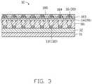
- FIG. 3is a cross sectional view of the TFT substrate in FIG. 1 .
- FIG. 4is a schematic circuit diagram of the TFT substrate in FIG. 1 .
- FIG. 5is a diagrammatic view of drive-time sequence of the TFT substrate in FIG. 2 through FIG. 4 .
- an exemplary embodiment of a touch display panel 100is an in-cell touch display panel.
- the touch display panel 100includes a TFT substrate 10 , a color filter substrate 60 facing the TFT substrate 10 , a liquid crystal layer 80 between the TFT substrate 10 and the color filter substrate 60 , and a plurality of conventional photo spacers (not shown) for supporting a gap between the TFT substrate 10 and the color filter substrate 60 .
- FIG. 2 through FIG. 3illustrate the TFT substrate 10 .
- the TFT substrate 10includes a substrate 11 , a TFT layer 12 on a surface of the substrate 11 , a first conductive layer 13 formed on a surface of the TFT layer 12 away from the substrate 11 , a second conductive layer 14 on a surface of the first conductive layer 13 away from the substrate 11 , and a third conductive layer 16 formed on a surface of the second conductive layer 14 away from the substrate 11 .
- the TFT substrate 10further includes a first insulating material layer 101 between the first conductive layer 13 and the second conductive layer 14 , to insulate the first conductive layer 13 from the second conductive layer 14 .
- the TFT substrate 10further includes a second insulating material layer 103 between the second conductive layer 14 and the third conductive layer 16 , to insulate the second conductive layer 14 from the third conductive layer 16 .
- the TFT substrate 10further includes a planarization layer 105 on the second insulating material layer 103 which covers the third conductive layer 16 .
- the planarization layer 105is electrically insulating.
- the TFT layer 12has a multilayer structure (not shown).
- the TFT layer 12includes a plurality of TFTs 124 (as shown in FIG. 4 ).
- Each TFT 124is conventional TFT in the art. As shown in FIG. 4 , each TFT 124 includes a gate electrode 1241 , a source electrode 1243 , and a drain electrode 1245 .
- the second conductive layer 14is patterned to form a plurality of common electrodes 20 .
- the second conductive layer 14is made of a transparent conductive material.
- each common electrode 20extends as a strip shape along a first direction D 1 shown in FIG. 2
- the plurality of common electrodes 20is arranged in a row along the second direction D 2 shown in FIG. 2 .
- the first directionintersects the second direction.
- the first directionis perpendicular to the second direction.
- the common electrodes 20are configured to cooperate with the pixel electrode 137 (shown in FIG. 4 ) to form an electric field (not shown).
- the electric fieldrotates the liquid crystal molecules (not shown) in the liquid crystal layer 80 .
- the common electrodes 20are also configured as touch sensing electrodes.
- the third conductive layer 16is patterned to form a plurality of connecting wires 30 .
- each connecting wire 30extends along the second direction D 2 shown in FIG. 2
- the plurality of connecting wires 30is arranged in a row along the first direction D 1 shown in FIG. 2 .
- Each connecting wire 30crosses the plurality of common electrodes 20 .
- the TFT substrate 10defines a display area 110 and a non-display area 120 surrounding the display area 110 .
- the plurality of common electrodes 20is located in the display area 110 .
- the TFT substrate 10further includes a control circuit 50 located in the non-display area 120 .
- Each of the common electrodes 20is electrically connected to the control circuit 50 by at least one connection wire 30 .
- the control circuit 50is configured to receive touch signals from the common electrode 20 .
- the plurality of connecting wires 30is divided into a plurality of connecting wire groups 300 .
- the plurality of connecting wire groups 300are arranged at intervals along the first direction.
- Each connecting wire group 300includes at least one connecting wire 30 .
- each connecting wire group 300includes seven connecting wires 30 .
- Each connecting wire group 300is electrically connected to one common electrode 20 and is electrically insulated from other common electrodes 20 . Therefore, a number of the connecting wire groups 300 is equal to a number of the common electrodes 20 .
- One end of each connecting wire set 300is electrically coupled to the control circuit 50 , such that each common electrode 20 is electrically coupled to the control circuit 50 by one connecting wire group 300 .
- the connecting wires 30 in each connecting wire group 300are electrically connected in parallel, to reduce the overall resistance of the connecting wire group 300 . It can be understood that the number of the connecting wires 30 in each connection wire group 300 is not limited to seven, and may also be any number larger than one, such as two, three, or more.
- the second insulating material layer 103is located on the first insulating material layer 101 and covers the common electrodes 20 .
- the third conductive layer 16 forming the plurality of connecting wires 30is located on the second insulating material layer 103 .
- Some of the connecting wires 30 in the plurality of connecting wires 30are electrically coupled to the common electrodes 20 by via holes 104 .
- Each via hole 104extends through the second insulating material layer 103 .
- three connecting wires 30 in each connecting wire group 300are electrically coupled to the corresponding one common electrode 20 .
- connection wires 30 in each connection wire group 300 electrically coupled to a common electrode 20is not limited to three, and may also be one, two or more. At least one connection wire 30 must be electrically coupled to the corresponding one common electrode 20 .
- the first conductive layer 13is patterned to form a plurality of data lines 132 .
- each data line 132extends along the second direction D 2 shown in FIG. 4
- the plurality of data lines 132is arranged at intervals along the first direction D 1 shown in FIG. 4 . Since each common electrode 20 extends along the first direction D 1 , each data line 132 intersects and crosses the plurality of common electrodes 20 .
- the data lines 132are configured to transmit data signals to the source electrodes of the TFTs.
- the data lines 132are also configured as touch driving electrodes.
- the first insulating material layer 101is located on the TFT layer 12 and completely covers the plurality of data lines 132 .
- the second conductive layer 14 forming the common electrodes 20is located on the first insulating material layer 101 .
- the TFT substrate 10further includes a plurality of scan lines 134 .
- Each scan line 134extends along the first direction D 1 shown in FIG. 4 , and the plurality of scan lines 134 is arranged at intervals along the second direction D 2 shown in FIG. 4 .
- the scan lines 134 and the data lines 132are not located at a same layer, the scan lines 134 being formed by conductive layers other than the first conductive layer 13 .
- the plurality of scan lines 134is insulated from the plurality of data lines 132 .
- the scan lines 134 and the data lines 132intersect with each other to define pixel units 136 .
- At least one TFT 124 and a pixel electrode 137are located in each pixel unit 136 .
- the gate electrode 1241 of one of the at least one TFT 124is electrically coupled to one scan line 134
- a source electrode 1243 of the one of the at least one TFT 124is electrically coupled to one data line 132
- a drain electrode 1245 of the one of the at least one TFT 124is electrically coupled to a pixel electrode 137 .
- each connecting wire 30extends along the second direction D 2 shown in FIG. 2
- each data line 132extends along the second direction D 2 shown in FIG. 4
- the connecting wires 30 and the data lines 132always being parallel.
- a number of the connection wires 30is equal to a number of the data lines 132 .
- the connecting wires 30 and the data lines 132are made of conductive material. A projection of each connecting wire 30 on the substrate 11 overlaps a projection of one data line 132 on the substrate 11 , thus the connecting wires have no effect on the aperture ratio.
- the TFT substrate 10further includes a demultiplexer 138 in the non-display area 120 .
- the demultiplexer 138is located between the plurality of data lines 132 and the control circuit 50 .
- Each data line 132is electrically coupled to the control circuit 50 by the demultiplexer 138 .
- the demultiplexer 138has three selection terminals, RSW, GSW, and BSW.
- the demultiplexer 138outputs signals to all of the data lines 132 according to the signals of the selection terminals RSW, GSW, and BSW.
- Data signals or touch driving signalscan be applied to the data lines 132 by the control circuit 5 and the demultiplexer 138 .
- Several adjacent data lines 132may be used as one touch driving electrode.
- the touch display panel 100adopts a time-division driving method.
- display driving signalse. g. a common electrode voltage
- a data signalsare applied to the data lines 132 .
- touch driving signalsare applied to the data lines 132 .
- the common electrodes 20receive the touch sensing signals and transmit the touch sensing signals to the control circuit 50 by the connecting wires 30 .
- the drive-time sequence of the TFT substrate 10is shown in FIG. 5 .
- the TFT substrate 10is driven in a plurality of frame times.
- Each frame timeincludes a display period T 1 and a touch sensing period T 2 .
- the control signals of the three selection terminals RSW, GSW, and BSW of the demultiplexer 138are sequentially alternating pulse signals.
- Data voltage signalsare applied to the data lines 132 , and each common electrode 20 receives a direct current voltage (common electrode voltage), each of the scan lines 134 receiving the scan signal in sequence.
- the control signals of the three selection terminals RSW, GSW, and BSW of the demultiplexer 138are all switched to a direct current voltage (high potential voltage), and touch driving signals (pulse signal voltages) are applied to the data lines 132 .
- Each common electrode 20receives a voltage which is different from the common electrode voltage (e. g. higher than the common electrode voltage in this exemplary embodiment), and scan signals stop being applied to the scan lines 134 .
- each data line 132functions as a touch driving electrode and each common electrode 20 functions as a touch sensing electrode, each data line 132 and one common electrode 20 forming a first mutual capacitor.
- Each data line 132also cooperates with one connecting wire 30 that overlaps the data line 132 to form a second mutual capacitor.
- Each common electrode 20cooperates with a connecting wires 30 that is not electrically coupled to the common electrode 20 to form a parasitic capacitor.
- the TFT substrate 10does not need to set additional electrodes functioning as the touch driving electrode and the touch sensing electrodes, thus thickness the TFT substrate can be effectively reduced.
Landscapes
- Engineering & Computer Science (AREA)
- Physics & Mathematics (AREA)
- Theoretical Computer Science (AREA)
- General Engineering & Computer Science (AREA)
- General Physics & Mathematics (AREA)
- Human Computer Interaction (AREA)
- Nonlinear Science (AREA)
- Crystallography & Structural Chemistry (AREA)
- Optics & Photonics (AREA)
- Mathematical Physics (AREA)
- Chemical & Material Sciences (AREA)
- Computer Networks & Wireless Communication (AREA)
- Liquid Crystal (AREA)
- Microelectronics & Electronic Packaging (AREA)
- Geometry (AREA)
- Devices For Indicating Variable Information By Combining Individual Elements (AREA)
- Position Input By Displaying (AREA)
Abstract
Description
Claims (12)
Priority Applications (1)
| Application Number | Priority Date | Filing Date | Title |
|---|---|---|---|
| US15/820,384US10748940B2 (en) | 2016-11-24 | 2017-11-21 | TFT substrate having data lines as touch driving electrode and common electrodes as touch sensing electrode and touch display panel using same |
Applications Claiming Priority (2)
| Application Number | Priority Date | Filing Date | Title |
|---|---|---|---|
| US201662426303P | 2016-11-24 | 2016-11-24 | |
| US15/820,384US10748940B2 (en) | 2016-11-24 | 2017-11-21 | TFT substrate having data lines as touch driving electrode and common electrodes as touch sensing electrode and touch display panel using same |
Publications (2)
| Publication Number | Publication Date |
|---|---|
| US20180145090A1 US20180145090A1 (en) | 2018-05-24 |
| US10748940B2true US10748940B2 (en) | 2020-08-18 |
Family
ID=62147833
Family Applications (1)
| Application Number | Title | Priority Date | Filing Date |
|---|---|---|---|
| US15/820,384ActiveUS10748940B2 (en) | 2016-11-24 | 2017-11-21 | TFT substrate having data lines as touch driving electrode and common electrodes as touch sensing electrode and touch display panel using same |
Country Status (3)
| Country | Link |
|---|---|
| US (1) | US10748940B2 (en) |
| CN (1) | CN108108070B (en) |
| TW (1) | TW201820003A (en) |
Families Citing this family (7)
| Publication number | Priority date | Publication date | Assignee | Title |
|---|---|---|---|---|
| CN108877543A (en)* | 2018-06-27 | 2018-11-23 | 维沃移动通信有限公司 | A kind of display panel and preparation method thereof, mobile terminal |
| CN109491550B (en)* | 2019-01-03 | 2022-05-10 | 京东方科技集团股份有限公司 | A touch substrate, a detection method thereof, and a display device |
| CN111103696A (en)* | 2019-12-30 | 2020-05-05 | 联想(北京)有限公司 | Electronic equipment and display equipment thereof |
| CN113282199B (en)* | 2020-02-20 | 2023-05-02 | 上海中航光电子有限公司 | Touch display panel and display device |
| CN113282187B (en)* | 2020-02-20 | 2022-12-13 | 上海中航光电子有限公司 | Display panel and display device |
| CN113176835B (en)* | 2021-04-26 | 2023-01-24 | Tcl华星光电技术有限公司 | Touch display panel and display device |
| TWI861592B (en)* | 2022-01-17 | 2024-11-11 | 禾瑞亞科技股份有限公司 | Touch sensitive structure and touch sensitive processing apparatus, method and electronic system thereof |
Citations (11)
| Publication number | Priority date | Publication date | Assignee | Title |
|---|---|---|---|---|
| TW201236127A (en) | 2011-02-25 | 2012-09-01 | Lg Display Co Ltd | Touch sensor integrated display device |
| US20130162570A1 (en) | 2011-12-22 | 2013-06-27 | Lg Display Co., Ltd. | Liquid crystal display device and method for manufaturing the same |
| US20140062943A1 (en)* | 2012-09-04 | 2014-03-06 | Samsung Display Co., Ltd. | Display apparatus |
| CN103902120A (en) | 2012-12-27 | 2014-07-02 | 乐金显示有限公司 | Touch sensor integrated type display device |
| US20140184944A1 (en) | 2012-12-31 | 2014-07-03 | Shanghai Tianma Micro-electronics Co., Ltd. | Array substrate and touch screen with horizontal electric field driving mode |
| CN104020904A (en) | 2014-05-28 | 2014-09-03 | 京东方科技集团股份有限公司 | Capacitive type embedded touch screen and display device |
| US20160098144A1 (en)* | 2014-10-01 | 2016-04-07 | Apple Inc. | Display Having Vertical Gate Line Extensions and Touch Sensor |
| US20160109992A1 (en)* | 2014-10-17 | 2016-04-21 | Mstar Semiconductor, Inc. | In-cell touch display device and driving method thereof |
| US20170017320A1 (en)* | 2015-07-17 | 2017-01-19 | Innolux Corporation | Touch display panel |
| US20170185196A1 (en)* | 2015-12-28 | 2017-06-29 | Lg Display Co., Ltd. | Display Device with Touch Sensor |
| US20170249044A1 (en)* | 2016-02-26 | 2017-08-31 | Boe Technology Group Co., Ltd. | Display panel, method for driving the same and display device |
Family Cites Families (8)
| Publication number | Priority date | Publication date | Assignee | Title |
|---|---|---|---|---|
| KR101258255B1 (en)* | 2006-05-25 | 2013-04-25 | 엘지디스플레이 주식회사 | Method for fabricating of thin film transistor substrate using maskless exposure device |
| KR101735386B1 (en)* | 2010-06-25 | 2017-05-30 | 엘지디스플레이 주식회사 | Liquid crystal display device having touch sensor embedded therein, method for driving the same and method for fabricating the same |
| TW201518829A (en)* | 2013-11-15 | 2015-05-16 | Chunghwa Picture Tubes Ltd | Thin film transistor substrate and repairing method thereof |
| CN104656332B (en)* | 2015-01-28 | 2018-11-06 | 上海天马微电子有限公司 | Array substrate, preparation method thereof and display device |
| CN105895657B (en)* | 2015-02-13 | 2020-05-05 | 鸿富锦精密工业(深圳)有限公司 | Thin film transistor substrate and touch display panel with same |
| CN104991678B (en)* | 2015-07-28 | 2018-05-22 | 京东方科技集团股份有限公司 | Array substrate and its driving method, production method, display device |
| CN105511669A (en)* | 2015-11-30 | 2016-04-20 | 信利光电股份有限公司 | Touch screen with pressure detection function and electronic equipment |
| CN105514119A (en)* | 2016-01-04 | 2016-04-20 | 武汉华星光电技术有限公司 | TFT substrate manufacturing method and TFT substrate |
- 2017
- 2017-11-17TWTW106139838Apatent/TW201820003A/enunknown
- 2017-11-17CNCN201711146986.3Apatent/CN108108070B/enactiveActive
- 2017-11-21USUS15/820,384patent/US10748940B2/enactiveActive
Patent Citations (15)
| Publication number | Priority date | Publication date | Assignee | Title |
|---|---|---|---|---|
| TW201236127A (en) | 2011-02-25 | 2012-09-01 | Lg Display Co Ltd | Touch sensor integrated display device |
| US20160132166A1 (en) | 2011-02-25 | 2016-05-12 | Lg Display Co., Ltd. | Touch Sensor Integrated Display Device |
| US20130162570A1 (en) | 2011-12-22 | 2013-06-27 | Lg Display Co., Ltd. | Liquid crystal display device and method for manufaturing the same |
| TW201326998A (en) | 2011-12-22 | 2013-07-01 | Lg Display Co Ltd | Liquid crystal display device and method of manufacturing same |
| US20140062943A1 (en)* | 2012-09-04 | 2014-03-06 | Samsung Display Co., Ltd. | Display apparatus |
| US20140184559A1 (en)* | 2012-12-27 | 2014-07-03 | Lg Display Co., Ltd. | Touch sensor integrated type display device |
| CN103902120A (en) | 2012-12-27 | 2014-07-02 | 乐金显示有限公司 | Touch sensor integrated type display device |
| US20140184944A1 (en) | 2012-12-31 | 2014-07-03 | Shanghai Tianma Micro-electronics Co., Ltd. | Array substrate and touch screen with horizontal electric field driving mode |
| CN104020904A (en) | 2014-05-28 | 2014-09-03 | 京东方科技集团股份有限公司 | Capacitive type embedded touch screen and display device |
| US20150346860A1 (en) | 2014-05-28 | 2015-12-03 | Boe Technology Group Co., Ltd. | Capacitive in-cell touch panel, display device, and driving method |
| US20160098144A1 (en)* | 2014-10-01 | 2016-04-07 | Apple Inc. | Display Having Vertical Gate Line Extensions and Touch Sensor |
| US20160109992A1 (en)* | 2014-10-17 | 2016-04-21 | Mstar Semiconductor, Inc. | In-cell touch display device and driving method thereof |
| US20170017320A1 (en)* | 2015-07-17 | 2017-01-19 | Innolux Corporation | Touch display panel |
| US20170185196A1 (en)* | 2015-12-28 | 2017-06-29 | Lg Display Co., Ltd. | Display Device with Touch Sensor |
| US20170249044A1 (en)* | 2016-02-26 | 2017-08-31 | Boe Technology Group Co., Ltd. | Display panel, method for driving the same and display device |
Also Published As
| Publication number | Publication date |
|---|---|
| CN108108070B (en) | 2021-06-25 |
| TW201820003A (en) | 2018-06-01 |
| CN108108070A (en) | 2018-06-01 |
| US20180145090A1 (en) | 2018-05-24 |
Similar Documents
| Publication | Publication Date | Title |
|---|---|---|
| US10748940B2 (en) | TFT substrate having data lines as touch driving electrode and common electrodes as touch sensing electrode and touch display panel using same | |
| CN105468202B (en) | Array substrate, touch-control display panel and touch control display apparatus | |
| US9851832B2 (en) | Display panel, driving method thereof and display device | |
| US10168593B2 (en) | Liquid crystal display panel having dual capacitors connected in parallel to shift register unit and array substrate thereof | |
| CN206470722U (en) | Array base palte, display panel and display device | |
| US9715320B2 (en) | In-cell touch display panel | |
| US10509499B2 (en) | TFT substrate and touch display panel using same | |
| US20180341159A1 (en) | Coa substrate and liquid crystal display panel | |
| US9971218B2 (en) | Display device, display panel, array substrate and driving method thereof | |
| US9927919B2 (en) | Array substrate, drive method, display panel and display device | |
| CN102243838A (en) | display screen | |
| US9583512B2 (en) | Array substrate and manufacturing method thereof, and display panel | |
| CN203894514U (en) | Display panel and display device | |
| CN104698711A (en) | Array substrate, display panel and electronic equipment | |
| CN104965622A (en) | Array substrate and display panel | |
| CN205375436U (en) | Array substrate , touch -control display panel and touch -sensitive display device | |
| CN107678590B (en) | A touch display panel and its driving method | |
| CN107132685A (en) | A kind of display base plate, display panel and display device | |
| US20180181239A1 (en) | Liquid crystal display device with touch sensor and method for driving the same | |
| CN107179639A (en) | Array base palte and preparation method thereof and display panel | |
| CN107003769A (en) | Display device with position input function | |
| CN105739768A (en) | Touch display panel and touch display equipment | |
| CN104536631A (en) | Touch display substrate and touch display device | |
| US10386682B2 (en) | Substrate and display device | |
| US10429970B2 (en) | Display device |
Legal Events
| Date | Code | Title | Description |
|---|---|---|---|
| FEPP | Fee payment procedure | Free format text:ENTITY STATUS SET TO UNDISCOUNTED (ORIGINAL EVENT CODE: BIG.); ENTITY STATUS OF PATENT OWNER: LARGE ENTITY | |
| AS | Assignment | Owner name:HON HAI PRECISION INDUSTRY CO., LTD., TAIWAN Free format text:ASSIGNMENT OF ASSIGNORS INTEREST;ASSIGNORS:LIU, CHIA-LIN;WENG, YU-FU;LIN, CHIEN-WEN;AND OTHERS;SIGNING DATES FROM 20171019 TO 20171030;REEL/FRAME:044196/0327 | |
| STPP | Information on status: patent application and granting procedure in general | Free format text:RESPONSE TO NON-FINAL OFFICE ACTION ENTERED AND FORWARDED TO EXAMINER | |
| STPP | Information on status: patent application and granting procedure in general | Free format text:FINAL REJECTION MAILED | |
| STPP | Information on status: patent application and granting procedure in general | Free format text:RESPONSE AFTER FINAL ACTION FORWARDED TO EXAMINER | |
| STPP | Information on status: patent application and granting procedure in general | Free format text:ADVISORY ACTION MAILED | |
| STPP | Information on status: patent application and granting procedure in general | Free format text:DOCKETED NEW CASE - READY FOR EXAMINATION | |
| STPP | Information on status: patent application and granting procedure in general | Free format text:NON FINAL ACTION MAILED | |
| STPP | Information on status: patent application and granting procedure in general | Free format text:NOTICE OF ALLOWANCE MAILED -- APPLICATION RECEIVED IN OFFICE OF PUBLICATIONS | |
| STPP | Information on status: patent application and granting procedure in general | Free format text:PUBLICATIONS -- ISSUE FEE PAYMENT VERIFIED | |
| STCF | Information on status: patent grant | Free format text:PATENTED CASE | |
| MAFP | Maintenance fee payment | Free format text:PAYMENT OF MAINTENANCE FEE, 4TH YEAR, LARGE ENTITY (ORIGINAL EVENT CODE: M1551); ENTITY STATUS OF PATENT OWNER: LARGE ENTITY Year of fee payment:4 |