US10737263B2 - Electronic label-free DNA and genome sequencing - Google Patents
Electronic label-free DNA and genome sequencingDownload PDFInfo
- Publication number
- US10737263B2 US10737263B2US16/076,673US201716076673AUS10737263B2US 10737263 B2US10737263 B2US 10737263B2US 201716076673 AUS201716076673 AUS 201716076673AUS 10737263 B2US10737263 B2US 10737263B2
- Authority
- US
- United States
- Prior art keywords
- electrodes
- biomolecule
- electrode
- nanogap
- pair
- Prior art date
- Legal status (The legal status is an assumption and is not a legal conclusion. Google has not performed a legal analysis and makes no representation as to the accuracy of the status listed.)
- Expired - Fee Related, expires
Links
- 238000012268genome sequencingMethods0.000titleclaimsabstractdescription36
- 238000001712DNA sequencingMethods0.000titleclaimsabstractdescription31
- 238000000034methodMethods0.000claimsabstractdescription96
- 238000000059patterningMethods0.000claimsabstractdescription30
- 238000000151depositionMethods0.000claimsabstractdescription23
- 238000004519manufacturing processMethods0.000claimsabstractdescription20
- 239000000758substrateSubstances0.000claimsabstractdescription18
- 239000010931goldSubstances0.000claimsdescription201
- VYPSYNLAJGMNEJ-UHFFFAOYSA-NSilicium dioxideChemical compoundO=[Si]=OVYPSYNLAJGMNEJ-UHFFFAOYSA-N0.000claimsdescription30
- 229910052737goldInorganic materials0.000claimsdescription30
- BASFCYQUMIYNBI-UHFFFAOYSA-NplatinumChemical compound[Pt]BASFCYQUMIYNBI-UHFFFAOYSA-N0.000claimsdescription29
- 239000002105nanoparticleSubstances0.000claimsdescription28
- 230000008569processEffects0.000claimsdescription26
- PCHJSUWPFVWCPO-UHFFFAOYSA-NgoldChemical compound[Au]PCHJSUWPFVWCPO-UHFFFAOYSA-N0.000claimsdescription24
- 239000000956alloySubstances0.000claimsdescription21
- 229910045601alloyInorganic materials0.000claimsdescription20
- 238000000137annealingMethods0.000claimsdescription19
- 238000000576coating methodMethods0.000claimsdescription19
- 238000001020plasma etchingMethods0.000claimsdescription18
- 239000011248coating agentSubstances0.000claimsdescription17
- 229910052681coesiteInorganic materials0.000claimsdescription15
- 229910052906cristobaliteInorganic materials0.000claimsdescription15
- 239000000377silicon dioxideSubstances0.000claimsdescription15
- 229910052682stishoviteInorganic materials0.000claimsdescription15
- 229910052905tridymiteInorganic materials0.000claimsdescription15
- 239000002122magnetic nanoparticleSubstances0.000claimsdescription14
- 238000005530etchingMethods0.000claimsdescription13
- PNEYBMLMFCGWSK-UHFFFAOYSA-Naluminium oxideInorganic materials[O-2].[O-2].[O-2].[Al+3].[Al+3]PNEYBMLMFCGWSK-UHFFFAOYSA-N0.000claimsdescription12
- 229910052593corundumInorganic materials0.000claimsdescription12
- 238000000609electron-beam lithographyMethods0.000claimsdescription12
- 229910052697platinumInorganic materials0.000claimsdescription12
- 229910001845yogo sapphireInorganic materials0.000claimsdescription12
- 238000007306functionalization reactionMethods0.000claimsdescription10
- 229910052751metalInorganic materials0.000claimsdescription10
- 239000002184metalSubstances0.000claimsdescription10
- 229910052703rhodiumInorganic materials0.000claimsdescription9
- 239000000126substanceSubstances0.000claimsdescription9
- 239000000919ceramicSubstances0.000claimsdescription8
- 238000010884ion-beam techniqueMethods0.000claimsdescription8
- 229910052709silverInorganic materials0.000claimsdescription8
- 238000000992sputter etchingMethods0.000claimsdescription8
- 238000002513implantationMethods0.000claimsdescription7
- 238000005329nanolithographyMethods0.000claimsdescription7
- 229920000642polymerPolymers0.000claimsdescription7
- 229910001092metal group alloyInorganic materials0.000claimsdescription5
- 230000000873masking effectEffects0.000claimsdescription4
- 229910002708Au–CuInorganic materials0.000claimsdescription3
- 229910017392Au—CoInorganic materials0.000claimsdescription3
- 229910017401Au—GeInorganic materials0.000claimsdescription3
- 229910015365Au—SiInorganic materials0.000claimsdescription3
- 229910052797bismuthInorganic materials0.000claimsdescription3
- 238000004090dissolutionMethods0.000claimsdescription3
- 229910052750molybdenumInorganic materials0.000claimsdescription3
- 229910052702rheniumInorganic materials0.000claimsdescription3
- WUAPFZMCVAUBPE-UHFFFAOYSA-Nrhenium atomChemical compound[Re]WUAPFZMCVAUBPE-UHFFFAOYSA-N0.000claimsdescription3
- 229910052707rutheniumInorganic materials0.000claimsdescription3
- 238000005191phase separationMethods0.000claimsdescription2
- 238000007788rougheningMethods0.000abstract1
- 108020004414DNAProteins0.000description30
- 238000012163sequencing techniqueMethods0.000description24
- 102000004169proteins and genesHuman genes0.000description13
- 108090000623proteins and genesProteins0.000description13
- 239000002773nucleotideSubstances0.000description12
- 125000003729nucleotide groupChemical group0.000description12
- 239000012212insulatorSubstances0.000description10
- 229920003229poly(methyl methacrylate)Polymers0.000description10
- 239000004926polymethyl methacrylateSubstances0.000description10
- KDLHZDBZIXYQEI-UHFFFAOYSA-NpalladiumSubstances[Pd]KDLHZDBZIXYQEI-UHFFFAOYSA-N0.000description9
- 230000002829reductive effectEffects0.000description9
- 238000005259measurementMethods0.000description8
- 239000010948rhodiumSubstances0.000description8
- 229910052763palladiumInorganic materials0.000description7
- 239000002202Polyethylene glycolSubstances0.000description6
- 239000004205dimethyl polysiloxaneSubstances0.000description6
- 239000010408filmSubstances0.000description6
- 230000001965increasing effectEffects0.000description6
- 238000005468ion implantationMethods0.000description6
- XEEYBQQBJWHFJM-UHFFFAOYSA-NironSubstances[Fe]XEEYBQQBJWHFJM-UHFFFAOYSA-N0.000description6
- 239000006249magnetic particleSubstances0.000description6
- 239000000463materialSubstances0.000description6
- 238000005442molecular electronicMethods0.000description6
- 239000002245particleSubstances0.000description6
- 229920000435poly(dimethylsiloxane)Polymers0.000description6
- 229920003209poly(hydridosilsesquioxane)Polymers0.000description6
- 229920001223polyethylene glycolPolymers0.000description6
- 238000001514detection methodMethods0.000description5
- WABPQHHGFIMREM-UHFFFAOYSA-Nlead(0)Chemical compound[Pb]WABPQHHGFIMREM-UHFFFAOYSA-N0.000description5
- UQSXHKLRYXJYBZ-UHFFFAOYSA-NIron oxideChemical compound[Fe]=OUQSXHKLRYXJYBZ-UHFFFAOYSA-N0.000description4
- 229910052581Si3N4Inorganic materials0.000description4
- 230000001464adherent effectEffects0.000description4
- 238000005275alloyingMethods0.000description4
- 238000013459approachMethods0.000description4
- 238000001704evaporationMethods0.000description4
- 230000008020evaporationEffects0.000description4
- SZVJSHCCFOBDDC-UHFFFAOYSA-Nferrosoferric oxideChemical compoundO=[Fe]O[Fe]O[Fe]=OSZVJSHCCFOBDDC-UHFFFAOYSA-N0.000description4
- 229910052742ironInorganic materials0.000description4
- 238000011898label-free detectionMethods0.000description4
- 238000001459lithographyMethods0.000description4
- 238000001127nanoimprint lithographyMethods0.000description4
- 150000004767nitridesChemical class0.000description4
- 238000012545processingMethods0.000description4
- 238000004544sputter depositionMethods0.000description4
- 238000004458analytical methodMethods0.000description3
- 239000000427antigenSubstances0.000description3
- 238000004630atomic force microscopyMethods0.000description3
- 238000003486chemical etchingMethods0.000description3
- 239000004020conductorSubstances0.000description3
- 238000005260corrosionMethods0.000description3
- 230000008878couplingEffects0.000description3
- 238000010168coupling processMethods0.000description3
- 238000005859coupling reactionMethods0.000description3
- 230000008021depositionEffects0.000description3
- 230000003100immobilizing effectEffects0.000description3
- 239000007788liquidSubstances0.000description3
- 229920002120photoresistant polymerPolymers0.000description3
- 239000010944silver (metal)Substances0.000description3
- 239000010936titaniumSubstances0.000description3
- -1(e.g.Polymers0.000description2
- XKRFYHLGVUSROY-UHFFFAOYSA-NArgonChemical compound[Ar]XKRFYHLGVUSROY-UHFFFAOYSA-N0.000description2
- IJGRMHOSHXDMSA-UHFFFAOYSA-NAtomic nitrogenChemical compoundN#NIJGRMHOSHXDMSA-UHFFFAOYSA-N0.000description2
- 229910017390Au—FeInorganic materials0.000description2
- 238000001015X-ray lithographyMethods0.000description2
- 238000003491arrayMethods0.000description2
- 239000012298atmosphereSubstances0.000description2
- 230000008901benefitEffects0.000description2
- 229960002685biotinDrugs0.000description2
- 239000011616biotinSubstances0.000description2
- 229910052802copperInorganic materials0.000description2
- 239000010949copperSubstances0.000description2
- 230000007797corrosionEffects0.000description2
- 230000006872improvementEffects0.000description2
- 238000009413insulationMethods0.000description2
- 230000003993interactionEffects0.000description2
- JEIPFZHSYJVQDO-UHFFFAOYSA-Niron(III) oxideInorganic materialsO=[Fe]O[Fe]=OJEIPFZHSYJVQDO-UHFFFAOYSA-N0.000description2
- 230000005415magnetizationEffects0.000description2
- 239000011159matrix materialSubstances0.000description2
- 239000002086nanomaterialSubstances0.000description2
- 229910052759nickelInorganic materials0.000description2
- 239000000615nonconductorSubstances0.000description2
- 230000003287optical effectEffects0.000description2
- 230000000750progressive effectEffects0.000description2
- 239000011253protective coatingSubstances0.000description2
- 230000009467reductionEffects0.000description2
- 238000004621scanning probe microscopyMethods0.000description2
- 238000005204segregationMethods0.000description2
- 229910052717sulfurInorganic materials0.000description2
- 239000011593sulfurSubstances0.000description2
- 239000010409thin filmSubstances0.000description2
- 125000003396thiol groupChemical class[H]S*0.000description2
- 102000014914Carrier ProteinsHuman genes0.000description1
- 102000053602DNAHuman genes0.000description1
- 239000004593EpoxySubstances0.000description1
- CERQOIWHTDAKMF-UHFFFAOYSA-MMethacrylateChemical compoundCC(=C)C([O-])=OCERQOIWHTDAKMF-UHFFFAOYSA-M0.000description1
- 206010028980NeoplasmDiseases0.000description1
- GRYLNZFGIOXLOG-UHFFFAOYSA-NNitric acidChemical compoundO[N+]([O-])=OGRYLNZFGIOXLOG-UHFFFAOYSA-N0.000description1
- 108091036333Rapid DNAProteins0.000description1
- BQCADISMDOOEFD-UHFFFAOYSA-NSilverChemical compound[Ag]BQCADISMDOOEFD-UHFFFAOYSA-N0.000description1
- RTAQQCXQSZGOHL-UHFFFAOYSA-NTitaniumChemical compound[Ti]RTAQQCXQSZGOHL-UHFFFAOYSA-N0.000description1
- 239000000853adhesiveSubstances0.000description1
- 230000001070adhesive effectEffects0.000description1
- 229910000905alloy phaseInorganic materials0.000description1
- 229910052786argonInorganic materials0.000description1
- 108091008324binding proteinsProteins0.000description1
- 201000011510cancerDiseases0.000description1
- 230000008859changeEffects0.000description1
- 238000006243chemical reactionMethods0.000description1
- 230000002153concerted effectEffects0.000description1
- 229920001577copolymerPolymers0.000description1
- 239000007822coupling agentSubstances0.000description1
- 230000005347demagnetizationEffects0.000description1
- 230000001419dependent effectEffects0.000description1
- 238000013461designMethods0.000description1
- 238000011161developmentMethods0.000description1
- 230000003467diminishing effectEffects0.000description1
- KPUWHANPEXNPJT-UHFFFAOYSA-NdisiloxaneChemical class[SiH3]O[SiH3]KPUWHANPEXNPJT-UHFFFAOYSA-N0.000description1
- 239000003814drugSubstances0.000description1
- 238000010292electrical insulationMethods0.000description1
- 239000007772electrode materialSubstances0.000description1
- 230000002708enhancing effectEffects0.000description1
- 239000007850fluorescent dyeSubstances0.000description1
- 238000001215fluorescent labellingMethods0.000description1
- 239000007789gasSubstances0.000description1
- 238000010438heat treatmentMethods0.000description1
- 230000010354integrationEffects0.000description1
- 238000007737ion beam depositionMethods0.000description1
- 150000002500ionsChemical class0.000description1
- 238000002372labellingMethods0.000description1
- 239000003446ligandSubstances0.000description1
- 229910001004magnetic alloyInorganic materials0.000description1
- 150000002739metalsChemical class0.000description1
- 238000002156mixingMethods0.000description1
- 239000000203mixtureSubstances0.000description1
- 230000004048modificationEffects0.000description1
- 238000012986modificationMethods0.000description1
- 239000002114nanocompositeSubstances0.000description1
- 239000002070nanowireSubstances0.000description1
- 229910017604nitric acidInorganic materials0.000description1
- 229910052757nitrogenInorganic materials0.000description1
- 230000003647oxidationEffects0.000description1
- 238000007254oxidation reactionMethods0.000description1
- TWNQGVIAIRXVLR-UHFFFAOYSA-Noxo(oxoalumanyloxy)alumaneChemical compoundO=[Al]O[Al]=OTWNQGVIAIRXVLR-UHFFFAOYSA-N0.000description1
- 238000012856packingMethods0.000description1
- 230000036961partial effectEffects0.000description1
- 230000035515penetrationEffects0.000description1
- 239000002953phosphate buffered salineSubstances0.000description1
- 238000003672processing methodMethods0.000description1
- 230000002250progressing effectEffects0.000description1
- 230000001681protective effectEffects0.000description1
- 230000010069protein adhesionEffects0.000description1
- 238000004549pulsed laser depositionMethods0.000description1
- 238000011946reduction processMethods0.000description1
- 230000004044responseEffects0.000description1
- 238000001338self-assemblyMethods0.000description1
- 239000004332silverSubstances0.000description1
- 125000006850spacer groupChemical group0.000description1
- 238000010301surface-oxidation reactionMethods0.000description1
- 238000010408sweepingMethods0.000description1
- 229910052719titaniumInorganic materials0.000description1
- 238000005406washingMethods0.000description1
- XLYOFNOQVPJJNP-UHFFFAOYSA-NwaterSubstancesOXLYOFNOQVPJJNP-UHFFFAOYSA-N0.000description1
- 229910000859α-FeInorganic materials0.000description1
Images


Classifications
- B—PERFORMING OPERATIONS; TRANSPORTING
- B01—PHYSICAL OR CHEMICAL PROCESSES OR APPARATUS IN GENERAL
- B01L—CHEMICAL OR PHYSICAL LABORATORY APPARATUS FOR GENERAL USE
- B01L3/00—Containers or dishes for laboratory use, e.g. laboratory glassware; Droppers
- B01L3/50—Containers for the purpose of retaining a material to be analysed, e.g. test tubes
- B01L3/502—Containers for the purpose of retaining a material to be analysed, e.g. test tubes with fluid transport, e.g. in multi-compartment structures
- B01L3/5027—Containers for the purpose of retaining a material to be analysed, e.g. test tubes with fluid transport, e.g. in multi-compartment structures by integrated microfluidic structures, i.e. dimensions of channels and chambers are such that surface tension forces are important, e.g. lab-on-a-chip
- B01L3/502707—Containers for the purpose of retaining a material to be analysed, e.g. test tubes with fluid transport, e.g. in multi-compartment structures by integrated microfluidic structures, i.e. dimensions of channels and chambers are such that surface tension forces are important, e.g. lab-on-a-chip characterised by the manufacture of the container or its components
- C—CHEMISTRY; METALLURGY
- C12—BIOCHEMISTRY; BEER; SPIRITS; WINE; VINEGAR; MICROBIOLOGY; ENZYMOLOGY; MUTATION OR GENETIC ENGINEERING
- C12Q—MEASURING OR TESTING PROCESSES INVOLVING ENZYMES, NUCLEIC ACIDS OR MICROORGANISMS; COMPOSITIONS OR TEST PAPERS THEREFOR; PROCESSES OF PREPARING SUCH COMPOSITIONS; CONDITION-RESPONSIVE CONTROL IN MICROBIOLOGICAL OR ENZYMOLOGICAL PROCESSES
- C12Q1/00—Measuring or testing processes involving enzymes, nucleic acids or microorganisms; Compositions therefor; Processes of preparing such compositions
- C12Q1/68—Measuring or testing processes involving enzymes, nucleic acids or microorganisms; Compositions therefor; Processes of preparing such compositions involving nucleic acids
- C12Q1/6869—Methods for sequencing
- B—PERFORMING OPERATIONS; TRANSPORTING
- B01—PHYSICAL OR CHEMICAL PROCESSES OR APPARATUS IN GENERAL
- B01L—CHEMICAL OR PHYSICAL LABORATORY APPARATUS FOR GENERAL USE
- B01L3/00—Containers or dishes for laboratory use, e.g. laboratory glassware; Droppers
- B01L3/50—Containers for the purpose of retaining a material to be analysed, e.g. test tubes
- B01L3/502—Containers for the purpose of retaining a material to be analysed, e.g. test tubes with fluid transport, e.g. in multi-compartment structures
- B01L3/5027—Containers for the purpose of retaining a material to be analysed, e.g. test tubes with fluid transport, e.g. in multi-compartment structures by integrated microfluidic structures, i.e. dimensions of channels and chambers are such that surface tension forces are important, e.g. lab-on-a-chip
- B01L3/502715—Containers for the purpose of retaining a material to be analysed, e.g. test tubes with fluid transport, e.g. in multi-compartment structures by integrated microfluidic structures, i.e. dimensions of channels and chambers are such that surface tension forces are important, e.g. lab-on-a-chip characterised by interfacing components, e.g. fluidic, electrical, optical or mechanical interfaces
- C—CHEMISTRY; METALLURGY
- C12—BIOCHEMISTRY; BEER; SPIRITS; WINE; VINEGAR; MICROBIOLOGY; ENZYMOLOGY; MUTATION OR GENETIC ENGINEERING
- C12Q—MEASURING OR TESTING PROCESSES INVOLVING ENZYMES, NUCLEIC ACIDS OR MICROORGANISMS; COMPOSITIONS OR TEST PAPERS THEREFOR; PROCESSES OF PREPARING SUCH COMPOSITIONS; CONDITION-RESPONSIVE CONTROL IN MICROBIOLOGICAL OR ENZYMOLOGICAL PROCESSES
- C12Q1/00—Measuring or testing processes involving enzymes, nucleic acids or microorganisms; Compositions therefor; Processes of preparing such compositions
- C—CHEMISTRY; METALLURGY
- C23—COATING METALLIC MATERIAL; COATING MATERIAL WITH METALLIC MATERIAL; CHEMICAL SURFACE TREATMENT; DIFFUSION TREATMENT OF METALLIC MATERIAL; COATING BY VACUUM EVAPORATION, BY SPUTTERING, BY ION IMPLANTATION OR BY CHEMICAL VAPOUR DEPOSITION, IN GENERAL; INHIBITING CORROSION OF METALLIC MATERIAL OR INCRUSTATION IN GENERAL
- C23C—COATING METALLIC MATERIAL; COATING MATERIAL WITH METALLIC MATERIAL; SURFACE TREATMENT OF METALLIC MATERIAL BY DIFFUSION INTO THE SURFACE, BY CHEMICAL CONVERSION OR SUBSTITUTION; COATING BY VACUUM EVAPORATION, BY SPUTTERING, BY ION IMPLANTATION OR BY CHEMICAL VAPOUR DEPOSITION, IN GENERAL
- C23C14/00—Coating by vacuum evaporation, by sputtering or by ion implantation of the coating forming material
- C23C14/06—Coating by vacuum evaporation, by sputtering or by ion implantation of the coating forming material characterised by the coating material
- C23C14/14—Metallic material, boron or silicon
- C23C14/16—Metallic material, boron or silicon on metallic substrates or on substrates of boron or silicon
- C—CHEMISTRY; METALLURGY
- C23—COATING METALLIC MATERIAL; COATING MATERIAL WITH METALLIC MATERIAL; CHEMICAL SURFACE TREATMENT; DIFFUSION TREATMENT OF METALLIC MATERIAL; COATING BY VACUUM EVAPORATION, BY SPUTTERING, BY ION IMPLANTATION OR BY CHEMICAL VAPOUR DEPOSITION, IN GENERAL; INHIBITING CORROSION OF METALLIC MATERIAL OR INCRUSTATION IN GENERAL
- C23C—COATING METALLIC MATERIAL; COATING MATERIAL WITH METALLIC MATERIAL; SURFACE TREATMENT OF METALLIC MATERIAL BY DIFFUSION INTO THE SURFACE, BY CHEMICAL CONVERSION OR SUBSTITUTION; COATING BY VACUUM EVAPORATION, BY SPUTTERING, BY ION IMPLANTATION OR BY CHEMICAL VAPOUR DEPOSITION, IN GENERAL
- C23C14/00—Coating by vacuum evaporation, by sputtering or by ion implantation of the coating forming material
- C23C14/22—Coating by vacuum evaporation, by sputtering or by ion implantation of the coating forming material characterised by the process of coating
- C23C14/48—Ion implantation
- C—CHEMISTRY; METALLURGY
- C23—COATING METALLIC MATERIAL; COATING MATERIAL WITH METALLIC MATERIAL; CHEMICAL SURFACE TREATMENT; DIFFUSION TREATMENT OF METALLIC MATERIAL; COATING BY VACUUM EVAPORATION, BY SPUTTERING, BY ION IMPLANTATION OR BY CHEMICAL VAPOUR DEPOSITION, IN GENERAL; INHIBITING CORROSION OF METALLIC MATERIAL OR INCRUSTATION IN GENERAL
- C23F—NON-MECHANICAL REMOVAL OF METALLIC MATERIAL FROM SURFACE; INHIBITING CORROSION OF METALLIC MATERIAL OR INCRUSTATION IN GENERAL; MULTI-STEP PROCESSES FOR SURFACE TREATMENT OF METALLIC MATERIAL INVOLVING AT LEAST ONE PROCESS PROVIDED FOR IN CLASS C23 AND AT LEAST ONE PROCESS COVERED BY SUBCLASS C21D OR C22F OR CLASS C25
- C23F4/00—Processes for removing metallic material from surfaces, not provided for in group C23F1/00 or C23F3/00
- G—PHYSICS
- G01—MEASURING; TESTING
- G01N—INVESTIGATING OR ANALYSING MATERIALS BY DETERMINING THEIR CHEMICAL OR PHYSICAL PROPERTIES
- G01N27/00—Investigating or analysing materials by the use of electric, electrochemical, or magnetic means
- G01N27/26—Investigating or analysing materials by the use of electric, electrochemical, or magnetic means by investigating electrochemical variables; by using electrolysis or electrophoresis
- G01N27/28—Electrolytic cell components
- G01N27/30—Electrodes, e.g. test electrodes; Half-cells
- G01N27/327—Biochemical electrodes, e.g. electrical or mechanical details for in vitro measurements
- G01N27/3275—Sensing specific biomolecules, e.g. nucleic acid strands, based on an electrode surface reaction
- G01N27/3278—Sensing specific biomolecules, e.g. nucleic acid strands, based on an electrode surface reaction involving nanosized elements, e.g. nanogaps or nanoparticles
- G—PHYSICS
- G01—MEASURING; TESTING
- G01N—INVESTIGATING OR ANALYSING MATERIALS BY DETERMINING THEIR CHEMICAL OR PHYSICAL PROPERTIES
- G01N33/00—Investigating or analysing materials by specific methods not covered by groups G01N1/00 - G01N31/00
- G01N33/48—Biological material, e.g. blood, urine; Haemocytometers
- G01N33/483—Physical analysis of biological material
- G01N33/487—Physical analysis of biological material of liquid biological material
- G01N33/48707—Physical analysis of biological material of liquid biological material by electrical means
- G01N33/48721—Investigating individual macromolecules, e.g. by translocation through nanopores
- B—PERFORMING OPERATIONS; TRANSPORTING
- B01—PHYSICAL OR CHEMICAL PROCESSES OR APPARATUS IN GENERAL
- B01L—CHEMICAL OR PHYSICAL LABORATORY APPARATUS FOR GENERAL USE
- B01L2200/00—Solutions for specific problems relating to chemical or physical laboratory apparatus
- B01L2200/12—Specific details about manufacturing devices
- B—PERFORMING OPERATIONS; TRANSPORTING
- B01—PHYSICAL OR CHEMICAL PROCESSES OR APPARATUS IN GENERAL
- B01L—CHEMICAL OR PHYSICAL LABORATORY APPARATUS FOR GENERAL USE
- B01L2300/00—Additional constructional details
- B01L2300/06—Auxiliary integrated devices, integrated components
- B01L2300/0627—Sensor or part of a sensor is integrated
- B01L2300/0645—Electrodes
- B—PERFORMING OPERATIONS; TRANSPORTING
- B01—PHYSICAL OR CHEMICAL PROCESSES OR APPARATUS IN GENERAL
- B01L—CHEMICAL OR PHYSICAL LABORATORY APPARATUS FOR GENERAL USE
- B01L2300/00—Additional constructional details
- B01L2300/08—Geometry, shape and general structure
- B01L2300/0887—Laminated structure
- B—PERFORMING OPERATIONS; TRANSPORTING
- B01—PHYSICAL OR CHEMICAL PROCESSES OR APPARATUS IN GENERAL
- B01L—CHEMICAL OR PHYSICAL LABORATORY APPARATUS FOR GENERAL USE
- B01L2300/00—Additional constructional details
- B01L2300/08—Geometry, shape and general structure
- B01L2300/0896—Nanoscaled
- C—CHEMISTRY; METALLURGY
- C12—BIOCHEMISTRY; BEER; SPIRITS; WINE; VINEGAR; MICROBIOLOGY; ENZYMOLOGY; MUTATION OR GENETIC ENGINEERING
- C12Q—MEASURING OR TESTING PROCESSES INVOLVING ENZYMES, NUCLEIC ACIDS OR MICROORGANISMS; COMPOSITIONS OR TEST PAPERS THEREFOR; PROCESSES OF PREPARING SUCH COMPOSITIONS; CONDITION-RESPONSIVE CONTROL IN MICROBIOLOGICAL OR ENZYMOLOGICAL PROCESSES
- C12Q2565/00—Nucleic acid analysis characterised by mode or means of detection
- C12Q2565/60—Detection means characterised by use of a special device
- C12Q2565/631—Detection means characterised by use of a special device being a biochannel or pore
Definitions
- This disclosurerelates generally to nanotechnology, nanofabrication and nanoelectronics, and more particularly to systems, devices, and processes for electronic sensing and analyzing of individual biomolecules, including DNA and proteins.
- This inventiondiscloses new, manufacturable and highly-scalable techniques of sub-10 nm nano-electrode design and fabrication, which comprise parts of label-free DNA or genome sequencing methods, apparatus, and applications.
- This inventionprovides unique structures, compositions and means of manufacturing the same, for extremely small and high-density nano-electrode arrays for use in electronic DNA sequencing systems.
- Such nano-electrode systemsmay also be used in analyzing other types of biomolecules, such as proteins, depending on how the nano-electrodes are functionalized to interact with biomolecule sensing targets.
- the nano-electrode systems disclosed hereinmay comprise part of a system for such biomolecule analysis, wherein the nano-electrode system is coupled to biomolecules to constitute a molecular electronics sensor with specific application to sensing and characterizing a biomolecule target, in particular applications to sequencing of a DNA molecule, or a collection of such molecules constituting an entire genome.
- a method of manufacturing a device for DNA or genome sequencingincludes: disposing a pair of electrodes on a substrate with the electrodes separated by a nanogap; depositing a resist layer over the pair of electrodes; patterning the resist layer to create an exposed region on each electrode at or near the nanogap; exposing the electrodes to plasma etching or gold (Au) ion beam implantation to roughen the surface within each exposed region; and exposing the exposed regions to a biomolecule, wherein the biomolecule has at least first and second ends, with each end including a functionalization for bonding to the pair of electrodes, wherein the biomolecule bridges the nanogap, with the first and second ends of the biomolecule being bound to the exposed regions.
- the resist layermay be an electrically insulating polymer or an oxide coating measuring from about 3 nm to about 20 nm in thickness
- the electrodesmay be gold (Au) electrodes.
- the patterning usedis e-beam or nano-lithography.
- plasma etchingincludes RF plasma, DC plasma or sputter etching processes.
- the plasma etching or the Au ion beam implantation stepresults in an increase in the surface area of the electrode within each exposed region by at least 50% from the surface area of the exposed region prior to plasma etching or Au ion beam implantation.
- a method of manufacturing a device for DNA or genome sequencingincludes: disposing a pair of electrodes on a substrate, with the electrodes separated by a nanogap; depositing a resist layer over the pair of electrodes; patterning the resist layer to create an exposed region on each electrode at or near the nanogap; exposing the electrodes to Au nanoparticles, wherein the Au nanoparticles attach to the electrode surfaces within each exposed region; annealing the array at from about 200° to about 500° C.
- the resist layeris an electrically insulating ceramic layer such as Al 2 O 3 or SiO 2 and the electrodes are gold (Au).
- the patterning stepmay include e-beam or nano-lithography.
- a method of manufacturing a device for DNA or genome sequencingincludes: disposing a pair of Au metal alloy electrodes on a substrate with the electrodes separated by a nanogap; depositing a resist layer over the electrode pair; patterning the resist layer to create an exposed region on each electrode at or near the nanogap; exposing the electrodes to an etchant solution to selectively remove the non-Au metal from the alloy within each exposed region; and exposing the exposed regions to a biomolecule, wherein the biomolecule has at least first and second ends, with each end including a functionalization for bonding to the pair of electrodes, wherein each biomolecule bridges the nanogap, with the first and second ends of the biomolecule being bound to the exposed regions.
- the Au metal alloymay be selected from the group consisting of Au—Si, Au—Ge, Au—Bi, Au—Co, Au—Mo, Au—Rh, Au—Ru, and Au—W.
- the resist layeris an electrically insulating ceramic layer such as Al 2 O 3 or SiO 2 .
- the methodmay further include a step of annealing at from about 200° to about 600° C. for about 10 minutes to about 12 hours to promote phase separation between the Au and non-Au metal.
- a method of manufacturing a device for DNA or genome sequencingincludes: disposing a pair of electrodes on a substrate, the electrodes separated by a nanogap; depositing a resist layer over the electrode pair; patterning the resist layer to create an exposed region on each electrode at or near the nanogap; depositing Au—Ag or Au—Cu alloy onto the electrode surface within each exposed region; exposing the electrodes to an etchant solution to selectively remove the non-Au metal from the alloy deposited within each exposed region; and exposing the exposed regions to a biomolecule, wherein the biomolecule has at least first and second ends, with each end including a functionalization for bonding to the pair of electrodes, wherein each biomolecule bridges the nanogap, with the first and second ends of the biomolecule being bound to the exposed regions.
- the resist layeris an electrically insulating ceramic layer such as Al 2 O 3 or SiO 2 .
- the electrodescan be gold (Au) electrodes.
- a method of manufacturing a device for DNA or genome sequencingincludes: disposing a pair of electrodes on a substrate, the electrodes separated by a nanogap; depositing a latchable magnetic layer over the electrodes; depositing a resist layer over the latchable magnetic layer; patterning the resist layer to create an exposed region at or near the nanogap in which the latchable magnetic layer is exposed; exposing the electrodes to an external magnetic field or to an applied voltage to magnetize the latchable magnetic layer; and exposing the exposed regions to a biomolecule, wherein the biomolecule has at least first and second ends with each end tagged with a magnetic nanoparticle for attraction to the magnetized latchable magnetic layer, wherein the biomolecule bridges the nanogap, with each magnetic nanoparticle held to each electrode at the exposed regions.
- the latchable magnetic layeris a FeCrCo or FeCuNi spinodal alloy with Hc higher than 10 Oe.
- This methodmay further include a step of depositing a layer of Au over the latchable magnetic layer prior to the step of patterning the resist layer.
- the magnetic layercan be magnetized or demagnetized to enable magnetically attracted attachment of magnetic nanoparticle-tagged biomolecules or removal and cleaning-out of attached magnetic nanoparticle-tagged biomolecules with a permanent magnet sweep, allowing multiple repeat operations of the device.
- a method of manufacturing a device for DNA or genome sequencingincludes: disposing a pair of platinum (Pt) or rhenium (Rh) electrodes on a substrate, the electrodes separated by a nanogap; depositing a gold (Au) film measuring from about 1 nm to about 10 nm in thickness over the electrode pair; patterning the resist layer to create an exposed region on each electrode at or near the nanogap; annealing the electrodes to induce spheroidization of the Au film into Au spheres, with one sphere disposed within each exposed region; etching the spheres to reduce the height of the spheres; repeating the annealing and etching steps at least two more times; and exposing the Au spheres to a biomolecule, wherein the biomolecule has at least first and second ends, with each end including a functionalization for bonding to the Au spheres, wherein the biomolecule bridges the nanogap, with the first and second ends
- the annealingcan be from about 200° to about 400° C. for about 10 minutes to about 12 hours, or the time/temperature sufficient to cause spheroidization.
- the etching stepmay include at least one of ion milling, sputter etching, and masking and chemical dissolution.
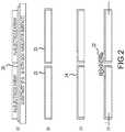
- FIG. 1illustrates genome sequencing compatible electrodes having a structure comprising a 5-20 nm nanogap, with a pair of Au islands for attaching or immobilizing biomolecules such as proteins or fragmented DNA for the purpose of fluorescence-free (label-free) detection of nucleotide attachments via electrical measurements;
- FIG. 2illustrates an embodiment of nano-patterning usable to obtain local-area-defined, massively parallel, Au island electrode arrays
- FIG. 3is a schematic illustration of microstructures having high surface area Au islands, introduced through particle-induced porous structure or etch-induced porous structure methods;
- FIG. 4illustrates a high surface area Au island for stronger, reduced-error enhanced biomolecule adhesion
- FIG. 5illustrates methods to obtain Au islands on electrodes (Pt, Rh or Au);
- FIG. 6illustrates progressive Au island diameter reduction by repeated spheroidization and sequential top-etching steps
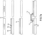
- FIG. 7( a )illustrates a magnetic attraction method to securely adhere a biomolecule (protein or DNA segment) to the selected position on all the electrodes surfaces simultaneously.
- 7 ( a )illustrates magnetic attraction for secure adhesion of a biomolecule (protein or DNA segment) to the selected positions on all the Au base electrode surfaces simultaneously;
- FIG. 7( b )illustrates magnetic attraction for secure adhesion of biomolecule.
- the magnetic layeris deposited on Pt, Pd, or Rh type electrode surface;
- FIG. 8illustrates a massively parallel gold-tip-exposed electrode array: (a) Tapered or sharp-tip Au electrode regions made by nano-imprinting or other lithography; (b) A structure that masks most of the Au electrode surfaces except an island position near the protruding tip to avoid unwanted biomolecule attachments on other regions of Au electrode surface;
- FIG. 9illustrates an array of electrode pairs for strong adhesion of biomolecules for massively parallel, label-free detection of nucleotide attachment or detachment events (e.g., 100 ⁇ 100 device array or 1,000 ⁇ 1,000 array);
- FIG. 10illustrates a configuration for sequential interrogation of electrodes by using a common lead wire on one side of the array and wherein the left side electrodes are interrogated one at a time, sequentially;
- FIG. 11illustrates a three-dimensional array of molecular electronics genome-sequencing platform.
- An electrically insulating top coatingsuch as a polymer or oxide layer is applied except over the very tip gold islands;
- FIG. 12illustrates a flowchart showing various aspects of a genome or DNA sequencing system according to the disclosure.
- the term “sub-10 nm”refers to the size of devices and components therein, and the scale at which methods can be executed. In particular, the term refers to physical structures measuring less than about 10 nm in size, and the ability to manipulate steps in various processes on a scale of less than about 10 nm.
- the term “nanogap”refers to a space, or “gap,” between elements, such as between two electrodes or two conductive islands, measuring in the nanometer range.
- the term “nanogapped”refers to two elements having a gap between them on a nanometer scale.
- label-freerefers to a process that does not require fluorescence labeling, or is in other words, is “fluorescence-free.”
- the element goldmay be denoted herein “Au,” “gold,” or “gold (Au).”
- latchable magnetic striperefers to a thin film or layer of magnetizable material having a capability to change magnetization direction in response to an external magnetic field, such as a layer having magnetic properties that are programmable and reconfigurable as an applied field or an applied voltage is altered.
- FIG. 1illustrates electrodes having a 5-20 nm nanogap and a pair of gold (Au) islands for attaching or otherwise immobilizing biomolecules such as proteins or fragmented DNA for use in devices capable of label-free detection of nucleotide attachments via electronic conductance measurements.
- FIG. 1( a )shows a top view
- FIG. 1( b )shows a side view, of an embodiment of a nanogapped electrode pair usable for genome/DNA sequencing by electronic conductance measurements.
- the electrodesmay comprise a stable and inert metal having high conductivity.
- the nanogap 10 between the electrodesmay be from about 5-20 nm in width.
- Exemplary electrode metalsinclude, but are not limited to, platinum (Pt), palladium (Pd), rhenium (Rh), titanium (Ti), silver (Ag), and gold (Au), or their alloys, with gold (Au) being the most widely used electrode material.
- platinumpalladium
- Rhrhenium
- Tititanium
- Augold
- alternatives to Ausuch Pt, Pd, Rh and their alloys, can be utilized so as to prevent the non-specific, random attachment of biomolecules, proteins or DNAs on the electrode surface.
- biomoleculesare much less prone to attach directly on the Pt surface.
- the attachment of a biomolecule, especially a single biomoleculecan be confined to the gold islands rather than on the Pt electrode surface itself.
- Nanoscale particlessuch as, for example, ⁇ 5 nm diameter gold nanoparticles, are difficult to accurately position and place directly on an electrode surface, such as on to a Pt electrode.
- Atomic Force Microscopy (AFM) or Scanning Probe Microscopy (SPM) methodsmay be used to pick-up, move, and release an individual Au nanoparticle onto an electrode surface, whereby van der Walls forces assist in holding the nanoparticle at its intended location, such as illustrated in FIG. 1( c ) , depicting Au nanoparticles 11 sitting indiscriminately on top of the Pt base electrodes, (see, for e.g., Huang, et al., U.S. Patent Application Publication No. 2014/0048776, published on Feb.
- nanoparticlesthat are not particularly well adhered onto the electrode surface. Further, the positioning of individual nanoparticles at desired locations is not reproducible. These nanoparticles 11 , which are not-so-strongly adhered, as illustrated in FIG. 1( c ) , will cause high contact resistance and reduced electrical conductivity. Further, these Au nanoparticles can be easily moved laterally to a different location, or detached entirely during handling, for example, during washing or microfluidic processing of biomolecules. Accordingly, such AFM guided placement of a nanoparticle, one by one, is laborious, time consuming and not scalable for low-cost manufacturing.
- the Au nanoparticleis more strongly bonded onto the electrode surface such that the contact area of the Au particle used in the bonding with the electrode surface comprises at least 20%, at least 30%, at least 40%, at least 50%, at least 60%, at least 70%, preferably at least 80%, more preferably at least 90%, and even more preferably up to 100% of the Au particle diameter, as illustrated in the top example in FIG. 1( d ) , which shows hemispherically shaped islands. In this example of hemispherical islands, a single biomolecule 12 is shown in contact with the islands and bridging the gap between the electrodes.
- FIG. 1( d )illustrates an embodiment comprising “pillar” shaped islands on the Pt base electrodes, which are available for bonding with a biomolecule bridge.
- Another embodiment according to the disclosureavoids fabricating Au islands on Pt electrodes entirely, relying instead on exposed portions of Au electrodes for biomolecule bonding and bridging.
- a nano-patterned maskis used to block almost the entire Au electrode surface except for a selected region left exposed and available for selective biomolecule attachment.
- a resist layersuch as for example, PMMA (polymethylmethacrylate), methacrylate-based co-polymers, hydrogen silsesquioxane (HSQ), and various siloxane polymers, can be utilized to cover the majority of the Au electrodes except for just the tips of the electrodes, as illustrated in the fourth example of FIG. 1( d ) .
- FIG. 2illustrates an embodiment of a nano-patterning process usable to obtain local-area defined electrodes having exposed regions on Au electrodes and single biomolecule bonding and bridging.
- the processbegins with a pair of Au electrodes as illustrated in FIG. 2( a ) .
- This cross-sectional side view illustrationshows two Au electrodes as a pair of electrodes on a substrate comprising Si with a SiO 2 insulator surface.
- the nanogap 20 in each electrode pairis from about 5 nm to about 20 nm.
- the electrodesare labeled “array” to emphasize that in a device, there can be a plurality of such electrode pairs, from less than a hundred, to hundreds, or thousands, or millions or more electrode pairs.
- a positive or negative resist layer 23is added over the electrode pair.
- a positive resiste.g., polymethylmethacrylate (PMMA)
- a negative resiste.g., hydrogen silsesquioxane (HSQ) or SU-8 epoxy resist
- the resist layer 23comprises a negative resist. The e-beam or nano-imprint lithography is then used to pattern the exposed regions 24 as illustrated in FIG. 2( c ) .
- Al 2 O 3 , SiO 2 or Si 3 N 4 , or other oxide or nitride layersmay be deposited on the Au electrodes and used as an insulating layer instead of using a polymer resist layer.
- a very thin adhesion layersuch as a 1-3 nm thick Ti layer, may be deposited on the Au electrode surface before the oxide or nitride coating is applied.
- This protective coatingwhether polymeric or ceramic, serves as an electrical insulator and also as a coating that prevents or minimizes the adhesion of biomolecules at unwanted locations.
- the configuration of an exposed region 24may be any shape, such as circular, oval, square, rectangular, or any other geometry.
- the size of each exposed region 24 on an Au electrodeis about 3 nm to about 15 nm in diameter on average (or the equivalent dimension across and parallel to the electrode surface if not circular in shape). In certain embodiments, each exposed region 24 is about 5 nm to about 10 nm in diameter (or equivalent dimension across the region if not circular).
- FIG. 2( d )illustrates an attached biomolecule 22 (e.g., a protein, a DNA segment, etc.) attached at each of its ends to the exposed region on each electrode to form a bridge.
- biomolecule 22e.g., a protein, a DNA segment, etc.
- the biomolecule 22may be immobilized into the position shown by functionalized ends using antibody-antigen, biotin-streptavidin, peptide bonding, functionalized ligands, surface charges, or other biomolecule immobilizing techniques.
- a complete electrode pair device illustrated in FIG. 2( d )is shown comprising electrical connections from each electrode, used for electrical interrogation (“i”) of sequencing events that comprise interactions of the biomolecule 22 with other molecules.
- ElectrodesFor molecular electronics devices, including those for protein analysis or DNA/genome sequencing, parallel electronic sensing using an array of many electrode pair devices is desirable. In order to package more electrical measurement devices and circuits within a given space, the electrode dimensions must be reduced to micro- or nano-dimensions.
- An array of nano-electrodes having the geometry such as shown in FIG. 2can be utilized. Such an array can be made by using convenient and scalable processing methods such as nano-imprint lithography. Alternative methods such as e-beam lithography, self-assembly and other means may also be utilized.
- biomolecule-to-electrodeor biomolecule-to-conductive island attachment
- Attachment of a biomolecule to a surfacecan be enhanced if the surface is “roughened,” meaning that the surface is modified in a way that increases the surface area onto which the biomolecule is to attach.
- An embodiment comprising subdivided nanostructures on an electrode surfaceis where an Au pillar, deposited on an electrode surface, is surface damaged in a way to make at least the top surface rough or porous.
- Au surfacesallow for the opportunity to use thiol (—SH) groups on a biomolecule for adhesion (immobilization) of the biomolecule to the Au surface, through Au-sulfur bonding. Nonetheless, if biomolecule adhesion can be enhanced beyond the basic Au-sulfur bonding afforded by thiol groups, the reliability and signal-to-noise ratio in electronic, label-free sequencing can be significantly improved. According to the present disclosure, increasing the surface area of a nano-island of Au increases biomolecule binding to the Au. Herein, further surface nano-structuring of a sub-10 nm island of Au is disclosed.
- the increase in surface areacan be the result of a particle-induced porous structure (illustrated in FIG. 3( a ) ) or an etch-induced porous structure (illustrated in FIG. 3( b ) ), or from other means.
- Methods to produce a particle-induced porous structure and an etch-induced porous structureare detailed herein.
- the increase in the surface area at or near the top surfaces of Au islands where biomolecules are to be adheredis at least 50%, and preferably at least 100% over a flat surfaced Au islands.
- the biomolecule adhesion strengthis improved by at least 30%, and preferably by at least 60% over adhesion on to plain, unmodified Au islands.
- FIG. 4exemplary large surface area Au island structures and methods of producing them are shown. As mentioned, increased surface area for bonding biomolecules results in stronger, reproducible, enhanced biomolecule adhesion.
- FIGS. 4( a ) through 4( f )only the left side each electrode pair is illustrated for the purposes of clarity.
- FIG. 4( a )schematically illustrates an embodiment of a base electrode structure, comprising electrode 49 and resist layer 48 , on which an exposed island location 44 . It is inside this region 44 where the surface area of the island is to be increased.
- the processbegins by forming a pattern-defined Au island region on a conductive electrode (e.g., Au, Pd, Pt, Rh, Ag or their alloys) surface, by utilizing insulating coating 48 such as PMMA and other polymers, or an oxide layer such as sputter-deposited SiO 2 or Al 2 O 3 .
- insulating coating 48such as PMMA and other polymers, or an oxide layer such as sputter-deposited SiO 2 or Al 2 O 3 .
- e-beam or nano-lithographycan be used to create each of the exposed regions 44 on the electrodes.
- the nature of the coatingis chosen based on desirable electrical insulation properties and the resistance the coating has to biomolecule adhesion.
- FIG. 4( b )is an example of a porous surface structure 401 created by plasma etching.
- rough surface structuresuch as a porous or vertical nanowire forest type surface structure, can be formed by RF plasma or DC plasma etching (or sputter etching) processing, more selectively on the exposed Au island region.
- the intensity and duration of plasma etchingcan be adjusted so as to minimize complete plasma etching of the insulation mask layer material.
- the thickness of the resist layermay be from about 3 nm to about 20 nm, and this thickness can be adjusted to mitigate complete plasma etching of the mask layer.
- a rough surface having an increased surface areacan also be created by ion implantation, e.g., by using an Au ion beam.
- An example of a rough surface formed by ion beam implantationis illustrated as surface 441 in FIG. 4( c ) .
- ion implantation damagecan occur on the Au electrode base underneath the insulating coating, depending on the penetration depth of ions as dictated by the accelerating field and total dose of ion implantation.
- the insulating resist coatingdoes not necessarily protect the Au surface beneath from ion implantation.
- a resultant roughened surface in areas other than the exposed island regiondoes not affect the sequencing operation because the insulation layer remains covering the roughened electrode surface.
- a post-annealing stepmay follow the ion implantation.
- Another embodiment used to increase the surface area of an Au islandcomprises attaching Au nanoparticles 421 to the exposed Au region, as shown in FIG. 4( d ) .
- Au nanoparticles attached to the Au electrodeincreases the surface area which results in enhanced biomolecule attachment.
- Au nanoparticles measuring about 1 nm to about 2 nm in diametermade by known methods, tend to preferentially attach naturally to the Au electrode within the exposed region.
- the Au nanoparticles thus depositedmay then be optionally annealed at from about 200 to about 500° C. Higher temperatures can only be used if the insulating layer 48 is ceramic based, (e.g., if the insulating layer comprises Al 2 O 3 or SiO 2 ). Post-annealing at these temperatures improves the adherence of the Au nanoparticles to the exposed Au surface.
- An example of particle-induced porous structureis illustrated, for example, in FIG. 3( a ) .
- FIG. 4( e )represents another embodiment of a process to increase the surface area of an exposed Au island surface, leveraging the immiscibility that Au and Fe exhibit at or near room temperature.
- an electrode base layermay be made, for example, from an Au—Fe alloy having about 50 wt. % Au and 50 wt. % Fe by sputtering or evaporation deposition. Toward room temperature, the alloy phase segregates into an Au matrix embedded with Fe nanoparticles that have precipitated out. The Fe nanoparticles can then be etched away to leave behind a porous Au matrix. An example of this type of etch-induced porous structure is illustrated in FIG. 3( b ) .
- Au base alloyssuch as Au—Si, Au—Ge, Au—Bi, Au—Co, Au—Mo, Au—Rh, Au—Ru, Au—W
- Annealing at high temperaturese.g., at 200-600° C. for 10 min to 12 hrs
- Another way of enhancing phase segregationis to perform sputter deposition or evaporation deposition at warm substrate temperatures, such as 150-400° C., optionally with a bias voltage applied.
- FIG. 4( f )illustrates another embodiment of a process used to increase the surface area of an Au island surface comprises de-alloying.
- the processbegins by first depositing Au—Ag, Au—Cu, or other Au base alloy layer having an Au content of about 20 to 80 wt. %, such as by sputtering or evaporation deposition, into each exposed region 44 . This is followed by strong chemical etching of the non-Au metal, such as by using 30% HNO 3 or other etchant.
- Such de-alloying processremoves Ag or Cu from the surface to leave behind a highly porous structure.
- Such de-alloying techniqueswhen applied to Au nano-islands in the electronic sequencing devices, results in significant surface area increases and associated improvement of biomolecule adhesion.
- FIG. 4( g )Shown in FIG. 4( g ) is an embodiment of how Au islands having increased surface areas (such as obtained by the processes exemplified in FIGS. 4( b )-( f ) ) can be utilized for enhanced attachment of a biomolecule 42 such as a protein or DNA.
- a biomolecule 42such as a protein or DNA.
- the volume of porosity within an Au island regionis at least 10%, preferably at least 30%, and even more preferably at least 50%, so as to increase the surface area of the Au island at or near its top surface by at least by 20%, preferably by at least 40%, and even more preferably by at least 60% over a flat and smooth Au island structure.
- FIG. 5shows three embodiments of methods to produce Au islands on electrodes such as Pt, Rh or Au.
- the processbegins with an electrode pair separated by a nanogap 50 .
- the underlying substrate of the devicesuch as Si with SiO 2 insulator surface, is not shown for the purposes of clarity.
- a first embodiment (1)utilizes a Pt base electrode incapable of biomolecule (e.g. protein or DNA segment) attachment, so that a biomolecule adheres only to an Au island region rather than to the electrode.
- patterned Au island 51is heated to cause it to ball up into the smaller diameter sphere 501 .
- Rh electrodeis also a useful option by virtue of having a lower electrical resistivity ( ⁇ 4.5 u ⁇ cm for Rh, vs 9.8 u ⁇ cm for Pt and 2.1 u ⁇ cm for Au), and a reduced propensity for undesired biomolecule attachment. Also, Rh has no (or very small) mutual solubility with Au, unlike Pt, so alloy mixing is minimized.
- a second embodiment (2)uses an all Au electrode configuration, with the Au electrode disposed in a rectangular shape but with much of the surface masked by insulator coating 58 , except for an island-like region at the end of the electrode.
- the insulator coatingmay comprise polymethylmethacrylate (PMMA), polyethylene glycol (PEG), polydimethylsiloxane (PDMS), or their combinations, hydrogen silsesquioxane (HSQ), or various oxide coatings such as Al 2 O 3 , SiO 2 or nitride coatings such as Si 3 N 4 coating.
- a third embodiment (3)comprises the fabrication of the Au electrodes in tapered shapes having sharp tip geometry, and then masking the majority of the surface of the electrode by insulator layer 580 at all other regions except for the sharp tips of the electrodes.
- PEG and PDMShave remarkably non-adhesive characteristics toward proteins and cells, which can be an additional advantage for electronic sequencing devices where protein adhesion at places other than on the Au island is undesirable.
- an optimal Au island sizeis from about 5 to about 9 nm in diameter. Too large a diameter or too small a diameter Au island does not enable reproducible and strong adhesion of biomolecules. Thus, in various aspects of the present disclosure, techniques are shown that are used to conveniently control the Au island diameter.
- FIG. 6illustrates a progressive Au island diameter reduction process.
- the methodcomprises repeated “spheroidization” (a balling up) and top-etching, progressing from FIG. 6( a ) through FIG. 6( f ) .
- spheroidizationa balling up
- top-etchingtop-etching
- a thin Au film(e.g., 1-10 nm thickness, not illustrated) is first deposited on a Pt or Rh electrode 69 by sputtering, ion beam deposition, evaporation, pulsed laser deposition, or other method, which is then nano-patterned (e.g. by nano-imprinting or other lithographic methods) to create a defined circular or oval film geometry 61 illustrated in FIG. 6( a ) .
- Subsequent annealinginduces a spheroidization ball-up of the Au region into a smaller diameter Au island 601 .
- Annealingmay be at about 200 to about 400° C.
- the balled-up Au island 601is then subjected to chemical or plasma etching for height-reduction (e.g., by ion milling, sputter etch, masking and chemical dissolution etching, etc.) to produce the flatter Au island geometry 611 .
- chemical or plasma etchingfor height-reduction (e.g., by ion milling, sputter etch, masking and chemical dissolution etching, etc.) to produce the flatter Au island geometry 611 .
- Subsequent spheroidization annealingreduces the Au island diameter further and results in Au spherical islands 621 .
- the steps of etching and spheroidization annealingare repeated again to convert the Au islands 621 to 631 and then to 641 .
- FIG. 7( a )illustrates an embodiment of a process for forming sequencing devices in which magnetic attraction provides a more secure adhesion of a biomolecule (protein or DNA segment) to selected positions on all of the electrode surfaces simultaneously.
- the processbegins with an electrode pair having electrodes separated by a nanogap 70 .
- a latchable magnetic stripe 785(such as a thin film stainless magnetic alloy based on FeCrCo or FeCuNi spinodal alloys, or other corrosion-resistant magnet alloys) is deposited on the Au electrode surface 790 .
- the magnetic hardness with coercivity (Hc)is selected to be higher than 10 Oersted (Oe) in order to guard against accidental magnetizing by a stray magnetic field, but less than 100 Oe for easier magnetization or demagnetization to attract or not attract magnetic nanoparticles.
- Nano-patterning of insulator spacer layer 780is then used to create an exposed area 74 on which magnetic nanoparticles can be strongly and reliably adhered with good electrical connection.
- the magnetic layeris magnetized by an externally applied magnetic field, e.g., using a ferrite magnet or an electromagnet, at a field of e.g., 100-1,000 Oe.
- a liquid mediumcomprising biomolecules 72 already tagged with magnetic nanoparticles 71 is introduced.
- Biomolecules with magnetic nanoparticles bonded theretomay comprise antibody-antigen binding, streptavidin-biotin binding, peptide bonding, or electrical charge attraction, or other binding approach.
- a magnetic particle 71 with biomolecule 72 attachedwill then be attracted onto the exposed area of the magnetic stripe 791 where it will be magnetically and electrically anchored as illustrated in the lower drawing in FIG. 7( a ) .
- an intermediate Au nanoparticlemay also be inserted to the biomolecule for various control purposes.
- the magnetic nanoparticles to be tagged onto the biomoleculescan be selected from Fe 2 O 3 , Fe 3 O 4 , or surface-protected or surface-functionalized metallic magnetic particles having higher magnetic moment than iron oxide, including Fe, Co, Ni and their alloys.
- the oxide-based magnetic nanoparticlesare chemically stable, but the metal-based magnetic nanoparticles, while having 2-4 times higher magnetic moment, may lack the chemical stability in a liquid environment of genome sequencing. A slight surface oxidation as a protective coat against oxidation is desirable.
- the surface of magnetic nanoparticlescan be Au-coated to provide chemical stability, as well as enhanced electrical conductivity and more affinity to biomolecules.
- a feature of such magnetic attachment techniqueis the reversibility of biomolecule attachment, i.e., easy detaching of biomolecules if needed.
- the magnetic stripe(the portion of the magnetic layer on an electrode) can easily be demagnetized (e.g., by using gradually diminishing magnetic field of from 200 Oe to near zero field using a 60 Hz AC field in a few seconds), all the magnetically attached biomolecules can be thoroughly removed once the desired sequencing measurement is completed, e.g., by employing a sweeping permanent magnet to detach and collect all the magnetic particles and associated biomolecules and discarding them.
- the sequencing deviceis reusable, for example, the device can be reused at least 10 times, at least 100 times, or even at least 1,000 times.
- FIG. 7( b )A modified method, utilizing Pt, Pd, or Rh base electrode pairs separated by nanogap 700 instead of Au base electrodes, is illustrated in FIG. 7( b ) .
- a thin Au coating 785is added on top of the surface of the magnetic layer 790 to enable better attachment of biomolecules.
- the Au layerdoes not noticeably affect magnetic attraction between the nanoparticle and the underlying magnetic stripe because the magnetic layer underneath is positioned very close to the exposed surface.
- the exposed regions 740are created by e-beam or nano-patterning of a resist layer 780 .
- the deviceis flooded with a solution of biomolecules 720 tagged with magnetic nanoparticles 710 , wherein the magnetic nanoparticle 710 bonds to the Au layer 791 and is magnetically attracted to the underlying magnetic stripe.
- FIG. 8Shown in FIG. 8 is a massively parallel Au-tip-exposed electrode array.
- Tapered or sharp-tip Au electrode regions 89are first made by nano-imprinting or other lithography, with many electrode pairs in the array, as shown in FIG. 8( a ) .
- Substrate materialsuch as Si with SiO 2 surface insulator is not shown for the purposes of clarity.
- the Au electrodes 89are then masked by a deposited mask layer 880 which is then patterned to cover the majority of the electrode surface areas except for the very tips 890 of the electrodes, in order to mitigate unwanted biomolecule attachments on other regions of the electrodes.
- An insulator film for this purposemay comprise, for example, PMMA, PEG, PDMS, Al 2 O 3 , SiO 2 or Si 3 N 4 .
- the desirable dimension of an Au electrode tip 890 thus left exposedis about 5-9 nm in diameter.
- Each electrodefurther comprises lead wires 802 and 820 .
- Nano-imprinting, for the simultaneous fabrication of a large number of devices as detailed in FIG. 9for example, more than 10,000 devices, is possible.
- a massively parallel electrode arraymay comprise at least 1,000, preferably at least 10,000, and even more preferably at least 1 million devices.
- FIG. 9Illustrated in FIG. 9 is an exemplary array of Au nano-tip structured electrode pairs 90 for massively parallel, label-free detection of nucleotide attachment or detachment events (e.g., a 100 ⁇ 100 device array or a 1,000 ⁇ 1,000 array), with pattern-defined exposed Au electrode tips 990 (or other conductor island activated for immobilization of biomolecules) near the electrode pair gap area.
- the lead wires 920can be Au or any other conductor (e.g., Ag, Cu, Pt, Pd, or Rh), insulated with a patterned top coating 98 .
- Electrode pairs for label-free detection of nucleotide attachment or detachmentare masked by an insulator film 98 (e.g., PMMA, PEG, PDMS, or SiO 2 , Al 2 O 3 or Si 3 N 4 ) to cover the Au electrode surface except the electrode tips 990 as illustrated in the drawing figure.
- the interrogation of nucleotide attachmentcan be performed in real time using the array structural configuration exemplified in FIG. 9 , comprising the individual lead wires 920 as shown.
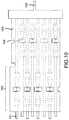
- FIG. 10An alternative embodiment of electronic signal interrogation is possible using the array configuration illustrated in FIG. 10 .
- all the lead wires from the right side of the electrode pairs of the array of devices 1000is shorted into a common lead wire 1020 .
- the arrayalso includes the insulator layer 1008 covering the majority of the electrode array except for the exposed Au tips 1009 .
- interrogation of nucleotide attachmentcomprises performing sequential interrogation with the right side of all the lead wires shorted to a common lead 1020 and then taking turns with the individual electrical lead wires 1021 present on the left side of the pairs, one at a time, e.g., every millisecond. This method results in fewer electronic measurement complications than handling many thousands of parallel signals all at once.
- FIG. 11Shown in FIG. 11 is an exemplary three-dimensional array of molecular electronics genome-sequencing platform.
- an electrically insulating top coating 1108such as polymer or oxide layer (e.g., PMMA, PEG, PDMS, aluminum oxide, Si oxide, Si nitride, etc.) is applied and patterned to cover all the electrode surfaces in the electrode pairs 1100 except for the very tips 1109 of the electrodes.
- This protective coatingserves as electrical insulator but also as a coating that prevents or minimizes the adhesion of biomolecules at unwanted locations.
- the right side electrode leadsmay be shorted into a common lead wire 1120 whilst the left side lead wires 1121 may be left singly for sequential interrogation.
- FIG. 9 or FIG. 10 type aerial array sequencing structureis stacked in three dimensions, such as illustrated in FIG. 11 , representing a three-dimensional array of molecular electronics genome-sequencing platform.
- the 3D arrayfurther comprises an accompanying microfluidic chamber for each two-dimensional array (as shown in FIG. 11( a ) , wherein 100 to 1,000 layers, each comprising about 10,000 devices and a microfluidic chamber), or in alternative embodiments, comprising one or more common microfluidic chambers encasing the entire three-dimensional array (as shown in FIG. 11( b ) , wherein 100 to 1,000 layers of sensing layers, each having about 10,000 devices, all encased in one microfluidic chamber).
- the desirable packing density of electronic sequencing pair devicesis at least 10,000/cm 2 , preferably at least 100,000/cm 2 , more preferably at least 1,000,000/cm 2 , and even more preferably at least 10,000,000/cm 2 .
- a DNA or genome sequencing structurecomprises an array of electrode pairs, each electrode in a pair separated by a nanogap and comprising a strongly adherent and highly conductive island with reduced contact resistance, and a biomolecule securely attached with each of its ends on one conductive island to bridge the nanogap, wherein the conductive islands comprise nano-pattern defined Au on a Au electrode, with the Au island dimension being sub-10 nm, and further comprising electronic means of DNA or genome sequencing using DC, RF or pulse signal on nucleotide attachment, but without using fluorescent element.
- a non-Au electrode based DNA or genome sequencing structurecomprises an array of electrodes and strongly adherent and highly conductive Au or other conductive islands having reduced contact resistance, with a biomolecule securely attached on a pair of conductive islands, with the Au island dimension being sub-10 nm, and the electrode base material selected from Pt, Pd, Rh, and Ag, with electronic means of DNA or genome sequencing using DC, RF or pulse signal on nucleotide attachment, but without using fluorescent element.
- the adherent conductoris made of Au, having a contact area to the electrode surface of at least 50%, and preferably %100 of the Au island diameter.
- the adherent gold nano-islandis branched or porous with a porosity of at least 10%, preferably at least 30%, and even more preferably at least 50%, so as to increase the surface area of gold island top surface by at least by 20%, preferably by at least 40%, and even more preferably by at least 60%, over a flat and smooth Au nano-island structure.
- an increase in the surface area of the Au islandsis obtained by one or more of the methods selected from a list of: i) plasma etching; ii) ion implantation and optional annealing heat treatment; iii) gold (Au) nanoparticles attaching and bonding; iv) selective dissolving non-Au component from a nanocomposite structure; or v) de-alloying process.
- the structurecomprises parallel devices with at least 1,000, preferably at least 10,000, even more preferably at least 1 million devices, fabricated by one or more methods selected from nano-patterning approaches such as nano-imprinting lithography, shadow mask patterning, electron beam lithography, extreme UV lithography, or X-ray lithography.
- nano-patterning approachessuch as nano-imprinting lithography, shadow mask patterning, electron beam lithography, extreme UV lithography, or X-ray lithography.
- the structurecomprises multilayers of devices with at least 10,000, preferably at least 1 million, even more preferably at least 100 million devices, in combination with microfluidic systems.
- a sequential interrogation of electrodesis enabled by a connected structure wherein one side of the device array lead wires are ganged into a common lead wire.
- a biomoleculeis attached to an Au island using antibody-antigen coupling, streptavidin-biotin coupling, peptide bonding, thiol-gold binding, gold binding proteins, or other coupling configurations.
- a genome or DNA sequencing systemcomprises a chamber containing a multitude of biomolecule sensing devices described herein, and a microfluidic subsystem that supplies or maintains biomolecules, nucleotides, PBS or water solution, and other needed materials.
- the Au island diameteris progressively reduced by repeated spheroidization annealing and top-etching, with the process repeated by at least 2 cycles of spheroidization and part of the top etching to reduce the height and diameter.
- the height reducing etchingcomprises chemical etching or plasma etching.
- the structurecomprises an added magnetic layer to enhance the attachment of magnetic-particle-tagged biomolecules, with the magnetic particles based on oxide material having natural chemical stability or metallic alloy material with surface coated with thin oxide or gold for anti-corrosion protection by a factor of at least 50% reduced corrosion rate, and/or enhanced affinity to biomolecules with at least 50% increased probability of biomolecule attachment.
- magnetic particlesare selected from Fe 2 O 3 , Fe 3 O 4 , surface-protected or surface-functionalized metallic magnetic particles having higher magnetic moment than iron oxide including Fe, Co, Ni and their alloys.
- the magnetic layeris magnetized or demagnetized to enable magnetically attracted attachment of biomolecules or removal and cleaning-out of attached biomolecules with a permanent magnet sweep, allowing multiple repeat operations of the sequencing devices by at least 10 times, preferably at least 1,000 times.
- these device structures for DNA sequencingcan be used for cancer detection and other medical uses.
- these devicesare usable for human genome sequencing.
Landscapes
- Chemical & Material Sciences (AREA)
- Health & Medical Sciences (AREA)
- Life Sciences & Earth Sciences (AREA)
- Engineering & Computer Science (AREA)
- Organic Chemistry (AREA)
- Proteomics, Peptides & Aminoacids (AREA)
- Physics & Mathematics (AREA)
- General Health & Medical Sciences (AREA)
- Analytical Chemistry (AREA)
- Molecular Biology (AREA)
- Zoology (AREA)
- Wood Science & Technology (AREA)
- Chemical Kinetics & Catalysis (AREA)
- Immunology (AREA)
- Biochemistry (AREA)
- Biophysics (AREA)
- General Engineering & Computer Science (AREA)
- Microbiology (AREA)
- Genetics & Genomics (AREA)
- Bioinformatics & Cheminformatics (AREA)
- Biotechnology (AREA)
- Hematology (AREA)
- Materials Engineering (AREA)
- Metallurgy (AREA)
- Mechanical Engineering (AREA)
- Dispersion Chemistry (AREA)
- Clinical Laboratory Science (AREA)
- Biomedical Technology (AREA)
- Nanotechnology (AREA)
- Spectroscopy & Molecular Physics (AREA)
- General Physics & Mathematics (AREA)
- Pathology (AREA)
- Electrochemistry (AREA)
- Medicinal Chemistry (AREA)
- Urology & Nephrology (AREA)
- Food Science & Technology (AREA)
- Apparatus Associated With Microorganisms And Enzymes (AREA)
- Measuring Or Testing Involving Enzymes Or Micro-Organisms (AREA)
- Investigating Or Analyzing Materials By The Use Of Electric Means (AREA)
Abstract
Description
Claims (25)
Priority Applications (1)
| Application Number | Priority Date | Filing Date | Title |
|---|---|---|---|
| US16/076,673US10737263B2 (en) | 2016-02-09 | 2017-02-09 | Electronic label-free DNA and genome sequencing |
Applications Claiming Priority (3)
| Application Number | Priority Date | Filing Date | Title |
|---|---|---|---|
| US201662293239P | 2016-02-09 | 2016-02-09 | |
| US16/076,673US10737263B2 (en) | 2016-02-09 | 2017-02-09 | Electronic label-free DNA and genome sequencing |
| PCT/US2017/017231WO2017139493A2 (en) | 2016-02-09 | 2017-02-09 | Electronic label-free dna and genome sequencing |
Related Parent Applications (1)
| Application Number | Title | Priority Date | Filing Date |
|---|---|---|---|
| PCT/US2017/017231A-371-Of-InternationalWO2017139493A2 (en) | 2016-02-09 | 2017-02-09 | Electronic label-free dna and genome sequencing |
Related Child Applications (1)
| Application Number | Title | Priority Date | Filing Date |
|---|---|---|---|
| US16/912,580ContinuationUS11440003B2 (en) | 2016-02-09 | 2020-06-25 | Electronic label-free DNA and genome sequencing |
Publications (2)
| Publication Number | Publication Date |
|---|---|
| US20190039065A1 US20190039065A1 (en) | 2019-02-07 |
| US10737263B2true US10737263B2 (en) | 2020-08-11 |
Family
ID=59564039
Family Applications (3)
| Application Number | Title | Priority Date | Filing Date |
|---|---|---|---|
| US16/076,673Expired - Fee RelatedUS10737263B2 (en) | 2016-02-09 | 2017-02-09 | Electronic label-free DNA and genome sequencing |
| US16/912,580Active2037-02-24US11440003B2 (en) | 2016-02-09 | 2020-06-25 | Electronic label-free DNA and genome sequencing |
| US17/879,254AbandonedUS20220371012A1 (en) | 2016-02-09 | 2022-08-02 | Electronic label-free dna and genome sequencing |
Family Applications After (2)
| Application Number | Title | Priority Date | Filing Date |
|---|---|---|---|
| US16/912,580Active2037-02-24US11440003B2 (en) | 2016-02-09 | 2020-06-25 | Electronic label-free DNA and genome sequencing |
| US17/879,254AbandonedUS20220371012A1 (en) | 2016-02-09 | 2022-08-02 | Electronic label-free dna and genome sequencing |
Country Status (7)
| Country | Link |
|---|---|
| US (3) | US10737263B2 (en) |
| EP (2) | EP3882616A1 (en) |
| JP (1) | JP6854532B2 (en) |
| KR (2) | KR102734671B1 (en) |
| CN (1) | CN109155354A (en) |
| CA (1) | CA3053103A1 (en) |
| WO (1) | WO2017139493A2 (en) |
Cited By (5)
| Publication number | Priority date | Publication date | Assignee | Title |
|---|---|---|---|---|
| US20220371012A1 (en)* | 2016-02-09 | 2022-11-24 | Roswell Biotechnologies, Inc. | Electronic label-free dna and genome sequencing |
| US12031981B2 (en) | 2018-05-09 | 2024-07-09 | Arizona Board Of Regents On Behalf Of Arizona State University | Method for electronic detection and quantification of antibodies |
| US12276653B2 (en) | 2020-05-29 | 2025-04-15 | Arizona Board Of Regents On Behalf Of Arizona State University | Bioelectronic devices with programmable adaptors |
| US12298300B2 (en) | 2020-04-17 | 2025-05-13 | Arizona Board Of Regents On Behalf Of Arizona State University | Single-molecule electronic sequence detector and methods of use |
| US12351855B2 (en) | 2019-01-30 | 2025-07-08 | Arizona Board Of Regents On Behalf Of Arizona State University | Bioelectronic circuits, systems and methods for preparing and using them |
Families Citing this family (22)
| Publication number | Priority date | Publication date | Assignee | Title |
|---|---|---|---|---|
| KR102713216B1 (en) | 2015-06-25 | 2024-10-02 | 로스웰 엠이 아이엔씨. | Biomolecular sensors and methods |
| WO2017132567A1 (en) | 2016-01-28 | 2017-08-03 | Roswell Biotechnologies, Inc. | Massively parallel dna sequencing apparatus |
| CN109071212A (en) | 2016-01-28 | 2018-12-21 | 罗斯韦尔生物技术股份有限公司 | Use the method and apparatus of large-scale molecular electronic sensor array measurement analyte |
| US10597767B2 (en) | 2016-02-22 | 2020-03-24 | Roswell Biotechnologies, Inc. | Nanoparticle fabrication |
| US9829456B1 (en) | 2016-07-26 | 2017-11-28 | Roswell Biotechnologies, Inc. | Method of making a multi-electrode structure usable in molecular sensing devices |
| US20190376925A1 (en)* | 2016-11-22 | 2019-12-12 | Roswell Biotechnologies, Inc. | Nucleic acid sequencing device containing graphene |
| KR102622275B1 (en) | 2017-01-10 | 2024-01-05 | 로스웰 바이오테크놀로지스 인코포레이티드 | Methods and systems for DNA data storage |
| US11656197B2 (en) | 2017-01-19 | 2023-05-23 | Roswell ME Inc. | Solid state sequencing devices comprising two dimensional layer materials |
| KR102692957B1 (en) | 2017-04-25 | 2024-08-06 | 로스웰 엠이 아이엔씨. | Enzyme circuits for molecular sensors |
| US10508296B2 (en) | 2017-04-25 | 2019-12-17 | Roswell Biotechnologies, Inc. | Enzymatic circuits for molecular sensors |
| CA3057155A1 (en) | 2017-05-09 | 2018-11-15 | Roswell Biotechnologies, Inc. | Binding probe circuits for molecular sensors |
| KR102737316B1 (en) | 2017-08-30 | 2024-12-02 | 로스웰 엠이 아이엔씨. | Progressive Enzyme Molecular Electronic Sensors for DNA Data Storage |
| WO2019075100A1 (en) | 2017-10-10 | 2019-04-18 | Roswell Biotechnologies, Inc. | Methods, apparatus and systems for amplification-free dna data storage |
| RU2679494C1 (en) | 2017-12-26 | 2019-02-11 | Ооо "Гамма-Днк" | Method of non-marking single-molecular sequency of dna and device for its implementation |
| TWI772618B (en)* | 2018-03-02 | 2022-08-01 | 國立研究開發法人科學技術振興機構 | Nano-slit electrode, method of making same, and nano-device with nano-slit electrode |
| TWI815865B (en)* | 2018-03-02 | 2023-09-21 | 國立研究開發法人科學技術振興機構 | single molecule transistor |
| WO2020163818A1 (en)* | 2019-02-08 | 2020-08-13 | Universal Sequencing Technology Corporation | Peptide nanostructure for biopolymer sensing |
| CN113826004A (en)* | 2019-03-26 | 2021-12-21 | 罗斯威尔生命技术公司 | Tunable nanopillar and nanogap electrode structures and methods therefor |
| US12146852B2 (en) | 2019-09-06 | 2024-11-19 | Roswell Biotechnologies, Inc. | Methods of fabricating nanoscale structures usable in molecular sensors and other devices |
| CN115605612A (en)* | 2020-03-25 | 2023-01-13 | 通用测序技术公司(Us) | Enzyme mutants directly connected to nanogap devices |
| EP4208567A4 (en)* | 2020-09-02 | 2024-11-20 | Roswell Biotechnologies, Inc. | SINGLE PARTICLE NANOWIRES FOR MOLECULAR ELECTRONIC SENSING |
| US20220252542A1 (en)* | 2020-09-02 | 2022-08-11 | Roswell Biotechnologies, Inc. | Single molecule nanoparticle nanowire for molecular electronic sensing |
Citations (242)
| Publication number | Priority date | Publication date | Assignee | Title |
|---|---|---|---|---|
| US5082627A (en) | 1987-05-01 | 1992-01-21 | Biotronic Systems Corporation | Three dimensional binding site array for interfering with an electrical field |
| US5194133A (en) | 1990-05-04 | 1993-03-16 | The General Electric Company, P.L.C. | Sensor devices |
| US5366140A (en) | 1993-09-30 | 1994-11-22 | Minnesota Mining And Manufacturing Company | Patterned array of uniform metal microbeads |
| US5414588A (en) | 1993-09-20 | 1995-05-09 | The Regents Of The University Of California | High performance capacitors using nano-structure multilayer materials fabrication |
| US5486449A (en) | 1989-02-07 | 1996-01-23 | Rohm Co., Ltd. | Photomask, photoresist and photolithography for a monolithic IC |
| US5532128A (en) | 1991-11-19 | 1996-07-02 | Houston Advanced Research Center | Multi-site detection apparatus |
| US5583359A (en) | 1995-03-03 | 1996-12-10 | Northern Telecom Limited | Capacitor structure for an integrated circuit |
| US5639507A (en) | 1995-05-03 | 1997-06-17 | Avx Corporation | Method of making a planar multi-layer capacitor |
| US5767687A (en) | 1996-11-29 | 1998-06-16 | Geist; Jon | Surface-capacitor type condensable-vapor sensor |
| US5871918A (en) | 1996-06-20 | 1999-02-16 | The University Of North Carolina At Chapel Hill | Electrochemical detection of nucleic acid hybridization |
| US5881184A (en) | 1996-05-22 | 1999-03-09 | Eastman Kodak Company | Active pixel sensor with single pixel reset |
| US5982018A (en) | 1997-05-23 | 1999-11-09 | Micron Technology, Inc. | Thin film capacitor coupons for memory modules and multi-chip modules |
| US6051380A (en) | 1993-11-01 | 2000-04-18 | Nanogen, Inc. | Methods and procedures for molecular biological analysis and diagnostics |
| US6060023A (en) | 1998-03-31 | 2000-05-09 | Motorola, Inc. | Molecular sensing apparatus |
| US6094335A (en) | 1998-10-09 | 2000-07-25 | Advanced Micro Devices, Inc. | Vertical parallel plate capacitor |
| US6110354A (en) | 1996-11-01 | 2000-08-29 | University Of Washington | Microband electrode arrays |
| US6123819A (en) | 1997-11-12 | 2000-09-26 | Protiveris, Inc. | Nanoelectrode arrays |
| US6144023A (en) | 1997-06-06 | 2000-11-07 | Commissariat A L'energie Atomique | Electrode support comprising at least one electrode covered by a deposit and system for reading this support |
| US6238927B1 (en) | 1998-10-05 | 2001-05-29 | Mosaic Technologies, Incorporated | Reverse displacement assay for detection of nucleic acid sequences |
| US20020022223A1 (en) | 1999-04-07 | 2002-02-21 | Connolly Dennis Michael | High resolution DNA detection methods and devices |
| WO2002049980A1 (en) | 2000-12-21 | 2002-06-27 | Ferro Gmbh | Substrates with a self-cleaning surface, a process for their production and their use |
| US20020090649A1 (en) | 1999-12-15 | 2002-07-11 | Tony Chan | High density column and row addressable electrode arrays |
| US6440662B1 (en) | 1995-12-01 | 2002-08-27 | Innogenetics N.V. | Impedimetric detection system and method of production thereof |
| US20020138049A1 (en) | 1998-06-10 | 2002-09-26 | Allen Mark G. | Microneedle devices and methods of manufacture and use thereof |
| WO2002074985A2 (en) | 2001-03-20 | 2002-09-26 | Infineon Technologies Ag | Method of detecting macromolecular biopolymers by means of an electrode arrangement |
| US20020137083A1 (en) | 2001-01-31 | 2002-09-26 | Shinichi Kobori | Gene detection chip and detection device |
| US20020142477A1 (en) | 1999-05-10 | 2002-10-03 | Lewis Nathan S. | Spatiotemporal and geometric optimization of sensor arrays for detecting analytes fluids |
| US6464889B1 (en) | 1996-01-22 | 2002-10-15 | Etex Corporation | Surface modification of medical implants |
| US20020172963A1 (en) | 2001-01-10 | 2002-11-21 | Kelley Shana O. | DNA-bridged carbon nanotube arrays |
| US20020184939A1 (en) | 1997-10-10 | 2002-12-12 | Tapesh Yadav | Multilaminated nano-engineered devices |
| US6506564B1 (en) | 1996-07-29 | 2003-01-14 | Nanosphere, Inc. | Nanoparticles having oligonucleotides attached thereto and uses therefor |
| US20030025133A1 (en) | 2001-07-13 | 2003-02-06 | Brousseau Louis C. | Methods of fabricating single electron transistors in which the thickness of an insulating layer defines spacing between electrodes |
| US20030040000A1 (en) | 2001-08-08 | 2003-02-27 | Connolly Dennis M. | Methods for attaching nucleic acid molecules to electrically conductive surfaces |
| US6537747B1 (en) | 1998-02-03 | 2003-03-25 | Lucent Technologies Inc. | Data transmission using DNA oligomers |
| US20030064390A1 (en) | 1999-12-13 | 2003-04-03 | Schuelein Jurgen | Method and device for detecting and quantifying biomolecules |
| US20030087296A1 (en) | 2001-11-02 | 2003-05-08 | Fujitsu Limited | Protein detecting device |
| WO2003042396A2 (en) | 2001-06-11 | 2003-05-22 | Genorx, Inc. | Electronic detection of biological molecules using thin layers |
| US20030186263A1 (en) | 2000-03-30 | 2003-10-02 | Alexander Frey | Biosensor and method for detecting macromolecular biopolymers using a biosensor |
| US20030224387A1 (en) | 2002-05-22 | 2003-12-04 | Sandeep Kunwar | Association of molecules with electrodes of an array of electrodes |
| US6670131B2 (en) | 2000-11-30 | 2003-12-30 | Kabushiki Kaisha Toshiba | Nucleic acid detection method and apparatus, and vessel for detecting nucleic acid |
| US6673533B1 (en) | 1995-03-10 | 2004-01-06 | Meso Scale Technologies, Llc. | Multi-array multi-specific electrochemiluminescence testing |
| US20040014106A1 (en) | 2002-05-14 | 2004-01-22 | Nanosphere, Inc. | Electrical detection of DNA hybridization and specific binding events |
| US20040012161A1 (en) | 2002-07-17 | 2004-01-22 | Li Jiun Chiu | Tool coupling device for changeable tool members |
| US20040023253A1 (en) | 2001-06-11 | 2004-02-05 | Sandeep Kunwar | Device structure for closely spaced electrodes |
| US20040038090A1 (en) | 2002-06-05 | 2004-02-26 | Faris Sadeg M. | Layered electrochemical cell and manufacturing method therefor |
| US20040063100A1 (en) | 2002-09-30 | 2004-04-01 | Wang Chung Lin | Nanoneedle chips and the production thereof |
| US6716620B2 (en) | 2000-04-17 | 2004-04-06 | Purdue Research Foundation | Biosensor and related method |
| US20040086929A1 (en) | 2002-11-01 | 2004-05-06 | Wisconsin Alumni Research Foundation | Direct radio-frequency detection of nucleotide hybridization at microelectrodes |
| US6762050B2 (en) | 1997-09-30 | 2004-07-13 | Seiko Epson Corporation | Manufacture of a microsensor device and a method for evaluating the function of a liquid by the use thereof |
| US6764745B1 (en) | 1999-02-25 | 2004-07-20 | Seiko Epson Corporation | Structural member superior in water repellency and method for manufacturing the same |
| US20040146863A1 (en) | 2001-06-11 | 2004-07-29 | Pisharody Sobha M. | Electronic detection of biological molecules using thin layers |
| US20040209355A1 (en) | 1996-12-06 | 2004-10-21 | Nanogen, Inc. | Systems and devices for photoelectrophoretic transport and hybridization of oligonucleotides |
| US20040209435A1 (en) | 2003-04-17 | 2004-10-21 | Aaron Partridge | Method of Making a Nanogap for Variable Capacitive Elements, and Device having a Nanogap |
| WO2004096986A2 (en) | 2003-04-29 | 2004-11-11 | Integrated Nano-Technologies, Llc | Method for quantitative detection of nucleic acid molecules |
| WO2004099307A2 (en) | 2003-02-07 | 2004-11-18 | Wisconsin Alumni Research Foundation | Nanocylinder-modified surfaces |
| US20050029227A1 (en) | 1999-02-26 | 2005-02-10 | Micron Technology, Inc. | Apparatus and method of detecting endpoint of a dielectric etch |
| US20050067086A1 (en) | 2003-09-29 | 2005-03-31 | Murata Manufacturing Co., Ltd. | Method of producing multi-terminal type laminated ceramic electronic component |
| US20050074911A1 (en) | 2003-10-07 | 2005-04-07 | Pavel Kornilovich | Fabricationof nano-object array |
| US6916614B1 (en) | 1999-10-20 | 2005-07-12 | Tum Gene, Inc. | Gene detecting chip, detector, and detecting method |
| US20050151541A1 (en) | 2003-12-17 | 2005-07-14 | Thomas Brinz | Measuring device having a plurality of potentiometric electrode pairs situated on a substrate |
| US20050172199A1 (en) | 2004-02-03 | 2005-08-04 | Phonex Broadband Corporation. | Reliable method and system for efficiently transporting dynamic data across a network |
| US20050181195A1 (en) | 2003-04-28 | 2005-08-18 | Nanosys, Inc. | Super-hydrophobic surfaces, methods of their construction and uses therefor |
| US20050221473A1 (en) | 2004-03-30 | 2005-10-06 | Intel Corporation | Sensor array integrated circuits |
| US20050227373A1 (en) | 2002-06-24 | 2005-10-13 | Denis Flandre | Method and device for high sensitivity detection of the presence of dna and other probes |
| US20050247573A1 (en) | 2004-03-23 | 2005-11-10 | Hideaki Nakamura | Biosensors |
| WO2005108612A2 (en) | 2003-11-28 | 2005-11-17 | Genorx, Inc. | Nanoscale biosensor device, system and technique |
| US20050287548A1 (en) | 2001-06-25 | 2005-12-29 | Gang Bao | Activatable probes and methods for in vivo gene detection |
| US20050285275A1 (en) | 2004-06-24 | 2005-12-29 | California Institute Of Technology | Fabrication of nano-gap electrode arrays by the construction and selective chemical etching of nano-crosswire stacks |
| US20060003482A1 (en) | 2004-06-30 | 2006-01-05 | International Business Machines Corporation | Elastomeric cmos based micro electromechanical varactor |
| US20060019273A1 (en) | 2004-05-12 | 2006-01-26 | Connolly Dennis M | Detection card for analyzing a sample for a target nucleic acid molecule, and uses thereof |
| US20060024508A1 (en) | 2004-07-27 | 2006-02-02 | D Urso Brian R | Composite, nanostructured, super-hydrophobic material |
| US20060024504A1 (en) | 2004-08-02 | 2006-02-02 | Nelson Curtis L | Methods of controlling flow |
| US20060029808A1 (en) | 2004-08-06 | 2006-02-09 | Lei Zhai | Superhydrophobic coatings |
| US20060051919A1 (en) | 2004-08-31 | 2006-03-09 | Stmicroelectronics S.R.L. | Nanometric structure and corresponding manufacturing method |
| US20060051946A1 (en) | 2004-08-31 | 2006-03-09 | Stmicroelectronics S.R.L. | Method for realizing a hosting structure of nanometric elements |
| US20060105467A1 (en) | 2004-11-12 | 2006-05-18 | Niksa Andrew J | MEMS-based sensor for lubricant analysis |
| US20060105449A1 (en) | 2004-09-03 | 2006-05-18 | Franz Larmer | Biochip having an electode array on a substrate |
| US20060128239A1 (en) | 2002-09-13 | 2006-06-15 | Edwin Nun | Production of self-cleaning surfaces on textile coatings |
| US20060147983A1 (en) | 2004-10-14 | 2006-07-06 | Kabushiki Kaisha Toshiba | Nucleic acid detecting sensor, nucleic acid detecting chip, and nucleic acid detecting circuit |
| US7075428B1 (en) | 2003-11-20 | 2006-07-11 | Biowarn Llc | Methodology and apparatus for the detection of biological substances |
| US20060154489A1 (en) | 2002-10-12 | 2006-07-13 | Fujitsu Limited | Semiconductor base structure for molecular electronics and molecular electronic-based biosensor devices and a method for producing such a semiconductor base structure |
| US20060275853A1 (en) | 2005-06-02 | 2006-12-07 | Board Of Trustees Of Michigan State University | Methods to increase dynamic range and improve quantitative analysis in rapid biosensors |
| US7169272B2 (en) | 1997-04-30 | 2007-01-30 | Board Of Trustees Of The University Of Arkansas | Microfabricated recessed disk microelectrodes: characterization in static and convective solutions |
| US20070026193A1 (en) | 2005-04-01 | 2007-02-01 | Clemson University | Ultrahydrophobic substrates |
| US20070048748A1 (en) | 2004-09-24 | 2007-03-01 | Li-Cor, Inc. | Mutant polymerases for sequencing and genotyping |
| US7189435B2 (en) | 2001-03-14 | 2007-03-13 | University Of Massachusetts | Nanofabrication |
| US7202480B2 (en) | 2003-09-30 | 2007-04-10 | Hitachi, Ltd. | Semiconductor radiological detector and semiconductor radiological imaging apparatus |
| US7208077B1 (en) | 1999-04-14 | 2007-04-24 | Fraunhofer-Gesellschaft Zur Foerderung Der Angewandten Forschung E.V. | Sensor arrangement with electrically controllable arrays |
| WO2007054649A1 (en) | 2005-11-14 | 2007-05-18 | Commissariat A L'energie Atomique | Superhydrophilic or superhydrophobic product, process for producing it and use of this product |
| KR20070059880A (en) | 2005-12-06 | 2007-06-12 | 한국전자통신연구원 | Sensor with nanogap electrode and manufacturing method thereof |
| US20070140902A1 (en) | 2003-12-16 | 2007-06-21 | Andreas Calatzis | Cartridge device for blood analysis |
| US20070148815A1 (en) | 2005-12-28 | 2007-06-28 | Industrial Technology Research Institue | Nano-array and fabrication method thereof |
| US20070184247A1 (en) | 2006-02-03 | 2007-08-09 | Simpson John T | Transparent, super-hydrophobic, disordered composite material |
| US20070207487A1 (en) | 2006-01-25 | 2007-09-06 | Emig Christopher J | Photoelectrochemical synthesis of high density combinatorial polymer arrays |
| WO2007102960A2 (en) | 2006-01-30 | 2007-09-13 | Ashland Licensing And Intellectual Property Llc | Hydrophobic self-cleaning coating compositions |
| US7276206B2 (en) | 2001-07-12 | 2007-10-02 | Merck & Co., Inc. | Electrical field stimulation of eukaryotic cells |
| US20070231542A1 (en) | 2006-04-03 | 2007-10-04 | General Electric Company | Articles having low wettability and high light transmission |
| WO2007126432A1 (en) | 2006-03-27 | 2007-11-08 | Georgia Tech Research Corporation | Superhydrophobic surface and method for forming same |
| WO2007128965A1 (en) | 2006-04-10 | 2007-11-15 | Cambridge Display Technology Limited | Electric devices and methods of manufacturing the same |
| US20080098815A1 (en) | 2006-10-27 | 2008-05-01 | Stmicroelectronics S.R.L. | Microelectromechanical sensor having multiple full-scale and sensitivity values |
| US7399585B2 (en) | 2000-05-03 | 2008-07-15 | The United States Of America As Represented By The Secretary Of The Navy | Biological identification system with integrated sensor chip |
| CN101231287A (en) | 2008-02-22 | 2008-07-30 | 东南大学 | Method for preparing biosensor by arranging nanoparticles in electrodes induced by external field |
| US20080199659A1 (en) | 2005-09-19 | 2008-08-21 | Wayne State University | Transparent hydrophobic article having self-cleaning and liquid repellant features and method of fabricating same |
| US7470533B2 (en) | 2002-12-20 | 2008-12-30 | Acea Biosciences | Impedance based devices and methods for use in assays |
| WO2009003208A1 (en) | 2007-07-04 | 2009-01-08 | Austrian Research Centers Gmbh - Arc | Method for identifying and quantifying organic and biochemical substances |
| US20090017571A1 (en) | 2005-12-15 | 2009-01-15 | The Trustees Of Columbia University In The City Of New York | Sensing devices from molecular electronic devices |
| US20090020428A1 (en) | 2007-07-19 | 2009-01-22 | University Of Pittsburgh - Of The Commonwealth System Of Higher Education | Manipulation, detection, and assay of small scale biological particles |
| US20090062684A1 (en) | 2005-03-31 | 2009-03-05 | Globalreach Holding Aps | Apparatus and method for a global model of hollow internal organs including the determination of cross-sectional areas and volume in internal hollow organs and wall properties |
| US7507320B2 (en) | 2004-10-09 | 2009-03-24 | Academia Sinica | Single-atom tip and preparation method thereof |
| EP2053383A1 (en) | 2006-07-20 | 2009-04-29 | Fujifilm Corporation | Microstructure and its fabrication method, sensor device, and raman spectroscopy device |
| US7531120B2 (en) | 2000-12-02 | 2009-05-12 | Aquamarijn Holding B.V. | Method of making a product with a micro or nano sized structure and product |
| US20090152109A1 (en) | 2006-03-17 | 2009-06-18 | Andrew John Whitehead | Microelectrode array |
| US20090170716A1 (en) | 2007-12-31 | 2009-07-02 | Xing Su | Electronic sensing for nucleic acid sequencing |
| US20090178935A1 (en) | 2006-04-10 | 2009-07-16 | Diagnoswiss S.A. | Miniaturised Biosensor with Optimized Amperometric Detection |
| US7579823B1 (en) | 2005-06-14 | 2009-08-25 | E. I. Spectra, Llc | Thin film sensor |
| US20090297913A1 (en) | 2008-03-25 | 2009-12-03 | The University Of Georgia Research Foundation, Inc. | Nanostructure-Enhanced stereo-electrodes for fuel cells and biosensors |
| US20090295372A1 (en) | 2008-01-25 | 2009-12-03 | Krstic Predrag S | Nanoscopic electrode molecular probes |
| US20090306578A1 (en) | 2004-03-24 | 2009-12-10 | Technion Research & Development Foundation Ltd. | Artificial receptors |
| US20090324308A1 (en) | 2008-06-30 | 2009-12-31 | Xerox Corporation | Oil less fusing using nano/micro textured fusing surfaces |
| US20100038342A1 (en) | 2007-04-05 | 2010-02-18 | Korea Institute Of Machinery And Materials | Preparation of super water repellent surface |
| US20100044212A1 (en) | 2008-08-21 | 2010-02-25 | Snu R&Db Foundation | Vertically standing ionic polymer-metal composite |
| WO2010022107A2 (en) | 2008-08-18 | 2010-02-25 | The Regents Of The University Of California | Nanostructured superhydrophobic, superoleophobic and/or superomniphobic coatings, methods for fabrication, and applications thereof |
| US20100055397A1 (en) | 2006-11-15 | 2010-03-04 | National Institute Of Advanced Industrial Science And Technology | Mold for optical device with anti-reflection structure, method for producing the same, and optical device |
| US7691433B2 (en) | 2004-12-15 | 2010-04-06 | Forschungszentrum Julich Gmbh | Method for structured application of molecules to a strip conductor and molecular memory matrix |
| US20100132771A1 (en) | 2008-10-06 | 2010-06-03 | The Regents Of The University Of California | 3D Carbon Nanotubes Membrane as a Solar Energy Absorbing Layer |
| US20100142259A1 (en) | 2005-03-21 | 2010-06-10 | The Trustees Of The University Of Pennsylvania | Nanogaps: methods and devices containing same |
| US20100167938A1 (en) | 2008-12-31 | 2010-07-01 | Xing Su | Nucleic acid sequencing and electronic detection |
| US20100188109A1 (en) | 2006-12-15 | 2010-07-29 | Joshua Edel | Electrode systems and their use in the characterization of molecules |
| US20100194409A1 (en) | 2006-08-16 | 2010-08-05 | Agency For Science, Technology And Research | Method of electrically detecting a biological analyte molecule |
| US20100206367A1 (en) | 2009-02-18 | 2010-08-19 | Korea Institute Of Industrial Technology | Method for fabricating silicon nano wire, solar cell including silicon nano wire and method for fabricating solar cell |
| US7785785B2 (en) | 2004-11-12 | 2010-08-31 | The Board Of Trustees Of The Leland Stanford Junior University | Charge perturbation detection system for DNA and other molecules |
| US20100280397A1 (en) | 2005-12-22 | 2010-11-04 | Board Of Regents, The University Of Texas Sys | Method and apparatus for monitoring an organ of a patient |
| US20100285275A1 (en) | 2009-05-06 | 2010-11-11 | Adra Smith Baca | Fingerprint-resistant glass substrates |
| US20100285601A1 (en) | 2007-09-28 | 2010-11-11 | Agency For Science, Technology And Research | Method of electrically detecting a nucleic acid molecule |
| US20100288543A1 (en) | 2009-04-14 | 2010-11-18 | Nanoink, Inc. | Conducting lines, nanoparticles, inks, and patterning |
| US20100300899A1 (en) | 2007-12-21 | 2010-12-02 | The Trustees Of Columbia University In The City Of New York | Active CMOS Sensor Array For Electrochemical Biomolecular Detection |
| US7851045B2 (en) | 2000-07-06 | 2010-12-14 | Saint-Gobain Glass France | Transparent textured substrate and methods for obtaining same |
| US20110056845A1 (en) | 2008-01-24 | 2011-03-10 | Francesco Stellacci | Insulated nanogap devices and methods of use thereof |
| US20110076783A1 (en) | 2008-06-19 | 2011-03-31 | Liu Ben H | Multi-dimensional fluid sensors and related detectors and methods |
| US20110091787A1 (en) | 2006-03-31 | 2011-04-21 | Quantumsphere, Inc. | Compositions of nanometal particles containing a metal or alloy and platinum particles for use in fuel cells |
| US20110160077A1 (en) | 2009-12-16 | 2011-06-30 | Pacific Biosciences Of California, Inc. | Sequencing methods using enzyme conformation |
| US20110166034A1 (en) | 2006-08-02 | 2011-07-07 | Kwong Gabriel A | Capture agents and related methods and systems for detecting and/or sorting targets |
| US20110217763A1 (en) | 2008-11-18 | 2011-09-08 | Avraham Rasooly | A semiconductor for measuring biological interactions |
| KR20110104245A (en) | 2010-03-16 | 2011-09-22 | 주식회사 나노플랫폼 | FET-based biosensor, preparation method thereof, and target material detection method using same |
| US20110227558A1 (en) | 2008-07-11 | 2011-09-22 | Mannion John T | Nanofluidic channels with integrated charge sensors and methods based thereon |
| US20110233075A1 (en) | 2008-09-02 | 2011-09-29 | The Governing Council Of The University Of Toronto | Nanostructured microelectrodes and biosensing devices incorporating the same |
| US20110287956A1 (en) | 2010-04-07 | 2011-11-24 | Board Of Regents, The University Of Texas System | Nano-Scale Biosensors |
| US20110291673A1 (en) | 2009-04-27 | 2011-12-01 | Sharp Kabushiki Kaisha | Chemical sensor |
| US20110311853A1 (en) | 2010-06-17 | 2011-12-22 | Lsi Corporation | Electrochemical cell system and apparatus to provide energy to a portable electronic device |
| US20110312529A1 (en) | 2010-06-18 | 2011-12-22 | Illumina, Inc. | Conformational probes and methods for sequencing nucleic acids |
| US20120060905A1 (en) | 2010-09-10 | 2012-03-15 | International Business Machines Corporation | Nanowires formed by employing solder nanodots |
| WO2012083249A2 (en) | 2010-12-17 | 2012-06-21 | The Trustees Of Columbia University In The City Of New York | Dna sequencing by synthesis using modified nucleotides and nanopore detection |
| WO2012087352A2 (en) | 2010-12-20 | 2012-06-28 | The Regents Of The University Of California | Superhydrophobic and superoleophobic nanosurfaces |
| US8241508B2 (en) | 2004-07-27 | 2012-08-14 | Ut-Battelle, Llc | Method of forming composite, ordered material having sharp surface features |
| US20120220046A1 (en) | 2011-02-24 | 2012-08-30 | Chih-Yu Chao | Method and apparatus for forming the doped cryo-biology specimen of electron microscope |
| US20120258870A1 (en) | 2010-11-22 | 2012-10-11 | The University Of Chicago | Methods, Systems, and/or Use of Oligonucleotide Conjugates to Develop Panels for Use in Assays and Detections |
| DE102012008375A1 (en) | 2011-04-27 | 2012-10-31 | Genovoxx Gmbh | Methods and components for the detection of nucleic acid chains |
| US20120286332A1 (en) | 2006-12-14 | 2012-11-15 | Life Technologies Corporation | Chemically sensitive sensors with sample and hold capacitors |
| WO2012152056A1 (en) | 2011-04-19 | 2012-11-15 | The Hong Kong University Of Science And Technology | Method and device for monitoring real-time polymerase chain reaction (pcr) utilizing electro-active hydrolysis probe (e-tag probe) |
| US8351181B1 (en) | 2011-06-23 | 2013-01-08 | Samsung Electro-Mechanics Co., Ltd. | Chip type laminated capacitor |
| US20130049158A1 (en) | 2011-08-30 | 2013-02-28 | International Business Machines Corporation | Formation of metal nanospheres and microspheres |
| US20130109577A1 (en) | 2011-10-14 | 2013-05-02 | Pacific Biosciences Of California, Inc. | Real-time redox sequencing |
| US20130108956A1 (en) | 2011-11-01 | 2013-05-02 | Az Electronic Materials Usa Corp. | Nanocomposite positive photosensitive composition and use thereof |
| US20130162276A1 (en) | 2010-09-07 | 2013-06-27 | Korea Institute Of Machinery & Materials | Probe card and method for manufacturing same |
| WO2013096851A1 (en) | 2011-12-22 | 2013-06-27 | President And Fellows Of Harvard College | Compositions and methods for analyte detection |
| US20130183492A1 (en) | 2012-01-17 | 2013-07-18 | Snu R&Db Foundation | Metal nanoparticles on substrate and method of forming the same |
| US20130214875A1 (en) | 2012-02-16 | 2013-08-22 | Elwha Llc | Graphene sheet and nanomechanical resonator |
| US20130239349A1 (en) | 2012-03-14 | 2013-09-19 | Palo Alto Research Center Incorporated | Self-powered manual toothbrush with sensors |
| US20130245416A1 (en) | 2010-09-14 | 2013-09-19 | Martin L. Yarmush | Nanoporous Metal Multiple Electrode Array and Method of Making Same |
| US20130273340A1 (en) | 2012-04-16 | 2013-10-17 | Temple University - Of the Commonwealth System of Higher Education | Self-assembly of small structures |
| US20130281325A1 (en) | 2011-12-15 | 2013-10-24 | Oguz H. Elibol | Diamond electrode nanogap transducers |
| US20130331299A1 (en) | 2011-02-28 | 2013-12-12 | Lexogen Gmbh | Biosensor array formed by junctions of functionalized electrodes |
| US20140001055A1 (en) | 2012-06-29 | 2014-01-02 | Oguz H. Elibol | High throughput biochemical detection using single molecule fingerprinting arrays |
| US20140018262A1 (en) | 2011-02-28 | 2014-01-16 | Lexogen Gmbh | Biosensor array formed by junctions of functionalized electrodes |
| US20140027775A1 (en) | 2012-07-24 | 2014-01-30 | Micron Technology, Inc. | Methods of forming a metal chalcogenide material, related methods of forming a semiconductor device structure, and a related semiconductor device structure |
| US8652768B1 (en) | 2011-01-31 | 2014-02-18 | Sandia Corporation | Nanopatterns by phase separation of patterned mixed polymer monolayers |
| US20140048776A1 (en) | 2012-08-17 | 2014-02-20 | National Chiao Tung University | Protein transistor device |
| US20140061049A1 (en) | 2010-10-21 | 2014-03-06 | Yu-hwa Lo | Microfluidics with wirelessly powered electronic circuits |
| US20140079592A1 (en) | 2012-09-19 | 2014-03-20 | National Chiao Tung University | Bio-nanowire device and method of fabricating the same |
| US20140170567A1 (en) | 2011-08-04 | 2014-06-19 | Nissan Chemical Industries, Ltd. | Resist underlayer film-forming composition for euv lithography containing condensation polymer |
| US20140174927A1 (en) | 2011-07-27 | 2014-06-26 | Rashid Bashir | Nanopore Sensors for Biomolecular Characterization |
| US20140197459A1 (en) | 2011-01-04 | 2014-07-17 | Ecole Polytechnique Federale De Lausanne (Epfl) | Semiconductor device |
| US20140218637A1 (en) | 2013-02-06 | 2014-08-07 | Nanchang O-Film Tech. Co., Ltd. | Conductive film, manufacturing method thereof, and touch screen including the conducting film |
| US20140235493A1 (en) | 2011-09-19 | 2014-08-21 | University Of Utah Research Foundation | Multimode platform for detection of compounds |
| US20140253827A1 (en) | 2013-02-06 | 2014-09-11 | Nanchang O-Film Tech, Co., Ltd. | Conductive film, manufacturing method thereof, and touch screen having the same |
| US20140284667A1 (en) | 2013-03-20 | 2014-09-25 | International Business Machines Corporation | Finfet with reduced capacitance |
| WO2014182630A1 (en) | 2013-05-06 | 2014-11-13 | Pacific Biosciences Of California , Inc. | Real-time electronic sequencing |
| US20140367749A1 (en) | 2013-06-18 | 2014-12-18 | International Business Machines Corporation | Nanochannel process and structure for bio-detection |
| US20140377900A1 (en)* | 2013-06-19 | 2014-12-25 | International Business Machines Corporation | Manufacturable sub-3 nanometer palladium gap devices for fixed electrode tunneling recognition |
| US8927464B2 (en) | 2007-11-29 | 2015-01-06 | President And Fellows Of Harvard College | Assembly and deposition of materials using a superhydrophobic surface structure |
| US20150017655A1 (en) | 2013-07-09 | 2015-01-15 | National Chiao Tung University | Label-free sequencing method for single nucleic acid molecule |
| DE102013012145A1 (en) | 2013-07-20 | 2015-01-22 | Borros Arneth | Protein transistor based on anti-silicon antibody |
| US20150049332A1 (en) | 2013-07-30 | 2015-02-19 | The Curators Of The University Of Missouri | Gold nanoisland arrays |
| US20150057182A1 (en) | 2012-05-01 | 2015-02-26 | Life Technologies Corporation | Methods for analysis of dna fragments |
| US20150068892A1 (en) | 2002-07-02 | 2015-03-12 | Panasonic Healthcare Holdings Co., Ltd. | Biosensor, biosensor chip and biosensor device |
| US20150148264A1 (en) | 2010-10-04 | 2015-05-28 | Genapsys, Inc. | Systems and methods for automated reusable parallel biological reactions |
| CN104685066A (en) | 2012-04-09 | 2015-06-03 | 一龙公司 | Compositions and methods for quantifying nucleic acid sequences in a sample |
| CN104703700A (en) | 2012-08-06 | 2015-06-10 | 康特姆斯集团有限公司 | Method and kit for nucleic acid sequencing |
| US20150177150A1 (en) | 2013-11-17 | 2015-06-25 | Quantum-Si Incorporated | Optical system and assay chip for probing, detecting and analyzing molecules |
| US20150191709A1 (en) | 2012-07-19 | 2015-07-09 | Oxford Nanopore Technologies Limited | Modified helicases |
| US20150263203A1 (en) | 2012-10-26 | 2015-09-17 | Research Triangle Institute | Intermediate band semiconductors, heterojunctions, and optoelectronic devices utilizing solution processed quantum dots, and related methods |
| US20150294875A1 (en) | 2014-04-15 | 2015-10-15 | University Of Central Florida Research Foundation, Inc. | Plasma treated semiconductor dichalcogenide materials and devices therefrom |
| US20150293025A1 (en) | 2012-12-18 | 2015-10-15 | Toray Industries Inc. | Metal dot substrate and method of manufacturing metal dot substrate |
| WO2015167019A1 (en) | 2014-04-28 | 2015-11-05 | Quantum Biosystems Inc. | Nanogap electrode devices and systems and methods for forming the same |
| WO2015176990A1 (en) | 2014-05-23 | 2015-11-26 | Thomson Licensing | Method and apparatus for storing information units in nucleic acid molecules and nucleic acid storage system |
| US20150344945A1 (en) | 2014-06-03 | 2015-12-03 | Illumina, Inc. | Compositions, systems, and methods for detecting events using tethers anchored to or adjacent to nanopores |
| WO2015188197A2 (en) | 2014-06-06 | 2015-12-10 | Solstice Biologics, Ltd. | Polynucleotide constructs having bioreversible and non-bioreversible groups |
| US20160017416A1 (en) | 2014-07-15 | 2016-01-21 | Illumina, Inc | Biochemically activated electronic device |
| WO2016016635A1 (en) | 2014-07-28 | 2016-02-04 | Isis Innovation Limited | Plasmonic filter |
| US20160045378A1 (en) | 2013-03-27 | 2016-02-18 | Jacques Geloen | Self-Contained Electronic Device for Detecting and Alerting of the Saturation of a Protection Layer Article for Urofecal Incontinence |
| US9306164B1 (en) | 2015-01-30 | 2016-04-05 | International Business Machines Corporation | Electrode pair fabrication using directed self assembly of diblock copolymers |
| US20160155971A1 (en) | 2014-11-25 | 2016-06-02 | Douglas Robert Strachan | Integrated multi-terminal devices consisting of carbon nanotube, few-layer graphene nanogaps and few-layer graphene nanoribbons having crystallographically controlled interfaces |
| WO2016100637A1 (en) | 2014-12-18 | 2016-06-23 | The Regents Of The University Of California | Detection of nucleic acid polymerase conformational changes using a nanotube |
| US20160187282A1 (en) | 2014-12-26 | 2016-06-30 | Intel Corporation | Device for single molecule detection and fabrication methods thereof |
| US20160284811A1 (en) | 2013-11-04 | 2016-09-29 | Massachusetts Institute Of Technology | Electronics including graphene-based hybrid structures |
| US20160319342A1 (en) | 2013-09-18 | 2016-11-03 | Osaka University | Biomolecule sequencing devices, systems and methods |
| WO2016196755A1 (en) | 2015-06-03 | 2016-12-08 | Illumina, Inc. | Compositions, systems, and methods for sequencing polynucleotides using tethers anchored to polymerases adjacent to nanopores |
| US20160377564A1 (en) | 2015-04-20 | 2016-12-29 | Commissariat A L'energie Atomique Et Aux Energies Alternatives | Electronical device for measuring at least one electrical characteristic of an object |
| WO2016210386A1 (en) | 2015-06-25 | 2016-12-29 | Roswell Biotechnologies, Inc | Biomolecular sensors and methods |
| US20170023512A1 (en) | 2013-12-12 | 2017-01-26 | Altratech Limited | A capacitive sensor and method of use |
| US20170037462A1 (en) | 2015-08-06 | 2017-02-09 | Pacific Biosciences Of California, Inc. | Single-molecule nanofet sequencing systems and methods |
| US20170043355A1 (en) | 2012-10-16 | 2017-02-16 | Abbott Laboratories | Localized desalting systems and methods |
| WO2017042038A1 (en) | 2015-09-10 | 2017-03-16 | F. Hoffmann-La Roche Ag | Polypeptide tagged nucleotides and use thereof in nucleic acid sequencing by nanopore detection |
| WO2017061129A1 (en) | 2015-10-08 | 2017-04-13 | Quantum Biosystems Inc. | Devices, systems and methods for nucleic acid sequencing |
| US20170184542A1 (en) | 2010-12-31 | 2017-06-29 | Cilag Gmbh International | Systems and methods for high accuracy analyte measurement |
| WO2017123416A1 (en) | 2016-01-14 | 2017-07-20 | Roswell Biotechnologies, Inc. | Molecular sensors and related methods |
| WO2017132586A1 (en) | 2016-01-28 | 2017-08-03 | Roswell Biotechnologies, Inc. | Methods and apparatus for measuring analytes using large scale molecular electronics sensor arrays |
| WO2017132567A1 (en) | 2016-01-28 | 2017-08-03 | Roswell Biotechnologies, Inc. | Massively parallel dna sequencing apparatus |
| WO2017139493A2 (en) | 2016-02-09 | 2017-08-17 | Roswell Biotechnologies, Inc. | Electronic label-free dna and genome sequencing |
| US20170240962A1 (en) | 2016-02-22 | 2017-08-24 | Roswell Biotechnologies, Inc. | Nanoparticle fabrication |
| WO2017151680A2 (en) | 2016-02-29 | 2017-09-08 | Dodo Omnidata, Inc. | Methods, compositions, and devices for information storage |
| WO2017184677A1 (en) | 2016-04-21 | 2017-10-26 | President And Fellows Of Harvard College | Method and system of nanopore-based information encoding |
| US20170332918A1 (en) | 2016-05-19 | 2017-11-23 | Dragon Medical Development Limited | Guidewire apparatus and method for multiple parameter analysis of coronary stenosis |
| US9829456B1 (en) | 2016-07-26 | 2017-11-28 | Roswell Biotechnologies, Inc. | Method of making a multi-electrode structure usable in molecular sensing devices |
| US20180014786A1 (en) | 2016-07-15 | 2018-01-18 | Dragon Medical Development Limited | Multi-spline, multi-electrode catheter and method of use for mapping of internal organs |
| WO2018026855A1 (en) | 2016-08-01 | 2018-02-08 | Roswell Biotechnologies, Inc. | Modified nucleotide triphosphates for molecular electronic sensors |
| WO2018098286A1 (en) | 2016-11-22 | 2018-05-31 | Roswell Biotechnologies, Inc. | Nucleic acid sequencing device containing graphene |
| WO2018132457A1 (en) | 2017-01-10 | 2018-07-19 | Roswell Biotechnologies, Inc. | Methods and systems for dna data storage |
| WO2018136148A1 (en) | 2017-01-19 | 2018-07-26 | Roswell Biotechnologies, Inc. | Solid state sequencing devices comprising two dimensional layer materials |
| US20180305727A1 (en) | 2017-04-25 | 2018-10-25 | Roswell Biotechnologies, Inc. | Enzymatic circuits for molecular sensors |
| WO2018200687A1 (en) | 2017-04-25 | 2018-11-01 | Roswell Biotechnologies, Inc. | Enzymatic circuits for molecular sensors |
| WO2018208505A1 (en) | 2017-05-09 | 2018-11-15 | Roswell Biotechnologies, Inc. | Binding probe circuits for molecular sensors |
Family Cites Families (60)
| Publication number | Priority date | Publication date | Assignee | Title |
|---|---|---|---|---|
| US4923586A (en) | 1987-03-31 | 1990-05-08 | Daikin Industries, Ltd. | Enzyme electrode unit |
| JPH0233981A (en) | 1988-07-23 | 1990-02-05 | Nec Corp | Multielement sensor |
| US5846708A (en)* | 1991-11-19 | 1998-12-08 | Massachusetts Institiute Of Technology | Optical and electrical methods and apparatus for molecule detection |
| US5965452A (en) | 1996-07-09 | 1999-10-12 | Nanogen, Inc. | Multiplexed active biologic array |
| JP3149718B2 (en) | 1995-02-03 | 2001-03-26 | 松下電器産業株式会社 | Single electron transistor |
| IL124322A (en) | 1998-05-04 | 2002-05-23 | Technion Res & Dev Foundation | Detection of an entity in a sample |
| US20040048241A1 (en) | 2001-06-11 | 2004-03-11 | Freeman Beverly Annette | Methods for attaching molecules |
| AU2002353778A1 (en) | 2001-08-14 | 2003-03-18 | The Penn State Research Foundation | Fabrication of molecular scale devices using fluidic assembly |
| CA2465220A1 (en) | 2001-11-06 | 2003-05-15 | Dennis M. Connolly | System for detecting biological materials in a sample |
| US6905586B2 (en) | 2002-01-28 | 2005-06-14 | Ut-Battelle, Llc | DNA and RNA sequencing by nanoscale reading through programmable electrophoresis and nanoelectrode-gated tunneling and dielectric detection |
| US6743368B2 (en) | 2002-01-31 | 2004-06-01 | Hewlett-Packard Development Company, L.P. | Nano-size imprinting stamp using spacer technique |
| US20040110277A1 (en)* | 2002-04-12 | 2004-06-10 | Seiko Epson Corporation | Sensor cell, bio-sensor, capacitance element manufacturing method, biological reaction detection method and genetic analytical method |
| WO2003091458A1 (en) | 2002-04-26 | 2003-11-06 | The Penn State Research Foundation | Integrated nanomechanical sensor array chips |
| AU2003229335A1 (en) | 2002-05-17 | 2003-12-02 | Washington University | Compositions and methods for treatment of wounds |
| WO2004065570A2 (en) | 2003-01-23 | 2004-08-05 | Integrated Nano-Technologies, Llc | Methods of metallizing nucleic acid molecules and methods of attaching nucleic acid molecules to conductive surfaces |
| US20050164371A1 (en) | 2003-03-28 | 2005-07-28 | Fujitsu Limited | Cavity electrode structure, and sensor and protein detection device using the same |
| JP2004347532A (en) | 2003-05-23 | 2004-12-09 | Japan Science & Technology Agency | Biosensor |
| US20050156157A1 (en) | 2003-07-21 | 2005-07-21 | Parsons Gregory N. | Hierarchical assembly of interconnects for molecular electronics |
| JP4411931B2 (en)* | 2003-10-23 | 2010-02-10 | ソニー株式会社 | Method for detecting interaction between substances |
| US8138496B2 (en) | 2004-04-01 | 2012-03-20 | Nanyang Technological University | Addressable transistor chip for conducting assays |
| US20080149479A1 (en) | 2005-02-18 | 2008-06-26 | Midorion Ab | Sensor for Detection of Single Molecules |
| US9695472B2 (en) | 2005-03-04 | 2017-07-04 | Intel Corporation | Sensor arrays and nucleic acid sequencing applications |
| US7357018B2 (en) | 2006-02-10 | 2008-04-15 | Agilent Technologies, Inc. | Method for performing a measurement inside a specimen using an insertable nanoscale FET probe |
| US20090162927A1 (en) | 2006-05-31 | 2009-06-25 | Yeda Research And Development Company Ltd. | Nanotubes and nanowires based electronic devices and method of fabrication thereof |
| WO2008018834A1 (en)* | 2006-08-11 | 2008-02-14 | Agency For Science, Technology And Research | Nanowire sensor, nanowire sensor array and method of fabricating the same |
| JP2008258594A (en) | 2007-03-09 | 2008-10-23 | Hokkaido Univ | Carbon nanotube field effect transistor manufacturing method and biosensor device |
| US9139614B2 (en) | 2007-04-25 | 2015-09-22 | The United States Of America, As Represented By The Secretary Of The Navy | Modular linkers for conjugation of organic substances to substantially inorganic substances and methods of manufacture and use thereof |
| US7685099B2 (en) | 2007-06-28 | 2010-03-23 | Microsoft Corporation | Forecasting time-independent search queries |
| EP3540436B1 (en) | 2007-09-12 | 2023-11-01 | President And Fellows Of Harvard College | High-resolution molecular sensor |
| WO2010019887A1 (en) | 2008-08-14 | 2010-02-18 | Brookhaven Science Associates | Structured pillar electrodes |
| US8283936B2 (en) | 2009-02-09 | 2012-10-09 | Board Of Regents, The University Of Texas System | Nano-scale biosensors |
| US8106428B2 (en) | 2009-03-03 | 2012-01-31 | Board Of Regents, The University Of Texas System | Nano-scale bridge biosensors |
| WO2010104479A1 (en) | 2009-03-11 | 2010-09-16 | Agency For Science, Technology And Research | Electrical sensor for ultrasensitive nucleic acid detection |
| US8313633B2 (en) | 2009-07-28 | 2012-11-20 | Polestar Technologies, Inc. | Molecular imprinted nanosensors and process for producing same |
| EP2366994A1 (en) | 2010-03-18 | 2011-09-21 | Wolfgang Knoll | Biosensor on thin-film transistors |
| GB2485559A (en) | 2010-11-18 | 2012-05-23 | Univ Plymouth | Graphene based electronic device |
| KR101572228B1 (en) | 2011-03-08 | 2015-11-26 | 고쿠리츠켄큐카이하츠호진 카가쿠기쥬츠신코키코 | Method for fabricating electrode structure having nanogap length, electrode structure having nanogap length obtained thereby, and nanodevice |
| EP2562135A1 (en)* | 2011-08-22 | 2013-02-27 | ETH Zurich | Method for producing and aligning nanowires and applications of such a method |
| JP2013090576A (en)* | 2011-10-24 | 2013-05-16 | Hitachi Ltd | Nucleic acid analyzing device and nucleic acid analyzer using the same |
| CN102706940B (en) | 2012-06-15 | 2014-05-14 | 湖南大学 | Electrochemical sensor capable of detecting trace mercury in water body, and preparation method and application thereof |
| US9282117B2 (en) | 2012-07-24 | 2016-03-08 | Webroot Inc. | System and method to provide automatic classification of phishing sites |
| JP2015530564A (en) | 2012-07-25 | 2015-10-15 | カリフォルニア インスティチュート オブ テクノロジー | Nanopillar field effect and junction transistors with functional gate and base electrodes |
| US9915614B2 (en) | 2013-04-26 | 2018-03-13 | Academia Sinica | Microfluidic systems and devices for molecular capture, manipulation, and analysis |
| CN103682098B (en)* | 2013-09-11 | 2016-01-13 | 北京大学 | An antibody-modified one-dimensional nanomaterial transistor device and its construction method |
| US9236841B2 (en) | 2013-09-19 | 2016-01-12 | Analog Devices, Inc. | Current-feedback operational amplifier |
| JP6443699B2 (en) | 2014-08-29 | 2018-12-26 | 国立研究開発法人科学技術振興機構 | Nanodevice |
| US9618474B2 (en) | 2014-12-18 | 2017-04-11 | Edico Genome, Inc. | Graphene FET devices, systems, and methods of using the same for sequencing nucleic acids |
| US10274455B2 (en) | 2015-03-31 | 2019-04-30 | Rg Smart Pte. Ltd. | Nanoelectronic sensor pixel |
| EP3334840A1 (en) | 2015-08-10 | 2018-06-20 | Stratos Genomics, Inc. | Single molecule nucleic acid sequencing with molecular sensor complexes |
| WO2017041056A1 (en) | 2015-09-02 | 2017-03-09 | Agilome, Inc. | Chemically-sensitive field effect transistors, systems, and methods for manufacturing and using the same |
| KR102737316B1 (en) | 2017-08-30 | 2024-12-02 | 로스웰 엠이 아이엔씨. | Progressive Enzyme Molecular Electronic Sensors for DNA Data Storage |
| WO2019075100A1 (en) | 2017-10-10 | 2019-04-18 | Roswell Biotechnologies, Inc. | Methods, apparatus and systems for amplification-free dna data storage |
| US20200393440A1 (en) | 2019-04-05 | 2020-12-17 | Roswell Biotechnologies, Inc. | Method, apparatus and system for single-molecule polymerase biosensor with transition metal nanobridge |
| JP7599720B2 (en) | 2019-04-12 | 2024-12-16 | ロズウェル バイオテクノロジーズ,インコーポレイテッド | Polycyclic aromatic bridges for molecular electronic sensors. |
| WO2021195637A2 (en) | 2020-03-27 | 2021-09-30 | Roswell Biotechnologies, Inc. | Molecular electronic sensors for genetic analysis by hybridization |
| WO2021226291A1 (en) | 2020-05-05 | 2021-11-11 | Roswell Biotechnologies, Inc. | Single-biomolecule-bridged sequencing biosensors and storage devices and methods for same |
| WO2021237180A1 (en) | 2020-05-22 | 2021-11-25 | Roswell Biotechnologies, Inc. | Near-room-temperature processable amorphous semiconductor nano-ribbon bridge biosensors and memory devices |
| WO2021257594A1 (en) | 2020-06-15 | 2021-12-23 | Roswell Biotechnologies, Inc. | Molecular electronic sensors for multiplex genetic analysis using dna reporter tags |
| US20220003756A1 (en) | 2020-06-22 | 2022-01-06 | Roswell Biotechnologies, Inc. | Methods for bonding molecules to ruthenium surfaces |
| EP4208567A4 (en) | 2020-09-02 | 2024-11-20 | Roswell Biotechnologies, Inc. | SINGLE PARTICLE NANOWIRES FOR MOLECULAR ELECTRONIC SENSING |
- 2017
- 2017-02-09JPJP2018560743Apatent/JP6854532B2/enactiveActive
- 2017-02-09EPEP21160955.7Apatent/EP3882616A1/ennot_activeWithdrawn
- 2017-02-09CACA3053103Apatent/CA3053103A1/enactivePending
- 2017-02-09WOPCT/US2017/017231patent/WO2017139493A2/ennot_activeCeased
- 2017-02-09EPEP17750776.1Apatent/EP3414784B1/enactiveActive
- 2017-02-09KRKR1020187025577Apatent/KR102734671B1/enactiveActive
- 2017-02-09CNCN201780022393.8Apatent/CN109155354A/enactivePending
- 2017-02-09USUS16/076,673patent/US10737263B2/ennot_activeExpired - Fee Related
- 2017-02-09KRKR1020247038831Apatent/KR20240170584A/enactivePending
- 2020
- 2020-06-25USUS16/912,580patent/US11440003B2/enactiveActive
- 2022
- 2022-08-02USUS17/879,254patent/US20220371012A1/ennot_activeAbandoned
Patent Citations (307)
| Publication number | Priority date | Publication date | Assignee | Title |
|---|---|---|---|---|
| US5082627A (en) | 1987-05-01 | 1992-01-21 | Biotronic Systems Corporation | Three dimensional binding site array for interfering with an electrical field |
| US5486449A (en) | 1989-02-07 | 1996-01-23 | Rohm Co., Ltd. | Photomask, photoresist and photolithography for a monolithic IC |
| US5194133A (en) | 1990-05-04 | 1993-03-16 | The General Electric Company, P.L.C. | Sensor devices |
| US5532128A (en) | 1991-11-19 | 1996-07-02 | Houston Advanced Research Center | Multi-site detection apparatus |
| US5414588A (en) | 1993-09-20 | 1995-05-09 | The Regents Of The University Of California | High performance capacitors using nano-structure multilayer materials fabrication |
| US5366140A (en) | 1993-09-30 | 1994-11-22 | Minnesota Mining And Manufacturing Company | Patterned array of uniform metal microbeads |
| US6051380A (en) | 1993-11-01 | 2000-04-18 | Nanogen, Inc. | Methods and procedures for molecular biological analysis and diagnostics |
| US5583359A (en) | 1995-03-03 | 1996-12-10 | Northern Telecom Limited | Capacitor structure for an integrated circuit |
| US7015046B2 (en) | 1995-03-10 | 2006-03-21 | Mesoscale Technologies, Llc. | Multi-array, multi-specific electrochemiluminescence testing |
| US6673533B1 (en) | 1995-03-10 | 2004-01-06 | Meso Scale Technologies, Llc. | Multi-array multi-specific electrochemiluminescence testing |
| US5639507A (en) | 1995-05-03 | 1997-06-17 | Avx Corporation | Method of making a planar multi-layer capacitor |
| US6440662B1 (en) | 1995-12-01 | 2002-08-27 | Innogenetics N.V. | Impedimetric detection system and method of production thereof |
| US6464889B1 (en) | 1996-01-22 | 2002-10-15 | Etex Corporation | Surface modification of medical implants |
| US5881184A (en) | 1996-05-22 | 1999-03-09 | Eastman Kodak Company | Active pixel sensor with single pixel reset |
| US5871918A (en) | 1996-06-20 | 1999-02-16 | The University Of North Carolina At Chapel Hill | Electrochemical detection of nucleic acid hybridization |
| US6506564B1 (en) | 1996-07-29 | 2003-01-14 | Nanosphere, Inc. | Nanoparticles having oligonucleotides attached thereto and uses therefor |
| US6790341B1 (en) | 1996-11-01 | 2004-09-14 | University Of Washington | Microband electrode arrays |
| US6110354A (en) | 1996-11-01 | 2000-08-29 | University Of Washington | Microband electrode arrays |
| US5767687A (en) | 1996-11-29 | 1998-06-16 | Geist; Jon | Surface-capacitor type condensable-vapor sensor |
| US20040209355A1 (en) | 1996-12-06 | 2004-10-21 | Nanogen, Inc. | Systems and devices for photoelectrophoretic transport and hybridization of oligonucleotides |
| US7169272B2 (en) | 1997-04-30 | 2007-01-30 | Board Of Trustees Of The University Of Arkansas | Microfabricated recessed disk microelectrodes: characterization in static and convective solutions |
| US5982018A (en) | 1997-05-23 | 1999-11-09 | Micron Technology, Inc. | Thin film capacitor coupons for memory modules and multi-chip modules |
| US6144023A (en) | 1997-06-06 | 2000-11-07 | Commissariat A L'energie Atomique | Electrode support comprising at least one electrode covered by a deposit and system for reading this support |
| US6762050B2 (en) | 1997-09-30 | 2004-07-13 | Seiko Epson Corporation | Manufacture of a microsensor device and a method for evaluating the function of a liquid by the use thereof |
| US20020184939A1 (en) | 1997-10-10 | 2002-12-12 | Tapesh Yadav | Multilaminated nano-engineered devices |
| US6123819A (en) | 1997-11-12 | 2000-09-26 | Protiveris, Inc. | Nanoelectrode arrays |
| US6537747B1 (en) | 1998-02-03 | 2003-03-25 | Lucent Technologies Inc. | Data transmission using DNA oligomers |
| US6060023A (en) | 1998-03-31 | 2000-05-09 | Motorola, Inc. | Molecular sensing apparatus |
| US20020138049A1 (en) | 1998-06-10 | 2002-09-26 | Allen Mark G. | Microneedle devices and methods of manufacture and use thereof |
| US6238927B1 (en) | 1998-10-05 | 2001-05-29 | Mosaic Technologies, Incorporated | Reverse displacement assay for detection of nucleic acid sequences |
| US6094335A (en) | 1998-10-09 | 2000-07-25 | Advanced Micro Devices, Inc. | Vertical parallel plate capacitor |
| US6764745B1 (en) | 1999-02-25 | 2004-07-20 | Seiko Epson Corporation | Structural member superior in water repellency and method for manufacturing the same |
| US20050029227A1 (en) | 1999-02-26 | 2005-02-10 | Micron Technology, Inc. | Apparatus and method of detecting endpoint of a dielectric etch |
| US20020022223A1 (en) | 1999-04-07 | 2002-02-21 | Connolly Dennis Michael | High resolution DNA detection methods and devices |
| US20050287589A1 (en) | 1999-04-07 | 2005-12-29 | Connolly Dennis M | High resolution DNA detection methods and devices |
| US7208077B1 (en) | 1999-04-14 | 2007-04-24 | Fraunhofer-Gesellschaft Zur Foerderung Der Angewandten Forschung E.V. | Sensor arrangement with electrically controllable arrays |
| US20020142477A1 (en) | 1999-05-10 | 2002-10-03 | Lewis Nathan S. | Spatiotemporal and geometric optimization of sensor arrays for detecting analytes fluids |
| US6916614B1 (en) | 1999-10-20 | 2005-07-12 | Tum Gene, Inc. | Gene detecting chip, detector, and detecting method |
| US20030064390A1 (en) | 1999-12-13 | 2003-04-03 | Schuelein Jurgen | Method and device for detecting and quantifying biomolecules |
| US20020090649A1 (en) | 1999-12-15 | 2002-07-11 | Tony Chan | High density column and row addressable electrode arrays |
| US20030186263A1 (en) | 2000-03-30 | 2003-10-02 | Alexander Frey | Biosensor and method for detecting macromolecular biopolymers using a biosensor |
| US6716620B2 (en) | 2000-04-17 | 2004-04-06 | Purdue Research Foundation | Biosensor and related method |
| US7399585B2 (en) | 2000-05-03 | 2008-07-15 | The United States Of America As Represented By The Secretary Of The Navy | Biological identification system with integrated sensor chip |
| US7851045B2 (en) | 2000-07-06 | 2010-12-14 | Saint-Gobain Glass France | Transparent textured substrate and methods for obtaining same |
| US6670131B2 (en) | 2000-11-30 | 2003-12-30 | Kabushiki Kaisha Toshiba | Nucleic acid detection method and apparatus, and vessel for detecting nucleic acid |
| US7531120B2 (en) | 2000-12-02 | 2009-05-12 | Aquamarijn Holding B.V. | Method of making a product with a micro or nano sized structure and product |
| WO2002049980A1 (en) | 2000-12-21 | 2002-06-27 | Ferro Gmbh | Substrates with a self-cleaning surface, a process for their production and their use |
| US20020142150A1 (en) | 2000-12-21 | 2002-10-03 | Ferro Gmbh | Substrates with a self-cleaning surface, a process for their production and their use |
| US20020172963A1 (en) | 2001-01-10 | 2002-11-21 | Kelley Shana O. | DNA-bridged carbon nanotube arrays |
| US6958216B2 (en) | 2001-01-10 | 2005-10-25 | The Trustees Of Boston College | DNA-bridged carbon nanotube arrays |
| US6749731B2 (en) | 2001-01-31 | 2004-06-15 | Kyocera Corporation | Gene detection chip and detection device |
| US20020137083A1 (en) | 2001-01-31 | 2002-09-26 | Shinichi Kobori | Gene detection chip and detection device |
| US7189435B2 (en) | 2001-03-14 | 2007-03-13 | University Of Massachusetts | Nanofabrication |
| US20040096866A1 (en) | 2001-03-20 | 2004-05-20 | Franz Hofmann | Method of detecting macromolecular biopolymers by means of an electrode arrangement |
| WO2002074985A2 (en) | 2001-03-20 | 2002-09-26 | Infineon Technologies Ag | Method of detecting macromolecular biopolymers by means of an electrode arrangement |
| WO2003042396A2 (en) | 2001-06-11 | 2003-05-22 | Genorx, Inc. | Electronic detection of biological molecules using thin layers |
| US20040146863A1 (en) | 2001-06-11 | 2004-07-29 | Pisharody Sobha M. | Electronic detection of biological molecules using thin layers |
| US6824974B2 (en) | 2001-06-11 | 2004-11-30 | Genorx, Inc. | Electronic detection of biological molecules using thin layers |
| US20040023253A1 (en) | 2001-06-11 | 2004-02-05 | Sandeep Kunwar | Device structure for closely spaced electrodes |
| US20040248282A1 (en)* | 2001-06-11 | 2004-12-09 | Pisharody Sobha M. | Electronic detection of biological molecules using thin layers |
| US20050287548A1 (en) | 2001-06-25 | 2005-12-29 | Gang Bao | Activatable probes and methods for in vivo gene detection |
| US7276206B2 (en) | 2001-07-12 | 2007-10-02 | Merck & Co., Inc. | Electrical field stimulation of eukaryotic cells |
| US20030025133A1 (en) | 2001-07-13 | 2003-02-06 | Brousseau Louis C. | Methods of fabricating single electron transistors in which the thickness of an insulating layer defines spacing between electrodes |
| US20030040000A1 (en) | 2001-08-08 | 2003-02-27 | Connolly Dennis M. | Methods for attaching nucleic acid molecules to electrically conductive surfaces |
| US20030087296A1 (en) | 2001-11-02 | 2003-05-08 | Fujitsu Limited | Protein detecting device |
| US6861224B2 (en) | 2001-11-02 | 2005-03-01 | Fujitsu Limited | Protein detecting device |
| US20040014106A1 (en) | 2002-05-14 | 2004-01-22 | Nanosphere, Inc. | Electrical detection of DNA hybridization and specific binding events |
| US20030224387A1 (en) | 2002-05-22 | 2003-12-04 | Sandeep Kunwar | Association of molecules with electrodes of an array of electrodes |
| US20040038090A1 (en) | 2002-06-05 | 2004-02-26 | Faris Sadeg M. | Layered electrochemical cell and manufacturing method therefor |
| US7943394B2 (en) | 2002-06-24 | 2011-05-17 | Université Catholique de Louvain | Method and device for high sensitivity detection of the presence of DNA and other probes |
| US20050227373A1 (en) | 2002-06-24 | 2005-10-13 | Denis Flandre | Method and device for high sensitivity detection of the presence of dna and other probes |
| US20150068892A1 (en) | 2002-07-02 | 2015-03-12 | Panasonic Healthcare Holdings Co., Ltd. | Biosensor, biosensor chip and biosensor device |
| US20040012161A1 (en) | 2002-07-17 | 2004-01-22 | Li Jiun Chiu | Tool coupling device for changeable tool members |
| US20060128239A1 (en) | 2002-09-13 | 2006-06-15 | Edwin Nun | Production of self-cleaning surfaces on textile coatings |
| US20040063100A1 (en) | 2002-09-30 | 2004-04-01 | Wang Chung Lin | Nanoneedle chips and the production thereof |
| US20060154489A1 (en) | 2002-10-12 | 2006-07-13 | Fujitsu Limited | Semiconductor base structure for molecular electronics and molecular electronic-based biosensor devices and a method for producing such a semiconductor base structure |
| US20040086929A1 (en) | 2002-11-01 | 2004-05-06 | Wisconsin Alumni Research Foundation | Direct radio-frequency detection of nucleotide hybridization at microelectrodes |
| US7183055B2 (en) | 2002-11-01 | 2007-02-27 | Wisconsin Alumni Research Foundation | Direct radio-frequency detection of nucleotide hybridization at microelectrodes |
| US20140057283A1 (en) | 2002-12-20 | 2014-02-27 | Acea Biosciences, Inc | Impedance based devices and methods for use in assays |
| US7470533B2 (en) | 2002-12-20 | 2008-12-30 | Acea Biosciences | Impedance based devices and methods for use in assays |
| US20040235016A1 (en) | 2003-02-07 | 2004-11-25 | Wisconsin Alumni Research Foundation | Nanocylinder-modified surfaces |
| WO2004099307A2 (en) | 2003-02-07 | 2004-11-18 | Wisconsin Alumni Research Foundation | Nanocylinder-modified surfaces |
| US20040209435A1 (en) | 2003-04-17 | 2004-10-21 | Aaron Partridge | Method of Making a Nanogap for Variable Capacitive Elements, and Device having a Nanogap |
| US20050181195A1 (en) | 2003-04-28 | 2005-08-18 | Nanosys, Inc. | Super-hydrophobic surfaces, methods of their construction and uses therefor |
| WO2004096986A2 (en) | 2003-04-29 | 2004-11-11 | Integrated Nano-Technologies, Llc | Method for quantitative detection of nucleic acid molecules |
| US20050067086A1 (en) | 2003-09-29 | 2005-03-31 | Murata Manufacturing Co., Ltd. | Method of producing multi-terminal type laminated ceramic electronic component |
| US7202480B2 (en) | 2003-09-30 | 2007-04-10 | Hitachi, Ltd. | Semiconductor radiological detector and semiconductor radiological imaging apparatus |
| US20050074911A1 (en) | 2003-10-07 | 2005-04-07 | Pavel Kornilovich | Fabricationof nano-object array |
| US7075428B1 (en) | 2003-11-20 | 2006-07-11 | Biowarn Llc | Methodology and apparatus for the detection of biological substances |
| WO2005108612A2 (en) | 2003-11-28 | 2005-11-17 | Genorx, Inc. | Nanoscale biosensor device, system and technique |
| US20070140902A1 (en) | 2003-12-16 | 2007-06-21 | Andreas Calatzis | Cartridge device for blood analysis |
| US7901629B2 (en) | 2003-12-16 | 2011-03-08 | Dynabyte Informationssysteme Gmbh | Cartridge device for blood analysis |
| US8591816B2 (en) | 2003-12-16 | 2013-11-26 | F. Hoffmann-La Roche Ag | Cartridge device for blood analysis |
| US20050151541A1 (en) | 2003-12-17 | 2005-07-14 | Thomas Brinz | Measuring device having a plurality of potentiometric electrode pairs situated on a substrate |
| US20050172199A1 (en) | 2004-02-03 | 2005-08-04 | Phonex Broadband Corporation. | Reliable method and system for efficiently transporting dynamic data across a network |
| US20050247573A1 (en) | 2004-03-23 | 2005-11-10 | Hideaki Nakamura | Biosensors |
| US20090306578A1 (en) | 2004-03-24 | 2009-12-10 | Technion Research & Development Foundation Ltd. | Artificial receptors |
| US20050221473A1 (en) | 2004-03-30 | 2005-10-06 | Intel Corporation | Sensor array integrated circuits |
| US20060019273A1 (en) | 2004-05-12 | 2006-01-26 | Connolly Dennis M | Detection card for analyzing a sample for a target nucleic acid molecule, and uses thereof |
| US20050285275A1 (en) | 2004-06-24 | 2005-12-29 | California Institute Of Technology | Fabrication of nano-gap electrode arrays by the construction and selective chemical etching of nano-crosswire stacks |
| US20060003482A1 (en) | 2004-06-30 | 2006-01-05 | International Business Machines Corporation | Elastomeric cmos based micro electromechanical varactor |
| US8241508B2 (en) | 2004-07-27 | 2012-08-14 | Ut-Battelle, Llc | Method of forming composite, ordered material having sharp surface features |
| US20060024508A1 (en) | 2004-07-27 | 2006-02-02 | D Urso Brian R | Composite, nanostructured, super-hydrophobic material |
| US20060024504A1 (en) | 2004-08-02 | 2006-02-02 | Nelson Curtis L | Methods of controlling flow |
| US20060029808A1 (en) | 2004-08-06 | 2006-02-09 | Lei Zhai | Superhydrophobic coatings |
| US20060051919A1 (en) | 2004-08-31 | 2006-03-09 | Stmicroelectronics S.R.L. | Nanometric structure and corresponding manufacturing method |
| US7432120B2 (en) | 2004-08-31 | 2008-10-07 | Stmicroelectronics S.R.L. | Method for realizing a hosting structure of nanometric elements |
| US7834344B2 (en) | 2004-08-31 | 2010-11-16 | Stmicroelectronics S.R.L. | Nanometric structure and corresponding manufacturing method |
| US20060051946A1 (en) | 2004-08-31 | 2006-03-09 | Stmicroelectronics S.R.L. | Method for realizing a hosting structure of nanometric elements |
| US20060105449A1 (en) | 2004-09-03 | 2006-05-18 | Franz Larmer | Biochip having an electode array on a substrate |
| US20070048748A1 (en) | 2004-09-24 | 2007-03-01 | Li-Cor, Inc. | Mutant polymerases for sequencing and genotyping |
| US7507320B2 (en) | 2004-10-09 | 2009-03-24 | Academia Sinica | Single-atom tip and preparation method thereof |
| US20060147983A1 (en) | 2004-10-14 | 2006-07-06 | Kabushiki Kaisha Toshiba | Nucleic acid detecting sensor, nucleic acid detecting chip, and nucleic acid detecting circuit |
| US7785785B2 (en) | 2004-11-12 | 2010-08-31 | The Board Of Trustees Of The Leland Stanford Junior University | Charge perturbation detection system for DNA and other molecules |
| US20060105467A1 (en) | 2004-11-12 | 2006-05-18 | Niksa Andrew J | MEMS-based sensor for lubricant analysis |
| US7691433B2 (en) | 2004-12-15 | 2010-04-06 | Forschungszentrum Julich Gmbh | Method for structured application of molecules to a strip conductor and molecular memory matrix |
| US20100142259A1 (en) | 2005-03-21 | 2010-06-10 | The Trustees Of The University Of Pennsylvania | Nanogaps: methods and devices containing same |
| US20090062684A1 (en) | 2005-03-31 | 2009-03-05 | Globalreach Holding Aps | Apparatus and method for a global model of hollow internal organs including the determination of cross-sectional areas and volume in internal hollow organs and wall properties |
| US20070026193A1 (en) | 2005-04-01 | 2007-02-01 | Clemson University | Ultrahydrophobic substrates |
| US20060275853A1 (en) | 2005-06-02 | 2006-12-07 | Board Of Trustees Of Michigan State University | Methods to increase dynamic range and improve quantitative analysis in rapid biosensors |
| US7579823B1 (en) | 2005-06-14 | 2009-08-25 | E. I. Spectra, Llc | Thin film sensor |
| US20080199659A1 (en) | 2005-09-19 | 2008-08-21 | Wayne State University | Transparent hydrophobic article having self-cleaning and liquid repellant features and method of fabricating same |
| WO2007054649A1 (en) | 2005-11-14 | 2007-05-18 | Commissariat A L'energie Atomique | Superhydrophilic or superhydrophobic product, process for producing it and use of this product |
| US20080199657A1 (en) | 2005-11-14 | 2008-08-21 | Commissariat A L'energie Atomique | Superhydrophilic or superhydrophobic product, process for producing it and use of this product |
| KR20070059880A (en) | 2005-12-06 | 2007-06-12 | 한국전자통신연구원 | Sensor with nanogap electrode and manufacturing method thereof |
| US20090017571A1 (en) | 2005-12-15 | 2009-01-15 | The Trustees Of Columbia University In The City Of New York | Sensing devices from molecular electronic devices |
| US20090027036A1 (en)* | 2005-12-15 | 2009-01-29 | The Trustees Of Columbia University In The City Of New York | Sensing devices from molecular electronic devices utilizing hexabenzocoronenes |
| US20100280397A1 (en) | 2005-12-22 | 2010-11-04 | Board Of Regents, The University Of Texas Sys | Method and apparatus for monitoring an organ of a patient |
| US20070148815A1 (en) | 2005-12-28 | 2007-06-28 | Industrial Technology Research Institue | Nano-array and fabrication method thereof |
| US20070207487A1 (en) | 2006-01-25 | 2007-09-06 | Emig Christopher J | Photoelectrochemical synthesis of high density combinatorial polymer arrays |
| WO2007102960A2 (en) | 2006-01-30 | 2007-09-13 | Ashland Licensing And Intellectual Property Llc | Hydrophobic self-cleaning coating compositions |
| US20070184247A1 (en) | 2006-02-03 | 2007-08-09 | Simpson John T | Transparent, super-hydrophobic, disordered composite material |
| US20090152109A1 (en) | 2006-03-17 | 2009-06-18 | Andrew John Whitehead | Microelectrode array |
| WO2007126432A1 (en) | 2006-03-27 | 2007-11-08 | Georgia Tech Research Corporation | Superhydrophobic surface and method for forming same |
| US20090011222A1 (en) | 2006-03-27 | 2009-01-08 | Georgia Tech Research Corporation | Superhydrophobic surface and method for forming same |
| US20110091787A1 (en) | 2006-03-31 | 2011-04-21 | Quantumsphere, Inc. | Compositions of nanometal particles containing a metal or alloy and platinum particles for use in fuel cells |
| US20070231542A1 (en) | 2006-04-03 | 2007-10-04 | General Electric Company | Articles having low wettability and high light transmission |
| WO2007128965A1 (en) | 2006-04-10 | 2007-11-15 | Cambridge Display Technology Limited | Electric devices and methods of manufacturing the same |
| US20090178935A1 (en) | 2006-04-10 | 2009-07-16 | Diagnoswiss S.A. | Miniaturised Biosensor with Optimized Amperometric Detection |
| US20100149530A1 (en) | 2006-07-20 | 2010-06-17 | Fujifilm Corporation | Microstructured body, process for producing the microstructured body, sensor device, and raman spectrometry device |
| EP2053383A1 (en) | 2006-07-20 | 2009-04-29 | Fujifilm Corporation | Microstructure and its fabrication method, sensor device, and raman spectroscopy device |
| US20110166034A1 (en) | 2006-08-02 | 2011-07-07 | Kwong Gabriel A | Capture agents and related methods and systems for detecting and/or sorting targets |
| US20100194409A1 (en) | 2006-08-16 | 2010-08-05 | Agency For Science, Technology And Research | Method of electrically detecting a biological analyte molecule |
| US20080098815A1 (en) | 2006-10-27 | 2008-05-01 | Stmicroelectronics S.R.L. | Microelectromechanical sensor having multiple full-scale and sensitivity values |
| US7886601B2 (en) | 2006-10-27 | 2011-02-15 | Stmicroelectronics S.R.L. | Microelectromechanical sensor having multiple full-scale and sensitivity values |
| US20100055397A1 (en) | 2006-11-15 | 2010-03-04 | National Institute Of Advanced Industrial Science And Technology | Mold for optical device with anti-reflection structure, method for producing the same, and optical device |
| US20120286332A1 (en) | 2006-12-14 | 2012-11-15 | Life Technologies Corporation | Chemically sensitive sensors with sample and hold capacitors |
| US20100188109A1 (en) | 2006-12-15 | 2010-07-29 | Joshua Edel | Electrode systems and their use in the characterization of molecules |
| US20100038342A1 (en) | 2007-04-05 | 2010-02-18 | Korea Institute Of Machinery And Materials | Preparation of super water repellent surface |
| US20100184062A1 (en) | 2007-07-04 | 2010-07-22 | Rho-Best Coating Hartstoffbeschichtigungs Gmbh | Method for Identifying and Quantifying Organic and Biochemical Substances |
| WO2009003208A1 (en) | 2007-07-04 | 2009-01-08 | Austrian Research Centers Gmbh - Arc | Method for identifying and quantifying organic and biochemical substances |
| US20090020428A1 (en) | 2007-07-19 | 2009-01-22 | University Of Pittsburgh - Of The Commonwealth System Of Higher Education | Manipulation, detection, and assay of small scale biological particles |
| US20100285601A1 (en) | 2007-09-28 | 2010-11-11 | Agency For Science, Technology And Research | Method of electrically detecting a nucleic acid molecule |
| US8927464B2 (en) | 2007-11-29 | 2015-01-06 | President And Fellows Of Harvard College | Assembly and deposition of materials using a superhydrophobic surface structure |
| US20100300899A1 (en) | 2007-12-21 | 2010-12-02 | The Trustees Of Columbia University In The City Of New York | Active CMOS Sensor Array For Electrochemical Biomolecular Detection |
| US20090170716A1 (en) | 2007-12-31 | 2009-07-02 | Xing Su | Electronic sensing for nucleic acid sequencing |
| US20110056845A1 (en) | 2008-01-24 | 2011-03-10 | Francesco Stellacci | Insulated nanogap devices and methods of use thereof |
| US20090295372A1 (en) | 2008-01-25 | 2009-12-03 | Krstic Predrag S | Nanoscopic electrode molecular probes |
| CN101231287A (en) | 2008-02-22 | 2008-07-30 | 东南大学 | Method for preparing biosensor by arranging nanoparticles in electrodes induced by external field |
| US20090297913A1 (en) | 2008-03-25 | 2009-12-03 | The University Of Georgia Research Foundation, Inc. | Nanostructure-Enhanced stereo-electrodes for fuel cells and biosensors |
| US8753893B2 (en) | 2008-06-19 | 2014-06-17 | Ben H. Liu | Multi-dimensional fluid sensors and related detectors and methods |
| US20110076783A1 (en) | 2008-06-19 | 2011-03-31 | Liu Ben H | Multi-dimensional fluid sensors and related detectors and methods |
| US20090324308A1 (en) | 2008-06-30 | 2009-12-31 | Xerox Corporation | Oil less fusing using nano/micro textured fusing surfaces |
| US20110227558A1 (en) | 2008-07-11 | 2011-09-22 | Mannion John T | Nanofluidic channels with integrated charge sensors and methods based thereon |
| US9108880B2 (en) | 2008-08-18 | 2015-08-18 | The Regents Of The University Of California | Nanostructured superhydrophobic, superoleophobic and/or superomniphobic coatings, methods for fabrication, and applications thereof |
| WO2010022107A2 (en) | 2008-08-18 | 2010-02-25 | The Regents Of The University Of California | Nanostructured superhydrophobic, superoleophobic and/or superomniphobic coatings, methods for fabrication, and applications thereof |
| US20110229667A1 (en) | 2008-08-18 | 2011-09-22 | The Regents Of The University Of California | Nanostructured superhydrophobic, superoleophobic and/or superomniphobic coatings, methods for fabrication, and applications thereof |
| US20100044212A1 (en) | 2008-08-21 | 2010-02-25 | Snu R&Db Foundation | Vertically standing ionic polymer-metal composite |
| US20110233075A1 (en) | 2008-09-02 | 2011-09-29 | The Governing Council Of The University Of Toronto | Nanostructured microelectrodes and biosensing devices incorporating the same |
| US20100132771A1 (en) | 2008-10-06 | 2010-06-03 | The Regents Of The University Of California | 3D Carbon Nanotubes Membrane as a Solar Energy Absorbing Layer |
| US20110217763A1 (en) | 2008-11-18 | 2011-09-08 | Avraham Rasooly | A semiconductor for measuring biological interactions |
| US20100167938A1 (en) | 2008-12-31 | 2010-07-01 | Xing Su | Nucleic acid sequencing and electronic detection |
| US20100206367A1 (en) | 2009-02-18 | 2010-08-19 | Korea Institute Of Industrial Technology | Method for fabricating silicon nano wire, solar cell including silicon nano wire and method for fabricating solar cell |
| US20100288543A1 (en) | 2009-04-14 | 2010-11-18 | Nanoink, Inc. | Conducting lines, nanoparticles, inks, and patterning |
| US20110291673A1 (en) | 2009-04-27 | 2011-12-01 | Sharp Kabushiki Kaisha | Chemical sensor |
| US20100285275A1 (en) | 2009-05-06 | 2010-11-11 | Adra Smith Baca | Fingerprint-resistant glass substrates |
| US20110160077A1 (en) | 2009-12-16 | 2011-06-30 | Pacific Biosciences Of California, Inc. | Sequencing methods using enzyme conformation |
| KR20110104245A (en) | 2010-03-16 | 2011-09-22 | 주식회사 나노플랫폼 | FET-based biosensor, preparation method thereof, and target material detection method using same |
| US20110287956A1 (en) | 2010-04-07 | 2011-11-24 | Board Of Regents, The University Of Texas System | Nano-Scale Biosensors |
| US8940663B2 (en) | 2010-04-07 | 2015-01-27 | Board Of Regents, The University Of Texas System | Nano-scale biosensors |
| US20110311853A1 (en) | 2010-06-17 | 2011-12-22 | Lsi Corporation | Electrochemical cell system and apparatus to provide energy to a portable electronic device |
| US20110312529A1 (en) | 2010-06-18 | 2011-12-22 | Illumina, Inc. | Conformational probes and methods for sequencing nucleic acids |
| US20130162276A1 (en) | 2010-09-07 | 2013-06-27 | Korea Institute Of Machinery & Materials | Probe card and method for manufacturing same |
| US20120060905A1 (en) | 2010-09-10 | 2012-03-15 | International Business Machines Corporation | Nanowires formed by employing solder nanodots |
| US20130245416A1 (en) | 2010-09-14 | 2013-09-19 | Martin L. Yarmush | Nanoporous Metal Multiple Electrode Array and Method of Making Same |
| US20150148264A1 (en) | 2010-10-04 | 2015-05-28 | Genapsys, Inc. | Systems and methods for automated reusable parallel biological reactions |
| US20140061049A1 (en) | 2010-10-21 | 2014-03-06 | Yu-hwa Lo | Microfluidics with wirelessly powered electronic circuits |
| US20120258870A1 (en) | 2010-11-22 | 2012-10-11 | The University Of Chicago | Methods, Systems, and/or Use of Oligonucleotide Conjugates to Develop Panels for Use in Assays and Detections |
| WO2012083249A2 (en) | 2010-12-17 | 2012-06-21 | The Trustees Of Columbia University In The City Of New York | Dna sequencing by synthesis using modified nucleotides and nanopore detection |
| US9956743B2 (en) | 2010-12-20 | 2018-05-01 | The Regents Of The University Of California | Superhydrophobic and superoleophobic nanosurfaces |
| WO2012087352A2 (en) | 2010-12-20 | 2012-06-28 | The Regents Of The University Of California | Superhydrophobic and superoleophobic nanosurfaces |
| US20140011013A1 (en) | 2010-12-20 | 2014-01-09 | The Regents Of The University Of California | Superhydrophobic and superoleophobic nanosurfaces |
| US20180297321A1 (en) | 2010-12-20 | 2018-10-18 | The Regents Of The University Of California | Superhydrophobic and superoleophobic nanosurfaces |
| US20170184542A1 (en) | 2010-12-31 | 2017-06-29 | Cilag Gmbh International | Systems and methods for high accuracy analyte measurement |
| US20140197459A1 (en) | 2011-01-04 | 2014-07-17 | Ecole Polytechnique Federale De Lausanne (Epfl) | Semiconductor device |
| US8652768B1 (en) | 2011-01-31 | 2014-02-18 | Sandia Corporation | Nanopatterns by phase separation of patterned mixed polymer monolayers |
| US20120220046A1 (en) | 2011-02-24 | 2012-08-30 | Chih-Yu Chao | Method and apparatus for forming the doped cryo-biology specimen of electron microscope |
| US20130331299A1 (en) | 2011-02-28 | 2013-12-12 | Lexogen Gmbh | Biosensor array formed by junctions of functionalized electrodes |
| US20140018262A1 (en) | 2011-02-28 | 2014-01-16 | Lexogen Gmbh | Biosensor array formed by junctions of functionalized electrodes |
| WO2012152056A1 (en) | 2011-04-19 | 2012-11-15 | The Hong Kong University Of Science And Technology | Method and device for monitoring real-time polymerase chain reaction (pcr) utilizing electro-active hydrolysis probe (e-tag probe) |
| DE102012008375A1 (en) | 2011-04-27 | 2012-10-31 | Genovoxx Gmbh | Methods and components for the detection of nucleic acid chains |
| US8351181B1 (en) | 2011-06-23 | 2013-01-08 | Samsung Electro-Mechanics Co., Ltd. | Chip type laminated capacitor |
| US20140174927A1 (en) | 2011-07-27 | 2014-06-26 | Rashid Bashir | Nanopore Sensors for Biomolecular Characterization |
| US20140170567A1 (en) | 2011-08-04 | 2014-06-19 | Nissan Chemical Industries, Ltd. | Resist underlayer film-forming composition for euv lithography containing condensation polymer |
| US20130049158A1 (en) | 2011-08-30 | 2013-02-28 | International Business Machines Corporation | Formation of metal nanospheres and microspheres |
| US20140235493A1 (en) | 2011-09-19 | 2014-08-21 | University Of Utah Research Foundation | Multimode platform for detection of compounds |
| US20130109577A1 (en) | 2011-10-14 | 2013-05-02 | Pacific Biosciences Of California, Inc. | Real-time redox sequencing |
| US20130108956A1 (en) | 2011-11-01 | 2013-05-02 | Az Electronic Materials Usa Corp. | Nanocomposite positive photosensitive composition and use thereof |
| US20130281325A1 (en) | 2011-12-15 | 2013-10-24 | Oguz H. Elibol | Diamond electrode nanogap transducers |
| US20150005188A1 (en) | 2011-12-22 | 2015-01-01 | President And Fellows Of Harvard College | Compositions and methods for analyte detection |
| WO2013096851A1 (en) | 2011-12-22 | 2013-06-27 | President And Fellows Of Harvard College | Compositions and methods for analyte detection |
| US20130183492A1 (en) | 2012-01-17 | 2013-07-18 | Snu R&Db Foundation | Metal nanoparticles on substrate and method of forming the same |
| US20130214875A1 (en) | 2012-02-16 | 2013-08-22 | Elwha Llc | Graphene sheet and nanomechanical resonator |
| US20130239349A1 (en) | 2012-03-14 | 2013-09-19 | Palo Alto Research Center Incorporated | Self-powered manual toothbrush with sensors |
| CN104685066A (en) | 2012-04-09 | 2015-06-03 | 一龙公司 | Compositions and methods for quantifying nucleic acid sequences in a sample |
| US20130273340A1 (en) | 2012-04-16 | 2013-10-17 | Temple University - Of the Commonwealth System of Higher Education | Self-assembly of small structures |
| US20150057182A1 (en) | 2012-05-01 | 2015-02-26 | Life Technologies Corporation | Methods for analysis of dna fragments |
| US20170234825A1 (en) | 2012-06-29 | 2017-08-17 | Intel Corporation | High throughput biochemical detection using single molecule fingerprinting arrays |
| US20140001055A1 (en) | 2012-06-29 | 2014-01-02 | Oguz H. Elibol | High throughput biochemical detection using single molecule fingerprinting arrays |
| US20150191709A1 (en) | 2012-07-19 | 2015-07-09 | Oxford Nanopore Technologies Limited | Modified helicases |
| US20140027775A1 (en) | 2012-07-24 | 2014-01-30 | Micron Technology, Inc. | Methods of forming a metal chalcogenide material, related methods of forming a semiconductor device structure, and a related semiconductor device structure |
| CN104703700A (en) | 2012-08-06 | 2015-06-10 | 康特姆斯集团有限公司 | Method and kit for nucleic acid sequencing |
| US20140048776A1 (en) | 2012-08-17 | 2014-02-20 | National Chiao Tung University | Protein transistor device |
| US20140079592A1 (en) | 2012-09-19 | 2014-03-20 | National Chiao Tung University | Bio-nanowire device and method of fabricating the same |
| US20170043355A1 (en) | 2012-10-16 | 2017-02-16 | Abbott Laboratories | Localized desalting systems and methods |
| US20150263203A1 (en) | 2012-10-26 | 2015-09-17 | Research Triangle Institute | Intermediate band semiconductors, heterojunctions, and optoelectronic devices utilizing solution processed quantum dots, and related methods |
| US20150293025A1 (en) | 2012-12-18 | 2015-10-15 | Toray Industries Inc. | Metal dot substrate and method of manufacturing metal dot substrate |
| US20140253827A1 (en) | 2013-02-06 | 2014-09-11 | Nanchang O-Film Tech, Co., Ltd. | Conductive film, manufacturing method thereof, and touch screen having the same |
| US20140218637A1 (en) | 2013-02-06 | 2014-08-07 | Nanchang O-Film Tech. Co., Ltd. | Conductive film, manufacturing method thereof, and touch screen including the conducting film |
| US20140284667A1 (en) | 2013-03-20 | 2014-09-25 | International Business Machines Corporation | Finfet with reduced capacitance |
| US20160045378A1 (en) | 2013-03-27 | 2016-02-18 | Jacques Geloen | Self-Contained Electronic Device for Detecting and Alerting of the Saturation of a Protection Layer Article for Urofecal Incontinence |
| WO2014182630A1 (en) | 2013-05-06 | 2014-11-13 | Pacific Biosciences Of California , Inc. | Real-time electronic sequencing |
| US20140367749A1 (en) | 2013-06-18 | 2014-12-18 | International Business Machines Corporation | Nanochannel process and structure for bio-detection |
| US20140377900A1 (en)* | 2013-06-19 | 2014-12-25 | International Business Machines Corporation | Manufacturable sub-3 nanometer palladium gap devices for fixed electrode tunneling recognition |
| US20150017655A1 (en) | 2013-07-09 | 2015-01-15 | National Chiao Tung University | Label-free sequencing method for single nucleic acid molecule |
| DE102013012145A1 (en) | 2013-07-20 | 2015-01-22 | Borros Arneth | Protein transistor based on anti-silicon antibody |
| US20150049332A1 (en) | 2013-07-30 | 2015-02-19 | The Curators Of The University Of Missouri | Gold nanoisland arrays |
| US20160319342A1 (en) | 2013-09-18 | 2016-11-03 | Osaka University | Biomolecule sequencing devices, systems and methods |
| US20160284811A1 (en) | 2013-11-04 | 2016-09-29 | Massachusetts Institute Of Technology | Electronics including graphene-based hybrid structures |
| US20150177150A1 (en) | 2013-11-17 | 2015-06-25 | Quantum-Si Incorporated | Optical system and assay chip for probing, detecting and analyzing molecules |
| US20170023512A1 (en) | 2013-12-12 | 2017-01-26 | Altratech Limited | A capacitive sensor and method of use |
| US20150294875A1 (en) | 2014-04-15 | 2015-10-15 | University Of Central Florida Research Foundation, Inc. | Plasma treated semiconductor dichalcogenide materials and devices therefrom |
| WO2015167019A1 (en) | 2014-04-28 | 2015-11-05 | Quantum Biosystems Inc. | Nanogap electrode devices and systems and methods for forming the same |
| US20170131237A1 (en) | 2014-04-28 | 2017-05-11 | Quantum Biosystems Inc. | Nanogap electrode devices and systems and methods for forming the same |
| WO2015176990A1 (en) | 2014-05-23 | 2015-11-26 | Thomson Licensing | Method and apparatus for storing information units in nucleic acid molecules and nucleic acid storage system |
| US20150344945A1 (en) | 2014-06-03 | 2015-12-03 | Illumina, Inc. | Compositions, systems, and methods for detecting events using tethers anchored to or adjacent to nanopores |
| WO2015188197A2 (en) | 2014-06-06 | 2015-12-10 | Solstice Biologics, Ltd. | Polynucleotide constructs having bioreversible and non-bioreversible groups |
| US20160017416A1 (en) | 2014-07-15 | 2016-01-21 | Illumina, Inc | Biochemically activated electronic device |
| WO2016016635A1 (en) | 2014-07-28 | 2016-02-04 | Isis Innovation Limited | Plasmonic filter |
| US20160155971A1 (en) | 2014-11-25 | 2016-06-02 | Douglas Robert Strachan | Integrated multi-terminal devices consisting of carbon nanotube, few-layer graphene nanogaps and few-layer graphene nanoribbons having crystallographically controlled interfaces |
| WO2016100637A1 (en) | 2014-12-18 | 2016-06-23 | The Regents Of The University Of California | Detection of nucleic acid polymerase conformational changes using a nanotube |
| US20160187282A1 (en) | 2014-12-26 | 2016-06-30 | Intel Corporation | Device for single molecule detection and fabrication methods thereof |
| US9306164B1 (en) | 2015-01-30 | 2016-04-05 | International Business Machines Corporation | Electrode pair fabrication using directed self assembly of diblock copolymers |
| US20160377564A1 (en) | 2015-04-20 | 2016-12-29 | Commissariat A L'energie Atomique Et Aux Energies Alternatives | Electronical device for measuring at least one electrical characteristic of an object |
| WO2016196755A1 (en) | 2015-06-03 | 2016-12-08 | Illumina, Inc. | Compositions, systems, and methods for sequencing polynucleotides using tethers anchored to polymerases adjacent to nanopores |
| JP2018522236A (en) | 2015-06-25 | 2018-08-09 | ロズウェル バイオテクノロジーズ,インコーポレイテッド | Biomolecular sensor and method |
| US20170044605A1 (en) | 2015-06-25 | 2017-02-16 | Roswell Biotechnologies, Inc. | Biomolecular sensors and methods |
| US20180340220A1 (en) | 2015-06-25 | 2018-11-29 | Roswell Biotechnologies, Inc. | Biomolecular sensors and methods |
| US10036064B2 (en) | 2015-06-25 | 2018-07-31 | Roswell Biotechnologies, Inc. | Biomolecular sensors and methods |
| WO2016210386A1 (en) | 2015-06-25 | 2016-12-29 | Roswell Biotechnologies, Inc | Biomolecular sensors and methods |
| CN108027335A (en) | 2015-06-25 | 2018-05-11 | 罗斯韦尔生物技术股份有限公司 | Bimolecular sensors and method |
| US20170037462A1 (en) | 2015-08-06 | 2017-02-09 | Pacific Biosciences Of California, Inc. | Single-molecule nanofet sequencing systems and methods |
| WO2017042038A1 (en) | 2015-09-10 | 2017-03-16 | F. Hoffmann-La Roche Ag | Polypeptide tagged nucleotides and use thereof in nucleic acid sequencing by nanopore detection |
| WO2017061129A1 (en) | 2015-10-08 | 2017-04-13 | Quantum Biosystems Inc. | Devices, systems and methods for nucleic acid sequencing |
| WO2017123416A1 (en) | 2016-01-14 | 2017-07-20 | Roswell Biotechnologies, Inc. | Molecular sensors and related methods |
| US20190094175A1 (en) | 2016-01-14 | 2019-03-28 | Roswell Biotechnologies, Inc. | Molecular sensors and related methods |
| EP3403079A1 (en) | 2016-01-14 | 2018-11-21 | Roswell Biotechnologies, Inc | Molecular sensors and related methods |
| WO2017132567A1 (en) | 2016-01-28 | 2017-08-03 | Roswell Biotechnologies, Inc. | Massively parallel dna sequencing apparatus |
| EP3408219A1 (en) | 2016-01-28 | 2018-12-05 | Roswell Biotechnologies, Inc | Massively parallel dna sequencing apparatus |
| EP3408220A1 (en) | 2016-01-28 | 2018-12-05 | Roswell Biotechnologies, Inc | Methods and apparatus for measuring analytes using large scale molecular electronics sensor arrays |
| US20190041378A1 (en) | 2016-01-28 | 2019-02-07 | Roswell Biotechnologies, Inc. | Massively parallel dna sequencing apparatus |
| US20190041355A1 (en) | 2016-01-28 | 2019-02-07 | Roswell Biotechnologies, Inc. | Methods and apparatus for measuring analytes using large scale molecular electronics sensor arrays |
| WO2017132586A1 (en) | 2016-01-28 | 2017-08-03 | Roswell Biotechnologies, Inc. | Methods and apparatus for measuring analytes using large scale molecular electronics sensor arrays |
| EP3414784A2 (en) | 2016-02-09 | 2018-12-19 | Roswell Biotechnologies, Inc | Electronic label-free dna and genome sequencing |
| WO2017139493A2 (en) | 2016-02-09 | 2017-08-17 | Roswell Biotechnologies, Inc. | Electronic label-free dna and genome sequencing |
| US20170240962A1 (en) | 2016-02-22 | 2017-08-24 | Roswell Biotechnologies, Inc. | Nanoparticle fabrication |
| US10597767B2 (en) | 2016-02-22 | 2020-03-24 | Roswell Biotechnologies, Inc. | Nanoparticle fabrication |
| WO2017147187A1 (en) | 2016-02-22 | 2017-08-31 | Roswell Biotechnologies, Inc. | Nanoparticle fabrication |
| EP3420580A1 (en) | 2016-02-22 | 2019-01-02 | Roswell Biotechnologies, Inc | Nanoparticle fabrication |
| WO2017151680A2 (en) | 2016-02-29 | 2017-09-08 | Dodo Omnidata, Inc. | Methods, compositions, and devices for information storage |
| WO2017184677A1 (en) | 2016-04-21 | 2017-10-26 | President And Fellows Of Harvard College | Method and system of nanopore-based information encoding |
| US20170332918A1 (en) | 2016-05-19 | 2017-11-23 | Dragon Medical Development Limited | Guidewire apparatus and method for multiple parameter analysis of coronary stenosis |
| US20180014786A1 (en) | 2016-07-15 | 2018-01-18 | Dragon Medical Development Limited | Multi-spline, multi-electrode catheter and method of use for mapping of internal organs |
| US9829456B1 (en) | 2016-07-26 | 2017-11-28 | Roswell Biotechnologies, Inc. | Method of making a multi-electrode structure usable in molecular sensing devices |
| WO2018022799A1 (en) | 2016-07-26 | 2018-02-01 | Roswell Biotechnologies, Inc. | Multi-electrode structures for molecular sensing devices and methods of making same |
| US10125420B2 (en) | 2016-07-26 | 2018-11-13 | Roswell Biotechnologies, Inc. | Method of making multi-electrode molecular sensing devices |
| US20190194801A1 (en) | 2016-07-26 | 2019-06-27 | Roswell Biotechnologies, Inc. | Multi-electrode molecular sensing devices and methods of making the same |
| US20180031509A1 (en) | 2016-07-26 | 2018-02-01 | Roswell Biotechnologies, Inc. | Multi-electrode molecular sensing devices and methods of making the same |
| US20180031508A1 (en) | 2016-07-26 | 2018-02-01 | Roswell Biotechnologies, Inc. | Multi-electrode molecular sensing devices and methods of making the same |
| US10584410B2 (en) | 2016-07-26 | 2020-03-10 | Roswell Biotechnologies, Inc. | Multi-electrode molecular sensing devices and methods of making the same |
| US20180045665A1 (en) | 2016-07-26 | 2018-02-15 | Roswell Biotechnologies, Inc. | Multi-electrode molecular sensing devices and methods of making the same |
| US10151722B2 (en) | 2016-07-26 | 2018-12-11 | Roswell Biotechnologies, Inc. | Method of making a multi-electrode structure usable in molecular sensing devices |
| US20190033244A1 (en) | 2016-07-26 | 2019-01-31 | Roswell Biotechnologies, Inc. | Multi-electrode molecular sensing devices and methods of making the same |
| US20180259474A1 (en) | 2016-07-26 | 2018-09-13 | Roswell Biotechnologies, Inc. | Multi-electrode molecular sensing devices and methods of making the same |
| US10526696B2 (en) | 2016-07-26 | 2020-01-07 | Roswell Biotechnologies, Inc. | Multi-electrode molecular sensing devices and methods of making the same |
| WO2018026855A1 (en) | 2016-08-01 | 2018-02-08 | Roswell Biotechnologies, Inc. | Modified nucleotide triphosphates for molecular electronic sensors |
| WO2018098286A1 (en) | 2016-11-22 | 2018-05-31 | Roswell Biotechnologies, Inc. | Nucleic acid sequencing device containing graphene |
| US20190376925A1 (en) | 2016-11-22 | 2019-12-12 | Roswell Biotechnologies, Inc. | Nucleic acid sequencing device containing graphene |
| WO2018132457A1 (en) | 2017-01-10 | 2018-07-19 | Roswell Biotechnologies, Inc. | Methods and systems for dna data storage |
| US20190355442A1 (en) | 2017-01-10 | 2019-11-21 | Roswell Biotechnologies, Inc. | Methods and systems for dna data storage |
| US20190383770A1 (en) | 2017-01-19 | 2019-12-19 | Roswell Biotechnologies, Inc. | Solid state sequencing devices comprising two dimensional layer materials |
| WO2018136148A1 (en) | 2017-01-19 | 2018-07-26 | Roswell Biotechnologies, Inc. | Solid state sequencing devices comprising two dimensional layer materials |
| US20180305727A1 (en) | 2017-04-25 | 2018-10-25 | Roswell Biotechnologies, Inc. | Enzymatic circuits for molecular sensors |
| US10508296B2 (en) | 2017-04-25 | 2019-12-17 | Roswell Biotechnologies, Inc. | Enzymatic circuits for molecular sensors |
| WO2018200687A1 (en) | 2017-04-25 | 2018-11-01 | Roswell Biotechnologies, Inc. | Enzymatic circuits for molecular sensors |
| US20190004003A1 (en) | 2017-05-09 | 2019-01-03 | Roswell Biotechnologies, Inc. | Binding probe circuits for molecular sensors |
| WO2018208505A1 (en) | 2017-05-09 | 2018-11-15 | Roswell Biotechnologies, Inc. | Binding probe circuits for molecular sensors |
Non-Patent Citations (184)
| Title |
|---|
| Alayo et al., "Gold Interdigitated Nanoelectrodes as a Sensitive Analytical Tool for Selective Detection of Electroactive Species via Redox Cycling," Microchim Acta, vol. 183, pp. 1633-1639, (2016). |
| Alm et al., "Electrical Immunosensor Based on a Submicron-Gap Interdigitated Electrode and Gold Enhancement," Biosensors and Bioelectronics, vol. 26, pp. 4690-4696, (2011). |
| Antibody Structure Downloaded from https://absoluteantibody.com/antibody-resources/antibody-overview/antibody-structure/ (Mar. 1, 2019). |
| Bai et al., "Review: Gas Sensors Based on Conducting Polymers," Sensors, vol. 7, pp. 267-307, (2007). |
| Bailey et al., "DNA-Encoded Antibody Libraries: A Unified Platform for Multiplexed Cell Sorting and Detection of Genes and Proteins," Journal of Am Chem Soc, vol. 129, pp. 1959-1967, (2007). |
| Bechelany et al., "Synthesis Mechanisms of Organized Nanoparticles: Influence of Annealing Temperature and Atmosphere," Crystal Growth and Design, vol. 10, pp. 587-596, (Oct. 21, 2010). |
| Berdat et al., "Label-Free Detection of DNA with Interdigitated Micro-Electrodes in a Fluidic Cell," Lab on a Chip, vol. 8, pp. 302-308, (2008). |
| Bhura, "3D Interdigitated Electrode Array (IDEA) Biosensor for Detection of Serum Biomarker," Master Thesis, Portland State University, 68 Pages, (2011). |
| Blossey, R., "Self-Cleaning Surfaces-Virtual Realities," Nature Materials, vol. 2(5), pp. 301-306, (May 2006). |
| Blossey, R., "Self-Cleaning Surfaces—Virtual Realities," Nature Materials, vol. 2(5), pp. 301-306, (May 2006). |
| Bonilla et al., "Electrical Readout of Protein Microarrays on Regular Glass Slides," Analytical Chemistry, vol. 83, pp. 1726-1731, (2011). |
| Botsialas et al., "A Miniaturized Chemocapacitor System for the Detection of Volatile Organic Compounds," Sensors and Actuators B, Chemical, vol. 177, pp. 776-784, (2013). |
| Branagan et al., "Enhanced Mass Transport of Electroactive Species to Annular Nanoband Electrodes Embedded in Nanocapillary Array Membranes," Journal of the American Chemical Society, vol. 134, pp. 8617-8624, (2012). |
| Braun et al., "DNA-Templated Assembly and Electrode Attachment of a Conducting Silver Wire," Letters to Nature, vol. 391(6669), pp. 775-778, (Feb. 1998). |
| Briglin et al., "Exploitation of Spatiotemporal Information and Geometric Optimization of Signal/Noise Performance Using Arrays of Carbon Black-Polymer Composite Vapor Detectors," Sensors and Actuators B, vol. 82, pp. 54-74, (2002). |
| Cassie, A.B.D. et al., "Wettability of Porous Surfaces," Transitions of the Faraday Society, vol. 40, pp. 546-551, (Jan. 1944) (Abstract Only). |
| Cerofolini et al., "A Hybrid Approach to Nanoelectronics: A Hybrid Approach to Nanoelectrics," Nanotechnology, Institute of Physics Publishing, GB, vol. 16, No. 8, pp. 1040-1047 (2005). |
| Chen et al., "Electrochemical Approach for Fabricating Nanogap Electrodes with Well Controllable Separation," Applied Physics Letters, vol. 86, pp. 123105.1-123105.3, (2005). |
| Chen et al., "Fabrication of Submicron-Gap Electrodes by Silicon Volume Expansion for DNA-Detection," Sensors and Actuators A, vol. 175, pp. 73-77, (2012). |
| Chen, X. et al., "Electrical Nanogap Devices for Biosensing," Materials Today, vol. 13, pp. 28-41, (Nov. 2010). |
| Choi Y.S. et al., "Hybridization by an Electroatomical Genome on Detection on Using an Indicator-Free DNA on a Microelectrode-Array DNA Chip," Bulletin of the Korean Chemistry Society, vol. 26, pp. 379-383, (2005). |
| Choi, C. et al., "Strongly Superhydrophobic Silicon Nanowires by Supercritical CO2 Drying," Electronic Materials Letters, vol. 6 (2), pp. 59-64, (Jun. 2010). |
| Choi, J. E. et al., "Fabrication of Microchannel with 60 Electrodes and Resistance Measurement," Flow Measurement and Instrumentation, vol. 21, pp. 178-183, (Sep. 2010) (Abstract Only). |
| Church et al., "Next-Generation Digital Information Storage in DNA," Science, vol. 337(6102), p. 6102, (Sep. 28, 2012). |
| CN; Notice of the First Office Action dated Sep. 2, 2019 in Chinese Application No. 201680049272.8. |
| Cosofret et al., "Microfabricated Sensor Arrays Sensitive to pH and K+ for Ionic Distribution Measurements in the Beating Heart," Analytical Chemistry, vol. 67, pp. 1647-1653, (1995). |
| Coulson S.R. et al., "Super-Repellent Composite Fluoropolymer Surfaces," The Journal of Physical Chemistry B., vol. 104(37), pp. 8836-8840, (Aug. 2000). |
| Dickey et al., "Electrically Addressable Parallel Nanowires with 30 NM Spacing from Micromolding and Nanoskiving," Nano Letters, vol. 8(12), pp. 4568-4573, (2008). |
| EP; European Search Report dated Aug. 2, 2019 in Application No. EP16885434.7. |
| EP; European Search Report dated Aug. 2, 2019 in Application No. EP17745026.9. |
| EP; European Search Report dated Feb. 7, 2020 in Application No. 17837566.3. |
| EP; European Search Report dated Jan. 29, 2020 in Application No. 17745013.7. |
| EP; European Search Report dated Jan. 29, 2020 in Application No. 17750776.1. |
| EP; European Search Report dated Jan. 30, 2019 in Application No. EP16815467.2. |
| EP; European Search Report dated Mar. 6, 2020 in Application No. 17835231.6. |
| EP; European Search Report dated Oct. 24, 2019 in Application No. 17757146. |
| Fan et al., "Detection of MicroRNAs Using Target-Guided Formation of Conducting Polymer Nanowires in Nanogaps," Journal of the American Chemical Society, vol. 129, pp. 5437-5443, (2007). |
| Fink et al., "Electrical Conduction Through DNA Molecules," Nature, vol. 398, pp. 407-410, (Jan. 20, 1999). |
| Fuller et al., "Real-Time Single-Molecule Electronic DNA Sequencing by Synthesis Using Polymer-Tagged Nucleotides on a Nanopore Array," Proceedings of the National Academy of Sciences, vol. 113(19), pp. 5233-523, (May 10, 2016). |
| Gapin, A.I. et al., "CoPt Patterned Media in Anodized Aluminum Oxide Templates," Journal of Applied Physics, vol. 99(8), pp. 08G902 (1-3), (Apr. 2006). |
| Ghindilis, A. et al., "Real Time Biosensor Platforms Fully Integrated Device for Impedimetric Assays," ECS Transactions, vol. 33, pp. 59-68, (2010). |
| Guo et al., "Conductivity of a single DNA duplex bridging a carbon nanotube gap," Nat. Nanotechnol., vol. 3, No. 3, pp. 1-12 (2008). |
| H. Nishida, et al., "Self-Oriented Immobilization of DNA Polymerase Tagged by Titanium-Binding Peptide Motif," Langmuir, vol. 31, pp. 732-740, (Dec. 17, 2014). |
| Han et al., "Redox Cycling in Nanopore-Confined Recessed Dual-Ring Electrode Arrays," Journal of Physical Chemistry C, vol. 120, pp. 20634-20641, (2016). |
| Han, "Energy Band Gap Engineering of Graphene Nanoribbons," Physical Review Letters, vol. 98, pp. 1-7, (May 16, 2007). |
| Hanief, Topic, Pineda-Vargas, "Solid State Dewetting of Continuous Thin Platinum Coatings," Nuclear Instruments and Methods in Physics Research, vol. 363, pp. 173-176, (2015). |
| Hashioka et al., "Deoxyribonucleic Acid Sensing Device with 40-NM-Gap-Electrodes Fabricated by Low-Cost Conventional Techniques," Applied Physics Letters, vol. 85(4), p. 687-688, (Jul. 2004). |
| He et al., "Electromechanical Fabrication of Atomically Thin Metallic Wires and Electrodes Separated with Molecular-Scale Gaps," Journal of Electroanalytical Chemistry, vol. 522, pp. 167-172, (Jan. 2002). |
| Heerema et al., "Graphene Nanodevices for DNA Sequencing," Nature Nanotechnology, vol. 11, pp. 127-136, (Feb. 3, 2016). |
| Henry et al., "Microcavities Containing Individually Addressable Recessed Microdisk and Tubular Nanoband Electrodes," Journal of the Electrochemical Society, vol. 146(9), pp. 3367-3373, (1999). |
| Hwang et al., "Electrical Transport Through 60 Base Pairs of Poly (dG)-Poly (dC) DNA Molecules," Applied Physics Letters, vol. 81(6), p. 1134-1136, (Aug. 2002). |
| Ino et al., "Addressable Electrode Array Device with IDA Electrodes for High-Throughput Detection," Lab on a Chip, vol. 11, p. 385-388, (2011). |
| Ino et al., "Local Redox-Cycling-Based Electrochemical Chip Device with Seep Microwells for Evaluation of Embryoid Bodies," Angewandte Chemie International Edition, vol. 51, pp. 6648-6652, (2012). |
| Iqbal et al., "Direct Current Electrical Characterization of ds-DNA in Nanogap Junctions," Applied Physics Letter, vol. 86, p. 153901-1-153901-3, (Apr. 2005). |
| Javey et al., "Layer-By-Layer Assembly of Nanowires for Three-Dimensional, Multifunctional Electronics," Nano Letters, vol. 7, pp. 773-777, (2007). |
| Khawli et al., "Charge Variants in IgG1-Isolation, Characterization, In Vitro Binding Properties and Pharmacokinetics in Rats," Landes Bioscience, pp. 613-623, (2010). |
| Kim et al., "Rapid Fabrication of Uniformly Sized Nanopores and Nanopore Arrays for Parallel DNA Analysis," Advances Materials, vol. 18, pp. 3149-3153, (Dec. 4, 2006). |
| Kim, J. Y. et al., "Optically Transparent Glass with Vertically Aligned Surface AI203 Nanowires Having Superhydrophobic Characteristics," NANO: Brief Reports and Reviews, vol. 5(2), pp. 89-95, (Apr. 2010) (Abstract Only). |
| Kitsara et al., "Single Chip Interdigitated Electrode Capacitive Chemical Sensor Arrays," Sensors and Actuators B, vol. 127, pp. 186-192, (2007). |
| Kitsara et al., "Small-Volume Multiparametric Electrochemical Detection at Low Cost Polymeric Devices Featuring Nanoelectrodes," SPIE, vol. 9518, 9 Pages, (2015). |
| Kraft, "Doped Diamond: A Compact Review on a New, Versatile Electrode Material," International Journal of Electrochemistry, vol. 2, pp. 355-385, (May 2007). |
| Kumar et al., "Terminal Phosphate Labeled Nucleotides: Synthesis, Applications and Linker Effect on Incorporation by DNA Polymerases," Nucleosides, Nucleotides and Nucleic Acids, Taylor and Francis, vol. 24, No. 5-7, pp. 401-408 (2005). |
| Lee, K. H. et al., "One-Chip Electronic Detection of DNA Hybridization using Precision Impedance-Based CMOS Array Sensor," Biosensors and Bioelectronics, vol. 26, pp. 1373-1379, (Dec. 15, 2010). |
| Lin et al., "An Addressable Microelectrode Array for Electrichemical Detection," Analytical Chemistry, vol. 80, pp. 6830-6833, (2008). |
| Liu et al., "An Enzyme-Based E-DNA Sensor for Sequence-Specific Detection of Femtomolar DNA Targets," J. Am. Chem. Soc., vol. 130(21), pp. 6820-6825, (2008). |
| Liu et al., "Atomically Thin Molybdenum Disulfide Nanopores with High Sensitivity for DNA Translocation," ACS Nano, vol. 8, pp. 2504-2511, (Feb. 18, 2014). |
| Liu et al., "Controllable Nanogap Fabrication on Microchip by Chronopotentiometry," Electrochimica Acta, vol. 50, pp. 3041-3047, (2005). |
| MacNaughton et al., "High-Throughput Heterogeneous Integration of Diverse Nanomaterials on a Single Chip for Sensing Applications," PLOS One, vol. 9(10), e111377, 7 Pages, (2014). |
| Mastrototaro et al., "Rigid and Flexible Thin-Film Multielectrode Arrays for Transmural Cardiac Recording," IEEE Transactions on Biomedical Engineering, vol. 39, pp. 217-279, (1992). |
| Mastrototaro et al., "Thin-Film Flexible Multielectrode Arrays for Voltage Measurements in the Heart," IEEE Engineering in Medicine & Biology Society 11th Annual International Conference, 1 Page, (1989). |
| Mirando-Castro et al., "Hairpin-DNA Probe for Enzyme-Amplified Electrochemical Detection of Legionella Pnuemophila," Anal. Chem., vol. 79, pp. 4050-4055, (Jun. 1, 2007). |
| Niwa, O. et al., "Fabrication and Characteristics of Vertically Separated Interdigitated Array Electrodes," Journal of Electroanalytical Chemistry and Interfacial Electrochemistry, vol. 267, pp. 291-297, (Aug. 10, 1989) (Abstract Only). |
| Okinaka et al., ""Polymer" Inclusions in Cobalt-Hardened Electroplated Gold," Journal the of Electrochemical Society, vol. 125, p. 1745, (1978). |
| Park, C.W. et al., "Fabrication of Poly-Si/ AU Nano-Gaps Using Atomic-Layer-Deposited AI2O3 as a Sacrificial Layer," Nanotechnology, vol. 16, pp. 361-364, (Feb. 1, 2005) (Abstract Only). |
| Park, S.J. et al., "Array-Based Electrical Detection of DNA with Nanoparticle Probes," Science, vol. 295, pp. 1503-1506, (Feb. 22, 2002). |
| Parkin, I. P. et al., "Self-Cleaning Coatings," Journal of Materials Chemistry, vol. 15(17), pp. 1689-1695, (Dec. 2004). |
| PCT; International Preliminary Report on Patentability in Application No. PCT/US2017/017231. |
| PCT; International Search Report and Written Opinion dated Apr. 13, 2018 in Application No. PCT/US2018/013140. |
| PCT; International Search Report and Written Opinion dated Apr. 18, 2017 in Application No. PCT/US2016/068922. |
| PCT; International Search Report and Written Opinion dated Apr. 8, 2010 in Application No. PCT/US2009/054235. |
| PCT; International Search Report and Written Opinion dated Dec. 26, 2017 in Application No. PCT/US2017/044965. |
| PCT; International Search Report and Written Opinion dated Jan. 18, 2019 in Application No. PCT/US2018/055264. |
| PCT; International Search Report and Written Opinion dated Jan. 27, 2017 in Application No. PCT/US2017/015437. |
| PCT; International Search Report and Written Opinion dated Jan. 27, 2017 in Application No. PCT/US2017/015465. |
| PCT; International Search Report and Written Opinion dated Jul. 20, 2018 in Application No. PCT/US2018/029382. |
| PCT; International Search Report and Written Opinion dated Jul. 20, 2018 in Application No. PCT/US2018/029393. |
| PCT; International Search Report and Written Opinion dated Jul. 26, 2017 in Application No. PCT/US2017/017231. |
| PCT; International Search Report and Written Opinion dated Mar. 12, 2018 in Application No. PCT/US2017/063025. |
| PCT; International Search Report and Written Opinion dated Mar. 7, 2018 in Application No. PCT/US2017/063105. |
| PCT; International Search Report and Written Opinion dated May 25, 2017 in Application No. PCT/US2017/18950. |
| PCT; International Search Report and Written Opinion dated Nov. 22, 2017 in Application No. PCT/US2017/044023. |
| PCT; International Search Report and Written Opinion dated Nov. 29, 2012 in Application No. PCT/US2011/001995. |
| PCT; International Search Report and Written Opinion dated Sep. 27, 2016 in Application No. PCT/US2016/039446. |
| PCT; International Search Report in Application No. PCT/US2018/048873. |
| PCT; Written Opinion in Application No. PCT/US2018/048873. |
| Prins et al., "Room-Temperature Gating of Molecular Junctions Using Few-Layer Graphene Nanogap Electrodes," Nano Letters, vol. 11, pp. 4607-4611, (Oct. 21, 2011). |
| Pugliese et al., "Processive Incorporation of Deoxynucleoside Triphosphate Analogs by Single-Molecule DNA Polymerase I (Klenow Fragment) Nanocircuits," Journal of the American Chemical Society, vol. 137, No. 30, pp. 9587-9594 (2015). |
| Qing et al., "Finely Tuning Metallic Nanogap Size with Electrodeposition by Utilizing High-Frequency Impedance in Feedback," Angewandte Chemie Int ed, vol. 44, pp. 7771-7775, (2005). |
| Reed et al., "Conductance of a Molecular Junction Reports," Science, vol. 278, pp. 252-254, (Oct. 1997). |
| Reichert et al., "Driving Current Through Single Organic Molecules," Physical Review Letters, vol. 88(17), pp. 176804-1-176804-4, (Apr. 2002). |
| Roppert et al., "A New Approach for an Interdigitated Electrodes DNA-Sensor," XVIIIth International Symposium on Bioelectrochemistry and Bioenergetics, Bioelectrochemistry, p. 143, (2005). |
| Roy, S. et al., "Mass-Produced Nanogap Sensor Arrays for Ultra-Sensitive Detection of DNA," Journal of the American Chemical Society, vol. 131, pp. 12211-12217, (Aug. 5, 2009) (Abstract Only). |
| Ruttkowski, E. et al., "CMOS Based Arrays of Nanogaps Devices for Molecular Devices," Proceedings of 2005 5th IEEE Conference on Nanotechnology, vol. 1, pp. 438-441, (Jul. 2005) (Abstract Only). |
| Sanguino et al., "Interdigitated Capacitive Immunosensors with PVDF Immobilization Layers," IEEE Sensors Journal, vol. 14(4), pp. 1260-1265, (Apr. 2014). |
| Santschi et al., "Interdigitated 50nm Ti Electrode Arrays Fabricated using XeF2 Enhanced Focused Ion Beam Etching," Nanotechnology, vol. 17, pp. 2722-2729, (2006). |
| Schaefer et al., "Stability and Dewetting Kinetics of Thin Gold Films on Ti, TiOx, and ZnO Adhesion Layers," Acta Materialia, vol. 61, pp. 7841-7848, (2013). |
| Schrott, W. et al., "Metal Electrodes in Plastic Microfluidic Systems," Microelectronic Engineering, vol. 86, pp. 1340-1342, (Jun. 2009). |
| Shimanovsky et al., "Hiding Data in DNA," International Workshop on Information Hiding, Lecture Notes in Computer Science, pp. 373-386, (Dec. 18, 2012). |
| Shimoda, T. et al., "Solution-Processed Silicon Films and Transistors," Nature, vol. 440(7085), pp. 783-786, (Apr. 2006). |
| Sholders et al., "Distinct Conformations of a Putative Translocation Element in Poliovirus Polymerase," Journal of Molecular Biology, vol. 426(7), pp. 1407-1419, (Apr. 3, 2014). |
| Singh et al., "3D Nanogap Interdigitated Electrode Array Biosensors," Analytical and Bioanalytical Chemistry, vol. 397, pp. 1493-1502, (2010). |
| Singh et al., "Evaluation of Nanomaterials-Biomolecule Hybrids for Signals Enhancement of Impedimetric Biosensors," 11th IEEE International Conference on Nanotechnology, pp. 707-710, (2011). |
| Singh et al., "Nanoparticle-Enhanced Sensitivity of a Nanogap-Interdigitated Electrode Array Impedimetric Biosensor," Langmuir, vol. 27, pp. 13931-13939, (2011). |
| Stagni, C. et al., "CMOS DNA Sensor Array with Integrated A/D Conversation Based on Label-Free Capacitance Measurement," IEEE Journal of Solid-State Circuits, vol. 41, pp. 2956-2964, (Nov. 20, 2006). |
| Stenning, "The Investigation of Grain Boundary Development and Crystal Synthesis of Thin Gold Films on Silicon Wafers," http://www.ucl.ac.uk/˜ucapikr/projects, (Mar. 31, 2009). |
| Su, Y., "Modeling and Characteristic Study of Thin Film Based Biosensor Based on COMSOL," Mathematical Problems in Engineering, Article 581063 (6 Pages), (Apr. 7, 2014). |
| Thompson, "Solid-State Dewetting of Thin Films," Department of Materials Science and Engineering, vol. 42, pp. 399-434, (2012). |
| Urban, M. et al., "A Paralleled Readout System for an Electrical DNA-Hybridization Assay Based on a Microstructured Electrode Array," Review of Scientific Instruments, vol. 74, pp. 1077-1081, (Jan. 2003) (Abstract Only). |
| USPTO; Advisory Action dated Mar. 14, 2017 in U.S. Appl. No. 15/050,270. |
| USPTO; Advisory Action dated May 22, 2019 in U.S. Appl. No. 15/979,135. |
| USPTO; Advisory Action dated Nov. 14, 2018 in U.S. Appl. No. 15/728,400. |
| USPTO; Advisory Action dated Oct. 12, 2018 in U.S. Appl. No. 15/728,400. |
| USPTO; Advisory Action dated Sep. 26, 2018 in U.S. Appl. No. 15/050,270. |
| USPTO; Advisory Action dated Sep. 4, 2018 in U.S. Appl. No. 15/796,080. |
| USPTO; Final Office Action dated Apr. 15, 2019 in U.S. Appl. No. 16/015,028. |
| USPTO; Final Office Action dated Dec. 30, 2016 in U.S. Appl. No. 15/050,270. |
| USPTO; Final Office Action dated Feb. 19, 2019 in U.S. Appl. No. 12/667,583. |
| USPTO; Final Office Action dated Jul. 10, 2018 in U.S. Appl. No. 15/050,270. |
| USPTO; Final Office Action dated Jul. 10, 2018 in U.S. Appl. No. 15/728,400. |
| USPTO; Final Office Action dated Jul. 10, 2019 in U.S. Appl. No. 15/050,270. |
| USPTO; Final Office Action dated Jun. 13, 2018 in U.S. Appl. No. 15/728,412. |
| USPTO; Final Office Action dated Jun. 14, 2018 in U.S. Appl. No. 15/796,080. |
| USPTO; Final Office Action dated Jun. 19, 2019 in U.S. Appl. No. 16/015,049. |
| USPTO; Final Office Action dated Mar. 1, 2019 in U.S. Appl. No. 15/979,135. |
| USPTO; Final Office Action dated Mar. 6, 2020 in U.S. Appl. No. 16/011,065. |
| USPTO; Final Office Action dated Mar. 8, 2018 in U.S. Appl. No. 15/336,557. |
| USPTO; Final Office Action dated Oct. 4, 2017 in U.S. Appl. No. 13/996,477. |
| USPTO; Non-Final Office Action dated Apr. 13, 2020 in U.S. Appl. No. 16/070,133. |
| USPTO; Non-Final Office Action dated Aug. 19, 2019 in U.S. Appl. No. 12/667,583. |
| USPTO; Non-Final Office Action dated Aug. 22, 2019 in the U.S. Appl. No. 16/011,065. |
| USPTO; Non-Final Office Action dated Dec. 26, 2018 in U.S. Appl. No. 16/015,028. |
| USPTO; Non-Final Office Action dated Feb. 1, 2019 in U.S. Appl. No. 16/152,190. |
| USPTO; Non-Final Office Action dated Feb. 23, 2018 in U.S. Appl. No. 15/728,412. |
| USPTO; Non-Final Office Action dated Feb. 23, 2018 in U.S. Appl. No. 15/796,080. |
| USPTO; Non-Final Office Action dated Feb. 26, 2019 in U.S. Appl. No. 15/050,270. |
| USPTO; Non-Final Office Action dated Feb. 9, 2018 in U.S. Appl. No. 15/728,400. |
| USPTO; Non-Final Office Action dated Jul. 30, 2019 in the U.S. Appl. No. 16/015,028. |
| USPTO; Non-Final Office Action dated Jun. 25, 2019 in U.S. Appl. No. 15/979,135. |
| USPTO; Non-Final Office Action dated Mar. 6, 2019 in U.S. Appl. No. 16/015,049. |
| USPTO; Non-Final Office Action dated Mar. 7, 2019 in U.S. Appl. No. 15/944,356. |
| USPTO; Non-Final Office Action dated May 16, 2017 in U.S. Appl. No. 15/336,557. |
| USPTO; Non-Final Office Action dated May 5, 2017 in U.S. Appl. No. 13/996,477. |
| USPTO; Non-Final Office Action dated Nov. 30, 2018 in U.S. Appl. No. 15/979,135. |
| USPTO; Non-Final Office Action dated Nov. 5, 2019 in U.S. Appl. No. 16/015,049. |
| USPTO; Non-Final Office Action dated Oct. 19, 2016 in U.S. Appl. No. 15/220,307. |
| USPTO; Non-Final Office Action dated Oct. 24, 2019 in U.S. Appl. No. 16/073,706. |
| USPTO; Non-Final Office Action dated Sep. 28, 2018 in U.S. Appl. No. 12/667,583. |
| USPTO; Non-Final Office Action dated Sep. 29, 2017 in U.S. Appl. No. 15/050,270. |
| USPTO; Non-Final Office Action dated Sep. 4, 2018 in U.S. Appl. No. 15/979,135. |
| USPTO; Notice of Allowance dated Dec. 11, 2019 in U.S. Appl. No. 15/979,135. |
| USPTO; Notice of Allowance dated Dec. 6, 2018 in U.S. Appl. No. 15/728,400. |
| USPTO; Notice of Allowance dated Feb. 20, 2020 in U.S. Appl. No. 16/015,049. |
| USPTO; Notice of Allowance dated Jan. 3, 2018 in U.S. Appl. No. 13/996,477. |
| USPTO; Notice of Allowance dated Jan. 6, 2020 in U.S. Appl. No. 15/050,270. |
| USPTO; Notice of Allowance dated Jul. 28, 2017 in U.S. Appl. No. 15/220,307. |
| USPTO; Notice of Allowance dated May 25, 2018 in U.S. Appl. No. 15/336,557. |
| USPTO; Notice of Allowance dated May 30, 2019, in U.S. Appl. No. 16/152,190. |
| USPTO; Notice of Allowance dated Nov. 8, 2019 in U.S. Appl. No. 16/015,028. |
| USPTO; Notice of Allowance dated Oct. 11, 2018 in U.S. Appl. No. 15/796,080. |
| USPTO; Notice of Allowance dated Oct. 23, 2019 in U.S. Appl. No. 16/250,929. |
| USPTO; Notice of Allowance dated Sep. 12, 2018 in U.S. Appl. No. 15/728,412. |
| USPTO; Requirement for Restriction dated Dec. 1, 2016 in U.S. Appl. No. 13/996,477. |
| USPTO; Requirement for Restriction dated Dec. 17, 2018 in U.S. Appl. No. 16/015,049. |
| USPTO; Requirement for Restriction dated Jan. 17, 2017 in U.S. Appl. No. 15/336,557. |
| USPTO; Requirement for Restriction dated Nov. 2, 2011 in U.S. Appl. No. 12/667,583. |
| USPTO; Requirement for Restriction dated Oct. 15, 2018 in U.S. Appl. No. 16/015,028. |
| USPTO; Restriction Requirement dated Apr. 8, 2020 in U.S. Appl. No. 16/479,257. |
| USPTO; Restriction Requirement dated May 29, 2019 in U.S. Appl. No. 16/250,929. |
| USPTO; Restriction Requirement dated Sep. 19, 2019 in U.S. Appl. No. 16/073,706. |
| Van Gerwin et al., "Nanoscaled Interdigitated Electrode Arrays for Biochemical Sensors," Sensors and Actuators B, vol. 49, pp. 73-80, (1998). |
| Van Megan et al., "Submicron Electrode Gaps Fabricated by Gold Electrodeposition at Interdigitated Electrodes," Key Engineering Materials, vol. 605, pp. 107-110, (2014). |
| Wang et al., "Electronics and Optoelectronics of Two-Dimensional Transition Metal Dichalcogenides," Nature Nanotechnology, vol. 7, pp. 699-712, (Nov. 6, 2012). |
| Xu et al., "Fabrication of Complex Metallic Nanostructures by Nanoskiving," American Chemical Society Nano, vol. 1(3), pp. 215-227, (2007). |
| Zafarani et al., "Electrochemical Redox Cycling in a New Nanogap Sensor: Design and Simulation," Journal of Electroanalytical Chemistry, vol. 760, pp. 42-47, (2015). |
Cited By (5)
| Publication number | Priority date | Publication date | Assignee | Title |
|---|---|---|---|---|
| US20220371012A1 (en)* | 2016-02-09 | 2022-11-24 | Roswell Biotechnologies, Inc. | Electronic label-free dna and genome sequencing |
| US12031981B2 (en) | 2018-05-09 | 2024-07-09 | Arizona Board Of Regents On Behalf Of Arizona State University | Method for electronic detection and quantification of antibodies |
| US12351855B2 (en) | 2019-01-30 | 2025-07-08 | Arizona Board Of Regents On Behalf Of Arizona State University | Bioelectronic circuits, systems and methods for preparing and using them |
| US12298300B2 (en) | 2020-04-17 | 2025-05-13 | Arizona Board Of Regents On Behalf Of Arizona State University | Single-molecule electronic sequence detector and methods of use |
| US12276653B2 (en) | 2020-05-29 | 2025-04-15 | Arizona Board Of Regents On Behalf Of Arizona State University | Bioelectronic devices with programmable adaptors |
Also Published As
| Publication number | Publication date |
|---|---|
| KR20240170584A (en) | 2024-12-03 |
| US20190039065A1 (en) | 2019-02-07 |
| WO2017139493A2 (en) | 2017-08-17 |
| US20210077998A1 (en) | 2021-03-18 |
| CN109155354A (en) | 2019-01-04 |
| KR102734671B1 (en) | 2024-11-25 |
| JP6854532B2 (en) | 2021-04-07 |
| JP2019507892A (en) | 2019-03-22 |
| WO2017139493A3 (en) | 2017-09-14 |
| EP3882616A1 (en) | 2021-09-22 |
| EP3414784A4 (en) | 2020-02-26 |
| US20220371012A1 (en) | 2022-11-24 |
| KR20180104159A (en) | 2018-09-19 |
| US11440003B2 (en) | 2022-09-13 |
| CA3053103A1 (en) | 2017-08-17 |
| EP3414784B1 (en) | 2021-04-14 |
| EP3414784A2 (en) | 2018-12-19 |
Similar Documents
| Publication | Publication Date | Title |
|---|---|---|
| US11440003B2 (en) | Electronic label-free DNA and genome sequencing | |
| CN109328301B (en) | Large-scale parallel DNA sequencing device | |
| US20250044253A1 (en) | Solid state sequencing devices comprising two dimensional layer materials | |
| US20190376925A1 (en) | Nucleic acid sequencing device containing graphene | |
| US11013437B2 (en) | Nanopatterned biosensor electrode for enhanced sensor signal and sensitivity | |
| CN101156228B (en) | A method of making nanogap and nanogap sensor | |
| US20200393440A1 (en) | Method, apparatus and system for single-molecule polymerase biosensor with transition metal nanobridge | |
| JP2015163882A (en) | Magnetic nanoparticles, magnetic detector arrays, and methods for their use in detecting biological molecules | |
| JP2012500396A (en) | Method for forming a receptor array for microorganisms | |
| WO2021226291A1 (en) | Single-biomolecule-bridged sequencing biosensors and storage devices and methods for same | |
| KR100532812B1 (en) | Method for fabricating a nano-biochip using the nanopattern of block copolymers |
Legal Events
| Date | Code | Title | Description |
|---|---|---|---|
| FEPP | Fee payment procedure | Free format text:ENTITY STATUS SET TO UNDISCOUNTED (ORIGINAL EVENT CODE: BIG.); ENTITY STATUS OF PATENT OWNER: SMALL ENTITY | |
| FEPP | Fee payment procedure | Free format text:ENTITY STATUS SET TO SMALL (ORIGINAL EVENT CODE: SMAL); ENTITY STATUS OF PATENT OWNER: SMALL ENTITY | |
| AS | Assignment | Owner name:ROSWELL BIOTECHNOLOGIES, INC., CALIFORNIA Free format text:ASSIGNMENT OF ASSIGNORS INTEREST;ASSIGNORS:CHOI, CHULMIN;JIN, SUNGHO;MOLA, PAUL W.;AND OTHERS;SIGNING DATES FROM 20180912 TO 20180913;REEL/FRAME:046903/0751 | |
| STPP | Information on status: patent application and granting procedure in general | Free format text:APPLICATION DISPATCHED FROM PREEXAM, NOT YET DOCKETED | |
| STPP | Information on status: patent application and granting procedure in general | Free format text:DOCKETED NEW CASE - READY FOR EXAMINATION | |
| STPP | Information on status: patent application and granting procedure in general | Free format text:NON FINAL ACTION MAILED | |
| STPP | Information on status: patent application and granting procedure in general | Free format text:RESPONSE TO NON-FINAL OFFICE ACTION ENTERED AND FORWARDED TO EXAMINER | |
| ZAAA | Notice of allowance and fees due | Free format text:ORIGINAL CODE: NOA | |
| ZAAB | Notice of allowance mailed | Free format text:ORIGINAL CODE: MN/=. | |
| STPP | Information on status: patent application and granting procedure in general | Free format text:PUBLICATIONS -- ISSUE FEE PAYMENT VERIFIED | |
| STCF | Information on status: patent grant | Free format text:PATENTED CASE | |
| AS | Assignment | Owner name:WESTERN ALLIANCE BANK, AN ARIZONA CORPORATION, CALIFORNIA Free format text:SECURITY INTEREST;ASSIGNOR:ROSWELL BIOTECHNOLOGIES, INC.;REEL/FRAME:058025/0921 Effective date:20211101 | |
| AS | Assignment | Owner name:PROCOPIO, CORY, HARGREAVES & SAVITCH LLP, CALIFORNIA Free format text:SECURITY INTEREST;ASSIGNOR:ROSWELL BIOTECHNOLOGIES, INC.;REEL/FRAME:063601/0105 Effective date:20221208 | |
| AS | Assignment | Owner name:ROSWELL ME INC., CALIFORNIA Free format text:ASSIGNMENT OF ASSIGNORS INTEREST;ASSIGNOR:ROSWELL BIOTECHNOLOGIES, INC.;REEL/FRAME:064073/0448 Effective date:20230622 | |
| AS | Assignment | Owner name:ROSWELL ME INC., CALIFORNIA Free format text:RELEASE BY SECURED PARTY;ASSIGNOR:PROCOPIO, CORY, HARGREAVES & SAVITCH LLP;REEL/FRAME:065474/0214 Effective date:20221230 | |
| FEPP | Fee payment procedure | Free format text:MAINTENANCE FEE REMINDER MAILED (ORIGINAL EVENT CODE: REM.); ENTITY STATUS OF PATENT OWNER: SMALL ENTITY | |
| LAPS | Lapse for failure to pay maintenance fees | Free format text:PATENT EXPIRED FOR FAILURE TO PAY MAINTENANCE FEES (ORIGINAL EVENT CODE: EXP.); ENTITY STATUS OF PATENT OWNER: SMALL ENTITY | |
| STCH | Information on status: patent discontinuation | Free format text:PATENT EXPIRED DUE TO NONPAYMENT OF MAINTENANCE FEES UNDER 37 CFR 1.362 | |
| FP | Lapsed due to failure to pay maintenance fee | Effective date:20240811 |