US10729011B2 - Method of providing power input to a flexible printed circuit and a flexible printed circuit having power input in accordance with the method - Google Patents
Method of providing power input to a flexible printed circuit and a flexible printed circuit having power input in accordance with the methodDownload PDFInfo
- Publication number
- US10729011B2 US10729011B2US16/546,891US201916546891AUS10729011B2US 10729011 B2US10729011 B2US 10729011B2US 201916546891 AUS201916546891 AUS 201916546891AUS 10729011 B2US10729011 B2US 10729011B2
- Authority
- US
- United States
- Prior art keywords
- conductive area
- flexible printed
- printed circuit
- power input
- electrical components
- Prior art date
- Legal status (The legal status is an assumption and is not a legal conclusion. Google has not performed a legal analysis and makes no representation as to the accuracy of the status listed.)
- Expired - Fee Related
Links
Images


Classifications
- H—ELECTRICITY
- H05—ELECTRIC TECHNIQUES NOT OTHERWISE PROVIDED FOR
- H05K—PRINTED CIRCUITS; CASINGS OR CONSTRUCTIONAL DETAILS OF ELECTRIC APPARATUS; MANUFACTURE OF ASSEMBLAGES OF ELECTRICAL COMPONENTS
- H05K1/00—Printed circuits
- H05K1/18—Printed circuits structurally associated with non-printed electric components
- H05K1/189—Printed circuits structurally associated with non-printed electric components characterised by the use of a flexible or folded printed circuit
- H—ELECTRICITY
- H05—ELECTRIC TECHNIQUES NOT OTHERWISE PROVIDED FOR
- H05B—ELECTRIC HEATING; ELECTRIC LIGHT SOURCES NOT OTHERWISE PROVIDED FOR; CIRCUIT ARRANGEMENTS FOR ELECTRIC LIGHT SOURCES, IN GENERAL
- H05B45/00—Circuit arrangements for operating light-emitting diodes [LED]
- H—ELECTRICITY
- H05—ELECTRIC TECHNIQUES NOT OTHERWISE PROVIDED FOR
- H05K—PRINTED CIRCUITS; CASINGS OR CONSTRUCTIONAL DETAILS OF ELECTRIC APPARATUS; MANUFACTURE OF ASSEMBLAGES OF ELECTRICAL COMPONENTS
- H05K2201/00—Indexing scheme relating to printed circuits covered by H05K1/00
- H05K2201/09—Shape and layout
- H05K2201/09209—Shape and layout details of conductors
- H05K2201/0929—Conductive planes
- H05K2201/09345—Power and ground in the same plane; Power planes for two voltages in one plane
- H—ELECTRICITY
- H05—ELECTRIC TECHNIQUES NOT OTHERWISE PROVIDED FOR
- H05K—PRINTED CIRCUITS; CASINGS OR CONSTRUCTIONAL DETAILS OF ELECTRIC APPARATUS; MANUFACTURE OF ASSEMBLAGES OF ELECTRICAL COMPONENTS
- H05K2201/00—Indexing scheme relating to printed circuits covered by H05K1/00
- H05K2201/09—Shape and layout
- H05K2201/09818—Shape or layout details not covered by a single group of H05K2201/09009 - H05K2201/09809
- H05K2201/09972—Partitioned, e.g. portions of a PCB dedicated to different functions; Boundary lines therefore; Portions of a PCB being processed separately or differently
- H—ELECTRICITY
- H05—ELECTRIC TECHNIQUES NOT OTHERWISE PROVIDED FOR
- H05K—PRINTED CIRCUITS; CASINGS OR CONSTRUCTIONAL DETAILS OF ELECTRIC APPARATUS; MANUFACTURE OF ASSEMBLAGES OF ELECTRICAL COMPONENTS
- H05K2201/00—Indexing scheme relating to printed circuits covered by H05K1/00
- H05K2201/10—Details of components or other objects attached to or integrated in a printed circuit board
- H05K2201/10007—Types of components
- H05K2201/10106—Light emitting diode [LED]
- H—ELECTRICITY
- H05—ELECTRIC TECHNIQUES NOT OTHERWISE PROVIDED FOR
- H05K—PRINTED CIRCUITS; CASINGS OR CONSTRUCTIONAL DETAILS OF ELECTRIC APPARATUS; MANUFACTURE OF ASSEMBLAGES OF ELECTRICAL COMPONENTS
- H05K2201/00—Indexing scheme relating to printed circuits covered by H05K1/00
- H05K2201/10—Details of components or other objects attached to or integrated in a printed circuit board
- H05K2201/10613—Details of electrical connections of non-printed components, e.g. special leads
- H05K2201/10621—Components characterised by their electrical contacts
- H05K2201/10651—Component having two leads, e.g. resistor, capacitor
Definitions
- the Carel referencegoes on to describe a flexible printed circuit that can be robed or folded.
- the Carel referencefurther describes “butterfly” connectors that are used to connect electrical components, such as light emitting diodes (LEDs), to the flexible printed circuit.
- the connectorsare referred to as “butterfly” connectors due to their shape, having a body with a central portion and opposed wing portions.
- a method of providing power input to a flexible printed circuitinvolves the step of bisecting a flexible printed circuit into a first conductive area adapted for power input and a second conductive area adapted for ground connection.
- power inputis provided to electrical components attached to the flexible printed circuit via first conductive area and second conductive area.
- the flexible printed circuitis bisected by communication lines between the electrical components.
- the electrical componentsare light emitting diodes (LEDs), which are attached to the flexible printed circuit by a conductive adhesive. It is preferred that the LEDs have integrated controllers that use a serial communications protocol that facilitates daisy chaining. It will be understood that LEDs have been chosen as the most obvious immediate application for the method. However, the method has broader application to other electrical components.
- a flexible printed circuitthat has been fabricated in accordance with the method.
- the flexible printed circuithas a flexible printed circuit substrate bisected by communication lines between electrical components into a first conductive area adapted for power input and a second conductive area adapted for ground connection. Electrical components are attached to the substrate along the communication lines and connected to the first conductive area and the second conductive area. With this connection power input is provided to the electrical components via first conductive area and second conductive area.
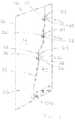
- FIG. 1is a rear elevation view of a flexible conductive circuit developed for use with a display.
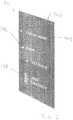
- FIG. 2is a front elevation view of a display into which has been incorporated the flexible conductive circuit of FIG. 1 .
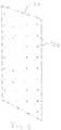
- FIG. 3is an exploded side elevation view of the display of FIG. 2 .
- FIG. 4is a front elevation view of the flexible conductive circuit of FIG. 1 .
- FIG. 5is a rear elevation view of the display of FIG. 2 .
- a flexible printed circuit generally identified by reference numeral 10will now be described with reference to FIG. 1 .
- a display 100will then he described with reference to FIG. 2 through FIG. 5 .
- the method of providing power input to flexible printed circuit 10consists of bisecting flexible printed circuit 10 into first conductive area 18 adapted for power input and a second conductive area 20 adapted for ground connection. Power input is then provided to electrical components, such as LEDs 16 , attached to flexible printed circuit 10 via first conductive area 18 and second conductive area 20 , rather than through individual control lines.
- Flexible printed circuit 10has a flexible printed circuit substrate 12 bisected by communication lines 14 between electrical components, in the form of light emitting diodes 16 (LEDs) into a first conductive area 18 adapted tor power input and a second conductive area 20 adapted for ground connection.
- Light emitting diodes 16LEDs
- Butterfly connectors 24are used to mount LEDs 16 .
- Each butterfly connector 24has a first wing 26 and a second wing 28 .
- a conductive adhesive(not visible in this view) is used to attach each butterfly connector 24 to substrate 12 , with first wing 26 connected to first conductive area 18 and second wing 28 connected to second conductive area 28 .
- power inputis provided to LEDs 16 via first conductive area 26 and second conductive area 28 .
- LEDs 16have integrated controllers that use a serial communications protocol that facilitates daisy chaining.
- serially addressable LEDssuch as the ws2812.
- RGBred, green blue
- LEDs 16integrate a serial shift register utilizing either a 1 wire or 2 wire serial communication interface.
- large common tracescan be used to deliver power (voltage and ground), while thin traces connecting the LEDs in sequence provide the signals needed to control the color and brightness of each LED.
- Common flood filled power delivery areascan be used as well, reducing the amount of material that needs to be removed for subtractive fabrication methods. This also dramatically simplifies the design of the circuit, as individual traces from the controller to each LED are no longer needed.
- Each addressable LED 16receives power through integrated contacts on it's breakout board which connect to of power delivery regions of first conductive area 26 and second conductive area 28 .
- Input signal datacomes from input contact 30 through serial communication line 14 , from either the controller output or the output of the previous LED in the linear daisy chain, which signal is output to the next LED through output contact 32 , again through serial communication line 14 .
- ESDElectrostatic Discharge
- Display 100includes a graphic overlay 102 .
- Graphic overlay 102has an alpha-numeric message 104 .
- the messages chosen for illustrationis “Look Here For Todays Big Savings”
- display 100has “windows” for display elements to show through. Two different sizes of “windows” have been selected for illustration: a series of three small windows 106 and a single larger window 108 .
- FIG. 3there is illustrated an exploded side elevation view of the various layers that make up display 100 .
- Those layersinclude graphic overlay 102 , flexible conductive circuit 10 and a conformal protective backing layer 110 .
- butterfly connectors 24 supporting LEDs 16As previously described, butterfly connectors 24 secure LEDs to flexible conductive circuit 10 .
- LEDs 16are positioned so that they light they project is visible through small windows 106 of graphic overlay 102 .
- ePaper display element 112As will hereafter further described ePaper display element 112 .
- ePaper display element 112has been chosen for illustration, to demonstrate that various display elements can be used.
- ePaper display element 112is positioned so that the light it projects is visible through larger window 108 of graphic overlay 102 .
- flexible printed circuit substrate 12 for flexible conductive circuit 10is shown in FIG. 3 , as having a front face 114 on which is positioned a front circuit and a rear face 116 on which is positioned a rear circuit.
- FIG. 4there is illustrated a front elevation view showing front face 114 of flexible conductive circuit 10 . From this front elevation view, it can be seen that flexible conductive circuit 10 has three small windows 106 , which correspond to the three small windows 106 in graphic overlay 102 .
- the small windows 106have been given the same reference numeral to help the reader understand that they are aligned so that LEDs 16 mounted to rear face of flexible conductive circuit 10 are visible through small windows 106 on graphic overlay 102 .
- Connector circuit 118is connected to controller 120 on rear face 116 of flexible conductive circuit 10 , with a flexible connector that extends through holes in substrate 12 for flexible conductive circuit 10 or wraps around an edge of substrate 12 .
- rear face 116 of flexible conductive circuitis protected by conformal protective backing layer 110 .
- Backing layer 110is secured by rear face 116 of flexible conductive circuit 10 by adhesive arranged in a pattern of dots 122 .
Landscapes
- Engineering & Computer Science (AREA)
- Microelectronics & Electronic Packaging (AREA)
- Illuminated Signs And Luminous Advertising (AREA)
- Led Device Packages (AREA)
Abstract
Description
Claims (14)
Applications Claiming Priority (2)
| Application Number | Priority Date | Filing Date | Title |
|---|---|---|---|
| CA3016051ACA3016051A1 (en) | 2018-08-31 | 2018-08-31 | A method of providing power input to a flexible printed circuit and a flexible printed circuit having power input in accordance with the method. |
| CA3016051 | 2018-08-31 |
Publications (2)
| Publication Number | Publication Date |
|---|---|
| US20200077519A1 US20200077519A1 (en) | 2020-03-05 |
| US10729011B2true US10729011B2 (en) | 2020-07-28 |
Family
ID=69640641
Family Applications (1)
| Application Number | Title | Priority Date | Filing Date |
|---|---|---|---|
| US16/546,891Expired - Fee RelatedUS10729011B2 (en) | 2018-08-31 | 2019-08-21 | Method of providing power input to a flexible printed circuit and a flexible printed circuit having power input in accordance with the method |
Country Status (2)
| Country | Link |
|---|---|
| US (1) | US10729011B2 (en) |
| CA (1) | CA3016051A1 (en) |
Citations (21)
| Publication number | Priority date | Publication date | Assignee | Title |
|---|---|---|---|---|
| US5375044A (en)* | 1991-05-13 | 1994-12-20 | Guritz; Steven P. W. | Multipurpose optical display for articulating surfaces |
| US6411359B1 (en)* | 1998-04-24 | 2002-06-25 | Hitachi, Ltd. | Liquid crystal display device having smaller frame area |
| US20060181772A1 (en)* | 2005-01-19 | 2006-08-17 | Byers Donald C | Mirror assembly with heater element |
| US20070279570A1 (en)* | 2006-05-30 | 2007-12-06 | Canon Kabushiki Kaisha | Liquid crystal display and liquid crystal projector |
| US20080048817A1 (en)* | 2006-07-26 | 2008-02-28 | Energy Recovery Technology, Llc | Circuit module |
| US20090040415A1 (en)* | 2007-07-05 | 2009-02-12 | Samsung Electronics Co., Ltd. | Flexible Printed Circuit Board and Liquid Crystal Display Device Using the Same |
| US7557776B2 (en)* | 2004-04-26 | 2009-07-07 | Hitachi, Ltd. | Plasma display apparatus |
| US20100312625A1 (en)* | 2009-06-08 | 2010-12-09 | Miller Mark A | Data transfer and control among multiple computer devices in a gaming environment |
| US20120097987A1 (en)* | 2010-10-22 | 2012-04-26 | Do-Hyung Ryu | Organic light emitting diode display |
| US8244486B2 (en)* | 2008-10-30 | 2012-08-14 | Acellent Technologies, Inc. | Structural health monitoring system having memory on structure |
| US20140022390A1 (en)* | 2010-10-15 | 2014-01-23 | Magna Mirrors Of America, Inc. | Interior rearview mirror assembly |
| US8724038B2 (en)* | 2010-10-18 | 2014-05-13 | Qualcomm Mems Technologies, Inc. | Wraparound assembly for combination touch, handwriting and fingerprint sensor |
| US9052545B2 (en)* | 2011-12-06 | 2015-06-09 | Lg Display Co., Ltd. | Liquid crystal display device |
| US9282893B2 (en)* | 2012-09-11 | 2016-03-15 | L.I.F.E. Corporation S.A. | Wearable communication platform |
| US9316858B2 (en)* | 2011-04-22 | 2016-04-19 | Sharp Kabushiki Kaisha | Display device |
| US20160313769A1 (en)* | 2015-04-23 | 2016-10-27 | Semiconductor Energy Laboratory Co., Ltd. | Electronic device |
| WO2017127943A1 (en) | 2016-01-29 | 2017-08-03 | Alain Carel | Flexible printed circuit |
| US20180217465A1 (en)* | 2015-08-03 | 2018-08-02 | Sharp Kabushiki Kaisha | Display device |
| US20180341290A1 (en)* | 2017-05-29 | 2018-11-29 | Samsung Electronics Co .. Ltd. | Electronic device including module mounted in sunken area of layer |
| US20190043928A1 (en)* | 2017-08-02 | 2019-02-07 | Samsung Electronics Co., Ltd. | Electronic device including flexible display panel |
| US20190243492A1 (en)* | 2009-10-07 | 2019-08-08 | Magna Mirrors Of America, Inc. | Exterior rearview mirror assembly |
- 2018
- 2018-08-31CACA3016051Apatent/CA3016051A1/enactivePending
- 2019
- 2019-08-21USUS16/546,891patent/US10729011B2/ennot_activeExpired - Fee Related
Patent Citations (22)
| Publication number | Priority date | Publication date | Assignee | Title |
|---|---|---|---|---|
| US5375044A (en)* | 1991-05-13 | 1994-12-20 | Guritz; Steven P. W. | Multipurpose optical display for articulating surfaces |
| US6411359B1 (en)* | 1998-04-24 | 2002-06-25 | Hitachi, Ltd. | Liquid crystal display device having smaller frame area |
| US7557776B2 (en)* | 2004-04-26 | 2009-07-07 | Hitachi, Ltd. | Plasma display apparatus |
| US20060181772A1 (en)* | 2005-01-19 | 2006-08-17 | Byers Donald C | Mirror assembly with heater element |
| US20070279570A1 (en)* | 2006-05-30 | 2007-12-06 | Canon Kabushiki Kaisha | Liquid crystal display and liquid crystal projector |
| US20080048817A1 (en)* | 2006-07-26 | 2008-02-28 | Energy Recovery Technology, Llc | Circuit module |
| US20090040415A1 (en)* | 2007-07-05 | 2009-02-12 | Samsung Electronics Co., Ltd. | Flexible Printed Circuit Board and Liquid Crystal Display Device Using the Same |
| US8244486B2 (en)* | 2008-10-30 | 2012-08-14 | Acellent Technologies, Inc. | Structural health monitoring system having memory on structure |
| US20100312625A1 (en)* | 2009-06-08 | 2010-12-09 | Miller Mark A | Data transfer and control among multiple computer devices in a gaming environment |
| US20190243492A1 (en)* | 2009-10-07 | 2019-08-08 | Magna Mirrors Of America, Inc. | Exterior rearview mirror assembly |
| US20140022390A1 (en)* | 2010-10-15 | 2014-01-23 | Magna Mirrors Of America, Inc. | Interior rearview mirror assembly |
| US8724038B2 (en)* | 2010-10-18 | 2014-05-13 | Qualcomm Mems Technologies, Inc. | Wraparound assembly for combination touch, handwriting and fingerprint sensor |
| US20120097987A1 (en)* | 2010-10-22 | 2012-04-26 | Do-Hyung Ryu | Organic light emitting diode display |
| US9316858B2 (en)* | 2011-04-22 | 2016-04-19 | Sharp Kabushiki Kaisha | Display device |
| US9052545B2 (en)* | 2011-12-06 | 2015-06-09 | Lg Display Co., Ltd. | Liquid crystal display device |
| US9282893B2 (en)* | 2012-09-11 | 2016-03-15 | L.I.F.E. Corporation S.A. | Wearable communication platform |
| US20160313769A1 (en)* | 2015-04-23 | 2016-10-27 | Semiconductor Energy Laboratory Co., Ltd. | Electronic device |
| US20180217465A1 (en)* | 2015-08-03 | 2018-08-02 | Sharp Kabushiki Kaisha | Display device |
| WO2017127943A1 (en) | 2016-01-29 | 2017-08-03 | Alain Carel | Flexible printed circuit |
| US20190029116A1 (en) | 2016-01-29 | 2019-01-24 | Alain Carel | Flexible printed circuit |
| US20180341290A1 (en)* | 2017-05-29 | 2018-11-29 | Samsung Electronics Co .. Ltd. | Electronic device including module mounted in sunken area of layer |
| US20190043928A1 (en)* | 2017-08-02 | 2019-02-07 | Samsung Electronics Co., Ltd. | Electronic device including flexible display panel |
Also Published As
| Publication number | Publication date |
|---|---|
| US20200077519A1 (en) | 2020-03-05 |
| CA3016051A1 (en) | 2020-02-29 |
Similar Documents
| Publication | Publication Date | Title |
|---|---|---|
| RU2680257C1 (en) | Led module, led panel and led screen | |
| US7703941B2 (en) | Expandable LED module for arbitrarily display assembly | |
| CN101248477B (en) | Electroluminescent one-way vision panel | |
| US10436395B2 (en) | Flexible illuminating flat cable structure | |
| JP3200708U (en) | LED lighting device | |
| US8916902B2 (en) | LED module packaging structure with an IC chip | |
| US20200018474A1 (en) | Attaching Light Emitting Devices to Items of Clothing | |
| CN108761904B (en) | Back lighting device | |
| KR101838567B1 (en) | liquid crystal display device and method of manufacturing the same | |
| US10729011B2 (en) | Method of providing power input to a flexible printed circuit and a flexible printed circuit having power input in accordance with the method | |
| EP3142468B1 (en) | Flexible printed circuit board and method of folding a flexible printed circuit board | |
| US9280920B2 (en) | Status indicating retractable connection label assembly | |
| US9097917B2 (en) | Electronic display screen modular unit structure | |
| JP2018055631A (en) | Industrial electronic device | |
| JP5914051B2 (en) | Light emitting element substrate, surface light source, and method of installing light emitting element substrate | |
| US7553038B2 (en) | Sign structure for a personal computer | |
| KR102555310B1 (en) | Connecting device of circuit type with multi-layer structure and display device comprising thereof | |
| US20030137513A1 (en) | Apparatus and method for displaying status of port conditions | |
| US20030002295A1 (en) | Apparatus and method for displaying a luminescent icon | |
| CN215181649U (en) | Computer with a display | |
| TWI665650B (en) | A led light-bar and an advertising display with led light-bar | |
| CN214795504U (en) | Backlight LightBar antistatic structure | |
| KR101878130B1 (en) | The flexible PCB with connector | |
| WO2021114351A1 (en) | Display screen and terminal | |
| KR20160037491A (en) | Module type led bulletin board |
Legal Events
| Date | Code | Title | Description |
|---|---|---|---|
| AS | Assignment | Owner name:CAREL, ALAIN, CANADA Free format text:ASSIGNMENT OF ASSIGNORS INTEREST;ASSIGNORS:CAREL, ALAIN;ANDERSEN, KIMBALL;SIGNING DATES FROM 20190808 TO 20190819;REEL/FRAME:050119/0162 | |
| FEPP | Fee payment procedure | Free format text:ENTITY STATUS SET TO UNDISCOUNTED (ORIGINAL EVENT CODE: BIG.); ENTITY STATUS OF PATENT OWNER: SMALL ENTITY | |
| FEPP | Fee payment procedure | Free format text:ENTITY STATUS SET TO SMALL (ORIGINAL EVENT CODE: SMAL); ENTITY STATUS OF PATENT OWNER: SMALL ENTITY | |
| AS | Assignment | Owner name:TF MASSIF TECHNOLOGIES LTD., CANADA Free format text:ASSIGNMENT OF ASSIGNORS INTEREST;ASSIGNOR:CAREL, ALAIN;REEL/FRAME:050744/0714 Effective date:20180831 | |
| STPP | Information on status: patent application and granting procedure in general | Free format text:NOTICE OF ALLOWANCE MAILED -- APPLICATION RECEIVED IN OFFICE OF PUBLICATIONS | |
| STPP | Information on status: patent application and granting procedure in general | Free format text:PUBLICATIONS -- ISSUE FEE PAYMENT VERIFIED | |
| STCF | Information on status: patent grant | Free format text:PATENTED CASE | |
| FEPP | Fee payment procedure | Free format text:MAINTENANCE FEE REMINDER MAILED (ORIGINAL EVENT CODE: REM.); ENTITY STATUS OF PATENT OWNER: SMALL ENTITY | |
| LAPS | Lapse for failure to pay maintenance fees | Free format text:PATENT EXPIRED FOR FAILURE TO PAY MAINTENANCE FEES (ORIGINAL EVENT CODE: EXP.); ENTITY STATUS OF PATENT OWNER: SMALL ENTITY | |
| STCH | Information on status: patent discontinuation | Free format text:PATENT EXPIRED DUE TO NONPAYMENT OF MAINTENANCE FEES UNDER 37 CFR 1.362 | |
| FP | Lapsed due to failure to pay maintenance fee | Effective date:20240728 |