US10727362B2 - Methods of hermetically sealing photovoltaic modules - Google Patents
Methods of hermetically sealing photovoltaic modulesDownload PDFInfo
- Publication number
- US10727362B2 US10727362B2US16/265,419US201916265419AUS10727362B2US 10727362 B2US10727362 B2US 10727362B2US 201916265419 AUS201916265419 AUS 201916265419AUS 10727362 B2US10727362 B2US 10727362B2
- Authority
- US
- United States
- Prior art keywords
- glass
- powder
- glass sheet
- photovoltaic device
- edge region
- Prior art date
- Legal status (The legal status is an assumption and is not a legal conclusion. Google has not performed a legal analysis and makes no representation as to the accuracy of the status listed.)
- Active
Links
Images


Classifications
- H01L31/0488—
- H—ELECTRICITY
- H10—SEMICONDUCTOR DEVICES; ELECTRIC SOLID-STATE DEVICES NOT OTHERWISE PROVIDED FOR
- H10F—INORGANIC SEMICONDUCTOR DEVICES SENSITIVE TO INFRARED RADIATION, LIGHT, ELECTROMAGNETIC RADIATION OF SHORTER WAVELENGTH OR CORPUSCULAR RADIATION
- H10F19/00—Integrated devices, or assemblies of multiple devices, comprising at least one photovoltaic cell covered by group H10F10/00, e.g. photovoltaic modules
- H10F19/80—Encapsulations or containers for integrated devices, or assemblies of multiple devices, having photovoltaic cells
- H10F19/807—Double-glass encapsulation, e.g. photovoltaic cells arranged between front and rear glass sheets
- H—ELECTRICITY
- H01—ELECTRIC ELEMENTS
- H01G—CAPACITORS; CAPACITORS, RECTIFIERS, DETECTORS, SWITCHING DEVICES, LIGHT-SENSITIVE OR TEMPERATURE-SENSITIVE DEVICES OF THE ELECTROLYTIC TYPE
- H01G9/00—Electrolytic capacitors, rectifiers, detectors, switching devices, light-sensitive or temperature-sensitive devices; Processes of their manufacture
- H01G9/20—Light-sensitive devices
- H01G9/2068—Panels or arrays of photoelectrochemical cells, e.g. photovoltaic modules based on photoelectrochemical cells
- H01G9/2077—Sealing arrangements, e.g. to prevent the leakage of the electrolyte
- H01L31/0201—
- H01L31/028—
- H01L31/0296—
- H01L31/0304—
- H01L31/0322—
- H01L31/0326—
- H01L31/0445—
- H01L31/048—
- H01L31/068—
- H01L31/075—
- H01L31/18—
- H01L31/186—
- H—ELECTRICITY
- H10—SEMICONDUCTOR DEVICES; ELECTRIC SOLID-STATE DEVICES NOT OTHERWISE PROVIDED FOR
- H10F—INORGANIC SEMICONDUCTOR DEVICES SENSITIVE TO INFRARED RADIATION, LIGHT, ELECTROMAGNETIC RADIATION OF SHORTER WAVELENGTH OR CORPUSCULAR RADIATION
- H10F10/00—Individual photovoltaic cells, e.g. solar cells
- H10F10/10—Individual photovoltaic cells, e.g. solar cells having potential barriers
- H10F10/14—Photovoltaic cells having only PN homojunction potential barriers
- H—ELECTRICITY
- H10—SEMICONDUCTOR DEVICES; ELECTRIC SOLID-STATE DEVICES NOT OTHERWISE PROVIDED FOR
- H10F—INORGANIC SEMICONDUCTOR DEVICES SENSITIVE TO INFRARED RADIATION, LIGHT, ELECTROMAGNETIC RADIATION OF SHORTER WAVELENGTH OR CORPUSCULAR RADIATION
- H10F10/00—Individual photovoltaic cells, e.g. solar cells
- H10F10/10—Individual photovoltaic cells, e.g. solar cells having potential barriers
- H10F10/17—Photovoltaic cells having only PIN junction potential barriers
- H—ELECTRICITY
- H10—SEMICONDUCTOR DEVICES; ELECTRIC SOLID-STATE DEVICES NOT OTHERWISE PROVIDED FOR
- H10F—INORGANIC SEMICONDUCTOR DEVICES SENSITIVE TO INFRARED RADIATION, LIGHT, ELECTROMAGNETIC RADIATION OF SHORTER WAVELENGTH OR CORPUSCULAR RADIATION
- H10F19/00—Integrated devices, or assemblies of multiple devices, comprising at least one photovoltaic cell covered by group H10F10/00, e.g. photovoltaic modules
- H10F19/30—Integrated devices, or assemblies of multiple devices, comprising at least one photovoltaic cell covered by group H10F10/00, e.g. photovoltaic modules comprising thin-film photovoltaic cells
- H—ELECTRICITY
- H10—SEMICONDUCTOR DEVICES; ELECTRIC SOLID-STATE DEVICES NOT OTHERWISE PROVIDED FOR
- H10F—INORGANIC SEMICONDUCTOR DEVICES SENSITIVE TO INFRARED RADIATION, LIGHT, ELECTROMAGNETIC RADIATION OF SHORTER WAVELENGTH OR CORPUSCULAR RADIATION
- H10F19/00—Integrated devices, or assemblies of multiple devices, comprising at least one photovoltaic cell covered by group H10F10/00, e.g. photovoltaic modules
- H10F19/80—Encapsulations or containers for integrated devices, or assemblies of multiple devices, having photovoltaic cells
- H—ELECTRICITY
- H10—SEMICONDUCTOR DEVICES; ELECTRIC SOLID-STATE DEVICES NOT OTHERWISE PROVIDED FOR
- H10F—INORGANIC SEMICONDUCTOR DEVICES SENSITIVE TO INFRARED RADIATION, LIGHT, ELECTROMAGNETIC RADIATION OF SHORTER WAVELENGTH OR CORPUSCULAR RADIATION
- H10F71/00—Manufacture or treatment of devices covered by this subclass
- H—ELECTRICITY
- H10—SEMICONDUCTOR DEVICES; ELECTRIC SOLID-STATE DEVICES NOT OTHERWISE PROVIDED FOR
- H10F—INORGANIC SEMICONDUCTOR DEVICES SENSITIVE TO INFRARED RADIATION, LIGHT, ELECTROMAGNETIC RADIATION OF SHORTER WAVELENGTH OR CORPUSCULAR RADIATION
- H10F77/00—Constructional details of devices covered by this subclass
- H10F77/10—Semiconductor bodies
- H10F77/12—Active materials
- H10F77/122—Active materials comprising only Group IV materials
- H—ELECTRICITY
- H10—SEMICONDUCTOR DEVICES; ELECTRIC SOLID-STATE DEVICES NOT OTHERWISE PROVIDED FOR
- H10F—INORGANIC SEMICONDUCTOR DEVICES SENSITIVE TO INFRARED RADIATION, LIGHT, ELECTROMAGNETIC RADIATION OF SHORTER WAVELENGTH OR CORPUSCULAR RADIATION
- H10F77/00—Constructional details of devices covered by this subclass
- H10F77/10—Semiconductor bodies
- H10F77/12—Active materials
- H10F77/123—Active materials comprising only Group II-VI materials, e.g. CdS, ZnS or HgCdTe
- H—ELECTRICITY
- H10—SEMICONDUCTOR DEVICES; ELECTRIC SOLID-STATE DEVICES NOT OTHERWISE PROVIDED FOR
- H10F—INORGANIC SEMICONDUCTOR DEVICES SENSITIVE TO INFRARED RADIATION, LIGHT, ELECTROMAGNETIC RADIATION OF SHORTER WAVELENGTH OR CORPUSCULAR RADIATION
- H10F77/00—Constructional details of devices covered by this subclass
- H10F77/10—Semiconductor bodies
- H10F77/12—Active materials
- H10F77/124—Active materials comprising only Group III-V materials, e.g. GaAs
- H—ELECTRICITY
- H10—SEMICONDUCTOR DEVICES; ELECTRIC SOLID-STATE DEVICES NOT OTHERWISE PROVIDED FOR
- H10F—INORGANIC SEMICONDUCTOR DEVICES SENSITIVE TO INFRARED RADIATION, LIGHT, ELECTROMAGNETIC RADIATION OF SHORTER WAVELENGTH OR CORPUSCULAR RADIATION
- H10F77/00—Constructional details of devices covered by this subclass
- H10F77/10—Semiconductor bodies
- H10F77/12—Active materials
- H10F77/126—Active materials comprising only Group I-III-VI chalcopyrite materials, e.g. CuInSe2, CuGaSe2 or CuInGaSe2 [CIGS]
- H—ELECTRICITY
- H10—SEMICONDUCTOR DEVICES; ELECTRIC SOLID-STATE DEVICES NOT OTHERWISE PROVIDED FOR
- H10F—INORGANIC SEMICONDUCTOR DEVICES SENSITIVE TO INFRARED RADIATION, LIGHT, ELECTROMAGNETIC RADIATION OF SHORTER WAVELENGTH OR CORPUSCULAR RADIATION
- H10F77/00—Constructional details of devices covered by this subclass
- H10F77/10—Semiconductor bodies
- H10F77/12—Active materials
- H10F77/128—Active materials comprising only Group I-II-IV-VI kesterite materials, e.g. Cu2ZnSnSe4 or Cu2ZnSnS4
- H—ELECTRICITY
- H10—SEMICONDUCTOR DEVICES; ELECTRIC SOLID-STATE DEVICES NOT OTHERWISE PROVIDED FOR
- H10F—INORGANIC SEMICONDUCTOR DEVICES SENSITIVE TO INFRARED RADIATION, LIGHT, ELECTROMAGNETIC RADIATION OF SHORTER WAVELENGTH OR CORPUSCULAR RADIATION
- H10F77/00—Constructional details of devices covered by this subclass
- H10F77/93—Interconnections
- H10F77/933—Interconnections for devices having potential barriers
- H10F77/935—Interconnections for devices having potential barriers for photovoltaic devices or modules
- H10F77/937—Busbar structures for modules
- H—ELECTRICITY
- H10—SEMICONDUCTOR DEVICES; ELECTRIC SOLID-STATE DEVICES NOT OTHERWISE PROVIDED FOR
- H10K—ORGANIC ELECTRIC SOLID-STATE DEVICES
- H10K85/00—Organic materials used in the body or electrodes of devices covered by this subclass
- H10K85/50—Organic perovskites; Hybrid organic-inorganic perovskites [HOIP], e.g. CH3NH3PbI3
- H—ELECTRICITY
- H01—ELECTRIC ELEMENTS
- H01G—CAPACITORS; CAPACITORS, RECTIFIERS, DETECTORS, SWITCHING DEVICES, LIGHT-SENSITIVE OR TEMPERATURE-SENSITIVE DEVICES OF THE ELECTROLYTIC TYPE
- H01G9/00—Electrolytic capacitors, rectifiers, detectors, switching devices, light-sensitive or temperature-sensitive devices; Processes of their manufacture
- H01G9/20—Light-sensitive devices
- H01G9/2027—Light-sensitive devices comprising an oxide semiconductor electrode
- H01G9/2031—Light-sensitive devices comprising an oxide semiconductor electrode comprising titanium oxide, e.g. TiO2
- H01L51/448—
- H—ELECTRICITY
- H10—SEMICONDUCTOR DEVICES; ELECTRIC SOLID-STATE DEVICES NOT OTHERWISE PROVIDED FOR
- H10K—ORGANIC ELECTRIC SOLID-STATE DEVICES
- H10K30/00—Organic devices sensitive to infrared radiation, light, electromagnetic radiation of shorter wavelength or corpuscular radiation
- H10K30/80—Constructional details
- H10K30/88—Passivation; Containers; Encapsulations
- Y—GENERAL TAGGING OF NEW TECHNOLOGICAL DEVELOPMENTS; GENERAL TAGGING OF CROSS-SECTIONAL TECHNOLOGIES SPANNING OVER SEVERAL SECTIONS OF THE IPC; TECHNICAL SUBJECTS COVERED BY FORMER USPC CROSS-REFERENCE ART COLLECTIONS [XRACs] AND DIGESTS
- Y02—TECHNOLOGIES OR APPLICATIONS FOR MITIGATION OR ADAPTATION AGAINST CLIMATE CHANGE
- Y02E—REDUCTION OF GREENHOUSE GAS [GHG] EMISSIONS, RELATED TO ENERGY GENERATION, TRANSMISSION OR DISTRIBUTION
- Y02E10/00—Energy generation through renewable energy sources
- Y02E10/50—Photovoltaic [PV] energy
- Y02E10/541—CuInSe2 material PV cells
- Y—GENERAL TAGGING OF NEW TECHNOLOGICAL DEVELOPMENTS; GENERAL TAGGING OF CROSS-SECTIONAL TECHNOLOGIES SPANNING OVER SEVERAL SECTIONS OF THE IPC; TECHNICAL SUBJECTS COVERED BY FORMER USPC CROSS-REFERENCE ART COLLECTIONS [XRACs] AND DIGESTS
- Y02—TECHNOLOGIES OR APPLICATIONS FOR MITIGATION OR ADAPTATION AGAINST CLIMATE CHANGE
- Y02E—REDUCTION OF GREENHOUSE GAS [GHG] EMISSIONS, RELATED TO ENERGY GENERATION, TRANSMISSION OR DISTRIBUTION
- Y02E10/00—Energy generation through renewable energy sources
- Y02E10/50—Photovoltaic [PV] energy
- Y02E10/542—Dye sensitized solar cells
- Y—GENERAL TAGGING OF NEW TECHNOLOGICAL DEVELOPMENTS; GENERAL TAGGING OF CROSS-SECTIONAL TECHNOLOGIES SPANNING OVER SEVERAL SECTIONS OF THE IPC; TECHNICAL SUBJECTS COVERED BY FORMER USPC CROSS-REFERENCE ART COLLECTIONS [XRACs] AND DIGESTS
- Y02—TECHNOLOGIES OR APPLICATIONS FOR MITIGATION OR ADAPTATION AGAINST CLIMATE CHANGE
- Y02E—REDUCTION OF GREENHOUSE GAS [GHG] EMISSIONS, RELATED TO ENERGY GENERATION, TRANSMISSION OR DISTRIBUTION
- Y02E10/00—Energy generation through renewable energy sources
- Y02E10/50—Photovoltaic [PV] energy
- Y02E10/544—Solar cells from Group III-V materials
- Y—GENERAL TAGGING OF NEW TECHNOLOGICAL DEVELOPMENTS; GENERAL TAGGING OF CROSS-SECTIONAL TECHNOLOGIES SPANNING OVER SEVERAL SECTIONS OF THE IPC; TECHNICAL SUBJECTS COVERED BY FORMER USPC CROSS-REFERENCE ART COLLECTIONS [XRACs] AND DIGESTS
- Y02—TECHNOLOGIES OR APPLICATIONS FOR MITIGATION OR ADAPTATION AGAINST CLIMATE CHANGE
- Y02E—REDUCTION OF GREENHOUSE GAS [GHG] EMISSIONS, RELATED TO ENERGY GENERATION, TRANSMISSION OR DISTRIBUTION
- Y02E10/00—Energy generation through renewable energy sources
- Y02E10/50—Photovoltaic [PV] energy
- Y02E10/547—Monocrystalline silicon PV cells
- Y—GENERAL TAGGING OF NEW TECHNOLOGICAL DEVELOPMENTS; GENERAL TAGGING OF CROSS-SECTIONAL TECHNOLOGIES SPANNING OVER SEVERAL SECTIONS OF THE IPC; TECHNICAL SUBJECTS COVERED BY FORMER USPC CROSS-REFERENCE ART COLLECTIONS [XRACs] AND DIGESTS
- Y02—TECHNOLOGIES OR APPLICATIONS FOR MITIGATION OR ADAPTATION AGAINST CLIMATE CHANGE
- Y02E—REDUCTION OF GREENHOUSE GAS [GHG] EMISSIONS, RELATED TO ENERGY GENERATION, TRANSMISSION OR DISTRIBUTION
- Y02E10/00—Energy generation through renewable energy sources
- Y02E10/50—Photovoltaic [PV] energy
- Y02E10/548—Amorphous silicon PV cells
- Y—GENERAL TAGGING OF NEW TECHNOLOGICAL DEVELOPMENTS; GENERAL TAGGING OF CROSS-SECTIONAL TECHNOLOGIES SPANNING OVER SEVERAL SECTIONS OF THE IPC; TECHNICAL SUBJECTS COVERED BY FORMER USPC CROSS-REFERENCE ART COLLECTIONS [XRACs] AND DIGESTS
- Y02—TECHNOLOGIES OR APPLICATIONS FOR MITIGATION OR ADAPTATION AGAINST CLIMATE CHANGE
- Y02P—CLIMATE CHANGE MITIGATION TECHNOLOGIES IN THE PRODUCTION OR PROCESSING OF GOODS
- Y02P70/00—Climate change mitigation technologies in the production process for final industrial or consumer products
- Y02P70/50—Manufacturing or production processes characterised by the final manufactured product
- Y02P70/521—
Definitions
- the present inventionrelates to photovoltaic devices, and in particular to glass-sealed photovoltaic modules.
- PV modules based on silicon (Si) wafer technologyemploy a front glass/encapsulant/wafer/encapsulant/backsheet structure.
- Polyvinyl fluoridee.g., Tedlar® from DuPont
- Tedlar®is the most commonly used backsheet in wafer-based Si PV modules. This material is inherently transparent for water vapor and gases—i.e., it does not enable or maintain a hermetic seal.
- Thin-film PV modules based on amorphous Si (a-Si), CdTe, or copper indium gallium selenide (CuIn x Ga 1-x Se 2 or CIGS)most often utilize a glass-glass architecture with one of the glass sheets either serving as the substrate (CIGS) or superstrate (a-Si, CdTe) onto which the active PV material is deposited directly.
- the function of the second glass sheetis to serve as either the protective top (CIGS) or back cover (a-Si, CdTe). Both sheets of glass are held together with a single encapsulant layer.
- the 1.8-4 mm-thick sheets of glassare impermeable to water and gases.
- butyl-based edge sealsare typically applied, as butyl rubber has water vapor transmission rates (WVTR) on the order of 10 ⁇ 6 g/m 2 -day, orders of magnitude below the WVTR for typical encapsulant materials.
- WVTRwater vapor transmission rates
- Embodiments of the present inventionprovide PV modules hermetically sealed against environmental contamination via edge seals consisting entirely of glass. While preferred embodiments of the invention utilize “thin-film” PV modules featuring PV devices based on CIGS, a-Si, or CdTe, other embodiments of the invention utilize PV devices based on crystalline Si (e.g., in wafer or ribbon form) or III-V semiconductors such as GaAs or InP (e.g., in wafer form) or solid-state dye-sensitized perovskite material (organic-inorganic hybrid).
- crystalline Sie.g., in wafer or ribbon form
- III-V semiconductorssuch as GaAs or InP (e.g., in wafer form) or solid-state dye-sensitized perovskite material (organic-inorganic hybrid).
- PV devicesare the active PV materials within PV modules, and these typically include or consist essentially of materials forming one or more p-n or p-i-n junctions that each absorb at least a portion of the solar spectrum and convert it into electricity.
- a powder consisting essentially of or consisting of glassis utilized to seal a PV device fronted and backed by glass sheets, thereby forming a sealed PV module.
- the glass powderis locally heated to a temperature higher than the melting point, glass transition temperature, and/or softening point of the powder such that the powder softens and/or flows into a unified mass that bonds with the glass sheets to form a hermetic seal.
- embodiments of the present inventionincrease the active area of the PV module, and hence the power output for a fixed PV module size.
- Typical safety requirementse.g., IEC or UL, mandate a minimum insulation distance from the current-carrying live parts inside a PV module to the outside edge of the module—i.e., the clearance and creepage distance.
- Such “edge delete” lossesdepend on various aspects such as the total system voltage or micro-environment (e.g., pollution degree and altitude), but are typically at the order of 8-15 mm.
- the insulation against electrical shockis compromised and, in the case of moisture ingress, current can track over the glass or polymer surface from the module circuit to its edge.
- the glass-based seals in accordance with embodiments of the present inventionare truly durable cemented joints retaining their superior electrical insulation properties over time. These seals allow the clearance—i.e., the edge delete—to be smaller, in turn proportionally increasing the power output from the PV module for the same total area.
- the polymeric encapsulant (filler sheet)—e.g., EVA, PVB, polyolefin, ionomers, TPU—conventionally utilized to bond glass sheets togethermay be eliminated in accordance with embodiments of the present invention.
- filler sheetsare typically the most expensive elements of thin-film PV modules.
- embodiments of the inventionenable significant reductions in material cost.
- elimination of polymeric filler sheets and the conventional butyl rubber edge sealsalso enables PV modules in accordance with embodiments of the invention to obtain higher fire ratings.
- elimination of such conventional polymer-based filler sheets and edge sealsobviates the need for the slow and capital-intensive lamination step, resulting in additional manufacturing cost savings for PV modules in accordance with embodiments of the present invention.
- PV modules that are hermetically sealed in accordance with embodiments of the present inventionexhibit advantageously enhanced durability in climates and/or ambient conditions that have high relative humidity, e.g., coastal or equatorial locations.
- PV modules and devices sealed in accordance with embodiments of the inventiondo not rely on seals based on glass-polymer adhesion, they are less susceptible than to fatigue under conditions such as UV radiation, elevated temperature, and high humidity or moisture levels. Glass-polymer bonds also tend to be susceptible to failure due to mechanical stresses from, e.g., etch pinch during module lamination.
- embodiments of the inventionfeature a photovoltaic module that includes, consists essentially of, or consists of a first glass sheet, a photovoltaic device disposed on the first glass sheet, a second glass sheet disposed over and in contact with at least a portion of the photovoltaic device, and a layer of melted glass powder.
- the first glass sheet and the second glass sheethave a gap therebetween spanned, over only a portion of an area of the gap, by the photovoltaic device, and the layer of melted glass powder seals the gap between the first and second glass sheets at an edge region proximate an edge of at least one of the first or second glass sheets so as to hermetically seal the photovoltaic device.
- Embodiments of the inventionmay include one or more of the following in any of a variety of different combinations.
- the photovoltaic devicemay include, consist essentially of, or consist of an active region including, consisting essentially of, or consisting of one or more p-n or p-i-n junctions.
- the photovoltaic modulemay include (i) a first substrate layer disposed between the active region and the first glass sheet and/or (ii) a second substrate layer disposed between the active region and the second glass sheet.
- the first and/or second substrate layersmay each include, consist essentially of, or consist of a metal foil and/or a polymer layer.
- a conductive bus ribbonmay be electrically coupled to the photovoltaic device and may extend out from the first and second glass sheets in contact with the layer of melted glass powder.
- the conductive bus ribbonmay be (i) disposed in contact with both the first and second glass sheets, (ii) disposed in contact with the first glass sheet and the layer of melted glass powder, but not with the second glass sheet, (iii) disposed in contact with the second glass sheet and the layer of melted glass powder, but not with the first glass sheet, or (iv) disposed in contact with the layer of melted glass powder, but not with the first or second glass sheets.
- the melted glass powdermay include a colorant or other absorber utilized to, e.g., locally increase the absorption of particular wavelengths of light.
- the photovoltaic devicemay include, consist essentially of, or consist of multiple junctions, each of which is a p-n junction or a p-i-n junction.
- the photovoltaic devicemay be a thin-film photovoltaic device that includes, consists essentially of, or consists of amorphous silicon.
- the photovoltaic devicemay be a thin-film photovoltaic device that includes, consists essentially of, or consists of CdTe.
- the photovoltaic devicemay be a thin-film photovoltaic device that includes, consists essentially of, or consists of chalcopyrite (Cu(In,Ga)(S,Se) 2 ).
- the photovoltaic devicemay be a thin-film photovoltaic device that includes, consists essentially of, or consists of kesterite (Cu 2 (Zn,Fe)Sn(S,Se) 4 ).
- the photovoltaic devicemay include, consist essentially of, or consist of crystalline silicon and/or GaAs.
- the photovoltaic devicemay include, consist essentially of, or consist of solid-state dye-sensitized perovskite material (organic-inorganic hybrid).
- the composition of the melted glass powdermay be substantially the same as the composition of the first and/or second glass sheets.
- the composition of the melted glass powdermay be different from a composition of either of the first or second glass sheets (i.e., different from the compositions of both of the first and second glass sheets).
- embodiments of the inventionfeature a method of hermetically sealing a photovoltaic module.
- a structureincludes, consists essentially of, or consists of a first glass sheet, a photovoltaic device disposed on the first glass sheet, and a second glass sheet disposed over and in contact with at least a portion of the photovoltaic device, the first glass sheet and the second glass sheet defining a gap therebetween spanned, over only a portion of an area of the gap, by the photovoltaic device.
- a powderis disposed within the gap at an edge region proximate an edge of at least one of the first or second glass sheets.
- the powderincludes, consists essentially of, or consists of glass. The powder is heated within the gap to seal the first and second glass sheets at the edge region with a layer of melted glass powder.
- Embodiments of the inventionmay include one or more of the following in any of a variety of different combinations.
- Heating the powdermay include, consist essentially of, or consist of application of laser energy to the powder (e.g., through one or both of the first or second glass sheets).
- the photovoltaic devicemay include, consist essentially of, or consist of an active region including, consisting essentially of, or consisting of one or more p-n or p-i-n junctions.
- the photovoltaic modulemay include (i) a first substrate layer disposed between the active region and the first glass sheet and/or (ii) a second substrate layer disposed between the active region and the second glass sheet.
- the first and/or second substrate layersmay each include, consist essentially of, or consist of a metal foil and/or a polymer layer.
- a conductive bus ribbonmay be electrically coupled to the photovoltaic device and may extend out from the first and second glass sheets in contact with the layer of melted glass powder (i.e., the powder may be melted at least partially around the bus ribbon in the edge region).
- the conductive bus ribbonmay be (i) disposed in contact with both the first and second glass sheets, (ii) disposed in contact with the first glass sheet and the layer of melted glass powder, but not with the second glass sheet, (iii) disposed in contact with the second glass sheet and the layer of melted glass powder, but not with the first glass sheet, or (iv) disposed in contact with the layer of melted glass powder, but not with the first or second glass sheets.
- the powdermay include a colorant or other absorber utilized to, e.g., locally increase the absorption of particular wavelengths of light.
- the photovoltaic devicemay include, consist essentially of, or consist of multiple junctions, each of which is a p-n junction or a p-i-n junction.
- the photovoltaic devicemay be a thin-film photovoltaic device that includes, consists essentially of, or consists of amorphous silicon.
- the photovoltaic devicemay be a thin-film photovoltaic device that includes, consists essentially of, or consists of CdTe.
- the photovoltaic devicemay be a thin-film photovoltaic device that includes, consists essentially of, or consists of chalcopyrite (Cu(In,Ga)(S,Se) 2 ).
- the photovoltaic devicemay be a thin-film photovoltaic device that includes, consists essentially of, or consists of kesterite (Cu 2 (Zn,Fe)Sn(S,Se) 4 ).
- the photovoltaic devicemay include, consist essentially of, or consist of crystalline silicon and/or GaAs.
- the photovoltaic devicemay include, consist essentially of, or consist of solid-state dye-sensitized perovskite material (organic-inorganic hybrid).
- the composition of the melted glass powdermay be substantially the same as the composition of the first and/or second glass sheets.
- the composition of the melted glass powdermay be different from a composition of either of the first or second glass sheets (i.e., different from the compositions of both of the first and second glass sheets).
- a structure consisting essentially of glasswill generally include only glass and only unintentional impurities (which may be metallic or non-metallic) that may be detectable via chemical analysis but do not contribute to function.
- a powder or seal consisting essentially of glasstypically does not incorporate organic fillers, binders, solvents, glass frit, frit material(s), glass solder, and/or melting-point reduction agents such as Pb.
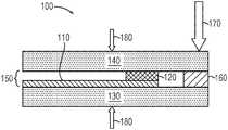
- FIG. 1is a schematic cross-section of a portion of a photovoltaic module being sealed via application of thermal energy in accordance with various embodiments of the invention
- FIG. 2is a schematic plan view of a photovoltaic module in accordance with various embodiments of the invention.
- FIGS. 3A-3Dare schematic cross-sections of edge portions of sealed photovoltaic modules in accordance with various embodiments of the invention.
- FIG. 1illustrates a portion of a PV module 100 being sealed at an edge region via application of thermal energy in accordance with embodiments of the present invention.
- the PV module 100includes an active PV device 110 , one or more conductive bus ribbons 120 , a lower glass sheet 130 , and an upper glass sheet 140 .
- While preferred embodiments of the inventionutilize thin-film PV modules 100 featuring PV devices 110 based on CIGS, a-Si, or CdTe, other embodiments of the invention utilize PV devices 110 based on crystalline Si (e.g., in wafer or ribbon form) or III-V semiconductors such as GaAs or InP (e.g., in wafer form) or solid-state dye-sensitized perovskite material (organic-inorganic hybrid incorporating a dye such as hybrid perovskite CH 3 NH 3 PbI 3 dye).
- the one or more bus ribbons 120are electrically coupled to the PV device 110 and extend beyond the lower glass sheet 130 and upper glass sheet 140 (see FIG. 2 ), thereby enabling external electrical contact to the PV device 110 .
- the bus ribbon(s)may include, consist essentially of, or consist of one or more highly electrically conductive metals, e.g., aluminum, copper, or a multilayer stack of one or more aluminum layers and one or more copper layers.
- conventional alkali alkaline-earth silicate glassesi.e., soda lime glass
- alkali-lead silicate glassalkaline-earth aluminosilicate glass
- borosilicate glassany of which might also be utilized.
- one or both of the lower glass sheet 130 and the upper glass sheet 140have a composition that is approximately 71% SiO 2 , approximately 15% alkali (e.g., primarily Na 2 O, but may also include K 2 O), approximately 13-16% alkaline earths (e.g., CaO+MgO), approximately 0-2% Al 2 O 3 , and, in some embodiments, BaO.
- alkalie.g., primarily Na 2 O, but may also include K 2 O
- approximately 13-16% alkaline earthse.g., CaO+MgO
- approximately 0-2% Al 2 O 3e.g., BaO.
- a gap 150 between the glass sheets 130 , 140is partially or substantially filled with a glass powder 160 at or near the edge of at least one of the glass sheets 130 , 140 , and the glass powder 160 is then melted via application of thermal energy 170 .
- the glass powder 160may be dispensed within the gap 150 (or on at least one of the glass sheets 130 , 140 in the vicinity of gap 150 prior to one or both of the glass sheets 130 , 140 being applied to the PV device 110 ) as a bead.
- the gap 150 between the glass sheets 130 , 140has a thickness (i.e., height) between approximately 50 ⁇ m and approximately 500 ⁇ m, for example, between approximately 50 ⁇ m and 100 ⁇ m.
- the glass powder 160may have a grain size (or range of grain sizes) optimized to allow fast melting/fusing and to provide a geometrically stable powder track (e.g., width and height) during powder dispense.
- the glass powder 160may have a grain size between approximately 0.1 ⁇ m and approximately 10 ⁇ m, or even between approximately 0.1 ⁇ m and 1 ⁇ m.
- the glass powder 160does not require any preconditioning after it has been dispensed onto one or both of the glass sheets 130 , 140 , i.e. the upper glass sheet 140 may be placed on top immediately after the glass powder 160 is dispensed, and the sealing step is conducted in one operation.
- the melted glass powder 160fuses into a solid glass seal filling the gap 150 between the sheets 130 , 140 and bonding to the sheets 130 , 140 , thereby forming a hermetic seal that is much more durable than similar seals utilizing polymer-based fills.
- the glass powder 160may consist entirely or essentially of glass, in contrast with glass-frit materials that incorporate organic fillers, binders, solvents, and/or melting-point reduction agents such as Pb.
- the glass powdermay include colorants or other absorbers utilized to locally increase the absorption of particular wavelengths of light.
- the glass powder 160 utilized to seal the gap 150has the same composition as at least one of the glass sheets 130 , 140 .
- the glass powder 160may include, consist essentially of, or consist of a low-melting glass that fuses with glass sheets 130 , 140 upon melting.
- the melting point of the glass powder 160may be, for example, between approximately 200° C. and approximately 550° C., or even between approximately 200° C. and approximately 400° C.
- the glass powder 160includes, consists essentially of, or consists of a zinc-silicoborate glass and/or a binary or ternary mixture of thallium, arsenic and sulfur.
- pressure 180is applied to one or both of the glass sheets 130 , 140 in order to facilitate seal formation when the glass powder 160 is heated.
- various embodimentsutilize laser energy as the thermal energy 170 to heat and melt the glass powder 160 during seal formation.
- the laser utilized to impart the thermal energy 170may emit substantially red light.
- the laser energy 170may be applied via one or multiple passes along the edges of glass sheets 130 , 140 by a laser, depending upon how well the beam energy is coupled into the glass powder 160 and how best to minimize any thermally induced stress in the glass sheets 130 , 140 along the seal.
- the laser energy 170is pulsed in order to prevent excess heating of the PV device 110 and/or other parts of module 100 away from the edge region being sealed.
- the localized heating temperaturedoes not exceed 400-500° C. for times of ⁇ 1 minute, does not exceed 300-400° C. for times of ⁇ 1-3 minutes, and/or does not exceed 200-300° C. for times of ⁇ 3-10 minutes.
- one or more conductive bus ribbons 120may be electrically coupled to the sealed PV device 110 and extend out of the sealed module 100 through the layer of melted glass powder 160 .
- An exampleis shown in the plan view of FIG. 2 , in which upper glass sheet 140 is omitted for clarity.
- the PV device 110itself includes or consists essentially of one or more p-n and/or p-i-n junctions (i.e., homojunctions and/or heterojunctions), and may be fabricated from a-Si, CdTe, or a chalcopyrite (Cu(In,Ga)(S,Se) 2 ) such as CIGS or a kesterite (Cu 2 (Zn,Fe)Sn(S,Se) 4 ) such as CZTS (copper zinc tin sulfide).
- a-Si, CdTeor a chalcopyrite (Cu(In,Ga)(S,Se) 2 ) such as CIGS or a kesterite (Cu 2 (Zn,Fe)Sn(S,Se) 4 ) such as CZTS (copper zinc tin sulfide).
- PV devices 110based on crystalline Si (e.g., in wafer or ribbon form) or III-V semiconductors such as GaAs or InP (e.g., in wafer form) or solid-state dye-sensitized perovskite material (organic-inorganic hybrid).
- crystalline Sie.g., in wafer or ribbon form
- III-V semiconductorssuch as GaAs or InP (e.g., in wafer form) or solid-state dye-sensitized perovskite material (organic-inorganic hybrid).
- the junction(s) of PV device 110may be in direct contact with one or both of the glass sheets 130 , 140 (if, e.g., the glass sheets 130 , 140 are utilized as a substrate or superstrate for the PV device 110 ), or the PV device 110 may incorporate a substrate layer (e.g., a foil of a metal or another conductor, or of a polymer such as polyimide) below and/or above the PV device junctions and in contact with one or both of the glass sheets 130 , 140 .
- a substrate layere.g., a foil of a metal or another conductor, or of a polymer such as polyimide
- the “substrate”is understood to include “superstrate” configurations as they are known in the art.
- the conductive bus ribbon 120 and glass-powder seal 160may have any of several different configurations.
- the conductive bus ribbon 120is in contact with both the upper glass sheet 140 and the lower glass sheet 130 , and the glass powder 160 seals the remaining portion of the gap 150 between the glass sheets 130 , 140 and contacts the bus ribbon 120 .
- the bus ribbon 120is in contact with only the lower glass sheet 130 ( FIG. 3B ) or upper glass sheet 140 ( FIG. 3C ), and the glass powder 160 seals the remaining portion of the gap 150 between the glass sheets 130 , 140 and above or below the bus ribbon 120 .
- FIG. 3Athe conductive bus ribbon 120 is in contact with both the upper glass sheet 140 and the lower glass sheet 130 , and the glass powder 160 seals the remaining portion of the gap 150 between the glass sheets 130 , 140 and above or below the bus ribbon 120 .
- the bus ribbon 120extends through the glass-powder seal 160 without contacting either of the glass sheets 130 , 140 .
- the configurations of FIGS. 3B-3Dmay result in a metal-glass seal between the bus ribbon 120 and the glass powder 160 upon application of the localized thermal energy 170 .
- the surfaces of the glass sheets 130 , 140 to be joined togethermay be treated (e.g., cleaned to remove bond-impeding contamination or have thin surface layers removed) prior to the application of force 180 and localized heating 170 .
- the force 180is typically applied to the surface of at least one of the glass sheets 130 , 140 until the glass powder 160 has melted, sealed the edge region, and then cooled to form a solid (or at least semi-solid) phase.
- any localized stress at the sealed edge regionmay be at least partially reduced via annealing of the sealed module 100 (or at least the sealed edge region) at a moderate temperature (e.g., at a temperature lower than the melting point and/or the softening point of the glass powder 160 ).
- a moderate temperaturee.g., at a temperature lower than the melting point and/or the softening point of the glass powder 160 .
Landscapes
- Engineering & Computer Science (AREA)
- Chemical & Material Sciences (AREA)
- Power Engineering (AREA)
- Chemical Kinetics & Catalysis (AREA)
- Electrochemistry (AREA)
- Microelectronics & Electronic Packaging (AREA)
- Materials Engineering (AREA)
- Life Sciences & Earth Sciences (AREA)
- Sustainable Development (AREA)
- Photovoltaic Devices (AREA)
- Sustainable Energy (AREA)
- Manufacturing & Machinery (AREA)
- Crystallography & Structural Chemistry (AREA)
Abstract
Description
Claims (18)
Priority Applications (1)
| Application Number | Priority Date | Filing Date | Title |
|---|---|---|---|
| US16/265,419US10727362B2 (en) | 2013-08-21 | 2019-02-01 | Methods of hermetically sealing photovoltaic modules |
Applications Claiming Priority (5)
| Application Number | Priority Date | Filing Date | Title |
|---|---|---|---|
| US201361868203P | 2013-08-21 | 2013-08-21 | |
| US14/457,922US9257585B2 (en) | 2013-08-21 | 2014-08-12 | Methods of hermetically sealing photovoltaic modules using powder consisting essentially of glass |
| US14/986,983US9929295B2 (en) | 2013-08-21 | 2016-01-04 | Methods of hermetically sealing photovoltaic modules |
| US15/896,180US10236402B2 (en) | 2013-08-21 | 2018-02-14 | Methods of hermetically sealing photovoltaic modules |
| US16/265,419US10727362B2 (en) | 2013-08-21 | 2019-02-01 | Methods of hermetically sealing photovoltaic modules |
Related Parent Applications (1)
| Application Number | Title | Priority Date | Filing Date |
|---|---|---|---|
| US15/896,180ContinuationUS10236402B2 (en) | 2013-08-21 | 2018-02-14 | Methods of hermetically sealing photovoltaic modules |
Publications (2)
| Publication Number | Publication Date |
|---|---|
| US20190165196A1 US20190165196A1 (en) | 2019-05-30 |
| US10727362B2true US10727362B2 (en) | 2020-07-28 |
Family
ID=52479270
Family Applications (5)
| Application Number | Title | Priority Date | Filing Date |
|---|---|---|---|
| US14/457,922ActiveUS9257585B2 (en) | 2013-08-21 | 2014-08-12 | Methods of hermetically sealing photovoltaic modules using powder consisting essentially of glass |
| US14/457,917AbandonedUS20150053258A1 (en) | 2013-08-21 | 2014-08-12 | Hermetically sealed glass photovoltaic module |
| US14/986,983Active2034-08-18US9929295B2 (en) | 2013-08-21 | 2016-01-04 | Methods of hermetically sealing photovoltaic modules |
| US15/896,180Active2034-08-15US10236402B2 (en) | 2013-08-21 | 2018-02-14 | Methods of hermetically sealing photovoltaic modules |
| US16/265,419ActiveUS10727362B2 (en) | 2013-08-21 | 2019-02-01 | Methods of hermetically sealing photovoltaic modules |
Family Applications Before (4)
| Application Number | Title | Priority Date | Filing Date |
|---|---|---|---|
| US14/457,922ActiveUS9257585B2 (en) | 2013-08-21 | 2014-08-12 | Methods of hermetically sealing photovoltaic modules using powder consisting essentially of glass |
| US14/457,917AbandonedUS20150053258A1 (en) | 2013-08-21 | 2014-08-12 | Hermetically sealed glass photovoltaic module |
| US14/986,983Active2034-08-18US9929295B2 (en) | 2013-08-21 | 2016-01-04 | Methods of hermetically sealing photovoltaic modules |
| US15/896,180Active2034-08-15US10236402B2 (en) | 2013-08-21 | 2018-02-14 | Methods of hermetically sealing photovoltaic modules |
Country Status (2)
| Country | Link |
|---|---|
| US (5) | US9257585B2 (en) |
| WO (1) | WO2015026575A1 (en) |
Families Citing this family (19)
| Publication number | Priority date | Publication date | Assignee | Title |
|---|---|---|---|---|
| EP2596527B1 (en)* | 2010-07-22 | 2019-05-15 | Ferro Corporation | Method of hermetically sealing an active layer and corresponding photovoltaic device |
| US9257585B2 (en) | 2013-08-21 | 2016-02-09 | Siva Power, Inc. | Methods of hermetically sealing photovoltaic modules using powder consisting essentially of glass |
| US10580587B2 (en)* | 2013-12-24 | 2020-03-03 | Fujikura Ltd. | Photoelectric conversion element |
| PL3182466T3 (en)* | 2015-12-14 | 2020-11-02 | Oxford Photovoltaics Limited | HERMETIZATION OF THE PHOTOVOLTAIC MODULE |
| CN109923687B (en)* | 2016-09-20 | 2024-01-26 | 小利兰斯坦福大学理事会 | Solar cells containing metal oxide buffer layers and manufacturing methods |
| US10457148B2 (en) | 2017-02-24 | 2019-10-29 | Epic Battery Inc. | Solar car |
| US20180248061A1 (en)* | 2017-02-24 | 2018-08-30 | Epic Battery Inc. | Stable perovskite solar cell |
| WO2018187384A1 (en) | 2017-04-03 | 2018-10-11 | Epic Battery Inc. | Modular solar battery |
| WO2019160264A1 (en) | 2018-02-14 | 2019-08-22 | 엘지전자 주식회사 | Solar cell module comprising perovskite solar cell and manufacturing method thereof |
| JP2019165073A (en)* | 2018-03-19 | 2019-09-26 | 株式会社リコー | Solar cell module |
| CN113544872B (en)* | 2019-04-11 | 2025-06-17 | 松下知识产权经营株式会社 | Solar cell modules |
| US11489082B2 (en) | 2019-07-30 | 2022-11-01 | Epic Battery Inc. | Durable solar panels |
| JP7307798B2 (en)* | 2019-08-13 | 2023-07-12 | 泉州三安半導体科技有限公司 | Light-emitting package assemblies, light-emitting modules and display panels |
| KR102321757B1 (en)* | 2019-09-03 | 2021-11-03 | 부산대학교 산학협력단 | Bus stop using large-scale perovskite solar cell |
| US11659723B2 (en)* | 2019-11-13 | 2023-05-23 | Cubicpv Inc. | Perovskite material photovoltaic device and method for assembly |
| CN113968681A (en)* | 2020-07-23 | 2022-01-25 | 青岛达城真空玻璃科技发展有限公司 | Toughened photovoltaic vacuum glass structure |
| AU2021347825B2 (en) | 2020-09-22 | 2024-11-07 | Caelux Corporation | Methods and devices for integrated tandem solar module fabrication |
| JP2023170819A (en)* | 2022-05-20 | 2023-12-01 | パナソニックホールディングス株式会社 | Solar cell module and method for manufacturing the same |
| CN118367045A (en)* | 2024-05-30 | 2024-07-19 | 天合光能股份有限公司 | Edge packaging equipment and packaging method for photovoltaic double-glass modules |
Citations (27)
| Publication number | Priority date | Publication date | Assignee | Title |
|---|---|---|---|---|
| US4673770A (en) | 1985-10-21 | 1987-06-16 | Joseph Mandelkorn | Glass sealed silicon membrane solar cell |
| US20030108664A1 (en)* | 2001-10-05 | 2003-06-12 | Kodas Toivo T. | Methods and compositions for the formation of recessed electrical features on a substrate |
| JP2004172048A (en) | 2002-11-22 | 2004-06-17 | Fujikura Ltd | Method of manufacturing photoelectric conversion element |
| US20070039644A1 (en) | 2005-08-18 | 2007-02-22 | Jae-Kwan Lee | Dye for dye sensitized photovoltaic cell and dye sensitized photovoltaic cell prepared using the same |
| WO2007145524A1 (en) | 2006-06-15 | 2007-12-21 | Stichting Energieonderzoek Centrum Nederland | Solar panel and associated method |
| KR20080007242A (en) | 2005-04-08 | 2008-01-17 | 엔테그리스, 아이엔씨. | Identification Tag for Fluid Storage Drum |
| JP2008115057A (en) | 2006-11-07 | 2008-05-22 | Electric Power Dev Co Ltd | Sealing material, glass panel manufacturing method, and dye-sensitized solar cell |
| US20090297862A1 (en) | 2008-05-30 | 2009-12-03 | Heather Debra Boek | Method for sintering a frit to a glass plate |
| US20090308105A1 (en)* | 2008-06-11 | 2009-12-17 | Michelle Nicole Pastel | Mask and method for sealing a glass envelope |
| US20110008947A1 (en) | 2009-07-13 | 2011-01-13 | Applied Materials, Inc. | Apparatus and method for performing multifunction laser processes |
| US20110014731A1 (en) | 2009-07-15 | 2011-01-20 | Kelvin Nguyen | Method for sealing a photonic device |
| WO2011046483A1 (en) | 2009-10-16 | 2011-04-21 | Lars Eriksson | A method to enclose solar cells |
| US20110306161A1 (en) | 2008-12-05 | 2011-12-15 | Magalhaes Mendes Adelio Miguel | Glass sealing of dye-sensitized solar cells |
| US20120006390A1 (en) | 2009-12-08 | 2012-01-12 | Yijie Huo | Nano-wire solar cell or detector |
| US8096296B2 (en) | 2008-07-09 | 2012-01-17 | Tvp Solar Sa | Vacuum solar thermal panel with a vacuum tight glass-metal sealing |
| WO2012012675A1 (en) | 2010-07-22 | 2012-01-26 | Ferro Corporation | Hermetically sealed electronic device using coated glass flakes |
| US20120043814A1 (en) | 2010-08-18 | 2012-02-23 | International Business Machines Corporation | Solar cell and battery 3d integration |
| US20120048373A1 (en)* | 2010-08-30 | 2012-03-01 | Nam-Choul Yang | Sealing material for solar cell and solar cell module including same |
| US20120107995A1 (en)* | 2009-06-10 | 2012-05-03 | Asahi Glass Company, Limited | Process for producing solar cell module |
| US20120152349A1 (en)* | 2010-12-17 | 2012-06-21 | Solopower, Inc. | Junction box attachment for photovoltaic thin film devices |
| US20120192928A1 (en) | 2011-01-27 | 2012-08-02 | Mark Francis Krol | Laminated pv module package |
| WO2013020128A1 (en) | 2011-08-04 | 2013-02-07 | Corning Incorporated | Photovoltaic module package |
| WO2013039940A1 (en) | 2011-09-13 | 2013-03-21 | Ferro Corporation | Induction sealing of inorganic substrates |
| US20130104980A1 (en)* | 2010-04-15 | 2013-05-02 | Ferro Corporation | Low-Melting Lead-Free Bismuth Sealing Glasses |
| US20130111953A1 (en)* | 2010-04-27 | 2013-05-09 | Ferro Corporation | Hermetic Sealing of Glass Plates |
| US20150042617A1 (en) | 2013-08-08 | 2015-02-12 | Henghao Technology Co. Ltd | Light-energy sensing apparatus and a method of operating the same |
| WO2015026575A1 (en) | 2013-08-21 | 2015-02-26 | Siva Power, Inc. | Hermetically sealed glass photovoltaic module |
Family Cites Families (9)
| Publication number | Priority date | Publication date | Assignee | Title |
|---|---|---|---|---|
| US4832755A (en)* | 1987-08-11 | 1989-05-23 | The Boeing Company | Glass encapsulation of solar cell arrays to minimize voltage/plasma interaction effects in a space environment |
| JP2008015875A (en)* | 2006-07-07 | 2008-01-24 | Matsushita Electric Ind Co Ltd | Power circuit |
| KR20080072425A (en)* | 2007-02-02 | 2008-08-06 | 주식회사 동진쎄미켐 | Dye-Sensitized Solar Cell and Manufacturing Method Thereof |
| DE102008005492B3 (en)* | 2008-01-22 | 2009-11-12 | Dürr Systems GmbH | Pressure actuator, in particular color pressure regulator or coating agent valve |
| US8822813B2 (en)* | 2008-05-12 | 2014-09-02 | Mtpv Power Corporation | Submicron gap thermophotovoltaic structure and method |
| US8288220B2 (en)* | 2009-03-27 | 2012-10-16 | Cree, Inc. | Methods of forming semiconductor devices including epitaxial layers and related structures |
| CN101937280A (en)* | 2009-07-01 | 2011-01-05 | 鸿富锦精密工业(深圳)有限公司 | Touch system and file browsing method thereof |
| US8647995B2 (en)* | 2009-07-24 | 2014-02-11 | Corsam Technologies Llc | Fusion formable silica and sodium containing glasses |
| JP5259891B1 (en)* | 2011-08-18 | 2013-08-07 | 三井化学株式会社 | Solar cell encapsulant, method for producing solar cell encapsulant, and solar cell module |
- 2014
- 2014-08-12USUS14/457,922patent/US9257585B2/enactiveActive
- 2014-08-12USUS14/457,917patent/US20150053258A1/ennot_activeAbandoned
- 2014-08-12WOPCT/US2014/050740patent/WO2015026575A1/enactiveApplication Filing
- 2016
- 2016-01-04USUS14/986,983patent/US9929295B2/enactiveActive
- 2018
- 2018-02-14USUS15/896,180patent/US10236402B2/enactiveActive
- 2019
- 2019-02-01USUS16/265,419patent/US10727362B2/enactiveActive
Patent Citations (31)
| Publication number | Priority date | Publication date | Assignee | Title |
|---|---|---|---|---|
| US4673770A (en) | 1985-10-21 | 1987-06-16 | Joseph Mandelkorn | Glass sealed silicon membrane solar cell |
| US20030108664A1 (en)* | 2001-10-05 | 2003-06-12 | Kodas Toivo T. | Methods and compositions for the formation of recessed electrical features on a substrate |
| JP2004172048A (en) | 2002-11-22 | 2004-06-17 | Fujikura Ltd | Method of manufacturing photoelectric conversion element |
| KR20080007242A (en) | 2005-04-08 | 2008-01-17 | 엔테그리스, 아이엔씨. | Identification Tag for Fluid Storage Drum |
| US20070039644A1 (en) | 2005-08-18 | 2007-02-22 | Jae-Kwan Lee | Dye for dye sensitized photovoltaic cell and dye sensitized photovoltaic cell prepared using the same |
| WO2007145524A1 (en) | 2006-06-15 | 2007-12-21 | Stichting Energieonderzoek Centrum Nederland | Solar panel and associated method |
| JP2008115057A (en) | 2006-11-07 | 2008-05-22 | Electric Power Dev Co Ltd | Sealing material, glass panel manufacturing method, and dye-sensitized solar cell |
| US20090297862A1 (en) | 2008-05-30 | 2009-12-03 | Heather Debra Boek | Method for sintering a frit to a glass plate |
| US20090308105A1 (en)* | 2008-06-11 | 2009-12-17 | Michelle Nicole Pastel | Mask and method for sealing a glass envelope |
| US8096296B2 (en) | 2008-07-09 | 2012-01-17 | Tvp Solar Sa | Vacuum solar thermal panel with a vacuum tight glass-metal sealing |
| US20110306161A1 (en) | 2008-12-05 | 2011-12-15 | Magalhaes Mendes Adelio Miguel | Glass sealing of dye-sensitized solar cells |
| US20120107995A1 (en)* | 2009-06-10 | 2012-05-03 | Asahi Glass Company, Limited | Process for producing solar cell module |
| US20110008947A1 (en) | 2009-07-13 | 2011-01-13 | Applied Materials, Inc. | Apparatus and method for performing multifunction laser processes |
| US20110014731A1 (en) | 2009-07-15 | 2011-01-20 | Kelvin Nguyen | Method for sealing a photonic device |
| WO2011046483A1 (en) | 2009-10-16 | 2011-04-21 | Lars Eriksson | A method to enclose solar cells |
| US20120006390A1 (en) | 2009-12-08 | 2012-01-12 | Yijie Huo | Nano-wire solar cell or detector |
| US20130104980A1 (en)* | 2010-04-15 | 2013-05-02 | Ferro Corporation | Low-Melting Lead-Free Bismuth Sealing Glasses |
| US20130111953A1 (en)* | 2010-04-27 | 2013-05-09 | Ferro Corporation | Hermetic Sealing of Glass Plates |
| WO2012012675A1 (en) | 2010-07-22 | 2012-01-26 | Ferro Corporation | Hermetically sealed electronic device using coated glass flakes |
| US20120043814A1 (en) | 2010-08-18 | 2012-02-23 | International Business Machines Corporation | Solar cell and battery 3d integration |
| US20120048373A1 (en)* | 2010-08-30 | 2012-03-01 | Nam-Choul Yang | Sealing material for solar cell and solar cell module including same |
| US20120152349A1 (en)* | 2010-12-17 | 2012-06-21 | Solopower, Inc. | Junction box attachment for photovoltaic thin film devices |
| US20120192928A1 (en) | 2011-01-27 | 2012-08-02 | Mark Francis Krol | Laminated pv module package |
| WO2013020128A1 (en) | 2011-08-04 | 2013-02-07 | Corning Incorporated | Photovoltaic module package |
| WO2013039940A1 (en) | 2011-09-13 | 2013-03-21 | Ferro Corporation | Induction sealing of inorganic substrates |
| US20150042617A1 (en) | 2013-08-08 | 2015-02-12 | Henghao Technology Co. Ltd | Light-energy sensing apparatus and a method of operating the same |
| WO2015026575A1 (en) | 2013-08-21 | 2015-02-26 | Siva Power, Inc. | Hermetically sealed glass photovoltaic module |
| US20150053258A1 (en) | 2013-08-21 | 2015-02-26 | Markus Eberhard Beck | Hermetically sealed glass photovoltaic module |
| US9257585B2 (en) | 2013-08-21 | 2016-02-09 | Siva Power, Inc. | Methods of hermetically sealing photovoltaic modules using powder consisting essentially of glass |
| US9929295B2 (en) | 2013-08-21 | 2018-03-27 | Siva Power, Inc. | Methods of hermetically sealing photovoltaic modules |
| US20180175226A1 (en) | 2013-08-21 | 2018-06-21 | Markus Eberhard Beck | Methods of hermetically sealing photovoltaic modules |
Non-Patent Citations (1)
| Title |
|---|
| PCT International Application No. PCT/US2014/050740, International Search Report and Written Opinion dated Nov. 26, 2014, 10 pages. |
Also Published As
| Publication number | Publication date |
|---|---|
| US20150053258A1 (en) | 2015-02-26 |
| US10236402B2 (en) | 2019-03-19 |
| US20150056736A1 (en) | 2015-02-26 |
| US9929295B2 (en) | 2018-03-27 |
| WO2015026575A1 (en) | 2015-02-26 |
| US20160118520A1 (en) | 2016-04-28 |
| US9257585B2 (en) | 2016-02-09 |
| US20180175226A1 (en) | 2018-06-21 |
| US20190165196A1 (en) | 2019-05-30 |
Similar Documents
| Publication | Publication Date | Title |
|---|---|---|
| US10727362B2 (en) | Methods of hermetically sealing photovoltaic modules | |
| EP2740160B1 (en) | Photovoltaic module package | |
| US20090090412A1 (en) | Photovoltaic device and method for encapsulating | |
| KR101652607B1 (en) | Thin film solar module having series connection and method for the series connection of thin film solar cells | |
| US20140158201A1 (en) | Photovoltaic module package | |
| JP5905475B2 (en) | Solar cell module with connecting element | |
| US20120192928A1 (en) | Laminated pv module package | |
| KR20120047894A (en) | Method for manufacturing photovoltaic cells with multiple junctions and multiple electrodes | |
| JP5641728B2 (en) | Thin-film solar cell module and method for manufacturing thin-film solar cell module | |
| KR101594841B1 (en) | Solar cell module and method for manufactoring the same | |
| US20140000679A1 (en) | Thin film solar cell module and method of manufacturing the same | |
| KR20140135095A (en) | Solar cell | |
| US20150083208A1 (en) | Solar cell and method of fabricating the same | |
| KR102543008B1 (en) | Solar cell module contaning perovskite eolar cell and manufacturing method for the same | |
| JP2009099883A (en) | Thin film solar cell module | |
| EP3803985B1 (en) | Solar modul with an enlarged aperture area | |
| KR20200063757A (en) | Shingled photovoltaic cell array, photovoltaic cell module and the manufacturing method thereof | |
| KR101081072B1 (en) | Solar cell and method of fabricating the same | |
| WO2024242948A1 (en) | Solar panel including recyclable package encapsulating photovoltaic cells | |
| JP2024543374A (en) | Materials and methods for tandem photovoltaic devices | |
| KR101449097B1 (en) | Solar cell | |
| JP2022544874A (en) | Photovoltaic device and fabrication method |
Legal Events
| Date | Code | Title | Description |
|---|---|---|---|
| FEPP | Fee payment procedure | Free format text:ENTITY STATUS SET TO UNDISCOUNTED (ORIGINAL EVENT CODE: BIG.); ENTITY STATUS OF PATENT OWNER: LARGE ENTITY | |
| FEPP | Fee payment procedure | Free format text:ENTITY STATUS SET TO SMALL (ORIGINAL EVENT CODE: SMAL); ENTITY STATUS OF PATENT OWNER: LARGE ENTITY | |
| STPP | Information on status: patent application and granting procedure in general | Free format text:NON FINAL ACTION MAILED | |
| STPP | Information on status: patent application and granting procedure in general | Free format text:RESPONSE TO NON-FINAL OFFICE ACTION ENTERED AND FORWARDED TO EXAMINER | |
| STPP | Information on status: patent application and granting procedure in general | Free format text:FINAL REJECTION MAILED | |
| STPP | Information on status: patent application and granting procedure in general | Free format text:RESPONSE AFTER FINAL ACTION FORWARDED TO EXAMINER | |
| STPP | Information on status: patent application and granting procedure in general | Free format text:NOTICE OF ALLOWANCE MAILED -- APPLICATION RECEIVED IN OFFICE OF PUBLICATIONS | |
| AS | Assignment | Owner name:SIVA POWER, INC., CALIFORNIA Free format text:ASSIGNMENT OF ASSIGNORS INTEREST;ASSIGNOR:BECK, MARKUS EBERHARD;REEL/FRAME:052269/0331 Effective date:20140820 | |
| FEPP | Fee payment procedure | Free format text:ENTITY STATUS SET TO UNDISCOUNTED (ORIGINAL EVENT CODE: BIG.); ENTITY STATUS OF PATENT OWNER: LARGE ENTITY | |
| STPP | Information on status: patent application and granting procedure in general | Free format text:PUBLICATIONS -- ISSUE FEE PAYMENT VERIFIED | |
| STCF | Information on status: patent grant | Free format text:PATENTED CASE | |
| AS | Assignment | Owner name:FIRST SOLAR, INC., ARIZONA Free format text:ASSIGNMENT OF ASSIGNORS INTEREST;ASSIGNOR:SIVA POWER, INC.;REEL/FRAME:053281/0716 Effective date:20200123 | |
| AS | Assignment | Owner name:JPMORGAN CHASE BANK, N.A., AS ADMINISTRATIVE AGENT, ILLINOIS Free format text:SECURITY INTEREST;ASSIGNOR:FIRST SOLAR, INC.;REEL/FRAME:064237/0462 Effective date:20230630 | |
| MAFP | Maintenance fee payment | Free format text:PAYMENT OF MAINTENANCE FEE, 4TH YEAR, LARGE ENTITY (ORIGINAL EVENT CODE: M1551); ENTITY STATUS OF PATENT OWNER: LARGE ENTITY Year of fee payment:4 |