US10714337B2 - Process for growing nanowires or nanopyramids on graphitic substrates - Google Patents
Process for growing nanowires or nanopyramids on graphitic substratesDownload PDFInfo
- Publication number
- US10714337B2 US10714337B2US15/749,228US201615749228AUS10714337B2US 10714337 B2US10714337 B2US 10714337B2US 201615749228 AUS201615749228 AUS 201615749228AUS 10714337 B2US10714337 B2US 10714337B2
- Authority
- US
- United States
- Prior art keywords
- nanowires
- nanopyramids
- group iii
- graphitic
- substrate
- Prior art date
- Legal status (The legal status is an assumption and is not a legal conclusion. Google has not performed a legal analysis and makes no representation as to the accuracy of the status listed.)
- Active
Links
- 239000002070nanowireSubstances0.000titleclaimsabstractdescription392
- 239000000758substrateSubstances0.000titleclaimsabstractdescription214
- 238000000034methodMethods0.000titleclaimsabstractdescription112
- 230000008569processEffects0.000titleclaimsabstractdescription71
- 230000006911nucleationEffects0.000claimsabstractdescription59
- 238000010899nucleationMethods0.000claimsabstractdescription59
- 229910002704AlGaNInorganic materials0.000claimsabstractdescription50
- 238000002488metal-organic chemical vapour depositionMethods0.000claimsabstractdescription27
- 238000000151depositionMethods0.000claimsabstractdescription26
- -1InGaNInorganic materials0.000claimsabstractdescription13
- 239000013078crystalSubstances0.000claimsdescription39
- 239000003054catalystSubstances0.000claimsdescription31
- 239000002019doping agentSubstances0.000claimsdescription13
- 230000007423decreaseEffects0.000claimsdescription4
- 239000011258core-shell materialSubstances0.000claimsdescription3
- 150000001875compoundsChemical class0.000abstractdescription14
- 239000010410layerSubstances0.000description202
- OKTJSMMVPCPJKN-UHFFFAOYSA-NCarbonChemical compound[C]OKTJSMMVPCPJKN-UHFFFAOYSA-N0.000description90
- 229910021389grapheneInorganic materials0.000description67
- IJGRMHOSHXDMSA-UHFFFAOYSA-NAtomic nitrogenChemical compoundN#NIJGRMHOSHXDMSA-UHFFFAOYSA-N0.000description52
- 239000004065semiconductorSubstances0.000description39
- 238000001451molecular beam epitaxyMethods0.000description35
- 230000004907fluxEffects0.000description31
- 229910052757nitrogenInorganic materials0.000description27
- 239000000463materialSubstances0.000description25
- 229910052751metalInorganic materials0.000description23
- 239000002184metalSubstances0.000description22
- 229910002804graphiteInorganic materials0.000description21
- 239000010439graphiteSubstances0.000description21
- 229910001218Gallium arsenideInorganic materials0.000description20
- 238000000137annealingMethods0.000description18
- 125000004429atomChemical group0.000description18
- 229910052782aluminiumInorganic materials0.000description16
- 230000008021depositionEffects0.000description16
- 229910052710siliconInorganic materials0.000description15
- 230000015572biosynthetic processEffects0.000description14
- 239000010408filmSubstances0.000description12
- 229910021417amorphous siliconInorganic materials0.000description11
- 238000005530etchingMethods0.000description11
- 239000011777magnesiumSubstances0.000description11
- QVGXLLKOCUKJST-UHFFFAOYSA-Natomic oxygenChemical compound[O]QVGXLLKOCUKJST-UHFFFAOYSA-N0.000description10
- 229910052733galliumInorganic materials0.000description10
- 239000000203mixtureSubstances0.000description10
- 229910052760oxygenInorganic materials0.000description10
- 239000001301oxygenSubstances0.000description10
- 239000000243solutionSubstances0.000description10
- 239000012298atmosphereSubstances0.000description9
- 239000002585baseSubstances0.000description9
- 238000005229chemical vapour depositionMethods0.000description9
- 238000001878scanning electron micrographMethods0.000description9
- QGZKDVFQNNGYKY-UHFFFAOYSA-NAmmoniaChemical compoundNQGZKDVFQNNGYKY-UHFFFAOYSA-N0.000description8
- XUIMIQQOPSSXEZ-UHFFFAOYSA-NSiliconChemical compound[Si]XUIMIQQOPSSXEZ-UHFFFAOYSA-N0.000description8
- 238000002425crystallisationMethods0.000description8
- 238000002474experimental methodMethods0.000description8
- 239000010931goldSubstances0.000description8
- 239000002243precursorSubstances0.000description8
- 239000010703siliconSubstances0.000description8
- CBENFWSGALASAD-UHFFFAOYSA-NOzoneChemical compound[O-][O+]=OCBENFWSGALASAD-UHFFFAOYSA-N0.000description7
- PNEYBMLMFCGWSK-UHFFFAOYSA-Naluminium oxideInorganic materials[O-2].[O-2].[O-2].[Al+3].[Al+3]PNEYBMLMFCGWSK-UHFFFAOYSA-N0.000description7
- 229910052785arsenicInorganic materials0.000description7
- 230000008025crystallizationEffects0.000description7
- 229910021478group 5 elementInorganic materials0.000description7
- 239000007787solidSubstances0.000description7
- XLYOFNOQVPJJNP-UHFFFAOYSA-NwaterSubstancesOXLYOFNOQVPJJNP-UHFFFAOYSA-N0.000description7
- GWEVSGVZZGPLCZ-UHFFFAOYSA-NTitan oxideChemical compoundO=[Ti]=OGWEVSGVZZGPLCZ-UHFFFAOYSA-N0.000description6
- 230000008901benefitEffects0.000description6
- 125000004432carbon atomChemical groupC*0.000description6
- 230000000873masking effectEffects0.000description6
- 229910000069nitrogen hydrideInorganic materials0.000description6
- 239000000376reactantSubstances0.000description6
- 241000894007speciesSpecies0.000description6
- XCZXGTMEAKBVPV-UHFFFAOYSA-NtrimethylgalliumChemical compoundC[Ga](C)CXCZXGTMEAKBVPV-UHFFFAOYSA-N0.000description6
- 229910017115AlSbInorganic materials0.000description5
- 239000000370acceptorSubstances0.000description5
- RQNWIZPPADIBDY-UHFFFAOYSA-Narsenic atomChemical compound[As]RQNWIZPPADIBDY-UHFFFAOYSA-N0.000description5
- 229910052790berylliumInorganic materials0.000description5
- 229910052749magnesiumInorganic materials0.000description5
- 229910010271silicon carbideInorganic materials0.000description5
- HBMJWWWQQXIZIP-UHFFFAOYSA-Nsilicon carbideChemical compound[Si+]#[C-]HBMJWWWQQXIZIP-UHFFFAOYSA-N0.000description5
- 239000000126substanceSubstances0.000description5
- 229910016920AlzGa1−zInorganic materials0.000description4
- XKRFYHLGVUSROY-UHFFFAOYSA-NArgonChemical compound[Ar]XKRFYHLGVUSROY-UHFFFAOYSA-N0.000description4
- GYHNNYVSQQEPJS-UHFFFAOYSA-NGalliumChemical compound[Ga]GYHNNYVSQQEPJS-UHFFFAOYSA-N0.000description4
- KFZMGEQAYNKOFK-UHFFFAOYSA-NIsopropanolChemical compoundCC(C)OKFZMGEQAYNKOFK-UHFFFAOYSA-N0.000description4
- VYPSYNLAJGMNEJ-UHFFFAOYSA-NSilicium dioxideChemical compoundO=[Si]=OVYPSYNLAJGMNEJ-UHFFFAOYSA-N0.000description4
- 229910045601alloyInorganic materials0.000description4
- 239000000956alloySubstances0.000description4
- 229910052787antimonyInorganic materials0.000description4
- 238000003491arrayMethods0.000description4
- 238000004630atomic force microscopyMethods0.000description4
- 230000004888barrier functionEffects0.000description4
- 239000012159carrier gasSubstances0.000description4
- 229910021419crystalline siliconInorganic materials0.000description4
- 238000005516engineering processMethods0.000description4
- 238000004299exfoliationMethods0.000description4
- 239000005350fused silica glassSubstances0.000description4
- 239000007789gasSubstances0.000description4
- 239000001257hydrogenSubstances0.000description4
- 229910052739hydrogenInorganic materials0.000description4
- 238000002347injectionMethods0.000description4
- 239000007924injectionSubstances0.000description4
- 150000002500ionsChemical class0.000description4
- 239000007788liquidSubstances0.000description4
- 238000004211migration-enhanced epitaxyMethods0.000description4
- 229910052759nickelInorganic materials0.000description4
- 239000002245particleSubstances0.000description4
- 238000012546transferMethods0.000description4
- 229910052984zinc sulfideInorganic materials0.000description4
- 229910000673Indium arsenideInorganic materials0.000description3
- 229910001199N alloyInorganic materials0.000description3
- 239000004411aluminiumSubstances0.000description3
- XAGFODPZIPBFFR-UHFFFAOYSA-NaluminiumChemical compound[Al]XAGFODPZIPBFFR-UHFFFAOYSA-N0.000description3
- 238000000231atomic layer depositionMethods0.000description3
- 229910052799carbonInorganic materials0.000description3
- 230000003197catalytic effectEffects0.000description3
- 229910052593corundumInorganic materials0.000description3
- 230000003247decreasing effectEffects0.000description3
- 230000007547defectEffects0.000description3
- 230000001419dependent effectEffects0.000description3
- 239000000539dimerSubstances0.000description3
- 150000002118epoxidesChemical group0.000description3
- 230000008020evaporationEffects0.000description3
- 238000001704evaporationMethods0.000description3
- 229910052737goldInorganic materials0.000description3
- 238000010438heat treatmentMethods0.000description3
- 239000012535impuritySubstances0.000description3
- 229910052738indiumInorganic materials0.000description3
- RPQDHPTXJYYUPQ-UHFFFAOYSA-Nindium arsenideChemical compound[In]#[As]RPQDHPTXJYYUPQ-UHFFFAOYSA-N0.000description3
- 239000000178monomerSubstances0.000description3
- 239000002086nanomaterialSubstances0.000description3
- 150000004767nitridesChemical class0.000description3
- 125000004430oxygen atomChemical groupO*0.000description3
- 230000002829reductive effectEffects0.000description3
- 239000002356single layerSubstances0.000description3
- 239000010409thin filmSubstances0.000description3
- IBEFSUTVZWZJEL-UHFFFAOYSA-NtrimethylindiumChemical compoundC[In](C)CIBEFSUTVZWZJEL-UHFFFAOYSA-N0.000description3
- 229910001845yogo sapphireInorganic materials0.000description3
- CSCPPACGZOOCGX-UHFFFAOYSA-NAcetoneChemical compoundCC(C)=OCSCPPACGZOOCGX-UHFFFAOYSA-N0.000description2
- 229910017083AlNInorganic materials0.000description2
- RYGMFSIKBFXOCR-UHFFFAOYSA-NCopperChemical compound[Cu]RYGMFSIKBFXOCR-UHFFFAOYSA-N0.000description2
- 229910005542GaSbInorganic materials0.000description2
- 241000295146GallionellaceaeSpecies0.000description2
- 229910000530Gallium indium arsenideInorganic materials0.000description2
- UFHFLCQGNIYNRP-UHFFFAOYSA-NHydrogenChemical compound[H][H]UFHFLCQGNIYNRP-UHFFFAOYSA-N0.000description2
- XOJVVFBFDXDTEG-UHFFFAOYSA-NNorphytaneNatural productsCC(C)CCCC(C)CCCC(C)CCCC(C)CXOJVVFBFDXDTEG-UHFFFAOYSA-N0.000description2
- NBIIXXVUZAFLBC-UHFFFAOYSA-NPhosphoric acidChemical compoundOP(O)(O)=ONBIIXXVUZAFLBC-UHFFFAOYSA-N0.000description2
- BLRPTPMANUNPDV-UHFFFAOYSA-NSilaneChemical compound[SiH4]BLRPTPMANUNPDV-UHFFFAOYSA-N0.000description2
- WATWJIUSRGPENY-UHFFFAOYSA-Nantimony atomChemical compound[Sb]WATWJIUSRGPENY-UHFFFAOYSA-N0.000description2
- 229910052786argonInorganic materials0.000description2
- 230000000903blocking effectEffects0.000description2
- 229910052796boronInorganic materials0.000description2
- 239000000969carrierSubstances0.000description2
- 238000006555catalytic reactionMethods0.000description2
- 150000001768cationsChemical class0.000description2
- 230000008859changeEffects0.000description2
- 238000006243chemical reactionMethods0.000description2
- 239000004020conductorSubstances0.000description2
- 239000000356contaminantSubstances0.000description2
- 229910052802copperInorganic materials0.000description2
- 239000008367deionised waterSubstances0.000description2
- 229910001873dinitrogenInorganic materials0.000description2
- 238000001035dryingMethods0.000description2
- 230000009977dual effectEffects0.000description2
- 238000005566electron beam evaporationMethods0.000description2
- 238000000609electron-beam lithographyMethods0.000description2
- 239000011888foilSubstances0.000description2
- 150000002431hydrogenChemical class0.000description2
- 230000006872improvementEffects0.000description2
- 238000010348incorporationMethods0.000description2
- 238000004519manufacturing processMethods0.000description2
- 239000002923metal particleSubstances0.000description2
- 239000002061nanopillarSubstances0.000description2
- 239000002073nanorodSubstances0.000description2
- 125000004433nitrogen atomChemical groupN*0.000description2
- 238000010943off-gassingMethods0.000description2
- 230000003071parasitic effectEffects0.000description2
- 238000000206photolithographyMethods0.000description2
- 229920002120photoresistant polymerPolymers0.000description2
- 229910052697platinumInorganic materials0.000description2
- 230000010287polarizationEffects0.000description2
- 238000002128reflection high energy electron diffractionMethods0.000description2
- 238000004544sputter depositionMethods0.000description2
- 238000000859sublimationMethods0.000description2
- 230000008022sublimationEffects0.000description2
- WGPCGCOKHWGKJJ-UHFFFAOYSA-NsulfanylidenezincChemical compound[Zn]=SWGPCGCOKHWGKJJ-UHFFFAOYSA-N0.000description2
- 238000000352supercritical dryingMethods0.000description2
- 230000003746surface roughnessEffects0.000description2
- 229910052723transition metalInorganic materials0.000description2
- 150000003624transition metalsChemical class0.000description2
- RGGPNXQUMRMPRA-UHFFFAOYSA-NtriethylgalliumChemical compoundCC[Ga](CC)CCRGGPNXQUMRMPRA-UHFFFAOYSA-N0.000description2
- OTRPZROOJRIMKW-UHFFFAOYSA-NtriethylindiganeChemical compoundCC[In](CC)CCOTRPZROOJRIMKW-UHFFFAOYSA-N0.000description2
- 239000013638trimerSubstances0.000description2
- 239000011701zincSubstances0.000description2
- 229910000980Aluminium gallium arsenideInorganic materials0.000description1
- 240000006829Ficus sundaicaSpecies0.000description1
- 229910005267GaCl3Inorganic materials0.000description1
- 229910002601GaNInorganic materials0.000description1
- 229910005540GaPInorganic materials0.000description1
- 229910003803Gold(III) chlorideInorganic materials0.000description1
- 229910021578Iron(III) chlorideInorganic materials0.000description1
- GRYLNZFGIOXLOG-UHFFFAOYSA-NNitric acidChemical compoundO[N+]([O-])=OGRYLNZFGIOXLOG-UHFFFAOYSA-N0.000description1
- JCXJVPUVTGWSNB-UHFFFAOYSA-NNitrogen dioxideChemical compoundO=[N]=OJCXJVPUVTGWSNB-UHFFFAOYSA-N0.000description1
- 229910052581Si3N4Inorganic materials0.000description1
- USZGMDQWECZTIQ-UHFFFAOYSA-N[Mg](C1C=CC=C1)C1C=CC=C1Chemical compound[Mg](C1C=CC=C1)C1C=CC=C1USZGMDQWECZTIQ-UHFFFAOYSA-N0.000description1
- 238000010521absorption reactionMethods0.000description1
- 239000002253acidSubstances0.000description1
- 229910052784alkaline earth metalInorganic materials0.000description1
- 229910000147aluminium phosphateInorganic materials0.000description1
- 229910021529ammoniaInorganic materials0.000description1
- 229910021486amorphous silicon dioxideInorganic materials0.000description1
- 150000001450anionsChemical class0.000description1
- 125000003118aryl groupChemical group0.000description1
- 230000005540biological transmissionEffects0.000description1
- 239000011203carbon fibre reinforced carbonSubstances0.000description1
- 239000002800charge carrierSubstances0.000description1
- 230000001010compromised effectEffects0.000description1
- 239000002178crystalline materialSubstances0.000description1
- 230000032798delaminationEffects0.000description1
- 238000013461designMethods0.000description1
- 238000010586diagramMethods0.000description1
- 238000009792diffusion processMethods0.000description1
- 230000000694effectsEffects0.000description1
- 238000000407epitaxyMethods0.000description1
- 238000007306functionalization reactionMethods0.000description1
- UPWPDUACHOATKO-UHFFFAOYSA-Kgallium trichlorideChemical compoundCl[Ga](Cl)ClUPWPDUACHOATKO-UHFFFAOYSA-K0.000description1
- 229910052732germaniumInorganic materials0.000description1
- 239000011521glassSubstances0.000description1
- PCHJSUWPFVWCPO-UHFFFAOYSA-NgoldChemical compound[Au]PCHJSUWPFVWCPO-UHFFFAOYSA-N0.000description1
- RJHLTVSLYWWTEF-UHFFFAOYSA-Kgold trichlorideChemical compoundCl[Au](Cl)ClRJHLTVSLYWWTEF-UHFFFAOYSA-K0.000description1
- 238000001198high resolution scanning electron microscopyMethods0.000description1
- 239000003097hole (electron)Substances0.000description1
- 238000005984hydrogenation reactionMethods0.000description1
- 238000011065in-situ storageMethods0.000description1
- WPYVAWXEWQSOGY-UHFFFAOYSA-Nindium antimonideChemical compound[Sb]#[In]WPYVAWXEWQSOGY-UHFFFAOYSA-N0.000description1
- 239000011261inert gasSubstances0.000description1
- 239000012212insulatorSubstances0.000description1
- 238000005468ion implantationMethods0.000description1
- 238000010884ion-beam techniqueMethods0.000description1
- RBTARNINKXHZNM-UHFFFAOYSA-Kiron trichlorideChemical compoundCl[Fe](Cl)ClRBTARNINKXHZNM-UHFFFAOYSA-K0.000description1
- 230000000670limiting effectEffects0.000description1
- 238000011068loading methodMethods0.000description1
- PPWWEWQTQCZLMW-UHFFFAOYSA-Nmagnesium 5-methylcyclopenta-1,3-dieneChemical compound[Mg+2].C[C-]1C=CC=C1.C[C-]1C=CC=C1PPWWEWQTQCZLMW-UHFFFAOYSA-N0.000description1
- 230000007246mechanismEffects0.000description1
- 229910001510metal chlorideInorganic materials0.000description1
- 229910044991metal oxideInorganic materials0.000description1
- 150000004706metal oxidesChemical class0.000description1
- VNWKTOKETHGBQD-UHFFFAOYSA-NmethaneChemical compoundCVNWKTOKETHGBQD-UHFFFAOYSA-N0.000description1
- 229910003465moissaniteInorganic materials0.000description1
- 239000002105nanoparticleSubstances0.000description1
- 229910017604nitric acidInorganic materials0.000description1
- 229910052756noble gasInorganic materials0.000description1
- 230000003287optical effectEffects0.000description1
- 230000005693optoelectronicsEffects0.000description1
- 230000003647oxidationEffects0.000description1
- 238000007254oxidation reactionMethods0.000description1
- 229910052698phosphorusInorganic materials0.000description1
- 238000009832plasma treatmentMethods0.000description1
- 229910021420polycrystalline siliconInorganic materials0.000description1
- 238000010926purgeMethods0.000description1
- 229910002059quaternary alloyInorganic materials0.000description1
- 230000009257reactivityEffects0.000description1
- 238000011160researchMethods0.000description1
- 238000012552reviewMethods0.000description1
- 229910052594sapphireInorganic materials0.000description1
- 239000010980sapphireSubstances0.000description1
- 238000000851scanning transmission electron micrographMethods0.000description1
- 229910000077silaneInorganic materials0.000description1
- 229910052709silverInorganic materials0.000description1
- 229910021649silver-doped titanium dioxideInorganic materials0.000description1
- 238000000603solid-source molecular beam epitaxyMethods0.000description1
- 238000001179sorption measurementMethods0.000description1
- 229910052717sulfurInorganic materials0.000description1
- 238000004381surface treatmentMethods0.000description1
- 230000029305taxisEffects0.000description1
- 229910052716thalliumInorganic materials0.000description1
- 238000007725thermal activationMethods0.000description1
- 238000002207thermal evaporationMethods0.000description1
- 238000007736thin film deposition techniqueMethods0.000description1
- 238000012876topographyMethods0.000description1
- 229910001931tungsten(III) oxideInorganic materials0.000description1
- 229910052725zincInorganic materials0.000description1
Images


Classifications
- H—ELECTRICITY
- H01—ELECTRIC ELEMENTS
- H01L—SEMICONDUCTOR DEVICES NOT COVERED BY CLASS H10
- H01L21/00—Processes or apparatus adapted for the manufacture or treatment of semiconductor or solid state devices or of parts thereof
- H01L21/02—Manufacture or treatment of semiconductor devices or of parts thereof
- H01L21/02104—Forming layers
- H01L21/02365—Forming inorganic semiconducting materials on a substrate
- H01L21/02612—Formation types
- H01L21/02617—Deposition types
- H01L21/0262—Reduction or decomposition of gaseous compounds, e.g. CVD
- H—ELECTRICITY
- H01—ELECTRIC ELEMENTS
- H01L—SEMICONDUCTOR DEVICES NOT COVERED BY CLASS H10
- H01L21/00—Processes or apparatus adapted for the manufacture or treatment of semiconductor or solid state devices or of parts thereof
- H01L21/02—Manufacture or treatment of semiconductor devices or of parts thereof
- H01L21/02104—Forming layers
- H01L21/02365—Forming inorganic semiconducting materials on a substrate
- H01L21/02367—Substrates
- H01L21/0237—Materials
- H01L21/02373—Group 14 semiconducting materials
- H01L21/02376—Carbon, e.g. diamond-like carbon
- H—ELECTRICITY
- H01—ELECTRIC ELEMENTS
- H01L—SEMICONDUCTOR DEVICES NOT COVERED BY CLASS H10
- H01L21/00—Processes or apparatus adapted for the manufacture or treatment of semiconductor or solid state devices or of parts thereof
- H01L21/02—Manufacture or treatment of semiconductor devices or of parts thereof
- H01L21/02104—Forming layers
- H01L21/02365—Forming inorganic semiconducting materials on a substrate
- H01L21/02367—Substrates
- H01L21/0237—Materials
- H01L21/0242—Crystalline insulating materials
- H—ELECTRICITY
- H01—ELECTRIC ELEMENTS
- H01L—SEMICONDUCTOR DEVICES NOT COVERED BY CLASS H10
- H01L21/00—Processes or apparatus adapted for the manufacture or treatment of semiconductor or solid state devices or of parts thereof
- H01L21/02—Manufacture or treatment of semiconductor devices or of parts thereof
- H01L21/02104—Forming layers
- H01L21/02365—Forming inorganic semiconducting materials on a substrate
- H01L21/02436—Intermediate layers between substrates and deposited layers
- H01L21/02439—Materials
- H01L21/02441—Group 14 semiconducting materials
- H01L21/02444—Carbon, e.g. diamond-like carbon
- H—ELECTRICITY
- H01—ELECTRIC ELEMENTS
- H01L—SEMICONDUCTOR DEVICES NOT COVERED BY CLASS H10
- H01L21/00—Processes or apparatus adapted for the manufacture or treatment of semiconductor or solid state devices or of parts thereof
- H01L21/02—Manufacture or treatment of semiconductor devices or of parts thereof
- H01L21/02104—Forming layers
- H01L21/02365—Forming inorganic semiconducting materials on a substrate
- H01L21/02436—Intermediate layers between substrates and deposited layers
- H01L21/02439—Materials
- H01L21/02455—Group 13/15 materials
- H01L21/02458—Nitrides
- H—ELECTRICITY
- H01—ELECTRIC ELEMENTS
- H01L—SEMICONDUCTOR DEVICES NOT COVERED BY CLASS H10
- H01L21/00—Processes or apparatus adapted for the manufacture or treatment of semiconductor or solid state devices or of parts thereof
- H01L21/02—Manufacture or treatment of semiconductor devices or of parts thereof
- H01L21/02104—Forming layers
- H01L21/02365—Forming inorganic semiconducting materials on a substrate
- H01L21/02518—Deposited layers
- H01L21/02521—Materials
- H01L21/02538—Group 13/15 materials
- H01L21/0254—Nitrides
- H—ELECTRICITY
- H01—ELECTRIC ELEMENTS
- H01L—SEMICONDUCTOR DEVICES NOT COVERED BY CLASS H10
- H01L21/00—Processes or apparatus adapted for the manufacture or treatment of semiconductor or solid state devices or of parts thereof
- H01L21/02—Manufacture or treatment of semiconductor devices or of parts thereof
- H01L21/02104—Forming layers
- H01L21/02365—Forming inorganic semiconducting materials on a substrate
- H01L21/02518—Deposited layers
- H01L21/02587—Structure
- H01L21/0259—Microstructure
- H01L21/02603—Nanowires
- H—ELECTRICITY
- H01—ELECTRIC ELEMENTS
- H01L—SEMICONDUCTOR DEVICES NOT COVERED BY CLASS H10
- H01L21/00—Processes or apparatus adapted for the manufacture or treatment of semiconductor or solid state devices or of parts thereof
- H01L21/02—Manufacture or treatment of semiconductor devices or of parts thereof
- H01L21/02104—Forming layers
- H01L21/02365—Forming inorganic semiconducting materials on a substrate
- H01L21/02612—Formation types
- H01L21/02617—Deposition types
- H01L21/02631—Physical deposition at reduced pressure, e.g. MBE, sputtering, evaporation
- H—ELECTRICITY
- H01—ELECTRIC ELEMENTS
- H01L—SEMICONDUCTOR DEVICES NOT COVERED BY CLASS H10
- H01L21/00—Processes or apparatus adapted for the manufacture or treatment of semiconductor or solid state devices or of parts thereof
- H01L21/02—Manufacture or treatment of semiconductor devices or of parts thereof
- H01L21/02104—Forming layers
- H01L21/02365—Forming inorganic semiconducting materials on a substrate
- H01L21/02612—Formation types
- H01L21/02617—Deposition types
- H01L21/02636—Selective deposition, e.g. simultaneous growth of mono- and non-monocrystalline semiconductor materials
- H01L21/02639—Preparation of substrate for selective deposition
- H—ELECTRICITY
- H01—ELECTRIC ELEMENTS
- H01L—SEMICONDUCTOR DEVICES NOT COVERED BY CLASS H10
- H01L21/00—Processes or apparatus adapted for the manufacture or treatment of semiconductor or solid state devices or of parts thereof
- H01L21/02—Manufacture or treatment of semiconductor devices or of parts thereof
- H01L21/02104—Forming layers
- H01L21/02365—Forming inorganic semiconducting materials on a substrate
- H01L21/02518—Deposited layers
- H01L21/0257—Doping during depositing
- H01L21/02573—Conductivity type
- H01L21/02576—N-type
- H—ELECTRICITY
- H01—ELECTRIC ELEMENTS
- H01L—SEMICONDUCTOR DEVICES NOT COVERED BY CLASS H10
- H01L21/00—Processes or apparatus adapted for the manufacture or treatment of semiconductor or solid state devices or of parts thereof
- H01L21/02—Manufacture or treatment of semiconductor devices or of parts thereof
- H01L21/02104—Forming layers
- H01L21/02365—Forming inorganic semiconducting materials on a substrate
- H01L21/02518—Deposited layers
- H01L21/0257—Doping during depositing
- H01L21/02573—Conductivity type
- H01L21/02579—P-type
- Y—GENERAL TAGGING OF NEW TECHNOLOGICAL DEVELOPMENTS; GENERAL TAGGING OF CROSS-SECTIONAL TECHNOLOGIES SPANNING OVER SEVERAL SECTIONS OF THE IPC; TECHNICAL SUBJECTS COVERED BY FORMER USPC CROSS-REFERENCE ART COLLECTIONS [XRACs] AND DIGESTS
- Y02—TECHNOLOGIES OR APPLICATIONS FOR MITIGATION OR ADAPTATION AGAINST CLIMATE CHANGE
- Y02E—REDUCTION OF GREENHOUSE GAS [GHG] EMISSIONS, RELATED TO ENERGY GENERATION, TRANSMISSION OR DISTRIBUTION
- Y02E10/00—Energy generation through renewable energy sources
- Y02E10/50—Photovoltaic [PV] energy
- Y02E10/548—Amorphous silicon PV cells
Definitions
- This inventionconcerns the use of a thin graphitic layer as a transparent, conductive and flexible substrate for nanowire or nanopyramid arrays preferably grown by a bottom-up method using metal-organic vapour phase epitaxy (MOVPE) or molecular beam epitaxy (MBE).
- MOVPEmetal-organic vapour phase epitaxy
- MBEmolecular beam epitaxy
- Nanowireswhich are also referred to as nanowhiskers, nanorods, nanopillars, nanocolumns, etc. by some authors, have found important applications in a variety of electrical and optoelectrical devices such as sensors, solar cells to LEDs.
- nanowireis to be interpreted as a structure being essentially in one-dimensional form, i.e. is of nanometer dimensions in its width or diameter and its length typically in the range of a few 100 nm to a few ⁇ m.
- nanowiresare considered to have at least two dimensions not greater than 500 nm, such as not greater than 350 nm, especially not greater than 300 nm such as not greater than 200 nm.
- nanowiresinclude metallic (e.g., Ni, Pt, Au), semiconducting (e.g., Si, InP, GaN, GaAs, ZnO), and insulating (e.g., SiO 2 , TiO 2 ) nanowires.
- metallice.g., Ni, Pt, Au
- semiconductinge.g., Si, InP, GaN, GaAs, ZnO
- insulatinge.g., SiO 2 , TiO 2
- GaAs nanowiresare grown on GaAs substrates and so on. This, of course, ensures that there is a lattice match between the crystal structure of the substrate and the crystal structure of the growing nanowire. Both substrate and nanowire can have identical crystal structures.
- the present inventionconcerns nanowires grown on graphitic substrates.
- Graphitic substratesare substrates composed of single or multiple layers of graphene or its derivatives. In its finest form, graphene is a one atomic layer thick sheet of carbon atoms bound together with double electron bonds (called a sp 2 bond) arranged in a honeycomb lattice pattern. Graphitic substrates are thin, light, and flexible, yet very strong.
- nanowirescan be grown perpendicular to the substrate surface.
- Semiconductor nanowiresnormally grow in the [111] direction (if cubic crystal structure) or the [0001] direction (if hexagonal crystal structure). This means that the substrate surface needs to be (111) or (0001) oriented where the surface atoms of the substrate is arranged in a hexagonal symmetry.
- the present inventionrelates, inter alia, to functionalization of the graphene surface or to the inclusion of new layers or small islands on top of the graphene surface to enhance nucleation of nanowires thereon.
- the inventorsstill benefit, however, from the remarkable properties of graphene in terms of its strength, flexibility, transparency and electrical conductivity.
- the present inventorshave surprisingly found that improvements in nanowire or nanopyramid nucleation can be achieved in various ways.
- the inventionprovides a process for growing nanowires or nanopyramids comprising:
- the inventionprovides a process for growing nanowires or nanopyramids comprising:
- the inventionprovides a process for growing nanowires or nanopyramids comprising:
- the at least one group V speciesis not N.
- the inventionprovides a process for growing nanowires or nanopyramids comprising:
- the group V speciesis a group V element such as As or Sb or a mixture thereof.
- the group V elementmay be in the form of a monomer, dimer, trimer or tetramer of the element such as As 2 and Sb 2 .
- the inventionprovides a process for growing nanowires or nanopyramids comprising:
- step (II)annealing the treated substrate of step (I) in the presence of hydrogen to convert at least a portion of said C—O bonds to C—H bonds;
- step (III)growing a plurality of semiconducting group III-V nanowires or nanopyramids on the annealed surface of step (II), preferably via MOVPE or MBE.
- the inventionprovides a process for growing nanowires or nanopyramids comprising:
- the inventionprovides a product obtained by a process as hereinbefore defined.
- the inventionprovides a device, such as an electronic device, comprising a product as hereinbefore defined, e.g. a solar cell, light emitting device or photodetector.
- a productas hereinbefore defined, e.g. a solar cell, light emitting device or photodetector.
- a group III-V compound semiconductoris meant one comprising at least one element from group III and at least one element from group V. There may be more than one element present from each group, e.g. InGaAs, AlGaN (i.e. a ternary compound), AlInGaN (i.e. a quaternary compound) and so on.
- the term semiconducting nanowire or nanopyramidis meant nanowire or nanopyramid made of semiconducting materials from group III-V elements.
- Nanowireis used herein to describe a solid, wire-like structure of nanometer dimensions. Nanowires preferably have an even diameter throughout the majority of the nanowire, e.g. at least 75% of its length.
- the term nanowireis intended to cover the use of nanorods, nanopillars, nanocolumns or nanowhiskers some of which may have tapered end structures.
- the nanowirescan be said to be in essentially in one-dimensional form with nanometer dimensions in their width or diameter and their length typically in the range of a few 100 nm to a few ⁇ m. Ideally, the nanowire diameter is not greater than 500 nm. Ideally, the nanowire diameter is between 50 and 500 nm, however, the diameter can exceed few microns (called microwires).
- the diameter at the base of the nanowire and at the top of the nanowireshould remain about the same (e.g. within 20% of each other). It will be appreciated that the substrate carries a plurality of nanowires. This may be called an array of nanowires.
- nanopyramidrefers to a solid pyramidal type structure.
- pyramidalis used herein to define a structure with a base whose sides taper to (almost) a single point generally above the centre of the base. It will be appreciated that the single vertex point may appear chamferred.
- the nanopyramidsmay have multiple faces, such as 3 to 8 faces, or 4 to 7 faces.
- the base of the nanopyramidsmight be a square, pentagonal, hexagonal, heptagonal, octagonal and so on.
- the pyramidis formed as the faces taper from the base to a central point (forming therefore triangular faces).
- the baseitself may comprise a portion of even cross-section before tapering to form a pyramidal structure begins. The thickness of the base may therefore be up to 200 nm, such as 50 nm.
- the base of the nanopyramidscan be 50 and 500 nm in diameter across its widest point.
- the height of the nanopyramidsmay be 500 nm to a few microns.
- the substratecarries a plurality of nanowires or nanopyramids. This may be called an array of nanowires or nanopyramids.
- Graphitic layers for substrates or possibly for top contactsare films composed of single or multiple layers of graphene or its derivatives.
- the term graphenerefers to a planar sheet of sp 2 -bonded carbon atoms in a honeycomb crystal structure.
- epitaxycomes from the Greek roots epi, meaning “above”, and taxis, meaning “in ordered manner”.
- the atomic arrangement of the nanowire or nanopyramidis based on the crystallographic structure of the substrate. It is a term well used in this art.
- Epitaxial growthmeans herein the growth on the substrate of a nanowire or nanopyramid that mimics the orientation of the substrate or mimics the orientation of the Si layer, buffer layer or nucleation islands, depending on the embodiment in question.
- MBEis a method of forming depositions on crystalline substrates.
- the MBE processis performed by heating a crystalline substrate in a vacuum so as to energize the substrate's lattice structure. Then, an atomic or molecular mass beam(s) is directed onto the substrate's surface.
- the term element used aboveis intended to cover application of atoms, molecules or ions of that element.
- the directed atoms or moleculesarrive at the substrate's surface, the directed atoms or molecules encounter the substrate's energized lattice structure or a catalyst droplet as described in detail below. Over time, the oncoming atoms form a nanowire.
- MOVPEalso called as metal organic chemical vapour deposition (MOCVD) is an alternative method to MBE for forming depositions on crystalline substrates.
- MOCVDmetal organic chemical vapour deposition
- the deposition materialis supplied in the form of metal organic precursors, which on reaching the high temperature substrate decompose leaving atoms on the substrate surface.
- this methodrequires a carrier gas (typically H 2 and/or N 2 ) to transport deposition materials (atoms/molecules) across the substrate surface. These atoms reacting with other atoms form an epitaxial layer on the substrate surface. Choosing the deposition parameters carefully results in the formation of a nanowire.
- MICmetal-induced crystallization
- This inventionconcerns the use of graphitic layers as a substrate for nanowire or nanopyramid growth or as a substrate for carrying a further layer on which nanowires or nanopyramids will grow.
- the graphitic layeris transparent, conductive and flexible.
- the semiconductor nanowire or nanopyramid arraycomprises a plurality of nanowires or nanopyramids preferably grown epitaxially from said graphitic substrate or from the top layer present.
- nanowire or nanopyramid grown epitaxiallyprovides homogeneity to the formed material which may enhance various end properties, e.g. mechanical, optical or electrical properties.
- Epitaxial nanowires or nanopyramidsmay be grown from gaseous, liquid or solid precursors. Because the substrate acts as a seed crystal, the deposited nanowire or nanopyramid can take on a lattice structure and orientation identical to those of the substrate. This is different from other thin film deposition methods which deposit polycrystalline or amorphous films, even on single-crystal substrates.
- the substrate used to grow nanowires or nanopyramidsis a graphitic substrate, more especially it is graphene.
- graphenerefers to a planar sheet of sp 2 -bonded carbon atoms that are densely packed in a honeycomb (hexagonal) crystal lattice.
- This graphene substrateshould preferably be no more than 20 nm in thickness. Ideally, it should contain no more than 10 layers of graphene or its derivatives, preferably no more than 5 layers (which is called as a few-layered graphene). Especially preferably, it is a one-atom-thick planar sheet of graphene.
- the crystalline or “flake” form of graphiteconsists of many graphene sheets stacked together (i.e. more than 10 sheets).
- graphitic substratetherefore, is meant one formed from one or a plurality of graphene sheets.
- the substrate in generalis 20 nm in thickness or less.
- Graphene sheetsstack to form graphite with an interplanar spacing of 0.335 nm.
- the graphitic substratepreferred comprises only a few such layers and may ideally be less than 10 nm in thickness. Even more preferably, the graphitic substrate may be 5 nm or less in thickness.
- the area of the substrate in generalis not limited. This might be as much as 0.5 mm 2 or more, e.g. up to 5 mm 2 or more such as up to 10 cm 2 . The area of the substrate is thus only limited by practicalities.
- the substrateis a laminated substrate exfoliated from a Kish graphite, a single crystal of graphite or is a highly ordered pyrolytic graphite (HOPG).
- the substratecould be grown on a Ni film or Cu foil by using a chemical vapour deposition (CVD) method.
- the substratecould be a chemical vapour deposition (CVD)-grown graphene substrate on metallic films or foils made of e.g. Cu, Ni, or Pt, and on semiconductors such as Si and Ge, and on insulators such as SiO 2 and Al 2 O 3 .
- High quality graphene grown on SiC film by Si sublimation at high temperaturecould be also used.
- These grown graphitic layerscan be exfoliated from the growth substrate and transferred.
- CVD-grown graphitic layerscan be chemically exfoliated from the metal foil such as a Ni or Cu film by etching or by an electrochemical delamination method.
- the graphitic layers after exfoliationare then transferred and deposited to the supporting substrates for nanowire or nanopyramid growth.
- e-beam resist or photoresistmay be used to support the thin graphene layers. These supporting materials can be easily removed by acetone after deposition.
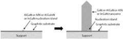
- a thin buffer layer or nanoscale nucleation islandscould be grown on the graphitic surface.
- the buffer layercould be made of AlN or AlGaN or AlGaInN or InGaN, which enhances the density, and controls the polarity and orientation of nanowires or nanopyramids such as GaN.
- Use of AlN buffer layerhas been previously reported for GaN nanowire or nanopyramid growth on Si substrates (Nanotechnology 26 (2015) 085605); however, not on graphitic substrates.
- the buffer layer on the graphitic substratecan be grown by migration enhanced epitaxy (MEE). Tuning the growth conditions, such as temperature and VIII ratio, and the thickness of the buffer layer, the density, alignment and polarity of the nanowires or nanopyramids can be controlled.
- MEEmigration enhanced epitaxy
- nanoscale nucleation islands of AlN or AlGaN or AlGaInN or InGaN on graphitic substratecan be used to facilitate the growth of nanowires or nanopyramids.
- These nucleation islandsincrease the density, and control the polarity and alignment of nanowires or nanopyramids.
- AlGaN islandscan be grown on a graphitic substrate. The density of the islands can be increased by increasing the island growth time. Then the nanowire or nanopyramid growth (e.g. GaN or AlGaN) can be initiated on the said islands.
- nucleation islandsas compared to a buffer layer has some additional advantages.
- the graphitic surfacedoes not get covered by the buffer layer that might reduce the transparency of graphene.
- the nucleation island sizetypically 5-20 nm
- the nanowire or nanopyramid diametertypically 50-500 nm
- the electrical conduction path between nanowire or nanopyramid and grapheneis not much compromised; especially, with regard to the case when the buffer layer is undoped or has a higher bandgap (e.g. AlN and AlGaN) than the nanowire or nanopyramid (e.g. GaN and InGaN).
- the graphitic surfacebefore nanowire or nanopyramid growth the graphitic surface is subjected to a nitrogen plasma, leading to the incorporation of nitrogen as a substitutional impurity or/and formation of ledges and step edges on its surface, preferably both.
- the atomic ledgesfacilitate the nucleation of nanowires or nanopyramids as mentioned above.
- the inclusion of nitrogenchanges the Fermi level and hence the electronic structure of the graphitic substrate (Nano Lett. 8, 4373, (2008)).
- the inclusion of nitrogenalso increases the chemical reactivity of the graphitic substrate and makes nanowire or nanopyramid nucleation on the surface easier.
- dopingsuch as n-type doping of the graphene in combination with nitrogen plasma may facilitate nanowire or nanopyramid growth and further device fabrication.
- the inventionrelates to the introduction of a buffer layer or nanoscale islands of an Al-group V compound such as AlAs, AlAsSb or AlSb on the graphitic substrate.
- Alis first deposited on the graphitic substrate to form a thin Al layer or nanoscale Al islands on the graphitic substrate. Due to the relatively high binding energy and thus a low diffusion coefficient of the Al adatoms, Al tends to stick on the graphitic surface.
- Group V element fluxsuch as As and/or Sb fluxes are provided onto the above Al layer or nanoscale islands, thereby forming a buffer layer or nanoscale islands of Al-group V compound such as AlAs, AlAsSb or AlSb.
- a change in the surface energy by the introduction of the buffer layer or nanoscale islandsfacilitates the nucleation and growth of nanowires or nanopyramids.
- the fluxmay be in the form of monomers, dimers, trimers or tetramers, such as As 2 and Sb 2 .
- an Al layer of nominal thickness 0.01 to 2 nmis deposited on the graphitic substrate such as at temperatures between 500-700° C.
- the layeris then transformed into a buffer layer or nanoscale islands of AlAs, AlAsSb or AlSb by supplying As and/or Sb fluxes such as in the range of 0.05-5 ⁇ 10 ⁇ 6 Torr, such as 1-3 ⁇ 10 ⁇ 6 Torr.
- Ga dropletsare formed on the said buffer layer or nanoscale islands by supplying only Ga flux to catalyse the growth of a plurality of semiconducting group III-V nanowires, preferably nanowires comprising GaAs and/or GaAsSb, on said buffer layer or nucleation islands on the graphitic substrate, preferably via MOVPE or MBE. Nanowires preferably grow perpendicular to the substrate.
- defects and holes of single or multiple atomic layers in depthare formed on the graphitic substrate.
- defects or holes steps or ledgesare formed on the graphitic substrate.
- steps or ledgesare created on the graphitic substrate that aid the nucleation of nanowires or nanopyramids.
- Thiscan be achieved through treatment with oxygen plasma or through treatment with ozone, e.g. UV and ozone.
- the treatmentis preferably effected at elevated temperature, such as 100° C. or more, ideally 125 to 175° C., such as 150° C.
- the etching processappears to work better at these slightly elevated temperatures.
- the use of elevated temperaturesbegins the annealing process described below.
- this treatmentintroduces oxygen atoms to the surface of the graphitic layer, typically via the formation of an epoxide group on the graphitic surface.
- the treatmentintroduces both ledges/steps and oxygen atoms to the surface of the graphitic layer.
- the use of elevated temperatures during the treatment processmay also enhance the etching process (i.e. the formation of ledges).
- this surface treatmentresults in the formation of a rough graphitic surface, with holes and defects on the surface of the graphitic substrate, and the carbon dangling bonds are bonded with oxygen atoms.
- the introduction of ledges onto the substrate surfaceincreases the surface roughness and creates a fluctuation in surface potential of the substrate making nucleation thereon easier.
- the surface of the UV-ozone or oxygen plasma treated graphitic substratecould itself be used as a surface for nanowire or nanopyramid nucleation; however, the inventors have found that annealing the treated graphitic substrate with hydrogen results in a more interesting surface for nanowire or nanopyramid nucleation.
- the ozone or oxygen plasma treated graphitic substrateis annealed in the presence of hydrogen, typically in an inert atmosphere.
- the annealing processmay take place at a temperature of 100 to 500° C., such as 250 to 400° C.
- a suitable graphene treatment processis described in Science 330 (2010) 655.
- the inert gasis typically nitrogen or a noble gas such as argon.
- the annealing processreduces the epoxide surface groups at the ledges down to C—H groups and therefore provides an improved surface for nanowire or nanopyramid nucleation and hence nanowire or nanopyramid growth.
- the C—H bondis believed to break at the elevated temperatures used for nanowire or nanopyramid growth, leaving the surface with dangling bond for the nanowire or nanopyramid nucleation to take place.
- the oxygen or ozone treatmentcauses vertical etching of the graphitic substrate and hence the introduction of ledges/steps.
- the annealing processcauses lateral etching increasing surface roughness across the surface of the substrate.
- the inventionrelates to the introduction of a crystalline Si layer, in particular an alpha-crystalline Si(111) layer onto the graphitic substrate using the metal-induced crystallization (MIC) process.
- a crystalline Si layerin particular an alpha-crystalline Si(111) layer onto the graphitic substrate using the metal-induced crystallization (MIC) process.
- MICmetal-induced crystallization
- This crystalline Si layerallows nanowire or nanopyramid growth in the [111] direction and hence the formation of perpendicular nanowires or nanopyramids.
- Al layercan be deposited by any known technique such as e-beam or thermal evaporation, atomic layer deposition (ALD), CVD and so on.
- ALDatomic layer deposition
- CVDchemical vapor deposition
- the inventorshave shown that the electron beam evaporation of Al can be used, something which ensures that the graphitic surface is not damaged in said process.
- the graphitic surfaceis modified only at those spots where nanowires are to nucleate, whereas the rest of the graphitic surface should remain undamaged in order to keep the good electrical properties of the graphitic surface between the nanowires or nanopyramids.
- the Al layeris preferably 10 to 30 nm in thickness.
- the uppermost atomic layers of this Al layerare preferably oxidised by exposing the Al to an oxygen source such as air.
- the uppermost atomic layersare preferably represented by around the top 5 nm of the Al layer.
- a Si layeris applied on top of the oxidised Al layer (aluminium oxide layer). Again, the same application techniques can be employed.
- the Si layeris amorphous at this point.
- a structureis preferably formed in which a graphitic substrate carries an Al layer, an oxidised Al layer and an amorphous Si layer, in that order.
- the Si layercan be 5 to 50 nm in thickness
- Annealingmay take place at a temperature of 300 to 500° C. Typically, annealing occurs in an inert atmosphere, such as an atmosphere of nitrogen.
- the as-deposited Al layer on arbitrary substratesis polycrystalline with no preferential orientation of the grains.
- the Si layeris also amorphous at this stage with no crystalline Si before annealing. Therefore, the initial bilayer consists of amorphous Si on top of polycrystalline Al, with a thin oxide interface.
- Si atomsdiffuse into the Al layer and form spontaneously crystalline nuclei.
- the driving forceis the free energy difference between the amorphous and crystalline phases of Si.
- the Al and Si layershave exchanged their initial stacking position: the Al layer is on top of the stack.
- a (Si)Al-oxide layeris located between the Al and Si layers at this point.
- the crystallization of Si grainsis determined.
- the present inventorshave found that the electron beam evaporation of Al on graphene can give a preferable (111)-orientation of the Al layer, which is much enhanced compared to that on amorphous SiO 2 substrates. This subsequently results in a highly (111)-oriented Si film on graphene after the AIC process without any damage in the graphene substrate.
- the Al layercan then be removed, preferably via etching of the Al layer (as well as any (Si)Al-oxide in-between the two layers) to leave a substrate coated with a mainly (111) crystalline nanostructured Si layer on the graphitic substrate.
- the Si layer at this pointcan be 5 to 50 nm in thickness. Since the Si layer is very thin, the properties of underlying graphene can still be realised, i.e. it will still be flexible, conductive and mostly transparent.
- a further advantage of using the Si layeris that the nanowire or nanopyramid growth recipe can readily be transferred from the growth on standard Si(111) substrates.
- nanowire or nanopyramid growthtakes place on the Si layer on top of graphic substrate, the standard recipes for growing III-V nanowires or nanopyramids on Si can readily be applied. Moreover, the density of nanowires or nanopyramids is much higher than on the bare graphitic substrate.
- Combining with a mask with hole pattern on top of the Si(111) layerone can achieve the nanowire or nanopyramid growth only at exposed hole region by high temperature growth, resulting in a position-controlled or selective area growth.
- the graphitic substratemay need to be supported in order to allow growth of the nanowires or nanopyramids thereon.
- the substratecan be supported on any kind of material including conventional semiconductor substrates and transparent glasses. It is preferred if the support is transparent so that the substrate does not block light from exiting or entering the device.
- Examples of preferred substratesinclude fused silica, fused quartz, fused alumina, silicon carbide or AlN.
- fused silica or SiCis preferred, especially fused silica.
- the supportshould be inert. After nanowire or nanopyramid growth and before use in a device, the support might be removed, e.g. by peeling away the support from the graphitic substrate.
- nanowires or nanopyramidsof commercial importance, it is preferred that these grow epitaxially on the substrate, Si layer, buffer layer or nucleation islands. It is also ideal if growth occurs perpendicular to the growing surface and ideally therefore in the [111] (for cubic crystal structure) or [0001] (for hexagonal crystal structure) direction.
- the present inventorshave determined that epitaxial growth on graphitic substrates is possible by determining a possible lattice match between the atoms in the semiconductor nanowire or nanopyramid and the carbon atoms in the graphene sheet.
- the carbon-carbon bond length in graphene layersis about 0.142 nm.
- Graphitehas hexagonal crystal geometry. The present inventors have previously realised that graphite can provide a substrate on which semiconductor nanowires or nanopyramids can be grown as the lattice mismatch between the growing nanowire or nanopyramid material and the graphitic substrate can be very low.
- the inventorshave realised that due to the hexagonal symmetry of the graphitic substrate and the hexagonal symmetry of the semiconductor atoms in the (111) planes of a nanowire or nanopyramid growing in the [111] direction with a cubic crystal structure (or in the (0001) planes of a nanowire or nanopyramid growing in the [0001] direction with a hexagonal crystal structure), a lattice match can be achieved between the growing nanowires or nanopyramids and the substrate.
- the different hexagonal arrangements of the semiconductor atoms as described in WO2013/104723can enable semiconductor nanowires or nanopyramids of such materials to be vertically grown to form free standing nanowires or nanopyramids on top of a thin carbon-based graphitic material.
- the triangular facesare normally terminated with (1-101) or (1-102) planes.
- the triangular side surfaces with (1-101) facetscould either converge to a single point at the tip or could form a new facets ((1-102) planes) before converging at the tip.
- the nanopyramidsare truncated with its top terminated with ⁇ 0001 ⁇ planes.
- nanowires or nanopyramidsWhilst it is ideal that there is no lattice mismatch between a growing nanowire or nanopyramid and the substrate, nanowires or nanopyramids can accommodate much more lattice mismatch than thin films for example.
- the nanowires or nanopyramids of the inventionmay have a lattice mismatch of up to about 10% with the substrate and epitaxial growth is still possible. Ideally, lattice mismatches should be 7.5% or less, e.g. 5% or less.
- the nanowire or nanopyramid grown in the present inventionmay be from 250 nm to several microns in length, e.g. up to 5 microns.
- the nanowires or nanopyramidsare at least 1 micron in length.
- at least 90% of the nanowires grownwill be at least 1 micron in length.
- substantially all the nanowireswill be at least 1 micron in length.
- Nanowires/nanopyramidscan be controlled through flux ratios. Nanopyramids are encouraged, for example if high group V flux is employed.
- the nanowires grownhave the same dimensions, e.g. to within 10% of each other.
- at least 90% (preferably substantially all) of the nanowireswill preferably be of the same diameter and/or the same length (i.e. to within 10% of the diameter/length of each other).
- the skilled manis looking for homogeneity and nanowires then are substantially the same in terms of dimensions.
- the length of the nanowires or nanopyramidsis often controlled by the length of time for which the growing process runs. A longer process typically leads to a (much) longer nanowire.
- the nanowires or nanopyramidshave typically a hexagonal cross sectional shape.
- the nanowire or nanopyramidmay have a cross sectional diameter of 25 to 200 nm (i.e. its thickness). As noted above, the diameter is ideally constant throughout the majority of the nanowire. Nanowire diameter can be controlled by the manipulation of the ratio of the atoms used to make the nanowire as described further below.
- the length and diameter of the nanowires or nanopyramidscan be affected by the temperature at which they are formed. Higher temperatures encourage high aspect ratios (i.e. longer and/or thinner nanowires). The skilled man is able to manipulate the growing process to design nanowires of desired dimensions.
- the nanowires or nanopyramids of the inventionare formed from at least one III-V compound.
- Group III optionsare B, Al, Ga, In, and Tl.
- Preferred options hereare Ga, Al and In.
- Group V optionsare N, P, As, Sb. All are preferred.
- Preferred compounds for nanowire or nanopyramid manufactureinclude AlAs, GaSb, GaP, GaN, AlN, AlGaN, AlGaInN, GaAs, InP, InN, InGaAs, InSb, InAs, or AlGaAs.
- Compounds based on Al, Ga and In in combination with Nare one option.
- the use of GaN, AlGaN, AlInGaN or AlNis highly preferred, especially in combination with a group III-N buffer layer or nucleation islands.
- the ternary compoundsmay therefore be of formula XYZ wherein X is a group III element, Y is a group III different from X, and Z is a group V element.
- the X to Y molar ratio in XYZis preferably 0.1 to 0.9, i.e. the formula is preferably X x Y 1-x Z where subscript x is 0.1 to 0.9.
- Quaternary systemsmight also be used and may be represented by the formula A x B 1-x C y D 1-y where A and B are group III elements and C and D are group V elements. Again subscripts x and y are typically 0.1 to 0.9. Other options will be clear to the skilled man.
- the nanowires or nanopyramids of the inventionshould preferably grow in the [111] direction for nanowires or nanopyramids with cubic crystal structure and [0001] direction for nanowires or nanopyramids with hexagonal crystal structure. If the crystal structure of the growing nanowire or nanopyramid is cubic, then the (111) interface between the nanowire or nanopyramid and the catalyst droplet represents the plane from which axial growth takes place. If the nanowire or nanopyramid has a hexagonal crystal structure, then the (0001) interface between the nanowire or nanopyramid and the catalyst droplet represents the plane from which axial growth takes place. Planes (111) and (0001) both represent the same (hexagonal) plane of the nanowire, it is just that the nomenclature of the plane varies depending on the crystal structure of the growing nanowire.
- the nanowires or nanopyramidsare preferably grown by MBE or MOVPE.
- the growing surfaceis provided with a molecular beam of each reactant, e.g. a group III element and a group V element preferably supplied simultaneously.
- a higher degree of control of the nucleation and growth of the nanowires or nanopyramids on the graphitic substratemight be achieved with the MBE technique by using migration-enhanced epitaxy (MEE) or atomic-layer MBE (ALMBE) where e.g. the group III and V elements can be supplied alternatively.
- MEEmigration-enhanced epitaxy
- AMBEatomic-layer MBE
- a preferred techniqueis solid-source MBE, in which very pure elements such as gallium and arsenic are heated in separate effusion cells, until they begin to slowly evaporate (e.g. gallium) or sublimate (e.g. arsenic).
- a rf-plasma nitrogen sourceis typically used to produce low energy beams of nitrogen atoms.
- the gaseous elementsthen condense on the substrate, where they may react with each other.
- single-crystal GaAsis formed.
- beamimplies that evaporated atoms (e.g. gallium) or molecules (e.g. As 4 or As 2 ) do not interact with each other or vacuum chamber gases until they reach the substrate.
- MBEtakes place in ultra-high vacuum, with a background pressure of typically around 10 ⁇ 10 to 10 ⁇ 9 Torr.
- Nanostructuresare typically grown slowly, such as at a speed of up to a few, such as about 10, ⁇ m per hour. This allows nanowires or nanopyramids to grow epitaxially and maximises structural performance.
- the substrateis kept in a reactor in which the substrate is provided with a carrier gas and a metal organic gas of each reactant, e.g. a metal organic precursor containing a group III element and a metal organic precursor containing a group V element.
- the typical carrier gasesare hydrogen, nitrogen, or a mixture of the two.
- the nanowires or nanopyramids of the inventionmay be grown with or without the presence of a catalyst.
- Catalystcan be introduced to provide nucleating sites for nanowire or nanopyramid growth.
- the catalystcan be one of the elements making up the nanowire or nanopyramid—so called self-catalysed, or different from any of the elements making up the nanowire.
- the catalystmay be Au or Ag or the catalyst may be a metal from the group used in the nanowire or nanopyramid growth (e.g. group III metal), especially one of the metal elements making up the actual nanowire or nanopyramid (self-catalysis). It is thus possible to use another element from group III as a catalyst for growing a III-V nanowire, e.g. use Ga as a catalyst for an In—V) nanowire or nanopyramid and so on.
- the catalystis Au or the growth is self-catalysed (i.e. Ga for a Ga—V) nanowire or nanopyramid and so on).
- the catalystcan be deposited onto the growing surface to act as a nucleation site for the growth of the nanowires or nanopyramids. Ideally, this can be achieved by providing a thin film of catalytic material formed over the growing surface. When the catalyst film is melted as the temperature increases to the nanowire or nanopyramid growth temperature, the catalyst forms nanometre sized particle-like droplets on the growing surface and these droplets form the points where nanowires or nanopyramids can grow.
- VLSvapour-liquid-solid growth
- the molecular beamis the vapour
- the nanowire or nanopyramidprovides the solid component.
- the catalyst particlecan also be solid during the nanowire or nanopyramid growth, by a so called vapour-solid-solid growth (VSS) mechanism.
- VLSvapour-solid-solid growth
- the liquide.g. gold
- a maskcan be used on the substrate.
- This maskcan be provided with regular holes, where catalyst particles (of one of the group-III elements) are deposited in the holes such that nanowires or nanopyramids can grow homogeneously in size in a regular array across the substrate.
- the hole patterns in the maskcan be easily fabricated using conventional photo/e-beam lithography or nanoimprinting. Focussed ion beam technology may also be used in order to create a regular array of nucleation sites on the graphitic surface for the nanowire or nanopyramid growth.
- a thin film of Ausuch as with a thickness less than 50 nm, can be deposited on a hole-patterned photo or e-beam resist.
- a regular arrayed pattern of Au dots on the substrate surfacecan be fabricated.
- the growth of nanowires or nanopyramids without the presence of a catalystis also possible and is known as selective area growth method.
- This methodmay require a mask with nano-hole patterns deposited on the graphitic layers as described herein.
- the mask materialcan be an oxide or nitride masking layer, preferably a metal oxide or metal nitride layer or semimetal oxide or semimetal nitride).
- the mask layercan be applied through atomic layer deposition or the techniques discussed above in connection with the deposition of the other layers.
- the oxide usedis preferably based on a metal or semimetal (such as Si).
- the nature of the cation used in the masking layermay be Al, Si or a transition metal, especially a first 3d row transition metal (Sc—Zn).
- Preferred masking layersare based on oxides, such as SiO 2 , Si 3 N 4 , TiO 2 or Al 2 O 3 , W 2 O 3 , and so on.
- Masking layersmay be 5 to 100 nm in thickness, such as 10 to 50 nm.
- the masking layeris preferably continuous and covers the substrate as a whole. This ensures that the layer is defect-free and thus prevents nucleation of nanowires or nanopyramids on the masking layer.
- a maskcan be applied to the substrate and etched with holes exposing the substrate surface, optionally in a regular pattern. Moreover, the size and the pitch of the holes can be carefully controlled. By arranging the holes regularly, a regular pattern of nanowires or nanopyramids can be grown.
- the size of the holescan be controlled to ensure that only one nanowire or nanopyramid can grow in each hole.
- the holescan be made of a size where the hole is sufficiently large to allow nanowire or nanopyramid growth. In this way, a regular array of nanowires can be grown.
- the graphitic surfacesmay be treated with the above mentioned techniques (oxygen or ozone treatment and hydrogenation, nitrogen plasma, MIC of amorphous silicon, deposition of buffer layer, or formation of nucleation islands) before or after the deposition of mask.
- self-catalysed nanowiresAs noted above, it is also possible to prepare self-catalysed nanowires.
- self-catalysedis meant that one of the components of the nanowire or nanopyramid acts as a catalyst for its growth.
- a Ga layercan be applied to the hole-patterned mask layer, melted to form droplets acting as nucleation sites for the growth of Ga containing nanowires.
- a Ga metal portionmay end up positioned on the top of the nanowire.
- a Ga/In fluxcan be supplied to the substrate surface for a period of time to initiate the formation of Ga/In droplets on the surface upon heating of the substrate.
- the substrate temperaturecan then be set to a temperature suitable for the growth of the nanowire or nanopyramid in question.
- the growth temperaturemay be in the range 300 to 700° C.
- the temperature employedis, however, specific to the nature of the material in the nanowire, the catalyst material and the substrate material.
- a preferred temperatureis 540 to 630° C., e.g. 590 to 630° C., such as 610° C.
- InAsthe range is lower, for example 420 to 540° C., such as 430 to 540° C., e.g. 450° C.
- Nanowire or nanopyramid growthcan be initiated by opening the shutter of the Ga/In effusion cell and the counter ion effusion cell, simultaneously once a catalyst film has been deposited and melted.
- the temperature of the effusion cellscan be used to control growth rate.
- Convenient growth rates, as measured during conventional planar (layer by layer) growth,are 0.05 to 2 ⁇ m per hour, e.g. 0.1 ⁇ m per hour.
- the pressure of the molecular beamscan also be adjusted depending on the nature of the nanowire or nanopyramid being grown. Suitable levels for beam equivalent pressures are between 1 ⁇ 10 ⁇ 7 and 1 ⁇ 10 ⁇ 5 Torr.
- the beam flux ratio between reactantscan be varied, the preferred flux ratio being dependent on other growth parameters and on the nature of the nanowire or nanopyramid being grown.
- the beam flux ratio between reactantscan affect crystal structure of the nanowire.
- growth of GaAs nanowires with a growth temperature of 540° C., a Ga flux equivalent to a planar (layer by layer) growth rate of 0.6 ⁇ m per hour, and a beam equivalent pressure (BEP) of 9 ⁇ 10 ⁇ 6 Torr for As 4produces wurtzite crystal structure.
- BEPbeam equivalent pressure
- growth of GaAs nanowires at the same growth temperature, but with a Ga flux equivalent to a planar growth rate of 0.9 ⁇ m per hour and a BEP of 4 ⁇ 10 ⁇ 6 Torr for As 4produces zinc blende crystal structure.
- Nanowire or nanopyramid diametercan in some cases be varied by changing the growth parameters. For example, when growing self-catalyzed GaAs nanowires under conditions where the axial nanowire or nanopyramid growth rate is determined by the As 4 flux, the nanowire or nanopyramid diameter can be increased/decreased by increasing/decreasing the Ga:As 4 flux ratio. The skilled man is therefore able to manipulate the nanowire or nanopyramid in a number of ways.
- RHEEDreflection high-energy electron diffraction
- the nanowires of the inventionpreferably grow as cubic (zinc blende) or hexagonal (wurtzite) structures.
- the inventorshave found that it is possible to change the crystal structure of the growing nanowire or nanopyramid by manipulating the amounts of the reactants fed to the substrate as discussed above. Higher feeds of Ga, for example, force a GaAs crystal into the cubic crystal structure. Lower feeds encourage a hexagonal structure. By manipulating reactant concentrations, the crystal structure within the nanowire or nanopyramid can therefore be changed.
- MOVPEmetal-organic chemical vapor deposition
- radial and axial heterostructured nanowirescan be grown using the MOVPE method.
- this methodfavours the growth of radial heterostructured nanowires and microwires, for example: n-doped GaN core with shell consisting of intrinsic GaN/InGaN multiple quantum wells (MQW), p-doped AlGaN electron blocking layer (EBL) and p-doped GaN shell.
- MQWintrinsic GaN/InGaN multiple quantum wells
- EBLp-doped AlGaN electron blocking layer
- This methodalso allows the growth of axial heterostructured nanowires using techniques such as pulsed growth technique or continuous growth mode with modified growth parameters for e.g., lower VIII molar ratio and higher substrate temperature.
- the reactoris evacuated after placing the sample, and is purged with N 2 to remove oxygen and water in the reactor. This is to avoid any damage to the graphitic substrate at the growth temperatures, and to avoid unwanted reactions of oxygen and water with the precursors.
- the reactor pressureis set to be between 50 and 400 Torr.
- the substrateis thermally cleaned under H 2 atmosphere at a substrate temperature of about 1200° C. Subsequently, a very thin buffer layer or nucleation islands is grown which consists of Al(In)GaN or AlN by introducing metal organic precursors and NH 3 .
- the metal organic precursorscan be either trimethylgallium (TMGa), or triethylgallium (TEGa) for Ga, trimethylalumnium (TMA1) or triethylalumnium (TEA1) for Al, and trimethylindium (TMIn) or triethylindium (TEIn) for In.
- the metal precursors for dopantscan be SiH 4 for silicon and bis(cyclopentadienyl)magnesium (Cp 2 Mg) or bis(methylcyclopentadienyl)magnesium ((MeCp) 2 Mg) for Mg.
- the substrate temperaturemay be set in the range of 600 to 1200° C.
- the flow rates of TMGa, TMA1 and TMIncan be maintained between 5 and 100 sccm.
- the NH 3 flow ratecan be varied between 5 and 550 sccm.
- TMGa/TMA1 and NH 3are supplied to the substrate surface for a period of time to initiate the formation of Al(In)GaN or AlN buffer layer or nucleation islands on the graphitic surface.
- the growth parameters used for buffer layer or nucleation islandscan strongly influence the density, polarity and alignment of the nanowires.
- the substrate temperaturecan then be set to a temperature suitable for the growth of the nanowire or nanopyramid in question.
- the growth temperaturemay be in the range 700 to 1200° C.
- the temperature employedis, however, specific to the nature of the material in the nanowire.
- a preferred temperatureis 800 to 1150° C., e.g. 900 to 1100° C., such as 1100° C.
- the rangeis slightly higher, for example 900 to 1400° C., such as 1050 to 1250° C., e.g. 1250° C.
- the nanowires or nanopyramids of the inventionpreferably grow epitaxially. They attach to the underlying substrate through covalent, ionic or quasi van der Waals binding. Accordingly, at the junction of the growing surface and the base of the nanowire, crystal planes are formed epitaxially within the nanowire. These build up, one upon another, in the same crystallographic direction thus allowing the epitaxial growth of the nanowire.
- the nanowires or nanopyramidsgrow perpendicularly. It will be appreciated that in experimental science the growth angle may not be exactly 90° but the term perpendicularly implies that the nanowires are within about 10° of perpendicular, e.g. within 5°.
- the substratecan be doped to match the major carriers of grown nanowires or nanopyramids.
- the bottom contactis preferably ohmic.
- inventive compositionscomprise a plurality of nanowires or nanopyramids.
- the nanowires or nanopyramidsgrow about parallel to each other. It is preferred therefore if at least 90%, e.g. at least 95%, preferably substantially all nanowires or nanopyramids grow in the same direction from the same plane of the growing surface.
- nanowires or nanopyramidsgrow from the same plane. It is preferred if that plane is parallel to the substrate surface. Ideally the grown nanowires or nanopyramids are substantially parallel. Preferably, the nanowires or nanopyramids grow substantially perpendicular to the growing surface.
- nanowires or nanopyramids of the inventioncan contain a p-n or p-i-n junction, e.g. to enable their use in LEDs.
- Nanowires or nanopyramids of the inventionare therefore provided with an undoped intrinsic semiconductor region between a p-type semiconductor and an n-type semiconductor region. All of or sections of the p-type and n-type regions are typically heavily doped because they are used for ohmic contacts.
- the nanowires or nanopyramidsare doped. Doping typically involves the introduction of impurity ions into the nanowire, e.g. during MBE or MOVPE growth. The doping level can be controlled from ⁇ 10 15 /cm 3 to 10 20 /cm 3 .
- the nanowires or nanopyramidscan be p-doped or n-doped as desired. Doped semiconductors are extrinsic semiconductors.
- n(p)-type semiconductorshave a larger electron (hole) concentration than hole (electron) concentration by doping an intrinsic semiconductor with donor (acceptor) impurities.
- Suitable donor (acceptors) for III-V compoundscan be Te (Mg, Be and Zn).
- Dopantscan be introduced during the growth process or by ion implantation of the nanowires or nanopyramids after their formation.
- the nanowires or nanopyramids of the inventioncomprise Al.
- the use of Alis advantageous as high Al content leads to high band gaps, enabling UV-C LED emission from the active layer(s) of nanowires or nanopyramids and/or avoiding absorption of the emitted light in the p-region and/or n-region layers. Where the band gap is high, it is less likely that UV light is absorbed by this part of the nanowires or nanopyramids.
- the use therefore of AlN or AlGaN in nanowires or nanopyramidsis preferred.
- nanowires or nanopyramidscomprise AlN or AlGaN
- achieving high electrical conductivity by introducing p-type dopantsis a challenge.
- One solutionrelies on a short period superlattice (SPSL).
- SPSLsuperlattice
- the low ionization energy of acceptors in layers with lower Al compositionleads to improved hole injection efficiency without compromising on the barrier height in the p-region layer. This effect is additionally enhanced by the polarization fields at the interfaces.
- the SPSLcan be followed with a highly p-doped GaN:Mg layer for better hole injection.
- the inventorspropose to introduce a p-type doped Al x Ga 1-x N/Al y Ga 1-y N short period superlattice (i.e. alternating thin layers of Al x Ga 1-x N and Al y Ga 1-y N) into the nanowires or nanopyramid structure, where the Al mole fraction x is less than y, instead of a p-type doped Al z Ga 1-z N alloy where x ⁇ z ⁇ y.
- xcould be as low as 0 (i.e. GaN) and y could be as high as 1 (i.e. AlN).
- the superlattice periodshould preferably be 5 nm or less, such as 2 nm, in which case the superlattice will act as a single Al z Ga 1-z N alloy (with z being a layer thickness weighted average of x and y) but with a higher electrical conductivity than that of the Al z Ga 1-z N alloy, due to the higher p-type doping efficiency for the lower Al content Al z Ga 1-z N layers.
- the p-type dopantis an alkali earth metal such as Mg or Be.
- a further option to solve the problem of doping an Al containing nanowire/nanopyramidfollows similar principles. Instead of a superlattice containing thin AlGaN layers with low or no Al content, a nanostructure can be designed containing a gradient of Al content (mole fraction) in the growth direction of the AlGaN within the nanowires or nanopyramids. Thus, as the nanowires or nanopyramids grow, the Al content is reduced/increased and then increased/reduced again to create an Al content gradient within the nanowires or nanopyramids.
- the layersare graded either from GaN to AlN or AlN to GaN.
- the graded region from GaN to AlN and AlN to GaNmay lead to n-type and p-type conduction, respectively. This can happen due to the presence of dipoles with different magnitude compared to its neighbouring dipoles.
- the GaN to AlN and AlN to GaN graded regionscan be additionally doped with n-type dopant and p-type dopant respectively.
- p-type dopingis used in AlGaN nanowires using Be as a dopant.
- one optionwould be to start with a GaN nanowire/nanopyramid and increase Al and decrease Ga content gradually to form AlN, perhaps over a growth thickness of 100 nm.
- This graded regioncould act as a p- or n-type region, depending on the crystal plane, polarity and whether the Al content is decreasing or increasing in the graded region, respectively.
- the opposite processis effected to produce GaN once more to create an n- or p-type region (opposite to that previously prepared).
- These graded regionscould be additionally doped with n-type dopants such as Si and p-type dopants such as Mg or Be to obtain n- or p-type regions with high charge carrier density, respectively.
- the crystal planes and polarityis governed by the type of nanowire/nanopyramid as is known in the art.
- the nanowires or nanopyramids of the inventioncomprise Al, Ga and N atoms wherein during the growth of the nanowires or nanopyramids the concentration of Al is varied to create an Al concentration gradient within the nanowires or nanopyramids.
- a tunnel junctionis a barrier, such as a thin layer, between two electrically conducting materials.
- the barrierfunctions as an ohmic electrical contact in the middle of a semiconductor device.
- a thin electron blocking layeris inserted immediately after the active region, which is followed by a p-type doped AlGaN layer with Al content higher than the Al content used in the active layers.
- the p-type doped layeris followed by a highly p-type doped AlGaN layer and a very thin tunnel junction layer followed by an n-type doped AlGaN layer.
- the tunnel junction layeris chosen such that the electrons tunnel from the valence band in p-AlGaN to the conduction band in the n-AlGaN, creating holes that are injected into the p-AlGaN layer.
- the nanowire or nanopyramidcomprises two regions of doped GaN (one p- and one n-doped region) separated by an Al layer, such as a very thin Al layer.
- the Al layermight be a few nm thick such as 1 to 10 nm in thickness. It is appreciated that there are other optional materials that can serve as a tunnel junction which includes highly doped InGaN layers.
- doped GaN layerscan be grown on the Al layer.
- the inventionprovides a nanowire or nanopyramid having a p-type doped (Al)GaN region and an n-type doped (Al)GaN region separated by an Al layer.
- the nanowires or nanopyramids of the inventioncan be grown to have a heterostructured form radially or axially.
- p-n junctioncan be axially formed by growing a p-type doped core first, and then continue with an n-doped core (or vice versa).
- p-n junctioncan be radially formed by growing the p-doped nanowire or nanopyramid core first, and then the n-doped semiconducting shell is grown (or vice versa)—a core shell nanowire.
- An intrinsic shellcan be grown between doped regions to obtain a radially heterostructured nanowire or nanopyramid with p-i-n junction.
- the nanowires or nanopyramidsare grown axially and are therefore formed from a first section and a second section.
- the two sectionsare doped differently to generate a p-n junction or p-i-n junction. It does not matter whether the top or bottom section of the nanowire or nanopyramid is the p-doped or n-doped section.
- nanowireshave been grown on a substrate in the presence of a catalyst, it is envisaged that some of the nanowires will have a catalyst deposit on top of nanowire. Ideally, the majority of the nanowires will have such a deposit, preferably substantially all the nanowires will comprise this deposit.
- the top of the nanowires or nanopyramidsneeds to comprise a top contact.
- a top contactis formed using another graphitic layer.
- the inventionthen involves placing a graphitic layer on top of the formed nanowires or nanopyramids to make a top contact. It is preferred that the graphitic top contact layer is substantially parallel with the substrate layer. It will also be appreciated that the area of the graphitic layer does not need to be the same as the area of the substrate. It may be that a number of graphitic layers are required to form a top contact with a substrate with an array of nanowires or nanopyramids.
- the graphitic layers usedcan be the same as those described in detail above in connection with the substrate.
- the top contactis graphitic, more especially it is graphene.
- This graphene top contactshould contain no more than 10 layers of graphene or its derivatives, preferably no more than 5 layers (which is called as a few-layered graphene). Especially preferably, it is a one-atom-thick planar sheet of graphene.
- the crystalline or “flake” form of graphiteconsists of many graphene sheets stacked together (i.e. more than 10 sheets). It is preferred if the top contact is 20 nm in thickness or less. Even more preferably, the graphitic top contact may be 5 nm or less in thickness.
- the inventorshave realized that the growing of semiconductor nanowires can involve metal catalysis.
- the metal catalystssuch as Au, Ga, or In are preferably used as seeds for nanowire or nanopyramid growth and they remain as a form of nanoparticles on top of nanowires after completion of the nanowire or nanopyramid growth.
- These catalyst depositscan be used as an intermediate material between metallic graphene and semiconductor nanowires.
- top contact to the formed nanowirescan be achieved by any convenient method. Methods akin to those mentioned previously for transferring graphitic layers to substrate carriers may be used.
- the graphitic layers from Kish graphite, highly ordered pyrolytic graphite (HOPG), or CVDmay be exfoliated by mechanical or chemical methods. Then they can be transferred into etching solutions such as HF or acid solutions to remove Cu (Ni, Pt, etc.) (especially for CVD grown graphitic layers) and any contaminants from the exfoliation process.
- the etching solutioncan be further exchanged into other solutions such as deionised water to clean the graphitic layers.
- the graphitic layerscan then be easily transferred onto the formed nanowires as the top contact. Again e-beam resist or photoresist may be used to support the thin graphitic layers during the exfoliation and transfer processes, which can be removed easily after deposition.
- the graphitic layersare dried completely after etching and rinsing, before they are transferred to the top of the nanowire or nanopyramid arrays.
- a mild pressure and heatcan be applied during this “dry” transfer.
- the graphitic layerscan be transferred on top of the nanowire or nanopyramid arrays, together with a solution (e.g. deionised water). As the solution dries off, the graphitic layers naturally form a close contact to underlying nanowires.
- a solutione.g. deionised water
- the surface tension of the solution during the drying processmight bend or knock out the nanowire or nanopyramid arrays.
- more robust nanowiresare preferably employed. Nanowires having a diameter of >80 nm might be suitable.
- hole patterned substrates which support the perpendicular nanowire or nanopyramid structurecould be used.
- the top contact graphitic layeris preferably transparent, conductive and flexible.
- a post-annealing processmay be used. After the deposition of the graphitic top contact, the sample can be annealed in an inert atmosphere, e.g. of argon, or vacuum. Temperatures can be up to 600° C. Annealing times can be up to 10 min.
- doping of the graphitic top contactcan be utilized.
- the major carrier of the graphitic top contactcan be controlled as either holes or electrons by doping. It is preferable to have the same doping type in the graphitic top contact and in the semiconducting nanowires, especially at the region below the metal catalytic particles, which would give a better ohmic behaviour after the post-annealing process. For example, for a core-shell nanowire or nanopyramid with p-doping in the shell, p-doping of the top graphitic layers matches the carrier type across the metal particles at the top of the nanowire or nanopyramid shell.
- top graphitic layer and the substratecan be doped.
- the substrate and/or the graphitic layeris doped by a chemical method which involves with an adsorption of organic or inorganic molecules such as metal chlorides (FeCl 3 , AuCl 3 or GaCl 3 ), NO 2 , HNO 3 , aromatic molecules or chemical solutions such as ammonia.
- organic or inorganic moleculessuch as metal chlorides (FeCl 3 , AuCl 3 or GaCl 3 ), NO 2 , HNO 3 , aromatic molecules or chemical solutions such as ammonia.
- the surface of substrate and/or the graphitic layercould also be doped by a substitutional doping method during its growth with incorporation of dopants such as B, N, S, or Si.
- Semiconductor nanowires or nanopyramidshave wide ranging utility. They are semiconductors so can be expected to offer applications in any field where semiconductor technology is useful. They are primarily of use in integrated nanoelectronics and nano-optoelectronic applications.
- An ideal device for their deploymentmight be a solar cell in particular.
- One possible deviceis a nanowire or nanopyramid solar cell sandwiched between two graphene layers as the two terminals.
- Such a solar cellhas the potential to be efficient, cheap and flexible at the same time. This is a rapidly developing field and further applications on these valuable materials will be found in the next years.
- the same conceptcan be used to also fabricate other opto-electronic devices such as light-emitting diodes (LEDs), photodetectors, waveguides and lasers.
- devices of the inventionare provided with electrodes to enable charge to be passed into the device.
- FIG. 1( a )shows a schematic representation of deposition of buffer layer on graphitic substrate, followed by the nanowire growth.
- FIG. 1( b )shows a schematic representation of deposition of nucleation islands on graphitic substrate, followed by the nanowire growth.
- FIG. 2shows representative results of the formation of nucleation island and nanowire growth scheme.
- FIG. 3( a )is a cross-sectional high-resolution scanning transmission electron microscope (STEM) image of a GaN nanowire grown on graphene using AlGaN nucleation islands.
- FIG. 3( b )is a high-angle annular dark-field STEM image of the same nanowire in (a), showing the AlGaN nucleation island.
- FIG. 4 ais a SEM image of (Al)GaN nanopyramids of the invention grown in a regular array. After growing the AlGaN nucleation islands, AlGaN with 3% Al in gas phase was grown for 150 s.
- FIG. 4 bis a closer image of said nanopyramids.
- FIG. 5(a) Schematic diagram showing the growth of nanowires on graphite flake and the top and bottom contacts to the nanowires. Tilted view SEM image (b) and high-resolution SEM image (c) of selectively grown GaN nanowires on multi-layer graphene flakes by MBE.
- FIG. 6shows an SEM image of self-catalyzed GaAsSb nanowires grown by MBE using AlAsSb nanoscale islands for enhanced nucleation on pristine graphitic substrate.
- InsetMagnified view of the perpendicular GaAsSb nanowires.
- FIG. 7shows atomic force microscopy (AFM) topography image after the treatment of graphite with (a) UV-ozone and (b) UV-ozone and H 2 annealing in Ar atmosphere.
- AFMatomic force microscopy
- FIG. 8( a )shows the AFM height profile along the solid line in FIG. 6( a ) of the graphite surface after the treatment with UV-ozone.
- FIG. 8( b )shows the AFM height profile along the dashed line in FIG. 6( b ) of the graphite surface after the UV-ozone treatment and the following H 2 annealing in Ar atmosphere, showing the formation of atomic steps and ledges. (Nanowires or nanopyramids are then grown on the treated graphitic substrate.)
- FIG. 9( a )shows an SEM image of GaAsSb nanowires grown on untreated pristine graphitic surface.
- FIG. 9( b )shows an SEM image of GaAsSb nanowires grown on UV-ozone treated and H 2 annealed graphitic surface. Improved density of perpendicular nanowires can be seen in (b) as compared to (a).
- FIG. 10shows the main process steps of aluminium-induced crystallization (MIC) of silicon on graphene layer 1, where amorphous silicon (a-Si) layer 3 diffuses through an aluminium metal layer 2 by thermal activation.
- a-Siamorphous silicon
- the siliconrearranges into a polycrystalline structure (p-Si) with [111]-orientation.
- the aluminium metal layer and the oxide layer above the p-Si structuremay be etched using HCl and HF, respectively. (Nanowires or nanopyramids are then grown on the MIC silicon on graphene.)
- FIG. 11shows an SEM image of self-catalyzed GaAs nanowires grown by MBE on amorphous (SiO 2 ) substrate covered with MIC silicon.
- the substrate temperaturewas lowered to ⁇ 1150° C. and the NH 3 flow was set to 25 sccm.
- Si-doped GaN nanowire growthwas carried out for ⁇ 3.5 min by introducing TMGa and Silane with a flow of 44.8 and 0.03 ⁇ mol/min, respectively.
- the samplewas cooled down under NH 3 flow of 25 sccm until the temperature dropped below 500° C.
- multi-layer graphenewas mechanically exfoliated from Kish graphite flakes and then indium-bonded to a SiO 2 /Si supporting substrate.
- a mask materialsuch as Al 2 O 3 and SiO 2 can be optionally deposited on the graphite flake.
- a big hole of 10 ⁇ m in diameteris etched in the mask material using photolithography such that the graphite surface is exposed in the hole.
- several periodically spaced small holes of diameter ⁇ 100 nmcan be etched using e-beam lithography, such that the nanowires selectively grow on the graphitic surface exposed in the hole.
- the nitrogen plasma treatment and the nanowire growthwere carried out in a Veeco Gen 930 MBE system equipped with a nitrogen plasma source, a Ga dual filament cell, and an Al double-crucible cell.
- the above samplesare then loaded into the MBE system for sample outgassing and nanowire growth.
- the samplesare annealed at a substrate temperature of 550° C. for a duration of 30 min to get rid of any oxide residues and any other contaminants on the substrate.
- the substrate temperatureis then increased to a temperature suitable for GaN nanowire growth: i.e. typically 755° C.
- the temperatures of the Ga and Al effusion cellis preset to yield nominal planar growth rate of 0.3 and 0.2 ⁇ m per hour, respectively.
- the nitrogen plasmais generated using a RF generator power of 450 W and nitrogen gas flow of 2.8 sccm. After the sample temperature reaches the growth temperature, the gate valve and the shutter in front of the nitrogen source was opened for 1 min, such that the nitrogen plasma is directed on to the sample.
- the samplecan then either be subjected to the nanowire growth by MBE or taken out of the MBE growth chamber for the nanowire or nanopyramid growth by MOCVD. In the case of nanowire growth by MBE, an Al flux was supplied for 6 seconds or longer and then an Al flux and a nitrogen plasma was supplied for 1 minute or longer.
- Nanowiresare grown in a Varian Gen II Modular MBE system equipped with a Ga dual filament cell, an Al double-crucible cell, an As valved cracker cell, and an Sb valved cracker cell.
- the cracker cellsallow to fix the proportion of monomers, dimers and tetramers.
- the major species of arsenic and antimonyare As 2 and Sb 2 , respectively.
- NWsare performed either on a Kish graphite flake or on a graphene film grown on SiC substrates by using a high-temperature sublimation technique.
- the graphene film samplesare purchased from external supplier.
- the Kish graphite samplesare cleaned by isopropanol followed by a blow dry with nitrogen, then indium-bonded to a silicon wafer and finally cleaved to provide a fresh graphitic surface for growth of NWs.
- the graphene/SiC substratesare blow dried with nitrogen, and then indium-bonded to a silicon wafer.
- the samplesare then loaded into the MBE system for sample outgassing and nanowire growth.
- the samplesare annealed at a substrate temperature of 550° C. for a duration of 30 min to get rid of any oxide residues on the substrate.
- the substrate temperatureis then increased to a temperature suitable for GaAs or GaAsSb nanowire growth: i.e. 630° C.
- the temperatures of the Al and Ga effusion cellsare preset to yield nominal planar growth rates of 0.1 ⁇ m per hour and 0.7 ⁇ m per hour, respectively.
- an As e flux of 2.5 ⁇ 10 ⁇ 6 Torris used, whereas the Sb 2 flux is set to a value in the range 0-1 ⁇ 10 ⁇ 6 Torr (dependent on the intended GaAsSb composition), for example 6 ⁇ 10 ⁇ 7 Torr.
- the Al fluxis first supplied to the surface during a time interval of typically 1 s or longer, while the shutters/valves for the other sources are closed.
- the Al shutteris then closed and As and/or Sb flux are supplied to the surface for a time interval of typically 60 s to form AlAs(Sb) nanoscale islands on the graphitic surface.
- the group V shutters and valvesare then closed and the Ga shutter opened, typically for 5 s, to supply Ga flux to the surface to initiate the formation of Ga droplets at the nanoscale islands.
- the relevant group V shutters and valvesare then opened again to initiate the growth of nanowires.
- the Sb shutter and valveare opened.
- the duration of the nanowire growthdepends on the intended length of the nanowires. In case of the GaAsSb nanowires sample depicted in FIG. 6 , the nanowire growth time was 5 min. The growth is stopped by closing all the shutters/valves, and simultaneously ramping down the substrate to room temperature.
- Kish graphite flakeswere used as the graphitic substrates.
- the Kish graphite samplesare cleaned by isopropanol followed by a blow dry with nitrogen, then indium-bonded to a silicon wafer and finally cleaved to provide a fresh graphitic surface for growth of nanowires.
- the substrateswere treated in UV-ozone at ⁇ 150° C. for 6 min, followed by annealing in H 2 at ⁇ 300° C. for 45 min.
- Nanowiresare grown in the same MBE system as described in Example 3.
- the major species of arsenic and antimonyare As 2 and Sb 2 , respectively.
- the samplesare loaded into the MBE system and outgassed at ⁇ 550° C. for a duration of 30 min to get rid of any oxide residues on the substrate.
- the substrate temperatureis then increased to a temperature suitable for GaAs or GaAsSb nanowire growth: i.e. 630° C.
- the temperatures of the Ga effusion cellis preset to yield nominal planar growth rate of 0.7 ⁇ m per hour.
- Ga fluxwas supplied for 10 s at a substrate temperature of ⁇ 630° C. After that the temperature is reduced to ⁇ 250° C. and an Sb 2 flux of 8 ⁇ 10 ⁇ 7 Torr and As 2 flux of 2.5 ⁇ 10 ⁇ 6 Torr are subsequently supplied for 50 s and 40 s, respectively. Then the substrate temperature is again increased to ⁇ 630° C.
- Ga fluxwas supplied for 10 min together with an As 2 flux of 2.5 ⁇ 10 ⁇ 6 Torr, whereas the Sb 2 flux is set to a value in the range 0-1 ⁇ 10 ⁇ 6 Torr (dependent on the intended GaAsSb composition), for example 8 ⁇ 10 ⁇ 7 Torr.
- the shuttersare closed and simultaneously the substrate temperate is ramped down.
- the MIC poly-Si(111) on graphene sampleswere of commercial chemical vapor deposition (CVD) grown monolayer graphene transferred onto Si(001).
- CVDchemical vapor deposition
- 50 nm Alwas deposited by e-beam evaporation at a rate of 1 ⁇ /s and a pressure of ⁇ 10 ⁇ 8 Torr.
- the sampleswere oxidized for 24 h in an ISO5 cleanroom atmosphere before depositing 50 nm amorphous Si (a-Si) by e-beam evaporation at a rate of 1 ⁇ /s and a pressure of ⁇ 10 ⁇ 8 Torr. All depositions were done at room temperature.
- the sampleswere annealed for 15 h at 500° C. in a nitrogen gas. After the layer exchange by annealing, the top layer of Al was removed by etching in a phosphoric acid mixture.
Landscapes
- Engineering & Computer Science (AREA)
- Physics & Mathematics (AREA)
- Condensed Matter Physics & Semiconductors (AREA)
- General Physics & Mathematics (AREA)
- Manufacturing & Machinery (AREA)
- Computer Hardware Design (AREA)
- Microelectronics & Electronic Packaging (AREA)
- Power Engineering (AREA)
- Chemical & Material Sciences (AREA)
- Crystallography & Structural Chemistry (AREA)
- Materials Engineering (AREA)
- Nanotechnology (AREA)
- Crystals, And After-Treatments Of Crystals (AREA)
- Led Devices (AREA)
- Physical Deposition Of Substances That Are Components Of Semiconductor Devices (AREA)
- Photovoltaic Devices (AREA)
- Light Receiving Elements (AREA)
Abstract
Description
Claims (33)
Applications Claiming Priority (5)
| Application Number | Priority Date | Filing Date | Title |
|---|---|---|---|
| GB1513567.6 | 2015-07-31 | ||
| GBGB1513567.6AGB201513567D0 (en) | 2015-07-31 | 2015-07-31 | Processes for growing nanowires |
| GB1600162.0 | 2016-01-05 | ||
| GBGB1600162.0AGB201600162D0 (en) | 2016-01-05 | 2016-01-05 | Processes for growing nanowires or nanopyramids |
| PCT/EP2016/068350WO2017021380A1 (en) | 2015-07-31 | 2016-08-01 | Process for growing nanowires or nanopyramids on graphitic substrates |
Related Parent Applications (1)
| Application Number | Title | Priority Date | Filing Date |
|---|---|---|---|
| PCT/EP2016/068350A-371-Of-InternationalWO2017021380A1 (en) | 2015-07-31 | 2016-08-01 | Process for growing nanowires or nanopyramids on graphitic substrates |
Related Child Applications (1)
| Application Number | Title | Priority Date | Filing Date |
|---|---|---|---|
| US16/456,591DivisionUS11450528B2 (en) | 2015-07-31 | 2019-06-28 | Process for growing nanowires or nanopyramids on graphitic substrates |
Publications (2)
| Publication Number | Publication Date |
|---|---|
| US20180226242A1 US20180226242A1 (en) | 2018-08-09 |
| US10714337B2true US10714337B2 (en) | 2020-07-14 |
Family
ID=56741015
Family Applications (2)
| Application Number | Title | Priority Date | Filing Date |
|---|---|---|---|
| US15/749,228ActiveUS10714337B2 (en) | 2015-07-31 | 2016-08-01 | Process for growing nanowires or nanopyramids on graphitic substrates |
| US16/456,591ActiveUS11450528B2 (en) | 2015-07-31 | 2019-06-28 | Process for growing nanowires or nanopyramids on graphitic substrates |
Family Applications After (1)
| Application Number | Title | Priority Date | Filing Date |
|---|---|---|---|
| US16/456,591ActiveUS11450528B2 (en) | 2015-07-31 | 2019-06-28 | Process for growing nanowires or nanopyramids on graphitic substrates |
Country Status (11)
| Country | Link |
|---|---|
| US (2) | US10714337B2 (en) |
| EP (2) | EP3329509A1 (en) |
| JP (1) | JP7009358B2 (en) |
| KR (1) | KR102698244B1 (en) |
| CN (1) | CN108156828A (en) |
| AU (2) | AU2016302692B2 (en) |
| BR (1) | BR112018001815A2 (en) |
| CA (1) | CA2993884A1 (en) |
| EA (1) | EA201890238A1 (en) |
| TW (1) | TWI711072B (en) |
| WO (1) | WO2017021380A1 (en) |
Cited By (2)
| Publication number | Priority date | Publication date | Assignee | Title |
|---|---|---|---|---|
| US11275238B2 (en)* | 2016-03-11 | 2022-03-15 | Valeo Comfort And Driving Assistance | Active screen and head-up display comprising such a screen |
| EP3981856A1 (en)* | 2020-09-30 | 2022-04-13 | Stanley Electric Co., Ltd. | Group-iii nitride semiconductor nanoparticles and production method thereof |
Families Citing this family (31)
| Publication number | Priority date | Publication date | Assignee | Title |
|---|---|---|---|---|
| CN106206212A (en)* | 2016-07-25 | 2016-12-07 | 六盘水师范学院 | A kind of method growing controlled AlN ordered nano array |
| GB201701829D0 (en) | 2017-02-03 | 2017-03-22 | Norwegian Univ Of Science And Tech (Ntnu) | Device |
| JP6947386B2 (en)* | 2017-06-29 | 2021-10-13 | 学校法人 名城大学 | Semiconductor light emitting element and manufacturing method of semiconductor light emitting element |
| FR3070791B1 (en)* | 2017-09-05 | 2023-04-14 | Centre Nat Rech Scient | NANOWIRE ION BEAM GENERATOR |
| EP3514257A1 (en)* | 2018-01-18 | 2019-07-24 | Heraeus GMSI LLC | Process for manufacturing a silicon carbide coated body |
| GB2570126B (en)* | 2018-01-11 | 2022-07-27 | Paragraf Ltd | Graphene based contact layers for electronic devices |
| CN109003888A (en)* | 2018-07-20 | 2018-12-14 | 华南理工大学 | Epitaxial growth GaN nano-pillar and preparation method in silicon/graphene compound substrate |
| CN108977887B (en)* | 2018-07-20 | 2023-11-17 | 深圳市科创数字显示技术有限公司 | Method for growing single crystal indium nitride |
| US11056338B2 (en) | 2018-10-10 | 2021-07-06 | The Johns Hopkins University | Method for printing wide bandgap semiconductor materials |
| US11823900B2 (en) | 2018-10-10 | 2023-11-21 | The Johns Hopkins University | Method for printing wide bandgap semiconductor materials |
| WO2020161685A1 (en)* | 2019-02-10 | 2020-08-13 | King Abdullah University Of Science And Technology | Dislocation free semiconductor nanostructures grown by pulse laser deposition with no seeding or catalyst |
| DE102019111225A1 (en) | 2019-04-30 | 2020-11-05 | Forschungsverbund Berlin E.V. | Process for producing a 2D material, 2D material and its applications |
| CN110190162A (en)* | 2019-06-04 | 2019-08-30 | 深圳扑浪创新科技有限公司 | A kind of epitaxial structure of LED chip and preparation method thereof |
| CN110364582B (en)* | 2019-06-20 | 2024-08-16 | 华南理工大学 | AlGaN nano-pillar MSM-type ultraviolet detector based on graphene template and preparation method thereof |
| CN110246913B (en)* | 2019-06-21 | 2024-09-20 | 华南理工大学 | An InGaN nanorod array-based GSG type tunable photodetector and its preparation method |
| FR3098011B1 (en)* | 2019-06-28 | 2022-07-15 | Aledia | PROCESS FOR MANUFACTURING MICROWIRE OR NANOWIRE |
| CN110284198B (en)* | 2019-07-22 | 2020-11-10 | 南京大学 | A Molecular Beam Epitaxy Growth Method for Controlling the Structure and Morphology of GaN Nanowires |
| GB201913701D0 (en)* | 2019-09-23 | 2019-11-06 | Crayonano As | Composition of matter |
| CN110993755B (en)* | 2019-12-18 | 2021-09-21 | 天津工业大学 | Electro-injection three-dimensional GaN core-shell structure Nano-LED and manufacturing method thereof |
| US10930490B1 (en)* | 2019-12-26 | 2021-02-23 | Wisconsin Alumni Research Foundation | Arrays of high-aspect-ratio germanium nanostructures with nanoscale pitch and methods for the fabrication thereof |
| US11393682B2 (en)* | 2020-03-05 | 2022-07-19 | Microsoft Technology Licensing, Llc | Nanowire with reduced defects |
| CN113451108B (en)* | 2020-03-24 | 2024-06-25 | 中国科学院苏州纳米技术与纳米仿生研究所 | Ultra-flexible transparent semiconductor film and preparation method thereof |
| US11295983B2 (en) | 2020-05-27 | 2022-04-05 | International Business Machines Corporation | Transistor having source or drain formation assistance regions with improved bottom isolation |
| CN112018213B (en)* | 2020-07-20 | 2022-03-29 | 烟台南山学院 | Preparation method of upright Au nanocone with high adhesion to substrate surface |
| KR102740240B1 (en)* | 2020-12-08 | 2024-12-09 | 한국전자기술연구원 | Method for fabricating semiconductor device for image sensor capable of detecting broadband wavelengths and semiconductor device manufactured by the same |
| CN112614910B (en)* | 2020-12-17 | 2023-07-21 | 华南师范大学 | An ultraviolet photodetector based on PIN-type gallium nitride microwire and its preparation method |
| EP4117019A1 (en)* | 2021-07-08 | 2023-01-11 | Imec VZW | Semiconductor structure |
| US12310054B2 (en) | 2021-09-28 | 2025-05-20 | International Business Machines Corporation | Late replacement bottom isolation for nanosheet devices |
| CN114878546B (en)* | 2022-05-30 | 2025-04-11 | 山东大学 | A carbon-doped silver composite nanoflower SERS substrate and its preparation method and application |
| CN115976644B (en)* | 2022-12-21 | 2025-05-16 | 中国科学院长春光学精密机械与物理研究所 | Van der Waals epitaxy method of high-quality AlGaN material on amorphous substrate |
| CN117038712B (en)* | 2023-08-21 | 2024-03-26 | 西南交通大学 | A two-dimensional InGa3(ZnO)m superlattice nanoribbon and its preparation method |
Citations (116)
| Publication number | Priority date | Publication date | Assignee | Title |
|---|---|---|---|---|
| US4213801A (en) | 1979-03-26 | 1980-07-22 | Bell Telephone Laboratories, Incorporated | Ohmic contact of N-GaAs to electrical conductive substrates by controlled growth of N-GaAs polycrystalline layers |
| US20020175408A1 (en) | 2001-03-30 | 2002-11-28 | The Regents Of The University Of California | Methods of fabricating nanostructures and nanowires and devices fabricated therefrom |
| US20030044608A1 (en) | 2001-09-06 | 2003-03-06 | Fuji Xerox Co., Ltd. | Nanowire, method for producing the nanowire, nanonetwork using the nanowires, method for producing the nanonetwork, carbon structure using the nanowire, and electronic device using the nanowire |
| US20050217565A1 (en) | 2002-05-28 | 2005-10-06 | Hacene Lahreche | Method for epitaxial growth of a gallium nitride film separated from its substrate |
| US20060054909A1 (en) | 2004-09-13 | 2006-03-16 | Samsung Electro-Mechanics Co., Ltd. | Light emitting diode improved in luminous efficiency |
| WO2006062947A2 (en) | 2004-12-09 | 2006-06-15 | Nanosys, Inc. | Nanowire-based membrane electrode assemblies for fuel cells |
| US20060125056A1 (en) | 2004-06-25 | 2006-06-15 | Btg International Limited | Formation of nanowhiskers on a substrate of dissimilar material |
| WO2007061945A2 (en) | 2005-11-21 | 2007-05-31 | Nanosys, Inc. | Nanowire structures comprising carbon |
| US20070177139A1 (en) | 2006-01-27 | 2007-08-02 | Kamins Theodore I | Nanowire heterostructures and methods of forming the same |
| US20070177138A1 (en) | 2006-02-02 | 2007-08-02 | Optilia Instruments Ab | Device for inspection of narrow spaces and objects in narrow spaces |
| US20070212538A1 (en) | 2004-12-09 | 2007-09-13 | Nanosys, Inc. | Nanowire structures comprising carbon |
| US20080036038A1 (en)* | 2006-03-10 | 2008-02-14 | Hersee Stephen D | PULSED GROWTH OF CATALYST-FREE GROWITH OF GaN NANOWIRES AND APPLICATION IN GROUP III NITRIDE SEMICONDUCTOR BULK MATERIAL |
| US7335908B2 (en) | 2002-07-08 | 2008-02-26 | Qunano Ab | Nanostructures and methods for manufacturing the same |
| US20080081439A1 (en) | 2006-09-29 | 2008-04-03 | Coffer Jeffery L | Method of manufacturing semiconductor nanowires |
| US20080142066A1 (en) | 2006-07-20 | 2008-06-19 | Commissariat A L'energie Atomique | Method for producing a nanostructure based on interconnected nanowires, nanostructure and use as thermoelectric converter |
| US20080142926A1 (en) | 2004-02-06 | 2008-06-19 | Qunano Ab | Directionally controlled growth of nanowhiskers |
| US20080191317A1 (en) | 2007-02-13 | 2008-08-14 | International Business Machines Corporation | Self-aligned epitaxial growth of semiconductor nanowires |
| KR20090003840A (en) | 2007-07-05 | 2009-01-12 | 삼성전자주식회사 | Method for manufacturing a nanowire in the form of a core / shell, nanowires produced thereby and nanowire devices comprising the same |
| US20090057649A1 (en) | 2007-08-30 | 2009-03-05 | Brookhaven Science Associates, Llc | Assembly of Ordered Carbon Shells on Semiconducting Nanomaterials |
| US20090159907A1 (en) | 2004-09-28 | 2009-06-25 | Wang Nang Wang | Textured light emitting diodes |
| US20090176159A1 (en) | 2008-01-09 | 2009-07-09 | Aruna Zhamu | Mixed nano-filament electrode materials for lithium ion batteries |
| US20090191317A1 (en) | 2008-01-30 | 2009-07-30 | Ocean Duke Corporation | Double-stack shrimp tray |
| CN101504961A (en) | 2008-12-16 | 2009-08-12 | 华中科技大学 | Surface emission multi-color LED and its making method |
| US20090200540A1 (en)* | 2008-02-07 | 2009-08-13 | Bjoerk Mikael T | Metal-Oxide-Semiconductor Device Including a Multiple-Layer Energy Filter |
| US20090235862A1 (en) | 2008-03-24 | 2009-09-24 | Samsung Electronics Co., Ltd. | Method of manufacturing zinc oxide nanowires |
| US7594982B1 (en) | 2002-06-22 | 2009-09-29 | Nanosolar, Inc. | Nanostructured transparent conducting electrode |
| US7608147B2 (en) | 2003-04-04 | 2009-10-27 | Qunano Ab | Precisely positioned nanowhiskers and nanowhisker arrays and method for preparing them |
| US20090293946A1 (en) | 2008-06-03 | 2009-12-03 | Ching-Fuh Lin | Mixed-typed heterojunction thin-film solar cell structure and method for fabricating the same |
| US20100029037A1 (en) | 2006-09-14 | 2010-02-04 | Satoshi Tokuda | Light or radiation detector manufacturing method |
| CN101710567A (en) | 2009-11-27 | 2010-05-19 | 晶能光电(江西)有限公司 | Gallium nitride-based semiconductor device with composite carbon-based substrate and manufacturing method thereof |
| WO2010056061A2 (en) | 2008-11-14 | 2010-05-20 | Korea Advanced Institute Of Science And Technology | A single-crystalline germanium cobalt nanowire, a germanium cobalt nanowire structure, and a fabrication method thereof |
| WO2010056064A2 (en) | 2008-11-13 | 2010-05-20 | 주식회사 엘지화학 | Non-aqueous electrolytic solution for a lithium secondary battery, and lithium secondary battery comprising same |
| US20100155702A1 (en) | 2007-03-28 | 2010-06-24 | Qunano Ab | Nanowire circuit architecture |
| US20100171096A1 (en) | 2009-01-06 | 2010-07-08 | Brookhaven Science Associates, Llc | Segmented Nanowires Displaying Locally Controllable Properties |
| KR20100094228A (en) | 2009-02-18 | 2010-08-26 | 한국과학기술원 | Thin film forming apparatus for thin film solar cell |
| WO2010096035A1 (en) | 2009-02-23 | 2010-08-26 | Nanosys, Inc. | Nanostructured catalyst supports |
| US20100252808A1 (en) | 2007-10-26 | 2010-10-07 | Qunano Ab | Nanowire growth on dissimilar material |
| US20100314617A1 (en) | 2009-06-16 | 2010-12-16 | Sony Corporation | Vanadium dioxide nanowire, fabrication process thereof, and nanowire device using vanadium dioxide nanowire |
| US20100320445A1 (en) | 2009-06-23 | 2010-12-23 | Oki Data Corporation | Separation method of nitride semiconductor layer, semiconductor device, manufacturing method thereof, semiconductor wafer, and manufacturing method thereof |
| WO2011016837A1 (en) | 2009-08-07 | 2011-02-10 | Guardian Industries Corp. | Large area deposition and doping of graphene, and products including the same |
| US20110121264A1 (en) | 2009-11-25 | 2011-05-26 | Samsung Electronics Co., Ltd. | Composite structure of graphene and nanostructure and method of manufacturing the same |
| US20110129675A1 (en) | 2009-12-01 | 2011-06-02 | Samsung Electronics Co., Ltd. | Material including graphene and an inorganic material and method of manufacturing the material |
| KR20110061492A (en) | 2009-12-01 | 2011-06-09 | 삼성전자주식회사 | Laminated structure of graphene and inorganic material and electric device having same |
| US20110133061A1 (en) | 2009-12-08 | 2011-06-09 | Zena Technologies, Inc. | Nanowire photo-detector grown on a back-side illuminated image sensor |
| US7965960B2 (en) | 2009-01-16 | 2011-06-21 | Samsung Electronics Co., Ltd. | Light guide and charge eliminating unit, image forming apparatus and image reading apparatus having the same |
| US20110148284A1 (en) | 2009-10-20 | 2011-06-23 | Panasonic Corporation | Light-emitting diode element and method for fabricating the same |
| WO2011081440A2 (en) | 2009-12-30 | 2011-07-07 | 성균관대학교산학협력단 | Roll-to-roll doping method of graphene film, and doped graphene film |
| US20110163292A1 (en) | 2006-12-18 | 2011-07-07 | The Regents Of The University Of California | Nanowire Array-Based Light Emitting Diodes and Lasers |
| US20110168256A1 (en) | 2007-12-21 | 2011-07-14 | Shih-Yuan Wang | Photonic Device And Method Of Making Same Using Nanowires |
| US20110177683A1 (en) | 2010-01-19 | 2011-07-21 | Kahen Keith B | Forming ii-vi core-shell semiconductor nanowires |
| US20110175059A1 (en) | 2010-01-19 | 2011-07-21 | Kahen Keith B | Ii-vi core-shell semiconductor nanowires |
| US20110174626A1 (en) | 2009-12-04 | 2011-07-21 | Panasonic Corporation | Substrate and method for fabricating the same |
| WO2011090863A1 (en) | 2010-01-19 | 2011-07-28 | Eastman Kodak Company | Ii-vi core-shell semiconductor nanowires |
| US20110203651A1 (en) | 2009-10-21 | 2011-08-25 | Panasonic Corporation | Solar cell and method for fabricating the same |
| US20110220171A1 (en) | 2009-01-30 | 2011-09-15 | Mathai Sagi V | Photovoltaic Structure and Solar Cell and Method of Fabrication Employing Hidden Electrode |
| US20110239932A1 (en) | 2010-04-02 | 2011-10-06 | National Chiao Tung University | Method for reducing defects in epitaxially grown on the group III-nitride materials |
| US20110240099A1 (en) | 2010-03-30 | 2011-10-06 | Ellinger Carolyn R | Photovoltaic nanowire device |
| US20110254034A1 (en) | 2008-07-07 | 2011-10-20 | Glo Ab | Nanostructured led |
| US20110272723A1 (en) | 2005-05-24 | 2011-11-10 | Jun Seok Ha | Rod Type Light Emitting Device And Method For Fabricating The Same |
| CN102254969A (en) | 2011-08-17 | 2011-11-23 | 中国科学院苏州纳米技术与纳米仿生研究所 | Nanopillar array-based photoelectric device and manufacturing method thereof |
| US20110313194A1 (en) | 2010-06-21 | 2011-12-22 | Samsung Electronics Co., Ltd. | Graphene substituted with boron and nitrogen , method of fabricating the same, and transistor having the same |
| US20120021554A1 (en) | 2009-01-30 | 2012-01-26 | Commissariat A L'energie Atomique Et Aux Ene Alt | Method of formation of nanowires and method of manufacture of associated optical component |
| US20120041246A1 (en) | 2010-05-24 | 2012-02-16 | Siluria Technologies, Inc. | Nanowire catalysts |
| US20120056237A1 (en) | 2010-09-03 | 2012-03-08 | Samsung Electronics Co., Ltd. | Semiconductor compound structure and method of fabricating the same using graphene or carbon nanotubes, and semiconductor device including the semiconductor compound structure |
| WO2012029381A1 (en) | 2010-09-01 | 2012-03-08 | シャープ株式会社 | Light emitting element and production method for same, production method for light-emitting device, illumination device, backlight, display device, and diode |
| CN102376817A (en) | 2010-08-11 | 2012-03-14 | 王浩 | Method for preparing semiconductor photoelectric device |
| US20120068122A1 (en) | 2009-05-31 | 2012-03-22 | College Of William & Mary | Method for making polymer composites containing graphene sheets |
| US20120068153A1 (en) | 2010-09-14 | 2012-03-22 | Han Kyu Seong | Group iii nitride nanorod light emitting device and method of manufacturing thereof |
| US20120068157A1 (en) | 2010-09-21 | 2012-03-22 | The Government Of The United States Of America, As Represented By The Secretary Of The Navy | Transistor Having Graphene Base |
| US20120090057A1 (en) | 2010-10-07 | 2012-04-12 | International Business Machines Corporation | Production scale fabrication method for high resolution afm tips |
| US20120087422A1 (en) | 2009-06-18 | 2012-04-12 | Huawei Technologies Co., Ltd. | Method for generating codebook, method and apparatus for data transmission |
| KR20120035841A (en) | 2010-10-05 | 2012-04-16 | 삼성전자주식회사 | Transparent electrode comprising doped graphene, process for preparing the same, and display device and solar cell comprising the electrode |
| US20120135158A1 (en) | 2009-05-26 | 2012-05-31 | Sharp Kabushiki Kaisha | Methods and systems for electric field deposition of nanowires and other devices |
| US20120132930A1 (en) | 2010-08-07 | 2012-05-31 | Michael Eugene Young | Device components with surface-embedded additives and related manufacturing methods |
| US20120141799A1 (en) | 2010-12-03 | 2012-06-07 | Francis Kub | Film on Graphene on a Substrate and Method and Devices Therefor |
| US20120145549A1 (en) | 2010-12-13 | 2012-06-14 | Samsung Electronics Co., Ltd. | Nanosensor and method of manufacturing the same |
| WO2012080252A1 (en) | 2010-12-13 | 2012-06-21 | Norwegian University Of Science And Technology (Ntnu) | Nanowire epitaxy on a graphitic substrate |
| US8212335B2 (en) | 2008-02-21 | 2012-07-03 | The University Of Tokyo | Semiconductor substrate having a flexible, heat resistant, graphite substrate |
| KR20120083084A (en) | 2011-01-17 | 2012-07-25 | 삼성엘이디 주식회사 | Nano lod light emitting device and method of manufacturing the same |
| US20120192931A1 (en) | 2009-08-03 | 2012-08-02 | Min-Hyon Jeon | Carbonaceous Nanocomposite Having Novel Structure And Fabrication Method Thereof |
| KR20120092431A (en) | 2011-02-11 | 2012-08-21 | 서울대학교산학협력단 | Photosensor based on graphene-nanowire hybrid structures and the manufacturing method of the same |
| US20120211073A1 (en) | 2010-06-07 | 2012-08-23 | Panasonic Corporation | Solar cell |
| US20120241192A1 (en) | 2011-03-25 | 2012-09-27 | The University Of Western Ontario | Microfiber supported metal silicide nanowires |
| JP2012250868A (en) | 2011-06-01 | 2012-12-20 | Sumitomo Electric Ind Ltd | Method for growing group iii nitride layer and group iii nitride substrate |
| CN103050498A (en) | 2012-12-28 | 2013-04-17 | 中山大学 | Ultraviolet avalanche photo detector having microware or nanowire array structure and manufacturing method thereof |
| US8440350B1 (en) | 2011-11-10 | 2013-05-14 | GM Global Technology Operations LLC | Lithium-ion battery electrodes with shape-memory-alloy current collecting substrates |
| US20130137220A1 (en) | 2011-04-25 | 2013-05-30 | Sumitomo Electric Industries, Ltd. | METHOD OF MANUFACTURING GaN-BASED SEMICONDUCTOR DEVICE |
| US20130153860A1 (en) | 2011-12-16 | 2013-06-20 | Samsung Electronics Co., Ltd. | Method of forming hybrid nanostructure on graphene, hybrid nanostructure, and device including the hybrid nanostructure |
| US20130158322A1 (en) | 2011-11-29 | 2013-06-20 | Siluria Technologies, Inc. | Polymer templated nanowire catalysts |
| WO2013104723A1 (en) | 2012-01-10 | 2013-07-18 | Norwegian University Of Science And Technology (Ntnu) | A nanowire device having graphene top and bottom electrodes and method of making such a device |
| US20130187128A1 (en) | 2010-10-07 | 2013-07-25 | Snu R&Db Foundation | Light-emitting element and method for manufacturing same |
| US20130213470A1 (en) | 2010-10-25 | 2013-08-22 | Snu R&Db Foundation | Solar cell and method for manufacturing same |
| WO2013121289A2 (en) | 2012-02-14 | 2013-08-22 | Qunano Ab | Gallium nitride nanowire based electronics |
| US20130221385A1 (en) | 2010-09-01 | 2013-08-29 | Sharp Kabushiki Kaisha | Light emitting element and production method for same, production method for light-emitting device, illumination device, backlight, display device, and diode |
| US20130221322A1 (en) | 2010-06-24 | 2013-08-29 | Glo Ab | Substrate with Buffer Layer for Oriented Nanowire Growth |
| US20130231470A1 (en) | 2010-11-12 | 2013-09-05 | Gentium Spa | Defibrotide for use in prophylaxis and/or treatment of graft versus host disease (gvhd) |
| US20130280894A1 (en) | 2012-04-23 | 2013-10-24 | Nanocrystal Asia Inc. | Method for production of selective growth masks using underfill dispensing and sintering |
| US20130311363A1 (en) | 2012-05-15 | 2013-11-21 | Jonathan E. Ramaci | Dynamically re-programmable transaction card |
| WO2013190128A2 (en) | 2012-06-21 | 2013-12-27 | Norwegian University Of Science And Technology (Ntnu) | Solar cells |
| US20140151826A1 (en) | 2011-05-27 | 2014-06-05 | University Of North Texsas | Graphene magnetic tunnel junction spin filters and methods of making |
| US20140161730A1 (en) | 2011-05-06 | 2014-06-12 | The Research Foundation For The State University Of New York | Magnetic graphene-like nanoparticles or graphitic nano- or microparticles and method of production and uses thereof |
| JP2014120548A (en) | 2012-12-14 | 2014-06-30 | Nippon Telegr & Teleph Corp <Ntt> | Method of producing nanowire |
| US20140182668A1 (en) | 2011-06-02 | 2014-07-03 | Brown University | High efficiency silicon-compatible photodetectors based on ge quantum dots and ge/si hetero-nanowires |
| US20140252316A1 (en) | 2011-10-04 | 2014-09-11 | Hao Yan | Quantum dots, rods, wires, sheets, and ribbons, and uses thereof |
| US20140293164A1 (en) | 2011-07-12 | 2014-10-02 | Lg Innotek Co., Ltd. | Touch panel and method for electrode |
| WO2014202796A1 (en) | 2013-06-21 | 2014-12-24 | Norwegian University Of Science And Technology (Ntnu) | Iii-v or ii-vi compound semiconductor films on graphitic substrates |
| GB2517186A (en) | 2013-08-14 | 2015-02-18 | Norwegian University Of Science And Technology | Radial P-N junction nanowire solar cells |
| US9000449B2 (en) | 2009-09-07 | 2015-04-07 | The University Of Tokyo | Semiconductor substrate, method for producing semiconductor substrate, substrate for semiconductor growth, method for producing substrate for semiconductor growth, semiconductor element, light-emitting element, display panel, electronic element, solar cell element, and electronic device |
| KR101517551B1 (en) | 2013-11-14 | 2015-05-06 | 포항공과대학교 산학협력단 | Method for manufacturing light emitting device and light emitting device manufactured thereby |
| US20150255677A1 (en)* | 2012-10-26 | 2015-09-10 | Aledia | Optoelectronic device and method for manufacturing same |
| US20150311363A1 (en) | 2012-11-26 | 2015-10-29 | Massachusetts Institute Of Technology | Nanowire-modified graphene and methods of making and using same |
| US20160005751A1 (en) | 2011-07-18 | 2016-01-07 | Taiwan Semiconductor Manufacturing Company, Ltd. | Structure and method for single gate non-volatile memory device |
| WO2017009394A1 (en) | 2015-07-13 | 2017-01-19 | Crayonano As | Nanowires/nanopyramids shaped light emitting diodes and photodetectors |
| US9577176B1 (en) | 2015-06-18 | 2017-02-21 | Raytheon Bbn Technologies Corp. | Josephson junction readout for graphene-based single photon detector |
| US9666673B2 (en) | 2011-08-31 | 2017-05-30 | Snu R&Db Foundation | Electronic device having carbon layer and method for manufacturing the same |
| US9985150B2 (en) | 2010-04-07 | 2018-05-29 | Shimadzu Corporation | Radiation detector and method of manufacturing the same |
Family Cites Families (21)
| Publication number | Priority date | Publication date | Assignee | Title |
|---|---|---|---|---|
| JP3631157B2 (en) | 2001-03-21 | 2005-03-23 | 日本電信電話株式会社 | Ultraviolet light emitting diode |
| JP3679097B2 (en) | 2002-05-31 | 2005-08-03 | 株式会社光波 | Light emitting element |
| US20070240757A1 (en) | 2004-10-15 | 2007-10-18 | The Trustees Of Boston College | Solar cells using arrays of optical rectennas |
| JP4425194B2 (en) | 2005-08-18 | 2010-03-03 | 株式会社神戸製鋼所 | Deposition method |
| JP2008130877A (en) | 2006-11-22 | 2008-06-05 | Sharp Corp | Manufacturing method of nitride semiconductor light emitting device |
| JP2009010012A (en) | 2007-06-26 | 2009-01-15 | Panasonic Electric Works Co Ltd | Semiconductor light emitting device, method for manufacturing the same, and light emitting device |
| US7781780B2 (en) | 2008-03-31 | 2010-08-24 | Bridgelux, Inc. | Light emitting diodes with smooth surface for reflective electrode |
| JP5453045B2 (en) | 2008-11-26 | 2014-03-26 | 株式会社日立製作所 | Substrate on which graphene layer is grown and electronic / optical integrated circuit device using the same |
| US10164135B2 (en) | 2009-08-07 | 2018-12-25 | Guardian Glass, LLC | Electronic device including graphene-based layer(s), and/or method or making the same |
| US20110081500A1 (en)* | 2009-10-06 | 2011-04-07 | Tokyo Electron Limited | Method of providing stable and adhesive interface between fluorine-based low-k material and metal barrier layer |
| CA2802539A1 (en) | 2010-06-18 | 2011-12-22 | Glo Ab | Nanowire led structure and method for manufacturing the same |
| WO2012067687A2 (en) | 2010-08-26 | 2012-05-24 | The Ohio State University | Nanoscale emitters with polarization grading |
| FR2975532B1 (en) | 2011-05-18 | 2013-05-10 | Commissariat Energie Atomique | ELECTRICAL CONNECTION IN SERIES OF LIGHT EMITTING NANOWIRES |
| JP5795527B2 (en) | 2011-12-20 | 2015-10-14 | 日本電信電話株式会社 | Fabrication method of nanowire |
| US20140014171A1 (en) | 2012-06-15 | 2014-01-16 | Purdue Research Foundation | High optical transparent two-dimensional electronic conducting system and process for generating same |
| US9401452B2 (en) | 2012-09-14 | 2016-07-26 | Palo Alto Research Center Incorporated | P-side layers for short wavelength light emitters |
| CN103903973B (en) | 2014-03-05 | 2017-03-29 | 复旦大学 | The method that high K dielectric is grown on Graphene using spin coating liquid metal Seed Layer |
| KR102198694B1 (en) | 2014-07-11 | 2021-01-06 | 삼성전자주식회사 | Semiconductor light emitting device and manufacturing method of the same |
| WO2016203184A1 (en) | 2015-06-18 | 2016-12-22 | The University Of Manchester | Heterostructures and electronic devices derived therefrom |
| US10347791B2 (en)* | 2015-07-13 | 2019-07-09 | Crayonano As | Nanowires or nanopyramids grown on graphitic substrate |
| WO2017192667A1 (en) | 2016-05-04 | 2017-11-09 | Schneider Jr Richard P | Monolithic multicolor direct view display containing different color leds and method of making thereof |
- 2016
- 2016-08-01AUAU2016302692Apatent/AU2016302692B2/enactiveActive
- 2016-08-01CNCN201680055313.4Apatent/CN108156828A/enactivePending
- 2016-08-01BRBR112018001815-5Apatent/BR112018001815A2/ennot_activeApplication Discontinuation
- 2016-08-01KRKR1020187005686Apatent/KR102698244B1/enactiveActive
- 2016-08-01EPEP16754215.8Apatent/EP3329509A1/enactivePending
- 2016-08-01TWTW105124534Apatent/TWI711072B/enactive
- 2016-08-01USUS15/749,228patent/US10714337B2/enactiveActive
- 2016-08-01JPJP2018504896Apatent/JP7009358B2/enactiveActive
- 2016-08-01EPEP19173937.4Apatent/EP3544046A1/enactivePending
- 2016-08-01CACA2993884Apatent/CA2993884A1/enactivePending
- 2016-08-01EAEA201890238Apatent/EA201890238A1/enunknown
- 2016-08-01WOPCT/EP2016/068350patent/WO2017021380A1/ennot_activeCeased
- 2019
- 2019-06-25AUAU2019204449Apatent/AU2019204449A1/ennot_activeAbandoned
- 2019-06-28USUS16/456,591patent/US11450528B2/enactiveActive
Patent Citations (133)
| Publication number | Priority date | Publication date | Assignee | Title |
|---|---|---|---|---|
| US4213801A (en) | 1979-03-26 | 1980-07-22 | Bell Telephone Laboratories, Incorporated | Ohmic contact of N-GaAs to electrical conductive substrates by controlled growth of N-GaAs polycrystalline layers |
| US20020175408A1 (en) | 2001-03-30 | 2002-11-28 | The Regents Of The University Of California | Methods of fabricating nanostructures and nanowires and devices fabricated therefrom |
| US20030044608A1 (en) | 2001-09-06 | 2003-03-06 | Fuji Xerox Co., Ltd. | Nanowire, method for producing the nanowire, nanonetwork using the nanowires, method for producing the nanonetwork, carbon structure using the nanowire, and electronic device using the nanowire |
| US20050217565A1 (en) | 2002-05-28 | 2005-10-06 | Hacene Lahreche | Method for epitaxial growth of a gallium nitride film separated from its substrate |
| US7594982B1 (en) | 2002-06-22 | 2009-09-29 | Nanosolar, Inc. | Nanostructured transparent conducting electrode |
| US7335908B2 (en) | 2002-07-08 | 2008-02-26 | Qunano Ab | Nanostructures and methods for manufacturing the same |
| US7608147B2 (en) | 2003-04-04 | 2009-10-27 | Qunano Ab | Precisely positioned nanowhiskers and nanowhisker arrays and method for preparing them |
| US20100035412A1 (en) | 2003-04-04 | 2010-02-11 | Qunano Ab | Precisely positioned nanowhiskers and nanowhisker arrays and method for preparing them |
| US20080142926A1 (en) | 2004-02-06 | 2008-06-19 | Qunano Ab | Directionally controlled growth of nanowhiskers |
| US7911035B2 (en) | 2004-02-06 | 2011-03-22 | Qunano Ab | Directionally controlled growth of nanowhiskers |
| US20060125056A1 (en) | 2004-06-25 | 2006-06-15 | Btg International Limited | Formation of nanowhiskers on a substrate of dissimilar material |
| US20060054909A1 (en) | 2004-09-13 | 2006-03-16 | Samsung Electro-Mechanics Co., Ltd. | Light emitting diode improved in luminous efficiency |
| US20090159907A1 (en) | 2004-09-28 | 2009-06-25 | Wang Nang Wang | Textured light emitting diodes |
| WO2006062947A2 (en) | 2004-12-09 | 2006-06-15 | Nanosys, Inc. | Nanowire-based membrane electrode assemblies for fuel cells |
| US20070212538A1 (en) | 2004-12-09 | 2007-09-13 | Nanosys, Inc. | Nanowire structures comprising carbon |
| EP1829141A2 (en) | 2004-12-09 | 2007-09-05 | Nanosys, Inc. | Nanowire-based membrane electrode assemblies for fuel cells |
| US20060188774A1 (en) | 2004-12-09 | 2006-08-24 | Nanosys, Inc. | Nanowire-based membrane electrode assemblies for fuel cells |
| US20110272723A1 (en) | 2005-05-24 | 2011-11-10 | Jun Seok Ha | Rod Type Light Emitting Device And Method For Fabricating The Same |
| EP1952467A2 (en) | 2005-11-21 | 2008-08-06 | Nanosys, Inc. | Nanowire structures comprising carbon |
| WO2007061945A2 (en) | 2005-11-21 | 2007-05-31 | Nanosys, Inc. | Nanowire structures comprising carbon |
| US20070177139A1 (en) | 2006-01-27 | 2007-08-02 | Kamins Theodore I | Nanowire heterostructures and methods of forming the same |
| US20070177138A1 (en) | 2006-02-02 | 2007-08-02 | Optilia Instruments Ab | Device for inspection of narrow spaces and objects in narrow spaces |
| US20080036038A1 (en)* | 2006-03-10 | 2008-02-14 | Hersee Stephen D | PULSED GROWTH OF CATALYST-FREE GROWITH OF GaN NANOWIRES AND APPLICATION IN GROUP III NITRIDE SEMICONDUCTOR BULK MATERIAL |
| US20080142066A1 (en) | 2006-07-20 | 2008-06-19 | Commissariat A L'energie Atomique | Method for producing a nanostructure based on interconnected nanowires, nanostructure and use as thermoelectric converter |
| US20100029037A1 (en) | 2006-09-14 | 2010-02-04 | Satoshi Tokuda | Light or radiation detector manufacturing method |
| US7442575B2 (en) | 2006-09-29 | 2008-10-28 | Texas Christian University | Method of manufacturing semiconductor nanowires |
| US20080081439A1 (en) | 2006-09-29 | 2008-04-03 | Coffer Jeffery L | Method of manufacturing semiconductor nanowires |
| US20110163292A1 (en) | 2006-12-18 | 2011-07-07 | The Regents Of The University Of California | Nanowire Array-Based Light Emitting Diodes and Lasers |
| US20080191317A1 (en) | 2007-02-13 | 2008-08-14 | International Business Machines Corporation | Self-aligned epitaxial growth of semiconductor nanowires |
| US20100155702A1 (en) | 2007-03-28 | 2010-06-24 | Qunano Ab | Nanowire circuit architecture |
| US8043942B2 (en)* | 2007-07-05 | 2011-10-25 | Samsung Electronics Co., Ltd. | Method for producing core-shell nanowires, nanowires produced by the method and nanowire device comprising the nanowires |
| KR20090003840A (en) | 2007-07-05 | 2009-01-12 | 삼성전자주식회사 | Method for manufacturing a nanowire in the form of a core / shell, nanowires produced thereby and nanowire devices comprising the same |
| US20100327258A1 (en)* | 2007-07-05 | 2010-12-30 | Samsung Electronics Co., Ltd. | Method for producing core-shell nanowires, nanowires produced by the method and nanowire device comprising the nanowires |
| US20090057649A1 (en) | 2007-08-30 | 2009-03-05 | Brookhaven Science Associates, Llc | Assembly of Ordered Carbon Shells on Semiconducting Nanomaterials |
| US20100252808A1 (en) | 2007-10-26 | 2010-10-07 | Qunano Ab | Nanowire growth on dissimilar material |
| US20110168256A1 (en) | 2007-12-21 | 2011-07-14 | Shih-Yuan Wang | Photonic Device And Method Of Making Same Using Nanowires |
| US20090176159A1 (en) | 2008-01-09 | 2009-07-09 | Aruna Zhamu | Mixed nano-filament electrode materials for lithium ion batteries |
| US20090191317A1 (en) | 2008-01-30 | 2009-07-30 | Ocean Duke Corporation | Double-stack shrimp tray |
| US20090200540A1 (en)* | 2008-02-07 | 2009-08-13 | Bjoerk Mikael T | Metal-Oxide-Semiconductor Device Including a Multiple-Layer Energy Filter |
| US8212335B2 (en) | 2008-02-21 | 2012-07-03 | The University Of Tokyo | Semiconductor substrate having a flexible, heat resistant, graphite substrate |
| US20090235862A1 (en) | 2008-03-24 | 2009-09-24 | Samsung Electronics Co., Ltd. | Method of manufacturing zinc oxide nanowires |
| US20090293946A1 (en) | 2008-06-03 | 2009-12-03 | Ching-Fuh Lin | Mixed-typed heterojunction thin-film solar cell structure and method for fabricating the same |
| US20110254034A1 (en) | 2008-07-07 | 2011-10-20 | Glo Ab | Nanostructured led |
| WO2010056064A2 (en) | 2008-11-13 | 2010-05-20 | 주식회사 엘지화학 | Non-aqueous electrolytic solution for a lithium secondary battery, and lithium secondary battery comprising same |
| US20110220864A1 (en) | 2008-11-14 | 2011-09-15 | Korea Advanced Institute Of Science And Technology | Single-crystalline germanium cobalt nanowire, a germanium cobalt nanowire structure, and a fabrication method thereof |
| WO2010056061A2 (en) | 2008-11-14 | 2010-05-20 | Korea Advanced Institute Of Science And Technology | A single-crystalline germanium cobalt nanowire, a germanium cobalt nanowire structure, and a fabrication method thereof |
| CN101504961A (en) | 2008-12-16 | 2009-08-12 | 华中科技大学 | Surface emission multi-color LED and its making method |
| US20100171096A1 (en) | 2009-01-06 | 2010-07-08 | Brookhaven Science Associates, Llc | Segmented Nanowires Displaying Locally Controllable Properties |
| US7965960B2 (en) | 2009-01-16 | 2011-06-21 | Samsung Electronics Co., Ltd. | Light guide and charge eliminating unit, image forming apparatus and image reading apparatus having the same |
| US8417153B2 (en) | 2009-01-16 | 2013-04-09 | Samsung Electronics Co., Ltd. | Light guide and charge eliminating unit, image forming apparatus and image reading apparatus having the same |
| US20120021554A1 (en) | 2009-01-30 | 2012-01-26 | Commissariat A L'energie Atomique Et Aux Ene Alt | Method of formation of nanowires and method of manufacture of associated optical component |
| US20110220171A1 (en) | 2009-01-30 | 2011-09-15 | Mathai Sagi V | Photovoltaic Structure and Solar Cell and Method of Fabrication Employing Hidden Electrode |
| KR20100094228A (en) | 2009-02-18 | 2010-08-26 | 한국과학기술원 | Thin film forming apparatus for thin film solar cell |
| WO2010096035A1 (en) | 2009-02-23 | 2010-08-26 | Nanosys, Inc. | Nanostructured catalyst supports |
| US20120135158A1 (en) | 2009-05-26 | 2012-05-31 | Sharp Kabushiki Kaisha | Methods and systems for electric field deposition of nanowires and other devices |
| US20120068122A1 (en) | 2009-05-31 | 2012-03-22 | College Of William & Mary | Method for making polymer composites containing graphene sheets |
| US20100314617A1 (en) | 2009-06-16 | 2010-12-16 | Sony Corporation | Vanadium dioxide nanowire, fabrication process thereof, and nanowire device using vanadium dioxide nanowire |
| US20120087422A1 (en) | 2009-06-18 | 2012-04-12 | Huawei Technologies Co., Ltd. | Method for generating codebook, method and apparatus for data transmission |
| US20100320445A1 (en) | 2009-06-23 | 2010-12-23 | Oki Data Corporation | Separation method of nitride semiconductor layer, semiconductor device, manufacturing method thereof, semiconductor wafer, and manufacturing method thereof |
| US20120192931A1 (en) | 2009-08-03 | 2012-08-02 | Min-Hyon Jeon | Carbonaceous Nanocomposite Having Novel Structure And Fabrication Method Thereof |
| US20110030991A1 (en) | 2009-08-07 | 2011-02-10 | Guardian Industries Corp. | Large area deposition and doping of graphene, and products including the same |
| WO2011016837A1 (en) | 2009-08-07 | 2011-02-10 | Guardian Industries Corp. | Large area deposition and doping of graphene, and products including the same |
| US9000449B2 (en) | 2009-09-07 | 2015-04-07 | The University Of Tokyo | Semiconductor substrate, method for producing semiconductor substrate, substrate for semiconductor growth, method for producing substrate for semiconductor growth, semiconductor element, light-emitting element, display panel, electronic element, solar cell element, and electronic device |
| US20110148284A1 (en) | 2009-10-20 | 2011-06-23 | Panasonic Corporation | Light-emitting diode element and method for fabricating the same |
| US20110203651A1 (en) | 2009-10-21 | 2011-08-25 | Panasonic Corporation | Solar cell and method for fabricating the same |
| US20110121264A1 (en) | 2009-11-25 | 2011-05-26 | Samsung Electronics Co., Ltd. | Composite structure of graphene and nanostructure and method of manufacturing the same |
| CN101710567A (en) | 2009-11-27 | 2010-05-19 | 晶能光电(江西)有限公司 | Gallium nitride-based semiconductor device with composite carbon-based substrate and manufacturing method thereof |
| KR20110061492A (en) | 2009-12-01 | 2011-06-09 | 삼성전자주식회사 | Laminated structure of graphene and inorganic material and electric device having same |
| US20110129675A1 (en) | 2009-12-01 | 2011-06-02 | Samsung Electronics Co., Ltd. | Material including graphene and an inorganic material and method of manufacturing the material |
| US20110174626A1 (en) | 2009-12-04 | 2011-07-21 | Panasonic Corporation | Substrate and method for fabricating the same |
| US20110133061A1 (en) | 2009-12-08 | 2011-06-09 | Zena Technologies, Inc. | Nanowire photo-detector grown on a back-side illuminated image sensor |
| US20120270054A1 (en) | 2009-12-30 | 2012-10-25 | Byung Hee Hong | Roll-to-roll doping method of graphene film, and doped graphene film |
| WO2011081440A2 (en) | 2009-12-30 | 2011-07-07 | 성균관대학교산학협력단 | Roll-to-roll doping method of graphene film, and doped graphene film |
| WO2011090863A1 (en) | 2010-01-19 | 2011-07-28 | Eastman Kodak Company | Ii-vi core-shell semiconductor nanowires |
| US20110175059A1 (en) | 2010-01-19 | 2011-07-21 | Kahen Keith B | Ii-vi core-shell semiconductor nanowires |
| US20110177683A1 (en) | 2010-01-19 | 2011-07-21 | Kahen Keith B | Forming ii-vi core-shell semiconductor nanowires |
| US20110240099A1 (en) | 2010-03-30 | 2011-10-06 | Ellinger Carolyn R | Photovoltaic nanowire device |
| US20110239932A1 (en) | 2010-04-02 | 2011-10-06 | National Chiao Tung University | Method for reducing defects in epitaxially grown on the group III-nitride materials |
| US9985150B2 (en) | 2010-04-07 | 2018-05-29 | Shimadzu Corporation | Radiation detector and method of manufacturing the same |
| US20120041246A1 (en) | 2010-05-24 | 2012-02-16 | Siluria Technologies, Inc. | Nanowire catalysts |
| US20120211073A1 (en) | 2010-06-07 | 2012-08-23 | Panasonic Corporation | Solar cell |
| US20110313194A1 (en) | 2010-06-21 | 2011-12-22 | Samsung Electronics Co., Ltd. | Graphene substituted with boron and nitrogen , method of fabricating the same, and transistor having the same |
| US20130221322A1 (en) | 2010-06-24 | 2013-08-29 | Glo Ab | Substrate with Buffer Layer for Oriented Nanowire Growth |
| US20120132930A1 (en) | 2010-08-07 | 2012-05-31 | Michael Eugene Young | Device components with surface-embedded additives and related manufacturing methods |
| CN102376817A (en) | 2010-08-11 | 2012-03-14 | 王浩 | Method for preparing semiconductor photoelectric device |
| WO2012029381A1 (en) | 2010-09-01 | 2012-03-08 | シャープ株式会社 | Light emitting element and production method for same, production method for light-emitting device, illumination device, backlight, display device, and diode |
| US20130221385A1 (en) | 2010-09-01 | 2013-08-29 | Sharp Kabushiki Kaisha | Light emitting element and production method for same, production method for light-emitting device, illumination device, backlight, display device, and diode |
| US20120056237A1 (en) | 2010-09-03 | 2012-03-08 | Samsung Electronics Co., Ltd. | Semiconductor compound structure and method of fabricating the same using graphene or carbon nanotubes, and semiconductor device including the semiconductor compound structure |
| US20120068153A1 (en) | 2010-09-14 | 2012-03-22 | Han Kyu Seong | Group iii nitride nanorod light emitting device and method of manufacturing thereof |
| US8455284B2 (en) | 2010-09-14 | 2013-06-04 | Samsung Electronics Co., Ltd. | Group III nitride nanorod light emitting device and method of manufacturing thereof |
| US20120068157A1 (en) | 2010-09-21 | 2012-03-22 | The Government Of The United States Of America, As Represented By The Secretary Of The Navy | Transistor Having Graphene Base |
| KR20120035841A (en) | 2010-10-05 | 2012-04-16 | 삼성전자주식회사 | Transparent electrode comprising doped graphene, process for preparing the same, and display device and solar cell comprising the electrode |
| US20120090057A1 (en) | 2010-10-07 | 2012-04-12 | International Business Machines Corporation | Production scale fabrication method for high resolution afm tips |
| US8916850B2 (en) | 2010-10-07 | 2014-12-23 | Snu R&Db Foundation | Light-emitting element and method for manufacturing same |
| US20130187128A1 (en) | 2010-10-07 | 2013-07-25 | Snu R&Db Foundation | Light-emitting element and method for manufacturing same |
| US20130213470A1 (en) | 2010-10-25 | 2013-08-22 | Snu R&Db Foundation | Solar cell and method for manufacturing same |
| US20130231470A1 (en) | 2010-11-12 | 2013-09-05 | Gentium Spa | Defibrotide for use in prophylaxis and/or treatment of graft versus host disease (gvhd) |
| US20120141799A1 (en) | 2010-12-03 | 2012-06-07 | Francis Kub | Film on Graphene on a Substrate and Method and Devices Therefor |
| WO2012080252A1 (en) | 2010-12-13 | 2012-06-21 | Norwegian University Of Science And Technology (Ntnu) | Nanowire epitaxy on a graphitic substrate |
| US20120145549A1 (en) | 2010-12-13 | 2012-06-14 | Samsung Electronics Co., Ltd. | Nanosensor and method of manufacturing the same |
| US20130334497A1 (en) | 2010-12-13 | 2013-12-19 | Norwegian University Of Science And Technology | Nanowire epitaxy on a graphitic substrate |
| KR20120083084A (en) | 2011-01-17 | 2012-07-25 | 삼성엘이디 주식회사 | Nano lod light emitting device and method of manufacturing the same |
| KR20120092431A (en) | 2011-02-11 | 2012-08-21 | 서울대학교산학협력단 | Photosensor based on graphene-nanowire hybrid structures and the manufacturing method of the same |
| US20120241192A1 (en) | 2011-03-25 | 2012-09-27 | The University Of Western Ontario | Microfiber supported metal silicide nanowires |
| US20130137220A1 (en) | 2011-04-25 | 2013-05-30 | Sumitomo Electric Industries, Ltd. | METHOD OF MANUFACTURING GaN-BASED SEMICONDUCTOR DEVICE |
| US20140161730A1 (en) | 2011-05-06 | 2014-06-12 | The Research Foundation For The State University Of New York | Magnetic graphene-like nanoparticles or graphitic nano- or microparticles and method of production and uses thereof |
| US20140151826A1 (en) | 2011-05-27 | 2014-06-05 | University Of North Texsas | Graphene magnetic tunnel junction spin filters and methods of making |
| JP2012250868A (en) | 2011-06-01 | 2012-12-20 | Sumitomo Electric Ind Ltd | Method for growing group iii nitride layer and group iii nitride substrate |
| US20140182668A1 (en) | 2011-06-02 | 2014-07-03 | Brown University | High efficiency silicon-compatible photodetectors based on ge quantum dots and ge/si hetero-nanowires |
| US20140293164A1 (en) | 2011-07-12 | 2014-10-02 | Lg Innotek Co., Ltd. | Touch panel and method for electrode |
| US20160005751A1 (en) | 2011-07-18 | 2016-01-07 | Taiwan Semiconductor Manufacturing Company, Ltd. | Structure and method for single gate non-volatile memory device |
| CN102254969A (en) | 2011-08-17 | 2011-11-23 | 中国科学院苏州纳米技术与纳米仿生研究所 | Nanopillar array-based photoelectric device and manufacturing method thereof |
| US9666673B2 (en) | 2011-08-31 | 2017-05-30 | Snu R&Db Foundation | Electronic device having carbon layer and method for manufacturing the same |
| US20140252316A1 (en) | 2011-10-04 | 2014-09-11 | Hao Yan | Quantum dots, rods, wires, sheets, and ribbons, and uses thereof |
| US8440350B1 (en) | 2011-11-10 | 2013-05-14 | GM Global Technology Operations LLC | Lithium-ion battery electrodes with shape-memory-alloy current collecting substrates |
| US20130158322A1 (en) | 2011-11-29 | 2013-06-20 | Siluria Technologies, Inc. | Polymer templated nanowire catalysts |
| US20130153860A1 (en) | 2011-12-16 | 2013-06-20 | Samsung Electronics Co., Ltd. | Method of forming hybrid nanostructure on graphene, hybrid nanostructure, and device including the hybrid nanostructure |
| WO2013104723A1 (en) | 2012-01-10 | 2013-07-18 | Norwegian University Of Science And Technology (Ntnu) | A nanowire device having graphene top and bottom electrodes and method of making such a device |
| US20150076450A1 (en)* | 2012-01-10 | 2015-03-19 | Norwegian University Of Science And Technology (Ntnu) | Nanowire device having graphene top and bottom electrodes and method of making such a device |
| WO2013121289A2 (en) | 2012-02-14 | 2013-08-22 | Qunano Ab | Gallium nitride nanowire based electronics |
| US20130280894A1 (en) | 2012-04-23 | 2013-10-24 | Nanocrystal Asia Inc. | Method for production of selective growth masks using underfill dispensing and sintering |
| US20130311363A1 (en) | 2012-05-15 | 2013-11-21 | Jonathan E. Ramaci | Dynamically re-programmable transaction card |
| WO2013190128A2 (en) | 2012-06-21 | 2013-12-27 | Norwegian University Of Science And Technology (Ntnu) | Solar cells |
| US20150194549A1 (en) | 2012-06-21 | 2015-07-09 | Norwegian University Of Science And Technology (Ntnu) | Solar cells |
| US20150255677A1 (en)* | 2012-10-26 | 2015-09-10 | Aledia | Optoelectronic device and method for manufacturing same |
| US20150311363A1 (en) | 2012-11-26 | 2015-10-29 | Massachusetts Institute Of Technology | Nanowire-modified graphene and methods of making and using same |
| JP2014120548A (en) | 2012-12-14 | 2014-06-30 | Nippon Telegr & Teleph Corp <Ntt> | Method of producing nanowire |
| CN103050498A (en) | 2012-12-28 | 2013-04-17 | 中山大学 | Ultraviolet avalanche photo detector having microware or nanowire array structure and manufacturing method thereof |
| WO2014202796A1 (en) | 2013-06-21 | 2014-12-24 | Norwegian University Of Science And Technology (Ntnu) | Iii-v or ii-vi compound semiconductor films on graphitic substrates |
| GB2517186A (en) | 2013-08-14 | 2015-02-18 | Norwegian University Of Science And Technology | Radial P-N junction nanowire solar cells |
| KR101517551B1 (en) | 2013-11-14 | 2015-05-06 | 포항공과대학교 산학협력단 | Method for manufacturing light emitting device and light emitting device manufactured thereby |
| US9577176B1 (en) | 2015-06-18 | 2017-02-21 | Raytheon Bbn Technologies Corp. | Josephson junction readout for graphene-based single photon detector |
| WO2017009394A1 (en) | 2015-07-13 | 2017-01-19 | Crayonano As | Nanowires/nanopyramids shaped light emitting diodes and photodetectors |
Non-Patent Citations (53)
| Title |
|---|
| , "Nanocomposite Thin Films and Coatings-Processing, Properties, Performance, Table 2.1. The Physical, Mechanical and Thermal Properties of Hard Materials, 2007, World Scientific." |
| Bonaccorsco et al., Graphene photonics and optoelectronics, Nature Photonics, 2010, 4, 611. |
| Boukhvalov et al., Chemical functionalization of graphene with defects, Nano Letters, 2008, 8(12), 4373-4379. |
| Chung et al., Transferable GaN Layers Grown on ZnO-Coated Graphene Lyers for Optoelectronic Devices, Science, 2010, 330, 655-657. |
| Cohin et al. Growth of Vertical GaAs Nanowires on an Amorphous Substrate via a Fiber-Textured Si Platform, Nano letters 2013, 13, 2743. |
| Colombo et al., Ga-assisted cataiyst-free growth mechanism of GaAs nanowires by molecular beam epitaxy, Phys Rev B, 2008, 77, 155326 |
| Dheeraj et al., Controlling crystal phases in GaAs nanowires grown by Au-assisted molecular beam epitaxy, Nanotechnology, 2013, 24, 015601. |
| Gao et al., Repeated growth and bubbling transfer of graphene with millimetre-size single-crystal grains using platinum, Nat Commun 2012, 3, 699. |
| Heib et al., Growth mechanisms and optical properties of GaAs-based semiconductor microstructures by selective area epitaxy, Journal of Crystal Growth, 2008, 310, 1049-1056. |
| Hong et al., Controlled can der Waals Heteroepitaxy of InAs Nanowires on Carbon Honeycomb Lattices, ACS Nano, 2011, 5(9), 7576-7584. |
| Huh et al., UV/Ozone-Oxidized Large-Scale Graphene Platform with Large Chemical Enhancement in Surface-Enhanced Raman Scattering, ACS Nano, 2011, 5(12), 9799-9806. |
| International Search Report and Written Opinion dated Jan. 11, 2017 in related application PCT/EP2016/068350 (16 pages). |
| International Search Report and Written Opinion dated Oct. 14, 2016 in related application PCT/EP2016/006696 (11 pages). |
| International Search Report and Written Opinion dated Oct. 19, 2016 in related application PCT/EP2016/066694 (13 pages). |
| Jiang, Yeping et al., "Fermi-Level Tuning of Epitaxial Sb2Te3 Thin Films on Graphene by Regulating Intrinsic Defects and Substrate Transfer Doping", Physical Review Letters, 2012, 108:066809. |
| Kent et al., Deep ultraviolet emitting polarization induced nanowire light emitting diods with AlxGa(1-x)N active regions, Nanotechnology, 2014, 25, 455201. |
| Kim et al., Realization of a high mobility dual-gated graphene field-effect transistor with Al2O3 dielectric, Appl. Phys. Lett. 2009, 94, 062107. |
| Kim et al., Vertically aligned ZnO nanostructures grown on graphene layers, Applied Physics Letters, 2009, 95, 213101-1 through 213101-3. |
| Kishino et al., Improved Ti-mask selective-area growth (SAG) by rf-plasma-assisted molecular beam epitaxy demonstrating extremely uniform GaN nanocolumn arrays, J. Crystal Growth 2009, 311, 2063-68. |
| Kneissl, Advances in group III-nitride-based deep UV light-emitting diode technology, Semiconductor Sci and Tech, 2011, 26, 014036. |
| Mariani et al., Patterned radial GaAs nanopillar solar cells, Nano Letters, 2011, 11, 2490-2494. |
| Marzouki et al. Structural and optical characterizations of nitrogen doped ZnO nanowires grown by MOCVD, Materials Letters, 2010, 64, 2112-2114 |
| Mohseni et al., Hybrid GaAs-Nanowire Carbon-Nanotube Flexible Photovaltaics, IEEE Journal of Selected Topics in Quantum Electronics, 201, 17(4), 1070-1077. |
| Mulyana et al., Reverisbie Oxidation of Graphene Through Uitravioiet/Ozone Treatment and its Nonthermal Reduction through Ultraviolet Irradiation, Phys Chem C, 2014, 118(4-7), 27372-27381. |
| Mulyana et al., Thermal reversibility in electrical characteristics of ultraviolet/ozone-treated graphene, Applied Physics Letters, 2013, 103, 063107. |
| Munshi et al., Position-Controlled Uniform GaAs Nanowires on Silicon using Nanoimprint Lithography, Nano Letters, 2014, 14, 960-966. |
| Musolino et al. Compatibility of the selective area growth of GaN nanowires on AIN-buffered Si substrates with the operation of light emitting diodes. Nanotechnology 2015, 26, 085605. |
| Nevidomskyy et al., Chemically active substitutional nitrogen impurity in carbon nanotubes, Phys Rev Lett, 91, 105502. |
| Nistor et al., The role of chemistry in graphene doping for carbon-based electronics, ACS Nano, 2011, 5(4), 3096-3103. |
| Non-Final Office Action dated Jul. 5, 2018 in related U.S. Appl. No. 15/744,457. |
| Notice of Allowance dated Oct. 30, 2018 in related U.S. Appl. No. 14/371,621 (9 pages). |
| Paek et al., MBE-VLS growth of GaAs nanowires on (111)Si substrate, Physica Status Solidi (C), 2008, 5(9), 2740-2742. |
| Park et al., Inorganic nanostructures grown on graphene layers, Nanoscale, 2011, 3(9), 3522-3533. |
| Park, et al., "Hybrid Semiconductor Nanostructures with Graphene Layers", 2012, Chapter 6. |
| Patsha et al., Growth of GaN nanostructures on graphene, Nanoscience, 2011 International Conference on Enginieering and Technology (ICONSET), pp. 553-555. |
| Pela et al. "Accurate band gaps of AlGaN, InGaN, and AlInN alloys calculations based on LDA-1/2 approach." Appl Phys Lett, 2011, 98, 151907. |
| Peng et al., Control of growth orientation of GaN nanowires, Chemical Physics Letters, 2002, 359, 241-245. |
| Pierret et al., Generic nanp-imprint process for fabrication of nanowire arrays, Nanotechnology, 21(6), 065305. |
| Plissard et al., Gold-free growth of GaAs nanowires on silicon: arrays and polytypism, Nanotechnology, 2010, 21, 1-8. |
| Plissard et al., High yield of self-catalyzed GaAs nanowire arrays grown on silicon via gallium droplet positioning, Nanotechnology, 2011, 22, 275602. |
| Sun et al., Compounds Semiconductor Nanowire Solar Cells, IEEE Journal of Selected Topics in Quantum Electronics, 2011, 17)(4), 1033-1049. |
| Toko et al. Selective formation of large-grained (100)- or (111)—oreinted Si on glass by Al—induced layer exchanged. J Appl Phys, 2014, 115, 094301. |
| Tomioka et al., Control of InAs Nanowire Growth Directions on Si, Nano Letters, 2008, 8(10), 3475-3480. |
| Virojanadara, et al., "Large homogeneous mono-/bi-ayer graphene on 6H-SiC (0001) and buffer layer elimination", J Phys D: Appl Phys. 2010, 43, 374010. |
| Wang et al., Growth of Nanowires, Materials Science and Engineering, 2008, 60, 1-51. |
| Wang et al., Nanocrystal growth on graphene in various degrees of oxidation, Journal of American Chemical Society, 2010, 132, 3270-3271. |
| Yamaguchi et al., Passivating chemical vapor deposited graphene with metal oxides for transfer and transistor fabrication processes, Appl Phys Lett, 2013, 102, 143505. |
| Yin et al., Application of CVD graphene as transparent front electrode in Cu(In Ga)Se2 solar cell, 2014 IEEE 40th Photovoltaic Specialist Conference (PVSC), pp. 1740-1744, XP032660257. |
| YIN LING; YANG CHUNLEI; ZHANG KANG; LUO HAILIN; ZHANG XIEQIU; LIU ZHUANG; CHENG GUANGMING; XIONG ZHIYU; XIAO XUDONG: "Application of CVD graphene as transparent front electrode in Cu(In,Ga)Se2 solar cell", 2014 IEEE 40TH PHOTOVOLTAIC SPECIALIST CONFERENCE (PVSC), IEEE, 8 June 2014 (2014-06-08), pages 1740 - 1744, XP032660257, DOI: 10.1109/PVSC.2014.6925257 |
| Yoo, et al., "Microstructural defects in GaN thin films grown on chemically vapor-deposited graphene layers", Applied Physics Letters 2013, 102 (5): 051908-1-051908-3. |
| Yoon et al., Vertical epitaxial Co5Ge7 nanowires and nanobelt arrays on a thin graphitic layer for flexible Field Emission Displays, Advanced Materials, 2009, 21, 4979-4982. |
| Yu et al., Electronic properties of nitrogen-atom-adsorbed graphene nanoribbons with armchair edges, IEEE transactions on Nanotechnology, 2010, 9(2). |
| Zhao et al, Aluminum nitride nanowire light emitting diodes: Breaking the fundamental bottleneck of deep ultraviolet light sources, Scientific Reports, 2015, 5, 8332. |
Cited By (3)
| Publication number | Priority date | Publication date | Assignee | Title |
|---|---|---|---|---|
| US11275238B2 (en)* | 2016-03-11 | 2022-03-15 | Valeo Comfort And Driving Assistance | Active screen and head-up display comprising such a screen |
| EP3981856A1 (en)* | 2020-09-30 | 2022-04-13 | Stanley Electric Co., Ltd. | Group-iii nitride semiconductor nanoparticles and production method thereof |
| US11767469B2 (en) | 2020-09-30 | 2023-09-26 | Stanley Electric Co., Ltd. | Group-III nitride semiconductor nanoparticles and production method thereof |
Also Published As
| Publication number | Publication date |
|---|---|
| EA201890238A1 (en) | 2018-08-31 |
| KR102698244B1 (en) | 2024-08-22 |
| TW201737314A (en) | 2017-10-16 |
| KR20180053652A (en) | 2018-05-23 |
| US20200006051A1 (en) | 2020-01-02 |
| US20180226242A1 (en) | 2018-08-09 |
| EP3329509A1 (en) | 2018-06-06 |
| CN108156828A (en) | 2018-06-12 |
| BR112018001815A2 (en) | 2018-09-18 |
| EP3544046A1 (en) | 2019-09-25 |
| CA2993884A1 (en) | 2017-02-09 |
| TWI711072B (en) | 2020-11-21 |
| JP2018529610A (en) | 2018-10-11 |
| US11450528B2 (en) | 2022-09-20 |
| AU2016302692A1 (en) | 2018-02-22 |
| JP7009358B2 (en) | 2022-01-25 |
| WO2017021380A1 (en) | 2017-02-09 |
| AU2016302692B2 (en) | 2019-04-18 |
| AU2019204449A1 (en) | 2019-07-11 |
Similar Documents
| Publication | Publication Date | Title |
|---|---|---|
| US11450528B2 (en) | Process for growing nanowires or nanopyramids on graphitic substrates | |
| US11264536B2 (en) | Nanowires or nanopyramids grown on a graphene substrate | |
| US10243104B2 (en) | Nanowire device having graphene top and bottom electrodes and method of making such a device | |
| US20220262978A1 (en) | Nanowire device | |
| US20220352398A1 (en) | Composition of matter | |
| WO2024042221A1 (en) | Nanostructure/microstructure device | |
| WO2024042219A1 (en) | Nanowire device with mask layer |
Legal Events
| Date | Code | Title | Description |
|---|---|---|---|
| FEPP | Fee payment procedure | Free format text:ENTITY STATUS SET TO UNDISCOUNTED (ORIGINAL EVENT CODE: BIG.); ENTITY STATUS OF PATENT OWNER: LARGE ENTITY | |
| AS | Assignment | Owner name:NORWEGIAN UNIVERSITY OF SCIENCE AND TECHNOLOGY (NTNU), NORWAY Free format text:ASSIGNMENT OF ASSIGNORS INTEREST;ASSIGNORS:KIM, DONG-CHUL;HOEIAAS, IDA MARIE;MUNSHI, MAZID;AND OTHERS;SIGNING DATES FROM 20180309 TO 20180321;REEL/FRAME:045729/0818 Owner name:NORWEGIAN UNIVERSITY OF SCIENCE AND TECHNOLOGY (NT Free format text:ASSIGNMENT OF ASSIGNORS INTEREST;ASSIGNORS:KIM, DONG-CHUL;HOEIAAS, IDA MARIE;MUNSHI, MAZID;AND OTHERS;SIGNING DATES FROM 20180309 TO 20180321;REEL/FRAME:045729/0818 Owner name:CRAYONANO AS, NORWAY Free format text:ASSIGNMENT OF ASSIGNORS INTEREST;ASSIGNORS:KIM, DONG-CHUL;HOEIAAS, IDA MARIE;MUNSHI, MAZID;AND OTHERS;SIGNING DATES FROM 20180309 TO 20180321;REEL/FRAME:045729/0818 | |
| STPP | Information on status: patent application and granting procedure in general | Free format text:NON FINAL ACTION MAILED | |
| STPP | Information on status: patent application and granting procedure in general | Free format text:RESPONSE TO NON-FINAL OFFICE ACTION ENTERED AND FORWARDED TO EXAMINER | |
| STPP | Information on status: patent application and granting procedure in general | Free format text:FINAL REJECTION MAILED | |
| STPP | Information on status: patent application and granting procedure in general | Free format text:DOCKETED NEW CASE - READY FOR EXAMINATION | |
| STPP | Information on status: patent application and granting procedure in general | Free format text:NON FINAL ACTION MAILED | |
| STPP | Information on status: patent application and granting procedure in general | Free format text:NOTICE OF ALLOWANCE MAILED -- APPLICATION RECEIVED IN OFFICE OF PUBLICATIONS | |
| STPP | Information on status: patent application and granting procedure in general | Free format text:PUBLICATIONS -- ISSUE FEE PAYMENT VERIFIED | |
| STCF | Information on status: patent grant | Free format text:PATENTED CASE | |
| FEPP | Fee payment procedure | Free format text:ENTITY STATUS SET TO SMALL (ORIGINAL EVENT CODE: SMAL); ENTITY STATUS OF PATENT OWNER: SMALL ENTITY | |
| MAFP | Maintenance fee payment | Free format text:PAYMENT OF MAINTENANCE FEE, 4TH YR, SMALL ENTITY (ORIGINAL EVENT CODE: M2551); ENTITY STATUS OF PATENT OWNER: SMALL ENTITY Year of fee payment:4 |