US10712434B2 - Multi-channel LIDAR illumination driver - Google Patents
Multi-channel LIDAR illumination driverDownload PDFInfo
- Publication number
- US10712434B2 US10712434B2US16/134,068US201816134068AUS10712434B2US 10712434 B2US10712434 B2US 10712434B2US 201816134068 AUS201816134068 AUS 201816134068AUS 10712434 B2US10712434 B2US 10712434B2
- Authority
- US
- United States
- Prior art keywords
- pulse
- node
- illumination
- signal
- lidar
- Prior art date
- Legal status (The legal status is an assumption and is not a legal conclusion. Google has not performed a legal analysis and makes no representation as to the accuracy of the status listed.)
- Active
Links
- 238000005286illuminationMethods0.000titleclaimsabstractdescription222
- 238000005259measurementMethods0.000claimsabstractdescription173
- 230000001105regulatory effectEffects0.000claimsabstractdescription18
- JMASRVWKEDWRBT-UHFFFAOYSA-NGallium nitrideChemical compound[Ga]#NJMASRVWKEDWRBT-UHFFFAOYSA-N0.000claimsdescription47
- 230000000977initiatory effectEffects0.000claimsdescription43
- 229910002601GaNInorganic materials0.000claimsdescription39
- 230000004044responseEffects0.000claimsdescription20
- 239000003990capacitorSubstances0.000claimsdescription16
- 230000003111delayed effectEffects0.000claimsdescription11
- 238000003079width controlMethods0.000claimsdescription10
- 230000005669field effectEffects0.000claimsdescription9
- 238000010304firingMethods0.000abstractdescription14
- 230000003287optical effectEffects0.000description23
- 238000010586diagramMethods0.000description14
- 230000000630rising effectEffects0.000description12
- 101100243108Saccharomyces cerevisiae (strain ATCC 204508 / S288c) PDI1 geneProteins0.000description9
- 230000001934delayEffects0.000description8
- 230000007704transitionEffects0.000description7
- 238000001514detection methodMethods0.000description6
- XUIMIQQOPSSXEZ-UHFFFAOYSA-NSiliconChemical compound[Si]XUIMIQQOPSSXEZ-UHFFFAOYSA-N0.000description5
- 229910052710siliconInorganic materials0.000description5
- 239000010703siliconSubstances0.000description5
- 101710170230Antimicrobial peptide 1Proteins0.000description4
- 238000004891communicationMethods0.000description4
- 239000000463materialSubstances0.000description4
- 238000000034methodMethods0.000description4
- ATCJTYORYKLVIA-SRXJVYAUSA-Nvamp regimenChemical compoundO=C1C=C[C@]2(C)[C@H]3[C@@H](O)C[C@](C)([C@@](CC4)(O)C(=O)CO)[C@@H]4[C@@H]3CCC2=C1.C=1N=C2N=C(N)N=C(N)C2=NC=1CN(C)C1=CC=C(C(=O)N[C@@H](CCC(O)=O)C(O)=O)C=C1.O([C@H]1C[C@@](O)(CC=2C(O)=C3C(=O)C=4C=CC=C(C=4C(=O)C3=C(O)C=21)OC)C(=O)CO)[C@H]1C[C@H](N)[C@H](O)[C@H](C)O1.C([C@H](C[C@]1(C(=O)OC)C=2C(=CC3=C(C45[C@H]([C@@]([C@H](OC(C)=O)[C@]6(CC)C=CCN([C@H]56)CC4)(O)C(=O)OC)N3C=O)C=2)OC)C[C@@](C2)(O)CC)N2CCC2=C1NC1=CC=CC=C21ATCJTYORYKLVIA-SRXJVYAUSA-N0.000description4
- 238000009825accumulationMethods0.000description3
- 230000009471actionEffects0.000description3
- 230000005540biological transmissionEffects0.000description3
- 239000003086colorantSubstances0.000description3
- CNQCVBJFEGMYDW-UHFFFAOYSA-Nlawrencium atomChemical compound[Lr]CNQCVBJFEGMYDW-UHFFFAOYSA-N0.000description3
- 239000000758substrateSubstances0.000description3
- 230000009897systematic effectEffects0.000description3
- 238000004458analytical methodMethods0.000description2
- 238000004364calculation methodMethods0.000description2
- 230000008859changeEffects0.000description2
- 238000006243chemical reactionMethods0.000description2
- 230000000295complement effectEffects0.000description2
- 238000013461designMethods0.000description2
- 238000005516engineering processMethods0.000description2
- 239000000835fiberSubstances0.000description2
- 230000006870functionEffects0.000description2
- 238000003384imaging methodMethods0.000description2
- 229910044991metal oxideInorganic materials0.000description2
- 150000004706metal oxidesChemical class0.000description2
- 230000008569processEffects0.000description2
- 238000007493shaping processMethods0.000description2
- 230000011664signalingEffects0.000description2
- 230000003595spectral effectEffects0.000description2
- 230000006978adaptationEffects0.000description1
- 239000000654additiveSubstances0.000description1
- 230000000996additive effectEffects0.000description1
- 230000004075alterationEffects0.000description1
- 230000008901benefitEffects0.000description1
- 238000004590computer programMethods0.000description1
- 230000001276controlling effectEffects0.000description1
- 238000012937correctionMethods0.000description1
- 230000003247decreasing effectEffects0.000description1
- 230000000694effectsEffects0.000description1
- 238000004146energy storageMethods0.000description1
- 230000007613environmental effectEffects0.000description1
- 230000006872improvementEffects0.000description1
- 238000012986modificationMethods0.000description1
- 230000004048modificationEffects0.000description1
- 238000001208nuclear magnetic resonance pulse sequenceMethods0.000description1
- 238000013021overheatingMethods0.000description1
- 230000000704physical effectEffects0.000description1
- 238000012545processingMethods0.000description1
- 238000002310reflectometryMethods0.000description1
- 229920006395saturated elastomerPolymers0.000description1
- 238000000926separation methodMethods0.000description1
- 238000001228spectrumMethods0.000description1
- 230000003068static effectEffects0.000description1
- 238000012546transferMethods0.000description1
Images


Classifications
- G—PHYSICS
- G01—MEASURING; TESTING
- G01S—RADIO DIRECTION-FINDING; RADIO NAVIGATION; DETERMINING DISTANCE OR VELOCITY BY USE OF RADIO WAVES; LOCATING OR PRESENCE-DETECTING BY USE OF THE REFLECTION OR RERADIATION OF RADIO WAVES; ANALOGOUS ARRANGEMENTS USING OTHER WAVES
- G01S7/00—Details of systems according to groups G01S13/00, G01S15/00, G01S17/00
- G01S7/48—Details of systems according to groups G01S13/00, G01S15/00, G01S17/00 of systems according to group G01S17/00
- G01S7/483—Details of pulse systems
- G01S7/486—Receivers
- G01S7/4865—Time delay measurement, e.g. time-of-flight measurement, time of arrival measurement or determining the exact position of a peak
- G—PHYSICS
- G01—MEASURING; TESTING
- G01S—RADIO DIRECTION-FINDING; RADIO NAVIGATION; DETERMINING DISTANCE OR VELOCITY BY USE OF RADIO WAVES; LOCATING OR PRESENCE-DETECTING BY USE OF THE REFLECTION OR RERADIATION OF RADIO WAVES; ANALOGOUS ARRANGEMENTS USING OTHER WAVES
- G01S17/00—Systems using the reflection or reradiation of electromagnetic waves other than radio waves, e.g. lidar systems
- G01S17/02—Systems using the reflection of electromagnetic waves other than radio waves
- G01S17/06—Systems determining position data of a target
- G01S17/08—Systems determining position data of a target for measuring distance only
- G01S17/10—Systems determining position data of a target for measuring distance only using transmission of interrupted, pulse-modulated waves
- G—PHYSICS
- G01—MEASURING; TESTING
- G01S—RADIO DIRECTION-FINDING; RADIO NAVIGATION; DETERMINING DISTANCE OR VELOCITY BY USE OF RADIO WAVES; LOCATING OR PRESENCE-DETECTING BY USE OF THE REFLECTION OR RERADIATION OF RADIO WAVES; ANALOGOUS ARRANGEMENTS USING OTHER WAVES
- G01S17/00—Systems using the reflection or reradiation of electromagnetic waves other than radio waves, e.g. lidar systems
- G01S17/02—Systems using the reflection of electromagnetic waves other than radio waves
- G01S17/06—Systems determining position data of a target
- G01S17/42—Simultaneous measurement of distance and other co-ordinates
- G—PHYSICS
- G01—MEASURING; TESTING
- G01S—RADIO DIRECTION-FINDING; RADIO NAVIGATION; DETERMINING DISTANCE OR VELOCITY BY USE OF RADIO WAVES; LOCATING OR PRESENCE-DETECTING BY USE OF THE REFLECTION OR RERADIATION OF RADIO WAVES; ANALOGOUS ARRANGEMENTS USING OTHER WAVES
- G01S7/00—Details of systems according to groups G01S13/00, G01S15/00, G01S17/00
- G01S7/48—Details of systems according to groups G01S13/00, G01S15/00, G01S17/00 of systems according to group G01S17/00
- G01S7/481—Constructional features, e.g. arrangements of optical elements
- G01S7/4814—Constructional features, e.g. arrangements of optical elements of transmitters alone
- G01S7/4815—Constructional features, e.g. arrangements of optical elements of transmitters alone using multiple transmitters
- G—PHYSICS
- G01—MEASURING; TESTING
- G01S—RADIO DIRECTION-FINDING; RADIO NAVIGATION; DETERMINING DISTANCE OR VELOCITY BY USE OF RADIO WAVES; LOCATING OR PRESENCE-DETECTING BY USE OF THE REFLECTION OR RERADIATION OF RADIO WAVES; ANALOGOUS ARRANGEMENTS USING OTHER WAVES
- G01S7/00—Details of systems according to groups G01S13/00, G01S15/00, G01S17/00
- G01S7/48—Details of systems according to groups G01S13/00, G01S15/00, G01S17/00 of systems according to group G01S17/00
- G01S7/483—Details of pulse systems
- G01S7/484—Transmitters
- G—PHYSICS
- G01—MEASURING; TESTING
- G01S—RADIO DIRECTION-FINDING; RADIO NAVIGATION; DETERMINING DISTANCE OR VELOCITY BY USE OF RADIO WAVES; LOCATING OR PRESENCE-DETECTING BY USE OF THE REFLECTION OR RERADIATION OF RADIO WAVES; ANALOGOUS ARRANGEMENTS USING OTHER WAVES
- G01S17/00—Systems using the reflection or reradiation of electromagnetic waves other than radio waves, e.g. lidar systems
- G01S17/02—Systems using the reflection of electromagnetic waves other than radio waves
- G01S17/06—Systems determining position data of a target
- G01S17/08—Systems determining position data of a target for measuring distance only
- G01S17/10—Systems determining position data of a target for measuring distance only using transmission of interrupted, pulse-modulated waves
- G01S17/14—Systems determining position data of a target for measuring distance only using transmission of interrupted, pulse-modulated waves wherein a voltage or current pulse is initiated and terminated in accordance with the pulse transmission and echo reception respectively, e.g. using counters
- G—PHYSICS
- G01—MEASURING; TESTING
- G01S—RADIO DIRECTION-FINDING; RADIO NAVIGATION; DETERMINING DISTANCE OR VELOCITY BY USE OF RADIO WAVES; LOCATING OR PRESENCE-DETECTING BY USE OF THE REFLECTION OR RERADIATION OF RADIO WAVES; ANALOGOUS ARRANGEMENTS USING OTHER WAVES
- G01S7/00—Details of systems according to groups G01S13/00, G01S15/00, G01S17/00
- G01S7/48—Details of systems according to groups G01S13/00, G01S15/00, G01S17/00 of systems according to group G01S17/00
- G01S7/481—Constructional features, e.g. arrangements of optical elements
- G01S7/4811—Constructional features, e.g. arrangements of optical elements common to transmitter and receiver
- G01S7/4812—Constructional features, e.g. arrangements of optical elements common to transmitter and receiver transmitted and received beams following a coaxial path
Definitions
- the described embodimentsrelate to LIDAR based 3-D point cloud measuring systems.
- LIDAR systemsemploy pulses of light to measure distance to an object based on the time of flight (TOF) of each pulse of light.
- a pulse of light emitted from a light source of a LIDAR systeminteracts with a distal object. A portion of the light reflects from the object and returns to a detector of the LIDAR system. Based on the time elapsed between emission of the pulse of light and detection of the returned pulse of light, a distance is estimated.
- pulses of lightare generated by a laser emitter. The light pulses are focused through a lens or lens assembly. The time it takes for a pulse of laser light to return to a detector mounted near the emitter is measured. A distance is derived from the time measurement with high accuracy.
- LIDAR systemsemploy a single laser emitter/detector combination combined with a rotating mirror to effectively scan across a plane.
- Distance measurements performed by such a systemare effectively two dimensional (i.e., planar), and the captured distance points are rendered as a 2-D (i.e. single plane) point cloud.
- rotating mirrorsare rotated at very fast speeds (e.g., thousands of revolutions per minute).
- a 3-D point cloudis required.
- a number of schemeshave been employed to interrogate the surrounding environment in three dimensions.
- a 2-D instrumentis actuated up and down and/or back and forth, often on a gimbal. This is commonly known within the art as “winking” or “nodding” the sensor.
- a single beam LIDAR unitcan be employed to capture an entire 3-D array of distance points, albeit one point at a time.
- a prismis employed to “divide” the laser pulse into multiple layers, each having a slightly different vertical angle. This simulates the nodding effect described above, but without actuation of the sensor itself.
- the light path of a single laser emitter/detector combinationis somehow altered to achieve a broader field of view than a single sensor.
- the number of pixels such devices can generate per unit timeis inherently limited due limitations on the pulse repetition rate of a single laser. Any alteration of the beam path, whether it is by mirror, prism, or actuation of the device that achieves a larger coverage area comes at a cost of decreased point cloud density.
- 3-D point cloud systemsexist in several configurations.
- the vertical field of viewshould extend down as close as possible to see the ground in front of the vehicle.
- the vertical field of viewshould extend above the horizon, in the event the car enters a dip in the road.
- a 3-D LIDAR systemhas been developed that includes an array of multiple laser emitters and detectors. This system is described in U.S. Pat. No. 7,969,558 issued on Jun. 28, 2011, the subject matter of which is incorporated herein by reference in its entirety.
- a sequence of pulsesis emitted.
- the direction of each pulseis sequentially varied in rapid succession.
- a distance measurement associated with each individual pulsecan be considered a pixel, and a collection of pixels emitted and captured in rapid succession (i.e., “point cloud”) can be rendered as an image or analyzed for other reasons (e.g., detecting obstacles).
- viewing softwareis employed to render the resulting point clouds as images that appear three dimensional to a user. Different schemes can be used to depict the distance measurements as 3-D images that appear as if they were captured by a live action camera.
- Some existing LIDAR systemsemploy an illumination source and a detector that are not integrated together onto a common substrate (e.g., electrical mounting board). Furthermore, the illumination beam path and the collection beam path are separated within the LIDAR device. This leads to opto-mechanical design complexity and alignment difficulty.
- mechanical devices employed to scan the illumination beams in different directionsmay be sensitive to mechanical vibrations, inertial forces, and general environmental conditions. Without proper design these mechanical devices may degrade leading to loss of performance or failure.
- Saturation of the detectorlimits measurement capability as target reflectivity and proximity vary greatly in realistic operating environments. In addition, power consumption may cause overheating of the LIDAR system. Light devices, targets, circuits, and temperatures vary in actual systems. The variability of all of these elements limits system performance without proper calibration of the photon output of each LIDAR device.
- Improvements in the illumination drive electronics and receiver electronics of LIDAR systemsare desired to improve imaging resolution and range.
- the multiple channel, GaN based illumination driver ICincludes field effect transistors (FETs) that offer higher current density than conventional silicon based complementary metal oxide on silicon (CMOS) devices.
- FETsfield effect transistors
- CMOScomplementary metal oxide on silicon
- an illumination driver of a LIDAR measurement deviceis a multiple channel, GaN based IC that selectively couples each illumination source associated with each measurement channel to a source of electrical power to generate a measurement pulse of illumination light.
- the response of each measurement channelis controlled by a pulse trigger signal and a number of control signals received onto the multiple channel, GaN based illumination driver IC.
- each pulse trigger signal associated with each independent measurement channelis received on a separate node of the multiple channel, GaN based illumination driver IC. In this manner, each measurement channel responds to a trigger signal that is unique to each measurement channel.
- each of the control signalsare received on a separate node of the multiple channel and each of the control signals is communicated to all of the measurement channels of the multiple channel, GaN based illumination driver IC.
- each measurement channelresponds to control signals that are shared among all of the measurement channels of the multiple channel, GaN based illumination driver IC.
- the multiple channel, GaN based illumination driver ICincludes a power regulation module.
- the power regulation moduleonly supplies regulated voltage to various elements of each measurement channel when any pulse trigger signal received by the illumination driver IC is in a state that triggers the firing of an illumination pulse. In this manner, power is not supplied to many circuit elements during periods of time when the illumination driver IC is not required to trigger a pulse emission.
- FIG. 1is a simplified diagram illustrative of one embodiment of a LIDAR measurement system including a multiple channel, GaN based illumination driver in at least one novel aspect.
- FIG. 2depicts an illustration of the timing associated with the emission of a measurement pulse and capture of the returning measurement pulse.
- FIG. 3depicts a simplified diagram illustrative of a multiple channel, GaN based illumination driver IC in one embodiment.
- FIG. 4depicts a simplified diagram illustrative of one embodiment of a power regulation module of the multiple channel, GaN based illumination driver IC depicted in FIG. 3 .
- FIG. 5depicts a simplified diagram illustrative of one embodiment of a power control module of the multiple channel, GaN based illumination driver IC depicted in FIG. 3 .
- FIG. 6depicts a simplified illustration of the changes in various operational signals of the power control module depicted in FIG. 5 .
- FIG. 7depicts a simplified diagram illustrative of one embodiment of a pulse initiation signal generator of the multiple channel, GaN based illumination driver IC depicted in FIG. 3 .
- FIG. 8depicts a simplified diagram illustrative of one embodiment of a pulse termination signal generator of the multiple channel, GaN based illumination driver IC depicted in FIG. 3 .
- FIG. 9depicts a simplified diagram illustrative of one embodiment of a control signal generator of the multiple channel, GaN based illumination driver IC depicted in FIG. 3 .
- FIG. 10depicts a simplified diagram illustrative of one embodiment of a power driver module of the multiple channel, GaN based illumination driver IC depicted in FIG. 3 .
- FIG. 11depicts a simplified diagram illustrative of another embodiment of a power driver module of the multiple channel, GaN based illumination driver IC depicted in FIG. 3 .
- FIG. 12depicts a simplified illustration of the changes in various operational signals of the multiple channel, GaN based illumination driver IC depicted in FIG. 3 .
- FIG. 13is a diagram illustrative of an embodiment of a 3-D LIDAR system 100 in one exemplary operational scenario.
- FIG. 14is a diagram illustrative of another embodiment of a 3-D LIDAR system 10 in one exemplary operational scenario.
- FIG. 15depicts a diagram illustrative of an exploded view of 3-D LIDAR system 100 in one exemplary embodiment.
- FIG. 16depicts a view of optical elements 116 in greater detail.
- FIG. 17depicts a cutaway view of optics 116 to illustrate the shaping of each beam of collected light 118 .
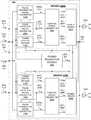
- FIG. 1depicts a two channel LIDAR measurement system 120 in one embodiment.
- LIDAR measurement system 120includes a master controller 190 and a multiple channel Gallium Nitride (GaN) based illumination driver integrated circuit (IC) 140 .
- each channel of LIDAR measurement system 120includes a return signal receiver IC, a photodetector, and an illumination source.
- LIDAR measurement channel Aincludes return signal receiver IC 150 A, photodetector 170 A and illumination source 160 A.
- LIDAR measurement channel Bincludes return signal receiver IC 150 B, photodetector 170 B and illumination source 160 B.
- the multiple channel GaN based illumination driver IC 140 , illumination sources 160 A-B, photodetectors 170 A-B, and return signal receiver ICs 150 A-Bare mounted, either directly or indirectly, to a common substrate (e.g., printed circuit board) that provides mechanical support and electrical connectivity among the elements.
- a common substratee.g., printed circuit board
- LIDAR measurement system 120includes one or more voltage supplies that provide voltage to various electronic elements and electrical power to illumination devices 160 A-B. As depicted in FIG. 1 , LIDAR measurement system 120 includes a low signal voltage supply 132 configured to supply a relatively low voltage across nodes VDD LV 125 and VSS 124 . In some embodiments, the low signal voltage supply is approximately five volts. This voltage is selected to ensure that the voltage supplied at the gates of one or more of the transistors of multiple channel GaN based illumination driver IC 140 does not exceed the damage threshold. In addition, LIDAR measurement system 120 includes a medium signal voltage supply 133 configured to supply a voltage across nodes VDD MV 127 and VSS 126 that is higher than the voltage supplied by the low signal voltage supply.
- the voltage supplied by the medium signal voltage supplyis approximately twelve volts. This voltage is selected to ensure fast switching transitions of one or more of the transistors of multiple channel GaN based illumination driver IC 140 .
- LIDAR measurement system 120includes a power voltage supply 131 configured to supply a voltage across nodes VDD HV 122 and VSS 121 that is higher than the voltage supplied by the medium voltage supply. In some embodiments, the voltage supplied by the power voltage supply is approximately fifteen to twenty volts.
- the power voltage supplyis configured to supply high current 123 A and 123 B (e.g., one hundred amperes, or more) to illumination sources 160 A and 160 B, respectively, that causes illumination sources 160 A and 160 B to each emit a pulse of measurement light.
- the low signal voltage supply, the medium signal voltage supply, and the power voltage supplymay be configured to supply any suitable voltages.
- any of the power supplies described hereinmay be mounted to a separate substrate and electrically coupled to the various electronic elements in any suitable manner.
- the power supplies 131 , 132 , and 133are described as voltage supplies with reference to FIG. 1
- any electrical power source described hereinmay be configured to supply electrical power specified as voltage or current.
- any electrical power source described herein as a voltage source or a current sourcemay be contemplated as an equivalent current source or voltage source, respectively.
- Each illumination source 160 A-Bemits a measurement pulse of illumination light 162 A-B in response to a corresponding pulse of electrical current 123 A-B.
- Each beam of illumination light 162 A-Bis focused and projected onto a location in the surrounding environment by one or more optical elements of the LIDAR system.
- each illumination source 160 A-Bis laser based (e.g., laser diode). In some embodiments, each illumination source is based on one or more light emitting diodes. In general, any suitable pulsed illumination source may be contemplated.
- illumination light 162 A-B emitted from each channel of LIDAR measurement system 120 and corresponding return measurement light 171 A-B directed toward LIDAR measurement system 120share a common optical path.
- Each channel of LIDAR measurement system 120includes a photodetector 170 A-B.
- an overmold lens 172 A-Bis mounted over each photodetector 170 A-B, respectively.
- Each overmold lens 172 A-Bincludes a conical cavity that corresponds with the ray acceptance cone of return light 171 A-B, respectively.
- Return light 171 A-Bis reflected from mirrors 161 A-B to corresponding photodetectors 170 A-B, respectively.
- FIG. 1illumination light 162 A-B emitted from each channel of LIDAR measurement system 120 and corresponding return measurement light 171 A-B directed toward LIDAR measurement system 120 share a common optical path.
- Each channel of LIDAR measurement system 120includes a photodetector 170 A-B.
- each illumination source 160 A-Bis located outside the field of view of each photodetector. Illumination light 162 A-B from illumination sources 160 A-B is injected into the corresponding detector reception cone through an opening in mirrors 161 A-B, respectively.
- each photodetectoris an avalanche photodiode.
- Each photodetectorgenerates an output signal 173 A-B that is communicated to corresponding return signal receiver ICs 150 A-B.
- Each receiver IC 150 A-Bincludes timing circuitry and a time-to-digital converter that estimates the time of flight of each measurement pulse from each illumination source 160 A-B, to reflective objects in the three dimensional environment, and back to each corresponding photodetector 170 A-B.
- Signals 152 A-B indicative of the estimated times of flightare communicated to master controller 190 for further processing and communication to a user of the LIDAR measurement system 120 .
- each return signal receiver IC 150 A-Bis configured to digitize segments of each corresponding return signal 173 A-B that include peak values (i.e., return pulses), and communicate signals 153 A-B indicative of the digitized segments to master controller 190 .
- master controller 190processes these signal segments to identify properties of detected objects.
- Master controller 190is configured to generate pulse command signals 191 A-B communicated to receiver ICs 150 A-B, respectively.
- LIDAR measurement system 120includes any number of LIDAR measurement channels.
- master controller 190communicates a pulse command signal to each different LIDAR measurement channel. In this manner, master controller 190 coordinates the timing of LIDAR measurements performed by any number of LIDAR measurement channels.
- Each pulse command signalis a digital signal generated by master controller 190 .
- the timing of each pulse command signalis determined by a clock associated with master controller 190 .
- each pulse command signal 191 A-Bis directly used to trigger pulse generation by multiple channel GaN based illumination driver IC 140 and data acquisition by each corresponding receiver IC 150 A-B.
- illumination driver IC 140 and each receiver IC 150 A-Bdo not share the same clock as master controller 190 . For this reason, precise estimation of time of flight becomes much more computationally tedious when a pulse command signal is directly used to trigger pulse generation and data acquisition.
- each receiver IC 150 A-Breceives a pulse command signal 191 A-B and generates corresponding pulse trigger signals 151 A and 151 B, in response to pulse command signals 191 A-B, respectively.
- Each pulse trigger signal 151 A-Bis communicated to illumination driver IC 140 and directly triggers illumination driver IC 140 to electrically couple each illumination source 160 A-B to power supply 131 and generate a corresponding pulse of illumination light 162 A-B.
- each pulse trigger signal 151 A-Bdirectly triggers data acquisition of return signals 173 A-B and associated time of flight calculations.
- pulse trigger signals 151 A-B generated based on the internal clock of receiver ICs 150 A-B, respectively,is employed to trigger both pulse generation and return pulse data acquisition for a particular LIDAR measurement channel. This ensures precise synchronization of pulse generation and return pulse acquisition which enables precise time of flight calculations by time-to-digital conversion.
- FIG. 2depicts an illustration of the timing associated with the emission of a measurement pulse from channel A of LIDAR measurement system 120 and capture of the returning measurement pulse.
- a measurementis initiated by the rising edge of pulse trigger signal 191 A generated by receiver IC 150 A.
- a return signal 173 Ais received by receiver IC 150 A.
- a measurement windowi.e., a period of time over which collected return signal data is associated with a particular measurement pulse
- Receiver IC 150 Acontrols the duration of the measurement window, T measurement , to correspond with the window of time when a return signal is expected in response to the emission of a measurement pulse sequence.
- the measurement windowis enabled at the rising edge of pulse trigger signal 191 A and is disabled at a time corresponding to the time of flight of light over a distance that is approximately twice the range of the LIDAR system. In this manner, the measurement window is open to collect return light from objects adjacent to the LIDAR system (i.e., negligible time of flight) to objects that are located at the maximum range of the LIDAR system. In this manner, all other light that cannot possibly contribute to useful return signal is rejected.
- return signal 173 Aincludes three return measurement pulses (e.g., MP 1 , MP 2 , and MP 3 ) that correspond with the emitted measurement pulse.
- signal detectionis performed on all detected measurement pulses. Further signal analysis may be performed to identify the closest valid signal P 1 (i.e., first valid instance of the return measurement pulse), the strongest signal, and the furthest valid signal P 3 (i.e., last valid instance of the return measurement pulse in the measurement window). Any of these instances may be reported as potentially valid distance measurements by the LIDAR system.
- Internal system delays associated with emission of light from the LIDAR systeme.g., signal communication delays and latency associated with the switching elements, energy storage elements, and pulsed light emitting device
- delays associated with collecting light and generating signals indicative of the collected lighte.g., amplifier latency, analog-digital conversion delay, etc.
- measurement of time of flightbased on the elapsed time between the rising edge of the pulse trigger signal 191 A and each return pulse (i.e., MP 1 , MP 2 , and MP 3 ) introduces undesireable measurement error.
- a calibrated, pre-determined delay timeis employed to compensate for the electronic delays to arrive at a corrected estimate of the actual optical time of flight.
- accuracy of a static correction to dynamically changing electronic delaysis limited.
- frequent re-calibrationsmay be employed, this comes at a cost of computational complexity and may interfere with system up-time.
- each receiver IC 150 A-Bmeasures time of flight based on the time elapsed between the detection of a detected pulse (e.g., MP 1 ) due to internal cross-talk between each illumination source 160 A-B and corresponding photodetector 170 A-B and a valid return pulse (e.g., MP 2 and MP 3 ).
- a detected pulsee.g., MP 1
- a valid return pulsee.g., MP 2 and MP 3
- receiver IC 150 Aestimates the time of flight, TOF 1 , associated with return pulse MP 2 and the time of flight, TOF 2 , associated with return pulse MP 3 with reference to return pulse MP 1 .
- the signal analysesare performed by receiver ICs 150 A-B, entirely.
- signals 152 A-B communicatedinclude an indication of the time of flight determined by receiver IC 150 A-B, respectively.
- signals 153 A-Binclude digitized segments of return signals 173 A-B generated by receiver ICs 150 A-B, respectively. These raw measurement signal segments are processed further by one or more processors located on board the 3-D LIDAR system, or external to the 3-D LIDAR system to arrive at another estimate of distance, an estimate of one of more physical properties of the detected object, or a combination thereof.
- a LIDAR measurement systemincludes a multiple channel GaN based illumination driver IC that selectively couples an illumination source corresponding to each measurement channel to a source of electrical power to generate a measurement pulse of illumination light in response to a pulse trigger signal.
- the multiple channel GaN based illumination driverincludes field effect transistors (FETs) that offer higher current density than conventional silicon based complementary metal oxide on silicon (CMOS) devices.
- FETsfield effect transistors
- CMOScomplementary metal oxide on silicon
- multiple channel GaN based illumination driver IC 140is coupled to a voltage node 121 of power voltage supply 131 and nodes of illumination sources 160 A-B, each corresponding to a different LIDAR measurement channel. Another node of each illumination source 160 A-B is coupled to voltage node 122 of power voltage supply 131 .
- one or more field effect transistors (FETs) of illumination driver IC 140becomes substantially conductive, and effectively couples each corresponding illumination source 160 A-B to node 121 . This induces high current flows 123 A-B through illumination sources 160 A-B, respectively, which stimulates the emission of measurement pulses of illumination light 162 A-B.
- FETsfield effect transistors
- FIG. 3depicts multiple channel GaN based illumination driver IC 140 in one embodiment.
- illumination driver IC 140includes two independently controlled illumination driver channels, drivers 220 A and 220 B.
- a multiple channel GaN based illumination driver IC as described hereinmay include any number of independently controlled illumination driver channels.
- many input signals provided to illumination driver IC 140are shared by both drivers 220 A and 220 B. This reduces the size of illumination driver IC 140 by minimizing chip and routing area that would be required to accommodate a larger number of separate control signals.
- pulse width control signal 192 , selection signal 194 , and amplitude control signal 193are all shared by drivers 220 A and 220 B (i.e., each of these signals is received on chip on a node and distributed to various elements of drivers 220 A and 220 B on chip).
- the pulse trigger signals 151 A and 151 B provided to drivers 220 A and 220 Bare the only signals received onto illumination driver IC 140 that are individually provided to drivers 220 A and 220 B, respectively, and thus are not shared by drivers 220 A and 220 B.
- master controller 190communicates pulse trigger signals to each measurement channel of the LIDAR measurement system 100 such that only one channel of the LIDAR measurement system is firing at a given time.
- master controller 190updates the shared control signals supplied to all of the measurement channels (e.g., pulse width control signal 192 , selection signal 194 , and amplitude control signal 193 ) to desired values for each firing instance of each measurement channel. In this manner, master controller 190 independently controls the pulse emission parameters of each LIDAR measurement channel with control signals shared by all LIDAR measurement channels.
- master controller 190communicates pulse trigger signals to a subset of measurement channels of the LIDAR measurement system 100 such that only the subset of measurement channels are firing at a given time.
- master controller 190updates the shared control signals supplied to all of the measurement channels (e.g., pulse width control signal 192 , selection signal 194 , and amplitude control signal 193 ) to desired values for each firing instance of each subset of measurement channels. In this manner, master controller 190 independently controls the pulse emission parameters of each subset of LIDAR measurement channels with control signals shared by all LIDAR measurement channels.
- pulse width control signal 192 , selection signal 194 , and amplitude control signal 193are communicated to multi-channel GaN based illumination driver IC 140 from a return signal receiver IC of illumination driver IC 140 , rather than master controller 190 .
- an illumination driver ICincludes a power regulation module that supplies a regulated voltage to various elements of each measurement channel when any pulse trigger signal received by the illumination driver IC is in a state that triggers the firing of an illumination pulse. In this manner, power is not supplied to many circuit elements during periods of time when illumination driver IC 140 is not required to trigger a pulse emission.
- illumination driver IC 140includes a power regulation module 260 that supplies a regulated voltage 261 to various elements of drivers 220 A and 220 B when pulse trigger signal 151 A, pulse trigger signal 151 B, or both, are in a state (e.g., high state or low state) that triggers the firing of an illumination pulse.
- a statee.g., high state or low state
- regulated voltage 261is supplied to power drivers 290 A-B, control signal generators 280 A-B, pulse termination signal generators 230 A-B, and power control modules 210 A-B only when either, or both, pulse trigger signals 151 A-B are in a state that triggers the firing of an illumination pulse.
- each illumination driverincludes a pulse termination signal generator, a pulse initiation signal generator, a power control module, a control signal generator, and a power driver.
- illumination driver 220 Aincludes a pulse initiation signal generator 250 A that generates pulse initiation signal 251 A based on pulse trigger signal 151 A.
- Pulse initiations signal 251 Ais communicated to pulse termination signal generator 230 A and control signal generator 280 A.
- Pulse termination signal generator 230 Agenerates a pulse termination signal 231 A based on pulse width control signal 192 and pulse initiation signal 251 A.
- Power control module 210 Agenerates a channel amplitude control signal 211 A based on pulse trigger signal 151 A.
- Control signal generator 280generates gate control signal 293 A, gate charge control signal 281 A, and gate discharge control signal 282 A based on pulse initiation signal 251 A, pulse termination signal 231 A, and channel amplitude control signal 211 A.
- Power driver 290 Aincludes a number of field effect transistors (FETS) that control the flow of current through illumination source 160 A based on gate control signal 293 A, gate charge control signal 281 A, and gate discharge control signal 282 A.
- FETSfield effect transistors
- illumination driver 220 Bincludes a pulse initiation signal generator 250 B that generates pulse initiation signal 251 B based on pulse trigger signal 151 B.
- Pulse initiations signal 251 Bis communicated to pulse termination signal generator 230 A and control signal generator 280 B.
- Pulse termination signal generator 230 Bgenerates a pulse termination signal 231 B based on pulse width control signal 192 and pulse initiation signal 251 B.
- Power control module 210 Bgenerates a channel amplitude control signal 211 B based on pulse trigger signal 151 B.
- Control signal generator 280generates gate control signal 293 B, gate charge control signal 281 B, and gate discharge control signal 282 B based on pulse initiation signal 251 B, pulse termination signal 231 B, and channel amplitude control signal 211 B.
- Power driver 290 Bincludes a number of field effect transistors (FETS) that control the flow of current through illumination source 160 B based on gate control signal 293 B, gate charge control signal 281 B, and gate discharge control signal 282 B
- the number of FETS employed to generate electrical current flow through an illumination sourceis controlled by selection signal 194 .
- the amount of current flow generated through the illumination source for a given set of transistor control signalse.g., gate control signals 293 A-B, gate charge control signals 281 A-B, and gate discharge control signals 282 A-B is controlled.
- FIG. 4depicts a power regulation module 260 in one embodiment.
- illumination driver IC 140includes a power regulation module 260 that controls the power supplied to a portion of the circuitry of multiple channel GaN based illumination driver IC 140 to reduce power consumption.
- the illumination driver IC 140spends a relatively short amount of time generating a measurement pulse and a relatively long amount of time waiting for a trigger signal to generate the next measurement pulse. During these idle periods, it is desireable to reduce or eliminate power supplied to circuit components that do not need to be active for the entire waiting period.
- power regulation module 260is coupled between voltage nodes VDD MV and VSS of signal voltage supply 132 depicted in FIG. 1 .
- power regulation module 260receives pulse trigger signals 151 A and 151 B from master controller 190 and, in response, generates a regulated voltage, REG, that is supplied to various portions of illumination driver IC 140 .
- REGis provided to power control module 210 depicted in FIG. 5 , pulse termination signal generator 230 depicted in FIG. 8 , control signal generator 280 depicted in FIG. 9 , and the main FET groups 491 A-N depicted in FIG. 11 .
- FIG. 4depicts power regulation module 260 in one embodiment.
- power regulation module 260includes a logical AND circuit module 268 that receives pulse trigger signals 151 A and 151 B and generates an input signal to regulator module 269 .
- the value of the input signalis determined by the values of pulse trigger signals 151 A and 151 B. If either or both of pulse trigger signals 151 A and 151 B is in a low state (i.e., indicating a trigger to fire one or both illumination channels), the value of the input signal is low.
- FET 264is “off” and FET 266 is diode connected.
- a non-zero regulated voltage 261is provided by regulator module 269 .
- pulse trigger signals 151 A and 151 Bare both in a high state (i.e., indicating no trigger to fire either of the illumination channels), the value of the input signal is high.
- FET 264is “on” and the gate voltage of FET 266 is driven to VSS.
- zero regulated voltage 261is provided by regulator module 269 .
- no electrical poweris supplied by power regulation module 260 .
- logic circuit 268is an active circuit coupled to voltage nodes 124 and 125 of low voltage supply 132 depicted in FIG. 1 .
- regulator module 269is coupled to voltage nodes 126 and 127 of medium voltage supply 133 depicted in FIG. 1 .
- VDD MVis provided to one node of resistor 265 and the drain of FET 266 .
- the other node of resistor 265is coupled to the drain of FET 264 and the gate of FET 266 .
- VSSis provided to the source of FET 264 , one node of capacitor 263 and one node of capacitor 267 .
- the other node of capacitor 263is coupled to the gate of FET 264 and a node of resistor 262 .
- the other node of resistor 262is coupled to the output of logic circuit 268 .
- the other node of capacitor 267is coupled to the source of FET 266 , where the output of power regulation module 260 is provided.
- Resistor 262 and capacitor 263create an RC network that introduces a delay at the gate of FET 264 . This introduces a delay (T D-SLEEP depicted in FIG. 12 ) between the rising edge of TRG 1 and the time when REG drops to VSS during sleep mode.
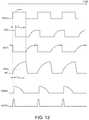
- FIG. 12depicts a simplified illustration of the changes in the regulated voltage, REG, generated by the power regulation module 260 in response to any of the pulse trigger signals, TRG 1 and TRG, being in a state that triggers the firing of an illumination pulse.
- the regulated voltageremains high for a period of time, T D-SLEEP . This length of time is determined by the values of resistor 262 and capacitor 263 . After this period of time, the REG drops quickly.
- the regulated voltageremains low for a period of time and then ramps up to a relatively high voltage value, so that the illumination driver IC 140 is ready to generate a measurement pulse in response to the subsequent rising edge of TRG 1 .
- each channel of an illumination driver ICincludes a power control module that generates a channel amplitude control signal and communicates the signal to the corresponding control signal generator.
- the power control moduleWhen the pulse trigger signal associated with a particular measurement channel is in a state that triggers the firing of an illumination pulse, the power control module generates a channel amplitude control signal having a value of the amplitude control signal received from the master controller. However, when the pulse trigger signal associated with the particular measurement channel is in a state that does not trigger the firing of an illumination pulse, the power control module generates a channel amplitude control signal having a zero value. In this manner, power is not supplied to circuit elements of the corresponding control signal generator and power driver during periods of time when the particular LIDAR measurement channel is not required to trigger a pulse emission.
- FIG. 5depicts a power control module 210 in one embodiment.
- Power control module 210is replicated as power control module 210 A and 210 B in illumination driver IC 140 depicted in FIG. 3 .
- power control module 210is implemented as power control module 210 A depicted in FIG. 3 for explanatory purposes.
- Power control module 210includes a delay module 220 that receives a pulse trigger signal (e.g., pulse trigger signal 151 A) and generates a delayed pulse trigger signal 227 .
- Power save module 217receives the delayed pulse trigger signal 227 and generates channel pulse amplitude signal 211 A based on the delayed pulse trigger signal 227 and pulse amplitude control signal 193 shared among all measurement channels of illumination driver IC 140 .
- a pulse trigger signale.g., pulse trigger signal 151 A
- Power save module 217receives the delayed pulse trigger signal 227 and generates channel pulse amplitude signal 211 A based on the delayed pulse trigger signal 227 and pulse amplitude control signal 19
- delay module 220includes resistors 221 and 222 , capacitors 224 and 226 , and FETS 223 and 225 .
- VSSis supplied to the source of FET 225 , the source of FET 223 , a first node of capacitor 224 and a first node of capacitor 226 .
- Pulse trigger signal 151 Ais provided at the gate of FET 225 .
- the drain of FET 225is coupled to a second node of capacitor 224 , the gate of FET 223 and a first node of resistor 221 .
- the drain of FET 223is coupled to a second node of capacitor 226 and a first node of resistor 222 .
- Delayed pulse trigger signal 227is provided at the drain of FET 223 .
- VDD LVis provided at the second node of resistors 221 and 222 .
- Power save module 217includes resistor 213 and FETS 214 , 215 , and 216 .
- VSSis supplied to the source of FET 214 and the source of FET 215 .
- the gate of FET 214 and the gate of FET 215are coupled to the drain of FET 223 .
- Regulated voltage 261is provided at a first node of resistor 213 .
- the second node of resistor 213is coupled to the gate of FET 216 .
- Amplitude control signal 193is provided at the drain of FET 216 .
- the source of FET 216is coupled to the drain of FET 215 , where the channel amplitude control signal 211 A is present.
- delay module 220generates a delayed pulse trigger signal 227 having a time delay, T DEL , from pulse trigger signal 151 A.
- Power save module 217generates a channel amplitude control signal 211 A having an amplitude value, AMP, that matches the amplitude value of the amplitude control signal 193 at the falling edge of delayed pulse trigger signal 227 .
- Channel amplitude control signal 211 Amaintains the amplitude value, AMP, until the rising edge of delayed pulse trigger signal 227 . At this instance, the channel amplitude control signal 211 A drops to a zero value.
- T DELthe firing of an illumination pulse from channel A occurs at a time, T FIREA , when the amplitude value of channel amplitude control signal 211 A is at the amplitude value, AMP, of the amplitude control signal 193 .
- the amplitude value, AMP, of the amplitude control signal 193is effectively transmitted to the control signal generator 280 around the period of time when control signal generator 280 generates control signals that cause an illumination pulse to be emitted from the corresponding LIDAR measurement channel.
- a zero valued signalis transmitted to the control signal generator 280 .
- FIG. 7depicts a pulse initiation signal generator 250 in one embodiment.
- Pulse initiation signal generator 250is replicated as pulse initiation signal generators 250 A and 250 B in illumination driver IC 140 depicted in FIG. 3 .
- pulse initiation signal generator 250is implemented as pulse initiation signal generator 250 A depicted in FIG. 3 for explanatory purposes.
- Pulse initiation signal generator 250generates a pulse initiation signal 251 A based on the pulse trigger signal 151 A.
- Pulse initiation signal generator 250includes a FET 252 and a resistor 253 .
- Pulse trigger signal 151 Ais provided on the gate of FET 252 .
- VSSis provided to the source of FET 252 .
- VDD MVis provided to a first node of resistor 253 and a second node of resistor 253 is coupled to the drain of FET 252 .
- Pulse initiation signal 251 Ais provided at the drain of FET 252 .
- FIG. 12depicts a simplified illustration of the changes in the pulse initiation signal, INIT 1 , generated by the pulse initiation signal generator 250 in response to the pulse trigger signal, TRG 1 .
- INIT 1the pulse initiation signal
- VSSthe pulse trigger signal
- FIG. 8depicts a pulse termination signal generator 230 in one embodiment.
- Pulse termination signal generator 230is replicated as pulse termination signal generators 230 A and 230 B in illumination driver IC 140 depicted in FIG. 3 .
- pulse termination signal generator 230is implemented as pulse termination signal generator 230 A depicted in FIG. 3 for explanatory purposes.
- Pulse termination signal generator 230is configured to generate a pulse of programmable duration based on a value of an analog input signal.
- master controller 190generates an analog pulse width control signal 192 , and communicates PWC 192 to illumination driver IC 140 .
- illumination driver IC 140changes the pulse duration based on the received value of PWC 192 .
- pulse termination signal generator 230receives, PWC 192 and INIT 1 251 A and generates a pulse termination signal, TERM 1 231 A, having a delay from INIT 1 251 A programmed in accordance with a value of PWC 192 .
- pulse termination signal generator 230includes resistor 238 and FETs 236 - 237 configured as an operational amplifier.
- the output of the operational amplifieris coupled to the gate of FET 243 .
- the operational amplifierreceives PWC 192 as input at the gate of FET 236 .
- the operational amplifierreceives an input voltage 249 at the gate of FET 237 .
- Input voltage 249is the voltage of the RC circuit formed by resistor 241 and capacitor 242 .
- INIT 1 251 Ais received at the gate of FET 240 .
- FET 240effectively disconnects the RC circuit from VSS. This allows the RC circuit to begin to charge.
- FET 239provides a nonzero starting voltage for the RC circuit.
- the voltage of the RC circuitrises, eventually it exceeds the value of PWC 192 , thus triggering the transition of output node 248 . Since the voltage ramp rate of the RC circuit is constant, the delay until the transition of output voltage 248 is determined in part by the value of PWC 192 . The larger the value of PWC 192 , the longer the delay from pulse initiation before the generation of the termination signal, TERM 1 231 A.
- Pulse termination signal generator 230includes resistor 232 and FETs 233 - 235 configured as a current source for the operational amplifier structure.
- FETS 243 and 244are configured to scale down the value of output voltage 248 .
- Resistors 245 and 247 and FET 246are configured to invert the scaled value of output voltage 248 .
- the pulse termination signal, TERM 1 231 Ais provided at the drain of FET 246 .
- FIG. 12depicts a simplified illustration of the changes in the pulse termination signal, TERM 1 231 A, generated by the pulse termination signal generator 230 in response to the pulse initiation signal, INIT 1 251 A and the pulse width control signal, PWC 192 .
- INIT 1goes low
- the voltage of the RC circuitbegins to ramp up.
- TERM 1goes high, holds for a period of time and then ramps down again. Note that the period of time, T D-PULSE between pulse initiation and the rising edge of TERM 1 determines the relative duration of the measurement pulse.
- TERM 1ramps down again so that the illumination driver IC 140 is ready to generate a pulse termination signal for the subsequent pulse.
- the gate voltage, GATE 1 , of main FET 141 , or group of FETSis also depicted.
- illumination driver IC 140includes pulse termination signal generators 230 A-B that generate pulse termination signals, TERM 1 and TERM 2 , based on corresponding pulse initiation signals. Together, the pulse initiation signals and the pulse termination signals directly determine the timing of each pulse generated by illumination driver IC 140 .
- a pulse trigger signale.g., TRG 1 , TRG 2
- a pulse trigger signalis employed to trigger the generation of a pulse initiation signal.
- the pulse initiation signalin turn, directly initiates the pulse generation, and also initiates the generation of the pulse termination signal.
- the pulse termination signalin turn, directly terminates the pulse generation.
- FIG. 9depicts a control signal generator 280 in one embodiment.
- Control signal generator 280is replicated as control signal generators 280 A and 280 B in illumination driver IC 140 depicted in FIG. 3 .
- control signal generator 280is implemented as control signal generator 280 A depicted in FIG. 3 for explanatory purposes.
- Control signal generator 280generates gate control signal 283 A, gate charge control signal 281 A and gate discharge control signal 282 A based on the pulse initiation signal 251 A, pulse termination signal 231 A, and channel amplitude control signal 211 A.
- the control signals generated by control signal generator 280directly control the FETS that control the flow of current through an illumination source coupled to illumination driver 140 .
- Control signal generator 280includes a pulse amplitude control circuit 255 , FETS 284 , 286 , 287 , 288 , and resistor 285 .
- pulse termination signal generator 230is configured to generate a pulse of programmable amplitude based on a value of an analog input signal.
- receiver IC 150generates an analog amplitude control signal, V AMP 153 , and communicates V AMP to illumination driver IC 140 .
- illumination driver IC 140changes the pulse amplitude based on the received value of V AMP .
- pulse amplitude control circuit 250receives, V AMP , that controls the amplitude of the pulse generated by illumination source 160 .
- FET 286quickly releases the gate of a charge FET (e.g., charge FET 393 depicted in FIG. 10 ) from VSS via gate charge control signal 281 A, allowing the charge FET to quickly charge.
- FET 287quickly releases the gate of the main FET (e.g., main FET 391 depicted in FIG. 10 ) from VSS, allowing the main FET to charge via gate control signal 283 A.
- FET 288When TERM 1 231 A goes high (signaling the end of a measurement pulse), FET 288 shorts the gate of the charge FET to VSS. Similarly, a discharge FET (e.g., discharge FET 394 depicted in FIG. 10 ) shorts the gate of the main FET to VSS via gate discharge control signal 282 A as quickly as possible to shut off current flow through illumination source 160 . FET 285 and resistor 285 provide a quick turn-on of the discharge FET and FET 288 .
- a discharge FETe.g., discharge FET 394 depicted in FIG. 10
- pulse amplitude control circuit 255includes resistors 256 and 259 , capacitor 257 , and FET 258 .
- Channel amplitude control signal, AMP 1 211 Ais received on a first node of resistor 256 .
- the second node of resistor 256is coupled to the gate of FET 258 and to a first node of capacitor 257 .
- the drain of FET 258is coupled to the regulated voltage supply, VREG, and receives regulated voltage 261 .
- the source of FET 258is coupled to a first node of resistor 259 .
- the second node of resistor 259is coupled to the second node of capacitor 257 , where gate charge control signal 281 A is provided.
- the pulse amplitude control circuit 255controls the charge at the gate of a charge FET (e.g., charge FET 393 depicted in FIG. 10 ).
- the value of AMP 1controls the ramp rate of the pulse amplitude control circuit 255 .
- AMP 1increases, the rate of charge accumulation at the gate of FET 258 increases. In turn, this increases rate of charge accumulation on the gate of a charge FET via gate charge control signal 281 A. This, in turn, increases the rate of charge accumulation on the gate of a main FET, which accelerates the ramp rate of the resulting illumination pulse generated by illumination source 160 A.
- AMP 1controls the peak amplitude of the illumination pulse for a given pulse duration.
- FIG. 10depicts a power driver 390 in one embodiment.
- power driver 390is replicated as power drivers 290 A and 290 B in illumination driver IC 140 depicted in FIG. 3 .
- power driver 390is implemented as power driver 290 A depicted in FIG. 3 for explanatory purposes.
- power driver 390includes three FETs 391 , 393 , and 394 integrated onto GaN based IC 140 .
- main FET 391controls the flow of current 123 A through illumination source 160 A (e.g., laser diode 160 A).
- Gate control signal 283 Acontributes to the gate voltage of main FET 393 .
- charge FET 393 and discharge FET 394also contribute to the gate voltage of main FET 391 and accelerate the transitions and minimize power losses.
- the drain of charge FET 393is coupled to voltage node 125 of low voltage supply 132 depicted in FIG. 1 .
- the source of charge FET 393is coupled to the drain of discharge FET 394 and to the gate of main FET 391 .
- the source of discharge FET 394is coupled to voltage node 124 of low voltage supply 132 .
- a resistor 392is coupled between the gate of main FET 391 and voltage node 124 of low voltage supply 132 .
- a gate charge control signal 281 Ais provided at the gate of charge FET 393
- a gate discharge control signal 282 Ais provided at the gate of discharge FET 394 . In this manner, gate charge control signal 281 A, gate discharge control signal 282 A, and gate control signal 283 A determine the charge at the gate of main FET 391 , and thus the conductive state of main FET 391 .
- FIG. 10depicts embodiment 390 implemented as power driver 290 A depicted in FIG. 3
- embodiment 390may be implemented as a power driver of any LIDAR measurement channel (e.g., power driver 290 A, 290 B, or both).
- the embodiment 390 of power driver module 290 A depicted in FIG. 10includes a single main FET 391 that determines the current flow through illumination source 160 A.
- a power driverincludes a number of different FETs configured to control the current flow through an illumination source.
- the number of FETs coupled to each illumination sourceis programmable. This enables a programmable maximum current flow through each illumination source, and thus a programmable maximum illumination pulse amplitude.
- FIG. 11depicts a power driver 490 in another embodiment.
- power driver 490is replicated as power drivers 290 A and 290 B in illumination driver IC 140 depicted in FIG. 3 .
- power driver 490is implemented as power driver 290 A depicted in FIG. 3 for explanatory purposes.
- N groups of one or more FETsare coupled in parallel with illumination source 160 A, where N is any positive, integer number.
- a drain of each main FET of each FET group 491 A- 491 Nis coupled to a node of illumination source 160 A.
- each main FET of each FET group 491 A- 491 Nis coupled to node 121 of power voltage supply 131 .
- the gates of each main FET of each FET group 141 A- 141 Nare selectively coupled to the source of a charge FET and the drain of a discharge FET as described with reference to FIG. 10 .
- Whether each main FET of a particular group of FETs is electrically coupled to the source of a charge FET and the drain of a discharge FETis determined by the state of selection signal, SEL 194 , received from master controller 190 .
- SELis an N-bit word. Each bit corresponds with a particular main FET group.
- each main FET associated with the corresponding main FET groupis coupled to the source of a charge FET and the drain of a discharge FET.
- gate control signal 283 A, gate charge control signal 281 A, and gate discharge control signal 282 Adetermine the charge at the gate of each main FET of the corresponding main FET group. In this manner, the state of each bit of the N-bit word determines which main FET groups will participate in pulse generation by illumination source 160 A.
- Master controller 190determines which FET groups should participate in the next measurement pulse by generating and communicating the SEL signal to illumination driver IC 140 . In some examples, the determination is based on the return signal received from the prior measurement pulse. For example, if the received return signal is saturated, master controller 190 generates and communicates a selection signal, SEL, to illumination driver 140 with a larger number of zero valued bits to reduce the number of participating main FET groups. In this manner, the number of photons emitted in the next illumination pulse is reduced.
- SELselection signal
- the number of FETS in each main FET groupis different. In this manner, different combinations of FET groups can be activated to achieve a wide range of participating FETs with uniform resolution.
- FIG. 11depicts embodiment 490 implemented as power driver 290 A depicted in FIG. 3
- embodiment 490may be implemented as a power driver of any LIDAR measurement channel (e.g., power driver 290 A, 290 B, or both).
- FIGS. 13-15depict 3-D LIDAR systems that include one or more multiple channel GaN based illumination driver ICs.
- a delay timeis set between the firing of each LIDAR measurement channel. In some examples, the delay time is greater than the time of flight of the measurement pulse to and from an object located at the maximum range of the LIDAR device. In this manner, there is no cross-talk among any of the LIDAR measurement channels.
- a measurement pulseis emitted from one LIDAR measurement channel before a measurement pulse emitted from another LIDAR measurement channel has had time to return to the LIDAR device. In these embodiments, care is taken to ensure that there is sufficient spatial separation between the areas of the surrounding environment interrogated by each beam to avoid cross-talk.
- FIG. 13is a diagram illustrative of an embodiment of a 3-D LIDAR system 100 in one exemplary operational scenario.
- 3-D LIDAR system 100includes a lower housing 101 and an upper housing 102 that includes a domed shell element 103 constructed from a material that is transparent to infrared light (e.g., light having a wavelength within the spectral range of 700 to 1,700 nanometers).
- domed shell element 103is transparent to light having a wavelengths centered at 905 nanometers.
- a plurality of beams of light 105are emitted from 3-D LIDAR system 100 through domed shell element 103 over an angular range, a, measured from a central axis 104 .
- each beam of lightis projected onto a plane defined by the x and y axes at a plurality of different locations spaced apart from one another.
- beam 106is projected onto the xy plane at location 107 .
- 3-D LIDAR system 100is configured to scan each of the plurality of beams of light 105 about central axis 104 .
- Each beam of light projected onto the xy planetraces a circular pattern centered about the intersection point of the central axis 104 and the xy plane.
- beam 106 projected onto the xy planetraces out a circular trajectory 108 centered about central axis 104 .
- FIG. 14is a diagram illustrative of another embodiment of a 3-D LIDAR system 10 in one exemplary operational scenario.
- 3-D LIDAR system 10includes a lower housing 11 and an upper housing 12 that includes a cylindrical shell element 13 constructed from a material that is transparent to infrared light (e.g., light having a wavelength within the spectral range of 700 to 1,700 nanometers).
- cylindrical shell element 13is transparent to light having a wavelengths centered at 905 nanometers.
- each beam of light 15is emitted from 3-D LIDAR system 10 through cylindrical shell element 13 over an angular range, ⁇ .
- the chief ray of each beam of lightis illustrated.
- Each beam of lightis projected outward into the surrounding environment in a plurality of different directions.
- beam 16is projected onto location 17 in the surrounding environment.
- each beam of light emitted from system 10diverges slightly.
- a beam of light emitted from system 10illuminates a spot size of 20 centimeters in diameter at a distance of 100 meters from system 10 .
- each beam of illumination lightis a cone of illumination light emitted from system 10 .
- 3-D LIDAR system 10is configured to scan each of the plurality of beams of light 15 about central axis 14 .
- beams of light 15are illustrated in one angular orientation relative to a non-rotating coordinate frame of 3-D LIDAR system 10 and beams of light 15 ′ are illustrated in another angular orientation relative to the non-rotating coordinate frame.
- each beam of light projected into the surrounding environmente.g., each cone of illumination light associated with each beam
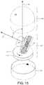
- FIG. 15depicts an exploded view of 3-D LIDAR system 100 in one exemplary embodiment.
- 3-D LIDAR system 100further includes a light emission/collection engine 112 that rotates about central axis 104 .
- a central optical axis 117 of light emission/collection engine 112is tilted at an angle, ⁇ , with respect to central axis 104 .
- 3-D LIDAR system 100includes a stationary electronics board 110 mounted in a fixed position with respect to lower housing 101 .
- Rotating electronics board 111is disposed above stationary electronics board 110 and is configured to rotate with respect to stationary electronics board 110 at a predetermined rotational velocity (e.g., more than 200 revolutions per minute).
- Light emission/collection engine 112is fixedly positioned with respect to the rotating electronics board 111 , and thus rotates about central axis 104 at the predetermined angular velocity, w.
- light emission/collection engine 112includes an array of LIDAR measurement devices 113 .
- each LIDAR measurement deviceis a multiple channel LIDAR measurement device such as LIDAR measurement device 120 illustrated in FIG. 1 .
- each LIDAR measurement devicepasses through a series of optical elements 116 that collimate the emitted light to generate a beam of illumination light projected from the 3-D LIDAR system into the environment.
- an array of beams of light 105each emitted from a different LIDAR measurement device are emitted from 3-D LIDAR system 100 as depicted in FIG. 13 .
- any number of LIDAR measurement devicescan be arranged to simultaneously emit any number of light beams from 3-D LIDAR system 100 .
- Light reflected from an object in the environment due to its illumination by a particular LIDAR measurement deviceis collected by optical elements 116 .
- the collected lightpasses through optical elements 116 where it is focused onto the detecting element of the same, particular LIDAR measurement device. In this manner, collected light associated with the illumination of different portions of the environment by illumination generated by different LIDAR measurement devices is separately focused onto the detector of each corresponding LIDAR measurement device.
- FIG. 16depicts a view of optical elements 116 in greater detail.
- optical elements 116include four lens elements 116 A-D arranged to focus collected light 118 onto each detector of the array of LIDAR measurement devices 113 .
- light passing through optics 116is reflected from mirror 124 and is directed onto each detector of the array of LIDAR measurement devices 113 .
- one or more of the optical elements 116is constructed from one or more materials that absorb light outside of a predetermined wavelength range.
- the predetermined wavelength rangeincludes the wavelengths of light emitted by the array of integrated LIDAR measurement devices 113 .
- one or more of the lens elementsare constructed from a plastic material that includes a colorant additive to absorb light having wavelengths less than infrared light generated by each of the array of integrated LIDAR measurement devices 113 .
- the colorantis Epolight 7276A available from Aako BV (The Netherlands). In general, any number of different colorants can be added to any of the plastic lens elements of optics 116 to filter out undesired spectra.
- FIG. 16depicts a cutaway view of optics 116 to illustrate the shaping of each beam of collected light 118 .
- a LIDAR systemsuch as 3-D LIDAR system 10 depicted in FIG. 14 , and system 100 , depicted in FIG. 13 , includes a plurality of LIDAR measurement devices each emitting multiple pulsed beams of illumination light from the LIDAR device into the surrounding environment and measuring return light reflected from objects in the surrounding environment.
- an array of LIDAR measurement devicesis mounted to a rotating frame of the LIDAR device. This rotating frame rotates with respect to a base frame of the LIDAR device.
- an array of LIDAR measurement devicesmay be movable in any suitable manner (e.g., gimbal, pan/tilt, etc.) or fixed with respect to a base frame of the LIDAR device.
- each LIDAR measurement deviceincludes a beam directing element (e.g., a scanning mirror, MEMS mirror etc.) that scans the illumination beams generated by the LIDAR measurement device.
- a beam directing elemente.g., a scanning mirror, MEMS mirror etc.
- two or more LIDAR measurement deviceseach emit beams of illumination light toward a scanning mirror device (e.g., MEMS mirror) that reflects the beams into the surrounding environment in different directions.
- a scanning mirror devicee.g., MEMS mirror
- one or more LIDAR measurement devicesare in optical communication with an optical phase modulation device that directs the illumination beams generated by the LIDAR measurement devices in different directions.
- the optical phase modulation deviceis an active device that receives a control signal that causes the optical phase modulation device to change state and thus change the direction of light diffracted from the optical phase modulation device.
- the illumination beam generated by the LIDAR measurement devicesare scanned through a number of different orientations and effectively interrogate the surrounding 3-D environment under measurement.
- the diffracted beams projected into the surrounding environmentinteract with objects in the environment.
- Each respective LIDAR measurement channelmeasures the distance between the LIDAR measurement system and the detected object based on return light collected from the object.
- the optical phase modulation deviceis disposed in the optical path between the LIDAR measurement device and an object under measurement in the surrounding environment. Thus, both illumination light and corresponding return light pass through the optical phase modulation device.
- a computing system as described hereinmay include, but is not limited to, a personal computer system, mainframe computer system, workstation, image computer, parallel processor, or any other device known in the art.
- the term “computing system”may be broadly defined to encompass any device having one or more processors, which execute instructions from a memory medium.
- Program instructions implementing methods such as those described hereinmay be transmitted over a transmission medium such as a wire, cable, or wireless transmission link.
- Program instructionsare stored in a computer readable medium.
- Exemplary computer-readable mediainclude read-only memory, a random access memory, a magnetic or optical disk, or a magnetic tape.
- the functions describedmay be implemented in hardware, software, firmware, or any combination thereof. If implemented in software, the functions may be stored on or transmitted over as one or more instructions or code on a computer-readable medium.
- Computer-readable mediaincludes both computer storage media and communication media including any medium that facilitates transfer of a computer program from one place to another.
- a storage mediamay be any available media that can be accessed by a general purpose or special purpose computer.
- such computer-readable mediacan comprise RAM, ROM, EEPROM, CD-ROM or other optical disk storage, magnetic disk storage or other magnetic storage devices, or any other medium that can be used to carry or store desired program code means in the form of instructions or data structures and that can be accessed by a general-purpose or special-purpose computer, or a general-purpose or special-purpose processor. Also, any connection is properly termed a computer-readable medium.
- Disk and discincludes compact disc (CD), laser disc, optical disc, digital versatile disc (DVD), floppy disk and blu-ray disc where disks usually reproduce data magnetically, while discs reproduce data optically with lasers. Combinations of the above should also be included within the scope of computer-readable media.
Landscapes
- Engineering & Computer Science (AREA)
- Physics & Mathematics (AREA)
- Computer Networks & Wireless Communication (AREA)
- General Physics & Mathematics (AREA)
- Radar, Positioning & Navigation (AREA)
- Remote Sensing (AREA)
- Electromagnetism (AREA)
- Optical Radar Systems And Details Thereof (AREA)
Abstract
Description
Claims (20)
Priority Applications (10)
| Application Number | Priority Date | Filing Date | Title |
|---|---|---|---|
| US16/134,068US10712434B2 (en) | 2018-09-18 | 2018-09-18 | Multi-channel LIDAR illumination driver |
| MX2021003173AMX2021003173A (en) | 2018-09-18 | 2019-09-18 | Multi-channel lidar illumination driver. |
| CA3112491ACA3112491A1 (en) | 2018-09-18 | 2019-09-18 | Multi-channel lidar illumination driver |
| JP2021539496AJP2022502679A (en) | 2018-09-18 | 2019-09-18 | Multiple lidar lighting driver |
| CN201980075724.3ACN113196091B (en) | 2018-09-18 | 2019-09-18 | Multi-channel LIDAR illumination driver |
| EP19863803.3AEP3834005B1 (en) | 2018-09-18 | 2019-09-18 | Multi-channel lidar illumination driver |
| PCT/US2019/051729WO2020061191A1 (en) | 2018-09-18 | 2019-09-18 | Multi-channel lidar illumination driver |
| KR1020217011103AKR20210062651A (en) | 2018-09-18 | 2019-09-18 | Multi channel lidar lighting driver |
| US16/890,951US11796648B2 (en) | 2018-09-18 | 2020-06-02 | Multi-channel lidar illumination driver |
| IL281415AIL281415A (en) | 2018-09-18 | 2021-03-10 | Multi-channel lidar illumination driver |
Applications Claiming Priority (1)
| Application Number | Priority Date | Filing Date | Title |
|---|---|---|---|
| US16/134,068US10712434B2 (en) | 2018-09-18 | 2018-09-18 | Multi-channel LIDAR illumination driver |
Related Child Applications (1)
| Application Number | Title | Priority Date | Filing Date |
|---|---|---|---|
| US16/890,951ContinuationUS11796648B2 (en) | 2018-09-18 | 2020-06-02 | Multi-channel lidar illumination driver |
Publications (2)
| Publication Number | Publication Date |
|---|---|
| US20200088851A1 US20200088851A1 (en) | 2020-03-19 |
| US10712434B2true US10712434B2 (en) | 2020-07-14 |
Family
ID=69772144
Family Applications (2)
| Application Number | Title | Priority Date | Filing Date |
|---|---|---|---|
| US16/134,068ActiveUS10712434B2 (en) | 2018-09-18 | 2018-09-18 | Multi-channel LIDAR illumination driver |
| US16/890,951ActiveUS11796648B2 (en) | 2018-09-18 | 2020-06-02 | Multi-channel lidar illumination driver |
Family Applications After (1)
| Application Number | Title | Priority Date | Filing Date |
|---|---|---|---|
| US16/890,951ActiveUS11796648B2 (en) | 2018-09-18 | 2020-06-02 | Multi-channel lidar illumination driver |
Country Status (9)
| Country | Link |
|---|---|
| US (2) | US10712434B2 (en) |
| EP (1) | EP3834005B1 (en) |
| JP (1) | JP2022502679A (en) |
| KR (1) | KR20210062651A (en) |
| CN (1) | CN113196091B (en) |
| CA (1) | CA3112491A1 (en) |
| IL (1) | IL281415A (en) |
| MX (1) | MX2021003173A (en) |
| WO (1) | WO2020061191A1 (en) |
Cited By (15)
| Publication number | Priority date | Publication date | Assignee | Title |
|---|---|---|---|---|
| USRE48491E1 (en) | 2006-07-13 | 2021-03-30 | Velodyne Lidar Usa, Inc. | High definition lidar system |
| US10983218B2 (en) | 2016-06-01 | 2021-04-20 | Velodyne Lidar Usa, Inc. | Multiple pixel scanning LIDAR |
| US11073617B2 (en)* | 2016-03-19 | 2021-07-27 | Velodyne Lidar Usa, Inc. | Integrated illumination and detection for LIDAR based 3-D imaging |
| US11082010B2 (en) | 2018-11-06 | 2021-08-03 | Velodyne Lidar Usa, Inc. | Systems and methods for TIA base current detection and compensation |
| US11137480B2 (en) | 2016-01-31 | 2021-10-05 | Velodyne Lidar Usa, Inc. | Multiple pulse, LIDAR based 3-D imaging |
| US11294041B2 (en) | 2017-12-08 | 2022-04-05 | Velodyne Lidar Usa, Inc. | Systems and methods for improving detection of a return signal in a light ranging and detection system |
| US11703569B2 (en) | 2017-05-08 | 2023-07-18 | Velodyne Lidar Usa, Inc. | LIDAR data acquisition and control |
| US11796648B2 (en)* | 2018-09-18 | 2023-10-24 | Velodyne Lidar Usa, Inc. | Multi-channel lidar illumination driver |
| US11808891B2 (en)* | 2017-03-31 | 2023-11-07 | Velodyne Lidar Usa, Inc. | Integrated LIDAR illumination power control |
| US11885958B2 (en) | 2019-01-07 | 2024-01-30 | Velodyne Lidar Usa, Inc. | Systems and methods for a dual axis resonant scanning mirror |
| US11933967B2 (en) | 2019-08-22 | 2024-03-19 | Red Creamery, LLC | Distally actuated scanning mirror |
| US12032063B2 (en) | 2019-01-07 | 2024-07-09 | Velodyne Lidar Usa, Inc. | Application specific integrated circuits for lidar sensor and multi-type sensor systems |
| US12123950B2 (en) | 2016-02-15 | 2024-10-22 | Red Creamery, LLC | Hybrid LADAR with co-planar scanning and imaging field-of-view |
| US12399278B1 (en) | 2016-02-15 | 2025-08-26 | Red Creamery Llc | Hybrid LIDAR with optically enhanced scanned laser |
| US12399279B1 (en) | 2016-02-15 | 2025-08-26 | Red Creamery Llc | Enhanced hybrid LIDAR with high-speed scanning |
Families Citing this family (5)
| Publication number | Priority date | Publication date | Assignee | Title |
|---|---|---|---|---|
| WO2021059317A1 (en)* | 2019-09-23 | 2021-04-01 | 株式会社Fuji | Periphery monitoring device |
| US11994589B2 (en)* | 2020-03-30 | 2024-05-28 | Gm Cruise Holdings Llc | Vapor detection in lidar point cloud |
| CN111899328B (en)* | 2020-07-10 | 2022-08-09 | 西北工业大学 | Point cloud three-dimensional reconstruction method based on RGB data and generation countermeasure network |
| CN112596044B (en)* | 2020-11-20 | 2022-09-23 | 上海禾赛科技有限公司 | Receiving device, laser radar and method for reducing interference signals of laser radar receiving device |
| US20220206115A1 (en)* | 2020-12-29 | 2022-06-30 | Beijing Voyager Technology Co., Ltd. | Detection and ranging operation of close proximity object |
Citations (7)
| Publication number | Priority date | Publication date | Assignee | Title |
|---|---|---|---|---|
| US7969558B2 (en) | 2006-07-13 | 2011-06-28 | Velodyne Acoustics Inc. | High definition lidar system |
| US8675181B2 (en) | 2009-06-02 | 2014-03-18 | Velodyne Acoustics, Inc. | Color LiDAR scanner |
| US8767190B2 (en) | 2006-07-13 | 2014-07-01 | Velodyne Acoustics, Inc. | High definition LiDAR system |
| US20180321360A1 (en)* | 2017-05-08 | 2018-11-08 | Velodyne Lidar, Inc. | LIDAR Data Acquisition And Control |
| US20190001442A1 (en)* | 2015-09-09 | 2019-01-03 | Electro Scientific Industries, Inc. | Laser processing apparatus, methods of laser-processing workpieces and related arrangements |
| US10386465B2 (en)* | 2017-03-31 | 2019-08-20 | Velodyne Lidar, Inc. | Integrated LIDAR illumination power control |
| US20190293764A1 (en)* | 2016-11-30 | 2019-09-26 | Sony Semiconductor Solutions Corporation | Apparatus and method |
Family Cites Families (536)
| Publication number | Priority date | Publication date | Assignee | Title |
|---|---|---|---|---|
| DE930909C (en) | 1943-03-30 | 1955-07-28 | Hans Dr-Ing Thoma | Hydraulic transmission system |
| US3064252A (en) | 1952-03-31 | 1962-11-13 | Arthur A Varela | Height finding radar system |
| US3636250A (en) | 1964-02-26 | 1972-01-18 | Andrew V Haeff | Apparatus for scanning and reproducing a three-dimensional representation of an object |
| US3373441A (en) | 1966-06-17 | 1968-03-12 | Ernest A. Zadig | Laser speed detector |
| US3551845A (en) | 1968-05-09 | 1970-12-29 | Gen Systems Inc | Transistor-magnetic oscillators incorporating voltage reference means to regulate the output frequency |
| US4944036A (en) | 1970-12-28 | 1990-07-24 | Hyatt Gilbert P | Signature filter system |
| US3730633A (en) | 1970-12-31 | 1973-05-01 | Aerotherm Corp | Photometric detector and measuring system |
| US3686514A (en) | 1971-07-16 | 1972-08-22 | Ney Co J M | Slip ring assembly |
| US3781111A (en) | 1972-03-16 | 1973-12-25 | Nasa | Short range laser obstacle detector |
| US3897150A (en) | 1972-04-03 | 1975-07-29 | Hughes Aircraft Co | Scanned laser imaging and ranging system |
| US5026156A (en) | 1972-07-24 | 1991-06-25 | Martin Marietta Corporation | Method and system for pulse interval modulation |
| US5023888A (en) | 1972-07-24 | 1991-06-11 | Martin Marietta Corporation | Pulse code recognition method and system |
| US3862415A (en) | 1972-10-31 | 1975-01-21 | Gen Electric | Opto-electronic object detector using semiconductor light source |
| US3921081A (en) | 1974-10-30 | 1975-11-18 | Gen Electric | Pulse generator for producing pulses of definable width |
| AT353487B (en) | 1977-05-31 | 1979-11-12 | Plasser Bahnbaumasch Franz | MEASURING DEVICE FOR DISPLAY OR REGISTRATION OF THE PROFILE OF TUNNEL PIPES, THROUGHOUTS, ETC. CLOGGING |
| DE2744130A1 (en) | 1977-09-30 | 1979-04-12 | Siemens Ag | DEVICE FOR CONTACT-FREE MEASUREMENT OF THE DISTANCE OF A SURFACE OF AN OBJECT FROM A REFERENCE PLANE |
| DE2818942C2 (en) | 1978-04-28 | 1986-03-27 | Zellweger Uster Ag, Uster | Method for room monitoring and device for carrying out the method |
| US4199697A (en) | 1978-07-05 | 1980-04-22 | Northern Telecom Limited | Pulse amplitude modulation sampling gate including filtering |
| CH640050A5 (en) | 1978-07-20 | 1983-12-15 | Kern & Co Ag | METHOD AND DEVICE FOR MEASURING THE RELATIVE POSITION BETWEEN A FIRST AND AT LEAST A SECOND POINT. |
| JPS5525883U (en) | 1978-08-10 | 1980-02-19 | ||
| US4201442A (en) | 1978-10-02 | 1980-05-06 | Sperry Corporation | Liquid crystal switching coupler matrix |
| GB2041687B (en) | 1978-12-18 | 1983-03-23 | Decca Ltd | Narrow beam scanning radar or lidas |
| JPS5596475A (en) | 1979-01-19 | 1980-07-22 | Nissan Motor Co Ltd | Obstacle detector for vehicle |
| US4327437A (en) | 1980-07-30 | 1982-04-27 | Nasa | Reconfiguring redundancy management |
| DE3134815C2 (en) | 1981-09-03 | 1986-07-10 | Telenot Electronic GmbH, 7080 Aalen | Area security |
| DE3216313C2 (en) | 1982-05-03 | 1994-11-03 | Hipp Johann F | Electronic control device for electro-optical rangefinders with light pulse transit time measuring method |
| DE3216312A1 (en) | 1982-05-03 | 1983-11-03 | Johann F. Dipl.-Phys. 2000 Hamburg Hipp | Circuit arrangement for operating pulse-laser diodes |
| JPS58211677A (en) | 1982-06-02 | 1983-12-09 | Nissan Motor Co Ltd | Optical radar device |
| US4516837A (en) | 1983-02-22 | 1985-05-14 | Sperry Corporation | Electro-optical switch for unpolarized optical signals |
| US4700301A (en) | 1983-11-02 | 1987-10-13 | Dyke Howard L | Method of automatically steering agricultural type vehicles |
| GB2158232B (en) | 1984-04-25 | 1987-11-18 | Matsushita Electric Works Ltd | Object detecting apparatus including photosensors for restricted detection area |
| EP0185816A1 (en) | 1984-12-27 | 1986-07-02 | THE GENERAL ELECTRIC COMPANY, p.l.c. | A vehicle guidance and control system |
| DE3530646A1 (en) | 1985-08-28 | 1987-03-12 | Telenot Electronic Gmbh | AREA SECURING |
| US4834531A (en) | 1985-10-31 | 1989-05-30 | Energy Optics, Incorporated | Dead reckoning optoelectronic intelligent docking system |
| JPH0690149B2 (en) | 1986-01-31 | 1994-11-14 | 東洋ガラス株式会社 | Transparency inspection device |
| DE3635396A1 (en) | 1986-10-17 | 1988-04-28 | Bayerische Motoren Werke Ag | DEVICE FOR DETECTING OBSTACLES FOR MOTOR VEHICLES |
| US5241481A (en) | 1987-06-22 | 1993-08-31 | Arnex Handelsbolag | Method and a device for laser optical navigation |
| DE3741259A1 (en) | 1987-12-05 | 1989-06-15 | Hipp Johann F | Method and device for the autonomous steering of a vehicle |
| US4902126A (en) | 1988-02-09 | 1990-02-20 | Fibertek, Inc. | Wire obstacle avoidance system for helicopters |
| DE3808972A1 (en) | 1988-03-17 | 1989-10-05 | Hipp Johann F | Device for continuous tracking and position measurement of an object |
| US4896343A (en) | 1988-05-02 | 1990-01-23 | Saunders Allan M | Radiation apparatus with distance mapper for dose control |
| US4952911A (en) | 1988-05-18 | 1990-08-28 | Eastman Kodak Company | Scanning intrusion detection device |
| US4967183A (en) | 1988-05-18 | 1990-10-30 | Eastman Kodak Company | Method of intrusion detection over a wide area |
| DE3821892C1 (en) | 1988-06-29 | 1990-02-22 | Johann F. Dipl.-Phys. 2000 Hamburg De Hipp | Method and device for position measurement of container repositioning vehicles |
| US4862257A (en) | 1988-07-07 | 1989-08-29 | Kaman Aerospace Corporation | Imaging lidar system |
| US4895440A (en) | 1988-08-22 | 1990-01-23 | Spectra-Physics, Inc. | Laser-based measurement system |
| US5710417A (en) | 1988-10-21 | 1998-01-20 | Symbol Technologies, Inc. | Bar code reader for reading both one dimensional and two dimensional symbologies with programmable resolution |
| US4916536A (en) | 1988-11-07 | 1990-04-10 | Flir Systems, Inc. | Imaging range finder and method |
| JPH0755525Y2 (en) | 1989-02-10 | 1995-12-20 | 旭光学工業株式会社 | Light-shielding device for lens barrel of lens shutter type camera |
| DE3915627A1 (en) | 1989-05-12 | 1990-11-15 | Dornier Luftfahrt | OPTICAL RADAR |
| JPH036407A (en) | 1989-06-03 | 1991-01-11 | Daido Steel Co Ltd | Outer circumferential shape measuring device |
| US5004916A (en) | 1989-07-28 | 1991-04-02 | Ncr Corporation | Scanning system having automatic laser shutdown upon detection of defective scanning element motion |
| ES2049876T3 (en) | 1989-08-08 | 1994-05-01 | Siemens Ag | INSTALLATION OF COLLISION PROTECTION FOR TRANSPORT DEVICES. |
| US5291261A (en) | 1990-02-06 | 1994-03-01 | Motorola, Inc. | Optical object detection system incorporating fiber optic coupling |
| US5175694A (en) | 1990-02-08 | 1992-12-29 | The United States Of America As Represented By The Secretary Of The Navy | Centroid target tracking system utilizing parallel processing of digital data patterns |
| DE4107850B4 (en) | 1990-03-10 | 2006-06-29 | Daimlerchrysler Ag | Arrangement for improving visibility, especially in vehicles |
| US5006721A (en) | 1990-03-23 | 1991-04-09 | Perceptron, Inc. | Lidar scanning system |
| US5059008A (en) | 1990-03-26 | 1991-10-22 | General Electric Company | Wide angle beam steerer using translation of plural lens arrays |
| EP0464263A3 (en) | 1990-06-27 | 1992-06-10 | Siemens Aktiengesellschaft | Device for obstacle detection for pilots of low flying aircrafts |
| US5249157A (en) | 1990-08-22 | 1993-09-28 | Kollmorgen Corporation | Collision avoidance system |
| CH681756A5 (en) | 1990-11-12 | 1993-05-14 | Beat Decoi | |
| JP2975424B2 (en) | 1990-11-14 | 1999-11-10 | 株式会社トプコン | Lightwave ranging device |
| DE4040894C1 (en) | 1990-12-20 | 1992-04-30 | Eltro Gmbh, Gesellschaft Fuer Strahlungstechnik, 6900 Heidelberg, De | Motor vehicle parking aid using pulsed laser - evaluates signal reflected from obstacle and received by semiconductor diode at rear corner of vehicle |
| IE71181B1 (en) | 1991-01-29 | 1997-01-29 | Proximeter Co Ltd | Proximity detector |
| US5463384A (en) | 1991-02-11 | 1995-10-31 | Auto-Sense, Ltd. | Collision avoidance system for vehicles |
| DE4115747C2 (en) | 1991-05-14 | 1998-02-26 | Hipp Johann F | Device and method for situation, obstacle and object detection |
| DE4215272C2 (en) | 1991-06-15 | 1994-11-17 | Leuze Electronic Gmbh & Co | A photoelectric monitoring device having a transmitter, a receiver and a circuit arrangement for signal evaluation |
| US5357331A (en) | 1991-07-02 | 1994-10-18 | Flockencier Stuart W | System for processing reflected energy signals |
| DE4124192A1 (en) | 1991-07-20 | 1993-01-21 | Dornier Luftfahrt | Optical rangefinder for spacing between moving road vehicles - measures propagation time of infrared reflection from preceding vehicle, and gives warning of too near approach |
| DE4127168C2 (en) | 1991-08-16 | 1994-07-07 | Spies Martin J Dipl Ing Fh | Signal processing for distance measurement |
| DE4130619A1 (en) | 1991-09-14 | 1993-03-25 | Deutsche Aerospace | OBJECT PROTECTION |
| US5177768A (en) | 1991-11-22 | 1993-01-05 | Bell Communications Research, Inc. | Spread-time code division multiple access technique with arbitrary spectral shaping |
| JPH05240940A (en) | 1992-02-26 | 1993-09-21 | Toshihiro Tsumura | Optical measuring system |
| US5241315A (en) | 1992-08-13 | 1993-08-31 | The United States Of America As Represented By The Administrator Of The National Aeronautics And Space Administration | Micro pulse laser radar |
| US5309212A (en) | 1992-09-04 | 1994-05-03 | Yaskawa Electric Corporation | Scanning rangefinder with range to frequency conversion |
| US6333121B1 (en) | 1992-10-13 | 2001-12-25 | General Electric Company | Low-sulfur article having a platinum-aluminide protective layer and its preparation |
| US5838239A (en) | 1992-10-20 | 1998-11-17 | Robotic Vision Systems, Inc. | System for detecting ice or snow on surface which specularly reflects light |
| US5546188A (en) | 1992-11-23 | 1996-08-13 | Schwartz Electro-Optics, Inc. | Intelligent vehicle highway system sensor and method |
| DE4345448C2 (en) | 1992-12-08 | 1998-07-30 | Sick Ag | Laser range finder, e.g. for driverless transport system |
| DE4340756C5 (en) | 1992-12-08 | 2006-08-10 | Sick Ag | Laser range finding device |
| DE4243631A1 (en) | 1992-12-22 | 1994-06-23 | Siemens Ag | Method for controlling a spoil conveyor bridge and spoil conveyor bridge |
| US5793491A (en) | 1992-12-30 | 1998-08-11 | Schwartz Electro-Optics, Inc. | Intelligent vehicle highway system multi-lane sensor and method |
| US5314037A (en) | 1993-01-22 | 1994-05-24 | Shaw David C H | Automobile collision avoidance system |
| CA2089105A1 (en) | 1993-02-09 | 1994-08-10 | Denis Jacob | Borehole laser cavity monitoring system |
| JP3345953B2 (en) | 1993-04-01 | 2002-11-18 | 大同特殊鋼株式会社 | Wire diameter measuring device |
| US5465142A (en) | 1993-04-30 | 1995-11-07 | Northrop Grumman Corporation | Obstacle avoidance system for helicopters and other aircraft |
| US5515156A (en) | 1993-07-29 | 1996-05-07 | Omron Corporation | Electromagentic wave generating device and a distance measuring device |
| US5563706A (en) | 1993-08-24 | 1996-10-08 | Nikon Corporation | Interferometric surface profiler with an alignment optical member |
| US5612781A (en) | 1993-09-09 | 1997-03-18 | Kabushiki Kaisha Topcon | Object reflector detection system |
| JP3444310B2 (en) | 1993-10-20 | 2003-09-08 | 東京電力株式会社 | Optical vibration detector |
| JP2827930B2 (en)* | 1993-11-12 | 1998-11-25 | 日本電気株式会社 | Integrated laser device and light beam scanning device |
| DE4406821A1 (en) | 1994-03-02 | 1995-09-07 | Hipp Johann | Device for guiding the pilot of an aircraft approaching its parking position |
| DE4411448C5 (en) | 1994-03-31 | 2009-05-14 | Sick Ag | Method and device for controlling a given monitoring area |
| DE4412044A1 (en) | 1994-04-08 | 1995-10-12 | Leuze Electronic Gmbh & Co | Opto-electronic system for detecting objects in monitoring region |
| US5526291A (en) | 1994-09-08 | 1996-06-11 | Trimble Navigation Limited | Compensation for receiver and satellite signal differences |
| JPH08122060A (en) | 1994-10-21 | 1996-05-17 | Mitsubishi Electric Corp | Vehicle surroundings monitoring system |
| JP3264109B2 (en) | 1994-10-21 | 2002-03-11 | 三菱電機株式会社 | Obstacle detection device |
| JP3130223B2 (en) | 1994-11-18 | 2001-01-31 | 三菱電機株式会社 | Detection method and detection device |
| FR2730829B1 (en) | 1995-02-22 | 2003-06-06 | Asahi Optical Co Ltd | DISTANCE MEASURING DEVICE |
| DE19512644A1 (en) | 1995-04-05 | 1996-10-10 | Bayerische Motoren Werke Ag | Method for avoiding a collision of a motor vehicle |
| DE19512681A1 (en) | 1995-04-07 | 1996-10-10 | Hipp Johann | Safety device for collision avoidance of driverless vehicles |
| EP0737869A3 (en) | 1995-04-12 | 1997-08-20 | Matsushita Electric Industrial Co Ltd | Apparatus for thermal measurement of an object, system for estimating the audience of viewers, rangefinder, method and thermal device for detecting an object |
| DE19517001A1 (en) | 1995-05-09 | 1996-11-14 | Sick Optik Elektronik Erwin | Method and device for determining the light propagation time over a measuring section arranged between a measuring device and a reflecting object |
| US5638163A (en) | 1995-06-07 | 1997-06-10 | Hughes Electronics | Low cost laser range finder system architecture |
| US5691687A (en) | 1995-07-03 | 1997-11-25 | The United States Of America As Represented By The Administrator Of The National Aeronautics And Space Administration | Contactless magnetic slip ring |
| US5572219A (en) | 1995-07-07 | 1996-11-05 | General Electric Company | Method and apparatus for remotely calibrating a phased array system used for satellite communication |
| DE19530281C2 (en) | 1995-08-17 | 1999-01-07 | Johann Hipp | Device for optically detecting obstacles in front of vehicles |
| JP3619299B2 (en) | 1995-09-29 | 2005-02-09 | パイオニア株式会社 | Light emitting element drive circuit |
| DE19539955A1 (en) | 1995-10-26 | 1997-04-30 | Sick Ag | Optical detection device |
| DE19546563C2 (en) | 1995-12-13 | 1997-09-18 | Leica Ag | Power supply for a pulse output stage |
| US6629641B2 (en) | 2000-06-07 | 2003-10-07 | Metrologic Instruments, Inc. | Method of and system for producing images of objects using planar laser illumination beams and image detection arrays |
| DE19607345A1 (en) | 1996-02-27 | 1997-08-28 | Sick Ag | Laser distance determination device |
| DE29607076U1 (en) | 1996-04-18 | 1996-08-29 | Erwin Sick Gmbh Optik-Elektronik, 79183 Waldkirch | Opto-electronic sensor for the detection of transparent objects |
| US5988862A (en) | 1996-04-24 | 1999-11-23 | Cyra Technologies, Inc. | Integrated system for quickly and accurately imaging and modeling three dimensional objects |
| US5742384A (en) | 1996-05-02 | 1998-04-21 | Lockheed Martin Corporation | Compact scanning infrared countermeasure emitter |
| JPH1075347A (en) | 1996-06-24 | 1998-03-17 | Nikon Corp | Film image reading device and storage medium storing control procedure for film image reading device |
| US5790244A (en) | 1996-08-23 | 1998-08-04 | Laser Technology, Inc. | Pre-biasing technique for a transistor based avalanche circuit in a laser based distance measurement and ranging instrument |
| GB9620001D0 (en) | 1996-09-25 | 1996-11-13 | Firearms Research Ltd | Optical sighting devices |
| FR2754909B1 (en) | 1996-10-22 | 1999-01-08 | Thomson Csf | LIDAR MONOSTATIC |
| DE19647152A1 (en) | 1996-11-14 | 1998-05-28 | Sick Ag | Laser distance determination device |
| US5847817A (en) | 1997-01-14 | 1998-12-08 | Mcdonnell Douglas Corporation | Method for extending range and sensitivity of a fiber optic micro-doppler ladar system and apparatus therefor |
| DE19701803A1 (en) | 1997-01-20 | 1998-10-01 | Sick Ag | Light sensor with light transit time evaluation |
| DE19704340A1 (en) | 1997-02-05 | 1998-08-06 | Sick Ag | Rangefinder |
| JP3456120B2 (en) | 1997-09-09 | 2003-10-14 | 三菱電機株式会社 | Power control device for laser diode |
| US6420698B1 (en) | 1997-04-24 | 2002-07-16 | Cyra Technologies, Inc. | Integrated system for quickly and accurately imaging and modeling three-dimensional objects |
| DE19717399C2 (en) | 1997-04-24 | 2001-05-23 | Martin Spies | Device for determining the distance and type of objects and the visibility |
| US6621764B1 (en) | 1997-04-30 | 2003-09-16 | Thomas Smith | Weapon location by acoustic-optic sensor fusion |
| US6034803A (en) | 1997-04-30 | 2000-03-07 | K2 T, Inc. | Method and apparatus for directing energy based range detection sensor |
| DE19727792C2 (en) | 1997-06-30 | 2000-03-23 | Sick Ag | scanner |
| US5910767A (en) | 1997-07-11 | 1999-06-08 | Laser Guard | Intruder detector system |
| DE19735037C2 (en) | 1997-08-13 | 1999-06-02 | Schmersal Eot Gmbh & Co Kg | Device for locating objects entering a room area to be monitored |
| DE19741730B4 (en) | 1997-09-22 | 2006-02-02 | Sick Ag | Method for determining the surface contour of DUTs |
| DE19741731A1 (en) | 1997-09-22 | 1999-04-01 | Sick Ag | System for optical scanning surface, especially cavities and inner spaces |
| US7962285B2 (en) | 1997-10-22 | 2011-06-14 | Intelligent Technologies International, Inc. | Inertial measurement unit for aircraft |
| US6201236B1 (en) | 1997-11-13 | 2001-03-13 | Auto Sense Ltd. | Detection system with improved noise tolerance |
| DE19752145A1 (en) | 1997-11-25 | 1999-05-27 | Hipp Johann F | Optical supervision arrangement for vehicle interior |
| DE19757849C5 (en) | 1997-12-24 | 2013-11-21 | Sick Ag | Scanner and device for the optical detection of obstacles, and their use |
| DE19757847A1 (en) | 1997-12-24 | 1999-07-15 | Hipp Johann F | Scanner for optical object detection arrangement, especially in immediate vicinity of motor vehicles |
| DE19757848C2 (en) | 1997-12-24 | 2003-04-30 | Sick Ag | Device for the optical detection of objects |
| DE19757840C1 (en) | 1997-12-24 | 1999-09-30 | Johann F Hipp | Optical object detection and range measuring device for autonomous vehicle |
| JP3420049B2 (en) | 1997-12-27 | 2003-06-23 | 本田技研工業株式会社 | Vehicle object detection device |
| US5903386A (en) | 1998-01-20 | 1999-05-11 | Northrop Grumman Corporation | Tilted primary clamshell lens laser scanner |
| DE19805606A1 (en) | 1998-02-12 | 1999-09-02 | Schmersal Eot Gmbh & Co Kg | Procedure for configuring sensors |
| JPH11242518A (en) | 1998-02-25 | 1999-09-07 | Honda Motor Co Ltd | Radar equipment |
| DE19815149A1 (en) | 1998-04-03 | 1999-10-07 | Leuze Electronic Gmbh & Co | Arrangement of optoelectronic distance sensors for detecting objects |
| AUPP299498A0 (en) | 1998-04-15 | 1998-05-07 | Commonwealth Scientific And Industrial Research Organisation | Method of tracking and sensing position of objects |
| US5953110A (en) | 1998-04-23 | 1999-09-14 | H.N. Burns Engineering Corporation | Multichannel laser radar |
| US6529923B2 (en) | 1998-05-29 | 2003-03-04 | Cidra Corporation | Method for improving the accuracy in the determination of a waveform center of a waveform signal |
| DE19828000C2 (en) | 1998-06-24 | 2000-06-21 | Schmersal Eot Gmbh & Co Kg | Method for optoelectronic monitoring of a protected area |
| WO2000025089A1 (en) | 1998-10-28 | 2000-05-04 | Measurement Devices Limited | Apparatus and method for obtaining 3d images |
| JP2000162318A (en) | 1998-11-24 | 2000-06-16 | Hamamatsu Photonics Kk | All direction distance detector |
| US6744800B1 (en) | 1998-12-30 | 2004-06-01 | Xerox Corporation | Method and structure for nitride based laser diode arrays on an insulating substrate |
| DE19902903C1 (en) | 1999-01-26 | 2000-05-31 | Schmersal Eot Gmbh & Co Kg | Arrangement for locating object entering monitored space has light scattering test zone on reception mirror outside effective zone for received light to deflect part of incident light to receiver |
| US6137566A (en) | 1999-02-24 | 2000-10-24 | Eoo, Inc. | Method and apparatus for signal processing in a laser radar receiver |
| CN1314853A (en) | 1999-02-24 | 2001-09-26 | 美国西门子汽车公司 | Vehicel occupant sensing system |
| DE19911375A1 (en) | 1999-03-15 | 2000-09-21 | Johann F Hipp | Missile position detection device for practice firing, includes transmitter for transmitting light-beam into zone of intersection of fields of view |
| EP1159636B1 (en) | 1999-03-18 | 2003-05-28 | Siemens Aktiengesellschaft | Resoluting range finding device |
| US9191260B1 (en) | 1999-04-05 | 2015-11-17 | Lightworks Ii, Llc | Method and apparatus to determine a match between signals |
| DE19919925C2 (en) | 1999-04-30 | 2001-06-13 | Siemens Ag | Arrangement and method for the simultaneous measurement of the speed and the surface shape of moving objects |
| EP1055937A3 (en) | 1999-05-22 | 2002-05-08 | Volkswagen Aktiengesellschaft | Receiver device for a laser scanner |
| DE19927501A1 (en) | 1999-05-22 | 2000-11-23 | Volkswagen Ag | Transmitter for laser scanner has laser light source for generating laser light beam(s) that is radiated in rotary manner and that has vertically expanding beam profile |
| KR20010007146A (en) | 1999-06-01 | 2001-01-26 | 안자이 이치로 | Heat sinks for cpus for use in personal computers |
| AU5874300A (en) | 1999-06-14 | 2001-01-02 | Escort Inc. | Radar warning receiver with position and velocity sensitive functions |
| DE19936440C2 (en) | 1999-08-03 | 2003-12-24 | Leuze Electronic Gmbh & Co Kg | Optoelectronic device |
| US6687373B1 (en) | 1999-08-24 | 2004-02-03 | Nortel Networks Limited | Heusristics for optimum beta factor and filter order determination in echo canceler systems |
| US6836285B1 (en) | 1999-09-03 | 2004-12-28 | Arete Associates | Lidar with streak-tube imaging,including hazard detection in marine applications; related optics |
| DE19953008A1 (en) | 1999-10-27 | 2001-05-03 | Johann F Hipp | Device for controlling the flow of traffic at an intersection, in particular for controlling traffic lights |
| DE19953009C2 (en) | 1999-10-27 | 2003-11-27 | Sick Ag | Device for monitoring the occupancy of motor vehicle parking spaces |
| DE19953006B4 (en) | 1999-10-27 | 2008-07-24 | Sick Ag | Device for controlling the traffic flow in the area of an intersection, in particular for traffic light control |
| DE19953010B4 (en) | 1999-10-27 | 2006-03-23 | Sick Ag | Device for passage control in parking garages |
| US6297844B1 (en) | 1999-11-24 | 2001-10-02 | Cognex Corporation | Video safety curtain |
| US6794725B2 (en) | 1999-12-21 | 2004-09-21 | Xerox Corporation | Amorphous silicon sensor with micro-spring interconnects for achieving high uniformity in integrated light-emitting sources |
| DE10002090A1 (en) | 2000-01-19 | 2001-07-26 | Sick Ag | Optical scanner |
| JP2001216592A (en) | 2000-02-03 | 2001-08-10 | Mitsubishi Cable Ind Ltd | Road surface state detector of road |
| US6650402B2 (en) | 2000-02-10 | 2003-11-18 | Oceanit Laboratories, Inc. | Omni-directional cloud height indicator |
| US7525567B2 (en) | 2000-02-16 | 2009-04-28 | Immersive Media Company | Recording a stereoscopic image of a wide field of view |
| JP4370660B2 (en) | 2000-03-09 | 2009-11-25 | 株式会社Ihi | Fire monitoring system |
| DE10025511C1 (en) | 2000-05-23 | 2001-12-06 | Schmersal Eot Gmbh & Co Kg | Object location device for surveillance system with integrated detection of soiling level of housing window |
| DE10027239A1 (en) | 2000-05-31 | 2001-12-06 | Sick Ag | Distance measuring method and distance measuring device |
| JP4486737B2 (en) | 2000-07-14 | 2010-06-23 | アジア航測株式会社 | Spatial information generation device for mobile mapping |
| US6664529B2 (en) | 2000-07-19 | 2003-12-16 | Utah State University | 3D multispectral lidar |
| DE50105230D1 (en) | 2000-07-21 | 2005-03-10 | Leuze Electronic Gmbh & Co Kg | Optical sensor |
| DE10043694A1 (en) | 2000-09-04 | 2002-03-14 | Bosch Gmbh Robert | Method for adaptive knock control of a gasoline direct injection internal combustion engine and corresponding device |
| IL138683A0 (en) | 2000-09-25 | 2001-10-31 | Vital Medical Ltd | Apparatus and method for monitoring tissue vitality parameters |
| US6329800B1 (en) | 2000-10-17 | 2001-12-11 | Sigmatel | Method and apparatus for reducing power consumption in driver circuits |
| FR2817339B1 (en) | 2000-11-24 | 2004-05-14 | Mensi | THREE-DIMENSIONAL LIFTING DEVICE OF A LASER EMISSION SCENE |
| US6441889B1 (en) | 2000-11-29 | 2002-08-27 | P.A.T.C.O. Properties, Inc. | LIDAR with increased emitted laser power |
| JP2002286959A (en) | 2000-12-28 | 2002-10-03 | Canon Inc | Semiconductor device, photoelectric fusion substrate, and method of manufacturing the same |
| US6682478B2 (en) | 2001-02-08 | 2004-01-27 | Olympus Optical Co., Ltd. | Endoscope apparatus with an insertion part having a small outer diameter which includes and object optical system |
| DE10110420A1 (en) | 2001-03-05 | 2002-09-12 | Sick Ag | Device for determining a distance profile |
| DE10110416A1 (en) | 2001-03-05 | 2002-09-12 | Sick Ag | Method and device for monitoring a protection zone |
| US6396577B1 (en) | 2001-03-19 | 2002-05-28 | Thomas P. Ramstack | Lidar-based air defense system |
| DE10114362C2 (en) | 2001-03-22 | 2003-12-24 | Martin Spies | Laser scanning system for distance measurement |
| ATE310268T1 (en) | 2001-04-04 | 2005-12-15 | Instro Prec Ltd | SYSTEM FOR IMAGE ANALYSIS |
| US6798527B2 (en) | 2001-04-27 | 2004-09-28 | Minolta Co., Ltd. | Three-dimensional shape-measuring system |
| US6593582B2 (en) | 2001-05-11 | 2003-07-15 | Science & Engineering Services, Inc. | Portable digital lidar system |
| DE10127204A1 (en) | 2001-06-05 | 2003-03-20 | Ibeo Automobile Sensor Gmbh | Registration procedure and device |
| DE10127417A1 (en) | 2001-06-06 | 2002-12-12 | Ibeo Automobile Sensor Gmbh | Transport protocol system for communication between units and a host using data packets with identification |
| ATE405853T1 (en) | 2001-06-15 | 2008-09-15 | Ibeo Automobile Sensor Gmbh | METHOD FOR PROCESSING A DEPTH-RESOLUTED IMAGE |
| US20040247157A1 (en) | 2001-06-15 | 2004-12-09 | Ulrich Lages | Method for preparing image information |
| DE10128954A1 (en) | 2001-06-15 | 2002-12-19 | Ibeo Automobile Sensor Gmbh | Monitoring method of spatial areas for moving or stationary objects using a laser scanning system, e.g. for monitoring the area in front of a motor vehicle, ensures that only one object is detected in an overlapping zone |
| US6844924B2 (en) | 2001-06-29 | 2005-01-18 | The United States Of America As Represented By The Secretary Of The Army | Ladar system for detecting objects |
| US6646725B1 (en) | 2001-07-11 | 2003-11-11 | Iowa Research Foundation | Multiple beam lidar system for wind measurement |
| JP2003037484A (en)* | 2001-07-19 | 2003-02-07 | Fuji Xerox Co Ltd | Signal processor, and laser driver |
| DE10138641A1 (en) | 2001-08-07 | 2003-02-20 | Ibeo Automobile Sensor Gmbh | Fast and reliable determination of a model or optimum-driving course for a motor vehicle based on information relating to the actual path of a road obtained using an optoelectronic scanning or sensing system |
| US6804693B2 (en) | 2001-08-14 | 2004-10-12 | Cidra Corporation | Method for reducing skew in a real-time centroid calculation |
| DE10141055B4 (en) | 2001-08-22 | 2013-09-05 | Ibeo Automobile Sensor Gmbh | Method for determining movement information |
| WO2003019234A1 (en) | 2001-08-22 | 2003-03-06 | Ibeo Automobile Sensor Gmbh | Method for detecting and tracking objects |
| US7190465B2 (en) | 2001-08-30 | 2007-03-13 | Z + F Zoller & Froehlich Gmbh | Laser measurement system |
| DE10143059A1 (en) | 2001-09-03 | 2003-03-27 | Sick Ag | Optoelectronic detection device with a memory device |
| DE10143060A1 (en) | 2001-09-03 | 2003-03-20 | Sick Ag | Vehicle laser scanner transmits wide beam front towards moving deflector, causing reflective front to adopt various orientations in scanned space |
| DE10143061A1 (en) | 2001-09-03 | 2003-03-20 | Sick Ag | Optoelectronic distance measuring device |
| US6542227B2 (en) | 2001-09-04 | 2003-04-01 | Rosemount Aerospace, Inc. | System and method of measuring flow velocity in three axes |
| US6556282B2 (en) | 2001-09-04 | 2003-04-29 | Rosemount Aerospace, Inc. | Combined LOAS and LIDAR system |
| US6665063B2 (en) | 2001-09-04 | 2003-12-16 | Rosemount Aerospace Inc. | Distributed laser obstacle awareness system |
| DE10146692B4 (en) | 2001-09-21 | 2004-08-05 | Spies, Martin, Dipl.-Ing. (FH) | Distance image sensor |
| DE10148070A1 (en) | 2001-09-28 | 2003-04-17 | Ibeo Automobile Sensor Gmbh | Recognition and tracking of objects in e.g. road scene using laser scanner, detects further object characteristics which are used for segment-object-allocation |
| DE10151983A1 (en) | 2001-10-22 | 2003-04-30 | Ibeo Automobile Sensor Gmbh | Method for automatic documentation of a traffic accident and recording of the layout of vehicles and objects involved in it, by use of a laser measurement device with an associated differential global positioning system |
| DE10153270A1 (en) | 2001-10-29 | 2003-05-08 | Sick Ag | Optoelectronic distance measuring device |
| AT412028B (en) | 2001-11-09 | 2004-08-26 | Riegl Laser Measurement Sys | DEVICE FOR RECORDING AN OBJECT SPACE |
| DE10162668B4 (en) | 2001-12-19 | 2004-03-04 | Spies, Martin, Dipl.-Ing. (FH) | System for measuring the distance to objects by means of electromagnetic pulses |
| US7489865B2 (en) | 2002-02-01 | 2009-02-10 | Cubic Corporation | Integrated optical communication and range finding system and applications thereof |
| WO2003067276A2 (en) | 2002-02-04 | 2003-08-14 | Bae Systems Information And Electronic Systems Integration Inc. | Reentry vehicle interceptor with ir and variable fov laser radar |
| US20030163030A1 (en) | 2002-02-25 | 2003-08-28 | Arriaga Moises A. | Hollow endoscopy |
| US7868665B2 (en) | 2002-03-05 | 2011-01-11 | Nova R&D, Inc. | Integrated circuit and sensor for imaging |
| IL148795A0 (en) | 2002-03-20 | 2002-09-12 | Vital Medical Ltd | Apparatus and method for monitoring tissue vitality parameters for the diagnosis of body metabolic emergency state |
| WO2003088485A1 (en) | 2002-04-10 | 2003-10-23 | The Johns Hopkins University | The time of flight system on a chip |
| DE10217295B4 (en) | 2002-04-18 | 2014-05-15 | Ibeo Automotive Systems GmbH | Determining the orientation of an optoelectronic sensor |
| US6876790B2 (en) | 2002-05-17 | 2005-04-05 | Science & Engineering Services, Inc. | Method of coupling a laser signal to an optical carrier |
| JP3779644B2 (en) | 2002-05-21 | 2006-05-31 | ナブテスコ株式会社 | Automatic door device and touch sensor thereof |
| DE10222797C5 (en) | 2002-05-23 | 2018-07-12 | Sick Ag | distance determination |
| DE10229408B4 (en) | 2002-06-29 | 2006-09-07 | Leuze Electronic Gmbh & Co Kg | Optical sensor |
| DE10230397A1 (en) | 2002-07-05 | 2004-01-15 | Sick Ag | laser scanning |
| US6922632B2 (en) | 2002-08-09 | 2005-07-26 | Intersense, Inc. | Tracking, auto-calibration, and map-building system |
| DE10244638A1 (en) | 2002-09-25 | 2004-04-08 | Ibeo Automobile Sensor Gmbh | Position monitoring system for use on road vehicle uses pulsed lasers, sensor module and mechanical scanner with mirror set at angle on shaft with calibration disk driven by electric motor |
| DE10244641A1 (en) | 2002-09-25 | 2004-04-08 | Ibeo Automobile Sensor Gmbh | Optoelectronic position monitoring system for road vehicle has two pulsed lasers, sensor and mechanical scanner with mirror at 45 degrees on shaft with calibration disk driven by electric motor |
| DE10244643A1 (en) | 2002-09-25 | 2004-04-08 | Ibeo Automobile Sensor Gmbh | Optoelectronic position monitoring system for road vehicle has two pulsed lasers, sensor and mechanical scanner with rotating mirror at 45 degrees to shaft with calibration disk adjacent to reader |
| DE10244640A1 (en) | 2002-09-25 | 2004-04-08 | Ibeo Automobile Sensor Gmbh | Optoelectronic position monitoring system for use on road vehicle uses laser scanner and sensor module with mirror set at angle on shaft with calibration disk driven by electric motor |
| US20040066500A1 (en) | 2002-10-02 | 2004-04-08 | Gokturk Salih Burak | Occupancy detection and measurement system and method |
| US7139459B2 (en) | 2002-10-16 | 2006-11-21 | Lake Shore Cryotronics, Inc. | Spectral filter for green and longer wavelengths |
| US6879419B2 (en) | 2002-12-05 | 2005-04-12 | Northrop Grumman Corporation | Laser scanner with peripheral scanning capability |
| DE10258794A1 (en) | 2002-12-16 | 2004-06-24 | Ibeo Automobile Sensor Gmbh | Detecting/tracking objects, e.g. before vehicles, involves using object profile from image points to predict contours for objects in preceding cycle starting from respective profile in preceding cycle |
| DE10303015A1 (en) | 2003-01-27 | 2004-08-12 | Daimlerchrysler Ag | Device for detecting environment around motor vehicle, uses system with rotating laser scanner and catadioptric camera |
| US6781677B1 (en) | 2003-01-31 | 2004-08-24 | The Boeing Company | Laser range finding apparatus |
| EP1595131A4 (en) | 2003-02-10 | 2008-11-26 | Univ Virginia | SYSTEM AND METHOD FOR REMOTELY DETECTING AND / OR ANALYZING THE SPECTRAL PROPERTIES OF TARGETS AND / OR CHEMICAL SPECIES FOR DETECTION AND IDENTIFICATION THEREOF |
| US7248342B1 (en) | 2003-02-14 | 2007-07-24 | United States Of America As Represented By The Administrator Of The National Aeronautics And Space Administration | Three-dimension imaging lidar |
| GB2398841A (en) | 2003-02-28 | 2004-09-01 | Qinetiq Ltd | Wind turbine control having a Lidar wind speed measurement apparatus |
| US7106424B2 (en) | 2003-03-11 | 2006-09-12 | Rosemount Aerospace Inc. | Compact laser altimeter system |
| US20040213463A1 (en) | 2003-04-22 | 2004-10-28 | Morrison Rick Lee | Multiplexed, spatially encoded illumination system for determining imaging and range estimation |
| JP4284644B2 (en) | 2003-05-23 | 2009-06-24 | 財団法人生産技術研究奨励会 | 3D model construction system and 3D model construction program |
| US7379559B2 (en) | 2003-05-28 | 2008-05-27 | Trw Automotive U.S. Llc | Method and apparatus for determining an occupant's head location in an actuatable occupant restraining system |
| US7089114B1 (en) | 2003-07-03 | 2006-08-08 | Baojia Huang | Vehicle collision avoidance system and method |
| DE10331529A1 (en) | 2003-07-11 | 2005-01-27 | Ibeo Automobile Sensor Gmbh | Optoelectronic detection device, especially laser scanner, has inlet and outlet surfaces for electromagnetic radiation confined within housing having spherical shape |
| CN2681085Y (en) | 2003-07-22 | 2005-02-23 | 烟台麦特电子有限公司 | Apparatus for measuring three dimensional size using laser |
| US8242428B2 (en) | 2007-12-06 | 2012-08-14 | The United States Of America As Represented By The Secretary Of The Army | Method and system for lidar using spatial information from a light source in combination with nonspatial information influenced by the subject to derive an image |
| JP2005070840A (en) | 2003-08-25 | 2005-03-17 | East Japan Railway Co | 3D model creation device, 3D model creation method, and 3D model creation program |
| DE10341548A1 (en) | 2003-09-09 | 2005-03-31 | Ibeo Automobile Sensor Gmbh | Optoelectronic detection device |
| DE10360889A1 (en) | 2003-12-19 | 2005-07-14 | Robert Bosch Gmbh | System with two or more sensors |
| JP3908226B2 (en) | 2004-02-04 | 2007-04-25 | 日本電産株式会社 | Scanning range sensor |
| US7373473B2 (en) | 2004-03-10 | 2008-05-13 | Leica Geosystems Hds Llc | System and method for efficient storage and manipulation of extremely large amounts of scan data |
| US7323670B2 (en) | 2004-03-16 | 2008-01-29 | Leica Geosystems Hds Llc | Laser operation for survey instruments |
| US8042056B2 (en) | 2004-03-16 | 2011-10-18 | Leica Geosystems Ag | Browsers for large geometric data visualization |
| US7187823B2 (en) | 2004-03-16 | 2007-03-06 | Leica Geosystems Hds Llc | Contact-free slip ring for survey instrumentation |
| US7583364B1 (en) | 2004-03-19 | 2009-09-01 | University Corporation For Atmospheric Research | High pulse-energy, eye-safe lidar system |
| WO2005100613A2 (en) | 2004-04-13 | 2005-10-27 | Hyo Sang Lee | Ultraviolet lidar for detection of biological warfare agents |
| JP2005297863A (en) | 2004-04-14 | 2005-10-27 | Bunpei Sono | Safety system of vehicle |
| DE102004018813A1 (en) | 2004-04-19 | 2006-02-23 | Ibeo Automobile Sensor Gmbh | Method for detecting and / or tracking objects |
| CA2505715A1 (en) | 2004-05-03 | 2005-11-03 | Her Majesty In Right Of Canada As Represented By The Minister Of National Defence | Volumetric sensor for mobile robotics |
| US20050248749A1 (en) | 2004-05-10 | 2005-11-10 | Ibeo Automobile Sensor Gmbh | Method and an apparatus for distance measurement |
| US7240314B1 (en) | 2004-06-04 | 2007-07-03 | Magma Design Automation, Inc. | Redundantly tied metal fill for IR-drop and layout density optimization |
| DE102004033114A1 (en) | 2004-07-08 | 2006-01-26 | Ibeo Automobile Sensor Gmbh | Method for calibrating a distance image sensor |
| US7667769B2 (en) | 2004-07-12 | 2010-02-23 | Honeywell International Inc. | Rotatable wireless electrical coupler |
| DE102004044973B4 (en) | 2004-09-16 | 2014-12-04 | Sick Ag | Control of a surveillance area |
| US20060073621A1 (en) | 2004-10-01 | 2006-04-06 | Palo Alto Research Center Incorporated | Group III-nitride based HEMT device with insulating GaN/AlGaN buffer layer |
| US20060100783A1 (en) | 2004-10-21 | 2006-05-11 | Sick Ag | Monitoring the surroundings of a vehicle |
| US8078338B2 (en) | 2004-10-22 | 2011-12-13 | Irobot Corporation | System and method for behavior based control of an autonomous vehicle |
| DE102005050824A1 (en) | 2004-11-17 | 2006-05-24 | Heidelberger Druckmaschinen Ag | Dangerous area protecting method for use in sheet rotation printing machine, involves monitoring dangerous area by sensor, detecting position of object penetrating cross section and activating machine based on detected position |
| WO2006083349A2 (en) | 2004-11-19 | 2006-08-10 | Science & Engineering Services, Inc. | Enhanced portable digital lidar system |
| EP1672382A1 (en) | 2004-12-18 | 2006-06-21 | Leica Geosystems AG | Method for single channel heterodyne distance measurement |
| US7688374B2 (en) | 2004-12-20 | 2010-03-30 | The United States Of America As Represented By The Secretary Of The Army | Single axis CCD time gated ladar sensor |
| JP4171728B2 (en) | 2004-12-24 | 2008-10-29 | パルステック工業株式会社 | 3D shape measuring device |
| WO2006076731A1 (en) | 2005-01-12 | 2006-07-20 | University Of Florida Research Foundation, Inc. | Full circumferential scanning oct intravascular imaging probe based on scanning mems miror |
| DE102005003827B4 (en) | 2005-01-26 | 2007-01-04 | Fraunhofer-Gesellschaft zur Förderung der angewandten Forschung e.V. | Apparatus and method for interaction between a human and a robot unit at a robot workstation |
| US20060176697A1 (en) | 2005-02-08 | 2006-08-10 | Arruda Steven S | Combination light fixture and motion sensor apparatus |
| US7477360B2 (en) | 2005-02-11 | 2009-01-13 | Deltasphere, Inc. | Method and apparatus for displaying a 2D image data set combined with a 3D rangefinder data set |
| US20060186326A1 (en) | 2005-02-21 | 2006-08-24 | Takashi Ito | Wave receiving apparatus and distance measuring apparatus |
| CN2773714Y (en) | 2005-02-21 | 2006-04-19 | 王治平 | Laser scanning detector |
| US20060197867A1 (en) | 2005-03-02 | 2006-09-07 | Peter Johnson | Imaging head and imaging system |
| US8139685B2 (en) | 2005-05-10 | 2012-03-20 | Qualcomm Incorporated | Systems, methods, and apparatus for frequency control |
| US8451432B2 (en) | 2005-06-09 | 2013-05-28 | Analog-Modules, Inc. | Laser spot tracking with off-axis angle detection |
| US8203702B1 (en) | 2005-06-13 | 2012-06-19 | ARETé ASSOCIATES | Optical system |
| US20080002176A1 (en) | 2005-07-08 | 2008-01-03 | Lockheed Martin Corporation | Lookdown and loitering ladar system |
| US7907333B2 (en) | 2005-07-27 | 2011-03-15 | The United States Of America As Represented By The Administrator Of The National Aeronautics And Space Administration | Optical source and apparatus for remote sensing |
| US20070071056A1 (en) | 2005-09-09 | 2007-03-29 | Ye Chen | Laser ranging with large-format VCSEL array |
| US7511800B2 (en) | 2005-11-28 | 2009-03-31 | Robert Bosch Company Limited | Distance measurement device with short range optics |
| US7649182B2 (en) | 2006-10-26 | 2010-01-19 | Searete Llc | Variable multi-stage waveform detector |
| CA2636381C (en) | 2006-01-13 | 2014-08-12 | Leica Geosystems Ag | Coordinate measurment apparatus |
| US7358819B2 (en) | 2006-01-17 | 2008-04-15 | Rockwell Automation Technologies, Inc. | Reduced-size sensor circuit |
| DE102006002376A1 (en) | 2006-01-17 | 2007-07-19 | Robert Bosch Gmbh | Method and device for transit traffic detection |
| US7489186B2 (en) | 2006-01-18 | 2009-02-10 | International Rectifier Corporation | Current sense amplifier for voltage converter |
| US7544945B2 (en) | 2006-02-06 | 2009-06-09 | Avago Technologies General Ip (Singapore) Pte. Ltd. | Vertical cavity surface emitting laser (VCSEL) array laser scanner |
| US20070201027A1 (en) | 2006-02-07 | 2007-08-30 | Doushkina Valentina V | Innovative Raster-Mirror Optical Detection System For Bistatic Lidar |
| US7826117B2 (en) | 2006-02-20 | 2010-11-02 | Sanyo Electric Co., Ltd. | Beam irradiation apparatus |
| US7944548B2 (en) | 2006-03-07 | 2011-05-17 | Leica Geosystems Ag | Increasing measurement rate in time of flight measurement apparatuses |
| US8050863B2 (en) | 2006-03-16 | 2011-11-01 | Gray & Company, Inc. | Navigation and control system for autonomous vehicles |
| DE202006005643U1 (en) | 2006-03-31 | 2006-07-06 | Faro Technologies Inc., Lake Mary | Device for three-dimensional detection of a spatial area |
| US7501616B2 (en) | 2006-05-25 | 2009-03-10 | Microvision, Inc. | Method and apparatus for capturing an image of a moving object |
| DE102006027063A1 (en) | 2006-06-10 | 2007-12-13 | Sick Ag | scanner |
| US20080013896A1 (en) | 2006-06-28 | 2008-01-17 | Salzberg Jose B | Miniature optical transceiver |
| DE602006014263D1 (en) | 2006-07-03 | 2010-06-24 | Trimble Ab | Surveying instrument and method for controlling a surveying instrument |
| DE102006031580A1 (en) | 2006-07-03 | 2008-01-17 | Faro Technologies, Inc., Lake Mary | Method and device for the three-dimensional detection of a spatial area |
| US7587260B2 (en) | 2006-07-05 | 2009-09-08 | Battelle Energy Alliance, Llc | Autonomous navigation system and method |
| USRE46672E1 (en) | 2006-07-13 | 2018-01-16 | Velodyne Lidar, Inc. | High definition LiDAR system |
| EP1895318B1 (en) | 2006-08-28 | 2009-12-16 | IBEO Automobile Sensor GmbH | Method for determining the global position |
| JP4116053B2 (en) | 2006-09-20 | 2008-07-09 | 北陽電機株式会社 | Ranging device |
| US7701558B2 (en) | 2006-09-22 | 2010-04-20 | Leica Geosystems Ag | LIDAR system |
| KR100758987B1 (en) | 2006-09-26 | 2007-09-17 | 삼성전자주식회사 | LED light emitting device and control method thereof |
| US8884763B2 (en) | 2006-10-02 | 2014-11-11 | iRobert Corporation | Threat detection sensor suite |
| US7755743B2 (en) | 2006-10-18 | 2010-07-13 | Panasonic Electric Works Co., Ltd. | Spatial information detecting apparatus |
| DE502006007272D1 (en) | 2006-10-19 | 2010-08-05 | Sick Ag | Optical detection device |
| EP2618102A2 (en) | 2006-11-21 | 2013-07-24 | Mantisvision Ltd. | 3d geometric modeling and 3d video content creation |
| DE102006060108A1 (en) | 2006-12-20 | 2008-06-26 | Sick Ag | laser scanner |
| US20080170826A1 (en) | 2007-01-16 | 2008-07-17 | Applied Optical Materials | Misalignment-tolerant optical coupler/connector |
| US8953647B1 (en) | 2007-03-21 | 2015-02-10 | Lockheed Martin Corporation | High-power laser using thulium-doped fiber amplifier and frequency quadrupling for blue output |
| US8110835B2 (en) | 2007-04-19 | 2012-02-07 | Luminus Devices, Inc. | Switching device integrated with light emitting device |
| US8767215B2 (en) | 2007-06-18 | 2014-07-01 | Leddartech Inc. | Method for detecting objects with light |
| US8063415B2 (en) | 2007-07-25 | 2011-11-22 | Renesas Electronics Corporation | Semiconductor device |
| US7944420B2 (en) | 2007-09-28 | 2011-05-17 | Osram Sylvania Inc. | Light emitting diode driver providing current and power control |
| TWI358606B (en) | 2007-12-28 | 2012-02-21 | Ind Tech Res Inst | Method for three-dimension (3d) measurement and an |
| JP5376707B2 (en) | 2008-01-24 | 2013-12-25 | 株式会社半導体エネルギー研究所 | Laser annealing equipment |
| JP2011517428A (en) | 2008-03-28 | 2011-06-09 | エレクトロ サイエンティフィック インダストリーズ インコーポレーテッド | Autofocus method and apparatus for wafer scribe |
| US7642946B2 (en) | 2008-04-07 | 2010-01-05 | Broadcom Corporation | Successive approximation analog to digital converter |
| AU2009245508B2 (en) | 2008-04-18 | 2013-05-16 | Bae Systems Plc | Improvements in LIDARs |
| US8301027B2 (en) | 2008-05-02 | 2012-10-30 | Massachusetts Institute Of Technology | Agile-beam laser array transmitter |
| US20090299633A1 (en) | 2008-05-29 | 2009-12-03 | Delphi Technologies, Inc. | Vehicle Pre-Impact Sensing System Having Terrain Normalization |
| US8311067B2 (en) | 2008-06-12 | 2012-11-13 | Akonia Holographics, Llc | System and devices for improving external cavity diode lasers using wavelength and mode sensors and compact optical paths |
| US8466725B2 (en) | 2008-08-13 | 2013-06-18 | Pierre F. Thibault | Method and device for generating short pulses |
| IL200332A0 (en) | 2008-08-19 | 2010-04-29 | Rosemount Aerospace Inc | Lidar system using a pseudo-random pulse sequence |
| US8107056B1 (en) | 2008-09-17 | 2012-01-31 | University Of Central Florida Research Foundation, Inc. | Hybrid optical distance sensor |
| JP5243161B2 (en) | 2008-09-18 | 2013-07-24 | 日本板硝子株式会社 | Image reading device |
| JP2010072557A (en) | 2008-09-22 | 2010-04-02 | Oki Data Corp | Lens array unit, optical head and information apparatus |
| EP2357676A4 (en) | 2008-10-17 | 2013-05-29 | Univ Hokkaido Nat Univ Corp | SEMICONDUCTOR LIGHT EMITTING ELEMENT ARRAY AND METHOD FOR MANUFACTURING THE SAME |
| KR101781399B1 (en)* | 2008-11-17 | 2017-09-25 | 익스프레스 이미징 시스템즈, 엘엘씨 | Electronic control to regulate power for solid-state lighting and methods thereof |
| JP5688876B2 (en) | 2008-12-25 | 2015-03-25 | 株式会社トプコン | Calibration method for laser scanner measurement system |
| US20100204964A1 (en) | 2009-02-09 | 2010-08-12 | Utah State University | Lidar-assisted multi-image matching for 3-d model and sensor pose refinement |
| AU2010257107B2 (en) | 2009-02-20 | 2015-07-09 | Digital Signal Corporation | System and method for generating three dimensional images using lidar and video measurements |
| US8761465B2 (en) | 2009-03-18 | 2014-06-24 | Microsoft Corporation | Centroid processing |
| US8447563B2 (en) | 2009-03-31 | 2013-05-21 | The United States Of America As Represented By The Secretary Of The Navy | Method and system for determination of detection probability or a target object based on a range |
| US8077047B2 (en) | 2009-04-16 | 2011-12-13 | Ut-Battelle, Llc | Tampering detection system using quantum-mechanical systems |
| US8743176B2 (en) | 2009-05-20 | 2014-06-03 | Advanced Scientific Concepts, Inc. | 3-dimensional hybrid camera and production system |
| EP2442711B1 (en) | 2009-06-17 | 2024-02-21 | Human Chimp Pty Ltd | Determining haemodynamic performance |
| US20110028859A1 (en) | 2009-07-31 | 2011-02-03 | Neuropace, Inc. | Methods, Systems and Devices for Monitoring a Target in a Neural System and Facilitating or Controlling a Cell Therapy |
| JP2011069726A (en) | 2009-09-25 | 2011-04-07 | Hamamatsu Photonics Kk | Distance image acquisition apparatus |
| US9294280B2 (en) | 2009-10-14 | 2016-03-22 | Robert Anderson Malaney | Location verification in quantum communications |
| US8875409B2 (en) | 2010-01-20 | 2014-11-04 | Faro Technologies, Inc. | Coordinate measurement machines with removable accessories |
| JP2011150100A (en) | 2010-01-21 | 2011-08-04 | Nippon Sheet Glass Co Ltd | Erecting equal-magnification lens array plate and image reading device |
| US8760631B2 (en) | 2010-01-27 | 2014-06-24 | Intersil Americas Inc. | Distance sensing by IQ domain differentiation of time of flight (TOF) measurements |
| DE102010010097A1 (en) | 2010-03-01 | 2011-09-01 | Esw Gmbh | Compact laser rangefinder |
| WO2011109753A1 (en) | 2010-03-05 | 2011-09-09 | TeraDiode, Inc. | Wavelength beam combining based pump / pulsed lasers |
| US9465228B2 (en) | 2010-03-19 | 2016-10-11 | Optical Biosystems, Inc. | Illumination apparatus optimized for synthetic aperture optics imaging using minimum selective excitation patterns |
| US8502867B2 (en) | 2010-03-19 | 2013-08-06 | Lightspeed Genomics, Inc. | Synthetic aperture optics imaging method using minimum selective excitation patterns |
| US8305561B2 (en) | 2010-03-25 | 2012-11-06 | Hokuyo Automatic Co., Ltd. | Scanning-type distance measuring apparatus |
| US20110280265A1 (en) | 2010-05-14 | 2011-11-17 | Institut National D'optique | Driver circuit for the direct modulation of a laser diode |
| US8605262B2 (en) | 2010-06-23 | 2013-12-10 | The United States Of America As Represented By The Administrator Of The National Aeronautics And Space Administration | Time shifted PN codes for CW LiDAR, radar, and sonar |
| CN102299621B (en) | 2010-06-28 | 2014-12-10 | 东芝照明技术株式会社 | Switching power supply device, switching power supply circuit, and electrical equipment |
| US8736818B2 (en) | 2010-08-16 | 2014-05-27 | Ball Aerospace & Technologies Corp. | Electronically steered flash LIDAR |
| WO2012056615A1 (en) | 2010-10-26 | 2012-05-03 | パナソニック株式会社 | Semiconductor device |
| CA2817104A1 (en) | 2010-11-16 | 2012-05-24 | Thunder Bay Regional Research Institute | Methods and apparatus for alignment of interferometer |
| WO2012066387A1 (en) | 2010-11-19 | 2012-05-24 | Nokia Corporation | Handling complex signal parameters |
| US20120173185A1 (en) | 2010-12-30 | 2012-07-05 | Caterpillar Inc. | Systems and methods for evaluating range sensor calibration data |
| EP2503360B1 (en) | 2011-03-25 | 2020-08-19 | Baumer Electric AG | Method for optically detecting at least partially transparent objects |
| US8976340B2 (en) | 2011-04-15 | 2015-03-10 | Advanced Scientific Concepts, Inc. | Ladar sensor for landing, docking and approach |
| US8908159B2 (en) | 2011-05-11 | 2014-12-09 | Leddartech Inc. | Multiple-field-of-view scannerless optical rangefinder in high ambient background light |
| DE102011076493A1 (en) | 2011-05-26 | 2012-11-29 | Hilti Aktiengesellschaft | Measuring device for distance measurement |
| EP2721593B1 (en) | 2011-06-17 | 2017-04-05 | Leddartech Inc. | System and method for traffic side detection and characterization |
| US9059562B2 (en) | 2011-06-23 | 2015-06-16 | Daylight Solutions, Inc. | Control system for directing power to a laser assembly |
| US9069061B1 (en) | 2011-07-19 | 2015-06-30 | Ball Aerospace & Technologies Corp. | LIDAR with analog memory |
| JP2013037298A (en) | 2011-08-10 | 2013-02-21 | Nippon Sheet Glass Co Ltd | Erecting life-size lens array plate |
| US9288513B2 (en) | 2011-08-29 | 2016-03-15 | Aerovironment, Inc. | System and method of high-resolution digital data image transmission |
| US8907921B2 (en) | 2011-08-30 | 2014-12-09 | Synaptics Incorporated | Interference sensing within a display device with an integrated sensing device |
| US9453914B2 (en) | 2011-09-08 | 2016-09-27 | Continental Advanced Lidar Solutions Us, Inc. | Terrain mapping LADAR system |
| US9217415B2 (en) | 2011-10-14 | 2015-12-22 | Vestas Wind Systems A/S | Estimation of wind properties using a light detection and ranging device |
| US20130093583A1 (en) | 2011-10-14 | 2013-04-18 | Alan D. Shapiro | Automotive panel warning and protection system |
| CN103975250B (en) | 2011-10-14 | 2016-12-28 | Iee国际电子工程股份公司 | The spatial selectivity utilizing dynamic mask in the plane of delineation detects |
| EP2795244B1 (en) | 2011-12-21 | 2018-02-07 | Carl Zeiss Industrielle Messtechnik GmbH | Method for coupling two system components of a measuring device, in particular a co-ordinate measuring device |
| EP2607924A1 (en) | 2011-12-23 | 2013-06-26 | Leica Geosystems AG | Distance sensor adjustment |
| US8754412B2 (en) | 2012-01-03 | 2014-06-17 | International Business Machines Corporation | Intra die variation monitor using through-silicon via |
| WO2013121366A1 (en) | 2012-02-15 | 2013-08-22 | Primesense Ltd. | Scanning depth engine |
| JP5863512B2 (en) | 2012-02-29 | 2016-02-16 | 日本板硝子株式会社 | Lens array unit, erecting equal-magnification lens array, optical scanning unit, image reading device, and image writing device |
| EP3171201B1 (en) | 2012-03-07 | 2018-05-09 | Safran Vectronix AG | Distance sensor |
| US8804101B2 (en) | 2012-03-16 | 2014-08-12 | Advanced Scientific Concepts, Inc. | Personal LADAR sensor |
| US20130241761A1 (en) | 2012-03-16 | 2013-09-19 | Nikon Corporation | Beam steering for laser radar and other uses |
| US9915726B2 (en) | 2012-03-16 | 2018-03-13 | Continental Advanced Lidar Solutions Us, Llc | Personal LADAR sensor |
| US8994925B2 (en) | 2012-03-27 | 2015-03-31 | Pulsedlight, Inc. | Optical distance measurement device |
| US20160191173A1 (en) | 2012-04-10 | 2016-06-30 | Robert Anderson Malaney | Location Verification in Quantum Communications |
| US9246041B1 (en) | 2012-04-26 | 2016-01-26 | Id Quantique Sa | Apparatus and method for allowing avalanche photodiode based single-photon detectors to be driven by the same electrical circuit in gated and in free-running modes |
| US9634156B2 (en) | 2012-05-25 | 2017-04-25 | Sensl Technologies Ltd. | Semiconductor photomultiplier and readout method |
| IN2014MN02311A (en) | 2012-05-29 | 2015-08-07 | Univ Macquarie | |
| US9349263B2 (en) | 2012-06-22 | 2016-05-24 | GM Global Technology Operations LLC | Alert systems and methods for a vehicle |
| KR101908304B1 (en) | 2012-08-10 | 2018-12-18 | 엘지전자 주식회사 | Distance detecting device and Image processing apparatus including the same |
| US9093969B2 (en) | 2012-08-15 | 2015-07-28 | Skyworks Solutions, Inc. | Systems, circuits and methods related to controllers for radio-frequency power amplifiers |
| US20140063189A1 (en) | 2012-08-28 | 2014-03-06 | Digital Signal Corporation | System and Method for Refining Coordinate-Based Three-Dimensional Images Obtained from a Three-Dimensional Measurement System |
| US9081096B2 (en) | 2012-08-31 | 2015-07-14 | The United States Of America As Represented By The Administrator Of The National Aeronautics And Space Administration | Apparatus, method, and computer program for a resolution-enhanced pseudo-noise code technique |
| CN108345006B (en) | 2012-09-10 | 2022-04-08 | 广稹阿马斯公司 | Device, apparatus and system for capturing motion scene |
| DE112013004489T5 (en) | 2012-09-14 | 2015-05-28 | Faro Technologies, Inc. | Laser scanner with dynamic setting of the angular scanning speed |
| US9383753B1 (en) | 2012-09-26 | 2016-07-05 | Google Inc. | Wide-view LIDAR with areas of special attention |
| US9442195B2 (en) | 2012-10-11 | 2016-09-13 | Lumentum Operations Llc | Power efficient pulsed laser driver for time of flight cameras |
| WO2014083485A1 (en) | 2012-11-29 | 2014-06-05 | Koninklijke Philips N.V. | Laser device for projecting a structured light pattern onto a scene |
| US8879050B2 (en) | 2012-12-04 | 2014-11-04 | Texas Instruments Incorporated | Method for dynamically adjusting the operating parameters of a TOF camera according to vehicle speed |
| US9151940B2 (en) | 2012-12-05 | 2015-10-06 | Kla-Tencor Corporation | Semiconductor inspection and metrology system using laser pulse multiplier |
| US9660639B2 (en) | 2012-12-21 | 2017-05-23 | Gan Systems Inc. | Distributed driver circuitry integrated with GaN power transistors |
| US9285477B1 (en) | 2013-01-25 | 2016-03-15 | Apple Inc. | 3D depth point cloud from timing flight of 2D scanned light beam pulses |
| US8908251B2 (en) | 2013-01-30 | 2014-12-09 | Hrl Laboratories, Llc | Tunable optical metamaterial |
| KR102048361B1 (en) | 2013-02-28 | 2019-11-25 | 엘지전자 주식회사 | Distance detecting device and Image processing apparatus including the same |
| US9250327B2 (en) | 2013-03-05 | 2016-02-02 | Subcarrier Systems Corporation | Method and apparatus for reducing satellite position message payload by adaptive data compression techniques |
| US9063549B1 (en) | 2013-03-06 | 2015-06-23 | Google Inc. | Light detection and ranging device with oscillating mirror driven by magnetically interactive coil |
| US9128190B1 (en) | 2013-03-06 | 2015-09-08 | Google Inc. | Light steering device with an array of oscillating reflective slats |
| US9086273B1 (en) | 2013-03-08 | 2015-07-21 | Google Inc. | Microrod compression of laser beam in combination with transmit lens |
| US9110169B2 (en) | 2013-03-08 | 2015-08-18 | Advanced Scientific Concepts, Inc. | LADAR enabled impact mitigation system |
| US20160098620A1 (en) | 2013-03-11 | 2016-04-07 | 1626628 Ontario Limited | Method and system for object identification |
| US9215430B2 (en) | 2013-03-15 | 2015-12-15 | Omnivision Technologies, Inc. | Image sensor with pixels having increased optical crosstalk |
| US9319916B2 (en) | 2013-03-15 | 2016-04-19 | Isco International, Llc | Method and appartus for signal interference processing |
| JP6175835B2 (en) | 2013-03-26 | 2017-08-09 | 株式会社デンソーウェーブ | Laser radar equipment |
| US20140293263A1 (en) | 2013-03-28 | 2014-10-02 | James Justice | LIDAR Comprising Polyhedron Transmission and Receiving Scanning Element |
| US9239959B1 (en) | 2013-04-08 | 2016-01-19 | Lockheed Martin Corporation | Multi-resolution, wide field-of-view, unmanned ground vehicle navigation sensor |
| US10132928B2 (en) | 2013-05-09 | 2018-11-20 | Quanergy Systems, Inc. | Solid state optical phased array lidar and method of using same |
| US9069080B2 (en) | 2013-05-24 | 2015-06-30 | Advanced Scientific Concepts, Inc. | Automotive auxiliary ladar sensor |
| CN103278808B (en) | 2013-05-28 | 2015-12-23 | 中国科学院合肥物质科学研究院 | A kind of multi-thread scanning type laser radar installations |
| US20150002852A1 (en) | 2013-06-26 | 2015-01-01 | Zygo Corporation | Coherence scanning interferometry using phase shifted interferometrty signals |
| US9113154B2 (en) | 2013-07-10 | 2015-08-18 | Faro Technologies, Inc. | Three-dimensional measurement device having three-dimensional overview camera |
| US9297900B2 (en) | 2013-07-25 | 2016-03-29 | Hand Held Products, Inc. | Code symbol reading system having adjustable object detection |
| US9629220B2 (en) | 2013-08-05 | 2017-04-18 | Peter Panopoulos | Sensor-based controllable LED lighting system with repositionable components and method |
| US10126412B2 (en) | 2013-08-19 | 2018-11-13 | Quanergy Systems, Inc. | Optical phased array lidar system and method of using same |
| US8836922B1 (en) | 2013-08-20 | 2014-09-16 | Google Inc. | Devices and methods for a rotating LIDAR platform with a shared transmit/receive path |
| CN105518541B (en) | 2013-08-23 | 2018-09-28 | 锡克拜控股有限公司 | Method and system for verifying equipment |
| US9368936B1 (en)* | 2013-09-30 | 2016-06-14 | Google Inc. | Laser diode firing system |
| US9684066B2 (en) | 2013-10-28 | 2017-06-20 | Texas Instruments Incorporated | Light radar signal processing apparatus, systems and methods |
| US10203399B2 (en) | 2013-11-12 | 2019-02-12 | Big Sky Financial Corporation | Methods and apparatus for array based LiDAR systems with reduced interference |
| WO2015077614A1 (en) | 2013-11-22 | 2015-05-28 | Schwarz Brent S | Lidar scanner calibration |
| JP6135481B2 (en) | 2013-11-28 | 2017-05-31 | トヨタ自動車株式会社 | Autonomous mobile |
| KR101770872B1 (en) | 2013-12-27 | 2017-08-23 | 주식회사 만도 | TOF camera for vehicle and method for driving thereof |
| WO2015104572A1 (en) | 2014-01-08 | 2015-07-16 | Dh Technologies Development Pte. Ltd. | Detector current amplification with current gain transformer followed by transimpedance amplifier |
| US9831630B2 (en) | 2014-02-06 | 2017-11-28 | GM Global Technology Operations LLC | Low cost small size LiDAR for automotive |
| KR20150095033A (en) | 2014-02-12 | 2015-08-20 | 한국전자통신연구원 | Laser radar apparatus and method for acquiring image thereof |
| US9110154B1 (en) | 2014-02-19 | 2015-08-18 | Raytheon Company | Portable programmable ladar test target |
| JP2015169491A (en) | 2014-03-06 | 2015-09-28 | 株式会社ミツトヨ | Displacement detector and displacement detection method |
| US9658322B2 (en) | 2014-03-13 | 2017-05-23 | Garmin Switzerland Gmbh | LIDAR optical scanner system |
| US8995478B1 (en) | 2014-04-08 | 2015-03-31 | Tekhnoscan-Lab LLC | Passively mode-locked pulsed fiber laser |
| US9360554B2 (en) | 2014-04-11 | 2016-06-07 | Facet Technology Corp. | Methods and apparatus for object detection and identification in a multiple detector lidar array |
| US9286538B1 (en) | 2014-05-01 | 2016-03-15 | Hrl Laboratories, Llc | Adaptive 3D to 2D projection for different height slices and extraction of robust morphological features for 3D object recognition |
| FR3022349B1 (en) | 2014-06-13 | 2016-09-23 | Thales Sa | LIDAR DOPPLER WITH RELATIVE MEASUREMENT OF SPEED |
| DE202014005508U1 (en) | 2014-07-02 | 2014-10-09 | Robert Bosch Gmbh | Distance measuring device |
| US9575184B2 (en) | 2014-07-03 | 2017-02-21 | Continental Advanced Lidar Solutions Us, Inc. | LADAR sensor for a dense environment |
| US9759809B2 (en) | 2014-07-08 | 2017-09-12 | Sikorsky Aircraft Corporation | LIDAR-based shipboard tracking and state estimation for autonomous landing |
| WO2016007669A1 (en) | 2014-07-08 | 2016-01-14 | Flir Systems, Inc. | Gimbal system with imbalance compensation |
| WO2016025502A1 (en) | 2014-08-11 | 2016-02-18 | Gerard Dirk Smits | Three-dimensional triangulation and time-of-flight based tracking systems and methods |
| US9342968B2 (en) | 2014-08-12 | 2016-05-17 | Tyco Fire & Security Gmbh | Electronic article surveillance systems implementing methods for determining security tag locations |
| US9934681B2 (en) | 2014-09-05 | 2018-04-03 | Halliburton Energy Services, Inc. | Electromagnetic signal booster |
| US9647476B2 (en) | 2014-09-16 | 2017-05-09 | Navitas Semiconductor Inc. | Integrated bias supply, reference and bias current circuits for GaN devices |
| US10782392B2 (en) | 2014-10-09 | 2020-09-22 | Konica Minolta, Inc. | Scanning optical system and light projecting and receiving apparatus |
| US9734276B2 (en) | 2014-10-22 | 2017-08-15 | Samsung Electronics Co., Ltd. | Integrated circuit and method of designing layout of the same |
| US10054675B2 (en) | 2014-10-24 | 2018-08-21 | Analog Devices, Inc. | Active compensation for phase alignment errors in time-of-flight cameras |
| EP3029494A1 (en) | 2014-12-02 | 2016-06-08 | Sick Ag | Optoelectronic sensor |
| JP2016133341A (en) | 2015-01-16 | 2016-07-25 | 株式会社リコー | Object detection device, sensing device, mobile device, and object detection method |
| US10107914B2 (en) | 2015-02-20 | 2018-10-23 | Apple Inc. | Actuated optical element for light beam scanning device |
| DE102016103623B4 (en) | 2015-03-02 | 2023-05-17 | Epistar Corporation | LED driver |
| US10036801B2 (en) | 2015-03-05 | 2018-07-31 | Big Sky Financial Corporation | Methods and apparatus for increased precision and improved range in a multiple detector LiDAR array |
| US9625582B2 (en) | 2015-03-25 | 2017-04-18 | Google Inc. | Vehicle with multiple light detection and ranging devices (LIDARs) |
| US9529079B1 (en) | 2015-03-26 | 2016-12-27 | Google Inc. | Multiplexed multichannel photodetector |
| US9866035B2 (en) | 2015-03-27 | 2018-01-09 | Irobot Corporation | Rotatable coupling |
| DE102015004272B4 (en) | 2015-04-07 | 2019-05-29 | Metek Meteorologische Messtechnik Gmbh | Distortion-tolerant Lidar measuring system and interfering light-tolerant Lidar measuring method |
| EP3280333A4 (en) | 2015-04-09 | 2018-12-12 | Avaz Surgical LLC | Device and system for placing securing device within bone |
| EP3078935A1 (en) | 2015-04-10 | 2016-10-12 | The European Atomic Energy Community (EURATOM), represented by the European Commission | Method and device for real-time mapping and localization |
| US10436904B2 (en) | 2015-04-15 | 2019-10-08 | The Boeing Company | Systems and methods for modular LADAR scanning |
| JP6554310B2 (en) | 2015-04-28 | 2019-07-31 | 浜松ホトニクス株式会社 | Distance measuring device |
| US10215847B2 (en) | 2015-05-07 | 2019-02-26 | GM Global Technology Operations LLC | Pseudo random sequences in array lidar systems |
| WO2016187344A1 (en) | 2015-05-18 | 2016-11-24 | Lasermotive, Inc. | Multi-layered safety system |
| US10605730B2 (en)* | 2015-05-20 | 2020-03-31 | Quantum-Si Incorporated | Optical sources for fluorescent lifetime analysis |
| US20170214861A1 (en) | 2015-05-22 | 2017-07-27 | Massachusetts Institute Of Technology | Rapid and precise optically multiplexed imaging |
| US10356392B2 (en) | 2015-05-28 | 2019-07-16 | University College Cork—National Univesity of Ireland, Cork | Coded access optical sensor |
| CN107615005B (en) | 2015-05-28 | 2021-06-01 | 赛莱特私人有限公司 | High-resolution 3-D spectral domain optical imaging device and method |
| US9866208B2 (en) | 2015-06-15 | 2018-01-09 | Microsoft Technology Lincensing, LLC | Precision measurements and calibrations for timing generators |
| US10591592B2 (en) | 2015-06-15 | 2020-03-17 | Humatics Corporation | High-precision time of flight measurement systems |
| US9887537B2 (en)* | 2015-06-30 | 2018-02-06 | Microsoft Technology Licensing, Llc | Analog limit on digitally set pulse widths |
| US10754034B1 (en) | 2015-09-30 | 2020-08-25 | Near Earth Autonomy, Inc. | Apparatus for redirecting field of view of lidar scanner, and lidar scanner including same |
| US10215846B2 (en) | 2015-11-20 | 2019-02-26 | Texas Instruments Incorporated | Compact chip scale LIDAR solution |
| US10539661B2 (en) | 2015-11-25 | 2020-01-21 | Velodyne Lidar, Inc. | Three dimensional LIDAR system with targeted field of view |
| EP3411660A4 (en) | 2015-11-30 | 2019-11-27 | Luminar Technologies, Inc. | LIDAR SYSTEM WITH DISTRIBUTED LASER AND MULTIPLE DETECTION HEADS AND PULSED LASER FOR LIDAR SYSTEM |
| EP3185038B1 (en) | 2015-12-23 | 2018-02-14 | Sick Ag | Optoelectronic sensor and method for measuring a distance |
| WO2017116383A1 (en) | 2015-12-28 | 2017-07-06 | Halliburton Energy Services, Inc. | Distributed optical sensing using compressive sampling |
| US10627490B2 (en) | 2016-01-31 | 2020-04-21 | Velodyne Lidar, Inc. | Multiple pulse, LIDAR based 3-D imaging |
| US10761196B2 (en) | 2016-02-18 | 2020-09-01 | Aeye, Inc. | Adaptive ladar receiving method |
| EP3423865B1 (en) | 2016-03-01 | 2024-03-06 | Brightway Vision Ltd. | Gated imaging apparatus, system and method |
| EP3430428B1 (en) | 2016-03-19 | 2025-04-02 | Velodyne Lidar USA, Inc. | Integrated illumination and detection for lidar based 3-d imaging |
| EP3433634B8 (en) | 2016-03-21 | 2021-07-21 | Velodyne Lidar USA, Inc. | Lidar based 3-d imaging with varying illumination field density |
| EP3433633B1 (en) | 2016-03-21 | 2023-05-03 | Velodyne Lidar USA, Inc. | Lidar based 3-d imaging with varying pulse repetition |
| US10761195B2 (en)* | 2016-04-22 | 2020-09-01 | OPSYS Tech Ltd. | Multi-wavelength LIDAR system |
| US10690756B2 (en) | 2016-05-10 | 2020-06-23 | Texas Instruments Incorporated | Methods and apparatus for LIDAR operation with pulse position modulation |
| US10838046B2 (en) | 2016-05-10 | 2020-11-17 | Suteng Innovation Technology Co., Ltd. | Multiline lidar |
| KR102384875B1 (en) | 2016-05-11 | 2022-04-08 | 삼성전자주식회사 | Method, Device and System for Calibration of Distant Sensor |
| US10393877B2 (en)* | 2016-06-01 | 2019-08-27 | Velodyne Lidar, Inc. | Multiple pixel scanning LIDAR |
| US11270904B2 (en) | 2016-07-12 | 2022-03-08 | Brooks Automation Us, Llc | Substrate processing apparatus |
| US10495736B2 (en)* | 2016-08-04 | 2019-12-03 | Stmicroelectronics (Research & Development) Limited | Single SPAD array ranging system |
| US20180059219A1 (en)* | 2016-08-31 | 2018-03-01 | Qualcomm Incorporated | Multi-beam position sensing devices |
| KR102698290B1 (en) | 2016-09-09 | 2024-08-23 | 삼성전자주식회사 | Phase modulation active device, method of driving the same and optical apparatus including the phase modulation active device |
| CN106443699B (en) | 2016-09-09 | 2019-02-15 | 深圳市砝石激光雷达有限公司 | A kind of multi-composite type laser radar apparatus and corresponding scan method |
| US20180081041A1 (en) | 2016-09-22 | 2018-03-22 | Apple Inc. | LiDAR with irregular pulse sequence |
| CN106597471B (en) | 2016-11-08 | 2019-05-24 | 上海禾赛光电科技有限公司 | Vehicle and method with transparent barriers object automatic detection function |
| US10109183B1 (en) | 2016-12-30 | 2018-10-23 | Panosense Inc. | Interface for transferring data between a non-rotating body and a rotating body |
| US10048358B2 (en) | 2016-12-30 | 2018-08-14 | Panosense Inc. | Laser power calibration and correction |
| US10830878B2 (en)* | 2016-12-30 | 2020-11-10 | Panosense Inc. | LIDAR system |
| US10673204B2 (en) | 2017-03-07 | 2020-06-02 | Sensl Technologies Ltd. | Laser driver |
| CA3057460A1 (en) | 2017-03-20 | 2018-09-27 | Velodyne Lidar, Inc. | Lidar based 3-d imaging with structured light and integrated illumination and detection |
| US9869754B1 (en) | 2017-03-22 | 2018-01-16 | Luminar Technologies, Inc. | Scan patterns for lidar systems |
| US9989629B1 (en) | 2017-03-30 | 2018-06-05 | Luminar Technologies, Inc. | Cross-talk mitigation using wavelength switching |
| US20180284246A1 (en) | 2017-03-31 | 2018-10-04 | Luminar Technologies, Inc. | Using Acoustic Signals to Modify Operation of a Lidar System |
| US10460180B2 (en) | 2017-04-20 | 2019-10-29 | GM Global Technology Operations LLC | Systems and methods for visual classification with region proposals |
| WO2018196001A1 (en) | 2017-04-28 | 2018-11-01 | SZ DJI Technology Co., Ltd. | Sensing assembly for autonomous driving |
| WO2018213338A1 (en) | 2017-05-15 | 2018-11-22 | Ouster, Inc. | Augmenting panoramic lidar results with color |
| CN107037444A (en) | 2017-06-07 | 2017-08-11 | 深圳大学 | Optical system and laser radar |
| CN206773192U (en) | 2017-06-19 | 2017-12-19 | 上海禾赛光电科技有限公司 | Laser radar based on multiple non-uniform Distribution lasers |
| WO2018232192A1 (en) | 2017-06-14 | 2018-12-20 | Ubiqd Inc. | Fiber-coupled broadband light source |
| CN207457508U (en) | 2017-08-08 | 2018-06-05 | 上海禾赛光电科技有限公司 | Laser radar system based on two-dimensional scanning mirrors |
| US10211593B1 (en) | 2017-10-18 | 2019-02-19 | Luminar Technologies, Inc. | Optical amplifier with multi-wavelength pumping |
| CN108061884B (en) | 2017-11-10 | 2021-12-03 | 无锡英菲感知技术有限公司 | Shared window laser radar system based on micro-mirror |
| CN111587407B (en) | 2017-11-10 | 2024-01-23 | 辉达公司 | System and method for a safe and reliable autonomous vehicle |
| CN207457499U (en) | 2017-11-14 | 2018-06-05 | 北京万集科技股份有限公司 | A kind of MEMS galvanometers synchronizing signal feedback device and laser radar |
| US10481269B2 (en) | 2017-12-07 | 2019-11-19 | Ouster, Inc. | Rotating compact light ranging system |
| US11294041B2 (en) | 2017-12-08 | 2022-04-05 | Velodyne Lidar Usa, Inc. | Systems and methods for improving detection of a return signal in a light ranging and detection system |
| WO2020032996A2 (en) | 2018-01-10 | 2020-02-13 | Velodyne Lidar, Inc. | Lidar based distance measurements with tiered power control |
| CN109116367B (en) | 2018-06-27 | 2020-05-19 | 上海禾赛光电科技有限公司 | Laser radar |
| US11971507B2 (en) | 2018-08-24 | 2024-04-30 | Velodyne Lidar Usa, Inc. | Systems and methods for mitigating optical crosstalk in a light ranging and detection system |
| CN208902906U (en) | 2018-09-03 | 2019-05-24 | 上海禾赛光电科技有限公司 | Shading piece, the lens group with light-shielding structure and laser radar |
| US10712434B2 (en) | 2018-09-18 | 2020-07-14 | Velodyne Lidar, Inc. | Multi-channel LIDAR illumination driver |
| US11082010B2 (en) | 2018-11-06 | 2021-08-03 | Velodyne Lidar Usa, Inc. | Systems and methods for TIA base current detection and compensation |
| US10613203B1 (en) | 2019-07-01 | 2020-04-07 | Velodyne Lidar, Inc. | Interference mitigation for light detection and ranging |
- 2018
- 2018-09-18USUS16/134,068patent/US10712434B2/enactiveActive
- 2019
- 2019-09-18CACA3112491Apatent/CA3112491A1/enactivePending
- 2019-09-18KRKR1020217011103Apatent/KR20210062651A/ennot_activeWithdrawn
- 2019-09-18WOPCT/US2019/051729patent/WO2020061191A1/ennot_activeCeased
- 2019-09-18EPEP19863803.3Apatent/EP3834005B1/enactiveActive
- 2019-09-18CNCN201980075724.3Apatent/CN113196091B/enactiveActive
- 2019-09-18MXMX2021003173Apatent/MX2021003173A/enunknown
- 2019-09-18JPJP2021539496Apatent/JP2022502679A/enactivePending
- 2020
- 2020-06-02USUS16/890,951patent/US11796648B2/enactiveActive
- 2021
- 2021-03-10ILIL281415Apatent/IL281415A/enunknown
Patent Citations (8)
| Publication number | Priority date | Publication date | Assignee | Title |
|---|---|---|---|---|
| US7969558B2 (en) | 2006-07-13 | 2011-06-28 | Velodyne Acoustics Inc. | High definition lidar system |
| US8767190B2 (en) | 2006-07-13 | 2014-07-01 | Velodyne Acoustics, Inc. | High definition LiDAR system |
| US8675181B2 (en) | 2009-06-02 | 2014-03-18 | Velodyne Acoustics, Inc. | Color LiDAR scanner |
| US20190001442A1 (en)* | 2015-09-09 | 2019-01-03 | Electro Scientific Industries, Inc. | Laser processing apparatus, methods of laser-processing workpieces and related arrangements |
| US20190293764A1 (en)* | 2016-11-30 | 2019-09-26 | Sony Semiconductor Solutions Corporation | Apparatus and method |
| US10386465B2 (en)* | 2017-03-31 | 2019-08-20 | Velodyne Lidar, Inc. | Integrated LIDAR illumination power control |
| US20190339365A1 (en)* | 2017-03-31 | 2019-11-07 | Velodyne Lidar, Inc. | Integrated LIDAR Illumination Power Control |
| US20180321360A1 (en)* | 2017-05-08 | 2018-11-08 | Velodyne Lidar, Inc. | LIDAR Data Acquisition And Control |
Cited By (28)
| Publication number | Priority date | Publication date | Assignee | Title |
|---|---|---|---|---|
| USRE48666E1 (en) | 2006-07-13 | 2021-08-03 | Velodyne Lidar Usa, Inc. | High definition LiDAR system |
| USRE48490E1 (en) | 2006-07-13 | 2021-03-30 | Velodyne Lidar Usa, Inc. | High definition LiDAR system |
| USRE48503E1 (en) | 2006-07-13 | 2021-04-06 | Velodyne Lidar Usa, Inc. | High definition LiDAR system |
| USRE48504E1 (en) | 2006-07-13 | 2021-04-06 | Velodyne Lidar Usa, Inc. | High definition LiDAR system |
| USRE48688E1 (en) | 2006-07-13 | 2021-08-17 | Velodyne Lidar Usa, Inc. | High definition LiDAR system |
| USRE48491E1 (en) | 2006-07-13 | 2021-03-30 | Velodyne Lidar Usa, Inc. | High definition lidar system |
| US11550036B2 (en) | 2016-01-31 | 2023-01-10 | Velodyne Lidar Usa, Inc. | Multiple pulse, LIDAR based 3-D imaging |
| US11698443B2 (en)* | 2016-01-31 | 2023-07-11 | Velodyne Lidar Usa, Inc. | Multiple pulse, lidar based 3-D imaging |
| US11137480B2 (en) | 2016-01-31 | 2021-10-05 | Velodyne Lidar Usa, Inc. | Multiple pulse, LIDAR based 3-D imaging |
| US12399278B1 (en) | 2016-02-15 | 2025-08-26 | Red Creamery Llc | Hybrid LIDAR with optically enhanced scanned laser |
| US12399279B1 (en) | 2016-02-15 | 2025-08-26 | Red Creamery Llc | Enhanced hybrid LIDAR with high-speed scanning |
| US12123950B2 (en) | 2016-02-15 | 2024-10-22 | Red Creamery, LLC | Hybrid LADAR with co-planar scanning and imaging field-of-view |
| US11073617B2 (en)* | 2016-03-19 | 2021-07-27 | Velodyne Lidar Usa, Inc. | Integrated illumination and detection for LIDAR based 3-D imaging |
| US11550056B2 (en) | 2016-06-01 | 2023-01-10 | Velodyne Lidar Usa, Inc. | Multiple pixel scanning lidar |
| US11561305B2 (en) | 2016-06-01 | 2023-01-24 | Velodyne Lidar Usa, Inc. | Multiple pixel scanning LIDAR |
| US11808854B2 (en) | 2016-06-01 | 2023-11-07 | Velodyne Lidar Usa, Inc. | Multiple pixel scanning LIDAR |
| US11874377B2 (en) | 2016-06-01 | 2024-01-16 | Velodyne Lidar Usa, Inc. | Multiple pixel scanning LIDAR |
| US10983218B2 (en) | 2016-06-01 | 2021-04-20 | Velodyne Lidar Usa, Inc. | Multiple pixel scanning LIDAR |
| US11808891B2 (en)* | 2017-03-31 | 2023-11-07 | Velodyne Lidar Usa, Inc. | Integrated LIDAR illumination power control |
| US11703569B2 (en) | 2017-05-08 | 2023-07-18 | Velodyne Lidar Usa, Inc. | LIDAR data acquisition and control |
| US20230052333A1 (en)* | 2017-12-08 | 2023-02-16 | Velodyne Lidar Usa, Inc. | Systems and methods for improving detection of a return signal in a light ranging and detection system |
| US11294041B2 (en) | 2017-12-08 | 2022-04-05 | Velodyne Lidar Usa, Inc. | Systems and methods for improving detection of a return signal in a light ranging and detection system |
| US11885916B2 (en)* | 2017-12-08 | 2024-01-30 | Velodyne Lidar Usa, Inc. | Systems and methods for improving detection of a return signal in a light ranging and detection system |
| US11796648B2 (en)* | 2018-09-18 | 2023-10-24 | Velodyne Lidar Usa, Inc. | Multi-channel lidar illumination driver |
| US11082010B2 (en) | 2018-11-06 | 2021-08-03 | Velodyne Lidar Usa, Inc. | Systems and methods for TIA base current detection and compensation |
| US12032063B2 (en) | 2019-01-07 | 2024-07-09 | Velodyne Lidar Usa, Inc. | Application specific integrated circuits for lidar sensor and multi-type sensor systems |
| US11885958B2 (en) | 2019-01-07 | 2024-01-30 | Velodyne Lidar Usa, Inc. | Systems and methods for a dual axis resonant scanning mirror |
| US11933967B2 (en) | 2019-08-22 | 2024-03-19 | Red Creamery, LLC | Distally actuated scanning mirror |
Also Published As
| Publication number | Publication date |
|---|---|
| KR20210062651A (en) | 2021-05-31 |
| US20200088851A1 (en) | 2020-03-19 |
| MX2021003173A (en) | 2021-05-14 |
| JP2022502679A (en) | 2022-01-11 |
| CN113196091B (en) | 2024-09-17 |
| CA3112491A1 (en) | 2020-03-26 |
| EP3834005B1 (en) | 2024-05-15 |
| WO2020061191A1 (en) | 2020-03-26 |
| EP3834005A1 (en) | 2021-06-16 |
| US20200292678A1 (en) | 2020-09-17 |
| EP3834005A4 (en) | 2022-04-20 |
| US11796648B2 (en) | 2023-10-24 |
| CN113196091A (en) | 2021-07-30 |
| IL281415A (en) | 2021-04-29 |
Similar Documents
| Publication | Publication Date | Title |
|---|---|---|
| US11796648B2 (en) | Multi-channel lidar illumination driver | |
| US10627491B2 (en) | Integrated LIDAR illumination power control | |
| US11703569B2 (en) | LIDAR data acquisition and control | |
| US12196889B2 (en) | LIDAR signal acquisition | |
| US9983297B2 (en) | LIDAR based 3-D imaging with varying illumination field density | |
| US10048374B2 (en) | LIDAR based 3-D imaging with varying pulse repetition | |
| WO2017165319A1 (en) | Lidar based 3-d imaging with varying illumination intensity | |
| RU2778356C1 (en) | Multichannel lidar irradiation shaper |
Legal Events
| Date | Code | Title | Description |
|---|---|---|---|
| FEPP | Fee payment procedure | Free format text:ENTITY STATUS SET TO UNDISCOUNTED (ORIGINAL EVENT CODE: BIG.); ENTITY STATUS OF PATENT OWNER: LARGE ENTITY | |
| STPP | Information on status: patent application and granting procedure in general | Free format text:PUBLICATIONS -- ISSUE FEE PAYMENT VERIFIED | |
| STCF | Information on status: patent grant | Free format text:PATENTED CASE | |
| AS | Assignment | Owner name:VELODYNE LIDAR USA, INC., CALIFORNIA Free format text:MERGER AND CHANGE OF NAME;ASSIGNORS:VL MERGER SUB INC.;VELODYNE LIDAR, INC.;VELODYNE LIDAR USA, INC.;REEL/FRAME:054438/0260 Effective date:20200929 | |
| AS | Assignment | Owner name:VELODYNE LIDAR USA, INC., CALIFORNIA Free format text:ASSIGNMENT OF ASSIGNORS INTEREST;ASSIGNORS:MILGROME, OREN;LIOU, RAYMOND;VENKATESAN, PRAVIN KUMAR;SIGNING DATES FROM 20210809 TO 20210820;REEL/FRAME:059050/0659 Owner name:VELODYNE LIDAR, INC., CALIFORNIA Free format text:ASSIGNMENT OF ASSIGNORS INTEREST;ASSIGNOR:HALL, DAVID S.;REEL/FRAME:059051/0100 Effective date:20160712 | |
| AS | Assignment | Owner name:HERCULES CAPITAL, INC., AS AGENT, CALIFORNIA Free format text:SECURITY INTEREST;ASSIGNOR:VELODYNE LIDAR USA, INC.;REEL/FRAME:063593/0463 Effective date:20230509 | |
| AS | Assignment | Owner name:VELODYNE LIDAR USA, INC., CALIFORNIA Free format text:RELEASE OF INTELLECTUAL PROPERTY SECURITY AGREEMENT RECORDED AT REEL/FRAME NO. 063593/0463;ASSIGNOR:HERCULES CAPITAL, INC.;REEL/FRAME:065350/0801 Effective date:20231025 | |
| MAFP | Maintenance fee payment | Free format text:PAYMENT OF MAINTENANCE FEE, 4TH YEAR, LARGE ENTITY (ORIGINAL EVENT CODE: M1551); ENTITY STATUS OF PATENT OWNER: LARGE ENTITY Year of fee payment:4 |