US10707819B2 - Phase tuning for monolithic microwave integrated circuits - Google Patents
Phase tuning for monolithic microwave integrated circuitsDownload PDFInfo
- Publication number
- US10707819B2 US10707819B2US16/042,351US201816042351AUS10707819B2US 10707819 B2US10707819 B2US 10707819B2US 201816042351 AUS201816042351 AUS 201816042351AUS 10707819 B2US10707819 B2US 10707819B2
- Authority
- US
- United States
- Prior art keywords
- amplifier
- mmic
- input
- output
- adjustable cover
- Prior art date
- Legal status (The legal status is an assumption and is not a legal conclusion. Google has not performed a legal analysis and makes no representation as to the accuracy of the status listed.)
- Active
Links
Images


Classifications
- H—ELECTRICITY
- H03—ELECTRONIC CIRCUITRY
- H03F—AMPLIFIERS
- H03F3/00—Amplifiers with only discharge tubes or only semiconductor devices as amplifying elements
- H03F3/20—Power amplifiers, e.g. Class B amplifiers, Class C amplifiers
- H03F3/21—Power amplifiers, e.g. Class B amplifiers, Class C amplifiers with semiconductor devices only
- H03F3/211—Power amplifiers, e.g. Class B amplifiers, Class C amplifiers with semiconductor devices only using a combination of several amplifiers
- H—ELECTRICITY
- H03—ELECTRONIC CIRCUITRY
- H03F—AMPLIFIERS
- H03F3/00—Amplifiers with only discharge tubes or only semiconductor devices as amplifying elements
- H03F3/60—Amplifiers in which coupling networks have distributed constants, e.g. with waveguide resonators
- H03F3/602—Combinations of several amplifiers
- H—ELECTRICITY
- H01—ELECTRIC ELEMENTS
- H01P—WAVEGUIDES; RESONATORS, LINES, OR OTHER DEVICES OF THE WAVEGUIDE TYPE
- H01P1/00—Auxiliary devices
- H01P1/18—Phase-shifters
- H01P1/182—Waveguide phase-shifters
- H—ELECTRICITY
- H01—ELECTRIC ELEMENTS
- H01P—WAVEGUIDES; RESONATORS, LINES, OR OTHER DEVICES OF THE WAVEGUIDE TYPE
- H01P3/00—Waveguides; Transmission lines of the waveguide type
- H01P3/02—Waveguides; Transmission lines of the waveguide type with two longitudinal conductors
- H01P3/06—Coaxial lines
- H—ELECTRICITY
- H01—ELECTRIC ELEMENTS
- H01P—WAVEGUIDES; RESONATORS, LINES, OR OTHER DEVICES OF THE WAVEGUIDE TYPE
- H01P5/00—Coupling devices of the waveguide type
- H01P5/12—Coupling devices having more than two ports
- H—ELECTRICITY
- H03—ELECTRONIC CIRCUITRY
- H03F—AMPLIFIERS
- H03F3/00—Amplifiers with only discharge tubes or only semiconductor devices as amplifying elements
- H03F3/189—High-frequency amplifiers, e.g. radio frequency amplifiers
- H03F3/19—High-frequency amplifiers, e.g. radio frequency amplifiers with semiconductor devices only
- H03F3/195—High-frequency amplifiers, e.g. radio frequency amplifiers with semiconductor devices only in integrated circuits
- H—ELECTRICITY
- H01—ELECTRIC ELEMENTS
- H01P—WAVEGUIDES; RESONATORS, LINES, OR OTHER DEVICES OF THE WAVEGUIDE TYPE
- H01P5/00—Coupling devices of the waveguide type
- H01P5/02—Coupling devices of the waveguide type with invariable factor of coupling
- H01P5/022—Transitions between lines of the same kind and shape, but with different dimensions
- H01P5/024—Transitions between lines of the same kind and shape, but with different dimensions between hollow waveguides
Definitions
- the disclosurerelates generally to a monolithic microwave integrated circuit, and more particularly to phase tuning for a monolithic microwave integrated circuit for solid state power amplification.
- Spatial power-combining devicessuch as a Qorvo® Spatium® spatial power-combining device, are used for broadband radio frequency power amplification in commercial and defense communications, radar, electronic warfare, satellite, and various other communication systems. Spatial power-combining techniques are implemented by combining broadband signals from a number of amplifiers to provide output powers with high efficiencies and operating frequencies.
- a spatial power-combining deviceutilizes a plurality of solid-state amplifier assemblies that form a coaxial waveguide to amplify an electromagnetic signal. Each amplifier assembly may include an input antenna structure, an amplifier, and an output antenna structure. When the amplifier assemblies are combined to form the coaxial waveguide, the input antenna structures may form an input antipodal antenna array, and the output antenna structures may form an output antipodal antenna array.
- an electromagnetic signalis passed through an input port to an input coaxial waveguide section of the spatial power-combining device.
- the input coaxial waveguide sectiondistributes the electromagnetic signal to be split across the input antipodal antenna array.
- the amplifiersreceive the split signals and in turn transmit amplified split signals across the output antipodal antenna array.
- the output antipodal antenna array and an output coaxial waveguide sectioncombine the amplified split signals to form an amplified electromagnetic signal that is passed to an output port of the spatial power-combining device.
- the performance of spatial power-combining devicesdepends on a number of parameters, including the size and spacing of amplifier assemblies relative to each other.
- the size and spacing of amplifier assemblies in a coaxial arrangement about a center axisis relatively important for a given operating frequency range and bandwidth of the spatial power-combining device. If the spacing between the amplifier assemblies it too great, the device does not function; if the spacing between the amplifier assemblies is too close, there may be interference. Additionally, phase variation between amplifiers of different amplifier assemblies for a given operating frequency range may contribute to degradation of power-combining efficiency.
- a MMIC structuremay include a MMIC amplifier with electrically coupled input and output lines.
- the MMIC structuremay further include an adjustable cover over the MMIC amplifier that includes at least one portion that can be adjusted closer to or farther away from either the input or output lines. In this manner, a signal capacitance between the adjustable cover and the input or output lines is adjustable, and accordingly, a signal phase of the MMIC structure may be tuned.
- a spatial power-combining devicemay include a plurality of amplifier assemblies, wherein each amplifier assembly includes a MMIC amplifier with an adjustable cover. In this manner, the plurality of amplifier assemblies may be phase-tuned to a target value.
- a MMIC structureincludes a substrate; a MMIC amplifier on the substrate; an input line and an output line on the substrate, wherein the input line and the output line are electrically coupled to the MMIC amplifier; and an adjustable cover over the MMIC amplifier.
- a portion of the adjustable coverincludes a first spacing between the adjustable cover and the output line
- the portion of the adjustable covercomprises a second spacing between the adjustable cover and the output line, wherein the second spacing is different than the first spacing.
- the adjustable coverincludes one or more tuning features that are integrated with the adjustable cover.
- the one or more tuning featuresmay be configured to selectively adjust a profile of the adjustable cover.
- the one or more tuning featuresmay be configured to selectively adjust a height of a gap between portions of the adjustable cover and the output line.
- the one or more tuning featuresinclude at least one of screws, taps, or bolts.
- the MMIC structurefurther includes a housing, and the adjustable cover is mechanically secured to the housing. In some embodiments, a portion of the substrate, a portion of the input line, a portion of the output line, and the MMIC amplifier are between the adjustable cover and the housing.
- the MMIC structuremay further include an input port configured to supply an input signal to the input line and an output port configured to receive an amplified signal from the output line.
- the MMIC amplifierincludes a gallium nitride based MMIC.
- a spatial power-combining deviceincludes an input coaxial waveguide section; an output coaxial waveguide section; and a center waveguide section including a plurality of amplifier assemblies.
- Each amplifier assemblyincludes an input line and an output line electrically connected to a MMIC amplifier; and an adjustable cover over the MMIC amplifier, wherein for a first configuration, a portion of the adjustable cover includes a first spacing between the adjustable cover and the output line, and in a second configuration, the portion of the adjustable cover includes a second spacing between the adjustable cover and the output line, wherein the second spacing is different than the first spacing.
- the plurality of amplifier assembliesare arranged radially around a center axis.
- each amplifier assemblyfurther includes an input antenna structure comprising an input signal conductor and an input ground conductor; and an output antenna structure comprising an output signal conductor and an output ground conductor.
- the input lineis an integral single component with the input signal conductor and the output line is an integral single component with the output signal conductor.
- the input coaxial waveguide sectionmay include an input inner conductor and the output coaxial waveguide section may include an output inner conductor.
- the plurality of amplifier assembliesform an input end and an output end, and the input inner conductor is mechanically attached to the input end and the output inner conductor is mechanically attached to the output end.
- the spatial power-combining devicemay further include an input port for receiving a signal and an output port for transmitting an amplified signal.
- the MMIC amplifierincludes a gallium nitride based MMIC.
- a method for phase tuning a solid state power amplifierincludes assembling a plurality of individual amplifier assemblies, wherein each individual amplifier assembly of the plurality of individual amplifier assemblies comprises a MMIC amplifier; phase tuning at least one individual amplifier assembly of the plurality of individual amplifier assemblies to a target value; and assembling the plurality of individual amplifier assemblies together to form a solid state power amplifier.
- phase tuning the at least one individual amplifier assemblyincludes making adjustments to an adjustable cover that is provided over the MMIC amplifier.
- the solid state power amplifiercomprises a spatial power-combining device.
- FIG. 1is a perspective view of a monolithic microwave integrated circuit (MMIC) structure with a cover.
- MMICmonolithic microwave integrated circuit
- FIG. 2is a perspective view of a model representation of tuning features configured over a transmission line for a radio frequency (RF) signal.
- RFradio frequency
- FIG. 3is a plot representing simulation results for the model of FIG. 2 .
- FIG. 4is a scattering parameters (S-parameters) plot of the simulation results for the model of FIG. 2 .
- FIG. 5Ais a perspective top view of a representative adjustable cover according to embodiments disclosed herein.
- FIG. 5Bis a bottom view of the adjustable cover of FIG. 5A .
- FIG. 6Ais a top view of a MMIC structure according to embodiments disclosed herein.
- FIG. 6Bis a perspective view of the MMIC structure of FIG. 6A .
- FIG. 7is a perspective exploded view of a representative spatial power-combining device according to some embodiments.
- FIG. 8is a partial and unexploded cross-sectional view of the spatial power-combining device of FIG. 7 .
- FIG. 9is a flowchart of a method according to some embodiments disclosed herein.
- a MMIC structuremay include a MMIC amplifier with electrically coupled input and output lines.
- the MMIC structuremay further include an adjustable cover over the MMIC amplifier that includes at least one cover portion that can be adjusted closer to or farther away from either the input or output lines. In this manner, a signal capacitance between the adjustable cover and the input or output lines is adjustable, and accordingly, a signal phase of the MMIC structure may be tuned.
- a spatial power-combining devicemay include a plurality of amplifier assemblies, wherein each amplifier assembly includes a MMIC amplifier with an adjustable cover. In this manner, the plurality of amplifier assemblies may be phase-tuned to a target value.
- an amplifierincludes a MMIC amplifier that is a solid-state gallium nitride (GaN)-based MMIC.
- GaN MMIC amplifierprovides high power density and bandwidth with high power added efficiency and good linearity.
- Power-combining devicesmay combine power from a plurality of GaN MMIC amplifiers efficiently in a single step to minimize combining loss.
- FIG. 1is a perspective view of a MMIC structure 10 with a cover 12 .
- the MMIC structure 10includes a MMIC amplifier 14 on a substrate 16 .
- the substrate 16may include at least one of a printed circuit board, quartz, woven fiberglass, and/or other laminate materials.
- the MMIC structure 10may also include an input line 18 and an output line 20 that are electrically coupled to the MMIC amplifier 14 for transmitting a signal to and from the MMIC amplifier 14 .
- the input line 18 and the output line 20include one or more conductive metal layers that have been deposited on a surface of the substrate 16 .
- the input line 18 and the output line 20may be referred to as input and output microstrip lines.
- the input line 18transmits an input signal, such as a radio frequency (RF) signal, to the MMIC amplifier 14 for amplification, and the output line 20 receives an amplified signal from the MMIC amplifier 14 .
- the cover 12is placed over the MMIC amplifier 14 and the substrate 16 .
- the cover 12is illustrated as transparent in order to better show the MMIC amplifier 14 and portions of the input line 18 and output line 20 that are underneath the cover 12 .
- the cover 12is not transparent.
- the cover 12includes one or more mounting holes 22 for mounting the cover 12 to another structure (not shown), such as a housing.
- the one or more mounting holes 22are located in areas of the cover 12 that extend beyond lateral edges of the substrate 16 .
- the substrate 16may be larger such that the cover 12 may be mounted to the substrate 16 via the mounting holes 22 .
- the mounting holes 22may be configured as screw holes for mechanical attachment of the cover 12 . While the mounting holes 22 are shown, it is understood the cover 12 may be mounted by other mechanical connections, including snap-fit, press-fit, bolts and nuts, rivets, and clamps.
- a gap 24is formed between the cover 12 and the input line 18 as well as between the cover 12 and the output line 20 .
- the gap 24is represented as a three dimensional channel in FIG. 1 that extends from underneath the cover 12 to an edge of the substrate 16 that is outside of the cover 12 .
- the gap 24comprises an air gap.
- a phase of the RF signal passing through the MMIC structure 10is influenced by a number of factors including, among others: the original phase of the MMIC amplifier 14 ; the electrical connections between the MMIC amplifier 14 and the input line 18 and the output line 20 ; and the RF signal capacitance between the cover 12 and the input line 18 and the output line 20 .
- Phase variation between different MMIC amplifiersis common and combined with additional factors introduced when assembling other components of an MMIC structure, it can be challenging to manufacture several different MMIC structures that are in phase with one another.
- a MMIC structuremay be considered out of phase with another MMIC structure if the phase of signals passing through each MMIC structure have any phase variation with each other, such as a variation of greater than zero degrees.
- a spatial power-combining devicemay experience a noticeable performance impact.
- a spatial power-combining devicemay experience significant power loss.
- a conventional technique to address thisinvolves binning MMIC amplifiers by narrow phase ranges before integration with the MMIC structures, which can be time consuming, costly, and reliant on the availability of MMIC amplifiers with matching phases within a distribution of MMIC amplifiers. Additionally, the other components of the MMIC structure have to be tightly controlled in order to prevent additional phase variation with other MMIC structures.
- a MMIC structureincludes an adjustable cover that is configured to allow a RF signal capacitance between the cover and at least one of an input line and n output line to be adjustable. In this manner, the MMIC structure may be assembled and thereafter, a phase of the MMIC structure may be adjusted.
- the adjustable coverincludes one or more tuning features that are integrated with the adjustable cover. The one or more tuning features are configured to adjust a height of a gap between portions of the adjustable cover registered with the tuning features and at least one of the input and output lines.
- FIG. 2is a perspective view of a model 26 representation of one or more tuning features 28 - 1 to 28 - 5 configured over a transmission line 30 for an RF signal.
- Each of the tuning features 28 - 1 to 28 - 5forms a corresponding gap 32 - 1 to 32 - 5 between each tuning feature 28 - 1 to 28 - 5 and the transmission line 30 .
- Combinations of the gaps 32 - 1 to 32 - 5are represented as a three dimensional channel in a similar manner as in FIG. 1 .
- a MMIC amplifierwas omitted from the model 26 . Simulations were run to demonstrate the phase and response of the RF signal through the model 26 .
- the simulationsincluded varying positions of the tuning features 28 - 1 to 28 - 5 to provide the gaps 32 - 1 to 32 - 5 of varying heights.
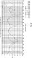
- FIG. 3is a plot representing simulation results for the model 26 of FIG. 2 .
- the simulation resultsshow the angle of phase for scattering parameter (S-parameter) S 2 , 1 in degrees (y-axis) by frequency in gigahertz (GHz) (x-axis).
- the plotincludes simulation plots for a model that does not include tuning features (NO TF) and a model that includes the tuning features ( 28 - 1 to 28 - 5 of FIG. 2 ) that have been positioned to configure the corresponding gaps ( 32 - 1 to 32 - 5 of FIG. 2 ) with the transmission line ( 30 of FIG. 2 ).
- the corresponding gapis configured to be about 0.050 inches from the transmission line, or about 0.03 inches closer than a gap without tuning features.
- the simulation resultsshow it is possible to tune the phase of the RF signal by adjusting the gap or height of the tuning features 28 - 1 to 28 - 5 ( FIG. 2 ) relative to the transmission line 30 ( FIG. 2 ).
- the simulation resultsshow the phase angle of the RF signal can be adjusted by a delta ( ⁇ ) of about 18 degrees.
- the simulation resultsshow the phase angle of the RF signal can be adjusted by a delta ( ⁇ ) of about 25 degrees.
- the simulation resultsshow the phase angle of the RF signal can be adjusted can be adjusted by a delta ( ⁇ ) of about 40 degrees.
- FIG. 4is an S-parameters plot of the simulation results for the model 26 of FIG. 2 .
- the S-parameter magnitudeis plotted in decibels (dB) across a GHz frequency range.
- Return lossin this case S 2 , 2 or output return loss, is an indication of how much power is reflected. For frequencies where S 2 , 2 is equal to 0 dB, then substantially all power from a RF signal is reflected.
- Insertion loss, in this case S 2 , 1is an indication of how much power is transferred. For frequencies where S 2 , 1 is equal to 0 dB, then substantially all power from the RF signal is transferred.
- a return loss of at least ⁇ 10 dB or loweris desirable for a target operating frequency range.
- S-parametersare plotted for S 2 , 1 and S 2 , 2 without tuning features (NO TF) and with tuning features configured to provide a gap of about 0.050 inches from the transmission line (WITH TF (0.050′′ GAP)). Accordingly, the simulation results show a desirable output return loss and insertion loss that can be realized with the presence of the tuning features 28 - 1 to 28 - 5 ( FIG. 2 ). In this particular model, a desirable output return loss and insertion loss is realized across a frequency range of 25 GHz to 40 GHz.
- FIG. 5Ais a perspective top view of a representative adjustable cover 34 according to embodiments disclosed herein, and FIG. 5B is a bottom view of the adjustable cover 34 of FIG. 5A .
- the adjustable cover 34includes one or more tuning features 36 - 1 to 36 - 3 .
- the one or more tuning features 36 - 1 to 36 - 3are integrated with the adjustable cover 34 and configured to selectively adjust a profile of the adjustable cover 34 .
- the adjustable cover 34includes a first surface 38 and a second surface 40 that generally opposes the first surface 38 .
- the perspective top viewfaces the first surface 38 and in FIG. 5B , the bottom view faces the second surface 40 .
- the adjustable cover 34forms a profile that includes an input channel opening 34 - 1 and an output channel opening 34 - 2 on opposing sides of an amplifier opening 34 - 3 .
- the adjustable cover 34is represented as transparent to also show three dimensional perspective views of the input channel opening 34 - 1 , the output channel opening 34 - 2 , and the amplifier opening 34 - 3 through the first surface 38 ; however, in practice, the adjustable cover may not be transparent.
- the second surface 40is configured closer to the amplifier and the corresponding input and output lines than the first surface 38 .
- the amplifier opening 34 - 3 of the second surface 40may cover the amplifier, and the input channel opening 34 - 1 and the output channel opening 34 - 2 may form gaps between the adjustable cover 34 and their respective input and output lines for the amplifier.
- the one or more tuning features 36 - 1 to 36 - 3are configured to protrude from the second surface 40 .
- a distance the one or more tuning features 36 - 1 to 36 - 3 protrudes from the second surface 40is separately adjustable, thereby allowing independent adjustment of a height of the gap between the adjustable cover 34 and the input and/or output lines. Accordingly, a profile of the second surface 40 is adjustable. In FIGS.
- the one or more tuning features 36 - 1 to 36 - 3are configured to adjust a profile of the output channel opening 34 - 2 .
- one or more tuning featuresmay be configured to adjust a profile of the input channel opening 34 - 1 , or both of the input channel opening 34 - 1 and the output channel opening 34 - 2 .
- the one or more tuning features 36 - 1 to 36 - 3comprise at least one of screws, taps, or bolts, which are configured to have adjustable heights or other positions relative to the adjustable cover 34 .
- FIG. 6Ais a top view of a MMIC structure 42 according to embodiments disclosed herein, and FIG. 6B is a perspective view of the MMIC structure 42 of FIG. 6A .
- the MMIC structure 42includes a substrate 44 .
- the substrate 44includes a printed circuit board.
- the substrate 44may also include at least one of quartz, woven fiberglass, and/or other laminate materials.
- a MMIC amplifier 46 , an input line 48 , and an output line 50are included on the substrate 44 .
- the input line 48 and the output line 50are electrically coupled to the MMIC amplifier 46 .
- An input port 52is configured to supply an input signal to the input line 48
- an output port 54is configured to receive an amplified signal from the output line 50 .
- the input port 52 and the output port 54may be any type of coaxial or waveguide transition connector.
- the MMIC structure 42further includes an adjustable cover 56 over the MMIC amplifier 46 and a portion of the substrate 44 .
- the adjustable cover 56is represented as transparent for illustration purposes; however, in practice, the adjustable cover 56 may not be transparent.
- the adjustable cover 56is mechanically secured to a housing 58 of the MMIC structure 42 in such a manner that a portion of the substrate 44 , a portion of the input line 48 , a portion of the output line 50 , and the MMIC amplifier 46 are between the adjustable cover 56 and the housing 58 .
- the housing 58further supports a bias board 60 that is configured to provide drive power to the MMIC amplifier 46 .
- the bias board 60is continuous with the substrate 44 that supports the MMIC amplifier 46 , and in other embodiments, the bias board 60 is separate from the substrate 44 .
- the bias board 60is on an area of the housing 58 that is outside of the area covered by the adjustable cover 56 .
- the adjustable cover 56is secured to the housing 58 by a plurality of screws 62 , although other mechanical fastening techniques could be used as previously described.
- the adjustable cover 56includes includes one or more tuning features 64 that are integrated with the adjustable cover 56 .
- the one or more tuning features 64are configured to selectively adjust a profile of the adjustable cover 56 as previously described.
- the one or more tuning features 64are configured to adjust a height of a gap between portions of the adjustable cover 56 and at least one of the input line 48 and the output line 50 .
- the one or more tuning features 64are configured to adjust the height of the gap over a portion of the output line 50 that is covered by the adjustable cover 56 .
- a portion of the adjustable cover 56comprises a first spacing between the adjustable cover 56 and the output line 50 .
- the portion of the adjustable cover 56comprises a second spacing between the adjustable cover 56 and the output line 50 , wherein the second spacing is different than the first spacing.
- an RF signal capacitance between the adjustable cover 56 and the output line 50may be adjusted to tune the phase of a signal passing through the MMIC structure 42 .
- the phase tuning of the signalmay be performed after assembly of the MMIC structure 42 .
- the one or more tuning features 64may also be located over the input line 48 in a similar manner.
- the one or more tuning features 64are configured to adjust multiple portions of the adjustable cover 56 .
- the embodiments disclosed hereinare particularly adapted to solid state power amplifiers, such as spatial power-combining devices or planar power-combining devices, which combine amplified signals from a plurality of amplifiers.
- the plurality of amplifiersmay be phase-tuned to a target value, thereby reducing phase variation between the amplifiers and improving power-combining efficiency.
- the plurality of amplifiersdo not require phase binning to tight value ranges before assembly.
- spatial power-combining devicesoperate at microwave frequencies such as, by way of non-limiting example, energy between about 300 megahertz (MHz) (100 centimeters (cm) wavelength) and 300 GHz (0.1 cm wavelength).
- embodimentsmay comprise operating frequency ranges that extend above microwave frequencies.
- a spatial power-combining devicemay operate within one or more common radar bands including, but not limited to S-band, C-band, X-band, Ku-band, K-band, Ka-band, and Q-band.
- the operating frequency rangeincludes an operating bandwidth spread of 2 GHz to 20 GHz. In other embodiments, the operating frequency range includes an operating bandwidth spread of 4 GHz to 40 GHz.
- a spatial power-combining devicegenerally includes a plurality of amplifier assemblies, and each amplifier assembly is an individual signal path and includes an amplifier connected to an input antenna structure and an output antenna structure.
- An input coaxial waveguideis configured to provide a signal concurrently to each input antenna structure, and an output coaxial waveguide is configured to concurrently combine amplified signals from each output antenna structure.
- the plurality of amplifier assembliesare arranged coaxially about a center axis. Accordingly, the spatial power-combining device is configured to split, amplify, and combine an electromagnetic signal.
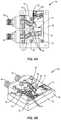
- FIG. 7is a perspective exploded view of a representative spatial power-combining device 66 according to some embodiments.
- the spatial power-combining device 66comprises an input port 68 and an input coaxial waveguide section 70 .
- the input coaxial waveguide section 70provides a broadband transition from the input port 68 to a center waveguide section 72 .
- the input coaxial waveguide section 70provides broadband impedance matching from an impedance Z p1 of the input port 68 to an impedance Z c of the center waveguide section 72 .
- the input coaxial waveguide section 70comprises an input inner conductor 74 and an input outer conductor 76 . Outer surfaces of the input inner conductor 74 and inner surfaces of the input outer conductor 76 have gradually changed profiles configured to minimize the impedance mismatch from the input port 68 to the center waveguide section 72 .
- the center waveguide section 72comprises a plurality of amplifier assemblies 78 arranged radially around a center axis 80 of the spatial power-combining device 66 .
- Each amplifier assembly 78comprises a body 82 having a predetermined wedge-shaped cross-section, an inner surface 84 , and an arcuate outer surface 86 .
- the amplifier assemblies 78When the amplifier assemblies 78 are collectively assembled, they may form a cylinder with a cylindrical central cavity, defined by the inner surfaces 84 .
- the body 82is similar to the housing 58 of FIGS. 6A and 6B .
- the spatial power-combining device 66also comprises an output coaxial waveguide section 88 and an output port 90 .
- the input port 68 and the output port 90may comprise field-replaceable Subminiature A (SMA) connectors.
- the input port 68 or the output port 90may comprise at least one of a super SMA connector, a type N connector, a type K connector, a WR28 connector, other coaxial to waveguide transition connectors, or any other suitable coaxial or waveguide connectors.
- the output coaxial waveguide section 88provides a broadband transition from the center waveguide section 72 to the output port 90 .
- the output coaxial waveguide section 88provides broadband impedance matching from the impedance Z c of the center waveguide section 72 to an impedance Z p2 of the output port 90 .
- the output coaxial waveguide section 88comprises an output inner conductor 92 and an output outer conductor 94 . Outer surfaces of the output inner conductor 92 and inner surfaces of the output outer conductor 94 have gradually changed profiles configured to minimize the impedance mismatch from the output port 90 to the center waveguide section 72 .
- impedance matchingis configured for 50 Ohms, although other designs such as 30 Ohms are possible.
- a first screw 96 and a first nut 98are provided for mechanically attaching the input inner conductor 74 to the plurality of amplifier assemblies 78 .
- a second screw 100 and a second nut 102are provided for mechanically attaching the output inner conductor 92 to the plurality of amplifier assemblies 78 .
- the plurality of amplifier assemblies 78comprise an input end 104 and an output end 106 .
- the input inner conductor 74is mechanically attached to the input end 104
- the output inner conductor 92is mechanically attached to the output end 106 .
- a spatial power-combining device 66comprises a center waveguide section 72 comprising a plurality of amplifier assemblies 78 , wherein the plurality of amplifier assemblies 78 forms an input end 104 and an output end 106 , an input inner conductor 74 mechanically attached to the input end 104 , and an output inner conductor 92 mechanically attached to the output end 106 .
- the input inner conductor 74may be directly attached to the input end 104 and the output inner conductor 92 may be directly attached to the output end 106 .
- inner conductorsmay be mechanically attached to a separate support element, such as a center post or rod.
- Amplifier assembliesmay be stacked circumferentially around the center post and may have inner surfaces that conform to the outer shape of the center post. Accordingly, the center post is provided for mechanical support and assembly of the spatial power-combining device.
- mechanical support in the spatial power-combining device 66 of FIG. 7comprises mechanically attaching the input inner conductor 74 to the input end 104 of the plurality of amplifier assemblies 78 and mechanically attaching the output inner conductor 92 to the output end 106 of the plurality of amplifier assemblies 78 .
- a separate support element, such as a center post or rod,is therefore not required for assembly.
- Removing the center postmay have particular benefit for applications that include higher frequency operation with shorter wavelengths of electromagnetic radiation and increased bandwidth.
- the operating frequency rangeincludes an operating bandwidth spread of 4 GHz to 41 GHz. In other embodiments, such as those with an operating frequency range of 2 GHz to 20 GHz, a center post or rod may be present.
- the input port 68receives a signal 108
- the input coaxial waveguide section 70is configured to provide the signal 108 concurrently to each of the amplifier assemblies 78 where the signal 108 is concurrently amplified by the respective amplifier assemblies 78 .
- the output coaxial waveguide section 88is configured to concurrently combine the amplified signals to form an amplified output signal 108 AMP , which is propagated through the output coaxial waveguide section 88 to the output port 90 for transmitting the amplified output signal 108 AMP .
- the amplifier assemblies 78each comprise an output connector portion 110 configured to mechanically attach to the output inner conductor 92 .
- the output connector portions 110comprise a shape, such as curved in FIG. 7 , that when assembled, are configured to collectively attach with the output inner conductor 92 .
- the amplifier assemblies 78may each comprise an input connector portion (not shown) configured to mechanically attach to the input inner conductor 74 .
- Each of the plurality of amplifier assemblies 78further includes an adjustable cover 112 with one or more tuning features 114 as previously described.
- the tuning features 114allow multiple configurations in order to selectively adjust a profile of the adjustable cover 112 that accordingly adjusts a signal phase of an amplifier underneath the adjustable cover 112 .
- the spatial power-combining device 66includes eight amplifier assemblies 78 to provide eight-way power-combining. Accordingly, signal phases of each of the eight amplifier assemblies 78 may be initially out of phase with each other and subsequently tuned in phase with each other by the adjustable covers 112 .
- a spatial power-combining devicemay include different numbers of amplifier assemblies, from as low as two amplifier assemblies to as many as sixteen amplifier assemblies or more.
- FIG. 8is a partial and unexploded cross-sectional view of the spatial power-combining device 66 of FIG. 7 .
- Several amplifier assemblies 78are omitted to illustrate the following details. Both the input end 104 and the output end 106 of the plurality of amplifier assemblies 78 are visible within the center waveguide section 72 .
- the input port 68 and the input coaxial waveguide section 70are located adjacent the input end 104
- the output port 90 and the output coaxial waveguide section 88are located adjacent the output end 106 .
- the input coaxial waveguide section 70comprises the input inner conductor 74 and the input outer conductor 76
- the output coaxial waveguide section 88comprises the output inner conductor 92 and the output outer conductor 94 .
- the output connector portions 110 of the plurality of amplifier assemblies 78collectively form an output connector receptacle 116
- input connector portions 118 of the plurality of amplifier assemblies 78collectively form an input connector receptacle 120 .
- the output connector receptacle 116 and the input connector receptacle 120comprise a cylindrical shape, although other shapes are possible, including various polygonal shapes.
- the input inner conductor 74is configured to mechanically attach to the input end 104 at the input connector receptacle 120 by the first screw 96
- the output inner conductor 92is configured to mechanically attach to the output end 106 at the output connector receptacle 116 by the second screw 100
- the first nut 98is inside the input connector receptacle 120 and is configured to receive the first screw 96
- the second nut 102is inside the output connector receptacle 116 and is configured to receive the second screw 100 .
- each amplifier assembly 78allows the center axis 80 to be hollow, and thus the inner surface 84 of the body 82 of each amplifier assembly 78 is separated from the center axis 80 by empty space.
- the inner surface 84 of each amplifier assembly 78is separated from the center axis 80 completely by empty space, with no support structure in between.
- the inner surface 84 of each amplifier assembly 78is spaced from the center axis 80 by a distance of no more than 50 mil, and in further embodiments the spacing may be smaller.
- each amplifier assembly 78may be spaced from the center axis 80 by a distance of about 10 mil.
- Amplifier assemblies in other spatial power-combining devicesare not spaced from a center axis by a distance of 50 mil or less due to the presence of the center rod.
- spatial power-combining devices with center rodstypically have amplifier assemblies spaced from the center axis by at least 80 mil.
- the spacing of the amplifier assembliescan be reduced to achieve higher frequency operation and increased bandwidth.
- the operating frequency rangeincludes an operating bandwidth spread of 4 GHz to 41 GHz.
- the reduced spacingmay only allow for a reduced number of amplifier assemblies.
- the plurality of amplifier assembliescomprise fewer than ten amplifier assemblies.
- some embodimentsmay comprise eight amplifier assemblies and may therefore be referred to as an eight-way spatial power-combining device, as represented in FIG. 7 .
- the spacingmay be greater and more amplifier assemblies may be included.
- each amplifier assembly 78comprises an input antenna structure 122 , an amplifier 124 , and an output antenna structure 126 .
- the amplifier 124comprises a MMIC amplifier, such as a GaN-based MMIC.
- the input antenna structure 122comprises an input antenna pattern, with an input signal conductor 128 visible in FIG. 8 , supported on a first board 130 .
- the output antenna structure 126comprises an output antenna pattern, with an output signal conductor 132 visible in FIG. 8 , supported on a second board 134 . It is understood that the input antenna pattern may additionally include an input ground conductor on an opposite side of the first board 130 , and the output antenna pattern may additionally comprise an output ground conductor on an opposite side of the second board 134 .
- the first board 130 and the second board 134may comprise substrates, such as printed circuit boards, that provide the desired form factor and mechanical support for the input antenna pattern and the output antenna pattern, respectively. Additionally, one or more electromagnetic interference filters 136 are supported on both the first board 130 and the second board 134 . The electromagnetic interference filters 136 are located around the input antenna pattern and the output antenna pattern to help suppress modes and reduce leakage between the amplifier assemblies 78 .
- the signal 108enters through the input port 68 and propagates through the input coaxial waveguide 70 to the input antenna structure 122 of each amplifier assembly 78 .
- Each input antenna structure 122couples the signal 108 to each amplifier 124
- each output antenna structure 126couples the amplified signal 108 AMP to the output coaxial waveguide section 88 to be propagated to the output port 90 .
- the adjustable cover 112 of FIG. 7is removed to show the amplifier 124 as well as an input line 138 from the input antenna structure 122 and an output line 140 to the output antenna structure 126 .
- the input line 138 and the output line 140are electrically connected to the amplifier 124 .
- the input line 138is continuous or an integral single component with the input signal conductor 128
- the output line 140is continuous or an integral single component with the output signal conductor 132
- the tuning features ( 114 of FIG. 7 ) of the adjustable cover ( 122 of FIG. 7 )are positioned over or aligned with the output line 140 to allow phase tuning of the amplifier 124 as previously described.
- additional tuning featuresmay be positioned over or aligned with the input line 138 in a similar manner.
- FIG. 9is a flowchart of a method according to some embodiments disclosed herein.
- the methodincludes assembling a plurality of individual amplifier assemblies that include a MMIC amplifier (block 200 ); phase tuning at least one individual amplifier assembly of the plurality of individual amplifier assemblies to a target value (block 202 ); and then assembling the plurality of individual amplifier assemblies together to form a solid state power amplifier (block 204 ).
- the phase of a signalsuch as an RF signal
- passing through an amplifier assemblyis influenced by a number of factors including, among others: the original phase of the MMIC amplifier; electrical connections that connect the MMIC amplifier between an input line and an output line; and a signal capacitance between an adjustable cover and the input line and the output line.
- phase tuning at least one individual amplifier assemblyincludes making adjustments to the adjustable cover that is provided over the MMIC amplifier. Phase variation between different MMIC amplifiers is common and combined with the additional factors introduced when assembling the amplifier assemblies, it can be challenging to manufacture several different MMIC structures that are in phase with one another.
- a plurality of individual amplifier assembliesmay be formed with MMIC amplifiers that are out of phase with each other. The plurality of individual amplifier assemblies may be separately phase-tuned to a target value by adjusting the adjustable cover as described herein. The plurality of now phase-tuned amplifier assemblies may then be joined together to form a solid state power amplifier. In this manner, a solid state power amplifier is provided with phase-tuned amplifier assemblies that are formed with at least some MMIC amplifiers that are originally out of phase with one another. In some embodiments, the solid state power amplifier includes a spatial power-combining device.
Landscapes
- Engineering & Computer Science (AREA)
- Power Engineering (AREA)
- Microelectronics & Electronic Packaging (AREA)
- Microwave Amplifiers (AREA)
Abstract
Description
Claims (19)
Priority Applications (1)
| Application Number | Priority Date | Filing Date | Title |
|---|---|---|---|
| US16/042,351US10707819B2 (en) | 2017-08-22 | 2018-07-23 | Phase tuning for monolithic microwave integrated circuits |
Applications Claiming Priority (2)
| Application Number | Priority Date | Filing Date | Title |
|---|---|---|---|
| US201762548448P | 2017-08-22 | 2017-08-22 | |
| US16/042,351US10707819B2 (en) | 2017-08-22 | 2018-07-23 | Phase tuning for monolithic microwave integrated circuits |
Publications (2)
| Publication Number | Publication Date |
|---|---|
| US20190068141A1 US20190068141A1 (en) | 2019-02-28 |
| US10707819B2true US10707819B2 (en) | 2020-07-07 |
Family
ID=65435683
Family Applications (1)
| Application Number | Title | Priority Date | Filing Date |
|---|---|---|---|
| US16/042,351ActiveUS10707819B2 (en) | 2017-08-22 | 2018-07-23 | Phase tuning for monolithic microwave integrated circuits |
Country Status (1)
| Country | Link |
|---|---|
| US (1) | US10707819B2 (en) |
Families Citing this family (18)
| Publication number | Priority date | Publication date | Assignee | Title |
|---|---|---|---|---|
| US10003118B2 (en) | 2015-12-22 | 2018-06-19 | Qorvo Us, Inc. | Spatial coupler and antenna for splitting and combining electromagnetic signals |
| US10651527B2 (en) | 2017-08-22 | 2020-05-12 | Qorvo Us, Inc. | Spatial power-combining devices with segmented waveguides and antennas |
| US10720711B2 (en) | 2017-08-22 | 2020-07-21 | Qorvo Us, Inc. | Antenna structures for spatial power-combining devices |
| US10340574B2 (en) | 2017-08-22 | 2019-07-02 | Qorvo Us, Inc. | Spatial combining device and antenna |
| US10587027B2 (en) | 2017-08-22 | 2020-03-10 | Qorvo Us, Inc. | Spatial combining devices for high-frequency operation |
| US10749276B2 (en) | 2017-08-22 | 2020-08-18 | Qorvo Us, Inc. | Spatial power-combining devices and antenna assemblies |
| US10812021B2 (en) | 2017-08-22 | 2020-10-20 | Qorvo Us, Inc. | Antenna waveguide transitions for solid state power amplifiers |
| US10833386B2 (en) | 2018-04-09 | 2020-11-10 | Qorvo Us, Inc. | Waveguide transitions for power-combining devices |
| US11162734B2 (en) | 2018-08-06 | 2021-11-02 | Qorvo Us, Inc. | Heat exchanger assemblies for electronic devices and related methods |
| US11255608B2 (en) | 2018-08-06 | 2022-02-22 | Qorvo Us, Inc. | Heat exchanger assemblies for electronic devices |
| US10855240B2 (en) | 2018-11-15 | 2020-12-01 | Qorvo Us, Inc. | Structures for spatial power-combining devices |
| US10804588B2 (en) | 2018-12-10 | 2020-10-13 | Qorvo Us, Inc. | Antenna structures for spatial power-combining devices |
| US11005437B2 (en) | 2019-02-25 | 2021-05-11 | Qorvo Us, Inc. | Spatial power-combining devices with thin film resistors |
| US11564337B2 (en) | 2020-03-17 | 2023-01-24 | Qorvo Us, Inc. | Thermal structures for heat transfer devices and spatial power-combining devices |
| US11387791B2 (en) | 2020-03-17 | 2022-07-12 | Qorvo Us, Inc. | Spatial power-combining devices with reduced size |
| CN114582850A (en)* | 2020-11-30 | 2022-06-03 | 上海华为技术有限公司 | Electronic element and electronic equipment |
| US11621469B2 (en) | 2021-02-01 | 2023-04-04 | Qorvo Us, Inc. | Power-combining devices with increased output power |
| US11955687B2 (en) | 2022-01-10 | 2024-04-09 | Qorvo Us, Inc. | Structural arrangements for spatial power-combining devices |
Citations (40)
| Publication number | Priority date | Publication date | Assignee | Title |
|---|---|---|---|---|
| US3023382A (en) | 1960-07-15 | 1962-02-27 | Microwave Dev Lab Inc | Inline waveguide to coaxial transition |
| US4234854A (en) | 1978-05-12 | 1980-11-18 | Westinghouse Electric Corp. | Amplifier with radial line divider/combiner |
| US4424496A (en) | 1981-10-13 | 1984-01-03 | Raytheon Company | Divider/combiner amplifier |
| US5036335A (en) | 1989-06-09 | 1991-07-30 | The Marconi Company Limited | Tapered slot antenna with balun slot line and stripline feed |
| US5162803A (en) | 1991-05-20 | 1992-11-10 | Trw Inc. | Beamforming structure for modular phased array antennas |
| US5214394A (en) | 1991-04-15 | 1993-05-25 | Rockwell International Corporation | High efficiency bi-directional spatial power combiner amplifier |
| US5256988A (en) | 1992-09-01 | 1993-10-26 | Loral Aerospace Corp. | Conical transverse electromagnetic divider/combiner |
| US5736908A (en) | 1996-06-19 | 1998-04-07 | The Regents Of The University Of California | Waveguide-based spatial power combining array and method for using the same |
| US5920240A (en) | 1996-06-19 | 1999-07-06 | The Regents Of The University Of California | High efficiency broadband coaxial power combiner/splitter with radial slotline cards |
| US6028483A (en) | 1998-05-06 | 2000-02-22 | Hughes Electronics Corporation | Universal fixture/package for spatial-power-combined amplifier |
| US6037840A (en) | 1997-12-18 | 2000-03-14 | Lucent Technologies, Inc. | Article comprising a combiner-splitter |
| US6181221B1 (en) | 1998-10-06 | 2001-01-30 | Hughes Electronics Corporation | Reflective waveguide variable power divider/combiner |
| US6828875B2 (en) | 2002-12-09 | 2004-12-07 | Mia-Com, Inc. | Compact slotted-waveguide spatial power divider/combiner/amplifier |
| US20060202777A1 (en) | 2005-03-08 | 2006-09-14 | Deckman Blythe C | Method and apparatus for increasing performance in a waveguide-based spatial power combiner |
| US7110165B2 (en) | 2002-10-29 | 2006-09-19 | Wavestream Wireless Technologies | Power management for spatial power combiners |
| US7215220B1 (en) | 2004-08-23 | 2007-05-08 | Cap Wireless, Inc. | Broadband power combining device using antipodal finline structure |
| US20070229186A1 (en) | 2006-03-31 | 2007-10-04 | Hacker Jonathan B | Compact stabilized full-band power amplifier arrangement |
| US20070279146A1 (en) | 2006-06-06 | 2007-12-06 | Rector Robert M | Flexible microwave transmission line |
| US7466203B2 (en)* | 2006-06-06 | 2008-12-16 | Keragis Corporation | Solid state microwave power amplifier |
| US8698577B2 (en)* | 2010-07-02 | 2014-04-15 | Nuvotronics, Llc | Three-dimensional microstructures |
| US20140145794A1 (en) | 2012-11-26 | 2014-05-29 | Cap Wireless, Inc. | Power combiner |
| US20140167880A1 (en) | 2012-12-18 | 2014-06-19 | Triquint Cw, Inc. | Passive coaxial power splitter/combiner |
| US8928429B2 (en) | 2011-05-17 | 2015-01-06 | City University Of Hong Kong | Multiple-way ring cavity power combiner and divider |
| US9019036B2 (en) | 2010-05-10 | 2015-04-28 | Raytheon Company | Multiple E-probe waveguide power combiner/divider |
| US9054427B2 (en) | 2010-07-19 | 2015-06-09 | Bae Systems Plc | Planar Vivaldi antenna array |
| US9065163B1 (en) | 2011-12-23 | 2015-06-23 | Nuvotronics, Llc | High frequency power combiner/divider |
| US9276304B2 (en) | 2012-11-26 | 2016-03-01 | Triquint Semiconductor, Inc. | Power combiner using tri-plane antennas |
| US9325074B2 (en) | 2011-11-23 | 2016-04-26 | Raytheon Company | Coaxial waveguide antenna |
| US20170149113A1 (en) | 2015-11-23 | 2017-05-25 | Commissariat A L'energie Atomique Et Aux Energies Alternatives | Spatial power combiner |
| US20170179598A1 (en) | 2015-12-22 | 2017-06-22 | Qorvo Us, Inc. | Spatial coupler and antenna for splitting and combining electromagnetic signals |
| US9917343B2 (en) | 2016-03-16 | 2018-03-13 | The United States Of America As Represented By The Secretary Of The Navy | Waveguide to coaxial line transition having rigid hollow cone portions |
| US9954706B1 (en) | 2016-10-28 | 2018-04-24 | L3 Technologies Inc. | Outphased spatial combiner |
| US10009067B2 (en) | 2014-12-04 | 2018-06-26 | At&T Intellectual Property I, L.P. | Method and apparatus for configuring a communication interface |
| US10164667B1 (en) | 2018-03-21 | 2018-12-25 | Qorvo Us, Inc. | Spatial power-combining devices with amplifier connectors |
| US20190007007A1 (en) | 2017-06-29 | 2019-01-03 | Qorvo Us, Inc. | Amplifier assembly and spatial power combining device |
| US20190067836A1 (en) | 2017-08-22 | 2019-02-28 | Qorvo Us, Inc. | Spatial power-combining devices and antenna assemblies |
| US20190067783A1 (en) | 2017-08-22 | 2019-02-28 | Qorvo Us, Inc. | Spatial power-combining devices with filtering elements |
| US20190068123A1 (en) | 2017-08-22 | 2019-02-28 | Qorvo Us, Inc. | Antenna waveguide transitions for solid state power amplifiers |
| US20190067782A1 (en) | 2017-08-22 | 2019-02-28 | Qorvo Us, Inc. | Spatial combining devices for high-frequency operation |
| US20190067778A1 (en) | 2017-08-22 | 2019-02-28 | Qorvo Us, Inc. | Spatial power-combining devices with segmented waveguides and antennas |
- 2018
- 2018-07-23USUS16/042,351patent/US10707819B2/enactiveActive
Patent Citations (45)
| Publication number | Priority date | Publication date | Assignee | Title |
|---|---|---|---|---|
| US3023382A (en) | 1960-07-15 | 1962-02-27 | Microwave Dev Lab Inc | Inline waveguide to coaxial transition |
| US4234854A (en) | 1978-05-12 | 1980-11-18 | Westinghouse Electric Corp. | Amplifier with radial line divider/combiner |
| US4424496A (en) | 1981-10-13 | 1984-01-03 | Raytheon Company | Divider/combiner amplifier |
| US5036335A (en) | 1989-06-09 | 1991-07-30 | The Marconi Company Limited | Tapered slot antenna with balun slot line and stripline feed |
| US5214394A (en) | 1991-04-15 | 1993-05-25 | Rockwell International Corporation | High efficiency bi-directional spatial power combiner amplifier |
| US5162803A (en) | 1991-05-20 | 1992-11-10 | Trw Inc. | Beamforming structure for modular phased array antennas |
| US5256988A (en) | 1992-09-01 | 1993-10-26 | Loral Aerospace Corp. | Conical transverse electromagnetic divider/combiner |
| US5736908A (en) | 1996-06-19 | 1998-04-07 | The Regents Of The University Of California | Waveguide-based spatial power combining array and method for using the same |
| US5920240A (en) | 1996-06-19 | 1999-07-06 | The Regents Of The University Of California | High efficiency broadband coaxial power combiner/splitter with radial slotline cards |
| US6037840A (en) | 1997-12-18 | 2000-03-14 | Lucent Technologies, Inc. | Article comprising a combiner-splitter |
| US6028483A (en) | 1998-05-06 | 2000-02-22 | Hughes Electronics Corporation | Universal fixture/package for spatial-power-combined amplifier |
| US6181221B1 (en) | 1998-10-06 | 2001-01-30 | Hughes Electronics Corporation | Reflective waveguide variable power divider/combiner |
| US7110165B2 (en) | 2002-10-29 | 2006-09-19 | Wavestream Wireless Technologies | Power management for spatial power combiners |
| US6828875B2 (en) | 2002-12-09 | 2004-12-07 | Mia-Com, Inc. | Compact slotted-waveguide spatial power divider/combiner/amplifier |
| US7215220B1 (en) | 2004-08-23 | 2007-05-08 | Cap Wireless, Inc. | Broadband power combining device using antipodal finline structure |
| US20060202777A1 (en) | 2005-03-08 | 2006-09-14 | Deckman Blythe C | Method and apparatus for increasing performance in a waveguide-based spatial power combiner |
| US20070229186A1 (en) | 2006-03-31 | 2007-10-04 | Hacker Jonathan B | Compact stabilized full-band power amplifier arrangement |
| US20070279146A1 (en) | 2006-06-06 | 2007-12-06 | Rector Robert M | Flexible microwave transmission line |
| US7466203B2 (en)* | 2006-06-06 | 2008-12-16 | Keragis Corporation | Solid state microwave power amplifier |
| US9019036B2 (en) | 2010-05-10 | 2015-04-28 | Raytheon Company | Multiple E-probe waveguide power combiner/divider |
| US8698577B2 (en)* | 2010-07-02 | 2014-04-15 | Nuvotronics, Llc | Three-dimensional microstructures |
| US9054427B2 (en) | 2010-07-19 | 2015-06-09 | Bae Systems Plc | Planar Vivaldi antenna array |
| US8928429B2 (en) | 2011-05-17 | 2015-01-06 | City University Of Hong Kong | Multiple-way ring cavity power combiner and divider |
| US9325074B2 (en) | 2011-11-23 | 2016-04-26 | Raytheon Company | Coaxial waveguide antenna |
| US9065163B1 (en) | 2011-12-23 | 2015-06-23 | Nuvotronics, Llc | High frequency power combiner/divider |
| US20140145794A1 (en) | 2012-11-26 | 2014-05-29 | Cap Wireless, Inc. | Power combiner |
| US9276304B2 (en) | 2012-11-26 | 2016-03-01 | Triquint Semiconductor, Inc. | Power combiner using tri-plane antennas |
| US20140167880A1 (en) | 2012-12-18 | 2014-06-19 | Triquint Cw, Inc. | Passive coaxial power splitter/combiner |
| US9287605B2 (en) | 2012-12-18 | 2016-03-15 | Triquint Cw, Inc. | Passive coaxial power splitter/combiner |
| US10009067B2 (en) | 2014-12-04 | 2018-06-26 | At&T Intellectual Property I, L.P. | Method and apparatus for configuring a communication interface |
| US20170149113A1 (en) | 2015-11-23 | 2017-05-25 | Commissariat A L'energie Atomique Et Aux Energies Alternatives | Spatial power combiner |
| US10003118B2 (en) | 2015-12-22 | 2018-06-19 | Qorvo Us, Inc. | Spatial coupler and antenna for splitting and combining electromagnetic signals |
| US20170179598A1 (en) | 2015-12-22 | 2017-06-22 | Qorvo Us, Inc. | Spatial coupler and antenna for splitting and combining electromagnetic signals |
| US20180294539A1 (en) | 2015-12-22 | 2018-10-11 | Qorvo Us, Inc. | Spatial coupler and antenna for splitting and combining electromagnetic signals |
| US9917343B2 (en) | 2016-03-16 | 2018-03-13 | The United States Of America As Represented By The Secretary Of The Navy | Waveguide to coaxial line transition having rigid hollow cone portions |
| US9954706B1 (en) | 2016-10-28 | 2018-04-24 | L3 Technologies Inc. | Outphased spatial combiner |
| US20190007007A1 (en) | 2017-06-29 | 2019-01-03 | Qorvo Us, Inc. | Amplifier assembly and spatial power combining device |
| US20190067836A1 (en) | 2017-08-22 | 2019-02-28 | Qorvo Us, Inc. | Spatial power-combining devices and antenna assemblies |
| US20190067783A1 (en) | 2017-08-22 | 2019-02-28 | Qorvo Us, Inc. | Spatial power-combining devices with filtering elements |
| US20190068123A1 (en) | 2017-08-22 | 2019-02-28 | Qorvo Us, Inc. | Antenna waveguide transitions for solid state power amplifiers |
| US20190067782A1 (en) | 2017-08-22 | 2019-02-28 | Qorvo Us, Inc. | Spatial combining devices for high-frequency operation |
| US20190067778A1 (en) | 2017-08-22 | 2019-02-28 | Qorvo Us, Inc. | Spatial power-combining devices with segmented waveguides and antennas |
| US20190068140A1 (en) | 2017-08-22 | 2019-02-28 | Qorvo Us, Inc. | Amplifier assemblies with multiple antenna structures and amplifiers |
| US20190067781A1 (en) | 2017-08-22 | 2019-02-28 | Qorvo Us, Inc. | Spatial combining device and antenna |
| US10164667B1 (en) | 2018-03-21 | 2018-12-25 | Qorvo Us, Inc. | Spatial power-combining devices with amplifier connectors |
Non-Patent Citations (57)
| Title |
|---|
| Amjadi, S., et al., "Design of a Broadband Eight-Way Coaxial Wavelength Power Combiner," IEEE Transactions on Microwave Theory and Techniques, vol. 60, Issue 1, Nov. 15, 2011, pp. 39-45. |
| Author Unknown, "Interpack 2005: An assessment for PMMI members," 2005, PMMI, 32 pages. |
| Author Unknown, "Spatial Combining Technology: Revolutionizing the Microwave Power Amplifier," Microwave Journal, Sep. 8, 2008, http://www.microwavejournal.com/articles/print/6838-spatial-combining, CAP Wireless Inc., 7 pages. |
| Author Unknown, "Vivaldi antenna," Wikipedia, web page last edited Feb. 7, 2017, accessed May 11, 2017, https://en.wikipedia.org/wiki/Vivaldi_antenna, Wikimedia Foundation, Inc., 2 pages. |
| Beyers, R., et al., "Compact Conical-Line Power Combiner Design Using Circuit Models," IEEE Transactions on Microwave Theory and Techniques, vol. 62, Issue 11, Oct. 9, 2014, pp. 2650-2658. |
| Caturla, F., et al., "Electroless Plating of Graphite with Copper and Nickel," Journal of the Electrochemical Soceity, vol. 142, Issue 12, Dec. 1995, The Electrochemical Society, Inc., pp. 4084-4090. |
| Corrected Notice of Allowance and Applicant-Initiated Interview Summary for U.S. Appl. No. 15/846,840, dated Dec. 31, 2019, 6 pages. |
| Corrected Notice of Allowance and Examiner-Initiated Interview Summary for U.S. Appl. No. 15/846,840, dated Dec. 12, 2019, 6 pages. |
| Courtney, Patrick G. et al., "120 W Ka Band Power Amplifier Utilizing GaN MMICs and Coaxial Waveguide Spatial Power Combining," White Paper, May 2016, Qorvo, pp. 1-8. |
| Fathy, A., et al., "A Simplified Approach for Radial Power Combiners," IEEE Transactions on Microwave Theory and Techniques, vol. 54, No. 1, Jan. 2006, pp. 247-255. |
| Final Office Action for U.S. Appl. No. 16/191,541, dated Mar. 31, 2020, 8 pages. |
| Fitzhugh, William, et al., "Modulation of Ionic Current Limitations by Doping Graphite Anodes," Journal of Electrochemical Society, vol. 165, Issue 10, Jul. 2018, The Electrochemical Society, 6 pages. |
| Gharehkand, F., "Design of a 16 Way Radial Microwave Power Divider/Combiner with Rectangular Waveguide Output and Coaxial Inputs," International Journal of Electronics and Communications (AEU), vol. 68, 2014, pp. 422-428. |
| Glenis, S., et al., "Sulfur doped graphite prepared via arc discharge of carbon rods in the presence of thiopenes," Journal of Applied Physics, vol. 86, Issue 8, Oct. 1999, American Institute of Physics, pp. 4464-4466. |
| Jia, Pengcheng et al., "Broadband High Power Amplifier using Spatial Power Combining Technique" IEEE Transactions on Microwave Theory and Techniques, vol. 51, Issue 12, Dec. 2003, IEEE, 4 pages. |
| Larkins, Grover, et al., "Evidence of Superconductivity in Doped Graphite and Graphene," Superconductor Science and Technology, vol. 29, Issue 1, Dec. 2015, IOP Publishing Ltd, 18 pages. |
| Leggieri, Alberto et al., "The Squarax Spatial Power Combiner," Progress in Electromagnetics Research C, vol. 45, Oct. 2013, EMW Publishing, pp. 43-55. |
| Montgomery, R., et al., "Solid-State PAs Battle TWTAs for ECM Systems," Microwave Journal, Jun. 2017 Supplement, Jun. 14, 2017, 3 pages. |
| Möttönen, V. S., "Receiver Front-End Circuits and Components for Millimetre and Submillimetre Wavelengths," Dissertation for the degree of Doctor of Science in Technology, Helsinki University of Technology, Department of Electrical and Communications Engineering, Radio Laboratory, Apr. 2005, 40 pages. |
| Non-Final Office Action for U.S. Appl. No. 15/637,472, dated Aug. 10, 2018, 8 pages. |
| Non-Final Office Action for U.S. Appl. No. 15/846,840, dated Mar. 21, 2019, 4 pages. |
| Non-Final Office Action for U.S. Appl. No. 15/933,783, dated May 1, 2019, 8 pages. |
| Non-Final Office Action for U.S. Appl. No. 15/933,821, dated Jul. 11, 2019, 7 pages. |
| Non-Final Office Action for U.S. Appl. No. 15/981,516, dated Jul. 17, 2019, 5 pages. |
| Non-Final Office Action for U.S. Appl. No. 15/981,535, dated Jul. 8, 2019, 5 pages. |
| Non-Final Office Action for U.S. Appl. No. 16/005,794, dated Oct. 7, 2019, 11 pages. |
| Non-Final Office Action for U.S. Appl. No. 16/008,586, dated Oct. 24, 2019, 10 pages. |
| Non-Final Office Action for U.S. Appl. No. 16/032,252, dated Dec. 27, 2019, 5 pages. |
| Non-Final Office Action for U.S. Appl. No. 16/039,435, dated Jan. 7, 2020, 5 pages. |
| Non-Final Office Action for U.S. Appl. No. 16/191,541, dated Dec. 9, 2019, 7 pages. |
| Notice of Allowance for U.S. Appl. No. 15/290,749, dated Feb. 16, 2018, 9 pages. |
| Notice of Allowance for U.S. Appl. No. 15/637,472, dated Mar. 12, 2019, 7 pages. |
| Notice of Allowance for U.S. Appl. No. 15/845,225, dated Jan. 10, 2019, 7 pages. |
| Notice of Allowance for U.S. Appl. No. 15/846,840, dated Jul. 5, 2019, 7 pages. |
| Notice of Allowance for U.S. Appl. No. 15/927,565, dated Aug. 8, 2018, 8 pages. |
| Notice of Allowance for U.S. Appl. No. 15/933,321, dated Jan. 15, 2020, 7 pages. |
| Notice of Allowance for U.S. Appl. No. 15/981,516, dated Jan. 15, 2020, 7 pages. |
| Notice of Allowance for U.S. Appl. No. 15/981,535, dated Dec. 31, 2019, 7 pages. |
| Notice of Allowance for U.S. Appl. No. 16/005,194, dated Jan. 9, 2020, 7 pages. |
| Notice of Allowance for U.S. Appl. No. 16/008,586, dated Feb. 4, 2020, 8 pages. |
| Notice of Allowance for U.S. Appl. No. 16/166,548, dated Nov. 29, 2018, 8 pages. |
| Notice of Allowance for U.S. Appl. No. 16/214,234, dated May 15, 2020, 8 pages. |
| Ortiz, Sean C., "High Power Spatial Combiners: Tile and Tray Approaches," Dissertation, North Carolina State University, Electrical Engineering, Nov. 2001, 194 pages. |
| Scheike, T., et al., "Can doping graphite trigger room temperature superconductivity: Evidence for granular high-temperature superconductivity in water-treated graphite powder," Advanced Materials, vol. 24, Issue 43, Sep. 2012, 19 pages. |
| Smalc, Martin, et al., "Thermal Performance of Natural Graphite Heat Spreaders," Proceedings of IPACK2005, Jul. 17-22, San Francisco, California, American Society of Mechanical Engineers, 11 pages. |
| Tribak, A., et al., "Ultra-Broadband High Efficiency Mode Converter," Progress in Electromagnetics Research C, vol. 36, 2013, pp. 145-158. |
| U.S. Appl. No. 15/637,472, filed Jun. 29, 2017. |
| U.S. Appl. No. 15/845,225, filed Dec. 18, 2017. |
| U.S. Appl. No. 15/846,840, filed Dec. 19, 2017. |
| U.S. Appl. No. 15/927,565, filed Mar. 21, 2018. |
| U.S. Appl. No. 15/933,783, filed Mar. 23, 2018. |
| U.S. Appl. No. 15/933,821, filed Mar. 23, 2018. |
| U.S. Appl. No. 15/981,516, filed May 16, 2018. |
| U.S. Appl. No. 15/981,535, filed May 16, 2018. |
| U.S. Appl. No. 16/008,586, filed Jun. 14, 2018. |
| U.S. Appl. No. 16/032,252, filed Jul. 11, 2018. |
| U.S. Appl. No. 16/039,435, filed Jul. 19, 2018. |
Also Published As
| Publication number | Publication date |
|---|---|
| US20190068141A1 (en) | 2019-02-28 |
Similar Documents
| Publication | Publication Date | Title |
|---|---|---|
| US10707819B2 (en) | Phase tuning for monolithic microwave integrated circuits | |
| US10615482B2 (en) | Amplifier assemblies with multiple antenna structures and amplifiers | |
| US10587027B2 (en) | Spatial combining devices for high-frequency operation | |
| US10651527B2 (en) | Spatial power-combining devices with segmented waveguides and antennas | |
| US10263651B1 (en) | Spatial power-combining devices with amplifier connectors | |
| US10833386B2 (en) | Waveguide transitions for power-combining devices | |
| US10811754B2 (en) | Power couplers and related devices having antenna element power absorbers | |
| US10720711B2 (en) | Antenna structures for spatial power-combining devices | |
| US9761937B2 (en) | Fragmented aperture for the Ka/K/Ku frequency bands | |
| US10749276B2 (en) | Spatial power-combining devices and antenna assemblies | |
| EP3105820B1 (en) | A reconfigurable radio frequency aperture | |
| US9941584B2 (en) | Reducing antenna array feed modules through controlled mutual coupling of a pixelated EM surface | |
| US12143074B2 (en) | Spatial power-combining devices with reduced size | |
| US9252497B2 (en) | Hybrid single aperture inclined antenna | |
| KR101496302B1 (en) | Millimeter Wave Transition Method Between Microstrip Line and Waveguide | |
| US10020595B2 (en) | Negative group delay circuit | |
| TW201924136A (en) | Apparatus with rectangular waveguide to radial mode transition | |
| US20160156105A1 (en) | Combined aperture and manifold applicable to probe fed or capacitively coupled radiating elements | |
| JP3970222B2 (en) | Phased array antenna | |
| Sielck et al. | Self-diplexing, dual-polarized Ka-band SIW slot antenna with integrated K-band patch | |
| Chaloun et al. | Wide-angle scanning cavity antenna element for mobile Satcom applications at Ka band | |
| CN116345164A (en) | Ku frequency band broadband double circularly polarized microstrip antenna | |
| Yektakhah et al. | Wideband circularly polarized modular active phased array for vehicular satellite communication | |
| US11217895B2 (en) | Tuneable waveguide transition | |
| US20250202113A1 (en) | Signal coupler configurations |
Legal Events
| Date | Code | Title | Description |
|---|---|---|---|
| FEPP | Fee payment procedure | Free format text:ENTITY STATUS SET TO UNDISCOUNTED (ORIGINAL EVENT CODE: BIG.); ENTITY STATUS OF PATENT OWNER: LARGE ENTITY | |
| AS | Assignment | Owner name:QORVO US, INC., NORTH CAROLINA Free format text:ASSIGNMENT OF ASSIGNORS INTEREST;ASSIGNORS:YOON, SOACK;MOHAN, ANKUSH;DENNINGHOFF, DAN;SIGNING DATES FROM 20180719 TO 20180723;REEL/FRAME:046436/0326 | |
| STPP | Information on status: patent application and granting procedure in general | Free format text:DOCKETED NEW CASE - READY FOR EXAMINATION | |
| STPP | Information on status: patent application and granting procedure in general | Free format text:NON FINAL ACTION MAILED | |
| STPP | Information on status: patent application and granting procedure in general | Free format text:RESPONSE TO NON-FINAL OFFICE ACTION ENTERED AND FORWARDED TO EXAMINER | |
| STPP | Information on status: patent application and granting procedure in general | Free format text:NOTICE OF ALLOWANCE MAILED -- APPLICATION RECEIVED IN OFFICE OF PUBLICATIONS | |
| STPP | Information on status: patent application and granting procedure in general | Free format text:NOTICE OF ALLOWANCE MAILED -- APPLICATION RECEIVED IN OFFICE OF PUBLICATIONS | |
| STPP | Information on status: patent application and granting procedure in general | Free format text:PUBLICATIONS -- ISSUE FEE PAYMENT RECEIVED | |
| STPP | Information on status: patent application and granting procedure in general | Free format text:PUBLICATIONS -- ISSUE FEE PAYMENT VERIFIED | |
| STPP | Information on status: patent application and granting procedure in general | Free format text:PUBLICATIONS -- ISSUE FEE PAYMENT VERIFIED | |
| STCF | Information on status: patent grant | Free format text:PATENTED CASE | |
| STPP | Information on status: patent application and granting procedure in general | Free format text:PUBLICATIONS -- ISSUE FEE PAYMENT VERIFIED | |
| STCF | Information on status: patent grant | Free format text:PATENTED CASE | |
| MAFP | Maintenance fee payment | Free format text:PAYMENT OF MAINTENANCE FEE, 4TH YEAR, LARGE ENTITY (ORIGINAL EVENT CODE: M1551); ENTITY STATUS OF PATENT OWNER: LARGE ENTITY Year of fee payment:4 |