US10707283B2 - Organic EL element, organic EL display panel using same, and organic EL display panel manufacturing method - Google Patents
Organic EL element, organic EL display panel using same, and organic EL display panel manufacturing methodDownload PDFInfo
- Publication number
- US10707283B2 US10707283B2US16/001,399US201816001399AUS10707283B2US 10707283 B2US10707283 B2US 10707283B2US 201816001399 AUS201816001399 AUS 201816001399AUS 10707283 B2US10707283 B2US 10707283B2
- Authority
- US
- United States
- Prior art keywords
- light
- pixel electrode
- layer
- layers
- row
- Prior art date
- Legal status (The legal status is an assumption and is not a legal conclusion. Google has not performed a legal analysis and makes no representation as to the accuracy of the status listed.)
- Active
Links
Images


Classifications
- H01L27/3246—
- H—ELECTRICITY
- H10—SEMICONDUCTOR DEVICES; ELECTRIC SOLID-STATE DEVICES NOT OTHERWISE PROVIDED FOR
- H10K—ORGANIC ELECTRIC SOLID-STATE DEVICES
- H10K59/00—Integrated devices, or assemblies of multiple devices, comprising at least one organic light-emitting element covered by group H10K50/00
- H10K59/10—OLED displays
- H10K59/12—Active-matrix OLED [AMOLED] displays
- H10K59/122—Pixel-defining structures or layers, e.g. banks
- H01L27/1218—
- H01L27/3248—
- H01L27/3272—
- H01L27/3274—
- H01L27/3276—
- H01L27/3297—
- H01L51/5271—
- H01L51/56—
- H—ELECTRICITY
- H10—SEMICONDUCTOR DEVICES; ELECTRIC SOLID-STATE DEVICES NOT OTHERWISE PROVIDED FOR
- H10D—INORGANIC ELECTRIC SEMICONDUCTOR DEVICES
- H10D86/00—Integrated devices formed in or on insulating or conducting substrates, e.g. formed in silicon-on-insulator [SOI] substrates or on stainless steel or glass substrates
- H10D86/40—Integrated devices formed in or on insulating or conducting substrates, e.g. formed in silicon-on-insulator [SOI] substrates or on stainless steel or glass substrates characterised by multiple TFTs
- H10D86/411—Integrated devices formed in or on insulating or conducting substrates, e.g. formed in silicon-on-insulator [SOI] substrates or on stainless steel or glass substrates characterised by multiple TFTs characterised by materials, geometry or structure of the substrates
- H—ELECTRICITY
- H10—SEMICONDUCTOR DEVICES; ELECTRIC SOLID-STATE DEVICES NOT OTHERWISE PROVIDED FOR
- H10D—INORGANIC ELECTRIC SEMICONDUCTOR DEVICES
- H10D86/00—Integrated devices formed in or on insulating or conducting substrates, e.g. formed in silicon-on-insulator [SOI] substrates or on stainless steel or glass substrates
- H10D86/40—Integrated devices formed in or on insulating or conducting substrates, e.g. formed in silicon-on-insulator [SOI] substrates or on stainless steel or glass substrates characterised by multiple TFTs
- H10D86/60—Integrated devices formed in or on insulating or conducting substrates, e.g. formed in silicon-on-insulator [SOI] substrates or on stainless steel or glass substrates characterised by multiple TFTs wherein the TFTs are in active matrices
- H—ELECTRICITY
- H10—SEMICONDUCTOR DEVICES; ELECTRIC SOLID-STATE DEVICES NOT OTHERWISE PROVIDED FOR
- H10K—ORGANIC ELECTRIC SOLID-STATE DEVICES
- H10K50/00—Organic light-emitting devices
- H10K50/80—Constructional details
- H10K50/85—Arrangements for extracting light from the devices
- H10K50/856—Arrangements for extracting light from the devices comprising reflective means
- H—ELECTRICITY
- H10—SEMICONDUCTOR DEVICES; ELECTRIC SOLID-STATE DEVICES NOT OTHERWISE PROVIDED FOR
- H10K—ORGANIC ELECTRIC SOLID-STATE DEVICES
- H10K59/00—Integrated devices, or assemblies of multiple devices, comprising at least one organic light-emitting element covered by group H10K50/00
- H—ELECTRICITY
- H10—SEMICONDUCTOR DEVICES; ELECTRIC SOLID-STATE DEVICES NOT OTHERWISE PROVIDED FOR
- H10K—ORGANIC ELECTRIC SOLID-STATE DEVICES
- H10K59/00—Integrated devices, or assemblies of multiple devices, comprising at least one organic light-emitting element covered by group H10K50/00
- H10K59/10—OLED displays
- H10K59/12—Active-matrix OLED [AMOLED] displays
- H10K59/123—Connection of the pixel electrodes to the thin film transistors [TFT]
- H—ELECTRICITY
- H10—SEMICONDUCTOR DEVICES; ELECTRIC SOLID-STATE DEVICES NOT OTHERWISE PROVIDED FOR
- H10K—ORGANIC ELECTRIC SOLID-STATE DEVICES
- H10K59/00—Integrated devices, or assemblies of multiple devices, comprising at least one organic light-emitting element covered by group H10K50/00
- H10K59/10—OLED displays
- H10K59/12—Active-matrix OLED [AMOLED] displays
- H10K59/125—Active-matrix OLED [AMOLED] displays including organic TFTs [OTFT]
- H—ELECTRICITY
- H10—SEMICONDUCTOR DEVICES; ELECTRIC SOLID-STATE DEVICES NOT OTHERWISE PROVIDED FOR
- H10K—ORGANIC ELECTRIC SOLID-STATE DEVICES
- H10K59/00—Integrated devices, or assemblies of multiple devices, comprising at least one organic light-emitting element covered by group H10K50/00
- H10K59/10—OLED displays
- H10K59/12—Active-matrix OLED [AMOLED] displays
- H10K59/126—Shielding, e.g. light-blocking means over the TFTs
- H—ELECTRICITY
- H10—SEMICONDUCTOR DEVICES; ELECTRIC SOLID-STATE DEVICES NOT OTHERWISE PROVIDED FOR
- H10K—ORGANIC ELECTRIC SOLID-STATE DEVICES
- H10K71/00—Manufacture or treatment specially adapted for the organic devices covered by this subclass
- H—ELECTRICITY
- H10—SEMICONDUCTOR DEVICES; ELECTRIC SOLID-STATE DEVICES NOT OTHERWISE PROVIDED FOR
- H10K—ORGANIC ELECTRIC SOLID-STATE DEVICES
- H10K71/00—Manufacture or treatment specially adapted for the organic devices covered by this subclass
- H10K71/10—Deposition of organic active material
- H10K71/16—Deposition of organic active material using physical vapour deposition [PVD], e.g. vacuum deposition or sputtering
- H01L27/3258—
- H—ELECTRICITY
- H10—SEMICONDUCTOR DEVICES; ELECTRIC SOLID-STATE DEVICES NOT OTHERWISE PROVIDED FOR
- H10K—ORGANIC ELECTRIC SOLID-STATE DEVICES
- H10K59/00—Integrated devices, or assemblies of multiple devices, comprising at least one organic light-emitting element covered by group H10K50/00
- H10K59/10—OLED displays
- H10K59/12—Active-matrix OLED [AMOLED] displays
- H10K59/124—Insulating layers formed between TFT elements and OLED elements
- H—ELECTRICITY
- H10—SEMICONDUCTOR DEVICES; ELECTRIC SOLID-STATE DEVICES NOT OTHERWISE PROVIDED FOR
- H10K—ORGANIC ELECTRIC SOLID-STATE DEVICES
- H10K59/00—Integrated devices, or assemblies of multiple devices, comprising at least one organic light-emitting element covered by group H10K50/00
- H10K59/10—OLED displays
- H10K59/12—Active-matrix OLED [AMOLED] displays
- H10K59/131—Interconnections, e.g. wiring lines or terminals
- H—ELECTRICITY
- H10—SEMICONDUCTOR DEVICES; ELECTRIC SOLID-STATE DEVICES NOT OTHERWISE PROVIDED FOR
- H10K—ORGANIC ELECTRIC SOLID-STATE DEVICES
- H10K59/00—Integrated devices, or assemblies of multiple devices, comprising at least one organic light-emitting element covered by group H10K50/00
- H10K59/80—Constructional details
- H10K59/8791—Arrangements for improving contrast, e.g. preventing reflection of ambient light
- H10K59/8792—Arrangements for improving contrast, e.g. preventing reflection of ambient light comprising light absorbing layers, e.g. black layers
Definitions
- the present disclosurerelates to organic electroluminescence (EL) elements that use electroluminescence of organic material, organic EL display panels that use the organic EL elements, and organic EL display panel manufacturing methods.
- ELorganic electroluminescence
- organic EL display panelsare being implemented in which a plurality of organic EL elements are arrayed in a matrix on a substrate. Such organic EL display panels have high visibility, because each organic EL element is self-luminous.
- each organic EL elementtypically has a structure in which a light-emitting layer that includes an organic light-emitting material is disposed between an anode and cathode pair of electrodes.
- a voltageis applied between the pair of electrodes, holes are injected to the light-emitting layer from the anode, electrons are injected to the light-emitting layer from the cathode, and the holes and the electrons recombine to emit light.
- organic EL display panelIn the organic EL display panel, light-emitting layers are typically separated from adjacent organic EL elements by banks composed of an insulative material. In an organic EL display panel for color display, such organic EL elements form RGB color pixels, one pixel in a color display being formed by a combination of adjacent RGB pixels.
- a lattice-shaped light-shielding layeris provided above the banks at boundaries between adjacent pixels.
- WO 2013108783discloses an organic EL element that suppresses a decrease in aperture ratio while also preventing color mixing between adjacent pixels, by using a matrix-shaped light-shielding member that has different thicknesses above a color filter substrate.
- JP 2015-72827discloses an organic EL display device that has an element substrate on which a light-emitting layer and a light-shielding member are disposed, and has a color filter layer that includes colored layers of multiple colors and an inter-pixel light-shielding member between colored layers.
- the light-shielding memberis disposed more centrally in each pixel than the inter-pixel light-shielding member and thereby suppresses parallax mixed color due to light leakage to adjacent pixels and obtains high light extraction efficiency.
- the present disclosureaims to provide an organic EL element that improves suppression of glare from external light on a display surface and improves light emission efficiency, an organic EL display panel using the organic EL element, and a method of manufacturing the organic EL display panel.
- an organic EL display panel pertaining to one aspect of the technology described in the present disclosureis an organic EL display panel in which a plurality of pixels are arranged in a row direction and a column direction in a matrix, the organic EL display panel including: a substrate; a plurality of pixel electrode layers arranged in the row direction and the column direction in a matrix on the substrate, the pixel electrode layers including a light-reflective material; a plurality of column banks disposed on the substrate and on the pixel electrode layers, covering row-direction edge portions of the pixel electrode layers, extending in the column direction, arranged side-by-side in the row direction, and defining row-direction edges of self-luminous regions of the pixels; a plurality of row banks disposed on the substrate and on the pixel electrode layers, covering column-direction edge portions of the pixel electrode layers and contact regions of the pixel electrode layers that are for electrically connecting the pixel electrode layers, extending in the row direction, arranged side-by-side in the column direction
- FIG. 1is a schematic block diagram illustrating a configuration of a display device 1 pertaining to an embodiment.
- FIG. 2is a schematic circuit diagram showing a circuit configuration of a pixel 100 e of an organic EL display panel 10 used in the display device 1 .
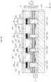
- FIG. 3is a schematic plan view illustrating a portion of the organic EL display panel 10 .
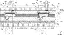
- FIG. 4is a schematic cross-sectional view of A-A in FIG. 3 .
- FIG. 5is a schematic cross-sectional view of B-B in FIG. 3 .
- FIG. 6A , FIG. 6B , FIG. 6C , FIG. 6D , and FIG. 6Eare schematic cross-sectional views illustrating states of processes in manufacturing the organic EL display panel 10 .
- FIG. 7A , FIG. 7B , and FIG. 7Care schematic cross-sectional views illustrating states of processes in manufacturing the organic EL display panel 10 .
- FIG. 8A , FIG. 8B , FIG. 8C , FIG. 8D , FIG. 8E , and FIG. 8Fare schematic cross-sectional views illustrating states of processes in manufacturing the organic EL display panel 10 .
- FIG. 9A and FIG. 9Bare schematic cross-sectional views illustrating states of processes in manufacturing the organic EL display panel 10 .
- FIG. 10is an enlarged plan view of a portion A in FIG. 3 .
- FIG. 11A , FIG. 11B , and FIG. 11Care plan view photographs of the pixel 100 e of the organic EL display panel 10 , captured from above an upper substrate 130 .
- FIG. 12A , FIG. 12B , and FIG. 12Care plan view photographs of the pixel 100 e of the organic EL display panel when emitting light, captured from above the upper substrate.
- FIG. 13is a schematic cross-sectional view at the same position as A-A in FIG. 3 , of an organic EL display panel 10 A pertaining to a modification.
- FIG. 14is a schematic cross-sectional view at the same position as B-B in FIG. 3 , of the organic EL display panel 10 A pertaining to a modification.
- An organic EL display panel pertaining to the present embodimentis an organic EL display panel in which a plurality of pixels are arranged in a row direction and a column direction in a matrix, the organic EL display panel including: a substrate; a plurality of pixel electrode layers arranged in the row direction and the column direction in a matrix on the substrate, the pixel electrode layers including a light-reflective material; a plurality of column banks disposed on the substrate and on the pixel electrode layers, covering row-direction edge portions of the pixel electrode layers, extending in the column direction, arranged side-by-side in the row direction, and defining row-direction edges of self-luminous regions of the pixels; a plurality of row banks disposed on the substrate and on the pixel electrode layers, covering column-direction edge portions of the pixel electrode layers and contact regions of the pixel electrode layers that are for electrically connecting the pixel electrode layers, extending in the row direction, arranged side-by-side in the column direction, and defining column-direction edges of the self-
- a plurality of thin-film transistorsare arranged in the row direction and the column direction in a matrix in the substrate, in positions corresponding to the pixels, wherein sources or drains of the thin-film transistors are connected to the pixel electrode layers via connecting recesses in which portions of the pixel electrode layers in the contact regions are recessed in the direction of the substrate, and in plan view of the substrate, the row light-shielding layers do not overlap with the connecting recesses.
- the light-emitting layersextend continuously in the column direction above the row banks.
- the light-emitting layersare interrupted by the row banks.
- any two of the light-emitting layers disposed in the intervals between the column banks that are adjacent to each other in the row directionemit different colors of light from each other.
- any one of the light-emitting layers interrupted by the row banks in the column directionemits the same color of light along its length in the column direction.
- an upper substrateis disposed above the opposing electrode, the upper substrate including a light-transmissive material, wherein the row light-shielding layers and the column light-shielding layers are disposed in direct contact with the upper substrate.
- an upper substrateis disposed above the opposing electrode, the upper substrate including a light-transmissive material, wherein the row light-shielding layers, the column light-shielding layers, or both the row light-shielding layers and the column light-shielding layers are disposed in direct contact with the upper substrate.
- an upper substrateis disposed above the opposing electrode, the upper substrate including a light-transmissive material, wherein the row light-shielding layers and the column light-shielding layers are disposed in direct contact with the upper substrate.
- the column light-shielding layersare disposed on upper surfaces of the column banks.
- the row light-shielding layersare disposed on upper surfaces of the row banks.
- An organic EL element pertaining to the present embodimentis an organic EL element including: a substrate; a pixel electrode layer disposed on the substrate, the pixel electrode layer including a light-reflective material; banks disposed on the substrate and on the pixel electrode layer, covering edge portions of the pixel electrode layer and a portion of a contact region of the pixel electrode layer, the contact region being for electrically connecting the pixel electrode layer; a light-emitting layer disposed above the pixel electrode layer; an opposing electrode layer disposed above the light-emitting layer, the opposing electrode layer including a light-transmissive material; and a light-shielding layer disposed higher than the pixel electrode layer, the light-shielding layer overlapping the edge portions of the pixel electrode layers and partially overlapping the contact region in plan view of the substrate.
- a method of manufacturing an organic EL display panel pertaining to the present embodimentis a method including: preparing a substrate; disposing a plurality of pixel electrode layers in a row direction and a column direction in a matrix on the substrate, the pixel electrode layers including a light-reflective material; disposing a plurality of column banks on the substrate and on the pixel electrode layers, the column banks covering row-direction edge portions of the pixel electrode layers, extending in the column direction, and arranged side-by-side in the row direction; disposing a plurality of row banks on the substrate and on the pixel electrode layers, the row banks covering column-direction edge portions of the pixel electrode layers, extending in the row direction, and arranged side-by-side in the column direction; disposing a plurality of light-emitting layers above the pixel electrode layers in intervals between adjacent ones of the column banks; disposing an opposing electrode layer above the light-emitting layers, the opposing electrode layer including a light-transmissive material; disposing, higher than the
- the followingdescribes an overall configuration of the display device 1 pertaining to the embodiment, with reference to FIG. 1 .
- the display device 1 pertaining to the present embodimentincludes an organic EL display panel 10 (hereinafter referred to as “display panel 10 ”) and a drive control circuit 20 connected thereto.
- display panel 10organic EL display panel 10
- drive control circuit 20connected thereto.
- the display panel 10is an organic electroluminescence (EL) panel that uses electroluminescence of organic material, in which a plurality of organic EL elements are, for example, arrayed in a matrix.
- the drive control circuit 20comprises four drive circuits 21 , 22 , 23 , 24 and a control circuit 25 .
- the arrangement of circuits of the drive control circuit 20 with respect to the display panel 10 in the display device 1is not limited to the configuration illustrated in FIG. 1 .
- FIG. 2is a schematic circuit diagram showing a circuit configuration in each of the organic EL elements 100 , which correspond to pixels 100 e of the organic EL display panel 10 used in the display device 1 .
- each of the organic EL elements 100 in the pixels 100 eincludes two transistors Tr 1 , Tr 2 , a capacitor C, and an EL element portion EL as a light-emitter.
- the transistor Tr 1is a drive transistor and the transistor Tr 2 is a switching transistor.
- a gate G 2 of the switching transistor Tr 2is connected to a scan line Vscn and a source S 2 is connected to a data line Vdat.
- a drain D 2 of the switching transistor Tr 2is connected to a gate G 1 of the drive transistor Tr 1 .
- a drain D 1 of the drive transistor Tr 1is connected to a power supply line Va, and a source S 1 is connected to a pixel electrode layer (anode) of the EL element portion EL.
- An opposing electrode layer (cathode) of the EL element portion ELis connected to a ground line Vcat.
- the capacitor Cconnects the drain D 2 of the switching transistor Tr 2 , the gate G 1 of the drive transistor Tr 1 , and the power supply line Va.
- the organic EL elements 100 in the pixels 100 e that each have the circuit configuration shown in FIG. 2are disposed in a matrix to form a display region.
- FIG. 3is a schematic plan view illustrating a portion of a display panel pertaining to the embodiment.
- the display panel 10is an organic EL display panel that uses electroluminescence of an organic compound, and has a top-emission configuration emitting light from an upper surface thereof, in which a plurality of the organic EL elements 100 are arranged in a matrix on a substrate 100 x (TFT substrate) on which thin film transistors (TFT) are disposed.
- TFT substratesubstrate 100 x
- TFTthin film transistors
- self-luminous regions 100 aare formed, which are regions that emit light by using an organic compound.
- the self-luminous regions 100 aare in three varieties, a region that emits red light 100 a R, a region that emits green light 100 a G, and a region that emits blue light 100 a B (hereinafter, when 100 a R, 100 a G, 100 a B are not distinguished they are referred to by “ 100 a ”).
- Three self-luminous regions 100 a R, 100 a G, 100 a B lined up in a row directionare a set that make up one pixel in a color display.
- a plurality of pixel electrode layers 119are arranged in a matrix on the substrate 100 x .
- the pixel electrode layers 119each have a rectangular shape in plan view and include a light-reflective material.
- each bank of column banks 122 Yextending in a column direction (direction 3 Y in the drawings) and the column banks 122 Y being arranged side-by-side in a row direction.
- Each of the column banks 122 Yis disposed above row-direction edge portions of two of the pixel electrode layers 119 that are adjacent in the row direction.
- the display panel 10has a configuration in which the column banks 122 Y and the intervals 122 z alternate in the row direction.
- the intervalsare sub-divided into red intervals 122 z R that correspond to the self-luminous regions 100 a R, green intervals 122 z G that correspond to the self-luminous regions 100 a G, and blue intervals 122 z B that correspond to the self-luminous regions 100 a B (hereinafter, when the red intervals 122 z R, the green intervals 122 z G, and the blue intervals 122 v B are not distinguished they are collectively referred to as the intervals 122 z ).
- Row-direction edges of the self-luminous regions 100 aare defined by row-direction edges of the column banks 122 Y.
- each bank of row banks 122 Xextends in a row direction (direction X in FIG. 3 ) and the row banks 122 X are arranged side-by-side in a column direction.
- Each of the row banks 122 Xis disposed above column-direction edges of two adjacent ones of the pixel electrode layers 119 that are adjacent in the column direction.
- regions in which the row banks 122 X are disposedbecome not-self-luminous regions 100 b .
- edges of the self-luminous regions 100 a in the column directionare defined by column-direction edges of the row banks 122 X.
- connection recesses 119 cthat connect the pixel electrode layers 119 to the sources S 1 of the TFTs via connecting electrode layers 117 , and contact regions 119 b (contact windows) on the pixel electrode layers 119 for electrically connecting the pixel electrode layers 119 .
- the column banks 122 Y and the row banks 122 Xare orthogonal to each other, and the row banks 122 X overlap with the self-luminous regions 100 a in the column direction (hereinafter, when the row banks 122 X and the column banks 122 Y are not distinguished, they are referred to as the banks 122 ). Further, above the pixel electrode layers 119 , column light-shielding layers 129 Y are disposed that overlap with row-direction edge portions of the pixel electrode layers 119 , and row light-shielding layers 129 X are disposed that overlap with column-direction edge portions of the pixel electrode layers 119 and do not overlap with portions of the contact regions 119 b.
- FIG. 4is a schematic cross-sectional view of A-A in FIG. 3 .
- FIG. 5is a schematic cross-sectional view of B-B in FIG. 3 .
- the display panel 10 pertaining to the present embodimentis a top-emission type of organic EL display panel.
- the substrate 100 xTFT substrate
- On the substrate 100 xis disposed an organic EL element portion.
- gate electrodes 101 , 102are disposed on a lower substrate 100 p
- a gate insulating layer 103is disposed covering the gate electrodes 101 , 102 and a surface of the substrate 100 x .
- Channel layers 104 , 105 corresponding to the gate electrodes 101 , 102are disposed on the Rate insulating layer 103 .
- a channel protection layer 106is disposed covering the channel layers 104 , 105 and a surface of the gate insulating layer 103 .
- source electrodes 107 and drain electrodes 108are disposed with intervals therebetween, corresponding to the gate electrodes 101 and the channel layers 104 .
- source electrodes 110 and drain electrodes 109are disposed with intervals therebetween, corresponding to the gate electrodes 102 and the channel layers 105 .
- Source lower electrodes 111 , 115 and drain lower electrodes 112 , 114are disposed under the source electrodes 107 , 110 and the drain electrodes 108 , 109 .
- source lower electrodes 111 and the drain lower electrodes 112are in contact with the channel layers 104 .
- drain lower electrodes 114 and the source lower electrodesare in contact with the channel layers 105 .
- drain electrodes 108 and the gate electrodes 102are connected to each other by connector plugs 113 , which penetrate the gate insulating layer 103 and the channel protection layer 106 .
- the gate electrodes 101correspond to the gate G 2 in FIG. 2
- the source electrodes 107correspond to the source S 2 in FIG. 2
- the drain electrodes 108correspond to the drain D 2 in FIG. 2
- the gate electrodes 102correspond to the gate G 1 in FIG. 1
- the source electrodes 110correspond to the source S 1 in FIG. 1
- the drain electrodes 109correspond to the drain D 1 in FIG. 1 .
- the switching transistor Tr 2is formed at a Y axis direction left-hand side of FIG. 4
- the drive transistor Tr 1is formed further right, in the Y axis direction of FIG. 4 .
- the configuration described aboveis merely an example, and the transistors Tr 1 , Tr 2 may be configured as top-gate type, bottom-gate type, channel etch type, etch stop type, etc., transistors, and are not limited to the configuration illustrated in FIG. 4 .
- a passivation layer 116is disposed covering the source electrodes 107 , 110 , the drain electrodes 108 , 109 , and the channel protection layer 106 .
- Contact holes 116 aare formed in the passivation layer 116 above portions of the source electrodes 110 , and connecting electrode layers 117 are layered to follow the contours of the contact holes 116 a.
- lower portions of the connecting electrode layers 117are connected to the source electrodes 110 and parts of upper portions of the connecting electrode layers 117 are on the passivation layer 116 .
- An interlayer insulating layer 118is disposed on and covering the connecting electrode layers 117 and the passivation layer 116 .
- one of the pixel electrode layers 119is disposed on the interlayer insulating layer 118 .
- the pixel electrode layers 119supply carriers to the light-emitting layers 123 ; for example, when functioning as anodes they supply holes to the light-emitting layers 123 .
- the panel 10is a top-emission type, and therefore the pixel electrode layers 119 are Might-reflective.
- Each of the pixel electrode layers 119has a flat rectangular shape.
- the pixel electrode layers 119are disposed on the substrate 100 x with intervals ⁇ X therebetween in the row direction and intervals ⁇ Y therebetween in the column direction in the intervals 122 z .
- the connecting recesses 119 c of the pixel electrode layers 119are connected to the connecting electrode layers 117 via contact holes 118 a formed in the connecting electrode layers 117 and the interlayer insulating layer 118 .
- the connecting electrode layers 117via the connecting electrode layers 117 , the pixel electrode layers 119 and the source S 1 of the TFT are connected.
- the connecting recesses 119 care concavities in portions of the pixel electrode layers 119 , recessed towards the substrate 100 x , composed of bottom portions 119 c 1 and inner peripheral surface portions 119 c 2 .
- Surfaces of the inner peripheral surface portions 119 c 2are preferably conical (tapered) inclined slopes. This is in order that a portion of light that leaks in the column direction from the light-emitting layers 123 can be reflected upwards.
- Hole injection layers 120 and hole transport layers 121are disposed in this order on the pixel electrode layers 119 , the hole transport layers 121 being in contact with the hole injection layers 120 .
- the hole injection layers 120 and the hole transport layers 121have the function of transporting holes injected from the pixel electrode layers 119 to the light-emitting layers 123 .
- the banks 122are disposed covering edges of the pixel electrode layers 119 , the hole injection layers 120 , and the hole transport layers 121 .
- the banks 122include an insulative material.
- the banks 122include column banks 122 Y that extend in the column direction and are lined up in the row direction, and row banks 122 X that extend in the row direction and are lined up in the column direction.
- the column banks 122 Y and the row banks 122 Xform a lattice shape.
- the column banks 122 Yprevent flow in the row direction of ink containing an organic compound that is a material of the light-emitting layers 123 , and define row-direction edges of the light-emitting layers 123 .
- the column banks 122 Yare disposed above edge portions 119 a 3 , 119 a 4 in the row direction of the pixel electrode layers 119 , covering portions of the pixel electrode layers 119 .
- the row banks 122 Xare for suppressing flow in the column direction of ink containing the organic compound that is a material of the light-emitting layers 123 .
- the row banks 122 Xare disposed above edge portions 119 a 1 , 119 a 2 in the column direction of the pixel electrode layers 119 , covering portions of the pixel electrode layers 119 .
- the row banks 122 Xdefine edges of self-luminous regions of pixels in the column direction, as described above.
- the row banks 122 Xlinearly extend in the row direction and a cross-section taken parallel to the column direction shows a trapezoidal shape that tapers upwards.
- the row banks 122 Xpass through the column banks 122 Y, following the row direction that is perpendicular to the column direction.
- the row banks 122 Xhave upper surfaces that are lower than upper surfaces of the column banks 122 Y. Thus, openings corresponding to the self-luminous regions 100 a are formed by the rows banks 122 X and the column banks 122
- the display panel 10has a configuration in which the column banks 122 Y and the intervals 122 z alternate in the row direction.
- the light-emitting layers 123are formed in the intervals 122 z , which are defined by the column banks 122 Y, and extend in the column direction.
- the light-emitting layers 123 that emit light of the following colorsare disposed in the red intervals 122 z R that correspond to the self-luminous regions 100 a R, the green intervals 122 z G that correspond to the self-luminous regions 100 a G, and the blue intervals 122 z B that correspond to the self-luminous regions 100 a B.
- the light-emitting layers 123are layers including organic compounds and have a function of emitting light due to recombination of holes and electrons therein. In the intervals 122 z , the light-emitting layers 123 extend linearly in the column direction.
- the light-emitting layers 123emit light only from portions thereof that are supplied with carriers from the pixel electrode layers 119 , and therefore electroluminescence of organic compounds does not occur in areas in which the row banks 122 X are present, the row banks 122 X being inter-layer insulators.
- the light-emitting layers 123emit light only from portions where the row banks 122 X are not present, these portions are the self-luminous regions 100 a , and edges of the self-luminous regions 100 a in the column direction are defined by edges of the row banks 122 X in the column direction.
- the not-self-luminous regions 100 bare regions obtained by projecting the row banks 122 X in a plan view direction.
- the light-emitting layers 123are disposed on upper surfaces of the hole transport layers 121 in the self-luminous regions 100 a and on upper and side surfaces of the row banks 122 X in the not-self-luminous regions 100 b.
- the light-emitting layers 123extend into the not-self-luminous regions 100 b that are contiguous, and not only the self-luminous regions 100 a .
- ink applied to the self-luminous regions 100 acan flow in the column direction via ink applied to the not-self-luminous regions 100 b , and film thickness thereof can be planarized between pixels in the column direction.
- flow of inkis appropriately suppressed by the row banks 122 X. Accordingly, large irregularities in film thickness in the column direction are unlikely to occur, and irregularity in luminance of each pixel is improved.
- Electron Transport Layer 124
- the electron transport layer 124is disposed on the banks 122 and on the light-emitting layers 123 in the openings defined by the banks 122 . Further, in the present example, the electron transport layer 124 is also disposed on the column banks 122 Y that are exposed above the light-emitting layers 123 . The electron transport layer 124 has the function of transporting electrons injected from the opposing electrode layer 125 to the light-emitting layers 123 .
- the opposing electrode layer 125is disposed on the electron transport layer 124 , covering the electron transport layer 124 .
- the opposing electrode layer 125is disposed continuously across an entire surface of the display panel 10 and may be connected to bus bar wiring per pixel, or per plurality of pixels (not illustrated).
- the opposing electrode layer 125creates electrical paths by opposing the pixel electrode layers 119 , sandwiching the light-emitting layers 123 , and supplies carriers to the light-emitting layers 123 .
- the opposing electrode layer 125functions as a cathode, it supplies electrons to the light-emitting layers 123 .
- the opposing electrode 125conforms to the surface of the electron transport layer 124 and is a common electrode across the light-emitting layers 123 .
- the opposing electrode 125uses a light-transmissive electrically conductive material, because the display panel 10 is a top-emission type.
- a light-transmissive electrically conductive materialfor example, indium tin oxide (ITO) or indium zinc oxide (IZO) may be used.
- ITOindium tin oxide
- IZOindium zinc oxide
- silver (Ag) or aluminium (Al)may be used as a thin film electrode.
- the sealing layer 126is disposed on the opposing electrode layer 125 , covering the opposing electrode layer 125 .
- the sealing layer 126is for suppressing degradation of the light-emitting layer 123 due to contact with moisture, air, etc.
- the sealing layer 126is disposed across an entire surface of the display panel 10 , covering an upper surface of the opposing electrode layer 125 .
- a light-transmissive materialis used such as silicon nitride or silicon oxynitride, because the display panel 10 is a top-emission type.
- the sealing layer 126 in the Z axis directionis disposed a CF substrate 131 , joined to the sealing layer 126 by the joining layer 127 .
- the CF substrateincludes the upper substrate 130 and color filter layers 128 and the light-shielding layers 129 below the upper substrate in the Z axis direction.
- the joining layer 127has a function of joining a back panel, in other words each layer from the substrate 100 x to the sealing layer 126 , to the CF substrate 131 , and a function of preventing each layer from being exposed to moisture or air.
- the CF substrate 131is disposed on and joined to the joining layer 127 .
- the CF substrate 131includes the upper substrate 130 , the color filter layers 128 , and the shielding layers 129 .
- a light-transmissive materialis used such as cover glass or light-transmissive resin film, because the display panel 10 is a top-emission type. Further, the upper substrate 130 can improve stiffness of the display panel 10 and prevent penetration of the display panel 10 by moisture or air.
- Color filter layers 128are disposed under the upper substrate 130 at locations corresponding to the self-luminous regions 100 a of each color of pixel.
- the color filter layers 128are light-transmissive layers for transmitting visible light of wavelengths corresponding to red, green, and blue, and have a function of transmitting light emitted from each color of pixel and correcting the chromaticity thereof.
- above the self-luminous regions 100 a R in the red intervals 122 z R, the self-luminous regions 100 a G in the green intervals 122 z G, and the self-luminous regions 100 a B in the blue intervalsare disposed red color filter layers 128 R, green color filter layers 128 G, and blue color filter layers 128 B, respectively.
- the color filter layers 128are formed, for example, by a process of applying ink containing a color filter material and a solvent to the upper substrate 130 , the upper substrate 130 being made from cover glass that has openings corresponding to pixels in a matrix for forming color filters.
- the light-shielding layer 129is disposed under the upper substrate 130 in locations corresponding to boundaries between the self-luminous regions 100 a of pixels.
- the light-shielding layer 129is a black resin layer for preventing transmission of visible light in wavelengths corresponding to red, green, and blue.
- the light-shielding layer 129is composed of a resin material that includes black pigment that has excellent light-absorbing and light-shielding properties.
- the light-shielding layer 129is intended to prevent entry of external light into the display panel 10 , prevent visibility of internal parts through the upper substrate 130 , and improve contrast of the display panel 10 to suppress glare from external light.
- Glare from external lightis a phenomenon caused by external light entering the display panel 10 from above the upper substrate 130 , being reflected at the pixel electrode layers 119 , and being emitted from the upper substrate 130 .
- the light-shielding layer 129has a function of preventing, by blocking a portion of light emitted from a pixel that leaks to adjacent pixels, boundaries between pixels becoming unclear, and has a function of increasing color purity of light emitted from pixels.
- the light-shielding layer 129includes column light-shielding layers 129 Y that extend in the column direction and are lined up in the row direction, and row light-shielding layers 129 X that extend in the row direction are lined up in the column direction, the column light-shielding layers 129 Y and the row light-shielding layers 129 X forming a matrix.
- the column light-shielding layers 129 Yare disposed in positions overlapping row-direction edge portions 119 a 3 , 119 a 4 of the pixel electrode layers 119 (hereinafter, when 119 a 3 and 119 a 4 are not distinguished, they are referred to as “edge portions 119 a ”), as illustrated in FIG. 5
- the row light-shielding layers 129 Xare disposed in positions overlapping column-direction edge portions 119 a 1 , 119 a 2 of the pixel electrode layers 119 (hereinafter, when 119 a 1 and 119 a 2 are not distinguished, they are referred to as “edge portions 119 a ”), as illustrated in FIG. 4 .
- a width WX in the row direction of the column light-shielding layers 129 Yis greater than a distance ⁇ X in the row direction between adjacent ones of the pixel electrode layers 119
- a width WY in the column direction of the row light-shielding layers 129 Xis greater than a distance ⁇ Y in the column direction between adjacent ones of the pixel electrode layers 119 .
- the self-luminous regions 100 a and the not-self-luminous regions 100 bare arranged alternating with each other in the column direction.
- regions where row banks 122 X overlap with portions of the pixel electrode layers 119 nearest the edge portions 119 a 2 of the pixel electrode layers 119 on the side of the connecting recesses 119 care defined as contact regions 119 b of the pixel electrode layers 119 for electrically connecting the pixel electrode layers 119
- the row light-shielding layers 129 Xare disposed in positions that do not overlap with portions of the contact regions 119 b of the pixel electrode layers 119 , as illustrated in FIG. 4 .
- light emission efficiency of the organic EL elements 100is improved. The improvement in light emission efficiency is described later.
- a glass substratefor example, a glass substrate, a silica glass substrate, a metal substrate such as molybdenum sulfide, copper, zinc, aluminium, stainless steel, magnesium, iron, nickel, gold, or silver, a semiconductor substrate based on gallium arsenide, or a plastic substrate can be used.
- a metal substratesuch as molybdenum sulfide, copper, zinc, aluminium, stainless steel, magnesium, iron, nickel, gold, or silver
- a semiconductor substrate based on gallium arsenidefor example, a glass substrate, a silica glass substrate, a metal substrate such as molybdenum sulfide, copper, zinc, aluminium, stainless steel, magnesium, iron, nickel, gold, or silver, a semiconductor substrate based on gallium arsenide, or a plastic substrate can be used.
- any thermoplastic or thermosetting resinmay be used.
- polyolefinsuch as polyethylene, polypropylene, ethylene-propylene copolymer, ethylene-vinyl acetate copolymer (EVA), cyclic polyolefin, modified polyolefin, polyvinyl chloride, polyvinylidene chloride, polystyrene, polyamide, polyimide (PI), polyamide-imide, polycarbonate, poly-(4-methyl-1-pentene), ionomer, acrylic resin, polymethyl methacrylate, styrene acrylonitrile copolymer (SAN), butadiene styrene copolymer, ethylene vinyl alcohol (EVOH), polyethylene terephthalate (PET), polybutylene terephthalate, polyethylene naphthalate (PEN), polyester such as polycyclohexylenedimethylene terephthalate (PCT), polyether, polyether ketone, polyether
- a layered body of copper (Cu) and molybdenum (Mo)can be used, for example.
- the material of the gate electrodes 101 , 102is not limited to this example, and other metal material may be used.
- the gate electrode layer 103As a material of the gate electrode layer 103 , as long as the material is electrically insulating a known organic material or inorganic material can be used, such as silicon oxide (SiO 2 ) or silicon nitride (SiNx), for example.
- a known organic material or inorganic materialsuch as silicon oxide (SiO 2 ) or silicon nitride (SiNx), for example.
- an oxide semiconductor including at least one material selected from indium (In), gallium (Ga), and zinc (Zn)can be used.
- silicon oxynitrideSiON
- silicon nitrideSiN
- aluminium oxideAlOx
- layered bodies of copper-manganese (CuMn), copper (Cu), and molybdenum (Mo)can be used, for example.
- source lower electrodes 111 , 115 and the drain lower electrodes 112 , 114can be configured using the same materials as the source electrodes 107 , 110 and the drain electrodes 108 , 109 .
- the passivation layer 116may use silicon oxide (SiO2), silicon nitride (SiN), or silicon oxynitride (SiON).
- layered bodies of molybdenum (Mo), copper (Cu), and copper-manganese (CuMn)may be used (Mo approx. 20 nm, Cu approx. 375 nm, and CuMn approx. 65 nm).
- thickness of each layeris not limited to this example, and thickness of a molybdenum (Mo) layer may be in a range from 5 nm to 200 nm, thickness of a copper (Cu) layer may be in a range from 50 nm to 800 nm, and thickness of a copper-manganese (CuMn) layer may be in a range from 5 nm to 200 nm.
- Material used in the connecting electrode layers 117is not limited to this example, and may be selected from appropriate electrically conductive materials.
- the interlayer insulating layeris formed from an organic compound such as polyimide, polyamide, or an acrylic-based resin, and has a thickness of approx. 4000 nm. However, thickness is not limited to this example, and may be in a range from 2000 nm to 8000 nm, for example.
- the pixel electrode layers 119are made from metal material. In the case of the display panel 10 pertaining to the present embodiment, surfaces of the pixel electrode layers 119 are preferably highly reflective. In the display panel 10 pertaining to the present embodiment, the pixel electrode layers 119 may each be a structure in which a plurality of layers are selected from metal layers, alloy layers, and light-transmissive electrically-conductive layers.
- a metal layera metal material including silver (Ag) or aluminium (Al) may be used, for example.
- As an alloy layersilver palladium copper alloy (APC), silver palladium gold alloy (ARA), molybdenum chromium alloy (MoCr), or nickel chromium alloy (NiCr) may be used, for example.
- As a light-transmissive electrically-conductive materialindium tin oxide (ITO) or indium zinc oxide (IZO) may be used, for example.
- the hole injection layers 120are layers made from an oxide of silver (Ag), molybdenum (Mo), chromium (Cr), vanadium (V), tungsten (W), nickel (Ni), or iridium (Ir), or an electrically conductive polymer such as poly(3,4-ethylenedioxythiophene) polystyrene sulfonate (PEDOT:PSS).
- Momolybdenum
- Crchromium
- Vvanadium
- Wtungsten
- Ninickel
- Iriridium
- PEDOTpoly(3,4-ethylenedioxythiophene) polystyrene sulfonate
- the hole injection layers 120being configured from a transition metal oxide, a plurality of energy levels can be obtained from a plurality of valences, and as a result hole injection becomes easier and drive voltage can be decreased.
- a high molecular compoundsuch as polyfluorene, a derivative thereof, poly arylamine, or a derivative thereof may be used, for example.
- the banks 122are formed from an organic material such as a resin and have insulating properties.
- organic materialsacrylic-based resin, polyimide-based resin, or novolac-type phenolic resin may be used.
- the banks 122preferably have organic solvent resistance. Further, during the production process, the banks 122 are subjected to an etching process, a baking process, etc., and therefore the banks 122 are preferably formed from a material having a high resistance to deformation, deterioration, etc., during such processes. Further, in order to impart water repellency to surfaces of the banks 122 , the surfaces may be fluorine-treated. Further, the banks 122 may be formed by using material that contains fluorine.
- structure of the banks 122is not limited to the single-layer structure illustrated in FIG. 4 , and may be a multi-layered structure having two or more layers.
- each layermay be a combination of the materials above, or each layer may be an inorganic material and an organic material.
- the light-emitting layers 123have a function of emitting light generated by an excited state due to recombination of holes and electrons injected thereto.
- As a material used in forming the light-emitting layers 123it is necessary to use a light emitting organic material that can form a thin film by using a wet printing method.
- a phosphorescent materialis preferably used, such as an oxinoid compound, perylene compound, coumarin compound, azacoumarin compound, oxazole compound, oxadiazole compound, perinone compound, pyrrolo-pyrrole compound, naphthalene compound, anthracene compound, fluorene compound, fluoranthene compound, tetracene compound, pyrene compound, coronene compound, quinolone compound and azaquinolone compound, pyrazoline derivative and pyrazolone derivative, rhodamine compound, chrysene compound, phenanthrene compound, cyclopentadiene compound, stilbene compound, diphenyiquinone compound, styryl compound, butadiene compound, dicyanomethylene pyran compound, dicyanomethylene thiopyran compound, fluorescein compound, pyryliurn compound, thia
- the electron transport layer 124may be formed using an oxadiazole derivative (OXD), a triazole derivative (TAZ), or a phenanthroline derivative (BCP, Bphen), for example.
- OXDoxadiazole derivative
- TEZtriazole derivative
- BCPphenanthroline derivative
- the opposing electrode layer 125may be formed from indium tin oxide (ITO) or indium zinc oxide (IZO), for example. Further, silver (Ag) or aluminium (Al) may be used as a thin film electrode.
- ITOindium tin oxide
- IZOindium zinc oxide
- silver (Ag) or aluminium (Al)may be used as a thin film electrode.
- the sealing layer 126has a function of suppressing exposure of organic layers such as the light-emitting layers 123 to moisture and air, and may be formed from a light-transmissive material such as silicon nitride (SiN) or silicon oxynitride (SiON). Further, on a layer formed from a material such as silicon nitride (SiN) or silicon oxynitride (SiON), a sealing resin layer composed of resin material such as acrylic resin or silicone resin may be provided.
- a light-transmissive materialsuch as silicon nitride (SiN) or silicon oxynitride (SiON).
- the sealing layer 126in the case of the display panel 10 pertaining to present embodiment, which is a top-emission type, is necessarily formed from a light-transmissive material.
- the joining layer 127may be made from a resin adhesive, for example.
- the joining layer 127may be made from a light-transmissive resin material such as acrylic resin, silicone resin, or epoxy resin.
- a light-transmissive materialmay be used such as a glass substrate, silica glass substrate, or plastic substrate, for example.
- a known resin materialmay be used (examples of commercial products are color resists manufactured by JSR Co., Ltd).
- a resin material including an ultraviolet light curable resin (for example, an ultraviolet light curable acrylic resin) material as a main component and a black pigment as an additional componentmay be used.
- a black pigmenta light-shielding material such as a carbon black pigment, titanium black pigment, metal oxide pigment, or organic pigment may be used.
- the followingdescribes a method of manufacturing the display device 10 , with reference to drawings from FIG. 6A to FIG. 9B .
- a substrate 100 x 0is prepared on which the source electrodes 107 , 110 and the drain electrodes 108 , 109 are formed.
- the substrate 100 x 0can be manufactured by using a known TFT manufacturing method.
- the passivation layer 116is layered on the source electrodes 107 , 110 , the drain electrodes 108 , 109 , and the channel protection layer 106 , by using a plasma CVD method or sputtering, for example.
- the contact holes 116 aare opened in the passivation layer 116 at locations above the source electrodes 110 , by using a dry etching method. Bottoms of the contact holes 116 a are formed to expose surfaces 110 a of the source electrodes 110 .
- the connecting electrode layers 117are formed conforming to the contours of the side walls of the contact holes 116 a in the passivation layer 116 . Upper portions of the connecting electrode layers 117 are disposed on the passivation layer 116 . Sputtering may be used to forming the connecting electrode layers 117 , for example. After forming a metal film, patterning is performed by using photolithography and wet etching.
- interlayer insulating layer 118is formed covering the connecting electrode layers 117 and the passivation layer 116 , by applying the organic material and planarizing the surface thereof.
- contact holesare opened in the interlayer insulating layer 118 above the connecting electrode layers 117 , and the pixel electrode layers 119 are formed.
- Forming the pixel electrode layers 119comprises forming a metal film by using a method such as sputtering or vacuum deposition, followed by patterning by using photolithography and etching.
- the pixel electrode layers 119are electrically connected to the connecting electrode layers 117 .
- the hole injection layers 120 and the hole transport layers 121are formed on the pixel electrode layers 119 and the banks 122 are formed covering edge portions of the hole transport layers 121 .
- the banks 122surround the openings 122 a that define pixels, surfaces of the hole transport layers 121 being exposed by the openings 122 a.
- the hole injection layers 120 and the hole transport layers 121are formed by forming films from a metal oxide (for example, tungsten oxide) by using sputtering, then patterning to each pixel by using photolithography and etching.
- a metal oxidefor example, tungsten oxide
- the banks 122are formed by first forming a layer composed of a bank 122 material (for example, a photosensitive resin material) on the hole transport layers 121 by using a spin coating method or similar, Subsequently, the resin layer is patterned to form the openings 122 a . Forming the openings 122 a includes arranging a mask above the resin layer, exposure to light, and developing.
- a bank 122 materialfor example, a photosensitive resin material
- the light-emitting layers 123 and the electron transport layer 124are formed in this order.
- Forming the light-emitting layers 123includes applying ink that contains component material into the openings 122 a defined by the banks 122 , and subsequently baking.
- the electron transport layer 124is formed by sputtering or similar.
- the opposing electrode layer 125 and the sealing layer 126are formed in this order, covering the electron transport layer 124 .
- the opposing electrode layer 125 and the sealing layer 126are formed by using CVD or sputtering, for example.
- Material of the light-shielding layer 129including an ultraviolet-curable resin (for example, an ultraviolet-curable acrylic resin) as a primary component and a black pigment added thereto is dispersed in a solvent, adjusted to a light-shielding layer paste 129 X, and applied to one surface of the upper substrate 130 , which is light-transmissive ( FIG. 8A ).
- an ultraviolet-curable resinfor example, an ultraviolet-curable acrylic resin
- a black pigment added theretois dispersed in a solvent, adjusted to a light-shielding layer paste 129 X, and applied to one surface of the upper substrate 130 , which is light-transmissive ( FIG. 8A ).
- the light-shielding layer paste 129 Xis dried, and after the solvent has to some extent vaporized a pattern mask PM 1 that has predefined openings is overlaid on the light-shielding layer paste 129 X and irradiated with ultraviolet light from above ( FIG. 8B ).
- the light-shielding layer paste 129 Xis baked, the pattern mask PM 1 and uncured BM paste 120 X are removed and developed, and, when cured, the light-shielding layer 129 that is rectangular in cross-section is completed ( FIG. 8C ).
- a paste 129 Xis applied on a surface of the upper substrate 130 on which the light-shielding layer 129 is complete.
- the paste 128 Xis material of the color filter layers 128 , a primary component of which is ultraviolet-curable resin, dispersed in a solvent. After application, an amount of the solvent is removed, and a predefined pattern mask PM 2 is overlaid thereon and irradiated with ultraviolet light ( FIG. 8D ).
- FIG. 8D and FIG. 8Eare repeated for color filter materials of each color to form color filter layers 128 (R) and color filter layers 128 (B).
- a commercial color filter productmay be used instead of using the paste 128 X.
- the CF substrate 131is formed.
- material of the joining layer 127which is primarily a light-transmissive ultraviolet-curable resin such as acrylic resin, silicone resin, or epoxy resin, is applied to a rear panel, which consists of each layer from the substrate 100 x to the sealing layer 126 ( FIG. 9A ).
- the applied materialis irradiated by ultraviolet light and the rear panel and the CF substrate 131 are then bonded to each other, maintaining their positional relationship with each other. At this time, care is taken to ensure that no gas enters between the rear panel and the CF substrate 131 . Subsequently, both substrates are baked and sealed, completing the organic EL display panel 1 ( FIG. 9B ).
- FIG. 10is an enlarged plan view of a portion A in FIG. 3 .
- the self-luminous regions 100 a and the not-self-luminous regions 100 bare arranged alternating with each other in the column direction.
- the row light-shielding layers 129 X, as shown in FIG. 4are disposed in positions that do not overlap with portions of the contact regions 119 b.
- the organic EL elements 100only portions of the light-emitting layers 123 that are supplied carriers from the pixel electrode layers 119 emit light, and in the not-self-luminous regions 100 b where the row banks 122 X are present, which are inter-layer insulators, electroluminescence of organic compounds does not occur.
- light emitted from the self-luminous regions 100 a of the light-emitting layers 123is partially transmitted in all directions within the light-emitting layers 123 , and therefore light that leaks in the column direction from the light-emitting layers 123 is transmitted into the row banks 122 X that are adjacent, into the not-self-luminous regions 100 b . A portion of such light is reflected upwards at the contact regions 119 b of the pixel electrode layers 119 in the not-self-luminous regions 100 b.
- the column light-shielding layers 129 Yare disposed in positions overlapping the row-direction edge portions 119 a 3 , 119 a 4 of the pixel electrode layers 119
- the row light-shielding layers 129 Xare disposed in positions overlapping the column-direction edge portions 119 a 1 , 119 a 2 of the pixel electrode layers 119 .
- upper surfaces of the pixel electrode layers 119are smooth because they are formed by a process such as sputtering or vacuum deposition, and external light glare from upper surfaces other than the edge portions 119 a of the pixel electrode layers 119 is not as visible as from the edge portions 119 a .
- the edge portions 119 a of the pixel electrode layers 119are formed by patterning by etching, and therefore edge surfaces of the edge portions 119 a are rougher than the upper surfaces and the edge surfaces become inclined away from the vertical to form trapezoidal shapes.
- irregular reflectionoccurs when external light is incident on the edge portions 119 a of the pixel electrode layers 119 , which are finely patterned in all directions as internal surfaces of the display panel. Light reflected in all directions that is incident on the eyes of an observer is recognized as glare on the surface of the display panel, and becomes a factor in degradation of quality of a displayed image.
- the light-shielding layer 129is disposed above the edge portions 119 a of the pixel electrode layers 119 , and therefore can prevent direct incidence of external light on the edge portions 119 a of the pixel electrode layers 119 as well as interrupt emission of light reflected at the edge portions 119 a , Thus, external light glare on the display panel 10 is effectively suppressed.
- the light-shielding layer 129has a function of preventing boundaries between pixels becoming unclear by blocking a portion of light emitted from a pixel that leaks to adjacent pixels, and has a function of increasing color purity of light emitted from pixels.
- the width WX in the row direction of the column light-shielding layers 129 Yis greater than the distance ⁇ X in the row direction between adjacent ones of the pixel electrode layers 119
- the width WY in the column direction of the row light-shielding layers 129 Xis greater than the distance ⁇ Y in the column direction between adjacent ones of the pixel electrode layers 119 .
- the distance ⁇ X and the distance ⁇ Y between the pixel electrode layers 119are determined by the accuracy of etching in a manufacturing process of patterning the pixel electrode layers 119 , and are equivalent to each other.
- the width WX in the row direction of the column light-shielding layers 129 Y and the width WY in the column direction of the row light-shielding layers 129 Xcan be made equivalent to each other, and therefore a decrease in color purity of light emitted from pixels does not occur when the decrease in color purity would be caused by color mixing between adjacent pixels when pixel boundaries become unclear as a result of emitted light leaking to adjacent pixels when the row light-shielding layers 129 X are not above portions of the not-self-luminous regions 100 b.
- Lighting testswere performed on the display panel 10 incorporating the organic EL elements 100 and luminance was measured.
- FIG. 11A , FIG. 11B , and FIG. 11Care photographs captured from above the upper substrate 130 , showing the pixels 100 e of the display panel it) in plan view.
- FIG. 11Ashows one of the self-luminous regions 100 a and one of the not-self-luminous regions 100 b of one of the organic EL elements 100 in one of the red intervals 122 z R
- FIG. 11Bshows one of the green intervals 122 z G
- FIG. 11Cshows one of the blue intervals 122 z B.
- FIG. 12A , FIG. 12B , and FIG. 12Care photographs captured from above the upper substrate 130 , showing the pixels 100 e of the display panel 10 in plan view.
- FIG. 12A , FIG. 12B , and FIG. 12Cshow the same pixels shown in FIG. 11A , FIG. 11B , and FIG. 11C , in a state of emitting light.
- the red intervals 122 z R, the green intervals 122 z G, and the blue intervals 122 z Bit was confirmed that a small amount of luminance was obtained from the not-self-luminous regions 100 b .
- Luminance per unit area of the not-self-luminous regions 100 b of each of the intervalswas approximately 8% of luminance per unit area of the self-luminous regions 100 a of the same intervals.
- the area of the not-self-luminous region 100 bis approximately 20% of the area of the self-luminous region 100 a , and therefore an increase in luminance of approximately 1.6% (0.2 ⁇ 0.08) was confirmed over a conventional configuration for which light is extracted from only the self-luminous region 100 a , When viewed quantitatively, this is considered to be a sufficiently significant amount for a rate of improvement in element levels of luminance.
- the connecting recesses 119 care concavities in portions of the pixel electrode layers 119 , recessed towards the substrate 100 x , composed of bottom portions 119 c 1 and inner peripheral surface portions 119 c 2 .
- Surfaces of the inner peripheral surface portions 119 c 2are conical inclined slopes.
- the row light-shielding layers 129 Xdo not overlap with the connecting recesses 119 c of the pixel electrode layers 119 , which are for connecting thin film transistor sources and the pixel electrode layers 119 .
- Embodimentdescribes the display panel 10 pertaining to the present embodiment, but the present invention is not limited to the embodiment described above, except for essential characteristic features thereof.
- configurations obtained by applying various modifications that could occur to a person having ordinary skill in the art or configurations of the embodiment implementing any combination of components and functions that do not depart from the scope of the present inventionare included in the scope of the present invention.
- the followingdescribes modifications of the display panel 10 as examples of such configurations.
- the CF substrate 131 including the row light-shielding layers 129 X and the column light-shielding layers 129 Yis disposed on and attached to the rear panel that comprises each layer from the substrate 100 x to the sealing layer 126 ,
- the row light-shielding layers 129 X and the column light-shielding layers 129 Ymay be directly disposed on the rear panel.
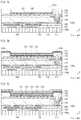
- FIG. 13 and FIG. 14are schematic cross-sectional views at the same positions as A-A and B-B in FIG. 3 , of an organic EL display panel 10 A pertaining to this modification.
- the row light-shielding layers 129 X and the column light-shielding layers 129 Yare not formed on the upper substrate 130 .
- Light-shielding layers 129 YAare disposed on the sealing layer 126 above peaks 122 Yb of the column banks 122 Y, extending in the column direction.
- Light-shielding layers 129 XAare disposed on the sealing layer 126 above peaks 122 Xb of the row banks 122 X, extending in the row direction.
- the light-shielding layers 129 XA and the light-shielding layers 129 YAare disposed above peripheral portions of the pixel electrode layers 119 , and therefore glare from external light is suppressed. Further, by arranging the light-shielding layers 129 XA in positions that do not overlap with the contact regions 119 b in the not-self-luminous regions 100 b , while avoiding being above the pixel electrode layers 119 , light that leaks in the column direction from the light-emitting layers 123 can be emitted upwards in the not-self-luminous regions 100 b , improving light emission efficiency of the organic EL elements 100 A.
- the display panel 10 Aachieves suppression of glare from external light and improves light emission efficiency even in a configuration that does not include the CF substrate 131 , such as a transparent display.
- the row light-shielding layers 129 Xmay be disposed on the upper substrate 130 and the light-shielding layers 129 YA disposed on upper surfaces of the column banks 122 Y.
- the column light-shielding layers 129 Ymay be disposed on the upper substrate 130 and the light-shielding layers 129 XA disposed on upper surfaces of the row banks 122 X.
- the row light-shielding layers 129 X or the column light-shielding layers 129 Yform stripes on the upper substrate 130 , and therefore, for example, die coating can be used to apply paste for the row light-shielding layers 129 X or the column light-shielding layers 129 Y onto the upper substrate 130 , which is then baked to manufacture light-shielding layers.
- die coatingcan be used to apply paste for the row light-shielding layers 129 X or the column light-shielding layers 129 Y onto the upper substrate 130 , which is then baked to manufacture light-shielding layers.
- the light-emitting layers 123extend continuously in the column direction above the row banks.
- the light-emitting layers 123may be interrupted above the row banks to form discrete pixels. This configuration also suppresses glare from external light and improves light emission efficiency.
- any two of the light-emitting layers 123 disposed in the intervals 122 z between the column banks 122 Y that are adjacent to each other in the row directionemit different colors of light from each other and any two of the light-emitting layers 123 disposed in the intervals 122 z between the row banks 122 X that are adjacent to each other in the column direction emit the same color of light.
- any two of the light-emitting layers 123 that are adjacent to each other in the row directionmay emit the same color of light and any two of the light-emitting layers 123 that are adjacent to each other in the column direction may emit different colors of light from each other.
- any of the light-emitting layers 123 that are adjacent to each other in the row direction and/or the column directionmay emit different colors of light from each other. This configuration also suppresses glare from external light and improves light emission efficiency. Further, loss of clarity due to light emitted from pixels leaking into adjacent pixels does not occur and a decrease in color purity of light emitted from pixels caused by color mixing between adjacent pixels does not occur.
- the CF substrate 131is, via the joining layer 127 , disposed on and attached to the rear panel that comprises each layer from the substrate 100 x to the sealing layer 126 . Further, photo spacers may be disposed between the rear panel and the CF substrate 131 .
- the photo spacersare primarily used for the purpose of adjusting spacing between the CF substrate 131 and the rear panel.
- the photo spacersmay each have a cylindrical shape with an axis along the Z direction, each end of the cylindrical shape in the Z axis direction being in direct contact with the CF substrate 131 or the rear panel.
- the photo spacersare not limited to being cylindrical shapes and may be rectangular solids, spheres, etc., and may be elongated shapes like the light-shielding layers 129 XA or the light-shielding layers 129 YA.
- the photo spacersWhen the photo spacers have elongated shapes along the XY plane, an effect for each organic EL element of preventing light entering adjacent ones of the light-emitting layers 123 can be achieved.
- a known materialcan be used as material of the photo spacers, exemplified by a high transparency resin material such as a methacrylic acid ester.
- the photo spacersmay be disposed at the intersections between the light-shielding layers 129 XA and the light-shielding layers 129 YA in each pixel, but are not limited to this disposition.
- the photo spacersmay be disposed at intersections of pixels in a color display comprising sets of three colors of the color filter layers 128 .
- the present inventionis not limited to this.
- one type of light-emitting layermay be used, or four types of light-emitting layer emitting red, green, blue, and yellow light may be used.
- the pixels 100 eare arranged in a matrix, but the present invention is not limited to this.
- the interval of pixel regionsis one pitch
- adjacent pixel regionsmay be shifted by a half pitch in the column direction.
- shifting in the column directionbecomes difficult to determine by visual inspection and for straight lines (or zigzags) of a certain width, even irregularity in film thickness is perceived as being regular. Accordingly, variation in luminance can be suppressed by a zigzag alignment, improving display quality of the display panel.
- the pixel electrode avers 119are disposed in all of the intervals 122 z , but the present invention is not limited to this configuration.
- intervals 122 z in which the pixel electrode layers 119 are not presentmay exist.
- the color filter layers 128are formed above the intervals 122 z of the pixels 100 e of each color.
- the display panel 10may be configured without the color filter layers 128 above the intervals 122 z.
- the hole injection layers 120 , the hole transport layers 121 , the light-emitting layers 123 , and the electron transport layer 124are formed between the pixel electrode layers 119 and the opposing electrode layer 125 , but the present invention is not limited to this.
- a configurationmay be used in which only the light-emitting layers 123 are between the pixel electrode layers 119 and the opposing electrode layer 125 , without using the hole injection layers 120 , the hole transport layers 121 , or the electron transport layer 124 .
- a configurationmay include hole injection layers, hole transport layers, an electron transport layer, an electron injection layer, or some or all of these. Further, these layers need not all be composed of organic compounds, and may be composed of inorganic materials, etc.
- wet processessuch as printing, spin coating, and inkjets are used, but the present invention is not limited to these.
- dry processessuch as vacuum deposition, electron beam deposition, sputtering, reactive sputtering, ion plating, and vapor phase growth may be used.
- known materialsmay be appropriately applied as materials of each element.
- the pixel electrode layers 119which are anodes, are disposed in lower portions of EL elements and TFT source electrodes 110 are connected to the pixel electrode layers 119 .
- the opposing electrode layermay be disposed in the lower portions of the EL elements and an anode disposed at the upper portions.
- the drains of the TFTare connected to the cathode disposed in the lower portion.
- a configurationis used in which two transistors Tr 1 , Tr 2 are supplied for each of the pixels 100 e , but the present invention is not limited to this.
- a configurationmay be used in which one transistor is supplied for each sub-pixel, or three or more transistors are supplied for each sub-pixel.
- a top-emission type of EL display panelis given as one example, but the present invention is not limited to this.
- a bottom-emission type of display panelmay be used. In such cases each configuration may be modified as appropriate.
- the display panel 10is an active matrix, but the present invention is not limited in this way.
- a passive matrixmay be used. More specifically, straight line electrodes parallel to the column direction and straight line electrodes parallel to the row direction may surround the light-emitting layers 123 . In such cases each configuration may be modified as appropriate.
- the substrate 100 xincludes a TFT layer but as described above in the example of a passive matrix, the substrate 100 x may be configured without a TFT layer.
- the organic EL display panel pertaining to the present embodimentis an organic EL display panel in which a plurality of pixels are arranged in a row direction and a column direction in a matrix, the organic EL display panel including: a substrate 100 x ; a plurality of pixel electrode layers 119 arranged in the row direction and the column direction in a matrix on the substrate 100 x , the pixel electrode layers 119 including a light-reflective material; a plurality of column banks 122 Y disposed on the substrate 100 x and on the pixel electrode layers 119 , covering row-direction edge portions 119 a 3 , 119 a 4 of the pixel electrode layers 119 , extending in the column direction, arranged side-by-side in the row direction, and defining row-direction edges of self-luminous regions 100 a of the pixels; a plurality of row banks 122 X disposed on the substrate 100 x and on the pixel electrode layers 119 , covering column-direction edge portions 119 a 1 ,
- an organic EL elementthat improves suppression of glare from external light on a display surface and improves light emission efficiency and an organic EL display panel using the organic EL element can be provided.
- sequence in which processes are described as being executedis an illustrative example for describing the present invention, and sequences other than those described may be used. Further, a portion of the processes described may be executed simultaneously (in parallel) with another process or other processes.
Landscapes
- Engineering & Computer Science (AREA)
- Microelectronics & Electronic Packaging (AREA)
- Manufacturing & Machinery (AREA)
- Physics & Mathematics (AREA)
- Optics & Photonics (AREA)
- Electroluminescent Light Sources (AREA)
- Devices For Indicating Variable Information By Combining Individual Elements (AREA)
Abstract
Description
Claims (13)
Priority Applications (1)
| Application Number | Priority Date | Filing Date | Title |
|---|---|---|---|
| US16/001,399US10707283B2 (en) | 2015-09-07 | 2018-06-06 | Organic EL element, organic EL display panel using same, and organic EL display panel manufacturing method |
Applications Claiming Priority (4)
| Application Number | Priority Date | Filing Date | Title |
|---|---|---|---|
| JP2015175758AJP6685675B2 (en) | 2015-09-07 | 2015-09-07 | Organic EL device, organic EL display panel using the same, and method for manufacturing organic EL display panel |
| JP2015-175758 | 2015-09-07 | ||
| US15/252,463US10014354B2 (en) | 2015-09-07 | 2016-08-31 | Organic EL element, organic EL display panel using same, and organic EL display panel manufacturing method |
| US16/001,399US10707283B2 (en) | 2015-09-07 | 2018-06-06 | Organic EL element, organic EL display panel using same, and organic EL display panel manufacturing method |
Related Parent Applications (1)
| Application Number | Title | Priority Date | Filing Date |
|---|---|---|---|
| US15/252,463ContinuationUS10014354B2 (en) | 2015-09-07 | 2016-08-31 | Organic EL element, organic EL display panel using same, and organic EL display panel manufacturing method |
Publications (2)
| Publication Number | Publication Date |
|---|---|
| US20180286935A1 US20180286935A1 (en) | 2018-10-04 |
| US10707283B2true US10707283B2 (en) | 2020-07-07 |
Family
ID=58190380
Family Applications (2)
| Application Number | Title | Priority Date | Filing Date |
|---|---|---|---|
| US15/252,463ActiveUS10014354B2 (en) | 2015-09-07 | 2016-08-31 | Organic EL element, organic EL display panel using same, and organic EL display panel manufacturing method |
| US16/001,399ActiveUS10707283B2 (en) | 2015-09-07 | 2018-06-06 | Organic EL element, organic EL display panel using same, and organic EL display panel manufacturing method |
Family Applications Before (1)
| Application Number | Title | Priority Date | Filing Date |
|---|---|---|---|
| US15/252,463ActiveUS10014354B2 (en) | 2015-09-07 | 2016-08-31 | Organic EL element, organic EL display panel using same, and organic EL display panel manufacturing method |
Country Status (2)
| Country | Link |
|---|---|
| US (2) | US10014354B2 (en) |
| JP (1) | JP6685675B2 (en) |
Families Citing this family (28)
| Publication number | Priority date | Publication date | Assignee | Title |
|---|---|---|---|---|
| WO2015128921A1 (en)* | 2014-02-25 | 2015-09-03 | 株式会社Joled | Method for manufacturing display device |
| JP6685675B2 (en)* | 2015-09-07 | 2020-04-22 | 株式会社Joled | Organic EL device, organic EL display panel using the same, and method for manufacturing organic EL display panel |
| US10867834B2 (en)* | 2015-12-31 | 2020-12-15 | Taiwan Semiconductor Manufacturing Company Ltd. | Semiconductor structure and manufacturing method thereof |
| KR102801173B1 (en)* | 2016-10-31 | 2025-04-25 | 엘지디스플레이 주식회사 | Organic light emitting display device amd nethod for manufacutring the same |
| KR102555383B1 (en) | 2016-12-07 | 2023-07-12 | 엘지디스플레이 주식회사 | Lighting apparatus using organic light emitting diode and method of fabricating the same |
| JP2019008962A (en)* | 2017-06-23 | 2019-01-17 | 株式会社Joled | Organic EL display panel and organic EL display panel manufacturing method |
| TWI634468B (en)* | 2017-08-18 | 2018-09-01 | 財團法人工業技術研究院 | Transparent display device |
| CN109671738B (en) | 2017-10-13 | 2021-02-05 | 京东方科技集团股份有限公司 | Array substrate, display panel, manufacturing method of display panel and display device |
| CN107887418B (en)* | 2017-10-19 | 2021-10-22 | 武汉天马微电子有限公司 | A display panel and display device |
| TWI647457B (en)* | 2017-10-23 | 2019-01-11 | 旺矽科技股份有限公司 | Probe card and signal path switching module assembly |
| JP6969316B2 (en)* | 2017-11-24 | 2021-11-24 | トヨタ自動車株式会社 | Battery monitoring device and power status monitoring method |
| KR102479020B1 (en)* | 2017-11-28 | 2022-12-19 | 삼성디스플레이 주식회사 | Display device |
| JP6976571B2 (en)* | 2018-02-23 | 2021-12-08 | 株式会社Joled | Manufacturing method of organic EL display panel and organic EL display panel |
| TWI648879B (en)* | 2018-04-11 | 2019-01-21 | 友達光電股份有限公司 | Light-emitting element |
| JP6873486B2 (en)* | 2018-08-06 | 2021-05-19 | 株式会社Joled | Display display device |
| KR102531312B1 (en)* | 2018-08-24 | 2023-05-11 | 엘지디스플레이 주식회사 | Display Device |
| US10648938B2 (en)* | 2018-08-31 | 2020-05-12 | Rohde & Schwarz Gmbh & Co. Kg | Method and system for determining optimum parameters with respect to electromagnetic behavior of a surface |
| KR102763274B1 (en)* | 2018-11-30 | 2025-02-10 | 삼성디스플레이 주식회사 | Display device |
| CN114973943B (en)* | 2019-04-03 | 2025-01-07 | 京东方科技集团股份有限公司 | Display panel and display device |
| JP7474040B2 (en)* | 2019-10-07 | 2024-04-24 | JDI Design and Development 合同会社 | Self-luminous display panel |
| KR20220005675A (en)* | 2020-07-06 | 2022-01-14 | 삼성디스플레이 주식회사 | Display panel and mask sheet for manufacturing the same |
| JP7522002B2 (en)* | 2020-10-27 | 2024-07-24 | JDI Design and Development 合同会社 | Self-luminous element with power generation function, self-luminous display panel, and self-luminous display device |
| JP2022075254A (en)* | 2020-11-06 | 2022-05-18 | 株式会社ジャパンディスプレイ | Display, and method for manufacturing organic electroluminescence display panel |
| CN112952021B (en)* | 2021-02-09 | 2022-08-05 | 武汉华星光电半导体显示技术有限公司 | Display panel and display device |
| CN115421338B (en)* | 2021-04-27 | 2025-01-21 | 厦门天马微电子有限公司 | Display panel and manufacturing method thereof, and display device |
| US20240243234A1 (en)* | 2021-10-11 | 2024-07-18 | Beijing Boe Technology Development Co., Ltd. | Display panel and method for manufacturing the same, display apparatus |
| CN114156282B (en)* | 2021-11-30 | 2025-03-28 | 京东方科技集团股份有限公司 | Display device, display panel, driving backplane and manufacturing method thereof |
| CN118648391A (en)* | 2022-11-25 | 2024-09-13 | 京东方科技集团股份有限公司 | Display panel and display device |
Citations (114)
| Publication number | Priority date | Publication date | Assignee | Title |
|---|---|---|---|---|
| JPH05163488A (en) | 1991-12-17 | 1993-06-29 | Konica Corp | Electroluminescent element of organic thin film |
| US5443922A (en) | 1991-11-07 | 1995-08-22 | Konica Corporation | Organic thin film electroluminescence element |
| US20020036462A1 (en)* | 2000-06-13 | 2002-03-28 | Takashi Hirano | Display apparatus |
| US6392722B1 (en)* | 1998-07-30 | 2002-05-21 | Matsushita Electric Industrial Co., Ltd. | Liquid crystal display device, and video display apparatus, information processing apparatus using it and method thereof |
| US20020158570A1 (en)* | 2001-03-27 | 2002-10-31 | Tsutomu Yamada | Electroluminescence display and manufacturing method of same, mask and manufacturing method of same |
| US20040027514A1 (en)* | 2002-04-15 | 2004-02-12 | Hironori Kobayashi | Method for manufacturing pattern of light shielding layer and pattern forming body of light shielding layer |
| US20040123753A1 (en)* | 2002-12-27 | 2004-07-01 | Lg. Philips Lcd Co., Ltd. | Method of fabricating color filter in display device |
| US20040155240A1 (en)* | 2003-02-10 | 2004-08-12 | Solid State Measurements, Inc. | Apparatus and method for measuring semiconductor wafer electrical properties |
| US20050005848A1 (en)* | 2003-04-25 | 2005-01-13 | Shunpei Yamazaki | Apparatus for forming a film and an electroluminescence device |
| US20060124940A1 (en)* | 2004-12-14 | 2006-06-15 | Seiko Epson Corporation | Electro-optical device, method of manufacturing the same, and electronic apparatus |
| US20060139254A1 (en) | 2004-06-29 | 2006-06-29 | Masahiko Hayakawa | Display device and driving method of the same, and electronic apparatus |
| US20070085475A1 (en)* | 2005-10-17 | 2007-04-19 | Semiconductor Energy Laboratory Co., Ltd. | Semiconductor device and manufacturing method thereof |
| US20070153371A1 (en)* | 2005-12-30 | 2007-07-05 | Samsung Electronics Co., Ltd. | Display device, method of manufacturing the same, and composition for use in manufacturing the same |
| US20070200488A1 (en) | 2006-02-27 | 2007-08-30 | Naoyuki Ito | Display device |
| US20080024701A1 (en) | 2006-07-28 | 2008-01-31 | Makoto Abe | Liquid crystal display device |
| US20080150421A1 (en) | 2006-12-21 | 2008-06-26 | Canon Kabushiki Kaisha | Organic light-emitting apparatus |
| JP2008176291A (en) | 2006-12-21 | 2008-07-31 | Canon Inc | Organic light emitting device |
| US20080231778A1 (en) | 2007-03-19 | 2008-09-25 | Au Optronics Corp. | Color Filter and Black Matrix Thereof |
| US20080303424A1 (en)* | 2007-04-25 | 2008-12-11 | Seiko Epson Corporation | Organic electroluminescent device |
| US20090109143A1 (en) | 1999-10-12 | 2009-04-30 | Semiconductor Energy Laboratory Co., Ltd. | EL Display Device and A Method of Manufacturing the Same |
| US20090174923A1 (en) | 2008-01-09 | 2009-07-09 | Seiko Epson Corporation | Electro-optical device and electronic apparatus |
| US20090206749A1 (en)* | 2008-02-14 | 2009-08-20 | Hitachi Displays, Ltd. | Display device and manufacturing method thereof |
| US20100059747A1 (en)* | 2008-09-11 | 2010-03-11 | Fujifilm Corporation | Thin film field-effect transistor and display device |
| US20100133993A1 (en)* | 2008-12-02 | 2010-06-03 | Hee-Suk Pang | Top emission type organic electroluminescent display device and method of fabricating the same |
| US20100148168A1 (en)* | 2008-12-12 | 2010-06-17 | Industrial Technology Research Institute | Integrated circuit structure |
| US20100283049A1 (en)* | 2007-12-04 | 2010-11-11 | Canon Kabushiki Kaisha | Oxide semiconductor device including insulating layer and display apparatus using the same |
| US20110031500A1 (en) | 2009-08-10 | 2011-02-10 | Suh Min-Chul | Organic light emitting display apparatus and method of manufacturing organic light emitting display apparatus |
| US20110108859A1 (en) | 2009-11-11 | 2011-05-12 | Panasonic Corporation | Organic electroluminescence element and manufacturing method thereof |
| US20110180793A1 (en)* | 2010-01-26 | 2011-07-28 | Sony Corporation | Thin film transistor, method of manufacturing thin film transistor, display unit, and electronic device |
| US20110199564A1 (en)* | 2008-10-02 | 2011-08-18 | Hiroyuki Moriwaki | Display device substrate, display device substrate manufacturing method, display device, liquid crystal display device, liquid crystal display device manufacturing method and organic electroluminescent display device |
| US8003417B2 (en) | 2009-05-06 | 2011-08-23 | Lg Display Co., Ltd. | Organic electroluminescent display device and method of manufacturing the same |
| US20120181561A1 (en)* | 2011-01-14 | 2012-07-19 | Rohm Co., Ltd. | Light-emitting element |
| US20120299116A1 (en) | 2011-05-26 | 2012-11-29 | Panasonic Corporation | Display panel and method of manufacturing the same |
| US20120313509A1 (en)* | 2011-05-19 | 2012-12-13 | Sony Corporation | Display and electronic unit |
| US20130033655A1 (en)* | 2010-04-16 | 2013-02-07 | Sharp Kabushiki Kaisha | Thin film transistor substrate, method for producing same, and display device |
| WO2013047622A1 (en) | 2011-09-30 | 2013-04-04 | シャープ株式会社 | Display device and display device manufacturing method |
| US20130126839A1 (en) | 2010-10-15 | 2013-05-23 | Panasonic Corporation | Organic light-emitting panel, manufacturing method thereof, and organic display device |
| WO2013108783A1 (en) | 2012-01-19 | 2013-07-25 | シャープ株式会社 | Color filter substrate, display element, and method for manufacturing color filter substrate |
| JP2013165014A (en) | 2012-02-13 | 2013-08-22 | Seiko Epson Corp | Organic el device and electronic apparatus |
| US20130234129A1 (en) | 2010-11-29 | 2013-09-12 | Panasonic Corporation | Organic electroluminescence panel, method of manufacturing organic electroluminescence panel, organic light emitting apparatus using organic electroluminescence panel, and organic display apparatus using organic electroluminescence panel |
| US20130234126A1 (en) | 2011-04-22 | 2013-09-12 | Panasonic Corporation | Organic el display panel and method for manufacturing same |
| US20140042424A1 (en)* | 2011-07-19 | 2014-02-13 | Panasonic Corporation | Organic electroluminescence display panel and display device |
| US20140048779A1 (en)* | 2012-08-14 | 2014-02-20 | Min Tak LEE | Organic light emitting display device |
| US20140078434A1 (en)* | 2012-09-19 | 2014-03-20 | Boe Technology Group Co., Ltd. | Liquid crystal display device and method of fabricating the same |
| US20140102877A1 (en) | 2012-10-17 | 2014-04-17 | Semiconductor Energy Laboratory Co., Ltd. | Method for using sputtering target and method for manufacturing oxide film |
| US20140117334A1 (en)* | 2012-10-29 | 2014-05-01 | Seiko Epson Corporation | Method of manufacturing organic el device, organic el device and electronic apparatus |
| US20140117324A1 (en)* | 2012-10-31 | 2014-05-01 | Lg Display Co., Ltd. | Organic light emitting device and method of manufacturing the same |
| US20140127846A1 (en) | 2011-07-15 | 2014-05-08 | Panasonic Corporation | Method for producing organic light-emitting element |
| US20140151709A1 (en) | 2011-08-03 | 2014-06-05 | Panasonic Corporation | Display panel and production method for same |
| US20140267985A1 (en)* | 2013-03-12 | 2014-09-18 | Japan Display Inc. | Display device and liquid crystal display device |
| US20140284572A1 (en) | 2013-03-22 | 2014-09-25 | Japan Display Inc. | Organic electroluminescence display device |
| US20140307194A1 (en)* | 2013-04-11 | 2014-10-16 | Japan Display Inc. | Thin film transistor and display device using the same |
| US20140312329A1 (en) | 2013-04-19 | 2014-10-23 | Sony Corporation | Display unit, method of manufacturing the same, and electronic apparatus |
| US20140319499A1 (en)* | 2001-12-28 | 2014-10-30 | Semiconductor Energy Laboratory Co., Ltd. | Light Emitting Device, Method of Manufacturing the Same, and Manufacturing Apparatus Therefor |
| US8884849B2 (en) | 2010-07-23 | 2014-11-11 | Panasonic Corporation | Display panel and production method thereof |
| US8907341B2 (en) | 2011-10-28 | 2014-12-09 | Panasonic Corporation | Thin-film semiconductor device and method for fabricating thin-film semiconductor device |
| US8952365B2 (en) | 2011-06-08 | 2015-02-10 | Panasonic Corporation | Light-emitting panel, manufacturing method of light-emitting panel, and film forming system |
| US20150041813A1 (en) | 2013-08-07 | 2015-02-12 | Samsung Display Co., Ltd. | Display panel and method of manufacturing the same |
| US20150048347A1 (en)* | 2013-08-15 | 2015-02-19 | Japan Display Inc. | Organic electro luminescent display device |
| US20150060827A1 (en) | 2013-09-02 | 2015-03-05 | Japan Display Inc. | Display device |
| US20150069362A1 (en)* | 2013-09-11 | 2015-03-12 | Japan Display Inc. | Organic electroluminescent display device having an input function |
| US20150090991A1 (en) | 2013-09-30 | 2015-04-02 | Japan Display Inc. | Electro-luminescence device and method of manufacturing the same |
| US9006758B2 (en) | 2012-06-01 | 2015-04-14 | Panasonic Corporation | Light-emitting element and display device using same |
| JP2015072827A (en) | 2013-10-03 | 2015-04-16 | 大日本印刷株式会社 | Organic electroluminescence display device |
| US20150155347A1 (en) | 2013-12-02 | 2015-06-04 | Lg Display Co., Ltd. | Organic Light Emitting Display Device |
| US20150162394A1 (en)* | 2013-12-05 | 2015-06-11 | Japan Display Inc. | Organic electroluminescence display device |
| US20150162386A1 (en)* | 2013-12-05 | 2015-06-11 | Japan Display Inc | Organic el display device |
| US20150187857A1 (en)* | 2013-12-27 | 2015-07-02 | Sony Corporation | Display unit and electronic apparatus |
| US9087964B2 (en)* | 2012-10-17 | 2015-07-21 | Semiconductor Energy Laboratory Co., Ltd. | Light-emitting device |
| US20150226990A1 (en) | 2014-02-07 | 2015-08-13 | Japan Display Inc. | Liquid crystal display device and manufacturing method thereof |
| US20150270319A1 (en)* | 2014-03-20 | 2015-09-24 | Japan Display Inc. | Manufacturing method of an organic electroluminescence display device and the organic electroluminescence display device |
| US9224956B2 (en) | 2012-03-27 | 2015-12-29 | Joled Inc. | Method for manufacturing organic thin-film element, apparatus for manufacturing organic thin-film element, method for forming organic film, and method for manufacturing organic EL element |
| US20160078828A1 (en) | 2014-09-16 | 2016-03-17 | Japan Display Inc. | Image display device, electronic apparatus, and method for driving image display device |
| US20160133675A1 (en) | 2014-11-10 | 2016-05-12 | Japan Display Inc. | Display device |
| US20160181336A1 (en) | 2014-12-19 | 2016-06-23 | Japan Display Inc. | Display device |
| US20160211311A1 (en) | 2015-01-20 | 2016-07-21 | Japan Display Inc. | Display device |
| US20160276421A1 (en)* | 2015-03-17 | 2016-09-22 | Japan Display Inc. | Display device |
| US20160293676A1 (en) | 2013-11-15 | 2016-10-06 | Joled Inc. | Organic el display panel, display device using same, and method for producing organic el display panel |
| US20160321982A1 (en) | 2015-04-28 | 2016-11-03 | Lg Display Co., Ltd. | Transparent display device and transparent display panel |
| US20160322437A1 (en) | 2015-04-30 | 2016-11-03 | Japan Display Inc. | Display device |
| US20170012087A1 (en)* | 2015-07-10 | 2017-01-12 | Samsung Display Co., Ltd. | Organic light-emitting display apparatus |
| US20170010533A1 (en)* | 2015-07-07 | 2017-01-12 | Boe Technology Group Co., Ltd. | Composite White Pigment, Photoresist Material Comprising the Pigment and Use Thereof |
| US20170033314A1 (en) | 2014-03-18 | 2017-02-02 | Joled Inc. | Organic el element and method for manufacturing organic el element |
| US20170045773A1 (en)* | 2015-08-11 | 2017-02-16 | Samsung Display Co., Ltd. | Liquid crystal display and method for manufacturing the same |
| US20170047381A1 (en) | 2014-04-30 | 2017-02-16 | Joled Inc. | Method for forming functional layer of organic light-emitting device and method for manufacturing organic light-emitting device |
| US20170069696A1 (en) | 2015-09-07 | 2017-03-09 | Joled Inc. | Organic el element, organic el display panel using same, and organic el display panel manufacturing method |
| US20170077448A1 (en)* | 2015-09-14 | 2017-03-16 | Japan Display Inc. | Display device |
| US20170076654A1 (en) | 2015-09-14 | 2017-03-16 | Japan Display Inc. | Display device |
| US20170084632A1 (en)* | 2014-05-02 | 2017-03-23 | Joled Inc. | Thin-film transistor device and display device using same |
| US9620560B2 (en) | 2011-08-26 | 2017-04-11 | Joled Inc. | EL display device and method for manufacturing same |
| US20170117476A1 (en)* | 2015-10-23 | 2017-04-27 | Samsung Display Co., Ltd. | Method of manufacturing organic light-emitting display apparatus and organic light-emitting display apparatus |
| US20170117339A1 (en) | 2014-04-08 | 2017-04-27 | Joled Inc. | Organic light emitting device and method for manufacturing same |
| US20170125739A1 (en)* | 2015-10-28 | 2017-05-04 | Japan Display Inc. | Display device and method of manufacturing the same |
| US20170154942A1 (en)* | 2015-11-30 | 2017-06-01 | Lg Display Co., Ltd. | Organic light emitting display device and method of manufacturing the same |
| US20170170250A1 (en)* | 2015-12-15 | 2017-06-15 | Japan Display Inc. | Organic el display device |
| US20170186825A1 (en)* | 2015-12-25 | 2017-06-29 | Japan Display Inc. | Display device and method of manufacturing a display device |
| US20170207417A1 (en) | 2004-05-20 | 2017-07-20 | Semiconductor Energy Laboratory Co., Ltd. | Light-Emitting Element and Display Device |
| US9722006B2 (en) | 2012-02-21 | 2017-08-01 | Joled Inc. | Organic light-emitting device and method for producing same |
| US20170256752A1 (en)* | 2014-08-29 | 2017-09-07 | Lg Display Co., Ltd. | Display panel and manufacturing method of the same |
| US20180026087A1 (en)* | 2015-10-01 | 2018-01-25 | Samsung Display Co., Ltd. | Organic light-emitting display apparatus |
| US20180061894A1 (en)* | 2016-08-31 | 2018-03-01 | Lg Display Co., Ltd. | Display Device and Method of Manufacturing the Same |
| US20180174515A1 (en)* | 2016-12-16 | 2018-06-21 | Lg Display Co., Ltd. | Electroluminescent Display Device |
| US20180233694A1 (en)* | 2017-02-16 | 2018-08-16 | Joled Inc. | Organic el display panel and method of manufacturing organic el display panel |
| US20180240822A1 (en)* | 2017-02-23 | 2018-08-23 | Samsung Display Co., Ltd. | Display apparatus and method of manufacturing the same |
| US20180252862A1 (en)* | 2017-03-02 | 2018-09-06 | E Ink Holdings Inc. | Cover plate structure and display device |
| US20180275469A1 (en)* | 2017-03-23 | 2018-09-27 | Boe Technology Group Co., Ltd. | Color filter substrate and method of manufacturing the same, and display panel |
| US20180299736A1 (en)* | 2017-04-18 | 2018-10-18 | Boe Technology Group Co., Ltd. | Thin film transistor, method for manufacturing the same, array substrate and display device |
| US20180374909A1 (en)* | 2017-06-23 | 2018-12-27 | Joled Inc. | Organic el display panel and organic el display panel manufacturing method |
| US10229959B2 (en)* | 2016-08-10 | 2019-03-12 | Joled Inc. | Organic el display panel and method of manufacturing organic el display panel |
| US20190123112A1 (en)* | 2017-10-24 | 2019-04-25 | Samsung Display Co., Ltd. | Display device |
| US20190165039A1 (en)* | 2017-11-27 | 2019-05-30 | Centrillion Technologies Taiwan Co. LTD. | Microarray and method for forming the same |
| US20190165068A1 (en)* | 2017-11-30 | 2019-05-30 | Lg Display Co., Ltd. | Electroluminescent display device |
| US20190267438A1 (en)* | 2018-02-23 | 2019-08-29 | Joled Inc. | Organic el display panel manufacturing method and organic el display panel |
| US20190371872A1 (en)* | 2018-05-30 | 2019-12-05 | Joled Inc. | Organic el display panel, organic el display device, and method of manufacturing organic el display panel |
Family Cites Families (5)
| Publication number | Priority date | Publication date | Assignee | Title |
|---|---|---|---|---|
| JP2008311212A (en)* | 2007-05-14 | 2008-12-25 | Sony Corp | Organic electroluminescence display device |
| JP2010118162A (en)* | 2008-11-11 | 2010-05-27 | Seiko Epson Corp | Organic electroluminescent device, and manufacturing method of organic electroluminescent device |
| JP2011076760A (en)* | 2009-09-29 | 2011-04-14 | Toppan Printing Co Ltd | Organic el device and method of manufacturing the same |
| KR102071330B1 (en)* | 2012-12-27 | 2020-01-30 | 엘지디스플레이 주식회사 | Organic light emitting display device and method for manufacturing the same |
| US9224980B2 (en)* | 2013-03-28 | 2015-12-29 | Semiconductor Energy Laboratory Co., Ltd. | Light-emitting device |
- 2015
- 2015-09-07JPJP2015175758Apatent/JP6685675B2/enactiveActive
- 2016
- 2016-08-31USUS15/252,463patent/US10014354B2/enactiveActive
- 2018
- 2018-06-06USUS16/001,399patent/US10707283B2/enactiveActive
Patent Citations (122)
| Publication number | Priority date | Publication date | Assignee | Title |
|---|---|---|---|---|
| US5443922A (en) | 1991-11-07 | 1995-08-22 | Konica Corporation | Organic thin film electroluminescence element |
| JPH05163488A (en) | 1991-12-17 | 1993-06-29 | Konica Corp | Electroluminescent element of organic thin film |
| US6392722B1 (en)* | 1998-07-30 | 2002-05-21 | Matsushita Electric Industrial Co., Ltd. | Liquid crystal display device, and video display apparatus, information processing apparatus using it and method thereof |
| US20090109143A1 (en) | 1999-10-12 | 2009-04-30 | Semiconductor Energy Laboratory Co., Ltd. | EL Display Device and A Method of Manufacturing the Same |
| US20020036462A1 (en)* | 2000-06-13 | 2002-03-28 | Takashi Hirano | Display apparatus |
| US20020158570A1 (en)* | 2001-03-27 | 2002-10-31 | Tsutomu Yamada | Electroluminescence display and manufacturing method of same, mask and manufacturing method of same |
| US20140319499A1 (en)* | 2001-12-28 | 2014-10-30 | Semiconductor Energy Laboratory Co., Ltd. | Light Emitting Device, Method of Manufacturing the Same, and Manufacturing Apparatus Therefor |
| US20040027514A1 (en)* | 2002-04-15 | 2004-02-12 | Hironori Kobayashi | Method for manufacturing pattern of light shielding layer and pattern forming body of light shielding layer |
| US20040123753A1 (en)* | 2002-12-27 | 2004-07-01 | Lg. Philips Lcd Co., Ltd. | Method of fabricating color filter in display device |
| US20040155240A1 (en)* | 2003-02-10 | 2004-08-12 | Solid State Measurements, Inc. | Apparatus and method for measuring semiconductor wafer electrical properties |
| US20050005848A1 (en)* | 2003-04-25 | 2005-01-13 | Shunpei Yamazaki | Apparatus for forming a film and an electroluminescence device |
| US20170207417A1 (en) | 2004-05-20 | 2017-07-20 | Semiconductor Energy Laboratory Co., Ltd. | Light-Emitting Element and Display Device |
| US20060139254A1 (en) | 2004-06-29 | 2006-06-29 | Masahiko Hayakawa | Display device and driving method of the same, and electronic apparatus |
| US20060124940A1 (en)* | 2004-12-14 | 2006-06-15 | Seiko Epson Corporation | Electro-optical device, method of manufacturing the same, and electronic apparatus |
| US20070085475A1 (en)* | 2005-10-17 | 2007-04-19 | Semiconductor Energy Laboratory Co., Ltd. | Semiconductor device and manufacturing method thereof |
| US20070153371A1 (en)* | 2005-12-30 | 2007-07-05 | Samsung Electronics Co., Ltd. | Display device, method of manufacturing the same, and composition for use in manufacturing the same |
| US20070200488A1 (en) | 2006-02-27 | 2007-08-30 | Naoyuki Ito | Display device |
| US20080024701A1 (en) | 2006-07-28 | 2008-01-31 | Makoto Abe | Liquid crystal display device |
| US20080150421A1 (en) | 2006-12-21 | 2008-06-26 | Canon Kabushiki Kaisha | Organic light-emitting apparatus |
| JP2008176291A (en) | 2006-12-21 | 2008-07-31 | Canon Inc | Organic light emitting device |
| US20080231778A1 (en) | 2007-03-19 | 2008-09-25 | Au Optronics Corp. | Color Filter and Black Matrix Thereof |
| US20080303424A1 (en)* | 2007-04-25 | 2008-12-11 | Seiko Epson Corporation | Organic electroluminescent device |
| US20100283049A1 (en)* | 2007-12-04 | 2010-11-11 | Canon Kabushiki Kaisha | Oxide semiconductor device including insulating layer and display apparatus using the same |
| US20090174923A1 (en) | 2008-01-09 | 2009-07-09 | Seiko Epson Corporation | Electro-optical device and electronic apparatus |
| US20090206749A1 (en)* | 2008-02-14 | 2009-08-20 | Hitachi Displays, Ltd. | Display device and manufacturing method thereof |
| US20100059747A1 (en)* | 2008-09-11 | 2010-03-11 | Fujifilm Corporation | Thin film field-effect transistor and display device |
| US20110199564A1 (en)* | 2008-10-02 | 2011-08-18 | Hiroyuki Moriwaki | Display device substrate, display device substrate manufacturing method, display device, liquid crystal display device, liquid crystal display device manufacturing method and organic electroluminescent display device |
| US20100133993A1 (en)* | 2008-12-02 | 2010-06-03 | Hee-Suk Pang | Top emission type organic electroluminescent display device and method of fabricating the same |
| US20100148168A1 (en)* | 2008-12-12 | 2010-06-17 | Industrial Technology Research Institute | Integrated circuit structure |
| US8003417B2 (en) | 2009-05-06 | 2011-08-23 | Lg Display Co., Ltd. | Organic electroluminescent display device and method of manufacturing the same |
| US20110031500A1 (en) | 2009-08-10 | 2011-02-10 | Suh Min-Chul | Organic light emitting display apparatus and method of manufacturing organic light emitting display apparatus |
| JP2011040380A (en) | 2009-08-10 | 2011-02-24 | Samsung Mobile Display Co Ltd | Organic light-emitting display and method of manufacturing the same |
| US20110108859A1 (en) | 2009-11-11 | 2011-05-12 | Panasonic Corporation | Organic electroluminescence element and manufacturing method thereof |
| US20110180793A1 (en)* | 2010-01-26 | 2011-07-28 | Sony Corporation | Thin film transistor, method of manufacturing thin film transistor, display unit, and electronic device |
| US20130033655A1 (en)* | 2010-04-16 | 2013-02-07 | Sharp Kabushiki Kaisha | Thin film transistor substrate, method for producing same, and display device |
| US8884849B2 (en) | 2010-07-23 | 2014-11-11 | Panasonic Corporation | Display panel and production method thereof |
| US20130126839A1 (en) | 2010-10-15 | 2013-05-23 | Panasonic Corporation | Organic light-emitting panel, manufacturing method thereof, and organic display device |
| US20130234129A1 (en) | 2010-11-29 | 2013-09-12 | Panasonic Corporation | Organic electroluminescence panel, method of manufacturing organic electroluminescence panel, organic light emitting apparatus using organic electroluminescence panel, and organic display apparatus using organic electroluminescence panel |
| US20120181561A1 (en)* | 2011-01-14 | 2012-07-19 | Rohm Co., Ltd. | Light-emitting element |
| US20130234126A1 (en) | 2011-04-22 | 2013-09-12 | Panasonic Corporation | Organic el display panel and method for manufacturing same |
| US20120313509A1 (en)* | 2011-05-19 | 2012-12-13 | Sony Corporation | Display and electronic unit |
| US20120299116A1 (en) | 2011-05-26 | 2012-11-29 | Panasonic Corporation | Display panel and method of manufacturing the same |
| US9246138B2 (en) | 2011-06-08 | 2016-01-26 | Joled Inc. | Light-emitting panel, manufacturing method of light-emitting panel, and film forming system |
| US8952365B2 (en) | 2011-06-08 | 2015-02-10 | Panasonic Corporation | Light-emitting panel, manufacturing method of light-emitting panel, and film forming system |
| US20140127846A1 (en) | 2011-07-15 | 2014-05-08 | Panasonic Corporation | Method for producing organic light-emitting element |
| US20140042424A1 (en)* | 2011-07-19 | 2014-02-13 | Panasonic Corporation | Organic electroluminescence display panel and display device |
| US20140151709A1 (en) | 2011-08-03 | 2014-06-05 | Panasonic Corporation | Display panel and production method for same |
| US9620560B2 (en) | 2011-08-26 | 2017-04-11 | Joled Inc. | EL display device and method for manufacturing same |
| WO2013047622A1 (en) | 2011-09-30 | 2013-04-04 | シャープ株式会社 | Display device and display device manufacturing method |
| US8907341B2 (en) | 2011-10-28 | 2014-12-09 | Panasonic Corporation | Thin-film semiconductor device and method for fabricating thin-film semiconductor device |
| US9081141B2 (en) | 2012-01-19 | 2015-07-14 | Sharp Kabushiki Kaisha | Color filter substrate with light shield members of different thicknesses |
| WO2013108783A1 (en) | 2012-01-19 | 2013-07-25 | シャープ株式会社 | Color filter substrate, display element, and method for manufacturing color filter substrate |
| US20140367675A1 (en) | 2012-01-19 | 2014-12-18 | Sharp Kabushiki Kaisha | Color filter substrate, display element, and method for manufacturing color filter substrate |
| JP2013165014A (en) | 2012-02-13 | 2013-08-22 | Seiko Epson Corp | Organic el device and electronic apparatus |
| US9722006B2 (en) | 2012-02-21 | 2017-08-01 | Joled Inc. | Organic light-emitting device and method for producing same |
| US9224956B2 (en) | 2012-03-27 | 2015-12-29 | Joled Inc. | Method for manufacturing organic thin-film element, apparatus for manufacturing organic thin-film element, method for forming organic film, and method for manufacturing organic EL element |
| US9006758B2 (en) | 2012-06-01 | 2015-04-14 | Panasonic Corporation | Light-emitting element and display device using same |
| US20140048779A1 (en)* | 2012-08-14 | 2014-02-20 | Min Tak LEE | Organic light emitting display device |
| US20140078434A1 (en)* | 2012-09-19 | 2014-03-20 | Boe Technology Group Co., Ltd. | Liquid crystal display device and method of fabricating the same |
| US20140102877A1 (en) | 2012-10-17 | 2014-04-17 | Semiconductor Energy Laboratory Co., Ltd. | Method for using sputtering target and method for manufacturing oxide film |
| US9087964B2 (en)* | 2012-10-17 | 2015-07-21 | Semiconductor Energy Laboratory Co., Ltd. | Light-emitting device |
| US20140117334A1 (en)* | 2012-10-29 | 2014-05-01 | Seiko Epson Corporation | Method of manufacturing organic el device, organic el device and electronic apparatus |
| US20140117324A1 (en)* | 2012-10-31 | 2014-05-01 | Lg Display Co., Ltd. | Organic light emitting device and method of manufacturing the same |
| US20140267985A1 (en)* | 2013-03-12 | 2014-09-18 | Japan Display Inc. | Display device and liquid crystal display device |
| US20170236893A1 (en)* | 2013-03-22 | 2017-08-17 | Japan Display Inc. | Organic electroluminescence display device |
| US20140284572A1 (en) | 2013-03-22 | 2014-09-25 | Japan Display Inc. | Organic electroluminescence display device |
| US9231036B2 (en) | 2013-03-22 | 2016-01-05 | Japan Display Inc | Organic electroluminescence display device |
| US20140307194A1 (en)* | 2013-04-11 | 2014-10-16 | Japan Display Inc. | Thin film transistor and display device using the same |
| US20140312329A1 (en) | 2013-04-19 | 2014-10-23 | Sony Corporation | Display unit, method of manufacturing the same, and electronic apparatus |
| US20150041813A1 (en) | 2013-08-07 | 2015-02-12 | Samsung Display Co., Ltd. | Display panel and method of manufacturing the same |
| US20150048347A1 (en)* | 2013-08-15 | 2015-02-19 | Japan Display Inc. | Organic electro luminescent display device |
| JP2015050059A (en) | 2013-09-02 | 2015-03-16 | 株式会社ジャパンディスプレイ | Display device |
| US20150060827A1 (en) | 2013-09-02 | 2015-03-05 | Japan Display Inc. | Display device |
| US20150069362A1 (en)* | 2013-09-11 | 2015-03-12 | Japan Display Inc. | Organic electroluminescent display device having an input function |
| US20150090991A1 (en) | 2013-09-30 | 2015-04-02 | Japan Display Inc. | Electro-luminescence device and method of manufacturing the same |
| JP2015072827A (en) | 2013-10-03 | 2015-04-16 | 大日本印刷株式会社 | Organic electroluminescence display device |
| US20160293676A1 (en) | 2013-11-15 | 2016-10-06 | Joled Inc. | Organic el display panel, display device using same, and method for producing organic el display panel |
| US9761638B2 (en) | 2013-11-15 | 2017-09-12 | Joled Inc. | Organic EL display panel, display device using same, and method for producing organic EL display panel |
| US20150155347A1 (en) | 2013-12-02 | 2015-06-04 | Lg Display Co., Ltd. | Organic Light Emitting Display Device |
| US20150162394A1 (en)* | 2013-12-05 | 2015-06-11 | Japan Display Inc. | Organic electroluminescence display device |
| US20150162386A1 (en)* | 2013-12-05 | 2015-06-11 | Japan Display Inc | Organic el display device |
| US20150187857A1 (en)* | 2013-12-27 | 2015-07-02 | Sony Corporation | Display unit and electronic apparatus |
| US20150226990A1 (en) | 2014-02-07 | 2015-08-13 | Japan Display Inc. | Liquid crystal display device and manufacturing method thereof |
| US20170033314A1 (en) | 2014-03-18 | 2017-02-02 | Joled Inc. | Organic el element and method for manufacturing organic el element |
| US20150270319A1 (en)* | 2014-03-20 | 2015-09-24 | Japan Display Inc. | Manufacturing method of an organic electroluminescence display device and the organic electroluminescence display device |
| US20170117339A1 (en) | 2014-04-08 | 2017-04-27 | Joled Inc. | Organic light emitting device and method for manufacturing same |
| US20170047381A1 (en) | 2014-04-30 | 2017-02-16 | Joled Inc. | Method for forming functional layer of organic light-emitting device and method for manufacturing organic light-emitting device |
| US20170084632A1 (en)* | 2014-05-02 | 2017-03-23 | Joled Inc. | Thin-film transistor device and display device using same |
| US20170256752A1 (en)* | 2014-08-29 | 2017-09-07 | Lg Display Co., Ltd. | Display panel and manufacturing method of the same |
| US20160078828A1 (en) | 2014-09-16 | 2016-03-17 | Japan Display Inc. | Image display device, electronic apparatus, and method for driving image display device |
| US20160133675A1 (en) | 2014-11-10 | 2016-05-12 | Japan Display Inc. | Display device |
| US20160181336A1 (en) | 2014-12-19 | 2016-06-23 | Japan Display Inc. | Display device |
| US20160211311A1 (en) | 2015-01-20 | 2016-07-21 | Japan Display Inc. | Display device |
| US20160276421A1 (en)* | 2015-03-17 | 2016-09-22 | Japan Display Inc. | Display device |
| US20160321982A1 (en) | 2015-04-28 | 2016-11-03 | Lg Display Co., Ltd. | Transparent display device and transparent display panel |
| US20160322437A1 (en) | 2015-04-30 | 2016-11-03 | Japan Display Inc. | Display device |
| US20170010533A1 (en)* | 2015-07-07 | 2017-01-12 | Boe Technology Group Co., Ltd. | Composite White Pigment, Photoresist Material Comprising the Pigment and Use Thereof |
| US20170012087A1 (en)* | 2015-07-10 | 2017-01-12 | Samsung Display Co., Ltd. | Organic light-emitting display apparatus |
| US20170045773A1 (en)* | 2015-08-11 | 2017-02-16 | Samsung Display Co., Ltd. | Liquid crystal display and method for manufacturing the same |
| US20170069696A1 (en) | 2015-09-07 | 2017-03-09 | Joled Inc. | Organic el element, organic el display panel using same, and organic el display panel manufacturing method |
| US20170077448A1 (en)* | 2015-09-14 | 2017-03-16 | Japan Display Inc. | Display device |
| US20170076654A1 (en) | 2015-09-14 | 2017-03-16 | Japan Display Inc. | Display device |
| US20180026087A1 (en)* | 2015-10-01 | 2018-01-25 | Samsung Display Co., Ltd. | Organic light-emitting display apparatus |
| US20170117476A1 (en)* | 2015-10-23 | 2017-04-27 | Samsung Display Co., Ltd. | Method of manufacturing organic light-emitting display apparatus and organic light-emitting display apparatus |
| US20170125739A1 (en)* | 2015-10-28 | 2017-05-04 | Japan Display Inc. | Display device and method of manufacturing the same |
| US20170154942A1 (en)* | 2015-11-30 | 2017-06-01 | Lg Display Co., Ltd. | Organic light emitting display device and method of manufacturing the same |
| US20170170250A1 (en)* | 2015-12-15 | 2017-06-15 | Japan Display Inc. | Organic el display device |
| US20170186825A1 (en)* | 2015-12-25 | 2017-06-29 | Japan Display Inc. | Display device and method of manufacturing a display device |
| US10229959B2 (en)* | 2016-08-10 | 2019-03-12 | Joled Inc. | Organic el display panel and method of manufacturing organic el display panel |
| US20180061894A1 (en)* | 2016-08-31 | 2018-03-01 | Lg Display Co., Ltd. | Display Device and Method of Manufacturing the Same |
| US20180174515A1 (en)* | 2016-12-16 | 2018-06-21 | Lg Display Co., Ltd. | Electroluminescent Display Device |
| US20180233694A1 (en)* | 2017-02-16 | 2018-08-16 | Joled Inc. | Organic el display panel and method of manufacturing organic el display panel |
| US20180240822A1 (en)* | 2017-02-23 | 2018-08-23 | Samsung Display Co., Ltd. | Display apparatus and method of manufacturing the same |
| US20180252862A1 (en)* | 2017-03-02 | 2018-09-06 | E Ink Holdings Inc. | Cover plate structure and display device |
| US20180275469A1 (en)* | 2017-03-23 | 2018-09-27 | Boe Technology Group Co., Ltd. | Color filter substrate and method of manufacturing the same, and display panel |
| US20180299736A1 (en)* | 2017-04-18 | 2018-10-18 | Boe Technology Group Co., Ltd. | Thin film transistor, method for manufacturing the same, array substrate and display device |
| US20180374909A1 (en)* | 2017-06-23 | 2018-12-27 | Joled Inc. | Organic el display panel and organic el display panel manufacturing method |
| US20190123112A1 (en)* | 2017-10-24 | 2019-04-25 | Samsung Display Co., Ltd. | Display device |
| US20190165039A1 (en)* | 2017-11-27 | 2019-05-30 | Centrillion Technologies Taiwan Co. LTD. | Microarray and method for forming the same |
| US20190165068A1 (en)* | 2017-11-30 | 2019-05-30 | Lg Display Co., Ltd. | Electroluminescent display device |
| US20190267438A1 (en)* | 2018-02-23 | 2019-08-29 | Joled Inc. | Organic el display panel manufacturing method and organic el display panel |
| US20190371872A1 (en)* | 2018-05-30 | 2019-12-05 | Joled Inc. | Organic el display panel, organic el display device, and method of manufacturing organic el display panel |
Also Published As
| Publication number | Publication date |
|---|---|
| US20180286935A1 (en) | 2018-10-04 |
| US20170069696A1 (en) | 2017-03-09 |
| JP6685675B2 (en) | 2020-04-22 |
| JP2017054601A (en) | 2017-03-16 |
| US10014354B2 (en) | 2018-07-03 |
Similar Documents
| Publication | Publication Date | Title |
|---|---|---|
| US10707283B2 (en) | Organic EL element, organic EL display panel using same, and organic EL display panel manufacturing method | |
| US10312308B2 (en) | Organic light emitting device and method for manufacturing same | |
| US10680047B2 (en) | Organic EL display panel, organic EL display device, and method of manufacturing organic EL display panel | |
| US10229959B2 (en) | Organic el display panel and method of manufacturing organic el display panel | |
| US10854839B2 (en) | Organic el display panel and method of manufacturing organic el display panel | |
| US10861910B2 (en) | Organic EL display panel and method for manufacturing organic EL display panel | |
| US10833138B2 (en) | Organic EL display panel and production method therefor | |
| US11038133B2 (en) | Organic EL display panel, organic EL display device, and manufacturing method of organic display panel | |
| US11594707B2 (en) | Self-luminous display panel having different distances between openings of light-shielding film and light-emitting elements depending on light emission color of the light-emitting elements | |
| US12342704B2 (en) | Self-luminous display panel having different optical distances between light-shielding film and light emission reference points depending on light emission color | |
| US10692946B2 (en) | Organic EL display panel and method for producing same | |
| KR20130018501A (en) | Method of fabricating the organic light emitting device | |
| US20160133677A1 (en) | Organic light-emitting device and organic display device each including light emitters in a two-dimensional arrangement along a main surface of a substrate, the light emitters being defined by banks | |
| US20190206287A1 (en) | Organic el display panel, organic el display device, and method for manufacturing same | |
| CN111640880A (en) | Organic EL display panel and method for manufacturing organic EL display panel | |
| US9640592B2 (en) | Method for forming functional layer of organic light-emitting device and method for manufacturing organic light-emitting device | |
| US10109690B2 (en) | Organic light-emitting panel and organic light-emitting device with optimized bank profile | |
| US9881899B2 (en) | Organic light-emitting device and organic display device | |
| JP7412999B2 (en) | Organic EL display panel and method for manufacturing organic EL display panel |
Legal Events
| Date | Code | Title | Description |
|---|---|---|---|
| AS | Assignment | Owner name:JAPAN DISPLAY INC., JAPAN Free format text:ASSIGNMENT OF ASSIGNORS INTEREST;ASSIGNOR:KONDO, TETSURO;REEL/FRAME:046004/0059 Effective date:20160810 Owner name:JOLED INC., JAPAN Free format text:ASSIGNMENT OF ASSIGNORS INTEREST;ASSIGNOR:KONDO, TETSURO;REEL/FRAME:046004/0059 Effective date:20160810 | |
| FEPP | Fee payment procedure | Free format text:ENTITY STATUS SET TO UNDISCOUNTED (ORIGINAL EVENT CODE: BIG.); ENTITY STATUS OF PATENT OWNER: LARGE ENTITY | |
| AS | Assignment | Owner name:JOLED INC., JAPAN Free format text:ASSIGNMENT OF ASSIGNORS INTEREST;ASSIGNOR:JAPAN DISPLAY INC.;REEL/FRAME:046319/0637 Effective date:20180628 | |
| STPP | Information on status: patent application and granting procedure in general | Free format text:NON FINAL ACTION MAILED | |
| STPP | Information on status: patent application and granting procedure in general | Free format text:RESPONSE TO NON-FINAL OFFICE ACTION ENTERED AND FORWARDED TO EXAMINER | |
| STPP | Information on status: patent application and granting procedure in general | Free format text:FINAL REJECTION MAILED | |
| STPP | Information on status: patent application and granting procedure in general | Free format text:RESPONSE AFTER FINAL ACTION FORWARDED TO EXAMINER | |
| STPP | Information on status: patent application and granting procedure in general | Free format text:ADVISORY ACTION MAILED | |
| STPP | Information on status: patent application and granting procedure in general | Free format text:NON FINAL ACTION MAILED | |
| STPP | Information on status: patent application and granting procedure in general | Free format text:FINAL REJECTION MAILED | |
| STPP | Information on status: patent application and granting procedure in general | Free format text:ADVISORY ACTION MAILED | |
| STPP | Information on status: patent application and granting procedure in general | Free format text:DOCKETED NEW CASE - READY FOR EXAMINATION | |
| STPP | Information on status: patent application and granting procedure in general | Free format text:NOTICE OF ALLOWANCE MAILED -- APPLICATION RECEIVED IN OFFICE OF PUBLICATIONS | |
| STCF | Information on status: patent grant | Free format text:PATENTED CASE | |
| AS | Assignment | Owner name:INCJ, LTD., JAPAN Free format text:SECURITY INTEREST;ASSIGNOR:JOLED, INC.;REEL/FRAME:063396/0671 Effective date:20230112 | |
| AS | Assignment | Owner name:JOLED, INC., JAPAN Free format text:CORRECTION BY AFFIDAVIT FILED AGAINST REEL/FRAME 063396/0671;ASSIGNOR:JOLED, INC.;REEL/FRAME:064067/0723 Effective date:20230425 | |
| MAFP | Maintenance fee payment | Free format text:PAYMENT OF MAINTENANCE FEE, 4TH YEAR, LARGE ENTITY (ORIGINAL EVENT CODE: M1551); ENTITY STATUS OF PATENT OWNER: LARGE ENTITY Year of fee payment:4 | |
| AS | Assignment | Owner name:JDI DESIGN AND DEVELOPMENT G.K., JAPAN Free format text:ASSIGNMENT OF ASSIGNORS INTEREST;ASSIGNOR:JOLED, INC.;REEL/FRAME:066382/0619 Effective date:20230714 | |
| AS | Assignment | Owner name:MAGNOLIA BLUE CORPORATION, JAPAN Free format text:ASSIGNMENT OF ASSIGNORS INTEREST;ASSIGNOR:JDI DESIGN AND DEVELOPMENT G.K.;REEL/FRAME:072039/0656 Effective date:20250625 |