US10692842B2 - Microelectronic package including microelectronic elements having stub minimization for wirebond assemblies without windows - Google Patents
Microelectronic package including microelectronic elements having stub minimization for wirebond assemblies without windowsDownload PDFInfo
- Publication number
- US10692842B2 US10692842B2US16/148,325US201816148325AUS10692842B2US 10692842 B2US10692842 B2US 10692842B2US 201816148325 AUS201816148325 AUS 201816148325AUS 10692842 B2US10692842 B2US 10692842B2
- Authority
- US
- United States
- Prior art keywords
- microelectronic
- terminals
- package
- contacts
- substrate
- Prior art date
- Legal status (The legal status is an assumption and is not a legal conclusion. Google has not performed a legal analysis and makes no representation as to the accuracy of the status listed.)
- Active
Links
Images


Classifications
- H—ELECTRICITY
- H01—ELECTRIC ELEMENTS
- H01L—SEMICONDUCTOR DEVICES NOT COVERED BY CLASS H10
- H01L25/00—Assemblies consisting of a plurality of semiconductor or other solid state devices
- H01L25/03—Assemblies consisting of a plurality of semiconductor or other solid state devices all the devices being of a type provided for in a single subclass of subclasses H10B, H10D, H10F, H10H, H10K or H10N, e.g. assemblies of rectifier diodes
- H01L25/04—Assemblies consisting of a plurality of semiconductor or other solid state devices all the devices being of a type provided for in a single subclass of subclasses H10B, H10D, H10F, H10H, H10K or H10N, e.g. assemblies of rectifier diodes the devices not having separate containers
- H01L25/065—Assemblies consisting of a plurality of semiconductor or other solid state devices all the devices being of a type provided for in a single subclass of subclasses H10B, H10D, H10F, H10H, H10K or H10N, e.g. assemblies of rectifier diodes the devices not having separate containers the devices being of a type provided for in group H10D89/00
- H01L25/0657—Stacked arrangements of devices
- G—PHYSICS
- G06—COMPUTING OR CALCULATING; COUNTING
- G06F—ELECTRIC DIGITAL DATA PROCESSING
- G06F1/00—Details not covered by groups G06F3/00 - G06F13/00 and G06F21/00
- G06F1/16—Constructional details or arrangements
- G06F1/18—Packaging or power distribution
- G—PHYSICS
- G11—INFORMATION STORAGE
- G11C—STATIC STORES
- G11C5/00—Details of stores covered by group G11C11/00
- G11C5/06—Arrangements for interconnecting storage elements electrically, e.g. by wiring
- G11C5/066—Means for reducing external access-lines for a semiconductor memory clip, e.g. by multiplexing at least address and data signals
- H—ELECTRICITY
- H01—ELECTRIC ELEMENTS
- H01L—SEMICONDUCTOR DEVICES NOT COVERED BY CLASS H10
- H01L23/00—Details of semiconductor or other solid state devices
- H01L23/28—Encapsulations, e.g. encapsulating layers, coatings, e.g. for protection
- H01L23/31—Encapsulations, e.g. encapsulating layers, coatings, e.g. for protection characterised by the arrangement or shape
- H01L23/3107—Encapsulations, e.g. encapsulating layers, coatings, e.g. for protection characterised by the arrangement or shape the device being completely enclosed
- H01L23/3121—Encapsulations, e.g. encapsulating layers, coatings, e.g. for protection characterised by the arrangement or shape the device being completely enclosed a substrate forming part of the encapsulation
- H01L23/3128—Encapsulations, e.g. encapsulating layers, coatings, e.g. for protection characterised by the arrangement or shape the device being completely enclosed a substrate forming part of the encapsulation the substrate having spherical bumps for external connection
- H—ELECTRICITY
- H01—ELECTRIC ELEMENTS
- H01L—SEMICONDUCTOR DEVICES NOT COVERED BY CLASS H10
- H01L23/00—Details of semiconductor or other solid state devices
- H01L23/34—Arrangements for cooling, heating, ventilating or temperature compensation ; Temperature sensing arrangements
- H01L23/36—Selection of materials, or shaping, to facilitate cooling or heating, e.g. heatsinks
- H01L23/367—Cooling facilitated by shape of device
- H01L23/3672—Foil-like cooling fins or heat sinks
- H—ELECTRICITY
- H01—ELECTRIC ELEMENTS
- H01L—SEMICONDUCTOR DEVICES NOT COVERED BY CLASS H10
- H01L23/00—Details of semiconductor or other solid state devices
- H01L23/48—Arrangements for conducting electric current to or from the solid state body in operation, e.g. leads, terminal arrangements ; Selection of materials therefor
- H01L23/488—Arrangements for conducting electric current to or from the solid state body in operation, e.g. leads, terminal arrangements ; Selection of materials therefor consisting of soldered or bonded constructions
- H01L23/498—Leads, i.e. metallisations or lead-frames on insulating substrates, e.g. chip carriers
- H01L23/49811—Additional leads joined to the metallisation on the insulating substrate, e.g. pins, bumps, wires, flat leads
- H01L23/49816—Spherical bumps on the substrate for external connection, e.g. ball grid arrays [BGA]
- H—ELECTRICITY
- H01—ELECTRIC ELEMENTS
- H01L—SEMICONDUCTOR DEVICES NOT COVERED BY CLASS H10
- H01L23/00—Details of semiconductor or other solid state devices
- H01L23/48—Arrangements for conducting electric current to or from the solid state body in operation, e.g. leads, terminal arrangements ; Selection of materials therefor
- H01L23/488—Arrangements for conducting electric current to or from the solid state body in operation, e.g. leads, terminal arrangements ; Selection of materials therefor consisting of soldered or bonded constructions
- H01L23/498—Leads, i.e. metallisations or lead-frames on insulating substrates, e.g. chip carriers
- H01L23/49838—Geometry or layout
- H—ELECTRICITY
- H01—ELECTRIC ELEMENTS
- H01L—SEMICONDUCTOR DEVICES NOT COVERED BY CLASS H10
- H01L24/00—Arrangements for connecting or disconnecting semiconductor or solid-state bodies; Methods or apparatus related thereto
- H01L24/01—Means for bonding being attached to, or being formed on, the surface to be connected, e.g. chip-to-package, die-attach, "first-level" interconnects; Manufacturing methods related thereto
- H01L24/18—High density interconnect [HDI] connectors; Manufacturing methods related thereto
- H01L24/23—Structure, shape, material or disposition of the high density interconnect connectors after the connecting process
- H01L24/24—Structure, shape, material or disposition of the high density interconnect connectors after the connecting process of an individual high density interconnect connector
- H—ELECTRICITY
- H01—ELECTRIC ELEMENTS
- H01L—SEMICONDUCTOR DEVICES NOT COVERED BY CLASS H10
- H01L25/00—Assemblies consisting of a plurality of semiconductor or other solid state devices
- H01L25/03—Assemblies consisting of a plurality of semiconductor or other solid state devices all the devices being of a type provided for in a single subclass of subclasses H10B, H10D, H10F, H10H, H10K or H10N, e.g. assemblies of rectifier diodes
- H01L25/04—Assemblies consisting of a plurality of semiconductor or other solid state devices all the devices being of a type provided for in a single subclass of subclasses H10B, H10D, H10F, H10H, H10K or H10N, e.g. assemblies of rectifier diodes the devices not having separate containers
- H01L25/065—Assemblies consisting of a plurality of semiconductor or other solid state devices all the devices being of a type provided for in a single subclass of subclasses H10B, H10D, H10F, H10H, H10K or H10N, e.g. assemblies of rectifier diodes the devices not having separate containers the devices being of a type provided for in group H10D89/00
- H01L25/0655—Assemblies consisting of a plurality of semiconductor or other solid state devices all the devices being of a type provided for in a single subclass of subclasses H10B, H10D, H10F, H10H, H10K or H10N, e.g. assemblies of rectifier diodes the devices not having separate containers the devices being of a type provided for in group H10D89/00 the devices being arranged next to each other
- H—ELECTRICITY
- H01—ELECTRIC ELEMENTS
- H01L—SEMICONDUCTOR DEVICES NOT COVERED BY CLASS H10
- H01L25/00—Assemblies consisting of a plurality of semiconductor or other solid state devices
- H01L25/03—Assemblies consisting of a plurality of semiconductor or other solid state devices all the devices being of a type provided for in a single subclass of subclasses H10B, H10D, H10F, H10H, H10K or H10N, e.g. assemblies of rectifier diodes
- H01L25/04—Assemblies consisting of a plurality of semiconductor or other solid state devices all the devices being of a type provided for in a single subclass of subclasses H10B, H10D, H10F, H10H, H10K or H10N, e.g. assemblies of rectifier diodes the devices not having separate containers
- H01L25/07—Assemblies consisting of a plurality of semiconductor or other solid state devices all the devices being of a type provided for in a single subclass of subclasses H10B, H10D, H10F, H10H, H10K or H10N, e.g. assemblies of rectifier diodes the devices not having separate containers the devices being of a type provided for in group subclass H10D
- H01L25/072—Assemblies consisting of a plurality of semiconductor or other solid state devices all the devices being of a type provided for in a single subclass of subclasses H10B, H10D, H10F, H10H, H10K or H10N, e.g. assemblies of rectifier diodes the devices not having separate containers the devices being of a type provided for in group subclass H10D the devices being arranged next to each other
- H—ELECTRICITY
- H01—ELECTRIC ELEMENTS
- H01L—SEMICONDUCTOR DEVICES NOT COVERED BY CLASS H10
- H01L25/00—Assemblies consisting of a plurality of semiconductor or other solid state devices
- H01L25/03—Assemblies consisting of a plurality of semiconductor or other solid state devices all the devices being of a type provided for in a single subclass of subclasses H10B, H10D, H10F, H10H, H10K or H10N, e.g. assemblies of rectifier diodes
- H01L25/04—Assemblies consisting of a plurality of semiconductor or other solid state devices all the devices being of a type provided for in a single subclass of subclasses H10B, H10D, H10F, H10H, H10K or H10N, e.g. assemblies of rectifier diodes the devices not having separate containers
- H01L25/075—Assemblies consisting of a plurality of semiconductor or other solid state devices all the devices being of a type provided for in a single subclass of subclasses H10B, H10D, H10F, H10H, H10K or H10N, e.g. assemblies of rectifier diodes the devices not having separate containers the devices being of a type provided for in group H10H20/00
- H01L25/0753—Assemblies consisting of a plurality of semiconductor or other solid state devices all the devices being of a type provided for in a single subclass of subclasses H10B, H10D, H10F, H10H, H10K or H10N, e.g. assemblies of rectifier diodes the devices not having separate containers the devices being of a type provided for in group H10H20/00 the devices being arranged next to each other
- H—ELECTRICITY
- H01—ELECTRIC ELEMENTS
- H01L—SEMICONDUCTOR DEVICES NOT COVERED BY CLASS H10
- H01L25/00—Assemblies consisting of a plurality of semiconductor or other solid state devices
- H01L25/03—Assemblies consisting of a plurality of semiconductor or other solid state devices all the devices being of a type provided for in a single subclass of subclasses H10B, H10D, H10F, H10H, H10K or H10N, e.g. assemblies of rectifier diodes
- H01L25/10—Assemblies consisting of a plurality of semiconductor or other solid state devices all the devices being of a type provided for in a single subclass of subclasses H10B, H10D, H10F, H10H, H10K or H10N, e.g. assemblies of rectifier diodes the devices having separate containers
- H01L25/105—Assemblies consisting of a plurality of semiconductor or other solid state devices all the devices being of a type provided for in a single subclass of subclasses H10B, H10D, H10F, H10H, H10K or H10N, e.g. assemblies of rectifier diodes the devices having separate containers the devices being integrated devices of class H10
- H—ELECTRICITY
- H05—ELECTRIC TECHNIQUES NOT OTHERWISE PROVIDED FOR
- H05K—PRINTED CIRCUITS; CASINGS OR CONSTRUCTIONAL DETAILS OF ELECTRIC APPARATUS; MANUFACTURE OF ASSEMBLAGES OF ELECTRICAL COMPONENTS
- H05K1/00—Printed circuits
- H05K1/18—Printed circuits structurally associated with non-printed electric components
- H05K1/181—Printed circuits structurally associated with non-printed electric components associated with surface mounted components
- H—ELECTRICITY
- H01—ELECTRIC ELEMENTS
- H01L—SEMICONDUCTOR DEVICES NOT COVERED BY CLASS H10
- H01L21/00—Processes or apparatus adapted for the manufacture or treatment of semiconductor or solid state devices or of parts thereof
- H01L21/02—Manufacture or treatment of semiconductor devices or of parts thereof
- H01L21/04—Manufacture or treatment of semiconductor devices or of parts thereof the devices having potential barriers, e.g. a PN junction, depletion layer or carrier concentration layer
- H01L21/50—Assembly of semiconductor devices using processes or apparatus not provided for in a single one of the groups H01L21/18 - H01L21/326 or H10D48/04 - H10D48/07 e.g. sealing of a cap to a base of a container
- H01L21/56—Encapsulations, e.g. encapsulation layers, coatings
- H01L21/563—Encapsulation of active face of flip-chip device, e.g. underfilling or underencapsulation of flip-chip, encapsulation preform on chip or mounting substrate
- H—ELECTRICITY
- H01—ELECTRIC ELEMENTS
- H01L—SEMICONDUCTOR DEVICES NOT COVERED BY CLASS H10
- H01L2224/00—Indexing scheme for arrangements for connecting or disconnecting semiconductor or solid-state bodies and methods related thereto as covered by H01L24/00
- H01L2224/01—Means for bonding being attached to, or being formed on, the surface to be connected, e.g. chip-to-package, die-attach, "first-level" interconnects; Manufacturing methods related thereto
- H01L2224/10—Bump connectors; Manufacturing methods related thereto
- H01L2224/15—Structure, shape, material or disposition of the bump connectors after the connecting process
- H01L2224/16—Structure, shape, material or disposition of the bump connectors after the connecting process of an individual bump connector
- H01L2224/161—Disposition
- H01L2224/16135—Disposition the bump connector connecting between different semiconductor or solid-state bodies, i.e. chip-to-chip
- H01L2224/16145—Disposition the bump connector connecting between different semiconductor or solid-state bodies, i.e. chip-to-chip the bodies being stacked
- H—ELECTRICITY
- H01—ELECTRIC ELEMENTS
- H01L—SEMICONDUCTOR DEVICES NOT COVERED BY CLASS H10
- H01L2224/00—Indexing scheme for arrangements for connecting or disconnecting semiconductor or solid-state bodies and methods related thereto as covered by H01L24/00
- H01L2224/01—Means for bonding being attached to, or being formed on, the surface to be connected, e.g. chip-to-package, die-attach, "first-level" interconnects; Manufacturing methods related thereto
- H01L2224/10—Bump connectors; Manufacturing methods related thereto
- H01L2224/15—Structure, shape, material or disposition of the bump connectors after the connecting process
- H01L2224/16—Structure, shape, material or disposition of the bump connectors after the connecting process of an individual bump connector
- H01L2224/161—Disposition
- H01L2224/16151—Disposition the bump connector connecting between a semiconductor or solid-state body and an item not being a semiconductor or solid-state body, e.g. chip-to-substrate, chip-to-passive
- H01L2224/16221—Disposition the bump connector connecting between a semiconductor or solid-state body and an item not being a semiconductor or solid-state body, e.g. chip-to-substrate, chip-to-passive the body and the item being stacked
- H01L2224/16225—Disposition the bump connector connecting between a semiconductor or solid-state body and an item not being a semiconductor or solid-state body, e.g. chip-to-substrate, chip-to-passive the body and the item being stacked the item being non-metallic, e.g. insulating substrate with or without metallisation
- H—ELECTRICITY
- H01—ELECTRIC ELEMENTS
- H01L—SEMICONDUCTOR DEVICES NOT COVERED BY CLASS H10
- H01L2224/00—Indexing scheme for arrangements for connecting or disconnecting semiconductor or solid-state bodies and methods related thereto as covered by H01L24/00
- H01L2224/01—Means for bonding being attached to, or being formed on, the surface to be connected, e.g. chip-to-package, die-attach, "first-level" interconnects; Manufacturing methods related thereto
- H01L2224/18—High density interconnect [HDI] connectors; Manufacturing methods related thereto
- H01L2224/23—Structure, shape, material or disposition of the high density interconnect connectors after the connecting process
- H01L2224/24—Structure, shape, material or disposition of the high density interconnect connectors after the connecting process of an individual high density interconnect connector
- H01L2224/241—Disposition
- H01L2224/24135—Connecting between different semiconductor or solid-state bodies, i.e. chip-to-chip
- H01L2224/24145—Connecting between different semiconductor or solid-state bodies, i.e. chip-to-chip the bodies being stacked
- H—ELECTRICITY
- H01—ELECTRIC ELEMENTS
- H01L—SEMICONDUCTOR DEVICES NOT COVERED BY CLASS H10
- H01L2224/00—Indexing scheme for arrangements for connecting or disconnecting semiconductor or solid-state bodies and methods related thereto as covered by H01L24/00
- H01L2224/01—Means for bonding being attached to, or being formed on, the surface to be connected, e.g. chip-to-package, die-attach, "first-level" interconnects; Manufacturing methods related thereto
- H01L2224/26—Layer connectors, e.g. plate connectors, solder or adhesive layers; Manufacturing methods related thereto
- H01L2224/31—Structure, shape, material or disposition of the layer connectors after the connecting process
- H01L2224/32—Structure, shape, material or disposition of the layer connectors after the connecting process of an individual layer connector
- H01L2224/321—Disposition
- H01L2224/32135—Disposition the layer connector connecting between different semiconductor or solid-state bodies, i.e. chip-to-chip
- H01L2224/32145—Disposition the layer connector connecting between different semiconductor or solid-state bodies, i.e. chip-to-chip the bodies being stacked
- H—ELECTRICITY
- H01—ELECTRIC ELEMENTS
- H01L—SEMICONDUCTOR DEVICES NOT COVERED BY CLASS H10
- H01L2224/00—Indexing scheme for arrangements for connecting or disconnecting semiconductor or solid-state bodies and methods related thereto as covered by H01L24/00
- H01L2224/01—Means for bonding being attached to, or being formed on, the surface to be connected, e.g. chip-to-package, die-attach, "first-level" interconnects; Manufacturing methods related thereto
- H01L2224/26—Layer connectors, e.g. plate connectors, solder or adhesive layers; Manufacturing methods related thereto
- H01L2224/31—Structure, shape, material or disposition of the layer connectors after the connecting process
- H01L2224/32—Structure, shape, material or disposition of the layer connectors after the connecting process of an individual layer connector
- H01L2224/321—Disposition
- H01L2224/32151—Disposition the layer connector connecting between a semiconductor or solid-state body and an item not being a semiconductor or solid-state body, e.g. chip-to-substrate, chip-to-passive
- H01L2224/32221—Disposition the layer connector connecting between a semiconductor or solid-state body and an item not being a semiconductor or solid-state body, e.g. chip-to-substrate, chip-to-passive the body and the item being stacked
- H01L2224/32225—Disposition the layer connector connecting between a semiconductor or solid-state body and an item not being a semiconductor or solid-state body, e.g. chip-to-substrate, chip-to-passive the body and the item being stacked the item being non-metallic, e.g. insulating substrate with or without metallisation
- H—ELECTRICITY
- H01—ELECTRIC ELEMENTS
- H01L—SEMICONDUCTOR DEVICES NOT COVERED BY CLASS H10
- H01L2224/00—Indexing scheme for arrangements for connecting or disconnecting semiconductor or solid-state bodies and methods related thereto as covered by H01L24/00
- H01L2224/01—Means for bonding being attached to, or being formed on, the surface to be connected, e.g. chip-to-package, die-attach, "first-level" interconnects; Manufacturing methods related thereto
- H01L2224/42—Wire connectors; Manufacturing methods related thereto
- H01L2224/47—Structure, shape, material or disposition of the wire connectors after the connecting process
- H01L2224/48—Structure, shape, material or disposition of the wire connectors after the connecting process of an individual wire connector
- H01L2224/481—Disposition
- H01L2224/48135—Connecting between different semiconductor or solid-state bodies, i.e. chip-to-chip
- H01L2224/48145—Connecting between different semiconductor or solid-state bodies, i.e. chip-to-chip the bodies being stacked
- H—ELECTRICITY
- H01—ELECTRIC ELEMENTS
- H01L—SEMICONDUCTOR DEVICES NOT COVERED BY CLASS H10
- H01L2224/00—Indexing scheme for arrangements for connecting or disconnecting semiconductor or solid-state bodies and methods related thereto as covered by H01L24/00
- H01L2224/01—Means for bonding being attached to, or being formed on, the surface to be connected, e.g. chip-to-package, die-attach, "first-level" interconnects; Manufacturing methods related thereto
- H01L2224/42—Wire connectors; Manufacturing methods related thereto
- H01L2224/47—Structure, shape, material or disposition of the wire connectors after the connecting process
- H01L2224/48—Structure, shape, material or disposition of the wire connectors after the connecting process of an individual wire connector
- H01L2224/481—Disposition
- H01L2224/48151—Connecting between a semiconductor or solid-state body and an item not being a semiconductor or solid-state body, e.g. chip-to-substrate, chip-to-passive
- H01L2224/48221—Connecting between a semiconductor or solid-state body and an item not being a semiconductor or solid-state body, e.g. chip-to-substrate, chip-to-passive the body and the item being stacked
- H01L2224/48225—Connecting between a semiconductor or solid-state body and an item not being a semiconductor or solid-state body, e.g. chip-to-substrate, chip-to-passive the body and the item being stacked the item being non-metallic, e.g. insulating substrate with or without metallisation
- H01L2224/48227—Connecting between a semiconductor or solid-state body and an item not being a semiconductor or solid-state body, e.g. chip-to-substrate, chip-to-passive the body and the item being stacked the item being non-metallic, e.g. insulating substrate with or without metallisation connecting the wire to a bond pad of the item
- H—ELECTRICITY
- H01—ELECTRIC ELEMENTS
- H01L—SEMICONDUCTOR DEVICES NOT COVERED BY CLASS H10
- H01L2224/00—Indexing scheme for arrangements for connecting or disconnecting semiconductor or solid-state bodies and methods related thereto as covered by H01L24/00
- H01L2224/01—Means for bonding being attached to, or being formed on, the surface to be connected, e.g. chip-to-package, die-attach, "first-level" interconnects; Manufacturing methods related thereto
- H01L2224/42—Wire connectors; Manufacturing methods related thereto
- H01L2224/47—Structure, shape, material or disposition of the wire connectors after the connecting process
- H01L2224/48—Structure, shape, material or disposition of the wire connectors after the connecting process of an individual wire connector
- H01L2224/484—Connecting portions
- H01L2224/48463—Connecting portions the connecting portion on the bonding area of the semiconductor or solid-state body being a ball bond
- H01L2224/48465—Connecting portions the connecting portion on the bonding area of the semiconductor or solid-state body being a ball bond the other connecting portion not on the bonding area being a wedge bond, i.e. ball-to-wedge, regular stitch
- H—ELECTRICITY
- H01—ELECTRIC ELEMENTS
- H01L—SEMICONDUCTOR DEVICES NOT COVERED BY CLASS H10
- H01L2224/00—Indexing scheme for arrangements for connecting or disconnecting semiconductor or solid-state bodies and methods related thereto as covered by H01L24/00
- H01L2224/01—Means for bonding being attached to, or being formed on, the surface to be connected, e.g. chip-to-package, die-attach, "first-level" interconnects; Manufacturing methods related thereto
- H01L2224/42—Wire connectors; Manufacturing methods related thereto
- H01L2224/47—Structure, shape, material or disposition of the wire connectors after the connecting process
- H01L2224/48—Structure, shape, material or disposition of the wire connectors after the connecting process of an individual wire connector
- H01L2224/484—Connecting portions
- H01L2224/4847—Connecting portions the connecting portion on the bonding area of the semiconductor or solid-state body being a wedge bond
- H01L2224/48471—Connecting portions the connecting portion on the bonding area of the semiconductor or solid-state body being a wedge bond the other connecting portion not on the bonding area being a ball bond, i.e. wedge-to-ball, reverse stitch
- H—ELECTRICITY
- H01—ELECTRIC ELEMENTS
- H01L—SEMICONDUCTOR DEVICES NOT COVERED BY CLASS H10
- H01L2224/00—Indexing scheme for arrangements for connecting or disconnecting semiconductor or solid-state bodies and methods related thereto as covered by H01L24/00
- H01L2224/73—Means for bonding being of different types provided for in two or more of groups H01L2224/10, H01L2224/18, H01L2224/26, H01L2224/34, H01L2224/42, H01L2224/50, H01L2224/63, H01L2224/71
- H01L2224/732—Location after the connecting process
- H01L2224/73201—Location after the connecting process on the same surface
- H01L2224/73203—Bump and layer connectors
- H01L2224/73204—Bump and layer connectors the bump connector being embedded into the layer connector
- H—ELECTRICITY
- H01—ELECTRIC ELEMENTS
- H01L—SEMICONDUCTOR DEVICES NOT COVERED BY CLASS H10
- H01L2224/00—Indexing scheme for arrangements for connecting or disconnecting semiconductor or solid-state bodies and methods related thereto as covered by H01L24/00
- H01L2224/73—Means for bonding being of different types provided for in two or more of groups H01L2224/10, H01L2224/18, H01L2224/26, H01L2224/34, H01L2224/42, H01L2224/50, H01L2224/63, H01L2224/71
- H01L2224/732—Location after the connecting process
- H01L2224/73251—Location after the connecting process on different surfaces
- H01L2224/73253—Bump and layer connectors
- H—ELECTRICITY
- H01—ELECTRIC ELEMENTS
- H01L—SEMICONDUCTOR DEVICES NOT COVERED BY CLASS H10
- H01L2224/00—Indexing scheme for arrangements for connecting or disconnecting semiconductor or solid-state bodies and methods related thereto as covered by H01L24/00
- H01L2224/73—Means for bonding being of different types provided for in two or more of groups H01L2224/10, H01L2224/18, H01L2224/26, H01L2224/34, H01L2224/42, H01L2224/50, H01L2224/63, H01L2224/71
- H01L2224/732—Location after the connecting process
- H01L2224/73251—Location after the connecting process on different surfaces
- H01L2224/73265—Layer and wire connectors
- H—ELECTRICITY
- H01—ELECTRIC ELEMENTS
- H01L—SEMICONDUCTOR DEVICES NOT COVERED BY CLASS H10
- H01L2225/00—Details relating to assemblies covered by the group H01L25/00 but not provided for in its subgroups
- H01L2225/03—All the devices being of a type provided for in the same main group of the same subclass of class H10, e.g. assemblies of rectifier diodes
- H01L2225/04—All the devices being of a type provided for in the same main group of the same subclass of class H10, e.g. assemblies of rectifier diodes the devices not having separate containers
- H01L2225/065—All the devices being of a type provided for in the same main group of the same subclass of class H10
- H01L2225/06503—Stacked arrangements of devices
- H01L2225/06506—Wire or wire-like electrical connections between devices
- H—ELECTRICITY
- H01—ELECTRIC ELEMENTS
- H01L—SEMICONDUCTOR DEVICES NOT COVERED BY CLASS H10
- H01L2225/00—Details relating to assemblies covered by the group H01L25/00 but not provided for in its subgroups
- H01L2225/03—All the devices being of a type provided for in the same main group of the same subclass of class H10, e.g. assemblies of rectifier diodes
- H01L2225/04—All the devices being of a type provided for in the same main group of the same subclass of class H10, e.g. assemblies of rectifier diodes the devices not having separate containers
- H01L2225/065—All the devices being of a type provided for in the same main group of the same subclass of class H10
- H01L2225/06503—Stacked arrangements of devices
- H01L2225/0651—Wire or wire-like electrical connections from device to substrate
- H—ELECTRICITY
- H01—ELECTRIC ELEMENTS
- H01L—SEMICONDUCTOR DEVICES NOT COVERED BY CLASS H10
- H01L2225/00—Details relating to assemblies covered by the group H01L25/00 but not provided for in its subgroups
- H01L2225/03—All the devices being of a type provided for in the same main group of the same subclass of class H10, e.g. assemblies of rectifier diodes
- H01L2225/04—All the devices being of a type provided for in the same main group of the same subclass of class H10, e.g. assemblies of rectifier diodes the devices not having separate containers
- H01L2225/065—All the devices being of a type provided for in the same main group of the same subclass of class H10
- H01L2225/06503—Stacked arrangements of devices
- H01L2225/06513—Bump or bump-like direct electrical connections between devices, e.g. flip-chip connection, solder bumps
- H—ELECTRICITY
- H01—ELECTRIC ELEMENTS
- H01L—SEMICONDUCTOR DEVICES NOT COVERED BY CLASS H10
- H01L2225/00—Details relating to assemblies covered by the group H01L25/00 but not provided for in its subgroups
- H01L2225/03—All the devices being of a type provided for in the same main group of the same subclass of class H10, e.g. assemblies of rectifier diodes
- H01L2225/04—All the devices being of a type provided for in the same main group of the same subclass of class H10, e.g. assemblies of rectifier diodes the devices not having separate containers
- H01L2225/065—All the devices being of a type provided for in the same main group of the same subclass of class H10
- H01L2225/06503—Stacked arrangements of devices
- H01L2225/06517—Bump or bump-like direct electrical connections from device to substrate
- H—ELECTRICITY
- H01—ELECTRIC ELEMENTS
- H01L—SEMICONDUCTOR DEVICES NOT COVERED BY CLASS H10
- H01L2225/00—Details relating to assemblies covered by the group H01L25/00 but not provided for in its subgroups
- H01L2225/03—All the devices being of a type provided for in the same main group of the same subclass of class H10, e.g. assemblies of rectifier diodes
- H01L2225/04—All the devices being of a type provided for in the same main group of the same subclass of class H10, e.g. assemblies of rectifier diodes the devices not having separate containers
- H01L2225/065—All the devices being of a type provided for in the same main group of the same subclass of class H10
- H01L2225/06503—Stacked arrangements of devices
- H01L2225/06541—Conductive via connections through the device, e.g. vertical interconnects, through silicon via [TSV]
- H—ELECTRICITY
- H01—ELECTRIC ELEMENTS
- H01L—SEMICONDUCTOR DEVICES NOT COVERED BY CLASS H10
- H01L2225/00—Details relating to assemblies covered by the group H01L25/00 but not provided for in its subgroups
- H01L2225/03—All the devices being of a type provided for in the same main group of the same subclass of class H10, e.g. assemblies of rectifier diodes
- H01L2225/04—All the devices being of a type provided for in the same main group of the same subclass of class H10, e.g. assemblies of rectifier diodes the devices not having separate containers
- H01L2225/065—All the devices being of a type provided for in the same main group of the same subclass of class H10
- H01L2225/06503—Stacked arrangements of devices
- H01L2225/06551—Conductive connections on the side of the device
- H—ELECTRICITY
- H01—ELECTRIC ELEMENTS
- H01L—SEMICONDUCTOR DEVICES NOT COVERED BY CLASS H10
- H01L2225/00—Details relating to assemblies covered by the group H01L25/00 but not provided for in its subgroups
- H01L2225/03—All the devices being of a type provided for in the same main group of the same subclass of class H10, e.g. assemblies of rectifier diodes
- H01L2225/04—All the devices being of a type provided for in the same main group of the same subclass of class H10, e.g. assemblies of rectifier diodes the devices not having separate containers
- H01L2225/065—All the devices being of a type provided for in the same main group of the same subclass of class H10
- H01L2225/06503—Stacked arrangements of devices
- H01L2225/06555—Geometry of the stack, e.g. form of the devices, geometry to facilitate stacking
- H01L2225/06562—Geometry of the stack, e.g. form of the devices, geometry to facilitate stacking at least one device in the stack being rotated or offset
- H—ELECTRICITY
- H01—ELECTRIC ELEMENTS
- H01L—SEMICONDUCTOR DEVICES NOT COVERED BY CLASS H10
- H01L2225/00—Details relating to assemblies covered by the group H01L25/00 but not provided for in its subgroups
- H01L2225/03—All the devices being of a type provided for in the same main group of the same subclass of class H10, e.g. assemblies of rectifier diodes
- H01L2225/04—All the devices being of a type provided for in the same main group of the same subclass of class H10, e.g. assemblies of rectifier diodes the devices not having separate containers
- H01L2225/065—All the devices being of a type provided for in the same main group of the same subclass of class H10
- H01L2225/06503—Stacked arrangements of devices
- H01L2225/06589—Thermal management, e.g. cooling
- H—ELECTRICITY
- H01—ELECTRIC ELEMENTS
- H01L—SEMICONDUCTOR DEVICES NOT COVERED BY CLASS H10
- H01L23/00—Details of semiconductor or other solid state devices
- H01L23/34—Arrangements for cooling, heating, ventilating or temperature compensation ; Temperature sensing arrangements
- H01L23/36—Selection of materials, or shaping, to facilitate cooling or heating, e.g. heatsinks
- H—ELECTRICITY
- H01—ELECTRIC ELEMENTS
- H01L—SEMICONDUCTOR DEVICES NOT COVERED BY CLASS H10
- H01L23/00—Details of semiconductor or other solid state devices
- H01L23/48—Arrangements for conducting electric current to or from the solid state body in operation, e.g. leads, terminal arrangements ; Selection of materials therefor
- H01L23/481—Internal lead connections, e.g. via connections, feedthrough structures
- H—ELECTRICITY
- H01—ELECTRIC ELEMENTS
- H01L—SEMICONDUCTOR DEVICES NOT COVERED BY CLASS H10
- H01L23/00—Details of semiconductor or other solid state devices
- H01L23/48—Arrangements for conducting electric current to or from the solid state body in operation, e.g. leads, terminal arrangements ; Selection of materials therefor
- H01L23/50—Arrangements for conducting electric current to or from the solid state body in operation, e.g. leads, terminal arrangements ; Selection of materials therefor for integrated circuit devices, e.g. power bus, number of leads
- H—ELECTRICITY
- H01—ELECTRIC ELEMENTS
- H01L—SEMICONDUCTOR DEVICES NOT COVERED BY CLASS H10
- H01L23/00—Details of semiconductor or other solid state devices
- H01L23/52—Arrangements for conducting electric current within the device in operation from one component to another, i.e. interconnections, e.g. wires, lead frames
- H01L23/522—Arrangements for conducting electric current within the device in operation from one component to another, i.e. interconnections, e.g. wires, lead frames including external interconnections consisting of a multilayer structure of conductive and insulating layers inseparably formed on the semiconductor body
- H01L23/525—Arrangements for conducting electric current within the device in operation from one component to another, i.e. interconnections, e.g. wires, lead frames including external interconnections consisting of a multilayer structure of conductive and insulating layers inseparably formed on the semiconductor body with adaptable interconnections
- H—ELECTRICITY
- H01—ELECTRIC ELEMENTS
- H01L—SEMICONDUCTOR DEVICES NOT COVERED BY CLASS H10
- H01L23/00—Details of semiconductor or other solid state devices
- H01L23/52—Arrangements for conducting electric current within the device in operation from one component to another, i.e. interconnections, e.g. wires, lead frames
- H01L23/538—Arrangements for conducting electric current within the device in operation from one component to another, i.e. interconnections, e.g. wires, lead frames the interconnection structure between a plurality of semiconductor chips being formed on, or in, insulating substrates
- H01L23/5385—Assembly of a plurality of insulating substrates
- H—ELECTRICITY
- H01—ELECTRIC ELEMENTS
- H01L—SEMICONDUCTOR DEVICES NOT COVERED BY CLASS H10
- H01L24/00—Arrangements for connecting or disconnecting semiconductor or solid-state bodies; Methods or apparatus related thereto
- H01L24/73—Means for bonding being of different types provided for in two or more of groups H01L24/10, H01L24/18, H01L24/26, H01L24/34, H01L24/42, H01L24/50, H01L24/63, H01L24/71
- H—ELECTRICITY
- H01—ELECTRIC ELEMENTS
- H01L—SEMICONDUCTOR DEVICES NOT COVERED BY CLASS H10
- H01L2924/00—Indexing scheme for arrangements or methods for connecting or disconnecting semiconductor or solid-state bodies as covered by H01L24/00
- H—ELECTRICITY
- H01—ELECTRIC ELEMENTS
- H01L—SEMICONDUCTOR DEVICES NOT COVERED BY CLASS H10
- H01L2924/00—Indexing scheme for arrangements or methods for connecting or disconnecting semiconductor or solid-state bodies as covered by H01L24/00
- H01L2924/0001—Technical content checked by a classifier
- H01L2924/00012—Relevant to the scope of the group, the symbol of which is combined with the symbol of this group
- H—ELECTRICITY
- H01—ELECTRIC ELEMENTS
- H01L—SEMICONDUCTOR DEVICES NOT COVERED BY CLASS H10
- H01L2924/00—Indexing scheme for arrangements or methods for connecting or disconnecting semiconductor or solid-state bodies as covered by H01L24/00
- H01L2924/013—Alloys
- H01L2924/0132—Binary Alloys
- H01L2924/01322—Eutectic Alloys, i.e. obtained by a liquid transforming into two solid phases
- H—ELECTRICITY
- H01—ELECTRIC ELEMENTS
- H01L—SEMICONDUCTOR DEVICES NOT COVERED BY CLASS H10
- H01L2924/00—Indexing scheme for arrangements or methods for connecting or disconnecting semiconductor or solid-state bodies as covered by H01L24/00
- H01L2924/15—Details of package parts other than the semiconductor or other solid state devices to be connected
- H01L2924/151—Die mounting substrate
- H01L2924/153—Connection portion
- H01L2924/1531—Connection portion the connection portion being formed only on the surface of the substrate opposite to the die mounting surface
- H01L2924/15311—Connection portion the connection portion being formed only on the surface of the substrate opposite to the die mounting surface being a ball array, e.g. BGA
- H—ELECTRICITY
- H01—ELECTRIC ELEMENTS
- H01L—SEMICONDUCTOR DEVICES NOT COVERED BY CLASS H10
- H01L2924/00—Indexing scheme for arrangements or methods for connecting or disconnecting semiconductor or solid-state bodies as covered by H01L24/00
- H01L2924/15—Details of package parts other than the semiconductor or other solid state devices to be connected
- H01L2924/181—Encapsulation
- H01L2924/1815—Shape
- H01L2924/1816—Exposing the passive side of the semiconductor or solid-state body
- H01L2924/18161—Exposing the passive side of the semiconductor or solid-state body of a flip chip
- H—ELECTRICITY
- H01—ELECTRIC ELEMENTS
- H01L—SEMICONDUCTOR DEVICES NOT COVERED BY CLASS H10
- H01L2924/00—Indexing scheme for arrangements or methods for connecting or disconnecting semiconductor or solid-state bodies as covered by H01L24/00
- H01L2924/30—Technical effects
- H01L2924/301—Electrical effects
- H01L2924/3011—Impedance
- H—ELECTRICITY
- H05—ELECTRIC TECHNIQUES NOT OTHERWISE PROVIDED FOR
- H05K—PRINTED CIRCUITS; CASINGS OR CONSTRUCTIONAL DETAILS OF ELECTRIC APPARATUS; MANUFACTURE OF ASSEMBLAGES OF ELECTRICAL COMPONENTS
- H05K1/00—Printed circuits
- H05K1/02—Details
- H05K1/0213—Electrical arrangements not otherwise provided for
- H05K1/0237—High frequency adaptations
- H05K1/0243—Printed circuits associated with mounted high frequency components
- H—ELECTRICITY
- H05—ELECTRIC TECHNIQUES NOT OTHERWISE PROVIDED FOR
- H05K—PRINTED CIRCUITS; CASINGS OR CONSTRUCTIONAL DETAILS OF ELECTRIC APPARATUS; MANUFACTURE OF ASSEMBLAGES OF ELECTRICAL COMPONENTS
- H05K2201/00—Indexing scheme relating to printed circuits covered by H05K1/00
- H05K2201/10—Details of components or other objects attached to or integrated in a printed circuit board
- H05K2201/10007—Types of components
- H05K2201/10159—Memory
- H—ELECTRICITY
- H05—ELECTRIC TECHNIQUES NOT OTHERWISE PROVIDED FOR
- H05K—PRINTED CIRCUITS; CASINGS OR CONSTRUCTIONAL DETAILS OF ELECTRIC APPARATUS; MANUFACTURE OF ASSEMBLAGES OF ELECTRICAL COMPONENTS
- H05K2201/00—Indexing scheme relating to printed circuits covered by H05K1/00
- H05K2201/10—Details of components or other objects attached to or integrated in a printed circuit board
- H05K2201/10431—Details of mounted components
- H05K2201/10507—Involving several components
- H05K2201/10545—Related components mounted on both sides of the PCB
- H—ELECTRICITY
- H05—ELECTRIC TECHNIQUES NOT OTHERWISE PROVIDED FOR
- H05K—PRINTED CIRCUITS; CASINGS OR CONSTRUCTIONAL DETAILS OF ELECTRIC APPARATUS; MANUFACTURE OF ASSEMBLAGES OF ELECTRICAL COMPONENTS
- H05K2201/00—Indexing scheme relating to printed circuits covered by H05K1/00
- H05K2201/10—Details of components or other objects attached to or integrated in a printed circuit board
- H05K2201/10613—Details of electrical connections of non-printed components, e.g. special leads
- H05K2201/10621—Components characterised by their electrical contacts
- H05K2201/10734—Ball grid array [BGA]; Bump grid array
- Y—GENERAL TAGGING OF NEW TECHNOLOGICAL DEVELOPMENTS; GENERAL TAGGING OF CROSS-SECTIONAL TECHNOLOGIES SPANNING OVER SEVERAL SECTIONS OF THE IPC; TECHNICAL SUBJECTS COVERED BY FORMER USPC CROSS-REFERENCE ART COLLECTIONS [XRACs] AND DIGESTS
- Y02—TECHNOLOGIES OR APPLICATIONS FOR MITIGATION OR ADAPTATION AGAINST CLIMATE CHANGE
- Y02P—CLIMATE CHANGE MITIGATION TECHNOLOGIES IN THE PRODUCTION OR PROCESSING OF GOODS
- Y02P70/00—Climate change mitigation technologies in the production process for final industrial or consumer products
- Y02P70/50—Manufacturing or production processes characterised by the final manufactured product
- Y02P70/611—
Definitions
- the subject matter of the present applicationrelates to microelectronic packages and assemblies incorporating microelectronic packages.
- a standard chiphas a flat, rectangular body with a large front face having contacts connected to the internal circuitry of the chip.
- Each individual chiptypically is contained in a package having external terminals connected to the contacts of the chip.
- the terminalsi.e., the external connection points of the package, are configured to electrically connect to a circuit panel, such as a printed circuit board.
- the chip packageoccupies an area of the circuit panel considerably larger than the area of the chip itself.
- the “area of the chip”should be understood as referring to the area of the front face.
- Sizeis a significant consideration in any physical arrangement of chips.
- devices commonly referred to as “smart phones”integrate the functions of a cellular telephone with powerful data processors, memory and ancillary devices such as global positioning system receivers, electronic cameras, and local area network connections along with high-resolution displays and associated image processing chips.
- Such devicescan provide capabilities such as full internet connectivity, entertainment including full-resolution video, navigation, electronic banking and more, all in a pocket-size device.
- Complex portable devicesrequire packing numerous chips into a small space.
- I/Osinput and output connections
- the components which form the interconnectionsshould not greatly increase the size of the assembly. Similar needs arise in other applications as, for example, in data servers such as those used in internet search engines where increased performance and size reduction are needed.
- DRAMsdynamic random access memory chips
- flash memory chipsare commonly packaged in single- or multiple-chip packages and assemblies.
- Each packagehas many electrical connections for carrying signals, power and ground between terminals and the chips therein.
- the electrical connectionscan include different kinds of conductors such as horizontal conductors, e.g., traces, beam leads, etc., which extend in a horizontal direction relative to a contact-bearing surface of a chip, vertical conductors such as vias, which extend in a vertical direction relative to the surface of the chip, and wire bonds which extend in both horizontal and vertical directions relative to the surface of the chip.
- microelectronic packagescan incorporate a microelectronic element which is configured to predominantly provide memory storage array function, i.e., a microelectronic element that embodies a greater number of active devices to provide memory storage array function than any other function.
- the microelectronic elementmay be or include a DRAM chip, or a stacked electrically interconnected assembly of such semiconductor chips.
- all of the terminals of such packageare placed in sets of columns adjacent to one or more peripheral edges of a package substrate to which the microelectronic element is mounted.
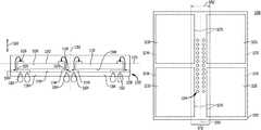
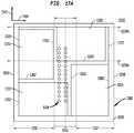
- FIG. 1further shows a semiconductor chip 11 within the package having element contacts 26 on a face 28 thereof which are electrically interconnected with the columns 14 , 18 of terminals of the package 12 through wire bonds 30 extending through an aperture, e.g., bond window, in the central region 24 of package substrate 20 .
- an adhesive layer 32may be disposed between the face 28 of the microelectronic element 11 and the substrate 20 to reinforce the mechanical connection between the microelectronic element and the substrate, with the wire bonds extending through an opening in the adhesive layer 32 .
- a microelectronic packagecan include a substrate having a first surface, a second surface opposite the first surface, and a plurality of substrate contacts exposed at the second surface.
- the second surfacecan extend in the first direction and in a second direction transverse thereto.
- the microelectronic packageincludes a microelectronic element having memory storage array function, the microelectronic element having a rear face facing the first surface, a front face opposite the first surface, and first and second opposed edges each extending between the front and rear faces and extending in the first direction parallel to the front face.
- the microelectronic elementcan have one or more columns of element contacts exposed at the front face, each column extending in the first direction along the front face.
- An axial plane normal to the front facecan intersect the front face along a line extending in the first direction and centered relative to the one or more columns of element contacts.
- Conductive structuremay extend above the front face. The conductive structure can electrically connect the element contacts with the substrate contacts.
- the microelectronic packagemay include a plurality of columns of terminals extending in the first direction which are exposed at the second surface of the substrate and electrically connected with the substrate contacts.
- the terminalscan include first terminals exposed at the second surface in a central region of the second surface of the substrate.
- the first terminalscan be configured to carry address information usable by circuitry within the package to determine an addressable memory location from among all the available addressable memory locations of a memory storage array of the microelectronic element.
- the central regioncan have a width in the second direction which is not more than three and one-half times a minimum pitch between any two adjacent columns of the parallel columns of the terminals.
- the axial planecan intersect the central region.
- the microelectronic elementmay embody a greater number of active devices to provide memory storage array function than any other function.
- the first terminalscan be configured to carry all of the address information usable by the circuitry within the package to determine the addressable memory location in the memory storage array. In a particular example, the first terminals can be configured to carry information that controls an operating mode of the microelectronic element. In one example, the first terminals can be configured to carry all of the command signals transferred to the microelectronic package, the command signals being write enable, row address strobe, and column address strobe signals. In an exemplary embodiment, the first terminals can be configured to carry clock signals transferred to the microelectronic package which are clocks usable for sampling signals carrying the address information. In a particular embodiment, the first terminals can be configured to carry all of the bank address signals transferred to the microelectronic package.
- the terminalscan be configured to connect the microelectronic package to at least one component external to the microelectronic package.
- the element contactscan include redistribution contacts exposed at the front face of the microelectronic element. Each redistribution contact can be electrically connected with a contact pad of the microelectronic element through at least one of a trace or a via.
- the conductive structurecan include wire bonds extending from the element contacts and electrically connected with the substrate contacts.
- the first terminalsmay be arranged in no more than two of the columns of terminals. In a particular embodiment, the first terminals can be arranged in a single one of the columns of terminals. In one example, the first terminals may be arranged in no more than four of the columns of terminals.
- the substratecan have first and second opposed edges between the first and second opposed surfaces. The first and second edges can extend in the first direction.
- the second surfacecan have first and second peripheral regions adjacent to the first and second edges, respectively.
- the central regioncan separate the first and second peripheral regions.
- the terminalscan include a plurality of second terminals exposed at the second surface in at least one of the peripheral regions. At least some of the second terminals can be configured to carry information other than the address information. In one embodiment, at least some of the second terminals can be configured to carry data signals.
- the substratecan include a dielectric element having a coefficient of thermal expansion (“CTE”) in the plane of the dielectric element of less than 30 parts per million per degree Celsius (“ppm/° C.”). In an exemplary embodiment, the substrate can include an element having a CTE of less than 12 ppm/° C.
- a microelectronic packagecan include a substrate having a first surface, a second surface opposite the first surface, a plurality of substrate contacts exposed at the first surface, and a microelectronic element having a rear face facing the first surface of the substrate, the microelectronic element having memory storage array function.
- the microelectronic elementmay have a greater number of active devices configured for providing memory storage array function than any other function.
- Conductive structurewhich may extend above the front face, electrically connects the contacts with the substrate contacts.
- a plurality of parallel columns of terminalscan be exposed at the second surface of the substrate and extending in a first direction along the second surface, the terminals electrically connected with the substrate contacts.
- the microelectronic elementcan have a front face opposite the front face and facing away from the first surface, and first and second opposed edges each extending between the front and rear faces and extending in a first direction parallel to the front face.
- the microelectronic elementcan have at least one column of element contacts extending in the first direction along the front face.
- the first and second edgescan define an axial plane extending in the first direction and also in a third direction normal to the rear face of the microelectronic element. The axial plane can be centered relative to the first and second edges.
- the terminalscan include first terminals exposed at the second surface of the substrate in a central region of the second surface.
- the first terminalscan be configured to carry a majority of the address information usable by circuitry within the package to determine an addressable memory location from among all the available addressable memory locations of a memory storage array of the microelectronic element.
- the central regioncan have a width in the second direction. The width of the central region may be not more than three and one-half times a minimum pitch between any two adjacent columns of the parallel columns of the terminals.
- the axial planecan intersect the central region.
- the first terminalscan be configured to carry at least three-quarters of the address information usable by the circuitry within the package to determine the addressable memory location in the memory storage array.
- a microelectronic packagecan include a substrate having a first surface, a second surface opposite the first surface, a plurality of first substrate contacts exposed at the first surface and a plurality of second substrate contacts exposed at the first surface.
- the microelectronic packagecan include first and second microelectronic elements each having memory storage array function.
- the microelectronic packagecan embody a greater number of active devices to provide memory storage array function than any other function.
- the first and second microelectronic elementscan be spaced apart from one another on the first surface, and can have parallel first edges each extending in the first direction.
- An axial plane normal to the first surface of the substratecan extend in the first direction and can be centered among the first edges.
- the first and second microelectronic elementscan have rear faces facing the first surface, front faces opposite the rear faces, and a plurality of contacts exposed at the front faces.
- Conductive structurewhich may extend above the front faces, can electrically connect the contacts of the first and second microelectronic elements with the first and second substrate contacts, respectively.
- a plurality of parallel columns of terminalscan be exposed at the second surface of the substrate and electrically connected with the first and second substrate contacts.
- the terminalscan include first terminals exposed in a central region of the second surface of the substrate.
- the columns of terminalsmay extend in the first direction.
- the first terminalscan be configured to carry address information usable by circuitry within the package to determine an addressable memory location from among all the available addressable memory locations of a memory storage array within the first and second microelectronic elements.
- the central regioncan have a width in the second direction. The width of the central region may be not more than three and one-half times a minimum pitch between any two adjacent columns of the parallel columns of the terminals.
- the axial planecan intersect the central region.
- the first terminalscan be configured to carry all of the address information usable by the circuitry within the package to determine the addressable memory location in the memory storage array.
- the first terminalscan be configured to carry information that controls an operating mode of a microelectronic element of the first and second microelectronic elements.
- the first terminalscan be configured to carry clock signals and all of the command signals, address signals, and bank address signals transferred to the microelectronic package, the command signals being write enable, row address strobe, and column address strobe, and the clock signals being clocks used for sampling signals carrying the address information.
- the front faces of the first and second microelectronic elementscan extend in a single plane parallel to the first surface of the substrate.
- the conductive structurecan include wire bonds extending from the contacts of the first and second microelectronic elements and electrically connected with the respective first and second substrate contacts.
- the first terminalsmay be arranged in no more than four of the columns of terminals.
- the contacts of each of the microelectronic elementscan include redistribution contacts exposed at the front face of the respective microelectronic element. Each redistribution contact can be electrically connected with a contact pad of the respective microelectronic element through at least one of a trace or a via. At least some of the redistribution contacts can be displaced from the contacts of the respective microelectronic element in at least one direction along the front face of the microelectronic element.
- the substratecan have first and second opposed edges between the first and second opposed surfaces.
- the first and second edgescan extend in the first direction.
- the second surfacecan have first and second peripheral regions adjacent to the first and second edges, respectively.
- the central regioncan separate the first and second peripheral regions.
- the terminalscan include a plurality of second terminals exposed at the second surface in at least one of the peripheral regions. At least some of the second terminals can be configured to carry information other than the address information. In one embodiment, at least some of the second terminals can be configured to carry data signals.
- a microelectronic packagecan include a substrate having a first surface, a plurality of first substrate contacts exposed at the first surface, and a plurality of second substrate contacts exposed at the first surface, the package including first and second microelectronic elements having memory storage array function.
- each microelectronic elementmay embody a greater number of active devices to provide memory storage array function than any other function.
- the microelectronic packageincludes conductive structure electrically connecting the contacts of the microelectronic elements with the substrate contacts.
- the conductive structurecan extend above the front face of each microelectronic element, and a plurality of parallel columns of terminals can be exposed at a second surface of the substrate and electrically connected with the first and second substrate contacts.
- the second surface of the substratecan be opposite the first surface.
- the second surfacecan extend in a first direction and in a second direction transverse thereto.
- the first and second microelectronic elementscan be spaced apart from one another on the first surface, and can have first parallel edges each extending in the first direction.
- An axial plane normal to the first surface of the substratecan extend in the first direction and can be centered among the first edges.
- the first and second microelectronic elementscan have rear faces facing the first surface, front faces opposite the rear faces, and a plurality of contacts exposed at the front faces.
- the conductive structurecan electrically connect the contacts of the first and second microelectronic elements with the first and second substrate contacts, respectively.
- the terminalscan include first terminals exposed a the second surface in a central region of the second surface of the substrate.
- the first terminalscan be configured to carry a majority of the address information usable by circuitry within the package to determine an addressable memory location from among all the available addressable memory locations of a memory storage array of the first and second microelectronic elements.
- the central regioncan have a width in the second direction. The width of the central region may be not more than three and one-half times a minimum pitch between any two adjacent columns of the parallel columns of the terminals.
- the axial planecan intersect the central region.
- the terminalscan be configured to carry at least three-quarters of the address information usable by the circuitry within the package to determine the addressable memory location in the memory storage array.
- An aspect of the inventionprovides a microelectronic package comprising a substrate having a first surface, a second surface opposite the first surface, and a plurality of substrate contacts exposed at the second surface.
- a plurality of stacked semiconductor chipsmay overlie the first surface, at least one of the semiconductor chips having a front face facing away from the first surface, and a plurality of contacts exposed at the front face. At least some of the contacts can be disposed at positions of at least one column thereof extending in a first direction along the front face. An axial plane normal to the front face of the at least one semiconductor chip can extend in the first direction and be centered relative to the at least one column of contacts.
- the packagefurther includes conductive structure electrically connecting the contacts with the substrate contacts, which in one example, can extend above the front face of the at least one semiconductor chip.
- Terminals exposed at the second surfacecan be disposed at positions within a plurality of parallel columns each extending in the first direction.
- the terminalscan be electrically connected with the substrate contacts and can include a plurality of first terminals exposed in a central region of the second surface, the first terminals configured to carry address information usable by circuitry within the package to determine an addressable memory location of a memory storage array of at least one of the stacked semiconductor chips having memory storage array function,
- the central regioncan have a width in a direction transverse to the second direction, the width not more than three and one-half times a minimum pitch between any two adjacent parallel columns of the terminals, wherein the axial plane intersects the central region.
- the microelectronic elementmay embody a greater number of active devices configured for providing memory storage array function than any other function.
- the at least one semiconductor chip having the front face facing away from the first surfacecan be a first semiconductor chip
- the stacked semiconductor chipscan include at least one second semiconductor chip overlying the front face of the first semiconductor chip and electrically interconnected with the first semiconductor chip.
- At least one of the first semiconductor chip or the at least one second semiconductor chipmay be configured to perform at least one of: partially or fully decode information received at a contact thereof, or regenerate information received at the contact thereof for transfer to another of at least one of the first semiconductor chip or to another of the at least one second semiconductor chip.
- At least some of the first and second semiconductor chipscan be electrically connected with one another by a plurality of through-silicon vias.
- At least one of the first semiconductor chip or the at least one second semiconductor chipcan embody a greater number of active devices to provide memory storage array function than any other function.
- At least some of the electrical interconnections between the first and second semiconductor chipscan be through wire bonds extending between at least some contacts of the first semiconductor chip and at least some contacts exposed at a face of the at least one second semiconductor chip which faces away from the first surface.
- the wire bondsmay include wire bonds extending from the contacts adjacent to first and second opposed edges of the at least one second semiconductor chip.
- the wire bondsmay include wire bonds extending from the contacts adjacent to a first edge of each of a plurality of the at least one second semiconductor chips.
- the second semiconductor chipsmay have contact-bearing faces facing away from the front face of the first semiconductor chip and can be staggered such that at least some contacts of each second semiconductor chip are exposed beyond the first edge of each second semiconductor chip disposed thereabove.
- At least some of the electrical interconnections between the first and second semiconductor chipscan be through conductors disposed on or within the substrate.
- the at least one second semiconductor chiphas contacts on a face confronting the front face of the first semiconductor chip.
- the contacts of the at least one second semiconductor chipcan face and be joined to corresponding contacts on the front face of the first semiconductor chip.
- the first semiconductor chipcan be configured to regenerate the address information for transfer to the at least one second semiconductor chip.
- the first semiconductor chipcan be configured to at least partially decode at least one of address information or command information received at the first terminals for transfer to the at least one second semiconductor chip.
- the at least one second semiconductor chipcan be a plurality of second semiconductor chips electrically interconnected with one another, wherein at least some of the electrical connections between the plurality of second semiconductor chips can be through wire bonds.
- the at least one second semiconductor chipcan be a plurality of second semiconductor chips electrically interconnected with one another.
- at least some of the electrical connections between the plurality of second semiconductor chipscan be through electrically conductive traces extending along at least one edge of the microelectronic element.
- the at least one second semiconductor chipcan be a plurality of second semiconductor chips electrically interconnected with one another by a plurality of through-silicon vias.
- each of the first and second semiconductor chipscan embody a greater number of active devices to provide memory storage array function than any other function.
- the first semiconductor chipcan be configured to regenerate at least some of the address information received at the first terminals for transfer to each second semiconductor chip, and each second semiconductor chip may be not configured to regenerate the address information for transfer to another semiconductor chip of the first and second semiconductor chips.
- the first semiconductor chipcan be configured to at least partially decode the address information received at the first terminals for transfer to each second semiconductor chip, and each second semiconductor chip may be not configured to fully decode the address information.
- the first semiconductor chipcan be configured to at least partially decode information received at at least one of the first terminals for controlling an operating mode of the at least one second semiconductor chip.
- the at least one second semiconductor chipmay include a dynamic random access memory (“DRAM”) storage array.
- DRAMdynamic random access memory
- the memory storage array function of the at least one second semiconductor chipcan be implemented in NAND flash, resistive RAM, phase-change memory, magnetic RAM, static RAM, spin-torque RAM, or content-addressable memory technology.
- a microelectronic packagecan include a substrate having first and second opposed surfaces and a plurality of substrate contacts exposed at the first surface.
- First and second microelectronic elements each having memory storage array functioncan be spaced apart from one another in a direction along the first surface and may have first parallel edges each extending in the first direction.
- An axial plane normal to the first surfacemay extend in the first direction and can be centered among the first parallel edges.
- Each microelectronic elementmay have a front face facing away from the first surface and a plurality of substrate contacts exposed at the front face. The contacts of each microelectronic element can be electrically connected with the substrate contacts through conductive structure.
- a plurality of terminalscan be exposed at the second surface at positions within a plurality of parallel columns.
- the terminalscan be electrically connected with the substrate contacts.
- the terminalscan include first terminals exposed in a central region of the second surface of the substrate, the first terminals being configured to carry address information usable by circuitry within the package to determine an addressable memory location of a memory storage array of the microelectronic elements.
- the central regioncan have a width in the second direction, the width of the central region not more than three and one-half times a minimum pitch between any two adjacent columns of the parallel columns of the terminals.
- the axial planemay intersect the central region.
- each of the microelectronic elementsmay embody a greater number of active devices to provide memory storage array function than any other function.
- the first terminalscan be configured to carry all of the address information usable by the circuitry within the package to determine the addressable memory location.
- the first terminalscan be configured to carry information that controls an operating mode of at least one of the microelectronic elements.
- the first terminalscan be configured to carry clock signals and the command signals, address signals, and bank address signals transferred to the microelectronic package, the command signals being write enable, row address strobe, and column address strobe, and the clock signals being clocks used for sampling signals carrying the address information.
- the front faces of each of the microelectronic elementscan extend in a single plane parallel to the first surface of the substrate.
- the microelectronic packagemay further include third and fourth microelectronic elements spaced apart from one another in a direction parallel to the first surface.
- the third and fourth microelectronic elementsmay have front surfaces facing away from the first surface and first parallel edges extending in the first direction and a plurality of element contacts exposed at the front surface.
- the contacts of each microelectronic elementmay include at least one column thereof extending in the first direction adjacent to at least one of the first parallel edges of such microelectronic element.
- the axial planecan be centered among the first edges of the first, second, third and fourth microelectronic elements.
- the central regioncan be disposed within an area of the substrate beyond which none of the faces of the first, second, third or fourth microelectronic elements extend.
- each of the microelectronic elementsmay have two first parallel edges extending in the same direction as the columns of contacts on the respective microelectronic element, and two second parallel edges extending in a direction transverse to the first edge.
- a plane containing either first edge of at least one of the microelectronic elements and normal to the face of such microelectronic elementcan intersect the first edge of another of the microelectronic elements.
- a microelectronic assemblycan include a circuit panel having a first surface, a second surface opposite the first surface, and panel contacts exposed at each of the first and second opposed surfaces, and first and second microelectronic packages having terminals mounted to the panel contacts at the first and second surfaces, respectively.
- the circuit panelcan electrically interconnect at least some terminals of the first microelectronic package with at least some corresponding terminals of the second microelectronic package.
- Each of the first and second microelectronic packagescan include a substrate having a first surface, a second surface opposite the first surface, and a plurality of substrate contacts exposed at the first surface.
- Each packagemay include a microelectronic element having memory storage array function.
- the microelectronic elementmay include a greater number of active devices configured for providing memory storage array function than any other function.
- the microelectronic elementmay have a front face facing away from the first surface of the substrate and one or more columns of element contacts exposed at the front face and extending in a first direction along the front face, such that an axial plane normal to the front face extends in the first direction and is centered relative to the one or more columns of element contacts.
- Conductive structurewhich in some cases may extend above the front face of the microelectronic element, electrically connects the contacts of the microelectronic element with the substrate contacts.
- a plurality of parallel columns of terminalscan extend in the first direction, which are exposed at the second surface and electrically connected with the substrate contacts.
- the terminalscan include first terminals exposed in a central region of the second surface of the substrate.
- the first terminalscan be configured to carry a majority of the address information usable by circuitry within the package to determine an addressable memory location from among all the available addressable memory locations of a memory storage array of the microelectronic element.
- the central regionin some cases may have a width in the second direction which is not more than three and one-half times a minimum pitch between any two adjacent columns of the parallel columns of the terminals, and the axial plane may intersect the central region.
- the first terminals of each microelectronic packagecan be configured to carry all of the address information usable by the circuitry within the respective microelectronic package to determine an addressable memory location.
- the first terminals of each microelectronic packagecan be configured to carry information that controls an operating mode of the microelectronic element of the respective microelectronic package.
- the first terminals of each microelectronic packagecan be configured to carry all of the command signals transferred to the respective microelectronic package, the command signals being write enable, row address strobe, and column address strobe signals.
- the first terminals of each microelectronic packagecan be configured to carry clock signals transferred to the respective microelectronic package, the clock signals being clocks used for sampling signals carrying the address information.
- the first terminals of each microelectronic packagecan be configured to carry all of the bank address signals transferred to the respective microelectronic package.
- at least the first terminals of the first and second microelectronic packagescan be arranged at corresponding positions of grids, respectively. The grids can be aligned within one ball pitch of one another in x and y orthogonal directions parallel to the first and second circuit panel surfaces.
- the gridscan be aligned with one another in the x and y orthogonal directions such that the terminals of the grids are coincident with one another.
- each position of each gridcan be occupied by one of the terminals.
- at least one position of each gridmay not be occupied by a terminal.
- at least half of the positions of the grids of the first and second packagescan be aligned with one another in x and y orthogonal directions parallel to the first surface of the circuit panel.
- the grids of the first and second microelectronic packagescan be functionally and mechanically matched.
- a length of a stub of at least one of electrical connections between one of the first terminals of the first microelectronic package and a corresponding one of the first terminals of the second microelectronic packagecan be less than seven times a minimum pitch of the first terminals of each of the microelectronic packages.
- the electrical connections through the circuit panel between the first terminals of the first and second microelectronic packagescan have an electrical length of approximately a thickness of the circuit panel.
- the signal assignments of the first terminalscan be the same on each of the first and second packages.
- the first terminals on each of the first and second packagescan be disposed at positions within first and second columns of terminals.
- the first column of terminals of the first packagecan be aligned within one ball pitch in x and y orthogonal directions with the second column of terminals of the second package.
- the second column of terminals of the first packagecan be aligned within one ball pitch in x and y orthogonal directions with the first column of terminals of the second package.
- the total combined length of the conductive elements connecting a pair of electrically coupled first and second panel contacts exposed at the first and second surfaces of the circuit panelcan be less than seven times a smallest pitch of the panel contacts.
- the circuit panelcan include a bus having a plurality of conductors configured to carry all of the address information transferred to each of the microelectronic packages. The conductors can extend in a direction parallel to the first and second surfaces.
- the first terminals of each microelectronic packagecan be disposed at positions within a single column of terminals of the respective microelectronic package.
- the circuit panelmay include no more than one routing layer for routing of the address information between a connection site on the circuit panel at which the terminals of the first and second microelectronic packages are electrically connected and a different connection site at which the terminals of at least a third microelectronic package are electrically connected.
- the first terminals of each microelectronic packagemay be disposed at positions within no more than two parallel columns of terminals of the respective microelectronic package.
- the circuit panelcan include no more than two routing layers for routing of the address information between a connection site on the circuit panel at which the terminals of the first and second microelectronic packages are electrically connected and a different connection site at which the terminals of at least a third microelectronic package are electrically connected.
- the circuit panelmay have no more than one routing layer for the routing of the address information.
- each microelectronic packagecan include a buffer element electrically connected to at least some of the terminals and the microelectronic element in the respective microelectronic package.
- Each buffer elementcan be configured to regenerate at least one signal received at one or more of the terminals of the respective microelectronic package.
- the circuit panelcan include an element having a coefficient of thermal expansion (“CTE”) of less than 12 parts per million per degree Celsius (“ppm/° C.”).
- CTEcoefficient of thermal expansion
- the panel contacts exposed at the first and second surfacescan be connected by vias extending through the element.
- the elementcan consist essentially of semiconductor, glass, ceramic or liquid crystal polymer material.
- a microelectronic assemblycan include a circuit panel having a first surface, a second surface opposite the first surface, and panel contacts exposed at each of the first and second surfaces.
- First and second microelectronic packagescan have terminals mounted to the panel contacts at the first and second surfaces, respectively.
- the circuit panelcan electrically interconnect at least some terminals of the first microelectronic package with at least some corresponding terminals of the second microelectronic package.
- Each of the first and second microelectronic packagesmay include a substrate having first and second opposed surfaces. A plurality of substrate contacts may be exposed at the first surface of the substrate.
- Each microelectronic packagemay include first and second microelectronic elements each having memory storage array function.
- the first and second microelectronic elementscan be spaced apart from one another in a direction along the first surface of the substrate and may have first parallel edges each extending in the first direction, wherein an axial plane normal to the first surface of the substrate extends in the first direction and is centered among the first parallel edges.
- Each microelectronic elementmay have a front face facing away from the first surface of the substrate and a plurality of contacts exposed at the front face electrically connected with the substrate contacts through conductive structure.
- a plurality of terminalscan be exposed at the second surface of the substrate at positions within a plurality of parallel columns.
- the terminalscan be electrically connected with the substrate contacts, the terminals including first terminals exposed at a central region of the second surface of the substrate.
- the first terminalscan be configured to carry address information usable by circuitry within the package to determine an addressable memory location of a memory storage array of the microelectronic elements.
- the central regionmay have a width in a second direction transverse to the first direction, wherein the width of the central region is not more than three and one-half times a minimum pitch between any two adjacent columns of the parallel columns of the terminals, and the axial plane intersects the central region.
- the first terminalsmay be configured to carry only a majority of the information needed to determine an addressable memory location of a memory storage array of one or more microelectronic elements of the respective microelectronic package.
- the first terminals of a microelectronic package of the assemblymay be configured to carry at least three-quarters of the address information usable by the circuitry within the package to determine the addressable memory location.
- a modulecan be provided which includes a circuit panel and a plurality of microelectronic packages mounted to, and electrically connected with the circuit panel through terminals of each microelectronic package for transport of signals to and from each microelectronic package.
- Each of the plurality of microelectronic packages of the modulemay each be in accordance with one or more of the examples described above.
- a systemcan be provided which includes a microelectronic package and one or more other electronic components electrically connected with the microelectronic package.
- Each microelectronic packagemay be in accordance with one or more of the examples described above.
- the systemmay include a housing, and the microelectronic package and other electronic components may be assembled together with the housing.
- the systemmay include a second microelectronic package in accordance with one or more of the examples described above.
- FIG. 1is a sectional view illustrating a conventional microelectronic package containing a DRAM chip.
- FIG. 2is a diagrammatic schematic diagram illustrating a microelectronic assembly, e.g., a DIMM module, incorporating a circuit panel and a plurality of microelectronic packages mounted opposite one another to first and second opposite surfaces thereof.
- a microelectronic assemblye.g., a DIMM module
- FIG. 3is a sectional view further illustrating an electrical interconnection between first and second microelectronic packages and a circuit panel in an assembly such as shown in FIG. 2 .
- FIG. 4is a diagrammatic plan view further illustrating the electrical interconnection between first and second microelectronic packages in an assembly such as shown in FIG. 2 .
- FIG. 5is a diagrammatic plan view illustrating an arrangement and signal assignment of terminals in a microelectronic package according to an embodiment of the invention.
- FIG. 6Ais a sectional view through line 6 A- 6 A of FIG. 5 further illustrating the microelectronic package shown in FIG. 5 .
- FIG. 6Bis a plan view of the microelectronic element of FIG. 6A illustrating an arrangement of contacts in accordance with the embodiment shown in FIGS. 5 and 6A .
- FIG. 6Cis a plan view illustrating an alternative arrangement of contacts on a microelectronic element according to a variation of the embodiment shown in FIG. 6B .
- FIG. 6Dis a plan view illustrating another alternative arrangement of contacts on a microelectronic element according to a variation of the embodiment shown in FIG. 6B .
- FIG. 6Eis a sectional view illustrating a microelectronic package according to a variation of the embodiment shown in FIGS. 5 and 6A .
- FIG. 7Ais a plan view further illustrating an arrangement of terminals in accordance with the embodiment shown in FIGS. 5 and 6A .
- FIG. 7Bis a sectional view illustrating a microelectronic assembly and first and second microelectronic packages electrically interconnected therewith in accordance with an embodiment of the invention.
- FIG. 7Cis a schematic diagram illustrating a microelectronic assembly including a circuit panel and microelectronic packages electrically connected thereto, e.g., a memory module, among others, according to an embodiment of the invention.
- FIG. 8is a plan view illustrating an alternative arrangement of terminals on a microelectronic package according to a variation of the embodiment shown in FIGS. 5 and 6A .
- FIG. 9Ais a plan view illustrating an alternative arrangement of terminals on a microelectronic package according to another variation of the embodiment shown in FIGS. 5 and 6A .
- FIG. 9Bis a sectional view illustrating a microelectronic assembly and first and second microelectronic packages as shown in FIG. 9A electrically interconnected therewith in accordance with an embodiment of the invention.
- FIG. 10Ais a sectional view illustrating a microelectronic package including a stacked electrically connected assembly of semiconductor chips therein in accordance with an embodiment of the invention.
- FIG. 10Bis a sectional view illustrating a microelectronic package according to a variation of the embodiment shown in FIG. 10A .
- FIGS. 11A and 11Bare a sectional view and a corresponding top view illustrating a microelectronic package including a stacked electrically connected assembly of semiconductor chips therein in accordance with an embodiment of the invention.
- FIG. 12is a sectional view illustrating a microelectronic package including a stacked electrically connected assembly of semiconductor chips therein in accordance with an embodiment of the invention.
- FIG. 13Ais a sectional view illustrating a microelectronic package according to a variation of the embodiment shown in FIG. 12 .
- FIG. 13Bis a sectional view illustrating a microelectronic package according to another variation of the embodiment shown in FIG. 12 .
- FIG. 13Cis a sectional view illustrating a microelectronic package according to a variation of the embodiment shown in FIG. 13B .
- FIG. 14Ais a diagrammatic plan view illustrating an arrangement and signal assignment of terminals in a microelectronic package according to another embodiment of the invention.
- FIG. 14Bis a plan view further illustrating an arrangement of terminals in accordance with the embodiment shown in FIG. 14A .
- FIG. 15is a sectional view through line 15 - 15 of FIG. 14A further illustrating the microelectronic package shown in FIG. 14A .
- FIG. 16Ais a diagrammatic plan view illustrating an arrangement of terminals in a microelectronic package according to yet another embodiment of the invention.
- FIG. 16Bis a plan view further illustrating an arrangement and signal assignment of terminals in accordance with the embodiment shown in FIG. 16A .
- FIG. 17Ais a diagrammatic plan view illustrating an arrangement of terminals in a microelectronic package according to a variation of the embodiment shown in FIGS. 16A and 16B .
- FIG. 17Bis a plan view further illustrating an arrangement and signal assignment of terminals in accordance with the embodiment shown in FIG. 17A .
- FIG. 18is a schematic sectional view illustrating a system according to an embodiment of the invention.
- FIG. 19is a schematic sectional view illustrating a system according to an embodiment of the invention.
- the inventorshave recognized improvements which can be made that may help improve the electrical performance of a microelectronic package incorporating a memory storage array chip, and a microelectronic assembly that incorporates such microelectronic package.
- Improvementscan be made particularly for use of a microelectronic package when provided in an assembly such as shown in FIGS. 2-4 , in which a package 12 A is mounted to a surface of a circuit panel with another like package 12 B mounted opposite thereto on an opposite surface of the circuit panel.
- the packages 12 A, 12 Btypically are functionally and mechanically equivalent to one another.
- Other pairs 12 C and 12 D; and 12 E and 12 F, of functionally and mechanically equivalent packagestypically are also mounted to the same circuit panel 34 .
- the circuit panel and the packages assembled theretomay form a portion of an assembly commonly referred to as a dual in-line memory module (“DIMM”).
- DIMMdual in-line memory module
- the packages in each oppositely mounted pair of packagesconnect to contacts on opposite surfaces of the circuit panel so that the packages in each pair overlie one another typically by more than 90% of their respective areas.
- Local wiring within the circuit panel 34connects terminals, e.g., the terminals labeled “1” and “5” on each package to global wiring on the circuit panel.
- the global wiringincludes the signal conductors of a bus 36 used to conduct some signals to connection sites on the circuit panel 34 such as sites I, II and III.
- packages 12 A, 12 Bare electrically connected to the bus 36 by local wiring coupled to a connection site I
- packages 12 C, 12 Dare electrically connected to the bus by local wiring coupled to connection site II
- packages 12 E, 12 Fare electrically connected to the bus by local wiring coupled to connection site lit.
- the circuit panel 34electrically interconnects the terminals of the respective packages 12 A, 12 B using local interconnect wiring that appears similar to a crisscross or “shoelace” pattern in which a terminal labeled “1” near one edge 16 of package 12 A connects through the circuit panel 34 to a terminal labeled “1” of package 12 B near the same edge 16 of package 12 B.
- the edge 16 of package 12 B as assembled to circuit panel 34is far from the edge 16 of package 12 A.
- FIGS. 2-4further shows that a terminal labeled “5” near an edge 22 of package 12 A is connected through the circuit panel 34 to a terminal labeled “5” of package 12 B near the same edge 22 of package 12 B. In assembly 38 the edge 22 of package 12 A is far from the edge 22 of package 12 B.
- connections through the circuit panel between terminals on each package, e.g., package 12 A, to the corresponding terminals on the package mounted opposite thereto, i.e., package 12 B,are fairly long.
- the circuit panel 34may electrically interconnect a signal conductor of the bus 36 with the terminal of package 12 A marked “1” and the corresponding terminal of package 12 B marked “1”, when the same signal from the bus is to be transmitted to each package.
- the circuit panel 34may electrically interconnect another signal conductor of the bus 36 with the terminal of package 12 A marked “2” and the corresponding terminal of package 12 B marked “2”.
- the same connection arrangementmay also apply to other signal conductors of the bus and corresponding terminals of each package.
- Local wiring between the bus 36 on the circuit panel 34 and each package of the respective pair of packages, e.g., packages 12 A, 12 B ( FIG. 2 ) at a connection site I of the boardcan be in form of unterminated stubs. Such local wiring when relatively long may in some cases impact the performance of the assembly 38 as discussed below.
- the circuit panel 34also requires local wiring to electrically interconnect certain terminals of other packages: the pair of packages 12 C and 12 D, and the pair of packages 12 E and 12 F to the global wiring of the bus 36 , and such wiring can also impact the performance of the assembly in the same way.
- FIG. 4further illustrates the interconnection between microelectronic packages 12 A, 12 B of respective pairs of terminals assigned to carry signals “1”, “2”, “3”, “4”, “5”, “6”, “7”, and “8”.
- the wiring needed to traverse the circuit panel 34 in a direction 40 transverse to the direction 42 in which the columns 14 , 18 of terminals extendcan be quite long.
- the length of the local wiring in a circuit panel 34 in an assembly 38 seen in FIGS. 2-4that is required to route the same signal to the corresponding terminals of two oppositely mounted packages 12 A, 12 B can range between five and ten millimeters and may typically be about seven millimeters.
- the impactsmay be tolerable for some packages containing microelectronic elements of current manufacture.
- the inventorsrecognize that the impacts can become severe. For these assemblies, settling time, ringing, jitter, or intersymbol interference of a transmitted signal may increase to an unacceptable degree.
- the inventorsfurther recognize that the electrical lengths of the unterminated stubs are usually longer than the local wiring that connects the bus 36 on the circuit panel with the terminals of the packages mounted thereto. Unterminated wiring within each package from the package terminals to the semiconductor chip therein adds to the lengths of the stubs.
- the bus 36is a command-address bus of an assembly having a predominant memory storage array function such as a DIMM.
- the command-address bus 36can be configured to carry address information transferred to the microelectronic packages that is usable by circuitry within the packages, e.g., row address and column address decoders, and bank selection circuitry, if present, to determine an addressable memory location from among all the available addressable memory locations of a memory storage array within a microelectronic element in the packages.
- the command-address bus 36can be configured to carry the above-noted address information to connection sites, e.g., sites I, II, and III shown in FIG. 2 . These above-noted address information can then be distributed by local wiring to respective sets of panel contacts on opposite surfaces of the circuit panel, to which packages 12 A, 12 B, 12 C, 12 D, 12 E and 12 F are connected.
- command-address bus 36can be configured to carry all of a group of signals of a command-address bus of the microelectronic element, i.e., command signals, address signals, bank address signals and clock signals that are transferred to the microelectronic packages, wherein the command signals include write enable, row address strobe, and column address strobe signals, and the clock signals are clocks used for sampling the address signals.
- the clock signalscan be of various types, in one embodiment, the clock signals carried by these terminals can be one or more pairs of differential clock signals received as differential or true and complement clock signals.
- certain embodiments of the invention described hereinprovide a microelectronic package configured so as to permit the lengths of stubs to be reduced when first and second such packages are mounted opposite one another on opposite surfaces of a circuit panel, e.g., a circuit board, module board or card, or flexible circuit panel.
- Assemblies which incorporate first and second microelectronic packages mounted opposite one another on a circuit panelcan have significantly reduced stub lengths between the respective packages. Reducing the stub lengths within such assemblies can improve electrical performance, such as by reducing one or more of settling time, ringing, jitter, or intersymbol interference, among others.
- the packagecan include a substrate 102 on which a plurality of columns 104 A, 104 B are disposed, each column 104 A and 104 B having at least some first terminals 105 disposed within the column.
- a plurality of columns 106 A, 106 Bare also disposed on the substrate 102 , each column 106 A and 106 B having second terminals 107 disposed within the column.
- an electrically conductive elementsuch as a terminal, or a contact
- a supporting elementsuch as a substrate of a package or a circuit panel
- the electrically conductive elementoverlie a surface of the supporting element, so long as the electrically conductive element is available at the surface of the supporting element for contact with a theoretical point moving in a direction perpendicular to the surface of the supporting element.
- the terminal or contactmay project above the surface, be recessed relative to the surface, or be flush with the surface.
- the substratemay include a dielectric element, which in some cases can consist essentially of polymeric material, e.g., a resin or polyimide, among others, and which may be sheet-like.
- the substrate 102can include a dielectric element having a composite construction such as glass-reinforced epoxy, e.g., of BT resin or FR-4 construction.
- the substratecan include a supporting element of material having a coefficient of thermal expansion (“CTE”) of less than 12 parts per million per degree Celsius (“ppm/° C.”), on which the terminals and other conductive structure are disposed.
- CTEcoefficient of thermal expansion
- such low CTE elementcan consist essentially of glass, ceramic or semiconductor material or liquid crystal polymer material, or a combination of such materials.
- the terminals 105 and 107can be disposed at positions within a plurality of columns 104 A, 104 B, 106 A and 106 B exposed at a surface 110 of the substrate.
- a statement that an electrically conductive element is “exposed at” a surface of a structureindicates that the electrically conductive element is available for contact with a theoretical point moving in a direction perpendicular to the surface toward the surface from outside the structure.
- a terminal or other conductive element which is exposed at a surface of a structurecan project from such surface; can be flush with such surface; or can be recessed relative to such surface and exposed through a hole or depression in the structure. In the example shown in FIG.
- columns 104 A and 104 Beach extend in a first direction along the surface 110 and includes a plurality of first terminals 105 .
- Columns 106 A, 106 Bmay each include a plurality of second terminals 107 and may in some cases be parallel with the columns 104 A, 104 B and extend in the first direction as well.
- some second terminalscan also be disposed within columns 104 A, 104 B.
- the central region 112is not wider than three and one-half times a minimum pitch between adjacent ones of the parallel columns of the terminals, as seen and further described relative to FIG. 7A below.
- the first terminalscan be configured to carry address information usable by circuitry within the package to determine an addressable memory location from among all the available addressable memory locations of a memory storage array within the microelectronic element.
- the first terminalsare configured to carry address information transferred to the microelectronic package which is usable by circuitry within the package, e.g., row address and column address decoders, and bank selection circuitry, if present, to determine an addressable memory location from among all the available addressable memory locations of a memory storage array within a microelectronic element in the package.
- the address information carried by the first terminalsis sufficient to determine the addressable memory location.
- the first terminalscan be configured to carry all the address information used by such circuitry within the package to determine an addressable memory location within such memory storage array.
- the first terminalscan be configured to carry a majority of the address information that is used by such circuitry within the package to determine an addressable memory location within such memory storage array, and then other terminals such as the above-referenced second terminals on the package would then be configured to carry the remaining part of the address information.
- the first terminalsare configured to carry three quarters or more of the address information that is used by such circuitry within the package to determine an addressable memory location within such memory storage array.
- the first terminalsmay not be configured to carry chip select information, e.g., information usable to select a particular chip within the package for access to a memory storage location within the chip.
- the first terminalsmay indeed carry chip select information.
- microelectronic elementse.g., semiconductor chips
- a microelectronic elementmay contain a greater number of active devices to provide memory storage array function than any other function.
- each one of some contacts of a plurality of external contacts at an exterior of the microelectronic elementis dedicated to receiving a respective address signal of a plurality of address signals supplied to the microelectronic element.
- each of such contactsis able to receive one address signal of the plurality of address signals supplied to the microelectronic element from an external component, e.g., from a circuit panel via connections through a microelectronic package in which the microelectronic element is incorporated.
- each of the plurality of address signals present at the external contactscan be sampled relative to an edge of a clock used by the microelectronic element, i.e., upon on a transition of the clock between first and second different voltage states. That is, each address signal can be sampled upon a rising transition between a lower voltage state and a higher voltage state of the clock, or upon a falling transition between a higher voltage state and a lower voltage state of the clock.
- the plurality of address signalsmay all be sampled upon the rising transition of the clock, or may all be sampled upon the falling transition of the clock, or in another example, the address signal at one of the external contacts can be sampled upon the rising transition of the clock and the address signal at one other external contact can be sampled upon the falling transition of the clock.
- one or more of the address contacts thereoncan be used in a multiplexed manner
- a particular external contact of the microelectronic elementcan be configured to receive two or more different signals supplied to the microelectronic element from the outside.
- a first address signalcan be sampled at the particular contact upon a first transition of the clock between the first and second different voltage states (e.g., a rising transition)
- a signal other than the first address signalcan be sampled at the particular contact upon a second transition of the clock (e.g., a falling transition) between the first and second voltage states that is opposite the first transition.
- multiplexing in this mannercan allow a first address signal and a different signal to be received in the same clock cycle on the same external contact of the microelectronic element.
- multiplexing in this mannercan allow a first address signal and a second different address signal to be received in the same clock cycle on the same external contact of the microelectronic element.
- the first terminalscan be configured to carry all of a group of command signals, address signals, bank address signals and clock signals which are transferred to the microelectronic package.
- the “command signals”are a write enable signal, row address strobe signal, and column address strobe signal utilized by a microelectronic element within the microelectronic package, when such microelectronic element is a dynamic random access memory storage device.
- “Clock signals”are signals used as clocks for sampling the address signals.
- the first terminalscan include clock signals CK and CKB, row address strobe RAS, column address strobe CAS and write enable signals WE, as well as address signals A0 through A15 inclusive, and bank address signals BA0, BA1 and BA2.
- terminalse.g., second terminals
- other terminalscan also be disposed in the central region and be configured to carry other signals, e.g., data signals to and or from the microelectronic element of the package.
- some first terminals in FIG. 5are assigned for carrying a power supply voltage (VDD)
- the power supply connections as well as connections to groundcan be among any of the first or second terminals.
- VDDpower supply voltage
- the terminals used for connecting to a power supply or to groundare omitted from the drawings and need not be mentioned further in the description which follows.
- the second terminalsare arranged in one or more columns each having a plurality of second terminals.
- the second terminals 106 A, 106 Bmay be arranged in one or more of first and second peripheral regions 114 A, 114 B of the second surface 110 of the substrate 102 , the peripheral regions 114 A, 114 B being adjacent to first and second opposed edges 116 , 118 of the second surface 110 .
- the central region 112can be disposed between the first and second peripheral regions 114 A, 114 B.
- a microelectronic element 130 within microelectronic package 100has a rear face 131 facing the second surface 110 of the substrate 102 , and a front face 134 opposite the rear face 131 , and first and second opposed edges 170 , 172 extending between the front and rear faces.
- the microelectronic elemente.g., a semiconductor chip, or stacked arrangement of semiconductor chips, can be configured to provide memory storage array function, and in one example, may be configured to predominantly provide memory storage array function.
- the number of active devices, e.g., transistors, therein which are configured, i.e., constructed and interconnected with other devices, to provide memory storage array functionmay be greater than the number of active devices which are configured to provide any other function.
- a microelectronic elementsuch as a DRAM chip may have memory storage array function as its primary or sole function.
- such microelectronic elementmay have mixed use and may incorporate active devices configured to provide memory storage array function, and also incorporate other active devices configured to provide another function such as processor function, or signal processor or graphics processor function, among others.
- the microelectronic elementmay in some cases still have a greater number of active devices configured to provide the memory storage array function than any other function of the microelectronic element.
- An axial plane 174 normal to the face 134 of the microelectronic element 130intersects the second surface 110 of the substrate 102 along a line which extends in the first direction and is parallel to and centered with respect to the first and second edges 170 , 172 of the microelectronic element 130 .
- an edge 170 of microelectronic element 130extends in the first direction 142 and a column 138 of contacts 132 exposed at the front face 134 of the microelectronic element and adjacent to edge 170 can extend in the same first direction 142 along the front face 134 .
- Another edge 172 of microelectronic element 130extends in the first direction 142 and a second column 139 of contacts 132 exposed at the front face 134 of the microelectronic element may extend in the same first direction 142 along the front face 134 adjacent to edge 172 .
- a column of contacts on the microelectronic elementcan be fully populated as in the case of column 138 , or a column of contacts may have only have contacts at some of the positions within the column, as in the case of column 139 .
- Conductive structuresuch as wire bonds 173 ( FIG. 6A ) may electrically connect the contacts 132 with corresponding contacts 136 on a first surface 108 of the substrate.
- the axial plane 174 of microelectronic element 130intersects the central region 112 of the second surface 110 of the substrate, the central region 112 of the substrate surface being where at least a first column 104 A and a second column 104 B of terminals, each having at least some first terminals 105 are disposed within the column of the microelectronic package.
- Second terminalsmay be disposed in one or more of the peripheral regions 114 A, 114 B of the substrate surface 110 .
- one or more second terminalsmay be disposed in the central region, such as can be disposed within columns 104 A, 104 B.
- joining elements 154 attached to terminalscan include a bond metal, e.g., solder, tin, indium or eutectic, or other electrically conductive bond material attached to the terminals that can be used to join the terminals of the package 100 to a component external to the package, such as to corresponding contacts of a circuit panel.
- a bond metale.g., solder, tin, indium or eutectic, or other electrically conductive bond material attached to the terminals that can be used to join the terminals of the package 100 to a component external to the package, such as to corresponding contacts of a circuit panel.
- FIG. 6Cillustrates a variation of the embodiment shown in FIG. 6B in which the contacts 132 of a microelectronic element 180 exposed at the front face thereof are disposed in columns or rows adjacent to and aligned with respective peripheral edges 170 , 172 , 176 , 178 of the microelectronic element 180 . Edges 170 , 172 are parallel and extend in a first direction 142 .
- FIG. 6Cillustrates the location of an axial plane 174 of the microelectronic element 180 . In such variation, the axial plane 174 is shown to extend in the first direction and is centered among the parallel edges 170 , 172 .
- FIG. 6Dillustrates another variation of the embodiment shown in FIG. 6B in which the contacts of a microelectronic element 190 are disposed in columns 188 and 189 adjacent to edges 170 , 172 of the microelectronic element.
- the microelectronic element 190includes a semiconductor chip having a conductive redistribution layer thereon, and the contacts 132 can include redistribution contacts which are connected to the contacts 192 , 194 of the semiconductor chip by conductive traces, or metalized vias formed in contact with the contacts 192 , 194 of the semiconductor chip (or which can be connected to the contacts 192 194 of the chip by both metalized vias and traces).
- the axial plane 174intersects the face 196 of the microelectronic element along a line centered among the columns of 188 , 189 of redistribution contacts.
- the wire bonds 173 electrically connecting the microelectronic element 130 with the substrate 102may be formed starting from the microelectronic element 130 , in which case the wire bond forms a ball 175 on the contact 132 of the microelectronic element and is wedge-bonded to the corresponding substrate contact 136 .
- FIG. 6Eshows a package 101 according to a variation thereof in which the wire bond 183 forms a ball 185 on the contact 136 of the substrate and is wedge-bonded to the corresponding contact 132 of the microelectronic element 130 .
- the variation of FIG. 6Emay be employed if desired to reduce a height 103 of the microelectronic package 101 , as the wire bonds 183 formed in this way can generally have lower height excursion above the contacts 132 than the wire bonds 173 shown in FIG. 6A .
- FIG. 7Ais a plan view of the package 100 looking toward a terminal-bearing surface 110 of the substrate therein.
- Columns 104 A, 104 B in which first terminals are disposedcan lie within a central region 112 of the surface 110
- columns 106 A, 106 B in which second terminals are disposedcan lie within one or more peripheral regions 114 A, 114 B of the surface 110 .
- the smallest distance between any two adjacent columns of terminals on the substrateis the minimum pitch 150 as shown in FIG. 7A .
- the minimum pitchis in a direction 164 perpendicular to the direction 162 in which the terminals in a particular column, e.g., column 104 A are arranged. In the example shown in FIG.
- the minimum pitch 150occurs between columns 104 A, 104 B which are closest to one another.
- the central region 112has a width 152 along the substrate surface 110 in the direction 164 of the pitch.
- the width 152may be not greater than three and one-half times the minimum pitch 150 between any two adjacent columns of the terminals, i.e., not more than three and one-half times the minimum pitch 150 between the closest adjacent columns 104 A, 104 B.
- FIG. 7Billustrates a microelectronic assembly 300 of a circuit panel 354 and first and second microelectronic packages 100 A, 100 B, each being a microelectronic package 100 having a structure according to one or more of the embodiments described above relative to FIGS. 5-6E .
- each package 100 A, 100 Bmay have the same signals assigned to the respective locations of terminals on the package, and the columns 104 A, 104 B, 106 A, 106 B of terminals on each package can be arranged at the same locations in x and y orthogonal directions 164 , 162 relative to an edge 116 of the substrate.
- the packages 100 A, 100 Bare electrically connected to contacts 360 , 362 , respectively, exposed at first and second opposite surfaces 350 , 352 of the circuit panel 354 , respectively.
- the circuit panelcan be of various types, such as a printed circuit board used in a dual inline memory module (“DIMM”) module, a circuit board or panel to be connected with other components in a system, or a motherboard, among others.
- the circuit panelmay include an element having a coefficient of thermal expansion (“CTE”) of less than 12 parts per million per degree Celsius (“ppm/° C.”), wherein the panel contacts at the first and second surfaces are connected by vias extending through the element.
- the elementmay consist essentially of semiconductor, glass, ceramic or liquid crystal polymer material.
- the first terminals 105 in the columns 104 A, 104 Bcan be disposed at positions within a grid 104 on the first package 100 A, and the first terminals 105 in the columns 104 A, 104 B on the second package 100 B can be disposed at positions of within a similar grid 104 .
- Each grid of terminalsmay be fully populated, i.e., having a terminal at each position of each grid. Alternatively, there may not be a terminal disposed at one or more positions of the grid on a package. As apparent from FIG.
- the grids 104which include first terminals on each package 100 A, 100 B can be aligned within a distance of one ball pitch of one another in x and y orthogonal directions parallel to the surface 350 of the circuit panel, the ball pitch being no greater than a minimum pitch between any two adjacent parallel columns of the terminals on either package.
- the grids 104may be coincident with one another.
- the alignmentcan be within customary manufacturing tolerances or can be within a tolerance of less than one-half of one ball pitch of one another in x and y orthogonal directions parallel to the first and second circuit panel surfaces, the ball pitch being as described above.
- Wiring within the circuit panel 354electrically connects the terminals in column 104 A of package 100 A with terminals in column 104 A of package 100 B, as shown.
- the wiring that forms the electrical connectionsis shown schematically by the dashed line 320 in FIG. 7B , since the wiring can be hidden from view in the example shown in FIG. 7B .
- wiring within the circuit panel 354electrically connects the terminals in column 104 B of package 100 A with terminals in column 104 B of package 100 B, and the electrical interconnections between such terminals is shown schematically by the dashed line 322 in FIG. 7B .
- the wiring on the circuit panel 354 required to connect one of the first terminals labeled “A” of package 100 A with a corresponding one of the first terminals labeled “A” of package 100 Bcan be relatively short.
- each grid 104 on each packagehas two columns 104 A, 104 B, and the grids 104 are aligned in the above-described manner, then a terminal of the first column 104 A of the first package 100 A is aligned within one ball pitch of a terminal of the second column 104 B of the second package 100 B in x and y orthogonal directions parallel to the first surface 350 of the circuit panel, the first surface 350 being a major surface of the circuit panel.
- a terminal of the second column 104 B of the first package 100 Ais aligned within one ball pitch of a terminal of the first column 104 A of the second package in x and y orthogonal directions parallel to the first surface 350 of the circuit panel.
- the electrical lengths of stubs on the circuit panel 354 that electrically connect a first terminal of the first column of package 100 A with the corresponding first terminal of the first column of the second package 100 Bcan be less than seven times a minimum pitch of the first terminals on each package: for example, less than seven times the pitch 150 between columns 104 A, 104 B of first terminals in FIG. 7A .
- the total combined length of the conductive elements connecting a pair of electrically coupled first and second panel contacts 360 , 362 exposed at the first and second surfaces of the circuit panel to the corresponding conductor of the bus 36 on the circuit panelcan be less than seven times a smallest pitch of the panel contacts.
- the total combined length of the conductive elements connecting a pair of electrically coupled first and second panel contacts 360 , 362may be approximately the same as a thickness 356 of the circuit panel 354 between first and second surfaces 350 , 352 .
- the electrical length of the connection between a first terminal in column 104 A of the first package 100 A with the corresponding first terminal in column 104 A on the second package 100 Bmay be approximately the same as the thickness 356 of the circuit panel 354 .
- the reductions in the lengths of these electrical connectionscan reduce stub lengths from bus 36 ( FIG. 2 ) on the circuit panel to the connection sites of the packages thereon.
- the reduced stub lengthscan improve electrical performance, such as by reducing one or more of settling time, ringing, jitter, or intersymbol interference, among others, for the above-noted signals of the bus 36 .
- connections on the circuit panelmay require fewer layers of wiring to interconnect first terminals of each package to routing layers within the circuit panel which constitute a set of conductors which carry the address information or carry the address information and other information as described above.
- the number of global routing layers of wiring on the circuit panel needed to implement a bus 36 such as used to transmit the above-noted address information or command and address information as described abovecan also be reduced when the microelectronic packages attached thereto are constructed according to the principles herein.
- the number of required routing layersmay in some cases be reduced to two or fewer routing layers.
- the circuit panel 354may include no more than one routing layer for global routing of all of the address information between a connection site on the circuit panel at which the terminals of the first and second microelectronic packages 100 A, 100 B are electrically connected and a different connection site at which the terminals of at least a third microelectronic package are electrically connected.
- the circuit panel 354may include no more than two routing layers for global routing of all of the address information between a connection site on the circuit panel at which the terminals of the first and second microelectronic packages 100 A, 100 B are electrically connected and a different connection site at which the terminals of at least a third microelectronic package are electrically connected.
- theremay be no more than one routing layer for the above-noted global routing.
- FIG. 7Cillustrates a microelectronic assembly such as, for example, a DIMM, among others, incorporating a circuit panel and a plurality of microelectronic packages mounted opposite one another to first and second opposite surfaces thereof.
- the above-noted address signals or command-address bus signalscan be routed on a bus 36 , e.g., an address bus or command-address bus on the circuit panel or circuit board 354 in at least one direction 143 between connection sites I, II or III at which respective pairs of microelectronic packages 100 A, 110 B are connected to opposite sides of the circuit panel. Signals of such bus 36 reach each pair of packages at the respective connection sites I, II or III at slightly different times.
- the at least one direction 143can be transverse or orthogonal to a direction 142 in which at least one column 138 of a plurality of contacts on at least one microelectronic element within each package 100 A or 100 B extends.
- the signal conductors of the bus 36 on (i.e., on or within) the circuit panel 354can in some cases be spaced apart from one another in a direction 142 which is parallel to the at least one column 138 of contacts on a microelectronic element within a package 100 A, or 100 B connected to the circuit panel.
- Such configurationmay help simplify the routing of signal conductors of one or more global routing layers on the circuit panel used to route the signals of the bus 36 .
- first terminalsconfigured to receive address signals A3 and A1.
- the microelectronic assembly 354can have a microelectronic element 358 that can include a semiconductor chip configured to perform buffering of at least some signals transferred to the microelectronic packages 100 A, 100 B of the assembly 354 .
- the microelectronic element 358can be configured predominantly to perform a logic function, such as a solid state drive controller, and one or more of the microelectronic elements 358 in the microelectronic packages 100 A and 100 B can each include memory storage elements such as nonvolatile flash memory.
- the microelectronic element 358can include a special purpose processor that is configured to relieve a central processing unit of a system such as the system 1500 ( FIG. 18 ) from supervision of transfers of data to and from the memory storage elements included in the microelectronic elements 358 .
- a microelectronic element 358 including a solid state drive controllercan provide direct memory access to and from a data bus on a motherboard (e.g., the circuit panel 1502 shown in FIG. 18 ) of a system such as the system 1300 .
- the microelectronic element 358can have a buffering function.
- Such a microelectronic element 358can be configured to help provide impedance isolation for each of the microelectronic elements 358 with respect to components external to the microelectronic assembly 354 .
- the first terminals 104 of the microelectronic packagecan be configured to carry information that controls an operating mode of the microelectronic element 101 . More specifically, the first terminals can be configured to carry all of a particular set of command signals and/or clock signals transferred to the microelectronic package 100 . In one embodiment, the first terminals 104 can be configured to carry all of the command signals, address signals, bank address signals, and clock signals transferred to the microelectronic package 100 from an external component, wherein the command signals include row address strobe, column address strobe and write enable. In such embodiment, the first chip can be configured to regenerate the information that controls the operating mode.
- the first chipcan be configured to partially or fully decode the information that controls the operating mode of the microelectronic element.
- each second chipmay or may not be configured to fully decode one or more of address information, command information, or information that controls an operating mode of the microelectronic element.
- Microelectronic packages having other arrangements of terminals thereoncan be provided.
- four columns 404 A, 404 B, 404 C, and 404 D of terminalsare disposed in a central region 112 of the substrate surface, these columns containing the first terminals that are configured to carry the above-noted address information, or in a particular embodiment, are configured to carry all of the above-noted command signals, address signals, bank address signals and clock signals used to sample the address signals.
- second terminalscan also be disposed within the columns 404 A, 404 B, 404 C, 404 D, which are configured to carry information other than the above-noted information or signals carried by the first terminals.
- the first terminalsare arranged at positions within a single column 504 disposed in the central region 512 of the substrate surface, the single column extending in a direction parallel to the edges 516 , 518 of the microelectronic package.
- the second terminalsmay be omitted from the figures illustrating various aspects of the invention, although the second terminals may nevertheless be present in such embodiments.
- the minimum pitch between any two columns of terminals on the substrateis the pitch 552 between the adjacent columns 506 B and 506 C of second terminals disposed in peripheral region 514 B of the substrate surface.
- the width 554 of the central regionis not greater than three and one-half times the minimum pitch 552 between the columns 506 B and 506 C of terminals.
- FIG. 10Aillustrates a microelectronic package 600 according to a particular example in which the microelectronic element includes a vertical stack 630 of an electrically interconnected first semiconductor chip 632 and a plurality of second semiconductor chips 634 , each having a contact-bearing front face 631 that faces away from the substrate 602 and a rear face that faces toward the first surface of the substrate.
- Wire bonds 635electrically interconnect the contacts 626 on the semiconductor chips 632 , 634 with corresponding contacts 636 on the substrate.
- Spacers 638can be disposed between adjacent faces of the semiconductor chips 634 , and a spacer 638 can be disposed between the contact-bearing face 631 of the semiconductor chip 632 and a rear face of semiconductor chip 634 .
- adhesive layerscan be provided between each spacer and the faces of the semiconductor chips adjacent to such spacer.
- the one or more second semiconductor chips 634are electrically interconnected with the first semiconductor chip 632 .
- each of the first and second semiconductor chips 632 , 634can be configured such that each such semiconductor chip has memory storage array function.
- each such semiconductor chipcan embody a greater number of active devices to provide memory storage array function than any other function.
- each of the first and second semiconductor chipsmay include a memory storage array and all circuitry required for inputting data to and outputting data from the memory storage array.
- each of the semiconductor chipsmay include circuitry configured to receive external data input from terminals of the package, as well as circuitry configured to transfer data output from such semiconductor chip to terminals of the package.
- each first and each second semiconductor chip 632 , 634can be a dynamic random access memory (“DRAM”) chip or other memory chip which is capable of inputting and outputting data from the memory storage array within such semiconductor chip and receiving and transmitting such data to a component external to the microelectronic package.
- DRAMdynamic random access memory
- signals to and from the memory storage array within each DRAM chip or other memory chipdoes not require buffering by an additional semiconductor chip within the microelectronic package.
- the one or more second semiconductor chips 634may embody a greater number of active devices to provide memory storage array function than any other function, but the first semiconductor chip 632 may be a different type of chip.
- the first semiconductor chip 632can be configured, e.g., designed, constructed, or set up, to buffer signals, i.e., regenerate signals received at the terminals for transfer to the one or more second semiconductor chips 634 , or to regenerate signals received from one or more of the second semiconductor chips 634 for transfer to the terminals, or to regenerate signals being transferred in both directions from the terminals to the one or more second semiconductor chips 634 ; and from the one or more semiconductor chips to the terminals of the microelectronic package.
- the first semiconductor chipcan be configured to partially or fully decode at least one of address information or command information received at the terminals, such as at the first terminals.
- the first chipcan then output the result of such partial or full decoding for transfer to the one or more second semiconductor chips 634 .
- the first semiconductor chipcan be configured to buffer the command signals, address signals and clock signals which are transferred to the one or more second semiconductor chips.
- the first semiconductor chip 632can be a buffer chip which embodies a greater number of active devices to provide a buffering function in transferring signals to other devices, e.g., to the one or more second semiconductor chips 634 , than for any other function.
- the one or more second semiconductor chipsmay be reduced function chips which have memory storage arrays but which can omit circuitry common to DRAM chips, such as buffer circuitry, decoders or predecoders or wordline drivers, among others.
- the first chip 632may function as a “master” chip in the stack and to control operations in each of the second semiconductor chips 634 .
- the second semiconductor chipsmay be configured such that they are not capable of performing the buffering function, and so the stacked arrangement of the first and second semiconductor chips is configured such that the buffering function required in the microelectronic package can be performed by the first semiconductor chip, and cannot be performed by any of the second semiconductor chips in the stacked arrangement.
- the one or more second semiconductor chipscan be implemented in one or more of the following technologies: DRAM, NAND flash memory, RRAM (“resistive RAM” or “resistive random access memory”), phase-change memory (“PCM”), magnetoresistive random access memory, e.g. such as may embodiment tunnel junction devices, static random access memory (“SRAM”), spin-torque RAM, or content-addressable memory, among others.
- FIG. 10Billustrates a variation of the above-described embodiment in which the first semiconductor chip 633 within microelectronic package 601 is configured to buffer at least some signals received at terminals of the package, e.g., the first terminals, for transmission to other semiconductor chips 634 within the package.
- the first semiconductor chip 633can be mounted to the substrate 602 in flip-chip orientation, i.e., having contacts 643 on a face thereof facing corresponding contacts on the substrate 602 and being joined thereto such as by solder, other bond metal or other conductive material.
- FIG. 11Ais a sectional view and FIG. 11B is a corresponding plan view illustrating a microelectronic package 660 according to a further variation in which the second semiconductor chips 634 are mounted in stair-step manner relative to one another such that the contacts of the first semiconductor chip 632 are exposed beyond an edge 618 of the second semiconductor chip 634 A immediately above the first semiconductor chip 632 , and the contacts of that semiconductor chip 634 A are exposed beyond an edge 618 of the second semiconductor chip 634 B immediately above that second semiconductor chip.
- Electrical connections between the first and second chips and the substrate and among the chipscan be provided by wire bonds 635 which electrically connect adjacent chips within the stack of semiconductor chips, or wire bonds 637 which electrically connect the chips directly to the package substrate 662 .
- FIG. 12illustrates a microelectronic package 670 according to a further variation of the embodiment described above relative to FIG. 10A , in which connections between contacts of the one or more second semiconductor chips 634 can include traces or leads 640 which extend along one or more edges of a unit of stacked semiconductor chips 630 , i.e., along edges of the semiconductor chips 634 within such unit 630 .
- Unit 630is mounted and electrically interconnected with contacts 627 of the first semiconductor chip 632 , such as with a bond metal, e.g., solder, tin, gold, indium, a eutectic, or electrically conductive bumps, or both, which may in some cases include conductive posts, e.g., micropillars.
- Traces 654may extend along a face 631 of the first semiconductor chip from the contacts 627 to second contacts 626 , which in turn can be electrically connected with the substrate, such as through wire bonds 645 .
- the electrical connections between the second semiconductor chips 634may further include traces 644 which extend along front faces of the second semiconductor chips 634 . As further shown in FIG. 12 , the front faces 642 of the second semiconductor chips may face upwardly away from the substrate 602 or downwardly towards the substrate 602 .
- FIG. 13Afurther illustrates a microelectronic package 680 in which a second semiconductor chip 634 has contacts 647 facing contacts 627 of the first chip and joined thereto in flip-chip manner, such as through a bond metal, e.g., solder, tin, gold, indium, a eutectic, or electrically conductive bumps, or both.
- Traces 654may electrically connect the contacts 627 with other contacts 626 on the first chip that are electrically connected to the substrate, such as through wire bonds.
- FIG. 13Bfurther illustrates a microelectronic package 690 according to a particular example in which the one or more second semiconductor chips 634 are electrically connected with one another by through-silicon vias (“TSVs”) 650 that extend in a direction of the thicknesses 652 of at least some of the second semiconductor chips 634 , i.e., in a direction normal to the faces 642 of the chips 634 .
- TSVsthrough-silicon vias
- the TSVs 650can be electrically connected with contacts 627 of the first semiconductor chip 632 , such as through a bond metal, e.g., solder, tin, gold, indium, a eutectic, or electrically conductive bumps, or both, which may in some cases include conductive posts, e.g., micropillars.
- Traces 654may extend along a face 631 of the first semiconductor chip from the contacts 627 to second contacts 626 , which in turn can be wire-bonded to the substrate.
- information or signals received at terminals of the package 690can be received by the first semiconductor chip 632 through wire bonds 645 that are joined to substrate contacts 636 , which in turn are joined to such terminals of the microelectronic package.
- the first semiconductor chip 632operating as a buffer element, can then regenerate the received information or signals and then transfer the regenerated information or signals to the one or more second semiconductor chips, e.g., through the connections between the first and second chips 632 , 634 and through the TSVs 650 within the stack of second chips 634 .
- FIG. 13Cillustrates a variation of the microelectronic package shown in FIG. 13B .
- semiconductor chip 664which is configured to regenerate or at least partially decode address information or other information, e.g., regenerate signals for transfer to other semiconductor chips in the package, is not located adjacent to the first surface 108 of the substrate 602 . Rather, in this case, the semiconductor chip 664 can be disposed at a position within the package that overlies one or more other semiconductor chips. For example, as shown in FIG.
- the chip 664at least partially overlies the semiconductor chip 662 that is disposed adjacent to the first surface 108 of the substrate 602 and at least partially overlies semiconductor chips 663 A, 663 B and 663 C which are disposed atop semiconductor chip 662 .
- the semiconductor chips 662 and 663 A, 663 B and 663 Cmay include memory storage arrays. As in the examples described above, such chips 662 , and 663 A, 663 B and 663 C may each incorporate circuits configured to buffer, e.g., temporarily store, data that is to be written to such chip, or data that is being read from such chip, or both. Alternatively, the chips 662 , and 663 A, 663 B and 663 C may be more limited in function and may need to be used together with at least one other chip that is configured to temporarily store data that is to be written to such chip or data that is being read from such chip, or both.
- the semiconductor chip 664can be electrically connected to terminals of the microelectronic package, e.g., to grids in which the first terminals 604 and the second terminals 606 are disposed, through electrically conductive structure, e.g., wire bonds 665 , that partially overlies a front face 631 of the semiconductor chip 663 A and that connects to contacts 636 exposed at the first surface 108 of the substrate 602 .
- electrically conductive structuree.g., wire bonds 665
- the electrically conductive structuree.g., the wire bonds 665
- the electrically conductive structurecan electrically connect to the semiconductor chip 664 through contacts 638 on a chip 663 A and through conductors (not shown) that extend along the face 631 of the chip 663 A, or along a confronting face 641 of the chip 664 , or along the faces 631 , 641 of both of the chips 663 A, 664 .
- the semiconductor chip 664may be configured to regenerate or at least partially decode signals or information that it receives through the conductive structure, e.g., the wire bonds 665 , and it may be configured to transfer the regenerated or at least partially decoded signals or information to other chips within the package such as to the chips 662 , and 663 A, 663 B and 663 C.
- the semiconductor chips 662 , 663 A, 663 B and 663 Ccan be electrically connected to the semiconductor chip 664 and to one another by a plurality of through-silicon vias (“TSVs”) 672 , 674 , and 676 that can extend through one, two, or three or more of such chips.
- TSVsthrough-silicon vias
- Each such TSVmay electrically connect with wiring within the package, e.g., conductive pads or traces of two or more of the semiconductor chips 662 , 663 A, 663 B and 663 C and 664 .
- through silicon viasmay extend through the thicknesses of all semiconductor chips 662 , 663 A, 663 B and 663 C, even though each through silicon via may not electrically connect with each such semiconductor chip through which it extends.
- a heat sink or heat spreader 668which may include a plurality of fins 671 , can be thermally coupled to a face of the semiconductor chip 664 , e.g., a rear face 633 thereof, such as through a thermally conductive material such as thermal adhesive, thermally conductive grease, or solder, among others.
- the microelectronic assembly 695 shown in FIG. 13Cmay be configured to operate as a memory module capable of transferring a designated number of data bits per cycle onto or off of the microelectronic package through the first and second terminals provided therefor on the substrate.
- the microelectronic assemblymay be configured to transfer a number of data bits such as thirty-two data bits, sixty-four data bits, or ninety-six data bits, among other possible configurations, to or from an external component such as a circuit panel that can be electrically connected with the terminals 604 , 606 .
- the bits transferred to and from the packageinclude error correction code bits
- the number of bits transferred per cycle to or from the packagemay be thirty-six bits, seventy-two bits, or one-hundred-eight bits. Other data widths are possible other than those that are specifically described here.
- FIGS. 14A, 14B, and 15illustrate a microelectronic package 1100 according to a further variation of one or more of the above-described embodiments.
- the package 1100includes first and second microelectronic elements 1130 , 1131 that are spaced apart from one another on a first surface 1108 of the substrate 1102 .
- Each microelectronic element 1130 , 1131has first parallel edges 1170 extending away from a face 1142 of the respective microelectronic element which faces away from the substrate 1102 , and second parallel edges 1172 that extend in a direction transverse or orthogonal to a direction in which the first edges extend.
- the contacts 1138 of the microelectronic elementsare electrically connected with corresponding substrate contacts 1148 on the first surface 1108 of the substrate 1102 .
- some of the substrate contacts 1148are electrically connected with first terminals 1104 disposed in a central region 1112 on the second surface 1110 , such as through electrically conductive traces 1144 , or through electrically conductive vias 1146 , or through both traces and vias.
- some of the substrate contacts 1148may instead be electrically connected with second terminals 1162 in one or more peripheral regions 1164 of the second surface.
- FIG. 14Aillustrates possible signal assignments of the terminals 1104 , 1162 on the package.
- the central region 1112 of the substrate surface 1110has a width 1154 that is not greater than three and one-half times a minimum pitch 1152 between any two adjacent columns of terminals on the package, where each of the two adjacent columns has a plurality of terminals therein.
- An axial plane 1150 normal to the surface 1110 of the substrate 1102intersects the surface 1110 along a line which is parallel to and centered among the first edges 1170 of the first and second microelectronic elements 1130 , 1131 .
- an axis 1151 along which a column of first terminals 1104 extendscan be disposed between adjacent edges 1134 , 1135 of the first and second microelectronic elements as shown therein. This can be true for the axes of more than one columns of the terminals.
- the axis along which a column of the first terminals 1104 extendscan overlie one or more of the faces 1140 of the first and second microelectronic elements 1130 , 1131 , and this may be true for the axes of more than one column.
- the faces 1142 of the first and second microelectronic elementscan extend within a single plane 1124 parallel to the first surface 1108 of the substrate 1102 .
- FIGS. 16A-16Billustrate a microelectronic package 1200 according to a variation of the embodiment seen in FIGS. 14A-B and 15 which, in addition to first and second microelectronic elements 1230 , 1231 having the same arrangement and electrical interconnections within the package 1200 as discussed above regarding microelectronic package 1100 ( FIGS. 14A-B , 15 ), further includes third and fourth microelectronic elements 1233 and 1235 . Like the first and second microelectronic elements, each of the third and fourth microelectronic elements may embody a greater number of active devices to provide memory storage array function than any other function.
- the third and fourth microelectronic elements 1233 and 1235are mounted face-up on the substrate 1202 and are electrically interconnected with the first terminals 1204 of the package, such as through electrical connections extending above the respective contact-bearing faces (not shown) of the microelectronic elements.
- the electrical connectionscan be wire bonds, as discussed above.
- the terminals 1204 of the microelectronic packagecan be arranged within a central region 1212 having width 1252 no greater than three and one-half times the minimum pitch between columns of terminals, as described above. As further shown in FIG. 16A , the intersection of the axial plane 1250 with the substrate 1202 can be centered among all of the first parallel edges 1270 of the first, second, third and fourth microelectronic elements within the package 1200 .
- the contact-bearing faces (not shown) of the microelectronic elements 1230 , 1231 , 1233 and 1235can be arranged within the package 1200 such that all of such faces are co-planar, i.e., extend within a single plane, i.e., such as a single plane 1124 as illustrated in FIG. 15 .
- FIG. 16Billustrates a possible signal assignment of terminals on the package 1200 in which first terminals 1204 are arranged in one or more columns in the central region and second terminals 1206 are arranged in multiple areas near peripheral edges 1260 , 1261 , 1262 and 1263 of the package.
- some of the second terminals 1206can be disposed at positions within a grid such as grid 1270
- some second terminalscan be disposed at positions within a grid such as grid 1272 .
- some second terminalscan be disposed at positions within a grid such as grid 1274
- some second terminalscan be disposed at positions within a grid 1276 .
- the signal class assignments of the second terminals 1206 in the grid 1276can be symmetric about a vertical axis 1251 that can extend within the axial plane 1250
- the signal class assignments of the second terminals in the grid 1274can be symmetric about the vertical axis 1251 .
- two signal class assignmentscan be symmetric with respect to one another if the signal assignments are in the same class of assignments, even if the numerical index within the class differs.
- Exemplary signal class assignmentscan include data signals, data strobe signals, data strobe complement signals, and data mask signals.
- the second terminals 1206 having signal assignments DQSH # and DQSL #are symmetric about the vertical axis 1251 with respect to their signal class assignment, which is data strobe complement, even though those second terminals have different signal assignments.
- the assignments of the data signals to the spatial positions of the second terminals on the microelectronic packagecan have modulo-X symmetry about the vertical axis 1251 .
- the modulo-X symmetrycan help preserve signal integrity in an assembly 300 such as seen in FIG. 7B , in which one or more pairs of first and second packages are mounted opposite one another to a circuit panel, and the circuit panel electrically connects corresponding pairs of second terminals of those first and second packages in each oppositely-mounted package pair.
- modulo-X symmetrycan permit electrical connections to be made through the circuit panel so that a terminal DQ0 of a first package can be electrically connected through the circuit panel to a terminal DQ8 of the second package that has the same index number modulo X (X being 8 in this case), so that the connection can be made in a direction essentially straight through, i.e., normal to, the thickness of the circuit panel.
- “X”can be a number 2 n (2 to the power of n), wherein n is greater than or equal to 2, or X can be 8 ⁇ N, N being two or more.
- Xmay be equal to the number of bits in a half-byte (4 bits), byte (8 bits), multiple bytes (8 ⁇ N, N being two or more), a word (32 bits) or multiple words.
- the signal assignment of a package terminal DQ0 in grid 1274 configured to carry data signal DQ0is symmetric about the vertical axis 1251 with the signal assignment of another package terminal configured to carry data signal DQ8.
- the signal assignments of package terminals DQ2 and DQ10 in grid 1274have modulo-8 symmetry about the vertical axis, and the same is also true for grid 1276 .
- Modulo-8 symmetrysuch as described herein can be seen in grids 1274 , 1276 with respect to each of the signal assignments of package terminals DQ0 through DQ15.
- the modulo number “X”can be a number other than 2 n (2 to the power of n) and can be any number greater than two.
- the modulo number X upon which the symmetry is basedcan depend upon how many bits are present in a data size for which the package is constructed or configured. For example, when the data size is 10 bits instead of 8, then the signal assignments may have modulo-10 symmetry. It may even be the case that when the data size has an odd number of bits, the modulo number X can have such number.
- FIGS. 17A and 17Billustrate a microelectronic package 1300 according to a variation of the embodiment 1200 described above relative to FIGS. 16A and 16B , the package 1300 having a substrate surface 1310 having a central region 1312 in which first terminals 1304 are disposed.
- microelectronic elements 1330 , 1331are arranged on substrate 1302 in a manner similar to the arrangement of microelectronic elements 1130 , 1131 of microelectronic package 1100 ( FIGS. 14A-B , 15 ), in that edges 1360 of adjacent microelectronic elements 1130 , 1131 are parallel to each other and extend in the same first direction 1342 .
- Edges 1362 of microelectronic elementsextend in a direction 1344 transverse to, and typically orthogonal to the direction 1342 .
- first edges 1360 of a respective microelectronic elementcan have greater length than the second edges 1362 of such microelectronic element.
- the second edges 1362can have greater length than the first edges 1360 .
- a plane 1370 that contains either first edge 1360 of any of the microelectronic elements 1330 , 1331 , 1332 , or 1333 and which is normal to the face of such microelectronic elementintersects the edge 1360 of another microelectronic element within the package 1300 . For example, as shown in FIG.
- the plane 1370 that contains the edge 1360 of microelectronic element 1333extends in direction 1344 and intersects the edge 1360 of microelectronic element 1330 within the package.
- planes 1370 A and 1370 B that contain the first edges of microelectronic element 1333intersect the first edge of no more than one other microelectronic element within the package.
- plane 1370 Aintersects edges 1360 of only microelectronic element 1330 .
- the central region 1312can be further limited. Specifically, FIG. 17A shows that there is a rectangular subsection area 1372 on the surface 1302 of the substrate 1302 , beyond which none of the faces of the first, second, third and fourth microelectronic elements 1330 , 1331 , 1332 and 1333 extend. In the microelectronic package 1300 depicted in FIGS. 17A-17B , the central region 1312 does not extend beyond the boundaries of such rectangular subsection area 1372 .
- FIG. 17Bfurther illustrates a possible arrangement of terminals within microelectronic package 1300 in which first terminals 1304 are disposed within the central region 1312 which spans a width 1354 in a direction orthogonal to opposed edges 1316 , 1318 of the package that is no greater than three and one-half times the minimum pitch between the closest two adjacent columns of terminals on the package.
- Peripheral regionstake up the remaining area of the surface 1310 of the substrate 1302 , spanning widths 1356 , 1357 between edges of the central region and the opposed edges 1316 , 1318 of the package, respectively.
- microelectronic packages and microelectronic assemblies described above with reference to FIGS. 5 through 17Bcan be utilized in construction of diverse electronic systems, such as the system 1500 shown in FIG. 18 .
- the system 1500 in accordance with a further embodiment of the inventionincludes a plurality of modules or components 1506 such as the microelectronic packages and/or microelectronic assemblies as described above in conjunction with other electronic components 1508 and 1510 .
- the systemcan include a circuit panel, motherboard, or riser panel 1502 such as a flexible printed circuit board, and the circuit panel can include numerous conductors 1504 , of which only one is depicted in FIG. 18 , interconnecting the modules or components 1506 with one another.
- a circuit panel 1502can transport signals to and from each of the microelectronic packages and/or microelectronic assemblies included in the system 1500 .
- thisis merely exemplary; any suitable structure for making electrical connections between the modules or components 1506 can be used.
- the system 1500can also include a processor such as the semiconductor chip 1508 , such that each module or component 1506 can be configured to transfer a number N of data bits in parallel in a clock cycle, and the processor can be configured to transfer a number M of data bits in parallel in a clock cycle, M being greater than or equal to N.
- a processorsuch as the semiconductor chip 1508 , such that each module or component 1506 can be configured to transfer a number N of data bits in parallel in a clock cycle, and the processor can be configured to transfer a number M of data bits in parallel in a clock cycle, M being greater than or equal to N.
- the system 1500can include a processor chip 1508 that is configured to transfer thirty-two data bits in parallel in a clock cycle, and the system can also include four modules 1506 such as the microelectronic package 100 described with reference to FIG. 5 , each module 1506 configured to transfer eight data bits in parallel in a clock cycle (i.e., each module 1506 can include first and second microelectronic elements, each of the two microelectronic elements being configured to transfer four data bits in parallel in a clock cycle).
- the system 1500can include a processor chip 1508 that is configured to transfer sixty-four data bits in parallel in a clock cycle, and the system can also include four modules 1506 such as the microelectronic package 1200 described with reference to FIGS. 16A-B , each module 1506 configured to transfer sixteen data bits in parallel in a clock cycle (i.e., each module 1506 can include four microelectronic elements, each of the four microelectronic elements being configured to transfer four data bits in parallel in a clock cycle).
- the component 1508is a semiconductor chip and component 1510 is a display screen, but any other components can be used in the system 1500 .
- the system 1500can include any number of such components.
- Modules or components 1506 and components 1508 and 1510can be mounted in a common housing 1501 , schematically depicted in broken lines, and can be electrically interconnected with one another as necessary to form the desired circuit.
- the housing 1501is depicted as a portable housing of the type usable, for example, in a cellular telephone or personal digital assistant, and screen 1510 can be exposed at the surface of the housing.
- a structure 1506includes a light-sensitive element such as an imaging chip
- a lens 1511 or other optical devicealso can be provided for routing light to the structure.
- the simplified system shown in FIG. 18is merely exemplary; other systems, including systems commonly regarded as fixed structures, such as desktop computers, routers and the like can be made using the structures discussed above.
- microelectronic packages and microelectronic assemblies described above with reference to FIGS. 5-17Bcan also be utilized in construction of an electronic system such as the system 1600 shown in FIG. 19 .
- the system 1600 in accordance with a further embodiment of the inventionis the same as the system 1500 shown in FIG. 18 , except the component 1506 has been replaced by a plurality of components 1606 .
- Each of the components 1606can be or can include one or more of the microelectronic packages or microelectronic assemblies described above with reference to FIGS. 5-17B .
- one or more of the components 1606can be a variation of the microelectronic assembly 300 shown in FIG. 7B , in which the circuit panel 354 includes exposed edge contacts, and the circuit panel 354 of each microelectronic assembly 300 can be suitable for insertion into a socket 1605 .
- Each socket 1605can include a plurality of contacts 1607 at one or both sides of the socket, such that each socket 1605 can be suitable for mating with corresponding exposed edge contacts of a corresponding component 1606 such as the above-described variation of the microelectronic assembly 300 .
- the systemcan include a second circuit panel 1602 or motherboard such as a flexible printed circuit board, and the second circuit panel can include numerous conductors 1604 , of which only one is depicted in FIG. 19 , interconnecting the components 1606 with one another.
- a modulesuch as the system 1600 can include a plurality of components 1606 , each component 1606 being the above-described variation of the microelectronic assembly 300 .
- Each component 1606can be mounted to, and electrically connected with the second circuit panel 1602 for transport of signals to and from each component 1606 .
- the specific example of the system 1600is merely exemplary; any suitable structure for making electrical connections between the components 1606 can be used.
Landscapes
- Engineering & Computer Science (AREA)
- Microelectronics & Electronic Packaging (AREA)
- Power Engineering (AREA)
- Physics & Mathematics (AREA)
- Computer Hardware Design (AREA)
- General Physics & Mathematics (AREA)
- Condensed Matter Physics & Semiconductors (AREA)
- Theoretical Computer Science (AREA)
- Geometry (AREA)
- Human Computer Interaction (AREA)
- General Engineering & Computer Science (AREA)
- Chemical & Material Sciences (AREA)
- Materials Engineering (AREA)
- Semiconductor Memories (AREA)
- Dram (AREA)
- Internal Circuitry In Semiconductor Integrated Circuit Devices (AREA)
Abstract
Description
Claims (20)
Priority Applications (1)
| Application Number | Priority Date | Filing Date | Title |
|---|---|---|---|
| US16/148,325US10692842B2 (en) | 2011-10-03 | 2018-10-01 | Microelectronic package including microelectronic elements having stub minimization for wirebond assemblies without windows |
Applications Claiming Priority (14)
| Application Number | Priority Date | Filing Date | Title |
|---|---|---|---|
| US201161542553P | 2011-10-03 | 2011-10-03 | |
| US201161542495P | 2011-10-03 | 2011-10-03 | |
| US201161542488P | 2011-10-03 | 2011-10-03 | |
| US201261600271P | 2012-02-17 | 2012-02-17 | |
| US13/440,290US8659142B2 (en) | 2011-10-03 | 2012-04-05 | Stub minimization for wirebond assemblies without windows |
| US13/440,299US8659143B2 (en) | 2011-10-03 | 2012-04-05 | Stub minimization for wirebond assemblies without windows |
| US13/440,313US8405207B1 (en) | 2011-10-03 | 2012-04-05 | Stub minimization for wirebond assemblies without windows |
| PCT/US2012/058273WO2013052411A1 (en) | 2011-10-03 | 2012-10-01 | Stub minimization for wirebond assemblies without windows |
| PCT/US2012/058398WO2013052441A2 (en) | 2011-10-03 | 2012-10-02 | Stub minimization for wirebond assemblies without windows |
| PCT/US2012/058407WO2013052448A1 (en) | 2011-10-03 | 2012-10-02 | Stub minimization for wirebond assemblies without windows |
| US14/244,007US9377824B2 (en) | 2011-10-03 | 2014-04-03 | Microelectronic assembly including memory packages connected to circuit panel, the memory packages having stub minimization for wirebond assemblies without windows |
| US15/168,789US9679876B2 (en) | 2011-10-03 | 2016-05-31 | Microelectronic package having at least two microelectronic elements that are horizontally spaced apart from each other |
| US15/600,050US10090280B2 (en) | 2011-10-03 | 2017-05-19 | Microelectronic package including microelectronic elements having stub minimization for wirebond assemblies without windows |
| US16/148,325US10692842B2 (en) | 2011-10-03 | 2018-10-01 | Microelectronic package including microelectronic elements having stub minimization for wirebond assemblies without windows |
Related Parent Applications (1)
| Application Number | Title | Priority Date | Filing Date |
|---|---|---|---|
| US15/600,050ContinuationUS10090280B2 (en) | 2011-10-03 | 2017-05-19 | Microelectronic package including microelectronic elements having stub minimization for wirebond assemblies without windows |
Publications (2)
| Publication Number | Publication Date |
|---|---|
| US20190035769A1 US20190035769A1 (en) | 2019-01-31 |
| US10692842B2true US10692842B2 (en) | 2020-06-23 |
Family
ID=47892307
Family Applications (7)
| Application Number | Title | Priority Date | Filing Date |
|---|---|---|---|
| US13/440,313ActiveUS8405207B1 (en) | 2011-10-03 | 2012-04-05 | Stub minimization for wirebond assemblies without windows |
| US13/440,290ActiveUS8659142B2 (en) | 2011-10-03 | 2012-04-05 | Stub minimization for wirebond assemblies without windows |
| US13/440,299ActiveUS8659143B2 (en) | 2011-10-03 | 2012-04-05 | Stub minimization for wirebond assemblies without windows |
| US14/244,007Active2032-09-04US9377824B2 (en) | 2011-10-03 | 2014-04-03 | Microelectronic assembly including memory packages connected to circuit panel, the memory packages having stub minimization for wirebond assemblies without windows |
| US15/168,789Expired - Fee RelatedUS9679876B2 (en) | 2011-10-03 | 2016-05-31 | Microelectronic package having at least two microelectronic elements that are horizontally spaced apart from each other |
| US15/600,050ActiveUS10090280B2 (en) | 2011-10-03 | 2017-05-19 | Microelectronic package including microelectronic elements having stub minimization for wirebond assemblies without windows |
| US16/148,325ActiveUS10692842B2 (en) | 2011-10-03 | 2018-10-01 | Microelectronic package including microelectronic elements having stub minimization for wirebond assemblies without windows |
Family Applications Before (6)
| Application Number | Title | Priority Date | Filing Date |
|---|---|---|---|
| US13/440,313ActiveUS8405207B1 (en) | 2011-10-03 | 2012-04-05 | Stub minimization for wirebond assemblies without windows |
| US13/440,290ActiveUS8659142B2 (en) | 2011-10-03 | 2012-04-05 | Stub minimization for wirebond assemblies without windows |
| US13/440,299ActiveUS8659143B2 (en) | 2011-10-03 | 2012-04-05 | Stub minimization for wirebond assemblies without windows |
| US14/244,007Active2032-09-04US9377824B2 (en) | 2011-10-03 | 2014-04-03 | Microelectronic assembly including memory packages connected to circuit panel, the memory packages having stub minimization for wirebond assemblies without windows |
| US15/168,789Expired - Fee RelatedUS9679876B2 (en) | 2011-10-03 | 2016-05-31 | Microelectronic package having at least two microelectronic elements that are horizontally spaced apart from each other |
| US15/600,050ActiveUS10090280B2 (en) | 2011-10-03 | 2017-05-19 | Microelectronic package including microelectronic elements having stub minimization for wirebond assemblies without windows |
Country Status (1)
| Country | Link |
|---|---|
| US (7) | US8405207B1 (en) |
Families Citing this family (39)
| Publication number | Priority date | Publication date | Assignee | Title |
|---|---|---|---|---|
| US8823165B2 (en) | 2011-07-12 | 2014-09-02 | Invensas Corporation | Memory module in a package |
| TWI515864B (en) | 2011-10-03 | 2016-01-01 | 英帆薩斯公司 | Stub minimization with terminal grids offset from center of package |
| US8405207B1 (en) | 2011-10-03 | 2013-03-26 | Invensas Corporation | Stub minimization for wirebond assemblies without windows |
| US8436477B2 (en) | 2011-10-03 | 2013-05-07 | Invensas Corporation | Stub minimization using duplicate sets of signal terminals in assemblies without wirebonds to package substrate |
| US8525327B2 (en) | 2011-10-03 | 2013-09-03 | Invensas Corporation | Stub minimization for assemblies without wirebonds to package substrate |
| JP5947904B2 (en) | 2011-10-03 | 2016-07-06 | インヴェンサス・コーポレイション | Stub minimization for multi-die wirebond assemblies with orthogonal windows |
| KR101894823B1 (en) | 2011-10-03 | 2018-09-04 | 인벤사스 코포레이션 | Stub minimization for multi-die wirebond assemblies with parallel windows |
| US8653646B2 (en) | 2011-10-03 | 2014-02-18 | Invensas Corporation | Stub minimization using duplicate sets of terminals for wirebond assemblies without windows |
| US10163877B2 (en)* | 2011-11-07 | 2018-12-25 | Taiwan Semiconductor Manufacturing Co., Ltd. | System in package process flow |
| US8848391B2 (en) | 2012-08-27 | 2014-09-30 | Invensas Corporation | Co-support component and microelectronic assembly |
| US8848392B2 (en) | 2012-08-27 | 2014-09-30 | Invensas Corporation | Co-support module and microelectronic assembly |
| US9368477B2 (en) | 2012-08-27 | 2016-06-14 | Invensas Corporation | Co-support circuit panel and microelectronic packages |
| US9472284B2 (en)* | 2012-11-19 | 2016-10-18 | Silicon Storage Technology, Inc. | Three-dimensional flash memory system |
| US9070423B2 (en) | 2013-06-11 | 2015-06-30 | Invensas Corporation | Single package dual channel memory with co-support |
| KR102301573B1 (en)* | 2014-06-05 | 2021-09-10 | 삼성전자주식회사 | Semiconductor device |
| US9281296B2 (en) | 2014-07-31 | 2016-03-08 | Invensas Corporation | Die stacking techniques in BGA memory package for small footprint CPU and memory motherboard design |
| US9691437B2 (en) | 2014-09-25 | 2017-06-27 | Invensas Corporation | Compact microelectronic assembly having reduced spacing between controller and memory packages |
| US9515035B2 (en)* | 2014-12-19 | 2016-12-06 | International Business Machines Corporation | Three-dimensional integrated circuit integration |
| KR102424402B1 (en)* | 2015-08-13 | 2022-07-25 | 삼성전자주식회사 | Semiconductor packages and methods for fabricating the same |
| US9484080B1 (en) | 2015-11-09 | 2016-11-01 | Invensas Corporation | High-bandwidth memory application with controlled impedance loading |
| US9679613B1 (en) | 2016-05-06 | 2017-06-13 | Invensas Corporation | TFD I/O partition for high-speed, high-density applications |
| US9918407B2 (en)* | 2016-08-02 | 2018-03-13 | Qualcomm Incorporated | Multi-layer heat dissipating device comprising heat storage capabilities, for an electronic device |
| US10068866B2 (en)* | 2016-09-29 | 2018-09-04 | Intel Corporation | Integrated circuit package having rectangular aspect ratio |
| CN110689910B (en)* | 2018-07-05 | 2024-10-11 | 森富科技股份有限公司 | Memory configuration structure |
| US11139283B2 (en)* | 2018-12-22 | 2021-10-05 | Xcelsis Corporation | Abstracted NAND logic in stacks |
| JP2021044278A (en)* | 2019-09-06 | 2021-03-18 | キオクシア株式会社 | Semiconductor device |
| KR102749207B1 (en) | 2019-12-06 | 2025-01-06 | 삼성전자주식회사 | Semiconductor package and a method for manufacturing the same |
| US11074952B1 (en)* | 2020-07-20 | 2021-07-27 | Dell Products L.P. | System and method for compression Dual In-Line Memory Module reversibility |
| US11321009B2 (en)* | 2020-07-21 | 2022-05-03 | Dell Products L.P. | System and method for compression dual in-line memory module scalability |
| US12265482B2 (en) | 2020-07-22 | 2025-04-01 | Dell Products L.P. | System and method for providing compression attached memory module offset stacking |
| US12298923B2 (en) | 2020-07-22 | 2025-05-13 | Dell Products L.P. | Compression attached memory module for offset stacking |
| US12142341B2 (en) | 2020-07-22 | 2024-11-12 | Dell Products L.P. | System and method for providing compression attached memory module compression connectors |
| US12183717B2 (en) | 2020-07-22 | 2024-12-31 | Dell Products L.P. | System and method for stacking compression attached memory modules |
| JP7186931B2 (en)* | 2020-07-29 | 2022-12-09 | 三菱電機株式会社 | semiconductor equipment |
| CN112261781A (en)* | 2020-10-20 | 2021-01-22 | Oppo广东移动通信有限公司 | Encapsulation module and terminal |
| KR20220151485A (en) | 2021-05-06 | 2022-11-15 | 삼성전자주식회사 | Semiconductor package, and package on package type semiconductor package having the same |
| US20220368069A1 (en)* | 2021-05-16 | 2022-11-17 | Electron Square Spólka Z Ograniczona Odpowiedzialnoscia | Electric interface |
| US12362270B2 (en)* | 2022-02-23 | 2025-07-15 | Taiwan Semiconductor Manufacturing Company, Ltd. | Package structure and method of fabricating the same |
| CN117577588A (en)* | 2022-08-08 | 2024-02-20 | 长鑫存储技术有限公司 | Packaging structure and preparation method thereof |
Citations (294)
| Publication number | Priority date | Publication date | Assignee | Title |
|---|---|---|---|---|
| US3670208A (en) | 1970-07-13 | 1972-06-13 | Logic Dynamics Inc | Microelectronic package, buss strip and printed circuit base assembly |
| JPS6193694A (en) | 1984-10-15 | 1986-05-12 | 松下電器産業株式会社 | integrated circuit device |
| US4599634A (en) | 1978-08-15 | 1986-07-08 | National Semiconductor Corporation | Stress insensitive integrated circuit |
| US4747081A (en) | 1983-12-30 | 1988-05-24 | Texas Instruments Incorporated | Video display system using memory with parallel and serial access employing serial shift registers selected by column address |
| JPS63232389A (en) | 1987-03-20 | 1988-09-28 | 株式会社日立製作所 | Wiring method for surface mount package |
| JPS641257A (en) | 1987-06-23 | 1989-01-05 | Fujitsu Ltd | Semiconductor device |
| US5148266A (en) | 1990-09-24 | 1992-09-15 | Ist Associates, Inc. | Semiconductor chip assemblies having interposer and flexible lead |
| US5148265A (en) | 1990-09-24 | 1992-09-15 | Ist Associates, Inc. | Semiconductor chip assemblies with fan-in leads |
| US5163024A (en) | 1983-12-30 | 1992-11-10 | Texas Instruments Incorporated | Video display system using memory with parallel and serial access employing serial shift registers selected by column address |
| US5210639A (en) | 1983-12-30 | 1993-05-11 | Texas Instruments, Inc. | Dual-port memory with inhibited random access during transfer cycles with serial access |
| US5480840A (en) | 1992-07-14 | 1996-01-02 | At&T Global Information Solutions Company | Multi-chip module with multiple compartments |
| JPH08186227A (en) | 1995-01-05 | 1996-07-16 | Hitachi Ltd | Semiconductor device and electronic device |
| TW312044B (en) | 1996-02-23 | 1997-08-01 | Mitsubishi Electric Corp | The semiconductor package |
| US5679977A (en) | 1990-09-24 | 1997-10-21 | Tessera, Inc. | Semiconductor chip assemblies, methods of making same and components for same |
| US5691570A (en) | 1993-09-29 | 1997-11-25 | Kabushiki Kaisha Toshiba | Integrated circuits having patterns of mirror images and packages incorporating the same |
| US5751553A (en) | 1992-09-16 | 1998-05-12 | Clayton; James E. | Thin multichip module including a connector frame socket having first and second apertures |
| US5777391A (en) | 1994-12-20 | 1998-07-07 | Hitachi, Ltd. | Semiconductor device having an improved connection arrangement between a semiconductor pellet and base substrate electrodes and a method of manufacture thereof |
| US5821614A (en) | 1994-05-06 | 1998-10-13 | Seiko Epson Corporation | Card type semiconductor device |
| JPH1187640A (en) | 1997-09-09 | 1999-03-30 | Hitachi Ltd | Semiconductor device and electronic device |
| US5899705A (en) | 1997-11-20 | 1999-05-04 | Akram; Salman | Stacked leads-over chip multi-chip module |
| US5929517A (en) | 1994-12-29 | 1999-07-27 | Tessera, Inc. | Compliant integrated circuit package and method of fabricating the same |
| US5949700A (en) | 1998-05-26 | 1999-09-07 | International Business Machines Corporation | Five square vertical dynamic random access memory cell |
| US5973403A (en) | 1996-11-20 | 1999-10-26 | Micron Technology, Inc. | Device and method for stacking wire-bonded integrated circuit dice on flip-chip bonded integrated circuit dice |
| JP2000063767A (en) | 1998-08-17 | 2000-02-29 | Toagosei Co Ltd | Photo-curable adhesive composition |
| US6086386A (en) | 1996-05-24 | 2000-07-11 | Tessera, Inc. | Flexible connectors for microelectronic elements |
| JP2000196008A (en) | 1998-12-24 | 2000-07-14 | Sharp Corp | Multi-chip type semiconductor device |
| US6125419A (en) | 1996-06-13 | 2000-09-26 | Hitachi, Ltd. | Bus system, printed circuit board, signal transmission line, series circuit and memory module |
| US6130116A (en) | 1996-12-13 | 2000-10-10 | Tessera, Inc. | Method of encapsulating a microelectronic assembly utilizing a barrier |
| JP2000315776A (en) | 1999-05-06 | 2000-11-14 | Hitachi Ltd | Semiconductor device |
| US6159837A (en) | 1998-07-16 | 2000-12-12 | Kabushiki Kaisha Toshiba | Manufacturing method of semiconductor device |
| KR20010002214A (en) | 1999-06-12 | 2001-01-05 | 마이클 디. 오브라이언 | A semiconductor packages and manufacturing method for it |
| US6177636B1 (en) | 1994-12-29 | 2001-01-23 | Tessera, Inc. | Connection components with posts |
| US6197665B1 (en) | 1998-04-15 | 2001-03-06 | Tessera, Inc. | Lamination machine and method to laminate a coverlay to a microelectronic package |
| TW428258B (en) | 1998-11-10 | 2001-04-01 | Nippon Electric Co | Semiconductor device with connection terminals in the form of a grid array |
| TW429561B (en) | 1999-05-31 | 2001-04-11 | Mitsubishi Electric Corp | Semiconductor package |
| US20010002727A1 (en) | 1997-09-16 | 2001-06-07 | Tsukasa Shiraishi | Semiconductor device and module of the same |
| US6252264B1 (en) | 1999-07-30 | 2001-06-26 | International Business Machines Corporation | Integrated circuit chip with features that facilitate a multi-chip module having a number of the chips |
| US6255899B1 (en) | 1999-09-01 | 2001-07-03 | International Business Machines Corporation | Method and apparatus for increasing interchip communications rates |
| US6261867B1 (en) | 1998-03-13 | 2001-07-17 | Stratedge Corporation | Method of making a package for microelectronic devices using iron oxide as a bonding agent |
| US20010013662A1 (en) | 1996-02-29 | 2001-08-16 | Manami Kudou | Pad layout and lead layout in semiconductor device |
| US20010022740A1 (en) | 1999-09-02 | 2001-09-20 | Nuxoll James P. | Semiconductor devices having mirrored terminal arrangements, devices including same, and methods of testing such semiconductor devices |
| US6297960B1 (en) | 1998-06-30 | 2001-10-02 | Micron Technology, Inc. | Heat sink with alignment and retaining features |
| US20010027019A1 (en) | 2000-04-04 | 2001-10-04 | Hiromu Ishii | Pattern forming method |
| US6313532B1 (en) | 1997-06-06 | 2001-11-06 | Matsushita Electric Industrial Co., Ltd. | Semiconductor device and method for manufacturing the same |
| US20010038106A1 (en) | 2000-04-24 | 2001-11-08 | Coteus Paul William | AC drive cross point adjust method and apparatus |
| US6323436B1 (en) | 1997-04-08 | 2001-11-27 | International Business Machines Corporation | High density printed wiring board possessing controlled coefficient of thermal expansion with thin film redistribution layer |
| US20020000583A1 (en) | 1995-11-09 | 2002-01-03 | Goro Kitsukawa | System with meshed power and signal buses on cell array |
| US6343019B1 (en) | 1997-12-22 | 2002-01-29 | Micron Technology, Inc. | Apparatus and method of stacking die on a substrate |
| US20020016056A1 (en) | 1999-02-19 | 2002-02-07 | Corisis David J. | Methods of packaging an integrated circuit |
| TW478137B (en) | 2000-02-10 | 2002-03-01 | Mitsubishi Electric Corp | Semiconductor device |
| US20020027019A1 (en) | 2000-09-05 | 2002-03-07 | Seiko Epson Corporation | Semiconductor device and method of manufacture thereof, circuit board, and electronic instrument |
| US20020030261A1 (en) | 1999-12-17 | 2002-03-14 | Rolda Ruben A. | Multi-flip-chip semiconductor assembly |
| JP2002076252A (en) | 2000-08-31 | 2002-03-15 | Nec Kyushu Ltd | Semiconductor device |
| US6376769B1 (en) | 1999-05-18 | 2002-04-23 | Amerasia International Technology, Inc. | High-density electronic package, and method for making same |
| US6380318B1 (en) | 1997-07-25 | 2002-04-30 | Nippon Mektron, Limited | Process for producing modified acrylic rubber |
| US6384473B1 (en) | 2000-05-16 | 2002-05-07 | Sandia Corporation | Microelectronic device package with an integral window |
| EP1205977A2 (en) | 2000-11-07 | 2002-05-15 | Infineon Technologies AG | Memory device with central connecting area |
| US20020066950A1 (en) | 2000-12-04 | 2002-06-06 | Fairchild Semiconductor Corporation | Flip chip in leaded molded package with two dies |
| US6414381B1 (en) | 1999-03-15 | 2002-07-02 | Fujitsu Media Devices Limited | Interposer for separating stacked semiconductor chips mounted on a multi-layer printed circuit board |
| US6426560B1 (en) | 1999-08-06 | 2002-07-30 | Hitachi, Ltd. | Semiconductor device and memory module |
| US20020130412A1 (en) | 1999-12-30 | 2002-09-19 | Akira Nagai | Semiconductor device and method of manufacture thereof |
| US6461895B1 (en) | 1999-01-05 | 2002-10-08 | Intel Corporation | Process for making active interposer for high performance packaging applications |
| US6462423B1 (en) | 2000-08-31 | 2002-10-08 | Micron Technology, Inc. | Flip-chip with matched lines and ground plane |
| US20020171142A1 (en) | 2001-05-21 | 2002-11-21 | Kinsman Larry D. | Bumped die and wire bonded board-on-chip package |
| US20020180025A1 (en)* | 2001-05-30 | 2002-12-05 | Koji Miyata | Semiconductor device and method of stacking semiconductor chips |
| US6521981B2 (en) | 1996-03-22 | 2003-02-18 | Hitachi, Ltd. | Semiconductor device and manufacturing method thereof |
| JP2003051545A (en) | 2001-08-03 | 2003-02-21 | Mitsubishi Electric Corp | Semiconductor memory chip and semiconductor memory device using the same |
| US20030064547A1 (en) | 1999-02-01 | 2003-04-03 | Salman Akram | High density modularity for IC's |
| US20030085465A1 (en) | 2001-11-07 | 2003-05-08 | Kabushiki Kaisha Toshiba | Semiconductor device, electronic card and pad rearrangement substrate |
| US20030089978A1 (en) | 1999-02-26 | 2003-05-15 | Hitachi, Ltd. | Memory-module and a method of manufacturing the same |
| US20030089982A1 (en) | 2001-08-16 | 2003-05-15 | Robert Feurle | Sharing of multiple-access signal line in a printed circuit board |
| US6577004B1 (en) | 2000-08-31 | 2003-06-10 | Micron Technology, Inc. | Solder ball landpad design to improve laminate performance |
| US20030107908A1 (en) | 2001-12-06 | 2003-06-12 | Samsung Electronics Co., Ltd. | Integrated circuit device and module with integrated circuits |
| US20030107118A1 (en) | 2001-10-09 | 2003-06-12 | Tessera, Inc. | Stacked packages |
| US6611057B2 (en) | 2000-11-09 | 2003-08-26 | Nec Corporation | Semiconductor device attaining both high speed processing and sufficient cooling capacity |
| US6617695B1 (en) | 2000-05-30 | 2003-09-09 | Mitsubishi Denki Kabushiki Kaisha | Semiconductor device and semiconductor module using the same |
| US20030168748A1 (en) | 2002-03-08 | 2003-09-11 | Mitsuaki Katagiri | Semiconductor device |
| US6620648B2 (en) | 1999-08-17 | 2003-09-16 | Micron Technology, Inc. | Multi-chip module with extension |
| US6619973B2 (en) | 1995-05-26 | 2003-09-16 | Rambus, Inc. | Chip socket assembly and chip file assembly for semiconductor chips |
| US6628528B2 (en) | 2000-11-30 | 2003-09-30 | Theodore Zale Schoenborn | Current sharing in memory packages |
| US6633078B2 (en) | 2000-03-21 | 2003-10-14 | Mitsubishi Denki Kabushiki Kaisha | Semiconductor device, method for manufacturing an electronic equipment, electronic equipment and portable information terminal |
| US20030205801A1 (en) | 2002-05-03 | 2003-11-06 | Baik Hyung Gil | Ball grid array package with stacked center pad chips and method for manufacturing the same |
| US20030211660A1 (en) | 2001-12-12 | 2003-11-13 | Micron Technology, Inc. | BOC BGA package for die with I-shaped bond pad layout |
| US6658530B1 (en) | 2000-10-12 | 2003-12-02 | Sun Microsystems, Inc. | High-performance memory module |
| US6661089B2 (en) | 2000-05-19 | 2003-12-09 | Siliconware Precision Industries Co., Ltd. | Semiconductor package which has no resinous flash formed on lead frame and method for manufacturing the same |
| TW567593B (en) | 2002-03-21 | 2003-12-21 | Nanya Technology Corp | Packaging method of memory and apparatus of the same |
| US20040016999A1 (en) | 2002-07-29 | 2004-01-29 | Mitsubishi Denki Kabushiki Kaisha | Semiconductor device |
| US6692987B2 (en) | 2001-12-12 | 2004-02-17 | Micron Technology, Inc. | BOC BGA package for die with I-shaped bond pad layout |
| CN1477688A (en) | 2002-07-31 | 2004-02-25 | 印芬龙科技股份有限公司 | Semiconductor module and method of manufacturing semiconductor module |
| US20040061577A1 (en) | 2002-02-01 | 2004-04-01 | James Breisch | Dual referenced microstrip |
| US20040061211A1 (en) | 2002-10-01 | 2004-04-01 | Mitsubishi Denki Kabushiki Kaisha | Semiconductor package |
| US20040084538A1 (en) | 2000-01-25 | 2004-05-06 | Hitachi, Ltd. | IC card |
| US20040090756A1 (en) | 2002-11-07 | 2004-05-13 | Kwun-Yo Ho | Chip packaging structure and manufacturing process thereof |
| US6742098B1 (en) | 2000-10-03 | 2004-05-25 | Intel Corporation | Dual-port buffer-to-memory interface |
| JP2004152131A (en) | 2002-10-31 | 2004-05-27 | Elpida Memory Inc | Memory module, memory chip and memory system |
| US20040099938A1 (en)* | 2002-09-11 | 2004-05-27 | Tessera, Inc. | Assemblies having stacked semiconductor chips and methods of making same |
| US20040112088A1 (en) | 2000-11-30 | 2004-06-17 | Tetsuji Ueda | Blank for an optical member as well as vessel and method of producing the same |
| US6765288B2 (en) | 2002-08-05 | 2004-07-20 | Tessera, Inc. | Microelectronic adaptors, assemblies and methods |
| US20040145054A1 (en) | 2002-09-06 | 2004-07-29 | Tessera, Inc. | Components, methods and assemblies for stacked packages |
| US20040145042A1 (en) | 2003-01-14 | 2004-07-29 | Sadayuki Morita | Semiconductor device |
| US20040159954A1 (en) | 2002-12-17 | 2004-08-19 | Infineon Technologies Ag | Electronic device having a stack of semiconductor chips and method for the production thereof |
| US6781220B2 (en) | 2001-05-30 | 2004-08-24 | Infineon Technologies Ag | Printed circuit board for semiconductor memory device |
| US20040164382A1 (en) | 2003-02-21 | 2004-08-26 | Gerber Mark A. | Multi-die semiconductor package |
| US20040168826A1 (en) | 2002-03-01 | 2004-09-02 | Tongbi Jiang | Selectively configurable circuit board |
| US20040184240A1 (en) | 2003-03-18 | 2004-09-23 | Ultratera Corporation | Semiconductor package with heat sink |
| US20040201111A1 (en) | 2003-04-09 | 2004-10-14 | Thurgood Blaine J. | Interposer substrates with multisegment interconnect slots, semiconductor die packages including same, semiconductor dice for use therewith and methods of fabrication |
| US20040245617A1 (en) | 2003-05-06 | 2004-12-09 | Tessera, Inc. | Dense multichip module |
| US6876088B2 (en) | 2003-01-16 | 2005-04-05 | International Business Machines Corporation | Flex-based IC package construction employing a balanced lamination |
| US20050116358A1 (en) | 2003-11-12 | 2005-06-02 | Tessera,Inc. | Stacked microelectronic assemblies with central contacts |
| US6906415B2 (en) | 2002-06-27 | 2005-06-14 | Micron Technology, Inc. | Semiconductor device assemblies and packages including multiple semiconductor devices and methods |
| US6927992B1 (en) | 2003-05-12 | 2005-08-09 | Pericom Semiconductor Corp. | Trace-impedance matching at junctions of multi-load signal traces to eliminate termination |
| US20050194672A1 (en) | 2003-11-04 | 2005-09-08 | Tessera, Inc. | Stacked packages and systems incorporating the same |
| US6943057B1 (en) | 2004-08-31 | 2005-09-13 | Stats Chippac Ltd. | Multichip module package and fabrication method |
| US20050206585A1 (en) | 2000-09-27 | 2005-09-22 | Stewart Roger G | Display devices and integrated circuits |
| US20050243590A1 (en) | 2003-01-23 | 2005-11-03 | Lee Terry R | Apparatus and methods for optically-coupled memory systems |
| US20050258532A1 (en) | 2004-05-24 | 2005-11-24 | Yasuhiro Yoshikawa | Semiconductor device |
| JP2005340724A (en) | 2004-05-31 | 2005-12-08 | Matsushita Electric Ind Co Ltd | Semiconductor integrated circuit |
| US6977440B2 (en) | 2001-10-09 | 2005-12-20 | Tessera, Inc. | Stacked packages |
| KR20050119414A (en) | 2004-06-16 | 2005-12-21 | 삼성전자주식회사 | Stacked package comprising two edge pad-type semiconductor chips and method of manufacturing the same |
| US6982485B1 (en) | 2002-02-13 | 2006-01-03 | Amkor Technology, Inc. | Stacking structure for semiconductor chips and a semiconductor package using it |
| US20060004981A1 (en) | 2004-06-30 | 2006-01-05 | Bains Kuljit S | Apparatus and method for initialization of a double-sided dimm having at least one pair of mirrored pins |
| US20060081983A1 (en) | 2004-10-14 | 2006-04-20 | Giles Humpston | Wafer level microelectronic packaging with double isolation |
| US20060087013A1 (en) | 2004-10-21 | 2006-04-27 | Etron Technology, Inc. | Stacked multiple integrated circuit die package assembly |
| US20060091518A1 (en) | 2004-10-08 | 2006-05-04 | Jurgen Grafe | Semiconductor module having an internal semiconductor chip stack, and method for producing said semiconductor module |
| US7061105B2 (en) | 2000-01-31 | 2006-06-13 | Hitachi, Ltd. | Semiconductor device and a method of manufacturing the same |
| US7084515B2 (en) | 2002-08-29 | 2006-08-01 | Micron, Technology Inc. | Electronic device package |
| US20060170093A1 (en) | 2003-11-08 | 2006-08-03 | Chippac, Inc. | Flip chip interconnection pad layout |
| US7091064B2 (en) | 2002-04-04 | 2006-08-15 | Micron Technology, Inc. | Method and apparatus for attaching microelectronic substrates and support members |
| US20060192282A1 (en) | 2005-02-25 | 2006-08-31 | Motoo Suwa | Semiconductor device |
| US20060207788A1 (en) | 2005-03-15 | 2006-09-21 | Chil-Nam Yoon | Memory module and signal line arrangement method thereof |
| US7122897B2 (en) | 2004-05-12 | 2006-10-17 | Fujitsu Limited | Semiconductor device and method of manufacturing the semiconductor device |
| US7123497B2 (en) | 2003-04-21 | 2006-10-17 | Elpida Memory, Inc. | Memory module and memory system |
| JP2006310411A (en) | 2005-04-26 | 2006-11-09 | Fujitsu Ltd | Semiconductor device |
| US7139183B2 (en) | 2004-07-21 | 2006-11-21 | Hewlett-Packard Development Company, L.P. | Logical arrangement of memory arrays |
| US7138709B2 (en) | 2003-06-30 | 2006-11-21 | Intel Corporation | Microelectronic package array |
| KR20060120365A (en) | 2005-05-19 | 2006-11-27 | 삼성테크윈 주식회사 | Semiconductor chip stack package |
| US7141879B2 (en) | 2000-10-10 | 2006-11-28 | Renesas Technology Corp. | Semiconductor device |
| US7151319B2 (en) | 2003-06-27 | 2006-12-19 | Hitachi, Ltd. | Semiconductor device |
| US20060290005A1 (en) | 2005-06-28 | 2006-12-28 | Jochen Thomas | Multi-chip device and method for producing a multi-chip device |
| US7164149B2 (en) | 2003-04-18 | 2007-01-16 | Kabushiki Kaisha Toshiba | Semiconductor device, semiconductor device manufacturing method, and semiconductor device test method |
| JP2007013146A (en) | 2006-06-26 | 2007-01-18 | Renesas Technology Corp | Semiconductor integrated circuit device |
| US7170158B2 (en) | 2001-06-29 | 2007-01-30 | Samsung Electronics Co., Ltd. | Double-sided circuit board and multi-chip package including such a circuit board and method for manufacture |
| US20070025131A1 (en) | 2005-07-29 | 2007-02-01 | Hermann Ruckerbauer | Semiconductor memory module and system |
| US20070080456A1 (en) | 2005-10-11 | 2007-04-12 | Via Technologies, Inc. | Arrangement of conductive pads on grid array package and on circuit board |
| US20070108592A1 (en) | 2004-12-02 | 2007-05-17 | Siliconware Precision Industries Co., Ltd. | Method for fabricating semiconductor package |
| US20070120245A1 (en) | 2005-11-28 | 2007-05-31 | Yasuhiro Yoshikawa | Semiconductor device |
| US20070143553A1 (en) | 2004-02-05 | 2007-06-21 | Micron Technology, Inc. | Dynamic command and/or address mirroring system and method for memory modules |
| US20070187836A1 (en) | 2006-02-15 | 2007-08-16 | Texas Instruments Incorporated | Package on package design a combination of laminate and tape substrate, with back-to-back die combination |
| US7262507B2 (en) | 2003-12-26 | 2007-08-28 | Nec Electronics Corporation | Semiconductor-mounted device and method for producing same |
| KR20070088177A (en) | 2006-02-24 | 2007-08-29 | 삼성테크윈 주식회사 | Semiconductor package and manufacturing method thereof |
| US7272888B2 (en) | 1996-03-07 | 2007-09-25 | Tessera, Inc. | Method of fabricating semiconductor chip assemblies |
| US20070241441A1 (en) | 2006-04-17 | 2007-10-18 | Stats Chippac Ltd. | Multichip package system |
| US20070260841A1 (en) | 2006-05-02 | 2007-11-08 | Hampel Craig E | Memory module with reduced access granularity |
| US20080012110A1 (en) | 2006-07-17 | 2008-01-17 | Micron Technology, Inc. | Microelectronic packages with leadframes, including leadframes configured for stacked die packages, and associated systems and methods |
| JP2008016666A (en) | 2006-07-06 | 2008-01-24 | Elpida Memory Inc | Semiconductor device |
| US7324352B2 (en) | 2004-09-03 | 2008-01-29 | Staktek Group L.P. | High capacity thin module system and method |
| US20080052462A1 (en) | 2006-08-24 | 2008-02-28 | Blakely Robert J | Buffered memory architecture |
| US20080061423A1 (en) | 2006-09-12 | 2008-03-13 | Martin Brox | Method for producing a circuit module comprising at least one integrated circuit |
| CN101149964A (en) | 2006-09-22 | 2008-03-26 | 株式会社东芝 | semiconductor storage device |
| US20080088030A1 (en) | 2006-10-16 | 2008-04-17 | Formfactor, Inc. | Attaching and interconnecting dies to a substrate |
| US20080088033A1 (en) | 2006-10-17 | 2008-04-17 | Tessera, Inc. | Microelectronic packages and methods therefor |
| US20080098277A1 (en) | 2006-10-23 | 2008-04-24 | International Business Machines Corporation | High density high reliability memory module with power gating and a fault tolerant address and command bus |
| US7368319B2 (en) | 2006-03-17 | 2008-05-06 | Stats Chippac Ltd. | Stacked integrated circuit package-in-package system |
| US20080105984A1 (en) | 2006-11-03 | 2008-05-08 | Samsung Electronics Co., Ltd. | Semiconductor chip stack package with reinforcing member for preventing package warpage connected to substrate |
| JP2008135597A (en) | 2006-11-29 | 2008-06-12 | Elpida Memory Inc | Memory module |
| US7389937B2 (en) | 2004-12-15 | 2008-06-24 | Kabushiki Kaisha Toshiba | Card-shaped memory device incorporating IC card function |
| US20080150155A1 (en) | 2006-12-20 | 2008-06-26 | Shanggar Periaman | Stacked-die packages with silicon vias and surface activated bonding |
| US20080157393A1 (en)* | 2006-12-27 | 2008-07-03 | Chikaaki Kodama | Semiconductor device |
| US7405471B2 (en) | 2000-10-16 | 2008-07-29 | Legacy Electronics, Inc. | Carrier-based electronic module |
| US20080182443A1 (en) | 2006-10-12 | 2008-07-31 | International Business Machines Corporation | Socket and Method for Compensating for Differing Coefficients of Thermal Expansion |
| US20080185705A1 (en) | 2005-12-23 | 2008-08-07 | Tessera, Inc. | Microelectronic packages and methods therefor |
| TWM338433U (en) | 2008-02-14 | 2008-08-11 | Orient Semiconductor Elect Ltd | Multi-chip package structure |
| US20080191338A1 (en) | 2007-02-14 | 2008-08-14 | Samsung Electronics Co., Ltd | Semiconductor memory device, memory device support and memory module |
| US7414312B2 (en) | 2005-05-24 | 2008-08-19 | Kingston Technology Corp. | Memory-module board layout for use with memory chips of different data widths |
| JP2008198841A (en) | 2007-02-14 | 2008-08-28 | Elpida Memory Inc | Semiconductor device |
| US7420284B2 (en) | 1996-03-22 | 2008-09-02 | Renesas Technology Corp. | Semiconductor device and manufacturing method thereof |
| US20080230888A1 (en) | 2007-03-19 | 2008-09-25 | Nec Electronics Corporation | Semiconductor device |
| US20080256281A1 (en) | 2007-04-16 | 2008-10-16 | International Business Machines Corporation | System and method for providing an adapter for re-use of legacy dimms in a fully buffered memory environment |
| US20080265397A1 (en) | 2007-04-30 | 2008-10-30 | Chipmos Technology Inc. | Chip-Stacked Package Structure |
| TW200842998A (en) | 2007-04-18 | 2008-11-01 | Siliconware Precision Industries Co Ltd | Semiconductor device and manufacturing method thereof |
| US20080284003A1 (en) | 2007-05-17 | 2008-11-20 | Chua Swee Kwang | Semiconductor Packages And Method For Fabricating Semiconductor Packages With Discrete Components |
| TW200901194A (en) | 2007-02-16 | 2009-01-01 | Mosaid Technologies Inc | Clock mode determination in a memory system |
| US20090001574A1 (en) | 2007-06-29 | 2009-01-01 | Fang Chun-Fu | Multi-chips Stacked package structure |
| US7476975B2 (en) | 2004-08-23 | 2009-01-13 | Seiko Epson Corporation | Semiconductor device and resin structure therefor |
| KR20090008341A (en) | 2006-05-15 | 2009-01-21 | 산요덴키가부시키가이샤 | Refrigeration unit |
| US20090065948A1 (en) | 2007-09-06 | 2009-03-12 | Micron Technology, Inc. | Package structure for multiple die stack |
| US7518226B2 (en) | 2007-02-06 | 2009-04-14 | Stats Chippac Ltd. | Integrated circuit packaging system with interposer |
| US20090108425A1 (en) | 2007-10-30 | 2009-04-30 | Samsung Electronics Co. Ltd. | Stacked package and method of manufacturing the same |
| US7535110B2 (en) | 2006-06-15 | 2009-05-19 | Marvell World Trade Ltd. | Stack die packages |
| US20090140442A1 (en) | 2007-12-03 | 2009-06-04 | Stats Chippac, Ltd. | Wafer Level Package Integration and Method |
| US7550842B2 (en) | 2002-12-12 | 2009-06-23 | Formfactor, Inc. | Integrated circuit assembly |
| TWM363079U (en) | 2009-03-24 | 2009-08-11 | Xintec Inc | Semiconductor device and layout structure for array package |
| KR20090086314A (en) | 2008-02-08 | 2009-08-12 | 가부시끼가이샤 르네사스 테크놀로지 | Semiconductor devices |
| JP2009182163A (en) | 2008-01-31 | 2009-08-13 | Elpida Memory Inc | Semiconductor module, board, and wiring method |
| US20090218670A1 (en) | 2008-02-29 | 2009-09-03 | Kabushiki Kaisha Toshiba | Storage medium and semiconductor package |
| US20090250255A1 (en) | 2008-04-02 | 2009-10-08 | Spansion Llc | Connections for electronic devices on double-sided circuit board |
| US20090250822A1 (en) | 2008-04-07 | 2009-10-08 | Nanya Technology Corporation | Multi-chip stack package |
| US20090273075A1 (en) | 2008-05-05 | 2009-11-05 | Infineon Technologies Ag | Semiconductor device and manufacturing of the semiconductor device |
| US20090294942A1 (en) | 2008-06-03 | 2009-12-03 | Palmer Eric C | Package on package using a bump-less build up layer (bbul) package |
| US20090294938A1 (en) | 2008-05-27 | 2009-12-03 | Nan-Cheng Chen | Flip-chip package with fan-out wlcsp |
| US20090303768A1 (en) | 2008-06-04 | 2009-12-10 | Elpida Memory, Inc. | Memory module, method for using same and memory system |
| US7633147B2 (en) | 2002-09-26 | 2009-12-15 | Elpida Memory, Inc. | Semiconductor unit having two device terminals for every one input/output signal |
| US20090314538A1 (en) | 2008-06-20 | 2009-12-24 | Houssam Jomaa | Dual epoxy dielectric and photosensitive solder mask coatings, and processes of making same |
| US20090321950A1 (en) | 2008-06-30 | 2009-12-31 | Hem Takiar | Stacked semiconductor package with localized cavities for wire bonding |
| US7642635B2 (en) | 2003-02-28 | 2010-01-05 | Elpida Memory, Inc. | Stacked semiconductor package |
| US20100005366A1 (en) | 2008-07-01 | 2010-01-07 | International Business Machines Corporation | Cascade interconnect memory system with enhanced reliability |
| KR20100020772A (en) | 2008-08-13 | 2010-02-23 | 주식회사 하이닉스반도체 | Semiconductor package |
| US20100052111A1 (en) | 2008-08-26 | 2010-03-04 | Kabushiki Kaisha Toshiba | Stacked-chip device |
| US20100078635A1 (en) | 2008-09-29 | 2010-04-01 | Hitachi, Ltd. | Semiconductor device |
| US20100090333A1 (en) | 2008-10-09 | 2010-04-15 | Renesas Technology Corp. | Semiconductor device, manufacturing method thereof, and manufacturing method of semiconductor module |
| US20100090326A1 (en) | 2008-10-14 | 2010-04-15 | Samsung Electronics Co., Ltd. | Stack package |
| US20100102428A1 (en) | 2008-10-28 | 2010-04-29 | Samsung Electronics Co., Ltd | Semiconductor package |
| JP2010098098A (en) | 2008-10-16 | 2010-04-30 | Denso Corp | Method of manufacturing electronic apparatus |
| US20100148172A1 (en) | 2008-12-16 | 2010-06-17 | Elpida Memory, Inc. | Semiconductor device |
| US20100182040A1 (en) | 2009-01-22 | 2010-07-22 | International Business Machines Corporation | Programmable through silicon via |
| US7763964B2 (en) | 2007-02-20 | 2010-07-27 | Kabushiki Kaisha Toshiba | Semiconductor device and semiconductor module using the same |
| US7763969B2 (en) | 2005-12-23 | 2010-07-27 | Phoenix Precision Technology Corporation | Structure with semiconductor chips embeded therein |
| US7795721B2 (en) | 2004-06-30 | 2010-09-14 | Nec Electronics Corporation | Semiconductor device and method for manufacturing the same |
| US20100244278A1 (en) | 2009-03-27 | 2010-09-30 | Chipmos Technologies Inc. | Stacked multichip package |
| US20100244272A1 (en) | 2008-06-10 | 2010-09-30 | Micron Technology, Inc. | Packaged microelectronic devices and methods for manufacturing packaged microelectronic devices |
| WO2010120310A1 (en) | 2009-04-17 | 2010-10-21 | Hewlett-Packard Company | Method and system for reducing trace length and capacitance in a large memory footprint background |
| US20100295166A1 (en) | 2009-05-21 | 2010-11-25 | Samsung Electronics Co., Ltd. | Semiconductor package |
| USRE41972E1 (en) | 1994-07-20 | 2010-11-30 | Sandvik Intellectual Property Ab | Aluminum oxide coated tool |
| US20100301466A1 (en) | 2009-05-29 | 2010-12-02 | Renesas Technology Corp. | Semiconductor device |
| JP2010282510A (en) | 2009-06-05 | 2010-12-16 | Elpida Memory Inc | Memory module |
| US7855445B2 (en) | 2008-04-29 | 2010-12-21 | Silicon Laboratories, Inc. | Circuit device including rotated stacked die |
| US20100327457A1 (en) | 2008-02-19 | 2010-12-30 | Liquid Design Systems, Inc. | Semiconductor chip and semiconductor device |
| TWM398313U (en) | 2009-03-27 | 2011-02-11 | Molex Inc | Microelectronic component support with reinforced structure |
| US20110042824A1 (en) | 2009-08-20 | 2011-02-24 | Fujitsu Limited | Multi-chip module and method of manufacturing the same |
| US20110084758A1 (en) | 2009-10-09 | 2011-04-14 | Elpida Memory, Inc. | Semiconductor device |
| TW201115659A (en) | 2009-10-22 | 2011-05-01 | Powertech Technology Inc | Back-to-back chip assembly stacked packaging method and structure |
| JP2011096268A (en) | 2010-12-06 | 2011-05-12 | Renesas Electronics Corp | Multi-chip module |
| US20110140247A1 (en) | 2009-12-11 | 2011-06-16 | Reza Argenty Pagaila | Integrated circuit packaging system with shielded package and method of manufacture thereof |
| US20110149493A1 (en) | 2009-12-17 | 2011-06-23 | Samsung Electronics Co., Ltd. | Stacked semiconductor packages, methods of fabricating the same, and/or systems employing the same |
| US7989940B2 (en) | 2003-12-19 | 2011-08-02 | Tessera, Inc. | System and method for increasing the number of IO-s on a ball grid package by wire bond stacking of same size packages through apertures |
| US20110193226A1 (en) | 2010-02-08 | 2011-08-11 | Micron Technology, Inc. | Microelectronic devices with through-substrate interconnects and associated methods of manufacturing |
| US20110193178A1 (en) | 2010-02-09 | 2011-08-11 | Taiwan Semiconductor Manufacturing Company, Ltd. | Bottom-Notched SiGe FinFET Formation Using Condensation |
| JP2011155203A (en) | 2010-01-28 | 2011-08-11 | Elpida Memory Inc | Semiconductor device |
| US20110254156A1 (en) | 2007-12-03 | 2011-10-20 | Stats Chippac, Ltd. | Semiconductor Device and Method of Wafer Level Package Integration |
| US8072037B2 (en) | 2001-10-15 | 2011-12-06 | Micron Technology, Inc. | Method and system for electrically coupling a chip to chip package |
| US20120020026A1 (en) | 2010-07-23 | 2012-01-26 | Tessera Research Llc | Microelectronic elements with post-assembly planarization |
| US20120018863A1 (en) | 2010-07-23 | 2012-01-26 | Tessera Research Llc | Microelectronic elements with rear contacts connected with via first or via middle structures |
| TW201208004A (en) | 2010-08-13 | 2012-02-16 | King Dragon Internat Inc | Semiconductor device package structure and forming method of the same |
| US20120038059A1 (en) | 2010-08-10 | 2012-02-16 | Lai Nguk Chin | Stitch bump stacking design for overall package size reduction for multiple stack |
| US8138015B2 (en) | 2008-04-28 | 2012-03-20 | International Business Machines Corporation | Interconnection in multi-chip with interposers and bridges |
| US20120079176A1 (en) | 2010-06-25 | 2012-03-29 | Biwin Technology Limited | Memory device |
| TWM426922U (en) | 2011-11-08 | 2012-04-11 | Wistron Neweb Corp | Memory card connector |
| US20120086125A1 (en) | 2010-10-06 | 2012-04-12 | Kang Uk-Song | Semiconductor Having Chip Stack, Semiconductor System, and Method of Fabricating the Semiconductor Apparatus |
| US20120115277A1 (en) | 2010-09-23 | 2012-05-10 | Walton Advanced Engineering Inc. | Multi-chip stacking method to reduce voids between stacked chips |
| TW201222684A (en) | 2010-08-13 | 2012-06-01 | Tesa Se | Method for encapsulating an electronic arrangement |
| US20120153435A1 (en) | 2010-12-17 | 2012-06-21 | Tessera, Inc. | Enhanced stacked microelectronic assemblies with central contacts and improved ground or power distribution |
| US20120155049A1 (en) | 2010-12-17 | 2012-06-21 | Tessera Research Llc | Enhanced stacked microelectronic assemblies with central contacts |
| US20120206181A1 (en) | 2011-02-15 | 2012-08-16 | Cavium, Inc. | Multi-function delay locked loop |
| US8254155B1 (en) | 2011-10-03 | 2012-08-28 | Invensas Corporation | Stub minimization for multi-die wirebond assemblies with orthogonal windows |
| US20120217642A1 (en) | 2011-02-28 | 2012-08-30 | Yu-Ching Sun | Semiconductor device packages having a side-by-side device arrangement and stacking functionality |
| US20120217645A1 (en) | 2011-02-25 | 2012-08-30 | Stats Chippac, Ltd. | Semiconductor Device and Method of Forming Interposer and Opposing Build-Up Interconnect Structure with Connecting Conductive TMV for Electrical Interconnect of FO-WLCSP |
| US20120261837A1 (en) | 2011-04-14 | 2012-10-18 | Elpida Memory, Inc. | Semiconductor device |
| US20120267771A1 (en) | 2011-04-21 | 2012-10-25 | Tessera, Inc. | Stacked chip-on-board module with edge connector |
| US20120271990A1 (en) | 2007-06-01 | 2012-10-25 | Netlist, Inc. | Non-Volatile Memory Module |
| US20120313239A1 (en) | 2011-06-13 | 2012-12-13 | Tessera, Inc. | Flip chip assembly and process with sintering material on metal bumps |
| US20120313253A1 (en) | 2011-06-08 | 2012-12-13 | c/o Tessera, Inc. | Fan-out wlp with package |
| US8338963B2 (en) | 2011-04-21 | 2012-12-25 | Tessera, Inc. | Multiple die face-down stacking for two or more die |
| US8345441B1 (en) | 2011-10-03 | 2013-01-01 | Invensas Corporation | Stub minimization for multi-die wirebond assemblies with parallel windows |
| US20130009318A1 (en) | 2011-07-07 | 2013-01-10 | Pierre Chor-Fung Chia | Stacked memory layers having multiple orientations and through-layer interconnects |
| US20130009308A1 (en) | 2011-07-06 | 2013-01-10 | Heung-Kyu Kwon | Semiconductor stack package apparatus |
| US20130015590A1 (en) | 2011-07-12 | 2013-01-17 | Invensas Corporation | Memory module in a package |
| US8378478B2 (en) | 2010-11-24 | 2013-02-19 | Tessera, Inc. | Enhanced stacked microelectronic assemblies with central contacts and vias connected to the central contacts |
| US8405207B1 (en) | 2011-10-03 | 2013-03-26 | Invensas Corporation | Stub minimization for wirebond assemblies without windows |
| US20130083583A1 (en) | 2011-10-03 | 2013-04-04 | Invensas Corporation | Stub minimization for multi-die wirebond assemblies with parallel windows |
| US20130099393A1 (en) | 2010-06-22 | 2013-04-25 | Hana Micron Inc. | Stacked Semiconductor Package |
| US8432046B2 (en) | 2005-10-03 | 2013-04-30 | Rohm Co., Ltd. | Semiconductor device |
| US8436477B2 (en) | 2011-10-03 | 2013-05-07 | Invensas Corporation | Stub minimization using duplicate sets of signal terminals in assemblies without wirebonds to package substrate |
| US20130168843A1 (en) | 2011-12-29 | 2013-07-04 | Invensas Corporation | Embedded heat spreader for package with multiple microelectronic elements and face-down connection |
| US8502390B2 (en) | 2011-07-12 | 2013-08-06 | Tessera, Inc. | De-skewed multi-die packages |
| US8513813B2 (en) | 2011-10-03 | 2013-08-20 | Invensas Corporation | Stub minimization using duplicate sets of terminals for wirebond assemblies without windows |
| US8513817B2 (en) | 2011-07-12 | 2013-08-20 | Invensas Corporation | Memory module in a package |
| US8525327B2 (en) | 2011-10-03 | 2013-09-03 | Invensas Corporation | Stub minimization for assemblies without wirebonds to package substrate |
| US20130286707A1 (en) | 2011-10-03 | 2013-10-31 | Invensas Corporation | Stub minimization using duplicate sets of signal terminals |
| US20140042644A1 (en) | 2011-04-21 | 2014-02-13 | Tessera, Inc. | Flip-chip, face-up and face-down wirebond combination package |
| US8654663B2 (en) | 2010-04-05 | 2014-02-18 | Nec Laboratories America, Inc. | MU-MIMO-OFDMA systems and methods for multi-rank CQI computation and precoder selection |
| US20140055941A1 (en) | 2012-08-27 | 2014-02-27 | Invensas Corporation | Co-support system and microelectronic assembly |
| US20140055970A1 (en) | 2012-08-27 | 2014-02-27 | Invensas Corporation | Co-support component and microelectronic assembly |
| US20140055942A1 (en) | 2012-08-27 | 2014-02-27 | Invensas Corp. | Co-support module and microelectronic assembly |
| US8723329B1 (en) | 2013-03-15 | 2014-05-13 | Invensas Corporation | In-package fly-by signaling |
| US8902680B2 (en) | 2013-01-23 | 2014-12-02 | Micron Technology, Inc. | Identifying stacked dice |
| US20140362629A1 (en) | 2013-06-11 | 2014-12-11 | Invensas Corporation | Single package dual channel memory with co-support |
| US8917532B2 (en) | 2011-10-03 | 2014-12-23 | Invensas Corporation | Stub minimization with terminal grids offset from center of package |
| US20150043295A1 (en) | 2013-08-06 | 2015-02-12 | Samsung Electronics Co., Ltd. | Method of refreshing volatile memory device |
| US20150048521A1 (en) | 2013-08-16 | 2015-02-19 | Heungkyu Kwon | Semiconductor package |
| US8981547B2 (en) | 2011-10-03 | 2015-03-17 | Invensas Corporation | Stub minimization for multi-die wirebond assemblies with parallel windows |
| US20150130040A1 (en) | 2011-04-01 | 2015-05-14 | Schlumberger Technology Corporation | High Density Microelectronics Packaging |
| US20160035703A1 (en) | 2014-07-31 | 2016-02-04 | Invensas Corporation | Die stacking techniques in bga memory package for small footprint cpu and memory motherboard design |
| US9432298B1 (en) | 2011-12-09 | 2016-08-30 | P4tents1, LLC | System, method, and computer program product for improving memory systems |
| US9484080B1 (en) | 2015-11-09 | 2016-11-01 | Invensas Corporation | High-bandwidth memory application with controlled impedance loading |
Family Cites Families (1)
| Publication number | Priority date | Publication date | Assignee | Title |
|---|---|---|---|---|
| JP2626604B2 (en) | 1994-12-28 | 1997-07-02 | 日本電気株式会社 | Lead processing equipment for semiconductor devices |
- 2012
- 2012-04-05USUS13/440,313patent/US8405207B1/enactiveActive
- 2012-04-05USUS13/440,290patent/US8659142B2/enactiveActive
- 2012-04-05USUS13/440,299patent/US8659143B2/enactiveActive
- 2014
- 2014-04-03USUS14/244,007patent/US9377824B2/enactiveActive
- 2016
- 2016-05-31USUS15/168,789patent/US9679876B2/ennot_activeExpired - Fee Related
- 2017
- 2017-05-19USUS15/600,050patent/US10090280B2/enactiveActive
- 2018
- 2018-10-01USUS16/148,325patent/US10692842B2/enactiveActive
Patent Citations (356)
| Publication number | Priority date | Publication date | Assignee | Title |
|---|---|---|---|---|
| US3670208A (en) | 1970-07-13 | 1972-06-13 | Logic Dynamics Inc | Microelectronic package, buss strip and printed circuit base assembly |
| US4599634A (en) | 1978-08-15 | 1986-07-08 | National Semiconductor Corporation | Stress insensitive integrated circuit |
| US4747081A (en) | 1983-12-30 | 1988-05-24 | Texas Instruments Incorporated | Video display system using memory with parallel and serial access employing serial shift registers selected by column address |
| US5163024A (en) | 1983-12-30 | 1992-11-10 | Texas Instruments Incorporated | Video display system using memory with parallel and serial access employing serial shift registers selected by column address |
| US5210639A (en) | 1983-12-30 | 1993-05-11 | Texas Instruments, Inc. | Dual-port memory with inhibited random access during transfer cycles with serial access |
| JPS6193694A (en) | 1984-10-15 | 1986-05-12 | 松下電器産業株式会社 | integrated circuit device |
| JPS63232389A (en) | 1987-03-20 | 1988-09-28 | 株式会社日立製作所 | Wiring method for surface mount package |
| JPS641257A (en) | 1987-06-23 | 1989-01-05 | Fujitsu Ltd | Semiconductor device |
| US5148266A (en) | 1990-09-24 | 1992-09-15 | Ist Associates, Inc. | Semiconductor chip assemblies having interposer and flexible lead |
| US5148265A (en) | 1990-09-24 | 1992-09-15 | Ist Associates, Inc. | Semiconductor chip assemblies with fan-in leads |
| US5679977A (en) | 1990-09-24 | 1997-10-21 | Tessera, Inc. | Semiconductor chip assemblies, methods of making same and components for same |
| US5480840A (en) | 1992-07-14 | 1996-01-02 | At&T Global Information Solutions Company | Multi-chip module with multiple compartments |
| US5751553A (en) | 1992-09-16 | 1998-05-12 | Clayton; James E. | Thin multichip module including a connector frame socket having first and second apertures |
| US5691570A (en) | 1993-09-29 | 1997-11-25 | Kabushiki Kaisha Toshiba | Integrated circuits having patterns of mirror images and packages incorporating the same |
| US5821614A (en) | 1994-05-06 | 1998-10-13 | Seiko Epson Corporation | Card type semiconductor device |
| USRE41972E1 (en) | 1994-07-20 | 2010-11-30 | Sandvik Intellectual Property Ab | Aluminum oxide coated tool |
| USRE42972E1 (en) | 1994-12-20 | 2011-11-29 | Renesas Electronics Corporation | Semiconductor device having an improved connection arrangement between a semiconductor pellet and base substrate electrodes and a method of manufacture thereof |
| USRE41478E1 (en) | 1994-12-20 | 2010-08-10 | Renesas Electronics Corporation | Semiconductor device having an improved connection arrangement between a semiconductor pellet and base substrate electrodes and a method of manufacture thereof |
| US5777391A (en) | 1994-12-20 | 1998-07-07 | Hitachi, Ltd. | Semiconductor device having an improved connection arrangement between a semiconductor pellet and base substrate electrodes and a method of manufacture thereof |
| USRE41721E1 (en) | 1994-12-20 | 2010-09-21 | Renesas Electronics Corporation | Semiconductor device having an improved connected arrangement between a semiconductor pellet and base substrate electrodes |
| USRE41722E1 (en) | 1994-12-20 | 2010-09-21 | Renesas Electronics Corp. | Semiconductor device having an improved connection arrangement between a semiconductor pellet and base substrate electrodes and a method of manufacture thereof |
| US6177636B1 (en) | 1994-12-29 | 2001-01-23 | Tessera, Inc. | Connection components with posts |
| US5929517A (en) | 1994-12-29 | 1999-07-27 | Tessera, Inc. | Compliant integrated circuit package and method of fabricating the same |
| JPH08186227A (en) | 1995-01-05 | 1996-07-16 | Hitachi Ltd | Semiconductor device and electronic device |
| US6619973B2 (en) | 1995-05-26 | 2003-09-16 | Rambus, Inc. | Chip socket assembly and chip file assembly for semiconductor chips |
| US20020000583A1 (en) | 1995-11-09 | 2002-01-03 | Goro Kitsukawa | System with meshed power and signal buses on cell array |
| TW312044B (en) | 1996-02-23 | 1997-08-01 | Mitsubishi Electric Corp | The semiconductor package |
| US20010013662A1 (en) | 1996-02-29 | 2001-08-16 | Manami Kudou | Pad layout and lead layout in semiconductor device |
| US7272888B2 (en) | 1996-03-07 | 2007-09-25 | Tessera, Inc. | Method of fabricating semiconductor chip assemblies |
| US6521981B2 (en) | 1996-03-22 | 2003-02-18 | Hitachi, Ltd. | Semiconductor device and manufacturing method thereof |
| US7420284B2 (en) | 1996-03-22 | 2008-09-02 | Renesas Technology Corp. | Semiconductor device and manufacturing method thereof |
| US6086386A (en) | 1996-05-24 | 2000-07-11 | Tessera, Inc. | Flexible connectors for microelectronic elements |
| US6125419A (en) | 1996-06-13 | 2000-09-26 | Hitachi, Ltd. | Bus system, printed circuit board, signal transmission line, series circuit and memory module |
| US6707141B2 (en) | 1996-06-26 | 2004-03-16 | Micron Technology, Inc. | Multi-chip module substrate for use with leads-over chip type semiconductor devices |
| US5973403A (en) | 1996-11-20 | 1999-10-26 | Micron Technology, Inc. | Device and method for stacking wire-bonded integrated circuit dice on flip-chip bonded integrated circuit dice |
| US6130116A (en) | 1996-12-13 | 2000-10-10 | Tessera, Inc. | Method of encapsulating a microelectronic assembly utilizing a barrier |
| US6821815B2 (en) | 1996-12-13 | 2004-11-23 | Tessera, Inc. | Method of assembling a semiconductor chip package |
| US6323436B1 (en) | 1997-04-08 | 2001-11-27 | International Business Machines Corporation | High density printed wiring board possessing controlled coefficient of thermal expansion with thin film redistribution layer |
| US6313532B1 (en) | 1997-06-06 | 2001-11-06 | Matsushita Electric Industrial Co., Ltd. | Semiconductor device and method for manufacturing the same |
| US6380318B1 (en) | 1997-07-25 | 2002-04-30 | Nippon Mektron, Limited | Process for producing modified acrylic rubber |
| JPH1187640A (en) | 1997-09-09 | 1999-03-30 | Hitachi Ltd | Semiconductor device and electronic device |
| US20010002727A1 (en) | 1997-09-16 | 2001-06-07 | Tsukasa Shiraishi | Semiconductor device and module of the same |
| US5899705A (en) | 1997-11-20 | 1999-05-04 | Akram; Salman | Stacked leads-over chip multi-chip module |
| US5936305A (en) | 1997-11-20 | 1999-08-10 | Micron Technology, Inc. | Stacked leads-over chip multi-chip module |
| US6343019B1 (en) | 1997-12-22 | 2002-01-29 | Micron Technology, Inc. | Apparatus and method of stacking die on a substrate |
| US6261867B1 (en) | 1998-03-13 | 2001-07-17 | Stratedge Corporation | Method of making a package for microelectronic devices using iron oxide as a bonding agent |
| US6197665B1 (en) | 1998-04-15 | 2001-03-06 | Tessera, Inc. | Lamination machine and method to laminate a coverlay to a microelectronic package |
| US5949700A (en) | 1998-05-26 | 1999-09-07 | International Business Machines Corporation | Five square vertical dynamic random access memory cell |
| US6297960B1 (en) | 1998-06-30 | 2001-10-02 | Micron Technology, Inc. | Heat sink with alignment and retaining features |
| US6159837A (en) | 1998-07-16 | 2000-12-12 | Kabushiki Kaisha Toshiba | Manufacturing method of semiconductor device |
| JP2000063767A (en) | 1998-08-17 | 2000-02-29 | Toagosei Co Ltd | Photo-curable adhesive composition |
| TW428258B (en) | 1998-11-10 | 2001-04-01 | Nippon Electric Co | Semiconductor device with connection terminals in the form of a grid array |
| US20020105096A1 (en) | 1998-11-10 | 2002-08-08 | Masayoshi Hirata | Semiconductor device with connection terminals in the form of a grid array |
| JP2000196008A (en) | 1998-12-24 | 2000-07-14 | Sharp Corp | Multi-chip type semiconductor device |
| US6461895B1 (en) | 1999-01-05 | 2002-10-08 | Intel Corporation | Process for making active interposer for high performance packaging applications |
| US20030064547A1 (en) | 1999-02-01 | 2003-04-03 | Salman Akram | High density modularity for IC's |
| US7061092B2 (en) | 1999-02-01 | 2006-06-13 | Micron Technology, Inc. | High-density modularity for ICS |
| US20020016056A1 (en) | 1999-02-19 | 2002-02-07 | Corisis David J. | Methods of packaging an integrated circuit |
| US20030089978A1 (en) | 1999-02-26 | 2003-05-15 | Hitachi, Ltd. | Memory-module and a method of manufacturing the same |
| US6414381B1 (en) | 1999-03-15 | 2002-07-02 | Fujitsu Media Devices Limited | Interposer for separating stacked semiconductor chips mounted on a multi-layer printed circuit board |
| US20020053732A1 (en) | 1999-05-06 | 2002-05-09 | Hitachi, Ltd. | Semiconductor device |
| US20020043719A1 (en) | 1999-05-06 | 2002-04-18 | Hitachi, Ltd. | Semiconductor device |
| JP2000315776A (en) | 1999-05-06 | 2000-11-14 | Hitachi Ltd | Semiconductor device |
| US6452266B1 (en) | 1999-05-06 | 2002-09-17 | Hitachi, Ltd. | Semiconductor device |
| US6376769B1 (en) | 1999-05-18 | 2002-04-23 | Amerasia International Technology, Inc. | High-density electronic package, and method for making same |
| US6433422B1 (en) | 1999-05-31 | 2002-08-13 | Mitsubishi Denki Kabushiki Kaisha | Semiconductor integrated circuit having semiconductor packages for mounting integrated circuit chips on both sides of a substrate |
| TW429561B (en) | 1999-05-31 | 2001-04-11 | Mitsubishi Electric Corp | Semiconductor package |
| KR20010002214A (en) | 1999-06-12 | 2001-01-05 | 마이클 디. 오브라이언 | A semiconductor packages and manufacturing method for it |
| US6252264B1 (en) | 1999-07-30 | 2001-06-26 | International Business Machines Corporation | Integrated circuit chip with features that facilitate a multi-chip module having a number of the chips |
| US6426560B1 (en) | 1999-08-06 | 2002-07-30 | Hitachi, Ltd. | Semiconductor device and memory module |
| US6620648B2 (en) | 1999-08-17 | 2003-09-16 | Micron Technology, Inc. | Multi-chip module with extension |
| US6255899B1 (en) | 1999-09-01 | 2001-07-03 | International Business Machines Corporation | Method and apparatus for increasing interchip communications rates |
| US20010022740A1 (en) | 1999-09-02 | 2001-09-20 | Nuxoll James P. | Semiconductor devices having mirrored terminal arrangements, devices including same, and methods of testing such semiconductor devices |
| US20020030261A1 (en) | 1999-12-17 | 2002-03-14 | Rolda Ruben A. | Multi-flip-chip semiconductor assembly |
| US20020130412A1 (en) | 1999-12-30 | 2002-09-19 | Akira Nagai | Semiconductor device and method of manufacture thereof |
| US20040084538A1 (en) | 2000-01-25 | 2004-05-06 | Hitachi, Ltd. | IC card |
| US7633146B2 (en) | 2000-01-31 | 2009-12-15 | Elpida Memory Inc. | Semiconductor device and a method of manufacturing the same |
| US7061105B2 (en) | 2000-01-31 | 2006-06-13 | Hitachi, Ltd. | Semiconductor device and a method of manufacturing the same |
| KR100382035B1 (en) | 2000-02-10 | 2003-05-01 | 미쓰비시덴키 가부시키가이샤 | Semiconductor device |
| US6445594B1 (en) | 2000-02-10 | 2002-09-03 | Mitsubishi Denki Kabushiki Kaisha | Semiconductor device having stacked semiconductor elements |
| TW478137B (en) | 2000-02-10 | 2002-03-01 | Mitsubishi Electric Corp | Semiconductor device |
| US6633078B2 (en) | 2000-03-21 | 2003-10-14 | Mitsubishi Denki Kabushiki Kaisha | Semiconductor device, method for manufacturing an electronic equipment, electronic equipment and portable information terminal |
| US20010027019A1 (en) | 2000-04-04 | 2001-10-04 | Hiromu Ishii | Pattern forming method |
| US20010038106A1 (en) | 2000-04-24 | 2001-11-08 | Coteus Paul William | AC drive cross point adjust method and apparatus |
| US6518794B2 (en) | 2000-04-24 | 2003-02-11 | International Business Machines Corporation | AC drive cross point adjust method and apparatus |
| US6384473B1 (en) | 2000-05-16 | 2002-05-07 | Sandia Corporation | Microelectronic device package with an integral window |
| US6661089B2 (en) | 2000-05-19 | 2003-12-09 | Siliconware Precision Industries Co., Ltd. | Semiconductor package which has no resinous flash formed on lead frame and method for manufacturing the same |
| US6617695B1 (en) | 2000-05-30 | 2003-09-09 | Mitsubishi Denki Kabushiki Kaisha | Semiconductor device and semiconductor module using the same |
| US6462423B1 (en) | 2000-08-31 | 2002-10-08 | Micron Technology, Inc. | Flip-chip with matched lines and ground plane |
| US6577004B1 (en) | 2000-08-31 | 2003-06-10 | Micron Technology, Inc. | Solder ball landpad design to improve laminate performance |
| US20020053727A1 (en) | 2000-08-31 | 2002-05-09 | Naoto Kimura | Semiconductor device |
| JP2002076252A (en) | 2000-08-31 | 2002-03-15 | Nec Kyushu Ltd | Semiconductor device |
| JP2002083897A (en) | 2000-09-05 | 2002-03-22 | Seiko Epson Corp | Semiconductor device and its manufacturing method, circuit board, and electronic equipment |
| US20020027019A1 (en) | 2000-09-05 | 2002-03-07 | Seiko Epson Corporation | Semiconductor device and method of manufacture thereof, circuit board, and electronic instrument |
| US20050206585A1 (en) | 2000-09-27 | 2005-09-22 | Stewart Roger G | Display devices and integrated circuits |
| US6742098B1 (en) | 2000-10-03 | 2004-05-25 | Intel Corporation | Dual-port buffer-to-memory interface |
| US7141879B2 (en) | 2000-10-10 | 2006-11-28 | Renesas Technology Corp. | Semiconductor device |
| US6658530B1 (en) | 2000-10-12 | 2003-12-02 | Sun Microsystems, Inc. | High-performance memory module |
| US7405471B2 (en) | 2000-10-16 | 2008-07-29 | Legacy Electronics, Inc. | Carrier-based electronic module |
| US20020062430A1 (en) | 2000-11-07 | 2002-05-23 | Martin Brox | Memory configuration with a central connection area |
| EP1205977A2 (en) | 2000-11-07 | 2002-05-15 | Infineon Technologies AG | Memory device with central connecting area |
| US6560134B2 (en) | 2000-11-07 | 2003-05-06 | Infineon Technologies Ag | Memory configuration with a central connection area |
| US6611057B2 (en) | 2000-11-09 | 2003-08-26 | Nec Corporation | Semiconductor device attaining both high speed processing and sufficient cooling capacity |
| US6628528B2 (en) | 2000-11-30 | 2003-09-30 | Theodore Zale Schoenborn | Current sharing in memory packages |
| US20040112088A1 (en) | 2000-11-30 | 2004-06-17 | Tetsuji Ueda | Blank for an optical member as well as vessel and method of producing the same |
| US20020066950A1 (en) | 2000-12-04 | 2002-06-06 | Fairchild Semiconductor Corporation | Flip chip in leaded molded package with two dies |
| US6744137B2 (en) | 2001-05-21 | 2004-06-01 | Micron Technology, Inc. | Bumped die and wire bonded board-on-chip package |
| US20020171142A1 (en) | 2001-05-21 | 2002-11-21 | Kinsman Larry D. | Bumped die and wire bonded board-on-chip package |
| US20020180025A1 (en)* | 2001-05-30 | 2002-12-05 | Koji Miyata | Semiconductor device and method of stacking semiconductor chips |
| US6781220B2 (en) | 2001-05-30 | 2004-08-24 | Infineon Technologies Ag | Printed circuit board for semiconductor memory device |
| US7170158B2 (en) | 2001-06-29 | 2007-01-30 | Samsung Electronics Co., Ltd. | Double-sided circuit board and multi-chip package including such a circuit board and method for manufacture |
| JP2003051545A (en) | 2001-08-03 | 2003-02-21 | Mitsubishi Electric Corp | Semiconductor memory chip and semiconductor memory device using the same |
| US20030089982A1 (en) | 2001-08-16 | 2003-05-15 | Robert Feurle | Sharing of multiple-access signal line in a printed circuit board |
| US6894379B2 (en) | 2001-08-16 | 2005-05-17 | Infineon Technologies Ag | Sharing of multiple-access signal line in a printed circuit board |
| US20030107118A1 (en) | 2001-10-09 | 2003-06-12 | Tessera, Inc. | Stacked packages |
| US6977440B2 (en) | 2001-10-09 | 2005-12-20 | Tessera, Inc. | Stacked packages |
| US8072037B2 (en) | 2001-10-15 | 2011-12-06 | Micron Technology, Inc. | Method and system for electrically coupling a chip to chip package |
| US20030085465A1 (en) | 2001-11-07 | 2003-05-08 | Kabushiki Kaisha Toshiba | Semiconductor device, electronic card and pad rearrangement substrate |
| US20030107908A1 (en) | 2001-12-06 | 2003-06-12 | Samsung Electronics Co., Ltd. | Integrated circuit device and module with integrated circuits |
| JP2003264240A (en) | 2001-12-06 | 2003-09-19 | Samsung Electronics Co Ltd | Integrated circuit, semiconductor device, and data processing system |
| US6720666B2 (en) | 2001-12-12 | 2004-04-13 | Micron Technology, Inc. | BOC BGA package for die with I-shaped bond pad layout |
| US20030211660A1 (en) | 2001-12-12 | 2003-11-13 | Micron Technology, Inc. | BOC BGA package for die with I-shaped bond pad layout |
| US6692987B2 (en) | 2001-12-12 | 2004-02-17 | Micron Technology, Inc. | BOC BGA package for die with I-shaped bond pad layout |
| US20040061577A1 (en) | 2002-02-01 | 2004-04-01 | James Breisch | Dual referenced microstrip |
| US6982485B1 (en) | 2002-02-13 | 2006-01-03 | Amkor Technology, Inc. | Stacking structure for semiconductor chips and a semiconductor package using it |
| US20040168826A1 (en) | 2002-03-01 | 2004-09-02 | Tongbi Jiang | Selectively configurable circuit board |
| US20030168748A1 (en) | 2002-03-08 | 2003-09-11 | Mitsuaki Katagiri | Semiconductor device |
| TW567593B (en) | 2002-03-21 | 2003-12-21 | Nanya Technology Corp | Packaging method of memory and apparatus of the same |
| US7091064B2 (en) | 2002-04-04 | 2006-08-15 | Micron Technology, Inc. | Method and apparatus for attaching microelectronic substrates and support members |
| US20030205801A1 (en) | 2002-05-03 | 2003-11-06 | Baik Hyung Gil | Ball grid array package with stacked center pad chips and method for manufacturing the same |
| US6906415B2 (en) | 2002-06-27 | 2005-06-14 | Micron Technology, Inc. | Semiconductor device assemblies and packages including multiple semiconductor devices and methods |
| US20040016999A1 (en) | 2002-07-29 | 2004-01-29 | Mitsubishi Denki Kabushiki Kaisha | Semiconductor device |
| JP2004063767A (en) | 2002-07-29 | 2004-02-26 | Renesas Technology Corp | Semiconductor device |
| CN1477688A (en) | 2002-07-31 | 2004-02-25 | 印芬龙科技股份有限公司 | Semiconductor module and method of manufacturing semiconductor module |
| US7074696B1 (en) | 2002-07-31 | 2006-07-11 | Infineon Technologies Ag | Semiconductor circuit module and method for fabricating semiconductor circuit modules |
| US6765288B2 (en) | 2002-08-05 | 2004-07-20 | Tessera, Inc. | Microelectronic adaptors, assemblies and methods |
| US7084515B2 (en) | 2002-08-29 | 2006-08-01 | Micron, Technology Inc. | Electronic device package |
| US7294928B2 (en) | 2002-09-06 | 2007-11-13 | Tessera, Inc. | Components, methods and assemblies for stacked packages |
| US20080042274A1 (en) | 2002-09-06 | 2008-02-21 | Tessera, Inc. | Components, methods and assemblies for stacked packages |
| US20040145054A1 (en) | 2002-09-06 | 2004-07-29 | Tessera, Inc. | Components, methods and assemblies for stacked packages |
| US20040099938A1 (en)* | 2002-09-11 | 2004-05-27 | Tessera, Inc. | Assemblies having stacked semiconductor chips and methods of making same |
| US7633147B2 (en) | 2002-09-26 | 2009-12-15 | Elpida Memory, Inc. | Semiconductor unit having two device terminals for every one input/output signal |
| US6836007B2 (en) | 2002-10-01 | 2004-12-28 | Renesas Technology Corp. | Semiconductor package including stacked semiconductor chips |
| US20040061211A1 (en) | 2002-10-01 | 2004-04-01 | Mitsubishi Denki Kabushiki Kaisha | Semiconductor package |
| JP2004152131A (en) | 2002-10-31 | 2004-05-27 | Elpida Memory Inc | Memory module, memory chip and memory system |
| US20040090756A1 (en) | 2002-11-07 | 2004-05-13 | Kwun-Yo Ho | Chip packaging structure and manufacturing process thereof |
| US7550842B2 (en) | 2002-12-12 | 2009-06-23 | Formfactor, Inc. | Integrated circuit assembly |
| US6894381B2 (en) | 2002-12-17 | 2005-05-17 | Infineon Technologies Ag | Electronic device having a stack of semiconductor chips and method for the production thereof |
| US20040159954A1 (en) | 2002-12-17 | 2004-08-19 | Infineon Technologies Ag | Electronic device having a stack of semiconductor chips and method for the production thereof |
| US20040145042A1 (en) | 2003-01-14 | 2004-07-29 | Sadayuki Morita | Semiconductor device |
| US6876088B2 (en) | 2003-01-16 | 2005-04-05 | International Business Machines Corporation | Flex-based IC package construction employing a balanced lamination |
| US20050243590A1 (en) | 2003-01-23 | 2005-11-03 | Lee Terry R | Apparatus and methods for optically-coupled memory systems |
| US20040164382A1 (en) | 2003-02-21 | 2004-08-26 | Gerber Mark A. | Multi-die semiconductor package |
| US7642635B2 (en) | 2003-02-28 | 2010-01-05 | Elpida Memory, Inc. | Stacked semiconductor package |
| US20040184240A1 (en) | 2003-03-18 | 2004-09-23 | Ultratera Corporation | Semiconductor package with heat sink |
| US20040201111A1 (en) | 2003-04-09 | 2004-10-14 | Thurgood Blaine J. | Interposer substrates with multisegment interconnect slots, semiconductor die packages including same, semiconductor dice for use therewith and methods of fabrication |
| US7164149B2 (en) | 2003-04-18 | 2007-01-16 | Kabushiki Kaisha Toshiba | Semiconductor device, semiconductor device manufacturing method, and semiconductor device test method |
| US7123497B2 (en) | 2003-04-21 | 2006-10-17 | Elpida Memory, Inc. | Memory module and memory system |
| US20040245617A1 (en) | 2003-05-06 | 2004-12-09 | Tessera, Inc. | Dense multichip module |
| US6927992B1 (en) | 2003-05-12 | 2005-08-09 | Pericom Semiconductor Corp. | Trace-impedance matching at junctions of multi-load signal traces to eliminate termination |
| US7151319B2 (en) | 2003-06-27 | 2006-12-19 | Hitachi, Ltd. | Semiconductor device |
| US7145226B2 (en) | 2003-06-30 | 2006-12-05 | Intel Corporation | Scalable microelectronic package using conductive risers |
| US7138709B2 (en) | 2003-06-30 | 2006-11-21 | Intel Corporation | Microelectronic package array |
| US20050194672A1 (en) | 2003-11-04 | 2005-09-08 | Tessera, Inc. | Stacked packages and systems incorporating the same |
| US7589409B2 (en) | 2003-11-04 | 2009-09-15 | Tessera, Inc. | Stacked packages and microelectronic assemblies incorporating the same |
| US20060170093A1 (en) | 2003-11-08 | 2006-08-03 | Chippac, Inc. | Flip chip interconnection pad layout |
| US20050116358A1 (en) | 2003-11-12 | 2005-06-02 | Tessera,Inc. | Stacked microelectronic assemblies with central contacts |
| US7061121B2 (en) | 2003-11-12 | 2006-06-13 | Tessera, Inc. | Stacked microelectronic assemblies with central contacts |
| US7989940B2 (en) | 2003-12-19 | 2011-08-02 | Tessera, Inc. | System and method for increasing the number of IO-s on a ball grid package by wire bond stacking of same size packages through apertures |
| US7262507B2 (en) | 2003-12-26 | 2007-08-28 | Nec Electronics Corporation | Semiconductor-mounted device and method for producing same |
| US20070143553A1 (en) | 2004-02-05 | 2007-06-21 | Micron Technology, Inc. | Dynamic command and/or address mirroring system and method for memory modules |
| US7122897B2 (en) | 2004-05-12 | 2006-10-17 | Fujitsu Limited | Semiconductor device and method of manufacturing the semiconductor device |
| US20050258532A1 (en) | 2004-05-24 | 2005-11-24 | Yasuhiro Yoshikawa | Semiconductor device |
| JP2005340724A (en) | 2004-05-31 | 2005-12-08 | Matsushita Electric Ind Co Ltd | Semiconductor integrated circuit |
| KR20050119414A (en) | 2004-06-16 | 2005-12-21 | 삼성전자주식회사 | Stacked package comprising two edge pad-type semiconductor chips and method of manufacturing the same |
| US20060004981A1 (en) | 2004-06-30 | 2006-01-05 | Bains Kuljit S | Apparatus and method for initialization of a double-sided dimm having at least one pair of mirrored pins |
| US7795721B2 (en) | 2004-06-30 | 2010-09-14 | Nec Electronics Corporation | Semiconductor device and method for manufacturing the same |
| US7139183B2 (en) | 2004-07-21 | 2006-11-21 | Hewlett-Packard Development Company, L.P. | Logical arrangement of memory arrays |
| US7476975B2 (en) | 2004-08-23 | 2009-01-13 | Seiko Epson Corporation | Semiconductor device and resin structure therefor |
| US6943057B1 (en) | 2004-08-31 | 2005-09-13 | Stats Chippac Ltd. | Multichip module package and fabrication method |
| US7324352B2 (en) | 2004-09-03 | 2008-01-29 | Staktek Group L.P. | High capacity thin module system and method |
| US20060091518A1 (en) | 2004-10-08 | 2006-05-04 | Jurgen Grafe | Semiconductor module having an internal semiconductor chip stack, and method for producing said semiconductor module |
| US20060081983A1 (en) | 2004-10-14 | 2006-04-20 | Giles Humpston | Wafer level microelectronic packaging with double isolation |
| US20060087013A1 (en) | 2004-10-21 | 2006-04-27 | Etron Technology, Inc. | Stacked multiple integrated circuit die package assembly |
| US20070108592A1 (en) | 2004-12-02 | 2007-05-17 | Siliconware Precision Industries Co., Ltd. | Method for fabricating semiconductor package |
| US7389937B2 (en) | 2004-12-15 | 2008-06-24 | Kabushiki Kaisha Toshiba | Card-shaped memory device incorporating IC card function |
| US20060192282A1 (en) | 2005-02-25 | 2006-08-31 | Motoo Suwa | Semiconductor device |
| US20060207788A1 (en) | 2005-03-15 | 2006-09-21 | Chil-Nam Yoon | Memory module and signal line arrangement method thereof |
| JP2006310411A (en) | 2005-04-26 | 2006-11-09 | Fujitsu Ltd | Semiconductor device |
| KR20060120365A (en) | 2005-05-19 | 2006-11-27 | 삼성테크윈 주식회사 | Semiconductor chip stack package |
| US7414312B2 (en) | 2005-05-24 | 2008-08-19 | Kingston Technology Corp. | Memory-module board layout for use with memory chips of different data widths |
| US20060290005A1 (en) | 2005-06-28 | 2006-12-28 | Jochen Thomas | Multi-chip device and method for producing a multi-chip device |
| US20070025131A1 (en) | 2005-07-29 | 2007-02-01 | Hermann Ruckerbauer | Semiconductor memory module and system |
| US8432046B2 (en) | 2005-10-03 | 2013-04-30 | Rohm Co., Ltd. | Semiconductor device |
| US7372169B2 (en) | 2005-10-11 | 2008-05-13 | Via Technologies, Inc. | Arrangement of conductive pads on grid array package and on circuit board |
| US20070080456A1 (en) | 2005-10-11 | 2007-04-12 | Via Technologies, Inc. | Arrangement of conductive pads on grid array package and on circuit board |
| US20070120245A1 (en) | 2005-11-28 | 2007-05-31 | Yasuhiro Yoshikawa | Semiconductor device |
| JP2007149977A (en) | 2005-11-28 | 2007-06-14 | Renesas Technology Corp | Semiconductor device |
| US7763969B2 (en) | 2005-12-23 | 2010-07-27 | Phoenix Precision Technology Corporation | Structure with semiconductor chips embeded therein |
| US20080185705A1 (en) | 2005-12-23 | 2008-08-07 | Tessera, Inc. | Microelectronic packages and methods therefor |
| US20070187836A1 (en) | 2006-02-15 | 2007-08-16 | Texas Instruments Incorporated | Package on package design a combination of laminate and tape substrate, with back-to-back die combination |
| KR20070088177A (en) | 2006-02-24 | 2007-08-29 | 삼성테크윈 주식회사 | Semiconductor package and manufacturing method thereof |
| US7368319B2 (en) | 2006-03-17 | 2008-05-06 | Stats Chippac Ltd. | Stacked integrated circuit package-in-package system |
| US20070241441A1 (en) | 2006-04-17 | 2007-10-18 | Stats Chippac Ltd. | Multichip package system |
| US20070260841A1 (en) | 2006-05-02 | 2007-11-08 | Hampel Craig E | Memory module with reduced access granularity |
| KR20090008341A (en) | 2006-05-15 | 2009-01-21 | 산요덴키가부시키가이샤 | Refrigeration unit |
| US7535110B2 (en) | 2006-06-15 | 2009-05-19 | Marvell World Trade Ltd. | Stack die packages |
| JP2007013146A (en) | 2006-06-26 | 2007-01-18 | Renesas Technology Corp | Semiconductor integrated circuit device |
| JP2008016666A (en) | 2006-07-06 | 2008-01-24 | Elpida Memory Inc | Semiconductor device |
| US20080012110A1 (en) | 2006-07-17 | 2008-01-17 | Micron Technology, Inc. | Microelectronic packages with leadframes, including leadframes configured for stacked die packages, and associated systems and methods |
| US7692931B2 (en) | 2006-07-17 | 2010-04-06 | Micron Technology, Inc. | Microelectronic packages with leadframes, including leadframes configured for stacked die packages, and associated systems and methods |
| US20080052462A1 (en) | 2006-08-24 | 2008-02-28 | Blakely Robert J | Buffered memory architecture |
| US7793043B2 (en) | 2006-08-24 | 2010-09-07 | Hewlett-Packard Development Company, L.P. | Buffered memory architecture |
| US20080061423A1 (en) | 2006-09-12 | 2008-03-13 | Martin Brox | Method for producing a circuit module comprising at least one integrated circuit |
| CN101149964A (en) | 2006-09-22 | 2008-03-26 | 株式会社东芝 | semiconductor storage device |
| US20080074930A1 (en) | 2006-09-22 | 2008-03-27 | Kabushiki Kaisha Toshiba | Semiconductor memory device |
| US20080182443A1 (en) | 2006-10-12 | 2008-07-31 | International Business Machines Corporation | Socket and Method for Compensating for Differing Coefficients of Thermal Expansion |
| US20080088030A1 (en) | 2006-10-16 | 2008-04-17 | Formfactor, Inc. | Attaching and interconnecting dies to a substrate |
| US20080088033A1 (en) | 2006-10-17 | 2008-04-17 | Tessera, Inc. | Microelectronic packages and methods therefor |
| US20080098277A1 (en) | 2006-10-23 | 2008-04-24 | International Business Machines Corporation | High density high reliability memory module with power gating and a fault tolerant address and command bus |
| US20080105984A1 (en) | 2006-11-03 | 2008-05-08 | Samsung Electronics Co., Ltd. | Semiconductor chip stack package with reinforcing member for preventing package warpage connected to substrate |
| JP2008135597A (en) | 2006-11-29 | 2008-06-12 | Elpida Memory Inc | Memory module |
| US7692278B2 (en) | 2006-12-20 | 2010-04-06 | Intel Corporation | Stacked-die packages with silicon vias and surface activated bonding |
| US20080150155A1 (en) | 2006-12-20 | 2008-06-26 | Shanggar Periaman | Stacked-die packages with silicon vias and surface activated bonding |
| US20080157393A1 (en)* | 2006-12-27 | 2008-07-03 | Chikaaki Kodama | Semiconductor device |
| US7518226B2 (en) | 2007-02-06 | 2009-04-14 | Stats Chippac Ltd. | Integrated circuit packaging system with interposer |
| US20080191338A1 (en) | 2007-02-14 | 2008-08-14 | Samsung Electronics Co., Ltd | Semiconductor memory device, memory device support and memory module |
| JP2008198841A (en) | 2007-02-14 | 2008-08-28 | Elpida Memory Inc | Semiconductor device |
| US20110110165A1 (en) | 2007-02-16 | 2011-05-12 | Mosaid Technologies Incorporated | Clock mode determination in a memory system |
| TW200901194A (en) | 2007-02-16 | 2009-01-01 | Mosaid Technologies Inc | Clock mode determination in a memory system |
| US7763964B2 (en) | 2007-02-20 | 2010-07-27 | Kabushiki Kaisha Toshiba | Semiconductor device and semiconductor module using the same |
| US20080230888A1 (en) | 2007-03-19 | 2008-09-25 | Nec Electronics Corporation | Semiconductor device |
| US20080256281A1 (en) | 2007-04-16 | 2008-10-16 | International Business Machines Corporation | System and method for providing an adapter for re-use of legacy dimms in a fully buffered memory environment |
| TW200842998A (en) | 2007-04-18 | 2008-11-01 | Siliconware Precision Industries Co Ltd | Semiconductor device and manufacturing method thereof |
| US20080265397A1 (en) | 2007-04-30 | 2008-10-30 | Chipmos Technology Inc. | Chip-Stacked Package Structure |
| US20080284003A1 (en) | 2007-05-17 | 2008-11-20 | Chua Swee Kwang | Semiconductor Packages And Method For Fabricating Semiconductor Packages With Discrete Components |
| US20120271990A1 (en) | 2007-06-01 | 2012-10-25 | Netlist, Inc. | Non-Volatile Memory Module |
| US20090001574A1 (en) | 2007-06-29 | 2009-01-01 | Fang Chun-Fu | Multi-chips Stacked package structure |
| US20090065948A1 (en) | 2007-09-06 | 2009-03-12 | Micron Technology, Inc. | Package structure for multiple die stack |
| US20090108425A1 (en) | 2007-10-30 | 2009-04-30 | Samsung Electronics Co. Ltd. | Stacked package and method of manufacturing the same |
| US20110254156A1 (en) | 2007-12-03 | 2011-10-20 | Stats Chippac, Ltd. | Semiconductor Device and Method of Wafer Level Package Integration |
| TW200926312A (en) | 2007-12-03 | 2009-06-16 | Stats Chippac Ltd | Wafer level package integration and method |
| US20090140442A1 (en) | 2007-12-03 | 2009-06-04 | Stats Chippac, Ltd. | Wafer Level Package Integration and Method |
| JP2009182163A (en) | 2008-01-31 | 2009-08-13 | Elpida Memory Inc | Semiconductor module, board, and wiring method |
| US20090200680A1 (en) | 2008-02-08 | 2009-08-13 | Renesas Technology Corp. | Semiconductor device |
| KR20090086314A (en) | 2008-02-08 | 2009-08-12 | 가부시끼가이샤 르네사스 테크놀로지 | Semiconductor devices |
| TWM338433U (en) | 2008-02-14 | 2008-08-11 | Orient Semiconductor Elect Ltd | Multi-chip package structure |
| US20100327457A1 (en) | 2008-02-19 | 2010-12-30 | Liquid Design Systems, Inc. | Semiconductor chip and semiconductor device |
| US20090218670A1 (en) | 2008-02-29 | 2009-09-03 | Kabushiki Kaisha Toshiba | Storage medium and semiconductor package |
| US20090250255A1 (en) | 2008-04-02 | 2009-10-08 | Spansion Llc | Connections for electronic devices on double-sided circuit board |
| US20090250822A1 (en) | 2008-04-07 | 2009-10-08 | Nanya Technology Corporation | Multi-chip stack package |
| US8138015B2 (en) | 2008-04-28 | 2012-03-20 | International Business Machines Corporation | Interconnection in multi-chip with interposers and bridges |
| US7855445B2 (en) | 2008-04-29 | 2010-12-21 | Silicon Laboratories, Inc. | Circuit device including rotated stacked die |
| US20090273075A1 (en) | 2008-05-05 | 2009-11-05 | Infineon Technologies Ag | Semiconductor device and manufacturing of the semiconductor device |
| US20090294938A1 (en) | 2008-05-27 | 2009-12-03 | Nan-Cheng Chen | Flip-chip package with fan-out wlcsp |
| WO2009158098A2 (en) | 2008-06-03 | 2009-12-30 | Intel Corporation | Package on package using a bump-less build up layer (bbul) package |
| US20090294942A1 (en) | 2008-06-03 | 2009-12-03 | Palmer Eric C | Package on package using a bump-less build up layer (bbul) package |
| US20090303768A1 (en) | 2008-06-04 | 2009-12-10 | Elpida Memory, Inc. | Memory module, method for using same and memory system |
| US20100244272A1 (en) | 2008-06-10 | 2010-09-30 | Micron Technology, Inc. | Packaged microelectronic devices and methods for manufacturing packaged microelectronic devices |
| US20090314538A1 (en) | 2008-06-20 | 2009-12-24 | Houssam Jomaa | Dual epoxy dielectric and photosensitive solder mask coatings, and processes of making same |
| US20090321950A1 (en) | 2008-06-30 | 2009-12-31 | Hem Takiar | Stacked semiconductor package with localized cavities for wire bonding |
| US20100005366A1 (en) | 2008-07-01 | 2010-01-07 | International Business Machines Corporation | Cascade interconnect memory system with enhanced reliability |
| KR20100020772A (en) | 2008-08-13 | 2010-02-23 | 주식회사 하이닉스반도체 | Semiconductor package |
| US20100052111A1 (en) | 2008-08-26 | 2010-03-04 | Kabushiki Kaisha Toshiba | Stacked-chip device |
| US20100078635A1 (en) | 2008-09-29 | 2010-04-01 | Hitachi, Ltd. | Semiconductor device |
| US20100090333A1 (en) | 2008-10-09 | 2010-04-15 | Renesas Technology Corp. | Semiconductor device, manufacturing method thereof, and manufacturing method of semiconductor module |
| US20100090326A1 (en) | 2008-10-14 | 2010-04-15 | Samsung Electronics Co., Ltd. | Stack package |
| JP2010098098A (en) | 2008-10-16 | 2010-04-30 | Denso Corp | Method of manufacturing electronic apparatus |
| US20100102428A1 (en) | 2008-10-28 | 2010-04-29 | Samsung Electronics Co., Ltd | Semiconductor package |
| US20100148172A1 (en) | 2008-12-16 | 2010-06-17 | Elpida Memory, Inc. | Semiconductor device |
| US20100182040A1 (en) | 2009-01-22 | 2010-07-22 | International Business Machines Corporation | Programmable through silicon via |
| TWM363079U (en) | 2009-03-24 | 2009-08-11 | Xintec Inc | Semiconductor device and layout structure for array package |
| TWM398313U (en) | 2009-03-27 | 2011-02-11 | Molex Inc | Microelectronic component support with reinforced structure |
| US20100244278A1 (en) | 2009-03-27 | 2010-09-30 | Chipmos Technologies Inc. | Stacked multichip package |
| WO2010120310A1 (en) | 2009-04-17 | 2010-10-21 | Hewlett-Packard Company | Method and system for reducing trace length and capacitance in a large memory footprint background |
| US20100295166A1 (en) | 2009-05-21 | 2010-11-25 | Samsung Electronics Co., Ltd. | Semiconductor package |
| US20100301466A1 (en) | 2009-05-29 | 2010-12-02 | Renesas Technology Corp. | Semiconductor device |
| JP2010282510A (en) | 2009-06-05 | 2010-12-16 | Elpida Memory Inc | Memory module |
| US20110042824A1 (en) | 2009-08-20 | 2011-02-24 | Fujitsu Limited | Multi-chip module and method of manufacturing the same |
| US20110084758A1 (en) | 2009-10-09 | 2011-04-14 | Elpida Memory, Inc. | Semiconductor device |
| TW201115659A (en) | 2009-10-22 | 2011-05-01 | Powertech Technology Inc | Back-to-back chip assembly stacked packaging method and structure |
| US20110140247A1 (en) | 2009-12-11 | 2011-06-16 | Reza Argenty Pagaila | Integrated circuit packaging system with shielded package and method of manufacture thereof |
| US20110149493A1 (en) | 2009-12-17 | 2011-06-23 | Samsung Electronics Co., Ltd. | Stacked semiconductor packages, methods of fabricating the same, and/or systems employing the same |
| JP2011155203A (en) | 2010-01-28 | 2011-08-11 | Elpida Memory Inc | Semiconductor device |
| US8426983B2 (en) | 2010-01-28 | 2013-04-23 | Elpida Memory, Inc. | Semiconductor device |
| US20110193226A1 (en) | 2010-02-08 | 2011-08-11 | Micron Technology, Inc. | Microelectronic devices with through-substrate interconnects and associated methods of manufacturing |
| US20110193178A1 (en) | 2010-02-09 | 2011-08-11 | Taiwan Semiconductor Manufacturing Company, Ltd. | Bottom-Notched SiGe FinFET Formation Using Condensation |
| US8654663B2 (en) | 2010-04-05 | 2014-02-18 | Nec Laboratories America, Inc. | MU-MIMO-OFDMA systems and methods for multi-rank CQI computation and precoder selection |
| US20130099393A1 (en) | 2010-06-22 | 2013-04-25 | Hana Micron Inc. | Stacked Semiconductor Package |
| US20120203954A1 (en) | 2010-06-25 | 2012-08-09 | Biwin Technology Limited | Data storage device |
| US20120079176A1 (en) | 2010-06-25 | 2012-03-29 | Biwin Technology Limited | Memory device |
| US20120018863A1 (en) | 2010-07-23 | 2012-01-26 | Tessera Research Llc | Microelectronic elements with rear contacts connected with via first or via middle structures |
| US20120020026A1 (en) | 2010-07-23 | 2012-01-26 | Tessera Research Llc | Microelectronic elements with post-assembly planarization |
| US20120038059A1 (en) | 2010-08-10 | 2012-02-16 | Lai Nguk Chin | Stitch bump stacking design for overall package size reduction for multiple stack |
| TW201222684A (en) | 2010-08-13 | 2012-06-01 | Tesa Se | Method for encapsulating an electronic arrangement |
| TW201208004A (en) | 2010-08-13 | 2012-02-16 | King Dragon Internat Inc | Semiconductor device package structure and forming method of the same |
| US20120115277A1 (en) | 2010-09-23 | 2012-05-10 | Walton Advanced Engineering Inc. | Multi-chip stacking method to reduce voids between stacked chips |
| US20120086125A1 (en) | 2010-10-06 | 2012-04-12 | Kang Uk-Song | Semiconductor Having Chip Stack, Semiconductor System, and Method of Fabricating the Semiconductor Apparatus |
| US8378478B2 (en) | 2010-11-24 | 2013-02-19 | Tessera, Inc. | Enhanced stacked microelectronic assemblies with central contacts and vias connected to the central contacts |
| JP2011096268A (en) | 2010-12-06 | 2011-05-12 | Renesas Electronics Corp | Multi-chip module |
| US20120153435A1 (en) | 2010-12-17 | 2012-06-21 | Tessera, Inc. | Enhanced stacked microelectronic assemblies with central contacts and improved ground or power distribution |
| TW201234556A (en) | 2010-12-17 | 2012-08-16 | Tessera Inc | Enhanced stacked microelectronic assemblies with central contacts and improved ground or power distribution |
| US20120155049A1 (en) | 2010-12-17 | 2012-06-21 | Tessera Research Llc | Enhanced stacked microelectronic assemblies with central contacts |
| US20120206181A1 (en) | 2011-02-15 | 2012-08-16 | Cavium, Inc. | Multi-function delay locked loop |
| US20120217645A1 (en) | 2011-02-25 | 2012-08-30 | Stats Chippac, Ltd. | Semiconductor Device and Method of Forming Interposer and Opposing Build-Up Interconnect Structure with Connecting Conductive TMV for Electrical Interconnect of FO-WLCSP |
| US20120217642A1 (en) | 2011-02-28 | 2012-08-30 | Yu-Ching Sun | Semiconductor device packages having a side-by-side device arrangement and stacking functionality |
| US20150130040A1 (en) | 2011-04-01 | 2015-05-14 | Schlumberger Technology Corporation | High Density Microelectronics Packaging |
| US20120261837A1 (en) | 2011-04-14 | 2012-10-18 | Elpida Memory, Inc. | Semiconductor device |
| US8338963B2 (en) | 2011-04-21 | 2012-12-25 | Tessera, Inc. | Multiple die face-down stacking for two or more die |
| US20140042644A1 (en) | 2011-04-21 | 2014-02-13 | Tessera, Inc. | Flip-chip, face-up and face-down wirebond combination package |
| US20120267771A1 (en) | 2011-04-21 | 2012-10-25 | Tessera, Inc. | Stacked chip-on-board module with edge connector |
| US20120313253A1 (en) | 2011-06-08 | 2012-12-13 | c/o Tessera, Inc. | Fan-out wlp with package |
| US20120313239A1 (en) | 2011-06-13 | 2012-12-13 | Tessera, Inc. | Flip chip assembly and process with sintering material on metal bumps |
| US20130009308A1 (en) | 2011-07-06 | 2013-01-10 | Heung-Kyu Kwon | Semiconductor stack package apparatus |
| US20130009318A1 (en) | 2011-07-07 | 2013-01-10 | Pierre Chor-Fung Chia | Stacked memory layers having multiple orientations and through-layer interconnects |
| US20130307138A1 (en) | 2011-07-12 | 2013-11-21 | Tessera, Inc. | Deskewed multi-die packages |
| US8513817B2 (en) | 2011-07-12 | 2013-08-20 | Invensas Corporation | Memory module in a package |
| US8502390B2 (en) | 2011-07-12 | 2013-08-06 | Tessera, Inc. | De-skewed multi-die packages |
| US20130015590A1 (en) | 2011-07-12 | 2013-01-17 | Invensas Corporation | Memory module in a package |
| US8823165B2 (en) | 2011-07-12 | 2014-09-02 | Invensas Corporation | Memory module in a package |
| US8436457B2 (en) | 2011-10-03 | 2013-05-07 | Invensas Corporation | Stub minimization for multi-die wirebond assemblies with parallel windows |
| US8659141B2 (en) | 2011-10-03 | 2014-02-25 | Invensas Corporation | Stub minimization using duplicate sets of terminals for wirebond assemblies without windows |
| US8441111B2 (en) | 2011-10-03 | 2013-05-14 | Invensas Corporation | Stub minimization for multi-die wirebond assemblies with parallel windows |
| US8981547B2 (en) | 2011-10-03 | 2015-03-17 | Invensas Corporation | Stub minimization for multi-die wirebond assemblies with parallel windows |
| US20130082394A1 (en) | 2011-10-03 | 2013-04-04 | Invensas Corporation | Stub minimization for multi-die wirebond assemblies with parallel windows |
| US8513813B2 (en) | 2011-10-03 | 2013-08-20 | Invensas Corporation | Stub minimization using duplicate sets of terminals for wirebond assemblies without windows |
| US20130083583A1 (en) | 2011-10-03 | 2013-04-04 | Invensas Corporation | Stub minimization for multi-die wirebond assemblies with parallel windows |
| US8525327B2 (en) | 2011-10-03 | 2013-09-03 | Invensas Corporation | Stub minimization for assemblies without wirebonds to package substrate |
| US20130286707A1 (en) | 2011-10-03 | 2013-10-31 | Invensas Corporation | Stub minimization using duplicate sets of signal terminals |
| US8405207B1 (en) | 2011-10-03 | 2013-03-26 | Invensas Corporation | Stub minimization for wirebond assemblies without windows |
| US8610260B2 (en) | 2011-10-03 | 2013-12-17 | Invensas Corporation | Stub minimization for assemblies without wirebonds to package substrate |
| US8629545B2 (en) | 2011-10-03 | 2014-01-14 | Invensas Corporation | Stub minimization for assemblies without wirebonds to package substrate |
| US8345441B1 (en) | 2011-10-03 | 2013-01-01 | Invensas Corporation | Stub minimization for multi-die wirebond assemblies with parallel windows |
| US8653646B2 (en) | 2011-10-03 | 2014-02-18 | Invensas Corporation | Stub minimization using duplicate sets of terminals for wirebond assemblies without windows |
| US8278764B1 (en) | 2011-10-03 | 2012-10-02 | Invensas Corporation | Stub minimization for multi-die wirebond assemblies with orthogonal windows |
| US8659142B2 (en) | 2011-10-03 | 2014-02-25 | Invensas Corporation | Stub minimization for wirebond assemblies without windows |
| US8659140B2 (en) | 2011-10-03 | 2014-02-25 | Invensas Corporation | Stub minimization using duplicate sets of signal terminals in assemblies without wirebonds to package substrate |
| US8436477B2 (en) | 2011-10-03 | 2013-05-07 | Invensas Corporation | Stub minimization using duplicate sets of signal terminals in assemblies without wirebonds to package substrate |
| US8659143B2 (en) | 2011-10-03 | 2014-02-25 | Invensas Corporation | Stub minimization for wirebond assemblies without windows |
| US8659139B2 (en) | 2011-10-03 | 2014-02-25 | Invensas Corporation | Stub minimization using duplicate sets of signal terminals in assemblies without wirebonds to package substrate |
| US8917532B2 (en) | 2011-10-03 | 2014-12-23 | Invensas Corporation | Stub minimization with terminal grids offset from center of package |
| US8254155B1 (en) | 2011-10-03 | 2012-08-28 | Invensas Corporation | Stub minimization for multi-die wirebond assemblies with orthogonal windows |
| US8670261B2 (en) | 2011-10-03 | 2014-03-11 | Invensas Corporation | Stub minimization using duplicate sets of signal terminals |
| TWM426922U (en) | 2011-11-08 | 2012-04-11 | Wistron Neweb Corp | Memory card connector |
| US9432298B1 (en) | 2011-12-09 | 2016-08-30 | P4tents1, LLC | System, method, and computer program product for improving memory systems |
| US20130168843A1 (en) | 2011-12-29 | 2013-07-04 | Invensas Corporation | Embedded heat spreader for package with multiple microelectronic elements and face-down connection |
| US20140055970A1 (en) | 2012-08-27 | 2014-02-27 | Invensas Corporation | Co-support component and microelectronic assembly |
| US20140055942A1 (en) | 2012-08-27 | 2014-02-27 | Invensas Corp. | Co-support module and microelectronic assembly |
| US20140055941A1 (en) | 2012-08-27 | 2014-02-27 | Invensas Corporation | Co-support system and microelectronic assembly |
| US8902680B2 (en) | 2013-01-23 | 2014-12-02 | Micron Technology, Inc. | Identifying stacked dice |
| US8723329B1 (en) | 2013-03-15 | 2014-05-13 | Invensas Corporation | In-package fly-by signaling |
| US20140362629A1 (en) | 2013-06-11 | 2014-12-11 | Invensas Corporation | Single package dual channel memory with co-support |
| US20150043295A1 (en) | 2013-08-06 | 2015-02-12 | Samsung Electronics Co., Ltd. | Method of refreshing volatile memory device |
| US20150048521A1 (en) | 2013-08-16 | 2015-02-19 | Heungkyu Kwon | Semiconductor package |
| US20160035703A1 (en) | 2014-07-31 | 2016-02-04 | Invensas Corporation | Die stacking techniques in bga memory package for small footprint cpu and memory motherboard design |
| US9484080B1 (en) | 2015-11-09 | 2016-11-01 | Invensas Corporation | High-bandwidth memory application with controlled impedance loading |
Non-Patent Citations (91)
| Title |
|---|
| Chinese Office Action for Application No. 201280044481.5 dated Dec. 25, 2015. |
| Chinese Office Action for Application No. 201280044482.X dated Jan. 25, 2016. |
| Chinese Office Action for Application No. CN201280043482.8 dated Jan. 19, 2016. |
| Elpida User's Manual, "Introduction to GDDR5 SGRAM", Document No. E1600E10 (Ver. 1.0), Published Mar. 2010, Japan, URL: http:′www.elpida.com. |
| Hynix, "2GB (64M×32) GDDR5 SGRAM HRGQ2H24AFR", Nov. 2011-Feb. 2012. |
| International Search Report and Written Opinion dated Mar. 21, 2013 for Application No. PCT/US2012/000425. |
| International Search Report and Written Opinion dated Mar. 21, 2013 for Application No. PCT/US2012/057911. |
| International Search Report and Written Opinion for Application No. PCT/US2012/046049 dated Jan. 10, 2013. |
| International Search Report and Written Opinion for Application No. PCT/US2012/046049 dated Nov. 29, 2012. |
| International Search Report and Written Opinion for Application No. PCT/US2012/046249 dated Mar. 20, 2013. |
| International Search Report and Written Opinion for Application No. PCT/US2012/046255 dated Mar. 20, 2013. |
| International Search Report and Written Opinion for Application No. PCT/US2012/057170 dated Mar. 22, 2013. |
| International Search Report and Written Opinion for Application No. PCT/US2012/057179 dated Apr. 4, 2013. |
| International Search Report and Written Opinion for Application No. PCT/US2012/057200 dated Mar. 1, 2013. |
| International Search Report and Written Opinion for Application No. PCT/US2012/057204 dated Aug. 30, 2013. |
| International Search Report and Written Opinion for Application No. PCT/US2012/057554 dated Feb. 28, 2013. |
| International Search Report and Written Opinion for Application No. PCT/US2012/057563 dated Mar. 5, 2013. |
| International Search Report and Written Opinion for Application No. PCT/US2012/057810 dated Jul. 23, 2013. |
| International Search Report and Written Opinion for Application No. PCT/US2012/057895 dated Jun. 10, 2013. |
| International Search Report and Written Opinion for Application No. PCT/US2012/058229 dated Jul. 3, 2013. |
| International Search Report and Written Opinion for Application No. PCT/US2012/058273 dated Mar. 6, 2013. |
| International Search Report and Written Opinion for Application No. PCT/US2012/058398 dated Jul. 4, 2013. |
| International Search Report and Written Opinion for Application No. PCT/US2012/058407 dated Mar. 28, 2013. |
| International Search Report and Written Opinion for Application No. PCT/US2012/058423 dated Mar. 20, 2013. |
| International Search Report and Written Opinion for Application No. PCT/US2012/058434 dated Jun. 21, 2013. |
| International Search Report and Written Opinion for Application No. PCT/US2012/058557 dated Mar. 12, 2013. |
| International Search Report and Written Opinion for Application No. PCT/US2013/056773 dated Dec. 4, 2013. |
| International Search Report and Written Opinion for Application No. PCT/US2013/056777 dated Jan. 21, 2015. |
| International Search Report and Written Opinion for Application No. PCT/US2014/041709 dated Nov. 4, 2014. |
| International Search Report and Written Opinion for Application No. PCT/US2015/042726 dated Nov. 12, 2015. |
| International Search Report and Written Opinion for Application No. PCT/US2016/060841 dated Feb. 15, 2017. |
| International Search Report and Written Opinion for Application PCT/US2013/056777 dated Jan. 2, 2014. |
| International Search Report for Application No. PCT/US2012/057173 dated Aug. 5, 2013. |
| International Search Report for Application No. PCT/US2012/057905 dated Aug. 20, 2013. |
| Kang, et al., 8Gb 3D DDR3 DRAM Using Through-Silicon-Via Technology, IEEE, International Solid-State Circuits Conference, 2009, pp. 130-132. |
| Kang, et al., 8Gb 3D DDR3 DRAM Using Through-Silicon-Via Technology, IEEE, International Solid-State Circuits Conference, 2009, Samsung Electronics, Hwasung, Korea. |
| Office Action from Taiwan for Application No. 101125197 dated May 19, 2014. |
| Partial International Search Report dated Oct. 12, 2012 in International Patent Appl. No. PCT/US2012/046249. |
| Partial International Search Report dated Oct. 12, 2012 in International Patent Appl. No. PCT/US2012/046255. |
| Partial International Search Report dated Oct. 26, 2012 in International Patent Appl. No. PCT/US2012/046049. |
| Partial Search Report for Application No. PCT/US2012/000425 dated Jan. 30, 2013. |
| Partial Search Report for Application No. PCT/US2012/057170 dated Jan. 31, 2013. |
| Partial Search Report for Application No. PCT/US2012/057554 dated Jan. 24, 2013. |
| Partial Search Report for Application No. PCT/US2012/058273 dated Jan. 24, 2013. |
| Partial Search Report for Application No. PCT/US2012/058557 dated Feb. 4, 2013. |
| Sandforce, "SF-2200 & SF-2100 Client SSD Processors", 2011. |
| Taiwanese Allowance and Search Report for Application No. 101136592 dated Jun. 27, 2014. |
| Taiwanese Notice of Allowance for Application No. 102130518 dated Mar. 31, 2015. |
| Taiwanese Office Action for Application No. 101125193 dated Aug. 4, 2015. |
| Taiwanese Office Action for Application No. 101136575 dated Oct. 28, 2014. |
| Taiwanese Office Action for Application No. 101136577 dated May 12, 2015. |
| Taiwanese Office Action for Application No. 101136578 dated May 12, 2015. |
| Taiwanese Office Action for Application No. 101136585 dated Jan. 21, 2015. |
| Taiwanese Office Action for Application No. 101136594 dated Aug. 13, 2014. |
| Taiwanese Office Action for Application No. 101136595 dated Oct. 27, 2014. |
| Taiwanese Office Action for Application No. 101136606 dated Mar. 27, 2015. |
| Taiwanese Office Action for Application No. 102130519 dated May 7, 2015. |
| U.S. Amendment for U.S. Appl. No. 13/439,299 dated Jan. 18, 2013. |
| U.S. Amendment for U.S. Appl. No. 13/440,199 dated Nov. 30, 2012. |
| U.S. Amendment for U.S. Appl. No. 13/440,280 dated Nov. 30, 2012. |
| U.S. Appl. No. 13/080,876, filed Apr. 6, 2011. |
| U.S. Appl. No. 13/306,068, filed Nov. 29, 2011. |
| U.S. Appl. No. 13/306,300, filed Nov. 29, 2011. |
| U.S. Appl. No. 13/337,565, filed Dec. 27, 2011. |
| U.S. Appl. No. 13/337,575, filed Dec. 27, 2011. |
| U.S. Appl. No. 13/346,185, filed Jan. 9, 2012. |
| U.S. Appl. No. 13/346,201, filed Jan. 9, 2012. |
| U.S. Appl. No. 13/354,747, filed Jan. 20, 2012. |
| U.S. Appl. No. 13/354,772, filed Jan. 20, 2012. |
| U.S. Appl. No. 13/439,228, filed Apr. 4, 2012. |
| U.S. Appl. No. 13/439,273, filed Apr. 4, 2012. |
| U.S. Appl. No. 13/439,286, filed Apr. 5, 2012. |
| U.S. Appl. No. 13/439,299, filed Apr. 4, 2012. |
| U.S. Appl. No. 13/439,317, filed Apr. 5, 2012. |
| U.S. Appl. No. 13/439,354, filed Apr. 4, 2012. |
| U.S. Appl. No. 13/440,199, filed Apr. 5, 2012. |
| U.S. Appl. No. 13/440,212, filed Apr. 5, 2012. |
| U.S. Appl. No. 13/440,280, filed Apr. 5, 2012. |
| U.S. Appl. No. 13/440,290, filed Apr. 5, 2012. |
| U.S. Appl. No. 13/440,299, filed Apr. 5, 2012. |
| U.S. Appl. No. 13/440,313, filed Apr. 5, 2012. |
| U.S. Appl. No. 13/440,515, filed Apr. 5, 2012. |
| U.S. Appl. No. 13/839,402, filed Mar. 15, 2013. |
| U.S. Appl. No. 13/840,353, filed Mar. 15, 2013. |
| U.S. Appl. No. 13/840,542, filed Mar. 15, 2013. |
| U.S. Appl. No. 13/841,052, filed Mar. 15, 2013. |
| U.S. Appl. No. 61/477,877, filed Apr. 21, 2011. |
| U.S. Non Final Office Action dated Oct. 18, 2012 for U.S. Appl. No. 13/439,299. |
| U.S. Non-Final Office Action for Application U.S. Appl. No. 13/440,199 dated Aug. 31, 2012. |
| U.S. Non-Final Office Action for U.S. Appl. No. 13/440,280 dated Aug. 31, 2012. |
| Witten Opinion of the International Preliminary Examining Authority for Application No. PCT/US2014/041709 dated Jun. 1, 2015. |
Also Published As
| Publication number | Publication date |
|---|---|
| US20190035769A1 (en) | 2019-01-31 |
| US20140328015A1 (en) | 2014-11-06 |
| US9679876B2 (en) | 2017-06-13 |
| US8405207B1 (en) | 2013-03-26 |
| US8659142B2 (en) | 2014-02-25 |
| US8659143B2 (en) | 2014-02-25 |
| US20130082391A1 (en) | 2013-04-04 |
| US20160276316A1 (en) | 2016-09-22 |
| US10090280B2 (en) | 2018-10-02 |
| US20170256519A1 (en) | 2017-09-07 |
| US20130082398A1 (en) | 2013-04-04 |
| US9377824B2 (en) | 2016-06-28 |
| US20130082397A1 (en) | 2013-04-04 |
Similar Documents
| Publication | Publication Date | Title |
|---|---|---|
| US10692842B2 (en) | Microelectronic package including microelectronic elements having stub minimization for wirebond assemblies without windows | |
| US10643977B2 (en) | Microelectronic package having stub minimization using symmetrically-positioned duplicate sets of terminals for wirebond assemblies without windows | |
| US9679838B2 (en) | Stub minimization for assemblies without wirebonds to package substrate | |
| US9281271B2 (en) | Stub minimization using duplicate sets of signal terminals having modulo-x symmetry in assemblies without wirebonds to package substrate | |
| EP2764513B1 (en) | Stub minimization using duplicate sets of signal terminals in assemblies without wirebonds to package substrate | |
| KR101901218B1 (en) | Stub minimization for assemblies without wirebonds to package substrate | |
| EP2764549B1 (en) | Stub minimization using duplicate sets of terminals for wirebond assemblies without windows | |
| EP2764545B1 (en) | Stub minimization for wirebond assemblies without windows |
Legal Events
| Date | Code | Title | Description |
|---|---|---|---|
| FEPP | Fee payment procedure | Free format text:ENTITY STATUS SET TO UNDISCOUNTED (ORIGINAL EVENT CODE: BIG.); ENTITY STATUS OF PATENT OWNER: LARGE ENTITY | |
| AS | Assignment | Owner name:INVENSAS CORPORATION, CALIFORNIA Free format text:ASSIGNMENT OF ASSIGNORS INTEREST;ASSIGNORS:CRISP, RICHARD DEWITT;ZOHNI, WAEL;HABA, BELGACEM;AND OTHERS;REEL/FRAME:047032/0340 Effective date:20120402 | |
| STPP | Information on status: patent application and granting procedure in general | Free format text:APPLICATION DISPATCHED FROM PREEXAM, NOT YET DOCKETED | |
| STPP | Information on status: patent application and granting procedure in general | Free format text:DOCKETED NEW CASE - READY FOR EXAMINATION | |
| STPP | Information on status: patent application and granting procedure in general | Free format text:NON FINAL ACTION MAILED | |
| STPP | Information on status: patent application and granting procedure in general | Free format text:NOTICE OF ALLOWANCE MAILED -- APPLICATION RECEIVED IN OFFICE OF PUBLICATIONS | |
| STPP | Information on status: patent application and granting procedure in general | Free format text:PUBLICATIONS -- ISSUE FEE PAYMENT RECEIVED | |
| AS | Assignment | Owner name:BANK OF AMERICA, N.A., NORTH CAROLINA Free format text:SECURITY INTEREST;ASSIGNORS:ROVI SOLUTIONS CORPORATION;ROVI TECHNOLOGIES CORPORATION;ROVI GUIDES, INC.;AND OTHERS;REEL/FRAME:053468/0001 Effective date:20200601 | |
| STCF | Information on status: patent grant | Free format text:PATENTED CASE | |
| MAFP | Maintenance fee payment | Free format text:PAYMENT OF MAINTENANCE FEE, 4TH YEAR, LARGE ENTITY (ORIGINAL EVENT CODE: M1551); ENTITY STATUS OF PATENT OWNER: LARGE ENTITY Year of fee payment:4 |