US10692705B2 - Advanced optical sensor and method for detecting an optical event in a light emission signal in a plasma chamber - Google Patents
Advanced optical sensor and method for detecting an optical event in a light emission signal in a plasma chamberDownload PDFInfo
- Publication number
- US10692705B2 US10692705B2US15/351,916US201615351916AUS10692705B2US 10692705 B2US10692705 B2US 10692705B2US 201615351916 AUS201615351916 AUS 201615351916AUS 10692705 B2US10692705 B2US 10692705B2
- Authority
- US
- United States
- Prior art keywords
- optical
- light emission
- plasma processing
- plasma
- event
- Prior art date
- Legal status (The legal status is an assumption and is not a legal conclusion. Google has not performed a legal analysis and makes no representation as to the accuracy of the status listed.)
- Active, expires
Links
- 230000003287optical effectEffects0.000titleclaimsabstractdescription118
- 238000000034methodMethods0.000titleclaimsabstractdescription64
- 238000012545processingMethods0.000claimsabstractdescription92
- 238000001514detection methodMethods0.000claimsabstractdescription80
- 239000000758substrateSubstances0.000claimsdescription27
- 230000008569processEffects0.000claimsdescription20
- 238000001636atomic emission spectroscopyMethods0.000claimsdescription13
- 230000009471actionEffects0.000claimsdescription4
- 229920006395saturated elastomerPolymers0.000claimsdescription2
- 238000000295emission spectrumMethods0.000claims1
- 238000012360testing methodMethods0.000description16
- 235000012431wafersNutrition0.000description16
- 230000002159abnormal effectEffects0.000description10
- 239000000523sampleSubstances0.000description10
- 230000003595spectral effectEffects0.000description8
- 238000012544monitoring processMethods0.000description7
- 239000007789gasSubstances0.000description5
- 239000000463materialSubstances0.000description5
- 238000003860storageMethods0.000description5
- 230000008901benefitEffects0.000description4
- 230000007547defectEffects0.000description4
- 238000010586diagramMethods0.000description4
- 239000013307optical fiberSubstances0.000description4
- 229920003223poly(pyromellitimide-1,4-diphenyl ether)Polymers0.000description4
- 238000000231atomic layer depositionMethods0.000description3
- 238000004891communicationMethods0.000description3
- 238000005530etchingMethods0.000description3
- 230000006870functionEffects0.000description3
- 238000000623plasma-assisted chemical vapour depositionMethods0.000description3
- 239000004065semiconductorSubstances0.000description3
- TXEYQDLBPFQVAA-UHFFFAOYSA-NtetrafluoromethaneChemical compoundFC(F)(F)FTXEYQDLBPFQVAA-UHFFFAOYSA-N0.000description3
- XKRFYHLGVUSROY-UHFFFAOYSA-NArgonChemical compound[Ar]XKRFYHLGVUSROY-UHFFFAOYSA-N0.000description2
- IJGRMHOSHXDMSA-UHFFFAOYSA-NAtomic nitrogenChemical compoundN#NIJGRMHOSHXDMSA-UHFFFAOYSA-N0.000description2
- 239000003990capacitorSubstances0.000description2
- 230000001413cellular effectEffects0.000description2
- 238000005229chemical vapour depositionMethods0.000description2
- 238000001914filtrationMethods0.000description2
- 238000005468ion implantationMethods0.000description2
- 238000004519manufacturing processMethods0.000description2
- 238000005297material degradation processMethods0.000description2
- 238000005240physical vapour depositionMethods0.000description2
- 230000004044responseEffects0.000description2
- VYPSYNLAJGMNEJ-UHFFFAOYSA-Nsilicon dioxideInorganic materialsO=[Si]=OVYPSYNLAJGMNEJ-UHFFFAOYSA-N0.000description2
- 229910052724xenonInorganic materials0.000description2
- FHNFHKCVQCLJFQ-UHFFFAOYSA-Nxenon atomChemical compound[Xe]FHNFHKCVQCLJFQ-UHFFFAOYSA-N0.000description2
- KZBUYRJDOAKODT-UHFFFAOYSA-NChlorineChemical compoundClClKZBUYRJDOAKODT-UHFFFAOYSA-N0.000description1
- ZAMOUSCENKQFHK-UHFFFAOYSA-NChlorine atomChemical compound[Cl]ZAMOUSCENKQFHK-UHFFFAOYSA-N0.000description1
- CPELXLSAUQHCOX-UHFFFAOYSA-NHydrogen bromideChemical compoundBrCPELXLSAUQHCOX-UHFFFAOYSA-N0.000description1
- 239000004341OctafluorocyclobutaneSubstances0.000description1
- ATJFFYVFTNAWJD-UHFFFAOYSA-NTinChemical compound[Sn]ATJFFYVFTNAWJD-UHFFFAOYSA-N0.000description1
- RTAQQCXQSZGOHL-UHFFFAOYSA-NTitaniumChemical compound[Ti]RTAQQCXQSZGOHL-UHFFFAOYSA-N0.000description1
- 229910052786argonInorganic materials0.000description1
- 238000013473artificial intelligenceMethods0.000description1
- QVGXLLKOCUKJST-UHFFFAOYSA-Natomic oxygenChemical compound[O]QVGXLLKOCUKJST-UHFFFAOYSA-N0.000description1
- 238000012512characterization methodMethods0.000description1
- 239000013626chemical specieSubstances0.000description1
- 239000000460chlorineSubstances0.000description1
- 229910052801chlorineInorganic materials0.000description1
- 230000000295complement effectEffects0.000description1
- 239000004020conductorSubstances0.000description1
- 230000008878couplingEffects0.000description1
- 238000010168coupling processMethods0.000description1
- 238000005859coupling reactionMethods0.000description1
- 238000007405data analysisMethods0.000description1
- 230000001419dependent effectEffects0.000description1
- 230000000694effectsEffects0.000description1
- 230000005672electromagnetic fieldEffects0.000description1
- 230000008030eliminationEffects0.000description1
- 238000003379elimination reactionMethods0.000description1
- 238000000802evaporation-induced self-assemblyMethods0.000description1
- 239000000835fiberSubstances0.000description1
- 239000005350fused silica glassSubstances0.000description1
- 239000011521glassSubstances0.000description1
- 239000001307heliumSubstances0.000description1
- 229910052734heliumInorganic materials0.000description1
- SWQJXJOGLNCZEY-UHFFFAOYSA-Nhelium atomChemical compound[He]SWQJXJOGLNCZEY-UHFFFAOYSA-N0.000description1
- 230000006872improvementEffects0.000description1
- 230000010365information processingEffects0.000description1
- 238000010801machine learningMethods0.000description1
- 238000012423maintenanceMethods0.000description1
- 238000005259measurementMethods0.000description1
- 229910052751metalInorganic materials0.000description1
- 239000002184metalSubstances0.000description1
- 238000012986modificationMethods0.000description1
- 230000004048modificationEffects0.000description1
- 229910052757nitrogenInorganic materials0.000description1
- BCCOBQSFUDVTJQ-UHFFFAOYSA-NoctafluorocyclobutaneChemical compoundFC1(F)C(F)(F)C(F)(F)C1(F)FBCCOBQSFUDVTJQ-UHFFFAOYSA-N0.000description1
- 235000019407octafluorocyclobutaneNutrition0.000description1
- 239000001301oxygenSubstances0.000description1
- 229910052760oxygenInorganic materials0.000description1
- 238000003909pattern recognitionMethods0.000description1
- 230000002093peripheral effectEffects0.000description1
- 239000002861polymer materialSubstances0.000description1
- 238000005086pumpingMethods0.000description1
- 239000010453quartzSubstances0.000description1
- 238000011897real-time detectionMethods0.000description1
- 230000009467reductionEffects0.000description1
- 229910052594sapphireInorganic materials0.000description1
- 239000010980sapphireSubstances0.000description1
- 238000001228spectrumMethods0.000description1
- 238000004544sputter depositionMethods0.000description1
- 239000000126substanceSubstances0.000description1
- 230000001629suppressionEffects0.000description1
- 239000010936titaniumSubstances0.000description1
- 229910052719titaniumInorganic materials0.000description1
- 230000007704transitionEffects0.000description1
- 230000000007visual effectEffects0.000description1
- 238000010792warmingMethods0.000description1
Images


Classifications
- G—PHYSICS
- G01—MEASURING; TESTING
- G01J—MEASUREMENT OF INTENSITY, VELOCITY, SPECTRAL CONTENT, POLARISATION, PHASE OR PULSE CHARACTERISTICS OF INFRARED, VISIBLE OR ULTRAVIOLET LIGHT; COLORIMETRY; RADIATION PYROMETRY
- G01J1/00—Photometry, e.g. photographic exposure meter
- G01J1/42—Photometry, e.g. photographic exposure meter using electric radiation detectors
- G01J1/44—Electric circuits
- G01J1/46—Electric circuits using a capacitor
- G—PHYSICS
- G01—MEASURING; TESTING
- G01J—MEASUREMENT OF INTENSITY, VELOCITY, SPECTRAL CONTENT, POLARISATION, PHASE OR PULSE CHARACTERISTICS OF INFRARED, VISIBLE OR ULTRAVIOLET LIGHT; COLORIMETRY; RADIATION PYROMETRY
- G01J3/00—Spectrometry; Spectrophotometry; Monochromators; Measuring colours
- G01J3/28—Investigating the spectrum
- G01J3/2803—Investigating the spectrum using photoelectric array detector
- G—PHYSICS
- G01—MEASURING; TESTING
- G01J—MEASUREMENT OF INTENSITY, VELOCITY, SPECTRAL CONTENT, POLARISATION, PHASE OR PULSE CHARACTERISTICS OF INFRARED, VISIBLE OR ULTRAVIOLET LIGHT; COLORIMETRY; RADIATION PYROMETRY
- G01J3/00—Spectrometry; Spectrophotometry; Monochromators; Measuring colours
- G01J3/28—Investigating the spectrum
- G01J3/443—Emission spectrometry
- H—ELECTRICITY
- H01—ELECTRIC ELEMENTS
- H01J—ELECTRIC DISCHARGE TUBES OR DISCHARGE LAMPS
- H01J37/00—Discharge tubes with provision for introducing objects or material to be exposed to the discharge, e.g. for the purpose of examination or processing thereof
- H01J37/32—Gas-filled discharge tubes
- H01J37/32917—Plasma diagnostics
- H01J37/32935—Monitoring and controlling tubes by information coming from the object and/or discharge
- H01J37/32944—Arc detection
- H—ELECTRICITY
- H01—ELECTRIC ELEMENTS
- H01J—ELECTRIC DISCHARGE TUBES OR DISCHARGE LAMPS
- H01J37/00—Discharge tubes with provision for introducing objects or material to be exposed to the discharge, e.g. for the purpose of examination or processing thereof
- H01J37/32—Gas-filled discharge tubes
- H01J37/32917—Plasma diagnostics
- H01J37/32935—Monitoring and controlling tubes by information coming from the object and/or discharge
- H01J37/32972—Spectral analysis
- G—PHYSICS
- G01—MEASURING; TESTING
- G01J—MEASUREMENT OF INTENSITY, VELOCITY, SPECTRAL CONTENT, POLARISATION, PHASE OR PULSE CHARACTERISTICS OF INFRARED, VISIBLE OR ULTRAVIOLET LIGHT; COLORIMETRY; RADIATION PYROMETRY
- G01J1/00—Photometry, e.g. photographic exposure meter
- G01J1/42—Photometry, e.g. photographic exposure meter using electric radiation detectors
- G01J2001/4247—Photometry, e.g. photographic exposure meter using electric radiation detectors for testing lamps or other light sources
- G—PHYSICS
- G01—MEASURING; TESTING
- G01J—MEASUREMENT OF INTENSITY, VELOCITY, SPECTRAL CONTENT, POLARISATION, PHASE OR PULSE CHARACTERISTICS OF INFRARED, VISIBLE OR ULTRAVIOLET LIGHT; COLORIMETRY; RADIATION PYROMETRY
- G01J3/00—Spectrometry; Spectrophotometry; Monochromators; Measuring colours
- G01J3/28—Investigating the spectrum
Definitions
- the present disclosurerelates to detecting arcing events in a plasma processing system, and, more particularly, to methods, systems, and apparatuses for detecting light emission from an arcing event.
- Plasma processing systemsare used to process substrates by techniques including etching, physical vapor deposition (PVD), chemical vapor deposition (CVD), ion implantation, and resist removal. Diagnostic tools are often used to monitor a state of the plasma in order to understand and minimize defects to substrates during the manufacturing process.
- One source of defects during plasma processingis related to arcing events. Arcing can cause material degradation of a wafer being processed, including undesirable sputtering of the substrate material, and can also cause damage to the plasma processing system itself. Other abnormal characteristics of the plasma can cause defects or lower yield of production devices.
- An aspect of the present disclosureincludes a method for detection of optical events in a plasma processing system that detects at least one light emission signal in a plasma processing chamber.
- the at least one detected light emission signalincludes light emissions from an optical event.
- the methodprocesses the at least one light emission signal and detects a signature of the optical event from the processed light emission signal.
- the apparatusincludes a window disposed on a plasma processing chamber of the plasma processing system, for providing optical access to the plasma processing chamber; at least one optical detector for detecting light emission signal from an optical event in the plasma processing chamber via a light collector; and a controller.
- the controlleris configured to process the light emission signal based on an operation status of the plasma, and detect a signature of the optical event from the at processed light emission signal.
- the systemincludes a plasma processing chamber; at least one optical detector for detecting light emission signal from an optical event in the plasma processing chamber via a light collector; and a controller.
- the controlleris configured to process the light emission signal based on an operation status of the plasma, and detect a signature of the optical event from the at processed light emission signal.
- FIG. 1is side view schematic of a plasma processing system equipped with an arcing detection system according to one example
- FIG. 2Ais a top view schematic of the plasma processing system equipped with the arcing detection system according to one example
- FIG. 2Bis a top view schematic of the plasma processing system equipped with the arcing detection system according to one example
- FIG. 3Ais an exemplary block diagram of the arcing detection system according to one example
- FIG. 3Bis an exemplary block diagram of a light detector according to one example
- FIG. 4is a flowchart that shows a method for arcing detection according to one example
- FIG. 5is a flowchart that shows a method for monitoring arcing events according to one example
- FIG. 6Ais an exemplary arcing intensity signal acquired using the arcing detection system
- FIG. 6Bis a schematic that shows the plasma intensity according to one example
- FIG. 6Cis a schematic that shows exemplary results.
- FIG. 7is an exemplary block diagram of a computer according to one example.
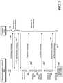
- FIG. 1is a side view schematic of a plasma processing system 100 equipped with an optical detection system 102 according to one example.
- the plasma processing system 100includes a plasma processing chamber 104 , inside which a substrate holder 106 is disposed, such as an electrostatic chuck, for receiving a substrate 108 (e.g., semiconductor wafer, integrated circuit, a sheet of a polymer material to be coated, a metal to be surface hardened by ion implantation, or other semiconductor material to be etched or deposited) to be processed.
- a substrate 108e.g., semiconductor wafer, integrated circuit, a sheet of a polymer material to be coated, a metal to be surface hardened by ion implantation, or other semiconductor material to be etched or deposited
- RF and/or microwave power from an RF and/or microwave source(not shown) is supplied to the plasma processing chamber 104 to ignite and sustain a plasma proximate to the substrate 108 , wherein the energetic chemical species from the plasma are used to perform a plasma processing step on the substrate 108 .
- the plasma processing system 100may utilize a pulsed plasma during operation such as in atomic layer deposition (ALD) and atomic layer etching (ALE).
- Processing gasese.g., nitrogen, xenon, argon, carbon tetrafluoride (CF 4 ), or octafluorocyclobutane (C 4 F 8 ) for fluocarbon chemistries, chlorine (Cl 2 ), hydrogen bromide (HBr), or oxygen (O 2 )
- a pumping systemis provided (not shown) to maintain a vacuum in the plasma processing chamber 104 , at a desired process pressure.
- Examples of plasma processing stepsinclude plasma-enhanced chemical vapor deposition (PECVD), plasma-enhanced atomic layer deposition (PEALD), and the like.
- the energy sourceis an antenna 120 powered by an RF source to inductively couple RF energy into the plasma processing chamber 104 .
- An electromagnetic field generated by the application of RF power to the antenna 120energizes the process gas to form the plasma above the substrate 108 .
- the optical detection system 102is used to detect optical events in the plasma processing chamber 104 via at least a light collector 110 and at least one optical detector 112 , which communicates the detected light to and is controlled by a controller 114 .
- the controller 114may be a general purpose computer, as shown in FIG. 7 .
- the optical window 116can include a material that is transparent in the monitored spectrum (e.g., visible) such as glass, quartz, fused silica or sapphire depending on the application and how aggressive the chemistry of the plasma.
- Detection area 118defines the portion of space from which the light emission is collected.
- the plasma processing chamber 104may include additional windows. For example, a second window may be used for a conventional optical emission spectroscopy system used for process end-point detector (EPD), for example.
- the light collector 110may be positioned in other positions as well, the plasma processing chamber 104 depending on the location of the plasma to be monitored for optical events. For example, the light collector 110 may be positioned to detect arcing during pin-up (lifting of the substrate 108 from the substrate holder 106 ).
- arcingcan cause material degradation of a wafer being processed and/or damage to the plasma processing system itself.
- Specific conditionsmay lead to abnormal discharge (arc) in the plasma processing chamber 104 .
- the abnormal dischargemay release acoustic, RF, chemical, and light energy. By detecting one or more of these energies (signals), it is possible to detect the arc as an abnormal discharge.
- some arcing events within the plasma processing chamber 104can be observed by disruption of RF coupling to process gases within the plasma processing chamber 104 (i.e. impedance mismatch).
- the present inventordetermined through testing, for example, that RF and acoustic techniques for detecting of abnormal plasma discharge events such as arcing are inadequate for detecting and characterizing many abnormal plasma conditions in the plasma processing chamber 104 .
- the sensor, system, and associated methodologies described hereindetect optical signals associated with arcing events inside the plasma processing chamber 104 .
- the sensor described hereindetects arcs over a large volume of the plasma processing chamber 104 including a horizontal dimension covering the substrate surface, and a vertical dimension covering the plasma itself from the substrate 108 to the upper electrode, for example.
- the optical detection system 102can detect arcs on the surface of a wafer, a focus ring, an antenna (i.e., electrode of capacitive-coupled RF plasma chamber), and inside the plasma itself. Optical detection of arcs is achieved even when very bright background light from the normal plasma process is present and/or when no plasma is present.
- FIG. 2Ais a top view schematic of the plasma processing system 100 equipped with the optical detection system 102 according to one example.
- the light collector 110includes multiple optical paths covering a large portion of the plasma processing chamber 104 volume and the surface of the substrate 108 , a focus ring 122 , and the antenna 120 (detection area 118 ). In one embodiment, this is achieved by wide angle lenses. For example, six wide angle lenses may be positioned adjacent to one another such that their fields of view overlap to collectively cover the desired volume of the plasma processing chamber 104 .
- the light detector 112receives the detected light from the light collector 110 directly or via one or more optical fibers.
- One or more optical detectorsmay be used.
- the background light (i.e. light which is not indicative of an optical event) to optical detectorhas power in the range from a few microwatts to hundreds of microwatts.
- the background lightcan saturate the light detector 112 .
- the light from a typical arc itselfis in range from [pW] (picowatt) to [ ⁇ W] (microwatt).
- the detectoris equipped with software controlled gain and background subtraction for elimination of the background light signal.
- An exemplary light detector 112 with background light subtractionis shown in FIG. 3B discussed below.
- the light detector 112may detect arcing events having an optical signal with a power of at least 3 orders of magnitude lower than the power of the optical signal of the plasma light emission.
- the light detector 112provides a high gain for arc signals even when the intensity of the light from plasma is very high.
- the duration of the arcis in the range of a few microseconds to hundred milliseconds.
- the optical detector electronics and acquisition systeme.g., the controller 114
- the electronics, firmware, and softwarecan handle a real time detection of the arc and provide time stamp information when the arc happens as well as the amplitude and duration of the arc with a very high resolution.
- arc detectionmay be performed within the typical pulse duration of a pulsed plasma.
- the optical detection system 102can detect light pulses starting from the hundred nanosecond range when the optical pulse energy (i.e., duration of the pulse multiplied by the power of the pulse) is in the pJ range.
- the light detector 112detects light pulse energy in addition to the light intensity.
- the electrical signal from the light detector 112is proportional to the amplitude of a light pulse when the light pulse has a duration greater than 6 microseconds.
- the light detector 112can detect light pulses having a duration lower than 0.5 microseconds when the pulse light energy is greater than 0.1 pJ.
- FIG. 2Bis a top view schematic of the plasma processing system 100 equipped with the arcing detection system 102 according to one example.
- the plasma processing system 100may be equipped with multiple windows.
- the plasma processing system 100may include a second window 200 for OES (optical emission spectroscopy) endpoint detection.
- the detection area diameter ais 450 mm at the wafer center.
- the optical detection system 102may include the light collector 110 , the light detector 112 , a filter 300 , an ADC 302 (Analog to digital convertor), a digital controller 304 , an interface 306 , a computer 308 , and an optional optical filter 310 .
- ADC 302Analog to digital convertor
- the optical detection system 102is located outside the plasma processing chamber 104 such that light passes through the optical window 116 of the plasma processing chamber 104 .
- Light emitted in the plasma processing chamber 104is collected by the light collector 110 , and is passed to the light detector 112 via an optical fiber (not shown) for example.
- the detected intensitiesmay be filtered via the filter 300 (e.g., an electronic analog filter).
- the filtered intensitiesare then fed to the digital controller 304 via the ADC 302 .
- the digital controller 304passes the detected intensities to a computer 308 via the interface 306 .
- the digital controller 304controls the light detector 112 and the ADC 302 .
- the arcing eventsare in the micro-second order, thus the digital controller 304 has a fast response time. Note that the resolution of the ADC 302 controls the time resolution of the optical detection system 102 . However, the ADC 302 does not control the time resolution of the light pulse detected via the light detector 112 .
- the computer 308may be located proximate to the plasma processing system 100 , or may be located remotely, and connected via a network (e.g., internet, intranet) to the system.
- a networke.g., internet, intranet
- the light collector 110is configured to detect light emission from any point in an area covering the substrate 108 and the focus ring 122 (e.g., detection area 118 of FIG. 1 ). In the vertical direction, the light collector 110 is configured to detect any arc from the wafer to the antenna 120 as shown in FIG. 1 .
- the light collector 110may include one or more lens.
- the one or more lensmay have a focal length (f) and f number (N) as a function of the detection area 118 dimensions.
- the light collector 110may include one or more wide angle lens.
- the one or more lensesmay be positioned at different angles to cover detection area 118 .
- the detection area diameteris 450 mm at the center of the plasma processing chamber 104 as shown in FIG. 2B .
- the light collector 110may include six lenses each positioned at an angle of ⁇ 31.1, ⁇ 19.7, ⁇ 6.1, 6.1, 19.7, and 31.1 degree, respectively.
- the light collected by each lensis transmitted to the light detector 112 by an optical fiber.
- 800 ⁇ m fiberis used.
- the image sizeis 0.8 mm.
- the lensmay be positioned at a distance of 375 mm from the wafer center and have an aperture of 4.8 mm.
- NANumerical Aperture
- the image space numerical apertureis 0.44.
- the light detector 112may include a photomultiplier tube, CCD (Charged-coupled device), a photodiode, a CMOS (Complementary metal-oxide-semiconductor) photo array, a photodiode array.
- the light detector 112has a readout frequency of 5 MHz or higher.
- the light detector 112is configured to detect in the wavelength range 400 nm-900 nm.
- the light detector 112may have specific wavelength spectral characteristic based on application requirements.
- the photodiodemay include an optical filter configured for a specific wavelength.
- the light detector 112may have a variable gain controlled by the digital controller 304 .
- the light detector 112may be implemented by a variable gain photodiode controlled by the digital controller 304 .
- the light detector 112may include one or more light detectors. Each of the detectors/subareas of the detector may cover overlapping areas of the detection area 118 covering the wafer and the focus ring. Each signal emitted in by a subdetector outputs to a channel.
- the optical detection system 102may further include one or more optical filters in the optical path (e.g., optical filter 310 ).
- a spectral filtermay be included in front of the photodiode associated with a channel.
- the channelrepresents an output associated with a part of the detection area 118 .
- the optical detection system 102includes six channels. Further, multiple filters may be used to provide high spectral (wavelength resolution). This provides an ultra-high speed sensor with discrete spectral information.
- the optical filtersmay be included in all channels or fewer channels.
- the optical filter 310may be used to optically suppress background light signal. For example, a filter may be used to block a 700 nm signal associated with Ar in the plasma.
- each optical fibermay be split into multiple discrete spectral channels via optical spectral splitters (e.g., optical filters with beam splitters). For example, two or three spectral line-channels can be obtained from one channel.
- optical spectral splitterse.g., optical filters with beam splitters.
- the spectral informationmay be used for monitoring the plasma processing chamber and for the diagnostic of faults in the plasma processing chamber 104 .
- the optical detection system 102may detect helium gas leakage in the plasma processing chamber 104 from under the substrate 108 during plasma ramp down. Further, the optical detection system 102 may detect discrete gas emission line during etching as well as sporadic events.
- a sparking eventmay be detected by one or more channels. Large arcing may appear in all the channels at the same time with a same shape, and similar signal strength. Small arcing may have noticeable difference between channels, thus providing spatial location of the arc within the plasma processing chamber 104 .
- the optical detection system 102detects arcing from wafer chucking to wafer de-chucking (plasma off). Arcing events during de-chucking may be caused by residual charges.
- the light detector 112 and an end-point detector sensormay be collected in one housing.
- the light detector 112 and the end-point detector sensormay communicate with the computer 308 via communication cables.
- the computer 308may also detect and process a plasma optical emission spectroscopy (OES) signal.
- OESplasma optical emission spectroscopy
- FIG. 3Bis an exemplary block diagram of a light detector 112 according to one example.
- the light detector 112may include a background light subtraction circuit to avoid saturation of the detector.
- the light detector 112may include a photodiode 312 , a resistor 316 , a capacitor 318 , and an IC Op Amp (Integrated circuit operational amplifier) 314 (e.g., a high gain op amp).
- the background light subtraction circuitincludes an IC Op Amp 322 , resistors 320 , 324 , and 328 , and capacitors 322 and 326 .
- the background light subtraction circuitgenerates a current proportional to the background light and is not sensitive to a short light pulse.
- the current from resistor 320is subtracted from the photodiode current and thus the Op Amp 314 is not saturated by the background light.
- the current from resistor 320is proportional to the background light.
- FIG. 4is a flowchart that shows a method 400 for arcing detection according to one example.
- the method 400may be performed by the controller 114 described in relation to FIG. 1 .
- the method 400may begin when the PECVD chamber is activated.
- a light emission signalmay be detected.
- the light detector 112may detect a light signal received via the light collector 110 .
- the light emission signalis processed.
- the plasma light emissionis subtracted from the detected light emission signal.
- a background noisemay be subtracted.
- the background noiserepresents electronics noise or other noises that may cause fluctuations in the detected signals that are not due to the background light or optical events.
- the detected light intensitymay be processed as a function of an average noise.
- the emission to the light collector 110may be blocked and a background noise is detected and saved.
- the background noisemay be collected when the plasma is off and/or on. Then, the background noise may be subtracted from the detected light intensity.
- the background lightis suppressed using one or more techniques based on the process.
- one or more of optical filtering, light detector gain control and ADC controlmay be used to achieve optimal suppression of the background plasma light signal and to achieve high signal to noise ratio for optical emissions that indicate plasma anomalies.
- a signature of the arcing event from the processed light emission signalis detected.
- the arching eventis detected when the processed light emission signal is above a threshold value.
- the arcing eventmay be classified based on the detected intensities. For example, small arcing events may include arcing events having intensities between the threshold value and a second threshold value. Strong arcing events may include arcing events having intensities greater than the second threshold value.
- a warning signalmay be generated such as an audio warming, visual warning to take corrective action to minimize substrate arcing or to terminate plasma processing.
- the arcing eventsmay also be simultaneously detected via other arcing detection techniques such as via an acoustic emission sensor (AE), a RF probe, and/or an OES system. Data collected may be used for cross checking and further identifying an arcing event detected.
- AEacoustic emission sensor
- RF probea RF probe
- OES systeman OES system
- Software algorithmsmay be used in the detection and characterization of optical events.
- an algorithmmay learn normal signal patterns of a recipe at each step. Then, a signal pattern comparison algorithm is applied during measurement runs with the “learned” normal pattern to detect abnormal signals.
- the algorithmmay be used for arcing detection as well as for plasma monitoring.
- a machine learning algorithmor a trained model (e.g., with dimensional reduction) may be used to discriminate between an abnormal signal (e.g., arc, unstable plasma) and a normal signal (i.e., signal after all filtering applied such optical, electrical filters or the like).
- an abnormal signale.g., arc, unstable plasma
- a normal signali.e., signal after all filtering applied such optical, electrical filters or the like.
- Specific artificial intelligence algorithmsmay be dependent on the individual actual plasma process application (for example, etch runs).
- a trained model of signal pattern recognitionmay be used for identification of unusual signals from normal signals under many different scenarios (e.g., spike detection).
- FIG. 5is a flowchart that shows a method 500 for arcing detection according to one example.
- a substratee.g., substrate 108
- the plasma processing controller 502may send a message to the controller 114 ( 506 ) including information about the wafer load being processed.
- the controller 114may load information associated with the wafer load being processed for example, light plasma intensity associated with the current load ( 508 ).
- the controller 114may send an acknowledgment message ( 510 ).
- the plasma processing controller 502may send a message to the controller 114 to start the arcing monitoring process ( 512 ), for example, method 400 shown in FIG.
- a chucking sequenceis started ( 514 ).
- a chucking forceis applied to the substrate ( 514 ).
- the plasmais turned on ( 516 ) and a transition message indicating that the plasma is ON is sent to the controller 114 ( 518 ).
- a complete messageis sent to the controller 114 .
- the controller 114may adjust the processing of the detected light intensities. For example, the controller 114 may filter the detected light intensities as a function of the background noise.
- a de-chuck sequencemay be started ( 520 ). During the de-chuck sequence, the chucking force is removed from the substrate 108 . As described previously herein, during the de-chuck sequence the plasma processing chamber 104 is monitored for arcing events. Once the de-chuck sequence is completed, the plasma processing controller 502 may send a stop monitor message to the controller 114 ( 522 ). The controller 114 may send to the plasma processing controller 502 the monitoring results ( 524 ). The monitoring results may include information (e.g., intensity, timestamp, time span) about one or more arcing events detected.
- informatione.g., intensity, timestamp, time span
- the plasma processing controller 502may determine a “next” action ( 526 ) based on the severity of the arcing events detected.
- the “next” actionmay include outputting a flag to an operator, logging the wafer as a defect, performing a maintenance routine, or the like.
- the optical detection system 102may detect optical events other than arcing.
- the optical detection system 102may detect abnormal emission spikes (e.g., negative spikes) and/or unusual plasma emission occurrence (e.g., dips, extinguishing, flickering, or the like).
- the detected signalsmay be analyzed to determine a correlation between recipe, chamber conditions, and/or parts of the chamber/wafer with the unusual or abnormal emissions.
- the optical detection system 102provides the user with user interfaces.
- a first user interfacemay be for data acquisition and a second interface may be for data analysis.
- FIG. 6Ais an exemplary arcing intensity signal acquired using the arcing detection system.
- Schematic 600shows a user interface that shows exemplary results.
- Traces 602 and 604show an arcing event detected by two channels.
- a Kapton tape and a test chip with a TiN conductor layerare used to simulate an arcing event during plasma processing. Both edge arcing and surface arcing is generated using the kapton tape.
- the plasmais generated using a CF4/Ar source.
- FIG. 6Bis a schematic that shows the plasma intensity according to one example.
- Schematic 606shows the plasma (emission) intensity in time domain.
- Trace 608shows the emission intensity captured by a center channel. The center channel captures emission in the center of the plasma processing chamber 104 (e.g., P3 or P4 shown in FIG. 2B ).
- Trace 610shows the emission intensity captured by a side channel. As shown by trace 608 and trace 610 the plasma is not stable, about 10% fluctuation in emission intensity is observed in time domain. The high resolution of the optical detection system 102 gives more information about the stability of the plasma. In addition to the arcing events, the system may detect unusual plasma emission occurrence (e.g., dips, extinguishing, flickering). Trace 608 and trace 610 shows two extinguishing events. The extinguishing events represent dips in the plasma intensity that may occur in an unstable plasma.
- unusual plasma emission occurrencee.g., dips, extinguishing, flicker
- FIG. 6Cis a schematic that shows exemplary results.
- Schematic 612shows the arcing event detected using an RF probe.
- Schematic 614shows the same arcing event detected via an AE sensor.
- Schematic 616shows the same arcing event detected by the optical detection system 102 described herein. The arcing event is detected with a higher resolution via the optical detection system 102 compared to the other techniques.
- the computer 308includes a CPU 700 which performs the processes described herein.
- the process data and instructionsmay be stored in memory 702 .
- These processes and instructionsmay also be stored on a storage medium disk 704 such as a hard drive (HDD) or portable storage medium or may be stored remotely.
- a storage medium disk 704such as a hard drive (HDD) or portable storage medium or may be stored remotely.
- the claimed advancementsare not limited by the form of the computer-readable media on which the instructions of the inventive process are stored.
- the instructionsmay be stored on CDs, DVDs, in FLASH memory, RAM, ROM, PROM, EPROM, EEPROM, hard disk or any other information processing device with which the computer 308 communicates, such as the plasma processing system 100 .
- claimed advancementsmay be provided as a utility application, background daemon, or component of an operating system, or combination thereof, executing in conjunction with CPU 700 and an operating system such as Microsoft Windows 7, UNIX, Solaris, LINUX, Apple MAC-OS and other systems known to those skilled in the art.
- an operating systemsuch as Microsoft Windows 7, UNIX, Solaris, LINUX, Apple MAC-OS and other systems known to those skilled in the art.
- CPU 700may be a Xenon or Core processor from Intel of America or an Opteron processor from AMD of America, or may be other processor types that would be recognized by one of ordinary skill in the art.
- the CPU 700may be implemented on an FPGA, ASIC, PLD or using discrete logic circuits, as one of ordinary skill in the art would recognize.
- CPU 700may be implemented as multiple processors cooperatively working in parallel to perform the instructions of the inventive processes described above.
- the computer 308 in FIG. 7also includes a network controller 706 , such as an Intel Ethernet PRO network interface card from Intel Corporation of America, for interfacing with network 728 .
- the network 728can be a public network, such as the Internet, or a private network such as LAN or WAN network, or any combination thereof and can also include PSTN or ISDN sub-networks.
- the network 728can also be wired, such as an Ethernet network, or can be wireless such as a cellular network including EDGE, 3G and 4G wireless cellular systems.
- the wireless networkcan also be WiFi, Bluetooth, or any other wireless form of communication that is known.
- the computer 308further includes a display controller 708 , such as a NVIDIA GeForce GTX or Quadro graphics adaptor from NVIDIA Corporation of America for interfacing with display 710 , such as a Hewlett Packard HPL2445w LCD monitor.
- a general purpose I/O interface 712interfaces with a keyboard and/or mouse 714 as well as an optional touch screen panel 716 on or separate from display 710 .
- General purpose I/O interfacealso connects to a variety of peripherals 718 including printers and scanners, such as an OfficeJet or DeskJet from Hewlett Packard.
- a sound controller 720is also provided in the computer 308 , such as Sound Blaster X-Fi Titanium from Creative, to interface with speakers/microphone 722 thereby providing sounds and/or music. For example, audible alerts may be outputted via the speakers 722 when arcing events are detected.
- the general purpose storage controller 724connects the storage medium disk 704 with communication bus 726 , which may be an ISA, EISA, VESA, PCI, or similar, for interconnecting all of the components of the computer 308 .
- communication bus 726may be an ISA, EISA, VESA, PCI, or similar, for interconnecting all of the components of the computer 308 .
- a description of the general features and functionality of the display 710 , keyboard and/or mouse 714 , as well as the display controller 708 , storage controller 724 , network controller 706 , sound controller 720 , and general purpose I/O interface 712is omitted herein for brevity as these features are known.
- the optical detection system 102 described hereinhas a higher signal to noise (S/N) (i.e., around ten time better S/N) compared to other sensors (e.g., acoustic emission (AE) sensor, RF probe, and EPD sensor).
- S/Nsignal to noise
- other sensorse.g., acoustic emission (AE) sensor, RF probe, and EPD sensor.
- the optical detection system 102has a better time resolution (i.e. around 100 time better time resolution) compared to known techniques (e.g., AE sensor, RF probe, and EPD).
- the systemhas the advantage of detecting “small” arc events not detected by other known sensors.
- the inventorsperformed tests for determining the effects electromagnetic (EM) signals on the optical detection system. For example, a plasma was initiated and maintained in the plasma processing chamber 104 , without any substrate and without any arcing conditions simulated in the plasma processing chamber 104 .
- the optical detection system 102did not detect any arcing event signal (e.g., by controller 114 ), indicating that the plasma under normal conditions does not generate significant EM signals that may interfere with the optical detection system 102 and its associated electronics.
- Testswere also performed under arcing conditions. Arcing was produced for example, by use of kapton tape to fix a test chip to the substrate holder 106 . Arcing on the chip surface and at edges of the chip were visually confirmed by burn marks on the test chip and on the substrate holder 106 .
- one channel of the optical detectorwas optically blocked and compared to a non-blocked channel.
- An arcing eventwas detected on the non-blocked channel, while no event was detected on the optically blocked channel, indicating that any EM signals from an arcing event would not significantly affect on the optical detection electronics.
- an EM mesh shieldwas provided on the optical window to block any EM signals from within the chamber. The EM shield reduced the optical signal detected, no improvement of the detected arcing signal from the shield, indicating that an EM was not essential or even needed for use of the optical detection system.
- Arcswere generated in the plasma processing system 100 under varying conditions to assess the system's detection rate under varying conditions. Burn marks were used to confirm the occurrence of arcing events in the chamber. The optical detection system 102 did not detect any arcing signal when no burn marks are present. Thus, the optical system had no false positive detections. In some tests, burn marks were observed, but the system did not detect any arc event signal corresponding to the burn. This failure to detect some arcing events is thought to be attributed to certain test conditions, such as the recipe used, which can be improved by use of optical filters, detector gain control techniques, and analog signal filters to suppress the background plasma emissions and improve signal to noise ratio for the optical event.
- the inventorsperformed tests for characterizing arcing events. Different size arcing events were simulated by use of Kapton tape and or a test chip in the chamber. The observed burn mark was proportional to the size of the arcing event. Detection of the various arcing events by the optical detector disclosed herein was compared to other detection methods (e.g., RF probe, AE sensor, and optical emission spectroscopy detection (OES)). The results showed that the RF probe, AE sensor, OES system and the inventive optical detector could detect relatively large arcs. However, the inventive optical detector detected smaller arcs that were not detected by the RF probe, AE sensor, OES systems.
- detection methodse.g., RF probe, AE sensor, and optical emission spectroscopy detection (OES)
- the optical detection system 102has a better signal-to-noise (S/N) ratio than the RF probe and the AE sensor.
- S/Nsignal-to-noise
- the systemshowed a S/N of 20 for a large arc compared to a S/N of 2 for the RF probe and a S/N of 3 for the AE sensor.
- the testsshows an excellent time resolution ( ⁇ 1 msec) compared to the RF probe ( ⁇ 22 msec), AE sensor ( ⁇ 27 msec), and EPD ( ⁇ 10.9 sec).
- sparking event after the plasma is turned offAnother set of tests was conducted to detect sparking event after the plasma is turned off. Sparking is observed in all test wafers after the plasma is turned off. Sparking events after the plasma turned off occur in three distinct groups (i.e., small sparks followed by larger sparks followed by small sparks).
Landscapes
- Physics & Mathematics (AREA)
- Spectroscopy & Molecular Physics (AREA)
- Engineering & Computer Science (AREA)
- Chemical & Material Sciences (AREA)
- Plasma & Fusion (AREA)
- Analytical Chemistry (AREA)
- General Physics & Mathematics (AREA)
- Power Engineering (AREA)
- Drying Of Semiconductors (AREA)
- Plasma Technology (AREA)
- Chemical Kinetics & Catalysis (AREA)
- Materials Engineering (AREA)
- Mechanical Engineering (AREA)
- Metallurgy (AREA)
- Organic Chemistry (AREA)
Abstract
Description
Claims (23)
Priority Applications (1)
| Application Number | Priority Date | Filing Date | Title |
|---|---|---|---|
| US15/351,916US10692705B2 (en) | 2015-11-16 | 2016-11-15 | Advanced optical sensor and method for detecting an optical event in a light emission signal in a plasma chamber |
Applications Claiming Priority (2)
| Application Number | Priority Date | Filing Date | Title |
|---|---|---|---|
| US201562255573P | 2015-11-16 | 2015-11-16 | |
| US15/351,916US10692705B2 (en) | 2015-11-16 | 2016-11-15 | Advanced optical sensor and method for detecting an optical event in a light emission signal in a plasma chamber |
Publications (2)
| Publication Number | Publication Date |
|---|---|
| US20170140905A1 US20170140905A1 (en) | 2017-05-18 |
| US10692705B2true US10692705B2 (en) | 2020-06-23 |
Family
ID=58690269
Family Applications (1)
| Application Number | Title | Priority Date | Filing Date |
|---|---|---|---|
| US15/351,916Active2037-02-09US10692705B2 (en) | 2015-11-16 | 2016-11-15 | Advanced optical sensor and method for detecting an optical event in a light emission signal in a plasma chamber |
Country Status (4)
| Country | Link |
|---|---|
| US (1) | US10692705B2 (en) |
| KR (1) | KR20180073700A (en) |
| TW (1) | TWI637153B (en) |
| WO (1) | WO2017087378A1 (en) |
Cited By (4)
| Publication number | Priority date | Publication date | Assignee | Title |
|---|---|---|---|---|
| US11688413B2 (en) | 2019-12-19 | 2023-06-27 | Taiwan Semiconductor Manufacturing Co., Ltd. | Method and system for audio recognition of arcing during semiconductor process |
| US12158374B2 (en) | 2022-10-25 | 2024-12-03 | Tokyo Electron Limited | Time-resolved OES data collection |
| US12306044B2 (en) | 2022-09-20 | 2025-05-20 | Tokyo Electron Limited | Optical emission spectroscopy for advanced process characterization |
| US12362158B2 (en) | 2022-10-25 | 2025-07-15 | Tokyo Electron Limited | Method for OES data collection and endpoint detection |
Families Citing this family (21)
| Publication number | Priority date | Publication date | Assignee | Title |
|---|---|---|---|---|
| US10748797B2 (en)* | 2017-01-18 | 2020-08-18 | Applied Materials, Inc. | Plasma parameters and skew characterization by high speed imaging |
| DE102017130988B4 (en)* | 2017-12-21 | 2022-07-07 | Infineon Technologies Ag | DEVICES AND METHODS FOR UTILIZING THE PHOTOACOUSTIC EFFECT |
| US20190335078A1 (en)* | 2018-04-30 | 2019-10-31 | Macronix International Co., Ltd. | Detection system and associated detection method for detecting occurrence of arcing phenomenon |
| CN110582155A (en)* | 2018-06-08 | 2019-12-17 | 北京北方华创微电子装备有限公司 | plasma glow starting detection device and method and process chamber |
| JP2020065013A (en)* | 2018-10-18 | 2020-04-23 | 東京エレクトロン株式会社 | End point detection method and end point detection device |
| US10699871B2 (en) | 2018-11-09 | 2020-06-30 | Applied Materials, Inc. | System and method for spatially resolved optical metrology of an ion beam |
| US10903050B2 (en)* | 2018-12-10 | 2021-01-26 | Lam Research Corporation | Endpoint sensor based control including adjustment of an edge ring parameter for each substrate processed to maintain etch rate uniformity |
| JP7186646B2 (en)* | 2019-03-22 | 2022-12-09 | 東京エレクトロン株式会社 | SUBSTRATE PROCESSING APPARATUS AND METHOD FOR DETECTING PRESENCE OF FOCUS RING ON PLACEMENT |
| EP3796362A1 (en)* | 2019-09-23 | 2021-03-24 | TRUMPF Huettinger Sp. Z o. o. | Method of plasma processing a substrate in a plasma chamber and plasma processing system |
| US11894250B2 (en)* | 2020-03-31 | 2024-02-06 | Taiwan Semiconductor Manufacturing Co., Ltd. | Method and system for recognizing and addressing plasma discharge during semiconductor processes |
| KR102833984B1 (en)* | 2020-08-31 | 2025-07-15 | 삼성전자주식회사 | Monitoring method of semiconductor device and manufacturing method of semiconductor device including the same |
| CN112458440B (en)* | 2020-11-18 | 2022-11-25 | 北京北方华创微电子装备有限公司 | Semiconductor process equipment and its reaction chamber and film deposition method |
| KR102309039B1 (en)* | 2021-04-06 | 2021-10-06 | 국방과학연구소 | Arc plasma heater with detectable arc rotational spped |
| WO2022235926A1 (en)* | 2021-05-07 | 2022-11-10 | Mersen Usa Ep Corp. | Arc detection and recording in electric trains, subways, streetcars and busses |
| US20220406581A1 (en)* | 2021-06-18 | 2022-12-22 | Applied Materials, Inc. | Methods for detecting arcing in power delivery systems for process chambers |
| EP4113574B1 (en)* | 2021-07-02 | 2024-01-03 | Comet AG | Method for machine learning a detection of at least one irregularity in a plasma system |
| EP4242904A3 (en)* | 2021-07-02 | 2023-11-01 | Comet AG | Method for machine learning a detection of at least one irregularity in a plasma system |
| KR20230092176A (en) | 2021-12-17 | 2023-06-26 | 삼성전자주식회사 | Device for radical diagonostic in plasma process chamber, radical diagonostic systemt having the same, and operating method thereof |
| KR102781411B1 (en)* | 2022-11-03 | 2025-03-17 | 한국기계연구원 | Filter changeable plasma monitoring system and plasma monitoring method |
| US20250060307A1 (en)* | 2023-08-15 | 2025-02-20 | Honeywell International Inc. | Optical cavity-enhanced frequency comb spectroscopy |
| US20250157801A1 (en)* | 2023-11-09 | 2025-05-15 | Tokyo Electron Limited | Sub-millisecond optical detection of pulsed plasma processes |
Citations (58)
| Publication number | Priority date | Publication date | Assignee | Title |
|---|---|---|---|---|
| US3059611A (en) | 1960-07-05 | 1962-10-23 | Ibm | Monitoring apparatus |
| US3612692A (en) | 1968-11-21 | 1971-10-12 | Ibm | Dielectric film thickness monitoring and control system and method |
| US4147435A (en) | 1977-06-30 | 1979-04-03 | International Business Machines Corporation | Interferometric process and apparatus for the measurement of the etch rate of opaque surfaces |
| US5014217A (en) | 1989-02-09 | 1991-05-07 | S C Technology, Inc. | Apparatus and method for automatically identifying chemical species within a plasma reactor environment |
| US5308414A (en) | 1992-12-23 | 1994-05-03 | International Business Machines Corporation | Method and apparatus for optical emission end point detection in plasma etching processes |
| US5347460A (en) | 1992-08-25 | 1994-09-13 | International Business Machines Corporation | Method and system employing optical emission spectroscopy for monitoring and controlling semiconductor fabrication |
| US5353790A (en) | 1992-01-17 | 1994-10-11 | Board Of Regents, The University Of Texas System | Method and apparatus for optical measurement of bilirubin in tissue |
| EP0652415A1 (en) | 1993-11-09 | 1995-05-10 | Nova Measuring Instruments Limited | A device for measuring the thickness of thin films |
| US5450205A (en) | 1993-05-28 | 1995-09-12 | Massachusetts Institute Of Technology | Apparatus and method for real-time measurement of thin film layer thickness and changes thereof |
| US5751416A (en) | 1996-08-29 | 1998-05-12 | Mississippi State University | Analytical method using laser-induced breakdown spectroscopy |
| US5980767A (en) | 1994-02-25 | 1999-11-09 | Tokyo Electron Limited | Method and devices for detecting the end point of plasma process |
| US6060328A (en) | 1997-09-05 | 2000-05-09 | Advanced Micro Devices, Inc. | Methods and arrangements for determining an endpoint for an in-situ local interconnect etching process |
| US6081334A (en) | 1998-04-17 | 2000-06-27 | Applied Materials, Inc | Endpoint detection for semiconductor processes |
| US6090302A (en) | 1998-04-23 | 2000-07-18 | Sandia | Method and apparatus for monitoring plasma processing operations |
| US6132577A (en) | 1998-04-23 | 2000-10-17 | Sandia Corporation | Method and apparatus for monitoring plasma processing operations |
| US20020029851A1 (en) | 2000-09-12 | 2002-03-14 | Manabu Edamura | Plasma processing method and apparatus using dynamic sensing of a plasma environment |
| US6381008B1 (en) | 1998-06-20 | 2002-04-30 | Sd Acquisition Inc. | Method and system for identifying etch end points in semiconductor circuit fabrication |
| US20020139925A1 (en)* | 2001-03-30 | 2002-10-03 | Tokyo Electron Limited | Optical system and method for plasma optical emission analysis |
| US6535779B1 (en) | 1998-03-06 | 2003-03-18 | Applied Materials, Inc. | Apparatus and method for endpoint control and plasma monitoring |
| US20030054655A1 (en)* | 2001-01-17 | 2003-03-20 | Hiroyuki Nakano | Semiconductor device processing method and plasma processing method and its apparatus |
| US6564114B1 (en) | 1999-09-08 | 2003-05-13 | Advanced Micro Devices, Inc. | Determining endpoint in etching processes using real-time principal components analysis of optical emission spectra |
| US6582618B1 (en) | 1999-09-08 | 2003-06-24 | Advanced Micro Devices, Inc. | Method of determining etch endpoint using principal components analysis of optical emission spectra |
| US20040008336A1 (en) | 2002-05-29 | 2004-01-15 | Tokyo Electron Limited | Method and system of determining chamber seasoning condition by optical emission |
| US20040026035A1 (en)* | 2000-11-28 | 2004-02-12 | Mitrovic Andrej S. | Method and apparatus for 2-d spatially resolved optical emission and absorption spectroscopy |
| TW589659B (en) | 2001-12-19 | 2004-06-01 | Applied Materials Inc | Plasma reactor with overhead RF electrode tuned to the plasma with arcing suppression |
| US6745095B1 (en)* | 2000-10-04 | 2004-06-01 | Applied Materials, Inc. | Detection of process endpoint through monitoring fluctuation of output data |
| US20040104681A1 (en) | 2002-11-26 | 2004-06-03 | Tokyo Electron Limited | Plasma processing system and method |
| US6815653B2 (en) | 2002-04-15 | 2004-11-09 | Taiwan Semiconductor Manufacturing Co., Ltd | Method and apparatus for early detection of material accretion and peeling in plasma system |
| US6830939B2 (en) | 2002-08-28 | 2004-12-14 | Verity Instruments, Inc. | System and method for determining endpoint in etch processes using partial least squares discriminant analysis in the time domain of optical emission spectra |
| US6952657B2 (en)* | 2003-09-10 | 2005-10-04 | Peak Sensor Systems Llc | Industrial process fault detection using principal component analysis |
| US20060285108A1 (en)* | 2005-06-17 | 2006-12-21 | Perkinelmer, Inc. | Optical emission device with boost device |
| US7241397B2 (en) | 2004-03-30 | 2007-07-10 | Tokyo Electron Limited | Honeycomb optical window deposition shield and method for a plasma processing system |
| CN101038860A (en) | 2006-03-17 | 2007-09-19 | 东京毅力科创株式会社 | Plasma processing apparatus and method |
| US7328126B2 (en) | 2003-09-12 | 2008-02-05 | Tokyo Electron Limited | Method and system of diagnosing a processing system using adaptive multivariate analysis |
| US7334477B1 (en) | 2004-12-22 | 2008-02-26 | Lam Research Corporation | Apparatus and methods for the detection of an arc in a plasma processing system |
| CN101221891A (en) | 2007-01-12 | 2008-07-16 | 北京北方微电子基地设备工艺研究中心有限责任公司 | Etching terminal checking device and method for plasma etching equipment |
| US20080186473A1 (en) | 2007-07-25 | 2008-08-07 | Macronix International Co., Ltd. | Method of detecting end point of plasma etching process |
| US20080285202A1 (en)* | 2007-05-15 | 2008-11-20 | International Business Machines Corporation | In situ monitoring of wafer charge distribution in plasma processing |
| US7591923B2 (en) | 2002-09-30 | 2009-09-22 | Tokyo Electron Limited | Apparatus and method for use of optical system with a plasma processing system |
| US20090280581A1 (en) | 2008-05-12 | 2009-11-12 | Lam Research Corporation | Detection of arcing events in wafer plasma processing through monitoring of trace gas concentrations |
| US20110174776A1 (en) | 2007-08-28 | 2011-07-21 | Tokyo Electron Limited | Plasma processing apparatus, plasma processing method and end point detection method |
| US8048326B2 (en) | 2002-10-31 | 2011-11-01 | Tokyo Electron Limited | Method and apparatus for determining an etch property using an endpoint signal |
| CN102282654A (en) | 2009-03-17 | 2011-12-14 | 株式会社日立高新技术 | Etching device, analysis device, etching treatment method, and etching treatment program |
| US20120085494A1 (en) | 2008-02-27 | 2012-04-12 | Hiroshige Uchida | Plasma Etching Apparatus |
| US20120101622A1 (en)* | 2009-06-30 | 2012-04-26 | Gunsu Yun | Automatic fault detection and classification in a plasma processing system and methods thereof |
| US8173451B1 (en) | 2011-02-16 | 2012-05-08 | Tokyo Electron Limited | Etch stage measurement system |
| KR20120126418A (en) | 2011-05-11 | 2012-11-21 | (주)쎄미시스코 | System for monitoring plasma |
| US20130016344A1 (en) | 2011-07-14 | 2013-01-17 | Larry Bullock | Method and Apparatus for Measuring Process Parameters of a Plasma Etch Process |
| US8415884B2 (en) | 2009-09-08 | 2013-04-09 | Tokyo Electron Limited | Stable surface wave plasma source |
| US8416509B2 (en) | 2009-02-10 | 2013-04-09 | Samsung Electronics Co., Ltd. | Optical apparatus |
| US20130141720A1 (en) | 2011-12-05 | 2013-06-06 | Samsung Electronics Co., Ltd. | Plasma diagnostic apparatus and method |
| US8513583B2 (en) | 2009-11-23 | 2013-08-20 | The University Of Notre Dame Du Lac | Methods and apparatus for plasma based adaptive optics for generating a first plasma gradient and a second plasma gradient |
| US8553218B2 (en) | 2009-12-28 | 2013-10-08 | Asml Netherlands B.V. | Calibration method and apparatus |
| US20140097359A1 (en)* | 2011-06-06 | 2014-04-10 | Sicpa Holding Sa | In-line decay-time scanner |
| US20140209453A1 (en)* | 2013-01-31 | 2014-07-31 | Samsung Electronics Co., Ltd. | Method for predicting plasma micro-arcing, and method for controlling plasma process of production equipment using the same |
| US20150069912A1 (en)* | 2012-02-22 | 2015-03-12 | Lam Research Corporation | RF Impedance Model Based Fault Detection |
| US20150241272A1 (en) | 2014-02-25 | 2015-08-27 | Lei Lian | Pulsed Plasma Monitoring Using Optical Sensor |
| US20160268108A1 (en) | 2009-08-17 | 2016-09-15 | Verity Instruments, Inc. | Method and apparatus for the detection of arc events during the plasma processing of a wafer, surface of substrate |
- 2016
- 2016-11-15USUS15/351,916patent/US10692705B2/enactiveActive
- 2016-11-15WOPCT/US2016/062017patent/WO2017087378A1/ennot_activeCeased
- 2016-11-15KRKR1020187016983Apatent/KR20180073700A/enactivePending
- 2016-11-16TWTW105137371Apatent/TWI637153B/enactive
Patent Citations (65)
| Publication number | Priority date | Publication date | Assignee | Title |
|---|---|---|---|---|
| US3059611A (en) | 1960-07-05 | 1962-10-23 | Ibm | Monitoring apparatus |
| US3612692A (en) | 1968-11-21 | 1971-10-12 | Ibm | Dielectric film thickness monitoring and control system and method |
| US4147435A (en) | 1977-06-30 | 1979-04-03 | International Business Machines Corporation | Interferometric process and apparatus for the measurement of the etch rate of opaque surfaces |
| US5014217A (en) | 1989-02-09 | 1991-05-07 | S C Technology, Inc. | Apparatus and method for automatically identifying chemical species within a plasma reactor environment |
| US5353790A (en) | 1992-01-17 | 1994-10-11 | Board Of Regents, The University Of Texas System | Method and apparatus for optical measurement of bilirubin in tissue |
| US5347460A (en) | 1992-08-25 | 1994-09-13 | International Business Machines Corporation | Method and system employing optical emission spectroscopy for monitoring and controlling semiconductor fabrication |
| US5308414A (en) | 1992-12-23 | 1994-05-03 | International Business Machines Corporation | Method and apparatus for optical emission end point detection in plasma etching processes |
| US5450205A (en) | 1993-05-28 | 1995-09-12 | Massachusetts Institute Of Technology | Apparatus and method for real-time measurement of thin film layer thickness and changes thereof |
| EP0652415A1 (en) | 1993-11-09 | 1995-05-10 | Nova Measuring Instruments Limited | A device for measuring the thickness of thin films |
| US5980767A (en) | 1994-02-25 | 1999-11-09 | Tokyo Electron Limited | Method and devices for detecting the end point of plasma process |
| US5751416A (en) | 1996-08-29 | 1998-05-12 | Mississippi State University | Analytical method using laser-induced breakdown spectroscopy |
| US6060328A (en) | 1997-09-05 | 2000-05-09 | Advanced Micro Devices, Inc. | Methods and arrangements for determining an endpoint for an in-situ local interconnect etching process |
| US6535779B1 (en) | 1998-03-06 | 2003-03-18 | Applied Materials, Inc. | Apparatus and method for endpoint control and plasma monitoring |
| US6081334A (en) | 1998-04-17 | 2000-06-27 | Applied Materials, Inc | Endpoint detection for semiconductor processes |
| US6132577A (en) | 1998-04-23 | 2000-10-17 | Sandia Corporation | Method and apparatus for monitoring plasma processing operations |
| US6090302A (en) | 1998-04-23 | 2000-07-18 | Sandia | Method and apparatus for monitoring plasma processing operations |
| US6381008B1 (en) | 1998-06-20 | 2002-04-30 | Sd Acquisition Inc. | Method and system for identifying etch end points in semiconductor circuit fabrication |
| US6582618B1 (en) | 1999-09-08 | 2003-06-24 | Advanced Micro Devices, Inc. | Method of determining etch endpoint using principal components analysis of optical emission spectra |
| US6564114B1 (en) | 1999-09-08 | 2003-05-13 | Advanced Micro Devices, Inc. | Determining endpoint in etching processes using real-time principal components analysis of optical emission spectra |
| US20020029851A1 (en) | 2000-09-12 | 2002-03-14 | Manabu Edamura | Plasma processing method and apparatus using dynamic sensing of a plasma environment |
| US6745095B1 (en)* | 2000-10-04 | 2004-06-01 | Applied Materials, Inc. | Detection of process endpoint through monitoring fluctuation of output data |
| US6958484B2 (en) | 2000-11-28 | 2005-10-25 | Tokyo Electron Limited | Method and apparatus for 2-d spatially resolved optical emission and absorption spectroscopy |
| US20040026035A1 (en)* | 2000-11-28 | 2004-02-12 | Mitrovic Andrej S. | Method and apparatus for 2-d spatially resolved optical emission and absorption spectroscopy |
| US20030054655A1 (en)* | 2001-01-17 | 2003-03-20 | Hiroyuki Nakano | Semiconductor device processing method and plasma processing method and its apparatus |
| US20020139925A1 (en)* | 2001-03-30 | 2002-10-03 | Tokyo Electron Limited | Optical system and method for plasma optical emission analysis |
| TW589659B (en) | 2001-12-19 | 2004-06-01 | Applied Materials Inc | Plasma reactor with overhead RF electrode tuned to the plasma with arcing suppression |
| US6815653B2 (en) | 2002-04-15 | 2004-11-09 | Taiwan Semiconductor Manufacturing Co., Ltd | Method and apparatus for early detection of material accretion and peeling in plasma system |
| JP2005527984A (en) | 2002-05-29 | 2005-09-15 | 東京エレクトロン株式会社 | Method and system for determining seasoning state of chamber by light emission |
| US6825920B2 (en) | 2002-05-29 | 2004-11-30 | Tokyo Electron Limited | Method and system of determining chamber seasoning condition by optical emission |
| US20040058359A1 (en) | 2002-05-29 | 2004-03-25 | Lin Mei | Erbin as a negative regulator of Ras-Raf-Erk signaling |
| US20040008336A1 (en) | 2002-05-29 | 2004-01-15 | Tokyo Electron Limited | Method and system of determining chamber seasoning condition by optical emission |
| US6830939B2 (en) | 2002-08-28 | 2004-12-14 | Verity Instruments, Inc. | System and method for determining endpoint in etch processes using partial least squares discriminant analysis in the time domain of optical emission spectra |
| US7591923B2 (en) | 2002-09-30 | 2009-09-22 | Tokyo Electron Limited | Apparatus and method for use of optical system with a plasma processing system |
| US8048326B2 (en) | 2002-10-31 | 2011-11-01 | Tokyo Electron Limited | Method and apparatus for determining an etch property using an endpoint signal |
| US20040104681A1 (en) | 2002-11-26 | 2004-06-03 | Tokyo Electron Limited | Plasma processing system and method |
| US6952657B2 (en)* | 2003-09-10 | 2005-10-04 | Peak Sensor Systems Llc | Industrial process fault detection using principal component analysis |
| US7328126B2 (en) | 2003-09-12 | 2008-02-05 | Tokyo Electron Limited | Method and system of diagnosing a processing system using adaptive multivariate analysis |
| US7241397B2 (en) | 2004-03-30 | 2007-07-10 | Tokyo Electron Limited | Honeycomb optical window deposition shield and method for a plasma processing system |
| US7334477B1 (en) | 2004-12-22 | 2008-02-26 | Lam Research Corporation | Apparatus and methods for the detection of an arc in a plasma processing system |
| US20060285108A1 (en)* | 2005-06-17 | 2006-12-21 | Perkinelmer, Inc. | Optical emission device with boost device |
| CN101038860A (en) | 2006-03-17 | 2007-09-19 | 东京毅力科创株式会社 | Plasma processing apparatus and method |
| CN101221891A (en) | 2007-01-12 | 2008-07-16 | 北京北方微电子基地设备工艺研究中心有限责任公司 | Etching terminal checking device and method for plasma etching equipment |
| US20080285202A1 (en)* | 2007-05-15 | 2008-11-20 | International Business Machines Corporation | In situ monitoring of wafer charge distribution in plasma processing |
| US20080186473A1 (en) | 2007-07-25 | 2008-08-07 | Macronix International Co., Ltd. | Method of detecting end point of plasma etching process |
| US20110174776A1 (en) | 2007-08-28 | 2011-07-21 | Tokyo Electron Limited | Plasma processing apparatus, plasma processing method and end point detection method |
| US20120085494A1 (en) | 2008-02-27 | 2012-04-12 | Hiroshige Uchida | Plasma Etching Apparatus |
| US20090280581A1 (en) | 2008-05-12 | 2009-11-12 | Lam Research Corporation | Detection of arcing events in wafer plasma processing through monitoring of trace gas concentrations |
| US8416509B2 (en) | 2009-02-10 | 2013-04-09 | Samsung Electronics Co., Ltd. | Optical apparatus |
| CN102282654A (en) | 2009-03-17 | 2011-12-14 | 株式会社日立高新技术 | Etching device, analysis device, etching treatment method, and etching treatment program |
| US20120101622A1 (en)* | 2009-06-30 | 2012-04-26 | Gunsu Yun | Automatic fault detection and classification in a plasma processing system and methods thereof |
| US9842726B2 (en) | 2009-08-17 | 2017-12-12 | Verity Instruments, Inc. | Method and apparatus for the detection of arc events during the plasma processing of a wafer, surface of substrate |
| US20160268108A1 (en) | 2009-08-17 | 2016-09-15 | Verity Instruments, Inc. | Method and apparatus for the detection of arc events during the plasma processing of a wafer, surface of substrate |
| US8415884B2 (en) | 2009-09-08 | 2013-04-09 | Tokyo Electron Limited | Stable surface wave plasma source |
| US8513583B2 (en) | 2009-11-23 | 2013-08-20 | The University Of Notre Dame Du Lac | Methods and apparatus for plasma based adaptive optics for generating a first plasma gradient and a second plasma gradient |
| US8553218B2 (en) | 2009-12-28 | 2013-10-08 | Asml Netherlands B.V. | Calibration method and apparatus |
| US8173451B1 (en) | 2011-02-16 | 2012-05-08 | Tokyo Electron Limited | Etch stage measurement system |
| KR20120126418A (en) | 2011-05-11 | 2012-11-21 | (주)쎄미시스코 | System for monitoring plasma |
| US20140097359A1 (en)* | 2011-06-06 | 2014-04-10 | Sicpa Holding Sa | In-line decay-time scanner |
| US20130016344A1 (en) | 2011-07-14 | 2013-01-17 | Larry Bullock | Method and Apparatus for Measuring Process Parameters of a Plasma Etch Process |
| US20130141720A1 (en) | 2011-12-05 | 2013-06-06 | Samsung Electronics Co., Ltd. | Plasma diagnostic apparatus and method |
| US20150069912A1 (en)* | 2012-02-22 | 2015-03-12 | Lam Research Corporation | RF Impedance Model Based Fault Detection |
| US20140209453A1 (en)* | 2013-01-31 | 2014-07-31 | Samsung Electronics Co., Ltd. | Method for predicting plasma micro-arcing, and method for controlling plasma process of production equipment using the same |
| US20150241272A1 (en) | 2014-02-25 | 2015-08-27 | Lei Lian | Pulsed Plasma Monitoring Using Optical Sensor |
| WO2015130433A1 (en) | 2014-02-25 | 2015-09-03 | Applied Materials, Inc. | Pulsed plasma monitoring using optical sensor |
| US9200950B2 (en) | 2014-02-25 | 2015-12-01 | Applied Materials, Inc. | Pulsed plasma monitoring using optical sensor and a signal analyzer forming a mean waveform |
Non-Patent Citations (18)
| Title |
|---|
| Chinese Office Action dated Oct. 31, 2016 in Chinese Patent Application No. 201380054482.2 (with English translation). |
| Combined Chinese Office Action and Search Report dated Mar. 3, 2016 in Chinese Patent Application No. 201380054482.2 (with English translation), citing documents AG through AK and AR through AT therein, 12 pages. |
| Combined Office Action and Search Report dated Jan. 2, 2018 in Taiwanese Patent Application No. 105137371, with English translation citing document AO therein. |
| Combined Taiwanese Office Action and Search Report dated May 25, 2015 in Taiwanese Patent Application No. 102137525 (with English translation), citing documents AI, AK and BA therein, 19 pages. |
| Excerpt from Gary Selwyn, "Optical Diagnostic Techniques for Plasma Processing", AVS Press, 1993, Relevant Chapter 3 on Optical Emission Spectroscopy (OES) is provided, along with title and bibliographic information pages. |
| Goodlin, B. E., et al., "Quantitative Analysis and Comparison of Endpoint Detection Based on Multiple Wavelength Analysis", 201st Meeting of the Electrochemical Society, International Symposium on Plasma Processing XIV, Abs. 415, May 2002, pp. 1-30. |
| Goodlin, B.E., "Multivariate Endpoint Detection of Plasma Etching Processes", Dissertation presented Apr. 2002, at Massachusetts Institute of Technology, pp. 1-226. |
| International Patent Application No. PCT-US2014/063565, "International Search Report and Written Opinion," dated Jan. 29, 2015, International Filing Date Oct. 31, 2014. |
| International Search Report and Written Opinion dated Mar. 12, 2018 in PCT/US2017/062316, citing documents AA and AO through AQ therein, 13 pages. |
| International Search Report and Written Opinion dated Mar. 19, 2014 in PCT/US2013/65378, citing documents AI, AK, and BA therein, 22 pages. |
| International Search Report and Written Opinion of the International Searching Authority dated Jan. 31, 2017 in PCT/US2016/062017 filed Nov. 15, 2016. |
| Japanese Office Action dated Jul. 5, 2016 in Japanese Patent Application No. 2015-537813 (with English translation). |
| Master's Thesis of Jae-Wook Lee, presented at University of California, Berkeley, on Jul. 1, 2000. |
| Shannon, et al., "A spatially resolved optical emission sensor for plasma etch monitoring", Appl. Phys. Lett., vol. 71, No. 11, 1997, pp. 1467-1468. |
| Ventzek, P.L.G., et al., "Formation, Nature, and Stability of the Arsenic-Silicon-Oxygen Alloy for Plasma Doping of Non-Planar Silicon Structures", Applied Physics letters, vol. 105, 2014, pp. 262102-1-262102-5 with cover page. |
| White, D., et al., "Low-Open Area Endpoint Detection using a PCA based T2 Statistic and Q Statistic on Optical Emission Spectroscopy Measurements", IEEE Transactions on Semiconductor Manufacturing, vol. 13 No. 2, May 2000, pp. 1-30. |
| White, D.A., "Multivariate Analysis of Spectral Measurements for the Characterization of Semiconductor Processes", Dissertation presented Apr. 2002, at Massachusetts Institute of Technology, pp. 1-357. |
| Yue, H.H., et al., "Plasma Etching Endpoint Detection Using Multiple Wavelengths for Small Open-Area Wafers", J. Vac. Sci. Technol. A, vol. 19 No. 1, 2001, pp. 66-75 with cover page. |
Cited By (4)
| Publication number | Priority date | Publication date | Assignee | Title |
|---|---|---|---|---|
| US11688413B2 (en) | 2019-12-19 | 2023-06-27 | Taiwan Semiconductor Manufacturing Co., Ltd. | Method and system for audio recognition of arcing during semiconductor process |
| US12306044B2 (en) | 2022-09-20 | 2025-05-20 | Tokyo Electron Limited | Optical emission spectroscopy for advanced process characterization |
| US12158374B2 (en) | 2022-10-25 | 2024-12-03 | Tokyo Electron Limited | Time-resolved OES data collection |
| US12362158B2 (en) | 2022-10-25 | 2025-07-15 | Tokyo Electron Limited | Method for OES data collection and endpoint detection |
Also Published As
| Publication number | Publication date |
|---|---|
| TW201728880A (en) | 2017-08-16 |
| KR20180073700A (en) | 2018-07-02 |
| TWI637153B (en) | 2018-10-01 |
| WO2017087378A1 (en) | 2017-05-26 |
| US20170140905A1 (en) | 2017-05-18 |
Similar Documents
| Publication | Publication Date | Title |
|---|---|---|
| US10692705B2 (en) | Advanced optical sensor and method for detecting an optical event in a light emission signal in a plasma chamber | |
| WO2005045890A3 (en) | Method and apparatus for etch endpoint detection | |
| CN102630337B (en) | Method and apparatus for detecting arcing events during plasma processing of wafers, substrate surfaces | |
| KR101355728B1 (en) | Controlling plasma processing using parameters derived through the use of a planar ion flux probing arrangement | |
| KR102520779B1 (en) | Compositional Emission Spectroscopy for Particle-Induced Arc Detection in Manufacturing Processes | |
| US20200126829A1 (en) | Maintenance control method of controlling maintenance of processing device and control device | |
| KR20080000923A (en) | Real-time leak detection system of process chamber | |
| US6769288B2 (en) | Method and assembly for detecting a leak in a plasma system | |
| KR20090042576A (en) | Arc detection device and arc detection method | |
| TWI575555B (en) | Plasma processing device and monitoring method of plasma processing technology | |
| JP2003173896A (en) | Abnormal discharge detection device, abnormal discharge detection method, and plasma processing device | |
| JP2001250812A (en) | Method and device for detecting end point of plasma treatment | |
| US12158374B2 (en) | Time-resolved OES data collection | |
| US12362158B2 (en) | Method for OES data collection and endpoint detection | |
| US12306044B2 (en) | Optical emission spectroscopy for advanced process characterization | |
| JP5912011B2 (en) | Equipment for chemically etching workpieces | |
| JPH05179467A (en) | Etching end point detection method | |
| KR101020076B1 (en) | Plasma Detection System and Method | |
| US20210307151A1 (en) | Air Leak Detection In Plasma Processing Apparatus With Separation Grid | |
| US7561258B2 (en) | Wafer tilt detection apparatus and method | |
| TW201438091A (en) | Plasma processing apparatus and processing method thereof | |
| JP4042208B2 (en) | Plasma processing method and apparatus | |
| JP2007115765A (en) | Plasma processing equipment | |
| KR20120113848A (en) | Arc detecting power control apparatus and method thereof | |
| JP3885060B2 (en) | Plasma etching processing method |
Legal Events
| Date | Code | Title | Description |
|---|---|---|---|
| AS | Assignment | Owner name:TOKYO ELECTRON LIMITED, JAPAN Free format text:ASSIGNMENT OF ASSIGNORS INTEREST;ASSIGNORS:MIHAYLOV, MIHAIL;TIAN, XINKANG;MENG, CHING-LING;AND OTHERS;SIGNING DATES FROM 20161115 TO 20161118;REEL/FRAME:040398/0938 | |
| STPP | Information on status: patent application and granting procedure in general | Free format text:ADVISORY ACTION MAILED | |
| STPP | Information on status: patent application and granting procedure in general | Free format text:DOCKETED NEW CASE - READY FOR EXAMINATION | |
| STPP | Information on status: patent application and granting procedure in general | Free format text:NON FINAL ACTION MAILED | |
| STPP | Information on status: patent application and granting procedure in general | Free format text:RESPONSE TO NON-FINAL OFFICE ACTION ENTERED AND FORWARDED TO EXAMINER | |
| STPP | Information on status: patent application and granting procedure in general | Free format text:FINAL REJECTION MAILED | |
| STPP | Information on status: patent application and granting procedure in general | Free format text:ADVISORY ACTION MAILED | |
| STPP | Information on status: patent application and granting procedure in general | Free format text:DOCKETED NEW CASE - READY FOR EXAMINATION | |
| STPP | Information on status: patent application and granting procedure in general | Free format text:NOTICE OF ALLOWANCE MAILED -- APPLICATION RECEIVED IN OFFICE OF PUBLICATIONS | |
| STPP | Information on status: patent application and granting procedure in general | Free format text:PUBLICATIONS -- ISSUE FEE PAYMENT VERIFIED | |
| STCF | Information on status: patent grant | Free format text:PATENTED CASE | |
| CC | Certificate of correction | ||
| MAFP | Maintenance fee payment | Free format text:PAYMENT OF MAINTENANCE FEE, 4TH YEAR, LARGE ENTITY (ORIGINAL EVENT CODE: M1551); ENTITY STATUS OF PATENT OWNER: LARGE ENTITY Year of fee payment:4 |