US10691531B2 - Systems and methods for multi-zone data tiering for endurance extension in solid state drives - Google Patents
Systems and methods for multi-zone data tiering for endurance extension in solid state drivesDownload PDFInfo
- Publication number
- US10691531B2 US10691531B2US14/560,802US201414560802AUS10691531B2US 10691531 B2US10691531 B2US 10691531B2US 201414560802 AUS201414560802 AUS 201414560802AUS 10691531 B2US10691531 B2US 10691531B2
- Authority
- US
- United States
- Prior art keywords
- zone
- error correction
- write requests
- blocks
- solid state
- Prior art date
- Legal status (The legal status is an assumption and is not a legal conclusion. Google has not performed a legal analysis and makes no representation as to the accuracy of the status listed.)
- Active, expires
Links
Images


Classifications
- G—PHYSICS
- G06—COMPUTING OR CALCULATING; COUNTING
- G06F—ELECTRIC DIGITAL DATA PROCESSING
- G06F11/00—Error detection; Error correction; Monitoring
- G06F11/07—Responding to the occurrence of a fault, e.g. fault tolerance
- G06F11/08—Error detection or correction by redundancy in data representation, e.g. by using checking codes
- G06F11/10—Adding special bits or symbols to the coded information, e.g. parity check, casting out 9's or 11's
- G06F11/1008—Adding special bits or symbols to the coded information, e.g. parity check, casting out 9's or 11's in individual solid state devices
- G06F11/1048—Adding special bits or symbols to the coded information, e.g. parity check, casting out 9's or 11's in individual solid state devices using arrangements adapted for a specific error detection or correction feature
- G—PHYSICS
- G11—INFORMATION STORAGE
- G11C—STATIC STORES
- G11C29/00—Checking stores for correct operation ; Subsequent repair; Testing stores during standby or offline operation
- G11C29/02—Detection or location of defective auxiliary circuits, e.g. defective refresh counters
- G11C29/028—Detection or location of defective auxiliary circuits, e.g. defective refresh counters with adaption or trimming of parameters
- G—PHYSICS
- G11—INFORMATION STORAGE
- G11C—STATIC STORES
- G11C29/00—Checking stores for correct operation ; Subsequent repair; Testing stores during standby or offline operation
- G11C29/52—Protection of memory contents; Detection of errors in memory contents
- H—ELECTRICITY
- H03—ELECTRONIC CIRCUITRY
- H03M—CODING; DECODING; CODE CONVERSION IN GENERAL
- H03M13/00—Coding, decoding or code conversion, for error detection or error correction; Coding theory basic assumptions; Coding bounds; Error probability evaluation methods; Channel models; Simulation or testing of codes
- H03M13/35—Unequal or adaptive error protection, e.g. by providing a different level of protection according to significance of source information or by adapting the coding according to the change of transmission channel characteristics
- H03M13/353—Adaptation to the channel
- H—ELECTRICITY
- H03—ELECTRONIC CIRCUITRY
- H03M—CODING; DECODING; CODE CONVERSION IN GENERAL
- H03M13/00—Coding, decoding or code conversion, for error detection or error correction; Coding theory basic assumptions; Coding bounds; Error probability evaluation methods; Channel models; Simulation or testing of codes
- H03M13/35—Unequal or adaptive error protection, e.g. by providing a different level of protection according to significance of source information or by adapting the coding according to the change of transmission channel characteristics
- H03M13/356—Unequal error protection [UEP]
- G—PHYSICS
- G11—INFORMATION STORAGE
- G11C—STATIC STORES
- G11C29/00—Checking stores for correct operation ; Subsequent repair; Testing stores during standby or offline operation
- G11C29/04—Detection or location of defective memory elements, e.g. cell constructio details, timing of test signals
- G11C2029/0411—Online error correction
- H—ELECTRICITY
- H03—ELECTRONIC CIRCUITRY
- H03M—CODING; DECODING; CODE CONVERSION IN GENERAL
- H03M13/00—Coding, decoding or code conversion, for error detection or error correction; Coding theory basic assumptions; Coding bounds; Error probability evaluation methods; Channel models; Simulation or testing of codes
- H03M13/03—Error detection or forward error correction by redundancy in data representation, i.e. code words containing more digits than the source words
- H03M13/05—Error detection or forward error correction by redundancy in data representation, i.e. code words containing more digits than the source words using block codes, i.e. a predetermined number of check bits joined to a predetermined number of information bits
- H03M13/11—Error detection or forward error correction by redundancy in data representation, i.e. code words containing more digits than the source words using block codes, i.e. a predetermined number of check bits joined to a predetermined number of information bits using multiple parity bits
- H03M13/1102—Codes on graphs and decoding on graphs, e.g. low-density parity check [LDPC] codes
- H—ELECTRICITY
- H03—ELECTRONIC CIRCUITRY
- H03M—CODING; DECODING; CODE CONVERSION IN GENERAL
- H03M13/00—Coding, decoding or code conversion, for error detection or error correction; Coding theory basic assumptions; Coding bounds; Error probability evaluation methods; Channel models; Simulation or testing of codes
- H03M13/03—Error detection or forward error correction by redundancy in data representation, i.e. code words containing more digits than the source words
- H03M13/05—Error detection or forward error correction by redundancy in data representation, i.e. code words containing more digits than the source words using block codes, i.e. a predetermined number of check bits joined to a predetermined number of information bits
- H03M13/13—Linear codes
- H03M13/15—Cyclic codes, i.e. cyclic shifts of codewords produce other codewords, e.g. codes defined by a generator polynomial, Bose-Chaudhuri-Hocquenghem [BCH] codes
- H03M13/151—Cyclic codes, i.e. cyclic shifts of codewords produce other codewords, e.g. codes defined by a generator polynomial, Bose-Chaudhuri-Hocquenghem [BCH] codes using error location or error correction polynomials
- H03M13/152—Bose-Chaudhuri-Hocquenghem [BCH] codes
Definitions
- the present disclosurerelates to systems and methods for extending solid state drives endurance (operational lifetime), and more specifically to systems and methods for multi-zone data tiering for endurance extension in solid state drives.
- Flash memory devicesare widely used for primary and secondary storage in computer systems.
- the density and size of flash memoryhas increased with semiconductor scaling. Consequently, the cell size has decreased, which results in low native endurance for next generation commodity flash memory devices.
- Low endurance of flash memory devicescould severely limit the applications that flash memories could be used for and have severe impacts for solid state drive (SSD) applications.
- a method for increasing the endurancecan include providing a plurality of error correction mechanisms, each having a plurality of corresponding error correction levels and associating a first plurality of blocks of the solid state drive with a first zone and a second plurality of blocks of the solid state drive with a second zone.
- the methodcan also include assigning a first error correction mechanism and a first corresponding error correction level to the first zone and assigning a second error correction mechanism and a second corresponding error correction level to the second zone.
- the controller modulecan further be configured to associate a first plurality of blocks of a solid state drive having a plurality of blocks and in communication with the memory controller with a first zone and a second plurality of blocks of the solid state drive with a second zone, assign a first error correction mechanism and a first corresponding error correction level to the first zone, and assign a second error correction mechanism and a second corresponding error correction level to the second zone.
- FIG. 1illustrates an exemplary system implementing a communication protocol, in accordance with embodiments of the present disclosure.
- FIG. 2illustrates an example message flow of a Non-Volatile Memory Express (NVMe)-compliant read operation, in accordance with embodiments of the present disclosure.
- NVMeNon-Volatile Memory Express
- FIGS. 3A-3Bshow exemplary implementations of two zones, in accordance with embodiments of the present disclosure.
- FIG. 4shows an exemplary method, in accordance with embodiments of the present disclosure.
- FIG. 5shows a two-zone model illustrating traffic management between two endurance zones, in accordance with embodiments of the present disclosure.
- systems and methodsextend the endurance of a solid state drive by assigning the solid state drive blocks into one or more error correction zones, and applying an appropriate error correction mechanism and corresponding error correction level to the blocks of the particular zone.
- the disclosed methodsmanage the solid state drive traffic, such that traffic with particular error correction requirements are directed to the appropriate zone.
- FIG. 1illustrates an exemplary system 100 implementing a communication protocol, in accordance with some embodiments of the present disclosure.
- System 100can include host 102 in communication with target device 104 and storage 122 .
- Host 102can include user applications 106 , operating system 108 , driver 110 , host memory 112 , queues 118 a , and communication protocol 114 a .
- Target device 104can include interface controller 117 , communication protocol 114 b , queues 118 b , and storage controller 120 in communication with storage 122 .
- an SSD controllerfor example storage controller 120 can include logic for implementing error correction during data retrieval from storage 122 .
- storage controller 120can implement one or more error correction code (ECC) engines that implement the error correction scheme of system 100 .
- ECCerror correction code
- Host 102can run user-level applications 106 on operating system 108 .
- Operating system 108can run driver 110 that interfaces with host memory 112 .
- memory 112can be dynamic random access memory (DRAM).
- Host memory 112can use queues 118 a to store commands from host 102 for target 104 to process. Examples of stored or enqueued commands can include read operations from host 102 .
- Communication protocol 114 acan allow host 102 to communicate with target device 104 using interface controller 117 .
- Target device 104can communicate with host 102 using interface controller 117 and communication protocol 114 b .
- Communication protocol 114 bcan provide queues 118 to access storage 122 via storage controller 120 .
- FIG. 2illustrates an exemplary message flow 200 of a communication protocol, in accordance with aspects of the present disclosure.
- FIG. 2illustrates host 102 in communication with host memory 112 and target 104 over interface 116 .
- interface 116can implement an NVM Express (NVMe) communication protocol and can implement error detection and correction.
- NVMeNVM Express
- Those skilled in the artwould understand that the communication protocol is not restricted to NVME but other proprietary protocols are possible as well.
- the message flow and timing diagram shown in FIG. 2is for illustrative purposes. Time is generally shown flowing down, and the illustrated timing is not to scale.
- the communication protocol for reading a block from target 104can begin with host 102 preparing and enqueuing a read command in host memory 112 (step 202 ) and initiating the transaction by sending a “doorbell” packet (step 204 ) over interface 116 (e.g., PCI Express).
- the doorbellsignals the target device that there is a new command waiting, such as a read command.
- the target devicecan initiate a direct memory access (DMA) request—resulting in transmission of another PCI Express packet—to retrieve the enqueued command from the queue in memory 112 (step 206 a ).
- DMAdirect memory access
- host 102can enqueue (“enq”) a command (step 202 ) such as a read command, and can ring a command availability signal (“doorbell”) (step 204 ).
- host 102can include a CPU that interacts with host memory 112 .
- the doorbell signalcan represent a command availability signal that host 102 uses to indicate to the device that a command is available in a queue in memory 112 for the device to retrieve.
- the devicecan send a command request to retrieve the queue entry (step 206 a ).
- the command requestcan be a direct memory access (DMA) request for the queue entry.
- the devicecan receive the requested entry from the queue (step 206 b ).
- DMAdirect memory access
- the devicecan receive the DMA response from memory 112 on host 102 .
- the devicecan parse the command in the queue (e.g., the read command), and execute the command.
- the devicecan send the requested data packets to memory 112 (step 208 ).
- Rectangle 214illustrates an amount of time when the device actually reads storage data. Reading data from storage requires implementing error correction schemes while retrieving the data from the storage device memory cells. Error correction schemes ensure that data from storage is retrieved error free.
- the devicecan write an entry, or acknowledgement signal, into a completion queue (step 210 ).
- the devicecan further assert an interrupt that notifies the host that the device has finished writing the requested data (step 212 ).
- a thread on the CPU on host 102can handle the interrupt. From the time the interrupt signal reaches the CPU on host 102 , it can take many cycles to do the context switch and carry on with the thread that was waiting for the data from target 104 . Hence, the thread can be considered as if it is “sleeping” for a few microseconds after the interrupt arrives.
- the CPU on the host 102can query the host memory 112 to confirm that the completion signal is in fact in the completion queue (step 215 ).
- Memory 112can respond back to the host CPU with a confirmation when the completion signal is in the completion queue (step 216 ).
- retrieving data from NVM storage device 122involves implementing error correcting schemes that ensure that the data from storage is retrieved error free.
- Different error correcting schemesfor example, BCH (from the acronym of the code inventors, Raj Bose, D. K. Ray-Chaudhuri, and Alexis Hocquenghem) and low-density parity-check (LDPC) code, have different performance and area requirements. Error correction in flash memories is costly, because implementing it requires area, for example, for storing codewords. Error correction also reduces performance of the flash drive, because of the extra computation for the coding and decoding that is required for writing and reading data from cells.
- BCHfrom the acronym of the code inventors, Raj Bose, D. K. Ray-Chaudhuri, and Alexis Hocquenghem
- LDPClow-density parity-check
- An ECC implementation that can provide significant error correctionscan require a significant portion of the storage device and can also have an adverse effect on performance, because sophisticated error correction algorithm can be time consuming. Therefore, there are different trade-offs associated with each particular ECC implementation, that typically relate to (1) space efficiency of the implementation, for example, an ECC implementation that provides high level of error correction may require a lot of flash drive area to store the ECC codewords, (2) latency of the error correction mechanism, for example, an ECC implementation with a sophisticated error correction algorithm may require many cycles to run, (3) the error correction capability, for example, elaborate ECC implementation may be able to correctly retrieve data from flash memory cells with deteriorated integrity, and (4) architectural decisions, that relate, for example, to the number of error correction engine modules and the size of each module.
- Balancing these tradeoffsusually determines the type of the ECC mechanism implemented in a flash memory device.
- Typical error correction implementationsmay partition the flash memory into different partitions and assign a single type of ECC mechanism to each partition, for example, BCH for each partition.
- BCHthe ability of a storage device to return error free data deteriorates over time. Therefore, an ECC mechanism that is appropriate for a flash storage device at the beginning of life of the storage device, when the flash memory error count is low, may not be appropriate near the end of life of the storage device, when the error count is significantly higher. If the error correction mechanism cannot provide adequate error correction for the particular partition, then the partition may no longer be used. In some cases, when a partition is rendered unusable, the memory device may need to be replaced.
- Flash storage cells of the same partition within the flash storage devicecan exhibit different error counts.
- the difference in the error counts of the flash memory cellsis a function of many parameters, for example, fabrication technology, cell impurities, and cell usage. For example, if one cell has more impurities compared to another cell in the same partition within the flash storage device, then it will exhibit a higher number of error counts compared to a cell with less impurities.
- cells that are accessed more frequentlybecause, for example, of read-write traffic patterns, can also exhibit a higher number of error counts compared to others who are less frequently accessed. Accordingly, dividing the flash memory into physical partitions and assigning a particular ECC mechanism to each partition, may therefore not be very efficient.
- some applicationsmay require groups of flash memory blocks to offer different error correction levels. For example, an application might require two error correction levels, and can assign 80% of the flash memory to a low error correction level, and the remaining 20% of the flash memory to a high error correction level. Dividing the flash memory into two partitions may not be so efficient, if, for example, another application required a different type of allocation. Moreover, as explained above, flash memory blocks can deteriorate at different speeds. If one of the blocks allocated into the group with the high error correction level and started to deteriorate faster than the other blocks of the group, then the entire partition might not be appropriate for the particular application.
- the disclosed methodsassign them into different zones and assign different endurance capabilities to those zones. Accordingly, no physical partition of the flash memory takes place; rather a zone can be logical or virtual accumulation of blocks. Different applications can determine how many zones they can use and the level of error correction that each zone can offer. For example, the flash drive can be divided into a high-endurance (HE) zone and a low-endurance (LE) zone, and each zone need not be contiguous.
- HEhigh-endurance
- LElow-endurance
- FIGS. 3A and 3Bshow exemplary implementations of zones according to aspects of the disclosure. Specifically, FIGS. 3A and 3B show zones as dynamic arrays that contain information about the type and level of the particular error correction associated with each zone and identifications of the blocks that are assigned to the particular zone.
- FIG. 3Agenerally at 300 shows a first zone 302 and a second zone 304 . Both zones have entries ( 306 , 312 ) that specify the type of error correction that is associated with each zone, as well as, entries ( 308 , 314 ) for the particular level of error correction for the zone. In addition, both zones have entries ( 310 , 316 ) that identify the flash memory blocks that are assigned to each zone. In the example illustrated in FIGS.
- the flash memoryhas ten blocks.
- FIG. 3Athere are eight blocks 310 associated with the first zone 302 and two blocks 316 associated with the second zone 304 .
- the disclosed methodsallow the reallocation of blocks to a more appropriate zone, based on the different error corrections associated with each zone. This is shown in FIG. 3B .
- FIG. 3Bshows an updated assignment 350 of the flash memory blocks to the two zones. Specifically, block with id 10 has been reassigned to the second zone 304 . Accordingly, after the reassignment, there are seven blocks 310 associated with the first zone 302 and three blocks 316 associated with the second zone 304 .
- the first zonecan be smaller than the second zone.
- the first zonecan cover, for example, at least 10% of the solid state drive capacity.
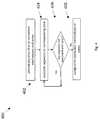
- FIG. 4illustrates an exemplary method 400 for assigning different blocks into any number of appropriate zones, and therefore, increasing the endurance of the flash memory.
- the method of FIG. 4provides a plurality of error correction mechanisms and zones 402 .
- the methodthen starts associating the flash memory blocks into corresponding zones 404 .
- the methodchecks whether there are any flash memory blocks that have not been associated with a corresponding zone. If there are, then the method continues associating those blocks. If there are no blocks that are not associated with a particular zone, then the method assigns appropriate error correction mechanism to the zones ( 408 ).
- Having different zonessimplifies directing traffic into the flash memory by directing it into the zone with the appropriate error correction and endurance for a particular write access pattern. For example, choosing the appropriate zone to direct traffic to can extend the flash memory device. For example, data that is not frequently overwritten can be assigned to a low endurance zone. Because, typically, low endurance zones include blocks with weak cells, assigning data that is not frequently overwritten does not impose additional stress to those cells. In contrast, data that is overwritten frequently can be assigned to a high endurance zone. Information about the transient behavior of the data can be obtained by analyzing the generated traffic of particular application types. For example, some applications generate a lot of transient data that can be overwritten frequently. Information about the transient behavior of the data can also be obtained by observation.
- a storage controllercan observe which data or file is overwritten frequently and store this information.
- information about the transient behavior of the datacan also be obtained through garbage collection.
- garbage collectionthe storage controller can collect information about which data or file is frequently overwritten.
- Garbage collectionis a background activity on the controller can remove invalid data from the flash and compact and/or free up contiguous flash area for new write operations.
- directing traffic appropriately to a high-endurance or a low-endurance zone according the write access patterncan extend the endurance of a flash memory.
- Traffic patternscan result in different levels of write amplification and over-provisioning for particular blocks.
- the endurance of flash memory devicesis linked to the write amplification phenomenon.
- Write amplification (WA)is a phenomenon associated with flash memory and solid-state drives (SSDs) where the actual amount of physical information written is a multiple of the logical amount that is intended to be written into the memory. Accordingly, increased write amplification at a particular block can result in a rapid deterioration of the endurance of the block, because of the extra amount of physical information that is written into the block.
- over-provisioningmeans allocating a portion of the total flash memory available to the flash storage processor, for performing various memory management functions.
- over-provisioningis the inclusion of extra storage capacity in a solid state drive, because the portion of the flash memory that is allocated to the flash storage processor is not visible to the host as available storage. This leaves less usable capacity for storage of data, but results in better performance and endurance.
- the amount of write amplification for a particular blockdepends on the ‘randomness’ in the write access pattern. A random write pattern, results in many overwrites, which in turn results in more write amplification.
- the amount of write amplification for a particular blockdepends on the write overprovisioning or garbage collection reserve/margin. Specifically, the amount of write amplification is inversely proportional to the amount of over provisioning—the more the overprovisioning, the less the write amplification
- the different disclosed zonescan be differentiated either by the endurance levels they support, as described above, or by the amount of write overprovisioning associated with them, which in turn influences the write amplification, and hence the endurance.
- writes that are likely to create more write amplificationcan be directed to higher endurance zones.
- Octal Die Packagerefers to packages of NAND flash which have eight dies contained within. This card would have a 3,072 GB total capacity. With a 28% write over provisioning (OP) the device exposes a total memory capacity of 2,211 GB to the user. This level of over provisioning provides a measured effective WA of 4.5 for a random 4 KB write pattern. This value of WA was measured by running a number of datasets over the card and recording the ratio of media writes to user writes.
- FIG. 5depicts a two-zone model 500 that illustrates how multiple endurance zones combined with traffic management may help reduce the overall write amplification.
- FIG. 5shows a system built out of a high endurance (HE) zone 502 and a low endurance (LE) zone 504 .
- the zonesdiffer in the WA they introduce on the traffic routed through the zone.
- the WA of a zoneis a function of both (i) the inherent endurance of the zone, because of either use of different flash modes or different write over provisioning or different ECC methods, and (ii) the randomness characteristics of the traffic routed through the zone.
- Each zoneis modeled using three parameters: (1) the fraction of device flash capacity (“c” for the HE zone), (2) the endurance characteristics (“e” for HE, l for LE), and (3) the WA (“wh” and “wl” respectively). If the HE zone 502 is constructed using a different flash mode, its effective capacity “c′” may end up being different from the raw flash capacity, “c r .” The aggregate system achieves a WA of “wm,” by directing a fraction “f” of incoming traffic to the HE zone 502 and the remaining incoming traffic (1-f) to the LE zone 504 .
- the modelalso introduces traffic flow of “x” units from the HE zone 502 to the LE zone 504 , which corresponds to some data items being relocated from the HE zone 502 to the LE zone 504 .
- datathat is identified as not very volatile, i.e., not changing rapidly, can be moved from the HE zone 502 to the LE zone 504 .
- datacan be relocated from HE zone 502 to LE zone 504 according to metrics on the usage of the HE zone. For example, if there is an unusual amount of HE zone traffic the system can decide to promote some LE zones, when the model includes more than one LE zones, into a HE zone. This can be accomplished, for example, by changing the way writes are targeted to the zone, by changing the overprovisioning for that zone, or by changing parameter settings within the device.
- FIG. 5also shows the traffic conservation equations for the system.
- the conservation equations shown beloware derived from the model of the two-zone system and attempt to utilize the available endurance capacity of each zone, such that both zones deteriorate in proportion to their endurance. The equations allow modifying some model parameters.
- Table 1shows some illustrative scenarios that utilize the model shown in FIG. 5 .
- the values of “c,” “e,” “wm,”are fixed.
- one of the “wh” and “wl” parametersare fixed.
- the scenarioattempts to identify for the minimum value of the other parameter (goal-seek parameter) that upon solving the traffic conservation equations, would yield valid (positive) values of “f” and “x.”
- the goal-seek parameter for each of scenarios 1-4is indicated in Table 1 with a (#) mark in the corresponding cell.
- the “base” scenariois included in order to baseline the model.
- the HE zone 502uses up to 10% of the flash resources, and exposes all of the resources for use by incoming traffic.
- the HE and LE zonesoffer the same endurance and the same write amplification, and the target write amplification remains the same as in current FM3 devices, which is a write amplification value of 4.5.
- Scenario 1illustrates the requirements for achieving an improvement in overall device write amplification, if the LE zone is constrained to have the same write amplification as in state-of-the-art high performance PCIe flash SSD cards, for example, the FlashMaxII high capacity card, which means the same over provisioning and the same randomness in its traffic.
- the HE zone 502To achieve a device write amplification of 4.05, which corresponds to 10% improvement over the baseline, it is desirable for the HE zone 502 to offer significantly lower write amplification. Note that write amplification levels of ⁇ 2.1 can be achieved using over provisioning in the 50% range, which given that the HE zone 502 corresponds to 10% of overall flash capacity, may well be justified.
- the HE zone 502can receive about 20% of the incoming traffic even if it exposes, post over-provisioning, space for only 5% of the overall logical block addressing (LBA) range, i.e., the incoming access pattern needs to have ‘hotness’ in the sense that some blocks see higher than proportional amount of traffic and are therefore “hot”. Most real-world access patterns do exhibit such behavior.
- LBAlogical block addressing
- Scenario 2illustrates the requirements for obtaining more significant WA improvements, e.g., in the 33% range.
- scenario 2the write amplification of the HE zone to 4.5 (i.e., ⁇ 28% overprovisioning) is fixed.
- the modelspecifies that the LE zone can support significantly lower than baseline WA.
- Such WA levelsare not practical to achieve by over-provisioning alone, because the device capacity can be reduced significantly.
- This scenariohighlights the importance of ‘filtering’ out the randomness in the incoming access traffic. More random traffic can to be directed towards the HE zone 504 , leaving less random traffic directed towards the LE zone. Note that this high level of randomness can be achieved at lower than proportional values of “f” (7% of traffic directed towards a zone with ⁇ 10% LBA), so may be difficult to achieve in practice.
- Scenario 3addresses this last point.
- the HE zone 502is constructed using a flash mode, which increases endurance by a factor of four at the cost of exposing only 50% of the underlying capacity for use by incoming traffic.
- This scenariorequires the LE zone 504 to achieve similar levels of write amplification as in Scenario 2. Accordingly, random traffic can be filtered out. The difference is that this scenario offers more flexibility for doing so, by directing higher than proportional traffic to the HE zone ( ⁇ 12% of traffic), where one can employ techniques such as generational garbage collection to move more stable/less random blocks to the LE zone 504 .
- scenario 3requires the underlying access pattern to exhibit hotness ( ⁇ 12% of traffic is directed to ⁇ 5% of the LBA space).
- Scenario 4expands on Scenario 3 and shows that significant benefits in write amplification, for example, two-fold in this case, are possible by increasing the extent to which randomness is filtered out of the traffic seen by the LE zone.
- data patterns seen by the storage deviceare observed and those observations can be used to reduce the write amplification required.
- most data patterns seen by the storage devicecan follow, for example, a Zipfian distribution.
- Implementing multiple endurance zonescan reduce write amplification on real-world access patterns without sacrificing flash capacity, as long as the access patterns exhibit ‘hotness,’ or equivalently the Zipfian-ness characteristic, where most accesses are directed to a relatively small subset of the overall LBAs.
- Multiple endurance zonescan also reduce write amplification if the high endurance zone 502 is used to “filter” out the randomness from the traffic to allow the LE zone 504 to operate at much lower levels of write amplification than would otherwise be seen.
- the HE zonecan offer higher levels of endurance, even at the expense of flash capacity, compared to the LE zone. This permits the HE zone to receive more traffic from which the randomness can be filtered out.
- High endurance zonescan be created by exploiting capabilities of modern-day multi-level cell (MLC) flash devices, which expose options for placing certain regions of flash into a single-level cell (SLC) mode.
- MLCmulti-level cell
- SLCsingle-level cell
- a 20 nm cMLC device from Micron®is organized into 8 MByte erase blocks which consist of 512 write pages each 16 Kbyte in size. These devices have the ability to be used in two modes which enhance the endurance beyond the base multi-level cell mode.
- the first modeis the “true SLC” mode.
- a portion of the diecan be reconfigured into an SLC device.
- the portioncan be restricted to the 1024 erase blocks per die.
- a restrictioncan be that once a device or a portion of it is used in a high-endurance mode, it may not be used in a low endurance mode.
- the enduranceincreases from a base of 3 k PE cycles to 30 k PE cycles.
- the second modecan be a “pseudo SLC” mode.
- the entire dieremains in MLC mode and the software can restrict the use of a particular erase block to only use the lower pages.
- the endurancecan increase from a base of 3 k PE cycles to 20 k PE cycles.
- Embodiments of the present disclosurewere discussed in connection with flash memories. Those of skill in the art would appreciate however, that the systems and methods disclosed herein are applicable to all memories that can have a variation in the error correction requirements across various portions of the array or across multiple devices.
- an implementation of the communication protocolcan be realized in a centralized fashion in one computer system, or in a distributed fashion where different elements are spread across several interconnected computer systems. Any kind of computer system, or other apparatus adapted for carrying out the methods described herein, is suited to perform the functions described herein.
- a typical combination of hardware and softwarecould be a general purpose computer system with a computer program that, when being loaded and executed, controls the computer system such that it carries out the methods described herein.
- the methods for the communications protocolcan also be embedded in a computer program product, which comprises all the features enabling the implementation of the methods described herein, and which, when loaded in a computer system is able to carry out these methods.
- Computer program or application in the present contextmeans any expression, in any language, code or notation, of a set of instructions intended to cause a system having an information processing capability to perform a particular function either directly or after either or both of the following a) conversion to another language, code or notation; b) reproduction in a different material form.
- this communications protocolcan be embodied in other specific forms without departing from the spirit or essential attributes thereof, and accordingly, reference should be had to the following claims, rather than to the foregoing specification, as indicating the scope of the invention.
Landscapes
- Engineering & Computer Science (AREA)
- Theoretical Computer Science (AREA)
- Physics & Mathematics (AREA)
- Probability & Statistics with Applications (AREA)
- Quality & Reliability (AREA)
- General Engineering & Computer Science (AREA)
- General Physics & Mathematics (AREA)
- Techniques For Improving Reliability Of Storages (AREA)
Abstract
Description
| TABLE 1 |
| Model Parameters for Illustrative Scenarios |
| Scenario | c | c′ | e | wm | wh | wl | F | x |
| Base | 0.1 | 0.1 | 1 | 4.50 | 4.50 | 4.50 | 0.100 | 0.000 |
| 1 | 0.1 | 0.1 | 1 | 4.05 | 2.10 (#) | 4.50 | 0.195 | 0.005 |
| 2 | 0.1 | 0.1 | 1 | 3.00 | 4.50 | 2.80 (#) | 0.076 | 0.040 |
| 3 | 0.1 | 0.05 | 4 | 3.00 | 4.50 | 2.79 (#) | 0.121 | 0.001 |
| 4 | 0.1 | 0.05 | 4 | 2.25 | 4.50 | 2.02 (#) | 0.092 | 0.003 |
Claims (23)
Priority Applications (3)
| Application Number | Priority Date | Filing Date | Title |
|---|---|---|---|
| US14/560,802US10691531B2 (en) | 2014-12-04 | 2014-12-04 | Systems and methods for multi-zone data tiering for endurance extension in solid state drives |
| US16/824,508US11150984B2 (en) | 2014-12-04 | 2020-03-19 | Systems and methods for multi-zone data tiering for endurance extension in solid state drives |
| US17/501,890US11640333B2 (en) | 2014-12-04 | 2021-10-14 | Systems and methods for allocating blocks of memory to multiple zones associated with corresponding error correction mechanisms |
Applications Claiming Priority (1)
| Application Number | Priority Date | Filing Date | Title |
|---|---|---|---|
| US14/560,802US10691531B2 (en) | 2014-12-04 | 2014-12-04 | Systems and methods for multi-zone data tiering for endurance extension in solid state drives |
Related Child Applications (1)
| Application Number | Title | Priority Date | Filing Date |
|---|---|---|---|
| US16/824,508ContinuationUS11150984B2 (en) | 2014-12-04 | 2020-03-19 | Systems and methods for multi-zone data tiering for endurance extension in solid state drives |
Publications (2)
| Publication Number | Publication Date |
|---|---|
| US20160162354A1 US20160162354A1 (en) | 2016-06-09 |
| US10691531B2true US10691531B2 (en) | 2020-06-23 |
Family
ID=56094436
Family Applications (3)
| Application Number | Title | Priority Date | Filing Date |
|---|---|---|---|
| US14/560,802Active2035-12-08US10691531B2 (en) | 2014-12-04 | 2014-12-04 | Systems and methods for multi-zone data tiering for endurance extension in solid state drives |
| US16/824,508ActiveUS11150984B2 (en) | 2014-12-04 | 2020-03-19 | Systems and methods for multi-zone data tiering for endurance extension in solid state drives |
| US17/501,890ActiveUS11640333B2 (en) | 2014-12-04 | 2021-10-14 | Systems and methods for allocating blocks of memory to multiple zones associated with corresponding error correction mechanisms |
Family Applications After (2)
| Application Number | Title | Priority Date | Filing Date |
|---|---|---|---|
| US16/824,508ActiveUS11150984B2 (en) | 2014-12-04 | 2020-03-19 | Systems and methods for multi-zone data tiering for endurance extension in solid state drives |
| US17/501,890ActiveUS11640333B2 (en) | 2014-12-04 | 2021-10-14 | Systems and methods for allocating blocks of memory to multiple zones associated with corresponding error correction mechanisms |
Country Status (1)
| Country | Link |
|---|---|
| US (3) | US10691531B2 (en) |
Cited By (3)
| Publication number | Priority date | Publication date | Assignee | Title |
|---|---|---|---|---|
| US11556274B1 (en) | 2021-09-01 | 2023-01-17 | Western Digital Technologies, Inc. | Endurance groups ECC allocation |
| US11640267B2 (en) | 2021-09-09 | 2023-05-02 | Western Digital Technologies, Inc. | Method and system for maintenance allocation between NVM groups |
| US20230153239A1 (en)* | 2021-11-15 | 2023-05-18 | Electronics And Telecommunications Research Institute | Method and apparatus for allocating memory addresses in resource-centric networks |
Families Citing this family (26)
| Publication number | Priority date | Publication date | Assignee | Title |
|---|---|---|---|---|
| US10977277B2 (en)* | 2010-12-23 | 2021-04-13 | Mongodb, Inc. | Systems and methods for database zone sharding and API integration |
| US11615115B2 (en) | 2010-12-23 | 2023-03-28 | Mongodb, Inc. | Systems and methods for managing distributed database deployments |
| US9805108B2 (en) | 2010-12-23 | 2017-10-31 | Mongodb, Inc. | Large distributed database clustering systems and methods |
| US11544288B2 (en) | 2010-12-23 | 2023-01-03 | Mongodb, Inc. | Systems and methods for managing distributed database deployments |
| US10346430B2 (en) | 2010-12-23 | 2019-07-09 | Mongodb, Inc. | System and method for determining consensus within a distributed database |
| US10713280B2 (en) | 2010-12-23 | 2020-07-14 | Mongodb, Inc. | Systems and methods for managing distributed database deployments |
| US10262050B2 (en) | 2015-09-25 | 2019-04-16 | Mongodb, Inc. | Distributed database systems and methods with pluggable storage engines |
| US8996463B2 (en) | 2012-07-26 | 2015-03-31 | Mongodb, Inc. | Aggregation framework system architecture and method |
| US10997211B2 (en) | 2010-12-23 | 2021-05-04 | Mongodb, Inc. | Systems and methods for database zone sharding and API integration |
| US9740762B2 (en) | 2011-04-01 | 2017-08-22 | Mongodb, Inc. | System and method for optimizing data migration in a partitioned database |
| US10740353B2 (en) | 2010-12-23 | 2020-08-11 | Mongodb, Inc. | Systems and methods for managing distributed database deployments |
| US11544284B2 (en) | 2012-07-26 | 2023-01-03 | Mongodb, Inc. | Aggregation framework system architecture and method |
| US11403317B2 (en) | 2012-07-26 | 2022-08-02 | Mongodb, Inc. | Aggregation framework system architecture and method |
| US10872095B2 (en) | 2012-07-26 | 2020-12-22 | Mongodb, Inc. | Aggregation framework system architecture and method |
| US10673623B2 (en) | 2015-09-25 | 2020-06-02 | Mongodb, Inc. | Systems and methods for hierarchical key management in encrypted distributed databases |
| US10846411B2 (en) | 2015-09-25 | 2020-11-24 | Mongodb, Inc. | Distributed database systems and methods with encrypted storage engines |
| US10671496B2 (en) | 2016-05-31 | 2020-06-02 | Mongodb, Inc. | Method and apparatus for reading and writing committed data |
| US10621050B2 (en) | 2016-06-27 | 2020-04-14 | Mongodb, Inc. | Method and apparatus for restoring data from snapshots |
| US10866868B2 (en) | 2017-06-20 | 2020-12-15 | Mongodb, Inc. | Systems and methods for optimization of database operations |
| JP2020030875A (en) | 2018-08-23 | 2020-02-27 | キオクシア株式会社 | Memory system |
| US11061787B2 (en) | 2019-04-23 | 2021-07-13 | Micron Technology, Inc. | Custom error recovery in selected regions of a data storage device |
| KR102835930B1 (en) | 2019-11-11 | 2025-07-17 | 삼성전자주식회사 | Storage device and storage device system and the operating method thereof |
| CN112910474B (en)* | 2021-01-18 | 2022-04-22 | 暨南大学 | Zipper code encoding method based on multi-dimensional coupling |
| CN114461145B (en)* | 2022-01-19 | 2024-07-23 | 合肥大唐存储科技有限公司 | Capacity-expansion solid state disk and capacity-expansion, data writing and data reading method thereof |
| US11940874B2 (en)* | 2022-08-08 | 2024-03-26 | Micron Technology, Inc. | Queue management for a memory system |
| US11977433B2 (en)* | 2022-09-27 | 2024-05-07 | Hitachi, Ltd. | Failure area identification system |
Citations (17)
| Publication number | Priority date | Publication date | Assignee | Title |
|---|---|---|---|---|
| US7096313B1 (en)* | 2002-10-28 | 2006-08-22 | Sandisk Corporation | Tracking the least frequently erased blocks in non-volatile memory systems |
| US20080195900A1 (en)* | 2007-02-12 | 2008-08-14 | Phison Electronics Corp. | Flash memory system and method for controlling the same |
| US20080279005A1 (en)* | 2007-05-11 | 2008-11-13 | Spansion Llc | Managing flash memory program and erase cycles in the time domain |
| US20100246266A1 (en)* | 2009-03-25 | 2010-09-30 | Samsung Electronics Co., Ltd. | Nonvolatile memory device and related programming method |
| US20110238899A1 (en)* | 2008-12-27 | 2011-09-29 | Kabushiki Kaisha Toshiba | Memory system, method of controlling memory system, and information processing apparatus |
| US20120303873A1 (en)* | 2011-05-24 | 2012-11-29 | Lau Nguyen | Method for storage devices to achieve low write amplification with low over provision |
| US20130179740A1 (en)* | 2009-01-23 | 2013-07-11 | Micron Technology, Inc. | Memory devices and methods for managing error regions |
| US20130227203A1 (en)* | 2008-11-12 | 2013-08-29 | Micron Technology, Inc. | Dynamic slc/mlc blocks allocations for non-volatile memory |
| US8621141B2 (en)* | 2010-04-01 | 2013-12-31 | Intel Corporations | Method and system for wear leveling in a solid state drive |
| US20140006688A1 (en)* | 2012-07-02 | 2014-01-02 | Super Talent Technology, Corp. | Endurance and Retention Flash Controller with Programmable Binary-Levels-Per-Cell Bits Identifying Pages or Blocks as having Triple, Multi, or Single-Level Flash-Memory Cells |
| US20140136927A1 (en)* | 2010-10-27 | 2014-05-15 | Lsi Corporation | Adaptive ecc techniques for flash memory based data storage |
| US8910017B2 (en)* | 2012-07-02 | 2014-12-09 | Sandisk Technologies Inc. | Flash memory with random partition |
| US20150089317A1 (en)* | 2013-09-20 | 2015-03-26 | Seagate Technology Llc | Storage device with multiple coding redundancies |
| US9015561B1 (en)* | 2014-06-11 | 2015-04-21 | Sandisk Technologies Inc. | Adaptive redundancy in three dimensional memory |
| US20150347029A1 (en)* | 2014-05-30 | 2015-12-03 | Sandisk Enterprise Ip Llc | Identification of Hot Regions to Enhance Performance and Endurance of a Non-Volatile Storage Device |
| US20160062663A1 (en)* | 2014-09-02 | 2016-03-03 | Sandisk Technologies Inc. | Process and Apparatus to Reduce Declared Capacity of a Storage Device by Altering an Encoding Format |
| US9442670B2 (en)* | 2013-09-03 | 2016-09-13 | Sandisk Technologies Llc | Method and system for rebalancing data stored in flash memory devices |
Family Cites Families (32)
| Publication number | Priority date | Publication date | Assignee | Title |
|---|---|---|---|---|
| US20080209114A1 (en) | 1999-08-04 | 2008-08-28 | Super Talent Electronics, Inc. | Reliability High Endurance Non-Volatile Memory Device with Zone-Based Non-Volatile Memory File System |
| US7953931B2 (en) | 1999-08-04 | 2011-05-31 | Super Talent Electronics, Inc. | High endurance non-volatile memory devices |
| US7337360B2 (en)* | 1999-10-19 | 2008-02-26 | Idocrase Investments Llc | Stored memory recovery system |
| US7539828B2 (en)* | 2000-08-08 | 2009-05-26 | Faronics Corporation | Method and system for automatically preserving persistent storage |
| US8412879B2 (en)* | 2002-10-28 | 2013-04-02 | Sandisk Technologies Inc. | Hybrid implementation for error correction codes within a non-volatile memory system |
| US7739576B2 (en) | 2006-08-31 | 2010-06-15 | Micron Technology, Inc. | Variable strength ECC |
| US7904780B2 (en) | 2006-11-03 | 2011-03-08 | Sandisk Corporation | Methods of modulating error correction coding |
| WO2008068747A2 (en) | 2006-12-03 | 2008-06-12 | Anobit Technologies Ltd. | Automatic defect management in memory devices |
| US8051358B2 (en) | 2007-07-06 | 2011-11-01 | Micron Technology, Inc. | Error recovery storage along a nand-flash string |
| US8095851B2 (en) | 2007-09-06 | 2012-01-10 | Siliconsystems, Inc. | Storage subsystem capable of adjusting ECC settings based on monitored conditions |
| US9477587B2 (en) | 2008-04-11 | 2016-10-25 | Micron Technology, Inc. | Method and apparatus for a volume management system in a non-volatile memory device |
| US20100100797A1 (en) | 2008-10-16 | 2010-04-22 | Genesys Logic, Inc. | Dual mode error correction code (ecc) apparatus for flash memory and method thereof |
| US8161354B2 (en) | 2008-10-16 | 2012-04-17 | Genesys Logic, Inc. | Flash memory controller having configuring unit for error correction code (ECC) capability and method thereof |
| US8209466B2 (en) | 2008-12-16 | 2012-06-26 | Intel Corporation | Methods and systems to allocate addresses in a high-endurance/low-endurance hybrid flash memory |
| US8479080B1 (en) | 2009-07-12 | 2013-07-02 | Apple Inc. | Adaptive over-provisioning in memory systems |
| US8499220B2 (en) | 2009-09-08 | 2013-07-30 | Lsi Corporation | Systems and methods for re-designating memory regions as error code corrected memory regions |
| US8381077B2 (en) | 2009-09-08 | 2013-02-19 | Lsi Corporation | Systems and methods for implementing error correction in relation to a flash memory |
| JP5349256B2 (en) | 2009-11-06 | 2013-11-20 | 株式会社東芝 | Memory system |
| US8327225B2 (en) | 2010-01-04 | 2012-12-04 | Micron Technology, Inc. | Error correction in a stacked memory |
| US8327226B2 (en) | 2010-02-03 | 2012-12-04 | Seagate Technology Llc | Adjustable error correction code length in an electrical storage device |
| US20110252289A1 (en) | 2010-04-08 | 2011-10-13 | Seagate Technology Llc | Adjusting storage device parameters based on reliability sensing |
| JP2012123880A (en) | 2010-12-10 | 2012-06-28 | Toshiba Corp | Semiconductor storage device |
| TWI459197B (en) | 2011-04-21 | 2014-11-01 | Phison Electronics Corp | Data writing and reading method, memory controller and memory storage apparatus |
| KR101467941B1 (en) | 2011-04-26 | 2014-12-02 | 엘에스아이 코포레이션 | Variable over provisioning for non-volatile storage |
| US20120311262A1 (en)* | 2011-06-01 | 2012-12-06 | International Business Machines Corporation | Memory cell presetting for improved memory performance |
| EP2718792A4 (en) | 2011-06-09 | 2015-06-17 | 3M Innovative Properties Co | Touch sensitive device with multilayer electrode and underlayer |
| US8583868B2 (en) | 2011-08-29 | 2013-11-12 | International Business Machines | Storage system cache using flash memory with direct block access |
| KR20130023985A (en) | 2011-08-30 | 2013-03-08 | 삼성전자주식회사 | Meta data group configuration method with improved random write performance and therefor semiconductor storage device |
| US9021231B2 (en) | 2011-09-02 | 2015-04-28 | SMART Storage Systems, Inc. | Storage control system with write amplification control mechanism and method of operation thereof |
| KR101654030B1 (en) | 2011-12-29 | 2016-09-05 | 인텔 코포레이션 | Dynamic window to improve nand memory endurance |
| US20150058697A1 (en) | 2013-08-22 | 2015-02-26 | Kabushiki Kaisha Toshiba | Storage device, controller and memory controlling method |
| US10983859B2 (en) | 2014-08-07 | 2021-04-20 | Pure Storage, Inc. | Adjustable error correction based on memory health in a storage unit |
- 2014
- 2014-12-04USUS14/560,802patent/US10691531B2/enactiveActive
- 2020
- 2020-03-19USUS16/824,508patent/US11150984B2/enactiveActive
- 2021
- 2021-10-14USUS17/501,890patent/US11640333B2/enactiveActive
Patent Citations (17)
| Publication number | Priority date | Publication date | Assignee | Title |
|---|---|---|---|---|
| US7096313B1 (en)* | 2002-10-28 | 2006-08-22 | Sandisk Corporation | Tracking the least frequently erased blocks in non-volatile memory systems |
| US20080195900A1 (en)* | 2007-02-12 | 2008-08-14 | Phison Electronics Corp. | Flash memory system and method for controlling the same |
| US20080279005A1 (en)* | 2007-05-11 | 2008-11-13 | Spansion Llc | Managing flash memory program and erase cycles in the time domain |
| US20130227203A1 (en)* | 2008-11-12 | 2013-08-29 | Micron Technology, Inc. | Dynamic slc/mlc blocks allocations for non-volatile memory |
| US20110238899A1 (en)* | 2008-12-27 | 2011-09-29 | Kabushiki Kaisha Toshiba | Memory system, method of controlling memory system, and information processing apparatus |
| US20130179740A1 (en)* | 2009-01-23 | 2013-07-11 | Micron Technology, Inc. | Memory devices and methods for managing error regions |
| US20100246266A1 (en)* | 2009-03-25 | 2010-09-30 | Samsung Electronics Co., Ltd. | Nonvolatile memory device and related programming method |
| US8621141B2 (en)* | 2010-04-01 | 2013-12-31 | Intel Corporations | Method and system for wear leveling in a solid state drive |
| US20140136927A1 (en)* | 2010-10-27 | 2014-05-15 | Lsi Corporation | Adaptive ecc techniques for flash memory based data storage |
| US20120303873A1 (en)* | 2011-05-24 | 2012-11-29 | Lau Nguyen | Method for storage devices to achieve low write amplification with low over provision |
| US20140006688A1 (en)* | 2012-07-02 | 2014-01-02 | Super Talent Technology, Corp. | Endurance and Retention Flash Controller with Programmable Binary-Levels-Per-Cell Bits Identifying Pages or Blocks as having Triple, Multi, or Single-Level Flash-Memory Cells |
| US8910017B2 (en)* | 2012-07-02 | 2014-12-09 | Sandisk Technologies Inc. | Flash memory with random partition |
| US9442670B2 (en)* | 2013-09-03 | 2016-09-13 | Sandisk Technologies Llc | Method and system for rebalancing data stored in flash memory devices |
| US20150089317A1 (en)* | 2013-09-20 | 2015-03-26 | Seagate Technology Llc | Storage device with multiple coding redundancies |
| US20150347029A1 (en)* | 2014-05-30 | 2015-12-03 | Sandisk Enterprise Ip Llc | Identification of Hot Regions to Enhance Performance and Endurance of a Non-Volatile Storage Device |
| US9015561B1 (en)* | 2014-06-11 | 2015-04-21 | Sandisk Technologies Inc. | Adaptive redundancy in three dimensional memory |
| US20160062663A1 (en)* | 2014-09-02 | 2016-03-03 | Sandisk Technologies Inc. | Process and Apparatus to Reduce Declared Capacity of a Storage Device by Altering an Encoding Format |
Cited By (4)
| Publication number | Priority date | Publication date | Assignee | Title |
|---|---|---|---|---|
| US11556274B1 (en) | 2021-09-01 | 2023-01-17 | Western Digital Technologies, Inc. | Endurance groups ECC allocation |
| US11640267B2 (en) | 2021-09-09 | 2023-05-02 | Western Digital Technologies, Inc. | Method and system for maintenance allocation between NVM groups |
| US20230153239A1 (en)* | 2021-11-15 | 2023-05-18 | Electronics And Telecommunications Research Institute | Method and apparatus for allocating memory addresses in resource-centric networks |
| US12367140B2 (en)* | 2021-11-15 | 2025-07-22 | Electronics And Telecommunications Research Institute | Method and apparatus for allocating memory addresses in resource-centric networks |
Also Published As
| Publication number | Publication date |
|---|---|
| US11150984B2 (en) | 2021-10-19 |
| US11640333B2 (en) | 2023-05-02 |
| US20220035699A1 (en) | 2022-02-03 |
| US20200218603A1 (en) | 2020-07-09 |
| US20160162354A1 (en) | 2016-06-09 |
Similar Documents
| Publication | Publication Date | Title |
|---|---|---|
| US11640333B2 (en) | Systems and methods for allocating blocks of memory to multiple zones associated with corresponding error correction mechanisms | |
| US10866740B2 (en) | System and method for performance-based multiple namespace resource allocation in a memory | |
| CN110088723B (en) | System and method for processing and arbitrating submit queues and completion queues | |
| US10466904B2 (en) | System and method for processing and arbitrating submission and completion queues | |
| US11635898B2 (en) | System and method for adaptive command fetch aggregation | |
| US10466903B2 (en) | System and method for dynamic and adaptive interrupt coalescing | |
| US10564857B2 (en) | System and method for QoS over NVMe virtualization platform using adaptive command fetching | |
| US10725835B2 (en) | System and method for speculative execution of commands using a controller memory buffer | |
| US10102119B2 (en) | Garbage collection based on queued and/or selected write commands | |
| KR102680418B1 (en) | Controller and storage device including controller and nonvolatile memory devices | |
| US10255191B2 (en) | Logical memory address regions | |
| TWI733324B (en) | Memory system | |
| US11698734B2 (en) | Collision reduction through just-in-time resource allocation | |
| US11307768B2 (en) | Namespace auto-routing data storage system | |
| CN112181274A (en) | Large block organization method for improving performance stability of storage device and storage device thereof | |
| CN119917426B (en) | Memory management method and memory controller | |
| US20220350485A1 (en) | Memory system and method for controlling memory system | |
| CN120255790A (en) | Data storage device and method of operating the same | |
| CN112216329A (en) | Data erasing method, memory control circuit unit and memory storage device |
Legal Events
| Date | Code | Title | Description |
|---|---|---|---|
| AS | Assignment | Owner name:WESTERN DIGITAL TECHNOLOGIES, INC., CALIFORNIA Free format text:ASSIGNMENT OF ASSIGNORS INTEREST;ASSIGNOR:HGST NETHERLANDS B.V.;REEL/FRAME:040829/0516 Effective date:20160831 | |
| AS | Assignment | Owner name:HGST NETHERLANDS B.V., NETHERLANDS Free format text:ASSIGNMENT OF ASSIGNORS INTEREST;ASSIGNORS:SINGHAI, ASHISH;KARAMCHETI, VIJAY;NARASIMHA, ASHWIN;SIGNING DATES FROM 20150914 TO 20160718;REEL/FRAME:042800/0622 | |
| STPP | Information on status: patent application and granting procedure in general | Free format text:NON FINAL ACTION MAILED | |
| STPP | Information on status: patent application and granting procedure in general | Free format text:RESPONSE TO NON-FINAL OFFICE ACTION ENTERED AND FORWARDED TO EXAMINER | |
| STPP | Information on status: patent application and granting procedure in general | Free format text:FINAL REJECTION MAILED | |
| STPP | Information on status: patent application and granting procedure in general | Free format text:RESPONSE AFTER FINAL ACTION FORWARDED TO EXAMINER | |
| STPP | Information on status: patent application and granting procedure in general | Free format text:ADVISORY ACTION MAILED | |
| STPP | Information on status: patent application and granting procedure in general | Free format text:DOCKETED NEW CASE - READY FOR EXAMINATION | |
| STPP | Information on status: patent application and granting procedure in general | Free format text:NOTICE OF ALLOWANCE MAILED -- APPLICATION RECEIVED IN OFFICE OF PUBLICATIONS | |
| AS | Assignment | Owner name:JPMORGAN CHASE BANK, N.A., AS AGENT, ILLINOIS Free format text:SECURITY INTEREST;ASSIGNOR:WESTERN DIGITAL TECHNOLOGIES, INC.;REEL/FRAME:052915/0566 Effective date:20200113 | |
| STPP | Information on status: patent application and granting procedure in general | Free format text:AWAITING TC RESP, ISSUE FEE PAYMENT VERIFIED | |
| STCF | Information on status: patent grant | Free format text:PATENTED CASE | |
| AS | Assignment | Owner name:WESTERN DIGITAL TECHNOLOGIES, INC., CALIFORNIA Free format text:RELEASE OF SECURITY INTEREST AT REEL 052915 FRAME 0566;ASSIGNOR:JPMORGAN CHASE BANK, N.A.;REEL/FRAME:059127/0001 Effective date:20220203 | |
| AS | Assignment | Owner name:JPMORGAN CHASE BANK, N.A., ILLINOIS Free format text:PATENT COLLATERAL AGREEMENT - A&R LOAN AGREEMENT;ASSIGNOR:WESTERN DIGITAL TECHNOLOGIES, INC.;REEL/FRAME:064715/0001 Effective date:20230818 Owner name:JPMORGAN CHASE BANK, N.A., ILLINOIS Free format text:PATENT COLLATERAL AGREEMENT - DDTL LOAN AGREEMENT;ASSIGNOR:WESTERN DIGITAL TECHNOLOGIES, INC.;REEL/FRAME:067045/0156 Effective date:20230818 | |
| MAFP | Maintenance fee payment | Free format text:PAYMENT OF MAINTENANCE FEE, 4TH YEAR, LARGE ENTITY (ORIGINAL EVENT CODE: M1551); ENTITY STATUS OF PATENT OWNER: LARGE ENTITY Year of fee payment:4 | |
| AS | Assignment | Owner name:SANDISK TECHNOLOGIES, INC., CALIFORNIA Free format text:ASSIGNMENT OF ASSIGNORS INTEREST;ASSIGNOR:WESTERN DIGITAL TECHNOLOGIES, INC.;REEL/FRAME:067567/0682 Effective date:20240503 | |
| AS | Assignment | Owner name:SANDISK TECHNOLOGIES, INC., CALIFORNIA Free format text:CHANGE OF NAME;ASSIGNOR:SANDISK TECHNOLOGIES, INC.;REEL/FRAME:067982/0032 Effective date:20240621 | |
| AS | Assignment | Owner name:JPMORGAN CHASE BANK, N.A., AS THE AGENT, ILLINOIS Free format text:PATENT COLLATERAL AGREEMENT;ASSIGNOR:SANDISK TECHNOLOGIES, INC.;REEL/FRAME:068762/0494 Effective date:20240820 | |
| AS | Assignment | Owner name:WESTERN DIGITAL TECHNOLOGIES, INC., CALIFORNIA Free format text:ASSIGNMENT OF ASSIGNORS INTEREST;ASSIGNOR:SANDISK TECHNOLOGIES, INC.;REEL/FRAME:069168/0273 Effective date:20241008 | |
| AS | Assignment | Owner name:JPMORGAN CHASE BANK, N.A., AS COLLATERAL AGENT, ILLINOIS Free format text:SECURITY AGREEMENT (SUPPLEMENTAL);ASSIGNOR:WESTERN DIGITAL TECHNOLOGIES, INC.;REEL/FRAME:069411/0208 Effective date:20241030 |