US10690851B2 - Holographic waveguides incorporating birefringence control and methods for their fabrication - Google Patents
Holographic waveguides incorporating birefringence control and methods for their fabricationDownload PDFInfo
- Publication number
- US10690851B2 US10690851B2US16/357,233US201916357233AUS10690851B2US 10690851 B2US10690851 B2US 10690851B2US 201916357233 AUS201916357233 AUS 201916357233AUS 10690851 B2US10690851 B2US 10690851B2
- Authority
- US
- United States
- Prior art keywords
- waveguide
- layer
- grating
- control layer
- birefringence control
- Prior art date
- Legal status (The legal status is an assumption and is not a legal conclusion. Google has not performed a legal analysis and makes no representation as to the accuracy of the status listed.)
- Active
Links
Images


Classifications
- G—PHYSICS
- G02—OPTICS
- G02B—OPTICAL ELEMENTS, SYSTEMS OR APPARATUS
- G02B6/00—Light guides; Structural details of arrangements comprising light guides and other optical elements, e.g. couplings
- G02B6/10—Light guides; Structural details of arrangements comprising light guides and other optical elements, e.g. couplings of the optical waveguide type
- G02B6/12—Light guides; Structural details of arrangements comprising light guides and other optical elements, e.g. couplings of the optical waveguide type of the integrated circuit kind
- G02B6/122—Basic optical elements, e.g. light-guiding paths
- G02B6/124—Geodesic lenses or integrated gratings
- G—PHYSICS
- G02—OPTICS
- G02B—OPTICAL ELEMENTS, SYSTEMS OR APPARATUS
- G02B5/00—Optical elements other than lenses
- G02B5/30—Polarising elements
- G02B5/3016—Polarising elements involving passive liquid crystal elements
- G—PHYSICS
- G02—OPTICS
- G02B—OPTICAL ELEMENTS, SYSTEMS OR APPARATUS
- G02B27/00—Optical systems or apparatus not provided for by any of the groups G02B1/00 - G02B26/00, G02B30/00
- G02B27/0081—Optical systems or apparatus not provided for by any of the groups G02B1/00 - G02B26/00, G02B30/00 with means for altering, e.g. enlarging, the entrance or exit pupil
- G—PHYSICS
- G02—OPTICS
- G02B—OPTICAL ELEMENTS, SYSTEMS OR APPARATUS
- G02B27/00—Optical systems or apparatus not provided for by any of the groups G02B1/00 - G02B26/00, G02B30/00
- G02B27/01—Head-up displays
- G—PHYSICS
- G02—OPTICS
- G02B—OPTICAL ELEMENTS, SYSTEMS OR APPARATUS
- G02B27/00—Optical systems or apparatus not provided for by any of the groups G02B1/00 - G02B26/00, G02B30/00
- G02B27/01—Head-up displays
- G02B27/0101—Head-up displays characterised by optical features
- G02B27/0103—Head-up displays characterised by optical features comprising holographic elements
- G—PHYSICS
- G02—OPTICS
- G02B—OPTICAL ELEMENTS, SYSTEMS OR APPARATUS
- G02B27/00—Optical systems or apparatus not provided for by any of the groups G02B1/00 - G02B26/00, G02B30/00
- G02B27/01—Head-up displays
- G02B27/017—Head mounted
- G02B27/0172—Head mounted characterised by optical features
- G—PHYSICS
- G02—OPTICS
- G02B—OPTICAL ELEMENTS, SYSTEMS OR APPARATUS
- G02B5/00—Optical elements other than lenses
- G02B5/30—Polarising elements
- G—PHYSICS
- G02—OPTICS
- G02B—OPTICAL ELEMENTS, SYSTEMS OR APPARATUS
- G02B6/00—Light guides; Structural details of arrangements comprising light guides and other optical elements, e.g. couplings
- G02B6/10—Light guides; Structural details of arrangements comprising light guides and other optical elements, e.g. couplings of the optical waveguide type
- G02B6/12—Light guides; Structural details of arrangements comprising light guides and other optical elements, e.g. couplings of the optical waveguide type of the integrated circuit kind
- G02B6/122—Basic optical elements, e.g. light-guiding paths
- G—PHYSICS
- G02—OPTICS
- G02B—OPTICAL ELEMENTS, SYSTEMS OR APPARATUS
- G02B6/00—Light guides; Structural details of arrangements comprising light guides and other optical elements, e.g. couplings
- G02B6/10—Light guides; Structural details of arrangements comprising light guides and other optical elements, e.g. couplings of the optical waveguide type
- G02B6/12—Light guides; Structural details of arrangements comprising light guides and other optical elements, e.g. couplings of the optical waveguide type of the integrated circuit kind
- G02B6/126—Light guides; Structural details of arrangements comprising light guides and other optical elements, e.g. couplings of the optical waveguide type of the integrated circuit kind using polarisation effects
- G—PHYSICS
- G02—OPTICS
- G02B—OPTICAL ELEMENTS, SYSTEMS OR APPARATUS
- G02B6/00—Light guides; Structural details of arrangements comprising light guides and other optical elements, e.g. couplings
- G02B6/10—Light guides; Structural details of arrangements comprising light guides and other optical elements, e.g. couplings of the optical waveguide type
- G02B6/12—Light guides; Structural details of arrangements comprising light guides and other optical elements, e.g. couplings of the optical waveguide type of the integrated circuit kind
- G02B6/13—Integrated optical circuits characterised by the manufacturing method
- G02B6/136—Integrated optical circuits characterised by the manufacturing method by etching
- G—PHYSICS
- G02—OPTICS
- G02B—OPTICAL ELEMENTS, SYSTEMS OR APPARATUS
- G02B6/00—Light guides; Structural details of arrangements comprising light guides and other optical elements, e.g. couplings
- G02B6/24—Coupling light guides
- G02B6/26—Optical coupling means
- G02B6/27—Optical coupling means with polarisation selective and adjusting means
- G02B6/2726—Optical coupling means with polarisation selective and adjusting means in or on light guides, e.g. polarisation means assembled in a light guide
- G02B6/274—Optical coupling means with polarisation selective and adjusting means in or on light guides, e.g. polarisation means assembled in a light guide based on light guide birefringence, e.g. due to coupling between light guides
- G—PHYSICS
- G02—OPTICS
- G02B—OPTICAL ELEMENTS, SYSTEMS OR APPARATUS
- G02B6/00—Light guides; Structural details of arrangements comprising light guides and other optical elements, e.g. couplings
- G02B6/24—Coupling light guides
- G02B6/26—Optical coupling means
- G02B6/34—Optical coupling means utilising prism or grating
- G—PHYSICS
- G02—OPTICS
- G02F—OPTICAL DEVICES OR ARRANGEMENTS FOR THE CONTROL OF LIGHT BY MODIFICATION OF THE OPTICAL PROPERTIES OF THE MEDIA OF THE ELEMENTS INVOLVED THEREIN; NON-LINEAR OPTICS; FREQUENCY-CHANGING OF LIGHT; OPTICAL LOGIC ELEMENTS; OPTICAL ANALOGUE/DIGITAL CONVERTERS
- G02F1/00—Devices or arrangements for the control of the intensity, colour, phase, polarisation or direction of light arriving from an independent light source, e.g. switching, gating or modulating; Non-linear optics
- G02F1/01—Devices or arrangements for the control of the intensity, colour, phase, polarisation or direction of light arriving from an independent light source, e.g. switching, gating or modulating; Non-linear optics for the control of the intensity, phase, polarisation or colour
- G02F1/13—Devices or arrangements for the control of the intensity, colour, phase, polarisation or direction of light arriving from an independent light source, e.g. switching, gating or modulating; Non-linear optics for the control of the intensity, phase, polarisation or colour based on liquid crystals, e.g. single liquid crystal display cells
- G02F1/133—Constructional arrangements; Operation of liquid crystal cells; Circuit arrangements
- G02F1/1333—Constructional arrangements; Manufacturing methods
- G02F1/1334—Constructional arrangements; Manufacturing methods based on polymer dispersed liquid crystals, e.g. microencapsulated liquid crystals
- G—PHYSICS
- G02—OPTICS
- G02B—OPTICAL ELEMENTS, SYSTEMS OR APPARATUS
- G02B6/00—Light guides; Structural details of arrangements comprising light guides and other optical elements, e.g. couplings
- G02B6/10—Light guides; Structural details of arrangements comprising light guides and other optical elements, e.g. couplings of the optical waveguide type
- G02B6/12—Light guides; Structural details of arrangements comprising light guides and other optical elements, e.g. couplings of the optical waveguide type of the integrated circuit kind
- G02B2006/12083—Constructional arrangements
- G02B2006/12116—Polariser; Birefringent
- G—PHYSICS
- G02—OPTICS
- G02B—OPTICAL ELEMENTS, SYSTEMS OR APPARATUS
- G02B27/00—Optical systems or apparatus not provided for by any of the groups G02B1/00 - G02B26/00, G02B30/00
- G02B27/01—Head-up displays
- G02B27/0101—Head-up displays characterised by optical features
- G02B27/0103—Head-up displays characterised by optical features comprising holographic elements
- G02B2027/0109—Head-up displays characterised by optical features comprising holographic elements comprising details concerning the making of holograms
- G—PHYSICS
- G02—OPTICS
- G02B—OPTICAL ELEMENTS, SYSTEMS OR APPARATUS
- G02B27/00—Optical systems or apparatus not provided for by any of the groups G02B1/00 - G02B26/00, G02B30/00
- G02B27/01—Head-up displays
- G02B27/0101—Head-up displays characterised by optical features
- G02B2027/0123—Head-up displays characterised by optical features comprising devices increasing the field of view
- G02B2027/0125—Field-of-view increase by wavefront division
- G—PHYSICS
- G02—OPTICS
- G02B—OPTICAL ELEMENTS, SYSTEMS OR APPARATUS
- G02B27/00—Optical systems or apparatus not provided for by any of the groups G02B1/00 - G02B26/00, G02B30/00
- G02B27/01—Head-up displays
- G02B27/017—Head mounted
- G02B27/0172—Head mounted characterised by optical features
- G02B2027/0174—Head mounted characterised by optical features holographic
- G—PHYSICS
- G02—OPTICS
- G02B—OPTICAL ELEMENTS, SYSTEMS OR APPARATUS
- G02B5/00—Optical elements other than lenses
- G02B5/18—Diffraction gratings
- G02B5/1833—Diffraction gratings comprising birefringent materials
- G—PHYSICS
- G02—OPTICS
- G02B—OPTICAL ELEMENTS, SYSTEMS OR APPARATUS
- G02B5/00—Optical elements other than lenses
- G02B5/30—Polarising elements
- G02B5/3083—Birefringent or phase retarding elements
- G—PHYSICS
- G02—OPTICS
- G02B—OPTICAL ELEMENTS, SYSTEMS OR APPARATUS
- G02B6/00—Light guides; Structural details of arrangements comprising light guides and other optical elements, e.g. couplings
- G02B6/10—Light guides; Structural details of arrangements comprising light guides and other optical elements, e.g. couplings of the optical waveguide type
- G02B6/12—Light guides; Structural details of arrangements comprising light guides and other optical elements, e.g. couplings of the optical waveguide type of the integrated circuit kind
- G02B6/122—Basic optical elements, e.g. light-guiding paths
- G02B6/1221—Basic optical elements, e.g. light-guiding paths made from organic materials
Definitions
- the present disclosurerelates to optical waveguides and more particularly to waveguide displays using birefringent gratings.
- Waveguidescan be referred to as structures with the capability of confining and guiding waves (i.e., restricting the spatial region in which waves can propagate).
- One subclassincludes optical waveguides, which are structures that can guide electromagnetic waves, typically those in the visible spectrum.
- Waveguide structurescan be designed to control the propagation path of waves using a number of different mechanisms.
- planar waveguidescan be designed to utilize diffraction gratings to diffract and couple incident light into the waveguide structure such that the in-coupled light can proceed to travel within the planar structure via total internal reflection (“TIR”).
- TIRtotal internal reflection
- Fabrication of waveguidescan include the use of material systems that allow for the recording of holographic optical elements within the waveguides.
- One class of such materialincludes polymer dispersed liquid crystal (“PDLC”) mixtures, which are mixtures containing photopolymerizable monomers and liquid crystals.
- PDLCpolymer dispersed liquid crystal
- HPDLCholographic polymer dispersed liquid crystal
- Holographic optical elementssuch as volume phase gratings, can be recorded in such a liquid mixture by illuminating the material with two mutually coherent laser beams.
- the monomerspolymerize and the mixture undergoes a photopolymerization-induced phase separation, creating regions densely populated by liquid crystal micro-droplets, interspersed with regions of clear polymer.
- the alternating liquid crystal-rich and liquid crystal-depleted regionsform the fringe planes of the grating.
- Waveguide opticssuch as those described above, can be considered for a range of display and sensor applications.
- waveguides containing one or more grating layers encoding multiple optical functionscan be realized using various waveguide architectures and material systems, enabling new innovations in near-eye displays for augmented reality (“AR”) and virtual reality (“VR”), compact heads-up displays (“HUDs”) for aviation and road transport, and sensors for biometric and laser radar (“LIDAR”) applications.
- ARaugmented reality
- VRvirtual reality
- HUDscompact heads-up displays
- LIDARbiometric and laser radar
- One embodimentincludes a waveguide including at least one waveguide substrate, at least one birefringent grating; at least one birefringence control layer, a light source for outputting light, an input coupler for directing the light into total internal reflection paths within the waveguide, and an output coupler for extracting light from the waveguide, wherein the interaction of the light with the birefringence control layer and the birefringent grating provides a predefined characteristic of light extracted from the waveguide.
- the interaction of light with the birefringence control layerprovides at least one of: an angular or spectral bandwidth variation, a polarization rotation, a birefringence variation, an angular or spectral dependence of at least one of beam transmission or polarization rotation, and a light transmission variation in at least one direction in the plane of the waveguide substrate.
- the predefined characteristicvaries across the waveguide.
- the predefined characteristicresults from the cumulative effect of the interaction of the light with the birefringence control layer and the birefringent grating along at least one direction of light propagation within the waveguide.
- the predefined characteristicincludes at least one of: uniform illumination and uniform polarization over the angular range of the light.
- the birefringence control layerprovides compensation for polarization rotation introduced by the birefringent grating along at least one direction of light propagation within the waveguide.
- the birefringence control layeris a liquid crystal and polymer material system.
- the birefringence control layeris a liquid crystal and polymer system aligned using directional ultraviolet radiation.
- the birefringence control layeris aligned by at least one of: electromagnetic radiation, electrical or magnetic fields, mechanical forces, chemical reaction, and thermal exposure.
- the birefringence control layerinfluences the alignment of LC directors in a birefringent grating formed in a liquid crystal and polymer system.
- the birefringence control layerhas an anisotropic refractive index.
- the birefringence control layeris formed on at least one internal or external optical surface of the waveguide.
- the birefringence control layerincludes at least one stack of refractive index layers disposed on at least one optical surface of the waveguide, wherein at least one layer in the stack of refractive index layers has an isotropic refractive index and at least one layer in the stack of refractive index layers has an anisotropic refractive index.
- the birefringence control layerprovides a high reflection layer.
- the birefringence control layerprovides optical power.
- the birefringence control layerprovides an environmental isolation layer for the waveguide.
- the birefringence control layerhas a gradient index structure.
- the birefringence control layeris formed by stretching a layer of an optical material to spatially vary its refractive index in the plane of the waveguide substrate.
- the light sourceprovides collimated light in angular space.
- At least one of the input coupler and output couplerincludes a birefringent grating.
- the birefringent gratingis recorded in a material system including at least one polymer and at least one liquid crystal.
- the at least one birefringent gratingincludes at least one birefringent grating for providing at least one of the functions of: beam expansion in a first direction, beam expansion in a second direction and light extraction from the waveguide, and coupling light from the source into a total internal reflection path in the waveguide.
- the light sourceincludes a laser
- the alignment of LC directors in the birefringent gratingspatially vary to compensate for illumination banding.
- a still yet another additional embodimentincludes a method of fabricating a waveguide, the method including providing a first transparent substrate, depositing a layer of grating recording material, exposing the layer of grating recording material to form a grating layer, forming a birefringence control layer, and applying a second transparent substrate.
- the layer of grating recording materialis deposited onto the substrate, the birefringence control layer is formed on the grating layer, and the second transparent substrate is applied over the birefringence control layer.
- the layer of grating recording materialis deposited onto the substrate, the second transparent substrate is applied over the grating layer, and the birefringence control layer is formed on second transparent substrate.
- the birefringence control layeris formed on the first transparent substrate, the layer of grating recording material is deposited onto the birefringence control layer, and the second transparent substrate is applied over the grating layer.
- the methodfurther includes depositing a layer of liquid crystal polymer material and aligning the liquid crystal polymer material using directional UV light, wherein the layer of grating recording material is deposited onto the substrate and the second transparent substrate is applied over the aligned liquid crystal polymer layer.
- the layer of liquid crystal polymer materialis deposited onto one of either the grating layer or the second transparent substrate.
- the layer of liquid crystal polymer materialis deposited onto the first transparent substrate, the layer of grating recording material is deposited onto the aligned liquid crystal polymer material, and the second transparent substrate is applied over the grating layer.
- FIG. 1conceptually illustrates a schematic cross section view of a waveguide incorporating a birefringent grating and birefringence control layer in accordance with an embodiment of the invention.
- FIG. 2conceptually illustrates a schematic cross section view of a waveguide incorporating a birefringent grating and birefringence control layer for compensating grating birefringence in accordance with some embodiments of the invention.
- FIG. 3conceptually illustrates a schematic cross section view of a waveguide incorporating a birefringent grating and birefringence control layer for providing uniform output illumination from the waveguide in accordance with an embodiment of the invention.
- FIG. 4conceptually illustrates a schematic cross section view of a birefringence control layer formed by a multilayer structure combining isotropic and anisotropic index layers in accordance with an embodiment of the invention.
- FIG. 5conceptually illustrates a schematic cross section view of a birefringence control layer formed by a multilayer structure combining isotropic and anisotropic index layers integrated with a birefringent grating layer in accordance with an embodiment of the invention.
- FIG. 6conceptually illustrates a plan view of a dual expansion waveguide with birefringent control layers in accordance with an embodiment of the invention.
- FIG. 7conceptually illustrates a schematic cross section view of a waveguide incorporating a birefringent grating and birefringence control layer for correcting birefringence introduced by an optical element in the output light path from the waveguide in accordance with an embodiment of the invention.
- FIG. 8conceptually illustrates a schematic plan view of an apparatus for aligning a birefringence control layer by applying forces to the edges of the layer in accordance with an embodiment of the invention.
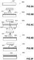
- FIGS. 9A-9Fconceptually illustrate the process steps and apparatus for fabricating a waveguide containing a birefringent grating and a birefringence control layer in accordance with various embodiments of the invention.
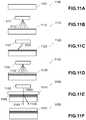
- FIGS. 10A-10Fconceptually illustrate the process steps and apparatus for fabricating a waveguide containing a birefringent grating with a birefringence control layer applied to an outer surface of the waveguide in accordance with various embodiments of the invention.
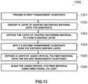
- FIGS. 11A-11Fconceptually illustrate the process steps and apparatus for fabricating a waveguide containing a birefringent grating and a birefringence control layer in accordance with various embodiments of the invention.
- FIG. 12conceptually illustrates a flow chart showing a method of fabricating a waveguide containing a birefringent grating and a birefringence control layer in accordance with an embodiment of the invention.
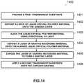
- FIG. 13conceptually illustrates a flow chart showing a method of fabricating a waveguide containing a birefringent grating and a birefringence control layer applied to an outer surface of the waveguide in accordance with an embodiment of the invention.
- FIG. 14conceptually illustrates a flow chart showing a method of fabricating a waveguide containing a birefringent grating and a birefringence control layer where forming the birefringence control layer is carried out before the recording of the grating layer in accordance with an embodiment of the invention.
- FIG. 15conceptually illustrates a schematic side view of a waveguide with a birefringence control layer applied at the waveguide to air interface in accordance with an embodiment of the invention.
- FIG. 16conceptually illustrates a schematic side view of a waveguide with a birefringence control layer that isolates the waveguide from its environment applied to the waveguide to air interface in accordance with an embodiment of the invention.
- FIG. 17conceptually illustrates a schematic side view of an apparatus for fabricating a structure containing a birefringent grating layer overlaying a birefringence control layer where the grating recording beams propagate through the birefringence control layer in accordance with an embodiment of the invention.
- FIG. 18conceptually illustrates a schematic side view of an apparatus for fabricating a structure containing a birefringence control layer overlaying a birefringent grating layer where the birefringence control layer is aligned by UV radiation propagating through the grating in accordance with an embodiment of the invention.
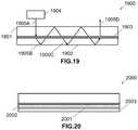
- FIG. 19conceptually illustrates a cross section of waveguide containing substrates sandwiching a grating layer.
- FIG. 20conceptually illustrates a waveguide with a quarter wave polarization layer inserted in accordance with an embodiment of the invention.
- FIG. 21conceptually illustrates a schematic cross section view showing a portion of a waveguide illustrating the use of a quarter wave polarization layer with a RKV grating in accordance with an embodiment of the invention.
- FIG. 22conceptually illustrates a polarization layer architecture containing an LCP quarter wave cell and a reactive monomer liquid crystal mixture (RMLCM) cell separated by index matching oil layer in accordance with an embodiment of the invention.
- RLCMreactive monomer liquid crystal mixture
- FIG. 23conceptually illustrates an example of a polarization architecture based on a grating cell with the RMLCM grating material layer in direct contact with a bare LCP film in accordance with an embodiment of the invention.
- FIG. 24conceptually illustrates a cross section view schematically showing an example of polarization layer architecture in which a bare LCP layer is bonded to a bare RMLCM layer in accordance with an embodiment of the invention.
- FIG. 25conceptually illustrates a cross section view schematically showing an example of a polarization layer architecture using a RMLCM layer as a polarization layer in accordance with an embodiment of the invention.
- FIG. 26conceptually illustrates an example of a polarization layer architecture that includes a feature for compensating for polarization rotation introduced by birefringent gratings in accordance with an embodiment of the invention.
- FIG. 27conceptually illustrates a plan view schematically showing a waveguide display incorporating the features of the embodiment of FIG. 26 in accordance with an embodiment of the invention.
- FIGS. 28 and 29conceptually illustrate cross section views schematically showing examples of polarization layer architectures containing an upper substrate, an LCP layer with hard encapsulation layer, a RMLCM layer, and a lower substrate in accordance with various embodiments of the invention.
- FIG. 30conceptually illustrates a plan view schematically showing a first example of a two-region polymer film in accordance with an embodiment of the invention.
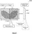
- FIG. 31conceptually illustrates a plan view schematically showing a second example of a two-region polymer film in accordance with an embodiment of the invention.
- FIG. 32conceptually illustrates a plan view schematically showing a third example of a two-region polymer film in accordance with an embodiment of the invention.
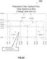
- FIG. 33conceptually illustrates a drawing showing a clear aperture layout in accordance with an embodiment of the invention.
- FIG. 34conceptually illustrates a plan view schematically showing a waveguide containing input, fold, and output gratings including the K-vectors and alignment layer fast axis directions for each grating in accordance with an embodiment of the invention.
- the term “on-axis” in relation to a ray or a beam directionrefers to propagation parallel to an axis normal to the surfaces of the optical components described in relation to the invention.
- the terms light, ray, beam, and directionmay be used interchangeably and in association with each other to indicate the direction of propagation of electromagnetic radiation along rectilinear trajectories.
- the term light and illuminationmay be used in relation to the visible and infrared bands of the electromagnetic spectrum.
- gratingmay be used to refer to any kind of diffractive structure used in a waveguide, including holograms and Bragg or volume holograms.
- the term gratingmay also encompass a grating that includes of a set of gratings.
- the input grating and output gratingeach include two or more gratings multiplexed into a single layer.
- Birefringenceis the optical property of a material having a refractive index that depends on the polarization and propagation direction of light.
- a birefringent gratingcan be referred to as a grating having such properties.
- the birefringent gratingis formed in a liquid crystal polymer material system such as but not limited to HPDLC mixtures.
- the polarization properties of such a gratingcan depend on average relative permittivity and relative permittivity modulation tensors.
- the waveguideincludes a birefringent grating layer and a birefringence control layer.
- the birefringence control layeris compact and efficient. Such structures can be utilized for various applications, including but not limited to: compensating for polarization related losses in holographic waveguides; providing three-dimensional LC director alignment in waveguides based on Bragg gratings; and spatially varying angular/spectral bandwidth for homogenizing the output from a waveguide.
- a polarization-maintaining, wide-angle, and high-reflection waveguide cladding with polarization compensationis implemented for grating birefringence.
- a thin polarization control layeris implemented for providing either quarter wave or half wave retardation.
- a polarization-maintaining, wide-angle birefringence control layeris implemented for modifying the polarization output of a waveguide to balance the birefringence of an external optical element used with the waveguide.
- the waveguideincludes at least one input grating and at least one output grating.
- the waveguidecan include additional gratings for various purposes, such as but not limited to fold gratings for beam expansion.
- the input grating and output gratingmay each include multiplexed gratings.
- the input grating and output gratingmay each include two overlapping gratings layers that are in contact or vertically separated by one or more thin optical substrate.
- the grating layersare sandwiched between glass or plastic substrates. In some embodiments two or more such gratings layers may form a stack within which total internal reflection occurs at the outer substrate and air interfaces.
- the waveguidemay include just one grating layer.
- electrodesmay be applied to faces of the substrates to switch gratings between diffracting and clear states.
- the stackmay further include additional layers such as beam splitting coatings and environmental protection layers.
- the input and output gratings shown in the drawingsmay be provided by any of the above described grating configurations.
- the input and output gratingscan be designed to have common surface grating pitch.
- the gratingscan be designed to have grating pitches such that the vector sum of the grating vectors is substantially zero.
- the input gratingcan combine gratings orientated such that each grating diffracts a polarization of the incident unpolarized light into a waveguide path.
- the output gratingscan be configured in a similar fashion such that the light from the waveguide paths is combined and coupled out of the waveguide as unpolarized light.
- Each gratingis characterized by at least one grating vector (or K-vector) in 3D space, which in the case of a Bragg grating is defined as the vector normal to the Bragg fringes.
- the grating vectorcan determine the optical efficiency for a given range of input and diffracted angles.
- the waveguideincludes at least one surface relief grating. Waveguide gratings structures, materials systems, and birefringence control are discussed below in further detail.
- Optical structures recorded in waveguidescan include many different types of optical elements, such as but not limited to diffraction gratings.
- the grating implementedis a Bragg grating (also referred to as a volume grating). Bragg gratings can have high efficiency with little light being diffracted into higher orders. The relative amount of light in the diffracted and zero order can be varied by controlling the refractive index modulation of the grating, a property that is can be used to make lossy waveguide gratings for extracting light over a large pupil.
- One class of gratings used in holographic waveguide devicesis the Switchable Bragg Grating (“SBG”).
- SBGSwitchable Bragg Grating
- SBGscan be fabricated by first placing a thin film of a mixture of photopolymerizable monomers and liquid crystal material between glass plates or substrates.
- the glass platesare in a parallel configuration.
- One or both glass platescan support electrodes, typically transparent tin oxide films, for applying an electric field across the film.
- the grating structure in an SBGcan be recorded in the liquid material (often referred to as the syrup) through photopolymerization-induced phase separation using interferential exposure with a spatially periodic intensity modulation.
- Factorssuch as but not limited to control of the irradiation intensity, component volume fractions of the materials in the mixture, and exposure temperature can determine the resulting grating morphology and performance.
- HPDLC materialis used.
- the monomerspolymerize and the mixture undergoes a phase separation.
- the LC moleculesaggregate to form discrete or coalesced droplets that are periodically distributed in polymer networks on the scale of optical wavelengths.
- the alternating liquid crystal-rich and liquid crystal-depleted regionsform the fringe planes of the grating, which can produce Bragg diffraction with a strong optical polarization resulting from the orientation ordering of the LC molecules in the droplets.
- the resulting volume phase gratingcan exhibit very high diffraction efficiency, which can be controlled by the magnitude of the electric field applied across the film.
- the electrodesare configured such that the applied electric field will be perpendicular to the substrates.
- the electrodesare fabricated from indium tin oxide (“ITO”). In the OFF state with no electric field applied, the extraordinary axis of the liquid crystals generally aligns normal to the fringes.
- the gratingthus exhibits high refractive index modulation and high diffraction efficiency for P-polarized light.
- the gratingswitches to the ON state wherein the extraordinary axes of the liquid crystal molecules align parallel to the applied field and hence perpendicular to the substrate.
- the gratingIn the ON state, the grating exhibits lower refractive index modulation and lower diffraction efficiency for both S- and P-polarized light.
- the grating regionno longer diffracts light.
- Each grating regioncan be divided into a multiplicity of grating elements such as for example a pixel matrix according to the function of the HPDLC device.
- the electrode on one substrate surfaceis uniform and continuous, while electrodes on the opposing substrate surface are patterned in accordance to the multiplicity of selectively switchable grating elements.
- transmission SBGsOne of the known attributes of transmission SBGs is that the LC molecules tend to align with an average direction normal to the grating fringe planes (i.e., parallel to the grating or K-vector).
- the effect of the LC molecule alignmentis that transmission SBGs efficiently diffract P polarized light (i.e., light with a polarization vector in the plane of incidence), but have nearly zero diffraction efficiency for S polarized light (i.e., light with the polarization vector normal to the plane of incidence).
- P polarized lighti.e., light with a polarization vector in the plane of incidence
- S polarized lighti.e., light with the polarization vector normal to the plane of incidence
- transmission SBGstypically cannot be used at near-grazing incidence as the diffraction efficiency of any grating for P polarization falls to zero when the included angle between the incident and reflected light is small.
- illumination light with non-matched polarizationis not captured efficiently in
- HPDLC mixturesin accordance with various embodiments of the invention generally include LC, monomers, photoinitiator dyes, and coinitiators.
- the mixture(often referred to as syrup) frequently also includes a surfactant.
- a surfactantis defined as any chemical agent that lowers the surface tension of the total liquid mixture.
- the use of surfactants in HPDLC mixturesis known and dates back to the earliest investigations of HPDLCs. For example, a paper by R. L Sutherland et al., SPIE Vol.
- Acrylatesoffer the benefits of fast kinetics, good mixing with other materials, and compatibility with film forming processes. Since acrylates are cross-linked, they tend to be mechanically robust and flexible. For example, urethane acrylates of functionality 2 (di) and 3 (tri) have been used extensively for HPDLC technology. Higher functionality materials such as penta and hex functional stems have also been used.
- Holographic waveguides based on HPDLCoffer the benefits of switching capability and high index modulation, but can suffer from the inherent birefringence resulting from the alignment of liquid crystal directors along grating vectors during the LC-polymer phase separation. While this can lead to a large degree of polarization selectivity, which can be advantageous in many applications, adverse effects such as polarization rotation can occur in gratings designed to fold and expand the waveguided beam in the plane of the waveguide (known as fold gratings). This polarization rotation can lead to efficiency losses and output light nonuniformity.
- Two common approaches for modifying the alignment of LC directorsinclude rubbing and the application of an alignment layer.
- LC directors in a plane parallel to the alignment layercan be realigned within the plane.
- the problemis more challenging owing to the natural alignment of LC directors along grating K-vectors, making director alignment in all but the simplest gratings a complex three-dimensional problem and rendering conventional techniques using rubbing or polyamide alignment layers impractical.
- Other approachescan include applying electric fields, magnetic fields, and mechanical pressure during curing. These approaches have been shown to have limited success when applied to reflection gratings. However, such techniques typically do not easily translate to transmission Bragg grating waveguides.
- a major design challenge in waveguidesis the coupling of image content from an external projector into the waveguide efficiently and in such a way that the waveguide image is free from chromatic dispersion and brightness non-uniformity.
- the use of laserscan be implemented.
- laserscan suffer from the problem of pupil banding artifacts, which manifest themselves as output illumination non-uniformity. Banding artifacts can form when the collimated pupil is replicated (expanded) in a TIR waveguide.
- the light beams diffracted out of the waveguide each time the beam interacts with the gratingcan have gaps or overlaps, leading to an illumination ripple.
- the degree of rippleis a function of field angle, waveguide thickness, and aperture thickness.
- the effect of bandingcan be smoothed by the dispersion typically exhibited by broadband sources such as LEDs.
- LED illuminationis not entirely free from the banding problem and, moreover, tends to result in bulky input optics and an increase in the thickness of the waveguide.
- Debandingcan be minimized using a pupil shifting technique for configuring the light coupled into the waveguide such that the input grating has an effective input aperture that is a function of the TIR angle. Techniques for performing pupil-shifting in international application No. PCT/US2018/015553 entitled “Waveguide Device with Uniform Output Illumination,” the disclosure of which is hereby incorporated by reference in its entirety.
- the polarization rotation that takes place in fold gratingscan compensate for illumination banding in waveguides that uses laser illumination.
- the mechanism for thisis that the large number of grating interactions in a fold grating combined with the small polarization rotation at each interaction can average out the banding (arising from imperfect matching of TIR beams and other coherent optical effects such as but not limited to those arising from parasitic gratings left over from the recording process, stray light interactions with the grating and waveguide surfaces, etc.).
- the process of compensating for the birefringencecan be aided by fine tuning the spatial variation of the birefringence (alignment of the LC directors) in the fold grating.
- a further issue that arises in waveguide displaysis that contact with moisture or surface combination can inhibit waveguide total internal reflection (TIR), leading to image gaps.
- TIRtotal internal reflection
- the scope for using protective outer layerscan be limited by the need for low index materials that will provide TIR over the waveguide angular bandwidth.
- a further design challenge in waveguidesis maintaining high efficiency over the angular bandwidth of the waveguide.
- One exemplary solutionwould be a polarization-maintaining, wide-angle, and high-reflection waveguide cladding.
- polarization balancing within a waveguidecan be accomplished using either a quarter wave retarding layer or a half wave retarder layer applied to one or both of the principal reflecting surfaces of the waveguide.
- One exemplary method of implementing a coatingincludes but not limited to the use of an inkjet printing or industry-standard spin-coating procedure.
- the coatingcould be applied directly to a printed grating layer.
- the coatingcould be applied to an external optical surface of the assembled waveguide.
- waveguidesare combined with conventional optics for correcting aberrations.
- aberrationsmay arise when waveguides are used in applications such as but not limited to a car HUD, which projects an image onto a car windscreen for reflection into the viewer's eyebox.
- the curvatures of the windscreencan introduce significant geometric aberration. Since many waveguides operate with collimated beams, it can be difficult to pre-compensate for the distortion within the waveguide itself.
- One solutionincludes mounting a pre-compensating optical element near the output surface of the waveguides. In many cases, the optical element is molded in plastic and can introduce severe birefringence, which should be balanced by the waveguide.
- a compact and efficient birefringence control layeris implemented for compensating for polarization related losses in holographic waveguides, for providing three-dimensional LC director alignment in waveguides based on Bragg gratings, for spatially varying angular/spectral bandwidth for homogenizing the output from a waveguide, and/or for isolating a waveguide from its environment while ensuring confinement of wave-guided beams.
- a polarization-maintaining, wide-angle, and high-reflection waveguide cladding with polarization compensationis implemented for grating birefringence.
- a thin polarization control layeris implemented for providing either quarter wave or half wave retardation.
- a polarization control layercan be implemented as a thin layer directly on top of the grating layer or to one or both of the waveguide substrates using a standard spin coating or inkjet printing process.
- a polarization-maintaining, wide-angle birefringence control layeris implemented for modifying the polarization output of a waveguide to balance the birefringence of an external optical element used with the waveguide. Other implementations and specific configurations are discussed below in further detail.
- Waveguides and waveguide displays implementing birefringence control techniques in accordance with various embodiments of the inventioncan be achieved using many different techniques.
- the waveguideincludes a birefringent grating layer and a birefringence control layer.
- a compact and efficient birefringence control layeris implemented.
- a birefringence control layercan be implemented for various functions such as but not limited to: compensating for polarization related losses in holographic waveguides; providing three-dimensional LC director alignment in waveguides based on Bragg gratings; and efficient and cost-effective integration within a waveguide for spatially varying angular/spectral bandwidth for homogenizing the output from the waveguide.
- the birefringence control layermay be formed on any optical surface of the waveguide.
- an optical surface of the waveguidemay be one of the TIR surfaces, a surface of the grating layer, a surface of the waveguide substrates sandwiching the grating layer, or a surface of any other optical substrate implemented within the waveguide (for example, a beam-splitter layer for improving uniformity).
- FIG. 1conceptually illustrates a waveguide implementing a birefringence control layer in accordance with an embodiment of the invention.
- the waveguide apparatus 100includes an optical substrate 101 containing a birefringent grating layer 102 and a birefringence control layer 103 .
- light 104 propagating under TIR within the waveguideinteracts with both layers.
- the light ray 104 A with an initial polarization state represented by the symbol 104 Bhas its polarization rotated to the state 104 C after propagation through the grating region around the point 102 A.
- the birefringence control layer 103rotates the polarization vector into the state 104 D, which is the polarization state for achieving some predefined diffraction efficiency of the ray 104 E when it interacts with the grating around the point 102 B and is diffracted into the direction 104 F with a polarization state 104 G, which is similar to the state 104 D.
- state 104 Dis the polarization state for achieving some predefined diffraction efficiency of the ray 104 E when it interacts with the grating around the point 102 B and is diffracted into the direction 104 F with a polarization state 104 G, which is similar to the state 104 D.
- FIG. 2conceptually illustrates a waveguide apparatus 200 that includes at least one optical substrate 201 and a coupler 202 for deflecting light 203 A, 203 B (covering a range of incident angles) from an external source 204 into TIR paths 205 A, 205 B in the waveguide substrate.
- Light in the TIR pathcan interact with the output grating, which can be configured to extract a portion of the light each time the TIR light satisfies the condition for diffraction by the grating.
- extractioncan occur when the Bragg condition is met. More precisely, efficient extraction can occur when a ray incident on the grating lies within an angular bandwidth and spectral bandwidth around the Bragg condition.
- the bandwidthsbeing defined according to some measure of acceptable diffraction efficiency (such as but not limited to 50% of peak DE).
- light in the TIR ray paths 205 A, 205 Bis diffracted by the output grating into output direction 206 A, 206 B, 207 A, and 207 B at different points along the output grating. It should be apparent from basic geometrical optics that a unique TIR angle can be defined by each light incidence angle at the input grating.
- the coupleris a grating.
- the coupleris a birefringent grating.
- the coupleris a prism.
- the apparatusfurther includes at least one birefringent grating 208 for providing beam expansion in a first direction and light extraction from the waveguide and at least one birefringence control layer 209 with anisotropic refractive index properties.
- the source 204can be an input image generator that includes a light source, a microdisplay panel, and optics for collimating the light. As can readily be appreciated, various input image generators can be used, including those that output non-collimated light.
- the input image generatorprojects the image displayed on the microdisplay panel such that each display pixel is converted into a unique angular direction within the substrate waveguide.
- the collimation opticsmay include lens and mirrors, which can be diffractive lenses and mirrors.
- the sourcemay be configured to provide illumination that is not modulated with image information.
- the light sourcecan be a laser or LED and can include one or more lenses for modifying the illumination beam angular characteristics.
- the image sourcecan be a micro-display or an image scanner.
- the interaction of the light with the birefringence control layer 209 and the birefringent grating 208 integrated along the total internal reflection path for any direction of the lightcan provide a predefined characteristic of the light extracted from the waveguide.
- the predefined characteristicincludes at least one of a uniform polarization or a uniform illumination over the angular range of the light.
- FIG. 2also illustrates how the birefringence control layer 209 and grating 208 provide uniform polarization.
- the input statewill correspond to P polarization, a state which may be used for gratings recorded in HPDLC.
- an initial polarization state represented by 210is assumed.
- the interaction of the light with the birefringence control layer near a grating interaction region along the TIR path 205 Ais represented by the polarization states 211 , 212 , which show the rotation of the polarization vector before and after propagation through the thickness AB of the birefringence control layer 209 .
- This polarization rotationcan be designed to balance the polarization rotation through the thickness CD of the adjacent grating region the ray encounters along the TIR path 205 A.
- the polarization of the light extracted by the gratingcan be aligned parallel to the input polarization vector as indicated by the polarization state 213 .
- the output polarization statemay differ from the input polarization state.
- the birefringent gratingthere is at least partial overlap of the birefringent grating and the birefringence control layer. In several embodiments, the two are separated by a portion of the waveguide path.
- FIG. 3conceptually illustrates a waveguide apparatus 300 in which the birefringence control layer and grating provide uniform output illumination in accordance with an embodiment of the invention.
- the waveguide apparatus 300includes at least one optical substrate 301 and a coupler 302 for deflecting light 303 from an external source 304 into TIR path 305 in the waveguide substrate.
- the apparatus 300further includes at least one birefringent grating 306 for providing beam expansion in a first direction and light extraction from the waveguide and at least one birefringence control layer 307 with anisotropic index properties. As shown, light in the TIR ray paths 305 can be diffracted by the output grating into output direction 308 , 309 .
- an initial beam illumination (I) versus angle (U) profile represented by 310is assumed.
- the interaction of the light with the birefringence control layer 307 near a grating interaction region along the TIR path 305is characterized by the illumination profiles before ( 311 ) and after ( 312 ) propagation through the thickness AB of the birefringence control layer.
- the waveguide apparatus 300can be designed to have uniform illumination versus angle across the exit pupil of the waveguide.
- the characteristics of the grating and birefringence control layervary over the aperture of the waveguide.
- the birefringent control layerhas anisotropic index properties that can be controlled during fabrication to provide a spatial distribution of birefringence such that the interaction of the light with the birefringence control layer and the birefringent grating integrated along the total internal reflection path for any direction of the light provides a predefined characteristic of the light extracted from the waveguide.
- the layermay be implemented as a thin stack that includes more than one layer.
- Alignment of HPDLC gratingscan present significant challenges depending on the grating configuration.
- polarization controlcan be confined to a single plane orthogonal to the grating plane.
- Rolled K-vector gratingscan require the alignment to vary across the grating plane.
- Fold gratings, particularly ones with slanted Bragg fringescan have much more complicated birefringence, requiring 3D alignment and, in some cases, more highly spatially resolved alignment.
- birefringence control layersfor use with the invention are illustrative only. In each case, it is assumed that the layer is processed such that the properties vary across the surface of the layer. It is also assumed that the birefringence control layer is configured within the waveguide or on an optical surface of the waveguide containing the grating. In some embodiments, the birefringence control layer is in contact with the grating layer. In several cases, the birefringence control layer spits into separate sections and are disposed on different surfaces of the waveguide. In a number of embodiments, a birefringence layer may include multiple layers.
- the inventionprovides a thin polarization control layer that can provide either quarter wave or half wave retardation.
- the polarization control layercan be implemented as a thin layer directly on top of the grating layer or to one or both of the waveguide substrates using a standard spin coating or ink jet printing process.
- the birefringence control layeris formed using materials using liquid crystal and polymer networks that can be aligned in 3D using directional UV light.
- the birefringence control layeris formed at least in part from a Liquid Crystal Polymer (LCP) Network.
- LCPswhich have also been referred to in the literature as reactive mesogens, are polymerizable liquid crystals containing liquid crystalline monomers that include, for example, reactive acrylate end groups, which polymerize with one another in the presence of photo-initiators and directional UV light to form a rigid network. The mutual polymerization of the ends of the liquid crystal molecules can freeze their orientation into a three-dimensional pattern.
- the processtypically includes coating a material system containing liquid crystal polymer onto a substrate and selectively aligning the LC directors using directionally/spatially controllable UV source prior to annealing.
- the birefringence control layeris formed at least in part from a Photo-Alignment Layer, also referred to in the literature as a linearly polymerized photopolymer (LPP).
- An LPPcan be configured to align LC directors parallel or perpendicular to incident linearly polarized UV light.
- LPPcan be formed in very thin layers (typically 50 nm) minimizing the risks of scatter or other spurious optical effect.
- the birefringence control layeris formed from LCP, LPP, and at least one dopant.
- Birefringence control layers based on LCPs and LPPscan be used align LC directors in the complex three-dimensional geometries characteristic of fold gratings and rolled K-vector gratings formed in thin film (2-4 microns).
- a birefringence control layer based on LCPs or LPPsfurther includes dichroic dyes, chiral dopants to achieve narrow or broadband cholesteric filters, twisted retarders, or negative c-plate retarders.
- birefringence control layers based on LCPs or LPPsprovide quarter or half-wave retardation layers.
- the birefringence control layeris formed by a multilayer structure combining isotropic and anisotropic index layers (as shown in FIG. 4 ).
- the multilayer structure 400includes isotropic layers 401 , 402 and anisotropic index layers 403 , 404 .
- a multiplayer stackmay include a high number of layers, such as but not limited to several tens or several hundreds of layers.
- FIG. 5conceptually illustrates a multilayer structure 500 that includes isotropic layers 501 , 502 and anisotropic index layers 503 , 504 combined with a birefringent grating layer 505 .
- a birefringent gratingwill typically have polarization rotation properties that are functions of angle wavelength.
- the birefringence control layercan be used to modify the angular, spectral, or polarization characteristics of the waveguide.
- the interaction of light with the birefringence control layercan provide an effective angular bandwidth variation along the waveguide.
- the interaction of light with the birefringence control layercan provide an effective spectral bandwidth variation along the waveguide.
- the interaction of light with the birefringence control layercan provide a polarization rotation along the waveguide.
- the grating birefringencecan be made to vary across the waveguide by spatially varying the composition of the liquid crystal polymer mixture during grating fabrication.
- the birefringence control layercan provide a birefringence variation in at least one direction in the plane of the waveguide substrate.
- the birefringence control layercan also provide a means for optimizing optical transmission (for different polarizations) within the waveguide.
- the birefringence control layercan provide a transmission variation in at least one direction in the plane of the waveguide substrate.
- the birefringence control layercan provide an angular dependence of at least one of beam transmission or polarization rotation in at least one direction in the plane of the waveguide substrate. In a number of embodiments, the birefringence control layer can provide a spectral dependence of at least one of beam transmission or polarization rotation in at least one direction in the plane of the waveguide substrate.
- birefringent gratingsmay provide input couplers, fold gratings, and output gratings in a wide range of waveguide architectures.
- FIG. 6conceptually illustrates a plan view of a dual expansion waveguide with birefringent control layers in accordance with an embodiment of the invention.
- the waveguide 600includes an optical substrate 601 that contains an input grating 602 , a fold grating 603 , and an output grating 604 that are overlaid by polarization control layers 605 , 606 , 607 , respectively.
- the inventionprovides a polarization-maintaining, wide angle birefringence control layer for modifying the polarization output of a waveguide to balance the birefringence of an external optical element used with the waveguide.
- FIG. 7conceptually illustrates an embodiment of the invention directed at automobile HUDs, which reflect collimated imagery off the windscreen into an eyebox. Any windscreen curvature will typically result in aberrations and other geometrical distortion, which cannot be corrected in certain waveguide implementations with the requirement for the beam to remain substantially collimated.
- a correction elementwhich may be a conventional refractive element or a diffractive element, near the output surface of the waveguide.
- the birefringence correction componentcan avoid disturbing ray paths from the waveguide and can be achromatic.
- the compensator technology usedcan provide spatially-varying configuration, low haze, and high transmission.
- the waveguide 700includes an optical substrate 701 containing a grating coupler 702 for deflecting light 703 from an external source of image modulated light (not shown) into the TIR path 704 in the waveguide, a birefringent grating 705 for providing beam expansion in a first direction and extracting light from the waveguide, and a birefringence control layer 706 .
- the apparatus 700further includes an optical element 707 disposed in proximity to the waveguide for correcting geometrical distortions and other aberrations introduced by reflection at the windscreen.
- the optical element 707is a refractive lens.
- the optical element 707can be a diffractive lens.
- the correctorwill typically have a large footprint with a horizontal dimension (along the dashboard) as large as 400 mm. However, if the corrector is molded in plastic, it will tend to suffer from birefringence. Hence, in the embodiment of FIG.
- the birefringence control element 706can be designed to compensate for both the grating polarization and polarization rotation introduced by the optical element 707 .
- an initial polarization state corresponding to P polarizationis assumed.
- the polarization state after propagation through the birefringence grating, birefringence control layer, and the correction elementsis represented by the symbols 708 - 711 .
- the interaction of the light with the birefringence control layer near to a grating interaction region along the TIR pathis represented by the polarization states.
- the polarization of the light 712 , 713 extracted by the gratingis aligned parallel to the input polarization vector.
- the birefringence control layer 706may be configured to rotate the output light polarization vector through ninety degrees.
- the birefringence control layercan be provided by various techniques using mechanical, thermal, or electro-magnetic processing of substrates.
- the birefringence control layeris formed by applying spatially varying mechanical stress across the surface of an optical substrate.
- FIG. 8conceptually illustrates an apparatus 800 for aligning a birefringence control layer 801 in which forces are applied in the directions indicated by 802 - 805 , resulting in the iso-birefringence contours 806 .
- the forces illustrateddo not necessarily all need to be applied to the layer.
- the birefringence control layer 801is formed by inducing thermal gradients into an optical substrate.
- the birefringence control layer 801is provided by a HPDLC grating in which LC directors are aligned using electric or magnetic fields during curing. In several embodiments, two or more of the above techniques may be combined.
- the present inventionalso provides methods and apparatus for fabricating a waveguide containing a birefringent grating and a birefringence control layer.
- the construction and arrangement of the apparatus and methods as shown in the various exemplary embodimentsare illustrative only. Although only a few embodiments have been described in detail in this disclosure, many modifications are possible (for example, additional steps for improving the efficiency of the process and quality of the finished waveguide, minimizing process variances, monitoring the process and others.) Any process step referring to the formation of a layer should be understood to cover multiple such layers. For example, where a process step of recording a grating layer is described, this step can extend to recording a stack containing two or more grating layers.
- FIGS. 9A-9Fconceptually illustrate the process steps and apparatus for fabricating a waveguide containing a birefringent grating and a birefringence control layer in accordance with various embodiments of the invention.
- FIG. 9Ashows the first step 900 of providing a first transparent substrate 901 .
- FIG. 9Billustrates an apparatus 910 for applying holographic recording material to the substrate 901 .
- the apparatus 910includes a coating apparatus 911 that provides a spray pattern 912 that forms a layer 913 of grating recording material onto the substrate 901 .
- the spray patternmay include a narrow jet or blade swept or stepped across the surface to be coated.
- the spray patternmay include a divergent jet for covering large areas of a surface simultaneously.
- the coating apparatusmay be used in conjunction with one or more masks for providing selective coating of regions of the surface.
- the coating apparatusis based on industry-standard standard spin-coating or ink-jet printing processes.
- FIG. 9Cconceptually illustrates an apparatus 920 for exposing a layer of grating recording material to form a grating layer in accordance with an embodiment of the invention.
- the apparatus 920contains a master grating 921 for contact copying the grating in the recording material and a laser 922 .
- the master 921diffracts incident light 923 to provide zero order 924 and diffracted light 925 , which interferes within the grating material layer to form a grating layer 926 .
- the apparatusmay have further features, such as but not limited to light stops and masks for overcoming stray light from higher diffraction orders or other sources.
- FIG. 9Dconceptually illustrates an apparatus 930 for coating a layer of liquid crystal polymer material onto the grating layer in accordance with an embodiment of the invention.
- the apparatus 930contains a coating apparatus 931 configured to deliver a spray pattern 932 forming a layer of material 933 .
- the coating apparatus 931may have similar features to the coating apparatus used to apply the grating recording material.
- FIG. 9Econceptually illustrates an apparatus 940 for providing an aligned liquid crystal polymer layer of material in accordance with an embodiment of the invention.
- the apparatus 940contains a UV source (which can include collimation, beams steering, and beam shaping optics, depending on the specific requirements of a given application) 941 providing directional UV light 942 for forming an aligned LC polymer layer 943 .
- FIG. 9Fconceptually illustrates the completed waveguide 950 after the step of applying a second substrate 951 over the aligned liquid crystal polymer layer 943 .
- exposure of the grating recording materialmay use conventional cross beam recording procedures instead of the mastering process described above.
- further processing of the grating layermay include annealing, thermal processing, and/or other processes for stabilizing the optical properties of grating layer.
- electrodes coatingsmay be applied to the substrates.
- a protective transparent layermay be applied over the grating layer after exposure.
- the liquid crystal polymer materialis based on the LCP, LPP material systems discussed above.
- the alignment of the liquid crystal polymercan result in an alignment of the liquid crystal directors parallel to the UV beam direction. In other embodiments, the alignment is at ninety degrees to the UV beam direction.
- the second transparent substratemay be replaced by a protective layer applied using a coating apparatus.
- FIGS. 10A-10Fconceptually illustrate the process steps and apparatus for fabricating a waveguide containing a birefringent grating with a birefringence control layer applied to an outer surface of the waveguide in accordance with various embodiments of the invention.
- FIG. 10Aconceptually illustrates the first step 1000 of providing a first transparent substrate 1001 in accordance with an embodiment of the invention.
- FIG. 10Bconceptually illustrates an apparatus 1010 for applying holographic recording material to the substrate in accordance with an embodiment of the invention.
- the apparatus 1010includes a coating apparatus 1011 providing a spray pattern 1012 that forms the layer 1013 of grating recording material onto the substrate 1001 .
- FIG. 1011providing a spray pattern 1012 that forms the layer 1013 of grating recording material onto the substrate 1001 .
- FIG. 10Cconceptually illustrates an apparatus 1020 for exposing a layer of grating recording material to form a grating layer in accordance with an embodiment of the invention.
- the apparatus 1020includes a master grating 1021 for contact copying the grating in the recording material and a laser 1022 .
- the master 1021converts light 1023 from the laser 1022 into zero order 1024 and diffracted light 1025 , which interfere within the grating material layer 1013 to form a grating layer 1026 .
- FIG. 10Dconceptually illustrates the partially completed waveguide 1030 after the step of applying a second substrate 1031 over the exposed grating layer in accordance with an embodiment of the invention.
- FIG. 10Econceptually illustrates an apparatus 1040 for coating a layer of liquid crystal polymer material onto the second substrate in accordance with an embodiment of the invention.
- the apparatus 1040includes a spray coater 1041 for delivering a spray pattern 1042 to form a layer of material 1043 .
- FIG. 10Fconceptually illustrates an apparatus 1050 for aligning the liquid crystal polymer material in accordance with an embodiment of the invention.
- the apparatus 1050includes a UV source 1051 providing the directional UV light 1052 for forming an aligned liquid crystal polymer layer 1053 , which can be configured to realign the LC directors of the grating layer 1026 .
- FIGS. 11A-11Fconceptually illustrate the process steps and apparatus for fabricating a waveguide containing a birefringent grating and a birefringence control layer in accordance with various embodiments of the invention. Unlike the above described embodiments, the step of forming the birefringence control layer can be carried out before the recording of the grating layer, which is formed above the birefringence control layer.
- FIG. 11Aconceptually illustrates the first step 1100 of providing a first transparent substrate 1101 .
- FIG. 11Bconceptually illustrates an apparatus 1110 for coating a layer of liquid crystal polymer material onto the first substrate in accordance with an embodiment of the invention.
- the apparatus 1110includes a coating apparatus 1111 configured to deliver a spray pattern 1112 to form a layer of material 1113 .
- FIG. 11Cconceptually illustrates an apparatus 1120 for aligning the liquid crystal polymer material in accordance with an embodiment of the invention.
- the apparatus 1120includes a UV source 1121 providing the directional UV light 1122 for forming an aligned liquid crystal polymer layer 1123 .
- FIG. 11Dconceptually illustrates an apparatus 1130 for applying holographic recording material to the substrate in accordance with an embodiment of the invention.
- the apparatus 1130includes a coating apparatus 1131 for providing a spray pattern 1132 to form a layer of grating recording material 1133 on top of the liquid crystal polymer layer 1123 .
- FIG. 11Econceptually illustrates an apparatus 1140 for exposing a layer of grating recording material to form a grating layer in accordance with an embodiment of the invention.
- the apparatus 1140includes a master grating 1141 for contact copying the grating in the recording material and a laser 1142 .
- the master 1141converts light 1142 from the laser into zero order 1143 and diffracted light 1144 , which interfere in the grating material layer 1133 to form a grating layer 1145 , which is aligned by the liquid crystal polymer material layer 1123 .
- FIG. 11Fconceptually illustrates the completed waveguide 1150 after the step of applying a second substrate 1151 over the exposed grating layer in accordance with an embodiment of the invention.
- FIG. 12conceptually illustrates a flow chart illustrating a method of fabricating a waveguide containing a birefringent grating and a birefringence control layer in accordance with an embodiment of the invention.
- the method 1200includes providing ( 1201 ) a first transparent substrate.
- a layer of grating recording materialcan be deposited ( 1202 ) onto the substrate.
- the layer of grating recording materialcan be exposed ( 1203 ) to form a grating layer.
- a layer of liquid crystal polymer materialcan be deposited ( 1204 ) onto the grating layer.
- the liquid crystal polymer materialcan be aligned ( 1205 ) using directional UV light.
- a second transparent substratecan be applied ( 1206 ) over the alignment layer.
- FIG. 13conceptually illustrates a flow chart illustrating a method of fabricating a waveguide containing a birefringent grating and a birefringence control layer applied to an outer surface of the waveguide in accordance with an embodiment of the invention.
- the method 1300includes providing ( 1301 ) a first transparent substrate.
- a layer of grating recording materialcan be deposited ( 1302 ) onto the substrate.
- the layer of grating recording materialcan be exposed ( 1303 ) to form a grating layer.
- a second transparent substratecan be applied ( 1304 ) over the exposed grating layer.
- a layer of liquid crystal polymer materialcan be deposited ( 1305 ) onto the second transparent substrate.
- the liquid crystal polymer materialcan be aligned ( 1306 ) using directional UV light.
- FIG. 14conceptually illustrates a flow chart illustrating a method of fabricating a waveguide containing a birefringent grating and a birefringence control layer where forming the birefringence control layer is carried out before the recording of the grating layer in accordance with an embodiment of the invention.
- the method 1400includes providing ( 1401 ) a first transparent substrate.
- a layer of liquid crystal polymer materialcan be deposited ( 1402 ) onto the substrate.
- the liquid crystal polymer materialcan be aligned ( 1403 ) using directional UV light.
- a layer of grating recording materialcan be deposited ( 1404 ) onto the aligned liquid crystal polymer material.
- the layer of grating recording materialcan be exposed ( 1405 ) to form a grating layer.
- a second transparent substratecan be applied ( 1406 ) over the grating layer.
- FIGS. 12-14illustrate specific processes for fabricating waveguides containing a birefringent grating and a birefringence control layer
- many other fabrication processes and apparatuscan be implemented to form such waveguides in accordance with various embodiments of the invention.
- the order or sequence of any process or method stepsmay be varied or re-sequenced according to alternative embodiments.
- Other substitutions, modifications, changes, and omissionsmay be made in the design of the process apparatus, operating conditions and arrangement of the exemplary embodiments without departing from the scope of the present disclosure.
- the waveguide 1500includes a waveguiding substrate 1501 containing a birefringent grating 1502 and a birefringence control layer 1503 overlaying the waveguiding substrate 1501 .
- guided light 1504 interacting with the birefringence control layer 1503 at its interface with the waveguiding substrate 1501has its polarization rotated from the state indicated by symbol 1505 (resulting from the previous interaction with the grating) to the state indicated by 1506 (which has a desired orientation for the next interaction with the grating, for example, having an orientation for providing a predefined diffraction efficiency at some pre-defined point along the grating).
- FIG. 16illustrates one such embodiment.
- the environmentally isolated waveguide 1600includes a waveguiding substrate 1601 containing a birefringent grating 1602 and a birefringence control layer 1603 overlaying the waveguiding substrate 1601 .
- guided light 1604 interacting with the birefringence control layer 1603 at its interface with the waveguiding substrate 1601has its polarization rotated from the state indicated by the symbol 1605 to the state indicated by 1606 .
- Environmental isolation of the waveguidecan be provided by designing the birefringence control layer 1603 such that total internal reflection occurs at the interface 1607 between the birefringence control layer 1603 and the waveguiding substrate 1601 .
- environmental isolationis provided by designing the birefringence control layer to have gradient index characteristics such that only a small portion of the guided light is reflected at the air interface of the birefringence control layer.
- the birefringence control layermay incorporate a separate GRIN layer.
- a GRIN layermay be based on embodiments disclosed in U.S. Provisional Patent Application No.
- FIG. 17conceptually illustrates an apparatus 1700 , which may be used in conjunction with some of the methods described above, for fabricating a structure containing a birefringent grating layer 1701 overlaying a birefringence control layer 1702 in accordance with an embodiment of the invention.
- the substrate supporting the birefringence control layeris not shown.
- the construction beams, indicated by rays 1703 , 1704may be provided by a master grating or a crossed beam holographic recording setup. As shown, the construction beams propagate through the birefringence control layer 1702 .
- the construction beamsare in the visible band. In some embodiments, the construction beams are in the UV band.
- FIG. 18conceptually illustrates an apparatus 1800 , which may be used in conjunction with some of the methods described above, for fabricating a structure containing a birefringence control layer 1801 overlaying a birefringent grating layer 1802 in accordance with an embodiment of the invention.
- the substrate supporting the grating layeris not shown.
- the direction of a recording beamis indicated by 1803 .
- the birefringence control layeris a liquid crystal polymer material system which uses a directional UV beam for alignment.
- an exposed gratingmay be erased during the process of aligning the birefringence control layer by applying an external stimulus such as heat, electric or magnetic fields or light to effective to create an isotropic phase of the liquid crystal.
- FIG. 19conceptually illustrates a cross section of waveguide 1900 containing substrates 1901 , 1902 sandwiching a grating layer 1903 .
- a source 1904emits collimated light 1905 A, which is coupled by the grating layer into the total internal reflection (TIR) path indicated by rays 1905 B, 1905 C and extracted by the grating layer 1903 into the output ray path 1905 D.
- the source 1904can be a variety of light sources, including but not limited to a laser or a LED.
- FIG. 20conceptually illustrates a waveguide similar to the one of FIG. 19 with a quarter wave polarization layer inserted by replacing the substrate 1902 by a quarter wave film 2001 sandwiched by substrates 2002 , 2003 in accordance with an embodiment of the invention.
- a quarter wave polarization layercan be beneficial to the holographic waveguide design in two ways. Firstly, it can reduce reinteraction (outcoupling) of a rolled K-vector (RKV) input grating to increase the overall coupling efficiency of the input grating. Secondly, it can continuously mix up the polarization of the light going into the fold and output gratings to provide better extraction.
- the quarter wave layercan be located on a waveguide surface along the optical from the input grating.
- a waveguide surfacecan include one of the TIR surface of the wave or some intermediate surface formed inside the waveguide.
- the optical characteristics of the quarter wave layercan be optimized for “waveguide angles”—i.e., angles in glass beyond the TIR angle.
- the center fieldis designed at approximately 55 deg. in glass (corresponding to a refractive index of approximately 1.51 at wavelength 532 nm).
- optimization for red, green, and bluecan be used for optimum performance of red, green, and blue transmitting waveguides.
- there are several different ways of incorporating the quarter wave film within a waveguideIn the following embodiment, we refer generally to a quarter wave polarization layer provided by a liquid crystal polymer (LCP) material. However, it should be understood that other materials be used in applications of the invention.
- LCPliquid crystal polymer
- FIG. 21conceptually illustrates a schematic cross section view 2100 showing a portion of a waveguide illustrating how the use of a quarter wave polarization layer with a RKV grating can overcome the problem of unwanted extraction of light along the propagation path in the input grating portion of the waveguide in accordance with an embodiment of the invention.
- One ray pathis illustrated in which input light including the P-polarized light 2101 A is coupled by the grating layer into a TIR path indicated by the rays 2101 B- 2101 L in the waveguide.
- the waveguide gratinghas rolled K-vectors of which examples occurring at three points along the length of the waveguide are illustrated schematically by the vectors 2102 A- 2102 C.
- the light 2101 A diffractively coupled into TIR by the input gratingis P-polarized with respect to the grating.
- the TIR anglecan be nominally 55 degrees in glass.
- the polarization of the lightchanges from P to circularly polarized ( 2101 C).
- the polarizationchanges to circularly polarized light ( 2101 D) of an opposing sense such that after traversing the quarter wave layer on its upward path becomes S-polarized ( 2101 E) with respect to the grating.
- the S-polarized lightpasses through the gating without deviation ( 2101 F) or substantial loss since it is both off-Bragg and “off polarization” (since the grating has zero or low diffraction efficiency for S).
- This lightthen undergoes TIR ( 2101 G) a second time retaining its S-polarization.
- the light 2101 Gis now on-Bragg but is still off polarization with respect to the P-polarization sensitive grating.
- the lighttherefore passes through the grating without diffraction ( 2101 H).
- the RKV ( 2102 B)has rolled slightly from the one ( 2102 A) near the light entry point on the UP grating.
- the ‘roll’ effect of RKVwould be small, and so the light would be strongly out-coupled.
- the S-polarization light passing through the gratinggoes through another full cycle, ( 2101 H- 2101 M) in a similar fashion to the cycle illustrated by rays 2101 B- 2101 G, and then returns to a P-polarized state for the next ( 2101 M) on-Bragg interaction at the grating region with K-vector 2102 C.
- the lighthas performed two complete TIR bounce cycles down the waveguide, increasing the angular separation of the incidence angle at the grating and K-vector, which strongly reduces the on-Bragg interaction.
- a 55-degree TIR angle light in a 1 mm thick waveguideis considered, with a 20 mm projector relief (distance of the projector from the input grating), and a nominal 4.3 mm diameter projector exit pupil:
- the first interaction with the gratingtakes place approximately 2.85 mm down the waveguide. This equates to an 8.1-degree angle at 20 mm projector relief.
- the FWHM angular bandwidth of a typical 1.6 um gratingis about 12 degrees in air (prescription dependent) i.e. the angle subtended by the pupil is not much larger than the semi-width of the lens. This leads to strong outcoupling if polarization is not changed to S-polarized as described above.
- the use of the quarter wave layerdoubles the TIR length to approximately 5.7 mm. This offset equates to about 15.9 deg, which is larger than the angular bandwidth of most waveguide gratings, thereby reducing outcoupling reinteraction losses from the waveguide.
- FIG. 22conceptually illustrates a polarization layer architecture 2200 containing an LCP quarter wave cell and a reactive monomer liquid crystal mixture (RMLCM) cell separated by index matching oil layer ( 2201 ) in accordance with an embodiment of the invention.
- the LCP cellincludes a substrate 2202 and the LCP film 2203 .
- the RMLCM cellincludes substrates 2204 , 2205 sandwiching the RMLCM layer 2206 .
- This configurationhas the advantage that the index matching oil bond can provide a non-permanent bond, which allows for installation and removal of polarization cell for testing purposes. Adhesive can also be applied at the edges (tacked) for a semi-permanent bond.
- the oil layercan be provided using a cell filled with oil.
- FIG. 23conceptually illustrates an example of a polarization architecture 2300 based on a grating cell with the RMLCM grating material layer 2301 in direct contact with a bare LCP film 2302 in accordance with an embodiment of the invention.
- the two filmsare sandwiched by the substrates 2303 , 2304 .
- Thisis a simple and cost-effective solution for implementing an LCP layer. Maintaining thickness control of the RMLCM layer using spacer beads can be difficult if the beads are embedded directly onto LCP layer.
- the embodiment of FIG. 23can required careful matching of the material properties of the RMLCM and LCP to avoid detrimental interactions between the RMLCM and the LCP layers.
- holographic exposure of the RMLCM layercan be applied directly into the RMLCM and does not need to be through the LCP layer. If exposure construction through the LCP layer is unavoidable, pre-compensation of polarization rotation of the LCP layer can be made in some embodiments.
- FIG. 24conceptually illustrates a cross section view schematically showing an example of polarization layer architecture 2400 in which a bare LCP layer is bonded to a bare RMLCM layer in accordance with an embodiment of the invention.
- the apparatusincludes an upper substrate 2401 , a bare LCP film 2402 , adhesive layer 2403 , an exposed RMLCM layer 2404 , and a lower substrate 2405 .
- the adhesive layercan be Norland NOA65 adhesive or a similar adhesive.
- FIG. 25conceptually illustrates a cross section view schematically showing an example of a polarization layer architecture 2500 using a RMLCM layer as a polarization layer in accordance with an embodiment of the invention.
- the apparatusincludes an upper substrate 2501 , an upper RMLCM layer 2502 , a transparent spacer 2503 , a lower RMLCM layer 2504 , and a lower substrate 2505 .
- One of the RMLCM layerscan be used not only as the grating material, but also as a polarization rotation layer, using the inherent birefringent properties of RMLCM materials.
- the ‘polarization rotation grating’should have a period and/or k-vector direction such that its diffraction is minimal.
- the RMLCM layercan be configure as a subwavelength grating.
- the RMCM layercan be provided sandwiched between two release layers such that after curing the layer can be removed and re-applied elsewhere.
- FIG. 26conceptually illustrates an example of a polarization layer architecture 2600 that includes a feature for compensating for polarization rotation introduced by birefringent gratings in accordance with an embodiment of the invention.
- the apparatusincludes an upper substrate 2601 , a polarization control layer 2602 , a transparent substrate 2603 , a grating layer 2604 , and a lower substrate 2605 .
- the grating layercontains a first grating 2606 A and a second grating 2606 B separated by a clear region 2607 .
- the clear regioncan a polymer with refractive index similar to that of the substrates. In many embodiments other low refractive index materials may be used to provide the clear region.
- the polarization control layerincludes quarter wave retarding regions 2608 A, 2608 B and a polarization compensation region, which balances the polarization rotation introduced by the birefringent grating 2606 A (in the case where the guide light propagates from grating 2606 A to grating 2606 B).
- FIG. 27conceptually illustrates a plan view schematically showing a waveguide display 2700 incorporating the features of the embodiment of FIG. 26 in accordance with an embodiment of the invention.
- the waveguide display 2700includes a waveguide substrate 2701 , an input grating 2702 , a fold grating 2703 , and an output grating 2704 .
- Polarization control regions 2705 , 2706apply compensation for grating depolarization according to the principle of the embodiment of FIG. 26 .
- FIG. 28conceptually illustrates a cross section view schematically showing an example of a polarization layer architecture 2800 containing an upper substrate 2801 , an LCP layer 2802 with hard encapsulation layer 2803 , a RMLCM layer 2804 , and a lower substrate 2805 in accordance with an embodiment of the invention.
- the hard encapsulation layer or filmcan be designed to protect the delicate LCP film from mechanical contact, such that standard cleaning procedures will not destroy the film.
- the hard encapsulation layercan employ a material resistant to spacer beads being pushed into it through the lamination process, as well as being chemically resistant to index matching oil and adhesives.
- FIG. 29conceptually illustrates a cross section view schematically showing an example of a polarization layer architecture 2900 containing an upper substrate 2901 , an LCP layer 2902 with soft encapsulation layer 2903 , a RMLCM layer 2904 , and a lower substrate 2905 in accordance with an embodiment of the invention.
- the polarization alignment filmcan be encapsulated with a soft encapsulation layer or film designed to protect the delicate LCP film from mechanical contact, such that standard cleaning procedures such as drag wiping with iso-propyl alcohol, for example, will not destroy the film.
- the soft encapsulationcan provide some resistance to spacer beads during the lamination process.
- FIG. 30conceptually illustrates a plan view schematically showing a first example 3000 of a two-region polymer film in accordance with an embodiment of the invention.
- This exampleusing a non-encapsulated LCP film 3001 supported by a 0.5 mm thickness Eagle XG substrate of dimensions 77.2 mm ⁇ 47.2 mm.
- Region 1is characterized by a fast axis 75° from horizontal and by quarter-wave retardance at 55° in-glass angle, 45° ellipticity ⁇ 5°, for wavelength 524 nm.
- Region 2is characterized by a fast axis 105° from horizontal and a quarter-wave retardance at 55° in-glass angle, 45° ellipticity ⁇ 5°, for wavelength 524 nm.
- region 1 and region 2extend to the halfway point horizontally, ⁇ 2 mm.
- FIG. 31conceptually illustrates a plan view schematically showing a second example 3100 of a two-region polymer film in accordance with an embodiment of the invention.
- This exampleuses encapsulation of the LCP layer 3101 by a protective film 3102 , said layers supported by a 0.5 mm thickness Eagle XG substrate of dimensions77.2 mm ⁇ 47.2 mm.
- Region 1is characterized by a fast axis 75° from horizontal and by quarter-wave retardance at 55° in-glass angle, 45° ellipticity ⁇ 5°, for wavelength 524 nm.
- Region 2is characterized by a fast axis 105° from horizontal and by quarter-wave retardance at 55° in-glass angle, 45° ellipticity ⁇ 5°, for wavelength 524 nm.
- Region 1 and region 2extend to the halfway point horizontally, ⁇ 2 mm.
- the encapsulation layercan seal the polarization layer such that performance is unaffected when covered by layer of oil such as Cargille Series A with refractive index 1.516.
- the encapsulation layercan seal the polarization layer such that performance is unaffected when covered by an additional layer of liquid crystal-based photopolymer.
- FIG. 32conceptually illustrates a plan view schematically showing a third example 3200 of a two-region polymer film in accordance with an embodiment of the invention.
- This exampleuses glass encapsulation of the LCP.
- a 0.5 mm thickness Eagle XG substrate of dimensions 77.2 mm ⁇ 47.2 mmsupports a LCP layer 3201 , an adhesive layer 3202 , and 0.2 mm thickness Willow glass cover 3203 .
- Region 1is characterized by a fast axis 75° from horizontal and by quarter-wave retardance at 55° in-glass angle, 45° ellipticity ⁇ 5°, for wavelength 524 nm.
- Region 2is characterized by a fast axis 105° from horizontal and by a quarter-wave retardance at 55° in-glass angle, 45° ellipticity ⁇ 5°, for wavelength 524 nm.
- the glass for encapsulations of the LCPis 0.5 mm EagleXG or 0.2 mm Willow glass.
- Region 1 and region 2extend to the halfway point horizontally, ⁇ 2 mm.
- FIG. 33conceptually illustrates a drawing showing the clear aperture layout 3300 for the embodiments illustrated in FIGS. 30-32 in accordance with an embodiment of the invention.
- the clear apertureis highlighted in the dashed line. All dimensions are in mm.
- FIG. 34conceptually illustrates a plan view 3400 schematically showing the waveguide 3401 containing input 3402 , fold 3403 , and output 3404 gratings based on the embodiments of FIGS. 30-33 , including the K-vectors and alignment layer fast axis directions for each grating in accordance with an embodiment of the invention.
- the K-vector and fast axis directionsare for the input grating K-vector: 30 degrees; for the fold grating K-vector: 270 degrees; and for the output grating K-vector: 150 degrees.
- the substratescan be fabricated from 0.5 mm thickness Corning Eagle XG glass. In some embodiments, thinner or thicker substrates can be used. In several embodiments, the substrates can be fabricated from plastic. In a number of embodiments, the substrates and optical layers encapsulated by the said substrates can be curved. Any of the embodiments can incorporated additional layers for protection from chemical contamination or damage incurred during processing and handling. In some embodiments, additional substrate layers may be provided to achieve a required waveguide thickness.
- additional layersmay be provided to perform at least one of the functions of illumination homogenization spectral filtering, angle selective filtering, stray light control, and debanding.
- the bare LCP layercan be bonded directly to a bare exposed RMLCM layer.
- an intermediate substratecan be disposed between the LCP layer and the RMLCM layer.
- the LCP layercan be combined with an unexposed layer of RMLCM material.
- layers of LCP, with or without encapsulationcan have haze characteristics ⁇ 0.25%, and preferably 0.1% or less.
- the quoted haze characteristicsare based on bulk material scatter and are independent of surface scatter losses, which are largely lost upon immersion.
- the LCP and encapsulation layerscan survive 100° C. exposure (>80° C. for thermal UM exposures).
- the LCP encapsulation layercan be drag wipe resistant to permit layer cleaning.
- the LCP and adhesive layerscan match the optical flatness criteria met by the waveguide substrates.
- a color waveguide according to the principles of the inventionwould typically include a stack of monochrome waveguides.
- the designmay use red, green, and blue waveguide layers or, alternatively, red and blue/green layers.
- the gratingsare all passive, that is non-switching. In some embodiments, at least one of the gratings is switching.
- the input gratings in each layerare switchable to avoid color crosstalk between the waveguide layers. In some embodiments color crosstalk is avoided by disposing dichroic filters between the input grating regions of the red and blue and the blue and green waveguides.
- the thickness of the birefringence control layeris optimized for the wavelengths of light propagating within the waveguide to provide the uniform birefringence compensation across the spectral bandwidth of the waveguide display.
- Wavelengths and spectral bandwidths bands for red, green, blue wavelengths typically used in waveguide displaysare red: 626 nm ⁇ 9 nm, green: 522 nm ⁇ 18 nm and blue: 452 nm ⁇ 11 nm.
- the thickness of the birefringence control layeris optimized for trichromatic light.
- the birefringence control layeris provided by a subwavelength grating recorded in HPDLC. Such gratings are known to exhibit the phenomenon of form birefringence and can be configured to provide a range of polarization functions including quarter wave and half wave retardation.
- the birefringence control layeris provided by a liquid crystal medium in which the LC directors are aligned by illuminating an azo-dye doped alignment layer with polarized or unpolarized light.
- a birefringence control layeris patterned to provide LC director orientation patterns with submicron resolution steps.
- the birefringence control layeris processed to provide continuous variation of the LC director orientations.
- a birefringence control layerprovided by combining one or more of the techniques described above is combined with a rubbing process or a polyimide alignment layer.
- the birefringence control layerprovides optical power.
- the birefringence control layerprovides a gradient index structure.
- the birefringence control layeris provided by a stack containing at least one HPDLC grating and at least one alignment layer.
- the birefringent gratingmay have rolled k-vectors. The K-vector is a vector aligned normal to the grating planes (or fringes) which determines the optical efficiency for a given range of input and diffracted angles.
- the birefringent gratingis a fold grating for providing exit pupil expansion.
- the fold gratingmay be based on any of the embodiments disclosed in PCT Application No.: PCT/GB2016000181 entitled WAVEGUIDE DISPLAY and embodiments discussed in the other references give above.
- the apparatusis used in a waveguide design to overcome the problem of laser banding.
- a waveguide according to the principles of the inventioncan provide a pupil shifting means for configuring the light coupled into the waveguide such that the input grating has an effective input aperture which is a function of the TIR angle.
- the effect of the pupil shifting meansis that successive light extractions from the waveguide by the output grating integrate to provide a substantially flat illumination profile for any light incidence angle at the input grating.
- the pupil shifting meanscan be implemented using the birefringence control layers to vary at least one of amplitude, polarization, phase, and wavefront displacement in 3D space as a function of incidence light angle.
- the effectis to provide an effective aperture that gives uniform extraction across the output grating for any light incidence angle at the input grating.
- the pupil shifting meansis provided at least in part by designing the optics of the input image generator to have a numerical aperture (NA) variation ranging from high NA on one side of the microdisplay panel varying smoothly to a low NA at the other side according to various embodiments, such as those similar to ones disclosed in PCT Application No.: PCT/GB2016000181 entitled WAVEGUIDE DISPLAY, the disclosure of which is hereby incorporated in its entirety.
- the microdisplayis a reflective device.
- the grating layermay be broken up into separate layers. The number of layers may then be laminated together into a single waveguide substrate.
- the grating layercontains several pieces, including the input coupler, the fold grating, and the output grating (or portions thereof) that are laminated together to form a single substrate waveguide. The pieces may be separated by optical glue or other transparent material of refractive index matching that of the pieces.
- the grating layermay be formed via a cell making process by creating cells of the desired grating thickness and vacuum filling each cell with SBG material for each of the input coupler, the fold grating and the output grating.
- the cellis formed by positioning multiple plates of glass with gaps between the plates of glass that define the desired grating thickness for the input coupler, the fold grating and the output grating.
- one cellmay be made with multiple apertures such that the separate apertures are filled with different pockets of SBG material. Any intervening spaces may then be separated by a separating material (e.g., glue, oil, etc.) to define separate areas.
- the SBG materialmay be spin-coated onto a substrate and then covered by a second substrate after curing of the material.
- the gratingscan be created by interfering two waves of light at an angle within the substrate to create a holographic wave front, thereby creating light and dark fringes that are set in the waveguide substrate at a desired angle.
- the grating in a given layeris recorded in stepwise fashion by scanning or stepping the recording laser beams across the grating area.
- the gratingsare recorded using mastering and contact copying process currently used in the holographic printing industry.
- the gratingsare Bragg gratings recorded in holographic polymer dispersed liquid crystal (HPDLC) as already discussed, although SBGs may also be recorded in other materials.
- SBGsare recorded in a uniform modulation material, such as POLICRYPS or POLIPHEM having a matrix of solid liquid crystals dispersed in a liquid polymer.
- the SBGscan be switching or non-switching in nature. In its non-switching form a SBG has the advantage over conventional holographic photopolymer materials of being capable of providing high refractive index modulation due to its liquid crystal component.
- Uniform modulation gratingsare characterized by high refractive index modulation (and hence high diffraction efficiency) and low scatter.
- at least one of the gratingsis a surface relief grating.
- at least one of the gratingsis a thin (or Raman-Nath) hologram,
- the gratingsare recorded in a reverse mode HPDLC material.
- Reverse mode HPDLCdiffers from conventional HPDLC in that the grating is passive when no electric field is applied and becomes diffractive in the presence of an electric field.
- the reverse mode HPDLCmay be based on any of the recipes and processes disclosed in PCT Application No.: PCT/GB2012/000680, entitled IMPROVEMENTS TO HOLOGRAPHIC POLYMER DISPERSED LIQUID CRYSTAL MATERIALS AND DEVICES.
- the gratingmay be recorded in any of the above material systems but used in a passive (non-switching) mode.
- the fabrication processcan be identical to that used for switched but with the electrode coating stage being omitted.
- LC polymer material systemsmay be used for their high index modulation.
- the gratingsare recorded in HPDLC but are not switched.
- a waveguide display according to the principles of the inventionmay be integrated within a window, for example, a windscreen-integrated HUD for road vehicle applications.
- a window-integrated displaymay be based on the embodiments and teachings disclosed in U.S. Provisional Patent Application No. 62/125,064 entitled OPTICAL WAVEGUIDE DISPLAYS FOR INTEGRATION IN WINDOWS and U.S. patent application Ser. No. 15/543,016 entitled ENVIRONMENTALLY ISOLATED WAVEGUIDE DISPLAY.
- a waveguide display according to the principles of the inventionmay incorporate a light pipe for providing beam expansion in one direction based on the embodiments disclosed in U.S. patent application Ser. No.
- the input image generatormay be based on a laser scanner as disclosed in U.S. Pat. No. 9,075,184 entitled COMPACT EDGE ILLUMINATED DIFFRACTIVE DISPLAY.
- the embodiments of the inventionmay be used in wide range of displays including HMDs for AR and VR, helmet mounted displays, projection displays, heads up displays (HUDs), Heads Down Displays, (HDDs), autostereoscopic displays and other 3D displays.
- Some of the embodiments and teachings of this disclosuremay be applied in waveguide sensors such as, for example, eye trackers, fingerprint scanners and LIDAR systems and in illuminators and backlights.
- the drawingsare exemplary and that the dimensions have been exaggerated. For example, thicknesses of the SBG layers have been greatly exaggerated.
- Optical devices based on any of the above-described embodimentsmay be implemented using plastic substrates using the materials and processes disclosed in PCT Application No.: PCT/GB2012/000680, entitled IMPROVEMENTS TO HOLOGRAPHIC POLYMER DISPERSED LIQUID CRYSTAL MATERIALS AND DEVICES.
- the dual expansion waveguide displaymay be curved.
Landscapes
- Physics & Mathematics (AREA)
- General Physics & Mathematics (AREA)
- Optics & Photonics (AREA)
- Engineering & Computer Science (AREA)
- Microelectronics & Electronic Packaging (AREA)
- Chemical & Material Sciences (AREA)
- Nonlinear Science (AREA)
- Crystallography & Structural Chemistry (AREA)
- Mathematical Physics (AREA)
- Dispersion Chemistry (AREA)
- Optical Integrated Circuits (AREA)
- Optical Modulation, Optical Deflection, Nonlinear Optics, Optical Demodulation, Optical Logic Elements (AREA)
- Holo Graphy (AREA)
- Polarising Elements (AREA)
- Diffracting Gratings Or Hologram Optical Elements (AREA)
Abstract
Description
- R. L. Sutherland et al., Chem. Mater. 5, 1533 (1993), the disclosure of which is incorporated herein by reference, describes the use of acrylate polymers and surfactants. Specifically, the recipe includes a crosslinking multifunctional acrylate monomer; a chain extender N-vinyl pyrrolidinone, LC E7, photo-initiator rose Bengal, and coinitiator N-phenyl glycine. Surfactant octanoic acid was added in certain variants.
- Fontecchio et al., SID 00 Digest 774-776, 2000, the disclosure of which is incorporated herein by reference, describes a UV curable HPDLC for reflective display applications including a multi-functional acrylate monomer, LC, a photoinitiator, a coinitiators, and a chain terminator.
- Y. H. Cho, et al., Polymer International, 48, 1085-1090, 1999, the disclosure of which is incorporated herein by reference, discloses HPDLC recipes including acrylates.
- Karasawa et al., Japanese Journal of Applied Physics, Vol. 36, 6388-6392, 1997, the disclosure of which is incorporated herein by reference, describes acrylates of various functional orders.
- T. J. Bunning et al., Polymer Science: Part B: Polymer Physics, Vol. 35, 2825-2833, 1997, the disclosure of which is incorporated herein by reference, also describes multifunctional acrylate monomers.
- G. S. Iannacchione et al., Europhysics Letters Vol. 36 (6). 425-430, 1996, the disclosure of which is incorporated herein by reference, describes a PDLC mixture including a penta-acrylate monomer, LC, chain extender, coinitiators, and photoinitiator.
Claims (29)
Priority Applications (3)
| Application Number | Priority Date | Filing Date | Title |
|---|---|---|---|
| US16/357,233US10690851B2 (en) | 2018-03-16 | 2019-03-18 | Holographic waveguides incorporating birefringence control and methods for their fabrication |
| US16/906,872US11150408B2 (en) | 2018-03-16 | 2020-06-19 | Holographic waveguides incorporating birefringence control and methods for their fabrication |
| US17/451,223US11726261B2 (en) | 2018-03-16 | 2021-10-18 | Holographic waveguides incorporating birefringence control and methods for their fabrication |
Applications Claiming Priority (2)
| Application Number | Priority Date | Filing Date | Title |
|---|---|---|---|
| US201862643977P | 2018-03-16 | 2018-03-16 | |
| US16/357,233US10690851B2 (en) | 2018-03-16 | 2019-03-18 | Holographic waveguides incorporating birefringence control and methods for their fabrication |
Related Child Applications (1)
| Application Number | Title | Priority Date | Filing Date |
|---|---|---|---|
| US16/906,872ContinuationUS11150408B2 (en) | 2018-03-16 | 2020-06-19 | Holographic waveguides incorporating birefringence control and methods for their fabrication |
Publications (2)
| Publication Number | Publication Date |
|---|---|
| US20190285796A1 US20190285796A1 (en) | 2019-09-19 |
| US10690851B2true US10690851B2 (en) | 2020-06-23 |
Family
ID=67903943
Family Applications (3)
| Application Number | Title | Priority Date | Filing Date |
|---|---|---|---|
| US16/357,233ActiveUS10690851B2 (en) | 2018-03-16 | 2019-03-18 | Holographic waveguides incorporating birefringence control and methods for their fabrication |
| US16/906,872ActiveUS11150408B2 (en) | 2018-03-16 | 2020-06-19 | Holographic waveguides incorporating birefringence control and methods for their fabrication |
| US17/451,223ActiveUS11726261B2 (en) | 2018-03-16 | 2021-10-18 | Holographic waveguides incorporating birefringence control and methods for their fabrication |
Family Applications After (2)
| Application Number | Title | Priority Date | Filing Date |
|---|---|---|---|
| US16/906,872ActiveUS11150408B2 (en) | 2018-03-16 | 2020-06-19 | Holographic waveguides incorporating birefringence control and methods for their fabrication |
| US17/451,223ActiveUS11726261B2 (en) | 2018-03-16 | 2021-10-18 | Holographic waveguides incorporating birefringence control and methods for their fabrication |
Country Status (6)
| Country | Link |
|---|---|
| US (3) | US10690851B2 (en) |
| EP (2) | EP4372451A3 (en) |
| JP (2) | JP7487109B2 (en) |
| KR (2) | KR102839391B1 (en) |
| CN (2) | CN112088332B (en) |
| WO (1) | WO2019178614A1 (en) |
Cited By (20)
| Publication number | Priority date | Publication date | Assignee | Title |
|---|---|---|---|---|
| US11150408B2 (en) | 2018-03-16 | 2021-10-19 | Digilens Inc. | Holographic waveguides incorporating birefringence control and methods for their fabrication |
| US11300795B1 (en)* | 2009-09-30 | 2022-04-12 | Digilens Inc. | Systems for and methods of using fold gratings coordinated with output couplers for dual axis expansion |
| WO2022140763A1 (en)* | 2020-12-21 | 2022-06-30 | Digilens Inc. | Eye glow suppression in waveguide based displays |
| US11726332B2 (en) | 2009-04-27 | 2023-08-15 | Digilens Inc. | Diffractive projection apparatus |
| US11747719B2 (en) | 2009-10-09 | 2023-09-05 | Digilens Inc. | Diffractive waveguide providing structured illumination for object detection |
| US20230305298A1 (en)* | 2020-08-18 | 2023-09-28 | Bayerische Motoren Werke Aktiengesellschaft | Waveguide Display Assembly for a 3D Head-up Display Device in a Vehicle, and Method for Operating Same |
| US20230324683A1 (en)* | 2022-03-29 | 2023-10-12 | Envisics Ltd | Display system and light control film therefor |
| US12140764B2 (en) | 2019-02-15 | 2024-11-12 | Digilens Inc. | Wide angle waveguide display |
| US12210153B2 (en) | 2019-01-14 | 2025-01-28 | Digilens Inc. | Holographic waveguide display with light control layer |
| US12248150B2 (en) | 2017-01-05 | 2025-03-11 | Digilens Inc. | Wearable heads up displays |
| US12271035B2 (en) | 2019-06-07 | 2025-04-08 | Digilens Inc. | Waveguides incorporating transmissive and reflective gratings and related methods of manufacturing |
| US12282163B2 (en) | 2021-12-30 | 2025-04-22 | Goertek Inc. | Optical waveguide system and electronic device |
| US12298513B2 (en) | 2016-12-02 | 2025-05-13 | Digilens Inc. | Waveguide device with uniform output illumination |
| US12306585B2 (en) | 2018-01-08 | 2025-05-20 | Digilens Inc. | Methods for fabricating optical waveguides |
| US12366823B2 (en) | 2018-01-08 | 2025-07-22 | Digilens Inc. | Systems and methods for high-throughput recording of holographic gratings in waveguide cells |
| US12372708B2 (en)* | 2021-10-08 | 2025-07-29 | Samsung Electronics Co., Ltd. | Waveguide and augmented reality device employing the same |
| US12379547B2 (en) | 2015-02-12 | 2025-08-05 | Digilens Inc. | Waveguide grating device |
| US12397477B2 (en) | 2019-02-05 | 2025-08-26 | Digilens Inc. | Methods for compensating for optical surface nonuniformity |
| US12405507B2 (en) | 2012-11-16 | 2025-09-02 | Digilens Inc. | Transparent waveguide display with grating lamina that both couple and extract modulated light |
| US12405471B2 (en) | 2015-10-05 | 2025-09-02 | Digilens Inc. | Apparatus for providing waveguide displays with two-dimensional pupil expansion |
Families Citing this family (32)
| Publication number | Priority date | Publication date | Assignee | Title |
|---|---|---|---|---|
| WO2016020630A2 (en) | 2014-08-08 | 2016-02-11 | Milan Momcilo Popovich | Waveguide laser illuminator incorporating a despeckler |
| WO2016042283A1 (en) | 2014-09-19 | 2016-03-24 | Milan Momcilo Popovich | Method and apparatus for generating input images for holographic waveguide displays |
| WO2016113534A1 (en) | 2015-01-12 | 2016-07-21 | Milan Momcilo Popovich | Environmentally isolated waveguide display |
| US11567322B2 (en)* | 2018-11-02 | 2023-01-31 | Google Llc | Systems, devices, and methods for eyebox expansion in wearable heads-up displays |
| KR102866596B1 (en) | 2019-02-15 | 2025-09-29 | 디지렌즈 인코포레이티드. | Method and device for providing a holographic waveguide display using an integral grating |
| CN109739054B (en)* | 2019-02-28 | 2021-07-30 | 上海天马微电子有限公司 | Display device |
| WO2020194215A1 (en)* | 2019-03-26 | 2020-10-01 | Terahertz Group Ltd. | Devices for generation of electromagnetic radiation of predetermined profile |
| KR102845980B1 (en)* | 2019-08-20 | 2025-08-12 | 삼성전자주식회사 | LiDAR device and operating method of the same |
| KR102775783B1 (en) | 2019-08-29 | 2025-02-28 | 디지렌즈 인코포레이티드. | Vacuum grid and method for manufacturing the same |
| US11054566B2 (en) | 2019-10-25 | 2021-07-06 | Facebook Technologies, Llc | Display waveguide with a high-index layer |
| WO2021102165A1 (en)* | 2019-11-22 | 2021-05-27 | Magic Leap, Inc. | Method and system for patterning a liquid crystal layer |
| US11513373B2 (en)* | 2019-12-05 | 2022-11-29 | Meta Platforms Technologies LLC | Anisotropic diffraction grating and waveguide |
| US11604366B2 (en)* | 2020-02-21 | 2023-03-14 | Meta Platforms Technologies, Llc | Head-mounted display devices with removable prescription lenses |
| CN115349105A (en)* | 2020-03-31 | 2022-11-15 | 索尼集团公司 | Optical device, method for manufacturing optical device, and image display device |
| KR102778216B1 (en)* | 2020-04-16 | 2025-03-10 | 쌩-고벵 글래스 프랑스 | Projection assembly for head-up display (HUD) with p-polarized radiation |
| US20230290290A1 (en)* | 2020-06-22 | 2023-09-14 | Digilens Inc. | Systems and Methods for Real-Time Color Correction of Waveguide Based Displays |
| US20220043287A1 (en)* | 2020-08-10 | 2022-02-10 | Digilens Inc. | Switchable Raman Nath Gratings |
| US20220113672A1 (en)* | 2020-10-08 | 2022-04-14 | Facebook Technologies, Llc | Method for fabricating off-axis focusing geometric phase element |
| KR20220049398A (en) | 2020-10-14 | 2022-04-21 | 삼성전자주식회사 | Waveguide structure, back light unit including the same, display apparatus including the same |
| WO2022119924A1 (en)* | 2020-12-01 | 2022-06-09 | Kent State University | Polarization state compensator |
| KR20220080960A (en)* | 2020-12-08 | 2022-06-15 | 한국전자기술연구원 | Holographic printing method without distortion caused by interference pattern from internal reflection |
| WO2022150841A1 (en) | 2021-01-07 | 2022-07-14 | Digilens Inc. | Grating structures for color waveguides |
| US12158612B2 (en) | 2021-03-05 | 2024-12-03 | Digilens Inc. | Evacuated periodic structures and methods of manufacturing |
| CN113030139B (en)* | 2021-05-31 | 2021-08-13 | 中国工程物理研究院激光聚变研究中心 | Novel crystal and compact imaging device |
| CN114428376B (en)* | 2021-12-29 | 2024-07-02 | 歌尔股份有限公司 | Optical waveguide system and augmented reality device |
| CN114089469B (en)* | 2022-01-20 | 2022-05-06 | 深圳珑璟光电科技有限公司 | Volume holographic optical waveguide, manufacturing method thereof and color volume holographic optical waveguide |
| US12197011B2 (en) | 2022-02-08 | 2025-01-14 | Goertek Inc. | Optical waveguide system, and electronic device |
| US12386179B2 (en) | 2022-04-29 | 2025-08-12 | Goertek Inc. | Optical waveguide system with angle-multiplexing polarization volume grating and electronic device |
| EP4336243A1 (en)* | 2022-09-09 | 2024-03-13 | Nokia Technologies Oy | An apparatus for projecting images towards a user |
| US20250067937A1 (en)* | 2023-08-25 | 2025-02-27 | Applied Materials, Inc. | Individual grating fabrication and assembly |
| WO2025114170A1 (en)* | 2023-11-28 | 2025-06-05 | Seereal Technologies S.A. | Light guide |
| WO2025147524A1 (en)* | 2024-01-03 | 2025-07-10 | Applied Materials, Inc. | Embedded fold grating for ar waveguide |
Citations (722)
| Publication number | Priority date | Publication date | Assignee | Title |
|---|---|---|---|---|
| US1043938A (en) | 1911-08-17 | 1912-11-12 | Friedrich Huttenlocher | Safety device for gas-lamps. |
| US3482498A (en) | 1967-05-09 | 1969-12-09 | Trw Inc | Ridge pattern recording apparatus |
| US3741716A (en) | 1971-03-30 | 1973-06-26 | Hoechst Ag | Heater for use in the manufacture of plastics filaments |
| US3843231A (en) | 1971-04-22 | 1974-10-22 | Commissariat Energie Atomique | Liquid crystal diffraction grating |
| US3965029A (en) | 1974-02-04 | 1976-06-22 | Kent State University | Liquid crystal materials |
| US3975711A (en) | 1974-08-30 | 1976-08-17 | Sperry Rand Corporation | Real time fingerprint recording terminal |
| US4035068A (en) | 1975-06-25 | 1977-07-12 | Xerox Corporation | Speckle minimization in projection displays by reducing spatial coherence of the image light |
| US4066334A (en) | 1975-01-06 | 1978-01-03 | National Research Development Corporation | Liquid crystal light deflector |
| US4248093A (en) | 1979-04-13 | 1981-02-03 | The Boeing Company | Holographic resolution of complex sound fields |
| US4251137A (en) | 1977-09-28 | 1981-02-17 | Rca Corporation | Tunable diffractive subtractive filter |
| US4322163A (en) | 1977-10-25 | 1982-03-30 | Fingermatrix Inc. | Finger identification |
| US4386361A (en) | 1980-09-26 | 1983-05-31 | S.H.E. Corporation | Thin film SQUID with low inductance |
| US4389612A (en) | 1980-06-17 | 1983-06-21 | S.H.E. Corporation | Apparatus for reducing low frequency noise in dc biased SQUIDS |
| US4403189A (en) | 1980-08-25 | 1983-09-06 | S.H.E. Corporation | Superconducting quantum interference device having thin film Josephson junctions |
| US4418993A (en) | 1981-05-07 | 1983-12-06 | Stereographics Corp. | Stereoscopic zoom lens system for three-dimensional motion pictures and television |
| US4472037A (en) | 1981-08-24 | 1984-09-18 | Stereographics Corporation | Additive color means for the calibration of stereoscopic projection |
| GB2140935A (en) | 1981-04-10 | 1984-12-05 | Yissum Res Dev Co | Eye testing system |
| US4523226A (en) | 1982-01-27 | 1985-06-11 | Stereographics Corporation | Stereoscopic television system |
| US4544267A (en) | 1980-11-25 | 1985-10-01 | Fingermatrix, Inc. | Finger identification |
| US4562463A (en) | 1981-05-15 | 1985-12-31 | Stereographics Corp. | Stereoscopic television system with field storage for sequential display of right and left images |
| US4566758A (en) | 1983-05-09 | 1986-01-28 | Tektronix, Inc. | Rapid starting, high-speed liquid crystal variable optical retarder |
| US4583117A (en) | 1984-07-17 | 1986-04-15 | Stereographics Corporation | Stereoscopic video camera |
| US4643515A (en) | 1985-04-01 | 1987-02-17 | Environmental Research Institute Of Michigan | Method and apparatus for recording and displaying edge-illuminated holograms |
| US4688900A (en) | 1984-03-19 | 1987-08-25 | Kent State University | Light modulating material comprising a liquid crystal dispersion in a plastic matrix |
| US4711512A (en) | 1985-07-12 | 1987-12-08 | Environmental Research Institute Of Michigan | Compact head-up display |
| US4728547A (en) | 1985-06-10 | 1988-03-01 | General Motors Corporation | Liquid crystal droplets dispersed in thin films of UV-curable polymers |
| US4729640A (en) | 1984-10-03 | 1988-03-08 | Canon Kabushiki Kaisha | Liquid crystal light modulation device |
| US4765703A (en) | 1985-08-05 | 1988-08-23 | Brother Kogyo Kabushiki Kaisha | Optical deflector |
| US4791788A (en) | 1987-08-24 | 1988-12-20 | Quantum Design, Inc. | Method for obtaining improved temperature regulation when using liquid helium cooling |
| US4792850A (en) | 1987-11-25 | 1988-12-20 | Sterographics Corporation | Method and system employing a push-pull liquid crystal modulator |
| US4811414A (en) | 1987-02-27 | 1989-03-07 | C.F.A. Technologies, Inc. | Methods for digitally noise averaging and illumination equalizing fingerprint images |
| US4848093A (en) | 1987-08-24 | 1989-07-18 | Quantum Design | Apparatus and method for regulating temperature in a cryogenic test chamber |
| US4884876A (en) | 1983-10-30 | 1989-12-05 | Stereographics Corporation | Achromatic liquid crystal shutter for stereoscopic and other applications |
| US4890902A (en) | 1985-09-17 | 1990-01-02 | Kent State University | Liquid crystal light modulating materials with selectable viewing angles |
| US4933976A (en) | 1988-01-25 | 1990-06-12 | C.F.A. Technologies, Inc. | System for generating rolled fingerprint images |
| US4938568A (en) | 1988-01-05 | 1990-07-03 | Hughes Aircraft Company | Polymer dispersed liquid crystal film devices, and method of forming the same |
| JPH02186319A (en) | 1989-01-13 | 1990-07-20 | Fujitsu Ltd | display system |
| US4960311A (en) | 1989-08-31 | 1990-10-02 | Hughes Aircraft Company | Holographic exposure system for computer generated holograms |
| US4964701A (en) | 1988-10-04 | 1990-10-23 | Raytheon Company | Deflector for an optical beam |
| US4967268A (en) | 1989-07-31 | 1990-10-30 | Stereographics | Liquid crystal shutter system for stereoscopic and other applications |
| US4970129A (en) | 1986-12-19 | 1990-11-13 | Polaroid Corporation | Holograms |
| US4971719A (en) | 1989-09-22 | 1990-11-20 | General Motors Corporation | Polymer dispersed liquid crystal films formed by electron beam curing |
| US4994204A (en) | 1988-11-04 | 1991-02-19 | Kent State University | Light modulating materials comprising a liquid crystal phase dispersed in a birefringent polymeric phase |
| US5004323A (en) | 1988-08-30 | 1991-04-02 | Kent State University | Extended temperature range polymer dispersed liquid crystal light shutters |
| US5009483A (en) | 1989-04-12 | 1991-04-23 | Rockwell Iii Marshall A | Optical waveguide display system |
| US5033814A (en) | 1989-04-10 | 1991-07-23 | Nilford Laboratories, Inc. | Line light source |
| US5053834A (en) | 1990-08-31 | 1991-10-01 | Quantum Magnetics, Inc. | High symmetry dc SQUID system |
| JPH03239384A (en) | 1990-02-16 | 1991-10-24 | Fujitsu Ltd | Semiconductor laser protection circuit |
| US5063441A (en) | 1990-10-11 | 1991-11-05 | Stereographics Corporation | Stereoscopic video cameras with image sensors having variable effective position |
| US5096282A (en) | 1988-01-05 | 1992-03-17 | Hughes Aircraft Co. | Polymer dispersed liquid crystal film devices |
| US5099343A (en) | 1989-05-25 | 1992-03-24 | Hughes Aircraft Company | Edge-illuminated liquid crystal display devices |
| US5110034A (en) | 1990-08-30 | 1992-05-05 | Quantum Magnetics, Inc. | Superconducting bonds for thin film devices |
| US5117302A (en) | 1990-04-13 | 1992-05-26 | Stereographics Corporation | High dynamic range electro-optical shutter for steroscopic and other applications |
| US5119454A (en) | 1988-05-23 | 1992-06-02 | Polaroid Corporation | Bulk optic wavelength division multiplexer |
| US5139192A (en) | 1990-08-30 | 1992-08-18 | Quantum Magnetics, Inc. | Superconducting bonds for thin film devices |
| US5142357A (en) | 1990-10-11 | 1992-08-25 | Stereographics Corp. | Stereoscopic video camera with image sensors having variable effective position |
| US5142644A (en) | 1991-03-08 | 1992-08-25 | General Motors Corporation | Electrical contacts for polymer dispersed liquid crystal films |
| US5148302A (en) | 1986-04-10 | 1992-09-15 | Akihiko Nagano | Optical modulation element having two-dimensional phase type diffraction grating |
| US5181133A (en) | 1991-05-15 | 1993-01-19 | Stereographics Corporation | Drive method for twisted nematic liquid crystal shutters for stereoscopic and other applications |
| US5193000A (en) | 1991-08-28 | 1993-03-09 | Stereographics Corporation | Multiplexing technique for stereoscopic video system |
| US5198912A (en) | 1990-01-12 | 1993-03-30 | Polaroid Corporation | Volume phase hologram with liquid crystal in microvoids between fringes |
| US5200861A (en) | 1991-09-27 | 1993-04-06 | U.S. Precision Lens Incorporated | Lens systems |
| US5218480A (en) | 1991-12-03 | 1993-06-08 | U.S. Precision Lens Incorporated | Retrofocus wide angle lens |
| US5224198A (en) | 1991-09-30 | 1993-06-29 | Motorola, Inc. | Waveguide virtual image display |
| US5239372A (en) | 1991-12-31 | 1993-08-24 | Stereographics Corporation | Stereoscopic video projection system |
| US5241337A (en) | 1991-05-13 | 1993-08-31 | Eastman Kodak Company | Real image viewfinder requiring no field lens |
| US5240636A (en) | 1988-04-11 | 1993-08-31 | Kent State University | Light modulating materials comprising a liquid crystal microdroplets dispersed in a birefringent polymeric matri method of making light modulating materials |
| US5242476A (en) | 1990-09-06 | 1993-09-07 | Kabelmetal Electro Gmbh | Process for the preparation of glass fiber optical waveguides with increased tensile strength |
| US5251048A (en) | 1992-05-18 | 1993-10-05 | Kent State University | Method and apparatus for electronic switching of a reflective color display |
| US5264950A (en) | 1992-01-06 | 1993-11-23 | Kent State University | Light modulating device with polarizer and liquid crystal interspersed as spherical or randomly distorted droplets in isotropic polymer |
| US5268792A (en) | 1991-05-20 | 1993-12-07 | Eastman Kodak Company | Zoom lens |
| US5284499A (en) | 1992-05-01 | 1994-02-08 | Corning Incorporated | Method and apparatus for drawing optical fibers |
| US5295208A (en) | 1992-02-26 | 1994-03-15 | The University Of Alabama In Huntsville | Multimode waveguide holograms capable of using non-coherent light |
| US5296967A (en) | 1992-03-02 | 1994-03-22 | U.S. Precision Lens Incorporated | High speed wide angle projection TV lens system |
| US5299289A (en) | 1991-06-11 | 1994-03-29 | Matsushita Electric Industrial Co., Ltd. | Polymer dispersed liquid crystal panel with diffraction grating |
| US5309283A (en) | 1993-03-30 | 1994-05-03 | U.S. Precision Lens Incorporated | Hybrid, color-corrected, projection TV lens system |
| US5313330A (en) | 1992-08-31 | 1994-05-17 | U.S. Precision Lens Incorporated | Zoom projection lens systems |
| US5315419A (en) | 1992-05-19 | 1994-05-24 | Kent State University | Method of producing a homogeneously aligned chiral smectic C liquid crystal having homeotropic alignment layers |
| US5315440A (en) | 1991-11-04 | 1994-05-24 | Eastman Kodak Company | Zoom lens having weak front lens group |
| US5315324A (en) | 1992-12-09 | 1994-05-24 | Delphax Systems | High precision charge imaging cartridge |
| US5327269A (en) | 1992-05-13 | 1994-07-05 | Standish Industries, Inc. | Fast switching 270° twisted nematic liquid crystal device and eyewear incorporating the device |
| US5329363A (en) | 1993-06-15 | 1994-07-12 | U. S. Precision Lens Incorporated | Projection lens systems having reduced spherochromatism |
| US5343147A (en) | 1992-09-08 | 1994-08-30 | Quantum Magnetics, Inc. | Method and apparatus for using stochastic excitation and a superconducting quantum interference device (SAUID) to perform wideband frequency response measurements |
| JPH06294952A (en) | 1993-04-09 | 1994-10-21 | Nippon Telegr & Teleph Corp <Ntt> | Reflective color liquid crystal display |
| US5368770A (en) | 1992-06-01 | 1994-11-29 | Kent State University | Method of preparing thin liquid crystal films |
| US5371626A (en) | 1993-03-09 | 1994-12-06 | Benopcon, Inc. | Wide angle binocular system with variable power capability |
| JPH0798439A (en) | 1993-09-29 | 1995-04-11 | Nippon Telegr & Teleph Corp <Ntt> | 3D stereoscopic display |
| US5416510A (en) | 1991-08-28 | 1995-05-16 | Stereographics Corporation | Camera controller for stereoscopic video system |
| US5418871A (en) | 1993-02-16 | 1995-05-23 | Eastman Kodak Company | Multichannel optical waveguide page scanner with individually addressable electro-optic modulators |
| US5428480A (en) | 1993-02-16 | 1995-06-27 | Eastman Kodak Company | Zoom lens having weak plastic element |
| US5437811A (en) | 1991-05-02 | 1995-08-01 | Kent State University | Liquid crystalline light modulating device and material |
| US5452385A (en) | 1993-03-09 | 1995-09-19 | Sharp Kabushiki Kaisha | Optical scanning device an optical scanning type display and an image data input/output device |
| US5453863A (en) | 1991-05-02 | 1995-09-26 | Kent State University | Multistable chiral nematic displays |
| US5455713A (en) | 1993-06-23 | 1995-10-03 | Kreitzer; Melvyn H. | High performance, thermally-stabilized projection television lens systems |
| US5455693A (en) | 1992-09-24 | 1995-10-03 | Hughes Aircraft Company | Display hologram |
| US5463428A (en) | 1994-02-08 | 1995-10-31 | Stereographics Corporation | Wireless active eyewear for stereoscopic applications |
| US5476611A (en) | 1992-03-31 | 1995-12-19 | Merck Patent Gesellschaft Mit Beschrankter Haftung | Electrooptical liquid crystal system |
| US5481321A (en) | 1991-01-29 | 1996-01-02 | Stereographics Corp. | Stereoscopic motion picture projection system |
| US5485313A (en) | 1993-10-27 | 1996-01-16 | Polaroid Corporation | Zoom lens systems |
| US5493430A (en) | 1994-08-03 | 1996-02-20 | Kent Display Systems, L.P. | Color, reflective liquid crystal displays |
| US5515184A (en) | 1991-11-12 | 1996-05-07 | The University Of Alabama In Huntsville | Waveguide hologram illuminators |
| US5516455A (en) | 1993-05-03 | 1996-05-14 | Loctite Corporation | Polymer dispersed liquid crystals in radiation curable electron-rich alkene-thiol polymer mixtures |
| US5530566A (en) | 1992-09-24 | 1996-06-25 | Kent State University | Polymer dispersed ferroelectric smectic liquid crystal formed by inducing a force during phase separation |
| US5543950A (en) | 1995-05-04 | 1996-08-06 | Kent State University | Liquid crystalline electrooptical device |
| USRE35310E (en) | 1989-09-05 | 1996-08-06 | U.S. Precision Lens Incorporated | Color corrected projection lens |
| US5559637A (en) | 1994-02-04 | 1996-09-24 | Corning Incorporated | Field curvature corrector |
| US5572250A (en) | 1994-10-20 | 1996-11-05 | Stereographics Corporation | Universal electronic stereoscopic display |
| US5585035A (en) | 1993-08-06 | 1996-12-17 | Minnesota Mining And Manufacturing Company | Light modulating device having a silicon-containing matrix |
| WO1997001133A1 (en) | 1995-06-23 | 1997-01-09 | Holoplex | Multiplexed hologram copying system and method |
| US5593615A (en) | 1994-04-29 | 1997-01-14 | Minnesota Mining And Manufacturing Company | Light modulating device having a matrix prepared from acid reactants |
| JPH0990312A (en) | 1995-09-27 | 1997-04-04 | Olympus Optical Co Ltd | Optical device |
| US5619586A (en) | 1990-12-20 | 1997-04-08 | Thorn Emi Plc | Method and apparatus for producing a directly viewable image of a fingerprint |
| US5621552A (en) | 1991-08-29 | 1997-04-15 | Merck Patent Gesellschaft Mit Beschrankter Haftung | Electrooptical liquid crystal system containing dual frequency liquid crystal mixture |
| US5621529A (en) | 1995-04-05 | 1997-04-15 | Intelligent Automation Systems, Inc. | Apparatus and method for projecting laser pattern with reduced speckle noise |
| US5625495A (en) | 1994-12-07 | 1997-04-29 | U.S. Precision Lens Inc. | Telecentric lens systems for forming an image of an object composed of pixels |
| WO1997027519A1 (en) | 1996-01-29 | 1997-07-31 | Foster-Miller, Inc. | Optical components containing complex diffraction gratings and methods for the fabrication thereof |
| US5668614A (en) | 1995-05-01 | 1997-09-16 | Kent State University | Pixelized liquid crystal display materials including chiral material adopted to change its chirality upon photo-irradiation |
| EP0795775A2 (en) | 1996-03-15 | 1997-09-17 | Matsushita Electric Industrial Co., Ltd | Display apparatus and method for forming hologram suitable for the display apparatus |
| US5677797A (en) | 1994-02-04 | 1997-10-14 | U.S. Precision Lens Inc. | Method for correcting field curvature |
| US5680231A (en) | 1995-06-06 | 1997-10-21 | Hughes Aircraft Company | Holographic lenses with wide angular and spectral bandwidths for use in a color display device |
| US5682255A (en) | 1993-02-26 | 1997-10-28 | Yeda Research & Development Co. Ltd. | Holographic optical devices for the transmission of optical signals of a plurality of channels |
| US5686975A (en) | 1993-10-18 | 1997-11-11 | Stereographics Corporation | Polarel panel for stereoscopic displays |
| US5686931A (en) | 1994-11-14 | 1997-11-11 | Rolic Ag | Device for displaying colors produced by controllable cholesteric color filters |
| US5691795A (en) | 1991-05-02 | 1997-11-25 | Kent State University | Polymer stabilized liquid crystalline light modulating device and material |
| US5695682A (en) | 1991-05-02 | 1997-12-09 | Kent State University | Liquid crystalline light modulating device and material |
| US5706136A (en) | 1995-02-28 | 1998-01-06 | Canon Kabushiki Kaisha | Optical system, and image observing apparatus and image pickup apparatus using it |
| US5710645A (en) | 1993-01-29 | 1998-01-20 | Imedge Technology, Inc. | Grazing incidence holograms and system and method for producing the same |
| WO1998004650A1 (en) | 1996-07-12 | 1998-02-05 | Science Applications International Corporation | Switchable volume hologram materials and devices |
| US5745266A (en) | 1996-10-02 | 1998-04-28 | Raytheon Company | Quarter-wave film for brightness enhancement of holographic thin taillamp |
| US5745301A (en) | 1994-12-19 | 1998-04-28 | Benopcon, Inc. | Variable power lens systems for producing small images |
| US5748272A (en) | 1993-02-22 | 1998-05-05 | Nippon Telegraph And Telephone Corporation | Method for making an optical device using a laser beam interference pattern |
| US5748277A (en) | 1995-02-17 | 1998-05-05 | Kent State University | Dynamic drive method and apparatus for a bistable liquid crystal display |
| US5757546A (en) | 1993-12-03 | 1998-05-26 | Stereographics Corporation | Electronic stereoscopic viewer |
| US5790314A (en) | 1997-01-31 | 1998-08-04 | Jds Fitel Inc. | Grin lensed optical device |
| US5798641A (en) | 1997-03-17 | 1998-08-25 | Quantum Design, Inc. | Torque magnetometer utilizing integrated piezoresistive levers |
| US5808804A (en) | 1995-09-21 | 1998-09-15 | U.S. Precision Lens Inc. | Projection television lens system |
| US5822089A (en) | 1993-01-29 | 1998-10-13 | Imedge Technology Inc. | Grazing incidence holograms and system and method for producing the same |
| US5825448A (en) | 1995-05-19 | 1998-10-20 | Kent State University | Reflective optically active diffractive device |
| US5831700A (en) | 1995-05-19 | 1998-11-03 | Kent State University | Polymer stabilized four domain twisted nematic liquid crystal display |
| US5835661A (en) | 1994-10-19 | 1998-11-10 | Tai; Ping-Kaung | Light expanding system for producing a linear or planar light beam from a point-like light source |
| US5841587A (en) | 1996-04-29 | 1998-11-24 | U.S. Precision Lens Inc. | LCD projection lens |
| US5856842A (en) | 1996-08-26 | 1999-01-05 | Kaiser Optical Systems Corporation | Apparatus facilitating eye-contact video communications |
| US5867238A (en) | 1991-01-11 | 1999-02-02 | Minnesota Mining And Manufacturing Company | Polymer-dispersed liquid crystal device having an ultraviolet-polymerizable matrix and a variable optical transmission and a method for preparing same |
| US5870228A (en) | 1996-05-24 | 1999-02-09 | U.S. Precision Lens Inc. | Projection lenses having larger back focal length to focal length ratios |
| US5875012A (en) | 1997-01-31 | 1999-02-23 | Xerox Corporation | Broadband reflective display, and methods of forming the same |
| WO1999009440A1 (en) | 1997-08-13 | 1999-02-25 | Foster-Miller, Inc. | Switchable optical components |
| US5877826A (en) | 1997-02-06 | 1999-03-02 | Kent State University | Dual frequency switchable cholesteric liquid crystal light shutter and driving waveform |
| US5892599A (en) | 1995-07-07 | 1999-04-06 | Advanced Precision Technology, Inc. | Miniature fingerprint sensor using a trapezoidal prism and a holographic optical element |
| JPH11109320A (en) | 1997-10-01 | 1999-04-23 | Nec Corp | Liquid crystal display device and its manufacture |
| US5900989A (en) | 1996-08-16 | 1999-05-04 | U.S. Precision Lens Inc. | Mini-zoom projection lenses for use with pixelized panels |
| US5900987A (en) | 1997-02-13 | 1999-05-04 | U.S. Precision Lens Inc | Zoom projection lenses for use with pixelized panels |
| DE19751190A1 (en) | 1997-11-19 | 1999-05-20 | Bosch Gmbh Robert | Laser display device has a polymer-dispersed liquid crystal disk |
| JPH11142806A (en) | 1997-11-13 | 1999-05-28 | Nippon Telegr & Teleph Corp <Ntt> | Optical device |
| US5930433A (en) | 1997-07-23 | 1999-07-27 | Hewlett-Packard Company | Waveguide array document scanner |
| US5929960A (en) | 1997-10-17 | 1999-07-27 | Kent State University | Method for forming liquid crystal display cell walls using a patterned electric field |
| US5936776A (en) | 1996-09-27 | 1999-08-10 | U.S. Precision Lens Inc. | Focusable front projection lens systems for use with large screen formats |
| US5937115A (en) | 1997-02-12 | 1999-08-10 | Foster-Miller, Inc. | Switchable optical components/structures and methods for the fabrication thereof |
| US5949508A (en) | 1997-12-10 | 1999-09-07 | Kent State University | Phase separated composite organic film and methods for the manufacture thereof |
| US5956113A (en) | 1997-01-31 | 1999-09-21 | Xerox Corporation | Bistable reflective display and methods of forming the same |
| US5963375A (en) | 1996-01-31 | 1999-10-05 | U.S. Precision Lens Inc. | Athermal LCD projection lens |
| US5966223A (en) | 1993-02-26 | 1999-10-12 | Yeda Research & Development Co., Ltd. | Planar holographic optical device |
| US5969874A (en) | 1996-05-30 | 1999-10-19 | U.S. Precision Lens Incorporated | Long focal length projection lenses |
| US5974162A (en) | 1994-02-18 | 1999-10-26 | Imedge Technology, Inc. | Device for forming and detecting fingerprint images with valley and ridge structure |
| US5973727A (en) | 1997-05-13 | 1999-10-26 | New Light Industries, Ltd. | Video image viewing device and method |
| US5986746A (en) | 1994-02-18 | 1999-11-16 | Imedge Technology Inc. | Topographical object detection system |
| US5999089A (en) | 1997-05-13 | 1999-12-07 | Carlson; Lance K. | Alarm system |
| US5999282A (en) | 1995-11-08 | 1999-12-07 | Victor Company Of Japan, Ltd. | Color filter and color image display apparatus employing the filter |
| US6014187A (en) | 1995-02-24 | 2000-01-11 | Matsushita Electric Industrial Co., Ltd. | Display device |
| JP2000056259A (en) | 1998-08-10 | 2000-02-25 | Fuji Xerox Co Ltd | Picture display device |
| WO2000016136A1 (en) | 1998-09-14 | 2000-03-23 | Digilens, Inc. | Holographic illumination system and holographic projection system |
| US6046585A (en) | 1997-11-21 | 2000-04-04 | Quantum Design, Inc. | Method and apparatus for making quantitative measurements of localized accumulations of target particles having magnetic particles bound thereto |
| US6052540A (en) | 1992-09-11 | 2000-04-18 | Canon Kabushiki Kaisha | Viewfinder device for displaying photographic information relating to operation of a camera |
| WO2000023847A1 (en) | 1998-10-16 | 2000-04-27 | Digilens, Inc. | Image tiling technique based on electrically switchable holograms |
| WO2000023830A1 (en) | 1998-10-16 | 2000-04-27 | Digilens Inc. | Autostereoscopic display based on electrically switchable holograms |
| US6061107A (en) | 1996-05-10 | 2000-05-09 | Kent State University | Bistable polymer dispersed cholesteric liquid crystal displays |
| US6061463A (en) | 1995-02-21 | 2000-05-09 | Imedge Technology, Inc. | Holographic fingerprint device |
| US6094311A (en) | 1996-04-29 | 2000-07-25 | U.S. Precision Lens Inc. | LCD projection lens |
| US6097551A (en) | 1996-11-29 | 2000-08-01 | U.S. Precision Lens Inc. | Lenses for electronic imaging systems |
| US6104448A (en) | 1991-05-02 | 2000-08-15 | Kent State University | Pressure sensitive liquid crystalline light modulating device and material |
| JP2000267042A (en) | 1999-03-17 | 2000-09-29 | Fuji Xerox Co Ltd | Head-mounted type video display device |
| US6128058A (en) | 1997-05-22 | 2000-10-03 | Sharp Kabushiki Kaisha | Liquid crystal device with patterned reactive mesogen alignment layer |
| US6133971A (en) | 1997-01-31 | 2000-10-17 | Xerox Corporation | Holographically formed reflective display, liquid crystal display and projection system and methods of forming the same |
| US6133975A (en) | 1996-05-10 | 2000-10-17 | Kent State University | Bistable liquid crystal display device using polymer stabilization |
| US6141154A (en) | 1997-08-22 | 2000-10-31 | U.S. Precision Lens Inc. | Focusable, color corrected, high performance projection lens systems |
| US6151142A (en) | 1993-01-29 | 2000-11-21 | Imedge Technology, Inc. | Grazing incidence holograms and system and method for producing the same |
| US6154190A (en) | 1995-02-17 | 2000-11-28 | Kent State University | Dynamic drive methods and apparatus for a bistable liquid crystal display |
| US6169594B1 (en) | 1998-08-24 | 2001-01-02 | Physical Optics Corporation | Beam deflector and scanner |
| US6169636B1 (en) | 1999-05-04 | 2001-01-02 | U.S. Precision Lens Incorporated | Focus corrector for zoom projection lenses used with pixelized panels |
| JP2001027739A (en) | 1999-07-14 | 2001-01-30 | Sony Corp | Virtual image observation optical device |
| US6188462B1 (en) | 1998-09-02 | 2001-02-13 | Kent State University | Diffraction grating with electrically controlled periodicity |
| US6191887B1 (en) | 1999-01-20 | 2001-02-20 | Tropel Corporation | Laser illumination with speckle reduction |
| US6204835B1 (en) | 1998-05-12 | 2001-03-20 | Kent State University | Cumulative two phase drive scheme for bistable cholesteric reflective displays |
| WO2001050200A2 (en) | 1999-12-22 | 2001-07-12 | Science Applications International Corp. | Switchable polymer-dispersed liquid crystal optical elements |
| US6268839B1 (en) | 1998-05-12 | 2001-07-31 | Kent State University | Drive schemes for gray scale bistable cholesteric reflective displays |
| US6269203B1 (en) | 1999-03-17 | 2001-07-31 | Radiant Photonics | Holographic optical devices for transmission of optical signals |
| US6278429B1 (en) | 1998-09-11 | 2001-08-21 | Kent State University | Bistable reflective cholesteric liquid crystal displays utilizing super twisted nematic driver chips |
| US6297860B1 (en) | 1996-04-29 | 2001-10-02 | Corning Precision Lens | Partial color-corrected projection lens system |
| US6301056B1 (en) | 1999-11-08 | 2001-10-09 | Corning Precision Lens | High speed retrofocus projection television lens systems |
| US6301057B1 (en) | 1999-02-02 | 2001-10-09 | Corning Precision Lens | Long focal length projection lenses |
| JP2001296503A (en) | 2000-04-13 | 2001-10-26 | Mitsubishi Heavy Ind Ltd | Device for reducing speckle |
| US6317228B2 (en) | 1999-09-14 | 2001-11-13 | Digilens, Inc. | Holographic illumination system |
| US6320563B1 (en) | 1999-01-21 | 2001-11-20 | Kent State University | Dual frequency cholesteric display and drive scheme |
| US20010043163A1 (en) | 1996-03-15 | 2001-11-22 | Jonathan David Waldern | Method of and apparatus for viewing an image |
| US6324014B1 (en) | 1997-11-13 | 2001-11-27 | Corning Precision Lens | Wide field of view projection lenses for compact projection lens systems employing pixelized panels |
| WO2001090822A1 (en) | 2000-05-24 | 2001-11-29 | Science Applications International Corporation | A system and method for replicating volume holograms |
| US6330109B1 (en) | 1998-05-13 | 2001-12-11 | Olympus Optical Co., Ltd. | Optical system comprising a diffractive optical element, and method of designing the same |
| US20010050756A1 (en) | 2000-06-07 | 2001-12-13 | Lenny Lipton | Software generated color organ for stereoscopic and planar applications |
| US20020003509A1 (en) | 2000-01-20 | 2002-01-10 | Lenny Lipton | Method for eliminating pi-cell artifacts |
| US20020009299A1 (en) | 1999-12-04 | 2002-01-24 | Lenny Lipton | System for the display of stereoscopic photographs |
| US20020011969A1 (en) | 2000-06-07 | 2002-01-31 | Lenny Lipton | Autostereoscopic pixel arrangement techniques |
| JP2002090858A (en) | 2000-09-20 | 2002-03-27 | Olympus Optical Co Ltd | In-finder display device |
| US20020036825A1 (en) | 2000-08-30 | 2002-03-28 | Lenny Lipton | Autostereoscopic lenticular screen |
| US6366281B1 (en) | 1996-12-06 | 2002-04-02 | Stereographics Corporation | Synthetic panoramagram |
| US6377321B1 (en) | 1997-03-22 | 2002-04-23 | Kent Displays, Inc. | Stacked color liquid crystal display device |
| US6377238B1 (en) | 1993-04-28 | 2002-04-23 | Mcpheters Robert Douglas | Holographic control arrangement |
| US20020047837A1 (en) | 1996-01-17 | 2002-04-25 | Nippon Telegraph And Telephone Corporation | Optical device and three-dimensional display device |
| JP2002122906A (en) | 2000-10-17 | 2002-04-26 | Olympus Optical Co Ltd | Display device within finder |
| US6388797B1 (en) | 1998-05-29 | 2002-05-14 | Stereographics Corporation | Electrostereoscopic eyewear |
| JP2002162598A (en) | 2000-11-28 | 2002-06-07 | Olympus Optical Co Ltd | Observation optical system and imaging optical system |
| US6411444B1 (en) | 1998-06-30 | 2002-06-25 | Corning Precision Lens, Incorporated | Lenses for electronic imaging systems having long wavelength filtering properties |
| US6414760B1 (en) | 1998-10-29 | 2002-07-02 | Hewlett-Packard Company | Image scanner with optical waveguide and enhanced optical sampling rate |
| US6417971B1 (en) | 1997-08-05 | 2002-07-09 | U.S. Precision Lens Incorporated | Zoom projection lens having a lens correction unit |
| US20020110077A1 (en) | 1998-06-02 | 2002-08-15 | Saic | Multiple channel scanning device using oversampling and image processing to increase throughput |
| US6437563B1 (en) | 1997-11-21 | 2002-08-20 | Quantum Design, Inc. | Method and apparatus for making measurements of accumulations of magnetically susceptible particles combined with analytes |
| US6445512B1 (en) | 1998-06-24 | 2002-09-03 | U.S. Precision Lens Incorporated | Projection television lens systems having improved modulation transfer functions |
| US20020126332A1 (en) | 1998-09-14 | 2002-09-12 | Popovich Milan M. | System and method for modulating light intesity |
| WO2002082168A1 (en) | 2001-04-07 | 2002-10-17 | Cambridge Flat Projection Displays Limited | Display |
| US6476974B1 (en) | 2001-02-28 | 2002-11-05 | Corning Precision Lens Incorporated | Projection lenses for use with reflective pixelized panels |
| US20020196332A1 (en) | 2001-06-01 | 2002-12-26 | Lenny Lipton | Plano-stereoscopic DVD movie |
| US6504629B1 (en) | 1999-03-23 | 2003-01-07 | Digilens, Inc. | Method and apparatus for illuminating a display |
| US20030007070A1 (en) | 2001-03-29 | 2003-01-09 | Lenny Lipton | Above-and-below stereoscopic format with signifier |
| US6509937B1 (en) | 1997-07-11 | 2003-01-21 | U.S. Precision Lens Incorporated | High performance projection television lens systems |
| US6518747B2 (en) | 2001-02-16 | 2003-02-11 | Quantum Design, Inc. | Method and apparatus for quantitative determination of accumulations of magnetic particles |
| US6519088B1 (en) | 2000-01-21 | 2003-02-11 | Stereographics Corporation | Method and apparatus for maximizing the viewing zone of a lenticular stereogram |
| US20030038912A1 (en) | 2000-12-14 | 2003-02-27 | Broer Dirk Jan | Liquid crystal display laminate and method of manufacturing such |
| US6529336B1 (en) | 1998-11-12 | 2003-03-04 | U.S. Precision Lens Incorporated | Color corrected projection lenses employing diffractive optical surfaces |
| JP2003066428A (en) | 2001-08-23 | 2003-03-05 | Toppan Printing Co Ltd | Projector using holographic polymer dispersed liquid crystal |
| US20030067685A1 (en) | 2001-10-09 | 2003-04-10 | Planop Planar Optics Ltd. | Optical device |
| US6559813B1 (en) | 1998-07-01 | 2003-05-06 | Deluca Michael | Selective real image obstruction in a virtual reality display apparatus and method |
| US20030086670A1 (en) | 2001-07-30 | 2003-05-08 | Hideya Moridaira | Single mode optical fiber, method of manufacturing the same, and apparatus for manufacturing the same |
| US6563648B2 (en) | 2000-10-20 | 2003-05-13 | Three-Five Systems, Inc. | Compact wide field of view imaging system |
| US6563650B2 (en) | 2001-01-17 | 2003-05-13 | 3M Innovative Properties Company | Compact, telecentric projection lenses for use with pixelized panels |
| US6567573B1 (en) | 1997-02-12 | 2003-05-20 | Digilens, Inc. | Switchable optical components |
| US6577429B1 (en) | 2002-01-15 | 2003-06-10 | Eastman Kodak Company | Laser projection display system |
| US6577411B1 (en) | 1996-11-12 | 2003-06-10 | Planop-Planar Optics Ltd. | Optical system for alternative or simultaneous direction of light originating from two scenes to the eye of a viewer |
| US20030107809A1 (en) | 2001-11-30 | 2003-06-12 | Jianmin Chen | Compensated color management systems and methods |
| US6580529B1 (en) | 1998-04-02 | 2003-06-17 | Elop Electro -Optics Industries Ltd. | Holographic optical devices |
| US6583838B1 (en) | 1996-05-10 | 2003-06-24 | Kent State University | Bistable liquid crystal display device using polymer stabilization |
| US6594090B2 (en) | 2001-08-27 | 2003-07-15 | Eastman Kodak Company | Laser projection display system |
| US6597475B1 (en) | 1999-03-19 | 2003-07-22 | Sony Corporation | Image recording apparatus and image recording method as well as recording medium |
| US6600590B2 (en) | 2001-02-20 | 2003-07-29 | Eastman Kodak Company | Speckle suppressed laser projection system using RF injection |
| US6618104B1 (en) | 1998-07-28 | 2003-09-09 | Nippon Telegraph And Telephone Corporation | Optical device having reverse mode holographic PDLC and front light guide |
| US6625381B2 (en) | 2001-02-20 | 2003-09-23 | Eastman Kodak Company | Speckle suppressed laser projection system with partial beam reflection |
| JP2003270419A (en) | 2002-03-18 | 2003-09-25 | Sony Corp | Diffractive optical element and image display device |
| WO2003081320A1 (en) | 2002-03-21 | 2003-10-02 | Lumus Ltd. | Light guide optical device |
| US20030202247A1 (en) | 2002-04-25 | 2003-10-30 | Planop Planar Optics Ltd. | Optical device having a wide field-of-view for multicolor images |
| US6646772B1 (en) | 1999-09-14 | 2003-11-11 | Digilens, Inc. | Holographic illumination system |
| US20040004767A1 (en) | 2002-05-13 | 2004-01-08 | Samsung Electronics Co., Ltd. | Wearable display system adjusting magnification of an image |
| US6706086B2 (en) | 2000-10-16 | 2004-03-16 | Fibermark Gressner Gmbh & Co. Kg | Dust filter bag including a highly porous backing material ply |
| EP1413972A1 (en) | 2002-10-24 | 2004-04-28 | ZN Vision Technologies AG | Examination of images of persons |
| US6731434B1 (en) | 2001-05-23 | 2004-05-04 | University Of Central Florida | Compact lens assembly for the teleportal augmented reality system |
| US6738105B1 (en) | 2000-11-02 | 2004-05-18 | Intel Corporation | Coherent light despeckling |
| US6747781B2 (en) | 2001-06-25 | 2004-06-08 | Silicon Light Machines, Inc. | Method, apparatus, and diffuser for reducing laser speckle |
| US20040109234A1 (en) | 2002-09-19 | 2004-06-10 | Nokia Corporation | Electrically tunable diffractive grating element |
| US20040112862A1 (en) | 2002-12-12 | 2004-06-17 | Molecular Imprints, Inc. | Planarization composition and method of patterning a substrate using the same |
| US20040141217A1 (en) | 2003-01-22 | 2004-07-22 | Minolta Co., Ltd. | Image display apparatus |
| US6791629B2 (en) | 2000-11-09 | 2004-09-14 | 3M Innovative Properties Company | Lens systems for projection televisions |
| US6791739B2 (en) | 2001-08-08 | 2004-09-14 | Eastman Kodak Company | Electro-optic despeckling modulator and method of use |
| US20040179764A1 (en) | 2003-03-14 | 2004-09-16 | Noureddine Melikechi | Interferometric analog optical modulator for single mode fibers |
| US6805490B2 (en) | 2002-09-30 | 2004-10-19 | Nokia Corporation | Method and system for beam expansion in a display device |
| US6822713B1 (en) | 2000-11-27 | 2004-11-23 | Kent State University | Optical compensation film for liquid crystal display |
| US6821457B1 (en) | 1998-07-29 | 2004-11-23 | Science Applications International Corporation | Electrically switchable polymer-dispersed liquid crystal materials including switchable optical couplers and reconfigurable optical interconnects |
| US6825987B2 (en) | 2002-07-17 | 2004-11-30 | C.R.F. Societa Consortile Per Azioni | Light guide for display devices of the head-mounted or head-up type |
| US6829095B2 (en) | 2000-06-05 | 2004-12-07 | Lumus, Ltd. | Substrate-guided optical beam expander |
| US6830789B2 (en) | 2000-06-09 | 2004-12-14 | Kent Displays, Inc. | Chiral additives for cholesteric displays |
| US20040263969A1 (en) | 2002-11-25 | 2004-12-30 | Lenny Lipton | Lenticular antireflection display |
| US20040263971A1 (en) | 2003-02-12 | 2004-12-30 | Lenny Lipton | Dual mode autosteroscopic lens sheet |
| WO2005001753A1 (en) | 2003-06-21 | 2005-01-06 | Aprilis, Inc. | Acquisition of high resolution boimetric images |
| WO2005006065A2 (en) | 2003-07-09 | 2005-01-20 | Consiglio Nazionale Delle Ricerche - Infm Istituto Nazionale Per La Fisica Della Materia | Holographic diffraction grating, process for its preparation and electro-optical devices including the same |
| US20050018304A1 (en) | 2003-04-15 | 2005-01-27 | Lenny Lipton | Neutralizing device for autostereoscopic lens sheet |
| US6850210B1 (en) | 1998-11-12 | 2005-02-01 | Stereographics Corporation | Parallax panoramagram having improved depth and sharpness |
| US6853493B2 (en) | 2003-01-07 | 2005-02-08 | 3M Innovative Properties Company | Folded, telecentric projection lenses for use with pixelized panels |
| US6867888B2 (en) | 1996-07-12 | 2005-03-15 | Science Applications International Corporation | Switchable polymer-dispersed liquid crystal optical elements |
| US20050079663A1 (en) | 2001-12-13 | 2005-04-14 | Akira Masutani | Method of forming a composite |
| EP1526709A2 (en) | 2003-10-22 | 2005-04-27 | Alps Electric Co., Ltd. | Optical image reader |
| US20050105909A1 (en) | 2003-11-18 | 2005-05-19 | Stone Thomas W. | Optical add/drop multiplexing systems |
| US20050122395A1 (en) | 2003-10-02 | 2005-06-09 | Lenny Lipton | Hardware based interdigitation |
| US20050134404A1 (en) | 2003-12-17 | 2005-06-23 | Microsoft Corporation | Transmission line phase shifter |
| US20050141066A1 (en) | 2002-07-26 | 2005-06-30 | Nikon Corporation | Image combiner and image display unit |
| US6927694B1 (en) | 2001-08-20 | 2005-08-09 | Research Foundation Of The University Of Central Florida | Algorithm for monitoring head/eye motion for driver alertness with one camera |
| WO2005073798A1 (en) | 2004-01-29 | 2005-08-11 | Matsushita Electric Industrial Co., Ltd. | Light source device, and two-dimensional image display unit |
| US20050195276A1 (en) | 2003-10-02 | 2005-09-08 | Lenny Lipton | Hardware based interdigitation |
| US6950173B1 (en) | 2003-04-08 | 2005-09-27 | Science Applications International Corporation | Optimizing performance parameters for switchable polymer dispersed liquid crystal optical elements |
| US6952435B2 (en) | 2002-02-11 | 2005-10-04 | Ming Lai | Speckle free laser probe beam |
| US20050232530A1 (en) | 2004-04-01 | 2005-10-20 | Jason Kekas | Electronically controlled volume phase grating devices, systems and fabrication methods |
| US6958868B1 (en) | 2004-03-29 | 2005-10-25 | John George Pender | Motion-free tracking solar concentrator |
| TW200535633A (en) | 2004-03-02 | 2005-11-01 | Microsoft Corp | Key-based advanced navigation techniques |
| US6963454B1 (en) | 2002-03-01 | 2005-11-08 | Research Foundation Of The University Of Central Florida | Head-mounted display by integration of phase-conjugate material |
| US20050265585A1 (en) | 2004-06-01 | 2005-12-01 | Lumidigm, Inc. | Multispectral liveness determination |
| US20050271258A1 (en) | 2004-06-01 | 2005-12-08 | Lumidigm, Inc. | Multispectral imaging biometrics |
| US6975345B1 (en) | 1998-03-27 | 2005-12-13 | Stereographics Corporation | Polarizing modulator for an electronic stereoscopic display |
| US6980365B2 (en) | 2003-03-05 | 2005-12-27 | 3M Innovative Properties Company | Diffractive lens optical design |
| US20050286133A1 (en) | 2003-02-12 | 2005-12-29 | Lenny Lipton | Autostereoscopic lens sheet with planar areas |
| WO2006002870A1 (en) | 2004-06-29 | 2006-01-12 | Fraunhofer-Gesellschaft zur Förderung der angewandten Forschung e.V. | Method for the preparation of high-efficient, tuneable and switchable optical elements based on polymer-liquid crystal composites |
| US20060012878A1 (en) | 2004-04-19 | 2006-01-19 | Lenny Lipton | Method and apparatus for optimizing the viewing distance of a lenticular stereogram |
| US6999239B1 (en) | 2001-05-23 | 2006-02-14 | Research Foundation Of The University Of Central Florida, Inc | Head-mounted display by integration of phase-conjugate material |
| US7002753B2 (en) | 2004-06-02 | 2006-02-21 | 3M Innovative Properties Company | Color-corrected projection lenses for use with pixelized panels |
| US20060043938A1 (en) | 2004-08-24 | 2006-03-02 | O'gorman Patrick A | Automotive electrical system configuration using a two bus structure |
| US7009773B2 (en) | 2001-05-23 | 2006-03-07 | Research Foundation Of The University Of Central Florida, Inc. | Compact microlenslet arrays imager |
| US7018563B1 (en) | 2002-11-26 | 2006-03-28 | Science Applications International Corporation | Tailoring material composition for optimization of application-specific switchable holograms |
| US7021777B2 (en) | 2003-09-10 | 2006-04-04 | Lumus Ltd. | Optical devices particularly for remote viewing applications |
| US7054045B2 (en) | 2003-07-03 | 2006-05-30 | Holotouch, Inc. | Holographic human-machine interfaces |
| US20060119837A1 (en) | 2004-10-16 | 2006-06-08 | Raguin Daniel H | Diffractive imaging system and method for the reading and analysis of skin topology |
| US20060132914A1 (en) | 2003-06-10 | 2006-06-22 | Victor Weiss | Method and system for displaying an informative image against a background image |
| WO2006064301A1 (en) | 2004-12-13 | 2006-06-22 | Nokia Corporation | System and method for beam expansion with near focus in a display device |
| WO2006064334A1 (en) | 2004-12-13 | 2006-06-22 | Nokia Corporation | General diffractive optics method for expanding an exit pupil |
| WO2006064325A1 (en) | 2004-12-13 | 2006-06-22 | Nokia Corporation | Method and system for beam expansion in a display device |
| US20060146422A1 (en) | 2004-10-08 | 2006-07-06 | Pioneer Corporation | Diffractive optical element, objective lens module, optical pickup, and optical information recording and reproducing apparatus |
| US7077984B1 (en) | 1996-07-12 | 2006-07-18 | Science Applications International Corporation | Electrically switchable polymer-dispersed liquid crystal materials |
| US20060171647A1 (en) | 2002-12-18 | 2006-08-03 | The Regents Of The University Of Michigan | Enhancing fiber-optic sensing technique using a dual-core fiber |
| US7088457B1 (en) | 2003-10-01 | 2006-08-08 | University Of Central Florida Research Foundation, Inc. | Iterative least-squares wavefront estimation for general pupil shapes |
| US20060191293A1 (en) | 2005-02-28 | 2006-08-31 | Weatherford/Lamb, Inc. | Furnace and process for drawing radiation resistant optical fiber |
| US7108383B1 (en) | 2004-04-22 | 2006-09-19 | Raytheon Company | Optical system with reflection-angle-selective mirror |
| WO2006102073A2 (en) | 2005-03-18 | 2006-09-28 | Sbg Labs, Inc. | Spatial light modulator |
| US20060215244A1 (en) | 2003-12-02 | 2006-09-28 | Jacob Yosha | Vehicle display system |
| US7119965B1 (en) | 2003-02-24 | 2006-10-10 | University Of Central Florida Research Foundation, Inc. | Head mounted projection display with a wide field of view |
| US20060228073A1 (en) | 2004-03-29 | 2006-10-12 | Hiroshi Mukawa | Optical device and virtual image display device |
| US7123421B1 (en) | 2005-04-22 | 2006-10-17 | Panavision International, L.P. | Compact high performance zoom lens system |
| US7139109B2 (en) | 2001-10-31 | 2006-11-21 | Sony Corporation | Transmission type laminated hologram optical element and image display device comprising this optical element |
| US20060268104A1 (en) | 2005-05-26 | 2006-11-30 | Real D | Ghost-compensation for improved stereoscopic projection |
| US20060268412A1 (en) | 2004-08-19 | 2006-11-30 | Downing Elizabeth A | Transformable, applicable material and methods for using same for optical effects |
| US7145729B2 (en) | 2004-08-04 | 2006-12-05 | 3M Innovative Properties Company | Foldable projection lenses |
| US7149385B2 (en) | 2001-04-12 | 2006-12-12 | Nokia Corporation | Optical coupling arrangement |
| WO2006132614A1 (en) | 2005-06-03 | 2006-12-14 | Nokia Corporation | General diffractive optics method for expanding and exit pupil |
| US20060284974A1 (en) | 2005-04-08 | 2006-12-21 | Lenny Lipton | Autostereoscopic display with planar pass-through |
| US20060285205A1 (en) | 2005-06-07 | 2006-12-21 | Lenny Lipton | Controlling the angular extent of autostereoscopic viewing zones |
| US20060291052A1 (en) | 2005-06-24 | 2006-12-28 | Lenny Lipton | Autostereoscopic display with increased sharpness for non-primary viewing zones |
| US20070012777A1 (en) | 1998-03-24 | 2007-01-18 | Tsikos Constantine J | Planar laser illumination and imaging (PLIIM) systems with integrated despeckling mechanisms provided therein |
| US7167286B2 (en) | 2003-03-10 | 2007-01-23 | Inphase Technologies, Inc. | Polytopic multiplex holography |
| EP1748305A1 (en) | 2004-05-17 | 2007-01-31 | Nikon Corporation | Optical element, combiner optical system, and image display unit |
| WO2007015141A2 (en) | 2005-08-04 | 2007-02-08 | Milan Momcilo Popovich | Laser illuminator |
| US7181108B2 (en) | 2003-05-13 | 2007-02-20 | Nokia Corporation | Method and optical system for coupling light into a waveguide |
| US20070041684A1 (en) | 2003-05-09 | 2007-02-22 | Sbg Labs Inc. A Delaware Corporation | Switchable viewfinder display |
| US7186567B1 (en) | 2002-08-29 | 2007-03-06 | Science Applications International Corporation | Device and method for detection and identification of biological agents |
| WO2007029032A1 (en) | 2005-09-07 | 2007-03-15 | Bae Systems Plc | A projection display with two plate-like, co-planar waveguides including gratings |
| US20070070476A1 (en) | 2005-09-20 | 2007-03-29 | Sony Corporation | Three-dimensional display |
| US20070097502A1 (en) | 2005-10-27 | 2007-05-03 | Lenny Lipton | Temperature compensation for the differential expansion of an autostereoscopic lenticular array and display srceen |
| US20070109401A1 (en) | 2005-11-14 | 2007-05-17 | Real D | Monitor with integral interdigitation |
| US7230770B2 (en) | 2004-08-04 | 2007-06-12 | 3M Innovative Properties Company | Projection lenses having color-correcting rear lens units |
| US20070133089A1 (en) | 2005-12-08 | 2007-06-14 | Real D | Projection screen with virtual compound curvature |
| US20070154153A1 (en) | 2005-12-30 | 2007-07-05 | General Electric Company | System and method for fiber optic bundle-based illumination for imaging system |
| US20070160325A1 (en) | 2006-01-11 | 2007-07-12 | Hyungbin Son | Angle-tunable transmissive grating |
| WO2007085682A1 (en) | 2006-01-26 | 2007-08-02 | Nokia Corporation | Eye tracker device |
| US20070177007A1 (en) | 2006-01-27 | 2007-08-02 | Real D | Multiple mode display device |
| US20070183650A1 (en) | 2002-07-02 | 2007-08-09 | Lenny Lipton | Stereoscopic format converter |
| US20070206155A1 (en) | 2006-03-03 | 2007-09-06 | Real D | Steady state surface mode device for stereoscopic projection |
| US20070237456A1 (en) | 2002-09-25 | 2007-10-11 | Xponent Photonics Inc | Optical assemblies for free-space optical propagation between waveguide(s) and/or fiber(s) |
| US20070236560A1 (en) | 2006-04-07 | 2007-10-11 | Real D | Vertical surround parallax correction |
| US20070247687A1 (en) | 2006-04-24 | 2007-10-25 | Handschy Mark A | Spatial light modulators with changeable phase masks for use in holographic data storage |
| US20070258138A1 (en) | 2005-12-06 | 2007-11-08 | Matt Cowan | Enhanced ZScreen modulator techniques |
| WO2007130130A2 (en) | 2006-04-06 | 2007-11-15 | Sbg Labs Inc. | Method and apparatus for providing a transparent display |
| US20070263169A1 (en) | 2006-05-12 | 2007-11-15 | Stereographics Corporation | 3-D eyewear |
| US7301601B2 (en) | 2004-05-20 | 2007-11-27 | Alps Electric (Usa) Inc. | Optical switching device using holographic polymer dispersed liquid crystals |
| WO2007141589A1 (en) | 2006-06-02 | 2007-12-13 | Nokia Corporation | Stereoscopic exit pupil expander display |
| WO2007141587A1 (en) | 2006-06-02 | 2007-12-13 | Nokia Corporation | Color distribution in exit pupil expanders |
| US7312906B2 (en) | 1996-07-12 | 2007-12-25 | Science Applications International Corporation | Switchable polymer-dispersed liquid crystal optical elements |
| TW200801583A (en) | 2006-06-02 | 2008-01-01 | Nokia Corp | Split exit pupil expander |
| CN101103297A (en) | 2004-12-13 | 2008-01-09 | 诺基亚公司 | A Universal Diffractive Optics Method for Extending the Exit Pupil |
| US20080018851A1 (en) | 2006-07-20 | 2008-01-24 | Lenny Lipton | Low-cost circular polarizing eyewear |
| US20080024598A1 (en) | 2000-07-21 | 2008-01-31 | New York University | Autostereoscopic display |
| US7333685B2 (en) | 2003-11-24 | 2008-02-19 | Avago Technologies Fiber Ip (Singapore) Pte. Ltd. | Variable optical attenuator systems |
| US20080043334A1 (en) | 2006-08-18 | 2008-02-21 | Mirage Innovations Ltd. | Diffractive optical relay and method for manufacturing the same |
| US20080049100A1 (en) | 2006-08-24 | 2008-02-28 | Real D | Algorithmic interaxial reduction |
| US20080062259A1 (en) | 2006-09-12 | 2008-03-13 | Real D; | Shuttering eyewear for use with stereoscopic liquid crystal display |
| US7359597B1 (en) | 2004-08-23 | 2008-04-15 | Lightsmyth Technologies Inc | Birefringence control in planar optical waveguides |
| US20080106779A1 (en) | 2006-11-02 | 2008-05-08 | Infocus Corporation | Laser Despeckle Device |
| US20080106775A1 (en) | 2003-09-10 | 2008-05-08 | Lumus Ltd. | High brightness optical device |
| US20080117289A1 (en) | 2004-08-06 | 2008-05-22 | Schowengerdt Brian T | Variable Fixation Viewing Distance Scanned Light Displays |
| US20080138013A1 (en) | 2004-04-23 | 2008-06-12 | Parriaux Olivier M | High Efficiency Optical Diffraction Device |
| US20080143965A1 (en) | 2006-10-18 | 2008-06-19 | Real D | Combining P and S rays for bright stereoscopic projection |
| US20080143964A1 (en) | 2006-10-18 | 2008-06-19 | Real D | Dual ZScreen® projection |
| US7391573B2 (en) | 2003-09-10 | 2008-06-24 | Lumus Ltd. | Substrate-guided optical devices |
| US20080149517A1 (en) | 2006-12-21 | 2008-06-26 | Real D | Eyewear receptacle |
| US20080151370A1 (en) | 2006-12-21 | 2008-06-26 | Real D | Method of recycling eyewear |
| US20080186573A1 (en) | 2007-02-01 | 2008-08-07 | Real D | Aperture correction for lenticular screens |
| US20080186574A1 (en) | 2007-02-01 | 2008-08-07 | Real D | Soft aperture correction for lenticular screens |
| US20080197518A1 (en) | 2006-12-18 | 2008-08-21 | Rohm And Haas Denmark Finance A/S | Shaped article with polymer domains and process |
| US20080198471A1 (en) | 2004-06-17 | 2008-08-21 | Lumus Ltd. | Substrate-Guided Optical Device with Wide Aperture |
| US20080226281A1 (en) | 2007-03-13 | 2008-09-18 | Real D | Business system for three-dimensional snapshots |
| US20080239067A1 (en) | 2007-04-02 | 2008-10-02 | Real D | Optical concatenation for field sequential stereoscpoic displays |
| US20080239068A1 (en) | 2007-04-02 | 2008-10-02 | Real D | Color and polarization timeplexed stereoscopic display apparatus |
| US20080273081A1 (en) | 2007-03-13 | 2008-11-06 | Lenny Lipton | Business system for two and three dimensional snapshots |
| US7453612B2 (en) | 2005-06-17 | 2008-11-18 | Sony Corporation | Optical device, and virtual image display |
| US20080285137A1 (en) | 2005-09-07 | 2008-11-20 | Bae Systems Plc | Projection Display |
| US20080298649A1 (en) | 2004-06-01 | 2008-12-04 | Lumidigm, Inc. | Hygienic biometric sensors |
| US20080297731A1 (en) | 2007-06-01 | 2008-12-04 | Microvision, Inc. | Apparent speckle reduction apparatus and method for mems laser projection system |
| US20080304111A1 (en) | 2007-05-10 | 2008-12-11 | L-1 Identity Solutions, Inc | Identification reader |
| US20080303895A1 (en) | 2007-06-07 | 2008-12-11 | Real D | Stereoplexing for video and film applications |
| US20080303896A1 (en) | 2007-06-07 | 2008-12-11 | Real D | Stereoplexing for film and video applications |
| US20080316375A1 (en) | 2007-06-20 | 2008-12-25 | Real D | ZScreen® modulator with wire grid polarizer for stereoscopic projection |
| US20080316303A1 (en) | 2007-06-08 | 2008-12-25 | Joseph Chiu | Display Device |
| WO2009013597A2 (en) | 2007-07-26 | 2009-01-29 | Milan Momcilo Popovich | Laser illumination device |
| JP2009036955A (en) | 2007-08-01 | 2009-02-19 | Sony Corp | Image display device and drive method therefor |
| US20090052047A1 (en) | 2006-02-14 | 2009-02-26 | Lumus Ltd. | Substrate-guided imaging lens |
| US7499217B2 (en) | 2006-03-03 | 2009-03-03 | University Of Central Florida Research Foundation, Inc. | Imaging systems for eyeglass-based display devices |
| US20090074356A1 (en) | 2004-10-15 | 2009-03-19 | Sanchez Carlos I | Waveguide Comprising an Anisotropic Diffracting Layer |
| US7511891B2 (en) | 2006-09-28 | 2009-03-31 | Grintech Gmbh | Miniaturized optically imaging system with high lateral and axial resolution |
| US7522344B1 (en) | 2005-12-14 | 2009-04-21 | University Of Central Florida Research Foundation, Inc. | Projection-based head-mounted display with eye-tracking capabilities |
| US20090128495A1 (en) | 2007-11-20 | 2009-05-21 | Microsoft Corporation | Optical input device |
| US20090128911A1 (en) | 2005-09-14 | 2009-05-21 | Moti Itzkovitch | Diffraction Grating With a Spatially Varying Duty-Cycle |
| US20090141324A1 (en) | 2007-11-29 | 2009-06-04 | Sony Corporation | Image display device |
| WO2009077803A1 (en) | 2007-12-17 | 2009-06-25 | Nokia Corporation | Exit pupil expanders with spherical and aspheric substrates |
| WO2009077802A1 (en) | 2007-12-18 | 2009-06-25 | Nokia Corporation | Exit pupil expanders with wide field-of-view |
| US7577326B2 (en) | 2004-08-05 | 2009-08-18 | Lumus Ltd. | Optical device for light coupling |
| WO2009101238A1 (en) | 2008-02-14 | 2009-08-20 | Nokia Corporation | Device and method for determining gaze direction |
| US7589901B2 (en) | 2007-07-10 | 2009-09-15 | Microvision, Inc. | Substrate-guided relays for use with scanned beam light sources |
| JP2009211091A (en) | 2001-12-07 | 2009-09-17 | Nokia Corp | Portable multimode display device |
| US20090242021A1 (en) | 2008-03-31 | 2009-10-01 | Noribachi Llc | Solar cell with colorization layer |
| EP2110701A1 (en) | 2008-04-14 | 2009-10-21 | BAE Systems PLC | Improvements in or relating to waveguides |
| JP4367775B2 (en) | 2003-08-30 | 2009-11-18 | シャープ株式会社 | Dual view display |
| US20090296218A1 (en) | 2006-02-27 | 2009-12-03 | Pasi Ryytty | Diffraction Gratings With Tunable Efficiency |
| WO2009155437A1 (en) | 2008-06-18 | 2009-12-23 | L-1 Identity Solutions | Personalizing id document images |
| US7639208B1 (en) | 2004-05-21 | 2009-12-29 | University Of Central Florida Research Foundation, Inc. | Compact optical see-through head-mounted display with occlusion support |
| US20100014312A1 (en) | 2006-10-10 | 2010-01-21 | Microsoft Corporation | Prismatic Film Backlight |
| US20100039796A1 (en) | 2008-08-18 | 2010-02-18 | Sony Corporation | Image display apparatus |
| US7672549B2 (en) | 2007-09-10 | 2010-03-02 | Banyan Energy, Inc. | Solar energy concentrator |
| WO2010023444A1 (en) | 2008-08-27 | 2010-03-04 | Milan Momcilo Popovich | Laser display incorporating speckle reduction |
| US20100053565A1 (en) | 2007-03-19 | 2010-03-04 | Tetsuro Mizushima | Laser illuminating device and image display device |
| US20100079865A1 (en) | 2008-09-26 | 2010-04-01 | Nokia Corporation | Near-to-eye scanning display with exit-pupil expansion |
| US20100086256A1 (en) | 2008-09-30 | 2010-04-08 | Commissariat A L' Energie Atomique | Light coupler between an optical fibre and a waveguide made on an soi substrate |
| US20100097820A1 (en) | 2008-10-17 | 2010-04-22 | Microsoft Corporation | Method and apparatus for directing light around an obstacle using an optical waveguide for uniform lighting of a cylindrical cavity |
| US20100103078A1 (en) | 2008-10-23 | 2010-04-29 | Sony Corporation | Head-mounted display apparatus |
| US7710622B2 (en) | 1999-04-12 | 2010-05-04 | Dai Nippon Printing Co., Ltd. | Color hologram display and its fabrication process |
| WO2010057219A1 (en) | 2008-11-17 | 2010-05-20 | Luminit Llc | Holographic substrate-guided wave-based see-through display |
| US7724443B2 (en) | 2005-02-10 | 2010-05-25 | Lumus Ltd. | Substrate-guided optical device utilizing thin transparent layer |
| US20100134534A1 (en) | 2007-05-04 | 2010-06-03 | Carl Zeiss Ag | Display unit, and displaying method for the binocular representation of a multicolor image |
| WO2010067114A1 (en) | 2008-12-12 | 2010-06-17 | Bae Systems Plc | Improvements in or relating to waveguides |
| US20100149073A1 (en) | 2008-11-02 | 2010-06-17 | David Chaum | Near to Eye Display System and Appliance |
| US7740387B2 (en) | 2006-05-24 | 2010-06-22 | 3M Innovative Properties Company | Backlight wedge with side mounted light source |
| US7751662B2 (en) | 2008-01-24 | 2010-07-06 | Carl Zeiss Ag | Optical display device |
| US7751122B2 (en) | 2005-02-10 | 2010-07-06 | Lumus Ltd. | Substrate-guided optical device particularly for vision enhanced optical systems |
| US7777819B2 (en) | 2005-11-10 | 2010-08-17 | Bae Systems Plc | Display source |
| US20100220293A1 (en) | 2007-09-14 | 2010-09-02 | Tetsuro Mizushima | Projector |
| WO2010104692A2 (en) | 2009-03-13 | 2010-09-16 | Microsoft Corporation | Image display via multiple light guide sections |
| US20100231532A1 (en) | 2009-03-12 | 2010-09-16 | Samsung Electronics Co., Ltd. | Touch sensing system and display apparatus employing the same |
| US20100246003A1 (en) | 2007-12-18 | 2010-09-30 | Bae Systems Plc | projection displays |
| US20100246004A1 (en) | 2007-12-18 | 2010-09-30 | Bae Systems Plc | display projectors |
| EP2244114A1 (en) | 2009-04-20 | 2010-10-27 | BAE Systems PLC | Surface relief grating in an optical waveguide having a reflecting surface and dielectric layer conforming to the surface |
| WO2010122330A1 (en) | 2009-04-20 | 2010-10-28 | Bae Systems Plc | Surface relief grating in an optical waveguide having a reflecting surface and dielectric layer conforming to the surface |
| WO2010125337A2 (en) | 2009-04-27 | 2010-11-04 | Milan Momcilo Popovich | Compact holographic edge illuminated wearable display |
| US20100284085A1 (en) | 2006-09-28 | 2010-11-11 | Nokia Corporation | Beam expansion with three-dimensional diffractive elements |
| US20100284090A1 (en) | 2007-10-18 | 2010-11-11 | Michael David Simmonds | Improvements in or relating to display systems |
| US20100284180A1 (en) | 2005-11-11 | 2010-11-11 | Sbg Labs Inc. | Compact holographic illumination device |
| US7843642B2 (en) | 2006-05-04 | 2010-11-30 | University Of Central Florida Research Foundation | Systems and methods for providing compact illumination in head mounted displays |
| US20100321781A1 (en) | 2006-12-28 | 2010-12-23 | Nokia Corporation | Device for expanding an exit pupil in two dimensions |
| US7866869B2 (en) | 2007-10-26 | 2011-01-11 | Corporation For Laser Optics Research | Laser illuminated backlight for flat panel displays |
| US20110026128A1 (en) | 2008-04-14 | 2011-02-03 | Bae Systems Plc | waveguides |
| US7884593B2 (en) | 2008-03-26 | 2011-02-08 | Quantum Design, Inc. | Differential and symmetrical current source |
| US20110032618A1 (en) | 2008-04-14 | 2011-02-10 | Bae Systems Plc | Lamination of optical substrates |
| US20110032602A1 (en) | 2009-08-07 | 2011-02-10 | Northrop Grumman Space & Mission Systems Corp. | All-fiber integrated high power coherent beam combination |
| US20110032706A1 (en) | 2007-11-29 | 2011-02-10 | Sony Corporation | Image display apparatus |
| WO2011032005A2 (en) | 2009-09-11 | 2011-03-17 | Identix Corporation | Optically based planar scanner |
| WO2011042711A2 (en) | 2009-10-09 | 2011-04-14 | Milan Momcilo Popovich | Compact edge illuminated diffractive display |
| US7936519B2 (en) | 2008-12-19 | 2011-05-03 | Sony Corporation | Head mounted display |
| WO2011051660A1 (en) | 2009-10-27 | 2011-05-05 | Milan Momcilo Popovich | Compact holographic edge illuminated eyeglass display |
| WO2011055109A2 (en) | 2009-11-03 | 2011-05-12 | Milan Momcilo Popovich | Apparatus for reducing laser speckle |
| US7944616B2 (en) | 2008-08-21 | 2011-05-17 | Sony Corporation | Head-mounted display |
| US7949214B2 (en) | 2008-11-06 | 2011-05-24 | Microvision, Inc. | Substrate guided relay with pupil expanding input coupler |
| WO2011073673A1 (en) | 2009-12-17 | 2011-06-23 | Bae Systems Plc | Projector lens assembly |
| US7969657B2 (en) | 2007-10-25 | 2011-06-28 | University Of Central Florida Research Foundation, Inc. | Imaging systems for eyeglass-based display devices |
| US20110187293A1 (en) | 2003-06-06 | 2011-08-04 | Microsoft Corporation | Scanning backlight for flat-panel display |
| US8014050B2 (en) | 2007-04-02 | 2011-09-06 | Vuzix Corporation | Agile holographic optical phased array device and applications |
| WO2011107831A1 (en) | 2010-03-04 | 2011-09-09 | Nokia Corporation | Optical apparatus and method for expanding an exit pupil |
| US8018579B1 (en) | 2005-10-21 | 2011-09-13 | Apple Inc. | Three-dimensional imaging and display system |
| WO2011110821A1 (en) | 2010-03-12 | 2011-09-15 | Milan Momcilo Popovich | Biometric sensor |
| US20110236803A1 (en) | 2010-03-29 | 2011-09-29 | Bayer Materialscience Ag | Photopolymer formulation for producing visible holograms |
| US20110235179A1 (en) | 2008-12-12 | 2011-09-29 | Bae Systems Plc | waveguides |
| US20110242670A1 (en) | 2008-12-12 | 2011-10-06 | Bae Systems Plc | Waveguides |
| US20110249309A1 (en) | 2010-01-07 | 2011-10-13 | Holotouch, Inc. | Compact holograhic human-machine interface |
| WO2011131978A1 (en) | 2010-04-23 | 2011-10-27 | Bae Systems Plc | Optical waveguide and display device |
| US20110274435A1 (en) | 2010-03-10 | 2011-11-10 | Ofs Fitel, Llc. | Multicore fiber transmission systems and methods |
| US8093451B2 (en) | 2003-04-14 | 2012-01-10 | Agriculture Victoria Services Pty Ltd | Chalcone synthase dihydroflavonol 4-reductase and leucoanthocyanidine reductase from clover, medic ryegrass or fescue |
| US8098439B2 (en) | 2004-06-17 | 2012-01-17 | Lumus Ltd. | High brightness optical device |
| US20120033306A1 (en) | 2009-04-14 | 2012-02-09 | Bae Systems Plc | Optical waveguide and display device |
| US20120044573A1 (en) | 2009-04-29 | 2012-02-23 | Bae Systems Plc | Head mounted display |
| US20120044572A1 (en) | 2009-04-20 | 2012-02-23 | Bae Systems Plc | Optical waveguides |
| US8134434B2 (en) | 2007-01-05 | 2012-03-13 | Quantum Design, Inc. | Superconducting quick switch |
| US20120062850A1 (en) | 2010-09-15 | 2012-03-15 | Microsoft Corporation | Laser-scanning virtual image display |
| US20120062998A1 (en) | 2010-09-13 | 2012-03-15 | Vuzix Corporation | Prismatic multiple waveguide for near-eye display |
| US8142016B2 (en) | 2008-09-04 | 2012-03-27 | Innovega, Inc. | Method and apparatus for constructing a contact lens with optics |
| US20120075168A1 (en) | 2010-09-14 | 2012-03-29 | Osterhout Group, Inc. | Eyepiece with uniformly illuminated reflective display |
| US8155489B2 (en) | 2006-11-02 | 2012-04-10 | Nokia Corporation | Method for coupling light into a thin planar waveguide |
| US20120092632A1 (en) | 2010-04-01 | 2012-04-19 | The Regents Of The University Of Colorado, A Body Corporate | Diffraction unlimited photolithography |
| WO2012052352A1 (en) | 2010-10-19 | 2012-04-26 | Bae Systems Plc | Viewing device comprising an image combiner |
| US8167173B1 (en) | 2008-07-21 | 2012-05-01 | 3Habto, Llc | Multi-stream draught beer dispensing system |
| WO2012062658A1 (en) | 2010-11-08 | 2012-05-18 | Bayer Materialscience Ag | Photopolymer formulation for producing holographic media |
| US8194325B2 (en) | 2009-06-30 | 2012-06-05 | Nokia Corporation | Optical apparatus and method |
| US20120162549A1 (en) | 2010-12-24 | 2012-06-28 | Chunyu Gao | Ergonomic Head Mounted Display Device And Optical System |
| JP2012137616A (en) | 2010-12-27 | 2012-07-19 | Dic Corp | Birefringent lens material for stereoscopic image display device, and manufacturing method of birefringent lens for stereoscopic image display device |
| US20120183888A1 (en) | 2011-01-19 | 2012-07-19 | Oliveira Sergio Assumpcao | Photopolymer for volume holographic recording and its production process |
| US8233204B1 (en) | 2009-09-30 | 2012-07-31 | Rockwell Collins, Inc. | Optical displays |
| US20120194420A1 (en) | 2010-02-28 | 2012-08-02 | Osterhout Group, Inc. | Ar glasses with event triggered user action control of ar eyepiece facility |
| US20120200532A1 (en) | 2011-02-03 | 2012-08-09 | Microsoft Corporation | Touch-pressure sensing in a display panel |
| US20120207434A1 (en) | 2006-09-29 | 2012-08-16 | Microsoft Corporation | Flat-panel optical projection apparatus |
| US20120206937A1 (en) | 2009-08-21 | 2012-08-16 | Microsoft Corporation | Efficient collimation of light with optical wedge |
| US20120207432A1 (en) | 2006-10-02 | 2012-08-16 | Microsoft Corporation | Flat-panel optical projection apparatus with reduced distortion |
| US20120214090A1 (en) | 2009-11-03 | 2012-08-23 | Bayer Intellectual Property Gmbh | Method for producing holographic media |
| US20120214089A1 (en) | 2009-11-03 | 2012-08-23 | Bayer Intellectual Property Gmbh | Method for producing a holographic film |
| US20120235886A1 (en) | 2010-02-28 | 2012-09-20 | Osterhout Group, Inc. | See-through near-eye display glasses with a small scale image source |
| US8294749B2 (en) | 2005-09-16 | 2012-10-23 | Light Blue Optics Ltd. | Methods and apparatus for displaying images using holograms |
| US8310327B2 (en) | 2007-06-11 | 2012-11-13 | Moog Limited | Low-profile transformer |
| US20120290973A1 (en) | 2003-02-25 | 2012-11-15 | Microsoft Corporation | System and method that facilitates computer desktop use via scaling of displayed objects |
| WO2012158950A1 (en) | 2011-05-17 | 2012-11-22 | Cross Match Technologies, Inc. | Fingerprint sensors |
| US8320032B2 (en) | 2007-06-04 | 2012-11-27 | Nokia Corporation | Diffractive beam expander and a virtual display based on a diffractive beam expander |
| US20120300311A1 (en) | 2010-01-25 | 2012-11-29 | Bae Systems Plc | Projection display |
| US8325166B2 (en) | 2008-06-10 | 2012-12-04 | Sony Corporation | Optical device and virtual image display device including volume hologram gratings |
| US8329773B2 (en) | 2009-02-17 | 2012-12-11 | Bayer Materialscience Ag | Holographic media and photopolymers |
| WO2012172295A1 (en) | 2011-06-16 | 2012-12-20 | Milan Momcilo Popovich | Holographic beam deflector for autostereoscopic displays |
| US20130016324A1 (en) | 2011-07-11 | 2013-01-17 | Microsoft Corporation | Wide field-of-view projector |
| US20130021392A1 (en) | 2011-07-18 | 2013-01-24 | Microsoft Corporation | Wide field-of-view virtual image projector |
| US20130021586A1 (en) | 2010-12-07 | 2013-01-24 | Laser Light Engines | Frequency Control of Despeckling |
| US20130033485A1 (en) | 2011-08-02 | 2013-02-07 | Microsoft Corporation | Changing between display device viewing modes |
| US20130039619A1 (en) | 2011-08-08 | 2013-02-14 | Richard H. Laughlin | Grin-lensed, tuned wedge waveguide termination and method of reducing back reflection caused thereby |
| US8376548B2 (en) | 2010-09-22 | 2013-02-19 | Vuzix Corporation | Near-eye display with on-axis symmetry |
| US8382293B2 (en) | 2008-05-05 | 2013-02-26 | 3M Innovative Properties Company | Light source module |
| US8384504B2 (en) | 2006-01-06 | 2013-02-26 | Quantum Design International, Inc. | Superconducting quick switch |
| WO2013027006A1 (en) | 2011-08-24 | 2013-02-28 | Milan Momcilo Popovich | Improvements to holographic polymer dispersed liquid crystal materials and devices |
| WO2013027004A1 (en) | 2011-08-24 | 2013-02-28 | Milan Momcilo Popovich | Wearable data display |
| US20130059233A1 (en) | 2009-04-23 | 2013-03-07 | Akonia Holographics, Llc | Photopolymer media with enhanced dynamic range |
| WO2013034879A1 (en) | 2011-09-07 | 2013-03-14 | Milan Momcilo Popovich | Method and apparatus for switching electro optical arrays |
| US20130077049A1 (en) | 2011-09-26 | 2013-03-28 | David D. Bohn | Integrated eye tracking and display system |
| US8432614B2 (en) | 2005-02-10 | 2013-04-30 | Lumus Ltd. | Substrate-guide optical device utilizing polarization beam splitters |
| US20130117377A1 (en) | 2011-10-28 | 2013-05-09 | Samuel A. Miller | System and Method for Augmented and Virtual Reality |
| US8441731B2 (en) | 2008-09-04 | 2013-05-14 | Innovega, Inc. | System and apparatus for pixel matrix see-through display panels |
| US20130125027A1 (en) | 2011-05-06 | 2013-05-16 | Magic Leap, Inc. | Massive simultaneous remote digital presence world |
| US20130128230A1 (en) | 2011-11-23 | 2013-05-23 | John Graham Macnamara | Three dimensional virtual and augmented reality display system |
| US20130143336A1 (en) | 2010-09-10 | 2013-06-06 | VerLASE TECHNOLOGIES LLC | Methods of Fabricating Optoelectronic Devices Using Layers Detached from Semiconductor Donors and Devices Made Thereby |
| US8472120B2 (en) | 2010-02-28 | 2013-06-25 | Osterhout Group, Inc. | See-through near-eye display glasses with a small scale image source |
| US20130163089A1 (en) | 2011-12-23 | 2013-06-27 | David D. Bohn | Reflective array waveguide |
| US8482858B2 (en) | 2008-09-04 | 2013-07-09 | Innovega Inc. | System and apparatus for deflection optics |
| US8481130B2 (en) | 2003-08-08 | 2013-07-09 | Merck Patent Gmbh | Alignment layer with reactive mesogens for aligning liquid crystal molecules |
| US20130176704A1 (en) | 2011-11-29 | 2013-07-11 | Douglas Lanman | Polarization fields for dynamic light field display |
| WO2013102759A2 (en) | 2012-01-06 | 2013-07-11 | Milan Momcilo Popovich | Contact image sensor using switchable bragg gratings |
| US8488246B2 (en) | 2010-02-28 | 2013-07-16 | Osterhout Group, Inc. | See-through near-eye display glasses including a curved polarizing film in the image source, a partially reflective, partially transmitting optical element and an optically flat film |
| US8493662B2 (en) | 2008-09-16 | 2013-07-23 | Bae Systems Plc | Waveguides |
| US20130207887A1 (en) | 2012-02-15 | 2013-08-15 | Google Inc. | Heads-up display including eye tracking |
| US8520309B2 (en) | 2008-09-04 | 2013-08-27 | Innovega Inc. | Method and apparatus to process display and non-display information |
| US20130224634A1 (en) | 2010-11-08 | 2013-08-29 | Bayer Intellectual Property Gmbh | Photopolymer formulation for producing holographic media having highly crosslinked matrix polymers |
| US20130250430A1 (en) | 2012-03-21 | 2013-09-26 | Steve Robbins | Increasing field of view of reflective waveguide |
| US20130250207A1 (en) | 2012-03-21 | 2013-09-26 | David D. Bohn | Freeform-prism eyepiece with illumination waveguide |
| US20130250431A1 (en) | 2012-03-21 | 2013-09-26 | Steve Robbins | Two-dimensional exit-pupil expansion |
| US8548290B2 (en) | 2011-08-23 | 2013-10-01 | Vuzix Corporation | Dynamic apertured waveguide for near-eye display |
| JP5303928B2 (en) | 2006-12-26 | 2013-10-02 | 東レ株式会社 | Reflective polarizing plate, method for producing the same, and liquid crystal display device using the same |
| US20130267309A1 (en) | 2012-04-05 | 2013-10-10 | Microsoft Corporation | Augmented reality and physical games |
| US20130271731A1 (en) | 2012-04-17 | 2013-10-17 | Milan Momcilo Popovich | Compact edge illuminated diffractive display |
| US20130277890A1 (en) | 2010-11-04 | 2013-10-24 | The Regents Of The University Of Colorado, A Body Corporate | Dual-Cure Polymer Systems |
| WO2013167864A1 (en) | 2012-05-11 | 2013-11-14 | Milan Momcilo Popovich | Apparatus for eye tracking |
| US20130322810A1 (en) | 2012-06-04 | 2013-12-05 | Steven John Robbins | Multiple waveguide imaging structure |
| US20130342525A1 (en) | 2012-06-22 | 2013-12-26 | Microsoft Corporation | Focus guidance within a three-dimensional interface |
| US20140003762A1 (en) | 2012-06-11 | 2014-01-02 | Magic Leap, Inc. | Multiple depth plane three-dimensional display using a wave guide reflector array projector |
| US20140024159A1 (en) | 2011-04-06 | 2014-01-23 | VerLASE TECHNOLOGIES LLC | Optoelectronic Device Containing at Least One Active Device Layer Having a Wurtzite Crystal Structure, and Methods of Making Same |
| US8639072B2 (en) | 2011-10-19 | 2014-01-28 | Milan Momcilo Popovich | Compact wearable display |
| US8643948B2 (en) | 2007-04-22 | 2014-02-04 | Lumus Ltd. | Collimating optical device and system |
| US8659826B1 (en) | 2010-02-04 | 2014-02-25 | Rockwell Collins, Inc. | Worn display system and method without requiring real time tracking for boresight precision |
| US20140055845A1 (en) | 2011-05-16 | 2014-02-27 | VerLASE TECHNOLOGIES LLC | Resonator-Enhanced Optoelectronic Devices and Methods of Making Same |
| US20140063055A1 (en) | 2010-02-28 | 2014-03-06 | Osterhout Group, Inc. | Ar glasses specific user interface and control interface based on a connected external device type |
| US20140064655A1 (en) | 2012-08-31 | 2014-03-06 | Ian A. Nguyen | Ned polarization system for wavelength pass-through |
| US20140071538A1 (en) | 2012-09-04 | 2014-03-13 | SoliDDD Corp. | Switchable lenticular array for autostereoscopic video display |
| DE102012108424A1 (en) | 2012-09-10 | 2014-03-13 | Institut für Mess- und Regelungstechnik der Leibniz Universität Hannover | Optical system for endoscopic applications, has image interface that is oriented parallel to object interface with surface geometry and is oriented orthogonally to optical axis of gradient index (GRIN) lens |
| USD701206S1 (en) | 2013-06-04 | 2014-03-18 | Oculus VR, Inc. | Virtual reality headset |
| US20140098010A1 (en) | 2012-10-05 | 2014-04-10 | Microsoft Corporation | Backlight for viewing three-dimensional images from a display from variable viewing angles |
| US8698705B2 (en) | 2009-12-04 | 2014-04-15 | Vuzix Corporation | Compact near eye display with scanned image generation |
| US20140104665A1 (en) | 2012-04-25 | 2014-04-17 | Milan Momcilo Popovich | Holographic wide angle display |
| WO2014064427A1 (en) | 2012-10-24 | 2014-05-01 | Oxford Energy Technologies Limited | Low refractive index particles |
| US20140118647A1 (en) | 2012-10-30 | 2014-05-01 | Kabushiki Kaisha Toshiba | Liquid crystal lens device and method of driving the same |
| US20140130132A1 (en) | 2010-06-07 | 2014-05-08 | Microsoft Corporation | Feature set differentiation by tenant and user |
| US8731350B1 (en) | 2012-09-11 | 2014-05-20 | The United States Of America As Represented By The Secretary Of The Navy | Planar-waveguide Bragg gratings in curved waveguides |
| EP2733517A1 (en) | 2012-11-16 | 2014-05-21 | Rockwell Collins, Inc. | Transparent waveguide display |
| US20140140653A1 (en) | 2012-11-16 | 2014-05-22 | Rockwell Collins, Inc. | Transparent waveguide display |
| US20140146394A1 (en) | 2012-11-28 | 2014-05-29 | Nigel David Tout | Peripheral display for a near-eye display device |
| WO2014080155A1 (en) | 2012-11-20 | 2014-05-30 | Milan Momcilo Popovich | Waveguide device for homogenizing illumination light |
| US8746008B1 (en) | 2009-03-29 | 2014-06-10 | Montana Instruments Corporation | Low vibration cryocooled system for low temperature microscopy and spectroscopy applications |
| GB2508661A (en) | 2012-12-10 | 2014-06-11 | Bae Systems Plc | Improved display |
| US20140160576A1 (en) | 2012-12-12 | 2014-06-12 | Steve J. Robbins | Three piece prism eye-piece |
| US20140168735A1 (en) | 2012-12-19 | 2014-06-19 | Sheng Yuan | Multiplexed hologram tiling in a waveguide display |
| WO2014090379A1 (en) | 2012-12-14 | 2014-06-19 | Merck Patent Gmbh | Birefringent rm lens |
| US20140168783A1 (en) | 2012-07-02 | 2014-06-19 | Nvidia Corporation | Near-eye microlens array displays |
| WO2014091200A1 (en) | 2012-12-10 | 2014-06-19 | Bae Systems Plc | Display comprising an optical waveguide and switchable diffraction gratings and method of producing the same |
| WO2014093601A1 (en) | 2012-12-13 | 2014-06-19 | Microsoft Corporation | Waveguide spacers within an ned device |
| US20140176528A1 (en) | 2012-12-20 | 2014-06-26 | Microsoft Corporation | Auto-stereoscopic augmented reality display |
| US20140177023A1 (en) | 2012-04-05 | 2014-06-26 | Augmented Vision Inc. | Apparatus for optical see-through head mounted display with mutual occlusion and opaqueness control capability |
| EP1573369B1 (en) | 2002-12-16 | 2014-07-09 | Nokia Corporation | Pupil enlarging waveguide device with splitted diffractive grating for balancing diffraction efficiency |
| GB2509536A (en) | 2013-01-08 | 2014-07-09 | Bae Systems Plc | Diffraction grating |
| US20140198128A1 (en) | 2013-01-13 | 2014-07-17 | Qualcomm Incorporated | Dynamic zone plate augmented vision eyeglasses |
| US8786923B2 (en) | 2002-11-22 | 2014-07-22 | Akonia Holographics, Llc | Methods and systems for recording to holographic storage media |
| WO2014113506A1 (en) | 2013-01-15 | 2014-07-24 | Magic Leap, Inc. | Ultra-high resolution scanning fiber display |
| US20140211322A1 (en) | 2013-01-28 | 2014-07-31 | David D. Bohn | Projection optical system for coupling image light to a near-eye display |
| US20140218801A1 (en) | 2011-08-17 | 2014-08-07 | Bae Systems Plc | Projection display |
| US20140232759A1 (en) | 2011-08-26 | 2014-08-21 | Bae Systems Plc | Display |
| US20140240834A1 (en) | 2011-10-04 | 2014-08-28 | Bae Systems Plc | Optical waveguide and display device |
| WO2014130383A1 (en) | 2013-02-22 | 2014-08-28 | Microsoft Corporation | Alignment-insensitive image input coupling in a near-eye display |
| US8824836B2 (en) | 2010-06-10 | 2014-09-02 | Fujitsu Optical Components Limited | Optical waveguide, optical modulator and optical coupler |
| WO2014144526A2 (en) | 2013-03-15 | 2014-09-18 | Magic Leap, Inc. | Display system and method |
| GB2512077A (en) | 2013-03-19 | 2014-09-24 | Univ Erasmus Medical Ct | Intravascular optical imaging system |
| WO2014159621A1 (en) | 2013-03-14 | 2014-10-02 | Microsoft Corporation | Image correction using reconfigurable phase mask |
| US20140300947A1 (en) | 2012-04-27 | 2014-10-09 | Leia Inc. | Directional pixel for use in a display screen |
| US20140300966A1 (en) | 2011-08-29 | 2014-10-09 | Vuzix Corporation | Controllable waveguide for near-eye display applications |
| WO2014164901A1 (en) | 2013-03-11 | 2014-10-09 | Magic Leap, Inc. | System and method for augmented and virtual reality |
| US20140300960A1 (en) | 2012-05-31 | 2014-10-09 | Leia Inc. | Directional backlight |
| US8872435B2 (en) | 2010-02-16 | 2014-10-28 | Midmark Corporation | LED light for examinations and procedures |
| US20140327970A1 (en) | 2013-05-02 | 2014-11-06 | David D. Bohn | Spherical interface for binocular display |
| US20140330159A1 (en) | 2011-09-26 | 2014-11-06 | Beth Israel Deaconess Medical Center, Inc. | Quantitative methods and systems for neurological assessment |
| WO2014176695A1 (en) | 2013-04-30 | 2014-11-06 | Lensvector Inc. | Reprogrammable tuneable liquid crystal lens intraocular implant and methods therefor |
| WO2014188149A1 (en) | 2013-05-20 | 2014-11-27 | Milan Momcilo Popovich | Holographic waveguide eye tracker |
| US8903207B1 (en) | 2011-09-30 | 2014-12-02 | Rockwell Collins, Inc. | System for and method of extending vertical field of view in head up display utilizing a waveguide combiner |
| GB2514658A (en) | 2013-03-28 | 2014-12-03 | Bae Systems Plc | Improvements in and relating to displays |
| KR20140140063A (en) | 2012-03-23 | 2014-12-08 | 마이크로소프트 코포레이션 | Light Guide Display and Field of View |
| US8906088B2 (en) | 2011-12-23 | 2014-12-09 | Johnson & Johnson Vision Care, Inc. | Variable focus ophthalmic device including liquid crystal elements |
| CN104204901A (en) | 2012-03-28 | 2014-12-10 | 微软公司 | Mobile device light guide display |
| KR20140142337A (en) | 2012-03-28 | 2014-12-11 | 마이크로소프트 코포레이션 | Augmented reality light guide display |
| US8913865B1 (en) | 2013-06-27 | 2014-12-16 | Microsoft Corporation | Waveguide including light turning gaps |
| US20140367719A1 (en) | 2011-09-14 | 2014-12-18 | VerLASE TECHNOLOGIES LLC | Phosphors For Use With LEDS and Other Optoelectronic Devices |
| US20140375542A1 (en) | 2013-06-25 | 2014-12-25 | Steve Robbins | Adjusting a near-eye display device |
| US20140375789A1 (en) | 2013-06-25 | 2014-12-25 | Xinye Lou | Eye-tracking system for head-mounted display |
| US20140375790A1 (en) | 2013-06-25 | 2014-12-25 | Steve Robbins | Eye-tracking system for head-mounted display |
| WO2014209733A1 (en) | 2013-06-24 | 2014-12-31 | Microsoft Corporation | Active binocular alignment for near eye displays |
| WO2014210349A1 (en) | 2013-06-28 | 2014-12-31 | Microsoft Corporation | Display efficiency optimization by color filtering |
| US20150001677A1 (en) | 2013-06-28 | 2015-01-01 | Stmicroelectronics S.R.L. | Semiconductor device integrating a voltage divider and process for manufacturing a semiconductor device |
| US20150015946A1 (en) | 2010-10-08 | 2015-01-15 | SoliDDD Corp. | Perceived Image Depth for Autostereoscopic Displays |
| US20150016777A1 (en) | 2012-06-11 | 2015-01-15 | Magic Leap, Inc. | Planar waveguide apparatus with diffraction element(s) and system employing same |
| WO2015006784A2 (en) | 2013-07-12 | 2015-01-15 | Magic Leap, Inc. | Planar waveguide apparatus with diffraction element(s) and system employing same |
| US20150035744A1 (en) | 2013-07-30 | 2015-02-05 | Steve Robbins | Near-eye optic positioning in display devices |
| US20150036068A1 (en) | 2013-07-30 | 2015-02-05 | Leia Inc. | Multibeam diffraction grating-based backlighting |
| US8964298B2 (en) | 2010-02-28 | 2015-02-24 | Microsoft Corporation | Video display modification based on sensor input for a see-through near-to-eye display |
| US20150058791A1 (en) | 1999-04-06 | 2015-02-26 | Microsoft Corporation | Method and apparatus for providing a three-dimensional task gallery computer interface |
| US20150062675A1 (en) | 2013-01-23 | 2015-03-05 | Akonia Holographics, Llc | Dynamic aperture holography |
| US20150086163A1 (en) | 2012-03-27 | 2015-03-26 | Bae Systems Plc | Optical waveguides |
| US9025253B2 (en) | 2006-08-22 | 2015-05-05 | Lumus Ltd. | Optical device having a light transmitting substrate with external light coupling means |
| US20150125109A1 (en) | 2013-11-06 | 2015-05-07 | Steve J. Robbins | Grating configurations for a tiled waveguide display |
| US20150148728A1 (en) | 2011-09-08 | 2015-05-28 | Children's Medical Center Corporation | Isolated orthosis for thumb actuation |
| WO2015081313A2 (en) | 2013-11-27 | 2015-06-04 | Magic Leap, Inc. | Virtual and augmented reality systems and methods |
| US9069228B2 (en)* | 2011-08-25 | 2015-06-30 | Samsung Electronics Co., Ltd. | Acousto-optic device having wide diffraction angle, optical scanner, light modulator, and display apparatus using the acousto-optic device |
| US20150185475A1 (en) | 2013-12-26 | 2015-07-02 | Pasi Saarikko | Eye tracking apparatus, method and system |
| WO2015117039A1 (en) | 2014-01-31 | 2015-08-06 | Magic Leap, Inc. | Multi-focal display system and method |
| US20150235447A1 (en) | 2013-07-12 | 2015-08-20 | Magic Leap, Inc. | Method and system for generating map data from an image |
| US9129295B2 (en) | 2010-02-28 | 2015-09-08 | Microsoft Technology Licensing, Llc | See-through near-eye display glasses with a fast response photochromic film system for quick transition from dark to clear |
| US20150260994A1 (en) | 2014-03-14 | 2015-09-17 | Sony Corporation | Optical device, head mounted display, assembling method for the same, holographic diffraction grating, display device, and alignment device |
| US20150277375A1 (en) | 2014-03-27 | 2015-10-01 | Microsoft Corporation | Optical waveguide including spatially-varying volume hologram |
| WO2015145119A1 (en) | 2014-03-24 | 2015-10-01 | Wave Optics Ltd | Display system |
| US20150288129A1 (en) | 2012-11-28 | 2015-10-08 | VerLASE TECHNOLOGIES LLC | Optically Surface-Pumped Edge-Emitting Devices and Systems and Methods of Making Same |
| EP2929378A1 (en) | 2012-12-10 | 2015-10-14 | BAE Systems PLC | Display comprising an optical waveguide and switchable diffraction gratings and method of producing the same |
| HK1204684A1 (en) | 2013-01-31 | 2015-11-27 | 镭亚股份有限公司 | Multiview 3d wrist watch |
| US9201270B2 (en) | 2012-06-01 | 2015-12-01 | Leia Inc. | Directional backlight with a modulation layer |
| US20150346490A1 (en) | 2014-05-30 | 2015-12-03 | Magic Leap, Inc. | Methods and systems for generating virtual content display with a virtual or augmented reality apparatus |
| US20150346495A1 (en) | 2014-05-30 | 2015-12-03 | Magic Leap, Inc. | Methods and system for creating focal planes in virtual and augmented reality |
| US20150355394A1 (en) | 2013-01-08 | 2015-12-10 | Bae Systems Plc | Diffraction gratings and the manufacture thereof |
| HK1205563A1 (en) | 2012-05-31 | 2015-12-18 | 镭亚股份有限公司 | Directional backlight |
| HK1205793A1 (en) | 2012-06-01 | 2015-12-24 | 镭亚股份有限公司 | Directional backlight with a modulation layer |
| HK1206101A1 (en) | 2012-04-27 | 2015-12-31 | 镭亚股份有限公司 | Directional pixel for use in a display screen |
| TW201600943A (en) | 2014-06-26 | 2016-01-01 | 雷亞有限公司 | Multiview 3D wrist watch |
| US20160003847A1 (en) | 2008-04-11 | 2016-01-07 | Seattle Genetics, Inc. | Detection and Treatment of Pancreatic, Ovarian and Other CD70 Positive Cancers |
| WO2016010289A1 (en) | 2014-07-15 | 2016-01-21 | Samsung Electronics Co., Ltd. | Holographic see-through optical device, stereoscopic imaging system, and multimedia head mounted system |
| US20160026253A1 (en) | 2014-03-11 | 2016-01-28 | Magic Leap, Inc. | Methods and systems for creating virtual and augmented reality |
| TW201604601A (en) | 2014-07-30 | 2016-02-01 | 雷亞有限公司 | Multibeam diffraction grating-based color backlighting |
| US20160033698A1 (en)* | 2014-07-31 | 2016-02-04 | North Carolina State University | Bragg liquid crystal polarization gratings |
| US20160033705A1 (en) | 2014-07-30 | 2016-02-04 | Leia Inc. | Multibeam diffraction grating-based color backlighting |
| US20160041387A1 (en) | 2013-03-28 | 2016-02-11 | Bae Systems Plc | Improvements in and relating to displays |
| WO2016020643A1 (en) | 2014-08-03 | 2016-02-11 | Wave Optics Ltd | Exit pupil expanding diffractive optical waveguiding device |
| US20160038992A1 (en) | 2013-03-15 | 2016-02-11 | Station 4 Llc | Devices and Methods for Bending a Tab on a Container |
| WO2016025350A1 (en) | 2014-08-11 | 2016-02-18 | Microsoft Technology Licensing, Llc | Waveguide eye tracking employing volume bragg grating |
| US20160077338A1 (en) | 2014-09-16 | 2016-03-17 | Steven John Robbins | Compact Projection Light Engine For A Diffractive Waveguide Display |
| US20160085300A1 (en) | 2014-09-24 | 2016-03-24 | Steven Robbins | Waveguide eye tracking employing switchable diffraction gratings |
| WO2016046514A1 (en) | 2014-09-26 | 2016-03-31 | LOKOVIC, Kimberly, Sun | Holographic waveguide opticaltracker |
| US20160116739A1 (en) | 2014-09-29 | 2016-04-28 | Magic Leap, Inc. | Architectures and methods for outputting different wavelength light out of waveguides |
| US20160124223A1 (en) | 2014-10-29 | 2016-05-05 | Seiko Epson Corporation | Virtual image display apparatus |
| US20160132025A1 (en) | 2013-01-31 | 2016-05-12 | Leia Inc. | Multiview 3d wrist watch |
| US9366862B2 (en) | 2010-02-28 | 2016-06-14 | Microsoft Technology Licensing, Llc | System and method for delivering content to a group of see-through near eye display eyepieces |
| US9372347B1 (en) | 2015-02-09 | 2016-06-21 | Microsoft Technology Licensing, Llc | Display system |
| WO2016103263A1 (en) | 2014-12-25 | 2016-06-30 | Lumus Ltd. | Method for fabricating a substrate-guided optical device |
| WO2016111706A1 (en) | 2015-01-10 | 2016-07-14 | Leia Inc. | Polarization-mixing light guide and multibeam grating-based backlighting using same |
| WO2016111708A1 (en) | 2015-01-10 | 2016-07-14 | Leia Inc. | Two-dimensional/three-dimensional (2d/3d) switchable display backlight and electronic display |
| WO2016111709A1 (en) | 2015-01-10 | 2016-07-14 | Leia Inc. | Diffraction grating-based backlighting having controlled diffractive coupling efficiency |
| WO2016111707A1 (en) | 2015-01-10 | 2016-07-14 | Leia Inc. | Grating coupled light guide |
| WO2016113534A1 (en) | 2015-01-12 | 2016-07-21 | Milan Momcilo Popovich | Environmentally isolated waveguide display |
| US20160209648A1 (en) | 2010-02-28 | 2016-07-21 | Microsoft Technology Licensing, Llc | Head-worn adaptive display |
| WO2016118107A1 (en) | 2015-01-19 | 2016-07-28 | Leia Inc. | Unidirectional grating-based backlighting employing a reflective island |
| WO2016122679A1 (en) | 2015-01-28 | 2016-08-04 | Leia Inc. | Three-dimensional (3d) electronic display |
| US20160231568A1 (en) | 2015-02-09 | 2016-08-11 | Microsoft Technology Licensing, Llc | Waveguide |
| US9423360B1 (en) | 2015-02-09 | 2016-08-23 | Microsoft Technology Licensing, Llc | Optical components |
| US20160266398A1 (en) | 2015-03-13 | 2016-09-15 | Yarn Chee Poon | Light engine with lenticular microlenslet arrays |
| US20160274362A1 (en) | 2015-03-20 | 2016-09-22 | Magic Leap, Inc. | Light combiner for augmented reality display systems |
| US20160299344A1 (en) | 2013-11-22 | 2016-10-13 | Carl Zeiss Smart Optics Gmbh | Imaging optical system as well as display device with such an imaging optical system |
| US20160320536A1 (en) | 2013-12-19 | 2016-11-03 | Bae Systems Plc | Improvements in and relating to waveguides |
| US20160327705A1 (en) | 2013-12-19 | 2016-11-10 | Bae Systems Plc | Improvements in and relating to waveguides |
| US20160341964A1 (en) | 2007-08-03 | 2016-11-24 | Lumus Ltd. | Substrate-guide optical device |
| US20170003505A1 (en) | 2015-07-02 | 2017-01-05 | Tuomas Vallius | Diffractive optical elements with asymmetric profiles |
| US20170010488A1 (en) | 2015-06-15 | 2017-01-12 | Magic Leap, Inc. | Virtual and augmented reality systems and methods |
| US9551880B2 (en) | 2005-11-08 | 2017-01-24 | Lumus Ltd. | Polarizing optical system |
| US20170031171A1 (en) | 2015-07-30 | 2017-02-02 | Tuomas Vallius | Diffractive optical elements with varying direction for depth modulation |
| US20170034435A1 (en) | 2015-07-30 | 2017-02-02 | Tuomas Vallius | Diffractive optical element using crossed grating for pupil expansion |
| US20170038579A1 (en) | 2015-07-20 | 2017-02-09 | Magic Leap, Inc. | Collimating fiber scanner design with inward pointing angles in virtual/augmented reality system |
| US20170052376A1 (en) | 2005-11-08 | 2017-02-23 | Lumus Ltd. | Polarizing optical system |
| US20170059759A1 (en) | 2015-08-24 | 2017-03-02 | Akonia Holographics, Llc | Skew mirrors, methods of use, and methods of manufacture |
| WO2017060665A1 (en) | 2015-10-05 | 2017-04-13 | Milan Momcilo Popovich | Waveguide display |
| US20170102543A1 (en) | 2015-10-07 | 2017-04-13 | Tuomas Vallius | Diffractive optical element with integrated in-coupling, exit pupil expansion, and out-coupling |
| US9632226B2 (en) | 2015-02-12 | 2017-04-25 | Digilens Inc. | Waveguide grating device |
| US20170115487A1 (en) | 2015-10-23 | 2017-04-27 | Microsoft Technology Licensing, Llc | Holographic display |
| US20170123208A1 (en) | 2015-10-29 | 2017-05-04 | Tuomas Vallius | Diffractive optical element with uncoupled grating structures |
| US20170131546A1 (en) | 2015-11-10 | 2017-05-11 | Scott Woltman | Waveguide gratings to improve intensity distributions |
| US20170131551A1 (en) | 2015-11-10 | 2017-05-11 | Steven John Robbins | Waveguides with embedded components to improve intensity distributions |
| US20170131460A1 (en) | 2015-11-06 | 2017-05-11 | Magic Leap, Inc. | Metasurfaces for redirecting light and methods for fabricating |
| US20170180404A1 (en) | 2015-12-22 | 2017-06-22 | Sap Se | Efficient identification of log events in enterprise threat detection |
| US20170180408A1 (en) | 2015-12-21 | 2017-06-22 | Bank Of America Corporation | System for determining effectiveness and allocation of information security technologies |
| US20170219841A1 (en) | 2011-08-24 | 2017-08-03 | Digilens, Inc. | Waveguide laser illuminator incorporating a despeckler |
| US9727772B2 (en) | 2013-07-31 | 2017-08-08 | Digilens, Inc. | Method and apparatus for contact image sensing |
| WO2017162999A1 (en) | 2016-03-24 | 2017-09-28 | Popovich Milan Momcilo | Method and apparatus for providing a polarization selective holographic waveguide device |
| US20170276940A1 (en) | 2014-09-19 | 2017-09-28 | Digilens, Inc. | Method and apparatus for generating input images for holographic waveguide displays |
| US20170299860A1 (en) | 2016-04-13 | 2017-10-19 | Richard Andrew Wall | Waveguide-Based Displays With Exit Pupil Expander |
| WO2017180403A1 (en) | 2016-04-13 | 2017-10-19 | Microsoft Technology Licensing, Llc | Waveguides with extended field of view |
| US20180059305A1 (en) | 2015-03-16 | 2018-03-01 | Digilens, Inc. | Waveguide device incorporating a light pipe |
| WO2018102834A2 (en) | 2016-12-02 | 2018-06-07 | Digilens, Inc. | Waveguide device with uniform output illumination |
| US20180246354A1 (en) | 2015-02-23 | 2018-08-30 | Digilens, Inc. | Electrically focus-tunable lens |
Family Cites Families (59)
| Publication number | Priority date | Publication date | Assignee | Title |
|---|---|---|---|---|
| JPS6294952A (en) | 1985-10-22 | 1987-05-01 | Canon Inc | Disc object positioning device |
| JPH09218407A (en)* | 1995-12-05 | 1997-08-19 | Canon Inc | Illumination device and liquid crystal device including the illumination device |
| EP1952189B1 (en)* | 2005-11-21 | 2016-06-01 | Microvision, Inc. | Display with image-guiding substrate |
| US8502643B2 (en) | 2006-07-18 | 2013-08-06 | L-I Identity Solutions Operating Company | Methods and apparatus for self check-in of items for transportation |
| US20080155426A1 (en) | 2006-12-21 | 2008-06-26 | Microsoft Corporation | Visualization and navigation of search results |
| AU2008216707B2 (en) | 2007-02-12 | 2014-06-19 | E. I. Du Pont De Nemours And Company | Production of arachidonic acid in oilseed plants |
| EP2388625B1 (en)* | 2007-04-16 | 2013-01-09 | North Carolina State University | Low-twist chiral liquid crystal polarization gratings and related fabrication methods |
| JP4965369B2 (en)* | 2007-07-25 | 2012-07-04 | 共同印刷株式会社 | Method for manufacturing element substrate for liquid crystal display device |
| EP3798996A1 (en) | 2009-01-07 | 2021-03-31 | IDEMIA Identity & Security Germany AG | Apparatus for a checkpoint |
| WO2016020630A2 (en)* | 2014-08-08 | 2016-02-11 | Milan Momcilo Popovich | Waveguide laser illuminator incorporating a despeckler |
| JP5549717B2 (en)* | 2012-09-06 | 2014-07-16 | 大日本印刷株式会社 | Optical film measuring method and optical film measuring mask |
| JP6287095B2 (en)* | 2013-11-19 | 2018-03-07 | セイコーエプソン株式会社 | Optical device and electronic apparatus |
| WO2016181108A1 (en) | 2015-05-08 | 2016-11-17 | Bae Systems Plc | Improvements in and relating to displays |
| US10359627B2 (en) | 2015-11-10 | 2019-07-23 | Microsoft Technology Licensing, Llc | Waveguide coatings or substrates to improve intensity distributions having adjacent planar optical component separate from an input, output, or intermediate coupler |
| KR102315190B1 (en) | 2016-04-21 | 2021-10-19 | 배 시스템즈 피엘시 | Display with meta-material coated waveguide |
| GB201609027D0 (en) | 2016-05-23 | 2016-07-06 | Bae Systems Plc | Waveguide manufacturing method |
| GB201609026D0 (en) | 2016-05-23 | 2016-07-06 | Bae Systems Plc | Waveguide manufacturing method |
| GB2550958B (en) | 2016-06-03 | 2022-02-23 | Bae Systems Plc | Waveguide structure |
| GB2556938B (en) | 2016-11-28 | 2022-09-07 | Bae Systems Plc | Multiple waveguide structure for colour displays |
| WO2018150163A1 (en) | 2017-02-14 | 2018-08-23 | Bae Systems Plc | Waveguide structure |
| US10613268B1 (en) | 2017-03-07 | 2020-04-07 | Facebook Technologies, Llc | High refractive index gratings for waveguide displays manufactured by self-aligned stacked process |
| CN107167925A (en)* | 2017-06-08 | 2017-09-15 | 东南大学 | A kind of field sequence three dimensional display of holographic grating backing structure |
| US10569449B1 (en) | 2017-09-13 | 2020-02-25 | Facebook Technologies, Llc | Nanoimprint lithography system and method |
| KR20250090393A (en) | 2017-10-19 | 2025-06-19 | 스냅 아이엔씨 | An image projection apparatus, and a head up display comprising the same |
| US10983257B1 (en) | 2017-11-21 | 2021-04-20 | Facebook Technologies, Llc | Fabrication of self-aligned grating elements with high refractive index for waveguide displays |
| KR102662955B1 (en) | 2017-12-21 | 2024-05-02 | 스냅 아이엔씨 | wearable devices |
| US10823887B1 (en) | 2018-01-23 | 2020-11-03 | Facebook Technologigegs, Llc | Diffraction grating with a variable refractive index using multiple resins |
| US12038582B2 (en) | 2018-03-07 | 2024-07-16 | Snap Inc. | Waveguide structure for head up displays |
| US10690851B2 (en) | 2018-03-16 | 2020-06-23 | Digilens Inc. | Holographic waveguides incorporating birefringence control and methods for their fabrication |
| US10732351B2 (en) | 2018-04-23 | 2020-08-04 | Facebook Technologies, Llc | Gratings with variable depths formed using planarization for waveguide displays |
| US10649119B2 (en) | 2018-07-16 | 2020-05-12 | Facebook Technologies, Llc | Duty cycle, depth, and surface energy control in nano fabrication |
| KR102092217B1 (en) | 2018-07-30 | 2020-03-23 | 김완수 | Healing station |
| US10578876B1 (en) | 2018-09-10 | 2020-03-03 | Facebook Technologies, Llc | Waveguide having a phase-matching region |
| US11103892B1 (en) | 2018-09-25 | 2021-08-31 | Facebook Technologies, Llc | Initiated chemical vapor deposition method for forming nanovoided polymers |
| US11243333B1 (en) | 2018-10-24 | 2022-02-08 | Facebook Technologies, Llc | Nanovoided optical structures and corresponding systems and methods |
| US10598938B1 (en) | 2018-11-09 | 2020-03-24 | Facebook Technologies, Llc | Angular selective grating coupler for waveguide display |
| US10690831B2 (en) | 2018-11-20 | 2020-06-23 | Facebook Technologies, Llc | Anisotropically formed diffraction grating device |
| US11340386B1 (en) | 2018-12-07 | 2022-05-24 | Facebook Technologies, Llc | Index-gradient structures with nanovoided materials and corresponding systems and methods |
| US11306193B1 (en) | 2018-12-10 | 2022-04-19 | Facebook Technologies, Llc | Methods for forming ordered and disordered nanovoided composite polymers |
| US11107972B2 (en) | 2018-12-11 | 2021-08-31 | Facebook Technologies, Llc | Nanovoided tunable optics |
| US11307357B2 (en) | 2018-12-28 | 2022-04-19 | Facebook Technologies, Llc | Overcoating slanted surface-relief structures using atomic layer deposition |
| US11667059B2 (en) | 2019-01-31 | 2023-06-06 | Meta Platforms Technologies, Llc | Techniques for reducing surface adhesion during demolding in nanoimprint lithography |
| US20200249568A1 (en) | 2019-02-05 | 2020-08-06 | Facebook Technologies, Llc | Curable formulation with high refractive index and its application in surface relief grating using nanoimprinting lithography |
| GB2584537B (en) | 2019-04-18 | 2022-11-16 | Bae Systems Plc | Optical arrangements for displays |
| US11137603B2 (en) | 2019-06-20 | 2021-10-05 | Facebook Technologies, Llc | Surface-relief grating with patterned refractive index modulation |
| US11391950B2 (en) | 2019-06-26 | 2022-07-19 | Meta Platforms Technologies, Llc | Techniques for controlling effective refractive index of gratings |
| KR20220045988A (en) | 2019-08-21 | 2022-04-13 | 배 시스템즈 피엘시 | optical waveguide |
| BR112022003132B1 (en) | 2019-08-21 | 2023-10-31 | Bae Systems Plc | Etching method and system for etching a burnt surface relief structure onto a substrate |
| WO2021044121A1 (en) | 2019-09-06 | 2021-03-11 | Bae Systems Plc | Waveguide and method for fabricating a waveguide master grating tool |
| US11598919B2 (en) | 2019-10-14 | 2023-03-07 | Meta Platforms Technologies, Llc | Artificial reality system having Bragg grating |
| US11428938B2 (en) | 2019-12-23 | 2022-08-30 | Meta Platforms Technologies, Llc | Switchable diffractive optical element and waveguide containing the same |
| US11662584B2 (en) | 2019-12-26 | 2023-05-30 | Meta Platforms Technologies, Llc | Gradient refractive index grating for display leakage reduction |
| US20210199873A1 (en) | 2019-12-26 | 2021-07-01 | Facebook Technologies, Llc | Dual-side antireflection coatings for broad angular and wavelength bands |
| US20210238374A1 (en) | 2020-02-04 | 2021-08-05 | Facebook Technologies, Llc | Templated synthesis of nanovoided polymers |
| US11543584B2 (en) | 2020-07-14 | 2023-01-03 | Meta Platforms Technologies, Llc | Inorganic matrix nanoimprint lithographs and methods of making thereof with reduced carbon |
| US20220082739A1 (en) | 2020-09-17 | 2022-03-17 | Facebook Technologies, Llc | Techniques for manufacturing variable etch depth gratings using gray-tone lithography |
| US11592681B2 (en) | 2020-09-23 | 2023-02-28 | Meta Platforms Technologies, Llc | Device including diffractive optical element |
| US20220206232A1 (en) | 2020-12-30 | 2022-06-30 | Facebook Technologies, Llc | Layered waveguide fabrication by additive manufacturing |
| US20220204790A1 (en) | 2020-12-31 | 2022-06-30 | Facebook Technologies, Llc | High refractive index overcoat formulation and method of use with inkjet printing |
- 2019
- 2019-03-18USUS16/357,233patent/US10690851B2/enactiveActive
- 2019-03-18EPEP24152203.6Apatent/EP4372451A3/enactivePending
- 2019-03-18KRKR1020207029776Apatent/KR102839391B1/enactiveActive
- 2019-03-18CNCN201980029130.9Apatent/CN112088332B/enactiveActive
- 2019-03-18CNCN202411587172.3Apatent/CN119471906A/enactivePending
- 2019-03-18JPJP2020549679Apatent/JP7487109B2/enactiveActive
- 2019-03-18WOPCT/US2019/022822patent/WO2019178614A1/ennot_activeCeased
- 2019-03-18KRKR1020257024743Apatent/KR20250117711A/enactivePending
- 2019-03-18EPEP19766755.3Apatent/EP3765897B1/enactiveActive
- 2020
- 2020-06-19USUS16/906,872patent/US11150408B2/enactiveActive
- 2021
- 2021-10-18USUS17/451,223patent/US11726261B2/enactiveActive
- 2024
- 2024-05-07JPJP2024075265Apatent/JP2024107002A/enactivePending
Patent Citations (946)
| Publication number | Priority date | Publication date | Assignee | Title |
|---|---|---|---|---|
| US1043938A (en) | 1911-08-17 | 1912-11-12 | Friedrich Huttenlocher | Safety device for gas-lamps. |
| US3482498A (en) | 1967-05-09 | 1969-12-09 | Trw Inc | Ridge pattern recording apparatus |
| US3741716A (en) | 1971-03-30 | 1973-06-26 | Hoechst Ag | Heater for use in the manufacture of plastics filaments |
| US3843231A (en) | 1971-04-22 | 1974-10-22 | Commissariat Energie Atomique | Liquid crystal diffraction grating |
| US3965029A (en) | 1974-02-04 | 1976-06-22 | Kent State University | Liquid crystal materials |
| US3975711A (en) | 1974-08-30 | 1976-08-17 | Sperry Rand Corporation | Real time fingerprint recording terminal |
| US4066334A (en) | 1975-01-06 | 1978-01-03 | National Research Development Corporation | Liquid crystal light deflector |
| US4035068A (en) | 1975-06-25 | 1977-07-12 | Xerox Corporation | Speckle minimization in projection displays by reducing spatial coherence of the image light |
| US4251137A (en) | 1977-09-28 | 1981-02-17 | Rca Corporation | Tunable diffractive subtractive filter |
| US4322163A (en) | 1977-10-25 | 1982-03-30 | Fingermatrix Inc. | Finger identification |
| US4248093A (en) | 1979-04-13 | 1981-02-03 | The Boeing Company | Holographic resolution of complex sound fields |
| US4389612A (en) | 1980-06-17 | 1983-06-21 | S.H.E. Corporation | Apparatus for reducing low frequency noise in dc biased SQUIDS |
| US4403189A (en) | 1980-08-25 | 1983-09-06 | S.H.E. Corporation | Superconducting quantum interference device having thin film Josephson junctions |
| US4386361A (en) | 1980-09-26 | 1983-05-31 | S.H.E. Corporation | Thin film SQUID with low inductance |
| US4544267A (en) | 1980-11-25 | 1985-10-01 | Fingermatrix, Inc. | Finger identification |
| GB2140935A (en) | 1981-04-10 | 1984-12-05 | Yissum Res Dev Co | Eye testing system |
| US4418993A (en) | 1981-05-07 | 1983-12-06 | Stereographics Corp. | Stereoscopic zoom lens system for three-dimensional motion pictures and television |
| US4562463A (en) | 1981-05-15 | 1985-12-31 | Stereographics Corp. | Stereoscopic television system with field storage for sequential display of right and left images |
| US4472037A (en) | 1981-08-24 | 1984-09-18 | Stereographics Corporation | Additive color means for the calibration of stereoscopic projection |
| US4523226A (en) | 1982-01-27 | 1985-06-11 | Stereographics Corporation | Stereoscopic television system |
| US4566758A (en) | 1983-05-09 | 1986-01-28 | Tektronix, Inc. | Rapid starting, high-speed liquid crystal variable optical retarder |
| US4884876A (en) | 1983-10-30 | 1989-12-05 | Stereographics Corporation | Achromatic liquid crystal shutter for stereoscopic and other applications |
| US4688900A (en) | 1984-03-19 | 1987-08-25 | Kent State University | Light modulating material comprising a liquid crystal dispersion in a plastic matrix |
| US4583117A (en) | 1984-07-17 | 1986-04-15 | Stereographics Corporation | Stereoscopic video camera |
| US4729640A (en) | 1984-10-03 | 1988-03-08 | Canon Kabushiki Kaisha | Liquid crystal light modulation device |
| US4643515A (en) | 1985-04-01 | 1987-02-17 | Environmental Research Institute Of Michigan | Method and apparatus for recording and displaying edge-illuminated holograms |
| US4728547A (en) | 1985-06-10 | 1988-03-01 | General Motors Corporation | Liquid crystal droplets dispersed in thin films of UV-curable polymers |
| US4711512A (en) | 1985-07-12 | 1987-12-08 | Environmental Research Institute Of Michigan | Compact head-up display |
| US4765703A (en) | 1985-08-05 | 1988-08-23 | Brother Kogyo Kabushiki Kaisha | Optical deflector |
| US4890902A (en) | 1985-09-17 | 1990-01-02 | Kent State University | Liquid crystal light modulating materials with selectable viewing angles |
| US5148302A (en) | 1986-04-10 | 1992-09-15 | Akihiko Nagano | Optical modulation element having two-dimensional phase type diffraction grating |
| US4970129A (en) | 1986-12-19 | 1990-11-13 | Polaroid Corporation | Holograms |
| US4811414A (en) | 1987-02-27 | 1989-03-07 | C.F.A. Technologies, Inc. | Methods for digitally noise averaging and illumination equalizing fingerprint images |
| US4791788A (en) | 1987-08-24 | 1988-12-20 | Quantum Design, Inc. | Method for obtaining improved temperature regulation when using liquid helium cooling |
| US4848093A (en) | 1987-08-24 | 1989-07-18 | Quantum Design | Apparatus and method for regulating temperature in a cryogenic test chamber |
| US4792850A (en) | 1987-11-25 | 1988-12-20 | Sterographics Corporation | Method and system employing a push-pull liquid crystal modulator |
| US4938568A (en) | 1988-01-05 | 1990-07-03 | Hughes Aircraft Company | Polymer dispersed liquid crystal film devices, and method of forming the same |
| US5096282A (en) | 1988-01-05 | 1992-03-17 | Hughes Aircraft Co. | Polymer dispersed liquid crystal film devices |
| US4933976A (en) | 1988-01-25 | 1990-06-12 | C.F.A. Technologies, Inc. | System for generating rolled fingerprint images |
| US5240636A (en) | 1988-04-11 | 1993-08-31 | Kent State University | Light modulating materials comprising a liquid crystal microdroplets dispersed in a birefringent polymeric matri method of making light modulating materials |
| US5119454A (en) | 1988-05-23 | 1992-06-02 | Polaroid Corporation | Bulk optic wavelength division multiplexer |
| US5004323A (en) | 1988-08-30 | 1991-04-02 | Kent State University | Extended temperature range polymer dispersed liquid crystal light shutters |
| US4964701A (en) | 1988-10-04 | 1990-10-23 | Raytheon Company | Deflector for an optical beam |
| US4994204A (en) | 1988-11-04 | 1991-02-19 | Kent State University | Light modulating materials comprising a liquid crystal phase dispersed in a birefringent polymeric phase |
| JPH02186319A (en) | 1989-01-13 | 1990-07-20 | Fujitsu Ltd | display system |
| US5033814A (en) | 1989-04-10 | 1991-07-23 | Nilford Laboratories, Inc. | Line light source |
| US5009483A (en) | 1989-04-12 | 1991-04-23 | Rockwell Iii Marshall A | Optical waveguide display system |
| US5099343A (en) | 1989-05-25 | 1992-03-24 | Hughes Aircraft Company | Edge-illuminated liquid crystal display devices |
| US4967268A (en) | 1989-07-31 | 1990-10-30 | Stereographics | Liquid crystal shutter system for stereoscopic and other applications |
| US4960311A (en) | 1989-08-31 | 1990-10-02 | Hughes Aircraft Company | Holographic exposure system for computer generated holograms |
| USRE35310E (en) | 1989-09-05 | 1996-08-06 | U.S. Precision Lens Incorporated | Color corrected projection lens |
| US4971719A (en) | 1989-09-22 | 1990-11-20 | General Motors Corporation | Polymer dispersed liquid crystal films formed by electron beam curing |
| US5198912A (en) | 1990-01-12 | 1993-03-30 | Polaroid Corporation | Volume phase hologram with liquid crystal in microvoids between fringes |
| JPH03239384A (en) | 1990-02-16 | 1991-10-24 | Fujitsu Ltd | Semiconductor laser protection circuit |
| US5117302A (en) | 1990-04-13 | 1992-05-26 | Stereographics Corporation | High dynamic range electro-optical shutter for steroscopic and other applications |
| US5139192A (en) | 1990-08-30 | 1992-08-18 | Quantum Magnetics, Inc. | Superconducting bonds for thin film devices |
| US5110034A (en) | 1990-08-30 | 1992-05-05 | Quantum Magnetics, Inc. | Superconducting bonds for thin film devices |
| US5053834A (en) | 1990-08-31 | 1991-10-01 | Quantum Magnetics, Inc. | High symmetry dc SQUID system |
| US5242476A (en) | 1990-09-06 | 1993-09-07 | Kabelmetal Electro Gmbh | Process for the preparation of glass fiber optical waveguides with increased tensile strength |
| US5142357A (en) | 1990-10-11 | 1992-08-25 | Stereographics Corp. | Stereoscopic video camera with image sensors having variable effective position |
| US5063441A (en) | 1990-10-11 | 1991-11-05 | Stereographics Corporation | Stereoscopic video cameras with image sensors having variable effective position |
| US5619586A (en) | 1990-12-20 | 1997-04-08 | Thorn Emi Plc | Method and apparatus for producing a directly viewable image of a fingerprint |
| US5867238A (en) | 1991-01-11 | 1999-02-02 | Minnesota Mining And Manufacturing Company | Polymer-dispersed liquid crystal device having an ultraviolet-polymerizable matrix and a variable optical transmission and a method for preparing same |
| US5481321A (en) | 1991-01-29 | 1996-01-02 | Stereographics Corp. | Stereoscopic motion picture projection system |
| US5142644A (en) | 1991-03-08 | 1992-08-25 | General Motors Corporation | Electrical contacts for polymer dispersed liquid crystal films |
| US5453863A (en) | 1991-05-02 | 1995-09-26 | Kent State University | Multistable chiral nematic displays |
| US5437811A (en) | 1991-05-02 | 1995-08-01 | Kent State University | Liquid crystalline light modulating device and material |
| US6104448A (en) | 1991-05-02 | 2000-08-15 | Kent State University | Pressure sensitive liquid crystalline light modulating device and material |
| US5691795A (en) | 1991-05-02 | 1997-11-25 | Kent State University | Polymer stabilized liquid crystalline light modulating device and material |
| US5695682A (en) | 1991-05-02 | 1997-12-09 | Kent State University | Liquid crystalline light modulating device and material |
| US5241337A (en) | 1991-05-13 | 1993-08-31 | Eastman Kodak Company | Real image viewfinder requiring no field lens |
| US5181133A (en) | 1991-05-15 | 1993-01-19 | Stereographics Corporation | Drive method for twisted nematic liquid crystal shutters for stereoscopic and other applications |
| US5268792A (en) | 1991-05-20 | 1993-12-07 | Eastman Kodak Company | Zoom lens |
| US5299289A (en) | 1991-06-11 | 1994-03-29 | Matsushita Electric Industrial Co., Ltd. | Polymer dispersed liquid crystal panel with diffraction grating |
| US5193000A (en) | 1991-08-28 | 1993-03-09 | Stereographics Corporation | Multiplexing technique for stereoscopic video system |
| US5416510A (en) | 1991-08-28 | 1995-05-16 | Stereographics Corporation | Camera controller for stereoscopic video system |
| US5621552A (en) | 1991-08-29 | 1997-04-15 | Merck Patent Gesellschaft Mit Beschrankter Haftung | Electrooptical liquid crystal system containing dual frequency liquid crystal mixture |
| US5200861A (en) | 1991-09-27 | 1993-04-06 | U.S. Precision Lens Incorporated | Lens systems |
| US5224198A (en) | 1991-09-30 | 1993-06-29 | Motorola, Inc. | Waveguide virtual image display |
| US5315440A (en) | 1991-11-04 | 1994-05-24 | Eastman Kodak Company | Zoom lens having weak front lens group |
| US5493448A (en) | 1991-11-04 | 1996-02-20 | Eastman Kodak Company | Zoom lens having weak front lens group |
| US5515184A (en) | 1991-11-12 | 1996-05-07 | The University Of Alabama In Huntsville | Waveguide hologram illuminators |
| US5218480A (en) | 1991-12-03 | 1993-06-08 | U.S. Precision Lens Incorporated | Retrofocus wide angle lens |
| US5239372A (en) | 1991-12-31 | 1993-08-24 | Stereographics Corporation | Stereoscopic video projection system |
| US5264950A (en) | 1992-01-06 | 1993-11-23 | Kent State University | Light modulating device with polarizer and liquid crystal interspersed as spherical or randomly distorted droplets in isotropic polymer |
| US5295208A (en) | 1992-02-26 | 1994-03-15 | The University Of Alabama In Huntsville | Multimode waveguide holograms capable of using non-coherent light |
| US5465311A (en) | 1992-02-26 | 1995-11-07 | The University Of Alabama In Huntsville | Side illuminated multimode waveguide |
| US5296967A (en) | 1992-03-02 | 1994-03-22 | U.S. Precision Lens Incorporated | High speed wide angle projection TV lens system |
| US5476611A (en) | 1992-03-31 | 1995-12-19 | Merck Patent Gesellschaft Mit Beschrankter Haftung | Electrooptical liquid crystal system |
| US5284499A (en) | 1992-05-01 | 1994-02-08 | Corning Incorporated | Method and apparatus for drawing optical fibers |
| US5327269A (en) | 1992-05-13 | 1994-07-05 | Standish Industries, Inc. | Fast switching 270° twisted nematic liquid crystal device and eyewear incorporating the device |
| US5251048A (en) | 1992-05-18 | 1993-10-05 | Kent State University | Method and apparatus for electronic switching of a reflective color display |
| US5315419A (en) | 1992-05-19 | 1994-05-24 | Kent State University | Method of producing a homogeneously aligned chiral smectic C liquid crystal having homeotropic alignment layers |
| US5368770A (en) | 1992-06-01 | 1994-11-29 | Kent State University | Method of preparing thin liquid crystal films |
| US5313330A (en) | 1992-08-31 | 1994-05-17 | U.S. Precision Lens Incorporated | Zoom projection lens systems |
| US5343147A (en) | 1992-09-08 | 1994-08-30 | Quantum Magnetics, Inc. | Method and apparatus for using stochastic excitation and a superconducting quantum interference device (SAUID) to perform wideband frequency response measurements |
| US6052540A (en) | 1992-09-11 | 2000-04-18 | Canon Kabushiki Kaisha | Viewfinder device for displaying photographic information relating to operation of a camera |
| US5455693A (en) | 1992-09-24 | 1995-10-03 | Hughes Aircraft Company | Display hologram |
| US5530566A (en) | 1992-09-24 | 1996-06-25 | Kent State University | Polymer dispersed ferroelectric smectic liquid crystal formed by inducing a force during phase separation |
| US5315324A (en) | 1992-12-09 | 1994-05-24 | Delphax Systems | High precision charge imaging cartridge |
| US5710645A (en) | 1993-01-29 | 1998-01-20 | Imedge Technology, Inc. | Grazing incidence holograms and system and method for producing the same |
| US6151142A (en) | 1993-01-29 | 2000-11-21 | Imedge Technology, Inc. | Grazing incidence holograms and system and method for producing the same |
| US5822089A (en) | 1993-01-29 | 1998-10-13 | Imedge Technology Inc. | Grazing incidence holograms and system and method for producing the same |
| US5428480A (en) | 1993-02-16 | 1995-06-27 | Eastman Kodak Company | Zoom lens having weak plastic element |
| US5418871A (en) | 1993-02-16 | 1995-05-23 | Eastman Kodak Company | Multichannel optical waveguide page scanner with individually addressable electro-optic modulators |
| US5748272A (en) | 1993-02-22 | 1998-05-05 | Nippon Telegraph And Telephone Corporation | Method for making an optical device using a laser beam interference pattern |
| US5751452A (en) | 1993-02-22 | 1998-05-12 | Nippon Telegraph And Telephone Corporation | Optical devices with high polymer material and method of forming the same |
| US5966223A (en) | 1993-02-26 | 1999-10-12 | Yeda Research & Development Co., Ltd. | Planar holographic optical device |
| US6169613B1 (en) | 1993-02-26 | 2001-01-02 | Yeda Research & Devel Co., Ltd. | Planar holographic optical device for beam expansion and display |
| US5682255A (en) | 1993-02-26 | 1997-10-28 | Yeda Research & Development Co. Ltd. | Holographic optical devices for the transmission of optical signals of a plurality of channels |
| US5499140A (en) | 1993-03-09 | 1996-03-12 | Benopcon, Inc. | Wide angle binocular system with variable power capability |
| US5576888A (en) | 1993-03-09 | 1996-11-19 | Benopcon, Inc. | Wide angle binocular system with variable power capability |
| US5452385A (en) | 1993-03-09 | 1995-09-19 | Sharp Kabushiki Kaisha | Optical scanning device an optical scanning type display and an image data input/output device |
| US5532875A (en) | 1993-03-09 | 1996-07-02 | Benopcon, Inc. | Wide angle binocular system with variable power capability |
| US5371626A (en) | 1993-03-09 | 1994-12-06 | Benopcon, Inc. | Wide angle binocular system with variable power capability |
| US5500769A (en) | 1993-03-09 | 1996-03-19 | Benopcon, Inc. | Wide angle binocular system with variable power capability |
| US5309283A (en) | 1993-03-30 | 1994-05-03 | U.S. Precision Lens Incorporated | Hybrid, color-corrected, projection TV lens system |
| JPH06294952A (en) | 1993-04-09 | 1994-10-21 | Nippon Telegr & Teleph Corp <Ntt> | Reflective color liquid crystal display |
| US6377238B1 (en) | 1993-04-28 | 2002-04-23 | Mcpheters Robert Douglas | Holographic control arrangement |
| US5516455A (en) | 1993-05-03 | 1996-05-14 | Loctite Corporation | Polymer dispersed liquid crystals in radiation curable electron-rich alkene-thiol polymer mixtures |
| US5329363A (en) | 1993-06-15 | 1994-07-12 | U. S. Precision Lens Incorporated | Projection lens systems having reduced spherochromatism |
| US5455713A (en) | 1993-06-23 | 1995-10-03 | Kreitzer; Melvyn H. | High performance, thermally-stabilized projection television lens systems |
| US5585035A (en) | 1993-08-06 | 1996-12-17 | Minnesota Mining And Manufacturing Company | Light modulating device having a silicon-containing matrix |
| JPH0798439A (en) | 1993-09-29 | 1995-04-11 | Nippon Telegr & Teleph Corp <Ntt> | 3D stereoscopic display |
| US5686975A (en) | 1993-10-18 | 1997-11-11 | Stereographics Corporation | Polarel panel for stereoscopic displays |
| US5485313A (en) | 1993-10-27 | 1996-01-16 | Polaroid Corporation | Zoom lens systems |
| US5757546A (en) | 1993-12-03 | 1998-05-26 | Stereographics Corporation | Electronic stereoscopic viewer |
| US5559637A (en) | 1994-02-04 | 1996-09-24 | Corning Incorporated | Field curvature corrector |
| US5677797A (en) | 1994-02-04 | 1997-10-14 | U.S. Precision Lens Inc. | Method for correcting field curvature |
| US5463428A (en) | 1994-02-08 | 1995-10-31 | Stereographics Corporation | Wireless active eyewear for stereoscopic applications |
| US5974162A (en) | 1994-02-18 | 1999-10-26 | Imedge Technology, Inc. | Device for forming and detecting fingerprint images with valley and ridge structure |
| US5986746A (en) | 1994-02-18 | 1999-11-16 | Imedge Technology Inc. | Topographical object detection system |
| US5593615A (en) | 1994-04-29 | 1997-01-14 | Minnesota Mining And Manufacturing Company | Light modulating device having a matrix prepared from acid reactants |
| US5493430A (en) | 1994-08-03 | 1996-02-20 | Kent Display Systems, L.P. | Color, reflective liquid crystal displays |
| US5835661A (en) | 1994-10-19 | 1998-11-10 | Tai; Ping-Kaung | Light expanding system for producing a linear or planar light beam from a point-like light source |
| US5572250A (en) | 1994-10-20 | 1996-11-05 | Stereographics Corporation | Universal electronic stereoscopic display |
| US5686931A (en) | 1994-11-14 | 1997-11-11 | Rolic Ag | Device for displaying colors produced by controllable cholesteric color filters |
| US5625495A (en) | 1994-12-07 | 1997-04-29 | U.S. Precision Lens Inc. | Telecentric lens systems for forming an image of an object composed of pixels |
| USRE39424E1 (en) | 1994-12-07 | 2006-12-12 | 3M Innovative Properties Company | Telecentric lens systems for forming an image of an object composed of pixels |
| US5745301A (en) | 1994-12-19 | 1998-04-28 | Benopcon, Inc. | Variable power lens systems for producing small images |
| US5748277A (en) | 1995-02-17 | 1998-05-05 | Kent State University | Dynamic drive method and apparatus for a bistable liquid crystal display |
| US6154190A (en) | 1995-02-17 | 2000-11-28 | Kent State University | Dynamic drive methods and apparatus for a bistable liquid crystal display |
| US6061463A (en) | 1995-02-21 | 2000-05-09 | Imedge Technology, Inc. | Holographic fingerprint device |
| US6014187A (en) | 1995-02-24 | 2000-01-11 | Matsushita Electric Industrial Co., Ltd. | Display device |
| US5706136A (en) | 1995-02-28 | 1998-01-06 | Canon Kabushiki Kaisha | Optical system, and image observing apparatus and image pickup apparatus using it |
| US5621529A (en) | 1995-04-05 | 1997-04-15 | Intelligent Automation Systems, Inc. | Apparatus and method for projecting laser pattern with reduced speckle noise |
| US5668614A (en) | 1995-05-01 | 1997-09-16 | Kent State University | Pixelized liquid crystal display materials including chiral material adopted to change its chirality upon photo-irradiation |
| US5543950A (en) | 1995-05-04 | 1996-08-06 | Kent State University | Liquid crystalline electrooptical device |
| US5825448A (en) | 1995-05-19 | 1998-10-20 | Kent State University | Reflective optically active diffractive device |
| US5831700A (en) | 1995-05-19 | 1998-11-03 | Kent State University | Polymer stabilized four domain twisted nematic liquid crystal display |
| US6141074A (en) | 1995-05-19 | 2000-10-31 | Kent State University | Four domain pixel for liquid crystalline light modulating device |
| US5680231A (en) | 1995-06-06 | 1997-10-21 | Hughes Aircraft Company | Holographic lenses with wide angular and spectral bandwidths for use in a color display device |
| WO1997001133A1 (en) | 1995-06-23 | 1997-01-09 | Holoplex | Multiplexed hologram copying system and method |
| US5892599A (en) | 1995-07-07 | 1999-04-06 | Advanced Precision Technology, Inc. | Miniature fingerprint sensor using a trapezoidal prism and a holographic optical element |
| US5808804A (en) | 1995-09-21 | 1998-09-15 | U.S. Precision Lens Inc. | Projection television lens system |
| JPH0990312A (en) | 1995-09-27 | 1997-04-04 | Olympus Optical Co Ltd | Optical device |
| US5999282A (en) | 1995-11-08 | 1999-12-07 | Victor Company Of Japan, Ltd. | Color filter and color image display apparatus employing the filter |
| US20020047837A1 (en) | 1996-01-17 | 2002-04-25 | Nippon Telegraph And Telephone Corporation | Optical device and three-dimensional display device |
| WO1997027519A1 (en) | 1996-01-29 | 1997-07-31 | Foster-Miller, Inc. | Optical components containing complex diffraction gratings and methods for the fabrication thereof |
| US5963375A (en) | 1996-01-31 | 1999-10-05 | U.S. Precision Lens Inc. | Athermal LCD projection lens |
| EP0795775A2 (en) | 1996-03-15 | 1997-09-17 | Matsushita Electric Industrial Co., Ltd | Display apparatus and method for forming hologram suitable for the display apparatus |
| US20010043163A1 (en) | 1996-03-15 | 2001-11-22 | Jonathan David Waldern | Method of and apparatus for viewing an image |
| US5841587A (en) | 1996-04-29 | 1998-11-24 | U.S. Precision Lens Inc. | LCD projection lens |
| US6094311A (en) | 1996-04-29 | 2000-07-25 | U.S. Precision Lens Inc. | LCD projection lens |
| US6297860B1 (en) | 1996-04-29 | 2001-10-02 | Corning Precision Lens | Partial color-corrected projection lens system |
| US6061107A (en) | 1996-05-10 | 2000-05-09 | Kent State University | Bistable polymer dispersed cholesteric liquid crystal displays |
| US6583838B1 (en) | 1996-05-10 | 2003-06-24 | Kent State University | Bistable liquid crystal display device using polymer stabilization |
| US6133975A (en) | 1996-05-10 | 2000-10-17 | Kent State University | Bistable liquid crystal display device using polymer stabilization |
| US5969876A (en) | 1996-05-24 | 1999-10-19 | U.S. Precision Lens Inc. | Projection lenses having large back focal length to focal length ratios |
| US5870228A (en) | 1996-05-24 | 1999-02-09 | U.S. Precision Lens Inc. | Projection lenses having larger back focal length to focal length ratios |
| US5969874A (en) | 1996-05-30 | 1999-10-19 | U.S. Precision Lens Incorporated | Long focal length projection lenses |
| US7018686B2 (en) | 1996-07-12 | 2006-03-28 | Science Applications International Corporation | Switchable volume hologram materials and devices |
| US6667134B1 (en) | 1996-07-12 | 2003-12-23 | Science Applications International Corporation | Electrically switchable polymer dispersed liquid crystal materials including transmissive holographic gratings |
| US6699407B1 (en) | 1996-07-12 | 2004-03-02 | Science Applications International Corporation | Switchable volume hologram materials and devices |
| US7583423B2 (en) | 1996-07-12 | 2009-09-01 | Science Applications International Corporation | Switchable polymer-dispersed liquid crystal optical elements |
| US6692666B2 (en) | 1996-07-12 | 2004-02-17 | Science Applications International Corporation | Switchable volume hologram materials and devices |
| US20040089842A1 (en) | 1996-07-12 | 2004-05-13 | Sutehrland Richard L. | Switchable volume hologram materials and devices |
| US7416818B2 (en) | 1996-07-12 | 2008-08-26 | Science Applications International Corporation | Switchable volume hologram materials and devices |
| US6706451B1 (en) | 1996-07-12 | 2004-03-16 | Science Applications International Corporation | Switchable volume hologram materials and devices |
| US6677086B1 (en) | 1996-07-12 | 2004-01-13 | Science Applications International Corporation | Switchable volume hologram materials and devices |
| US7077984B1 (en) | 1996-07-12 | 2006-07-18 | Science Applications International Corporation | Electrically switchable polymer-dispersed liquid crystal materials |
| US20030197157A1 (en) | 1996-07-12 | 2003-10-23 | Richard L. Sutherland | Switchable volume hologram materials and devices |
| WO1998004650A1 (en) | 1996-07-12 | 1998-02-05 | Science Applications International Corporation | Switchable volume hologram materials and devices |
| US6867888B2 (en) | 1996-07-12 | 2005-03-15 | Science Applications International Corporation | Switchable polymer-dispersed liquid crystal optical elements |
| US7312906B2 (en) | 1996-07-12 | 2007-12-25 | Science Applications International Corporation | Switchable polymer-dispersed liquid crystal optical elements |
| US5942157A (en) | 1996-07-12 | 1999-08-24 | Science Applications International Corporation | Switchable volume hologram materials and devices |
| US6878494B2 (en) | 1996-07-12 | 2005-04-12 | Science Applications International Corporation | Switchable volume hologram materials and devices |
| US7265903B2 (en) | 1996-07-12 | 2007-09-04 | Science Applications International Corporation | Switchable polymer-dispersed liquid crystal optical elements |
| US7265882B2 (en) | 1996-07-12 | 2007-09-04 | Science Applications International Corporation | Switchable polymer-dispersed liquid crystal optical elements |
| US7256915B2 (en) | 1996-07-12 | 2007-08-14 | Science Applications International Corporation | Switchable polymer-dispersed liquid crystal optical elements |
| US7068405B2 (en) | 1996-07-12 | 2006-06-27 | Science Applications International Corporation | Switchable polymer-dispersed liquid crystal optical elements |
| US6023375A (en) | 1996-08-16 | 2000-02-08 | U.S. Precision Lens Inc. | Projection lenses for use with large pixelized panels |
| US5900989A (en) | 1996-08-16 | 1999-05-04 | U.S. Precision Lens Inc. | Mini-zoom projection lenses for use with pixelized panels |
| US5856842A (en) | 1996-08-26 | 1999-01-05 | Kaiser Optical Systems Corporation | Apparatus facilitating eye-contact video communications |
| US5936776A (en) | 1996-09-27 | 1999-08-10 | U.S. Precision Lens Inc. | Focusable front projection lens systems for use with large screen formats |
| US5745266A (en) | 1996-10-02 | 1998-04-28 | Raytheon Company | Quarter-wave film for brightness enhancement of holographic thin taillamp |
| US6577411B1 (en) | 1996-11-12 | 2003-06-10 | Planop-Planar Optics Ltd. | Optical system for alternative or simultaneous direction of light originating from two scenes to the eye of a viewer |
| US6097551A (en) | 1996-11-29 | 2000-08-01 | U.S. Precision Lens Inc. | Lenses for electronic imaging systems |
| US6366281B1 (en) | 1996-12-06 | 2002-04-02 | Stereographics Corporation | Synthetic panoramagram |
| US5790314A (en) | 1997-01-31 | 1998-08-04 | Jds Fitel Inc. | Grin lensed optical device |
| US6133971A (en) | 1997-01-31 | 2000-10-17 | Xerox Corporation | Holographically formed reflective display, liquid crystal display and projection system and methods of forming the same |
| US5875012A (en) | 1997-01-31 | 1999-02-23 | Xerox Corporation | Broadband reflective display, and methods of forming the same |
| US5956113A (en) | 1997-01-31 | 1999-09-21 | Xerox Corporation | Bistable reflective display and methods of forming the same |
| US5877826A (en) | 1997-02-06 | 1999-03-02 | Kent State University | Dual frequency switchable cholesteric liquid crystal light shutter and driving waveform |
| US5937115A (en) | 1997-02-12 | 1999-08-10 | Foster-Miller, Inc. | Switchable optical components/structures and methods for the fabrication thereof |
| US6567573B1 (en) | 1997-02-12 | 2003-05-20 | Digilens, Inc. | Switchable optical components |
| US5900987A (en) | 1997-02-13 | 1999-05-04 | U.S. Precision Lens Inc | Zoom projection lenses for use with pixelized panels |
| US5798641A (en) | 1997-03-17 | 1998-08-25 | Quantum Design, Inc. | Torque magnetometer utilizing integrated piezoresistive levers |
| US6377321B1 (en) | 1997-03-22 | 2002-04-23 | Kent Displays, Inc. | Stacked color liquid crystal display device |
| US5973727A (en) | 1997-05-13 | 1999-10-26 | New Light Industries, Ltd. | Video image viewing device and method |
| US5999089A (en) | 1997-05-13 | 1999-12-07 | Carlson; Lance K. | Alarm system |
| US6128058A (en) | 1997-05-22 | 2000-10-03 | Sharp Kabushiki Kaisha | Liquid crystal device with patterned reactive mesogen alignment layer |
| US6509937B1 (en) | 1997-07-11 | 2003-01-21 | U.S. Precision Lens Incorporated | High performance projection television lens systems |
| US5930433A (en) | 1997-07-23 | 1999-07-27 | Hewlett-Packard Company | Waveguide array document scanner |
| US6417971B1 (en) | 1997-08-05 | 2002-07-09 | U.S. Precision Lens Incorporated | Zoom projection lens having a lens correction unit |
| WO1999009440A1 (en) | 1997-08-13 | 1999-02-25 | Foster-Miller, Inc. | Switchable optical components |
| US6141154A (en) | 1997-08-22 | 2000-10-31 | U.S. Precision Lens Inc. | Focusable, color corrected, high performance projection lens systems |
| JP2953444B2 (en) | 1997-10-01 | 1999-09-27 | 日本電気株式会社 | Liquid crystal display device and manufacturing method thereof |
| JPH11109320A (en) | 1997-10-01 | 1999-04-23 | Nec Corp | Liquid crystal display device and its manufacture |
| US5929960A (en) | 1997-10-17 | 1999-07-27 | Kent State University | Method for forming liquid crystal display cell walls using a patterned electric field |
| USRE39911E1 (en) | 1997-11-13 | 2007-11-06 | 3M Innovative Properties Company | Wide field of view projection lenses for compact projection lens systems employing pixelized panels |
| JPH11142806A (en) | 1997-11-13 | 1999-05-28 | Nippon Telegr & Teleph Corp <Ntt> | Optical device |
| US6324014B1 (en) | 1997-11-13 | 2001-11-27 | Corning Precision Lens | Wide field of view projection lenses for compact projection lens systems employing pixelized panels |
| DE19751190A1 (en) | 1997-11-19 | 1999-05-20 | Bosch Gmbh Robert | Laser display device has a polymer-dispersed liquid crystal disk |
| US6927570B2 (en) | 1997-11-21 | 2005-08-09 | Quantum Design, Inc. | Method and apparatus for making measurements of accumulations of magnetically susceptible particles combined with analytes |
| US6046585A (en) | 1997-11-21 | 2000-04-04 | Quantum Design, Inc. | Method and apparatus for making quantitative measurements of localized accumulations of target particles having magnetic particles bound thereto |
| US6437563B1 (en) | 1997-11-21 | 2002-08-20 | Quantum Design, Inc. | Method and apparatus for making measurements of accumulations of magnetically susceptible particles combined with analytes |
| US6483303B2 (en) | 1997-11-21 | 2002-11-19 | Quantum Design, Inc. | Computer program for making measurements of accumulations of magnetic particles |
| US6275031B1 (en) | 1997-11-21 | 2001-08-14 | Quantum Design, Inc. | Method and apparatus for making quantitative measurements of localized accumulations of magnetic particles |
| US6597176B2 (en) | 1997-11-21 | 2003-07-22 | Quantum Design, Inc. | Method and apparatus for making measurements of patterns of magnetic particles in lateral flow membranes and microfluidic systems |
| US5949508A (en) | 1997-12-10 | 1999-09-07 | Kent State University | Phase separated composite organic film and methods for the manufacture thereof |
| US20070012777A1 (en) | 1998-03-24 | 2007-01-18 | Tsikos Constantine J | Planar laser illumination and imaging (PLIIM) systems with integrated despeckling mechanisms provided therein |
| US6975345B1 (en) | 1998-03-27 | 2005-12-13 | Stereographics Corporation | Polarizing modulator for an electronic stereoscopic display |
| US6580529B1 (en) | 1998-04-02 | 2003-06-17 | Elop Electro -Optics Industries Ltd. | Holographic optical devices |
| US6204835B1 (en) | 1998-05-12 | 2001-03-20 | Kent State University | Cumulative two phase drive scheme for bistable cholesteric reflective displays |
| US6268839B1 (en) | 1998-05-12 | 2001-07-31 | Kent State University | Drive schemes for gray scale bistable cholesteric reflective displays |
| US6330109B1 (en) | 1998-05-13 | 2001-12-11 | Olympus Optical Co., Ltd. | Optical system comprising a diffractive optical element, and method of designing the same |
| US6388797B1 (en) | 1998-05-29 | 2002-05-14 | Stereographics Corporation | Electrostereoscopic eyewear |
| US20020110077A1 (en) | 1998-06-02 | 2002-08-15 | Saic | Multiple channel scanning device using oversampling and image processing to increase throughput |
| US6445512B1 (en) | 1998-06-24 | 2002-09-03 | U.S. Precision Lens Incorporated | Projection television lens systems having improved modulation transfer functions |
| US6411444B1 (en) | 1998-06-30 | 2002-06-25 | Corning Precision Lens, Incorporated | Lenses for electronic imaging systems having long wavelength filtering properties |
| US6559813B1 (en) | 1998-07-01 | 2003-05-06 | Deluca Michael | Selective real image obstruction in a virtual reality display apparatus and method |
| US6618104B1 (en) | 1998-07-28 | 2003-09-09 | Nippon Telegraph And Telephone Corporation | Optical device having reverse mode holographic PDLC and front light guide |
| US6821457B1 (en) | 1998-07-29 | 2004-11-23 | Science Applications International Corporation | Electrically switchable polymer-dispersed liquid crystal materials including switchable optical couplers and reconfigurable optical interconnects |
| US7413678B1 (en) | 1998-07-29 | 2008-08-19 | Science Applications International Corporation | Electrically switchable polymer-dispersed liquid crystal materials |
| US7198737B2 (en) | 1998-07-29 | 2007-04-03 | Science Applications International Corporation | Electrically switchable polymer-dispersed liquid crystal materials including switchable optical couplers and reconfigurable optical interconnects |
| US7420733B1 (en) | 1998-07-29 | 2008-09-02 | Science Applications International Corporation | Electrically switchable polymer-dispersed liquid crystal materials including switchable optical couplers and reconfigurable optical interconnects |
| US7081215B2 (en) | 1998-07-29 | 2006-07-25 | Science Applications International Corporation | Electrically switchable polymer-dispersed liquid crystal materials including switchable optical couplers and reconfigurable optical interconnects |
| JP2000056259A (en) | 1998-08-10 | 2000-02-25 | Fuji Xerox Co Ltd | Picture display device |
| US6169594B1 (en) | 1998-08-24 | 2001-01-02 | Physical Optics Corporation | Beam deflector and scanner |
| JP2002523802A (en) | 1998-08-24 | 2002-07-30 | フィジィカル オプティクス コーポレーション | Beam deflectors and scanners |
| US6188462B1 (en) | 1998-09-02 | 2001-02-13 | Kent State University | Diffraction grating with electrically controlled periodicity |
| US6278429B1 (en) | 1998-09-11 | 2001-08-21 | Kent State University | Bistable reflective cholesteric liquid crystal displays utilizing super twisted nematic driver chips |
| WO2000016136A1 (en) | 1998-09-14 | 2000-03-23 | Digilens, Inc. | Holographic illumination system and holographic projection system |
| US6115152A (en) | 1998-09-14 | 2000-09-05 | Digilens, Inc. | Holographic illumination system |
| US20020126332A1 (en) | 1998-09-14 | 2002-09-12 | Popovich Milan M. | System and method for modulating light intesity |
| US6211976B1 (en) | 1998-09-14 | 2001-04-03 | Digilens, Inc. | Holographic projection system |
| WO2000023847A1 (en) | 1998-10-16 | 2000-04-27 | Digilens, Inc. | Image tiling technique based on electrically switchable holograms |
| WO2000023830A1 (en) | 1998-10-16 | 2000-04-27 | Digilens Inc. | Autostereoscopic display based on electrically switchable holograms |
| US6414760B1 (en) | 1998-10-29 | 2002-07-02 | Hewlett-Packard Company | Image scanner with optical waveguide and enhanced optical sampling rate |
| US6850210B1 (en) | 1998-11-12 | 2005-02-01 | Stereographics Corporation | Parallax panoramagram having improved depth and sharpness |
| US6529336B1 (en) | 1998-11-12 | 2003-03-04 | U.S. Precision Lens Incorporated | Color corrected projection lenses employing diffractive optical surfaces |
| US6191887B1 (en) | 1999-01-20 | 2001-02-20 | Tropel Corporation | Laser illumination with speckle reduction |
| US6320563B1 (en) | 1999-01-21 | 2001-11-20 | Kent State University | Dual frequency cholesteric display and drive scheme |
| US6301057B1 (en) | 1999-02-02 | 2001-10-09 | Corning Precision Lens | Long focal length projection lenses |
| US6269203B1 (en) | 1999-03-17 | 2001-07-31 | Radiant Photonics | Holographic optical devices for transmission of optical signals |
| JP2000267042A (en) | 1999-03-17 | 2000-09-29 | Fuji Xerox Co Ltd | Head-mounted type video display device |
| US6597475B1 (en) | 1999-03-19 | 2003-07-22 | Sony Corporation | Image recording apparatus and image recording method as well as recording medium |
| US6504629B1 (en) | 1999-03-23 | 2003-01-07 | Digilens, Inc. | Method and apparatus for illuminating a display |
| US20150058791A1 (en) | 1999-04-06 | 2015-02-26 | Microsoft Corporation | Method and apparatus for providing a three-dimensional task gallery computer interface |
| US7710622B2 (en) | 1999-04-12 | 2010-05-04 | Dai Nippon Printing Co., Ltd. | Color hologram display and its fabrication process |
| US6169636B1 (en) | 1999-05-04 | 2001-01-02 | U.S. Precision Lens Incorporated | Focus corrector for zoom projection lenses used with pixelized panels |
| US6195209B1 (en) | 1999-05-04 | 2001-02-27 | U.S. Precision Lens Incorporated | Projection lenses having reduced lateral color for use with pixelized panels |
| JP2001027739A (en) | 1999-07-14 | 2001-01-30 | Sony Corp | Virtual image observation optical device |
| US6646772B1 (en) | 1999-09-14 | 2003-11-11 | Digilens, Inc. | Holographic illumination system |
| US6317228B2 (en) | 1999-09-14 | 2001-11-13 | Digilens, Inc. | Holographic illumination system |
| US6301056B1 (en) | 1999-11-08 | 2001-10-09 | Corning Precision Lens | High speed retrofocus projection television lens systems |
| US20020009299A1 (en) | 1999-12-04 | 2002-01-24 | Lenny Lipton | System for the display of stereoscopic photographs |
| WO2001050200A2 (en) | 1999-12-22 | 2001-07-12 | Science Applications International Corp. | Switchable polymer-dispersed liquid crystal optical elements |
| US20020003509A1 (en) | 2000-01-20 | 2002-01-10 | Lenny Lipton | Method for eliminating pi-cell artifacts |
| US6519088B1 (en) | 2000-01-21 | 2003-02-11 | Stereographics Corporation | Method and apparatus for maximizing the viewing zone of a lenticular stereogram |
| JP2001296503A (en) | 2000-04-13 | 2001-10-26 | Mitsubishi Heavy Ind Ltd | Device for reducing speckle |
| US6730442B1 (en) | 2000-05-24 | 2004-05-04 | Science Applications International Corporation | System and method for replicating volume holograms |
| WO2001090822A1 (en) | 2000-05-24 | 2001-11-29 | Science Applications International Corporation | A system and method for replicating volume holograms |
| US20040175627A1 (en) | 2000-05-24 | 2004-09-09 | Sutherland Richard L. | System and method for replicating volume holograms |
| US6829095B2 (en) | 2000-06-05 | 2004-12-07 | Lumus, Ltd. | Substrate-guided optical beam expander |
| US20020011969A1 (en) | 2000-06-07 | 2002-01-31 | Lenny Lipton | Autostereoscopic pixel arrangement techniques |
| US20010050756A1 (en) | 2000-06-07 | 2001-12-13 | Lenny Lipton | Software generated color organ for stereoscopic and planar applications |
| US6830789B2 (en) | 2000-06-09 | 2004-12-14 | Kent Displays, Inc. | Chiral additives for cholesteric displays |
| US20080024598A1 (en) | 2000-07-21 | 2008-01-31 | New York University | Autostereoscopic display |
| US20020036825A1 (en) | 2000-08-30 | 2002-03-28 | Lenny Lipton | Autostereoscopic lenticular screen |
| US7099080B2 (en) | 2000-08-30 | 2006-08-29 | Stereo Graphics Corporation | Autostereoscopic lenticular screen |
| JP2002090858A (en) | 2000-09-20 | 2002-03-27 | Olympus Optical Co Ltd | In-finder display device |
| US6706086B2 (en) | 2000-10-16 | 2004-03-16 | Fibermark Gressner Gmbh & Co. Kg | Dust filter bag including a highly porous backing material ply |
| JP2002122906A (en) | 2000-10-17 | 2002-04-26 | Olympus Optical Co Ltd | Display device within finder |
| US6563648B2 (en) | 2000-10-20 | 2003-05-13 | Three-Five Systems, Inc. | Compact wide field of view imaging system |
| US6738105B1 (en) | 2000-11-02 | 2004-05-18 | Intel Corporation | Coherent light despeckling |
| US7019793B2 (en) | 2000-11-09 | 2006-03-28 | 3M Innovative Properties Company | Lens systems for projection televisions |
| US7133084B2 (en) | 2000-11-09 | 2006-11-07 | 3M Innovative Properties Company | Lens systems for projection televisions |
| US6791629B2 (en) | 2000-11-09 | 2004-09-14 | 3M Innovative Properties Company | Lens systems for projection televisions |
| US6822713B1 (en) | 2000-11-27 | 2004-11-23 | Kent State University | Optical compensation film for liquid crystal display |
| JP2002162598A (en) | 2000-11-28 | 2002-06-07 | Olympus Optical Co Ltd | Observation optical system and imaging optical system |
| US20030038912A1 (en) | 2000-12-14 | 2003-02-27 | Broer Dirk Jan | Liquid crystal display laminate and method of manufacturing such |
| US6563650B2 (en) | 2001-01-17 | 2003-05-13 | 3M Innovative Properties Company | Compact, telecentric projection lenses for use with pixelized panels |
| US6518747B2 (en) | 2001-02-16 | 2003-02-11 | Quantum Design, Inc. | Method and apparatus for quantitative determination of accumulations of magnetic particles |
| US6600590B2 (en) | 2001-02-20 | 2003-07-29 | Eastman Kodak Company | Speckle suppressed laser projection system using RF injection |
| US6625381B2 (en) | 2001-02-20 | 2003-09-23 | Eastman Kodak Company | Speckle suppressed laser projection system with partial beam reflection |
| US6476974B1 (en) | 2001-02-28 | 2002-11-05 | Corning Precision Lens Incorporated | Projection lenses for use with reflective pixelized panels |
| US20030007070A1 (en) | 2001-03-29 | 2003-01-09 | Lenny Lipton | Above-and-below stereoscopic format with signifier |
| US7184002B2 (en) | 2001-03-29 | 2007-02-27 | Stereographics Corporation | Above-and-below stereoscopic format with signifier |
| WO2002082168A1 (en) | 2001-04-07 | 2002-10-17 | Cambridge Flat Projection Displays Limited | Display |
| US6847488B2 (en) | 2001-04-07 | 2005-01-25 | Cambridge Flat Projection Displays Limited | Far-field display |
| US7149385B2 (en) | 2001-04-12 | 2006-12-12 | Nokia Corporation | Optical coupling arrangement |
| US6804066B1 (en) | 2001-05-23 | 2004-10-12 | University Of Central Florida | Compact lens assembly for the teleportal augmented reality system |
| US7009773B2 (en) | 2001-05-23 | 2006-03-07 | Research Foundation Of The University Of Central Florida, Inc. | Compact microlenslet arrays imager |
| US6999239B1 (en) | 2001-05-23 | 2006-02-14 | Research Foundation Of The University Of Central Florida, Inc | Head-mounted display by integration of phase-conjugate material |
| US6731434B1 (en) | 2001-05-23 | 2004-05-04 | University Of Central Florida | Compact lens assembly for the teleportal augmented reality system |
| US20020196332A1 (en) | 2001-06-01 | 2002-12-26 | Lenny Lipton | Plano-stereoscopic DVD movie |
| US7002618B2 (en) | 2001-06-01 | 2006-02-21 | Stereographics Corporation | Plano-stereoscopic DVD movie |
| US6747781B2 (en) | 2001-06-25 | 2004-06-08 | Silicon Light Machines, Inc. | Method, apparatus, and diffuser for reducing laser speckle |
| US20030086670A1 (en) | 2001-07-30 | 2003-05-08 | Hideya Moridaira | Single mode optical fiber, method of manufacturing the same, and apparatus for manufacturing the same |
| US6791739B2 (en) | 2001-08-08 | 2004-09-14 | Eastman Kodak Company | Electro-optic despeckling modulator and method of use |
| US6927694B1 (en) | 2001-08-20 | 2005-08-09 | Research Foundation Of The University Of Central Florida | Algorithm for monitoring head/eye motion for driver alertness with one camera |
| JP2003066428A (en) | 2001-08-23 | 2003-03-05 | Toppan Printing Co Ltd | Projector using holographic polymer dispersed liquid crystal |
| US6594090B2 (en) | 2001-08-27 | 2003-07-15 | Eastman Kodak Company | Laser projection display system |
| US6833955B2 (en) | 2001-10-09 | 2004-12-21 | Planop Planar Optics Ltd. | Compact two-plane optical device |
| US20030067685A1 (en) | 2001-10-09 | 2003-04-10 | Planop Planar Optics Ltd. | Optical device |
| US7139109B2 (en) | 2001-10-31 | 2006-11-21 | Sony Corporation | Transmission type laminated hologram optical element and image display device comprising this optical element |
| US20030107809A1 (en) | 2001-11-30 | 2003-06-12 | Jianmin Chen | Compensated color management systems and methods |
| JP2009211091A (en) | 2001-12-07 | 2009-09-17 | Nokia Corp | Portable multimode display device |
| US20050079663A1 (en) | 2001-12-13 | 2005-04-14 | Akira Masutani | Method of forming a composite |
| US6577429B1 (en) | 2002-01-15 | 2003-06-10 | Eastman Kodak Company | Laser projection display system |
| US6952435B2 (en) | 2002-02-11 | 2005-10-04 | Ming Lai | Speckle free laser probe beam |
| US6963454B1 (en) | 2002-03-01 | 2005-11-08 | Research Foundation Of The University Of Central Florida | Head-mounted display by integration of phase-conjugate material |
| JP2003270419A (en) | 2002-03-18 | 2003-09-25 | Sony Corp | Diffractive optical element and image display device |
| WO2003081320A1 (en) | 2002-03-21 | 2003-10-02 | Lumus Ltd. | Light guide optical device |
| US7457040B2 (en) | 2002-03-21 | 2008-11-25 | Lumus Ltd. | Light guide optical device |
| US20050180687A1 (en) | 2002-03-21 | 2005-08-18 | Yaakov Amitai | Light guide optical device |
| US20030202247A1 (en) | 2002-04-25 | 2003-10-30 | Planop Planar Optics Ltd. | Optical device having a wide field-of-view for multicolor images |
| US20040004767A1 (en) | 2002-05-13 | 2004-01-08 | Samsung Electronics Co., Ltd. | Wearable display system adjusting magnification of an image |
| US20070183650A1 (en) | 2002-07-02 | 2007-08-09 | Lenny Lipton | Stereoscopic format converter |
| US6825987B2 (en) | 2002-07-17 | 2004-11-30 | C.R.F. Societa Consortile Per Azioni | Light guide for display devices of the head-mounted or head-up type |
| US20050141066A1 (en) | 2002-07-26 | 2005-06-30 | Nikon Corporation | Image combiner and image display unit |
| US7619739B1 (en) | 2002-08-29 | 2009-11-17 | Science Applications International Corporation | Detection and identification of biological agents using Bragg filters |
| US7186567B1 (en) | 2002-08-29 | 2007-03-06 | Science Applications International Corporation | Device and method for detection and identification of biological agents |
| US20040109234A1 (en) | 2002-09-19 | 2004-06-10 | Nokia Corporation | Electrically tunable diffractive grating element |
| US7184615B2 (en) | 2002-09-19 | 2007-02-27 | Nokia Corporation | Electrically tunable diffractive grating element |
| US20070237456A1 (en) | 2002-09-25 | 2007-10-11 | Xponent Photonics Inc | Optical assemblies for free-space optical propagation between waveguide(s) and/or fiber(s) |
| US6805490B2 (en) | 2002-09-30 | 2004-10-19 | Nokia Corporation | Method and system for beam expansion in a display device |
| JP2008112187A (en) | 2002-09-30 | 2008-05-15 | Nokia Corp | Beam light expanding method and system in display device |
| EP1413972A1 (en) | 2002-10-24 | 2004-04-28 | ZN Vision Technologies AG | Examination of images of persons |
| EP1413972B1 (en) | 2002-10-24 | 2008-10-22 | L-1 Identity Solutions AG | Examination of images of persons |
| US8786923B2 (en) | 2002-11-22 | 2014-07-22 | Akonia Holographics, Llc | Methods and systems for recording to holographic storage media |
| US20040263969A1 (en) | 2002-11-25 | 2004-12-30 | Lenny Lipton | Lenticular antireflection display |
| US7018563B1 (en) | 2002-11-26 | 2006-03-28 | Science Applications International Corporation | Tailoring material composition for optimization of application-specific switchable holograms |
| US7413679B1 (en) | 2002-11-26 | 2008-08-19 | Science Applications International Corporation | Tailoring material composition for optimization of application-specific switchable holograms |
| US7175780B1 (en) | 2002-11-26 | 2007-02-13 | Science Applications International Corporation | Tailoring material composition for optimization of application-specific switchable holograms |
| US20040112862A1 (en) | 2002-12-12 | 2004-06-17 | Molecular Imprints, Inc. | Planarization composition and method of patterning a substrate using the same |
| EP1573369B1 (en) | 2002-12-16 | 2014-07-09 | Nokia Corporation | Pupil enlarging waveguide device with splitted diffractive grating for balancing diffraction efficiency |
| US20060171647A1 (en) | 2002-12-18 | 2006-08-03 | The Regents Of The University Of Michigan | Enhancing fiber-optic sensing technique using a dual-core fiber |
| US6853493B2 (en) | 2003-01-07 | 2005-02-08 | 3M Innovative Properties Company | Folded, telecentric projection lenses for use with pixelized panels |
| US20040141217A1 (en) | 2003-01-22 | 2004-07-22 | Minolta Co., Ltd. | Image display apparatus |
| US7088515B2 (en) | 2003-02-12 | 2006-08-08 | Stereographics Corporation | Autostereoscopic lens sheet with planar areas |
| US20040263971A1 (en) | 2003-02-12 | 2004-12-30 | Lenny Lipton | Dual mode autosteroscopic lens sheet |
| US20050286133A1 (en) | 2003-02-12 | 2005-12-29 | Lenny Lipton | Autostereoscopic lens sheet with planar areas |
| US7119965B1 (en) | 2003-02-24 | 2006-10-10 | University Of Central Florida Research Foundation, Inc. | Head mounted projection display with a wide field of view |
| US20120290973A1 (en) | 2003-02-25 | 2012-11-15 | Microsoft Corporation | System and method that facilitates computer desktop use via scaling of displayed objects |
| US6980365B2 (en) | 2003-03-05 | 2005-12-27 | 3M Innovative Properties Company | Diffractive lens optical design |
| US7167286B2 (en) | 2003-03-10 | 2007-01-23 | Inphase Technologies, Inc. | Polytopic multiplex holography |
| US20040179764A1 (en) | 2003-03-14 | 2004-09-16 | Noureddine Melikechi | Interferometric analog optical modulator for single mode fibers |
| US7072020B1 (en) | 2003-04-08 | 2006-07-04 | Science Applications International Corporation | Controlling haze in holographically polymerized polymer dispersed liquid crystal optical elements |
| US7570405B1 (en) | 2003-04-08 | 2009-08-04 | Science Applications International Corporation | Optimizing performance parameters for switchable polymer dispersed liquid crystal optical elements |
| US20110102711A1 (en) | 2003-04-08 | 2011-05-05 | Sutherland Richard L | Optimizing Performance Parameters For Switchable Polymer Dispersed Liquid Crystal Optical Elements |
| US8077274B2 (en) | 2003-04-08 | 2011-12-13 | Science Applications International Corporation | Optimizing performance parameters for switchable polymer dispersed liquid crystal optical elements |
| US7605882B1 (en) | 2003-04-08 | 2009-10-20 | Science Applications International Corporation | Optimizing performance parameters for switchable polymer dispersed liquid crystal optical elements |
| US7872707B1 (en) | 2003-04-08 | 2011-01-18 | Science Applications International Corporation | Method for controlling an index modulation of a switchable polymer dispersed liquid crystal optical component |
| US6950173B1 (en) | 2003-04-08 | 2005-09-27 | Science Applications International Corporation | Optimizing performance parameters for switchable polymer dispersed liquid crystal optical elements |
| US7570322B1 (en) | 2003-04-08 | 2009-08-04 | Science Applications International Corporation | Optimizing performance parameters for switchable polymer dispersed liquid crystal optical elements |
| US8093451B2 (en) | 2003-04-14 | 2012-01-10 | Agriculture Victoria Services Pty Ltd | Chalcone synthase dihydroflavonol 4-reductase and leucoanthocyanidine reductase from clover, medic ryegrass or fescue |
| US6985296B2 (en) | 2003-04-15 | 2006-01-10 | Stereographics Corporation | Neutralizing device for autostereoscopic lens sheet |
| US20050018304A1 (en) | 2003-04-15 | 2005-01-27 | Lenny Lipton | Neutralizing device for autostereoscopic lens sheet |
| US20070041684A1 (en) | 2003-05-09 | 2007-02-22 | Sbg Labs Inc. A Delaware Corporation | Switchable viewfinder display |
| US7181108B2 (en) | 2003-05-13 | 2007-02-20 | Nokia Corporation | Method and optical system for coupling light into a waveguide |
| US20110187293A1 (en) | 2003-06-06 | 2011-08-04 | Microsoft Corporation | Scanning backlight for flat-panel display |
| US20060132914A1 (en) | 2003-06-10 | 2006-06-22 | Victor Weiss | Method and system for displaying an informative image against a background image |
| WO2005001753A1 (en) | 2003-06-21 | 2005-01-06 | Aprilis, Inc. | Acquisition of high resolution boimetric images |
| US7054045B2 (en) | 2003-07-03 | 2006-05-30 | Holotouch, Inc. | Holographic human-machine interfaces |
| WO2005006065A2 (en) | 2003-07-09 | 2005-01-20 | Consiglio Nazionale Delle Ricerche - Infm Istituto Nazionale Per La Fisica Della Materia | Holographic diffraction grating, process for its preparation and electro-optical devices including the same |
| WO2005006065A3 (en) | 2003-07-09 | 2005-02-17 | Infm | Holographic diffraction grating, process for its preparation and electro-optical devices including the same |
| US20070019152A1 (en) | 2003-07-09 | 2007-01-25 | Robert Caputo | Holographic diffraction grating, process for its preparation and opto-electronic devices incorporating it |
| WO2005006065A8 (en) | 2003-07-09 | 2005-03-24 | Infm | Holographic diffraction grating, process for its preparation and electro-optical devices including the same |
| US8481130B2 (en) | 2003-08-08 | 2013-07-09 | Merck Patent Gmbh | Alignment layer with reactive mesogens for aligning liquid crystal molecules |
| JP4367775B2 (en) | 2003-08-30 | 2009-11-18 | シャープ株式会社 | Dual view display |
| US7884985B2 (en) | 2003-09-10 | 2011-02-08 | Lumus Ltd. | High brightness optical device |
| US7021777B2 (en) | 2003-09-10 | 2006-04-04 | Lumus Ltd. | Optical devices particularly for remote viewing applications |
| US20080106775A1 (en) | 2003-09-10 | 2008-05-08 | Lumus Ltd. | High brightness optical device |
| US7391573B2 (en) | 2003-09-10 | 2008-06-24 | Lumus Ltd. | Substrate-guided optical devices |
| US7672055B2 (en) | 2003-09-10 | 2010-03-02 | Lumus Ltd. | Substrate-guided optical devices |
| US7088457B1 (en) | 2003-10-01 | 2006-08-08 | University Of Central Florida Research Foundation, Inc. | Iterative least-squares wavefront estimation for general pupil shapes |
| US20050195276A1 (en) | 2003-10-02 | 2005-09-08 | Lenny Lipton | Hardware based interdigitation |
| US20050122395A1 (en) | 2003-10-02 | 2005-06-09 | Lenny Lipton | Hardware based interdigitation |
| EP1526709A2 (en) | 2003-10-22 | 2005-04-27 | Alps Electric Co., Ltd. | Optical image reader |
| US20050105909A1 (en) | 2003-11-18 | 2005-05-19 | Stone Thomas W. | Optical add/drop multiplexing systems |
| US7333685B2 (en) | 2003-11-24 | 2008-02-19 | Avago Technologies Fiber Ip (Singapore) Pte. Ltd. | Variable optical attenuator systems |
| US20060215244A1 (en) | 2003-12-02 | 2006-09-28 | Jacob Yosha | Vehicle display system |
| US20050134404A1 (en) | 2003-12-17 | 2005-06-23 | Microsoft Corporation | Transmission line phase shifter |
| US7026892B2 (en) | 2003-12-17 | 2006-04-11 | Microsoft Corporation | Transmission line phase shifter with controllable high permittivity dielectric element |
| US20100097674A1 (en) | 2004-01-29 | 2010-04-22 | Panasonic Corporation | Light source device, and two-dimensional image display device |
| WO2005073798A1 (en) | 2004-01-29 | 2005-08-11 | Matsushita Electric Industrial Co., Ltd. | Light source device, and two-dimensional image display unit |
| TW200535633A (en) | 2004-03-02 | 2005-11-01 | Microsoft Corp | Key-based advanced navigation techniques |
| US7418170B2 (en) | 2004-03-29 | 2008-08-26 | Sony Corporation | Optical device and virtual image display device |
| US8023783B2 (en) | 2004-03-29 | 2011-09-20 | Sony Corporation | Optical device, and virtual image display device |
| US7747113B2 (en) | 2004-03-29 | 2010-06-29 | Sony Corporation | Optical device and virtual image display device |
| US6958868B1 (en) | 2004-03-29 | 2005-10-25 | John George Pender | Motion-free tracking solar concentrator |
| US8073296B2 (en) | 2004-03-29 | 2011-12-06 | Sony Corporation | Optical device, and virtual image display device |
| US20120081789A1 (en) | 2004-03-29 | 2012-04-05 | Sony Corporation | Optical device, and virtual image display device |
| US8213755B2 (en) | 2004-03-29 | 2012-07-03 | Sony Corporation | Optical device, and virtual image display device |
| US8396339B2 (en) | 2004-03-29 | 2013-03-12 | Sony Corporation | Optical device, and virtual image display device |
| US20060228073A1 (en) | 2004-03-29 | 2006-10-12 | Hiroshi Mukawa | Optical device and virtual image display device |
| US20120206811A1 (en) | 2004-03-29 | 2012-08-16 | Sony Corporation | Optical device, and virtual image display device |
| US20050232530A1 (en) | 2004-04-01 | 2005-10-20 | Jason Kekas | Electronically controlled volume phase grating devices, systems and fabrication methods |
| US7375886B2 (en) | 2004-04-19 | 2008-05-20 | Stereographics Corporation | Method and apparatus for optimizing the viewing distance of a lenticular stereogram |
| US20060012878A1 (en) | 2004-04-19 | 2006-01-19 | Lenny Lipton | Method and apparatus for optimizing the viewing distance of a lenticular stereogram |
| US7108383B1 (en) | 2004-04-22 | 2006-09-19 | Raytheon Company | Optical system with reflection-angle-selective mirror |
| US20080138013A1 (en) | 2004-04-23 | 2008-06-12 | Parriaux Olivier M | High Efficiency Optical Diffraction Device |
| US7454103B2 (en) | 2004-04-23 | 2008-11-18 | Parriaux Olivier M | High efficiency optical diffraction device |
| EP1748305A1 (en) | 2004-05-17 | 2007-01-31 | Nikon Corporation | Optical element, combiner optical system, and image display unit |
| US7301601B2 (en) | 2004-05-20 | 2007-11-27 | Alps Electric (Usa) Inc. | Optical switching device using holographic polymer dispersed liquid crystals |
| US7639208B1 (en) | 2004-05-21 | 2009-12-29 | University Of Central Florida Research Foundation, Inc. | Compact optical see-through head-mounted display with occlusion support |
| US20080298649A1 (en) | 2004-06-01 | 2008-12-04 | Lumidigm, Inc. | Hygienic biometric sensors |
| US20050271258A1 (en) | 2004-06-01 | 2005-12-08 | Lumidigm, Inc. | Multispectral imaging biometrics |
| US20050265585A1 (en) | 2004-06-01 | 2005-12-01 | Lumidigm, Inc. | Multispectral liveness determination |
| US7002753B2 (en) | 2004-06-02 | 2006-02-21 | 3M Innovative Properties Company | Color-corrected projection lenses for use with pixelized panels |
| US20080198471A1 (en) | 2004-06-17 | 2008-08-21 | Lumus Ltd. | Substrate-Guided Optical Device with Wide Aperture |
| US8098439B2 (en) | 2004-06-17 | 2012-01-17 | Lumus Ltd. | High brightness optical device |
| US7643214B2 (en) | 2004-06-17 | 2010-01-05 | Lumus Ltd. | Substrate-guided optical device with wide aperture |
| WO2006002870A1 (en) | 2004-06-29 | 2006-01-12 | Fraunhofer-Gesellschaft zur Förderung der angewandten Forschung e.V. | Method for the preparation of high-efficient, tuneable and switchable optical elements based on polymer-liquid crystal composites |
| US7230770B2 (en) | 2004-08-04 | 2007-06-12 | 3M Innovative Properties Company | Projection lenses having color-correcting rear lens units |
| US7145729B2 (en) | 2004-08-04 | 2006-12-05 | 3M Innovative Properties Company | Foldable projection lenses |
| US7577326B2 (en) | 2004-08-05 | 2009-08-18 | Lumus Ltd. | Optical device for light coupling |
| US20080117289A1 (en) | 2004-08-06 | 2008-05-22 | Schowengerdt Brian T | Variable Fixation Viewing Distance Scanned Light Displays |
| US20060268412A1 (en) | 2004-08-19 | 2006-11-30 | Downing Elizabeth A | Transformable, applicable material and methods for using same for optical effects |
| US7359597B1 (en) | 2004-08-23 | 2008-04-15 | Lightsmyth Technologies Inc | Birefringence control in planar optical waveguides |
| US20060043938A1 (en) | 2004-08-24 | 2006-03-02 | O'gorman Patrick A | Automotive electrical system configuration using a two bus structure |
| US7075273B2 (en) | 2004-08-24 | 2006-07-11 | Motorola, Inc. | Automotive electrical system configuration using a two bus structure |
| US20060146422A1 (en) | 2004-10-08 | 2006-07-06 | Pioneer Corporation | Diffractive optical element, objective lens module, optical pickup, and optical information recording and reproducing apparatus |
| US20090074356A1 (en) | 2004-10-15 | 2009-03-19 | Sanchez Carlos I | Waveguide Comprising an Anisotropic Diffracting Layer |
| US20060119837A1 (en) | 2004-10-16 | 2006-06-08 | Raguin Daniel H | Diffractive imaging system and method for the reading and analysis of skin topology |
| WO2006064325A1 (en) | 2004-12-13 | 2006-06-22 | Nokia Corporation | Method and system for beam expansion in a display device |
| WO2006064334A1 (en) | 2004-12-13 | 2006-06-22 | Nokia Corporation | General diffractive optics method for expanding an exit pupil |
| CN100492099C (en) | 2004-12-13 | 2009-05-27 | 诺基亚公司 | Universal diffractive optics method for expanding exit pupil |
| EP1828832B1 (en) | 2004-12-13 | 2013-05-22 | Nokia Corporation | General diffractive optics method for expanding an exit pupil |
| US7764413B2 (en) | 2004-12-13 | 2010-07-27 | Nokia Corporation | General diffractive optics method for expanding an exit pupil |
| US7206107B2 (en) | 2004-12-13 | 2007-04-17 | Nokia Corporation | Method and system for beam expansion in a display device |
| CN101103297A (en) | 2004-12-13 | 2008-01-09 | 诺基亚公司 | A Universal Diffractive Optics Method for Extending the Exit Pupil |
| WO2006064301A1 (en) | 2004-12-13 | 2006-06-22 | Nokia Corporation | System and method for beam expansion with near focus in a display device |
| US20130229717A1 (en) | 2005-02-10 | 2013-09-05 | Lumus Ltd. | Substrate-Guide Optical Device |
| US7724443B2 (en) | 2005-02-10 | 2010-05-25 | Lumus Ltd. | Substrate-guided optical device utilizing thin transparent layer |
| US8873150B2 (en) | 2005-02-10 | 2014-10-28 | Lumus Ltd. | Method of making a substrate-guided optical device utilizing polarization beam splitters |
| US9551874B2 (en) | 2005-02-10 | 2017-01-24 | Lumus Ltd. | Substrate-guide optical device |
| US7751122B2 (en) | 2005-02-10 | 2010-07-06 | Lumus Ltd. | Substrate-guided optical device particularly for vision enhanced optical systems |
| US8432614B2 (en) | 2005-02-10 | 2013-04-30 | Lumus Ltd. | Substrate-guide optical device utilizing polarization beam splitters |
| US20060191293A1 (en) | 2005-02-28 | 2006-08-31 | Weatherford/Lamb, Inc. | Furnace and process for drawing radiation resistant optical fiber |
| WO2006102073A3 (en) | 2005-03-18 | 2007-01-04 | Sbg Labs Inc | Spatial light modulator |
| WO2006102073A2 (en) | 2005-03-18 | 2006-09-28 | Sbg Labs, Inc. | Spatial light modulator |
| US20060284974A1 (en) | 2005-04-08 | 2006-12-21 | Lenny Lipton | Autostereoscopic display with planar pass-through |
| US7123421B1 (en) | 2005-04-22 | 2006-10-17 | Panavision International, L.P. | Compact high performance zoom lens system |
| US20060268104A1 (en) | 2005-05-26 | 2006-11-30 | Real D | Ghost-compensation for improved stereoscopic projection |
| US20070188602A1 (en) | 2005-05-26 | 2007-08-16 | Matt Cowan | Projection of stereoscopic images using linearly polarized light |
| WO2006132614A1 (en) | 2005-06-03 | 2006-12-14 | Nokia Corporation | General diffractive optics method for expanding and exit pupil |
| US20090303599A1 (en) | 2005-06-03 | 2009-12-10 | Nokia Corporation | General diffractive optics method for expanding an exit pupil |
| US20060285205A1 (en) | 2005-06-07 | 2006-12-21 | Lenny Lipton | Controlling the angular extent of autostereoscopic viewing zones |
| US7453612B2 (en) | 2005-06-17 | 2008-11-18 | Sony Corporation | Optical device, and virtual image display |
| US20060291052A1 (en) | 2005-06-24 | 2006-12-28 | Lenny Lipton | Autostereoscopic display with increased sharpness for non-primary viewing zones |
| WO2007015141A2 (en) | 2005-08-04 | 2007-02-08 | Milan Momcilo Popovich | Laser illuminator |
| WO2007029032A1 (en) | 2005-09-07 | 2007-03-15 | Bae Systems Plc | A projection display with two plate-like, co-planar waveguides including gratings |
| US20080285137A1 (en) | 2005-09-07 | 2008-11-20 | Bae Systems Plc | Projection Display |
| US20090190222A1 (en) | 2005-09-07 | 2009-07-30 | Bae Systems Plc | Projection Display |
| US9081178B2 (en) | 2005-09-07 | 2015-07-14 | Bae Systems Plc | Projection display for displaying an image to a viewer |
| US7907342B2 (en) | 2005-09-07 | 2011-03-15 | Bae Systems Plc | Projection display |
| US20090128911A1 (en) | 2005-09-14 | 2009-05-21 | Moti Itzkovitch | Diffraction Grating With a Spatially Varying Duty-Cycle |
| US8294749B2 (en) | 2005-09-16 | 2012-10-23 | Light Blue Optics Ltd. | Methods and apparatus for displaying images using holograms |
| US20070070476A1 (en) | 2005-09-20 | 2007-03-29 | Sony Corporation | Three-dimensional display |
| US8018579B1 (en) | 2005-10-21 | 2011-09-13 | Apple Inc. | Three-dimensional imaging and display system |
| US20070097502A1 (en) | 2005-10-27 | 2007-05-03 | Lenny Lipton | Temperature compensation for the differential expansion of an autostereoscopic lenticular array and display srceen |
| US9551880B2 (en) | 2005-11-08 | 2017-01-24 | Lumus Ltd. | Polarizing optical system |
| US20170052376A1 (en) | 2005-11-08 | 2017-02-23 | Lumus Ltd. | Polarizing optical system |
| US7777819B2 (en) | 2005-11-10 | 2010-08-17 | Bae Systems Plc | Display source |
| US20170030550A1 (en) | 2005-11-11 | 2017-02-02 | Digilens, Inc. | Compact holographic illumination device |
| US20140185286A1 (en) | 2005-11-11 | 2014-07-03 | Sbg Labs Inc. | Apparatus for condensing light from multiple sources using bragg gratings |
| US8634120B2 (en) | 2005-11-11 | 2014-01-21 | Sbg Labs Inc. | Apparatus for condensing light from multiple sources using Bragg gratings |
| US20100284180A1 (en) | 2005-11-11 | 2010-11-11 | Sbg Labs Inc. | Compact holographic illumination device |
| US20070109401A1 (en) | 2005-11-14 | 2007-05-17 | Real D | Monitor with integral interdigitation |
| US20070258138A1 (en) | 2005-12-06 | 2007-11-08 | Matt Cowan | Enhanced ZScreen modulator techniques |
| US7477206B2 (en) | 2005-12-06 | 2009-01-13 | Real D | Enhanced ZScreen modulator techniques |
| US20070133089A1 (en) | 2005-12-08 | 2007-06-14 | Real D | Projection screen with virtual compound curvature |
| US7522344B1 (en) | 2005-12-14 | 2009-04-21 | University Of Central Florida Research Foundation, Inc. | Projection-based head-mounted display with eye-tracking capabilities |
| US20070154153A1 (en) | 2005-12-30 | 2007-07-05 | General Electric Company | System and method for fiber optic bundle-based illumination for imaging system |
| US8384504B2 (en) | 2006-01-06 | 2013-02-26 | Quantum Design International, Inc. | Superconducting quick switch |
| US20070160325A1 (en) | 2006-01-11 | 2007-07-12 | Hyungbin Son | Angle-tunable transmissive grating |
| US20110109880A1 (en) | 2006-01-26 | 2011-05-12 | Ville Nummela | Eye Tracker Device |
| WO2007085682A1 (en) | 2006-01-26 | 2007-08-02 | Nokia Corporation | Eye tracker device |
| US20070177007A1 (en) | 2006-01-27 | 2007-08-02 | Real D | Multiple mode display device |
| US8000020B2 (en) | 2006-02-14 | 2011-08-16 | Lumus Ltd. | Substrate-guided imaging lens |
| US20090052047A1 (en) | 2006-02-14 | 2009-02-26 | Lumus Ltd. | Substrate-guided imaging lens |
| US20090296218A1 (en) | 2006-02-27 | 2009-12-03 | Pasi Ryytty | Diffraction Gratings With Tunable Efficiency |
| US20070206155A1 (en) | 2006-03-03 | 2007-09-06 | Real D | Steady state surface mode device for stereoscopic projection |
| US7499217B2 (en) | 2006-03-03 | 2009-03-03 | University Of Central Florida Research Foundation, Inc. | Imaging systems for eyeglass-based display devices |
| US9746688B2 (en) | 2006-04-06 | 2017-08-29 | Digilens Inc. | Laser illumination device |
| WO2007130130A2 (en) | 2006-04-06 | 2007-11-15 | Sbg Labs Inc. | Method and apparatus for providing a transparent display |
| US20070236560A1 (en) | 2006-04-07 | 2007-10-11 | Real D | Vertical surround parallax correction |
| US20070247687A1 (en) | 2006-04-24 | 2007-10-25 | Handschy Mark A | Spatial light modulators with changeable phase masks for use in holographic data storage |
| US7843642B2 (en) | 2006-05-04 | 2010-11-30 | University Of Central Florida Research Foundation | Systems and methods for providing compact illumination in head mounted displays |
| US20070263169A1 (en) | 2006-05-12 | 2007-11-15 | Stereographics Corporation | 3-D eyewear |
| US7740387B2 (en) | 2006-05-24 | 2010-06-22 | 3M Innovative Properties Company | Backlight wedge with side mounted light source |
| US8466953B2 (en) | 2006-06-02 | 2013-06-18 | Nokia Corporation | Stereoscopic exit pupil expander display |
| US8547638B2 (en) | 2006-06-02 | 2013-10-01 | Nokia Corporation | Color distribution in exit pupil expanders |
| WO2007141589A1 (en) | 2006-06-02 | 2007-12-13 | Nokia Corporation | Stereoscopic exit pupil expander display |
| WO2007141587A1 (en) | 2006-06-02 | 2007-12-13 | Nokia Corporation | Color distribution in exit pupil expanders |
| TW200801583A (en) | 2006-06-02 | 2008-01-01 | Nokia Corp | Split exit pupil expander |
| US8314993B2 (en) | 2006-06-02 | 2012-11-20 | Nokia Corporation | Split exit pupil expander |
| US20080018851A1 (en) | 2006-07-20 | 2008-01-24 | Lenny Lipton | Low-cost circular polarizing eyewear |
| US20080043334A1 (en) | 2006-08-18 | 2008-02-21 | Mirage Innovations Ltd. | Diffractive optical relay and method for manufacturing the same |
| US9025253B2 (en) | 2006-08-22 | 2015-05-05 | Lumus Ltd. | Optical device having a light transmitting substrate with external light coupling means |
| US9664910B2 (en) | 2006-08-22 | 2017-05-30 | Lumus Ltd. | Optical device having a light transmitting substrate with external light coupling means |
| US20080049100A1 (en) | 2006-08-24 | 2008-02-28 | Real D | Algorithmic interaxial reduction |
| US20080062259A1 (en) | 2006-09-12 | 2008-03-13 | Real D; | Shuttering eyewear for use with stereoscopic liquid crystal display |
| US20100284085A1 (en) | 2006-09-28 | 2010-11-11 | Nokia Corporation | Beam expansion with three-dimensional diffractive elements |
| US7511891B2 (en) | 2006-09-28 | 2009-03-31 | Grintech Gmbh | Miniaturized optically imaging system with high lateral and axial resolution |
| US8593734B2 (en) | 2006-09-28 | 2013-11-26 | Nokia Corporation | Beam expansion with three-dimensional diffractive elements |
| US20120207434A1 (en) | 2006-09-29 | 2012-08-16 | Microsoft Corporation | Flat-panel optical projection apparatus |
| US8422840B2 (en) | 2006-09-29 | 2013-04-16 | Microsoft Corporation | Flat-panel optical projection apparatus |
| US20120207432A1 (en) | 2006-10-02 | 2012-08-16 | Microsoft Corporation | Flat-panel optical projection apparatus with reduced distortion |
| US8491136B2 (en) | 2006-10-02 | 2013-07-23 | Microsoft Corporation | Flat-panel optical projection apparatus with reduced distortion |
| US8016475B2 (en) | 2006-10-10 | 2011-09-13 | Microsoft Corporation | Prismatic film backlight |
| US20100014312A1 (en) | 2006-10-10 | 2010-01-21 | Microsoft Corporation | Prismatic Film Backlight |
| US20080143965A1 (en) | 2006-10-18 | 2008-06-19 | Real D | Combining P and S rays for bright stereoscopic projection |
| US20080143964A1 (en) | 2006-10-18 | 2008-06-19 | Real D | Dual ZScreen® projection |
| US20080106779A1 (en) | 2006-11-02 | 2008-05-08 | Infocus Corporation | Laser Despeckle Device |
| US8155489B2 (en) | 2006-11-02 | 2012-04-10 | Nokia Corporation | Method for coupling light into a thin planar waveguide |
| US8565560B2 (en) | 2006-11-13 | 2013-10-22 | Sbg Labs, Inc. | Laser illumination device |
| US20080197518A1 (en) | 2006-12-18 | 2008-08-21 | Rohm And Haas Denmark Finance A/S | Shaped article with polymer domains and process |
| US20080149517A1 (en) | 2006-12-21 | 2008-06-26 | Real D | Eyewear receptacle |
| US20080151370A1 (en) | 2006-12-21 | 2008-06-26 | Real D | Method of recycling eyewear |
| JP5303928B2 (en) | 2006-12-26 | 2013-10-02 | 東レ株式会社 | Reflective polarizing plate, method for producing the same, and liquid crystal display device using the same |
| US20100321781A1 (en) | 2006-12-28 | 2010-12-23 | Nokia Corporation | Device for expanding an exit pupil in two dimensions |
| US8160411B2 (en) | 2006-12-28 | 2012-04-17 | Nokia Corporation | Device for expanding an exit pupil in two dimensions |
| US8134434B2 (en) | 2007-01-05 | 2012-03-13 | Quantum Design, Inc. | Superconducting quick switch |
| US20080186573A1 (en) | 2007-02-01 | 2008-08-07 | Real D | Aperture correction for lenticular screens |
| US20080186574A1 (en) | 2007-02-01 | 2008-08-07 | Real D | Soft aperture correction for lenticular screens |
| US20080273081A1 (en) | 2007-03-13 | 2008-11-06 | Lenny Lipton | Business system for two and three dimensional snapshots |
| US20080226281A1 (en) | 2007-03-13 | 2008-09-18 | Real D | Business system for three-dimensional snapshots |
| US20100053565A1 (en) | 2007-03-19 | 2010-03-04 | Tetsuro Mizushima | Laser illuminating device and image display device |
| US20080239067A1 (en) | 2007-04-02 | 2008-10-02 | Real D | Optical concatenation for field sequential stereoscpoic displays |
| US20080239068A1 (en) | 2007-04-02 | 2008-10-02 | Real D | Color and polarization timeplexed stereoscopic display apparatus |
| US8014050B2 (en) | 2007-04-02 | 2011-09-06 | Vuzix Corporation | Agile holographic optical phased array device and applications |
| US8643948B2 (en) | 2007-04-22 | 2014-02-04 | Lumus Ltd. | Collimating optical device and system |
| US8810914B2 (en) | 2007-04-22 | 2014-08-19 | Lumus Ltd. | Collimating optical device and system |
| US20100134534A1 (en) | 2007-05-04 | 2010-06-03 | Carl Zeiss Ag | Display unit, and displaying method for the binocular representation of a multicolor image |
| US20080304111A1 (en) | 2007-05-10 | 2008-12-11 | L-1 Identity Solutions, Inc | Identification reader |
| US20080297731A1 (en) | 2007-06-01 | 2008-12-04 | Microvision, Inc. | Apparent speckle reduction apparatus and method for mems laser projection system |
| US8320032B2 (en) | 2007-06-04 | 2012-11-27 | Nokia Corporation | Diffractive beam expander and a virtual display based on a diffractive beam expander |
| US20080303895A1 (en) | 2007-06-07 | 2008-12-11 | Real D | Stereoplexing for video and film applications |
| US20080303896A1 (en) | 2007-06-07 | 2008-12-11 | Real D | Stereoplexing for film and video applications |
| US20080316303A1 (en) | 2007-06-08 | 2008-12-25 | Joseph Chiu | Display Device |
| US8310327B2 (en) | 2007-06-11 | 2012-11-13 | Moog Limited | Low-profile transformer |
| US20080316375A1 (en) | 2007-06-20 | 2008-12-25 | Real D | ZScreen® modulator with wire grid polarizer for stereoscopic projection |
| US7589901B2 (en) | 2007-07-10 | 2009-09-15 | Microvision, Inc. | Substrate-guided relays for use with scanned beam light sources |
| WO2009013597A2 (en) | 2007-07-26 | 2009-01-29 | Milan Momcilo Popovich | Laser illumination device |
| US8224133B2 (en) | 2007-07-26 | 2012-07-17 | Sbg Labs Inc. | Laser illumination device |
| JP2009036955A (en) | 2007-08-01 | 2009-02-19 | Sony Corp | Image display device and drive method therefor |
| US20160341964A1 (en) | 2007-08-03 | 2016-11-24 | Lumus Ltd. | Substrate-guide optical device |
| US7672549B2 (en) | 2007-09-10 | 2010-03-02 | Banyan Energy, Inc. | Solar energy concentrator |
| US20100220293A1 (en) | 2007-09-14 | 2010-09-02 | Tetsuro Mizushima | Projector |
| US20100284090A1 (en) | 2007-10-18 | 2010-11-11 | Michael David Simmonds | Improvements in or relating to display systems |
| US8355610B2 (en) | 2007-10-18 | 2013-01-15 | Bae Systems Plc | Display systems |
| US7969657B2 (en) | 2007-10-25 | 2011-06-28 | University Of Central Florida Research Foundation, Inc. | Imaging systems for eyeglass-based display devices |
| US7866869B2 (en) | 2007-10-26 | 2011-01-11 | Corporation For Laser Optics Research | Laser illuminated backlight for flat panel displays |
| US20090128495A1 (en) | 2007-11-20 | 2009-05-21 | Microsoft Corporation | Optical input device |
| US20090141324A1 (en) | 2007-11-29 | 2009-06-04 | Sony Corporation | Image display device |
| US8213065B2 (en) | 2007-11-29 | 2012-07-03 | Sony Corporation | Image display device |
| US20110032706A1 (en) | 2007-11-29 | 2011-02-10 | Sony Corporation | Image display apparatus |
| US8220966B2 (en) | 2007-11-29 | 2012-07-17 | Sony Corporation | Image display apparatus |
| US8830584B2 (en) | 2007-12-17 | 2014-09-09 | Nokia Corporation | Exit pupil expanders with spherical and aspheric substrates |
| WO2009077803A1 (en) | 2007-12-17 | 2009-06-25 | Nokia Corporation | Exit pupil expanders with spherical and aspheric substrates |
| KR20100092059A (en) | 2007-12-17 | 2010-08-19 | 노키아 코포레이션 | Exit pupil expanders with spherical and aspheric substrates |
| US8107023B2 (en) | 2007-12-18 | 2012-01-31 | Bae Systems Plc | Projection displays |
| US20100246004A1 (en) | 2007-12-18 | 2010-09-30 | Bae Systems Plc | display projectors |
| US8107780B2 (en) | 2007-12-18 | 2012-01-31 | Bae Systems Plc | Display projectors |
| US20100246003A1 (en) | 2007-12-18 | 2010-09-30 | Bae Systems Plc | projection displays |
| WO2009077802A1 (en) | 2007-12-18 | 2009-06-25 | Nokia Corporation | Exit pupil expanders with wide field-of-view |
| US7751662B2 (en) | 2008-01-24 | 2010-07-06 | Carl Zeiss Ag | Optical display device |
| US20110019874A1 (en) | 2008-02-14 | 2011-01-27 | Nokia Corporation | Device and method for determining gaze direction |
| US8494229B2 (en) | 2008-02-14 | 2013-07-23 | Nokia Corporation | Device and method for determining gaze direction |
| WO2009101238A1 (en) | 2008-02-14 | 2009-08-20 | Nokia Corporation | Device and method for determining gaze direction |
| US7884593B2 (en) | 2008-03-26 | 2011-02-08 | Quantum Design, Inc. | Differential and symmetrical current source |
| US20090242021A1 (en) | 2008-03-31 | 2009-10-01 | Noribachi Llc | Solar cell with colorization layer |
| US20160003847A1 (en) | 2008-04-11 | 2016-01-07 | Seattle Genetics, Inc. | Detection and Treatment of Pancreatic, Ovarian and Other CD70 Positive Cancers |
| US8369019B2 (en) | 2008-04-14 | 2013-02-05 | Bae Systems Plc | Waveguides |
| US20110032618A1 (en) | 2008-04-14 | 2011-02-10 | Bae Systems Plc | Lamination of optical substrates |
| EP2110701A1 (en) | 2008-04-14 | 2009-10-21 | BAE Systems PLC | Improvements in or relating to waveguides |
| US20110026128A1 (en) | 2008-04-14 | 2011-02-03 | Bae Systems Plc | waveguides |
| US8382293B2 (en) | 2008-05-05 | 2013-02-26 | 3M Innovative Properties Company | Light source module |
| US8325166B2 (en) | 2008-06-10 | 2012-12-04 | Sony Corporation | Optical device and virtual image display device including volume hologram gratings |
| WO2009155437A8 (en) | 2008-06-18 | 2010-03-04 | L-1 Identity Solutions | Personalizing id document images |
| WO2009155437A1 (en) | 2008-06-18 | 2009-12-23 | L-1 Identity Solutions | Personalizing id document images |
| US8167173B1 (en) | 2008-07-21 | 2012-05-01 | 3Habto, Llc | Multi-stream draught beer dispensing system |
| US20100039796A1 (en) | 2008-08-18 | 2010-02-18 | Sony Corporation | Image display apparatus |
| US7944616B2 (en) | 2008-08-21 | 2011-05-17 | Sony Corporation | Head-mounted display |
| WO2010023444A1 (en) | 2008-08-27 | 2010-03-04 | Milan Momcilo Popovich | Laser display incorporating speckle reduction |
| US8142016B2 (en) | 2008-09-04 | 2012-03-27 | Innovega, Inc. | Method and apparatus for constructing a contact lens with optics |
| US8520309B2 (en) | 2008-09-04 | 2013-08-27 | Innovega Inc. | Method and apparatus to process display and non-display information |
| US8441731B2 (en) | 2008-09-04 | 2013-05-14 | Innovega, Inc. | System and apparatus for pixel matrix see-through display panels |
| US8482858B2 (en) | 2008-09-04 | 2013-07-09 | Innovega Inc. | System and apparatus for deflection optics |
| US8493662B2 (en) | 2008-09-16 | 2013-07-23 | Bae Systems Plc | Waveguides |
| EP2326983A1 (en) | 2008-09-26 | 2011-06-01 | Nokia Corporation | Near-to-eye scanning display with exit-pupil expansion |
| US20100079865A1 (en) | 2008-09-26 | 2010-04-01 | Nokia Corporation | Near-to-eye scanning display with exit-pupil expansion |
| US20100086256A1 (en) | 2008-09-30 | 2010-04-08 | Commissariat A L' Energie Atomique | Light coupler between an optical fibre and a waveguide made on an soi substrate |
| US20100097820A1 (en) | 2008-10-17 | 2010-04-22 | Microsoft Corporation | Method and apparatus for directing light around an obstacle using an optical waveguide for uniform lighting of a cylindrical cavity |
| US8132948B2 (en) | 2008-10-17 | 2012-03-13 | Microsoft Corporation | Method and apparatus for directing light around an obstacle using an optical waveguide for uniform lighting of a cylindrical cavity |
| US8335040B2 (en) | 2008-10-23 | 2012-12-18 | Sony Corporation | Head-mounted display apparatus |
| US20100103078A1 (en) | 2008-10-23 | 2010-04-29 | Sony Corporation | Head-mounted display apparatus |
| US20130069850A1 (en) | 2008-10-23 | 2013-03-21 | Sony Corporation | Head-mounted display apparatus |
| US20100149073A1 (en) | 2008-11-02 | 2010-06-17 | David Chaum | Near to Eye Display System and Appliance |
| US7949214B2 (en) | 2008-11-06 | 2011-05-24 | Microvision, Inc. | Substrate guided relay with pupil expanding input coupler |
| WO2010057219A1 (en) | 2008-11-17 | 2010-05-20 | Luminit Llc | Holographic substrate-guided wave-based see-through display |
| US9465213B2 (en) | 2008-12-12 | 2016-10-11 | Bae Systems Plc | Waveguides |
| WO2010067114A1 (en) | 2008-12-12 | 2010-06-17 | Bae Systems Plc | Improvements in or relating to waveguides |
| US20110242670A1 (en) | 2008-12-12 | 2011-10-06 | Bae Systems Plc | Waveguides |
| US8654420B2 (en) | 2008-12-12 | 2014-02-18 | Bae Systems Plc | Waveguides |
| US20110242661A1 (en) | 2008-12-12 | 2011-10-06 | Bae Systems Plc | waveguides |
| US8965152B2 (en) | 2008-12-12 | 2015-02-24 | Bae Systems Plc | Waveguides |
| US20110235179A1 (en) | 2008-12-12 | 2011-09-29 | Bae Systems Plc | waveguides |
| US7936519B2 (en) | 2008-12-19 | 2011-05-03 | Sony Corporation | Head mounted display |
| US8329773B2 (en) | 2009-02-17 | 2012-12-11 | Bayer Materialscience Ag | Holographic media and photopolymers |
| US20100231532A1 (en) | 2009-03-12 | 2010-09-16 | Samsung Electronics Co., Ltd. | Touch sensing system and display apparatus employing the same |
| WO2010104692A2 (en) | 2009-03-13 | 2010-09-16 | Microsoft Corporation | Image display via multiple light guide sections |
| US8746008B1 (en) | 2009-03-29 | 2014-06-10 | Montana Instruments Corporation | Low vibration cryocooled system for low temperature microscopy and spectroscopy applications |
| US8611014B2 (en) | 2009-04-14 | 2013-12-17 | Bae Systems Plc | Optical waveguide and display device |
| US20120033306A1 (en) | 2009-04-14 | 2012-02-09 | Bae Systems Plc | Optical waveguide and display device |
| WO2010122330A1 (en) | 2009-04-20 | 2010-10-28 | Bae Systems Plc | Surface relief grating in an optical waveguide having a reflecting surface and dielectric layer conforming to the surface |
| US20120120493A1 (en) | 2009-04-20 | 2012-05-17 | Bae Systems Plc | Optical waveguides |
| US20120044572A1 (en) | 2009-04-20 | 2012-02-23 | Bae Systems Plc | Optical waveguides |
| EP2244114A1 (en) | 2009-04-20 | 2010-10-27 | BAE Systems PLC | Surface relief grating in an optical waveguide having a reflecting surface and dielectric layer conforming to the surface |
| US9329325B2 (en) | 2009-04-20 | 2016-05-03 | Bae Systems Plc | Optical waveguides |
| US20130059233A1 (en) | 2009-04-23 | 2013-03-07 | Akonia Holographics, Llc | Photopolymer media with enhanced dynamic range |
| WO2010125337A2 (en) | 2009-04-27 | 2010-11-04 | Milan Momcilo Popovich | Compact holographic edge illuminated wearable display |
| US20120044573A1 (en) | 2009-04-29 | 2012-02-23 | Bae Systems Plc | Head mounted display |
| US20150062707A1 (en) | 2009-04-29 | 2015-03-05 | Bae Systems Plc | Head mounted display |
| US8842368B2 (en) | 2009-04-29 | 2014-09-23 | Bae Systems Plc | Head mounted display |
| US8194325B2 (en) | 2009-06-30 | 2012-06-05 | Nokia Corporation | Optical apparatus and method |
| US20110032602A1 (en) | 2009-08-07 | 2011-02-10 | Northrop Grumman Space & Mission Systems Corp. | All-fiber integrated high power coherent beam combination |
| US20120206937A1 (en) | 2009-08-21 | 2012-08-16 | Microsoft Corporation | Efficient collimation of light with optical wedge |
| US8351744B2 (en) | 2009-08-21 | 2013-01-08 | Microsoft Corporation | Efficient collimation of light with optical wedge |
| US20110063604A1 (en) | 2009-09-11 | 2011-03-17 | Identix Incorporated | Optically based planar scanner |
| WO2011032005A2 (en) | 2009-09-11 | 2011-03-17 | Identix Corporation | Optically based planar scanner |
| US8354640B2 (en) | 2009-09-11 | 2013-01-15 | Identix Incorporated | Optically based planar scanner |
| US8233204B1 (en) | 2009-09-30 | 2012-07-31 | Rockwell Collins, Inc. | Optical displays |
| US8817350B1 (en) | 2009-09-30 | 2014-08-26 | Rockwell Collins, Inc. | Optical displays |
| WO2011042711A2 (en) | 2009-10-09 | 2011-04-14 | Milan Momcilo Popovich | Compact edge illuminated diffractive display |
| WO2011051660A1 (en) | 2009-10-27 | 2011-05-05 | Milan Momcilo Popovich | Compact holographic edge illuminated eyeglass display |
| US8885112B2 (en) | 2009-10-27 | 2014-11-11 | Sbg Labs, Inc. | Compact holographic edge illuminated eyeglass display |
| US20120214090A1 (en) | 2009-11-03 | 2012-08-23 | Bayer Intellectual Property Gmbh | Method for producing holographic media |
| US20120214089A1 (en) | 2009-11-03 | 2012-08-23 | Bayer Intellectual Property Gmbh | Method for producing a holographic film |
| WO2011055109A2 (en) | 2009-11-03 | 2011-05-12 | Milan Momcilo Popovich | Apparatus for reducing laser speckle |
| US8698705B2 (en) | 2009-12-04 | 2014-04-15 | Vuzix Corporation | Compact near eye display with scanned image generation |
| WO2011073673A1 (en) | 2009-12-17 | 2011-06-23 | Bae Systems Plc | Projector lens assembly |
| US20110249309A1 (en) | 2010-01-07 | 2011-10-13 | Holotouch, Inc. | Compact holograhic human-machine interface |
| US20120300311A1 (en) | 2010-01-25 | 2012-11-29 | Bae Systems Plc | Projection display |
| US8810913B2 (en) | 2010-01-25 | 2014-08-19 | Bae Systems Plc | Projection display |
| US8659826B1 (en) | 2010-02-04 | 2014-02-25 | Rockwell Collins, Inc. | Worn display system and method without requiring real time tracking for boresight precision |
| US8872435B2 (en) | 2010-02-16 | 2014-10-28 | Midmark Corporation | LED light for examinations and procedures |
| US8488246B2 (en) | 2010-02-28 | 2013-07-16 | Osterhout Group, Inc. | See-through near-eye display glasses including a curved polarizing film in the image source, a partially reflective, partially transmitting optical element and an optically flat film |
| US9366862B2 (en) | 2010-02-28 | 2016-06-14 | Microsoft Technology Licensing, Llc | System and method for delivering content to a group of see-through near eye display eyepieces |
| US20160209648A1 (en) | 2010-02-28 | 2016-07-21 | Microsoft Technology Licensing, Llc | Head-worn adaptive display |
| US20120235886A1 (en) | 2010-02-28 | 2012-09-20 | Osterhout Group, Inc. | See-through near-eye display glasses with a small scale image source |
| US20120194420A1 (en) | 2010-02-28 | 2012-08-02 | Osterhout Group, Inc. | Ar glasses with event triggered user action control of ar eyepiece facility |
| US8472120B2 (en) | 2010-02-28 | 2013-06-25 | Osterhout Group, Inc. | See-through near-eye display glasses with a small scale image source |
| US9129295B2 (en) | 2010-02-28 | 2015-09-08 | Microsoft Technology Licensing, Llc | See-through near-eye display glasses with a fast response photochromic film system for quick transition from dark to clear |
| US8964298B2 (en) | 2010-02-28 | 2015-02-24 | Microsoft Corporation | Video display modification based on sensor input for a see-through near-to-eye display |
| US20140063055A1 (en) | 2010-02-28 | 2014-03-06 | Osterhout Group, Inc. | Ar glasses specific user interface and control interface based on a connected external device type |
| WO2011107831A1 (en) | 2010-03-04 | 2011-09-09 | Nokia Corporation | Optical apparatus and method for expanding an exit pupil |
| US20110274435A1 (en) | 2010-03-10 | 2011-11-10 | Ofs Fitel, Llc. | Multicore fiber transmission systems and methods |
| WO2011110821A1 (en) | 2010-03-12 | 2011-09-15 | Milan Momcilo Popovich | Biometric sensor |
| US20110236803A1 (en) | 2010-03-29 | 2011-09-29 | Bayer Materialscience Ag | Photopolymer formulation for producing visible holograms |
| US20120092632A1 (en) | 2010-04-01 | 2012-04-19 | The Regents Of The University Of Colorado, A Body Corporate | Diffraction unlimited photolithography |
| US20130044376A1 (en) | 2010-04-23 | 2013-02-21 | Bae Systems Plc | Optical waveguide and display device |
| WO2011131978A1 (en) | 2010-04-23 | 2011-10-27 | Bae Systems Plc | Optical waveguide and display device |
| US20140130132A1 (en) | 2010-06-07 | 2014-05-08 | Microsoft Corporation | Feature set differentiation by tenant and user |
| US8824836B2 (en) | 2010-06-10 | 2014-09-02 | Fujitsu Optical Components Limited | Optical waveguide, optical modulator and optical coupler |
| US9269854B2 (en) | 2010-09-10 | 2016-02-23 | VerLASE TECHNOLOGIES LLC | Methods of fabricating optoelectronic devices using layers detached from semiconductor donors and devices made thereby |
| US20130143336A1 (en) | 2010-09-10 | 2013-06-06 | VerLASE TECHNOLOGIES LLC | Methods of Fabricating Optoelectronic Devices Using Layers Detached from Semiconductor Donors and Devices Made Thereby |
| US8649099B2 (en) | 2010-09-13 | 2014-02-11 | Vuzix Corporation | Prismatic multiple waveguide for near-eye display |
| US20120062998A1 (en) | 2010-09-13 | 2012-03-15 | Vuzix Corporation | Prismatic multiple waveguide for near-eye display |
| US20120075168A1 (en) | 2010-09-14 | 2012-03-29 | Osterhout Group, Inc. | Eyepiece with uniformly illuminated reflective display |
| US8582206B2 (en) | 2010-09-15 | 2013-11-12 | Microsoft Corporation | Laser-scanning virtual image display |
| US20120062850A1 (en) | 2010-09-15 | 2012-03-15 | Microsoft Corporation | Laser-scanning virtual image display |
| US8376548B2 (en) | 2010-09-22 | 2013-02-19 | Vuzix Corporation | Near-eye display with on-axis symmetry |
| US20150015946A1 (en) | 2010-10-08 | 2015-01-15 | SoliDDD Corp. | Perceived Image Depth for Autostereoscopic Displays |
| WO2012052352A1 (en) | 2010-10-19 | 2012-04-26 | Bae Systems Plc | Viewing device comprising an image combiner |
| US20130277890A1 (en) | 2010-11-04 | 2013-10-24 | The Regents Of The University Of Colorado, A Body Corporate | Dual-Cure Polymer Systems |
| WO2012062658A1 (en) | 2010-11-08 | 2012-05-18 | Bayer Materialscience Ag | Photopolymer formulation for producing holographic media |
| US20130224634A1 (en) | 2010-11-08 | 2013-08-29 | Bayer Intellectual Property Gmbh | Photopolymer formulation for producing holographic media having highly crosslinked matrix polymers |
| US20130021586A1 (en) | 2010-12-07 | 2013-01-24 | Laser Light Engines | Frequency Control of Despeckling |
| US20120162549A1 (en) | 2010-12-24 | 2012-06-28 | Chunyu Gao | Ergonomic Head Mounted Display Device And Optical System |
| JP2012137616A (en) | 2010-12-27 | 2012-07-19 | Dic Corp | Birefringent lens material for stereoscopic image display device, and manufacturing method of birefringent lens for stereoscopic image display device |
| US20120183888A1 (en) | 2011-01-19 | 2012-07-19 | Oliveira Sergio Assumpcao | Photopolymer for volume holographic recording and its production process |
| US20120200532A1 (en) | 2011-02-03 | 2012-08-09 | Microsoft Corporation | Touch-pressure sensing in a display panel |
| US20140024159A1 (en) | 2011-04-06 | 2014-01-23 | VerLASE TECHNOLOGIES LLC | Optoelectronic Device Containing at Least One Active Device Layer Having a Wurtzite Crystal Structure, and Methods of Making Same |
| US8859412B2 (en) | 2011-04-06 | 2014-10-14 | VerLASE TECHNOLOGIES LLC | Optoelectronic device containing at least one active device layer having a wurtzite crystal structure, and methods of making same |
| US9431794B2 (en) | 2011-04-06 | 2016-08-30 | VerLASE TECHNOLOGIES LLC | Optoelectronic device containing at least one active device layer having a wurtzite crystal structure, and methods of making same |
| US20130125027A1 (en) | 2011-05-06 | 2013-05-16 | Magic Leap, Inc. | Massive simultaneous remote digital presence world |
| US9354366B2 (en) | 2011-05-16 | 2016-05-31 | VerLASE TECHNOLOGIES LLC | Resonator-enhanced optoelectronic devices and methods of making same |
| US20140055845A1 (en) | 2011-05-16 | 2014-02-27 | VerLASE TECHNOLOGIES LLC | Resonator-Enhanced Optoelectronic Devices and Methods of Making Same |
| US9019595B2 (en) | 2011-05-16 | 2015-04-28 | VerLASE TECHNOLOGIES LLC | Resonator-enhanced optoelectronic devices and methods of making same |
| WO2012158950A1 (en) | 2011-05-17 | 2012-11-22 | Cross Match Technologies, Inc. | Fingerprint sensors |
| WO2012172295A1 (en) | 2011-06-16 | 2012-12-20 | Milan Momcilo Popovich | Holographic beam deflector for autostereoscopic displays |
| US20130016324A1 (en) | 2011-07-11 | 2013-01-17 | Microsoft Corporation | Wide field-of-view projector |
| US20130021392A1 (en) | 2011-07-18 | 2013-01-24 | Microsoft Corporation | Wide field-of-view virtual image projector |
| US20130033485A1 (en) | 2011-08-02 | 2013-02-07 | Microsoft Corporation | Changing between display device viewing modes |
| US20130039619A1 (en) | 2011-08-08 | 2013-02-14 | Richard H. Laughlin | Grin-lensed, tuned wedge waveguide termination and method of reducing back reflection caused thereby |
| US20140218801A1 (en) | 2011-08-17 | 2014-08-07 | Bae Systems Plc | Projection display |
| US8548290B2 (en) | 2011-08-23 | 2013-10-01 | Vuzix Corporation | Dynamic apertured waveguide for near-eye display |
| US20160004090A1 (en) | 2011-08-24 | 2016-01-07 | Milan Momcilo Popovich | Wearable data display |
| WO2013027006A1 (en) | 2011-08-24 | 2013-02-28 | Milan Momcilo Popovich | Improvements to holographic polymer dispersed liquid crystal materials and devices |
| EP2748670B1 (en) | 2011-08-24 | 2015-11-18 | Rockwell Collins, Inc. | Wearable data display |
| US20170219841A1 (en) | 2011-08-24 | 2017-08-03 | Digilens, Inc. | Waveguide laser illuminator incorporating a despeckler |
| WO2013027004A1 (en) | 2011-08-24 | 2013-02-28 | Milan Momcilo Popovich | Wearable data display |
| US20140204455A1 (en) | 2011-08-24 | 2014-07-24 | Milan Momcilo Popovich | Wearable data display |
| EP2995986A1 (en) | 2011-08-24 | 2016-03-16 | Rockwell Collins, Inc. | Data display |
| US9069228B2 (en)* | 2011-08-25 | 2015-06-30 | Samsung Electronics Co., Ltd. | Acousto-optic device having wide diffraction angle, optical scanner, light modulator, and display apparatus using the acousto-optic device |
| US20140232759A1 (en) | 2011-08-26 | 2014-08-21 | Bae Systems Plc | Display |
| US20140300966A1 (en) | 2011-08-29 | 2014-10-09 | Vuzix Corporation | Controllable waveguide for near-eye display applications |
| US9400395B2 (en) | 2011-08-29 | 2016-07-26 | Vuzix Corporation | Controllable waveguide for near-eye display applications |
| WO2013034879A1 (en) | 2011-09-07 | 2013-03-14 | Milan Momcilo Popovich | Method and apparatus for switching electro optical arrays |
| US20150148728A1 (en) | 2011-09-08 | 2015-05-28 | Children's Medical Center Corporation | Isolated orthosis for thumb actuation |
| US20140367719A1 (en) | 2011-09-14 | 2014-12-18 | VerLASE TECHNOLOGIES LLC | Phosphors For Use With LEDS and Other Optoelectronic Devices |
| US9035344B2 (en) | 2011-09-14 | 2015-05-19 | VerLASE TECHNOLOGIES LLC | Phosphors for use with LEDs and other optoelectronic devices |
| US20130077049A1 (en) | 2011-09-26 | 2013-03-28 | David D. Bohn | Integrated eye tracking and display system |
| US20140330159A1 (en) | 2011-09-26 | 2014-11-06 | Beth Israel Deaconess Medical Center, Inc. | Quantitative methods and systems for neurological assessment |
| WO2013049012A1 (en) | 2011-09-26 | 2013-04-04 | Bohn David D | Integrated eye tracking and display system |
| TW201314263A (en) | 2011-09-26 | 2013-04-01 | Microsoft Corp | Integrated eye tracking and display system |
| US8903207B1 (en) | 2011-09-30 | 2014-12-02 | Rockwell Collins, Inc. | System for and method of extending vertical field of view in head up display utilizing a waveguide combiner |
| US20140240834A1 (en) | 2011-10-04 | 2014-08-28 | Bae Systems Plc | Optical waveguide and display device |
| US8639072B2 (en) | 2011-10-19 | 2014-01-28 | Milan Momcilo Popovich | Compact wearable display |
| US20130117377A1 (en) | 2011-10-28 | 2013-05-09 | Samuel A. Miller | System and Method for Augmented and Virtual Reality |
| US9215293B2 (en) | 2011-10-28 | 2015-12-15 | Magic Leap, Inc. | System and method for augmented and virtual reality |
| US8950867B2 (en) | 2011-11-23 | 2015-02-10 | Magic Leap, Inc. | Three dimensional virtual and augmented reality display system |
| US20130128230A1 (en) | 2011-11-23 | 2013-05-23 | John Graham Macnamara | Three dimensional virtual and augmented reality display system |
| US20130176704A1 (en) | 2011-11-29 | 2013-07-11 | Douglas Lanman | Polarization fields for dynamic light field display |
| US8917453B2 (en) | 2011-12-23 | 2014-12-23 | Microsoft Corporation | Reflective array waveguide |
| US20130163089A1 (en) | 2011-12-23 | 2013-06-27 | David D. Bohn | Reflective array waveguide |
| US8906088B2 (en) | 2011-12-23 | 2014-12-09 | Johnson & Johnson Vision Care, Inc. | Variable focus ophthalmic device including liquid crystal elements |
| US20150010265A1 (en) | 2012-01-06 | 2015-01-08 | Milan, Momcilo POPOVICH | Contact image sensor using switchable bragg gratings |
| WO2013102759A2 (en) | 2012-01-06 | 2013-07-11 | Milan Momcilo Popovich | Contact image sensor using switchable bragg gratings |
| US20130207887A1 (en) | 2012-02-15 | 2013-08-15 | Google Inc. | Heads-up display including eye tracking |
| US20130250207A1 (en) | 2012-03-21 | 2013-09-26 | David D. Bohn | Freeform-prism eyepiece with illumination waveguide |
| US9274338B2 (en) | 2012-03-21 | 2016-03-01 | Microsoft Technology Licensing, Llc | Increasing field of view of reflective waveguide |
| US20130250430A1 (en) | 2012-03-21 | 2013-09-26 | Steve Robbins | Increasing field of view of reflective waveguide |
| US8736963B2 (en) | 2012-03-21 | 2014-05-27 | Microsoft Corporation | Two-dimensional exit-pupil expansion |
| US20130250431A1 (en) | 2012-03-21 | 2013-09-26 | Steve Robbins | Two-dimensional exit-pupil expansion |
| US8985803B2 (en) | 2012-03-21 | 2015-03-24 | Microsoft Technology Licensing, Llc | Freeform-prism eyepiece with illumination waveguide |
| KR20140140063A (en) | 2012-03-23 | 2014-12-08 | 마이크로소프트 코포레이션 | Light Guide Display and Field of View |
| US9310566B2 (en) | 2012-03-27 | 2016-04-12 | Bae Systems Plc | Optical waveguides |
| US20150086163A1 (en) | 2012-03-27 | 2015-03-26 | Bae Systems Plc | Optical waveguides |
| CN104204901A (en) | 2012-03-28 | 2014-12-10 | 微软公司 | Mobile device light guide display |
| KR20140142337A (en) | 2012-03-28 | 2014-12-11 | 마이크로소프트 코포레이션 | Augmented reality light guide display |
| US20140218468A1 (en) | 2012-04-05 | 2014-08-07 | Augmented Vision Inc. | Wide-field of view (fov) imaging devices with active foveation capability |
| US20140177023A1 (en) | 2012-04-05 | 2014-06-26 | Augmented Vision Inc. | Apparatus for optical see-through head mounted display with mutual occlusion and opaqueness control capability |
| US9547174B2 (en) | 2012-04-05 | 2017-01-17 | Magic Leap, Inc. | Apparatus for optical see-through head mounted display with mutual occlusion and opaqueness control capability |
| US20130267309A1 (en) | 2012-04-05 | 2013-10-10 | Microsoft Corporation | Augmented reality and physical games |
| US20130271731A1 (en) | 2012-04-17 | 2013-10-17 | Milan Momcilo Popovich | Compact edge illuminated diffractive display |
| US9075184B2 (en) | 2012-04-17 | 2015-07-07 | Milan Momcilo Popovich | Compact edge illuminated diffractive display |
| US9341846B2 (en) | 2012-04-25 | 2016-05-17 | Rockwell Collins Inc. | Holographic wide angle display |
| US20140104665A1 (en) | 2012-04-25 | 2014-04-17 | Milan Momcilo Popovich | Holographic wide angle display |
| US20140300947A1 (en) | 2012-04-27 | 2014-10-09 | Leia Inc. | Directional pixel for use in a display screen |
| HK1206101A1 (en) | 2012-04-27 | 2015-12-31 | 镭亚股份有限公司 | Directional pixel for use in a display screen |
| US9389415B2 (en) | 2012-04-27 | 2016-07-12 | Leia Inc. | Directional pixel for use in a display screen |
| WO2013167864A1 (en) | 2012-05-11 | 2013-11-14 | Milan Momcilo Popovich | Apparatus for eye tracking |
| US20140300960A1 (en) | 2012-05-31 | 2014-10-09 | Leia Inc. | Directional backlight |
| HK1205563A1 (en) | 2012-05-31 | 2015-12-18 | 镭亚股份有限公司 | Directional backlight |
| US20160033706A1 (en) | 2012-06-01 | 2016-02-04 | Leia Inc. | Directional backlight with a modulation layer |
| US9201270B2 (en) | 2012-06-01 | 2015-12-01 | Leia Inc. | Directional backlight with a modulation layer |
| HK1205793A1 (en) | 2012-06-01 | 2015-12-24 | 镭亚股份有限公司 | Directional backlight with a modulation layer |
| US8989535B2 (en) | 2012-06-04 | 2015-03-24 | Microsoft Technology Licensing, Llc | Multiple waveguide imaging structure |
| US20130322810A1 (en) | 2012-06-04 | 2013-12-05 | Steven John Robbins | Multiple waveguide imaging structure |
| US20150016777A1 (en) | 2012-06-11 | 2015-01-15 | Magic Leap, Inc. | Planar waveguide apparatus with diffraction element(s) and system employing same |
| US20140003762A1 (en) | 2012-06-11 | 2014-01-02 | Magic Leap, Inc. | Multiple depth plane three-dimensional display using a wave guide reflector array projector |
| US20130342525A1 (en) | 2012-06-22 | 2013-12-26 | Microsoft Corporation | Focus guidance within a three-dimensional interface |
| US20140168783A1 (en) | 2012-07-02 | 2014-06-19 | Nvidia Corporation | Near-eye microlens array displays |
| US20140064655A1 (en) | 2012-08-31 | 2014-03-06 | Ian A. Nguyen | Ned polarization system for wavelength pass-through |
| US8885997B2 (en) | 2012-08-31 | 2014-11-11 | Microsoft Corporation | NED polarization system for wavelength pass-through |
| US20140071538A1 (en) | 2012-09-04 | 2014-03-13 | SoliDDD Corp. | Switchable lenticular array for autostereoscopic video display |
| DE102012108424A1 (en) | 2012-09-10 | 2014-03-13 | Institut für Mess- und Regelungstechnik der Leibniz Universität Hannover | Optical system for endoscopic applications, has image interface that is oriented parallel to object interface with surface geometry and is oriented orthogonally to optical axis of gradient index (GRIN) lens |
| US8731350B1 (en) | 2012-09-11 | 2014-05-20 | The United States Of America As Represented By The Secretary Of The Navy | Planar-waveguide Bragg gratings in curved waveguides |
| US20140098010A1 (en) | 2012-10-05 | 2014-04-10 | Microsoft Corporation | Backlight for viewing three-dimensional images from a display from variable viewing angles |
| WO2014064427A1 (en) | 2012-10-24 | 2014-05-01 | Oxford Energy Technologies Limited | Low refractive index particles |
| US20140118647A1 (en) | 2012-10-30 | 2014-05-01 | Kabushiki Kaisha Toshiba | Liquid crystal lens device and method of driving the same |
| US20140140654A1 (en) | 2012-11-16 | 2014-05-22 | Sbg Labs, Inc. | Transparent waveguide display |
| EP2733517A1 (en) | 2012-11-16 | 2014-05-21 | Rockwell Collins, Inc. | Transparent waveguide display |
| US20140140653A1 (en) | 2012-11-16 | 2014-05-22 | Rockwell Collins, Inc. | Transparent waveguide display |
| WO2014080155A1 (en) | 2012-11-20 | 2014-05-30 | Milan Momcilo Popovich | Waveguide device for homogenizing illumination light |
| WO2014085734A1 (en) | 2012-11-28 | 2014-06-05 | Microsoft Corporation | Peripheral display for a near-eye display device |
| US20150288129A1 (en) | 2012-11-28 | 2015-10-08 | VerLASE TECHNOLOGIES LLC | Optically Surface-Pumped Edge-Emitting Devices and Systems and Methods of Making Same |
| US20140146394A1 (en) | 2012-11-28 | 2014-05-29 | Nigel David Tout | Peripheral display for a near-eye display device |
| CN104956252A (en) | 2012-11-28 | 2015-09-30 | 微软公司 | Peripheral display for a near-eye display device |
| GB2508661A (en) | 2012-12-10 | 2014-06-11 | Bae Systems Plc | Improved display |
| WO2014091200A1 (en) | 2012-12-10 | 2014-06-19 | Bae Systems Plc | Display comprising an optical waveguide and switchable diffraction gratings and method of producing the same |
| US9664824B2 (en) | 2012-12-10 | 2017-05-30 | Bae Systems Plc | Display comprising an optical waveguide and switchable diffraction gratings and method of producing the same |
| EP2929378A1 (en) | 2012-12-10 | 2015-10-14 | BAE Systems PLC | Display comprising an optical waveguide and switchable diffraction gratings and method of producing the same |
| CN105074537A (en) | 2012-12-12 | 2015-11-18 | 微软技术许可有限责任公司 | Three piece prism eye-piece |
| US8937771B2 (en) | 2012-12-12 | 2015-01-20 | Microsoft Corporation | Three piece prism eye-piece |
| US20140160576A1 (en) | 2012-12-12 | 2014-06-12 | Steve J. Robbins | Three piece prism eye-piece |
| WO2014093601A1 (en) | 2012-12-13 | 2014-06-19 | Microsoft Corporation | Waveguide spacers within an ned device |
| WO2014090379A1 (en) | 2012-12-14 | 2014-06-19 | Merck Patent Gmbh | Birefringent rm lens |
| CN105190407A (en) | 2012-12-19 | 2015-12-23 | 微软技术许可有限责任公司 | Multiplexed hologram tiling in a waveguide display |
| US20140168735A1 (en) | 2012-12-19 | 2014-06-19 | Sheng Yuan | Multiplexed hologram tiling in a waveguide display |
| WO2014100182A1 (en) | 2012-12-19 | 2014-06-26 | Microsoft Corporation | Multiplexed hologram tiling in a waveguide display |
| CA2889727A1 (en) | 2012-12-20 | 2014-06-26 | Microsoft Technology Licensing, Llc | Auto-stereoscopic augmented reality display |
| US20140176528A1 (en) | 2012-12-20 | 2014-06-26 | Microsoft Corporation | Auto-stereoscopic augmented reality display |
| GB2509536A (en) | 2013-01-08 | 2014-07-09 | Bae Systems Plc | Diffraction grating |
| US20150355394A1 (en) | 2013-01-08 | 2015-12-10 | Bae Systems Plc | Diffraction gratings and the manufacture thereof |
| US20140198128A1 (en) | 2013-01-13 | 2014-07-17 | Qualcomm Incorporated | Dynamic zone plate augmented vision eyeglasses |
| WO2014113506A1 (en) | 2013-01-15 | 2014-07-24 | Magic Leap, Inc. | Ultra-high resolution scanning fiber display |
| US20150268415A1 (en) | 2013-01-15 | 2015-09-24 | Magic Leap, Inc. | Ultra-high resolution scanning fiber display |
| US20150062675A1 (en) | 2013-01-23 | 2015-03-05 | Akonia Holographics, Llc | Dynamic aperture holography |
| WO2014116615A1 (en) | 2013-01-28 | 2014-07-31 | Microsoft Corporation | Projection optical system for coupling image light to a near-eye display |
| US20140211322A1 (en) | 2013-01-28 | 2014-07-31 | David D. Bohn | Projection optical system for coupling image light to a near-eye display |
| US8873149B2 (en) | 2013-01-28 | 2014-10-28 | David D. Bohn | Projection optical system for coupling image light to a near-eye display |
| CN105229514A (en) | 2013-01-28 | 2016-01-06 | 微软技术许可有限责任公司 | For image light being coupled to the projection optical system of near-to-eye |
| US20160132025A1 (en) | 2013-01-31 | 2016-05-12 | Leia Inc. | Multiview 3d wrist watch |
| HK1204684A1 (en) | 2013-01-31 | 2015-11-27 | 镭亚股份有限公司 | Multiview 3d wrist watch |
| CN105074539A (en) | 2013-02-22 | 2015-11-18 | 微软公司 | Alignment-insensitive image input coupling in a near-eye display |
| WO2014130383A1 (en) | 2013-02-22 | 2014-08-28 | Microsoft Corporation | Alignment-insensitive image input coupling in a near-eye display |
| US20140240842A1 (en) | 2013-02-22 | 2014-08-28 | Ian Nguyen | Alignment-insensitive image input coupling |
| WO2014164901A1 (en) | 2013-03-11 | 2014-10-09 | Magic Leap, Inc. | System and method for augmented and virtual reality |
| WO2014159621A1 (en) | 2013-03-14 | 2014-10-02 | Microsoft Corporation | Image correction using reconfigurable phase mask |
| US20160038992A1 (en) | 2013-03-15 | 2016-02-11 | Station 4 Llc | Devices and Methods for Bending a Tab on a Container |
| WO2014144526A2 (en) | 2013-03-15 | 2014-09-18 | Magic Leap, Inc. | Display system and method |
| US20140267420A1 (en) | 2013-03-15 | 2014-09-18 | Magic Leap, Inc. | Display system and method |
| GB2512077A (en) | 2013-03-19 | 2014-09-24 | Univ Erasmus Medical Ct | Intravascular optical imaging system |
| GB2514658A (en) | 2013-03-28 | 2014-12-03 | Bae Systems Plc | Improvements in and relating to displays |
| US20160041387A1 (en) | 2013-03-28 | 2016-02-11 | Bae Systems Plc | Improvements in and relating to displays |
| WO2014176695A1 (en) | 2013-04-30 | 2014-11-06 | Lensvector Inc. | Reprogrammable tuneable liquid crystal lens intraocular implant and methods therefor |
| WO2014179632A1 (en) | 2013-05-02 | 2014-11-06 | Microsoft Corporation | Spherical interface for binocular display |
| US20140327970A1 (en) | 2013-05-02 | 2014-11-06 | David D. Bohn | Spherical interface for binocular display |
| CN105408803A (en) | 2013-05-02 | 2016-03-16 | 微软技术许可有限责任公司 | Spherical interface for binocular display |
| WO2014188149A1 (en) | 2013-05-20 | 2014-11-27 | Milan Momcilo Popovich | Holographic waveguide eye tracker |
| USD701206S1 (en) | 2013-06-04 | 2014-03-18 | Oculus VR, Inc. | Virtual reality headset |
| US9612403B2 (en) | 2013-06-11 | 2017-04-04 | Magic Leap, Inc. | Planar waveguide apparatus with diffraction element(s) and system employing same |
| WO2014209733A1 (en) | 2013-06-24 | 2014-12-31 | Microsoft Corporation | Active binocular alignment for near eye displays |
| US20140375790A1 (en) | 2013-06-25 | 2014-12-25 | Steve Robbins | Eye-tracking system for head-mounted display |
| CN105408802A (en) | 2013-06-25 | 2016-03-16 | 微软技术许可有限责任公司 | Eye-tracking system for head-mounted display |
| WO2014209819A1 (en) | 2013-06-25 | 2014-12-31 | Microsoft Corporation | Eye-tracking system for head-mounted display |
| US20140375789A1 (en) | 2013-06-25 | 2014-12-25 | Xinye Lou | Eye-tracking system for head-mounted display |
| CN105408801A (en) | 2013-06-25 | 2016-03-16 | 微软技术许可有限责任公司 | Eye-tracking system for head-mounted display |
| CN105393159A (en) | 2013-06-25 | 2016-03-09 | 微软技术许可有限责任公司 | Adjusting a near-eye display device |
| WO2014209820A1 (en) | 2013-06-25 | 2014-12-31 | Microsoft Corporation | Adjusting a near-eye display device |
| US20140375542A1 (en) | 2013-06-25 | 2014-12-25 | Steve Robbins | Adjusting a near-eye display device |
| WO2014209821A1 (en) | 2013-06-25 | 2014-12-31 | Microsoft Corporation | Eye-tracking system for head-mounted display |
| US8913865B1 (en) | 2013-06-27 | 2014-12-16 | Microsoft Corporation | Waveguide including light turning gaps |
| US20150003796A1 (en) | 2013-06-27 | 2015-01-01 | John Grant Bennett | Waveguide including light turning gaps |
| WO2014210349A1 (en) | 2013-06-28 | 2014-12-31 | Microsoft Corporation | Display efficiency optimization by color filtering |
| US20150001677A1 (en) | 2013-06-28 | 2015-01-01 | Stmicroelectronics S.R.L. | Semiconductor device integrating a voltage divider and process for manufacturing a semiconductor device |
| US9651368B2 (en) | 2013-07-12 | 2017-05-16 | Magic Leap, Inc. | Planar waveguide apparatus configured to return light therethrough |
| US20150235447A1 (en) | 2013-07-12 | 2015-08-20 | Magic Leap, Inc. | Method and system for generating map data from an image |
| WO2015006784A2 (en) | 2013-07-12 | 2015-01-15 | Magic Leap, Inc. | Planar waveguide apparatus with diffraction element(s) and system employing same |
| US9541383B2 (en) | 2013-07-12 | 2017-01-10 | Magic Leap, Inc. | Optical system having a return planar waveguide |
| US20150247975A1 (en) | 2013-07-12 | 2015-09-03 | Magic Leap, Inc. | Optical system having a return planar waveguide |
| US20150035744A1 (en) | 2013-07-30 | 2015-02-05 | Steve Robbins | Near-eye optic positioning in display devices |
| US20150036068A1 (en) | 2013-07-30 | 2015-02-05 | Leia Inc. | Multibeam diffraction grating-based backlighting |
| WO2015017291A1 (en) | 2013-07-30 | 2015-02-05 | Microsoft Corporation | Near-eye optic positioning in display devices |
| US20160195664A1 (en) | 2013-07-30 | 2016-07-07 | Leia Inc. | Multibeam diffraction grating-based backlighting |
| CN105531716A (en) | 2013-07-30 | 2016-04-27 | 微软技术许可有限责任公司 | Near-eye optical positioning in display devices |
| US9128226B2 (en) | 2013-07-30 | 2015-09-08 | Leia Inc. | Multibeam diffraction grating-based backlighting |
| US9727772B2 (en) | 2013-07-31 | 2017-08-08 | Digilens, Inc. | Method and apparatus for contact image sensing |
| WO2015069553A1 (en) | 2013-11-06 | 2015-05-14 | Microsoft Technology Licensing, Llc | Grating configurations for a tiled waveguide display |
| CN105705981A (en) | 2013-11-06 | 2016-06-22 | 微软技术许可有限责任公司 | Grating configurations for a tiled waveguide display |
| US20150125109A1 (en) | 2013-11-06 | 2015-05-07 | Steve J. Robbins | Grating configurations for a tiled waveguide display |
| US9164290B2 (en) | 2013-11-06 | 2015-10-20 | Microsoft Corporation | Grating configurations for a tiled waveguide display |
| US20160299344A1 (en) | 2013-11-22 | 2016-10-13 | Carl Zeiss Smart Optics Gmbh | Imaging optical system as well as display device with such an imaging optical system |
| US20150235448A1 (en) | 2013-11-27 | 2015-08-20 | Magic Leap, Inc. | Using multiple exit pupils to transmit light into a user's pupil for augmented or virtual reality |
| WO2015081313A2 (en) | 2013-11-27 | 2015-06-04 | Magic Leap, Inc. | Virtual and augmented reality systems and methods |
| US20160327705A1 (en) | 2013-12-19 | 2016-11-10 | Bae Systems Plc | Improvements in and relating to waveguides |
| US20160320536A1 (en) | 2013-12-19 | 2016-11-03 | Bae Systems Plc | Improvements in and relating to waveguides |
| US20150185475A1 (en) | 2013-12-26 | 2015-07-02 | Pasi Saarikko | Eye tracking apparatus, method and system |
| US9459451B2 (en) | 2013-12-26 | 2016-10-04 | Microsoft Technology Licensing, Llc | Eye tracking apparatus, method and system |
| WO2015117039A1 (en) | 2014-01-31 | 2015-08-06 | Magic Leap, Inc. | Multi-focal display system and method |
| US20160026253A1 (en) | 2014-03-11 | 2016-01-28 | Magic Leap, Inc. | Methods and systems for creating virtual and augmented reality |
| US20150260994A1 (en) | 2014-03-14 | 2015-09-17 | Sony Corporation | Optical device, head mounted display, assembling method for the same, holographic diffraction grating, display device, and alignment device |
| WO2015145119A1 (en) | 2014-03-24 | 2015-10-01 | Wave Optics Ltd | Display system |
| US20150277375A1 (en) | 2014-03-27 | 2015-10-01 | Microsoft Corporation | Optical waveguide including spatially-varying volume hologram |
| US20150346490A1 (en) | 2014-05-30 | 2015-12-03 | Magic Leap, Inc. | Methods and systems for generating virtual content display with a virtual or augmented reality apparatus |
| US20150346495A1 (en) | 2014-05-30 | 2015-12-03 | Magic Leap, Inc. | Methods and system for creating focal planes in virtual and augmented reality |
| TW201600943A (en) | 2014-06-26 | 2016-01-01 | 雷亞有限公司 | Multiview 3D wrist watch |
| WO2016010289A1 (en) | 2014-07-15 | 2016-01-21 | Samsung Electronics Co., Ltd. | Holographic see-through optical device, stereoscopic imaging system, and multimedia head mounted system |
| TW201604601A (en) | 2014-07-30 | 2016-02-01 | 雷亞有限公司 | Multibeam diffraction grating-based color backlighting |
| US20160033705A1 (en) | 2014-07-30 | 2016-02-04 | Leia Inc. | Multibeam diffraction grating-based color backlighting |
| US20160033698A1 (en)* | 2014-07-31 | 2016-02-04 | North Carolina State University | Bragg liquid crystal polarization gratings |
| WO2016020643A1 (en) | 2014-08-03 | 2016-02-11 | Wave Optics Ltd | Exit pupil expanding diffractive optical waveguiding device |
| WO2016025350A1 (en) | 2014-08-11 | 2016-02-18 | Microsoft Technology Licensing, Llc | Waveguide eye tracking employing volume bragg grating |
| US9377623B2 (en) | 2014-08-11 | 2016-06-28 | Microsoft Technology Licensing, Llc | Waveguide eye tracking employing volume Bragg grating |
| US20160077338A1 (en) | 2014-09-16 | 2016-03-17 | Steven John Robbins | Compact Projection Light Engine For A Diffractive Waveguide Display |
| US20170276940A1 (en) | 2014-09-19 | 2017-09-28 | Digilens, Inc. | Method and apparatus for generating input images for holographic waveguide displays |
| US20160085300A1 (en) | 2014-09-24 | 2016-03-24 | Steven Robbins | Waveguide eye tracking employing switchable diffraction gratings |
| US9494799B2 (en) | 2014-09-24 | 2016-11-15 | Microsoft Technology Licensing, Llc | Waveguide eye tracking employing switchable diffraction gratings |
| WO2016046514A1 (en) | 2014-09-26 | 2016-03-31 | LOKOVIC, Kimberly, Sun | Holographic waveguide opticaltracker |
| US20160116739A1 (en) | 2014-09-29 | 2016-04-28 | Magic Leap, Inc. | Architectures and methods for outputting different wavelength light out of waveguides |
| US20160124223A1 (en) | 2014-10-29 | 2016-05-05 | Seiko Epson Corporation | Virtual image display apparatus |
| WO2016103263A1 (en) | 2014-12-25 | 2016-06-30 | Lumus Ltd. | Method for fabricating a substrate-guided optical device |
| WO2016111709A1 (en) | 2015-01-10 | 2016-07-14 | Leia Inc. | Diffraction grating-based backlighting having controlled diffractive coupling efficiency |
| WO2016111707A1 (en) | 2015-01-10 | 2016-07-14 | Leia Inc. | Grating coupled light guide |
| WO2016111708A1 (en) | 2015-01-10 | 2016-07-14 | Leia Inc. | Two-dimensional/three-dimensional (2d/3d) switchable display backlight and electronic display |
| WO2016111706A1 (en) | 2015-01-10 | 2016-07-14 | Leia Inc. | Polarization-mixing light guide and multibeam grating-based backlighting using same |
| US20180011324A1 (en) | 2015-01-12 | 2018-01-11 | Digilens, Inc. | Environmentally isolated waveguide display |
| WO2016113534A1 (en) | 2015-01-12 | 2016-07-21 | Milan Momcilo Popovich | Environmentally isolated waveguide display |
| WO2016118107A1 (en) | 2015-01-19 | 2016-07-28 | Leia Inc. | Unidirectional grating-based backlighting employing a reflective island |
| WO2016122679A1 (en) | 2015-01-28 | 2016-08-04 | Leia Inc. | Three-dimensional (3d) electronic display |
| US9372347B1 (en) | 2015-02-09 | 2016-06-21 | Microsoft Technology Licensing, Llc | Display system |
| US9423360B1 (en) | 2015-02-09 | 2016-08-23 | Microsoft Technology Licensing, Llc | Optical components |
| US20160231568A1 (en) | 2015-02-09 | 2016-08-11 | Microsoft Technology Licensing, Llc | Waveguide |
| US9632226B2 (en) | 2015-02-12 | 2017-04-25 | Digilens Inc. | Waveguide grating device |
| US20180246354A1 (en) | 2015-02-23 | 2018-08-30 | Digilens, Inc. | Electrically focus-tunable lens |
| US20160266398A1 (en) | 2015-03-13 | 2016-09-15 | Yarn Chee Poon | Light engine with lenticular microlenslet arrays |
| US20180059305A1 (en) | 2015-03-16 | 2018-03-01 | Digilens, Inc. | Waveguide device incorporating a light pipe |
| US20160274362A1 (en) | 2015-03-20 | 2016-09-22 | Magic Leap, Inc. | Light combiner for augmented reality display systems |
| US20170010488A1 (en) | 2015-06-15 | 2017-01-12 | Magic Leap, Inc. | Virtual and augmented reality systems and methods |
| US20170003505A1 (en) | 2015-07-02 | 2017-01-05 | Tuomas Vallius | Diffractive optical elements with asymmetric profiles |
| US20170038579A1 (en) | 2015-07-20 | 2017-02-09 | Magic Leap, Inc. | Collimating fiber scanner design with inward pointing angles in virtual/augmented reality system |
| US20170034435A1 (en) | 2015-07-30 | 2017-02-02 | Tuomas Vallius | Diffractive optical element using crossed grating for pupil expansion |
| US20170031171A1 (en) | 2015-07-30 | 2017-02-02 | Tuomas Vallius | Diffractive optical elements with varying direction for depth modulation |
| US20170059759A1 (en) | 2015-08-24 | 2017-03-02 | Akonia Holographics, Llc | Skew mirrors, methods of use, and methods of manufacture |
| WO2017060665A1 (en) | 2015-10-05 | 2017-04-13 | Milan Momcilo Popovich | Waveguide display |
| US20170102543A1 (en) | 2015-10-07 | 2017-04-13 | Tuomas Vallius | Diffractive optical element with integrated in-coupling, exit pupil expansion, and out-coupling |
| US20170115487A1 (en) | 2015-10-23 | 2017-04-27 | Microsoft Technology Licensing, Llc | Holographic display |
| US20170123208A1 (en) | 2015-10-29 | 2017-05-04 | Tuomas Vallius | Diffractive optical element with uncoupled grating structures |
| US20170131460A1 (en) | 2015-11-06 | 2017-05-11 | Magic Leap, Inc. | Metasurfaces for redirecting light and methods for fabricating |
| US20170131546A1 (en) | 2015-11-10 | 2017-05-11 | Scott Woltman | Waveguide gratings to improve intensity distributions |
| US20170131551A1 (en) | 2015-11-10 | 2017-05-11 | Steven John Robbins | Waveguides with embedded components to improve intensity distributions |
| US20170180408A1 (en) | 2015-12-21 | 2017-06-22 | Bank Of America Corporation | System for determining effectiveness and allocation of information security technologies |
| US20170180404A1 (en) | 2015-12-22 | 2017-06-22 | Sap Se | Efficient identification of log events in enterprise threat detection |
| WO2017162999A1 (en) | 2016-03-24 | 2017-09-28 | Popovich Milan Momcilo | Method and apparatus for providing a polarization selective holographic waveguide device |
| US20170299860A1 (en) | 2016-04-13 | 2017-10-19 | Richard Andrew Wall | Waveguide-Based Displays With Exit Pupil Expander |
| WO2017180403A1 (en) | 2016-04-13 | 2017-10-19 | Microsoft Technology Licensing, Llc | Waveguides with extended field of view |
| WO2018102834A2 (en) | 2016-12-02 | 2018-06-07 | Digilens, Inc. | Waveguide device with uniform output illumination |
| WO2018102834A3 (en) | 2016-12-02 | 2018-11-15 | Digilens, Inc. | Waveguide device with uniform output illumination |
Non-Patent Citations (316)
| Title |
|---|
| "Agilent ADNS-2051 Optical Mouse Sensor: Data Sheet", Agilent Technologies, Jan. 9, 2002, 40 pgs. |
| "Application Note AN16: Optical Considerations for Bridgelux LED Arrays", BridgeLux, Jul. 31, 2010, 23 pgs. |
| "Application Note: Variable Attenuator for Lasers", Technology and Applications Center, Newport Corporation, www.newport.com, 2006, DS-08067, 6 pgs. |
| "Application Note—Moxtek ProFlux Polarizer use with LCOS displays", CRL Opto Limited, http://www.crlopto.com, 2003, 6 pgs. |
| "Bae Systems to Unveil Q-Sight Family of Helmet-Mounted Display at AUSA Symposium", Released on Tuesday, Oct. 9, 2007, 1 pg. |
| "Beam Steering Using Liquid Crystals", Boulder Nonlinear Systems, Inc., info@bnonlinear.com, May 8, 2001, 4 pgs. |
| "BragGrate—Deflector: Transmitting volume Bragg Grating for angular selection and magnification", 2015, www.OptiGrate.com. |
| "Cree XLamp XP-E LEDs", Cree, Inc., Retrieved from www.cree.com/Xlamp, CLD-DS18 Rev 17, 2013, 17 pgs. |
| "Desmodur N 3900", Bayer MaterialScience AG, Mar. 18, 2013, www.bayercoatings.com, 4 pgs. |
| "Digilens—Innovative Augmented Reality Display and Sensor Solutions for OEMs", Jun. 6, 2017, 31 pgs. |
| "Exotic Optical Components", Building Electro-Optical Systems, Making It All Work, Chapter 7, John Wley & Sons, Inc., pp. 233-261. |
| "FHS Lenses Series", Fraen Corporation, www.fraen.com, Jun. 16, 2003, 10 pgs. |
| "FLP Lens Series for Luxeontm Rebel and Rebel ES LEDs", Fraen Corporation, www.fraensrl.com, Aug. 7, 2015, 8 pgs. |
| "Head-up Displays, See-through display for military aviation", BAE Systems, 2016, 3 pgs. |
| "Holder for LUXEON Rebel—Part No. 180", Polymer Optics Ltd., 2008, 12 pgs. |
| "LED 7-Segment Displays", Lumex, uk.digikey.com, 2003, UK031, 36 pgs. |
| "LED325W UVTOP UV LED with Window", Thorlabs, Specifications and Documentation, 21978-S01 Rev. A, Apr. 8, 2011, 5 pgs. |
| "Liquid Crystal Phases", Phases of Liquid Crystals, http://plc.cwru.edu/tutorial/enhanced/files/lc/phase, Retrieved on Sep. 21, 2004, 6 pgs. |
| "LiteHUD Head-up display infographic", BAE Systems, 2017, 2 pgs. |
| "LiteHUD Head-up display", BAE Systems, 2016, 2 pgs. |
| "Luxeon C: Power Light Source", Philips Lumileds, www.philipslumileds.com, 2012, 18 pgs. |
| "Luxeon Rebel ES: Leading efficacy and light output, maximum design flexibility", Luxeon Rebel ES Datasheet DS61 20130221, www.philipslumileds.com, 2013, 33 pgs. |
| "Mobile Display Report", Insight Media, LLC, Apr. 2012, vol. 7, No. 4, 72 pgs. |
| "Molecular Imprints Imprio 55", Engineering at Illinois, Micro + Nanotechnology Lab, Retrieved from https://mntl.illinois.edu/facilities/cleanrooms/equipment/Nano-Imprint.asp, Dec. 28, 2015, 2 pgs. |
| "Optical measurements of retinal flow", Industrial Research Limited, Feb. 2012, 18 pgs. |
| "Osterhout Design Group Develops Next-Generation, Fully-integrated Smart Glasses Using Qualcomm Technologies", ODG, www.osterhoutgroup.com, Sep. 18, 2014, 2 pgs. |
| "Range Finding Using Pulse Lasers", OSRAM, Opto Semiconductors, Sep. 10, 2004, 7 pgs. |
| "Response time in Liquid-Crystal Variable Retarders", Meadowlark Optics, Inc., 2005, 4 pgs. |
| "Secondary Optics Design Considerations for SuperFlux LEDs", Lumileds, application brief AB20-5, Sep. 2002, 23 pgs. |
| "Solid-State Optical Mouse Sensor with Quadrature Outputs", IC Datasheet, UniqueICs, Jul. 15, 2004, 11 pgs. |
| "SVGA TransparentVLSITM Microdisplay Evaluation Kit", Radiant Images, Inc., Product Data Sheet, 2003, 3 pgs. |
| "Technical Data Sheet LPR1", Luminus Devices, Inc., Luminus Projection Chipset, Release 1, Preliminary, Revision B, Sep. 21, 2004, 9 pgs. |
| "The Next Generation of TV", SID Information Display, Nov./Dec. 2014, vol. 30, No. 6, 56 pgs. |
| "Thermal Management Considerations for SuperFlux LEDs", Lumileds, application brief AB20-4, Sep. 2002, 14 pgs. |
| "UVTOP240", Roithner LaserTechnik GmbH, v 2.0, Jun. 24, 2013, 6 pgs. |
| "UVTOP310", Roithner LaserTechnik GmbH, v 2.0, Jun. 24, 2013, 6 pgs. |
| "Velodyne's HDL-64E: A High Definition Lidar Sensor for 3-D Applications", High Definition Lidar, white paper, Oct. 2007, 7 pgs. |
| "VerLASE Gets Patent for Breakthrough Color Conversion Technology That Enables Full Color MicroLED Arrays for Near Eye Displays", Cision PRweb, Apr. 28, 2015, Retrieved from the Internet http://www.prweb.com/releases/2015/04/prweb12681038.htm, 3 pgs. |
| "X-Cubes—Revisited for LCOS", BASID, RAF Electronics Corp. Rawson Optics, Inc., Oct. 24, 2002, 16 pgs. |
| Aachen, "Design of plastic optics for LED applications", Optics Colloquium 2009, Mar. 19, 2009, 30 pgs. |
| Abbate et al., "Characterization of LC-polymer composites for opto-electronic application", Proceedings of OPTOEL'03, Leganes-Madrid, Spain, Jul. 14-16 2003, 4 pgs. |
| Al-Kalbani et al., "Ocular Microtremor laser speckle metrology", Proc. of SPIE, 2009, vol. 7176 717606-1, 12 pgs. |
| Almanza-Workman et al., "Planarization coating for polyimide substrates used in roll-to-roll fabrication of active matrix backplanes for flexible displays", HP Laboratories, HPL-2012-23, Feb. 6, 2012, 12 pgs. |
| Amundson et al., "Morphology and electro-optic properties of polymer-dispersed liquid-crystal films", Physical Review E, Feb. 1997, vol. 55. No. 2, pp. 1646-1654. |
| An et al., "Speckle suppression in laser display using several partially coherent beams", Optics Express, Jan. 5, 2009, vol. 17, No. 1, pp. 92-103. |
| Apter et al., "Electrooptical Wide-Angle Beam Deflector Based on Fringing-Field-Induced Refractive Inhomogeneity in a Liquid Crystal Layer", 23rd IEEE Convention of Electrical and Electronics Engineers in Israel, Sep. 6-7, 2004, pp. 240-243. |
| Arnold et al., "52.3: An Improved Polarizing Beamsplitter LCOS Projection Display Based on Wre-Grid Polarizers", Society for Information Display, Jun. 2001, pp. 1282-1285. |
| Ayras et al., "Exit pupil expander with a large field of view based on diffractive optics", Journal of the SID, May 18, 2009, 17/8, pp. 659-664. |
| Baets et al., "Resonant-Cavity Light-Emitting Diodes: a review", Proceedings of SPIE, 2003, vol. 4996, pp. 74-86. |
| Bayer et al., "Introduction to Helmet-Mounted Displays", 2016, pp. 47-108. |
| Beckel et al., "Electro-optic properties of thiol-ene polymer stabilized ferroelectric liquid crystals", Liquid Crystals, vol. 30, No. 11, Nov. 2003, pp. 1343-1350. |
| Bergkvist, "Biospeckle-based Study of the Line Profile of Light Scattered in Strawberries", Master Thesis, Lund Reports on Atomic Physics, LRAP-220, Lund 1997, pp. 1-62. |
| Bernards et al., "Nanoscale porosity in polymer films: fabrication and therapeutic applications", Soft Matter, Jan. 1, 2010, vol. 6, No. 8, pp. 1621-1631. |
| Bleha et al., "Binocular Holographic Waveguide Visor Display", SID Symposium Digest of Technical Papers, Holoeye Systems Inc., Jun. 2014, San Diego, CA, 4 pgs. |
| Bleha et al., "D-ILA Technology for High Resolution Projection Displays", Sep. 10, 2003, Proceedings, vol. 5080, doi:10.1117/12.497532, 11 pgs. |
| Bone, "Design Obstacles for LCOS Displays in Projection Applications "Optics architectures for LCOS are still evolving"", Aurora Systems Inc., Bay Area SID Seminar, Mar. 27, 2001, 22 pgs. |
| Born et al., "Optics of Crystals", Principles of Optics 5th Edition 1975, pp. 705-707. |
| Bourzac, "Magic Leap Needs to Engineer a Miracle", Intelligent Machines, Jun. 11, 2015, 7 pgs. |
| Bowen et al., "Optimisation of interdigitated electrodes for piezoelectric actuators and active fibre composites", J Electroceram, Jul. 2006, vol. 16, pp. 263-269, DOI 10.1007/s10832-006-9862-8. |
| Bowley et al., "Variable-wavelength switchable Bragg gratings formed in polymer-dispersed liquid crystals", Applied Physics Letters, Jul. 2, 2001, vol. 79, No. 1, pp. 9-11. |
| Bronnikov et al., "Polymer-Dispersed Liquid Crystals: Progress in Preparation, Investigation and Application", Journal of Macromolecular Science Part B, published online Sep. 30, 2013, vol. 52, pp. 1718-1738. |
| Brown, "Waveguide Displays", Rockwell Collins, 2015, 11 pgs. |
| Bruzzone et al., "Compact, high-brightness LED illumination for projection systems", Journal of the SID 17/12, Dec. 2009, pp. 1043-1049. |
| Buckley et al., "Full colour holographic laser projector HUD", Light Blue Optics Ltd., Aug. 10, 2015, 5 pgs. |
| Buckley et al., "Rear-view virtual image displays", in Proc. SID Conference 16th Annual Symposium on Vehicle Displays, Jan. 2009, 5 pgs. |
| Buckley, "Colour holographic laser projection technology for heads-up and instrument cluster displays", Conference: Proc. SID Conference 14th Annual Symposium on Vehicle Displays, Jan. 2007, 5 pgs. |
| Buckley, "Pixtronix DMS technology for head-up displays", Pixtronix, Inc., Jan. 2011, 4 pgs. |
| Bunning et al., "Effect of gel-point versus conversion on the real-time dynamics of holographic polymer-dispersed liquid crystal (HPDLC) formation", Proceedings of SPIE—vol. 5213, Liquid Crystals VII, Iam-Choon Khoo, Editor, Dec. 2003, pp. 123-129. |
| Bunning et al., "Electro-optical photonic crystals formed in H-PDLCs by thiol-ene photopolymerization", American Physical Society, Annual APS, Mar. 3-7, 2003, abstract #R1.135. |
| Bunning et al., "Holographic Polymer-Dispersed Liquid Crystals (H-PDLCs)1", Annu. Rev. Mater. Sci., 2000, vol. 30, pp. 83-115. |
| Bunning et al., "Morphology of Anisotropic Polymer Dispersed Liquid Crystals and the Effect of Monomer Functionality", Polymer Science: Part B: Polymer Physics, Jul. 30, 1997, vol. 35, pp. 2825-2833. |
| Busbee et al., "SiO2 Nanoparticle Sequestration via Reactive Functionalization in Holographic Polymer-Dispersed Liquid Crystals", Advanced Materials, Sep. 2009, vol. 21, pp. 3659-3662. |
| Butler et al., "Diffractive Properties of Highly Birefringent vol. Gratings: Investigation", Journal of Optical Society of America, Feb. 2002, vol. 19, No. 2, pp. 183-189. |
| Cai et al., "Recent advances in antireflective surfaces based on nanostructure arrays", Mater. Horiz., 2015, vol. 2, pp. 37-53. |
| Cameron, "Optical Waveguide Technology & Its Application in Head Mounted Displays", Proc. of SPIE, May 22, 2012, vol. 8383, pp. 83830E-1-83830E-11. |
| Caputo et al., "POLICRYPS Composite Materials: Features and Applications", Advances in Composite Materials—Analysis of Natural and Man-Made Materials, www.intechopen.com, Sep. 2011, pp. 93-118. |
| Caputo et al., "POLICRYPS Switchable Holographic Grating: A Promising Grating Electro-Optical Pixel for High Resolution Display Application", Journal of Display Technology, Mar. 2006, vol. 2, No. 1, pp. 38-51. |
| Carclo Optics, "Guide to choosing secondary optics", Carclo Optics, Dec. 15, 2014, www.carclo-optics.com, 48 pgs. |
| Chen et al, "Polarization rotators fabricated by thermally-switched liquid crystal alignments based on rubbed poly(N-vinyl carbazole) films", Optics Express, Apr. 11, 2011, vol. 19, No. 8, pp. 7553-7558. |
| Cheng et al., "Design of an ultra-thin near-eye display with geometrical waveguide and freeform optics", Optics Express, Aug. 2014, 16 pgs. |
| Chi et al., "Ultralow-refractive-index optical thin films through nanoscale etching of ordered mesoporous silica films", Optic Letters, May 1, 2012, vol. 37, No. 9, pp. 1406-1408. |
| Chigrinov et al., "Photo-aligning by azo-dyes: Physics and applications", Liquid Crystals Today, Sep. 6, 2006, http://www.tandfonline.com/action/journalInformation?journalCode=tlcy20, 15 pgs. |
| Cho et al., "Electro-optic Properties of CO2 Fixed Polymer/Nematic LC Composite Films", Journal of Applied Polymer Science, Nov. 5, 2000, vol. 81, Issue 11, pp. 2744-2753. |
| Cho et al., "Optimization of Holographic Polymer Dispersed Liquid Crystals for.Ternary Monomers", Polymer International, Nov. 1999, vol. 48, pp. 1085-1090. |
| Colegrove et al., "P-59: Technology of Stacking HPDLC for Higher Reflectance", SID 00 Digest, May 2000, pp. 770-773. |
| Cruz-Arreola et al., "Diffraction of beams by infinite or finite amplitude-phase gratings", Investigacio' N Revista Mexicana De Fi'Sica, Feb. 2011, vol. 57, No. 1, pp. 6-16. |
| Dainty, "Some statistical properties of random speckle patterns in coherent and partially coherent illumination", Optica Acta, Mar. 12, 1970, vol. 17, No. 10, pp. 761-772. |
| Date et al., "52.3: Direct-viewing Display Using Alignment-controlled PDLC and Holographic PDLC", Society for Information Display Digest, May 2000, pp. 1184-1187, DOI: 10.1889/1.1832877. |
| Date et al., "Full-color reflective display device using holographically fabricated polymer-dispersed liquid crystal (HPDLC)", Journal of the SID, 1999, vol. 7, No. 1, pp. 17-22. |
| Date, "Alignment Control in Holographic Polymer Dispersed Liquid Crystal", Journal of Photopolymer Science and Technology, Nov. 2, 2000, vol. 13, pp. 289-284. |
| De Bitetto, "White light viewing of surface holograms by simple dispersion compensation", Applied Physics Letters, Dec. 15, 1966, vol. 9, No. 12, pp. 417-418. |
| Developer World, "Create customized augmented reality solutions", printed Oct. 19, 2017, LMX-001 holographic waveguide display, Sony Developer World, 3 pgs. |
| Dhar et al., "Recording media that exhibit high dynamic range for digital holographic data storage", Optics Letters, Apr. 1, 1999, vol. 24, No. 7, pp. 487-489. |
| Domash et al., "Applications of switchable Polaroid holograms", SPIE Proceedings, vol. 2152, Diffractive and Holographic Optics Technology, Jan. 23-29, 1994, Los Angeles, CA, pp. 127-138, ISBN: 0-8194-1447-6. |
| Drake et al., "Waveguide Hologram Fingerprint Entry Device", Optical Engineering, Sep. 1996, vol. 35, No. 9, pp. 2499-2505. |
| Drevensek-Olenik et al., "In-Plane Switching of Holographic Polymer-Dispersed Liquid Crystal Transmission Gratings", Mol. Cryst. Liq. Cryst., 2008, vol. 495, pp. 177/[529]-185/[537]. |
| Drevensek-Olenik et al., "Optical diffraction gratings from polymer-dispersed liquid crystals switched by interdigitated electrodes", Journal of Applied Physics, Dec. 1, 2004, vol. 96, No. 11, pp. 6207-6212. |
| Ducharme, "Microlens diffusers for efficient laser speckle generation", Optics Express, Oct. 29, 2007, vol. 15, No. 22, pp. 14573-14579. |
| Duong et al., "Centrifugal Deposition of Iron Oxide Magnetic Nanorods for Hyperthermia Application", Journal of Thermal Engineering, Yildiz Technical University Press, Istanbul, Turkey, Apr. 2015, vol. 1, No. 2, pp. 99-103. |
| Fattal et al., "A multi directional backlight for a wide-angle glasses-free three-dimensional display", Nature, Mar. 21, 2012, vol. 495, pp. 348-351. |
| Fontecchio et al., "Spatially Pixelated Reflective Arrays from Holographic Polymer Dispersed Liquid Crystals", SID 00 Digest, May 2000, pp. 774-776. |
| Forman et al., "Materials development for PhotolNhibited SuperResolution (PINSR) lithography", Proc. of SPIE, 2012, vol. 8249, 824904, doi: 10.1117/12.908512, pp. 824904-1-824904-9. |
| Forman et al., "Radical diffusion limits to photoinhibited superresolution lithography", Phys.Chem. Chem. Phys., May 31, 2013, vol. 15, pp. 14862-14867. |
| Friedrich-Schiller, "Spatial Noise and Speckle", Version 1.12.2011, Dec. 2011, Abbe School of Photonics, Jena, Germany, 27 pgs. |
| Fujii et al., "Nanoparticle-polymer-composite volume gratings incorporating chain-transfer agents for holography and slow-neutron optics", Optics Letters, Apr. 25, 2014, vol. 39, Issue 12, 5 pgs. |
| Funayama et al., "Proposal of a new type thin film light-waveguide display device using", the International Conference on Electrical Engineering, 2008, No. P-044, 5 pgs. |
| Gabor, "Laser Speckle and its Elimination", BM Research and Development, Eliminating Speckle Noise, Sep. 1970, vol. 14, No. 5, pp. 509-514. |
| Gardiner et al., "Bistable liquid-crystals reduce power consumption for high-efficiency smart glazing", SPIE, 2009, 10.1117/2.1200904.1596, 2 pgs. |
| Giancola, "Holographic Diffuser, Makes Light Work of Screen Tests", Photonics Spectra, 1996, vol. 30, No. 8, pp. 121-122. |
| Goodman et al., "Speckle Reduction by a Moving Diffuser in Laser Projection Displays", The Optical Society of America, 2000, 15 pgs. |
| Goodman, "Some fundamental properties of speckle", J. Opt. Soc. Am., Nov. 1976, vol. 66, No. 11, pp. 1145-1150. |
| Goodman, "Statistical Properties of Laser Speckle Patterns", Applied Physics, 1975, vol. 9, Chapter 2, Laser Speckle and Related Phenomena, pp. 9-75. |
| Guldin et al., "Self-Cleaning Antireflective Optical Coatings", Nano Letters, Oct. 14, 2013, vol. 13, pp. 5329-5335. |
| Guo et al., "Review Article: A Review of the Optimisation of Photopolymer Materials for Holographic Data Storage", Physics Research International, vol. 2012, Article ID 803439, Academic Editor: Sergi Gallego, 16 pages, http://dx.doi.org/10.1155/2012/803439, May 4, 2012. |
| Han et al., "Study of Holographic Waveguide Display System", Advanced Photonics for Communications, 2014, 4 pgs. |
| Harbers et al., "I-15.3: LED Backlighting for LCD-HDTV", Journal of the Society for Information Display, 2002, vol. 10, No. 4, pp. 347-350. |
| Harbers et al., "Performance of High Power LED Illuminators in Color Sequential Projection Displays", Lumileds Lighting, 2007, 4 pgs. |
| Harbers et al., "Performance of High Power LED Illuminators in Color Sequential Projection Displays", Lumileds, Aug. 7, 2001, 11 pgs. |
| Harbers et al., "Performance of High-Power LED illuminators in Projection Displays", Proc. Int. Disp. Workshops, Japan. vol. 10, pp. 1585-1588, 2003. |
| Harding et al., "Reactive Liquid Crystal Materials for Optically Anisotropic Patterned Retarders", Merck, licrivue, 2008, ME-GR-RH-08-010, 20 pgs. |
| Harding et al., "Reactive Liquid Crystal Materials for Optically Anisotropic Patterned Retarders", SPIE Lithography Asia—Taiwan, 2008, Proceedings vol. 7140, Lithography Asia 2008; 71402J, doi: 10.1117/12.805378. |
| Hariharan, "Optical Holography: Principles, techniques and applications", Cambridge University Press, 1996, pp. 231-233. |
| Harris, "Photonic Devices", EE 216 Principals and Models of Semiconductor Devices, Autumn 2002, 20 pgs. |
| Harrold et al., "3D Display Systems Hardware Research at Sharp Laboratories of Europe: an update", Sharp Laboratories of Europe, Ltd., received May 21, 1999, 7 pgs. |
| Harthong et al., "Speckle phase averaging in high-resolution color holography", J. Opt. Soc. Am. A, Feb. 1997, vol. 14, No. 2, pp. 405-409. |
| Hasan et al., "Tunable-focus lens for adaptive eyeglasses", Optics Express, Jan. 23, 2017, vol. 25, No. 2, 1221, 13 pgs. |
| Hasman et al., "Diffractive Optics: Design, Realization, and Applications", Fiber and Integrated Optics, vol. 16, pp. 1-25, 1997. |
| Hata et al., "Holographic nanoparticle-polymer composites based on step-growth thiol-ene photopolymerization", Optical Materials Express, Jun. 1, 2011, vol. 1, No. 2, pp. 207-222. |
| He et al., "Dynamics of peristrophic multiplexing in holographic polymer-dispersed liquid crystal", Liquid Crystals, Mar. 26, 2014, vol. 41, No. 5, pp. 673-684. |
| He et al., "Holographic 3D display based on polymer-dispersed liquid-crystal thin films", Proceedings of China Display/Asia Display 2011, pp. 158-160. |
| He et al., "Properties of vol. Holograms Recording in Photopolymer Films with Various Pulse Exposures Repetition Frequencies", Proceedings of SPIE vol. 5636, Bellingham, WA, 2005, doi: 10.1117/12.580978, pp. 842-848. |
| Herman et al., "Production and Uses of Diffractionless Beams", J. Opt. Soc. Am. A., Jun. 1991, vol. 8, No. 6, pp. 932-942. |
| Hisano, "Alignment layer-free molecular ordering induced by masked photopolymerization with nonpolarized light", Appl. Phys. Express 9, Jun. 6, 2016, pp. 072601-1-072601-4. |
| Hoepfner et al., "LED Front Projection Goes Mainstream", Luminus Devices, Inc., Projection Summit, 2008, 18 pgs. |
| Holmes et al., "Controlling the anisotropy of holographic polymer-dispersed liquid-crystal gratings", Physical Review E, Jun. 11, 2002, vol. 65, 066603-1-066603-4. |
| Hoyle et al., "Advances in the Polymerization of Thiol-Ene Formulations", Heraeus Noblelight Fusion UV Inc., 2003 Conference, 6 pgs. |
| Hua, "Sunglass-like displays become a reality with free-form optical technology", Illumination & Displays 3D Visualization and Imaging Systems Laboratory (3DVIS) College of Optical Sciences University of Arizona Tucson, AZ. 2014, 3 pgs. |
| Huang et al., "Diffraction properties of substrate guided-wave holograms", Optical Engineering, Oct. 1995, vol. 34, No. 10, pp. 2891-2899. |
| Huang et al., "Theory and characteristics of holographic polymer dispersed liquid crystal transmission grating with scaffolding morphology", Applied Optics, Jun. 20, 2012, vol. 51, No. 18, pp. 4013-4020. |
| Iannacchione et al., "Deuterium NMR and morphology study of copolymer- dispersed liquid-crystal Bragg gratings", Europhysics Letters, 1996, vol. 36, No. 6, pp. 425-430. |
| International Preliminary Report on Patentability for International Application PCT/GB2009/051676, dated Jun. 14, 2011, dated Jun. 23, 2011, 6 pgs. |
| International Preliminary Report on Patentability for International Application PCT/GB2011/000349, dated Sep. 18, 2012, dated Sep. 27, 2012, 10 pgs. |
| International Preliminary Report on Patentability for International Application PCT/GB2012/000331, dated Oct. 8, 2013, dated Oct. 17, 2013, 8 pgs. |
| International Preliminary Report on Patentability for International Application PCT/GB2012/000677, dated Feb. 25, 2014, dated Mar. 6, 2014, 5 pgs. |
| International Preliminary Report on Patentability for International Application PCT/GB2013/000005, dated Jul. 8, 2014, dated Jul. 17, 2014, 12 pgs. |
| International Preliminary Report on Patentability for International Application PCT/GB2014/000295, dated Feb. 2, 2016, dated Feb. 11, 2016, 4 pgs. |
| International Preliminary Report on Patentability for International Application PCT/GB2015/000225, dated Feb. 14, 2017, dated Feb. 23, 2017, 8 pgs. |
| International Preliminary Report on Patentability for International application PCT/GB2015/000274, dated Mar. 28, 2017, dated Apr. 6, 2017, 8 pgs. |
| International Preliminary Report on Patentability for International Application PCT/GB2016/000014, dated Jul. 25, 2017, dated Aug. 3, 2017, 7 pgs. |
| International Preliminary Report on Patentability for International Application PCT/US2014/011736, dated Jul. 21, 2015, dated Jul. 30, 2015, 9 pgs. |
| International Preliminary Report on Patentability for International Application PCT/US2016/017091, dated Aug. 15, 2017, dated Aug. 24, 2017, 5 pgs. |
| International Search Report and Written Opinion for International Application No. PCT/US2014/011736, completed Apr. 18, 2014, dated May 8, 2014, 10 pgs. |
| International Search Report and Written Opinion for International Application No. PCT/US2019/022822, completed May 15, 2019, dated May 29, 2019, 11 pgs. |
| International Search Report and Written Opinion for International Application PCT/GB2009/051676, completed May 10, 2010, dated May 18, 2010, 7 pgs. |
| International Search Report and Written Opinion for International Application PCT/US2016/017091, completed by the European Patent Office dated Apr. 20, 2016, 7 pgs. |
| International Search Report for International Application No PCT/GB2014/000295, completed Nov. 18, 2014, dated Jan. 5, 2015, 4 pgs. |
| International Search Report for International Application PCT/GB2017/000040, dated Jul. 18, 2017, completed Jul. 10, 2017, 3 pgs. |
| International Search Report for PCT/GB2011/000349, completed by the European Patent Office dated Aug. 17, 2011, 4 pgs. |
| International Search Report for PCT/GB2012/000331, completed by the European Patent Office dated Aug. 29, 2012, 4 pgs. |
| International Search Report for PCT/GB2012/000677, completed by the European Patent Office dated Dec. 10, 2012, 4 pgs. |
| International Search Report for PCT/GB2013/000005, completed by the European Patent Office dated Jul. 16, 2013, 3 pgs. |
| International Search Report for PCT/GB2015/000203, completed by the European Patent Office dated Oct. 9, 2015, 4 pgs. |
| International Search Report for PCT/GB2015/000225, completed by the European Patent Office dated Nov 10, 2015, dated Dec. 2, 2016, 5 pgs. |
| International Search Report for PCT/GB2015/000274, completed by the European Patent Office dated Jan. 7, 2016, 4 pgs. |
| International Search Report for PCT/GB2016/000014, completed by the European Patent Office dated Jun. 27, 2016, 4 pgs. |
| Jeng et al., "Aligning liquid crystal molecules", SPIE, 2012, 10.1117/2.1201203.004148, 2 pgs. |
| Jo et al., "Control of Liquid Crystal Pretilt Angle using Polymerization of Reactive Mesogen", IMID 2009 Digest, P1-25, 2009, pp. 604-606. |
| Juhl et al., "Holographically Directed Assembly of Polymer Nanocomposites", ACS Nano, Oct. 7, 2010, vol. 4, No. 10, pp. 5953-5961. |
| Juhl, "Interference Lithography for Optical Devices and Coatings", Dissertation, University of Illinois at Urbana-Champaign, 2010. |
| Jurbergs et al., "New recording materials for the holographic industry", Proc. of SPIE, 2009 vol. 7233, pp. 72330K-1-72330L-10, doi: 10.1117/12.809579. |
| Kahn et al., "Private Line Report on Large Area Display", Kahn International, Jan. 7, 2003, vol. 8, No. 10, 9 pgs. |
| Karasawa et al., "Effects of Material Systems on the Polarization Behavior of Holographic Polymer Dispersed Liquid Crystal Gratings", Japanese Journal of Applied Physics, Oct. 1997, vol. 36, No. 10, pp. 6388-6392. |
| Karp et al., "Planar micro-optic solar concentration using multiple imaging lenses into a common slab waveguide", Proc. of SPIE vol. 7407, 2009 SPIE, CCC code: 0277-786X/09, doi: 10.1117/12.826531, pp. 74070D-1-74070D-11. |
| Karp et al., "Planar micro-optic solar concentrator", Optics Express, Jan. 18, 2010, vol. 18, No. 2, pp. 1122-1133. |
| Kato et al., "Alignment-Controlled Holographic Polymer Dispersed Liquid Crystal (HPDLC) for Reflective Display Devices", SPIE,1998, vol. 3297, pp. 52-57. |
| Kessler, "Optics of Near to Eye Displays (NEDs)", Oasis 2013, Tel Aviv, Feb. 19, 2013, 37 pgs. |
| Keuper et al., "26.1: RGB LED Illuminator for Pocket-Sized Projectors", SID 04 Digest, 2004, Issn/0004-0966X/04/3502, pp. 943-945. |
| Keuper et al., "P-126: Ultra-Compact LED based Image Projector for Portable Applications", SID 03 Digest, 2003, ISSN/0003-0966X/03/3401-0713, pp. 713-715. |
| Kim et al., "Effect of Polymer Structure on the Morphology and Electro optic Properties of UV Curable PNLCs", Polymer, Feb. 2000, vol. 41, pp. 1325-1335. |
| Kim et al., "Enhancement of electro-optical properties in holographic polymer-dispersed liquid crystal films by incorporation of multiwalled carbon nanotubes into a polyurethane acrylate matrix", Polym. Int., Jun. 16, 2010, vol. 59, pp. 1289-1295. |
| Kim et al., "Fabrication of Reflective Holographic PDLC for Blue", Molecular Crystals and Liquid Crystals Science, 2001, vol. 368, pp. 3845-3853. |
| Kim et al., "Optimization of Holographic PDLC for Green", Mol. Cryst. Liq. Cryst., vol. 368, pp. 3855-3864, 2001. |
| Klein, "Optical Efficiency for Different Liquid Crystal Colour Displays", Digital Media Department, HPL-2000-83, Jun. 29, 2000, 18 pgs. |
| Kogelnik, "Coupled Wave Theory for Thick Hologram Gratings", The Bell System Technical Journal, vol. 48, No. 9, pp. 2909-2945, Nov. 1969. |
| Kotakonda et al., "Electro-optical Switching of the Holographic Polymer-dispersed Liquid Crystal Diffraction Gratings", Journal of Optics A: Pure and Applied Optics, Jan. 1, 2009, vol. 11, No. 2, 11 pgs. |
| Kress et al., "Diffractive and Holographic Optics as Optical Combiners in Head Mounted Displays", UbiComp '13, Sep. 9-12, 2013, Session: Wearable Systems for Industrial Augmented Reality Applications, pp. 1479-1482. |
| Lauret et al., "Solving the Optics Equation for Effective LED Applications", Gaggione North America, LLFY System Design Workshop 2010, Oct. 28, 2010, 26 pgs. |
| Lee, "Patents Shows Widespread Augmented Reality Innovation", PatentVue, May 26, 2015, 5 pgs. |
| Levola et al., "Near-to-eye display with diffractive exit pupil expander having chevron design", Journal of the SID, 2008, 16/8, pp. 857-862. |
| Levola, "Diffractive optics for virtual reality displays", Journal of the SID, 2006, 14/5, pp. 467-475. |
| Li et al., "Design and Optimization of Tapered Light Pipes", Proceedings vol. 5529, Nonimaging Optics and Efficient Illumination Systems, Sep. 29, 2004, doi: 10.1117/12.559844, 10 pgs. |
| Li et al., "Dual Paraboloid Reflector and Polarization Recycling Systems for Projection Display", Proceedings vol. 5002, Projection Displays IX, Mar. 28, 2003, doi: 10.1117/12.479585, 12 pgs. |
| Li et al., "Light Pipe Based Optical Train and its Applications", Proceedings vol. 5524, Novel Optical Systems Design and Optimization VII, Oct. 24, 2004, doi: 10.1117/12.559833, 10 pgs. |
| Li et al., "Novel Projection Engine with Dual Paraboloid Reflector and Polarization Recovery Systems", Wavien Inc., SPIE EI 5289-38, Jan. 21, 2004, 49 pgs. |
| Li et al., "Polymer crystallization/melting induced thermal switching in a series of holographically patterned Bragg reflectors", Soft Matter, Jul. 11, 2005, vol. 1, pp. 238-242. |
| Lin et al., "Ionic Liquids in Photopolymerizable Holographic Materials", in book: Holograms—Recording Materials and Applications, Nov. 9, 2011, 21 pgs. |
| Liu et al., "Holographic Polymer-Dispersed Liquid Crystals: Materials, Formation, and Applications", Advances in OptoElectronics, Nov. 30, 2008, vol. 2008, Article ID 684349, 52 pgs. |
| Lorek, "Experts Say Mass Adoption of augmented and Virtual Reality is Many Years Away", Siliconhills, Sep. 9, 2017, 4 pgs. |
| Lowenthal et al., "Speckle Removal by a Slowly Moving Diffuser Associated with a Motionless Diffuser", Journal of the Optical Society of America, Jul. 1971, vol. 61, No. 7, pp. 847-851. |
| Lu et al., "Polarization switch using thick holographic polymer-dispersed liquid crystal grating", Journal of Applied Physics, Feb. 1, 2004, vol. 95, No. 3, pp. 810-815. |
| Lu et al., "The Mechanism of electric-field-induced segregation of additives in a liquid-crystal host", Phys Rev E Stat Nonlin Soft Matter Phys., Nov. 27, 2012, 14 pgs. |
| Ma et al., "Holographic Reversed-Mode Polymer-Stabilized Liquid Crystal Grating", Chinese Phys. Lett., 2005, vol. 22, No. 1, pp. 103-106. |
| Mach et al., "Switchable Bragg diffraction from liquid crystal in colloid-templated structures", Europhysics Letters, Jun. 1, 2002, vol. 58, No. 5, pp. 679-685. |
| Magarinos et al., "Wide Angle Color Holographic infinity optics display", Air Force Systems Command, Brooks Air Force Base, Texas, AFHRL-TR-80-53, Mar. 1981, 100 pgs. |
| Marino et al., "Dynamical Behaviour of Policryps Gratings", Electronic-Liquid Crystal Communications, Feb. 5, 2004, 10 pgs. |
| Massenot et al., "Multiplexed holographic transmission gratings recorded in holographic polymer-dispersed liquid crystals: static and dynamic studies", Applied Optics, 2005, vol. 44, Issue 25, pp. 5273-5280. |
| Matay et al., "Planarization of Microelectronic Structures by Using Polyimides", Journal of Electrical Engineering, 2002, vol. 53, No. 3-4, pp. 86-90. |
| Mathews, "The LED FAQ Pages", Jan. 31, 2002, 23 pgs. |
| Matic, "Blazed phase liquid crystal beam steering", Proc. of the SPIE, 1994, vol. 2120, pp. 194-205. |
| Mcleod, "Axicons and Their Uses", Journal of the Optical Society of America, Feb. 1960, vol. 50, No. 2, pp. 166-169. |
| Mcmanamon et al., "A Review of Phased Array Steering for Narrow-Band Electrooptical Systems", Proceedings of the IEEE, Jun. 2009, vol. 97, No. 6, pp. 1078-1096. |
| Mcmanamon et al., "Optical Phased Array Technology", Proceedings of the IEEE, Feb. 1996, vol. 84, Issue 2, pp. 268-298. |
| Miller, "Coupled Wave Theory and Waveguide Applications", The Bell System Technical Journal, Short Hills, NJ, Feb. 2, 1954, 166 pgs. |
| Nair et al., "Enhanced Two-Stage Reactive Polymer Network Forming Systems", Polymer (Guildf). May 25, 2012, vol. 53, No. 12, pp. 2429-2434, doi:10.1016/j.polymer.2012.04.007. |
| Nair et al., "Two-Stage Reactive Polymer Network Forming Systems", Advanced Functional Materials, 2012, pp. 1-9, DOI: 10.1002/adfm.201102742. |
| Naqvi et al., "Concentration-dependent toxicity of iron oxide nanoparticles mediated by increased oxidative stress", International Journal of Nanomedicine, Dovepress, Nov. 13, 2010, vol. 5, pp. 983-989. |
| Natarajan et al., "Electro Optical Switching Characteristics of vol. Holograms in Polymer Dispersed Liquid Crystals", Journal of Nonlinear Optical Physics and Materials, 1997, vol. 5, No. 1, pp. 666-668. |
| Natarajan et al., "Electro-Optical Switching Characteristics of vol. Holograms in Polymer Dispersed Liquid Crystals", J. of Nonlinear Optical Physics Materials, Jan. 1996, vol. 5, No. 1, pp. 89-98. |
| Natarajan et al., "Holographic polymer dispersed liquid crystal reflection gratings formed by visible light initiated thiol-ene photopolymerization", Polymer, vol. 47, May 8, 2006, pp. 4411-4420. |
| Naydenova et al., "Low-scattering Volume Holographic Material", DIT PhD Project, http://www.dit.ie/ieo/, Oct. 2017, 2 pgs. |
| Neipp et al., "Non-local polymerization driven diffusion based model: general dependence of the polymerization rate to the exposure intensity", Optics Express, Aug. 11, 2003, vol. 11, No. 16, pp. 1876-1886. |
| Nishikawa et al., "Mechanically and Light Induced Anchoring of Liquid Crystal on Polyimide Film", Mol. Cryst. Liq. Cryst., Aug. 1999, vol. 329, 8 pgs. |
| Nishikawa et al., "Mechanism of Unidirectional Liquid-Crystal Alignment on Polyimides with Linearly Polarized Ultraviolet Light Exposure", Applied Physics Letters, May 11, 1998, vol. 72, No. 19, 4 pgs. |
| Oh et al., "Achromatic diffraction from polarization gratings with high efficiency", Optic Letters, Oct. 15, 2008, vol. 33, No. 20, pp. 2287-2289. |
| Olson et al., "Templating Nanoporous Polymers with Ordered Block Copolymers", Chemistry of Materials, Web publication Nov. 27, 2007, vol. 20, pp. 869-890. |
| Ondax, Inc., "vol. Holographic Gratings (VHG)", 2005, 7 pgs. |
| Orcutt, "Coming Soon: Smart Glasses That Look Like Regular Spectacles", Intelligent Machines, Jan. 9, 2014, 4 pgs. |
| Osredkar et al., "Planarization methods in IC fabrication technologies", Informacije MIDEM, 2002, vol. 32, 3, ISSN0352-9045, 5 pgs. |
| Osredkar, "A study of the limits of spin-on-glass planarization process", Informacije MIDEM, 2001, vol. 31, 2, ISSN0352-9045, pp. 102-105. |
| Ou et al., "A Simple LCOS Optical System (Late News)", Industrial Technology Research Institute/OES Lab. Q100/Q200, SID 2002, Boston, USA, 2 pgs. |
| Paolini et al., "High-Power LED Illuminators in Projection Displays", Lumileds, Aug. 7, 2001, 19 pgs. |
| Park et al., "Aligned Single-Wall Carbon Nanotube Polymer Composites Using an Electric Field", Journal of Polymer Science: Part B: Polymer Physics, Mar. 24, 2006, DOI 10.1002/polb.20823, pp. 1751-1762. |
| Park et al., "Fabrication of Reflective Holographic Gratings with Polyurethane Acrylates (PUA)", Current Applied Physics, Jun. 2002, vol. 2, pp. 249-252. |
| Plawsky et al., "Engineered nanoporous and nanostructured films", MaterialsToday, Jun. 2009, vol. 12, No. 6, pp. 36-45. |
| Potenza, "These smart glasses automatically focus on what you're looking at", The Verge, Voc Media, Inc., Jan. 29, 2017, https://www.theverge.com/2017/1/29/14403924/smart-glasses-automatic-focus-presbyopia-ces-2017, 6 pgs. |
| Presnyakov et al., "Electrically tunable polymer stabilized liquid-crystal lens", Journal of Applied Physics, Apr. 29, 2005, vol. 97, pp. 103101-1-103101-6. |
| Qi et al., "P-111: Reflective Display Based on Total Internal Reflection and Grating-Grating Coupling", Society for Information Display Digest, May 2003, pp. 648-651, DOI: 10.1889/1.1832359. |
| RAMóN, "Formation of 3D micro- and nanostructures using liquid crystals as a template", Technische Universiteit Eindhoven, Apr. 17, 2008, Thesis, DOI:http://dx.doi.org/10.6100/IR634422, 117 pgs. |
| Ramsey et al., "Holographically recorded reverse-mode transmission gratings in polymer-dispersed liquid crystal cells", Applied Physics B: Laser and Optics, Sep. 10, 2008, vol. 93, Nos. 2-3, pp. 481-489. |
| Ramsey, "Holographic Patterning of Polymer Dispersed Liquid Crystal Materials for Diffractive Optical Elements", Thesis, The University of Texas at Arlington, Dec. 2006, 166 pgs. |
| Reid, "Thin film silica nanocomposites for anti-reflection coatings", Oxford Advance Surfaces, www.oxfordsurfaces.com, Oct. 18, 2012, 23 pgs. |
| Riechert, "Speckle Reduction in Projection Systems", Dissertation, University Karlsruhe, 2009, 178 pgs. |
| Rossi et al., "Diffractive Optical Elements for Passive Infrared Detectors", Submitted to OSA Topical Meeting "Diffractive Optics and Micro-Optics", Quebec, Jun. 18-22, 2000, 3 pgs. |
| Saleh et al., "Fourier Optics : 4.1 Propagation of light in free space, 4.2 Optical Fourier Transform, 4.3 Diffraction of Light, 4.4 Image Formation, 4.5 Holography", Fundamentals of Photonics 1991, Chapter 4, pp. 108-143. |
| Saraswat, "Deposition & Planarization", EE 311 Notes, Aug. 29, 2017, 28 pgs. |
| Schreiber et al., "Laser display with single-mirror MEMS scanner", Journal of the SID 17/7, 2009, pp. 591-595. |
| Seiberle et al., "Photo-aligned anisotropic optical thin films", Journal of the SID 12/1, 2004, 6 pgs. |
| Serebriakov et al., "Correction of the phase retardation caused by intrinsic birefringence in deep UV lithography", Proc. of SPIE, May 21, 2010, vol. 5754, pp. 1780-1791. |
| Shi et al., "Design considerations for high efficiency liquid crystal decentered microlens arrays for steering light", Applied Optics, vol. 49, No. 3, Jan. 20, 2010, pp. 409-421. |
| Shriyan et al., "Analysis of effects of oxidized multiwalled carbon nanotubes on electro-optic polymer/liquid crystal thin film gratings", Optics Express, Nov. 12, 2010, vol. 18, No. 24, pp. 24842-24852. |
| Simonite, "How Magic Leap's Augmented Reality Works", Intelligent Machines, Oct. 23, 2014, 7 pgs. |
| Smith et al., "RM-Plus—Overview", Licrivue, Nov. 5, 2013, 16 pgs. |
| Sony Global, "Sony Releases the Transparent Lens Eyewear ‘SmartEyeglass Developer Edition’", printed Oct. 19, 2017, Sony Global—News Releases, 5 pgs. |
| Steranka et al., "High-Power LEDs—Technology Status and Market Applications", Lumileds, Jul. 2002, 23 pgs. |
| Stumpe et al., "Active and Passive LC Based Polarization Elements", Mol. Cryst. Liq. Cryst., 2014, vol. 594: pp. 140-149. |
| Stumpe et al., "New type of polymer-LC electrically switchable diffractive devices—POLIPHEM", May 19, 2015, p. 97. |
| Subbarayappa et al., "Bistable Nematic Liquid Crystal Device", Jul. 30, 2009, 14 pgs. |
| Sun et al., "Effects of multiwalled carbon nanotube on holographic polymer dispersed liquid crystal", Polymers Advanced Technologies, Feb. 19, 2010, DOI: 10.1002/pat.1708, 8 pgs. |
| Sun et al., "Low-birefringence lens design for polarization sensitive optical systems", Proceedings of SPIE, 2006, vol. 6289, doi: 10.1117/12.679416, pp. 6289DH-1-6289DH-10. |
| Sun et al., "Transflective multiplexing of holographic polymer dispersed liquid crystal using Si additives", eXPRESS Polymer Letters, 2011, vol. 5, No. 1, pp. 73-81. |
| Sutherland et al., "Bragg Gratings in an Acrylate Polymer Consisting of Periodic Polymer-Dispersed Liquid-Crystal Planes", Chem. Mater., 1993, vol. 5, pp. 1533-1538. |
| Sutherland et al., "Electrically switchable vol. gratings in polymer-dispersed liquid crystals", Applied Physics Letters, Feb. 28, 1994, vol. 64, No. 9, pp. 1074-1076. |
| Sutherland et al., "Enhancing the electro-optical properties of liquid crystal nanodroplets for switchable Bragg gratings", Proc. of SPIE, 2008, vol. 7050, pp. 705003-1-705003-9, doi: 10.1117/12.792629. |
| Sutherland et al., "Liquid crystal bragg gratings: dynamic optical elements for spatial light modulators", Hardened Materials Branch, Hardened Materials Branch, AFRL-ML-WP-TP-2007-514, Jan. 2007, Wright-Patterson Air Force Base, OH, 18 pgs. |
| Sutherland et al., "The physics of photopolymer liquid crystal composite holographic gratings", presented at SPIE: Diffractive and Holographic Optics Technology San Jose, CA,1996, SPIE, vol. 2689, pp. 158-169. |
| Sweatt, "Achromatic triplet using holographic optical elements", Applied Optics, May 1977, vol. 16, No. 5, pp. 1390-1391. |
| Talukdar, "Technology Forecast: Augmented reality", Changing the economics of Smartglasses, Issue 2, 2016, 5 pgs. |
| Tao et al., "TiO2 nanocomposites with high refractive index and transparency", J. Mater. Chem., Oct. 4, 2011, vol. 21, pp. 18623-18629. |
| Titus et al., "Efficient, Accurate Liquid Crystal Digital Light Deflector", Proc. SPIE 3633, Diffractive and Holographic Technologies, Systems, and Spatial Light Modulators VI, 1 Jun. 1, 1999, doi: 10.1117/12.349334, 10 pgs. |
| Tiziani, "Physical Properties of Speckles", Speckle Metrology, Chapter 2, Academic Press, Inc., 1978, pp. 5-9. |
| Tominaga et al., "Fabrication of holographic polymer dispersed liquid crystals doped with gold nanoparticles", 2010 Japanese Liquid Crystal Society Annual Meeting, 2 pgs. |
| Tomita, "Holographic assembly of nanoparticles in photopolymers for photonic applications", The International Society for Optical Engineering, SPIE Newsroom, 2006, 10.1117/2.1200612.0475, 3 pgs. |
| Trisnadi, "Hadamard Speckle Contrast Reduction", Optics Letters, Jan. 1, 2004, vol. 29, No. 1, pp. 11-13. |
| Trisnadi, "Speckle contrast reduction in laser projection displays", Proc. SPIE 4657, 2002, 7 pgs. |
| Tzeng et al., "Axially symmetric polarization converters based on photo-aligned liquid crystal films", Optics Express, Mar. 17, 2008, vol. 16, No. 6, pp. 3768-3775. |
| Upatnieks et al., "Color Holograms for white light reconstruction", Applied Physics Letters, Jun. 1, 1996, vol. 8, No. 11, pp. 286-287. |
| Ushenko, "The Vector Structure of Laser Biospeckle Fields and Polarization Diagnostics of Collagen Skin Structures", Laser Physics, 2000, vol. 10, No. 5, pp. 1143-1149. |
| Valoriani, "Mixed Reality: Dalle demo a un prodotto", Disruptive Technologies Conference, Sep. 23, 2016, 67 pgs. |
| Van Gerwen et al., "Nanoscaled interdigitated electrode arrays for biochemical sensors", Sensors and Actuators, Mar. 3, 1998, vol. B 49, pp. 73-80. |
| Vecchi, "Studi Esr Di Sistemi Complessi Basati Su Cristalli Liquidi", Thesis, University of Bologna, Department of Physical and Inorganic Chemistry, 2004-2006, 110 pgs. |
| Veltri et al., "Model for the photoinduced formation of diffraction gratings in liquid-crystalline composite materials", Applied Physics Letters, May 3, 2004, vol. 84, No. 18, pp. 3492-3494. |
| Vita, "Switchable Bragg Gratings", Thesis, Universita degli Studi di Napoli Federico II, Nov. 2005, 103 pgs. |
| Vuzix, "M3000 Smart Glasses, Advanced Waveguide Optics", brochure, Jan. 1, 2017, 2 pgs. |
| Wang et al., "Liquid-crystal blazed-grating beam deflector", Applied Optics, Dec. 10, 2000, vol. 39, No. 35, pp. 6545-6555. |
| Wang et al., "Optical Design of Waveguide Holographic Binocular Display for Machine Vision", Applied Mechanics and Materials, Sep. 27, 2013, vols. 427-429, pp. 763-769. |
| Wang et al., "Speckle reduction in laser projection systems by diffractive optical elements", Applied Optics, Apr. 1, 1998, vol. 37, No. 10, pp. 1770-1775. |
| Weber et al., "Giant Birefringent Optics in Multilayer Polymer Mirrors", Science, Mar. 31, 2000, vol. 287, pp. 2451-2456. |
| Wei an, "Industrial Applications of Speckle Techniques", Doctoral Thesis, Royal Institute of Technology, Department of Production Engineering, Chair of Industrial Metrology & Optics, Stockholm, Sweden 2002, 76 pgs. |
| Welde et al., "Investigation of methods for speckle contrast reduction", Master of Science in Electronics, Jul. 2010, Norwegian University of Science and Technology, Department of Electronics and Telecommunications, 127 pgs. |
| Weng et al., "Polarization vol. grating with high efficiency and large diffraction angle", Optics Express, 2016, vol. 24, pp. 17746-17759. |
| White, "Influence of thiol-ene polymer evolution on the formation and performance of holographic polymer dispersed liquid crystals", The 232nd ACS National Meeting, San Francisco, CA, Sep. 10-14, 2006, 1 pg. |
| Wicht et al., "Nanoporous Films with Low Refractive Index for Large-Surface Broad-Band Anti-Reflection Coatings", Macromol. Mater. Eng., 2010, 295, DOI: 10.1002/mame.201000045, 9 pgs. |
| Wilderbeek et al., "Photoinitiated Bulk Polymerization of Liquid Crystalline Thiolene Monomers", Macromolecules, 2002, vol. 35, pp. 8962-8969. |
| Wilderbeek et al., "Photo-Initiated Polymerization of Liquid Crystalline Thiol-Ene Monomers in Isotropic and Anisotropic Solvents", J. Phys. Chem. B, 2002, vol. 106, No. 50, pp. 12874-12883. |
| Wofford et al., "Liquid crystal bragg gratings: dynamic optical elements for spatial light modulators", Hardened Materials Branch, Survivability and Sensor Materials Division, AFRL-ML-WP-TP-2007-551, Air Force Research Laboratory, Jan. 2007, Wright-Patterson Air Force Base, OH, 17 pgs. |
| Written Opinion for International Application No. PCT/GB2011/000349, completed Aug. 17, 2011, dated Aug. 25, 2011, 9 pgs. |
| Written Opinion for International Application No. PCT/GB2012/000331, completed Aug. 29, 2012, dated Sep. 6, 2012, 7 pgs. |
| Written Opinion for International Application No. PCT/GB2012/000677, completed Dec. 10, 2012, dated Dec. 17, 2012, 4 pgs. |
| Written Opinion for International Application No. PCT/GB2013/000005, search completed Jul. 16, 2013, dated Jul. 24, 2013, 11 pgs. |
| Written Opinion for International Application No. PCT/GB2014/000295, search completed Nov. 18, 2014, dated Jan. 5, 2015, 3 pgs. |
| Written Opinion for International Application No. PCT/GB2015/000225, search completed Nov. 10, 2015, dated Feb. 4, 2016, 7 pgs. |
| Written Opinion for International Application No. PCT/GB2015/000274, search completed Jan. 7, 2016, dated Jan. 19, 2016, 7 pgs. |
| Written Opinion for International Application No. PCT/GB2016/000014, search completed Jun. 27, 2016, dated Jul. 7, 2016, 6 pgs. |
| Written Opinion for International Application No. PCT/GB2017/000040, search completed Jul. 10, 2017, dated Jul. 18, 2017, 6 pgs. |
| Yaqoob et al., "High-speed two-dimensional laser scanner based on Bragg grating stored in photothermorefractive glass", Applied Optics, Sep. 10, 2003, vol. 42, No. 26, pp. 5251-5262. |
| Yaroshchuk et al., "Stabilization of liquid crystal photoaligning layers by reactive mesogens", Applied Physics Letters, Jul. 14, 2009, vol. 95, pp. 021902-1-021902-3. |
| Ye, "Three-dimensional Gradient Index Optics Fabricated in Diffusive Photopolymers", Thesis, Department of Electrical, Computer and Energy Engineering, University of Colorado, 2012, 224 pgs. |
| Yemtsova et al., "Determination of liquid crystal orientation in holographic polymer dispersed liquid crystals by linear and nonlinear optics", Journal of Applied Physics, Oct. 13, 2008, vol. 104, pp. 073115-1-073115-4. |
| Yeralan et al., "Switchable Bragg grating devices for telecommunications applications", Opt. Eng., Aug. 2012, vol. 41, No. 8, pp. 1774-1779. |
| Yoshida et al., "Nanoparticle-Dispersed Liquid Crystals Fabricated by Sputter Doping", Adv. Mater., 2010, vol. 22, pp. 622-626. |
| Zhang et al., "Dynamic Holographic Gratings Recorded by Photopolymerization of Liquid Crystalline Monomers", J. Am. Chem. Soc., 1994, vol. 116, pp. 7055-7063. |
| Zhang et al., "Switchable Liquid Crystalline Photopolymer Media for Holography", J. Am. Chem. Soc., 1992, vol. 114, pp. 1506-1507. |
| Zhao et al., "Designing Nanostructures by Glancing Angle Deposition", Proc. of SPIE, Oct. 27, 2003, vol. 5219, pp. 59-73. |
| ZleBACZ, "Dynamics of nano and micro objects in complex liquids", Ph.D. dissertation, Institute of Physical Chemistry of the Polish Academy of Sciences, Warsaw 2011, 133 pgs. |
| Zou et al., "Functionalized nano interdigitated electrodes arrays on polymer with integrated microfluidics for direct bio-affinity sensing using impedimetric measurement", Sensors and Actuators A, Jan. 16, 2007, vol. 136, pp. 518-526. |
| Zyga, "Liquid crystals controlled by magnetic fields may lead to new optical applications", Nanotechnology, Nanophysics, Retrieved from http://phys.org/news/2014-07-liquid-crystals-magnetic-fields-optical.html, Jul. 9, 2014, 3 pgs. |
Cited By (25)
| Publication number | Priority date | Publication date | Assignee | Title |
|---|---|---|---|---|
| US11726332B2 (en) | 2009-04-27 | 2023-08-15 | Digilens Inc. | Diffractive projection apparatus |
| US11300795B1 (en)* | 2009-09-30 | 2022-04-12 | Digilens Inc. | Systems for and methods of using fold gratings coordinated with output couplers for dual axis expansion |
| US11747719B2 (en) | 2009-10-09 | 2023-09-05 | Digilens Inc. | Diffractive waveguide providing structured illumination for object detection |
| US12405507B2 (en) | 2012-11-16 | 2025-09-02 | Digilens Inc. | Transparent waveguide display with grating lamina that both couple and extract modulated light |
| US12379547B2 (en) | 2015-02-12 | 2025-08-05 | Digilens Inc. | Waveguide grating device |
| US12405471B2 (en) | 2015-10-05 | 2025-09-02 | Digilens Inc. | Apparatus for providing waveguide displays with two-dimensional pupil expansion |
| US12298513B2 (en) | 2016-12-02 | 2025-05-13 | Digilens Inc. | Waveguide device with uniform output illumination |
| US12248150B2 (en) | 2017-01-05 | 2025-03-11 | Digilens Inc. | Wearable heads up displays |
| US12306585B2 (en) | 2018-01-08 | 2025-05-20 | Digilens Inc. | Methods for fabricating optical waveguides |
| US12366823B2 (en) | 2018-01-08 | 2025-07-22 | Digilens Inc. | Systems and methods for high-throughput recording of holographic gratings in waveguide cells |
| US11726261B2 (en) | 2018-03-16 | 2023-08-15 | Digilens Inc. | Holographic waveguides incorporating birefringence control and methods for their fabrication |
| US11150408B2 (en) | 2018-03-16 | 2021-10-19 | Digilens Inc. | Holographic waveguides incorporating birefringence control and methods for their fabrication |
| US12210153B2 (en) | 2019-01-14 | 2025-01-28 | Digilens Inc. | Holographic waveguide display with light control layer |
| US12397477B2 (en) | 2019-02-05 | 2025-08-26 | Digilens Inc. | Methods for compensating for optical surface nonuniformity |
| US12140764B2 (en) | 2019-02-15 | 2024-11-12 | Digilens Inc. | Wide angle waveguide display |
| US12271035B2 (en) | 2019-06-07 | 2025-04-08 | Digilens Inc. | Waveguides incorporating transmissive and reflective gratings and related methods of manufacturing |
| US20230305298A1 (en)* | 2020-08-18 | 2023-09-28 | Bayerische Motoren Werke Aktiengesellschaft | Waveguide Display Assembly for a 3D Head-up Display Device in a Vehicle, and Method for Operating Same |
| US12013530B2 (en)* | 2020-08-18 | 2024-06-18 | Bayerische Motoren Werke Aktiengesellschaft | Waveguide display assembly for a 3D head-up display device in a vehicle, and method for operating same |
| US12222499B2 (en) | 2020-12-21 | 2025-02-11 | Digilens Inc. | Eye glow suppression in waveguide based displays |
| WO2022140763A1 (en)* | 2020-12-21 | 2022-06-30 | Digilens Inc. | Eye glow suppression in waveguide based displays |
| US12372708B2 (en)* | 2021-10-08 | 2025-07-29 | Samsung Electronics Co., Ltd. | Waveguide and augmented reality device employing the same |
| US12282163B2 (en) | 2021-12-30 | 2025-04-22 | Goertek Inc. | Optical waveguide system and electronic device |
| US12276788B2 (en)* | 2022-03-29 | 2025-04-15 | Envisics Ltd | Display system and light control film therefor |
| US12181668B2 (en)* | 2022-03-29 | 2024-12-31 | Envisics Ltd | Display system and light control film therefor |
| US20230324683A1 (en)* | 2022-03-29 | 2023-10-12 | Envisics Ltd | Display system and light control film therefor |
Also Published As
| Publication number | Publication date |
|---|---|
| US20220137294A1 (en) | 2022-05-05 |
| EP4372451A2 (en) | 2024-05-22 |
| JP7487109B2 (en) | 2024-05-20 |
| KR20250117711A (en) | 2025-08-05 |
| US20200319404A1 (en) | 2020-10-08 |
| EP3765897B1 (en) | 2024-01-17 |
| CN112088332A (en) | 2020-12-15 |
| KR102839391B1 (en) | 2025-07-28 |
| US20190285796A1 (en) | 2019-09-19 |
| JP2021515917A (en) | 2021-06-24 |
| US11726261B2 (en) | 2023-08-15 |
| KR20200133265A (en) | 2020-11-26 |
| CN112088332B (en) | 2024-11-29 |
| JP2024107002A (en) | 2024-08-08 |
| EP3765897A1 (en) | 2021-01-20 |
| EP4372451A3 (en) | 2024-08-14 |
| CN119471906A (en) | 2025-02-18 |
| WO2019178614A1 (en) | 2019-09-19 |
| EP3765897A4 (en) | 2022-01-26 |
| US11150408B2 (en) | 2021-10-19 |
Similar Documents
| Publication | Publication Date | Title |
|---|---|---|
| US11726261B2 (en) | Holographic waveguides incorporating birefringence control and methods for their fabrication | |
| US11573483B2 (en) | Systems and methods for multiplying the image resolution of a pixelated display | |
| US11543594B2 (en) | Methods and apparatuses for providing a holographic waveguide display using integrated gratings | |
| US11378732B2 (en) | Holographic waveguide backlight and related methods of manufacturing | |
| US12271035B2 (en) | Waveguides incorporating transmissive and reflective gratings and related methods of manufacturing | |
| US11681143B2 (en) | Methods and apparatus for multiplying the image resolution and field-of-view of a pixelated display | |
| US20240012242A1 (en) | Methods and Apparatuses for Providing a Single Grating Layer Color Holographic Waveguide Display | |
| US20200400946A1 (en) | Methods and Apparatuses for Providing a Waveguide Display with Angularly Varying Optical Power |
Legal Events
| Date | Code | Title | Description |
|---|---|---|---|
| FEPP | Fee payment procedure | Free format text:ENTITY STATUS SET TO UNDISCOUNTED (ORIGINAL EVENT CODE: BIG.); ENTITY STATUS OF PATENT OWNER: LARGE ENTITY | |
| FEPP | Fee payment procedure | Free format text:ENTITY STATUS SET TO SMALL (ORIGINAL EVENT CODE: SMAL); ENTITY STATUS OF PATENT OWNER: LARGE ENTITY | |
| STPP | Information on status: patent application and granting procedure in general | Free format text:NON FINAL ACTION MAILED | |
| AS | Assignment | Owner name:DIGILENS INC., CALIFORNIA Free format text:ASSIGNMENT OF ASSIGNORS INTEREST;ASSIGNORS:POPOVICH, MILAN MOMCILO;WALDERN, JONATHAN DAVID;GRANT, ALASTAIR JOHN;SIGNING DATES FROM 20190410 TO 20191105;REEL/FRAME:050950/0346 | |
| STPP | Information on status: patent application and granting procedure in general | Free format text:RESPONSE TO NON-FINAL OFFICE ACTION ENTERED AND FORWARDED TO EXAMINER | |
| STPP | Information on status: patent application and granting procedure in general | Free format text:NOTICE OF ALLOWANCE MAILED -- APPLICATION RECEIVED IN OFFICE OF PUBLICATIONS | |
| FEPP | Fee payment procedure | Free format text:ENTITY STATUS SET TO UNDISCOUNTED (ORIGINAL EVENT CODE: BIG.); ENTITY STATUS OF PATENT OWNER: LARGE ENTITY | |
| STCF | Information on status: patent grant | Free format text:PATENTED CASE | |
| FEPP | Fee payment procedure | Free format text:MAINTENANCE FEE REMINDER MAILED (ORIGINAL EVENT CODE: REM.); ENTITY STATUS OF PATENT OWNER: LARGE ENTITY | |
| FEPP | Fee payment procedure | Free format text:SURCHARGE FOR LATE PAYMENT, LARGE ENTITY (ORIGINAL EVENT CODE: M1554); ENTITY STATUS OF PATENT OWNER: LARGE ENTITY | |
| MAFP | Maintenance fee payment | Free format text:PAYMENT OF MAINTENANCE FEE, 4TH YEAR, LARGE ENTITY (ORIGINAL EVENT CODE: M1551); ENTITY STATUS OF PATENT OWNER: LARGE ENTITY Year of fee payment:4 |