US10686107B2 - Light emitter devices and components with improved chemical resistance and related methods - Google Patents
Light emitter devices and components with improved chemical resistance and related methodsDownload PDFInfo
- Publication number
- US10686107B2 US10686107B2US13/691,102US201213691102AUS10686107B2US 10686107 B2US10686107 B2US 10686107B2US 201213691102 AUS201213691102 AUS 201213691102AUS 10686107 B2US10686107 B2US 10686107B2
- Authority
- US
- United States
- Prior art keywords
- component
- protective layers
- protective layer
- light emitter
- aspects
- Prior art date
- Legal status (The legal status is an assumption and is not a legal conclusion. Google has not performed a legal analysis and makes no representation as to the accuracy of the status listed.)
- Active
Links
Images


Classifications
- H—ELECTRICITY
- H10—SEMICONDUCTOR DEVICES; ELECTRIC SOLID-STATE DEVICES NOT OTHERWISE PROVIDED FOR
- H10H—INORGANIC LIGHT-EMITTING SEMICONDUCTOR DEVICES HAVING POTENTIAL BARRIERS
- H10H20/00—Individual inorganic light-emitting semiconductor devices having potential barriers, e.g. light-emitting diodes [LED]
- H10H20/80—Constructional details
- H10H20/85—Packages
- H10H20/855—Optical field-shaping means, e.g. lenses
- H10H20/856—Reflecting means
- H01L33/60—
- H—ELECTRICITY
- H01—ELECTRIC ELEMENTS
- H01L—SEMICONDUCTOR DEVICES NOT COVERED BY CLASS H10
- H01L2224/00—Indexing scheme for arrangements for connecting or disconnecting semiconductor or solid-state bodies and methods related thereto as covered by H01L24/00
- H01L2224/01—Means for bonding being attached to, or being formed on, the surface to be connected, e.g. chip-to-package, die-attach, "first-level" interconnects; Manufacturing methods related thereto
- H01L2224/42—Wire connectors; Manufacturing methods related thereto
- H01L2224/47—Structure, shape, material or disposition of the wire connectors after the connecting process
- H01L2224/48—Structure, shape, material or disposition of the wire connectors after the connecting process of an individual wire connector
- H01L2224/4805—Shape
- H01L2224/4809—Loop shape
- H01L2224/48091—Arched
- H—ELECTRICITY
- H01—ELECTRIC ELEMENTS
- H01L—SEMICONDUCTOR DEVICES NOT COVERED BY CLASS H10
- H01L2224/00—Indexing scheme for arrangements for connecting or disconnecting semiconductor or solid-state bodies and methods related thereto as covered by H01L24/00
- H01L2224/01—Means for bonding being attached to, or being formed on, the surface to be connected, e.g. chip-to-package, die-attach, "first-level" interconnects; Manufacturing methods related thereto
- H01L2224/42—Wire connectors; Manufacturing methods related thereto
- H01L2224/47—Structure, shape, material or disposition of the wire connectors after the connecting process
- H01L2224/48—Structure, shape, material or disposition of the wire connectors after the connecting process of an individual wire connector
- H01L2224/481—Disposition
- H01L2224/48135—Connecting between different semiconductor or solid-state bodies, i.e. chip-to-chip
- H01L2224/48137—Connecting between different semiconductor or solid-state bodies, i.e. chip-to-chip the bodies being arranged next to each other, e.g. on a common substrate
- H—ELECTRICITY
- H01—ELECTRIC ELEMENTS
- H01L—SEMICONDUCTOR DEVICES NOT COVERED BY CLASS H10
- H01L2224/00—Indexing scheme for arrangements for connecting or disconnecting semiconductor or solid-state bodies and methods related thereto as covered by H01L24/00
- H01L2224/01—Means for bonding being attached to, or being formed on, the surface to be connected, e.g. chip-to-package, die-attach, "first-level" interconnects; Manufacturing methods related thereto
- H01L2224/42—Wire connectors; Manufacturing methods related thereto
- H01L2224/47—Structure, shape, material or disposition of the wire connectors after the connecting process
- H01L2224/48—Structure, shape, material or disposition of the wire connectors after the connecting process of an individual wire connector
- H01L2224/481—Disposition
- H01L2224/48151—Connecting between a semiconductor or solid-state body and an item not being a semiconductor or solid-state body, e.g. chip-to-substrate, chip-to-passive
- H01L2224/48221—Connecting between a semiconductor or solid-state body and an item not being a semiconductor or solid-state body, e.g. chip-to-substrate, chip-to-passive the body and the item being stacked
- H01L2224/48245—Connecting between a semiconductor or solid-state body and an item not being a semiconductor or solid-state body, e.g. chip-to-substrate, chip-to-passive the body and the item being stacked the item being metallic
- H01L2224/48247—Connecting between a semiconductor or solid-state body and an item not being a semiconductor or solid-state body, e.g. chip-to-substrate, chip-to-passive the body and the item being stacked the item being metallic connecting the wire to a bond pad of the item
- H—ELECTRICITY
- H01—ELECTRIC ELEMENTS
- H01L—SEMICONDUCTOR DEVICES NOT COVERED BY CLASS H10
- H01L2224/00—Indexing scheme for arrangements for connecting or disconnecting semiconductor or solid-state bodies and methods related thereto as covered by H01L24/00
- H01L2224/80—Methods for connecting semiconductor or other solid state bodies using means for bonding being attached to, or being formed on, the surface to be connected
- H01L2224/85—Methods for connecting semiconductor or other solid state bodies using means for bonding being attached to, or being formed on, the surface to be connected using a wire connector
- H01L2224/85909—Post-treatment of the connector or wire bonding area
- H01L2224/8592—Applying permanent coating, e.g. protective coating
- H—ELECTRICITY
- H01—ELECTRIC ELEMENTS
- H01L—SEMICONDUCTOR DEVICES NOT COVERED BY CLASS H10
- H01L2924/00—Indexing scheme for arrangements or methods for connecting or disconnecting semiconductor or solid-state bodies as covered by H01L24/00
- H01L2924/0001—Technical content checked by a classifier
- H01L2924/00012—Relevant to the scope of the group, the symbol of which is combined with the symbol of this group
- H—ELECTRICITY
- H01—ELECTRIC ELEMENTS
- H01L—SEMICONDUCTOR DEVICES NOT COVERED BY CLASS H10
- H01L2924/00—Indexing scheme for arrangements or methods for connecting or disconnecting semiconductor or solid-state bodies as covered by H01L24/00
- H01L2924/0001—Technical content checked by a classifier
- H01L2924/00014—Technical content checked by a classifier the subject-matter covered by the group, the symbol of which is combined with the symbol of this group, being disclosed without further technical details
- H—ELECTRICITY
- H01—ELECTRIC ELEMENTS
- H01L—SEMICONDUCTOR DEVICES NOT COVERED BY CLASS H10
- H01L2924/00—Indexing scheme for arrangements or methods for connecting or disconnecting semiconductor or solid-state bodies as covered by H01L24/00
- H01L2924/15—Details of package parts other than the semiconductor or other solid state devices to be connected
- H01L2924/181—Encapsulation
- H01L2933/0058—
- H01L33/44—
- H—ELECTRICITY
- H10—SEMICONDUCTOR DEVICES; ELECTRIC SOLID-STATE DEVICES NOT OTHERWISE PROVIDED FOR
- H10H—INORGANIC LIGHT-EMITTING SEMICONDUCTOR DEVICES HAVING POTENTIAL BARRIERS
- H10H20/00—Individual inorganic light-emitting semiconductor devices having potential barriers, e.g. light-emitting diodes [LED]
- H10H20/01—Manufacture or treatment
- H10H20/036—Manufacture or treatment of packages
- H10H20/0363—Manufacture or treatment of packages of optical field-shaping means
- H—ELECTRICITY
- H10—SEMICONDUCTOR DEVICES; ELECTRIC SOLID-STATE DEVICES NOT OTHERWISE PROVIDED FOR
- H10H—INORGANIC LIGHT-EMITTING SEMICONDUCTOR DEVICES HAVING POTENTIAL BARRIERS
- H10H20/00—Individual inorganic light-emitting semiconductor devices having potential barriers, e.g. light-emitting diodes [LED]
- H10H20/80—Constructional details
- H10H20/84—Coatings, e.g. passivation layers or antireflective coatings
- Y—GENERAL TAGGING OF NEW TECHNOLOGICAL DEVELOPMENTS; GENERAL TAGGING OF CROSS-SECTIONAL TECHNOLOGIES SPANNING OVER SEVERAL SECTIONS OF THE IPC; TECHNICAL SUBJECTS COVERED BY FORMER USPC CROSS-REFERENCE ART COLLECTIONS [XRACs] AND DIGESTS
- Y10—TECHNICAL SUBJECTS COVERED BY FORMER USPC
- Y10T—TECHNICAL SUBJECTS COVERED BY FORMER US CLASSIFICATION
- Y10T428/00—Stock material or miscellaneous articles
- Y10T428/24—Structurally defined web or sheet [e.g., overall dimension, etc.]
- Y10T428/24479—Structurally defined web or sheet [e.g., overall dimension, etc.] including variation in thickness
- Y10T428/24612—Composite web or sheet
- Y—GENERAL TAGGING OF NEW TECHNOLOGICAL DEVELOPMENTS; GENERAL TAGGING OF CROSS-SECTIONAL TECHNOLOGIES SPANNING OVER SEVERAL SECTIONS OF THE IPC; TECHNICAL SUBJECTS COVERED BY FORMER USPC CROSS-REFERENCE ART COLLECTIONS [XRACs] AND DIGESTS
- Y10—TECHNICAL SUBJECTS COVERED BY FORMER USPC
- Y10T—TECHNICAL SUBJECTS COVERED BY FORMER US CLASSIFICATION
- Y10T428/00—Stock material or miscellaneous articles
- Y10T428/26—Web or sheet containing structurally defined element or component, the element or component having a specified physical dimension
- Y10T428/263—Coating layer not in excess of 5 mils thick or equivalent
- Y10T428/264—Up to 3 mils
- Y10T428/265—1 mil or less
- Y—GENERAL TAGGING OF NEW TECHNOLOGICAL DEVELOPMENTS; GENERAL TAGGING OF CROSS-SECTIONAL TECHNOLOGIES SPANNING OVER SEVERAL SECTIONS OF THE IPC; TECHNICAL SUBJECTS COVERED BY FORMER USPC CROSS-REFERENCE ART COLLECTIONS [XRACs] AND DIGESTS
- Y10—TECHNICAL SUBJECTS COVERED BY FORMER USPC
- Y10T—TECHNICAL SUBJECTS COVERED BY FORMER US CLASSIFICATION
- Y10T428/00—Stock material or miscellaneous articles
- Y10T428/31504—Composite [nonstructural laminate]
- Y10T428/3154—Of fluorinated addition polymer from unsaturated monomers
- Y—GENERAL TAGGING OF NEW TECHNOLOGICAL DEVELOPMENTS; GENERAL TAGGING OF CROSS-SECTIONAL TECHNOLOGIES SPANNING OVER SEVERAL SECTIONS OF THE IPC; TECHNICAL SUBJECTS COVERED BY FORMER USPC CROSS-REFERENCE ART COLLECTIONS [XRACs] AND DIGESTS
- Y10—TECHNICAL SUBJECTS COVERED BY FORMER USPC
- Y10T—TECHNICAL SUBJECTS COVERED BY FORMER US CLASSIFICATION
- Y10T428/00—Stock material or miscellaneous articles
- Y10T428/31504—Composite [nonstructural laminate]
- Y10T428/31678—Of metal
- Y10T428/31692—Next to addition polymer from unsaturated monomers
Definitions
- the subject matter hereinrelates generally to light emitter devices, components and methods. More particularly, the subject matter herein relates to light emitter devices, components and methods with improved resistance to chemicals and/or chemical vapors or gases that can adversely affect the brightness and reliability of such devices.
- LEDsLight emitting diodes
- LED chipscan be utilized in light emitter devices or packages for providing white light (e.g., perceived as being white or near-white), and are developing as replacements for incandescent, fluorescent, and metal halide high-intensity discharge (HID) light products.
- Conventional light emitter devices or packagescan incorporate components such as metallic traces or mounting surfaces which can become tarnished, corroded, or otherwise degraded when exposed to various undesirable chemicals and/or chemical vapors. Such chemicals and/or chemical vapors can enter conventional light emitter devices, for example, by permeating an encapsulant filling material disposed over such components.
- undesirable chemicals and/or chemical vaporscan contain sulfur, sulfur-containing compounds (e.g., sulfides, sulfites, sulfates, SO x ), chlorine and bromine containing complexes, nitric oxide or nitrogen dioxides (e.g., NO x ), and oxidizing organic vapor compounds which can permeate the encapsulant and physically degrade various components within the light emitter device via corroding, oxidizing, darkening, and/or tarnishing such components.
- Such degradationcan adversely affect brightness, reliability, and/or thermal properties of conventional light emitter devices over time, and can further adversely affect the performance of the devices during operation.
- Described devices and/or methodscan be used and applied to create chemically resistant surface mount device (SMD) type of light emitter devices of any size, thickness, and/or dimension.
- SMDsurface mount device
- Devices, components, and methods described hereincan advantageously be used and adapted within any style of light emitter device, for example, devices including a single LED chip, multiple LED chips, and/or multi-arrays of LED chips and/or devices incorporating different materials for the body or submount such as plastic, ceramic, glass, aluminum nitride (AlN), aluminum oxide (Al 2 O 3 ), printed circuit board (PCB), metal core printed circuit board (MCPCB), and aluminum panel based devices.
- AlNaluminum nitride
- Al 2 O 3aluminum oxide
- PCBprinted circuit board
- MCPCBmetal core printed circuit board
- devices, components, and methods hereincan prevent degradation of optical and/or thermal properties of devices or packages incorporating silver (Ag) components and/or Ag-plated components by preventing tarnishing of the Ag or Ag-plated components.
- FIG. 1is a top perspective view of a first embodiment of a light emitter device according to the disclosure herein;
- FIG. 2is a cross-sectional view of the first embodiment of the light emitter device according to the disclosure herein;
- FIG. 3is a top perspective view of a second embodiment of a light emitter device according to the disclosure herein;
- FIG. 4is a cross-sectional view of the second embodiment of the light emitter device according to the disclosure herein;
- FIGS. 5 through 12are cross-sectional views of light emitter devices according to the disclosure herein.
- references to a structure being formed “on” or “above” another structure or portioncontemplates that additional structure, portion, or both may intervene. References to a structure or a portion being formed “on” another structure or portion without an intervening structure or portion are described herein as being formed “directly on” the structure or portion.
- relative terms such as “on”, “above”, “upper”, “top”, “lower”, or “bottom”are used herein to describe one structure's or portion's relationship to another structure or portion as illustrated in the figures. It will be understood that relative terms such as “on”, “above”, “upper”, “top”, “lower” or “bottom” are intended to encompass different orientations of the device in addition to the orientation depicted in the figures. For example, if the device in the figures is turned over, structure or portion described as “above” other structures or portions would now be oriented “below” the other structures or portions. Likewise, if devices in the figures are rotated along an axis, structure or portion described as “above”, other structures or portions would now be oriented “next to” or “left of” the other structures or portions. Like numbers refer to like elements throughout.
- LEDsLight emitting diodes
- LEDscan comprise group III-V nitride (e.g., gallium nitride (GaN)) based LED chips or lasers that can be fabricated on a growth substrate, for example, a silicon carbide (SiC) substrate, such as those devices manufactured and sold by Cree, Inc. of Durham, N.C.
- SiC substrates/layerscan be 4H polytype silicon carbide substrates/layers.
- Other Sic candidate polytypes, such as 3C, 6H, and 15R polytypes, however,can be used.
- SiC substratesare available from Cree, Inc., of Durham, N.C., the assignee of the present subject matter, and the methods for producing such substrates are set forth in the scientific literature as well as in a number of commonly assigned U.S. patents, including but not limited to U.S. Pat. No. Re. 34,861; U.S. Pat. Nos. 4,946,547; and 5,200,022, the disclosures of which are incorporated by reference herein in their entireties. Any other suitable growth substrates are contemplated herein.
- Group III nitriderefers to those semiconducting compounds formed between nitrogen and one or more elements in Group III of the periodic table, usually aluminum (Al), gallium (Ga), and indium (In).
- the termalso refers to binary, ternary, and quaternary compounds such as GaN, AlGaN and AlInGaN.
- the Group III elementscan combine with nitrogen to form binary (e.g., GaN), ternary (e.g., AlGaN), and quaternary (e.g., AlInGaN) compounds. These compounds may have empirical formulas in which one mole of nitrogen is combined with a total of one mole of the Group III elements. Accordingly, formulas such as AlxGa1-xN where 1>x>0 are often used to describe these compounds. Techniques for epitaxial growth of Group III nitrides have become reasonably well developed and reported in the appropriate scientific literature.
- LED chips disclosed hereincomprise a growth substrate
- the crystalline epitaxial growth substrate on which the epitaxial layers comprising an LED chip are growncan be removed, and the freestanding epitaxial layers can be mounted on a substitute carrier substrate or substrate which can have different thermal, electrical, structural and/or optical characteristics than the original substrate.
- the subject matter described hereinis not limited to structures having crystalline epitaxial growth substrates and can be used in connection with structures in which the epitaxial layers have been removed from their original growth substrates and bonded to substitute carrier substrates.
- Group III nitride based LED chipscan be fabricated on growth substrates (e.g., Si, SiC, or sapphire substrates) to provide horizontal devices (with at least two electrical contacts on a same side of the LED chip) or vertical devices (with electrical contacts on opposing sides of the LED chip).
- the growth substratecan be maintained on the LED chip after fabrication or removed (e.g., by etching, grinding, polishing, etc.). The growth substrate can be removed, for example, to reduce a thickness of the resulting LED chip and/or to reduce a forward voltage through a vertical LED chip.
- a horizontal device(with or without the growth substrate), for example, can be flip chip bonded (e.g., using solder) to a carrier substrate or printed circuit board (PCB), or wire bonded.
- a vertical device(with or without the growth substrate) can have a first terminal solder bonded to a carrier substrate, mounting pad, or PCB and a second terminal wire bonded to the carrier substrate, electrical element, or PCB. Examples of vertical and horizontal LED chip structures are discussed by way of example in U.S. Publication No. 2008/0258130 to Bergmann et al. and in U.S. Publication No. 2006/0186418 to Edmond et al., the disclosures of which are hereby incorporated by reference herein in their entireties.
- one or more LED chipscan be at least partially coated with one or more phosphors.
- the phosphorscan absorb a portion of the LED chip emission and in turn emit light having a different wavelength of light such that the light emitter device or package emits a combination of light from each of the LED chip and the phosphor.
- the light emitter device or packageemits what is perceived as white light resulting from a combination of light emission from the LED chip and the phosphor.
- One or more LED chipscan be coated and fabricated using many different methods, with one suitable method being described in U.S. patent application Ser. Nos. 11/656,759 and 11/899,790, both entitled “Wafer Level Phosphor Coating Method and Devices Fabricated Utilizing Method”, and both of which are incorporated herein by reference in their entireties.
- LED chipscan also be coated using other methods such electrophoretic deposition (EPD), with a suitable EPD method described in U.S. patent application Ser. No.
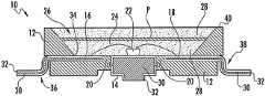
- FIGS. 1 and 2illustrate respective top and sectional views of one example of a light emitter package or light emitter device, generally designated 10 .
- light emitter device 10can comprise a surface mount device (SMD) comprising a body 12 which can be molded or otherwise formed about one or more electrical leads.
- SMD types of light emitter packages or devicescan be suitable for general LED illumination applications, such as indoor and outdoor lighting, automotive lighting, and preferably suitable for high power and/or high brightness lighting applications.
- the subject matter disclosed hereincan be suitably adapted for application within a wide range of SMD type emitters and designs, not limited to dimensional and/or material variations.
- devices, components, and methods disclosed hereincan maintain or exceed brightness levels associated with device 10 even in the presence of harmful chemicals, chemical vapors, or complexes by provision of a protective barrier or protective layer P ( FIG. 2 ) adapted to prevent harmful chemicals or complexes from tarnishing and/or otherwise degrading components within device 10 .
- a body 12can be disposed about a leadframe, also referred to as “leads”, which can comprise a thermal element 14 and one or more electrical elements.
- body 12can comprise a plastic body molded about the leads.
- Electrical elementscan include for example, first and second electrical elements 16 and 18 , respectively. That is, thermal element 14 and electrical elements 16 and 18 can be collectively referred to as “leads” and can be singulated from a sheet of leadframes (not shown).
- a corner notch, generally designated Ncan be used for indicating electrical polarity of first and second electrical elements 16 and 18 .
- thermal element 14 and first and second electrical elements 16 and 18can comprise a material that is electrically and/or thermally conductive such as a metal or metal alloy. In one aspect, thermal element 14 can be electrically and/or thermally separated from one and/or both of first and second electrical elements 16 and 18 by one or more insulating or isolating portions 20 of the body.
- one or more LEDs or LED chips 22can be mounted over thermal element 14 using any suitable die attach technique(s) and/or material(s), for example only and not limited to die attach adhesive (e.g., silicone, epoxy, or conductive silver (Ag) epoxy) or a metal-to-metal die attach technique such as flux or no-flux eutectic, non-eutectic, or thermal compression die attach.
- die attach adhesivee.g., silicone, epoxy, or conductive silver (Ag) epoxy
- a metal-to-metal die attach techniquesuch as flux or no-flux eutectic, non-eutectic, or thermal compression die attach.
- multiple LED chips 22can electrically communicate with one and/or both first and second electrical elements 16 and 18 via one or more electrical connectors such as electrically conductive wire bonds 24 .
- each LED chip 22 within a plurality of LED chips 22can be electrically connected in parallel.
- LED chips 22 having two electrical contacts on the same sideare shown as electrically connected to two electrical elements (e.g., 16 and 18 ) via wire bonds 24 .
- LED chips 22 with two electrical contacts on a lower surface, such that wire bonds 24 are unnecessary,are also contemplated herein.
- LED chips 22 having one electrical contact on the upper surface that is electrically connected with a single electrical elementis also contemplated.
- LED chip 22can comprise a horizontally structured chip (e.g., having at least two electrical contacts on a same side of the LED) or a vertically structured chip (e.g., with electrical contacts on opposing sides of the LED) with or without a growth substrate.
- a horizontally structured chipe.g., having at least two electrical contacts on a same side of the LED
- a vertically structured chipe.g., with electrical contacts on opposing sides of the LED
- LED chips 22can comprise one or more substantially straight cut and/or beveled (i.e., angled) cut sides or surfaces.
- LED chips 22can comprise a direct attach build (e.g., bonded to a carrier substrate) or a build incorporating a grown substrate such as sapphire, SiC, or GaN.
- LED chips 22having any build, structure, type, style, shape, and/or dimension are contemplated herein.
- Wire bonds 24 or other electrical attachment connectorsare optional to device designs and can be adapted to communicate, transmit, or convey an electrical current or signal from electrical elements 16 and 18 to one or more LED chips 22 thereby causing illumination of the one or more LED chips 22 .
- portions of thermal element 14 and/or first and second electrical elements 16 and 18 , respectively,can be coated, plated, deposited, or otherwise layered with a reflective material ( FIG. 2 ), such as, for example and without limitation, Ag or a Ag-containing alloy for reflecting light from the one or more LED chips 22 .
- a reflective materialsuch as, for example and without limitation, Ag or a Ag-containing alloy for reflecting light from the one or more LED chips 22 .
- body 12can comprise any suitable material molded or otherwise disposed about portions of thermal element 14 and/or first and second elements 16 and 18 , respectively.
- body 12can comprise a ceramic material such as a low temperature co-fired ceramic (LTCC) material, a high temperature co-fired ceramic (HTCC) material, alumina, aluminum nitride (AlN), aluminum oxide (Al 2 O 3 ), glass, and/or an Al panel material.
- body 12can comprise a molded plastic material such as polyamide (PA), polyphthalamide (PPA), liquid crystal polymer (LCP) or silicone.
- At least one electrostatic discharge (ESD) protection device 25can be disposed within device 10 and can be electrically connected to electrical elements 16 and 18 reverse biased with respect to LED chips 22 .
- ESD device 25can protect against damage from ESD within device 10 .
- different elementscan be used as ESD protection devices 25 such as various vertical or horizontal silicon (Si) Zener diodes, different LED chips arranged reverse biased to LED chips 22 , surface mount varistors and lateral Si diodes.
- ESD device 25can comprise a vertically structured device having one electrical contact on the bottom and another electrical contact on the top; however, horizontally structured ESD protection devices can also be provided.
- body 12 of device 10can comprise a cavity, generally designated 26 , for example, a reflector cavity optionally coated with a reflective material for reflecting light from the one or more LED chips 22 .
- cavity 26can be filled at least partially or completely with a filling material, such as an encapsulant 28 .
- encapsulant 28can optionally comprise one or more phosphor materials adapted to emit light of a desired wavelength when activated by light emitted from the one or more LED chips 22 .
- device 10can emit light having a desired wavelength or color point that can be a combination of light emitted from phosphors disposed in encapsulant 28 and from the light emitted from one or more LED chips 22 .
- thermal element 14 and first and second electrical elements 16 and 18can comprise an inner portion 30 and an outer portion 32 .
- inner portion 30 and outer portion 32can comprise electrically and/or thermally conductive materials.
- Outer portion 32may be applied such that it entirely surrounds inner portion 30 as shown, or in other aspects outer portion 32 can partially plate, coat, or comprise a partial layer or coating over a single surface or two or more surfaces of inner portion 30 .
- outer portion 32can comprise a highly reflective Ag substrate, a substrate containing Ag, or a layer of material such as Ag or a Ag-alloy for maximizing light output from device 10 and for assisting in heat dissipation by conducting heat away from the one or more LED chips 22 .
- Outer portion 32can also comprise a substrate of Ag-containing alloy instead of pure Ag, and such alloy can optionally contain other metals such as titanium (Ti) or nickel (Ni).
- Inner portion 30can comprise a metal or metal alloy such as a copper (Cu) substrate or a Cu-alloy substrate.
- an optional layer of materialcan be disposed between inner portion 30 and outer portion 32 , such as a layer of Ni for providing a barrier between the Ag and Cu, thereby preventing defects caused by migratory Cu atoms, such as a defect commonly known as “red plague”.
- outer portion 32can be directly attached to and/or directly coat inner portion 30 . Outer portion 32 can advantageously reflect light emitted from the one or more LED chips 22 thereby improving optical performance of device 10 .
- Upper surfaces of thermal element 14 and electrical elements 16 and 18can be disposed along a floor 34 of cavity 26 such that respective upper surfaces of thermal and electrical elements are disposed along the same plane and/or different planes.
- First and second electrical elements 16 and 18can extend from one or more lateral sides of body 12 and form one or more external tab portions, generally designated 36 and 38 .
- Tab portions 36 and 38can bend to form one or more lower mounting surfaces such that device 10 can be mounted to an underlying substrate.
- Tab portions 36 and 38can outwardly bend away from each other or inwardly bend towards each other thereby adapting either a J-bend or gull-wing orientation as known in the art.
- any configuration of external tabs 36 and 38can be provided.
- a filling materialcan be disposed and filled to any level within cavity 26 and may be partially disposed below and/or above a top surface 40 of device 10 .
- filling materialcan comprise an encapsulant 28 that it is filled to a level flush with top surface 40 of device as shown.
- encapsulant 28can be filled such that it forms a concave or convex surface with respect to top surface 40 of device 10 as indicated in broken lines adjacent portions of top surface 40 .
- encapsulant 28can be adapted for dispensing within cavity 26 .
- encapsulant 28can comprise a selective and optional amount of one or more phosphors adapted to emit light or combinations of light when activated by light emission from the one or more LED chips 22 thereby emitting light of any desired color point or color temperature.
- encapsulant 28can comprise a silicone material, such as a methyl or phenyl silicone encapsulant.
- SMD type devicessuch as device 10
- secondary opticse.g., a secondary lens
- encapsulant 28can provide physical protection against foreign solids and liquids, but may not provide adequate protection against gaseous chemicals or airborne elements such as sulfur, oxygen, or moisture which can tarnish or otherwise degrade outer portion 32 where outer portion comprises Ag (e.g., pure Ag, Ag-alloys, or Ag plating).
- Ag-containing componentssuch as outer portion 32 of thermal and electrical elements 14 , 16 , and 18 can over time become tarnished, corroded, or otherwise degraded where the device 10 has poor chemical resistance. This can decrease the brightness of device 10 .
- undesirable chemicals, vapors, or complexes Ccan permeate encapsulant 28 and potentially interact with outer portion 32 of elements, for example, by tarnishing such elements thereby resulting in degradation to optical, physical, electrical, and/or thermal properties such as a loss in brightness output and the noticeable darkening of surfaces along cavity floor 34 .
- undesirable chemical vapors or complexes Ccan permeate the encapsulant 28 as indicated by the broken and arrowed trajectory lines shown in FIG. 2 and could potentially adversely affect outer portion 32 if not deflected from surfaces within the device as shown.
- the current subject mattercan improve the chemical resistance of device 10 by incorporating a protective layer P serving as a protective barrier or barrier layer disposed over one or more surfaces of device 10 , within device 10 , and/or over components of device 10 to prevent complexes C from reaching, interacting with, and/or adversely affecting components such as Ag-containing outer portion 32 of thermal and electrical elements 14 , 16 , and 18 .
- a protective layer Pserving as a protective barrier or barrier layer disposed over one or more surfaces of device 10 , within device 10 , and/or over components of device 10 to prevent complexes C from reaching, interacting with, and/or adversely affecting components such as Ag-containing outer portion 32 of thermal and electrical elements 14 , 16 , and 18 .
- protective layer Pcan be directly disposed over outer portion 32 of elements as shown and along cavity floor 34 .
- protective layer Pcan be applied prior to attaching the one or more LED chips 22 to thermal element 14 such that protective layer P can be disposed between portions of LED chip 22 and outer portion 32 of thermal/electrical components or elements.
- Protective layer Pcan be used either alone or in combination with a phenyl silicone encapsulant for improving the chemical resistance of light emitter devices as described herein.
- FIGS. 4 to 12illustrate various other devices and/or alternative locations or placement of protective layer P for providing protection against chemical complexes C within light emitter devices or packages.
- undesired chemicals, vapors, or complexes Ccan comprise chemical vapors containing sulfur, sulfur containing compounds (sulfides, sulfites, sulfates, SO x ), chlorine or bromine containing complexes, nitric oxide or nitrogen dioxide (NO x ), and/or oxidizing organic vapor compounds.
- Complexes Ccan degrade the Ag components (e.g., outer portion 32 of thermal/electrical elements) and result in a loss of brightness output and noticeable darkening of surfaces within the device.
- Improved devices as described hereincan incorporate one or more protective layers P for improving the chemical resistance of device 10 and components within device 10 such that harmful vapors, chemicals, or complexes C cannot reach Ag-containing components (e.g., outer portion 32 ).
- protective layers Pfor improving the chemical resistance of device 10 and components within device 10 such that harmful vapors, chemicals, or complexes C cannot reach Ag-containing components (e.g., outer portion 32 ).
- complexes Ccan be repelled from the surface of protective layer P, thereby minimizing the damage to reflective Ag components, and further minimizing and/or totally preventing any loss in brightness from device 10 and/or darkening of components within device 10 .
- protective layer Pcan be directly and/or indirectly disposed over vulnerable components within devices described herein, such as located directly or indirectly over Ag or Ag-alloy containing components.
- Protective layer Pcan be adapted for application to a variety of surfaces of components within light emitter devices which is also advantageous.
- protective layer Pcan be directly applied to portions of surfaces of Ag or Ag-alloy containing components (e.g., outer portions 32 of thermal element 14 and electrical elements 16 , 18 ) alone and/or layer P can be applied to portions of surfaces of LED chips 22 including underfills, on or over wires, wire bonds 24 , wire bond balls (e.g., ball formed where wire 24 attaches to LED chip 22 ), and on surfaces of the LED housing or body all of which, when comprising a portion or layer of Ag over the surface, can comprise Ag-containing components.
- Ag or Ag-alloy containing componentse.g., outer portions 32 of thermal element 14 and electrical elements 16 , 18
- layer Pcan be applied to portions of surfaces of LED chips 22 including underfills, on or over wires, wire bonds 24 , wire bond balls (e.g., ball formed where wire 24 attaches to LED chip 22 ), and on surfaces of the LED housing or body all of which, when comprising a portion or layer of Ag over the surface, can comprise Ag-containing components.
- protective layer Pcan be applied over internal and/or external portions of the ceramic or plastic body 12 of light emitter device 10 , for example, over isolating portions 20 of body 12 ( FIG. 2 ).
- protective layer Pcan be selectively applied at and/or parallel to any number of processing steps within the manufacturing process (e.g., before/after die attachment of LED, before/during encapsulation, see FIGS. 4 to 12 ) for providing broad protection against chemical vapors, such as but not limited to, nitric oxide or nitrogen dioxide (NO x ), oxidizing organic vapor compounds, sulfur, sulfur-containing compounds (e.g., sulfides, sulfates, SO x ) and chlorine- or bromine-containing complexes.
- NO xnitric oxide or nitrogen dioxide
- Devices using or adapted for use with LEDscan comprise a protective barrier or protective layer P.
- Protective layer Pis not limited in application or use, and can be used, for example, in devices comprising ceramic, plastic, PCB, MCPCB, or laminate substrates or submounts and can advantageously be applied over multiple surfaces, including LED chips 22 disposed within the SMDs.
- Protective layer Pcan at least partially comprise an organic material for increasing chemical resistance of the substrate.
- the organic materialcan comprise for example an organic coating or film deposited using chemical vapor deposition (CVD) techniques and where protective layer P can be of any suitable thickness.
- CVDchemical vapor deposition
- protective layer Pcan comprise a thickness of between approximately 1 nm and approximately 100 ⁇ m. Any sub-range of thickness between approximately 1 nm and 100 ⁇ m is also contemplated herein, and can be provided within devices described herein.
- the thickness of protective layer Pcan comprise approximately 1 to 10 nm; approximately 10 nm to 50 nm; approximately 50 nm to 200 nm; approximately 200 nm to 400 nm; approximately 400 to 600 nm; approximately 600 to 800 nm; approximately 800 nm to 1 ⁇ m; approximately 0.5 ⁇ m to 1 ⁇ m; approximately 1 ⁇ m to 5 ⁇ m; approximately 5 ⁇ m to 10 ⁇ m; approximately 10 ⁇ m to 50 ⁇ m; or approximately 50 ⁇ m to 100 ⁇ m.
- protective layer Pcan comprise a thickness of approximately 0.7 to 1.0 ⁇ m. In some aspects, a thicker protective layer P can provide superior barrier protection of Ag components against harmful chemical complexes C, thereby improving the brightness retention of light emitter device 10 .
- protective layer Pcan comprise a barrier layer of poly(p-xylylene) polymers (e.g., such as Parylene) deposited via CVD processing techniques and polymerized in-situ to form a protective polymer coating or protective layer P.
- Parylene materialsincluding PARYLENE HT®, are commercially available for example from Specialty Coating SystemsTM (SCS) headquartered in Indianapolis, Ind.
- protective layer Pcan be highly efficient in repelling or preventing harmful chemicals and vapors from permeating the device thereby protecting components comprised of one or more of Ag or Ag-containing portions within device 10 from tarnishing, corroding, or otherwise degrading.
- Any other reactive organic barrier coatingcan be deposited directly on or over Ag or Ag-containing portions of components within device 10 .
- Such coatingscan be applied via CVD processing and can polymerize in-situ, preferably at room temperature.
- poly(p-xylylene) polymer or Parylene layersmay be preferred for thermal stability purposes; as such materials can comprise a fluorocarbon-containing organic barrier coating even though not all Parylene coatings or layers are fluorocarbons.
- Other variations of fluorocarbon containing coatingscan also comprise effective barrier coatings.
- protective layer Pcan comprise an organic barrier coating comprising an aromatic polymer or copolymer or a polymer or copolymer prepared using aromatic precursors. In some aspects, protective layer P can comprise an organic barrier coating resistant to chemical vapors and gases, such as sulfur. In some aspects, protective layer P can comprise an organic barrier layer having a thermal stability in air of approximately 100° C. or greater (e.g., approximately 100, 150, 200, 250, 300, 350, or 400° C. or greater).
- protective layer Pcan comprise arylene and/or aralkylene monomer units (e.g., phenylene, napthylene, xylene, etc.) or monomer units (e.g., cycloaliphatic monomer units) derived from aryl or aralkyl polymer precursors.
- the arylene and/or aralkylene monomer unitscan be unsubstituted or can be substituted by one or more aryl or alkyl group substituent (e.g., alkyl, aryl, halo, nitro, alkoxy, etc.).
- the protective layer Pcan be a copolymer of the arylene or aralkylene monomer, further comprising one or more monomer units derived from a vinyl-containing monomer.
- the organic barrier coatingcan be a fluorinated aromatic or fluorinated cycloaliphatic polymer or copolymer.
- protective layer Pcan comprise a polyxylylene.
- the polyxylylenecan have between about 10 and about 100,000 repeating units (e.g., about 10, about 50, about 100, about 500, about 1,000, about 2,500, about 5,000, about 75,000, about 10,000, about 25,000, about 50,000, about 75,000, or about 100,000 repeating units), wherein each repeating unit has an aromatic group and can be substituted or unsubstituted.
- each repeating unithas an aromatic group and can be substituted or unsubstituted.
- Each substituentcan be the same or different and can be selected from the group including, but not limited to, alkyl, aryl, alkenyl, amino, cyano, carboxyl, alkoxy, aryloxy, hydroxylalkyl, aminoalkyl, acyl, carboxyalkyl, mercapto, hydroxyl, nitro, halo, and the like.
- the substituentscan be selected from lower alkyl groups (e.g., methyl, ethyl, propyl, butyl, and hexyl) and halo groups (e.g., chloro, bromo, iodo, and fluoro).
- the organic barrier coatingcomprises poly(p-xylylene), poly(p-2-chloroxylylene), poly(p-2,6-dichloroxylylene) and fluoro-substituted poly(p-xylylene).
- the fluoro-substituted poly(p-xylylene)can comprise fluoro substituents on non-aromatic carbon atoms and have the structure [—CF 2 —(C 6 H 4 )—CF 2 —] n , which is PARYLENE HT®.
- the fluoro-substituted poly(p-xylylene)can comprise one or more fluoro substituents on an aromatic carbon atom or can comprise fluoro substituents on both aromatic and non-aromatic carbon atoms.
- the polyxylylene protective layer Pcan be a homopolymer. In other aspects, the polyxylylene protective layer P can be a copolymer of at least two different xylylene monomers.
- the protective layer Pcomprises reaction products of a poly(p-xylylene) preparation process where aromatic groups in the backbone of one or more monomer units are at least partially converted to non-aromatic cyclic (or non-cyclic) groups (e.g., to cyclohexylene groups).
- the poly(p-xylylene)is a fluoro-substituted poly(p-xylylene) containing one or more monomer units wherein the backbone aromatic group has been converted to a non-aromatic cyclic group.
- the fluoro-substituted poly(p-xylylene)is PARYLENE HT® wherein the C 6 H 4 group of one or more [—CF 2 —(C 6 H 4 )—CF 2 —] n , repeating units has been converted to a non-aromatic and/or fully saturated cyclic group.
- the process of applying the polyxylylenecan include chemical vapor deposition (CVD).
- the processcan, for example, comprise vaporizing a solid precursor compound, such as a suitable dimer (e.g., cyclo-di(p-xylene) or a substituted cyclo-di(p-xylene), such as cyclo-di(p-2-chloroxylene), cyclo-di(p-2,6-dichloroxylene), or tetrafluoro-cyclo-di(p-xylene)).
- a suitable dimere.g., cyclo-di(p-xylene) or a substituted cyclo-di(p-xylene
- cyclo-di(p-2-chloroxylene)such as cyclo-di(p-2-chloroxylene
- cyclo-di(p-2,6-dichloroxylenecyclo-di(p-2,6-dichloroxylene
- Suitable vaporization temperaturescan be between about 110° C. and about 200° C. In some aspects, the vaporization temperature can be about 150° C.
- the vaporized precursorcan subsequently be subjected to pyrolysis to provide a reactive monomer (e.g., by cleavage of the methylene-methylene bonds in the dimer precursor). Pyrolysis can be performed at temperatures between about 400° C. and about 700° C. In some embodiments, the pyrolysis can be performed at between about 650° C. and about 680° C. Following pyrolysis, the monomeric vapor can be cooled. Upon cooling, the reactive monomers can condense and copolymerize.
- the vapor comprising the reactive monomeris cooled over a substrate (e.g., one or more portions, surfaces, Ag, and/or Ag-containing components of device 10 ), the monomers can deposit and polymerize on the substrate, thereby forming a polymer film such as protective layer P.
- a substratee.g., one or more portions, surfaces, Ag, and/or Ag-containing components of device 10
- the monomerscan deposit and polymerize on the substrate, thereby forming a polymer film such as protective layer P.
- the pyrolysis of the vaporized xylylenic species stated in this applicationcan lead to reactive species of structures that are different from xylylene monomers when performed at between about 650° C. and about 680° C.
- protective layer P subsequently derivedcan have different structures than the one represented by poly(p-xylylene).
- protective layer P as preparedcan be substantially free of aromatic rings.
- the poly(p-xylylene)is a derivative of a poly(p-xylylene) that is partially or substantially fully non-aromatic.
- the vapor comprising the reactive monomerscan be transferred from a pyrolysis chamber to a room temperature deposition chamber where a substrate is present to cool and deposit and polymerize on a surface of the substrate.
- the substratecan comprise any portion of device 10 at any step in the manufacturing process.
- protective layer Pcan be applied to any desired substrates or components, including the leads (e.g., thermal element 14 and electrical elements 16 and 18 ) prior to molding body 12 about the leads, over any and all surfaces of device 10 prior to die attaching one or more LED chips 22 , over any and all surfaces before/after wirebonding the LED chips 22 , and/or over any and all surfaces before/during encapsulation as described further hereinbelow.
- protective layer Pcan comprise a flexible continuous film.
- one or more portions of device 10can be physically or chemically masked such that protective layer P does not deposit in the masked (e.g., unwanted) areas.
- alkylcan refer to C 1-20 inclusive, linear (i.e., “straight-chain”), branched, or cyclic, saturated or at least partially and in some cases fully unsaturated (i.e., alkenyl and alkynyl) hydrocarbon chains, including for example, methyl, ethyl, propyl, isopropyl, butyl, isobutyl, tert-butyl, pentyl, hexyl, octyl, ethenyl, propenyl, butenyl, pentenyl, hexenyl, octenyl, butadienyl, propynyl, butynyl, pentynyl, hexynyl, heptynyl, and allenyl groups.
- the term “branched”can refer to an alkyl group in which a lower alkyl group, such as methyl, ethyl or propyl, is attached to a linear alkyl chain.
- the term “lower alkyl”can refer to an alkyl group having 1 to about 8 carbon atoms (i.e., a C 1-8 alkyl), e.g., 1, 2, 3, 4, 5, 6, 7, or 8 carbon atoms.
- the term “higher alkyl”can refer to an alkyl group having about 10 to about 20 carbon atoms, e.g., 10, 11, 12, 13, 14, 15, 16, 17, 18, 19, or 20 carbon atoms.
- “alkyl”refers, in particular, to C 1-8 straight-chain alkyls.
- “alkyl”refers, in particular, to C 1-8 branched-chain alkyls.
- Alkyl groupscan optionally be substituted (e.g., a “substituted alkyl”) with one or more alkyl group substituents, which can be the same or different.
- alkyl group substituentincludes but is not limited to alkyl, substituted alkyl, halo, arylamino, acyl, hydroxyl, aryloxyl, alkoxyl, alkylthio, arylthio, aralkyloxyl, aralkylthio, carboxyl, alkoxycarbonyl, oxo, and cycloalkyl.
- alkyl chainThere can be optionally inserted along the alkyl chain one or more oxygen, sulfur or substituted or unsubstituted nitrogen atoms, wherein the nitrogen substituent is hydrogen, lower alkyl (also referred to herein as “alkylaminoalkyl”), or aryl.
- substituted alkylincludes alkyl groups, as defined herein, in which one or more atoms or functional groups of the alkyl group are replaced with one or more atoms or functional groups, including for example, alkyl, substituted alkyl, halogen, e.g., CH 2 X, CHX 2 , and CX 3 , wherein X is a halogen selected from the group consisting of Cl, Br, F, and I, aryl, substituted aryl, alkoxyl, hydroxyl, nitro, amino, alkylamino, dialkylamino, sulfate, and mercapto.
- halogene.g., CH 2 X, CHX 2 , and CX 3
- Xis a halogen selected from the group consisting of Cl, Br, F, and I, aryl, substituted aryl, alkoxyl, hydroxyl, nitro, amino, alkylamino, dialkylamino, sulfate, and
- alkenylrefers to an alkyl group containing a carbon-carbon double bond.
- the term “vinyl”refers to a terminal alkyl group, i.e., —CH ⁇ CH 2 .
- arylcan refer to an aromatic substituent that can be a single aromatic ring, or multiple aromatic rings that are fused together, linked covalently, or linked to a common group, such as, but not limited to, a methylene or ethylene moiety.
- the common linking groupalso can be a carbonyl, as in benzophenone, or oxygen, as in diphenylether, or nitrogen, as in diphenylamine.
- arylspecifically encompasses, heterocyclic aromatic compounds.
- the term “aryl”refers exclusively to aromatic groups that do not include heteroatoms (e.g., O, N, S, etc.) in the backbone of the ring structure(s).
- the aromatic ring(s)can comprise phenyl, naphthyl, biphenyl, diphenylether, diphenylamine and benzophenone, among others.
- the term “aryl”means a cyclic aromatic comprising about 5 to about 10 carbon atoms, e.g., 5, 6, 7, 8, 9, or 10 carbon atoms, and including 5- and 6-membered hydrocarbon and heterocyclic aromatic rings.
- the aryl groupcan be optionally substituted (a “substituted aryl”) with one or more aryl group substituents, which can be the same or different, wherein “aryl group substituent” includes alkyl, substituted alkyl, aryl, substituted aryl, aralkyl, hydroxyl, alkoxyl, aryloxyl, aralkyloxyl, carboxyl, acyl, halo, nitro, alkoxycarbonyl, aryloxycarbonyl, aralkoxycarbonyl, acyloxyl, acylamino, aroylamino, carbamoyl, alkylcarbamoyl, dialkylcarbamoyl, arylthio, alkylthio, alkylene, and —NR′R′′, wherein R′ and R′′ can each be independently hydrogen, alkyl, substituted alkyl, aryl, substituted aryl, and aralkyl.
- substituted arylincludes aryl groups, as defined herein, in which one or more atoms or functional groups of the aryl group are replaced with another atom or functional group, including for example, alkyl, substituted alkyl, halogen, aryl, substituted aryl, alkoxyl, hydroxyl, nitro, amino, alkylamino, dialkylamino, sulfate, and mercapto.
- aryl groupsinclude, but are not limited to, cyclopentadienyl, phenyl, napthyl, furan, thiophene, pyrrole, pyran, pyridine, imidazole, benzimidazole, isothiazole, isoxazole, pyrazole, pyrazine, triazine, pyrimidine, quinoline, isoquinoline, indole, carbazole, and the like.
- Alkylrefers to an aryl-alkyl-group wherein aryl and alkyl are as previously described, and included substituted aryl and substituted alkyl.
- exemplary aralkyl groupsinclude benzyl, phenylethyl, ortho-, meta-, or para-dimethylbenzene (i.e., ortho-, meta- or para-xylene), and naphthylmethyl.
- Alkylenerefers to a straight or branched bivalent aliphatic hydrocarbon group having from 1 to about 20 carbon atoms, e.g., 1, 2, 3, 4, 5, 6, 7, 8, 9, 10, 11, 12, 13, 14, 15, 16, 17, 18, 19, or 20 carbon atoms.
- the alkylene groupcan be straight, branched or cyclic.
- the alkylene groupalso can be optionally unsaturated and/or substituted with one or more “alkyl group substituents.” There can be optionally inserted along the alkylene group one or more oxygen, sulfur or substituted or unsubstituted nitrogen atoms (also referred to herein as “alkylaminoalkyl”), wherein the nitrogen substituent is alkyl as previously described.
- alkylene groupsinclude methylene (—CH 2 —); ethylene (—CH 2 —CH 2 —); propylene (—(CH 2 ) 3 —); cyclohexylene (—C 6 H 10 —); —CH ⁇ CH—CH ⁇ CH—; —CH ⁇ CH—CH 2 —; —(CH 2 ) q —N(R)—(CH 2 ) r —, wherein each of q and r is independently an integer from 0 to about 20, e.g., 0, 1, 2, 3, 4, 5, 6, 7, 8, 9, 10, 11, 12, 13, 14, 15, 16, 17, 18, 19, or 20, and R is hydrogen or lower alkyl; methylenedioxyl (—O—CH 2 —O—); and ethylenedioxyl (—O—(CH 2 ) 2 —O—).
- An alkylene groupcan have about 2 to about 3 carbon atoms and can further have 6-20 carbons.
- arylenerefers to a bivalent radical of an aryl group as previously described.
- exemplary arylene groupsinclude phenylene and napthylene.
- aralkylenerefers to a bivalent radical of an aralkyl group as previously described and/or to combinations of alkylene and arylene groups (e.g., to alkylene-arylene-alkylene groups).
- exemplary aralkylene groupsinclude the diradicals of xylene and substituted xylenes.
- Alkoxyrefers to an alkyl-O— group wherein alkyl is as previously described.
- alkoxycan refer to C 1-20 inclusive, linear, branched, or cyclic, saturated or unsaturated oxo-hydrocarbon chains, including, for example, methoxyl, ethoxyl, propoxyl, isopropoxyl, butoxyl, t-butoxyl, and pentoxyl.
- Aryloxyrefers to an aryl-O— group wherein the aryl group is as previously described, including a substituted aryl.
- aryloxyas used herein can refer to phenyloxyl or hexyloxyl, and alkyl, substituted alkyl, halo, or alkoxyl substituted phenyloxyl or hexyloxyl.
- acylrefers to an organic acid group wherein the OH of the carboxyl group has been replaced with another substituent (i.e., as represented by RCO—, wherein R is an alkyl, substituted alkyl, aryl, or substituted aryl group as defined herein).
- RCO—substituent
- the term acylcan refer to the group RCO— wherein R is an amino-substituted alkyl group, an alkylamino-substituted alkyl group, a dialkylamino-substituted alkyl group, or a hydroxyl-substituted alkyl group.
- acylcan refer to groups such as H 2 NR 1 CO—, R 2 HNR 1 CO—, R 3 R 2 NR 1 CO—, and HOR 1 CO—, wherein R 1 is alkylene and R 2 and R 3 are lower alkyl.
- acylalso specifically includes arylacyl groups, such as an acetylfuran and a phenacyl group. Specific examples of acyl groups include acetyl and benzoyl.
- Aminorefers to an —NRR′ group wherein each of R and R′ is independently a hydrogen, an alkyl group and/or a substituted alkyl group as previously described, an aryl group and/or a substituted aryl group, or an aralkyl group.
- the term “amino”refers to the —NH 2 group.
- Carboxyalkylrefers to an alkyl-O—CO— group. Exemplary carboxyalkyl groups include methoxycarbonyl, ethoxycarbonyl, butyloxycarbonyl, and t butyloxycarbonyl.
- halorefers to fluoro, chloro, bromo, and iodo groups.
- hydroxylrefers to the —OH group.
- hydroxyalkylrefers to an alkyl group substituted with an —OH group.
- cyanorefers to the —CN group.
- nitrorefers to the —NO 2 group.
- mercaptorefers to the —SH group.
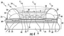
- FIGS. 3 and 4illustrate top perspective and cross-sectional views of another embodiment of an LED package or device, generally designated 50 .
- Light emitter device 50can also be improved for chemical resistance by incorporating a protective layer P, for example, on external surfaces of device 50 and/or on internal surfaces of device ( FIG. 4 ).
- Light emitter device 50can comprise an SMD type device, similar to device 10 in that a secondary optics can, but may not be used.
- SMD type devicesimilar to device 10 in that a secondary optics can, but may not be used.
- light emitter device 50can comprise a submount 52 over which an emission area, generally designated 54 , can be disposed.
- emission area 54can comprise one or more LED chips 22 disposed under a filling material, such as an encapsulant 58 (see FIG. 4 ).
- emission area 54can be substantially centrally disposed with respect to submount 52 of light emitter device 50 .
- emission area 54can be disposed at any location over light emitter device 50 , for example, in a corner or adjacent an edge. Any location is contemplated, and more than one emission area 54 is also contemplated.
- Emission area 54can comprise any suitable shape such as a substantially circular, square, oval, rectangular, diamond, irregular, regular, or asymmetrical shape.
- light emitter device 50can further comprise a retention material 56 at least partially disposed about emission area 54 where retention material 56 can be referred to as a “dam”.
- Retention material 56can comprise any material such as a silicone, ceramic, thermoplastic, and/or thermosetting polymer material.
- retention material 56can be adapted for dispensing about emission area 54 , which is advantageous as it is easy to apply and easy to obtain any desired size and/or shape.
- submount 52can comprise any suitable mounting substrate, for example, a printed circuit board (PCB), a metal core printed circuit board (MCPCB), an external circuit, a dielectric laminate panel, a ceramic panel, an Al panel, AlN, Al 2 O 3 , or any other suitable substrate over which lighting devices such as LED chips may mount and/or attach.
- LED chips 22 disposed in emission area 54can electrically and/or thermally communicate with electrical elements disposed with submount 52 , for example, conductive traces ( FIG. 4 ).
- Emission area 54can comprise a plurality of LED chips 22 disposed within and/or below a filling material 58 such as illustrated in FIG. 4 .
- LED chips 22can comprise any suitable size and/or shape of chip and can be vertically structured (e.g., electrical contacts on opposing sides) and/or horizontally structured (e.g., contacts on the same side or surface).
- LED chips 22can comprise any style of chip for example, straight cut and/or bevel cut chips, a sapphire, SiC, or GaN growth substrate or no substrate.
- One or more LED chips 22can form a multi-chip array of LED chips 22 electrically connected to each other and/or electrically conductive traces in combinations of series and parallel configurations.
- LED chips 22can be arranged in one or more strings of LED chips, where each string can comprise more than one LED chip electrically connected in series.
- Strings of LED chips 22can be electrically connected in parallel to other strings of LED chips 22 .
- Strings of LED chips 22can be arranged in one or more pattern (not shown).
- LED chips 22can be electrically connected to other LED chips in series, parallel, and/or combinations of series and parallel arrangements depending upon the application.
- light emitter device 50can further comprise at least one opening or hole, generally designated 60 , that can be disposed through or at least partially through submount 52 for facilitating attachment of light emitter device 50 to an external substrate, circuit, or surface.
- at least one hole 60can be disposed through or at least partially through submount 52 for facilitating attachment of light emitter device 50 to an external substrate, circuit, or surface.
- one or more screws (not shown) or pinscan be inserted through the at least one hole 60 for securing device 50 to another member, structure, or substrate.
- Light emitter device 50can also comprise one or more electrical attachment surfaces 62 .
- attachment surfaces 62comprise electrical contacts such as solder contacts or connectors.
- Attachment surfaces 62can be any suitable configuration, size, shape and/or location and can comprise positive and negative electrode terminals, denoted by the “+” and/or “ ⁇ ” signs on respective sides of device 50 , through which an electrical current or signal can pass when connected to an external power source.
- attachment surfaces 62can comprise devices configured to clamp, crimp, or otherwise attached to external wires (not shown). Electrical current or signal can pass into light emitter device 50 from the external wires electrically connected to device 10 at the attachment surfaces 62 . Electrical current can flow into the emission area 54 to facilitate light output from the LED chips disposed therein. Attachment surfaces 62 can electrically communicate with LED chips 22 of emission area 54 via conductive traces 64 and 66 ( FIG. 4 ).
- attachment surfaces 62can comprise a same layer of material as first and second conductive traces 64 and 66 ( FIG. 4 ) and therefore can electrically communicate to LED chips 22 attached to traces 64 and 66 via electrical connectors such as wire bonds 24 .
- Electrical connectorscan comprise wire bonds 24 or other suitable members for electrically connecting LED chips 22 to first and second conductive traces 64 and 66 ( FIG. 4 ).
- a filling material 58can be disposed between inner walls of retention material 56 .
- Filling material 58can comprise an encapsulant that can include a predetermined, or selective, amount of one or more phosphors and/or lumiphors in an amount suitable for any desired light emission, for example, suitable for white light conversion or any given color temperature or color point. Alternatively, no phosphors may be included in filling material 58 .
- Filling material 58can comprise a silicone encapsulant material, such as a methyl and/or phenyl silicone material. Filling material 58 can interact with light emitted from the plurality of LED chips 22 such that a perceived white light, or any suitable and/or desirable wavelength of light, can be observed.
- LED chips 22can comprise one primarily red, green, blue, cyan, green, yellow, orange, amber, or white chip.
- filling material 58can comprise one or more phosphors adapted to emit red, blue, yellow, or green light when activated by light from one or more LED chips 22 .
- retention material 56can be adapted for dispensing, positioning, damming, or placing, about at least a portion of emission area 54 .
- filling material 58can be selectively filled to any suitable level within the space disposed between one or more inner walls of retention material 56 as indicated in broken lines.
- filling material 58can be filled to a level equal to the height of retention material 56 or to any level above or below retention material 56 , for example, as indicated by the broken lines terminating at retention material 56 shown in FIG. 4 .
- the level of filling material 58can be planar or curved in any suitable manner, such as concave or convex (e.g., see broken lines in FIG. 4 ).
- FIG. 4illustrates retention material 56 dispensed or otherwise placed over submount 52 after wire bonding the one or more LED chips 22 such that retention material 56 is disposed over and at least partially covers at least a portion of the wire bonds 24 .
- wire bonds 24 of the outermost edge LED chips in a given set or string of LED chips 22can be disposed within a portion of retention material 14 .
- devicecan contain many strings of LED chips 22 of any number, for example, less than four or more than four LED chips 22 can be electrically connected in series, parallel, and/or combinations of series and parallel arrangements.
- strings of LED chips 22can comprise diodes of the same and/or different colors, or wavelength bins, and different colors of phosphors can be used in the filling material 58 disposed over LED chips 22 that are the same or different colors in order to achieve emitted light of a desired color temperature or color point.
- LED chips 22can attach directly to portions of conductive pad 70 and/or indirectly to portions of conductive pad 70 such as by connecting to one or more intervening layers (e.g., layers 68 and/or protective layer P, described below) which can be disposed between LED chip 22 and conductive pad 70 using any die attach technique or materials as known in art and mentioned above, for example epoxy or metal-to-metal die attach techniques and materials.
- LED chips 22can be arranged, disposed, or mounted over an electrically and/or thermally conductive pad 70 .
- Conductive pad 70can be electrically and/or thermally conductive and can comprise any suitable electrically and/or thermally conducting material.
- conductive pad 70comprises a layer of Cu or a Cu substrate.
- LED chips 22can be electrically connected to first and second conductive traces 64 and 66 .
- One of first and second conductive traces 64 and 66can comprise an anode and the other a cathode.
- conductive traces 64 and 66can also comprise a layer of electrically conductive Cu or Cu substrate.
- conductive pad 70 and traces 64 and 66can comprise the same Cu substrate from which traces 64 and 66 have been singulated or separated from pad 70 via etching or other removal method.
- an electrically insulating solder mask 72can be applied such that it is at least partially disposed between conductive pad 70 and respective conductive traces 64 and 66 .
- Solder mask 72can comprise a white material for reflecting light from light emitter device 50 .
- One or more layers of materialcan be disposed between portions of LED chips 22 and conductive pad 70 .
- one or more layers of materialcan be disposed over conductive traces 64 and 66 .
- first intervening layer or substrate of material 68can be disposed between LED chips 22 and conductive pad 70 and disposed over traces 64 and 66 .
- First layer of material 68can comprise a layer of reflective Ag or Ag-alloy material for maximizing brightness of light emitted from light emitter device 50 . That is, first layer of material 68 can comprise a Ag or Ag-containing substrate adapted to increase brightness of device 50 .
- One or more optional, additional layers of materialcan be disposed between first layer 68 and conductive pad 70 and/or first layer 68 and traces 64 and 66 , for example, a layer of Ni can be disposed therebetween for providing a barrier between the Cu of pad and traces 70 , 64 , and 66 and the Ag of layer 68 .
- a protective layer Pcan be at least partially disposed over and/or adjacent to Ag components within device 50 , for example, over first layer 68 of material which can coat conductive pad 70 and traces 64 and 68 .
- Protective layer Pcan provide a barrier over the Ag coated components thereby preventing such components from being physically or electrically degraded via tarnishing, oxidizing, corroding, or other degrading phenomenon caused when harmful chemical, vaporous, or atmospheric complexes C permeate filling material 58 .
- complexes Csuch as sulfur, sulfides, sulfates, chlorine complexes, bromine complexes, NO x , oxygen, and/or moisture can damage Ag coatings or Ag coated components, such as layer 68 which can coat Cu components including pad 70 and/or traces 64 and 66 .
- protective layer Pcan comprise an organic barrier coating adapted to prevent undesirable chemical or vapor complexes C from reaching vulnerable components within light emitter device 50 as shown by the broken lines and arrows.
- protective layer Pcan as described previously comprise a barrier layer of poly(p-xylylene) polymers (e.g., such as Parylene) deposited in any suitable manner such as via CVD processing techniques and polymerized in-situ to form a protective polymer coating or protective layer P.
- Protective layer Pis highly efficient in repelling harmful chemicals and vapors thereby protecting components comprising one or more of Ag or Ag containing portions within a device such as those disclosed herein from tarnishing, corroding, or otherwise degrading.
- Any other reactive organic barrier coatingcan be deposited directly on or over Ag or Ag-containing portions of components within the device. Such coatings can be applied via CVD processing and can polymerize in-situ, preferably at room temperature.
- poly(p-xylylene) polymer or Parylene or PARYLENE® layersmay be preferred for thermal stability purposes; as such materials comprise a fluorocarbon-containing organic barrier coating.
- fluorocarbon containing coatingscan also comprise effective barrier coatings in accordance with the disclosure herein.
- protective layer Pcan be an organic barrier coating comprising an aromatic polymer or copolymer. In some aspects, protective layer P can comprise an organic barrier coating resistant to chemical vapors and gases, such as sulfur. In some aspects, protective layer P can comprise arylene and/or aralkylene monomer groups (e.g., phenylene, napthylene, xylene, etc.). The arylene and/or aralkylene monomer groups can be unsubstituted or can be substituted by one or more aryl or alkyl group substituent (e.g., alkyl, aryl, halo, nitro, alkoxy, etc.).
- arylene and/or aralkylene monomer groupse.g., phenylene, napthylene, xylene, etc.
- the arylene and/or aralkylene monomer groupscan be unsubstituted or can be substituted by one or more aryl or alkyl group substituent (e.g., al
- the aromatic polymer of protective layer Pcan be a copolymer of the arylene or aralkylene monomer group, further comprising one or more monomer units derived from a vinyl-containing monomer.
- the organic barrier coatingis a fluorinated aromatic polymer or copolymer. In some embodiments, the organic barrier coating is a non-aromatic fluoropolymer.
- protective layer Pcan comprise a polyxylylene (e.g., poly(p-xylylene), a substituted poly(p-xylylene) or any other polymer prepared from a xylylene and/or comprising —CH 2 —(C 6 H 4 )—CH 2 — repeating units wherein one or more of the hydrogen atoms in the repeating unit can be replaced by an alkyl or aryl group substituent).
- a polyxylylenee.g., poly(p-xylylene), a substituted poly(p-xylylene) or any other polymer prepared from a xylylene and/or comprising —CH 2 —(C 6 H 4 )—CH 2 — repeating units wherein one or more of the hydrogen atoms in the repeating unit can be replaced by an alkyl or aryl group substituent).
- the polyxylylenecan have between about 10 and about 100,000 repeating units (e.g., about 10, about 50, about 100, about 500, about 1,000, about 2,500, about 5,000, about 75,000, about 10,000, about 25,000, about 50,000, about 75,000, or about 100,000 repeating units), wherein each repeating unit has an aromatic group and can be substituted or unsubstituted.
- the organic barrier coating or protective layer Pcomprises poly(p-xylylene), poly(p-2-chloroxylylene), poly(p-2,6-dichloroxylylene) and fluoro-substituted poly(p-xylylene).
- the fluoro-substituted poly(p-xylylene)comprises fluoro substituents on non-aromatic carbon atoms and has the structure [—CF 2 —(C 6 H 4 )—CF 2 —] n .
- the polyxylylene protective layer Pis a homopolymer. In some aspects, the polyxylylene protective layer P is a copolymer of at least two different xylylene monomers.
- FIG. 4illustrates a sectional view of submount 52 over which LED chips 22 can be mounted or otherwise supported or arranged.
- Submount 52can comprise, for example, conductive pad 70 , first and second conductive traces 64 and 66 , and solder mask 72 at least partially disposed between conductive pad 70 and each of conductive traces 64 and/or 66 .
- Conductive traces 64 , 66 and conductive pad 70can be coated with a first layer 68 , for example Ag.
- Protective layer Pcan be disposed over Ag as shown, or similar to any of the embodiments illustrated in FIGS. 5 to 12 .
- Submount 52can further comprise a dielectric layer 74 , and a core layer 76 . Solder mask 72 can directly adhere to portions of dielectric layer 74 .
- submount 52can comprise a MCPCB, for example, those available and manufactured by The Bergquist Company of Chanhassan, Minn. Any suitable submount 52 can be used, however.
- Core layer 76can comprise a conductive metal layer, for example copper or aluminum.
- Dielectric layer 74can comprise an electrically insulating but thermally conductive material to assist with heat dissipation through submount 52 .
- device 50can comprise a package which may not require or use any secondary optics to keep harmful elements from degrading conductive pad 70 .
- devices, components and methods disclosed hereinprovide for improved chemical resistance and improved chemical properties where zero and/or a minimum loss of brightness occurs, even in the presence of harmful chemicals and can be applicable to any SMD type device or multi-array device disclosed herein. Such improvements can prevent Ag coated components from tarnishing, darkening, corroding, or otherwise degrading.
- one or more additional processing techniques or stepscan optionally be performed during manufacture of devices described herein for improving adhesion between one or more layers within the devices.
- Such optionally processing stepscan be used and applied to devices previously shown and described, as well as those in FIGS. 5 through 12 described hereinbelow.
- such optional techniquescan be performed to one or more surfaces prior to deposition or application of one or more adjacent surfaces within a device.
- surfaces or layerssuch as, for example and without limitation, Cu surfaces (e.g., inner portion 30 of elements 14 , 16 , and/or 18 of device 10 and/or surfaces of conductive pad 70 , traces 64 and 66 of device 50 ), Ag surfaces (e.g., outer portion 32 of elements 14 , 16 , and/or 18 of device 10 , layer of material 68 of device 50 ), and/or surfaces of protective layer P.
- Cu surfacese.g., inner portion 30 of elements 14 , 16 , and/or 18 of device 10 and/or surfaces of conductive pad 70 , traces 64 and 66 of device 50
- Ag surfacese.g., outer portion 32 of elements 14 , 16 , and/or 18 of device 10 , layer of material 68 of device 50
- surfaces of protective layer Pe.g., one or more of these surfaces can be physically, chemically, or thermally prepared or treated to improve adhesion between the treated surface and adjacent surface(s) or adjacent layer(s).
- Optional processing steps that are physical in naturecan comprise, for example and without limitation, sandblasting, plasma etching, brushing, lapping, sanding, burnishing, grinding, and/or any suitable form of surface roughening (e.g., physically texturizing the surface) to improve adhesion between one or more layers or surfaces within devices shown and described herein.
- Optional processing steps that are chemical in naturecan comprise, for example and without limitation, chemical etching, applying solvents, applying organic solvents, applying acids, applying bases, vapor degreasing, priming, or any suitable chemically process for treating a surface to improve adhesion between one or more layers or surfaces within devices shown and described herein.
- Optional thermal processing stepscan comprise, without limitation, prebaking, preheating, or any suitable thermal treatment that improves adhesion between one or more layers or surfaces within devices shown and described herein.
- FIGS. 5 to 12are sectional views of previously described light emitter device 10 which illustrate various locations or placement of protective layer P within and/or over different surfaces of device 10 .
- the location of protective layer P shown and described in FIGS. 5 to 12can be equally applicable to device 50 ( FIGS. 3 and 4 ) as well as any other LED device, component, or embodiment (e.g., downset devices, see FIG. 12 , through-hole, TV backlighting downset components), however, for illustration purposes only device 10 has been illustrated in such numerous aspects.
- At least one protective layer Pcan be used within the light emitter device for improving chemical resistance of the device by providing a barrier of protection against chemical complexes C ( FIGS. 2, 4 ).
- protective layer Pcan prevent Ag components from tarnishing, corroding, darkening and/or degrading thereby retaining brightness and optical properties of light emitter device even in the presence of complexes C ( FIGS. 2, 4 ).
- FIGS. 5 to 12illustrate a protective coating or layer P which can be applied directly and/or indirectly over the Ag coated thermal and electrical components 14 and 16 , 18 at different locations with respect to device components and/or at different stages of production of device 10 .
- the placement of protective layer Pcan be dictated by the order of processing steps. For example, if the LED chip 22 or wire bonds 24 are installed before protective layer P is applied, protective layer P will usually coat portions of the LED chips 22 and wire bonds as well as portions of Ag or Ag-containing surface(s). Other processing steps may involve the masking and/or subsequent removal of protective layer P. All processing sequences and therefore placements of protective layer P are contemplated and are not limited to such exemplary sequences and/or locations as described herein.
- Two or more protective layersfor example, a first and a second organic barrier protective layer, P 1 and P 2 (e.g., FIG. 8 ) respectively, can be used within device 10 for protecting against harmful chemical complexes which may permeate device 10 and degrade components of device 10 (see FIG. 8 ).
- a first and a second organic barrier protective layerP 1 and P 2 (e.g., FIG. 8 ) respectively
- P 1 and P 2e.g., FIG. 8
- the number of protective layers shown hereinmay be limited to two, however, any suitable number of protective layers comprising organic barrier coatings applied via CVD processing can be used applied at any step in the production process and/or at any location within device 10 , and such application steps and/or locations are contemplated herein.
- protective layer P(and/or P 1 and P 2 , FIG. 8 ) can comprise an organic barrier coating of polyxylylene and/or a fluorocarbon containing polyxylylene having a thickness comprising, for example, between approximately 1 nm and 100 ⁇ m. Any sub-range of thickness between approximately 1 nm and 100 ⁇ m is contemplated as described previously.
- Protective layer Pcan be delivered and/or applied in any form to device 10 , such as but not limited to application via CVD. Protection layer P can provide protection against undesired chemicals, chemical vapors, and chemical complexes C ( FIGS. 2, 4 ) serving as a flexible anti-oxidation and/or anti-corrosion layer over Ag and Cu, and substrates containing such metals.
- protective layer Pcan be applied, deposited, or otherwise disposed over electrical and thermal elements 16 , 18 , and 14 before the processing step of molding the device body 12 about the leadframe components. That is, in some aspects, protective layer P can extend to a location at least partially within a portion of the molded plastic body 12 such that it contacts one or more surfaces of body 12 . In one aspect, protective layer P can be disposed between one or more portions of body 12 as illustrated. Protective layer P can also be disposed between LED chip 22 and outer portion 32 of thermal element 14 .
- outer portion 32can comprise a layer of Ag (or Ag-alloy coating or plating) over which protective layer P can provide a protective barrier for protecting against complexes which can tarnish, oxidize, or corrode the Ag.
- Protective layer Pcan retain optical properties (e.g., brightness) of device 10 despite exposure to undesired chemical complexes which may permeate the device.
- Protective layer Pmay also optionally be applied such that it fully extends over floor 34 of cavity 26 and within portions of body 12 such that layer P extends over isolating portions 20 of body as well as over portions of Ag coated components (e.g., over outer portions 32 of elements 14 , 16 , and 18 ).
- FIG. 6illustrates an embodiment of device 10 where protective layer P can be applied or deposited after the processing step of molding the body 12 , but prior to die attaching one or more LED chips, wire bonding the LED chips, and/or application of encapsulant 28 .
- protective layer Pcan extend to a location within device 10 that is below LED chip 22 and along at least a portion of cavity floor 34 .
- protective layer Pcan extend between upper surfaces of thermal element 14 and LED chip 22 .
- protective layer Pcan be disposed over the entire surface of cavity floor 34 , thus, disposed over surfaces of each of thermal and electrical elements 14 , 16 , and 18 and isolating portions 20 of body 12 .
- protective layer Pcan optionally extend along one or more side walls of reflector cavity 26 as shown. Where desired, additional processing steps such as masking and/or etching protective layer P can be employed and are contemplated herein.
- FIG. 7illustrates an embodiment of device 10 where protective layer P can be applied after the processing step of wire bonding but before the processing step of application of encapsulant 28 .
- protective layer Pcan at least partially coat portions or surfaces of wire bonds 24 , LED chip 22 , walls of cavity 26 , cavity floor 34 , and surfaces of thermal element 14 and electrical elements 16 and 18 (e.g., outer portions 32 of elements 14 , 16 , and 18 ).
- FIG. 8illustrates an embodiment where more than one protective layer can be applied, for example, a first protective layer P 1 and a second protective layer P 2 .
- First and second protective layers P 1 and P 2can be applied at any processing step during production of light emitter device 10 (and/or device 50 ), thereby assuming the placement illustrated and described in any of FIGS. 2, 4, and 5 to 12 (e.g., the only difference being application of more than one protective layer P).
- Each of first and second protective layers P 1 and P 2can comprise an organic barrier material as previously described.
- Protective layers P 1 and P 2can comprise any thickness ranging from approximately 1 nm to approximately 100 ⁇ m.
- First and second protective layers P 1 and P 2can be applied as shown over outer portions 32 of thermal and electrical elements 14 , 16 , and 18 before die attaching LED chip 22 .
- First and second layers P 1 and P 2can optionally extend up side walls of reflector cavity 26 as shown.
- FIG. 9illustrates a further embodiment of device 10 , where protective layer P has been applied after the processing step of die attach but before the step of applying encapsulant 28 . That is, protective layer P can be located such that it extends about the side and upper surfaces of LED chip 22 , and over portions of wire bonds 24 , where wire bonds 24 attach to LED chip 22 (e.g., at wire bond balls). Protective layer P can also be disposed entirely over floor 34 of cavity over outer portions 32 of elements 14 , 16 , and 18 as well as isolating portions 20 of body 12 . Protective layer P can optionally extend up side walls of cavity 26 . Notably, protective layer P can, but does not need to comprise a uniform thickness.
- layer Pmay develop thicker areas or fillets around features within light emitter device 10 during the in-situ polymerization of layer P.
- layer Pmay be thicker in areas T surrounding LED chip 22 as indicated. Thinner areas of protective layer P are also contemplated and can be provided herein.
- FIG. 10illustrates an embodiment of device 10 where protective layer P has been applied after die attachment of LED chip 22 but prior to application of encapsulant 28 .
- protective layer Pcan be located and applied subsequently over a first layer 80 .
- First layer 80can comprise any type of coating or layer, for example, an adhesion coating or layer, a light-affecting coating or layer, an optical coating, or another protective barrier coating or layer such as an organic coating, inorganic coating, or oxide.
- first layer 80comprises a layer of light-affecting material such as a layer of encapsulant containing phosphor material that emits light of a desired color point when activated by light emission from the LED chip 22 .
- First layer 80can be disposed between portions of LED chip 22 and protective layer P, between outer portions 32 of elements 14 , 16 , and 18 and protective layer P, and/or between isolating portions 20 of body 12 and protective layer P.
- LED chip 22can comprise a horizontally structured (i.e., both contacts on the same side, a bottom side) chip that is directly attached (e.g., no wire bonds) to electrical elements 16 and 18 .
- electrical contacts or bond padscan be disposed on a bottom surface of LED chip 22 and directly attach to electrical elements 16 and 18 via electrically conductive die attach adhesive (e.g., silicone, epoxy, or conductive silver (Ag) epoxy such that the electrical contacts of LED chip 22 electrically communicate directly to elements 16 and 18 without the need for wire bonds 24 .
- First layer 80can then be applied over LED chip 22 and can comprise a layer of encapsulant containing phosphor.
- Protective layer Pcan then be applied over each of LED chip 22 and first layer 80 as indicated.
- FIG. 11illustrates a further embodiments of device 10 , where protective layer P can be applied during the processing step of application (e.g., dispensing) of encapsulant 28 .
- FIG. 11illustrates protective layer P applied during the processing step of application of encapsulant 28 such that it is disposed between more than one discreet portion of encapsulant 28 .
- protective layer Pcan be disposed between two portions of encapsulant 28 , such that undesirable complexes C ( FIG. 2 ) can be prevented from reaching Ag coated components (e.g., outer portion 32 of elements 14 , 16 , and 18 ) thereby preventing any potential damage, corrosion, or darkening that may occur to the Ag components.
- protective layer Pcan be disposed between layers or portions of encapsulant 28 or between two or more separate encapsulation steps. In some aspects, more than one protective layer P can be provided between two or more layers of encapsulant 28 . This can advantageously allow device 10 to incur approximately zero, or minimal, brightness loss during operation, even in the presence of harmful chemicals, chemical vapors, oxygen, or moisture.
- FIG. 12illustrates a further embodiment of device 10 .
- Device 10can comprise two electrical elements 16 and 18 to which LED chip 22 can electrically connect. Tab portions 36 and 38 can bend inwardly towards each other thereby adapting either a J-bend.
- LED chip 22can comprise a vertically structured device with a first electrical contact or bond pad on a bottom surface and a second electrical contact or bond pad on the opposing top surface.
- the first electrical contactcan electrically and physically connect with first electrical element 16 via a die attach adhesive (e.g., silicone, flux, solder, epoxy, etc.) and second electrical contact can electrically and physically connect to second electrical element 18 via wire bond 24 .
- a die attach adhesivee.g., silicone, flux, solder, epoxy, etc.
- light emitter device 10can comprise a downset or recessed type of package where LED chip 22 and/or at least a first electrical element can be on a different plane than other components of the LED package or device (e.g., on a different plane from second electrical element 18 ).
- protective layer Pcan be applied in any of the locations shown in FIGS. 5-12 .
- protective layer Pis shown as applied before attaching and wire bonding LED chip 22 .
- any suitable sequence for placing and/or location of protective layer Pis contemplated, for example, along one or more sidewalls of device 10 and/or applied in combination with other layers.
- Protective layer Pcan be applied such that it is disposed over a portion of body 12 (e.g., between 16 and 18 ) and can be subsequently removed as shown via optional masking and/or etching steps if desired.
- Protective layer Pcan be applied in one or more substantially uniform or substantially non-uniform layers.
Landscapes
- Led Device Packages (AREA)
Abstract
Description
Claims (16)
Priority Applications (1)
| Application Number | Priority Date | Filing Date | Title |
|---|---|---|---|
| US13/691,102US10686107B2 (en) | 2011-07-21 | 2012-11-30 | Light emitter devices and components with improved chemical resistance and related methods |
Applications Claiming Priority (5)
| Application Number | Priority Date | Filing Date | Title |
|---|---|---|---|
| US201161510310P | 2011-07-21 | 2011-07-21 | |
| US13/309,177US10211380B2 (en) | 2011-07-21 | 2011-12-01 | Light emitting devices and components having improved chemical resistance and related methods |
| US201161576764P | 2011-12-16 | 2011-12-16 | |
| US13/554,769US10490712B2 (en) | 2011-07-21 | 2012-07-20 | Light emitter device packages, components, and methods for improved chemical resistance and related methods |
| US13/691,102US10686107B2 (en) | 2011-07-21 | 2012-11-30 | Light emitter devices and components with improved chemical resistance and related methods |
Related Parent Applications (1)
| Application Number | Title | Priority Date | Filing Date |
|---|---|---|---|
| US13/309,177Continuation-In-PartUS10211380B2 (en) | 2011-07-21 | 2011-12-01 | Light emitting devices and components having improved chemical resistance and related methods |
Publications (2)
| Publication Number | Publication Date |
|---|---|
| US20130161658A1 US20130161658A1 (en) | 2013-06-27 |
| US10686107B2true US10686107B2 (en) | 2020-06-16 |
Family
ID=48653654
Family Applications (1)
| Application Number | Title | Priority Date | Filing Date |
|---|---|---|---|
| US13/691,102ActiveUS10686107B2 (en) | 2011-07-21 | 2012-11-30 | Light emitter devices and components with improved chemical resistance and related methods |
Country Status (1)
| Country | Link |
|---|---|
| US (1) | US10686107B2 (en) |
Cited By (1)
| Publication number | Priority date | Publication date | Assignee | Title |
|---|---|---|---|---|
| US11563156B2 (en) | 2011-07-21 | 2023-01-24 | Creeled, Inc. | Light emitting devices and components having improved chemical resistance and related methods |
Families Citing this family (7)
| Publication number | Priority date | Publication date | Assignee | Title |
|---|---|---|---|---|
| US10043960B2 (en)* | 2011-11-15 | 2018-08-07 | Cree, Inc. | Light emitting diode (LED) packages and related methods |
| US20160260880A1 (en)* | 2012-11-27 | 2016-09-08 | Citizen Electronics Co., Ltd. | Light-emitting device using mounting substrate |
| US8981408B2 (en)* | 2013-07-26 | 2015-03-17 | Avago Technologies General Ip (Singapore) Pte. Ltd. | Light source having liquid encapsulant |
| FI20135967A7 (en)* | 2013-09-27 | 2015-03-28 | Lumichip Oy | Assembly level encapsulation layer with multifunctional purpose, and method of producing the same |
| EP3205584B1 (en)* | 2016-02-12 | 2020-06-03 | Goodrich Lighting Systems GmbH | Exterior aircraft light and aircraft comprising the same |
| US10879195B2 (en)* | 2018-02-15 | 2020-12-29 | Micron Technology, Inc. | Method for substrate moisture NCF voiding elimination |
| US11056625B2 (en)* | 2018-02-19 | 2021-07-06 | Creeled, Inc. | Clear coating for light emitting device exterior having chemical resistance and related methods |
Citations (207)
| Publication number | Priority date | Publication date | Assignee | Title |
|---|---|---|---|---|
| US3288728A (en) | 1966-02-18 | 1966-11-29 | Union Carbide Corp | Para-xylylene copolymers |
| US3609475A (en) | 1970-05-04 | 1971-09-28 | Hewlett Packard Co | Light-emitting diode package with dual-colored plastic encapsulation |
| US3875456A (en) | 1972-04-04 | 1975-04-01 | Hitachi Ltd | Multi-color semiconductor lamp |
| JPS5867077A (en) | 1981-10-19 | 1983-04-21 | Toshiba Corp | Manufacture of lead frame for semiconductor device |
| USH445H (en) | 1985-11-29 | 1988-03-01 | American Telephone and Telegraph Company, AT&T Technologies, Incorporated | Method of forming light emitting device with direct contact lens |
| US4918497A (en) | 1988-12-14 | 1990-04-17 | Cree Research, Inc. | Blue light emitting diode formed in silicon carbide |
| US4946547A (en) | 1989-10-13 | 1990-08-07 | Cree Research, Inc. | Method of preparing silicon carbide surfaces for crystal growth |
| US4966862A (en) | 1989-08-28 | 1990-10-30 | Cree Research, Inc. | Method of production of light emitting diodes |
| US5027168A (en) | 1988-12-14 | 1991-06-25 | Cree Research, Inc. | Blue light emitting diode formed in silicon carbide |
| US5200022A (en) | 1990-10-03 | 1993-04-06 | Cree Research, Inc. | Method of improving mechanically prepared substrate surfaces of alpha silicon carbide for deposition of beta silicon carbide thereon and resulting product |
| US5210051A (en) | 1990-03-27 | 1993-05-11 | Cree Research, Inc. | High efficiency light emitting diodes from bipolar gallium nitride |
| US5338944A (en) | 1993-09-22 | 1994-08-16 | Cree Research, Inc. | Blue light-emitting diode with degenerate junction structure |
| US5359345A (en) | 1992-08-05 | 1994-10-25 | Cree Research, Inc. | Shuttered and cycled light emitting diode display and method of producing the same |
| USRE34861E (en) | 1987-10-26 | 1995-02-14 | North Carolina State University | Sublimation of silicon carbide to produce large, device quality single crystals of silicon carbide |
| US5393993A (en) | 1993-12-13 | 1995-02-28 | Cree Research, Inc. | Buffer structure between silicon carbide and gallium nitride and resulting semiconductor devices |
| US5416342A (en) | 1993-06-23 | 1995-05-16 | Cree Research, Inc. | Blue light-emitting diode with high external quantum efficiency |
| US5523589A (en) | 1994-09-20 | 1996-06-04 | Cree Research, Inc. | Vertical geometry light emitting diode with group III nitride active layer and extended lifetime |
| US5604135A (en) | 1994-08-12 | 1997-02-18 | Cree Research, Inc. | Method of forming green light emitting diode in silicon carbide |
| US5631190A (en) | 1994-10-07 | 1997-05-20 | Cree Research, Inc. | Method for producing high efficiency light-emitting diodes and resulting diode structures |
| US5739554A (en) | 1995-05-08 | 1998-04-14 | Cree Research, Inc. | Double heterojunction light emitting diode with gallium nitride active layer |
| US5959316A (en) | 1998-09-01 | 1999-09-28 | Hewlett-Packard Company | Multiple encapsulation of phosphor-LED devices |
| US6121637A (en) | 1997-10-03 | 2000-09-19 | Rohm Co., Ltd. | Semiconductor light emitting device with increased luminous power |
| US6187606B1 (en) | 1997-10-07 | 2001-02-13 | Cree, Inc. | Group III nitride photonic devices on silicon carbide substrates with conductive buffer interlayer structure |
| US6252254B1 (en) | 1998-02-06 | 2001-06-26 | General Electric Company | Light emitting device with phosphor composition |
| JP2001291406A (en) | 2000-04-07 | 2001-10-19 | Yamada Shomei Kk | Lighting |
| US20020004577A1 (en) | 1996-07-10 | 2002-01-10 | International Business Machines Corporation | Siloxane and siloxane derivatives as encapsulants for organic light emitting devices |
| US6350041B1 (en) | 1999-12-03 | 2002-02-26 | Cree Lighting Company | High output radial dispersing lamp using a solid state light source |
| US20020163006A1 (en) | 2001-04-25 | 2002-11-07 | Yoganandan Sundar A/L Natarajan | Light source |
| US6514782B1 (en) | 1999-12-22 | 2003-02-04 | Lumileds Lighting, U.S., Llc | Method of making a III-nitride light-emitting device with increased light generating capability |
| US20030067761A1 (en) | 2001-10-09 | 2003-04-10 | Citizen Electronics Co., Ltd. | Edge light for a lighting panel |
| US6576930B2 (en) | 1996-06-26 | 2003-06-10 | Osram Opto Semiconductors Gmbh | Light-radiating semiconductor component with a luminescence conversion element |
| US6600175B1 (en) | 1996-03-26 | 2003-07-29 | Advanced Technology Materials, Inc. | Solid state white light emitter and display using same |
| JP2003243704A (en) | 2002-02-07 | 2003-08-29 | Lumileds Lighting Us Llc | Light emitting semiconductor device and method |
| US6717353B1 (en) | 2002-10-14 | 2004-04-06 | Lumileds Lighting U.S., Llc | Phosphor converted light emitting device |
| US20040069993A1 (en) | 2001-06-11 | 2004-04-15 | Citizen Electronics Co., Ltd. | Light emitting device and manufacturing method thereof |
| US20040079957A1 (en) | 2002-09-04 | 2004-04-29 | Andrews Peter Scott | Power surface mount light emitting die package |
| WO2004077580A2 (en) | 2003-02-26 | 2004-09-10 | Cree, Inc. | White light source using emitting diode and phosphor and method of fabrication |
| US6791119B2 (en) | 2001-02-01 | 2004-09-14 | Cree, Inc. | Light emitting diodes including modifications for light extraction |
| US20040252501A1 (en) | 2002-04-24 | 2004-12-16 | Hideo Moriyama | Light source coupler, illuminant device, patterned conductor, and method for manufacturing light source coupler |
| US20050007783A1 (en) | 2003-07-09 | 2005-01-13 | Masato Ono | Light emitting device, method of manufacturing the same and lighting equipment |
| US6853010B2 (en) | 2002-09-19 | 2005-02-08 | Cree, Inc. | Phosphor-coated light emitting diodes including tapered sidewalls, and fabrication methods therefor |
| US6860621B2 (en) | 2000-07-10 | 2005-03-01 | Osram Opto Semiconductors Gmbh | LED module and methods for producing and using the module |
| US20050045898A1 (en) | 2003-09-03 | 2005-03-03 | Charles Leu | Light-emitting diode and backlight system using the same |
| EP1536487A1 (en) | 2002-05-28 | 2005-06-01 | Matsushita Electric Works, Ltd. | Light emitting element, light emitting device and surface emission illuminating device using it |
| US20050159581A1 (en)* | 2003-10-22 | 2005-07-21 | Dirk Vanderzande | Method of preparing derivatives of polyarylene vinylene and method of preparing an electronic device including same |
| US6936857B2 (en) | 2003-02-18 | 2005-08-30 | Gelcore, Llc | White light LED device |
| US20050194609A1 (en)* | 2000-07-31 | 2005-09-08 | Kabushiki Kaisha Toshiba | Semiconductor light emitting device and method for manufacturing same |
| JP2005244226A (en) | 2004-02-23 | 2005-09-08 | Lumileds Lighting Us Llc | Wavelength conversion type semiconductor light emitting device |
| US20050224830A1 (en) | 2004-04-09 | 2005-10-13 | Blonder Greg E | Illumination devices comprising white light emitting diodes and diode arrays and method and apparatus for making them |
| US6958497B2 (en) | 2001-05-30 | 2005-10-25 | Cree, Inc. | Group III nitride based light emitting diode structures with a quantum well and superlattice, group III nitride based quantum well structures and group III nitride based superlattice structures |
| JP2006054209A (en) | 2003-09-30 | 2006-02-23 | Toyoda Gosei Co Ltd | Light emitting device |
| US7005679B2 (en) | 2003-05-01 | 2006-02-28 | Cree, Inc. | Multiple component solid state white light |
| US20060091415A1 (en) | 2004-10-29 | 2006-05-04 | Ledengin, Inc. (Cayman) | LED package with structure and materials for high heat dissipation |
| US20060091788A1 (en) | 2004-10-29 | 2006-05-04 | Ledengin, Inc. | Light emitting device with a thermal insulating and refractive index matching material |
| US20060099449A1 (en)* | 2004-11-09 | 2006-05-11 | Kabushiki Kaisha Toshiba | Light-emitting device |
| US20060105484A1 (en)* | 2004-11-15 | 2006-05-18 | Grigoriy Basin | Molded lens over LED die |
| US20060113906A1 (en) | 2004-11-29 | 2006-06-01 | Satoru Ogawa | Light emitting device and method for manufacturing thereof |
| US20060124953A1 (en) | 2004-12-14 | 2006-06-15 | Negley Gerald H | Semiconductor light emitting device mounting substrates and packages including cavities and cover plates, and methods of packaging same |
| US20060138621A1 (en) | 2002-09-30 | 2006-06-29 | Osram Opto Semiconductors Gmbh | Optoelectronic component and a module based thereon |
| US20060145172A1 (en) | 2004-12-30 | 2006-07-06 | Jung-Chieh Su | Light emitting diode with a quasi-omnidirectional reflector |
| US20060163589A1 (en) | 2005-01-21 | 2006-07-27 | Zhaoyang Fan | Heterogeneous integrated high voltage DC/AC light emitter |
| US7087936B2 (en) | 2003-04-30 | 2006-08-08 | Cree, Inc. | Methods of forming light-emitting devices having an antireflective layer that has a graded index of refraction |
| US20060181866A1 (en) | 2005-02-16 | 2006-08-17 | Samsung Electronics Co., Ltd. | Multi-chip light emitting diode unit, and backlight unit and liquid crystal display device employing the same |
| US7095056B2 (en) | 2003-12-10 | 2006-08-22 | Sensor Electronic Technology, Inc. | White light emitting device and method |
| US20060186418A1 (en) | 2004-05-18 | 2006-08-24 | Edmond John A | External extraction light emitting diode based upon crystallographic faceted surfaces |
| JP2006245443A (en) | 2005-03-07 | 2006-09-14 | Citizen Electronics Co Ltd | Light emitting device and lighting device |
| US20060221272A1 (en) | 2005-04-04 | 2006-10-05 | Negley Gerald H | Light emitting diode backlighting systems and methods that use more colors than display picture elements |
| US20060226759A1 (en) | 2005-03-06 | 2006-10-12 | Sharp Kabushiki Kaisha | Light emitting device and fabricating method thereof |
| US20070012940A1 (en) | 2005-07-14 | 2007-01-18 | Samsung Electro-Mechanics Co., Ltd. | Wavelength-convertible light emitting diode package |
| US7183677B2 (en) | 2002-08-30 | 2007-02-27 | Denso Corporation | Automotive alternator having rectifier mounted on heatsink plate with cooling fins |
| KR100705552B1 (en) | 2006-06-30 | 2007-04-09 | 서울반도체 주식회사 | Light emitting diode |
| US20070090383A1 (en) | 2000-12-28 | 2007-04-26 | Toyoda Gosei Co., Ltd. | Light emitting device |
| US7213940B1 (en) | 2005-12-21 | 2007-05-08 | Led Lighting Fixtures, Inc. | Lighting device and lighting method |
| US20070139923A1 (en) | 2005-12-21 | 2007-06-21 | Led Lighting Fixtures, Inc. | Lighting device |
| US20070158668A1 (en) | 2005-08-25 | 2007-07-12 | Cree, Inc. | Close loop electrophoretic deposition of semiconductor devices |
| US7246930B2 (en) | 2003-09-17 | 2007-07-24 | Stanley Electric Co., Ltd. | Light source and vehicle lamp |
| US20070170447A1 (en) | 2006-01-20 | 2007-07-26 | Led Lighting Fixtures, Inc. | Shifting spectral content in solid state light emitters by spatially separating lumiphor films |
| US20070182323A1 (en)* | 2004-07-09 | 2007-08-09 | Matsushita Electric Industrial Co., Ltd. | Light-emitting device |
| KR20070084959A (en) | 2006-02-22 | 2007-08-27 | 삼성전기주식회사 | LED Package |
| US20070223219A1 (en) | 2005-01-10 | 2007-09-27 | Cree, Inc. | Multi-chip light emitting device lamps for providing high-cri warm white light and light fixtures including the same |
| CN101047220A (en) | 2006-03-29 | 2007-10-03 | 丰田合成株式会社 | Light emitting device |
| US20070228387A1 (en) | 2006-04-04 | 2007-10-04 | Gerald Negley | Uniform emission LED package |
| KR20070100124A (en) | 2006-04-05 | 2007-10-10 | 샤프 가부시키가이샤 | Semiconductor light emitting device |
| US20070253209A1 (en) | 2006-04-27 | 2007-11-01 | Cree, Inc. | Submounts for semiconductor light emitting device packages and semiconductor light emitting device packages including the same |
| US20070268694A1 (en) | 2006-04-18 | 2007-11-22 | Lamina Ceramics, Inc. | Optical devices for controlled color mixing |
| US7304326B2 (en) | 2004-02-06 | 2007-12-04 | Toyoda Gosei Co., Ltd. | Light emitting device and sealing material |
| US20080012036A1 (en) | 2006-07-13 | 2008-01-17 | Loh Ban P | Leadframe-based packages for solid state light emitting devices and methods of forming leadframe-based packages for solid state light emitting devices |
| JP2008010591A (en) | 2006-06-28 | 2008-01-17 | Nichia Chem Ind Ltd | LIGHT EMITTING DEVICE AND ITS MANUFACTURING METHOD, PACKAGE, LIGHT EMITTING DEVICE MOUNTING BOARD |
| US20080037252A1 (en)* | 2006-08-04 | 2008-02-14 | Nichia Corporation, A Corporation Of Japan | Light emitting device |
| US7344902B2 (en) | 2004-11-15 | 2008-03-18 | Philips Lumileds Lighting Company, Llc | Overmolded lens over LED die |
| US20080080165A1 (en) | 2006-10-02 | 2008-04-03 | Samsung Electro-Mechanics Co. Ltd. | Surface light source device using light emitting diodes |
| US20080081065A1 (en) | 2002-03-22 | 2008-04-03 | Govermment of the United States of America, represente by the Secretary, Department of Health | Materials and methods for inhibiting wip1 |
| TW200821371A (en) | 2006-08-22 | 2008-05-16 | Mitsubishi Chem Corp | Semiconductor device member, liquid for forming semiconductor device member, method for manufacturing semiconductor device member, and liquid for forming semiconductor device member using the method, phosphor composition, semiconductor light emitting |
| US20080121921A1 (en) | 2006-07-13 | 2008-05-29 | Cree, Inc. | Leadframe-based packages for solid state light emitting devices and methods of forming leadframe-based packages for solid state light emitting devices |
| US20080169758A1 (en)* | 2007-01-15 | 2008-07-17 | Cok Ronald S | Light-emitting device having improved light output |
| US20080173884A1 (en) | 2007-01-22 | 2008-07-24 | Cree, Inc. | Wafer level phosphor coating method and devices fabricated utilizing method |
| US20080179811A1 (en) | 2007-01-25 | 2008-07-31 | Neopost Technologies, French Limited Company | Feed module including an envelope closure device that retains water |
| US20080179617A1 (en)* | 2007-01-18 | 2008-07-31 | Citizen Electronics Co., Ltd. | Semiconductor light-emitting device |
| US20080198112A1 (en) | 2007-02-15 | 2008-08-21 | Cree, Inc. | Partially filterless liquid crystal display devices and methods of operating the same |
| CN101276870A (en) | 2007-03-27 | 2008-10-01 | 株式会社东芝 | Semiconductor light emitting device and manufacturing method thereof |
| US20080239724A1 (en) | 2004-03-24 | 2008-10-02 | Toshiba Lighting & Technology Corporation | Illuminating Device |
| US20080258130A1 (en) | 2007-04-23 | 2008-10-23 | Bergmann Michael J | Beveled LED Chip with Transparent Substrate |
| US7456499B2 (en) | 2004-06-04 | 2008-11-25 | Cree, Inc. | Power light emitting die package with reflecting lens and the method of making the same |
| US20080303052A1 (en)* | 2004-09-10 | 2008-12-11 | Seoul Semiconductor Co., Ltd. | Light emitting diode package having multiple molding resins |
| US20080308825A1 (en) | 2007-06-14 | 2008-12-18 | Cree, Inc. | Encapsulant with scatterer to tailor spatial emission pattern and color uniformity in light emitting diodes |
| US20090010017A1 (en)* | 2007-07-04 | 2009-01-08 | Nichia Corporation | Light emitting device |
| US7476909B2 (en) | 2004-12-20 | 2009-01-13 | Sumitomo Electric Industries, Ltd. | Light emitting device |
| TW200903859A (en) | 2007-03-12 | 2009-01-16 | Nichia Corp | High power light emitting device and package for using the same |
| JP2009033107A (en) | 2007-07-04 | 2009-02-12 | Nichia Corp | Light emitting device |
| US20090039375A1 (en) | 2007-08-07 | 2009-02-12 | Cree, Inc. | Semiconductor light emitting devices with separated wavelength conversion materials and methods of forming the same |
| US20090050907A1 (en) | 2005-01-10 | 2009-02-26 | Cree, Inc. | Solid state lighting component |
| US20090050924A1 (en) | 2007-06-11 | 2009-02-26 | Cree, Inc. | Droop-free high output light emitting devices and methods of fabricating and operating same |
| US20090050908A1 (en) | 2005-01-10 | 2009-02-26 | Cree, Inc. | Solid state lighting component |
| US20090065792A1 (en) | 2007-09-07 | 2009-03-12 | 3M Innovative Properties Company | Method of making an led device having a dome lens |
| US20090080185A1 (en) | 2007-09-25 | 2009-03-26 | Cree, Inc. | LED multi-chip lighting units and related methods |
| JP2009076948A (en) | 2009-01-14 | 2009-04-09 | Panasonic Corp | Lead frame for optical semiconductor device, optical semiconductor device using the same, and manufacturing method thereof |
| US20090108281A1 (en) | 2007-10-31 | 2009-04-30 | Cree, Inc. | Light emitting diode package and method for fabricating same |
| US7534635B1 (en) | 2008-03-24 | 2009-05-19 | General Electric Company | Getter precursors for hermetically sealed packaging |
| US20090179213A1 (en) | 2008-01-15 | 2009-07-16 | Cree, Inc. | Phosphor coating systems and methods for light emitting structures and packaged light emitting diodes including phosphor coating |
| US7564180B2 (en) | 2005-01-10 | 2009-07-21 | Cree, Inc. | Light emission device and method utilizing multiple emitters and multiple phosphors |
| US20090184616A1 (en) | 2007-10-10 | 2009-07-23 | Cree Led Lighting Solutions, Inc. | Lighting device and method of making |
| JP2009170825A (en) | 2008-01-19 | 2009-07-30 | Nichia Corp | Light emitting device and manufacturing method thereof |
| US20090194782A1 (en) | 2008-02-06 | 2009-08-06 | Sharp Kabushiki Kaisha | Semiconductor light emitting device |
| CN101514806A (en) | 2009-03-04 | 2009-08-26 | 深圳市洲明科技有限公司 | LED light-emitting unit for street lamp |
| US20090212316A1 (en) | 2005-08-30 | 2009-08-27 | Osram Opto Semiconductors Gmbh | Surface-mounted optoelectronic semiconductor component and method for the production thereof |
| WO2009107052A1 (en) | 2008-02-27 | 2009-09-03 | Koninklijke Philips Electronics N.V. | Illumination device with led and one or more transmissive windows |
| US20090231833A1 (en) | 2005-02-18 | 2009-09-17 | Tomohide Miki | Light emitting device provided with lens for controlling light distribution characteristic |
| US20090236759A1 (en) | 2008-03-24 | 2009-09-24 | Tsutomu Kashiwagi | Curable silicone rubber composition and semiconductor device |
| US20090236621A1 (en) | 2008-03-19 | 2009-09-24 | Cree, Inc. | Low index spacer layer in LED devices |
| JP2009224536A (en) | 2008-03-17 | 2009-10-01 | Citizen Holdings Co Ltd | Led device and method of manufacturing the same |
| US7598669B2 (en) | 2002-03-29 | 2009-10-06 | Samsung Mobile Display Co., Ltd. | Light-emitting diode, its manufacturing method, and display device using the same |
| US20090250714A1 (en) | 2008-04-03 | 2009-10-08 | Samsung Electro-Mechanics Co., Ltd. | White light emitting diode and lighting apparatus using the same |
| US20090283779A1 (en) | 2007-06-14 | 2009-11-19 | Cree, Inc. | Light source with near field mixing |
| US20090295265A1 (en) | 2004-12-24 | 2009-12-03 | Kyocera Corporation | Light Emitting Device and Illumination Apparatus |
| US20090315057A1 (en) | 2008-06-24 | 2009-12-24 | Sharp Kabushiki Kaisha | Light-emitting apparatus, surface light source, and method for manufacturing package for light-emitting apparatus |
| US7638811B2 (en) | 2007-03-13 | 2009-12-29 | Cree, Inc. | Graded dielectric layer |
| JP2010007013A (en) | 2008-06-30 | 2010-01-14 | Jsr Corp | Coating material for metal surface, light emitter, and method for protecting metal surface |
| US20100025709A1 (en) | 2008-07-29 | 2010-02-04 | Toyoda Gosei Co., Ltd. | Light emitting device |
| US20100025699A1 (en) | 2008-07-30 | 2010-02-04 | Lustrous International Technology Ltd. | Light emitting diode chip package |
| US20100090244A1 (en)* | 2005-03-14 | 2010-04-15 | Yasuo Ohba | Light emitting device |
| JP2010092956A (en) | 2008-10-06 | 2010-04-22 | Mitsubishi Electric Corp | Led light source and luminary using it |
| US20100103660A1 (en) | 2008-10-24 | 2010-04-29 | Cree Led Lighting Solutions, Inc. | Array layout for color mixing |
| US20100102344A1 (en)* | 2007-03-01 | 2010-04-29 | Yoshinori Ueji | Led device and illuminating apparatus |
| US7709853B2 (en) | 2007-02-12 | 2010-05-04 | Cree, Inc. | Packaged semiconductor light emitting devices having multiple optical elements |
| JP2010103404A (en) | 2008-10-27 | 2010-05-06 | Sanyo Electric Co Ltd | Lighting device |
| US20100133556A1 (en) | 2009-06-18 | 2010-06-03 | Bridgelux, Inc. | Led array package covered with a highly thermal conductive plate |
| JP2010135277A (en) | 2008-12-03 | 2010-06-17 | Seoul Semiconductor Co Ltd | Light-emitting diode, and backlight unit having the same |
| US20100155763A1 (en) | 2008-01-15 | 2010-06-24 | Cree, Inc. | Systems and methods for application of optical materials to optical elements |
| KR20100079970A (en) | 2008-12-31 | 2010-07-08 | 서울반도체 주식회사 | Light source package |
| KR20100086955A (en) | 2009-01-23 | 2010-08-02 | 신에쓰 가가꾸 고교 가부시끼가이샤 | Primer composition and optical semiconductor device using the same |
| US20100203657A1 (en) | 2009-02-09 | 2010-08-12 | Samsung Electronics Co., Ltd. | Method of fabricating light emitting device |
| US20100200874A1 (en) | 2007-09-03 | 2010-08-12 | National Institute For Materials Science | Phosphor, method for producing the same and light-emitting device using the same |
| US20100208487A1 (en) | 2009-02-13 | 2010-08-19 | PerkinElmer LED Solutions, Inc. | Led illumination device |
| CN101814571A (en) | 2009-02-24 | 2010-08-25 | 信越化学工业株式会社 | Optical semiconductor device encapsulated with silicone resin |
| US20100226130A1 (en) | 2009-03-04 | 2010-09-09 | Unilumin Group Co., Ltd. | Led light module for street lamp and method of manufacturing same |
| JP2010206015A (en) | 2009-03-04 | 2010-09-16 | Toyoda Gosei Co Ltd | Method of manufacturing light emitting device |
| US20100237375A1 (en) | 2007-12-07 | 2010-09-23 | Panasonic Electric Works Co., Ltd. | Light Emitting Device |
| US20100252851A1 (en) | 2007-10-31 | 2010-10-07 | Cree, Inc. | Led package with increased feature sizes |
| WO2010113852A1 (en) | 2009-03-31 | 2010-10-07 | 東芝ライテック株式会社 | Light-emitting device and illumination device |
| US20100258830A1 (en) | 2007-11-19 | 2010-10-14 | Yoshiyuki Ide | Semiconductor light-emitting device and manufacturing method of the same |
| JP2010239043A (en) | 2009-03-31 | 2010-10-21 | Citizen Holdings Co Ltd | Led light source and method of manufacturing led light source |
| US7825575B2 (en) | 2005-09-13 | 2010-11-02 | Sumita Optical Glass, Inc. | Solid-state element device and light-emitting apparatus using same |
| US20100283381A1 (en) | 2005-09-06 | 2010-11-11 | Sharp Kabushiki Kaisha | Phosphor and light emitting device |
| US20100289395A1 (en) | 2009-05-13 | 2010-11-18 | Light Prescriptions Innovators, Llc | Dimmable led lamp |
| US7842526B2 (en) | 2004-09-09 | 2010-11-30 | Toyoda Gosei Co., Ltd. | Light emitting device and method of producing same |
| US20110001148A1 (en) | 2009-07-06 | 2011-01-06 | Zhuo Sun | Thin flat solid state light source module |
| US7868343B2 (en) | 2004-04-06 | 2011-01-11 | Cree, Inc. | Light-emitting devices having multiple encapsulation layers with at least one of the encapsulation layers including nanoparticles and methods of forming the same |
| US20110031513A1 (en)* | 2009-08-04 | 2011-02-10 | Advanced Optoelectronic Technology, Inc. | Waterproof smd led module and method of manufacturing the same |
| US20110046319A1 (en) | 2009-08-21 | 2011-02-24 | Shin-Etsu Chemical Co., Ltd. | Organopolysilmethylene and a cured product thereof |
| JP2011096793A (en) | 2009-10-29 | 2011-05-12 | Nichia Corp | Light-emitting device |
| US20110108875A1 (en) | 2008-06-25 | 2011-05-12 | Sharp Kabushiki Kaisha | Light-emitting device and method for producing same |
| US7948076B2 (en) | 2008-03-25 | 2011-05-24 | Bridge Semiconductor Corporation | Semiconductor chip assembly with post/base heat spreader and vertical signal routing |
| US7952115B2 (en) | 2006-05-31 | 2011-05-31 | Cree, Inc. | Packaged light emitting devices including multiple index lenses and methods of fabricating the same |
| JP2011127011A (en) | 2009-12-18 | 2011-06-30 | Sekisui Chem Co Ltd | Sealant for optical semiconductor device and optical semiconductor device produced by using the same |
| JP2011134508A (en) | 2009-12-22 | 2011-07-07 | Panasonic Electric Works Co Ltd | Lighting fixture |
| CN201918428U (en) | 2010-12-28 | 2011-08-03 | 广州市鸿利光电股份有限公司 | Vulcanization-preventive surface-mounted LED |
| CN102150480A (en) | 2008-08-18 | 2011-08-10 | 赛姆布兰特环球有限公司 | Halocarbon polymer coating |
| CN102163680A (en) | 2010-02-19 | 2011-08-24 | 旭硝子株式会社 | Substrate for mounting light-emitting element and light-emitting device |
| US8011818B2 (en) | 2006-11-13 | 2011-09-06 | Cree, Inc. | Lighting device including plural optical structures having at least two different refraction indices, and lighting methods |
| WO2011109097A1 (en) | 2010-03-03 | 2011-09-09 | Cree, Inc. | Enhanced color rendering index emitter through phosphor separation |
| EP2365549A1 (en) | 2010-03-12 | 2011-09-14 | Asahi Glass Company, Limited | Light-emitting device |
| US20110220929A1 (en) | 2010-03-09 | 2011-09-15 | Cree, Inc. | Warm white leds having high color rendering index values and related luminophoric mediums |
| US20110220920A1 (en) | 2010-03-09 | 2011-09-15 | Brian Thomas Collins | Methods of forming warm white light emitting devices having high color rendering index values and related light emitting devices |
| US20110241049A1 (en) | 2010-04-02 | 2011-10-06 | Asahi Glass Company, Limited | Substrate for mounting light-emitting element and light-emitting device employing the substrate |
| US20110242806A1 (en) | 2010-03-31 | 2011-10-06 | Renaissance Lighting, Inc. | Solid state lighting with selective matching of index of refraction |
| CN102214776A (en) | 2010-04-09 | 2011-10-12 | 亿广科技(上海)有限公司 | Light emitting diode package, lighting device and light emitting diode package substrate |
| US20110248289A1 (en) | 2010-04-09 | 2011-10-13 | Everlight Electronics Co., Ltd. | Light emitting diode package, lighting device and light emitting diode package substrate |
| US8052307B2 (en) | 2009-11-19 | 2011-11-08 | Lg Innotek Co., Ltd. | Lens and light emitting apparatus having the same |
| US20110272721A1 (en) | 2010-05-07 | 2011-11-10 | Philips Lumileds Lighting Company, Llc | Led package with a rounded square lens |
| US20110278618A1 (en)* | 2010-05-14 | 2011-11-17 | Asahi Glass Company, Limited | Substrate for mounting light-emitting element and light-emitting device |
| US20110284897A1 (en)* | 2010-05-18 | 2011-11-24 | Stanley Electric Co., Ltd. | Semiconductor light emitting device |
| US20120007119A1 (en)* | 2010-07-08 | 2012-01-12 | Shin-Etsu Chemical Co., Ltd. | Light-emitting semiconductor device, mounted substrate, and fabrication method thereof |
| US20120126257A1 (en) | 2010-11-22 | 2012-05-24 | Jesse Colin Reiherzer | Light emitting devices and methods |
| US20120161621A1 (en) | 2010-12-28 | 2012-06-28 | Nichia Corporation | Light emitting device |
| US20120193649A1 (en) | 2011-01-31 | 2012-08-02 | Matthew Donofrio | Light emitting diode (led) arrays including direct die attach and related assemblies |
| US20120193660A1 (en) | 2011-01-31 | 2012-08-02 | Cree, Inc. | Horizontal light emitting diodes including phosphor particles |
| US20130020590A1 (en) | 2011-07-21 | 2013-01-24 | Shaow Lin | Light emitting devices and components having excellent chemical resistance and related methods |
| WO2013013154A2 (en) | 2011-07-21 | 2013-01-24 | Cree, Inc. | Light emitter device packages, components, and methods for improved chemical resistance and related methods |
| US20130141920A1 (en) | 2011-12-06 | 2013-06-06 | Cree, Inc. | Light emitter devices and methods with reduced dimensions and improved light output |
| US20130141905A1 (en) | 2011-12-06 | 2013-06-06 | Cree, Inc. | Light emitter devices and methods for improved light extraction |
| WO2013082445A1 (en) | 2011-12-01 | 2013-06-06 | Cree, Inc. | Light emitter devices and components with improved chemical resistance and related methods |
| US20130168719A1 (en) | 2010-03-02 | 2013-07-04 | Micron Technology, Inc. | Method for forming a light conversion material |
| US20130207141A1 (en) | 2012-02-13 | 2013-08-15 | Cree, Inc. | Lighting device including multiple encapsulant material layers |
| US20130207142A1 (en) | 2012-02-13 | 2013-08-15 | Jesse Colin Reiherzer | Light emitter devices having improved chemical and physical resistance and related methods |
| US20130208442A1 (en) | 2012-02-13 | 2013-08-15 | Cree, Inc. | Lighting device including multiple wavelength conversion material layers |
| US20130207130A1 (en) | 2012-02-13 | 2013-08-15 | Jesse Colin Reiherzer | Light emitter devices having improved light output and related methods |
| US8858022B2 (en) | 2011-05-05 | 2014-10-14 | Ledengin, Inc. | Spot TIR lens system for small high-power emitter |
- 2012
- 2012-11-30USUS13/691,102patent/US10686107B2/enactiveActive
Patent Citations (268)
| Publication number | Priority date | Publication date | Assignee | Title |
|---|---|---|---|---|
| US3288728A (en) | 1966-02-18 | 1966-11-29 | Union Carbide Corp | Para-xylylene copolymers |
| US3609475A (en) | 1970-05-04 | 1971-09-28 | Hewlett Packard Co | Light-emitting diode package with dual-colored plastic encapsulation |
| US3875456A (en) | 1972-04-04 | 1975-04-01 | Hitachi Ltd | Multi-color semiconductor lamp |
| JPS5867077A (en) | 1981-10-19 | 1983-04-21 | Toshiba Corp | Manufacture of lead frame for semiconductor device |
| USH445H (en) | 1985-11-29 | 1988-03-01 | American Telephone and Telegraph Company, AT&T Technologies, Incorporated | Method of forming light emitting device with direct contact lens |
| USRE34861E (en) | 1987-10-26 | 1995-02-14 | North Carolina State University | Sublimation of silicon carbide to produce large, device quality single crystals of silicon carbide |
| US4918497A (en) | 1988-12-14 | 1990-04-17 | Cree Research, Inc. | Blue light emitting diode formed in silicon carbide |
| US5027168A (en) | 1988-12-14 | 1991-06-25 | Cree Research, Inc. | Blue light emitting diode formed in silicon carbide |
| US4966862A (en) | 1989-08-28 | 1990-10-30 | Cree Research, Inc. | Method of production of light emitting diodes |
| US4946547A (en) | 1989-10-13 | 1990-08-07 | Cree Research, Inc. | Method of preparing silicon carbide surfaces for crystal growth |
| US5210051A (en) | 1990-03-27 | 1993-05-11 | Cree Research, Inc. | High efficiency light emitting diodes from bipolar gallium nitride |
| US5200022A (en) | 1990-10-03 | 1993-04-06 | Cree Research, Inc. | Method of improving mechanically prepared substrate surfaces of alpha silicon carbide for deposition of beta silicon carbide thereon and resulting product |
| US5359345A (en) | 1992-08-05 | 1994-10-25 | Cree Research, Inc. | Shuttered and cycled light emitting diode display and method of producing the same |
| US5416342A (en) | 1993-06-23 | 1995-05-16 | Cree Research, Inc. | Blue light-emitting diode with high external quantum efficiency |
| US5338944A (en) | 1993-09-22 | 1994-08-16 | Cree Research, Inc. | Blue light-emitting diode with degenerate junction structure |
| US5393993A (en) | 1993-12-13 | 1995-02-28 | Cree Research, Inc. | Buffer structure between silicon carbide and gallium nitride and resulting semiconductor devices |
| US5604135A (en) | 1994-08-12 | 1997-02-18 | Cree Research, Inc. | Method of forming green light emitting diode in silicon carbide |
| US5523589A (en) | 1994-09-20 | 1996-06-04 | Cree Research, Inc. | Vertical geometry light emitting diode with group III nitride active layer and extended lifetime |
| US5912477A (en) | 1994-10-07 | 1999-06-15 | Cree Research, Inc. | High efficiency light emitting diodes |
| US5631190A (en) | 1994-10-07 | 1997-05-20 | Cree Research, Inc. | Method for producing high efficiency light-emitting diodes and resulting diode structures |
| US6120600A (en) | 1995-05-08 | 2000-09-19 | Cree, Inc. | Double heterojunction light emitting diode with gallium nitride active layer |
| US5739554A (en) | 1995-05-08 | 1998-04-14 | Cree Research, Inc. | Double heterojunction light emitting diode with gallium nitride active layer |
| US6600175B1 (en) | 1996-03-26 | 2003-07-29 | Advanced Technology Materials, Inc. | Solid state white light emitter and display using same |
| US6576930B2 (en) | 1996-06-26 | 2003-06-10 | Osram Opto Semiconductors Gmbh | Light-radiating semiconductor component with a luminescence conversion element |
| US20020004577A1 (en) | 1996-07-10 | 2002-01-10 | International Business Machines Corporation | Siloxane and siloxane derivatives as encapsulants for organic light emitting devices |
| US6121637A (en) | 1997-10-03 | 2000-09-19 | Rohm Co., Ltd. | Semiconductor light emitting device with increased luminous power |
| US6187606B1 (en) | 1997-10-07 | 2001-02-13 | Cree, Inc. | Group III nitride photonic devices on silicon carbide substrates with conductive buffer interlayer structure |
| US6201262B1 (en) | 1997-10-07 | 2001-03-13 | Cree, Inc. | Group III nitride photonic devices on silicon carbide substrates with conductive buffer interlay structure |
| US6252254B1 (en) | 1998-02-06 | 2001-06-26 | General Electric Company | Light emitting device with phosphor composition |
| US5959316A (en) | 1998-09-01 | 1999-09-28 | Hewlett-Packard Company | Multiple encapsulation of phosphor-LED devices |
| US6350041B1 (en) | 1999-12-03 | 2002-02-26 | Cree Lighting Company | High output radial dispersing lamp using a solid state light source |
| US6514782B1 (en) | 1999-12-22 | 2003-02-04 | Lumileds Lighting, U.S., Llc | Method of making a III-nitride light-emitting device with increased light generating capability |
| JP2001291406A (en) | 2000-04-07 | 2001-10-19 | Yamada Shomei Kk | Lighting |
| US6860621B2 (en) | 2000-07-10 | 2005-03-01 | Osram Opto Semiconductors Gmbh | LED module and methods for producing and using the module |
| US20050194609A1 (en)* | 2000-07-31 | 2005-09-08 | Kabushiki Kaisha Toshiba | Semiconductor light emitting device and method for manufacturing same |
| US20070090383A1 (en) | 2000-12-28 | 2007-04-26 | Toyoda Gosei Co., Ltd. | Light emitting device |
| US6791119B2 (en) | 2001-02-01 | 2004-09-14 | Cree, Inc. | Light emitting diodes including modifications for light extraction |
| US20020163006A1 (en) | 2001-04-25 | 2002-11-07 | Yoganandan Sundar A/L Natarajan | Light source |
| US6958497B2 (en) | 2001-05-30 | 2005-10-25 | Cree, Inc. | Group III nitride based light emitting diode structures with a quantum well and superlattice, group III nitride based quantum well structures and group III nitride based superlattice structures |
| US7026661B2 (en) | 2001-06-11 | 2006-04-11 | Citizen Electronics Co., Ltd. | Light emitting device and manufacturing method thereof |
| US20040069993A1 (en) | 2001-06-11 | 2004-04-15 | Citizen Electronics Co., Ltd. | Light emitting device and manufacturing method thereof |
| US20030067761A1 (en) | 2001-10-09 | 2003-04-10 | Citizen Electronics Co., Ltd. | Edge light for a lighting panel |
| JP2003243704A (en) | 2002-02-07 | 2003-08-29 | Lumileds Lighting Us Llc | Light emitting semiconductor device and method |
| US20080081065A1 (en) | 2002-03-22 | 2008-04-03 | Govermment of the United States of America, represente by the Secretary, Department of Health | Materials and methods for inhibiting wip1 |
| US7598669B2 (en) | 2002-03-29 | 2009-10-06 | Samsung Mobile Display Co., Ltd. | Light-emitting diode, its manufacturing method, and display device using the same |
| US20040252501A1 (en) | 2002-04-24 | 2004-12-16 | Hideo Moriyama | Light source coupler, illuminant device, patterned conductor, and method for manufacturing light source coupler |
| EP1536487A1 (en) | 2002-05-28 | 2005-06-01 | Matsushita Electric Works, Ltd. | Light emitting element, light emitting device and surface emission illuminating device using it |
| US7183677B2 (en) | 2002-08-30 | 2007-02-27 | Denso Corporation | Automotive alternator having rectifier mounted on heatsink plate with cooling fins |
| US20040079957A1 (en) | 2002-09-04 | 2004-04-29 | Andrews Peter Scott | Power surface mount light emitting die package |
| US7244965B2 (en) | 2002-09-04 | 2007-07-17 | Cree Inc, | Power surface mount light emitting die package |
| US6853010B2 (en) | 2002-09-19 | 2005-02-08 | Cree, Inc. | Phosphor-coated light emitting diodes including tapered sidewalls, and fabrication methods therefor |
| US20060138621A1 (en) | 2002-09-30 | 2006-06-29 | Osram Opto Semiconductors Gmbh | Optoelectronic component and a module based thereon |
| US6717353B1 (en) | 2002-10-14 | 2004-04-06 | Lumileds Lighting U.S., Llc | Phosphor converted light emitting device |
| US6936857B2 (en) | 2003-02-18 | 2005-08-30 | Gelcore, Llc | White light LED device |
| US20050093430A1 (en) | 2003-02-26 | 2005-05-05 | Cree, Inc. | Composite white light source and method for fabricating |
| WO2004077580A2 (en) | 2003-02-26 | 2004-09-10 | Cree, Inc. | White light source using emitting diode and phosphor and method of fabrication |
| US7087936B2 (en) | 2003-04-30 | 2006-08-08 | Cree, Inc. | Methods of forming light-emitting devices having an antireflective layer that has a graded index of refraction |
| US7005679B2 (en) | 2003-05-01 | 2006-02-28 | Cree, Inc. | Multiple component solid state white light |
| US20050007783A1 (en) | 2003-07-09 | 2005-01-13 | Masato Ono | Light emitting device, method of manufacturing the same and lighting equipment |
| US7211835B2 (en) | 2003-07-09 | 2007-05-01 | Nichia Corporation | Light emitting device, method of manufacturing the same and lighting equipment |
| US20050045898A1 (en) | 2003-09-03 | 2005-03-03 | Charles Leu | Light-emitting diode and backlight system using the same |
| US7246930B2 (en) | 2003-09-17 | 2007-07-24 | Stanley Electric Co., Ltd. | Light source and vehicle lamp |
| JP2006054209A (en) | 2003-09-30 | 2006-02-23 | Toyoda Gosei Co Ltd | Light emitting device |
| US20050159581A1 (en)* | 2003-10-22 | 2005-07-21 | Dirk Vanderzande | Method of preparing derivatives of polyarylene vinylene and method of preparing an electronic device including same |
| US7095056B2 (en) | 2003-12-10 | 2006-08-22 | Sensor Electronic Technology, Inc. | White light emitting device and method |
| US7304326B2 (en) | 2004-02-06 | 2007-12-04 | Toyoda Gosei Co., Ltd. | Light emitting device and sealing material |
| US7250715B2 (en) | 2004-02-23 | 2007-07-31 | Philips Lumileds Lighting Company, Llc | Wavelength converted semiconductor light emitting devices |
| JP2005244226A (en) | 2004-02-23 | 2005-09-08 | Lumileds Lighting Us Llc | Wavelength conversion type semiconductor light emitting device |
| US20080239724A1 (en) | 2004-03-24 | 2008-10-02 | Toshiba Lighting & Technology Corporation | Illuminating Device |
| US7868343B2 (en) | 2004-04-06 | 2011-01-11 | Cree, Inc. | Light-emitting devices having multiple encapsulation layers with at least one of the encapsulation layers including nanoparticles and methods of forming the same |
| US20050224830A1 (en) | 2004-04-09 | 2005-10-13 | Blonder Greg E | Illumination devices comprising white light emitting diodes and diode arrays and method and apparatus for making them |
| US20060186418A1 (en) | 2004-05-18 | 2006-08-24 | Edmond John A | External extraction light emitting diode based upon crystallographic faceted surfaces |
| US7791061B2 (en) | 2004-05-18 | 2010-09-07 | Cree, Inc. | External extraction light emitting diode based upon crystallographic faceted surfaces |
| US7456499B2 (en) | 2004-06-04 | 2008-11-25 | Cree, Inc. | Power light emitting die package with reflecting lens and the method of making the same |
| US20070182323A1 (en)* | 2004-07-09 | 2007-08-09 | Matsushita Electric Industrial Co., Ltd. | Light-emitting device |
| US7842526B2 (en) | 2004-09-09 | 2010-11-30 | Toyoda Gosei Co., Ltd. | Light emitting device and method of producing same |
| US20080303052A1 (en)* | 2004-09-10 | 2008-12-11 | Seoul Semiconductor Co., Ltd. | Light emitting diode package having multiple molding resins |
| US20060091788A1 (en) | 2004-10-29 | 2006-05-04 | Ledengin, Inc. | Light emitting device with a thermal insulating and refractive index matching material |
| US20060091415A1 (en) | 2004-10-29 | 2006-05-04 | Ledengin, Inc. (Cayman) | LED package with structure and materials for high heat dissipation |
| US20060099449A1 (en)* | 2004-11-09 | 2006-05-11 | Kabushiki Kaisha Toshiba | Light-emitting device |
| US7344902B2 (en) | 2004-11-15 | 2008-03-18 | Philips Lumileds Lighting Company, Llc | Overmolded lens over LED die |
| US20060105484A1 (en)* | 2004-11-15 | 2006-05-18 | Grigoriy Basin | Molded lens over LED die |
| US20060113906A1 (en) | 2004-11-29 | 2006-06-01 | Satoru Ogawa | Light emitting device and method for manufacturing thereof |
| US7833073B2 (en) | 2004-11-29 | 2010-11-16 | Nichia Corporation | Method of manufacturing a light emitting device |
| US20060124953A1 (en) | 2004-12-14 | 2006-06-15 | Negley Gerald H | Semiconductor light emitting device mounting substrates and packages including cavities and cover plates, and methods of packaging same |
| US7476909B2 (en) | 2004-12-20 | 2009-01-13 | Sumitomo Electric Industries, Ltd. | Light emitting device |
| US20090295265A1 (en) | 2004-12-24 | 2009-12-03 | Kyocera Corporation | Light Emitting Device and Illumination Apparatus |
| US20060145172A1 (en) | 2004-12-30 | 2006-07-06 | Jung-Chieh Su | Light emitting diode with a quasi-omnidirectional reflector |
| US20090050907A1 (en) | 2005-01-10 | 2009-02-26 | Cree, Inc. | Solid state lighting component |
| US7564180B2 (en) | 2005-01-10 | 2009-07-21 | Cree, Inc. | Light emission device and method utilizing multiple emitters and multiple phosphors |
| US20090050908A1 (en) | 2005-01-10 | 2009-02-26 | Cree, Inc. | Solid state lighting component |
| US20070223219A1 (en) | 2005-01-10 | 2007-09-27 | Cree, Inc. | Multi-chip light emitting device lamps for providing high-cri warm white light and light fixtures including the same |
| US7821023B2 (en) | 2005-01-10 | 2010-10-26 | Cree, Inc. | Solid state lighting component |
| US20060163589A1 (en) | 2005-01-21 | 2006-07-27 | Zhaoyang Fan | Heterogeneous integrated high voltage DC/AC light emitter |
| US20060181866A1 (en) | 2005-02-16 | 2006-08-17 | Samsung Electronics Co., Ltd. | Multi-chip light emitting diode unit, and backlight unit and liquid crystal display device employing the same |
| US20090231833A1 (en) | 2005-02-18 | 2009-09-17 | Tomohide Miki | Light emitting device provided with lens for controlling light distribution characteristic |
| US20060226759A1 (en) | 2005-03-06 | 2006-10-12 | Sharp Kabushiki Kaisha | Light emitting device and fabricating method thereof |
| JP2006245443A (en) | 2005-03-07 | 2006-09-14 | Citizen Electronics Co Ltd | Light emitting device and lighting device |
| US20100090244A1 (en)* | 2005-03-14 | 2010-04-15 | Yasuo Ohba | Light emitting device |
| US20060221272A1 (en) | 2005-04-04 | 2006-10-05 | Negley Gerald H | Light emitting diode backlighting systems and methods that use more colors than display picture elements |
| US20070012940A1 (en) | 2005-07-14 | 2007-01-18 | Samsung Electro-Mechanics Co., Ltd. | Wavelength-convertible light emitting diode package |
| US20070158668A1 (en) | 2005-08-25 | 2007-07-12 | Cree, Inc. | Close loop electrophoretic deposition of semiconductor devices |
| US20090212316A1 (en) | 2005-08-30 | 2009-08-27 | Osram Opto Semiconductors Gmbh | Surface-mounted optoelectronic semiconductor component and method for the production thereof |
| US20100283381A1 (en) | 2005-09-06 | 2010-11-11 | Sharp Kabushiki Kaisha | Phosphor and light emitting device |
| US7825575B2 (en) | 2005-09-13 | 2010-11-02 | Sumita Optical Glass, Inc. | Solid-state element device and light-emitting apparatus using same |
| US7213940B1 (en) | 2005-12-21 | 2007-05-08 | Led Lighting Fixtures, Inc. | Lighting device and lighting method |
| US20070139923A1 (en) | 2005-12-21 | 2007-06-21 | Led Lighting Fixtures, Inc. | Lighting device |
| US20070170447A1 (en) | 2006-01-20 | 2007-07-26 | Led Lighting Fixtures, Inc. | Shifting spectral content in solid state light emitters by spatially separating lumiphor films |
| KR20070084959A (en) | 2006-02-22 | 2007-08-27 | 삼성전기주식회사 | LED Package |
| CN101047220A (en) | 2006-03-29 | 2007-10-03 | 丰田合成株式会社 | Light emitting device |
| JP2007266343A (en) | 2006-03-29 | 2007-10-11 | Toyoda Gosei Co Ltd | Light emitting device |
| US20070228387A1 (en) | 2006-04-04 | 2007-10-04 | Gerald Negley | Uniform emission LED package |
| CN101438424A (en) | 2006-04-04 | 2009-05-20 | 美商克立股份有限公司 | Uniform emission LED package |
| JP2009532900A (en) | 2006-04-04 | 2009-09-10 | クリー インコーポレイテッド | Uniform radiation LED package |
| KR20070100124A (en) | 2006-04-05 | 2007-10-10 | 샤프 가부시키가이샤 | Semiconductor light emitting device |
| US20070268694A1 (en) | 2006-04-18 | 2007-11-22 | Lamina Ceramics, Inc. | Optical devices for controlled color mixing |
| US20070253209A1 (en) | 2006-04-27 | 2007-11-01 | Cree, Inc. | Submounts for semiconductor light emitting device packages and semiconductor light emitting device packages including the same |
| US7655957B2 (en) | 2006-04-27 | 2010-02-02 | Cree, Inc. | Submounts for semiconductor light emitting device packages and semiconductor light emitting device packages including the same |
| US7952115B2 (en) | 2006-05-31 | 2011-05-31 | Cree, Inc. | Packaged light emitting devices including multiple index lenses and methods of fabricating the same |
| JP2008010591A (en) | 2006-06-28 | 2008-01-17 | Nichia Chem Ind Ltd | LIGHT EMITTING DEVICE AND ITS MANUFACTURING METHOD, PACKAGE, LIGHT EMITTING DEVICE MOUNTING BOARD |
| KR100705552B1 (en) | 2006-06-30 | 2007-04-09 | 서울반도체 주식회사 | Light emitting diode |
| US20080121921A1 (en) | 2006-07-13 | 2008-05-29 | Cree, Inc. | Leadframe-based packages for solid state light emitting devices and methods of forming leadframe-based packages for solid state light emitting devices |
| US20080012036A1 (en) | 2006-07-13 | 2008-01-17 | Loh Ban P | Leadframe-based packages for solid state light emitting devices and methods of forming leadframe-based packages for solid state light emitting devices |
| US20080037252A1 (en)* | 2006-08-04 | 2008-02-14 | Nichia Corporation, A Corporation Of Japan | Light emitting device |
| TW200821371A (en) | 2006-08-22 | 2008-05-16 | Mitsubishi Chem Corp | Semiconductor device member, liquid for forming semiconductor device member, method for manufacturing semiconductor device member, and liquid for forming semiconductor device member using the method, phosphor composition, semiconductor light emitting |
| US20090309116A1 (en) | 2006-08-22 | 2009-12-17 | Mitsubishi Chemical Corporation | Semiconductor device member, production method of semiconductor-device-member formation liquid and semiconductor device member, and semiconductor-device-member formation liquid, phosphor composition, semiconductor light-emitting device, lighting system and image display system using the same |
| US20080080165A1 (en) | 2006-10-02 | 2008-04-03 | Samsung Electro-Mechanics Co. Ltd. | Surface light source device using light emitting diodes |
| US8011818B2 (en) | 2006-11-13 | 2011-09-06 | Cree, Inc. | Lighting device including plural optical structures having at least two different refraction indices, and lighting methods |
| US20080169758A1 (en)* | 2007-01-15 | 2008-07-17 | Cok Ronald S | Light-emitting device having improved light output |
| US20080179617A1 (en)* | 2007-01-18 | 2008-07-31 | Citizen Electronics Co., Ltd. | Semiconductor light-emitting device |
| US20080173884A1 (en) | 2007-01-22 | 2008-07-24 | Cree, Inc. | Wafer level phosphor coating method and devices fabricated utilizing method |
| US20080179811A1 (en) | 2007-01-25 | 2008-07-31 | Neopost Technologies, French Limited Company | Feed module including an envelope closure device that retains water |
| US7709853B2 (en) | 2007-02-12 | 2010-05-04 | Cree, Inc. | Packaged semiconductor light emitting devices having multiple optical elements |
| US20080198112A1 (en) | 2007-02-15 | 2008-08-21 | Cree, Inc. | Partially filterless liquid crystal display devices and methods of operating the same |
| US20100102344A1 (en)* | 2007-03-01 | 2010-04-29 | Yoshinori Ueji | Led device and illuminating apparatus |
| TW200903859A (en) | 2007-03-12 | 2009-01-16 | Nichia Corp | High power light emitting device and package for using the same |
| US20090261374A1 (en) | 2007-03-12 | 2009-10-22 | Nichia Corporation | High output power light emitting device and packaged used therefor |
| US7638811B2 (en) | 2007-03-13 | 2009-12-29 | Cree, Inc. | Graded dielectric layer |
| CN101276870A (en) | 2007-03-27 | 2008-10-01 | 株式会社东芝 | Semiconductor light emitting device and manufacturing method thereof |
| US20080237616A1 (en) | 2007-03-27 | 2008-10-02 | Kabushiki Kaisha Toshiba | Semiconductor light emitting device and method for manufacturing the same |
| US20080258130A1 (en) | 2007-04-23 | 2008-10-23 | Bergmann Michael J | Beveled LED Chip with Transparent Substrate |
| US20090050924A1 (en) | 2007-06-11 | 2009-02-26 | Cree, Inc. | Droop-free high output light emitting devices and methods of fabricating and operating same |
| US20090283779A1 (en) | 2007-06-14 | 2009-11-19 | Cree, Inc. | Light source with near field mixing |
| US20080308825A1 (en) | 2007-06-14 | 2008-12-18 | Cree, Inc. | Encapsulant with scatterer to tailor spatial emission pattern and color uniformity in light emitting diodes |
| JP2009033107A (en) | 2007-07-04 | 2009-02-12 | Nichia Corp | Light emitting device |
| US20090010017A1 (en)* | 2007-07-04 | 2009-01-08 | Nichia Corporation | Light emitting device |
| US20090039375A1 (en) | 2007-08-07 | 2009-02-12 | Cree, Inc. | Semiconductor light emitting devices with separated wavelength conversion materials and methods of forming the same |
| US20100200874A1 (en) | 2007-09-03 | 2010-08-12 | National Institute For Materials Science | Phosphor, method for producing the same and light-emitting device using the same |
| US8398892B2 (en) | 2007-09-03 | 2013-03-19 | Showa Denko K.K. | Phosphor, method for producing the same and light-emitting device using the same |
| US20090065792A1 (en) | 2007-09-07 | 2009-03-12 | 3M Innovative Properties Company | Method of making an led device having a dome lens |
| US20090080185A1 (en) | 2007-09-25 | 2009-03-26 | Cree, Inc. | LED multi-chip lighting units and related methods |
| US20090184616A1 (en) | 2007-10-10 | 2009-07-23 | Cree Led Lighting Solutions, Inc. | Lighting device and method of making |
| US20100252851A1 (en) | 2007-10-31 | 2010-10-07 | Cree, Inc. | Led package with increased feature sizes |
| US20090108281A1 (en) | 2007-10-31 | 2009-04-30 | Cree, Inc. | Light emitting diode package and method for fabricating same |
| EP2056363A2 (en) | 2007-10-31 | 2009-05-06 | Cree, Inc. | Light emitting diode package and method for fabricating same |
| JP2009111395A (en) | 2007-10-31 | 2009-05-21 | Cree Inc | Light emitting diode package and manufacturing method thereof |
| US20100258830A1 (en) | 2007-11-19 | 2010-10-14 | Yoshiyuki Ide | Semiconductor light-emitting device and manufacturing method of the same |
| US20100237375A1 (en) | 2007-12-07 | 2010-09-23 | Panasonic Electric Works Co., Ltd. | Light Emitting Device |
| US20100155763A1 (en) | 2008-01-15 | 2010-06-24 | Cree, Inc. | Systems and methods for application of optical materials to optical elements |
| US8058088B2 (en) | 2008-01-15 | 2011-11-15 | Cree, Inc. | Phosphor coating systems and methods for light emitting structures and packaged light emitting diodes including phosphor coating |
| US20090179213A1 (en) | 2008-01-15 | 2009-07-16 | Cree, Inc. | Phosphor coating systems and methods for light emitting structures and packaged light emitting diodes including phosphor coating |
| JP2009170825A (en) | 2008-01-19 | 2009-07-30 | Nichia Corp | Light emitting device and manufacturing method thereof |
| US20090194782A1 (en) | 2008-02-06 | 2009-08-06 | Sharp Kabushiki Kaisha | Semiconductor light emitting device |
| WO2009107052A1 (en) | 2008-02-27 | 2009-09-03 | Koninklijke Philips Electronics N.V. | Illumination device with led and one or more transmissive windows |
| JP2009224536A (en) | 2008-03-17 | 2009-10-01 | Citizen Holdings Co Ltd | Led device and method of manufacturing the same |
| US20090236621A1 (en) | 2008-03-19 | 2009-09-24 | Cree, Inc. | Low index spacer layer in LED devices |
| US7534635B1 (en) | 2008-03-24 | 2009-05-19 | General Electric Company | Getter precursors for hermetically sealed packaging |
| US20090236759A1 (en) | 2008-03-24 | 2009-09-24 | Tsutomu Kashiwagi | Curable silicone rubber composition and semiconductor device |
| US7948076B2 (en) | 2008-03-25 | 2011-05-24 | Bridge Semiconductor Corporation | Semiconductor chip assembly with post/base heat spreader and vertical signal routing |
| US20090250714A1 (en) | 2008-04-03 | 2009-10-08 | Samsung Electro-Mechanics Co., Ltd. | White light emitting diode and lighting apparatus using the same |
| US20090315057A1 (en) | 2008-06-24 | 2009-12-24 | Sharp Kabushiki Kaisha | Light-emitting apparatus, surface light source, and method for manufacturing package for light-emitting apparatus |
| US20110108875A1 (en) | 2008-06-25 | 2011-05-12 | Sharp Kabushiki Kaisha | Light-emitting device and method for producing same |
| JP2010007013A (en) | 2008-06-30 | 2010-01-14 | Jsr Corp | Coating material for metal surface, light emitter, and method for protecting metal surface |
| US20100025709A1 (en) | 2008-07-29 | 2010-02-04 | Toyoda Gosei Co., Ltd. | Light emitting device |
| US20100025699A1 (en) | 2008-07-30 | 2010-02-04 | Lustrous International Technology Ltd. | Light emitting diode chip package |
| US9055700B2 (en) | 2008-08-18 | 2015-06-09 | Semblant Limited | Apparatus with a multi-layer coating and method of forming the same |
| US20110253429A1 (en)* | 2008-08-18 | 2011-10-20 | Semblant Global Limited | Apparatus with a Multi-Layer Coating and Method of Forming the Same |
| CN102150480A (en) | 2008-08-18 | 2011-08-10 | 赛姆布兰特环球有限公司 | Halocarbon polymer coating |
| JP2010092956A (en) | 2008-10-06 | 2010-04-22 | Mitsubishi Electric Corp | Led light source and luminary using it |
| US20100103660A1 (en) | 2008-10-24 | 2010-04-29 | Cree Led Lighting Solutions, Inc. | Array layout for color mixing |
| JP2010103404A (en) | 2008-10-27 | 2010-05-06 | Sanyo Electric Co Ltd | Lighting device |
| US8723200B2 (en) | 2008-12-03 | 2014-05-13 | Seoul Semiconductor Co., Ltd. | Lead frame, light emitting diode having the lead frame, and backlight unit having the light emitting diode |
| JP2010135277A (en) | 2008-12-03 | 2010-06-17 | Seoul Semiconductor Co Ltd | Light-emitting diode, and backlight unit having the same |
| KR20100079970A (en) | 2008-12-31 | 2010-07-08 | 서울반도체 주식회사 | Light source package |
| JP2009076948A (en) | 2009-01-14 | 2009-04-09 | Panasonic Corp | Lead frame for optical semiconductor device, optical semiconductor device using the same, and manufacturing method thereof |
| KR20100086955A (en) | 2009-01-23 | 2010-08-02 | 신에쓰 가가꾸 고교 가부시끼가이샤 | Primer composition and optical semiconductor device using the same |
| US20100203657A1 (en) | 2009-02-09 | 2010-08-12 | Samsung Electronics Co., Ltd. | Method of fabricating light emitting device |
| US20100208487A1 (en) | 2009-02-13 | 2010-08-19 | PerkinElmer LED Solutions, Inc. | Led illumination device |
| JP2010226093A (en) | 2009-02-24 | 2010-10-07 | Shin-Etsu Chemical Co Ltd | Optical semiconductor device sealed with silicone resin |
| US20100213502A1 (en)* | 2009-02-24 | 2010-08-26 | Tsutomu Kashiwagi | Optical semiconductor device encapsulated with silicone resin |
| CN101814571A (en) | 2009-02-24 | 2010-08-25 | 信越化学工业株式会社 | Optical semiconductor device encapsulated with silicone resin |
| CN101514806A (en) | 2009-03-04 | 2009-08-26 | 深圳市洲明科技有限公司 | LED light-emitting unit for street lamp |
| EP2226553A3 (en) | 2009-03-04 | 2014-01-08 | Unilumin Group Co., Ltd. | LED light module for street lamp and method of manufacturing same |
| JP2010206015A (en) | 2009-03-04 | 2010-09-16 | Toyoda Gosei Co Ltd | Method of manufacturing light emitting device |
| US20100226130A1 (en) | 2009-03-04 | 2010-09-09 | Unilumin Group Co., Ltd. | Led light module for street lamp and method of manufacturing same |
| EP2226553A2 (en) | 2009-03-04 | 2010-09-08 | Unilumin Group Co., Ltd. | LED light module for street lamp and method of manufacturing same |
| JP2010239043A (en) | 2009-03-31 | 2010-10-21 | Citizen Holdings Co Ltd | Led light source and method of manufacturing led light source |
| WO2010113852A1 (en) | 2009-03-31 | 2010-10-07 | 東芝ライテック株式会社 | Light-emitting device and illumination device |
| US20100289395A1 (en) | 2009-05-13 | 2010-11-18 | Light Prescriptions Innovators, Llc | Dimmable led lamp |
| US20100133556A1 (en) | 2009-06-18 | 2010-06-03 | Bridgelux, Inc. | Led array package covered with a highly thermal conductive plate |
| US20110001148A1 (en) | 2009-07-06 | 2011-01-06 | Zhuo Sun | Thin flat solid state light source module |
| US20110031513A1 (en)* | 2009-08-04 | 2011-02-10 | Advanced Optoelectronic Technology, Inc. | Waterproof smd led module and method of manufacturing the same |
| TW201109370A (en) | 2009-08-21 | 2011-03-16 | Shinetsu Chemical Co | Organopolysilmethylene and a cured product thereof |
| US20110046319A1 (en) | 2009-08-21 | 2011-02-24 | Shin-Etsu Chemical Co., Ltd. | Organopolysilmethylene and a cured product thereof |
| JP2011096793A (en) | 2009-10-29 | 2011-05-12 | Nichia Corp | Light-emitting device |
| US8052307B2 (en) | 2009-11-19 | 2011-11-08 | Lg Innotek Co., Ltd. | Lens and light emitting apparatus having the same |
| JP2011127011A (en) | 2009-12-18 | 2011-06-30 | Sekisui Chem Co Ltd | Sealant for optical semiconductor device and optical semiconductor device produced by using the same |
| JP2011134508A (en) | 2009-12-22 | 2011-07-07 | Panasonic Electric Works Co Ltd | Lighting fixture |
| CN102163680A (en) | 2010-02-19 | 2011-08-24 | 旭硝子株式会社 | Substrate for mounting light-emitting element and light-emitting device |
| US8378379B2 (en) | 2010-02-19 | 2013-02-19 | Asahi Glass Company, Limited | Substrate for mounting light-emitting element and light-emitting device |
| US20110204398A1 (en)* | 2010-02-19 | 2011-08-25 | Asahi Glass Company, Limited | Substrate for mounting light-emitting element and light-emitting device |
| US20130168719A1 (en) | 2010-03-02 | 2013-07-04 | Micron Technology, Inc. | Method for forming a light conversion material |
| WO2011109097A1 (en) | 2010-03-03 | 2011-09-09 | Cree, Inc. | Enhanced color rendering index emitter through phosphor separation |
| US20110220920A1 (en) | 2010-03-09 | 2011-09-15 | Brian Thomas Collins | Methods of forming warm white light emitting devices having high color rendering index values and related light emitting devices |
| US20110220929A1 (en) | 2010-03-09 | 2011-09-15 | Cree, Inc. | Warm white leds having high color rendering index values and related luminophoric mediums |
| EP2365549A1 (en) | 2010-03-12 | 2011-09-14 | Asahi Glass Company, Limited | Light-emitting device |
| US20110220939A1 (en)* | 2010-03-12 | 2011-09-15 | Asahi Glass Company, Limited | Light-emitting device |
| CN102192423A (en) | 2010-03-12 | 2011-09-21 | 旭硝子株式会社 | Light-emitting device |
| US8319240B2 (en) | 2010-03-12 | 2012-11-27 | Asahi Glass Company, Limited | Light-emitting device |
| US20110242806A1 (en) | 2010-03-31 | 2011-10-06 | Renaissance Lighting, Inc. | Solid state lighting with selective matching of index of refraction |
| CN102214775A (en) | 2010-04-02 | 2011-10-12 | 旭硝子株式会社 | Substrate for mounting light-emitting element and light-emitting device employing the substrate |
| KR20110111243A (en) | 2010-04-02 | 2011-10-10 | 아사히 가라스 가부시키가이샤 | Light emitting element mounting substrate and light emitting device using the substrate |
| US20110241049A1 (en) | 2010-04-02 | 2011-10-06 | Asahi Glass Company, Limited | Substrate for mounting light-emitting element and light-emitting device employing the substrate |
| CN102214776A (en) | 2010-04-09 | 2011-10-12 | 亿广科技(上海)有限公司 | Light emitting diode package, lighting device and light emitting diode package substrate |
| US20110248289A1 (en) | 2010-04-09 | 2011-10-13 | Everlight Electronics Co., Ltd. | Light emitting diode package, lighting device and light emitting diode package substrate |
| US20110272721A1 (en) | 2010-05-07 | 2011-11-10 | Philips Lumileds Lighting Company, Llc | Led package with a rounded square lens |
| US20110278618A1 (en)* | 2010-05-14 | 2011-11-17 | Asahi Glass Company, Limited | Substrate for mounting light-emitting element and light-emitting device |
| US20110284897A1 (en)* | 2010-05-18 | 2011-11-24 | Stanley Electric Co., Ltd. | Semiconductor light emitting device |
| US20120007119A1 (en)* | 2010-07-08 | 2012-01-12 | Shin-Etsu Chemical Co., Ltd. | Light-emitting semiconductor device, mounted substrate, and fabrication method thereof |
| US20120126257A1 (en) | 2010-11-22 | 2012-05-24 | Jesse Colin Reiherzer | Light emitting devices and methods |
| CN201918428U (en) | 2010-12-28 | 2011-08-03 | 广州市鸿利光电股份有限公司 | Vulcanization-preventive surface-mounted LED |
| US20120161621A1 (en) | 2010-12-28 | 2012-06-28 | Nichia Corporation | Light emitting device |
| US20120193660A1 (en) | 2011-01-31 | 2012-08-02 | Cree, Inc. | Horizontal light emitting diodes including phosphor particles |
| US20120193649A1 (en) | 2011-01-31 | 2012-08-02 | Matthew Donofrio | Light emitting diode (led) arrays including direct die attach and related assemblies |
| US8858022B2 (en) | 2011-05-05 | 2014-10-14 | Ledengin, Inc. | Spot TIR lens system for small high-power emitter |
| CN103782402A (en) | 2011-07-21 | 2014-05-07 | 克利公司 | Emitter device packages, components and methods for improved chemical resistance, and related methods |
| US20130214298A1 (en) | 2011-07-21 | 2013-08-22 | Cree Inc. | Light emitter device packages, components, and methods for improved chemical resistance and related methods |
| CN103782402B (en) | 2011-07-21 | 2017-12-01 | 克利公司 | Emitter device packages, components and methods for improved chemical resistance, and related methods |
| US20130020590A1 (en) | 2011-07-21 | 2013-01-24 | Shaow Lin | Light emitting devices and components having excellent chemical resistance and related methods |
| US10490712B2 (en) | 2011-07-21 | 2019-11-26 | Cree, Inc. | Light emitter device packages, components, and methods for improved chemical resistance and related methods |
| WO2013013154A2 (en) | 2011-07-21 | 2013-01-24 | Cree, Inc. | Light emitter device packages, components, and methods for improved chemical resistance and related methods |
| US20190165228A1 (en) | 2011-07-21 | 2019-05-30 | Cree, Inc. | Light emitting devices and components having excellent chemical resistance and related methods |
| US10211380B2 (en) | 2011-07-21 | 2019-02-19 | Cree, Inc. | Light emitting devices and components having improved chemical resistance and related methods |
| EP2786429A1 (en) | 2011-12-01 | 2014-10-08 | Cree, Inc. | Light emitter devices and components with improved chemical resistance and related methods |
| EP2791982A1 (en) | 2011-12-01 | 2014-10-22 | Cree, Inc. | Light emitting devices and components having excellent chemical resistance and related methods |
| WO2013101385A1 (en) | 2011-12-01 | 2013-07-04 | Cree, Inc. | Light emitting devices and components having excellent chemical resistance and related methods |
| WO2013082445A1 (en) | 2011-12-01 | 2013-06-06 | Cree, Inc. | Light emitter devices and components with improved chemical resistance and related methods |
| CN104247055A (en) | 2011-12-01 | 2014-12-24 | 克利公司 | Light emitting devices and components having excellent chemical resistance and related methods |
| CN104247060A (en) | 2011-12-01 | 2014-12-24 | 克利公司 | Light emitting device, component with improved chemical resistance, and related method |
| WO2013085816A1 (en) | 2011-12-06 | 2013-06-13 | Cree, Inc. | Light emitter devices and methods with reduced dimensions and improved light output |
| CN104115293A (en) | 2011-12-06 | 2014-10-22 | 克利公司 | Light emitter devices and methods for improved light extraction |
| EP2791984A1 (en) | 2011-12-06 | 2014-10-22 | Cree, Inc. | Light emitter devices and methods for improved light extraction |
| US20130141905A1 (en) | 2011-12-06 | 2013-06-06 | Cree, Inc. | Light emitter devices and methods for improved light extraction |
| WO2013085793A1 (en) | 2011-12-06 | 2013-06-13 | Cree, Inc. | Light emitter devices and methods for improved light extraction |
| CN103988324A (en) | 2011-12-06 | 2014-08-13 | 克利公司 | Light emitter device and method with reduced size and increased light output |
| CN104115293B (en) | 2011-12-06 | 2018-07-06 | 克利公司 | For improving the luminescent device and method of light extraction |
| US10008637B2 (en) | 2011-12-06 | 2018-06-26 | Cree, Inc. | Light emitter devices and methods with reduced dimensions and improved light output |
| US20130141920A1 (en) | 2011-12-06 | 2013-06-06 | Cree, Inc. | Light emitter devices and methods with reduced dimensions and improved light output |
| US9496466B2 (en) | 2011-12-06 | 2016-11-15 | Cree, Inc. | Light emitter devices and methods, utilizing light emitting diodes (LEDs), for improved light extraction |
| CN103988324B (en) | 2011-12-06 | 2017-03-29 | 克利公司 | Size reduces and light output is improved light transmitter device and method |
| US20130207142A1 (en) | 2012-02-13 | 2013-08-15 | Jesse Colin Reiherzer | Light emitter devices having improved chemical and physical resistance and related methods |
| US9343441B2 (en) | 2012-02-13 | 2016-05-17 | Cree, Inc. | Light emitter devices having improved light output and related methods |
| US9240530B2 (en) | 2012-02-13 | 2016-01-19 | Cree, Inc. | Light emitter devices having improved chemical and physical resistance and related methods |
| US8957580B2 (en) | 2012-02-13 | 2015-02-17 | Cree, Inc. | Lighting device including multiple wavelength conversion material layers |
| US8946747B2 (en) | 2012-02-13 | 2015-02-03 | Cree, Inc. | Lighting device including multiple encapsulant material layers |
| US20130207130A1 (en) | 2012-02-13 | 2013-08-15 | Jesse Colin Reiherzer | Light emitter devices having improved light output and related methods |
| US20130208442A1 (en) | 2012-02-13 | 2013-08-15 | Cree, Inc. | Lighting device including multiple wavelength conversion material layers |
| US20130207141A1 (en) | 2012-02-13 | 2013-08-15 | Cree, Inc. | Lighting device including multiple encapsulant material layers |
Non-Patent Citations (108)
| Title |
|---|
| "Diameter_Definition of Diameter by Merriam-Webster", accessed at http://www.merriam-webster.com/dictionary/diameter on Nov. 22, 2016. |
| "Press Release Nichia Corporation" posted to http://www.nichia.com/en/about_nichia/2010/2010_110201.html on Nov. 2, 2010, captured by Wayback Machine on Dec. 1, 2011, accessed on Nov. 7, 2014. |
| "SCS Electronic Coatings," Specialty Coating Systems, 2010, pp. 1-4, Indianapolis, IN, USA. |
| "SCS Parylene Coatings for LEDS," Specialty Coating Systems, 2009, pp. 1-2, Indianapolis, IN, USA. |
| Advisory Action for U.S. Appl. No. 13/309,177 dated Feb. 12, 2016. |
| Advisory Action for U.S. Appl. No. 13/309,177 dated Jan. 24, 2018. |
| Advisory Action for U.S. Appl. No. 13/554,769 dated Jan. 5, 2015. |
| Advisory Action for U.S. Appl. No. 13/554,769 dated Mar. 24, 2016. |
| Advisory Action for U.S. Appl. No. 13/554,769 dated Oct. 13, 2017. |
| Chinese Notice of Allowance for Application No. 201280060437 dated Dec. 29, 2016. |
| Chinese Notice of Allowance for Chinese Application No. 201280044022.7 dated Sep. 27, 2017. |
| Chinese Office Action for Application No. 2012 800 690 449 dated Apr. 6, 2016. |
| Chinese Office Action for Application No. 2012 800604373 dated Feb. 15, 2016. |
| Chinese Office Action for Application No. 2012800440227 dated Aug. 9, 2016. |
| Chinese Office Action for Application No. 2012800440227 dated Feb. 24, 2017. |
| Chinese Office Action for Application No. 201280060437 dated Jul. 22, 2016. |
| Chinese Office Action for Application No. 201280068933 dated May 27, 2016. |
| Chinese Office Action for Application No. 201280068934 dated Jun. 14, 2016. |
| Chinese Office Action for Application No. 2012800690449 dated May 27, 2017. |
| Chinese Office Action for Application No. 2012800690449 dated Nov. 16, 2016. |
| Chinese Office Action for Chinese Application No. 201280069044.9 dated Jan. 2, 2018. |
| Decision of Refusal for Japanese Application No. 2014-521828 dated Aug. 18, 2015. |
| Examiner-Initiated Interview Summary for U.S. Appl. No. 13/312,508 dated Jul. 1, 2016. |
| Extended European Search Report for Application No. EP 12853831 dated Jun. 22, 2015. |
| Extended European Search Report for Application No. EP 12863904 dated Jun. 22, 2015. |
| Final Office Action for U.S. Appl. No. 13/309,177 dated Dec. 21, 2016. |
| Final Office Action for U.S. Appl. No. 13/309,177 dated Nov. 16, 2015. |
| Final Office Action for U.S. Appl. No. 13/309,177 dated Oct. 20, 2017. |
| Final Office Action for U.S. Appl. No. 13/312,508 dated Aug. 20, 2014. |
| Final Office Action for U.S. Appl. No. 13/312,508 dated Jul. 22, 2015. |
| Final Office Action for U.S. Appl. No. 13/312,518 dated Aug. 4, 2015. |
| Final Office Action for U.S. Appl. No. 13/312,518 dated Jun. 1, 2016. |
| Final Office Action for U.S. Appl. No. 13/312,518 dated Nov. 24, 2014. |
| Final Office Action for U.S. Appl. No. 13/444,394 dated Jan. 15, 2015. |
| Final Office Action for U.S. Appl. No. 13/444,399 dated Apr. 28, 2015. |
| Final Office Action for U.S. Appl. No. 13/554,769 dated Aug. 9, 2017. |
| Final Office Action for U.S. Appl. No. 13/554,769 dated Dec. 4, 2015. |
| Final Office Action for U.S. Appl. No. 13/554,769 dated Oct. 16, 2014. |
| First Chinese Office Action for Application No. 2012 800 440 227 dated Jan. 15, 2016. |
| First Search for Chinese Application No. 201280044022.7 dated Jan. 6, 2016; retrieved from Global Dossier on Oct. 16, 2018. |
| First Search for Chinese Application No. 201280068934 dated Jun. 3, 2016; retrieved from Global Dossier on Oct. 16, 2018. |
| International Search Report and Written Opinion for Application No. PCT/US2012/047608 dated Jan. 31, 2013. |
| International Search Report and Written Opinion for Application No. PCT/US2012/067055 dated Mar. 28, 2013. |
| International Search Report and Written Opinion for Application No. PCT/US2012/067058 dated Mar. 29, 2013. |
| International Search Report and Written Opinion for Application No. PCT/US2012/067323 dated Mar. 15, 2013. |
| International Search Report and Written Opinion for Application No. PCT/US2012/067326 dated Mar. 15, 2013. |
| Japanese Office Action for Application No. 2014/521828 dated Jan. 6, 2015. |
| Japanese Office Action for Application No. 2014-545949 dated May 19, 2015. |
| Japanese Search Report for Application No. 2014-521828 dated Dec. 26, 2014; retrieved from Global Dossier on Oct. 16, 2018. |
| Korean Office Action for Application No. 10 2014 7018692 dated Jun. 9, 2015. |
| Korean Office Action for Application No. 10 2014 7018718 dated Jun. 10, 2015. |
| Korean Office Action for Application No. 10-2014-7004030 dated Feb. 9, 2015. |
| Korean Office Action for Application No. 10-2014-7004030 dated Sep. 22, 2015. |
| Ming Ma, et al., Effects of the refractive index of the encapsulant on the light-extraction efficiency of light-emitting diodes, Optics Express, Sep. 12, 2011, pp. A1135-A1140, vol. 19, No. S5. |
| Narukawa et al. "White light emitting diodes with super-high luminous efficacy", Journal of Physics D, 43 (2010) 354002. |
| Non-Final Office Action for U.S. Appl. No. 13/309,177 dated Apr. 11, 2017. |
| Non-Final Office Action for U.S. Appl. No. 13/309,177 dated Apr. 23, 2015. |
| Non-Final Office Action for U.S. Appl. No. 13/309,177 dated Apr. 6, 2018. |
| Non-Final Office Action for U.S. Appl. No. 13/309,177 dated Feb. 13, 2014. |
| Non-Final Office Action for U.S. Appl. No. 13/309,177 dated Jun. 9, 2016. |
| Non-Final Office Action for U.S. Appl. No. 13/309,177 dated Sep. 11, 2014. |
| Non-Final Office Action for U.S. Appl. No. 13/312,508 dated Dec. 17, 2013. |
| Non-Final Office Action for U.S. Appl. No. 13/312,508 dated Feb. 18, 2015. |
| Non-Final Office Action for U.S. Appl. No. 13/312,508 dated Nov. 17, 2015. |
| Non-Final Office Action for U.S. Appl. No. 13/312,518 dated Dec. 3, 2015. |
| Non-Final Office Action for U.S. Appl. No. 13/312,518 dated Feb. 28, 2014. |
| Non-Final Office Action for U.S. Appl. No. 13/312,518 dated Jul. 17, 2014. |
| Non-Final Office Action for U.S. Appl. No. 13/312,518 dated Mar. 13, 2015. |
| Non-Final Office Action for U.S. Appl. No. 13/312,518 dated Nov. 30, 2016. |
| Non-Final Office Action for U.S. Appl. No. 13/372,063 dated Jul. 28, 2014. |
| Non-Final Office Action for U.S. Appl. No. 13/372,076 dated Aug. 8, 2013. |
| Non-Final Office Action for U.S. Appl. No. 13/372,076 dated Mar. 18, 2014. |
| Non-Final Office Action for U.S. Appl. No. 13/444,394 dated Jul. 22, 2014. |
| Non-Final Office Action for U.S. Appl. No. 13/444,399 dated Aug. 27, 2015. |
| Non-Final Office Action for U.S. Appl. No. 13/444,399 dated Nov. 14, 2014. |
| Non-Final Office Action for U.S. Appl. No. 13/544,769 dated Mar. 7, 2018. |
| Non-Final Office Action for U.S. Appl. No. 13/554,769 dated Apr. 27, 2015. |
| Non-Final Office Action for U.S. Appl. No. 13/554,769 dated Jan. 18, 2017. |
| Non-Final Office Action for U.S. Appl. No. 13/554,769 dated Jun. 10, 2016. |
| Non-Final Office Action for U.S. Appl. No. 13/554,769 dated Mar. 18, 2014. |
| Non-Final Office Action for U.S. Appl. No. 16/263,191 dated Apr. 30, 2020. |
| Notice of Allowance for U.S. Appl. No. 13/309,177 dated Oct. 4, 2018. |
| Notice of Allowance for U.S. Appl. No. 13/312,508 dated Jul. 1, 2016. |
| Notice of Allowance for U.S. Appl. No. 13/372,063 dated Jan. 22, 2015. |
| Notice of Allowance for U.S. Appl. No. 13/372,063 dated Oct. 8, 2014. |
| Notice of Allowance for U.S. Appl. No. 13/372,076 dated Oct. 7, 2014. |
| Notice of Allowance for U.S. Appl. No. 13/444,394 dated Jun. 29, 2015. |
| Notice of Allowance for U.S. Appl. No. 13/444,394 dated Jun. 5, 2015. |
| Notice of Allowance for U.S. Appl. No. 13/444,394 dated Sep. 11, 2015. |
| Notice of Allowance for U.S. Appl. No. 13/444,399 dated Jan. 15, 2016. |
| Notice of Allowance for U.S. Appl. No. 13/554,769 dated Jul. 25, 2019. |
| Notice of Allowance for U.S. Appl. No. 13/554,769 dated Jul. 26, 2018. |
| Notice of Allowance with Inteview Summary for U.S. Appl. No. 13/312,518 dated Sep. 18, 2017. |
| Restriction Requirement for U.S. Appl. No. 13/309,177 dated Sep. 16, 2013. |
| Restriction Requirement for U.S. Appl. No. 13/372,063 dated Apr. 10, 2014. |
| Restriction Requirement for U.S. Appl. No. 13/372,076 dated Jan. 31, 2013. |
| Restriction Requirement for U.S. Appl. No. 13/554,769 dated Oct. 9, 2013. |
| Supplementary European Search Report for Application No. EP 12855245 dated Jun. 12, 2015. |
| Taiwanese Office Action for Application No. 101126247 dated Dec. 19, 2014. |
| U.S. Appl. No. 12/757,891, filed Apr. 9, 2010. |
| U.S. Appl. No. 13/309,117, filed Dec. 1, 2011. |
| U.S. Appl. No. 13/312,508, filed Dec. 6, 2011. |
| U.S. Appl. No. 13/312,518, filed Dec. 6, 2011. |
| U.S. Appl. No. 13/372,063, filed Feb. 13, 2012. |
| U.S. Appl. No. 13/372,076, filed Feb. 13, 2012. |
| U.S. Appl. No. 13/444,394, filed Apr. 11, 2012. |
| U.S. Appl. No. 13/444,399, filed Apr. 11, 2012. |
| U.S. Appl. No. 13/554,769, filed Jul. 20, 2012. |
Cited By (1)
| Publication number | Priority date | Publication date | Assignee | Title |
|---|---|---|---|---|
| US11563156B2 (en) | 2011-07-21 | 2023-01-24 | Creeled, Inc. | Light emitting devices and components having improved chemical resistance and related methods |
Also Published As
| Publication number | Publication date |
|---|---|
| US20130161658A1 (en) | 2013-06-27 |
Similar Documents
| Publication | Publication Date | Title |
|---|---|---|
| US11563156B2 (en) | Light emitting devices and components having improved chemical resistance and related methods | |
| US10686107B2 (en) | Light emitter devices and components with improved chemical resistance and related methods | |
| US10490712B2 (en) | Light emitter device packages, components, and methods for improved chemical resistance and related methods | |
| EP2786429A1 (en) | Light emitter devices and components with improved chemical resistance and related methods | |
| US9240530B2 (en) | Light emitter devices having improved chemical and physical resistance and related methods | |
| US9343441B2 (en) | Light emitter devices having improved light output and related methods | |
| EP2856524B1 (en) | Light emitter packages, systems, and methods | |
| US9349929B2 (en) | Light emitter packages, systems, and methods | |
| JP5937696B2 (en) | Improved light emitting device and light emitting method | |
| US10043960B2 (en) | Light emitting diode (LED) packages and related methods | |
| US9590155B2 (en) | Light emitting devices and substrates with improved plating | |
| WO2012112666A2 (en) | Light emitting semiconductor device having multi-level substrate | |
| US11056625B2 (en) | Clear coating for light emitting device exterior having chemical resistance and related methods | |
| US10295124B2 (en) | Light emitter packages and methods |
Legal Events
| Date | Code | Title | Description |
|---|---|---|---|
| AS | Assignment | Owner name:CREE, INC., NORTH CAROLINA Free format text:ASSIGNMENT OF ASSIGNORS INTEREST;ASSIGNORS:LIN, SHAOW B.;ANDREWS, PETER SCOTT;REEL/FRAME:029916/0658 Effective date:20130211 | |
| STPP | Information on status: patent application and granting procedure in general | Free format text:RESPONSE TO NON-FINAL OFFICE ACTION ENTERED AND FORWARDED TO EXAMINER | |
| STPP | Information on status: patent application and granting procedure in general | Free format text:NON FINAL ACTION MAILED | |
| STPP | Information on status: patent application and granting procedure in general | Free format text:FINAL REJECTION MAILED | |
| STPP | Information on status: patent application and granting procedure in general | Free format text:ADVISORY ACTION MAILED | |
| STPP | Information on status: patent application and granting procedure in general | Free format text:NOTICE OF ALLOWANCE MAILED -- APPLICATION RECEIVED IN OFFICE OF PUBLICATIONS | |
| STPP | Information on status: patent application and granting procedure in general | Free format text:NOTICE OF ALLOWANCE MAILED -- APPLICATION RECEIVED IN OFFICE OF PUBLICATIONS | |
| STPP | Information on status: patent application and granting procedure in general | Free format text:PUBLICATIONS -- ISSUE FEE PAYMENT VERIFIED | |
| STCF | Information on status: patent grant | Free format text:PATENTED CASE | |
| AS | Assignment | Owner name:CREELED, INC., CALIFORNIA Free format text:ASSIGNMENT OF ASSIGNORS INTEREST;ASSIGNOR:CREE, INC.;REEL/FRAME:055780/0121 Effective date:20210301 | |
| AS | Assignment | Owner name:CITIZENS BANK, N.A., MASSACHUSETTS Free format text:SECURITY INTEREST;ASSIGNORS:SMART MODULAR TECHNOLOGIES, INC.;SMART HIGH RELIABILITY SOLUTIONS, LLC;SMART EMBEDDED COMPUTING, INC.;AND OTHERS;REEL/FRAME:058983/0001 Effective date:20220207 | |
| MAFP | Maintenance fee payment | Free format text:PAYMENT OF MAINTENANCE FEE, 4TH YEAR, LARGE ENTITY (ORIGINAL EVENT CODE: M1551); ENTITY STATUS OF PATENT OWNER: LARGE ENTITY Year of fee payment:4 | |
| AS | Assignment | Owner name:SMART MODULAR TECHNOLOGIES, INC., CALIFORNIA Free format text:RELEASE OF PATENT SECURITY INTEREST RECORDED AT R/F 058983/0001;ASSIGNOR:CITIZENS BANK, N.A.;REEL/FRAME:071725/0207 Effective date:20250624 Owner name:SMART EMBEDDED COMPUTING, INC., ARIZONA Free format text:RELEASE OF PATENT SECURITY INTEREST RECORDED AT R/F 058983/0001;ASSIGNOR:CITIZENS BANK, N.A.;REEL/FRAME:071725/0207 Effective date:20250624 Owner name:SMART HIGH RELIABILITY SOLUTIONS LLC, CALIFORNIA Free format text:RELEASE OF PATENT SECURITY INTEREST RECORDED AT R/F 058983/0001;ASSIGNOR:CITIZENS BANK, N.A.;REEL/FRAME:071725/0207 Effective date:20250624 Owner name:CREELED, INC., CALIFORNIA Free format text:RELEASE OF PATENT SECURITY INTEREST RECORDED AT R/F 058983/0001;ASSIGNOR:CITIZENS BANK, N.A.;REEL/FRAME:071725/0207 Effective date:20250624 | |
| AS | Assignment | Owner name:JPMORGAN CHASE BANK, N.A., ILLINOIS Free format text:PATENT SECURITY AGREEMENT;ASSIGNORS:CREELED, INC.;PENGUIN SOLUTIONS CORPORATION (DE);SMART EMBEDDED COMPUTING, INC.;AND OTHERS;REEL/FRAME:071755/0001 Effective date:20250624 |