US10673379B2 - Systems and methods for reworking shingled solar cell modules - Google Patents
Systems and methods for reworking shingled solar cell modulesDownload PDFInfo
- Publication number
- US10673379B2 US10673379B2US15/177,093US201615177093AUS10673379B2US 10673379 B2US10673379 B2US 10673379B2US 201615177093 AUS201615177093 AUS 201615177093AUS 10673379 B2US10673379 B2US 10673379B2
- Authority
- US
- United States
- Prior art keywords
- solar cell
- defective
- cell
- solar
- super
- Prior art date
- Legal status (The legal status is an assumption and is not a legal conclusion. Google has not performed a legal analysis and makes no representation as to the accuracy of the status listed.)
- Active, expires
Links
Images


Classifications
- H—ELECTRICITY
- H10—SEMICONDUCTOR DEVICES; ELECTRIC SOLID-STATE DEVICES NOT OTHERWISE PROVIDED FOR
- H10F—INORGANIC SEMICONDUCTOR DEVICES SENSITIVE TO INFRARED RADIATION, LIGHT, ELECTROMAGNETIC RADIATION OF SHORTER WAVELENGTH OR CORPUSCULAR RADIATION
- H10F19/00—Integrated devices, or assemblies of multiple devices, comprising at least one photovoltaic cell covered by group H10F10/00, e.g. photovoltaic modules
- H10F19/90—Structures for connecting between photovoltaic cells, e.g. interconnections or insulating spacers
- H10F19/902—Structures for connecting between photovoltaic cells, e.g. interconnections or insulating spacers for series or parallel connection of photovoltaic cells
- H—ELECTRICITY
- H02—GENERATION; CONVERSION OR DISTRIBUTION OF ELECTRIC POWER
- H02S—GENERATION OF ELECTRIC POWER BY CONVERSION OF INFRARED RADIATION, VISIBLE LIGHT OR ULTRAVIOLET LIGHT, e.g. USING PHOTOVOLTAIC [PV] MODULES
- H02S40/00—Components or accessories in combination with PV modules, not provided for in groups H02S10/00 - H02S30/00
- H02S40/30—Electrical components
- H02S40/34—Electrical components comprising specially adapted electrical connection means to be structurally associated with the PV module, e.g. junction boxes
- H01L31/042—
- H01L31/044—
- H—ELECTRICITY
- H02—GENERATION; CONVERSION OR DISTRIBUTION OF ELECTRIC POWER
- H02S—GENERATION OF ELECTRIC POWER BY CONVERSION OF INFRARED RADIATION, VISIBLE LIGHT OR ULTRAVIOLET LIGHT, e.g. USING PHOTOVOLTAIC [PV] MODULES
- H02S20/00—Supporting structures for PV modules
- H02S20/20—Supporting structures directly fixed to an immovable object
- H02S20/22—Supporting structures directly fixed to an immovable object specially adapted for buildings
- H02S20/23—Supporting structures directly fixed to an immovable object specially adapted for buildings specially adapted for roof structures
- H02S20/25—Roof tile elements
- H—ELECTRICITY
- H02—GENERATION; CONVERSION OR DISTRIBUTION OF ELECTRIC POWER
- H02S—GENERATION OF ELECTRIC POWER BY CONVERSION OF INFRARED RADIATION, VISIBLE LIGHT OR ULTRAVIOLET LIGHT, e.g. USING PHOTOVOLTAIC [PV] MODULES
- H02S40/00—Components or accessories in combination with PV modules, not provided for in groups H02S10/00 - H02S30/00
- H02S40/30—Electrical components
- H02S40/36—Electrical components characterised by special electrical interconnection means between two or more PV modules, e.g. electrical module-to-module connection
- H—ELECTRICITY
- H10—SEMICONDUCTOR DEVICES; ELECTRIC SOLID-STATE DEVICES NOT OTHERWISE PROVIDED FOR
- H10F—INORGANIC SEMICONDUCTOR DEVICES SENSITIVE TO INFRARED RADIATION, LIGHT, ELECTROMAGNETIC RADIATION OF SHORTER WAVELENGTH OR CORPUSCULAR RADIATION
- H10F19/00—Integrated devices, or assemblies of multiple devices, comprising at least one photovoltaic cell covered by group H10F10/00, e.g. photovoltaic modules
- H10F19/70—Integrated devices, or assemblies of multiple devices, comprising at least one photovoltaic cell covered by group H10F10/00, e.g. photovoltaic modules comprising bypass diodes
- Y—GENERAL TAGGING OF NEW TECHNOLOGICAL DEVELOPMENTS; GENERAL TAGGING OF CROSS-SECTIONAL TECHNOLOGIES SPANNING OVER SEVERAL SECTIONS OF THE IPC; TECHNICAL SUBJECTS COVERED BY FORMER USPC CROSS-REFERENCE ART COLLECTIONS [XRACs] AND DIGESTS
- Y02—TECHNOLOGIES OR APPLICATIONS FOR MITIGATION OR ADAPTATION AGAINST CLIMATE CHANGE
- Y02B—CLIMATE CHANGE MITIGATION TECHNOLOGIES RELATED TO BUILDINGS, e.g. HOUSING, HOUSE APPLIANCES OR RELATED END-USER APPLICATIONS
- Y02B10/00—Integration of renewable energy sources in buildings
- Y02B10/10—Photovoltaic [PV]
- Y02B10/12—
- Y—GENERAL TAGGING OF NEW TECHNOLOGICAL DEVELOPMENTS; GENERAL TAGGING OF CROSS-SECTIONAL TECHNOLOGIES SPANNING OVER SEVERAL SECTIONS OF THE IPC; TECHNICAL SUBJECTS COVERED BY FORMER USPC CROSS-REFERENCE ART COLLECTIONS [XRACs] AND DIGESTS
- Y02—TECHNOLOGIES OR APPLICATIONS FOR MITIGATION OR ADAPTATION AGAINST CLIMATE CHANGE
- Y02E—REDUCTION OF GREENHOUSE GAS [GHG] EMISSIONS, RELATED TO ENERGY GENERATION, TRANSMISSION OR DISTRIBUTION
- Y02E10/00—Energy generation through renewable energy sources
- Y02E10/50—Photovoltaic [PV] energy
Definitions
- PV cellsPhotovoltaic (PV) cells, commonly known as solar cells, are devices for conversion of solar radiation into electrical energy.
- solar radiation impinging on the surface of, and entering into, the substrate of a solar cellcreates electron and hole pairs in the bulk of the substrate.
- the electron and hole pairsmigrate to p-doped and n-doped regions in the substrate, thereby creating a voltage differential between the doped regions.
- the doped regionsare connected to conductive regions on the solar cell to direct an electrical current from the cell to an external circuit.
- PV cellsare combined in an array such as a PV module, the electrical energy collected from all of the PV cells can be combined in series and parallel arrangements to provide power with a desired voltage and current.
- FIG. 1shows a cross-sectional view of a string of series-connected solar cells arranged in a shingled manner with the ends of adjacent solar cells overlapping and electrically connected to form a super cell;
- FIG. 2shows the front surface metallization pattern of an example rectangular solar cell that may be used in a super cell
- FIG. 3shows an example solar cell rear surface metallization pattern suitable for use with the defective solar cell bypass techniques discussed herein;
- FIG. 4shows an example rectangular solar module comprising six rectangular super cells, each of which has a length approximately equal to the length of the long sides of the solar module;
- FIGS. 5A-5Ishow example illustrations of defective cell bypass conductors partially or completely bypassing defective solar cells in a super cell
- FIG. 6shows examples of solar modules with one or more completely bypassed solar cells and/or defective solar cells
- FIGS. 7A-7Dshow example IV curves of solar modules with one or more completely bypassed solar cells and/or defective solar cells.
- FIGS. 8A-8Bdepict example inspection and reworking methods for reworking a super cell in accordance with the presently described embodiments.
- Embodimentsmay include a photovoltaic module comprising: a first super cell comprising a plurality of solar cells, each having a rear surface, arranged with sides of adjacent solar cells overlapping in a shingled manner and conductively bonded to each other in series wherein at least one of the plurality of solar cells is a first defective solar cell; and a bypass conductor coupled to the rear surface of a first solar cell in the first super cell and coupled to the rear surface of a second solar cell in the first super cell disposed after the first defective solar cell in series, wherein the bypass conductor is adapted to bypass the first defective solar cell by conducting electricity from the rear surface of the first solar cell in the first super cell to the rear surface of the second solar cell in the first super cell.
- Embodimentsmay also include an apparatus comprising: a plurality of solar cells, including a first solar cell and a second solar cell, arranged with sides of adjacent solar cells overlapping in a shingled manner and conductively bonded to each other in series wherein at least one of the plurality of solar cells is a defective solar cell, wherein each solar cell has a rear surface having at least one set of contact pads (e.g., a plurality of sets of contact pads); a bypass conductor coupled to at least one set of contact pads of the first solar cell and at least one set of contact pads of the second solar cell, wherein the bypass conductor bypasses the defective solar cell.
- a plurality of solar cellsincluding a first solar cell and a second solar cell, arranged with sides of adjacent solar cells overlapping in a shingled manner and conductively bonded to each other in series wherein at least one of the plurality of solar cells is a defective solar cell, wherein each solar cell has a rear surface having at least one set of contact pads (e.g.,
- Embodimentsmay further include, an apparatus comprising: a plurality of solar cells, including a first solar cell and a second solar cell, arranged with sides of adjacent solar cells overlapping in a shingled manner and conductively bonded to each other in series wherein one of more of the plurality of solar cells is one or more defective solar cells, wherein each solar cell has a rear surface; and a bypass conductor coupled to the rear surface of the first solar cell and coupled to the rear surface of the second solar cell; wherein the bypass conductor is adapted to short circuit the one or more defective solar cells by conducting electricity from the rear surface of the first solar cell to the rear surface of the second solar cell.
- an apparatuscomprising: a plurality of solar cells, including a first solar cell and a second solar cell, arranged with sides of adjacent solar cells overlapping in a shingled manner and conductively bonded to each other in series wherein one of more of the plurality of solar cells is one or more defective solar cells, wherein each solar cell has a rear surface; and a bypass conduct
- firstsilicon solar cell
- secondsilicon solar cell
- this termis used to describe one or more factors that affect a determination. This term does not foreclose additional factors that may affect a determination. That is, a determination may be solely based on those factors or based, at least in part, on those factors.
- a determinationmay be solely based on those factors or based, at least in part, on those factors.
- Coupledmeans that one element/node/feature is directly or indirectly joined to (or directly or indirectly communicates with) another element/node/feature, and not necessarily mechanically.
- inhibitis used to describe a reducing or minimizing effect. When a component or feature is described as inhibiting an action, motion, or condition it may completely prevent the result or outcome or future state completely. Additionally, “inhibit” can also refer to a reduction or lessening of the outcome, performance, and/or effect which might otherwise occur. Accordingly, when a component, element, or feature is referred to as inhibiting a result or state, it need not completely prevent or eliminate the result or state.
- FIG. 1shows a cross-sectional view of a string of series-connected solar cells 102 arranged in a shingled manner with the ends of adjacent solar cells overlapping and electrically connected to form a super cell 100 .
- Each solar cell 102comprises a semiconductor diode structure and electrical contacts to the semiconductor diode structure by which electric current generated in solar cell 102 when it is illuminated by light may be provided to an external load.
- each solar cell 102is a crystalline silicon solar cell having front (sun side) surface and rear (shaded side) surface metallization patterns providing electrical contact to opposite sides of an n-p junction, the front surface metallization pattern is disposed on a semiconductor layer of n-type conductivity, and the rear surface metallization pattern is disposed on a semiconductor layer of p-type conductivity.
- any other suitable solar cellsemploying any other suitable material system, diode structure, physical dimensions, or electrical contact arrangement may be used instead of or in addition to solar cells 102 in the solar modules described in this specification.
- the front (sun side) surface metallization patternmay be disposed on a semiconductor layer of p-type conductivity
- the rear (shaded side) surface metallization patterndisposed on a semiconductor layer of n-type conductivity.
- adjacent solar cells 102are conductively bonded to each other in the region in which they overlap by an electrically conducting bonding material that electrically connects the front surface metallization pattern of one solar cell to the rear surface metallization pattern of the adjacent solar cell.
- Suitable electrically conducting bonding materialsmay include, for example, electrically conducting adhesives and electrically conducting adhesive films and adhesive tapes, and conventional solders.
- the electrically conducting bonding materialprovides mechanical compliance in the bond between the adjacent solar cells that accommodates stress arising from mismatch between the coefficient of thermal expansion (CTE) of the electrically conducting bonding material and that of the solar cells (e.g., the CTE of silicon).
- CTEcoefficient of thermal expansion
- the electrically conducting bonding materialis selected to have a glass transition temperature of less than or equal to about 0° C.
- the electrically conductive bonding materialmay optionally be applied only at discrete locations along the overlapping regions of the solar cells rather than in a continuous line extending substantially the length of the edges of the solar cells.
- the thickness of the electrically conductive bond between adjacent overlapping solar cells formed by the electrically conductive bonding material, measured perpendicularly to the front and rear surfaces of the solar cells,may be for example less than about 0.1 mm. Such a thin bond reduces resistive loss at the interconnection between cells, and also promotes flow of heat along the super cell from any hot spot in the super cell that might develop during operation.
- the thermal conductivity of the bond between solar cellsmay be, for example, ⁇ about 1.5 Watts/(meter K).
- the profitability of production of solar modules 400 comprising super cells 100may depend on high volume of production with low margins, it may be important to repair or rework super cells 100 where one or more solar cells 102 is defective as discussed herein.
- the delicacy of the super cell 100e.g., the thinness of the solar cells 102 , the relative strength of the electrically conductive bond, etc.
- removing a solar cell 102 from a super cell 100may be difficult and expensive.
- inserting a replacement solar cell 102may also be difficult and expensive. Accordingly, it may be advantageous to bypass solar cells 102 to avoid or mitigate defects as discussed herein rather than removing the solar cells 102 .
- FIG. 2shows the front surface metallization pattern 200 of an example rectangular solar cell 102 that may be used in a super cell 100 .
- Other shapes for solar cell 102may also be used, as suitable (e.g., a square solar cell 102 , a solar cell 102 with one or more chamfered corners).
- the front surface metallization pattern 200 of solar cell 102includes a bus bar 202 positioned adjacent to the edge of one of the long sides of solar cell 102 and running parallel to the long sides for substantially the length of the long sides, and fingers 204 attached perpendicularly to the bus bar and running parallel to each other and to the short sides of solar cell 102 for substantially the length of the short sides.
- end conductor 208that interconnects fingers 204 at their far ends, opposite from bus bar 202 .
- the width of end conductor 208may be about the same as that of a finger 204 , for example.
- End conductor 208interconnects fingers 204 to electrically bypass cracks that may form between bypass conductor 206 and end conductor 208 , and thereby provides a current path to bus bar 202 for regions of solar cell 102 that might otherwise be electrically isolated by such cracks.
- solar cell 102has a length of about 156 mm, a width of about 26 mm, and thus an aspect ratio (length of short side/length of long side) of about 1:6.
- Six such solar cellsmay be prepared on a standard 156 mm ⁇ 156 mm dimension silicon wafer, then separated (diced) to provide solar cells as illustrated.
- eight solar cells 102 having dimensions of about 19.5 mm ⁇ 156 mm, and thus an aspect ratio of about 1:8,may be prepared from a standard silicon wafer. More generally, solar cells 102 may have aspect ratios of, for example, about 1:2 to about 1:20 and may be prepared from standard size wafers or from wafers of any other suitable dimensions.
- FIG. 3shows an example solar cell rear surface metallization pattern 300 suitable for use with the defective solar cell bypass techniques discussed herein.
- the rear surface metallization pattern 300comprises a continuous aluminum electrical contact 302 , a plurality of silver contact pads 304 arranged parallel to and adjacent the edge of a long side of the rear surface of the solar cell, and a plurality of hidden tap contact pads 306 arranged in two rows parallel to the long sides of the solar cell and approximately centered on the rear surface of the solar cell. While FIG.
- FIG. 3shows three sets of hidden tap contact pads 306 , each set having two contact pads 306 (one in each row), it will be understood that any number of sets of hidden tap contact pads 306 may be used (e.g., one, two, three, four, or more) and that each set may include any number of contact pads (e.g., one, two, three, four, or more). As discussed in International Publication WO 2015/183827, which is hereby incorporated by reference herein in its entirety, these hidden tap contact pads 306 may be used for coupling components such as bypass diodes to the rear surface of a solar cell 102 .
- bypass diodesmay only be advantageous to couple bypass diodes to a minority of solar cells 102 in a solar module 400 (e.g., one bypass diode for every 21 solar cells 102 ).
- the rear surface metallization pattern 300may be the same for each solar cell 102 (e.g., to save costs, to simplify manufacturing processes, etc.).
- a majority of solar cells 102may have hidden tap contact pads 306 that are not coupled to bypass diodes and therefore not being used. The inventor discovered another use for these hidden tap contact pads 306 : bypassing defective solar cells 502 as discussed herein.
- FIG. 4shows an example rectangular solar module 400 comprising six rectangular super cells 100 , each of which has a length approximately equal to the length of the long sides of the solar module.
- the super cellsare arranged as six parallel rows with their long sides oriented parallel to the long sides of the module.
- a similarly configured solar modulemay include more or fewer rows of such side-length super cells than shown in this example.
- Each super cell in this example(and in several of the following examples) comprises 72 rectangular solar cells each having a width approximately equal to 1 ⁇ 6 the width of a 156 mm square or pseudo square wafer. Any other suitable number of rectangular solar cells of any other suitable dimensions may also be used.
- the front surface terminal contacts of the super cellsare electrically connected to each other with flexible interconnects 402 positioned adjacent to and running parallel to the edge of one short side of the module.
- the rear surface terminal contacts of the super cellsare similarly connected to each other by flexible interconnects 402 positioned adjacent to and running parallel to the edge of the other short side, behind the solar module.
- the rear surface interconnectswould be hidden or partially hidden from view in the top surface view of FIG. 4 , but both the front and rear surface interconnects 402 are shown in FIG. 4 to indicate their location in the module. This arrangement electrically connects the six module-length super cells in parallel.
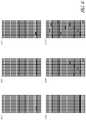
- FIGS. 5A-5Ishow example illustrations of defective cell bypass conductors 504 A- 504 C, 506 A- 506 C, 508 , 510 , 512 , or 514 used to partially or completely bypass defective solar cells 502 in a super cell 100 .
- the defective solar cells 502may be “partially bypassed” or “completely bypassed.” It will be understood that a “partially bypassed” defective solar cell 502 does not contribute any power to the electrical output of the solar module 400 .
- a partially bypassed defective solar cell 502conducts electricity from one neighboring solar cell 102 along the rear surface metallization pattern 300 and then through the defective cell bypass conductor 504 A- 504 C, 506 A- 506 C, 508 , 510 , 512 , or 514 to the next neighboring solar cell 102 in series.
- the defective cell bypass conductor 504 A- 504 C, 506 A- 506 C, 508 , 510 , 512 , or 514provides a low resistance path so that current does not have to pass through the defective solar cell 502 . By providing this path, the defective solar cell 502 is shorted and will not generate power.
- a partial bypassuses the rear surface metallization pattern 300 to conduct electricity, the rear surface metallization pattern 300 must be intact enough to allow electrical conductivity. Additionally, a partial bypass may not be appropriate if a significant portion of the defective solar cell 502 is missing (also referred to herein as a “chip”).
- a “completely bypassed” defective solar cell 502will also not contribute any electrical power to the electrical output of the solar module 400 because the completely bypassed defective solar cell 502 will be short circuited by a defective cell bypass conductor 504 A- 504 C, 506 A- 506 C, 508 , 510 , 512 , or 514 that is coupled to the rear surface metallization pattern 300 of one neighboring solar cell 102 and coupled to the rear surface metallization pattern 300 of the other neighboring solar cell 102 .
- the defective cell bypass conductors 504 A- 504 C, 506 A- 506 C, 508 , 510 , 512 , or 514may be made of any of a number of conductive materials such as metal (e.g., copper, silver, aluminum, etc.), conductive composite, or conductive polymers.
- the defective cell bypass conductors 504 A- 504 C, 506 A- 506 C, 508 , 510 , 512 , or 514may be coupled to the hidden tap contact pads 306 of the various solar cells 102 and defective solar cells 502 by any of a number of known techniques (e.g., by welding, by electrically conductive adhesive, etc.).
- FIGS. 5A-5Iincludes a view of the rear surface metallization pattern 300 of portions of three super cells 100 A, 100 B, and 100 C. While only six silicon solar cells 102 are shown in each super cell 100 shown on FIGS. 5A-5I , it will be understood that each super cell 100 could include fewer or greater numbers of silicon solar cells 102 (e.g., 72 silicon solar cells 102 as shown in FIG. 4 ).
- Each of FIGS. 5A-5Ishows at least one defective solar cell 502 and one or more bypass conductors 504 A- 504 C, 506 , 508 , 510 , 512 , or 514 .
- each solar cell 102includes at least one set of hidden tap contact pads 306 (e.g., a plurality of sets of hidden tap contact pads 306 ) which may be used to bypass defective solar cells 502 .
- each such set of hidden tap contact padsis represented by a single contact pad 306 in FIGS. 5A-5I .
- a set of hidden tap contact padsmay include any number of hidden tap contact pads 306 (e.g., one, two, three, four, or more). While only three sets of hidden tap contact pads 306 are shown in the illustrated examples, a greater number or lesser number of sets may be present.
- each defective solar cell 502 in FIGS. 5A-5Iis shown having a crack on the left side, it will be understood that the defective solar cell 502 may be defective in other ways as discussed herein.
- a defective solar cell 502may include one or more variances from acceptable parameters for a solar cell 102 . Such variances may include a crack in the substrate, front surface metallization pattern 200 , and/or rear surface metallization pattern 300 of defective solar cell 502 ; a chip in the defective solar cell 502 (i.e., a piece of the defective solar cell 502 is missing); a malformed front surface metallization pattern 200 of the defective solar cell 502 ; a malformed rear surface metallization pattern 300 of the defective solar cell 502 ; an electrical short in the defective solar cell 502 ; an out-of-specification voltage of the defective solar cell 502 ; an out-of-specification power output of the defective solar cell 502 ; poor electrical conductivity from the defective solar cell 502 to another solar cell 102 ; etc.
- the performance (e.g., IV curve, power output, reliability, etc.) of the super cell 100may be improved by bypassing a particular solar cell 102 , that solar cell 102 may be a defective solar cell 502 and it may be advantageous to bypass that particular solar cell 102 as discussed herein.
- FIG. 5Ashows three super cells 100 A, 100 B, and 100 C, each having at least one defective solar cell 502 and a defective cell bypass conductor 504 A, 504 B, or 504 C.
- the defective solar bypass conductors 504 A, 504 B, and 504 Cmay be made of a single, continuous piece of conductive material or made of multiple pieces of conductive material that are conductively bonded to each other (e.g., by welding, by electrically conductive adhesive).
- Super cell 100 Aincludes a defective solar cell 502 third in series from the top.
- the defective solar cell 502 in the super cell 100 Ais completely bypassed by a bypass conductor 504 A coupled to a plurality of sets of the hidden tap contact pads 306 of the solar cell 102 A and coupled to a plurality of sets of the hidden tap contact pads 306 of the solar cell 102 A′. Accordingly, current flowing through the super cell 100 A will completely bypass the defective solar cell 502 because current will flow from the solar cell 102 A through the bypass conductor 504 A to the solar cell 102 A′.
- Super cell 100 Bincludes a defective solar cell 502 third in series from the top.
- the defective solar cell 502 in the super cell 100 Bis partially bypassed by a bypass conductor 504 B coupled to a plurality of sets of the hidden tap contact pads 306 of the defective solar cell 502 and coupled to a plurality of sets of the hidden tap contact pads 306 of the solar cell 102 B.
- Electricityis conducted from the solar cell 102 B through the bypass conductor 504 B to the defective solar cell 502 .
- Currentthen passes from the rear surface metallization pattern 300 of the defective solar cell 502 to the front surface metallization pattern 200 of the solar cell 102 B′ as discussed herein.
- Super cell 100 Cincludes a first defective solar cell 502 third in series from the top and a second defective solar cell 502 fourth in series from the top.
- the first and second defective solar cells 502 in the super cell 100 Care bypassed by a bypass conductor 504 C coupled to a plurality of sets of the hidden tap contact pads 306 of the solar cell 102 C and coupled to a plurality of sets of the hidden tap contact pads 306 of the solar cell 102 C′. Accordingly, current flowing through the super cell 100 C will completely bypass the first and second defective solar cells 502 because current will flow from the solar cell 102 C through the bypass conductor 504 C to the solar cell 102 C′. It will be understood that more than two defective solar cells 502 (e.g., three, four, five, or more) may be bypassed in this way.
- FIG. 5Bshows three super cells 100 A, 100 B, and 100 C, each having one completely bypassed defective solar cell 502 and one or more defective cell bypass conductors 506 A- 506 C.
- Super cell 100 Aincludes a defective solar cell 502 third in series from the top.
- the defective solar cell 502 in the super cell 100 Ais completely bypassed by a bypass conductor 506 A coupled to one set of the hidden tap contact pads 306 of the solar cell 102 A and coupled to one set of the hidden tap contact pads 306 of the solar cell 102 A′. While FIG.
- FIG. 5Bshows the bypass conductor 506 A coupled to the set of hidden tap contact pads 306 in the middle of solar cell 102 A and coupled to the set of silver hidden contact pads 306 in the middle of solar cell 102 A′
- any of the sets of hidden tap contact pads 306 of solar cell 102 Amay be so coupled to any of the sets of silver hidden contact pads 306 of solar cell 102 A′ via the bypass conductor 506 A.
- current flowing through the super cell 100 Awill completely bypass the defective solar cell 502 because current will flow from the solar cell 102 A through the defective cell bypass conductor 506 A to the solar cell 102 A′.
- more than one defective solar cells 502e.g., two, three, four, five, or more may be bypassed in this way.
- Super cell 100 Bincludes a defective solar cell 502 third in series from the top.
- the defective solar cell 502 in the super cell 100 Bis completely bypassed by a pair of defective cell bypass conductors 506 B connecting two sets of the hidden tap contact pads 306 of the solar cell 102 B to two sets of hidden tap contact pads 306 of the solar cell 102 B′. While FIG.
- FIG. 5Bshows the sets of hidden tap contact pads 306 on the left and right of solar cell 102 B coupled to the sets of silver hidden contact pads 306 on the left and right of solar cell 102 B′ by the pair of defective cell bypass conductors 506 B
- any two of the sets of hidden tap contact pads 306 of solar cell 102 B ofmay be so coupled to any two of the sets of silver hidden contact pads 306 of solar cell 102 B′.
- current flowing through the super cell 100 Bwill completely bypass the defective solar cell 502 because current will flow from the solar cell 102 B through the defective cell bypass conductors 506 B to the solar cell 102 B′.
- more than one defective solar cells 502e.g., two, three, four, five, or more may be bypassed in this way.
- Super cell 100 Cincludes a defective solar cell 502 third in series from the top.
- the defective solar cell 502 in the super cell 100 Cis completely bypassed by a trio of defective cell bypass conductor 506 C coupled to three sets of the hidden tap contact pads 306 of the solar cell 102 C and coupled to three sets of hidden tap contact pads 306 of the solar cell 102 C′. Accordingly, current flowing through the super cell 100 C will completely bypass the defective solar cell 502 because current will flow from the solar cell 102 C through the defective cell bypass conductors 506 C to the solar cell 102 C′.
- more than one defective solar cell 502e.g., two, three, four, five, or more
- more than three straight defective cell bypass conductorsmay be used.
- FIG. 5Cshows three super cells 100 A, 100 B, and 100 C, each having one partially bypassed defective solar cell 502 and one or more defective cell bypass conductors 506 A- 506 C.
- Super cell 100 Aincludes a defective solar cell 502 fourth in series from the top.
- the defective solar cell 502 in the super cell 100 Ais partially bypassed by a single defective cell bypass conductor 506 A coupled to one set of the hidden tap contact pads 306 of the solar cell 102 A and coupled to the hidden tap contact pads 306 of the defective solar cell 502 .
- Electricityis conducted from the solar cell 102 A through the single defective cell bypass conductor 506 A to the defective solar cell 502 .
- Currentthen passes from the rear surface metallization pattern 300 of the defective solar cell 502 to the front surface metallization pattern 200 of the solar cell 102 A′ as discussed herein.
- FIG. 5Cshows the bypass conductor 506 A coupled to the set of hidden tap contact pads 306 in the middle of solar cell 102 A and coupled to the set of silver hidden contact pads 306 in the middle of defective solar cell 502
- any of the sets of hidden tap contact pads 306 of solar cell 102 Amay be so coupled to any of the sets of hidden tap contact pads 306 of the defective solar cell 502 if the defective cell bypass conductor 506 A allows for a current path to bypass the defects(s).
- a pair of defective cell bypass conductors 506 B as in super cell 100 B or a trio of defective cell bypass conductors 506 C as in super cell 100 Cmay be used.
- more than three straight defective cell bypass conductorsmay be used.
- FIG. 5Dshows three super cells 100 A, 100 B, and 100 C, with super cell 100 A having a defective solar cell 502 third in series from the top and a single multi-row defective cell bypass conductor 508 .
- the multi-row defective cell bypass conductor 508may be coupled to the defective solar cell 502 and the solar cells 102 third in series from the top in super cells 100 B and 100 C via one or more of the sets of silver hidden contact pads 306 of each cell in the row. Accordingly, the multi-row defective cell bypass conductor 508 may create a current path around the defect in the defective solar cell 502 , partially bypassing the defective solar cell 502 .
- FIG. 5Eshows three super cells 100 A, 100 B, and 100 C, with super cell 100 A having a defective solar cell 502 fourth in series from the top and a pair of multi-row defective cell bypass conductors 508 and 508 ′.
- the multi-row defective cell bypass conductor 508may be coupled to the solar cells 102 A, 102 B, and 102 C via one or more of the sets of silver hidden contact pads 306 of each cell in the row.
- the multi-row defective cell bypass conductor 508 ′may be coupled to the defective solar cell 502 and solar cells 102 B′ and 102 C′ via one or more of the sets of silver hidden contact pads 306 of each cell in the row. Accordingly, the multi-row defective cell bypass conductors 508 and 508 ′ may create a current path around the defect in the defective solar cell 502 , thereby partially bypassing the defective solar cell 502 .
- FIG. 5Fshows three super cells 100 A, 100 B, and 100 C, with super cell 100 A having a defective solar cell 502 fourth in series from the top and a pair of multi-row defective cell bypass conductors 508 and 508 ′.
- the multi-row defective cell bypass conductor 508may be coupled to the solar cells 102 A, 102 B, and 102 C via one or more of the sets of silver hidden contact pads 306 of each cell in the row.
- the multi-row defective cell bypass conductor 508 ′may be coupled to the solar cells 102 A′, 102 B′, and 102 C′ via one or more of the sets of silver hidden contact pads 306 of each cell in the row. Accordingly, the multi-row defective cell bypass conductors 508 and 508 ′ may create a current path around the defect in the defective solar cell 502 , thereby completely bypassing the defective solar cell 502 .
- FIG. 5Gshows three super cells 100 A, 100 B, and 100 C, with super cell 100 A having a defective solar cell 502 fourth in series from the top and a multi-row defective cell bypass conductor 510 .
- the multi-row defective cell bypass conductor 510may be made of a single, continuous piece of conductive material or made of multiple pieces of conductive material that are conductively bonded to each other (e.g., by welding, by electrically conductive adhesive).
- the multi-row defective cell bypass conductor 510may be coupled to the solar cells 102 A, 102 B, and 102 C via one or more of the sets of silver hidden contact pads 306 of each cell in the row.
- the multi-row defective cell bypass conductor 510may also be coupled to the defective solar cell 502 and solar cells 102 B′ and 102 C′ via one or more of the sets of silver hidden contact pads 306 of each cell in the row. Additionally, it will be understood that the multi-row defective cell bypass conductor 510 could be coupled to the solar cells 102 A′′, 102 B′′, and 102 C′′ instead of to the defective solar cell 502 and solar cells 102 B′ and 102 C′ as shown. In such an embodiment, the defective solar cell 502 would be completely rather than partially bypassed. Accordingly, the multi-row defective cell bypass conductor 510 may create a current path around the defect in the defective solar cell 502 , either by partially or completely bypassing defective solar cell 502 .
- FIG. 5Hshows three super cells 100 A, 100 B, and 100 C, with super cell 100 A having a defective solar cell 502 fourth in series from the top and a multi-row defective cell bypass conductor 512 .
- the multi-row defective cell bypass conductor 514may be made of a single, continuous piece of conductive material or made of multiple pieces of conductive material that are conductively bonded to each other (e.g., by welding, by electrically conductive adhesive).
- the multi-row defective cell bypass conductor 512may be coupled to solar cells 102 A, 102 B, 102 C, and 102 A′ as shown in FIG. 5H via one or more of the sets of silver hidden contact pads 306 of each cell. Accordingly, the multi-row defective cell bypass conductor 512 may create a current path around the defect in the defective solar cell 502 by completely bypassing the defective solar cell 502 and the other solar cells 102 fourth in series from the top of super cells 100 B and 100 C.
- FIG. 5Ishows three super cells 100 A, 100 B, and 100 C, with super cell 100 A having a defective solar cell 502 fourth in series from the top and a multi-row defective cell bypass conductor 514 .
- the multi-row defective cell bypass conductor 514may be coupled to solar cells 102 A, 102 B, 102 C, 102 A′ and defective solar cell 502 via one or more of the sets of silver hidden contact pads 306 of each cell. Accordingly the multi-row defective cell bypass conductor 514 may create a current path around the defect in the defective solar cell 502 by partially bypassing the defective solar cell 502 .
- FIG. 6shows examples of solar modules with one or more bypassed solar cells 102 and/or defective solar cells 502 .
- bypassed solar cells solar cells 102 and/or defective solar cells 502are represented by being blacked out.
- Solar module 600has one partially bypassed defective solar cell 502 in the second super cell 100 from the left.
- Solar module 602has an entire partially bypassed row of solar cells 102 including one or more defective solar cells 502 .
- the solar module 602could comprise super cells 100 each having an individually partially bypassed defective solar cell 502 (i.e., bypassed with a defective cell bypass 504 B) or with a multi-row defective cell bypass 510 that partially bypasses an entire row of defective solar cells 502 and/or solar cells 102 .
- Solar module 604has a completely bypassed defective solar cell 502 and a bypassed solar cell 102 in the second super cell 100 from the left.
- Solar module 606has two bypassed rows of solar cells 102 including one or more defective solar cells 502 .
- the solar module 606could comprise super cells 100 each having a completely bypassed defective solar cell 502 (i.e., bypassed with a defective cell bypass 504 A) or with a multi-row defective cell bypass 510 that completely bypasses two entire rows of defective solar cells 502 and/or solar cells 102 .
- Solar module 608has one partially bypassed defective solar cell 502 in each super cell 100 in different rows.
- Solar module 610includes two partially bypassed defective solar cells 502 in each super cell 100 in different rows.
- a solar modulecan include super cells 100 that include more than two (e.g., three, four, or more) partially bypassed or completely bypassed defective solar cells 502 in different rows. Such defective solar cells 502 may be partially bypassed or completely bypassed. As discussed below, bypassing a defective solar cell 502 or a solar cell 102 will decrease the power output of a super cell 100 and will also decrease the voltage of the maximum power point (MPP) of that super cell 100 .
- MPPmaximum power point
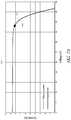
- FIGS. 7A-7Cshow example IV (current-voltage) curves of solar modules with one or more completely bypassed solar cells 102 and/or defective solar cells 502 .
- the X-axis of each curverepresents the voltage of the solar module and the Y-axis of each curve represents the current output of the solar module at the voltage on the X-axis.
- Each IV curveincludes a (reference) IV curve of a solar module with no bypassed solar cells 102 and an IV curve of a solar module with one or more defective solar cells 502 and/or bypassed solar cells 102 .
- the dot on each IV curverepresents the MPP of the solar module to which the IV curve corresponds.
- the MPPis the voltage at which the solar module generates the maximum amount of power under current operating conditions.
- a controllermay be coupled to the solar module and may adjust the operating voltage of the solar module to maintain maximum power (“MPP tracking”) generation under changing conditions.
- MPP trackingmaximum power
- Graph 700shows an IV curve 702 of a reference solar module with no bypassed solar cells 102 and IV curve 704 of a solar module 600 ( FIG. 6 ) with one bypassed defective solar cell 502 .
- the MPP voltage of the curve 704is slightly lower than the MPP voltage of the curve 702 . Because the current through the solar module at the MPP voltage for both the reference solar module and the solar module 600 is the same (e.g., to prevent damaging a super cell 100 with too much current flow), the total power generated by the solar module 600 at MPP voltage will be lower than the reference solar module.
- the voltage across each super cell 100(including the super cell 100 with the completely bypassed defective solar cell 502 ) will be identical. Accordingly, the MPP voltage for the super cell 100 with the bypassed defective solar cell 502 will also be the voltage across the other super cells 100 , resulting in a reduction of power generation potential by the other super cells 100 .
- Graph 706shows the IV curve 702 of a reference solar module with no bypassed solar cells 102 and an IV curve 708 of a solar module 602 or 608 ( FIG. 6 ) with one bypassed solar cell (either solar cells 102 or defective solar cells 502 ) in each super cell 100 .
- the MPP voltage of the curve 708is lower than the MPP voltage of the curve 702 by a larger amount than the curve 704 from graph 700 . Because the current through the solar module at the MPP voltage for both the reference solar module and the solar module 602 or 608 is the same, the total power generated by the solar module 602 or 608 at the MPP voltage will be lower than the reference solar module.
- the MPP voltage for each super cell 100 in the solar modules 602 and 608is identical. Accordingly, there is no reduction of power generation potential of super cells not including a bypassed solar cell, as occurs in the solar module 600 .
- Graph 710shows the IV curve 702 of a reference solar module with no bypassed solar cells 102 and an IV curve 712 of a solar module 604 ( FIG. 6 ) with two bypassed defective solar cell 502 in a single super cell 100 .
- the MPP voltage of the curve 712is lower than the MPP voltage of the curve 702 . Because the current through the solar module at the MPP voltage for both the reference solar module and the solar module 604 is the same, the total power generated by the solar module 604 at the MPP voltage will be lower than the reference solar module.
- the voltage across each super cell 100(including the super cell 100 with the two completely bypassed defective solar cells 502 ) will be identical. Accordingly, the MPP voltage for the super cell 100 with the two bypassed defective solar cells 502 will also be the voltage across the other super cells 100 , resulting in a reduction of power generation potential by the other super cells 100 .
- Graph 714shows the IV curve 702 of a reference solar module with no bypassed solar cells 102 and IV curve 708 of a solar module 606 or 610 ( FIG. 6 ) with two bypassed solar cell (either solar cells 102 or defective solar cells 502 ) in each super cell 100 .
- the MPP voltage of the curve 708is lower than the MPP voltage of the curve 702 by a larger amount than the curve 704 from graphs 700 , 706 , and 710 .
- the total power generated by the solar module 606 or 610 at the MPP voltagewill be lower than the reference solar module.
- the MPP voltage for each super cell 100 in the solar modules 606 and 610is identical. Accordingly, there is no reduction of power generation potential of super cells not including a bypassed solar cell, as occurs in the solar module 600 or 604 .
- a block diagramshows an inspection and reworking method 800 for reworking a super cell 100 with one or more defective solar cells.
- a number of super cells 100are assembled.
- the super cells 100may be inspected to determine whether there are one or more defective solar cells 502 in the super cell 100 at block 802 .
- the inspectionmay include one or more of visual inspection, electroluminescence testing, or photoluminescence testing.
- a visual inspectionmay be performed by a human technician examining the super cell 100 to identify one or more defective solar cells 502 . Additionally or alternatively, visual inspection may be performed by a computer coupled to a camera.
- Electroluminescence testingmay include applying a charge to a super cell 100 and measuring (e.g., with a computer coupled to a camera, with a human technician) the light pattern emitted by the super cell 100 to identify one or more defects.
- Photoluminescence testingmay include applying a homogenous wavelength of light (e.g., 800 nm red light) to the super cell 100 and measuring (e.g., with a computer coupled to a camera, with a human technician) the light pattern emitted by the super cell 100 to identify one or more defects.
- the super cells 100may be assembled into a solar module 400 at block 804 .
- the super cell 100may be set aside to be assembled into a solar module 400 comprising super cells 100 with defective solar cells 502 on the same rows (e.g., each super cell 100 has a defective solar cell 502 fifth in series from the top and a defective solar cell 502 twentieth in series from the top).
- the solar module 400may then be inspected to determine whether there are defective solar cells 502 in the solar modules. As discussed herein, the inspection may be one or more of visual inspection or electroluminescence testing. If one or more defective solar cells 502 are detected, at block 808 one or more bypass conductors (e.g., 504 A- 504 C, 506 A- 506 C, 508 , 510 , 512 , or 514 ) may be applied to the rear surface of super cell(s) 100 to bypass (partially or completely) the defective solar cells 502 in accordance with the present disclosure.
- one or more bypass conductorse.g., 504 A- 504 C, 506 A- 506 C, 508 , 510 , 512 , or 514
- FIG. 8Ba block diagram shows an inspection and reworking method 820 for reworking a super cell 100 with one or more defective solar cells 502 .
- the method 820may include reworking super cells 100 by installing one or more bypass conductors (e.g., 504 A- 504 C, 506 A- 506 C, 508 , 510 , 512 , or 514 ) before assembling the super cells 100 into a solar module 400 .
- the super cells 100are inspected (e.g., visual inspection, electroluminescence testing) and defective solar cells 502 are identified.
- one or more bypass conductorsmay be applied to the rear surface of super cell(s) 100 to bypass (partially or completely) the defective solar cells 502 in accordance with the present disclosure.
- the super cells 100may be assembled into a solar module 400 .
- a solar module 400may include super cells 100 with bypassed defective solar cells 502 and super cells 100 with no bypassed solar cells (e.g., the solar modules 600 or 604 ).
- a solar module 400may include only super cells with bypassed defective solar cells 502 (e.g., solar modules 608 or 610 ).
Landscapes
- Engineering & Computer Science (AREA)
- Architecture (AREA)
- Civil Engineering (AREA)
- Structural Engineering (AREA)
- Photovoltaic Devices (AREA)
Abstract
Description
Claims (19)
Priority Applications (6)
| Application Number | Priority Date | Filing Date | Title |
|---|---|---|---|
| US15/177,093US10673379B2 (en) | 2016-06-08 | 2016-06-08 | Systems and methods for reworking shingled solar cell modules |
| PCT/US2016/047624WO2017213674A1 (en) | 2016-06-08 | 2016-08-18 | Systems and methods for reworking shingled solar cell modules |
| KR1020247003722AKR102773881B1 (en) | 2016-06-08 | 2016-08-18 | Systems and methods for reworking shingled solar cell modules |
| KR1020187033445AKR102633537B1 (en) | 2016-06-08 | 2016-08-18 | System and method for reworking shingled solar modules |
| CN201680086378.5ACN109463012B (en) | 2016-06-08 | 2016-08-18 | System and method for reworking of cover-stacked solar cell module |
| US16/791,949US11070167B2 (en) | 2016-06-08 | 2020-02-14 | Systems and methods for reworking shingled solar cell modules |
Applications Claiming Priority (1)
| Application Number | Priority Date | Filing Date | Title |
|---|---|---|---|
| US15/177,093US10673379B2 (en) | 2016-06-08 | 2016-06-08 | Systems and methods for reworking shingled solar cell modules |
Related Child Applications (1)
| Application Number | Title | Priority Date | Filing Date |
|---|---|---|---|
| US16/791,949ContinuationUS11070167B2 (en) | 2016-06-08 | 2020-02-14 | Systems and methods for reworking shingled solar cell modules |
Publications (2)
| Publication Number | Publication Date |
|---|---|
| US20170359019A1 US20170359019A1 (en) | 2017-12-14 |
| US10673379B2true US10673379B2 (en) | 2020-06-02 |
Family
ID=60574280
Family Applications (2)
| Application Number | Title | Priority Date | Filing Date |
|---|---|---|---|
| US15/177,093Active2037-11-08US10673379B2 (en) | 2016-06-08 | 2016-06-08 | Systems and methods for reworking shingled solar cell modules |
| US16/791,949ActiveUS11070167B2 (en) | 2016-06-08 | 2020-02-14 | Systems and methods for reworking shingled solar cell modules |
Family Applications After (1)
| Application Number | Title | Priority Date | Filing Date |
|---|---|---|---|
| US16/791,949ActiveUS11070167B2 (en) | 2016-06-08 | 2020-02-14 | Systems and methods for reworking shingled solar cell modules |
Country Status (4)
| Country | Link |
|---|---|
| US (2) | US10673379B2 (en) |
| KR (2) | KR102633537B1 (en) |
| CN (1) | CN109463012B (en) |
| WO (1) | WO2017213674A1 (en) |
Cited By (1)
| Publication number | Priority date | Publication date | Assignee | Title |
|---|---|---|---|---|
| USD933584S1 (en)* | 2012-11-08 | 2021-10-19 | Sunpower Corporation | Solar panel |
Families Citing this family (8)
| Publication number | Priority date | Publication date | Assignee | Title |
|---|---|---|---|---|
| USD1009775S1 (en)* | 2014-10-15 | 2024-01-02 | Maxeon Solar Pte. Ltd. | Solar panel |
| US10411153B2 (en)* | 2015-01-29 | 2019-09-10 | Solaria Corporation | Tiled solar module repair process |
| US10673379B2 (en) | 2016-06-08 | 2020-06-02 | Sunpower Corporation | Systems and methods for reworking shingled solar cell modules |
| USD832203S1 (en)* | 2017-09-01 | 2018-10-30 | Sunpower Corporation | Solar panel |
| CN109509797B (en)* | 2018-12-30 | 2024-04-16 | 苏州阿特斯阳光电力科技有限公司 | Strip-shaped battery piece, preparation method thereof, solar battery piece and solar module |
| KR102384451B1 (en) | 2020-01-02 | 2022-04-08 | 주식회사 신성이엔지 | Manufacturing method and device of high efficiency photovoltaic strip using it |
| WO2023214601A1 (en)* | 2022-05-04 | 2023-11-09 | 주식회사 에스제이이노테크 | Apparatus for producing shingled array units |
| US20240313701A1 (en)* | 2023-03-14 | 2024-09-19 | GAF Energy LLC | Integrated cell and circuit interconnection |
Citations (149)
| Publication number | Priority date | Publication date | Assignee | Title |
|---|---|---|---|---|
| US2938938A (en) | 1956-07-03 | 1960-05-31 | Hoffman Electronics Corp | Photo-voltaic semiconductor apparatus or the like |
| US3116171A (en) | 1961-03-14 | 1963-12-31 | Bell Telephone Labor Inc | Satellite solar cell assembly |
| US3340096A (en) | 1962-02-26 | 1967-09-05 | Spectrolab A Division Of Textr | Solar cell array |
| US3369939A (en)* | 1962-10-23 | 1968-02-20 | Hughes Aircraft Co | Photovoltaic generator |
| US3459597A (en) | 1966-02-04 | 1969-08-05 | Trw Inc | Solar cells with flexible overlapping bifurcated connector |
| US3769091A (en) | 1972-03-31 | 1973-10-30 | Us Navy | Shingled array of solar cells |
| US3837924A (en) | 1971-06-01 | 1974-09-24 | Trw Inc | Solar array |
| US4257821A (en) | 1978-11-13 | 1981-03-24 | Trw Inc. | Universal solar cell/conductor junction element and solar panel embodying same |
| US4577051A (en)* | 1984-09-28 | 1986-03-18 | The Standard Oil Company | Bypass diode assembly for photovoltaic modules |
| US4617420A (en) | 1985-06-28 | 1986-10-14 | The Standard Oil Company | Flexible, interconnected array of amorphous semiconductor photovoltaic cells |
| US4617421A (en) | 1985-04-01 | 1986-10-14 | Sovonics Solar Systems | Photovoltaic cell having increased active area and method for producing same |
| US4652693A (en) | 1985-08-30 | 1987-03-24 | The Standard Oil Company | Reformed front contact current collector grid and cell interconnect for a photovoltaic cell module |
| US4877460A (en) | 1987-03-17 | 1989-10-31 | Telefunken Electronic Gmbh | Solar cell module |
| DE4017933A1 (en) | 1990-06-05 | 1991-12-12 | Telefunken Systemtechnik | SOLAR CELL ELEMENT WITH A COVER |
| DE4030713A1 (en) | 1990-09-28 | 1992-04-02 | Telefunken Systemtechnik | Photoelectric solar generator - has flexible intermediate connecting plate designed to prevent solar cell fracture due to temp. change stresses |
| US5590495A (en) | 1995-07-06 | 1997-01-07 | Bressler Group Inc. | Solar roofing system |
| US5990415A (en)* | 1994-12-08 | 1999-11-23 | Pacific Solar Pty Ltd | Multilayer solar cells with bypass diode protection |
| JPH11350685A (en) | 1998-06-09 | 1999-12-21 | Misawa Homes Co Ltd | Roof with solar cell |
| US6034322A (en) | 1999-07-01 | 2000-03-07 | Space Systems/Loral, Inc. | Solar cell assembly |
| ES2146182A1 (en) | 1998-10-15 | 2000-07-16 | Univ Madrid Politecnica | PROCEDURE FOR THE INTERCONNECTION OF SOLAR CELLS IN PHOTOVOLTAIC PANELS THROUGH DIRECT AND SIMULTANEOUS WELDING. |
| US6180868B1 (en) | 1998-06-12 | 2001-01-30 | Canon Kabushiki Kaisha | Solar cell module, solar cell module string, solar cell system, and method for supervising said solar cell module or solar cell module string |
| US6232545B1 (en) | 1998-08-06 | 2001-05-15 | Jx Crystals Inc. | Linear circuit designs for solar photovoltaic concentrator and thermophotovoltaic applications using cell and substrate materials with matched coefficients of thermal expansion |
| US6303853B1 (en) | 1998-08-06 | 2001-10-16 | Jx Crystals Inc. | Shingle circuits for thermophotovoltaic systems |
| US6313396B1 (en)* | 2000-05-22 | 2001-11-06 | The Boeing Company | Lightweight solar module and method of fabrication |
| US6315575B1 (en) | 1999-03-10 | 2001-11-13 | Sharp Kabushiki Kaisha | Interconnector electrically connecting plurality of electronic device elements, fabrication method thereof, and join apparatus thereof |
| US20010054262A1 (en) | 2000-06-09 | 2001-12-27 | Prem Nath | Self-adhesive photovoltaic module |
| US6353175B1 (en) | 1999-09-17 | 2002-03-05 | Jx Crystals Inc. | Two-terminal cell-interconnected-circuits using mechanically-stacked photovoltaic cells for line-focus concentrator arrays |
| US6359209B1 (en)* | 2000-02-23 | 2002-03-19 | Hughes Electronics Corporation | Solar panel and solar cell having in-plane solar cell interconnect with integrated diode tab |
| US6414235B1 (en) | 1999-03-30 | 2002-07-02 | Daniel Luch | Substrate and collector grid structures for integrated series connected photovoltaic arrays and process of manufacture of such arrays |
| US6441297B1 (en) | 1998-03-13 | 2002-08-27 | Steffen Keller | Solar cell arrangement |
| US6489553B1 (en) | 2001-05-30 | 2002-12-03 | Jx Crystals Inc. | TPV cylindrical generator for home cogeneration |
| US20030029494A1 (en) | 2000-12-28 | 2003-02-13 | Mitsuru Ohkubo | Solar battery |
| US6525262B1 (en) | 1998-01-06 | 2003-02-25 | Canon Kabushiki Kaisha | Solar cell module array and method for installing solar cell modules |
| US6538193B1 (en) | 2000-04-21 | 2003-03-25 | Jx Crystals Inc. | Thermophotovoltaic generator in high temperature industrial process |
| US6563289B1 (en) | 1998-09-04 | 2003-05-13 | Eev Limited | Solar cell arrangements |
| US6573445B1 (en) | 1998-11-23 | 2003-06-03 | Stichting Energieonderzoek Centrum Nederland | Method for manufacturing a metallization pattern on a photovoltaic cell |
| US20030121228A1 (en) | 2001-12-31 | 2003-07-03 | Stoehr Robert P. | System and method for dendritic web solar cell shingling |
| US6653550B2 (en) | 2001-05-17 | 2003-11-25 | Kaneka Corporation | Integrated thin-film photoelectric conversion module |
| US6670787B2 (en) | 2001-06-29 | 2003-12-30 | Sharp Kabushiki Kaisha | Solar battery module with cover member and method of fabricating the same |
| US6770544B2 (en) | 2001-02-21 | 2004-08-03 | Nec Machinery Corporation | Substrate cutting method |
| US6803513B2 (en) | 2002-08-20 | 2004-10-12 | United Solar Systems Corporation | Series connected photovoltaic module and method for its manufacture |
| US20040261836A1 (en) | 2003-04-17 | 2004-12-30 | Canon Kabushiki Kaisha | Solar cell module and solar cell module array |
| US20050126619A1 (en) | 2002-02-28 | 2005-06-16 | Shin-Etsu Handotai Co., Ltd | Solar cell module and manufacturing method thereof |
| US20050133079A1 (en) | 2003-12-23 | 2005-06-23 | Alcatel | Solar generator panel and an associated satellite |
| US20050217717A1 (en) | 2002-01-02 | 2005-10-06 | Sadeg Faris | Photovoltaic cell and method of manufacture of photovoltaic cells |
| US20050263178A1 (en) | 2004-06-01 | 2005-12-01 | Alan Montello | Photovoltaic module architecture |
| US20070107766A1 (en) | 2005-11-12 | 2007-05-17 | Langley John B Ii | Multi-source ambient energy power supply for embedded devices or remote sensor or RFID networks |
| US7238878B2 (en) | 2002-06-12 | 2007-07-03 | Gonsiorawski Ronald C | Photovoltaic module with light reflecting backskin |
| US7271333B2 (en) | 2001-07-20 | 2007-09-18 | Ascent Solar Technologies, Inc. | Apparatus and method of production of thin film photovoltaic modules |
| US20070283997A1 (en) | 2006-06-13 | 2007-12-13 | Miasole | Photovoltaic module with integrated current collection and interconnection |
| US7388146B2 (en) | 2002-04-24 | 2008-06-17 | Jx Crystals Inc. | Planar solar concentrator power module |
| US7390961B2 (en) | 2004-06-04 | 2008-06-24 | Sunpower Corporation | Interconnection of solar cells in a solar cell module |
| US20080156365A1 (en) | 2006-10-25 | 2008-07-03 | Scholz Jeremy H | Edge mountable electrical connection assembly |
| US20080216887A1 (en) | 2006-12-22 | 2008-09-11 | Advent Solar, Inc. | Interconnect Technologies for Back Contact Solar Cells and Modules |
| US20090014505A1 (en) | 2006-12-15 | 2009-01-15 | General Electric Company | Braze materials and processes therefor |
| US20090038671A1 (en) | 2007-08-10 | 2009-02-12 | Sharp Kabushiki Kaisha | Solar cell array and solar cell module |
| US7507903B2 (en) | 1999-03-30 | 2009-03-24 | Daniel Luch | Substrate and collector grid structures for integrated series connected photovoltaic arrays and process of manufacture of such arrays |
| WO2009047815A1 (en) | 2007-10-12 | 2009-04-16 | System S.P.A. | A process for connecting photovoltaic cells in series, a photovoltaic cell connectable in series using the process, and a module obtained with the process |
| US7534699B2 (en) | 2003-05-09 | 2009-05-19 | Origin Energy Solar Pty Ltd | Separating and assembling semiconductor strips |
| US20090184746A1 (en) | 2008-01-22 | 2009-07-23 | Microsemi Corporation | Low Voltage Drop Unidirectional Electronic Valve |
| US20090229596A1 (en)* | 2008-03-12 | 2009-09-17 | Myung-Hun Shin | Solar energy module having repair line, solar energy assembly having the same, method of repairing the solar energy module and method of trimming the solar energy assembly |
| US7635810B2 (en) | 1999-03-30 | 2009-12-22 | Daniel Luch | Substrate and collector grid structures for integrated photovoltaic arrays and process of manufacture of such arrays |
| US20100001587A1 (en) | 2008-07-01 | 2010-01-07 | Satcon Technology Corporation | Photovoltaic dc/dc micro-converter |
| US20100012172A1 (en) | 2008-04-29 | 2010-01-21 | Advent Solar, Inc. | Photovoltaic Modules Manufactured Using Monolithic Module Assembly Techniques |
| US20100043863A1 (en) | 2008-03-20 | 2010-02-25 | Miasole | Interconnect assembly |
| US20100075151A1 (en) | 2008-09-19 | 2010-03-25 | Seagate Technology Llc | Method for controlling and limiting adhesive migration using anti wetting agent |
| US20100071752A1 (en) | 2009-10-23 | 2010-03-25 | Applied Materials, Inc. | Solar Cell Module Having Buss Adhered With Conductive Adhesive |
| US20100078064A1 (en) | 2008-09-29 | 2010-04-01 | Thinsilicion Corporation | Monolithically-integrated solar module |
| US20100078057A1 (en) | 2006-04-13 | 2010-04-01 | Franz Karg | Solar module |
| US20100084004A1 (en) | 2002-05-17 | 2010-04-08 | Ugur Ortabasi | Integrating sphere photovoltaic receiver employing multi-junction cells |
| US20100131108A1 (en) | 2008-01-18 | 2010-05-27 | Tenksolar, Inc | Thin-film photovoltaic module |
| US20100136748A1 (en) | 2007-03-22 | 2010-06-03 | Tracy Autry | Flexible diode package and method of manufacturing |
| US20100139734A1 (en) | 2009-02-05 | 2010-06-10 | Tigo Energy | Systems and Methods for an Enhanced Watchdog in Solar Module Installations |
| US20100147364A1 (en) | 2008-12-16 | 2010-06-17 | Solopower, Inc. | Thin film photovoltaic module manufacturing methods and structures |
| WO2010095583A1 (en) | 2009-02-17 | 2010-08-26 | 三洋電機株式会社 | Solar cell and solar cell module |
| US20100224230A1 (en) | 2006-04-13 | 2010-09-09 | Daniel Luch | Collector grid and interconnect structures for photovoltaic arrays and modules |
| US20100243024A1 (en) | 2009-03-31 | 2010-09-30 | Sanyo Electric Co., Ltd | Solar cell, solar cell module and solar cell system |
| US7825329B2 (en) | 2007-01-03 | 2010-11-02 | Solopower, Inc. | Thin film solar cell manufacturing and integration |
| US7829785B2 (en) | 2006-08-04 | 2010-11-09 | Solopower, Inc. | Thin film solar cell with finger pattern |
| US20100308662A1 (en) | 2007-10-15 | 2010-12-09 | Ampt, Llc | High Efficiency Remotely Controllable Solar Energy System |
| DE102009026027A1 (en) | 2009-06-24 | 2011-01-05 | Q-Cells Se | Wafer solar cell has semiconductor wafer with front side and rear side and rear electrode-structure is arranged on rear side of semiconductor wafer |
| US20110005572A1 (en) | 2008-02-18 | 2011-01-13 | Akira Shimizu | Thin-film solar cell module |
| EP2284908A1 (en) | 2008-04-23 | 2011-02-16 | Sharp Kabushiki Kaisha | Power lines for solar power generation system, solar power generation system using the power lines, and method for inspecting malfunction of the solar power generation system |
| US20110048501A1 (en) | 2008-04-15 | 2011-03-03 | Joachim Jaus | Solar cell module |
| US20110079263A1 (en) | 2009-10-02 | 2011-04-07 | Tigo Energy, Inc. | Systems and Methods to Provide Enhanced Diode Bypass Paths |
| US20110083726A1 (en) | 2008-06-23 | 2011-04-14 | Asahi Glass Company, Limited | Backsheet for solar cell module and solar cell module |
| US20110114158A1 (en) | 2009-11-16 | 2011-05-19 | Sunpower Corporation | Replaceable photovoltaic roof panel |
| US20110155209A1 (en) | 2008-08-29 | 2011-06-30 | Odersun Ag | Thin film solar cell and photovoltaic string assembly |
| US20110168238A1 (en) | 2010-01-11 | 2011-07-14 | Solopower, Inc. | Flexible solar modules and manufacturing the same |
| US20110168237A1 (en) | 2008-09-22 | 2011-07-14 | Tohru Takeda | Integrated thin-film solar battery and manufacturing method thereof |
| US20110192448A1 (en) | 2008-05-15 | 2011-08-11 | Miasole | Solar-cell module with in-laminate diodes and external-connection mechanisms mounted to respective edge regions |
| US20110197947A1 (en) | 2008-03-20 | 2011-08-18 | Miasole | Wire network for interconnecting photovoltaic cells |
| EP2362430A1 (en) | 2010-02-18 | 2011-08-31 | SAVIO S.p.A. | A photovoltaic module |
| US20110214714A1 (en) | 2008-06-17 | 2011-09-08 | Armin Gerhard Aberle | Thin-film solar cell interconnection |
| US20110240337A1 (en) | 2010-04-05 | 2011-10-06 | John Montello | Interconnects for photovoltaic panels |
| US20110271999A1 (en) | 2010-05-05 | 2011-11-10 | Cogenra Solar, Inc. | Receiver for concentrating photovoltaic-thermal system |
| US20110272004A1 (en) | 2010-05-06 | 2011-11-10 | Davis Robert F | Solar panels with opaque EVA film backseets |
| US20110315184A1 (en) | 2010-06-29 | 2011-12-29 | Primestar Solar, Inc. | Photovoltaic (pv) module with improved bus tape to foil ribbon contact |
| US8110737B2 (en) | 1999-03-30 | 2012-02-07 | Daniel Luch | Collector grid, electrode structures and interrconnect structures for photovoltaic arrays and methods of manufacture |
| US20120037206A1 (en) | 2010-08-16 | 2012-02-16 | Richard Norman | Systems for cost effective concentration and utilization of solar energy |
| US20120048349A1 (en) | 2009-01-09 | 2012-03-01 | Solopower, Inc. | Flexible solar modules and manufacturing the same |
| WO2012033657A2 (en) | 2010-09-07 | 2012-03-15 | Dow Global Technologies Llc | Improved photovoltaic cell assembly |
| US8138413B2 (en) | 2006-04-13 | 2012-03-20 | Daniel Luch | Collector grid and interconnect structures for photovoltaic arrays and modules |
| US20120118355A1 (en) | 2010-11-12 | 2012-05-17 | Solopower, Inc. | Flexible solar shell and support structure for use with rooftops |
| US20120125391A1 (en) | 2010-11-19 | 2012-05-24 | Solopower, Inc. | Methods for interconnecting photovoltaic cells |
| US20120152349A1 (en) | 2010-12-17 | 2012-06-21 | Solopower, Inc. | Junction box attachment for photovoltaic thin film devices |
| US20120152327A1 (en) | 2010-11-12 | 2012-06-21 | Solopower, Inc. | Method of manufacturing solar modules |
| US8207440B2 (en) | 2008-08-11 | 2012-06-26 | Solopower, Inc. | Photovoltaic modules with improved reliability |
| WO2012099705A2 (en) | 2011-01-17 | 2012-07-26 | Kent Kernahan | Idealized solar panel |
| US20120234388A1 (en) | 2009-08-26 | 2012-09-20 | Robert Stancel | Assembly for electrical breakdown protection for high current, non-elongate solar cells with electrically conductive substrates |
| US20120244656A1 (en) | 2011-03-25 | 2012-09-27 | Samsung Electro-Mechanics Co., Ltd. | Method and apparatus for producing solar cell |
| US20120279548A1 (en) | 2009-05-18 | 2012-11-08 | Muench Markus | Arrangement and circuit, and method for interconnecting flat solar cells |
| US20120312347A1 (en)* | 2011-06-08 | 2012-12-13 | Thomas Buettner | Solar module and photovoltaic array |
| US20120312354A1 (en)* | 2011-06-08 | 2012-12-13 | Thomas Buettner | Solar module and photovoltaic array |
| US8334451B2 (en) | 2003-10-03 | 2012-12-18 | Ixys Corporation | Discrete and integrated photo voltaic solar cells |
| US20120318319A1 (en) | 2011-06-17 | 2012-12-20 | Solopower, Inc. | Methods of interconnecting thin film solar cells |
| US20120318318A1 (en) | 2011-06-17 | 2012-12-20 | Solopower, Inc. | Cigs based thin film solar cells having shared bypass diodes |
| US20120325282A1 (en) | 2011-06-24 | 2012-12-27 | Solopower, Inc. | Solar cells with grid wire interconnections |
| WO2013020590A1 (en) | 2011-08-09 | 2013-02-14 | Kioto Photovoltaics Gmbh | Rectangular solar cell and associated solar cell arrangement |
| US8378209B2 (en) | 2009-07-29 | 2013-02-19 | Cyrium Technologies Incorporated | Solar cell and method of fabrication thereof |
| US20130048046A1 (en) | 2011-08-30 | 2013-02-28 | Raymond Domsic | Photovoltaic module |
| US20130068279A1 (en) | 2011-09-15 | 2013-03-21 | Benyamin Buller | Photovoltaic module interlayer |
| US20130096710A1 (en) | 2011-10-17 | 2013-04-18 | Solopower, Inc. | Tracking system and method for solar cell manufacturing |
| US20130160824A1 (en) | 2011-12-21 | 2013-06-27 | Solopower, Inc. | Roof integrated solar module assembly |
| US20130160823A1 (en) | 2011-12-21 | 2013-06-27 | Solopower, Inc. | Integrated structural solar module and chassis |
| US20130206206A1 (en) | 2010-05-13 | 2013-08-15 | Rec Solar As | Photo voltaic generator panel, method and system |
| US20130206221A1 (en) | 2012-02-13 | 2013-08-15 | John Anthony Gannon | Solar cell with metallization compensating for or preventing cracking |
| US20130206203A1 (en) | 2010-08-26 | 2013-08-15 | Innotech Solar Asa | Photovoltaic module with integrated solar cell diodes |
| US20130206213A1 (en) | 2012-02-15 | 2013-08-15 | Alta Devices, Inc. | Photovoltaic module containing shingled photovoltaic tiles and fabrication processes thereof |
| US8574943B2 (en) | 2007-09-10 | 2013-11-05 | Dyesol Industries Pty Ltd | Method for manufacturing solar cells |
| US8586875B2 (en) | 2010-02-26 | 2013-11-19 | Ibiden Co., Ltd. | Wiring board and method for manufacturing the same |
| JP2014017447A (en) | 2012-07-11 | 2014-01-30 | Sharp Corp | Integrated thin film solar cell and manufacturing method of the same |
| US20140060610A1 (en) | 2011-11-20 | 2014-03-06 | Mehrdad M. Moslehi | Smart photovoltaic cells and modules |
| US20140116495A1 (en) | 2012-10-25 | 2014-05-01 | Sunpower Corporation | Bifacial solar cell module with backside reflector |
| US20140124014A1 (en)* | 2012-11-08 | 2014-05-08 | Cogenra Solar, Inc. | High efficiency configuration for solar cell string |
| US8729385B2 (en) | 2006-04-13 | 2014-05-20 | Daniel Luch | Collector grid and interconnect structures for photovoltaic arrays and modules |
| WO2014098771A1 (en) | 2012-12-17 | 2014-06-26 | Agency For Science, Technology And Research | Wafer dicing apparatus and wafer dicing method |
| US8766090B2 (en) | 2012-03-19 | 2014-07-01 | Rec Solar Pte. Ltd. | Method for metallization or metallization and interconnection of back contact solar cells |
| US20140318613A1 (en) | 2011-04-12 | 2014-10-30 | Schott Solar Ag | Solar cell |
| WO2014192272A1 (en) | 2013-05-28 | 2014-12-04 | 三洋電機株式会社 | Solar cell module |
| WO2015001413A1 (en) | 2013-07-05 | 2015-01-08 | Rec Solar Pte. Ltd. | Solar cell assembly |
| US20150349703A1 (en)* | 2014-05-27 | 2015-12-03 | Cogenra Solar, Inc. | Shingled solar cell module |
| US20160163888A1 (en) | 2014-12-05 | 2016-06-09 | Solarcity Corporation | Photovoltaic cells with electrodes adapted to house conductive paste |
| US20160163907A1 (en) | 2014-12-05 | 2016-06-09 | Solarcity Corporation | Photovoltaic structure cleaving system |
| US20160163909A1 (en) | 2014-12-05 | 2016-06-09 | Solarcity Corporation | Systems and methods for cascading photovoltaic structures |
| US20160163908A1 (en) | 2014-12-05 | 2016-06-09 | Solarcity Corporation | Systems and method for precision automated placement of backsheet on pv modules |
| US20160158890A1 (en) | 2014-12-05 | 2016-06-09 | Solarcity Corporation | Systems and methods for scribing photovoltaic structures |
| US20160163912A1 (en) | 2014-12-05 | 2016-06-09 | Solarcity Corporation | Methods and systems for precision application of conductive adhesive paste on photovoltaic structures |
| US20160163913A1 (en) | 2014-12-05 | 2016-06-09 | Solarcity Corporation | System and apparatus for precision automation of tab attachment for fabrications of solar panels |
Family Cites Families (20)
| Publication number | Priority date | Publication date | Assignee | Title |
|---|---|---|---|---|
| US3811181A (en) | 1972-03-31 | 1974-05-21 | Us Navy | New approach to shingling of solar cells |
| US5616185A (en) | 1995-10-10 | 1997-04-01 | Hughes Aircraft Company | Solar cell with integrated bypass diode and method |
| US6218605B1 (en) | 1997-04-23 | 2001-04-17 | Robert B. Dally | Performance optimizing system for a satellite solar array |
| US6262358B1 (en) | 1999-02-18 | 2001-07-17 | Sharp Kabushiki Kaisha | Solar cell module and solar cell panel using the same |
| US8222513B2 (en) | 2006-04-13 | 2012-07-17 | Daniel Luch | Collector grid, electrode structures and interconnect structures for photovoltaic arrays and methods of manufacture |
| JP3888860B2 (en)* | 2000-05-24 | 2007-03-07 | シャープ株式会社 | Solar cell protection method |
| US6531653B1 (en)* | 2001-09-11 | 2003-03-11 | The Boeing Company | Low cost high solar flux photovoltaic concentrator receiver |
| US8212138B2 (en) | 2003-05-16 | 2012-07-03 | The United States Of America As Represented By The Administrator Of National Aeronautics And Space Administration | Reverse bias protected solar array with integrated bypass battery |
| US20070283996A1 (en) | 2006-06-13 | 2007-12-13 | Miasole | Photovoltaic module with insulating interconnect carrier |
| WO2009006110A2 (en) | 2007-06-28 | 2009-01-08 | Jacobs Gregory F | Photovoltaic devices including cover elements, and photovoltaic systems, arrays, roofs and methods using them |
| CN101431115B (en) | 2007-11-07 | 2011-05-18 | E.I.内穆尔杜邦公司 | Solar cell panel and manufacturing method thereof |
| US8586857B2 (en) | 2008-11-04 | 2013-11-19 | Miasole | Combined diode, lead assembly incorporating an expansion joint |
| KR101097252B1 (en) | 2009-11-17 | 2011-12-21 | 삼성에스디아이 주식회사 | Photoelectric conversion element |
| WO2012046319A1 (en) | 2010-10-06 | 2012-04-12 | 三菱電機株式会社 | Solar cell module, photovoltaic device, and process for manufacture of solar cell module |
| JP2012138518A (en)* | 2010-12-27 | 2012-07-19 | Sony Corp | Photovoltaic power generation module and inspection method |
| US9947820B2 (en) | 2014-05-27 | 2018-04-17 | Sunpower Corporation | Shingled solar cell panel employing hidden taps |
| KR102368110B1 (en)* | 2014-05-27 | 2022-02-25 | 선파워 코포레이션 | Shingled solar cell module |
| DK3518126T3 (en)* | 2014-05-27 | 2023-01-30 | Maxeon Solar Pte Ltd | Overlapping solar module |
| CN110828591B (en) | 2015-08-18 | 2023-05-02 | 迈可晟太阳能有限公司 | Solar panel |
| US10673379B2 (en) | 2016-06-08 | 2020-06-02 | Sunpower Corporation | Systems and methods for reworking shingled solar cell modules |
- 2016
- 2016-06-08USUS15/177,093patent/US10673379B2/enactiveActive
- 2016-08-18KRKR1020187033445Apatent/KR102633537B1/enactiveActive
- 2016-08-18WOPCT/US2016/047624patent/WO2017213674A1/ennot_activeCeased
- 2016-08-18CNCN201680086378.5Apatent/CN109463012B/enactiveActive
- 2016-08-18KRKR1020247003722Apatent/KR102773881B1/enactiveActive
- 2020
- 2020-02-14USUS16/791,949patent/US11070167B2/enactiveActive
Patent Citations (168)
| Publication number | Priority date | Publication date | Assignee | Title |
|---|---|---|---|---|
| US2938938A (en) | 1956-07-03 | 1960-05-31 | Hoffman Electronics Corp | Photo-voltaic semiconductor apparatus or the like |
| US3116171A (en) | 1961-03-14 | 1963-12-31 | Bell Telephone Labor Inc | Satellite solar cell assembly |
| US3340096A (en) | 1962-02-26 | 1967-09-05 | Spectrolab A Division Of Textr | Solar cell array |
| US3369939A (en)* | 1962-10-23 | 1968-02-20 | Hughes Aircraft Co | Photovoltaic generator |
| US3459597A (en) | 1966-02-04 | 1969-08-05 | Trw Inc | Solar cells with flexible overlapping bifurcated connector |
| US3837924A (en) | 1971-06-01 | 1974-09-24 | Trw Inc | Solar array |
| US3769091A (en) | 1972-03-31 | 1973-10-30 | Us Navy | Shingled array of solar cells |
| US4257821A (en) | 1978-11-13 | 1981-03-24 | Trw Inc. | Universal solar cell/conductor junction element and solar panel embodying same |
| US4577051A (en)* | 1984-09-28 | 1986-03-18 | The Standard Oil Company | Bypass diode assembly for photovoltaic modules |
| US4617421A (en) | 1985-04-01 | 1986-10-14 | Sovonics Solar Systems | Photovoltaic cell having increased active area and method for producing same |
| US4617420A (en) | 1985-06-28 | 1986-10-14 | The Standard Oil Company | Flexible, interconnected array of amorphous semiconductor photovoltaic cells |
| US4652693A (en) | 1985-08-30 | 1987-03-24 | The Standard Oil Company | Reformed front contact current collector grid and cell interconnect for a photovoltaic cell module |
| US4877460A (en) | 1987-03-17 | 1989-10-31 | Telefunken Electronic Gmbh | Solar cell module |
| DE4017933A1 (en) | 1990-06-05 | 1991-12-12 | Telefunken Systemtechnik | SOLAR CELL ELEMENT WITH A COVER |
| DE4030713A1 (en) | 1990-09-28 | 1992-04-02 | Telefunken Systemtechnik | Photoelectric solar generator - has flexible intermediate connecting plate designed to prevent solar cell fracture due to temp. change stresses |
| US5990415A (en)* | 1994-12-08 | 1999-11-23 | Pacific Solar Pty Ltd | Multilayer solar cells with bypass diode protection |
| US5590495A (en) | 1995-07-06 | 1997-01-07 | Bressler Group Inc. | Solar roofing system |
| US6525262B1 (en) | 1998-01-06 | 2003-02-25 | Canon Kabushiki Kaisha | Solar cell module array and method for installing solar cell modules |
| US6441297B1 (en) | 1998-03-13 | 2002-08-27 | Steffen Keller | Solar cell arrangement |
| JPH11350685A (en) | 1998-06-09 | 1999-12-21 | Misawa Homes Co Ltd | Roof with solar cell |
| US6180868B1 (en) | 1998-06-12 | 2001-01-30 | Canon Kabushiki Kaisha | Solar cell module, solar cell module string, solar cell system, and method for supervising said solar cell module or solar cell module string |
| US6303853B1 (en) | 1998-08-06 | 2001-10-16 | Jx Crystals Inc. | Shingle circuits for thermophotovoltaic systems |
| US6232545B1 (en) | 1998-08-06 | 2001-05-15 | Jx Crystals Inc. | Linear circuit designs for solar photovoltaic concentrator and thermophotovoltaic applications using cell and substrate materials with matched coefficients of thermal expansion |
| US6563289B1 (en) | 1998-09-04 | 2003-05-13 | Eev Limited | Solar cell arrangements |
| ES2146182A1 (en) | 1998-10-15 | 2000-07-16 | Univ Madrid Politecnica | PROCEDURE FOR THE INTERCONNECTION OF SOLAR CELLS IN PHOTOVOLTAIC PANELS THROUGH DIRECT AND SIMULTANEOUS WELDING. |
| US6573445B1 (en) | 1998-11-23 | 2003-06-03 | Stichting Energieonderzoek Centrum Nederland | Method for manufacturing a metallization pattern on a photovoltaic cell |
| US6315575B1 (en) | 1999-03-10 | 2001-11-13 | Sharp Kabushiki Kaisha | Interconnector electrically connecting plurality of electronic device elements, fabrication method thereof, and join apparatus thereof |
| US6414235B1 (en) | 1999-03-30 | 2002-07-02 | Daniel Luch | Substrate and collector grid structures for integrated series connected photovoltaic arrays and process of manufacture of such arrays |
| US7989692B2 (en) | 1999-03-30 | 2011-08-02 | Daniel Luch | Substrate and collector grid structures for integrated series connected photovoltaic arrays and process of manufacturing of such arrays |
| US7989693B2 (en) | 1999-03-30 | 2011-08-02 | Daniel Luch | Substrate and collector grid structures for integrated series connected photovoltaic arrays and process of manufacture of such arrays |
| US8110737B2 (en) | 1999-03-30 | 2012-02-07 | Daniel Luch | Collector grid, electrode structures and interrconnect structures for photovoltaic arrays and methods of manufacture |
| US7851700B2 (en) | 1999-03-30 | 2010-12-14 | Daniel Luch | Substrate and collector grid structures for integrated series connected photovoltaic arrays and process of manufacture of such arrays |
| US8319097B2 (en) | 1999-03-30 | 2012-11-27 | Daniel Luch | Substrate and collector grid structures for integrated series connected photovoltaic arrays and process of manufacture of such arrays |
| US7635810B2 (en) | 1999-03-30 | 2009-12-22 | Daniel Luch | Substrate and collector grid structures for integrated photovoltaic arrays and process of manufacture of such arrays |
| US7507903B2 (en) | 1999-03-30 | 2009-03-24 | Daniel Luch | Substrate and collector grid structures for integrated series connected photovoltaic arrays and process of manufacture of such arrays |
| US8304646B2 (en) | 1999-03-30 | 2012-11-06 | Daniel Luch | Substrate and collector grid structures for integrated series connected photovoltaic arrays and process of manufacture of such arrays |
| US7868249B2 (en) | 1999-03-30 | 2011-01-11 | Daniel Luch | Substrate and collector grid structures for integrated series connected photovoltaic arrays and process of manufacture of such arrays |
| US6034322A (en) | 1999-07-01 | 2000-03-07 | Space Systems/Loral, Inc. | Solar cell assembly |
| US6353175B1 (en) | 1999-09-17 | 2002-03-05 | Jx Crystals Inc. | Two-terminal cell-interconnected-circuits using mechanically-stacked photovoltaic cells for line-focus concentrator arrays |
| US6359209B1 (en)* | 2000-02-23 | 2002-03-19 | Hughes Electronics Corporation | Solar panel and solar cell having in-plane solar cell interconnect with integrated diode tab |
| US6538193B1 (en) | 2000-04-21 | 2003-03-25 | Jx Crystals Inc. | Thermophotovoltaic generator in high temperature industrial process |
| US6313396B1 (en)* | 2000-05-22 | 2001-11-06 | The Boeing Company | Lightweight solar module and method of fabrication |
| US20010054262A1 (en) | 2000-06-09 | 2001-12-27 | Prem Nath | Self-adhesive photovoltaic module |
| US6610919B2 (en) | 2000-12-28 | 2003-08-26 | Mitsubishi Denki Kabushiki Kaisha | Solar battery |
| US20030029494A1 (en) | 2000-12-28 | 2003-02-13 | Mitsuru Ohkubo | Solar battery |
| US6770544B2 (en) | 2001-02-21 | 2004-08-03 | Nec Machinery Corporation | Substrate cutting method |
| US6653550B2 (en) | 2001-05-17 | 2003-11-25 | Kaneka Corporation | Integrated thin-film photoelectric conversion module |
| US6489553B1 (en) | 2001-05-30 | 2002-12-03 | Jx Crystals Inc. | TPV cylindrical generator for home cogeneration |
| US6670787B2 (en) | 2001-06-29 | 2003-12-30 | Sharp Kabushiki Kaisha | Solar battery module with cover member and method of fabricating the same |
| US7271333B2 (en) | 2001-07-20 | 2007-09-18 | Ascent Solar Technologies, Inc. | Apparatus and method of production of thin film photovoltaic modules |
| US20030121228A1 (en) | 2001-12-31 | 2003-07-03 | Stoehr Robert P. | System and method for dendritic web solar cell shingling |
| US20050217717A1 (en) | 2002-01-02 | 2005-10-06 | Sadeg Faris | Photovoltaic cell and method of manufacture of photovoltaic cells |
| US20050126619A1 (en) | 2002-02-28 | 2005-06-16 | Shin-Etsu Handotai Co., Ltd | Solar cell module and manufacturing method thereof |
| US7388146B2 (en) | 2002-04-24 | 2008-06-17 | Jx Crystals Inc. | Planar solar concentrator power module |
| US7872192B1 (en) | 2002-04-24 | 2011-01-18 | Jx Crystals Inc. | Planar solar concentrator power module |
| US20100084004A1 (en) | 2002-05-17 | 2010-04-08 | Ugur Ortabasi | Integrating sphere photovoltaic receiver employing multi-junction cells |
| US7238878B2 (en) | 2002-06-12 | 2007-07-03 | Gonsiorawski Ronald C | Photovoltaic module with light reflecting backskin |
| US6803513B2 (en) | 2002-08-20 | 2004-10-12 | United Solar Systems Corporation | Series connected photovoltaic module and method for its manufacture |
| US20040261836A1 (en) | 2003-04-17 | 2004-12-30 | Canon Kabushiki Kaisha | Solar cell module and solar cell module array |
| US7534699B2 (en) | 2003-05-09 | 2009-05-19 | Origin Energy Solar Pty Ltd | Separating and assembling semiconductor strips |
| US8334451B2 (en) | 2003-10-03 | 2012-12-18 | Ixys Corporation | Discrete and integrated photo voltaic solar cells |
| US20050133079A1 (en) | 2003-12-23 | 2005-06-23 | Alcatel | Solar generator panel and an associated satellite |
| US20050263178A1 (en) | 2004-06-01 | 2005-12-01 | Alan Montello | Photovoltaic module architecture |
| US7777128B2 (en) | 2004-06-01 | 2010-08-17 | Konarka Technologies, Inc. | Photovoltaic module architecture |
| US7772484B2 (en) | 2004-06-01 | 2010-08-10 | Konarka Technologies, Inc. | Photovoltaic module architecture |
| US7781672B2 (en) | 2004-06-01 | 2010-08-24 | Konarka Technologies, Inc. | Photovoltaic module architecture |
| US7829781B2 (en) | 2004-06-01 | 2010-11-09 | Konarka Technologies, Inc. | Photovoltaic module architecture |
| US7390961B2 (en) | 2004-06-04 | 2008-06-24 | Sunpower Corporation | Interconnection of solar cells in a solar cell module |
| US20070107766A1 (en) | 2005-11-12 | 2007-05-17 | Langley John B Ii | Multi-source ambient energy power supply for embedded devices or remote sensor or RFID networks |
| US20100078057A1 (en) | 2006-04-13 | 2010-04-01 | Franz Karg | Solar module |
| US8729385B2 (en) | 2006-04-13 | 2014-05-20 | Daniel Luch | Collector grid and interconnect structures for photovoltaic arrays and modules |
| US20100224230A1 (en) | 2006-04-13 | 2010-09-09 | Daniel Luch | Collector grid and interconnect structures for photovoltaic arrays and modules |
| US8138413B2 (en) | 2006-04-13 | 2012-03-20 | Daniel Luch | Collector grid and interconnect structures for photovoltaic arrays and modules |
| US20070283997A1 (en) | 2006-06-13 | 2007-12-13 | Miasole | Photovoltaic module with integrated current collection and interconnection |
| US7829785B2 (en) | 2006-08-04 | 2010-11-09 | Solopower, Inc. | Thin film solar cell with finger pattern |
| US20080156365A1 (en) | 2006-10-25 | 2008-07-03 | Scholz Jeremy H | Edge mountable electrical connection assembly |
| US20090014505A1 (en) | 2006-12-15 | 2009-01-15 | General Electric Company | Braze materials and processes therefor |
| US20080216887A1 (en) | 2006-12-22 | 2008-09-11 | Advent Solar, Inc. | Interconnect Technologies for Back Contact Solar Cells and Modules |
| US7825329B2 (en) | 2007-01-03 | 2010-11-02 | Solopower, Inc. | Thin film solar cell manufacturing and integration |
| US20100136748A1 (en) | 2007-03-22 | 2010-06-03 | Tracy Autry | Flexible diode package and method of manufacturing |
| US20090038671A1 (en) | 2007-08-10 | 2009-02-12 | Sharp Kabushiki Kaisha | Solar cell array and solar cell module |
| US8574943B2 (en) | 2007-09-10 | 2013-11-05 | Dyesol Industries Pty Ltd | Method for manufacturing solar cells |
| WO2009047815A1 (en) | 2007-10-12 | 2009-04-16 | System S.P.A. | A process for connecting photovoltaic cells in series, a photovoltaic cell connectable in series using the process, and a module obtained with the process |
| US20100218799A1 (en) | 2007-10-12 | 2010-09-02 | System S.P.A. | Process for connecting photovoltaic cells in series, a photovoltaic cell connectable in series using the process, and a module obtained with the process |
| US20100308662A1 (en) | 2007-10-15 | 2010-12-09 | Ampt, Llc | High Efficiency Remotely Controllable Solar Energy System |
| US20100131108A1 (en) | 2008-01-18 | 2010-05-27 | Tenksolar, Inc | Thin-film photovoltaic module |
| US20090184746A1 (en) | 2008-01-22 | 2009-07-23 | Microsemi Corporation | Low Voltage Drop Unidirectional Electronic Valve |
| US20110005572A1 (en) | 2008-02-18 | 2011-01-13 | Akira Shimizu | Thin-film solar cell module |
| US20090229596A1 (en)* | 2008-03-12 | 2009-09-17 | Myung-Hun Shin | Solar energy module having repair line, solar energy assembly having the same, method of repairing the solar energy module and method of trimming the solar energy assembly |
| US20110197947A1 (en) | 2008-03-20 | 2011-08-18 | Miasole | Wire network for interconnecting photovoltaic cells |
| US20100043863A1 (en) | 2008-03-20 | 2010-02-25 | Miasole | Interconnect assembly |
| US20110048501A1 (en) | 2008-04-15 | 2011-03-03 | Joachim Jaus | Solar cell module |
| EP2284908A1 (en) | 2008-04-23 | 2011-02-16 | Sharp Kabushiki Kaisha | Power lines for solar power generation system, solar power generation system using the power lines, and method for inspecting malfunction of the solar power generation system |
| US20100012172A1 (en) | 2008-04-29 | 2010-01-21 | Advent Solar, Inc. | Photovoltaic Modules Manufactured Using Monolithic Module Assembly Techniques |
| US20110192448A1 (en) | 2008-05-15 | 2011-08-11 | Miasole | Solar-cell module with in-laminate diodes and external-connection mechanisms mounted to respective edge regions |
| US20110214714A1 (en) | 2008-06-17 | 2011-09-08 | Armin Gerhard Aberle | Thin-film solar cell interconnection |
| US20110083726A1 (en) | 2008-06-23 | 2011-04-14 | Asahi Glass Company, Limited | Backsheet for solar cell module and solar cell module |
| US20100001587A1 (en) | 2008-07-01 | 2010-01-07 | Satcon Technology Corporation | Photovoltaic dc/dc micro-converter |
| US8207440B2 (en) | 2008-08-11 | 2012-06-26 | Solopower, Inc. | Photovoltaic modules with improved reliability |
| US20110155209A1 (en) | 2008-08-29 | 2011-06-30 | Odersun Ag | Thin film solar cell and photovoltaic string assembly |
| US20100075151A1 (en) | 2008-09-19 | 2010-03-25 | Seagate Technology Llc | Method for controlling and limiting adhesive migration using anti wetting agent |
| US20110168237A1 (en) | 2008-09-22 | 2011-07-14 | Tohru Takeda | Integrated thin-film solar battery and manufacturing method thereof |
| US20100078064A1 (en) | 2008-09-29 | 2010-04-01 | Thinsilicion Corporation | Monolithically-integrated solar module |
| US20100147364A1 (en) | 2008-12-16 | 2010-06-17 | Solopower, Inc. | Thin film photovoltaic module manufacturing methods and structures |
| US20120048349A1 (en) | 2009-01-09 | 2012-03-01 | Solopower, Inc. | Flexible solar modules and manufacturing the same |
| US20100139734A1 (en) | 2009-02-05 | 2010-06-10 | Tigo Energy | Systems and Methods for an Enhanced Watchdog in Solar Module Installations |
| US20120031457A1 (en) | 2009-02-17 | 2012-02-09 | Sanyo Electric Co., Ltd. | Solar cell and solar cell module |
| WO2010095583A1 (en) | 2009-02-17 | 2010-08-26 | 三洋電機株式会社 | Solar cell and solar cell module |
| US20100243024A1 (en) | 2009-03-31 | 2010-09-30 | Sanyo Electric Co., Ltd | Solar cell, solar cell module and solar cell system |
| US20120279548A1 (en) | 2009-05-18 | 2012-11-08 | Muench Markus | Arrangement and circuit, and method for interconnecting flat solar cells |
| DE102009026027A1 (en) | 2009-06-24 | 2011-01-05 | Q-Cells Se | Wafer solar cell has semiconductor wafer with front side and rear side and rear electrode-structure is arranged on rear side of semiconductor wafer |
| US8378209B2 (en) | 2009-07-29 | 2013-02-19 | Cyrium Technologies Incorporated | Solar cell and method of fabrication thereof |
| US20120234388A1 (en) | 2009-08-26 | 2012-09-20 | Robert Stancel | Assembly for electrical breakdown protection for high current, non-elongate solar cells with electrically conductive substrates |
| US20110079263A1 (en) | 2009-10-02 | 2011-04-07 | Tigo Energy, Inc. | Systems and Methods to Provide Enhanced Diode Bypass Paths |
| US20100071752A1 (en) | 2009-10-23 | 2010-03-25 | Applied Materials, Inc. | Solar Cell Module Having Buss Adhered With Conductive Adhesive |
| US20110114158A1 (en) | 2009-11-16 | 2011-05-19 | Sunpower Corporation | Replaceable photovoltaic roof panel |
| US20110168238A1 (en) | 2010-01-11 | 2011-07-14 | Solopower, Inc. | Flexible solar modules and manufacturing the same |
| EP2362430A1 (en) | 2010-02-18 | 2011-08-31 | SAVIO S.p.A. | A photovoltaic module |
| US8586875B2 (en) | 2010-02-26 | 2013-11-19 | Ibiden Co., Ltd. | Wiring board and method for manufacturing the same |
| US20110240337A1 (en) | 2010-04-05 | 2011-10-06 | John Montello | Interconnects for photovoltaic panels |
| US20110271999A1 (en) | 2010-05-05 | 2011-11-10 | Cogenra Solar, Inc. | Receiver for concentrating photovoltaic-thermal system |
| US20110272004A1 (en) | 2010-05-06 | 2011-11-10 | Davis Robert F | Solar panels with opaque EVA film backseets |
| US20130206206A1 (en) | 2010-05-13 | 2013-08-15 | Rec Solar As | Photo voltaic generator panel, method and system |
| US20110315184A1 (en) | 2010-06-29 | 2011-12-29 | Primestar Solar, Inc. | Photovoltaic (pv) module with improved bus tape to foil ribbon contact |
| US20120037206A1 (en) | 2010-08-16 | 2012-02-16 | Richard Norman | Systems for cost effective concentration and utilization of solar energy |
| US20130206203A1 (en) | 2010-08-26 | 2013-08-15 | Innotech Solar Asa | Photovoltaic module with integrated solar cell diodes |
| WO2012033657A2 (en) | 2010-09-07 | 2012-03-15 | Dow Global Technologies Llc | Improved photovoltaic cell assembly |
| US20130152996A1 (en) | 2010-09-07 | 2013-06-20 | Dow Global Technologies Llc | Photovoltaic cell assembly |
| US20120152327A1 (en) | 2010-11-12 | 2012-06-21 | Solopower, Inc. | Method of manufacturing solar modules |
| US20120118355A1 (en) | 2010-11-12 | 2012-05-17 | Solopower, Inc. | Flexible solar shell and support structure for use with rooftops |
| US20120125391A1 (en) | 2010-11-19 | 2012-05-24 | Solopower, Inc. | Methods for interconnecting photovoltaic cells |
| US20120152349A1 (en) | 2010-12-17 | 2012-06-21 | Solopower, Inc. | Junction box attachment for photovoltaic thin film devices |
| WO2012099705A2 (en) | 2011-01-17 | 2012-07-26 | Kent Kernahan | Idealized solar panel |
| US20120268087A1 (en) | 2011-01-17 | 2012-10-25 | Kent Kernahan | Idealized solar panel |
| US20120244656A1 (en) | 2011-03-25 | 2012-09-27 | Samsung Electro-Mechanics Co., Ltd. | Method and apparatus for producing solar cell |
| US20140318613A1 (en) | 2011-04-12 | 2014-10-30 | Schott Solar Ag | Solar cell |
| US20120312354A1 (en)* | 2011-06-08 | 2012-12-13 | Thomas Buettner | Solar module and photovoltaic array |
| US20120312347A1 (en)* | 2011-06-08 | 2012-12-13 | Thomas Buettner | Solar module and photovoltaic array |
| US20120318318A1 (en) | 2011-06-17 | 2012-12-20 | Solopower, Inc. | Cigs based thin film solar cells having shared bypass diodes |
| US20120318319A1 (en) | 2011-06-17 | 2012-12-20 | Solopower, Inc. | Methods of interconnecting thin film solar cells |
| US20120325282A1 (en) | 2011-06-24 | 2012-12-27 | Solopower, Inc. | Solar cells with grid wire interconnections |
| WO2013020590A1 (en) | 2011-08-09 | 2013-02-14 | Kioto Photovoltaics Gmbh | Rectangular solar cell and associated solar cell arrangement |
| US20130048046A1 (en) | 2011-08-30 | 2013-02-28 | Raymond Domsic | Photovoltaic module |
| US20130068279A1 (en) | 2011-09-15 | 2013-03-21 | Benyamin Buller | Photovoltaic module interlayer |
| US20130096710A1 (en) | 2011-10-17 | 2013-04-18 | Solopower, Inc. | Tracking system and method for solar cell manufacturing |
| US20140060610A1 (en) | 2011-11-20 | 2014-03-06 | Mehrdad M. Moslehi | Smart photovoltaic cells and modules |
| US20130160823A1 (en) | 2011-12-21 | 2013-06-27 | Solopower, Inc. | Integrated structural solar module and chassis |
| US20130160824A1 (en) | 2011-12-21 | 2013-06-27 | Solopower, Inc. | Roof integrated solar module assembly |
| US20130206221A1 (en) | 2012-02-13 | 2013-08-15 | John Anthony Gannon | Solar cell with metallization compensating for or preventing cracking |
| US20130206213A1 (en) | 2012-02-15 | 2013-08-15 | Alta Devices, Inc. | Photovoltaic module containing shingled photovoltaic tiles and fabrication processes thereof |
| US8766090B2 (en) | 2012-03-19 | 2014-07-01 | Rec Solar Pte. Ltd. | Method for metallization or metallization and interconnection of back contact solar cells |
| JP2014017447A (en) | 2012-07-11 | 2014-01-30 | Sharp Corp | Integrated thin film solar cell and manufacturing method of the same |
| US20140116495A1 (en) | 2012-10-25 | 2014-05-01 | Sunpower Corporation | Bifacial solar cell module with backside reflector |
| US20140124014A1 (en)* | 2012-11-08 | 2014-05-08 | Cogenra Solar, Inc. | High efficiency configuration for solar cell string |
| WO2014074826A2 (en) | 2012-11-08 | 2014-05-15 | Cogenra Solar, Inc. | High efficiency configuration for solar cell string |
| WO2014098771A1 (en) | 2012-12-17 | 2014-06-26 | Agency For Science, Technology And Research | Wafer dicing apparatus and wafer dicing method |
| WO2014192272A1 (en) | 2013-05-28 | 2014-12-04 | 三洋電機株式会社 | Solar cell module |
| WO2015001413A1 (en) | 2013-07-05 | 2015-01-08 | Rec Solar Pte. Ltd. | Solar cell assembly |
| US20150349703A1 (en)* | 2014-05-27 | 2015-12-03 | Cogenra Solar, Inc. | Shingled solar cell module |
| US20160163888A1 (en) | 2014-12-05 | 2016-06-09 | Solarcity Corporation | Photovoltaic cells with electrodes adapted to house conductive paste |
| US20160163907A1 (en) | 2014-12-05 | 2016-06-09 | Solarcity Corporation | Photovoltaic structure cleaving system |
| US20160163909A1 (en) | 2014-12-05 | 2016-06-09 | Solarcity Corporation | Systems and methods for cascading photovoltaic structures |
| US20160163908A1 (en) | 2014-12-05 | 2016-06-09 | Solarcity Corporation | Systems and method for precision automated placement of backsheet on pv modules |
| US20160158890A1 (en) | 2014-12-05 | 2016-06-09 | Solarcity Corporation | Systems and methods for scribing photovoltaic structures |
| US20160163914A1 (en) | 2014-12-05 | 2016-06-09 | Solarcity Corporation | Systems, methods and apparatus for precision automation of manufacturing solar panels |
| US20160163912A1 (en) | 2014-12-05 | 2016-06-09 | Solarcity Corporation | Methods and systems for precision application of conductive adhesive paste on photovoltaic structures |
| US20160163903A1 (en) | 2014-12-05 | 2016-06-09 | Solarcity Corporation | High-efficiency pv panel with conductive backsheet |
| US20160163913A1 (en) | 2014-12-05 | 2016-06-09 | Solarcity Corporation | System and apparatus for precision automation of tab attachment for fabrications of solar panels |
Non-Patent Citations (22)
| Title |
|---|
| 3M™ "Thermally Conductive Heat Spreading Tape, 9876B-05, 9876B-08, 9876-10, 9876-15", Nov. 2012, pp. 1-4. |
| Breitenstein, O. et al., "Shunts due to laser scribing of solar cells evaluated by highly sensitive lock-in thermography", 11th International Photovoltaic Science and Engineering Conference (PVSEC-11), Sep. 20-24, 1999 Sapporo, Japan, 9 pages. |
| Creative Materials, "124-08 A/B Electrically Conductive Epoxy Adhesive", www.creativematerials.com, Apr. 22, 2010, Revision: E, 1 page. |
| Creative Materials, "Product Announcement: Flexible Electrically Conductive Adhesive Family as Solder Replacements in Solar Cells", http://www.creativematerials.com/news/pr-conductive-adhesive-for-solar-cells.php, Feb. 9, 2015, 2 pages. |
| Goldberg, Lee H., "Active Bypass Diodes Improve Solar Panel Efficiency and Performance", Digi-Key Corporation, http://www.digikey.com/en/articles/techzone/2012/dec/activebypassdiodesimprovesolarpanelefficiencyandperformance, Dec. 12, 2012, 8 pages. |
| Halavani, et al., "Results of Pressue-Only Cell Interconnections in High Voltage PV-Modules", 29th European Photovoltaic Solar Energy Conference and Exhibition, Vienna University of Technology, pp. 64-68. |
| Heimann, M., et al., "Ultrasonic Bonding of Aluminum Ribbons to Interconnect High-Efficiency Crystalline-Silicon Solar Cells", Energy Procedia 27 (2012) pp. 670-675. |
| Herrmann, W. et al. "Hot Spot Investigations on PV Modules-New Concepts for a Test Standard and Consequences for Module Design with Respect to Bypass Diodes", TÜV Rheinland Sicherheit und Umweltschutz GmbH, 4 pages. |
| Herrmann, W. et al. "Hot Spot Investigations on PV Modules—New Concepts for a Test Standard and Consequences for Module Design with Respect to Bypass Diodes", TÜV Rheinland Sicherheit und Umweltschutz GmbH, 4 pages. |
| Herrmann, W. et al., "Hot Spot Investigations on PV Modules-New Concepts for a Test Standard and Consequences for Module Design with Respect to Bypass Diodes," TÜV Rheinland Sicherheit und Umweltschutz GmbH, http://ieeexplore.ieee.org, Dec. 20, 2014, 6 pages. |
| Herrmann, W. et al., "Operational Behaviour of Commercial Solar Cells Under Reverse Biased Conditins", TÜV Rheinland Sicherheit und Umweltschutz GmbH, 3 pages. |
| Herrmann, W. et al., "Hot Spot Investigations on PV Modules—New Concepts for a Test Standard and Consequences for Module Design with Respect to Bypass Diodes," TÜV Rheinland Sicherheit und Umweltschutz GmbH, http://ieeexplore.ieee.org, Dec. 20, 2014, 6 pages. |
| Kray, D., et al., "Reducing AG Cost and Increasing Efficiency. Multicrystalline Silicon Solar Cells With Direct Plated Contacts Exceeding 17% Efficiency", 26th EU PVSEC Proceedings, pp. 1199-1202. |
| Kyocera, News Releases 2009, "Kyocera Explains Innovations Used in Solar Panel for New Toyota Prius", http://global.kyocera.com/new/2009/0902/fpri.html, Dec. 21, 2014, 2 pages. |
| Mäki, et al., "Power Losses in Long String and Parallel-Connected Short Strings of Series-Connected Silicon-Based Photovoltaic Modules Due to Partial Shading Conditions", IEEE Transactions on Energy Conversion, vol. 27, No. 1, Mar. 2012, pp. 173-183. |
| Matula, J. Phys. Chem. Ref. Daa, vol. 8, No. 4, 1979. |
| Scholten, "Silicone Encapsulation of c-Si Photovoltaic Modules", Solar Novus Today, Feb. 10, 2014, 5 pages, http://www.solarnovus.com. |
| Silvestre S., et al., "Study of bypass diodes configuration on PV modules", Applied Energy 86 (2009) pp. 1632-1640. |
| STMicroelectronics, "How to choose a bypass diode for a silicon panel junction box", Sep. 2011, pp. 1-24. |
| U.S. Appl. No. 62/088,509 "System, Method, and Apparatus for Automatic Manufacturing of Solar Panels" filed Dec. 5, 2014, Jiunn Benjamin Heng, et al., 28 pages. |
| U.S. Appl. No. 62/143,694 "Systems and Methods for Precision Automation of Manufacturing Solar Panels" filed Apr. 6, 2015, Jiunn Benjamin Heng, et al., 101 pages. |
| Yang, et al., "Investigation of the Relationship between Reverse Current of Crystalline Silicon Solar Cells and Conduction of Bypass Diode", Hindawi Publishing Corporation International Journal of Photoenergy, vol. 2012, Article ID 357218, 6 pages. |
Cited By (1)
| Publication number | Priority date | Publication date | Assignee | Title |
|---|---|---|---|---|
| USD933584S1 (en)* | 2012-11-08 | 2021-10-19 | Sunpower Corporation | Solar panel |
Also Published As
| Publication number | Publication date |
|---|---|
| CN109463012A (en) | 2019-03-12 |
| KR20190016491A (en) | 2019-02-18 |
| CN109463012B (en) | 2023-04-11 |
| KR102773881B1 (en) | 2025-02-26 |
| US20200195193A1 (en) | 2020-06-18 |
| US20170359019A1 (en) | 2017-12-14 |
| KR102633537B1 (en) | 2024-02-06 |
| KR20240023188A (en) | 2024-02-20 |
| WO2017213674A1 (en) | 2017-12-14 |
| US11070167B2 (en) | 2021-07-20 |
Similar Documents
| Publication | Publication Date | Title |
|---|---|---|
| US11070167B2 (en) | Systems and methods for reworking shingled solar cell modules | |
| US11804565B2 (en) | Solar panel | |
| EP3398209B1 (en) | Advanced interconnect method for photovoltaic strings and modules | |
| US11139403B2 (en) | Solar panel | |
| US8378706B2 (en) | Method to dice back-contact solar cells | |
| US20130206221A1 (en) | Solar cell with metallization compensating for or preventing cracking | |
| KR101426972B1 (en) | Photovoltaic module and its use | |
| US20140124013A1 (en) | High efficiency configuration for solar cell string | |
| US20080142070A1 (en) | Photovoltaic module | |
| US6271462B1 (en) | Inspection method and production method of solar cell module | |
| US20120132246A1 (en) | Photovoltaic modules with improved electrical characteristics and methods thereof | |
| JP6554230B2 (en) | Manufacturing method of multi-junction photoelectric conversion device | |
| CN108352415A (en) | The preceding metal contact element of resistance to stress enhancing is formed on the solar cell | |
| JP2002076402A (en) | Thin film solar battery module | |
| US11165387B2 (en) | Current cyclical testing for PV electrical connections | |
| AU2009292241A1 (en) | Photovoltaic cell circuit | |
| US20150255654A1 (en) | Solar power cell matrix | |
| Eerenstein et al. | Climate chamber test results of MWT back contact modules | |
| Johnston et al. | Luminescence and Thermal Imaging Applied to Half-Cut-Cell and Emitter-Wrap-Through-Cell Modules | |
| KR20190043291A (en) | Solar cell module using divided cell and conductive foil | |
| KR20190046357A (en) | Solar cell module with optimized electrical pad |
Legal Events
| Date | Code | Title | Description |
|---|---|---|---|
| AS | Assignment | Owner name:SUNPOWER CORPORATION, CALIFORNIA Free format text:ASSIGNMENT OF ASSIGNORS INTEREST;ASSIGNOR:CASWELL, NATHANIEL ALEXIS;REEL/FRAME:038847/0861 Effective date:20160603 | |
| STPP | Information on status: patent application and granting procedure in general | Free format text:RESPONSE TO NON-FINAL OFFICE ACTION ENTERED AND FORWARDED TO EXAMINER | |
| STPP | Information on status: patent application and granting procedure in general | Free format text:FINAL REJECTION MAILED | |
| STPP | Information on status: patent application and granting procedure in general | Free format text:ADVISORY ACTION MAILED | |
| STPP | Information on status: patent application and granting procedure in general | Free format text:DOCKETED NEW CASE - READY FOR EXAMINATION | |
| STPP | Information on status: patent application and granting procedure in general | Free format text:NON FINAL ACTION MAILED | |
| STPP | Information on status: patent application and granting procedure in general | Free format text:RESPONSE TO NON-FINAL OFFICE ACTION ENTERED AND FORWARDED TO EXAMINER | |
| STPP | Information on status: patent application and granting procedure in general | Free format text:NOTICE OF ALLOWANCE MAILED -- APPLICATION RECEIVED IN OFFICE OF PUBLICATIONS | |
| STPP | Information on status: patent application and granting procedure in general | Free format text:PUBLICATIONS -- ISSUE FEE PAYMENT RECEIVED | |
| STCF | Information on status: patent grant | Free format text:PATENTED CASE | |
| CC | Certificate of correction | ||
| AS | Assignment | Owner name:UNITED STATES DEPARTMENT OF ENERGY, DISTRICT OF COLUMBIA Free format text:CONFIRMATORY LICENSE;ASSIGNOR:SUNPOWER CORPORATION;REEL/FRAME:060851/0414 Effective date:20220621 | |
| AS | Assignment | Owner name:UNITED STATES DEPARTMENT OF ENERGY, DISTRICT OF COLUMBIA Free format text:CONFIRMATORY LICENSE;ASSIGNOR:SUNPOWER CORPORATION;REEL/FRAME:061202/0460 Effective date:20220621 | |
| AS | Assignment | Owner name:MAXEON SOLAR PTE. LTD., SINGAPORE Free format text:ASSIGNMENT OF ASSIGNORS INTEREST;ASSIGNOR:SUNPOWER CORPORATION;REEL/FRAME:062490/0742 Effective date:20221214 | |
| MAFP | Maintenance fee payment | Free format text:PAYMENT OF MAINTENANCE FEE, 4TH YEAR, LARGE ENTITY (ORIGINAL EVENT CODE: M1551); ENTITY STATUS OF PATENT OWNER: LARGE ENTITY Year of fee payment:4 | |
| AS | Assignment | Owner name:DB TRUSTEES (HONG KONG) LIMITED, HONG KONG Free format text:SECURITY INTEREST;ASSIGNOR:MAXEON SOLAR PTE. LTD.;REEL/FRAME:067637/0598 Effective date:20240531 | |
| AS | Assignment | Owner name:DB TRUSTEES (HONG KONG) LIMITED, HONG KONG Free format text:SECOND LIEN SECURITY INTEREST AGREEMENT;ASSIGNOR:MAXEON SOLAR PTE. LTD;REEL/FRAME:071343/0553 Effective date:20240620 | |
| AS | Assignment | Owner name:DB TRUSTEES (HONG KONG) LIMITED, HONG KONG Free format text:SECURITY INTEREST;ASSIGNOR:MAXEON SOLAR PTE. LTD.;REEL/FRAME:067924/0062 Effective date:20240620 |