US10672919B2 - Moisture-resistant solar cells for solar roof tiles - Google Patents
Moisture-resistant solar cells for solar roof tilesDownload PDFInfo
- Publication number
- US10672919B2 US10672919B2US15/709,315US201715709315AUS10672919B2US 10672919 B2US10672919 B2US 10672919B2US 201715709315 AUS201715709315 AUS 201715709315AUS 10672919 B2US10672919 B2US 10672919B2
- Authority
- US
- United States
- Prior art keywords
- layer
- encapsulant
- moisture
- photovoltaic
- encapsulant layer
- Prior art date
- Legal status (The legal status is an assumption and is not a legal conclusion. Google has not performed a legal analysis and makes no representation as to the accuracy of the status listed.)
- Active
Links
Images


Classifications
- H—ELECTRICITY
- H10—SEMICONDUCTOR DEVICES; ELECTRIC SOLID-STATE DEVICES NOT OTHERWISE PROVIDED FOR
- H10F—INORGANIC SEMICONDUCTOR DEVICES SENSITIVE TO INFRARED RADIATION, LIGHT, ELECTROMAGNETIC RADIATION OF SHORTER WAVELENGTH OR CORPUSCULAR RADIATION
- H10F77/00—Constructional details of devices covered by this subclass
- H10F77/30—Coatings
- H10F77/306—Coatings for devices having potential barriers
- H10F77/311—Coatings for devices having potential barriers for photovoltaic cells
- H01L31/02167—
- H01L31/0481—
- H01L31/0488—
- H01L31/049—
- H01L31/0747—
- H01L31/202—
- H01L31/208—
- H—ELECTRICITY
- H02—GENERATION; CONVERSION OR DISTRIBUTION OF ELECTRIC POWER
- H02S—GENERATION OF ELECTRIC POWER BY CONVERSION OF INFRARED RADIATION, VISIBLE LIGHT OR ULTRAVIOLET LIGHT, e.g. USING PHOTOVOLTAIC [PV] MODULES
- H02S20/00—Supporting structures for PV modules
- H02S20/20—Supporting structures directly fixed to an immovable object
- H02S20/22—Supporting structures directly fixed to an immovable object specially adapted for buildings
- H02S20/23—Supporting structures directly fixed to an immovable object specially adapted for buildings specially adapted for roof structures
- H—ELECTRICITY
- H10—SEMICONDUCTOR DEVICES; ELECTRIC SOLID-STATE DEVICES NOT OTHERWISE PROVIDED FOR
- H10F—INORGANIC SEMICONDUCTOR DEVICES SENSITIVE TO INFRARED RADIATION, LIGHT, ELECTROMAGNETIC RADIATION OF SHORTER WAVELENGTH OR CORPUSCULAR RADIATION
- H10F10/00—Individual photovoltaic cells, e.g. solar cells
- H10F10/10—Individual photovoltaic cells, e.g. solar cells having potential barriers
- H10F10/16—Photovoltaic cells having only PN heterojunction potential barriers
- H10F10/164—Photovoltaic cells having only PN heterojunction potential barriers comprising heterojunctions with Group IV materials, e.g. ITO/Si or GaAs/SiGe photovoltaic cells
- H10F10/165—Photovoltaic cells having only PN heterojunction potential barriers comprising heterojunctions with Group IV materials, e.g. ITO/Si or GaAs/SiGe photovoltaic cells the heterojunctions being Group IV-IV heterojunctions, e.g. Si/Ge, SiGe/Si or Si/SiC photovoltaic cells
- H10F10/166—Photovoltaic cells having only PN heterojunction potential barriers comprising heterojunctions with Group IV materials, e.g. ITO/Si or GaAs/SiGe photovoltaic cells the heterojunctions being Group IV-IV heterojunctions, e.g. Si/Ge, SiGe/Si or Si/SiC photovoltaic cells the Group IV-IV heterojunctions being heterojunctions of crystalline and amorphous materials, e.g. silicon heterojunction [SHJ] photovoltaic cells
- H—ELECTRICITY
- H10—SEMICONDUCTOR DEVICES; ELECTRIC SOLID-STATE DEVICES NOT OTHERWISE PROVIDED FOR
- H10F—INORGANIC SEMICONDUCTOR DEVICES SENSITIVE TO INFRARED RADIATION, LIGHT, ELECTROMAGNETIC RADIATION OF SHORTER WAVELENGTH OR CORPUSCULAR RADIATION
- H10F19/00—Integrated devices, or assemblies of multiple devices, comprising at least one photovoltaic cell covered by group H10F10/00, e.g. photovoltaic modules
- H10F19/80—Encapsulations or containers for integrated devices, or assemblies of multiple devices, having photovoltaic cells
- H10F19/804—Materials of encapsulations
- H—ELECTRICITY
- H10—SEMICONDUCTOR DEVICES; ELECTRIC SOLID-STATE DEVICES NOT OTHERWISE PROVIDED FOR
- H10F—INORGANIC SEMICONDUCTOR DEVICES SENSITIVE TO INFRARED RADIATION, LIGHT, ELECTROMAGNETIC RADIATION OF SHORTER WAVELENGTH OR CORPUSCULAR RADIATION
- H10F19/00—Integrated devices, or assemblies of multiple devices, comprising at least one photovoltaic cell covered by group H10F10/00, e.g. photovoltaic modules
- H10F19/80—Encapsulations or containers for integrated devices, or assemblies of multiple devices, having photovoltaic cells
- H10F19/807—Double-glass encapsulation, e.g. photovoltaic cells arranged between front and rear glass sheets
- H—ELECTRICITY
- H10—SEMICONDUCTOR DEVICES; ELECTRIC SOLID-STATE DEVICES NOT OTHERWISE PROVIDED FOR
- H10F—INORGANIC SEMICONDUCTOR DEVICES SENSITIVE TO INFRARED RADIATION, LIGHT, ELECTROMAGNETIC RADIATION OF SHORTER WAVELENGTH OR CORPUSCULAR RADIATION
- H10F19/00—Integrated devices, or assemblies of multiple devices, comprising at least one photovoltaic cell covered by group H10F10/00, e.g. photovoltaic modules
- H10F19/80—Encapsulations or containers for integrated devices, or assemblies of multiple devices, having photovoltaic cells
- H10F19/85—Protective back sheets
- H—ELECTRICITY
- H10—SEMICONDUCTOR DEVICES; ELECTRIC SOLID-STATE DEVICES NOT OTHERWISE PROVIDED FOR
- H10F—INORGANIC SEMICONDUCTOR DEVICES SENSITIVE TO INFRARED RADIATION, LIGHT, ELECTROMAGNETIC RADIATION OF SHORTER WAVELENGTH OR CORPUSCULAR RADIATION
- H10F71/00—Manufacture or treatment of devices covered by this subclass
- H10F71/10—Manufacture or treatment of devices covered by this subclass the devices comprising amorphous semiconductor material
- H10F71/103—Manufacture or treatment of devices covered by this subclass the devices comprising amorphous semiconductor material including only Group IV materials
- Y—GENERAL TAGGING OF NEW TECHNOLOGICAL DEVELOPMENTS; GENERAL TAGGING OF CROSS-SECTIONAL TECHNOLOGIES SPANNING OVER SEVERAL SECTIONS OF THE IPC; TECHNICAL SUBJECTS COVERED BY FORMER USPC CROSS-REFERENCE ART COLLECTIONS [XRACs] AND DIGESTS
- Y02—TECHNOLOGIES OR APPLICATIONS FOR MITIGATION OR ADAPTATION AGAINST CLIMATE CHANGE
- Y02B—CLIMATE CHANGE MITIGATION TECHNOLOGIES RELATED TO BUILDINGS, e.g. HOUSING, HOUSE APPLIANCES OR RELATED END-USER APPLICATIONS
- Y02B10/00—Integration of renewable energy sources in buildings
- Y02B10/10—Photovoltaic [PV]
- Y—GENERAL TAGGING OF NEW TECHNOLOGICAL DEVELOPMENTS; GENERAL TAGGING OF CROSS-SECTIONAL TECHNOLOGIES SPANNING OVER SEVERAL SECTIONS OF THE IPC; TECHNICAL SUBJECTS COVERED BY FORMER USPC CROSS-REFERENCE ART COLLECTIONS [XRACs] AND DIGESTS
- Y02—TECHNOLOGIES OR APPLICATIONS FOR MITIGATION OR ADAPTATION AGAINST CLIMATE CHANGE
- Y02E—REDUCTION OF GREENHOUSE GAS [GHG] EMISSIONS, RELATED TO ENERGY GENERATION, TRANSMISSION OR DISTRIBUTION
- Y02E10/00—Energy generation through renewable energy sources
- Y02E10/50—Photovoltaic [PV] energy
- Y—GENERAL TAGGING OF NEW TECHNOLOGICAL DEVELOPMENTS; GENERAL TAGGING OF CROSS-SECTIONAL TECHNOLOGIES SPANNING OVER SEVERAL SECTIONS OF THE IPC; TECHNICAL SUBJECTS COVERED BY FORMER USPC CROSS-REFERENCE ART COLLECTIONS [XRACs] AND DIGESTS
- Y02—TECHNOLOGIES OR APPLICATIONS FOR MITIGATION OR ADAPTATION AGAINST CLIMATE CHANGE
- Y02P—CLIMATE CHANGE MITIGATION TECHNOLOGIES IN THE PRODUCTION OR PROCESSING OF GOODS
- Y02P70/00—Climate change mitigation technologies in the production process for final industrial or consumer products
- Y02P70/50—Manufacturing or production processes characterised by the final manufactured product
Definitions
- Solar cellor “cell” is a photovoltaic structure capable of converting light into electricity.
- a cellmay have any size and any shape, and may be created from a variety of materials.
- a solar cellmay be a photovoltaic structure fabricated on a silicon wafer or one or more thin films on a substrate material (e.g., glass, plastic, or any other material capable of supporting the photovoltaic structure), or a combination thereof.
- a “solar cell strip,” “photovoltaic strip,” or “strip”is a portion or segment of a photovoltaic structure, such as a solar cell.
- a photovoltaic structuremay be divided into a number of strips.
- a stripmay have any shape and any size. The width and length of a strip may be the same as or different from each other. Strips may be formed by further dividing a previously divided strip.
- a “cascade”is a physical arrangement of solar cells or strips that are electrically coupled via electrodes on or near their edges.
- One wayis to physically overlap them at or near the edges (e.g., one edge on the positive side and another edge on the negative side) of adjacent structures. This overlapping process is sometimes referred to as “shingling.”
- Two or more cascading photovoltaic structures or stripscan be referred to as a “cascaded string,” or more simply as a “string.”
- Finger linesrefer to elongated, electrically conductive (e.g., metallic) electrodes of a photovoltaic structure for collecting carriers.
- a “busbar,” “bus line,” or “bus electrode”refers to an elongated, electrically conductive (e.g., metallic) electrode of a photovoltaic structure for aggregating current collected by two or more finger lines.
- a busbaris usually wider than a finger line, and can be deposited or otherwise positioned anywhere on or within the photovoltaic structure.
- a single photovoltaic structuremay have one or more busbars.
- a “photovoltaic structure”can refer to a solar cell, a segment, or solar cell strip.
- a photovoltaic structureis not limited to a device fabricated by a particular method.
- a photovoltaic structurecan be a crystalline silicon-based solar cell, a thin film solar cell, an amorphous silicon-based solar cell, a poly-crystalline silicon-based solar cell, or a strip thereof.
- a “solar roof tile”refers to a solar module that not only is capable of generating electricity by absorbing sunlight but can also function as a conventional roof tile.
- Solar shingles or tilesare solar modules that have a similar appearance to conventional roof shingles or tiles. In addition to converting sunlight into electricity, the solar shingles or tiles also protect the roof from weather the same way traditional shingles or tiles do. They allow homeowners to turn their roof into an electricity generator while maintaining a conventional roofline.
- TCOtransparent conductive oxide
- ITOindium tin oxide
- ZnOzinc oxide
- TCO-based SHJ solar cellsare more susceptible to moisture ingress. More specifically, conventional TCO materials tend to lose their material properties when exposed to moisture and may even serve as a medium through which moisture can reach the junction of the solar cell, thus degrading the solar cell performance drastically. Photovoltaic structures encapsulated within the solar roof tiles need to be moisture resistant.
- the solar modulecan include one or more moisture-resistant photovoltaic structures.
- a respective photovoltaic structurecan include a base layer, an emitter layer positioned on a first side of the base layer, and a moisture barrier layer positioned on a first side of the emitter layer, thereby reducing the amount of moisture that reaches a junction between the base layer and the emitter layer.
- the moisture barrier layercan include a moisture-resistant transparent conductive oxide (TCO) layer deposited on a surface of the emitter layer.
- TCOtransparent conductive oxide
- the moisture-resistant TCO layercan include an indium tin oxide (ITO) layer with a grain size of at least 40 nm.
- ITOindium tin oxide
- the moisture-resistant TCO layercan include one or more of: Ti doped indium oxide, Ti and Ta doped indium oxide, tungsten doped indium oxide cerium doped indium oxide, Si doped ZnO, and Ga and In co-doped ZnO (IGZO).
- the moisture barrier layercan include a dielectric coating.
- the solar modulecan further include a transparent conductive oxide (TCO) layer positioned between the dielectric coating and the emitter layer.
- TCOtransparent conductive oxide
- the dielectric coatingcan include silicon oxide (SiO x ) or silicon nitride (SiN x ).
- the dielectric coatingcan be formed using a plasma-enhanced chemical vapor deposition (PECVD) technique.
- PECVDplasma-enhanced chemical vapor deposition
- the solar modulecan include a surface field layer positioned on a second side of the base layer and a second moisture barrier layer positioned on a first side of the surface field layer.
- the solar roof tilecan include a front cover, a back cover, and one or more photovoltaic structures positioned between the front cover and the back cover.
- a respective photovoltaic structurecan include a base layer, an emitter layer positioned on a first side of the base layer, and a moisture barrier layer positioned on a first side of the emitter layer, thereby reducing the amount of moisture that reaches a junction between the base layer and the emitter layer.
- FIG. 1Ashows an exemplary conductive grid pattern on the front surface of a photovoltaic structure.
- FIG. 1Bshows an exemplary conductive grid pattern on the back surface of a photovoltaic structure.
- FIG. 2Ashows a string of strips stacked in a cascaded pattern.
- FIG. 2Bshows the side view of the string of cascaded strips.
- FIG. 3Ashows an exemplary configuration of solar roof tiles on a house, according to one embodiment.
- FIG. 3Bshows the structure of an exemplary solar roof tile, according to one embodiment.
- FIG. 3Cshows the structure of an exemplary photovoltaic strip, according to one embodiment.
- FIG. 4Ashows the structure of an exemplary solar roof tile, according to one embodiment.
- FIG. 4Bshows the structure of an exemplary solar roof tile, according to one embodiment.
- FIG. 5Ashows the structure of an exemplary moisture-resistant photovoltaic structure, according to one embodiment.
- FIG. 5Bshows the structure of an exemplary moisture-resistant photovoltaic structure, according to one embodiment.
- FIG. 6shows an exemplary fabrication process of a moisture-resistant photovoltaic structure, according to one embodiment.
- FIG. 7shows the top view of an exemplary solar roof tile, according to one embodiment.
- FIG. 8shows a flowchart illustrating an exemplary fabrication process of a solar roof tile, according to one embodiment.
- Embodiments described hereinprovide a solution for the technical problem of providing moisture-resistant photovoltaic structures for solar roof tile application.
- a moisture-resistant layere.g., a dielectric layer
- TCOtransparent-conductive oxide
- specially designed TCO materialcan be used to form a moisture-resistant TCO layer, thus preventing moisture from penetrating the TCO layer.
- a cellcan be divided into a number of (e.g., n) strips, and a module can contain a number of parallel strings of cascaded strips (the number of strings can be the same as or different from the number of strips in the cell). If a string has the same number of strips as the number of undivided photovoltaic structures in a conventional single-string module, the string can output approximately the same voltage as the conventional module. Multiple strings can be connected in parallel to form a module.
- the modulecan output roughly the same current as the conventional module.
- the module's total internal resistancecan be a fraction (e.g., 1/n) of the resistance of a string. Therefore, in general, the greater n is, the lower the total internal resistance of the module, and the more power one can extract from the module.
- nincreases, the number of connections required to interconnect the strings also increases, which increases the amount of contact resistance.
- the greater nis, the more strips a single cell needs to be divided into, which increases the associated production cost and decreases overall reliability due to the larger number of strips used in a single panel.
- nAnother consideration in determining n is the contact resistance between the electrode and the photovoltaic structure on which the electrode is formed. The greater this contact resistance, the greater n might need to be to reduce effectively the panel's overall internal resistance. Hence, for a particular type of electrode, different values of n might be needed to attain sufficient benefit in reduced total panel internal resistance to offset the increased production cost and reduced reliability. For example, a conventional electrode based on silver-paste or aluminum may require n to be greater than 4, because the process of screen printing and firing silver paste onto a cell does not produce an ideal resistance between the electrode and the underlying photovoltaic structure.
- the electrodescan be fabricated using a combination of physical vapor deposition (PVD) and electroplating of copper as an electrode material.
- PVDphysical vapor deposition
- the resulting copper electrodecan exhibit lower resistance than an aluminum or screen-printed, silver-paste electrode. Consequently, a smaller n can be used to attain the benefit of reduced panel internal resistance.
- nis selected to be three, which is less than the n value generally needed for cells with silver-paste electrodes or other types of electrodes.
- two groovescan be scribed on a single cell to allow the cell to be divided into three strips.
- electroplated copper electrodescan also offer better tolerance to microcracks, which may occur during a cleaving process. Such microcracks might adversely affect cells with silver-paste electrodes. Plated-copper electrodes, on the other hand, can preserve the conductivity across the cell surface even if there are microcracks in the photovoltaic structure.
- the copper electrode's higher tolerance for microcracksallows one to use thinner silicon wafers to manufacture cells. As a result, the grooves to be scribed on a cell can be shallower than the grooves scribed on a thicker wafer, which in turn helps increase the throughput of the scribing process.
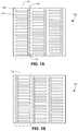
- FIG. 1Ashows an exemplary grid pattern on the front surface of a photovoltaic structure, according to one embodiment.
- grid 102includes three sub-grids, such as sub-grid 104 .
- This three sub-grid configurationallows the photovoltaic structure to be divided into three strips.
- each sub-gridneeds to have an edge busbar, which can be located either at or near the edge.
- each sub-gridincludes an edge busbar (“edge” here refers to the edge of a respective strip) running along the longer edge of the corresponding strip and a plurality of parallel finger lines running in a direction parallel to the shorter edge of the strip.
- sub-grid 104can include edge busbar 106 , and a plurality of finger lines, such as finger lines 108 and 110 .
- a predefined blank spacei.e., space not covered by electrodes
- blank space 112is defined to separate sub-grid 104 from its adjacent sub-grid.
- the width of the blank space, such as blank space 112can be between 0.1 mm and 5 mm, preferably between 0.5 mm and 2 mm. There is a tradeoff between a wider space that leads to a more tolerant scribing operation and a narrower space that leads to more effective current collection. In a further embodiment, the width of such a blank space can be approximately 1 mm.
- FIG. 1Bshows an exemplary grid pattern on the back surface of a photovoltaic structure, according to one embodiment.
- back grid 120can include three sub-grids, such as sub-grid 122 .
- the back sub-gridmay correspond to the front sub-grid.
- the back edge busbarneeds to be located near the opposite edge of the frontside edge busbar.
- the front and back sub-gridshave similar patterns except that the front and back edge busbars are located adjacent to opposite edges of the strip.
- locations of the blank spaces in back conductive grid 120correspond to locations of the blank spaces in front conductive grid 102 , such that the grid lines do not interfere with the subsequent scribe-and-cleave process.
- the finger line patterns on the front and back side of the photovoltaic structuremay be the same or different.
- the finger line patternscan include continuous, non-broken loops.
- finger lines 108 and 110both include connected loops with rounded corners.
- This type of “looped” finger line patterncan reduce the likelihood of the finger lines peeling away from the photovoltaic structure after a long period of usage.
- the sections where parallel lines are joinedcan be wider than the rest of the finger lines to provide more durability and prevent peeling. Patterns other than the one shown in FIGS. 1A and 1B , such as un-looped straight lines or loops with different shapes, are also possible.
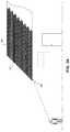
- FIG. 2Ashows a string of cascaded strips, according to one embodiment.
- strips 202 , 204 , and 206are stacked in such a way that strip 206 partially overlaps adjacent strip 204 , which also partially overlaps (on an opposite edge) strip 202 .
- Such a string of stripsforms a pattern that is similar to roof shingles.
- Each stripincludes top and bottom edge busbars located at opposite edges of the top and bottom surfaces, respectively.
- Strips 202 and 204are coupled to each other via an edge busbar 208 located at the top surface of strip 202 and an edge busbar 210 located at the bottom surface of strip 204 .
- strips 202 and 204are placed in such a way that bottom edge busbar 210 is placed on top of and in direct contact with top edge busbar 208 .
- FIG. 2Bshows a side view of the string of cascaded strips, according to one embodiment of the invention.
- the stripscan be part of a six-inch square or pseudo-square photovoltaic structure, with each strip having a dimension of approximately two inches by six inches. To reduce shading, the overlapping between adjacent strips should be kept as small as possible.
- the single busbarsboth at the top and the bottom surfaces
- the same cascaded patterncan extend along an entire row of strips to form a serially connected string.
- FIG. 3Ashows an exemplary configuration of solar roof tiles on a house, according to one embodiment.
- solar roof tiles 300can be installed on a house like conventional roof tiles or shingles, and can provide the functions of conventional roof tiles as well as solar cells.
- a solar roof tilecan be placed along with other tiles in such a way as to prevent water leakage.
- electrical connectionscan be made between two adjacent tiles to interconnect multiple tiles into a module, so that a number of solar roof tiles can jointly provide electrical power.
- FIG. 3Bshows the structure of an exemplary solar roof tile, according to one embodiment.
- Solar roof tile 310can include front cover 312 , back cover 314 , one or more photovoltaic structures 316 , and encapsulant 318 that encapsulates photovoltaic structures 316 between front cover 312 and back cover 314 .
- Front cover 312can be made of tempered glass and back cover 314 can be made of a wide variety of materials, including but not limited to: glass, polyethylene terephthalate (PET), fluoropolymer, polyvinyl fluoride (PVF), polyamide, etc.
- PETpolyethylene terephthalate
- PVFpolyvinyl fluoride
- Front cover 312can be made of tempered glass and back cover 314 can be made of a wide variety of materials, including but not limited to: glass, polyethylene terephthalate (PET), fluoropolymer, polyvinyl fluoride (PVF), polyamide, etc.
- PVFpolyvinyl fluoride
- Front cover 312can be made of tempered glass and back cover 314 can be made of a wide variety of materials, including but not limited to: glass, polyethylene terephthalate (PET), fluoropolymer, polyvinyl fluoride (PVF), polyamide, etc.
- non-transparent backsheetse
- Photovoltaic structures 316can include a number of electrically coupled, either in series or in parallel, photovoltaic strips.
- photovoltaic structures 316can include a plurality of cascaded strips, which are arranged in a way similar to the ones shown in FIGS. 2A-2B .
- FIG. 3Cshows the structure of an exemplary photovoltaic strip, according to one embodiment.
- Photovoltaic strip 320can include crystalline-Si (c-Si) base layer 322 .
- QTBquantum tunneling barrier
- layers 324 and 326can be deposited on both surfaces of base layer 322 .
- thin QTB layercan include a thin layer of silicon oxide (SiO x ), which can be formed on c-Si base layer 322 using a wet oxidation process. More specifically, the QTB layer can include a layer of silicon monoxide (SiO) having a thickness between 1 and 10 nm.
- Photovoltaic strip 320can also include emitter layer 328 , surface field layer 330 , and transparent conductive oxide (TCO) layers 332 and 334 .
- Emitter layer 328can include doped amorphous-Si (a-Si)
- surface field layer 330can include doped c-Si.
- TCO layers 332 and 334can be made of typical TCO materials, including but not limited to: indium tin oxide (ITO), tin-oxide (SnO x ), aluminum doped zinc-oxide (ZnO:Al or AZO), or gallium doped zinc-oxide (ZnO:Ga).
- photovoltaic strip 320can also include edge busbars 336 and 338 that are located on opposite surfaces and edges of photovoltaic strip 320 . Details, including fabrication methods, about the photovoltaic strip can be found in U.S. Pat. No. 8,686,283, entitled “Solar Cell with Oxide Tunneling Junctions,” filed Nov. 12, 2010, the disclosure of which is incorporated by reference in its entirety herein.
- photovoltaic structures 316are encapsulated between front cover 312 and back cover 314 by encapsulant 318 .
- Encapsulant 318typically can include EVA (ethyl vinyl acetate), which can be designed to be transparent (or mostly transparent) to the entire spectrum of visible light.
- a solar roof tileis frameless. This means that encapsulant 318 can be directly exposed to the external environment and moisture can enter the solar roof tile from the edges, as shown by the arrows. In addition, moisture may also enter the roof tile though back cover 314 , if back cover 314 is a backsheet. Once inside the solar roof tile, moisture can gradually penetrate encapsulant 318 to reach photovoltaic structures 316 , because the widely used encapsulant material EVA has a relatively high moisture vapor transmission rate (MVTR).
- MVTRmoisture vapor transmission rate
- Moisture within a solar roof tilecan degrade solar cell performance in multiple ways. For example, metal electrodes may corrode when exposed to moisture for a prolonged period, thus reducing power output. Moreover, once moisture reaches the surfaces of the photovoltaic structure, it may change the TCO properties. For example, ZnO or ITO films may become rough or porous when exposed to moisture for a prolonged time. A rough TCO layer may scatter light, reducing the solar cell efficiency, and a porous TCO film can allow the moisture to reach the solar cell junction, thus significantly degrading the energy conversion efficiency. In addition, moisture absorption in the TCO layer can increase the TCO resistivity, which can also cause reduction in output power. Therefore, moisture protection plays a very important role in ensuring long-term reliability of solar roof tiles.
- encapsulant materialthat is more resistant to moisture.
- Polyolefinhas a low MVTR and can be used as an encapsulant.
- siliconecan provide better moisture protection than EVA.
- both polyolefin and siliconeare more rigid than EVA and often cannot provide adequate protection to photovoltaic structures against shocks and vibrations.
- a hybrid approachis used when choosing the encapsulant material.
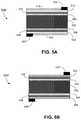
- FIG. 4Ashows the structure of an exemplary solar roof tile, according to one embodiment.
- Solar roof tile 400can include front cover 402 , backsheet 404 , and one or more photovoltaic structures 406 , which are similar to corresponding elements of solar roof tile 310 shown in FIG. 3B .
- solar roof tile 400can include two different types of encapsulant. More specifically, encapsulant layers 408 and 410 can be made of different materials.
- Encapsulant layer 408is situated between photovoltaic structures 406 and backsheet 404 and can include a material having a low MVTR, such as polyolefin.
- encapsulant layer 408can include silicone. Both polyolefin and silicone can effectively prevent moisture ingress from backsheet 404 .
- the moisture-resistant requirement for encapsulant layer 410can be more relaxed, because encapsulant layer 410 is positioned between front glass cover 402 and photovoltaic structures 406 and glass itself can be resistant to moisture ingress. Therefore, encapsulant layer 410 can include EVA, which can be a better shock absorber than polyolefin or silicone.
- FIG. 4Bshows the structure of an exemplary solar roof tile, according to one embodiment.
- photovoltaic structures 426is surrounded by encapsulant layer 428 , which can include EVA.
- encapsulant layer 430wraps around encapsulant layer 428 .
- Encapsulant layer 430can be made of moisture-resistant material, such as polyolefin and silicone and can effectively prevent moisture ingress from edges and the backsheet of solar roof tile 420 . Both encapsulant layers 428 and 430 can facilitate encapsulation of photovoltaic structures between front cover 422 and backsheet 424 .
- TCO layersare often permeable to moisture and can sometimes act as a medium for the moisture to reach the solar cell junction. To prevent degradation of the photovoltaic structures in the presence of moisture, one may need to prevent moisture ingress through the TCO layers.
- a moisture-protection coatingcan be applied onto each TCO layer to serve as a moisture barrier.
- the moisture-protection coatingcan be made of dielectric material, such as silicon oxide (SiO x ) or silicon nitride (SiN x ). Note that, to ensure greater moisture resistance, it is preferred that the SiO x or SiN x films are deposited onto the TCO layers using a plasma-enhanced chemical vapor deposition (PECVD) technique.
- PECVDplasma-enhanced chemical vapor deposition
- FIG. 5Ashows the structure of an exemplary moisture-resistant photovoltaic structure, according to one embodiment.
- Photovoltaic structure 500can include base layer 502 , QTB layers 504 and 506 , emitter layer 508 , surface field layer 510 , TCO layers 512 and 514 , moisture-protection coatings 516 and 518 , and edge busbars 520 and 522 .
- Base layer 502 and QTB layers 504 and 506can be similar to base layer 322 and QTB layers 324 and 326 , respectively, shown in FIG. 3C .
- Emitter layer 508 and surface field layer 510can be similar to emitter layer 328 and surface field layer 330 , respectively, shown in FIG. 3C .
- TCO layers 512 and 514can be similar to TCO layers 332 and 334 , respectively, shown in FIG. 3C . More specifically, TCO layers 512 and 514 can be made of conventional TCO materials, such as ZnO and ITO, and can be sensitive to moisture.
- Moisture-protection coatings 516 and 518can substantially cover the surface of TCO layers 512 and 514 , respectively. More particularly, other than the portions that are in contact with the metal electrode (e.g., the finger lines and the edge busbars), the entire surface of each TCO layer is covered by a moisture-protection coating, thus preventing moisture from reaching the TCO layer.
- Moisture-protection coatings 516 and 518can each include one or more dielectric thin films, such as SiO x or SiN x thin films. For good moisture-protection effect, the thickness of moisture-protection coatings 516 and 518 should be sufficiently thick.
- moisture-protection coatings 516 and 518can have a thickness that is between 50 and 500 nm.
- a Si 3 N 4 film having a thickness of 100 nmcan be deposited onto TCO layers 512 and 514 to form moisture-protection coatings 516 and 518 .
- Various deposition techniquesincluding chemical vapor deposition (CVD) and physical vapor deposition (PVD), can be used to form moisture-protection coatings 516 and 518 .
- CVDchemical vapor deposition
- PVDphysical vapor deposition
- moisture-protection coatings 516 and 518can be deposited onto TCO layers 512 and 514 using a PECVD technique.
- photovoltaic structure 500includes TCO layers as part of the electrical contacts.
- the photovoltaic structures encapsulated inside a solar roof tiledo not have TCO layers. Instead, electrical contacts can be established directly between a metal electrode and the emitter or surface field layer. In such scenarios, a moisture-protecting coating can be deposited onto the emitter or surface field layer. The moisture-protecting coating used here also needs to be patterned to allow electrical coupling between the metal electrode and the emitter or surface field layer.
- a moisture-resistant photovoltaic structureIn addition to applying a moisture-protection coating on the TCO layer to serve as a moisture barrier, in some embodiments, it is also possible to fabricate a moisture-resistant photovoltaic structure by replacing the conventional TCO layers with moisture-resistant TCO layers.
- the moisture-resistant TCO layerscan serve as moisture barriers to prevent moisture from reaching the junction between the base layer and the emitter.
- TCO layers fabricated using conventional techniques or materialscan be sensitive to moisture and can be permeable to moisture. Therefore, a novel fabrication technique or material is needed to obtain moisture-resistant TCO layers.
- ITOsignificantly outperforms ZnO, such as Al:ZnO (also known as AZO).
- ZnOsuch as Al:ZnO
- ITO fabricated under conventional conditionscannot meet the moisture-resistant requirement of solar roof tiles. This is because, under conventional conditions, the grain size of a fabricated ITO layer can be relatively small, thus resulting in a higher permeability to moisture.
- an ITO layer with a larger grain sizee.g., the smallest dimension of the grains is larger than 40 nm
- the ITO layercan undergo a high temperature (e.g., greater than 400° C.) annealing process to obtain larger grain sizes.
- conventional ITO fabrication processesoften involve an annealing temperature at about 250° C., which can result in an ITO layer with smaller grain sizes.
- Si doped ZnOIn addition to increasing the anneal temperature of the ITO, it is also possible to use Si doped ZnO to obtain a moisture-resistant TCO layer.
- Alternative dopantssuch as Ga and In ions, can also be used to dope ZnO to obtain IGZO films. Studies have shown that by tuning the dopant concentration, more particularly the Ga concentration, one can improve the moisture resistance of the IGZO film. In some embodiments, the concentration of In 2 O 3 is increased to at least 10 wt % to obtain a moisture-resistant IGZO film.
- Additional types of moisture-resistant TCO materialcan include indium oxide (In 2 O 3 ) doped with Ti, Ta, or both.
- the moisture-resistant TCO materialcan include TiO 2 doped In 2 O 3 , with the doping concentration (by weight) of TiO 2 in the range between 0.2% and 2%, preferably between 0.5% and 1%.
- the moisture-resistant TCO materialcan include In 2 O 3 doped with both TiO 2 and Ta 2 O 5 , with the doping concentration (by weight) of TiO 2 in the range between 0.2% and 2%, preferably between 0.5% and 1%, and the doping concentration (by weight) of Ta 2 O 5 in the range between 0 and 1%, preferably between 0.2% and 0.6%.
- TCO materialare also possible for enhancing moisture resistance, including but not limited to: ITO with low (e.g., less than 2% by weight) SnO 2 doping, tungsten doped In 2 O 3 (IWO), and cerium doped indium oxide (ICeO).
- ITOwith low (e.g., less than 2% by weight) SnO 2 doping
- IWOtungsten doped In 2 O 3
- ICeOcerium doped indium oxide
- FIG. 5Bshows the structure of an exemplary moisture-resistant photovoltaic structure, according to one embodiment.
- Photovoltaic structure 540can include base layer 542 , QTB layers 544 and 546 , emitter layer 548 , surface field layer 550 , moisture-resistant TCO layers 552 and 554 , and edge busbars 556 and 558 .
- Base layer 542 and QTB layers 544 and 546can be similar to base layer 322 and QTB layers 324 and 326 , respectively, shown in FIG. 3C .
- Emitter layer 548 and surface field layer 550can be similar to emitter layer 328 and surface field layer 330 , respectively, shown in FIG. 3C .
- Moisture-resistant TCO layers 552 and 554can include ITO with a grain size larger than 40 nm, Si doped ZnO, or IGZO with the concentration of In 2 O 3 being greater than 10 wt %. More specifically, the larger grain ITO layers can be fabricated using a low temperature (e.g., less than 200° C.) PVD process followed by a high temperature (e.g., greater than 400° C.) thermal annealing process. When moisture-resistant TCO layers are applied, there is no longer a need for the dielectric moisture-protection coating, thus significantly simplifying the fabrication process. Edge busbars 556 and 558 can be formed on top of moisture-resistant TCO layers 552 and 554 , respectively.
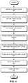
- FIG. 6shows an exemplary fabrication process of a moisture-resistant photovoltaic structure, according to one embodiment.
- a crystalline-Si (c-Si) substratecan be prepared (operation 602 ).
- a standard texturing and cleaning processcan be applied to both surfaces of a crystalline-Si wafer.
- Front and back QTB layerscan then be formed (e.g., using a wet oxidation process) on both surfaces of the c-Si base layer (operation 604 ).
- a layer of hydrogenated amorphous Sia-Si
- a-Sican be deposited on a QTB layer (e.g., the back QTB layer that faces away from sunlight) to form an emitter (operation 606 ).
- the emittertypically has a doping type that is opposite to that of the base layer.
- the emitter layercan have a graded doping profile.
- a different layer of hydrogenated amorphous Si (a-Si)can be deposited on the other QTB layer (e.g., the front QTB layer) to form a surface field layer (operation 608 ).
- the surface field layertypically has a doping type that is the same as that of the base layer.
- front and back TCO layerscan be deposited on the emitter and surface field layers (operation 610 ).
- the front and back TCO layersmay be formed simultaneously.
- the front and back TCO layersmay be formed sequentially.
- a PVD processsuch as evaporation or sputtering, can be used to deposit the TCO layers.
- the TCO layerscan be formed in such a way that they have superior moisture-resistant properties.
- forming the TCO layerscan include depositing, using a low-temperature PVD process, an ITO layer on the emitter or surface field layer, followed by a high temperature thermal annealing process, which can include annealing the ITO at a temperature greater than 400° C.
- forming the TCO layerscan include depositing a Si doped ZnO layer or a Ga and In co-doped ZnO layer on the emitter or surface field layer.
- a patterned moisture-protection coatingcan be formed on each TCO layer (operation 612 ). More specifically, the moisture-protection coating is patterned according to the pattern of the metal grid (e.g., locations of finger lines and busbars). Because the moisture-protection coating is dielectric, to enable electrical coupling between the metal electrode and the TCO layers, the moisture-protection coating needs to be patterned. Various techniques can be used to form the patterned moisture-protection coatings. In some embodiments, a combination of a photolithography process and a PECVD process can be used to form a patterned moisture-protection layer (e.g., a patterned Si 3 N 4 layer). Operation 612 can be optional if the TCO layers have superior moisture-resistant properties.
- Front and back metallic gridsincluding finger lines and busbars can then be formed on the patterned front and back moisture-protection coatings, respectively, to complete the fabrication of the photovoltaic structure (operation 614 ). More specifically, metallic material (e.g., Cu ions) can be deposited into the windows of the patterned moisture-protection coating to form a metallic grid.
- the metallic gridcan include a PVD seed layer and an electroplated bulk layer.
- FIG. 7shows the top view of an exemplary solar roof tile, according to one embodiment.
- solar roof tile 700can include front glass cover 702 and solar cells 704 and 706 .
- Each solar cellcan be a conventional square or pseudo-square solar cell, such as a six-inch solar cell.
- solar cells 704 and 706can each be divided into three separate pieces of similar or different sizes.
- solar cell 704can include strips 708 , 712 , and 712 . These strips can be arranged in such a way that adjacent strips partially overlap at the edges, similar to the ones shown in FIGS. 2A-2B .
- the electrode grids, including the finger lines and edge busbars, of the stripsare not shown in FIG. 7 .
- FIG. 8shows a flowchart illustrating an exemplary fabrication process of a solar roof tile, according to one embodiment.
- a front cover of an appropriate sizecan be obtained (operation 802 ).
- the front covercan be large enough to accommodate at least two 6-inch square solar cells placed side by side.
- the front covercan be made of tempered glass.
- a front encapsulant layercan be placed on the front cover (operation 804 ).
- the front encapsulant layermay include a layer of EVA.
- the front encapsulant layermay include multiple layers of encapsulant material.
- the encapsulant layer that is in direct contact with the photovoltaic structurescan include EVA, whereas the encapsulant layer that is in direct contact with the front cover can include moisture-resistant silicone or polyolefin.
- moisture-resistant photovoltaic stripscan be obtained (operation 806 ).
- the moisture-resistant photovoltaic stripscan include dielectric moisture-protection layers deposited onto conventional TCO layers.
- the moisture-resistant photovoltaic stripscan include moisture-resistant TCO layers.
- the moisture-resistant photovoltaic stripscan include dielectric moisture-protection layers deposited onto the moisture-resistant TCO layers.
- a number of photovoltaic stripscan be electrically and mechanically coupled to form a string (operation 808 ), and a string of photovoltaic strips can be placed on the front encapsulant layer (operation 810 ).
- a solar roof tilemay include one string that comprises six cascaded strips.
- photovoltaic stripscan be obtained by dividing a standard square or pseudo-square solar cell into multiple pieces; and a string of strips can be formed by cascading multiple strips at the edges. The cascading forms a serial connection among the strips.
- a cascaded string of photovoltaic stripscan be found in U.S. patent application Ser. No. 14/826,129, entitled “PHOTOVOLTAIC STRUCTURE CLEAVING SYSTEM,” filed Aug. 13, 2015; U.S. patent application Ser. No. 14/866,776, entitled “SYSTEMS AND METHODS FOR CASCADING PHOTOVOLTAIC STRUCTURES,” filed Sep. 25, 2015; U.S. patent application Ser. No.
- a back encapsulant layercan be placed on the photovoltaic string (operation 812 ). Similar to the front encapsulant layer, the back encapsulant layer can include a single EVA layer or multiple layers of encapsulant material. The encapsulant layer that is in direct contact with the photovoltaic structures can include EVA, whereas the encapsulant layer that is in direct contact with the backsheet can include moisture-resistant silicone or polyolefin. A backsheet can then be placed on the back encapsulant layer (operation 814 ), followed by a lamination process to form a solar roof tile (operation 816 ).
Landscapes
- Engineering & Computer Science (AREA)
- Architecture (AREA)
- Civil Engineering (AREA)
- Structural Engineering (AREA)
- Life Sciences & Earth Sciences (AREA)
- Sustainable Energy (AREA)
- Sustainable Development (AREA)
- Photovoltaic Devices (AREA)
Abstract
Description
Claims (7)
Priority Applications (1)
| Application Number | Priority Date | Filing Date | Title |
|---|---|---|---|
| US15/709,315US10672919B2 (en) | 2017-09-19 | 2017-09-19 | Moisture-resistant solar cells for solar roof tiles |
Applications Claiming Priority (1)
| Application Number | Priority Date | Filing Date | Title |
|---|---|---|---|
| US15/709,315US10672919B2 (en) | 2017-09-19 | 2017-09-19 | Moisture-resistant solar cells for solar roof tiles |
Publications (2)
| Publication Number | Publication Date |
|---|---|
| US20190088802A1 US20190088802A1 (en) | 2019-03-21 |
| US10672919B2true US10672919B2 (en) | 2020-06-02 |
Family
ID=65720607
Family Applications (1)
| Application Number | Title | Priority Date | Filing Date |
|---|---|---|---|
| US15/709,315ActiveUS10672919B2 (en) | 2017-09-19 | 2017-09-19 | Moisture-resistant solar cells for solar roof tiles |
Country Status (1)
| Country | Link |
|---|---|
| US (1) | US10672919B2 (en) |
Cited By (1)
| Publication number | Priority date | Publication date | Assignee | Title |
|---|---|---|---|---|
| US11411528B2 (en)* | 2017-03-31 | 2022-08-09 | Vamsi Krishna GADDAM | Eco-friendly energy generating roofs |
Families Citing this family (5)
| Publication number | Priority date | Publication date | Assignee | Title |
|---|---|---|---|---|
| US10651781B2 (en)* | 2017-08-24 | 2020-05-12 | Corning Incorporated | Glass roof shingle |
| EP3966507B1 (en) | 2019-05-10 | 2024-07-03 | Solartag ApS | A system for mounting glass roof tiles on a roof construction |
| CN111710735B (en)* | 2020-06-29 | 2022-05-24 | 晶科绿能(上海)管理有限公司 | Photovoltaic cell, shingled photovoltaic module, and manufacturing method of photovoltaic cell |
| WO2024108259A1 (en)* | 2022-11-22 | 2024-05-30 | The University Of Sydney | Encapsulated optoelectronic device |
| JP7631573B1 (en) | 2024-01-30 | 2025-02-18 | 株式会社東芝 | Solar cell module and method for manufacturing the solar cell module |
Citations (524)
| Publication number | Priority date | Publication date | Assignee | Title |
|---|---|---|---|---|
| US819360A (en) | 1905-03-22 | 1906-05-01 | Edward Newton A | Electrical switch. |
| US2626907A (en) | 1951-05-14 | 1953-01-27 | Petrolite Corp | Process for breaking petroleum emulsions |
| US2938938A (en) | 1956-07-03 | 1960-05-31 | Hoffman Electronics Corp | Photo-voltaic semiconductor apparatus or the like |
| US3094439A (en) | 1961-07-24 | 1963-06-18 | Spectrolab | Solar cell system |
| US3116171A (en) | 1961-03-14 | 1963-12-31 | Bell Telephone Labor Inc | Satellite solar cell assembly |
| US3459597A (en) | 1966-02-04 | 1969-08-05 | Trw Inc | Solar cells with flexible overlapping bifurcated connector |
| US3676179A (en) | 1968-10-03 | 1972-07-11 | Gulf Oil Corp | Coated article and method for making same |
| US3961997A (en) | 1975-05-12 | 1976-06-08 | The United States Of America As Represented By The Administrator Of The National Aeronautics And Space Administration | Fabrication of polycrystalline solar cells on low-cost substrates |
| US3969163A (en) | 1974-09-19 | 1976-07-13 | Texas Instruments Incorporated | Vapor deposition method of forming low cost semiconductor solar cells including reconstitution of the reacted gases |
| US4015280A (en) | 1974-10-19 | 1977-03-29 | Sony Corporation | Multi-layer semiconductor photovoltaic device |
| US4082568A (en) | 1977-05-10 | 1978-04-04 | Joseph Lindmayer | Solar cell with multiple-metal contacts |
| US4124410A (en) | 1977-11-21 | 1978-11-07 | Union Carbide Corporation | Silicon solar cells with low-cost substrates |
| US4193975A (en) | 1977-11-21 | 1980-03-18 | Union Carbide Corporation | Process for the production of improved refined metallurgical silicon |
| US4200621A (en) | 1978-07-18 | 1980-04-29 | Motorola, Inc. | Sequential purification and crystal growth |
| US4213798A (en) | 1979-04-27 | 1980-07-22 | Rca Corporation | Tellurium schottky barrier contact for amorphous silicon solar cells |
| US4228315A (en) | 1979-05-04 | 1980-10-14 | Rca Corporation | Solar cell grid patterns |
| US4251285A (en) | 1979-08-14 | 1981-02-17 | Westinghouse Electric Corp. | Diffusion of dopant from optical coating and single step formation of PN junction in silicon solar cell and coating thereon |
| US4284490A (en) | 1978-09-28 | 1981-08-18 | Coulter Systems Corporation | R.F. Sputtering apparatus including multi-network power supply |
| US4315096A (en) | 1980-07-25 | 1982-02-09 | Eastman Kodak Company | Integrated array of photovoltaic cells having minimized shorting losses |
| JPS5789269A (en) | 1980-09-26 | 1982-06-03 | Licentia Gmbh | Solar battery unit |
| US4336648A (en) | 1979-11-02 | 1982-06-29 | Licentia Patent-Verwaltungs-G.M.B.H. | Method of contacting a solar cell |
| US4342044A (en) | 1978-03-08 | 1982-07-27 | Energy Conversion Devices, Inc. | Method for optimizing photoresponsive amorphous alloys and devices |
| US4377723A (en) | 1980-05-02 | 1983-03-22 | The University Of Delaware | High efficiency thin-film multiple-gap photovoltaic device |
| US4431858A (en) | 1982-05-12 | 1984-02-14 | University Of Florida | Method of making quasi-grain boundary-free polycrystalline solar cell structure and solar cell structure obtained thereby |
| US4514579A (en) | 1984-01-30 | 1985-04-30 | Energy Conversion Devices, Inc. | Large area photovoltaic cell and method for producing same |
| US4540843A (en) | 1983-03-09 | 1985-09-10 | Licentia Patent-Verwaltungs-Gmbh | Solar cell |
| US4567642A (en) | 1984-09-28 | 1986-02-04 | The Standard Oil Company | Method of making photovoltaic modules |
| US4571448A (en) | 1981-11-16 | 1986-02-18 | University Of Delaware | Thin film photovoltaic solar cell and method of making the same |
| US4577051A (en) | 1984-09-28 | 1986-03-18 | The Standard Oil Company | Bypass diode assembly for photovoltaic modules |
| US4586988A (en) | 1983-08-19 | 1986-05-06 | Energy Conversion Devices, Inc. | Method of forming an electrically conductive member |
| US4589191A (en) | 1983-10-20 | 1986-05-20 | Unisearch Limited | Manufacture of high efficiency solar cells |
| US4612409A (en) | 1981-11-04 | 1986-09-16 | Kanegafuchi Kagaku Kogyo Kabushiki Kaisha | Flexible photovoltaic device |
| US4617421A (en) | 1985-04-01 | 1986-10-14 | Sovonics Solar Systems | Photovoltaic cell having increased active area and method for producing same |
| US4633033A (en) | 1985-02-08 | 1986-12-30 | Energy Conversion Devices, Inc. | Photovoltaic device and method |
| US4652693A (en) | 1985-08-30 | 1987-03-24 | The Standard Oil Company | Reformed front contact current collector grid and cell interconnect for a photovoltaic cell module |
| US4657060A (en) | 1982-03-01 | 1987-04-14 | Graber Industries, Inc. | Vertical venetian blind with inline drive |
| US4667060A (en) | 1985-05-28 | 1987-05-19 | Spire Corporation | Back junction photovoltaic solar cell |
| US4670096A (en) | 1984-05-23 | 1987-06-02 | Bayer Aktiengesellschaft | Process and apparatus for producing semi-conductor foils |
| US4694115A (en) | 1986-11-04 | 1987-09-15 | Spectrolab, Inc. | Solar cell having improved front surface metallization |
| US4729970A (en) | 1986-09-15 | 1988-03-08 | Energy Conversion Devices, Inc. | Conversion process for passivating short circuit current paths in semiconductor devices |
| US4753683A (en) | 1985-09-09 | 1988-06-28 | Hughes Aircraft Company | Gallium arsenide solar cell system |
| US4771017A (en) | 1987-06-23 | 1988-09-13 | Spire Corporation | Patterning process |
| US4784702A (en) | 1986-04-22 | 1988-11-15 | Thomson-Csf | PIN photodiode formed from an amorphous semiconductor |
| US4877460A (en) | 1987-03-17 | 1989-10-31 | Telefunken Electronic Gmbh | Solar cell module |
| US4933061A (en) | 1988-12-29 | 1990-06-12 | Trifari, Krussman & Fishel, Inc. | Electroplating tank |
| US4968384A (en) | 1988-09-29 | 1990-11-06 | Fuji Electric Corporate Research And Development Ltd. | Method of producing carbon-doped amorphous silicon thin film |
| US5053355A (en) | 1989-01-14 | 1991-10-01 | Nukem Gmbh | Method and means for producing a layered system of semiconductors |
| US5057163A (en) | 1988-05-04 | 1991-10-15 | Astropower, Inc. | Deposited-silicon film solar cell |
| WO1991017839A1 (en) | 1990-05-18 | 1991-11-28 | Bp Chemicals (Hitco) Inc. | Materials for chemical vapor deposition processes |
| US5075763A (en) | 1988-09-28 | 1991-12-24 | Kopin Corporation | High temperature metallization system for contacting semiconductor materials |
| WO1991020097A1 (en) | 1990-05-14 | 1991-12-26 | The Boeing Company | Tandem photovoltaic solar cell with iii-v diffused junction booster cell |
| US5084107A (en) | 1989-06-05 | 1992-01-28 | Mitsubishi Denki Kabushiki Kaisha | Solar cell and solar cell array with adhered electrode |
| DE4030713A1 (en) | 1990-09-28 | 1992-04-02 | Telefunken Systemtechnik | Photoelectric solar generator - has flexible intermediate connecting plate designed to prevent solar cell fracture due to temp. change stresses |
| US5118361A (en) | 1990-05-21 | 1992-06-02 | The Boeing Company | Terrestrial concentrator solar cell module |
| US5131933A (en) | 1990-03-23 | 1992-07-21 | Telefunken Systemtechnik Gmbh | Solar cell |
| JPH04245683A (en) | 1991-01-31 | 1992-09-02 | Tonen Corp | Manufacture of solar cell |
| US5155051A (en) | 1990-06-22 | 1992-10-13 | Sanyo Electric Co., Ltd. | Method of manufacturing photovoltaic device |
| US5178685A (en) | 1991-06-11 | 1993-01-12 | Mobil Solar Energy Corporation | Method for forming solar cell contacts and interconnecting solar cells |
| US5181968A (en) | 1991-06-24 | 1993-01-26 | United Solar Systems Corporation | Photovoltaic device having an improved collector grid |
| US5213628A (en) | 1990-09-20 | 1993-05-25 | Sanyo Electric Co., Ltd. | Photovoltaic device |
| US5217539A (en) | 1991-09-05 | 1993-06-08 | The Boeing Company | III-V solar cells and doping processes |
| US5279682A (en) | 1991-06-11 | 1994-01-18 | Mobil Solar Energy Corporation | Solar cell and method of making same |
| US5286306A (en) | 1992-02-07 | 1994-02-15 | Shalini Menezes | Thin film photovoltaic cells from I-III-VI-VII compounds |
| JPH06196766A (en) | 1992-12-24 | 1994-07-15 | Fujitsu Ltd | Superconducting transistor |
| US5364518A (en) | 1991-05-28 | 1994-11-15 | Leybold Aktiengesellschaft | Magnetron cathode for a rotating target |
| US5401331A (en) | 1993-09-07 | 1995-03-28 | Midwest Research Institute | Substrate for thin silicon solar cells |
| JPH07249788A (en) | 1994-03-11 | 1995-09-26 | Tonen Corp | Solar cell |
| US5455430A (en) | 1991-08-01 | 1995-10-03 | Sanyo Electric Co., Ltd. | Photovoltaic device having a semiconductor grade silicon layer formed on a metallurgical grade substrate |
| US5461002A (en) | 1990-05-30 | 1995-10-24 | Safir; Yakov | Method of making diffused doped areas for semiconductor components |
| US5563092A (en) | 1993-04-23 | 1996-10-08 | Canon Kabushiki Kaisha | Method of producing a substrate for an amorphous semiconductor |
| US5576241A (en) | 1994-05-31 | 1996-11-19 | Fuji Electric Co., Ltd. | Method of separating semiconductor wafer with dielectrics |
| US5627081A (en) | 1994-11-29 | 1997-05-06 | Midwest Research Institute | Method for processing silicon solar cells |
| US5676766A (en) | 1993-09-30 | 1997-10-14 | Siemens Aktiengesellschaft | Solar cell having a chalcopyrite absorber layer |
| US5681402A (en) | 1994-11-04 | 1997-10-28 | Canon Kabushiki Kaisha | Photovoltaic element |
| US5698451A (en) | 1988-06-10 | 1997-12-16 | Mobil Solar Energy Corporation | Method of fabricating contacts for solar cells |
| JPH104204A (en) | 1996-06-18 | 1998-01-06 | Sharp Corp | Solar cell manufacturing method |
| US5705828A (en) | 1991-08-10 | 1998-01-06 | Sanyo Electric Co., Ltd. | Photovoltaic device |
| US5726065A (en) | 1995-02-21 | 1998-03-10 | Imec Vzw | Method of preparing solar cell front contacts |
| US5808315A (en) | 1992-07-21 | 1998-09-15 | Semiconductor Energy Laboratory Co., Ltd. | Thin film transistor having transparent conductive film |
| US5814195A (en) | 1995-04-25 | 1998-09-29 | The Boc Group, Inc. | Sputtering system using cylindrical rotating magnetron electrically powered using alternating current |
| JPH1131834A (en) | 1997-07-10 | 1999-02-02 | Showa Shell Sekiyu Kk | Glass sandwich solar panel |
| US5903382A (en) | 1997-12-19 | 1999-05-11 | Rockwell International Corporation | Electrodeposition cell with high light transmission |
| US5935345A (en) | 1994-07-13 | 1999-08-10 | Centre National De La Recherche Scientifique, Etablissement Public A Caractere Scientifique Et Technologique | Process for the production of a photovoltaic material or device, material or device thus obtained, and photocell comprising such a material or device |
| US5942048A (en) | 1994-05-19 | 1999-08-24 | Canon Kabushiki Kaisha | Photovoltaic element electrode structure thereof and process for producing the same |
| US6017581A (en) | 1997-04-18 | 2000-01-25 | Semi-Alloys Company | Method for coating lenticular articles |
| US6034322A (en) | 1999-07-01 | 2000-03-07 | Space Systems/Loral, Inc. | Solar cell assembly |
| CN1253381A (en) | 1998-11-04 | 2000-05-17 | 北京市太阳能研究所 | Efficient solar battery and its making method |
| JP2000164902A (en) | 1998-11-27 | 2000-06-16 | Kyocera Corp | Solar cell |
| US6091019A (en) | 1997-09-26 | 2000-07-18 | Sanyo Electric Co., Ltd. | Photovoltaic element and manufacturing method thereof |
| US6140570A (en) | 1997-10-29 | 2000-10-31 | Canon Kabushiki Kaisha | Photovoltaic element having a back side transparent and electrically conductive layer with a light incident side surface region having a specific cross section and a module comprising said photovolatic element |
| US6232545B1 (en) | 1998-08-06 | 2001-05-15 | Jx Crystals Inc. | Linear circuit designs for solar photovoltaic concentrator and thermophotovoltaic applications using cell and substrate materials with matched coefficients of thermal expansion |
| US20010008143A1 (en) | 1998-05-20 | 2001-07-19 | Makoto Sasaoka | Photovoltaic power generating structure |
| US20010023702A1 (en) | 1998-05-15 | 2001-09-27 | Katsumi Nakagawa | Solar cell module and method of producing the same |
| US6303853B1 (en) | 1998-08-06 | 2001-10-16 | Jx Crystals Inc. | Shingle circuits for thermophotovoltaic systems |
| US6333457B1 (en) | 2000-08-29 | 2001-12-25 | Sunpower Corporation | Edge passivated silicon solar/photo cell and method of manufacture |
| US20020015881A1 (en) | 2000-06-13 | 2002-02-07 | Yoshisada Nakamura | Photoelectric conversion device and photo cell |
| JP2002057357A (en) | 2000-08-11 | 2002-02-22 | Fuji Electric Co Ltd | Thin film solar cell and method of manufacturing the same |
| US20020072207A1 (en) | 2000-12-12 | 2002-06-13 | Hideyuki Andoh | Semiconductor device and manufacturing method thereof |
| US6408786B1 (en) | 1999-09-23 | 2002-06-25 | Lam Research Corporation | Semiconductor processing equipment having tiled ceramic liner |
| US6410843B1 (en) | 1999-11-22 | 2002-06-25 | Sanyo Electric Co., Ltd. | Solar cell module |
| US20020086456A1 (en) | 2000-12-19 | 2002-07-04 | Cunningham Shawn Jay | Bulk micromachining process for fabricating an optical MEMS device with integrated optical aperture |
| US6441297B1 (en) | 1998-03-13 | 2002-08-27 | Steffen Keller | Solar cell arrangement |
| US6468828B1 (en) | 1998-07-14 | 2002-10-22 | Sky Solar L.L.C. | Method of manufacturing lightweight, high efficiency photovoltaic module |
| US20020176404A1 (en) | 2001-04-13 | 2002-11-28 | Girard Gregory D. | Distributed edge switching system for voice-over-packet multiservice network |
| US6488824B1 (en) | 1998-11-06 | 2002-12-03 | Raycom Technologies, Inc. | Sputtering apparatus and process for high rate coatings |
| US20020189939A1 (en) | 2001-06-14 | 2002-12-19 | German John R. | Alternating current rotatable sputter cathode |
| US20030000568A1 (en) | 2001-06-15 | 2003-01-02 | Ase Americas, Inc. | Encapsulated photovoltaic modules and method of manufacturing same |
| US20030000571A1 (en) | 2001-06-13 | 2003-01-02 | Junzou Wakuda | Solar cell and method of producing the same |
| US20030034062A1 (en) | 2001-08-17 | 2003-02-20 | Stern Theodore Garry | Electrostatically clean solar array |
| US20030042516A1 (en) | 2001-08-30 | 2003-03-06 | Micron Technology, Inc. | Technique to control tunneling currents in dram capacitors, cells, and devices |
| US6538193B1 (en) | 2000-04-21 | 2003-03-25 | Jx Crystals Inc. | Thermophotovoltaic generator in high temperature industrial process |
| US20030070705A1 (en) | 2001-10-11 | 2003-04-17 | Hayden Herbert T. | Structure for supporting a photovoltaic module in a solar energy collection system |
| US6552414B1 (en) | 1996-12-24 | 2003-04-22 | Imec Vzw | Semiconductor device with selectively diffused regions |
| CN1416179A (en) | 2001-10-31 | 2003-05-07 | 四川大学 | Silicon solar cell of nesa with transparent conductive folm front electrode |
| US20030097447A1 (en) | 2001-10-25 | 2003-05-22 | Johnston Alan B. | Bridging user agent and a proxy server for supporting network services |
| US20030118865A1 (en) | 2001-08-27 | 2003-06-26 | Marks Tobin J. | High work function transparent conducting oxides as anodes for organic light-emitting diodes |
| US20030116185A1 (en) | 2001-11-05 | 2003-06-26 | Oswald Robert S. | Sealed thin film photovoltaic modules |
| US6586270B2 (en) | 2000-06-01 | 2003-07-01 | Canon Kabushiki Kaisha | Process for producing a photovoltaic element |
| US20030121228A1 (en) | 2001-12-31 | 2003-07-03 | Stoehr Robert P. | System and method for dendritic web solar cell shingling |
| US20030136440A1 (en) | 2000-03-13 | 2003-07-24 | Akio Machida | Optical energy transducer |
| US20030168578A1 (en) | 2001-11-29 | 2003-09-11 | Mikio Taguchi | Photovoltaic device and manufacturing method thereof |
| US6620645B2 (en) | 2000-11-16 | 2003-09-16 | G.T. Equipment Technologies, Inc | Making and connecting bus bars on solar cells |
| US20030183270A1 (en) | 2000-08-31 | 2003-10-02 | Fritz Falk | Multicrystalline laser-crystallized silicon thin layer solar cell deposited on a glass substrate |
| WO2003083953A1 (en) | 2002-03-29 | 2003-10-09 | Ebara Corporation | Solar cell and method of manufacturing the same |
| US20030201007A1 (en) | 2002-04-24 | 2003-10-30 | Fraas Lewis M. | Planar solar concentrator power module |
| US6672018B2 (en) | 2001-10-12 | 2004-01-06 | Jefferson Shingleton | Solar module mounting method and clip |
| US6683360B1 (en) | 2002-01-24 | 2004-01-27 | Fillfactory | Multiple or graded epitaxial wafers for particle or radiation detection |
| US20040035458A1 (en) | 2002-08-20 | 2004-02-26 | Kevin Beernink | Series connected photovoltaic module and method for its manufacture |
| US20040065363A1 (en) | 2002-10-02 | 2004-04-08 | The Boeing Company | Isoelectronic surfactant induced sublattice disordering in optoelectronic devices |
| US6736948B2 (en) | 2002-01-18 | 2004-05-18 | Von Ardenne Anlagentechnik Gmbh | Cylindrical AC/DC magnetron with compliant drive system and improved electrical and thermal isolation |
| US20040094196A1 (en)* | 2000-04-27 | 2004-05-20 | Sean Shaheen | Photovoltaic cell |
| US20040103937A1 (en) | 2002-09-09 | 2004-06-03 | Interuniversitair Microelektronica Centrum (Imec) | Photovoltaic device |
| US20040112419A1 (en) | 2001-03-21 | 2004-06-17 | Bernard Boulanger | Solar panel having electrical terminals distributed across the surface thereof |
| US20040112426A1 (en) | 2002-12-11 | 2004-06-17 | Sharp Kabushiki Kaisha | Solar cell and method of manufacturing the same |
| US20040123897A1 (en) | 2001-03-19 | 2004-07-01 | Satoyuki Ojima | Solar cell and its manufacturing method |
| US20040126213A1 (en) | 2001-05-18 | 2004-07-01 | Arthur Pelzmann | Device for accommodating disk-shaped objects and apparatus for handling objects |
| US6761771B2 (en) | 2000-10-19 | 2004-07-13 | Asm Japan K.K. | Semiconductor substrate-supporting apparatus |
| US20040135979A1 (en) | 2003-01-13 | 2004-07-15 | Nikon Corporation | Vibration-attenuation devices and methods using pressurized bellows exhibiting substantially zero lateral stiffness |
| US20040152326A1 (en) | 2003-01-28 | 2004-08-05 | Kyocera Corporation | Multicrystalline silicon substrate and process for roughening surface thereof |
| US20040185683A1 (en) | 2003-03-20 | 2004-09-23 | Hiroki Nakamura | Wiring, display device and method of manufacturing the same |
| US20040200520A1 (en) | 2003-04-10 | 2004-10-14 | Sunpower Corporation | Metal contact structure for solar cell and method of manufacture |
| US6841051B2 (en) | 2002-03-14 | 2005-01-11 | Sputtering Components, Inc. | High-power ion sputtering magnetron |
| US20050009319A1 (en) | 2003-07-08 | 2005-01-13 | Kazuhide Abe | Method of forming buried wiring in semiconductor device |
| US20050012095A1 (en) | 2003-06-26 | 2005-01-20 | Kyocera Corporation | Semiconductor/electrode contact structure and semiconductor device using the same |
| US20050022746A1 (en) | 2003-08-01 | 2005-02-03 | Sgl Carbon, Llc | Holder for supporting wafers during semiconductor manufacture |
| US20050022861A1 (en) | 2003-08-01 | 2005-02-03 | Rose Douglas H. | Etching of solar cell materials |
| US20050062041A1 (en) | 2003-09-24 | 2005-03-24 | Sanyo Electric Co., Ltd. | Photovoltaic cell and method of fabricating the same |
| US20050064247A1 (en) | 2003-06-25 | 2005-03-24 | Ajit Sane | Composite refractory metal carbide coating on a substrate and method for making thereof |
| US20050061665A1 (en) | 2003-08-06 | 2005-03-24 | Sunpower Corporation | Substrate carrier for electroplating solar cells |
| US20050074954A1 (en) | 2002-10-11 | 2005-04-07 | Hideo Yamanaka | Method and apparatus for producing ultra-thin semiconductor chip and method and apparatus for producing ultra-thin back-illuminated solid-state image pickup device |
| JP2005122721A (en) | 2003-09-25 | 2005-05-12 | Fuji Photo Film Co Ltd | Image processing method, apparatus, and program |
| US20050109388A1 (en) | 2003-11-05 | 2005-05-26 | Canon Kabushiki Kaisha | Photovoltaic device and manufacturing method thereof |
| US20050126622A1 (en) | 2003-12-11 | 2005-06-16 | Canon Kabushiki Kaisha | Solar cell module and method of producing the same |
| JP2005159312A (en) | 2003-11-05 | 2005-06-16 | Canon Inc | Base material for polycrystalline silicon substrate for solar cell and polycrystalline silicon substrate for solar cell |
| US20050133084A1 (en) | 2003-10-10 | 2005-06-23 | Toshio Joge | Silicon solar cell and production method thereof |
| US6917755B2 (en) | 2003-02-27 | 2005-07-12 | Applied Materials, Inc. | Substrate support |
| US20050172996A1 (en)* | 2004-02-05 | 2005-08-11 | Advent Solar, Inc. | Contact fabrication of emitter wrap-through back contact silicon solar cells |
| US20050178662A1 (en) | 2002-03-22 | 2005-08-18 | Dieter Wurczinger | Rotating tubular cathode |
| US20050189015A1 (en) | 2003-10-30 | 2005-09-01 | Ajeet Rohatgi | Silicon solar cells and methods of fabrication |
| US20050199279A1 (en) | 2004-01-29 | 2005-09-15 | Sanyo Electric Co., Ltd. | Solar cell module |
| US20050252544A1 (en) | 2004-05-11 | 2005-11-17 | Ajeet Rohatgi | Silicon solar cells and methods of fabrication |
| US20050257823A1 (en) | 2004-05-19 | 2005-11-24 | Dutch Space B.V. | Solar cell assembly |
| US20050263178A1 (en) | 2004-06-01 | 2005-12-01 | Alan Montello | Photovoltaic module architecture |
| US20050268963A1 (en) | 2004-02-24 | 2005-12-08 | David Jordan | Process for manufacturing photovoltaic cells |
| WO2006003277A1 (en) | 2004-06-04 | 2006-01-12 | Aventis Pharma S.A. | Aromatic biaryl products, compositions containing same and use as medicines |
| US20060012000A1 (en) | 2001-05-21 | 2006-01-19 | Estes Michael J | Thin-film transistors based on tunneling structures and applications |
| US20060060238A1 (en) | 2004-02-05 | 2006-03-23 | Advent Solar, Inc. | Process and fabrication methods for emitter wrap through back contact solar cells |
| US20060060791A1 (en) | 2004-09-08 | 2006-03-23 | Nikon Corporation | Bellows with spring anti-gravity device |
| US7030413B2 (en) | 2000-09-05 | 2006-04-18 | Sanyo Electric Co., Ltd. | Photovoltaic device with intrinsic amorphous film at junction, having varied optical band gap through thickness thereof |
| US20060130891A1 (en) | 2004-10-29 | 2006-06-22 | Carlson David E | Back-contact photovoltaic cells |
| US20060154389A1 (en) | 2005-01-11 | 2006-07-13 | Doan Trung T | Light emitting diode with conducting metal substrate |
| KR20060097189A (en) | 2005-03-04 | 2006-09-14 | 삼성전자주식회사 | Semiconductor device manufacturing equipment |
| US20060213548A1 (en) | 2005-03-22 | 2006-09-28 | Applied Materials, Inc. | Scalable photovoltaic cell and solar panel manufacturing with improved wiring |
| US20060231803A1 (en) | 2005-04-14 | 2006-10-19 | Yueli Wang | Electroconductive thick film composition(s), electrode(s), and semiconductor device(s) formed therefrom |
| US20060255340A1 (en) | 2005-05-12 | 2006-11-16 | Venkatesan Manivannan | Surface passivated photovoltaic devices |
| US20060260673A1 (en) | 2003-10-17 | 2006-11-23 | Canon Kabushiki Kaisha | Photovoltaic element and method of producing photovoltaic element |
| JP2006324504A (en) | 2005-05-19 | 2006-11-30 | Shin Etsu Handotai Co Ltd | Solar cell |
| US20060272698A1 (en) | 2005-06-06 | 2006-12-07 | Durvasula Ravi S | Photovoltaic concentrator for solar energy system |
| US20060283496A1 (en) | 2005-06-16 | 2006-12-21 | Sanyo Electric Co., Ltd. | Method for manufacturing photovoltaic module |
| US20060283499A1 (en) | 2005-02-25 | 2006-12-21 | Sanyo Electric Co., Ltd. | Photovoltaic cell |
| US7164150B2 (en) | 2002-03-05 | 2007-01-16 | Sanyo Electric Co., Ltd. | Photovoltaic device and manufacturing method thereof |
| US20070023082A1 (en) | 2005-07-28 | 2007-02-01 | Venkatesan Manivannan | Compositionally-graded back contact photovoltaic devices and methods of fabricating such devices |
| US20070023081A1 (en) | 2005-07-28 | 2007-02-01 | General Electric Company | Compositionally-graded photovoltaic device and fabrication method, and related articles |
| US20070029186A1 (en)* | 2005-08-02 | 2007-02-08 | Alexey Krasnov | Method of thermally tempering coated article with transparent conductive oxide (TCO) coating using inorganic protective layer during tempering and product made using same |
| EP1770791A1 (en) | 2005-09-30 | 2007-04-04 | Sanyo Electric Co., Ltd. | Rectangular shaped solar cell module and its manufacturing method using hexagonal shaped unit solar cells |
| US20070110975A1 (en) | 2003-12-09 | 2007-05-17 | Schunk Kohlensteofftechnik Gmbh | Carrier for receiving an object and method for the production of a carrier |
| US20070108437A1 (en) | 1998-06-08 | 2007-05-17 | Avto Tavkhelidze | Method of fabrication of high temperature superconductors based on new mechanism of electron-electron interaction |
| JP2007123792A (en) | 2005-09-28 | 2007-05-17 | Kyocera Corp | Solar cell module |
| US20070132034A1 (en) | 2005-12-14 | 2007-06-14 | Giuseppe Curello | Isolation body for semiconductor devices and method to form the same |
| US20070137699A1 (en) | 2005-12-16 | 2007-06-21 | General Electric Company | Solar cell and method for fabricating solar cell |
| US20070148336A1 (en) | 2005-11-07 | 2007-06-28 | Robert Bachrach | Photovoltaic contact and wiring formation |
| EP1816684A2 (en) | 2006-02-01 | 2007-08-08 | Sanyo Electric Co. Ltd. | Solar battery module |
| US20070186970A1 (en) | 2003-05-09 | 2007-08-16 | Masatoshi Takahashi | Solar cell and method of fabricating the same |
| US20070186968A1 (en) | 2006-01-24 | 2007-08-16 | Atsushi Nakauchi | Photovoltaic Module |
| US20070187652A1 (en) | 2005-12-21 | 2007-08-16 | Takuya Konno | Paste for solar cell electrodes, method for the manufacture of solar cell electrodes, and the solar cell |
| US20070186853A1 (en) | 2006-02-10 | 2007-08-16 | Veeco Instruments Inc. | System and method for varying wafer surface temperature via wafer-carrier temperature offset |
| DE102006009194A1 (en) | 2006-02-22 | 2007-08-23 | Siegfried Gutfleisch | Arrangement of primary building structure e.g. photo-voltaic cell, consists of pre-mounted unit, with which structure of solar cell with respective segment of building structure forms assembly unit |
| US20070202029A1 (en) | 2003-12-04 | 2007-08-30 | Gary Burns | Method Of Removing Impurities From Metallurgical Grade Silicon To Produce Solar Grade Silicon |
| US20070235077A1 (en) | 2006-03-27 | 2007-10-11 | Kyocera Corporation | Solar Cell Module and Manufacturing Process Thereof |
| US20070235829A1 (en) | 2005-02-11 | 2007-10-11 | Levine Peter A | Dark Current Reduction in Back-Illuminated Imaging Sensors and Method of Fabricating Same |
| US20070256728A1 (en) | 2006-05-04 | 2007-11-08 | Sunpower Corporation | Solar cell having doped semiconductor heterojunction contacts |
| US20070274504A1 (en) | 2006-05-12 | 2007-11-29 | Oracle International Corporation | Customized sip routing to cross firewalls |
| US20070283997A1 (en) | 2006-06-13 | 2007-12-13 | Miasole | Photovoltaic module with integrated current collection and interconnection |
| US20070283996A1 (en) | 2006-06-13 | 2007-12-13 | Miasole | Photovoltaic module with insulating interconnect carrier |
| US20080000522A1 (en) | 2006-06-30 | 2008-01-03 | General Electric Company | Photovoltaic device which includes all-back-contact configuration; and related processes |
| US20080006323A1 (en)* | 2006-07-08 | 2008-01-10 | Kalkanoglu Husnu M | Photovoltaic Module |
| US20080011350A1 (en) | 1999-03-30 | 2008-01-17 | Daniel Luch | Collector grid, electrode structures and interconnect structures for photovoltaic arrays and other optoelectric devices |
| US7328534B2 (en) | 2002-02-20 | 2008-02-12 | Sunpower Corporation, Systems | Shingle system |
| US20080035489A1 (en) | 2006-06-05 | 2008-02-14 | Rohm And Haas Electronic Materials Llc | Plating process |
| US20080041437A1 (en) | 2006-06-23 | 2008-02-21 | Sharp Kabushiki Kaisha | Photoelectric conversion element and interconnector-equipped photoelectric conversion element |
| US20080041436A1 (en) | 2006-08-16 | 2008-02-21 | Lau Po K | Bifacial photovoltaic devices |
| US20080047604A1 (en) | 2006-08-25 | 2008-02-28 | General Electric Company | Nanowires in thin-film silicon solar cells |
| US20080047602A1 (en) | 2006-08-22 | 2008-02-28 | Guardian Industries Corp. | Front contact with high-function TCO for use in photovoltaic device and method of making same |
| US20080053519A1 (en) | 2006-08-30 | 2008-03-06 | Miasole | Laminated photovoltaic cell |
| US20080061293A1 (en) | 2005-01-20 | 2008-03-13 | Commissariat A'energie Atomique | Semiconductor Device with Heterojunctions and an Inter-Finger Structure |
| US20080092942A1 (en) | 2006-10-13 | 2008-04-24 | The Boeing Company | Front contact design for high-intensity solar cells and optical power converters |
| US20080092947A1 (en) | 2006-10-24 | 2008-04-24 | Applied Materials, Inc. | Pulse plating of a low stress film on a solar cell substrate |
| US20080121276A1 (en) | 2006-11-29 | 2008-05-29 | Applied Materials, Inc. | Selective electroless deposition for solar cells |
| US20080121932A1 (en) | 2006-09-18 | 2008-05-29 | Pushkar Ranade | Active regions with compatible dielectric layers |
| US20080121272A1 (en) | 2006-11-27 | 2008-05-29 | Besser David A | System and apparatuses with multiple power extractors coupled to different power sources |
| US20080128013A1 (en) | 2006-12-01 | 2008-06-05 | Applied Materials, Inc. | Electroplating on roll-to-roll flexible solar cell substrates |
| US20080128017A1 (en) | 2004-06-24 | 2008-06-05 | Heliodynamics Limited | Solar Energy Collection Systems |
| JP2008135655A (en) | 2006-11-29 | 2008-06-12 | Sanyo Electric Co Ltd | Solar battery module, manufacturing method therefor, and solar battery cell |
| US20080149163A1 (en) | 2004-08-31 | 2008-06-26 | Ron Gangemi | System and method for mounting photovoltaic cells |
| US20080149161A1 (en) | 2006-12-25 | 2008-06-26 | Sanyo Electric Co., Ltd. | Solar cell and solar cell module |
| US20080156370A1 (en) | 2005-04-20 | 2008-07-03 | Hahn-Meitner-Institut Berlin Gmbh | Heterocontact Solar Cell with Inverted Geometry of its Layer Structure |
| DE202007002897U1 (en) | 2007-02-28 | 2008-07-10 | SCHÜCO International KG | Photovoltaic solar module |
| US7399385B2 (en) | 2001-06-14 | 2008-07-15 | Tru Vue, Inc. | Alternating current rotatable sputter cathode |
| US20080173347A1 (en) | 2007-01-23 | 2008-07-24 | General Electric Company | Method And Apparatus For A Semiconductor Structure |
| US20080173350A1 (en) | 2007-01-18 | 2008-07-24 | Applied Materials, Inc. | Multi-junction solar cells and methods and apparatuses for forming the same |
| US20080178928A1 (en) | 2006-12-29 | 2008-07-31 | Bp Corporation North America Inc. | Photovoltaic Modules with a Transparent Material Having a Camouflaged Pattern |
| WO2008089657A1 (en) | 2007-01-17 | 2008-07-31 | Binxuan Yi | Solar cell and method for reducing the serial resistance of solar cells |
| US20080196757A1 (en) | 2007-02-19 | 2008-08-21 | Sanyo Electric Co., Ltd. | Solar cell and solar cell module |
| US20080202577A1 (en) | 2007-02-16 | 2008-08-28 | Henry Hieslmair | Dynamic design of solar cell structures, photovoltaic modules and corresponding processes |
| US20080202582A1 (en) | 2004-01-15 | 2008-08-28 | Japan Science And Technology Agency | Process for Producing Monocrystal Thin Film and Monocrystal Thin Film Device |
| US20080216891A1 (en) | 2007-03-05 | 2008-09-11 | Seagate Technology Llc | Quantum dot sensitized wide bandgap semiconductor photovoltaic devices & methods of fabricating same |
| US20080223439A1 (en) | 2004-02-19 | 2008-09-18 | Xunming Deng | Interconnected Photoelectrochemical Cell |
| US20080230122A1 (en) | 2007-03-19 | 2008-09-25 | Sanyo Electric Co., Ltd. | Photvoltaic device and method of manufacturing the same |
| US20080251117A1 (en) | 2005-03-14 | 2008-10-16 | Markus Schubert | Solar Cell |
| US20080251114A1 (en) | 2005-03-29 | 2008-10-16 | Kyocera Corporation | Method For Packing Solar Battery Elements and Package For Solar Battery Elements |
| US20080264477A1 (en) | 2006-10-09 | 2008-10-30 | Soltaix, Inc. | Methods for manufacturing three-dimensional thin-film solar cells |
| US20080276983A1 (en) | 2005-11-04 | 2008-11-13 | Robert Andrew Drake | Encapsulation of Photovoltaic Cells |
| US20080283115A1 (en) | 2004-01-28 | 2008-11-20 | Yuko Fukawa | Solar Battery Module and Photovoltaic Generation Device |
| US20080302030A1 (en) | 2007-05-07 | 2008-12-11 | Robert Stancel | Structures for Low Cost, Reliable Solar Roofing |
| US20080303503A1 (en) | 2004-07-13 | 2008-12-11 | Central Queensland University | Device For Distributed Maximum Power Tracking For Solar Arrays |
| US20080308145A1 (en) | 2007-06-12 | 2008-12-18 | Guardian Industries Corp | Front electrode including transparent conductive coating on etched glass substrate for use in photovoltaic device and method of making same |
| US20090014055A1 (en) | 2006-03-18 | 2009-01-15 | Solyndra, Inc. | Photovoltaic Modules Having a Filling Material |
| WO2009011519A1 (en) | 2007-07-13 | 2009-01-22 | Byung Hak Lee | Pencil lead sharpeners |
| US20090056805A1 (en) | 2007-08-28 | 2009-03-05 | Blue Square Energy Incorporated | Photovoltaic Thin-Film Solar Cell and Method Of Making The Same |
| JP2009054748A (en) | 2007-08-27 | 2009-03-12 | Sanyo Electric Co Ltd | SOLAR CELL MODULE, SOLAR CELL, AND MANUFACTURING METHOD THEREOF |
| US20090065043A1 (en) | 2006-02-22 | 2009-03-12 | Jean-Christophe Hadorn | Method of coupling photovoltaic cells and film for implementing it |
| US20090078318A1 (en) | 2007-09-25 | 2009-03-26 | First Solar, Inc. | Photovoltaic Devices Including An Interfacial Layer |
| US20090084439A1 (en) | 2007-10-02 | 2009-04-02 | Chang Gung University | TCO-based hybrid solar photovoltaic energy conversion apparatus |
| US20090101872A1 (en) | 2007-10-18 | 2009-04-23 | E.I. Du Pont De Nemours And Company | LEAD-FREE CONDUCTIVE COMPOSITIONS AND PROCESSES FOR USE IN THE MANUFACTURE OF SEMICONDUCTOR DEVICES: Mg-CONTAINING ADDITIVE |
| US20090120492A1 (en) | 2007-11-09 | 2009-05-14 | Ashok Sinha | Low-cost solar cells and methods for their production |
| US7534632B2 (en) | 2007-02-20 | 2009-05-19 | Advanced Chip Engineering Technology Inc. | Method for circuits inspection and method of the same |
| US20090139512A1 (en) | 2007-11-30 | 2009-06-04 | Lima Daniel D De | Solar Line Boiler Roof |
| EP2071635A2 (en) | 2007-12-11 | 2009-06-17 | HEIc Hornbachner Energie Innovation Consulting GmbH | Cambered photovoltaic module and method for its manufacture |
| US20090155028A1 (en) | 2007-12-12 | 2009-06-18 | Veeco Instruments Inc. | Wafer carrier with hub |
| US20090151783A1 (en) | 2007-12-13 | 2009-06-18 | Chun-Hsiung Lu | Translucent solar cell and manufacturing method thereof |
| US20090151771A1 (en) | 2007-12-17 | 2009-06-18 | Qualcomm Mems Technologies, Inc. | Photovoltaics with interferometric ribbon masks |
| US20090160259A1 (en) | 2007-12-21 | 2009-06-25 | Wi-Chi, Inc. | Distributed Energy Conversion Systems |
| WO2009094578A2 (en) | 2008-01-24 | 2009-07-30 | Applied Materials, Inc. | Improved hit solar cell structure |
| US20090188561A1 (en) | 2008-01-25 | 2009-07-30 | Emcore Corporation | High concentration terrestrial solar array with III-V compound semiconductor cell |
| US20090194233A1 (en) | 2005-06-23 | 2009-08-06 | Tokyo Electron Limited | Component for semicondutor processing apparatus and manufacturing method thereof |
| JP2009177225A (en) | 2009-05-15 | 2009-08-06 | Sharp Corp | Thin film solar cell module |
| US20090211627A1 (en)* | 2008-02-25 | 2009-08-27 | Suniva, Inc. | Solar cell having crystalline silicon p-n homojunction and amorphous silicon heterojunctions for surface passivation |
| US20090221111A1 (en) | 2008-02-28 | 2009-09-03 | Sunlight Photonics Inc. | Method and apparatus for fabricating composite substrates for thin film electro-optical devices |
| US20090229854A1 (en) | 2005-11-18 | 2009-09-17 | Replisaurus Technologies Ab | Electrode and method of forming the electrode |
| US20090229660A1 (en) | 2008-03-11 | 2009-09-17 | Seiko Epson Corporation | Solar cell and method for manufacturing the same |
| US20090239331A1 (en) | 2008-03-24 | 2009-09-24 | Palo Alto Research Center Incorporated | Methods for forming multiple-layer electrode structures for silicon photovoltaic cells |
| US20090250108A1 (en) | 2008-04-02 | 2009-10-08 | Applied Materials, Inc. | Silicon carbide for crystalline silicon solar cell surface passivation |
| US20090255574A1 (en) | 2008-04-14 | 2009-10-15 | Sierra Solar Power, Inc. | Solar cell fabricated by silicon liquid-phase deposition |
| US20090260689A1 (en) | 2008-02-13 | 2009-10-22 | Hitachi Cable, Ltd. | Solar cell lead wire, method of making the same, and solar cell |
| EP2113946A2 (en) | 2008-04-30 | 2009-11-04 | General Electric Company | Compositionally-graded and structurally-graded photovoltaic devices and methods of fabricating such devices |
| US20090272419A1 (en) | 2006-12-26 | 2009-11-05 | Kyocera Corporation | Solar Cell Module |
| US20090277491A1 (en) | 2005-10-14 | 2009-11-12 | Sharp Kabushiki Kaisha | Solar Cell, Interconnector-Equipped Solar Cell, Solar Cell String And Solar Cell Module |
| US20090283138A1 (en) | 2008-05-19 | 2009-11-19 | Tatung Company | High performance optoelectronic device |
| US20090283145A1 (en) | 2008-05-13 | 2009-11-19 | Kim Yun-Gi | Semiconductor Solar Cells Having Front Surface Electrodes |
| US20090293948A1 (en) | 2008-05-28 | 2009-12-03 | Stichting Energieonderzoek Centrum Nederland | Method of manufacturing an amorphous/crystalline silicon heterojunction solar cell |
| US20090301549A1 (en) | 2006-10-09 | 2009-12-10 | Soltaix, Inc. | Solar module structures and assembly methods for three-dimensional thin-film solar cells |
| WO2009150654A2 (en) | 2008-06-12 | 2009-12-17 | Yissum Research Development Company | Solar volumetric structure |
| US20090308439A1 (en) | 2008-06-11 | 2009-12-17 | Solar Implant Technologies Inc. | Solar cell fabrication using implantation |
| US7635810B2 (en) | 1999-03-30 | 2009-12-22 | Daniel Luch | Substrate and collector grid structures for integrated photovoltaic arrays and process of manufacture of such arrays |
| US20090317934A1 (en) | 2006-09-05 | 2009-12-24 | Maximilian Scherff | Local heterostructure contacts |
| US20090320897A1 (en) | 2008-06-26 | 2009-12-31 | Semiconductor Energy Laboratory Co., Ltd. | Photoelectric conversion device module and manufacturing method of the photoelectric conversion device module |
| CN100580957C (en) | 2007-12-28 | 2010-01-13 | 中国科学院上海技术物理研究所 | Metastable assisted quantum dot resonant tunneling diode and its working conditions |
| US20100006145A1 (en) | 2008-07-08 | 2010-01-14 | Synos Technology, Inc. | Solar cell and fabricating method for the same |
| US20100015756A1 (en) | 2008-07-16 | 2010-01-21 | Applied Materials, Inc. | Hybrid heterojunction solar cell fabrication using a doping layer mask |
| US20100043863A1 (en) | 2008-03-20 | 2010-02-25 | Miasole | Interconnect assembly |
| DE102008045522A1 (en) | 2008-09-03 | 2010-03-04 | Fraunhofer-Gesellschaft zur Förderung der angewandten Forschung e.V. | Hetero-solar cell and process for the preparation of hetero-solar cells |
| US20100065111A1 (en) | 2008-09-16 | 2010-03-18 | Sierra Solar Power, Inc. | Solar cells fabricated by using cvd epitaxial si films on metallurgical-grade si wafers |
| US20100068890A1 (en) | 2006-10-30 | 2010-03-18 | Merck Patent Gesellschaft | Printable medium for etching oxidic, transparent and conductive layers |
| US20100084009A1 (en) | 2007-03-16 | 2010-04-08 | Bp Corporation North America Inc. | Solar Cells |
| US20100087031A1 (en) | 2006-09-26 | 2010-04-08 | Commissariat A L'energie Atomique | Method of producing a photovoltaic cell with a heterojunction on the rear face |
| JP2010085949A (en) | 2008-10-03 | 2010-04-15 | Hitachi Displays Ltd | Liquid crystal display |
| US20100108134A1 (en) | 2008-10-31 | 2010-05-06 | Crystal Solar, Inc. | Thin two sided single crystal solar cell and manufacturing process thereof |
| US20100116325A1 (en) | 2008-11-12 | 2010-05-13 | Mehrdad Nikoonahad | High efficiency solar panel and system |
| US20100124619A1 (en) | 2008-11-14 | 2010-05-20 | Palo Alto Research Center Incorporated | Solar cell metallization using inline electroless plating |
| US20100131108A1 (en) | 2008-01-18 | 2010-05-27 | Tenksolar, Inc | Thin-film photovoltaic module |
| US20100132774A1 (en) | 2008-12-11 | 2010-06-03 | Applied Materials, Inc. | Thin Film Silicon Solar Cell Device With Amorphous Window Layer |
| US20100132792A1 (en) | 2008-11-19 | 2010-06-03 | Sunho Kim | Solar cell and method of manufacturing the same |
| US20100147364A1 (en) | 2008-12-16 | 2010-06-17 | Solopower, Inc. | Thin film photovoltaic module manufacturing methods and structures |
| WO2010070015A1 (en) | 2008-12-19 | 2010-06-24 | Q-Cells Se | Solar cell |
| US20100154869A1 (en) | 2008-12-24 | 2010-06-24 | Min-Seok Oh | Photoelectric conversion device and manufacturing method thereof |
| US20100169478A1 (en) | 2008-12-29 | 2010-07-01 | Genband Inc. | Systems, methods, and computer program products for adaptively adjusting a registration interval of an endpoint |
| US7749883B2 (en) | 2007-09-20 | 2010-07-06 | Fry's Metals, Inc. | Electroformed stencils for solar cell front side metallization |
| WO2010075606A1 (en) | 2008-12-29 | 2010-07-08 | Shaun Joseph Cunningham | Improved photo-voltaic device |
| US20100175743A1 (en) | 2009-01-09 | 2010-07-15 | Solopower, Inc. | Reliable thin film photovoltaic module structures |
| US20100186802A1 (en) | 2009-01-27 | 2010-07-29 | Peter Borden | Hit solar cell structure |
| US7769887B1 (en) | 2006-02-03 | 2010-08-03 | Sprint Communications Company L.P. | Opportunistic data transfer over heterogeneous wireless networks |
| US20100193014A1 (en) | 2007-09-05 | 2010-08-05 | Skyline Solar, Inc. | Photovoltaic receiver |
| US20100218799A1 (en) | 2007-10-12 | 2010-09-02 | System S.P.A. | Process for connecting photovoltaic cells in series, a photovoltaic cell connectable in series using the process, and a module obtained with the process |
| US20100224230A1 (en) | 2006-04-13 | 2010-09-09 | Daniel Luch | Collector grid and interconnect structures for photovoltaic arrays and modules |
| US20100229914A1 (en) | 2008-06-04 | 2010-09-16 | Solexant Corp. | Solar cells with shunt resistance |
| WO2010104726A2 (en) | 2009-03-10 | 2010-09-16 | Sierra Solar Power, Inc. | Heterojunction solar cell based on epitaxial crystalline-silicon thin film on metallurgical silicon substrate design |
| US20100240172A1 (en) | 2008-09-19 | 2010-09-23 | Applied Materials, Inc. | Methods of making an emitter having a desired dopant profile |
| US20100236612A1 (en) | 2009-02-20 | 2010-09-23 | Sayed Ali Khajehoddin | Inverter for a Distributed Power Generator |
| US20100243021A1 (en) | 2009-03-26 | 2010-09-30 | Samsung Electronics Co., Ltd. | Solar cells and methods for manufacturing the same |
| US20100243059A1 (en) | 2007-11-15 | 2010-09-30 | Hitachi Chemical Company, Ltd. | Solar battery cell |
| WO2010123974A1 (en) | 2009-04-21 | 2010-10-28 | Tetrasun, Inc. | High-efficiency solar cell structures and methods of manufacture |
| US7825329B2 (en) | 2007-01-03 | 2010-11-02 | Solopower, Inc. | Thin film solar cell manufacturing and integration |
| US20100279492A1 (en) | 2009-05-02 | 2010-11-04 | Atomic Energy Council-Institute Of Nuclear Energy Research | Method of Fabricating Upgraded Metallurgical Grade Silicon by External Gettering Procedure |
| US7829785B2 (en) | 2006-08-04 | 2010-11-09 | Solopower, Inc. | Thin film solar cell with finger pattern |
| US20100282293A1 (en) | 2009-01-21 | 2010-11-11 | Tenksolar | Illumination agnostic solar panel |
| US20100295091A1 (en) | 2009-05-19 | 2010-11-25 | Strzegowski Luke A | Encapsulant compositions, methods of manufacture and uses thereof |
| US20100300506A1 (en) | 2009-06-02 | 2010-12-02 | Sierra Solar Power, Inc. | Low-cost high-efficiency solar module using epitaxial si thin-film absorber and double-sided heterojunction solar cell with integrated module fabrication |
| US20100300525A1 (en) | 2009-05-26 | 2010-12-02 | Koeng Su Lim | Integrated thin-film solar cell and manufacturing method thereof |
| US20100300507A1 (en) | 2009-06-02 | 2010-12-02 | Sierra Solar Power, Inc. | High efficiency low cost crystalline-si thin film solar module |
| US20100307592A1 (en) | 2009-06-08 | 2010-12-09 | National Chiao Tung University | Three-dimensional indium-tin-oxide electrode, method of fabricating the same, device of fabricating the same, and method of fabricating solar cell comprising the same |
| US20100313877A1 (en) | 2008-02-20 | 2010-12-16 | Corning Incorporated | Solar heat collection element with glass-ceramic central tube |
| US20100326518A1 (en) | 2008-02-21 | 2010-12-30 | Hiroyuki Juso | Solar cell and method of manufacturing solar cell |
| WO2011005447A2 (en) | 2009-06-22 | 2011-01-13 | International Business Machines Corporation | Semiconductor optical detector structure |
| US20110005569A1 (en) | 2007-10-16 | 2011-01-13 | Renewable Energy Corporation Asa | Parallel interconnection of solar cell units |
| US20110005920A1 (en) | 2009-07-13 | 2011-01-13 | Seagate Technology Llc | Low Temperature Deposition of Amorphous Thin Films |
| JP2011008881A (en) | 2009-06-26 | 2011-01-13 | Toshiba Storage Device Corp | Magnetic recording device and magnetic recording medium |
| WO2011008881A2 (en) | 2009-07-14 | 2011-01-20 | Spectrawatt, Inc. | Light conversion efficiency-enhanced solar cell fabricated with downshifting nanomaterial |
| US20110023958A1 (en) | 2009-07-29 | 2011-02-03 | Cyrium Technologies Incorporated | Solar cell and method of fabrication thereof |
| US20110030777A1 (en) | 2009-08-06 | 2011-02-10 | Koeng Su Lim | Photovoltaic device and method for manufacturing thereof |
| US20110036390A1 (en) | 2009-08-11 | 2011-02-17 | Miasole | Composite encapsulants containing fillers for photovoltaic modules |
| US20110048491A1 (en) | 2009-08-26 | 2011-03-03 | Sanyo Electric Co., Ltd. | Solar-cell module and solar cell |
| US20110056545A1 (en) | 2009-09-07 | 2011-03-10 | Kwangsun Ji | Solar cell |
| US20110073175A1 (en) | 2009-09-29 | 2011-03-31 | Twin Creeks Technologies, Inc. | Photovoltaic cell comprising a thin lamina having emitter formed at light-facing and back surfaces |
| US20110089079A1 (en) | 2009-10-18 | 2011-04-21 | Yu-Nan Lo | Chip Carrying Tray |
| US20110088762A1 (en) | 2009-10-15 | 2011-04-21 | Applied Materials, Inc. | Barrier layer disposed between a substrate and a transparent conductive oxide layer for thin film silicon solar cells |
| WO2011053006A2 (en) | 2009-10-30 | 2011-05-05 | Lg Electronics Inc. | Thin film solar cell module |
| US20110120518A1 (en) | 2009-10-24 | 2011-05-26 | Photon Energy Systems | Manufacturing Photovoltaic Devices And Devices Formed |
| CN102088040A (en) | 2010-12-09 | 2011-06-08 | 泰通(泰州)工业有限公司 | Double-face battery assembly |
| US20110132426A1 (en) | 2009-12-09 | 2011-06-09 | Juwan Kang | Solar cell module |
| US20110146759A1 (en) | 2008-08-19 | 2011-06-23 | Yoo Jin Lee | Solar battery module and method for manufacturing the same |
| US20110146781A1 (en) | 2009-06-26 | 2011-06-23 | E.I. Du Pont De Nemours And Company | Process of forming a grid cathode on the front-side of a silicon wafer |
| US20110156188A1 (en) | 2009-12-31 | 2011-06-30 | Kingpak Technology Inc. | Image sensor packaging structure with low transmittance encapsulant |
| US7977220B2 (en) | 2008-03-05 | 2011-07-12 | Sri International | Substrates for silicon solar cells and methods of producing the same |
| US20110168261A1 (en) | 2010-01-08 | 2011-07-14 | Magnolia Solar, Inc. | High transmittance optical windows and method of constructing the same |
| US20110168250A1 (en) | 2010-01-11 | 2011-07-14 | Tatung Company | Solar cell and manufacturing method thereof |
| US20110174374A1 (en) | 2008-07-01 | 2011-07-21 | Institut Fur Solarenergieforschung Gmbh | Heterojunction solar cell with absorber having an integrated doping profile |
| US20110177648A1 (en)* | 2010-01-18 | 2011-07-21 | Applied Materials, Inc. | Method of manufacturing thin film solar cells having a high conversion efficiency |
| US7985919B1 (en)* | 2006-08-18 | 2011-07-26 | Nanosolar, Inc. | Thermal management for photovoltaic devices |
| US20110186112A1 (en) | 2008-07-03 | 2011-08-04 | Tom Aernouts | Multi-junction photovoltaic module and the processing thereof |
| US20110197947A1 (en) | 2008-03-20 | 2011-08-18 | Miasole | Wire network for interconnecting photovoltaic cells |
| EP2362430A1 (en) | 2010-02-18 | 2011-08-31 | SAVIO S.p.A. | A photovoltaic module |
| JP2011181966A (en) | 2011-06-20 | 2011-09-15 | Sanyo Electric Co Ltd | Solar battery cell and solar battery module |
| US20110220182A1 (en) | 2010-03-12 | 2011-09-15 | Rfmarq, Inc. | Solar Panel Tracking and Performance Monitoring Through Wireless Communication |
| WO2011123646A2 (en) | 2010-03-31 | 2011-10-06 | Mustang Solar, Llc | Cylindrical rotating magnetron sputtering cathode device and method of depositing material using radio frequency emissions |
| US20110245957A1 (en) | 2010-04-06 | 2011-10-06 | Applied Materials, Inc. | Advanced platform for processing crystalline silicon solar cells |
| US20110259419A1 (en) | 2009-09-28 | 2011-10-27 | Volker Hagemann | Solar cell with an improved pigmented dielectric reflector |
| EP2385561A2 (en) | 2010-05-04 | 2011-11-09 | Sierra Solar Power, Inc. | Solar Cell |
| EP2387079A2 (en) | 2010-05-14 | 2011-11-16 | Sierra Solar Power, Inc. | Solar cell with metal grid |
| US20110277816A1 (en) | 2010-05-11 | 2011-11-17 | Sierra Solar Power, Inc. | Solar cell with shade-free front electrode |
| US20110277688A1 (en) | 2010-05-14 | 2011-11-17 | Sierra Solar Power, Inc. | Dynamic support system for quartz process chamber |
| US8070925B2 (en) | 2008-10-17 | 2011-12-06 | Applied Materials, Inc. | Physical vapor deposition reactor with circularly symmetric RF feed and DC feed to the sputter target |
| US20110297224A1 (en) | 2009-04-30 | 2011-12-08 | Shinsuke Miyamoto | Solar battery cell |
| US20110300661A1 (en) | 2010-06-03 | 2011-12-08 | NuvoSun, Inc. | Solar cell interconnection method using a flat metallic mesh |
| US20110308573A1 (en) | 2010-06-21 | 2011-12-22 | Fraunhofer USA, Inc. Center for Sustainable Energy Systems | Devices and methods to create a diffuse reflection surface |
| US20120000502A1 (en) | 2009-12-28 | 2012-01-05 | Global Solar Energy, Inc. | Integrated thin film solar cell interconnection |
| US20120012174A1 (en) | 2010-07-14 | 2012-01-19 | Solapoint Corporation | Solar cell device having an airbridge type contact |
| US20120012153A1 (en) | 2009-03-11 | 2012-01-19 | Shin-Etsu Chemical Co., Ltd. | Connection sheet for solar battery cell electrode, process for manufacturing solar cell module, and solar cell module |
| US20120028461A1 (en) | 2010-07-30 | 2012-02-02 | Applied Materials, Inc. | Methods for depositing metal in high aspect ratio features |
| US20120031480A1 (en) | 2010-01-20 | 2012-02-09 | Tisler Anthony C | Current collection system for a photovoltaic cell |
| US8115093B2 (en) | 2005-02-15 | 2012-02-14 | General Electric Company | Layer-to-layer interconnects for photoelectric devices and methods of fabricating the same |
| US20120040487A1 (en) | 2010-08-11 | 2012-02-16 | Crystal Solar, Inc. | Mwt architecture for thin si solar cells |
| US8119901B2 (en) | 2009-11-03 | 2012-02-21 | Lg Electronics Inc. | Solar cell module having a conductive pattern part |
| US20120042925A1 (en) | 2009-02-16 | 2012-02-23 | Q-Cells Se | Solar Cell String And Solar Module Equipped With Such Solar Cell String |
| US20120060911A1 (en) | 2010-09-10 | 2012-03-15 | Sierra Solar Power, Inc. | Solar cell with electroplated metal grid |
| US20120073975A1 (en) | 2010-09-23 | 2012-03-29 | Ganti Kalyana Bhargava | Sealed substrate carrier for electroplating |
| US20120080083A1 (en) | 2010-09-30 | 2012-04-05 | Twin Creeks Technologies, Inc. | Semiconductor assembly with a metal oxide layer having intermediate refractive index |
| US8152536B2 (en) | 2009-03-10 | 2012-04-10 | Tyco Electronics Amp Gmbh | Connection device for connection to a solar module and solar module comprising such connection device |
| US20120085384A1 (en) | 2010-10-08 | 2012-04-12 | Silevo, Inc. | Solar panels with integrated cell-level mppt devices |
| US8168880B2 (en) | 2006-04-26 | 2012-05-01 | Certainteed Corporation | Shingle with photovoltaic element(s) and array of same laid up on a roof |
| US20120103408A1 (en)* | 2010-08-05 | 2012-05-03 | Solexel, Inc. | Backplane reinforcement and interconnects for solar cells |
| US20120122262A1 (en) | 2008-08-29 | 2012-05-17 | Yeon-Il Kang | Thin film solar cell module and method of manufacturing the same |
| US8182662B2 (en) | 2009-03-27 | 2012-05-22 | Sputtering Components, Inc. | Rotary cathode for magnetron sputtering apparatus |
| US20120125391A1 (en) | 2010-11-19 | 2012-05-24 | Solopower, Inc. | Methods for interconnecting photovoltaic cells |
| US8196360B2 (en) | 2006-01-12 | 2012-06-12 | Msr Innovations Inc. | Photovoltaic solar roof tile assembly system |
| US20120145233A1 (en) | 2010-10-11 | 2012-06-14 | Lg Electronics Inc. | Back contact solar cell and manufacturing method thereof |
| US20120152752A1 (en) | 2010-12-17 | 2012-06-21 | Nexx Systems, Inc. | Seed layer deposition in microscale features |
| DE102010061317A1 (en) | 2010-12-17 | 2012-06-21 | Q-Cells Se | Screen printing mask for producing electrode finger structure for wafer solar cell, has bar displays spaced at distance from each other, where width of electrode displays along one of bar displays is smaller than that along other display |
| US20120152349A1 (en) | 2010-12-17 | 2012-06-21 | Solopower, Inc. | Junction box attachment for photovoltaic thin film devices |
| JP2012119393A (en) | 2010-11-29 | 2012-06-21 | Sanyo Electric Co Ltd | Solar cell and solar cell module |
| US8209920B2 (en) | 2007-11-06 | 2012-07-03 | Certain Teed Corporation | Photovoltaic roofing systems and methods for installing them |
| US20120167986A1 (en) | 2008-04-29 | 2012-07-05 | Applied Materials, Inc. | Photovoltaic modules manufactuerd using monolithic module assembly techniques |
| US8222516B2 (en) | 2008-02-20 | 2012-07-17 | Sunpower Corporation | Front contact solar cell with formed emitter |
| US8222513B2 (en) | 2006-04-13 | 2012-07-17 | Daniel Luch | Collector grid, electrode structures and interconnect structures for photovoltaic arrays and methods of manufacture |
| US20120180851A1 (en)* | 2009-09-18 | 2012-07-19 | Schott Solar Ag | Crystalline solar cell, method for producing said type of solar cell and method for producing a solar cell module |
| EP2479796A1 (en) | 2009-09-18 | 2012-07-25 | Sanyo Electric Co., Ltd. | Solar battery, solar battery module, and solar battery system |
| US20120192932A1 (en) | 2011-03-25 | 2012-08-02 | Neo Solar Power Corp. | Solar cell and its electrode structure |
| US20120199184A1 (en) | 2011-02-09 | 2012-08-09 | Alta Devices, Inc. | Self-bypass diode function for gallium arsenide photovoltaic devices |
| US8258050B2 (en) | 2009-07-17 | 2012-09-04 | Hewlett-Packard Development Company, L.P. | Method of making light trapping crystalline structures |
| US20120240995A1 (en) | 2011-03-25 | 2012-09-27 | Kevin Michael Coakley | Foil-based interconnect for rear-contact solar cells |
| US20120248497A1 (en) | 2011-04-01 | 2012-10-04 | Sabic Innovative Plastics Ip B.V. | Optoelectronic devices and coatings therefore, and methods for making and using the same |
| US20120279443A1 (en) | 2009-12-11 | 2012-11-08 | Kgt Graphit Technologie Gmbh | Substrate support |
| US20120279548A1 (en) | 2009-05-18 | 2012-11-08 | Muench Markus | Arrangement and circuit, and method for interconnecting flat solar cells |
| US20120285517A1 (en) | 2011-05-09 | 2012-11-15 | International Business Machines Corporation | Schottky barrier solar cells with high and low work function metal contacts |
| US20120305060A1 (en) | 2011-06-02 | 2012-12-06 | Silevo, Inc. | Tunneling-junction solar cell with copper grid for concentrated photovoltaic application |
| US20120318319A1 (en) | 2011-06-17 | 2012-12-20 | Solopower, Inc. | Methods of interconnecting thin film solar cells |
| US20120319253A1 (en) | 2010-02-24 | 2012-12-20 | Toyota Jidosha Kabushiki Kaisha | Semiconductor module manufacturing method, semiconductor module, and manufacturing device |
| US20120318340A1 (en) | 2010-05-04 | 2012-12-20 | Silevo, Inc. | Back junction solar cell with tunnel oxide |
| US20120325282A1 (en) | 2011-06-24 | 2012-12-27 | Solopower, Inc. | Solar cells with grid wire interconnections |
| US8343795B2 (en) | 2009-09-12 | 2013-01-01 | Yuhao Luo | Method to break and assemble solar cells |
| US20130000715A1 (en)* | 2011-03-28 | 2013-01-03 | Solexel, Inc. | Active backplane for thin silicon solar cells |
| US20130000705A1 (en) | 2009-12-16 | 2013-01-03 | Yissum Research Development Company Of The Hebrew University Of Jerusalem, Ltd. | Photovoltaic device and method of its fabrication |
| US20130014802A1 (en) | 2011-07-12 | 2013-01-17 | Astrium Gmbh | Solar cell and solar cell assembly |
| US20130019919A1 (en) | 2011-07-22 | 2013-01-24 | Space Systems/Loral, Inc. | Current collector bar and grid pattern for a photovoltaic solar cell |
| WO2013020590A1 (en) | 2011-08-09 | 2013-02-14 | Kioto Photovoltaics Gmbh | Rectangular solar cell and associated solar cell arrangement |
| US20130056051A1 (en) | 2011-09-07 | 2013-03-07 | Lg Electronics Inc. | Solar cell and manufacturing method thereof |
| WO2013046351A1 (en) | 2011-09-28 | 2013-04-04 | 三洋電機株式会社 | Solar cell and method for manufacturing solar cell |
| US20130096710A1 (en) | 2011-10-17 | 2013-04-18 | Solopower, Inc. | Tracking system and method for solar cell manufacturing |
| US20130098429A1 (en)* | 2010-06-14 | 2013-04-25 | Katsuya Funayama | Solar cell module |
| US20130112239A1 (en) | 2011-04-14 | 2013-05-09 | Cool Earh Solar | Solar energy receiver |
| US20130130430A1 (en) | 2011-05-20 | 2013-05-23 | Solexel, Inc. | Spatially selective laser annealing applications in high-efficiency solar cells |
| US20130139878A1 (en) | 2010-04-07 | 2013-06-06 | Applied Materials, Inc. | Use of a1 barrier layer to produce high haze zno films on glass substrates |
| US20130152996A1 (en) | 2010-09-07 | 2013-06-20 | Dow Global Technologies Llc | Photovoltaic cell assembly |
| JP2013526045A (en) | 2010-04-26 | 2013-06-20 | ローベルト ボツシユ ゲゼルシヤフト ミツト ベシユレンクテル ハフツング | Solar cell |
| US20130160826A1 (en) | 2011-11-14 | 2013-06-27 | Prism Solar Technologies, Inc. | Frameless photovoltaic module |
| US20130174897A1 (en) | 2012-01-09 | 2013-07-11 | Dongjoo YOU | Thin film solar cell |
| US20130199608A1 (en)* | 2010-04-22 | 2013-08-08 | Excico Group Nv | Method for manufacturing a photovoltaic cell comprising a tco layer |
| US20130206219A1 (en)* | 2010-08-06 | 2013-08-15 | Juanita N. Kurtin | Cooperative photovoltaic networks and photovoltaic cell adaptations for use therein |
| US20130206213A1 (en) | 2012-02-15 | 2013-08-15 | Alta Devices, Inc. | Photovoltaic module containing shingled photovoltaic tiles and fabrication processes thereof |
| US20130206221A1 (en) | 2012-02-13 | 2013-08-15 | John Anthony Gannon | Solar cell with metallization compensating for or preventing cracking |
| JP2013161855A (en) | 2012-02-02 | 2013-08-19 | Sharp Corp | Interconnector for solar battery, and solar battery cell with interconnector |
| US20130213469A1 (en) | 2011-08-05 | 2013-08-22 | Solexel, Inc. | High efficiency solar cell structures and manufacturing methods |
| US20130220401A1 (en) | 2012-02-29 | 2013-08-29 | Bakersun | Bifacial crystalline silicon solar panel with reflector |
| US20130228221A1 (en) | 2011-08-05 | 2013-09-05 | Solexel, Inc. | Manufacturing methods and structures for large-area thin-film solar cells and other semiconductor devices |
| JP2013536512A (en) | 2010-08-18 | 2013-09-19 | ボルテラ セミコンダクター コーポレイション | Switching circuit and associated method for extracting power from a power supply |
| US20130239891A1 (en) | 2010-12-03 | 2013-09-19 | Sharp Kabushiki Kaisha | Deposition apparatus and recovery apparatus |
| US20130269771A1 (en) | 2012-04-17 | 2013-10-17 | Lg Electronics Inc. | Solar cell |
| JP2013219378A (en) | 2007-08-02 | 2013-10-24 | Sanyo Electric Co Ltd | Solar cell module |
| US8569096B1 (en) | 2013-03-13 | 2013-10-29 | Gtat Corporation | Free-standing metallic article for semiconductors |
| US20130291743A1 (en) | 2011-01-31 | 2013-11-07 | Shin-Etsu Chemical Co., Ltd. | Screen printing plate for solar cell and method for printing solar cell electrode |
| US8586857B2 (en) | 2008-11-04 | 2013-11-19 | Miasole | Combined diode, lead assembly incorporating an expansion joint |
| US20130306128A1 (en) | 2011-01-28 | 2013-11-21 | Sanyo Electric Co., Ltd. | Solar cell and solar cell module |
| JP2013233553A (en) | 2012-05-07 | 2013-11-21 | Npc Inc | Wiring material connection device |
| JP2013239694A (en) | 2012-05-14 | 2013-11-28 | Sereebo Inc | Back junction solar cell with tunnel oxide |
| DE102012010151A1 (en) | 2012-05-24 | 2013-11-28 | Manz Ag | Holder, used to hold electrostatic substrate, includes identical layered structure that includes support and electrode and cover layers, where geometric ratio of support surface to thickness of layered structure has specified value |
| JP2013247231A (en) | 2012-05-25 | 2013-12-09 | Mitsubishi Electric Corp | Solar cell and solar cell module |
| US20140000682A1 (en) | 2012-06-27 | 2014-01-02 | E I Du Pont De Nemours And Company | Integrated back-sheet for back contact photovoltaic module |
| US20140053899A1 (en) | 2012-08-22 | 2014-02-27 | International Business Machines Corporation | Increasing the Efficiency of Solar Cells By Transfer of Solder |
| US20140066265A1 (en) | 2012-09-05 | 2014-03-06 | Bryan P. Oliver | Ski training device and method |
| US20140060621A1 (en) | 2012-08-31 | 2014-03-06 | Primestar Solar, Inc. | Direct connection of lead bar to conductive ribbon in a thin film photovoltaic device |
| US8671630B2 (en) | 2007-04-06 | 2014-03-18 | Certainteed Corporation | Photovoltaic roof covering |
| US20140096823A1 (en)* | 2012-10-04 | 2014-04-10 | Silevo, Inc. | Photovoltaic devices with electroplated metal grids |
| US20140102524A1 (en) | 2012-10-15 | 2014-04-17 | Silevo, Inc. | Novel electron collectors for silicon photovoltaic cells |
| US20140102502A1 (en) | 2006-04-13 | 2014-04-17 | Daniel Luch | Collector grid and interconnect structures for photovoltaic arrays and modules |
| US20140120699A1 (en) | 2010-11-05 | 2014-05-01 | Win Semiconductors Corp. | Fabrication method for dicing of semiconductor wafers using laser cutting techniques |
| WO2014066265A1 (en) | 2012-10-25 | 2014-05-01 | Sunpower Corporation | Bifacial solar cell module with backside reflector |
| US20140124013A1 (en) | 2012-11-08 | 2014-05-08 | Cogenra Solar, Inc. | High efficiency configuration for solar cell string |
| US20140124014A1 (en) | 2012-11-08 | 2014-05-08 | Cogenra Solar, Inc. | High efficiency configuration for solar cell string |
| US20140154836A1 (en) | 2012-01-17 | 2014-06-05 | Hojin Platech Co., Ltd. | Plating equipment for solar cell wafer using electroplating and light-induced plating jointly and method of the same |
| US20140196768A1 (en) | 2013-01-11 | 2014-07-17 | Silevo, Inc. | Module fabrication of solar cells with low resistivity electrodes |
| WO2014117138A1 (en) | 2013-01-28 | 2014-07-31 | Global Solar Energy, Inc. | Photovoltaic interconnect systems, devices, and methods |
| EP2626907B1 (en) | 2012-02-13 | 2014-08-27 | LG Electronics Inc. | Solar cell |
| US20140242746A1 (en) | 2013-02-22 | 2014-08-28 | King Abdulaziz City For Science And Technology | Electrode formation for heterojunction solar cells |
| US20140261661A1 (en) | 2013-03-13 | 2014-09-18 | Gtat Corporation | Free-standing metallic article with overplating |
| US20140262793A1 (en) | 2013-03-13 | 2014-09-18 | Gtat Corporation | Adaptable free-standing metallic article for semiconductors |
| US20140261624A1 (en) | 2013-03-15 | 2014-09-18 | Sandia Corporation | Customized color patterning of photovoltaic cells |
| US20140273338A1 (en)* | 2013-03-15 | 2014-09-18 | Applied Materials, Inc. | Methods of forming solar cells and solar cell modules |
| US20140261654A1 (en) | 2013-03-13 | 2014-09-18 | Gtat Corporation | Free-standing metallic article for semiconductors |
| US20140284750A1 (en)* | 2013-03-22 | 2014-09-25 | First Solar, Inc. | Photovoltaic Device Including A Back Contact And Method Of Manufacturing |
| US20140299187A1 (en) | 2013-04-03 | 2014-10-09 | Lg Electronics Inc. | Solar cell |
| US20140318611A1 (en) | 2011-08-09 | 2014-10-30 | Solexel, Inc. | Multi-level solar cell metallization |
| US20140345674A1 (en)* | 2013-05-24 | 2014-11-27 | Silevo, Inc. | Moisture ingress resistant photovoltaic module |
| US20140352777A1 (en) | 2011-12-07 | 2014-12-04 | NuvoSun, Inc. | Automated flexible solar cell fabrication and interconnection utilizing rolls expanded metallic mesh |
| US20150007879A1 (en) | 2013-07-05 | 2015-01-08 | Lg Electronics Inc. | Solar cell and method for manufacturing the same |
| US20150020877A1 (en) | 2011-08-09 | 2015-01-22 | Solexel, Inc. | High-efficiency solar photovoltaic cells and modules using thin crystalline semiconductor absorbers |
| CN104409402A (en) | 2014-12-30 | 2015-03-11 | 厦门市三安光电科技有限公司 | Graphite bearing disc used for production process of LED epitaxial wafer |
| US20150075599A1 (en) | 2013-09-19 | 2015-03-19 | Zena Technologies, Inc. | Pillar structured multijunction photovoltaic devices |
| US20150090314A1 (en) | 2013-01-11 | 2015-04-02 | Silevo, Inc. | High efficiency solar panel |
| US20150096613A1 (en) | 2013-06-24 | 2015-04-09 | Sino-American Silicon Products Inc. | Photovoltaic device and method of manufacturing the same |
| US20150114444A1 (en) | 2013-10-24 | 2015-04-30 | Sandia Corporation | Photovoltaic power generation system with photovoltaic cells as bypass diodes |
| US9029181B2 (en) | 2009-02-02 | 2015-05-12 | Hanergy Hi-Tech Power (Hk) Limited | Two-part screen printing for solar collection grid |
| US20150129024A1 (en) | 2013-11-13 | 2015-05-14 | Gtat Corporation | Free-Standing Metallic Article With Expansion Segment |
| US20150144180A1 (en) | 2012-06-05 | 2015-05-28 | Ebfoil S.R.L. | Encapsulating layer adapted to be applied to back-sheets for photovoltaic modules including back-contact cells |
| US20150171230A1 (en) | 2011-08-09 | 2015-06-18 | Solexel, Inc. | Fabrication methods for back contact solar cells |
| US20150206997A1 (en)* | 2012-04-06 | 2015-07-23 | Solar Junction Corporation | Multi-junction solar cells with recessed through-substrate vias |
| US20150207011A1 (en)* | 2013-12-20 | 2015-07-23 | Uriel Solar, Inc. | Multi-junction photovoltaic cells and methods for forming the same |
| US20150214409A1 (en) | 2012-04-03 | 2015-07-30 | Flisom Ag | Thin-film photovoltaic device with wavy monolithic interconnects |
| US20150270410A1 (en) | 2013-01-11 | 2015-09-24 | Silevo, Inc. | Module fabrication of solar cells with low resistivity electrodes |
| US20150280641A1 (en) | 2014-03-28 | 2015-10-01 | Gopal Krishan Garg | High voltage solar modules |
| JP5789269B2 (en) | 2010-01-12 | 2015-10-07 | シリコン イメージ,インコーポレイテッド | Video management and control of home multimedia network |
| US20150303338A1 (en)* | 2012-12-06 | 2015-10-22 | Lg Chem, Ltd. | Backsheet |
| US20150325731A1 (en) | 2012-08-15 | 2015-11-12 | Dow Global Technologies Llc | Bi-component electrical connector |
| US20150333199A1 (en) | 2010-12-06 | 2015-11-19 | Lg Electronics Inc. | Solar cell |
| US20150340531A1 (en) | 2014-05-26 | 2015-11-26 | Panasonic Intellectual Property Management Co., Ltd. | Method of manufacturing solar cell and solar cell |
| WO2015183827A2 (en) | 2014-05-27 | 2015-12-03 | Cogenra Solar, Inc. | Shingled solar cell module |
| US20150349701A1 (en) | 2014-05-27 | 2015-12-03 | Cogenra Solar, Inc. | Shingled solar cell module |
| US20150349176A1 (en) | 2014-05-27 | 2015-12-03 | Cogenra Solar, Inc. | High voltage solar panel |
| US20150349175A1 (en) | 2014-05-27 | 2015-12-03 | Cogenra Solar, Inc. | Shingled solar cell panel employing hidden taps |
| WO2015195283A1 (en) | 2014-06-20 | 2015-12-23 | Gtat Corporation | Photovoltaic cell having a coupled expanded metal article |
| US9287431B2 (en) | 2012-12-10 | 2016-03-15 | Alliance For Sustainable Energy, Llc | Superstrate sub-cell voltage-matched multijunction solar cells |
| US20160163888A1 (en) | 2014-12-05 | 2016-06-09 | Solarcity Corporation | Photovoltaic cells with electrodes adapted to house conductive paste |
| WO2016090332A1 (en) | 2014-12-05 | 2016-06-09 | Solarcity Corporation | Photovoltaic electrode design with contact pads for cascaded application |
| US20160190354A1 (en) | 2013-12-20 | 2016-06-30 | Mukul Agrawal | Barrier-less metal seed stack and contact |
| US20160204289A1 (en) | 2013-11-26 | 2016-07-14 | Meng Tao | Solar cells formed via aluminum electroplating |
| US20160233353A1 (en) | 2013-11-07 | 2016-08-11 | Mitsubishi Electric Corporation | Solar cell, manufacturing method thereof, and solar cell module |
| US20160268963A1 (en) | 2013-11-14 | 2016-09-15 | NuvoSun, Inc. | Method for Delivering Flexible Solar Cells into a Roll-to-Roll Module Assembly Process |
| US20160322513A1 (en) | 2015-04-28 | 2016-11-03 | International Business Machines Corporation | Optimized Grid Design for Concentrator Solar Cell |
| US20160329443A1 (en) | 2015-05-06 | 2016-11-10 | Solarcity Corporation | Solar cell with a low-resistivity transparent conductive oxide layer |
| US20170084766A1 (en) | 2015-09-18 | 2017-03-23 | Alta Devices, Inc. | Via structures for solar cell interconnection in solar module |
| US20170162722A1 (en)* | 2015-12-08 | 2017-06-08 | Solarcity Corporation | Photovoltaic structures with electrodes having variable width and height |
| US20170222082A1 (en) | 2014-09-28 | 2017-08-03 | Jolywood (Suzhou) Sunwatt Co., Ltd. | Main-gate-free and high-efficiency back-contact solar cell module, main-gate-free and high-efficiency back-contact solar cell assembly, and preparation process thereof |
| US9761744B2 (en) | 2015-10-22 | 2017-09-12 | Tesla, Inc. | System and method for manufacturing photovoltaic structures with a metal seed layer |
| US20170288081A1 (en) | 2013-03-13 | 2017-10-05 | Merlin Solar Technologies, Inc. | Photovoltaic module |
| US20170373204A1 (en) | 2016-06-22 | 2017-12-28 | Beijing Apollo Ding Rong Solar Technology Co., Ltd. | Photovoltaic module with flexible wire interconnection |
| US20180122964A1 (en)* | 2015-06-30 | 2018-05-03 | Kaneka Corporation | Solar battery and solar battery module |
- 2017
- 2017-09-19USUS15/709,315patent/US10672919B2/enactiveActive
Patent Citations (571)
| Publication number | Priority date | Publication date | Assignee | Title |
|---|---|---|---|---|
| US819360A (en) | 1905-03-22 | 1906-05-01 | Edward Newton A | Electrical switch. |
| US2626907A (en) | 1951-05-14 | 1953-01-27 | Petrolite Corp | Process for breaking petroleum emulsions |
| US2938938A (en) | 1956-07-03 | 1960-05-31 | Hoffman Electronics Corp | Photo-voltaic semiconductor apparatus or the like |
| US3116171A (en) | 1961-03-14 | 1963-12-31 | Bell Telephone Labor Inc | Satellite solar cell assembly |
| US3094439A (en) | 1961-07-24 | 1963-06-18 | Spectrolab | Solar cell system |
| US3459597A (en) | 1966-02-04 | 1969-08-05 | Trw Inc | Solar cells with flexible overlapping bifurcated connector |
| US3676179A (en) | 1968-10-03 | 1972-07-11 | Gulf Oil Corp | Coated article and method for making same |
| US3969163A (en) | 1974-09-19 | 1976-07-13 | Texas Instruments Incorporated | Vapor deposition method of forming low cost semiconductor solar cells including reconstitution of the reacted gases |
| US4015280A (en) | 1974-10-19 | 1977-03-29 | Sony Corporation | Multi-layer semiconductor photovoltaic device |
| US3961997A (en) | 1975-05-12 | 1976-06-08 | The United States Of America As Represented By The Administrator Of The National Aeronautics And Space Administration | Fabrication of polycrystalline solar cells on low-cost substrates |
| US4082568A (en) | 1977-05-10 | 1978-04-04 | Joseph Lindmayer | Solar cell with multiple-metal contacts |
| US4124455A (en) | 1977-05-10 | 1978-11-07 | Joseph Lindmayer | Method of making solar cell with multiple-metal contacts |
| US4124410A (en) | 1977-11-21 | 1978-11-07 | Union Carbide Corporation | Silicon solar cells with low-cost substrates |
| US4193975A (en) | 1977-11-21 | 1980-03-18 | Union Carbide Corporation | Process for the production of improved refined metallurgical silicon |
| US4342044A (en) | 1978-03-08 | 1982-07-27 | Energy Conversion Devices, Inc. | Method for optimizing photoresponsive amorphous alloys and devices |
| US4200621A (en) | 1978-07-18 | 1980-04-29 | Motorola, Inc. | Sequential purification and crystal growth |
| US4284490A (en) | 1978-09-28 | 1981-08-18 | Coulter Systems Corporation | R.F. Sputtering apparatus including multi-network power supply |
| US4213798A (en) | 1979-04-27 | 1980-07-22 | Rca Corporation | Tellurium schottky barrier contact for amorphous silicon solar cells |
| US4228315A (en) | 1979-05-04 | 1980-10-14 | Rca Corporation | Solar cell grid patterns |
| US4251285A (en) | 1979-08-14 | 1981-02-17 | Westinghouse Electric Corp. | Diffusion of dopant from optical coating and single step formation of PN junction in silicon solar cell and coating thereon |
| US4336648A (en) | 1979-11-02 | 1982-06-29 | Licentia Patent-Verwaltungs-G.M.B.H. | Method of contacting a solar cell |
| US4377723A (en) | 1980-05-02 | 1983-03-22 | The University Of Delaware | High efficiency thin-film multiple-gap photovoltaic device |
| US4315096A (en) | 1980-07-25 | 1982-02-09 | Eastman Kodak Company | Integrated array of photovoltaic cells having minimized shorting losses |
| JPS5789269A (en) | 1980-09-26 | 1982-06-03 | Licentia Gmbh | Solar battery unit |
| US4612409A (en) | 1981-11-04 | 1986-09-16 | Kanegafuchi Kagaku Kogyo Kabushiki Kaisha | Flexible photovoltaic device |
| US4571448A (en) | 1981-11-16 | 1986-02-18 | University Of Delaware | Thin film photovoltaic solar cell and method of making the same |
| US4657060A (en) | 1982-03-01 | 1987-04-14 | Graber Industries, Inc. | Vertical venetian blind with inline drive |
| US4431858A (en) | 1982-05-12 | 1984-02-14 | University Of Florida | Method of making quasi-grain boundary-free polycrystalline solar cell structure and solar cell structure obtained thereby |
| US4540843A (en) | 1983-03-09 | 1985-09-10 | Licentia Patent-Verwaltungs-Gmbh | Solar cell |
| US4586988A (en) | 1983-08-19 | 1986-05-06 | Energy Conversion Devices, Inc. | Method of forming an electrically conductive member |
| US4589191A (en) | 1983-10-20 | 1986-05-20 | Unisearch Limited | Manufacture of high efficiency solar cells |
| US4514579A (en) | 1984-01-30 | 1985-04-30 | Energy Conversion Devices, Inc. | Large area photovoltaic cell and method for producing same |
| US4670096A (en) | 1984-05-23 | 1987-06-02 | Bayer Aktiengesellschaft | Process and apparatus for producing semi-conductor foils |
| US4577051A (en) | 1984-09-28 | 1986-03-18 | The Standard Oil Company | Bypass diode assembly for photovoltaic modules |
| US4567642A (en) | 1984-09-28 | 1986-02-04 | The Standard Oil Company | Method of making photovoltaic modules |
| US4633033A (en) | 1985-02-08 | 1986-12-30 | Energy Conversion Devices, Inc. | Photovoltaic device and method |
| US4617421A (en) | 1985-04-01 | 1986-10-14 | Sovonics Solar Systems | Photovoltaic cell having increased active area and method for producing same |
| US4667060A (en) | 1985-05-28 | 1987-05-19 | Spire Corporation | Back junction photovoltaic solar cell |
| US4652693A (en) | 1985-08-30 | 1987-03-24 | The Standard Oil Company | Reformed front contact current collector grid and cell interconnect for a photovoltaic cell module |
| US4753683A (en) | 1985-09-09 | 1988-06-28 | Hughes Aircraft Company | Gallium arsenide solar cell system |
| US4784702A (en) | 1986-04-22 | 1988-11-15 | Thomson-Csf | PIN photodiode formed from an amorphous semiconductor |
| US4729970A (en) | 1986-09-15 | 1988-03-08 | Energy Conversion Devices, Inc. | Conversion process for passivating short circuit current paths in semiconductor devices |
| US4694115A (en) | 1986-11-04 | 1987-09-15 | Spectrolab, Inc. | Solar cell having improved front surface metallization |
| US4877460A (en) | 1987-03-17 | 1989-10-31 | Telefunken Electronic Gmbh | Solar cell module |
| US4771017A (en) | 1987-06-23 | 1988-09-13 | Spire Corporation | Patterning process |
| US5057163A (en) | 1988-05-04 | 1991-10-15 | Astropower, Inc. | Deposited-silicon film solar cell |
| US5698451A (en) | 1988-06-10 | 1997-12-16 | Mobil Solar Energy Corporation | Method of fabricating contacts for solar cells |
| US5075763A (en) | 1988-09-28 | 1991-12-24 | Kopin Corporation | High temperature metallization system for contacting semiconductor materials |
| US4968384A (en) | 1988-09-29 | 1990-11-06 | Fuji Electric Corporate Research And Development Ltd. | Method of producing carbon-doped amorphous silicon thin film |
| US4933061A (en) | 1988-12-29 | 1990-06-12 | Trifari, Krussman & Fishel, Inc. | Electroplating tank |
| US5053355A (en) | 1989-01-14 | 1991-10-01 | Nukem Gmbh | Method and means for producing a layered system of semiconductors |
| US5084107A (en) | 1989-06-05 | 1992-01-28 | Mitsubishi Denki Kabushiki Kaisha | Solar cell and solar cell array with adhered electrode |
| US5131933A (en) | 1990-03-23 | 1992-07-21 | Telefunken Systemtechnik Gmbh | Solar cell |
| WO1991020097A1 (en) | 1990-05-14 | 1991-12-26 | The Boeing Company | Tandem photovoltaic solar cell with iii-v diffused junction booster cell |
| WO1991017839A1 (en) | 1990-05-18 | 1991-11-28 | Bp Chemicals (Hitco) Inc. | Materials for chemical vapor deposition processes |
| US5118361A (en) | 1990-05-21 | 1992-06-02 | The Boeing Company | Terrestrial concentrator solar cell module |
| US5461002A (en) | 1990-05-30 | 1995-10-24 | Safir; Yakov | Method of making diffused doped areas for semiconductor components |
| US5155051A (en) | 1990-06-22 | 1992-10-13 | Sanyo Electric Co., Ltd. | Method of manufacturing photovoltaic device |
| US5213628A (en) | 1990-09-20 | 1993-05-25 | Sanyo Electric Co., Ltd. | Photovoltaic device |
| DE4030713A1 (en) | 1990-09-28 | 1992-04-02 | Telefunken Systemtechnik | Photoelectric solar generator - has flexible intermediate connecting plate designed to prevent solar cell fracture due to temp. change stresses |
| JPH04245683A (en) | 1991-01-31 | 1992-09-02 | Tonen Corp | Manufacture of solar cell |
| US5364518A (en) | 1991-05-28 | 1994-11-15 | Leybold Aktiengesellschaft | Magnetron cathode for a rotating target |
| US5178685A (en) | 1991-06-11 | 1993-01-12 | Mobil Solar Energy Corporation | Method for forming solar cell contacts and interconnecting solar cells |
| US5279682A (en) | 1991-06-11 | 1994-01-18 | Mobil Solar Energy Corporation | Solar cell and method of making same |
| US5181968A (en) | 1991-06-24 | 1993-01-26 | United Solar Systems Corporation | Photovoltaic device having an improved collector grid |
| US5455430A (en) | 1991-08-01 | 1995-10-03 | Sanyo Electric Co., Ltd. | Photovoltaic device having a semiconductor grade silicon layer formed on a metallurgical grade substrate |
| US5705828A (en) | 1991-08-10 | 1998-01-06 | Sanyo Electric Co., Ltd. | Photovoltaic device |
| US5217539A (en) | 1991-09-05 | 1993-06-08 | The Boeing Company | III-V solar cells and doping processes |
| US5286306A (en) | 1992-02-07 | 1994-02-15 | Shalini Menezes | Thin film photovoltaic cells from I-III-VI-VII compounds |
| US5808315A (en) | 1992-07-21 | 1998-09-15 | Semiconductor Energy Laboratory Co., Ltd. | Thin film transistor having transparent conductive film |
| JPH06196766A (en) | 1992-12-24 | 1994-07-15 | Fujitsu Ltd | Superconducting transistor |
| US5563092A (en) | 1993-04-23 | 1996-10-08 | Canon Kabushiki Kaisha | Method of producing a substrate for an amorphous semiconductor |
| US5401331A (en) | 1993-09-07 | 1995-03-28 | Midwest Research Institute | Substrate for thin silicon solar cells |
| US5676766A (en) | 1993-09-30 | 1997-10-14 | Siemens Aktiengesellschaft | Solar cell having a chalcopyrite absorber layer |
| JPH07249788A (en) | 1994-03-11 | 1995-09-26 | Tonen Corp | Solar cell |
| US5942048A (en) | 1994-05-19 | 1999-08-24 | Canon Kabushiki Kaisha | Photovoltaic element electrode structure thereof and process for producing the same |
| US5576241A (en) | 1994-05-31 | 1996-11-19 | Fuji Electric Co., Ltd. | Method of separating semiconductor wafer with dielectrics |
| US5935345A (en) | 1994-07-13 | 1999-08-10 | Centre National De La Recherche Scientifique, Etablissement Public A Caractere Scientifique Et Technologique | Process for the production of a photovoltaic material or device, material or device thus obtained, and photocell comprising such a material or device |
| US5681402A (en) | 1994-11-04 | 1997-10-28 | Canon Kabushiki Kaisha | Photovoltaic element |
| US5627081A (en) | 1994-11-29 | 1997-05-06 | Midwest Research Institute | Method for processing silicon solar cells |
| US5726065A (en) | 1995-02-21 | 1998-03-10 | Imec Vzw | Method of preparing solar cell front contacts |
| US5814195A (en) | 1995-04-25 | 1998-09-29 | The Boc Group, Inc. | Sputtering system using cylindrical rotating magnetron electrically powered using alternating current |
| JPH104204A (en) | 1996-06-18 | 1998-01-06 | Sharp Corp | Solar cell manufacturing method |
| US6552414B1 (en) | 1996-12-24 | 2003-04-22 | Imec Vzw | Semiconductor device with selectively diffused regions |
| US6017581A (en) | 1997-04-18 | 2000-01-25 | Semi-Alloys Company | Method for coating lenticular articles |
| JPH1131834A (en) | 1997-07-10 | 1999-02-02 | Showa Shell Sekiyu Kk | Glass sandwich solar panel |
| US6091019A (en) | 1997-09-26 | 2000-07-18 | Sanyo Electric Co., Ltd. | Photovoltaic element and manufacturing method thereof |
| US6140570A (en) | 1997-10-29 | 2000-10-31 | Canon Kabushiki Kaisha | Photovoltaic element having a back side transparent and electrically conductive layer with a light incident side surface region having a specific cross section and a module comprising said photovolatic element |
| US5903382A (en) | 1997-12-19 | 1999-05-11 | Rockwell International Corporation | Electrodeposition cell with high light transmission |
| US6441297B1 (en) | 1998-03-13 | 2002-08-27 | Steffen Keller | Solar cell arrangement |
| US20010023702A1 (en) | 1998-05-15 | 2001-09-27 | Katsumi Nakagawa | Solar cell module and method of producing the same |
| US20010008143A1 (en) | 1998-05-20 | 2001-07-19 | Makoto Sasaoka | Photovoltaic power generating structure |
| US20070108437A1 (en) | 1998-06-08 | 2007-05-17 | Avto Tavkhelidze | Method of fabrication of high temperature superconductors based on new mechanism of electron-electron interaction |
| US6468828B1 (en) | 1998-07-14 | 2002-10-22 | Sky Solar L.L.C. | Method of manufacturing lightweight, high efficiency photovoltaic module |
| US6232545B1 (en) | 1998-08-06 | 2001-05-15 | Jx Crystals Inc. | Linear circuit designs for solar photovoltaic concentrator and thermophotovoltaic applications using cell and substrate materials with matched coefficients of thermal expansion |
| US6303853B1 (en) | 1998-08-06 | 2001-10-16 | Jx Crystals Inc. | Shingle circuits for thermophotovoltaic systems |
| CN1253381A (en) | 1998-11-04 | 2000-05-17 | 北京市太阳能研究所 | Efficient solar battery and its making method |
| US6488824B1 (en) | 1998-11-06 | 2002-12-03 | Raycom Technologies, Inc. | Sputtering apparatus and process for high rate coatings |
| JP2000164902A (en) | 1998-11-27 | 2000-06-16 | Kyocera Corp | Solar cell |
| US7635810B2 (en) | 1999-03-30 | 2009-12-22 | Daniel Luch | Substrate and collector grid structures for integrated photovoltaic arrays and process of manufacture of such arrays |
| US20080011350A1 (en) | 1999-03-30 | 2008-01-17 | Daniel Luch | Collector grid, electrode structures and interconnect structures for photovoltaic arrays and other optoelectric devices |
| US6034322A (en) | 1999-07-01 | 2000-03-07 | Space Systems/Loral, Inc. | Solar cell assembly |
| US6408786B1 (en) | 1999-09-23 | 2002-06-25 | Lam Research Corporation | Semiconductor processing equipment having tiled ceramic liner |
| US6410843B1 (en) | 1999-11-22 | 2002-06-25 | Sanyo Electric Co., Ltd. | Solar cell module |
| US20030136440A1 (en) | 2000-03-13 | 2003-07-24 | Akio Machida | Optical energy transducer |
| US6538193B1 (en) | 2000-04-21 | 2003-03-25 | Jx Crystals Inc. | Thermophotovoltaic generator in high temperature industrial process |
| US20040094196A1 (en)* | 2000-04-27 | 2004-05-20 | Sean Shaheen | Photovoltaic cell |
| US6586270B2 (en) | 2000-06-01 | 2003-07-01 | Canon Kabushiki Kaisha | Process for producing a photovoltaic element |
| US20020015881A1 (en) | 2000-06-13 | 2002-02-07 | Yoshisada Nakamura | Photoelectric conversion device and photo cell |
| JP2002057357A (en) | 2000-08-11 | 2002-02-22 | Fuji Electric Co Ltd | Thin film solar cell and method of manufacturing the same |
| US6333457B1 (en) | 2000-08-29 | 2001-12-25 | Sunpower Corporation | Edge passivated silicon solar/photo cell and method of manufacture |
| US20030183270A1 (en) | 2000-08-31 | 2003-10-02 | Fritz Falk | Multicrystalline laser-crystallized silicon thin layer solar cell deposited on a glass substrate |
| US7030413B2 (en) | 2000-09-05 | 2006-04-18 | Sanyo Electric Co., Ltd. | Photovoltaic device with intrinsic amorphous film at junction, having varied optical band gap through thickness thereof |
| US6761771B2 (en) | 2000-10-19 | 2004-07-13 | Asm Japan K.K. | Semiconductor substrate-supporting apparatus |
| US6620645B2 (en) | 2000-11-16 | 2003-09-16 | G.T. Equipment Technologies, Inc | Making and connecting bus bars on solar cells |
| US20020072207A1 (en) | 2000-12-12 | 2002-06-13 | Hideyuki Andoh | Semiconductor device and manufacturing method thereof |
| US20020086456A1 (en) | 2000-12-19 | 2002-07-04 | Cunningham Shawn Jay | Bulk micromachining process for fabricating an optical MEMS device with integrated optical aperture |
| US20040123897A1 (en) | 2001-03-19 | 2004-07-01 | Satoyuki Ojima | Solar cell and its manufacturing method |
| US20040112419A1 (en) | 2001-03-21 | 2004-06-17 | Bernard Boulanger | Solar panel having electrical terminals distributed across the surface thereof |
| US20020176404A1 (en) | 2001-04-13 | 2002-11-28 | Girard Gregory D. | Distributed edge switching system for voice-over-packet multiservice network |
| US20040126213A1 (en) | 2001-05-18 | 2004-07-01 | Arthur Pelzmann | Device for accommodating disk-shaped objects and apparatus for handling objects |
| US20060012000A1 (en) | 2001-05-21 | 2006-01-19 | Estes Michael J | Thin-film transistors based on tunneling structures and applications |
| US20030000571A1 (en) | 2001-06-13 | 2003-01-02 | Junzou Wakuda | Solar cell and method of producing the same |
| US20020189939A1 (en) | 2001-06-14 | 2002-12-19 | German John R. | Alternating current rotatable sputter cathode |
| US7905995B2 (en) | 2001-06-14 | 2011-03-15 | Applied Materials, Inc. | Alternating current rotatable sputter cathode |
| US7399385B2 (en) | 2001-06-14 | 2008-07-15 | Tru Vue, Inc. | Alternating current rotatable sputter cathode |
| US20030000568A1 (en) | 2001-06-15 | 2003-01-02 | Ase Americas, Inc. | Encapsulated photovoltaic modules and method of manufacturing same |
| US20030034062A1 (en) | 2001-08-17 | 2003-02-20 | Stern Theodore Garry | Electrostatically clean solar array |
| US20030118865A1 (en) | 2001-08-27 | 2003-06-26 | Marks Tobin J. | High work function transparent conducting oxides as anodes for organic light-emitting diodes |
| US20030042516A1 (en) | 2001-08-30 | 2003-03-06 | Micron Technology, Inc. | Technique to control tunneling currents in dram capacitors, cells, and devices |
| US20030070705A1 (en) | 2001-10-11 | 2003-04-17 | Hayden Herbert T. | Structure for supporting a photovoltaic module in a solar energy collection system |
| US6672018B2 (en) | 2001-10-12 | 2004-01-06 | Jefferson Shingleton | Solar module mounting method and clip |
| US20030097447A1 (en) | 2001-10-25 | 2003-05-22 | Johnston Alan B. | Bridging user agent and a proxy server for supporting network services |
| CN1416179A (en) | 2001-10-31 | 2003-05-07 | 四川大学 | Silicon solar cell of nesa with transparent conductive folm front electrode |
| US20030116185A1 (en) | 2001-11-05 | 2003-06-26 | Oswald Robert S. | Sealed thin film photovoltaic modules |
| US20030168578A1 (en) | 2001-11-29 | 2003-09-11 | Mikio Taguchi | Photovoltaic device and manufacturing method thereof |
| US20030121228A1 (en) | 2001-12-31 | 2003-07-03 | Stoehr Robert P. | System and method for dendritic web solar cell shingling |
| US6736948B2 (en) | 2002-01-18 | 2004-05-18 | Von Ardenne Anlagentechnik Gmbh | Cylindrical AC/DC magnetron with compliant drive system and improved electrical and thermal isolation |
| US6683360B1 (en) | 2002-01-24 | 2004-01-27 | Fillfactory | Multiple or graded epitaxial wafers for particle or radiation detection |
| US7328534B2 (en) | 2002-02-20 | 2008-02-12 | Sunpower Corporation, Systems | Shingle system |
| US7164150B2 (en) | 2002-03-05 | 2007-01-16 | Sanyo Electric Co., Ltd. | Photovoltaic device and manufacturing method thereof |
| US6841051B2 (en) | 2002-03-14 | 2005-01-11 | Sputtering Components, Inc. | High-power ion sputtering magnetron |
| US20050178662A1 (en) | 2002-03-22 | 2005-08-18 | Dieter Wurczinger | Rotating tubular cathode |
| WO2003083953A1 (en) | 2002-03-29 | 2003-10-09 | Ebara Corporation | Solar cell and method of manufacturing the same |
| US7872192B1 (en) | 2002-04-24 | 2011-01-18 | Jx Crystals Inc. | Planar solar concentrator power module |
| US7388146B2 (en) | 2002-04-24 | 2008-06-17 | Jx Crystals Inc. | Planar solar concentrator power module |
| US20030201007A1 (en) | 2002-04-24 | 2003-10-30 | Fraas Lewis M. | Planar solar concentrator power module |
| US6803513B2 (en) | 2002-08-20 | 2004-10-12 | United Solar Systems Corporation | Series connected photovoltaic module and method for its manufacture |
| US20040035458A1 (en) | 2002-08-20 | 2004-02-26 | Kevin Beernink | Series connected photovoltaic module and method for its manufacture |
| US20040103937A1 (en) | 2002-09-09 | 2004-06-03 | Interuniversitair Microelektronica Centrum (Imec) | Photovoltaic device |
| US20040065363A1 (en) | 2002-10-02 | 2004-04-08 | The Boeing Company | Isoelectronic surfactant induced sublattice disordering in optoelectronic devices |
| US20050074954A1 (en) | 2002-10-11 | 2005-04-07 | Hideo Yamanaka | Method and apparatus for producing ultra-thin semiconductor chip and method and apparatus for producing ultra-thin back-illuminated solid-state image pickup device |
| US20040112426A1 (en) | 2002-12-11 | 2004-06-17 | Sharp Kabushiki Kaisha | Solar cell and method of manufacturing the same |
| US20040135979A1 (en) | 2003-01-13 | 2004-07-15 | Nikon Corporation | Vibration-attenuation devices and methods using pressurized bellows exhibiting substantially zero lateral stiffness |
| US20040152326A1 (en) | 2003-01-28 | 2004-08-05 | Kyocera Corporation | Multicrystalline silicon substrate and process for roughening surface thereof |
| US7128975B2 (en) | 2003-01-28 | 2006-10-31 | Kyocera Corporation | Multicrystalline silicon substrate and process for roughening surface thereof |
| US6917755B2 (en) | 2003-02-27 | 2005-07-12 | Applied Materials, Inc. | Substrate support |
| US20040185683A1 (en) | 2003-03-20 | 2004-09-23 | Hiroki Nakamura | Wiring, display device and method of manufacturing the same |
| US20040200520A1 (en) | 2003-04-10 | 2004-10-14 | Sunpower Corporation | Metal contact structure for solar cell and method of manufacture |
| JP2006523025A (en) | 2003-04-10 | 2006-10-05 | サンパワー コーポレイション | Metal contact structure for solar cell and manufacturing method |
| US20070186970A1 (en) | 2003-05-09 | 2007-08-16 | Masatoshi Takahashi | Solar cell and method of fabricating the same |
| US20050064247A1 (en) | 2003-06-25 | 2005-03-24 | Ajit Sane | Composite refractory metal carbide coating on a substrate and method for making thereof |
| US20050012095A1 (en) | 2003-06-26 | 2005-01-20 | Kyocera Corporation | Semiconductor/electrode contact structure and semiconductor device using the same |
| US20050009319A1 (en) | 2003-07-08 | 2005-01-13 | Kazuhide Abe | Method of forming buried wiring in semiconductor device |
| US20050022746A1 (en) | 2003-08-01 | 2005-02-03 | Sgl Carbon, Llc | Holder for supporting wafers during semiconductor manufacture |
| US20050022861A1 (en) | 2003-08-01 | 2005-02-03 | Rose Douglas H. | Etching of solar cell materials |
| US20050061665A1 (en) | 2003-08-06 | 2005-03-24 | Sunpower Corporation | Substrate carrier for electroplating solar cells |
| US20050062041A1 (en) | 2003-09-24 | 2005-03-24 | Sanyo Electric Co., Ltd. | Photovoltaic cell and method of fabricating the same |
| JP2005122721A (en) | 2003-09-25 | 2005-05-12 | Fuji Photo Film Co Ltd | Image processing method, apparatus, and program |
| US20050133084A1 (en) | 2003-10-10 | 2005-06-23 | Toshio Joge | Silicon solar cell and production method thereof |
| US20060260673A1 (en) | 2003-10-17 | 2006-11-23 | Canon Kabushiki Kaisha | Photovoltaic element and method of producing photovoltaic element |
| US20050189015A1 (en) | 2003-10-30 | 2005-09-01 | Ajeet Rohatgi | Silicon solar cells and methods of fabrication |
| JP2005159312A (en) | 2003-11-05 | 2005-06-16 | Canon Inc | Base material for polycrystalline silicon substrate for solar cell and polycrystalline silicon substrate for solar cell |
| US20050109388A1 (en) | 2003-11-05 | 2005-05-26 | Canon Kabushiki Kaisha | Photovoltaic device and manufacturing method thereof |
| US20070202029A1 (en) | 2003-12-04 | 2007-08-30 | Gary Burns | Method Of Removing Impurities From Metallurgical Grade Silicon To Produce Solar Grade Silicon |
| US20070110975A1 (en) | 2003-12-09 | 2007-05-17 | Schunk Kohlensteofftechnik Gmbh | Carrier for receiving an object and method for the production of a carrier |
| US20050126622A1 (en) | 2003-12-11 | 2005-06-16 | Canon Kabushiki Kaisha | Solar cell module and method of producing the same |
| US20080202582A1 (en) | 2004-01-15 | 2008-08-28 | Japan Science And Technology Agency | Process for Producing Monocrystal Thin Film and Monocrystal Thin Film Device |
| US20080283115A1 (en) | 2004-01-28 | 2008-11-20 | Yuko Fukawa | Solar Battery Module and Photovoltaic Generation Device |
| US20050199279A1 (en) | 2004-01-29 | 2005-09-15 | Sanyo Electric Co., Ltd. | Solar cell module |
| US20050172996A1 (en)* | 2004-02-05 | 2005-08-11 | Advent Solar, Inc. | Contact fabrication of emitter wrap-through back contact silicon solar cells |
| US20060060238A1 (en) | 2004-02-05 | 2006-03-23 | Advent Solar, Inc. | Process and fabrication methods for emitter wrap through back contact solar cells |
| US20080223439A1 (en) | 2004-02-19 | 2008-09-18 | Xunming Deng | Interconnected Photoelectrochemical Cell |
| US20050268963A1 (en) | 2004-02-24 | 2005-12-08 | David Jordan | Process for manufacturing photovoltaic cells |
| US20090007965A1 (en) | 2004-05-11 | 2009-01-08 | Georgia Tech Research Corporation | Solar cell device having amorphous silicon layers |
| US20050252544A1 (en) | 2004-05-11 | 2005-11-17 | Ajeet Rohatgi | Silicon solar cells and methods of fabrication |
| US20050257823A1 (en) | 2004-05-19 | 2005-11-24 | Dutch Space B.V. | Solar cell assembly |
| US7829781B2 (en) | 2004-06-01 | 2010-11-09 | Konarka Technologies, Inc. | Photovoltaic module architecture |
| US7777128B2 (en) | 2004-06-01 | 2010-08-17 | Konarka Technologies, Inc. | Photovoltaic module architecture |
| US7772484B2 (en) | 2004-06-01 | 2010-08-10 | Konarka Technologies, Inc. | Photovoltaic module architecture |
| US20050263178A1 (en) | 2004-06-01 | 2005-12-01 | Alan Montello | Photovoltaic module architecture |
| WO2006003277A1 (en) | 2004-06-04 | 2006-01-12 | Aventis Pharma S.A. | Aromatic biaryl products, compositions containing same and use as medicines |
| US20080128017A1 (en) | 2004-06-24 | 2008-06-05 | Heliodynamics Limited | Solar Energy Collection Systems |
| US20080303503A1 (en) | 2004-07-13 | 2008-12-11 | Central Queensland University | Device For Distributed Maximum Power Tracking For Solar Arrays |
| US20080149163A1 (en) | 2004-08-31 | 2008-06-26 | Ron Gangemi | System and method for mounting photovoltaic cells |
| US20060060791A1 (en) | 2004-09-08 | 2006-03-23 | Nikon Corporation | Bellows with spring anti-gravity device |
| US20060130891A1 (en) | 2004-10-29 | 2006-06-22 | Carlson David E | Back-contact photovoltaic cells |
| US20060154389A1 (en) | 2005-01-11 | 2006-07-13 | Doan Trung T | Light emitting diode with conducting metal substrate |
| US20080061293A1 (en) | 2005-01-20 | 2008-03-13 | Commissariat A'energie Atomique | Semiconductor Device with Heterojunctions and an Inter-Finger Structure |
| US20070235829A1 (en) | 2005-02-11 | 2007-10-11 | Levine Peter A | Dark Current Reduction in Back-Illuminated Imaging Sensors and Method of Fabricating Same |
| US8115093B2 (en) | 2005-02-15 | 2012-02-14 | General Electric Company | Layer-to-layer interconnects for photoelectric devices and methods of fabricating the same |
| US20060283499A1 (en) | 2005-02-25 | 2006-12-21 | Sanyo Electric Co., Ltd. | Photovoltaic cell |
| KR20060097189A (en) | 2005-03-04 | 2006-09-14 | 삼성전자주식회사 | Semiconductor device manufacturing equipment |
| US20080251117A1 (en) | 2005-03-14 | 2008-10-16 | Markus Schubert | Solar Cell |
| US20060213548A1 (en) | 2005-03-22 | 2006-09-28 | Applied Materials, Inc. | Scalable photovoltaic cell and solar panel manufacturing with improved wiring |
| US20080251114A1 (en) | 2005-03-29 | 2008-10-16 | Kyocera Corporation | Method For Packing Solar Battery Elements and Package For Solar Battery Elements |
| US20060231803A1 (en) | 2005-04-14 | 2006-10-19 | Yueli Wang | Electroconductive thick film composition(s), electrode(s), and semiconductor device(s) formed therefrom |
| US20080156370A1 (en) | 2005-04-20 | 2008-07-03 | Hahn-Meitner-Institut Berlin Gmbh | Heterocontact Solar Cell with Inverted Geometry of its Layer Structure |
| US20060255340A1 (en) | 2005-05-12 | 2006-11-16 | Venkatesan Manivannan | Surface passivated photovoltaic devices |
| JP2006324504A (en) | 2005-05-19 | 2006-11-30 | Shin Etsu Handotai Co Ltd | Solar cell |
| US20060272698A1 (en) | 2005-06-06 | 2006-12-07 | Durvasula Ravi S | Photovoltaic concentrator for solar energy system |
| US20060283496A1 (en) | 2005-06-16 | 2006-12-21 | Sanyo Electric Co., Ltd. | Method for manufacturing photovoltaic module |
| US20090194233A1 (en) | 2005-06-23 | 2009-08-06 | Tokyo Electron Limited | Component for semicondutor processing apparatus and manufacturing method thereof |
| CN101233620A (en) | 2005-07-28 | 2008-07-30 | 通用电气公司 | Compositionally graded photovoltaic devices, methods of making same, and related article technologies |
| US20070023082A1 (en) | 2005-07-28 | 2007-02-01 | Venkatesan Manivannan | Compositionally-graded back contact photovoltaic devices and methods of fabricating such devices |
| US20070023081A1 (en) | 2005-07-28 | 2007-02-01 | General Electric Company | Compositionally-graded photovoltaic device and fabrication method, and related articles |
| US20070029186A1 (en)* | 2005-08-02 | 2007-02-08 | Alexey Krasnov | Method of thermally tempering coated article with transparent conductive oxide (TCO) coating using inorganic protective layer during tempering and product made using same |
| JP2007123792A (en) | 2005-09-28 | 2007-05-17 | Kyocera Corp | Solar cell module |
| EP1770791A1 (en) | 2005-09-30 | 2007-04-04 | Sanyo Electric Co., Ltd. | Rectangular shaped solar cell module and its manufacturing method using hexagonal shaped unit solar cells |
| US20090277491A1 (en) | 2005-10-14 | 2009-11-12 | Sharp Kabushiki Kaisha | Solar Cell, Interconnector-Equipped Solar Cell, Solar Cell String And Solar Cell Module |
| US20080276983A1 (en) | 2005-11-04 | 2008-11-13 | Robert Andrew Drake | Encapsulation of Photovoltaic Cells |
| US20070148336A1 (en) | 2005-11-07 | 2007-06-28 | Robert Bachrach | Photovoltaic contact and wiring formation |
| CN101305454A (en) | 2005-11-07 | 2008-11-12 | 应用材料股份有限公司 | Method for forming photovoltaic contacts and connections |
| US20090229854A1 (en) | 2005-11-18 | 2009-09-17 | Replisaurus Technologies Ab | Electrode and method of forming the electrode |
| US20070132034A1 (en) | 2005-12-14 | 2007-06-14 | Giuseppe Curello | Isolation body for semiconductor devices and method to form the same |
| US20070137699A1 (en) | 2005-12-16 | 2007-06-21 | General Electric Company | Solar cell and method for fabricating solar cell |
| US20070187652A1 (en) | 2005-12-21 | 2007-08-16 | Takuya Konno | Paste for solar cell electrodes, method for the manufacture of solar cell electrodes, and the solar cell |
| US8196360B2 (en) | 2006-01-12 | 2012-06-12 | Msr Innovations Inc. | Photovoltaic solar roof tile assembly system |
| US20070186968A1 (en) | 2006-01-24 | 2007-08-16 | Atsushi Nakauchi | Photovoltaic Module |
| EP1816684A2 (en) | 2006-02-01 | 2007-08-08 | Sanyo Electric Co. Ltd. | Solar battery module |
| US7769887B1 (en) | 2006-02-03 | 2010-08-03 | Sprint Communications Company L.P. | Opportunistic data transfer over heterogeneous wireless networks |
| US20070186853A1 (en) | 2006-02-10 | 2007-08-16 | Veeco Instruments Inc. | System and method for varying wafer surface temperature via wafer-carrier temperature offset |
| US20090065043A1 (en) | 2006-02-22 | 2009-03-12 | Jean-Christophe Hadorn | Method of coupling photovoltaic cells and film for implementing it |
| DE102006009194A1 (en) | 2006-02-22 | 2007-08-23 | Siegfried Gutfleisch | Arrangement of primary building structure e.g. photo-voltaic cell, consists of pre-mounted unit, with which structure of solar cell with respective segment of building structure forms assembly unit |
| US20090014055A1 (en) | 2006-03-18 | 2009-01-15 | Solyndra, Inc. | Photovoltaic Modules Having a Filling Material |
| US20070235077A1 (en) | 2006-03-27 | 2007-10-11 | Kyocera Corporation | Solar Cell Module and Manufacturing Process Thereof |
| US8222513B2 (en) | 2006-04-13 | 2012-07-17 | Daniel Luch | Collector grid, electrode structures and interconnect structures for photovoltaic arrays and methods of manufacture |
| US20100224230A1 (en) | 2006-04-13 | 2010-09-09 | Daniel Luch | Collector grid and interconnect structures for photovoltaic arrays and modules |
| US20140102502A1 (en) | 2006-04-13 | 2014-04-17 | Daniel Luch | Collector grid and interconnect structures for photovoltaic arrays and modules |
| US8168880B2 (en) | 2006-04-26 | 2012-05-01 | Certainteed Corporation | Shingle with photovoltaic element(s) and array of same laid up on a roof |
| US7737357B2 (en) | 2006-05-04 | 2010-06-15 | Sunpower Corporation | Solar cell having doped semiconductor heterojunction contacts |
| US20100269904A1 (en) | 2006-05-04 | 2010-10-28 | Peter John Cousins | Solar Cell Having Doped Semiconductor Heterojunction Contacts |
| US8815631B2 (en) | 2006-05-04 | 2014-08-26 | Sunpower Corporation | Solar cell having doped semiconductor heterojunction contacts |
| US20070256728A1 (en) | 2006-05-04 | 2007-11-08 | Sunpower Corporation | Solar cell having doped semiconductor heterojunction contacts |
| US20070274504A1 (en) | 2006-05-12 | 2007-11-29 | Oracle International Corporation | Customized sip routing to cross firewalls |
| US20080035489A1 (en) | 2006-06-05 | 2008-02-14 | Rohm And Haas Electronic Materials Llc | Plating process |
| US20070283997A1 (en) | 2006-06-13 | 2007-12-13 | Miasole | Photovoltaic module with integrated current collection and interconnection |
| US20070283996A1 (en) | 2006-06-13 | 2007-12-13 | Miasole | Photovoltaic module with insulating interconnect carrier |
| US20080041437A1 (en) | 2006-06-23 | 2008-02-21 | Sharp Kabushiki Kaisha | Photoelectric conversion element and interconnector-equipped photoelectric conversion element |
| US20080000522A1 (en) | 2006-06-30 | 2008-01-03 | General Electric Company | Photovoltaic device which includes all-back-contact configuration; and related processes |
| US20080006323A1 (en)* | 2006-07-08 | 2008-01-10 | Kalkanoglu Husnu M | Photovoltaic Module |
| US7829785B2 (en) | 2006-08-04 | 2010-11-09 | Solopower, Inc. | Thin film solar cell with finger pattern |
| US20080041436A1 (en) | 2006-08-16 | 2008-02-21 | Lau Po K | Bifacial photovoltaic devices |
| US7985919B1 (en)* | 2006-08-18 | 2011-07-26 | Nanosolar, Inc. | Thermal management for photovoltaic devices |
| US20080047602A1 (en) | 2006-08-22 | 2008-02-28 | Guardian Industries Corp. | Front contact with high-function TCO for use in photovoltaic device and method of making same |
| US20080047604A1 (en) | 2006-08-25 | 2008-02-28 | General Electric Company | Nanowires in thin-film silicon solar cells |
| US20080053519A1 (en) | 2006-08-30 | 2008-03-06 | Miasole | Laminated photovoltaic cell |
| US20090317934A1 (en) | 2006-09-05 | 2009-12-24 | Maximilian Scherff | Local heterostructure contacts |
| US20080121932A1 (en) | 2006-09-18 | 2008-05-29 | Pushkar Ranade | Active regions with compatible dielectric layers |
| US20100087031A1 (en) | 2006-09-26 | 2010-04-08 | Commissariat A L'energie Atomique | Method of producing a photovoltaic cell with a heterojunction on the rear face |
| US20090301549A1 (en) | 2006-10-09 | 2009-12-10 | Soltaix, Inc. | Solar module structures and assembly methods for three-dimensional thin-film solar cells |
| US20080264477A1 (en) | 2006-10-09 | 2008-10-30 | Soltaix, Inc. | Methods for manufacturing three-dimensional thin-film solar cells |
| US20080092942A1 (en) | 2006-10-13 | 2008-04-24 | The Boeing Company | Front contact design for high-intensity solar cells and optical power converters |
| US20080092947A1 (en) | 2006-10-24 | 2008-04-24 | Applied Materials, Inc. | Pulse plating of a low stress film on a solar cell substrate |
| CN101553933A (en) | 2006-10-24 | 2009-10-07 | 应用材料股份有限公司 | Method for pulse electroplating low-stress film layer on solar cell substrate |
| US20100068890A1 (en) | 2006-10-30 | 2010-03-18 | Merck Patent Gesellschaft | Printable medium for etching oxidic, transparent and conductive layers |
| US20080121272A1 (en) | 2006-11-27 | 2008-05-29 | Besser David A | System and apparatuses with multiple power extractors coupled to different power sources |
| JP2008135655A (en) | 2006-11-29 | 2008-06-12 | Sanyo Electric Co Ltd | Solar battery module, manufacturing method therefor, and solar battery cell |
| US20080121276A1 (en) | 2006-11-29 | 2008-05-29 | Applied Materials, Inc. | Selective electroless deposition for solar cells |
| US20080128013A1 (en) | 2006-12-01 | 2008-06-05 | Applied Materials, Inc. | Electroplating on roll-to-roll flexible solar cell substrates |
| US20080149161A1 (en) | 2006-12-25 | 2008-06-26 | Sanyo Electric Co., Ltd. | Solar cell and solar cell module |
| US20090272419A1 (en) | 2006-12-26 | 2009-11-05 | Kyocera Corporation | Solar Cell Module |
| US20080178928A1 (en) | 2006-12-29 | 2008-07-31 | Bp Corporation North America Inc. | Photovoltaic Modules with a Transparent Material Having a Camouflaged Pattern |
| US7825329B2 (en) | 2007-01-03 | 2010-11-02 | Solopower, Inc. | Thin film solar cell manufacturing and integration |
| WO2008089657A1 (en) | 2007-01-17 | 2008-07-31 | Binxuan Yi | Solar cell and method for reducing the serial resistance of solar cells |
| US20080173350A1 (en) | 2007-01-18 | 2008-07-24 | Applied Materials, Inc. | Multi-junction solar cells and methods and apparatuses for forming the same |
| US20080173347A1 (en) | 2007-01-23 | 2008-07-24 | General Electric Company | Method And Apparatus For A Semiconductor Structure |
| US20080202577A1 (en) | 2007-02-16 | 2008-08-28 | Henry Hieslmair | Dynamic design of solar cell structures, photovoltaic modules and corresponding processes |
| US20080196757A1 (en) | 2007-02-19 | 2008-08-21 | Sanyo Electric Co., Ltd. | Solar cell and solar cell module |
| US7534632B2 (en) | 2007-02-20 | 2009-05-19 | Advanced Chip Engineering Technology Inc. | Method for circuits inspection and method of the same |
| DE202007002897U1 (en) | 2007-02-28 | 2008-07-10 | SCHÜCO International KG | Photovoltaic solar module |
| US20080216891A1 (en) | 2007-03-05 | 2008-09-11 | Seagate Technology Llc | Quantum dot sensitized wide bandgap semiconductor photovoltaic devices & methods of fabricating same |
| US20100084009A1 (en) | 2007-03-16 | 2010-04-08 | Bp Corporation North America Inc. | Solar Cells |
| US20080230122A1 (en) | 2007-03-19 | 2008-09-25 | Sanyo Electric Co., Ltd. | Photvoltaic device and method of manufacturing the same |
| US8671630B2 (en) | 2007-04-06 | 2014-03-18 | Certainteed Corporation | Photovoltaic roof covering |
| US20080302030A1 (en) | 2007-05-07 | 2008-12-11 | Robert Stancel | Structures for Low Cost, Reliable Solar Roofing |
| US20080308145A1 (en) | 2007-06-12 | 2008-12-18 | Guardian Industries Corp | Front electrode including transparent conductive coating on etched glass substrate for use in photovoltaic device and method of making same |
| WO2009011519A1 (en) | 2007-07-13 | 2009-01-22 | Byung Hak Lee | Pencil lead sharpeners |
| JP2013219378A (en) | 2007-08-02 | 2013-10-24 | Sanyo Electric Co Ltd | Solar cell module |
| JP2009054748A (en) | 2007-08-27 | 2009-03-12 | Sanyo Electric Co Ltd | SOLAR CELL MODULE, SOLAR CELL, AND MANUFACTURING METHOD THEREOF |
| US20090056805A1 (en) | 2007-08-28 | 2009-03-05 | Blue Square Energy Incorporated | Photovoltaic Thin-Film Solar Cell and Method Of Making The Same |
| US20100193014A1 (en) | 2007-09-05 | 2010-08-05 | Skyline Solar, Inc. | Photovoltaic receiver |
| US7749883B2 (en) | 2007-09-20 | 2010-07-06 | Fry's Metals, Inc. | Electroformed stencils for solar cell front side metallization |
| US20090078318A1 (en) | 2007-09-25 | 2009-03-26 | First Solar, Inc. | Photovoltaic Devices Including An Interfacial Layer |
| US20090084439A1 (en) | 2007-10-02 | 2009-04-02 | Chang Gung University | TCO-based hybrid solar photovoltaic energy conversion apparatus |
| US20100218799A1 (en) | 2007-10-12 | 2010-09-02 | System S.P.A. | Process for connecting photovoltaic cells in series, a photovoltaic cell connectable in series using the process, and a module obtained with the process |
| US20110005569A1 (en) | 2007-10-16 | 2011-01-13 | Renewable Energy Corporation Asa | Parallel interconnection of solar cell units |
| US20090101872A1 (en) | 2007-10-18 | 2009-04-23 | E.I. Du Pont De Nemours And Company | LEAD-FREE CONDUCTIVE COMPOSITIONS AND PROCESSES FOR USE IN THE MANUFACTURE OF SEMICONDUCTOR DEVICES: Mg-CONTAINING ADDITIVE |
| US8209920B2 (en) | 2007-11-06 | 2012-07-03 | Certain Teed Corporation | Photovoltaic roofing systems and methods for installing them |
| US20090120492A1 (en) | 2007-11-09 | 2009-05-14 | Ashok Sinha | Low-cost solar cells and methods for their production |
| US20100243059A1 (en) | 2007-11-15 | 2010-09-30 | Hitachi Chemical Company, Ltd. | Solar battery cell |
| US20090139512A1 (en) | 2007-11-30 | 2009-06-04 | Lima Daniel D De | Solar Line Boiler Roof |
| EP2071635A2 (en) | 2007-12-11 | 2009-06-17 | HEIc Hornbachner Energie Innovation Consulting GmbH | Cambered photovoltaic module and method for its manufacture |
| US20090155028A1 (en) | 2007-12-12 | 2009-06-18 | Veeco Instruments Inc. | Wafer carrier with hub |
| US20090151783A1 (en) | 2007-12-13 | 2009-06-18 | Chun-Hsiung Lu | Translucent solar cell and manufacturing method thereof |
| US20090151771A1 (en) | 2007-12-17 | 2009-06-18 | Qualcomm Mems Technologies, Inc. | Photovoltaics with interferometric ribbon masks |
| US20090160259A1 (en) | 2007-12-21 | 2009-06-25 | Wi-Chi, Inc. | Distributed Energy Conversion Systems |
| CN100580957C (en) | 2007-12-28 | 2010-01-13 | 中国科学院上海技术物理研究所 | Metastable assisted quantum dot resonant tunneling diode and its working conditions |
| US20100131108A1 (en) | 2008-01-18 | 2010-05-27 | Tenksolar, Inc | Thin-film photovoltaic module |
| WO2009094578A2 (en) | 2008-01-24 | 2009-07-30 | Applied Materials, Inc. | Improved hit solar cell structure |
| US20090188561A1 (en) | 2008-01-25 | 2009-07-30 | Emcore Corporation | High concentration terrestrial solar array with III-V compound semiconductor cell |
| US20090260689A1 (en) | 2008-02-13 | 2009-10-22 | Hitachi Cable, Ltd. | Solar cell lead wire, method of making the same, and solar cell |
| US8222516B2 (en) | 2008-02-20 | 2012-07-17 | Sunpower Corporation | Front contact solar cell with formed emitter |
| US20100313877A1 (en) | 2008-02-20 | 2010-12-16 | Corning Incorporated | Solar heat collection element with glass-ceramic central tube |
| US20100326518A1 (en) | 2008-02-21 | 2010-12-30 | Hiroyuki Juso | Solar cell and method of manufacturing solar cell |
| US20090211627A1 (en)* | 2008-02-25 | 2009-08-27 | Suniva, Inc. | Solar cell having crystalline silicon p-n homojunction and amorphous silicon heterojunctions for surface passivation |
| US20090221111A1 (en) | 2008-02-28 | 2009-09-03 | Sunlight Photonics Inc. | Method and apparatus for fabricating composite substrates for thin film electro-optical devices |
| US7977220B2 (en) | 2008-03-05 | 2011-07-12 | Sri International | Substrates for silicon solar cells and methods of producing the same |
| US20090229660A1 (en) | 2008-03-11 | 2009-09-17 | Seiko Epson Corporation | Solar cell and method for manufacturing the same |
| US20100043863A1 (en) | 2008-03-20 | 2010-02-25 | Miasole | Interconnect assembly |
| US20110197947A1 (en) | 2008-03-20 | 2011-08-18 | Miasole | Wire network for interconnecting photovoltaic cells |
| US20090239331A1 (en) | 2008-03-24 | 2009-09-24 | Palo Alto Research Center Incorporated | Methods for forming multiple-layer electrode structures for silicon photovoltaic cells |
| US20090250108A1 (en) | 2008-04-02 | 2009-10-08 | Applied Materials, Inc. | Silicon carbide for crystalline silicon solar cell surface passivation |
| US20090255574A1 (en) | 2008-04-14 | 2009-10-15 | Sierra Solar Power, Inc. | Solar cell fabricated by silicon liquid-phase deposition |
| US20120167986A1 (en) | 2008-04-29 | 2012-07-05 | Applied Materials, Inc. | Photovoltaic modules manufactuerd using monolithic module assembly techniques |
| EP2113946A2 (en) | 2008-04-30 | 2009-11-04 | General Electric Company | Compositionally-graded and structurally-graded photovoltaic devices and methods of fabricating such devices |
| US20090283145A1 (en) | 2008-05-13 | 2009-11-19 | Kim Yun-Gi | Semiconductor Solar Cells Having Front Surface Electrodes |
| US20090283138A1 (en) | 2008-05-19 | 2009-11-19 | Tatung Company | High performance optoelectronic device |
| US20090293948A1 (en) | 2008-05-28 | 2009-12-03 | Stichting Energieonderzoek Centrum Nederland | Method of manufacturing an amorphous/crystalline silicon heterojunction solar cell |
| US20100229914A1 (en) | 2008-06-04 | 2010-09-16 | Solexant Corp. | Solar cells with shunt resistance |
| US20090308439A1 (en) | 2008-06-11 | 2009-12-17 | Solar Implant Technologies Inc. | Solar cell fabrication using implantation |
| WO2009150654A2 (en) | 2008-06-12 | 2009-12-17 | Yissum Research Development Company | Solar volumetric structure |
| US20090320897A1 (en) | 2008-06-26 | 2009-12-31 | Semiconductor Energy Laboratory Co., Ltd. | Photoelectric conversion device module and manufacturing method of the photoelectric conversion device module |
| US20110174374A1 (en) | 2008-07-01 | 2011-07-21 | Institut Fur Solarenergieforschung Gmbh | Heterojunction solar cell with absorber having an integrated doping profile |
| US20110186112A1 (en) | 2008-07-03 | 2011-08-04 | Tom Aernouts | Multi-junction photovoltaic module and the processing thereof |
| US20100006145A1 (en) | 2008-07-08 | 2010-01-14 | Synos Technology, Inc. | Solar cell and fabricating method for the same |
| US20100015756A1 (en) | 2008-07-16 | 2010-01-21 | Applied Materials, Inc. | Hybrid heterojunction solar cell fabrication using a doping layer mask |
| US20110146759A1 (en) | 2008-08-19 | 2011-06-23 | Yoo Jin Lee | Solar battery module and method for manufacturing the same |
| US20120122262A1 (en) | 2008-08-29 | 2012-05-17 | Yeon-Il Kang | Thin film solar cell module and method of manufacturing the same |
| US20110297227A1 (en) | 2008-09-03 | 2011-12-08 | Fraunhofer-Gesellschaft Zur Forderung Der Angewandten Forschung E.V. | Hetero solar cell and method for producing hetero solar cells |
| DE102008045522A1 (en) | 2008-09-03 | 2010-03-04 | Fraunhofer-Gesellschaft zur Förderung der angewandten Forschung e.V. | Hetero-solar cell and process for the preparation of hetero-solar cells |
| US20100065111A1 (en) | 2008-09-16 | 2010-03-18 | Sierra Solar Power, Inc. | Solar cells fabricated by using cvd epitaxial si films on metallurgical-grade si wafers |
| US20100240172A1 (en) | 2008-09-19 | 2010-09-23 | Applied Materials, Inc. | Methods of making an emitter having a desired dopant profile |
| JP2010085949A (en) | 2008-10-03 | 2010-04-15 | Hitachi Displays Ltd | Liquid crystal display |
| US8070925B2 (en) | 2008-10-17 | 2011-12-06 | Applied Materials, Inc. | Physical vapor deposition reactor with circularly symmetric RF feed and DC feed to the sputter target |
| US20100108134A1 (en) | 2008-10-31 | 2010-05-06 | Crystal Solar, Inc. | Thin two sided single crystal solar cell and manufacturing process thereof |
| US8586857B2 (en) | 2008-11-04 | 2013-11-19 | Miasole | Combined diode, lead assembly incorporating an expansion joint |
| US20100116325A1 (en) | 2008-11-12 | 2010-05-13 | Mehrdad Nikoonahad | High efficiency solar panel and system |
| US20100124619A1 (en) | 2008-11-14 | 2010-05-20 | Palo Alto Research Center Incorporated | Solar cell metallization using inline electroless plating |
| US20100132792A1 (en) | 2008-11-19 | 2010-06-03 | Sunho Kim | Solar cell and method of manufacturing the same |
| US20100132774A1 (en) | 2008-12-11 | 2010-06-03 | Applied Materials, Inc. | Thin Film Silicon Solar Cell Device With Amorphous Window Layer |
| US20100147364A1 (en) | 2008-12-16 | 2010-06-17 | Solopower, Inc. | Thin film photovoltaic module manufacturing methods and structures |
| US20110284064A1 (en) | 2008-12-19 | 2011-11-24 | Q-Cells Se | Solar cell |
| WO2010070015A1 (en) | 2008-12-19 | 2010-06-24 | Q-Cells Se | Solar cell |
| US20100154869A1 (en) | 2008-12-24 | 2010-06-24 | Min-Seok Oh | Photoelectric conversion device and manufacturing method thereof |
| US20100169478A1 (en) | 2008-12-29 | 2010-07-01 | Genband Inc. | Systems, methods, and computer program products for adaptively adjusting a registration interval of an endpoint |
| WO2010075606A1 (en) | 2008-12-29 | 2010-07-08 | Shaun Joseph Cunningham | Improved photo-voltaic device |
| US20100175743A1 (en) | 2009-01-09 | 2010-07-15 | Solopower, Inc. | Reliable thin film photovoltaic module structures |
| US20100282293A1 (en) | 2009-01-21 | 2010-11-11 | Tenksolar | Illumination agnostic solar panel |
| US20100186802A1 (en) | 2009-01-27 | 2010-07-29 | Peter Borden | Hit solar cell structure |
| US9029181B2 (en) | 2009-02-02 | 2015-05-12 | Hanergy Hi-Tech Power (Hk) Limited | Two-part screen printing for solar collection grid |
| US20120042925A1 (en) | 2009-02-16 | 2012-02-23 | Q-Cells Se | Solar Cell String And Solar Module Equipped With Such Solar Cell String |
| US20100236612A1 (en) | 2009-02-20 | 2010-09-23 | Sayed Ali Khajehoddin | Inverter for a Distributed Power Generator |
| US8152536B2 (en) | 2009-03-10 | 2012-04-10 | Tyco Electronics Amp Gmbh | Connection device for connection to a solar module and solar module comprising such connection device |
| WO2010104726A2 (en) | 2009-03-10 | 2010-09-16 | Sierra Solar Power, Inc. | Heterojunction solar cell based on epitaxial crystalline-silicon thin film on metallurgical silicon substrate design |
| US20120012153A1 (en) | 2009-03-11 | 2012-01-19 | Shin-Etsu Chemical Co., Ltd. | Connection sheet for solar battery cell electrode, process for manufacturing solar cell module, and solar cell module |
| US20100243021A1 (en) | 2009-03-26 | 2010-09-30 | Samsung Electronics Co., Ltd. | Solar cells and methods for manufacturing the same |
| US8182662B2 (en) | 2009-03-27 | 2012-05-22 | Sputtering Components, Inc. | Rotary cathode for magnetron sputtering apparatus |
| WO2010123974A1 (en) | 2009-04-21 | 2010-10-28 | Tetrasun, Inc. | High-efficiency solar cell structures and methods of manufacture |
| US20110297224A1 (en) | 2009-04-30 | 2011-12-08 | Shinsuke Miyamoto | Solar battery cell |
| US20100279492A1 (en) | 2009-05-02 | 2010-11-04 | Atomic Energy Council-Institute Of Nuclear Energy Research | Method of Fabricating Upgraded Metallurgical Grade Silicon by External Gettering Procedure |
| JP2009177225A (en) | 2009-05-15 | 2009-08-06 | Sharp Corp | Thin film solar cell module |
| US20120279548A1 (en) | 2009-05-18 | 2012-11-08 | Muench Markus | Arrangement and circuit, and method for interconnecting flat solar cells |
| US20100295091A1 (en) | 2009-05-19 | 2010-11-25 | Strzegowski Luke A | Encapsulant compositions, methods of manufacture and uses thereof |
| US20100300525A1 (en) | 2009-05-26 | 2010-12-02 | Koeng Su Lim | Integrated thin-film solar cell and manufacturing method thereof |
| US20100300507A1 (en) | 2009-06-02 | 2010-12-02 | Sierra Solar Power, Inc. | High efficiency low cost crystalline-si thin film solar module |
| US20100300506A1 (en) | 2009-06-02 | 2010-12-02 | Sierra Solar Power, Inc. | Low-cost high-efficiency solar module using epitaxial si thin-film absorber and double-sided heterojunction solar cell with integrated module fabrication |
| US20100307592A1 (en) | 2009-06-08 | 2010-12-09 | National Chiao Tung University | Three-dimensional indium-tin-oxide electrode, method of fabricating the same, device of fabricating the same, and method of fabricating solar cell comprising the same |
| WO2011005447A2 (en) | 2009-06-22 | 2011-01-13 | International Business Machines Corporation | Semiconductor optical detector structure |
| US20110146781A1 (en) | 2009-06-26 | 2011-06-23 | E.I. Du Pont De Nemours And Company | Process of forming a grid cathode on the front-side of a silicon wafer |
| JP2011008881A (en) | 2009-06-26 | 2011-01-13 | Toshiba Storage Device Corp | Magnetic recording device and magnetic recording medium |
| US20110005920A1 (en) | 2009-07-13 | 2011-01-13 | Seagate Technology Llc | Low Temperature Deposition of Amorphous Thin Films |
| WO2011008881A2 (en) | 2009-07-14 | 2011-01-20 | Spectrawatt, Inc. | Light conversion efficiency-enhanced solar cell fabricated with downshifting nanomaterial |
| US8258050B2 (en) | 2009-07-17 | 2012-09-04 | Hewlett-Packard Development Company, L.P. | Method of making light trapping crystalline structures |
| US20110023958A1 (en) | 2009-07-29 | 2011-02-03 | Cyrium Technologies Incorporated | Solar cell and method of fabrication thereof |
| US20110030777A1 (en) | 2009-08-06 | 2011-02-10 | Koeng Su Lim | Photovoltaic device and method for manufacturing thereof |
| US20110036390A1 (en) | 2009-08-11 | 2011-02-17 | Miasole | Composite encapsulants containing fillers for photovoltaic modules |
| US20110048491A1 (en) | 2009-08-26 | 2011-03-03 | Sanyo Electric Co., Ltd. | Solar-cell module and solar cell |
| US20110056545A1 (en) | 2009-09-07 | 2011-03-10 | Kwangsun Ji | Solar cell |
| US8343795B2 (en) | 2009-09-12 | 2013-01-01 | Yuhao Luo | Method to break and assemble solar cells |
| US20120180851A1 (en)* | 2009-09-18 | 2012-07-19 | Schott Solar Ag | Crystalline solar cell, method for producing said type of solar cell and method for producing a solar cell module |
| EP2479796A1 (en) | 2009-09-18 | 2012-07-25 | Sanyo Electric Co., Ltd. | Solar battery, solar battery module, and solar battery system |
| US20110259419A1 (en) | 2009-09-28 | 2011-10-27 | Volker Hagemann | Solar cell with an improved pigmented dielectric reflector |
| US20110073175A1 (en) | 2009-09-29 | 2011-03-31 | Twin Creeks Technologies, Inc. | Photovoltaic cell comprising a thin lamina having emitter formed at light-facing and back surfaces |
| US20110088762A1 (en) | 2009-10-15 | 2011-04-21 | Applied Materials, Inc. | Barrier layer disposed between a substrate and a transparent conductive oxide layer for thin film silicon solar cells |
| US20110089079A1 (en) | 2009-10-18 | 2011-04-21 | Yu-Nan Lo | Chip Carrying Tray |
| US20110120518A1 (en) | 2009-10-24 | 2011-05-26 | Photon Energy Systems | Manufacturing Photovoltaic Devices And Devices Formed |
| WO2011053006A2 (en) | 2009-10-30 | 2011-05-05 | Lg Electronics Inc. | Thin film solar cell module |
| US8119901B2 (en) | 2009-11-03 | 2012-02-21 | Lg Electronics Inc. | Solar cell module having a conductive pattern part |
| US20110132426A1 (en) | 2009-12-09 | 2011-06-09 | Juwan Kang | Solar cell module |
| US20120279443A1 (en) | 2009-12-11 | 2012-11-08 | Kgt Graphit Technologie Gmbh | Substrate support |
| US20130000705A1 (en) | 2009-12-16 | 2013-01-03 | Yissum Research Development Company Of The Hebrew University Of Jerusalem, Ltd. | Photovoltaic device and method of its fabrication |
| US20120000502A1 (en) | 2009-12-28 | 2012-01-05 | Global Solar Energy, Inc. | Integrated thin film solar cell interconnection |
| US20110156188A1 (en) | 2009-12-31 | 2011-06-30 | Kingpak Technology Inc. | Image sensor packaging structure with low transmittance encapsulant |
| US20110168261A1 (en) | 2010-01-08 | 2011-07-14 | Magnolia Solar, Inc. | High transmittance optical windows and method of constructing the same |
| US20110168250A1 (en) | 2010-01-11 | 2011-07-14 | Tatung Company | Solar cell and manufacturing method thereof |
| JP5789269B2 (en) | 2010-01-12 | 2015-10-07 | シリコン イメージ,インコーポレイテッド | Video management and control of home multimedia network |
| US20110177648A1 (en)* | 2010-01-18 | 2011-07-21 | Applied Materials, Inc. | Method of manufacturing thin film solar cells having a high conversion efficiency |
| US20120031480A1 (en) | 2010-01-20 | 2012-02-09 | Tisler Anthony C | Current collection system for a photovoltaic cell |
| EP2362430A1 (en) | 2010-02-18 | 2011-08-31 | SAVIO S.p.A. | A photovoltaic module |
| US20120319253A1 (en) | 2010-02-24 | 2012-12-20 | Toyota Jidosha Kabushiki Kaisha | Semiconductor module manufacturing method, semiconductor module, and manufacturing device |
| US20110220182A1 (en) | 2010-03-12 | 2011-09-15 | Rfmarq, Inc. | Solar Panel Tracking and Performance Monitoring Through Wireless Communication |
| WO2011123646A2 (en) | 2010-03-31 | 2011-10-06 | Mustang Solar, Llc | Cylindrical rotating magnetron sputtering cathode device and method of depositing material using radio frequency emissions |
| US20110245957A1 (en) | 2010-04-06 | 2011-10-06 | Applied Materials, Inc. | Advanced platform for processing crystalline silicon solar cells |
| US20130139878A1 (en) | 2010-04-07 | 2013-06-06 | Applied Materials, Inc. | Use of a1 barrier layer to produce high haze zno films on glass substrates |
| US20130199608A1 (en)* | 2010-04-22 | 2013-08-08 | Excico Group Nv | Method for manufacturing a photovoltaic cell comprising a tco layer |
| JP2013526045A (en) | 2010-04-26 | 2013-06-20 | ローベルト ボツシユ ゲゼルシヤフト ミツト ベシユレンクテル ハフツング | Solar cell |
| US20120318340A1 (en) | 2010-05-04 | 2012-12-20 | Silevo, Inc. | Back junction solar cell with tunnel oxide |
| US8686283B2 (en) | 2010-05-04 | 2014-04-01 | Silevo, Inc. | Solar cell with oxide tunneling junctions |
| US20110272012A1 (en) | 2010-05-04 | 2011-11-10 | Sierra Solar Power, Inc. | Solar cell with oxide tunneling junctions |
| EP2385561A2 (en) | 2010-05-04 | 2011-11-09 | Sierra Solar Power, Inc. | Solar Cell |
| CN102263157A (en) | 2010-05-04 | 2011-11-30 | 美国喜瑞能源公司 | Solar cells with oxide tunnel junctions |
| US20110277816A1 (en) | 2010-05-11 | 2011-11-17 | Sierra Solar Power, Inc. | Solar cell with shade-free front electrode |
| US20140349441A1 (en) | 2010-05-14 | 2014-11-27 | Silevo, Inc. | Solar cell with metal grid fabricated by electroplating |
| US20110277825A1 (en) | 2010-05-14 | 2011-11-17 | Sierra Solar Power, Inc. | Solar cell with metal grid fabricated by electroplating |
| EP2387079A2 (en) | 2010-05-14 | 2011-11-16 | Sierra Solar Power, Inc. | Solar cell with metal grid |
| US20110277688A1 (en) | 2010-05-14 | 2011-11-17 | Sierra Solar Power, Inc. | Dynamic support system for quartz process chamber |
| US20110300661A1 (en) | 2010-06-03 | 2011-12-08 | NuvoSun, Inc. | Solar cell interconnection method using a flat metallic mesh |
| US20130098429A1 (en)* | 2010-06-14 | 2013-04-25 | Katsuya Funayama | Solar cell module |
| US20110308573A1 (en) | 2010-06-21 | 2011-12-22 | Fraunhofer USA, Inc. Center for Sustainable Energy Systems | Devices and methods to create a diffuse reflection surface |
| US20120012174A1 (en) | 2010-07-14 | 2012-01-19 | Solapoint Corporation | Solar cell device having an airbridge type contact |
| US20120028461A1 (en) | 2010-07-30 | 2012-02-02 | Applied Materials, Inc. | Methods for depositing metal in high aspect ratio features |
| US20120103408A1 (en)* | 2010-08-05 | 2012-05-03 | Solexel, Inc. | Backplane reinforcement and interconnects for solar cells |
| US20130206219A1 (en)* | 2010-08-06 | 2013-08-15 | Juanita N. Kurtin | Cooperative photovoltaic networks and photovoltaic cell adaptations for use therein |
| US20120040487A1 (en) | 2010-08-11 | 2012-02-16 | Crystal Solar, Inc. | Mwt architecture for thin si solar cells |
| JP2013536512A (en) | 2010-08-18 | 2013-09-19 | ボルテラ セミコンダクター コーポレイション | Switching circuit and associated method for extracting power from a power supply |
| US9147788B2 (en) | 2010-09-07 | 2015-09-29 | Dow Global Technologies Llc | Photovoltaic cell assembly |
| JP2013537000A (en) | 2010-09-07 | 2013-09-26 | ダウ グローバル テクノロジーズ エルエルシー | Improved photovoltaic cell assembly |
| US20130152996A1 (en) | 2010-09-07 | 2013-06-20 | Dow Global Technologies Llc | Photovoltaic cell assembly |
| US20120060911A1 (en) | 2010-09-10 | 2012-03-15 | Sierra Solar Power, Inc. | Solar cell with electroplated metal grid |
| US20120073975A1 (en) | 2010-09-23 | 2012-03-29 | Ganti Kalyana Bhargava | Sealed substrate carrier for electroplating |
| US20120080083A1 (en) | 2010-09-30 | 2012-04-05 | Twin Creeks Technologies, Inc. | Semiconductor assembly with a metal oxide layer having intermediate refractive index |
| US20120085384A1 (en) | 2010-10-08 | 2012-04-12 | Silevo, Inc. | Solar panels with integrated cell-level mppt devices |
| US20120145233A1 (en) | 2010-10-11 | 2012-06-14 | Lg Electronics Inc. | Back contact solar cell and manufacturing method thereof |
| US20140120699A1 (en) | 2010-11-05 | 2014-05-01 | Win Semiconductors Corp. | Fabrication method for dicing of semiconductor wafers using laser cutting techniques |
| US20120125391A1 (en) | 2010-11-19 | 2012-05-24 | Solopower, Inc. | Methods for interconnecting photovoltaic cells |
| JP2012119393A (en) | 2010-11-29 | 2012-06-21 | Sanyo Electric Co Ltd | Solar cell and solar cell module |
| US20130247955A1 (en) | 2010-11-29 | 2013-09-26 | Sanyo Electric Co., Ltd. | Solar battery cell and solar battery module |
| US20130239891A1 (en) | 2010-12-03 | 2013-09-19 | Sharp Kabushiki Kaisha | Deposition apparatus and recovery apparatus |
| US20150333199A1 (en) | 2010-12-06 | 2015-11-19 | Lg Electronics Inc. | Solar cell |
| CN102088040A (en) | 2010-12-09 | 2011-06-08 | 泰通(泰州)工业有限公司 | Double-face battery assembly |
| US20120152752A1 (en) | 2010-12-17 | 2012-06-21 | Nexx Systems, Inc. | Seed layer deposition in microscale features |
| DE102010061317A1 (en) | 2010-12-17 | 2012-06-21 | Q-Cells Se | Screen printing mask for producing electrode finger structure for wafer solar cell, has bar displays spaced at distance from each other, where width of electrode displays along one of bar displays is smaller than that along other display |
| US20120152349A1 (en) | 2010-12-17 | 2012-06-21 | Solopower, Inc. | Junction box attachment for photovoltaic thin film devices |
| US20130306128A1 (en) | 2011-01-28 | 2013-11-21 | Sanyo Electric Co., Ltd. | Solar cell and solar cell module |
| US20130291743A1 (en) | 2011-01-31 | 2013-11-07 | Shin-Etsu Chemical Co., Ltd. | Screen printing plate for solar cell and method for printing solar cell electrode |
| US20120199184A1 (en) | 2011-02-09 | 2012-08-09 | Alta Devices, Inc. | Self-bypass diode function for gallium arsenide photovoltaic devices |
| US20120192932A1 (en) | 2011-03-25 | 2012-08-02 | Neo Solar Power Corp. | Solar cell and its electrode structure |
| US20120240995A1 (en) | 2011-03-25 | 2012-09-27 | Kevin Michael Coakley | Foil-based interconnect for rear-contact solar cells |
| US20130000715A1 (en)* | 2011-03-28 | 2013-01-03 | Solexel, Inc. | Active backplane for thin silicon solar cells |
| US20120248497A1 (en) | 2011-04-01 | 2012-10-04 | Sabic Innovative Plastics Ip B.V. | Optoelectronic devices and coatings therefore, and methods for making and using the same |
| US20130112239A1 (en) | 2011-04-14 | 2013-05-09 | Cool Earh Solar | Solar energy receiver |
| US20120285517A1 (en) | 2011-05-09 | 2012-11-15 | International Business Machines Corporation | Schottky barrier solar cells with high and low work function metal contacts |
| US20130130430A1 (en) | 2011-05-20 | 2013-05-23 | Solexel, Inc. | Spatially selective laser annealing applications in high-efficiency solar cells |
| US20120305060A1 (en) | 2011-06-02 | 2012-12-06 | Silevo, Inc. | Tunneling-junction solar cell with copper grid for concentrated photovoltaic application |
| US20150236177A1 (en) | 2011-06-02 | 2015-08-20 | Solarcity Corporation | Tunneling-junction solar cell with copper grid for concentrated photovoltaic application |
| US20120318319A1 (en) | 2011-06-17 | 2012-12-20 | Solopower, Inc. | Methods of interconnecting thin film solar cells |
| JP2011181966A (en) | 2011-06-20 | 2011-09-15 | Sanyo Electric Co Ltd | Solar battery cell and solar battery module |
| US20120325282A1 (en) | 2011-06-24 | 2012-12-27 | Solopower, Inc. | Solar cells with grid wire interconnections |
| US20130014802A1 (en) | 2011-07-12 | 2013-01-17 | Astrium Gmbh | Solar cell and solar cell assembly |
| US20130019919A1 (en) | 2011-07-22 | 2013-01-24 | Space Systems/Loral, Inc. | Current collector bar and grid pattern for a photovoltaic solar cell |
| US20130228221A1 (en) | 2011-08-05 | 2013-09-05 | Solexel, Inc. | Manufacturing methods and structures for large-area thin-film solar cells and other semiconductor devices |
| US20130213469A1 (en) | 2011-08-05 | 2013-08-22 | Solexel, Inc. | High efficiency solar cell structures and manufacturing methods |
| US20150171230A1 (en) | 2011-08-09 | 2015-06-18 | Solexel, Inc. | Fabrication methods for back contact solar cells |
| US20140318611A1 (en) | 2011-08-09 | 2014-10-30 | Solexel, Inc. | Multi-level solar cell metallization |
| WO2013020590A1 (en) | 2011-08-09 | 2013-02-14 | Kioto Photovoltaics Gmbh | Rectangular solar cell and associated solar cell arrangement |
| US20150020877A1 (en) | 2011-08-09 | 2015-01-22 | Solexel, Inc. | High-efficiency solar photovoltaic cells and modules using thin crystalline semiconductor absorbers |
| US20130056051A1 (en) | 2011-09-07 | 2013-03-07 | Lg Electronics Inc. | Solar cell and manufacturing method thereof |
| WO2013046351A1 (en) | 2011-09-28 | 2013-04-04 | 三洋電機株式会社 | Solar cell and method for manufacturing solar cell |
| US20130096710A1 (en) | 2011-10-17 | 2013-04-18 | Solopower, Inc. | Tracking system and method for solar cell manufacturing |
| US20130160826A1 (en) | 2011-11-14 | 2013-06-27 | Prism Solar Technologies, Inc. | Frameless photovoltaic module |
| US20140352777A1 (en) | 2011-12-07 | 2014-12-04 | NuvoSun, Inc. | Automated flexible solar cell fabrication and interconnection utilizing rolls expanded metallic mesh |
| US20130174897A1 (en) | 2012-01-09 | 2013-07-11 | Dongjoo YOU | Thin film solar cell |
| US20140154836A1 (en) | 2012-01-17 | 2014-06-05 | Hojin Platech Co., Ltd. | Plating equipment for solar cell wafer using electroplating and light-induced plating jointly and method of the same |
| JP2013161855A (en) | 2012-02-02 | 2013-08-19 | Sharp Corp | Interconnector for solar battery, and solar battery cell with interconnector |
| EP2626907B1 (en) | 2012-02-13 | 2014-08-27 | LG Electronics Inc. | Solar cell |
| US20130206221A1 (en) | 2012-02-13 | 2013-08-15 | John Anthony Gannon | Solar cell with metallization compensating for or preventing cracking |
| CN104205347A (en) | 2012-02-15 | 2014-12-10 | 奥塔装置公司 | Photovoltaic module comprising shingled photovoltaic tiles and manufacturing process thereof |
| US20130206213A1 (en) | 2012-02-15 | 2013-08-15 | Alta Devices, Inc. | Photovoltaic module containing shingled photovoltaic tiles and fabrication processes thereof |
| US20130220401A1 (en) | 2012-02-29 | 2013-08-29 | Bakersun | Bifacial crystalline silicon solar panel with reflector |
| US20150214409A1 (en) | 2012-04-03 | 2015-07-30 | Flisom Ag | Thin-film photovoltaic device with wavy monolithic interconnects |
| US20150206997A1 (en)* | 2012-04-06 | 2015-07-23 | Solar Junction Corporation | Multi-junction solar cells with recessed through-substrate vias |
| US20130269771A1 (en) | 2012-04-17 | 2013-10-17 | Lg Electronics Inc. | Solar cell |
| JP2013233553A (en) | 2012-05-07 | 2013-11-21 | Npc Inc | Wiring material connection device |
| JP2013239694A (en) | 2012-05-14 | 2013-11-28 | Sereebo Inc | Back junction solar cell with tunnel oxide |
| DE102012010151A1 (en) | 2012-05-24 | 2013-11-28 | Manz Ag | Holder, used to hold electrostatic substrate, includes identical layered structure that includes support and electrode and cover layers, where geometric ratio of support surface to thickness of layered structure has specified value |
| JP2013247231A (en) | 2012-05-25 | 2013-12-09 | Mitsubishi Electric Corp | Solar cell and solar cell module |
| US20150144180A1 (en) | 2012-06-05 | 2015-05-28 | Ebfoil S.R.L. | Encapsulating layer adapted to be applied to back-sheets for photovoltaic modules including back-contact cells |
| US20140000682A1 (en) | 2012-06-27 | 2014-01-02 | E I Du Pont De Nemours And Company | Integrated back-sheet for back contact photovoltaic module |
| US20150325731A1 (en) | 2012-08-15 | 2015-11-12 | Dow Global Technologies Llc | Bi-component electrical connector |
| US20140053899A1 (en) | 2012-08-22 | 2014-02-27 | International Business Machines Corporation | Increasing the Efficiency of Solar Cells By Transfer of Solder |
| US20140060621A1 (en) | 2012-08-31 | 2014-03-06 | Primestar Solar, Inc. | Direct connection of lead bar to conductive ribbon in a thin film photovoltaic device |
| US20140066265A1 (en) | 2012-09-05 | 2014-03-06 | Bryan P. Oliver | Ski training device and method |
| US20140096823A1 (en)* | 2012-10-04 | 2014-04-10 | Silevo, Inc. | Photovoltaic devices with electroplated metal grids |
| US20140102524A1 (en) | 2012-10-15 | 2014-04-17 | Silevo, Inc. | Novel electron collectors for silicon photovoltaic cells |
| WO2014066265A1 (en) | 2012-10-25 | 2014-05-01 | Sunpower Corporation | Bifacial solar cell module with backside reflector |
| US20140124013A1 (en) | 2012-11-08 | 2014-05-08 | Cogenra Solar, Inc. | High efficiency configuration for solar cell string |
| US20140124014A1 (en) | 2012-11-08 | 2014-05-08 | Cogenra Solar, Inc. | High efficiency configuration for solar cell string |
| WO2014074826A2 (en) | 2012-11-08 | 2014-05-15 | Cogenra Solar, Inc. | High efficiency configuration for solar cell string |
| US20150303338A1 (en)* | 2012-12-06 | 2015-10-22 | Lg Chem, Ltd. | Backsheet |
| US9287431B2 (en) | 2012-12-10 | 2016-03-15 | Alliance For Sustainable Energy, Llc | Superstrate sub-cell voltage-matched multijunction solar cells |
| US20140196768A1 (en) | 2013-01-11 | 2014-07-17 | Silevo, Inc. | Module fabrication of solar cells with low resistivity electrodes |
| WO2014110520A1 (en) | 2013-01-11 | 2014-07-17 | Silevo, Inc. | Module fabrication of solar cells with low resistivity electrodes |
| US20150090314A1 (en) | 2013-01-11 | 2015-04-02 | Silevo, Inc. | High efficiency solar panel |
| US20150270410A1 (en) | 2013-01-11 | 2015-09-24 | Silevo, Inc. | Module fabrication of solar cells with low resistivity electrodes |
| WO2014117138A1 (en) | 2013-01-28 | 2014-07-31 | Global Solar Energy, Inc. | Photovoltaic interconnect systems, devices, and methods |
| US20140242746A1 (en) | 2013-02-22 | 2014-08-28 | King Abdulaziz City For Science And Technology | Electrode formation for heterojunction solar cells |
| US20170288081A1 (en) | 2013-03-13 | 2017-10-05 | Merlin Solar Technologies, Inc. | Photovoltaic module |
| US20140261661A1 (en) | 2013-03-13 | 2014-09-18 | Gtat Corporation | Free-standing metallic article with overplating |
| US20140262793A1 (en) | 2013-03-13 | 2014-09-18 | Gtat Corporation | Adaptable free-standing metallic article for semiconductors |
| US8569096B1 (en) | 2013-03-13 | 2013-10-29 | Gtat Corporation | Free-standing metallic article for semiconductors |
| US20140261654A1 (en) | 2013-03-13 | 2014-09-18 | Gtat Corporation | Free-standing metallic article for semiconductors |
| US20140261624A1 (en) | 2013-03-15 | 2014-09-18 | Sandia Corporation | Customized color patterning of photovoltaic cells |
| US20140273338A1 (en)* | 2013-03-15 | 2014-09-18 | Applied Materials, Inc. | Methods of forming solar cells and solar cell modules |
| US20140284750A1 (en)* | 2013-03-22 | 2014-09-25 | First Solar, Inc. | Photovoltaic Device Including A Back Contact And Method Of Manufacturing |
| US20140299187A1 (en) | 2013-04-03 | 2014-10-09 | Lg Electronics Inc. | Solar cell |
| US20140345674A1 (en)* | 2013-05-24 | 2014-11-27 | Silevo, Inc. | Moisture ingress resistant photovoltaic module |
| US20150096613A1 (en) | 2013-06-24 | 2015-04-09 | Sino-American Silicon Products Inc. | Photovoltaic device and method of manufacturing the same |
| US20150007879A1 (en) | 2013-07-05 | 2015-01-08 | Lg Electronics Inc. | Solar cell and method for manufacturing the same |
| US20150075599A1 (en) | 2013-09-19 | 2015-03-19 | Zena Technologies, Inc. | Pillar structured multijunction photovoltaic devices |
| US20150114444A1 (en) | 2013-10-24 | 2015-04-30 | Sandia Corporation | Photovoltaic power generation system with photovoltaic cells as bypass diodes |
| US20160233353A1 (en) | 2013-11-07 | 2016-08-11 | Mitsubishi Electric Corporation | Solar cell, manufacturing method thereof, and solar cell module |
| US20150129024A1 (en) | 2013-11-13 | 2015-05-14 | Gtat Corporation | Free-Standing Metallic Article With Expansion Segment |
| US20160268963A1 (en) | 2013-11-14 | 2016-09-15 | NuvoSun, Inc. | Method for Delivering Flexible Solar Cells into a Roll-to-Roll Module Assembly Process |
| US20160204289A1 (en) | 2013-11-26 | 2016-07-14 | Meng Tao | Solar cells formed via aluminum electroplating |
| US20150207011A1 (en)* | 2013-12-20 | 2015-07-23 | Uriel Solar, Inc. | Multi-junction photovoltaic cells and methods for forming the same |
| US20160190354A1 (en) | 2013-12-20 | 2016-06-30 | Mukul Agrawal | Barrier-less metal seed stack and contact |
| US20150280641A1 (en) | 2014-03-28 | 2015-10-01 | Gopal Krishan Garg | High voltage solar modules |
| US20150340531A1 (en) | 2014-05-26 | 2015-11-26 | Panasonic Intellectual Property Management Co., Ltd. | Method of manufacturing solar cell and solar cell |
| US20150349701A1 (en) | 2014-05-27 | 2015-12-03 | Cogenra Solar, Inc. | Shingled solar cell module |
| WO2015183827A2 (en) | 2014-05-27 | 2015-12-03 | Cogenra Solar, Inc. | Shingled solar cell module |
| US20150349172A1 (en) | 2014-05-27 | 2015-12-03 | Cogenra Solar, Inc. | Shingled solar cell module |
| US20150349169A1 (en) | 2014-05-27 | 2015-12-03 | Cogenra Solar, Inc. | Shingled solar cell module |
| US20150349170A1 (en) | 2014-05-27 | 2015-12-03 | Cogenra Solar, Inc. | Shingled solar cell module |
| US20150349193A1 (en) | 2014-05-27 | 2015-12-03 | Cogenra Solar, Inc. | Shingled solar cell module |
| US20150349703A1 (en) | 2014-05-27 | 2015-12-03 | Cogenra Solar, Inc. | Shingled solar cell module |
| US20150349162A1 (en) | 2014-05-27 | 2015-12-03 | Cogenra Solar, Inc. | Shingled solar cell module |
| US20150349161A1 (en) | 2014-05-27 | 2015-12-03 | Cogenra Solar, Inc. | Shingled solar cell module |
| US20150349153A1 (en) | 2014-05-27 | 2015-12-03 | Cogenra Solar, Inc. | Shingled solar cell module |
| US20150349168A1 (en) | 2014-05-27 | 2015-12-03 | Cogenra Solar, Inc. | Shingled solar cell module |
| US20150349145A1 (en) | 2014-05-27 | 2015-12-03 | Cogenra Solar, Inc. | Shingled solar cell module |
| US20150349175A1 (en) | 2014-05-27 | 2015-12-03 | Cogenra Solar, Inc. | Shingled solar cell panel employing hidden taps |
| US20150349173A1 (en) | 2014-05-27 | 2015-12-03 | Cogenra Solar, Inc. | Shingled solar cell module |
| US20150349171A1 (en) | 2014-05-27 | 2015-12-03 | Cogenra Solar, Inc. | Shingled solar cell module |
| US20150349176A1 (en) | 2014-05-27 | 2015-12-03 | Cogenra Solar, Inc. | High voltage solar panel |
| US20150349702A1 (en) | 2014-05-27 | 2015-12-03 | Cogenra Solar, Inc. | Shingled solar cell module |
| US20150349167A1 (en) | 2014-05-27 | 2015-12-03 | Cogenra Solar, Inc. | Shingled solar cell module |
| US20150349174A1 (en) | 2014-05-27 | 2015-12-03 | Cogenra Solar, Inc. | Shingled solar cell module |
| US20150349190A1 (en) | 2014-05-27 | 2015-12-03 | Cogenra Solar, Inc. | Shingled solar cell module |
| WO2015195283A1 (en) | 2014-06-20 | 2015-12-23 | Gtat Corporation | Photovoltaic cell having a coupled expanded metal article |
| US20170222082A1 (en) | 2014-09-28 | 2017-08-03 | Jolywood (Suzhou) Sunwatt Co., Ltd. | Main-gate-free and high-efficiency back-contact solar cell module, main-gate-free and high-efficiency back-contact solar cell assembly, and preparation process thereof |
| WO2016090332A1 (en) | 2014-12-05 | 2016-06-09 | Solarcity Corporation | Photovoltaic electrode design with contact pads for cascaded application |
| US20160163888A1 (en) | 2014-12-05 | 2016-06-09 | Solarcity Corporation | Photovoltaic cells with electrodes adapted to house conductive paste |
| CN104409402A (en) | 2014-12-30 | 2015-03-11 | 厦门市三安光电科技有限公司 | Graphite bearing disc used for production process of LED epitaxial wafer |
| US20160322513A1 (en) | 2015-04-28 | 2016-11-03 | International Business Machines Corporation | Optimized Grid Design for Concentrator Solar Cell |
| US20160329443A1 (en) | 2015-05-06 | 2016-11-10 | Solarcity Corporation | Solar cell with a low-resistivity transparent conductive oxide layer |
| US20180122964A1 (en)* | 2015-06-30 | 2018-05-03 | Kaneka Corporation | Solar battery and solar battery module |
| US20170084766A1 (en) | 2015-09-18 | 2017-03-23 | Alta Devices, Inc. | Via structures for solar cell interconnection in solar module |
| US9761744B2 (en) | 2015-10-22 | 2017-09-12 | Tesla, Inc. | System and method for manufacturing photovoltaic structures with a metal seed layer |
| US20170162722A1 (en)* | 2015-12-08 | 2017-06-08 | Solarcity Corporation | Photovoltaic structures with electrodes having variable width and height |
| US20170373204A1 (en) | 2016-06-22 | 2017-12-28 | Beijing Apollo Ding Rong Solar Technology Co., Ltd. | Photovoltaic module with flexible wire interconnection |
Non-Patent Citations (41)
| Title |
|---|
| "Doping Diffusion and Implantation" Parthavi, <http://www.leb.eei.uni-erlangen.de/winterakademie/2010/report/content/course03/pdf/0306.pdf>; accessed Jul. 27, 2017. |
| "Nonequilibrium boron doping effects in low-temperature epitaxial silicon" Meyerson et al., Appl. Phys. Lett. 50 (2), p. 113 (1987). |
| Beaucarne G et al: 'Epitaxial thin-film Si solar cells' Thin Solid Films, Elsevier-Sequoia S.A. Lausanne, CH LNKD-DOI:10.1016/J.TSF.2005.12.003, vol. 511-512, Jul. 26, 2006 (Jul. 26, 2006), pp. 533-542, XP025007243 ISSN: 0040-6090 [retrieved on Jul. 26, 2006]. |
| BEAUCARNE, G. ; DUERINCKX, F. ; KUZMA, I. ; VAN NIEUWENHUYSEN, K. ; KIM, H.J. ; POORTMANS, J.: "Epitaxial thin-film Si solar cells", THIN SOLID FILMS, ELSEVIER, AMSTERDAM, NL, vol. 511-512, 26 July 2006 (2006-07-26), AMSTERDAM, NL, pages 533 - 542, XP025007243, ISSN: 0040-6090, DOI: 10.1016/j.tsf.2005.12.003 |
| Chabal, Yves J. et al., ‘Silicon Surface and Interface Issues for Nanoelectronics,’ The Electrochemical Society Interface, Spring 2005, pp. 31-33. |
| Collins English Dictionary (Convex. (2000). In Collins English Dictionary. http://search.credoreference.com/content/entry/hcengdict/convex/0 on Oct. 18, 2014). |
| Cui, ‘Chapter 7 Dopant diffusion’, publically available as early as Nov. 4, 2010 at <https://web.archive.org/web/20101104143332/http://ece.uwaterloo.ca/˜bcui/content/NE/%20343/Chapter/%207%20Dopant%20 diffusion%20_%20I.pptx> and converted to PDF. |
| Cui, et al., Advanced Materials, 2001, col. 13, pp. 1476-1480 (Year:2001). |
| Davies, P.C.W., ‘Quantum tunneling time,’ Am. J. Phys. 73, Jan. 2005, pp. 23-27. |
| Dosaj V D et al: 'Single Crystal Silicon Ingot Pulled From Chemically-Upgraded Metallurgical-Grade Silicon' Conference Record of the IEEE Photovoltaic Specialists Conference, May 6, 1975 (May 6, 1975), pp. 275-279, XP001050345. |
| DOSAJ V D, HUNT L P, CROSSMAN L D: "SINGLE CRYSTAL SILICON INGOT PULLED FROM CHEMICALLY-UPGRADED METALLURGICAL-GRADE SILICON", CONFERENCE RECORD OF THE IEEE PHOTOVOLTAIC SPECIALISTS CONFERENCE, XX, XX, 6 May 1975 (1975-05-06), XX, pages 275 - 279, XP001050345 |
| Electrically Conductive Foil Tape for Bus Bar Components in Photovoltaic Modules, Adhesives Research, http://www.adhesivesresearch.com/electrically-conductive-foil-tape-for-bus-bar-components-in-photovoltaic-modules/, accessed Oct. 12, 2017. |
| Geissbuhler et al., Silicon Heterojunction solar Cells with Copper-Plated Grid Electrodes: Status and Comparison with Silver Thick-Film Techniques, IEEE Journal of Photovoltaics, vol. 4, No. 4, Jul. 2014. |
| Green, Martin A. et al., ‘High-Efficiency Silicon Solar Cells,’ IEEE Transactions on Electron Devices, vol. ED-31, No. 5, May 1984, pp. 679-683. |
| Hamm, Gary, Wei, Lingyum, Jacques, Dave, Development of a Plated Nickel Seed Layer for Front Side Metallization of Silicon Solar Cells, EU PVSEC Proceedings, Presented Sep. 2009. |
| Hornbachner et al., "Cambered Photovoltaic Module and Method for its Manufacture" Jun. 17, 2009. |
| JCS Pires, J Otubo, AFB Braga, PR Mei; The purification of metallurgical grade silicon by electron beam melting, J of Mats Process Tech 169 (2005) 16-20. |
| Jianhua Zhao et al. "24% Efficient perl silicon solar cell: Recent improvements in high efficiency silicon cell research"; Jun. 1996. |
| Kanani, Nasser. Electroplating: Basic Principles, Processes and Practice, Chapter 8—"Coating Thickness and its Measurement," 2004, pp. 247-291. |
| Khattak, C. P. et al., "Refining Molten Metallurgical Grade Silicon for use as Feedstock for Photovoltaic Applications", 16th E.C. Photovoltaic Solar Energy Conference, May 1-5, 2000, pp. 1282-1283. |
| L. Korte et al. "Overview on a-Se:H/c heterojunction solar cells—physics and technology", Proceedings of the 22nd European Photovoltaic Solar Energy Conference, Sep. 3, 2007-Sep. 7, 2007, pp. 859-865. |
| Li, "Surface and Bulk Passsivation of Multicrystalline Silicon Solar Cells by Silicon Nitride (H) Layer: Modeling and Experiments", Ph.D. dissertation,N.J. Inst. of Tech., Jan. 2009. |
| Machine translation of JP 10004204 A, Shindou et al. |
| Merriam-Webster online dictionary—"mesh". (accessed Oct. 8, 2012). |
| Meyerson et al. "Nonequilibrium boron doping effects in low-temperature epitaxial silicon", Appl. Phys. Lett. 50 (2), p. 113 (1987). |
| Mueller, Thomas, et al. "Application of wide-band gap hydrogenated amorphous silicon oxide layers to heterojunction solar cells for high quality passivation." Photovoltaic Specialists Conference, 2008. PVSC'08. 33rd IEEE. IEEE, 2008. |
| Mueller, Thomas, et al. "High quality passivation for heteroj unction solar cells by hydrogenated amorphous silicon suboxide films." Applied Physics Letters 92.3 (2008): 033504-033504. |
| Munzer, K.A. "High Throughput Industrial In-Line Boron BSF Diffusion" Jun. 2005. 20th European Photovoltaic Solar Energy Conference, pp. 777-780. |
| National Weather Service Weather Forecast Office ("Why Do We have Seasons?" http://www.crh.noaa.gov/lmk/?n=seasons Accessed Oct. 18, 2014). |
| O'Mara, W.C.; Herring, R.B.; Hunt L.P. (1990). Handbook of Semiconductor Silicon Technology. William Andrew Publishing/Noyes. pp. 275-293. |
| P. Borden et al. "Polysilicon Tunnel Junctions as Alternates to Diffused Junctions" Proceedings of the 23rd European Photovoltaic Solar Energy Conference, Sep. 1, 2008-Sep. 5, 2008, pp. 1149-1152. |
| Parthavi, "Doping by Diffusion and Implantation", <http://www.leb.eei.uni-erlangen.de/winterakademie/2010/report/course03/pdf/0306.pdf>. |
| Roedern, B. von, et al., ‘Why is the Open-Circuit Voltage of Crystalline Si Solar Cells so Critically Dependent on Emitter-and Base-Doping?’ Presented at the 9th Workshop on Crystalline Silicon Solar Cell Materials and Processes, Breckenridge, CO, Aug. 9-11, 1999. |
| Stangl et al., Amorphous/Crystalline Silicon heterojunction solar cells—a simulation study; 17th European Photovoltaic Conference, Munich, Oct. 2001. |
| Tomasi, "Back-contacted Silicon Heterojunction Solar Cells With Efficiency>21%" 2014 IEEE. |
| Warabisako T et al: 'Efficient Solar Cells From Metallurgical-Grade Silicon' Japanese Journal of Applied Physics, Japan Society of Applied Physics, JP, vol. 19, No. Suppl. 19-01, Jan. 1, 1980 (Jan. 1, 1980), pp. 539-544, XP008036363 ISSN: 0021-4922. |
| WARABISAKO T, ET AL.: "EFFICIENT SOLAR CELLS FROM METALLURGICAL-GRADE SILICON", JAPANESE JOURNAL OF APPLIED PHYSICS, JAPAN SOCIETY OF APPLIED PHYSICS, JP, vol. 19, no. SUPPL. 19-01, 1 January 1980 (1980-01-01), JP, pages 539 - 544, XP008036363, ISSN: 0021-4922 |
| Weiss, "Development of different copper seed layers with respect to the copper electroplating process," Microelectronic Engineering 50 (2000) 443-440, Mar 15, 2000. |
| WP Leroy et al., "In Search for the Limits of Rotating Cylindrical Magnetron Sputtering", Magnetron, ION Processing and ARC Technologies European Conference, Jun. 18, 2010, pp. 1-32. |
| Yao Wen-Jie et al: 'Interdisciplinary Physics and Related Areas of Science and Technology;The p recombination layer in tunnel junctions for micromorph tandem solar cells', Chinese Physics B, Chinese Physics B, Bristol GB, vol. 20, No. 7, Jul. 26, 2011 (Jul. 26, 2011), p. 78402, XP020207379, ISSN: 1674-1056, DOI: 10.1088/1674-1056/20/7/078402. |
| YAO WEN-JIE; ZENG XIANG-BO; PENG WEN-BO; LIU SHI-YONG; XIE XIAO-BING; WANG CHAO; LIAO XIAN-BO: "INTERDISCIPLINARY PHYSICS AND RELATED AREAS OF SCIENCE AND TECHNOLOGY;The p recombination layer in tunnel junctions for micromorph tandem solar cells", CHINESE PHYSICS B, CHINESE PHYSICS B, BRISTOL GB, vol. 20, no. 7, 26 July 2011 (2011-07-26), Bristol GB, pages 78402, XP020207379, ISSN: 1674-1056, DOI: 10.1088/1674-1056/20/7/078402 |
Cited By (1)
| Publication number | Priority date | Publication date | Assignee | Title |
|---|---|---|---|---|
| US11411528B2 (en)* | 2017-03-31 | 2022-08-09 | Vamsi Krishna GADDAM | Eco-friendly energy generating roofs |
Also Published As
| Publication number | Publication date |
|---|---|
| US20190088802A1 (en) | 2019-03-21 |
Similar Documents
| Publication | Publication Date | Title |
|---|---|---|
| US10672919B2 (en) | Moisture-resistant solar cells for solar roof tiles | |
| US10164127B2 (en) | Module fabrication of solar cells with low resistivity electrodes | |
| CN204928739U (en) | Double-sided solar panels and double-sided solar cells | |
| EP3095138B1 (en) | Module fabrication of solar cells with low resistivity electrodes | |
| CN107039542B (en) | Solar battery | |
| US20170194516A1 (en) | Advanced design of metallic grid in photovoltaic structures | |
| CN103797585B (en) | Thin-film solar module with series connection and method for series connection of thin-film solar cells | |
| US11431282B2 (en) | Glass cover with optical-filtering coating for managing color of a solar roof tile | |
| CN106784041A (en) | A kind of silicon based hetero-junction solar cell and preparation method thereof | |
| US20170256661A1 (en) | Method of manufacturing photovoltaic panels with various geometrical shapes | |
| WO2011143250A2 (en) | Solar cell with a shade-free front electrode | |
| CN106997906A (en) | Solar cell | |
| KR102632402B1 (en) | Back contact silicon solar cell and method for manufacturing the same | |
| CN102931267A (en) | Silicon-based heterojunction solar cell and preparation method thereof | |
| CN107112378A (en) | Solar cell, manufacturing method thereof, and solar cell module | |
| CN106684161B (en) | A kind of silicon based hetero-junction solar cell and preparation method thereof | |
| CN106784113A (en) | A kind of silicon based hetero-junction solar cell and preparation method thereof | |
| CN101496178A (en) | Solar cell module | |
| KR20140095658A (en) | Solar cell | |
| CN101393942B (en) | Polycrystalline-silicon carbide lamination thin-film solar cell | |
| TWI463680B (en) | Transparent thin film solar cells | |
| KR101643132B1 (en) | Method for fabricating solar cell using carbon substrate | |
| CN113611762A (en) | Double-sided illuminated mechanical laminated solar cell, cell module and photovoltaic system | |
| JP2011222591A (en) | Photoelectric conversion apparatus | |
| KR20180127607A (en) | Bifacial solar cell and method for manufacturing the same |
Legal Events
| Date | Code | Title | Description |
|---|---|---|---|
| FEPP | Fee payment procedure | Free format text:ENTITY STATUS SET TO UNDISCOUNTED (ORIGINAL EVENT CODE: BIG.); ENTITY STATUS OF PATENT OWNER: LARGE ENTITY | |
| AS | Assignment | Owner name:TESLA, INC., CALIFORNIA Free format text:ASSIGNMENT OF ASSIGNORS INTEREST;ASSIGNORS:KANG, YANGSEN;XIE, ZHIGANG;HU, JIANHUA;SIGNING DATES FROM 20170910 TO 20170918;REEL/FRAME:043637/0335 | |
| STPP | Information on status: patent application and granting procedure in general | Free format text:FINAL REJECTION MAILED | |
| STPP | Information on status: patent application and granting procedure in general | Free format text:NON FINAL ACTION MAILED | |
| STPP | Information on status: patent application and granting procedure in general | Free format text:RESPONSE TO NON-FINAL OFFICE ACTION ENTERED AND FORWARDED TO EXAMINER | |
| STPP | Information on status: patent application and granting procedure in general | Free format text:NOTICE OF ALLOWANCE MAILED -- APPLICATION RECEIVED IN OFFICE OF PUBLICATIONS | |
| STPP | Information on status: patent application and granting procedure in general | Free format text:PUBLICATIONS -- ISSUE FEE PAYMENT VERIFIED | |
| STCF | Information on status: patent grant | Free format text:PATENTED CASE | |
| MAFP | Maintenance fee payment | Free format text:PAYMENT OF MAINTENANCE FEE, 4TH YEAR, LARGE ENTITY (ORIGINAL EVENT CODE: M1551); ENTITY STATUS OF PATENT OWNER: LARGE ENTITY Year of fee payment:4 |