US10672745B2 - 3D processor - Google Patents
3D processorDownload PDFInfo
- Publication number
- US10672745B2 US10672745B2US16/159,705US201816159705AUS10672745B2US 10672745 B2US10672745 B2US 10672745B2US 201816159705 AUS201816159705 AUS 201816159705AUS 10672745 B2US10672745 B2US 10672745B2
- Authority
- US
- United States
- Prior art keywords
- die
- processor
- connections
- dies
- circuits
- Prior art date
- Legal status (The legal status is an assumption and is not a legal conclusion. Google has not performed a legal analysis and makes no representation as to the accuracy of the status listed.)
- Active
Links
Images


Classifications
- H—ELECTRICITY
- H01—ELECTRIC ELEMENTS
- H01L—SEMICONDUCTOR DEVICES NOT COVERED BY CLASS H10
- H01L25/00—Assemblies consisting of a plurality of semiconductor or other solid state devices
- H01L25/03—Assemblies consisting of a plurality of semiconductor or other solid state devices all the devices being of a type provided for in a single subclass of subclasses H10B, H10D, H10F, H10H, H10K or H10N, e.g. assemblies of rectifier diodes
- H01L25/04—Assemblies consisting of a plurality of semiconductor or other solid state devices all the devices being of a type provided for in a single subclass of subclasses H10B, H10D, H10F, H10H, H10K or H10N, e.g. assemblies of rectifier diodes the devices not having separate containers
- H01L25/065—Assemblies consisting of a plurality of semiconductor or other solid state devices all the devices being of a type provided for in a single subclass of subclasses H10B, H10D, H10F, H10H, H10K or H10N, e.g. assemblies of rectifier diodes the devices not having separate containers the devices being of a type provided for in group H10D89/00
- H01L25/0657—Stacked arrangements of devices
- H—ELECTRICITY
- H01—ELECTRIC ELEMENTS
- H01L—SEMICONDUCTOR DEVICES NOT COVERED BY CLASS H10
- H01L25/00—Assemblies consisting of a plurality of semiconductor or other solid state devices
- H01L25/18—Assemblies consisting of a plurality of semiconductor or other solid state devices the devices being of the types provided for in two or more different main groups of the same subclass of H10B, H10D, H10F, H10H, H10K or H10N
- H—ELECTRICITY
- H01—ELECTRIC ELEMENTS
- H01L—SEMICONDUCTOR DEVICES NOT COVERED BY CLASS H10
- H01L24/00—Arrangements for connecting or disconnecting semiconductor or solid-state bodies; Methods or apparatus related thereto
- H01L24/91—Methods for connecting semiconductor or solid state bodies including different methods provided for in two or more of groups H01L24/80 - H01L24/90
- H01L24/92—Specific sequence of method steps
- H—ELECTRICITY
- H01—ELECTRIC ELEMENTS
- H01L—SEMICONDUCTOR DEVICES NOT COVERED BY CLASS H10
- H01L25/00—Assemblies consisting of a plurality of semiconductor or other solid state devices
- H01L25/50—Multistep manufacturing processes of assemblies consisting of devices, the devices being individual devices of subclass H10D or integrated devices of class H10
- H—ELECTRICITY
- H01—ELECTRIC ELEMENTS
- H01L—SEMICONDUCTOR DEVICES NOT COVERED BY CLASS H10
- H01L2224/00—Indexing scheme for arrangements for connecting or disconnecting semiconductor or solid-state bodies and methods related thereto as covered by H01L24/00
- H01L2224/01—Means for bonding being attached to, or being formed on, the surface to be connected, e.g. chip-to-package, die-attach, "first-level" interconnects; Manufacturing methods related thereto
- H01L2224/02—Bonding areas; Manufacturing methods related thereto
- H01L2224/03—Manufacturing methods
- H—ELECTRICITY
- H01—ELECTRIC ELEMENTS
- H01L—SEMICONDUCTOR DEVICES NOT COVERED BY CLASS H10
- H01L2224/00—Indexing scheme for arrangements for connecting or disconnecting semiconductor or solid-state bodies and methods related thereto as covered by H01L24/00
- H01L2224/01—Means for bonding being attached to, or being formed on, the surface to be connected, e.g. chip-to-package, die-attach, "first-level" interconnects; Manufacturing methods related thereto
- H01L2224/02—Bonding areas; Manufacturing methods related thereto
- H01L2224/07—Structure, shape, material or disposition of the bonding areas after the connecting process
- H01L2224/08—Structure, shape, material or disposition of the bonding areas after the connecting process of an individual bonding area
- H01L2224/081—Disposition
- H01L2224/0812—Disposition the bonding area connecting directly to another bonding area, i.e. connectorless bonding, e.g. bumpless bonding
- H01L2224/08135—Disposition the bonding area connecting directly to another bonding area, i.e. connectorless bonding, e.g. bumpless bonding the bonding area connecting between different semiconductor or solid-state bodies, i.e. chip-to-chip
- H01L2224/08145—Disposition the bonding area connecting directly to another bonding area, i.e. connectorless bonding, e.g. bumpless bonding the bonding area connecting between different semiconductor or solid-state bodies, i.e. chip-to-chip the bodies being stacked
- H—ELECTRICITY
- H01—ELECTRIC ELEMENTS
- H01L—SEMICONDUCTOR DEVICES NOT COVERED BY CLASS H10
- H01L2224/00—Indexing scheme for arrangements for connecting or disconnecting semiconductor or solid-state bodies and methods related thereto as covered by H01L24/00
- H01L2224/01—Means for bonding being attached to, or being formed on, the surface to be connected, e.g. chip-to-package, die-attach, "first-level" interconnects; Manufacturing methods related thereto
- H01L2224/10—Bump connectors; Manufacturing methods related thereto
- H01L2224/11—Manufacturing methods
- H—ELECTRICITY
- H01—ELECTRIC ELEMENTS
- H01L—SEMICONDUCTOR DEVICES NOT COVERED BY CLASS H10
- H01L2224/00—Indexing scheme for arrangements for connecting or disconnecting semiconductor or solid-state bodies and methods related thereto as covered by H01L24/00
- H01L2224/01—Means for bonding being attached to, or being formed on, the surface to be connected, e.g. chip-to-package, die-attach, "first-level" interconnects; Manufacturing methods related thereto
- H01L2224/10—Bump connectors; Manufacturing methods related thereto
- H01L2224/15—Structure, shape, material or disposition of the bump connectors after the connecting process
- H01L2224/16—Structure, shape, material or disposition of the bump connectors after the connecting process of an individual bump connector
- H01L2224/161—Disposition
- H01L2224/16135—Disposition the bump connector connecting between different semiconductor or solid-state bodies, i.e. chip-to-chip
- H01L2224/16145—Disposition the bump connector connecting between different semiconductor or solid-state bodies, i.e. chip-to-chip the bodies being stacked
- H—ELECTRICITY
- H01—ELECTRIC ELEMENTS
- H01L—SEMICONDUCTOR DEVICES NOT COVERED BY CLASS H10
- H01L2224/00—Indexing scheme for arrangements for connecting or disconnecting semiconductor or solid-state bodies and methods related thereto as covered by H01L24/00
- H01L2224/01—Means for bonding being attached to, or being formed on, the surface to be connected, e.g. chip-to-package, die-attach, "first-level" interconnects; Manufacturing methods related thereto
- H01L2224/10—Bump connectors; Manufacturing methods related thereto
- H01L2224/15—Structure, shape, material or disposition of the bump connectors after the connecting process
- H01L2224/16—Structure, shape, material or disposition of the bump connectors after the connecting process of an individual bump connector
- H01L2224/161—Disposition
- H01L2224/16151—Disposition the bump connector connecting between a semiconductor or solid-state body and an item not being a semiconductor or solid-state body, e.g. chip-to-substrate, chip-to-passive
- H01L2224/16221—Disposition the bump connector connecting between a semiconductor or solid-state body and an item not being a semiconductor or solid-state body, e.g. chip-to-substrate, chip-to-passive the body and the item being stacked
- H01L2224/16225—Disposition the bump connector connecting between a semiconductor or solid-state body and an item not being a semiconductor or solid-state body, e.g. chip-to-substrate, chip-to-passive the body and the item being stacked the item being non-metallic, e.g. insulating substrate with or without metallisation
- H—ELECTRICITY
- H01—ELECTRIC ELEMENTS
- H01L—SEMICONDUCTOR DEVICES NOT COVERED BY CLASS H10
- H01L2224/00—Indexing scheme for arrangements for connecting or disconnecting semiconductor or solid-state bodies and methods related thereto as covered by H01L24/00
- H01L2224/01—Means for bonding being attached to, or being formed on, the surface to be connected, e.g. chip-to-package, die-attach, "first-level" interconnects; Manufacturing methods related thereto
- H01L2224/10—Bump connectors; Manufacturing methods related thereto
- H01L2224/15—Structure, shape, material or disposition of the bump connectors after the connecting process
- H01L2224/17—Structure, shape, material or disposition of the bump connectors after the connecting process of a plurality of bump connectors
- H01L2224/171—Disposition
- H01L2224/1718—Disposition being disposed on at least two different sides of the body, e.g. dual array
- H01L2224/17181—On opposite sides of the body
- H—ELECTRICITY
- H01—ELECTRIC ELEMENTS
- H01L—SEMICONDUCTOR DEVICES NOT COVERED BY CLASS H10
- H01L2224/00—Indexing scheme for arrangements for connecting or disconnecting semiconductor or solid-state bodies and methods related thereto as covered by H01L24/00
- H01L2224/01—Means for bonding being attached to, or being formed on, the surface to be connected, e.g. chip-to-package, die-attach, "first-level" interconnects; Manufacturing methods related thereto
- H01L2224/26—Layer connectors, e.g. plate connectors, solder or adhesive layers; Manufacturing methods related thereto
- H01L2224/31—Structure, shape, material or disposition of the layer connectors after the connecting process
- H01L2224/32—Structure, shape, material or disposition of the layer connectors after the connecting process of an individual layer connector
- H01L2224/321—Disposition
- H01L2224/32135—Disposition the layer connector connecting between different semiconductor or solid-state bodies, i.e. chip-to-chip
- H01L2224/32145—Disposition the layer connector connecting between different semiconductor or solid-state bodies, i.e. chip-to-chip the bodies being stacked
- H—ELECTRICITY
- H01—ELECTRIC ELEMENTS
- H01L—SEMICONDUCTOR DEVICES NOT COVERED BY CLASS H10
- H01L2224/00—Indexing scheme for arrangements for connecting or disconnecting semiconductor or solid-state bodies and methods related thereto as covered by H01L24/00
- H01L2224/80—Methods for connecting semiconductor or other solid state bodies using means for bonding being attached to, or being formed on, the surface to be connected
- H01L2224/80001—Methods for connecting semiconductor or other solid state bodies using means for bonding being attached to, or being formed on, the surface to be connected by connecting a bonding area directly to another bonding area, i.e. connectorless bonding, e.g. bumpless bonding
- H01L2224/808—Bonding techniques
- H01L2224/80894—Direct bonding, i.e. joining surfaces by means of intermolecular attracting interactions at their interfaces, e.g. covalent bonds, van der Waals forces
- H01L2224/80895—Direct bonding, i.e. joining surfaces by means of intermolecular attracting interactions at their interfaces, e.g. covalent bonds, van der Waals forces between electrically conductive surfaces, e.g. copper-copper direct bonding, surface activated bonding
- H—ELECTRICITY
- H01—ELECTRIC ELEMENTS
- H01L—SEMICONDUCTOR DEVICES NOT COVERED BY CLASS H10
- H01L2224/00—Indexing scheme for arrangements for connecting or disconnecting semiconductor or solid-state bodies and methods related thereto as covered by H01L24/00
- H01L2224/80—Methods for connecting semiconductor or other solid state bodies using means for bonding being attached to, or being formed on, the surface to be connected
- H01L2224/80001—Methods for connecting semiconductor or other solid state bodies using means for bonding being attached to, or being formed on, the surface to be connected by connecting a bonding area directly to another bonding area, i.e. connectorless bonding, e.g. bumpless bonding
- H01L2224/808—Bonding techniques
- H01L2224/80894—Direct bonding, i.e. joining surfaces by means of intermolecular attracting interactions at their interfaces, e.g. covalent bonds, van der Waals forces
- H01L2224/80896—Direct bonding, i.e. joining surfaces by means of intermolecular attracting interactions at their interfaces, e.g. covalent bonds, van der Waals forces between electrically insulating surfaces, e.g. oxide or nitride layers
- H—ELECTRICITY
- H01—ELECTRIC ELEMENTS
- H01L—SEMICONDUCTOR DEVICES NOT COVERED BY CLASS H10
- H01L2224/00—Indexing scheme for arrangements for connecting or disconnecting semiconductor or solid-state bodies and methods related thereto as covered by H01L24/00
- H01L2224/91—Methods for connecting semiconductor or solid state bodies including different methods provided for in two or more of groups H01L2224/80 - H01L2224/90
- H01L2224/92—Specific sequence of method steps
- H01L2224/9202—Forming additional connectors after the connecting process
- H—ELECTRICITY
- H01—ELECTRIC ELEMENTS
- H01L—SEMICONDUCTOR DEVICES NOT COVERED BY CLASS H10
- H01L2225/00—Details relating to assemblies covered by the group H01L25/00 but not provided for in its subgroups
- H01L2225/03—All the devices being of a type provided for in the same main group of the same subclass of class H10, e.g. assemblies of rectifier diodes
- H01L2225/04—All the devices being of a type provided for in the same main group of the same subclass of class H10, e.g. assemblies of rectifier diodes the devices not having separate containers
- H01L2225/065—All the devices being of a type provided for in the same main group of the same subclass of class H10
- H01L2225/06503—Stacked arrangements of devices
- H01L2225/06524—Electrical connections formed on device or on substrate, e.g. a deposited or grown layer
- H—ELECTRICITY
- H01—ELECTRIC ELEMENTS
- H01L—SEMICONDUCTOR DEVICES NOT COVERED BY CLASS H10
- H01L2225/00—Details relating to assemblies covered by the group H01L25/00 but not provided for in its subgroups
- H01L2225/03—All the devices being of a type provided for in the same main group of the same subclass of class H10, e.g. assemblies of rectifier diodes
- H01L2225/04—All the devices being of a type provided for in the same main group of the same subclass of class H10, e.g. assemblies of rectifier diodes the devices not having separate containers
- H01L2225/065—All the devices being of a type provided for in the same main group of the same subclass of class H10
- H01L2225/06503—Stacked arrangements of devices
- H01L2225/06541—Conductive via connections through the device, e.g. vertical interconnects, through silicon via [TSV]
- H—ELECTRICITY
- H01—ELECTRIC ELEMENTS
- H01L—SEMICONDUCTOR DEVICES NOT COVERED BY CLASS H10
- H01L2225/00—Details relating to assemblies covered by the group H01L25/00 but not provided for in its subgroups
- H01L2225/03—All the devices being of a type provided for in the same main group of the same subclass of class H10, e.g. assemblies of rectifier diodes
- H01L2225/04—All the devices being of a type provided for in the same main group of the same subclass of class H10, e.g. assemblies of rectifier diodes the devices not having separate containers
- H01L2225/065—All the devices being of a type provided for in the same main group of the same subclass of class H10
- H01L2225/06503—Stacked arrangements of devices
- H01L2225/06548—Conductive via connections through the substrate, container, or encapsulation
- H—ELECTRICITY
- H01—ELECTRIC ELEMENTS
- H01L—SEMICONDUCTOR DEVICES NOT COVERED BY CLASS H10
- H01L2225/00—Details relating to assemblies covered by the group H01L25/00 but not provided for in its subgroups
- H01L2225/03—All the devices being of a type provided for in the same main group of the same subclass of class H10, e.g. assemblies of rectifier diodes
- H01L2225/04—All the devices being of a type provided for in the same main group of the same subclass of class H10, e.g. assemblies of rectifier diodes the devices not having separate containers
- H01L2225/065—All the devices being of a type provided for in the same main group of the same subclass of class H10
- H01L2225/06503—Stacked arrangements of devices
- H01L2225/06555—Geometry of the stack, e.g. form of the devices, geometry to facilitate stacking
- H01L2225/06565—Geometry of the stack, e.g. form of the devices, geometry to facilitate stacking the devices having the same size and there being no auxiliary carrier between the devices
- H—ELECTRICITY
- H01—ELECTRIC ELEMENTS
- H01L—SEMICONDUCTOR DEVICES NOT COVERED BY CLASS H10
- H01L24/00—Arrangements for connecting or disconnecting semiconductor or solid-state bodies; Methods or apparatus related thereto
- H01L24/01—Means for bonding being attached to, or being formed on, the surface to be connected, e.g. chip-to-package, die-attach, "first-level" interconnects; Manufacturing methods related thereto
- H01L24/02—Bonding areas ; Manufacturing methods related thereto
- H01L24/03—Manufacturing methods
- H—ELECTRICITY
- H01—ELECTRIC ELEMENTS
- H01L—SEMICONDUCTOR DEVICES NOT COVERED BY CLASS H10
- H01L24/00—Arrangements for connecting or disconnecting semiconductor or solid-state bodies; Methods or apparatus related thereto
- H01L24/01—Means for bonding being attached to, or being formed on, the surface to be connected, e.g. chip-to-package, die-attach, "first-level" interconnects; Manufacturing methods related thereto
- H01L24/02—Bonding areas ; Manufacturing methods related thereto
- H01L24/07—Structure, shape, material or disposition of the bonding areas after the connecting process
- H01L24/08—Structure, shape, material or disposition of the bonding areas after the connecting process of an individual bonding area
- H—ELECTRICITY
- H01—ELECTRIC ELEMENTS
- H01L—SEMICONDUCTOR DEVICES NOT COVERED BY CLASS H10
- H01L24/00—Arrangements for connecting or disconnecting semiconductor or solid-state bodies; Methods or apparatus related thereto
- H01L24/01—Means for bonding being attached to, or being formed on, the surface to be connected, e.g. chip-to-package, die-attach, "first-level" interconnects; Manufacturing methods related thereto
- H01L24/10—Bump connectors ; Manufacturing methods related thereto
- H01L24/11—Manufacturing methods
- H—ELECTRICITY
- H01—ELECTRIC ELEMENTS
- H01L—SEMICONDUCTOR DEVICES NOT COVERED BY CLASS H10
- H01L24/00—Arrangements for connecting or disconnecting semiconductor or solid-state bodies; Methods or apparatus related thereto
- H01L24/01—Means for bonding being attached to, or being formed on, the surface to be connected, e.g. chip-to-package, die-attach, "first-level" interconnects; Manufacturing methods related thereto
- H01L24/10—Bump connectors ; Manufacturing methods related thereto
- H01L24/15—Structure, shape, material or disposition of the bump connectors after the connecting process
- H01L24/16—Structure, shape, material or disposition of the bump connectors after the connecting process of an individual bump connector
- H—ELECTRICITY
- H01—ELECTRIC ELEMENTS
- H01L—SEMICONDUCTOR DEVICES NOT COVERED BY CLASS H10
- H01L24/00—Arrangements for connecting or disconnecting semiconductor or solid-state bodies; Methods or apparatus related thereto
- H01L24/01—Means for bonding being attached to, or being formed on, the surface to be connected, e.g. chip-to-package, die-attach, "first-level" interconnects; Manufacturing methods related thereto
- H01L24/26—Layer connectors, e.g. plate connectors, solder or adhesive layers; Manufacturing methods related thereto
- H01L24/31—Structure, shape, material or disposition of the layer connectors after the connecting process
- H01L24/32—Structure, shape, material or disposition of the layer connectors after the connecting process of an individual layer connector
- H—ELECTRICITY
- H01—ELECTRIC ELEMENTS
- H01L—SEMICONDUCTOR DEVICES NOT COVERED BY CLASS H10
- H01L24/00—Arrangements for connecting or disconnecting semiconductor or solid-state bodies; Methods or apparatus related thereto
- H01L24/80—Methods for connecting semiconductor or other solid state bodies using means for bonding being attached to, or being formed on, the surface to be connected
- H—ELECTRICITY
- H01—ELECTRIC ELEMENTS
- H01L—SEMICONDUCTOR DEVICES NOT COVERED BY CLASS H10
- H01L25/00—Assemblies consisting of a plurality of semiconductor or other solid state devices
- H01L25/03—Assemblies consisting of a plurality of semiconductor or other solid state devices all the devices being of a type provided for in a single subclass of subclasses H10B, H10D, H10F, H10H, H10K or H10N, e.g. assemblies of rectifier diodes
- H01L25/04—Assemblies consisting of a plurality of semiconductor or other solid state devices all the devices being of a type provided for in a single subclass of subclasses H10B, H10D, H10F, H10H, H10K or H10N, e.g. assemblies of rectifier diodes the devices not having separate containers
- H01L25/041—Assemblies consisting of a plurality of semiconductor or other solid state devices all the devices being of a type provided for in a single subclass of subclasses H10B, H10D, H10F, H10H, H10K or H10N, e.g. assemblies of rectifier diodes the devices not having separate containers the devices being of a type provided for in subclass H10F
- H01L25/043—Stacked arrangements of devices
- H—ELECTRICITY
- H01—ELECTRIC ELEMENTS
- H01L—SEMICONDUCTOR DEVICES NOT COVERED BY CLASS H10
- H01L25/00—Assemblies consisting of a plurality of semiconductor or other solid state devices
- H01L25/03—Assemblies consisting of a plurality of semiconductor or other solid state devices all the devices being of a type provided for in a single subclass of subclasses H10B, H10D, H10F, H10H, H10K or H10N, e.g. assemblies of rectifier diodes
- H01L25/04—Assemblies consisting of a plurality of semiconductor or other solid state devices all the devices being of a type provided for in a single subclass of subclasses H10B, H10D, H10F, H10H, H10K or H10N, e.g. assemblies of rectifier diodes the devices not having separate containers
- H01L25/07—Assemblies consisting of a plurality of semiconductor or other solid state devices all the devices being of a type provided for in a single subclass of subclasses H10B, H10D, H10F, H10H, H10K or H10N, e.g. assemblies of rectifier diodes the devices not having separate containers the devices being of a type provided for in group subclass H10D
- H01L25/074—Stacked arrangements of non-apertured devices
- H—ELECTRICITY
- H01—ELECTRIC ELEMENTS
- H01L—SEMICONDUCTOR DEVICES NOT COVERED BY CLASS H10
- H01L25/00—Assemblies consisting of a plurality of semiconductor or other solid state devices
- H01L25/03—Assemblies consisting of a plurality of semiconductor or other solid state devices all the devices being of a type provided for in a single subclass of subclasses H10B, H10D, H10F, H10H, H10K or H10N, e.g. assemblies of rectifier diodes
- H01L25/04—Assemblies consisting of a plurality of semiconductor or other solid state devices all the devices being of a type provided for in a single subclass of subclasses H10B, H10D, H10F, H10H, H10K or H10N, e.g. assemblies of rectifier diodes the devices not having separate containers
- H01L25/075—Assemblies consisting of a plurality of semiconductor or other solid state devices all the devices being of a type provided for in a single subclass of subclasses H10B, H10D, H10F, H10H, H10K or H10N, e.g. assemblies of rectifier diodes the devices not having separate containers the devices being of a type provided for in group H10H20/00
- H01L25/0756—Stacked arrangements of devices
- H—ELECTRICITY
- H01—ELECTRIC ELEMENTS
- H01L—SEMICONDUCTOR DEVICES NOT COVERED BY CLASS H10
- H01L25/00—Assemblies consisting of a plurality of semiconductor or other solid state devices
- H01L25/03—Assemblies consisting of a plurality of semiconductor or other solid state devices all the devices being of a type provided for in a single subclass of subclasses H10B, H10D, H10F, H10H, H10K or H10N, e.g. assemblies of rectifier diodes
- H01L25/10—Assemblies consisting of a plurality of semiconductor or other solid state devices all the devices being of a type provided for in a single subclass of subclasses H10B, H10D, H10F, H10H, H10K or H10N, e.g. assemblies of rectifier diodes the devices having separate containers
- H01L25/105—Assemblies consisting of a plurality of semiconductor or other solid state devices all the devices being of a type provided for in a single subclass of subclasses H10B, H10D, H10F, H10H, H10K or H10N, e.g. assemblies of rectifier diodes the devices having separate containers the devices being integrated devices of class H10
- H—ELECTRICITY
- H01—ELECTRIC ELEMENTS
- H01L—SEMICONDUCTOR DEVICES NOT COVERED BY CLASS H10
- H01L25/00—Assemblies consisting of a plurality of semiconductor or other solid state devices
- H01L25/03—Assemblies consisting of a plurality of semiconductor or other solid state devices all the devices being of a type provided for in a single subclass of subclasses H10B, H10D, H10F, H10H, H10K or H10N, e.g. assemblies of rectifier diodes
- H01L25/10—Assemblies consisting of a plurality of semiconductor or other solid state devices all the devices being of a type provided for in a single subclass of subclasses H10B, H10D, H10F, H10H, H10K or H10N, e.g. assemblies of rectifier diodes the devices having separate containers
- H01L25/11—Assemblies consisting of a plurality of semiconductor or other solid state devices all the devices being of a type provided for in a single subclass of subclasses H10B, H10D, H10F, H10H, H10K or H10N, e.g. assemblies of rectifier diodes the devices having separate containers the devices being of a type provided for in subclass H10D
- H01L25/117—Stacked arrangements of devices
- H—ELECTRICITY
- H01—ELECTRIC ELEMENTS
- H01L—SEMICONDUCTOR DEVICES NOT COVERED BY CLASS H10
- H01L25/00—Assemblies consisting of a plurality of semiconductor or other solid state devices
- H01L25/16—Assemblies consisting of a plurality of semiconductor or other solid state devices the devices being of types provided for in two or more different subclasses of H10B, H10D, H10F, H10H, H10K or H10N, e.g. forming hybrid circuits
- H—ELECTRICITY
- H10—SEMICONDUCTOR DEVICES; ELECTRIC SOLID-STATE DEVICES NOT OTHERWISE PROVIDED FOR
- H10B—ELECTRONIC MEMORY DEVICES
- H10B41/00—Electrically erasable-and-programmable ROM [EEPROM] devices comprising floating gates
- H10B41/20—Electrically erasable-and-programmable ROM [EEPROM] devices comprising floating gates characterised by three-dimensional arrangements, e.g. with cells on different height levels
- H—ELECTRICITY
- H10—SEMICONDUCTOR DEVICES; ELECTRIC SOLID-STATE DEVICES NOT OTHERWISE PROVIDED FOR
- H10B—ELECTRONIC MEMORY DEVICES
- H10B51/00—Ferroelectric RAM [FeRAM] devices comprising ferroelectric memory transistors
- H10B51/20—Ferroelectric RAM [FeRAM] devices comprising ferroelectric memory transistors characterised by the three-dimensional arrangements, e.g. with cells on different height levels
- H—ELECTRICITY
- H10—SEMICONDUCTOR DEVICES; ELECTRIC SOLID-STATE DEVICES NOT OTHERWISE PROVIDED FOR
- H10B—ELECTRONIC MEMORY DEVICES
- H10B53/00—Ferroelectric RAM [FeRAM] devices comprising ferroelectric memory capacitors
- H10B53/20—Ferroelectric RAM [FeRAM] devices comprising ferroelectric memory capacitors characterised by the three-dimensional arrangements, e.g. with cells on different height levels
- H—ELECTRICITY
- H10—SEMICONDUCTOR DEVICES; ELECTRIC SOLID-STATE DEVICES NOT OTHERWISE PROVIDED FOR
- H10B—ELECTRONIC MEMORY DEVICES
- H10B63/00—Resistance change memory devices, e.g. resistive RAM [ReRAM] devices
- H10B63/80—Arrangements comprising multiple bistable or multi-stable switching components of the same type on a plane parallel to the substrate, e.g. cross-point arrays
- H10B63/84—Arrangements comprising multiple bistable or multi-stable switching components of the same type on a plane parallel to the substrate, e.g. cross-point arrays arranged in a direction perpendicular to the substrate, e.g. 3D cell arrays
- H—ELECTRICITY
- H10—SEMICONDUCTOR DEVICES; ELECTRIC SOLID-STATE DEVICES NOT OTHERWISE PROVIDED FOR
- H10D—INORGANIC ELECTRIC SEMICONDUCTOR DEVICES
- H10D88/00—Three-dimensional [3D] integrated devices
- H—ELECTRICITY
- H10—SEMICONDUCTOR DEVICES; ELECTRIC SOLID-STATE DEVICES NOT OTHERWISE PROVIDED FOR
- H10K—ORGANIC ELECTRIC SOLID-STATE DEVICES
- H10K19/00—Integrated devices, or assemblies of multiple devices, comprising at least one organic element specially adapted for rectifying, amplifying, oscillating or switching, covered by group H10K10/00
- H10K19/201—Integrated devices having a three-dimensional layout, e.g. 3D ICs
Definitions
- This applicationis also a continuation-in-part of U.S. Non-Provisional patent application Ser. No. 15/976,809, filed on May 10, 2018, now published as U.S. Patent Publication 2018/0331037, which claims the benefit of U.S. Provisional Patent Application 62/619,910, filed Jan. 21, 2018.
- This applicationis also a continuation-in-part of U.S.
- U.S. Provisional Patent Applications 62/678,246, 62/619,910, 62/575,221, 62/575,184, 62/575,240, 62/575,259, and 62/405,833are incorporated herein by reference.
- Some embodiments of the inventionprovide a three-dimensional (3D) circuit that is formed by vertically stacking two or more integrated circuit (IC) dies to at least partially overlap.
- 3D circuitin some embodiments can be any type of circuit such as a processor, like a CPU (central processing unit), a GPU (graphics processing unit), a TPU (tensor processing unit), etc., or other kind of circuits, like an FPGA (field programmable gate array), AI (artificial intelligence) neural network chip, encrypting/decrypting chips, etc.
- connectionsin some embodiments cross the bonding layer(s) in a direction normal to the bonded surface.
- the overlapping, connected circuit block pairsinclude pairs of computation blocks and pairs of computation and memory blocks.
- the connections that cross bonding layers to electrically connect circuit blocks on different diesare referred to below as z-axis wiring or connections. This is because these connections traverse completely or mostly in the z-axis of the 3D circuit, with the x-y axes of the 3D circuit defining the planar surface of the IC die substrate or interconnect layers. These connections are also referred to as vertical connections to differentiate them from the horizontal planar connections along the interconnect layers of the IC dies.
- FIG. 1illustrates a 3D circuit of some embodiments of the invention.
- FIG. 2illustrates an example of a high-performance 3D processor that has a multi-core processor on one die and an embedded memory on another die.
- FIG. 3illustrates how multi-core processors are commonly used today in many devices.
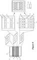
- FIG. 4illustrates an example of a 3D processor that is formed by vertically stacking three dies.
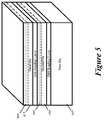
- FIG. 5illustrates three vertically stacked dies with the backside of the second die thinned through a thinning process after face-to-face bonding the first and second dies but before face-to-back mounting the third die to the second die.
- FIGS. 6-9illustrate other 3D processors of some embodiments.
- FIG. 10illustrates that some embodiments place on different stacked dies two compute circuits that perform successive computations.
- FIG. 11illustrates an example of a high-performance 3D processor that has overlapping processor cores on different dies.
- FIG. 12illustrates another example of a high-performance 3D processor that has a processor core on one die overlap with a cache on another die.
- FIG. 13illustrates an example of a 3D processor that has different parts of a processor core on two face-to-face mounted dies.
- FIG. 14shows a compute circuit on a first die that overlaps a memory circuit on a second die, which is vertically stacked over the first die.
- FIG. 15shows two overlapping compute circuits on two vertically stacked dies.
- FIG. 16illustrates an array of compute circuits on a first die overlapping an array of memories on a second die that is face-to-face mounted with the first die through direct bonded interconnect (DBI) boding process.
- DBIdirect bonded interconnect
- FIG. 17illustrates a traditional way of interlacing a memory array with a compute array.
- FIGS. 18 and 19illustrates two examples that show how high density DBI connections can be used to reduce the size of an arrangement of compute circuit that is formed by several successive stages of circuits, each of which performs a computation that produces a result that is passed to another stage of circuits until a final stage of circuits is reached.
- FIG. 20presents a compute circuit that performs a computation (e.g., an addition or multiplication) on sixteen multi-bit input values on two face-to-face mounted dies.
- a computatione.g., an addition or multiplication
- FIG. 21illustrates a device that uses a 3D IC.
- FIG. 22provides an example of a 3D chip that is formed by two face-to-face mounted IC dies that are mounted on a ball grid array.
- FIG. 23illustrates a manufacturing process that some embodiments use to produce the 3D chip.
- FIGS. 24-27show two wafers at different stages of the fabrication process of FIG. 23 .
- FIG. 28illustrates an example of a 3D chip with three stacked IC dies.
- FIG. 29illustrates an example of a 3D chip with four stacked IC dies.
- FIG. 30illustrates a 3D chip that is formed by face-to-face mounting three smaller dies on a larger die.
- Some embodiments of the inventionprovide a three-dimensional (3D) circuit that is formed by vertically stacking two or more integrated circuit (IC) dies to at least partially overlap.
- ICintegrated circuit
- several circuit blocks defined on each die(1) overlap with other circuit blocks defined on one or more other dies, and (2) electrically connect to these other circuit blocks through connections that cross one or more bonding layers that bond one or more pairs of dies.
- the overlapping, connected circuit block pairsinclude pairs of computation blocks and pairs of computation and memory blocks.
- connections that cross bonding layers to electrically connect circuit blocks on different diesare referred to below as z-axis wiring or connections. This is because these connections traverse completely or mostly in the z-axis of the 3D circuit (e.g., because these connections in some embodiments cross the bonding layer(s) in a direction normal or nearly normal to the bonded surface), with the x-y axes of the 3D circuit defining the planar surface of the IC die substrate or interconnect layers. These connections are also referred to as vertical connections to differentiate them from the horizontal planar connections along the interconnect layers of the IC dies.
- FIG. 1illustrates an example of such a 3D circuit. Specifically, it illustrates a 3D circuit 100 that is formed by vertically stacking two IC dies 105 and 110 such that each of several circuit blocks on one die (1) overlaps at least one other circuit block on the other die, and (2) electrically connects to the overlapping die in part through z-axis connections 150 that cross a bonding layer that bonds the two IC dies.
- the two dies 105 and 110are face-to-face mounted as further described below.
- the stacked first and second diesin some embodiments are encapsulated into one integrated circuit package by an encapsulating epoxy and/or a chip case.
- the first die 105includes a first semiconductor substrate 120 and a first set of interconnect layers 125 defined above the first semiconductor substrate 120 .
- the second IC die 110includes a second semiconductor substrate 130 and a second set of interconnect layers 135 defined below the second semiconductor substrate 130 .
- numerous electronic componentse.g., active components, like transistors and diodes, or passive components, like resistors and capacitors) are defined on the first semiconductor substrate 120 and on the second semiconductor substrate 130 .
- the electronic components on the first substrate 120are connected to each other through interconnect wiring on the first set of interconnect layers 125 to form numerous microcircuits (e.g., Boolean gates, such as AND gates, OR gates, etc.) and/or larger circuit blocks (e.g., functional blocks, such as memories, decoders, logic units, multipliers, adders, etc.).
- the electronic components on the second substrate 130are connected to each other through interconnect wiring on the second set of interconnect layers 135 to form additional microcircuits and/or larger circuit block.
- a portion of the interconnect wiring needed to define a circuit block on one die's substrateis provided by interconnect layer(s) (e.g., the second set interconnect layers 135 ) of the other die (e.g., the second die 110 ).
- the electronic components on one die's substratee.g., the first substrate 120 of the first die 105
- the electronic components on one die's substratein some embodiments are also connected to other electronic components on the same substrate (e.g., substrate 120 ) through interconnect wiring on the other die's set of interconnect layers (e.g., the second set of interconnect layers 135 of the second die 110 ) to form a circuit block on the first die.
- the interconnect layers of one diecan be shared by the electronic components and circuits of the other die in some embodiments.
- the interconnect layers of one diecan also be used to carry power, clock and data signals for the electronic components and circuits of the other die, as described in U.S. patent application Ser. No. 15/976,815 filed May 10, 2018, now published as U.S. Patent Publication 2018/0330992, which is incorporated herein by reference.
- the interconnect layers that are shared between two diesare referred to as the shared interconnect layers in the discussion below.
- Each interconnect layer of an IC dietypically has a preferred wiring direction (also called routing direction).
- the preferred wiring directions of successive interconnect layers of an IC dieare orthogonal to each other.
- the preferred wiring directions of an IC dietypically alternate between horizontal and vertical preferred wiring directions, although several wiring architectures have been introduced that employ 45 degree and 60 degree offset between the preferred wiring directions of successive interconnect layers. Alternating the wiring directions between successive interconnect layers of an IC die has several advantages, such as providing better signal routing and avoiding capacitive coupling between long parallel segments on adjacent interconnect layers.
- the first and second diesare face-to-face stacked so that the first and second set of interconnect layers 125 and 135 are facing each other.
- the top interconnect layers 160 and 165are bonded to each other through a direct bonding process that establishes direct-contact metal-to-metal bonding, oxide bonding, or fusion bonding between these two sets of interconnect layers.
- An example of such bondingis copper-to-copper (Cu—Cu) metallic bonding between two copper conductors in direct contact.
- the direct bondingis provided by a hybrid bonding technique such as DBI® (direct bond interconnect) technology, and other metal bonding techniques (such as those offered by Invensas Bonding Technologies, Inc., an Xperi Corporation company, San Jose, Calif.).
- DBIdirect bond interconnect
- other metal bonding techniquessuch as those offered by Invensas Bonding Technologies, Inc., an Xperi Corporation company, San Jose, Calif.
- DBIconnects span across silicon oxide and silicon nitride surfaces.
- the DBI processis further described in U.S. Pat. Nos. 6,962,835 and 7,485,968, both of which are incorporated herein by reference. This process is also described in U.S. patent application Ser. No. 15/725,030, now published as U.S. Patent Publication 2018/0102251, which is also incorporated herein by reference.
- the direct bonded connections between two face-to-face mounted IC diesare native interconnects that allow signals to span two different dies with no standard interfaces and no input/output protocols at the cross-die boundaries.
- the direct bonded interconnectsallow native signals from one die to pass directly to the other die with no modification of the native signal or negligible modification of the native signal, thereby forgoing standard interfacing and consortium-imposed input/output protocols.
- Direct bonded interconnectsallow circuits to be formed across and/or to be accessed through the cross-die boundary of two face-to-face mounted dies. Examples of such circuits are further described in U.S. patent application Ser. No. 15/725,030. The incorporated U.S. Pat. Nos. 6,962,835, 7,485,968, and U.S. patent application Ser. No. 15/725,030 also describe fabrication techniques for manufacturing two face-to-face mounted dies.
- a DBI connection between two diesterminates on electrical contacts (referred to as pads in this document) on each die's top interconnect layer.
- the DBI-connection pad on each dieelectrically connects the DBI connection with circuit nodes on the die that need to provide the signal to the DBI connection or to receive the signal from the DBI connection.
- a DBI-connection padconnects to an interconnect segment on the top interconnect layer of a die, which then carries the signal to a circuit block on the die's substrate through a series of vias and interconnect lines.
- Viasare z-axis structures on each die that carry signals between the interconnect layers of the die and between the IC die substrate and the interconnect layers of the die.
- the direct bonding techniques of some embodimentsallow a large number of direct connections 150 to be established between the top interconnect layer 165 of the second die 110 and top interconnect layer 160 of the first die 105 .
- the first diein some embodiments uses other IC structures (e.g., vias) to carry these signals from its top interconnect layer to these other layers and/or substrate.
- more than 1,000 connections/mm 2 , 10,000 connections/mm 2 , 100,000 connections/mm 2 , 1,000,000 connections/mm 2 or less, etc.can be established between the top interconnect layers 160 and 165 of the first and second dies 105 and 110 in order to allow signals to traverse between the first and second IC dies.
- the direct-bonded connections 150 between the first and second diesare very short in length.
- the direct-bonded connectionscan range from a fraction of a micron to a single-digit or low double-digit microns (e.g., 2-10 microns).
- the short length of these connectionsallows the signals traversing through these connections to reach their destinations quickly while experiencing no or minimal capacitive load from nearby planar wiring and nearby direct-bonded vertical connections.
- the planar wiring connectionsare referred to as x-y wiring or connections, as such wiring stays mostly within a plane defined by an x-y axis of the 3D circuit.
- z-axis wiring or connectionsvertical connections between two dies or between two interconnect layers are referred to as z-axis wiring or connections, as such wiring mostly traverses in the z-axis of the 3D circuit.
- the use of “vertical” in expressing a z-axis connectionshould not be confused with horizontal or vertical preferred direction planar wiring that traverses an individual interconnect layer.
- the pitch (distance) between two neighboring direct-bonded connections 150can be extremely small, e.g., the pitch for two neighboring connections is between 0.5 ⁇ m to 15 ⁇ m. This close proximity allows for the large number and high density of such connections between the top interconnect layers 160 and 165 of the first and second dies 105 and 110 . Moreover, the close proximity of these connections does not introduce much capacitive load between two neighboring z-axis connections because of their short length and small interconnect pad size.
- the direct bonded connectionsare less then 1 or 2 ⁇ m in length (e.g., 0.1 to 0.5 ⁇ m in length), and facilitate short z-axis connections (e.g., 1 to 10 ⁇ m in length) between two different locations on the two dies even after accounting for the length of vias on each of the dies.
- the direct vertical connections between two diesoffer short, fast paths between different locations on these dies.
- electrical nodes in overlapping portions of the circuit blocks on the first and second diescan be electrically connected.
- These electrical nodescan be on the IC die substrates (e.g., on the portions of the substrates that contain node of electronic components of the circuit blocks) or on the IC die interconnect layers (e.g., on the interconnect layer wiring that form the circuit block).
- viasare used to carry the signals to or from the z-axis connections to these nodes.
- viasare z-axis structures that carry signals between the interconnect layers and between the IC die substrate and the interconnect layers.
- FIG. 1illustrates numerous z-axis connections 150 between overlapping regions 181 - 185 in the top interconnect layers 160 and 165 .
- Each of these regionscorresponds to a circuit block 171 - 175 that is defined on one of the IC die substrates 120 and 130 .
- each region on the top interconnect layer of one dieconnects to one or more overlapping regions in the top interconnect layer of the other die through numerous z-axis connections.
- z-axis connectionsconnect overlapping regions 181 and 184 , regions 182 and 184 , and regions 183 and 185 .
- Viasare used to provide signals to these z-axis connections from the IC die substrates and interconnect layers.
- viasare used to carry signals from the z-axis connections when the electrical nodes that need to receive these signals are on the die substrates or the interconnect layers below the top layer.
- the density of connections between overlapping connected regionscan be in the range of 1,000 connections/mm 2 to 1,000,000 connections/mm 2 .
- the pitch between two neighboring direct-bonded connections 150can be extremely small, e.g., the pitch for two neighboring connections is between 0.5 ⁇ m to 15 ⁇ m.
- these connectionscan be very short, e.g., in the range from a fraction of a micron to a low single-digit microns.
- each top interconnect-layer region 181 - 185corresponds to a circuit block region 171 - 175 on an IC die substrate 120 or 130 .
- a circuit block's corresponding top interconnect-layer regioni.e., the region that is used to establish the z-axis connections for that circuit block
- all the z-axis connections that are used to connect two overlapping circuit blocks in two different diesdo not connect one contiguous region in the top-interconnect layer of one die with another contiguous region in the top-interconnect layer of the other die.
- the z-axis connectionsconnect circuits on the two dies that do not overlap (i.e., do not have any of their horizontal cross section vertically overlap).
- the number of connections that can be established between themis limited by the number of connections that can be made through their perimeters on one or more interconnect layers.
- the connections between the two circuitsare not limited to periphery connections that come through the perimeter of the circuits, but also include z-axis connections (e.g., DBI connections and via connections) that are available through the area of the overlapping region.
- Stacking IC diesin many cases allows the wiring for delivering the signals to be much shorter, as the stacking provides more candidate locations for shorter connections between overlapping circuit blocks that need to be interconnected to receive these signals.
- circuit blocks 173 and 175 on dies 105 and 110share a data bus 190 on the top interconnect layer of the second die 110 . This data bus carries data signals to both of these circuits.
- Direct-bonded connectionsare used to carry signals from this data bus 190 to the circuit block 175 on the first die 105 . These direct-bonded connections are much shorter than connections that would route data-bus signals on the first die about several functional blocks in order to reach the circuit block 175 from this block's periphery. The data signals that traverse the short direct-bonded connections reach this circuit 175 on the first die very quickly (e.g., within 1 or 2 clock cycles) as they do not need to be routed from the periphery of the destination block.
- a data-bus linecan be positioned over or near a destination circuit on the first die to ensure that the data-bus signal on this line can be provided to the destination circuit through a short direct-bonded connection.
- Z-axis connection and the ability to share interconnect layers on multiple diesreduce the congestion and route limitations that may be more constrained on one die than another.
- Stacking IC diesalso reduces the overall number of interconnect layers of the two dies because it allows the two dies to share some of the higher-level interconnect layers in order to distribute signals. Reducing the higher-level interconnect layers is beneficial as the wiring on these layers often consumes more space due to their thicker, wider and coarser arrangements.
- two diesare face-to-face mounted
- these two diesare face-to-back stacked (i.e., the set of interconnect layers of one die is mounted next to the backside of the semiconductor substrate of the other die), or back-to-back stacked (i.e., the backside of the semiconductor substrate of one die is mounted next to the backside of the semiconductor substrate of the other die).
- a third die(e.g., an interposer die) is placed between the first and second dies, which are face-to-face stacked, face-to-back stacked (with the third die between the backside of the substrate of one die and the set of interconnect layers of the other die), or back-to-back stacked (with the third die between the backsides of the substrates of the first and second dies).
- the vertical stack of diesin some embodiments includes three or more IC dies in a stack.
- While some embodimentsuse a direct bonding technique to establish connections between the top interconnect layers of two face-to-face stacked dies, other embodiments use alternative connection schemes (such as through silicon vias, TSVs, through-oxide vias, TOVs, or through-glass vias, TGVs) to establish connections between face-to-back dies and between back-to-back dies.
- alternative connection schemessuch as through silicon vias, TSVs, through-oxide vias, TOVs, or through-glass vias, TGVs
- the overlapping circuit blocks 171 - 175 on the two dies 105 and 110are different types of blocks in different embodiments. Examples of such blocks in some embodiments include memory blocks that store data, computational blocks that perform computations on the data, and I/O blocks that receive and output data from the 3D circuit 100 .
- FIGS. 2, 4, and 6illustrate several different overlapping memory blocks, computational blocks, and/or I/O blocks architectures of some embodiments. Some of these examples illustrate high performance 3D multi-core processors.
- FIGS. 10-11then illustrate several examples of overlapping computation blocks, including different cores of a multi-core processor being placed on different IC dies.
- FIG. 13illustrates an example of overlapping functional blocks of a processor core.
- FIG. 2illustrates an example of a high-performance 3D processor 200 that has a multi-core processor 250 on one die 205 and an embedded memory 255 on another die 210 .
- the horizontal cross section of the multi-core processorhas a substantially vertical overlaps with the horizontal cross section of the embedded memory.
- the two dies 205 and 210are face-to-face mounted through a direct bonding process, such as the DBI process. In other embodiments, these two dies can be face-to-back or back-to-back mounted.
- numerous z-axis connections 150cross a direct bonding layer that bonds the two IC dies 205 and 210 in order to establish numerous signal paths between the multi-core processor 250 and the embedded memory 255 .
- the z-axis connectionscan be in the range of 1,000 connections/mm 2 to 1,000,000 connections/mm 2 .
- the DBI z-axis connectionsallow a very large number of signal paths to be defined between the multi-core processor 250 and the embedded memory 255 .
- the DBI z-axis connections 150also support very fast signal paths as the DBI connections are typically very short (e.g., are 0.2 ⁇ m to 2 ⁇ m).
- the overall length of the signal pathsis also typically short because the signal paths are mostly vertical.
- the signal pathsoften rely on interconnect lines (on the interconnect layers) and vias (between the interconnect layers) to connect nodes of the processor 250 and the embedded memory 255 .
- the signal pathsare mostly vertical as they often connect nodes that are in the same proximate z-cross section.
- the length of a vertical signal pathmostly accounts for the height of the interconnect layers of the dies 205 and 210 , which is typically in the single digit to low-double digit microns (e.g., the vertical signal paths are typically in the range of 10-20 ⁇ m long).
- z-axis connectionsprovide short, fast and plentiful connections between the multi-core processor 250 and the embedded memory 255 , they allow the embedded memory 255 to replace many of the external memories that are commonly used today in devices that employ multi-core processors.
- robust z-axis connections between vertically stacked IC diesenable next generation system on chip (SoC) architectures that combine the computational power of the fastest multi-core processors with large embedded memories that take the place of external memories.
- SoCsystem on chip
- FIG. 3illustrates how multi-core processors are commonly used today in many devices.
- a multi-core processor 350 in a device 305typically communicates with multiple external memories 310 of the device 305 through an external I/O interface 355 (such as a double data rate (DDR) interface).
- the multi-core processorhas multiple general processing cores 352 and one or more graphical processing cores 354 that form a graphical processing unit 356 of the processor 350 .
- Each of the processing coreshas its own level 1 (L1) cache 362 to store data. Also, multiple level 2 (L2) caches 364 are used to allow different processing cores to store their data for access by themselves and by other cores.
- L3 caches 366are also used to store data retrieved from external memories 310 and to supply data to external memories 310 .
- the different coresaccess the L2 and L3 caches through arbiters 368 .
- I/O interfaces 355are used to retrieve data for L3 cache 366 and the processing cores 352 and 354 .
- L1 cachestypically have faster access times than L2 caches, which, in turn, have faster access times often than L3 caches.
- the I/O interfacesconsume a lot of power and also have limited I/O capabilities. Often, I/O interfaces have to serialize and de-serialize the output data and the input data, which consumes power and also restricts the multi-core processors input/output. Also, the architecture illustrated in FIG. 3 requires enough wiring to route the signals between the various components of the multi-core processor and the I/O interfaces.
- the power consumption, wiring and processor's I/O bottleneckis dramatically improved by replacing the external memories with one or more embedded memories 255 that are vertically stacked with the multi-core processor 250 in the same IC package.
- This arrangementdramatically reduces the length of the wires needed to carry signals between the multi-core processor 250 and its external memory (which in FIG. 2 is the embedded memory 255 ). Instead of being millimeters in length, this wiring is now in the low microns. This is a 100-1000 times improvement in wirelength.
- the reduction in wirelengthallows the 3D processor 200 of FIG. 2 to have much lower power consumption than the present day design of FIG. 3 .
- the 3D processor's stacked designalso consumes much less power as it foregoes the low throughput, high power consuming I/O interface between the external memories 310 and the multi-core processor 350 with plentiful, short z-axis connections between the embedded memory 255 and the multi-core processor 250 .
- the 3D processor 200still needs an I/O interface on one of its dies (e.g., the first die 205 , the second die 210 or another stacked die, not shown), but this processor 200 does not need to rely on it as heavily to input data for consumption as a large amount of data (e.g., more than 200 MB, 500 MB, 1 GB, etc.) can be stored in the embedded memory 255 .
- a large amount of datae.g., more than 200 MB, 500 MB, 1 GB, etc.
- the stacked design of the 3D processor 200also reduces the size of the multi-core processor by requiring less I/O interface circuits and by placing the I/O interface circuits 257 on the second die 210 .
- the I/O interface circuits 257are on the first die 205 , but are fewer and/or smaller circuits.
- the I/O interface circuitsare placed on a third die stacked with the first and second dies, as further described below.
- the stacked design of the 3D processor 200also frees up space in the device that uses the multi-core processor as it moves some of the external memories to be in the same IC chip housing as the multi-core processor.
- Examples of memories that can be embedded memories 255 stacked with the multi-core processor 250include any type of memory, such as SRAM (static random access memory), DRAM (dynamic random access memory), MRAM (magnetoresistive random access memory), TCAM (ternary content addressable random access memory), NAND Flash, NOR Flash, RRAM (resistive random access memory), PCRAM (phase change random access memory), etc.
- FIG. 2illustrates one embedded memory on the second die 210
- multiple embedded memoriesare defined on the second die 210 in some embodiments, while multiple embedded memories are defined on two or more dies that are vertically stacked with the first die 205 that contains the multi-core processor 250 .
- the different embedded memoriesall are of the same type, while in other embodiments, the different embedded memories are different types (e.g., some are SRAMs while others are NAND/NOR Flash memories).
- the different embedded memoriesare defined on the same IC die, while in other embodiments, different embedded memories are defined on different IC dies.
- FIG. 2illustrates that in some embodiments the multi-core processor 250 has the similar components (e.g., multiple general processing cores 270 , L1, L2, and L3 caches 272 , 274 , and 276 , cache arbiters 278 and 280 , graphical processing core 282 , etc.) like other multi-processor cores.
- the I/O interface circuits 257 for the multi-core processor 250are placed on the second die 205 , as mentioned above.
- the I/O circuits 257write data to the embedded memory 255 from external devices and memories, and reads data from the embedded memory 255 for the external devices and memories.
- the I/O circuit 255can also retrieve data from external devices and memories for the L3 cache, or receive data from the L3 cache for external devices and memories, without the data first going through the embedded memory 255 .
- Some of these embodimentshave a direct vertical (z-axis) bus between the L3 cache and the I/O circuit 257 .
- the first die 205also includes I/O circuits as interfaces between the I/O circuit 255 and the L3 cache 276 , or as interfaces between the L3 cache 276 and the external devices/memories.
- FIG. 4illustrates an example of a 3D processor 400 that is formed by vertically stacking three dies 405 , 410 and 415 , with the first die 405 including multiple processor cores 422 and 424 of a multi-core processor, the second die 410 including L1-L3 caches 426 , 428 and 430 for the processing cores, and the third die 415 including I/O circuits 435 .
- the first and second dies 405 and 410are face-to-face mounted (e.g., through a direct bonding process, such as a DBI process), while the second and third dies 410 and 415 are back-to-face mounted.
- the processor coresare in two sets of four cores 432 and 434 . As shown, each core on the first die 405 overlaps (1) with that core's L1 cache 426 on the second die 410 , (2) with one L2 cache 428 on the second die 410 that is shared by the three other cores in the same four-core set 432 or 434 , and (3) with the L3 cache 430 on the second die 410 .
- numerous z-axis connections(e.g., DBI connections) establish numerous signal paths between each core and each L1, L2, or L3 cache that it overlaps. These signal paths are also established by interconnect segments on the interconnect layers, and vias between the interconnect layers, of the first and second dies.
- some or all of the cache memoriesare multi-ported memories that can be simultaneously accessed by different cores.
- One or more of the cache memoriesinclude cache arbiter circuits that arbitrate (e.g., control and regulate) simultaneous and at time conflicting access to the memories by different processing cores.
- the 3D processor 400also includes one L2 cache memory 436 on the first die 405 between the two four-core sets 432 and 434 in order to allow data to be shared between these sets of processor cores.
- the L2 cache memory 436includes a cache arbiter circuit (not shown).
- the 3D processor 400does not include the L2 cache memory 436 .
- the different processor core sets 432 and 434share data through the L3 cache 430 .
- the L3 cache 430stores data for all processing cores 422 and 424 to access. Some of this data is retrieved from external memories (i.e., memories outside of the 3D processor 400 ) by the I/O circuit 435 that is defined on the third die 415 .
- the third die 415in some embodiments is face-to-back mounted with the second die.
- TSVs 460are defined through the second die's substrate, and these TSVs electrically connect (either directly or through interconnect segments defined on the back side of the second die) to direct bonded connections that connect the backside of the second die to the front side of the third die (i.e., to the top interconnect layer on the front side of the third die). As shown in FIG.
- the backside of the second dieis thinned through a thinning process after face-to-face bonding the first and second dies but before face-to-back mounting the third die to the second die.
- This thinningallows the TSVs through the second die's substrate to be shorter.
- the shorter length of the TSVsallows the TSVs to have smaller cross sections and smaller pitch (i.e., smaller center-to-center distance to neighboring TSVs), which thereby improves their density.
- Most of the signal paths between the second and third dies 410 and 415are very short (e.g., typically in the range of 10-20 ⁇ m long) as they mostly traverse in the vertical direction through the thinned second die's substrate and third die's interconnect layers, which have relatively short heights.
- a large number of short, vertical signal pathsare defined between the L3 cache 430 on the second die 410 and the I/O circuit 435 on the third die 415 .
- These signal pathsuse (1) direct-bonded connections between the top interconnect layer of the third die 415 and the backside of the second die 410 , (2) TSVs 460 through the second die's substrate, and (3) vias between the interconnect layers, and interconnect segments on the interconnect layers, of the second and third die.
- the number and short length of these signal pathsallow the I/O circuit to rapidly write to and read from the L3 cache.
- the signal paths between the first and second dies 405 and 410use (1) direct-bonded connections between the top interconnect layers of the first and second dies 405 and 410 , and (2) vias between the interconnect layers, and interconnect segments on the interconnect layers, of the first and second dies 405 and 410 .
- Most of these signal paths between the first and second dies 405 and 410are also very short (e.g., typically in the range of 10-20 ⁇ m long) as they mostly traverse in the vertical direction through the first and second dies' interconnect layers, which have relatively short heights.
- a large number of short, vertical signal pathsare defined between the processing cores on the first die 405 and their associated L1-L3 caches.
- the processor coresuse these fast and plentiful signal paths to perform very fast writes and reads of large data bit sets to and from the L1-L3 cache memories.
- the processor coresthen perform their operations (e.g., their instruction fetch, instruction decode, arithmetic logic, and data write back operations) based on these larger data sets, which in turn allows them to perform more complex instruction sets and/or to perform smaller instruction sets more quickly.
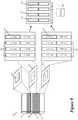
- FIG. 6illustrates another 3D processor 600 of some embodiments.
- This processor 600combines features of the 3D processor 200 of FIG. 2 with features of the 3D processor 400 of FIG. 4 .
- the processor 600places multiple processor cores 422 and 424 on a first die 605 , L1-L3 caches 426 , 428 and 430 on a second die 610 , and I/O circuits 435 on a third die 615 .
- the processor 600also has one die with an embedded memory 622 . This embedded memory is defined on a fourth die 620 that is placed between the second and third dies 610 and 615 .
- the first and second dies 605 and 610are face-to-face mounted (e.g., through a direct bonding process, such as a DBI process), the fourth and second dies 620 and 610 are face-to-back mounted, and the third and fourth dies 615 and 620 are face-to-back mounted.
- TSVs 460are defined through the substrates of the second die and third dies.
- the TSVs through the second die 610electrically connect (either directly or through interconnect segments defined on the back side of the second die) to direct bonded connections that connect the backside of the second die 610 to the front side of the fourth die 620
- the TSVs through the fourth die 620electrically connect (either directly or through interconnect segments defined on the back side of the second die) to direct bonded connections that connect the backside of the fourth die 620 to the front side of the third die 615 .
- the backside of the second dieis thinned through a thinning process after face-to-face bonding the first and second dies but before face-to-back mounting the fourth die 620 to the second die 610 .
- the backside of the fourth die 620is thinned through a thinning process after face-to-back mounting the fourth and second dies 620 and 610 but before face-to-back mounting the third die 615 to the fourth die 620 .
- the shorter length of the TSVsallows the TSVs to have smaller cross sections and smaller pitch (i.e., smaller center-to-center distance to neighboring TSVs), which thereby improves their density.
- the L3 cache 430 in FIG. 6stores data for all processing cores 422 and 424 to access. However, in FIG. 6 , the L3 cache does not connect to the I/O circuits 435 but rather connects to the embedded memory 622 on the fourth die through vertical signal paths. In this design, the embedded memory 622 connects to the I/O circuits 435 on the third die 615 through vertical signal paths.
- the vertical signal paths between the second and fourth dies 610 and 620 and between the fourth and third dies 620 and 615are established by z-axis direct bonded connections and TSVs, as well as interconnect segments on the interconnect layers and vias between the interconnect layers. Most of these signal paths are very short (e.g., typically in the range of 10-20 ⁇ m long) as they are mostly vertical and the height of the thinned substrates and their associated interconnect layers is relatively short.
- the embedded memory 622is a large memory (e.g., is larger than 200 MB, 500 MB, 1 GB, etc.) in some embodiments. As such, the embedded memory in some embodiments can replace one or more external memories that are commonly used today in devices that employ multi-core processors. Examples of the embedded memory 622 include SRAM, DRAM, MRAM, NAND Flash, NOR Flash, RRAM, PCRAM, etc. In some embodiments, two or more different types of embedded memories are defined on one die or multiple dies in the stack of dies that includes one or more dies on which a multi-core processor is defined.
- the embedded memory 622receives data from, and supplies data to, the I/P circuit 435 .
- the I/O circuit 435writes data to the embedded memory 622 from external devices and memories, and reads data from the embedded memory 622 for the external devices and memories.
- the I/O circuit 435can also retrieve data from external devices and memories for the L3 cache, or receive data from the L3 cache for external devices and memories, without the data first going through the embedded memory 622 .
- Some of these embodimentshave a direct vertical (z-axis) bus between the L3 cache and the I/O circuit 435 .
- the second die 610 and/or fourth die 620also include I/O circuits as interfaces between the I/O circuit 435 and the L3 cache 430 , or as interfaces between the L3 cache 430 and the external devices/memories.
- FIG. 7illustrates yet another 3D processor 700 of some embodiments.
- This processor 700is identical to the processor 600 of FIG. 6 , except that it only has two layers of caches, L1 and L2, on a second die 710 that is face-to-face mounted on a first die 705 that has eight processor cores 722 .
- each L1 cache 726overlaps just one core 722 .
- the L2 cache 728is shared among all the cores 722 and overlaps each of the cores 722 .
- each coreconnects to each L1 or L2 cache that it overlaps through (1) numerous z-axis DBI connections that connect the top interconnect layers of the dies 705 and 721 , and (2) the interconnects and vias that carry the signals from these DBI connections to other metal and substrate layers of the dies 705 and 710 .
- the DBI connectionsin some embodiments allow the data buses between the caches and the cores to be much wider and faster than traditional data buses between the caches and the cores.
- L1 cachesare formed by memories that can be accessed faster (i.e., have faster read or write times) than the memories that are used to form L2 caches.
- Each L1 cache 726 in some embodimentsis composed of just one bank of memories, while in other embodiments it is composed of several banks of memories.
- the L2 cache 728 in some embodimentsis composed of just one bank of memories, while in other embodiments it is composed of several banks of memories.
- the L1 caches 726 and/or L2 cache 728are denser than traditional L1 and L2 caches as they use z-axis DBI connections to provide and receive their signals to and from the overlapping cores 722 .
- the L1 and L2 caches 726 and 728are much larger than traditional L1 and L2 caches as they are defined on another die than the die on which the cores are defined, and hence face less space restrictions on their placement and the amount of space that they consume on the chip.
- FIG. 8illustrates another 3D processor 800 of some embodiments.
- This processor 800is identical to the processor 700 of FIG. 7 , except that it does not have the L2 cache 728 .
- the processor 900has a network on chip (NOC) 8028 on the die 810 , which is face-to-face mounted to the die 705 through a DBI bonding process.
- NOCnetwork on chip
- the NOC 828is an interface through which the cores 722 communicate. This interface includes one or more buses and associated bus circuitry.
- the NOC 828in some embodiments also communicatively connects each core to the L1 caches that overlap the other cores. Through this NOC, a first core can access data stored by a second core in the L1 cache that overlap the second core. Also, through this NOC, a first core in some embodiments can store data in the L1 cache that overlaps a second core.
- an L1 and L2 cacheoverlaps each core 722 , and the NOC 828 connects the cores to L2 caches of other cores, but not to the L1 caches of these cores. In other embodiments, the NOC 828 connects the cores to both L1 and L2 caches that overlap other cores, as well as to the other cores.
- FIG. 9illustrates yet another 3D processor 900 of some embodiments.
- This processor 900is identical to the processor 400 of FIG. 4 , except that it only has one L1 cache 932 on a die 910 for each of six CPU (central processing unit) cores 922 and one L1 cache 934 for each of two GPU (graphics processing unit) cores 924 that are defined on a die 905 that is face-to-face mounted to the die 910 through a DBI bonding process.
- the processor 900does not use layers 2 and 3 caches as it uses large L1 caches for its CPU and GPU cores.
- the L1 cachescan be larger than traditional L1 caches as they are defined on another die than the die on which the cores are defined, and hence face less space restrictions on their placement and the amount of space that they consume on the chip.
- the processor 900has its I/O interface defined on a third die 415 that is face-to-back mounted on the die 910 .
- the processor 900does not include the third die 415 , but just includes the first and second dies 905 and 910 .
- the I/O interface of the processor 900is defined on the first and/or second dies 905 and 910 .
- one L1 cache 932is shared across multiple CPU cores 922 and/or multiple GPU cores 924 .
- FIG. 10illustrates that some embodiments place on different stacked dies two compute circuits that perform successive computations.
- a compute circuitis a circuit that receives a multi-bit value as input and computes a multi-bit value as output based on the received input.
- one compute circuit 1015is defined on a first die 1005 while the other compute circuit 1020 is defined on a second die 1010 .
- the first and second diesare face-to-face mounted through a direct bonding process (e.g., a DBI process).
- This mountingdefines numerous z-axis connections between the two dies 1005 and 1010 .
- the z-axis connectionsdefine numerous vertical signal paths between the two compute circuits 1015 and 1020 . These vertical signal paths are short as they mostly traverse in the vertical direction through the die interconnect layers, which are relatively short. As they are very short, these vertical signal paths are very fast parallel paths that connect the two compute circuit 1015 and 1020 .
- the first compute circuit 1015receives a multi-bit input value 1030 and computes a multi-bit output value 1040 based on this input value.
- the multi-bit input value 1030 and/or output value 1040are large bit values, e.g., 32 bits, 64 bits, 128 bits, 256 bits, 512 bits, 1024 bits, etc.
- the first compute circuit 1015provides its multi-bit output value 1040 as the input value to the compute circuit 1020 . Based on this value, the compute circuit 1020 computes another multi-bit output value 1045 .
- the two overlapping computation circuits on the two dies 1005 and 1010are different cores of a multi-core processor.
- FIG. 11illustrates an example of a high-performance 3D processor 1100 that has overlapping processor cores on different dies.
- two dies 1105 and 1110are face-to-face mounted through a direct bonding process (e.g., the DBI process).
- the first die 1105includes a first processor core 1112
- the second die 1110includes a second processor core 1114 .
- the first die 1105also includes an L1 cache 1116 for the second core 1114 on the second die 1110 , and L2 and L3 caches 1122 and 1126 for both cores 1112 and 1114 .
- the second die 1110also includes an L1 cache 1118 for the first core 1112 on the first die 1105 , and L2 and L3 caches 1124 and 1128 for both cores 1112 and 1114 .
- each corecompletely overlaps its corresponding L1 cache, and connects to its L1 cache through numerous vertical signal paths that are partially defined by z-axis connections between the top two interconnect layers of the dies 1105 and 1110 .
- such vertical signal pathsare also defined by (1) vias between interconnect layers of each die, and/or (3) interconnect segments on interconnect layers of each die.
- Each core on one diealso overlaps with one L2 cache and one L3 cache on the other die and is positioned near another L2 cache and another L3 cache on its own die.
- Each L2 and L3 cache 1122 - 826can be accessed by each core 1112 or 1114 .
- Each coreaccesses an overlapping L2 or L3 cache through numerous vertical signal paths that are partially defined by z-axis connections between the top two interconnect layers of the dies 1105 and 1110 and by (1) vias between interconnect layers of each die, and/or (3) interconnect segments on interconnect layers of each die.
- Each corecan also access an L2 or L3 cache on its own die through signal paths that are defined by visa between interconnect layers, and interconnect segments on interconnect layers, of its own die.
- each corewhen additional signal paths are needed between each core and an L2 or L3 cache on its own die, each core also connects to such L2 or L3 cache through signal paths that are not only defined by vias between interconnect layers, and interconnect segments on interconnect layers, of its own die, but by vias between interconnect layers and interconnect segments on interconnect layers of the other die.
- each core 1112 or 1114retrieves much larger sets of data bits and performs more complex operations faster with such larger sets of data bits.
- each coreuses wider instruction and data buses in its pipelines as it can retrieve wider instructions and data from overlapping memories.
- each corehas more pipelines that perform more operations in parallel as the core can retrieve more instruction and data bits from the overlapping memories.
- each core on one dieonly uses the L2 cache or L3 cache on the other die (i.e., only uses the L2 or L3 cache that vertically overlaps the core) in order to take advantage of the large number of vertical signal paths between it and the overlapping L2 cache.
- Each core in some of these embodimentsstores a redundant copy of each data, which it stores in its own overlapping cache (e.g., its own overlapping L2 cache) in the corresponding cache (e.g., in the other L2 cache) that is defined on the core's own die, so that the data is also available for the other core.
- each corereaches the cache on its own die through signal paths that are not only defined through the interconnect lines and vias on the core's die, but also defined through interconnect lines and vias of the other die.
- FIG. 12illustrates another example of a high-performance 3D processor 1200 that has a processor core on one die overlap with a cache on another die.
- two dies 1205 and 1210are face-to-face mounted through a direct bonding process (e.g., the DBI process).
- the first die 1205includes a first processor core 1212
- the second die 1210includes a second processor core 1214 .
- the first die 1205includes an L1 cache 1216 for the second processor core 1214 defined on the second die 1210
- the second die 1210includes an L1 cache 1218 for the first processor core 1212 defined on the first die 1205 .
- each L1 cache on one diecompletely overlaps the cross-section of the corresponding core on the other die.
- Thisensures the largest region for defining z-axis connections (e.g., DBI connections) in the overlapping regions of each core and its corresponding L1 cache.
- z-axis connectionsare very short and hence can be used to define a very fast bus between each core and its corresponding L1 cache.
- this z-axis buscan be wide and it can be defined wholly within the x-y cross-section of the core and its L1 cache, as further described below.
- the z-axis buswould not consume routing resources around the core and its L1 cache. Also, the speed and width of this bus allows the bus to have a very high throughput bandwidth, which perfectly complements the high speed of the L1 cache.
- the 3D processor 1200defines an L2 cache for each core on the same die on which the core is defined.
- each corecan access the other core's L2 cache through z-axis connections established through the face-to-face bonding of the two IC dies.
- the 3D process 1200in some embodiments does not use an L3 cache.
- FIG. 13illustrates an example of a 3D processor 1300 that has different parts of a processor core on two face-to-face mounted dies 1305 and 1310 .
- the first die 1305includes multiple pipeline 1390 , with each pipeline having an instruction fetch (IF) unit 1312 , an instruction decode unit 1314 , an execution unit 1316 and a write-back unit 1318 .
- the second dieincludes the instruction memory 1322 and data registers and memories 1324 .
- the instruction memory 1322 on the second dieoverlaps with the IF units 1312 on the first die 1305 .
- the data registers and memories 1324 on the second dieoverlap with the execution units 1316 and the write-back units.
- Numerous vertical signal pathsare defined between overlapping core components by the z-axis connections between the top two interconnect layers of the dies 1305 and 1310 , and by (1) vias between interconnect layers of each die 1305 or 1310 , and/or (2) interconnect segments on interconnect layers of each die.
- each IF unit 1312retrieves instructions from the instruction memory and provides the retrieved instructions to its instruction decode unit 1314 .
- This decode unitdecodes each instruction that it receives and supplies the decoded instruction to its execution unit to execute.
- each execution unitreceives, from the data registers and memories 1324 , operands that it needs to execute a received instruction, and provides the result of its execution to its write-back unit 1318 .
- each write-back unit 1318stores the execution results in the data registers and memories 1324 .
- Other embodimentsuse other architectures to split a processor core between two different dies.
- some embodimentsplace the instruction decode and execution units 1314 and 1316 on different layers than the instruction fetch and write back units 1312 and 1318 .
- Still other embodimentsuse other arrangements to split a processor core between different dies. These or other embodiments put different ALUs, or different portions of the same ALU, of a processor core on different vertically stacked dies (e.g., on two dies that are face-to-face mounted through a DBI bonding process).
- FIG. 14presents an example that illustrates this.
- This figureshows a compute circuit 1415 on a first die 1405 that overlaps a memory circuit 1420 on a second die 1410 , which is vertically stacked over the first die 1405 .
- the compute circuitcan be any type of compute circuit (e.g., processor cores, processor pipeline compute units, neural network neurons, logic gates, adders, multipliers, etc.) and the memory circuit can be any type of memory circuit (e.g., SRAMs, DRAMs, non-volatile memories, caches, etc.).
- both circuits 1415 and 1420occupy a square region of 250 by 250 microns on their respective dies 1405 and 1410 (only the substrate surfaces of which are shown in FIG. 14 ).
- a 100-bit z-axis bus 1425is defined between these circuits, with the term bus in this example referring to the data and control signals exchanged between these two circuits 1415 and 1420 (in other examples, a bus might only include data signals).
- FIG. 14illustrates that when TSVs are used to define this z-axis bus 1425 , this bus will consume on each die a region 1435 that is at least 2.5 times as large as the size of either circuit on that die. This is because TSVs have a 40 micron pitch.
- the two dies 1405 and 1410will be front-to-back mounted with the TSVs going through the substrate of one of the two dies.
- the cross-section 1430 of the DBI buscan be contained within the footprint (i.e., the substrate region) of both circuits 1415 and 1420 on their respective dies.
- the 100 DBI connectionscan be fit in as little as 20-by-20 micron square, as the 100 connections can be defined as a 10-by-10 array with each connection having a minimum center-to-center spacing of 2 microns with its neighboring connections.
- DBI connectionsBy being contained within the footprint of the circuits 1415 and 1420 , the DBI connections would typically not consume any precious routing space on the dies 1405 and 1410 beyond the portion already consumed by the circuits.
- DBI connectionscan have a pitch ranging from less than 1 micron (e.g., 0.2 or 0.5 microns) to 5 microns.
- DBI connectionsallow for very large bandwidth (e.g., in the high gigabytes or in the terabytes range) between overlapping compute and memory circuits.
- FIG. 15presents an example that illustrates this.
- This figureshows two overlapping compute circuits 1515 and 1520 on two vertically stacked dies 1505 and 1510 .
- Each of the circuitsoccupies a 250-by-250 micron square on its corresponding die's substrate, and can be any type of compute circuit (e.g., processor cores, processor pipeline compute units, neural network neurons, logic gates, adders, multipliers, etc.).
- the example in FIG. 15shows that when DBI connections are used (i.e., when the two dies 1505 and 1510 are face-to-face mounted through DBI), and the DBI connections have a 2-micron pitch, a 100-bit bus 1525 between the two circuits 1515 and 1520 can be contained in a region 1530 that is 20-by-20 micron square that can be wholly contained within the footprints of the circuits.
- the 100-bit bus 1525would consume at a minimum a 400-by-400 micron square region 1535 , which is larger than the footprint of the compute circuits 1515 and 1520 .
- This larger footprintwould consume additional routing space and would not be as beneficial as the smaller footprint that could be achieved by the DBI connections.
- High density DBI connectionscan also be used to reduce the size of a circuit formed by numerous compute circuits and their associated memories.
- the DBI connectionscan also provide this smaller circuit with very high bandwidth between the compute circuits and their associated memories.
- FIG. 16presents an example that illustrates these benefits. Specifically, it illustrates the reduction in the size of an array 1600 of compute circuits 1615 on a first die, by moving the memories 1620 for these circuits to a second die 1610 that is face-to-face mounted with the first die 1605 through DBI boding process.
- a 6-by-10 array of compute circuitsis illustrated, but in other examples, the array can have larger number of circuits (e.g., more than 100 circuits, more than 1000 circuits).
- the compute circuits and their associated memory circuitscan be organized in an arrangement other than an array.
- the compute circuits 1615 and the memory circuits 1620can be any type of computational processing circuits and memory circuits.
- the circuit array 1600is part of an FPGA that has an array of logic circuits (e.g., logic gates and/or look-up tables, LUTs) and an array of memory circuits, with each memory in the memory array corresponding to one logic circuit in the circuit array.
- the compute circuits 1615are neurons of a neural network or multiplier-accumulator (MAC) circuits of neurons.
- the memory circuits 1620 in these embodimentsstore the weights and/or the input/output data for the neurons or the MAC circuits.
- the compute circuits 1615are processing circuits of a GPU, and the memory circuits store the input/output data from these processing circuits.
- a memory arrayis typically interlaced with the circuit array in most single die implementations today.
- the combined length of the two interlaced arraysis X microns in the example in FIG. 17 .
- the wiringwould have to be at least X microns. But by moving the memory circuits onto the second die 1610 , as shown in FIG. 16 , two circuits in the same column can be connected with a minimum wiring length of X/2 microns.
- each memory circuitcan have a higher density of storage cells as less space is consumed for defining shared peripheral channels for outputting signals to the circuits, as these output signals can now traverse in the z-axis.
- more routing spaceis available in the open channels 1650 (on the substrate and metal layers) between the compute circuits in the compute array 1600 on the first die 1605 , and between the memory circuits in the memory array 1602 on the second die 1610 .
- This additional routing spacemakes it easier to connect the outputs of the compute circuits. In many instances, this extra routing space allows these interconnects to have shorter wire lengths.
- the DBI connectionsare also used in some embodiments to route signals through the metal layers of the second die 1610 in order to define the signal paths (i.e., the routes) for connecting the compute circuits 1615 that are defined on the first die 1605 .
- the higher density of DBI connectionsalso allow a higher number of z-axis connections to be defined between corresponding memory and compute circuits that are wholly contained within the footprints (i.e., within the substrate regions occupied by) of a pair of corresponding memory and compute circuits.
- these DBI connectionsconnect the top interconnect layer of one die with the top interconnect layer of the other die, while the rest of the connection between a pair of memory and compute circuits is established with interconnects and vias on these dies.
- the compute circuitsneed wide buses (e.g., 128 bit buses, 256 bit buses, 512 bit buses, 1000 bit buses, 4000 bit buses, etc.) to their corresponding memory circuits.
- One such examplewould be when the array of compute circuits are arrays of neurons that need to access a large amount of data from their corresponding memory circuits.
- FIGS. 18 and 19illustrates two examples that show how high density DBI connections can be used to reduce the size of an arrangement of compute circuit that is formed by several successive stages of circuits, each of which performs a computation that produces a result that is passed to another stage of circuits until a final stage of circuits is reached.
- an arrangement of compute circuitscan be an adder tree, with each compute circuit in the tree being an adder.
- the circuits in the arrangementare multiply accumulate (MAC) circuits, such as those used in neural networks to compute dot products.
- MACmultiply accumulate
- FIGS. 18 and 19both illustrate one implementation of a circuit 1800 that performs a computation (e.g., an addition or multiplication) based on eight input values.
- each input valueis a multi-bit value (e.g., a thirty-two bit value).
- the circuit 1800has three stages with the first stage 1802 having four compute circuits A-D, the second stage 1804 having two compute circuits E and F, and the third stage 1806 having a compute circuit G. Each compute circuit in the first stage 1802 performs an operation based on two input values.
- the compute circuit Eperforms a computation based on the outputs of compute circuits A and B, while the compute circuit F performs a computation based on the outputs of compute circuits C and D.
- the compute circuit G in the third stage 1806performs a computation based on the outputs of compute circuits E and F.
- FIG. 18illustrates a prior art implementation of the circuit 1800 on one IC die 1805 .
- the compute circuits A-Gare arranged in one row in the following order: A, E, B, G, C, F and D.
- the first stage compute circuits A-D(1) receive their inputs from circuits (e.g., memory circuits or other circuits) that are above and below in the planar y-axis direction, and (2) provide their results to the compute circuit E or F.
- the compute circuits E and Fprovide the result of their computations to compute circuit G in the middle of the row.
- the signal path from the compute circuits E and Fis relatively long and consumes nearby routing resources.
- the length and congestion of interconnectsbecome worse as the size of the circuit arrangement (e.g., the adder or multiplication tree) grows. For instance, to implement an adder tree that adds 100 or 1000 input values, numerous adders are needed in numerous stages, which quickly results in long, big data buses to transport computation results between successive stages of adders.
- FIG. 19illustrates a novel implementation of the circuit 1800 that drastically reduces the size of the connections needed to supply the output of compute circuits E and F to the compute circuit G.
- this implementationdefines the compute circuits A, B, E and G on a first die 1910 , while defining the compute circuits C, D and F on a second die 1905 that is face-to-face mounted on the first die 1905 through a DBI boding process.
- the compute circuits A, B, E, and Gare defined in a region on the first die 1910 that overlaps with a region on the second die 1905 in which the compute circuits C, D and F are defined.
- the compute circuit Gis placed below the compute circuit E in the planar y-direction. At this location, the compute circuit G receives the output of the compute circuit E through a short data bus defined on the die 1910 , while receiving the output of the compute circuit F through (1) z-axis DBI connections that connect overlapping locations 1950 and 1952 on the top interconnect layers of the dies 1905 and 1910 , and (2) interconnects and vias on these dies that take the output of circuit F to the input of circuit G.
- the interconnects that provide the inputs to the compute circuit Gare very short.
- the computation circuits E and Gare next to each other and hence the signal path just includes a short length of the interconnect and vias between the circuit E and G. Also, the length of interconnects, vias, and z-axis DBI connections needed to provide the output of the compute circuit F to the compute circuit G is very small.
- Compute circuit arrangementscan have more than three stages.
- large adder or MAC treescan have many more stages (e.g., 8 stages, 10 stages, 12 stages, etc.).
- some embodiments(1) divide up the compute circuits into two or more groups that are then defined on two or more vertically stacked dies, and (2) arrange the different groups of circuits on these dies to minimize the length of interconnects needed to connect compute circuits in successive stages.
- FIG. 20presents an example to illustrate this point.
- This exampleshows one implementation of a compute circuit 2000 that performs a computation (e.g., an addition or multiplication) on sixteen multi-bit input values.
- This circuitincludes two versions 2012 and 2014 of the compute circuit 1800 of FIGS. 18 and 19 .
- the compute circuits in the second versionare labeled as circuits H-N. Each of these versions has three stages. The outputs of these two versions are provided to a fourth stage compute circuit O that performs a computation based on these outputs, as shown.
- the two versions 2012 and 2014have an inverted layout. This is because the compute circuits A, B, and E (that operate on the first four inputs of the first version 2012 ) are defined on IC die 2010 while the compute circuits H, I and L (that operate on the first four inputs of the second version) are defined on the IC die 2005 . Similarly, the compute circuits C, D, and F (that operate on the second four inputs of the first version 2012 ) are defined on IC die 2005 while the compute circuits J, K, and M (that operate on the second four inputs of the second version) are defined on the IC die 2010 .
- the third stage circuit G of the first versionis defined on the IC die 2010
- the third stage circuit Nis defined on the IC die 2005
- the fourth stage aggregating circuit Ois also defined on IC die 2010 .
- the second version 2014is placed to the right of the first version in the x-axis direction.
- This overall inverted arrangement of the second version 2014 with respect to the first versionensures that the length of the interconnect needed to provide the output of the third stage compute circuits G and N to the fourth stage compute circuit O is short.
- the compute circuits L, M, and Nare placed in nearby and/or overlapping locations, which allows these three circuits L, M and N to be connected through short DBI connections, and mostly vertical signal paths facilitated by small planar interconnects plus several via connections.
- This arrangementalso places compute circuits G, N and O in nearby and/or overlapping locations, which again allows them to be connected through short DBI connections, and mostly vertical signal paths facilitated by small planar interconnects plus several via connections.
- FIG. 21illustrates a device 2102 that uses a 3D IC 2100 (like any of the 3D IC 210 , 200 , 400 , 600 - 900 ).
- the 3D IC 2100is formed by two face-to-face mounted IC dies 2105 and 2110 that have numerous direct bonded connections 2115 between them.
- the 3D IC 2100includes three or more vertically stacked IC dies. As shown, the 3D IC die 2100 includes a cap 2150 that encapsulates the dies of this IC in a secure housing 2125 .
- one or more TSVs and/or interconnect layers 2106are defined to connect the 3D IC to a ball grid array 2120 (e.g., a micro bump array) that allows this to be mounted on a printed circuit board 2130 of the device 2102 .
- the device 2102includes other components (not shown). In some embodiments, examples of such components include one or more memory storages (e.g., semiconductor or disk storages), input/output interface circuit(s), one or more processors, etc.
- the first and second dies 2105 and 2110are the first and second dies shown in any of the FIGS. 1-2, 4, 6-16, and 19-20 .
- the second die 2110receives data signals through the ball grid array, and routes the received signals to I/O circuits on the first and second dies through interconnect lines on the interconnect layer and vias between the interconnect layers. When such data signals need to traverse to the first die, these signals traverse through z-axis connections crossing the face-to-face bonding layer.
- FIG. 22provides another example of a 3D chip 2200 that is formed by two face-to-face mounted IC dies 2205 and 2210 that are mounted on a ball grid array 2240 .
- the first and second dies 2205 and 2210are face-to-face connected through direct bonded connections (e.g., DBI connections).
- direct bonded connectionse.g., DBI connections
- several TSVs 2222are defined through the second die 2210 . These TSVs electrically connect to interconnects/pads on the backside of the second die 2210 , on which multiple levels of interconnects are defined.
- the interconnects on the backside of the second die 2210create the signal paths for defining one or more system level circuits for the 3D chip 2200 (i.e., for the circuits of the first and second dies 2205 and 2210 ).
- system level circuitsare power circuits, clock circuits, data I/O signals, test circuits, etc.
- the circuit components that are part of the system level circuitsare defined on the front side of the second die 2210 .
- the circuit componentscan include active components (e.g., transistors, diodes, etc.), or passive/analog components (e.g., resistors, capacitors (e.g., decoupling capacitors), inductors, filters, etc.
- some or all of the wiring for interconnecting these circuit components to form the system level circuitsare defined on interconnect layers on the backside of the second die 2210 .
- Using these backside interconnect layers to implement the system level circuits of the 3D chip 2200frees up one or more interconnect layers on the front side of the second die 2210 to share other types of interconnect lines with the first die 2205 .
- the backside interconnect layersare also used to define some of the circuit components (e.g., decoupling capacitors, etc.) in some embodiments.
- the backside of the second die 2210 in some embodimentscan also connect to the front or back side of a third die.
- one or more of the layers on the backside of the second die 2210are also used to mount this die to the ball grid array 2240 , which allows the 3D chip 2100 to mount on a printed circuit board.
- the system circuitryreceives some or all of the system level signals (e.g., power signals, clock signals, data I/O signals, test signals, etc.) through the ball grid array 2240 connected to the backside of the third die.
- FIG. 23illustrates a manufacturing process 2300 that some embodiments use to produce the 3D chip 2200 of FIG. 22 .
- FIGS. 24-27show two wafers 2405 and 2410 at different stages of the process. Once cut, the two wafers produce two stacked dies, such as dies 2205 and 2210 .
- the process 2300 of FIG. 23cuts the wafers into dies after the wafers have been mounted and processed, the manufacturing process of other embodiments performs the cutting operation at a different stage at least for one of the wafers. Specifically, some embodiments cut the first wafer 2405 into several first dies that are each mounted on the second wafer before the second wafer is cut into individual second dies.
- the process 2300starts (at 2305 ) by defining components (e.g., transistors) on the substrates of the first and second wafers 2405 and 2410 , and defining multiple interconnect layers above each substrate to define interconnections that form micro-circuits (e.g., gates) on each die.
- the process 2300performs multiple IC fabrication operations (e.g., film deposition, patterning, doping, etc.) for each wafer in some embodiments.
- FIG. 24illustrates the first and second wafers 2405 and 2410 after several fabrication operations that have defined components and interconnects on these wafers.
- the fabrication operations for the second wafer 2410defines several TSVs 2412 that traverse the interconnect layers of the second wafer 2410 and penetrate a portion of this wafer's substrate 2416 .
- the process 2300face-to-face mounts (at 2310 ) the first and second wafers 2205 and 2210 through a direct bonding process, such as a DBI process.
- FIG. 25illustrates the first and second wafers 2405 and 2410 after they have been face-to-face mounted through a DBI process. As shown, this DBI process creates a number of direct bonded connections 2426 between the first and second wafers 2405 and 2410 .
- the process 2300performs a thinning operation on the backside of the second wafer 2410 to remove a portion of this wafer's substrate layer. As shown in FIG. 26 , this thinning operation exposes the TSVs 2412 on the backside of the second wafer 2410 . After the thinning operation, the process 2300 defines (at 2320 ) one or more interconnect layers 2430 the second wafer's backside.
- FIG. 27illustrates the first and second wafers 2405 and 2410 after interconnect layers have been defined on the second wafer's backside.
- interconnect layers 2430include one or more layers that allow the 3D chip stack to electrically connect to the ball grid array.
- the interconnect lines/pads on the backside of the third waferalso produce one or more redistribution layers (RDL layers) that allow signals to be redistributed to different locations on the backside.
- RDL layersredistribution layers
- the interconnect layers 2430 on the backside of the second diein some embodiments also create the signal paths for defining one or more system level circuits (e.g., power circuits, clock circuits, data I/O signals, test circuits, etc.) for the circuits of the first and second dies.
- the system level circuitsare defined by circuit components (e.g., transistors, etc.) that are defined on the front side of the second die.
- the process 2300in some embodiments does not define interconnect layers on the backside of the second wafer to create the signal paths for the system level circuits, as it uses only the first and second dies' interconnect layers between their two faces for
- the processcuts (at 2325 ) the stacked wafers into individual chip stacks, with each chip stack include two stacked IC dies 2205 and 2210 .
- the processthen mounts (at 2330 ) each chip stack on a ball grid array and encapsulates the chip stack within one chip housing (e.g., by using a chip case). The process then ends.
- FIG. 28illustrates an example of a 3D chip 2800 with three stacked IC dies 2805 , 2810 and 2815 .
- the first and second dies 2805 and 2810are face-to-face connected through direct bonded connections (e.g., DBI connections), while the third and second dies 2815 and 2810 are face-to-back connected (e.g., the face of the third die 2815 is mounted on the back of the second die 2810 ).
- the first and second dies 2805 and 2810are the first and second dies shown in any of the FIGS. 1-2, 4, 6-16, and 19-20 .
- TSVs 2822are defined through the second die 2810 . These TSVs electrically connect to interconnects/pads on the backside of the second die 2810 , which connect to interconnects/pads on the top interconnect layer of the third die 2815 .
- the third die 2815also has a number of TSVs that connect signals on the front side of this die to interconnects/pads on this die's backside. Through interconnects/pads, the third die's backside connects to a ball grid array 2840 that allows the 3D chip 2800 to mount on a printed circuit board.
- the third die 2815includes system circuitry, such as power circuits, clock circuits, data I/O circuits, test circuits, etc.
- the system circuitry of the third die 2815in some embodiments supplies system level signals (e.g., power signals, clock signals, data I/O signals, test signals, etc.) to the circuits of the first and second dies 2805 and 2810 .
- the system circuitryreceives some or all of the system level signals through the ball grid array 2840 connected to the backside of the third die.
- FIG. 29illustrates another example of a 3D chip 2900 with more than two stacked IC dies.
- the 3D chip 2900has four IC dies 2905 , 2910 , 2915 and 2920 .
- the first and second dies 2905 and 2910are face-to-face connected through direct bonded connections (e.g., DBI connections), while the third and second dies 2915 and 2910 are face-to-back connected (e.g., the face of the third die 2915 is mounted on the back of the second die 2910 ) and the fourth and third dies 2920 and 2915 are face-to-back connected (e.g., the face of the fourth die 2920 is mounted on the back of the third die 2915 ).
- the first and second dies 2905 and 2910are the first and second dies shown in any of the FIGS. 1-2, 4, 6-16, and 19-20 .
- TSVs 2922are defined through the second, third and fourth die 2910 , 2915 and 2920 . These TSVs electrically connect to interconnects/pads on the backside of these dies, which connect to interconnects/pads on the top interconnect layer of the die below or the interconnect layer below. Through interconnects/pads and TSVs, the signals from outside of the chip are received from the ball grid array 2940 .
- 3D chip stacking architecturesinstead of face-to-back mounting the fourth and third dies 2920 and 2915 in FIG. 29 , the 3D chip stack of another embodiment has these two dies face-to-face mounted, and the second and third dies 2910 and 2915 back-to-back mounted. This arrangement would have the third and fourth dies 2915 and 2920 share a more tightly arranged set of interconnect layers on their front sides.
- a first IC dieis shown to be face-to-face mounted with a second IC die.
- the first IC dieis face-to-face mounted with a passive interposer that electrically connects the die to circuits outside of the 3D chip or to other dies that are face-to-face mounted or back-to-face mounted on the interposer.
- Some embodimentsplace a passive interposer between two faces of two dies.
- Some embodimentsuse an interposer to allow a smaller die to connect to a bigger die.
- the 3D circuits and ICs of some embodimentshave been described by reference to several 3D structures with vertically aligned IC dies. However, other embodiments are implemented with a myriad of other 3D structures.
- the 3D circuitsare formed with multiple smaller dies placed on a larger die or wafer.
- FIG. 30illustrates one such example. Specifically, it illustrates a 3D chip 3000 that is formed by face-to-face mounting three smaller dies 3010 a - c on a larger die 3005 .
- All four diesare housed in one chip 3000 by having one side of this chip encapsulated by a cap 3020 , and the other side mounted on a micro-bump array 3025 , which connects to a board 3030 of a device 1935 .
- Some embodimentsare implemented in a 3D structure that is formed by vertically stacking two sets of vertically stacked multi-die structures.
Landscapes
- Engineering & Computer Science (AREA)
- Microelectronics & Electronic Packaging (AREA)
- Power Engineering (AREA)
- Computer Hardware Design (AREA)
- Physics & Mathematics (AREA)
- Condensed Matter Physics & Semiconductors (AREA)
- General Physics & Mathematics (AREA)
- Manufacturing & Machinery (AREA)
- Semiconductor Memories (AREA)
- Semiconductor Integrated Circuits (AREA)
Abstract
Description
Claims (20)
Priority Applications (7)
| Application Number | Priority Date | Filing Date | Title |
|---|---|---|---|
| US16/159,705US10672745B2 (en) | 2016-10-07 | 2018-10-14 | 3D processor |
| EP18803498.7AEP3698402A1 (en) | 2017-10-20 | 2018-10-18 | 3d compute circuit with high density z-axis interconnects |
| CN201880082142.3ACN111492477A (en) | 2017-10-20 | 2018-10-18 | 3D computation circuit with high density Z-axis interconnect |
| PCT/US2018/056559WO2019079625A1 (en) | 2017-10-20 | 2018-10-18 | 3d compute circuit with high density z-axis interconnects |
| TW107136961ATWI745626B (en) | 2017-10-20 | 2018-10-19 | 3d compute circuit with high density z-axis interconnects |
| US16/833,341US11152336B2 (en) | 2016-10-07 | 2020-03-27 | 3D processor having stacked integrated circuit die |
| US17/474,917US12401010B2 (en) | 2016-10-07 | 2021-09-14 | 3D processor having stacked integrated circuit die |
Applications Claiming Priority (15)
| Application Number | Priority Date | Filing Date | Title |
|---|---|---|---|
| US201662405833P | 2016-10-07 | 2016-10-07 | |
| US201762541064P | 2017-08-03 | 2017-08-03 | |
| US15/725,030US10522352B2 (en) | 2016-10-07 | 2017-10-04 | Direct-bonded native interconnects and active base die |
| US201762575184P | 2017-10-20 | 2017-10-20 | |
| US201762575240P | 2017-10-20 | 2017-10-20 | |
| US201762575221P | 2017-10-20 | 2017-10-20 | |
| US201762575259P | 2017-10-20 | 2017-10-20 | |
| US15/859,612US10762420B2 (en) | 2017-08-03 | 2017-12-31 | Self repairing neural network |
| US15/859,546US10607136B2 (en) | 2017-08-03 | 2017-12-31 | Time borrowing between layers of a three dimensional chip stack |
| US15/859,548US10719762B2 (en) | 2017-08-03 | 2017-12-31 | Three dimensional chip structure implementing machine trained network |
| US15/859,551US11176450B2 (en) | 2017-08-03 | 2017-12-31 | Three dimensional circuit implementing machine trained network |
| US201862619910P | 2018-01-21 | 2018-01-21 | |
| US15/976,809US10580735B2 (en) | 2016-10-07 | 2018-05-10 | Stacked IC structure with system level wiring on multiple sides of the IC die |
| US201862678246P | 2018-05-30 | 2018-05-30 | |
| US16/159,705US10672745B2 (en) | 2016-10-07 | 2018-10-14 | 3D processor |
Related Parent Applications (7)
| Application Number | Title | Priority Date | Filing Date |
|---|---|---|---|
| US15/725,030Continuation-In-PartUS10522352B2 (en) | 2016-10-07 | 2017-10-04 | Direct-bonded native interconnects and active base die |
| US15/859,546Continuation-In-PartUS10607136B2 (en) | 2016-10-07 | 2017-12-31 | Time borrowing between layers of a three dimensional chip stack |
| US15/859,548Continuation-In-PartUS10719762B2 (en) | 2016-10-07 | 2017-12-31 | Three dimensional chip structure implementing machine trained network |
| US15/859,612Continuation-In-PartUS10762420B2 (en) | 2016-10-07 | 2017-12-31 | Self repairing neural network |
| US15/859,551Continuation-In-PartUS11176450B2 (en) | 2016-10-07 | 2017-12-31 | Three dimensional circuit implementing machine trained network |
| US15/976,809Continuation-In-PartUS10580735B2 (en) | 2016-10-07 | 2018-05-10 | Stacked IC structure with system level wiring on multiple sides of the IC die |
| US16/159,705Continuation-In-PartUS10672745B2 (en) | 2016-10-07 | 2018-10-14 | 3D processor |
Related Child Applications (3)
| Application Number | Title | Priority Date | Filing Date |
|---|---|---|---|
| US15/859,546Continuation-In-PartUS10607136B2 (en) | 2016-10-07 | 2017-12-31 | Time borrowing between layers of a three dimensional chip stack |
| US16/159,705Continuation-In-PartUS10672745B2 (en) | 2016-10-07 | 2018-10-14 | 3D processor |
| US16/833,341ContinuationUS11152336B2 (en) | 2016-10-07 | 2020-03-27 | 3D processor having stacked integrated circuit die |
Publications (2)
| Publication Number | Publication Date |
|---|---|
| US20190123024A1 US20190123024A1 (en) | 2019-04-25 |
| US10672745B2true US10672745B2 (en) | 2020-06-02 |
Family
ID=66169521
Family Applications (3)
| Application Number | Title | Priority Date | Filing Date |
|---|---|---|---|
| US16/159,705ActiveUS10672745B2 (en) | 2016-10-07 | 2018-10-14 | 3D processor |
| US16/833,341ActiveUS11152336B2 (en) | 2016-10-07 | 2020-03-27 | 3D processor having stacked integrated circuit die |
| US17/474,917Active2038-06-24US12401010B2 (en) | 2016-10-07 | 2021-09-14 | 3D processor having stacked integrated circuit die |
Family Applications After (2)
| Application Number | Title | Priority Date | Filing Date |
|---|---|---|---|
| US16/833,341ActiveUS11152336B2 (en) | 2016-10-07 | 2020-03-27 | 3D processor having stacked integrated circuit die |
| US17/474,917Active2038-06-24US12401010B2 (en) | 2016-10-07 | 2021-09-14 | 3D processor having stacked integrated circuit die |
Country Status (1)
| Country | Link |
|---|---|
| US (3) | US10672745B2 (en) |
Cited By (11)
| Publication number | Priority date | Publication date | Assignee | Title |
|---|---|---|---|---|
| US10886177B2 (en) | 2016-10-07 | 2021-01-05 | Xcelsis Corporation | 3D chip with shared clock distribution network |
| US10892252B2 (en) | 2016-10-07 | 2021-01-12 | Xcelsis Corporation | Face-to-face mounted IC dies with orthogonal top interconnect layers |
| US10950547B2 (en) | 2016-10-07 | 2021-03-16 | Xcelsis Corporation | Stacked IC structure with system level wiring on multiple sides of the IC die |
| US10970627B2 (en) | 2017-08-03 | 2021-04-06 | Xcelsis Corporation | Time borrowing between layers of a three dimensional chip stack |
| US10978348B2 (en) | 2016-10-07 | 2021-04-13 | Xcelsis Corporation | 3D chip sharing power interconnect layer |
| US11152336B2 (en) | 2016-10-07 | 2021-10-19 | Xcelsis Corporation | 3D processor having stacked integrated circuit die |
| US11289333B2 (en) | 2016-10-07 | 2022-03-29 | Xcelsis Corporation | Direct-bonded native interconnects and active base die |
| US11527523B2 (en)* | 2018-12-10 | 2022-12-13 | HangZhou HaiCun Information Technology Co., Ltd. | Discrete three-dimensional processor |
| US20220399321A1 (en)* | 2021-06-15 | 2022-12-15 | Shanghai Biren Technology Co.,Ltd | Chipset and manufacturing method thereof |
| US11599299B2 (en) | 2019-11-19 | 2023-03-07 | Invensas Llc | 3D memory circuit |
| US20230411374A1 (en)* | 2018-12-10 | 2023-12-21 | HangZhou HaiCun Information Technology Co., Ltd. | Discrete Three-Dimensional Processor |
Families Citing this family (22)
| Publication number | Priority date | Publication date | Assignee | Title |
|---|---|---|---|---|
| US10593667B2 (en) | 2016-10-07 | 2020-03-17 | Xcelsis Corporation | 3D chip with shielded clock lines |
| US10600735B2 (en) | 2016-10-07 | 2020-03-24 | Xcelsis Corporation | 3D chip sharing data bus |
| US10672743B2 (en) | 2016-10-07 | 2020-06-02 | Xcelsis Corporation | 3D Compute circuit with high density z-axis interconnects |
| US10672744B2 (en) | 2016-10-07 | 2020-06-02 | Xcelsis Corporation | 3D compute circuit with high density Z-axis interconnects |
| US10586786B2 (en) | 2016-10-07 | 2020-03-10 | Xcelsis Corporation | 3D chip sharing clock interconnect layer |
| US10600780B2 (en) | 2016-10-07 | 2020-03-24 | Xcelsis Corporation | 3D chip sharing data bus circuit |
| US12402330B2 (en)* | 2016-10-10 | 2025-08-26 | Monolithic 3D Inc. | 3D memory devices and structures with memory arrays and metal layers |
| US12225704B2 (en)* | 2016-10-10 | 2025-02-11 | Monolithic 3D Inc. | 3D memory devices and structures with memory arrays and metal layers |
| US11930648B1 (en)* | 2016-10-10 | 2024-03-12 | Monolithic 3D Inc. | 3D memory devices and structures with metal layers |
| US12041791B2 (en)* | 2016-10-10 | 2024-07-16 | Monolithic 3D Inc. | 3D memory devices and structures with memory arrays and metal layers |
| US11632112B2 (en)* | 2017-12-27 | 2023-04-18 | Intel Corporation | Integrated circuit device with separate die for programmable fabric and programmable fabric support circuitry |
| US10884917B2 (en)* | 2018-12-05 | 2021-01-05 | Western Digital Technologies, Inc | Dual media packaging targeted for SSD usage |
| CN111033728A (en)* | 2019-04-15 | 2020-04-17 | 长江存储科技有限责任公司 | Bonded semiconductor device with programmable logic device and dynamic random access memory and method of forming the same |
| JP7303318B2 (en)* | 2019-04-30 | 2023-07-04 | 長江存儲科技有限責任公司 | Bonded integrated semiconductor chip and method of manufacturing and operating same |
| CN110870062A (en) | 2019-04-30 | 2020-03-06 | 长江存储科技有限责任公司 | Bonded semiconductor device with programmable logic device and NAND flash memory and method of forming the same |
| JP7311615B2 (en) | 2019-04-30 | 2023-07-19 | 長江存儲科技有限責任公司 | Junction semiconductor device with processor and NAND flash memory and method of forming same |
| US11264361B2 (en)* | 2019-06-05 | 2022-03-01 | Invensas Corporation | Network on layer enabled architectures |
| US11295053B2 (en)* | 2019-09-12 | 2022-04-05 | Arm Limited | Dielet design techniques |
| US20210125040A1 (en) | 2019-10-24 | 2021-04-29 | International Business Machines Corporation | 3d neural inference processing unit architectures |
| US20220406751A1 (en)* | 2021-06-22 | 2022-12-22 | Intel Corporation | Quasi-monolithic hierarchical integration architecture |
| CN113990843B (en)* | 2021-10-25 | 2023-06-27 | 上海壁仞智能科技有限公司 | Chip set and manufacturing method thereof |
| TW202401681A (en)* | 2022-01-27 | 2024-01-01 | 新加坡商發明與合作實驗室有限公司 | Integrated scaling and stretching platform for server processor and rack server unit |
Citations (88)
| Publication number | Priority date | Publication date | Assignee | Title |
|---|---|---|---|---|
| US5016138A (en) | 1987-10-27 | 1991-05-14 | Woodman John K | Three dimensional integrated circuit package |
| US5376825A (en) | 1990-10-22 | 1994-12-27 | Seiko Epson Corporation | Integrated circuit package for flexible computer system alternative architectures |
| US5579207A (en) | 1994-10-20 | 1996-11-26 | Hughes Electronics | Three-dimensional integrated circuit stacking |
| US5673478A (en) | 1995-04-28 | 1997-10-07 | Texas Instruments Incorporated | Method of forming an electronic device having I/O reroute |
| US5793115A (en) | 1993-09-30 | 1998-08-11 | Kopin Corporation | Three dimensional processor using transferred thin film circuits |
| US5909587A (en) | 1997-10-24 | 1999-06-01 | Advanced Micro Devices, Inc. | Multi-chip superscalar microprocessor module |
| US20010017418A1 (en) | 1999-12-22 | 2001-08-30 | Kabushiki Kaisha Toshiba | Semiconductor device |
| US6707124B2 (en)* | 1992-10-26 | 2004-03-16 | Texas Instruments Incorporated | HID land grid array packaged device having electrical and optical interconnects |
| US6844624B1 (en) | 2003-06-26 | 2005-01-18 | Renesas Technology Corp. | Multichip module |
| US20050127490A1 (en) | 2003-12-16 | 2005-06-16 | Black Bryan P. | Multi-die processor |
| US6909194B2 (en)* | 1999-08-27 | 2005-06-21 | Micron Technology, Inc. | Electronic assembly having semiconductor component with polymer support member and method of fabrication |
| US6917219B2 (en) | 2003-03-12 | 2005-07-12 | Xilinx, Inc. | Multi-chip programmable logic device having configurable logic circuitry and configuration data storage on different dice |
| US7046522B2 (en)* | 2002-03-21 | 2006-05-16 | Raymond Jit-Hung Sung | Method for scalable architectures in stackable three-dimensional integrated circuits and electronics |
| US7099215B1 (en) | 2005-02-11 | 2006-08-29 | North Carolina State University | Systems, methods and devices for providing variable-latency write operations in memory devices |
| US7124250B2 (en) | 2003-01-03 | 2006-10-17 | Samsung Electronics Co., Ltd. | Memory module device for use in high-frequency operation |
| US20070220207A1 (en) | 2006-03-14 | 2007-09-20 | Bryan Black | Transferring data from stacked memory |
| US20090070727A1 (en) | 2007-09-12 | 2009-03-12 | Solomon Research Llc | Three dimensional integrated circuits and methods of fabrication |
| US7638869B2 (en) | 2007-03-28 | 2009-12-29 | Qimonda Ag | Semiconductor device |
| US7692946B2 (en) | 2007-06-29 | 2010-04-06 | Intel Corporation | Memory array on more than one die |
| US20100140750A1 (en) | 2008-12-10 | 2010-06-10 | Qualcomm Incorporated | Parallel Plane Memory and Processor Coupling in a 3-D Micro-Architectural System |
| US8032711B2 (en) | 2006-12-22 | 2011-10-04 | Intel Corporation | Prefetching from dynamic random access memory to a static random access memory |
| US8110899B2 (en) | 2006-12-20 | 2012-02-07 | Intel Corporation | Method for incorporating existing silicon die into 3D integrated stack |
| US8148814B2 (en) | 2009-02-10 | 2012-04-03 | Hitachi, Ltd. | Semiconductor integrated circuit device comprising a plurality of semiconductor chips mounted to stack for transmitting a signal between the semiconductor chips |
| US20120201068A1 (en) | 2009-10-23 | 2012-08-09 | Ware Frederick A | Stacked semiconductor device |
| US20130051116A1 (en)* | 2011-08-24 | 2013-02-28 | Advanced Micro Devices, Inc. | Integrated circuit with face-to-face bonded passive variable resistance memory and method for making the same |
| US8432467B2 (en) | 2009-07-24 | 2013-04-30 | Raytheon Company | Integrated detection and display imaging system and method |
| US20130144542A1 (en) | 2010-06-07 | 2013-06-06 | California Institute Of Technology | Analysis device including a mems and/or nems network |
| US20130187292A1 (en) | 2012-01-20 | 2013-07-25 | Taiwan Semiconductor Manufacturing Company, Ltd. | Multi-Dimensional Integrated Circuit Structures and Methods of Forming the Same |
| US20130207268A1 (en) | 2012-02-14 | 2013-08-15 | Stmicroelectronics (Crolles 2) Sas | Chip assembly system |
| US8516409B2 (en) | 2010-11-11 | 2013-08-20 | International Business Machines Corporation | Implementing vertical die stacking to distribute logical function over multiple dies in through-silicon-via stacked semiconductor device |
| US8547769B2 (en) | 2011-03-31 | 2013-10-01 | Intel Corporation | Energy efficient power distribution for 3D integrated circuit stack |
| US8546955B1 (en) | 2012-08-16 | 2013-10-01 | Xilinx, Inc. | Multi-die stack package |
| US20130275823A1 (en)* | 2011-04-06 | 2013-10-17 | International Business Machines Corporation | Programmable logic circuit using three-dimensional stacking techniques |
| US20140022002A1 (en)* | 2012-07-20 | 2014-01-23 | Qualcomm Incorporated | Thermal management of tightly integrated semiconductor device, system and/or package |
| US8704384B2 (en) | 2012-02-17 | 2014-04-22 | Xilinx, Inc. | Stacked die assembly |
| US8736068B2 (en) | 2010-10-26 | 2014-05-27 | International Business Machines Corporation | Hybrid bonding techniques for multi-layer semiconductor stacks |
| US8797818B2 (en) | 2008-12-30 | 2014-08-05 | Micron Technology, Inc. | Variable memory refresh devices and methods |
| US8816506B2 (en) | 2008-12-19 | 2014-08-26 | Tessera Advanced Technologies, Inc. | Semiconductor device and method of manufacturing the same |
| US20140323046A1 (en) | 2012-09-18 | 2014-10-30 | Panasonic Corporation | Antenna, transmitter device, receiver device, three-dimensional integrated circuit, and contactless communication system |
| US8907439B1 (en)* | 2010-08-30 | 2014-12-09 | Sandia Corporation | Focal plane array with modular pixel array components for scalability |
| US8930647B1 (en)* | 2011-04-06 | 2015-01-06 | P4tents1, LLC | Multiple class memory systems |
| US9067272B2 (en) | 2010-06-18 | 2015-06-30 | Arizona Board Of Regents On Behalf Of Arizona State University | Systems and methods for high aspect ratio flip-chip interconnects |
| US20150228584A1 (en) | 2014-02-13 | 2015-08-13 | Taiwan Semiconductor Manufacturing Company, Ltd. | Multi-via interconnect structure and method of manufacture |
| US20160111386A1 (en) | 2014-10-16 | 2016-04-21 | Globalfoundries Inc. | Bond pad structure for low temperature flip chip bonding |
| US20160225431A1 (en) | 2006-12-14 | 2016-08-04 | Rambus Inc. | Multi-die memory device |
| US20160233134A1 (en) | 2015-02-09 | 2016-08-11 | Qualcomm Incorporated | Clock tree synthesis for low cost pre-bond testing of 3d integrated circuits |
| US9432298B1 (en) | 2011-12-09 | 2016-08-30 | P4tents1, LLC | System, method, and computer program product for improving memory systems |
| US9478496B1 (en) | 2015-10-26 | 2016-10-25 | United Microelectronics Corp. | Wafer to wafer structure and method of fabricating the same |
| US20160329312A1 (en) | 2015-05-05 | 2016-11-10 | Sean M. O'Mullan | Semiconductor chip with offloaded logic |
| US9497854B2 (en) | 2011-10-18 | 2016-11-15 | Arctic Sand Technologies, Inc. | Multi-layer power converter with devices having reduced lateral current |
| US9501603B2 (en) | 2014-09-05 | 2016-11-22 | International Business Machines Corporation | Integrated circuit design changes using through-silicon vias |
| US20160379115A1 (en) | 2015-06-29 | 2016-12-29 | Microsoft Technology Licensing, Llc | Deep neural network processing on hardware accelerators with stacked memory |
| US20170092615A1 (en) | 2015-06-02 | 2017-03-30 | Noda Screen Co., Ltd. | Semiconductor memory device |
| US20170092616A1 (en) | 2015-09-25 | 2017-03-30 | Michael Z. Su | Semiconductor workpiece with selective backside metallization |
| US9640233B2 (en)* | 2012-02-28 | 2017-05-02 | Samsung Electronics Co., Ltd. | Semiconductor memory device having inverting circuit and controlling method there of |
| US9647187B1 (en)* | 2013-05-30 | 2017-05-09 | Hrl Laboratories, Llc | Multi-slice two-dimensional phased array assembly |
| US9645603B1 (en) | 2013-09-12 | 2017-05-09 | Advanced Processor Architectures, Llc | System clock distribution in a distributed computing environment |
| US20170148737A1 (en)* | 2015-11-19 | 2017-05-25 | Globalfoundries Inc. | Method and structure for establishing interconnects in packages using thin interposers |
| US20170213787A1 (en) | 2016-01-27 | 2017-07-27 | Michael S. Alfano | Interposer with beyond reticle field conductor pads |
| US9746517B2 (en) | 2011-02-07 | 2017-08-29 | Texas Instruments Incorporated | IC interposer with TAP controller and output boundary scan cell |
| US20170278789A1 (en) | 2014-03-20 | 2017-09-28 | Taiwan Semiconductor Manufacturing Company, Ltd. | Method for layout design and structure with inter-layer vias |
| US20170278213A1 (en)* | 2016-03-24 | 2017-09-28 | Advanced Micro Devices, Inc. | Hierarchical register file at a graphics processing unit |
| US20170301625A1 (en)* | 2013-12-18 | 2017-10-19 | Intel Corporation | Integrated circuit package with embedded bridge |
| US20180017614A1 (en) | 2013-03-13 | 2018-01-18 | Glenn J Leedy | Configurable Vertical Integration |
| US9915978B2 (en) | 2015-09-21 | 2018-03-13 | Intel Corporaiton | Method of fabricating a stretchable computing device |
| US20180286800A1 (en)* | 2017-03-29 | 2018-10-04 | Qualcomm Incorporated | Power distribution networks for a three-dimensional (3d) integrated circuit (ic) (3dic) |
| US20180331072A1 (en) | 2016-10-07 | 2018-11-15 | Xcelsis Corporation | Face-to-Face Mounted IC Dies with Orthogonal Top Interconnect Layers |
| US20180331095A1 (en) | 2016-10-07 | 2018-11-15 | Xcelsis Corporation | 3D Chip with Shielded Clock Lines |
| US20180331037A1 (en) | 2016-10-07 | 2018-11-15 | Xcelsis Corporation | Stacked IC Structure with System Level Wiring on Multiple Sides of the IC Die |
| US20180330993A1 (en) | 2016-10-07 | 2018-11-15 | Xcelsis Corporation | 3D Chip Sharing Power Circuit |
| US20180331094A1 (en) | 2016-10-07 | 2018-11-15 | Xcelsis Corporation | 3D Chip Sharing Data Bus Circuit |
| US20180331038A1 (en) | 2016-10-07 | 2018-11-15 | Xcelsis Corporation | 3D Chip Sharing Data Bus |
| US20180330992A1 (en) | 2016-10-07 | 2018-11-15 | Xcelsis Corporation | 3D Chip Sharing Power Interconnect Layer |
| US20180350775A1 (en)* | 2016-10-07 | 2018-12-06 | Xcelsis Corporation | 3D Chip Sharing Clock Interconnect Layer |
| US20190042377A1 (en) | 2017-08-03 | 2019-02-07 | Xcelsis Corporation | Self repairing neural network |
| US20190051641A1 (en)* | 2017-08-08 | 2019-02-14 | iCometrue Company Ltd. | Logic drive based on standardized commodity programmable logic semiconductor ic chips |
| US10255969B2 (en) | 2014-07-09 | 2019-04-09 | Samsung Electronics Co., Ltd. | Multi channel semiconductor device having multi dies and operation method thereof |
| US10262911B1 (en)* | 2016-12-14 | 2019-04-16 | Xilinx, Inc. | Circuit for and method of testing bond connections between a first die and a second die |
| US10269586B2 (en)* | 2013-02-04 | 2019-04-23 | Taiwan Semiconductor Manufacturing Company, Ltd. | Package structure and methods of forming same |
| WO2019079625A1 (en) | 2017-10-20 | 2019-04-25 | Xcelsis Corporation | 3d compute circuit with high density z-axis interconnects |
| US20190123022A1 (en) | 2016-10-07 | 2019-04-25 | Xcelsis Corporation | 3D Compute Circuit with High Density Z-Axis Interconnects |
| US20190123023A1 (en) | 2016-10-07 | 2019-04-25 | Xcelsis Corporation | 3D Compute Circuit with High Density Z-Axis Interconnects |
| WO2019079631A1 (en) | 2017-10-20 | 2019-04-25 | Xcelsis Corporation | Face-to-face mounted ic dies with orthogonal top interconnect layers |
| US10373657B2 (en)* | 2016-08-10 | 2019-08-06 | Micron Technology, Inc. | Semiconductor layered device with data bus |
| US20190244933A1 (en) | 2016-10-10 | 2019-08-08 | Monolithic 3D Inc. | 3d semiconductor device and structure |
| US10446601B2 (en) | 2016-10-18 | 2019-10-15 | Sony Semiconductor Solutions Corporation | Photodetector |
| US10446207B2 (en)* | 2012-05-17 | 2019-10-15 | Samsung Electronics Co., Ltd. | Spin transfer torque magnetic random access memory for supporting operational modes with mode register |
| US20200013699A1 (en) | 2017-03-01 | 2020-01-09 | Telefonaktiebolaget Lm Ericsson (Publ) | Stacked Microfluidic Cooled 3D Electronic-Photonic Integrated Circuit |
Family Cites Families (114)
| Publication number | Priority date | Publication date | Assignee | Title |
|---|---|---|---|---|
| JPH07112041B2 (en)* | 1986-12-03 | 1995-11-29 | シャープ株式会社 | Method for manufacturing semiconductor device |
| DE69430528T2 (en) | 1994-07-28 | 2003-01-02 | International Business Machines Corp., Armonk | Search / sort circuit for neural networks |
| EP0694852B1 (en) | 1994-07-28 | 2002-06-26 | International Business Machines Corporation | Innovative neuron circuit architectures |
| DE69430744T2 (en) | 1994-07-28 | 2003-01-30 | International Business Machines Corp., Armonk | Improved neural semiconductor chip architectures and neural networks in them |
| FR2756073B1 (en) | 1996-11-18 | 1999-01-15 | Commissariat Energie Atomique | LEARNING METHOD GENERATING SMALL SIZE NEURON NETWORKS FOR DATA CLASSIFICATION |
| JPH11168185A (en) | 1997-12-03 | 1999-06-22 | Rohm Co Ltd | Laminated substrate body and semiconductor device |
| US6320255B1 (en) | 1998-10-09 | 2001-11-20 | Texas Instruments Incorporated | Rerouted semiconductor device and method of fabrication |
| US20100261159A1 (en)* | 2000-10-10 | 2010-10-14 | Robert Hess | Apparatus for assay, synthesis and storage, and methods of manufacture, use, and manipulation thereof |
| US6627985B2 (en)* | 2001-12-05 | 2003-09-30 | Arbor Company Llp | Reconfigurable processor module comprising hybrid stacked integrated circuit die elements |
| US7398259B2 (en) | 2002-03-12 | 2008-07-08 | Knowmtech, Llc | Training of a physical neural network |
| US6642081B1 (en)* | 2002-04-11 | 2003-11-04 | Robert Patti | Interlocking conductor method for bonding wafers to produce stacked integrated circuits |
| US6891447B2 (en) | 2002-07-12 | 2005-05-10 | Massachusetts Institute Of Technology | Electromagnetic coupling connector for three-dimensional electronic circuits |
| US6962835B2 (en) | 2003-02-07 | 2005-11-08 | Ziptronix, Inc. | Method for room temperature metal direct bonding |
| JP4419049B2 (en) | 2003-04-21 | 2010-02-24 | エルピーダメモリ株式会社 | Memory module and memory system |
| JP2005175415A (en) | 2003-12-05 | 2005-06-30 | Taiwan Semiconductor Manufacturing Co Ltd | Integrated circuit device and manufacturing method thereof |
| US20060087013A1 (en)* | 2004-10-21 | 2006-04-27 | Etron Technology, Inc. | Stacked multiple integrated circuit die package assembly |
| TWI249796B (en)* | 2004-11-08 | 2006-02-21 | Siliconware Precision Industries Co Ltd | Semiconductor device having flip chip package |
| US20060103023A1 (en)* | 2004-11-12 | 2006-05-18 | International Business Machines Corporation | Methods for incorporating high k dielectric materials for enhanced SRAM operation and structures produced thereby |
| US7485968B2 (en) | 2005-08-11 | 2009-02-03 | Ziptronix, Inc. | 3D IC method and device |
| US7562271B2 (en)* | 2005-09-26 | 2009-07-14 | Rambus Inc. | Memory system topologies including a buffer device and an integrated circuit memory device |
| DE102005056907B3 (en)* | 2005-11-29 | 2007-08-16 | Infineon Technologies Ag | 3-dimensional multi-chip module |
| US8241995B2 (en)* | 2006-09-18 | 2012-08-14 | International Business Machines Corporation | Bonding of substrates including metal-dielectric patterns with metal raised above dielectric |
| US7812459B2 (en)* | 2006-12-19 | 2010-10-12 | Taiwan Semiconductor Manufacturing Company, Ltd. | Three-dimensional integrated circuits with protection layers |
| US8198716B2 (en) | 2007-03-26 | 2012-06-12 | Intel Corporation | Die backside wire bond technology for single or stacked die package |
| ITMI20070933A1 (en)* | 2007-05-08 | 2008-11-09 | St Microelectronics Srl | MULTI PIASTRINA ELECTRONIC SYSTEM |
| US7827357B2 (en)* | 2007-07-31 | 2010-11-02 | Intel Corporation | Providing an inclusive shared cache among multiple core-cache clusters |
| US8042082B2 (en)* | 2007-09-12 | 2011-10-18 | Neal Solomon | Three dimensional memory in a system on a chip |
| US8059443B2 (en)* | 2007-10-23 | 2011-11-15 | Hewlett-Packard Development Company, L.P. | Three-dimensional memory module architectures |
| US7863918B2 (en) | 2007-11-13 | 2011-01-04 | International Business Machines Corporation | Disposable built-in self-test devices, systems and methods for testing three dimensional integrated circuits |
| US8597960B2 (en)* | 2008-03-04 | 2013-12-03 | International Business Machines Corporation | Semiconductor chip stacking for redundancy and yield improvement |
| KR101393311B1 (en)* | 2008-03-19 | 2014-05-12 | 삼성전자주식회사 | Multi-chip package memory for compensating process variation |
| US8816486B2 (en)* | 2008-05-12 | 2014-08-26 | Taiwan Semiconductor Manufacturing Co., Ltd. | Pad structure for 3D integrated circuit |
| US7977962B2 (en)* | 2008-07-15 | 2011-07-12 | Micron Technology, Inc. | Apparatus and methods for through substrate via test |
| KR100945800B1 (en)* | 2008-12-09 | 2010-03-05 | 김영혜 | Method for manufacturing heterogeneous bonded wafer |
| KR101307490B1 (en)* | 2009-03-30 | 2013-12-11 | 메기가 코포레이션 | Integrated circuit chip using top post-passivation technology and bottom structure technology |
| KR101049083B1 (en)* | 2009-04-10 | 2011-07-15 | (주)실리콘화일 | A unit pixel of an image sensor having a three-dimensional structure and a manufacturing method thereof |
| JP2010250511A (en)* | 2009-04-14 | 2010-11-04 | Kyushu Univ | Cache memory device |
| KR20100117977A (en)* | 2009-04-27 | 2010-11-04 | 삼성전자주식회사 | Semiconductor package |
| US8072056B2 (en)* | 2009-06-10 | 2011-12-06 | Medtronic, Inc. | Apparatus for restricting moisture ingress |
| US8698276B2 (en) | 2009-07-10 | 2014-04-15 | Hynix Semiconductor Inc. | Semiconductor device having a plurality of repair fuse units |
| JP2011029535A (en)* | 2009-07-29 | 2011-02-10 | Elpida Memory Inc | Semiconductor device |
| US8417917B2 (en)* | 2009-09-30 | 2013-04-09 | International Business Machines Corporation | Processor core stacking for efficient collaboration |
| KR101053534B1 (en)* | 2009-10-29 | 2011-08-03 | 주식회사 하이닉스반도체 | Semiconductor device and chip selection method thereof |
| US8159060B2 (en)* | 2009-10-29 | 2012-04-17 | International Business Machines Corporation | Hybrid bonding interface for 3-dimensional chip integration |
| US8315068B2 (en)* | 2009-11-12 | 2012-11-20 | International Business Machines Corporation | Integrated circuit die stacks having initially identical dies personalized with fuses and methods of manufacturing the same |
| US8310841B2 (en) | 2009-11-12 | 2012-11-13 | International Business Machines Corporation | Integrated circuit die stacks having initially identical dies personalized with switches and methods of making the same |
| US8421500B2 (en)* | 2009-11-30 | 2013-04-16 | International Business Machines Corporation | Integrated circuit with stacked computational units and configurable through vias |
| US8996836B2 (en) | 2009-12-18 | 2015-03-31 | Micron Technology, Inc. | Stacked device detection and identification |
| US8204927B1 (en) | 2010-03-15 | 2012-06-19 | California Institute Of Technology | System and method for cognitive processing for data fusion |
| US9123552B2 (en)* | 2010-03-30 | 2015-09-01 | Micron Technology, Inc. | Apparatuses enabling concurrent communication between an interface die and a plurality of dice stacks, interleaved conductive paths in stacked devices, and methods for forming and operating the same |
| US8546188B2 (en)* | 2010-04-09 | 2013-10-01 | International Business Machines Corporation | Bow-balanced 3D chip stacking |
| WO2011139496A2 (en) | 2010-04-26 | 2011-11-10 | Rambus Inc. | Techniques for interconnecting stacked dies using connection sites |
| KR101145312B1 (en) | 2010-07-06 | 2012-05-14 | 에스케이하이닉스 주식회사 | Semiconductor integrated circuit |
| KR101728067B1 (en)* | 2010-09-03 | 2017-04-18 | 삼성전자 주식회사 | Semiconductor memory device |
| FR2966283B1 (en)* | 2010-10-14 | 2012-11-30 | Soi Tec Silicon On Insulator Tech Sa | METHOD FOR PRODUCING A COLLAGE STRUCTURE |
| KR101208959B1 (en)* | 2010-11-17 | 2012-12-06 | 에스케이하이닉스 주식회사 | Semiconductor devices |
| KR20120079397A (en)* | 2011-01-04 | 2012-07-12 | 삼성전자주식회사 | Stacked semiconductor device and manufacturing method thereof |
| US8866488B2 (en) | 2011-03-22 | 2014-10-21 | Taiwan Semiconductor Manufacturing Company, Ltd. | Power compensation in 3DIC testing |
| JP2012226794A (en) | 2011-04-18 | 2012-11-15 | Elpida Memory Inc | Semiconductor device and method of controlling semiconductor device |
| KR20130004783A (en)* | 2011-07-04 | 2013-01-14 | 삼성전자주식회사 | Stacked semiconductor device including esd protection circuits and method of fabricating the stacked semiconductor device |
| US8697493B2 (en)* | 2011-07-18 | 2014-04-15 | Soitec | Bonding surfaces for direct bonding of semiconductor structures |
| KR20130011138A (en)* | 2011-07-20 | 2013-01-30 | 삼성전자주식회사 | Monolithic rank and multiple rank compatible memory device |
| WO2013080426A1 (en)* | 2011-12-01 | 2013-06-06 | パナソニック株式会社 | Integrated-circuit device with structure devised in consideration of heat, three-dimensional integrated circuit, three-dimensional processor device, and process scheduler |
| KR101931491B1 (en)* | 2011-12-02 | 2018-12-24 | 삼성전자주식회사 | Electrodes Connecting Structures Having Copper |
| US8987066B2 (en)* | 2012-01-03 | 2015-03-24 | Honeywell International Inc. | Processing unit comprising integrated circuits including a common configuration of electrical interconnects |
| TWI565026B (en)* | 2012-01-05 | 2017-01-01 | 威盛電子股份有限公司 | Chip package structure |
| US9647668B2 (en) | 2012-01-13 | 2017-05-09 | Altera Corporation | Apparatus for flexible electronic interfaces and associated methods |
| US9569402B2 (en)* | 2012-04-20 | 2017-02-14 | International Business Machines Corporation | 3-D stacked multiprocessor structure with vertically aligned identical layout operating processors in independent mode or in sharing mode running faster components |
| CN103426732B (en)* | 2012-05-18 | 2015-12-02 | 上海丽恒光微电子科技有限公司 | The method of low-temperature wafer bonding and the structure formed by the method |
| US9030253B1 (en)* | 2012-05-30 | 2015-05-12 | Altera Corporation | Integrated circuit package with distributed clock network |
| KR101937951B1 (en)* | 2012-05-31 | 2019-01-14 | 에스케이하이닉스 주식회사 | Semiconductor integrated circuit and method of driving the same |
| US9048283B2 (en)* | 2012-06-05 | 2015-06-02 | Taiwan Semiconductor Manufacturing Company, Ltd. | Hybrid bonding systems and methods for semiconductor wafers |
| US8922243B2 (en)* | 2012-12-23 | 2014-12-30 | Advanced Micro Devices, Inc. | Die-stacked memory device with reconfigurable logic |
| US9065722B2 (en)* | 2012-12-23 | 2015-06-23 | Advanced Micro Devices, Inc. | Die-stacked device with partitioned multi-hop network |
| US9171608B2 (en)* | 2013-03-15 | 2015-10-27 | Qualcomm Incorporated | Three-dimensional (3D) memory cell separation among 3D integrated circuit (IC) tiers, and related 3D integrated circuits (3DICS), 3DIC processor cores, and methods |
| KR101976612B1 (en)* | 2013-03-21 | 2019-05-10 | 에스케이하이닉스 주식회사 | Stack package |
| US9064937B2 (en)* | 2013-05-30 | 2015-06-23 | International Business Machines Corporation | Substrate bonding with diffusion barrier structures |
| JP6092019B2 (en)* | 2013-06-25 | 2017-03-08 | 株式会社東芝 | Processor |
| CN103354210B (en)* | 2013-06-27 | 2016-08-10 | 清华大学 | A kind of bonding method and use the bonding structure that this bonding method formed |
| US9336144B2 (en)* | 2013-07-25 | 2016-05-10 | Globalfoundries Inc. | Three-dimensional processing system having multiple caches that can be partitioned, conjoined, and managed according to more than one set of rules and/or configurations |
| US9230940B2 (en)* | 2013-09-13 | 2016-01-05 | Globalfoundries Inc. | Three-dimensional chip stack for self-powered integrated circuit |
| US9389876B2 (en)* | 2013-10-24 | 2016-07-12 | International Business Machines Corporation | Three-dimensional processing system having independent calibration and statistical collection layer |
| US9726691B2 (en) | 2014-01-07 | 2017-08-08 | International Business Machines Corporation | 3D chip testing through micro-C4 interface |
| US20150262902A1 (en) | 2014-03-12 | 2015-09-17 | Invensas Corporation | Integrated circuits protected by substrates with cavities, and methods of manufacture |
| US9190345B1 (en)* | 2014-03-28 | 2015-11-17 | Taiwan Semiconductor Manufacturing Company, Ltd. | Semiconductor devices and methods of manufacture thereof |
| US9257414B2 (en)* | 2014-04-10 | 2016-02-09 | Taiwan Semiconductor Manufacturing Company, Ltd. | Stacked semiconductor structure and method |
| KR101729378B1 (en) | 2014-05-30 | 2017-04-21 | 타이완 세미콘덕터 매뉴팩쳐링 컴퍼니 리미티드 | Semiconductor devices and methods of manufacture thereof |
| US8947931B1 (en)* | 2014-06-13 | 2015-02-03 | Sandisk Technologies Inc. | Memory module |
| US10289604B2 (en)* | 2014-08-07 | 2019-05-14 | Wisconsin Alumni Research Foundation | Memory processing core architecture |
| JP6335099B2 (en)* | 2014-11-04 | 2018-05-30 | 東芝メモリ株式会社 | Semiconductor device and manufacturing method of semiconductor device |
| US9626311B2 (en)* | 2015-01-22 | 2017-04-18 | Qualcomm Incorporated | Memory controller placement in a three-dimensional (3D) integrated circuit (IC) (3DIC) employing distributed through-silicon-via (TSV) farms |
| TWI699761B (en) | 2015-03-04 | 2020-07-21 | 日商東芝記憶體股份有限公司 | Semiconductor device |
| JP2016174101A (en)* | 2015-03-17 | 2016-09-29 | 株式会社東芝 | Semiconductor device and manufacturing method of the same |
| KR102373543B1 (en) | 2015-04-08 | 2022-03-11 | 삼성전자주식회사 | Method and device for controlling operation using temperature deviation in multi-chip package |
| US9559081B1 (en)* | 2015-08-21 | 2017-01-31 | Apple Inc. | Independent 3D stacking |
| US9953941B2 (en)* | 2015-08-25 | 2018-04-24 | Invensas Bonding Technologies, Inc. | Conductive barrier direct hybrid bonding |
| KR102373541B1 (en) | 2015-08-31 | 2022-03-11 | 삼성전자주식회사 | Semiconductor apparatus, stacked semiconductor apparatus and test method thereof |
| US9871014B2 (en) | 2015-09-08 | 2018-01-16 | Invensas Corporation | 3D-joining of microelectronic components with conductively self-adjusting anisotropic matrix |
| US9741693B2 (en)* | 2015-11-12 | 2017-08-22 | Taiwan Semiconductor Manufacturing Company Ltd. | Semiconductor package and method of forming the same |
| KR102410992B1 (en) | 2015-11-26 | 2022-06-20 | 삼성전자주식회사 | Stacked memory device, and memory package and memory system having the same |
| US10037982B2 (en)* | 2016-01-04 | 2018-07-31 | Infinera Corporation | Photonic integrated circuit package |
| KR102451650B1 (en) | 2016-02-05 | 2022-10-11 | 에스케이하이닉스 주식회사 | Stacked type seniconductor apparatus |
| KR20180109850A (en) | 2016-02-10 | 2018-10-08 | 르네사스 일렉트로닉스 가부시키가이샤 | Semiconductor device |
| JP6457421B2 (en) | 2016-04-04 | 2019-01-23 | ファナック株式会社 | Machine learning device, machine system, manufacturing system, and machine learning method for learning using simulation results |
| US9722588B1 (en) | 2016-04-25 | 2017-08-01 | Micron Technology, Inc. | Apparatuses and methods for detecting frequency ranges corresponding to signal delays of conductive vias |
| US10354975B2 (en)* | 2016-05-16 | 2019-07-16 | Raytheon Company | Barrier layer for interconnects in 3D integrated device |
| CN111210857B (en) | 2016-06-27 | 2023-07-18 | 苹果公司 | Memory system combining high-density low-bandwidth and low-density high-bandwidth memory |
| KR102824640B1 (en) | 2016-09-07 | 2025-06-25 | 삼성전자주식회사 | Recognition apparatus based on neural network and training method of neural network |
| US10672745B2 (en) | 2016-10-07 | 2020-06-02 | Xcelsis Corporation | 3D processor |
| KR102393946B1 (en) | 2016-10-07 | 2022-05-03 | 엑셀시스 코포레이션 | Direct-bonded native interconnect and active base die |
| US11321604B2 (en) | 2017-06-21 | 2022-05-03 | Arm Ltd. | Systems and devices for compressing neural network parameters |
| US20190156214A1 (en) | 2017-11-18 | 2019-05-23 | Neuralmagic Inc. | Systems and methods for exchange of data in distributed training of machine learning algorithms |
| US20190180183A1 (en) | 2017-12-12 | 2019-06-13 | Amazon Technologies, Inc. | On-chip computational network |
| SG10201904549QA (en) | 2019-05-21 | 2019-09-27 | Alibaba Group Holding Ltd | System And Method For Training Neural Networks |
- 2018
- 2018-10-14USUS16/159,705patent/US10672745B2/enactiveActive
- 2020
- 2020-03-27USUS16/833,341patent/US11152336B2/enactiveActive
- 2021
- 2021-09-14USUS17/474,917patent/US12401010B2/enactiveActive
Patent Citations (97)
| Publication number | Priority date | Publication date | Assignee | Title |
|---|---|---|---|---|
| US5016138A (en) | 1987-10-27 | 1991-05-14 | Woodman John K | Three dimensional integrated circuit package |
| US5376825A (en) | 1990-10-22 | 1994-12-27 | Seiko Epson Corporation | Integrated circuit package for flexible computer system alternative architectures |
| US6707124B2 (en)* | 1992-10-26 | 2004-03-16 | Texas Instruments Incorporated | HID land grid array packaged device having electrical and optical interconnects |
| US5793115A (en) | 1993-09-30 | 1998-08-11 | Kopin Corporation | Three dimensional processor using transferred thin film circuits |
| US5579207A (en) | 1994-10-20 | 1996-11-26 | Hughes Electronics | Three-dimensional integrated circuit stacking |
| US5673478A (en) | 1995-04-28 | 1997-10-07 | Texas Instruments Incorporated | Method of forming an electronic device having I/O reroute |
| US5909587A (en) | 1997-10-24 | 1999-06-01 | Advanced Micro Devices, Inc. | Multi-chip superscalar microprocessor module |
| US6909194B2 (en)* | 1999-08-27 | 2005-06-21 | Micron Technology, Inc. | Electronic assembly having semiconductor component with polymer support member and method of fabrication |
| US20010017418A1 (en) | 1999-12-22 | 2001-08-30 | Kabushiki Kaisha Toshiba | Semiconductor device |
| US7046522B2 (en)* | 2002-03-21 | 2006-05-16 | Raymond Jit-Hung Sung | Method for scalable architectures in stackable three-dimensional integrated circuits and electronics |
| US7124250B2 (en) | 2003-01-03 | 2006-10-17 | Samsung Electronics Co., Ltd. | Memory module device for use in high-frequency operation |
| US6917219B2 (en) | 2003-03-12 | 2005-07-12 | Xilinx, Inc. | Multi-chip programmable logic device having configurable logic circuitry and configuration data storage on different dice |
| US6844624B1 (en) | 2003-06-26 | 2005-01-18 | Renesas Technology Corp. | Multichip module |
| US20050127490A1 (en) | 2003-12-16 | 2005-06-16 | Black Bryan P. | Multi-die processor |
| US8860199B2 (en) | 2003-12-16 | 2014-10-14 | Intel Corporation | Multi-die processor |
| US7099215B1 (en) | 2005-02-11 | 2006-08-29 | North Carolina State University | Systems, methods and devices for providing variable-latency write operations in memory devices |
| US20070220207A1 (en) | 2006-03-14 | 2007-09-20 | Bryan Black | Transferring data from stacked memory |
| US20160225431A1 (en) | 2006-12-14 | 2016-08-04 | Rambus Inc. | Multi-die memory device |
| US8110899B2 (en) | 2006-12-20 | 2012-02-07 | Intel Corporation | Method for incorporating existing silicon die into 3D integrated stack |
| US8032711B2 (en) | 2006-12-22 | 2011-10-04 | Intel Corporation | Prefetching from dynamic random access memory to a static random access memory |
| US7638869B2 (en) | 2007-03-28 | 2009-12-29 | Qimonda Ag | Semiconductor device |
| US7692946B2 (en) | 2007-06-29 | 2010-04-06 | Intel Corporation | Memory array on more than one die |
| US20090070727A1 (en) | 2007-09-12 | 2009-03-12 | Solomon Research Llc | Three dimensional integrated circuits and methods of fabrication |
| US20100140750A1 (en) | 2008-12-10 | 2010-06-10 | Qualcomm Incorporated | Parallel Plane Memory and Processor Coupling in a 3-D Micro-Architectural System |
| US8816506B2 (en) | 2008-12-19 | 2014-08-26 | Tessera Advanced Technologies, Inc. | Semiconductor device and method of manufacturing the same |
| US9076700B2 (en) | 2008-12-19 | 2015-07-07 | Tessera Advanced Technologies, Inc. | Semiconductor device and method of manufacturing same |
| US9691739B2 (en) | 2008-12-19 | 2017-06-27 | Tessera Advanced Technologies, Inc. | Semiconductor device and method of manufacturing same |
| US9318418B2 (en) | 2008-12-19 | 2016-04-19 | Tessera Advanced Technologies, Inc. | Semiconductor device and method of manufacturing same |
| US8797818B2 (en) | 2008-12-30 | 2014-08-05 | Micron Technology, Inc. | Variable memory refresh devices and methods |
| US8148814B2 (en) | 2009-02-10 | 2012-04-03 | Hitachi, Ltd. | Semiconductor integrated circuit device comprising a plurality of semiconductor chips mounted to stack for transmitting a signal between the semiconductor chips |
| US8432467B2 (en) | 2009-07-24 | 2013-04-30 | Raytheon Company | Integrated detection and display imaging system and method |
| US20120201068A1 (en) | 2009-10-23 | 2012-08-09 | Ware Frederick A | Stacked semiconductor device |
| US20130144542A1 (en) | 2010-06-07 | 2013-06-06 | California Institute Of Technology | Analysis device including a mems and/or nems network |
| US9067272B2 (en) | 2010-06-18 | 2015-06-30 | Arizona Board Of Regents On Behalf Of Arizona State University | Systems and methods for high aspect ratio flip-chip interconnects |
| US8907439B1 (en)* | 2010-08-30 | 2014-12-09 | Sandia Corporation | Focal plane array with modular pixel array components for scalability |
| US8736068B2 (en) | 2010-10-26 | 2014-05-27 | International Business Machines Corporation | Hybrid bonding techniques for multi-layer semiconductor stacks |
| US8516409B2 (en) | 2010-11-11 | 2013-08-20 | International Business Machines Corporation | Implementing vertical die stacking to distribute logical function over multiple dies in through-silicon-via stacked semiconductor device |
| US9746517B2 (en) | 2011-02-07 | 2017-08-29 | Texas Instruments Incorporated | IC interposer with TAP controller and output boundary scan cell |
| US8547769B2 (en) | 2011-03-31 | 2013-10-01 | Intel Corporation | Energy efficient power distribution for 3D integrated circuit stack |
| US20130275823A1 (en)* | 2011-04-06 | 2013-10-17 | International Business Machines Corporation | Programmable logic circuit using three-dimensional stacking techniques |
| US8930647B1 (en)* | 2011-04-06 | 2015-01-06 | P4tents1, LLC | Multiple class memory systems |
| US20130051116A1 (en)* | 2011-08-24 | 2013-02-28 | Advanced Micro Devices, Inc. | Integrated circuit with face-to-face bonded passive variable resistance memory and method for making the same |
| US9497854B2 (en) | 2011-10-18 | 2016-11-15 | Arctic Sand Technologies, Inc. | Multi-layer power converter with devices having reduced lateral current |
| US9432298B1 (en) | 2011-12-09 | 2016-08-30 | P4tents1, LLC | System, method, and computer program product for improving memory systems |
| US20130187292A1 (en) | 2012-01-20 | 2013-07-25 | Taiwan Semiconductor Manufacturing Company, Ltd. | Multi-Dimensional Integrated Circuit Structures and Methods of Forming the Same |
| US20130207268A1 (en) | 2012-02-14 | 2013-08-15 | Stmicroelectronics (Crolles 2) Sas | Chip assembly system |
| US8704384B2 (en) | 2012-02-17 | 2014-04-22 | Xilinx, Inc. | Stacked die assembly |
| US9640233B2 (en)* | 2012-02-28 | 2017-05-02 | Samsung Electronics Co., Ltd. | Semiconductor memory device having inverting circuit and controlling method there of |
| US10446207B2 (en)* | 2012-05-17 | 2019-10-15 | Samsung Electronics Co., Ltd. | Spin transfer torque magnetic random access memory for supporting operational modes with mode register |
| US20140022002A1 (en)* | 2012-07-20 | 2014-01-23 | Qualcomm Incorporated | Thermal management of tightly integrated semiconductor device, system and/or package |
| US9508607B2 (en)* | 2012-07-20 | 2016-11-29 | Qualcomm Incorporated | Thermal management of tightly integrated semiconductor device, system and/or package |
| US8546955B1 (en) | 2012-08-16 | 2013-10-01 | Xilinx, Inc. | Multi-die stack package |
| US20140323046A1 (en) | 2012-09-18 | 2014-10-30 | Panasonic Corporation | Antenna, transmitter device, receiver device, three-dimensional integrated circuit, and contactless communication system |
| US10269586B2 (en)* | 2013-02-04 | 2019-04-23 | Taiwan Semiconductor Manufacturing Company, Ltd. | Package structure and methods of forming same |
| US20180017614A1 (en) | 2013-03-13 | 2018-01-18 | Glenn J Leedy | Configurable Vertical Integration |
| US9647187B1 (en)* | 2013-05-30 | 2017-05-09 | Hrl Laboratories, Llc | Multi-slice two-dimensional phased array assembly |
| US9645603B1 (en) | 2013-09-12 | 2017-05-09 | Advanced Processor Architectures, Llc | System clock distribution in a distributed computing environment |
| US20170301625A1 (en)* | 2013-12-18 | 2017-10-19 | Intel Corporation | Integrated circuit package with embedded bridge |
| US20150228584A1 (en) | 2014-02-13 | 2015-08-13 | Taiwan Semiconductor Manufacturing Company, Ltd. | Multi-via interconnect structure and method of manufacture |
| US20170278789A1 (en) | 2014-03-20 | 2017-09-28 | Taiwan Semiconductor Manufacturing Company, Ltd. | Method for layout design and structure with inter-layer vias |
| US10255969B2 (en) | 2014-07-09 | 2019-04-09 | Samsung Electronics Co., Ltd. | Multi channel semiconductor device having multi dies and operation method thereof |
| US9501603B2 (en) | 2014-09-05 | 2016-11-22 | International Business Machines Corporation | Integrated circuit design changes using through-silicon vias |
| US20160111386A1 (en) | 2014-10-16 | 2016-04-21 | Globalfoundries Inc. | Bond pad structure for low temperature flip chip bonding |
| US20160233134A1 (en) | 2015-02-09 | 2016-08-11 | Qualcomm Incorporated | Clock tree synthesis for low cost pre-bond testing of 3d integrated circuits |
| US20160329312A1 (en) | 2015-05-05 | 2016-11-10 | Sean M. O'Mullan | Semiconductor chip with offloaded logic |
| US20170092615A1 (en) | 2015-06-02 | 2017-03-30 | Noda Screen Co., Ltd. | Semiconductor memory device |
| US20160379115A1 (en) | 2015-06-29 | 2016-12-29 | Microsoft Technology Licensing, Llc | Deep neural network processing on hardware accelerators with stacked memory |
| US9915978B2 (en) | 2015-09-21 | 2018-03-13 | Intel Corporaiton | Method of fabricating a stretchable computing device |
| US20170092616A1 (en) | 2015-09-25 | 2017-03-30 | Michael Z. Su | Semiconductor workpiece with selective backside metallization |
| US9478496B1 (en) | 2015-10-26 | 2016-10-25 | United Microelectronics Corp. | Wafer to wafer structure and method of fabricating the same |
| US20170148737A1 (en)* | 2015-11-19 | 2017-05-25 | Globalfoundries Inc. | Method and structure for establishing interconnects in packages using thin interposers |
| US20170213787A1 (en) | 2016-01-27 | 2017-07-27 | Michael S. Alfano | Interposer with beyond reticle field conductor pads |
| US20170278213A1 (en)* | 2016-03-24 | 2017-09-28 | Advanced Micro Devices, Inc. | Hierarchical register file at a graphics processing unit |
| US10373657B2 (en)* | 2016-08-10 | 2019-08-06 | Micron Technology, Inc. | Semiconductor layered device with data bus |
| US20180331072A1 (en) | 2016-10-07 | 2018-11-15 | Xcelsis Corporation | Face-to-Face Mounted IC Dies with Orthogonal Top Interconnect Layers |
| US20180330993A1 (en) | 2016-10-07 | 2018-11-15 | Xcelsis Corporation | 3D Chip Sharing Power Circuit |
| US20180331038A1 (en) | 2016-10-07 | 2018-11-15 | Xcelsis Corporation | 3D Chip Sharing Data Bus |
| US20180330992A1 (en) | 2016-10-07 | 2018-11-15 | Xcelsis Corporation | 3D Chip Sharing Power Interconnect Layer |
| US20180350775A1 (en)* | 2016-10-07 | 2018-12-06 | Xcelsis Corporation | 3D Chip Sharing Clock Interconnect Layer |
| US20190123023A1 (en) | 2016-10-07 | 2019-04-25 | Xcelsis Corporation | 3D Compute Circuit with High Density Z-Axis Interconnects |
| US20180331094A1 (en) | 2016-10-07 | 2018-11-15 | Xcelsis Corporation | 3D Chip Sharing Data Bus Circuit |
| US20190123022A1 (en) | 2016-10-07 | 2019-04-25 | Xcelsis Corporation | 3D Compute Circuit with High Density Z-Axis Interconnects |
| US20180331037A1 (en) | 2016-10-07 | 2018-11-15 | Xcelsis Corporation | Stacked IC Structure with System Level Wiring on Multiple Sides of the IC Die |
| US20180331095A1 (en) | 2016-10-07 | 2018-11-15 | Xcelsis Corporation | 3D Chip with Shielded Clock Lines |
| US20190244933A1 (en) | 2016-10-10 | 2019-08-08 | Monolithic 3D Inc. | 3d semiconductor device and structure |
| US10446601B2 (en) | 2016-10-18 | 2019-10-15 | Sony Semiconductor Solutions Corporation | Photodetector |
| US10580817B2 (en) | 2016-10-18 | 2020-03-03 | Sony Semiconductor Solutions Corporation | Photodetector |
| US10262911B1 (en)* | 2016-12-14 | 2019-04-16 | Xilinx, Inc. | Circuit for and method of testing bond connections between a first die and a second die |
| US20200013699A1 (en) | 2017-03-01 | 2020-01-09 | Telefonaktiebolaget Lm Ericsson (Publ) | Stacked Microfluidic Cooled 3D Electronic-Photonic Integrated Circuit |
| US20180286800A1 (en)* | 2017-03-29 | 2018-10-04 | Qualcomm Incorporated | Power distribution networks for a three-dimensional (3d) integrated circuit (ic) (3dic) |
| US20190043832A1 (en) | 2017-08-03 | 2019-02-07 | Xcelsis Corporation | Three dimensional chip structure implementing machine trained network |
| US20190042929A1 (en) | 2017-08-03 | 2019-02-07 | Xcelsis Corporation | Three dimensional circuit implementing machine trained network |
| US20190042912A1 (en) | 2017-08-03 | 2019-02-07 | Xcelsis Corporation | Time borrowing between layers of a three dimensional chip stack |
| US20190042377A1 (en) | 2017-08-03 | 2019-02-07 | Xcelsis Corporation | Self repairing neural network |
| US20190051641A1 (en)* | 2017-08-08 | 2019-02-14 | iCometrue Company Ltd. | Logic drive based on standardized commodity programmable logic semiconductor ic chips |
| WO2019079631A1 (en) | 2017-10-20 | 2019-04-25 | Xcelsis Corporation | Face-to-face mounted ic dies with orthogonal top interconnect layers |
| WO2019079625A1 (en) | 2017-10-20 | 2019-04-25 | Xcelsis Corporation | 3d compute circuit with high density z-axis interconnects |
Non-Patent Citations (15)
| Title |
|---|
| Author Unknown, "Fact Sheet: New Intel Architectures and Technologies Target Expanded Market Opportunities," Dec. 12, 2018, 9 pages, Intel Corporation, Santa Clara, California. |
| Author Unknown, "Vector Supercomputer SX Series: SX-Aurora TSUBASA," Oct. 2017, 2 pages, NEC Corporation. |
| Author Unknown, "Vector Supercomputer SX Series: SX—Aurora TSUBASA," Oct. 2017, 2 pages, NEC Corporation. |
| Bansal, Samta, "3D-IC is Now Real: Wide-IO is Driving 3D-IC TSV," Cadence Flash Memory Summit, Aug. 2012, 14 pages, Cadence Design Systems, Inc. |
| Black, Bryan, "Die Stacking is Happening!," Dec. 9, 2013, 53 pages, Advanced Micro Devices, Inc., Santa Clara, California. |
| Black, Bryan, et al., "3D Processing Technology and its Impact on iA32 Microprocessors," Proceedings of 2004 IEEE International Conference on Computer Design: VLSI in Computers and Processors, Oct. 11-13, 2004, 3 pages, IEEE, San Jose, California. |
| Black, Bryan, et al., "Die Stacking (3D) Microarchitecture," Proceedings of the 39th Annual IEEE/ACM International Symposium on Microarchitecture, Dec. 9-13, 2006, 11 pages, IEEE, Orlando, Florida. |
| Hajkazemi, Mohammad Hossein, et al., "Wide I/O or LPDDR? Exploration and Analysis of Performance, Power and Temperature Trade-offs of Emerging DRAM Technologies in Embedded MPSoCs," Proceedings of 33rd IEEE International Conference on Computer Design (ICCD), Oct. 18-21, 2015, 8 pages, IEEE, New York City, New York. |
| Invitation to Pay Additional Fees for Commonly Owned International Patent Application PCT/US2018/056559, mailed Feb. 7, 2019, 15 pages, International Searching Authority (EPO). |
| Invitation to Pay Additional Fees for Commonly Owned International Patent Application PCT/US2018/056565, mailed Feb. 12, 2019, 13 pages, International Searching Authority (EPO). |
| Kim, Jung-Sik, et al., "A 1.2 V 12.8 GB/s 2 Gb Mobile Wide-I/O DRAM With 4x128 I/Os Using TSV Based Stacking," IEEE Journal of Solid-State Circuits, Jan. 2012, 10 pages, vol. 47, No. 1, IEEE. |
| Loh, Gabriel H., et al., "Processor Design in 3D Die-Stacking Technologies," IEEE Micro, May/Jun. 2007, 18 pages, vol. 27, Issue 3, IEEE Computer Society. |
| Nakamoto, Mark, et al., "Simulation Methodology and Flow Integration for 3D IC Stress Management," 2010 IEEE Custom Integrated Circuits Conference, Sep. 19-22, 2010, 4 pages, IEEE, San Jose, CA, USA. |
| Tran, Kevin, et al., "Start Your HBM/2.5D Design Today," High-Bandwidth Memory White Paper, Mar. 29, 2016, 6 pages, Amkor Technology, Inc., San Jose, CA, USA. |
| Wu, Xiaoxia, et al., "Electrical Characterization for Intertier Connections and Timing Analysis for 3-D ICs," IEEE Transactions on Very Large Scale Integration (VLSI) Systems, Dec. 6, 2010, 5 pages, IEEE. |
Cited By (25)
| Publication number | Priority date | Publication date | Assignee | Title |
|---|---|---|---|---|
| US10886177B2 (en) | 2016-10-07 | 2021-01-05 | Xcelsis Corporation | 3D chip with shared clock distribution network |
| US11557516B2 (en) | 2016-10-07 | 2023-01-17 | Adeia Semiconductor Inc. | 3D chip with shared clock distribution network |
| US10950547B2 (en) | 2016-10-07 | 2021-03-16 | Xcelsis Corporation | Stacked IC structure with system level wiring on multiple sides of the IC die |
| US12401010B2 (en) | 2016-10-07 | 2025-08-26 | Adeia Semiconductor Inc. | 3D processor having stacked integrated circuit die |
| US10978348B2 (en) | 2016-10-07 | 2021-04-13 | Xcelsis Corporation | 3D chip sharing power interconnect layer |
| US11152336B2 (en) | 2016-10-07 | 2021-10-19 | Xcelsis Corporation | 3D processor having stacked integrated circuit die |
| US10892252B2 (en) | 2016-10-07 | 2021-01-12 | Xcelsis Corporation | Face-to-face mounted IC dies with orthogonal top interconnect layers |
| US12362182B2 (en) | 2016-10-07 | 2025-07-15 | Adeia Semiconductor Inc. | Direct-bonded native interconnects and active base die |
| US11881454B2 (en) | 2016-10-07 | 2024-01-23 | Adeia Semiconductor Inc. | Stacked IC structure with orthogonal interconnect layers |
| US12293993B2 (en) | 2016-10-07 | 2025-05-06 | Adeia Semiconductor Inc. | 3D chip sharing data bus |
| US11289333B2 (en) | 2016-10-07 | 2022-03-29 | Xcelsis Corporation | Direct-bonded native interconnects and active base die |
| US12218059B2 (en) | 2016-10-07 | 2025-02-04 | Adeia Semiconductor Inc. | Stacked IC structure with orthogonal interconnect layers |
| US12142528B2 (en) | 2016-10-07 | 2024-11-12 | Adeia Semiconductor Inc. | 3D chip with shared clock distribution network |
| US11824042B2 (en) | 2016-10-07 | 2023-11-21 | Xcelsis Corporation | 3D chip sharing data bus |
| US11823906B2 (en) | 2016-10-07 | 2023-11-21 | Xcelsis Corporation | Direct-bonded native interconnects and active base die |
| US11176450B2 (en) | 2017-08-03 | 2021-11-16 | Xcelsis Corporation | Three dimensional circuit implementing machine trained network |
| US11790219B2 (en) | 2017-08-03 | 2023-10-17 | Adeia Semiconductor Inc. | Three dimensional circuit implementing machine trained network |
| US12248869B2 (en) | 2017-08-03 | 2025-03-11 | Adeia Semiconductor Inc. | Three dimensional circuit implementing machine trained network |
| US10970627B2 (en) | 2017-08-03 | 2021-04-06 | Xcelsis Corporation | Time borrowing between layers of a three dimensional chip stack |
| US20230411374A1 (en)* | 2018-12-10 | 2023-12-21 | HangZhou HaiCun Information Technology Co., Ltd. | Discrete Three-Dimensional Processor |
| US11527523B2 (en)* | 2018-12-10 | 2022-12-13 | HangZhou HaiCun Information Technology Co., Ltd. | Discrete three-dimensional processor |
| US11599299B2 (en) | 2019-11-19 | 2023-03-07 | Invensas Llc | 3D memory circuit |
| US12293108B2 (en) | 2019-11-19 | 2025-05-06 | Adeia Semiconductor Technologies Llc | 3D memory circuit |
| US12027512B2 (en)* | 2021-06-15 | 2024-07-02 | Shanghai Biren Technology Co., Ltd | Chipset and manufacturing method thereof |
| US20220399321A1 (en)* | 2021-06-15 | 2022-12-15 | Shanghai Biren Technology Co.,Ltd | Chipset and manufacturing method thereof |
Also Published As
| Publication number | Publication date |
|---|---|
| US20220068890A1 (en) | 2022-03-03 |
| US12401010B2 (en) | 2025-08-26 |
| US11152336B2 (en) | 2021-10-19 |
| US20190123024A1 (en) | 2019-04-25 |
| US20200227389A1 (en) | 2020-07-16 |
Similar Documents
| Publication | Publication Date | Title |
|---|---|---|
| US12401010B2 (en) | 3D processor having stacked integrated circuit die | |
| US10672743B2 (en) | 3D Compute circuit with high density z-axis interconnects | |
| US10672744B2 (en) | 3D compute circuit with high density Z-axis interconnects | |
| EP3698402A1 (en) | 3d compute circuit with high density z-axis interconnects | |
| US12068286B2 (en) | Device with embedded high-bandwidth, high-capacity memory using wafer bonding | |
| US10950547B2 (en) | Stacked IC structure with system level wiring on multiple sides of the IC die | |
| US20220375827A1 (en) | Soic chip architecture | |
| US10644826B2 (en) | Flexibile interfaces using through-silicon via technology | |
| US11756951B2 (en) | Layout design methodology for stacked devices | |
| US7834450B2 (en) | Semiconductor package having memory devices stacked on logic device | |
| KR101109562B1 (en) | Ultra high bandwidth memory die stack | |
| US20200203318A1 (en) | Face-to-Face Mounted IC Dies with Orthogonal Top Interconnect Layers | |
| US10509752B2 (en) | Configuration of multi-die modules with through-silicon vias | |
| CN113410223B (en) | Chip set and method for manufacturing the same | |
| CN113626374B (en) | A stacked chip | |
| CN113626372A (en) | Integrated chip integrating storage and calculation | |
| US20240387388A1 (en) | Memory bandwidth through vertical connections | |
| CN119012714B (en) | Chip packaging structure | |
| CN114497033A (en) | 3D chip | |
| CN120547881A (en) | In-memory computing chip |
Legal Events
| Date | Code | Title | Description |
|---|---|---|---|
| FEPP | Fee payment procedure | Free format text:ENTITY STATUS SET TO UNDISCOUNTED (ORIGINAL EVENT CODE: BIG.); ENTITY STATUS OF PATENT OWNER: LARGE ENTITY | |
| AS | Assignment | Owner name:XCELSIS CORPORATION, CALIFORNIA Free format text:ASSIGNMENT OF ASSIGNORS INTEREST;ASSIGNORS:TEIG, STEVEN L.;MOHAMMED, ILYAS;DUONG, KENNETH;AND OTHERS;REEL/FRAME:047945/0591 Effective date:20190108 | |
| STPP | Information on status: patent application and granting procedure in general | Free format text:DOCKETED NEW CASE - READY FOR EXAMINATION | |
| STPP | Information on status: patent application and granting procedure in general | Free format text:NON FINAL ACTION MAILED | |
| STPP | Information on status: patent application and granting procedure in general | Free format text:RESPONSE TO NON-FINAL OFFICE ACTION ENTERED AND FORWARDED TO EXAMINER | |
| STPP | Information on status: patent application and granting procedure in general | Free format text:NOTICE OF ALLOWANCE MAILED -- APPLICATION RECEIVED IN OFFICE OF PUBLICATIONS | |
| STPP | Information on status: patent application and granting procedure in general | Free format text:NOTICE OF ALLOWANCE MAILED -- APPLICATION RECEIVED IN OFFICE OF PUBLICATIONS | |
| STPP | Information on status: patent application and granting procedure in general | Free format text:NOTICE OF ALLOWANCE MAILED -- APPLICATION RECEIVED IN OFFICE OF PUBLICATIONS | |
| STPP | Information on status: patent application and granting procedure in general | Free format text:PUBLICATIONS -- ISSUE FEE PAYMENT VERIFIED | |
| STPP | Information on status: patent application and granting procedure in general | Free format text:NOTICE OF ALLOWANCE MAILED -- APPLICATION RECEIVED IN OFFICE OF PUBLICATIONS | |
| STCF | Information on status: patent grant | Free format text:PATENTED CASE | |
| MAFP | Maintenance fee payment | Free format text:PAYMENT OF MAINTENANCE FEE, 4TH YEAR, LARGE ENTITY (ORIGINAL EVENT CODE: M1551); ENTITY STATUS OF PATENT OWNER: LARGE ENTITY Year of fee payment:4 | |
| AS | Assignment | Owner name:ADEIA SEMICONDUCTOR INC., CALIFORNIA Free format text:CHANGE OF NAME;ASSIGNOR:XCELSIS CORPORATION;REEL/FRAME:068922/0628 Effective date:20220815 | |
| AS | Assignment | Owner name:ADEIA SEMICONDUCTOR INC., CALIFORNIA Free format text:CHANGE OF NAME;ASSIGNOR:XCELSIS CORPORATION;REEL/FRAME:069015/0766 Effective date:20220815 |