US10665777B2 - Precessional spin current structure with non-magnetic insertion layer for MRAM - Google Patents
Precessional spin current structure with non-magnetic insertion layer for MRAMDownload PDFInfo
- Publication number
- US10665777B2 US10665777B2US15/445,362US201715445362AUS10665777B2US 10665777 B2US10665777 B2US 10665777B2US 201715445362 AUS201715445362 AUS 201715445362AUS 10665777 B2US10665777 B2US 10665777B2
- Authority
- US
- United States
- Prior art keywords
- layer
- magnetic
- spin current
- nonmagnetic
- precessional spin
- Prior art date
- Legal status (The legal status is an assumption and is not a legal conclusion. Google has not performed a legal analysis and makes no representation as to the accuracy of the status listed.)
- Active
Links
- 230000005291magnetic effectEffects0.000titleclaimsabstractdescription431
- 238000003780insertionMethods0.000titleclaimsabstractdescription52
- 230000037431insertionEffects0.000titleclaimsabstractdescription52
- 230000005415magnetizationEffects0.000claimsabstractdescription119
- 230000005294ferromagnetic effectEffects0.000claimsabstractdescription94
- 239000010409thin filmSubstances0.000claimsdescription101
- 230000005290antiferromagnetic effectEffects0.000claimsdescription73
- 239000013598vectorSubstances0.000claimsdescription56
- 125000006850spacer groupChemical group0.000claimsdescription48
- 230000004888barrier functionEffects0.000claimsdescription32
- 238000012546transferMethods0.000claimsdescription28
- 229910019236CoFeBInorganic materials0.000claimsdescription27
- 238000009792diffusion processMethods0.000claimsdescription23
- 239000000463materialSubstances0.000claimsdescription23
- 229910052782aluminiumInorganic materials0.000claimsdescription2
- 229910052737goldInorganic materials0.000claimsdescription2
- 229910052749magnesiumInorganic materials0.000claimsdescription2
- 229910052709silverInorganic materials0.000claimsdescription2
- 230000008878couplingEffects0.000description57
- 238000010168coupling processMethods0.000description57
- 238000005859coupling reactionMethods0.000description57
- 238000004519manufacturing processMethods0.000description33
- 238000000151depositionMethods0.000description32
- 230000005641tunnelingEffects0.000description24
- 238000000034methodMethods0.000description23
- XEEYBQQBJWHFJM-UHFFFAOYSA-NironSubstances[Fe]XEEYBQQBJWHFJM-UHFFFAOYSA-N0.000description22
- 238000013016dampingMethods0.000description18
- 238000005086pumpingMethods0.000description17
- 230000000694effectsEffects0.000description15
- 229910017052cobaltInorganic materials0.000description11
- 239000010941cobaltSubstances0.000description11
- GUTLYIVDDKVIGB-UHFFFAOYSA-Ncobalt atomChemical compound[Co]GUTLYIVDDKVIGB-UHFFFAOYSA-N0.000description11
- 230000008021depositionEffects0.000description10
- ZOXJGFHDIHLPTG-UHFFFAOYSA-NBoronChemical compound[B]ZOXJGFHDIHLPTG-UHFFFAOYSA-N0.000description9
- 238000000137annealingMethods0.000description9
- 229910052796boronInorganic materials0.000description9
- 230000010287polarizationEffects0.000description9
- 230000007246mechanismEffects0.000description8
- 239000000758substrateSubstances0.000description8
- 230000003247decreasing effectEffects0.000description7
- 239000000696magnetic materialSubstances0.000description7
- 230000008859changeEffects0.000description6
- 238000002347injectionMethods0.000description6
- 239000007924injectionSubstances0.000description6
- 229910052759nickelInorganic materials0.000description6
- 230000008569processEffects0.000description6
- 230000003068static effectEffects0.000description6
- 230000000977initiatory effectEffects0.000description5
- 229910045601alloyInorganic materials0.000description4
- 239000000956alloySubstances0.000description4
- 238000013461designMethods0.000description4
- 239000011810insulating materialSubstances0.000description4
- 239000012212insulatorSubstances0.000description4
- 230000003993interactionEffects0.000description4
- 229910052742ironInorganic materials0.000description4
- 229910052721tungstenInorganic materials0.000description4
- XUIMIQQOPSSXEZ-UHFFFAOYSA-NSiliconChemical compound[Si]XUIMIQQOPSSXEZ-UHFFFAOYSA-N0.000description3
- 230000008901benefitEffects0.000description3
- 238000010276constructionMethods0.000description3
- 230000005350ferromagnetic resonanceEffects0.000description3
- 239000004065semiconductorSubstances0.000description3
- 229910052710siliconInorganic materials0.000description3
- 239000010703siliconSubstances0.000description3
- 229910052715tantalumInorganic materials0.000description3
- XKRFYHLGVUSROY-UHFFFAOYSA-NArgonChemical compound[Ar]XKRFYHLGVUSROY-UHFFFAOYSA-N0.000description2
- 230000000295complement effectEffects0.000description2
- -1e.g.Substances0.000description2
- 230000006870functionEffects0.000description2
- 229910052735hafniumInorganic materials0.000description2
- 230000006872improvementEffects0.000description2
- 229910052751metalInorganic materials0.000description2
- 239000002184metalSubstances0.000description2
- 229910044991metal oxideInorganic materials0.000description2
- 150000004706metal oxidesChemical class0.000description2
- 229910052750molybdenumInorganic materials0.000description2
- 230000010355oscillationEffects0.000description2
- 238000005240physical vapour depositionMethods0.000description2
- 230000000630rising effectEffects0.000description2
- 238000004544sputter depositionMethods0.000description2
- 230000007704transitionEffects0.000description2
- WFKWXMTUELFFGS-UHFFFAOYSA-NtungstenChemical compound[W]WFKWXMTUELFFGS-UHFFFAOYSA-N0.000description2
- 239000010937tungstenSubstances0.000description2
- KJTLSVCANCCWHF-UHFFFAOYSA-NRutheniumChemical compound[Ru]KJTLSVCANCCWHF-UHFFFAOYSA-N0.000description1
- 229910004166TaNInorganic materials0.000description1
- 230000002730additional effectEffects0.000description1
- 238000013459approachMethods0.000description1
- 229910052786argonInorganic materials0.000description1
- 230000009286beneficial effectEffects0.000description1
- 229910052804chromiumInorganic materials0.000description1
- 229910052802copperInorganic materials0.000description1
- 238000005516engineering processMethods0.000description1
- 239000003302ferromagnetic materialSubstances0.000description1
- 239000010408filmSubstances0.000description1
- 239000007789gasSubstances0.000description1
- 238000011065in-situ storageMethods0.000description1
- 229910052743kryptonInorganic materials0.000description1
- DNNSSWSSYDEUBZ-UHFFFAOYSA-Nkrypton atomChemical compound[Kr]DNNSSWSSYDEUBZ-UHFFFAOYSA-N0.000description1
- 238000001755magnetron sputter depositionMethods0.000description1
- 230000014759maintenance of locationEffects0.000description1
- 229910001092metal group alloyInorganic materials0.000description1
- 238000012986modificationMethods0.000description1
- 230000004048modificationEffects0.000description1
- PXHVJJICTQNCMI-UHFFFAOYSA-NnickelSubstances[Ni]PXHVJJICTQNCMI-UHFFFAOYSA-N0.000description1
- 230000003647oxidationEffects0.000description1
- 238000007254oxidation reactionMethods0.000description1
- 230000008092positive effectEffects0.000description1
- 238000004151rapid thermal annealingMethods0.000description1
- 229910052707rutheniumInorganic materials0.000description1
- 238000000926separation methodMethods0.000description1
- 238000000992sputter etchingMethods0.000description1
- 230000006641stabilisationEffects0.000description1
- 238000011105stabilizationMethods0.000description1
- 238000003860storageMethods0.000description1
- 238000006467substitution reactionMethods0.000description1
- GUVRBAGPIYLISA-UHFFFAOYSA-Ntantalum atomChemical compound[Ta]GUVRBAGPIYLISA-UHFFFAOYSA-N0.000description1
- 238000012360testing methodMethods0.000description1
- 229910052724xenonInorganic materials0.000description1
- FHNFHKCVQCLJFQ-UHFFFAOYSA-Nxenon atomChemical compound[Xe]FHNFHKCVQCLJFQ-UHFFFAOYSA-N0.000description1
Images


Classifications
- H—ELECTRICITY
- H10—SEMICONDUCTOR DEVICES; ELECTRIC SOLID-STATE DEVICES NOT OTHERWISE PROVIDED FOR
- H10N—ELECTRIC SOLID-STATE DEVICES NOT OTHERWISE PROVIDED FOR
- H10N50/00—Galvanomagnetic devices
- H10N50/01—Manufacture or treatment
- H01L43/12—
- G—PHYSICS
- G11—INFORMATION STORAGE
- G11C—STATIC STORES
- G11C11/00—Digital stores characterised by the use of particular electric or magnetic storage elements; Storage elements therefor
- G11C11/02—Digital stores characterised by the use of particular electric or magnetic storage elements; Storage elements therefor using magnetic elements
- G11C11/16—Digital stores characterised by the use of particular electric or magnetic storage elements; Storage elements therefor using magnetic elements using elements in which the storage effect is based on magnetic spin effect
- G11C11/161—Digital stores characterised by the use of particular electric or magnetic storage elements; Storage elements therefor using magnetic elements using elements in which the storage effect is based on magnetic spin effect details concerning the memory cell structure, e.g. the layers of the ferromagnetic memory cell
- H—ELECTRICITY
- H01—ELECTRIC ELEMENTS
- H01F—MAGNETS; INDUCTANCES; TRANSFORMERS; SELECTION OF MATERIALS FOR THEIR MAGNETIC PROPERTIES
- H01F10/00—Thin magnetic films, e.g. of one-domain structure
- H01F10/32—Spin-exchange-coupled multilayers, e.g. nanostructured superlattices
- H01F10/3213—Exchange coupling of magnetic semiconductor multilayers, e.g. MnSe/ZnSe superlattices
- H01L43/08—
- H01L43/10—
- H—ELECTRICITY
- H10—SEMICONDUCTOR DEVICES; ELECTRIC SOLID-STATE DEVICES NOT OTHERWISE PROVIDED FOR
- H10N—ELECTRIC SOLID-STATE DEVICES NOT OTHERWISE PROVIDED FOR
- H10N50/00—Galvanomagnetic devices
- H10N50/10—Magnetoresistive devices
- H—ELECTRICITY
- H10—SEMICONDUCTOR DEVICES; ELECTRIC SOLID-STATE DEVICES NOT OTHERWISE PROVIDED FOR
- H10N—ELECTRIC SOLID-STATE DEVICES NOT OTHERWISE PROVIDED FOR
- H10N50/00—Galvanomagnetic devices
- H10N50/80—Constructional details
- H10N50/85—Materials of the active region
Definitions
- the present patent documentrelates generally to spin-transfer torque magnetic random access memory and, more particularly, to a magnetic tunnel junction stack having improved performance of the free layer in the magnetic tunnel junction structure through use of a precessional spin current structure having in plane anisotropy through use of ferromagnetic materials and a nonmagnetic spacer layer.
- Magnetoresistive random-access memoryis a non-volatile memory technology that stores data through magnetic storage elements. These elements are two ferromagnetic plates or electrodes that can hold a magnetization and are separated by a nonmagnetic material, such as a nonmagnetic metal or insulator. In general, one of the plates has its magnetization pinned (i.e., a “reference layer”), meaning that this layer has a higher coercivity than the other layer and requires a larger magnetic field or spin-polarized current to change the orientation of its magnetization. The second plate is typically referred to as the free layer and its magnetization direction can be changed by a smaller magnetic field or spin-polarized current relative to the reference layer.
- the insulator between the reference layer and the free layerenables tunneling of electrons from the free layer to the reference layer.
- MRAM devicesstore information by changing the orientation of the magnetization of the free layer. In particular, based on whether the free layer is in a parallel or anti-parallel alignment relative to the reference layer, either a “1” or a “0” can be stored in each MRAM cell. Due to the spin-polarized electron tunneling effect, the electrical resistance of the cell change due to the orientation of the magnetization of the two layers. The cell's resistance will be different for the parallel and anti-parallel states and thus the cell's resistance can be used to distinguish between a “1” and a “0”.
- MRAM devicesare non-volatile memory devices, since they maintain the information even when the power is off.
- the two platescan be sub-micron in lateral size and the magnetization direction can still be stable with respect to thermal fluctuations.
- Spin transfer torque or spin transfer switchinguses spin-aligned (“polarized”) electrons to change the magnetization orientation of the free layer in the magnetic tunnel junction.
- electronspossess a spin, a quantized number of angular momentum intrinsic to the electron.
- An electrical currentis generally unpolarized, i.e., it consists of 50% spin up and 50% spin down electrons. Passing a current though a magnetic layer polarizes electrons with the spin orientation corresponding to the magnetization direction of the magnetic layer (i.e., polarizer), thus produces a spin-polarized current.
- a spin-polarized currentis passed to the magnetic region of a free layer in the magnetic tunnel junction device, the electrons will transfer a portion of their spin-angular momentum to the magnetization layer to produce a torque on the magnetization of the free layer.
- this spin transfer torquecan switch the magnetization of the free layer, which, in effect, writes either a “1” or a “0” based on whether the free layer is in the parallel or anti-parallel states relative to the reference layer.
- FIG. 1illustrates a magnetic tunnel junction (“MTJ”) stack 100 for a conventional MRAM device.
- stack 100includes one or more seed layers 110 provided at the bottom of stack 100 to initiate a desired crystalline growth in the above-deposited layers.
- MTJ 130is deposited on top of SAF layer 120 .
- MTJ 130includes reference layer 132 , which is a magnetic layer, a nonmagnetic tunneling barrier layer (i.e., the insulator) 134 , and the free layer 136 , which is also a magnetic layer.
- reference layer 132is actually part of SAF layer 120 , but forms one of the ferromagnetic plates of MTJ 130 when the nonmagnetic tunneling barrier layer 134 and free layer 136 are formed on reference layer 132 .
- magnetic reference layer 132has a magnetization direction perpendicular to its plane.
- free layer 136also has a magnetization direction perpendicular to its plane, but its direction can vary by 180 degrees.
- the first magnetic layer 114 in the SAF layer 120is disposed over seed layer 110 .
- SAF layer 120also has a antiferromagnetic coupling layer 116 disposed over the first magnetic layer 114 .
- a nonmagnetic spacer 140is disposed on top of MTJ 130 and a polarizer 150 is disposed on top of the nonmagnetic spacer 140 .
- Polarizer 150is a magnetic layer that has a magnetic direction in its plane, but is perpendicular to the magnetic direction of the reference layer 132 and free layer 136 .
- Polarizer 150is provided to polarize a current of electrons (“spin-aligned electrons”) applied to MTJ structure 100 .
- capping layers 160can be provided on top of polarizer 150 to protect the layers below on MTJ stack 100 .
- a hard mask 170is deposited over capping layers 160 and is provided to pattern the underlying layers of the MTJ structure 100 , using a reactive ion etch (RIE) process.
- RIEreactive ion etch
- MTJmagnetic tunnel junction
- One issuehas been that to realize the orthogonal spin transfer effect for in-plane MTJ structures, large spin currents may be required for switching. The need for large switching currents may limit such device's commercial applicability.
- One way proposed to reduce switching currentis to lower the magnetization of the free layer. However, if the effective magnetization of the free layer is lowered significantly, the orthogonal effect has to be limited so that the free-layer does not go into precessional mode that would make the end state of the free-layer magnetization un-deterministic. This defines the operation window for the in-plane OST structures.
- in-plane deviceunlike that shown in FIG. 1 , the magnetization direction of the reference layer and free layer are in the plane of the layer.
- thermal stability requirementsmay limit the size of the MTJ devices to approximately sixty nanometers or higher.
- FIGS. 2A-2Bshows switching of a free layer 136 of an MTJ.
- free layer 136has a magnetization direction 200 perpendicular to that of the polarizer 150 .
- the magnetization direction 200 of the free layer 136can rotate by 180 degrees.
- FIG. 2A-2Bshow precession about the axis of the magnetization vector of free layer 136 .
- magnetic vector 200begins to rotate about its axis in a cone-like manner such that its magnetization vector 200 ′ deflects from the perpendicular axis 202 of free layer 136 .
- a component of magnetic vector 200 ′can be found both in-plane and orthogonal to free layer 136 .
- magnetic vector 200 ′continues to precess (i.e., switch), the rotation of vector 200 ′ extends further from the center of free layer 136 , as is seen in FIG. 2B .
- the magnetization direction of polarizer 150is fixed, which is shown in FIGS. 1 and 3 . See also U.S. Pat. No. 6,532,164, which states that the direction of the magnetization of the polarizing layer cannot vary in the presence of current.
- the free layer 136Prior to current passing through the MTJ, the free layer 136 has a magnetization direction 200 substantially perpendicular to that of the polarizer 150 . While the magnetization direction 200 of the free layer 136 can rotate by 180 degrees, such rotation is normally precluded by the free layer's inherent damping ability 205 , which is represented by a vector 205 pointing to axis 202 (shown as a dashed line in FIG. 2A as well as FIG. 3 ). Axis 202 is perpendicular to the plane of free layer 136 . This damping 205 has value, defined by the damping constant, which maintains the magnetization direction of the free layer 136 .
- the magnetization of the free layer 136precesses in a continuous manner (i.e. it turns on itself in a continuous manner as shown in FIG. 3 ) with maintained oscillations until the magnetic direction of free layer 136 is opposite the magnetic direction prior to the spin torque causing precession, i.e., the magnetic direction of free layer 136 switches by 180 degrees.
- FIG. 3illustrates precession of a free layer 136 of an MTJ assisted by spin polarized current provided by polarizing magnetic layer 150 .
- the spin polarized electrons from polarizer 150provide torque 210 that helps overcome the damping 205 in the first half of the precession 215 because the torque 210 provided by the spin polarized current is opposite that of the inherent damping 205 of the free layer 136 . This is shown on the right-hand side of the middle portion of FIG. 3 .
- the spin polarized electrons from polarizer 150actually harm the switching process during the second half of the precession 220 . The reason for this is that the spin of the electrons in the spin polarized current only apply a torque 210 in the direction of their polarization.
- the spin transfer torque 210actually works with the inherent damping 205 of free layer 136 to make rotation more difficult. This is shown in the left-hand side of the middle portion of FIG. 3 . Indeed, it is the magnetization vector of the reference layer 132 (not shown in FIG. 3 ) that overcomes the damping of free layer 136 as well as the spin transfer torque 210 during the half of a precession cycle where the spin of the electrons harms precession, and thus it is the reference layer 132 that allows for completion of precession.
- PSCprecessional spin current
- the magnetization direction of the precessional spin current magnetic layerfollows precession of the magnetization direction of the free magnetic layer, thereby causing spin transfer torque to assist switching of the magnetization vector of the free magnetic layer.
- the performance of an MRAM device using a single ferromagnetic layer for the precessional spin current magnetic layervaries based on its thickness and the choice of materials.
- the ability to vary the thickness of the precessional spin current magnetic layeris important because thickness can affect the influence of the precessional spin current effect on switching of the free layer of the magnetic tunnel junction. The same is true for material selection. Indeed, thickness and material selection impact spin torque efficiency of the PSC structure as well as the coupling strength between the PSC structure and the free layer.
- the magnetic moment of in-plane ferromagnetic precessional spin current magnetic layerhas to be significant in order to develop sufficient spin polarization of current passing there through.
- the required exchange coupling between the precessional spin current magnetic layer and the free layer of the magnetic tunnel junction needed to achieve a precession of the precessional spin current magnetic layer with the free layermay also require a narrow window of exchange coupling strength. Additionally a dipolar field produced by the close proximity of in-plane PSC layer to the free layer can cause a decrease in the stability of the free layer due to strong magneto-static coupling.
- An precessional spin current structure for an MRAM device having a magnetic tunnel junction stackis disclosed.
- a magnetic devicein an embodiment, includes a first synthetic antiferromagnetic structure in a first plane.
- the first synthetic antiferromagnetic structureincludes a magnetic reference layer.
- the magnetic reference layerhas a magnetization vector that is perpendicular to the first plane and has a fixed magnetization direction.
- An embodimentalso includes a nonmagnetic tunnel barrier layer in a second plane and disposed over the magnetic reference layer.
- An embodimentincludes a free magnetic layer in a third plane and disposed over the nonmagnetic tunnel barrier layer.
- the free magnetic layerhas a magnetization vector that is perpendicular to the third plane and has a magnetization direction that can precess from a first magnetization direction to a second magnetization direction.
- the magnetic reference layer, the nonmagnetic tunnel barrier layer and the free magnetic layerform a magnetic tunnel junction.
- An embodimentalso includes a nonmagnetic spacer layer in a fourth plane and disposed over the free magnetic layer.
- the magnetic coupling layercomprises MgO.
- An embodimentalso includes a precessional spin current magnetic structure in a fifth plane that is physically separated from the free magnetic layer and coupled to the free magnetic layer by the nonmagnetic spacer layer.
- the precessional spin current magnetic structurehas a magnetization vector with a magnetization direction in the fifth plane which can freely rotate in any magnetic direction in the fifth plane.
- the precessional spin current magnetic structurecomprises a first precessional spin current ferromagnetic layer, a nonmagnetic precessional spin current insertion layer and a second precessional spin current ferromagnetic layer.
- the first precessional spin current ferromagnetic layercan be disposed over the nonmagnetic spacer layer.
- the nonmagnetic precessional spin current insertion layercan be disposed over the first precessional spin current ferromagnetic layer.
- the second precessional spin current ferromagnetic layercan be disposed over the nonmagnetic precessional spin current insertion layer.
- the magnetic devicesfurther includes a capping layer in a sixth plane and disposed over the precessional spin current magnetic structure.
- electrons of an electrical current passing through the precessional spin current magnetic structureare aligned in the magnetic direction of the precessional spin current magnetic layer and injected into the nonmagnetic spacer, the free magnetic layer, the nonmagnetic tunnel barrier layer, and the magnetic reference layer, and wherein the magnetization direction of the precessional spin current magnetic structure precesses, thereby causing spin transfer torque to assist switching of the magnetization vector of the free magnetic layer.
- the nonmagnetic precessional spin current insertion layeris constructed of a material having a spin diffusion length exceeding two (2) nanometers.
- the nonmagnetic precessional spin current insertion layeris constructed of a thin film of Ru.
- the thin film of Ruhas a thickness of at least one nanometer.
- the thin film of Ruhas a thickness of 1.5 nanometers.
- the first precessional spin current ferromagnetic layercomprises a thin film of Fe.
- the nonmagnetic precessional spin current insertion layercomprises a material with a long spin diffusion length.
- the second precessional spin current ferromagnetic layercomprises a thin film of CoFeB.
- the thin film of Fehas a thickness of 0.4 nanometers.
- the thin film of Fehas a thickness of 0.6 nanometers.
- the thin film of CoFeBis comprised of forty percent Co, forty percent Fe and twenty percent B.
- the thin film of CoFeBhas a thickness of 1.7 nanometers.
- the thin film of CoFeBhas a thickness of 1.85 nanometers.
- the material with a long spin diffusion lengthis selected from the group consisting of Ru, Cu, Ag, Au, Mg and Al.
- the free magnetic layerhas an effective magnetic anisotropy such that its easy axis magnetization axis points away from the perpendicular direction and forms an angle with respect to perpendicular plane.
- a method manufacturing a magnetic devicecomprises depositing a first synthetic antiferromagnetic structure over a substrate.
- the first synthetic antiferromagnetic structureis in a first plane and has a magnetization vector that is perpendicular to the first plane and has a fixed magnetization direction.
- the methodincludes depositing an exchange coupling layer over the first synthetic antiferromagnetic structure, where the exchange coupling layer being in a second plane.
- the methodalso includes depositing a second synthetic antiferromagnetic structure over the substrate.
- the second synthetic antiferromagnetic structureis in a third plane.
- the second synthetic antiferromagnetic structureincludes a magnetic reference layer.
- the second synthetic antiferromagnetic structure and the magnetic reference layerhaving a magnetization vector that is perpendicular to the third plane and has a fixed magnetization direction.
- the methodalso includes depositing a nonmagnetic tunnel barrier layer in a fourth plane.
- the nonmagnetic tunnel barrieris disposed over the magnetic reference layer.
- the methodalso includes depositing a free magnetic layer in a fifth plane.
- the free magnetic layeris disposed over the nonmagnetic tunnel barrier layer and has a magnetization vector that is perpendicular to the fifth plane.
- the free magnetic layerhas a magnetization direction that can precess from a first magnetization direction to a second magnetization direction.
- the magnetic reference layer, the nonmagnetic tunnel barrier layer and the free magnetic layerform a magnetic tunnel junction.
- the methodalso includes depositing a nonmagnetic spacer layer in a sixth plane that is disposed over the free magnetic layer.
- the methodfurther includes depositing a precessional spin current magnetic structure in a seventh plane that is physically separated from the free magnetic layer and coupled to the free magnetic layer by the nonmagnetic spacer layer.
- the precessional spin current magnetic structurehas a magnetization vector with a magnetization direction in the seventh plane which can freely rotate in any magnetic direction in the seventh plane.
- a method of depositing the precessional spin current magnetic structureincludes depositing a first precessional spin current ferromagnetic layer.
- the first precessional spin current ferromagnetic layeris disposed over the nonmagnetic spacer layer.
- the method offurther includes depositing a nonmagnetic precessional spin current insertion layer.
- the nonmagnetic precessional spin current insertion layeris disposed over the first precessional spin current ferromagnetic layer.
- the methodfurther includes depositing a second precessional spin current ferromagnetic layer.
- the second precessional spin current ferromagnetic layeris disposed over the nonmagnetic precessional spin current insertion layer.
- the method of manufacturing the magnetic devicefurther includes depositing a capping layer in an eighth plane.
- the capping layerbeing disposed over the precessional spin current magnetic layer.
- the methodfurther includes annealing the magnetic device at a temperature of 400 degrees Celsius or greater.
- FIG. 1illustrates a conventional MTJ stack for an MRAM device.
- FIGS. 2A-2Billustrate the precession of the free layer in an MTJ.
- FIG. 3illustrates the precession of the free layer in an MTJ used with a polarizing magnetic layer having a fixed magnetization direction.
- FIG. 4illustrates the precession of the free layer in an MTJ used with a precessional spin current magnetic layer having a magnetization direction that rotates freely.
- FIG. 5illustrates an MTJ stack for an embodiment of an MRAM device having a precessional spin current magnetic layer.
- FIGS. 6A-6Bis a flow chart showing manufacturing steps for an embodiment of an MRAM device having a precessional spin current magnetic layer as described herein.
- FIG. 7illustrates an embodiment of an MTJ stack for an MRAM device having a precessional spin current magnetic layer with a nonmagnetic precessional spin current insertion layer.
- FIGS. 8A-8Bis a flow chart showing manufacturing steps for an embodiment of an MRAM device having a precessional spin current magnetic layer as described herein.
- FIG. 9illustrates another embodiment of an MTJ stack for an MRAM device having a precessional spin current magnetic layer with a nonmagnetic precessional spin current insertion layer.
- FIG. 10illustrates the magnetic direction of the precessional spin current magnetic layer of an embodiment.
- FIG. 11is a graph of the thin film vibrating sample magnetometer (VSM) major hysteresis loop data for the device illustrated in FIG. 7 where the magnetic field is applied perpendicular to the plane of the device layers.
- VSMthin film vibrating sample magnetometer
- FIG. 12is a graph of the thin film vibrating sample magnetometer (VSM) major hysteresis loop data for the device illustrated in FIG. 7 where the magnetic field is applied in the plane of the device layers.
- VSMthin film vibrating sample magnetometer
- FIG. 13is a graph illustrating ferromagnetic resonance (FMR) of an MRAM device illustrated in FIG. 7 having a precessional spin current magnetic layer.
- FMRferromagnetic resonance
- FIG. 14is an alternative embodiment of an MTJ stack for an MRAM device having a precessional spin current magnetic layer with a nonmagnetic precessional spin current insertion layer.
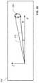
- This present patent documentdiscloses a MRAM device that does not use a polarization layer having a fixed magnetization direction. Instead of a polarization layer having a fixed magnetization direction, the MRAM device described in this patent document utilizes a precessional spin current (PSC) magnetic layer 350 in conjunction with a perpendicular MTJ 430 where the in-plane magnetization component direction of the PSC layer is free to rotate (and is shown, for example, in FIG. 4 ). PSC magnetic layer 350 can rotate with the free-layer magnetization precessional dynamics.
- PSCprecessional spin current
- FIG. 4shows the concept behind the MRAM device using a PSC magnetic layer 350 having magnetization vector 270 that rotates instead of a polarization layer 150 having a magnetic vector with a fixed magnetization direction.
- the free layer 336 in this embodimentis similar to the free layer 136 previously discussed, in that it has an inherent damping characteristic 205 that can be overcome with the assistance of spin transfer torque.
- the embodiment shown in FIG. 4replaces polarizing layer 150 with PSC magnetic layer 350 .
- the direction of the spin transfer torque 310 created by spin current passing through free layer 336changes with the rotation of the magnetization direction of PSC magnetic layer 350 .
- spin transfer torque 310helps the magnetization direction 200 ′ of the free layer 336 to precess in a cone-like manner around an axis 202 perpendicular to the plane of the layers.
- FIG. 4shows a progression of rotation of the magnetic direction 200 ′ about axis 202 .
- the magnetization of the free layer 336precesses in a continuous manner (i.e. it turns on itself in a continuous manner as shown in FIG. 4 ) with maintained oscillations until the magnetic direction of free layer 336 is opposite the magnetic direction prior to the spin torque causing precession, i.e., the magnetic direction of free layer 136 switches by 180 degrees.
- the precessional spin current layer 350 and the free-layer 336are magnetically and/or electronically coupled such that the magnetization direction of the magnetization vector 270 of the PSC magnetic layer 350 is free to follow the precessional rotation of the magnetic vector of the free layer 336 . This can be seen in FIG. 4 .
- the spin polarized electronsprovide torque 310 helps to overcome the damping 205 in the first half of the precession 215 because the torque 310 provided by the spin polarized current is opposite that of the inherent damping 205 of the free layer 336 .
- the magnetization direction of magnetization vector 270 of PSC magnetic layer 350rotates.
- the polarization of electrons of the spin current created by PSC magnetic layer 350changes as well. This means that the direction of torque 310 exerted on magnetic vector of free layer 336 changes as well, which is seen on the bottom of FIG. 4 .
- the spin of the electrons in the spin polarized currentapplies a torque 310 in both halves of the precession cycle, including the half of the precession cycle 220 where devices with fixed polarization magnetic layers 150 actually harmed precession. This is seen in the left-hand side of FIG. 4 . As is seen, the torque 310 continues to help overcome the inherent damping 205 of free layer 136 throughout the entire precession cycle.
- the precessional vector 270 of the PSC magnetic layer 350is free to follow the precessional rotation of the magnetic vector of the free layer 336 .
- the magnetization direction of the free layeris switched by the spin torque 310 from the reference layer 132 where the direction of the current defines the final state.
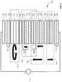
- a memory cell with a precessional spin current MTJ structure 300is shown in FIG. 5 .
- the embodiment shown in FIG. 5is preferably formed on a silicon substrate or other appropriate base for a magnetic device, and can include complementary metal oxide semiconductor (CMOS) circuitry fabricated thereon.
- MTJ structure 300includes one or more seed layers 320 provided at the bottom of stack 300 to initiate a desired crystalline growth in the above-deposited layers.
- a first synthetic antiferromagnetic (SAF) layer 322is disposed over seed layer 320 . As seen in FIG. 5 , first SAF layer 322 is a magnetic layer having a magnetization direction that is perpendicular to its plane. Details of the construction of first SAF layer 322 will be discussed below.
- An anti-ferromagnetic (AFM) coupling layer 324is disposed over first SAF layer 322 .
- AFM coupling layer 324is a nonmagnetic layer.
- a second SAF layer 326is disposed over AFM coupling layer 324 .
- second SAF layer 326has a magnetic direction that is perpendicular to its plane.
- the magnetic direction of first SAF layer 322 and second SAF layer 326are antiparallel, as is shown in FIG. 5 . Details of the construction of second SAF layer 326 will also be discussed below.
- a ferromagnetic coupling layer 328is placed over second SAF layer 326 . Ferromagnetic coupling layer 328 is a nonmagnetic layer.
- MTJ 330is deposited over ferromagnetic coupling layer 328 .
- MTJ 330includes reference layer 332 , tunneling barrier layer (i.e., the insulator) 334 and free layer 336 .
- Reference layer 332 of MTJ 330is fabricated over ferromagnetic coupling layer 328 .
- Tunneling barrier layer 334 of MTJ 330is fabricated over reference layer 332 .
- Free layer 336 of MTJ 330is fabricated over tunneling barrier layer 334 .
- synthetic antiferromagnetic layer 326technically also includes ferromagnetic coupling layer 328 and reference layer 332 , but are shown separately here for explanation purposes.
- the magnetization vector of reference layer 332has a magnetization direction that is perpendicular to its plane.
- free layer 336also has a magnetization vector that is perpendicular to its plane, but its direction can vary by 180 degrees.
- free layer 336 designmay include magnetization of the free layer 336 pointing a few degrees away from its perpendicular axis. The tilted angle of the free layer magnetization can be due to interaction with the PSC magnetic layer 350 or due to magnetocrystalline anisotropy, and will additionally help switching of the free layer magnetization by improving the initiation of the switching. Because reference layer 332 and free layer 336 each have a magnetic direction that is perpendicular to their respective planes, MTJ 330 is known as a perpendicular MTJ.
- a nonmagnetic spacer layer 340is disposed over of MTJ 330 .
- Precessional spin current (“PSC”) magnetic structure 350is disposed over nonmagnetic spacer layer 340 .
- PSC magnetic structure 350has a magnetization vector having a magnetic direction parallel to its plane, and is perpendicular to the magnetic vector of the reference layer 332 and free layer 336 .
- One or more capping layers 370can be provided on top of PSC layer 350 to protect the layers below on MTJ stack 300 .
- Nonmagnetic spacer layer 340has a number of properties. For example, nonmagnetic spacer layer 340 physically separates the free layer 336 and the PSC structure 350 . Nonmagnetic spacer layer 340 transmits spin current efficiently from the PSC magnetic structure 350 into the free layer 336 . Nonmagnetic spacer layer 340 also promotes good microstructure and high tunneling magnetoresistance (TMR) and helps keep the damping constant of the free layer 336 low.
- TMRtunneling magnetoresistance
- PSC magnetic structure 350comprises multiple layers.
- a first precessional spin current (“PSC”) ferromagnetic layer 343is formed over nonmagnetic spacer layer 340 .
- a nonmagnetic precessional spin current (“PSC”) insertion layer 345is formed over first PSC ferromagnetic layer 343 .
- a second precessional spin current (“PSC”) ferromagnetic layer 347is formed over nonmagnetic PSC insertion layer 345 .
- the nonmagnetic PSC insertion layer 345improves performance of PSC magnetic structure 350 because it allows tailoring of both the static and dynamic coupling of the PSC magnetic structure 350 to free layer 336 .
- the static couplingis exchange coupling while the dynamic coupling is the spin pumping effect.
- first and second ferromagnetic PSC layers 343 and 347 by nonmagnetic PSC insertion layer 345avoids strong magneto-static coupling of the PSC magnetic structure 350 to free layer 336 . This improves the impact that precession of PSC magnetic structure 350 has on free layer 336 while also retaining the stability of free layer 336 .
- a thin nonmagnetic PSC insertion layer 345is used, which can achieve static and dynamic coupling of first and second ferromagnetic PSC layers 343 and 347 via nonmagnetic PSC insertion layer 345 . Static coupling takes place via exchange coupling while dynamic coupling takes place via spin pumping.
- nonmagnetic PSC insertion layer 345can have a thickness ranging from one nanometer to three nanometers. When nonmagnetic PSC insertion layer 345 has a thickness of approximately one nanometer, one can achieve static coupling via exchange and dynamic coupling via spin pumping effect of precessing magnetizations of adjacent first and second ferromagnetic PSC layers 343 and 347 .
- nonmagnetic PSC insertion layer 345When the thickness of nonmagnetic PSC insertion layer 345 is greater than one nanometer, the exchange coupling between adjacent first and second ferromagnetic PSC layers 343 and 347 becomes smaller, but dynamic coupling via spin pumping effect will be present and becomes dominant. This approach provides better control of the coupling between PSC magnetic structure 350 and free layer 336 .
- the spin polarized current that can switch free layer 336 of magnetic tunnel junction 330is provided by PSC magnetic structure 350 by using a spin pumping mechanism and/or exchange coupling which is facilitated via nonmagnetic PSC insertion layer 345 .
- First ferromagnetic PSC layer 343which can be directly deposited on nonmagnetic spacer layer 340 , ensures continuity of a spin current generated by the second ferromagnetic PSC layer 347 and transfers the spin polarized electrons of the programming current to free layer 336 .
- an MRAM cellis programmed by passing direct current from, for example, current source 375 , through the PSC magnetic structure 350 , magnetic tunnel junction 330 , and the remaining structures of device 300 .
- Current used for programminge.g., a write operation
- the precessional angle of the magnetic vector of second PSC ferromagnetic layer 347becomes large.
- the in-plane component of the magnetic vector of second PSC ferromagnetic layer 347is transferred to the first PSC ferromagnetic layer 343 by spin pumping, which is now orthogonal to free layer 336 , thus lowering the energy barrier required for switching of free layer 336 .
- the amount of switching current required to switch free layer 336is reduced when compared to other MRAM devices that use fixed polarizing layers, e.g., polarizer layer 150 or other PSC magnetic layers.
- the magnetization direction of PSC magnetic structure 350has the following additional properties.
- the magnetization direction of PSC magnetic structure 350is in the plane of the layer but is perpendicular to magnetization direction of free layer 336 .
- the magnetization direction of PSC magnetic structure 350can have a horizontal component X and perpendicular component Z such that the angle ⁇ between the plane of free layer 336 and the magnetic direction 270 of PSC magnetic structure 350 can be anywhere between 0 and less than 90 degrees, although, as discussed, the angle is as close to zero as feasible so that the magnetic direction remains in-plane.
- the magnetization vectorcan also spin in a rotational manner, shown in FIG. 10 as cone-like rotation 280 while precessing about its perpendicular axis. Note that the angle ⁇ between the plane of free layer 336 and the magnetic direction 270 of PSC magnetic layer 350 will vary in this situation.
- Seed layer 320 in the MTJ structure shown in FIG. 5preferably comprises Ta, TaN, Cr, Cu, CuN, Ni, Fe or alloys thereof.
- First SAF layer 322preferably comprises either a Co/Ni or Co/Pt multilayer structure.
- Second SAF layer 326preferably comprises either a Co/Ni or Co/Pt multilayer structure plus a thin nonmagnetic layer comprised of tantalum having a thickness of two to five Angstroms.
- Anti-ferromagnetic coupling layer 324is preferably made from Ru having thickness in the range of three to ten Angstroms.
- Ferromagnetic coupling layer 328can be made of a layer of Ta, W, Mo or Hf having a thickness in the range of 1.0 to 10 Angstroms.
- Tunneling barrier layer 334is preferably made of an insulating material such as MgO, with a thickness of approximately ten Angstroms.
- Free layer 336is preferably made with CoFeB deposited on top of tunneling barrier layer 334 . Free layer 336 can also have layers of Fe, Co, Ni or alloys thereof.
- Spacer layer 340 over MTJ 330can be any nonmagnetic material such as 2 to 20 Angstroms of Ruthenium, 2-20 Angstroms of Ta, 2-20 Angstroms of TaN, 2-20 Angstroms of Cu, 2-20 Angstroms of CuN, or 2-20 Angstroms of MgO.
- an electrical currentis supplied, for example, by a current source 375 , which passes electrical current through the precessional spin current magnetic structure 350 , the nonmagnetic spacer layer 340 , the free magnetic layer 336 , the nonmagnetic tunneling barrier layer 334 , and the reference layer 332 .
- the electrons of the electrical current passing through the precessional spin current magnetic structure 350become spin polarized in the magnetic direction thereof, thus creating a spin polarized current that passes through nonmagnetic spacer layer 340 .
- the spin polarized currentexerts a spin transfer torque on free magnetic layer 336 , which helps overcome the inherent damping of the magnetic material making up the free layer 336 . This causes the free magnetic layer 336 to precess about its axis, which is shown in FIG. 4 .
- the magnetic direction of the PSC magnetic structure 350begins to rotate, as is also seen in FIG. 4 .
- the rotation of the magnetic direction of the PSC magnetic structure 350causes the spin polarization of the electrons of the electrical current to change in a manner corresponding to the magnetic direction of the PSC magnetic structure 350 .
- the spin of the electrons of the spin polarized currentcorresponds to the magnetic direction of PSC magnetic structure 350
- the spin of the electronsapplies spin transfer torque to the free layer 336 in a direction that varies through an entire switching cycle.
- devices using PSC magnetic structure 350can provide spin transfer torque 310 for an entire switching cycle.
- the structure described herein utilizing PSC magnetic structure 350 and spacer layer 340creates precessional magnetization that provides spin current to the free layer 336 of an MTJ throughout the whole precession cycle and therefore significantly enhance the free layer switching process, which will result in faster write times.
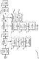
- FIGS. 6A-6BA flowchart showing a method 400 of manufacturing an embodiment of an MRAM stack 500 is illustrated in FIGS. 6A-6B .
- MRAM stack 500will normally be fabricated on some form of substrate, which in certain embodiments can be a silicon substrate.
- MRAM stack 500is illustrated in FIG. 7 .
- First step 402is to deposit seed layer 520 .
- seed layer 520can be constructed by depositing, at step 404 , a TaN layer 504 and then, at step 406 , depositing a Cu layer 506 .
- TaN layer 504is a thin film having a thickness of five nanometers and Cu layer 506 is a thin film having a thickness of five nanometers.
- TaN layer 504can have a thickness ranging from 2 to 20 nanometers while Cu layer 506 can have a thickness ranting from 0 to 20 nanometers.
- first perpendicular synthetic antiferromagnetic layer 522is deposited.
- first perpendicular synthetic antiferromagnetic layer 522can comprise a Pt layer 508 (deposited at step 410 ), a Co/Pt multilayer 510 (deposited at step 412 ) and a Co layer 512 (deposited at step 414 ).
- Pt layer 508is a Pt thin film having a thickness of 0.7 nanometers. In other embodiments, Pt layer 508 can comprise a Pt thin film having a thickness ranging from 0.5 to 20 nanometers.
- Co/Pt multilayer 510can comprise a thin film of Co having a thickness of 0.6 nanometers and a thin film of Pt having a thickness of 0.4 nanometers.
- the Co layer of Co/Pt multilayer 510can have a thickness of 0.1 to 1.0 nanometers and the Pt layer of Co/Pt multilayer 510 can have a thickness ranging from 0.1 to 1.0 nanometers.
- Co/Pt multilayer 510is repeated such that Co/Pt multilayer 510 comprises six Co/Pt multilayers.
- Co layer 512is a thin film having a thickness of 0.6 nanometers. In other embodiments, Co layer 512 can have a thickness ranging from 0.1 to 1.0 nanometers.
- first perpendicular synthetic antiferromagnetic layer 522has a magnetic vector having a direction perpendicular to its plane.
- the magnetic direction of first perpendicular synthetic antiferromagnetic layer 522is fixed and will not change directions (i.e., rotate or precess) under normal operating conditions.
- exchange coupling layer 524is deposited.
- exchange coupling layer 524comprises an Ru thin film having a thickness of 0.8 nanometers, and in other embodiments can range from 0.3 to 1.5 nanometers.
- second perpendicular synthetic antiferromagnetic layer 526is fabricated. Fabrication of second perpendicular synthetic antiferromagnetic layer 526 (step 418 ) comprises many steps, and includes fabrication of reference layer 532 of magnetic tunnel junction 530 , as will be discussed.
- Co layer 514is deposited. In an embodiment, Co layer 514 is a thin film having a thickness of 0.3 nanometers and in other embodiments, can have a thickness of 0.1 to 1.0 nanometers. Thereafter, at step 420 , a Co/Pt multilayer 516 is deposited.
- Co/Pt multilayer 516comprises a thin film of Co having a thickness of 0.6 nanometers and a thin film of Pt having a thickness of 0.4 nanometers.
- the thin film of Cocan have a thickness of 0.1 to 1.0 nanometers while the thin film of Pt can have a thickness of 0.1 to 1.0 nanometers.
- Co/Pt multilayer 516can comprise multiple Co/Pt layers as described herein.
- Co/Pt multilayer 516has two Co/Pt multilayers with the thickness properties described above. After depositing Co/Pt multilayer 516 at step 422 , the method described herein deposits a cobalt layer 518 at step 424 .
- Co layer 518is a thin film having a thickness of 0.6 nanometers, while other embodiments, Co layer 518 can have a thickness in the range of 0.1 to 1.0 nanometers.
- Co layer 514 , Co/Pt layer 516 and Co layer 518form a magnetic structure.
- the magnetic direction of the combination of Co layer 514 , Co/Pt layer 516 and Co layer 518is fixed, perpendicular to the plane of each layer, and antiparallel to the magnetic direction of first perpendicular synthetic antiferromagnetic layer 522 .
- the magnetic properties of the combination of Co layer 514 , Co/Pt layer 516 and Co layer 518will interact with the magnetic properties of reference layer 532 of second perpendicular synthetic antiferromagnetic layer 526 to generate a magnetic vector having a fixed magnetic direction that is also perpendicular to the plane of each layer of second perpendicular synthetic antiferromagnetic layer 526 and antiparallel to the magnetic direction of first perpendicular synthetic antiferromagnetic layer 522 .
- These magnetic vectorsare illustrated and FIG. 7 , where it can be seen that the second perpendicular synthetic antiferromagnetic layer 526 has a fixed and perpendicular magnetic direction that is antiparallel to the magnetic direction of first perpendicular synthetic antiferromagnetic layer 522 . Note that the magnetic directions of second perpendicular synthetic antiferromagnetic layer 526 and first perpendicular synthetic antiferromagnetic layer 522 are fixed under normal operating conditions.
- ferromagnetic coupling layer 528is deposited (step 526 ).
- ferromagnetic coupling layer 528is a thin film of Ta having a thickness of 0.2 nanometers.
- ferromagnetic coupling layer 528can be a thin film of Ta, W, Hf or Mo having a thickness ranging from 0.1 to 1.0 nanometers.
- reference layer 532is deposited (step 428 ).
- Step 428fabrication of reference layer 532 , comprises several steps, including deposition of magnetic layer 527 (step 430 ), deposition of a tungsten (W) layer 529 (step 432 ) and deposition of magnetic layer 531 (step 434 ).
- magnetic layer 527comprises a thin film of CoFeB comprised of sixty percent iron (Fe), twenty percent cobalt (Co) and twenty percent boron (B), where the thin film has a thickness of 0.6 nanometers.
- W layer 529comprises a thin film having a thickness of 0.2 nanometers.
- magnetic layer 531comprises a thin film of CoFeB comprised of sixty percent iron (Fe), twenty percent cobalt (Co) and twenty percent boron (B), where the thin film has a thickness of 0.8 nanometers.
- magnetic layer 527can comprise a thin film of CoFeB having a thickness ranging from 0.5 to 1.5 nanometers
- W layer 529can comprise a thin film having a thickness of 0.1 to 1.0 nanometers
- magnetic layer 531can comprise a thin film of CoFeB having a thickness of 0.5 to 2.0 nanometers.
- Reference layer 532is constructed using magnetic materials so that it has a magnetic vector having a magnetic direction perpendicular to its plane, is fixed in direction, and is antiparallel to the magnetic direction of first perpendicular synthetic antiferromagnetic layer 522 .
- the collective materials of the second perpendicular synthetic antiferromagnetic layer 526have a magnetic vector having a magnetic direction that is perpendicular to the plane of each of its collective layers, is fixed in direction and antiparallel to the magnetic direction of first perpendicular synthetic antiferromagnetic layer 522 .
- the particular magnetic direction of first perpendicular synthetic antiferromagnetic layer 522 and second perpendicular synthetic antiferromagnetic layer 526is not important, so long as they are perpendicular to their respective planes and antiparallel to each other.
- reference layer 532is one of the structures forming magnetic tunnel junction 530 .
- nonmagnetic tunneling barrier layer 534is deposited on reference layer 532 .
- nonmagnetic tunneling barrier 534is formed as a thin film of an insulating material, e.g., MgO, and has a thickness of 1.1 nm. The purpose of nonmagnetic tunneling barrier 534 is discussed above.
- Magnetic tunnel junction 530continues at step 438 , when free layer 536 is deposited over nonmagnetic tunneling barrier 534 .
- Fabrication of free layer 536comprises several steps.
- a magnetic layer 535is deposited over nonmagnetic tunneling barrier 534 .
- magnetic layer 535is comprised of a thin film of CoFeB comprised of sixty percent iron (Fe), twenty percent cobalt (Co) and twenty percent boron (B), and having a thickness of 1.2 nanometers.
- magnetic layer 535can comprise a thin film of CoFeB or other suitable magnetic material having a thickness ranging from 0.5 to 2.0 nanometers.
- W layer 537comprises a thin film of W having a thickness of 0.2 nanometers, and in other embodiments can have a thickness ranging from 0.1 to 1.0 nanometers.
- manufacture of free layer 536continues with forming magnetic layer 539 .
- magnetic layer 539can comprise a thin film of CoFeB comprised of sixty percent iron (Fe), twenty percent cobalt (Co) and twenty percent boron (B), and having a thickness of 0.9 nanometers.
- magnetic layer 539can comprise a thin film of CoFeB or other suitable magnetic material having a thickness ranging from 0.5 to 1.5 nanometers.
- Free magnetic layer 536has a magnetic vector having a magnetic direction perpendicular to its plane.
- free magnetic layer 536 designmay include magnetization of the free layer 536 pointing a few degrees away from its perpendicular axis. The tilted angle of the free layer magnetization can be due to interaction with the PSC magnetic layer 550 or due to magnetocrystalline anisotropy, will additionally help switching of the free layer magnetization by improving the initiation of the switching.
- the magnetic direction of free magnetic layer 536can switch one hundred eighty (180) degrees from one direction to another, antiparallel, direction.
- nonmagnetic spacer layer 540can comprise a thin film of MgO having a thickness of 0.9 nanometers. In other embodiments, spacer layer 540 can comprise a thin film of MgO having a thickness ranging from 0.5 to 1.5 nanometers. In other embodiments, spacer layer 540 can be constructed as described in U.S. patent application Ser. No. 14/866,359, filed Sep. 25, 2015, and entitled “Spin Transfer Torque Structure For MRAM Devices Having A Spin Current Injection Capping Layer.” U.S. patent application Ser. No. 14/866,359 is hereby incorporated by reference in its entirety.
- precessional spin current magnetic structure 550is deposited (step 450 ). As seen in FIG. 6B , manufacture of precessional spin current magnetic structure 550 comprises several steps. At step 452 , first precessional spin current ferromagnetic layer 543 is fabricated over spacer layer 540 . In an embodiment, first precessional spin current ferromagnetic layer 543 comprises a thin film of Fe having a thickness of 0.4 nanometers. In other embodiments, first precessional spin current ferromagnetic layer 543 can comprise a thin film of Fe having a thickness ranging from 0.5 to 2.0 nanometers.
- nonmagnetic precessional spin current insertion layer 545is deposited over magnetic Fe layer 543 .
- nonmagnetic precessional spin current insertion layer 545can comprise a thin film of Ru having a thickness of 1.5 nanometers.
- the thickness of nonmagnetic precessional spin current insertion layer 545can be selected to control and tune the coupling of the first precessional spin current ferromagnetic layer 543 to the second precessional spin current ferromagnetic layer 547 (described below).
- Use of nonmagnetic precessional spin current insertion layer 545provides several improvements and advantages.
- nonmagnetic precessional spin current insertion layer 545enables precessional spin current magnetic structure 550 to utilize a spin pumping mechanism to control the spin torque efficiency of precessional spin current magnetic structure 550 .
- Nonmagnetic precessional spin current insertion layer 545also enables decreasing of dipolar fringing fields from precessional spin current magnetic structure 550 acting on free layer 536 due to the thickness of separation between the first precessional spin current ferromagnetic layer 543 and free layer 536 . Strong fringing fields are an unwanted effect and can prevent free layer 536 from switching under normal operating conditions because of the large dipolar magnetic field acting on free layer 536 .
- nonmagnetic precessional spin current insertion layer 545 of the embodiment shown in FIG. 7can be constructed of Ru
- other nonmagnetic materials having a relatively long spin diffusion lengthe.g., greater than five nanometers
- nonmagnetic materialsinclude Cu (which has a spin diffusion length of approximately 400 nm), Ag (which has a spin diffusion length of approximately 150 nm), Au (which has a spin diffusion length of approximately 35 nm), Mg (which has a spin diffusion length of approximately 150 nm) and Al (which has a spin diffusion length of approximately 300 nm).
- Rudescribed above, has a spin diffusion length of approximately ten (10) nm.
- Use of materials like these, which have a relatively long spin diffusion lengthmakes it possible to achieve desired spin torque efficiency of precessional spin current magnetic structure 550 via dynamic coupling due to the spin pumping effect.
- second precessional spin current ferromagnetic layer 547is deposited.
- second precessional spin current ferromagnetic layer 547comprises a thin film of CoFeB comprised of forty percent iron (Fe), forty percent cobalt (Co) and twenty percent boron (B), and having a thickness of 1.7 nanometers.
- second precessional spin current ferromagnetic layer 547can comprise of a thin film of CoFeB, Co, Fe, Ni and their alloys having a thickness ranging between 1.0 to 5.0 nanometers.
- spacer layer 540is used for effective injection of spin polarized current into magnetic tunnel junction 530 from precessional spin current magnetic structure 550 .
- Spin currentis generated by precessing the magnetization direction of second precessional spin current ferromagnetic layer 547 and carried by spin diffusive transport through nonmagnetic precessional spin current insertion layer 545 into first precessional spin current ferromagnetic layer 543 using spin pumping effect.
- the second precessional spin current ferromagnetic layer 547 and first precessional spin current ferromagnetic layer 543 magnetizationsbecome dynamically coupled via spin pumping mechanism.
- First precessional spin current ferromagnetic layer 543serves as a spin current injection layer, which provides continuity of the spin current generated by second precessional spin current ferromagnetic layer 547 .
- nonmagnetic precessional spin current insertion layer 545has a thickness above approximately one nanometer, the exchange coupling between first precessional spin current ferromagnetic layer 543 and second precessional spin current ferromagnetic layer 547 is significantly reduced.
- nonmagnetic precessional spin current insertion layer 545has a thickness above approximately one nanometer, dynamic coupling between second precessional spin current ferromagnetic layer 547 and first precessional spin current ferromagnetic layer 543 via the spin pumping effect becomes dominant.
- a precessional spin current magnetic structure 550 having a first precessional spin current ferromagnetic layer 543 and second precessional spin current ferromagnetic layer 547 separated by nonmagnetic precessional spin current insertion layer 545provides better control and allows for tuning of the coupling between the precessional spin current magnetic structure 550 and free layer 536 .
- a capping layer 551is deposited (step 460 ).
- Manufacture of capping layer 551can comprise depositing TaN layer 553 (step 462 ) and depositing Ru layer 555 (step 464 ).
- TaN layer 553comprises a thin film of TaN having a thickness of 2.0 nanometers, while in other embodiments, TaN layer 553 can have a thickness ranging from 1.0 to 5.0 nanometers.
- Ru layer 555comprises a thin film of Ru having a thickness of ten (10) nanometers, while in other embodiments, Ru layer 555 can have a thickness ranging from 1.0 to 20 nanometers.
- capping layer 551comprise a layer of Ru (with no TaN) or a layer of MgO.
- the selection of a particular capping structureis influenced, among several reasons, by the particular annealing temperature to be used. This is due to the fact that these particular materials will have different characteristics depending on the annealing temperature.
- a hard mask 557is deposited.
- Hard mask 557can comprise TaN.
- MTJ stack 500is annealed at 300 degrees Celsius for one hour. Such a device, after annealing, had a tunneling magnetoresistance (TMR) above 100% with resistance area product (RA) range of 5-10 ⁇ m 2 .
- Currentcan be provided by a current source 575 .
- FIGS. 8A-8BA flowchart showing a method 600 of manufacturing an embodiment of an MRAM stack 700 is illustrated in FIGS. 8A-8B .
- MRAM stack 700will normally be fabricated on some form of substrate, which in certain embodiments can be a silicon substrate, and can include complementary metal oxide semiconductor (CMOS) circuitry fabricated thereon.
- CMOScomplementary metal oxide semiconductor
- First step 602is to deposit seed layer 720 .
- seed layer 720can be constructed by depositing, at step 604 , a TaN layer 704 and then, at step 606 , depositing a Cu layer 706 .
- TaN layer 704is a thin film having a thickness of ten nanometers and Cu layer 706 is a thin film having a thickness of three nanometers.
- TaN layer 704can have a thickness ranging from 2.0 to 20 nanometers while Cu layer 706 can have a thickness ranting from 0 to 20 nanometers.
- first perpendicular synthetic antiferromagnetic layer 722is deposited.
- first perpendicular synthetic antiferromagnetic layer 722can comprise a Pt layer 708 (deposited at step 610 ), a Co/Pt multilayer 710 (deposited at step 612 ) and a Co layer 712 (deposited at step 614 ).
- Pt layer 708is a Pt thin film having a thickness of 0.7 nanometers. In other embodiments, Pt layer 708 can comprise a Pt thin film having a thickness ranging from 0.5 to 20 nanometers.
- Co/Pt multilayer 710can comprise a thin film of Co having a thickness of 0.6 nanometers and a thin film of Pt having a thickness of 0.4 nanometers.
- the Co layer of Co/Pt multilayer 710can have a thickness of 0.1 to 1.0 nanometers and the Pt layer of Co/Pt multilayer 710 can have a thickness ranging from 0.1 to 1.0 nanometers.
- Co/Pt multilayer 710is repeated such that Co/Pt multilayer 710 comprises six Co/Pt multilayers.
- Co layer 712is a thin film having a thickness of 0.6 nanometers. In other embodiments, Co layer 712 can have a thickness ranging from 0.1 to 1.0 nanometers.
- first perpendicular synthetic antiferromagnetic layer 722has a magnetic vector having a direction perpendicular to its plane.
- the magnetic direction of first perpendicular synthetic antiferromagnetic layer 722is fixed and will not change directions (i.e., rotate or precess) under normal operating conditions.
- the thickness of synthetic antiferromagnetic layerscan be chosen such as to minimize the dipolar fringing fields emerging from the reference layer and other magnetic layers within MTJ structure which act on a free layer after device fabrication
- exchange coupling layer 724is deposited.
- exchange coupling layer 724comprises an Ru thin film having a thickness of 0.8 nanometers, and in other embodiments can range from 0.3 to 1.5 nanometers.
- second perpendicular synthetic antiferromagnetic layer 726is fabricated. Fabrication of second perpendicular synthetic antiferromagnetic layer 726 (step 618 ) comprises many steps, and includes fabrication of reference layer 732 of magnetic tunnel junction 730 , as will be discussed.
- Co layer 514is deposited.
- Co layer 714is a thin film having a thickness of 0.3 nanometers and in other embodiments, can have a thickness of 0.1 to 1.0 nanometers.
- a Co/Pt multilayer 716is deposited.
- Co/Pt multilayer 716comprises a thin film of Co having a thickness of 0.6 nanometers and a thin film of Pt having a thickness of 0.4 nanometers.
- the thin film of Cocan have a thickness of 0.1 to 1.0 nanometers while the thin film of Pt can have a thickness of 0.1 to 1.0 nanometers.
- Co/Pt multilayer 716can comprise multiple Co/Pt layers as described herein.
- Co/Pt multilayer 716has two Co/Pt multilayers with the thickness properties described above. After depositing Co/Pt multilayer 716 at step 622 , the method described herein deposits a cobalt layer 718 at step 624 .
- Co layer 718is a thin film having a thickness of 0.9 nanometers, while other embodiments, Co layer 718 can have a thickness in the range of 0.1 to 1.0 nanometers.
- Co layer 714 , Co/Pt layer 716 and Co layer 718form a magnetic structure.
- the magnetic direction of the combination of Co layer 714 , Co/Pt layer 716 and Co layer 718is fixed, perpendicular to the plane of each layer (although variations of a several degrees are within the scope of what is considered perpendicular), and antiparallel to the magnetic direction of first perpendicular synthetic antiferromagnetic layer 722 .
- the magnetic properties of the combination of Co layer 714 , Co/Pt layer 716 and Co layer 718will interact with the magnetic properties of reference layer 732 of second perpendicular synthetic antiferromagnetic layer 726 to generate a magnetic vector having a fixed magnetic direction that is also perpendicular to the plane of each layer of second perpendicular synthetic antiferromagnetic layer 726 and antiparallel to the magnetic direction of first perpendicular synthetic antiferromagnetic layer 722 .
- These magnetic vectorsare illustrated and FIG. 9 , where it can be seen that the second perpendicular synthetic antiferromagnetic layer 726 has a fixed and perpendicular magnetic direction that is antiparallel to the magnetic direction of first perpendicular synthetic antiferromagnetic layer 722 . Note that the magnetic directions of second perpendicular synthetic antiferromagnetic layer 726 and first perpendicular synthetic antiferromagnetic layer 722 are fixed under normal operating conditions.
- reference layer 732is deposited (step 628 ).
- fabrication of reference layer 732comprises several steps, including deposition of a tungsten (W) layer 729 (step 632 ) and deposition of magnetic layer 731 (step 634 ).
- W layer 729comprises a thin film having a thickness of 0.3 nanometers.
- magnetic layer 731comprises a thin film of CoFeB comprised of sixty percent iron (Fe), twenty percent cobalt (Co) and twenty percent boron (B), where the thin film has a thickness of 0.8 nanometers.
- W layer 729can comprise a thin film having a thickness of 0.2 to 1.0 nanometers
- magnetic layer 731can comprise a thin film of CoFeB having a thickness of 0.5 to 1.5 nanometers.
- Reference layer 732is constructed using magnetic materials so that it has a magnetic vector having a magnetic direction perpendicular to its plane, is fixed in direction, and is antiparallel to the magnetic direction of first perpendicular synthetic antiferromagnetic layer 722 .
- the collective materials of the second perpendicular synthetic antiferromagnetic layer 726have a magnetic vector having a magnetic direction that is perpendicular to the plane of each of its collective layers, is fixed in direction and antiparallel to the magnetic direction of first perpendicular synthetic antiferromagnetic layer 722 .
- the particular magnetic direction of first perpendicular synthetic antiferromagnetic layer 722 and second perpendicular synthetic antiferromagnetic layer 726is not important, so long as they are perpendicular to their respective planes and antiparallel to each other.
- reference layer 732is one of the structures forming magnetic tunnel junction 730 .
- nonmagnetic tunneling barrier layer 734is deposited on reference layer 732 .
- nonmagnetic tunneling barrier 734is formed as a thin film of an insulating material, e.g., MgO, and has a thickness of 1.1 nm. The purpose of nonmagnetic tunneling barrier 734 is discussed above.
- Magnetic tunnel junction 730continues at step 638 , when free layer 736 is deposited over nonmagnetic tunneling barrier 734 .
- Fabrication of free layer 736comprises several steps.
- a magnetic layer 735is deposited over nonmagnetic tunneling barrier 734 .
- magnetic layer 735is comprised of a thin film of CoFeB comprised of fifty-four (54) percent iron (Fe), eighteen (18) percent cobalt (Co) and twenty-eight (28) percent boron (B), with the thin film having a thickness of 1.5 nanometers.
- magnetic layer 735can comprise a thin film of CoFeB or other suitable magnetic material having a thickness ranging from 0.5 to 2.5 nanometers.
- a W layer 737is deposited.
- W layer 737comprises a thin film of W having a thickness of 0.5 nanometers, and in other embodiments can have a thickness ranging from 0.2 to 1.0 nanometers.
- manufacture of free layer 736continues with forming magnetic layer 739 .
- magnetic layer 739can comprise a thin film of CoFeB comprised of fifty-four (54) percent iron (Fe), eighteen (18) percent cobalt (Co) and twenty-eight (28) percent boron (B), with the thin film having a thickness of 0.8 nanometers.
- magnetic layer 739can comprise a thin film of CoFeB or other suitable magnetic material having a thickness ranging from 0.5 to 2.0 nanometers.
- Free magnetic layer 736has a magnetic vector having a magnetic direction perpendicular to its plane.
- free magnetic layer 736 designmay include magnetization of the free layer 736 pointing a few degrees away from its perpendicular axis. The tilted angle of the free layer magnetization can be due to interaction with the PSC magnetic layer 750 or due to magnetocrystalline anisotropy, will additionally help switching of the free layer magnetization by improving the initiation of the switching.
- the magnetic direction of free magnetic layer 736can switch one hundred eighty (180) degrees from one direction to another, antiparallel, direction.
- nonmagnetic spacer layer 740can comprise a thin film of MgO having a thickness of 0.9 nanometers. In other embodiments, spacer layer 740 can comprise a thin film of MgO having a thickness ranging from 0.5 to 2.0 nanometers. In other embodiments, spacer layer 740 can be constructed as described in U.S. patent application Ser. No. 14/866,359, filed Sep. 25, 2015, and entitled “Spin Transfer Torque Structure For MRAM Devices Having A Spin Current Injection Capping Layer.” U.S. patent application Ser. No. 14/866,359 is hereby incorporated by reference in its entirety.
- precessional spin current magnetic structure 750is deposited (step 650 ). As seen in FIG. 8B , manufacture of precessional spin current magnetic structure 750 comprises several steps. At step 652 , first precessional spin current ferromagnetic layer 743 is fabricated over spacer layer 740 . In an embodiment, first precessional spin current ferromagnetic layer 743 comprises a thin film of Fe having a thickness of 0.6 nanometers. In other embodiments, first precessional spin current ferromagnetic layer 743 can comprise a thin film of Fe having a thickness ranging from 0.5 to 2.0 nanometers.
- nonmagnetic precessional spin current insertion layer 745is deposited over magnetic first precessional spin current ferromagnetic layer 743 .
- nonmagnetic precessional spin current insertion layer 745can comprise a thin film of Ru having a thickness of 1.5 nanometers.
- nonmagnetic precessional spin current insertion layer 745provides several improvements and advantages. As discussed, nonmagnetic precessional spin current insertion layer 745 enables precessional spin current magnetic structure 750 to utilize a spin pumping mechanism to control the spin torque efficiency of precessional spin current magnetic structure 750 .
- nonmagnetic precessional spin current insertion layer 745also enables the spin pumping mechanism to couple precession of second precessional spin current ferromagnetic layer 747 (discussed below) to first precessional spin current ferromagnetic layer 743 , thus allowing for the spin torque to be injected from the precessional spin current magnetic structure 750 into free layer 736 using nonmagnetic spacer layer 740 .
- nonmagnetic precessional spin current insertion layer 745 of the embodiment shown in FIG. 9is constructed of Ru
- other nonmagnetic materials having a relatively long spin diffusion lengthe.g., greater than five nanometers
- nonmagnetic materialsinclude Cu (which has a spin diffusion length of approximately 400 nm), Ag (which has a spin diffusion length of approximately 150 nm), Au (which has a spin diffusion length of approximately 35 nm), Mg (which has a spin diffusion length of approximately 150 nm) and Al (which has a spin diffusion length of approximately 300 nm).
- Rudescribed above, has a spin diffusion length of approximately ten (10) nm.
- Use of materials like these, which have a relatively long spin diffusion lengthmakes it possible to achieve the desired spin torque efficiency of precessional spin current magnetic structure 750 via dynamic coupling due to the spin pumping effect.
- second precessional spin current ferromagnetic layer 747is deposited.
- second precessional spin current ferromagnetic layer 747comprises a thin film of CoFeB comprised of forty percent iron (Fe), forty percent cobalt (Co) and twenty percent boron (B), and having a thickness of 1.85 nanometers.
- second precessional spin current ferromagnetic layer 747can comprise of a thin film of CoFeB, Co, Fe, Ni and their alloys having a thickness ranging between 1.0 to 5.0 nanometers.
- spacer layer 740is used for effective injection of spin polarized current into magnetic tunnel junction 730 from precessional spin current magnetic structure 750 .
- spin currentis generated by precessing the magnetization direction of second precessional spin current ferromagnetic layer 747 and carried by spin diffusive transport through nonmagnetic precessional spin current insertion layer 745 into first precessional spin current ferromagnetic layer 743 using spin pumping effect.
- the second precessional spin current ferromagnetic layer 747 and first precessional spin current ferromagnetic layer 743 magnetizationsbecome dynamically coupled via a spin pumping mechanism.
- First precessional spin current ferromagnetic layer 743serves as a spin current injection layer, which provides continuity of the spin current generated by second precessional spin current ferromagnetic layer 747 .
- the thickness of the nonmagnetic precessional spin current insertion layer 745can be selected to select the desired amount of coupling of the second precessional spin current ferromagnetic layer 747 to the first precessional spin current ferromagnetic layer 743 , which in turn can be used to tune the coupling of precessional spin current magnetic structure 750 to free layer 736 .
- a capping layer 751is deposited (step 660 ).
- Manufacture of capping layer 751can comprise depositing TaN layer 753 (step 662 ) and depositing Ru layer 755 (step 664 ).
- TaN layer 753comprises a thin film of TaN having a thickness of 2.0 nanometers, while in other embodiments, TaN layer 753 can have a thickness ranging from 1.0 to 5.0 nanometers.
- Ru layer 755comprises a thin film of Ru having a thickness of ten (10) nanometers, while in other embodiments, Ru layer 755 can have a thickness ranging from 1.0 to 20 nanometers.
- capping layer 751comprise a layer of Ru (with no TaN) or a layer of MgO.
- the selection of a particular capping structureis influenced, among several reasons, by the particular annealing temperature to be used. This is due to the fact that these particular materials will have different characteristics depending on the annealing temperature.
- MTJ stack 700is annealed at 400 degrees Celsius for up to forty-five (45) minute soak time using in-situ rapid thermal annealing oven.
- hard mask 757is deposited.
- Hard mask 757can comprise a layer of TaN having a thickness of 7.0 nanometers.
- the acceptable range of temperatures for the annealing stepis within the range of 250 degrees Celsius to 450 degrees Celsius.
- Currentcan be provided by a current source 775 .
- the MTJ stack 700 manufactured as described with the high temperature annealing step 666results in a device 700 having tunneling magnetoresistance (TMR) of above one hundred sixty (160) percent (which is advantageously high) and a resistance area product (RA) range up to approximately ten (10) to twelve (12) ⁇ m 2 .
- TMRtunneling magnetoresistance
- RAresistance area product
- FIG. 11is a graph of the thin film vibrating sample magnetometer (VSM) major hysteresis loop data for magnetic device 500 having magnetic tunnel junction 530 and precessional spin current magnetic structure 550 .
- VSMthin film vibrating sample magnetometer
- a magnetic fieldwas applied with a magnetic direction that was perpendicular to the sample plane i.e. along easy axis of magnetic tunnel junction 530 .
- the applied magnetic fieldstarted at ⁇ 12,000 Oersteds, which then decreased to 0.00 Oersteds, before rising to +12,000 Oersteds, another very large magnetic field.
- the magnetic fieldwas then decreased from +12,000 Oersteds to 0.00 Oersteds, and then increased to ⁇ 12,000 Oersteds.
- Positive and negative signs of the DC applied fieldindicate perpendicular applied field directions of the field sweep.
- Switching of the magnetic direction of particular components of the pMTJis shown schematically by the arrows. Any switching of the magnetic direction of first perpendicular synthetic antiferromagnetic layer 522 is shown with the arrows 1110 A, 1110 B and 1110 C, each of which illustrates the magnetic direction of the layer. Any switching of the magnetic direction of second perpendicular synthetic antiferromagnetic layer 526 is shown with the arrows 1120 A, 1120 B and 1120 C, each of which illustrates the magnetic direction of the layer. Finally, any switching of free layer 536 is shown with the arrows 1130 A, 1130 B and 1130 C, each of which illustrates the magnetic direction of the layer.
- first perpendicular synthetic antiferromagnetic layer 522As is seen in FIG. 11 , as the perpendicular magnetic field is decreased from ⁇ 12,000 Oersteds, the magnetic direction first perpendicular synthetic antiferromagnetic layer 522 , does not reverse directions until the magnetic field measures approximately +4,000 Oersteds. This is shown by arrow 1110 C, illustrating that the magnetic direction of first perpendicular synthetic antiferromagnetic layer 522 has switched. This demonstrates first perpendicular synthetic antiferromagnetic layer 522 is very stable since it would not experience such conditions under normal use. This stability demonstrates that use of precessional spin current magnetic structure 550 does not negatively impact the stability of the entire reference layer 532 and its exchange coupling field.
- second perpendicular synthetic antiferromagnetic layer 526does not reverse directions until a perpendicular magnetic field of approximately ⁇ 4,000 Oersteds is applied. This is shown by arrow 1120 A, illustrating that the magnetic direction of second perpendicular synthetic antiferromagnetic layer 526 has switched. Because a device 500 will not experience such a large magnetic field under normal operating conditions, this test demonstrates that the second perpendicular synthetic antiferromagnetic layer 526 is very stable, which also demonstrates that use of precessional spin current magnetic structure 550 does not negatively impact other magnetic structures in device 500 . This is also important since the reference layer 532 contained in second perpendicular synthetic antiferromagnetic layer 526 must have a fixed magnetic direction for the magnetic tunnel junction 530 to function properly.
- FIG. 11demonstrates that device 500 , including precessional spin current magnetic structure 550 , has excellent free layer switching performance. Switching of free layer occurs at approximately 0.00 Oersteds, and is illustrated by arrow 1130 B.
- Sharp switching transitionsindicate good perpendicular anisotropies of first perpendicular synthetic antiferromagnetic layer 522 , reference layer 532 (including second perpendicular synthetic antiferromagnetic layer 526 ) and free layer 536 of the perpendicular magnetic tunnel junction 530 .
- Exchange coupling of 4.3 kOeindicates good stability of the reference layer.
- a slope of the hysteresis loop between ⁇ 3.0 kOeindicates a rotation of precessional spin current magnetic structure 550 which is orthogonal to the layers of perpendicular magnetic tunnel junction 530 , i.e., along hard axis of the perpendicular applied field.
- FIG. 12is a graph of the thin film vibrating sample magnetometer (VSM) major hysteresis loop data for magnetic device 500 having magnetic tunnel junction 530 and precessional spin current magnetic structure 550 .
- VSMthin film vibrating sample magnetometer
- 1200 in FIG. 12To measure the VSM major hysteresis loop (labeled as 1200 in FIG. 12 ), a magnetic field was applied with a magnetic direction that was in the plane of the layers of magnetic tunnel junction 530 . As seen in FIG. 12 , the applied magnetic field started at ⁇ 14,000 Oersteds, which then decreased to 0.00 Oersteds, before rising to +14,000 Oersteds, another very large magnetic field.
- the applied fieldwas then decreased steadily from +12,000 Oersteds to 0.00 Oersteds, before increasing to ⁇ 12000 Oersteds.
- the magnetic fieldwas then decreased from +14,000 Oersteds to 0.00 Oersteds, and then increased to ⁇ 14,000 Oersteds.
- Positive and negative signs of the DC applied fieldindicate in-plane applied field directions of the field sweep.
- VSM major hysteresis loop 1200Increasing slope of the VSM major hysteresis loop 1200 corresponds to the slow rotation of the layers of magnetic tunnel junction 530 when the magnetic field is applied in-plane, which is orthogonal to the magnetic direction of those layers.
- the sharp transition of the VSM major hysteresis loop 1200 around zero fieldcorresponds to precession of the precessional spin current magnetic structure 550 .
- This sharp switchingindicates that precessional spin current magnetic structure 550 is in-plane magnetized, i.e., along the easy axis of the in-plane applied magnetic field.
- the VSM major hysteresis loops 1100 and 1200 shown in FIGS. 11 and 12demonstrate that free layer 530 and precessional spin current magnetic structure 550 are orthogonally magnetized with respect to each other.
- FIG. 13shows the ferromagnetic resonance of a magnetic tunnel junction device 500 having precessional spin current magnetic structure 550 measured at twenty four (24) GHz.
- the magnetic fieldwas applied in perpendicular direction.
- precessional spin current magnetic structure 550 resonancewill occur in the field above the ⁇ / ⁇ ⁇ 8.0 kGauss boundary indicating strong in-plane magnetization.
- the effective magnetization valuesindicate strong perpendicular anisotropy of the free layer 536 (4 ⁇ M eff ⁇ 3.5 kGauss) and strong in-plane anisotropy of precessional spin current magnetic structure 550 (4 ⁇ M eff ⁇ 6 kGauss).
- magnetic device 1400has had its MTJ stack inverted with respect to the embodiment shown in FIG. 5 .
- magnetic device 1400includes a seed layer 1470 .
- Precessional spin current magnetic structure 1450is placed over seed layer 1470 .
- PSC structure 1450comprises a first precessional spin current ferromagnetic layer 1447 , a nonmagnetic PSC insertion layer 1445 and a second precessional spin current ferromagnetic layer 1443 .
- First precessional spin current ferromagnetic layer 1447is similar to the second precessional spin current ferromagnetic layers 347 , 547 and 747 described in the context of FIGS. 5, 7 and 9 , respectively.
- Nonmagnetic PSC insertion layer 1445is similar to the nonmagnetic PSC insertion layers 345 , 545 and 747 described in the context of FIGS. 5, 7 and 9 .
- second precessional spin current ferromagnetic layer 1443is similar to first precessional spin current ferromagnetic layer 343 , 543 and 743 described in the context of FIGS. 5, 7 and 9 , respectively.
- Precessional spin current magnetic structure 1450operates as described in the context of corresponding precessional spin current magnetic layers 350 , 550 and 750 .
- Nonmagnetic spacer layer 1440is placed over PSC structure 1450 .
- Nonmagnetic spacer layer 1440has the same properties, construction and characteristics as nonmagnetic spacer layer 340 , 540 and 740 , discussed above.
- MTJ 1430is placed over nonmagnetic spacer layer 1440 .
- MTJ 1430is generally constructed of free layer 1436 (which is placed over nonmagnetic spacer layer 1440 ) and reference layer 1432 . Free layer 1436 and reference layer 1432 are spatially separated from each other by tunneling barrier layer 1434 , which is made of an insulating material such as MgO or W.
- MTJ 1430as a perpendicular MTJ in that the magnetic direction of both reference layer and free layer are perpendicular to their respective planes.
- free magnetic layer 1436 designmay include magnetization of the free layer 1436 pointing a few degrees away from its perpendicular axis. The tilted angle of the free layer magnetization can be due to interaction with the PSC magnetic layer 1450 or due to magnetocrystalline anisotropy, will additionally help switching of the free layer magnetization by improving the initiation of the switching.
- Ferromagnetic coupling layer 1428is placed over reference layer 1432 .
- a synthetic antiferromagnetic (SAF) layer 1426is disposed over ferromagnetic coupling layer 1428 .
- An antiferromagnetic coupling layer 1424is placed over SAF layer 1426 .
- Another synthetic antiferromagnetic layer 1422is placed over antiferromagnetic coupling layer 1424 .
- SAF layer 1426technically also includes ferromagnetic coupling layer 1428 and reference layer 1432 , but are shown separately here for explanation purposes.
- SAF layers 1426 and 1422also have perpendicular magnetic directions under normal operating conditions.
- capping layer 1420is placed over SAF layer 1422 .
- Currentcan be provided by a current source 1475 .
- magnetic deviceoperates in the same manner as described with respect to the embodiment shown in FIGS. 5, 7 and 9 .
- PSC magnetic structure 1450rotates in such a way that spin transfer torque 310 is applied in a beneficial manner throughout the entire precession cycle of free layer 1436 .
- the thin film sputter deposition systemcan include the necessary physical vapor deposition (PVD) chambers, each having one or more targets, an oxidation chamber and a sputter etching chamber.
- PVDphysical vapor deposition
- the sputter deposition processinvolves a sputter gas (e.g., argon, krypton, xenon or the like) with an ultra-high vacuum and the targets can be made of the metal or metal alloys to be deposited on the substrate.
- each MTJ stack 300 , 500 , 700 and 1400can be implemented as a bit cell for a memory array having a plurality of bit cells.
Landscapes
- Engineering & Computer Science (AREA)
- Computer Hardware Design (AREA)
- Manufacturing & Machinery (AREA)
- Chemical & Material Sciences (AREA)
- Crystallography & Structural Chemistry (AREA)
- Power Engineering (AREA)
- Mram Or Spin Memory Techniques (AREA)
- Hall/Mr Elements (AREA)
Abstract
Description
Claims (12)
Priority Applications (8)
| Application Number | Priority Date | Filing Date | Title |
|---|---|---|---|
| US15/445,362US10665777B2 (en) | 2017-02-28 | 2017-02-28 | Precessional spin current structure with non-magnetic insertion layer for MRAM |
| KR1020197028383AKR102410725B1 (en) | 2017-02-28 | 2018-01-22 | Precession Spin Current Structure with Non-Magnetic Insertion Layer for MRAM |
| CN201880021775.3ACN110462739B (en) | 2017-02-28 | 2018-01-22 | Precession spin current structure with non-magnetic insertion layer for MRAM |
| EP18761833.5AEP3583599B1 (en) | 2017-02-28 | 2018-01-22 | Precessional spin current structure with non-magnetic insertion layer for mram |
| PCT/US2018/014645WO2018160286A1 (en) | 2017-02-28 | 2018-01-22 | Precessional spin current structure with non-magnetic insertion layer for mram |
| JP2019546791AJP7224295B2 (en) | 2017-02-28 | 2018-01-22 | Precessional spin current structure with non-magnetic insertion layer for MRAM |
| US16/821,656US11271149B2 (en) | 2017-02-28 | 2020-03-17 | Precessional spin current structure with nonmagnetic insertion layer for MRAM |
| US17/665,601US12075706B2 (en) | 2017-02-28 | 2022-02-07 | Precessional spin current structure with non-magnetic insertion layer for MRAM |
Applications Claiming Priority (1)
| Application Number | Priority Date | Filing Date | Title |
|---|---|---|---|
| US15/445,362US10665777B2 (en) | 2017-02-28 | 2017-02-28 | Precessional spin current structure with non-magnetic insertion layer for MRAM |
Related Child Applications (1)
| Application Number | Title | Priority Date | Filing Date |
|---|---|---|---|
| US16/821,656DivisionUS11271149B2 (en) | 2017-02-28 | 2020-03-17 | Precessional spin current structure with nonmagnetic insertion layer for MRAM |
Publications (2)
| Publication Number | Publication Date |
|---|---|
| US20180248110A1 US20180248110A1 (en) | 2018-08-30 |
| US10665777B2true US10665777B2 (en) | 2020-05-26 |
Family
ID=63246899
Family Applications (3)
| Application Number | Title | Priority Date | Filing Date |
|---|---|---|---|
| US15/445,362ActiveUS10665777B2 (en) | 2017-02-28 | 2017-02-28 | Precessional spin current structure with non-magnetic insertion layer for MRAM |
| US16/821,656Active2037-08-24US11271149B2 (en) | 2017-02-28 | 2020-03-17 | Precessional spin current structure with nonmagnetic insertion layer for MRAM |
| US17/665,601Active2037-08-12US12075706B2 (en) | 2017-02-28 | 2022-02-07 | Precessional spin current structure with non-magnetic insertion layer for MRAM |
Family Applications After (2)
| Application Number | Title | Priority Date | Filing Date |
|---|---|---|---|
| US16/821,656Active2037-08-24US11271149B2 (en) | 2017-02-28 | 2020-03-17 | Precessional spin current structure with nonmagnetic insertion layer for MRAM |
| US17/665,601Active2037-08-12US12075706B2 (en) | 2017-02-28 | 2022-02-07 | Precessional spin current structure with non-magnetic insertion layer for MRAM |
Country Status (6)
| Country | Link |
|---|---|
| US (3) | US10665777B2 (en) |
| EP (1) | EP3583599B1 (en) |
| JP (1) | JP7224295B2 (en) |
| KR (1) | KR102410725B1 (en) |
| CN (1) | CN110462739B (en) |
| WO (1) | WO2018160286A1 (en) |
Cited By (4)
| Publication number | Priority date | Publication date | Assignee | Title |
|---|---|---|---|---|
| US20210135090A1 (en)* | 2019-11-01 | 2021-05-06 | International Business Machines Corporation | Modified double magnetic tunnel junction structure suitable for beol integration |
| US11283010B2 (en)* | 2018-09-07 | 2022-03-22 | Integrated Silicon Solution, (Cayman) Inc. | Precessional spin current structure for magnetic random access memory with novel capping materials |
| US11501810B2 (en) | 2021-03-17 | 2022-11-15 | International Business Machines Corporation | Amorphous spin diffusion layer for modified double magnetic tunnel junction structure |
| US12063868B2 (en) | 2021-03-17 | 2024-08-13 | International Business Machines Corporation | Low RA narrow base modified double magnetic tunnel junction structure |
Families Citing this family (77)
| Publication number | Priority date | Publication date | Assignee | Title |
|---|---|---|---|---|
| US9728712B2 (en) | 2015-04-21 | 2017-08-08 | Spin Transfer Technologies, Inc. | Spin transfer torque structure for MRAM devices having a spin current injection capping layer |
| US10468590B2 (en) | 2015-04-21 | 2019-11-05 | Spin Memory, Inc. | High annealing temperature perpendicular magnetic anisotropy structure for magnetic random access memory |
| US9853206B2 (en) | 2015-06-16 | 2017-12-26 | Spin Transfer Technologies, Inc. | Precessional spin current structure for MRAM |
| US9773974B2 (en) | 2015-07-30 | 2017-09-26 | Spin Transfer Technologies, Inc. | Polishing stop layer(s) for processing arrays of semiconductor elements |
| US10163479B2 (en) | 2015-08-14 | 2018-12-25 | Spin Transfer Technologies, Inc. | Method and apparatus for bipolar memory write-verify |
| US9741926B1 (en) | 2016-01-28 | 2017-08-22 | Spin Transfer Technologies, Inc. | Memory cell having magnetic tunnel junction and thermal stability enhancement layer |
| US10360964B2 (en) | 2016-09-27 | 2019-07-23 | Spin Memory, Inc. | Method of writing contents in memory during a power up sequence using a dynamic redundancy register in a memory device |
| US10460781B2 (en) | 2016-09-27 | 2019-10-29 | Spin Memory, Inc. | Memory device with a dual Y-multiplexer structure for performing two simultaneous operations on the same row of a memory bank |
| US10818331B2 (en) | 2016-09-27 | 2020-10-27 | Spin Memory, Inc. | Multi-chip module for MRAM devices with levels of dynamic redundancy registers |
| US10546625B2 (en) | 2016-09-27 | 2020-01-28 | Spin Memory, Inc. | Method of optimizing write voltage based on error buffer occupancy |
| US10437723B2 (en) | 2016-09-27 | 2019-10-08 | Spin Memory, Inc. | Method of flushing the contents of a dynamic redundancy register to a secure storage area during a power down in a memory device |
| US10437491B2 (en) | 2016-09-27 | 2019-10-08 | Spin Memory, Inc. | Method of processing incomplete memory operations in a memory device during a power up sequence and a power down sequence using a dynamic redundancy register |
| US10366774B2 (en) | 2016-09-27 | 2019-07-30 | Spin Memory, Inc. | Device with dynamic redundancy registers |
| US10446210B2 (en) | 2016-09-27 | 2019-10-15 | Spin Memory, Inc. | Memory instruction pipeline with a pre-read stage for a write operation for reducing power consumption in a memory device that uses dynamic redundancy registers |
| US10665777B2 (en) | 2017-02-28 | 2020-05-26 | Spin Memory, Inc. | Precessional spin current structure with non-magnetic insertion layer for MRAM |
| US10672976B2 (en) | 2017-02-28 | 2020-06-02 | Spin Memory, Inc. | Precessional spin current structure with high in-plane magnetization for MRAM |
| US10481976B2 (en) | 2017-10-24 | 2019-11-19 | Spin Memory, Inc. | Forcing bits as bad to widen the window between the distributions of acceptable high and low resistive bits thereby lowering the margin and increasing the speed of the sense amplifiers |
| US10529439B2 (en) | 2017-10-24 | 2020-01-07 | Spin Memory, Inc. | On-the-fly bit failure detection and bit redundancy remapping techniques to correct for fixed bit defects |
| US10489245B2 (en) | 2017-10-24 | 2019-11-26 | Spin Memory, Inc. | Forcing stuck bits, waterfall bits, shunt bits and low TMR bits to short during testing and using on-the-fly bit failure detection and bit redundancy remapping techniques to correct them |
| US10656994B2 (en) | 2017-10-24 | 2020-05-19 | Spin Memory, Inc. | Over-voltage write operation of tunnel magnet-resistance (“TMR”) memory device and correcting failure bits therefrom by using on-the-fly bit failure detection and bit redundancy remapping techniques |
| US10891997B2 (en) | 2017-12-28 | 2021-01-12 | Spin Memory, Inc. | Memory array with horizontal source line and a virtual source line |
| US10395711B2 (en) | 2017-12-28 | 2019-08-27 | Spin Memory, Inc. | Perpendicular source and bit lines for an MRAM array |
| US10811594B2 (en) | 2017-12-28 | 2020-10-20 | Spin Memory, Inc. | Process for hard mask development for MRAM pillar formation using photolithography |
| US10360962B1 (en) | 2017-12-28 | 2019-07-23 | Spin Memory, Inc. | Memory array with individually trimmable sense amplifiers |
| US10693056B2 (en) | 2017-12-28 | 2020-06-23 | Spin Memory, Inc. | Three-dimensional (3D) magnetic memory device comprising a magnetic tunnel junction (MTJ) having a metallic buffer layer |
| US10395712B2 (en) | 2017-12-28 | 2019-08-27 | Spin Memory, Inc. | Memory array with horizontal source line and sacrificial bitline per virtual source |
| US10424726B2 (en) | 2017-12-28 | 2019-09-24 | Spin Memory, Inc. | Process for improving photoresist pillar adhesion during MRAM fabrication |
| US10236047B1 (en) | 2017-12-29 | 2019-03-19 | Spin Memory, Inc. | Shared oscillator (STNO) for MRAM array write-assist in orthogonal STT-MRAM |
| US10360961B1 (en) | 2017-12-29 | 2019-07-23 | Spin Memory, Inc. | AC current pre-charge write-assist in orthogonal STT-MRAM |
| US10270027B1 (en) | 2017-12-29 | 2019-04-23 | Spin Memory, Inc. | Self-generating AC current assist in orthogonal STT-MRAM |
| US10424723B2 (en) | 2017-12-29 | 2019-09-24 | Spin Memory, Inc. | Magnetic tunnel junction devices including an optimization layer |
| US10367139B2 (en) | 2017-12-29 | 2019-07-30 | Spin Memory, Inc. | Methods of manufacturing magnetic tunnel junction devices |
| US10886330B2 (en) | 2017-12-29 | 2021-01-05 | Spin Memory, Inc. | Memory device having overlapping magnetic tunnel junctions in compliance with a reference pitch |
| US10546624B2 (en) | 2017-12-29 | 2020-01-28 | Spin Memory, Inc. | Multi-port random access memory |
| US10367136B2 (en)* | 2017-12-29 | 2019-07-30 | Spin Memory, Inc. | Methods for manufacturing a perpendicular magnetic tunnel junction (p-MTJ) MRAM having a precessional spin current injection (PSC) structure |
| US10236048B1 (en) | 2017-12-29 | 2019-03-19 | Spin Memory, Inc. | AC current write-assist in orthogonal STT-MRAM |
| US10784439B2 (en) | 2017-12-29 | 2020-09-22 | Spin Memory, Inc. | Precessional spin current magnetic tunnel junction devices and methods of manufacture |
| US10840436B2 (en) | 2017-12-29 | 2020-11-17 | Spin Memory, Inc. | Perpendicular magnetic anisotropy interface tunnel junction devices and methods of manufacture |
| US10803916B2 (en)* | 2017-12-29 | 2020-10-13 | Spin Memory, Inc. | Methods and systems for writing to magnetic memory devices utilizing alternating current |
| US10840439B2 (en) | 2017-12-29 | 2020-11-17 | Spin Memory, Inc. | Magnetic tunnel junction (MTJ) fabrication methods and systems |
| US10319900B1 (en) | 2017-12-30 | 2019-06-11 | Spin Memory, Inc. | Perpendicular magnetic tunnel junction device with precessional spin current layer having a modulated moment density |
| US10236439B1 (en) | 2017-12-30 | 2019-03-19 | Spin Memory, Inc. | Switching and stability control for perpendicular magnetic tunnel junction device |
| US10339993B1 (en) | 2017-12-30 | 2019-07-02 | Spin Memory, Inc. | Perpendicular magnetic tunnel junction device with skyrmionic assist layers for free layer switching |
| US10255962B1 (en) | 2017-12-30 | 2019-04-09 | Spin Memory, Inc. | Microwave write-assist in orthogonal STT-MRAM |
| US10468588B2 (en) | 2018-01-05 | 2019-11-05 | Spin Memory, Inc. | Perpendicular magnetic tunnel junction device with skyrmionic enhancement layers for the precessional spin current magnetic layer |
| US10192789B1 (en) | 2018-01-08 | 2019-01-29 | Spin Transfer Technologies | Methods of fabricating dual threshold voltage devices |
| US10438996B2 (en) | 2018-01-08 | 2019-10-08 | Spin Memory, Inc. | Methods of fabricating magnetic tunnel junctions integrated with selectors |
| US10438995B2 (en) | 2018-01-08 | 2019-10-08 | Spin Memory, Inc. | Devices including magnetic tunnel junctions integrated with selectors |
| US10446744B2 (en) | 2018-03-08 | 2019-10-15 | Spin Memory, Inc. | Magnetic tunnel junction wafer adaptor used in magnetic annealing furnace and method of using the same |
| US11107974B2 (en) | 2018-03-23 | 2021-08-31 | Spin Memory, Inc. | Magnetic tunnel junction devices including a free magnetic trench layer and a planar reference magnetic layer |
| US20190296220A1 (en) | 2018-03-23 | 2019-09-26 | Spin Transfer Technologies, Inc. | Magnetic Tunnel Junction Devices Including an Annular Free Magnetic Layer and a Planar Reference Magnetic Layer |
| US10784437B2 (en) | 2018-03-23 | 2020-09-22 | Spin Memory, Inc. | Three-dimensional arrays with MTJ devices including a free magnetic trench layer and a planar reference magnetic layer |
| US11107978B2 (en) | 2018-03-23 | 2021-08-31 | Spin Memory, Inc. | Methods of manufacturing three-dimensional arrays with MTJ devices including a free magnetic trench layer and a planar reference magnetic layer |
| US10411185B1 (en) | 2018-05-30 | 2019-09-10 | Spin Memory, Inc. | Process for creating a high density magnetic tunnel junction array test platform |
| US11430943B2 (en) | 2018-06-28 | 2022-08-30 | Intel Corporation | Magnetic tunnel junction (MTJ) devices with a synthetic antiferromagnet (SAF) structure including a magnetic skyrmion |
| US10593396B2 (en) | 2018-07-06 | 2020-03-17 | Spin Memory, Inc. | Multi-bit cell read-out techniques for MRAM cells with mixed pinned magnetization orientations |
| US10600478B2 (en) | 2018-07-06 | 2020-03-24 | Spin Memory, Inc. | Multi-bit cell read-out techniques for MRAM cells with mixed pinned magnetization orientations |
| US10559338B2 (en) | 2018-07-06 | 2020-02-11 | Spin Memory, Inc. | Multi-bit cell read-out techniques |
| US10692569B2 (en) | 2018-07-06 | 2020-06-23 | Spin Memory, Inc. | Read-out techniques for multi-bit cells |
| US10650875B2 (en) | 2018-08-21 | 2020-05-12 | Spin Memory, Inc. | System for a wide temperature range nonvolatile memory |
| JP2020035975A (en)* | 2018-08-31 | 2020-03-05 | キオクシア株式会社 | Magnetic storage device |
| US10699761B2 (en) | 2018-09-18 | 2020-06-30 | Spin Memory, Inc. | Word line decoder memory architecture |
| US10692556B2 (en) | 2018-09-28 | 2020-06-23 | Spin Memory, Inc. | Defect injection structure and mechanism for magnetic memory |
| US10878870B2 (en) | 2018-09-28 | 2020-12-29 | Spin Memory, Inc. | Defect propagation structure and mechanism for magnetic memory |
| US11621293B2 (en) | 2018-10-01 | 2023-04-04 | Integrated Silicon Solution, (Cayman) Inc. | Multi terminal device stack systems and methods |
| US10971680B2 (en) | 2018-10-01 | 2021-04-06 | Spin Memory, Inc. | Multi terminal device stack formation methods |
| US10580827B1 (en) | 2018-11-16 | 2020-03-03 | Spin Memory, Inc. | Adjustable stabilizer/polarizer method for MRAM with enhanced stability and efficient switching |
| WO2020117341A1 (en)* | 2018-12-06 | 2020-06-11 | Sandisk Technologies Llc | Spin-transfer torque mram with assist layers and methods of operating the same |
| US11107979B2 (en) | 2018-12-28 | 2021-08-31 | Spin Memory, Inc. | Patterned silicide structures and methods of manufacture |
| US11031058B2 (en) | 2019-09-03 | 2021-06-08 | Western Digital Technologies, Inc. | Spin-transfer torque magnetoresistive memory device with a free layer stack including multiple spacers and methods of making the same |
| US11430832B2 (en) | 2019-10-30 | 2022-08-30 | Taiwan Semiconductor Manufacturing Company, Ltd. | Semiconductor MRAM device and method |
| JP2021090041A (en)* | 2019-11-26 | 2021-06-10 | Tdk株式会社 | Magnetization rotation element, magnetoresistive element, semiconductor element, magnetic recording array, and manufacturing method of magnetoresistive element |
| US11917925B2 (en)* | 2020-01-23 | 2024-02-27 | Everspin Technologies, Inc. | Magnetoresistive devices and methods therefor |
| US11183227B1 (en) | 2020-04-29 | 2021-11-23 | Regents Of The University Of Minnesota | Electric field switchable magnetic devices |
| US11574667B2 (en)* | 2020-11-17 | 2023-02-07 | International Business Machines Corporation | Resonant synthetic antiferromagnet reference layered structure |
| CN114628576A (en)* | 2020-12-11 | 2022-06-14 | 浙江驰拓科技有限公司 | Magnetic tunnel junction stack structure, memory and neural network computing device |
| US12108686B2 (en)* | 2021-12-14 | 2024-10-01 | International Business Machines Corporation | Paramagnetic hexagonal metal phase coupling spacer |
Citations (294)
| Publication number | Priority date | Publication date | Assignee | Title |
|---|---|---|---|---|
| US341801A (en) | 1886-05-11 | Appaeatus foe peepaeing geain foe mashing | ||
| US5541868A (en) | 1995-02-21 | 1996-07-30 | The United States Of America As Represented By The Secretary Of The Navy | Annular GMR-based memory element |
| US5629549A (en) | 1995-04-21 | 1997-05-13 | Johnson; Mark B. | Magnetic spin transistor device, logic gate & method of operation |
| US5640343A (en) | 1996-03-18 | 1997-06-17 | International Business Machines Corporation | Magnetic memory array using magnetic tunnel junction devices in the memory cells |
| US5654566A (en) | 1995-04-21 | 1997-08-05 | Johnson; Mark B. | Magnetic spin injected field effect transistor and method of operation |
| US5691936A (en) | 1995-08-21 | 1997-11-25 | Matsushita Electric Industrial Co., Ltd. | Magnetoresistive element and memory element |
| US5695864A (en) | 1995-09-28 | 1997-12-09 | International Business Machines Corporation | Electronic device using magnetic components |
| US5695846A (en) | 1995-01-12 | 1997-12-09 | The Procter & Gamble Company | Zero scrap absorbent core formation process and products derived from web-based absorbent materials |
| JPH104012A (en) | 1996-06-17 | 1998-01-06 | Sharp Corp | Magnetoresistive element, method of manufacturing the same, and magnetic head using the same |
| US5732016A (en) | 1996-07-02 | 1998-03-24 | Motorola | Memory cell structure in a magnetic random access memory and a method for fabricating thereof |
| US5856897A (en) | 1996-11-27 | 1999-01-05 | International Business Machines Corporation | Self-biased dual spin valve sensor |
| US5896252A (en) | 1995-08-11 | 1999-04-20 | Fujitsu Limited | Multilayer spin valve magneto-resistive effect magnetic head with free magnetic layer including two sublayers and magnetic disk drive including same |
| JPH11120758A (en) | 1997-10-09 | 1999-04-30 | Sony Corp | Nonvolatile random access memory |
| US5966323A (en) | 1997-12-18 | 1999-10-12 | Motorola, Inc. | Low switching field magnetoresistive tunneling junction for high density arrays |
| JPH11352867A (en) | 1998-06-05 | 1999-12-24 | Nippon Telegr & Teleph Corp <Ntt> | Server-client type learning support system, method, and recording medium storing learning support program |
| US6016269A (en) | 1998-09-30 | 2000-01-18 | Motorola, Inc. | Quantum random address memory with magnetic readout and/or nano-memory elements |
| US6055179A (en) | 1998-05-19 | 2000-04-25 | Canon Kk | Memory device utilizing giant magnetoresistance effect |
| US6097579A (en) | 1998-08-21 | 2000-08-01 | International Business Machines Corporation | Tunnel junction head structure without current shunting |
| US6124711A (en) | 1996-01-19 | 2000-09-26 | Fujitsu Limited | Magnetic sensor using tunnel resistance to detect an external magnetic field |
| US6134138A (en) | 1999-07-30 | 2000-10-17 | Honeywell Inc. | Method and apparatus for reading a magnetoresistive memory |
| US6140838A (en) | 1995-04-21 | 2000-10-31 | Johnson; Mark B. | High density and high speed magneto-electronic logic family |
| US6154349A (en) | 1996-04-26 | 2000-11-28 | Fujitsu Limited | Magnetoresistive transducer including CoFeZ soft magnetic layer |
| US6172902B1 (en) | 1998-08-12 | 2001-01-09 | Ecole Polytechnique Federale De Lausanne (Epfl) | Non-volatile magnetic random access memory |
| US6233172B1 (en) | 1999-12-17 | 2001-05-15 | Motorola, Inc. | Magnetic element with dual magnetic states and fabrication method thereof |
| US6243288B1 (en) | 1999-08-26 | 2001-06-05 | Hitachi, Ltd. | Giant magnetoresistive sensor, thin-film read/write head and magnetic recording apparatus using the sensor |
| US6252798B1 (en) | 1997-06-27 | 2001-06-26 | Kabushiki Kaisha Toshiba | Nonvolatile semiconductor memory device capable of controlling mutual timing of write voltage pulse and transfer voltage pulse |
| US6256223B1 (en) | 1998-07-28 | 2001-07-03 | International Business Machines Corporation | Current-induced magnetic switching device and memory including the same |
| JP2001195878A (en) | 1999-10-25 | 2001-07-19 | Canon Inc | Magnetoresistive memory, method of reproducing information recorded in the memory, and reproducing apparatus therefor |
| US6292389B1 (en) | 1999-07-19 | 2001-09-18 | Motorola, Inc. | Magnetic element with improved field response and fabricating method thereof |
| US6347049B1 (en) | 2001-07-25 | 2002-02-12 | International Business Machines Corporation | Low resistance magnetic tunnel junction device with bilayer or multilayer tunnel barrier |
| US6385082B1 (en) | 2000-11-08 | 2002-05-07 | International Business Machines Corp. | Thermally-assisted magnetic random access memory (MRAM) |
| FR2817998A1 (en) | 2000-12-07 | 2002-06-14 | Commissariat Energie Atomique | Magnetic device incorporating a magnetic layer for polarising the spin of electrons and rotation of magnetisation for the realisation of magnetic memory |
| US20020090533A1 (en) | 1999-11-23 | 2002-07-11 | Jing Zhang | Method and system for reducing assymetry in a spin valve having a synthetic pinned layer |
| US6436526B1 (en) | 1999-06-17 | 2002-08-20 | Matsushita Electric Industrial Co., Ltd. | Magneto-resistance effect element, magneto-resistance effect memory cell, MRAM and method for performing information write to or read from the magneto-resistance effect memory cell |
| US20020132140A1 (en) | 2001-03-19 | 2002-09-19 | Masukazu Igarashi | Magnetic recording medium |
| US6458603B1 (en) | 2000-10-10 | 2002-10-01 | Infineon Technologies Ag | Method of fabricating a micro-technical structure, and micro-technical component |
| US6493197B2 (en) | 1999-06-29 | 2002-12-10 | Fujitsu Limited | Magneto-resistance effect type head and information reproducing apparatus |
| JP2002357489A (en) | 2001-05-31 | 2002-12-13 | Matsushita Electric Ind Co Ltd | Stress sensor |
| US6522137B1 (en) | 2000-06-28 | 2003-02-18 | Schlumberger Technology Corporation | Two-dimensional magnetic resonance imaging in a borehole |
| US6538918B2 (en) | 2000-08-14 | 2003-03-25 | Micron Technology, Inc. | Pulsed write techniques for magneto-resistive memories |
| US6545906B1 (en) | 2001-10-16 | 2003-04-08 | Motorola, Inc. | Method of writing to scalable magnetoresistance random access memory element |
| US6563681B1 (en) | 1999-05-31 | 2003-05-13 | Tdk Corporation | Magnetoresistance effect film and magnetoresistance effect type head |
| US6566246B1 (en) | 2001-05-21 | 2003-05-20 | Novellus Systems, Inc. | Deposition of conformal copper seed layers by control of barrier layer morphology |
| FR2832542A1 (en) | 2001-11-16 | 2003-05-23 | Commissariat Energie Atomique | MAGNETIC DEVICE WITH MAGNETIC TUNNEL JUNCTION, MEMORY AND WRITING AND READING METHODS USING THE SAME |
| US20030117840A1 (en) | 2001-12-20 | 2003-06-26 | Manish Sharma | Magnetic memory device having soft reference layer |
| US6603677B2 (en) | 2000-12-07 | 2003-08-05 | Commissariat A L'energie Atomique | Three-layered stacked magnetic spin polarization device with memory |
| US20030151944A1 (en) | 2001-12-27 | 2003-08-14 | Kabushiki Kaisha Toshiba | Magnetic switching element and a magnetic memory |
| EP1345277A1 (en) | 2000-12-21 | 2003-09-17 | Fujitsu Limited | Magnetoresistive device, magnetic head, and magnetic disk player |
| US20030197984A1 (en) | 1999-09-16 | 2003-10-23 | Kabushiki Kaisha Toshiba | Magnetoresistive element and magnetic memory device |
| JP2003318461A (en) | 2002-04-22 | 2003-11-07 | Matsushita Electric Ind Co Ltd | Magnetoresistive element, magnetic head, magnetic memory and magnetic recording device using the same |
| US6654278B1 (en) | 2002-07-31 | 2003-11-25 | Motorola, Inc. | Magnetoresistance random access memory |
| US6653153B2 (en) | 2000-07-03 | 2003-11-25 | Merck & Co., Inc. | Methods for encoding combinatorial libraries |
| US20030218903A1 (en) | 2002-05-24 | 2003-11-27 | International Business Machines | Nonvolatile memory device utilizing spin-valve-type designs and current pulses |
| US6677165B1 (en) | 2003-03-20 | 2004-01-13 | Micron Technology, Inc. | Magnetoresistive random access memory (MRAM) cell patterning |
| US20040012994A1 (en) | 2002-07-17 | 2004-01-22 | Slaughter Jon M. | Multi-state magnetoresistance random access cell with improved memory storage density |
| US6710984B1 (en) | 1999-09-24 | 2004-03-23 | Kabushiki Kaisha Toshiba | Magnetoresistive effect device utilizing a magnetization-coupling layer which couples adjacent ferromagnetic layers perpendicularly |
| US6714444B2 (en) | 2002-08-06 | 2004-03-30 | Grandis, Inc. | Magnetic element utilizing spin transfer and an MRAM device using the magnetic element |
| US6713195B2 (en) | 2001-01-05 | 2004-03-30 | Nve Corporation | Magnetic devices using nanocomposite materials |
| US20040061154A1 (en) | 2002-09-27 | 2004-04-01 | Yiming Huai | Thermally stable magnetic elements utilizing spin transfer and an MRAM device using the magnetic element |
| US20040094785A1 (en) | 2002-11-18 | 2004-05-20 | Xiaochun Zhu | Magentic memory element and memory device including same |
| US6744086B2 (en) | 2001-05-15 | 2004-06-01 | Nve Corporation | Current switched magnetoresistive memory cell |
| US20040125649A1 (en) | 2003-10-02 | 2004-07-01 | Durlam Mark A. | MRAM and methods for reading the MRAM |
| US20040130936A1 (en) | 2003-01-07 | 2004-07-08 | Grandis Inc. | Spin-transfer multilayer stack containing magnetic layers with resettable magnetization |
| US6765824B2 (en) | 2002-03-29 | 2004-07-20 | Kabushiki Kaisha Toshiba | Magneto-resistance element capable of controlling the position and size of edge domain and the coercivity and magnetic memory |
| US6772036B2 (en) | 2001-08-30 | 2004-08-03 | Fisher-Rosemount Systems, Inc. | Control system using process model |
| US6773515B2 (en) | 2002-01-16 | 2004-08-10 | Headway Technologies, Inc. | FeTa nano-oxide layer as a capping layer for enhancement of giant magnetoresistance in bottom spin valve structures |
| US6777730B2 (en) | 2001-08-31 | 2004-08-17 | Nve Corporation | Antiparallel magnetoresistive memory cells |
| US6785159B2 (en) | 2002-08-29 | 2004-08-31 | Micron Technology, Inc. | Combination etch stop and in situ resistor in a magnetoresistive memory and methods for fabricating same |
| US6812437B2 (en) | 2000-04-28 | 2004-11-02 | The Holmes Group, Inc. | Electronic control circuit |
| US6829161B2 (en) | 2003-01-10 | 2004-12-07 | Grandis, Inc. | Magnetostatically coupled magnetic elements utilizing spin transfer and an MRAM device using the magnetic element |
| US20040257717A1 (en) | 2003-06-18 | 2004-12-23 | Manish Sharma | Coupled ferromagnetic systems having modified interfaces |
| US6835423B2 (en) | 2000-04-28 | 2004-12-28 | Freescale Semiconductor, Inc. | Method of fabricating a magnetic element with insulating veils |
| US6842317B2 (en) | 2002-04-22 | 2005-01-11 | Matsushita Electric Industrial Co., Ltd. | Magnetoresistive element, magnetic head, magnetic memory and magnetic recording apparatus using the same |
| US6847547B2 (en) | 2003-02-28 | 2005-01-25 | Grandis, Inc. | Magnetostatically coupled magnetic elements utilizing spin transfer and an MRAM device using the magnetic element |
| JP2005044848A (en) | 2003-07-23 | 2005-02-17 | Toshiba Corp | Magnetic memory device and method of manufacturing magnetic memory device |
| US20050041342A1 (en) | 2003-08-21 | 2005-02-24 | Yiming Huai | Magnetoresistive element having reduced spin transfer induced noise |
| US20050051820A1 (en) | 2003-09-10 | 2005-03-10 | George Stojakovic | Fabrication process for a magnetic tunnel junction device |
| US20050063222A1 (en) | 2003-09-19 | 2005-03-24 | Yiming Huai | Current confined pass layer for magnetic elements utilizing spin-transfer and an MRAM device using such magnetic elements |
| US6888742B1 (en) | 2002-08-28 | 2005-05-03 | Grandis, Inc. | Off-axis pinned layer magnetic element utilizing spin transfer and an MRAM device using the magnetic element |
| US20050104101A1 (en) | 2003-11-19 | 2005-05-19 | International Business Machines Corporation | Spin-current switched magnetic memory element suitable for circuit integration and method of fabricating the memory element |
| US6902807B1 (en) | 2002-09-13 | 2005-06-07 | Flex Products, Inc. | Alignable diffractive pigment flakes |
| JP2005150482A (en) | 2003-11-18 | 2005-06-09 | Sony Corp | Magnetoresistive element and magnetic memory device |
| US6906369B2 (en) | 2003-02-10 | 2005-06-14 | Massachusetts Institute Of Technology | Magnetic memory elements using 360° walls |
| US20050128842A1 (en) | 2003-11-07 | 2005-06-16 | Alexander Wei | Annular magnetic nanostructures |
| US20050136600A1 (en) | 2003-12-22 | 2005-06-23 | Yiming Huai | Magnetic elements with ballistic magnetoresistance utilizing spin-transfer and an MRAM device using such magnetic elements |
| US20050158881A1 (en) | 2004-01-15 | 2005-07-21 | Manish Sharma | Method of making toroidal mram cells |
| US20050174702A1 (en) | 2004-02-11 | 2005-08-11 | Hitachi Global Storage Technologies | Self-pinned double tunnel junction head |
| US20050180202A1 (en) | 2004-02-13 | 2005-08-18 | Yiming Huai | Method and system for providing heat assisted switching of a magnetic element utilizing spin transfer |
| US6933155B2 (en) | 2003-05-21 | 2005-08-23 | Grandis, Inc. | Methods for providing a sub .15 micron magnetic memory structure |
| US20050184839A1 (en) | 2004-02-19 | 2005-08-25 | Nguyen Paul P. | Spin transfer magnetic element having low saturation magnetization free layers |
| US6958927B1 (en) | 2002-10-09 | 2005-10-25 | Grandis Inc. | Magnetic element utilizing spin-transfer and half-metals and an MRAM device using the magnetic element |
| US20050237787A1 (en) | 2004-04-21 | 2005-10-27 | Yiming Huai | Spin transfer magnetic elements with spin depolarization layers |
| US6967863B2 (en) | 2004-02-25 | 2005-11-22 | Grandis, Inc. | Perpendicular magnetization magnetic element utilizing spin transfer |
| US20050280058A1 (en) | 2004-06-16 | 2005-12-22 | Mahendra Pakala | Re-configurable logic elements using heat assisted magnetic tunneling elements |
| US6980469B2 (en) | 2003-08-19 | 2005-12-27 | New York University | High speed low power magnetic devices based on current induced spin-momentum transfer |
| US20060002184A1 (en) | 2004-06-30 | 2006-01-05 | Headway Technologies, Inc. | Novel underlayer for high performance magnetic tunneling junction MRAM |
| US6985385B2 (en) | 2003-08-26 | 2006-01-10 | Grandis, Inc. | Magnetic memory element utilizing spin transfer switching and storing multiple bits |
| US20060018057A1 (en) | 2004-07-26 | 2006-01-26 | Yiming Huai | Magnetic tunnel junction having diffusion stop layer |
| US6992359B2 (en) | 2004-02-26 | 2006-01-31 | Grandis, Inc. | Spin transfer magnetic element with free layers having high perpendicular anisotropy and in-plane equilibrium magnetization |
| US6995962B2 (en) | 2001-03-12 | 2006-02-07 | Kabushiki Kaisha Toshiba | Ferromagnetic double tunnel junction element with asymmetric energy band |
| US7002839B2 (en) | 2003-04-23 | 2006-02-21 | Keio University | Magnetic ring unit and magnetic memory device |
| US7005958B2 (en) | 2002-06-14 | 2006-02-28 | Honeywell International Inc. | Dual axis magnetic sensor |
| US7006375B2 (en) | 2003-06-06 | 2006-02-28 | Seagate Technology Llc | Hybrid write mechanism for high speed and high density magnetic random access memory |
| US20060044703A1 (en) | 2002-12-13 | 2006-03-02 | Japan Science And Technology Agency | Spin injection device, magnetic device using the same, magnetic thin film used in the same |
| US7009877B1 (en) | 2003-11-14 | 2006-03-07 | Grandis, Inc. | Three-terminal magnetostatically coupled spin transfer-based MRAM cell |
| US20060049472A1 (en) | 2004-09-09 | 2006-03-09 | Zhitao Diao | Magnetic elements with spin engineered insertion layers and MRAM devices using the magnetic elements |
| US20060087880A1 (en) | 2004-10-22 | 2006-04-27 | Mancoff Frederick B | Spin-transfer based MRAM using angular-dependent selectivity |
| US20060092696A1 (en) | 2004-11-01 | 2006-05-04 | Kazuhiro Bessho | Storage element and memory |
| US7041598B2 (en) | 2003-06-25 | 2006-05-09 | Hewlett-Packard Development Company, L.P. | Directional ion etching process for patterning self-aligned via contacts |
| US7045368B2 (en) | 2004-05-19 | 2006-05-16 | Headway Technologies, Inc. | MRAM cell structure and method of fabrication |
| US20060132990A1 (en) | 2004-12-20 | 2006-06-22 | Kabushiki Kaisha Toshiba | Magnetic recording element, magnetic recording apparatus and recording method of information |
| US20060227465A1 (en) | 2005-03-22 | 2006-10-12 | Kabushiki Kaisha Toshiba | Magneto-resistance effect element and magnetic memory |
| US20070019337A1 (en) | 2005-07-19 | 2007-01-25 | Dmytro Apalkov | Magnetic elements having improved switching characteristics and magnetic memory devices using the magnetic elements |
| US20070047294A1 (en) | 2005-08-25 | 2007-03-01 | Alex Panchula | Oscillating-field assisted spin torque switching of a magnetic tunnel junction memory element |
| US7203129B2 (en) | 2004-02-16 | 2007-04-10 | Taiwan Semiconductor Manufacturing Company, Ltd. | Segmented MRAM memory array |
| US20070096229A1 (en) | 2005-10-28 | 2007-05-03 | Masatoshi Yoshikawa | Magnetoresistive element and magnetic memory device |
| US20070242501A1 (en) | 2006-04-18 | 2007-10-18 | Industrial Technology Research Institute | Structure and access method for magnetic memory cell and circuit of magnetic memory |
| US7324387B1 (en) | 2006-04-18 | 2008-01-29 | Maxim Integrated Products, Inc. | Low power high density random access memory flash cells and arrays |
| US20080031035A1 (en) | 2006-08-03 | 2008-02-07 | Commissariat A L'energie Atomique | Thin-film magnetic device with strong spin polarisation perpendicular to the plane of the layers, magnetic tunnel junction and spin valve using such a device |
| US7335960B2 (en) | 2003-12-10 | 2008-02-26 | Headway Technologies, Inc. | MRAM cell with flat topography and controlled bit line to free layer distance and method of manufacture |
| US20080049488A1 (en) | 2006-08-28 | 2008-02-28 | Rizzo Nicholas D | Spin-transfer based MRAM with reduced critical current density |
| US7352021B2 (en) | 2003-07-10 | 2008-04-01 | Samsung Electronics Co., Ltd. | Magnetic random access memory devices having titanium-rich lower electrodes with oxide layer and oriented tunneling barrier |
| JP2008098365A (en) | 2006-10-11 | 2008-04-24 | Toshiba Corp | Magnetic random access memory and manufacturing method thereof |
| US20080112094A1 (en) | 2003-08-19 | 2008-05-15 | New York University | High speed low power annular magnetic devices based on current induced spin-momentum transfer |
| US7376006B2 (en) | 2005-05-13 | 2008-05-20 | International Business Machines Corporation | Enhanced programming performance in a nonvolatile memory device having a bipolar programmable storage element |
| US7378699B2 (en) | 2002-03-25 | 2008-05-27 | Hitachi Global Storage Technologies Japan, Ltd. | Magnetic head having a magnetoresistive element and highly polarized spin injection layer |
| US20080151614A1 (en) | 2006-12-22 | 2008-06-26 | Magic Technologies, Inc. | Spin transfer MRAM device with magnetic biasing |
| US20080151442A1 (en) | 2006-12-26 | 2008-06-26 | Daniele Mauri | High iron free layer for magnetic tunnel junction sensors |
| FR2910716A1 (en) | 2006-12-26 | 2008-06-27 | Commissariat Energie Atomique | MULTILAYER MAGNETIC DEVICE, METHOD FOR PRODUCING THE SAME, MAGNETIC FIELD SENSOR, MAGNETIC MEMORY, AND LOGIC HOLDER USING SUCH A DEVICE |
| US20080164547A1 (en) | 2005-12-01 | 2008-07-10 | Yutaka Higo | Storage element and memory |
| JP2008192832A (en) | 2007-02-05 | 2008-08-21 | Hitachi Global Storage Technologies Netherlands Bv | Magnetic sensing element and manufacturing method thereof |
| US7449345B2 (en) | 2004-06-15 | 2008-11-11 | Headway Technologies, Inc. | Capping structure for enhancing dR/R of the MTJ device |
| US20080297292A1 (en) | 2005-07-21 | 2008-12-04 | Bernard Viala | Radio Frequency Device with Magnetic Element, Method for Making Such a Magnetic Element |
| US20090015958A1 (en) | 2007-07-11 | 2009-01-15 | Kabushiki Kaisha Toshiba | Magnetic recording device and magnetic recording apparatus |
| JP2009027177A (en) | 2007-07-23 | 2009-02-05 | Magic Technologies Inc | STT-MTJ-MRAM cell and manufacturing method thereof |
| US20090046501A1 (en) | 2006-04-27 | 2009-02-19 | Yadav Technology, Inc. | Low-cost non-volatile flash-ram memory |
| US7502249B1 (en) | 2006-07-17 | 2009-03-10 | Grandis, Inc. | Method and system for using a pulsed field to assist spin transfer induced switching of magnetic memory elements |
| US20090072185A1 (en) | 2001-07-31 | 2009-03-19 | Jds Uniphase Corporation | Anisotropic Magnetic Flakes |
| US20090091037A1 (en) | 2007-10-03 | 2009-04-09 | Solomon Assefa | Methods for Fabricating Contacts to Pillar Structures in Integrated Circuits |
| US20090098413A1 (en) | 2007-10-16 | 2009-04-16 | Hitachi, Ltd. | Dot-patterned structure magnetic recording medium and method for production thereof |
| US20090161421A1 (en) | 2006-04-06 | 2009-06-25 | Samsung Electronics Co., Ltd. | Phase change memory devices and systems, and related programming methods |
| WO2009080636A1 (en) | 2007-12-21 | 2009-07-02 | Commissariat A L'energie Atomique | Method for modeling a magnetic tunnel junction with spin-polarized current writing |
| US20090209050A1 (en) | 2008-02-18 | 2009-08-20 | Yung-Hung Wang | In-Situ Formed Capping Layer in MTJ Devices |
| US20090209102A1 (en) | 2008-02-14 | 2009-08-20 | Magic Technologies, Inc. | Use of CMP to contact a MTJ structure without forming a via |
| US20090231909A1 (en) | 2005-10-14 | 2009-09-17 | Commissariat A L'energie Atomique | Magnetoresistive Tunnel Junction Magnetic Device and Its Application to MRAM |
| US20090244792A1 (en)* | 2008-03-25 | 2009-10-01 | Kabushiki Kaisha Toshiba | Magnetoresistance effect element and magnetic random access memory |
| US7598555B1 (en) | 2003-08-22 | 2009-10-06 | International Business Machines Corporation | MgO tunnel barriers and method of formation |
| US7619431B2 (en) | 2003-12-23 | 2009-11-17 | Nxp B.V. | High sensitivity magnetic built-in current sensor |
| US7630232B2 (en) | 2006-02-08 | 2009-12-08 | Magic Technologies, Inc. | Synthetic anti-ferromagnetic structure with non-magnetic spacer for MRAM applications |
| US7643332B2 (en) | 2006-06-23 | 2010-01-05 | Infineon Technologies Ag | MRAM cell using multiple axes magnetization and method of operation |
| US20100019333A1 (en) | 2007-05-29 | 2010-01-28 | Headway Technologies, Inc. | Low resistance tunneling magnetoresistive sensor with composite inner pinned layer |
| US7679155B2 (en) | 2006-02-10 | 2010-03-16 | Vnk Innovation Ab | Multiple magneto-resistance devices based on doped magnesium oxide |
| US20100124091A1 (en) | 2008-11-13 | 2010-05-20 | Ingenia Holdings (Uk) Limited | Magnetic Data Storage Device and Method |
| US20100232206A1 (en) | 2009-03-10 | 2010-09-16 | Seagate Technology Llc | Non-volatile memory read/write verify |
| US20100246254A1 (en) | 2007-12-13 | 2010-09-30 | Crocus Technology Sa | Magnetic memory with a thermally assisted writing procedure |
| US20100271870A1 (en) | 2009-04-28 | 2010-10-28 | Seagate Technology Llc | Magnetic stack having assist layer |
| US20100290275A1 (en) | 2009-05-15 | 2010-11-18 | Kyoung Wook Park | Phase change memory apparatus |
| US20100304204A1 (en) | 2009-05-01 | 2010-12-02 | Synkera Technologies, Inc. | Energy conversion and energy storage devices and methods for making same |
| US20110001108A1 (en) | 2009-07-02 | 2011-01-06 | Actel Corporation | Front to back resistive random access memory cells |
| CA2766141A1 (en) | 2009-06-24 | 2011-01-13 | New York University | High speed low power magnetic devices based on current induced spin-momentum transfer |
| US20110032645A1 (en) | 2009-08-04 | 2011-02-10 | Canon Anelva Corporation | Magnetic sensor stack body, method of forming the same, film formation control program, and recording medium |
| US20110089511A1 (en) | 2007-02-12 | 2011-04-21 | Avalanche Technology, Inc. | Magnetic Random Access Memory (MRAM) Manufacturing Process for a Small Magnetic Tunnel Junction (MTJ) Design with a Low Programming Current Requirement |
| US7936595B2 (en) | 2005-12-31 | 2011-05-03 | Institute Of Physics, Chinese Academy Of Sciences | Close shaped magnetic multi-layer film comprising or not comprising a metal core and the manufacture method and the application of the same |
| US20110121417A1 (en) | 2009-11-25 | 2011-05-26 | Qualcomm Incorporated | Magnetic Tunnel Junction Device and Fabrication |
| US20110133298A1 (en) | 2009-12-08 | 2011-06-09 | Qualcomm Incorporated | Spin-Transfer Switching Magnetic Element Utilizing a Composite Free Layer Comprising a Superparamagnetic Layer |
| US20110141804A1 (en) | 2009-10-30 | 2011-06-16 | Grandis, Inc. | Method and system for providing dual magnetic tunneling junctions usable in spin transfer torque magnetic memories |
| US20110149632A1 (en) | 2009-12-17 | 2011-06-23 | Wenyu Chen | Multilevel frequency addressable field driven mram |
| US7986544B2 (en) | 2006-11-03 | 2011-07-26 | New York University | Electronic devices based on current induced magnetization dynamics in single magnetic layers |
| US20110216436A1 (en) | 2008-11-10 | 2011-09-08 | Masukazu Igarashi | Information recording device |
| US20110235217A1 (en) | 2010-03-29 | 2011-09-29 | Qualcomm Incorporated | Fabricating A Magnetic Tunnel Junction Storage Element |
| US20110305077A1 (en) | 2010-06-15 | 2011-12-15 | Sony Corporation | Memory device |
| US20120012952A1 (en) | 2010-07-16 | 2012-01-19 | Qualcomm Incorporated | Magnetic Storage Element Utilizing Improved Pinned Layer Stack |
| CN102334207A (en) | 2009-03-02 | 2012-01-25 | 高通股份有限公司 | Magnetic Tunnel Junction Device and Fabrication |
| US20120052258A1 (en) | 2009-05-18 | 2012-03-01 | Imec | Patterning of and contacting magnetic layers |
| US20120069649A1 (en) | 2006-10-20 | 2012-03-22 | Avalanche Technology, Inc. | Non-uniform switching based non-volatile magnetic based memory |
| US20120120520A1 (en) | 2005-07-18 | 2012-05-17 | Hitachi Global Storage Technologies Netherlands, B.V. | Cpp-tmr sensor with non-orthogonal free and reference layer magnetization orientation |
| US20120156390A1 (en) | 2010-12-21 | 2012-06-21 | Hitachi Global Storage Technologies Netherlands B.V. | Multi-angle hard bias deposition for optimal hard-bias deposition in a magnetic sensor |
| US20120155156A1 (en) | 2009-08-10 | 2012-06-21 | Grandis, Inc. | Method and system for providing magnetic tunneling junction elements having improved performance through capping layer induced perpendicular anisotropy and memories using such magnetic elements |
| US20120181642A1 (en) | 2011-01-13 | 2012-07-19 | Crocus Technology Sa | Magnetic tunnel junction comprising a polarizing layer |
| US20120188818A1 (en) | 2009-10-20 | 2012-07-26 | Avalanche Technology, Inc. | Low-crystallization temperature MTJ for Spin-Transfer Torque Magnetic Random Access Memory (STTMRAM) |
| US20120228728A1 (en) | 2011-03-07 | 2012-09-13 | Renesas Electronics Corporation | Semiconductor device and method of manufacturing the semiconductor device |
| US8279666B2 (en) | 2009-05-27 | 2012-10-02 | Institut Polytechnique De Grenoble | Spin polarised magnetic device |
| US20120280339A1 (en)* | 2011-02-16 | 2012-11-08 | Avalanche Technology, Inc. | PERPENDICULAR MAGNETIC TUNNEL JUNCTION (pMTJ) WITH IN-PLANE MAGNETO-STATIC SWITCHING-ENHANCING LAYER |
| US20120280336A1 (en) | 2011-05-04 | 2012-11-08 | Magic Technologies, Inc. | Multilayers having reduced perpendicular demagnetizing field using moment dilution for spintronic applications |
| US20120294078A1 (en) | 2003-08-19 | 2012-11-22 | New York University | Bipolar spin-transfer switching |
| US20120299133A1 (en) | 2011-05-24 | 2012-11-29 | Jongpil Son | Magnetic devices and methods of fabricating the same |
| US8334213B2 (en) | 2009-06-05 | 2012-12-18 | Magic Technologies, Inc. | Bottom electrode etching process in MRAM cell |
| US20130001506A1 (en) | 2011-06-29 | 2013-01-03 | Motoyuki Sato | Resistance change memory and method of manufacturing the same |
| US20130001652A1 (en) | 2011-07-01 | 2013-01-03 | Masatoshi Yoshikawa | Magnetoresistive element and method of manufacturing the same |
| JP2013012546A (en) | 2011-06-28 | 2013-01-17 | Toshiba Corp | Manufacturing method of nonvolatile storage device |
| US8357982B2 (en) | 2010-03-24 | 2013-01-22 | Kabushiki Kaisha Toshiba | Magnetic memory |
| US20130021841A1 (en) | 2011-07-20 | 2013-01-24 | Avalanche Technology, Inc. | Perpendicular magnetic random access memory (mram) device with a stable reference cell |
| WO2013027406A1 (en) | 2011-08-25 | 2013-02-28 | キヤノンアネルバ株式会社 | Magnetoresistive effect element manufacturing method and magnetoresistive effect film working method |
| CN102959693A (en) | 2010-06-30 | 2013-03-06 | 桑迪士克科技股份有限公司 | Ultra-high density vertical and non-memory device and method of manufacturing the same |
| JP2013048210A (en) | 2011-07-22 | 2013-03-07 | Toshiba Corp | Magnetic resistance element |
| US20130062714A1 (en) | 2011-09-12 | 2013-03-14 | Qualcomm Incorporated | Strain induced reduction of switching current in spin-transfer torque switching devices |
| US20130075845A1 (en) | 2011-09-22 | 2013-03-28 | Qualcomm Incorporated | Thermally tolerant perpendicular magnetic anisotropy coupled elements for spin-transfer torque switching device |
| US20130119495A1 (en) | 2011-11-11 | 2013-05-16 | International Business Machines Corporation | Magnetic tunnel junction devices having magnetic layers formed on composite, obliquely deposited seed layers |
| US8456883B1 (en) | 2012-05-29 | 2013-06-04 | Headway Technologies, Inc. | Method of spin torque MRAM process integration |
| US20130157385A1 (en) | 2011-12-16 | 2013-06-20 | Bo Kyoung Jung | Method for fabricating semiconductor device |
| US8488375B2 (en) | 2010-09-17 | 2013-07-16 | Kabushiki Kaisha Toshiba | Magnetic recording element and nonvolatile memory device |
| US20130181305A1 (en)* | 2010-09-17 | 2013-07-18 | Kabushiki Kaisha Toshiba | Magnetoresistive element and magnetic random access memory |
| US8492881B2 (en) | 2009-04-01 | 2013-07-23 | Renesas Electronics Corporation | Magnetic storage device |
| US8508979B2 (en) | 2011-03-17 | 2013-08-13 | Kabushiki Kaisha Toshiba | Magnetic recording element and nonvolatile memory device |
| US8535952B2 (en) | 2006-02-25 | 2013-09-17 | Avalanche Technology, Inc. | Method for manufacturing non-volatile magnetic memory |
| US20130244344A1 (en) | 2008-02-29 | 2013-09-19 | Roger Klas Malmhall | Method for manufacturing high density non-volatile magnetic memory |
| US20130267042A1 (en) | 2012-04-10 | 2013-10-10 | Kimihiro Satoh | MRAM Fabrication Method with Sidewall Cleaning |
| US20130270523A1 (en) | 2012-04-17 | 2013-10-17 | Headway Technologies, Inc. | Free Layer with High Thermal Stability for Magnetic Device Applications by Insertion of a Boron Dusting Layer |
| US20130270661A1 (en) | 2012-04-16 | 2013-10-17 | Ge Yi | Magnetoresistive random access memory cell design |
| JP2013219010A (en) | 2005-11-21 | 2013-10-24 | Nanosys Inc | Nanowire structures including carbon |
| US8576616B2 (en) | 2011-03-25 | 2013-11-05 | Kabushiki Kaisha Toshiba | Magnetic element and nonvolatile memory device |
| US8582355B2 (en) | 2011-09-21 | 2013-11-12 | Kabushiki Kaisha Toshiba | Magnetic memory element and nonvolatile memory device |
| US20130307097A1 (en) | 2012-05-15 | 2013-11-21 | Ge Yi | Magnetoresistive random access memory cell design |
| US20130341801A1 (en) | 2012-06-22 | 2013-12-26 | Kimihiro Satoh | Redeposition Control in MRAM Fabrication Process |
| US8617408B2 (en) | 2011-10-18 | 2013-12-31 | HGST Netherlands B.V. | Method for manufacturing a magnetic read sensor with narrow track width using amorphous carbon as a hard mask and localized CMP |
| US20140009994A1 (en) | 2012-07-06 | 2014-01-09 | International Business Machines Corporation | Domain wall motion in perpendicularly magnetized wires having artificial antiferromagnetically coupled multilayers with engineered interfaces |
| JP2014022751A (en) | 2012-07-20 | 2014-02-03 | Samsung Electronics Co Ltd | Magnetic junction, magnetic memory, method and system for providing magnetic junction having improved characteristics |
| US20140036573A1 (en) | 2012-08-03 | 2014-02-06 | Elpida Memory, Inc. | Semiconductor memory device |
| US20140042571A1 (en) | 2010-12-10 | 2014-02-13 | Avalanche Technology Inc. | Magnetic random access memory having perpendicular enhancement layer |
| US20140048896A1 (en) | 2012-08-20 | 2014-02-20 | Industrial Technology Research Institute | Magnetic Tunnel Junction Device And Method Of Making Same |
| JP2014039061A (en) | 2013-10-24 | 2014-02-27 | Renesas Electronics Corp | Semiconductor device manufacturing method |
| US20140070341A1 (en) | 2012-09-11 | 2014-03-13 | Headway Technologies, Inc. | Minimal Thickness Synthetic Antiferromagnetic (SAF) Structure with Perpendicular Magnetic Anisotropy for STT-MRAM |
| US20140087483A1 (en) | 2012-09-25 | 2014-03-27 | Kabushiki Kaisha Toshiba | Manufacturing method of magnetoresistive effect element and manufacturing apparatus of magnetoresistive effect element |
| US20140093701A1 (en) | 2012-09-28 | 2014-04-03 | Seagate Technology Llc | Methods of forming magnetic materials and articles formed thereby |
| US20140103472A1 (en) | 2012-10-17 | 2014-04-17 | New York University | Inverted orthogonal spin transfer layer stack |
| US20140103473A1 (en)* | 2012-10-17 | 2014-04-17 | New York University | Increased magnetoresistance in an inverted orthogonal spin transfer layer stack |
| US8716817B2 (en) | 2011-09-21 | 2014-05-06 | Kabushiki Kaisha Toshiba | Magnetic memory element and nonvolatile memory device |
| US8737122B2 (en) | 2011-09-21 | 2014-05-27 | Kabushiki Kaisha Toshiba | Nonvolatile memory device |
| US8737137B1 (en) | 2013-01-22 | 2014-05-27 | Freescale Semiconductor, Inc. | Flash memory with bias voltage for word line/row driver |
| US20140159175A1 (en) | 2011-05-12 | 2014-06-12 | Korea University Research And Business Foundation | Spin transfer torque magnetic memory device using magnetic resonance precession and the spin filtering effect |
| US20140169085A1 (en) | 2012-12-07 | 2014-06-19 | The Regents Of The University Of California | Voltage-controlled magnetic memory element with canted magnetization |
| US20140177316A1 (en) | 2012-12-21 | 2014-06-26 | Sony Corporation | Non-volatile memory system with reset verification mechanism and method of operation thereof |
| US8779537B2 (en) | 2010-07-26 | 2014-07-15 | Avalanche Technology, Inc. | Spin transfer torque magnetic random access memory (STTMRAM) having graded synthetic free layer |
| US20140217531A1 (en) | 2011-05-10 | 2014-08-07 | Headway Technologies, Inc. | Co/Ni Multilayers with Improved Out-of-Plane Anisotropy for Magnetic Device Applications |
| US8823118B2 (en) | 2012-01-05 | 2014-09-02 | Headway Technologies, Inc. | Spin torque transfer magnetic tunnel junction fabricated with a composite tunneling barrier layer |
| US20140252519A1 (en) | 2013-03-11 | 2014-09-11 | Kee-Won Kim | Magnetoresistive structures, magnetic random-access memory devices including the same and methods of manufacturing the magnetoresistive structure |
| US20140252439A1 (en) | 2013-03-08 | 2014-09-11 | T3Memory, Inc. | Mram having spin hall effect writing and method of making the same |
| US20140264671A1 (en) | 2013-03-15 | 2014-09-18 | Samsung Electronics Co., Ltd. | Magnetic junctions having insertion layers and magnetic memories using the magnetic junctions |
| US8878317B2 (en) | 2011-03-25 | 2014-11-04 | Kabushiki Kaisha Toshiba | Magnetoresistive element and magnetic memory |
| JP2015002352A (en) | 2013-06-17 | 2015-01-05 | アイメックImec | Magnetic memory element |
| US20150056368A1 (en) | 2012-02-28 | 2015-02-26 | Headway Technologies, Inc. | High Thermal Stability Reference Structure with Out-of-Plane Anisotropy for Magnetic Device Applications |
| US9019754B1 (en) | 2013-12-17 | 2015-04-28 | Micron Technology, Inc. | State determination in resistance variable memory |
| US9025368B2 (en) | 2013-03-13 | 2015-05-05 | Kabushiki Kaisha Toshiba | Magnetic memory element and nonvolatile memory device |
| US20150171316A1 (en) | 2013-12-17 | 2015-06-18 | Qualcomm Incorporated | Hybrid synthetic antiferromagnetic layer for perpendicular magnetic tunnel junction (mtj) |
| US20150171315A1 (en) | 2011-02-16 | 2015-06-18 | Avalanche Technology, Inc. | Magnetic random access memory with perpendicular enhancement layer |
| US9117995B2 (en) | 2012-11-14 | 2015-08-25 | Kabushiki Kaisha Toshiba | Magnetoresistance element and magnetic memory |
| US20150279904A1 (en) | 2014-04-01 | 2015-10-01 | Spin Transfer Technologies, Inc. | Magnetic tunnel junction for mram device |
| US20150287910A1 (en) | 2014-04-02 | 2015-10-08 | Qualcomm Incorporated | Replacement conductive hard mask for multi-step magnetic tunnel junction (mtj) etch |
| US9159342B2 (en) | 2013-09-18 | 2015-10-13 | Kabushiki Kaisha Toshiba | Magnetic recording apparatus |
| US20150372687A1 (en) | 2013-01-14 | 2015-12-24 | Cornell University | Quasi-linear spin torque nano-oscillators |
| WO2016011435A1 (en) | 2014-07-17 | 2016-01-21 | Cornell University | Circuits and devices based on enhanced spin hall effect for efficient spin transfer torque |
| US20160027999A1 (en) | 2014-07-25 | 2016-01-28 | Spin Transfer Technologies, Inc. | Method for manufacturing mtj memory device |
| US20160087193A1 (en) | 2014-09-22 | 2016-03-24 | Spin Transfer Technologies, Inc. | Magnetic tunnel junction structure for mram device |
| US20160093798A1 (en) | 2014-09-29 | 2016-03-31 | Keewon Kim | Magnetic memory device having perpendicular magnetic tunnel junction pattern and method of forming the same |
| US20160099405A1 (en) | 2013-03-26 | 2016-04-07 | Infineon Technologies Ag | Magnetoresistive devices and methods for manufacturing magnetoresistive devices |
| US20160111634A1 (en) | 2012-07-27 | 2016-04-21 | Qualcomm Incorporated | Amorphous alloy spacer for perpendicular mtjs |
| US20160126452A1 (en) | 2011-12-30 | 2016-05-05 | Intel Corporation | Balancing energy barrier between states in perpendicular magnetic tunnel junctions |
| US20160163965A1 (en) | 2013-11-01 | 2016-06-09 | Institute Of Physics, Chinese Academy Of Sciences | Nanometer magnetic multilayer film for temperature sensor and manufacturing method therefor |
| US20160181508A1 (en) | 2014-12-23 | 2016-06-23 | Qualcomm Incorporated | Ultrathin perpendicular pinned layer structure for magnetic tunneling junction devices |
| US9378817B2 (en) | 2011-03-25 | 2016-06-28 | Panasonic Intellectual Property Management Co., Ltd. | Variable resistance nonvolatile memory element writing method and variable resistance nonvolatile memory device |
| US20160276006A1 (en) | 2013-10-18 | 2016-09-22 | Cornell University | Circuits and devices based on spin hall effect to apply a spin transfer torque with a component perpendicular to the plane of magnetic layers |
| US20160284762A1 (en) | 2010-12-10 | 2016-09-29 | Avalanche Technology, Inc. | Magnetic random access memory having perpendicular enhancement layer |
| US9472282B2 (en) | 2015-01-06 | 2016-10-18 | Samsung Electronics Co., Ltd. | Resistive memory device and method of operating the same |
| WO2016171800A1 (en) | 2015-04-21 | 2016-10-27 | Spin Transfer Technologies, Inc. | Spin transfer torque structure for mram devices having a spin current injection capping layer |
| US20160315259A1 (en) | 2013-12-13 | 2016-10-27 | E. I. Du Pont De Nemours And Company | System for forming an electroactive layer |
| WO2016171920A1 (en) | 2015-04-21 | 2016-10-27 | Spin Transfer Technologies, Inc. | High annealing temperature perpendicular magnetic anisotropy structure for magnetic random access memory |
| WO2016204835A1 (en) | 2015-06-16 | 2016-12-22 | Spin Transfer Technologies, Inc. | Precessional spin current structure for mram |
| US20170018705A1 (en)* | 2015-07-13 | 2017-01-19 | Micron Technology, Inc. | Magnetic tunnel junctions |
| US20170025472A1 (en) | 2013-08-02 | 2017-01-26 | Samsung Electronics Co., Ltd. | Magnetic memory devices having a perpendicular magnetic tunnel junction |
| US20170033742A1 (en) | 2014-04-09 | 2017-02-02 | Johan Åkerman | Spin oscillator device |
| US20170033156A1 (en) | 2014-05-21 | 2017-02-02 | Avalanche Technology, Inc. | Magnetic random access memory with multilayered seed structure |
| US20170033283A1 (en) | 2015-07-30 | 2017-02-02 | Spin Transfer Technologies, Inc. | Polishing stop layer(s) for processing arrays of semiconductor elements |
| US20170047107A1 (en) | 2015-08-14 | 2017-02-16 | Spin Transfer Technologies, Inc. | Method and apparatus for bipolar memory write-verify |
| US9589616B2 (en) | 2014-11-02 | 2017-03-07 | Globalfoundries Singapore Pte. Ltd. | Energy efficient three-terminal voltage controlled memory cell |
| WO2017131894A1 (en) | 2016-01-28 | 2017-08-03 | Spin Transfer Technologies, Inc. | Memory cell having magnetic tunnel junction and thermal stability enhancement layer |
| US20170236570A1 (en) | 2007-10-31 | 2017-08-17 | New York University | Current induced spin-momentum transfer stack with dual insulating layers |
| WO2017151735A1 (en) | 2016-03-01 | 2017-09-08 | Virginia Commonwealth University | Switching skyrmions with vcma/electric field for memory, computing, and information processing |
| US9773540B2 (en) | 2015-07-17 | 2017-09-26 | The Johns Hopkins University | Skyrmion based universal memory operated by electric current |
| US9777974B2 (en) | 2012-05-09 | 2017-10-03 | Murata Manufacturing Co., Ltd. | Cooling device and heating and cooling apparatus |
| US9818464B2 (en) | 2014-03-13 | 2017-11-14 | Kabushiki Kaisha Toshiba | Magnetic memory element and memory device |
| US20170331032A1 (en)* | 2016-05-13 | 2017-11-16 | Micron Technology, Inc. | Magnetic Tunnel Junctions |
| US20180076382A1 (en) | 2015-10-16 | 2018-03-15 | Sang Hwan Park | Semiconductor memory device |
| US20180114898A1 (en) | 2016-10-20 | 2018-04-26 | Korea University Research And Business Foundation | Magnetic tunnel junction device and magnetic memory device |
| US20180205001A1 (en) | 2017-01-18 | 2018-07-19 | Samsung Electronics Co., Ltd. | Method and apparatus for measuring exchange stiffness at a patterned device level |
| US10032978B1 (en) | 2017-06-27 | 2018-07-24 | Spin Transfer Technologies, Inc. | MRAM with reduced stray magnetic fields |
| US20180248113A1 (en) | 2017-02-28 | 2018-08-30 | Spin Transfer Technologies, Inc. | Precessional spin current structure for mram |
| US10229724B1 (en) | 2017-12-30 | 2019-03-12 | Spin Memory, Inc. | Microwave write-assist in series-interconnected orthogonal STT-MRAM devices |
| US10236047B1 (en) | 2017-12-29 | 2019-03-19 | Spin Memory, Inc. | Shared oscillator (STNO) for MRAM array write-assist in orthogonal STT-MRAM |
| US10236048B1 (en) | 2017-12-29 | 2019-03-19 | Spin Memory, Inc. | AC current write-assist in orthogonal STT-MRAM |
| US10236439B1 (en) | 2017-12-30 | 2019-03-19 | Spin Memory, Inc. | Switching and stability control for perpendicular magnetic tunnel junction device |
| US10270027B1 (en) | 2017-12-29 | 2019-04-23 | Spin Memory, Inc. | Self-generating AC current assist in orthogonal STT-MRAM |
| US10360961B1 (en) | 2017-12-29 | 2019-07-23 | Spin Memory, Inc. | AC current pre-charge write-assist in orthogonal STT-MRAM |
| US20190304653A1 (en) | 2018-03-31 | 2019-10-03 | Intel Corporation | Spin orbit torque (sot) memory devices with enhanced tunnel magnetoresistance ratio and their methods of fabrication |
| US10468588B2 (en) | 2018-01-05 | 2019-11-05 | Spin Memory, Inc. | Perpendicular magnetic tunnel junction device with skyrmionic enhancement layers for the precessional spin current magnetic layer |
Family Cites Families (26)
| Publication number | Priority date | Publication date | Assignee | Title |
|---|---|---|---|---|
| US6272036B1 (en) | 1999-12-20 | 2001-08-07 | The University Of Chicago | Control of magnetic direction in multi-layer ferromagnetic devices by bias voltage |
| US6653154B2 (en) | 2001-03-15 | 2003-11-25 | Micron Technology, Inc. | Method of forming self-aligned, trenchless mangetoresistive random-access memory (MRAM) structure with sidewall containment of MRAM structure |
| JP4873338B2 (en)* | 2002-12-13 | 2012-02-08 | 独立行政法人科学技術振興機構 | Spin injection device and magnetic apparatus using the same |
| US7502248B2 (en)* | 2004-05-21 | 2009-03-10 | Samsung Electronics Co., Ltd. | Multi-bit magnetic random access memory device |
| US20060012926A1 (en)* | 2004-07-15 | 2006-01-19 | Parkin Stuart S P | Magnetic tunnel barriers and associated magnetic tunnel junctions with high tunneling magnetoresistance |
| CN100399538C (en) | 2005-07-28 | 2008-07-02 | 联华电子股份有限公司 | Method for Reducing Wafer Damage Caused by Shallow Trench Isolation Chemical Mechanical Polishing Process |
| TWI304586B (en)* | 2006-03-20 | 2008-12-21 | Univ Nat Yunlin Sci & Tech | System for reducing critical current of magnetic random access memory |
| US20070297220A1 (en) | 2006-06-22 | 2007-12-27 | Masatoshi Yoshikawa | Magnetoresistive element and magnetic memory |
| JP4081499B2 (en) | 2006-08-02 | 2008-04-23 | 有限会社シェルパ | Exploration device well insertion device and exploration device well insertion method |
| JP2008098523A (en)* | 2006-10-13 | 2008-04-24 | Toshiba Corp | Magnetoresistive element and magnetic memory |
| JP4380693B2 (en) | 2006-12-12 | 2009-12-09 | ソニー株式会社 | Memory element, memory |
| CN101425477A (en) | 2007-10-29 | 2009-05-06 | 联华电子股份有限公司 | Method for forming shallow trench isolation structure and method for grinding semiconductor structure |
| JP5260040B2 (en)* | 2007-12-19 | 2013-08-14 | 株式会社日立製作所 | Unidirectional current magnetization reversal magnetoresistive element and magnetic recording apparatus |
| US8421171B2 (en) | 2010-04-02 | 2013-04-16 | Industrial Technology Research Institute | Magnetic random access memory |
| US9337417B2 (en)* | 2010-12-10 | 2016-05-10 | Avalanche Technology, Inc. | Magnetic random access memory with perpendicular interfacial anisotropy |
| US9831421B2 (en)* | 2010-09-14 | 2017-11-28 | Avalanche Technology, Inc. | Magnetic memory element with composite fixed layer |
| US9123884B2 (en)* | 2011-09-22 | 2015-09-01 | Agency For Science, Technology And Research | Magnetoresistive device and a writing method for a magnetoresistive device |
| JP5982794B2 (en) | 2011-11-30 | 2016-08-31 | ソニー株式会社 | Memory element and memory device |
| US9368176B2 (en)* | 2012-04-20 | 2016-06-14 | Alexander Mikhailovich Shukh | Scalable magnetoresistive element |
| JP6069904B2 (en) | 2012-06-22 | 2017-02-01 | 富士通株式会社 | Magnetoresistive memory |
| US9203017B2 (en) | 2013-08-02 | 2015-12-01 | Samsung Electronics Co., Ltd. | Method and system for providing magnetic junctions including a package structure usable in spin transfer torque memories |
| US9373781B2 (en)* | 2013-11-12 | 2016-06-21 | Samsung Electronics Co., Ltd. | Dual perpendicular magnetic anisotropy magnetic junction usable in spin transfer torque magnetic random access memory applications |
| KR102126975B1 (en)* | 2013-12-09 | 2020-06-25 | 삼성전자주식회사 | Magnetic memory device and method of manufacturing the same |
| JP6812764B2 (en) | 2016-11-29 | 2021-01-13 | 日亜化学工業株式会社 | Field effect transistor |
| US10665777B2 (en) | 2017-02-28 | 2020-05-26 | Spin Memory, Inc. | Precessional spin current structure with non-magnetic insertion layer for MRAM |
| US10580827B1 (en) | 2018-11-16 | 2020-03-03 | Spin Memory, Inc. | Adjustable stabilizer/polarizer method for MRAM with enhanced stability and efficient switching |
- 2017
- 2017-02-28USUS15/445,362patent/US10665777B2/enactiveActive
- 2018
- 2018-01-22WOPCT/US2018/014645patent/WO2018160286A1/ennot_activeCeased
- 2018-01-22KRKR1020197028383Apatent/KR102410725B1/enactiveActive
- 2018-01-22CNCN201880021775.3Apatent/CN110462739B/enactiveActive
- 2018-01-22EPEP18761833.5Apatent/EP3583599B1/enactiveActive
- 2018-01-22JPJP2019546791Apatent/JP7224295B2/enactiveActive
- 2020
- 2020-03-17USUS16/821,656patent/US11271149B2/enactiveActive
- 2022
- 2022-02-07USUS17/665,601patent/US12075706B2/enactiveActive
Patent Citations (381)
| Publication number | Priority date | Publication date | Assignee | Title |
|---|---|---|---|---|
| US341801A (en) | 1886-05-11 | Appaeatus foe peepaeing geain foe mashing | ||
| US5695846A (en) | 1995-01-12 | 1997-12-09 | The Procter & Gamble Company | Zero scrap absorbent core formation process and products derived from web-based absorbent materials |
| US5541868A (en) | 1995-02-21 | 1996-07-30 | The United States Of America As Represented By The Secretary Of The Navy | Annular GMR-based memory element |
| US5629549A (en) | 1995-04-21 | 1997-05-13 | Johnson; Mark B. | Magnetic spin transistor device, logic gate & method of operation |
| US5654566A (en) | 1995-04-21 | 1997-08-05 | Johnson; Mark B. | Magnetic spin injected field effect transistor and method of operation |
| US6140838A (en) | 1995-04-21 | 2000-10-31 | Johnson; Mark B. | High density and high speed magneto-electronic logic family |
| US5896252A (en) | 1995-08-11 | 1999-04-20 | Fujitsu Limited | Multilayer spin valve magneto-resistive effect magnetic head with free magnetic layer including two sublayers and magnetic disk drive including same |
| US5691936A (en) | 1995-08-21 | 1997-11-25 | Matsushita Electric Industrial Co., Ltd. | Magnetoresistive element and memory element |
| US5695864A (en) | 1995-09-28 | 1997-12-09 | International Business Machines Corporation | Electronic device using magnetic components |
| US6124711A (en) | 1996-01-19 | 2000-09-26 | Fujitsu Limited | Magnetic sensor using tunnel resistance to detect an external magnetic field |
| US5640343A (en) | 1996-03-18 | 1997-06-17 | International Business Machines Corporation | Magnetic memory array using magnetic tunnel junction devices in the memory cells |
| US6154349A (en) | 1996-04-26 | 2000-11-28 | Fujitsu Limited | Magnetoresistive transducer including CoFeZ soft magnetic layer |
| JPH104012A (en) | 1996-06-17 | 1998-01-06 | Sharp Corp | Magnetoresistive element, method of manufacturing the same, and magnetic head using the same |
| US5732016A (en) | 1996-07-02 | 1998-03-24 | Motorola | Memory cell structure in a magnetic random access memory and a method for fabricating thereof |
| US5856897A (en) | 1996-11-27 | 1999-01-05 | International Business Machines Corporation | Self-biased dual spin valve sensor |
| US6252798B1 (en) | 1997-06-27 | 2001-06-26 | Kabushiki Kaisha Toshiba | Nonvolatile semiconductor memory device capable of controlling mutual timing of write voltage pulse and transfer voltage pulse |
| JP4066477B2 (en) | 1997-10-09 | 2008-03-26 | ソニー株式会社 | Nonvolatile random access memory device |
| JPH11120758A (en) | 1997-10-09 | 1999-04-30 | Sony Corp | Nonvolatile random access memory |
| US5966323A (en) | 1997-12-18 | 1999-10-12 | Motorola, Inc. | Low switching field magnetoresistive tunneling junction for high density arrays |
| US6055179A (en) | 1998-05-19 | 2000-04-25 | Canon Kk | Memory device utilizing giant magnetoresistance effect |
| JPH11352867A (en) | 1998-06-05 | 1999-12-24 | Nippon Telegr & Teleph Corp <Ntt> | Server-client type learning support system, method, and recording medium storing learning support program |
| US6256223B1 (en) | 1998-07-28 | 2001-07-03 | International Business Machines Corporation | Current-induced magnetic switching device and memory including the same |
| US6172902B1 (en) | 1998-08-12 | 2001-01-09 | Ecole Polytechnique Federale De Lausanne (Epfl) | Non-volatile magnetic random access memory |
| US6097579A (en) | 1998-08-21 | 2000-08-01 | International Business Machines Corporation | Tunnel junction head structure without current shunting |
| US6016269A (en) | 1998-09-30 | 2000-01-18 | Motorola, Inc. | Quantum random address memory with magnetic readout and/or nano-memory elements |
| US6563681B1 (en) | 1999-05-31 | 2003-05-13 | Tdk Corporation | Magnetoresistance effect film and magnetoresistance effect type head |
| US6436526B1 (en) | 1999-06-17 | 2002-08-20 | Matsushita Electric Industrial Co., Ltd. | Magneto-resistance effect element, magneto-resistance effect memory cell, MRAM and method for performing information write to or read from the magneto-resistance effect memory cell |
| US6493197B2 (en) | 1999-06-29 | 2002-12-10 | Fujitsu Limited | Magneto-resistance effect type head and information reproducing apparatus |
| US6292389B1 (en) | 1999-07-19 | 2001-09-18 | Motorola, Inc. | Magnetic element with improved field response and fabricating method thereof |
| US6376260B1 (en) | 1999-07-19 | 2002-04-23 | Motorola, Inc. | Magnetic element with improved field response and fabricating method thereof |
| US6134138A (en) | 1999-07-30 | 2000-10-17 | Honeywell Inc. | Method and apparatus for reading a magnetoresistive memory |
| US6243288B1 (en) | 1999-08-26 | 2001-06-05 | Hitachi, Ltd. | Giant magnetoresistive sensor, thin-film read/write head and magnetic recording apparatus using the sensor |
| US20030197984A1 (en) | 1999-09-16 | 2003-10-23 | Kabushiki Kaisha Toshiba | Magnetoresistive element and magnetic memory device |
| US6710984B1 (en) | 1999-09-24 | 2004-03-23 | Kabushiki Kaisha Toshiba | Magnetoresistive effect device utilizing a magnetization-coupling layer which couples adjacent ferromagnetic layers perpendicularly |
| JP2001195878A (en) | 1999-10-25 | 2001-07-19 | Canon Inc | Magnetoresistive memory, method of reproducing information recorded in the memory, and reproducing apparatus therefor |
| US20020090533A1 (en) | 1999-11-23 | 2002-07-11 | Jing Zhang | Method and system for reducing assymetry in a spin valve having a synthetic pinned layer |
| US6233172B1 (en) | 1999-12-17 | 2001-05-15 | Motorola, Inc. | Magnetic element with dual magnetic states and fabrication method thereof |
| US6812437B2 (en) | 2000-04-28 | 2004-11-02 | The Holmes Group, Inc. | Electronic control circuit |
| US6835423B2 (en) | 2000-04-28 | 2004-12-28 | Freescale Semiconductor, Inc. | Method of fabricating a magnetic element with insulating veils |
| US6522137B1 (en) | 2000-06-28 | 2003-02-18 | Schlumberger Technology Corporation | Two-dimensional magnetic resonance imaging in a borehole |
| US6653153B2 (en) | 2000-07-03 | 2003-11-25 | Merck & Co., Inc. | Methods for encoding combinatorial libraries |
| US6538918B2 (en) | 2000-08-14 | 2003-03-25 | Micron Technology, Inc. | Pulsed write techniques for magneto-resistive memories |
| US6458603B1 (en) | 2000-10-10 | 2002-10-01 | Infineon Technologies Ag | Method of fabricating a micro-technical structure, and micro-technical component |
| US6385082B1 (en) | 2000-11-08 | 2002-05-07 | International Business Machines Corp. | Thermally-assisted magnetic random access memory (MRAM) |
| JP2002261352A (en) | 2000-12-07 | 2002-09-13 | Commiss Energ Atom | Magnetic spin magnetization device and magnetization rotating device having storage function, and writing method using the device |
| FR2817998A1 (en) | 2000-12-07 | 2002-06-14 | Commissariat Energie Atomique | Magnetic device incorporating a magnetic layer for polarising the spin of electrons and rotation of magnetisation for the realisation of magnetic memory |
| US20020105823A1 (en) | 2000-12-07 | 2002-08-08 | Commissariat A L'energie Atomique | Magnetic spin polarisation and magnetisation rotation device with memory and writing process, using such a device |
| US6532164B2 (en) | 2000-12-07 | 2003-03-11 | Commissariat A L'energie Atomique | Magnetic spin polarization and magnetization rotation device with memory and writing process, using such a device |
| US6603677B2 (en) | 2000-12-07 | 2003-08-05 | Commissariat A L'energie Atomique | Three-layered stacked magnetic spin polarization device with memory |
| EP1345277A1 (en) | 2000-12-21 | 2003-09-17 | Fujitsu Limited | Magnetoresistive device, magnetic head, and magnetic disk player |
| US6713195B2 (en) | 2001-01-05 | 2004-03-30 | Nve Corporation | Magnetic devices using nanocomposite materials |
| US6995962B2 (en) | 2001-03-12 | 2006-02-07 | Kabushiki Kaisha Toshiba | Ferromagnetic double tunnel junction element with asymmetric energy band |
| US20020132140A1 (en) | 2001-03-19 | 2002-09-19 | Masukazu Igarashi | Magnetic recording medium |
| US6744086B2 (en) | 2001-05-15 | 2004-06-01 | Nve Corporation | Current switched magnetoresistive memory cell |
| US6566246B1 (en) | 2001-05-21 | 2003-05-20 | Novellus Systems, Inc. | Deposition of conformal copper seed layers by control of barrier layer morphology |
| JP2002357489A (en) | 2001-05-31 | 2002-12-13 | Matsushita Electric Ind Co Ltd | Stress sensor |
| US6347049B1 (en) | 2001-07-25 | 2002-02-12 | International Business Machines Corporation | Low resistance magnetic tunnel junction device with bilayer or multilayer tunnel barrier |
| US20090072185A1 (en) | 2001-07-31 | 2009-03-19 | Jds Uniphase Corporation | Anisotropic Magnetic Flakes |
| US6772036B2 (en) | 2001-08-30 | 2004-08-03 | Fisher-Rosemount Systems, Inc. | Control system using process model |
| US6777730B2 (en) | 2001-08-31 | 2004-08-17 | Nve Corporation | Antiparallel magnetoresistive memory cells |
| US6545906B1 (en) | 2001-10-16 | 2003-04-08 | Motorola, Inc. | Method of writing to scalable magnetoresistance random access memory element |
| FR2832542A1 (en) | 2001-11-16 | 2003-05-23 | Commissariat Energie Atomique | MAGNETIC DEVICE WITH MAGNETIC TUNNEL JUNCTION, MEMORY AND WRITING AND READING METHODS USING THE SAME |
| US20030117840A1 (en) | 2001-12-20 | 2003-06-26 | Manish Sharma | Magnetic memory device having soft reference layer |
| US6750491B2 (en) | 2001-12-20 | 2004-06-15 | Hewlett-Packard Development Company, L.P. | Magnetic memory device having soft reference layer |
| US20030151944A1 (en) | 2001-12-27 | 2003-08-14 | Kabushiki Kaisha Toshiba | Magnetic switching element and a magnetic memory |
| US7262941B2 (en) | 2002-01-16 | 2007-08-28 | Headway Technologies, Inc. | FeTa nano-oxide layer as a capping layer for enhancement of giant magnetoresistance in bottom spin valve structures |
| US6773515B2 (en) | 2002-01-16 | 2004-08-10 | Headway Technologies, Inc. | FeTa nano-oxide layer as a capping layer for enhancement of giant magnetoresistance in bottom spin valve structures |
| US7378699B2 (en) | 2002-03-25 | 2008-05-27 | Hitachi Global Storage Technologies Japan, Ltd. | Magnetic head having a magnetoresistive element and highly polarized spin injection layer |
| US6765824B2 (en) | 2002-03-29 | 2004-07-20 | Kabushiki Kaisha Toshiba | Magneto-resistance element capable of controlling the position and size of edge domain and the coercivity and magnetic memory |
| US6842317B2 (en) | 2002-04-22 | 2005-01-11 | Matsushita Electric Industrial Co., Ltd. | Magnetoresistive element, magnetic head, magnetic memory and magnetic recording apparatus using the same |
| JP2003318461A (en) | 2002-04-22 | 2003-11-07 | Matsushita Electric Ind Co Ltd | Magnetoresistive element, magnetic head, magnetic memory and magnetic recording device using the same |
| US20030218903A1 (en) | 2002-05-24 | 2003-11-27 | International Business Machines | Nonvolatile memory device utilizing spin-valve-type designs and current pulses |
| US7005958B2 (en) | 2002-06-14 | 2006-02-28 | Honeywell International Inc. | Dual axis magnetic sensor |
| US20040012994A1 (en) | 2002-07-17 | 2004-01-22 | Slaughter Jon M. | Multi-state magnetoresistance random access cell with improved memory storage density |
| JP2005535111A (en) | 2002-07-17 | 2005-11-17 | フリースケール セミコンダクター インコーポレイテッド | Multilevel MRAM with improved memory density |
| US6654278B1 (en) | 2002-07-31 | 2003-11-25 | Motorola, Inc. | Magnetoresistance random access memory |
| US20050201023A1 (en) | 2002-08-06 | 2005-09-15 | Yiming Huai | Magnetic element utilizing spin transfer and an MRAM device using the magnetic element |
| US6714444B2 (en) | 2002-08-06 | 2004-03-30 | Grandis, Inc. | Magnetic element utilizing spin transfer and an MRAM device using the magnetic element |
| US6920063B2 (en) | 2002-08-06 | 2005-07-19 | Grandis, Inc. | Magnetic element utilizing spin transfer and an MRAM device using the magnetic element |
| US6888742B1 (en) | 2002-08-28 | 2005-05-03 | Grandis, Inc. | Off-axis pinned layer magnetic element utilizing spin transfer and an MRAM device using the magnetic element |
| US6785159B2 (en) | 2002-08-29 | 2004-08-31 | Micron Technology, Inc. | Combination etch stop and in situ resistor in a magnetoresistive memory and methods for fabricating same |
| US6902807B1 (en) | 2002-09-13 | 2005-06-07 | Flex Products, Inc. | Alignable diffractive pigment flakes |
| US6838740B2 (en) | 2002-09-27 | 2005-01-04 | Grandis, Inc. | Thermally stable magnetic elements utilizing spin transfer and an MRAM device using the magnetic element |
| US20040061154A1 (en) | 2002-09-27 | 2004-04-01 | Yiming Huai | Thermally stable magnetic elements utilizing spin transfer and an MRAM device using the magnetic element |
| US7227773B1 (en) | 2002-10-09 | 2007-06-05 | Grandis, Inc. | Magnetic element utilizing spin-transfer and half-metals and an MRAM device using the magnetic element |
| US6958927B1 (en) | 2002-10-09 | 2005-10-25 | Grandis Inc. | Magnetic element utilizing spin-transfer and half-metals and an MRAM device using the magnetic element |
| US20040094785A1 (en) | 2002-11-18 | 2004-05-20 | Xiaochun Zhu | Magentic memory element and memory device including same |
| US20060044703A1 (en) | 2002-12-13 | 2006-03-02 | Japan Science And Technology Agency | Spin injection device, magnetic device using the same, magnetic thin film used in the same |
| US20040130936A1 (en) | 2003-01-07 | 2004-07-08 | Grandis Inc. | Spin-transfer multilayer stack containing magnetic layers with resettable magnetization |
| US7190611B2 (en) | 2003-01-07 | 2007-03-13 | Grandis, Inc. | Spin-transfer multilayer stack containing magnetic layers with resettable magnetization |
| US6829161B2 (en) | 2003-01-10 | 2004-12-07 | Grandis, Inc. | Magnetostatically coupled magnetic elements utilizing spin transfer and an MRAM device using the magnetic element |
| US6906369B2 (en) | 2003-02-10 | 2005-06-14 | Massachusetts Institute Of Technology | Magnetic memory elements using 360° walls |
| US6847547B2 (en) | 2003-02-28 | 2005-01-25 | Grandis, Inc. | Magnetostatically coupled magnetic elements utilizing spin transfer and an MRAM device using the magnetic element |
| US6677165B1 (en) | 2003-03-20 | 2004-01-13 | Micron Technology, Inc. | Magnetoresistive random access memory (MRAM) cell patterning |
| US6887719B2 (en) | 2003-03-20 | 2005-05-03 | Micron Technology, Inc. | Magnetoresistive random access memory (MRAM) cell patterning |
| US7002839B2 (en) | 2003-04-23 | 2006-02-21 | Keio University | Magnetic ring unit and magnetic memory device |
| US6933155B2 (en) | 2003-05-21 | 2005-08-23 | Grandis, Inc. | Methods for providing a sub .15 micron magnetic memory structure |
| US7006375B2 (en) | 2003-06-06 | 2006-02-28 | Seagate Technology Llc | Hybrid write mechanism for high speed and high density magnetic random access memory |
| US20040257717A1 (en) | 2003-06-18 | 2004-12-23 | Manish Sharma | Coupled ferromagnetic systems having modified interfaces |
| US7041598B2 (en) | 2003-06-25 | 2006-05-09 | Hewlett-Packard Development Company, L.P. | Directional ion etching process for patterning self-aligned via contacts |
| US7352021B2 (en) | 2003-07-10 | 2008-04-01 | Samsung Electronics Co., Ltd. | Magnetic random access memory devices having titanium-rich lower electrodes with oxide layer and oriented tunneling barrier |
| US7351594B2 (en) | 2003-07-10 | 2008-04-01 | Samsung Electronics Co., Ltd. | Methods of forming magnetic random access memory devices having titanium-rich lower electrodes with oxide layer and oriented tunneling barrier |
| JP2005044848A (en) | 2003-07-23 | 2005-02-17 | Toshiba Corp | Magnetic memory device and method of manufacturing magnetic memory device |
| US20120294078A1 (en) | 2003-08-19 | 2012-11-22 | New York University | Bipolar spin-transfer switching |
| US7170778B2 (en) | 2003-08-19 | 2007-01-30 | New York University | High speed low power magnetic devices based on current induced spin-momentum transfer |
| US20150357015A1 (en) | 2003-08-19 | 2015-12-10 | New York University | Current Induced Spin-Momentum Transfer Stack With Dual Insulating Layers |
| US7307876B2 (en) | 2003-08-19 | 2007-12-11 | New York University | High speed low power annular magnetic devices based on current induced spin-momentum transfer |
| US6980469B2 (en) | 2003-08-19 | 2005-12-27 | New York University | High speed low power magnetic devices based on current induced spin-momentum transfer |
| US20080259508A2 (en) | 2003-08-19 | 2008-10-23 | New York University | High speed low power magnetic devices based on current induced spin-momentum transfer |
| US7573737B2 (en) | 2003-08-19 | 2009-08-11 | New York University | High speed low power magnetic devices based on current induced spin-momentum transfer |
| JP2008524830A (en) | 2003-08-19 | 2008-07-10 | ニューヨーク・ユニバーシティ | High-speed and low-power magnetic devices based on current-induced spin moment transfer |
| US7911832B2 (en) | 2003-08-19 | 2011-03-22 | New York University | High speed low power magnetic devices based on current induced spin-momentum transfer |
| US8363465B2 (en) | 2003-08-19 | 2013-01-29 | New York University | High speed low power magnetic devices based on current induced spin-momentum transfer |
| US20080112094A1 (en) | 2003-08-19 | 2008-05-15 | New York University | High speed low power annular magnetic devices based on current induced spin-momentum transfer |
| US20050041342A1 (en) | 2003-08-21 | 2005-02-24 | Yiming Huai | Magnetoresistive element having reduced spin transfer induced noise |
| US7598555B1 (en) | 2003-08-22 | 2009-10-06 | International Business Machines Corporation | MgO tunnel barriers and method of formation |
| US6985385B2 (en) | 2003-08-26 | 2006-01-10 | Grandis, Inc. | Magnetic memory element utilizing spin transfer switching and storing multiple bits |
| US20050051820A1 (en) | 2003-09-10 | 2005-03-10 | George Stojakovic | Fabrication process for a magnetic tunnel junction device |
| US20050063222A1 (en) | 2003-09-19 | 2005-03-24 | Yiming Huai | Current confined pass layer for magnetic elements utilizing spin-transfer and an MRAM device using such magnetic elements |
| US20040125649A1 (en) | 2003-10-02 | 2004-07-01 | Durlam Mark A. | MRAM and methods for reading the MRAM |
| US20050128842A1 (en) | 2003-11-07 | 2005-06-16 | Alexander Wei | Annular magnetic nanostructures |
| US7009877B1 (en) | 2003-11-14 | 2006-03-07 | Grandis, Inc. | Three-terminal magnetostatically coupled spin transfer-based MRAM cell |
| JP2005150482A (en) | 2003-11-18 | 2005-06-09 | Sony Corp | Magnetoresistive element and magnetic memory device |
| US20050104101A1 (en) | 2003-11-19 | 2005-05-19 | International Business Machines Corporation | Spin-current switched magnetic memory element suitable for circuit integration and method of fabricating the memory element |
| US7335960B2 (en) | 2003-12-10 | 2008-02-26 | Headway Technologies, Inc. | MRAM cell with flat topography and controlled bit line to free layer distance and method of manufacture |
| US20050136600A1 (en) | 2003-12-22 | 2005-06-23 | Yiming Huai | Magnetic elements with ballistic magnetoresistance utilizing spin-transfer and an MRAM device using such magnetic elements |
| US7619431B2 (en) | 2003-12-23 | 2009-11-17 | Nxp B.V. | High sensitivity magnetic built-in current sensor |
| US20050158881A1 (en) | 2004-01-15 | 2005-07-21 | Manish Sharma | Method of making toroidal mram cells |
| US20050174702A1 (en) | 2004-02-11 | 2005-08-11 | Hitachi Global Storage Technologies | Self-pinned double tunnel junction head |
| US20050180202A1 (en) | 2004-02-13 | 2005-08-18 | Yiming Huai | Method and system for providing heat assisted switching of a magnetic element utilizing spin transfer |
| US7203129B2 (en) | 2004-02-16 | 2007-04-10 | Taiwan Semiconductor Manufacturing Company, Ltd. | Segmented MRAM memory array |
| US20050184839A1 (en) | 2004-02-19 | 2005-08-25 | Nguyen Paul P. | Spin transfer magnetic element having low saturation magnetization free layers |
| US6967863B2 (en) | 2004-02-25 | 2005-11-22 | Grandis, Inc. | Perpendicular magnetization magnetic element utilizing spin transfer |
| US6992359B2 (en) | 2004-02-26 | 2006-01-31 | Grandis, Inc. | Spin transfer magnetic element with free layers having high perpendicular anisotropy and in-plane equilibrium magnetization |
| US20050237787A1 (en) | 2004-04-21 | 2005-10-27 | Yiming Huai | Spin transfer magnetic elements with spin depolarization layers |
| US7476919B2 (en) | 2004-05-19 | 2009-01-13 | Headway Technologies, Inc. | MRAM cell structure and method of fabrication |
| US7045368B2 (en) | 2004-05-19 | 2006-05-16 | Headway Technologies, Inc. | MRAM cell structure and method of fabrication |
| US7449345B2 (en) | 2004-06-15 | 2008-11-11 | Headway Technologies, Inc. | Capping structure for enhancing dR/R of the MTJ device |
| US20050280058A1 (en) | 2004-06-16 | 2005-12-22 | Mahendra Pakala | Re-configurable logic elements using heat assisted magnetic tunneling elements |
| US20060002184A1 (en) | 2004-06-30 | 2006-01-05 | Headway Technologies, Inc. | Novel underlayer for high performance magnetic tunneling junction MRAM |
| US20060018057A1 (en) | 2004-07-26 | 2006-01-26 | Yiming Huai | Magnetic tunnel junction having diffusion stop layer |
| US20060049472A1 (en) | 2004-09-09 | 2006-03-09 | Zhitao Diao | Magnetic elements with spin engineered insertion layers and MRAM devices using the magnetic elements |
| US7149106B2 (en) | 2004-10-22 | 2006-12-12 | Freescale Semiconductor, Inc. | Spin-transfer based MRAM using angular-dependent selectivity |
| CN101036195A (en) | 2004-10-22 | 2007-09-12 | 飞思卡尔半导体公司 | Spin-transfer based MRAM using angular-dependent selectivity |
| US20060087880A1 (en) | 2004-10-22 | 2006-04-27 | Mancoff Frederick B | Spin-transfer based MRAM using angular-dependent selectivity |
| US20060092696A1 (en) | 2004-11-01 | 2006-05-04 | Kazuhiro Bessho | Storage element and memory |
| JP2006128579A (en) | 2004-11-01 | 2006-05-18 | Sony Corp | Storage element and memory |
| US20060132990A1 (en) | 2004-12-20 | 2006-06-22 | Kabushiki Kaisha Toshiba | Magnetic recording element, magnetic recording apparatus and recording method of information |
| US20060227465A1 (en) | 2005-03-22 | 2006-10-12 | Kabushiki Kaisha Toshiba | Magneto-resistance effect element and magnetic memory |
| US7376006B2 (en) | 2005-05-13 | 2008-05-20 | International Business Machines Corporation | Enhanced programming performance in a nonvolatile memory device having a bipolar programmable storage element |
| US20120120520A1 (en) | 2005-07-18 | 2012-05-17 | Hitachi Global Storage Technologies Netherlands, B.V. | Cpp-tmr sensor with non-orthogonal free and reference layer magnetization orientation |
| US20070019337A1 (en) | 2005-07-19 | 2007-01-25 | Dmytro Apalkov | Magnetic elements having improved switching characteristics and magnetic memory devices using the magnetic elements |
| US20080297292A1 (en) | 2005-07-21 | 2008-12-04 | Bernard Viala | Radio Frequency Device with Magnetic Element, Method for Making Such a Magnetic Element |
| US20070047294A1 (en) | 2005-08-25 | 2007-03-01 | Alex Panchula | Oscillating-field assisted spin torque switching of a magnetic tunnel junction memory element |
| US20090231909A1 (en) | 2005-10-14 | 2009-09-17 | Commissariat A L'energie Atomique | Magnetoresistive Tunnel Junction Magnetic Device and Its Application to MRAM |
| US20070096229A1 (en) | 2005-10-28 | 2007-05-03 | Masatoshi Yoshikawa | Magnetoresistive element and magnetic memory device |
| JP2013219010A (en) | 2005-11-21 | 2013-10-24 | Nanosys Inc | Nanowire structures including carbon |
| US20080164547A1 (en) | 2005-12-01 | 2008-07-10 | Yutaka Higo | Storage element and memory |
| US7936595B2 (en) | 2005-12-31 | 2011-05-03 | Institute Of Physics, Chinese Academy Of Sciences | Close shaped magnetic multi-layer film comprising or not comprising a metal core and the manufacture method and the application of the same |
| US7630232B2 (en) | 2006-02-08 | 2009-12-08 | Magic Technologies, Inc. | Synthetic anti-ferromagnetic structure with non-magnetic spacer for MRAM applications |
| US7679155B2 (en) | 2006-02-10 | 2010-03-16 | Vnk Innovation Ab | Multiple magneto-resistance devices based on doped magnesium oxide |
| US8535952B2 (en) | 2006-02-25 | 2013-09-17 | Avalanche Technology, Inc. | Method for manufacturing non-volatile magnetic memory |
| US20090161421A1 (en) | 2006-04-06 | 2009-06-25 | Samsung Electronics Co., Ltd. | Phase change memory devices and systems, and related programming methods |
| US7324387B1 (en) | 2006-04-18 | 2008-01-29 | Maxim Integrated Products, Inc. | Low power high density random access memory flash cells and arrays |
| US20070242501A1 (en) | 2006-04-18 | 2007-10-18 | Industrial Technology Research Institute | Structure and access method for magnetic memory cell and circuit of magnetic memory |
| US20090046501A1 (en) | 2006-04-27 | 2009-02-19 | Yadav Technology, Inc. | Low-cost non-volatile flash-ram memory |
| US7643332B2 (en) | 2006-06-23 | 2010-01-05 | Infineon Technologies Ag | MRAM cell using multiple axes magnetization and method of operation |
| US7502249B1 (en) | 2006-07-17 | 2009-03-10 | Grandis, Inc. | Method and system for using a pulsed field to assist spin transfer induced switching of magnetic memory elements |
| US20080031035A1 (en) | 2006-08-03 | 2008-02-07 | Commissariat A L'energie Atomique | Thin-film magnetic device with strong spin polarisation perpendicular to the plane of the layers, magnetic tunnel junction and spin valve using such a device |
| US20080049488A1 (en) | 2006-08-28 | 2008-02-28 | Rizzo Nicholas D | Spin-transfer based MRAM with reduced critical current density |
| JP2008098365A (en) | 2006-10-11 | 2008-04-24 | Toshiba Corp | Magnetic random access memory and manufacturing method thereof |
| US20080185670A1 (en) | 2006-10-11 | 2008-08-07 | Takeshi Kajiyama | Magnetic random access memory and method of manufacturing the same |
| US20120069649A1 (en) | 2006-10-20 | 2012-03-22 | Avalanche Technology, Inc. | Non-uniform switching based non-volatile magnetic based memory |
| US7986544B2 (en) | 2006-11-03 | 2011-07-26 | New York University | Electronic devices based on current induced magnetization dynamics in single magnetic layers |
| US20080151614A1 (en) | 2006-12-22 | 2008-06-26 | Magic Technologies, Inc. | Spin transfer MRAM device with magnetic biasing |
| US20080151442A1 (en) | 2006-12-26 | 2008-06-26 | Daniele Mauri | High iron free layer for magnetic tunnel junction sensors |
| FR2910716A1 (en) | 2006-12-26 | 2008-06-27 | Commissariat Energie Atomique | MULTILAYER MAGNETIC DEVICE, METHOD FOR PRODUCING THE SAME, MAGNETIC FIELD SENSOR, MAGNETIC MEMORY, AND LOGIC HOLDER USING SUCH A DEVICE |
| JP2008192832A (en) | 2007-02-05 | 2008-08-21 | Hitachi Global Storage Technologies Netherlands Bv | Magnetic sensing element and manufacturing method thereof |
| US20080273274A1 (en) | 2007-02-05 | 2008-11-06 | Shuichi Kojima | Magnetic detection element and manufacturing method thereof |
| US20110089511A1 (en) | 2007-02-12 | 2011-04-21 | Avalanche Technology, Inc. | Magnetic Random Access Memory (MRAM) Manufacturing Process for a Small Magnetic Tunnel Junction (MTJ) Design with a Low Programming Current Requirement |
| US20100019333A1 (en) | 2007-05-29 | 2010-01-28 | Headway Technologies, Inc. | Low resistance tunneling magnetoresistive sensor with composite inner pinned layer |
| US20090015958A1 (en) | 2007-07-11 | 2009-01-15 | Kabushiki Kaisha Toshiba | Magnetic recording device and magnetic recording apparatus |
| JP2009027177A (en) | 2007-07-23 | 2009-02-05 | Magic Technologies Inc | STT-MTJ-MRAM cell and manufacturing method thereof |
| US20090091037A1 (en) | 2007-10-03 | 2009-04-09 | Solomon Assefa | Methods for Fabricating Contacts to Pillar Structures in Integrated Circuits |
| US20090098413A1 (en) | 2007-10-16 | 2009-04-16 | Hitachi, Ltd. | Dot-patterned structure magnetic recording medium and method for production thereof |
| US20170236570A1 (en) | 2007-10-31 | 2017-08-17 | New York University | Current induced spin-momentum transfer stack with dual insulating layers |
| US20100246254A1 (en) | 2007-12-13 | 2010-09-30 | Crocus Technology Sa | Magnetic memory with a thermally assisted writing procedure |
| WO2009080636A1 (en) | 2007-12-21 | 2009-07-02 | Commissariat A L'energie Atomique | Method for modeling a magnetic tunnel junction with spin-polarized current writing |
| US20090209102A1 (en) | 2008-02-14 | 2009-08-20 | Magic Technologies, Inc. | Use of CMP to contact a MTJ structure without forming a via |
| US20090209050A1 (en) | 2008-02-18 | 2009-08-20 | Yung-Hung Wang | In-Situ Formed Capping Layer in MTJ Devices |
| US20100193891A1 (en) | 2008-02-18 | 2010-08-05 | Taiwan Semiconductor Manufacturing Company, Ltd. | In-Situ Formed Capping Layer in MTJ Devices |
| US20130244344A1 (en) | 2008-02-29 | 2013-09-19 | Roger Klas Malmhall | Method for manufacturing high density non-volatile magnetic memory |
| US8279663B2 (en) | 2008-03-25 | 2012-10-02 | Kabushiki Kaisha Toshiba | Magnetoresistance effect element and magnetic random access memory |
| US20090244792A1 (en)* | 2008-03-25 | 2009-10-01 | Kabushiki Kaisha Toshiba | Magnetoresistance effect element and magnetic random access memory |
| US8014193B2 (en) | 2008-03-25 | 2011-09-06 | Kabushiki Kaisha Toshiba | Magnetoresistance effect element and magnetic random access memory |
| US20110216436A1 (en) | 2008-11-10 | 2011-09-08 | Masukazu Igarashi | Information recording device |
| US20100124091A1 (en) | 2008-11-13 | 2010-05-20 | Ingenia Holdings (Uk) Limited | Magnetic Data Storage Device and Method |
| CN102334207A (en) | 2009-03-02 | 2012-01-25 | 高通股份有限公司 | Magnetic Tunnel Junction Device and Fabrication |
| US20100232206A1 (en) | 2009-03-10 | 2010-09-16 | Seagate Technology Llc | Non-volatile memory read/write verify |
| US8492881B2 (en) | 2009-04-01 | 2013-07-23 | Renesas Electronics Corporation | Magnetic storage device |
| US20110058412A1 (en) | 2009-04-28 | 2011-03-10 | Seagate Technology Llc | Magnetic stack having assist layer |
| US20100271870A1 (en) | 2009-04-28 | 2010-10-28 | Seagate Technology Llc | Magnetic stack having assist layer |
| US20100304204A1 (en) | 2009-05-01 | 2010-12-02 | Synkera Technologies, Inc. | Energy conversion and energy storage devices and methods for making same |
| US20100290275A1 (en) | 2009-05-15 | 2010-11-18 | Kyoung Wook Park | Phase change memory apparatus |
| US20120052258A1 (en) | 2009-05-18 | 2012-03-01 | Imec | Patterning of and contacting magnetic layers |
| US8279666B2 (en) | 2009-05-27 | 2012-10-02 | Institut Polytechnique De Grenoble | Spin polarised magnetic device |
| US8334213B2 (en) | 2009-06-05 | 2012-12-18 | Magic Technologies, Inc. | Bottom electrode etching process in MRAM cell |
| CA2766141A1 (en) | 2009-06-24 | 2011-01-13 | New York University | High speed low power magnetic devices based on current induced spin-momentum transfer |
| WO2011005484A2 (en) | 2009-06-24 | 2011-01-13 | New York University | High speed low power magnetic devices based on current induced spin-momentum transfer |
| US20110001108A1 (en) | 2009-07-02 | 2011-01-06 | Actel Corporation | Front to back resistive random access memory cells |
| US20110032645A1 (en) | 2009-08-04 | 2011-02-10 | Canon Anelva Corporation | Magnetic sensor stack body, method of forming the same, film formation control program, and recording medium |
| US20120155156A1 (en) | 2009-08-10 | 2012-06-21 | Grandis, Inc. | Method and system for providing magnetic tunneling junction elements having improved performance through capping layer induced perpendicular anisotropy and memories using such magnetic elements |
| US20120188818A1 (en) | 2009-10-20 | 2012-07-26 | Avalanche Technology, Inc. | Low-crystallization temperature MTJ for Spin-Transfer Torque Magnetic Random Access Memory (STTMRAM) |
| US20110141804A1 (en) | 2009-10-30 | 2011-06-16 | Grandis, Inc. | Method and system for providing dual magnetic tunneling junctions usable in spin transfer torque magnetic memories |
| US20110121417A1 (en) | 2009-11-25 | 2011-05-26 | Qualcomm Incorporated | Magnetic Tunnel Junction Device and Fabrication |
| US20110133298A1 (en) | 2009-12-08 | 2011-06-09 | Qualcomm Incorporated | Spin-Transfer Switching Magnetic Element Utilizing a Composite Free Layer Comprising a Superparamagnetic Layer |
| US20110149632A1 (en) | 2009-12-17 | 2011-06-23 | Wenyu Chen | Multilevel frequency addressable field driven mram |
| US8357982B2 (en) | 2010-03-24 | 2013-01-22 | Kabushiki Kaisha Toshiba | Magnetic memory |
| US20110235217A1 (en) | 2010-03-29 | 2011-09-29 | Qualcomm Incorporated | Fabricating A Magnetic Tunnel Junction Storage Element |
| US20110305077A1 (en) | 2010-06-15 | 2011-12-15 | Sony Corporation | Memory device |
| JP2012004222A (en) | 2010-06-15 | 2012-01-05 | Sony Corp | Memory |
| CN102959693A (en) | 2010-06-30 | 2013-03-06 | 桑迪士克科技股份有限公司 | Ultra-high density vertical and non-memory device and method of manufacturing the same |
| US20120012952A1 (en) | 2010-07-16 | 2012-01-19 | Qualcomm Incorporated | Magnetic Storage Element Utilizing Improved Pinned Layer Stack |
| US8779537B2 (en) | 2010-07-26 | 2014-07-15 | Avalanche Technology, Inc. | Spin transfer torque magnetic random access memory (STTMRAM) having graded synthetic free layer |
| US8488375B2 (en) | 2010-09-17 | 2013-07-16 | Kabushiki Kaisha Toshiba | Magnetic recording element and nonvolatile memory device |
| US20130181305A1 (en)* | 2010-09-17 | 2013-07-18 | Kabushiki Kaisha Toshiba | Magnetoresistive element and magnetic random access memory |
| US20140042571A1 (en) | 2010-12-10 | 2014-02-13 | Avalanche Technology Inc. | Magnetic random access memory having perpendicular enhancement layer |
| US20160284762A1 (en) | 2010-12-10 | 2016-09-29 | Avalanche Technology, Inc. | Magnetic random access memory having perpendicular enhancement layer |
| US20120156390A1 (en) | 2010-12-21 | 2012-06-21 | Hitachi Global Storage Technologies Netherlands B.V. | Multi-angle hard bias deposition for optimal hard-bias deposition in a magnetic sensor |
| US20120181642A1 (en) | 2011-01-13 | 2012-07-19 | Crocus Technology Sa | Magnetic tunnel junction comprising a polarizing layer |
| US20170084826A1 (en) | 2011-02-16 | 2017-03-23 | Avalanche Technology, Inc. | Magnetic random access memory with perpendicular enhancement layer |
| US20120280339A1 (en)* | 2011-02-16 | 2012-11-08 | Avalanche Technology, Inc. | PERPENDICULAR MAGNETIC TUNNEL JUNCTION (pMTJ) WITH IN-PLANE MAGNETO-STATIC SWITCHING-ENHANCING LAYER |
| US20150171315A1 (en) | 2011-02-16 | 2015-06-18 | Avalanche Technology, Inc. | Magnetic random access memory with perpendicular enhancement layer |
| US20120228728A1 (en) | 2011-03-07 | 2012-09-13 | Renesas Electronics Corporation | Semiconductor device and method of manufacturing the semiconductor device |
| US8508979B2 (en) | 2011-03-17 | 2013-08-13 | Kabushiki Kaisha Toshiba | Magnetic recording element and nonvolatile memory device |
| US9378817B2 (en) | 2011-03-25 | 2016-06-28 | Panasonic Intellectual Property Management Co., Ltd. | Variable resistance nonvolatile memory element writing method and variable resistance nonvolatile memory device |
| US8576616B2 (en) | 2011-03-25 | 2013-11-05 | Kabushiki Kaisha Toshiba | Magnetic element and nonvolatile memory device |
| US9299918B2 (en) | 2011-03-25 | 2016-03-29 | Kabushiki Kaisha Toshiba | Magnetoresistive element and magnetic memory |
| US8878317B2 (en) | 2011-03-25 | 2014-11-04 | Kabushiki Kaisha Toshiba | Magnetoresistive element and magnetic memory |
| US20120280336A1 (en) | 2011-05-04 | 2012-11-08 | Magic Technologies, Inc. | Multilayers having reduced perpendicular demagnetizing field using moment dilution for spintronic applications |
| US20140217531A1 (en) | 2011-05-10 | 2014-08-07 | Headway Technologies, Inc. | Co/Ni Multilayers with Improved Out-of-Plane Anisotropy for Magnetic Device Applications |
| US20140159175A1 (en) | 2011-05-12 | 2014-06-12 | Korea University Research And Business Foundation | Spin transfer torque magnetic memory device using magnetic resonance precession and the spin filtering effect |
| US20120299133A1 (en) | 2011-05-24 | 2012-11-29 | Jongpil Son | Magnetic devices and methods of fabricating the same |
| JP2013012546A (en) | 2011-06-28 | 2013-01-17 | Toshiba Corp | Manufacturing method of nonvolatile storage device |
| US20130001506A1 (en) | 2011-06-29 | 2013-01-03 | Motoyuki Sato | Resistance change memory and method of manufacturing the same |
| US20130001652A1 (en) | 2011-07-01 | 2013-01-03 | Masatoshi Yoshikawa | Magnetoresistive element and method of manufacturing the same |
| US20130021841A1 (en) | 2011-07-20 | 2013-01-24 | Avalanche Technology, Inc. | Perpendicular magnetic random access memory (mram) device with a stable reference cell |
| JP2013048210A (en) | 2011-07-22 | 2013-03-07 | Toshiba Corp | Magnetic resistance element |
| US20140131824A1 (en) | 2011-07-22 | 2014-05-15 | Kabushiki Kaisha Toshiba | Magnetoresistive element |
| WO2013027406A1 (en) | 2011-08-25 | 2013-02-28 | キヤノンアネルバ株式会社 | Magnetoresistive effect element manufacturing method and magnetoresistive effect film working method |
| US20130062714A1 (en) | 2011-09-12 | 2013-03-14 | Qualcomm Incorporated | Strain induced reduction of switching current in spin-transfer torque switching devices |
| US8582355B2 (en) | 2011-09-21 | 2013-11-12 | Kabushiki Kaisha Toshiba | Magnetic memory element and nonvolatile memory device |
| US8716817B2 (en) | 2011-09-21 | 2014-05-06 | Kabushiki Kaisha Toshiba | Magnetic memory element and nonvolatile memory device |
| US8737122B2 (en) | 2011-09-21 | 2014-05-27 | Kabushiki Kaisha Toshiba | Nonvolatile memory device |
| US20160126453A1 (en) | 2011-09-22 | 2016-05-05 | Qualcomm Incorporated | Thermally tolerant perpendicular magnetic anisotropy coupled elements for spin-transfer torque switching device |
| US20130075845A1 (en) | 2011-09-22 | 2013-03-28 | Qualcomm Incorporated | Thermally tolerant perpendicular magnetic anisotropy coupled elements for spin-transfer torque switching device |
| US9245608B2 (en) | 2011-09-22 | 2016-01-26 | Qualcomm Incorporated | Thermally tolerant perpendicular magnetic anisotropy coupled elements for spin-transfer torque switching device |
| US8617408B2 (en) | 2011-10-18 | 2013-12-31 | HGST Netherlands B.V. | Method for manufacturing a magnetic read sensor with narrow track width using amorphous carbon as a hard mask and localized CMP |
| US20130119495A1 (en) | 2011-11-11 | 2013-05-16 | International Business Machines Corporation | Magnetic tunnel junction devices having magnetic layers formed on composite, obliquely deposited seed layers |
| US20130157385A1 (en) | 2011-12-16 | 2013-06-20 | Bo Kyoung Jung | Method for fabricating semiconductor device |
| US20160126452A1 (en) | 2011-12-30 | 2016-05-05 | Intel Corporation | Balancing energy barrier between states in perpendicular magnetic tunnel junctions |
| US9472748B2 (en) | 2011-12-30 | 2016-10-18 | Intel Corporation | Balancing energy barrier between states in perpendicular magnetic tunnel junctions |
| US8823118B2 (en) | 2012-01-05 | 2014-09-02 | Headway Technologies, Inc. | Spin torque transfer magnetic tunnel junction fabricated with a composite tunneling barrier layer |
| US20150056368A1 (en) | 2012-02-28 | 2015-02-26 | Headway Technologies, Inc. | High Thermal Stability Reference Structure with Out-of-Plane Anisotropy for Magnetic Device Applications |
| US8574928B2 (en) | 2012-04-10 | 2013-11-05 | Avalanche Technology Inc. | MRAM fabrication method with sidewall cleaning |
| US20130267042A1 (en) | 2012-04-10 | 2013-10-10 | Kimihiro Satoh | MRAM Fabrication Method with Sidewall Cleaning |
| US20130270661A1 (en) | 2012-04-16 | 2013-10-17 | Ge Yi | Magnetoresistive random access memory cell design |
| US20130270523A1 (en) | 2012-04-17 | 2013-10-17 | Headway Technologies, Inc. | Free Layer with High Thermal Stability for Magnetic Device Applications by Insertion of a Boron Dusting Layer |
| US8852760B2 (en) | 2012-04-17 | 2014-10-07 | Headway Technologies, Inc. | Free layer with high thermal stability for magnetic device applications by insertion of a boron dusting layer |
| US9777974B2 (en) | 2012-05-09 | 2017-10-03 | Murata Manufacturing Co., Ltd. | Cooling device and heating and cooling apparatus |
| US20130307097A1 (en) | 2012-05-15 | 2013-11-21 | Ge Yi | Magnetoresistive random access memory cell design |
| US8456883B1 (en) | 2012-05-29 | 2013-06-04 | Headway Technologies, Inc. | Method of spin torque MRAM process integration |
| US20130341801A1 (en) | 2012-06-22 | 2013-12-26 | Kimihiro Satoh | Redeposition Control in MRAM Fabrication Process |
| US20140009994A1 (en) | 2012-07-06 | 2014-01-09 | International Business Machines Corporation | Domain wall motion in perpendicularly magnetized wires having artificial antiferromagnetically coupled multilayers with engineered interfaces |
| US9129690B2 (en) | 2012-07-20 | 2015-09-08 | Samsung Electronics Co., Ltd. | Method and system for providing magnetic junctions having improved characteristics |
| JP2014022751A (en) | 2012-07-20 | 2014-02-03 | Samsung Electronics Co Ltd | Magnetic junction, magnetic memory, method and system for providing magnetic junction having improved characteristics |
| US20160111634A1 (en) | 2012-07-27 | 2016-04-21 | Qualcomm Incorporated | Amorphous alloy spacer for perpendicular mtjs |
| US9548445B2 (en) | 2012-07-27 | 2017-01-17 | Qualcomm Incorporated | Amorphous alloy space for perpendicular MTJs |
| US20140036573A1 (en) | 2012-08-03 | 2014-02-06 | Elpida Memory, Inc. | Semiconductor memory device |
| US20140048896A1 (en) | 2012-08-20 | 2014-02-20 | Industrial Technology Research Institute | Magnetic Tunnel Junction Device And Method Of Making Same |
| US8860156B2 (en) | 2012-09-11 | 2014-10-14 | Headway Technologies, Inc. | Minimal thickness synthetic antiferromagnetic (SAF) structure with perpendicular magnetic anisotropy for STT-MRAM |
| US20140070341A1 (en) | 2012-09-11 | 2014-03-13 | Headway Technologies, Inc. | Minimal Thickness Synthetic Antiferromagnetic (SAF) Structure with Perpendicular Magnetic Anisotropy for STT-MRAM |
| US20140087483A1 (en) | 2012-09-25 | 2014-03-27 | Kabushiki Kaisha Toshiba | Manufacturing method of magnetoresistive effect element and manufacturing apparatus of magnetoresistive effect element |
| US20140093701A1 (en) | 2012-09-28 | 2014-04-03 | Seagate Technology Llc | Methods of forming magnetic materials and articles formed thereby |
| US20140103473A1 (en)* | 2012-10-17 | 2014-04-17 | New York University | Increased magnetoresistance in an inverted orthogonal spin transfer layer stack |
| US9082888B2 (en) | 2012-10-17 | 2015-07-14 | New York University | Inverted orthogonal spin transfer layer stack |
| US20140103472A1 (en) | 2012-10-17 | 2014-04-17 | New York University | Inverted orthogonal spin transfer layer stack |
| WO2014062681A1 (en) | 2012-10-17 | 2014-04-24 | New York University | Inverted orthogonal spin transfer layer stack |
| US9117995B2 (en) | 2012-11-14 | 2015-08-25 | Kabushiki Kaisha Toshiba | Magnetoresistance element and magnetic memory |
| US20140169085A1 (en) | 2012-12-07 | 2014-06-19 | The Regents Of The University Of California | Voltage-controlled magnetic memory element with canted magnetization |
| US20140177316A1 (en) | 2012-12-21 | 2014-06-26 | Sony Corporation | Non-volatile memory system with reset verification mechanism and method of operation thereof |
| US20150372687A1 (en) | 2013-01-14 | 2015-12-24 | Cornell University | Quasi-linear spin torque nano-oscillators |
| US8737137B1 (en) | 2013-01-22 | 2014-05-27 | Freescale Semiconductor, Inc. | Flash memory with bias voltage for word line/row driver |
| US20140252439A1 (en) | 2013-03-08 | 2014-09-11 | T3Memory, Inc. | Mram having spin hall effect writing and method of making the same |
| US20140252519A1 (en) | 2013-03-11 | 2014-09-11 | Kee-Won Kim | Magnetoresistive structures, magnetic random-access memory devices including the same and methods of manufacturing the magnetoresistive structure |
| US9025368B2 (en) | 2013-03-13 | 2015-05-05 | Kabushiki Kaisha Toshiba | Magnetic memory element and nonvolatile memory device |
| US20140264671A1 (en) | 2013-03-15 | 2014-09-18 | Samsung Electronics Co., Ltd. | Magnetic junctions having insertion layers and magnetic memories using the magnetic junctions |
| KR20140115246A (en) | 2013-03-15 | 2014-09-30 | 삼성전자주식회사 | Magnetic junctions having insertion layers and magnetic memories using the magnetic junctions |
| US20160099405A1 (en) | 2013-03-26 | 2016-04-07 | Infineon Technologies Ag | Magnetoresistive devices and methods for manufacturing magnetoresistive devices |
| US20150008550A1 (en) | 2013-06-17 | 2015-01-08 | Imec | Magnetic memory element |
| JP2015002352A (en) | 2013-06-17 | 2015-01-05 | アイメックImec | Magnetic memory element |
| US20170025472A1 (en) | 2013-08-02 | 2017-01-26 | Samsung Electronics Co., Ltd. | Magnetic memory devices having a perpendicular magnetic tunnel junction |
| US9159342B2 (en) | 2013-09-18 | 2015-10-13 | Kabushiki Kaisha Toshiba | Magnetic recording apparatus |
| US20160276006A1 (en) | 2013-10-18 | 2016-09-22 | Cornell University | Circuits and devices based on spin hall effect to apply a spin transfer torque with a component perpendicular to the plane of magnetic layers |
| JP5635666B2 (en) | 2013-10-24 | 2014-12-03 | ルネサスエレクトロニクス株式会社 | Manufacturing method of semiconductor device |
| JP2014039061A (en) | 2013-10-24 | 2014-02-27 | Renesas Electronics Corp | Semiconductor device manufacturing method |
| US20160163965A1 (en) | 2013-11-01 | 2016-06-09 | Institute Of Physics, Chinese Academy Of Sciences | Nanometer magnetic multilayer film for temperature sensor and manufacturing method therefor |
| US9484527B2 (en) | 2013-11-01 | 2016-11-01 | Institute Of Physics, Chinese Academy Of Sciences | Nanometer magnetic multilayer film for temperature sensor and manufacturing method therefor |
| US20160315259A1 (en) | 2013-12-13 | 2016-10-27 | E. I. Du Pont De Nemours And Company | System for forming an electroactive layer |
| US20150171316A1 (en) | 2013-12-17 | 2015-06-18 | Qualcomm Incorporated | Hybrid synthetic antiferromagnetic layer for perpendicular magnetic tunnel junction (mtj) |
| US9019754B1 (en) | 2013-12-17 | 2015-04-28 | Micron Technology, Inc. | State determination in resistance variable memory |
| US9379314B2 (en) | 2013-12-17 | 2016-06-28 | Qualcomm Incorporated | Hybrid synthetic antiferromagnetic layer for perpendicular magnetic tunnel junction (MTJ) |
| US9818464B2 (en) | 2014-03-13 | 2017-11-14 | Kabushiki Kaisha Toshiba | Magnetic memory element and memory device |
| JP2017510989A (en) | 2014-04-01 | 2017-04-13 | スピン トランスファー テクノロジーズ インク | Magnetic tunnel junction structure for MRAM device |
| CN105917480A (en) | 2014-04-01 | 2016-08-31 | 斯平转换技术公司 | Magnetic tunnel junction structure for MRAM device |
| WO2015153142A1 (en) | 2014-04-01 | 2015-10-08 | Spin Transfer Technologies, Inc. | Magnetic tunnel junction structure for mram device |
| US20150279904A1 (en) | 2014-04-01 | 2015-10-01 | Spin Transfer Technologies, Inc. | Magnetic tunnel junction for mram device |
| US20150287910A1 (en) | 2014-04-02 | 2015-10-08 | Qualcomm Incorporated | Replacement conductive hard mask for multi-step magnetic tunnel junction (mtj) etch |
| US20170033742A1 (en) | 2014-04-09 | 2017-02-02 | Johan Åkerman | Spin oscillator device |
| US20170033156A1 (en) | 2014-05-21 | 2017-02-02 | Avalanche Technology, Inc. | Magnetic random access memory with multilayered seed structure |
| WO2016011435A1 (en) | 2014-07-17 | 2016-01-21 | Cornell University | Circuits and devices based on enhanced spin hall effect for efficient spin transfer torque |
| US10008248B2 (en) | 2014-07-17 | 2018-06-26 | Cornell University | Circuits and devices based on enhanced spin hall effect for efficient spin transfer torque |
| US9406876B2 (en) | 2014-07-25 | 2016-08-02 | Spin Transfer Technologies, Inc. | Method for manufacturing MTJ memory device |
| US9263667B1 (en) | 2014-07-25 | 2016-02-16 | Spin Transfer Technologies, Inc. | Method for manufacturing MTJ memory device |
| US20160027999A1 (en) | 2014-07-25 | 2016-01-28 | Spin Transfer Technologies, Inc. | Method for manufacturing mtj memory device |
| JP2017527097A (en) | 2014-07-25 | 2017-09-14 | スピン トランスファー テクノロジーズ インク | Method for manufacturing MTJ memory device |
| CN105706259A (en) | 2014-07-25 | 2016-06-22 | 斯平转换技术公司 | Method for manufacturing MTJ memory device |
| US20160163973A1 (en) | 2014-07-25 | 2016-06-09 | Spin Transfer Technologies, Inc. | Method for manufacturing mtj memory device |
| WO2016014326A1 (en) | 2014-07-25 | 2016-01-28 | Spin Transfer Technologies, Inc. | Method for manufacturing mtj memory device |
| US20160218278A1 (en) | 2014-09-22 | 2016-07-28 | Spin Transfer Technologies, Inc. | Magnetic tunnel junction structure for mram device |
| CN106062979A (en) | 2014-09-22 | 2016-10-26 | 斯平转换技术公司 | Magnetic tunnel junction structure for MRAM device |
| US20160087193A1 (en) | 2014-09-22 | 2016-03-24 | Spin Transfer Technologies, Inc. | Magnetic tunnel junction structure for mram device |
| WO2016048603A1 (en) | 2014-09-22 | 2016-03-31 | Spin Transfer Technologies, Inc. | Magnetic tunnel junction structure for mram device |
| US9337412B2 (en) | 2014-09-22 | 2016-05-10 | Spin Transfer Technologies, Inc. | Magnetic tunnel junction structure for MRAM device |
| JP2017532752A (en) | 2014-09-22 | 2017-11-02 | スピン トランスファー テクノロジーズ インク | Magnetic tunnel junction structure for MRAM device |
| US9362486B2 (en) | 2014-09-29 | 2016-06-07 | Samsung Electronics Co., Ltd. | Magnetic memory device having perpendicular magnetic tunnel junction pattern and method of forming the same |
| US20160093798A1 (en) | 2014-09-29 | 2016-03-31 | Keewon Kim | Magnetic memory device having perpendicular magnetic tunnel junction pattern and method of forming the same |
| US9589616B2 (en) | 2014-11-02 | 2017-03-07 | Globalfoundries Singapore Pte. Ltd. | Energy efficient three-terminal voltage controlled memory cell |
| US20160181508A1 (en) | 2014-12-23 | 2016-06-23 | Qualcomm Incorporated | Ultrathin perpendicular pinned layer structure for magnetic tunneling junction devices |
| US9472282B2 (en) | 2015-01-06 | 2016-10-18 | Samsung Electronics Co., Ltd. | Resistive memory device and method of operating the same |
| US20160315118A1 (en) | 2015-04-21 | 2016-10-27 | Spin Transfer Technologies, Inc. | High annealing temperature perpendicular magnetic anisotropy structure for magnetic random access memory |
| US20170331033A1 (en) | 2015-04-21 | 2017-11-16 | Spin Transfer Technologies, Inc. | Spin transfer torque structure for mram devices having a spin current injection capping layer |
| US10468590B2 (en) | 2015-04-21 | 2019-11-05 | Spin Memory, Inc. | High annealing temperature perpendicular magnetic anisotropy structure for magnetic random access memory |
| WO2016171920A1 (en) | 2015-04-21 | 2016-10-27 | Spin Transfer Technologies, Inc. | High annealing temperature perpendicular magnetic anisotropy structure for magnetic random access memory |
| WO2016171800A1 (en) | 2015-04-21 | 2016-10-27 | Spin Transfer Technologies, Inc. | Spin transfer torque structure for mram devices having a spin current injection capping layer |
| US9728712B2 (en) | 2015-04-21 | 2017-08-08 | Spin Transfer Technologies, Inc. | Spin transfer torque structure for MRAM devices having a spin current injection capping layer |
| US20180047894A1 (en) | 2015-06-16 | 2018-02-15 | Spin Transfer Technologies, Inc. | Precessional spin current structure for mram |
| EP3298636A1 (en) | 2015-06-16 | 2018-03-28 | Spin Transfer Technologies Inc. | Precessional spin current structure for mram |
| WO2016204835A1 (en) | 2015-06-16 | 2016-12-22 | Spin Transfer Technologies, Inc. | Precessional spin current structure for mram |
| US10026892B2 (en) | 2015-06-16 | 2018-07-17 | Spin Transfer Technologies, Inc. | Precessional spin current structure for MRAM |
| US20160372656A1 (en)* | 2015-06-16 | 2016-12-22 | Spin Transfer Technologies, Inc. | Precessional spin current structure for mram |
| CN107750382A (en) | 2015-06-16 | 2018-03-02 | 斯平转换技术公司 | Precession spin current structure for MRAM |
| US9853206B2 (en) | 2015-06-16 | 2017-12-26 | Spin Transfer Technologies, Inc. | Precessional spin current structure for MRAM |
| US20170018705A1 (en)* | 2015-07-13 | 2017-01-19 | Micron Technology, Inc. | Magnetic tunnel junctions |
| US9773540B2 (en) | 2015-07-17 | 2017-09-26 | The Johns Hopkins University | Skyrmion based universal memory operated by electric current |
| WO2017019134A1 (en) | 2015-07-30 | 2017-02-02 | Spin Transfer Technologies, Inc. | Polishing stop layer(s) for processing arrays of semiconductor elements |
| CN107851712A (en) | 2015-07-30 | 2018-03-27 | 斯平转换技术公司 | For processing the polishing stop layer of semiconductor device array |
| US20170033283A1 (en) | 2015-07-30 | 2017-02-02 | Spin Transfer Technologies, Inc. | Polishing stop layer(s) for processing arrays of semiconductor elements |
| US20170346002A1 (en) | 2015-07-30 | 2017-11-30 | Spin Tranfer Technologies, Inc. | Polishing stop layer(s) for processing arrays of semiconductor elements |
| US9773974B2 (en) | 2015-07-30 | 2017-09-26 | Spin Transfer Technologies, Inc. | Polishing stop layer(s) for processing arrays of semiconductor elements |
| US20170047107A1 (en) | 2015-08-14 | 2017-02-16 | Spin Transfer Technologies, Inc. | Method and apparatus for bipolar memory write-verify |
| WO2017030647A1 (en) | 2015-08-14 | 2017-02-23 | Spin Transfer Technologies, Inc. | Method and apparatus for bipolar memory write-verify |
| US20180076382A1 (en) | 2015-10-16 | 2018-03-15 | Sang Hwan Park | Semiconductor memory device |
| US20170324029A1 (en) | 2016-01-28 | 2017-11-09 | Spin Transfer Technologies, Inc. | Memory cell having magnetic tunnel junction and thermal stability enhancement layer |
| US20170222132A1 (en) | 2016-01-28 | 2017-08-03 | Spin Transfer Technologies, Inc. | Memory cell having magnetic tunnel junction and thermal stability enhancement layer |
| WO2017131894A1 (en) | 2016-01-28 | 2017-08-03 | Spin Transfer Technologies, Inc. | Memory cell having magnetic tunnel junction and thermal stability enhancement layer |
| US9741926B1 (en) | 2016-01-28 | 2017-08-22 | Spin Transfer Technologies, Inc. | Memory cell having magnetic tunnel junction and thermal stability enhancement layer |
| WO2017151735A1 (en) | 2016-03-01 | 2017-09-08 | Virginia Commonwealth University | Switching skyrmions with vcma/electric field for memory, computing, and information processing |
| US20170331032A1 (en)* | 2016-05-13 | 2017-11-16 | Micron Technology, Inc. | Magnetic Tunnel Junctions |
| US20180114898A1 (en) | 2016-10-20 | 2018-04-26 | Korea University Research And Business Foundation | Magnetic tunnel junction device and magnetic memory device |
| US20180205001A1 (en) | 2017-01-18 | 2018-07-19 | Samsung Electronics Co., Ltd. | Method and apparatus for measuring exchange stiffness at a patterned device level |
| US20180248113A1 (en) | 2017-02-28 | 2018-08-30 | Spin Transfer Technologies, Inc. | Precessional spin current structure for mram |
| US10032978B1 (en) | 2017-06-27 | 2018-07-24 | Spin Transfer Technologies, Inc. | MRAM with reduced stray magnetic fields |
| US10270027B1 (en) | 2017-12-29 | 2019-04-23 | Spin Memory, Inc. | Self-generating AC current assist in orthogonal STT-MRAM |
| US10236048B1 (en) | 2017-12-29 | 2019-03-19 | Spin Memory, Inc. | AC current write-assist in orthogonal STT-MRAM |
| US10236047B1 (en) | 2017-12-29 | 2019-03-19 | Spin Memory, Inc. | Shared oscillator (STNO) for MRAM array write-assist in orthogonal STT-MRAM |
| US10360961B1 (en) | 2017-12-29 | 2019-07-23 | Spin Memory, Inc. | AC current pre-charge write-assist in orthogonal STT-MRAM |
| US10236439B1 (en) | 2017-12-30 | 2019-03-19 | Spin Memory, Inc. | Switching and stability control for perpendicular magnetic tunnel junction device |
| US10229724B1 (en) | 2017-12-30 | 2019-03-12 | Spin Memory, Inc. | Microwave write-assist in series-interconnected orthogonal STT-MRAM devices |
| US10468588B2 (en) | 2018-01-05 | 2019-11-05 | Spin Memory, Inc. | Perpendicular magnetic tunnel junction device with skyrmionic enhancement layers for the precessional spin current magnetic layer |
| US20190304653A1 (en) | 2018-03-31 | 2019-10-03 | Intel Corporation | Spin orbit torque (sot) memory devices with enhanced tunnel magnetoresistance ratio and their methods of fabrication |
Non-Patent Citations (93)
| Title |
|---|
| "Magnetic Technology Sprintronics, Media and Interface"; Data Storage Institute, R&D Highlights; Sep. 2010; 3 pages. |
| Andrew Kent, et al.; U.S. Appl. No. 61/715,111, filed Oct. 17, 2012, entitled "Inverted Orthogonal Spin Transfer Layer Stack". |
| Bartlomiej Adam Kardasz, et al.; U.S. Appl. No. 15/657,498, filed Jul. 24, 2017, entitled "Spin Transfer Torque Structure for MRAM Devices Having a Spin Current Injection Capping Layer". |
| Berger, et al.; U.S. Appl. No. 15/174,482, filed Jun. 6, 2016, entitled "Method and Apparatus for Bipolar Memory Write-Verify". |
| Eric Michael Ryan, et al.; U.S. Appl. No. 15/859,015, filed Dec. 29, 2017, entitled "Shared Oscillator (STNO) for MRAM Array Write-Assist in Orthogonal STT-MRAM". |
| Extended European Search Report dated Jan. 30, 2019 in EU Application No. 16812075.6. |
| Final Office Action dated Aug. 2, 2018 in U.S. Appl. No. 15/674,620. |
| Final Office Action dated Dec. 13, 2018 in U.S. Appl. No. 15/091,853. |
| Final Office Action dated Jul. 9, 2015 in U.S. Appl. No. 14/242,419; 19 pages. |
| Final Office Action dated Jun. 9, 2017 in U.S. Appl. No. 14/814,038; 19 pages. |
| Final Office Action dated Nov. 8, 2018 in U.S. Appl. No. 15/445,260. |
| International Search Report and Written Opinion dated Apr. 7, 2017 in PCT/US2016/067444; 13 pages. |
| International Search Report and Written Opinion dated Dec. 14, 2015 in PCT/US2015/047875; 13 pages. |
| International Search Report and Written Opinion dated Jul. 10, 2015 in PCT/US2015/021580; 12 pages. |
| International Search Report and Written Opinion dated Jul. 15, 2016 in PCT/US2016/026473; 9 pages. |
| International Search Report and Written Opinion dated Jul. 21, 2016 in PCT/US2016/027445; 10 pages. |
| International Search Report and Written Opinion dated Jun. 17, 2016 in PCT/US2016/021324; 9 pages. |
| International Search Report and Written Opinion dated Jun. 17, 2016 in PCT/US2016/021691; 9 pages. |
| International Search Report and Written Opinion dated May 10, 2018 in PCT/US2018/014645; 14 pages. |
| International Search Report and Written Opinion dated May 30, 2018 in PCT/US2018/014641; 13 pages. |
| International Search Report and Written Opinion dated Oct. 30, 2015 in PCT/US2015/040700; 11 pages. |
| International Search Report and Written Opinion dated Sep. 26, 2016 in PCT/US2016/037843; 10 pages. |
| K.J. Lee, et al., "Analytical investigation of spin-transfer dynamics using a perpendicular-to-plane polarizer"; Applied Physics Letters; American Institute of Physics; vol. 86, (2005); pp. 022505-1 to 022505-3 (3 pages). |
| Kadriye Deniz Bozdag, et al.; U.S. Appl. No. 15/859,047, filed Dec. 29, 2017, entitled "Three-Terminal MRAM with AC Write-Assist for Low Read Disturb". |
| Kardasz, et al.; U.S. Appl. No. 14/866,359, filed Sep. 25, 2015, entitled "Spin Transfer Torque Structure for MRAM Devices Having a Spin Current Injection Capping Layer". |
| Kardasz, et al.; U.S. Appl. No. 15/091,853, filed Apr. 6, 2016, entitled "High Annealing Temperature Perpendicular Magnetic Anisotropy Structure for Magnetic Random Access Memory". |
| Kirsten Martens, et al., "Magnetic Reversal in Nanoscopic Ferromagnetic Rings"; NSF grants PHY-0351964 (DLS); 2006; 23 pages. |
| Kirsten Martens, et al., "Thermally Induced Magnetic Switching in Thin Ferromagnetic Annuli"; NSF grants PHY-0351964 (DLS); 2005; 11 pages. |
| Manfred Ernst Schabes, et al.; U.S. Appl. No. 15/634,629, filed Jun. 27, 2017, entitled "MRAM with Reduced Stray Magnetic Fields". |
| Manfred Ernst Schabes, et al.; U.S. Appl. No. 15/859,374, filed Dec. 30, 2017, entitled "Switching and Stability Control for Perpendicular Magnetic Tunnel Junction Device". |
| Manfred Ernst Schabes, et al.; U.S. Appl. No. 15/859,379, filed Dec. 30, 2017, entitled "Perpendicular Magnetic Tunnel Junction Device with Offset Precessional Spin Current Layer". |
| Manfred Ernst Schabes, et al.; U.S. Appl. No. 15/859,381, filed Dec. 30, 2017, entitled "Perpendicular Magnetic Tunnel Junction Device with Precessional Spin Current Layer Having a Modulated Moment Density". |
| Manfred Ernst Schabes, et al.; U.S. Appl. No. 15/859,384, filed Dec. 30, 2017, entitled "Perpendicular Magnetic Tunnel Junction Device with Skyrmionic Assist Layers for Free Layer Switching". |
| Manfred Ernst Schabes, et al.; U.S. Appl. No. 15/862,788, filed Jan. 5, 2018, entitled "Perpendicular Magnetic Tunnel Junction Device with Skyrmionic Enhancement Layers for the Precessional Spin Current Magnetic Layer". |
| Marcin Jan Gajek, et al.; U.S. Appl. No. 15/858,988, filed Dec. 29, 2017, entitled "Self-Generating AC Current Assist in Orthogonal STT MRAM". |
| Michail Tzoufras, et al.; U.S. Appl. No. 15/858,950, filed Dec. 29, 2017, entitled "AC Current Pre-Charge Write-Assist in Orthogonal STT-MRAM". |
| Michail Tzoufras, et al.; U.S. Appl. No. 15/859,030, filed Dec. 29, 2017, entitled "AC Current Write-Assist in Orthogonal STT-MRAM". |
| Mourad El Baraji, et al.; U.S. Appl. No. 15/859,514, filed Dec. 30, 2017, entitled "Microwave Write-Assist in Orthogonal STT-MRAM". |
| Mourad El Baraji, et al.; U.S. Appl. No. 15/859,517, filed Dec. 30, 2017, entitled "Microwave Write-Assist in Series-Interconnected Orthogonal STT-MRAM Devices". |
| Mustafa Michael Pinarbasi, et al.; U.S. Appl. No. 15/794,871, filed Oct. 26, 2017, entitled "Precessional Spin Current Structure for MRAM". |
| Mustafa Pinarbasi, et al.; U.S. Appl. No. 15/656,398, filed Jul. 21, 2017, entitled "Memory Cell Having Magnetic Tunnel Junction and Thermal Stability Enhancement Layer". |
| Mustafa Pinarbasi, et al.; U.S. Appl. No. 15/674,620, filed Aug. 11, 2017, entitled "Polishing Stop Layer(s) for Processing Arrays of Semiconductor Elements". |
| NonFinal Office Action dated Aug. 15, 2019 in U.S. Appl. No. 15/674,620. |
| NonFinal Office Action dated Dec. 23, 2016 in U.S. Appl. No. 15/093,367; 13 pages. |
| NonFinal Office Action dated Dec. 9, 2017 in U.S. Appl. No. 14/866,359; 26 pages. |
| NonFinal Office Action dated Feb. 6, 2017 in U.S. Appl. No. 14/814,036; 22 pages. |
| NonFinal Office Action dated Feb. 8, 2017 in U.S. Appl. No. 15/174,482; 10 pages. |
| NonFinal Office Action dated Jan. 15, 2019 in U.S. Appl. No. 15/862,788. |
| NonFinal Office Action dated Jan. 20, 2016 in U.S. Appl. No. 14/242,419; 17 pages. |
| NonFinal Office Action dated Jan. 25, 2017 in U.S. Appl. No. 15/097,576; 17 pages. |
| NonFinal Office Action dated Jun. 25, 2019 in U.S. Appl. No. 16/197,622. |
| Nonfinal Office Action dated Jun. 26, 2018 in U.S. Appl. No. 15/859,384. |
| NonFinal Office Action dated Jun. 29, 2018 in U.S. Appl. No. 15/859,374. |
| NonFinal Office Action dated Jun. 29, 2018 in U.S. Appl. No. 15/859,381. |
| NonFinal Office Action dated Mar. 20, 2015 in U.S. Appl. No. 14/242,419; 18 pages. |
| NonFinal Office Action dated Mar. 22, 2019 in U.S. Appl. No. 16/027,739. |
| NonFinal Office Action dated Nov. 23, 2018 in U.S. Appl. No. 15/859,384. |
| NonFinal Office Action dated Nov. 26, 2018 in U.S. Appl. No. 15/858,950. |
| NonFinal Office Action dated Sep. 11, 2015 in U.S. Appl. No. 14/492,943; 13 pages. |
| NonFinal Office Action dated Sep. 4, 2019 in U.S. Appl. No. 15/445,260. |
| Notice of Allowance dated Apr. 21, 2017 in U.S. Appl. No. 15/157,783; 36 pages. |
| Notice of Allowance dated Dec. 11, 2019 in U.S. Appl. No. 16/197,622. |
| Notice of Allowance dated Dec. 12, 2018 in U.S. Appl. No. 15/858,988. |
| Notice of Allowance dated Feb. 12, 2019 in U.S. Appl. No. 15/859,381. |
| Notice of Allowance dated Jul. 27, 2017 in U.S. Appl. No. 151097,576; 22 pages. |
| Notice of Allowance dated Jun. 26, 2019 in U.S. Appl. No. 15/091,853. |
| Notice of Allowance dated Mar. 21, 2019 in U.S. Appl. No. 15/858,950. |
| Notice of Allowance dated Nov. 15, 2019 in U.S. Appl. No. 16/192,972. |
| Notice of Allowance dated Nov. 21, 2018 in U.S. Appl. No. 15/859,030. |
| Notice of Allowance dated Nov. 21, 2018 in U.S. Appl. No. 15/859,374. |
| Notice of Allowance dated Nov. 30, 2018 in U.S. Appl. No. 15/859,514. |
| Notice of Allowance dated Nov. 9, 2018 in U.S. Appl. No. 15/859,015. |
| Notice of Allowance dated Oct. 16, 2017 in U.S. Appl. No. 14/814,036; 16 pages. |
| Notice of Allowance dated Oct. 2, 2019 in U.S. Appl. No. 16/123,663. |
| Notice of Allowance dated Oct. 24, 2018 in U.S. Appl. No. 15/859,517. |
| Notice of Allowance dated Oct. 4, 2019 in U.S. Appl. No. 16/027,739. |
| Notice of Allowance dated Sep. 26, 2018 in U.S. Appl. No. 15/859,047; 10 pages. |
| Office Action dated Aug. 30, 2018 in Chinese Patent Application No. 201580009984.2. |
| Office Action dated Jul. 23, 2019 in Japanese Patent Application No. 2016- 529428 (with English translation). |
| Office Action dated Oct. 9, 2018 in Japanese Patent Application No. 2016-526761. |
| Pinarbasi, et al.; U.S. Appl. No. 14/341,185, filed Jul. 25, 2014, entitled "Method for Manufacturing MTJ Memory Device". |
| Pinarbasi, et al.; U.S. Appl. No. 14/492,943, filed Sep. 22, 2014, entitled "Magnetic Tunnel Junction Structure for MRAM Device". |
| Pinarbasi, et al.; U.S. Appl. No. 14/814,036, filed Jul. 30, 2016, entitled "Precessional Spin Current Structure for MRAM". |
| Pinarbasi, et al.; U.S. Appl. No. 15/041,325, filed Feb. 11, 2016, entitled "Method for Manufacturing Memory Device". |
| Pinarbasi, et al.; U.S. Appl. No. 15/093,367, filed Apr. 7, 2016, entitled "Magnetic Tunnel Junction Structure for MRAM Device". |
| Pinarbasi, et al.; U.S. Appl. No. 15/097,576, filed Apr. 13, 2016, entitled "Polishing Stop Layer(s) for Processing Arrays of Semiconductor Elements". |
| Pinarbasi, et al.; U.S. Appl. No. 15/157,783, filed May 18, 2016, entitled "Memory Cell Having Magnetic Tunnel Junction and Thermal Stability Enhancement Layer". |
| Pinarbasi, et al.; U.S. Appl. No. 15/445,260, filed Feb. 28, 2017, entitled "Precessional Spin Current Structure for MRAM". |
| R.H. Koch, et al., "Thermally Assisted Magnetization Reversal in Submicron-Sized Magnetic Thin Films"; Physical Review Letters; The American Physical Society; vol. 84, No. 23; Jun. 5, 2000, pp. 5419-5422 (4 pages). |
| Restriction Requirement in U.S. Appl. No. 16/123,663 dated Apr. 24, 2019. |
| S. Ikeda, et al.; "A perpendicular-anisotropy CoFeB-MgO magnetic tunnel junction"; Nature Materials, vol. 9, Sep. 2010; pp. 721-724; 4 pages. |
| S. Ikeda, et al.; "A perpendicular-anisotropy CoFeB—MgO magnetic tunnel junction"; Nature Materials, vol. 9, Sep. 2010; pp. 721-724; 4 pages. |
| Soo-Man Seo, et al.; "Current-induced synchronized switching of magnetization;" Applied Physics Letters 101; 2012 American Institute of Physics; Aug. 7, 2012; 6 pages. |
Cited By (5)
| Publication number | Priority date | Publication date | Assignee | Title |
|---|---|---|---|---|
| US11283010B2 (en)* | 2018-09-07 | 2022-03-22 | Integrated Silicon Solution, (Cayman) Inc. | Precessional spin current structure for magnetic random access memory with novel capping materials |
| US20210135090A1 (en)* | 2019-11-01 | 2021-05-06 | International Business Machines Corporation | Modified double magnetic tunnel junction structure suitable for beol integration |
| US11171283B2 (en)* | 2019-11-01 | 2021-11-09 | International Business Machines Corporation | Modified double magnetic tunnel junction structure suitable for BEOL integration |
| US11501810B2 (en) | 2021-03-17 | 2022-11-15 | International Business Machines Corporation | Amorphous spin diffusion layer for modified double magnetic tunnel junction structure |
| US12063868B2 (en) | 2021-03-17 | 2024-08-13 | International Business Machines Corporation | Low RA narrow base modified double magnetic tunnel junction structure |
Also Published As
| Publication number | Publication date |
|---|---|
| EP3583599B1 (en) | 2023-08-09 |
| EP3583599A1 (en) | 2019-12-25 |
| US12075706B2 (en) | 2024-08-27 |
| EP3583599A4 (en) | 2020-12-23 |
| KR20190115103A (en) | 2019-10-10 |
| US11271149B2 (en) | 2022-03-08 |
| WO2018160286A1 (en) | 2018-09-07 |
| KR102410725B1 (en) | 2022-06-20 |
| US20200220074A1 (en) | 2020-07-09 |
| JP2020511002A (en) | 2020-04-09 |
| US20220165942A1 (en) | 2022-05-26 |
| CN110462739B (en) | 2023-08-11 |
| JP7224295B2 (en) | 2023-02-17 |
| CN110462739A (en) | 2019-11-15 |
| US20180248110A1 (en) | 2018-08-30 |
Similar Documents
| Publication | Publication Date | Title |
|---|---|---|
| US12075706B2 (en) | Precessional spin current structure with non-magnetic insertion layer for MRAM | |
| US11355699B2 (en) | Precessional spin current structure for MRAM | |
| US10553787B2 (en) | Precessional spin current structure for MRAM | |
| US10236048B1 (en) | AC current write-assist in orthogonal STT-MRAM | |
| US10229724B1 (en) | Microwave write-assist in series-interconnected orthogonal STT-MRAM devices | |
| US10270027B1 (en) | Self-generating AC current assist in orthogonal STT-MRAM | |
| US10360961B1 (en) | AC current pre-charge write-assist in orthogonal STT-MRAM | |
| US10255962B1 (en) | Microwave write-assist in orthogonal STT-MRAM |
Legal Events
| Date | Code | Title | Description |
|---|---|---|---|
| AS | Assignment | Owner name:SPIN TRANSFER TECHNOLOGIES, INC., CALIFORNIA Free format text:ASSIGNMENT OF ASSIGNORS INTEREST;ASSIGNORS:PINARBASI, MUSTAFA MICHAEL;KARDASZ, BARTLOMIEJ ADAM;REEL/FRAME:041402/0487 Effective date:20170228 | |
| AS | Assignment | Owner name:SILICON VALLEY BANK, CALIFORNIA Free format text:SECURITY INTEREST;ASSIGNOR:SPIN TRANSFER TECHNOLOGIES, INC.;REEL/FRAME:042981/0819 Effective date:20170609 | |
| AS | Assignment | Owner name:SPIN MEMORY, INC., CALIFORNIA Free format text:CHANGE OF NAME;ASSIGNOR:SPIN TRANSFER TECHNOLOGIES, INC.;REEL/FRAME:048075/0550 Effective date:20181108 | |
| STPP | Information on status: patent application and granting procedure in general | Free format text:DOCKETED NEW CASE - READY FOR EXAMINATION | |
| STPP | Information on status: patent application and granting procedure in general | Free format text:NON FINAL ACTION MAILED | |
| STPP | Information on status: patent application and granting procedure in general | Free format text:RESPONSE TO NON-FINAL OFFICE ACTION ENTERED AND FORWARDED TO EXAMINER | |
| STPP | Information on status: patent application and granting procedure in general | Free format text:NOTICE OF ALLOWANCE MAILED -- APPLICATION RECEIVED IN OFFICE OF PUBLICATIONS | |
| STPP | Information on status: patent application and granting procedure in general | Free format text:PUBLICATIONS -- ISSUE FEE PAYMENT VERIFIED | |
| STCF | Information on status: patent grant | Free format text:PATENTED CASE | |
| AS | Assignment | Owner name:SPIN (ASSIGNMENT FOR THE BENEFIT OF CREDITORS), LLC, CALIFORNIA Free format text:ASSIGNMENT OF ASSIGNORS INTEREST;ASSIGNOR:SPIN MEMORY, INC.;REEL/FRAME:056927/0038 Effective date:20210625 | |
| AS | Assignment | Owner name:INTEGRATED SILICON SOLUTION, (CAYMAN) INC., CAYMAN ISLANDS Free format text:ASSIGNMENT OF ASSIGNORS INTEREST;ASSIGNOR:SPIN (ASSIGNMENT FOR BENEFIT OF CREDITORS), LLC;REEL/FRAME:057473/0319 Effective date:20210821 | |
| FEPP | Fee payment procedure | Free format text:ENTITY STATUS SET TO UNDISCOUNTED (ORIGINAL EVENT CODE: BIG.); ENTITY STATUS OF PATENT OWNER: LARGE ENTITY | |
| MAFP | Maintenance fee payment | Free format text:PAYMENT OF MAINTENANCE FEE, 4TH YEAR, LARGE ENTITY (ORIGINAL EVENT CODE: M1551); ENTITY STATUS OF PATENT OWNER: LARGE ENTITY Year of fee payment:4 |