US10665762B2 - LED lamp incorporating remote phosphor and diffuser with heat dissipation features - Google Patents
LED lamp incorporating remote phosphor and diffuser with heat dissipation featuresDownload PDFInfo
- Publication number
- US10665762B2 US10665762B2US14/108,815US201314108815AUS10665762B2US 10665762 B2US10665762 B2US 10665762B2US 201314108815 AUS201314108815 AUS 201314108815AUS 10665762 B2US10665762 B2US 10665762B2
- Authority
- US
- United States
- Prior art keywords
- phosphor
- carrier
- layer
- light
- heat sink
- Prior art date
- Legal status (The legal status is an assumption and is not a legal conclusion. Google has not performed a legal analysis and makes no representation as to the accuracy of the status listed.)
- Active
Links
Images


Classifications
- H—ELECTRICITY
- H10—SEMICONDUCTOR DEVICES; ELECTRIC SOLID-STATE DEVICES NOT OTHERWISE PROVIDED FOR
- H10H—INORGANIC LIGHT-EMITTING SEMICONDUCTOR DEVICES HAVING POTENTIAL BARRIERS
- H10H20/00—Individual inorganic light-emitting semiconductor devices having potential barriers, e.g. light-emitting diodes [LED]
- H10H20/80—Constructional details
- H10H20/85—Packages
- H10H20/851—Wavelength conversion means
- H10H20/8514—Wavelength conversion means characterised by their shape, e.g. plate or foil
- H01L33/505—
- F—MECHANICAL ENGINEERING; LIGHTING; HEATING; WEAPONS; BLASTING
- F21—LIGHTING
- F21K—NON-ELECTRIC LIGHT SOURCES USING LUMINESCENCE; LIGHT SOURCES USING ELECTROCHEMILUMINESCENCE; LIGHT SOURCES USING CHARGES OF COMBUSTIBLE MATERIAL; LIGHT SOURCES USING SEMICONDUCTOR DEVICES AS LIGHT-GENERATING ELEMENTS; LIGHT SOURCES NOT OTHERWISE PROVIDED FOR
- F21K9/00—Light sources using semiconductor devices as light-generating elements, e.g. using light-emitting diodes [LED] or lasers
- F21K9/20—Light sources comprising attachment means
- F21K9/23—Retrofit light sources for lighting devices with a single fitting for each light source, e.g. for substitution of incandescent lamps with bayonet or threaded fittings
- F21K9/232—Retrofit light sources for lighting devices with a single fitting for each light source, e.g. for substitution of incandescent lamps with bayonet or threaded fittings specially adapted for generating an essentially omnidirectional light distribution, e.g. with a glass bulb
- F—MECHANICAL ENGINEERING; LIGHTING; HEATING; WEAPONS; BLASTING
- F21—LIGHTING
- F21K—NON-ELECTRIC LIGHT SOURCES USING LUMINESCENCE; LIGHT SOURCES USING ELECTROCHEMILUMINESCENCE; LIGHT SOURCES USING CHARGES OF COMBUSTIBLE MATERIAL; LIGHT SOURCES USING SEMICONDUCTOR DEVICES AS LIGHT-GENERATING ELEMENTS; LIGHT SOURCES NOT OTHERWISE PROVIDED FOR
- F21K9/00—Light sources using semiconductor devices as light-generating elements, e.g. using light-emitting diodes [LED] or lasers
- F21K9/60—Optical arrangements integrated in the light source, e.g. for improving the colour rendering index or the light extraction
- F21K9/64—Optical arrangements integrated in the light source, e.g. for improving the colour rendering index or the light extraction using wavelength conversion means distinct or spaced from the light-generating element, e.g. a remote phosphor layer
- F—MECHANICAL ENGINEERING; LIGHTING; HEATING; WEAPONS; BLASTING
- F21—LIGHTING
- F21V—FUNCTIONAL FEATURES OR DETAILS OF LIGHTING DEVICES OR SYSTEMS THEREOF; STRUCTURAL COMBINATIONS OF LIGHTING DEVICES WITH OTHER ARTICLES, NOT OTHERWISE PROVIDED FOR
- F21V3/00—Globes; Bowls; Cover glasses
- F21V3/02—Globes; Bowls; Cover glasses characterised by the shape
- F—MECHANICAL ENGINEERING; LIGHTING; HEATING; WEAPONS; BLASTING
- F21—LIGHTING
- F21V—FUNCTIONAL FEATURES OR DETAILS OF LIGHTING DEVICES OR SYSTEMS THEREOF; STRUCTURAL COMBINATIONS OF LIGHTING DEVICES WITH OTHER ARTICLES, NOT OTHERWISE PROVIDED FOR
- F21V3/00—Globes; Bowls; Cover glasses
- F21V3/04—Globes; Bowls; Cover glasses characterised by materials, surface treatments or coatings
- F21V3/10—Globes; Bowls; Cover glasses characterised by materials, surface treatments or coatings characterised by coatings
- F21V3/12—Globes; Bowls; Cover glasses characterised by materials, surface treatments or coatings characterised by coatings the coatings comprising photoluminescent substances
- F—MECHANICAL ENGINEERING; LIGHTING; HEATING; WEAPONS; BLASTING
- F21—LIGHTING
- F21Y—INDEXING SCHEME ASSOCIATED WITH SUBCLASSES F21K, F21L, F21S and F21V, RELATING TO THE FORM OR THE KIND OF THE LIGHT SOURCES OR OF THE COLOUR OF THE LIGHT EMITTED
- F21Y2115/00—Light-generating elements of semiconductor light sources
- F21Y2115/10—Light-emitting diodes [LED]
- H—ELECTRICITY
- H01—ELECTRIC ELEMENTS
- H01L—SEMICONDUCTOR DEVICES NOT COVERED BY CLASS H10
- H01L2224/00—Indexing scheme for arrangements for connecting or disconnecting semiconductor or solid-state bodies and methods related thereto as covered by H01L24/00
- H01L2224/01—Means for bonding being attached to, or being formed on, the surface to be connected, e.g. chip-to-package, die-attach, "first-level" interconnects; Manufacturing methods related thereto
- H01L2224/42—Wire connectors; Manufacturing methods related thereto
- H01L2224/47—Structure, shape, material or disposition of the wire connectors after the connecting process
- H01L2224/48—Structure, shape, material or disposition of the wire connectors after the connecting process of an individual wire connector
- H01L2224/4805—Shape
- H01L2224/4809—Loop shape
- H01L2224/48091—Arched
- H—ELECTRICITY
- H01—ELECTRIC ELEMENTS
- H01L—SEMICONDUCTOR DEVICES NOT COVERED BY CLASS H10
- H01L2224/00—Indexing scheme for arrangements for connecting or disconnecting semiconductor or solid-state bodies and methods related thereto as covered by H01L24/00
- H01L2224/01—Means for bonding being attached to, or being formed on, the surface to be connected, e.g. chip-to-package, die-attach, "first-level" interconnects; Manufacturing methods related thereto
- H01L2224/42—Wire connectors; Manufacturing methods related thereto
- H01L2224/47—Structure, shape, material or disposition of the wire connectors after the connecting process
- H01L2224/48—Structure, shape, material or disposition of the wire connectors after the connecting process of an individual wire connector
- H01L2224/481—Disposition
- H01L2224/48151—Connecting between a semiconductor or solid-state body and an item not being a semiconductor or solid-state body, e.g. chip-to-substrate, chip-to-passive
- H01L2224/48221—Connecting between a semiconductor or solid-state body and an item not being a semiconductor or solid-state body, e.g. chip-to-substrate, chip-to-passive the body and the item being stacked
- H01L2224/48245—Connecting between a semiconductor or solid-state body and an item not being a semiconductor or solid-state body, e.g. chip-to-substrate, chip-to-passive the body and the item being stacked the item being metallic
- H01L2224/48247—Connecting between a semiconductor or solid-state body and an item not being a semiconductor or solid-state body, e.g. chip-to-substrate, chip-to-passive the body and the item being stacked the item being metallic connecting the wire to a bond pad of the item
- H—ELECTRICITY
- H01—ELECTRIC ELEMENTS
- H01L—SEMICONDUCTOR DEVICES NOT COVERED BY CLASS H10
- H01L2224/00—Indexing scheme for arrangements for connecting or disconnecting semiconductor or solid-state bodies and methods related thereto as covered by H01L24/00
- H01L2224/73—Means for bonding being of different types provided for in two or more of groups H01L2224/10, H01L2224/18, H01L2224/26, H01L2224/34, H01L2224/42, H01L2224/50, H01L2224/63, H01L2224/71
- H01L2224/732—Location after the connecting process
- H01L2224/73251—Location after the connecting process on different surfaces
- H01L2224/73265—Layer and wire connectors
- H—ELECTRICITY
- H01—ELECTRIC ELEMENTS
- H01L—SEMICONDUCTOR DEVICES NOT COVERED BY CLASS H10
- H01L2224/00—Indexing scheme for arrangements for connecting or disconnecting semiconductor or solid-state bodies and methods related thereto as covered by H01L24/00
- H01L2224/80—Methods for connecting semiconductor or other solid state bodies using means for bonding being attached to, or being formed on, the surface to be connected
- H01L2224/85—Methods for connecting semiconductor or other solid state bodies using means for bonding being attached to, or being formed on, the surface to be connected using a wire connector
- H01L2224/85909—Post-treatment of the connector or wire bonding area
- H01L2224/8592—Applying permanent coating, e.g. protective coating
- H—ELECTRICITY
- H01—ELECTRIC ELEMENTS
- H01L—SEMICONDUCTOR DEVICES NOT COVERED BY CLASS H10
- H01L2924/00—Indexing scheme for arrangements or methods for connecting or disconnecting semiconductor or solid-state bodies as covered by H01L24/00
- H01L2924/0001—Technical content checked by a classifier
- H01L2924/00012—Relevant to the scope of the group, the symbol of which is combined with the symbol of this group
- H—ELECTRICITY
- H01—ELECTRIC ELEMENTS
- H01L—SEMICONDUCTOR DEVICES NOT COVERED BY CLASS H10
- H01L2924/00—Indexing scheme for arrangements or methods for connecting or disconnecting semiconductor or solid-state bodies as covered by H01L24/00
- H01L2924/0001—Technical content checked by a classifier
- H01L2924/00014—Technical content checked by a classifier the subject-matter covered by the group, the symbol of which is combined with the symbol of this group, being disclosed without further technical details
- H—ELECTRICITY
- H01—ELECTRIC ELEMENTS
- H01L—SEMICONDUCTOR DEVICES NOT COVERED BY CLASS H10
- H01L2924/00—Indexing scheme for arrangements or methods for connecting or disconnecting semiconductor or solid-state bodies as covered by H01L24/00
- H01L2924/15—Details of package parts other than the semiconductor or other solid state devices to be connected
- H01L2924/181—Encapsulation
Definitions
- This inventionrelates to solid state lamps and bulbs and in particular to efficient and reliable light emitting diode (LED) based lamps and bulbs comprising remote phosphors with heat dissipation features.
- LEDlight emitting diode
- LEDLight emitting diodes
- LEDLight emitting diodes
- LEDsare solid state devices that convert electric energy to light, and generally comprise one or more active layers of semiconductor material sandwiched between oppositely doped layers. When a bias is applied across the doped layers, holes and electrons are injected into the active layer where they recombine to generate light. Light is emitted from the active layer and from all surfaces of the LED.
- an LED chipIn order to use an LED chip in a circuit or other like arrangement, it is known to enclose an LED chip in a package to provide environmental and/or mechanical protection, color selection, light focusing and the like.
- An LED packagealso includes electrical leads, contacts or traces for electrically connecting the LED package to an external circuit.
- a typical LED package 10 illustrated in FIG. 1a single LED chip 12 is mounted on a reflective cup 13 by means of a solder bond or conductive epoxy.
- One or more wire bonds 11connect the ohmic contacts of the LED chip 12 to leads 15 A and/or 15 B, which may be attached to or integral with the reflective cup 13 .
- the reflective cupmay be filled with an encapsulant material 16 which may contain a wavelength conversion material such as a phosphor.
- Light emitted by the LED at a first wavelengthmay be absorbed by the phosphor, which may responsively emit light at a second wavelength.
- the entire assemblyis then encapsulated in a clear protective resin 14 , which may be molded in the shape of a lens to collimate the light emitted from the LED chip 12 .
- the reflective cup 13may direct light in an upward direction, optical losses may occur when the light is reflected (i.e. some light may be absorbed by the reflective cup due to the less than 100% reflectivity of practical reflector surfaces).
- heat retentionmay be an issue for a package such as the package 10 shown in FIG. 1 , since it may be difficult to extract heat through the leads 15 A, 15 B.
- a conventional LED package 20 illustrated in FIG. 2may be more suited for high power operations which may generate more heat.
- one or more LED chips 22are mounted onto a carrier such as a printed circuit board (PCB) carrier, substrate or submount 23 .
- a metal reflector 24 mounted on the submount 23surrounds the LED chip(s) 22 and reflects light emitted by the LED chips 22 away from the package 20 .
- the reflector 24also provides mechanical protection to the LED chips 22 .
- One or more wirebond connections 27are made between ohmic contacts on the LED chips 22 and electrical traces 25 A, 25 B on the submount 23 .
- the mounted LED chips 22are then covered with an encapsulant 26 , which may provide environmental and mechanical protection to the chips while also acting as a lens.
- the metal reflector 24is typically attached to the carrier by means of a solder or epoxy bond.
- LED chipssuch as those found in the LED package 20 of FIG. 2 can be coated by conversion material comprising one or more phosphors, with the phosphors absorbing at least some of the LED light.
- the conversion materialcan emit a different wavelength of light such that LED package emits a combination of light from the LED chip and the phosphor.
- the LED chip(s)can be coated with a phosphor using many different methods, with one suitable method being described in U.S. patent application Ser. Nos. 11/656,759 and 11/899,790, both to Chitnis et al. and both entitled “Wafer Level Phosphor Coating Method and Devices Fabricated Utilizing Method”.
- the LEDscan be coated using other methods such as electrophoretic deposition (EPD), with a suitable EPD method described in U.S. patent application Ser. No. 11/473,089 to Tarsa et al. entitled “Close Loop Electrophoretic Deposition of Semiconductor Devices”.
- EPDelectrophoretic deposition
- the phosphor materialis on or in close proximity to the LED epitaxial layers and in some instances comprises a conformal coat over the LED.
- the phosphor materialis subjected to direct chip heating due to the lack of a heat dissipation path except through the chip itself.
- the phosphor materialcan operate at a temperature higher than the LED chip. This elevated operating temperature can cause degradation of the phosphor material, the binding material, and/or the encapsulant material over time. It can also cause a reduction in phosphor conversion efficiency and consequently often a shift in the perceived color of the LED light.
- Lampshave also been developed utilizing solid state light sources, such as LEDs, with a conversion material that is separated from or remote to the LEDs. Such arrangements are disclosed in. U.S. Pat. No. 6,350,041 to Tarsa et al., entitled “High Output Radial Dispersing Lamp Using a Solid State Light Source.”
- the lamps described in this patentcan comprise a solid state light source that transmits light through a separator to a disperser having a phosphor.
- the dispersercan disperse the light in a desired pattern and/or changes its color by converting at least some of the light through a phosphor.
- the separatorspaces the light source a sufficient distance from the disperser such that heat from the light source will not transfer to the disperser when the light source is carrying elevated currents necessary for room illumination. Additional remote phosphor techniques are described in U.S. Pat. No. 7,614,759 to Negley et al., entitled “Lighting Device.”
- Phosphorsgenerate heat during the light conversion process and this phosphor conversion heating can account for 20-30% of the total heat generation in an LED package.
- the phosphorIn applications where the phosphor is located in close proximity to the chip (e.g., conformally coated onto the chip), the high local density of excitation photons emerging from the chip surface can lead to very high local heating and hence high peak temperatures in the phosphor layer. In many remote phosphor applications, this photon density is spread out over a larger phosphor area, generally leading to reduced local temperatures.
- the heat from phosphor conversion heatinggenerally has inadequate heat dissipation paths to dissipate the phosphor conversion heat.
- thermally isolated remote phosphorsmay suffer from elevated operating temperatures that in some instances can be even higher than the temperature in comparable conformal coated layers. This can lead to degradation, conversion inefficiency and color shifting, some of which was meant to be avoided by having a remote phosphor.
- the present inventionprovides various embodiments of lamps and bulbs that are efficient, reliable and cost effective.
- the different embodimentscan be arranged with remote conversion material, which helps reduce or eliminate the spread of heat from the light emitters to the phosphor material.
- the lamps and bulbscan also comprise thermal management features that allow for efficient conduction of conversion generated heat away from the remote conversion material. This reduces or eliminates the negative impact that elevated temperature can have on efficiency and reliability of the conversion material.
- that conversion materialcan comprise a phosphor carrier that can be 2-dimensional or 3-dimensional shaped.
- the different embodimentscan be arranged to fit recognized standard size profiles, and can comprise various arrangements having a conversion material positioned remote to the lamp light source.
- the different embodimentscan also be arranged with features to promote uniform lamp or bulb color and intensity emission.
- a lamp according to the present inventioncomprises a light source and a phosphor carrier remote to the light source.
- the phosphor carriercan comprise a thermally conductive material that is at least partially transparent to light from the light source, and a conversion material that absorbs light from the light source and emits a different wavelength of light.
- a heat sink structureis included with the phosphor carrier thermally coupled to the heat sink structure.
- an LED based lampcomprises an LED light source and a phosphor arranged remote to the light source. Light emitted from the light source passes through the phosphor and at least some of light is converted by the phosphor.
- the lampfurther comprises a thermally conductive path to conduct phosphor conversion heat away from the phosphor and to dissipate the heat.
- Another embodiment of a lamp according to the present inventioncomprises a heat sink structure and an LED based light source.
- a conversion materialis arranged remote to the light source and arranged to absorb light from the light source and re-emit light of a different wavelength.
- a first thermally conductive pathis included to conduct conversion heat away from the conversion material to the heat sink.
- FIG. 1shows a sectional view of one embodiment of a prior art LED lamp
- FIG. 2shows a sectional view of another embodiment of a prior art LED lamp
- FIG. 3shows the size specifications for an A19 replacement bulb
- FIG. 4is a sectional view of one embodiment of a lamp according to the present invention.
- FIG. 5is a sectional view of another embodiment of a phosphor carrier according to the present invention.
- FIG. 6is a sectional view of another embodiment of a phosphor carrier according to the present invention.
- FIG. 7is a sectional view of another embodiment of a phosphor carrier according to the present invention.
- FIG. 8is a sectional view of another embodiment of a phosphor carrier according to the present invention.
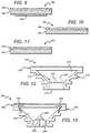
- FIG. 9is a sectional view of another embodiment of a phosphor carrier according to the present invention.
- FIG. 10is a sectional view of another embodiment of a phosphor carrier according to the present invention.
- FIG. 11is a sectional view of still another embodiment of a phosphor carrier according to the present invention.
- FIG. 12is a sectional view of another embodiment of a lamp according to the present invention.
- FIG. 13is a sectional view of another embodiment of a lamp according to the present invention.
- FIG. 14is a graph showing operating temperatures for different emitters and features of the lamps according to the present invention.
- FIG. 15is a side view of another embodiment of a lamp according to the present invention.
- FIG. 16is a graph showing steady state operating temperatures for one embodiment of a lamp according to the present invention.
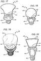
- FIG. 17is a sectional view of another embodiment of a lamp according to the present invention having a diffuser dome;
- FIG. 18is a sectional view of another embodiment of a lamp according to the present invention also having a diffuser dome;
- FIG. 19is a perspective view of another embodiment of a lamp according to the present invention with a diffuser dome having a different shape
- FIG. 20is a sectional view of the lamp shown in FIG. 19 ;
- FIG. 21is an exploded view of the lamp shown in FIG. 19 ;
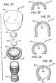
- FIG. 22is a sectional view of one embodiment of a three-dimensional phosphor carrier according to the present invention.
- FIG. 23is a sectional view of another embodiment of a three-dimensional phosphor carrier according to the present invention.
- FIG. 24is a sectional view of another embodiment of a three-dimensional phosphor carrier according to the present invention.
- FIG. 25is a sectional view of another embodiment of a three-dimensional phosphor carrier according to the present invention.
- FIG. 26is a perspective view of another embodiment of a lamp according to the present invention with a diffuser dome having a different shape;
- FIG. 27is a sectional view of the lamp shown in FIG. 26 ;
- FIG. 28is an exploded view of the lamp shown in FIG. 26 ;
- FIG. 29is a perspective view of another embodiment of a lamp according to the present invention with a diffuser dome having a different shape;
- FIG. 30is a sectional view of the lamp shown in FIG. 29 ;
- FIG. 31is an exploded view of the lamp shown in FIG. 29 ;
- FIG. 32is a sectional view of another embodiment of a lamp according to the present invention.
- FIG. 33is a sectional view of one embodiment of a collar cavity according to the present invention.
- the present inventionis directed to different embodiments of lamp or bulb structures comprising a remote conversion material that can be arranged so that less heat from the emitters heats the conversion material, with the remote conversion material also capable of being operated without the substantial build-up of heat in the conversion material due to the light conversion process. This reduces or eliminates the negative impact that elevated temperature can have on efficiency and reliability of the conversion material.
- the present inventionis also directed to lamps comprising features that mask the conversion material from the view by the lamp user, and can also disperse or redistribute the light from the remote conversion material and/or the lamp's light source into a desired emission pattern.
- Different embodiments of the lampscan have many different shapes and sizes, with some embodiments having dimensions to fit into standard size envelopes, such as the A19 size envelope 30 as shown in FIG. 3 .
- the lamps according to the present inventioncan also fit other types of standard size profiles including but not limited to A21 and A23.
- the conversion materialcan comprise one or multiple conversion materials, such as phosphors.
- Thermal pathscan be included for heat to dissipate from the conversion material during operation while at the same time keeping the conversion material remote to the light source so that most or all of the heat from the light source does not pass into the conversion material and the local density of excitation photons incident of the phosphor layer is reduced. This allows the remote conversion material to operate with a lower temperature and reduced photon excitation density compared to conversion materials lacking thermally conductive paths to dissipate conversion heat.
- the conversion materialBy being remote and remaining relatively cool, the conversion material can operate more efficiently and does not suffer the heat related color shift. Operating at lower temperature also reduces heat related degradation of the conversion material and can increase the long term reliability of the conversion material.
- the different remote arrangements according to the present inventioncan also allow the conversion material to operate with lower excitation density which can reduce the likelihood that the phosphor will be optically saturated by incident light from the light source.
- the conversion materialcan comprise a phosphor carrier that includes one or more phosphors arranged on or integral to a carrier layer or material.
- the carrier layercan comprise many different thermally conductive materials that are substantially transparent to the desired wavelengths of light, such as the light emitted by the lamp's light emitters.
- the phosphor carriercan be provided with a means for dissipating the build-up of conversion heating and in one embodiment the phosphor carrier is in good thermal contact with a heat sink structure.
- the phosphor carriercan be mounted to the heat sink with thermal contact at the edges of the phosphor carrier.
- a light sourcecan be mounted in the lamp, such as in or on the heat sink structure, at a location so that there is separation between the light source and the phosphor carrier; i.e. the phosphor carrier and its phosphor are remote from the light source.
- the light sourceis also arranged so that at least some of its emitted light passes through the phosphor carrier and its phosphor, with at least some of the light from the light source converted by the phosphor.
- this conversioncan comprise photon down conversion wherein the wavelength of the converted light is longer than the light source light.
- this conversioncan comprise up conversion wherein the wavelength of the converted light is shorter than the light source light.
- the conversioncan cause heat to be generated in the phosphor from the conversion process.
- the phosphor conversion heatcan be conducted through the thermally conductive carrier layer and into the heat sink structure where it can dissipate into the ambient.
- the carrier layercan collect the heat generated from the phosphor layer, spreads it laterally, and conducts the heat to the heat sink structure.
- the heat sink structurecan be arranged with different features that help dissipate the heat to the ambient, and this thermal management arrangement allows the remote phosphor layer to maintain a lower operating temperature leading to the benefits mentioned above.
- the lamps according to the present inventioncan be arranged in many different ways.
- the light sourcescan comprise solid state light sources, such as different types of LEDs, LED chips or LED packages with different lens or optic arrangements.
- a single LED chip or packagecan be used, while in others multiple LED chips or packages can be used and arranged in different types of arrays.
- These LED packagescan also comprise LEDs encapsulated with a material that can withstand the elevated luminous flux or can comprise unencapsulated LEDs.
- the light sourcecan comprise one or more blue emitting LEDs and the phosphor in the phosphor carrier can comprise one or more materials that absorb a portion of the blue light and emit one or more different wavelengths of light such that the lamp emits a white light combination from the blue LED and the conversion material.
- the conversion materialcan absorb the blue LED light and emit different colors of light including but not limited to yellow and green.
- the light sourcecan also comprise different LEDs and conversion materials emitting different colors of light so that the lamp emits light with the desired characteristics such as color temperature and color rendering.
- red and blue LED chipscan be subject to color instability with different operating temperatures and dimming. This can be due to the different behaviors of red and blue LEDs at different temperature and operating power (current/voltage), as well as different operating characteristics over time. This effect can be mitigated somewhat through the implementation of an active control system that can add cost and complexity to the overall lamp.
- Different embodiments according to the present inventioncan address this issue by having a light source with the same type of emitters in combination with a remote phosphor that can comprise multiple types or layers and/or regions of phosphors that remain relatively cool through the thermal dissipation arrangements disclosed herein.
- the remote phosphor carriercan absorb light from the emitters and can re-emit different colors of light, including red light, while still experiencing the efficiency and reliability of reduced operating temperature for the phosphors.
- LEDs from various binscan be assembled together to achieve substantially wavelength uniform excitation sources that can be used in different lamps. These can then be combined with phosphor carriers having substantially the same conversion characteristics to provide lamps emitting light within the desired bin.
- numerous phosphor carrierscan be manufactured and pre-binned according to their different conversion characteristics. Different phosphor carriers can be combined with light sources emitting different characteristics to provide a lamp emitting light within a target color bin.
- the heat sink structurecan comprise different structures and materials in different embodiments according to the present invention. In some embodiments it can comprise a thermally conductive material having heat dissipating features such as fins or heat pipes. In still other embodiments the heat sink structure can comprise different types of lamp collars that can be mounted to a different feature such as a separate heat sink.
- Different phosphor carriers according to the present inventioncan be arranged in different ways, such as with phosphor layers arranged on different surfaces of a carrier layer, phosphor regions patterned on a surface(s) of a carrier layer, or phosphor regions either uniformly or non-uniformly distributed across or throughout the carrier layer.
- the phosphor carriercan also include other materials such as scattering particles, while in other embodiments the phosphor carrier can comprise more than one phosphor material.
- the lamps according to the present inventioncan also provide for improved emission efficiency by surrounding the light source with a reflective surface. This can result in enhanced photon recycling by reflecting much of the light re-emitted from the conversion material back toward the light source.
- the surfaces of the phosphor layer, carrier layer or diffusercan be smooth or scattering.
- the internal surfaces of the carrier layer and diffusercan be optically smooth to promote total internal reflecting behavior that reduces the amount of light directed backward from the phosphor layer (either downconverted light or scattered light).
- one or more external surfaces of the carrier layer or phosphor layermay be roughened or otherwise modified to promote light emission from this external surface.
- the combination of one or more roughened external surfaces with smooth internal surfacesmay be used to promote light emission through the carrier and phosphor layer in preferred directions.
- Properties such as surface roughness, reflectivity, and index of refraction of the carrier layer and phosphor layermay in general be used to guide or direct the light emitted by or transferred through the carrier/phosphor layer into preferred directions, for example to provide improved efficiency by reducing the amount of backward emitted light that can be absorbed by the lamp's LED chips, associated substrate, or other non-ideal reflecting surfaces within the interior of the lamp, improving beam intensity profiles and color uniformity, etc.
- the phosphor layer and/or carrier layermay comprise either essentially two-dimensional or three-dimensional geometries.
- Two-dimensional geometriessuch as a planar or disk-shaped profile may facilitate fabrication and application of the phosphor layer and reduce manufacturing costs.
- Three-dimensionale.g., essentially spherical, conic, tubular, rectangular, etc. shapes
- the present inventionis described herein with reference to conversion materials, phosphor layers and phosphor carriers, all being “remote” to said light source or LED. Remote in this context refers being spaced apart from and/or not being on or in direct thermal contact.
- first, second, etc.may be used herein to describe various elements, components, regions, layers and/or sections, these elements, components, regions, layers and/or sections should not be limited by these terms. These terms are only used to distinguish one element, component, region, layer or section from another region, layer or section. Thus, a first element, component, region, layer or section discussed below could be termed a second element, component, region, layer or section without departing from the teachings of the present invention.
- Embodiments of the inventionare described herein with reference to cross-sectional view illustrations that are schematic illustrations of embodiments of the invention. As such, the actual thickness of the layers can be different, and variations from the shapes of the illustrations as a result, for example, of manufacturing techniques and/or tolerances are expected. Embodiments of the invention should not be construed as limited to the particular shapes of the regions illustrated herein but are to include deviations in shapes that result, for example, from manufacturing. A region illustrated or described as square or rectangular will typically have rounded or curved features due to normal manufacturing tolerances. Thus, the regions illustrated in the figures are schematic in nature and their shapes are not intended to illustrate the precise shape of a region of a device and are not intended to limit the scope of the invention.
- FIG. 4shows one embodiment of a lamp 50 according to the present invention that comprises a heat sink structure 52 having an optical cavity 54 with a platform 56 for holding a light source 58 .
- a lamp 50according to the present invention that comprises a heat sink structure 52 having an optical cavity 54 with a platform 56 for holding a light source 58 .
- This embodiment and some embodiments beloware described with reference to an optical cavity, it is understood that many other embodiments can be provided without optical cavities. These can include, but are not limited to, light sources being on a planar surface or on a pedestal.
- the light source 58can comprise many different emitters with the embodiment shown comprising an LED, which can comprise many different commercially available LED chips or LED packages including, but not limited to, those commercially available from Cree, Inc. located in Durham, N.C.
- the light source 58can be mounted to the platform 56 using many different known mounting methods and materials with light from the light source 58 emitting out the top opening of the cavity 54 .
- light source 58can be mounted directly to the platform 56 , while in other embodiments the light source can be included on a submount or printed circuit board (PCB) that is then mounted to the platform 56 .
- the platform 56 and the heat sink structure 52can comprise electrically conductive paths for applying an electrical signal to the light source 58 , with some of the conductive paths being conductive traces or wires. All or portions of the platform 56 can also be made of a thermally conductive material and the thermally conductive material can be thermally coupled to or integral to the heat sink structure 52 .
- the lamp's light sourcecan be provided as an array of emitters that are co-planar, with the emitters being mounted on a flat or planar surface.
- Co-planar light sourcescan reduce the complexity of the emitter arrangements, making them both easier and cheaper to manufacture.
- Co-planar light sourcestend to emit primarily in the forward direction such as in a Lambertian emission pattern.
- Different embodiments of the present inventionare arranged with a diffuser as described below that can achieve this uniform or essentially isotropic lamp emission pattern when using a planar light source emitting an emission pattern such as Lambertian.
- the heat sink structure 52can at least partially comprise a thermally conductive material, and many different thermally conductive materials can be used including different metals such as copper or aluminum, or metal alloys.
- the heat sinkcan comprise high purity aluminum that can have a thermal conductivity at room temperature of approximately 210 W/m-k).
- the heat sink structurecan comprise die cast aluminum having a thermal conductivity of approximately 200 W/m-k.
- the heat sink structure 52can also comprise other heat dissipation features such as heat fins 60 that increase the surface area of the heat sink to facilitate more efficient heat dissipation into the ambient.
- the heat fins 60can be made of material with higher thermal conductivity than the remainder of the heat sink.
- the fins 60are shown in a generally horizontal orientation, but it is understood that in other embodiments the fins can have a vertical or angled orientation.
- the heat sinkcan comprise active cooling elements, such as fans, to lower the convective thermal resistance within the lamp.
- heat dissipation from the phosphor carrieris achieved through a combination of convection thermal dissipation and conduction through the heat sink structure 52 .
- Reflective layers 53can also be included on the heat sink structure 52 , such as on the surface of the optical cavity 54 .
- the surfacescan be coated with a material having a reflectivity of approximately 75% or more to the visible wavelengths of light emitted by the light source 58 and/or a wavelength conversion material (“the lamp light”), while in other embodiments the material can have a reflectivity of approximately 85% or more to the lamp light. In still other embodiments the material can have a reflectivity to the lamp light of approximately 95% or more.
- the heat sink structure 52can also comprise features for connecting to a source of electricity such as to different electrical receptacles.
- the heat sink structurecan comprise a feature of the type to fit in conventional electrical receptacles.
- itcan include a feature for mounting to a standard Edison socket, which can comprise a screw-threaded portion which can be screwed into an Edison socket.
- itcan include a standard plug and the electrical receptacle can be a standard outlet, or can comprise a GU24 base unit, or it can be a clip and the electrical receptacle can be a receptacle which receives and retains the clip (e.g., as used in many fluorescent lights).
- the lamps according to the present inventioncan comprise a power conversion unit that can comprise a driver to allow the bulb to run from an AC line voltage/current and to provide light source dimming capabilities.
- the power supplycan comprise an offline constant-current LED driver using a non-isolated quasi-resonant flyback topology.
- the LED drivercan fit within the lamp and in some embodiments can comprise a less than 25 cubic centimeter volume, while in other embodiments it can comprise an approximately 20 cubic centimeter volume.
- the power supplycan be non-dimmable but is low cost. It is understood that the power supply used can have different topology or geometry and can be dimmable as well.
- a phosphor carrier 62is included over the top opening of the cavity 54 and in the embodiment shown it covers the entire opening.
- the cavity openingis shown as circular and the phosphor carrier 62 is a circular disk, but it is understood that the cavity opening and the phosphor carrier can be many different shapes and sizes. It is also understood that the phosphor carrier 62 can cover less than all of the cavity opening.
- Phosphor carriers according to the present inventioncan be characterized as comprising a conversion material and thermally conductive light transmitting material.
- the light transmitting materialcan be transparent to the light emitted from the light source 58 and the conversion material should be of the type that absorbs the wavelength of light from the light source and re-emits a different wavelength of light.
- the thermally conductive light transmitting materialcomprises a carrier layer 64 and the conversion material comprises a phosphor layer 66 on the carrier layer 64 .
- the thermally conductive light transmitting materialcomprises a carrier layer 64 and the conversion material comprises a phosphor layer 66 on the carrier layer 64 .
- different embodimentscan comprise many different arrangements of a carrier layer and phosphor layer.
- lamps according to the present inventionhaving a remote phosphor configuration, with LEDs on the platform 56 at the bottom of the cavity 54 , a higher percentage of the backward emitted phosphor light strikes a surface of the cavity instead of the LED. Coating these surfaces with reflective layer 53 increases the percentage of light that reflects back into the phosphor layer 66 where it can emit from the lamp. These reflective layers 53 allow for the optical cavity to effectively recycle photons, and increase the emission efficiency of the lamp. It is understood that the reflective layer can comprise many different materials and structures including but not limited to reflective metals or multiple layer reflective structures such as distributed Bragg reflectors. Reflective layers can also be included in embodiments not having an optical cavity. In embodiments having LEDs mounted on a planar surface or on a pedestal, reflective layers can also be included around the LEDs to increase efficiency in much the same way as the reflective layers in the embodiments with optical cavities.
- the carrier layer 64can be made of many different materials having a thermal conductivity of 0.5 W/m-k or more, such as quartz, silicon carbide (SiC) (thermal conductivity ⁇ 120 W/m-k), glass (thermal conductivity of 1.0-1.4 W/m-k) or sapphire (thermal conductivity of ⁇ 40 W/m-k).
- the phosphor carriercan also have different thicknesses depending on the material being used, with a suitable range of thicknesses being 0.1 mm to 10 mm or more. It is understood that other thicknesses can also be used depending on the characteristics of the material for the carrier layer. The material should be thick enough to provide sufficient lateral heat spreading for the particular operating conditions.
- Different factorscan impact which carrier layer material is used including but not limited to cost and transparency to the light source light. Some materials may also be more suitable for larger diameters, such as glass or quartz. These can provide reduced manufacturing costs by formation of the phosphor layer on the larger diameter carrier layers and then singulation into the smaller carrier layers.
- the light source 58can be LED based and can emit light in the blue wavelength spectrum.
- the phosphor layercan absorb some of the blue light and re-emit yellow. This allows the lamp to emit a white light combination of blue and yellow light.
- the blue LED lightcan be converted by a yellow conversion material using a commercially available YAG:Ce phosphor, although a full range of broad yellow spectral emission is possible using conversion particles made of phosphors based on the (Gd,Y) 3 (Al,Ga) 5 O 12 :Ce system, such as the Y 3 Al 5 O 12 :Ce (YAG).
- YAGYAG
- Other yellow phosphors that can be used for creating white light when used with a blue emitting LED based emitterinclude but not limited to:
- Tb 3-x RE x O 12 :CeTAG
- REY, Gd, La, Lu; or
- the phosphor layercan also be arranged with more than one phosphor either mixed in the phosphor layer 66 or as a separate phosphor layer/regions either vertically or laterally on the carrier layer 64 .
- each of the two phosphorscan absorb the LED light and can re-emit different colors of light.
- the colors from the two phosphor layerscan be combined for higher CRI white of different white hue (warm white). This can include light from yellow phosphors above that can be combined with light from red phosphors. Different red phosphors can be used including:
- phosphorscan be used to create color emission by converting substantially all light to a particular color.
- the following phosphorscan be used to generate green light:
- the phosphorcan be provided in the phosphor layer 66 in a binder, and the phosphor can also have different concentrations or loading of phosphor materials in the binder. A typical concentration being in a range of 30-70% by weight. In one embodiment, the phosphor concentration is approximately 65% by weight, and is preferably uniformly dispersed throughout the remote phosphor.
- the phosphor layer 66can also have different regions with different conversion materials and different concentrations of conversion material.
- Suitable materialsinclude silicones, epoxies, glass, inorganic glass, dielectrics, BCB, polymides, polymers and hybrids thereof, with the preferred material being silicone because of its high transparency and reliability in high power LEDs.
- Suitable phenyl- and methyl-based siliconesare commercially available from Dow® Chemical.
- the bindercan be cured using many different curing methods depending on different factors such as the type of binder used. Different curing methods include but are not limited to heat, ultraviolet (UV), infrared (IR) or air curing.
- Phosphor layer 66can be applied using different processes including but not limited to spray coating, spin coating, sputtering, printing, powder coating, electrophoretic deposition (EPD), electrostatic deposition, among others. As mentioned above, the phosphor layer 66 can be applied along with a binder material, but it is understood that a binder is not required. In still other embodiments, the phosphor layer 66 can be separately fabricated and then mounted to the carrier layer 64 .
- a phosphor-binder mixturecan be sprayed or dispersed over the carrier layer 64 with the binder then being cured to form the phosphor layer 66 .
- the phosphor-binder mixturecan be sprayed or dispersed on a heated carrier layer 64 so that when the phosphor binder mixture contacts the carrier layer 64 , heat from the carrier layer 64 spreads into and cures the binder.
- These processescan also include a solvent in the phosphor-binder mixture that can liquefy and lower the viscosity of the mixture making it more compatible with spraying.
- solventscan be used including but not limited to toluene, benzene, zylene, or OS-20 commercially available from Dow Corning®, and different concentration of the solvent can be used.
- the solvent-phosphor-binder mixtureis sprayed or dispersed on the heated carrier layer 64 the heat from the carrier layer 64 evaporates the solvent, with the temperature of the carrier layer impacting how quickly the solvent is evaporated.
- the heat from the carrier layer 64can also cure the binder in the mixture leaving a fixed phosphor layer on the carrier layer.
- the carrier layer 64can be heated to many different temperatures depending on the materials being used and the desired solvent evaporation and binder curing speed. A suitable range of temperature is 90 to 150° C., but it is understood that other temperatures can also be used.
- the phosphor layer 66can have many different thicknesses depending on the concentration of phosphor material and the desired amount of light to be converted by the phosphor layer 66 .
- Phosphor layers according to the present inventioncan be applied with concentration levels (phosphor loading) above 30%. Other embodiments can have concentration levels above 50%, while in still others the concentration level can be above 60%.
- the phosphor layercan have thicknesses in the range of 10-100 microns, while in other embodiments it can have thicknesses in the range of 40-50 microns.
- the methods described abovecan be used to apply multiple layers of the same of different phosphor materials and different phosphor materials can be applied in different areas/regions of the carrier layer using known masking and/or printing processes.
- the methods described aboveprovide some thickness control for the phosphor layer 66 , but for even greater thickness control, the phosphor layer can be grinded using known methods to reduce the thickness of the phosphor layer 66 or to even out the thickness over the entire layer. This grinding feature provides the added advantage of being able to produce lamps emitting within a single bin on the CIE chromaticity graph. Binning is generally known in the art and is intended to ensure that the LEDs or lamps provided to the end customer emit light within an acceptable color range.
- the LEDs or lampscan be tested and sorted by color or brightness into different bins, generally referred to in the art as binning.
- Each bintypically contains LEDs or lamps from one color and brightness group and is typically identified by a bin code.
- White emitting LEDs or lampscan be sorted by chromaticity (color) and luminous flux (brightness).
- the thickness control of the phosphor layerprovides greater control in producing lamps that emit light within a target bin by controlling the amount of light source light converted by the phosphor layer.
- Multiple phosphor carriers with the same thickness of phosphor layer 66can be provided.
- the lamp emissionsfall within a standard deviation from a point on a CIE diagram, and in some embodiments the standard deviation comprises less than a 10-step McAdams ellipse. In some embodiments the emission of the lamps falls within a 4-step McAdams ellipse centered at CIExy (0.313, 0.323).
- the phosphor carrier 62can be mounted and bonded over the opening in the cavity 54 using different known methods or materials such as thermally conductive bonding materials or a thermal grease.
- thermally conductive greasecan contain ceramic materials such as beryllium oxide and aluminum nitride or metal particles such colloidal silver.
- the phosphor carriercan be mounted over the opening using thermal conductive devices such as clamping mechanisms, screws, or thermal adhesive hold phosphor carrier 62 tightly to the heat sink structure to maximize thermal conductivity.
- phosphor conversion heatingis concentrated in the phosphor layer 66 , such as in the center of the phosphor layer 66 where the majority of LED light strikes and passes through the phosphor carrier 62 .
- the thermally conductive properties of the carrier layer 64spreads this heat laterally toward the edges of the phosphor carrier 62 as shown by first heat flow 70 .
- first heat flow 70There the heat passes through the thermal grease layer and into the heat sink structure 52 as shown by second heat flow 72 where it can efficiently dissipate into the ambient.
- the platform 56 and the heat sink structure 52are thermally connected or coupled.
- This coupled arrangementresults in the phosphor carrier 62 and that light source 58 at least partially sharing a thermally conductive path for dissipating heat.
- Heat passing through the platform 56 from the light source 58 as shown by third heat flow 74can also spread to the heat sink structure 52 .
- Heat from the phosphor carrier 62 flowing into the heat sink structure 52can also flow into the platform 56 .
- the phosphor carrier 62 and the light sourcecan have separate thermally conductive paths for dissipating heat, with these separate paths being referred to as “decoupled”.
- FIG. 5shows another embodiment of a phosphor carrier 80 according to the present invention comprising a carrier layer 82 and a phosphor layer 84 that can be made of the same materials described above and can be formed using the same processes.
- the phosphor layer 84is on the bottom surface of the carrier layer 82 so that light from the LED light source passes through the phosphor layer 84 first. Converted light and LED light leaking through the phosphor layer 84 then passes through the carrier layer 82 .
- the carrier layer 82should be transparent to the light from both the phosphor layer 84 and LED light source.
- the phosphor layer 84 in this embodimentneed not cover the entire bottom surface of the carrier layer 82 . Instead, the edge of the carrier layer 82 can be uncovered by the phosphor layer 84 to allow good thermal contact with the heat sink. In some embodiments, however, the phosphor layer 84 can cover the entire bottom surface of the carrier layer 82 .
- FIG. 6shows still another embodiment of a phosphor carrier 100 according to the present invention which instead of comprising separate phosphor and carrier layers, comprises a carrier layer 102 with a phosphor 104 dispersed throughout.
- the phosphor 104is dispersed in the carrier layer in a nearly uniform concentration, but it is understood that in other embodiments, the phosphor 104 can have different concentrations in different regions of the carrier layer 102 . It is also understood that more than one phosphor can be included in the carrier layer, either uniformly dispersed or dispersed in regions of different concentrations.
- FIG. 7shows another embodiment of phosphor carrier 120 according to the present invention also comprising a carrier layer 122 and phosphor layer 124 similar to those same elements described above and shown in FIG. 4 .
- a scattering particle layer 126can be included on the carrier layer 122 and is shown on the phosphor layer 124 . It is understood that it can be in many different locations on or in the carrier layer.
- the scattering particle layeris included to disperse the light as it emits from the phosphor carrier layer 120 to give it the desired emission pattern.
- the scattering particlesare arranged to disperse the light in generally uniform pattern.
- the scattering particles layercan be deposited using the methods described above with reference to deposition of the phosphor layer and can comprise a dense packing of particles.
- the scattering particlescan also be included in a binder material that can be the same as those described above in reference to the binder used with the phosphor layer.
- the scattering particle layercan have different concentrations of scattering particles depending on the application and materials used. A suitable range for scattering particle concentration is from 0.01% to 0.2%, but it is understood that the concentration can be higher or lower. In some embodiments the concentration can be as low as 0.001%. It is also understood that the scattering particle layer 126 can have different concentrations of scattering particles in different regions. For some scattering particles there can be an increase in loss due to absorption for higher concentrations. Thus, the concentrations of the scattering particles can be chosen in order to maintain an acceptable loss figure, while at the same time dispersing the light to provide the desired emission pattern.
- the scattering particlescan comprise many different materials including but not limited to:
- Y 2 O 3yttrium oxide
- TiO 2titanium dioxide
- zirconium dioxide(ZrO 2 );
- SiCsilicon carbide
- tantalum oxide(TaO 5 );
- silicon nitrideSi 3 N 4
- niobium oxideNb 2 O 5
- BNboron nitride
- phosphor particlese.g., YAG:Ce, BOSE
- More than one scattering material in various combinations of materials or combinations of different forms of the same materialmay be used to achieve a particular scattering effect. It is understood that in other embodiments the scattering particle can be included in the carrier layer 122 , the phosphor layer 124 , or both.
- FIG. 8shows another embodiment of a phosphor carrier 140 according to the present invention having a carrier layer 142 and phosphor 144 similar to the same elements described above and shown in FIG. 6 .
- scattering particles 146are dispersed in the carrier layer 142 to disperse both the LED light and phosphor light passing through the carrier layer 142 .
- the same scattering particlescan be used as those described above and they can be included in different concentration in different embodiments.
- Other embodimentscan comprise regions of different concentration so that light passing through the carrier layer is scattered to the desired emission pattern.
- FIG. 9shows another embodiment of a phosphor carrier 160 according to the present invention comprising a carrier layer 162 with a phosphor layer 164 on its bottom surface, with both arranged similarly to the same element described above and shown in FIG. 5 .
- a scattering particle layer 166is included on the top surface of the carrier layer 162 and can have the same materials deposited in the same way as scattering particle layer 126 in FIG. 7 .
- the scatting particles in the scattering particle layer 166can be arranged to scatter both the light from the phosphor layer 164 as well as the LED light leaking through the phosphor layer 164 .
- the scattering particlescan be arranged to scatter only one of these. It is understood that the scattering particles can also be dispersed in the carrier layer 162 or the phosphor layer 164 , or both.
- the phosphor carriercan also comprise features to enhance light extraction from the lamp. Certain amount of light may strike the surface of the carrier layer or phosphor layer outside the angle of escape, such that the light will be reflected back toward the cavity of the heat sink structure. Some of this light can be absorbed, while other portions of the light may experience total internal reflection (TIR).
- FIG. 10shows one embodiment of a phosphor carrier 180 having features arranged to reduce these losses.
- the phosphor carriercomprises a carrier layer 182 and a phosphor layer 184 .
- the surface of the phosphor layeris roughened or shaped to provide varying surface angles. This can increase the likelihood that light will strike the surface within its escape angle so that it can contribute to useful emission.
- the surfacecan be shaped using known roughing or etching processes.
- the phosphor carrier layer 182can also be arranged with scattering particles in different locations to disperse light as described above.
- FIG. 11shows another embodiment of a phosphor carrier 200 according to the present invention comprising a carrier layer 202 and a phosphor layer 204 .
- the shaped/roughened layeris provided on the top surface of the carrier layer 202 , with the phosphor layer provided on the roughened surface.
- the shape/roughened surfaceprovides a varying surface that increases the likelihood that light will escape through the phosphor carrier 200 .
- the roughened surfacecan be included on other surfaces of the carrier layer 202 , and the phosphor carrier 200 can also be arranged with scattering particles as described above. It is further understood that the roughened surface can be included on any of the surfaces of the different phosphor carrier layer embodiments described above.
- the cavities according to the present inventioncan comprise many different features beyond those described above.
- the cavity 54can be filled with a transparent heat conductive material to further enhance heat dissipation for the lamp.
- the cavity conductive materialcould provide a secondary path for dissipating heat from the light source 58 . Heat from the light source would still conduct through the platform 56 , but could also pass through the cavity material to the heat sink structure 52 . This would allow for lower operating temperature for the light source 58 , but presents the danger of elevated operating temperature for the phosphor carrier 62 .
- This arrangementcan be used in many different embodiments, but is particularly applicable to lamps having higher light source operating temperatures compared to that of the phosphor carrier. This arrangement allows for the heat to be more efficiently spread from the light source in applications where additional heating of the phosphor carrier layer can be tolerated.
- FIG. 12shows another embodiment of a lamp 210 similar to the lamp 50 described above and shown in FIG. 4 .
- the lamp 210comprises a heat sink structure 212 having a cavity 214 with a platform 216 arranged to hold a light source 218 .
- a phosphor carrier 220can be included over and at least partially covering the opening to the cavity 214 .
- the light source 218can comprise a plurality of LEDs arranged in separate LED packages or arranged in an array in a single multiple LED package.
- the emitterscan be coupled on different series and parallel arrangement. In one embodiment eight LEDs can be used that are connected in series with two wires to a circuit board.
- wirescan then be connected to the power supply unit described above.
- more or less than eight LEDscan be used and as mentioned above, commercially available LEDs from Cree, Inc. can used including eight XLamp® XP-E LEDs or four XLamp® XP-G LEDs.
- Different single string LED circuitsare described in U.S. patent application Ser. No. 12/566,195, to van de Ven et al., entitled “Color Control of Single String Light Emitting Devices Having Single String Color Control, and U.S. patent application Ser. No. 12/704,730 to van de Ven et al., entitled “Solid State Lighting Apparatus with Compensation Bypass Circuits and Methods of Operation Thereof”, both of with are incorporated herein by reference.
- each of the LEDscan comprise its own LED primary optics or lens 222 .
- a single primary optics or lens 224can cover all the LEDs. It is understood that the LEDs can be provided without lenses and that in the array embodiments each of the LEDs can have its own lens.
- unpackaged LEDscan be provided in a “chip on heat sink” or “chip on board” configuration. It is also understood that each can be provided with secondary optics arranged in different ways.
- the heat sink structure and platformcan be arranged with the necessary electrical traces or wires to provide an electrical signal to the light source 218 .
- FIG. 13shows another embodiment of a lamp 240 according to the present invention also comprising a heat sink structure 242 with a cavity 244 with a platform 246 for mounting a light source 248 .
- a phosphor carrier 250is mounted by a thermally conductive material over and at least partially covering the opening to the cavity 244 so that at least some of the light from the light source passes through the phosphor carrier 250 .
- the heat sink structure 242 and platform 246have separate thermal dissipation paths that are substantially thermally isolated from one another (although convection may cause some thermal coupling between the two).
- the heat from the light source 248conducts along fourth heat flow 252 and through the platform 246 where it can dissipate into the ambient or another heat sink structure (not shown), such as the connection of the lamp.
- Heat from the phosphor carrier 250conducts along fifth heat flow 254 and into the heat sink structure 242 where it dissipates into the ambient.
- the thermal separation between the heat sink structure 242 and the platform 246can be provided by physical separation of the two or by providing a thermally resistant material between the two such as through known thermal insulators (e.g. dielectrics).
- FIG. 14is a graph 260 showing the peak operating temperatures for conformal phosphor material compared to the operating temperature of remote phosphor carriers having carrier layers with different thermal conductivity and arranged so that heat can dissipate through thermal paths as described above.
- the graph 260further compares the thermal performance of these different arrangements for thermally coupled and thermally decoupled heat sinks.
- First solid line 262shows the junction temperature of the emitters having a heat sink that is thermally decoupled as described above
- second solid line 264shows the junction temperature of the emitters for a thermally coupled heat sink.
- the operating temperature for the coupled arrangementis slightly lower than that of the decoupled arrangement.
- First dashed line 266shows the peak phosphor temperature for a lamp having LEDs with a conformal phosphor coating and a thermally decoupled heat sink.
- Second dashed line 268shows the peak phosphor temperature for the same lamp with a thermally coupled heat sink.
- the phosphoroperates a generally consistent peak phosphor temperature and the thermally coupled lamp operates at a lower peak phosphor temperature compared to the decoupled arrangement.
- the third solid line 270shows the peak phosphor temperature for a remote phosphor carrier arranged on a thermally coupled heat sink, with the temperature measured for carrier layers of different thermal conductivities in the range of 0.2 to more that 100 w/m-K.
- Fourth solid line 272shows the same remote phosphor carrier and same range of thermal conductivities, with the phosphor carrier on a thermally decoupled heat sink.
- the remote phosphor carriers having carrier layers with thermal conductivity of above 1.05 W/m-k and arranged on a thermally decoupled heat sinkcan operate with lower phosphor temperature, thus higher conversion efficiency than conformal phosphor coated LEDs. This allows for the use of material such as regular glass, fused quartz, sapphire and silicon carbide.
- Thermally coupled heat sinkscan be used but require a somewhat higher thermal conductivity and operates at a higher temperature compared to the thermally coupled arrangements.
- FIG. 15shows another embodiment of lamp 270 according to the present invention arranged in a different way to provide the desired remote phosphor and thermal characteristics for the phosphor carrier.
- the lamp 270comprises a light source 272 mounted on the top surface of heat sink structure 274 .
- the heat sink structurecan be made of a heat conductive material as described above, and comprise heat dissipating structures such as fins 275 . During operation, heat spreads from the light source 272 into the heat sink structure 274 where it spreads into the fins 275 and the ambient.
- the lamp 270also comprises a lamp collar 276 having a collar cavity 278 , mounted on the top surface of the heat sink structure 274 .
- the collar cavity 278extends through the lamp collar such that it is open at the bottom and top.
- the light source 272is arranged so that it emits light out the top opening of the collar cavity 278 .
- the light source 272is also arranged so that it is within the collar cavity 278 .
- a phosphor carrier 280is mounted over the top opening of the collar cavity 278 with a thermally conductive material or device as described above. It is arranged so that light from the light source 272 passes through the phosphor carrier 280 , where at least some of it is converted.
- the phosphor carrier 280can be arranged with the structures and features described in the different embodiments described above, including but not limited to a carrier layer, phosphor, scattering particles, and/or roughening/shaping.
- the lamp collar 276is also made of a heat conductive material so that heat from the phosphor carrier 280 spreads into the lamp collar 276 . The heat from the lamp collar 276 can dissipate directly into the ambient or can spread into the heat sink structure 274 where it can spread into the ambient.
- the heat path for the phosphor carrier and the light sourceis coupled such that heat from phosphor carrier heat from the lamp collar 276 can spread into the heat sink structure 274 , and light source heat can spread from the heat sink structure 274 to the lamp collar 276 .
- the lamp collar 276also has a skirt 282 that fits closely around the top portion of the heat sink structure 274 to allow for efficient conduction between the lamp collar 276 and heat sink structure 274 .
- FIG. 16is a graph 285 showing the operating characteristics for different remote phosphors carriers used in the lamp 270 .
- the first dashed line 286shows the base or board temperature for the lamp, which remains constant at approximately 74.7° C. for a decoupled heat sink.
- Second dashed line 288shows the peak temperature for the phosphor in different embodiments of remote phosphor carriers according to the present invention. For 5 mm thick glass with a spin on phosphor layer and for 0.5 mm thick sapphire with a spin on phosphor layer, the peak phosphor operating temperature is below that of the base. Like above, this allows for greater emission efficiency and less heat related degradation of the phosphor.
- FIG. 17shows still another embodiment of lamp 300 according to the present invention that comprises an optical cavity 302 within a heat sink structure 305 .
- An LED based light source 304is mounted to the platform 306
- a phosphor carrier 308is mounted to the top opening of the cavity 302 , with the phosphor carrier 308 having any of the features of those described above.
- the phosphor carrier 308comprises a thermally conductive transparent material and a phosphor, and is mounted to the cavity with a thermally conductive material or device as described above.
- the cavity 302can have reflective surfaces to enhance the emission efficiency as described above.
- Light from the light source 304passes through the phosphor carrier 308 where a portion of it is converted to a different wavelength of light by the phosphor in the phosphor carrier 308 .
- the light source 304can comprise blue emitting LEDs and the phosphor carrier 308 can comprise a yellow phosphor as described above that absorbs a portion of the blue light and re-emits yellow light.
- the lamp 300emits a white light combination of LED light and yellow phosphor light.
- the light source 304can also comprise many different LEDs emitting different colors of light and the phosphor carrier can comprise other phosphors to generate light with the desired color temperature and rendering.
- the lamp 300also comprises a shaped diffuser dome 310 mounted over the cavity 302 that includes diffusing or scattering particles such as those listed above.
- the scattering particlescan be provided in a curable binder that is formed in the general shape of dome. Additionally, or alternatively, scattering structures may also be provided as part of the diffuser dome. In some embodiments, scattering structures are provided in lieu of the scattering particles.
- the dome 310is mounted to the heat sink structure 305 and has an enlarged portion at the end opposite the heat sink structure 305 .
- Different binder materialscan be used as discussed above such as silicones, epoxies, glass, inorganic glass, dielectrics, BCB, polymides, polymers and hybrids thereof.
- white scattering particlescan be used with the dome having a white color that hides the color of the phosphor in the phosphor carrier 308 in the optical cavity. This gives the overall lamp 300 a white appearance that is generally more visually acceptable or appealing to consumers than the color of the phosphor.
- the diffusercan include white titanium dioxide particles that can give the diffuser dome 310 its overall white appearance.
- the diffuser dome 310can provide the added advantage of distributing the light emitting from the optical cavity in a more omnidirectional and/or uniform pattern.
- light from the light source in the optical cavitycan be emitted in a generally forward or Lambertian pattern and the shape of the dome 310 along with the scattering properties of the scattering particles/structures causes light to emit from the dome in a more omnidirectional emission pattern.
- An engineered domecan have scattering particles/structures in different concentrations in different regions or can be shaped to a specific emission pattern.
- the domecan be engineered so that the emission pattern from the lamp complies with the Department of Energy (DOE) Energy Star defined omnidirectional distribution criteria.
- DOEDepartment of Energy
- some of the different lamp embodiments described hereincan comprise an A-type retrofit LED bulb that meets the DOE Energy Star.
- One requirement of this standard met by the lamp 300is that the emission uniformity must be within 20% of mean value from 0 to 135° viewing and; >5% of total flux from the lamp must be emitted in the 135-180° emission zone, with the measurements taken at 0, 45, 90° azimuthal angles.
- the present inventionprovides lamps that are efficient, reliable and cost effective.
- the entire lampcan comprise five components that can be quickly and easily assembled.
- the lamp 300can comprise a mounting mechanism of the type to fit in conventional electrical receptacles.
- the lamp 300includes a screw-threaded portion 312 for mounting to a standard Edison socket.
- the lamp 300can include standard plug and the electrical receptacle can be a standard outlet, a bayonet mount, a pin base, such as a GU24 base unit, or it can be a clip and the electrical receptacle can be a receptacle which receives and retains the clip (e.g., as used in many fluorescent lights).
- FIG. 18shows another embodiment of a lamp 320 according to the present invention that is similar to the lamp 300 and similarly comprises an optical cavity 322 in a heat sink structure 325 with a light source 324 mounted to the platform 326 in the optical cavity 322 .
- a phosphor carrier 328is mounted over the cavity opening with a thermal connection.
- the lamp 320also comprises a diffuser dome 330 mounted to the heat sink structure 325 , over the optical cavity 322 .
- the diffuser domecan be made of the same materials as diffuser dome 310 described above and shown in FIG.
- the dome 300is oval or egg shaped to provide a different lamp emission pattern while still masking the color from the phosphor in the phosphor carrier 328 .
- the heat sink structure 325 and the platform 326are thermally de-coupled. That is, there is a space between the platform 326 and the heat sink structure such that they do not share a thermal path for dissipating heat. As mentioned above, this can provide improved heat dissipation from the phosphor carrier compared to lamps not having de-coupled heat paths.
- the lamp 300also comprises a screw-threaded portion 332 for mounting to an Edison socket.
- FIGS. 19 through 21show another embodiment of a lamp 340 according to the present invention that is similar to the lamp 320 shown in FIG. 18 . It comprises a heat sink structure 345 having an optical cavity 342 with a light source 344 on the platform 346 , and a phosphor carrier 348 over the optical cavity 342 . It further comprises a screw-threaded portion 352 . It also includes a diffuser dome 350 , but in this embodiment the diffuser dome is flattened on top to provide the desired emission pattern while still masking the color of the phosphor.
- the lamp 340also comprises an interface layer 354 between the light source 344 and the heat sink structure 345 from the light source 344 .
- the interface layercan comprise a thermally insulating material and the light source 344 can have features that promote dissipation of heat from the emitters to the edge of the light source's substrate. This can promote heat dissipation to the outer edges of the heat sink structure 345 where it can dissipate through the heat fins.
- the interface layer 354can be electrically insulating to electrically isolate the heat sink structure 345 from the light source 344 . Electrical connection can then be made to the top surface of the light source.
- the phosphor carriersare flat planar with the LEDs in the light source being co-planer. It is understood, however, that in other lamp embodiments the phosphor carriers can take many different shapes including different three-dimensional shapes.
- the term three-dimensionalis meant to mean any shape other than planar as shown in the above embodiments, and the three-dimensional phosphor carriers can be mounted to a heat sink in the same manner as the two-dimensional planar phosphor carriers described above.
- FIGS. 22 through 25show different embodiments of three-dimensional phosphor carriers according to the present invention, but it is understood that they can also be many other shapes.
- FIG. 22shows a hemispheric shaped phosphor carrier 354 comprising a hemispheric carrier 355 and phosphor layer 356 .
- the hemispheric carrier 355can be made of the same materials as the carrier layers described above, and the phosphor layer can be made of the same materials as the phosphor layer described above, and scattering particles can be included in the carrier and phosphor layer as described above.
- the three dimensional carrierneed not be thermally conductive.
- the phosphor layer 356is shown on the outside surface of the carrier 355 although it is understood that the phosphor layer can be on the carrier's inside layer, mixed in with the carrier, or any combination of the three. In some embodiments, having the phosphor layer on the outside surface may minimize emission losses. When emitter light is absorbed by the phosphor layer 356 light is emitted omnidirectionally and some of the light can emit backwards and be absorbed by the lamp elements such as the LEDs. In the case where the phosphor layer is located on the inside surface of the carrier, the phosphor layer 356 can also have an index of refraction that is different from (e.g.
- the hemispheric carrier 355such that light emitting forward from the phosphor layer can be reflected back from the inside surface of the carrier 355 . This light can also be lost due to absorption by the lamp elements. With the phosphor layer 356 on the outside surface of the carrier 355 , light emitted forward does not need to pass through the carrier 355 and will not be lost to reflection. Light that is emitted back will encounter the top of the carrier where, particularly if the index of refraction of the phosphor layer is greater than that of the carrier, at least some of it will reflect back.
- the index of refraction of the carrier layeris greater than that of the surrounding ambient (e.g., air)
- some lightwill be reflected back from the inside surface of the carrier layer.
- This arrangementresults in a reduction of light from the phosphor layer 356 that emits back into the carrier where it can be absorbed.
- the desired benefit of limiting light directed backwards towards the light sourcemay be further enhanced by, in general, fabricating the surfaces of the phosphor and carrier layers such that they are approximately smooth. Further benefit may be obtained by fabricating the outermost surface of the phosphor layer (when applied to the outer surface of the carrier as shown in FIG. 22 ) such that it has surface roughness or other features for enhancing light extraction, thereby making forward light extraction from the phosphor layer+carrier layer structure favored with respect to backwards light emission.
- the phosphor layer 356can be deposited using many of the same methods described above. In some instances the three-dimensional shape of the carrier 355 may require additional steps or other processes to provide the necessary coverage. In the embodiments where a solvent-phosphor-binder mixture is sprayed and the carrier can be heated as described above and multiple spray nozzles may be needed to provide the desired coverage over the carrier, such as approximate uniform coverage. In other embodiments, fewer spray nozzles can be used while spinning the carrier to provide the desired coverage. Like above, the heat from the carrier 355 can evaporate the solvent and helps cure the binder.
- the phosphor layercan be formed through an emersion process whereby the phosphor layer can be formed on the inside and/or outside surface of the carrier 355 , but is particularly applicable to forming on the inside surface.
- the carrier 355can be at least partially filled with, or otherwise brought into contact with, a phosphor mixture that adheres to the surface of the carrier.
- the mixturecan then be drained from the carrier leaving behind a layer of the phosphor mixture on the surface, which can then be cured.
- the mixturecan comprise polyethylen oxide (PEO) and a phosphor.
- the carriercan be filled and then drained, leaving behind a layer of the PEO-phosphor mixture, which can then be heat cured.
- the PEOevaporates or is driven off by the heat leaving behind a phosphor layer.
- a bindercan be applied to further fix the phosphor layer, while in other embodiments the phosphor can remain without a binder.
- these processescan be utilized in three-dimensional carriers to apply multiple phosphor layers that can have the same or different phosphor materials.
- the phosphor layerscan also be applied both on the inside and outside of the carrier, and can have different types having different thickness in different regions of the carrier.
- different processescan be used such as coating the carrier with a sheet of phosphor material that can be thermally formed to the carrier.
- an emittercan be arranged at the base of the carrier so that light from the emitters emits up and passes through the carrier 355 .
- the carriernot only converts at least some of the light passing through it, but can also assist in dispersing the light in the desired pattern.
- the emitterscan emit light in a generally Lambertian pattern, and the carrier can help disperse the light in a more uniform pattern.
- FIG. 23shows another embodiment of a three dimensional phosphor carrier 357 according to the present invention comprising a bullet-shaped carrier 358 and a phosphor layer 359 on the outside surface of the carrier.
- the carrier 358 and phosphor layer 359can be formed of the same materials using the same methods as described above.
- the different shaped phosphor carriercan be used with different emitters to provide the overall desired lamp emission pattern.
- FIG. 24shows still another embodiment of a three dimensional phosphor carrier 360 according to the present invention comprising a globe-shaped carrier 361 and a phosphor layer 362 on the outside surface of the carrier.
- the carrier 361 and phosphor layer 362can be formed of the same materials using the same methods as described above.
- FIG. 25shows still another embodiment phosphor carrier 363 according to the present invention having a generally globe shaped carrier 364 with a narrow neck portion 365 .
- the phosphor carrier 363includes a phosphor layer 366 on the outside surface of the carrier 364 made of the same materials and formed using the same methods as those described above.
- phosphor carriers having a shape similar to the carrier 364can be more efficient in converting emitter light and re-emitting light from a Lambertian pattern from the light source, to a more omnidirectional emission pattern.
- FIGS. 26 through 28show another embodiment of a lamp 370 according to the present invention having a heat sink structure 372 , optical cavity 374 , light source 376 , diffuser dome 378 and a screw-threaded portion 380 .
- This embodimentalso comprises a three-dimensional phosphor carrier 382 that includes a transparent material and at least one phosphor layer.
- the three-dimensional phosphor carrier 382may be mounted to the heat sink structure 372 In some embodiments, the carrier 382 is mounted to the heat sink structure with a thermal connection. In this embodiment, however, the phosphor carrier 382 is globe shaped and the emitters are arranged so that light from the light source passes through the phosphor carrier 382 where at least some of it is converted.
- the shape of the three dimensional phosphor carrier 382provides natural separation between it and the light source 376 . Accordingly, the light source 376 is not mounted in a recess in the heat sink that forms the optical cavity. Instead, the light source 376 is mounted on the top surface of the heat sink structure 372 , with the optical cavity 374 formed by the space between the phosphor carrier 382 and the top of the heat sink structure 372 .
- the phosphor carrier 382can appear yellow, and the diffuser dome 378 masks this color while dispersing the lamp light into the desired emission pattern.
- the conductive paths for the platform and heat sink structureare coupled, but it is understood that in other embodiments they can be de-coupled.
- FIGS. 29 through 31show still another embodiment of a lamp 390 according to the present invention. It comprises many of the same features as the lamp 370 shown in FIGS. 26 through 28 .
- the phosphor carrier 392is bullet shaped and functions in much the same way as the other embodiments of phosphor carriers described above. It is understood that these are only two of the different shapes that the phosphor carrier can take in different embodiments of the invention.
- FIG. 32shows another embodiment of a lamp 400 according to the present invention that also comprises a heat sink 402 with an optical cavity 404 having a light source 406 and phosphor carrier 408 .
- the lamp 400also comprises a diffuser dome 410 and screw threaded portion 412 .
- the optical cavity 404can comprise a separate collar structure 414 , as shown in FIG. 33 that is removable from the heat sink 402 . This provides a separate piece that can more easily be coated by a reflective material than the entire heat sink.
- the collar structure 414can be threaded to mate with threads in the heat sink structure 402 .
- the collar structure 414can provide the added advantage of mechanically clamping down the PCB to the heat sink.
- the collar structure 414can comprise a mechanical snap-on device instead of threads for easier manufacture.
- the lamps according to the present inventioncan have a light source comprising many different numbers of LEDs with some embodiments having less than 30 and other embodiments having less than 20. Still other embodiments can have less than 10 LEDs, with the cost and complexity of the lamp light source generally being lower with fewer LED chips.
- the area covered by the multiple chips light source in some embodimentscan be less than 30 mm 2 and in other embodiments less than 20 mm 2 . In still other embodiments it can be less that 10 mm 2 .
- Some embodiments of lamps according to the present inventionalso provide a steady state lumen output of greater than 400 lumens and in other embodiments greater than 600 lumens. In still other embodiments the lamps can provide steady state lumen output of greater than 800 lumens.
- Some lamp embodimentscan provide this lumen output with the lamp's heat management features allowing the lamp to remain relatively cool to the touch. In one embodiment that lamp remains less that 60° C. to the touch, and in other embodiments it remains less that 50° C. to the touch. In still other embodiments the lamp remains less than 40° C. to the touch.
- lamps according to the present inventioncan also operate at an efficiency of greater than 40 lumens per watt, and in other embodiments at efficiency of greater than 50 lumens per watt. In still other embodiments the lamps can operate at greater than 55 lumens per watt. Some embodiments of lamps according to the present invention can produce light with a color rendering index (CRI) greater than 70, and in other embodiments with a CRI greater than 80. In still other embodiments the lamps can operate at a CRI greater than 90.
- One embodiment of a lamp according to the present inventioncan have phosphors that provide lamp emission with a CRI greater than 80 and a lumen equivalent of radiation (LER) greater than 320 lumens/optical Watt @ 3000K correlated color temperature (CCT).
- Lamps according to the present inventioncan also emit light in a distribution that is within 40% of a mean value in the 0 to 135° viewing angles, and in other embodiment the distribution can be within 30% of a mean value at the same viewing angles. Still other embodiments can have a distribution of 20% of a mean value at the same viewing angles in compliance with Energy Star specifications. The embodiments can also emit light that is greater than 5% of total flux in the 135 to 180° viewing angles.
Landscapes
- Engineering & Computer Science (AREA)
- General Engineering & Computer Science (AREA)
- Physics & Mathematics (AREA)
- Microelectronics & Electronic Packaging (AREA)
- Optics & Photonics (AREA)
- Led Device Packages (AREA)
- Arrangement Of Elements, Cooling, Sealing, Or The Like Of Lighting Devices (AREA)
- Non-Portable Lighting Devices Or Systems Thereof (AREA)
Abstract
Description
Claims (35)
Priority Applications (1)
| Application Number | Priority Date | Filing Date | Title |
|---|---|---|---|
| US14/108,815US10665762B2 (en) | 2010-03-03 | 2013-12-17 | LED lamp incorporating remote phosphor and diffuser with heat dissipation features |
Applications Claiming Priority (13)
| Application Number | Priority Date | Filing Date | Title |
|---|---|---|---|
| US33951610P | 2010-03-03 | 2010-03-03 | |
| US33951510P | 2010-03-03 | 2010-03-03 | |
| US12/848,825US8562161B2 (en) | 2010-03-03 | 2010-08-02 | LED based pedestal-type lighting structure |
| US38643710P | 2010-09-24 | 2010-09-24 | |
| US12/889,719US9523488B2 (en) | 2010-09-24 | 2010-09-24 | LED lamp |
| US201061424665P | 2010-12-19 | 2010-12-19 | |
| US201061424670P | 2010-12-19 | 2010-12-19 | |
| US12/975,820US9052067B2 (en) | 2010-12-22 | 2010-12-22 | LED lamp with high color rendering index |
| US201161434355P | 2011-01-19 | 2011-01-19 | |
| US201161435326P | 2011-01-23 | 2011-01-23 | |
| US201161435759P | 2011-01-24 | 2011-01-24 | |
| US13/029,005US8632196B2 (en) | 2010-03-03 | 2011-02-16 | LED lamp incorporating remote phosphor and diffuser with heat dissipation features |
| US14/108,815US10665762B2 (en) | 2010-03-03 | 2013-12-17 | LED lamp incorporating remote phosphor and diffuser with heat dissipation features |
Related Parent Applications (1)
| Application Number | Title | Priority Date | Filing Date |
|---|---|---|---|
| US13/029,005ContinuationUS8632196B2 (en) | 2010-03-03 | 2011-02-16 | LED lamp incorporating remote phosphor and diffuser with heat dissipation features |
Publications (2)
| Publication Number | Publication Date |
|---|---|
| US20140183584A1 US20140183584A1 (en) | 2014-07-03 |
| US10665762B2true US10665762B2 (en) | 2020-05-26 |
Family
ID=44530736
Family Applications (2)
| Application Number | Title | Priority Date | Filing Date |
|---|---|---|---|
| US13/029,005Active2030-12-26US8632196B2 (en) | 2010-03-03 | 2011-02-16 | LED lamp incorporating remote phosphor and diffuser with heat dissipation features |
| US14/108,815ActiveUS10665762B2 (en) | 2010-03-03 | 2013-12-17 | LED lamp incorporating remote phosphor and diffuser with heat dissipation features |
Family Applications Before (1)
| Application Number | Title | Priority Date | Filing Date |
|---|---|---|---|
| US13/029,005Active2030-12-26US8632196B2 (en) | 2010-03-03 | 2011-02-16 | LED lamp incorporating remote phosphor and diffuser with heat dissipation features |
Country Status (2)
| Country | Link |
|---|---|
| US (2) | US8632196B2 (en) |
| WO (1) | WO2011109094A1 (en) |
Cited By (5)
| Publication number | Priority date | Publication date | Assignee | Title |
|---|---|---|---|---|
| US10920971B2 (en) | 2015-12-15 | 2021-02-16 | Wangs Alliance Corporation | LED lighting methods and apparatus |
| US10941924B2 (en) | 2015-12-15 | 2021-03-09 | Wangs Alliance Corporation | LED lighting methods and apparatus |
| US11686459B2 (en) | 2015-12-15 | 2023-06-27 | Wangs Alliance Corporation | LED lighting methods and apparatus |
| US11802682B1 (en) | 2022-08-29 | 2023-10-31 | Wangs Alliance Corporation | Modular articulating lighting |
| US11812525B2 (en) | 2017-06-27 | 2023-11-07 | Wangs Alliance Corporation | Methods and apparatus for controlling the current supplied to light emitting diodes |
Families Citing this family (51)
| Publication number | Priority date | Publication date | Assignee | Title |
|---|---|---|---|---|
| US9732930B2 (en)* | 2010-07-20 | 2017-08-15 | Panasonic Intellectual Property Management Co., Ltd. | Light bulb shaped lamp |
| JP2012039031A (en)* | 2010-08-11 | 2012-02-23 | Nitto Denko Corp | Light emitting device |
| US9523491B2 (en)* | 2010-10-07 | 2016-12-20 | Hubbell Incorporated | LED luminaire having lateral cooling fins and adaptive LED assembly |
| US8192051B2 (en) | 2010-11-01 | 2012-06-05 | Quarkstar Llc | Bidirectional LED light sheet |
| US8847481B2 (en)* | 2010-11-08 | 2014-09-30 | Lg Innotek Co., Ltd. | Lighting device comprising photoluminescent plate |
| US8314566B2 (en) | 2011-02-22 | 2012-11-20 | Quarkstar Llc | Solid state lamp using light emitting strips |
| US8410726B2 (en) | 2011-02-22 | 2013-04-02 | Quarkstar Llc | Solid state lamp using modular light emitting elements |
| KR101315700B1 (en)* | 2011-09-08 | 2013-10-10 | 엘지이노텍 주식회사 | Lighting device |
| EP2581656A3 (en)* | 2011-10-13 | 2017-07-05 | OSRAM GmbH | Mounting device for lighting sources |
| DE102012204791A1 (en)* | 2012-03-26 | 2013-09-26 | Osram Gmbh | LIGHTING DEVICE WITH FLUORESCENT BODY ON COOLING BODY |
| DE102012206646B4 (en)* | 2012-04-23 | 2024-01-25 | Osram Gmbh | Lighting device with LED chip and casting compound and method for producing a lighting device |
| CN103375708B (en)* | 2012-04-26 | 2015-10-28 | 展晶科技(深圳)有限公司 | Light-emitting diode lamp source device |
| WO2013159664A1 (en)* | 2012-04-26 | 2013-10-31 | Qian Zhiqiang | White light led light-emitting device and method for preparing thereof |
| WO2014026486A1 (en)* | 2012-08-17 | 2014-02-20 | Qian Zhiqiang | Led light-emitting device for white light |
| US9388947B2 (en) | 2012-08-28 | 2016-07-12 | Cree, Inc. | Lighting device including spatially segregated lumiphor and reflector arrangement |
| WO2014036705A1 (en)* | 2012-09-06 | 2014-03-13 | Liu Lehua | Led lamp using glass lamp cover with internally coated remote fluorescent powder |
| CN103123104B (en)* | 2013-02-05 | 2015-11-25 | 东莞汉旭五金塑胶科技有限公司 | The LED cooling lamp holder of all-round light projection and heat radiation module thereof |
| JP2014165082A (en)* | 2013-02-26 | 2014-09-08 | Toshiba Lighting & Technology Corp | Lighting device |
| US8899794B2 (en) | 2013-03-15 | 2014-12-02 | Bby Solutions, Inc. | LED bulb optical system with uniform light distribution |
| JP6104682B2 (en)* | 2013-04-09 | 2017-03-29 | シチズン電子株式会社 | Lighting device |
| WO2014194044A1 (en)* | 2013-05-29 | 2014-12-04 | Venntis Technologies LLC | Volumetric light emitting device |
| US20150184833A1 (en)* | 2013-12-27 | 2015-07-02 | Ming-Che Wu | Tungsten-Filament-Like Light-Emitting Diode Lamp Structure |
| EP3117267B1 (en)* | 2014-03-11 | 2018-05-02 | Osram Sylvania Inc. | Light converter assemblies with enhanced heat dissipation |
| KR102204953B1 (en)* | 2014-06-25 | 2021-01-19 | 삼성디스플레이 주식회사 | Fluorescent sheet and light unit and liquid crystal display including the same |
| CN105579765B (en) | 2014-07-08 | 2017-06-09 | 飞利浦照明控股有限公司 | For the light-emitting device of improved cooling |
| GB201418810D0 (en)* | 2014-10-22 | 2014-12-03 | Infiniled Ltd | Display |
| US9568164B2 (en) | 2015-01-08 | 2017-02-14 | Avago Technologies General IP (Singapore) Pte. LM. | Light-emitting device with air ring |
| KR20160096318A (en)* | 2015-02-05 | 2016-08-16 | 현대자동차주식회사 | Battery charging status indicator for electric vehicle |
| DE102015001723A1 (en) | 2015-02-05 | 2016-08-11 | Sergey Dyukin | The method of improving the characteristics of lighting devices with a front lighting of the light guide, which include the luminophore, which is illuminated with semiconductor structures. |
| JP6680868B2 (en) | 2015-08-17 | 2020-04-15 | インフィニット アースロスコピー インコーポレーテッド, リミテッド | light source |
| US11437775B2 (en) | 2015-08-19 | 2022-09-06 | Kyocera Sld Laser, Inc. | Integrated light source using a laser diode |
| US10879673B2 (en) | 2015-08-19 | 2020-12-29 | Soraa Laser Diode, Inc. | Integrated white light source using a laser diode and a phosphor in a surface mount device package |
| US10938182B2 (en) | 2015-08-19 | 2021-03-02 | Soraa Laser Diode, Inc. | Specialized integrated light source using a laser diode |
| US11437774B2 (en) | 2015-08-19 | 2022-09-06 | Kyocera Sld Laser, Inc. | High-luminous flux laser-based white light source |
| WO2017087448A1 (en) | 2015-11-16 | 2017-05-26 | Infinite Arthroscopy Inc, Limited | Wireless medical imaging system |
| WO2017163598A1 (en) | 2016-03-24 | 2017-09-28 | ソニー株式会社 | Light emitting device, display apparatus, and illumination apparatus |
| US10244599B1 (en) | 2016-11-10 | 2019-03-26 | Kichler Lighting Llc | Warm dim circuit for use with LED lighting fixtures |
| EP4250721A3 (en) | 2017-02-15 | 2024-02-07 | Lazurite Holdings LLC | Wireless medical imaging system comprising a head unit and a light cable that comprises an integrated light source |
| CN111615753B (en)* | 2017-12-17 | 2024-05-31 | 英特曼帝克司公司 | Adjustable light solid state light emitting device |
| US11421843B2 (en) | 2018-12-21 | 2022-08-23 | Kyocera Sld Laser, Inc. | Fiber-delivered laser-induced dynamic light system |
| US11239637B2 (en) | 2018-12-21 | 2022-02-01 | Kyocera Sld Laser, Inc. | Fiber delivered laser induced white light system |
| US12000552B2 (en) | 2019-01-18 | 2024-06-04 | Kyocera Sld Laser, Inc. | Laser-based fiber-coupled white light system for a vehicle |
| US11884202B2 (en) | 2019-01-18 | 2024-01-30 | Kyocera Sld Laser, Inc. | Laser-based fiber-coupled white light system |
| US12152742B2 (en) | 2019-01-18 | 2024-11-26 | Kyocera Sld Laser, Inc. | Laser-based light guide-coupled wide-spectrum light system |
| CN110985903B (en) | 2019-12-31 | 2020-08-14 | 江苏舒适照明有限公司 | Lamp module |
| US11598517B2 (en) | 2019-12-31 | 2023-03-07 | Lumien Enterprise, Inc. | Electronic module group |
| US12281783B2 (en) | 2019-12-31 | 2025-04-22 | Lumien Enterprise, Inc. | Electronic module group |
| USD938584S1 (en) | 2020-03-30 | 2021-12-14 | Lazurite Holdings Llc | Hand piece |
| CN111503556B (en) | 2020-04-23 | 2020-11-27 | 江苏舒适照明有限公司 | a spotlight structure |
| USD972176S1 (en) | 2020-08-06 | 2022-12-06 | Lazurite Holdings Llc | Light source |
| US12230950B2 (en) | 2021-07-29 | 2025-02-18 | Lumien Enterprise, Inc. | Junction box |
Citations (392)
| Publication number | Priority date | Publication date | Assignee | Title |
|---|---|---|---|---|
| US2394992A (en) | 1943-06-30 | 1946-02-19 | Holophane Co Inc | Lighting unit |
| US3581162A (en) | 1969-07-01 | 1971-05-25 | Rca Corp | Optical semiconductor device |
| GB1423011A (en) | 1972-02-22 | 1976-01-28 | Northern Electric Co | Light emitting devices |
| US4219871A (en) | 1978-05-22 | 1980-08-26 | The United States Of America As Represented By The Secretary Of The Navy | High intensity navigation light |
| US4727289A (en) | 1985-07-22 | 1988-02-23 | Stanley Electric Co., Ltd. | LED lamp |
| JPH0381903A (en) | 1989-08-24 | 1991-04-08 | Fuji Electric Co Ltd | Display device |
| US5140220A (en) | 1985-12-02 | 1992-08-18 | Yumi Sakai | Light diffusion type light emitting diode |
| JPH06283006A (en) | 1993-03-26 | 1994-10-07 | Toshiba Lighting & Technol Corp | Glass globe for illumination and lighting fixture |
| DE4311937A1 (en) | 1993-04-10 | 1994-10-13 | Telefunken Microelectron | Light-emitting device |
| US5463280A (en) | 1994-03-03 | 1995-10-31 | National Service Industries, Inc. | Light emitting diode retrofit lamp |
| US5519596A (en) | 1995-05-16 | 1996-05-21 | Hewlett-Packard Company | Moldable nesting frame for light emitting diode array |
| US5535230A (en) | 1994-04-06 | 1996-07-09 | Shogo Tzuzuki | Illuminating light source device using semiconductor laser element |
| US5561346A (en) | 1994-08-10 | 1996-10-01 | Byrne; David J. | LED lamp construction |
| US5581683A (en) | 1994-04-07 | 1996-12-03 | Northern Telecom Limited | Light diffusing apparatus with U-shaped light guide |
| US5585783A (en) | 1994-06-28 | 1996-12-17 | Hall; Roger E. | Marker light utilizing light emitting diodes disposed on a flexible circuit board |
| US5655830A (en) | 1993-12-01 | 1997-08-12 | General Signal Corporation | Lighting device |
| JPH09265807A (en) | 1996-03-29 | 1997-10-07 | Toshiba Lighting & Technol Corp | LED light source, LED signal light and traffic light |
| US5688042A (en) | 1995-11-17 | 1997-11-18 | Lumacell, Inc. | LED lamp |
| US5806965A (en) | 1996-01-30 | 1998-09-15 | R&M Deese, Inc. | LED beacon light |
| EP0876085A2 (en) | 1997-04-24 | 1998-11-04 | Incerti & Simonini di Incerti Edda & C. S.n.c. | A low tension lighting device |
| US5838101A (en) | 1992-10-28 | 1998-11-17 | Gte Products Corporation | Fluorescent lamp with improved CRI and brightness |
| US5850126A (en) | 1997-04-11 | 1998-12-15 | Kanbar; Maurice S. | Screw-in led lamp |
| EP0890059A1 (en) | 1997-01-23 | 1999-01-13 | Koninklijke Philips Electronics N.V. | Luminaire |
| JPH1177149A (en) | 1997-09-08 | 1999-03-23 | Om Kogyo Kk | Bumper reinforcing material and its manufacture |
| US5890794A (en) | 1996-04-03 | 1999-04-06 | Abtahi; Homayoon | Lighting units |
| JPH11177149A (en) | 1997-12-10 | 1999-07-02 | Hiyoshi Denshi Kk | light bulb |
| US5931570A (en) | 1996-05-20 | 1999-08-03 | Hiyoshi Electric Co., Ltd. | Light emitting diode lamp |
| JPH11213730A (en) | 1998-01-26 | 1999-08-06 | Mitsubishi Electric Corp | lighting equipment |
| US5934798A (en) | 1997-03-07 | 1999-08-10 | Truck-Lite Co., Inc. | Light emitting diode license lamp |
| EP0936682A1 (en) | 1996-07-29 | 1999-08-18 | Nichia Chemical Industries, Ltd. | Light emitting device and display device |
| US5947588A (en) | 1997-10-06 | 1999-09-07 | Grand General Accessories Manufacturing Inc. | Light fixture with an LED light bulb having a conventional connection post |
| US5949347A (en) | 1996-09-11 | 1999-09-07 | Leotek Electronics Corporation | Light emitting diode retrofitting lamps for illuminated signs |
| US5956106A (en) | 1993-07-27 | 1999-09-21 | Physical Optics Corporation | Illuminated display with light source destructuring and shaping device |
| JPH11260125A (en) | 1998-03-13 | 1999-09-24 | Omron Corp | Light source module |
| US5959316A (en) | 1998-09-01 | 1999-09-28 | Hewlett-Packard Company | Multiple encapsulation of phosphor-LED devices |
| JP2000022222A (en) | 1998-07-07 | 2000-01-21 | Stanley Electric Co Ltd | Light emitting diode |
| WO2000017569A1 (en) | 1998-09-17 | 2000-03-30 | Koninklijke Philips Electronics N.V. | Led lamp |
| JP2000173304A (en) | 1998-11-30 | 2000-06-23 | Toshiba Lighting & Technology Corp | Aviation sign light |
| GB2345954A (en) | 1999-01-20 | 2000-07-26 | Ian Lennox Crawford | Light bulb with a plastic bulb mounting portion and LED light source. |
| US6147367A (en) | 1997-12-10 | 2000-11-14 | Industrial Technology Research Institute | Packaging design for light emitting diode |
| EP1058221A2 (en) | 1999-06-03 | 2000-12-06 | Leotek Electronics Corporation | Method and apparatus for retro-fitting a traffic signal light with a light-emitting diode lamp module |
| WO2001024583A1 (en) | 1999-09-29 | 2001-04-05 | Transportation And Environment Research Institute Ltd. | Light emitting diode (led) lamp |
| US6218785B1 (en) | 1999-03-19 | 2001-04-17 | Incerti & Simonini Di Incerti Edda & C. S.N.C. | Low-tension lighting device |
| US6220731B1 (en) | 1998-11-10 | 2001-04-24 | Altman Stage Lighting Co., Inc. | Cyclorama light |
| JP2001118403A (en) | 1999-10-18 | 2001-04-27 | Tokiwa Dengyo Kk | Light-emitting body and signal lamp |
| US6227679B1 (en) | 1999-09-16 | 2001-05-08 | Mule Lighting Inc | Led light bulb |
| US6234648B1 (en) | 1998-09-28 | 2001-05-22 | U.S. Philips Corporation | Lighting system |
| WO2001040702A1 (en) | 1999-12-03 | 2001-06-07 | Cree Lighting Company | Solid state lamp |
| US6270722B1 (en) | 1999-03-31 | 2001-08-07 | Nalco Chemical Company | Stabilized bromine solutions, method of manufacture and uses thereof for biofouling control |
| WO2001060119A2 (en) | 2000-02-11 | 2001-08-16 | Gerhard Abler | Lighting body |
| US6276822B1 (en) | 1998-02-20 | 2001-08-21 | Yerchanik Bedrosian | Method of replacing a conventional vehicle light bulb with a light-emitting diode array |
| GB2366610A (en) | 2000-09-06 | 2002-03-13 | Mark Shaffer | Electroluminscent lamp |
| US20020047516A1 (en) | 2000-10-24 | 2002-04-25 | Tadanobu Iwasa | Fluorescent tube |
| US20020114169A1 (en)* | 2001-02-22 | 2002-08-22 | Kenichi Harada | Light diffusion sheet and backlight unit using the same |
| US6465961B1 (en) | 2001-08-24 | 2002-10-15 | Cao Group, Inc. | Semiconductor light source using a heat sink with a plurality of panels |
| US20030021113A1 (en) | 1998-09-17 | 2003-01-30 | U. S. Philips Corporation | LED lamp |
| US6523978B1 (en) | 2000-10-27 | 2003-02-25 | Shining Blick Enterprises Co., Ltd. | Lamp bulb with stretchable lamp beads therein |
| US20030038291A1 (en) | 2001-08-24 | 2003-02-27 | Densen Cao | Semiconductor light source |
| US6550953B1 (en) | 1999-08-20 | 2003-04-22 | Toyoda Gosei Co. Ltd. | Light emitting diode lamp device |
| US20030081419A1 (en) | 2001-10-25 | 2003-05-01 | Jacob Stephane Frederick | Solid state continuous sealed clean room light fixture |
| US20030185005A1 (en) | 2002-04-01 | 2003-10-02 | Gelcore, Llc | Light emitting diode-based signal light |
| US6634770B2 (en) | 2001-08-24 | 2003-10-21 | Densen Cao | Light source using semiconductor devices mounted on a heat sink |
| US6659632B2 (en) | 2001-11-09 | 2003-12-09 | Solidlite Corporation | Light emitting diode lamp |
| CN1465106A (en) | 2001-07-26 | 2003-12-31 | 松下电工株式会社 | Light emitting device using led |
| US20040021629A1 (en) | 2002-07-18 | 2004-02-05 | Citizen Electronics Co., Ltd. | Light emitting diode device |
| US6709132B2 (en) | 2001-08-13 | 2004-03-23 | Atex Co., Ltd. | LED bulb |
| DE10251955A1 (en) | 2002-11-08 | 2004-05-19 | Hella Kg Hueck & Co. | High-power LED insert module for motor vehicle, has dielectric in flat contact with heat sink and conductive track structure |
| JP2004146225A (en) | 2002-10-25 | 2004-05-20 | Kurabe Ind Co Ltd | Illumination lighting device |
| US6746885B2 (en) | 2001-08-24 | 2004-06-08 | Densen Cao | Method for making a semiconductor light source |
| US6758582B1 (en) | 2003-03-19 | 2004-07-06 | Elumina Technology Incorporation | LED lighting device |
| US6764202B1 (en) | 2002-09-25 | 2004-07-20 | Larry Herring | Illuminator |
| WO2004068599A1 (en) | 2003-01-27 | 2004-08-12 | 3M Innovative Properties Company | Phosphor based light sources having a non-planar short pass reflector and method of making |
| US20040159846A1 (en) | 2003-02-18 | 2004-08-19 | Doxsee Daniel Darcy | White light LED device |
| JP2004241318A (en) | 2003-02-07 | 2004-08-26 | Seiwa Electric Mfg Co Ltd | Spot lighting fixture |
| US6803607B1 (en) | 2003-06-13 | 2004-10-12 | Cotco Holdings Limited | Surface mountable light emitting device |
| US20040201990A1 (en) | 2003-04-10 | 2004-10-14 | Meyer William E. | LED lamp |
| US20040223315A1 (en) | 2003-03-03 | 2004-11-11 | Toyoda Gosei Co., Ltd. | Light emitting apparatus and method of making same |
| WO2004100213A2 (en) | 2003-05-05 | 2004-11-18 | Gelcore Llc | Led-based light bulb |
| JP2005021635A (en) | 2003-07-04 | 2005-01-27 | Amada Insatsu Kako Kk | Freely derricking assembly ornamental body |
| TW200505054A (en) | 2003-05-01 | 2005-02-01 | Cree Inc | Multiple component solid state white light |
| US6848819B1 (en) | 1999-05-12 | 2005-02-01 | Osram Opto Semiconductors Gmbh | Light-emitting diode arrangement |
| TW200507686A (en) | 2003-08-11 | 2005-02-16 | Ming-De Lin | Light-emitting diode lamp |
| US6860620B2 (en) | 2003-05-09 | 2005-03-01 | Agilent Technologies, Inc. | Light unit having light emitting diodes |
| US6864513B2 (en) | 2003-05-07 | 2005-03-08 | Kaylu Industrial Corporation | Light emitting diode bulb having high heat dissipating efficiency |
| US20050068776A1 (en) | 2001-12-29 | 2005-03-31 | Shichao Ge | Led and led lamp |
| JP2005093097A (en) | 2003-09-12 | 2005-04-07 | Sanyo Electric Co Ltd | Lighting system |
| JP2005108700A (en) | 2003-09-30 | 2005-04-21 | Toshiba Lighting & Technology Corp | light source |
| US20050174780A1 (en) | 2004-02-06 | 2005-08-11 | Daejin Dmp Co., Ltd. | LED light |
| TW200527664A (en) | 2003-09-09 | 2005-08-16 | Cree Inc | Transmissive optical elements including transparent plastic shell having a phosphor dispersed therein, and methods of fabricating same |
| US20050184638A1 (en) | 2004-02-23 | 2005-08-25 | Lumileds Lighting, U.S., Llc | Wavelength converted semiconductor light emitting devices |
| US6948829B2 (en) | 2004-01-28 | 2005-09-27 | Dialight Corporation | Light emitting diode (LED) light bulbs |
| JP2005277127A (en) | 2004-03-25 | 2005-10-06 | Stanley Electric Co Ltd | Light emitting device |
| US20050219060A1 (en) | 2004-04-01 | 2005-10-06 | Curran John W | Method and apparatus for providing a notification appliance with a light emitting diode |
| JP2005286267A (en) | 2004-03-31 | 2005-10-13 | Hitachi Lighting Ltd | Light emitting diode lamp |
| US20050225988A1 (en) | 2003-05-13 | 2005-10-13 | Light Prescriptions Innovators, Llc | Optical device for LED-based lamp |
| US20050242711A1 (en) | 2004-04-30 | 2005-11-03 | Joseph Bloomfield | Multi-color solid state light emitting device |
| WO2005107420A2 (en) | 2004-05-05 | 2005-11-17 | Rensselaer Polytechnic Institute | High efficiency light source using solid-state emitter and down-conversion material |
| US20050253153A1 (en)* | 2004-04-23 | 2005-11-17 | Mitsunori Harada | Semiconductor light emitting device and method of manufacturing the same |
| US20050276053A1 (en) | 2003-12-11 | 2005-12-15 | Color Kinetics, Incorporated | Thermal management methods and apparatus for lighting devices |
| US6982518B2 (en) | 2003-10-01 | 2006-01-03 | Enertron, Inc. | Methods and apparatus for an LED light |
| JP2006019676A (en) | 2003-10-15 | 2006-01-19 | Nichia Chem Ind Ltd | Heat sink and semiconductor device provided with heat sink |
| CN1726410A (en) | 2002-10-11 | 2006-01-25 | 光处方革新有限公司 | Dense Folded Optics Illumination Lens |
| WO2006012043A1 (en) | 2004-06-30 | 2006-02-02 | 3M Innovative Properties Company | Phosphor based illumination system having a short pass reflector and method of making same |
| JP2006040850A (en) | 2004-07-23 | 2006-02-09 | Shuji Fukuya | Lighting system using ultraviolet light emitting diode |
| US6997580B2 (en) | 2003-09-19 | 2006-02-14 | Mattel, Inc. | Multidirectional light emitting diode unit |
| JP2006108661A (en) | 2004-09-30 | 2006-04-20 | Agilent Technol Inc | Light source using wavelength conversion material |
| DE102004051382A1 (en) | 2004-10-21 | 2006-04-27 | Oec Ag | Microlens array |
| US20060097245A1 (en) | 2002-08-30 | 2006-05-11 | Aanegola Srinath K | Light emitting diode component |
| US7048412B2 (en) | 2002-06-10 | 2006-05-23 | Lumileds Lighting U.S., Llc | Axial LED source |
| TW200618339A (en) | 2004-06-28 | 2006-06-01 | Kyocera Corp | Light-emitting apparatus and illuminating apparatus |
| US20060115482A1 (en) | 2004-04-27 | 2006-06-01 | The Regents Of The University Of California | Modifications of histone proteins as indicators of cell proliferation and differentiation |
| WO2006059535A2 (en) | 2004-11-30 | 2006-06-08 | Matsushita Electric Industrial Co., Ltd. | Semiconductor light emitting device, lighting module, illumination apparatus, surface mount led, and bullet led |
| JP2006148147A (en) | 2004-11-15 | 2006-06-08 | Lumileds Lighting Us Llc | Overmold lens on LED die |
| JP2006156187A (en) | 2004-11-30 | 2006-06-15 | Mitsubishi Electric Corp | LED light source device and LED bulb |
| TW200619744A (en) | 2004-12-15 | 2006-06-16 | Epistar Corp | A LED illumination device |
| WO2006065558A2 (en) | 2004-12-14 | 2006-06-22 | Cree, Inc. | Semiconductor light emitting device mounting substrates and packages including cavities and cover plates, and methods of packaging same |
| US20060152820A1 (en) | 2005-01-10 | 2006-07-13 | Shi-Hwa Huang | Lens and light-emitting device including the lens |
| US20060152140A1 (en) | 2005-01-10 | 2006-07-13 | Brandes George R | Light emission device |
| US7080924B2 (en) | 2002-12-02 | 2006-07-25 | Harvatek Corporation | LED light source with reflecting side wall |
| US7086767B2 (en) | 2004-05-12 | 2006-08-08 | Osram Sylvania Inc. | Thermally efficient LED bulb |
| US7086756B2 (en) | 2004-03-18 | 2006-08-08 | Lighting Science Group Corporation | Lighting element using electronically activated light emitting elements and method of making same |
| US20060180774A1 (en) | 2000-07-28 | 2006-08-17 | Canon Kabushiki Kaisha | Photoelectric conversion device, radiation detection apparatus, image processing system and driving method thereof |
| US7094362B2 (en) | 2003-10-29 | 2006-08-22 | General Electric Company | Garnet phosphor materials having enhanced spectral characteristics |
| US20060227558A1 (en) | 2005-04-08 | 2006-10-12 | Toshiba Lighting & Technology Corporation | Lamp having outer shell to radiate heat of light source |
| US20060250792A1 (en) | 2005-05-09 | 2006-11-09 | Gamasonic Ltd. | LED light bulb |
| US20060268555A1 (en) | 2004-02-17 | 2006-11-30 | Kelly William M | Utility lamp |
| US7144135B2 (en) | 2003-11-26 | 2006-12-05 | Philips Lumileds Lighting Company, Llc | LED lamp heat sink |
| JP2006331683A (en) | 2005-05-23 | 2006-12-07 | Sharp Corp | Backlight module, backlight panel, and display device |
| US7160012B2 (en) | 2002-01-07 | 2007-01-09 | Patent-Treuhand-Gesellschaft für elektrische Glëhlapen mbH | Lamp |
| US7160120B2 (en) | 2004-11-18 | 2007-01-09 | Hon Hai Precision Ind. Co., Ltd. | Electrical connector having strengthened members |
| US7165866B2 (en) | 2004-11-01 | 2007-01-23 | Chia Mao Li | Light enhanced and heat dissipating bulb |
| US7172314B2 (en) | 2003-07-29 | 2007-02-06 | Plastic Inventions & Patents, Llc | Solid state electric light bulb |
| JP2007049019A (en) | 2005-08-11 | 2007-02-22 | Koha Co Ltd | Light emitting device |
| US20070047232A1 (en) | 2005-08-30 | 2007-03-01 | Samsung Electro-Mechanics Co., Ltd. | Led lens for backlight |
| JP2007059911A (en) | 2005-08-23 | 2007-03-08 | Avago Technologies Ecbu Ip (Singapore) Pte Ltd | Light source with UVLED and UV reflector |
| JP2007059930A (en) | 2001-08-09 | 2007-03-08 | Matsushita Electric Ind Co Ltd | LED lighting device and card type LED illumination light source |
| JP2007081090A (en) | 2005-09-14 | 2007-03-29 | Fujikura Ltd | White light emitter and lighting device |
| TWM309750U (en) | 2006-10-18 | 2007-04-11 | Lighthouse Technology Co Ltd | Light emitting diode package |
| US20070090737A1 (en) | 2005-10-20 | 2007-04-26 | Foxconn Technology Co., Ltd. | Light-emitting diode assembly and method of fabrication |
| US20070091633A1 (en) | 2005-10-03 | 2007-04-26 | Kevin Harrity | Light apparatus |
| US7213940B1 (en) | 2005-12-21 | 2007-05-08 | Led Lighting Fixtures, Inc. | Lighting device and lighting method |
| US20070139938A1 (en) | 2003-03-31 | 2007-06-21 | Lumination, Llc | Led light with active cooling |
| US20070139949A1 (en) | 2005-12-16 | 2007-06-21 | Nichia Corporation | Light emitting device |
| JP2007173397A (en) | 2005-12-20 | 2007-07-05 | Matsushita Electric Ind Co Ltd | LIGHT EMITTING MODULE AND DISPLAY DEVICE AND LIGHTING DEVICE USING THE SAME |
| US20070158668A1 (en) | 2005-08-25 | 2007-07-12 | Cree, Inc. | Close loop electrophoretic deposition of semiconductor devices |
| USD546980S1 (en) | 2006-10-25 | 2007-07-17 | Hsin-Chih Chung Lee | LED bulb |
| JP2007184330A (en) | 2006-01-04 | 2007-07-19 | Rohm Co Ltd | Light-emitting device and manufacturing method therefor |
| US20070165408A1 (en) | 2006-01-13 | 2007-07-19 | Chia-Mao Li | High-power LED package structure |
| CN101012916A (en) | 2007-02-06 | 2007-08-08 | 诸建平 | Lamp using LED as light source |
| US20070182299A1 (en)* | 2003-01-27 | 2007-08-09 | 3M Innovative Properties Company | Phosphor based light source component |
| US20070206375A1 (en) | 2000-04-24 | 2007-09-06 | Color Kinetics Incorporated | Light emitting diode based products |
| US20070215890A1 (en) | 2006-03-17 | 2007-09-20 | Philips Lumileds Lighting Company, Llc | White LED for backlight with phosphor plates |
| US20070223219A1 (en) | 2005-01-10 | 2007-09-27 | Cree, Inc. | Multi-chip light emitting device lamps for providing high-cri warm white light and light fixtures including the same |
| TW200739151A (en) | 2005-12-27 | 2007-10-16 | Showa Denko Kk | Light guide member, flat light source device, and display device |
| USD553267S1 (en) | 2007-02-09 | 2007-10-16 | Wellion Asia Limited | LED light bulb |
| WO2007130358A2 (en) | 2006-05-02 | 2007-11-15 | Superbulbs, Inc. | Plastic led bulb |
| US20070263405A1 (en) | 2006-05-11 | 2007-11-15 | Ng Kee Y | Semiconductor light source configured as a light tube |
| US20070274080A1 (en) | 2006-05-23 | 2007-11-29 | Led Lighting Fixtures, Inc. | Lighting device |
| US20070285924A1 (en) | 2002-12-18 | 2007-12-13 | General Electric Company | Integral ballast lamp thermal management method and apparatus |
| WO2007146566A2 (en) | 2006-06-08 | 2007-12-21 | Lighting Science Group Corporation | Apparatus with a packed circuitry within a lightbulb |
| US20070297183A1 (en) | 2006-06-21 | 2007-12-27 | Coushaine Charles M | Heat sink |
| JP3138653U (en) | 2007-07-26 | 2008-01-17 | 崇越電通股▲フン▼有限公司 | Light emitting diode lamp |
| EP1881259A1 (en) | 2006-07-17 | 2008-01-23 | Liquidleds Lighting Co., Ltd. | High power LED lamp with heat dissipation enhancement |
| JP2008015707A (en) | 2006-07-04 | 2008-01-24 | Fuji Electric Systems Co Ltd | Information provision system, its street terminal, program |
| JP2008028183A (en) | 2006-07-21 | 2008-02-07 | Tokyo Seimitsu Co Ltd | Method for storing wafer |
| US20080037257A1 (en) | 2002-12-11 | 2008-02-14 | Charles Bolta | Light emitting diode (L.E.D.) lighting fixtures with emergency back-up and scotopic enhancement |
| WO2008018002A2 (en) | 2006-08-09 | 2008-02-14 | Koninklijke Philips Electronics N.V. | Illumination device with wavelength converting element side holding heat sink |
| CN101128695A (en) | 2005-02-24 | 2008-02-20 | 莱特浩斯科技有限公司 | Light-emitting device and light-emitting object using the light-emitting device |
| US20080055908A1 (en) | 2006-08-30 | 2008-03-06 | Chung Wu | Assembled structure of large-sized led lamp |
| US20080067640A1 (en) | 2006-09-15 | 2008-03-20 | Stats Chippac Ltd. | Integrated circuit package system with encapsulation lock |
| JP2008508742A (en) | 2004-08-02 | 2008-03-21 | ゲルコアー リミテッド ライアビリティ カンパニー | White LED with adjustable color rendering index |
| US20080080165A1 (en) | 2006-10-02 | 2008-04-03 | Samsung Electro-Mechanics Co. Ltd. | Surface light source device using light emitting diodes |
| US7354174B1 (en) | 2005-12-05 | 2008-04-08 | Technical Consumer Products, Inc. | Energy efficient festive lamp |
| US20080084701A1 (en) | 2006-09-21 | 2008-04-10 | Led Lighting Fixtures, Inc. | Lighting assemblies, methods of installing same, and methods of replacing lights |
| JP2008091140A (en) | 2006-09-29 | 2008-04-17 | Toshiba Lighting & Technology Corp | LED bulb and lighting fixture |
| US20080093615A1 (en) | 2006-10-23 | 2008-04-24 | Chang Gung University | Method for obtaining a better color rendering with a photoluminescence plate |
| WO2008052318A1 (en) | 2006-10-31 | 2008-05-08 | Tir Technology Lp | Light source comprising a light-excitable medium |
| JP2008108835A (en) | 2006-10-24 | 2008-05-08 | Harison Toshiba Lighting Corp | Semiconductor light emitting device and manufacturing method thereof |
| US20080106893A1 (en) | 2004-07-02 | 2008-05-08 | S. C. Johnson & Son, Inc. | Lamp and bulb for illumination and ambiance lighting |
| US20080117620A1 (en) | 2004-12-17 | 2008-05-22 | Nichia Corporation | Light emitting device |
| US7377674B2 (en) | 2005-10-28 | 2008-05-27 | Advanced Accessory Systems, Llc | Low profile light for article carrier system |
| US20080128735A1 (en) | 2006-12-05 | 2008-06-05 | Samsung Electro-Mechanics Co., Ltd. | White light emitting device and white light source module using the same |
| DE102006061164A1 (en) | 2006-12-22 | 2008-06-26 | Osram Opto Semiconductors Gmbh | Light-emitting device |
| US20080149166A1 (en) | 2006-12-21 | 2008-06-26 | Goldeneye, Inc. | Compact light conversion device and light source with high thermal conductivity wavelength conversion material |
| US7395142B2 (en) | 2004-08-20 | 2008-07-01 | Honda Motor Co., Ltd. | Counter steer detecting method |
| US20080173884A1 (en) | 2007-01-22 | 2008-07-24 | Cree, Inc. | Wafer level phosphor coating method and devices fabricated utilizing method |
| US7405857B2 (en) | 2001-01-17 | 2008-07-29 | 3M Innovative Properties Company | Light emitting diode (LED) device and method of making same |
| US20080179611A1 (en) | 2007-01-22 | 2008-07-31 | Cree, Inc. | Wafer level phosphor coating method and devices fabricated utilizing method |
| US20080192458A1 (en)* | 2007-02-12 | 2008-08-14 | Intematix Corporation | Light emitting diode lighting system |
| US7413325B2 (en) | 2005-12-28 | 2008-08-19 | International Development Corporation | LED bulb |
| CN101262032A (en) | 2007-03-07 | 2008-09-10 | 光宝科技股份有限公司 | white light emitting diode |
| US20080239724A1 (en)* | 2004-03-24 | 2008-10-02 | Toshiba Lighting & Technology Corporation | Illuminating Device |
| WO2008117211A1 (en) | 2007-03-26 | 2008-10-02 | Koninklijke Philips Electronics N.V. | Lighting device |
| JP2008262765A (en) | 2007-04-11 | 2008-10-30 | Stanley Electric Co Ltd | Light emitting diode lamp having wavelength conversion layer |
| DE102007037862A1 (en) | 2007-08-10 | 2008-10-30 | Siemens Ag | Heating arrangement, used on LED arrays, improved cooling performances at high oscillation frequencies |
| WO2008134056A1 (en) | 2007-04-26 | 2008-11-06 | Deak-Lam Inc. | Photon energy coversion structure |
| JP2008288409A (en) | 2007-05-18 | 2008-11-27 | Toshiba Corp | Light emitting device and manufacturing method thereof |
| WO2008146229A2 (en) | 2007-05-29 | 2008-12-04 | Koninklijke Philips Electronics N.V. | Illumination system, luminaire and backlighting unit |
| JP2008300117A (en) | 2007-05-30 | 2008-12-11 | Toshiba Lighting & Technology Corp | Light emitting diode lighting system |
| JP2008300203A (en) | 2007-05-31 | 2008-12-11 | Toshiba Lighting & Technology Corp | lighting equipment |
| JP2008300460A (en) | 2007-05-29 | 2008-12-11 | Toshiba Corp | Optical semiconductor device |
| JP2008300570A (en) | 2007-05-30 | 2008-12-11 | Panasonic Electric Works Co Ltd | Light emitting device |
| DE202008013667U1 (en) | 2008-10-15 | 2008-12-18 | Li, Chia-Mao | Multi-shell reflector cup |
| US20080308825A1 (en) | 2007-06-14 | 2008-12-18 | Cree, Inc. | Encapsulant with scatterer to tailor spatial emission pattern and color uniformity in light emitting diodes |
| US20090001399A1 (en) | 2007-06-27 | 2009-01-01 | The Regents Of The University Of California | Optical designs for high-efficacy white-light emitting diodes |
| CN101338887A (en) | 2008-08-13 | 2009-01-07 | 伟志光电(深圳)有限公司 | Energy-saving environment-friendly LED reflectoscope and its making process |
| US20090015137A1 (en) | 2007-07-13 | 2009-01-15 | Lite-On Technology Corporation | Light emitting apparatus with open loop control |
| JP2009016153A (en) | 2007-07-04 | 2009-01-22 | Yohohama Electron Kk | Led lamp for illumination |
| JP2009016058A (en) | 2007-06-29 | 2009-01-22 | Toshiba Lighting & Technology Corp | Illumination device, and illumination fixture using this |
| JP2009016689A (en) | 2007-07-06 | 2009-01-22 | Toshiba Lighting & Technology Corp | Lighting device |
| JP2009021264A (en) | 2008-10-17 | 2009-01-29 | Sanyo Electric Co Ltd | Illuminating device |
| TW200907239A (en) | 2007-08-13 | 2009-02-16 | Topco Technologies Corp | Light-emitting diode lamp |
| CN101368719A (en) | 2007-08-13 | 2009-02-18 | 崇越电通股份有限公司 | LED lamps |
| WO2009024952A2 (en) | 2007-08-23 | 2009-02-26 | Koninklijke Philips Electronics N.V. | Light source including reflective wavelength-converting layer |
| US20090058256A1 (en) | 2007-08-31 | 2009-03-05 | Iwao Mitsuishi | Light-emitting device |
| US20090059559A1 (en) | 2007-08-28 | 2009-03-05 | Wolfgang Pabst | Led lamp |
| WO2009028861A2 (en) | 2007-08-31 | 2009-03-05 | Lg Innotek Co., Ltd | Light emitting device package |
| US20090067180A1 (en) | 2006-02-28 | 2009-03-12 | Ghollam Tahmosybayat | Lens assembly |
| US20090086508A1 (en)* | 2007-09-27 | 2009-04-02 | Philips Lumileds Lighting Company, Llc | Thin Backlight Using Low Profile Side Emitting LEDs |
| US20090086492A1 (en) | 2007-09-27 | 2009-04-02 | Osram Sylvania Inc | LED lamp with heat sink optic |
| US20090095960A1 (en)* | 2003-10-15 | 2009-04-16 | Nichia Corporation | Heat dissipation member, semiconductor apparatus and semiconductor light emitting apparatus |
| US20090100213A1 (en) | 2007-10-10 | 2009-04-16 | Apple Inc. | Systems and Methods for Managing Memory Core Surface |
| US20090101930A1 (en) | 2007-10-17 | 2009-04-23 | Intematix Corporation | Light emitting device with phosphor wavelength conversion |
| US20090103293A1 (en) | 2007-10-17 | 2009-04-23 | Xicato, Inc. | Illumination Device with Light Emitting Diodes and Moveable Light Adjustment Member |
| US20090103296A1 (en) | 2007-10-17 | 2009-04-23 | Xicato, Inc. | Illumination Device with Light Emitting Diodes |
| US20090113296A1 (en) | 2007-10-26 | 2009-04-30 | Microsoft Corporation | Displaying a map and associated symbolic context information |
| US20090116217A1 (en) | 2007-11-06 | 2009-05-07 | Prodisc Technology Inc. | LED lighting apparatus having separate wavelength conversion unit |
| JP2009117346A (en) | 2007-10-16 | 2009-05-28 | Momo Alliance Co Ltd | Illuminating device |
| US20090141474A1 (en) | 2007-12-03 | 2009-06-04 | Boris Kolodin | Led-based changeable color light lamp |
| US20090140633A1 (en) | 2005-11-04 | 2009-06-04 | Matsushita Electric Industrial Co., Ltd. | Light-emitting module, and display unit and lighting unit using the same |
| US20090147179A1 (en)* | 2005-10-17 | 2009-06-11 | Tomoyoshi Yamashita | Prism Sheet and Production Method thereof and Surface Light Source Device |
| US20090161356A1 (en)* | 2007-05-30 | 2009-06-25 | Cree Led Lighting Solutions, Inc. | Lighting device and method of lighting |
| US7553047B2 (en) | 2006-06-01 | 2009-06-30 | Samsung Electronics Co., Ltd. | Lighting device |
| TW200928435A (en) | 2007-08-10 | 2009-07-01 | Koninkl Philips Electronics Nv | Lighting device |
| US20090175041A1 (en) | 2007-01-07 | 2009-07-09 | Pui Hang Yuen | High efficiency low cost safety light emitting diode illumination device |
| WO2009091562A2 (en) | 2008-01-15 | 2009-07-23 | Philip Premysler | Omnidirectional led light bulb |
| US20090184618A1 (en) | 2008-01-18 | 2009-07-23 | Sanyo Electric Co., Ltd. | Light-emitting device and lighting apparatus incorporating same |
| WO2009093163A2 (en) | 2008-01-22 | 2009-07-30 | Koninklijke Philips Electronics N.V. | Illumination device with led and a transmissive support comprising a luminescent material |
| US20090190353A1 (en) | 2005-03-22 | 2009-07-30 | Tom Barker | Modular display system |
| US20090195186A1 (en) | 2008-02-06 | 2009-08-06 | C. Crane Company, Inc. | Light emitting diode lighting device |
| US20090201679A1 (en) | 2006-09-20 | 2009-08-13 | Daijiro Konaka | Led lamp |
| US20090208307A1 (en) | 2008-02-18 | 2009-08-20 | Guyton Jason D | Releasable Fastener Systems and Methods |
| US20090213595A1 (en) | 2008-02-26 | 2009-08-27 | Clayton Alexander | Light fixture assembly and led assembly |
| US20090219713A1 (en)* | 2008-03-02 | 2009-09-03 | Altair Engineering, Inc. | Lens and heatsink assembly for a led light tube |
| WO2009107052A1 (en) | 2008-02-27 | 2009-09-03 | Koninklijke Philips Electronics N.V. | Illumination device with led and one or more transmissive windows |
| US20090217970A1 (en) | 2008-03-01 | 2009-09-03 | Goldeneye, Inc. | Fixtures for large area directional and isotropic solid state lighting panels |
| JP3153766U (en) | 2008-07-08 | 2009-09-17 | 築光光電股▲ふん▼有限公司 | lighting equipment |
| WO2009119038A2 (en) | 2008-03-28 | 2009-10-01 | Panasonic Corporation | Molded resin product, semiconductor light-emitting source, lighting device, and method for manufacturing molded resin product |
| US7600882B1 (en) | 2009-01-20 | 2009-10-13 | Lednovation, Inc. | High efficiency incandescent bulb replacement lamp |
| WO2009125314A2 (en) | 2008-04-08 | 2009-10-15 | Koninklijke Philips Electronics N.V. | Illumination device with led and a transmissive support comprising a luminescent material |
| JP2009238960A (en) | 2008-03-26 | 2009-10-15 | Panasonic Electric Works Co Ltd | Light-emitting device |
| WO2009128004A1 (en) | 2008-04-17 | 2009-10-22 | Koninklijke Philips Electronics N.V. | Led based light source |
| US7607802B2 (en) | 2007-07-23 | 2009-10-27 | Tamkang University | LED lamp instantly dissipating heat as effected by multiple-layer substrates |
| WO2009131627A1 (en) | 2008-04-25 | 2009-10-29 | Cree, Inc. | Semiconductor light emitting devices with separated wavelength conversion materials and methods of forming the same |
| US20090273727A1 (en) | 2004-12-03 | 2009-11-05 | Sony Corporation | Light-emission lens, light-emitting element assembly, sheet-shaped light source device and color liquid crystal display assembly |
| US7614759B2 (en) | 2005-12-22 | 2009-11-10 | Cree Led Lighting Solutions, Inc. | Lighting device |
| JP2009266780A (en) | 2008-04-30 | 2009-11-12 | Toshiba Lighting & Technology Corp | Luminous body and luminaire |
| JP2009267039A (en) | 2008-04-24 | 2009-11-12 | Citizen Electronics Co Ltd | Light-emitting device |
| US7618157B1 (en) | 2008-06-25 | 2009-11-17 | Osram Sylvania Inc. | Tubular blue LED lamp with remote phosphor |
| US20090286337A1 (en) | 2007-03-13 | 2009-11-19 | Samsung Electro-Mechanics Co., Ltd. | Method of manufacturing light emitting diode package |
| US20090283779A1 (en) | 2007-06-14 | 2009-11-19 | Cree, Inc. | Light source with near field mixing |
| WO2009143047A2 (en) | 2008-05-23 | 2009-11-26 | Altair Engineering, Inc. | Electric shock resistant l.e.d. based light |
| JP2009277586A (en) | 2008-05-16 | 2009-11-26 | San Corporation Kk | Electric lamp type led luminaire |
| US20090296387A1 (en) | 2008-05-27 | 2009-12-03 | Sea Gull Lighting Products, Llc | Led retrofit light engine |
| US20090310368A1 (en) | 2006-04-28 | 2009-12-17 | Edda Incerti | Device for Redirecting the Luminous Flux Emitted by One or More LED |
| JP2009295299A (en) | 2008-06-02 | 2009-12-17 | Tamura Seisakusho Co Ltd | Illumination body |
| US20090316073A1 (en) | 2006-01-20 | 2009-12-24 | Au Optronics Corporation | Light Diffusion Module and a Back Light Module Using the Same |
| US20090316383A1 (en) | 2008-06-20 | 2009-12-24 | Seoul Semiconductor Co., Ltd. | Lighting apparatus |
| WO2009158422A1 (en) | 2008-06-26 | 2009-12-30 | Osram Sylvania, Inc. | Led lamp with remote phosphor coating and method of making the lamp |
| US20090323333A1 (en) | 2008-06-25 | 2009-12-31 | Foxconn Technology Co., Ltd. | Led lamp |
| US20090322197A1 (en) | 2008-06-30 | 2009-12-31 | Rene Helbing | Light emitting device having a transparent thermally conductive layer |
| US20090322208A1 (en)* | 2008-06-30 | 2009-12-31 | Alex Shaikevitch | Light emitting device having a refractory phosphor layer |
| EP2146135A2 (en) | 2008-07-09 | 2010-01-20 | Ushiodenki Kabushiki Kaisha | Light emitting device and method for producing the light emitting device |
| US20100014839A1 (en) | 2006-09-14 | 2010-01-21 | Koninklijke Philips Electronics N.V. | Lighting assembly and method for providing cooling of a light source |
| JP2010016223A (en) | 2008-07-04 | 2010-01-21 | Panasonic Corp | lamp |
| US20100020547A1 (en) | 2005-02-10 | 2010-01-28 | Deepsea Power & Light Company | Led illumination device with cubic zirconia lens |
| WO2010013898A2 (en) | 2008-07-29 | 2010-02-04 | 주식회사 시누스 | Learning device |
| US20100027258A1 (en) | 2008-07-31 | 2010-02-04 | Maxik Fredric S | Illumination apparatus for conducting and dissipating heat from a light source |
| US20100026185A1 (en) | 2008-07-31 | 2010-02-04 | Toshiba Lighting & Technology Corporation | Self-ballasted lamp |
| WO2010013893A1 (en) | 2008-07-29 | 2010-02-04 | Seoul Semiconductor Co., Ltd. | Warm white light emitting apparatus and back light module comprising the same |
| WO2010012999A2 (en) | 2008-07-30 | 2010-02-04 | Photonstar Led Limited | Tunable colour led module |
| US7663315B1 (en) | 2007-07-24 | 2010-02-16 | Ilight Technologies, Inc. | Spherical bulb for light-emitting diode with spherical inner cavity |
| EP2154420A1 (en) | 2008-08-13 | 2010-02-17 | GE Investment Co., Ltd. | Light-emitting diode illumination apparatus |
| JP2010040494A (en) | 2008-08-07 | 2010-02-18 | Msm Tech Co Ltd | Fluorescent lamp type led lamp capable of attaching and detaching led driving device |
| KR100944181B1 (en) | 2009-04-07 | 2010-02-24 | 용남순 | Led lamp with a radial shape |
| US20100046231A1 (en) | 2007-03-01 | 2010-02-25 | Medinis David M | Led cooling system |
| US20100060144A1 (en) | 2002-03-25 | 2010-03-11 | Koninklijke Philips Electronics N.V. | Tri-color white light led lamp |
| US20100060130A1 (en) | 2008-09-08 | 2010-03-11 | Intematix Corporation | Light emitting diode (led) lighting device |
| US7686478B1 (en) | 2007-01-12 | 2010-03-30 | Ilight Technologies, Inc. | Bulb for light-emitting diode with color-converting insert |
| US20100079061A1 (en) | 2008-10-01 | 2010-04-01 | Tzeng-Guang Tsai | Light emitting diode device and manufacturing method thereof |
| KR20100037353A (en) | 2008-10-01 | 2010-04-09 | 주식회사 아모럭스 | Radiator and bulb type led lighting apparatus using the same |
| US20100102707A1 (en) | 2008-10-29 | 2010-04-29 | Kabushiki Kaisha Toshiba | Red fluorescent substance and light-emitting device employing the same |
| US7710016B2 (en) | 2005-02-18 | 2010-05-04 | Nichia Corporation | Light emitting device provided with lens for controlling light distribution characteristic |
| WO2010052640A1 (en) | 2008-11-06 | 2010-05-14 | Koninklijke Philips Electronics N.V. | Illumination device |
| US7726836B2 (en) | 2007-11-23 | 2010-06-01 | Taiming Chen | Light bulb with light emitting elements for use in conventional incandescent light bulb sockets |
| US20100134047A1 (en) | 2009-05-15 | 2010-06-03 | Ghulam Hasnain | Modular LED Light Bulb |
| JP2010129300A (en) | 2008-11-26 | 2010-06-10 | Keiji Iimura | Semiconductor light-emitting lamp and electric-bulb-shaped semiconductor light-emitting lamp |
| US20100140655A1 (en) | 2009-02-26 | 2010-06-10 | Wei Shi | Transparent heat spreader for leds |
| US20100149814A1 (en) | 2008-12-17 | 2010-06-17 | Lednovation, Inc. | Semiconductor Lighting Device With Wavelength Conversion on Back-Transferred Light Path |
| US20100149783A1 (en) | 2008-12-12 | 2010-06-17 | Toshiba Lighting & Technology Corporation | Light-emitting module and illumination apparatus |
| US7740365B2 (en) | 2005-09-03 | 2010-06-22 | Osram Opto Semiconductors Gmbh | Backlighting arrangement with semiconductor light sources arranged in light groups and lighting device |
| US20100170075A1 (en) | 2007-06-05 | 2010-07-08 | I2Ic Corporation | Method of Manufacturing Multicolored Illuminator |
| US7753568B2 (en) | 2007-01-23 | 2010-07-13 | Foxconn Technology Co., Ltd. | Light-emitting diode assembly and method of fabrication |
| US20100177522A1 (en) | 2009-01-15 | 2010-07-15 | Yeh-Chiang Technology Corp. | Led lamp |
| FR2941346A1 (en) | 2009-01-21 | 2010-07-23 | Cassiopee Decoration | Lighting device for illuminating lamp, has electrical power supplying units having rigid pins and electric wire for supplying electrical power to LEDs and extending in conduit when plate is installed on free end of support part |
| US20100201284A1 (en) | 2007-09-24 | 2010-08-12 | Osram Gesellschaft Mit Beschraenkter Haftung | Illuminating device with light buffer |
| US20100207502A1 (en) | 2009-02-17 | 2010-08-19 | Densen Cao | LED Light Bulbs for Space Lighting |
| US20100219735A1 (en) | 2009-02-27 | 2010-09-02 | Toshiba Lighting & Technology Corporation | Lighting device and lighting fixture |
| KR100980588B1 (en) | 2009-08-27 | 2010-09-06 | 윤인숙 | Led lamp |
| US20100232134A1 (en) | 2009-03-10 | 2010-09-16 | Nepes Led, Inc. | Light emitting device and lamp-cover structure containing luminescent material |
| US20100244729A1 (en) | 2009-03-30 | 2010-09-30 | Amerihua International Enterprises Inc. | Gazing Ball Having A Battery-Powered LED Device |
| US20100246165A1 (en) | 2009-03-31 | 2010-09-30 | Diaz Edmundo B | Invisible and/ or non-invisible designed inflatables combined with electric black ultra-violet lights and inflator nozzle fixture accessories |
| US20100259918A1 (en) | 2009-12-02 | 2010-10-14 | Renaissance Lighting, Inc. | Solid state lighting system with optic providing occluded remote phosphor |
| US20100264826A1 (en) | 2009-04-15 | 2010-10-21 | Yasushi Yatsuda | Liquid-cooled led lighting device |
| WO2010119618A1 (en) | 2009-04-13 | 2010-10-21 | 日東光学株式会社 | Light emitting device and bulb-type led lamp |
| US20100264799A1 (en) | 2009-04-20 | 2010-10-21 | Fu Zhun Precision Industry (Shen Zhen) Co., Ltd. | Led lamp |
| US7824065B2 (en) | 2004-03-18 | 2010-11-02 | Lighting Science Group Corporation | System and method for providing multi-functional lighting using high-efficiency lighting elements in an environment |
| WO2010128419A1 (en) | 2009-05-04 | 2010-11-11 | Koninklijke Philips Electronics N.V. | Light source comprising a light emitter arranged inside a translucent outer envelope |
| JP2010267826A (en) | 2009-05-15 | 2010-11-25 | Rohm Co Ltd | Led lighting system and liquid crystal display device |
| US20100314996A1 (en) | 2009-06-11 | 2010-12-16 | Van De Ven Antony P | Hot light emitting diode (led) lighting systems and methods |
| USD629928S1 (en) | 2010-04-05 | 2010-12-28 | Foxconn Technology Co., Ltd. | LED lamp |
| US20100327755A1 (en) | 2006-10-27 | 2010-12-30 | Koninklijke Philips Electronics N.V. | Color controlled light source and a method for controlling color generation in a light source |
| US20100327745A1 (en) | 2009-06-24 | 2010-12-30 | Mahendra Dassanayake | Opto-thermal solution for multi-utility solid state lighting device using conic section geometries |
| US20110001151A1 (en) | 2009-07-06 | 2011-01-06 | Cree, Inc. | Led packages with scattering particle regions |
| KR20110008445A (en) | 2009-07-20 | 2011-01-27 | 백일선 | Grounding Connector |
| US20110037368A1 (en) | 2009-08-14 | 2011-02-17 | Risun Expanse Corp. | Lamp structure |
| US20110044022A1 (en) | 2009-08-20 | 2011-02-24 | Illumitex, Inc. | System and method for a phosphor coated lens |
| US20110058379A1 (en) | 2008-05-08 | 2011-03-10 | Lok-F Gmbh | Lamp Device |
| US7909481B1 (en) | 2009-10-06 | 2011-03-22 | IMG Lighting, Inc. | LED lighting device having improved cooling characteristics |
| US20110068356A1 (en) | 2009-09-21 | 2011-03-24 | Walsin Lihwa Corporation | Method of manufacturing light emitting diode packaging lens and light emmiting diode package |
| US20110074296A1 (en) | 2009-09-28 | 2011-03-31 | Yu-Nung Shen | Light-Emitting Diode Illumination Apparatuses |
| US20110080096A1 (en) | 2009-10-02 | 2011-04-07 | Lumination Llc | Led lamp |
| US20110080742A1 (en) | 2009-10-02 | 2011-04-07 | GE Lighting Solutions, LLC | Light emitting diode (led) based lamp |
| US20110080740A1 (en) | 2009-10-02 | 2011-04-07 | Lumination Llc | Led lamp with uniform omnidirectional light intensity output |
| US20110089830A1 (en) | 2009-10-20 | 2011-04-21 | Cree Led Lighting Solutions, Inc. | Heat sinks and lamp incorporating same |
| US20110095686A1 (en) | 2009-10-22 | 2011-04-28 | Light Prescriptions Innovators, Llc | Solid-state light bulb |
| US20110149563A1 (en) | 2009-12-22 | 2011-06-23 | Lightel Technologies Inc. | Linear solid-state lighting with shock protection switches |
| US20110149578A1 (en) | 2008-08-12 | 2011-06-23 | Heiji Niiyama | Light-emitting device |
| US20110157989A1 (en) | 2009-12-28 | 2011-06-30 | Kabushiki Kaisha Toshiba | Non-volatile semiconductor memory device and semiconductor device |
| US7976335B2 (en) | 2007-05-01 | 2011-07-12 | Tyco Electronics Corporation | LED connector assembly with heat sink |
| US20110176316A1 (en) | 2011-03-18 | 2011-07-21 | Phipps J Michael | Semiconductor lamp with thermal handling system |
| US20110176291A1 (en) | 2011-03-18 | 2011-07-21 | Sanders Chad N | Semiconductor lamp |
| US20110175528A1 (en) | 2010-02-01 | 2011-07-21 | Renaissance Lighting, Inc. | Lamp using solid state source and doped semiconductor nanophosphor |
| US7989236B2 (en) | 2007-12-27 | 2011-08-02 | Toyoda Gosei Co., Ltd. | Method of making phosphor containing glass plate, method of making light emitting device |
| WO2011100193A1 (en) | 2010-02-12 | 2011-08-18 | Cree, Inc. | Lighting device with heat dissipation elements |
| US20110216523A1 (en) | 2010-03-03 | 2011-09-08 | Tao Tong | Non-uniform diffuser to scatter light into uniform emission pattern |
| US20110215697A1 (en) | 2010-03-03 | 2011-09-08 | Cree, Inc. | Led lamp with active cooling element |
| US20110215699A1 (en) | 2010-03-03 | 2011-09-08 | Cree, Inc. | Solid state lamp and bulb |
| US20110215696A1 (en) | 2010-03-03 | 2011-09-08 | Cree, Inc. | Led based pedestal-type lighting structure |
| WO2011109098A2 (en) | 2010-03-03 | 2011-09-09 | Cree, Inc. | Solid state lamp and bulb |
| US20110242816A1 (en) | 2010-04-02 | 2011-10-06 | GE Lighting Solutions, LLC | Lightweight heat sinks and led lamps employing same |
| US20110267835A1 (en) | 2009-01-09 | 2011-11-03 | Koninklijke Philips Electronics N.V. | Light source |
| US20110278609A1 (en) | 2010-05-11 | 2011-11-17 | Advanced Semiconductor Engineering, Inc. | Package structure and package process of light emitting diode |
| US20110291560A1 (en) | 2010-06-01 | 2011-12-01 | Young Lighting Technology Corporation | Illuminating device |
| WO2012011279A1 (en) | 2010-07-20 | 2012-01-26 | パナソニック株式会社 | Lightbulb shaped lamp |
| US20120040585A1 (en) | 2010-08-10 | 2012-02-16 | David Huang | Method of Assembling An Airtight LED Light Bulb |
| WO2012031533A1 (en) | 2010-09-08 | 2012-03-15 | 浙江锐迪生光电有限公司 | Led lamp bulb and led lighting bar capable of emitting light over 4π |
| EP2469154A1 (en) | 2010-01-14 | 2012-06-27 | Toshiba Lighting&Technology Corporation | Light bulb-shaped lamp and lighting fixture |
| US20120161626A1 (en) | 2010-12-22 | 2012-06-28 | Cree, Inc. | Led lamp with high color rendering index |
| US8235571B2 (en) | 2004-06-30 | 2012-08-07 | Lg Display Co., Ltd. | Backlight unit of liquid crystal display device and liquid crystal display device using the same |
| US8253316B2 (en) | 2009-05-13 | 2012-08-28 | Light Prescriptions Innovators, Llc | Dimmable LED lamp |
| DE102011004718A1 (en) | 2011-02-25 | 2012-08-30 | Osram Ag | Method for manufacturing transparent cover of incandescent lamp-retrofit lamp, involves inserting inner piston wall into outer piston wall so that hollow space is formed between walls, and introducing heat conducting filling into space |
| US8272762B2 (en) | 2010-09-28 | 2012-09-25 | Lighting Science Group Corporation | LED luminaire |
| US20120241778A1 (en) | 2009-10-05 | 2012-09-27 | Osram Ag | Light-emitting device and method for assembling a light-emitting device |
| US8282250B1 (en) | 2011-06-09 | 2012-10-09 | Elumigen Llc | Solid state lighting device using heat channels in a housing |
| US8292468B2 (en) | 2009-06-10 | 2012-10-23 | Rensselaer Polytechnic Institute | Solid state light source light bulb |
| US8309969B2 (en) | 2008-11-20 | 2012-11-13 | Toyoda Gosei Co., Ltd. | Light emitting device and method of making same |
| US8314537B2 (en) | 2008-11-18 | 2012-11-20 | Koninklijke Philips Electronics N.V. | Electric lamp |
| US20120320591A1 (en) | 2011-06-17 | 2012-12-20 | Enlight Corporation | Light bulb |
| CN102859258A (en) | 2010-03-03 | 2013-01-02 | 克利公司 | Enhanced color rendering index emitter through phosphor separation |
| US8368100B2 (en) | 2007-11-14 | 2013-02-05 | Cree, Inc. | Semiconductor light emitting diodes having reflective structures and methods of fabricating same |
| US8371722B2 (en) | 2009-11-04 | 2013-02-12 | Forever Bulb, Llc | LED-based light bulb device with Kelvin corrective features |
| US20130049018A1 (en) | 2011-08-30 | 2013-02-28 | Abl Ip Holding Llc | Optical/electrical transducer using semiconductor nanowire wicking structure in a thermal conductivity and phase transition heat transfer mechanism |
| US20130063945A1 (en) | 2011-09-12 | 2013-03-14 | Chaun-Choung Technology Corp. | Bulb-type led lamp having replaceable light source module |
| US8410512B2 (en) | 2009-11-25 | 2013-04-02 | Cree, Inc. | Solid state light emitting apparatus with thermal management structures and methods of manufacturing |
| US8415865B2 (en) | 2011-01-18 | 2013-04-09 | Silitek Electronic (Guangzhou) Co., Ltd. | Light-guide type illumination device |
| US8421322B2 (en) | 2008-06-04 | 2013-04-16 | Forever Bulb, Llc | LED-based light bulb device |
| US8421320B2 (en) | 2011-01-24 | 2013-04-16 | Sheng-Yi CHUANG | LED light bulb equipped with light transparent shell fastening structure |
| US8421321B2 (en) | 2011-01-24 | 2013-04-16 | Sheng-Yi CHUANG | LED light bulb |
| US20130119280A1 (en) | 2010-07-12 | 2013-05-16 | National University Corporation Nagoya University | Broadband infrared light emitting device |
| US8449154B2 (en) | 2009-09-30 | 2013-05-28 | Panasonic Corporation | Illumination device including a light-emitting module fastened to mount member with a constant orientation |
| US8502468B2 (en) | 2010-09-06 | 2013-08-06 | Lite-On Electronics (Guangzhou) Limited | Light emitting bulb, luminary and illumination device using LED |
| US20130249374A1 (en) | 2012-03-26 | 2013-09-26 | Cree, Inc. | Passive phase change radiators for led lamps and fixtures |
| US8568009B2 (en) | 2010-08-20 | 2013-10-29 | Dicon Fiberoptics Inc. | Compact high brightness LED aquarium light apparatus, using an extended point source LED array with light emitting diodes |
| US20130293098A1 (en) | 2006-08-03 | 2013-11-07 | Intematix Corporation | Solid-state linear lighting arrangements including light emitting phosphor |
| US8641237B2 (en) | 2012-02-09 | 2014-02-04 | Sheng-Yi CHUANG | LED light bulb providing high heat dissipation efficiency |
| US8696168B2 (en) | 2011-04-26 | 2014-04-15 | Lite-On Electronics (Guangzhou) Limited | Illumination device |
| US8740415B2 (en) | 2011-07-08 | 2014-06-03 | Switch Bulb Company, Inc. | Partitioned heatsink for improved cooling of an LED bulb |
| US8750671B1 (en) | 2009-04-16 | 2014-06-10 | Fusion Optix, Inc | Light bulb with omnidirectional output |
| US8752984B2 (en) | 2007-10-03 | 2014-06-17 | Switch Bulb Company, Inc. | Glass LED light bulbs |
| US8922106B2 (en) | 2009-06-02 | 2014-12-30 | Bridgelux, Inc. | Light source with optics to produce a spherical emission pattern |
| US9316386B2 (en) | 2010-11-15 | 2016-04-19 | Osram Gmbh | Semiconductor lamp having two groups of LEDs corresponding to upper and lower sides of a reflector |
Family Cites Families (2)
| Publication number | Priority date | Publication date | Assignee | Title |
|---|---|---|---|---|
| JP5250226B2 (en)* | 2007-09-04 | 2013-07-31 | 東京応化工業株式会社 | POLYMER COMPOUND, POSITIVE RESIST COMPOSITION, AND METHOD FOR FORMING RESIST PATTERN |
| US8940561B2 (en) | 2008-01-15 | 2015-01-27 | Cree, Inc. | Systems and methods for application of optical materials to optical elements |
- 2011
- 2011-02-16USUS13/029,005patent/US8632196B2/enactiveActive
- 2011-03-02WOPCT/US2011/000400patent/WO2011109094A1/enactiveApplication Filing
- 2013
- 2013-12-17USUS14/108,815patent/US10665762B2/enactiveActive
Patent Citations (441)
| Publication number | Priority date | Publication date | Assignee | Title |
|---|---|---|---|---|
| US2394992A (en) | 1943-06-30 | 1946-02-19 | Holophane Co Inc | Lighting unit |
| US3581162A (en) | 1969-07-01 | 1971-05-25 | Rca Corp | Optical semiconductor device |
| GB1423011A (en) | 1972-02-22 | 1976-01-28 | Northern Electric Co | Light emitting devices |
| US4219871A (en) | 1978-05-22 | 1980-08-26 | The United States Of America As Represented By The Secretary Of The Navy | High intensity navigation light |
| US4727289A (en) | 1985-07-22 | 1988-02-23 | Stanley Electric Co., Ltd. | LED lamp |
| US5140220A (en) | 1985-12-02 | 1992-08-18 | Yumi Sakai | Light diffusion type light emitting diode |
| JPH0381903A (en) | 1989-08-24 | 1991-04-08 | Fuji Electric Co Ltd | Display device |
| US5838101A (en) | 1992-10-28 | 1998-11-17 | Gte Products Corporation | Fluorescent lamp with improved CRI and brightness |
| JPH06283006A (en) | 1993-03-26 | 1994-10-07 | Toshiba Lighting & Technol Corp | Glass globe for illumination and lighting fixture |
| DE4311937A1 (en) | 1993-04-10 | 1994-10-13 | Telefunken Microelectron | Light-emitting device |
| US5956106A (en) | 1993-07-27 | 1999-09-21 | Physical Optics Corporation | Illuminated display with light source destructuring and shaping device |
| US5655830A (en) | 1993-12-01 | 1997-08-12 | General Signal Corporation | Lighting device |
| US5463280A (en) | 1994-03-03 | 1995-10-31 | National Service Industries, Inc. | Light emitting diode retrofit lamp |
| US5535230A (en) | 1994-04-06 | 1996-07-09 | Shogo Tzuzuki | Illuminating light source device using semiconductor laser element |
| US5581683A (en) | 1994-04-07 | 1996-12-03 | Northern Telecom Limited | Light diffusing apparatus with U-shaped light guide |
| US5585783A (en) | 1994-06-28 | 1996-12-17 | Hall; Roger E. | Marker light utilizing light emitting diodes disposed on a flexible circuit board |
| US5561346A (en) | 1994-08-10 | 1996-10-01 | Byrne; David J. | LED lamp construction |
| US5519596A (en) | 1995-05-16 | 1996-05-21 | Hewlett-Packard Company | Moldable nesting frame for light emitting diode array |
| US5688042A (en) | 1995-11-17 | 1997-11-18 | Lumacell, Inc. | LED lamp |
| US5806965A (en) | 1996-01-30 | 1998-09-15 | R&M Deese, Inc. | LED beacon light |
| JPH09265807A (en) | 1996-03-29 | 1997-10-07 | Toshiba Lighting & Technol Corp | LED light source, LED signal light and traffic light |
| US5890794A (en) | 1996-04-03 | 1999-04-06 | Abtahi; Homayoon | Lighting units |
| US5931570A (en) | 1996-05-20 | 1999-08-03 | Hiyoshi Electric Co., Ltd. | Light emitting diode lamp |
| EP0936682A1 (en) | 1996-07-29 | 1999-08-18 | Nichia Chemical Industries, Ltd. | Light emitting device and display device |
| US5949347A (en) | 1996-09-11 | 1999-09-07 | Leotek Electronics Corporation | Light emitting diode retrofitting lamps for illuminated signs |
| EP0890059A1 (en) | 1997-01-23 | 1999-01-13 | Koninklijke Philips Electronics N.V. | Luminaire |
| US6250774B1 (en) | 1997-01-23 | 2001-06-26 | U.S. Philips Corp. | Luminaire |
| US5934798A (en) | 1997-03-07 | 1999-08-10 | Truck-Lite Co., Inc. | Light emitting diode license lamp |
| US5850126A (en) | 1997-04-11 | 1998-12-15 | Kanbar; Maurice S. | Screw-in led lamp |
| EP0876085A2 (en) | 1997-04-24 | 1998-11-04 | Incerti & Simonini di Incerti Edda & C. S.n.c. | A low tension lighting device |
| JPH1177149A (en) | 1997-09-08 | 1999-03-23 | Om Kogyo Kk | Bumper reinforcing material and its manufacture |
| US5947588A (en) | 1997-10-06 | 1999-09-07 | Grand General Accessories Manufacturing Inc. | Light fixture with an LED light bulb having a conventional connection post |
| US6147367A (en) | 1997-12-10 | 2000-11-14 | Industrial Technology Research Institute | Packaging design for light emitting diode |
| JPH11177149A (en) | 1997-12-10 | 1999-07-02 | Hiyoshi Denshi Kk | light bulb |
| JPH11213730A (en) | 1998-01-26 | 1999-08-06 | Mitsubishi Electric Corp | lighting equipment |
| US6276822B1 (en) | 1998-02-20 | 2001-08-21 | Yerchanik Bedrosian | Method of replacing a conventional vehicle light bulb with a light-emitting diode array |
| JPH11260125A (en) | 1998-03-13 | 1999-09-24 | Omron Corp | Light source module |
| JP2000022222A (en) | 1998-07-07 | 2000-01-21 | Stanley Electric Co Ltd | Light emitting diode |
| US5959316A (en) | 1998-09-01 | 1999-09-28 | Hewlett-Packard Company | Multiple encapsulation of phosphor-LED devices |
| WO2000017569A1 (en) | 1998-09-17 | 2000-03-30 | Koninklijke Philips Electronics N.V. | Led lamp |
| US6220722B1 (en) | 1998-09-17 | 2001-04-24 | U.S. Philips Corporation | Led lamp |
| US20030021113A1 (en) | 1998-09-17 | 2003-01-30 | U. S. Philips Corporation | LED lamp |
| JP2002525814A (en) | 1998-09-17 | 2002-08-13 | コーニンクレッカ フィリップス エレクトロニクス エヌ ヴィ | LED bulb |
| US6234648B1 (en) | 1998-09-28 | 2001-05-22 | U.S. Philips Corporation | Lighting system |
| US6220731B1 (en) | 1998-11-10 | 2001-04-24 | Altman Stage Lighting Co., Inc. | Cyclorama light |
| JP2000173304A (en) | 1998-11-30 | 2000-06-23 | Toshiba Lighting & Technology Corp | Aviation sign light |
| GB2345954A (en) | 1999-01-20 | 2000-07-26 | Ian Lennox Crawford | Light bulb with a plastic bulb mounting portion and LED light source. |
| US6218785B1 (en) | 1999-03-19 | 2001-04-17 | Incerti & Simonini Di Incerti Edda & C. S.N.C. | Low-tension lighting device |
| US6270722B1 (en) | 1999-03-31 | 2001-08-07 | Nalco Chemical Company | Stabilized bromine solutions, method of manufacture and uses thereof for biofouling control |
| US6848819B1 (en) | 1999-05-12 | 2005-02-01 | Osram Opto Semiconductors Gmbh | Light-emitting diode arrangement |
| EP1058221A2 (en) | 1999-06-03 | 2000-12-06 | Leotek Electronics Corporation | Method and apparatus for retro-fitting a traffic signal light with a light-emitting diode lamp module |
| US6550953B1 (en) | 1999-08-20 | 2003-04-22 | Toyoda Gosei Co. Ltd. | Light emitting diode lamp device |
| US6227679B1 (en) | 1999-09-16 | 2001-05-08 | Mule Lighting Inc | Led light bulb |
| WO2001024583A1 (en) | 1999-09-29 | 2001-04-05 | Transportation And Environment Research Institute Ltd. | Light emitting diode (led) lamp |
| JP2001118403A (en) | 1999-10-18 | 2001-04-27 | Tokiwa Dengyo Kk | Light-emitting body and signal lamp |
| JP2003515899A (en) | 1999-12-03 | 2003-05-07 | クリー・ライティング・カンパニー | Solid lamp |
| US6350041B1 (en) | 1999-12-03 | 2002-02-26 | Cree Lighting Company | High output radial dispersing lamp using a solid state light source |
| WO2001040702A1 (en) | 1999-12-03 | 2001-06-07 | Cree Lighting Company | Solid state lamp |
| CN1425117A (en) | 1999-12-03 | 2003-06-18 | 美商克立光学公司 | Solid state lamp |
| WO2001060119A2 (en) | 2000-02-11 | 2001-08-16 | Gerhard Abler | Lighting body |
| US20070206375A1 (en) | 2000-04-24 | 2007-09-06 | Color Kinetics Incorporated | Light emitting diode based products |
| US20060180774A1 (en) | 2000-07-28 | 2006-08-17 | Canon Kabushiki Kaisha | Photoelectric conversion device, radiation detection apparatus, image processing system and driving method thereof |
| GB2366610A (en) | 2000-09-06 | 2002-03-13 | Mark Shaffer | Electroluminscent lamp |
| US20020047516A1 (en) | 2000-10-24 | 2002-04-25 | Tadanobu Iwasa | Fluorescent tube |
| US6523978B1 (en) | 2000-10-27 | 2003-02-25 | Shining Blick Enterprises Co., Ltd. | Lamp bulb with stretchable lamp beads therein |
| US7405857B2 (en) | 2001-01-17 | 2008-07-29 | 3M Innovative Properties Company | Light emitting diode (LED) device and method of making same |
| US20020114169A1 (en)* | 2001-02-22 | 2002-08-22 | Kenichi Harada | Light diffusion sheet and backlight unit using the same |
| CN1465106A (en) | 2001-07-26 | 2003-12-31 | 松下电工株式会社 | Light emitting device using led |
| JP2007059930A (en) | 2001-08-09 | 2007-03-08 | Matsushita Electric Ind Co Ltd | LED lighting device and card type LED illumination light source |
| US6709132B2 (en) | 2001-08-13 | 2004-03-23 | Atex Co., Ltd. | LED bulb |
| US6634770B2 (en) | 2001-08-24 | 2003-10-21 | Densen Cao | Light source using semiconductor devices mounted on a heat sink |
| US6465961B1 (en) | 2001-08-24 | 2002-10-15 | Cao Group, Inc. | Semiconductor light source using a heat sink with a plurality of panels |
| US20030038291A1 (en) | 2001-08-24 | 2003-02-27 | Densen Cao | Semiconductor light source |
| US6746885B2 (en) | 2001-08-24 | 2004-06-08 | Densen Cao | Method for making a semiconductor light source |
| US20030081419A1 (en) | 2001-10-25 | 2003-05-01 | Jacob Stephane Frederick | Solid state continuous sealed clean room light fixture |
| US6659632B2 (en) | 2001-11-09 | 2003-12-09 | Solidlite Corporation | Light emitting diode lamp |
| US20050068776A1 (en) | 2001-12-29 | 2005-03-31 | Shichao Ge | Led and led lamp |
| CN1608326A (en) | 2001-12-29 | 2005-04-20 | 杭州富阳新颖电子有限公司 | LED and LED lamp thereof |
| JP2010050473A (en) | 2001-12-29 | 2010-03-04 | Hangzhou Fuyang Xinying Electronics Co Ltd | Light emitting diode plane light source |
| US7160012B2 (en) | 2002-01-07 | 2007-01-09 | Patent-Treuhand-Gesellschaft für elektrische Glëhlapen mbH | Lamp |
| US20100060144A1 (en) | 2002-03-25 | 2010-03-11 | Koninklijke Philips Electronics N.V. | Tri-color white light led lamp |
| US20030185005A1 (en) | 2002-04-01 | 2003-10-02 | Gelcore, Llc | Light emitting diode-based signal light |
| US7048412B2 (en) | 2002-06-10 | 2006-05-23 | Lumileds Lighting U.S., Llc | Axial LED source |
| US20040021629A1 (en) | 2002-07-18 | 2004-02-05 | Citizen Electronics Co., Ltd. | Light emitting diode device |
| US20060097245A1 (en) | 2002-08-30 | 2006-05-11 | Aanegola Srinath K | Light emitting diode component |
| US6764202B1 (en) | 2002-09-25 | 2004-07-20 | Larry Herring | Illuminator |
| CN1726410A (en) | 2002-10-11 | 2006-01-25 | 光处方革新有限公司 | Dense Folded Optics Illumination Lens |
| JP2004146225A (en) | 2002-10-25 | 2004-05-20 | Kurabe Ind Co Ltd | Illumination lighting device |
| DE10251955A1 (en) | 2002-11-08 | 2004-05-19 | Hella Kg Hueck & Co. | High-power LED insert module for motor vehicle, has dielectric in flat contact with heat sink and conductive track structure |
| US7080924B2 (en) | 2002-12-02 | 2006-07-25 | Harvatek Corporation | LED light source with reflecting side wall |
| US20080037257A1 (en) | 2002-12-11 | 2008-02-14 | Charles Bolta | Light emitting diode (L.E.D.) lighting fixtures with emergency back-up and scotopic enhancement |
| US20070285924A1 (en) | 2002-12-18 | 2007-12-13 | General Electric Company | Integral ballast lamp thermal management method and apparatus |
| US20070182299A1 (en)* | 2003-01-27 | 2007-08-09 | 3M Innovative Properties Company | Phosphor based light source component |
| WO2004068599A1 (en) | 2003-01-27 | 2004-08-12 | 3M Innovative Properties Company | Phosphor based light sources having a non-planar short pass reflector and method of making |
| JP2004241318A (en) | 2003-02-07 | 2004-08-26 | Seiwa Electric Mfg Co Ltd | Spot lighting fixture |
| US20040159846A1 (en) | 2003-02-18 | 2004-08-19 | Doxsee Daniel Darcy | White light LED device |
| US20040223315A1 (en) | 2003-03-03 | 2004-11-11 | Toyoda Gosei Co., Ltd. | Light emitting apparatus and method of making same |
| US6758582B1 (en) | 2003-03-19 | 2004-07-06 | Elumina Technology Incorporation | LED lighting device |
| US20070139938A1 (en) | 2003-03-31 | 2007-06-21 | Lumination, Llc | Led light with active cooling |
| US20040201990A1 (en) | 2003-04-10 | 2004-10-14 | Meyer William E. | LED lamp |
| US20060138435A1 (en) | 2003-05-01 | 2006-06-29 | Cree, Inc. | Multiple component solid state white light |
| TW200505054A (en) | 2003-05-01 | 2005-02-01 | Cree Inc | Multiple component solid state white light |
| JP2006525648A (en) | 2003-05-05 | 2006-11-09 | ゲルコアー リミテッド ライアビリティ カンパニー | LED light bulb |
| US20070267976A1 (en) | 2003-05-05 | 2007-11-22 | Bohler Christopher L | Led-Based Light Bulb |
| WO2004100213A2 (en) | 2003-05-05 | 2004-11-18 | Gelcore Llc | Led-based light bulb |
| CN1802533A (en) | 2003-05-05 | 2006-07-12 | 吉尔科有限公司 | LED-based bulb |
| US6864513B2 (en) | 2003-05-07 | 2005-03-08 | Kaylu Industrial Corporation | Light emitting diode bulb having high heat dissipating efficiency |
| US6860620B2 (en) | 2003-05-09 | 2005-03-01 | Agilent Technologies, Inc. | Light unit having light emitting diodes |
| US20050225988A1 (en) | 2003-05-13 | 2005-10-13 | Light Prescriptions Innovators, Llc | Optical device for LED-based lamp |
| US6803607B1 (en) | 2003-06-13 | 2004-10-12 | Cotco Holdings Limited | Surface mountable light emitting device |
| JP2005021635A (en) | 2003-07-04 | 2005-01-27 | Amada Insatsu Kako Kk | Freely derricking assembly ornamental body |
| US7172314B2 (en) | 2003-07-29 | 2007-02-06 | Plastic Inventions & Patents, Llc | Solid state electric light bulb |
| TW200507686A (en) | 2003-08-11 | 2005-02-16 | Ming-De Lin | Light-emitting diode lamp |
| TW200527664A (en) | 2003-09-09 | 2005-08-16 | Cree Inc | Transmissive optical elements including transparent plastic shell having a phosphor dispersed therein, and methods of fabricating same |
| JP2005093097A (en) | 2003-09-12 | 2005-04-07 | Sanyo Electric Co Ltd | Lighting system |
| US6997580B2 (en) | 2003-09-19 | 2006-02-14 | Mattel, Inc. | Multidirectional light emitting diode unit |
| JP2005108700A (en) | 2003-09-30 | 2005-04-21 | Toshiba Lighting & Technology Corp | light source |
| US6982518B2 (en) | 2003-10-01 | 2006-01-03 | Enertron, Inc. | Methods and apparatus for an LED light |
| US20090095960A1 (en)* | 2003-10-15 | 2009-04-16 | Nichia Corporation | Heat dissipation member, semiconductor apparatus and semiconductor light emitting apparatus |
| JP2006019676A (en) | 2003-10-15 | 2006-01-19 | Nichia Chem Ind Ltd | Heat sink and semiconductor device provided with heat sink |
| CN1922286A (en) | 2003-10-29 | 2007-02-28 | 吉尔科有限公司 | Garnet phosphors with enhanced spectral properties |
| US7094362B2 (en) | 2003-10-29 | 2006-08-22 | General Electric Company | Garnet phosphor materials having enhanced spectral characteristics |
| US7144135B2 (en) | 2003-11-26 | 2006-12-05 | Philips Lumileds Lighting Company, Llc | LED lamp heat sink |
| US20050276053A1 (en) | 2003-12-11 | 2005-12-15 | Color Kinetics, Incorporated | Thermal management methods and apparatus for lighting devices |
| US6948829B2 (en) | 2004-01-28 | 2005-09-27 | Dialight Corporation | Light emitting diode (LED) light bulbs |
| US20050174780A1 (en) | 2004-02-06 | 2005-08-11 | Daejin Dmp Co., Ltd. | LED light |
| US20060268555A1 (en) | 2004-02-17 | 2006-11-30 | Kelly William M | Utility lamp |
| JP2005244226A (en) | 2004-02-23 | 2005-09-08 | Lumileds Lighting Us Llc | Wavelength conversion type semiconductor light emitting device |
| US7250715B2 (en) | 2004-02-23 | 2007-07-31 | Philips Lumileds Lighting Company, Llc | Wavelength converted semiconductor light emitting devices |
| US20050184638A1 (en) | 2004-02-23 | 2005-08-25 | Lumileds Lighting, U.S., Llc | Wavelength converted semiconductor light emitting devices |
| US7086756B2 (en) | 2004-03-18 | 2006-08-08 | Lighting Science Group Corporation | Lighting element using electronically activated light emitting elements and method of making same |
| US7824065B2 (en) | 2004-03-18 | 2010-11-02 | Lighting Science Group Corporation | System and method for providing multi-functional lighting using high-efficiency lighting elements in an environment |
| US20080239724A1 (en)* | 2004-03-24 | 2008-10-02 | Toshiba Lighting & Technology Corporation | Illuminating Device |
| JP2005277127A (en) | 2004-03-25 | 2005-10-06 | Stanley Electric Co Ltd | Light emitting device |
| JP2005286267A (en) | 2004-03-31 | 2005-10-13 | Hitachi Lighting Ltd | Light emitting diode lamp |
| US20050219060A1 (en) | 2004-04-01 | 2005-10-06 | Curran John W | Method and apparatus for providing a notification appliance with a light emitting diode |
| US20050253153A1 (en)* | 2004-04-23 | 2005-11-17 | Mitsunori Harada | Semiconductor light emitting device and method of manufacturing the same |
| US20060115482A1 (en) | 2004-04-27 | 2006-06-01 | The Regents Of The University Of California | Modifications of histone proteins as indicators of cell proliferation and differentiation |
| US20050242711A1 (en) | 2004-04-30 | 2005-11-03 | Joseph Bloomfield | Multi-color solid state light emitting device |
| WO2005107420A2 (en) | 2004-05-05 | 2005-11-17 | Rensselaer Polytechnic Institute | High efficiency light source using solid-state emitter and down-conversion material |
| US7086767B2 (en) | 2004-05-12 | 2006-08-08 | Osram Sylvania Inc. | Thermally efficient LED bulb |
| TW200618339A (en) | 2004-06-28 | 2006-06-01 | Kyocera Corp | Light-emitting apparatus and illuminating apparatus |
| US8235571B2 (en) | 2004-06-30 | 2012-08-07 | Lg Display Co., Ltd. | Backlight unit of liquid crystal display device and liquid crystal display device using the same |
| JP2008505448A (en) | 2004-06-30 | 2008-02-21 | スリーエム イノベイティブ プロパティズ カンパニー | Illumination system with phosphor having short path reflector and method for producing the same |
| WO2006012043A1 (en) | 2004-06-30 | 2006-02-02 | 3M Innovative Properties Company | Phosphor based illumination system having a short pass reflector and method of making same |
| US20080106893A1 (en) | 2004-07-02 | 2008-05-08 | S. C. Johnson & Son, Inc. | Lamp and bulb for illumination and ambiance lighting |
| JP2006040850A (en) | 2004-07-23 | 2006-02-09 | Shuji Fukuya | Lighting system using ultraviolet light emitting diode |
| JP2008508742A (en) | 2004-08-02 | 2008-03-21 | ゲルコアー リミテッド ライアビリティ カンパニー | White LED with adjustable color rendering index |
| US7395142B2 (en) | 2004-08-20 | 2008-07-01 | Honda Motor Co., Ltd. | Counter steer detecting method |
| JP2006108661A (en) | 2004-09-30 | 2006-04-20 | Agilent Technol Inc | Light source using wavelength conversion material |
| DE102004051382A1 (en) | 2004-10-21 | 2006-04-27 | Oec Ag | Microlens array |
| US7165866B2 (en) | 2004-11-01 | 2007-01-23 | Chia Mao Li | Light enhanced and heat dissipating bulb |
| JP2006148147A (en) | 2004-11-15 | 2006-06-08 | Lumileds Lighting Us Llc | Overmold lens on LED die |
| US7160120B2 (en) | 2004-11-18 | 2007-01-09 | Hon Hai Precision Ind. Co., Ltd. | Electrical connector having strengthened members |
| WO2006059535A2 (en) | 2004-11-30 | 2006-06-08 | Matsushita Electric Industrial Co., Ltd. | Semiconductor light emitting device, lighting module, illumination apparatus, surface mount led, and bullet led |
| JP2006156187A (en) | 2004-11-30 | 2006-06-15 | Mitsubishi Electric Corp | LED light source device and LED bulb |
| US20090273727A1 (en) | 2004-12-03 | 2009-11-05 | Sony Corporation | Light-emission lens, light-emitting element assembly, sheet-shaped light source device and color liquid crystal display assembly |
| JP2008523639A (en) | 2004-12-14 | 2008-07-03 | クリー インコーポレイテッド | Semiconductor light emitting device mounting substrate, package including cavity and cover plate, and mounting method thereof |
| WO2006065558A2 (en) | 2004-12-14 | 2006-06-22 | Cree, Inc. | Semiconductor light emitting device mounting substrates and packages including cavities and cover plates, and methods of packaging same |
| TW200619744A (en) | 2004-12-15 | 2006-06-16 | Epistar Corp | A LED illumination device |
| US20080117620A1 (en) | 2004-12-17 | 2008-05-22 | Nichia Corporation | Light emitting device |
| US20060152820A1 (en) | 2005-01-10 | 2006-07-13 | Shi-Hwa Huang | Lens and light-emitting device including the lens |
| US20060152140A1 (en) | 2005-01-10 | 2006-07-13 | Brandes George R | Light emission device |
| US20070223219A1 (en) | 2005-01-10 | 2007-09-27 | Cree, Inc. | Multi-chip light emitting device lamps for providing high-cri warm white light and light fixtures including the same |
| US20100020547A1 (en) | 2005-02-10 | 2010-01-28 | Deepsea Power & Light Company | Led illumination device with cubic zirconia lens |
| US7710016B2 (en) | 2005-02-18 | 2010-05-04 | Nichia Corporation | Light emitting device provided with lens for controlling light distribution characteristic |
| CN101128695A (en) | 2005-02-24 | 2008-02-20 | 莱特浩斯科技有限公司 | Light-emitting device and light-emitting object using the light-emitting device |
| US20090190353A1 (en) | 2005-03-22 | 2009-07-30 | Tom Barker | Modular display system |
| US20060227558A1 (en) | 2005-04-08 | 2006-10-12 | Toshiba Lighting & Technology Corporation | Lamp having outer shell to radiate heat of light source |
| US20060250792A1 (en) | 2005-05-09 | 2006-11-09 | Gamasonic Ltd. | LED light bulb |
| JP2006331683A (en) | 2005-05-23 | 2006-12-07 | Sharp Corp | Backlight module, backlight panel, and display device |
| JP2007049019A (en) | 2005-08-11 | 2007-02-22 | Koha Co Ltd | Light emitting device |
| JP2007059911A (en) | 2005-08-23 | 2007-03-08 | Avago Technologies Ecbu Ip (Singapore) Pte Ltd | Light source with UVLED and UV reflector |
| US20070158668A1 (en) | 2005-08-25 | 2007-07-12 | Cree, Inc. | Close loop electrophoretic deposition of semiconductor devices |
| US20070047232A1 (en) | 2005-08-30 | 2007-03-01 | Samsung Electro-Mechanics Co., Ltd. | Led lens for backlight |
| US7740365B2 (en) | 2005-09-03 | 2010-06-22 | Osram Opto Semiconductors Gmbh | Backlighting arrangement with semiconductor light sources arranged in light groups and lighting device |
| JP2007081090A (en) | 2005-09-14 | 2007-03-29 | Fujikura Ltd | White light emitter and lighting device |
| US20070091633A1 (en) | 2005-10-03 | 2007-04-26 | Kevin Harrity | Light apparatus |
| US20090147179A1 (en)* | 2005-10-17 | 2009-06-11 | Tomoyoshi Yamashita | Prism Sheet and Production Method thereof and Surface Light Source Device |
| US20070090737A1 (en) | 2005-10-20 | 2007-04-26 | Foxconn Technology Co., Ltd. | Light-emitting diode assembly and method of fabrication |
| US7377674B2 (en) | 2005-10-28 | 2008-05-27 | Advanced Accessory Systems, Llc | Low profile light for article carrier system |
| US20090140633A1 (en) | 2005-11-04 | 2009-06-04 | Matsushita Electric Industrial Co., Ltd. | Light-emitting module, and display unit and lighting unit using the same |
| US7354174B1 (en) | 2005-12-05 | 2008-04-08 | Technical Consumer Products, Inc. | Energy efficient festive lamp |
| US20070139949A1 (en) | 2005-12-16 | 2007-06-21 | Nichia Corporation | Light emitting device |
| JP2007173397A (en) | 2005-12-20 | 2007-07-05 | Matsushita Electric Ind Co Ltd | LIGHT EMITTING MODULE AND DISPLAY DEVICE AND LIGHTING DEVICE USING THE SAME |
| US7213940B1 (en) | 2005-12-21 | 2007-05-08 | Led Lighting Fixtures, Inc. | Lighting device and lighting method |
| US7614759B2 (en) | 2005-12-22 | 2009-11-10 | Cree Led Lighting Solutions, Inc. | Lighting device |
| TW200739151A (en) | 2005-12-27 | 2007-10-16 | Showa Denko Kk | Light guide member, flat light source device, and display device |
| US7413325B2 (en) | 2005-12-28 | 2008-08-19 | International Development Corporation | LED bulb |
| JP2007184330A (en) | 2006-01-04 | 2007-07-19 | Rohm Co Ltd | Light-emitting device and manufacturing method therefor |
| US20070165408A1 (en) | 2006-01-13 | 2007-07-19 | Chia-Mao Li | High-power LED package structure |
| US20090316073A1 (en) | 2006-01-20 | 2009-12-24 | Au Optronics Corporation | Light Diffusion Module and a Back Light Module Using the Same |
| US20090067180A1 (en) | 2006-02-28 | 2009-03-12 | Ghollam Tahmosybayat | Lens assembly |
| US20070215890A1 (en) | 2006-03-17 | 2007-09-20 | Philips Lumileds Lighting Company, Llc | White LED for backlight with phosphor plates |
| US20090310368A1 (en) | 2006-04-28 | 2009-12-17 | Edda Incerti | Device for Redirecting the Luminous Flux Emitted by One or More LED |
| WO2007130358A2 (en) | 2006-05-02 | 2007-11-15 | Superbulbs, Inc. | Plastic led bulb |
| US7549782B2 (en) | 2006-05-11 | 2009-06-23 | Avago Technologies Ecbu Ip (Singapore) Pte. Ltd. | Semiconductor light source configured as a light tube |
| US20070263405A1 (en) | 2006-05-11 | 2007-11-15 | Ng Kee Y | Semiconductor light source configured as a light tube |
| US20070274080A1 (en) | 2006-05-23 | 2007-11-29 | Led Lighting Fixtures, Inc. | Lighting device |
| US7553047B2 (en) | 2006-06-01 | 2009-06-30 | Samsung Electronics Co., Ltd. | Lighting device |
| WO2007146566A2 (en) | 2006-06-08 | 2007-12-21 | Lighting Science Group Corporation | Apparatus with a packed circuitry within a lightbulb |
| US20070297183A1 (en) | 2006-06-21 | 2007-12-27 | Coushaine Charles M | Heat sink |
| JP2008015707A (en) | 2006-07-04 | 2008-01-24 | Fuji Electric Systems Co Ltd | Information provision system, its street terminal, program |
| EP1881259A1 (en) | 2006-07-17 | 2008-01-23 | Liquidleds Lighting Co., Ltd. | High power LED lamp with heat dissipation enhancement |
| US20090273924A1 (en) | 2006-07-17 | 2009-11-05 | Liquidleds Lighting Corp. | High power LED lamp with heat dissipation enhancement |
| TW200806922A (en) | 2006-07-17 | 2008-02-01 | Liquidleds Lighting Co Ltd | High power LED lamp with heat dissipation enhancement |
| JP2008028183A (en) | 2006-07-21 | 2008-02-07 | Tokyo Seimitsu Co Ltd | Method for storing wafer |
| US20130293098A1 (en) | 2006-08-03 | 2013-11-07 | Intematix Corporation | Solid-state linear lighting arrangements including light emitting phosphor |
| CN101501388A (en) | 2006-08-09 | 2009-08-05 | 飞利浦拉米尔德斯照明设备有限责任公司 | Lighting device with heat sink laterally supporting wavelength converting element |
| WO2008018002A2 (en) | 2006-08-09 | 2008-02-14 | Koninklijke Philips Electronics N.V. | Illumination device with wavelength converting element side holding heat sink |
| US7663152B2 (en) | 2006-08-09 | 2010-02-16 | Philips Lumileds Lighting Company, Llc | Illumination device including wavelength converting element side holding heat sink |
| US20080055908A1 (en) | 2006-08-30 | 2008-03-06 | Chung Wu | Assembled structure of large-sized led lamp |
| US20100014839A1 (en) | 2006-09-14 | 2010-01-21 | Koninklijke Philips Electronics N.V. | Lighting assembly and method for providing cooling of a light source |
| US20080067640A1 (en) | 2006-09-15 | 2008-03-20 | Stats Chippac Ltd. | Integrated circuit package system with encapsulation lock |
| US20090201679A1 (en) | 2006-09-20 | 2009-08-13 | Daijiro Konaka | Led lamp |
| US20080084701A1 (en) | 2006-09-21 | 2008-04-10 | Led Lighting Fixtures, Inc. | Lighting assemblies, methods of installing same, and methods of replacing lights |
| JP2008091140A (en) | 2006-09-29 | 2008-04-17 | Toshiba Lighting & Technology Corp | LED bulb and lighting fixture |
| US20080080165A1 (en) | 2006-10-02 | 2008-04-03 | Samsung Electro-Mechanics Co. Ltd. | Surface light source device using light emitting diodes |
| TWM309750U (en) | 2006-10-18 | 2007-04-11 | Lighthouse Technology Co Ltd | Light emitting diode package |
| US20080093615A1 (en) | 2006-10-23 | 2008-04-24 | Chang Gung University | Method for obtaining a better color rendering with a photoluminescence plate |
| JP2008108835A (en) | 2006-10-24 | 2008-05-08 | Harison Toshiba Lighting Corp | Semiconductor light emitting device and manufacturing method thereof |
| USD546980S1 (en) | 2006-10-25 | 2007-07-17 | Hsin-Chih Chung Lee | LED bulb |
| US20100327755A1 (en) | 2006-10-27 | 2010-12-30 | Koninklijke Philips Electronics N.V. | Color controlled light source and a method for controlling color generation in a light source |
| WO2008052318A1 (en) | 2006-10-31 | 2008-05-08 | Tir Technology Lp | Light source comprising a light-excitable medium |
| JP2008187195A (en) | 2006-12-05 | 2008-08-14 | Samsung Electro-Mechanics Co Ltd | White light emitting device and white light source module using the same |
| US20080128735A1 (en) | 2006-12-05 | 2008-06-05 | Samsung Electro-Mechanics Co., Ltd. | White light emitting device and white light source module using the same |
| US20080149166A1 (en) | 2006-12-21 | 2008-06-26 | Goldeneye, Inc. | Compact light conversion device and light source with high thermal conductivity wavelength conversion material |
| DE102006061164A1 (en) | 2006-12-22 | 2008-06-26 | Osram Opto Semiconductors Gmbh | Light-emitting device |
| US20090175041A1 (en) | 2007-01-07 | 2009-07-09 | Pui Hang Yuen | High efficiency low cost safety light emitting diode illumination device |
| US7686478B1 (en) | 2007-01-12 | 2010-03-30 | Ilight Technologies, Inc. | Bulb for light-emitting diode with color-converting insert |
| US20080173884A1 (en) | 2007-01-22 | 2008-07-24 | Cree, Inc. | Wafer level phosphor coating method and devices fabricated utilizing method |
| US20080179611A1 (en) | 2007-01-22 | 2008-07-31 | Cree, Inc. | Wafer level phosphor coating method and devices fabricated utilizing method |
| US7753568B2 (en) | 2007-01-23 | 2010-07-13 | Foxconn Technology Co., Ltd. | Light-emitting diode assembly and method of fabrication |
| CN101012916A (en) | 2007-02-06 | 2007-08-08 | 诸建平 | Lamp using LED as light source |
| USD553267S1 (en) | 2007-02-09 | 2007-10-16 | Wellion Asia Limited | LED light bulb |
| CN101641623A (en) | 2007-02-12 | 2010-02-03 | 英特曼帝克司公司 | Light emitting diode lighting system |
| US20080192458A1 (en)* | 2007-02-12 | 2008-08-14 | Intematix Corporation | Light emitting diode lighting system |
| US20100046231A1 (en) | 2007-03-01 | 2010-02-25 | Medinis David M | Led cooling system |
| CN101262032A (en) | 2007-03-07 | 2008-09-10 | 光宝科技股份有限公司 | white light emitting diode |
| US20090286337A1 (en) | 2007-03-13 | 2009-11-19 | Samsung Electro-Mechanics Co., Ltd. | Method of manufacturing light emitting diode package |
| WO2008117211A1 (en) | 2007-03-26 | 2008-10-02 | Koninklijke Philips Electronics N.V. | Lighting device |
| US20100096967A1 (en) | 2007-03-26 | 2010-04-22 | Koninklijke Philips Electronics N.V. | Lighting device |
| JP2008262765A (en) | 2007-04-11 | 2008-10-30 | Stanley Electric Co Ltd | Light emitting diode lamp having wavelength conversion layer |
| WO2008134056A1 (en) | 2007-04-26 | 2008-11-06 | Deak-Lam Inc. | Photon energy coversion structure |
| US7976335B2 (en) | 2007-05-01 | 2011-07-12 | Tyco Electronics Corporation | LED connector assembly with heat sink |
| JP2008288409A (en) | 2007-05-18 | 2008-11-27 | Toshiba Corp | Light emitting device and manufacturing method thereof |
| JP2008300460A (en) | 2007-05-29 | 2008-12-11 | Toshiba Corp | Optical semiconductor device |
| WO2008146229A2 (en) | 2007-05-29 | 2008-12-04 | Koninklijke Philips Electronics N.V. | Illumination system, luminaire and backlighting unit |
| US20090161356A1 (en)* | 2007-05-30 | 2009-06-25 | Cree Led Lighting Solutions, Inc. | Lighting device and method of lighting |
| JP2008300570A (en) | 2007-05-30 | 2008-12-11 | Panasonic Electric Works Co Ltd | Light emitting device |
| JP2008300117A (en) | 2007-05-30 | 2008-12-11 | Toshiba Lighting & Technology Corp | Light emitting diode lighting system |
| JP2008300203A (en) | 2007-05-31 | 2008-12-11 | Toshiba Lighting & Technology Corp | lighting equipment |
| US20100170075A1 (en) | 2007-06-05 | 2010-07-08 | I2Ic Corporation | Method of Manufacturing Multicolored Illuminator |
| US20080308825A1 (en) | 2007-06-14 | 2008-12-18 | Cree, Inc. | Encapsulant with scatterer to tailor spatial emission pattern and color uniformity in light emitting diodes |
| US20090283779A1 (en) | 2007-06-14 | 2009-11-19 | Cree, Inc. | Light source with near field mixing |
| US20090001399A1 (en) | 2007-06-27 | 2009-01-01 | The Regents Of The University Of California | Optical designs for high-efficacy white-light emitting diodes |
| JP2009016058A (en) | 2007-06-29 | 2009-01-22 | Toshiba Lighting & Technology Corp | Illumination device, and illumination fixture using this |
| JP2009016153A (en) | 2007-07-04 | 2009-01-22 | Yohohama Electron Kk | Led lamp for illumination |
| JP2009016689A (en) | 2007-07-06 | 2009-01-22 | Toshiba Lighting & Technology Corp | Lighting device |
| US20090015137A1 (en) | 2007-07-13 | 2009-01-15 | Lite-On Technology Corporation | Light emitting apparatus with open loop control |
| US7607802B2 (en) | 2007-07-23 | 2009-10-27 | Tamkang University | LED lamp instantly dissipating heat as effected by multiple-layer substrates |
| US7663315B1 (en) | 2007-07-24 | 2010-02-16 | Ilight Technologies, Inc. | Spherical bulb for light-emitting diode with spherical inner cavity |
| JP3138653U (en) | 2007-07-26 | 2008-01-17 | 崇越電通股▲フン▼有限公司 | Light emitting diode lamp |
| TW200928435A (en) | 2007-08-10 | 2009-07-01 | Koninkl Philips Electronics Nv | Lighting device |
| DE102007037862A1 (en) | 2007-08-10 | 2008-10-30 | Siemens Ag | Heating arrangement, used on LED arrays, improved cooling performances at high oscillation frequencies |
| CN101368719A (en) | 2007-08-13 | 2009-02-18 | 崇越电通股份有限公司 | LED lamps |
| US20090046473A1 (en) | 2007-08-13 | 2009-02-19 | Topco Technologies Corp. | Light-emitting diode lamp |
| TW200907239A (en) | 2007-08-13 | 2009-02-16 | Topco Technologies Corp | Light-emitting diode lamp |
| WO2009024952A2 (en) | 2007-08-23 | 2009-02-26 | Koninklijke Philips Electronics N.V. | Light source including reflective wavelength-converting layer |
| US20090059559A1 (en) | 2007-08-28 | 2009-03-05 | Wolfgang Pabst | Led lamp |
| US20090058256A1 (en) | 2007-08-31 | 2009-03-05 | Iwao Mitsuishi | Light-emitting device |
| US7884538B2 (en) | 2007-08-31 | 2011-02-08 | Kabushiki Kaisha Toshiba | Light-emitting device |
| WO2009028861A2 (en) | 2007-08-31 | 2009-03-05 | Lg Innotek Co., Ltd | Light emitting device package |
| JP2009059896A (en) | 2007-08-31 | 2009-03-19 | Toshiba Corp | Light emitting device |
| US20100201284A1 (en) | 2007-09-24 | 2010-08-12 | Osram Gesellschaft Mit Beschraenkter Haftung | Illuminating device with light buffer |
| US20090086492A1 (en) | 2007-09-27 | 2009-04-02 | Osram Sylvania Inc | LED lamp with heat sink optic |
| US7588351B2 (en) | 2007-09-27 | 2009-09-15 | Osram Sylvania Inc. | LED lamp with heat sink optic |
| US20090086508A1 (en)* | 2007-09-27 | 2009-04-02 | Philips Lumileds Lighting Company, Llc | Thin Backlight Using Low Profile Side Emitting LEDs |
| US8752984B2 (en) | 2007-10-03 | 2014-06-17 | Switch Bulb Company, Inc. | Glass LED light bulbs |
| US20090100213A1 (en) | 2007-10-10 | 2009-04-16 | Apple Inc. | Systems and Methods for Managing Memory Core Surface |
| JP2009117346A (en) | 2007-10-16 | 2009-05-28 | Momo Alliance Co Ltd | Illuminating device |
| US20090103296A1 (en) | 2007-10-17 | 2009-04-23 | Xicato, Inc. | Illumination Device with Light Emitting Diodes |
| US20090103293A1 (en) | 2007-10-17 | 2009-04-23 | Xicato, Inc. | Illumination Device with Light Emitting Diodes and Moveable Light Adjustment Member |
| US20090101930A1 (en) | 2007-10-17 | 2009-04-23 | Intematix Corporation | Light emitting device with phosphor wavelength conversion |
| TW200930937A (en) | 2007-10-17 | 2009-07-16 | Xicato Inc | Illumination device with light emitting diodes and movable light adjustment member |
| WO2009052099A1 (en) | 2007-10-17 | 2009-04-23 | Xicato, Inc. | Illumination device with light emitting diodes and movable light adjustment member |
| US20090113296A1 (en) | 2007-10-26 | 2009-04-30 | Microsoft Corporation | Displaying a map and associated symbolic context information |
| US20090116217A1 (en) | 2007-11-06 | 2009-05-07 | Prodisc Technology Inc. | LED lighting apparatus having separate wavelength conversion unit |
| US8368100B2 (en) | 2007-11-14 | 2013-02-05 | Cree, Inc. | Semiconductor light emitting diodes having reflective structures and methods of fabricating same |
| US7726836B2 (en) | 2007-11-23 | 2010-06-01 | Taiming Chen | Light bulb with light emitting elements for use in conventional incandescent light bulb sockets |
| US7810954B2 (en) | 2007-12-03 | 2010-10-12 | Lumination Llc | LED-based changeable color light lamp |
| US20090141474A1 (en) | 2007-12-03 | 2009-06-04 | Boris Kolodin | Led-based changeable color light lamp |
| US7989236B2 (en) | 2007-12-27 | 2011-08-02 | Toyoda Gosei Co., Ltd. | Method of making phosphor containing glass plate, method of making light emitting device |
| US20100314985A1 (en) | 2008-01-15 | 2010-12-16 | Philip Premysler | Omnidirectional LED Light Bulb |
| WO2009091562A2 (en) | 2008-01-15 | 2009-07-23 | Philip Premysler | Omnidirectional led light bulb |
| US8400051B2 (en) | 2008-01-18 | 2013-03-19 | Sanyo Electric Co., Ltd. | Light-emitting device and lighting apparatus incorporating same |
| US20090184618A1 (en) | 2008-01-18 | 2009-07-23 | Sanyo Electric Co., Ltd. | Light-emitting device and lighting apparatus incorporating same |
| WO2009093163A2 (en) | 2008-01-22 | 2009-07-30 | Koninklijke Philips Electronics N.V. | Illumination device with led and a transmissive support comprising a luminescent material |
| US20100328925A1 (en) | 2008-01-22 | 2010-12-30 | Koninklijke Philips Electronics N.V. | Illumination device with led and a transmissive support comprising a luminescent material |
| TW200938768A (en) | 2008-01-22 | 2009-09-16 | Koninkl Philips Electronics Nv | Illumination device with LED and a transmissive support comprising a luminescent material |
| US20090195186A1 (en) | 2008-02-06 | 2009-08-06 | C. Crane Company, Inc. | Light emitting diode lighting device |
| US8274241B2 (en) | 2008-02-06 | 2012-09-25 | C. Crane Company, Inc. | Light emitting diode lighting device |
| US20090208307A1 (en) | 2008-02-18 | 2009-08-20 | Guyton Jason D | Releasable Fastener Systems and Methods |
| US20090213595A1 (en) | 2008-02-26 | 2009-08-27 | Clayton Alexander | Light fixture assembly and led assembly |
| TW200943592A (en) | 2008-02-27 | 2009-10-16 | Koninkl Philips Electronics Nv | Illumination device with LED and one or more transmissive windows |
| WO2009107052A1 (en) | 2008-02-27 | 2009-09-03 | Koninklijke Philips Electronics N.V. | Illumination device with led and one or more transmissive windows |
| US20090217970A1 (en) | 2008-03-01 | 2009-09-03 | Goldeneye, Inc. | Fixtures for large area directional and isotropic solid state lighting panels |
| US20090219713A1 (en)* | 2008-03-02 | 2009-09-03 | Altair Engineering, Inc. | Lens and heatsink assembly for a led light tube |
| JP2009238960A (en) | 2008-03-26 | 2009-10-15 | Panasonic Electric Works Co Ltd | Light-emitting device |
| WO2009119038A2 (en) | 2008-03-28 | 2009-10-01 | Panasonic Corporation | Molded resin product, semiconductor light-emitting source, lighting device, and method for manufacturing molded resin product |
| WO2009125314A2 (en) | 2008-04-08 | 2009-10-15 | Koninklijke Philips Electronics N.V. | Illumination device with led and a transmissive support comprising a luminescent material |
| WO2009128004A1 (en) | 2008-04-17 | 2009-10-22 | Koninklijke Philips Electronics N.V. | Led based light source |
| JP2009267039A (en) | 2008-04-24 | 2009-11-12 | Citizen Electronics Co Ltd | Light-emitting device |
| WO2009131627A1 (en) | 2008-04-25 | 2009-10-29 | Cree, Inc. | Semiconductor light emitting devices with separated wavelength conversion materials and methods of forming the same |
| JP2009266780A (en) | 2008-04-30 | 2009-11-12 | Toshiba Lighting & Technology Corp | Luminous body and luminaire |
| US20110058379A1 (en) | 2008-05-08 | 2011-03-10 | Lok-F Gmbh | Lamp Device |
| JP2009277586A (en) | 2008-05-16 | 2009-11-26 | San Corporation Kk | Electric lamp type led luminaire |
| WO2009143047A2 (en) | 2008-05-23 | 2009-11-26 | Altair Engineering, Inc. | Electric shock resistant l.e.d. based light |
| US20090296387A1 (en) | 2008-05-27 | 2009-12-03 | Sea Gull Lighting Products, Llc | Led retrofit light engine |
| WO2009148543A2 (en) | 2008-05-29 | 2009-12-10 | Cree, Inc. | Light source with near field mixing |
| JP2009295299A (en) | 2008-06-02 | 2009-12-17 | Tamura Seisakusho Co Ltd | Illumination body |
| US8421322B2 (en) | 2008-06-04 | 2013-04-16 | Forever Bulb, Llc | LED-based light bulb device |
| US20090316383A1 (en) | 2008-06-20 | 2009-12-24 | Seoul Semiconductor Co., Ltd. | Lighting apparatus |
| US20090323333A1 (en) | 2008-06-25 | 2009-12-31 | Foxconn Technology Co., Ltd. | Led lamp |
| US7618157B1 (en) | 2008-06-25 | 2009-11-17 | Osram Sylvania Inc. | Tubular blue LED lamp with remote phosphor |
| CN102077011A (en) | 2008-06-26 | 2011-05-25 | 奥斯兰姆施尔凡尼亚公司 | Led lamp with remote phosphor coating and method of making the lamp |
| WO2009158422A1 (en) | 2008-06-26 | 2009-12-30 | Osram Sylvania, Inc. | Led lamp with remote phosphor coating and method of making the lamp |
| US20110133222A1 (en) | 2008-06-26 | 2011-06-09 | Osram Sylvania Inc. | Led lamp with remote phosphor coating and method of making the lamp |
| US20090322197A1 (en) | 2008-06-30 | 2009-12-31 | Rene Helbing | Light emitting device having a transparent thermally conductive layer |
| US20090322208A1 (en)* | 2008-06-30 | 2009-12-31 | Alex Shaikevitch | Light emitting device having a refractory phosphor layer |
| JP2010016223A (en) | 2008-07-04 | 2010-01-21 | Panasonic Corp | lamp |
| JP3153766U (en) | 2008-07-08 | 2009-09-17 | 築光光電股▲ふん▼有限公司 | lighting equipment |
| EP2146135A2 (en) | 2008-07-09 | 2010-01-20 | Ushiodenki Kabushiki Kaisha | Light emitting device and method for producing the light emitting device |
| US20100025700A1 (en) | 2008-07-29 | 2010-02-04 | Seoul Semiconductor Co., Ltd. | Warm white light emitting apparatus and back light module comprising the same |
| WO2010013893A1 (en) | 2008-07-29 | 2010-02-04 | Seoul Semiconductor Co., Ltd. | Warm white light emitting apparatus and back light module comprising the same |
| WO2010013898A2 (en) | 2008-07-29 | 2010-02-04 | 주식회사 시누스 | Learning device |
| WO2010012999A2 (en) | 2008-07-30 | 2010-02-04 | Photonstar Led Limited | Tunable colour led module |
| US20100027258A1 (en) | 2008-07-31 | 2010-02-04 | Maxik Fredric S | Illumination apparatus for conducting and dissipating heat from a light source |
| US20100026185A1 (en) | 2008-07-31 | 2010-02-04 | Toshiba Lighting & Technology Corporation | Self-ballasted lamp |
| JP2010040494A (en) | 2008-08-07 | 2010-02-18 | Msm Tech Co Ltd | Fluorescent lamp type led lamp capable of attaching and detaching led driving device |
| US20110149578A1 (en) | 2008-08-12 | 2011-06-23 | Heiji Niiyama | Light-emitting device |
| EP2154420A1 (en) | 2008-08-13 | 2010-02-17 | GE Investment Co., Ltd. | Light-emitting diode illumination apparatus |
| CN101338887A (en) | 2008-08-13 | 2009-01-07 | 伟志光电(深圳)有限公司 | Energy-saving environment-friendly LED reflectoscope and its making process |
| US20100060130A1 (en) | 2008-09-08 | 2010-03-11 | Intematix Corporation | Light emitting diode (led) lighting device |
| KR20100037353A (en) | 2008-10-01 | 2010-04-09 | 주식회사 아모럭스 | Radiator and bulb type led lighting apparatus using the same |
| US20100079061A1 (en) | 2008-10-01 | 2010-04-01 | Tzeng-Guang Tsai | Light emitting diode device and manufacturing method thereof |
| DE202008013667U1 (en) | 2008-10-15 | 2008-12-18 | Li, Chia-Mao | Multi-shell reflector cup |
| JP2009021264A (en) | 2008-10-17 | 2009-01-29 | Sanyo Electric Co Ltd | Illuminating device |
| US20100102707A1 (en) | 2008-10-29 | 2010-04-29 | Kabushiki Kaisha Toshiba | Red fluorescent substance and light-emitting device employing the same |
| WO2010052640A1 (en) | 2008-11-06 | 2010-05-14 | Koninklijke Philips Electronics N.V. | Illumination device |
| US20110205733A1 (en) | 2008-11-06 | 2011-08-25 | Koninklijke Philips Electronics N.V. | Illumination device |
| US8314537B2 (en) | 2008-11-18 | 2012-11-20 | Koninklijke Philips Electronics N.V. | Electric lamp |
| US8309969B2 (en) | 2008-11-20 | 2012-11-13 | Toyoda Gosei Co., Ltd. | Light emitting device and method of making same |
| JP2010129300A (en) | 2008-11-26 | 2010-06-10 | Keiji Iimura | Semiconductor light-emitting lamp and electric-bulb-shaped semiconductor light-emitting lamp |
| US20100149783A1 (en) | 2008-12-12 | 2010-06-17 | Toshiba Lighting & Technology Corporation | Light-emitting module and illumination apparatus |
| US20100149814A1 (en) | 2008-12-17 | 2010-06-17 | Lednovation, Inc. | Semiconductor Lighting Device With Wavelength Conversion on Back-Transferred Light Path |
| US20110267835A1 (en) | 2009-01-09 | 2011-11-03 | Koninklijke Philips Electronics N.V. | Light source |
| US8021025B2 (en) | 2009-01-15 | 2011-09-20 | Yeh-Chiang Technology Corp. | LED lamp |
| US20100177522A1 (en) | 2009-01-15 | 2010-07-15 | Yeh-Chiang Technology Corp. | Led lamp |
| US7600882B1 (en) | 2009-01-20 | 2009-10-13 | Lednovation, Inc. | High efficiency incandescent bulb replacement lamp |
| FR2941346A1 (en) | 2009-01-21 | 2010-07-23 | Cassiopee Decoration | Lighting device for illuminating lamp, has electrical power supplying units having rigid pins and electric wire for supplying electrical power to LEDs and extending in conduit when plate is installed on free end of support part |
| US8653723B2 (en) | 2009-02-17 | 2014-02-18 | Cao Group, Inc. | LED light bulbs for space lighting |
| US20100207502A1 (en) | 2009-02-17 | 2010-08-19 | Densen Cao | LED Light Bulbs for Space Lighting |
| US20100140655A1 (en) | 2009-02-26 | 2010-06-10 | Wei Shi | Transparent heat spreader for leds |
| US8760042B2 (en) | 2009-02-27 | 2014-06-24 | Toshiba Lighting & Technology Corporation | Lighting device having a through-hole and a groove portion formed in the thermally conductive main body |
| US20100219735A1 (en) | 2009-02-27 | 2010-09-02 | Toshiba Lighting & Technology Corporation | Lighting device and lighting fixture |
| US20100232134A1 (en) | 2009-03-10 | 2010-09-16 | Nepes Led, Inc. | Light emitting device and lamp-cover structure containing luminescent material |
| US20100244729A1 (en) | 2009-03-30 | 2010-09-30 | Amerihua International Enterprises Inc. | Gazing Ball Having A Battery-Powered LED Device |
| US20100246165A1 (en) | 2009-03-31 | 2010-09-30 | Diaz Edmundo B | Invisible and/ or non-invisible designed inflatables combined with electric black ultra-violet lights and inflator nozzle fixture accessories |
| KR100944181B1 (en) | 2009-04-07 | 2010-02-24 | 용남순 | Led lamp with a radial shape |
| WO2010119618A1 (en) | 2009-04-13 | 2010-10-21 | 日東光学株式会社 | Light emitting device and bulb-type led lamp |
| US20100264826A1 (en) | 2009-04-15 | 2010-10-21 | Yasushi Yatsuda | Liquid-cooled led lighting device |
| US8750671B1 (en) | 2009-04-16 | 2014-06-10 | Fusion Optix, Inc | Light bulb with omnidirectional output |
| US20100264799A1 (en) | 2009-04-20 | 2010-10-21 | Fu Zhun Precision Industry (Shen Zhen) Co., Ltd. | Led lamp |
| WO2010128419A1 (en) | 2009-05-04 | 2010-11-11 | Koninklijke Philips Electronics N.V. | Light source comprising a light emitter arranged inside a translucent outer envelope |
| US8253316B2 (en) | 2009-05-13 | 2012-08-28 | Light Prescriptions Innovators, Llc | Dimmable LED lamp |
| JP2010267826A (en) | 2009-05-15 | 2010-11-25 | Rohm Co Ltd | Led lighting system and liquid crystal display device |
| US20100134047A1 (en) | 2009-05-15 | 2010-06-03 | Ghulam Hasnain | Modular LED Light Bulb |
| US8922106B2 (en) | 2009-06-02 | 2014-12-30 | Bridgelux, Inc. | Light source with optics to produce a spherical emission pattern |
| US8292468B2 (en) | 2009-06-10 | 2012-10-23 | Rensselaer Polytechnic Institute | Solid state light source light bulb |
| US20100314996A1 (en) | 2009-06-11 | 2010-12-16 | Van De Ven Antony P | Hot light emitting diode (led) lighting systems and methods |
| US8277082B2 (en) | 2009-06-24 | 2012-10-02 | Elumigen Llc | Solid state light assembly having light redirection elements |
| US20100327745A1 (en) | 2009-06-24 | 2010-12-30 | Mahendra Dassanayake | Opto-thermal solution for multi-utility solid state lighting device using conic section geometries |
| US20110001151A1 (en) | 2009-07-06 | 2011-01-06 | Cree, Inc. | Led packages with scattering particle regions |
| KR20110008445A (en) | 2009-07-20 | 2011-01-27 | 백일선 | Grounding Connector |
| US20110037368A1 (en) | 2009-08-14 | 2011-02-17 | Risun Expanse Corp. | Lamp structure |
| US20110044022A1 (en) | 2009-08-20 | 2011-02-24 | Illumitex, Inc. | System and method for a phosphor coated lens |
| KR100980588B1 (en) | 2009-08-27 | 2010-09-06 | 윤인숙 | Led lamp |
| US20110068356A1 (en) | 2009-09-21 | 2011-03-24 | Walsin Lihwa Corporation | Method of manufacturing light emitting diode packaging lens and light emmiting diode package |
| US20110074296A1 (en) | 2009-09-28 | 2011-03-31 | Yu-Nung Shen | Light-Emitting Diode Illumination Apparatuses |
| US8449154B2 (en) | 2009-09-30 | 2013-05-28 | Panasonic Corporation | Illumination device including a light-emitting module fastened to mount member with a constant orientation |
| US20110080742A1 (en) | 2009-10-02 | 2011-04-07 | GE Lighting Solutions, LLC | Light emitting diode (led) based lamp |
| US20110080740A1 (en) | 2009-10-02 | 2011-04-07 | Lumination Llc | Led lamp with uniform omnidirectional light intensity output |
| US20110080096A1 (en) | 2009-10-02 | 2011-04-07 | Lumination Llc | Led lamp |
| US20120241778A1 (en) | 2009-10-05 | 2012-09-27 | Osram Ag | Light-emitting device and method for assembling a light-emitting device |
| US7909481B1 (en) | 2009-10-06 | 2011-03-22 | IMG Lighting, Inc. | LED lighting device having improved cooling characteristics |
| US20110089830A1 (en) | 2009-10-20 | 2011-04-21 | Cree Led Lighting Solutions, Inc. | Heat sinks and lamp incorporating same |
| US8322896B2 (en) | 2009-10-22 | 2012-12-04 | Light Prescriptions Innovators, Llc | Solid-state light bulb |
| US20110095686A1 (en) | 2009-10-22 | 2011-04-28 | Light Prescriptions Innovators, Llc | Solid-state light bulb |
| US8371722B2 (en) | 2009-11-04 | 2013-02-12 | Forever Bulb, Llc | LED-based light bulb device with Kelvin corrective features |
| US8410512B2 (en) | 2009-11-25 | 2013-04-02 | Cree, Inc. | Solid state light emitting apparatus with thermal management structures and methods of manufacturing |
| US20100259918A1 (en) | 2009-12-02 | 2010-10-14 | Renaissance Lighting, Inc. | Solid state lighting system with optic providing occluded remote phosphor |
| US20110149563A1 (en) | 2009-12-22 | 2011-06-23 | Lightel Technologies Inc. | Linear solid-state lighting with shock protection switches |
| US20110157989A1 (en) | 2009-12-28 | 2011-06-30 | Kabushiki Kaisha Toshiba | Non-volatile semiconductor memory device and semiconductor device |
| EP2469154A1 (en) | 2010-01-14 | 2012-06-27 | Toshiba Lighting&Technology Corporation | Light bulb-shaped lamp and lighting fixture |
| US20110175528A1 (en) | 2010-02-01 | 2011-07-21 | Renaissance Lighting, Inc. | Lamp using solid state source and doped semiconductor nanophosphor |
| WO2011100193A1 (en) | 2010-02-12 | 2011-08-18 | Cree, Inc. | Lighting device with heat dissipation elements |
| CN102859258A (en) | 2010-03-03 | 2013-01-02 | 克利公司 | Enhanced color rendering index emitter through phosphor separation |
| US20110215697A1 (en) | 2010-03-03 | 2011-09-08 | Cree, Inc. | Led lamp with active cooling element |
| US20110215696A1 (en) | 2010-03-03 | 2011-09-08 | Cree, Inc. | Led based pedestal-type lighting structure |
| WO2011109098A2 (en) | 2010-03-03 | 2011-09-09 | Cree, Inc. | Solid state lamp and bulb |
| WO2011109091A1 (en) | 2010-03-03 | 2011-09-09 | Cree, Inc. | Led based pedestal-type lighting structure |
| US20110216523A1 (en) | 2010-03-03 | 2011-09-08 | Tao Tong | Non-uniform diffuser to scatter light into uniform emission pattern |
| US20110215699A1 (en) | 2010-03-03 | 2011-09-08 | Cree, Inc. | Solid state lamp and bulb |
| US20110242816A1 (en) | 2010-04-02 | 2011-10-06 | GE Lighting Solutions, LLC | Lightweight heat sinks and led lamps employing same |
| USD629928S1 (en) | 2010-04-05 | 2010-12-28 | Foxconn Technology Co., Ltd. | LED lamp |
| US20110278609A1 (en) | 2010-05-11 | 2011-11-17 | Advanced Semiconductor Engineering, Inc. | Package structure and package process of light emitting diode |
| US20110291560A1 (en) | 2010-06-01 | 2011-12-01 | Young Lighting Technology Corporation | Illuminating device |
| US20130119280A1 (en) | 2010-07-12 | 2013-05-16 | National University Corporation Nagoya University | Broadband infrared light emitting device |
| WO2012011279A1 (en) | 2010-07-20 | 2012-01-26 | パナソニック株式会社 | Lightbulb shaped lamp |
| US20120040585A1 (en) | 2010-08-10 | 2012-02-16 | David Huang | Method of Assembling An Airtight LED Light Bulb |
| US8568009B2 (en) | 2010-08-20 | 2013-10-29 | Dicon Fiberoptics Inc. | Compact high brightness LED aquarium light apparatus, using an extended point source LED array with light emitting diodes |
| US8502468B2 (en) | 2010-09-06 | 2013-08-06 | Lite-On Electronics (Guangzhou) Limited | Light emitting bulb, luminary and illumination device using LED |
| WO2012031533A1 (en) | 2010-09-08 | 2012-03-15 | 浙江锐迪生光电有限公司 | Led lamp bulb and led lighting bar capable of emitting light over 4π |
| US8272762B2 (en) | 2010-09-28 | 2012-09-25 | Lighting Science Group Corporation | LED luminaire |
| US9316386B2 (en) | 2010-11-15 | 2016-04-19 | Osram Gmbh | Semiconductor lamp having two groups of LEDs corresponding to upper and lower sides of a reflector |
| US20120161626A1 (en) | 2010-12-22 | 2012-06-28 | Cree, Inc. | Led lamp with high color rendering index |
| US8415865B2 (en) | 2011-01-18 | 2013-04-09 | Silitek Electronic (Guangzhou) Co., Ltd. | Light-guide type illumination device |
| US8421320B2 (en) | 2011-01-24 | 2013-04-16 | Sheng-Yi CHUANG | LED light bulb equipped with light transparent shell fastening structure |
| US8421321B2 (en) | 2011-01-24 | 2013-04-16 | Sheng-Yi CHUANG | LED light bulb |
| DE102011004718A1 (en) | 2011-02-25 | 2012-08-30 | Osram Ag | Method for manufacturing transparent cover of incandescent lamp-retrofit lamp, involves inserting inner piston wall into outer piston wall so that hollow space is formed between walls, and introducing heat conducting filling into space |
| US20110176316A1 (en) | 2011-03-18 | 2011-07-21 | Phipps J Michael | Semiconductor lamp with thermal handling system |
| US20110176291A1 (en) | 2011-03-18 | 2011-07-21 | Sanders Chad N | Semiconductor lamp |
| US8696168B2 (en) | 2011-04-26 | 2014-04-15 | Lite-On Electronics (Guangzhou) Limited | Illumination device |
| US8282250B1 (en) | 2011-06-09 | 2012-10-09 | Elumigen Llc | Solid state lighting device using heat channels in a housing |
| US20120320591A1 (en) | 2011-06-17 | 2012-12-20 | Enlight Corporation | Light bulb |
| US8740415B2 (en) | 2011-07-08 | 2014-06-03 | Switch Bulb Company, Inc. | Partitioned heatsink for improved cooling of an LED bulb |
| US20130049018A1 (en) | 2011-08-30 | 2013-02-28 | Abl Ip Holding Llc | Optical/electrical transducer using semiconductor nanowire wicking structure in a thermal conductivity and phase transition heat transfer mechanism |
| US20130063945A1 (en) | 2011-09-12 | 2013-03-14 | Chaun-Choung Technology Corp. | Bulb-type led lamp having replaceable light source module |
| US8641237B2 (en) | 2012-02-09 | 2014-02-04 | Sheng-Yi CHUANG | LED light bulb providing high heat dissipation efficiency |
| US20130249374A1 (en) | 2012-03-26 | 2013-09-26 | Cree, Inc. | Passive phase change radiators for led lamps and fixtures |
Non-Patent Citations (298)
| Title |
|---|
| "Design and Manufacturing of Integrated Multi-chip Light-Emitting Diodes Packages" Li Zongtao, 2003, vol. 11, pp. 46-57, Dated Nov. 15, 2013. |
| Appeal Decision from Japanese Appl. No. 2011-231319, dated Jan. 13, 2015. |
| C.Crane Geobulb®-II LED Light Bulb, Item #2SW, Description, p. 1-2. |
| Comments on the Written Opinon and Amendment of the Application from European Patent appl. No. 12740244.4, dated Feb. 20, 2014. |
| Communication from European Appl. No. 12816621.2-1757, dated Sep. 25, 2014. |
| Communication from European Paten Appl. No. 13762957.2-1757, dated Apr. 30, 2015. |
| Cree LR4, 4″ and 6″ Recessed Architectural Downlight, Product Info p. 1-2. |
| Cree, XLAMP® LEDs, Product Info and Data Sheets, 34 Pages. |
| Cree® XP-E LEDs, Data Sheet from Cree, Inc., 17 pages. |
| Cree® XP-G LEDs, Data Sheet from Cree, Inc., 12 pages. |
| Decision for Final Rejection for Japanese Patent Application No. 2001-542133 dated Jun. 28, 2011. |
| Decision of Board of Appeal and Minutes of Oral Proceedings from European Appl. No. 09152962, dated Jun. 2, 2015. |
| Decision of Dismissal of Amendment, Decision of Rejection from Japanese Patent Appl. No. 2011-231319, dated Oct. 15, 2013. |
| Decision of Rejection for Chinese Appl. 2011800223856; dated Jan. 5, 2017. |
| Decision of Rejection from Chinese Patent Appl. No. 201180020706.9, dated Mar. 2, 2016. |
| Decision of Rejection from Japanese Patent Appl. No. 2012-556064, dated Jun. 6, 2014. |
| Decision of Rejection from Japanese Patent Appl. No. 2012-566065, dated Aug. 18, 2015. |
| Decision to Grant from Chinese Patent Appl. No. 201080062056.X, dated Jul. 6, 2015. |
| Decision to Grant from Japanese Appl. No. 2012-556062, dated Nov. 27, 2014. |
| Decision to Grant from Japanese Patent Appl. No. 2012-556066, dated Jul. 4, 2014. |
| Decision to Refuse a European Patent Application for EP 09 152 962.8 dated Jul. 6, 2011. |
| Energy Star® Program Requirements for Integral LED Lamps, amended Mar. 22, 2010. |
| European Office Action for Application No. 11710348.1; dated Aug. 8, 2016. |
| Examination from European Patent Appl. No. 10799139.0, dated Nov. 18, 2015. |
| Examination from European Patent appl. No. 11 710 348.1-1757, dated Jan. 8, 2016. |
| Examination from European Patent appl. No. 11 710 906.6-1757, dated Jan. 8, 2016. |
| Examination Report from European Patent Appl. No. 11 709 509.1-1757, dated Mar. 4, 2016. |
| Examination Report from European Patent Appl. No. 11 710 348.1-1757, dated Feb. 18, 2015. |
| Examination Report from European Patent Appl. No. 11 710 906.6-1757, dated Feb. 18, 2015. |
| Examination Report from European Patent Appl. No. 12 740 244.4-1757, dated Feb. 9, 2015. |
| First Office Action and Search Report from Chinese Appl. No. 2011800223856, dated Aug. 1, 2014. |
| First Office Action from Chinese Appl. No. 201180022626.7, dated Nov. 15, 2014. |
| First Office Action from Chinese Patent Appl. No. 201080062056.X, dated Feb. 12, 2014. |
| First Office Action from Chinese Patent Appl. No. 201180020709.2, dated May 4, 2014. |
| First Office Action from Chinese Patent Appl. No. 2011800223837, dated Jul. 24, 2014. |
| First Office Action from Chinese Patent Appl. No. 2011800223856, dated Aug. 1, 2014. |
| First Office Action from Chinese Patent Appl. No. 2011800225832, dated Jan. 20, 2015. |
| First Office Action from Chinese Patent Appl. No. 2011800226214, dated Dec. 25, 2014. |
| First Office Action from Chinese Patent Appl. No. 2011800226248, dated Aug. 25, 2014. |
| First Office Action from Chinese Patent Application No. 2011800207069, dated May 5, 2014. |
| First Office Action from Chinese Patent Application No. 201180022606, dated May 4, 2014. |
| First Office Action from Chinses Appl. No. 201180022626.7, dated Nov. 15, 2014. |
| Foreign Notice of Allowance for European Application No. 11710906.6: dated Sep. 2, 2016. |
| Foreign Office Action for Chinese Appl. No. 2011800207069; dated Nov. 29, 2016. |
| Foreign Office Action for Chinese Appl. No. 2011800226220; dated Dec. 1, 2016. |
| Foreign Office Action for Chinese Appl. No. 2011800226267; dated Dec. 15, 2016. |
| Foreign Office Action for Chinese Application No. 201180022583.2; dated Apr. 4, 2018. |
| Foreign Office Action for Japanese Appl. No. 2012-556065; dated Nov. 22, 2016. |
| Fourth Office Action for Chinese Application No. 2011800223837: dated Jun. 6, 2016. |
| Fourth Office Action for Chinese Application No. 2011800223856; dated May 5, 2016. |
| Fourth Office Action for Chinese Application No. 201180022624.8; dated May 24, 2016. |
| Fourth Office Action from Chinese Patent Appl. No. 201180020709.2, dated Jan. 25, 2016. |
| International Preliminary Report on Patentability and Written Opinion from PCT/US2012/044705 dated Jan. 7, 2014. |
| International Preliminary Report on Patentability from PCT/US2011/000390, dated May 8, 2013. |
| International Preliminary Report on Patentablity from PCT/US2011/00389, dated May 8, 2013. |
| International Search Report and Written Opinion for counterpart PCT Application No. PCT/US2011/000397 dated May 24, 2011. |
| International Search Report and Written Opinion for PCT Application No. PCT/US2010/003146 dated Jun. 7, 2011. |
| International Search Report and Written Opinion for PCT Application No. PCT/US2011/000391 dated Oct. 6, 2011. |
| International Search Report and Written Opinion for PCT Application No. PCT/US2011/000399 dated Jul. 12, 2011. |
| International Search Report and Written Opinion for PCT Application No. PCT/US2011/000402 datd Sep. 30, 2011. |
| International Search Report and Written Opinion for PCT Patent Application No. PCT/US2011/000405 dated Nov. 2, 2011. |
| International Search Report and Written Opinion for PCT/US2011/000398 dated Aug. 30, 2011. |
| International Search Report and Written Opinion for PCT/US2011/000400 dated May 2, 2011. |
| International Search Report and Written Opinion for PCT/US2011/000403 dated Aug. 23, 2011. |
| International Search Report and Written Opinion for PCT/US2011/000404 dated Aug. 25, 2011. |
| International Search Report and Written Opinion for PCT/US2011/000406 dated Sep. 15, 2011. |
| International Search Report and Written Opinion for PCT/US2011/000407 dated Nov. 16, 2011. |
| International Search Report and Written Opinion from PCT Application No. PCT/US2011/000389, dated May 6, 2013. |
| International Search Report and Written Opinion from PCT Application No. PCT/US2011/000390, dated May 6, 2013. |
| International Search Report and Written Opinion from PCT Application No. PCT/US2012/044705 dated Oct. 9, 2012. |
| International Search Report and Written Opinion from PCT/US2013/057712 dated Feb. 4, 2014. |
| International Search Report and Written Opinion, PCT/US2009/063804, dated Feb. 26, 2010. |
| Nichia Corp Part Spec. High Brightness LEDs. (May 1999). 15 pgs. ea. (NSPW 300 BS, NSPW 312 BS, etc). |
| Notice of Allowance for Chinese Application No. 201180022624.8; dated Jan. 3, 2017. |
| Notice of Allowance from Japanese Patent Appl. No. 2014-122643, dated Sep. 3, 2015. |
| Notice of Decline of Amendments and Final Office Action from Japanese Appl. No. 2012-556065, dated Apr. 10, 2015. |
| Notice of Issuance for Chinese Application No. 201180020709.2; dated Jul. 25, 2016. |
| Notice of Issuance from Chinese Patent Appl. No. 2011800226063X, dated Dec. 10, 2015. |
| Notice of Reasons for Rejection from Japanese Patent Appl No. 2012-543086, dated Dec. 24, 2013. |
| Notice of Reasons for Rejection from Japanese Patent Appl. No. 2012-543086, dated Aug. 27, 2013. |
| Notice to Submit a Response from Korean Design Patent Application No. 30-2011-0024961, dated Sep. 10, 2012. |
| Notice to Submit a Response from Korean Patent Application No. 30-2011-0008445, dated Apr. 16, 2012. |
| Notice to Submit a Response from Korean Patent Application No. 30-2011-0008446, dated Apr. 16, 2012. |
| Notice to Submit a Response from Korean Patent Application No. 30-2011-0008446, dated Oct. 22, 2012. |
| Notice To Submit a Response from Korean Patent Application No. 30-2011-0008448, dated Apr. 16, 2012. |
| Notification of the Fourth Office Action from Chinese Patent Appl. No. 2011800207069, dated Aug. 24, 2015. |
| Office Acrtion from U.S. Appl. No. 12/901,405, dated Jul. 1, 2013. |
| Office Action and Search Report from Taiwanese Patent Appl. No. 100107051, dated May 12, 2015. |
| Office Action for Chinese Appl. 2011800225832; dated Feb. 4, 2017. |
| Office Action for Chinese Application No. 201180022383.7; dated Mar. 15, 2017. |
| Office Action for Chinese Application No. 2011800225832; dated Dec. 14, 2017. |
| Office Action for Chinese Application No. 201180022620; dated Jun. 26, 2017. |
| Office Action for Chinese Application No. 2015800540943; dated Apr. 28, 2018. |
| Office Action for European Application No. 10799139.0; dated Mar. 31, 2017. |
| Office Action for European Application No. 15750564.5; dated Mar. 15, 2017. |
| Office Action for Japanese Application No. 2012-556065; dated Jun. 16, 2017. |
| Office Action for Japanese Application No. 2012-556065; dated Oct. 24, 2017. |
| Office Action for Taiwanese Patent Application No. 100300961, dated May 7, 2012. |
| Office Action for U.S. Appl. No. 12/985,275; dated Aug. 30, 2016. |
| Office Action for U.S. Appl. No. 13/029,063; dated Aug. 2, 2017. |
| Office Action for U.S. Appl. No. 13/029,063; dated Sep. 8, 2016. |
| Office Action for U.S. Appl. No. 13/029,068; dated Feb. 8, 2018. |
| Office Action for U.S. Appl. No. 13/029,068; dated Jan. 10, 2017. |
| Office Action for U.S. Appl. No. 13/029,068; dated Jun. 15, 2018. |
| Office Action for U.S. Appl. No. 13/029,068; dated Jun. 2, 2017. |
| Office Action for U.S. Appl. No. 13/029,068; dated Nov. 3, 2017. |
| Office Action for U.S. Appl. No. 13/536,707; dated Feb. 22, 2018. |
| Office Action for U.S. Appl. No. 13/536,707; dated Jul. 10, 2018. |
| Office Action for U.S. Appl. No. 13/536,707; dated Jun. 30, 2017. |
| Office Action for U.S. Appl. No. 13/536,707; dated Oct. 19, 2016. |
| Office Action for U.S. Appl. No. 13/758,763; dated Apr. 5, 2017. |
| Office Action for U.S. Appl. No. 13/758,763; dated Jul. 26, 2016. |
| Office Action for U.S. Appl. No. 13/758,763; dated Jun. 14, 2018. |
| Office Action for U.S. Appl. No. 13/758,763; dated Oct. 17, 2017. |
| Office Action for U.S. Appl. No. 14/453,482; dated Apr. 20, 2017. |
| Office Action for U.S. Appl. No. 14/453,482; dated May 18, 2018. |
| Office Action for U.S. Appl. No. 14/453,482; dated Oct. 19, 2017. |
| Office Action for U.S. Appl. No. 14/453,482; dated Sep. 22, 2016. |
| Office Action from Chinese Patent Appl. No. 201180022583.2, dated Dec. 17, 2015. |
| Office Action from European Patent Appl. No. 11710906.6-1757, dated Sep. 10, 2014. |
| Office Action from Japanese Patent Appl. No. 2012-556062, dated Aug. 5, 2014. |
| Office Action from Japanese Patent Appl. No. 2012-556062, dated Dec. 20, 2013. |
| Office Action from Japanese Patent appl. No. 2012-556063, dated Jan. 28, 2014. |
| Office Action from Japanese Patent Appl. No. 2012-556063, dated Oct. 11, 2013. |
| Office Action from Japanese Patent Appl. No. 2012-556064, dated Oct. 29, 2013. |
| Office Action from Japanese Patent Appl. No. 2012-556065, dated Aug. 5, 2014. |
| Office Action from Japanese Patent Appl. No. 2012-556065, dated Oct. 25, 2013. |
| Office Action from Japanese Patent Appl. No. 2012-556066, dated Mar. 14, 2014. |
| Office Action from Japanese Patent Appl. No. 2012-556066, dated Oct. 25, 2013. |
| Office Action from Japanese Patent Appl. No. 2014-122643, dated Apr. 10, 2015. |
| Office Action from Taiwanese Appl. No. 100107040, dated Jun. 5, 2015. |
| Office Action from Taiwanese Appl. No. 100107047, dated Jun. 5, 2015. |
| Office Action from Taiwanese Appl. No. 101107038, dated Jul. 21, 2015. |
| Office Action from Taiwanese Patent Appl. No. 100107012, dated Jul. 22, 2015. |
| Office Action from Taiwanese Patent Appl. No. 100107040, dated Jun. 2, 2015. |
| Office Action from Taiwanese Patent Appl. No. 100107042, dated Jun. 2, 2015. |
| Office Action from Taiwanese Patent Appl. No. 100107044, dated Jun. 1, 2015. |
| Office Action from Taiwanese Patent Appl. No. 100107047, dated Jun. 2, 2015. |
| Office Action from Taiwanese Patent Appl. No. 100107048, dated Apr. 24, 2015. |
| Office Action from Taiwanese Patent Appl. No. 10420724800, dated Jun. 2, 2015. |
| Office Action from Taiwanese Patent Application No. 100300960, dated May 7, 2012. |
| Office Action from U.S. Appl. No. 11/149,999, dated Jan. 15, 2014. |
| Office Action from U.S. Appl. No. 11/149,999, dated Mar. 31, 2015. |
| Office Action from U.S. Appl. No. 11/149,999, dated May 13, 2013. |
| Office Action from U.S. Appl. No. 11/149,999, dated Oct. 1, 2015. |
| Office Action from U.S. Appl. No. 12/636,958, dated Jul. 19, 2012. |
| Office Action from U.S. Appl. No. 12/848,825, dated Nov. 5, 2012. |
| Office Action from U.S. Appl. No. 12/901,405, dated Feb. 4, 2015. |
| Office Action from U.S. Appl. No. 12/901,405, dated Jan. 9, 2013. |
| Office Action from U.S. Appl. No. 12/985,275, dated Apr. 10, 2014. |
| Office Action from U.S. Appl. No. 12/985,275, dated Apr. 3, 2015. |
| Office Action from U.S. Appl. No. 12/985,275, dated Aug. 27, 2013. |
| Office Action from U.S. Appl. No. 12/985,275, dated Dec. 29, 2014. |
| Office Action from U.S. Appl. No. 12/985,275, dated Feb. 18, 2016. |
| Office Action from U.S. Appl. No. 12/985,275, dated Feb. 28, 2013. |
| Office Action from U.S. Appl. No. 12/985,275, dated Sep. 2, 2015. |
| Office Action from U.S. Appl. No. 13/018,245, dated Dec. 11, 2014. |
| Office Action from U.S. Appl. No. 13/018,245, dated Jun. 10, 2014. |
| Office Action from U.S. Appl. No. 13/018,245, dated May 28, 2015. |
| Office Action from U.S. Appl. No. 13/018,291, dated Mar. 20, 2013. |
| Office Action from U.S. Appl. No. 13/018,291, dated Mar. 7, 2014. |
| Office Action from U.S. Appl. No. 13/018,291, dated May 31, 2013. |
| Office Action from U.S. Appl. No. 13/018,291, dated Oct. 10, 2013. |
| Office Action from U.S. Appl. No. 13/022,490, dated Apr. 2, 2013. |
| Office Action from U.S. Appl. No. 13/022,490, dated May 6, 2014. |
| Office Action from U.S. Appl. No. 13/022,490, dated Nov. 7, 2013. |
| Office Action from U.S. Appl. No. 13/022,490, dated Oct. 17, 2013. |
| Office Action from U.S. Appl. No. 13/028,863, dated Jul. 30, 2013. |
| Office Action from U.S. Appl. No. 13/028,863, dated Jun. 3, 2015. |
| Office Action from U.S. Appl. No. 13/028,863, dated Mar. 4, 2014. |
| Office Action from U.S. Appl. No. 13/028,863, dated May 9, 2014. |
| Office Action from U.S. Appl. No. 13/028,863, dated Nov. 10, 2014. |
| Office Action from U.S. Appl. No. 13/028,913, dated Apr. 29, 2013. |
| Office Action from U.S. Appl. No. 13/028,913, dated Feb. 19, 2014. |
| Office Action from U.S. Appl. No. 13/028,913, dated May 22, 2014. |
| Office Action from U.S. Appl. No. 13/028,913, dated Nov. 4, 2013. |
| Office Action from U.S. Appl. No. 13/028,946, dated Dec. 4, 2012. |
| Office Action from U.S. Appl. No. 13/028,946, dated May 27, 2014. |
| Office Action from U.S. Appl. No. 13/028,946, dated Oct. 31, 2013. |
| Office Action from U.S. Appl. No. 13/028,946, filed Apr. 11, 2013. |
| Office Action from U.S. Appl. No. 13/029,005, dated Jan. 24, 2013. |
| Office Action from U.S. Appl. No. 13/029,005, dated Jan. 4, 2013. |
| Office Action from U.S. Appl. No. 13/029,005, dated Jun. 11, 2013. |
| Office Action from U.S. Appl. No. 13/029,025, dated Apr. 29, 2015. |
| Office Action from U.S. Appl. No. 13/029,025, dated Aug. 17, 2015. |
| Office Action from U.S. Appl. No. 13/029,025, dated Dec. 11, 2014. |
| Office Action from U.S. Appl. No. 13/029,025, dated Dec. 6, 2013. |
| Office Action from U.S. Appl. No. 13/029,025, dated Jan. 6, 2016. |
| Office Action from U.S. Appl. No. 13/029,025, dated Jul. 16, 2013. |
| Office Action from U.S. Appl. No. 13/029,025, dated Mar. 19, 2014. |
| Office Action from U.S. Appl. No. 13/029,063, dated Apr. 1, 2014. |
| Office Action from U.S. Appl. No. 13/029,063, dated Feb. 11, 2016. |
| Office Action from U.S. Appl. No. 13/029,063, dated Jan. 13, 2015. |
| Office Action from U.S. Appl. No. 13/029,063, dated Oct. 23, 2013. |
| Office Action from U.S. Appl. No. 13/029,063, dated Sep. 17, 2015. |
| Office Action from U.S. Appl. No. 13/029,068, dated Apr. 24, 2014. |
| Office Action from U.S. Appl. No. 13/029,068, dated Dec. 23, 2014. |
| Office Action from U.S. Appl. No. 13/029,068, dated Dec. 3, 2015. |
| Office Action from U.S. Appl. No. 13/029,068, dated Jun. 13, 2014. |
| Office Action from U.S. Appl. No. 13/029,068, dated Mar. 31, 2015. |
| Office Action from U.S. Appl. No. 13/029,068, dated Nov. 15, 2013. |
| Office Action from U.S. Appl. No. 13/029,068, dated Sep. 26, 2014. |
| Office Action from U.S. Appl. No. 13/029,068, dated Sep. 8, 2015. |
| Office Action from U.S. Appl. No. 13/029,068: dated Jun. 9, 2016. |
| Office Action from U.S. Appl. No. 13/034,501, dated Dec. 3, 2012. |
| Office Action from U.S. Appl. No. 13/034,501, dated Jan. 23, 2014. |
| Office Action from U.S. Appl. No. 13/034,501, dated May 31, 2013. |
| Office Action from U.S. Appl. No. 13/034,501, dated May 5, 2014. |
| Office Action from U.S. Appl. No. 13/034,501, dated Nov. 5, 2014. |
| Office Action from U.S. Appl. No. 13/358,901, dated Mar. 6, 2014. |
| Office Action from U.S. Appl. No. 13/358,901, dated Oct. 31, 2014. |
| Office Action from U.S. Appl. No. 13/358,901, dated Oct. 9, 2013. |
| Office Action from U.S. Appl. No. 13/430,478, dated Apr. 22, 2015. |
| Office Action from U.S. Appl. No. 13/430,478, dated Aug. 27, 2015. |
| Office Action from U.S. Appl. No. 13/430,478, dated Feb. 21, 2014. |
| Office Action from U.S. Appl. No. 13/430,478, dated Jan. 7, 2016. |
| Office Action from U.S. Appl. No. 13/430,478, dated Nov. 5, 2014. |
| Office Action from U.S. Appl. No. 13/536,707, dated Nov. 16, 2015. |
| Office Action from U.S. Appl. No. 13/536,707: dated Jun. 23, 2016. |
| Office Action from U.S. Appl. No. 13/607,300, dated Nov. 19, 2014. |
| Office Action from U.S. Appl. No. 13/758,763, dated Feb. 2, 2016. |
| Office Action from U.S. Appl. No. 13/758,763, dated Jun. 5, 2015. |
| Office Action from U.S. Appl. No. 14/014,272, dated Jan. 14, 2015. |
| Office Action from U.S. Appl. No. 14/185,123, dated Jun. 9, 2015. |
| Office Action from U.S. Appl. No. 14/185,123, dated Nov. 17, 2015. |
| Office Action from U.S. Appl. No. 14/453,482, dated Apr. 1, 2016. |
| Office Action from U.S. Appl. No. 14/453,482, dated Oct. 1, 2015. |
| Office Action of the IPO for Taiwan Patent Application No. TW 100300960 dated Nov. 15, 2011. |
| Office Action of the IPO for Taiwan Patent Application No. TW 100300961 dated Nov. 16, 2011. |
| Office Action of the IPO for Taiwan Patent Application No. TW 100300962 dated Nov. 21, 2011. |
| Office Action of the IPO for Taiwan Patent Application No. TW 100302770 dated Jan. 13, 2012. |
| Official Action from European Patent Appl. No. 11710348.1-1757, dated Oct. 9, 2014. |
| Official Notification and Search Report from Taiwanese Patent Appl. No. 10421595210, dated Nov. 27, 2015. |
| Official Notification and Search Report from Taiwanese Patent appl. No. 10421609300, dated Dec. 1, 2015. |
| Official Notification and Search Report from Taiwanese Patent appl. No. 10421621560, dated Dec. 2, 2015. |
| Official Notification and Search Report from Taiwanese Patent appl. No. 10421651990, dated Dec. 7, 2015. |
| Pretrial Report from Japanese Patent Appl. No. 2011-231319, dated Apr. 14, 2014. |
| Reasons for Rejection from Japanese Patent Appl. No. 2011-198454, dated Mar. 7, 2013. |
| Re-Examination Report from Japanese Patent Appl. No. 2012-556065, dated Feb. 1, 2016. |
| Request for Correction from Chinese Patent Appl. No. 201180022606X, dated Nov. 12, 2015. |
| Response to OA from U.S. Appl. No. 11/149,99, filed Sep. 13, 2013. |
| Response to OA from U.S. Appl. No. 12/636,958, filed Nov. 19, 2012. |
| Response to OA from U.S. Appl. No. 12/848,825, filed Feb. 5, 2013. |
| Response to OA from U.S. Appl. No. 12/901,405, filed Apr. 29, 2013. |
| Response to OA from U.S. Appl. No. 12/985,275, filed May 28, 2013. |
| Response to OA from U.S. Appl. No. 13/018,291, filed Jan. 7, 2013. |
| Response to OA from U.S. Appl. No. 13/018,291, filed May 20, 2013. |
| Response to OA from U.S. Appl. No. 13/022,490, filed Feb. 1, 2013. |
| Response to OA from U.S. Appl. No. 13/028,946, filed Jan. 29, 2013. |
| Response to OA from U.S. Appl. No. 13/029,005, filed Apr. 17, 2013. |
| Response to OA from U.S. Appl. No. 13/029,068, filed Nov. 18, 2014. |
| Response to OA from U.S. Appl. No. 13/034,501, filed Apr. 3, 2013. |
| Response to OA from U.S. Appl. No. 14/014,272, filed Mar. 3, 2015. |
| Search Report and Officer Action from Taiwanese Patent Appl. No. 099143827, dated Jun. 12, 2015. |
| Search Report and Written Opinion from PCT Application No. PCT/US2012/072108, dated Feb. 27, 2013. |
| Second Office Action and Search Report from Chinese Patent Appl. No. 2011800207092, dated Jan. 22, 2015. |
| Second Office Action from Chinese Appl. No. 201080062056.X, dated Sep. 29, 2014. |
| Second Office Action from Chinese Appl. No. 201180022606X, dated Dec. 23, 2014. |
| Second Office Action from Chinese Appl. No. 201180022620X, dated Apr. 20, 2015. |
| Second Office Action from Chinese Patent Appl. No. 2011800207069, dated Dec. 5, 2014. |
| Second Office Action from Chinese Patent Appl. No. 2011800223837, dated Apr. 13, 2015. |
| Second Office Action from Chinese Patent Appl. No. 2011800223856, dated Apr. 16, 2015. |
| Second Office Action from Chinese Patent Appl. No. 2011800226248, dated May 4, 2015. |
| Second Office Action from Chinese Patent Appl. No. 2011800226267, dated Aug. 3, 2015. |
| Summons to Oral Proceedings from European Patent Appl. No. 09152962/2166580, dated Jan. 29, 2015. |
| Third Office Action for Chinese Application No. 2011800225832; dated Jul. 7, 2016. |
| Third Office Action from Chinese Patent Appl. No. 2011800207069, dated Apr. 13, 2015. |
| Third Office Action from Chinese Patent Appl. No. 2011800207092, dated Jul. 13, 2015. |
| Third Office Action from Chinese Patent Appl. No. 20118002126248, dated Nov. 20, 2015. |
| Third Office Action from Chinese Patent Appl. No. 2011800223856, dated Nov. 2, 2015. |
| Third Office Action from Chinese Patent Appl. No. 2011800223856—translations only, original already submitted. |
| Third Office Action from Chinese Patent Appl. No. 201180022606X, dated Jun. 10, 2015. |
| U.S. Appl. No. 11/473,089, filed Jun. 21, 2006, Tarsa et al. |
| U.S. Appl. No. 11/656,759, filed Jan. 22, 2007, Chitnis et al. |
| U.S. Appl. No. 11/899,790, filed Sep. 7, 2007, Chitnis et al. |
| U.S. Appl. No. 12/566,195, Van De Ven, filed Sep. 24, 2009. |
| U.S. Appl. No. 12/704,730, Van De Ven, filed Feb. 12, 2010. |
| U.S. Appl. No. 12/757,179, filed Apr. 9, 2010, Yuan et al. |
| U.S. Appl. No. 12/848,825, filed Aug. 2, 2010, Tong. |
| U.S. Appl. No. 12/901,405, filed Oct. 8, 2010, Tong. |
| U.S. Appl. No. 12/975,820, Van de Ven. |
| U.S. Appl. No. 13/017,778, filed Jan. 31, 2011, Andrews. |
| U.S. Appl. No. 13/018,245, filed Jan. 31, 2011, Tong. |
| U.S. Appl. No. 13/022,490, filed Feb. 7, 2011, Tong. |
| U.S. Appl. No. 13/029,063, filed Feb. 16, 2011, Hussell. |
| U.S. Appl. No. 13/358,901, filed Jan. 26, 2012, Progl, et al. |
| U.S. Appl. No. 13/649,052, filed Oct. 10, 2012, Lowes et al. |
| U.S. Appl. No. 13/649,067, filed Oct. 10, 2012, Lowes et al. |
| U.S. Appl. No. 61/339,515, filed Mar. 3, 2010, Tong. |
| U.S. Appl. No. 61/339,516, filed Mar. 3, 2010 Tong. |
| U.S. Appl. No. 61/424,670, filed Dec. 19, 2010, Zongjie Yuan. |
| U.S. Appl. No. 61/435,759, filed Jan. 24, 2011 Le. |
| U.S. Publication No. 2002/0047516 A1, date Apr. 25, 2002 Iwasa. |
| U.S. Publication No. 2005/0242711 AI, date Nov. 3, 2005 Bloomfield. |
| U.S. Publication No. 2007/0263405 A1, date Nov. 15, 2007 Ng. |
| U.S. Publication No. 2010/0155763, filing date Jun. 24, 2010 Donofrio. |
| WhiteOptics™ Metal, Technical Data Sheet from WhiteOptics, LLC, New Castel, DE. |
| WhiteOptics™ White97 Film, Reflector Film Technical Data Sheet from WhiteOptics, LLC, New Castel, DE. |
Cited By (11)
| Publication number | Priority date | Publication date | Assignee | Title |
|---|---|---|---|---|
| US10920971B2 (en) | 2015-12-15 | 2021-02-16 | Wangs Alliance Corporation | LED lighting methods and apparatus |
| US10928045B2 (en) | 2015-12-15 | 2021-02-23 | Wangs Alliance Corporation | LED lighting methods and apparatus |
| US10941924B2 (en) | 2015-12-15 | 2021-03-09 | Wangs Alliance Corporation | LED lighting methods and apparatus |
| US10962209B2 (en) | 2015-12-15 | 2021-03-30 | Wangs Alliance Corporation | LED lighting methods and apparatus |
| US11408597B2 (en) | 2015-12-15 | 2022-08-09 | Wangs Alliance Corporation | LED lighting methods and apparatus |
| US11686459B2 (en) | 2015-12-15 | 2023-06-27 | Wangs Alliance Corporation | LED lighting methods and apparatus |
| US11719422B2 (en) | 2015-12-15 | 2023-08-08 | Wangs Alliance Corporation | LED lighting methods and apparatus |
| US11892150B2 (en) | 2015-12-15 | 2024-02-06 | Wangs Alliance Corporation | LED lighting methods and apparatus |
| US11940135B2 (en) | 2015-12-15 | 2024-03-26 | Wangs Alliance Corporation | LED lighting methods and apparatus |
| US11812525B2 (en) | 2017-06-27 | 2023-11-07 | Wangs Alliance Corporation | Methods and apparatus for controlling the current supplied to light emitting diodes |
| US11802682B1 (en) | 2022-08-29 | 2023-10-31 | Wangs Alliance Corporation | Modular articulating lighting |
Also Published As
| Publication number | Publication date |
|---|---|
| US8632196B2 (en) | 2014-01-21 |
| WO2011109094A1 (en) | 2011-09-09 |
| US20140183584A1 (en) | 2014-07-03 |
| US20110215700A1 (en) | 2011-09-08 |
Similar Documents
| Publication | Publication Date | Title |
|---|---|---|
| US10665762B2 (en) | LED lamp incorporating remote phosphor and diffuser with heat dissipation features | |
| US8882284B2 (en) | LED lamp or bulb with remote phosphor and diffuser configuration with enhanced scattering properties | |
| US9500325B2 (en) | LED lamp incorporating remote phosphor with heat dissipation features | |
| US9316361B2 (en) | LED lamp with remote phosphor and diffuser configuration | |
| US9310030B2 (en) | Non-uniform diffuser to scatter light into uniform emission pattern | |
| US10359151B2 (en) | Solid state lamp with thermal spreading elements and light directing optics | |
| US9024517B2 (en) | LED lamp with remote phosphor and diffuser configuration utilizing red emitters | |
| US9625105B2 (en) | LED lamp with active cooling element | |
| US8931933B2 (en) | LED lamp with active cooling element | |
| US9062830B2 (en) | High efficiency solid state lamp and bulb | |
| US9057511B2 (en) | High efficiency solid state lamp and bulb | |
| CN103003625B (en) | Solid state lamp | |
| US20110227102A1 (en) | High efficacy led lamp with remote phosphor and diffuser configuration | |
| WO2011109092A2 (en) | Led lamp with remote phosphor and diffuser configuration | |
| JP2013528893A (en) | LED lamp using remote phosphor and diffuser configuration | |
| KR20130036220A (en) | Led lamp with remote phosphor and diffuser configuration | |
| TW201144684A (en) | LED lamp incorporating remote phosphor and diffuser with heat dissipation features |
Legal Events
| Date | Code | Title | Description |
|---|---|---|---|
| AS | Assignment | Owner name:CREE, INC., NORTH CAROLINA Free format text:ASSIGNMENT OF ASSIGNORS INTEREST;ASSIGNORS:TONG, TAO;LE TOQUIN, RONAN;KELLER, BERND;AND OTHERS;REEL/FRAME:032196/0810 Effective date:20110223 | |
| STPP | Information on status: patent application and granting procedure in general | Free format text:ADVISORY ACTION MAILED | |
| STPP | Information on status: patent application and granting procedure in general | Free format text:DOCKETED NEW CASE - READY FOR EXAMINATION | |
| AS | Assignment | Owner name:IDEAL INDUSTRIES, LLC, ILLINOIS Free format text:ASSIGNMENT OF ASSIGNORS INTEREST;ASSIGNOR:CREE, INC.;REEL/FRAME:049285/0753 Effective date:20190513 | |
| STPP | Information on status: patent application and granting procedure in general | Free format text:NON FINAL ACTION MAILED | |
| AS | Assignment | Owner name:IDEAL INDUSTRIES LIGHTING LLC, ILLINOIS Free format text:CORRECTIVE ASSIGNMENT TO CORRECT THE TYPOGRAPHICAL ERROR IN RECEIVING PARTY DATA FROM IDEAL INDUSTRIES, LLC TO IDEAL INDUSTRIES LIGHTING LLC PREVIOUSLY RECORDED ON REEL 049285 FRAME 0753. ASSIGNOR(S) HEREBY CONFIRMS THE ASSIGNMENT;ASSIGNOR:CREE, INC.;REEL/FRAME:051209/0001 Effective date:20190513 | |
| STPP | Information on status: patent application and granting procedure in general | Free format text:NON FINAL ACTION MAILED | |
| STPP | Information on status: patent application and granting procedure in general | Free format text:FINAL REJECTION MAILED | |
| STPP | Information on status: patent application and granting procedure in general | Free format text:RESPONSE AFTER FINAL ACTION FORWARDED TO EXAMINER | |
| STPP | Information on status: patent application and granting procedure in general | Free format text:NOTICE OF ALLOWANCE MAILED -- APPLICATION RECEIVED IN OFFICE OF PUBLICATIONS | |
| STPP | Information on status: patent application and granting procedure in general | Free format text:PUBLICATIONS -- ISSUE FEE PAYMENT VERIFIED | |
| STCF | Information on status: patent grant | Free format text:PATENTED CASE | |
| AS | Assignment | Owner name:FGI WORLDWIDE LLC, NEW YORK Free format text:SECURITY INTEREST;ASSIGNOR:IDEAL INDUSTRIES LIGHTING LLC;REEL/FRAME:064897/0413 Effective date:20230908 | |
| MAFP | Maintenance fee payment | Free format text:PAYMENT OF MAINTENANCE FEE, 4TH YEAR, LARGE ENTITY (ORIGINAL EVENT CODE: M1551); ENTITY STATUS OF PATENT OWNER: LARGE ENTITY Year of fee payment:4 | |
| AS | Assignment | Owner name:INTENSITY LIGHTING COMPANY, LLC, TEXAS Free format text:ASSIGNMENT OF ASSIGNORS INTEREST;ASSIGNOR:CREE LIGHTING USA LLC;REEL/FRAME:071911/0089 Effective date:20250520 |