US10658302B2 - Wire bonding method and apparatus for electromagnetic interference shielding - Google Patents
Wire bonding method and apparatus for electromagnetic interference shieldingDownload PDFInfo
- Publication number
- US10658302B2 US10658302B2US15/914,617US201815914617AUS10658302B2US 10658302 B2US10658302 B2US 10658302B2US 201815914617 AUS201815914617 AUS 201815914617AUS 10658302 B2US10658302 B2US 10658302B2
- Authority
- US
- United States
- Prior art keywords
- wire bond
- bond wires
- interference shielding
- interference
- conductive layer
- Prior art date
- Legal status (The legal status is an assumption and is not a legal conclusion. Google has not performed a legal analysis and makes no representation as to the accuracy of the status listed.)
- Active, expires
Links
- 238000000034methodMethods0.000titleclaimsdescription14
- 238000004377microelectronicMethods0.000claimsabstractdescription150
- 238000000465mouldingMethods0.000claimsdescription31
- 230000008878couplingEffects0.000claimsdescription12
- 238000010168coupling processMethods0.000claimsdescription12
- 238000005859coupling reactionMethods0.000claimsdescription12
- 230000001629suppressionEffects0.000claimsdescription11
- 238000000151depositionMethods0.000claimsdescription3
- 239000000758substrateSubstances0.000claimsdescription3
- 238000010586diagramMethods0.000description29
- 238000002955isolationMethods0.000description10
- RLLPVAHGXHCWKJ-IEBWSBKVSA-N(3-phenoxyphenyl)methyl (1s,3s)-3-(2,2-dichloroethenyl)-2,2-dimethylcyclopropane-1-carboxylateChemical compoundCC1(C)[C@H](C=C(Cl)Cl)[C@@H]1C(=O)OCC1=CC=CC(OC=2C=CC=CC=2)=C1RLLPVAHGXHCWKJ-IEBWSBKVSA-N0.000description7
- 239000000463materialSubstances0.000description4
- 238000010422paintingMethods0.000description4
- 238000007639printingMethods0.000description4
- 230000005855radiationEffects0.000description4
- 239000007787solidSubstances0.000description4
- 238000005507sprayingMethods0.000description4
- 238000004544sputter depositionMethods0.000description4
- 230000008569processEffects0.000description3
- 230000008901benefitEffects0.000description2
- 239000003990capacitorSubstances0.000description2
- 239000004020conductorSubstances0.000description2
- 230000002708enhancing effectEffects0.000description2
- 238000002347injectionMethods0.000description2
- 239000007924injectionSubstances0.000description2
- 238000007796conventional methodMethods0.000description1
- 239000003989dielectric materialSubstances0.000description1
- 238000005530etchingMethods0.000description1
- 230000005496eutecticsEffects0.000description1
- 230000006870functionEffects0.000description1
- 238000000227grindingMethods0.000description1
- 230000010354integrationEffects0.000description1
- 230000002452interceptive effectEffects0.000description1
- 230000001788irregularEffects0.000description1
- 238000004519manufacturing processMethods0.000description1
- 230000007246mechanismEffects0.000description1
- 238000007747platingMethods0.000description1
- 238000005498polishingMethods0.000description1
- 230000001902propagating effectEffects0.000description1
- 238000007493shaping processMethods0.000description1
- 229910000679solderInorganic materials0.000description1
Images


Classifications
- H—ELECTRICITY
- H01—ELECTRIC ELEMENTS
- H01L—SEMICONDUCTOR DEVICES NOT COVERED BY CLASS H10
- H01L23/00—Details of semiconductor or other solid state devices
- H01L23/552—Protection against radiation, e.g. light or electromagnetic waves
- H—ELECTRICITY
- H01—ELECTRIC ELEMENTS
- H01L—SEMICONDUCTOR DEVICES NOT COVERED BY CLASS H10
- H01L21/00—Processes or apparatus adapted for the manufacture or treatment of semiconductor or solid state devices or of parts thereof
- H01L21/02—Manufacture or treatment of semiconductor devices or of parts thereof
- H01L21/04—Manufacture or treatment of semiconductor devices or of parts thereof the devices having potential barriers, e.g. a PN junction, depletion layer or carrier concentration layer
- H01L21/50—Assembly of semiconductor devices using processes or apparatus not provided for in a single one of the groups H01L21/18 - H01L21/326 or H10D48/04 - H10D48/07 e.g. sealing of a cap to a base of a container
- H01L21/56—Encapsulations, e.g. encapsulation layers, coatings
- H01L21/565—Moulds
- H01L21/566—Release layers for moulds, e.g. release layers, layers against residue during moulding
- H—ELECTRICITY
- H01—ELECTRIC ELEMENTS
- H01L—SEMICONDUCTOR DEVICES NOT COVERED BY CLASS H10
- H01L2224/00—Indexing scheme for arrangements for connecting or disconnecting semiconductor or solid-state bodies and methods related thereto as covered by H01L24/00
- H01L2224/01—Means for bonding being attached to, or being formed on, the surface to be connected, e.g. chip-to-package, die-attach, "first-level" interconnects; Manufacturing methods related thereto
- H01L2224/10—Bump connectors; Manufacturing methods related thereto
- H01L2224/15—Structure, shape, material or disposition of the bump connectors after the connecting process
- H01L2224/16—Structure, shape, material or disposition of the bump connectors after the connecting process of an individual bump connector
- H01L2224/161—Disposition
- H01L2224/16151—Disposition the bump connector connecting between a semiconductor or solid-state body and an item not being a semiconductor or solid-state body, e.g. chip-to-substrate, chip-to-passive
- H01L2224/16221—Disposition the bump connector connecting between a semiconductor or solid-state body and an item not being a semiconductor or solid-state body, e.g. chip-to-substrate, chip-to-passive the body and the item being stacked
- H01L2224/16225—Disposition the bump connector connecting between a semiconductor or solid-state body and an item not being a semiconductor or solid-state body, e.g. chip-to-substrate, chip-to-passive the body and the item being stacked the item being non-metallic, e.g. insulating substrate with or without metallisation
- H01L2224/16227—Disposition the bump connector connecting between a semiconductor or solid-state body and an item not being a semiconductor or solid-state body, e.g. chip-to-substrate, chip-to-passive the body and the item being stacked the item being non-metallic, e.g. insulating substrate with or without metallisation the bump connector connecting to a bond pad of the item
- H—ELECTRICITY
- H01—ELECTRIC ELEMENTS
- H01L—SEMICONDUCTOR DEVICES NOT COVERED BY CLASS H10
- H01L2224/00—Indexing scheme for arrangements for connecting or disconnecting semiconductor or solid-state bodies and methods related thereto as covered by H01L24/00
- H01L2224/01—Means for bonding being attached to, or being formed on, the surface to be connected, e.g. chip-to-package, die-attach, "first-level" interconnects; Manufacturing methods related thereto
- H01L2224/42—Wire connectors; Manufacturing methods related thereto
- H01L2224/47—Structure, shape, material or disposition of the wire connectors after the connecting process
- H01L2224/48—Structure, shape, material or disposition of the wire connectors after the connecting process of an individual wire connector
- H01L2224/4805—Shape
- H01L2224/4809—Loop shape
- H01L2224/48091—Arched
- H—ELECTRICITY
- H01—ELECTRIC ELEMENTS
- H01L—SEMICONDUCTOR DEVICES NOT COVERED BY CLASS H10
- H01L2224/00—Indexing scheme for arrangements for connecting or disconnecting semiconductor or solid-state bodies and methods related thereto as covered by H01L24/00
- H01L2224/01—Means for bonding being attached to, or being formed on, the surface to be connected, e.g. chip-to-package, die-attach, "first-level" interconnects; Manufacturing methods related thereto
- H01L2224/42—Wire connectors; Manufacturing methods related thereto
- H01L2224/47—Structure, shape, material or disposition of the wire connectors after the connecting process
- H01L2224/48—Structure, shape, material or disposition of the wire connectors after the connecting process of an individual wire connector
- H01L2224/481—Disposition
- H01L2224/48135—Connecting between different semiconductor or solid-state bodies, i.e. chip-to-chip
- H01L2224/48137—Connecting between different semiconductor or solid-state bodies, i.e. chip-to-chip the bodies being arranged next to each other, e.g. on a common substrate
- H—ELECTRICITY
- H01—ELECTRIC ELEMENTS
- H01L—SEMICONDUCTOR DEVICES NOT COVERED BY CLASS H10
- H01L2224/00—Indexing scheme for arrangements for connecting or disconnecting semiconductor or solid-state bodies and methods related thereto as covered by H01L24/00
- H01L2224/01—Means for bonding being attached to, or being formed on, the surface to be connected, e.g. chip-to-package, die-attach, "first-level" interconnects; Manufacturing methods related thereto
- H01L2224/42—Wire connectors; Manufacturing methods related thereto
- H01L2224/47—Structure, shape, material or disposition of the wire connectors after the connecting process
- H01L2224/48—Structure, shape, material or disposition of the wire connectors after the connecting process of an individual wire connector
- H01L2224/481—Disposition
- H01L2224/48151—Connecting between a semiconductor or solid-state body and an item not being a semiconductor or solid-state body, e.g. chip-to-substrate, chip-to-passive
- H01L2224/48221—Connecting between a semiconductor or solid-state body and an item not being a semiconductor or solid-state body, e.g. chip-to-substrate, chip-to-passive the body and the item being stacked
- H01L2224/48225—Connecting between a semiconductor or solid-state body and an item not being a semiconductor or solid-state body, e.g. chip-to-substrate, chip-to-passive the body and the item being stacked the item being non-metallic, e.g. insulating substrate with or without metallisation
- H01L2224/48227—Connecting between a semiconductor or solid-state body and an item not being a semiconductor or solid-state body, e.g. chip-to-substrate, chip-to-passive the body and the item being stacked the item being non-metallic, e.g. insulating substrate with or without metallisation connecting the wire to a bond pad of the item
- H—ELECTRICITY
- H01—ELECTRIC ELEMENTS
- H01L—SEMICONDUCTOR DEVICES NOT COVERED BY CLASS H10
- H01L2224/00—Indexing scheme for arrangements for connecting or disconnecting semiconductor or solid-state bodies and methods related thereto as covered by H01L24/00
- H01L2224/01—Means for bonding being attached to, or being formed on, the surface to be connected, e.g. chip-to-package, die-attach, "first-level" interconnects; Manufacturing methods related thereto
- H01L2224/42—Wire connectors; Manufacturing methods related thereto
- H01L2224/47—Structure, shape, material or disposition of the wire connectors after the connecting process
- H01L2224/49—Structure, shape, material or disposition of the wire connectors after the connecting process of a plurality of wire connectors
- H01L2224/491—Disposition
- H01L2224/4912—Layout
- H01L2224/49171—Fan-out arrangements
- H—ELECTRICITY
- H01—ELECTRIC ELEMENTS
- H01L—SEMICONDUCTOR DEVICES NOT COVERED BY CLASS H10
- H01L23/00—Details of semiconductor or other solid state devices
- H01L23/28—Encapsulations, e.g. encapsulating layers, coatings, e.g. for protection
- H01L23/31—Encapsulations, e.g. encapsulating layers, coatings, e.g. for protection characterised by the arrangement or shape
- H01L23/3107—Encapsulations, e.g. encapsulating layers, coatings, e.g. for protection characterised by the arrangement or shape the device being completely enclosed
- H01L23/3121—Encapsulations, e.g. encapsulating layers, coatings, e.g. for protection characterised by the arrangement or shape the device being completely enclosed a substrate forming part of the encapsulation
- H—ELECTRICITY
- H01—ELECTRIC ELEMENTS
- H01L—SEMICONDUCTOR DEVICES NOT COVERED BY CLASS H10
- H01L24/00—Arrangements for connecting or disconnecting semiconductor or solid-state bodies; Methods or apparatus related thereto
- H01L24/01—Means for bonding being attached to, or being formed on, the surface to be connected, e.g. chip-to-package, die-attach, "first-level" interconnects; Manufacturing methods related thereto
- H01L24/10—Bump connectors ; Manufacturing methods related thereto
- H01L24/15—Structure, shape, material or disposition of the bump connectors after the connecting process
- H01L24/16—Structure, shape, material or disposition of the bump connectors after the connecting process of an individual bump connector
- H—ELECTRICITY
- H01—ELECTRIC ELEMENTS
- H01L—SEMICONDUCTOR DEVICES NOT COVERED BY CLASS H10
- H01L24/00—Arrangements for connecting or disconnecting semiconductor or solid-state bodies; Methods or apparatus related thereto
- H01L24/01—Means for bonding being attached to, or being formed on, the surface to be connected, e.g. chip-to-package, die-attach, "first-level" interconnects; Manufacturing methods related thereto
- H01L24/42—Wire connectors; Manufacturing methods related thereto
- H01L24/47—Structure, shape, material or disposition of the wire connectors after the connecting process
- H01L24/48—Structure, shape, material or disposition of the wire connectors after the connecting process of an individual wire connector
- H—ELECTRICITY
- H01—ELECTRIC ELEMENTS
- H01L—SEMICONDUCTOR DEVICES NOT COVERED BY CLASS H10
- H01L24/00—Arrangements for connecting or disconnecting semiconductor or solid-state bodies; Methods or apparatus related thereto
- H01L24/01—Means for bonding being attached to, or being formed on, the surface to be connected, e.g. chip-to-package, die-attach, "first-level" interconnects; Manufacturing methods related thereto
- H01L24/42—Wire connectors; Manufacturing methods related thereto
- H01L24/47—Structure, shape, material or disposition of the wire connectors after the connecting process
- H01L24/49—Structure, shape, material or disposition of the wire connectors after the connecting process of a plurality of wire connectors
- H—ELECTRICITY
- H01—ELECTRIC ELEMENTS
- H01L—SEMICONDUCTOR DEVICES NOT COVERED BY CLASS H10
- H01L2924/00—Indexing scheme for arrangements or methods for connecting or disconnecting semiconductor or solid-state bodies as covered by H01L24/00
- H01L2924/0001—Technical content checked by a classifier
- H01L2924/00014—Technical content checked by a classifier the subject-matter covered by the group, the symbol of which is combined with the symbol of this group, being disclosed without further technical details
- H—ELECTRICITY
- H01—ELECTRIC ELEMENTS
- H01L—SEMICONDUCTOR DEVICES NOT COVERED BY CLASS H10
- H01L2924/00—Indexing scheme for arrangements or methods for connecting or disconnecting semiconductor or solid-state bodies as covered by H01L24/00
- H01L2924/15—Details of package parts other than the semiconductor or other solid state devices to be connected
- H01L2924/151—Die mounting substrate
- H01L2924/153—Connection portion
- H01L2924/1531—Connection portion the connection portion being formed only on the surface of the substrate opposite to the die mounting surface
- H01L2924/15311—Connection portion the connection portion being formed only on the surface of the substrate opposite to the die mounting surface being a ball array, e.g. BGA
- H—ELECTRICITY
- H01—ELECTRIC ELEMENTS
- H01L—SEMICONDUCTOR DEVICES NOT COVERED BY CLASS H10
- H01L2924/00—Indexing scheme for arrangements or methods for connecting or disconnecting semiconductor or solid-state bodies as covered by H01L24/00
- H01L2924/19—Details of hybrid assemblies other than the semiconductor or other solid state devices to be connected
- H01L2924/191—Disposition
- H01L2924/19101—Disposition of discrete passive components
- H01L2924/19105—Disposition of discrete passive components in a side-by-side arrangement on a common die mounting substrate
- H—ELECTRICITY
- H01—ELECTRIC ELEMENTS
- H01L—SEMICONDUCTOR DEVICES NOT COVERED BY CLASS H10
- H01L2924/00—Indexing scheme for arrangements or methods for connecting or disconnecting semiconductor or solid-state bodies as covered by H01L24/00
- H01L2924/19—Details of hybrid assemblies other than the semiconductor or other solid state devices to be connected
- H01L2924/191—Disposition
- H01L2924/19101—Disposition of discrete passive components
- H01L2924/19107—Disposition of discrete passive components off-chip wires
- H—ELECTRICITY
- H01—ELECTRIC ELEMENTS
- H01L—SEMICONDUCTOR DEVICES NOT COVERED BY CLASS H10
- H01L2924/00—Indexing scheme for arrangements or methods for connecting or disconnecting semiconductor or solid-state bodies as covered by H01L24/00
- H01L2924/30—Technical effects
- H01L2924/301—Electrical effects
- H01L2924/3025—Electromagnetic shielding
Definitions
- the following descriptionrelates generally to integrated circuits (“ICs”). More particularly, the following description relates generally to wire bonding for electromagnetic interference shielding.
- Some passive or active microelectronic devicesmay be shielded from electromagnetic interference (“EMI”), including without limitation radio frequency interference (“RFI”).
- EMIelectromagnetic interference
- RFIDradio frequency interference
- conventional shieldingmay be complicated to fabricate, too heavy for some mobile applications, too expensive to produce and/or assemble, and/or too large for some low-profile applications.
- some shieldingmay not be suitable for a stacked die or a stacked package, generally referred to as three-dimensional (“3D”) ICs or “3D ICs.”
- FIG. 1-1is a top-down perspective view illustratively depicting an exemplary microelectronic package having interference protection.
- FIG. 1-2is the top-down perspective view illustratively depicting the exemplary microelectronic package of FIG. 1-1 after the addition of a conductive layer.
- FIG. 1-3is a cut-away diagram of the top-down perspective view illustratively depicting the exemplary microelectronic package of FIG. 1-1 after the addition of a molding layer and a conductive layer.
- FIG. 1-4is a block diagram of the top-down perspective view illustratively depicting the exemplary microelectronic package of FIG. 1-1 after the addition of a molding layer and a conductive layer, where conductive layer covers an upper surface of the microelectronic package.
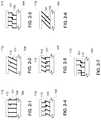
- FIGS. 2-1 through 2-7are respective block diagrams of side views illustratively depicting exemplary profiles of wire bond wires.
- FIG. 3-1is the exemplary microelectronic package of FIG. 1-3 though with slash-like shaped wire bond wires.
- FIG. 3-2is the exemplary microelectronic package of FIG. 1-3 though with squared-off vertical-z-like shaped wire bond wires.
- FIG. 4-1is a top-down perspective view illustratively depicting an exemplary microelectronic package having interference protection, as in FIG. 1-1 , though with a triangularly shaped microelectronic device.
- FIG. 4-2is a cut-away diagram of the top-down perspective view illustratively depicting the exemplary microelectronic package of FIG. 4-1 after the addition of a molding layer and a triangular conductive layer.
- FIG. 5is a block diagram of the top-down perspective view illustratively depicting the exemplary microelectronic package after the addition of a molding layer and an oval conductive layer.
- FIG. 6is a block diagram of a cross-sectional view illustratively depicting an exemplary microelectronic package with inner and outer interference shielding cages.
- FIG. 7-1is a top-down perspective view illustratively depicting an exemplary microelectronic package having inner and outer interference protection.
- FIG. 7-2is the top-down perspective view illustratively depicting the exemplary microelectronic package of FIG. 7-1 after the addition of a conductive layer.
- FIG. 7-3is a cut-away diagram of the top-down perspective view illustratively depicting the exemplary microelectronic package of FIG. 7-1 after the addition of a molding layer and a conductive layer.
- FIG. 8is a block diagram of a cross-sectional view illustratively depicting an exemplary microelectronic package with inner and outer interference shielding cages.
- FIG. 9-1is a top-down perspective view illustratively depicting an exemplary microelectronic package having inner and outer interference protection.
- FIG. 9-2is the top-down perspective view illustratively depicting the exemplary microelectronic package of FIG. 9-1 after the addition of a conductive layer.
- FIG. 10is a top-down perspective view illustratively depicting an exemplary microelectronic package having plots for interference shielding cages as in FIG. 1-1 and as in FIG. 7-1 for example.
- FIG. 11is a block diagram of a top-down view illustratively depicting an exemplary microelectronic package.
- FIG. 12-1is a block diagram of a cross-section along A 1 -A 2 of FIG. 11 .
- FIG. 12-2is a block diagram of a cross-section along A 1 -A 2 of FIG. 11 after addition of a molding layer.
- FIG. 13is a top-down perspective view illustratively depicting an exemplary microelectronic package having interference shielding cages.
- FIGS. 14-1 and 14-2are block diagrams of a top-down view illustratively depicting respective exemplary wire bond wire patterns for neighboring EMI isolation regions.
- FIGS. 15-1 through 15-3are block diagrams of a side view illustratively depicting respective exemplary wire bond wire patterns for neighboring EMI isolation regions.
- FIG. 16is a flow diagram illustratively depicting a process for forming a microelectronic package having wire bond wire interference shielding.
- Interferencemay be electromagnetic interference (“EMI”), including without limitation radio frequency interference (“RFI”), and/or another electrical and/or magnetic field that would produce undesirable EMI outside of the source generating the field.
- EMImay be emitted from one device to another separate device, and compatibility of a device with respect to such out-of-package or out-of-device EMI emissions may be referred to as electromagnetic compatibility (“EMC”).
- EMCelectromagnetic compatibility
- a common EMI emitting deviceis a mobile phone, and a mobile phone may have an EMC problem with respect to medical devices, which is a reason people are asked to turn-off their mobile phones in hospitals.
- EMCelectrostatic multi-media interface
- generally only shielding from EMIis described below in additional detail; however, it shall become apparent from the following description that this shielding may also be used to enhance EMC.
- thin profile devicessuch as mobile phones, wearables and/or Internet of Things devices, for reducing EM emission therefrom, and in some implementations enhancing EMC.
- an apparatusgenerally relates to protection from electromagnetic (“EM”) interference.
- a platformhas an upper surface and a lower surface opposite the upper surface and has a ground plane.
- a microelectronic deviceis coupled to the upper surface of the platform.
- Wire bond wiresare coupled to the ground plane.
- the wire bond wireshave a pitch.
- the wire bond wiresextend away from the upper surface of the platform with upper ends of the wire bond wires extending above an upper surface of the microelectronic device.
- the wire bond wiresare spaced apart from one another to provide a fence-like perimeter to provide an interference shielding cage.
- a conductive layeris coupled to at least a subset of the upper ends of the wire bond wires for electrical conductivity to provide a conductive shielding layer to cover the interference shielding cage.
- spacings between each pair of adjacent wire bond wiresmay be substantially smaller than electrical wavelengths of interest, including without limitation the electrical wavelength of the highest operation frequency of interest.
- spacing between two adjacent wirescan be less than approximately one tenth of the electromagnetic wavelength in a medium.
- the spacing between two adjacent wirescan be less than 500 microns (“um”) for an operational frequency of approximately 3 GHz, and less than 50 um for an operational frequency of approximately 30 GHz.
- the microelectronic devicecan be shielded from the interference outside of the interference shielding cage.
- the microelectronic devicecan be shielded by the interference shielding cage to reduce spread of the interference generated by the microelectronic device.
- the interferencecan be electromagnetic interference.
- the conductive layercan have an overhang extending beyond the perimeter. At least a subset of the wire bond wires can have gaps therebetween narrower than the pitch of at least the subset of the wire bond wires.
- the wire bond wirescan have a /-like shape.
- the wire bond wirescan have a -like shape.
- the wire bond wirescan have a -like shape.
- the perimetercan have a shape corresponding to a layout of the microelectronic device.
- the perimetercan have a contour or non-parallel sides shape.
- the perimetercan have a circular shape.
- the microelectronic devicecan be a first microelectronic device, and the apparatus can further include a second microelectronic device coupled to the platform and located outside of the interference shielding cage.
- the platformcan be selected from a leadframe, a circuit board, a substrate, and a redistribution layer.
- the wire bond wires having the pitchcan be first wire bond wires having a first pitch
- the interference shielding cagecan be a first interference shielding cage having a first perimeter
- the conductive layercan be a first conductive layer
- the apparatuscan further include: second wire bond wires coupled to the ground plane with a second pitch, with the second wire bond wires extending away from the upper surface of the platform with upper ends of the second wire bond wires being above an upper surface of the second microelectronic device and the upper ends of the first wire bond wires
- the second wire bond wirescan be spaced apart from one another to provide a second fence-like perimeter to provide a second interference shielding cage, with the first perimeter being within the second perimeter
- a second conductive layercan be coupled to at least a subset of the upper ends of the second wire bond wires for electrical conductivity to at least provide a shield cover over the first interference shielding cage and the second interference shielding cage including overlapping the first conductive layer for having the first interference shielding cage within the second interference shielding cage.
- the wire bond wires having the pitchcan be first wire bond wires having a first pitch
- the interference shielding cagecan be a first interference shielding cage having a first perimeter
- the apparatuscan further include: second wire bond wires coupled to the ground plane with a second pitch, with the second wire bond wires extending away from the upper surface of the platform with upper ends of the second wire bond wires being above an upper surface of the second microelectronic device and at a same level as the upper ends of at least the subset of the first wire bond wires;
- the second wire bond wirescan be spaced apart from one another to provide a second fence-like perimeter to provide a second interference shielding cage with the first perimeter being within the second perimeter;
- the conductive layercan be coupled to at least a subset of the upper ends of the second wire bond wires for electrical conductivity to at least provide a shield cover over the second interference shielding cage.
- the first microelectronic devicecan be coupled to the second microelectronic device though a gap in the interference shielding cage.
- the first microelectronic devicecan be a stronger electromagnetic interference source than the second microelectronic device.
- the wire bond wires having the pitchcan be first wire bond wires having a first pitch
- the interference shielding cagecan be a first interference shielding cage having a first perimeter; and the apparatus can further include: second wire bond wires coupled to the ground plane with a second pitch wider than the first pitch to provide a second interference for providing a portion of a second interference shielding cage having less shielding against interference than the first interference shielding cage.
- the conductive layercan define a ring-like hole therein having a pad therein isolated from a remainder of the conductive layer by the ring-like hole.
- the conductive layercan be a ground plane.
- the padcan be a signal pad or a power pad.
- the wire bond wires having the pitchcan be first wire bond wires having a first pitch
- the interference shielding cagecan be a first interference shielding cage having a first perimeter
- the apparatuscan further include: second wire bond wires coupled to the ground plane with a second pitch with the second wire bond wires extending away from the upper surface of the platform with upper ends of the second wire bond wires being above an upper surface of the second microelectronic device and at a same level as the upper ends of at least the subset of the first wire bond wires;
- the second wire bond wirescan be spaced apart from one another to provide a second fence-like perimeter in combination with a portion of the first wire bond wires to provide a second interference shielding cage with the first perimeter bordering the second perimeter;
- the conductive layercan be coupled to at least a subset of the upper ends of the second wire bond wires for electrical conductivity to at least provide a shield cover over the second interference shielding cage.
- a methodrelates generally to protection from EM interference.
- a platformis obtained having an upper surface and a lower surface opposite the upper surface and having a ground plane.
- a microelectronic deviceis coupled to the upper surface of the platform.
- Wire bond wiresare bonded to the ground plane, where the wire bond wires have a pitch.
- the wire bond wiresextend away from the upper surface of the platform with upper ends of the wire bond wires being above an upper surface of the microelectronic device.
- the wire bond wiresare spaced apart from one another to provide a fence-like perimeter to provide an interference shielding cage.
- a molding layeris deposited over the upper surface of the platform.
- a conductive layeris formed for coupling to at least a subset of the upper ends of the wire bond wires to provide a conductive shielding layer for electrical conductivity to cover the interference shielding cage.
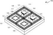
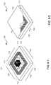
- FIG. 1-1is a top-down perspective view illustratively depicting an exemplary microelectronic package 100 having interference protection.
- FIG. 1-2is the top-down perspective view illustratively depicting the exemplary microelectronic package 100 of FIG. 1-1 after the addition of a conductive layer 112 .
- microelectronic package 100is further described.
- a platform 104has an upper surface 102 and a lower surface 106 opposite upper surface 102 .
- Platform 104further includes a ground plane 107 , which in this example is subsurface with respect to upper surface 102 , with surface accessible bond pads (not shown in this figure for purposes of clarity and not limitation) coupled to such ground plane 107 .
- Platform 104may be selected from a leadframe, a circuit board, a redistribution layer, a substrate, or other circuit base.
- a microelectronic device 105may be coupled to other bond pads (not shown in this figure for purposes of clarity and not limitation) on upper surface 102 of platform 104 .
- Microelectronic device 105for example may be an integrated circuit die, such as a resonator for example, or any other microelectronic component that generates EMI noise.
- Wire bond wires 101may be coupled to ground plane 107 with a pitch 108 .
- Wire bond wires 101extend away from upper surface 102 of platform 104 with upper ends 103 of wire bond wires 101 being above an upper surface 109 of microelectronic device 105 .
- wire bond wires 101may have a height of approximately 0.4 mm and a diameter of 20 microns, with a pitch of approximately 80 microns.
- Distance between a wire bond wire 101 used to provide a perimeter for shielding and a microelectronic device 105may be approximately 0.5 mm.
- An interference shielding cage in accordance therewithmay provide approximately 30 to 33 dB of EMI suppression at maximum radiation direction for a frequency in a range of approximately 3.0 to 4.5 GHz with E-field radiation and radiation power both reduced by approximately over 97 percent or higher.
- EMI shieldingas described herein, applications with operating frequencies of 5 GHz or greater frequencies may be have EMI suppression as described herein, including without limitation EMC enhancement. However, these or other parameter details to provide EMI shielding may be used as may vary from application-to-application.
- Wire bond wires 101are spaced apart from one another to provide a picket fence-like wall or perimeter 110 .
- a picket-fence like or bars on a cage-like perimeter of wire bond wires 101may be used to provide an interference shielding wall for an interference shielding cage 111 , such as a bond via array (“BVA”) cage.
- Interference shielding cage 111further includes a conductive layer 112 having a lower surface.
- Such lower surface of conductive layer 112may be mechanically coupled, such as by applying solder or other eutectic masses to at least a subset, if not all, of upper ends 103 of wire bond wires 101 to provide attachment of a conductive shielding layer for electrical conductivity to cover interference shielding cage 111 .
- Conductive surface 112 in this exampleis a sheet material, which may be used to provide an EMI shield cap or cover of an interference shielding cage 111 .
- a mesh of materialmay be deposited for use as a shield cover of an interference shielding cage 111 .
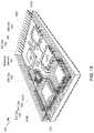
- FIG. 1-3is a cut-away diagram of the top-down perspective view illustratively depicting the exemplary microelectronic package 100 of FIG. 1-1 after the addition of a molding layer 113 and a conductive layer 112 .
- a molding layer 113over upper surface 102 and around bases and shafts of wire bond wires 101
- at least a subset, if not all, of upper ends 103 of wire bond wires 101may be temporarily exposed above an upper surface 114 of molding layer 113 .
- a mold assist film(removed in this figure) may be used in an injection mold for example to have upper ends 103 available for mechanical or other coupling.
- upper ends of wire bond wires 101do not have to be exposed by back grinding, planarizing, etching back, polishing or otherwise from molding layer 113 .
- conductive layer 112may be mechanically coupled as previously described. However, optionally conductive layer 112 may be formed by spraying, sputtering, printing, painting, ink stamping, or otherwise forming a conductive shielding layer on upper surface 114 for interconnect with upper ends 103 . By forming conductive layer 112 by spraying, sputtering, printing, painting, ink stamping, or otherwise depositing a conductive material, conductive layer 112 may be selectively applied.
- a mesh or solid surface, or a combination of part mesh and part solid surface, for conductive layer 112may be formed.
- FIG. 1-4is a block diagram of the top-down perspective view illustratively depicting the exemplary microelectronic package 100 of FIG. 1-1 after the addition of a molding layer 113 and a conductive layer 112 , where conductive layer 112 covers an upper surface of microelectronic package 100 .
- conductive layer 112there are four edges 139 to which conductive layer 112 extends; however, conductive layer 112 may be formed to cover an upper surface area of any shape of a microelectronic package 100 .
- EMI shieldingmay be enhanced over a corresponding interference shielding cage 111 where conductive layer 112 does not extend beyond perimeter 110 formed of wire bond wires 101 .
- such an overhang or extensionmay be approximately minimally half of the vertical or perpendicular height (“H”) of wire bond wires 101 .
- a perimeter of conductive layer 112may be greater than a surface area associated with a perimeter 110 of wire bond wires 101 of an interference shielding cage 111 minimally by 1 ⁇ 2 H in each direction toward one or more edges 139 .
- a 1 ⁇ 2 H overhangcan reduce EMI emissions, such as of an evanescent or standing wave, a larger overhang may suppress EMI emission further, as EMI emission may include both radial emission and an evanescent wave.
- EMI emissionmay include both radial emission and an evanescent wave.
- TEtransverse electric
- conductive layer 112may be extended to all edges 139 of a package part for an overhang of H or greater beyond perimeter 110 in all directions toward edges 139 .
- microelectronic device 105may be shielded from interference outside of interference shielding cage 111 , such as outside of a perimeter 110 of wire bond wires 101 .
- interference shielding cage 111such as by perimeter 110 of wire bond wires 101 , to reduce or prevent spread of EMI, namely size of an EM environment, generated by microelectronic device 105 .
- interference generated by microelectronic device 105 without interference shielding cage 111may generate an EMI environment affecting EMC.
- microelectronic device 105is an RF component.
- Microelectronic device 105may be a stacked die, such as a 3D IC or may be shielded from such a stacked die.
- FIGS. 2-1 through 2-7are respective block diagrams of side views illustratively depicting exemplary profiles of wire bond wires 101 .
- wire bond wires 101have a generally vertical profile, such as previously described.
- gaps between such generally vertical profile wire bond wires 101may have a generally consistent pitch 108 , where such wire bond wires 101 are bonded for example to platform 104 , and closest spaces or gaps 115 between such wires moving up from such platform 104 may be generally a consistent spacing or gapping.
- Routing wiring, such as signal, power, or ground traces for microelectronic package 100may extend through one or more gaps between adjacent wire bond wires 101 .
- wiring layersmay include routing on upper surface 102 of platform 104 without interfering with corresponding EMI shielding, thereby simplifying routing over traditional “can” style EMI shielding mechanisms, which would experience an electrical short if the solid conductive surface contacted surface routing.
- the closest spacings of gaps 115may be narrower than pitch 108 .
- pitchit is generally meant a predetermined center-to-center spacing between bases of wire bond wires, which may be contrast for example from slant of such wire bond wires.
- at least a subset, if not all, of wire bond wires 101may have gaps 115 therebetween narrower than a corresponding pitch 108 of at least a subset of wire bond wires 101 .
- Wire bond wires 101may have a slash-like or “/” shape or profile, such as in FIGS. 2-2 and 2-6 . In FIG.
- wire bond wires 101have a squared-off vertical-z-like, or a kinked or rounded shaped profile.
- the wires shown by way of example in FIGS. 2-1 through 2-7may have additional bends not shown in the schematic drawings.
- the “/” shaped wiresmay have portions that do not have a straight line profile and instead have slightly more vertical or horizontal portions at either end due to tooling parameters.
- the wiremay have be considered to have an imaginary axis extending from one end of the wire to the other with portions of the wire bond extending outside of that axis in the x, y, and/or z directions.
- wire bond wiresmay have a vertical partial four-like shape or profile.
- Other shapessuch as chevron (“ ⁇ ” or “>” shapes), arc (“(“or”)” shapes), or coil shaped configurations are optional.
- chevron (“ ⁇ ” or “>” shapesarc (“(“or”)” shapes
- coil shaped configurationsare optional.
- wire bond wires 101may be loops, such as having an open loop omega-like “ ⁇ ” shaped profile or a closed loop el-like “I” shaped profile.
- the wire loopsmay each be formed on a single pad and may be offset or angled relative to each other in the x and y direction (i.e., in a layout similar to “ ⁇ ⁇ ⁇ ” when viewed down the z direction) to facilitate a more tightly packed layout than might be possible if the wires in the wire loop extended in the same plane (i.e., in a layout similar to “- - -” when viewed down the z direction).
- FIG. 3-1is the exemplary microelectronic package 100 though with slash-like shaped wire bond wires 101
- FIG. 3-2is the exemplary microelectronic package 100 though with squared-off vertical-z-like shaped wire bond wires 101
- pitch, shape, and diameter of wire bond wires 101may be used to further reduce EM emissions from a fence-like perimeter, such as perimeter 110 for example, formed of wire bond wires 101
- Some of adjacent wire bond wires 101may be in contact with each other, and some wires 101 may not extend to conductive layer 112 , such as illustrative depicted in FIG. 2-7 for purposes of clarity by way of example and not limitation, and these or other options described herein may be selectable by a designer for a given EMI shield design or characteristic.
- perimeter 110 formed by layout of wire bond wires 101may have a shape corresponding to a layout of microelectronic device 105 .
- microelectronic device 105may have a layout shape other than that of a square, rectangle or other similar polygon.
- microelectronic device 105may have a layout shape of a circle, oval or other curvilinear shape.
- Shaping fence-like perimeters, such as for example perimeter 110 and/or below described perimeter 120 , formed of wire bond wires 101 to a microelectronic device 105 layout shape or footprintmay be used to provide more compact designs and/or better shielding performance than not contouring fence-like perimeters to such footprint.
- FIG. 4-1is a top-down perspective view illustratively depicting an exemplary microelectronic package 100 having interference protection, as in FIG. 1-1 , though with a triangularly shaped microelectronic device 105 .
- perimeter 110 formed of wire bond wires 101may have a corresponding triangular shape.
- wire bond wires 101have a slash-like profile.
- FIG. 4-2is a cut-away diagram of the top-down perspective view illustratively depicting the exemplary microelectronic package 100 of FIG. 4-1 after the addition of a molding layer 113 and a triangular conductive layer 112 .
- a perimetermay have one or more contoured sides, non-parallel sides and/or non-orthogonal sides in order to follow a layout of an irregularly shaped microelectronic device 105 .
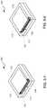
- FIG. 5is a block diagram of the top-down perspective view illustratively depicting the exemplary microelectronic package 100 after the addition of a molding layer 113 and a conductive layer 112 .
- Circles 116generally indicate upper ends of wire bond wires 101 positioned for providing an oval shaped perimeter 110 of wire bond wires 101 , as previously described though for an oval shaped microelectronic device 105 .
- Microelectronic devices 105 as described hereinmay be passive or active devices.
- Conductive layer 112may have an oval shape as generally indicated by dashed oval 112 A. However, conductive layer 112 may overhang an oval shaped perimeter 110 and need not be contoured like perimeter 110 .
- conductive layer 112may extend to edges of a package, as generally indicated by arrow 112 B.
- conductive layer 112may have an oval shape to extend beyond perimeter 110 , as generally indicated by dashed oval 112 C.
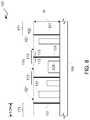
- FIG. 6is a block diagram of a cross-sectional view illustratively depicting an exemplary microelectronic package 100 with inner and outer interference shielding cages 111 and 121 , respectively.
- inner interference shielding cage 111has therein a microelectronic device 105 surrounded by a perimeter of wire bond wires 101 , where location of a conductive layer 112 is generally indicated with a dashed line bridging such wire bond wires 101 , such as previously described for example.
- conductive layer 112 of inner interference shielding cage 111does not overhang or extend beyond an inner perimeter formed of wire bond wires 101 .
- An outer interference shielding cage 121has one or more microelectronic devices 117 , as well as inner interference shielding cage 111 , therein.
- One or more of microelectronic devices 117may be taller than microelectronic device 105 . In other words, an upper surface of such one or more taller microelectronic devices 117 may be above, though not necessarily overlapping, an upper surface of microelectronic device 105 .
- Microelectronic devices 117may be coupled to an upper surface of platform 104 and may be located outside of inner interference shielding cage 111 .
- inner interference shielding cage 111is surrounded by a perimeter of wire bond wires 101 of outer interference shielding cage 121 .
- location of a conductive layer 122 thereforis generally indicated with a dashed line bridging such wire bond wires 101 , such as previously described with reference to conductive layer 112 for example, as well as extending beyond an outer perimeter of wire bond wires 101 of outer interference shielding cage 121 .
- an overhang or eave 171may extend beyond each side of a perimeter of wire bond wires 101 of outer interference shielding cage 121 by approximately a distance H, for H also a vertical height of wire bond wires 101 used to provide such a perimeter.
- FIG. 7-1is a top-down perspective view illustratively depicting an exemplary microelectronic package 100 having inner and outer interference protection.
- FIG. 7-2is the top-down perspective view illustratively depicting the exemplary microelectronic package 100 of FIG. 7-1 after the addition of conductive layer 122 .
- microelectronic package 100 of FIGS. 7-1 and 7-2is further described. As much of the above description is applicable to describing microelectronic package 100 of FIGS. 7-1 and 7-2 , some of such description is not repeated for purposes of clarity and not limitation.
- Inner perimeter wire bond wires 101may have a pitch 108 for an inner interference shielding cage 111 having a conductive layer 112 .
- Conductive layer 112may not have sufficient room for an overhang.
- Outer wire bond wires 101may be coupled to a ground plane 107 though with a same or different pitch 128 with reference to pitch 108 .
- Outer wire bond wires 101extend away from an upper surface of platform 104 with upper ends 103 of outer wire bond wires 101 being above an uppermost upper surface of microelectronic devices 117 , as well as above upper ends of inner wire bond wires 101 and inner conductive layer 112 .
- Outer wire bond wires 101may be spaced apart from one another to provide an outer picket fence-like perimeter 120 to provide an outer interference shielding cage 121 .
- Inner perimeter 110may be completely within outer perimeter 120 .
- An upper conductive layer 122may be coupled to at least a subset of upper ends 103 of outer wire bond wires 101 for electrical conductivity to cover inner interference shielding cage 111 and outer interference shielding cage 121 , where upper conductive layer 122 is above and overlapping inner-lower conductive layer 112 for having inner interference shielding cage 111 within outer interference shielding cage 121 .
- Outer interference shielding cage 121may be for EMC shielding, whereas inner interference shielding cage 111 may be for EMI shielding.
- conductive layer 122may extend beyond perimeter 120 to provide an overhang 171 , of at least approximately 1 ⁇ 2 H in order to enhance EMC, and overhangs greater than 1 ⁇ 2 H, such as an overhang of at least H may provide more EMI evanescent wave suppression.
- FIG. 7-3is a cut-away diagram of the top-down perspective view illustratively depicting the exemplary microelectronic package 100 of FIG. 7-1 after the addition of a molding layer 123 and a conductive layer 122 .
- at least a subset, if not all, of upper ends 103 of outer wire bond wires 101may be temporarily exposed above an upper surface 124 of molding layer 123 .
- a mold assist film(removed in this figure) may be used in an injection mold for example to have upper ends 103 of outer wire bond wires 101 available for mechanical or other coupling.
- conductive layer 122may be mechanically coupled as previously described. However, optionally conductive layer 122 may be formed by spraying, sputtering, printing, painting, ink stamping, or otherwise forming a conductive shielding layer on upper surface 124 for interconnect with upper ends 103 of outer wire bond wires 101 . Conductive layer 122 may provide an overhang 171 , which may or may not extend to outer edges 139 of microelectronic package 100 . Conductive layer 122 is illustratively depicted as being short of outer edges 139 in order to more clearly indicate a perimeter of conductive layer 122 .
- FIG. 8is a block diagram of a cross-sectional view illustratively depicting an exemplary microelectronic package 100 with inner and outer interference shielding cages 111 and 121 , respectively.
- inner interference shielding cage 111has therein a microelectronic device 105 surrounded by a perimeter of wire bond wires 101 , where location of a conductive layer 122 is generally indicated with a dashed line bridging such wire bond wires 101 .
- conductive layer 122provides a common cover for both of inner interference shielding cages 111 and 121 and also provides an overhang 171 to extend beyond an outer perimeter formed of wire bond wires 101 by approximately 1 ⁇ 2 H.
- An outer interference shielding cage 121has one or more microelectronic devices 117 , as well as inner interference shielding cage 111 , therein.
- One or more of microelectronic devices 117may be taller than microelectronic device 105 . In other words, an upper surface of such one or more taller microelectronic devices 117 may be above, though not necessarily overlapping, an upper surface of microelectronic device 105 .
- Microelectronic devices 117may be coupled to an upper surface of platform 104 and may be located outside of a perimeter of inner interference shielding cage 111 .
- inner interference shielding cage 111is surrounded by a perimeter of wire bond wires 101 of outer interference shielding cage 121 .
- Location of a conductive layer 122is generally indicated with a dashed line bridging wire bond wires 101 for both inner interference shielding cage 111 and outer interference shielding cage 121 , namely being an EMI shielding cover common to both of cages 111 and 121 without having a separate cover for inner interference shielding cage 111 .
- Conductive layer 122extends beyond an outer perimeter of wire bond wires 101 of outer interference shielding cages 121 .
- an overhang or eave 171may extend beyond each side of a perimeter of wire bond wires 101 of each outer interference shielding cage 121 by approximately at least a distance 1 ⁇ 2 H, for H also a vertical height of wire bond wires 101 used to provide such a perimeter.
- common sections 172provide overhangs 173 for EMI shielding, such as for EMI suppression of higher order modes and evanescent waves.
- FIG. 9-1is a top-down perspective view illustratively depicting an exemplary microelectronic package 100 having inner and outer interference protection.
- FIG. 9-2is the top-down cutaway perspective view illustratively depicting the exemplary microelectronic package 100 of FIG. 9-1 after the addition of conductive layer 122 .
- microelectronic package 100 of FIGS. 9-1 and 9-2is further described. As much of the above description is applicable to describing microelectronic package 100 of FIGS. 9-1 and 9-2 , some of such description is not repeated for purposes of clarity and not limitation.
- Inner perimeter wire bond wires 101may have a pitch 108 for an inner interference shielding cage 111 having a separate conductive layer 112 independent of another interference shielding cage or having a common conductive layer 122 for a common cover with another interference shielding cage.
- Outer wire bond wires 101 of outer interference shielding cage 121may be coupled to a ground plane 107 , though with a same or different pitch 128 with reference to pitch 108 as inner wire bond wires 101 of inner interference shielding cage 111 .
- Outer wire bond wires 101 coupled to ground plane 107 with a pitch 128 wider than pitch 108may be for EMC for providing an outer interference shielding cage 121 having less shielding against EMI than inner interference shielding cage 111 .
- Conductive layer 122may have an overhang 171 extending beyond a perimeter 120 of outer wire bond wires 101 for enhancing EMC.
- Outer wire bond wires 101extend away from an upper surface of platform 104 with upper ends 103 of outer wire bond wires 101 being above an uppermost upper surface of microelectronic devices 117 , but at a same level as upper ends of at least a subset, if not all, of inner wire bond wires 101 with no inner conductive layer 112 .
- Outer wire bond wires 101may be spaced apart from one another to provide an outer picket fence-like perimeter 120 to provide an outer interference shielding cage 121 .
- Inner perimeter 110may be completely within outer perimeter 120 .
- a conductive layer 122may be mechanically coupled to at least subsets of upper ends 103 of both inner and outer wire bond wires 101 for electrical conductivity to cover inner interference shielding cage 111 and outer interference shielding cage 121 , where conductive layer 122 is above and overlapping inner interference shielding cage 111 within outer interference shielding cage 121 .
- Outer interference shielding cage 121may be for EMI and/or EMC shielding
- inner interference shielding cage 111may be for EMI shielding, with a single conductive layer 122 for providing a ceiling for both inner and outer interference shielding cages.
- a microelectronic package 100may include multiple types of interference shielding cages in accordance with the description herein.
- FIG. 10is a top-down perspective view illustratively depicting an exemplary microelectronic package 100 having plots for interference shielding cages as in FIG. 1-1 and as in FIG. 7-1 for example.
- microelectronic package 100 of FIG. 10is further described, while much of the above description which is the same is not repeated for purposes of clarity and not limitation.
- wire bond wires 101 forming one or more picket fence-like perimeters 110 and/or 120 of one plotmay be adjacent another picket fence-like outer perimeter 110 or 120 .
- a portion of one picket fence-like perimetermay be used in combination with a portion of a neighboring or bordering picket fence-like perimeter to provide an interference shielding cage.
- a multiplex of interference shielding cages 121may be provided with a single microelectronic package 100 .
- Inner perimeters 110 of these interference shield cages 111 provided by wire bond wires 101may, but do not need to, run perpendicular to an edge or follow a straight line. Rather, such inner perimeters can be laid out or shaped to follow a contour or other irregular pattern.
- Conductive layer 122which is left off for clarity in FIG. 10 , may be formed over multiple outer interference shielding cages 121 , as previously described herein.
- a microelectronic device 105 in an inner or only interference shielding cage 111 or a microelectronic device 117 in an outer interference shielding cage 121 of a plotmay be coupled to another microelectronic device 105 or 117 in another interference shielding cage 111 or 121 in another plot by routing between pairs of adjacent wire bond wires 101 in one or more intervening perimeters 110 and/or 120 , such as routings 140 and 141 for example.
- a microelectronic device which is a stronger EMI source, such as a signal pad without grounding, than another microelectronic device, such as a ground pad which may not be caged,may be directly coupled to one another while still providing sufficient EMI shielding to such stronger EMI source. This may be used for more compact designs with fewer fences to provide sufficient shielding.
- one interference shielding cage 121may directly border, space apart or not, another interference shielding cage 121 without having to provide isolation gaps, such as in a molding layer for example, for electrical isolation between such neighboring interference shielding cages.
- routing through fences of cages as described hereinrouting may be at lower levels, rather than having to run such routing over on top of a microelectronic package.
- trenchesare formed which can significantly increase topside routing complexity, and this complexity may be significantly reduced with routing through cage fences, in addition to not having EMI isolation trenches.
- wire bond wires 101may be shared among such neighboring interference shielding cages, as previously described. Accordingly, either or both of these configurations may be used to provide a more densely populated microelectronic package 100 , namely a microelectronic package that has a smaller footprint.
- FIG. 11is a block diagram of a top-down view illustratively depicting an exemplary microelectronic package 100
- FIG. 12-1is a block diagram of a cross-section along A 1 -A 2 of FIG. 11 .
- microelectronic package 100 of FIGS. 11 and 12-1is further described.
- a conductive layer 112 or 122may be a ground plane, which as a hole 160 , such as a ring-like hole, cut or ablated therein, such as laser ablated for example, to define an electrical island or pad 161 therein, namely pad 161 is not in contact with, nor isolated from, a remainder of conductive layer 112 or 122 .
- Pad 161may be a signal pad or a power pad coupled to at least one wire bond wire 101 C, not part of an interference shielding cage 111 or 121 , located for interconnection with pad 161 . Isolation of pad 161 may be used for system-in-package (“SiP”) integration.
- a decoupling capacitor or other passive or active devicemay be coupled to one or more of such isolated pads 161 .
- This implementationallows passive and/or active devices to be placed on a level above EMI shielding with interconnects through microelectronic package 100 formed at the same time as one or more interference shielding cages, thereby simplifying package processing.
- multiple pads 161maybe formed singularly or in an array of two or more pads.
- Devicesmay be attached to one or more pads 161 , conductive layer 112 / 122 , or both, for an application.
- pad 161is illustratively depicted as surrounded by a conductive layer, this is for illustrative purposes only.
- Conductive layer 112 / 122may be generally adjacent to only one or more of the sides of contact pad 161 .
- FIG. 12-2is a block diagram of a cross-section along A 1 -A 2 of FIG. 11 after addition of a molding layer 113 .
- microelectronic package 100 of FIGS. 11 and 12-2is further described.
- one or more pads 161may be selectively formed on an upper surface of a molding layer 113 .
- molding layer 113may be a dielectric, and such one or more pads 161 may be electrically isolated from one another along an upper surface of molding layer 113 .
- conductive layer 112By forming conductive layer 112 by plating, spraying, sputtering, printing, painting, ink stamping, or otherwise selectively depositing a conductive material, conductive layer 112 may be selectively applied in any applicable pattern or design to an upper surface of molding layer 113 .
- FIG. 13is a top-down perspective view illustratively depicting an exemplary microelectronic package 100 having interference shielding cages, as described above.
- interference shielding cagesmay include multiple odd-shaped divisions or sections. Thus, there may be multiple isolation zones, which need not, though may, be orthogonal to one another.
- FIG. 13is further described with simultaneous reference to FIGS. 1 through 13 .
- microelectronic package 100may be a SiP having passive devices 181 , flip-chip (“FC”) dies 182 , and wire bond (“WB”) dies 183 all coupled to an upper surface 102 of a platform 104 .
- WB dies 183may be bonded to platform 104 with wire bonds 185 .
- the wire bonds 185 and/or surface traces (not shown) on platform 104may be configured to extend between adjacent wire bond wires 101 A- 101 D to other die, or to pads located on the platform 104 , on the other side of an EMI shielded area. In certain implementations, this allows the EMI shield wire bond wires 101 A- 101 D to be formed closer to the EMI source or EMI protected device than the pad on the platform 104 .
- FC dies 182being “flip-chip” coupled to platform 104 , along with having an underfill layer 184 for such coupling.
- Wire bond wires 101 B and 101 Dmay form separate EMI shielding perimeters, such as perimeters 110 for example, around respective FC dies 182 .
- Wire bond wires 101 Cmay form a separate EMI shielding perimeter, such as a perimeter 110 for example, around a WB die 183 .
- Wire bond wires 101 Amay form an EMI shielding perimeter, such as a perimeter 120 for example, around components coupled to upper surface 102 of platform 104 for EMI shielding to enhance EMC.
- a SiPmay be a number of active or/and passive components enclosed in a single IC package module, such as microelectronic package 100 .
- SiPsare widely used in RF applications, including without limitation mobile devices, wearables and Internet of Things (“IoT”) devices.
- IoTInternet of Things
- an RF SiPcan contain some active chips such as one or more ASIC and/or memory chips, and some passive components such as RF resistors, capacitors, inductors, oscillators, etc.
- a SiPis particularly useful in space constrained environments, as a SiP significantly reduces complexity of a printed circuit board (“PCB”) and system design.
- PCBprinted circuit board
- Recently, SiPsare attracting interest in small form factor electronics, including without limitation IoT devices.
- EMI and EMCmay be more problematic in future SiP designs because more components with multiple frequencies may be integrated into a single RF SiP.
- a SiP for 5G wireless devicesmay handle multiple RF functions including WiFi, 3G, 4G LTE, ZigBee, etc.
- EMI shieldingmay be provided for different domains within a same SiP.
- Wire bond wires 101may be implemented with high-frequency wire bonding machines for cost effective and high volume production.
- wire bond wires, whether ball bonded or wedge bondedmay be used to make good ground contacts without block surface signal routings between domains.
- FIGS. 14-1 and 14-2are block diagrams of a top-down view illustratively depicting respective exemplary wire bond wire patterns 191 and 192 for neighboring EMI isolation regions. With simultaneous reference to FIGS. 1 through 14-2 , wire bond wire patterns 191 and 192 are further described. A row of wire bond wires 101 B and a row of wire bond wires 101 D may be back-to-back and spaced apart from one another. Having two or more rows of wire bond wires may be laid out to create concentric perimeters with an array of wires instead of lines of wire bond wires as illustratively depicted in the earlier figures, or a combination thereof.
- wire bond wire pattern 191bases of wire bond wires 101 B and 101 D are horizontally- or vertically-aligned to one another, so gaps between wire bond wires 101 B correspond to gaps between wire bond wires 101 D. This arrangement or pattern may be useful for allowing direct surface routing to pass through fence-like EMI shield perimeters formed by wire bond wires 101 B and 101 D.
- wire bond wires 101 B and/or 101 Dmay include loop-like structures, such as open loop omega-like structures, as generally indicated with dashed lines 189 .
- wire bond wire pattern 192bases of wire bond wires 101 B and 101 D are offset-aligned to one another, so gaps between wire bond wires 101 B correspond to bases of wire bond wires 101 D, and gaps between wire bond wires 101 D correspond to bases of wire bond wires 101 B.
- This arrangement or patternmay be useful for having an overlapping and/or interspersing of wire bond wires with respect to EMI emissions to effectively provide a more dense mesh, for example by a combination of fence-like EMI shield perimeters formed by wire bond wires 101 B and 101 D.
- wire bond wires 101 B and 101 Dmay have same or different diameters, and may be made out of same or different materials. Pattern selection, as well as thickness and/or material selection, may be tailored to an application, such as may be associated with parameters of sources of EMI emission, including without limitation frequency of operation.
- FIGS. 15-1 through 15-3are block diagrams of a side view illustratively depicting respective exemplary wire bond wire patterns 193 and 194 for neighboring EMI isolation regions. With simultaneous reference to FIGS. 1 through 15-3 , wire bond wire patterns 193 and 194 are further described.
- a row of wire bond wires 101 B and a row of wire bond wires 101 Dmay be back-to-back and spaced apart from one another, and both sets of these rows of wire bond wires may be slanted.
- Wire bond wires 101 Dare illustrated with dashed lines to indicate they are in back of wire bond wires 101 B.
- An outer ring or other perimeter of an EMI cagemay have wires slanted in one direction, while an inner ring or other perimeter of another EMI cage may be slanted in a second direction opposite the first direction.
- a second directionmay be generally an opposite angle with respect to the angle in such a first direction in any of x, y, or z directions.
- wire bond wires 101 B and 101 Dare horizontally- or vertically-aligned to one another, so gaps between wire bond wires 101 B correspond to gaps between wire bond wires 101 D.
- this arrangement or patternmay be useful for allowing surface-based routing to pass through fence-like EMI shield perimeters formed by wire bond wires 101 B and 101 D.
- wire bond wires 101 B and 101 Dare slanted in opposite directions in order to form a crosswise mesh for a combination of fence-like EMI shield perimeters formed by wire bond wires 101 B and 101 D.
- Right wire bond pattern 193is the same as left wire bond pattern, except bases of wire bond wires 101 B and 101 D are offset-aligned to one another, so gaps between wire bond wires 101 B correspond to bases of wire bond wires 101 D, and gaps between wire bond wires 101 D correspond to bases of wire bond wires 101 B.
- This arrangement or patternmay be useful for forming a bi-directional mesh for a combination of fence-like EMI shield perimeters formed by wire bond wires 101 B and 101 D.
- wire bond wire pattern 194bases of wire bond wires 101 B and 101 D are offset-aligned to one another, so gaps between wire bond wires 101 B correspond to bases of wire bond wires 101 D, and gaps between wire bond wires 101 D correspond to bases of wire bond wires 101 B.
- This arrangement or patternmay be useful for forming a unidirectional mesh for a combination of fence-like EMI shield perimeters formed by wire bond wires 101 B and 101 D.
- FIG. 16is a flow diagram illustratively depicting a EMI shield forming process 200 for forming a microelectronic package 100 having wire bond wires 101 for interference shielding for protection from EMI. Process 200 is further described with simultaneous reference to FIGS. 1 through 16 .
- a platform 104is obtained having an upper surface 102 and a lower surface 106 opposite upper surface 102 and having a ground plane 107 .
- a microelectronic device 105is coupled to upper surface 102 of platform 104 .
- wire bond wires 101are wire bonded, such as ball, wedge or stitch bonded, for electrical interconnection with ground plane 107 .
- Such wire bond wires 101may have a pitch, as previously described. Wire bond wires 101 extend away from upper surface 102 of platform 104 with upper ends of wire bond wires 101 being above an upper surface of microelectronic device 105 .
- Such wire bond wires 101are spaced apart from one another to provide a fence-like perimeter to provide at least one interference shielding cage, such as previously described.
- a molding layer 113may be deposited over upper surface 102 of platform 104 , as previously described.
- a conductive layermay be formed, as previously described, for being coupled to at least a subset of upper ends of wire bond wires 101 for electrical conductivity to provide a conductive shielding layer 112 and/or 122 to cover such an interference shielding cage 111 and/or 121 .
- operation 202may be for coupling multiple microelectronic devices to an upper surface of a platform
- operation 203may be for forming multiple wire bond perimeters, such as described elsewhere herein.
- one or more conductive layersmay be formed.
Landscapes
- Physics & Mathematics (AREA)
- Engineering & Computer Science (AREA)
- Microelectronics & Electronic Packaging (AREA)
- Computer Hardware Design (AREA)
- Power Engineering (AREA)
- Condensed Matter Physics & Semiconductors (AREA)
- General Physics & Mathematics (AREA)
- Health & Medical Sciences (AREA)
- Electromagnetism (AREA)
- Toxicology (AREA)
- Shielding Devices Or Components To Electric Or Magnetic Fields (AREA)
- Manufacturing & Machinery (AREA)
Abstract
Description


Claims (16)
Priority Applications (5)
| Application Number | Priority Date | Filing Date | Title |
|---|---|---|---|
| US15/914,617US10658302B2 (en) | 2016-07-29 | 2018-03-07 | Wire bonding method and apparatus for electromagnetic interference shielding |
| US16/833,445US11335647B2 (en) | 2016-07-29 | 2020-03-27 | Wire bonding method and apparatus for electromagnetic interference shielding |
| US17/721,154US11837556B2 (en) | 2016-07-29 | 2022-04-14 | Wire bonding method and apparatus for electromagnetic interference shielding |
| US18/377,706US12094835B2 (en) | 2016-07-29 | 2023-10-06 | Wire bonding method and apparatus for electromagnetic interference shielding |
| US18/788,822US20250096151A1 (en) | 2016-07-29 | 2024-07-30 | Wire bonding method and apparatus for electromagnetic interference shielding |
Applications Claiming Priority (3)
| Application Number | Priority Date | Filing Date | Title |
|---|---|---|---|
| US201662368423P | 2016-07-29 | 2016-07-29 | |
| US15/237,936US9935075B2 (en) | 2016-07-29 | 2016-08-16 | Wire bonding method and apparatus for electromagnetic interference shielding |
| US15/914,617US10658302B2 (en) | 2016-07-29 | 2018-03-07 | Wire bonding method and apparatus for electromagnetic interference shielding |
Related Parent Applications (1)
| Application Number | Title | Priority Date | Filing Date |
|---|---|---|---|
| US15/237,936ContinuationUS9935075B2 (en) | 2016-07-29 | 2016-08-16 | Wire bonding method and apparatus for electromagnetic interference shielding |
Related Child Applications (1)
| Application Number | Title | Priority Date | Filing Date |
|---|---|---|---|
| US16/833,445ContinuationUS11335647B2 (en) | 2016-07-29 | 2020-03-27 | Wire bonding method and apparatus for electromagnetic interference shielding |
Publications (2)
| Publication Number | Publication Date |
|---|---|
| US20180197834A1 US20180197834A1 (en) | 2018-07-12 |
| US10658302B2true US10658302B2 (en) | 2020-05-19 |
Family
ID=61012240
Family Applications (6)
| Application Number | Title | Priority Date | Filing Date |
|---|---|---|---|
| US15/237,936ActiveUS9935075B2 (en) | 2016-07-29 | 2016-08-16 | Wire bonding method and apparatus for electromagnetic interference shielding |
| US15/914,617Active2036-10-17US10658302B2 (en) | 2016-07-29 | 2018-03-07 | Wire bonding method and apparatus for electromagnetic interference shielding |
| US16/833,445Active2036-12-05US11335647B2 (en) | 2016-07-29 | 2020-03-27 | Wire bonding method and apparatus for electromagnetic interference shielding |
| US17/721,154ActiveUS11837556B2 (en) | 2016-07-29 | 2022-04-14 | Wire bonding method and apparatus for electromagnetic interference shielding |
| US18/377,706ActiveUS12094835B2 (en) | 2016-07-29 | 2023-10-06 | Wire bonding method and apparatus for electromagnetic interference shielding |
| US18/788,822PendingUS20250096151A1 (en) | 2016-07-29 | 2024-07-30 | Wire bonding method and apparatus for electromagnetic interference shielding |
Family Applications Before (1)
| Application Number | Title | Priority Date | Filing Date |
|---|---|---|---|
| US15/237,936ActiveUS9935075B2 (en) | 2016-07-29 | 2016-08-16 | Wire bonding method and apparatus for electromagnetic interference shielding |
Family Applications After (4)
| Application Number | Title | Priority Date | Filing Date |
|---|---|---|---|
| US16/833,445Active2036-12-05US11335647B2 (en) | 2016-07-29 | 2020-03-27 | Wire bonding method and apparatus for electromagnetic interference shielding |
| US17/721,154ActiveUS11837556B2 (en) | 2016-07-29 | 2022-04-14 | Wire bonding method and apparatus for electromagnetic interference shielding |
| US18/377,706ActiveUS12094835B2 (en) | 2016-07-29 | 2023-10-06 | Wire bonding method and apparatus for electromagnetic interference shielding |
| US18/788,822PendingUS20250096151A1 (en) | 2016-07-29 | 2024-07-30 | Wire bonding method and apparatus for electromagnetic interference shielding |
Country Status (1)
| Country | Link |
|---|---|
| US (6) | US9935075B2 (en) |
Cited By (3)
| Publication number | Priority date | Publication date | Assignee | Title |
|---|---|---|---|---|
| US11404338B2 (en) | 2014-01-17 | 2022-08-02 | Invensas Corporation | Fine pitch bva using reconstituted wafer with area array accessible for testing |
| US11424211B2 (en) | 2011-05-03 | 2022-08-23 | Tessera Llc | Package-on-package assembly with wire bonds to encapsulation surface |
| US11735563B2 (en) | 2011-10-17 | 2023-08-22 | Invensas Llc | Package-on-package assembly with wire bond vias |
Families Citing this family (26)
| Publication number | Priority date | Publication date | Assignee | Title |
|---|---|---|---|---|
| US9935075B2 (en)* | 2016-07-29 | 2018-04-03 | Invensas Corporation | Wire bonding method and apparatus for electromagnetic interference shielding |
| US11189574B2 (en)* | 2017-05-31 | 2021-11-30 | Intel Corporation | Microelectronic package having electromagnetic interference shielding |
| US10573573B2 (en)* | 2018-03-20 | 2020-02-25 | Taiwan Semiconductor Manufacturing Co., Ltd. | Package and package-on-package structure having elliptical conductive columns |
| US11127689B2 (en) | 2018-06-01 | 2021-09-21 | Qorvo Us, Inc. | Segmented shielding using wirebonds |
| KR20200001102A (en) | 2018-06-26 | 2020-01-06 | 삼성전기주식회사 | Electronic component module and manufacturing mehthod therof |
| US11219144B2 (en) | 2018-06-28 | 2022-01-04 | Qorvo Us, Inc. | Electromagnetic shields for sub-modules |
| US10506704B1 (en)* | 2018-08-21 | 2019-12-10 | Nxp Usa, Inc. | Electromagnetically-shielded microelectronic assemblies and methods for the fabrication thereof |
| TWI744572B (en) | 2018-11-28 | 2021-11-01 | 蔡憲聰 | Semiconductor package with in-package compartmental shielding and fabrication method thereof |
| US10923435B2 (en) | 2018-11-28 | 2021-02-16 | Shiann-Tsong Tsai | Semiconductor package with in-package compartmental shielding and improved heat-dissipation performance |
| US11239179B2 (en) | 2018-11-28 | 2022-02-01 | Shiann-Tsong Tsai | Semiconductor package and fabrication method thereof |
| JP6802314B2 (en)* | 2018-11-28 | 2020-12-16 | 宗哲 蔡 | Semiconductor package and its manufacturing method |
| US10896880B2 (en) | 2018-11-28 | 2021-01-19 | Shiann-Tsong Tsai | Semiconductor package with in-package compartmental shielding and fabrication method thereof |
| US11211340B2 (en) | 2018-11-28 | 2021-12-28 | Shiann-Tsong Tsai | Semiconductor package with in-package compartmental shielding and active electro-magnetic compatibility shielding |
| US10615130B1 (en) | 2018-11-29 | 2020-04-07 | Nxp Usa, Inc. | Devices and methods for isolating signals in semiconductor devices |
| US11114363B2 (en) | 2018-12-20 | 2021-09-07 | Qorvo Us, Inc. | Electronic package arrangements and related methods |
| TWI720749B (en)* | 2019-01-01 | 2021-03-01 | 蔡憲聰 | Semiconductor package with in-package compartmental shielding and fabrication method thereof |
| TWI728604B (en)* | 2019-01-01 | 2021-05-21 | 蔡憲聰 | Semiconductor package with in-package compartmental shielding and active electro-magnetic compatibility shielding |
| CN111490034A (en)* | 2019-01-25 | 2020-08-04 | 苏州远创达科技有限公司 | Multi-chip module with high isolation |
| KR102711765B1 (en)* | 2019-03-06 | 2024-09-27 | 삼성전기주식회사 | Electronic device module and manufacturing method thereof |
| WO2020206625A1 (en)* | 2019-04-10 | 2020-10-15 | Intel Corporation | Resilient electrical connectors for electromagnetic interference shielding structures in integrated circuit assemblies |
| US11515282B2 (en) | 2019-05-21 | 2022-11-29 | Qorvo Us, Inc. | Electromagnetic shields with bonding wires for sub-modules |
| CN114068493B (en)* | 2020-07-31 | 2024-12-27 | 华为技术有限公司 | Packaging module and packaging method thereof, and electronic equipment |
| US11063629B1 (en)* | 2020-10-14 | 2021-07-13 | Nvidia Corporation | Techniques for detecting wireless communications interference from a wired communications channel |
| CN113809049A (en)* | 2021-09-17 | 2021-12-17 | 中国电子科技集团公司第五十八研究所 | Radio frequency chip packaging structure with high shielding performance and isolation and packaging method |
| CN114171502A (en)* | 2021-12-08 | 2022-03-11 | 华进半导体封装先导技术研发中心有限公司 | Radio frequency microsystem based on inhomogeneous electromagnetic metamaterial |
| CN116978798A (en)* | 2022-04-21 | 2023-10-31 | 华为技术有限公司 | Chip packaging structure, preparation method thereof and electronic equipment |
Citations (795)
| Publication number | Priority date | Publication date | Assignee | Title |
|---|---|---|---|---|
| US2230663A (en) | 1940-01-18 | 1941-02-04 | Alden Milton | Electric contact and wire assembly mechanism |
| US3289452A (en) | 1963-07-23 | 1966-12-06 | Siemens Ag | Method and device for bonding a contact wire to a semiconductor member |
| US3358897A (en) | 1964-03-31 | 1967-12-19 | Tempress Res Co | Electric lead wire bonding tools |
| US3430835A (en) | 1966-06-07 | 1969-03-04 | Westinghouse Electric Corp | Wire bonding apparatus for microelectronic components |
| US3623649A (en) | 1969-06-09 | 1971-11-30 | Gen Motors Corp | Wedge bonding tool for the attachment of semiconductor leads |
| US3795037A (en) | 1970-05-05 | 1974-03-05 | Int Computers Ltd | Electrical connector devices |
| US3900153A (en) | 1972-06-13 | 1975-08-19 | Licentia Gmbh | Formation of solder layers |
| JPS5150661A (en) | 1974-10-30 | 1976-05-04 | Hitachi Ltd | |
| US4067104A (en) | 1977-02-24 | 1978-01-10 | Rockwell International Corporation | Method of fabricating an array of flexible metallic interconnects for coupling microelectronics components |
| US4072816A (en) | 1976-12-13 | 1978-02-07 | International Business Machines Corporation | Integrated circuit package |
| US4213556A (en) | 1978-10-02 | 1980-07-22 | General Motors Corporation | Method and apparatus to detect automatic wire bonder failure |
| US4327860A (en) | 1980-01-03 | 1982-05-04 | Kulicke And Soffa Ind. Inc. | Method of making slack free wire interconnections |
| US4422568A (en) | 1981-01-12 | 1983-12-27 | Kulicke And Soffa Industries, Inc. | Method of making constant bonding wire tail lengths |
| US4437604A (en) | 1982-03-15 | 1984-03-20 | Kulicke & Soffa Industries, Inc. | Method of making fine wire interconnections |
| JPS59189069A (en) | 1983-04-12 | 1984-10-26 | Alps Electric Co Ltd | Device and method for coating solder on terminal |
| JPS61125062A (en) | 1984-11-22 | 1986-06-12 | Hitachi Ltd | Method and device for attaching pin |
| US4604644A (en) | 1985-01-28 | 1986-08-05 | International Business Machines Corporation | Solder interconnection structure for joining semiconductor devices to substrates that have improved fatigue life, and process for making |
| US4642889A (en) | 1985-04-29 | 1987-02-17 | Amp Incorporated | Compliant interconnection and method therefor |
| US4667267A (en) | 1985-01-22 | 1987-05-19 | Rogers Corporation | Decoupling capacitor for pin grid array package |
| JPS62158338A (en) | 1985-12-28 | 1987-07-14 | Tanaka Denshi Kogyo Kk | semiconductor equipment |
| US4695870A (en) | 1986-03-27 | 1987-09-22 | Hughes Aircraft Company | Inverted chip carrier |
| JPS62226307A (en) | 1986-03-28 | 1987-10-05 | Toshiba Corp | robot equipment |
| US4716049A (en) | 1985-12-20 | 1987-12-29 | Hughes Aircraft Company | Compressive pedestal for microminiature connections |
| US4725692A (en) | 1985-05-24 | 1988-02-16 | Hitachi, Ltd. | Electronic device and lead frame used thereon |
| US4771930A (en) | 1986-06-30 | 1988-09-20 | Kulicke And Soffa Industries Inc. | Apparatus for supplying uniform tail lengths |
| US4793814A (en) | 1986-07-21 | 1988-12-27 | Rogers Corporation | Electrical circuit board interconnect |
| JPS6412769A (en) | 1987-07-07 | 1989-01-17 | Sony Corp | Correction circuit for image distortion |
| US4804132A (en) | 1987-08-28 | 1989-02-14 | Difrancesco Louis | Method for cold bonding |
| JPS6471162A (en) | 1987-09-11 | 1989-03-16 | Hitachi Ltd | Semiconductor device |
| JPH01118364A (en) | 1987-10-30 | 1989-05-10 | Fujitsu Ltd | Preliminary solder dipping method |
| US4845354A (en) | 1988-03-08 | 1989-07-04 | International Business Machines Corporation | Process control for laser wire bonding |
| US4867267A (en) | 1987-10-14 | 1989-09-19 | Industrial Research Products, Inc. | Hearing aid transducer |
| US4902600A (en) | 1986-10-14 | 1990-02-20 | Fuji Photo Film Co., Ltd. | Light-sensitive material comprising light-sensitive layer provided on support wherein the light-sensitive layer and support have specified pH values |
| US4924353A (en) | 1985-12-20 | 1990-05-08 | Hughes Aircraft Company | Connector system for coupling to an integrated circuit chip |
| US4925083A (en) | 1987-02-06 | 1990-05-15 | Emhart Deutschland Gmbh | Ball bonding method and apparatus for performing the method |
| US4955523A (en) | 1986-12-17 | 1990-09-11 | Raychem Corporation | Interconnection of electronic components |
| US4975079A (en) | 1990-02-23 | 1990-12-04 | International Business Machines Corp. | Connector assembly for chip testing |
| US4982265A (en) | 1987-06-24 | 1991-01-01 | Hitachi, Ltd. | Semiconductor integrated circuit device and method of manufacturing the same |
| US4999472A (en) | 1990-03-12 | 1991-03-12 | Neinast James E | Electric arc system for ablating a surface coating |
| US4998885A (en) | 1989-10-27 | 1991-03-12 | International Business Machines Corporation | Elastomeric area array interposer |
| US5067007A (en) | 1988-06-13 | 1991-11-19 | Hitachi, Ltd. | Semiconductor device having leads for mounting to a surface of a printed circuit board |
| US5067382A (en) | 1990-11-02 | 1991-11-26 | Cray Computer Corporation | Method and apparatus for notching a lead wire attached to an IC chip to facilitate severing the wire |
| US5083697A (en) | 1990-02-14 | 1992-01-28 | Difrancesco Louis | Particle-enhanced joining of metal surfaces |
| US5095187A (en) | 1989-12-20 | 1992-03-10 | Raychem Corporation | Weakening wire supplied through a wire bonder |
| US5133495A (en) | 1991-08-12 | 1992-07-28 | International Business Machines Corporation | Method of bonding flexible circuit to circuitized substrate to provide electrical connection therebetween |
| US5138438A (en) | 1987-06-24 | 1992-08-11 | Akita Electronics Co. Ltd. | Lead connections means for stacked tab packaged IC chips |
| US5148265A (en) | 1990-09-24 | 1992-09-15 | Ist Associates, Inc. | Semiconductor chip assemblies with fan-in leads |
| US5148266A (en) | 1990-09-24 | 1992-09-15 | Ist Associates, Inc. | Semiconductor chip assemblies having interposer and flexible lead |
| JPH04346436A (en) | 1991-05-24 | 1992-12-02 | Fujitsu Ltd | Bump manufacturing method and bump manufacturing equipment |
| US5186381A (en) | 1991-04-16 | 1993-02-16 | Samsung Electronics, Co., Ltd. | Semiconductor chip bonding process |
| US5189505A (en) | 1989-11-08 | 1993-02-23 | Hewlett-Packard Company | Flexible attachment flip-chip assembly |
| US5196726A (en) | 1990-01-23 | 1993-03-23 | Sumitomo Electric Industries, Ltd. | Substrate for packaging a semiconductor device having particular terminal and bump structure |
| US5203075A (en) | 1991-08-12 | 1993-04-20 | Inernational Business Machines | Method of bonding flexible circuit to cicuitized substrate to provide electrical connection therebetween using different solders |
| US5214308A (en) | 1990-01-23 | 1993-05-25 | Sumitomo Electric Industries, Ltd. | Substrate for packaging a semiconductor device |
| US5220489A (en) | 1991-10-11 | 1993-06-15 | Motorola, Inc. | Multicomponent integrated circuit package |
| US5222014A (en) | 1992-03-02 | 1993-06-22 | Motorola, Inc. | Three-dimensional multi-chip pad array carrier |
| US5238173A (en) | 1991-12-04 | 1993-08-24 | Kaijo Corporation | Wire bonding misattachment detection apparatus and that detection method in a wire bonder |
| US5241456A (en) | 1990-07-02 | 1993-08-31 | General Electric Company | Compact high density interconnect structure |
| US5241454A (en) | 1992-01-22 | 1993-08-31 | International Business Machines Corporation | Mutlilayered flexible circuit package |
| US5316788A (en) | 1991-07-26 | 1994-05-31 | International Business Machines Corporation | Applying solder to high density substrates |
| US5340771A (en) | 1993-03-18 | 1994-08-23 | Lsi Logic Corporation | Techniques for providing high I/O count connections to semiconductor dies |
| US5346118A (en) | 1993-09-28 | 1994-09-13 | At&T Bell Laboratories | Surface mount solder assembly of leadless integrated circuit packages to substrates |
| JPH06268101A (en) | 1993-03-17 | 1994-09-22 | Hitachi Ltd | Semiconductor device and manufacturing method thereof, electronic device, lead frame and mounting substrate |
| JPH06268015A (en) | 1993-03-10 | 1994-09-22 | Nec Corp | Integrated circuit |
| US5371654A (en) | 1992-10-19 | 1994-12-06 | International Business Machines Corporation | Three dimensional high performance interconnection package |
| US5397997A (en) | 1991-08-23 | 1995-03-14 | Nchip, Inc. | Burn-in technologies for unpackaged integrated circuits |
| JPH07122787A (en) | 1993-09-06 | 1995-05-12 | Sharp Corp | Structure of chip component type LED and manufacturing method thereof |
| US5438224A (en) | 1992-04-23 | 1995-08-01 | Motorola, Inc. | Integrated circuit package having a face-to-face IC chip arrangement |
| US5455390A (en) | 1994-02-01 | 1995-10-03 | Tessera, Inc. | Microelectronics unit mounting with multiple lead bonding |
| US5468995A (en) | 1994-07-05 | 1995-11-21 | Motorola, Inc. | Semiconductor device having compliant columnar electrical connections |
| US5476211A (en) | 1993-11-16 | 1995-12-19 | Form Factor, Inc. | Method of manufacturing electrical contacts, using a sacrificial member |
| US5494667A (en) | 1992-06-04 | 1996-02-27 | Kabushiki Kaisha Hayahibara | Topically applied hair restorer containing pine extract |
| US5495667A (en) | 1994-11-07 | 1996-03-05 | Micron Technology, Inc. | Method for forming contact pins for semiconductor dice and interconnects |
| US5518964A (en) | 1994-07-07 | 1996-05-21 | Tessera, Inc. | Microelectronic mounting with multiple lead deformation and bonding |
| WO1996015458A1 (en) | 1994-11-15 | 1996-05-23 | Formfactor, Inc. | Probe card assembly and kit, and methods of using same |
| US5536909A (en) | 1992-07-24 | 1996-07-16 | Tessera, Inc. | Semiconductor connection components and methods with releasable lead support |
| US5541567A (en) | 1994-10-17 | 1996-07-30 | International Business Machines Corporation | Coaxial vias in an electronic substrate |
| US5571428A (en) | 1992-01-17 | 1996-11-05 | Hitachi, Ltd. | Semiconductor leadframe and its production method and plastic encapsulated semiconductor device |
| US5578869A (en) | 1994-03-29 | 1996-11-26 | Olin Corporation | Components for housing an integrated circuit device |
| US5615824A (en) | 1994-06-07 | 1997-04-01 | Tessera, Inc. | Soldering with resilient contacts |
| US5656550A (en) | 1994-08-24 | 1997-08-12 | Fujitsu Limited | Method of producing a semicondutor device having a lead portion with outer connecting terminal |
| US5659952A (en) | 1994-09-20 | 1997-08-26 | Tessera, Inc. | Method of fabricating compliant interface for semiconductor chip |
| US5679977A (en) | 1990-09-24 | 1997-10-21 | Tessera, Inc. | Semiconductor chip assemblies, methods of making same and components for same |
| US5688716A (en) | 1994-07-07 | 1997-11-18 | Tessera, Inc. | Fan-out semiconductor chip assembly |
| US5718361A (en) | 1995-11-21 | 1998-02-17 | International Business Machines Corporation | Apparatus and method for forming mold for metallic material |
| JPH1065054A (en) | 1996-06-20 | 1998-03-06 | Lg Semicon Co Ltd | Chip size semiconductor package and its manufacturing method |
| US5726493A (en) | 1994-06-13 | 1998-03-10 | Fujitsu Limited | Semiconductor device and semiconductor device unit having ball-grid-array type package structure |
| US5731709A (en) | 1996-01-26 | 1998-03-24 | Motorola, Inc. | Method for testing a ball grid array semiconductor device and a device for such testing |
| US5736785A (en) | 1996-12-20 | 1998-04-07 | Industrial Technology Research Institute | Semiconductor package for improving the capability of spreading heat |
| US5736780A (en) | 1995-11-07 | 1998-04-07 | Shinko Electric Industries Co., Ltd. | Semiconductor device having circuit pattern along outer periphery of sealing resin and related processes |
| JPH10135220A (en) | 1996-10-29 | 1998-05-22 | Taiyo Yuden Co Ltd | Bump-forming method |
| JPH10135221A (en) | 1996-10-29 | 1998-05-22 | Taiyo Yuden Co Ltd | Bump-forming method |
| US5766987A (en) | 1995-09-22 | 1998-06-16 | Tessera, Inc. | Microelectronic encapsulation methods and equipment |
| US5802699A (en) | 1994-06-07 | 1998-09-08 | Tessera, Inc. | Methods of assembling microelectronic assembly with socket for engaging bump leads |
| US5811982A (en) | 1995-11-27 | 1998-09-22 | International Business Machines Corporation | High density cantilevered probe for electronic devices |
| US5831836A (en) | 1992-01-30 | 1998-11-03 | Lsi Logic | Power plane for semiconductor device |
| US5830389A (en) | 1990-02-09 | 1998-11-03 | Toranaga Technologies, Inc. | Electrically conductive compositions and methods for the preparation and use thereof |
| US5839191A (en) | 1997-01-24 | 1998-11-24 | Unisys Corporation | Vibrating template method of placing solder balls on the I/O pads of an integrated circuit package |
| US5854507A (en) | 1998-07-21 | 1998-12-29 | Hewlett-Packard Company | Multiple chip assembly |
| US5874781A (en) | 1995-08-16 | 1999-02-23 | Micron Technology, Inc. | Angularly offset stacked die multichip device and method of manufacture |
| JPH1174295A (en) | 1997-08-29 | 1999-03-16 | Citizen Electron Co Ltd | Method for packaging electronic circuit |
| US5898991A (en) | 1997-01-16 | 1999-05-04 | International Business Machines Corporation | Methods of fabrication of coaxial vias and magnetic devices |
| JPH11135663A (en) | 1997-10-28 | 1999-05-21 | Nec Kyushu Ltd | Molded bga type semiconductor device and manufacture thereof |
| JPH11145323A (en) | 1997-11-05 | 1999-05-28 | Shinko Electric Ind Co Ltd | Semiconductor device and manufacturing method therefor |
| US5908317A (en) | 1996-03-11 | 1999-06-01 | Anam Semiconductor Inc. | Method of forming chip bumps of bump chip scale semiconductor package |
| EP0920058A2 (en) | 1997-11-25 | 1999-06-02 | Matsushita Electric Industrial Co., Ltd. | Circuit component built-in module and method for producing the same |
| US5912505A (en) | 1995-11-07 | 1999-06-15 | Sumitomo Metal (Smi) Electronics Devices, Inc. | Semiconductor package and semiconductor device |
| US5948533A (en) | 1990-02-09 | 1999-09-07 | Ormet Corporation | Vertically interconnected electronic assemblies and compositions useful therefor |
| US5953624A (en) | 1997-01-13 | 1999-09-14 | Kabushiki Kaisha Shinkawa | Bump forming method |
| JPH11251350A (en) | 1998-02-27 | 1999-09-17 | Fuji Xerox Co Ltd | Method and apparatus for forming bump |
| JPH11260856A (en) | 1998-03-11 | 1999-09-24 | Matsushita Electron Corp | Semiconductor device and its manufacture and mounting structure of the device |
| US5973391A (en) | 1997-12-11 | 1999-10-26 | Read-Rite Corporation | Interposer with embedded circuitry and method for using the same to package microelectronic units |
| US5971253A (en) | 1995-07-31 | 1999-10-26 | Tessera, Inc. | Microelectronic component mounting with deformable shell terminals |
| US5977618A (en) | 1992-07-24 | 1999-11-02 | Tessera, Inc. | Semiconductor connection components and methods with releasable lead support |
| US5977640A (en) | 1998-06-26 | 1999-11-02 | International Business Machines Corporation | Highly integrated chip-on-chip packaging |
| JPH11317476A (en) | 1997-10-02 | 1999-11-16 | Internatl Business Mach Corp <Ibm> | Angled flying lead wire bonding process |
| US5989936A (en) | 1994-07-07 | 1999-11-23 | Tessera, Inc. | Microelectronic assembly fabrication with terminal formation from a conductive layer |
| US5994152A (en) | 1996-02-21 | 1999-11-30 | Formfactor, Inc. | Fabricating interconnects and tips using sacrificial substrates |
| US6002168A (en) | 1997-11-25 | 1999-12-14 | Tessera, Inc. | Microelectronic component with rigid interposer |
| US6000126A (en) | 1996-03-29 | 1999-12-14 | General Dynamics Information Systems, Inc. | Method and apparatus for connecting area grid arrays to printed wire board |
| US6032359A (en) | 1997-08-21 | 2000-03-07 | Carroll; Keith C. | Method of manufacturing a female electrical connector in a single layer flexible polymeric dielectric film substrate |
| US6038136A (en) | 1997-10-29 | 2000-03-14 | Hestia Technologies, Inc. | Chip package with molded underfill |
| US6052287A (en) | 1997-12-09 | 2000-04-18 | Sandia Corporation | Silicon ball grid array chip carrier |
| US6054337A (en) | 1996-12-13 | 2000-04-25 | Tessera, Inc. | Method of making a compliant multichip package |
| US6054756A (en) | 1992-07-24 | 2000-04-25 | Tessera, Inc. | Connection components with frangible leads and bus |
| US6077380A (en) | 1995-06-30 | 2000-06-20 | Microfab Technologies, Inc. | Method of forming an adhesive connection |
| US6117694A (en) | 1994-07-07 | 2000-09-12 | Tessera, Inc. | Flexible lead structures and methods of making same |
| KR100265563B1 (en) | 1998-06-29 | 2000-09-15 | 김영환 | Ball grid array package and fabricating method thereof |
| US6121676A (en) | 1996-12-13 | 2000-09-19 | Tessera, Inc. | Stacked microelectronic assembly and method therefor |
| US6124546A (en) | 1997-12-03 | 2000-09-26 | Advanced Micro Devices, Inc. | Integrated circuit chip package and method of making the same |
| US6133072A (en) | 1996-12-13 | 2000-10-17 | Tessera, Inc. | Microelectronic connector with planar elastomer sockets |
| US6145733A (en) | 1996-05-07 | 2000-11-14 | Herbert Streckfuss Gmbh | Process for soldering electronic components to a printed circuit board |
| JP2000323516A (en) | 1999-05-14 | 2000-11-24 | Fujitsu Ltd | Wiring board manufacturing method, wiring board and semiconductor device |
| US6157080A (en) | 1997-11-06 | 2000-12-05 | Sharp Kabushiki Kaisha | Semiconductor device using a chip scale package |
| US6158647A (en) | 1998-09-29 | 2000-12-12 | Micron Technology, Inc. | Concave face wire bond capillary |
| US6164523A (en) | 1998-07-01 | 2000-12-26 | Semiconductor Components Industries, Llc | Electronic component and method of manufacture |
| US6168965B1 (en) | 1999-08-12 | 2001-01-02 | Tower Semiconductor Ltd. | Method for making backside illuminated image sensor |
| US6177636B1 (en) | 1994-12-29 | 2001-01-23 | Tessera, Inc. | Connection components with posts |
| US6180881B1 (en) | 1998-05-05 | 2001-01-30 | Harlan Ruben Isaak | Chip stack and method of making same |
| US6194250B1 (en) | 1998-09-14 | 2001-02-27 | Motorola, Inc. | Low-profile microelectronic package |
| US6202297B1 (en) | 1995-08-28 | 2001-03-20 | Tessera, Inc. | Socket for engaging bump leads on a microelectronic device and methods therefor |
| US6206273B1 (en) | 1999-02-17 | 2001-03-27 | International Business Machines Corporation | Structures and processes to create a desired probetip contact geometry on a wafer test probe |
| US6208024B1 (en) | 1996-12-12 | 2001-03-27 | Tessera, Inc. | Microelectronic mounting with multiple lead deformation using restraining straps |
| US6211574B1 (en) | 1999-04-16 | 2001-04-03 | Advanced Semiconductor Engineering Inc. | Semiconductor package with wire protection and method therefor |
| US6211572B1 (en) | 1995-10-31 | 2001-04-03 | Tessera, Inc. | Semiconductor chip package with fan-in leads |
| US6225688B1 (en) | 1997-12-11 | 2001-05-01 | Tessera, Inc. | Stacked microelectronic assembly and method therefor |
| US6238949B1 (en) | 1999-06-18 | 2001-05-29 | National Semiconductor Corporation | Method and apparatus for forming a plastic chip on chip package module |
| KR20010061849A (en) | 1999-12-29 | 2001-07-07 | 박종섭 | Wafer level package |
| US6258625B1 (en) | 1999-05-18 | 2001-07-10 | International Business Machines Corporation | Method of interconnecting electronic components using a plurality of conductive studs |
| US6260264B1 (en) | 1997-12-08 | 2001-07-17 | 3M Innovative Properties Company | Methods for making z-axis electrical connections |
| US6262482B1 (en) | 1998-02-03 | 2001-07-17 | Oki Electric Industry Co., Ltd. | Semiconductor device |
| JP2001196407A (en) | 2000-01-14 | 2001-07-19 | Seiko Instruments Inc | Semiconductor device and method of forming the same |
| US6268662B1 (en) | 1998-10-14 | 2001-07-31 | Texas Instruments Incorporated | Wire bonded flip-chip assembly of semiconductor devices |
| US6295729B1 (en) | 1992-10-19 | 2001-10-02 | International Business Machines Corporation | Angled flying lead wire bonding process |
| US6303997B1 (en) | 1998-04-08 | 2001-10-16 | Anam Semiconductor, Inc. | Thin, stackable semiconductor packages |
| KR20010094894A (en) | 2000-04-07 | 2001-11-03 | 마이클 디. 오브라이언 | Semiconductor package and its manufacturing method |
| US6316838B1 (en) | 1999-10-29 | 2001-11-13 | Fujitsu Limited | Semiconductor device |
| JP2001326236A (en) | 2000-05-12 | 2001-11-22 | Nec Kyushu Ltd | Manufacturing method of semiconductor device |
| US20010042925A1 (en) | 1998-05-12 | 2001-11-22 | Noriaki Yamamoto | Wire bonding method and apparatus, and semiconductor device |
| US6329224B1 (en) | 1998-04-28 | 2001-12-11 | Tessera, Inc. | Encapsulation of microelectronic assemblies |
| US6332270B2 (en) | 1998-11-23 | 2001-12-25 | International Business Machines Corporation | Method of making high density integral test probe |
| WO2002013256A1 (en) | 2000-08-08 | 2002-02-14 | Telefonaktiebolaget Lm Ericsson (Publ) | Method of securing solder balls and any components fixed to one and the same side of a substrate |
| JP2002050871A (en) | 2000-08-02 | 2002-02-15 | Casio Comput Co Ltd | Build-up circuit board and method of manufacturing the same |
| US6358627B2 (en) | 1999-04-03 | 2002-03-19 | International Business Machines Corporation | Rolling ball connector |
| US6362525B1 (en) | 1999-11-09 | 2002-03-26 | Cypress Semiconductor Corp. | Circuit structure including a passive element formed within a grid array substrate and method for making the same |
| US6376769B1 (en) | 1999-05-18 | 2002-04-23 | Amerasia International Technology, Inc. | High-density electronic package, and method for making same |
| US6388333B1 (en) | 1999-11-30 | 2002-05-14 | Fujitsu Limited | Semiconductor device having protruding electrodes higher than a sealed portion |
| US6395199B1 (en) | 2000-06-07 | 2002-05-28 | Graftech Inc. | Process for providing increased conductivity to a material |
| US6399426B1 (en) | 1998-07-21 | 2002-06-04 | Miguel Albert Capote | Semiconductor flip-chip package and method for the fabrication thereof |
| US6407456B1 (en) | 1996-02-20 | 2002-06-18 | Micron Technology, Inc. | Multi-chip device utilizing a flip chip and wire bond assembly |
| US6407448B2 (en) | 1998-05-30 | 2002-06-18 | Hyundai Electronics Industries Co., Inc. | Stackable ball grid array semiconductor package and fabrication method thereof |
| US6410431B2 (en) | 1998-04-07 | 2002-06-25 | International Business Machines Corporation | Through-chip conductors for low inductance chip-to-chip integration and off-chip connections |
| US6413850B1 (en) | 1999-11-18 | 2002-07-02 | Hitachi, Ltd. | Method of forming bumps |
| KR20020058216A (en) | 2000-12-29 | 2002-07-12 | 마이클 디. 오브라이언 | Stacked semiconductor package and its manufacturing method |
| US20020125556A1 (en) | 2001-03-09 | 2002-09-12 | Oh Kwang Seok | Stacking structure of semiconductor chips and semiconductor package using it |
| US6458411B1 (en) | 2001-01-17 | 2002-10-01 | Aralight, Inc. | Method of making a mechanically compliant bump |
| JP2002289769A (en) | 2001-03-26 | 2002-10-04 | Matsushita Electric Ind Co Ltd | Stacked semiconductor device and method of manufacturing the same |
| US6469373B2 (en) | 2000-05-15 | 2002-10-22 | Kabushiki Kaisha Toshiba | Semiconductor apparatus with improved thermal and mechanical characteristic under-fill layer and manufacturing method therefor |
| US6469260B2 (en) | 2000-02-28 | 2002-10-22 | Shinko Electric Industries Co., Ltd. | Wiring boards, semiconductor devices and their production processes |
| US6472743B2 (en) | 2001-02-22 | 2002-10-29 | Siliconware Precision Industries, Co., Ltd. | Semiconductor package with heat dissipating structure |
| US6476503B1 (en) | 1999-08-12 | 2002-11-05 | Fujitsu Limited | Semiconductor device having columnar electrode and method of manufacturing same |
| US6476583B2 (en) | 2000-07-21 | 2002-11-05 | Jomahip, Llc | Automatic battery charging system for a battery back-up DC power supply |
| US6476506B1 (en) | 2001-09-28 | 2002-11-05 | Motorola, Inc. | Packaged semiconductor with multiple rows of bond pads and method therefor |
| US20020171152A1 (en) | 2001-05-18 | 2002-11-21 | Nec Corporation | Flip-chip-type semiconductor device and manufacturing method thereof |
| US6486545B1 (en) | 2001-07-26 | 2002-11-26 | Amkor Technology, Inc. | Pre-drilled ball grid array package |
| US6489676B2 (en) | 2000-12-04 | 2002-12-03 | Fujitsu Limited | Semiconductor device having an interconnecting post formed on an interposer within a sealing resin |
| US6489182B2 (en) | 1999-03-09 | 2002-12-03 | Hynix Semiconductur, Inc. | Method of fabricating a wire arrayed chip size package |
| US6495914B1 (en) | 1997-08-19 | 2002-12-17 | Hitachi, Ltd. | Multi-chip module structure having conductive blocks to provide electrical connection between conductors on first and second sides of a conductive base substrate |
| US20030006494A1 (en) | 2001-07-03 | 2003-01-09 | Lee Sang Ho | Thin profile stackable semiconductor package and method for manufacturing |
| US6507104B2 (en) | 2000-09-07 | 2003-01-14 | Siliconware Precision Industries Co., Ltd. | Semiconductor package with embedded heat-dissipating device |
| US6509639B1 (en) | 2001-07-27 | 2003-01-21 | Charles W. C. Lin | Three-dimensional stacked semiconductor package |
| US6514847B1 (en) | 1997-11-28 | 2003-02-04 | Sony Corporation | Method for making a semiconductor device |
| US6515355B1 (en) | 1998-09-02 | 2003-02-04 | Micron Technology, Inc. | Passivation layer for packaged integrated circuits |
| JP2003037641A (en) | 2001-07-25 | 2003-02-07 | Mitsubishi Materials Corp | Filter decimation device and digital quadrature demodulator |
| US6522018B1 (en) | 2000-05-16 | 2003-02-18 | Micron Technology, Inc. | Ball grid array chip packages having improved testing and stacking characteristics |
| US6531784B1 (en) | 2000-06-02 | 2003-03-11 | Amkor Technology, Inc. | Semiconductor package with spacer strips |
| US20030048108A1 (en) | 1993-04-30 | 2003-03-13 | Beaman Brian Samuel | Structural design and processes to control probe position accuracy in a wafer test probe assembly |
| US20030057544A1 (en) | 2001-09-13 | 2003-03-27 | Nathan Richard J. | Integrated assembly protocol |
| US6545228B2 (en) | 2000-09-05 | 2003-04-08 | Seiko Epson Corporation | Semiconductor device with a plurality of stacked boards and method of making |
| US6550666B2 (en) | 2001-08-21 | 2003-04-22 | Advanpack Solutions Pte Ltd | Method for forming a flip chip on leadframe semiconductor package |
| JP2003122611A (en) | 2001-10-11 | 2003-04-25 | Oki Electric Ind Co Ltd | Data providing method and server device |
| US6555918B2 (en) | 1997-09-29 | 2003-04-29 | Hitachi, Ltd. | Stacked semiconductor device including improved lead frame arrangement |
| US6560117B2 (en) | 2000-06-28 | 2003-05-06 | Micron Technology, Inc. | Packaged microelectronic die assemblies and methods of manufacture |
| US6563205B1 (en) | 1995-08-16 | 2003-05-13 | Micron Technology, Inc. | Angularly offset and recessed stacked die multichip device and method of manufacture |
| US6563217B2 (en) | 1998-06-30 | 2003-05-13 | Micron Technology, Inc. | Module assembly for stacked BGA packages |
| US20030094666A1 (en) | 2001-11-16 | 2003-05-22 | R-Tec Corporation | Interposer |
| US6573458B1 (en) | 1998-09-07 | 2003-06-03 | Ngk Spark Plug Co., Ltd. | Printed circuit board |
| US6578754B1 (en) | 2000-04-27 | 2003-06-17 | Advanpack Solutions Pte. Ltd. | Pillar connections for semiconductor chips and method of manufacture |
| JP2003174124A (en) | 2001-12-04 | 2003-06-20 | Sainekkusu:Kk | Method for forming external electrode of semiconductor device |
| US6581276B2 (en) | 2000-04-04 | 2003-06-24 | Amerasia International Technology, Inc. | Fine-pitch flexible connector, and method for making same |
| US6581283B2 (en) | 1999-12-02 | 2003-06-24 | Kabushiki Kaisha Shinkawa | Method for forming pin-form wires and the like |
| JP2003197668A (en) | 2001-12-10 | 2003-07-11 | Senmao Koochii Kofun Yugenkoshi | Bonding wire for semiconductor package and manufacturing method thereof |
| US20030162378A1 (en) | 2001-12-28 | 2003-08-28 | Seiko Epson Corporation | Bonding method and bonding apparatus |
| US6624653B1 (en) | 2000-08-28 | 2003-09-23 | Micron Technology, Inc. | Method and system for wafer level testing and burning-in semiconductor components |
| US6630730B2 (en) | 2000-04-28 | 2003-10-07 | Micron Technology, Inc. | Semiconductor device assemblies including interposers with dams protruding therefrom |
| US6639303B2 (en) | 1996-10-29 | 2003-10-28 | Tru-Si Technolgies, Inc. | Integrated circuits and methods for their fabrication |
| JP2003307897A (en) | 2001-10-16 | 2003-10-31 | Hokushin Ind Inc | Conductive blade |
| JP2003318327A (en) | 2002-04-22 | 2003-11-07 | Mitsui Chemicals Inc | Printed wiring board and stacked package |
| US6647310B1 (en) | 2000-05-30 | 2003-11-11 | Advanced Micro Devices, Inc. | Temperature control of an integrated circuit |
| US6650013B2 (en) | 2001-08-29 | 2003-11-18 | Micron Technology, Inc. | Method of manufacturing wire bonded microelectronic device assemblies |
| US6653170B1 (en) | 2001-02-06 | 2003-11-25 | Charles W. C. Lin | Semiconductor chip assembly with elongated wire ball bonded to chip and electrolessly plated to support circuit |
| US6684007B2 (en) | 1998-10-09 | 2004-01-27 | Fujitsu Limited | Optical coupling structures and the fabrication processes |
| JP2004031754A (en) | 2002-06-27 | 2004-01-29 | Oki Electric Ind Co Ltd | Laminated multi-chip package, method of manufacturing chip constituting the same, and wire bonding method |
| US6686268B2 (en) | 1998-04-06 | 2004-02-03 | Micron Technology, Inc. | Method of forming overmolded chip scale package and resulting product |
| US6687988B1 (en) | 1999-10-20 | 2004-02-10 | Kabushiki Kaisha Shinkawa | Method for forming pin-form wires and the like |
| JP2004047702A (en) | 2002-07-11 | 2004-02-12 | Toshiba Corp | Semiconductor device stack module |
| JP2004048048A (en) | 2003-09-16 | 2004-02-12 | Oki Electric Ind Co Ltd | Semiconductor device and method of manufacturing the same |
| US6696305B2 (en) | 2002-01-23 | 2004-02-24 | Via Technologies, Inc. | Metal post manufacturing method |
| US20040041757A1 (en) | 2002-09-04 | 2004-03-04 | Ming-Hsiang Yang | Light emitting diode display module with high heat-dispersion and the substrate thereof |
| US6720783B2 (en) | 1999-06-25 | 2004-04-13 | Enplas Corporation | IC socket and spring means of IC socket |
| US6730544B1 (en) | 1999-12-20 | 2004-05-04 | Amkor Technology, Inc. | Stackable semiconductor package and method for manufacturing same |
| US6734539B2 (en) | 2000-12-27 | 2004-05-11 | Lucent Technologies Inc. | Stacked module package |
| US6733711B2 (en) | 2000-09-01 | 2004-05-11 | General Electric Company | Plastic packaging of LED arrays |
| US6734542B2 (en) | 2000-12-27 | 2004-05-11 | Matsushita Electric Industrial Co., Ltd. | Component built-in module and method for producing the same |
| US6740981B2 (en) | 2000-03-27 | 2004-05-25 | Kabushiki Kaisha, Toshiba | Semiconductor device including memory unit and semiconductor module including memory units |
| US6741085B1 (en) | 1993-11-16 | 2004-05-25 | Formfactor, Inc. | Contact carriers (tiles) for populating larger substrates with spring contacts |
| US6740980B2 (en) | 2002-07-04 | 2004-05-25 | Renesas Technology Corp. | Semiconductor device |
| US6746894B2 (en) | 2001-03-30 | 2004-06-08 | Micron Technology, Inc. | Ball grid array interposer, packages and methods |
| JP2004172157A (en) | 2002-11-15 | 2004-06-17 | Shinko Electric Ind Co Ltd | Semiconductor package and package stack semiconductor device |
| US6754407B2 (en) | 2001-06-26 | 2004-06-22 | Intel Corporation | Flip-chip package integrating optical and electrical devices and coupling to a waveguide on a board |
| US6756663B2 (en) | 1997-09-16 | 2004-06-29 | Matsushita Electric Industrial Co., Ltd. | Semiconductor device including wiring board with three dimensional wiring pattern |
| US6756252B2 (en) | 2002-07-17 | 2004-06-29 | Texas Instrument Incorporated | Multilayer laser trim interconnect method |
| US6759738B1 (en) | 1995-08-02 | 2004-07-06 | International Business Machines Corporation | Systems interconnected by bumps of joining material |
| US6762078B2 (en) | 1999-05-20 | 2004-07-13 | Amkor Technology, Inc. | Semiconductor package having semiconductor chip within central aperture of substrate |
| JP2004200316A (en) | 2002-12-17 | 2004-07-15 | Shinko Electric Ind Co Ltd | Semiconductor device |
| US6765287B1 (en) | 2001-07-27 | 2004-07-20 | Charles W. C. Lin | Three-dimensional stacked semiconductor package |
| US6774317B2 (en) | 1994-12-29 | 2004-08-10 | Tessera, Inc. | Connection components with posts |
| US6774473B1 (en) | 1999-07-30 | 2004-08-10 | Ming-Tung Shen | Semiconductor chip module |
| US6774494B2 (en) | 2001-03-22 | 2004-08-10 | Renesas Technology Corp. | Semiconductor device and manufacturing method thereof |
| US6774467B2 (en) | 2000-03-24 | 2004-08-10 | Shinko Electric Industries Co., Ltd | Semiconductor device and process of production of same |
| US6777787B2 (en) | 2000-03-28 | 2004-08-17 | Rohm Co., Ltd. | Semiconductor device with warp preventing board joined thereto |
| US6778406B2 (en) | 1993-11-16 | 2004-08-17 | Formfactor, Inc. | Resilient contact structures for interconnecting electronic devices |
| US6780746B2 (en) | 2000-06-02 | 2004-08-24 | Micron Technology, Inc. | Method for fabricating a chip scale package using wafer level processing and devices resulting therefrom |
| US6787926B2 (en) | 2001-09-05 | 2004-09-07 | Taiwan Semiconductor Manufacturing Co., Ltd | Wire stitch bond on an integrated circuit bond pad and method of making the same |
| WO2004077525A2 (en) | 2003-02-25 | 2004-09-10 | Tessera, Inc. | Ball grid array with bumps |
| US6790757B1 (en) | 1999-12-20 | 2004-09-14 | Agere Systems Inc. | Wire bonding method for copper interconnects in semiconductor devices |
| US6800941B2 (en) | 2001-12-31 | 2004-10-05 | Megic Corporation | Integrated chip package structure using ceramic substrate and method of manufacturing the same |
| JP2004281514A (en) | 2003-03-13 | 2004-10-07 | Denso Corp | Wire bonding method |
| US6812575B2 (en) | 2000-08-29 | 2004-11-02 | Nec Corporation | Semiconductor device |
| US6815257B2 (en) | 2002-03-18 | 2004-11-09 | Samsung Electro-Mechanics Co., Ltd. | Chip scale package and method of fabricating the same |
| JP2004319892A (en) | 2003-04-18 | 2004-11-11 | Renesas Technology Corp | Manufacturing method of semiconductor device |
| JP2004327856A (en) | 2003-04-25 | 2004-11-18 | North:Kk | Method for manufacturing wiring circuit board and method for manufacturing semiconductor integrated circuit device using the wiring circuit board |
| US6825552B2 (en) | 2001-05-09 | 2004-11-30 | Tessera, Inc. | Connection components with anisotropic conductive material interconnection |
| JP2004343030A (en) | 2003-03-31 | 2004-12-02 | North:Kk | Wiring circuit board, manufacturing method thereof, circuit module provided with this wiring circuit board |
| US6828665B2 (en) | 2002-10-18 | 2004-12-07 | Siliconware Precision Industries Co., Ltd. | Module device of stacked semiconductor packages and method for fabricating the same |
| US6828668B2 (en) | 1994-07-07 | 2004-12-07 | Tessera, Inc. | Flexible lead structures and methods of making same |
| US20040262728A1 (en) | 2003-06-30 | 2004-12-30 | Sterrett Terry L. | Modular device assemblies |
| JP2005011874A (en) | 2003-06-17 | 2005-01-13 | Matsushita Electric Ind Co Ltd | Semiconductor built-in module and manufacturing method thereof |
| US6844619B2 (en) | 2000-12-01 | 2005-01-18 | Nec Corporation | Compact semiconductor device capable of mounting a plurality of semiconductor chips with high density and method of manufacturing the same |
| JP2005033141A (en) | 2003-07-11 | 2005-02-03 | Sony Corp | Semiconductor device, its manufacturing method, false wafer, its manufacturing method, and packaging structure of semiconductor device |
| US6856235B2 (en) | 1996-04-18 | 2005-02-15 | Tessera, Inc. | Methods for manufacturing resistors using a sacrificial layer |
| US6864166B1 (en) | 2001-08-29 | 2005-03-08 | Micron Technology, Inc. | Method of manufacturing wire bonded microelectronic device assemblies |
| US6867499B1 (en) | 1999-09-30 | 2005-03-15 | Skyworks Solutions, Inc. | Semiconductor packaging |
| US20050062492A1 (en) | 2001-08-03 | 2005-03-24 | Beaman Brian Samuel | High density integrated circuit apparatus, test probe and methods of use thereof |
| US6874910B2 (en) | 2001-04-12 | 2005-04-05 | Matsushita Electric Works, Ltd. | Light source device using LED, and method of producing same |
| US20050082664A1 (en) | 2003-10-16 | 2005-04-21 | Elpida Memory, Inc. | Stacked semiconductor device and semiconductor chip control method |
| US20050095835A1 (en) | 2003-09-26 | 2005-05-05 | Tessera, Inc. | Structure and method of making capped chips having vertical interconnects |
| US6897565B2 (en) | 2001-10-09 | 2005-05-24 | Tessera, Inc. | Stacked packages |
| US6900530B1 (en) | 2003-12-29 | 2005-05-31 | Ramtek Technology, Inc. | Stacked IC |
| JP2005142378A (en) | 2003-11-07 | 2005-06-02 | North:Kk | Method for manufacturing member for wiring circuit |
| US6902869B2 (en) | 1997-11-12 | 2005-06-07 | International Business Machines Corporation | Manufacturing methods for printed circuit boards |
| US6902950B2 (en) | 2000-10-18 | 2005-06-07 | Intel Corporation | Method to protect an encapsulated die package during back grinding with a solder metallization layer and devices formed thereby |
| US6906408B2 (en) | 2000-07-12 | 2005-06-14 | Micron Technology, Inc. | Assemblies and packages including die-to-die connections |
| US6908785B2 (en) | 2001-12-06 | 2005-06-21 | Samsung Electronics Co., Ltd. | Multi-chip package (MCP) with a conductive bar and method for manufacturing the same |
| US6909181B2 (en) | 2001-11-16 | 2005-06-21 | Fujitsu Limited | Light signal processing system |
| JP2005175019A (en) | 2003-12-08 | 2005-06-30 | Sharp Corp | Semiconductor device and stacked semiconductor device |
| JP2005183880A (en) | 2003-12-24 | 2005-07-07 | Fujikura Ltd | SUBSTRATE FOR MULTILAYER WIRING BOARD, DOUBLE WIRE WIRING BOARD AND METHOD FOR PRODUCING THEM |
| JP2005183923A (en) | 2003-11-28 | 2005-07-07 | Matsushita Electric Ind Co Ltd | Semiconductor device and manufacturing method thereof |
| US6917098B1 (en) | 2003-12-29 | 2005-07-12 | Texas Instruments Incorporated | Three-level leadframe for no-lead packages |
| CN1641832A (en) | 2004-01-14 | 2005-07-20 | 株式会社东芝 | Semiconductor device and manufacturing method for the same |
| US20050161814A1 (en) | 2002-12-27 | 2005-07-28 | Fujitsu Limited | Method for forming bumps, semiconductor device and method for manufacturing same, substrate processing apparatus, and semiconductor manufacturing apparatus |
| US20050176233A1 (en) | 2002-11-15 | 2005-08-11 | Rajeev Joshi | Wafer-level chip scale package and method for fabricating and using the same |
| US20050173807A1 (en) | 2004-02-05 | 2005-08-11 | Jianbai Zhu | High density vertically stacked semiconductor device |
| US6930256B1 (en) | 2002-05-01 | 2005-08-16 | Amkor Technology, Inc. | Integrated circuit substrate having laser-embedded conductive patterns and method therefor |
| US6933598B2 (en) | 2002-10-08 | 2005-08-23 | Chippac, Inc. | Semiconductor stacked multi-package module having inverted second package and electrically shielded first package |
| US6933608B2 (en) | 2002-11-21 | 2005-08-23 | Kaijo Corporation | Wire loop, semiconductor device having same, wire bonding method and wire bonding apparatus |
| US6939723B2 (en) | 1999-08-25 | 2005-09-06 | Micron Technology, Inc. | Method of forming haze-free BST films |
| US6946380B2 (en) | 2002-02-19 | 2005-09-20 | Seiko Epson Corporation | Method for forming bump, semiconductor element having bumps and method of manufacturing the same, semiconductor device and method of manufacturing the same, circuit board, and electronic equipment |
| US6951773B2 (en) | 2002-11-07 | 2005-10-04 | Via Technologies, Inc. | Chip packaging structure and manufacturing process thereof |
| JP2005302765A (en) | 2004-04-06 | 2005-10-27 | Seiko Epson Corp | SEMICONDUCTOR DEVICE, ITS MANUFACTURING METHOD, AND ELECTRONIC DEVICE |
| US6962864B1 (en) | 2004-05-26 | 2005-11-08 | National Chung Cheng University | Wire-bonding method for chips with copper interconnects by introducing a thin layer |
| US6962282B2 (en) | 2002-03-09 | 2005-11-08 | Fujitsu Limited | System for providing an open-cavity low profile encapsulated semiconductor package |
| TW200539406A (en) | 2004-05-31 | 2005-12-01 | Via Tech Inc | Circuit carrier and manufacturing process thereof |
| US6977440B2 (en) | 2001-10-09 | 2005-12-20 | Tessera, Inc. | Stacked packages |
| US6979599B2 (en) | 2001-01-10 | 2005-12-27 | Silverbrook Research Pty Ltd | Chip with molded cap array |
| US6987032B1 (en) | 2002-07-19 | 2006-01-17 | Asat Ltd. | Ball grid array package and process for manufacturing same |
| US6989122B1 (en) | 2002-10-17 | 2006-01-24 | National Semiconductor Corporation | Techniques for manufacturing flash-free contacts on a semiconductor package |
| US7009297B1 (en) | 2000-10-13 | 2006-03-07 | Bridge Semiconductor Corporation | Semiconductor chip assembly with embedded metal particle |
| US7017794B2 (en) | 2003-01-14 | 2006-03-28 | Seiko Epson Corporation | Wire bonding method and wire bonding apparatus |
| US7021521B2 (en) | 1998-10-28 | 2006-04-04 | International Business Machines Corporation | Bump connection and method and apparatus for forming said connection |
| JP2006108588A (en) | 2004-10-08 | 2006-04-20 | Oki Electric Ind Co Ltd | Manufacturing method for semiconductor device |
| US20060087013A1 (en) | 2004-10-21 | 2006-04-27 | Etron Technology, Inc. | Stacked multiple integrated circuit die package assembly |
| US7045884B2 (en) | 2002-10-04 | 2006-05-16 | International Rectifier Corporation | Semiconductor device package |
| WO2006050691A2 (en) | 2004-11-02 | 2006-05-18 | Imasys Ag | Laying device, contacting device, advancing system, laying and contacting unit, production system, method for the production and a transponder unit |
| US7051915B2 (en) | 2002-08-29 | 2006-05-30 | Rohm Co., Ltd. | Capillary for wire bonding and method of wire bonding using it |
| US7053485B2 (en) | 2002-08-16 | 2006-05-30 | Tessera, Inc. | Microelectronic packages with self-aligning features |
| US7052935B2 (en) | 2003-02-26 | 2006-05-30 | Advanced Semiconductor Engineering, Inc. | Flip-chip package and fabricating process thereof |
| KR20060064291A (en) | 2004-12-08 | 2006-06-13 | 삼성전자주식회사 | Memory card and its manufacturing method |
| US7061079B2 (en) | 2003-11-17 | 2006-06-13 | Advanced Semiconductor Engineering, Inc. | Chip package structure and manufacturing method thereof |
| US7071028B2 (en) | 2001-07-31 | 2006-07-04 | Sony Corporation | Semiconductor device and its manufacturing method |
| US7071547B2 (en) | 2002-09-11 | 2006-07-04 | Tessera, Inc. | Assemblies having stacked semiconductor chips and methods of making same |
| JP2006186086A (en) | 2004-12-27 | 2006-07-13 | Itoo:Kk | Method for soldering printed circuit board and guide plate for preventing bridge |
| US7078822B2 (en) | 2002-06-25 | 2006-07-18 | Intel Corporation | Microelectronic device interconnects |
| US7078788B2 (en) | 2000-08-16 | 2006-07-18 | Intel Corporation | Microelectronic substrates with integrated devices |
| US7095105B2 (en) | 2004-03-23 | 2006-08-22 | Texas Instruments Incorporated | Vertically stacked semiconductor device |
| US7112520B2 (en) | 2002-03-04 | 2006-09-26 | Micron Technology, Inc. | Semiconductor die packages with recessed interconnecting structures and methods for assembling the same |
| US20060216868A1 (en) | 2005-03-25 | 2006-09-28 | Advanced Semiconductor Engineering Inc. | Package structure and fabrication thereof |
| US7115986B2 (en) | 2001-05-02 | 2006-10-03 | Micron Technology, Inc. | Flexible ball grid array chip scale packages |
| US7119427B2 (en) | 2003-11-13 | 2006-10-10 | Samsung Electronics Ltd., Co. | Stacked BGA packages |
| US7121891B2 (en) | 2002-03-20 | 2006-10-17 | Gabe Cherian | Interposer |
| US20060255449A1 (en) | 2005-05-12 | 2006-11-16 | Yonggill Lee | Lid used in package structure and the package structure having the same |
| US7138722B2 (en) | 1996-12-04 | 2006-11-21 | Renesas Technology Corp. | Semiconductor device |
| CN1877824A (en) | 2005-06-10 | 2006-12-13 | 夏普株式会社 | Semiconductor device, stacked semiconductor device, and manufacturing method for semiconductor device |
| US20070010086A1 (en) | 2005-07-06 | 2007-01-11 | Delta Electronics, Inc. | Circuit board with a through hole wire and manufacturing method thereof |
| US7176506B2 (en) | 2001-08-28 | 2007-02-13 | Tessera, Inc. | High frequency chip packages with connecting elements |
| US7176043B2 (en) | 2003-12-30 | 2007-02-13 | Tessera, Inc. | Microelectronic packages and methods therefor |
| US7176559B2 (en) | 2002-08-16 | 2007-02-13 | Via Technologies, Inc. | Integrated circuit package with a balanced-part structure |
| US7187072B2 (en) | 1994-03-18 | 2007-03-06 | Hitachi Chemical Company, Ltd. | Fabrication process of semiconductor package and semiconductor package |
| US7190061B2 (en) | 2003-01-03 | 2007-03-13 | Samsung Electronics Co., Ltd. | stack package made of chip scale packages |
| US7198980B2 (en) | 2002-06-27 | 2007-04-03 | Micron Technology, Inc. | Methods for assembling multiple semiconductor devices |
| US7198987B1 (en) | 2004-03-04 | 2007-04-03 | Skyworks Solutions, Inc. | Overmolded semiconductor package with an integrated EMI and RFI shield |
| US20070080360A1 (en) | 2005-10-06 | 2007-04-12 | Url Mirsky | Microelectronic interconnect substrate and packaging techniques |
| US7205670B2 (en) | 2002-08-30 | 2007-04-17 | Kabushiki Kaisha Toshiba | Semiconductor device and manufacturing method therefor |
| US7215033B2 (en) | 2003-11-19 | 2007-05-08 | Samsung Electronics Co., Ltd. | Wafer level stack structure for system-in-package and method thereof |
| US7216794B2 (en) | 2005-06-09 | 2007-05-15 | Texas Instruments Incorporated | Bond capillary design for ribbon wire bonding |
| JP2007123595A (en) | 2005-10-28 | 2007-05-17 | Nec Corp | Semiconductor device and its mounting structure |
| TW200721327A (en) | 2005-07-26 | 2007-06-01 | Nec Electronics Corp | Semiconductor device and method of manufacturing the same |
| US7227095B2 (en) | 2003-08-06 | 2007-06-05 | Micron Technology, Inc. | Wire bonders and methods of wire-bonding |
| KR20070058680A (en) | 2004-09-28 | 2007-06-08 | 프리스케일 세미컨덕터, 인크. | Method of forming semiconductor package and its structure |
| US7229906B2 (en) | 2002-09-19 | 2007-06-12 | Kulicke And Soffa Industries, Inc. | Method and apparatus for forming bumps for semiconductor interconnections using a wire bonding machine |
| US7233057B2 (en) | 2004-05-28 | 2007-06-19 | Nokia Corporation | Integrated circuit package with optimized mold shape |
| US7242081B1 (en) | 2006-04-24 | 2007-07-10 | Advanced Semiconductor Engineering Inc. | Stacked package structure |
| US20070164457A1 (en) | 2006-01-19 | 2007-07-19 | Elpida Memory Inc. | Semiconductor package, substrate with conductive post, stacked type semiconductor device, manufacturing method of semiconductor package and manufacturing method of stacked type semiconductor device |
| US7246431B2 (en) | 2002-09-06 | 2007-07-24 | Tessera, Inc. | Methods of making microelectronic packages including folded substrates |
| US7256069B2 (en) | 1999-06-28 | 2007-08-14 | Micron Technology, Inc. | Wafer-level package and methods of fabricating |
| US20070190747A1 (en) | 2006-01-23 | 2007-08-16 | Tessera Technologies Hungary Kft. | Wafer level packaging to lidded chips |
| JP2007208159A (en) | 2006-02-06 | 2007-08-16 | Hitachi Ltd | Semiconductor device |
| US7259445B2 (en) | 2002-09-30 | 2007-08-21 | Advanced Interconnect Technologies Limited | Thermal enhanced package for block mold assembly |
| US7262506B2 (en) | 2001-06-21 | 2007-08-28 | Micron Technology, Inc. | Stacked mass storage flash memory package |
| WO2007101251A2 (en) | 2006-02-28 | 2007-09-07 | Micron Technology, Inc. | Microelectronic devices, stacked microelectronic devices, and methods for manufacturing such devices |
| US7268421B1 (en) | 2004-11-10 | 2007-09-11 | Bridge Semiconductor Corporation | Semiconductor chip assembly with welded metal pillar that includes enlarged ball bond |
| JP2007234845A (en) | 2006-03-01 | 2007-09-13 | Nec Corp | Semiconductor device |
| US7276799B2 (en) | 2003-08-26 | 2007-10-02 | Samsung Electronics Co., Ltd. | Chip stack package and manufacturing method thereof |
| US7276785B2 (en) | 2002-03-07 | 2007-10-02 | Infineon Technologies Ag | Electronic module, panel having electronic modules which are to be divided up, and process for the production thereof |
| WO2007116544A1 (en) | 2006-04-10 | 2007-10-18 | Murata Manufacturing Co., Ltd. | Composite substrate and method of manufacturing composite substrate |
| US7287322B2 (en) | 1998-12-02 | 2007-10-30 | Formfactor, Inc. | Lithographic contact elements |
| JP2007287922A (en) | 2006-04-17 | 2007-11-01 | Elpida Memory Inc | Multilayer semiconductor device and manufacturing method thereof |
| US7290448B2 (en) | 2004-09-10 | 2007-11-06 | Yamaha Corporation | Physical quantity sensor, lead frame, and manufacturing method therefor |
| US7294920B2 (en) | 2004-07-23 | 2007-11-13 | Industrial Technology Research Institute | Wafer-leveled chip packaging structure and method thereof |
| US7294928B2 (en) | 2002-09-06 | 2007-11-13 | Tessera, Inc. | Components, methods and assemblies for stacked packages |
| US7298033B2 (en) | 2003-06-30 | 2007-11-20 | Samsung Electronics Co., Ltd. | Stack type ball grid array package and method for manufacturing the same |
| US7301770B2 (en) | 2004-12-10 | 2007-11-27 | International Business Machines Corporation | Cooling apparatus, cooled electronic module, and methods of fabrication thereof employing thermally conductive, wire-bonded pin fins |
| US7307348B2 (en) | 2005-12-07 | 2007-12-11 | Micron Technology, Inc. | Semiconductor components having through wire interconnects (TWI) |
| US20070290325A1 (en) | 2006-06-16 | 2007-12-20 | Lite-On Semiconductor Corporation | Surface mounting structure and packaging method thereof |
| JP2007335464A (en) | 2006-06-12 | 2007-12-27 | Nec Corp | Wiring board provided with metal post, semiconductor device, semiconductor device module, and manufacturing method therefor |
| US20080006942A1 (en) | 2006-07-06 | 2008-01-10 | Samsung Electro-Mechanics Co., Ltd. | Bottom substrate of package on package and manufacturing method thereof |
| US7321164B2 (en) | 2005-08-15 | 2008-01-22 | Phoenix Precision Technology Corporation | Stack structure with semiconductor chip embedded in carrier |
| US20080017968A1 (en) | 2006-07-18 | 2008-01-24 | Samsung Electronics Co., Ltd. | Stack type semiconductor package and method of fabricating the same |
| US7323767B2 (en) | 2002-04-25 | 2008-01-29 | Micron Technology, Inc. | Standoffs for centralizing internals in packaging process |
| US20080023805A1 (en) | 2006-07-26 | 2008-01-31 | Texas Instruments Incorporated | Array-Processed Stacked Semiconductor Packages |
| US7327038B2 (en) | 2004-12-27 | 2008-02-05 | Samsung Electronics Co., Ltd. | Semiconductor device package |
| JP2008034534A (en) | 2006-07-27 | 2008-02-14 | Shinko Electric Ind Co Ltd | Stack package structure and unitized package used in manufacturing it, and manufacturing method for them |
| US20080042265A1 (en) | 2006-08-15 | 2008-02-21 | Merilo Leo A | Chip scale module package in bga semiconductor package |
| KR20080020069A (en) | 2006-08-30 | 2008-03-05 | 삼성전자주식회사 | Semiconductor package and manufacturing method |
| US20080054434A1 (en) | 2006-08-31 | 2008-03-06 | Jae Myun Kim | Semiconductor stack package for optimal packaging of components having interconnections |
| US7342803B2 (en) | 1999-09-02 | 2008-03-11 | Ibiden Co., Ltd. | Printed circuit board and method of manufacturing printed circuit board |
| US7344917B2 (en) | 2005-11-30 | 2008-03-18 | Freescale Semiconductor, Inc. | Method for packaging a semiconductor device |
| US7345361B2 (en) | 2003-12-04 | 2008-03-18 | Intel Corporation | Stackable integrated circuit packaging |
| US20080073769A1 (en) | 2006-09-27 | 2008-03-27 | Yen-Yi Wu | Semiconductor package and semiconductor device |
| US7355289B2 (en) | 2005-07-29 | 2008-04-08 | Freescale Semiconductor, Inc. | Packaged integrated circuit with enhanced thermal dissipation |
| US7365416B2 (en) | 2004-12-16 | 2008-04-29 | Matsushita Electric Industrial Co., Ltd. | Multi-level semiconductor module and method for fabricating the same |
| US7368924B2 (en) | 1993-04-30 | 2008-05-06 | International Business Machines Corporation | Probe structure having a plurality of discrete insulated probe tips projecting from a support surface, apparatus for use thereof and methods of fabrication thereof |
| US20080105984A1 (en) | 2006-11-03 | 2008-05-08 | Samsung Electronics Co., Ltd. | Semiconductor chip stack package with reinforcing member for preventing package warpage connected to substrate |
| US7371676B2 (en) | 2005-04-08 | 2008-05-13 | Micron Technology, Inc. | Method for fabricating semiconductor components with through wire interconnects |
| US7372151B1 (en) | 2003-09-12 | 2008-05-13 | Asat Ltd. | Ball grid array package and process for manufacturing same |
| US7378726B2 (en) | 2005-12-28 | 2008-05-27 | Intel Corporation | Stacked packages with interconnecting pins |
| US20080123319A1 (en) | 2006-06-23 | 2008-05-29 | Advanced-Connectek Inc. | Memory card connector |
| US20080123320A1 (en) | 2006-06-26 | 2008-05-29 | Hon Hai Precision Ind. Co., Ltd. | Card connector with ejector |
| WO2008065896A1 (en) | 2006-11-28 | 2008-06-05 | Kyushu Institute Of Technology | Method for manufacturing semiconductor device having dual-face electrode structure and semiconductor device manufactured by the method |
| US7391121B2 (en) | 2005-02-10 | 2008-06-24 | Infineon Technologies Ag | Semiconductor device with a number of bonding leads and method for producing the same |
| US7390700B2 (en) | 2006-04-07 | 2008-06-24 | Texas Instruments Incorporated | Packaged system of semiconductor chips having a semiconductor interposer |
| US7391105B2 (en) | 2003-08-28 | 2008-06-24 | Samsung Electronics Co., Ltd. | Unit semiconductor chip and multi chip package with center bonding pads and methods for manufacturing the same |
| US20080156518A1 (en) | 2007-01-03 | 2008-07-03 | Tessera, Inc. | Alignment and cutting of microelectronic substrates |
| US20080164595A1 (en) | 2007-01-09 | 2008-07-10 | Advanced Semiconductor Engineering, Inc. | Stackable semiconductor package and the method for making the same |
| US20080169548A1 (en) | 2007-01-16 | 2008-07-17 | Samsung Electronics Co., Ltd | Semiconductor package having a semiconductor chip in a substrate and method of fabricating the same |
| JP2008166439A (en) | 2006-12-27 | 2008-07-17 | Spansion Llc | Semiconductor device and manufacturing method thereof |
| JP2008171938A (en) | 2007-01-10 | 2008-07-24 | Fujitsu Ltd | Semiconductor device and its manufacturing method |
| US20080217708A1 (en) | 2007-03-09 | 2008-09-11 | Skyworks Solutions, Inc. | Integrated passive cap in a system-in-package |
| US7425758B2 (en) | 2006-08-28 | 2008-09-16 | Micron Technology, Inc. | Metal core foldover package structures |
| JP2008235378A (en) | 2007-03-16 | 2008-10-02 | Nec Corp | Wiring board with metal post, semiconductor device and their manufacturing methods |
| US20080246126A1 (en) | 2007-04-04 | 2008-10-09 | Freescale Semiconductor, Inc. | Stacked and shielded die packages with interconnects |
| WO2008120755A1 (en) | 2007-03-30 | 2008-10-09 | Nec Corporation | Circuit board incorporating functional element, method for manufacturing the circuit board, and electronic device |
| JP2008251794A (en) | 2007-03-30 | 2008-10-16 | Aoi Electronics Co Ltd | Semiconductor device and manufacturing method of semiconductor device |
| KR20080094251A (en) | 2007-04-19 | 2008-10-23 | 삼성전자주식회사 | Wafer level package and manufacturing method thereof |
| KR100865125B1 (en) | 2007-06-12 | 2008-10-24 | 삼성전기주식회사 | Semiconductor package and manufacturing method |
| JP2008277362A (en) | 2007-04-26 | 2008-11-13 | Spansion Llc | Semiconductor device, and manufacturing method thereof |
| US20080280393A1 (en) | 2007-05-09 | 2008-11-13 | Taiwan Semiconductor Manufacturing Co., Ltd. | Methods for forming package structures |
| US7453157B2 (en) | 2004-06-25 | 2008-11-18 | Tessera, Inc. | Microelectronic packages and methods therefor |
| US20080284045A1 (en) | 2007-05-18 | 2008-11-20 | Texas Instruments Incorporated | Method for Fabricating Array-Molded Package-On-Package |
| US7456495B2 (en) | 2003-12-19 | 2008-11-25 | Infineon Technologies Ag | Semiconductor module with a semiconductor stack, and methods for its production |
| US7456091B2 (en) | 2005-05-20 | 2008-11-25 | Renesas Technology Corp. | Semiconductor device and method of manufacturing the same |
| US7462936B2 (en) | 2003-10-06 | 2008-12-09 | Tessera, Inc. | Formation of circuitry with modification of feature height |
| US20080303153A1 (en) | 2007-06-11 | 2008-12-11 | Shinko Electric Industries Co., Ltd. | Semiconductor device, manufacturing method thereof, and semiconductor device product |
| US20080308305A1 (en) | 2007-06-15 | 2008-12-18 | Ngk Spark Plug Co., Ltd. | Wiring substrate with reinforcing member |
| US20090008796A1 (en) | 2006-12-29 | 2009-01-08 | United Test And Assembly Center Ltd. | Copper on organic solderability preservative (osp) interconnect |
| JP2009004650A (en) | 2007-06-22 | 2009-01-08 | Oki Electric Ind Co Ltd | Semiconductor device and manufacturing method thereof |
| US7476962B2 (en) | 2005-03-04 | 2009-01-13 | Samsung Electronics Co., Ltd. | Stack semiconductor package formed by multiple molding and method of manufacturing the same |
| US7476608B2 (en) | 2005-07-14 | 2009-01-13 | Hewlett-Packard Development Company, L.P. | Electrically connecting substrate with electrical device |
| US20090014876A1 (en) | 2007-07-13 | 2009-01-15 | Samsung Electronics Co., Ltd. | Wafer level stacked package having via contact in encapsulation portion and manufacturing method thereof |
| US7485969B2 (en) | 2005-09-01 | 2009-02-03 | Micron Technology, Inc. | Stacked microelectronic devices and methods for manufacturing microelectronic devices |
| US7485562B2 (en) | 2002-08-27 | 2009-02-03 | Micron Technology, Inc. | Method of making multichip wafer level packages and computing systems incorporating same |
| US20090032913A1 (en) | 2003-02-27 | 2009-02-05 | Tessera, Inc. | Component and assemblies with ends offset downwardly |
| JP2009506553A (en) | 2005-08-31 | 2009-02-12 | マイクロン テクノロジー, インク. | Microelectronic device package, stacked microelectronic device package, and method of manufacturing microelectronic device |
| US7495179B2 (en) | 2003-10-06 | 2009-02-24 | Tessera, Inc. | Components with posts and pads |
| US7495644B2 (en) | 2003-12-26 | 2009-02-24 | Semiconductor Energy Laboratory Co., Ltd. | Display device and method for manufacturing display device |
| JP2009044110A (en) | 2007-08-13 | 2009-02-26 | Elpida Memory Inc | Semiconductor device and its manufacturing method |
| JP2009508324A (en) | 2005-08-19 | 2009-02-26 | マイクロン テクノロジー, インク. | Microelectronic device, stacked microelectronic device, and method of manufacturing microelectronic device |
| KR100886100B1 (en) | 2007-11-29 | 2009-02-27 | 앰코 테크놀로지 코리아 주식회사 | Semiconductor package and manufacturing method thereof |
| US7504284B2 (en) | 2005-08-26 | 2009-03-17 | Micron Technology, Inc. | Microelectronic device packages, stacked microelectronic device packages, and methods for manufacturing microelectronic devices |
| US7504716B2 (en) | 2005-10-26 | 2009-03-17 | Texas Instruments Incorporated | Structure and method of molded QFN device suitable for miniaturization, multiple rows and stacking |
| JP2009064966A (en) | 2007-09-06 | 2009-03-26 | Shinko Electric Ind Co Ltd | Multilayer wiring board and manufacturing method thereof, and semiconductor device |
| US20090085185A1 (en) | 2007-10-01 | 2009-04-02 | Samsung Electronics Co., Ltd. | Stack-type semiconductor package, method of forming the same and electronic system including the same |
| US20090091009A1 (en) | 2007-10-03 | 2009-04-09 | Corisis David J | Stackable integrated circuit package |
| US7517733B2 (en) | 2007-03-22 | 2009-04-14 | Stats Chippac, Ltd. | Leadframe design for QFN package with top terminal leads |
| CN101409241A (en) | 2007-10-09 | 2009-04-15 | 英飞凌科技股份有限公司 | Semiconductor chip package, semiconductor chip assembly and method of manufacturing device |
| JP2009088254A (en) | 2007-09-28 | 2009-04-23 | Toshiba Corp | Electronic component package and method of manufacturing electronic component package |
| US20090102063A1 (en) | 2007-10-22 | 2009-04-23 | Siliconware Precision Industries Co., Ltd. | Semiconductor package and method for fabricating the same |
| US7528474B2 (en) | 2005-05-31 | 2009-05-05 | Stats Chippac Ltd. | Stacked semiconductor package assembly having hollowed substrate |
| US7527505B2 (en) | 2006-08-03 | 2009-05-05 | Alps Electric Co., Ltd. | Semiconductor device contact resistant to deterioration due to heat and method for manufacturing contact |
| US7535090B2 (en) | 2003-12-26 | 2009-05-19 | Kabuhsiki Kaisha Toshiba | LSI package provided with interface module |
| US20090127686A1 (en) | 2007-11-21 | 2009-05-21 | Advanced Chip Engineering Technology Inc. | Stacking die package structure for semiconductor devices and method of the same |
| JP2009111384A (en) | 2007-10-26 | 2009-05-21 | 3D Plus | Method for vertical interconnection of 3d electronic modules using via |
| US7537962B2 (en) | 2006-12-22 | 2009-05-26 | Stats Chippac Ltd. | Method of fabricating a shielded stacked integrated circuit package system |
| CN101449375A (en) | 2006-06-29 | 2009-06-03 | 英特尔公司 | A device, a system and a method applied to the connection without leads in the encapsulation of an integrate circuit |
| US20090140415A1 (en) | 2007-11-29 | 2009-06-04 | Ibiden Co., Ltd | Combination substrate |
| US7550836B2 (en) | 2006-10-27 | 2009-06-23 | Advanced Semiconductor Engineering, Inc. | Structure of package on package and method for fabricating the same |
| US20090166664A1 (en) | 2007-12-28 | 2009-07-02 | Samsung Electro-Mechanics Co., Ltd. | High power light emitting diode package and manufacturing method thereof |
| US20090166873A1 (en) | 2007-12-27 | 2009-07-02 | Advanced Chip Engineering Technology Inc. | Inter-connecting structure for semiconductor device package and method of the same |
| US7560360B2 (en) | 2006-08-30 | 2009-07-14 | International Business Machines Corporation | Methods for enhancing trench capacitance and trench capacitor |
| US7564116B2 (en) | 2005-03-02 | 2009-07-21 | Samsung Electro-Mechanics Co., Ltd. | Printed circuit board with embedded capacitors therein and manufacturing process thereof |
| TW200933760A (en) | 2007-08-16 | 2009-08-01 | Micron Technology Inc | Microelectronic die packages with leadframes, including leadframe-based interposer for stacked die packages, and associated systems and methods |
| US20090194829A1 (en) | 2008-01-31 | 2009-08-06 | Shine Chung | MEMS Packaging Including Integrated Circuit Dies |
| WO2009096950A1 (en) | 2008-01-30 | 2009-08-06 | Kulicke And Soffa Industries, Inc. | Wire loop and method of forming the wire loop |
| US7576415B2 (en) | 2007-06-15 | 2009-08-18 | Advanced Semiconductor Engineering, Inc. | EMI shielded semiconductor package |
| US7582963B2 (en) | 2005-03-29 | 2009-09-01 | Texas Instruments Incorporated | Vertically integrated system-in-a-package |
| US7589394B2 (en) | 2007-04-10 | 2009-09-15 | Ibiden Co., Ltd. | Interposer |
| US7592638B2 (en) | 2005-10-19 | 2009-09-22 | Lg Innotek Co., Ltd. | Light emitting diode package |
| US7595548B2 (en) | 2004-10-08 | 2009-09-29 | Yamaha Corporation | Physical quantity sensor and manufacturing method therefor |
| US20090256229A1 (en) | 2005-11-16 | 2009-10-15 | Sharp Kabushiki Kaisha | Semiconductor Package, Method for Manufacturing the Same, Semiconductor Module, and Electronic Device |
| US7605479B2 (en) | 2001-08-22 | 2009-10-20 | Tessera, Inc. | Stacked chip assembly with encapsulant layer |
| US7612638B2 (en) | 2006-07-14 | 2009-11-03 | Taiwan Semiconductor Manufacturing Co., Ltd. | Waveguides in integrated circuits |
| JP2009260132A (en) | 2008-04-18 | 2009-11-05 | Oki Semiconductor Co Ltd | Method for manufacturing semiconductor device |
| US7621436B2 (en) | 2005-11-14 | 2009-11-24 | Kabushiki Kaisha Shinkawa | Wire bonding method |
| US7625781B2 (en) | 2005-02-15 | 2009-12-01 | Infineon Technologies Ag | Semiconductor device having a plastic housing and external connections and method for producing the same |
| KR20090123680A (en) | 2008-05-28 | 2009-12-02 | 주식회사 하이닉스반도체 | Laminated Semiconductor Packages |
| US7629695B2 (en) | 2004-05-20 | 2009-12-08 | Kabushiki Kaisha Toshiba | Stacked electronic component and manufacturing method thereof |
| US7633765B1 (en) | 2004-03-23 | 2009-12-15 | Amkor Technology, Inc. | Semiconductor package including a top-surface metal layer for implementing circuit features |
| US7633154B2 (en) | 2006-02-13 | 2009-12-15 | Industrial Technology Research Institute | Encapsulation and methods thereof |
| WO2009158098A2 (en) | 2008-06-03 | 2009-12-30 | Intel Corporation | Package on package using a bump-less build up layer (bbul) package |
| US7646102B2 (en) | 2000-02-16 | 2010-01-12 | Micron Technology, Inc. | Wafer level pre-packaged flip chip systems |
| WO2010014103A1 (en) | 2008-07-31 | 2010-02-04 | Skyworks Solutions, Inc. | Semiconductor package with integrated interference shielding and method of manufacture therof |
| US7659617B2 (en) | 2006-11-30 | 2010-02-09 | Tessera, Inc. | Substrate for a flexible microelectronic assembly and a method of fabricating thereof |
| US7659612B2 (en) | 2006-04-24 | 2010-02-09 | Micron Technology, Inc. | Semiconductor components having encapsulated through wire interconnects (TWI) |
| US20100032822A1 (en) | 2008-08-07 | 2010-02-11 | Advanced Semiconductor Engineering, Inc. | Chip package structure |
| US7663226B2 (en) | 2007-09-28 | 2010-02-16 | Samsung Electro-Mechanics Co., Ltd. | Heat-releasing printed circuit board and semiconductor chip package |
| US20100044860A1 (en) | 2008-08-21 | 2010-02-25 | Tessera Interconnect Materials, Inc. | Microelectronic substrate or element having conductive pads and metal posts joined thereto using bond layer |
| US7670940B2 (en) | 2004-10-18 | 2010-03-02 | Fujitsu Limited | Plating method, semiconductor device fabrication method and circuit board fabrication method |
| US7675152B2 (en) | 2005-09-01 | 2010-03-09 | Texas Instruments Incorporated | Package-on-package semiconductor assembly |
| US7683482B2 (en) | 1999-01-29 | 2010-03-23 | Panasonic Corporation | Electronic component unit |
| US7683460B2 (en) | 2006-09-22 | 2010-03-23 | Infineon Technologies Ag | Module with a shielding and/or heat dissipating element |
| US7682960B2 (en) | 2007-06-04 | 2010-03-23 | Advanced Semiconductor Engineering, Inc. | Method of fabricating a wafer structure having a pad and a first protection layer and a second protection layer |
| KR20100033012A (en) | 2008-09-19 | 2010-03-29 | 주식회사 하이닉스반도체 | Semiconductor package and stacked semiconductor package having the same |
| US20100078795A1 (en) | 2005-07-01 | 2010-04-01 | Koninklijke Philips Electronics, N.V. | Electronic device |
| US7692931B2 (en) | 2006-07-17 | 2010-04-06 | Micron Technology, Inc. | Microelectronic packages with leadframes, including leadframes configured for stacked die packages, and associated systems and methods |
| US7696631B2 (en) | 2007-12-10 | 2010-04-13 | International Business Machines Corporation | Wire bonding personalization and discrete component attachment on wirebond pads |
| WO2010041630A1 (en) | 2008-10-10 | 2010-04-15 | 日本電気株式会社 | Semiconductor device and method for manufacturing same |
| US7706144B2 (en) | 2007-12-17 | 2010-04-27 | Lynch Thomas W | Heat dissipation system and related method |
| US7709968B2 (en) | 2003-12-30 | 2010-05-04 | Tessera, Inc. | Micro pin grid array with pin motion isolation |
| JP2010103129A (en) | 2008-10-21 | 2010-05-06 | Panasonic Corp | Multilayer semiconductor device and electronic apparatus |
| US7719122B2 (en) | 2007-01-11 | 2010-05-18 | Taiwan Semiconductor Manufacturing Co., Ltd. | System-in-package packaging for minimizing bond wire contamination and yield loss |
| KR20100062315A (en) | 2008-12-02 | 2010-06-10 | 앰코 테크놀로지 코리아 주식회사 | Semiconductor package and fabricating method thereof |
| US7737545B2 (en) | 2003-09-24 | 2010-06-15 | Interconnect Portfolio Llc | Multi-surface IC packaging structures and methods for their manufacture |
| TW201023277A (en) | 2008-07-18 | 2010-06-16 | United Test & Assembly Ct Lt | Packaging structural member |
| JP2010135671A (en) | 2008-12-08 | 2010-06-17 | Panasonic Corp | Semiconductor equipment and method of manufacturing the same |
| US7750483B1 (en) | 2004-11-10 | 2010-07-06 | Bridge Semiconductor Corporation | Semiconductor chip assembly with welded metal pillar and enlarged plated contact terminal |
| US7759782B2 (en) | 2006-04-07 | 2010-07-20 | Tessera, Inc. | Substrate for a microelectronic package and method of fabricating thereof |
| US20100193937A1 (en) | 2009-01-30 | 2010-08-05 | Sanyo Electric Co., Ltd. | Semiconductor module |
| US20100200981A1 (en) | 2009-02-09 | 2010-08-12 | Advanced Semiconductor Engineering, Inc. | Semiconductor package and method of manufacturing the same |
| US7777351B1 (en) | 2007-10-01 | 2010-08-17 | Amkor Technology, Inc. | Thin stacked interposer package |
| US7777328B2 (en) | 2006-01-27 | 2010-08-17 | Ibiden Co., Ltd. | Substrate and multilayer circuit board |
| US7777238B2 (en) | 2004-09-07 | 2010-08-17 | Hitachi Aic Inc. | Chip-type light emitting device and wiring substrate for the same |
| US7781877B2 (en) | 2007-08-07 | 2010-08-24 | Micron Technology, Inc. | Packaged integrated circuit devices with through-body conductive vias, and methods of making same |
| US7780064B2 (en) | 2006-06-02 | 2010-08-24 | Asm Technology Singapore Pte Ltd | Wire bonding method for forming low-loop profiles |
| JP2010192928A (en) | 1999-08-12 | 2010-09-02 | Fujitsu Semiconductor Ltd | Semiconductor device, and method of manufacturing the same |
| JP2010199528A (en) | 2009-01-27 | 2010-09-09 | Tatsuta System Electronics Kk | Bonding wire |
| WO2010101163A1 (en) | 2009-03-04 | 2010-09-10 | 日本電気株式会社 | Substrate with built-in functional element, and electronic device using the substrate |
| US7795717B2 (en) | 2003-05-07 | 2010-09-14 | Infineon Technologies Ag | Electronic component embedded within a plastic compound and including copper columns within the plastic compound extending between upper and lower rewiring layers, and system carrier and panel for producing an electronic component |
| JP2010206007A (en) | 2009-03-04 | 2010-09-16 | Nec Corp | Semiconductor device and method of manufacturing the same |
| EP2234158A1 (en) | 2009-03-25 | 2010-09-29 | LSI Corporation | A three-dimensional electronics package |
| US7808439B2 (en) | 2007-09-07 | 2010-10-05 | University Of Tennessee Reserch Foundation | Substrate integrated waveguide antenna array |
| US7807512B2 (en) | 2008-03-21 | 2010-10-05 | Samsung Electronics Co., Ltd. | Semiconductor packages and methods of fabricating the same |
| US20100258955A1 (en) | 2009-04-14 | 2010-10-14 | Nec Electronics Corporation | Semiconductor device and method of manufacturing the same |
| US7815323B2 (en) | 2005-05-04 | 2010-10-19 | Lang-Mekra North America, Llc | Mirror stabilizer arm connector assembly |
| US20100289142A1 (en) | 2009-05-15 | 2010-11-18 | Il Kwon Shim | Integrated circuit packaging system with coin bonded interconnects and method of manufacture thereof |
| US7838334B2 (en) | 2008-12-01 | 2010-11-23 | Advanced Semiconductor Engineering, Inc. | Package-on-package device, semiconductor package and method for manufacturing the same |
| US7842541B1 (en) | 2008-09-24 | 2010-11-30 | Amkor Technology, Inc. | Ultra thin package and fabrication method |
| US7851259B2 (en) | 2007-08-31 | 2010-12-14 | Samsung Electronics Co., Ltd. | Stack-type semiconductor package, method of forming the same and electronic system including the same |
| US20100314748A1 (en) | 2009-06-15 | 2010-12-16 | Kun Yuan Technology Co., Ltd. | Chip packaging method and structure thereof |
| US7855462B2 (en) | 2007-07-09 | 2010-12-21 | Micron Technology, Inc. | Packaged semiconductor assemblies and methods for manufacturing such assemblies |
| US7855464B2 (en) | 2008-07-10 | 2010-12-21 | Mitsubishi Electric Corporation | Semiconductor device having a semiconductor chip and resin sealing portion |
| US7857190B2 (en) | 2005-12-28 | 2010-12-28 | Kabushiki Kaisha Shinkawa | Wire bonding apparatus, record medium storing bonding control program, and bonding method |
| US7859033B2 (en) | 2008-07-09 | 2010-12-28 | Eastman Kodak Company | Wafer level processing for backside illuminated sensors |
| US20100327419A1 (en) | 2009-06-26 | 2010-12-30 | Sriram Muthukumar | Stacked-chip packages in package-on-package apparatus, methods of assembling same, and systems containing same |
| US7872335B2 (en) | 2007-06-08 | 2011-01-18 | Broadcom Corporation | Lead frame-BGA package with enhanced thermal performance and I/O counts |
| US7876180B2 (en) | 2006-03-09 | 2011-01-25 | Kyocera Corporation | Waveguide forming apparatus, dielectric waveguide forming apparatus, pin structure, and high frequency circuit |
| US7880290B2 (en) | 2006-12-29 | 2011-02-01 | Samsung Electronics Co., Ltd. | Flip-chip packages allowing reduced size without electrical shorts and methods of manufacturing the same |
| US20110042699A1 (en) | 2009-08-24 | 2011-02-24 | Samsung Electro-Mechanics Co., Ltd, | Substrate for light emitting diode package and light emitting diode package having the same |
| US7898083B2 (en) | 2008-12-17 | 2011-03-01 | Texas Instruments Incorporated | Method for low stress flip-chip assembly of fine-pitch semiconductor devices |
| US7902652B2 (en) | 2006-09-26 | 2011-03-08 | Samsung Electronics Co., Ltd. | Semiconductor package and semiconductor system in package using the same |
| US7901989B2 (en) | 2006-10-10 | 2011-03-08 | Tessera, Inc. | Reconstituted wafer level stacking |
| US7902644B2 (en) | 2007-12-07 | 2011-03-08 | Stats Chippac Ltd. | Integrated circuit package system for electromagnetic isolation |
| US7910385B2 (en) | 2006-05-12 | 2011-03-22 | Micron Technology, Inc. | Method of fabricating microelectronic devices |
| US7911805B2 (en) | 2007-06-29 | 2011-03-22 | Tessera, Inc. | Multilayer wiring element having pin interface |
| US20110068478A1 (en) | 2009-03-26 | 2011-03-24 | Reza Argenty Pagaila | Integrated circuit packaging system with package stacking and method of manufacture thereof |
| US7919871B2 (en) | 2008-03-21 | 2011-04-05 | Stats Chippac Ltd. | Integrated circuit package system for stackable devices |
| US7923295B2 (en) | 2007-12-26 | 2011-04-12 | Stats Chippac, Ltd. | Semiconductor device and method of forming the device using sacrificial carrier |
| US7923304B2 (en) | 2009-09-10 | 2011-04-12 | Stats Chippac Ltd. | Integrated circuit packaging system with conductive pillars and method of manufacture thereof |
| US7928552B1 (en) | 2010-03-12 | 2011-04-19 | Stats Chippac Ltd. | Integrated circuit packaging system with multi-tier conductive interconnects and method of manufacture thereof |
| US7932170B1 (en) | 2008-06-23 | 2011-04-26 | Amkor Technology, Inc. | Flip chip bump structure and fabrication method |
| US7934313B1 (en) | 2009-12-28 | 2011-05-03 | Siliconware Precision Industries Co., Ltd. | Package structure fabrication method |
| US7939934B2 (en) | 2005-03-16 | 2011-05-10 | Tessera, Inc. | Microelectronic packages and methods therefor |
| US7944034B2 (en) | 2007-06-22 | 2011-05-17 | Texas Instruments Incorporated | Array molded package-on-package having redistribution lines |
| US7956456B2 (en) | 2008-02-27 | 2011-06-07 | Texas Instruments Incorporated | Thermal interface material design for enhanced thermal performance and improved package structural integrity |
| US7960843B2 (en) | 2008-06-27 | 2011-06-14 | Qimonda Ag | Chip arrangement and method of manufacturing a chip arrangement |
| US7964956B1 (en) | 2007-12-10 | 2011-06-21 | Oracle America, Inc. | Circuit packaging and connectivity |
| US7967062B2 (en) | 2006-06-16 | 2011-06-28 | International Business Machines Corporation | Thermally conductive composite interface, cooled electronic assemblies employing the same, and methods of fabrication thereof |
| US20110157834A1 (en) | 2009-12-25 | 2011-06-30 | Hsiang-Hua Wang | Heat/electricity discrete metal core-chip on board module |
| US7974099B2 (en) | 2007-11-19 | 2011-07-05 | Nexxus Lighting, Inc. | Apparatus and methods for thermal management of light emitting diodes |
| US7990711B1 (en) | 2010-02-24 | 2011-08-02 | International Business Machines Corporation | Double-face heat removal of vertically integrated chip-stacks utilizing combined symmetric silicon carrier fluid cavity and micro-channel cold plate |
| US7994622B2 (en) | 2007-04-16 | 2011-08-09 | Tessera, Inc. | Microelectronic packages having cavities for receiving microelectric elements |
| US8004074B2 (en) | 2007-04-13 | 2011-08-23 | Nec Corporation | Semiconductor device and fabrication method |
| US8004093B2 (en) | 2008-08-01 | 2011-08-23 | Stats Chippac Ltd. | Integrated circuit package stacking system |
| JP2011166051A (en) | 2010-02-15 | 2011-08-25 | Panasonic Corp | Semiconductor device and method of manufacturing the same |
| US8008121B2 (en) | 2009-11-04 | 2011-08-30 | Stats Chippac, Ltd. | Semiconductor package and method of mounting semiconductor die to opposite sides of TSV substrate |
| US20110209908A1 (en) | 2009-08-06 | 2011-09-01 | Advanced Chip Engineering Technology Inc. | Conductor package structure and method of the same |
| US8012797B2 (en) | 2009-01-07 | 2011-09-06 | Advanced Semiconductor Engineering, Inc. | Method for forming stackable semiconductor device packages including openings with conductive bumps of specified geometries |
| US20110215472A1 (en) | 2008-06-30 | 2011-09-08 | Qualcomm Incorporated | Through Silicon via Bridge Interconnect |
| US8018065B2 (en) | 2008-02-28 | 2011-09-13 | Atmel Corporation | Wafer-level integrated circuit package with top and bottom side electrical connections |
| US8018033B2 (en) | 2007-01-31 | 2011-09-13 | Fujitsu Semiconductor Limited | Semiconductor device and manufacturing method of the same |
| US8021907B2 (en) | 2008-06-09 | 2011-09-20 | Stats Chippac, Ltd. | Method and apparatus for thermally enhanced semiconductor package |
| US8020290B2 (en) | 2009-06-14 | 2011-09-20 | Jayna Sheats | Processes for IC fabrication |
| US8035213B2 (en) | 2007-10-22 | 2011-10-11 | Advanced Semiconductor Engineering, Inc. | Chip package structure and method of manufacturing the same |
| US8039316B2 (en) | 2009-04-14 | 2011-10-18 | Stats Chippac Ltd. | Integrated circuit packaging system with stacked integrated circuit and heat spreader with openings and method of manufacture thereof |
| US8039970B2 (en) | 2007-01-31 | 2011-10-18 | Kabushiki Kaisha Toshiba | Stacked semiconductor device and method of manufacturing the same |
| US8039960B2 (en) | 2007-09-21 | 2011-10-18 | Stats Chippac, Ltd. | Solder bump with inner core pillar in semiconductor package |
| US8048479B2 (en) | 2006-08-01 | 2011-11-01 | Qimonda Ag | Method for placing material onto a target board by means of a transfer board |
| US8053814B2 (en) | 2009-04-08 | 2011-11-08 | International Business Machines Corporation | On-chip embedded thermal antenna for chip cooling |
| US8053906B2 (en) | 2008-07-11 | 2011-11-08 | Advanced Semiconductor Engineering, Inc. | Semiconductor package and method for processing and bonding a wire |
| US8053879B2 (en) | 2008-09-01 | 2011-11-08 | Hynix Semiconductor Inc. | Stacked semiconductor package and method for fabricating the same |
| US8058101B2 (en) | 2005-12-23 | 2011-11-15 | Tessera, Inc. | Microelectronic packages and methods therefor |
| US8063475B2 (en) | 2008-09-26 | 2011-11-22 | Stats Chippac Ltd. | Semiconductor package system with through silicon via interposer |
| US8071431B2 (en) | 2004-03-04 | 2011-12-06 | Skyworks Solutions, Inc. | Overmolded semiconductor package with a wirebond cage for EMI shielding |
| US8071470B2 (en) | 2008-10-23 | 2011-12-06 | Carsem (M) Sdn. Bhd. | Wafer level package using stud bump coated with solder |
| US8076765B2 (en) | 2009-01-07 | 2011-12-13 | Advanced Semiconductor Engineering, Inc. | Stackable semiconductor device packages including openings partially exposing connecting elements, conductive bumps, or conductive conductors |
| US8080445B1 (en) | 2010-09-07 | 2011-12-20 | Stats Chippac, Ltd. | Semiconductor device and method of forming WLP with semiconductor die embedded within penetrable encapsulant between TSV interposers |
| US20120001336A1 (en) | 2010-07-02 | 2012-01-05 | Texas Instruments Incorporated | Corrosion-resistant copper-to-aluminum bonds |
| US8092734B2 (en) | 2004-05-13 | 2012-01-10 | Aptina Imaging Corporation | Covers for microelectronic imagers and methods for wafer-level packaging of microelectronics imagers |
| CN102324418A (en) | 2011-08-09 | 2012-01-18 | 日月光半导体制造股份有限公司 | Semiconductor element packaging structure and manufacturing method thereof |
| US8106498B2 (en) | 2009-03-05 | 2012-01-31 | Stats Chippac Ltd. | Integrated circuit packaging system with a dual board-on-chip structure and method of manufacture thereof |
| US8115283B1 (en) | 2009-07-14 | 2012-02-14 | Amkor Technology, Inc. | Reversible top/bottom MEMS package |
| US8120186B2 (en) | 2008-02-15 | 2012-02-21 | Qimonda Ag | Integrated circuit and method |
| US8119516B2 (en) | 2007-11-14 | 2012-02-21 | Tessera Interconnect Materials, Inc. | Bump structure formed from using removable mandrel |
| US8120054B2 (en) | 2007-09-04 | 2012-02-21 | Seoul Semiconductor Co., Ltd. | Light emitting diode package having heat dissipating slugs |
| US20120063090A1 (en) | 2010-09-09 | 2012-03-15 | Taiwan Semiconductor Manufacturing Company, Ltd. | Cooling mechanism for stacked die package and method of manufacturing the same |
| US8143141B2 (en) | 2004-11-12 | 2012-03-27 | Hamamatsu Photonics K.K. | Laser beam machining method and semiconductor chip |
| US8143710B2 (en) | 2008-11-06 | 2012-03-27 | Samsung Electronics Co., Ltd. | Wafer-level chip-on-chip package, package on package, and methods of manufacturing the same |
| US20120080787A1 (en) | 2010-10-05 | 2012-04-05 | Qualcomm Incorporated | Electronic Package and Method of Making an Electronic Package |
| US20120086111A1 (en) | 2010-10-12 | 2012-04-12 | Elpida Memory, Inc. | Semiconductor device |
| US8158888B2 (en) | 2008-07-03 | 2012-04-17 | Advanced Semiconductor Engineering, Inc. | Circuit substrate and method of fabricating the same and chip package structure |
| US8169065B2 (en) | 2009-12-22 | 2012-05-01 | Epic Technologies, Inc. | Stackable circuit structures and methods of fabrication thereof |
| US8174119B2 (en) | 2006-11-10 | 2012-05-08 | Stats Chippac, Ltd. | Semiconductor package with embedded die |
| US8183682B2 (en) | 2005-11-01 | 2012-05-22 | Nxp B.V. | Methods of packaging a semiconductor die and package formed by the methods |
| US8183684B2 (en) | 2007-03-23 | 2012-05-22 | Semiconductor Components Industries, Llc | Semiconductor device and method of manufacturing the same |
| WO2012067177A1 (en) | 2010-11-17 | 2012-05-24 | 株式会社フジクラ | Wiring board and method for producing same |
| US20120126431A1 (en) | 2010-11-24 | 2012-05-24 | Samsung Electronics Co., Ltd. | Semiconductor package |
| US8194411B2 (en) | 2009-03-31 | 2012-06-05 | Hong Kong Applied Science and Technology Research Institute Co. Ltd | Electronic package with stacked modules with channels passing through metal layers of the modules |
| US8193034B2 (en) | 2006-11-10 | 2012-06-05 | Stats Chippac, Ltd. | Semiconductor device and method of forming vertical interconnect structure using stud bumps |
| US8198716B2 (en) | 2007-03-26 | 2012-06-12 | Intel Corporation | Die backside wire bond technology for single or stacked die package |
| US20120153444A1 (en) | 2009-06-18 | 2012-06-21 | Rohm Co., Ltd | Semiconductor device |
| US8207604B2 (en) | 2003-12-30 | 2012-06-26 | Tessera, Inc. | Microelectronic package comprising offset conductive posts on compliant layer |
| US8213184B2 (en) | 2006-08-04 | 2012-07-03 | International Business Machines Corporation | Method of testing using a temporary chip attach carrier |
| KR20120075855A (en) | 2010-12-29 | 2012-07-09 | 앰코 테크놀로지 코리아 주식회사 | Semiconductor package structure and method of manufacturing the same |
| US8217502B2 (en) | 2010-06-08 | 2012-07-10 | Stats Chippac Ltd. | Integrated circuit packaging system with multipart conductive pillars and method of manufacture thereof |
| US20120184116A1 (en) | 2011-01-18 | 2012-07-19 | Tyco Electronics Corporation | Interposer |
| US8225982B2 (en) | 2007-10-04 | 2012-07-24 | Texas Instruments Incorporated | Dual capillary IC wirebonding |
| US8237257B2 (en) | 2008-09-25 | 2012-08-07 | King Dragon International Inc. | Substrate structure with die embedded inside and dual build-up layers over both side surfaces and method of the same |
| US8258010B2 (en) | 2009-03-17 | 2012-09-04 | Stats Chippac, Ltd. | Making a semiconductor device having conductive through organic vias |
| US8258015B2 (en) | 2008-02-22 | 2012-09-04 | Stats Chippac Ltd. | Integrated circuit package system with penetrable film adhesive |
| US8263435B2 (en) | 2010-10-28 | 2012-09-11 | Stats Chippac, Ltd. | Semiconductor device and method of stacking semiconductor die in mold laser package interconnected by bumps and conductive vias |
| US8264091B2 (en) | 2009-09-21 | 2012-09-11 | Stats Chippac Ltd. | Integrated circuit packaging system with encapsulated via and method of manufacture thereof |
| US8278746B2 (en) | 2010-04-02 | 2012-10-02 | Advanced Semiconductor Engineering, Inc. | Semiconductor device packages including connecting elements |
| US8288854B2 (en) | 2010-05-19 | 2012-10-16 | Advanced Semiconductor Engineering, Inc. | Semiconductor package and method for making the same |
| US8293580B2 (en) | 2010-03-24 | 2012-10-23 | Samsung Electronics Co., Ltd. | Method of forming package-on-package and device related thereto |
| US8299368B2 (en) | 2007-12-25 | 2012-10-30 | Invensas Corporation | Interconnection element for electric circuits |
| US8304900B2 (en) | 2010-08-11 | 2012-11-06 | Stats Chippac Ltd. | Integrated circuit packaging system with stacked lead and method of manufacture thereof |
| US8314492B2 (en) | 2009-07-30 | 2012-11-20 | Lapis Semiconductor Co., Ltd. | Semiconductor package and package-on-package semiconductor device |
| US8315060B2 (en) | 2008-03-31 | 2012-11-20 | Murata Manufacturing Co., Ltd. | Electronic component module and method of manufacturing the electronic component module |
| US8324633B2 (en) | 2007-11-08 | 2012-12-04 | Photonstar Led Limited | Ultra high thermal performance packaging for optoelectronics devices |
| US8330272B2 (en) | 2010-07-08 | 2012-12-11 | Tessera, Inc. | Microelectronic packages with dual or multiple-etched flip-chip connectors |
| TW201250979A (en) | 2011-05-03 | 2012-12-16 | Tessera Inc | Package-on-package assembly with wire bonds to encapsulation surface |
| US20130001797A1 (en) | 2011-06-28 | 2013-01-03 | Choi Yun-Seok | Package on package using through substrate vias |
| US8349735B2 (en) | 2010-09-22 | 2013-01-08 | Stats Chippac, Ltd. | Semiconductor device and method of forming conductive TSV with insulating annular ring |
| US8354297B2 (en) | 2010-09-03 | 2013-01-15 | Stats Chippac, Ltd. | Semiconductor device and method of forming different height conductive pillars to electrically interconnect stacked laterally offset semiconductor die |
| US8362620B2 (en) | 2009-08-28 | 2013-01-29 | Stmicroelectronics S.R.L. | Electronic devices with extended metallization layer on a passivation layer |
| US8372741B1 (en) | 2012-02-24 | 2013-02-12 | Invensas Corporation | Method for package-on-package assembly with wire bonds to encapsulation surface |
| US20130040423A1 (en) | 2011-08-10 | 2013-02-14 | Taiwan Semiconductor Manufacturing Company, Ltd. | Method of Multi-Chip Wafer Level Packaging |
| US20130049218A1 (en) | 2011-08-31 | 2013-02-28 | Zhiwei Gong | Semiconductor device packaging having pre-encapsulation through via formation |
| US8390117B2 (en) | 2007-12-11 | 2013-03-05 | Panasonic Corporation | Semiconductor device and method of manufacturing the same |
| US8390108B2 (en) | 2009-12-16 | 2013-03-05 | Stats Chippac Ltd. | Integrated circuit packaging system with stacking interconnect and method of manufacture thereof |
| US8395259B2 (en) | 2006-08-08 | 2013-03-12 | Samsung Electronics Co., Ltd. | Multi-chip package having a stacked plurality of different sized semiconductor chips, and method of manufacturing the same |
| US8404520B1 (en) | 2011-10-17 | 2013-03-26 | Invensas Corporation | Package-on-package assembly with wire bond vias |
| US8409922B2 (en) | 2010-09-14 | 2013-04-02 | Stats Chippac, Ltd. | Semiconductor device and method of forming leadframe interposer over semiconductor die and TSV substrate for vertical electrical interconnect |
| US8415704B2 (en) | 2010-09-22 | 2013-04-09 | Ut-Battelle, Llc | Close-packed array of light emitting devices |
| US20130087915A1 (en) | 2011-10-10 | 2013-04-11 | Conexant Systems, Inc. | Copper Stud Bump Wafer Level Package |
| US8419442B2 (en) | 2010-07-20 | 2013-04-16 | Shinko Electric Industries Co., Ltd. | Socket and method of fabricating the same |
| US8435899B2 (en) | 2002-12-13 | 2013-05-07 | Canon Kabushiki Kaisha | Method for producing columnar structured material |
| WO2013065895A1 (en) | 2011-11-03 | 2013-05-10 | 주식회사 네패스 | Method for manufacturing a fanout semiconductor package using a lead frame, and semiconductor package and package-on-package for same |
| US20130153646A1 (en) | 2011-12-14 | 2013-06-20 | Yuan Ze University | Method for suppressing kirkendall voids formation at the interface between solder and copper pad |
| US8476115B2 (en) | 2011-05-03 | 2013-07-02 | Stats Chippac, Ltd. | Semiconductor device and method of mounting cover to semiconductor die and interposer with adhesive material |
| US8476770B2 (en) | 2011-07-07 | 2013-07-02 | Taiwan Semiconductor Manufacturing Company, Ltd. | Apparatus and methods for forming through vias |
| US8482111B2 (en) | 2010-07-19 | 2013-07-09 | Tessera, Inc. | Stackable molded microelectronic packages |
| US8487421B2 (en) | 2011-08-01 | 2013-07-16 | Tessera, Inc. | Microelectronic package with stacked microelectronic elements and method for manufacture thereof |
| US8492201B2 (en) | 2008-05-27 | 2013-07-23 | Stats Chippac, Ltd. | Semiconductor device and method of forming through vias with reflowed conductive material |
| US8502387B2 (en) | 2010-12-09 | 2013-08-06 | Stats Chippac Ltd. | Integrated circuit packaging system with vertical interconnection and method of manufacture thereof |
| US20130200524A1 (en) | 2012-02-03 | 2013-08-08 | Samsung Electronics Co., Ltd. | Package-on-package type semiconductor packages and methods for fabricating the same |
| US8508045B2 (en) | 2011-03-03 | 2013-08-13 | Broadcom Corporation | Package 3D interconnection and method of making same |
| US8507297B2 (en) | 2008-08-06 | 2013-08-13 | Spatial Photonics, Inc. | Packaging and testing of multiple MEMS devices on a wafer |
| US8518746B2 (en) | 2010-09-02 | 2013-08-27 | Stats Chippac, Ltd. | Semiconductor device and method of forming TSV semiconductor wafer with embedded semiconductor die |
| US8520396B2 (en) | 2009-03-11 | 2013-08-27 | Robert Bosch Gmbh | Method for producing an electronic module |
| US8525314B2 (en) | 2004-11-03 | 2013-09-03 | Tessera, Inc. | Stacked packaging improvements |
| US8525214B2 (en) | 2008-03-25 | 2013-09-03 | Bridge Semiconductor Corporation | Semiconductor chip assembly with post/base heat spreader with thermal via |
| US8525318B1 (en) | 2010-11-10 | 2013-09-03 | Amkor Technology, Inc. | Semiconductor device and fabricating method thereof |
| US20130234317A1 (en) | 2012-03-09 | 2013-09-12 | Taiwan Semiconductor Manufacturing Company, Ltd. | Packaging Methods and Packaged Semiconductor Devices |
| US20130256847A1 (en) | 2012-04-02 | 2013-10-03 | Samsung Electronics Co., Ltd. | Semiconductor devices including electromagnetic interference shield |
| US8552556B1 (en) | 2011-11-22 | 2013-10-08 | Amkor Technology, Inc. | Wafer level fan out package |
| US8558392B2 (en) | 2010-05-14 | 2013-10-15 | Stats Chippac, Ltd. | Semiconductor device and method of forming interconnect structure and mounting semiconductor die in recessed encapsulant |
| US8558379B2 (en) | 2007-09-28 | 2013-10-15 | Tessera, Inc. | Flip chip interconnection with double post |
| US8564141B2 (en) | 2010-05-06 | 2013-10-22 | SK Hynix Inc. | Chip unit and stack package having the same |
| US8580607B2 (en) | 2010-07-27 | 2013-11-12 | Tessera, Inc. | Microelectronic packages with nanoparticle joining |
| US8598717B2 (en) | 2006-12-27 | 2013-12-03 | Spansion Llc | Semiconductor device and method for manufacturing the same |
| US20130323409A1 (en) | 2012-05-31 | 2013-12-05 | Skyworks Solutions, Inc. | Systems and methods for controlling electromagnetic interference for integrated circuit modules |
| US8618646B2 (en) | 2010-10-12 | 2013-12-31 | Headway Technologies, Inc. | Layered chip package and method of manufacturing same |
| US8618659B2 (en) | 2011-05-03 | 2013-12-31 | Tessera, Inc. | Package-on-package assembly with wire bonds to encapsulation surface |
| US8624374B2 (en) | 2010-04-02 | 2014-01-07 | Advanced Semiconductor Engineering, Inc. | Semiconductor device packages with fan-out and with connecting elements for stacking and manufacturing methods thereof |
| US8633059B2 (en) | 2011-05-11 | 2014-01-21 | Stats Chippac Ltd. | Integrated circuit packaging system with interconnect and method of manufacture thereof |
| US8637991B2 (en) | 2010-11-15 | 2014-01-28 | Tessera, Inc. | Microelectronic package with terminals on dielectric mass |
| US8642393B1 (en) | 2012-08-08 | 2014-02-04 | Taiwan Semiconductor Manufacturing Company, Ltd. | Package on package devices and methods of forming same |
| US20140035892A1 (en) | 2012-08-03 | 2014-02-06 | Qualcomm Mems Technologies, Inc. | Incorporation of passives and fine pitch through via for package on package |
| US8646508B2 (en) | 2010-10-27 | 2014-02-11 | Towa Seiko Co., Ltd. | Label peeling machine |
| US8653676B2 (en) | 2011-10-04 | 2014-02-18 | Samsung Electronics Co., Ltd. | Semiconductor package and method of manufacturing the same |
| US8653626B2 (en) | 2012-07-18 | 2014-02-18 | Taiwan Semiconductor Manufacturing Company, Ltd. | Package structures including a capacitor and methods of forming the same |
| US8653668B2 (en) | 2010-02-03 | 2014-02-18 | Nippon Steel & Sumikin Materials Co., Ltd. | Copper bonding wire for semiconductor device and bonding structure thereof |
| US8664780B2 (en) | 2011-08-31 | 2014-03-04 | Samsung Electronics Co., Ltd. | Semiconductor package having plural semiconductor chips and method of forming the same |
| US8670261B2 (en) | 2011-10-03 | 2014-03-11 | Invensas Corporation | Stub minimization using duplicate sets of signal terminals |
| US8669646B2 (en) | 2011-05-31 | 2014-03-11 | Broadcom Corporation | Apparatus and method for grounding an IC package lid for EMI reduction |
| US8680662B2 (en) | 2008-06-16 | 2014-03-25 | Tessera, Inc. | Wafer level edge stacking |
| US8680677B2 (en) | 2004-11-04 | 2014-03-25 | Nxp B.V. | Carbon nanotube-based conductive connections for integrated circuit devices |
| US8680684B2 (en) | 2012-01-09 | 2014-03-25 | Invensas Corporation | Stackable microelectronic package structures |
| US8685792B2 (en) | 2007-03-03 | 2014-04-01 | Stats Chippac Ltd. | Integrated circuit package system with interposer |
| US8686570B2 (en) | 2012-01-20 | 2014-04-01 | Taiwan Semiconductor Manufacturing Company, Ltd. | Multi-dimensional integrated circuit structures and methods of forming the same |
| US8697492B2 (en) | 2010-11-02 | 2014-04-15 | Tessera, Inc. | No flow underfill |
| US20140124949A1 (en) | 2012-11-06 | 2014-05-08 | Jong Sik Paek | Semiconductor device and method of manufacturing semiconductor device |
| US8729714B1 (en) | 2012-12-31 | 2014-05-20 | Intel Mobile Communications GmbH | Flip-chip wafer level package and methods thereof |
| US8742597B2 (en) | 2012-06-29 | 2014-06-03 | Intel Corporation | Package substrates with multiple dice |
| US8742576B2 (en) | 2012-02-15 | 2014-06-03 | Oracle International Corporation | Maintaining alignment in a multi-chip module using a compressible structure |
| US20140175657A1 (en) | 2012-12-21 | 2014-06-26 | Mihir A. Oka | Methods to improve laser mark contrast on die backside film in embedded die packages |
| US8766436B2 (en) | 2011-03-01 | 2014-07-01 | Lsi Corporation | Moisture barrier for a wire bond |
| US8772817B2 (en) | 2010-12-22 | 2014-07-08 | Cree, Inc. | Electronic device submounts including substrates with thermally conductive vias |
| WO2014107301A1 (en) | 2012-12-20 | 2014-07-10 | Invensas Corporation | Structure for microelectronic packaging with encapsulated bond elements |
| US8785245B2 (en) | 2010-07-15 | 2014-07-22 | Samsung Electronics Co., Ltd. | Method of manufacturing stack type semiconductor package |
| US8791575B2 (en) | 2010-07-23 | 2014-07-29 | Tessera, Inc. | Microelectronic elements having metallic pads overlying vias |
| US8791580B2 (en) | 2011-12-30 | 2014-07-29 | Samsung Electronics Co., Ltd. | Integrated circuit packages having redistribution structures |
| US8796135B2 (en) | 2010-07-23 | 2014-08-05 | Tessera, Inc. | Microelectronic elements with rear contacts connected with via first or via middle structures |
| US8796846B2 (en) | 2008-12-12 | 2014-08-05 | Stats Chippac, Ltd. | Semiconductor device with a vertical interconnect structure for 3-D FO-WLCSP |
| US8802494B2 (en) | 2009-08-04 | 2014-08-12 | Amkor Technology Korea, Inc. | Method of fabricating a semiconductor device having an interposer |
| US20140225248A1 (en) | 2013-02-13 | 2014-08-14 | Qualcomm Incorporated | Power distribution and thermal solution for direct stacked integrated circuits |
| US8810031B2 (en) | 2005-10-26 | 2014-08-19 | Industrial Technology Research Institute | Wafer-to-wafer stack with supporting pedestal |
| US8811055B2 (en) | 2011-09-19 | 2014-08-19 | Samsung Electronics Co., Ltd. | Semiconductor memory device |
| US8816505B2 (en) | 2011-07-29 | 2014-08-26 | Tessera, Inc. | Low stress vias |
| US8816404B2 (en) | 2011-09-16 | 2014-08-26 | Stats Chippac, Ltd. | Semiconductor device and method of forming stacked semiconductor die and conductive interconnect structure through an encapsulant |
| US20140239490A1 (en) | 2013-02-26 | 2014-08-28 | Unimicron Technology Corporation | Packaging substrate and fabrication method thereof |
| US20140239479A1 (en) | 2013-02-26 | 2014-08-28 | Paul R Start | Microelectronic package including an encapsulated heat spreader |
| US8835228B2 (en) | 2012-05-22 | 2014-09-16 | Invensas Corporation | Substrate-less stackable package with wire-bond interconnect |
| US8836140B2 (en) | 2010-10-12 | 2014-09-16 | Peking University | Three-dimensional vertically interconnected structure |
| US8836147B2 (en) | 2010-10-01 | 2014-09-16 | Nippon Steel & Sumikin Materials Co., Ltd. | Bonding structure of multilayer copper bonding wire |
| US8841765B2 (en) | 2011-04-22 | 2014-09-23 | Tessera, Inc. | Multi-chip module with stacked face-down connected dies |
| US8847376B2 (en) | 2010-07-23 | 2014-09-30 | Tessera, Inc. | Microelectronic elements with post-assembly planarization |
| US8853558B2 (en) | 2010-12-10 | 2014-10-07 | Tessera, Inc. | Interconnect structure |
| US20140312503A1 (en) | 2013-04-23 | 2014-10-23 | ByoungRim SEO | Semiconductor packages and methods of fabricating the same |
| US8884416B2 (en) | 2010-07-26 | 2014-11-11 | Samsung Electronics Co., Ltd. | Semiconductor apparatus having through vias configured to isolate power supplied to a memory chip from data signals supplied to the memory chip |
| US8893380B2 (en) | 2008-12-05 | 2014-11-25 | Samsung Electro-Mechanics Co., Ltd. | Method of manufacturing a chip embedded printed circuit board |
| US8907500B2 (en) | 2013-02-04 | 2014-12-09 | Invensas Corporation | Multi-die wirebond packages with elongated windows |
| US8912651B2 (en) | 2011-11-30 | 2014-12-16 | Taiwan Semiconductor Manufacturing Company, Ltd. | Package-on-package (PoP) structure including stud bulbs and method |
| US8916781B2 (en) | 2011-11-15 | 2014-12-23 | Invensas Corporation | Cavities containing multi-wiring structures and devices |
| US8922005B2 (en) | 2012-04-11 | 2014-12-30 | Taiwan Semiconductor Manufacturing Company, Ltd. | Methods and apparatus for package on package devices with reversed stud bump through via interconnections |
| US8923004B2 (en) | 2008-07-31 | 2014-12-30 | Micron Technology, Inc. | Microelectronic packages with small footprints and associated methods of manufacturing |
| US8937309B2 (en) | 2011-08-08 | 2015-01-20 | Micron Technology, Inc. | Semiconductor die assemblies, semiconductor devices including same, and methods of fabrication |
| US8940636B2 (en) | 2008-03-27 | 2015-01-27 | STATS ChipPAC, Ltc. | Through hole vias at saw streets including protrusions or recesses for interconnection |
| US8940630B2 (en) | 2013-02-01 | 2015-01-27 | Invensas Corporation | Method of making wire bond vias and microelectronic package having wire bond vias |
| US8946757B2 (en) | 2012-02-17 | 2015-02-03 | Invensas Corporation | Heat spreading substrate with embedded interconnects |
| US8948712B2 (en) | 2012-05-31 | 2015-02-03 | Skyworks Solutions, Inc. | Via density and placement in radio frequency shielding applications |
| US8963339B2 (en) | 2012-10-08 | 2015-02-24 | Qualcomm Incorporated | Stacked multi-chip integrated circuit package |
| US8970049B2 (en) | 2003-12-17 | 2015-03-03 | Chippac, Inc. | Multiple chip package module having inverted package stacked over die |
| US8975726B2 (en) | 2012-10-11 | 2015-03-10 | Taiwan Semiconductor Manufacturing Company, Ltd. | POP structures and methods of forming the same |
| US8981559B2 (en) | 2012-06-25 | 2015-03-17 | Taiwan Semiconductor Manufacturing Company, Ltd. | Package on package devices and methods of packaging semiconductor dies |
| US8978247B2 (en) | 2012-05-22 | 2015-03-17 | Invensas Corporation | TSV fabrication using a removable handling structure |
| US20150076714A1 (en) | 2013-09-16 | 2015-03-19 | Invensas Corporation | Microelectronic element with bond elements to encapsulation surface |
| US8987132B2 (en) | 2012-08-30 | 2015-03-24 | International Business Machines Corporation | Double solder bumps on substrates for low temperature flip chip bonding |
| US8988895B2 (en) | 2011-08-23 | 2015-03-24 | Tessera, Inc. | Interconnection elements with encased interconnects |
| US8993376B2 (en) | 2010-08-16 | 2015-03-31 | Stats Chippac, Ltd. | Semiconductor device and method of forming wafer-level multi-row etched leadframe with base leads and embedded semiconductor die |
| US9006031B2 (en) | 2011-06-23 | 2015-04-14 | Stats Chippac, Ltd. | Semiconductor device and method of forming EWLB package with standoff conductive layer over encapsulant bumps |
| US9012263B1 (en) | 2013-10-31 | 2015-04-21 | Freescale Semiconductor, Inc. | Method for treating a bond pad of a package substrate |
| US20150130054A1 (en) | 2013-11-13 | 2015-05-14 | Amkor Technology, Inc. | Semiconductor package structure and manufacturing method thereof |
| US9082763B2 (en) | 2012-03-15 | 2015-07-14 | Taiwan Semiconductor Manufacturing Company, Ltd. | Joint structure for substrates and methods of forming |
| US9105552B2 (en) | 2011-10-31 | 2015-08-11 | Taiwan Semiconductor Manufacturing Company, Ltd. | Package on package devices and methods of packaging semiconductor dies |
| US9117811B2 (en) | 2011-06-13 | 2015-08-25 | Tessera, Inc. | Flip chip assembly and process with sintering material on metal bumps |
| US9128123B2 (en) | 2011-06-03 | 2015-09-08 | Taiwan Semiconductor Manufacturing Company, Ltd. | Interposer test structures and methods |
| US9136254B2 (en) | 2013-02-01 | 2015-09-15 | Invensas Corporation | Microelectronic package having wire bond vias and stiffening layer |
| US9142586B2 (en) | 2009-02-24 | 2015-09-22 | Taiwan Semiconductor Manufacturing Company, Ltd. | Pad design for backside illuminated image sensor |
| US9167710B2 (en) | 2013-08-07 | 2015-10-20 | Invensas Corporation | Embedded packaging with preformed vias |
| US9171790B2 (en) | 2012-05-30 | 2015-10-27 | Taiwan Semiconductor Manufacturing Company, Ltd. | Package on package devices and methods of packaging semiconductor dies |
| US9177832B2 (en) | 2011-09-16 | 2015-11-03 | Stats Chippac, Ltd. | Semiconductor device and method of forming a reconfigured stackable wafer level package with vertical interconnect |
| US9196588B2 (en) | 2011-11-04 | 2015-11-24 | Invensas Corporation | EMI shield |
| US9196586B2 (en) | 2014-02-13 | 2015-11-24 | Taiwan Semiconductor Manufacturing Company, Ltd. | Semiconductor package including an embedded surface mount device and method of forming the same |
| US20150340305A1 (en) | 2014-05-20 | 2015-11-26 | Freescale Semiconductor, Inc. | Stacked die package with redistribution layer |
| US9209081B2 (en) | 2013-02-21 | 2015-12-08 | Freescale Semiconductor, Inc. | Semiconductor grid array package |
| US9224647B2 (en) | 2010-09-24 | 2015-12-29 | Stats Chippac, Ltd. | Semiconductor device and method of forming TSV interposer with semiconductor die and build-up interconnect structure on opposing surfaces of the interposer |
| US20150380376A1 (en) | 2014-06-25 | 2015-12-31 | Varughese Mathew | Surface finish for wirebonding |
| US9258922B2 (en) | 2012-01-18 | 2016-02-09 | Taiwan Semiconductor Manufacturing Company, Ltd. | PoP structures including through-assembly via modules |
| US9263394B2 (en) | 2013-11-22 | 2016-02-16 | Invensas Corporation | Multiple bond via arrays of different wire heights on a same substrate |
| US20160049374A1 (en)* | 2012-09-28 | 2016-02-18 | Skyworks Solutions, Inc. | Radio frequency module including segmented conductive ground plane |
| US9299670B2 (en) | 2013-03-14 | 2016-03-29 | Freescale Semiconductor, Inc. | Stacked microelectronic packages having sidewall conductors and methods for the fabrication thereof |
| US9318449B2 (en) | 2012-03-02 | 2016-04-19 | Robert Bosch Gmbh | Semiconductor module having an integrated waveguide for radar signals |
| US9318452B2 (en) | 2014-03-21 | 2016-04-19 | Taiwan Semiconductor Manufacturing Company, Ltd. | Semiconductor packages and methods of forming the same |
| US9324696B2 (en) | 2013-08-29 | 2016-04-26 | Samsung Electronics Co., Ltd. | Package-on-package devices, methods of fabricating the same, and semiconductor packages |
| US9330945B2 (en) | 2007-09-18 | 2016-05-03 | Stats Chippac Ltd. | Integrated circuit package system with multi-chip module |
| US9349706B2 (en) | 2012-02-24 | 2016-05-24 | Invensas Corporation | Method for package-on-package assembly with wire bonds to encapsulation surface |
| US9362161B2 (en) | 2014-03-20 | 2016-06-07 | Stats Chippac, Ltd. | Semiconductor device and method of forming 3D dual side die embedded build-up semiconductor package |
| US9379074B2 (en) | 2013-11-22 | 2016-06-28 | Invensas Corporation | Die stacks with one or more bond via arrays of wire bond wires and with one or more arrays of bump interconnects |
| US9378982B2 (en) | 2013-01-31 | 2016-06-28 | Taiwan Semiconductor Manufacturing Company, Ltd. | Die package with openings surrounding end-portions of through package vias (TPVs) and package on package (PoP) using the die package |
| US9379078B2 (en) | 2013-11-07 | 2016-06-28 | Taiwan Semiconductor Manufacturing Company, Ltd. | 3D die stacking structure with fine pitches |
| US9401338B2 (en) | 2012-11-29 | 2016-07-26 | Freescale Semiconductor, Inc. | Electronic devices with embedded die interconnect structures, and methods of manufacture thereof |
| US9405064B2 (en) | 2012-04-04 | 2016-08-02 | Texas Instruments Incorporated | Microstrip line of different widths, ground planes of different distances |
| US9412661B2 (en) | 2012-11-21 | 2016-08-09 | Taiwan Semiconductor Manufacturing Company, Ltd. | Method for forming package-on-package structure |
| US9418971B2 (en) | 2012-11-08 | 2016-08-16 | Taiwan Semiconductor Manufacturing Company, Ltd. | Package-on-package structure including a thermal isolation material and method of forming the same |
| US9437459B2 (en) | 2014-05-01 | 2016-09-06 | Freescale Semiconductor, Inc. | Aluminum clad copper structure of an electronic component package and a method of making an electronic component package with an aluminum clad copper structure |
| US9443797B2 (en) | 2012-09-14 | 2016-09-13 | STATS ChipPAC Pte. Ltd. | Semiconductor device having wire studs as vertical interconnect in FO-WLP |
| US9449941B2 (en) | 2011-07-07 | 2016-09-20 | Taiwan Semiconductor Manufacturing Company, Ltd. | Connecting function chips to a package to form package-on-package |
| US9461025B2 (en) | 2013-03-12 | 2016-10-04 | Taiwan Semiconductor Manfacturing Company, Ltd. | Electric magnetic shielding structure in packages |
| US9496152B2 (en) | 2010-03-12 | 2016-11-15 | STATS ChipPAC Pte. Ltd. | Carrier system with multi-tier conductive posts and method of manufacture thereof |
| US9502390B2 (en) | 2012-08-03 | 2016-11-22 | Invensas Corporation | BVA interposer |
| US9508658B1 (en)* | 2015-08-05 | 2016-11-29 | Macom Technology Solutions Holdings, Inc. | Electromagnetic wall in millimeter-wave cavity |
| US9508622B2 (en) | 2011-04-28 | 2016-11-29 | Freescale Semiconductor, Inc. | Method for protecting copper wire bonds on aluminum pads of a semiconductor device from corrosion |
| US9559088B2 (en) | 2010-12-22 | 2017-01-31 | Intel Corporation | Multi-chip package having a substrate with a plurality of vertically embedded die and a process of forming the same |
| US9583456B2 (en) | 2013-11-22 | 2017-02-28 | Invensas Corporation | Multiple bond via arrays of different wire heights on a same substrate |
| US9653442B2 (en) | 2014-01-17 | 2017-05-16 | Taiwan Semiconductor Manufacturing Company, Ltd. | Integrated circuit package and methods of forming same |
| US9659877B2 (en) | 2006-05-12 | 2017-05-23 | Infineon Technologies Ag | Shielding device |
| US9663353B2 (en) | 2013-06-28 | 2017-05-30 | Intel IP Corporation | Microelectromechanical system (MEMS) on application specific integrated circuit (ASIC) |
| US9685365B2 (en) | 2013-08-08 | 2017-06-20 | Invensas Corporation | Method of forming a wire bond having a free end |
| US9735084B2 (en) | 2014-12-11 | 2017-08-15 | Invensas Corporation | Bond via array for thermal conductivity |
| US9788466B2 (en) | 2013-04-16 | 2017-10-10 | Skyworks Solutions, Inc. | Apparatus and methods related to ground paths implemented with surface mount devices |
| US9812402B2 (en) | 2015-10-12 | 2017-11-07 | Invensas Corporation | Wire bond wires for interference shielding |
| US9842798B2 (en) | 2012-03-23 | 2017-12-12 | STATS ChipPAC Pte. Ltd. | Semiconductor device and method of forming a PoP device with embedded vertical interconnect units |
| US9859203B2 (en) | 2015-02-04 | 2018-01-02 | Amkor Technology, Inc. | Semiconductor package and fabricating method thereof |
| US9935075B2 (en)* | 2016-07-29 | 2018-04-03 | Invensas Corporation | Wire bonding method and apparatus for electromagnetic interference shielding |
Family Cites Families (6)
| Publication number | Priority date | Publication date | Assignee | Title |
|---|---|---|---|---|
| JPH06333931A (en) | 1993-05-20 | 1994-12-02 | Nippondenso Co Ltd | Manufacture of fine electrode of semiconductor device |
| JP2004327855A (en) | 2003-04-25 | 2004-11-18 | Nec Electronics Corp | Semiconductor device and its manufacturing method |
| US8405196B2 (en) | 2007-03-05 | 2013-03-26 | DigitalOptics Corporation Europe Limited | Chips having rear contacts connected by through vias to front contacts |
| US8373264B2 (en)* | 2008-07-31 | 2013-02-12 | Skyworks Solutions, Inc. | Semiconductor package with integrated interference shielding and method of manufacture thereof |
| US8970003B2 (en) | 2011-07-29 | 2015-03-03 | Tessera, Inc. | Embedded passive integration |
| WO2017171859A1 (en)* | 2016-04-01 | 2017-10-05 | Intel Corporation | Semiconductor package with electromagnetic interference shielding structures |
- 2016
- 2016-08-16USUS15/237,936patent/US9935075B2/enactiveActive
- 2018
- 2018-03-07USUS15/914,617patent/US10658302B2/enactiveActive
- 2020
- 2020-03-27USUS16/833,445patent/US11335647B2/enactiveActive
- 2022
- 2022-04-14USUS17/721,154patent/US11837556B2/enactiveActive
- 2023
- 2023-10-06USUS18/377,706patent/US12094835B2/enactiveActive
- 2024
- 2024-07-30USUS18/788,822patent/US20250096151A1/enactivePending
Patent Citations (945)
| Publication number | Priority date | Publication date | Assignee | Title |
|---|---|---|---|---|
| US2230663A (en) | 1940-01-18 | 1941-02-04 | Alden Milton | Electric contact and wire assembly mechanism |
| US3289452A (en) | 1963-07-23 | 1966-12-06 | Siemens Ag | Method and device for bonding a contact wire to a semiconductor member |
| US3358897A (en) | 1964-03-31 | 1967-12-19 | Tempress Res Co | Electric lead wire bonding tools |
| US3430835A (en) | 1966-06-07 | 1969-03-04 | Westinghouse Electric Corp | Wire bonding apparatus for microelectronic components |
| US3623649A (en) | 1969-06-09 | 1971-11-30 | Gen Motors Corp | Wedge bonding tool for the attachment of semiconductor leads |
| US3795037A (en) | 1970-05-05 | 1974-03-05 | Int Computers Ltd | Electrical connector devices |
| US3900153A (en) | 1972-06-13 | 1975-08-19 | Licentia Gmbh | Formation of solder layers |
| JPS5150661A (en) | 1974-10-30 | 1976-05-04 | Hitachi Ltd | |
| US4072816A (en) | 1976-12-13 | 1978-02-07 | International Business Machines Corporation | Integrated circuit package |
| US4067104A (en) | 1977-02-24 | 1978-01-10 | Rockwell International Corporation | Method of fabricating an array of flexible metallic interconnects for coupling microelectronics components |
| US4213556A (en) | 1978-10-02 | 1980-07-22 | General Motors Corporation | Method and apparatus to detect automatic wire bonder failure |
| US4327860A (en) | 1980-01-03 | 1982-05-04 | Kulicke And Soffa Ind. Inc. | Method of making slack free wire interconnections |
| US4422568A (en) | 1981-01-12 | 1983-12-27 | Kulicke And Soffa Industries, Inc. | Method of making constant bonding wire tail lengths |
| US4437604A (en) | 1982-03-15 | 1984-03-20 | Kulicke & Soffa Industries, Inc. | Method of making fine wire interconnections |
| JPS59189069A (en) | 1983-04-12 | 1984-10-26 | Alps Electric Co Ltd | Device and method for coating solder on terminal |
| JPS61125062A (en) | 1984-11-22 | 1986-06-12 | Hitachi Ltd | Method and device for attaching pin |
| US4667267A (en) | 1985-01-22 | 1987-05-19 | Rogers Corporation | Decoupling capacitor for pin grid array package |
| US4604644A (en) | 1985-01-28 | 1986-08-05 | International Business Machines Corporation | Solder interconnection structure for joining semiconductor devices to substrates that have improved fatigue life, and process for making |
| US4642889A (en) | 1985-04-29 | 1987-02-17 | Amp Incorporated | Compliant interconnection and method therefor |
| US4725692A (en) | 1985-05-24 | 1988-02-16 | Hitachi, Ltd. | Electronic device and lead frame used thereon |
| US4924353A (en) | 1985-12-20 | 1990-05-08 | Hughes Aircraft Company | Connector system for coupling to an integrated circuit chip |
| US4716049A (en) | 1985-12-20 | 1987-12-29 | Hughes Aircraft Company | Compressive pedestal for microminiature connections |
| JPS62158338A (en) | 1985-12-28 | 1987-07-14 | Tanaka Denshi Kogyo Kk | semiconductor equipment |
| US4695870A (en) | 1986-03-27 | 1987-09-22 | Hughes Aircraft Company | Inverted chip carrier |
| JPS62226307A (en) | 1986-03-28 | 1987-10-05 | Toshiba Corp | robot equipment |
| US4771930A (en) | 1986-06-30 | 1988-09-20 | Kulicke And Soffa Industries Inc. | Apparatus for supplying uniform tail lengths |
| US4793814A (en) | 1986-07-21 | 1988-12-27 | Rogers Corporation | Electrical circuit board interconnect |
| US4902600A (en) | 1986-10-14 | 1990-02-20 | Fuji Photo Film Co., Ltd. | Light-sensitive material comprising light-sensitive layer provided on support wherein the light-sensitive layer and support have specified pH values |
| US4955523A (en) | 1986-12-17 | 1990-09-11 | Raychem Corporation | Interconnection of electronic components |
| US4925083A (en) | 1987-02-06 | 1990-05-15 | Emhart Deutschland Gmbh | Ball bonding method and apparatus for performing the method |
| US4982265A (en) | 1987-06-24 | 1991-01-01 | Hitachi, Ltd. | Semiconductor integrated circuit device and method of manufacturing the same |
| US5138438A (en) | 1987-06-24 | 1992-08-11 | Akita Electronics Co. Ltd. | Lead connections means for stacked tab packaged IC chips |
| JPS6412769A (en) | 1987-07-07 | 1989-01-17 | Sony Corp | Correction circuit for image distortion |
| US4804132A (en) | 1987-08-28 | 1989-02-14 | Difrancesco Louis | Method for cold bonding |
| JPS6471162A (en) | 1987-09-11 | 1989-03-16 | Hitachi Ltd | Semiconductor device |
| US4867267A (en) | 1987-10-14 | 1989-09-19 | Industrial Research Products, Inc. | Hearing aid transducer |
| JPH01118364A (en) | 1987-10-30 | 1989-05-10 | Fujitsu Ltd | Preliminary solder dipping method |
| US4845354A (en) | 1988-03-08 | 1989-07-04 | International Business Machines Corporation | Process control for laser wire bonding |
| US5067007A (en) | 1988-06-13 | 1991-11-19 | Hitachi, Ltd. | Semiconductor device having leads for mounting to a surface of a printed circuit board |
| US4998885A (en) | 1989-10-27 | 1991-03-12 | International Business Machines Corporation | Elastomeric area array interposer |
| US5189505A (en) | 1989-11-08 | 1993-02-23 | Hewlett-Packard Company | Flexible attachment flip-chip assembly |
| US5095187A (en) | 1989-12-20 | 1992-03-10 | Raychem Corporation | Weakening wire supplied through a wire bonder |
| US5196726A (en) | 1990-01-23 | 1993-03-23 | Sumitomo Electric Industries, Ltd. | Substrate for packaging a semiconductor device having particular terminal and bump structure |
| US5214308A (en) | 1990-01-23 | 1993-05-25 | Sumitomo Electric Industries, Ltd. | Substrate for packaging a semiconductor device |
| US5948533A (en) | 1990-02-09 | 1999-09-07 | Ormet Corporation | Vertically interconnected electronic assemblies and compositions useful therefor |
| US5830389A (en) | 1990-02-09 | 1998-11-03 | Toranaga Technologies, Inc. | Electrically conductive compositions and methods for the preparation and use thereof |
| US5083697A (en) | 1990-02-14 | 1992-01-28 | Difrancesco Louis | Particle-enhanced joining of metal surfaces |
| US4975079A (en) | 1990-02-23 | 1990-12-04 | International Business Machines Corp. | Connector assembly for chip testing |
| US4999472A (en) | 1990-03-12 | 1991-03-12 | Neinast James E | Electric arc system for ablating a surface coating |
| US5241456A (en) | 1990-07-02 | 1993-08-31 | General Electric Company | Compact high density interconnect structure |
| US5148266A (en) | 1990-09-24 | 1992-09-15 | Ist Associates, Inc. | Semiconductor chip assemblies having interposer and flexible lead |
| US5148265A (en) | 1990-09-24 | 1992-09-15 | Ist Associates, Inc. | Semiconductor chip assemblies with fan-in leads |
| US5679977A (en) | 1990-09-24 | 1997-10-21 | Tessera, Inc. | Semiconductor chip assemblies, methods of making same and components for same |
| US5067382A (en) | 1990-11-02 | 1991-11-26 | Cray Computer Corporation | Method and apparatus for notching a lead wire attached to an IC chip to facilitate severing the wire |
| US5186381A (en) | 1991-04-16 | 1993-02-16 | Samsung Electronics, Co., Ltd. | Semiconductor chip bonding process |
| JPH04346436A (en) | 1991-05-24 | 1992-12-02 | Fujitsu Ltd | Bump manufacturing method and bump manufacturing equipment |
| US5316788A (en) | 1991-07-26 | 1994-05-31 | International Business Machines Corporation | Applying solder to high density substrates |
| US5133495A (en) | 1991-08-12 | 1992-07-28 | International Business Machines Corporation | Method of bonding flexible circuit to circuitized substrate to provide electrical connection therebetween |
| US5203075A (en) | 1991-08-12 | 1993-04-20 | Inernational Business Machines | Method of bonding flexible circuit to cicuitized substrate to provide electrical connection therebetween using different solders |
| US5397997A (en) | 1991-08-23 | 1995-03-14 | Nchip, Inc. | Burn-in technologies for unpackaged integrated circuits |
| US5220489A (en) | 1991-10-11 | 1993-06-15 | Motorola, Inc. | Multicomponent integrated circuit package |
| US5238173A (en) | 1991-12-04 | 1993-08-24 | Kaijo Corporation | Wire bonding misattachment detection apparatus and that detection method in a wire bonder |
| US5571428A (en) | 1992-01-17 | 1996-11-05 | Hitachi, Ltd. | Semiconductor leadframe and its production method and plastic encapsulated semiconductor device |
| US5241454A (en) | 1992-01-22 | 1993-08-31 | International Business Machines Corporation | Mutlilayered flexible circuit package |
| US5831836A (en) | 1992-01-30 | 1998-11-03 | Lsi Logic | Power plane for semiconductor device |
| US5222014A (en) | 1992-03-02 | 1993-06-22 | Motorola, Inc. | Three-dimensional multi-chip pad array carrier |
| US5438224A (en) | 1992-04-23 | 1995-08-01 | Motorola, Inc. | Integrated circuit package having a face-to-face IC chip arrangement |
| US5494667A (en) | 1992-06-04 | 1996-02-27 | Kabushiki Kaisha Hayahibara | Topically applied hair restorer containing pine extract |
| US5977618A (en) | 1992-07-24 | 1999-11-02 | Tessera, Inc. | Semiconductor connection components and methods with releasable lead support |
| US6054756A (en) | 1992-07-24 | 2000-04-25 | Tessera, Inc. | Connection components with frangible leads and bus |
| US5787581A (en) | 1992-07-24 | 1998-08-04 | Tessera, Inc. | Methods of making semiconductor connection components with releasable load support |
| US5536909A (en) | 1992-07-24 | 1996-07-16 | Tessera, Inc. | Semiconductor connection components and methods with releasable lead support |
| US5821763A (en) | 1992-10-19 | 1998-10-13 | International Business Machines Corporation | Test probe for high density integrated circuits, methods of fabrication thereof and methods of use thereof |
| US20080106291A1 (en) | 1992-10-19 | 2008-05-08 | Beaman Brian S | High density integrated circuit apparatus, test probe and methods of use thereof |
| US20080106872A1 (en) | 1992-10-19 | 2008-05-08 | International Business Machines Corporation | High density integrated circuit apparatus, test probe and methods of use thereof |
| US5531022A (en) | 1992-10-19 | 1996-07-02 | International Business Machines Corporation | Method of forming a three dimensional high performance interconnection package |
| US20080106285A1 (en) | 1992-10-19 | 2008-05-08 | International Business Machines Corporation | High density integrated circuit apparatus, test probe and methods of use thereof |
| US20080106282A1 (en) | 1992-10-19 | 2008-05-08 | International Business Machines Corporation | High density integrated circuit apparatus, test probe and methods of use thereof |
| US20080100316A1 (en) | 1992-10-19 | 2008-05-01 | International Business Machines Corporation | High density integrated circuit apparatus, test probe and methods of use thereof |
| US6295729B1 (en) | 1992-10-19 | 2001-10-02 | International Business Machines Corporation | Angled flying lead wire bonding process |
| US20080100318A1 (en) | 1992-10-19 | 2008-05-01 | International Business Machines Corporation | High density integrated circuit apparatus, test probe and methods of use thereof |
| US6300780B1 (en) | 1992-10-19 | 2001-10-09 | International Business Machines Corporation | High density integrated circuit apparatus, test probe and methods of use thereof |
| US5635846A (en) | 1992-10-19 | 1997-06-03 | International Business Machines Corporation | Test probe having elongated conductor embedded in an elostomeric material which is mounted on a space transformer |
| US20080100324A1 (en) | 1992-10-19 | 2008-05-01 | International Business Machines Corporation | High density integrated circuit apparatus, test probe and methods of use thereof |
| US20080106283A1 (en) | 1992-10-19 | 2008-05-08 | International Business Machines Corporation | High density integrated circuit apparatus, test probe and methods of use thereof |
| US20080100317A1 (en) | 1992-10-19 | 2008-05-01 | International Business Machines Corporation | High density integrated circuit apparatus, test probe and methods of use thereof |
| US20080106284A1 (en) | 1992-10-19 | 2008-05-08 | International Business Machines Corporation | High density integrated circuit apparatus, test probe and methods of use thereof |
| US20080116914A1 (en) | 1992-10-19 | 2008-05-22 | International Business Machines Corporation | High density integrated circuit apparatus, test probe and methods of use thereof |
| US20080123310A1 (en) | 1992-10-19 | 2008-05-29 | International Business Machines Corporation | High density integrated circuit apparatus, test probe and methods of use thereof |
| US20080047741A1 (en) | 1992-10-19 | 2008-02-28 | International Business Machines Corporation | High density integrated circuit apparatus, test probe and methods of use thereof |
| US20080121879A1 (en) | 1992-10-19 | 2008-05-29 | Brian Samuel Beaman | High density integrated circuit apparatus, test probe and methods of use thereof |
| US20080132094A1 (en) | 1992-10-19 | 2008-06-05 | International Business Machines Corporation | High density integrated circuit apparatus, test probe and methods of use thereof |
| US20080116912A1 (en) | 1992-10-19 | 2008-05-22 | International Business Machines Corporation | High density integrated circuit apparatus, test probe and methods of use thereof |
| US20080116913A1 (en) | 1992-10-19 | 2008-05-22 | International Business Machines Corporation | High density integrated circuit apparatus, test probe and methods of use thereof |
| US7495342B2 (en) | 1992-10-19 | 2009-02-24 | International Business Machines Corporation | Angled flying lead wire bonding process |
| US20090128176A1 (en) | 1992-10-19 | 2009-05-21 | Brian Samuel Beaman | High density integrated circuit apparatus, test probe and methods of use thereof |
| US6708403B2 (en) | 1992-10-19 | 2004-03-23 | International Business Machines Corporation | Angled flying lead wire bonding process |
| US20080048697A1 (en) | 1992-10-19 | 2008-02-28 | International Business Machines Corporation | High density integrated circuit apparatus, test probe and methods of use thereof |
| US20080048691A1 (en) | 1992-10-19 | 2008-02-28 | International Business Machines Corporation | High density integrated circuit apparatus, test probe and methods of use thereof |
| US7538565B1 (en) | 1992-10-19 | 2009-05-26 | International Business Machines Corporation | High density integrated circuit apparatus, test probe and methods of use thereof |
| US20080116915A1 (en) | 1992-10-19 | 2008-05-22 | International Business Machines Corporation | High density integrated circuit apparatus, test probe and methods of use thereof |
| US20080048690A1 (en) | 1992-10-19 | 2008-02-28 | International Business Machines Corporation | High density integrated circuit apparatus, test probe and methods of use thereof |
| US5371654A (en) | 1992-10-19 | 1994-12-06 | International Business Machines Corporation | Three dimensional high performance interconnection package |
| US20090189288A1 (en) | 1992-10-19 | 2009-07-30 | Brian Samuel Beaman | Angled flying lead wire bonding process |
| US20080106281A1 (en) | 1992-10-19 | 2008-05-08 | International Business Machines Corporation | High density integrated circuit apparatus, test probe and methods of use thereof |
| US20080111570A1 (en) | 1992-10-19 | 2008-05-15 | International Business Machines Corporation | High density integrated circuit apparatus, test probe and methods of use thereof |
| US20080117613A1 (en) | 1992-10-19 | 2008-05-22 | International Business Machines Corporation | High density integrated circuit apparatus, test probe and methods of use thereof |
| US20090315579A1 (en) | 1992-10-19 | 2009-12-24 | International Business Machines Corporation | High density integrated circuit apparatus, test probe and methods of use thereof |
| US20080116916A1 (en) | 1992-10-19 | 2008-05-22 | International Business Machines Corporation | High density integrated circuit apparatus, test probe and methods of use thereof |
| US20080117611A1 (en) | 1992-10-19 | 2008-05-22 | International Business Machines Corporation | High density integrated circuit apparatus, test probe and methods of use thereof |
| US6526655B2 (en) | 1992-10-19 | 2003-03-04 | International Business Machines Corporation | Angled flying lead wire bonding process |
| US20080117612A1 (en) | 1992-10-19 | 2008-05-22 | International Business Machines Corporation | High density integrated circuit apparatus, test probe and methods of use thereof |
| US20080112145A1 (en) | 1992-10-19 | 2008-05-15 | International Business Machines Corporation | High density integrated circuit apparatus, test probe and methods of use thereof |
| US20070271781A9 (en) | 1992-10-19 | 2007-11-29 | Beaman Brian S | High density integrated circuit apparatus, test probe and methods of use thereof |
| US20080112146A1 (en) | 1992-10-19 | 2008-05-15 | International Business Machines Corporation | High density integrated circuit apparatus, test probe and methods of use thereof |
| US20080112148A1 (en) | 1992-10-19 | 2008-05-15 | International Business Machines Corporation | High density integrated circuit apparatus, test probe and methods of use thereof |
| US20080112144A1 (en) | 1992-10-19 | 2008-05-15 | International Business Machines Corporation | High density integrated circuit apparatus, test probe and methods of use thereof |
| US20080112147A1 (en) | 1992-10-19 | 2008-05-15 | International Business Machines Corporation | High density integrated circuit apparatus, test probe and methods of use thereof |
| US6334247B1 (en) | 1992-10-19 | 2002-01-01 | International Business Machines Corporation | High density integrated circuit apparatus, test probe and methods of use thereof |
| US20020014004A1 (en) | 1992-10-19 | 2002-02-07 | Beaman Brian Samuel | High density integrated circuit apparatus, test probe and methods of use thereof |
| US20080111569A1 (en) | 1992-10-19 | 2008-05-15 | International Business Machines Corporation | High density integrated circuit apparatus, test probe and methods of use thereof |
| US20080111568A1 (en) | 1992-10-19 | 2008-05-15 | International Business Machines Corporation | High density integrated circuit apparatus, test probe and methods of use thereof |
| US20080112149A1 (en) | 1992-10-19 | 2008-05-15 | International Business Machines Corporation | High density integrated circuit apparatus, test probe and methods of use thereof |
| JPH06268015A (en) | 1993-03-10 | 1994-09-22 | Nec Corp | Integrated circuit |
| JPH06268101A (en) | 1993-03-17 | 1994-09-22 | Hitachi Ltd | Semiconductor device and manufacturing method thereof, electronic device, lead frame and mounting substrate |
| US5608265A (en) | 1993-03-17 | 1997-03-04 | Hitachi, Ltd. | Encapsulated semiconductor device package having holes for electrically conductive material |
| US5340771A (en) | 1993-03-18 | 1994-08-23 | Lsi Logic Corporation | Techniques for providing high I/O count connections to semiconductor dies |
| US7368924B2 (en) | 1993-04-30 | 2008-05-06 | International Business Machines Corporation | Probe structure having a plurality of discrete insulated probe tips projecting from a support surface, apparatus for use thereof and methods of fabrication thereof |
| US20030048108A1 (en) | 1993-04-30 | 2003-03-13 | Beaman Brian Samuel | Structural design and processes to control probe position accuracy in a wafer test probe assembly |
| JPH07122787A (en) | 1993-09-06 | 1995-05-12 | Sharp Corp | Structure of chip component type LED and manufacturing method thereof |
| US5346118A (en) | 1993-09-28 | 1994-09-13 | At&T Bell Laboratories | Surface mount solder assembly of leadless integrated circuit packages to substrates |
| US7225538B2 (en) | 1993-11-16 | 2007-06-05 | Formfactor, Inc. | Resilient contact structures formed and then attached to a substrate |
| US6215670B1 (en) | 1993-11-16 | 2001-04-10 | Formfactor, Inc. | Method for manufacturing raised electrical contact pattern of controlled geometry |
| US5476211A (en) | 1993-11-16 | 1995-12-19 | Form Factor, Inc. | Method of manufacturing electrical contacts, using a sacrificial member |
| US6778406B2 (en) | 1993-11-16 | 2004-08-17 | Formfactor, Inc. | Resilient contact structures for interconnecting electronic devices |
| US6741085B1 (en) | 1993-11-16 | 2004-05-25 | Formfactor, Inc. | Contact carriers (tiles) for populating larger substrates with spring contacts |
| US5455390A (en) | 1994-02-01 | 1995-10-03 | Tessera, Inc. | Microelectronics unit mounting with multiple lead bonding |
| US7187072B2 (en) | 1994-03-18 | 2007-03-06 | Hitachi Chemical Company, Ltd. | Fabrication process of semiconductor package and semiconductor package |
| US5578869A (en) | 1994-03-29 | 1996-11-26 | Olin Corporation | Components for housing an integrated circuit device |
| US5802699A (en) | 1994-06-07 | 1998-09-08 | Tessera, Inc. | Methods of assembling microelectronic assembly with socket for engaging bump leads |
| US5615824A (en) | 1994-06-07 | 1997-04-01 | Tessera, Inc. | Soldering with resilient contacts |
| US5980270A (en) | 1994-06-07 | 1999-11-09 | Tessera, Inc. | Soldering with resilient contacts |
| US5726493A (en) | 1994-06-13 | 1998-03-10 | Fujitsu Limited | Semiconductor device and semiconductor device unit having ball-grid-array type package structure |
| US5468995A (en) | 1994-07-05 | 1995-11-21 | Motorola, Inc. | Semiconductor device having compliant columnar electrical connections |
| US5518964A (en) | 1994-07-07 | 1996-05-21 | Tessera, Inc. | Microelectronic mounting with multiple lead deformation and bonding |
| US6828668B2 (en) | 1994-07-07 | 2004-12-07 | Tessera, Inc. | Flexible lead structures and methods of making same |
| US5688716A (en) | 1994-07-07 | 1997-11-18 | Tessera, Inc. | Fan-out semiconductor chip assembly |
| US6194291B1 (en) | 1994-07-07 | 2001-02-27 | Tessera, Inc. | Microelectronic assemblies with multiple leads |
| US5801441A (en) | 1994-07-07 | 1998-09-01 | Tessera, Inc. | Microelectronic mounting with multiple lead deformation and bonding |
| US5989936A (en) | 1994-07-07 | 1999-11-23 | Tessera, Inc. | Microelectronic assembly fabrication with terminal formation from a conductive layer |
| US6117694A (en) | 1994-07-07 | 2000-09-12 | Tessera, Inc. | Flexible lead structures and methods of making same |
| US5656550A (en) | 1994-08-24 | 1997-08-12 | Fujitsu Limited | Method of producing a semicondutor device having a lead portion with outer connecting terminal |
| US5659952A (en) | 1994-09-20 | 1997-08-26 | Tessera, Inc. | Method of fabricating compliant interface for semiconductor chip |
| US5541567A (en) | 1994-10-17 | 1996-07-30 | International Business Machines Corporation | Coaxial vias in an electronic substrate |
| US5495667A (en) | 1994-11-07 | 1996-03-05 | Micron Technology, Inc. | Method for forming contact pins for semiconductor dice and interconnects |
| WO1996015458A1 (en) | 1994-11-15 | 1996-05-23 | Formfactor, Inc. | Probe card assembly and kit, and methods of using same |
| US6177636B1 (en) | 1994-12-29 | 2001-01-23 | Tessera, Inc. | Connection components with posts |
| US6774317B2 (en) | 1994-12-29 | 2004-08-10 | Tessera, Inc. | Connection components with posts |
| US6077380A (en) | 1995-06-30 | 2000-06-20 | Microfab Technologies, Inc. | Method of forming an adhesive connection |
| US5971253A (en) | 1995-07-31 | 1999-10-26 | Tessera, Inc. | Microelectronic component mounting with deformable shell terminals |
| US6759738B1 (en) | 1995-08-02 | 2004-07-06 | International Business Machines Corporation | Systems interconnected by bumps of joining material |
| US5874781A (en) | 1995-08-16 | 1999-02-23 | Micron Technology, Inc. | Angularly offset stacked die multichip device and method of manufacture |
| US6563205B1 (en) | 1995-08-16 | 2003-05-13 | Micron Technology, Inc. | Angularly offset and recessed stacked die multichip device and method of manufacture |
| US6202297B1 (en) | 1995-08-28 | 2001-03-20 | Tessera, Inc. | Socket for engaging bump leads on a microelectronic device and methods therefor |
| US5766987A (en) | 1995-09-22 | 1998-06-16 | Tessera, Inc. | Microelectronic encapsulation methods and equipment |
| US6211572B1 (en) | 1995-10-31 | 2001-04-03 | Tessera, Inc. | Semiconductor chip package with fan-in leads |
| US5912505A (en) | 1995-11-07 | 1999-06-15 | Sumitomo Metal (Smi) Electronics Devices, Inc. | Semiconductor package and semiconductor device |
| US5736780A (en) | 1995-11-07 | 1998-04-07 | Shinko Electric Industries Co., Ltd. | Semiconductor device having circuit pattern along outer periphery of sealing resin and related processes |
| US5718361A (en) | 1995-11-21 | 1998-02-17 | International Business Machines Corporation | Apparatus and method for forming mold for metallic material |
| US5811982A (en) | 1995-11-27 | 1998-09-22 | International Business Machines Corporation | High density cantilevered probe for electronic devices |
| US5731709A (en) | 1996-01-26 | 1998-03-24 | Motorola, Inc. | Method for testing a ball grid array semiconductor device and a device for such testing |
| US6407456B1 (en) | 1996-02-20 | 2002-06-18 | Micron Technology, Inc. | Multi-chip device utilizing a flip chip and wire bond assembly |
| US5994152A (en) | 1996-02-21 | 1999-11-30 | Formfactor, Inc. | Fabricating interconnects and tips using sacrificial substrates |
| US5908317A (en) | 1996-03-11 | 1999-06-01 | Anam Semiconductor Inc. | Method of forming chip bumps of bump chip scale semiconductor package |
| US6000126A (en) | 1996-03-29 | 1999-12-14 | General Dynamics Information Systems, Inc. | Method and apparatus for connecting area grid arrays to printed wire board |
| US6856235B2 (en) | 1996-04-18 | 2005-02-15 | Tessera, Inc. | Methods for manufacturing resistors using a sacrificial layer |
| US6145733A (en) | 1996-05-07 | 2000-11-14 | Herbert Streckfuss Gmbh | Process for soldering electronic components to a printed circuit board |
| JPH1065054A (en) | 1996-06-20 | 1998-03-06 | Lg Semicon Co Ltd | Chip size semiconductor package and its manufacturing method |
| JPH10135221A (en) | 1996-10-29 | 1998-05-22 | Taiyo Yuden Co Ltd | Bump-forming method |
| US6639303B2 (en) | 1996-10-29 | 2003-10-28 | Tru-Si Technolgies, Inc. | Integrated circuits and methods for their fabrication |
| JPH10135220A (en) | 1996-10-29 | 1998-05-22 | Taiyo Yuden Co Ltd | Bump-forming method |
| US7138722B2 (en) | 1996-12-04 | 2006-11-21 | Renesas Technology Corp. | Semiconductor device |
| US6362520B2 (en) | 1996-12-12 | 2002-03-26 | Tessera, Inc. | Microelectronic mounting with multiple lead deformation using restraining straps |
| US6208024B1 (en) | 1996-12-12 | 2001-03-27 | Tessera, Inc. | Microelectronic mounting with multiple lead deformation using restraining straps |
| US6054337A (en) | 1996-12-13 | 2000-04-25 | Tessera, Inc. | Method of making a compliant multichip package |
| US6121676A (en) | 1996-12-13 | 2000-09-19 | Tessera, Inc. | Stacked microelectronic assembly and method therefor |
| US6699730B2 (en) | 1996-12-13 | 2004-03-02 | Tessers, Inc. | Stacked microelectronic assembly and method therefor |
| US6313528B1 (en) | 1996-12-13 | 2001-11-06 | Tessera, Inc. | Compliant multichip package |
| US6133072A (en) | 1996-12-13 | 2000-10-17 | Tessera, Inc. | Microelectronic connector with planar elastomer sockets |
| US5736785A (en) | 1996-12-20 | 1998-04-07 | Industrial Technology Research Institute | Semiconductor package for improving the capability of spreading heat |
| US5953624A (en) | 1997-01-13 | 1999-09-14 | Kabushiki Kaisha Shinkawa | Bump forming method |
| US5898991A (en) | 1997-01-16 | 1999-05-04 | International Business Machines Corporation | Methods of fabrication of coaxial vias and magnetic devices |
| US5839191A (en) | 1997-01-24 | 1998-11-24 | Unisys Corporation | Vibrating template method of placing solder balls on the I/O pads of an integrated circuit package |
| US6495914B1 (en) | 1997-08-19 | 2002-12-17 | Hitachi, Ltd. | Multi-chip module structure having conductive blocks to provide electrical connection between conductors on first and second sides of a conductive base substrate |
| US6032359A (en) | 1997-08-21 | 2000-03-07 | Carroll; Keith C. | Method of manufacturing a female electrical connector in a single layer flexible polymeric dielectric film substrate |
| JPH1174295A (en) | 1997-08-29 | 1999-03-16 | Citizen Electron Co Ltd | Method for packaging electronic circuit |
| US6756663B2 (en) | 1997-09-16 | 2004-06-29 | Matsushita Electric Industrial Co., Ltd. | Semiconductor device including wiring board with three dimensional wiring pattern |
| US6555918B2 (en) | 1997-09-29 | 2003-04-29 | Hitachi, Ltd. | Stacked semiconductor device including improved lead frame arrangement |
| JPH11317476A (en) | 1997-10-02 | 1999-11-16 | Internatl Business Mach Corp <Ibm> | Angled flying lead wire bonding process |
| JPH11135663A (en) | 1997-10-28 | 1999-05-21 | Nec Kyushu Ltd | Molded bga type semiconductor device and manufacture thereof |
| US6218728B1 (en) | 1997-10-28 | 2001-04-17 | Nec Corporation | Mold-BGA-type semiconductor device and method for making the same |
| US6038136A (en) | 1997-10-29 | 2000-03-14 | Hestia Technologies, Inc. | Chip package with molded underfill |
| JPH11145323A (en) | 1997-11-05 | 1999-05-28 | Shinko Electric Ind Co Ltd | Semiconductor device and manufacturing method therefor |
| US6157080A (en) | 1997-11-06 | 2000-12-05 | Sharp Kabushiki Kaisha | Semiconductor device using a chip scale package |
| US6902869B2 (en) | 1997-11-12 | 2005-06-07 | International Business Machines Corporation | Manufacturing methods for printed circuit boards |
| US6002168A (en) | 1997-11-25 | 1999-12-14 | Tessera, Inc. | Microelectronic component with rigid interposer |
| EP0920058A2 (en) | 1997-11-25 | 1999-06-02 | Matsushita Electric Industrial Co., Ltd. | Circuit component built-in module and method for producing the same |
| US6514847B1 (en) | 1997-11-28 | 2003-02-04 | Sony Corporation | Method for making a semiconductor device |
| US6124546A (en) | 1997-12-03 | 2000-09-26 | Advanced Micro Devices, Inc. | Integrated circuit chip package and method of making the same |
| US6260264B1 (en) | 1997-12-08 | 2001-07-17 | 3M Innovative Properties Company | Methods for making z-axis electrical connections |
| US7170185B1 (en) | 1997-12-08 | 2007-01-30 | 3M Innovative Properties Company | Solvent assisted burnishing of pre-underfilled solder bumped wafers for flipchip bonding |
| US6052287A (en) | 1997-12-09 | 2000-04-18 | Sandia Corporation | Silicon ball grid array chip carrier |
| US6225688B1 (en) | 1997-12-11 | 2001-05-01 | Tessera, Inc. | Stacked microelectronic assembly and method therefor |
| US5973391A (en) | 1997-12-11 | 1999-10-26 | Read-Rite Corporation | Interposer with embedded circuitry and method for using the same to package microelectronic units |
| US6262482B1 (en) | 1998-02-03 | 2001-07-17 | Oki Electric Industry Co., Ltd. | Semiconductor device |
| JPH11251350A (en) | 1998-02-27 | 1999-09-17 | Fuji Xerox Co Ltd | Method and apparatus for forming bump |
| JPH11260856A (en) | 1998-03-11 | 1999-09-24 | Matsushita Electron Corp | Semiconductor device and its manufacture and mounting structure of the device |
| US6686268B2 (en) | 1998-04-06 | 2004-02-03 | Micron Technology, Inc. | Method of forming overmolded chip scale package and resulting product |
| US6410431B2 (en) | 1998-04-07 | 2002-06-25 | International Business Machines Corporation | Through-chip conductors for low inductance chip-to-chip integration and off-chip connections |
| US6303997B1 (en) | 1998-04-08 | 2001-10-16 | Anam Semiconductor, Inc. | Thin, stackable semiconductor packages |
| US6329224B1 (en) | 1998-04-28 | 2001-12-11 | Tessera, Inc. | Encapsulation of microelectronic assemblies |
| US6180881B1 (en) | 1998-05-05 | 2001-01-30 | Harlan Ruben Isaak | Chip stack and method of making same |
| US20010042925A1 (en) | 1998-05-12 | 2001-11-22 | Noriaki Yamamoto | Wire bonding method and apparatus, and semiconductor device |
| US6407448B2 (en) | 1998-05-30 | 2002-06-18 | Hyundai Electronics Industries Co., Inc. | Stackable ball grid array semiconductor package and fabrication method thereof |
| US5977640A (en) | 1998-06-26 | 1999-11-02 | International Business Machines Corporation | Highly integrated chip-on-chip packaging |
| JP2000156461A (en) | 1998-06-26 | 2000-06-06 | Internatl Business Mach Corp <Ibm> | High-integration chip-on-chip packaging |
| KR100265563B1 (en) | 1998-06-29 | 2000-09-15 | 김영환 | Ball grid array package and fabricating method thereof |
| US6563217B2 (en) | 1998-06-30 | 2003-05-13 | Micron Technology, Inc. | Module assembly for stacked BGA packages |
| US6164523A (en) | 1998-07-01 | 2000-12-26 | Semiconductor Components Industries, Llc | Electronic component and method of manufacture |
| US6399426B1 (en) | 1998-07-21 | 2002-06-04 | Miguel Albert Capote | Semiconductor flip-chip package and method for the fabrication thereof |
| US5854507A (en) | 1998-07-21 | 1998-12-29 | Hewlett-Packard Company | Multiple chip assembly |
| US6515355B1 (en) | 1998-09-02 | 2003-02-04 | Micron Technology, Inc. | Passivation layer for packaged integrated circuits |
| US6573458B1 (en) | 1998-09-07 | 2003-06-03 | Ngk Spark Plug Co., Ltd. | Printed circuit board |
| US6194250B1 (en) | 1998-09-14 | 2001-02-27 | Motorola, Inc. | Low-profile microelectronic package |
| US6158647A (en) | 1998-09-29 | 2000-12-12 | Micron Technology, Inc. | Concave face wire bond capillary |
| US7677429B2 (en) | 1998-09-29 | 2010-03-16 | Micron Technology, Inc. | Concave face wire bond capillary and method |
| US6439450B1 (en) | 1998-09-29 | 2002-08-27 | Micron Technology, Inc. | Concave face wire bond capillary |
| US7416107B2 (en) | 1998-09-29 | 2008-08-26 | Micron Technology, Inc. | Concave face wire bond capillary and method |
| US6684007B2 (en) | 1998-10-09 | 2004-01-27 | Fujitsu Limited | Optical coupling structures and the fabrication processes |
| US6268662B1 (en) | 1998-10-14 | 2001-07-31 | Texas Instruments Incorporated | Wire bonded flip-chip assembly of semiconductor devices |
| US7021521B2 (en) | 1998-10-28 | 2006-04-04 | International Business Machines Corporation | Bump connection and method and apparatus for forming said connection |
| US6332270B2 (en) | 1998-11-23 | 2001-12-25 | International Business Machines Corporation | Method of making high density integral test probe |
| US7287322B2 (en) | 1998-12-02 | 2007-10-30 | Formfactor, Inc. | Lithographic contact elements |
| US7683482B2 (en) | 1999-01-29 | 2010-03-23 | Panasonic Corporation | Electronic component unit |
| US6206273B1 (en) | 1999-02-17 | 2001-03-27 | International Business Machines Corporation | Structures and processes to create a desired probetip contact geometry on a wafer test probe |
| US6489182B2 (en) | 1999-03-09 | 2002-12-03 | Hynix Semiconductur, Inc. | Method of fabricating a wire arrayed chip size package |
| US6358627B2 (en) | 1999-04-03 | 2002-03-19 | International Business Machines Corporation | Rolling ball connector |
| US6211574B1 (en) | 1999-04-16 | 2001-04-03 | Advanced Semiconductor Engineering Inc. | Semiconductor package with wire protection and method therefor |
| JP2000323516A (en) | 1999-05-14 | 2000-11-24 | Fujitsu Ltd | Wiring board manufacturing method, wiring board and semiconductor device |
| CN1352804A (en) | 1999-05-18 | 2002-06-05 | 阿梅拉西亚国际技术公司 | High-density electronic package and method for making same |
| US6258625B1 (en) | 1999-05-18 | 2001-07-10 | International Business Machines Corporation | Method of interconnecting electronic components using a plurality of conductive studs |
| US6376769B1 (en) | 1999-05-18 | 2002-04-23 | Amerasia International Technology, Inc. | High-density electronic package, and method for making same |
| US6762078B2 (en) | 1999-05-20 | 2004-07-13 | Amkor Technology, Inc. | Semiconductor package having semiconductor chip within central aperture of substrate |
| US6238949B1 (en) | 1999-06-18 | 2001-05-29 | National Semiconductor Corporation | Method and apparatus for forming a plastic chip on chip package module |
| US6720783B2 (en) | 1999-06-25 | 2004-04-13 | Enplas Corporation | IC socket and spring means of IC socket |
| US7256069B2 (en) | 1999-06-28 | 2007-08-14 | Micron Technology, Inc. | Wafer-level package and methods of fabricating |
| US6774473B1 (en) | 1999-07-30 | 2004-08-10 | Ming-Tung Shen | Semiconductor chip module |
| US6168965B1 (en) | 1999-08-12 | 2001-01-02 | Tower Semiconductor Ltd. | Method for making backside illuminated image sensor |
| JP2010192928A (en) | 1999-08-12 | 2010-09-02 | Fujitsu Semiconductor Ltd | Semiconductor device, and method of manufacturing the same |
| US6476503B1 (en) | 1999-08-12 | 2002-11-05 | Fujitsu Limited | Semiconductor device having columnar electrode and method of manufacturing same |
| US6939723B2 (en) | 1999-08-25 | 2005-09-06 | Micron Technology, Inc. | Method of forming haze-free BST films |
| US7342803B2 (en) | 1999-09-02 | 2008-03-11 | Ibiden Co., Ltd. | Printed circuit board and method of manufacturing printed circuit board |
| US6867499B1 (en) | 1999-09-30 | 2005-03-15 | Skyworks Solutions, Inc. | Semiconductor packaging |
| US6687988B1 (en) | 1999-10-20 | 2004-02-10 | Kabushiki Kaisha Shinkawa | Method for forming pin-form wires and the like |
| US6316838B1 (en) | 1999-10-29 | 2001-11-13 | Fujitsu Limited | Semiconductor device |
| US6362525B1 (en) | 1999-11-09 | 2002-03-26 | Cypress Semiconductor Corp. | Circuit structure including a passive element formed within a grid array substrate and method for making the same |
| US6413850B1 (en) | 1999-11-18 | 2002-07-02 | Hitachi, Ltd. | Method of forming bumps |
| US6388333B1 (en) | 1999-11-30 | 2002-05-14 | Fujitsu Limited | Semiconductor device having protruding electrodes higher than a sealed portion |
| US6581283B2 (en) | 1999-12-02 | 2003-06-24 | Kabushiki Kaisha Shinkawa | Method for forming pin-form wires and the like |
| US6730544B1 (en) | 1999-12-20 | 2004-05-04 | Amkor Technology, Inc. | Stackable semiconductor package and method for manufacturing same |
| US6790757B1 (en) | 1999-12-20 | 2004-09-14 | Agere Systems Inc. | Wire bonding method for copper interconnects in semiconductor devices |
| KR20010061849A (en) | 1999-12-29 | 2001-07-07 | 박종섭 | Wafer level package |
| JP2001196407A (en) | 2000-01-14 | 2001-07-19 | Seiko Instruments Inc | Semiconductor device and method of forming the same |
| US7646102B2 (en) | 2000-02-16 | 2010-01-12 | Micron Technology, Inc. | Wafer level pre-packaged flip chip systems |
| US6469260B2 (en) | 2000-02-28 | 2002-10-22 | Shinko Electric Industries Co., Ltd. | Wiring boards, semiconductor devices and their production processes |
| US6774467B2 (en) | 2000-03-24 | 2004-08-10 | Shinko Electric Industries Co., Ltd | Semiconductor device and process of production of same |
| US6740981B2 (en) | 2000-03-27 | 2004-05-25 | Kabushiki Kaisha, Toshiba | Semiconductor device including memory unit and semiconductor module including memory units |
| US6777787B2 (en) | 2000-03-28 | 2004-08-17 | Rohm Co., Ltd. | Semiconductor device with warp preventing board joined thereto |
| US6581276B2 (en) | 2000-04-04 | 2003-06-24 | Amerasia International Technology, Inc. | Fine-pitch flexible connector, and method for making same |
| KR20010094894A (en) | 2000-04-07 | 2001-11-03 | 마이클 디. 오브라이언 | Semiconductor package and its manufacturing method |
| US6578754B1 (en) | 2000-04-27 | 2003-06-17 | Advanpack Solutions Pte. Ltd. | Pillar connections for semiconductor chips and method of manufacture |
| US6630730B2 (en) | 2000-04-28 | 2003-10-07 | Micron Technology, Inc. | Semiconductor device assemblies including interposers with dams protruding therefrom |
| JP2001326236A (en) | 2000-05-12 | 2001-11-22 | Nec Kyushu Ltd | Manufacturing method of semiconductor device |
| US6469373B2 (en) | 2000-05-15 | 2002-10-22 | Kabushiki Kaisha Toshiba | Semiconductor apparatus with improved thermal and mechanical characteristic under-fill layer and manufacturing method therefor |
| US6522018B1 (en) | 2000-05-16 | 2003-02-18 | Micron Technology, Inc. | Ball grid array chip packages having improved testing and stacking characteristics |
| US6693363B2 (en) | 2000-05-16 | 2004-02-17 | Micron Technology, Inc. | Ball grid array chip packages having improved testing and stacking characteristics |
| US6647310B1 (en) | 2000-05-30 | 2003-11-11 | Advanced Micro Devices, Inc. | Temperature control of an integrated circuit |
| US6531784B1 (en) | 2000-06-02 | 2003-03-11 | Amkor Technology, Inc. | Semiconductor package with spacer strips |
| US6780746B2 (en) | 2000-06-02 | 2004-08-24 | Micron Technology, Inc. | Method for fabricating a chip scale package using wafer level processing and devices resulting therefrom |
| US6395199B1 (en) | 2000-06-07 | 2002-05-28 | Graftech Inc. | Process for providing increased conductivity to a material |
| US6560117B2 (en) | 2000-06-28 | 2003-05-06 | Micron Technology, Inc. | Packaged microelectronic die assemblies and methods of manufacture |
| US6906408B2 (en) | 2000-07-12 | 2005-06-14 | Micron Technology, Inc. | Assemblies and packages including die-to-die connections |
| US6476583B2 (en) | 2000-07-21 | 2002-11-05 | Jomahip, Llc | Automatic battery charging system for a battery back-up DC power supply |
| JP2002050871A (en) | 2000-08-02 | 2002-02-15 | Casio Comput Co Ltd | Build-up circuit board and method of manufacturing the same |
| WO2002013256A1 (en) | 2000-08-08 | 2002-02-14 | Telefonaktiebolaget Lm Ericsson (Publ) | Method of securing solder balls and any components fixed to one and the same side of a substrate |
| US7078788B2 (en) | 2000-08-16 | 2006-07-18 | Intel Corporation | Microelectronic substrates with integrated devices |
| US6624653B1 (en) | 2000-08-28 | 2003-09-23 | Micron Technology, Inc. | Method and system for wafer level testing and burning-in semiconductor components |
| US6812575B2 (en) | 2000-08-29 | 2004-11-02 | Nec Corporation | Semiconductor device |
| US6733711B2 (en) | 2000-09-01 | 2004-05-11 | General Electric Company | Plastic packaging of LED arrays |
| US6545228B2 (en) | 2000-09-05 | 2003-04-08 | Seiko Epson Corporation | Semiconductor device with a plurality of stacked boards and method of making |
| US6507104B2 (en) | 2000-09-07 | 2003-01-14 | Siliconware Precision Industries Co., Ltd. | Semiconductor package with embedded heat-dissipating device |
| US7067911B1 (en) | 2000-10-13 | 2006-06-27 | Bridge Semiconductor Corporation | Three-dimensional stacked semiconductor package with metal pillar in encapsulant aperture |
| US7071573B1 (en) | 2000-10-13 | 2006-07-04 | Bridge Semiconductor Corporation | Semiconductor chip assembly with welded metal pillar |
| US7009297B1 (en) | 2000-10-13 | 2006-03-07 | Bridge Semiconductor Corporation | Semiconductor chip assembly with embedded metal particle |
| US6902950B2 (en) | 2000-10-18 | 2005-06-07 | Intel Corporation | Method to protect an encapsulated die package during back grinding with a solder metallization layer and devices formed thereby |
| US6844619B2 (en) | 2000-12-01 | 2005-01-18 | Nec Corporation | Compact semiconductor device capable of mounting a plurality of semiconductor chips with high density and method of manufacturing the same |
| US6489676B2 (en) | 2000-12-04 | 2002-12-03 | Fujitsu Limited | Semiconductor device having an interconnecting post formed on an interposer within a sealing resin |
| US6734542B2 (en) | 2000-12-27 | 2004-05-11 | Matsushita Electric Industrial Co., Ltd. | Component built-in module and method for producing the same |
| US6734539B2 (en) | 2000-12-27 | 2004-05-11 | Lucent Technologies Inc. | Stacked module package |
| KR100393102B1 (en) | 2000-12-29 | 2003-07-31 | 앰코 테크놀로지 코리아 주식회사 | Stacked semiconductor package |
| KR20020058216A (en) | 2000-12-29 | 2002-07-12 | 마이클 디. 오브라이언 | Stacked semiconductor package and its manufacturing method |
| US6979599B2 (en) | 2001-01-10 | 2005-12-27 | Silverbrook Research Pty Ltd | Chip with molded cap array |
| US6458411B1 (en) | 2001-01-17 | 2002-10-01 | Aralight, Inc. | Method of making a mechanically compliant bump |
| US6653170B1 (en) | 2001-02-06 | 2003-11-25 | Charles W. C. Lin | Semiconductor chip assembly with elongated wire ball bonded to chip and electrolessly plated to support circuit |
| US6472743B2 (en) | 2001-02-22 | 2002-10-29 | Siliconware Precision Industries, Co., Ltd. | Semiconductor package with heat dissipating structure |
| US20020125556A1 (en) | 2001-03-09 | 2002-09-12 | Oh Kwang Seok | Stacking structure of semiconductor chips and semiconductor package using it |
| US6774494B2 (en) | 2001-03-22 | 2004-08-10 | Renesas Technology Corp. | Semiconductor device and manufacturing method thereof |
| JP2002289769A (en) | 2001-03-26 | 2002-10-04 | Matsushita Electric Ind Co Ltd | Stacked semiconductor device and method of manufacturing the same |
| US6746894B2 (en) | 2001-03-30 | 2004-06-08 | Micron Technology, Inc. | Ball grid array interposer, packages and methods |
| US6874910B2 (en) | 2001-04-12 | 2005-04-05 | Matsushita Electric Works, Ltd. | Light source device using LED, and method of producing same |
| US7115986B2 (en) | 2001-05-02 | 2006-10-03 | Micron Technology, Inc. | Flexible ball grid array chip scale packages |
| US6825552B2 (en) | 2001-05-09 | 2004-11-30 | Tessera, Inc. | Connection components with anisotropic conductive material interconnection |
| US20020171152A1 (en) | 2001-05-18 | 2002-11-21 | Nec Corporation | Flip-chip-type semiconductor device and manufacturing method thereof |
| US7262506B2 (en) | 2001-06-21 | 2007-08-28 | Micron Technology, Inc. | Stacked mass storage flash memory package |
| US6754407B2 (en) | 2001-06-26 | 2004-06-22 | Intel Corporation | Flip-chip package integrating optical and electrical devices and coupling to a waveguide on a board |
| US20030006494A1 (en) | 2001-07-03 | 2003-01-09 | Lee Sang Ho | Thin profile stackable semiconductor package and method for manufacturing |
| JP2003037641A (en) | 2001-07-25 | 2003-02-07 | Mitsubishi Materials Corp | Filter decimation device and digital quadrature demodulator |
| US6486545B1 (en) | 2001-07-26 | 2002-11-26 | Amkor Technology, Inc. | Pre-drilled ball grid array package |
| US6765287B1 (en) | 2001-07-27 | 2004-07-20 | Charles W. C. Lin | Three-dimensional stacked semiconductor package |
| US6509639B1 (en) | 2001-07-27 | 2003-01-21 | Charles W. C. Lin | Three-dimensional stacked semiconductor package |
| US7071028B2 (en) | 2001-07-31 | 2006-07-04 | Sony Corporation | Semiconductor device and its manufacturing method |
| US20050062492A1 (en) | 2001-08-03 | 2005-03-24 | Beaman Brian Samuel | High density integrated circuit apparatus, test probe and methods of use thereof |
| US6550666B2 (en) | 2001-08-21 | 2003-04-22 | Advanpack Solutions Pte Ltd | Method for forming a flip chip on leadframe semiconductor package |
| US7605479B2 (en) | 2001-08-22 | 2009-10-20 | Tessera, Inc. | Stacked chip assembly with encapsulant layer |
| US7176506B2 (en) | 2001-08-28 | 2007-02-13 | Tessera, Inc. | High frequency chip packages with connecting elements |
| US6650013B2 (en) | 2001-08-29 | 2003-11-18 | Micron Technology, Inc. | Method of manufacturing wire bonded microelectronic device assemblies |
| US6864166B1 (en) | 2001-08-29 | 2005-03-08 | Micron Technology, Inc. | Method of manufacturing wire bonded microelectronic device assemblies |
| US6787926B2 (en) | 2001-09-05 | 2004-09-07 | Taiwan Semiconductor Manufacturing Co., Ltd | Wire stitch bond on an integrated circuit bond pad and method of making the same |
| US20030057544A1 (en) | 2001-09-13 | 2003-03-27 | Nathan Richard J. | Integrated assembly protocol |
| US6476506B1 (en) | 2001-09-28 | 2002-11-05 | Motorola, Inc. | Packaged semiconductor with multiple rows of bond pads and method therefor |
| US6977440B2 (en) | 2001-10-09 | 2005-12-20 | Tessera, Inc. | Stacked packages |
| US6897565B2 (en) | 2001-10-09 | 2005-05-24 | Tessera, Inc. | Stacked packages |
| JP2003122611A (en) | 2001-10-11 | 2003-04-25 | Oki Electric Ind Co Ltd | Data providing method and server device |
| JP2003307897A (en) | 2001-10-16 | 2003-10-31 | Hokushin Ind Inc | Conductive blade |
| EP1449414A1 (en) | 2001-11-16 | 2004-08-25 | R-Tec Corporation | Interposer |
| US20050017369A1 (en) | 2001-11-16 | 2005-01-27 | Gary Clayton | Interposer |
| WO2003045123A1 (en) | 2001-11-16 | 2003-05-30 | R-Tec Corporation | Interposer |
| US20030094666A1 (en) | 2001-11-16 | 2003-05-22 | R-Tec Corporation | Interposer |
| US6909181B2 (en) | 2001-11-16 | 2005-06-21 | Fujitsu Limited | Light signal processing system |
| JP2003174124A (en) | 2001-12-04 | 2003-06-20 | Sainekkusu:Kk | Method for forming external electrode of semiconductor device |
| US6908785B2 (en) | 2001-12-06 | 2005-06-21 | Samsung Electronics Co., Ltd. | Multi-chip package (MCP) with a conductive bar and method for manufacturing the same |
| JP2003197668A (en) | 2001-12-10 | 2003-07-11 | Senmao Koochii Kofun Yugenkoshi | Bonding wire for semiconductor package and manufacturing method thereof |
| US20030162378A1 (en) | 2001-12-28 | 2003-08-28 | Seiko Epson Corporation | Bonding method and bonding apparatus |
| US6800941B2 (en) | 2001-12-31 | 2004-10-05 | Megic Corporation | Integrated chip package structure using ceramic substrate and method of manufacturing the same |
| US6696305B2 (en) | 2002-01-23 | 2004-02-24 | Via Technologies, Inc. | Metal post manufacturing method |
| US6946380B2 (en) | 2002-02-19 | 2005-09-20 | Seiko Epson Corporation | Method for forming bump, semiconductor element having bumps and method of manufacturing the same, semiconductor device and method of manufacturing the same, circuit board, and electronic equipment |
| US7112520B2 (en) | 2002-03-04 | 2006-09-26 | Micron Technology, Inc. | Semiconductor die packages with recessed interconnecting structures and methods for assembling the same |
| US7276785B2 (en) | 2002-03-07 | 2007-10-02 | Infineon Technologies Ag | Electronic module, panel having electronic modules which are to be divided up, and process for the production thereof |
| US6962282B2 (en) | 2002-03-09 | 2005-11-08 | Fujitsu Limited | System for providing an open-cavity low profile encapsulated semiconductor package |
| US6815257B2 (en) | 2002-03-18 | 2004-11-09 | Samsung Electro-Mechanics Co., Ltd. | Chip scale package and method of fabricating the same |
| US7121891B2 (en) | 2002-03-20 | 2006-10-17 | Gabe Cherian | Interposer |
| JP2003318327A (en) | 2002-04-22 | 2003-11-07 | Mitsui Chemicals Inc | Printed wiring board and stacked package |
| US7323767B2 (en) | 2002-04-25 | 2008-01-29 | Micron Technology, Inc. | Standoffs for centralizing internals in packaging process |
| US6930256B1 (en) | 2002-05-01 | 2005-08-16 | Amkor Technology, Inc. | Integrated circuit substrate having laser-embedded conductive patterns and method therefor |
| US7671457B1 (en) | 2002-05-01 | 2010-03-02 | Amkor Technology, Inc. | Semiconductor package including top-surface terminals for mounting another semiconductor package |
| US7185426B1 (en) | 2002-05-01 | 2007-03-06 | Amkor Technology, Inc. | Method of manufacturing a semiconductor package |
| US7078822B2 (en) | 2002-06-25 | 2006-07-18 | Intel Corporation | Microelectronic device interconnects |
| US7198980B2 (en) | 2002-06-27 | 2007-04-03 | Micron Technology, Inc. | Methods for assembling multiple semiconductor devices |
| JP2004031754A (en) | 2002-06-27 | 2004-01-29 | Oki Electric Ind Co Ltd | Laminated multi-chip package, method of manufacturing chip constituting the same, and wire bonding method |
| US6777797B2 (en) | 2002-06-27 | 2004-08-17 | Oki Electric Industry. Co., Ltd. | Stacked multi-chip package, process for fabrication of chip structuring package, and process for wire-bonding |
| US6740980B2 (en) | 2002-07-04 | 2004-05-25 | Renesas Technology Corp. | Semiconductor device |
| JP2004047702A (en) | 2002-07-11 | 2004-02-12 | Toshiba Corp | Semiconductor device stack module |
| US6756252B2 (en) | 2002-07-17 | 2004-06-29 | Texas Instrument Incorporated | Multilayer laser trim interconnect method |
| US6987032B1 (en) | 2002-07-19 | 2006-01-17 | Asat Ltd. | Ball grid array package and process for manufacturing same |
| US7053485B2 (en) | 2002-08-16 | 2006-05-30 | Tessera, Inc. | Microelectronic packages with self-aligning features |
| US7176559B2 (en) | 2002-08-16 | 2007-02-13 | Via Technologies, Inc. | Integrated circuit package with a balanced-part structure |
| US7485562B2 (en) | 2002-08-27 | 2009-02-03 | Micron Technology, Inc. | Method of making multichip wafer level packages and computing systems incorporating same |
| US7051915B2 (en) | 2002-08-29 | 2006-05-30 | Rohm Co., Ltd. | Capillary for wire bonding and method of wire bonding using it |
| US7205670B2 (en) | 2002-08-30 | 2007-04-17 | Kabushiki Kaisha Toshiba | Semiconductor device and manufacturing method therefor |
| US20040041757A1 (en) | 2002-09-04 | 2004-03-04 | Ming-Hsiang Yang | Light emitting diode display module with high heat-dispersion and the substrate thereof |
| US7246431B2 (en) | 2002-09-06 | 2007-07-24 | Tessera, Inc. | Methods of making microelectronic packages including folded substrates |
| US7294928B2 (en) | 2002-09-06 | 2007-11-13 | Tessera, Inc. | Components, methods and assemblies for stacked packages |
| US7071547B2 (en) | 2002-09-11 | 2006-07-04 | Tessera, Inc. | Assemblies having stacked semiconductor chips and methods of making same |
| US7229906B2 (en) | 2002-09-19 | 2007-06-12 | Kulicke And Soffa Industries, Inc. | Method and apparatus for forming bumps for semiconductor interconnections using a wire bonding machine |
| US7259445B2 (en) | 2002-09-30 | 2007-08-21 | Advanced Interconnect Technologies Limited | Thermal enhanced package for block mold assembly |
| US7045884B2 (en) | 2002-10-04 | 2006-05-16 | International Rectifier Corporation | Semiconductor device package |
| US7053477B2 (en) | 2002-10-08 | 2006-05-30 | Chippac, Inc. | Semiconductor multi-package module having inverted bump chip carrier second package |
| US6933598B2 (en) | 2002-10-08 | 2005-08-23 | Chippac, Inc. | Semiconductor stacked multi-package module having inverted second package and electrically shielded first package |
| US6989122B1 (en) | 2002-10-17 | 2006-01-24 | National Semiconductor Corporation | Techniques for manufacturing flash-free contacts on a semiconductor package |
| US6828665B2 (en) | 2002-10-18 | 2004-12-07 | Siliconware Precision Industries Co., Ltd. | Module device of stacked semiconductor packages and method for fabricating the same |
| US6951773B2 (en) | 2002-11-07 | 2005-10-04 | Via Technologies, Inc. | Chip packaging structure and manufacturing process thereof |
| US20050176233A1 (en) | 2002-11-15 | 2005-08-11 | Rajeev Joshi | Wafer-level chip scale package and method for fabricating and using the same |
| JP2004172157A (en) | 2002-11-15 | 2004-06-17 | Shinko Electric Ind Co Ltd | Semiconductor package and package stack semiconductor device |
| US7262124B2 (en) | 2002-11-21 | 2007-08-28 | Kaijo Corporation | Wire loop, semiconductor device having same, wire bonding method and wire bonding apparatus |
| US6933608B2 (en) | 2002-11-21 | 2005-08-23 | Kaijo Corporation | Wire loop, semiconductor device having same, wire bonding method and wire bonding apparatus |
| US8435899B2 (en) | 2002-12-13 | 2013-05-07 | Canon Kabushiki Kaisha | Method for producing columnar structured material |
| JP2004200316A (en) | 2002-12-17 | 2004-07-15 | Shinko Electric Ind Co Ltd | Semiconductor device |
| US20050161814A1 (en) | 2002-12-27 | 2005-07-28 | Fujitsu Limited | Method for forming bumps, semiconductor device and method for manufacturing same, substrate processing apparatus, and semiconductor manufacturing apparatus |
| US7190061B2 (en) | 2003-01-03 | 2007-03-13 | Samsung Electronics Co., Ltd. | stack package made of chip scale packages |
| US7017794B2 (en) | 2003-01-14 | 2006-03-28 | Seiko Epson Corporation | Wire bonding method and wire bonding apparatus |
| WO2004077525A2 (en) | 2003-02-25 | 2004-09-10 | Tessera, Inc. | Ball grid array with bumps |
| US7052935B2 (en) | 2003-02-26 | 2006-05-30 | Advanced Semiconductor Engineering, Inc. | Flip-chip package and fabricating process thereof |
| US20090032913A1 (en) | 2003-02-27 | 2009-02-05 | Tessera, Inc. | Component and assemblies with ends offset downwardly |
| JP2004281514A (en) | 2003-03-13 | 2004-10-07 | Denso Corp | Wire bonding method |
| JP2004343030A (en) | 2003-03-31 | 2004-12-02 | North:Kk | Wiring circuit board, manufacturing method thereof, circuit module provided with this wiring circuit board |
| JP2004319892A (en) | 2003-04-18 | 2004-11-11 | Renesas Technology Corp | Manufacturing method of semiconductor device |
| JP2004327856A (en) | 2003-04-25 | 2004-11-18 | North:Kk | Method for manufacturing wiring circuit board and method for manufacturing semiconductor integrated circuit device using the wiring circuit board |
| US7795717B2 (en) | 2003-05-07 | 2010-09-14 | Infineon Technologies Ag | Electronic component embedded within a plastic compound and including copper columns within the plastic compound extending between upper and lower rewiring layers, and system carrier and panel for producing an electronic component |
| JP2005011874A (en) | 2003-06-17 | 2005-01-13 | Matsushita Electric Ind Co Ltd | Semiconductor built-in module and manufacturing method thereof |
| US7298033B2 (en) | 2003-06-30 | 2007-11-20 | Samsung Electronics Co., Ltd. | Stack type ball grid array package and method for manufacturing the same |
| US20040262728A1 (en) | 2003-06-30 | 2004-12-30 | Sterrett Terry L. | Modular device assemblies |
| JP2005033141A (en) | 2003-07-11 | 2005-02-03 | Sony Corp | Semiconductor device, its manufacturing method, false wafer, its manufacturing method, and packaging structure of semiconductor device |
| US7227095B2 (en) | 2003-08-06 | 2007-06-05 | Micron Technology, Inc. | Wire bonders and methods of wire-bonding |
| US7977597B2 (en) | 2003-08-06 | 2011-07-12 | Micron Technology, Inc. | Wire bonders and methods of wire-bonding |
| US7276799B2 (en) | 2003-08-26 | 2007-10-02 | Samsung Electronics Co., Ltd. | Chip stack package and manufacturing method thereof |
| US7391105B2 (en) | 2003-08-28 | 2008-06-24 | Samsung Electronics Co., Ltd. | Unit semiconductor chip and multi chip package with center bonding pads and methods for manufacturing the same |
| US7372151B1 (en) | 2003-09-12 | 2008-05-13 | Asat Ltd. | Ball grid array package and process for manufacturing same |
| JP2004048048A (en) | 2003-09-16 | 2004-02-12 | Oki Electric Ind Co Ltd | Semiconductor device and method of manufacturing the same |
| US7737545B2 (en) | 2003-09-24 | 2010-06-15 | Interconnect Portfolio Llc | Multi-surface IC packaging structures and methods for their manufacture |
| US20050095835A1 (en) | 2003-09-26 | 2005-05-05 | Tessera, Inc. | Structure and method of making capped chips having vertical interconnects |
| US7462936B2 (en) | 2003-10-06 | 2008-12-09 | Tessera, Inc. | Formation of circuitry with modification of feature height |
| US7495179B2 (en) | 2003-10-06 | 2009-02-24 | Tessera, Inc. | Components with posts and pads |
| US20050082664A1 (en) | 2003-10-16 | 2005-04-21 | Elpida Memory, Inc. | Stacked semiconductor device and semiconductor chip control method |
| JP2005142378A (en) | 2003-11-07 | 2005-06-02 | North:Kk | Method for manufacturing member for wiring circuit |
| US7119427B2 (en) | 2003-11-13 | 2006-10-10 | Samsung Electronics Ltd., Co. | Stacked BGA packages |
| US7061079B2 (en) | 2003-11-17 | 2006-06-13 | Advanced Semiconductor Engineering, Inc. | Chip package structure and manufacturing method thereof |
| US7215033B2 (en) | 2003-11-19 | 2007-05-08 | Samsung Electronics Co., Ltd. | Wafer level stack structure for system-in-package and method thereof |
| JP2005183923A (en) | 2003-11-28 | 2005-07-07 | Matsushita Electric Ind Co Ltd | Semiconductor device and manufacturing method thereof |
| US7345361B2 (en) | 2003-12-04 | 2008-03-18 | Intel Corporation | Stackable integrated circuit packaging |
| JP2005175019A (en) | 2003-12-08 | 2005-06-30 | Sharp Corp | Semiconductor device and stacked semiconductor device |
| US8970049B2 (en) | 2003-12-17 | 2015-03-03 | Chippac, Inc. | Multiple chip package module having inverted package stacked over die |
| US7456495B2 (en) | 2003-12-19 | 2008-11-25 | Infineon Technologies Ag | Semiconductor module with a semiconductor stack, and methods for its production |
| JP2005183880A (en) | 2003-12-24 | 2005-07-07 | Fujikura Ltd | SUBSTRATE FOR MULTILAYER WIRING BOARD, DOUBLE WIRE WIRING BOARD AND METHOD FOR PRODUCING THEM |
| US7495644B2 (en) | 2003-12-26 | 2009-02-24 | Semiconductor Energy Laboratory Co., Ltd. | Display device and method for manufacturing display device |
| US7535090B2 (en) | 2003-12-26 | 2009-05-19 | Kabuhsiki Kaisha Toshiba | LSI package provided with interface module |
| US6900530B1 (en) | 2003-12-29 | 2005-05-31 | Ramtek Technology, Inc. | Stacked IC |
| US6917098B1 (en) | 2003-12-29 | 2005-07-12 | Texas Instruments Incorporated | Three-level leadframe for no-lead packages |
| US7176043B2 (en) | 2003-12-30 | 2007-02-13 | Tessera, Inc. | Microelectronic packages and methods therefor |
| US7709968B2 (en) | 2003-12-30 | 2010-05-04 | Tessera, Inc. | Micro pin grid array with pin motion isolation |
| US8207604B2 (en) | 2003-12-30 | 2012-06-26 | Tessera, Inc. | Microelectronic package comprising offset conductive posts on compliant layer |
| CN1641832A (en) | 2004-01-14 | 2005-07-20 | 株式会社东芝 | Semiconductor device and manufacturing method for the same |
| JP2005203497A (en) | 2004-01-14 | 2005-07-28 | Toshiba Corp | Semiconductor device and manufacturing method thereof |
| US7061097B2 (en) | 2004-01-14 | 2006-06-13 | Kabushiki Kaisha Toshiba | Semiconductor device and manufacturing method for the same |
| US20050173807A1 (en) | 2004-02-05 | 2005-08-11 | Jianbai Zhu | High density vertically stacked semiconductor device |
| US8071431B2 (en) | 2004-03-04 | 2011-12-06 | Skyworks Solutions, Inc. | Overmolded semiconductor package with a wirebond cage for EMI shielding |
| US7198987B1 (en) | 2004-03-04 | 2007-04-03 | Skyworks Solutions, Inc. | Overmolded semiconductor package with an integrated EMI and RFI shield |
| US8399972B2 (en) | 2004-03-04 | 2013-03-19 | Skyworks Solutions, Inc. | Overmolded semiconductor package with a wirebond cage for EMI shielding |
| US7633765B1 (en) | 2004-03-23 | 2009-12-15 | Amkor Technology, Inc. | Semiconductor package including a top-surface metal layer for implementing circuit features |
| US7095105B2 (en) | 2004-03-23 | 2006-08-22 | Texas Instruments Incorporated | Vertically stacked semiconductor device |
| JP2005302765A (en) | 2004-04-06 | 2005-10-27 | Seiko Epson Corp | SEMICONDUCTOR DEVICE, ITS MANUFACTURING METHOD, AND ELECTRONIC DEVICE |
| US8092734B2 (en) | 2004-05-13 | 2012-01-10 | Aptina Imaging Corporation | Covers for microelectronic imagers and methods for wafer-level packaging of microelectronics imagers |
| US7629695B2 (en) | 2004-05-20 | 2009-12-08 | Kabushiki Kaisha Toshiba | Stacked electronic component and manufacturing method thereof |
| US6962864B1 (en) | 2004-05-26 | 2005-11-08 | National Chung Cheng University | Wire-bonding method for chips with copper interconnects by introducing a thin layer |
| US7233057B2 (en) | 2004-05-28 | 2007-06-19 | Nokia Corporation | Integrated circuit package with optimized mold shape |
| TW200539406A (en) | 2004-05-31 | 2005-12-01 | Via Tech Inc | Circuit carrier and manufacturing process thereof |
| US7453157B2 (en) | 2004-06-25 | 2008-11-18 | Tessera, Inc. | Microelectronic packages and methods therefor |
| US7294920B2 (en) | 2004-07-23 | 2007-11-13 | Industrial Technology Research Institute | Wafer-leveled chip packaging structure and method thereof |
| US7777238B2 (en) | 2004-09-07 | 2010-08-17 | Hitachi Aic Inc. | Chip-type light emitting device and wiring substrate for the same |
| US7290448B2 (en) | 2004-09-10 | 2007-11-06 | Yamaha Corporation | Physical quantity sensor, lead frame, and manufacturing method therefor |
| KR20070058680A (en) | 2004-09-28 | 2007-06-08 | 프리스케일 세미컨덕터, 인크. | Method of forming semiconductor package and its structure |
| US8138584B2 (en) | 2004-09-28 | 2012-03-20 | Freescale Semiconductor, Inc. | Method of forming a semiconductor package and structure thereof |
| US7595548B2 (en) | 2004-10-08 | 2009-09-29 | Yamaha Corporation | Physical quantity sensor and manufacturing method therefor |
| JP2006108588A (en) | 2004-10-08 | 2006-04-20 | Oki Electric Ind Co Ltd | Manufacturing method for semiconductor device |
| US7670940B2 (en) | 2004-10-18 | 2010-03-02 | Fujitsu Limited | Plating method, semiconductor device fabrication method and circuit board fabrication method |
| US20060087013A1 (en) | 2004-10-21 | 2006-04-27 | Etron Technology, Inc. | Stacked multiple integrated circuit die package assembly |
| WO2006050691A2 (en) | 2004-11-02 | 2006-05-18 | Imasys Ag | Laying device, contacting device, advancing system, laying and contacting unit, production system, method for the production and a transponder unit |
| US9153562B2 (en) | 2004-11-03 | 2015-10-06 | Tessera, Inc. | Stacked packaging improvements |
| US8927337B2 (en) | 2004-11-03 | 2015-01-06 | Tessera, Inc. | Stacked packaging improvements |
| US8525314B2 (en) | 2004-11-03 | 2013-09-03 | Tessera, Inc. | Stacked packaging improvements |
| US8680677B2 (en) | 2004-11-04 | 2014-03-25 | Nxp B.V. | Carbon nanotube-based conductive connections for integrated circuit devices |
| US7750483B1 (en) | 2004-11-10 | 2010-07-06 | Bridge Semiconductor Corporation | Semiconductor chip assembly with welded metal pillar and enlarged plated contact terminal |
| US7268421B1 (en) | 2004-11-10 | 2007-09-11 | Bridge Semiconductor Corporation | Semiconductor chip assembly with welded metal pillar that includes enlarged ball bond |
| US8143141B2 (en) | 2004-11-12 | 2012-03-27 | Hamamatsu Photonics K.K. | Laser beam machining method and semiconductor chip |
| KR20060064291A (en) | 2004-12-08 | 2006-06-13 | 삼성전자주식회사 | Memory card and its manufacturing method |
| US7850087B2 (en) | 2004-12-08 | 2010-12-14 | Samsung Electronics Co. Ltd. | Semiconductor device and method of manufacturing the same |
| US7301770B2 (en) | 2004-12-10 | 2007-11-27 | International Business Machines Corporation | Cooling apparatus, cooled electronic module, and methods of fabrication thereof employing thermally conductive, wire-bonded pin fins |
| US7365416B2 (en) | 2004-12-16 | 2008-04-29 | Matsushita Electric Industrial Co., Ltd. | Multi-level semiconductor module and method for fabricating the same |
| JP2006186086A (en) | 2004-12-27 | 2006-07-13 | Itoo:Kk | Method for soldering printed circuit board and guide plate for preventing bridge |
| US7327038B2 (en) | 2004-12-27 | 2008-02-05 | Samsung Electronics Co., Ltd. | Semiconductor device package |
| US7391121B2 (en) | 2005-02-10 | 2008-06-24 | Infineon Technologies Ag | Semiconductor device with a number of bonding leads and method for producing the same |
| US7625781B2 (en) | 2005-02-15 | 2009-12-01 | Infineon Technologies Ag | Semiconductor device having a plastic housing and external connections and method for producing the same |
| US7564116B2 (en) | 2005-03-02 | 2009-07-21 | Samsung Electro-Mechanics Co., Ltd. | Printed circuit board with embedded capacitors therein and manufacturing process thereof |
| US7476962B2 (en) | 2005-03-04 | 2009-01-13 | Samsung Electronics Co., Ltd. | Stack semiconductor package formed by multiple molding and method of manufacturing the same |
| US7939934B2 (en) | 2005-03-16 | 2011-05-10 | Tessera, Inc. | Microelectronic packages and methods therefor |
| US20060216868A1 (en) | 2005-03-25 | 2006-09-28 | Advanced Semiconductor Engineering Inc. | Package structure and fabrication thereof |
| US7582963B2 (en) | 2005-03-29 | 2009-09-01 | Texas Instruments Incorporated | Vertically integrated system-in-a-package |
| US7919846B2 (en) | 2005-04-08 | 2011-04-05 | Micron Technology, Inc. | Stacked semiconductor component having through wire interconnect |
| US7682962B2 (en) | 2005-04-08 | 2010-03-23 | Micron Technology, Inc. | Method for fabricating stacked semiconductor components with through wire interconnects |
| US7728443B2 (en) | 2005-04-08 | 2010-06-01 | Micron Technology, Inc. | Semiconductor components with through wire interconnects |
| US7371676B2 (en) | 2005-04-08 | 2008-05-13 | Micron Technology, Inc. | Method for fabricating semiconductor components with through wire interconnects |
| US7757385B2 (en) | 2005-04-08 | 2010-07-20 | Micron Technology, Inc. | System for fabricating semiconductor components with through wire interconnects |
| US7815323B2 (en) | 2005-05-04 | 2010-10-19 | Lang-Mekra North America, Llc | Mirror stabilizer arm connector assembly |
| US20060255449A1 (en) | 2005-05-12 | 2006-11-16 | Yonggill Lee | Lid used in package structure and the package structure having the same |
| US7456091B2 (en) | 2005-05-20 | 2008-11-25 | Renesas Technology Corp. | Semiconductor device and method of manufacturing the same |
| US7528474B2 (en) | 2005-05-31 | 2009-05-05 | Stats Chippac Ltd. | Stacked semiconductor package assembly having hollowed substrate |
| US7216794B2 (en) | 2005-06-09 | 2007-05-15 | Texas Instruments Incorporated | Bond capillary design for ribbon wire bonding |
| US7578422B2 (en) | 2005-06-09 | 2009-08-25 | Texas Instruments Incorporated | Bond capillary design for ribbon wire bonding |
| US7723839B2 (en) | 2005-06-10 | 2010-05-25 | Sharp Kabushiki Kaisha | Semiconductor device, stacked semiconductor device, and manufacturing method for semiconductor device |
| CN1877824A (en) | 2005-06-10 | 2006-12-13 | 夏普株式会社 | Semiconductor device, stacked semiconductor device, and manufacturing method for semiconductor device |
| JP2006344917A (en) | 2005-06-10 | 2006-12-21 | Sharp Corp | Semiconductor device, stacked semiconductor device, and manufacturing method of semiconductor device |
| US20100078795A1 (en) | 2005-07-01 | 2010-04-01 | Koninklijke Philips Electronics, N.V. | Electronic device |
| US20070010086A1 (en) | 2005-07-06 | 2007-01-11 | Delta Electronics, Inc. | Circuit board with a through hole wire and manufacturing method thereof |
| US7476608B2 (en) | 2005-07-14 | 2009-01-13 | Hewlett-Packard Development Company, L.P. | Electrically connecting substrate with electrical device |
| US7576439B2 (en) | 2005-07-14 | 2009-08-18 | Hewlett-Packard Development Company, L.P. | Electrically connecting substrate with electrical device |
| TW200721327A (en) | 2005-07-26 | 2007-06-01 | Nec Electronics Corp | Semiconductor device and method of manufacturing the same |
| US7800233B2 (en) | 2005-07-26 | 2010-09-21 | Nec Electronics Corporation | Semiconductor device and method of manufacturing the same |
| US7355289B2 (en) | 2005-07-29 | 2008-04-08 | Freescale Semiconductor, Inc. | Packaged integrated circuit with enhanced thermal dissipation |
| US7321164B2 (en) | 2005-08-15 | 2008-01-22 | Phoenix Precision Technology Corporation | Stack structure with semiconductor chip embedded in carrier |
| JP2009508324A (en) | 2005-08-19 | 2009-02-26 | マイクロン テクノロジー, インク. | Microelectronic device, stacked microelectronic device, and method of manufacturing microelectronic device |
| US7504284B2 (en) | 2005-08-26 | 2009-03-17 | Micron Technology, Inc. | Microelectronic device packages, stacked microelectronic device packages, and methods for manufacturing microelectronic devices |
| JP2009506553A (en) | 2005-08-31 | 2009-02-12 | マイクロン テクノロジー, インク. | Microelectronic device package, stacked microelectronic device package, and method of manufacturing microelectronic device |
| US7675152B2 (en) | 2005-09-01 | 2010-03-09 | Texas Instruments Incorporated | Package-on-package semiconductor assembly |
| US7485969B2 (en) | 2005-09-01 | 2009-02-03 | Micron Technology, Inc. | Stacked microelectronic devices and methods for manufacturing microelectronic devices |
| US20070080360A1 (en) | 2005-10-06 | 2007-04-12 | Url Mirsky | Microelectronic interconnect substrate and packaging techniques |
| US7592638B2 (en) | 2005-10-19 | 2009-09-22 | Lg Innotek Co., Ltd. | Light emitting diode package |
| US8810031B2 (en) | 2005-10-26 | 2014-08-19 | Industrial Technology Research Institute | Wafer-to-wafer stack with supporting pedestal |
| US7504716B2 (en) | 2005-10-26 | 2009-03-17 | Texas Instruments Incorporated | Structure and method of molded QFN device suitable for miniaturization, multiple rows and stacking |
| JP2007123595A (en) | 2005-10-28 | 2007-05-17 | Nec Corp | Semiconductor device and its mounting structure |
| US8183682B2 (en) | 2005-11-01 | 2012-05-22 | Nxp B.V. | Methods of packaging a semiconductor die and package formed by the methods |
| US7621436B2 (en) | 2005-11-14 | 2009-11-24 | Kabushiki Kaisha Shinkawa | Wire bonding method |
| US20090256229A1 (en) | 2005-11-16 | 2009-10-15 | Sharp Kabushiki Kaisha | Semiconductor Package, Method for Manufacturing the Same, Semiconductor Module, and Electronic Device |
| US7344917B2 (en) | 2005-11-30 | 2008-03-18 | Freescale Semiconductor, Inc. | Method for packaging a semiconductor device |
| US7307348B2 (en) | 2005-12-07 | 2007-12-11 | Micron Technology, Inc. | Semiconductor components having through wire interconnects (TWI) |
| US8093697B2 (en) | 2005-12-23 | 2012-01-10 | Tessera, Inc. | Microelectronic packages and methods therefor |
| US8058101B2 (en) | 2005-12-23 | 2011-11-15 | Tessera, Inc. | Microelectronic packages and methods therefor |
| US8728865B2 (en) | 2005-12-23 | 2014-05-20 | Tessera, Inc. | Microelectronic packages and methods therefor |
| US7857190B2 (en) | 2005-12-28 | 2010-12-28 | Kabushiki Kaisha Shinkawa | Wire bonding apparatus, record medium storing bonding control program, and bonding method |
| US7378726B2 (en) | 2005-12-28 | 2008-05-27 | Intel Corporation | Stacked packages with interconnecting pins |
| JP2007194436A (en) | 2006-01-19 | 2007-08-02 | Elpida Memory Inc | Semiconductor package, substrate with conductive post, stacked semiconductor device, manufacturing method of semiconductor package, and manufacturing method of stacked semiconductor device |
| US20070164457A1 (en) | 2006-01-19 | 2007-07-19 | Elpida Memory Inc. | Semiconductor package, substrate with conductive post, stacked type semiconductor device, manufacturing method of semiconductor package and manufacturing method of stacked type semiconductor device |
| US20070190747A1 (en) | 2006-01-23 | 2007-08-16 | Tessera Technologies Hungary Kft. | Wafer level packaging to lidded chips |
| US7777328B2 (en) | 2006-01-27 | 2010-08-17 | Ibiden Co., Ltd. | Substrate and multilayer circuit board |
| JP2007208159A (en) | 2006-02-06 | 2007-08-16 | Hitachi Ltd | Semiconductor device |
| US7671459B2 (en) | 2006-02-08 | 2010-03-02 | Micron Technologies, Inc. | Microelectronic devices, stacked microelectronic devices, and methods for manufacturing such devices |
| US7633154B2 (en) | 2006-02-13 | 2009-12-15 | Industrial Technology Research Institute | Encapsulation and methods thereof |
| US8450839B2 (en) | 2006-02-28 | 2013-05-28 | Micron Technology, Inc. | Microelectronic devices, stacked microelectronic devices, and methods for manufacturing such devices |
| JP2009528706A (en) | 2006-02-28 | 2009-08-06 | マイクロン テクノロジー, インク. | Microelectronic device, stacked microelectronic device, and method of manufacturing such device |
| WO2007101251A2 (en) | 2006-02-28 | 2007-09-07 | Micron Technology, Inc. | Microelectronic devices, stacked microelectronic devices, and methods for manufacturing such devices |
| JP2007234845A (en) | 2006-03-01 | 2007-09-13 | Nec Corp | Semiconductor device |
| US7876180B2 (en) | 2006-03-09 | 2011-01-25 | Kyocera Corporation | Waveguide forming apparatus, dielectric waveguide forming apparatus, pin structure, and high frequency circuit |
| US7390700B2 (en) | 2006-04-07 | 2008-06-24 | Texas Instruments Incorporated | Packaged system of semiconductor chips having a semiconductor interposer |
| US7759782B2 (en) | 2006-04-07 | 2010-07-20 | Tessera, Inc. | Substrate for a microelectronic package and method of fabricating thereof |
| US8071424B2 (en) | 2006-04-07 | 2011-12-06 | Tessera, Inc. | Substrate for a microelectronic package and method of fabricating thereof |
| WO2007116544A1 (en) | 2006-04-10 | 2007-10-18 | Murata Manufacturing Co., Ltd. | Composite substrate and method of manufacturing composite substrate |
| TW200810079A (en) | 2006-04-17 | 2008-02-16 | Elpida Memory Inc | Stacked semiconductor device and fabrication method for same |
| US7808093B2 (en) | 2006-04-17 | 2010-10-05 | Elpida Memory, Inc. | Stacked semiconductor device |
| JP2007287922A (en) | 2006-04-17 | 2007-11-01 | Elpida Memory Inc | Multilayer semiconductor device and manufacturing method thereof |
| US7659612B2 (en) | 2006-04-24 | 2010-02-09 | Micron Technology, Inc. | Semiconductor components having encapsulated through wire interconnects (TWI) |
| US7242081B1 (en) | 2006-04-24 | 2007-07-10 | Advanced Semiconductor Engineering Inc. | Stacked package structure |
| US20070254406A1 (en) | 2006-04-24 | 2007-11-01 | Advanced Semiconductor Engineering Inc. | Method for manufacturing stacked package structure |
| US7910385B2 (en) | 2006-05-12 | 2011-03-22 | Micron Technology, Inc. | Method of fabricating microelectronic devices |
| US9659877B2 (en) | 2006-05-12 | 2017-05-23 | Infineon Technologies Ag | Shielding device |
| US7780064B2 (en) | 2006-06-02 | 2010-08-24 | Asm Technology Singapore Pte Ltd | Wire bonding method for forming low-loop profiles |
| JP2007335464A (en) | 2006-06-12 | 2007-12-27 | Nec Corp | Wiring board provided with metal post, semiconductor device, semiconductor device module, and manufacturing method therefor |
| US20070290325A1 (en) | 2006-06-16 | 2007-12-20 | Lite-On Semiconductor Corporation | Surface mounting structure and packaging method thereof |
| US7967062B2 (en) | 2006-06-16 | 2011-06-28 | International Business Machines Corporation | Thermally conductive composite interface, cooled electronic assemblies employing the same, and methods of fabrication thereof |
| US20080123319A1 (en) | 2006-06-23 | 2008-05-29 | Advanced-Connectek Inc. | Memory card connector |
| US20080123320A1 (en) | 2006-06-26 | 2008-05-29 | Hon Hai Precision Ind. Co., Ltd. | Card connector with ejector |
| US8084867B2 (en) | 2006-06-29 | 2011-12-27 | Intel Corporation | Apparatus, system, and method for wireless connection in integrated circuit packages |
| CN101449375A (en) | 2006-06-29 | 2009-06-03 | 英特尔公司 | A device, a system and a method applied to the connection without leads in the encapsulation of an integrate circuit |
| US20080006942A1 (en) | 2006-07-06 | 2008-01-10 | Samsung Electro-Mechanics Co., Ltd. | Bottom substrate of package on package and manufacturing method thereof |
| US7612638B2 (en) | 2006-07-14 | 2009-11-03 | Taiwan Semiconductor Manufacturing Co., Ltd. | Waveguides in integrated circuits |
| US7692931B2 (en) | 2006-07-17 | 2010-04-06 | Micron Technology, Inc. | Microelectronic packages with leadframes, including leadframes configured for stacked die packages, and associated systems and methods |
| US20080017968A1 (en) | 2006-07-18 | 2008-01-24 | Samsung Electronics Co., Ltd. | Stack type semiconductor package and method of fabricating the same |
| US20080023805A1 (en) | 2006-07-26 | 2008-01-31 | Texas Instruments Incorporated | Array-Processed Stacked Semiconductor Packages |
| US7892889B2 (en) | 2006-07-26 | 2011-02-22 | Texas Instruments Incorporated | Array-processed stacked semiconductor packages |
| JP2008034534A (en) | 2006-07-27 | 2008-02-14 | Shinko Electric Ind Co Ltd | Stack package structure and unitized package used in manufacturing it, and manufacturing method for them |
| US8048479B2 (en) | 2006-08-01 | 2011-11-01 | Qimonda Ag | Method for placing material onto a target board by means of a transfer board |
| US7527505B2 (en) | 2006-08-03 | 2009-05-05 | Alps Electric Co., Ltd. | Semiconductor device contact resistant to deterioration due to heat and method for manufacturing contact |
| US8213184B2 (en) | 2006-08-04 | 2012-07-03 | International Business Machines Corporation | Method of testing using a temporary chip attach carrier |
| US8395259B2 (en) | 2006-08-08 | 2013-03-12 | Samsung Electronics Co., Ltd. | Multi-chip package having a stacked plurality of different sized semiconductor chips, and method of manufacturing the same |
| US20080042265A1 (en) | 2006-08-15 | 2008-02-21 | Merilo Leo A | Chip scale module package in bga semiconductor package |
| US7425758B2 (en) | 2006-08-28 | 2008-09-16 | Micron Technology, Inc. | Metal core foldover package structures |
| US7560360B2 (en) | 2006-08-30 | 2009-07-14 | International Business Machines Corporation | Methods for enhancing trench capacitance and trench capacitor |
| KR20080020069A (en) | 2006-08-30 | 2008-03-05 | 삼성전자주식회사 | Semiconductor package and manufacturing method |
| US20080054434A1 (en) | 2006-08-31 | 2008-03-06 | Jae Myun Kim | Semiconductor stack package for optimal packaging of components having interconnections |
| US7683460B2 (en) | 2006-09-22 | 2010-03-23 | Infineon Technologies Ag | Module with a shielding and/or heat dissipating element |
| US7902652B2 (en) | 2006-09-26 | 2011-03-08 | Samsung Electronics Co., Ltd. | Semiconductor package and semiconductor system in package using the same |
| US7642133B2 (en) | 2006-09-27 | 2010-01-05 | Advanced Semiconductor Engineering, Inc. | Method of making a semiconductor package and method of making a semiconductor device |
| US20080073769A1 (en) | 2006-09-27 | 2008-03-27 | Yen-Yi Wu | Semiconductor package and semiconductor device |
| US7901989B2 (en) | 2006-10-10 | 2011-03-08 | Tessera, Inc. | Reconstituted wafer level stacking |
| US7550836B2 (en) | 2006-10-27 | 2009-06-23 | Advanced Semiconductor Engineering, Inc. | Structure of package on package and method for fabricating the same |
| US20080105984A1 (en) | 2006-11-03 | 2008-05-08 | Samsung Electronics Co., Ltd. | Semiconductor chip stack package with reinforcing member for preventing package warpage connected to substrate |
| US8193034B2 (en) | 2006-11-10 | 2012-06-05 | Stats Chippac, Ltd. | Semiconductor device and method of forming vertical interconnect structure using stud bumps |
| US8174119B2 (en) | 2006-11-10 | 2012-05-08 | Stats Chippac, Ltd. | Semiconductor package with embedded die |
| WO2008065896A1 (en) | 2006-11-28 | 2008-06-05 | Kyushu Institute Of Technology | Method for manufacturing semiconductor device having dual-face electrode structure and semiconductor device manufactured by the method |
| US8017452B2 (en) | 2006-11-28 | 2011-09-13 | Kyushu Institute Of Technology | Method of manufacturing semiconductor device with electrode for external connection and semiconductor device obtained by means of said method |
| US7659617B2 (en) | 2006-11-30 | 2010-02-09 | Tessera, Inc. | Substrate for a flexible microelectronic assembly and a method of fabricating thereof |
| US7537962B2 (en) | 2006-12-22 | 2009-05-26 | Stats Chippac Ltd. | Method of fabricating a shielded stacked integrated circuit package system |
| US8598717B2 (en) | 2006-12-27 | 2013-12-03 | Spansion Llc | Semiconductor device and method for manufacturing the same |
| JP2008166439A (en) | 2006-12-27 | 2008-07-17 | Spansion Llc | Semiconductor device and manufacturing method thereof |
| US7880290B2 (en) | 2006-12-29 | 2011-02-01 | Samsung Electronics Co., Ltd. | Flip-chip packages allowing reduced size without electrical shorts and methods of manufacturing the same |
| US20090008796A1 (en) | 2006-12-29 | 2009-01-08 | United Test And Assembly Center Ltd. | Copper on organic solderability preservative (osp) interconnect |
| US20080156518A1 (en) | 2007-01-03 | 2008-07-03 | Tessera, Inc. | Alignment and cutting of microelectronic substrates |
| US20080164595A1 (en) | 2007-01-09 | 2008-07-10 | Advanced Semiconductor Engineering, Inc. | Stackable semiconductor package and the method for making the same |
| JP2008171938A (en) | 2007-01-10 | 2008-07-24 | Fujitsu Ltd | Semiconductor device and its manufacturing method |
| US7719122B2 (en) | 2007-01-11 | 2010-05-18 | Taiwan Semiconductor Manufacturing Co., Ltd. | System-in-package packaging for minimizing bond wire contamination and yield loss |
| US20080169548A1 (en) | 2007-01-16 | 2008-07-17 | Samsung Electronics Co., Ltd | Semiconductor package having a semiconductor chip in a substrate and method of fabricating the same |
| US8018033B2 (en) | 2007-01-31 | 2011-09-13 | Fujitsu Semiconductor Limited | Semiconductor device and manufacturing method of the same |
| US8039970B2 (en) | 2007-01-31 | 2011-10-18 | Kabushiki Kaisha Toshiba | Stacked semiconductor device and method of manufacturing the same |
| US8685792B2 (en) | 2007-03-03 | 2014-04-01 | Stats Chippac Ltd. | Integrated circuit package system with interposer |
| US20080217708A1 (en) | 2007-03-09 | 2008-09-11 | Skyworks Solutions, Inc. | Integrated passive cap in a system-in-package |
| JP2008235378A (en) | 2007-03-16 | 2008-10-02 | Nec Corp | Wiring board with metal post, semiconductor device and their manufacturing methods |
| US7517733B2 (en) | 2007-03-22 | 2009-04-14 | Stats Chippac, Ltd. | Leadframe design for QFN package with top terminal leads |
| US8183684B2 (en) | 2007-03-23 | 2012-05-22 | Semiconductor Components Industries, Llc | Semiconductor device and method of manufacturing the same |
| US8198716B2 (en) | 2007-03-26 | 2012-06-12 | Intel Corporation | Die backside wire bond technology for single or stacked die package |
| JP2008251794A (en) | 2007-03-30 | 2008-10-16 | Aoi Electronics Co Ltd | Semiconductor device and manufacturing method of semiconductor device |
| WO2008120755A1 (en) | 2007-03-30 | 2008-10-09 | Nec Corporation | Circuit board incorporating functional element, method for manufacturing the circuit board, and electronic device |
| US20080246126A1 (en) | 2007-04-04 | 2008-10-09 | Freescale Semiconductor, Inc. | Stacked and shielded die packages with interconnects |
| US7589394B2 (en) | 2007-04-10 | 2009-09-15 | Ibiden Co., Ltd. | Interposer |
| US8004074B2 (en) | 2007-04-13 | 2011-08-23 | Nec Corporation | Semiconductor device and fabrication method |
| US7994622B2 (en) | 2007-04-16 | 2011-08-09 | Tessera, Inc. | Microelectronic packages having cavities for receiving microelectric elements |
| KR20080094251A (en) | 2007-04-19 | 2008-10-23 | 삼성전자주식회사 | Wafer level package and manufacturing method thereof |
| US9418940B2 (en) | 2007-04-26 | 2016-08-16 | Cypress Semiconductor Corporation | Structures and methods for stack type semiconductor packaging |
| JP2008277362A (en) | 2007-04-26 | 2008-11-13 | Spansion Llc | Semiconductor device, and manufacturing method thereof |
| US20080280393A1 (en) | 2007-05-09 | 2008-11-13 | Taiwan Semiconductor Manufacturing Co., Ltd. | Methods for forming package structures |
| US20080284045A1 (en) | 2007-05-18 | 2008-11-20 | Texas Instruments Incorporated | Method for Fabricating Array-Molded Package-On-Package |
| US7682960B2 (en) | 2007-06-04 | 2010-03-23 | Advanced Semiconductor Engineering, Inc. | Method of fabricating a wafer structure having a pad and a first protection layer and a second protection layer |
| US7872335B2 (en) | 2007-06-08 | 2011-01-18 | Broadcom Corporation | Lead frame-BGA package with enhanced thermal performance and I/O counts |
| JP2008306128A (en) | 2007-06-11 | 2008-12-18 | Shinko Electric Ind Co Ltd | Semiconductor device and its production process |
| US20080303153A1 (en) | 2007-06-11 | 2008-12-11 | Shinko Electric Industries Co., Ltd. | Semiconductor device, manufacturing method thereof, and semiconductor device product |
| TW200849551A (en) | 2007-06-11 | 2008-12-16 | Shinko Electric Ind Co | Semiconductor device, manufacturing method thereof, and semiconductor device product |
| US8017437B2 (en) | 2007-06-12 | 2011-09-13 | Samsung Electro—Mechanics Co., Ltd. | Method for manufacturing a semiconductor package |
| KR100865125B1 (en) | 2007-06-12 | 2008-10-24 | 삼성전기주식회사 | Semiconductor package and manufacturing method |
| US7576415B2 (en) | 2007-06-15 | 2009-08-18 | Advanced Semiconductor Engineering, Inc. | EMI shielded semiconductor package |
| US20080308305A1 (en) | 2007-06-15 | 2008-12-18 | Ngk Spark Plug Co., Ltd. | Wiring substrate with reinforcing member |
| US7944034B2 (en) | 2007-06-22 | 2011-05-17 | Texas Instruments Incorporated | Array molded package-on-package having redistribution lines |
| JP2009004650A (en) | 2007-06-22 | 2009-01-08 | Oki Electric Ind Co Ltd | Semiconductor device and manufacturing method thereof |
| US7911805B2 (en) | 2007-06-29 | 2011-03-22 | Tessera, Inc. | Multilayer wiring element having pin interface |
| US7855462B2 (en) | 2007-07-09 | 2010-12-21 | Micron Technology, Inc. | Packaged semiconductor assemblies and methods for manufacturing such assemblies |
| US20090014876A1 (en) | 2007-07-13 | 2009-01-15 | Samsung Electronics Co., Ltd. | Wafer level stacked package having via contact in encapsulation portion and manufacturing method thereof |
| US7781877B2 (en) | 2007-08-07 | 2010-08-24 | Micron Technology, Inc. | Packaged integrated circuit devices with through-body conductive vias, and methods of making same |
| US8723307B2 (en) | 2007-08-07 | 2014-05-13 | Micron Technology, Inc. | Packaged integrated circuit devices with through-body conductive vias, and methods of making same |
| JP2009044110A (en) | 2007-08-13 | 2009-02-26 | Elpida Memory Inc | Semiconductor device and its manufacturing method |
| US8076770B2 (en) | 2007-08-13 | 2011-12-13 | Elpida Memory, Inc. | Semiconductor device including a first land on the wiring substrate and a second land on the sealing portion |
| TW200933760A (en) | 2007-08-16 | 2009-08-01 | Micron Technology Inc | Microelectronic die packages with leadframes, including leadframe-based interposer for stacked die packages, and associated systems and methods |
| US7851259B2 (en) | 2007-08-31 | 2010-12-14 | Samsung Electronics Co., Ltd. | Stack-type semiconductor package, method of forming the same and electronic system including the same |
| US8120054B2 (en) | 2007-09-04 | 2012-02-21 | Seoul Semiconductor Co., Ltd. | Light emitting diode package having heat dissipating slugs |
| JP2009064966A (en) | 2007-09-06 | 2009-03-26 | Shinko Electric Ind Co Ltd | Multilayer wiring board and manufacturing method thereof, and semiconductor device |
| US7808439B2 (en) | 2007-09-07 | 2010-10-05 | University Of Tennessee Reserch Foundation | Substrate integrated waveguide antenna array |
| US9330945B2 (en) | 2007-09-18 | 2016-05-03 | Stats Chippac Ltd. | Integrated circuit package system with multi-chip module |
| US8039960B2 (en) | 2007-09-21 | 2011-10-18 | Stats Chippac, Ltd. | Solder bump with inner core pillar in semiconductor package |
| US7663226B2 (en) | 2007-09-28 | 2010-02-16 | Samsung Electro-Mechanics Co., Ltd. | Heat-releasing printed circuit board and semiconductor chip package |
| JP2009088254A (en) | 2007-09-28 | 2009-04-23 | Toshiba Corp | Electronic component package and method of manufacturing electronic component package |
| US8846521B2 (en) | 2007-09-28 | 2014-09-30 | Kabushiki Kaisha Toshiba | Method for manufacturing an electronic component package and electronic component package |
| US8558379B2 (en) | 2007-09-28 | 2013-10-15 | Tessera, Inc. | Flip chip interconnection with double post |
| US8319338B1 (en) | 2007-10-01 | 2012-11-27 | Amkor Technology, Inc. | Thin stacked interposer package |
| KR20090033605A (en) | 2007-10-01 | 2009-04-06 | 삼성전자주식회사 | Multilayer semiconductor package, method for forming the same and electronic device having same |
| US7777351B1 (en) | 2007-10-01 | 2010-08-17 | Amkor Technology, Inc. | Thin stacked interposer package |
| US20090085185A1 (en) | 2007-10-01 | 2009-04-02 | Samsung Electronics Co., Ltd. | Stack-type semiconductor package, method of forming the same and electronic system including the same |
| US20090091009A1 (en) | 2007-10-03 | 2009-04-09 | Corisis David J | Stackable integrated circuit package |
| US8225982B2 (en) | 2007-10-04 | 2012-07-24 | Texas Instruments Incorporated | Dual capillary IC wirebonding |
| US7834464B2 (en) | 2007-10-09 | 2010-11-16 | Infineon Technologies Ag | Semiconductor chip package, semiconductor chip assembly, and method for fabricating a device |
| CN101409241A (en) | 2007-10-09 | 2009-04-15 | 英飞凌科技股份有限公司 | Semiconductor chip package, semiconductor chip assembly and method of manufacturing device |
| US20090102063A1 (en) | 2007-10-22 | 2009-04-23 | Siliconware Precision Industries Co., Ltd. | Semiconductor package and method for fabricating the same |
| US8035213B2 (en) | 2007-10-22 | 2011-10-11 | Advanced Semiconductor Engineering, Inc. | Chip package structure and method of manufacturing the same |
| JP2009111384A (en) | 2007-10-26 | 2009-05-21 | 3D Plus | Method for vertical interconnection of 3d electronic modules using via |
| US8567051B2 (en) | 2007-10-26 | 2013-10-29 | 3D Plus | Process for the vertical interconnection of 3D electronic modules by vias |
| US8324633B2 (en) | 2007-11-08 | 2012-12-04 | Photonstar Led Limited | Ultra high thermal performance packaging for optoelectronics devices |
| US8119516B2 (en) | 2007-11-14 | 2012-02-21 | Tessera Interconnect Materials, Inc. | Bump structure formed from using removable mandrel |
| US7974099B2 (en) | 2007-11-19 | 2011-07-05 | Nexxus Lighting, Inc. | Apparatus and methods for thermal management of light emitting diodes |
| US20090127686A1 (en) | 2007-11-21 | 2009-05-21 | Advanced Chip Engineering Technology Inc. | Stacking die package structure for semiconductor devices and method of the same |
| US20090140415A1 (en) | 2007-11-29 | 2009-06-04 | Ibiden Co., Ltd | Combination substrate |
| KR100886100B1 (en) | 2007-11-29 | 2009-02-27 | 앰코 테크놀로지 코리아 주식회사 | Semiconductor package and manufacturing method thereof |
| US7902644B2 (en) | 2007-12-07 | 2011-03-08 | Stats Chippac Ltd. | Integrated circuit package system for electromagnetic isolation |
| US7964956B1 (en) | 2007-12-10 | 2011-06-21 | Oracle America, Inc. | Circuit packaging and connectivity |
| US7696631B2 (en) | 2007-12-10 | 2010-04-13 | International Business Machines Corporation | Wire bonding personalization and discrete component attachment on wirebond pads |
| US8390117B2 (en) | 2007-12-11 | 2013-03-05 | Panasonic Corporation | Semiconductor device and method of manufacturing the same |
| US7706144B2 (en) | 2007-12-17 | 2010-04-27 | Lynch Thomas W | Heat dissipation system and related method |
| US8299368B2 (en) | 2007-12-25 | 2012-10-30 | Invensas Corporation | Interconnection element for electric circuits |
| US7923295B2 (en) | 2007-12-26 | 2011-04-12 | Stats Chippac, Ltd. | Semiconductor device and method of forming the device using sacrificial carrier |
| US20090166873A1 (en) | 2007-12-27 | 2009-07-02 | Advanced Chip Engineering Technology Inc. | Inter-connecting structure for semiconductor device package and method of the same |
| US20090166664A1 (en) | 2007-12-28 | 2009-07-02 | Samsung Electro-Mechanics Co., Ltd. | High power light emitting diode package and manufacturing method thereof |
| WO2009096950A1 (en) | 2008-01-30 | 2009-08-06 | Kulicke And Soffa Industries, Inc. | Wire loop and method of forming the wire loop |
| US20090194829A1 (en) | 2008-01-31 | 2009-08-06 | Shine Chung | MEMS Packaging Including Integrated Circuit Dies |
| US8120186B2 (en) | 2008-02-15 | 2012-02-21 | Qimonda Ag | Integrated circuit and method |
| US8258015B2 (en) | 2008-02-22 | 2012-09-04 | Stats Chippac Ltd. | Integrated circuit package system with penetrable film adhesive |
| US7956456B2 (en) | 2008-02-27 | 2011-06-07 | Texas Instruments Incorporated | Thermal interface material design for enhanced thermal performance and improved package structural integrity |
| US8018065B2 (en) | 2008-02-28 | 2011-09-13 | Atmel Corporation | Wafer-level integrated circuit package with top and bottom side electrical connections |
| US7807512B2 (en) | 2008-03-21 | 2010-10-05 | Samsung Electronics Co., Ltd. | Semiconductor packages and methods of fabricating the same |
| US7919871B2 (en) | 2008-03-21 | 2011-04-05 | Stats Chippac Ltd. | Integrated circuit package system for stackable devices |
| US8525214B2 (en) | 2008-03-25 | 2013-09-03 | Bridge Semiconductor Corporation | Semiconductor chip assembly with post/base heat spreader with thermal via |
| US8940636B2 (en) | 2008-03-27 | 2015-01-27 | STATS ChipPAC, Ltc. | Through hole vias at saw streets including protrusions or recesses for interconnection |
| US8315060B2 (en) | 2008-03-31 | 2012-11-20 | Murata Manufacturing Co., Ltd. | Electronic component module and method of manufacturing the electronic component module |
| JP2009260132A (en) | 2008-04-18 | 2009-11-05 | Oki Semiconductor Co Ltd | Method for manufacturing semiconductor device |
| US8492201B2 (en) | 2008-05-27 | 2013-07-23 | Stats Chippac, Ltd. | Semiconductor device and method of forming through vias with reflowed conductive material |
| KR20090123680A (en) | 2008-05-28 | 2009-12-02 | 주식회사 하이닉스반도체 | Laminated Semiconductor Packages |
| WO2009158098A2 (en) | 2008-06-03 | 2009-12-30 | Intel Corporation | Package on package using a bump-less build up layer (bbul) package |
| US8021907B2 (en) | 2008-06-09 | 2011-09-20 | Stats Chippac, Ltd. | Method and apparatus for thermally enhanced semiconductor package |
| US8680662B2 (en) | 2008-06-16 | 2014-03-25 | Tessera, Inc. | Wafer level edge stacking |
| US7932170B1 (en) | 2008-06-23 | 2011-04-26 | Amkor Technology, Inc. | Flip chip bump structure and fabrication method |
| US7960843B2 (en) | 2008-06-27 | 2011-06-14 | Qimonda Ag | Chip arrangement and method of manufacturing a chip arrangement |
| US20110215472A1 (en) | 2008-06-30 | 2011-09-08 | Qualcomm Incorporated | Through Silicon via Bridge Interconnect |
| US8158888B2 (en) | 2008-07-03 | 2012-04-17 | Advanced Semiconductor Engineering, Inc. | Circuit substrate and method of fabricating the same and chip package structure |
| US7859033B2 (en) | 2008-07-09 | 2010-12-28 | Eastman Kodak Company | Wafer level processing for backside illuminated sensors |
| US7855464B2 (en) | 2008-07-10 | 2010-12-21 | Mitsubishi Electric Corporation | Semiconductor device having a semiconductor chip and resin sealing portion |
| US8053906B2 (en) | 2008-07-11 | 2011-11-08 | Advanced Semiconductor Engineering, Inc. | Semiconductor package and method for processing and bonding a wire |
| TW201023277A (en) | 2008-07-18 | 2010-06-16 | United Test & Assembly Ct Lt | Packaging structural member |
| US8923004B2 (en) | 2008-07-31 | 2014-12-30 | Micron Technology, Inc. | Microelectronic packages with small footprints and associated methods of manufacturing |
| WO2010014103A1 (en) | 2008-07-31 | 2010-02-04 | Skyworks Solutions, Inc. | Semiconductor package with integrated interference shielding and method of manufacture therof |
| US8004093B2 (en) | 2008-08-01 | 2011-08-23 | Stats Chippac Ltd. | Integrated circuit package stacking system |
| US8507297B2 (en) | 2008-08-06 | 2013-08-13 | Spatial Photonics, Inc. | Packaging and testing of multiple MEMS devices on a wafer |
| US20100032822A1 (en) | 2008-08-07 | 2010-02-11 | Advanced Semiconductor Engineering, Inc. | Chip package structure |
| US20100044860A1 (en) | 2008-08-21 | 2010-02-25 | Tessera Interconnect Materials, Inc. | Microelectronic substrate or element having conductive pads and metal posts joined thereto using bond layer |
| US8053879B2 (en) | 2008-09-01 | 2011-11-08 | Hynix Semiconductor Inc. | Stacked semiconductor package and method for fabricating the same |
| KR20100033012A (en) | 2008-09-19 | 2010-03-29 | 주식회사 하이닉스반도체 | Semiconductor package and stacked semiconductor package having the same |
| US7842541B1 (en) | 2008-09-24 | 2010-11-30 | Amkor Technology, Inc. | Ultra thin package and fabrication method |
| US8237257B2 (en) | 2008-09-25 | 2012-08-07 | King Dragon International Inc. | Substrate structure with die embedded inside and dual build-up layers over both side surfaces and method of the same |
| US8063475B2 (en) | 2008-09-26 | 2011-11-22 | Stats Chippac Ltd. | Semiconductor package system with through silicon via interposer |
| WO2010041630A1 (en) | 2008-10-10 | 2010-04-15 | 日本電気株式会社 | Semiconductor device and method for manufacturing same |
| US8569892B2 (en) | 2008-10-10 | 2013-10-29 | Nec Corporation | Semiconductor device and manufacturing method thereof |
| US8269335B2 (en) | 2008-10-21 | 2012-09-18 | Panasonic Corporation | Multilayer semiconductor device and electronic equipment |
| JP2010103129A (en) | 2008-10-21 | 2010-05-06 | Panasonic Corp | Multilayer semiconductor device and electronic apparatus |
| US8071470B2 (en) | 2008-10-23 | 2011-12-06 | Carsem (M) Sdn. Bhd. | Wafer level package using stud bump coated with solder |
| US20120043655A1 (en) | 2008-10-23 | 2012-02-23 | Carsem (M) Sdn. Bhd. | Wafer-level package using stud bump coated with solder |
| US8143710B2 (en) | 2008-11-06 | 2012-03-27 | Samsung Electronics Co., Ltd. | Wafer-level chip-on-chip package, package on package, and methods of manufacturing the same |
| US7838334B2 (en) | 2008-12-01 | 2010-11-23 | Advanced Semiconductor Engineering, Inc. | Package-on-package device, semiconductor package and method for manufacturing the same |
| KR101011863B1 (en) | 2008-12-02 | 2011-01-31 | 앰코 테크놀로지 코리아 주식회사 | Semiconductor package and manufacturing method thereof |
| KR20100062315A (en) | 2008-12-02 | 2010-06-10 | 앰코 테크놀로지 코리아 주식회사 | Semiconductor package and fabricating method thereof |
| US8893380B2 (en) | 2008-12-05 | 2014-11-25 | Samsung Electro-Mechanics Co., Ltd. | Method of manufacturing a chip embedded printed circuit board |
| JP2010135671A (en) | 2008-12-08 | 2010-06-17 | Panasonic Corp | Semiconductor equipment and method of manufacturing the same |
| US8796846B2 (en) | 2008-12-12 | 2014-08-05 | Stats Chippac, Ltd. | Semiconductor device with a vertical interconnect structure for 3-D FO-WLCSP |
| US7898083B2 (en) | 2008-12-17 | 2011-03-01 | Texas Instruments Incorporated | Method for low stress flip-chip assembly of fine-pitch semiconductor devices |
| US8076765B2 (en) | 2009-01-07 | 2011-12-13 | Advanced Semiconductor Engineering, Inc. | Stackable semiconductor device packages including openings partially exposing connecting elements, conductive bumps, or conductive conductors |
| US8012797B2 (en) | 2009-01-07 | 2011-09-06 | Advanced Semiconductor Engineering, Inc. | Method for forming stackable semiconductor device packages including openings with conductive bumps of specified geometries |
| JP2010199528A (en) | 2009-01-27 | 2010-09-09 | Tatsuta System Electronics Kk | Bonding wire |
| US20100193937A1 (en) | 2009-01-30 | 2010-08-05 | Sanyo Electric Co., Ltd. | Semiconductor module |
| CN101819959A (en) | 2009-01-30 | 2010-09-01 | 三洋电机株式会社 | Semiconductor module and portable set |
| US20100200981A1 (en) | 2009-02-09 | 2010-08-12 | Advanced Semiconductor Engineering, Inc. | Semiconductor package and method of manufacturing the same |
| US9142586B2 (en) | 2009-02-24 | 2015-09-22 | Taiwan Semiconductor Manufacturing Company, Ltd. | Pad design for backside illuminated image sensor |
| WO2010101163A1 (en) | 2009-03-04 | 2010-09-10 | 日本電気株式会社 | Substrate with built-in functional element, and electronic device using the substrate |
| JP2010206007A (en) | 2009-03-04 | 2010-09-16 | Nec Corp | Semiconductor device and method of manufacturing the same |
| US8106498B2 (en) | 2009-03-05 | 2012-01-31 | Stats Chippac Ltd. | Integrated circuit packaging system with a dual board-on-chip structure and method of manufacture thereof |
| US8520396B2 (en) | 2009-03-11 | 2013-08-27 | Robert Bosch Gmbh | Method for producing an electronic module |
| US8258010B2 (en) | 2009-03-17 | 2012-09-04 | Stats Chippac, Ltd. | Making a semiconductor device having conductive through organic vias |
| EP2234158A1 (en) | 2009-03-25 | 2010-09-29 | LSI Corporation | A three-dimensional electronics package |
| US20110068478A1 (en) | 2009-03-26 | 2011-03-24 | Reza Argenty Pagaila | Integrated circuit packaging system with package stacking and method of manufacture thereof |
| US8194411B2 (en) | 2009-03-31 | 2012-06-05 | Hong Kong Applied Science and Technology Research Institute Co. Ltd | Electronic package with stacked modules with channels passing through metal layers of the modules |
| US8053814B2 (en) | 2009-04-08 | 2011-11-08 | International Business Machines Corporation | On-chip embedded thermal antenna for chip cooling |
| US8039316B2 (en) | 2009-04-14 | 2011-10-18 | Stats Chippac Ltd. | Integrated circuit packaging system with stacked integrated circuit and heat spreader with openings and method of manufacture thereof |
| US20100258955A1 (en) | 2009-04-14 | 2010-10-14 | Nec Electronics Corporation | Semiconductor device and method of manufacturing the same |
| US20100289142A1 (en) | 2009-05-15 | 2010-11-18 | Il Kwon Shim | Integrated circuit packaging system with coin bonded interconnects and method of manufacture thereof |
| US8020290B2 (en) | 2009-06-14 | 2011-09-20 | Jayna Sheats | Processes for IC fabrication |
| US20100314748A1 (en) | 2009-06-15 | 2010-12-16 | Kun Yuan Technology Co., Ltd. | Chip packaging method and structure thereof |
| US20120153444A1 (en) | 2009-06-18 | 2012-06-21 | Rohm Co., Ltd | Semiconductor device |
| US20100327419A1 (en) | 2009-06-26 | 2010-12-30 | Sriram Muthukumar | Stacked-chip packages in package-on-package apparatus, methods of assembling same, and systems containing same |
| US8115283B1 (en) | 2009-07-14 | 2012-02-14 | Amkor Technology, Inc. | Reversible top/bottom MEMS package |
| US8314492B2 (en) | 2009-07-30 | 2012-11-20 | Lapis Semiconductor Co., Ltd. | Semiconductor package and package-on-package semiconductor device |
| US8802494B2 (en) | 2009-08-04 | 2014-08-12 | Amkor Technology Korea, Inc. | Method of fabricating a semiconductor device having an interposer |
| US20110209908A1 (en) | 2009-08-06 | 2011-09-01 | Advanced Chip Engineering Technology Inc. | Conductor package structure and method of the same |
| US20110042699A1 (en) | 2009-08-24 | 2011-02-24 | Samsung Electro-Mechanics Co., Ltd, | Substrate for light emitting diode package and light emitting diode package having the same |
| US8362620B2 (en) | 2009-08-28 | 2013-01-29 | Stmicroelectronics S.R.L. | Electronic devices with extended metallization layer on a passivation layer |
| US8232141B2 (en) | 2009-09-10 | 2012-07-31 | Stats Chippac Ltd. | Integrated circuit packaging system with conductive pillars and method of manufacture thereof |
| US7923304B2 (en) | 2009-09-10 | 2011-04-12 | Stats Chippac Ltd. | Integrated circuit packaging system with conductive pillars and method of manufacture thereof |
| US8264091B2 (en) | 2009-09-21 | 2012-09-11 | Stats Chippac Ltd. | Integrated circuit packaging system with encapsulated via and method of manufacture thereof |
| US8008121B2 (en) | 2009-11-04 | 2011-08-30 | Stats Chippac, Ltd. | Semiconductor package and method of mounting semiconductor die to opposite sides of TSV substrate |
| US8390108B2 (en) | 2009-12-16 | 2013-03-05 | Stats Chippac Ltd. | Integrated circuit packaging system with stacking interconnect and method of manufacture thereof |
| US8169065B2 (en) | 2009-12-22 | 2012-05-01 | Epic Technologies, Inc. | Stackable circuit structures and methods of fabrication thereof |
| US20110157834A1 (en) | 2009-12-25 | 2011-06-30 | Hsiang-Hua Wang | Heat/electricity discrete metal core-chip on board module |
| US7934313B1 (en) | 2009-12-28 | 2011-05-03 | Siliconware Precision Industries Co., Ltd. | Package structure fabrication method |
| US8653668B2 (en) | 2010-02-03 | 2014-02-18 | Nippon Steel & Sumikin Materials Co., Ltd. | Copper bonding wire for semiconductor device and bonding structure thereof |
| JP2011166051A (en) | 2010-02-15 | 2011-08-25 | Panasonic Corp | Semiconductor device and method of manufacturing the same |
| US7990711B1 (en) | 2010-02-24 | 2011-08-02 | International Business Machines Corporation | Double-face heat removal of vertically integrated chip-stacks utilizing combined symmetric silicon carrier fluid cavity and micro-channel cold plate |
| US7928552B1 (en) | 2010-03-12 | 2011-04-19 | Stats Chippac Ltd. | Integrated circuit packaging system with multi-tier conductive interconnects and method of manufacture thereof |
| US9496152B2 (en) | 2010-03-12 | 2016-11-15 | STATS ChipPAC Pte. Ltd. | Carrier system with multi-tier conductive posts and method of manufacture thereof |
| US8318539B2 (en) | 2010-03-12 | 2012-11-27 | Stats Chippac Ltd. | Method of manufacture of integrated circuit packaging system with multi-tier conductive interconnects |
| US8293580B2 (en) | 2010-03-24 | 2012-10-23 | Samsung Electronics Co., Ltd. | Method of forming package-on-package and device related thereto |
| US8278746B2 (en) | 2010-04-02 | 2012-10-02 | Advanced Semiconductor Engineering, Inc. | Semiconductor device packages including connecting elements |
| US8624374B2 (en) | 2010-04-02 | 2014-01-07 | Advanced Semiconductor Engineering, Inc. | Semiconductor device packages with fan-out and with connecting elements for stacking and manufacturing methods thereof |
| US8564141B2 (en) | 2010-05-06 | 2013-10-22 | SK Hynix Inc. | Chip unit and stack package having the same |
| US8558392B2 (en) | 2010-05-14 | 2013-10-15 | Stats Chippac, Ltd. | Semiconductor device and method of forming interconnect structure and mounting semiconductor die in recessed encapsulant |
| US8288854B2 (en) | 2010-05-19 | 2012-10-16 | Advanced Semiconductor Engineering, Inc. | Semiconductor package and method for making the same |
| US8217502B2 (en) | 2010-06-08 | 2012-07-10 | Stats Chippac Ltd. | Integrated circuit packaging system with multipart conductive pillars and method of manufacture thereof |
| US20120001336A1 (en) | 2010-07-02 | 2012-01-05 | Texas Instruments Incorporated | Corrosion-resistant copper-to-aluminum bonds |
| US8330272B2 (en) | 2010-07-08 | 2012-12-11 | Tessera, Inc. | Microelectronic packages with dual or multiple-etched flip-chip connectors |
| US8785245B2 (en) | 2010-07-15 | 2014-07-22 | Samsung Electronics Co., Ltd. | Method of manufacturing stack type semiconductor package |
| US8482111B2 (en) | 2010-07-19 | 2013-07-09 | Tessera, Inc. | Stackable molded microelectronic packages |
| US9570382B2 (en) | 2010-07-19 | 2017-02-14 | Tessera, Inc. | Stackable molded microelectronic packages |
| US9123664B2 (en) | 2010-07-19 | 2015-09-01 | Tessera, Inc. | Stackable molded microelectronic packages |
| US8907466B2 (en) | 2010-07-19 | 2014-12-09 | Tessera, Inc. | Stackable molded microelectronic packages |
| US8419442B2 (en) | 2010-07-20 | 2013-04-16 | Shinko Electric Industries Co., Ltd. | Socket and method of fabricating the same |
| US8796135B2 (en) | 2010-07-23 | 2014-08-05 | Tessera, Inc. | Microelectronic elements with rear contacts connected with via first or via middle structures |
| US8791575B2 (en) | 2010-07-23 | 2014-07-29 | Tessera, Inc. | Microelectronic elements having metallic pads overlying vias |
| US8847376B2 (en) | 2010-07-23 | 2014-09-30 | Tessera, Inc. | Microelectronic elements with post-assembly planarization |
| US8884416B2 (en) | 2010-07-26 | 2014-11-11 | Samsung Electronics Co., Ltd. | Semiconductor apparatus having through vias configured to isolate power supplied to a memory chip from data signals supplied to the memory chip |
| US8580607B2 (en) | 2010-07-27 | 2013-11-12 | Tessera, Inc. | Microelectronic packages with nanoparticle joining |
| US8304900B2 (en) | 2010-08-11 | 2012-11-06 | Stats Chippac Ltd. | Integrated circuit packaging system with stacked lead and method of manufacture thereof |
| US8993376B2 (en) | 2010-08-16 | 2015-03-31 | Stats Chippac, Ltd. | Semiconductor device and method of forming wafer-level multi-row etched leadframe with base leads and embedded semiconductor die |
| US8518746B2 (en) | 2010-09-02 | 2013-08-27 | Stats Chippac, Ltd. | Semiconductor device and method of forming TSV semiconductor wafer with embedded semiconductor die |
| US8354297B2 (en) | 2010-09-03 | 2013-01-15 | Stats Chippac, Ltd. | Semiconductor device and method of forming different height conductive pillars to electrically interconnect stacked laterally offset semiconductor die |
| US8080445B1 (en) | 2010-09-07 | 2011-12-20 | Stats Chippac, Ltd. | Semiconductor device and method of forming WLP with semiconductor die embedded within penetrable encapsulant between TSV interposers |
| US9054095B2 (en) | 2010-09-07 | 2015-06-09 | Stats Chippac, Ltd. | Semiconductor device and method of forming WLP with semiconductor die embedded within penetrable encapsulant between TSV interposers |
| US20120063090A1 (en) | 2010-09-09 | 2012-03-15 | Taiwan Semiconductor Manufacturing Company, Ltd. | Cooling mechanism for stacked die package and method of manufacturing the same |
| US8409922B2 (en) | 2010-09-14 | 2013-04-02 | Stats Chippac, Ltd. | Semiconductor device and method of forming leadframe interposer over semiconductor die and TSV substrate for vertical electrical interconnect |
| US8349735B2 (en) | 2010-09-22 | 2013-01-08 | Stats Chippac, Ltd. | Semiconductor device and method of forming conductive TSV with insulating annular ring |
| US8415704B2 (en) | 2010-09-22 | 2013-04-09 | Ut-Battelle, Llc | Close-packed array of light emitting devices |
| US9224647B2 (en) | 2010-09-24 | 2015-12-29 | Stats Chippac, Ltd. | Semiconductor device and method of forming TSV interposer with semiconductor die and build-up interconnect structure on opposing surfaces of the interposer |
| US8836147B2 (en) | 2010-10-01 | 2014-09-16 | Nippon Steel & Sumikin Materials Co., Ltd. | Bonding structure of multilayer copper bonding wire |
| US20120080787A1 (en) | 2010-10-05 | 2012-04-05 | Qualcomm Incorporated | Electronic Package and Method of Making an Electronic Package |
| US8618646B2 (en) | 2010-10-12 | 2013-12-31 | Headway Technologies, Inc. | Layered chip package and method of manufacturing same |
| US20120086111A1 (en) | 2010-10-12 | 2012-04-12 | Elpida Memory, Inc. | Semiconductor device |
| US8836140B2 (en) | 2010-10-12 | 2014-09-16 | Peking University | Three-dimensional vertically interconnected structure |
| US8646508B2 (en) | 2010-10-27 | 2014-02-11 | Towa Seiko Co., Ltd. | Label peeling machine |
| US8263435B2 (en) | 2010-10-28 | 2012-09-11 | Stats Chippac, Ltd. | Semiconductor device and method of stacking semiconductor die in mold laser package interconnected by bumps and conductive vias |
| US8697492B2 (en) | 2010-11-02 | 2014-04-15 | Tessera, Inc. | No flow underfill |
| US8525318B1 (en) | 2010-11-10 | 2013-09-03 | Amkor Technology, Inc. | Semiconductor device and fabricating method thereof |
| US8637991B2 (en) | 2010-11-15 | 2014-01-28 | Tessera, Inc. | Microelectronic package with terminals on dielectric mass |
| US8659164B2 (en) | 2010-11-15 | 2014-02-25 | Tessera, Inc. | Microelectronic package with terminals on dielectric mass |
| WO2012067177A1 (en) | 2010-11-17 | 2012-05-24 | 株式会社フジクラ | Wiring board and method for producing same |
| US20120126431A1 (en) | 2010-11-24 | 2012-05-24 | Samsung Electronics Co., Ltd. | Semiconductor package |
| US8502387B2 (en) | 2010-12-09 | 2013-08-06 | Stats Chippac Ltd. | Integrated circuit packaging system with vertical interconnection and method of manufacture thereof |
| US8853558B2 (en) | 2010-12-10 | 2014-10-07 | Tessera, Inc. | Interconnect structure |
| US8772817B2 (en) | 2010-12-22 | 2014-07-08 | Cree, Inc. | Electronic device submounts including substrates with thermally conductive vias |
| US9559088B2 (en) | 2010-12-22 | 2017-01-31 | Intel Corporation | Multi-chip package having a substrate with a plurality of vertically embedded die and a process of forming the same |
| KR20120075855A (en) | 2010-12-29 | 2012-07-09 | 앰코 테크놀로지 코리아 주식회사 | Semiconductor package structure and method of manufacturing the same |
| KR101215271B1 (en) | 2010-12-29 | 2012-12-26 | 앰코 테크놀로지 코리아 주식회사 | Semiconductor package structure and method of manufacturing the same |
| US20120184116A1 (en) | 2011-01-18 | 2012-07-19 | Tyco Electronics Corporation | Interposer |
| US8766436B2 (en) | 2011-03-01 | 2014-07-01 | Lsi Corporation | Moisture barrier for a wire bond |
| US8508045B2 (en) | 2011-03-03 | 2013-08-13 | Broadcom Corporation | Package 3D interconnection and method of making same |
| US8841765B2 (en) | 2011-04-22 | 2014-09-23 | Tessera, Inc. | Multi-chip module with stacked face-down connected dies |
| US9508622B2 (en) | 2011-04-28 | 2016-11-29 | Freescale Semiconductor, Inc. | Method for protecting copper wire bonds on aluminum pads of a semiconductor device from corrosion |
| TW201250979A (en) | 2011-05-03 | 2012-12-16 | Tessera Inc | Package-on-package assembly with wire bonds to encapsulation surface |
| US9224717B2 (en) | 2011-05-03 | 2015-12-29 | Tessera, Inc. | Package-on-package assembly with wire bonds to encapsulation surface |
| US9093435B2 (en) | 2011-05-03 | 2015-07-28 | Tessera, Inc. | Package-on-package assembly with wire bonds to encapsulation surface |
| US8476115B2 (en) | 2011-05-03 | 2013-07-02 | Stats Chippac, Ltd. | Semiconductor device and method of mounting cover to semiconductor die and interposer with adhesive material |
| US8618659B2 (en) | 2011-05-03 | 2013-12-31 | Tessera, Inc. | Package-on-package assembly with wire bonds to encapsulation surface |
| US8633059B2 (en) | 2011-05-11 | 2014-01-21 | Stats Chippac Ltd. | Integrated circuit packaging system with interconnect and method of manufacture thereof |
| US8669646B2 (en) | 2011-05-31 | 2014-03-11 | Broadcom Corporation | Apparatus and method for grounding an IC package lid for EMI reduction |
| US9128123B2 (en) | 2011-06-03 | 2015-09-08 | Taiwan Semiconductor Manufacturing Company, Ltd. | Interposer test structures and methods |
| US9117811B2 (en) | 2011-06-13 | 2015-08-25 | Tessera, Inc. | Flip chip assembly and process with sintering material on metal bumps |
| US9006031B2 (en) | 2011-06-23 | 2015-04-14 | Stats Chippac, Ltd. | Semiconductor device and method of forming EWLB package with standoff conductive layer over encapsulant bumps |
| US20130001797A1 (en) | 2011-06-28 | 2013-01-03 | Choi Yun-Seok | Package on package using through substrate vias |
| US9449941B2 (en) | 2011-07-07 | 2016-09-20 | Taiwan Semiconductor Manufacturing Company, Ltd. | Connecting function chips to a package to form package-on-package |
| US8476770B2 (en) | 2011-07-07 | 2013-07-02 | Taiwan Semiconductor Manufacturing Company, Ltd. | Apparatus and methods for forming through vias |
| US8816505B2 (en) | 2011-07-29 | 2014-08-26 | Tessera, Inc. | Low stress vias |
| US8487421B2 (en) | 2011-08-01 | 2013-07-16 | Tessera, Inc. | Microelectronic package with stacked microelectronic elements and method for manufacture thereof |
| US8937309B2 (en) | 2011-08-08 | 2015-01-20 | Micron Technology, Inc. | Semiconductor die assemblies, semiconductor devices including same, and methods of fabrication |
| CN102324418A (en) | 2011-08-09 | 2012-01-18 | 日月光半导体制造股份有限公司 | Semiconductor element packaging structure and manufacturing method thereof |
| US20130040423A1 (en) | 2011-08-10 | 2013-02-14 | Taiwan Semiconductor Manufacturing Company, Ltd. | Method of Multi-Chip Wafer Level Packaging |
| US8988895B2 (en) | 2011-08-23 | 2015-03-24 | Tessera, Inc. | Interconnection elements with encased interconnects |
| US20130049218A1 (en) | 2011-08-31 | 2013-02-28 | Zhiwei Gong | Semiconductor device packaging having pre-encapsulation through via formation |
| US8664780B2 (en) | 2011-08-31 | 2014-03-04 | Samsung Electronics Co., Ltd. | Semiconductor package having plural semiconductor chips and method of forming the same |
| US8816404B2 (en) | 2011-09-16 | 2014-08-26 | Stats Chippac, Ltd. | Semiconductor device and method of forming stacked semiconductor die and conductive interconnect structure through an encapsulant |
| US9177832B2 (en) | 2011-09-16 | 2015-11-03 | Stats Chippac, Ltd. | Semiconductor device and method of forming a reconfigured stackable wafer level package with vertical interconnect |
| US8811055B2 (en) | 2011-09-19 | 2014-08-19 | Samsung Electronics Co., Ltd. | Semiconductor memory device |
| US8670261B2 (en) | 2011-10-03 | 2014-03-11 | Invensas Corporation | Stub minimization using duplicate sets of signal terminals |
| US8653676B2 (en) | 2011-10-04 | 2014-02-18 | Samsung Electronics Co., Ltd. | Semiconductor package and method of manufacturing the same |
| US20130087915A1 (en) | 2011-10-10 | 2013-04-11 | Conexant Systems, Inc. | Copper Stud Bump Wafer Level Package |
| US9041227B2 (en) | 2011-10-17 | 2015-05-26 | Invensas Corporation | Package-on-package assembly with wire bond vias |
| US9105483B2 (en) | 2011-10-17 | 2015-08-11 | Invensas Corporation | Package-on-package assembly with wire bond vias |
| US8836136B2 (en) | 2011-10-17 | 2014-09-16 | Invensas Corporation | Package-on-package assembly with wire bond vias |
| US8404520B1 (en) | 2011-10-17 | 2013-03-26 | Invensas Corporation | Package-on-package assembly with wire bond vias |
| WO2013059181A1 (en) | 2011-10-17 | 2013-04-25 | Invensas Corporation | Package-on-package assembly with wire bond vias |
| US9105552B2 (en) | 2011-10-31 | 2015-08-11 | Taiwan Semiconductor Manufacturing Company, Ltd. | Package on package devices and methods of packaging semiconductor dies |
| WO2013065895A1 (en) | 2011-11-03 | 2013-05-10 | 주식회사 네패스 | Method for manufacturing a fanout semiconductor package using a lead frame, and semiconductor package and package-on-package for same |
| KR20130048810A (en) | 2011-11-03 | 2013-05-13 | 주식회사 네패스 | Method of manufacturing fan-out semiconductor package using lead frame, semiconductor package thereof, and package on package thereof |
| US9196588B2 (en) | 2011-11-04 | 2015-11-24 | Invensas Corporation | EMI shield |
| US8916781B2 (en) | 2011-11-15 | 2014-12-23 | Invensas Corporation | Cavities containing multi-wiring structures and devices |
| US9214434B1 (en) | 2011-11-22 | 2015-12-15 | Amkor Technology, Inc. | Fan-out semiconductor package |
| US8552556B1 (en) | 2011-11-22 | 2013-10-08 | Amkor Technology, Inc. | Wafer level fan out package |
| US8912651B2 (en) | 2011-11-30 | 2014-12-16 | Taiwan Semiconductor Manufacturing Company, Ltd. | Package-on-package (PoP) structure including stud bulbs and method |
| US20130153646A1 (en) | 2011-12-14 | 2013-06-20 | Yuan Ze University | Method for suppressing kirkendall voids formation at the interface between solder and copper pad |
| US8791580B2 (en) | 2011-12-30 | 2014-07-29 | Samsung Electronics Co., Ltd. | Integrated circuit packages having redistribution structures |
| US8680684B2 (en) | 2012-01-09 | 2014-03-25 | Invensas Corporation | Stackable microelectronic package structures |
| US9258922B2 (en) | 2012-01-18 | 2016-02-09 | Taiwan Semiconductor Manufacturing Company, Ltd. | PoP structures including through-assembly via modules |
| US8686570B2 (en) | 2012-01-20 | 2014-04-01 | Taiwan Semiconductor Manufacturing Company, Ltd. | Multi-dimensional integrated circuit structures and methods of forming the same |
| US20130200524A1 (en) | 2012-02-03 | 2013-08-08 | Samsung Electronics Co., Ltd. | Package-on-package type semiconductor packages and methods for fabricating the same |
| US8742576B2 (en) | 2012-02-15 | 2014-06-03 | Oracle International Corporation | Maintaining alignment in a multi-chip module using a compressible structure |
| US8946757B2 (en) | 2012-02-17 | 2015-02-03 | Invensas Corporation | Heat spreading substrate with embedded interconnects |
| US9349706B2 (en) | 2012-02-24 | 2016-05-24 | Invensas Corporation | Method for package-on-package assembly with wire bonds to encapsulation surface |
| US8772152B2 (en) | 2012-02-24 | 2014-07-08 | Invensas Corporation | Method for package-on-package assembly with wire bonds to encapsulation surface |
| US8372741B1 (en) | 2012-02-24 | 2013-02-12 | Invensas Corporation | Method for package-on-package assembly with wire bonds to encapsulation surface |
| US9318449B2 (en) | 2012-03-02 | 2016-04-19 | Robert Bosch Gmbh | Semiconductor module having an integrated waveguide for radar signals |
| US20130234317A1 (en) | 2012-03-09 | 2013-09-12 | Taiwan Semiconductor Manufacturing Company, Ltd. | Packaging Methods and Packaged Semiconductor Devices |
| US9082763B2 (en) | 2012-03-15 | 2015-07-14 | Taiwan Semiconductor Manufacturing Company, Ltd. | Joint structure for substrates and methods of forming |
| US9842798B2 (en) | 2012-03-23 | 2017-12-12 | STATS ChipPAC Pte. Ltd. | Semiconductor device and method of forming a PoP device with embedded vertical interconnect units |
| US20130256847A1 (en) | 2012-04-02 | 2013-10-03 | Samsung Electronics Co., Ltd. | Semiconductor devices including electromagnetic interference shield |
| US9405064B2 (en) | 2012-04-04 | 2016-08-02 | Texas Instruments Incorporated | Microstrip line of different widths, ground planes of different distances |
| US8922005B2 (en) | 2012-04-11 | 2014-12-30 | Taiwan Semiconductor Manufacturing Company, Ltd. | Methods and apparatus for package on package devices with reversed stud bump through via interconnections |
| US9263413B2 (en) | 2012-05-22 | 2016-02-16 | Invensas Corporation | Substrate-less stackable package with wire-bond interconnect |
| US8835228B2 (en) | 2012-05-22 | 2014-09-16 | Invensas Corporation | Substrate-less stackable package with wire-bond interconnect |
| KR20150012285A (en) | 2012-05-22 | 2015-02-03 | 인벤사스 코포레이션 | Substrate-less stackable package with wire-bond interconnect |
| US8978247B2 (en) | 2012-05-22 | 2015-03-17 | Invensas Corporation | TSV fabrication using a removable handling structure |
| US9171790B2 (en) | 2012-05-30 | 2015-10-27 | Taiwan Semiconductor Manufacturing Company, Ltd. | Package on package devices and methods of packaging semiconductor dies |
| US20130323409A1 (en) | 2012-05-31 | 2013-12-05 | Skyworks Solutions, Inc. | Systems and methods for controlling electromagnetic interference for integrated circuit modules |
| US9871599B2 (en) | 2012-05-31 | 2018-01-16 | Skyworks Solutions, Inc. | Via density in radio frequency shielding applications |
| US8948712B2 (en) | 2012-05-31 | 2015-02-03 | Skyworks Solutions, Inc. | Via density and placement in radio frequency shielding applications |
| US8981559B2 (en) | 2012-06-25 | 2015-03-17 | Taiwan Semiconductor Manufacturing Company, Ltd. | Package on package devices and methods of packaging semiconductor dies |
| US8742597B2 (en) | 2012-06-29 | 2014-06-03 | Intel Corporation | Package substrates with multiple dice |
| US8653626B2 (en) | 2012-07-18 | 2014-02-18 | Taiwan Semiconductor Manufacturing Company, Ltd. | Package structures including a capacitor and methods of forming the same |
| US20140035892A1 (en) | 2012-08-03 | 2014-02-06 | Qualcomm Mems Technologies, Inc. | Incorporation of passives and fine pitch through via for package on package |
| US9502390B2 (en) | 2012-08-03 | 2016-11-22 | Invensas Corporation | BVA interposer |
| US8642393B1 (en) | 2012-08-08 | 2014-02-04 | Taiwan Semiconductor Manufacturing Company, Ltd. | Package on package devices and methods of forming same |
| US8987132B2 (en) | 2012-08-30 | 2015-03-24 | International Business Machines Corporation | Double solder bumps on substrates for low temperature flip chip bonding |
| US9443797B2 (en) | 2012-09-14 | 2016-09-13 | STATS ChipPAC Pte. Ltd. | Semiconductor device having wire studs as vertical interconnect in FO-WLP |
| US20160049374A1 (en)* | 2012-09-28 | 2016-02-18 | Skyworks Solutions, Inc. | Radio frequency module including segmented conductive ground plane |
| US8963339B2 (en) | 2012-10-08 | 2015-02-24 | Qualcomm Incorporated | Stacked multi-chip integrated circuit package |
| US8975726B2 (en) | 2012-10-11 | 2015-03-10 | Taiwan Semiconductor Manufacturing Company, Ltd. | POP structures and methods of forming the same |
| US20140124949A1 (en) | 2012-11-06 | 2014-05-08 | Jong Sik Paek | Semiconductor device and method of manufacturing semiconductor device |
| US9418971B2 (en) | 2012-11-08 | 2016-08-16 | Taiwan Semiconductor Manufacturing Company, Ltd. | Package-on-package structure including a thermal isolation material and method of forming the same |
| US9412661B2 (en) | 2012-11-21 | 2016-08-09 | Taiwan Semiconductor Manufacturing Company, Ltd. | Method for forming package-on-package structure |
| US9401338B2 (en) | 2012-11-29 | 2016-07-26 | Freescale Semiconductor, Inc. | Electronic devices with embedded die interconnect structures, and methods of manufacture thereof |
| WO2014107301A1 (en) | 2012-12-20 | 2014-07-10 | Invensas Corporation | Structure for microelectronic packaging with encapsulated bond elements |
| US8878353B2 (en) | 2012-12-20 | 2014-11-04 | Invensas Corporation | Structure for microelectronic packaging with bond elements to encapsulation surface |
| US9095074B2 (en) | 2012-12-20 | 2015-07-28 | Invensas Corporation | Structure for microelectronic packaging with bond elements to encapsulation surface |
| US20140175657A1 (en) | 2012-12-21 | 2014-06-26 | Mihir A. Oka | Methods to improve laser mark contrast on die backside film in embedded die packages |
| US8729714B1 (en) | 2012-12-31 | 2014-05-20 | Intel Mobile Communications GmbH | Flip-chip wafer level package and methods thereof |
| US20170229432A1 (en) | 2013-01-31 | 2017-08-10 | Taiwan Semiconductor Manufacturing Company, Ltd. | Die package with Openings Surrounding End-portions of Through Package Vias (TPVs) and Package on Package (PoP) Using the Die Package |
| US9378982B2 (en) | 2013-01-31 | 2016-06-28 | Taiwan Semiconductor Manufacturing Company, Ltd. | Die package with openings surrounding end-portions of through package vias (TPVs) and package on package (PoP) using the die package |
| US9136254B2 (en) | 2013-02-01 | 2015-09-15 | Invensas Corporation | Microelectronic package having wire bond vias and stiffening layer |
| US9601454B2 (en) | 2013-02-01 | 2017-03-21 | Invensas Corporation | Method of forming a component having wire bonds and a stiffening layer |
| US8940630B2 (en) | 2013-02-01 | 2015-01-27 | Invensas Corporation | Method of making wire bond vias and microelectronic package having wire bond vias |
| US8907500B2 (en) | 2013-02-04 | 2014-12-09 | Invensas Corporation | Multi-die wirebond packages with elongated windows |
| US20140225248A1 (en) | 2013-02-13 | 2014-08-14 | Qualcomm Incorporated | Power distribution and thermal solution for direct stacked integrated circuits |
| US9209081B2 (en) | 2013-02-21 | 2015-12-08 | Freescale Semiconductor, Inc. | Semiconductor grid array package |
| US20140239479A1 (en) | 2013-02-26 | 2014-08-28 | Paul R Start | Microelectronic package including an encapsulated heat spreader |
| US20140239490A1 (en) | 2013-02-26 | 2014-08-28 | Unimicron Technology Corporation | Packaging substrate and fabrication method thereof |
| US9461025B2 (en) | 2013-03-12 | 2016-10-04 | Taiwan Semiconductor Manfacturing Company, Ltd. | Electric magnetic shielding structure in packages |
| US9299670B2 (en) | 2013-03-14 | 2016-03-29 | Freescale Semiconductor, Inc. | Stacked microelectronic packages having sidewall conductors and methods for the fabrication thereof |
| US9788466B2 (en) | 2013-04-16 | 2017-10-10 | Skyworks Solutions, Inc. | Apparatus and methods related to ground paths implemented with surface mount devices |
| US20140312503A1 (en) | 2013-04-23 | 2014-10-23 | ByoungRim SEO | Semiconductor packages and methods of fabricating the same |
| US9663353B2 (en) | 2013-06-28 | 2017-05-30 | Intel IP Corporation | Microelectromechanical system (MEMS) on application specific integrated circuit (ASIC) |
| TWI605558B (en) | 2013-08-07 | 2017-11-11 | 英凡薩斯公司 | Embedded packaging with preformed vias |
| US9167710B2 (en) | 2013-08-07 | 2015-10-20 | Invensas Corporation | Embedded packaging with preformed vias |
| US9685365B2 (en) | 2013-08-08 | 2017-06-20 | Invensas Corporation | Method of forming a wire bond having a free end |
| US9324696B2 (en) | 2013-08-29 | 2016-04-26 | Samsung Electronics Co., Ltd. | Package-on-package devices, methods of fabricating the same, and semiconductor packages |
| US20150076714A1 (en) | 2013-09-16 | 2015-03-19 | Invensas Corporation | Microelectronic element with bond elements to encapsulation surface |
| US9012263B1 (en) | 2013-10-31 | 2015-04-21 | Freescale Semiconductor, Inc. | Method for treating a bond pad of a package substrate |
| US9379078B2 (en) | 2013-11-07 | 2016-06-28 | Taiwan Semiconductor Manufacturing Company, Ltd. | 3D die stacking structure with fine pitches |
| US20150130054A1 (en) | 2013-11-13 | 2015-05-14 | Amkor Technology, Inc. | Semiconductor package structure and manufacturing method thereof |
| US9583456B2 (en) | 2013-11-22 | 2017-02-28 | Invensas Corporation | Multiple bond via arrays of different wire heights on a same substrate |
| US9263394B2 (en) | 2013-11-22 | 2016-02-16 | Invensas Corporation | Multiple bond via arrays of different wire heights on a same substrate |
| US9379074B2 (en) | 2013-11-22 | 2016-06-28 | Invensas Corporation | Die stacks with one or more bond via arrays of wire bond wires and with one or more arrays of bump interconnects |
| US9653442B2 (en) | 2014-01-17 | 2017-05-16 | Taiwan Semiconductor Manufacturing Company, Ltd. | Integrated circuit package and methods of forming same |
| US9196586B2 (en) | 2014-02-13 | 2015-11-24 | Taiwan Semiconductor Manufacturing Company, Ltd. | Semiconductor package including an embedded surface mount device and method of forming the same |
| US9362161B2 (en) | 2014-03-20 | 2016-06-07 | Stats Chippac, Ltd. | Semiconductor device and method of forming 3D dual side die embedded build-up semiconductor package |
| US9318452B2 (en) | 2014-03-21 | 2016-04-19 | Taiwan Semiconductor Manufacturing Company, Ltd. | Semiconductor packages and methods of forming the same |
| US9437459B2 (en) | 2014-05-01 | 2016-09-06 | Freescale Semiconductor, Inc. | Aluminum clad copper structure of an electronic component package and a method of making an electronic component package with an aluminum clad copper structure |
| US20150340305A1 (en) | 2014-05-20 | 2015-11-26 | Freescale Semiconductor, Inc. | Stacked die package with redistribution layer |
| US20150380376A1 (en) | 2014-06-25 | 2015-12-31 | Varughese Mathew | Surface finish for wirebonding |
| US9735084B2 (en) | 2014-12-11 | 2017-08-15 | Invensas Corporation | Bond via array for thermal conductivity |
| US9859203B2 (en) | 2015-02-04 | 2018-01-02 | Amkor Technology, Inc. | Semiconductor package and fabricating method thereof |
| US9508658B1 (en)* | 2015-08-05 | 2016-11-29 | Macom Technology Solutions Holdings, Inc. | Electromagnetic wall in millimeter-wave cavity |
| US9812402B2 (en) | 2015-10-12 | 2017-11-07 | Invensas Corporation | Wire bond wires for interference shielding |
| US9935075B2 (en)* | 2016-07-29 | 2018-04-03 | Invensas Corporation | Wire bonding method and apparatus for electromagnetic interference shielding |
Non-Patent Citations (70)
| Title |
|---|
| "Wafer Level Stack-WDoD", [online] [Retrieved Aug. 5, 2010] Retrieved from internet: <http://www.3d-plus.com/techno-wafer-level-stack-wdod.php>, 2 pages. |
| "Wafer Level Stack—WDoD", [online] [Retrieved Aug. 5, 2010] Retrieved from internet: <http://www.3d-plus.com/techno-wafer-level-stack-wdod.php>, 2 pages. |
| Brochure, "High Performance BVA PoP Package for Mobile Systems," Invensas Corporation, May 2013, 20 pages. |
| Brochure, "Invensas BVA PoP for Mobile Computing: 100+ GB/s BVA PoP," Invensas Corporation, c. 2012, 2 pages. |
| Brochure, "Invensas BVA PoP for Mobile Computing: Ultra High IO Without TSVs," Invensas Corporation, Jun. 26, 2012, 4 pages. |
| Campos et al., "System in Package Solutions Using Fan-Out Wafer Level Packaging Technology," Semi Networking Day, Jun. 27, 2013, 31 pages. |
| Chinese Office Action for Application No. 201180022247.8 dated Apr. 14, 2015. |
| Chinese Office Action for Application No. 201180022247.8 dated Sep. 16, 2014. |
| Chinese Office Action for Application No. 201310264264.3 dated May 12, 2015. |
| Chinese Office Action Search Report for Application No. 2014800551784 dated Jan. 23, 2018. |
| EE Times Asia "3D Plus Wafer Level Stack" [online] [Retrieved Aug. 5, 2010] Retrieved from internet: <http://www.eetasia.com/ART_8800428222_280300_NT_DEC52276.htm>, 2 pages. |
| European Search Report for Appln. No. EP12712792, dated Feb. 27, 2018, 2 pages. |
| Extended European Search Report for Appln. No. EP13162975, dated Sep. 5, 2013. |
| Ghaffarian Ph.D., Reza et al., "Evaluation Methodology Guidance for Stack Packages," Jet Propulsion Laboratory, California Institute of Technology, Pasadena, CA, NASA, Oct. 2009, 44 pages. |
| IBM et al., "Method of Producing Thin-Film Wirings with Vias," IBM Technical Disclosure Bulletin, Apr. 1, 1989, IBM Corp., (Thornwood), US-ISSN 0018-8689, vol. 31, No. 11, pp. 209-210, https://priorart.ip.com. |
| International Search Report and Written Opinion for Appln. No. PCT/US2011/024143, dated Jan. 17, 2012. |
| International Search Report and Written Opinion for Appln. No. PCT/US2011/024143, dated Sep. 14, 2011. |
| International Search Report and Written Opinion for Appln. No. PCT/US2011/044342, dated May 7, 2012. |
| International Search Report and Written Opinion for Appln. No. PCT/US2011/044346, dated May 11, 2012. |
| International Search Report and Written Opinion for Appln. No. PCT/US2011/060551, dated Apr. 18, 2012. |
| International Search Report and Written Opinion for Appln. No. PCT/US2012/060402, dated Apr. 2, 2011. |
| International Search Report and Written Opinion for Appln. No. PCT/US2013/026126, dated Jul. 25, 2013. |
| International Search Report and Written Opinion for Appln. No. PCT/US2013/041981, dated Nov. 13, 2013. |
| International Search Report and Written Opinion for Appln. No. PCT/US2013/052883, dated Oct. 21, 2011. |
| International Search Report and Written Opinion for Appln. No. PCT/US2013/053437, dated Nov. 25, 2013. |
| International Search Report and Written Opinion for Appln. No. PCT/US2013/075672, dated Apr. 22, 2014. |
| International Search Report and Written Opinion for Appln. No. PCT/US2014/014181, dated Jun. 13, 2014. |
| International Search Report and Written Opinion for Appln. No. PCT/US2014/050125, dated Feb. 4, 2015. |
| International Search Report and Written Opinion for Appln. No. PCT/US2014/050148, dated Feb. 9, 2015. |
| International Search Report and Written Opinion for Appln. No. PCT/US2014/055695, dated Dec. 15, 2015. |
| International Search Report and Written Opinion for Appln. No. PCT/US2014/055695, dated Mar. 20, 2015. |
| International Search Report and Written Opinion for Appln. No. PCT/US2015/011715, dated Apr. 20, 2015. |
| International Search Report and Written Opinion for Appln. No. PCT/US2015/032679, dated Nov. 11, 2015. |
| International Search Report and Written Opinion for Appln. No. PCT/US2016/056402, dated Jan. 31, 2017. |
| International Search Report and Written Opinion for Appln. No. PCT/US2016/056526, dated Jan. 20, 2017. |
| International Search Report and Written Opinion for Appln. No. PCT/US2016/068297, dated Apr. 17, 2017. |
| International Search Report and Written Opinion for Appln. No. PCT/US2017/064437, dated Mar. 29, 2018. |
| International Search Report for Appln. No. PCT/US2005/039716, dated Apr. 5, 2006. |
| Japanese Office Action for Appln. No. 2013-509325, dated Oct. 18, 2013. |
| Japanese Office Action for Appln. No. 2013-520776, dated Apr. 21, 2015. |
| Japanese Office Action for Appln. No. 2013-520777, dated May 22, 2015. |
| Jin, Yonggang et al., "STM 3D-IC Package and 3D eWLB Development," STMicroelectronics Singapore/STMicroelectronics France, May 21, 2010. |
| Kim et al., "Application of Through Mold Via (TMV) as PoP Base Package," 2008, 6 pages. |
| Korean Office Action for Appn. 10-2011-0041843, dated Jun. 20, 2011. |
| Korean Office Action for Appn. 2014-7025992, dated Feb. 5, 2015. |
| Korean Search Report KR10-2010-0113271, dated Jan. 12, 2011. |
| Korean Search Report KR10-2011-0041843, dated Feb. 24, 2011. |
| Neo-Manhattan Technology, A Novel HDI Manufacturing Process, "High-Density Interconnects for Advanced Flex Substrates and 3-D Package Stacking," IPC Flex & Chips Symposium, Tempe, AZ, Feb. 11-12, 2003. |
| North Corporation, Processed intra-Layer Interconnection Material for PWBs [Etched Copper Bump with Copper Foil], NMBITM, Version 2001.6, 1 p. |
| NTK HTCC Package General Design Guide, Communication Media Components Group, NGK Spark Plug Co., Ltd., Komaki, Aichi, Japan, Apr. 2010, 32 pages. |
| Partial International Search Report for Appln. No. PCT/US2012/060402, dated Feb. 21, 2013. |
| Partial International Search Report for Appln. No. PCT/US2013/026126, dated Jun. 17, 2013. |
| Partial International Search Report for Appln. No. PCT/US2013/075672, dated Mar. 12, 2014. |
| Partial International Search Report for Appln. No. PCT/US2014/014181, dated May 8, 2014. |
| Partial International Search Report for Appln. No. PCT/US2015/032679, dated Sep. 4, 2015. |
| Partial International Search Report for Appln. No. PCT/US2015/033004, dated Sep. 9, 2015. |
| Partial International Search Report from Invitation to Pay Additional Fees for Appln. No. PCT/US2012/028738, dated Jun. 6, 2012. |
| Redistributed Chip Package (RCP) Technology, Freescale Semiconductor, 2005, 6 pages. |
| Taiwan Office Action for 100125521, dated Dec. 20, 2013. |
| Taiwan Office Action for 100125522, dated Jan. 27, 2014. |
| Taiwan Office Action for 100138311, dated Jun. 27, 2014. |
| Taiwan Office Action for 100140428, dated Jan. 26, 2015. |
| Taiwan Office Action for 100141695, dated Mar. 19, 2014. |
| Taiwan Office Action for 102106326, dated Sep. 8, 2015. |
| Taiwan Office Action for 103103350, dated Mar. 21, 2016. |
| Taiwan Search Report for 105128420, dated Sep. 26, 2017. |
| U.S. Appl. No. 13/477,532, dated May 22, 2012. |
| U.S. Office Action for U.S. Appl. No. 12/769,930, dated May 5, 2011. |
| Written Opinion for Appln. No. PCT/US2014/050125, dated Jul. 15, 2015. |
| Yoon, PhD, Seung Wook, "Next Generation Wafer Level Packaging Solution for 3D Integration," May 2010, STATS ChipPAC Ltd. |
Cited By (4)
| Publication number | Priority date | Publication date | Assignee | Title |
|---|---|---|---|---|
| US11424211B2 (en) | 2011-05-03 | 2022-08-23 | Tessera Llc | Package-on-package assembly with wire bonds to encapsulation surface |
| US11735563B2 (en) | 2011-10-17 | 2023-08-22 | Invensas Llc | Package-on-package assembly with wire bond vias |
| US12211821B2 (en) | 2011-10-17 | 2025-01-28 | Adeia Semiconductor Technologies Llc | Package-on-package assembly with wire bond vias |
| US11404338B2 (en) | 2014-01-17 | 2022-08-02 | Invensas Corporation | Fine pitch bva using reconstituted wafer with area array accessible for testing |
Also Published As
| Publication number | Publication date |
|---|---|
| US12094835B2 (en) | 2024-09-17 |
| US11837556B2 (en) | 2023-12-05 |
| US20250096151A1 (en) | 2025-03-20 |
| US20200227360A1 (en) | 2020-07-16 |
| US9935075B2 (en) | 2018-04-03 |
| US20180197834A1 (en) | 2018-07-12 |
| US20220320006A1 (en) | 2022-10-06 |
| US11335647B2 (en) | 2022-05-17 |
| US20180033764A1 (en) | 2018-02-01 |
| US20240162162A1 (en) | 2024-05-16 |
Similar Documents
| Publication | Publication Date | Title |
|---|---|---|
| US12094835B2 (en) | Wire bonding method and apparatus for electromagnetic interference shielding | |
| US12040305B2 (en) | Shielded electronic component package | |
| US10468356B2 (en) | Systems and methods for providing electromagnetic interference (EMI) compartment shielding for components disposed inside of system electronic packages | |
| US10076023B2 (en) | Systems and methods for providing electromagnetic interference (EMI) compartment shielding for components disposed inside of system electronic packages | |
| US8525313B2 (en) | Chip assembly with frequency extending device | |
| US9144183B2 (en) | EMI compartment shielding structure and fabricating method thereof | |
| US11848275B2 (en) | Integrated shield package and method | |
| US9484311B2 (en) | Chip package and packaging method | |
| US20180098418A1 (en) | Systems and methods for providing electromagnetic interference (emi) compartment shielding for components disposed inside of system electronic packages | |
| KR102279979B1 (en) | Module | |
| CN105789183A (en) | Semiconductor device | |
| JP2020025076A (en) | module | |
| CN100539112C (en) | Optimization is to electric power transfer high-speed, the high pin counting apparatus | |
| JP6776280B2 (en) | Wireless communication module, printed circuit board, and manufacturing method | |
| JP6970262B2 (en) | Wireless communication module, printed circuit board, and manufacturing method | |
| JP2006114623A (en) | Substrate module, printed wiring board, and electronic apparatus using the same | |
| HK1099127A (en) | Optimized power delivery to high speed, high pin-count devices |
Legal Events
| Date | Code | Title | Description |
|---|---|---|---|
| AS | Assignment | Owner name:INVENSAS CORPORATION, CALIFORNIA Free format text:ASSIGNMENT OF ASSIGNORS INTEREST;ASSIGNORS:HUANG, SHAOWU;DELACRUZ, JAVIER A.;REEL/FRAME:045135/0305 Effective date:20160816 | |
| FEPP | Fee payment procedure | Free format text:ENTITY STATUS SET TO UNDISCOUNTED (ORIGINAL EVENT CODE: BIG.); ENTITY STATUS OF PATENT OWNER: LARGE ENTITY | |
| STPP | Information on status: patent application and granting procedure in general | Free format text:DOCKETED NEW CASE - READY FOR EXAMINATION | |
| STPP | Information on status: patent application and granting procedure in general | Free format text:NON FINAL ACTION MAILED | |
| STPP | Information on status: patent application and granting procedure in general | Free format text:RESPONSE TO NON-FINAL OFFICE ACTION ENTERED AND FORWARDED TO EXAMINER | |
| STPP | Information on status: patent application and granting procedure in general | Free format text:FINAL REJECTION MAILED | |
| STPP | Information on status: patent application and granting procedure in general | Free format text:NOTICE OF ALLOWANCE MAILED -- APPLICATION RECEIVED IN OFFICE OF PUBLICATIONS | |
| STPP | Information on status: patent application and granting procedure in general | Free format text:PUBLICATIONS -- ISSUE FEE PAYMENT VERIFIED | |
| STCF | Information on status: patent grant | Free format text:PATENTED CASE | |
| AS | Assignment | Owner name:BANK OF AMERICA, N.A., NORTH CAROLINA Free format text:SECURITY INTEREST;ASSIGNORS:ROVI SOLUTIONS CORPORATION;ROVI TECHNOLOGIES CORPORATION;ROVI GUIDES, INC.;AND OTHERS;REEL/FRAME:053468/0001 Effective date:20200601 | |
| AS | Assignment | Owner name:INVENSAS LLC, CALIFORNIA Free format text:CERTIFICATE OF CONVERSION & CHANGE OF NAME;ASSIGNOR:INVENSAS CORPORATION;REEL/FRAME:059581/0435 Effective date:20211001 | |
| MAFP | Maintenance fee payment | Free format text:PAYMENT OF MAINTENANCE FEE, 4TH YEAR, LARGE ENTITY (ORIGINAL EVENT CODE: M1551); ENTITY STATUS OF PATENT OWNER: LARGE ENTITY Year of fee payment:4 | |
| AS | Assignment | Owner name:ADEIA SEMICONDUCTOR TECHNOLOGIES LLC, CALIFORNIA Free format text:CHANGE OF NAME;ASSIGNOR:INVENSAS LLC;REEL/FRAME:069087/0330 Effective date:20220815 |