US10653332B2 - Conductive stiffener, method of making a conductive stiffener, and conductive adhesive and encapsulation layers - Google Patents
Conductive stiffener, method of making a conductive stiffener, and conductive adhesive and encapsulation layersDownload PDFInfo
- Publication number
- US10653332B2 US10653332B2US15/208,444US201615208444AUS10653332B2US 10653332 B2US10653332 B2US 10653332B2US 201615208444 AUS201615208444 AUS 201615208444AUS 10653332 B2US10653332 B2US 10653332B2
- Authority
- US
- United States
- Prior art keywords
- conductive
- circuit board
- printed circuit
- flexible printed
- stiffener
- Prior art date
- Legal status (The legal status is an assumption and is not a legal conclusion. Google has not performed a legal analysis and makes no representation as to the accuracy of the status listed.)
- Active, expires
Links
Images


Classifications
- A61B5/0496—
- A—HUMAN NECESSITIES
- A61—MEDICAL OR VETERINARY SCIENCE; HYGIENE
- A61B—DIAGNOSIS; SURGERY; IDENTIFICATION
- A61B5/00—Measuring for diagnostic purposes; Identification of persons
- A61B5/24—Detecting, measuring or recording bioelectric or biomagnetic signals of the body or parts thereof
- A61B5/316—Modalities, i.e. specific diagnostic methods
- A61B5/398—Electrooculography [EOG], e.g. detecting nystagmus; Electroretinography [ERG]
- A61B5/0408—
- A61B5/0476—
- A61B5/0478—
- A61B5/0488—
- A61B5/0492—
- A—HUMAN NECESSITIES
- A61—MEDICAL OR VETERINARY SCIENCE; HYGIENE
- A61B—DIAGNOSIS; SURGERY; IDENTIFICATION
- A61B5/00—Measuring for diagnostic purposes; Identification of persons
- A61B5/24—Detecting, measuring or recording bioelectric or biomagnetic signals of the body or parts thereof
- A61B5/25—Bioelectric electrodes therefor
- A61B5/279—Bioelectric electrodes therefor specially adapted for particular uses
- A61B5/291—Bioelectric electrodes therefor specially adapted for particular uses for electroencephalography [EEG]
- A—HUMAN NECESSITIES
- A61—MEDICAL OR VETERINARY SCIENCE; HYGIENE
- A61B—DIAGNOSIS; SURGERY; IDENTIFICATION
- A61B5/00—Measuring for diagnostic purposes; Identification of persons
- A61B5/24—Detecting, measuring or recording bioelectric or biomagnetic signals of the body or parts thereof
- A61B5/25—Bioelectric electrodes therefor
- A61B5/279—Bioelectric electrodes therefor specially adapted for particular uses
- A61B5/296—Bioelectric electrodes therefor specially adapted for particular uses for electromyography [EMG]
- A—HUMAN NECESSITIES
- A61—MEDICAL OR VETERINARY SCIENCE; HYGIENE
- A61B—DIAGNOSIS; SURGERY; IDENTIFICATION
- A61B5/00—Measuring for diagnostic purposes; Identification of persons
- A61B5/24—Detecting, measuring or recording bioelectric or biomagnetic signals of the body or parts thereof
- A61B5/316—Modalities, i.e. specific diagnostic methods
- A61B5/369—Electroencephalography [EEG]
- A—HUMAN NECESSITIES
- A61—MEDICAL OR VETERINARY SCIENCE; HYGIENE
- A61B—DIAGNOSIS; SURGERY; IDENTIFICATION
- A61B5/00—Measuring for diagnostic purposes; Identification of persons
- A61B5/24—Detecting, measuring or recording bioelectric or biomagnetic signals of the body or parts thereof
- A61B5/316—Modalities, i.e. specific diagnostic methods
- A61B5/389—Electromyography [EMG]
- A—HUMAN NECESSITIES
- A61—MEDICAL OR VETERINARY SCIENCE; HYGIENE
- A61B—DIAGNOSIS; SURGERY; IDENTIFICATION
- A61B5/00—Measuring for diagnostic purposes; Identification of persons
- A61B5/68—Arrangements of detecting, measuring or recording means, e.g. sensors, in relation to patient
- A61B5/6801—Arrangements of detecting, measuring or recording means, e.g. sensors, in relation to patient specially adapted to be attached to or worn on the body surface
- H—ELECTRICITY
- H05—ELECTRIC TECHNIQUES NOT OTHERWISE PROVIDED FOR
- H05K—PRINTED CIRCUITS; CASINGS OR CONSTRUCTIONAL DETAILS OF ELECTRIC APPARATUS; MANUFACTURE OF ASSEMBLAGES OF ELECTRICAL COMPONENTS
- H05K1/00—Printed circuits
- H05K1/18—Printed circuits structurally associated with non-printed electric components
- H05K1/189—Printed circuits structurally associated with non-printed electric components characterised by the use of a flexible or folded printed circuit
- A—HUMAN NECESSITIES
- A61—MEDICAL OR VETERINARY SCIENCE; HYGIENE
- A61B—DIAGNOSIS; SURGERY; IDENTIFICATION
- A61B2562/00—Details of sensors; Constructional details of sensor housings or probes; Accessories for sensors
- A61B2562/16—Details of sensor housings or probes; Details of structural supports for sensors
- A61B2562/164—Details of sensor housings or probes; Details of structural supports for sensors the sensor is mounted in or on a conformable substrate or carrier
- A—HUMAN NECESSITIES
- A61—MEDICAL OR VETERINARY SCIENCE; HYGIENE
- A61B—DIAGNOSIS; SURGERY; IDENTIFICATION
- A61B2562/00—Details of sensors; Constructional details of sensor housings or probes; Accessories for sensors
- A61B2562/16—Details of sensor housings or probes; Details of structural supports for sensors
- A61B2562/166—Details of sensor housings or probes; Details of structural supports for sensors the sensor is mounted on a specially adapted printed circuit board
- A—HUMAN NECESSITIES
- A61—MEDICAL OR VETERINARY SCIENCE; HYGIENE
- A61B—DIAGNOSIS; SURGERY; IDENTIFICATION
- A61B5/00—Measuring for diagnostic purposes; Identification of persons
- A61B5/01—Measuring temperature of body parts ; Diagnostic temperature sensing, e.g. for malignant or inflamed tissue
- A61B5/0402—
- A—HUMAN NECESSITIES
- A61—MEDICAL OR VETERINARY SCIENCE; HYGIENE
- A61B—DIAGNOSIS; SURGERY; IDENTIFICATION
- A61B5/00—Measuring for diagnostic purposes; Identification of persons
- A61B5/05—Detecting, measuring or recording for diagnosis by means of electric currents or magnetic fields; Measuring using microwaves or radio waves
- A61B5/053—Measuring electrical impedance or conductance of a portion of the body
- A—HUMAN NECESSITIES
- A61—MEDICAL OR VETERINARY SCIENCE; HYGIENE
- A61B—DIAGNOSIS; SURGERY; IDENTIFICATION
- A61B5/00—Measuring for diagnostic purposes; Identification of persons
- A61B5/24—Detecting, measuring or recording bioelectric or biomagnetic signals of the body or parts thereof
- A61B5/316—Modalities, i.e. specific diagnostic methods
- A61B5/318—Heart-related electrical modalities, e.g. electrocardiography [ECG]
- H—ELECTRICITY
- H05—ELECTRIC TECHNIQUES NOT OTHERWISE PROVIDED FOR
- H05K—PRINTED CIRCUITS; CASINGS OR CONSTRUCTIONAL DETAILS OF ELECTRIC APPARATUS; MANUFACTURE OF ASSEMBLAGES OF ELECTRICAL COMPONENTS
- H05K1/00—Printed circuits
- H05K1/02—Details
- H05K1/0201—Thermal arrangements, e.g. for cooling, heating or preventing overheating
- H05K1/0203—Cooling of mounted components
- H05K1/0209—External configuration of printed circuit board adapted for heat dissipation, e.g. lay-out of conductors, coatings
- H—ELECTRICITY
- H05—ELECTRIC TECHNIQUES NOT OTHERWISE PROVIDED FOR
- H05K—PRINTED CIRCUITS; CASINGS OR CONSTRUCTIONAL DETAILS OF ELECTRIC APPARATUS; MANUFACTURE OF ASSEMBLAGES OF ELECTRICAL COMPONENTS
- H05K1/00—Printed circuits
- H05K1/02—Details
- H05K1/0277—Bendability or stretchability details
- H05K1/0283—Stretchable printed circuits
- H—ELECTRICITY
- H05—ELECTRIC TECHNIQUES NOT OTHERWISE PROVIDED FOR
- H05K—PRINTED CIRCUITS; CASINGS OR CONSTRUCTIONAL DETAILS OF ELECTRIC APPARATUS; MANUFACTURE OF ASSEMBLAGES OF ELECTRICAL COMPONENTS
- H05K2201/00—Indexing scheme relating to printed circuits covered by H05K1/00
- H05K2201/09—Shape and layout
- H05K2201/09209—Shape and layout details of conductors
- H05K2201/09654—Shape and layout details of conductors covering at least two types of conductors provided for in H05K2201/09218 - H05K2201/095
- H05K2201/0969—Apertured conductors
- H—ELECTRICITY
- H05—ELECTRIC TECHNIQUES NOT OTHERWISE PROVIDED FOR
- H05K—PRINTED CIRCUITS; CASINGS OR CONSTRUCTIONAL DETAILS OF ELECTRIC APPARATUS; MANUFACTURE OF ASSEMBLAGES OF ELECTRICAL COMPONENTS
- H05K2201/00—Indexing scheme relating to printed circuits covered by H05K1/00
- H05K2201/10—Details of components or other objects attached to or integrated in a printed circuit board
- H05K2201/10007—Types of components
- H05K2201/10106—Light emitting diode [LED]
- H—ELECTRICITY
- H05—ELECTRIC TECHNIQUES NOT OTHERWISE PROVIDED FOR
- H05K—PRINTED CIRCUITS; CASINGS OR CONSTRUCTIONAL DETAILS OF ELECTRIC APPARATUS; MANUFACTURE OF ASSEMBLAGES OF ELECTRICAL COMPONENTS
- H05K2201/00—Indexing scheme relating to printed circuits covered by H05K1/00
- H05K2201/10—Details of components or other objects attached to or integrated in a printed circuit board
- H05K2201/10007—Types of components
- H05K2201/10151—Sensor
- H—ELECTRICITY
- H05—ELECTRIC TECHNIQUES NOT OTHERWISE PROVIDED FOR
- H05K—PRINTED CIRCUITS; CASINGS OR CONSTRUCTIONAL DETAILS OF ELECTRIC APPARATUS; MANUFACTURE OF ASSEMBLAGES OF ELECTRICAL COMPONENTS
- H05K2201/00—Indexing scheme relating to printed circuits covered by H05K1/00
- H05K2201/10—Details of components or other objects attached to or integrated in a printed circuit board
- H05K2201/10227—Other objects, e.g. metallic pieces
- H05K2201/10401—Eyelets, i.e. rings inserted into a hole through a circuit board
- H—ELECTRICITY
- H05—ELECTRIC TECHNIQUES NOT OTHERWISE PROVIDED FOR
- H05K—PRINTED CIRCUITS; CASINGS OR CONSTRUCTIONAL DETAILS OF ELECTRIC APPARATUS; MANUFACTURE OF ASSEMBLAGES OF ELECTRICAL COMPONENTS
- H05K2201/00—Indexing scheme relating to printed circuits covered by H05K1/00
- H05K2201/20—Details of printed circuits not provided for in H05K2201/01 - H05K2201/10
- H05K2201/2009—Reinforced areas, e.g. for a specific part of a flexible printed circuit
- H—ELECTRICITY
- H05—ELECTRIC TECHNIQUES NOT OTHERWISE PROVIDED FOR
- H05K—PRINTED CIRCUITS; CASINGS OR CONSTRUCTIONAL DETAILS OF ELECTRIC APPARATUS; MANUFACTURE OF ASSEMBLAGES OF ELECTRICAL COMPONENTS
- H05K2203/00—Indexing scheme relating to apparatus or processes for manufacturing printed circuits covered by H05K3/00
- H05K2203/13—Moulding and encapsulation; Deposition techniques; Protective layers
- H05K2203/1305—Moulding and encapsulation
- H05K2203/1327—Moulding over PCB locally or completely
Definitions
- the present disclosurerelates generally to sensors. More particularly, aspects of this disclosure relate to sensors wearable on a body, such as a human body.
- Integrated circuitsare the cornerstone of the information age and the foundation of today's information technology industries.
- the integrated circuita.k.a. “IC,” “chip,” or “microchip,” is a set of interconnected electronic components, such as transistors, capacitors, and resistors, which are etched or imprinted onto a semiconducting material, such as silicon or germanium.
- Integrated circuitstake on various forms including, as some non-limiting examples, microprocessors, amplifiers, Flash memories, application specific integrated circuits (ASICs), static random access memories (SRAMs), digital signal processors (DSPs), dynamic random access memories (DRAMs), erasable programmable read only memories (EPROMs), and programmable logic.
- Integrated circuitsare used in innumerable products, including computers (e.g., personal, laptop, and tablet computers), smartphones, flat-screen televisions, medical instruments, telecommunication and networking equipment, airplanes, watercraft, and automobiles.
- wearable deviceshave given rise to new methods of acquiring, analyzing, and diagnosing medical issues with patients, by having the patient wear a sensor that monitors specific characteristics.
- wearable deviceshave been created within the sports and recreational fields for the purpose of monitoring physical activity and fitness. For example, a user may don a wearable device, such as a wearable running coach, to measure the distance traveled during an activity (e.g., running, walking, etc.), and measure the kinematics of the user's motion during the activity.
- An important aspect of a wearable deviceis the interface between the wearable device and the biological surface of the user, such as the user's skin, and the ability of the wearable device to measure the specific characteristics of the user. Many of the specific characteristics measured by the wearable device rely on the wearable device being able to detect biological signals from the user, such as thermal and/or electrical signals. Conventionally, the wearable devices had to rely on connecting to external electrodes to measure the biological signals. However, such external electrodes that connect to such skin-mounted wearable devices are typically cumbersome and add to the overall thickness of the wearable devices. Consequently, the additional thickness of the external electrodes restricts the ability of the wearable device to conform, and can contribute to user discomfort.
- the wearable devicemust be robust and be able to withstand a wide variety of movements and environments during use to be effective both functionally and economically.
- modifications to the wearable device to increase its durabilitycannot impact the functionality of the device, such as the ability of the wearable device to detect the biological signals of the user.
- certain portions of the wearable devicesmay need reinforcement, such as to protect electronic components. Again, such reinforcement cannot impact the ability of the wearable device to function, such as detecting biological signals of the user.
- aspects of the present inventioninclude a device having a flexible printed circuit board (FPCB) and one or more conductive stiffeners.
- the flexible printed circuit board assemblyincludes a plurality of discrete operative electrically interconnected electronic components attached to the flexible printed circuit board.
- One or more of the discrete electronic componentscan be soldered to conductive contact pads on the flexible printed circuit board.
- the conductive padscan be connected to circuit traces that interconnect the electronic components.
- One or more stiffenerscan be affixed to the backside of the flexible printed circuit board to limit the ability of the flexible printed circuit board to flex and reduce the risk of the solder joints breaking when the FPCB is flexed.
- Each stiffenercan be electrically conductive (e.g., to function as an electrode) and can be electrically connected to conductive contact pads on the backside of flexible printed circuit board.
- Printed circuit board tracescan connect the conductive contact pad to one or more electronic components attached to the flexible printed circuit board.
- the conductive stiffenercan include one or more non-conductive substrate layers, one or more holes through the non-conductive substrate, and a conductive material attached (e.g., laminated or plated) to a surface of the non-conductive substrate.
- One or more of the holescan include a conductive material or conductive layer as well.
- the layer of conductive material on the non-conductive substratecan be electrically connected to the conductive material in one or more of the holes.
- aspects of the present disclosureinclude a method of forming a conductive stiffener. Aspects of the method include adhering at least two non-conductive substrate sheets together with an adhesive to form a stiffener, forming a hole through the stiffener, and forming a layer of conductive material on one or more surfaces of the stiffener.
- the conductive materialcan be formed within the hole in order to electrically connect the conductive material formed on opposite surfaces (e.g., the top and bottom surfaces) of the stiffener.
- the methodcan further include forming a resist layer (e.g., a photoresist layer) on the pad of conductive material on a top surface of the stiffener according to a thermal relief pattern surrounding the hole. Further, the method can include removing conductive material exposed through the resist layer to form the thermal relief pattern in the conductive material on the surface of the stiffener.
- a resist layere.g., a photoresist layer
- Still further aspects of the present conceptsinclude a method of attaching a stiffener to a flexible printed circuit board assembly. Aspects of the method include adhering the non-conductive substrate sheets together with an adhesive to form a stiffener, forming a hole through the stiffener, and forming a layer of conductive material on the stiffener. The conductive material can be formed within the hole in order to electrically connect the conductive material formed on opposite surfaces of the stiffener.
- aspects of the methodcan also include forming a resist layer on the pad of conductive material on a top surface of the stiffener according to a thermal relief pattern surrounding the hole, removing conductive material exposed through the resist layer to form the thermal relief pattern in the pad of conductive material on the top surface, and applying an adhesive to the top surface of the stiffener to adhere the top surface of the stiffener to the bottom of the flexible printed circuit board assembly.
- Still further aspects of the methodinclude adhering the top surface of the stiffener to a bottom surface of the flexible printed circuit board assembly with the hole aligned with a conductive contact pad on the bottom surface of the flexible printed circuit board assembly, and filling the hole with solder or another conductor to electrically and/or thermally connect one or more conductive surfaces of the stiffener to the flexible printed circuit board assembly.
- FIG. 1Ashows a top view of a conductive stiffener, in accord with aspects of the present concepts
- FIG. 1Bshows a bottom view of a conductive stiffener, in accord with aspects of the present concepts
- FIGS. 1C and 1Dshow several cross-section views of a conductive stiffener, in accord with aspects of the present concepts
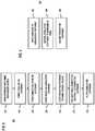
- FIG. 2shows a flow diagram of a process for making a conductive stiffener, in accord with aspects of the present concepts
- FIG. 3shows a flow diagram of a process for attaching the conductive stiffener to a flexible printed circuit board (FPCB), in accord with aspects of the present concepts
- FIG. 4shows a perspective view of a backside of a FPCB with attached conductive stiffener, in accord with aspects of the present concepts
- FIG. 5shows a cross section of a FPCB with an attached conductive stiffener along the line 5 - 5 in FIG. 4 , in accord with aspects of the present concepts
- FIG. 6shows a cross-section view of a wearable device, in accord with aspects of the present concepts
- FIG. 7shows an exploded perspective view of the wearable device of FIG. 6 , in accord with aspects of the present concepts
- FIG. 8shows an isometric view of the wearable device of FIGS. 6 and 7 , in accord with aspects of the present concepts
- FIGS. 9A and 9Bshow biological signals generated by a wearable device, in accord with aspects of the present concepts
- FIG. 10shows a cross section view of a wearable device, in accord with aspects of the present concepts
- FIG. 11shows a bottom view of features on a substrate to provide an improved interface, in accord with aspects of the present concepts
- FIG. 12shows an exemplary configuration of a FPCB to improve mechanical adhesion, in accord with some aspects of the present concepts
- FIG. 13Ashows an exemplary swage pin, in accord with some aspects of the present concepts
- FIG. 13Bshows the exemplary swage pin of FIG. 13A inserted within a VIA, in accord with some aspects of the present concepts.
- FIG. 13Cshows the exemplary swage pin of FIG. 13A fastened within the VIA of FIG. 13B by deformation, in accord with aspects of the present concepts.
- Flexible printed circuit board (FPCB) manufacturerstypically use stiffeners on the backside (e.g., the side without components) or the component side of the FPCB assembly for both ease of assembly and reliability purposes.
- the stiffenerscan be used to reinforce the FPCB assembly in the areas where electronic components are soldered to the FPCB to limit flexing that can cause the solder joints to break reducing the reliability of the assembly.
- the stiffenerscan be conductive stiffeners and utilized to transmit thermal and/or electrical energy to components of the FPCB, rather than requiring externally attached electrodes.
- the conductive stiffenerscan function as electrodes for thermal and/or electrical measurements on a biological surface (e.g., tissue, such as skin) and provide mechanical stiffening of the FPCB assembly that can be incorporated into a conformable wearable device.
- a biological surfacee.g., tissue, such as skin
- Such conductive stiffenerscan reduce the overall complexity and form factor of wearable devices by providing integrated permanent electrodes.
- the slender form factor of the wearable devicecan be achieved by fabricating and integrating positive, negative, and/or reference electrodes directly on the body-contacting surface of the FPCB assembly or the wearable device.
- the resulting conductive stiffenercan be used to conduct electrical and/or thermal energy from biological tissue (e.g., skin, soft tissue, organs, etc.) to components mounted to the FPCB.
- the resulting conductive stiffenercan also be used to increase the stiffness of at least a portion of the FPCB assembly. According to some embodiments, therefore, the conductive stiffener can have the same or similar shape and general dimensions as the FPCB assembly or a portion thereof.
- the conductive stiffenerscan be adhered and electrically and/or thermally connected to the surface (e.g., the backside or the component side) of the FPCB to allow for the collection of bio-potentials and/or bio-impedances such as electrooculography (EOG), electroencephalography (EEG), electromyogram (EMG), galvanic skin response (GSR), and electrocardiogram (ECG) signals by components of the FPCB assembly that forms part of the wearable device.
- the conductive stiffenerscan also allow for the collection of temperature data through a thermally conductive medium and the ability to measure skin, body and/or tissue temperature without the need for auxiliary electrodes.
- the conductive stiffenerscan also allow for the collection of bio-impedance data through the conductive skin contacting surfaces of the conductive stiffeners without the need for auxiliary electrodes.
- FIGS. 1A-1Dshow various diagrammatic views of a conductive stiffener 100 , in accord with aspects of the invention.
- FIG. 1Ashows a top view of the conductive stiffener 100 .
- the dimensions (e.g., length and width) of the conductive stiffener 100can correspond to the dimensions of the FPCB (or a portion thereof) to be stiffened.
- the conductive stiffener 100can be covered with a conductive material 102 such that the top of the conductive stiffener 100 has top conductive layer 102 a .
- the conductive material 102can be any conductive material, such as any conducting metal.
- the conductive material 102can include copper, gold, silver, nickel, chrome, brass, bronze, lead free hot air solder, electroless nickel, immersion palladium, electroless palladium, immersion gold, electroless gold, electrolytic nickel, electrolytic gold, immersion tin, immersion silver, and various metal alloys.
- the conductive material 102can be a ferrous material, such as stainless steel.
- the conductive stiffener 100could also function as an alignment mechanism for applications associated with magnets.
- the conductive stiffener 100could function as an alignment mechanism for a wireless charger used in conjunction with the FPCB assembly.
- the conductive stiffener 100can also include one or more vertical interconnect access holes or VIAs 104 that extend through the conductive stiffener 100 to electrically and/or thermally connect the top conductive layer 102 a with bottom conductive layer 102 c . Although shown as being in the center of the conductive stiffener 100 , the VIA(s) 104 can be located at other locations in the stiffener and can be positioned to align with conductive contact pads of the FPCB.
- the VIA 104can be lined or filled with conductive material 102 forming a conductive tube or hollow column 102 b , such as by plating or filling.
- the VIA 104can be surrounded by thermal reliefs 106 , which are areas in the surface of the conductive stiffener 100 that do not include the conductive material 102 .
- the thermal reliefs 106aid in soldering the conductive stiffener 100 to a FPCB assembly.
- FIG. 1Bshows the bottom of the conductive stiffener 100 , in accord with aspects of the present invention. Like the top, the bottom can be covered with the conductive material 102 to form a bottom conductive layer 102 c .
- the bottom of the conductive stiffener 100does not include the thermal reliefs 106 , as shown; however, according to some embodiments, the bottom may also include thermal reliefs 106 depending on the intended placement of the conductive stiffener 100 .
- FIG. 1Cshows a cross-section view of the conductive stiffener 100 through the line 1 C- 1 C in FIG. 1B
- FIG. 1Dshows a cross-section view of the conductive stiffener 100 through line 1 D- 1 D in FIG. 1A
- the conductive stiffener 100can include a top conductive layer 102 a and a bottom conductive layer 102 c .
- the conductive stiffener 100can also include one or more conductive VIAs 104 that electrically and/or thermally connect the bottom conductive layer 102 c to the top conductive layer 102 a .
- the conductive stiffener 100can include one or more non-conductive substrate layers 108 a , 108 b , between the top conductive layer 102 a and bottom conductive layer 102 c .
- the non-conductive substrate layerscan be formed from a fiber reinforced material, such as, epoxy fiberglass (e.g., 370HR FR4 epoxy fiberglass sheet) or a FPCB non-conductive base material such as polyester, polyethylene terephthalate (PET), polyimide (PI), polyethylene napthalate (PEN), polyetherimide (PEI), fluropolymers (FEP) or a combination thereof.
- epoxy fiberglasse.g., 370HR FR4 epoxy fiberglass sheet
- FPCB non-conductive base materialsuch as polyester, polyethylene terephthalate (PET), polyimide (PI), polyethylene napthalate (PEN), polyetherimide (PEI), fluropolymers (FEP) or a combination thereof.
- the conductive stiffener 100can include one or more top non-conductive substrate layers 108 a bonded or adhered to one or more bottom non-conductive substrate layers 108 b .
- One or more adhesive layers 110can be used to bond or adhere the adjacent non-conductive substrate layers 108 a , 108 b together.
- the top non-conductive substrate layer 108 a and the bottom reinforced layer 108 bcan be formed of any type of non-conductive substrate material, such as any material used in the manufacture of a printed circuit board (PCB).
- the top non-conductive substrate layer 108 a and the bottom non-conductive substrate layer 108 bare formed of 370HR FR-4 glass-reinforced epoxy laminate sheets.
- the top non-conductive substrate layer 108 a and the bottom non-conductive substrate layer 108 bcan be formed of other types of materials used in the PCB arts without departing from the spirit and scope of the present invention.
- the adhesive layer 110can be any suitable adhesive for adhering the top non-conductive substrate layer 108 a and the bottom reinforced layer 108 b together.
- the adhesive layer 110can be, for example, an acrylic-based adhesive, such as a Pyralux® FRO200 and FRO300 adhesive, a polyester based adhesive, an epoxy based adhesive, or a polyimide based adhesive.
- the adhesive layer 110can be formed of other types of adhesives used in the PCB arts without departing from the spirit and scope of the present disclosure.
- the conductive stiffenercan be oriented and used in configurations where the top layer is below the bottom layer as well as in any angular orientation without departing from the scope and spirit of the invention.
- the top conductive layer 102 a and the bottom conductive layer 102 bcan be formed to a thickness of 0.0014′′
- the top non-conductive substrate layer 108 a and the bottom non-conductive substrate layer 108 bcan formed to a thickness of 0.002′′
- the adhesive layer 110can be formed to a thickness of 0.002′′.
- the layerscan have varying and different thicknesses than the thicknesses disclosed herein without departing from the spirit and scope of the present disclosure. According to some embodiments, reducing the thickness of the various layers reduces the overall thickness of the FPCB assembly as well as the effectiveness as a stiffening component.
- the stiffnesscan be increased by laminating two or more thin layers of non-conductive substrate material using an appropriate adhesive.
- the thickness of the various layerscan be selected such that the conductive stiffener 100 provides both thermal and electrical conductivity between the top conductive layer 102 a and the bottom conductive layer 102 c while minimizing the overall profile (e.g., thickness) of the conductive stiffener 100 and providing the desired amount stiffness to limit flexing of the attached PFCB.
- the structure of the conductive stiffener 100can vary without departing from the spirit and scope of the present disclosure.
- the conductive stiffener 100may instead include a single non-conductive substrate layer between the top conductive layer 102 a and the bottom conductive layer 102 c .
- the single non-conductive substrate layercan have the same thickness as, for example, the combination of the top non-conductive substrate layer 108 a , the adhesive layer 110 , and the bottom non-conductive substrate layer 108 b , or may have a different thickness depending on, for example, the structural rigidity requirements of the resulting conductive stiffener 100 .
- the top of the conductive stiffener 100can exclude the top conductive layer 102 a . Rather, the conductive material 102 can form only the bottom conductive layer 102 c and the conductive tube or hollow column 102 b within the VIA 104 . With only the bottom conductive layer 102 c and the conductive tube or hollow column 102 b , the conductive stiffener 100 still provides electrical and thermal conductivity to the top of the conductive stiffener 100 .
- FIG. 2shows a flow diagram of a process 200 for making the conductive stiffener 100 illustrated in FIGS. 1A-1D , in accord with aspects of the invention.
- FIG. 2illustrates and the following remarks describe the process 200 according to various acts in a specific sequence, the acts can be performed in varying sequences, and one or more acts can be added or omitted, without departing from the spirit and scope of the present disclosure.
- the process 200begins with adhering two non-conductive substrate sheets together with an adhesive to form a stiffener.
- the two non-conductive substrate sheetscan be, for example, as described above with respect to the top non-conductive substrate sheet 108 a and the bottom non-conductive substrate sheet 108 b
- the adhesivecan be, for example, as described above with respect to the adhesive layer 110 .
- more than two non-conductive substrate sheets 108 a , 108 b . . . 108 zcan be adhered together using two or more adhesive layers 110 .
- one or more holescan be formed through the stiffener to form a VIA.
- a VIAcan be formed anywhere on the stiffener; however, according to some embodiments, the VIA is formed in the middle of the stiffener.
- the VIAcan be formed according to any conventional process for forming a VIA through the adhered non-conductive substrate layers, such as by drilling, punching, etching, etc.
- a conductive layer of conductive materialcan be formed on the exterior surfaces of the stiffener and lining the VIA.
- the conductive layercan be formed according to any conventional process, such as by plating, laminating, and/or using direct metallization, and can be formed to various thicknesses, such as 0.0007′′.
- the conductive material usedcan be, for example, copper, gold, silver, nickel, chrome, brass, bronze, and metal alloys.
- the conductive materialcan be applied on the top and bottom of the stiffener and through the VIA, thus electrically and/or thermally connecting the top and bottom surfaces of the stiffener through the VIA.
- the conductive stiffenercan be further processed by forming a resist layer (e.g., a light sensitive etch resist layer or photoresist layer) on the conductive stiffener in a pattern that defines thermal reliefs surrounding the VIA on one side of the conductive stiffener (e.g., the top side).
- the resist layercan be formed 0.002′′ thick to protect the conductive material that is intended to be left on the conductive stiffener after etching.
- the resistcan be any suitable resist material used in the removal of the conductive material to form the thermal relief.
- the resist materialcan be an ultraviolet light curing etch resistive material.
- the copper material exposed by the resist layeris then removed to form the thermal reliefs.
- the copper materialcan be removed by etching with ferric chloride, copper chloride or hydrochloric acid.
- the resist layercan be removed (e.g., by stripping) leaving the thermal relief pattern in the conductive material surrounding the VIA.
- additional conductive materialcan be formed on the remaining conductive material to thicken the conductive material surrounding the conductive stiffener.
- an additional 0.0007′′ of conductive materialsuch as copper, can be formed above the remaining conductive material.
- the additional conductive material added in step 212can be the same conductive material original formed on the stiffener.
- the additional conductive materialcan be a different conductive material, such as gold, silver, nickel, chrome, or a metal alloy.
- the conductive stiffenercan be plated using an electroless nickel immersion gold process to protect the conductive layers on the top and bottom surfaces of the conductive stiffener. Plating can occur to only one side of the conductive stiffener, such as the side opposite from the FPCB, to provide for optimal electrode conductivity. Alternatively, both sides can be plated using the electroless nickel immersion gold process. However, step 214 can be omitted, or the conductive stiffener can be exposed to a different process to protect the conductive layers on the top and bottom surfaces. After step 214 , the conductive stiffener is ready for application to a FPCB assembly.
- multiple conductive stiffenerscan be formed simultaneously through a single process.
- the dimensions of the two non-conductive substrate sheets in step 202can be large enough to form multiple conductive stiffeners simultaneously.
- the two conductive stiffenerscan be separated by cutting the two non-conductive substrate sheets into the respective conductive stiffeners.
- the two non-conductive substrate sheetscan be plated with tin and patterned with an additional resist based on a pattern of the conductive material for each conductive stiffener.
- the tin and conductive material left unprotected by the resistcan be removed, such as by submerging the structure in an alkaline solution. After removing the unprotected material, the resist and remaining tin can be removed, such as through a striping process.
- the conductive stiffenerscan then be separated into the individual stiffeners.
- FIG. 3shows a flow diagram of a process 300 for attaching a conductive stiffener to an FPCB assembly, in accord with aspects of the present concepts.
- FIG. 3illustrates and the following remarks describe the process 300 according to various acts in a specific sequence, the acts can be performed in varying sequences, and one or more acts can be added or omitted, without departing from the spirit and scope of the present disclosure.
- an adhesive layeris applied to the top surface of the conductive stiffener around the VIA and the thermal reliefs.
- the adhesive material used to form the adhesive layercan be any suitable adhesive used in the PCB and FPCB arts, such as, for example, a Pyralux® FRO200 adhesive, polyimide based adhesive or epoxy based adhesive.
- the adhesive layercan be any suitable thickness to attach the conductive stiffener, such as, for example, 0.002′′ thick.
- the adhesive layercan be formed around the VIA and the thermal reliefs of the VIA so as to provide room for solder to affix the conductive stiffener to the backside of a FPCB assembly.
- the conductive stiffeneris adhered to the backside of the FPCB assembly by the adhesive layer.
- the adhesive layerat least partially attaches the conductive stiffener to the backside of the FPCB assembly.
- the conductive stiffeneris adhered to the backside of the FPCB assembly such that the VIA of the conductive stiffener aligns with an electrical contact pad on the backside surface of the FPCB.
- the VIAis filled with solder (or another similar conductor) to complete the connection of the conductive stiffener to the backside of the FPCB assembly.
- the soldercan be any suitable conductive material for attaching a stiffener to an FPCB assembly.
- the solderis a lead-free (e.g., tin or silver based solder) or other biocompatible solder to avoid incompatibility when the device is worn by a user.
- the conductive column and the solder within the VIAmechanically, electrically, and thermally connect the backside of the electrical component and the electrical contact pad to the conductive pad on the bottom surface of the conductive stiffener. Accordingly, the conductive stiffener provides both structural rigidity at specific positions of the FPCB assembly and thermal and electrical conductivity to electrical components of the FPCB assembly.
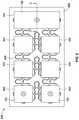
- FIG. 4shows a perspective view of a backside of a FPCB assembly 400 with attached conductive stiffeners 100 , in accord with aspects of the present concepts.
- the FPCB assembly 400includes FPCB sections arranged in device islands 404 and surrounded by or encapsulated in a flexible polymer or elastomer substrate 402 .
- the FPCB sectionscan be any conventional non-conductive or dielectric substrate for a FPCB, such as a polyimide and/or a silicone.
- the FPCB sectionscan include copper circuit traces and pads to facilitate attachment of electrical components, such as by soldering.
- the electrical componentscan be any discrete operative device embedded in and/or affixed to the FPCB substrate 402 , such as one or more microprocessors, microcontrollers, system on a chip devices, physical sensors (e.g., accelerometers, gyros, or inertial navigation sensors), biological and/or chemical sensors, active pixel sensors, amplifiers, analog-to-digital (A/D) converters, digital-to-analog (D/A) converters, optical sensors (e.g., photodiodes, photoresistors, CCD sensors), electro-mechanical transducers (e.g., MEMS sensors), piezo-electric sensors and actuators, light emitting diodes (LEDs), light emitting electronics, thermistors, thermocouples, memory devices, clock devices, active matrix switches, integrated circuits, resistors, capacitors, or other similar discrete operative devices.
- microprocessorse.g., accelerometers, gyros, or inertial navigation sensors
- the FPCB assembly 400can be constructed from two or more electrically interconnected device islands 404 , each device island 404 including one or more electronic components embedded in or affixed to the FPCB.
- the device islands 404can be interconnected by wires or interconnects 406 .
- the interconnects 406can be bendable and/or stretchable interconnects to accommodate the flexible, bendable, stretchable and conformal properties of the FPCB assembly 400 , while also maintaining an electrical interconnection between two or more electrical components 404 , such as two adjacent device islands 404 , while in use.
- the FPCB assembly 400 shown in FIG. 4includes seven device islands 404 , with the right most and two left most device islands 404 including conductive stiffeners 100 in accordance with some embodiments of the invention. Specifically, two conductive stiffeners 100 are aligned with and attached to the two leftmost device islands 404 , and one larger conductive stiffener 100 is aligned with and attached to the rightmost device island 404 . In accordance with some embodiments of the invention, the conductive stiffeners 100 can have the same shape as the device island 404 that the conductive stiffener 100 is attached is connected to. In accordance with some embodiments of the invention, the conductive stiffener 100 can larger or smaller (e.g., in one or two dimensions) than the device island 404 that it is attached to.
- the conductive stiffeners 100provide stiffness as needed across the various FPCB sections and protect the device islands 404 from damage caused by bending of the FPCB assembly 400 (e.g., within certain limits).
- the conductive stiffener 100can be slightly larger or slightly smaller than the device island 404 to provide more or less structural rigidity at the electrical component and, for example, to ensure complete overlap between the conductive stiffener 100 and the device island 404 during bending of the FPCB assembly 400 .
- FIG. 5shows a cross section of a FPCB assembly 400 with the attached conductive stiffener 100 along the line 5 - 5 in FIG. 4 , in accord with aspects of the present concepts.
- the conductive stiffener 100can include the top conductive layer 102 b and the bottom conductive layer 102 c , with the top non-conductive substrate layer 108 a and the bottom non-conductive substrate layer 108 b sandwiching the adhesive layer 110 .
- the conductive stiffener 100can also include the conductive tube or hollow column 102 b within the VIA 104 .
- the conductive stiffener 100is below a device island 404 of the FPCB assembly 400 .
- the device island 404can include one or more conductive contact pads 408 , such an electrical and/or a thermal conductive contact pad.
- the conductive stiffener 100can be affixed to the backside of the device island 404 so that the VIA 104 of the conductive stiffener 100 is aligned with the contact pad 408 .
- the conductive stiffener 100can further include solder 410 that fills the VIA and mechanically and electrically connects the conductive stiffener 100 to one or more contact pads 408 of device island 404 .
- the thermal reliefs 106(not shown in FIG. 5 ) allow the solder to fill the remaining void within the VIA 104 while reducing the thermal strain during soldering.
- the conductive stiffener 100provides structural rigidity to the FPCB assembly 400 at one or more device islands 404 and also thermally and/or electrically connects the device island 404 to the conductive stiffener 100 . Accordingly, with the conductive stiffener 100 installed, the FPCB assembly 400 , and particularly the device island 404 of the FPCB assembly 400 , does not need to be connected to external electrodes. Rather, the conductive stiffeners 100 function as the external electrodes while providing a slim profile that provides little to no resistance to the conformability of the FPCB assembly 400 .
- the resulting encapsulated FPCB assembly 400 together with the conductive stiffener 100can be referred to as a wearable device or a patch.
- the wearable devicecan be placed directly in contact with the user (e.g., the user's tissue, such as skin and generate mechanical, electrical and/or thermal measurements of the user using the electrical components of the FPCB assembly 400 and through the conductive stiffener 100 .
- the FPCB assembly 400 and the conductive stiffeners 100can be placed directly on the biological surface (e.g., a tissue of the user such as skin, endothelial tissue, and epithelial tissue).
- all or a portion of the bottom surface of the FPCB assembly 400 and conductive stiffeners 100can be coated with an adhesive layer.
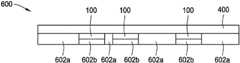
- FIG. 6shows a cross-section view of a wearable device 600 , in accord with aspects of the present concepts.
- the wearable device 600includes the FPCB assembly 400 and multiple conductive stiffeners 100 .
- the wearable device 600can include an adhesive layer on one surface for attaching the device to a biological surface of the body.
- the adhesive layercan be located on the bottom surface of the FPCB assembly 400 and surrounding the one or more conductive stiffeners 100 on three sides.
- the adhesive layer 602can be any conventional adhesive layer used in adhering bandages and devices to the body, such as a silicone gel based adhesive or an acrylic based adhesive.
- the adhesive layer 602can be formed generally of a silicone adhesive.
- the adhesive layer 602can include two different portions, a non-conductive adhesive portion 602 a and a conductive portion 602 b .
- the conductive portion 602 b of the adhesive layer 602permits electrical and/or thermal conduction through the adhesive layer 602 .
- the conductive portions 602 bcan be positioned to align with the conductive stiffeners 100 , and in some embodiments, the bottom conductive layers 102 c of the conductive stiffeners 100 , to allow thermal and electrical energy to pass through the adhesive layer 602 and reach the bottom conductive layers 102 c of the conductive stiffeners 100 .
- the adhesive layer 602includes the non-conductive adhesive portions 602 a that surround the conductive portions 602 b .
- the non-conductive adhesive portions 602 aare high impedance areas that prevent or substantially reduce the transmission of electrical energy and/or thermal energy there though.
- the conductive portions 602 aare high impedance areas that prevent or substantially reduce the transmission of electrical energy and/or thermal energy there though.
- the conductive portions 602 b of the adhesive layer 602provide a thermal and/or electrical conductive interface, where needed, between the biological surface and conductive stiffeners 100 . Because the adhesive layer 602 includes the conductive portions 602 b , the wearable device 600 can measure thermal and/or electric (e.g., biopotential and bioimpedance) signals, such as EMG, ECG, heart rate, galvanic skin response, and/or ECG tracking, among others, while having adhesive properties to aid the wearable device 600 in remaining coupled to the user. Accordingly, the adhesive layer 602 aids the wearable device 600 in remaining coupled to the user during the various activities in which the wearable device 600 monitors the physical and biological signals of the user, such as during exercising, sleeping, etc. For example, the conformal and flexible nature of the wearable device 600 allow for it to be placed on various parts of the body to monitor, for example, muscle activities.
- FIG. 7shows an exploded perspective view of the wearable device 600 of FIG. 6 , in accord with aspects of the present concepts
- FIG. 8shows an isometric view of the wearable device 600 of FIGS. 6 and 7 , in accord with aspects of the present concepts.
- the wearable device 600includes the FPCB assembly 400 , including the conductive stiffeners 100 , on a top surface.
- the FPCB assembly 400includes an adhesive layer 602 .
- the adhesive layer 602is generally comprised of the non-conductive adhesive portion 602 a surrounding the conductive portions 602 b .
- the conductive portions 602 balign with the conductive stiffeners 100 to allow the conductive stiffeners 100 to receive electrical and/or thermal energy from a biological surface below the adhesive layer 602 .
- the conductive portions 602 b of the adhesive layer 602are shown as separate elements of the adhesive layer 602 relative to the non-conductive adhesive portions 602 a , the conductive portions 602 b can be integral with the non-conductive portions 602 a . According to some embodiments, the conductive portions 602 b can be integral with the non-conductive portions 602 a by combining the same adhesive material (as the non-conductive portions 602 a ) with material additives that make the conductive adhesive portions 602 b conductive.
- the adhesive layer 602can be formed of a silicone adhesive, and the conductive adhesive portions 602 b can include additives that make the silicone within these portions conductive.
- the additives used to create the conductive portions 602 b electrically and/or thermally conductiveinclude silver (Ag), gold (Au), carbon, graphite, nickel/graphite, silver/silver chloride (Ag/AgCl) and other conductive material additives. Consequently, the non-conductive adhesive portions 602 a of the adhesive layer 602 lack the conductive additives and provide good insulating properties.
- the conductive silicone used to form the conductive adhesive portions 602 bcan be integrated into the adhesive layer 602 according to various methodologies, to form integral or non-integral conductive adhesive portions 602 b , such as by potting, insert molding, gluing, snapping, etc.
- the conductive portions 602 bprovide a conductive path through the adhesive layer 602 that protects and isolates the underlying circuitry (e.g., electrical components 404 and interconnects 406 ) from the external environment.
- the conductive pathonly exists in selected areas that couple directly to the conductive stiffeners 100 on the backside of the FPCB assembly 400 .
- the conductive portions 602 bhave volume resistivity in the range of 70 ohm ⁇ cm to 0.003 ohm ⁇ cm.
- the wearable device 600 of FIGS. 6-8can exclude the conductive stiffeners 100 .
- the wearable device 600may not require the additional stiffness provided by the conductive stiffeners 100 .
- the conductive stiffeners 100can be omitted.
- the conductive portions 602 b of the adhesive layer 602can interface directly with, for example, the various contact pads 408 or conductive surfaces of the device islands 404 of the FPCB assembly 400 .
- the conductive portions 602 b of the adhesive layer 602can be configured (e.g, by selecting the appropriate thermally or electrically conductive material) to transmit the thermal and/or electrical energy directly to the contact pads 408 of the device islands 404 .
- FIGS. 9A and 9Bshow the ability of the wearable device 600 located at various positions on a user to detect physical and biological electrical signals during use, in accord with aspects of the present concepts.
- the signals shownrepresent a wearable device 600 adhered to the chest of the user with the ability to measure acceleration in three axes (e.g., x, y, and z axes) and ECG signals.
- the signals shownrepresent a wearable device 600 adhered to the leg of the user with the ability to measure acceleration in three axes (e.g., x, y, and z axes) and EMG signals.
- the userwas performing squats as exemplary activity during which the signals are measured.
- the wearable devices 600are able to detect the biological signals from the user through the conductive portions 602 b.
- the FPCB assembly 400can be encapsulated within an encapsulation material to entirely protect the electrical components. Encapsulating the FPCB assembly 400 (and the conductive stiffeners 100 ) within the encapsulation layer seals off and protects the components from the elements of the outside environment during use, such as water, sweat, dirt, etc. Further, according to some embodiments, an encapsulation layer allows the resulting wearable device (e.g., a patch) to satisfy certain national and/or international standards or tests with respect to, for example, electrical devices and, more specifically, medical electrical devices. By way of example, an encapsulation layer allows a device to pass International Protection Marking tests.
- FIG. 10shows a cross section view of a wearable device 1000 , in accord with aspects of the present concepts.
- the wearable device 1000includes the FPCB assembly 400 and multiple conductive stiffeners 100 .
- the wearable device 1000may exclude the conductive stiffeners 100 .
- the wearable device 1000includes an encapsulation layer 1002 the entirely surrounds the FPCB assembly 400 .
- a bottom surface 1002 a of the encapsulation layer 1002can include an adhesive layer, similar to the adhesive layer 602 discussed above, but that the encapsulation layer also is above the FPCB assembly 400 .
- the encapsulation layer 1002can be formed of various conformable materials used in encapsulating electronics, such a silicones.
- the encapsulation layer 1002can be non-conductive to prevent, for example, electrical signals from short circuiting or affecting measurements of the electrical components of the FPCB assembly 400 .
- the encapsulation layer 1002includes conductive portions 1004 that transmit thermal and/or electrical energy through the encapsulation layer 1002 .
- the conductive portions 1004can be similar in construction and function as the conductive 602 b of the adhesive layer 602 , and similarly, the conductive portions 1004 can be aligned with the conductive stiffeners 100 or contact pads 408 of the FPCB assembly 400 .
- the wearable device 1000By encapsulating the FPCB assembly 400 within the encapsulation layer 1002 , the wearable device 1000 permits, for example, the monitoring of physical and biological signals, such as EMG, ECG, etc., underwater. Moreover, by having the conductive portions 1004 integrated into the encapsulation layer 1002 , and below the conductive stiffeners 100 or contact pads 408 of the device islands 404 , the wearable device 1000 functions as an entirely integrated monitoring device that does not require, for example, additional electrodes tethered by wires to the FPCB assembly 400 .
- the adhesive layer 602 and the encapsulation layer 1002can be generally applied to the FPCB assembly 400 such that, for example, the interface between the adhesive layer 602 or the encapsulation layer 1002 and the FPCB assembly 400 , or components thereof, is a planar or smooth interface.
- featurescan be formed into the FPCB assembly 400 and/or the conductive stiffeners 100 to provide a more mechanically stable interface for the adhesive layer 602 or the encapsulation layer 1002 .
- FIG. 11shows a bottom view of features 1102 formed on a substrate 1100 to provide an improved interface, in accord with aspects of the present concepts.
- FIG. 11shows a substrate 1100 .
- the substrate 1100can generally refer to a conductive stiffener 100 , a device island 404 of the FPCB assembly 400 , or the entire FPCB assembly 400 .
- the substrate 1100includes a surface that interfaces with the adhesive layer 602 or the encapsulation layer 1002 .
- the substrate 1100can includes features 1102 .
- the features 1102can be VIAs formed in the substrate 1100 .
- the VIAscan extend entirely through the substrate 1100 , or may extend partially into the substrate 1100 .
- the adhesive layer 602 or the encapsulation layer 1002at least partially fills the VIAs to provide a larger contact area and greater mechanical adhesion to the substrate 1100 .
- the features 1102 as VIAsprovide some additional mechanical grip for the adhesive layer 602 or the encapsulation layer 1002 such that these layers do not have to solely rely on adhesion to a planar surface.
- the features 1102 applied to the FPCB assembly 400 and/or the conductive stiffeners 100provide a better adhesive interface with the adhesive layer 602 and the encapsulation layer 1002 to improve the mechanical grip between the two different layers.
- the features 1102may be any other type of protuberance and/or indentation on the substrate 1100 that alters the smooth surface of the substrate 1100 to something other than substantially smooth or planar.
- the features 1102can be pad rings that protrude beyond the surface of the substrate 1100 .
- the features 1102can be a combination of VIAs and pad rings surrounding the VIAs, such that the adhesive layer 602 or the encapsulation layer 1002 both extends into the VIAs and extends over the pads rings.
- FIG. 11the number and arrangement of the features 1102 can vary without departing from the spirit and scope of the present disclosure.
- the configuration of the FPCB assembly 400can be changed.
- FIG. 12shows an exemplary configuration of a FPCB assembly 400 to improve mechanical adhesion to the FPCB assembly 400 , in accord with some aspects of the present concepts.
- FIG. 12includes a FPCB assembly 400 that has its ends 1202 a and 1202 b folded to form pockets 1204 a and 1204 b between the folded ends 1202 a and 1202 b and the main body 1200 of the FPCB assembly 400 .
- the pockets 1204 a and 1204 bsandwich the material of the adhesive layer 602 or the encapsulation layer 1002 between the pockets 1204 a and 1204 b and the main body 1202 .
- the configuration of the FPCB assembly 400provides additional mechanical strength and/or resistance to the adhesive layer 602 or the encapsulation layer 1002 from being removed from the FPCB assembly 400 .
- the ends 1202 a and 1202 bcan also include VIAs 1206 .
- the VIAs 1206can be through only the FPCB assembly 400 , or the VIAs 1206 can be through the FPCB assembly 400 and conductive stiffeners 100 located at the ends 1202 a and 1202 b of the FPCB assembly 400 .
- the pockets 1204 a and 1204 bare filled with the material of the adhesive layer 602 or the encapsulation layer 1002 , the material flows from inside the pockets 1204 a and 1204 b and through the VIAs 1206 to outside of the pockets 1204 a and 1204 b .
- the material through the VIAs 1206provides additional mechanical contact with FPCB assembly 400 such that the material of the adhesive layer 602 or the encapsulation layer 1002 does not rely solely on its adhesion to the planar surface of the FPCB assembly 400 .
- the VIAs 1206can be electrically connected to electrical components 404 of the FPCB assembly 400 , and the material that flows through the VIAs 1206 can be the conductive material that forms the conductive adhesive portions 602 b of the adhesive layer 602 or the conductive portion 1004 of the encapsulation layer 1002 .
- the point of mechanical contactcan also be a point of electrical contact between the adhesive layer 602 /encapsulation layer 1002 and the FPCB assembly 400 .
- the adhesive layer 602 or the encapsulation layer 1002 under the main body 1200can be filled to form a substantially planer surface of the adhesive layer 602 or the encapsulation layer 1002 on the backside of the FPCB assembly 400 to form the wearable device 600 or 1000 .
- the surface that contacts the biological surfacecan still be substantially planar.
- both ends 1202 a and 1202 bare shown in FIG. 12 as folded to form the pockets 1204 a and 1204 , according to some embodiments, only one end (e.g., 1202 a or 1202 b ) can be folded to form a pocket (e.g., 1204 a or 1204 b ) in the FPCB assembly 400 .
- FIGS. 13A-13Cshow an exemplary and optional configuration of the VIAs 1206 for electrical and mechanical contact, in accord with some aspects of the present concepts.
- electrical and mechanical contactcan be further improved by application of an electrically conductive insert within the VIA 1206 .
- Such an insertcan be, for example, an electrically conductive rivet or swage pin 1302 ( FIGS. 13A-13C ).
- the electrically conductive insertcan interface with a conductive ring 1304 ( FIGS. 13B and 13C ) around the VIA 1206 at the surface.
- Application of the electrically conductive insert into the VIA 1206can cause the insert to contact the conductive ring 1304 .
- the rivet or swage pin 1302can be applied using an arbor press (not shown) and swage punch 1306 ( FIG. 13B ) through the VIA 1206 , with the resulting flared portion 1302 a of the rivet or swage pin 1302 contacting the conductive ring 1304 ( FIGS. 13B and 13C ) to provide electrical contact to the rivet or swage pin 1302 after swaging.
- the various wearable devices disclosed aboveare fully-functional skin-mountable devices with conductive stiffeners functioning as integrated single-channel or multi-channel electrodes.
- the conductive stiffenersalso provide mechanical stability for the electrical components on the top side of the FPCB.
- the arrangement of the conductive stiffeners and the adhesive layer or encapsulation layerreduces the overall thickness of the resulting skin-mountable wearable device, while also simplifying the manufacturing process in which electrode functionality is required.
- conductive stiffeners on the backside surface of FPCB and aligned with contact pads of electronic components of the FPCBprovides both mechanical and electrical functionalities and benefits.
- the conductive stiffenersprovide mechanical stability to the backside of surface mounted or embedded electronic components in FPCB for mechanical reliability purposes.
- the conductive stiffenersprovide an electrically conductive medium on the backside of FPCB with conductive adhesive contact directly with skin or any other soft biological tissue.
- the conductive stiffenersalso provide a thermally conductive medium on the backside of the FPCB for thermal relief and/or temperature sensing of the surface mounted or embedded electronic components.
- combining the conductive stiffener with the FPCBcombines two elements and reduces the total number of parts and instructions for use that are required to measure, for example, electrical activity from a biological surface.
- the reduction in the number of components and complexitymanifest in less noisy signal quality because of, for example, the reduced electrical length between the sensor (e.g., the bottom conductive layer of the conductive stiffener) and the receiver (e.g., the electrical component).
- the reduced electrical lengtheliminates sources of noise, such as 60 Hz noise from power lines and motion artifacts from movement.
- the conductive stiffenersalso can provide sites for active alternating current (AC) and/or direct current (DC) stimuli to be applied to the skin, peripheral nerves, or any other soft biological site.
- the conductive stiffenersalso allow for charging a skin-mounted wearable device using the conductive surfaces as the charging interfaces.
Landscapes
- Health & Medical Sciences (AREA)
- Life Sciences & Earth Sciences (AREA)
- Engineering & Computer Science (AREA)
- Surgery (AREA)
- General Health & Medical Sciences (AREA)
- Biophysics (AREA)
- Biomedical Technology (AREA)
- Heart & Thoracic Surgery (AREA)
- Medical Informatics (AREA)
- Molecular Biology (AREA)
- Physics & Mathematics (AREA)
- Animal Behavior & Ethology (AREA)
- Pathology (AREA)
- Public Health (AREA)
- Veterinary Medicine (AREA)
- Microelectronics & Electronic Packaging (AREA)
- Ophthalmology & Optometry (AREA)
- Psychiatry (AREA)
- Psychology (AREA)
- Structure Of Printed Boards (AREA)
- Manufacturing & Machinery (AREA)
Abstract
Description
Claims (31)
Priority Applications (1)
| Application Number | Priority Date | Filing Date | Title |
|---|---|---|---|
| US15/208,444US10653332B2 (en) | 2015-07-17 | 2016-07-12 | Conductive stiffener, method of making a conductive stiffener, and conductive adhesive and encapsulation layers |
Applications Claiming Priority (2)
| Application Number | Priority Date | Filing Date | Title |
|---|---|---|---|
| US201562194058P | 2015-07-17 | 2015-07-17 | |
| US15/208,444US10653332B2 (en) | 2015-07-17 | 2016-07-12 | Conductive stiffener, method of making a conductive stiffener, and conductive adhesive and encapsulation layers |
Publications (2)
| Publication Number | Publication Date |
|---|---|
| US20170019988A1 US20170019988A1 (en) | 2017-01-19 |
| US10653332B2true US10653332B2 (en) | 2020-05-19 |
Family
ID=57775401
Family Applications (1)
| Application Number | Title | Priority Date | Filing Date |
|---|---|---|---|
| US15/208,444Active2037-10-28US10653332B2 (en) | 2015-07-17 | 2016-07-12 | Conductive stiffener, method of making a conductive stiffener, and conductive adhesive and encapsulation layers |
Country Status (2)
| Country | Link |
|---|---|
| US (1) | US10653332B2 (en) |
| WO (1) | WO2017015000A1 (en) |
Cited By (5)
| Publication number | Priority date | Publication date | Assignee | Title |
|---|---|---|---|---|
| US10986465B2 (en) | 2015-02-20 | 2021-04-20 | Medidata Solutions, Inc. | Automated detection and configuration of wearable devices based on on-body status, location, and/or orientation |
| US11771406B2 (en) | 2020-08-12 | 2023-10-03 | Apple Inc. | In-bed temperature array for menstrual cycle tracking |
| US11896136B2 (en) | 2019-09-19 | 2024-02-13 | Apple Inc. | Pneumatic haptic device having actuation cells for producing a haptic output over a bed mattress |
| US11992326B2 (en) | 2016-04-19 | 2024-05-28 | Medidata Solutions, Inc. | Method and system for measuring perspiration |
| US12185630B2 (en) | 2019-08-09 | 2024-12-31 | Apple Inc. | Layered sensor having multiple laterally adjacent substrates in a single layer |
Families Citing this family (28)
| Publication number | Priority date | Publication date | Assignee | Title |
|---|---|---|---|---|
| US8097926B2 (en) | 2008-10-07 | 2012-01-17 | Mc10, Inc. | Systems, methods, and devices having stretchable integrated circuitry for sensing and delivering therapy |
| US8389862B2 (en) | 2008-10-07 | 2013-03-05 | Mc10, Inc. | Extremely stretchable electronics |
| US9123614B2 (en) | 2008-10-07 | 2015-09-01 | Mc10, Inc. | Methods and applications of non-planar imaging arrays |
| WO2014058473A1 (en) | 2012-10-09 | 2014-04-17 | Mc10, Inc. | Conformal electronics integrated with apparel |
| US9171794B2 (en) | 2012-10-09 | 2015-10-27 | Mc10, Inc. | Embedding thin chips in polymer |
| US9706647B2 (en) | 2013-05-14 | 2017-07-11 | Mc10, Inc. | Conformal electronics including nested serpentine interconnects |
| EP3071096A4 (en) | 2013-11-22 | 2017-08-09 | Mc10, Inc. | Conformal sensor systems for sensing and analysis of cardiac activity |
| USD781270S1 (en) | 2014-10-15 | 2017-03-14 | Mc10, Inc. | Electronic device having antenna |
| EP4079383A3 (en) | 2015-10-01 | 2023-02-22 | Medidata Solutions, Inc. | Method and system for interacting with a virtual environment |
| US10532211B2 (en) | 2015-10-05 | 2020-01-14 | Mc10, Inc. | Method and system for neuromodulation and stimulation |
| US10673280B2 (en) | 2016-02-22 | 2020-06-02 | Mc10, Inc. | System, device, and method for coupled hub and sensor node on-body acquisition of sensor information |
| US10277386B2 (en) | 2016-02-22 | 2019-04-30 | Mc10, Inc. | System, devices, and method for on-body data and power transmission |
| US10447347B2 (en) | 2016-08-12 | 2019-10-15 | Mc10, Inc. | Wireless charger and high speed data off-loader |
| NL2017506B1 (en)* | 2016-09-21 | 2018-03-29 | Bambi Belt B V | Wearable device, method and system for monitoring one or more vital signs of a human body. |
| EP4066768B1 (en)* | 2016-10-04 | 2023-11-22 | St. Jude Medical, Cardiology Division, Inc. | Ablation catheter tip with flexible electronic circuitry |
| CN106932119A (en)* | 2017-03-24 | 2017-07-07 | 东华大学 | A kind of printing-type fabric base flexibility temperature sensor |
| US20180279940A1 (en)* | 2017-03-30 | 2018-10-04 | James Campbell | Disease Detection Device and Method for Detection of Abnormal Immunological Activity |
| CN107291311A (en)* | 2017-06-27 | 2017-10-24 | 长沙市宇顺显示技术有限公司 | A kind of preparation method of the anti-injureds of capacitor touch-control display screen FPC |
| US11311225B2 (en)* | 2017-07-11 | 2022-04-26 | General Electric Company | Systems and methods for shielded and adjustable medical monitoring devices |
| DE102017123553A1 (en)* | 2017-10-10 | 2019-04-11 | Sick Ag | Optoelectronic sensor |
| US10375826B2 (en)* | 2017-12-29 | 2019-08-06 | China Petroleum & Chemical Corporation | High temperature drilling electronics |
| CN112997587B (en)* | 2018-10-31 | 2024-07-16 | 大日本印刷株式会社 | Wiring board and method for manufacturing wiring board |
| FR3096865B1 (en)* | 2019-06-03 | 2021-06-04 | Inst Mines Telecom | Electronic system to be mounted on a flexible support, especially textile |
| EP3865051A1 (en)* | 2020-02-13 | 2021-08-18 | Linxens Holding | Sensing system, smart wearing arrangement and method of fabricating a sensing system |
| US11123011B1 (en) | 2020-03-23 | 2021-09-21 | Nix, Inc. | Wearable systems, devices, and methods for measurement and analysis of body fluids |
| US11721641B2 (en) | 2020-05-19 | 2023-08-08 | Google Llc | Weight optimized stiffener and sealing structure for direct liquid cooled modules |
| WO2021234156A1 (en)* | 2020-05-21 | 2021-11-25 | Bioserenity | Expandable electrode set |
| JP7584357B2 (en)* | 2021-06-02 | 2024-11-15 | 信越ポリマー株式会社 | Stretchable device and manufacturing method thereof |
Citations (272)
| Publication number | Priority date | Publication date | Assignee | Title |
|---|---|---|---|---|
| US3716861A (en) | 1971-03-22 | 1973-02-13 | J Root | Serpentine antenna mounted on a rotatable capacitive coupler |
| US3805427A (en) | 1972-12-18 | 1974-04-23 | H Epstein | Medical alarm bracelet |
| US3838240A (en) | 1973-04-04 | 1974-09-24 | Rca Corp | Bonding tool and method of bonding therewith |
| US4278474A (en) | 1980-03-25 | 1981-07-14 | The United States Of America As Represented By The United States Department Of Energy | Device for conversion of electromagnetic radiation into electrical current |
| US4304235A (en) | 1978-09-12 | 1981-12-08 | Kaufman John George | Electrosurgical electrode |
| US4416288A (en) | 1980-08-14 | 1983-11-22 | The Regents Of The University Of California | Apparatus and method for reconstructing subsurface electrophysiological patterns |
| US4658153A (en) | 1984-06-18 | 1987-04-14 | Amnon Brosh | Planar coil apparatus for providing a frequency output vs. position |
| JPH0587511A (en) | 1991-07-24 | 1993-04-06 | Yamaha Corp | Bending detection device |
| US5214000A (en) | 1991-12-19 | 1993-05-25 | Raychem Corporation | Thermal transfer posts for high density multichip substrates and formation method |
| US5272375A (en) | 1991-12-26 | 1993-12-21 | E. I. Du Pont De Nemours And Company | Electronic assembly with optimum heat dissipation |
| EP0585670A2 (en) | 1992-08-12 | 1994-03-09 | Reliant Laser Corporation | Electro-optical system for measuring and analying accumulated short-wave and long-wave ultraviolet radiation exposure |
| US5326521A (en) | 1993-05-26 | 1994-07-05 | East Douglas A | Method for preparing silicone mold tooling |
| US5331966A (en) | 1991-04-05 | 1994-07-26 | Medtronic, Inc. | Subcutaneous multi-electrode sensing system, method and pacer |
| US5360987A (en) | 1993-11-17 | 1994-11-01 | At&T Bell Laboratories | Semiconductor photodiode device with isolation region |
| US5454270A (en) | 1994-06-06 | 1995-10-03 | Motorola, Inc. | Hermetically sealed pressure sensor and method thereof |
| US5471982A (en) | 1992-09-29 | 1995-12-05 | Ep Technologies, Inc. | Cardiac mapping and ablation systems |
| US5491651A (en) | 1992-05-15 | 1996-02-13 | Key, Idea Development | Flexible wearable computer |
| US5567975A (en) | 1994-06-30 | 1996-10-22 | Santa Barbara Research Center | Group II-VI radiation detector for simultaneous visible and IR detection |
| US5580794A (en) | 1993-08-24 | 1996-12-03 | Metrika Laboratories, Inc. | Disposable electronic assay device |
| US5617870A (en) | 1993-04-29 | 1997-04-08 | Scimed Life Systems, Inc. | Intravascular flow measurement system |
| EP0779059A1 (en) | 1995-12-13 | 1997-06-18 | Cordis Corporation | Catheter with plate-like electrode array |
| US5811790A (en) | 1996-02-22 | 1998-09-22 | Canon Kabushiki Kaisha | Photoelectric conversion device having thermal conductive member |
| US5817008A (en) | 1996-10-31 | 1998-10-06 | Spacelabs Medical, Inc. | Conformal pulse oximetry sensor and monitor |
| US5907477A (en) | 1995-09-19 | 1999-05-25 | Micron Communications, Inc. | Substrate assembly including a compartmental dam for use in the manufacturing of an enclosed electrical circuit using an encapsulant |
| WO1999038211A1 (en) | 1998-01-22 | 1999-07-29 | Fraunhofer-Gesellschaft zur Förderung der angewandten Forschung e.V. | Microsystem and method for the production thereof |
| US6063046A (en) | 1997-04-11 | 2000-05-16 | Allum; John H. | Method and apparatus for the diagnosis and rehabilitation of balance disorders |
| US6265090B1 (en) | 1998-06-05 | 2001-07-24 | Murata Maufacturing Co., Ltd. | Electrically conductive paste ceramic multi-layered substrate |
| US20010012918A1 (en) | 1995-07-28 | 2001-08-09 | Swanson David K. | Systems and methods for conducting electrophysiological testing using high-voltage energy pulses to stun tissue |
| US6282960B1 (en) | 1996-03-15 | 2001-09-04 | Analog Devices, Inc. | Micromachined device with enhanced dimensional control |
| US20010021867A1 (en) | 1993-03-16 | 2001-09-13 | Kordis Thomas F. | Cardiac mapping and ablation systems |
| US6343514B1 (en) | 1996-01-30 | 2002-02-05 | Radi Medical Systems Ab | Combined flow, pressure and temperature sensor |
| US20020026127A1 (en) | 2000-03-23 | 2002-02-28 | Balbierz Daniel J. | Tissue biopsy and treatment apparatus and method |
| US6387052B1 (en) | 1991-01-29 | 2002-05-14 | Edwards Lifesciences Corporation | Thermodilution catheter having a safe, flexible heating element |
| US6410971B1 (en) | 2001-07-12 | 2002-06-25 | Ferrotec (Usa) Corporation | Thermoelectric module with thin film substrates |
| US20020082515A1 (en) | 1999-07-01 | 2002-06-27 | Campbell Thomas H. | Thermography catheter |
| US6421016B1 (en) | 2000-10-23 | 2002-07-16 | Motorola, Inc. | Antenna system with channeled RF currents |
| US20020094701A1 (en) | 2000-11-29 | 2002-07-18 | Biegelsen David Kalman | Stretchable interconnects using stress gradient films |
| US20020113739A1 (en) | 2000-12-14 | 2002-08-22 | Howard David Amundson | Arrayed-segment loop antenna |
| US20020128700A1 (en) | 2001-03-08 | 2002-09-12 | Cross Thomas E. | Lead with adjustable angular and spatial relationships between electrodes |
| US6455931B1 (en) | 2001-05-15 | 2002-09-24 | Raytheon Company | Monolithic microelectronic array structure having substrate islands and its fabrication |
| US20020145467A1 (en) | 2001-04-05 | 2002-10-10 | Minch Bradley A. | Folded floating-gate differential pair amplifier |
| US20020151934A1 (en) | 2001-04-12 | 2002-10-17 | Levine Paul A. | System and method for programmably controlling electrode activation sequence in a multi-site cardiac stimulation device |
| US20020158330A1 (en) | 2001-04-30 | 2002-10-31 | Ho-Jeong Moon | Circuit board having a heating means and a hermetically sealed multi-chip package |
| US20030017848A1 (en) | 2001-07-17 | 2003-01-23 | Engstrom G. Eric | Personalizing electronic devices and smart covering |
| US20030045025A1 (en) | 2000-01-26 | 2003-03-06 | Coyle Anthony L. | Method of fabricating a molded package for micromechanical devices |
| WO2003021679A2 (en) | 2001-09-03 | 2003-03-13 | National Microelectronic Research Centre University College Cork - National University Of Ireland Cork | Integrated circuit structure and a method of making an integrated circuit structure |
| US20030090000A1 (en) | 2001-06-05 | 2003-05-15 | Caletka David Vincent | Land grid array stiffener for use with flexible chip carriers |
| US6567158B1 (en) | 1999-01-26 | 2003-05-20 | Consiglio Nazionale Delle Ricerche | Fiber optic sensor with photochromic transducer, and corresponding method |
| US20030097165A1 (en) | 2001-11-16 | 2003-05-22 | The Regents Of The University Of California. | Flexible electrode array for artificial vision |
| US20030120271A1 (en) | 2000-06-30 | 2003-06-26 | Scimed Life Systems, Inc. | Medical probe with reduced number of temperature sensor wires |
| US20030146017A1 (en)* | 2000-08-24 | 2003-08-07 | Zhineng Fan | A Method of Forming A HiGH RELIABILITY INTERPOSER FOR LOW COST HIGH RELIABILITY APPLICATIONS |
| US20030162507A1 (en) | 2002-02-20 | 2003-08-28 | Vatt Gregory B. | Semiconductor structure for high speed digital and radio frequency processing |
| US20030168725A1 (en) | 1996-12-13 | 2003-09-11 | Tessera, Inc. | Methods of making microelectronic assemblies including folded substrates |
| US6626940B2 (en) | 2001-06-15 | 2003-09-30 | Scimed Life Systems, Inc. | Medical device activation system |
| US6641860B1 (en) | 2000-01-03 | 2003-11-04 | T-Ink, L.L.C. | Method of manufacturing printed circuit boards |
| US20030214408A1 (en) | 2002-05-14 | 2003-11-20 | Motorola, Inc. | Apparel having multiple alternative sensors and corresponding method |
| US20030236455A1 (en) | 2000-10-05 | 2003-12-25 | Scimed Life Systems, Inc. | Probe assembly for mapping and ablating pulmonary vein tissue and method of using same |
| US20040006264A1 (en) | 2001-11-20 | 2004-01-08 | Mojarradi Mohammad M. | Neural prosthetic micro system |
| US20040007376A1 (en) | 2002-07-09 | 2004-01-15 | Eric Urdahl | Integrated thermal vias |
| US20040085469A1 (en) | 2002-10-30 | 2004-05-06 | Eastman Kodak Company | Method to eliminate bus voltage drop effects for pixel source follower amplifiers |
| US20040092806A1 (en) | 2001-12-11 | 2004-05-13 | Sagon Stephen W | Microelectrode catheter for mapping and ablation |
| US20040106334A1 (en) | 2000-06-14 | 2004-06-03 | Tatsuo Suzuki | Microparticle arrangement film, electrical connection film, electrical connection structure, and microparticle arrangement method |
| US20040138558A1 (en) | 2002-11-14 | 2004-07-15 | Dunki-Jacobs Robert J | Methods and devices for detecting tissue cells |
| US20040135094A1 (en) | 2002-11-25 | 2004-07-15 | Hamamatsu Photonics K.K. | UV sensor |
| US20040149921A1 (en) | 2003-02-05 | 2004-08-05 | Alexander Smyk | Personal solar adviser |
| US6775906B1 (en) | 2000-10-20 | 2004-08-17 | Silverbrook Research Pty Ltd | Method of manufacturing an integrated circuit carrier |
| US6784844B1 (en) | 1999-10-08 | 2004-08-31 | Nokia Mobile Phone Limited | Antenna assembly and method of construction |
| US20040178466A1 (en) | 2003-01-31 | 2004-09-16 | Foveon, Inc. | Vertical color filter sensor group and semiconductor integrated circuit fabrication method for fabricating same |
| US20040192082A1 (en) | 2003-03-28 | 2004-09-30 | Sigurd Wagner | Stretchable and elastic interconnects |
| US20040203486A1 (en) | 2002-07-31 | 2004-10-14 | Robert Shepherd | Smart pouch cover for mobile device |
| US20040201134A1 (en) | 2001-08-01 | 2004-10-14 | Hideharu Kawai | Forming method of magnetic body, magnetic body, and printed circuit board |
| US20040221370A1 (en) | 2002-10-01 | 2004-11-11 | Nellcor Puritan Bennett Incorporated | Headband with tension indicator |
| US20040243204A1 (en) | 2003-04-30 | 2004-12-02 | The Regents Of The University Of California | Stretchable polymer-based electronic device |
| US20050021103A1 (en) | 1998-08-05 | 2005-01-27 | Dilorenzo Daniel John | Apparatus and method for closed-loop intracranial stimulation for optimal control of neurological disease |
| US20050029680A1 (en) | 2002-01-21 | 2005-02-10 | Infineon Technologies Ag | Method and apparatus for the integration of electronics in textiles |
| JP2005052212A (en) | 2003-08-05 | 2005-03-03 | Axiom Co Ltd | Skin sensor |
| US20050070778A1 (en) | 2003-08-20 | 2005-03-31 | Lackey Robert P. | Hydration monitoring |
| US20050067293A1 (en) | 2003-09-29 | 2005-03-31 | Toshiki Naito | Producing method of flexible wired circuit board |
| US20050096513A1 (en) | 1997-11-11 | 2005-05-05 | Irvine Sensors Corporation | Wearable biomonitor with flexible thinned integrated circuit |
| US20050113744A1 (en) | 2003-11-21 | 2005-05-26 | Cyberkinetics, Inc. | Agent delivery systems and related methods under control of biological electrical signals |
| US20050139683A1 (en) | 2003-12-26 | 2005-06-30 | Curitel Communications, Inc. | Communication terminal equipped with a replaceable cover and method of changing themes of communication terminal using the same |
| US20050171524A1 (en) | 2004-01-09 | 2005-08-04 | Barrx, Inc. | Devices and methods for treatment of luminal tissue |
| US20050203366A1 (en) | 2004-03-12 | 2005-09-15 | Donoghue John P. | Neurological event monitoring and therapy systems and related methods |
| US20050248312A1 (en) | 2004-05-05 | 2005-11-10 | Advanced Connectek Inc. | Portable power supply with computer port |
| US6965160B2 (en) | 2002-08-15 | 2005-11-15 | Micron Technology, Inc. | Semiconductor dice packages employing at least one redistribution layer |
| WO2005122285A2 (en) | 2004-06-04 | 2005-12-22 | The Board Of Trustees Of The University Of Illinois | Methods and devices for fabricating and assembling printable semiconductor elements |
| US20050285262A1 (en) | 2002-09-10 | 2005-12-29 | James Knapp | Semiconductor device with wire bond inductor and method |
| US20060003709A1 (en) | 2004-06-30 | 2006-01-05 | Nokia Corporation | Protective enclosure for a mobile terminal |
| US6987314B1 (en) | 2004-06-08 | 2006-01-17 | Amkor Technology, Inc. | Stackable semiconductor package with solder on pads on which second semiconductor package is stacked |
| US20060071349A1 (en) | 2004-10-06 | 2006-04-06 | Nobuaki Tokushige | Semiconductor device and semiconductor device unit |
| US20060084394A1 (en) | 2001-01-22 | 2006-04-20 | Engstrom G E | Visualization supplemented wireless wireless mobile telephony |
| US20060106321A1 (en) | 2003-01-16 | 2006-05-18 | Galil Medical Ltd. | Device, system, and method for detecting, localizing, and characterizing plaque-induced stenosis of a blood vessel |
| US20060128346A1 (en) | 2004-12-13 | 2006-06-15 | Nec Corporation | Flexible circuit board, electronic circuit device, and mobile communication terminal |
| US20060154398A1 (en) | 2003-06-20 | 2006-07-13 | Acellent Technologies, Inc. | Method of manufacturing a structural health monitoring layer |
| US20060160560A1 (en) | 2003-06-12 | 2006-07-20 | Michael Josenhans | Mobile communication device cover and method for its operation |
| US20060248946A1 (en) | 2004-12-20 | 2006-11-09 | Howell Thomas A | Moisture sensor for skin |
| US20060257945A1 (en) | 2005-05-02 | 2006-11-16 | Bioscale, Inc. | Methods and apparatus for detecting cardiac injury markers using an acoustic device |
| US20060264767A1 (en) | 2005-05-17 | 2006-11-23 | Cardiovu, Inc. | Programmable ECG sensor patch |
| US20060270135A1 (en) | 2001-07-31 | 2006-11-30 | Chrysler Gregory M | Electronic assembly including a die having an integrated circuit and a layer of diamond to transfer heat |
| US20060286785A1 (en) | 2004-06-04 | 2006-12-21 | The Board Of Trustees Of The University Of Illinois | A Stretchable Form of Single Crystal Silicon for High Performance Electronics on Rubber Substrates |
| WO2007003019A2 (en) | 2005-07-01 | 2007-01-11 | K.U. Leuven Research & Development | Means for functional restoration of a damaged nervous system |
| US20070027514A1 (en) | 2005-07-29 | 2007-02-01 | Medtronic, Inc. | Electrical stimulation lead with conformable array of electrodes |
| US20070031283A1 (en) | 2005-06-23 | 2007-02-08 | Davis Charles Q | Assay cartridges and methods for point of care instruments |
| WO2007024983A2 (en) | 2005-08-22 | 2007-03-01 | Ablation Frontiers | User interface for tissue ablation system |
| US20070108389A1 (en) | 2005-11-15 | 2007-05-17 | Nokia Corporation | UV radiation meter using visible light sensors |
| US20070113399A1 (en) | 2005-05-24 | 2007-05-24 | American Standard Circuits, Inc. | Thermally Conductive Interface |
| US20070123756A1 (en) | 2005-10-14 | 2007-05-31 | Konica Minolta Sensing, Inc. | Vital information measuring device |
| EP1808124A2 (en) | 2006-01-12 | 2007-07-18 | Biosense Webster | Mapping of complex fractionated atrial electrogram |
| US7259030B2 (en) | 2004-03-29 | 2007-08-21 | Articulated Technologies, Llc | Roll-to-roll fabricated light sheet and encapsulated semiconductor circuit devices |
| US7265298B2 (en) | 2003-05-30 | 2007-09-04 | The Regents Of The University Of California | Serpentine and corduroy circuits to enhance the stretchability of a stretchable electronic device |
| WO2007116344A1 (en) | 2006-04-07 | 2007-10-18 | Koninklijke Philips Electronics N.V. | Elastically deformable integrated-circuit device |
| US20070270672A1 (en) | 2004-08-31 | 2007-11-22 | Hayter Paul G | Wearable Sensor Device and System |
| WO2007136726A2 (en) | 2006-05-18 | 2007-11-29 | Ndi Medical, Llc | Portable assemblies, systems, and methods for providing functional or therapeutic neurostimulation |
| US7302751B2 (en) | 2004-04-30 | 2007-12-04 | Hewlett-Packard Development Company, L.P. | Method of fabricating a rat's nest RFID antenna |
| US20080036097A1 (en) | 2006-08-10 | 2008-02-14 | Teppei Ito | Semiconductor package, method of production thereof and encapsulation resin |
| US20080046080A1 (en) | 2006-07-07 | 2008-02-21 | Interuniversitair Microelektronica Centrum (Imec) | Method for forming packaged microelectronic devices and devices thus obtained |
| WO2008030960A2 (en) | 2006-09-06 | 2008-03-13 | The Board Of Trustees Of The University Of Illinois | Controlled buckling structures in semiconductor interconnects and nanomembranes for stretchable electronics |
| US20080074383A1 (en) | 2006-09-27 | 2008-03-27 | Dean Kenneth A | Portable electronic device having appearance customizable housing |
| US20080096620A1 (en) | 2006-10-20 | 2008-04-24 | Lee Min-Soo | Mobile terminal and case for mobile terminal |
| US20080099898A1 (en) | 2006-10-27 | 2008-05-01 | Compass Technology Co., Ltd. | Die-up integrated circuit package with grounded stiffener |
| US20080139894A1 (en) | 2006-12-08 | 2008-06-12 | Joanna Szydlo-Moore | Devices and systems for remote physiological monitoring |
| US20080157235A1 (en) | 2004-06-04 | 2008-07-03 | Rogers John A | Controlled buckling structures in semiconductor interconnects and nanomembranes for stretchable electronics |
| US20080188912A1 (en) | 2004-09-10 | 2008-08-07 | Minnow Medical, Inc. | System for inducing desirable temperature effects on body tissue |
| US20080193749A1 (en) | 2007-02-13 | 2008-08-14 | Thompson D Scott | Molded optical articles and methods of making same |
| US20080204021A1 (en) | 2004-06-17 | 2008-08-28 | Koninklijke Philips Electronics N.V. | Flexible and Wearable Radio Frequency Coil Garments for Magnetic Resonance Imaging |
| US20080211087A1 (en) | 2006-12-20 | 2008-09-04 | Infineon Technologies Ag | Chip module and method for producing a chip module |
| US20080237840A1 (en) | 2007-03-26 | 2008-10-02 | Endicott Interconnect Technologies, Inc. | Flexible circuit electronic package with standoffs |
| US20080259576A1 (en) | 2005-10-13 | 2008-10-23 | Nxp B.V. | Electronic Device or Circuit and Method for Fabricating the Same |
| US20080262381A1 (en) | 2007-04-12 | 2008-10-23 | Magneto Inertial Sensing Technology, Inc. | Infant SID Monitor Based On Accelerometer |
| US20080287167A1 (en) | 2007-04-04 | 2008-11-20 | Motorola, Inc. | Method and apparatus for controlling a skin texture surface on a device |
| US20080313552A1 (en) | 2005-05-13 | 2008-12-18 | Imbibo Ncorporated | Method for Customizing Cover for Electronic Device |
| US20090001550A1 (en) | 2007-06-28 | 2009-01-01 | Yonggang Li | Method of Forming a Multilayer Substrate Core Structure Using Sequential Microvia Laser Drilling And Substrate Core Structure Formed According to the Method |
| US20090000377A1 (en) | 2007-06-29 | 2009-01-01 | Shipps J Clay | Brain impact measurement system |
| US20090017884A1 (en) | 2006-03-09 | 2009-01-15 | Carmel Rotschild | Method and system for using a cellular phone in water activities |
| US20090015560A1 (en) | 2007-07-13 | 2009-01-15 | Motorola, Inc. | Method and apparatus for controlling a display of a device |
| US7487587B2 (en) | 2005-03-22 | 2009-02-10 | Interuniversitair Microelektronica Centrum Vzw (Imec) | Methods of producing a composite substrate |
| US20090048556A1 (en) | 2007-08-17 | 2009-02-19 | Isis Biopolymer Llc | Iontophoretic drug delivery system |
| US20090088750A1 (en) | 2007-09-28 | 2009-04-02 | Tyco Healthcare Group Lp | Insulating Boot with Silicone Overmold for Electrosurgical Forceps |
| US20090154736A1 (en) | 2007-12-17 | 2009-06-18 | Electronics And Telecommunications Research Institute | Apparatus for generating directional sound and mobile terminal using the same |
| US20090178274A1 (en) | 2006-04-19 | 2009-07-16 | Raj Kumar | Methods of manufacturing printed circuit boards with stacked micro vias |
| US20090184254A1 (en) | 2008-01-22 | 2009-07-23 | Noriyuki Miura | Ultraviolet sensor and method of manufacturing ultraviolet sensor |
| JP2009170173A (en) | 2008-01-11 | 2009-07-30 | Denso Corp | El element, and manufacturing method thereof |
| US20090204168A1 (en) | 2005-07-29 | 2009-08-13 | Medtronic, Inc. | Implantable medical device bus system and method |
| US20090215385A1 (en) | 2005-02-15 | 2009-08-27 | Vodafone Group Pic | Security for wireless communication |
| US20090225751A1 (en) | 2007-05-22 | 2009-09-10 | Koenck Steven E | Mobile nodal based communication system, method and apparatus |
| WO2009111641A1 (en) | 2008-03-05 | 2009-09-11 | The Board Of Trustees Of The University Of Illinois | Stretchable and foldable electronic devices |
| WO2009114689A1 (en) | 2008-03-12 | 2009-09-17 | The Trustees Of The University Of Pennsylvania | Flexible and scalable sensor arrays for recording and modulating physiologic activity |
| US20090261828A1 (en) | 2008-04-17 | 2009-10-22 | Universitat Zurich | Coil assembly and multiple coil arrangement for magnetic resonance imaging |
| US20090273909A1 (en) | 2004-09-10 | 2009-11-05 | Samsung Electronics Co., Ltd. | Flexible device, flexible pressure sensor, and fabrication method thereof |
| US7618260B2 (en) | 2004-02-27 | 2009-11-17 | Daniel Simon R | Wearable modular interface strap |
| US20090291508A1 (en) | 2008-05-20 | 2009-11-26 | Rapid Pathogen Screening Inc. | Nanoparticles in diagnostic tests |
| US20090322480A1 (en) | 2008-06-30 | 2009-12-31 | Robert Leon Benedict | Rfid tag and method of vehicle attachment thereof |
| US20100073669A1 (en) | 2008-09-19 | 2010-03-25 | Sensors For Medicine & Science, Inc. | Optical sensor assembly |
| WO2010036807A1 (en) | 2008-09-24 | 2010-04-01 | The Board Of Trustees Of The University Of Illinois | Arrays of ultrathin silicon solar microcells |
| US20100087782A1 (en) | 2008-10-07 | 2010-04-08 | Roozbeh Ghaffari | Catheter balloon having stretchable integrated circuitry and sensor array |
| US20100090781A1 (en) | 2005-09-30 | 2010-04-15 | Kenichi Yamamoto | Sheet-like composite electronic component and method for manufacturing same |
| US20100090824A1 (en) | 2008-10-14 | 2010-04-15 | Hong Kong Applied Science And Technology Research Institute Co., Ltd. | Miniature and Multi-Band RF Coil Design |
| WO2010042957A2 (en) | 2008-10-07 | 2010-04-15 | Mc10, Inc. | Systems, devices, and methods utilizing stretchable electronics to measure tire or road surface conditions |
| WO2010046883A1 (en) | 2008-10-23 | 2010-04-29 | L'oreal | A device for dispensing a preparation, with automatic or semi-automatic adjustment of the properties of the preparation by means of an integrated sensor of the surroundings |
| US20100116526A1 (en) | 2008-10-07 | 2010-05-13 | Arora William J | Extremely stretchable electronics |
| US20100117660A1 (en) | 2007-01-19 | 2010-05-13 | Douglas Malcolm F | Cable for a capacitive proximity sensor |
| WO2010056857A2 (en) | 2008-11-12 | 2010-05-20 | Mc10, Inc. | Extremely stretchable electronics |
| US7727228B2 (en) | 2004-03-23 | 2010-06-01 | Medtronic Cryocath Lp | Method and apparatus for inflating and deflating balloon catheters |
| US7739791B2 (en) | 2007-10-26 | 2010-06-22 | Delphi Technologies, Inc. | Method of producing an overmolded electronic module with a flexible circuit pigtail |
| US20100178722A1 (en) | 2008-10-07 | 2010-07-15 | De Graff Bassel | Methods and applications of non-planar imaging arrays |
| WO2010081137A2 (en) | 2009-01-12 | 2010-07-15 | Mc10, Inc. | Methods and applications of non-planar imaging arrays |
| US7759167B2 (en) | 2005-11-23 | 2010-07-20 | Imec | Method for embedding dies |
| WO2010082993A2 (en) | 2008-12-11 | 2010-07-22 | Mc10, Inc. | Systems, methods, and devices using stretchable or flexible electronics for medical applications |
| US20100207265A1 (en) | 2009-02-19 | 2010-08-19 | Sriram Muthukumar | Method of stiffening coreless package substrate |
| WO2010102310A2 (en) | 2009-03-03 | 2010-09-10 | Mc10, Inc. | Systems, methods, and devices having stretchable integrated circuitry for sensing and delivering therapy |
| US20100245011A1 (en) | 2009-01-16 | 2010-09-30 | Alkiviades Chatzopoulos | Integrated or printed margarita shaped inductor |
| US7815095B2 (en) | 2005-01-11 | 2010-10-19 | Kaijo Corporation | Wire loop, semiconductor device having same and wire bonding method |
| US20100271191A1 (en) | 2008-10-07 | 2010-10-28 | De Graff Bassel | Systems, devices, and methods utilizing stretchable electronics to measure tire or road surface conditions |
| WO2010132552A1 (en) | 2009-05-12 | 2010-11-18 | The Board Of Trustees Of The University Of Illinois | Printed assemblies of ultrathin, microscale inorganic light emitting diodes for deformable and semitransparent displays |
| US20100298895A1 (en) | 2008-10-07 | 2010-11-25 | Roozbeh Ghaffari | Systems, methods, and devices using stretchable or flexible electronics for medical applications |
| EP2259062A2 (en) | 2005-11-21 | 2010-12-08 | Universal Biosensors, Pty. Ltd. | Biosensor apparatus and methods of use |
| US20100321161A1 (en) | 2009-06-23 | 2010-12-23 | Avery Dennison Corporation | Washable rfid device for apparel tracking |
| US20100327387A1 (en) | 2009-06-26 | 2010-12-30 | Ichiro Kasai | Avalanche Photodiode |
| WO2011003181A1 (en) | 2009-07-06 | 2011-01-13 | Autonomous Identity Management Systems Inc. - Aims | Gait-based authentication system |
| US20110011179A1 (en) | 2009-07-16 | 2011-01-20 | Gustafsson Goeran | Moister sensor |
| US20110034912A1 (en) | 2008-10-07 | 2011-02-10 | Mc10, Inc. | Systems,methods, and devices having stretchable integrated circuitry for sensing and delivering therapy |
| US20110051384A1 (en) | 2006-02-02 | 2011-03-03 | Arno Kriechbaum | Printed circuit board element having at least one component embedded therein and method for embedding at least one component in a printed circuit board element |
| WO2011041727A1 (en) | 2009-10-01 | 2011-04-07 | Mc10, Inc. | Protective cases with integrated electronics |
| US20110098583A1 (en) | 2009-09-15 | 2011-04-28 | Texas Instruments Incorporated | Heart monitors and processes with accelerometer motion artifact cancellation, and other electronic systems |
| US20110101789A1 (en) | 2008-12-01 | 2011-05-05 | Salter Jr Thomas Steven | Rf power harvesting circuit |
| US20110121822A1 (en) | 2009-11-23 | 2011-05-26 | Harris Corporation | Planar communications antenna having an epicyclic structure and isotropic radiation, and associated methods |
| US7960246B2 (en) | 2004-06-04 | 2011-06-14 | Imec | Method for the manufacture of electronic devices on substrates and devices related thereto |
| US20110140897A1 (en) | 2011-02-16 | 2011-06-16 | Connor Kent Purks | Circuits, systems, and methods for monitoring and reporting foot impact, foot placement, shoe life, and other running/walking characteristics |
| WO2011084450A1 (en) | 2009-12-16 | 2011-07-14 | The Board Of Trustees Of The University Of Illinois | Electrophysiology in-vivo using conformal electronics |
| WO2011084709A2 (en) | 2009-12-17 | 2011-07-14 | Mc10, Inc. | Methods and apparatus for conformal sensing of force and/or change in motion |
| US20110175735A1 (en) | 2010-01-19 | 2011-07-21 | Avery Dennison Corporation | Medication regimen compliance monitoring systems and methods |
| US20110184320A1 (en) | 2010-01-26 | 2011-07-28 | Shipps J Clay | Measurement system using body mounted physically decoupled sensor |
| US20110218756A1 (en) | 2009-10-01 | 2011-09-08 | Mc10, Inc. | Methods and apparatus for conformal sensing of force and/or acceleration at a person's head |
| WO2011127331A2 (en) | 2010-04-07 | 2011-10-13 | Mc10, Inc. | Methods and apparatus for measuring technical parameters of equipment, tools and components via conformal electronics |
| US20110263950A1 (en) | 2010-04-22 | 2011-10-27 | Centauri Medical, INC. | Systems, devices and methods for preventing, detecting and treating pressure-induced ischemia, pressure ulcers, and other conditions |
| US20110284268A1 (en) | 2010-05-20 | 2011-11-24 | 3M Innovative Properties Company | Flexible circuit coverfilm adhesion enhancement |
| US20110306851A1 (en) | 2011-08-26 | 2011-12-15 | Jie Wang | Mapping sympathetic nerve distribution for renal ablation and catheters for same |
| US20120016258A1 (en) | 2010-07-14 | 2012-01-19 | Prima-Temp, Inc. | Wireless vaginal sensor probe |
| US20120051005A1 (en) | 2009-01-30 | 2012-03-01 | Universiteit Gent | Stretchable electronic device |
| US20120052268A1 (en) | 2009-01-30 | 2012-03-01 | Universiteit Gent | Stretchable electronic device |
| US20120065937A1 (en) | 2009-10-01 | 2012-03-15 | Mc10, Inc. | Methods and apparatus for measuring technical parameters of equipment, tools and components via conformal electronics |
| US20120074546A1 (en) | 2010-09-24 | 2012-03-29 | Chooi Mei Chong | Multi-chip Semiconductor Packages and Assembly Thereof |
| US20120087216A1 (en) | 2010-10-12 | 2012-04-12 | P.S.L. Limited | Watch |
| US20120091594A1 (en) | 2010-10-18 | 2012-04-19 | Christof Landesberger | Method of Producing a Chip Package, and Chip Package |
| US20120092222A1 (en) | 2009-07-03 | 2012-04-19 | Murata Manufacturing Co., Ltd. | Antenna and antenna module |
| US20120101538A1 (en) | 2010-10-25 | 2012-04-26 | Medtronic Ardian Luxembourg S.A.R.L. | Devices, systems and methods for evaluation and feedback of neuromodulation treatment |
| US20120101413A1 (en) | 2010-10-20 | 2012-04-26 | Medtronic Ardian Luxembourg S.a.r.I. | Catheter apparatuses having expandable mesh structures for renal neuromodulation and associated systems and methods |
| US20120108012A1 (en) | 2009-07-09 | 2012-05-03 | Hiroyuki Yasuda | Film for semiconductor and semiconductor device manufacturing method |
| US20120126418A1 (en) | 2010-11-24 | 2012-05-24 | Texas Instruments Incorporated | Integrated circuit device having die bonded to the polymer side of a polymer substrate |
| US8207473B2 (en) | 2008-06-24 | 2012-06-26 | Imec | Method for manufacturing a stretchable electronic device |
| US20120172697A1 (en) | 2010-12-30 | 2012-07-05 | Roy Urman | Catheter with sheet array of electrodes |
| US20120178367A1 (en) | 2010-07-23 | 2012-07-12 | Michihiro Matsumoto | Near field communication device and method of controlling the same |
| WO2012125494A2 (en) | 2011-03-11 | 2012-09-20 | Mc10, Inc. | Integrated devices to facilitate quantitative assays and diagnostics |
| US20120256308A1 (en) | 2011-04-11 | 2012-10-11 | Imec | Method for Sealing a Micro-Cavity |
| WO2012166686A2 (en) | 2011-05-27 | 2012-12-06 | Mc10, Inc. | Electronic, optical and/or mechanical apparatus and systems and methods for fabricating same |
| US20120316455A1 (en) | 2011-06-10 | 2012-12-13 | Aliphcom | Wearable device and platform for sensory input |
| WO2013010171A1 (en) | 2011-07-14 | 2013-01-17 | Mc10, Inc. | Detection of a force on a foot or footwear |
| WO2013022853A1 (en) | 2011-08-05 | 2013-02-14 | Mc10, Inc. | Catheter balloon methods and apparatus employing sensing elements |
| US20130041235A1 (en) | 2009-12-16 | 2013-02-14 | John A. Rogers | Flexible and Stretchable Electronic Systems for Epidermal Electronics |
| WO2013033724A1 (en) | 2011-09-01 | 2013-03-07 | Mc10, Inc. | Electronics for detection of a condition of tissue |
| WO2013034987A2 (en) | 2011-09-08 | 2013-03-14 | Offshore Incorporations (Cayman) Limited, | Sensor device and system for fitness equipment |
| WO2013049716A1 (en) | 2011-09-28 | 2013-04-04 | Mc10, Inc. | Electronics for detection of a property of a surface |
| WO2013052919A2 (en) | 2011-10-05 | 2013-04-11 | Mc10, Inc. | Cardiac catheter employing conformal electronics for mapping |
| US20130116520A1 (en) | 2011-09-01 | 2013-05-09 | Masoud Roham | Single and multi node, semi-disposable wearable medical electronic patches for bio-signal monitoring and robust feature extraction |
| US20130192356A1 (en) | 2009-10-01 | 2013-08-01 | Mc10, Inc. | Methods and apparatus for measuring technical parameters of equipment, tools, and components via conformal electronics |
| US20130211761A1 (en) | 2012-02-10 | 2013-08-15 | Nxp B.V. | Calibration method, calibration device and measurement device |
| US20130215467A1 (en) | 2012-02-21 | 2013-08-22 | Zih Corp. | Method and apparatus for implementing near field communications with a printer |
| US20130214300A1 (en) | 2010-08-27 | 2013-08-22 | Quarkstar Llc | Solid State Light Sheet Having Wide Support Substrate and Narrow Strips Enclosing LED Dies in Series |
| US20130237150A1 (en) | 2012-03-12 | 2013-09-12 | Broadcom Corporation | Near field communications (nfc) device having adjustable gain |
| WO2013170032A2 (en) | 2012-05-09 | 2013-11-14 | Aliphcom | System and method for monitoring the health of a user |
| US20130316645A1 (en) | 2012-05-23 | 2013-11-28 | Health & Life Co., Ltd. | Near field communication enabled medical device system |
| US20130316487A1 (en) | 2008-10-07 | 2013-11-28 | Bassel de Graff | Methods and applications of non-planar imaging arrays |
| US20130316442A1 (en) | 2011-02-07 | 2013-11-28 | Ecole Polytechnique Federale De Lausanne (Epfl) | Monitoring system for cell culture |
| US20130321373A1 (en) | 2012-05-31 | 2013-12-05 | Semiconductor Energy Laboratory Co., Ltd. | Electronic device, program, and recording medium |
| US20130328219A1 (en) | 2011-10-17 | 2013-12-12 | Invensas Corporation | Package-on-package assembly with wire bond vias |
| US8618656B2 (en) | 2008-11-06 | 2013-12-31 | Hynix Semiconductor Inc. | Flexible semiconductor package apparatus having a responsive bendable conductive wire member and a manufacturing the same |
| WO2014007871A1 (en) | 2012-07-05 | 2014-01-09 | Mc10, Inc. | Catheter device including flow sensing |
| US20140012160A1 (en) | 2011-08-05 | 2014-01-09 | Mc10, Inc. | Catheter balloon employing force sensing elements |
| US20140022746A1 (en) | 2012-06-11 | 2014-01-23 | MC10 ,Inc. | Strain relief structures for stretachble interconnects |
| US20140097944A1 (en) | 2012-10-09 | 2014-04-10 | Mc10, Inc. | Conformal electronics integrated with apparel |
| WO2014059032A1 (en) | 2012-10-09 | 2014-04-17 | Mc10, Inc. | Embedding thin chips in polymer |
| WO2014106041A1 (en) | 2012-12-27 | 2014-07-03 | Fastert Steven | Monitoring hit count from impact events |
| WO2014110176A1 (en) | 2013-01-08 | 2014-07-17 | Fastert Steven | Application for monitoring a property of a surface |
| WO2014130931A1 (en) | 2013-02-25 | 2014-08-28 | Yung-Yu Hsu | Strain relief structures for stretchable interconnects |
| US20140249520A1 (en) | 2012-07-05 | 2014-09-04 | Mc10, Inc. | Catheter or guidewire device including flow sensing and use thereof |
| US20140303452A1 (en) | 2008-10-07 | 2014-10-09 | Roozbeh Ghaffari | Systems, Methods, and Devices Having Stretchable Integrated Circuitry for Sensing and Delivering Therapy |
| US20140303680A1 (en) | 2007-06-13 | 2014-10-09 | Zoll Medical Corporation | Wearable medical treatment device |
| US20140340857A1 (en) | 2013-05-14 | 2014-11-20 | Mc10, Inc. | Conformal electronics including nested serpentine interconnects |
| WO2014197443A1 (en) | 2013-06-03 | 2014-12-11 | Kacyvenski Isaiah | Motion sensor and analysis |
| WO2014205434A2 (en) | 2013-06-21 | 2014-12-24 | Mc10, Inc. | Band with conformable electronics |
| US20150025394A1 (en) | 2012-06-22 | 2015-01-22 | Fitbit, Inc. | Wearable heart rate monitor |
| US20150035680A1 (en) | 2013-08-05 | 2015-02-05 | Mc10, Inc. | Flexible temperature sensor including conformable electronics |
| US20150100135A1 (en) | 2013-10-09 | 2015-04-09 | Mc10, Inc. | Utility gear including conformal sensors |
| WO2015077559A1 (en) | 2013-11-22 | 2015-05-28 | Mc10, Inc. | Conformal sensor systems for sensing and analysis of cardiac activity |
| WO2015102951A2 (en) | 2014-01-03 | 2015-07-09 | Mc10, Inc. | Catheter or guidewire device including flow sensing and use thereof |
| WO2015103580A2 (en) | 2014-01-06 | 2015-07-09 | Mc10, Inc. | Encapsulated conformal electronic systems and devices, and methods of making and using the same |
| WO2015103483A1 (en) | 2014-01-03 | 2015-07-09 | Mc10, Inc. | Integrated devices for low power quantitative measurements |
| US20150241288A1 (en) | 2014-02-24 | 2015-08-27 | Mc10. Inc. | Conformal electronics with deformation indicators |
| WO2015134588A1 (en) | 2014-03-04 | 2015-09-11 | Mc10, Inc. | Multi-part flexible encapsulation housing for electronic devices |
| WO2015138712A1 (en) | 2014-03-12 | 2015-09-17 | Mc10, Inc. | Quantification of a change in assay |
| US20160035658A1 (en)* | 2014-08-01 | 2016-02-04 | Infineon Technologies Ag | Encapsulated electronic chip device with mounting provision and externally accessible electric connection structure |
| US20160086909A1 (en) | 2014-09-22 | 2016-03-24 | Mc10, Inc. | Methods and apparatuses for shaping and looping bonding wires that serve as stretchable and bendable interconnects |
| US20160099214A1 (en) | 2014-10-03 | 2016-04-07 | Mc10, Inc. | Flexible electronic circuits with embedded integrated circuit die and methods of making and using the same |
| US20160099227A1 (en) | 2014-10-06 | 2016-04-07 | Mc10, Inc. | Flexible interconnects for modules of integrated circuits and methods of making and using the same |
| WO2016081244A1 (en) | 2014-11-18 | 2016-05-26 | Mc10, Inc. | System, device, and method for electronic device activation |
| WO2016127050A1 (en) | 2015-02-05 | 2016-08-11 | Mc10, Inc. | Method and system for interacting with an environment |
| US20160232807A1 (en) | 2013-10-07 | 2016-08-11 | Mc10, Inc. | Conformal sensor systems for sensing and analysis |
| US20160249174A1 (en) | 2015-02-20 | 2016-08-25 | Mc10, Inc. | Automated detection and configuration of wearable devices based on on-body status, location, and/or orientation |
| US20160256070A1 (en) | 2015-03-02 | 2016-09-08 | Mc10, Inc. | Perspiration sensor |
| US20170086291A1 (en)* | 2014-03-21 | 2017-03-23 | Nokia Technologies Oy | Flexible Electronics Apparatus and Associated Methods |
| US20190087622A1 (en)* | 2017-09-19 | 2019-03-21 | Idex Asa | Double sided sensor module suitable for integration into electronic devices |
| US10321561B2 (en)* | 2016-11-15 | 2019-06-11 | Avary Holding (Shenzhen) Co., Limited. | Flexible printed circuit board, printed circuit board structure and method for manufacturing flexible printed circuit board |
- 2016
- 2016-07-12WOPCT/US2016/041927patent/WO2017015000A1/ennot_activeCeased
- 2016-07-12USUS15/208,444patent/US10653332B2/enactiveActive
Patent Citations (387)
| Publication number | Priority date | Publication date | Assignee | Title |
|---|---|---|---|---|
| US3716861A (en) | 1971-03-22 | 1973-02-13 | J Root | Serpentine antenna mounted on a rotatable capacitive coupler |
| US3805427A (en) | 1972-12-18 | 1974-04-23 | H Epstein | Medical alarm bracelet |
| US3838240A (en) | 1973-04-04 | 1974-09-24 | Rca Corp | Bonding tool and method of bonding therewith |
| US4304235A (en) | 1978-09-12 | 1981-12-08 | Kaufman John George | Electrosurgical electrode |
| US4278474A (en) | 1980-03-25 | 1981-07-14 | The United States Of America As Represented By The United States Department Of Energy | Device for conversion of electromagnetic radiation into electrical current |
| US4416288A (en) | 1980-08-14 | 1983-11-22 | The Regents Of The University Of California | Apparatus and method for reconstructing subsurface electrophysiological patterns |
| US4658153A (en) | 1984-06-18 | 1987-04-14 | Amnon Brosh | Planar coil apparatus for providing a frequency output vs. position |
| US6387052B1 (en) | 1991-01-29 | 2002-05-14 | Edwards Lifesciences Corporation | Thermodilution catheter having a safe, flexible heating element |
| US5331966A (en) | 1991-04-05 | 1994-07-26 | Medtronic, Inc. | Subcutaneous multi-electrode sensing system, method and pacer |
| JPH0587511A (en) | 1991-07-24 | 1993-04-06 | Yamaha Corp | Bending detection device |
| US5214000A (en) | 1991-12-19 | 1993-05-25 | Raychem Corporation | Thermal transfer posts for high density multichip substrates and formation method |
| US5272375A (en) | 1991-12-26 | 1993-12-21 | E. I. Du Pont De Nemours And Company | Electronic assembly with optimum heat dissipation |
| US5491651A (en) | 1992-05-15 | 1996-02-13 | Key, Idea Development | Flexible wearable computer |
| EP0585670A2 (en) | 1992-08-12 | 1994-03-09 | Reliant Laser Corporation | Electro-optical system for measuring and analying accumulated short-wave and long-wave ultraviolet radiation exposure |
| US5306917A (en) | 1992-08-12 | 1994-04-26 | Reliant Laser Corporation | Electro-optical system for measuring and analyzing accumulated short-wave and long-wave ultraviolet radiation exposure |
| US5471982A (en) | 1992-09-29 | 1995-12-05 | Ep Technologies, Inc. | Cardiac mapping and ablation systems |
| US20010021867A1 (en) | 1993-03-16 | 2001-09-13 | Kordis Thomas F. | Cardiac mapping and ablation systems |
| US5617870A (en) | 1993-04-29 | 1997-04-08 | Scimed Life Systems, Inc. | Intravascular flow measurement system |
| US5326521A (en) | 1993-05-26 | 1994-07-05 | East Douglas A | Method for preparing silicone mold tooling |
| US5580794A (en) | 1993-08-24 | 1996-12-03 | Metrika Laboratories, Inc. | Disposable electronic assay device |
| US5360987A (en) | 1993-11-17 | 1994-11-01 | At&T Bell Laboratories | Semiconductor photodiode device with isolation region |
| US5454270A (en) | 1994-06-06 | 1995-10-03 | Motorola, Inc. | Hermetically sealed pressure sensor and method thereof |
| US5567975A (en) | 1994-06-30 | 1996-10-22 | Santa Barbara Research Center | Group II-VI radiation detector for simultaneous visible and IR detection |
| US20010012918A1 (en) | 1995-07-28 | 2001-08-09 | Swanson David K. | Systems and methods for conducting electrophysiological testing using high-voltage energy pulses to stun tissue |
| US5907477A (en) | 1995-09-19 | 1999-05-25 | Micron Communications, Inc. | Substrate assembly including a compartmental dam for use in the manufacturing of an enclosed electrical circuit using an encapsulant |
| EP0779059A1 (en) | 1995-12-13 | 1997-06-18 | Cordis Corporation | Catheter with plate-like electrode array |
| US6343514B1 (en) | 1996-01-30 | 2002-02-05 | Radi Medical Systems Ab | Combined flow, pressure and temperature sensor |
| US5811790A (en) | 1996-02-22 | 1998-09-22 | Canon Kabushiki Kaisha | Photoelectric conversion device having thermal conductive member |
| US6282960B1 (en) | 1996-03-15 | 2001-09-04 | Analog Devices, Inc. | Micromachined device with enhanced dimensional control |
| US5817008A (en) | 1996-10-31 | 1998-10-06 | Spacelabs Medical, Inc. | Conformal pulse oximetry sensor and monitor |
| US20030168725A1 (en) | 1996-12-13 | 2003-09-11 | Tessera, Inc. | Methods of making microelectronic assemblies including folded substrates |
| US6063046A (en) | 1997-04-11 | 2000-05-16 | Allum; John H. | Method and apparatus for the diagnosis and rehabilitation of balance disorders |
| US20050096513A1 (en) | 1997-11-11 | 2005-05-05 | Irvine Sensors Corporation | Wearable biomonitor with flexible thinned integrated circuit |
| WO1999038211A1 (en) | 1998-01-22 | 1999-07-29 | Fraunhofer-Gesellschaft zur Förderung der angewandten Forschung e.V. | Microsystem and method for the production thereof |
| US6265090B1 (en) | 1998-06-05 | 2001-07-24 | Murata Maufacturing Co., Ltd. | Electrically conductive paste ceramic multi-layered substrate |
| US20050021103A1 (en) | 1998-08-05 | 2005-01-27 | Dilorenzo Daniel John | Apparatus and method for closed-loop intracranial stimulation for optimal control of neurological disease |
| US6567158B1 (en) | 1999-01-26 | 2003-05-20 | Consiglio Nazionale Delle Ricerche | Fiber optic sensor with photochromic transducer, and corresponding method |
| US20020082515A1 (en) | 1999-07-01 | 2002-06-27 | Campbell Thomas H. | Thermography catheter |
| US6784844B1 (en) | 1999-10-08 | 2004-08-31 | Nokia Mobile Phone Limited | Antenna assembly and method of construction |
| US6641860B1 (en) | 2000-01-03 | 2003-11-04 | T-Ink, L.L.C. | Method of manufacturing printed circuit boards |
| US20030045025A1 (en) | 2000-01-26 | 2003-03-06 | Coyle Anthony L. | Method of fabricating a molded package for micromechanical devices |
| US20020026127A1 (en) | 2000-03-23 | 2002-02-28 | Balbierz Daniel J. | Tissue biopsy and treatment apparatus and method |
| US20040106334A1 (en) | 2000-06-14 | 2004-06-03 | Tatsuo Suzuki | Microparticle arrangement film, electrical connection film, electrical connection structure, and microparticle arrangement method |
| US20030120271A1 (en) | 2000-06-30 | 2003-06-26 | Scimed Life Systems, Inc. | Medical probe with reduced number of temperature sensor wires |
| US20030146017A1 (en)* | 2000-08-24 | 2003-08-07 | Zhineng Fan | A Method of Forming A HiGH RELIABILITY INTERPOSER FOR LOW COST HIGH RELIABILITY APPLICATIONS |
| US20030236455A1 (en) | 2000-10-05 | 2003-12-25 | Scimed Life Systems, Inc. | Probe assembly for mapping and ablating pulmonary vein tissue and method of using same |
| US6775906B1 (en) | 2000-10-20 | 2004-08-17 | Silverbrook Research Pty Ltd | Method of manufacturing an integrated circuit carrier |
| US6421016B1 (en) | 2000-10-23 | 2002-07-16 | Motorola, Inc. | Antenna system with channeled RF currents |
| US20020094701A1 (en) | 2000-11-29 | 2002-07-18 | Biegelsen David Kalman | Stretchable interconnects using stress gradient films |
| US20020113739A1 (en) | 2000-12-14 | 2002-08-22 | Howard David Amundson | Arrayed-segment loop antenna |
| US20060084394A1 (en) | 2001-01-22 | 2006-04-20 | Engstrom G E | Visualization supplemented wireless wireless mobile telephony |
| US20020128700A1 (en) | 2001-03-08 | 2002-09-12 | Cross Thomas E. | Lead with adjustable angular and spatial relationships between electrodes |
| US20020145467A1 (en) | 2001-04-05 | 2002-10-10 | Minch Bradley A. | Folded floating-gate differential pair amplifier |
| US20020151934A1 (en) | 2001-04-12 | 2002-10-17 | Levine Paul A. | System and method for programmably controlling electrode activation sequence in a multi-site cardiac stimulation device |
| US20020158330A1 (en) | 2001-04-30 | 2002-10-31 | Ho-Jeong Moon | Circuit board having a heating means and a hermetically sealed multi-chip package |
| US6455931B1 (en) | 2001-05-15 | 2002-09-24 | Raytheon Company | Monolithic microelectronic array structure having substrate islands and its fabrication |
| US20030090000A1 (en) | 2001-06-05 | 2003-05-15 | Caletka David Vincent | Land grid array stiffener for use with flexible chip carriers |
| US6626940B2 (en) | 2001-06-15 | 2003-09-30 | Scimed Life Systems, Inc. | Medical device activation system |
| US6410971B1 (en) | 2001-07-12 | 2002-06-25 | Ferrotec (Usa) Corporation | Thermoelectric module with thin film substrates |
| US20030017848A1 (en) | 2001-07-17 | 2003-01-23 | Engstrom G. Eric | Personalizing electronic devices and smart covering |
| US20060270135A1 (en) | 2001-07-31 | 2006-11-30 | Chrysler Gregory M | Electronic assembly including a die having an integrated circuit and a layer of diamond to transfer heat |
| US20040201134A1 (en) | 2001-08-01 | 2004-10-14 | Hideharu Kawai | Forming method of magnetic body, magnetic body, and printed circuit board |
| WO2003021679A2 (en) | 2001-09-03 | 2003-03-13 | National Microelectronic Research Centre University College Cork - National University Of Ireland Cork | Integrated circuit structure and a method of making an integrated circuit structure |
| US20030097165A1 (en) | 2001-11-16 | 2003-05-22 | The Regents Of The University Of California. | Flexible electrode array for artificial vision |
| US20040006264A1 (en) | 2001-11-20 | 2004-01-08 | Mojarradi Mohammad M. | Neural prosthetic micro system |
| US20040092806A1 (en) | 2001-12-11 | 2004-05-13 | Sagon Stephen W | Microelectrode catheter for mapping and ablation |
| US20050029680A1 (en) | 2002-01-21 | 2005-02-10 | Infineon Technologies Ag | Method and apparatus for the integration of electronics in textiles |
| US20030162507A1 (en) | 2002-02-20 | 2003-08-28 | Vatt Gregory B. | Semiconductor structure for high speed digital and radio frequency processing |
| US20030214408A1 (en) | 2002-05-14 | 2003-11-20 | Motorola, Inc. | Apparel having multiple alternative sensors and corresponding method |
| US20040007376A1 (en) | 2002-07-09 | 2004-01-15 | Eric Urdahl | Integrated thermal vias |
| US20040203486A1 (en) | 2002-07-31 | 2004-10-14 | Robert Shepherd | Smart pouch cover for mobile device |
| US6965160B2 (en) | 2002-08-15 | 2005-11-15 | Micron Technology, Inc. | Semiconductor dice packages employing at least one redistribution layer |
| US20050285262A1 (en) | 2002-09-10 | 2005-12-29 | James Knapp | Semiconductor device with wire bond inductor and method |
| US20040221370A1 (en) | 2002-10-01 | 2004-11-11 | Nellcor Puritan Bennett Incorporated | Headband with tension indicator |
| US20040085469A1 (en) | 2002-10-30 | 2004-05-06 | Eastman Kodak Company | Method to eliminate bus voltage drop effects for pixel source follower amplifiers |
| US20040138558A1 (en) | 2002-11-14 | 2004-07-15 | Dunki-Jacobs Robert J | Methods and devices for detecting tissue cells |
| US20040135094A1 (en) | 2002-11-25 | 2004-07-15 | Hamamatsu Photonics K.K. | UV sensor |
| US20060106321A1 (en) | 2003-01-16 | 2006-05-18 | Galil Medical Ltd. | Device, system, and method for detecting, localizing, and characterizing plaque-induced stenosis of a blood vessel |
| US20040178466A1 (en) | 2003-01-31 | 2004-09-16 | Foveon, Inc. | Vertical color filter sensor group and semiconductor integrated circuit fabrication method for fabricating same |
| US20040149921A1 (en) | 2003-02-05 | 2004-08-05 | Alexander Smyk | Personal solar adviser |
| US7491892B2 (en) | 2003-03-28 | 2009-02-17 | Princeton University | Stretchable and elastic interconnects |
| US20040192082A1 (en) | 2003-03-28 | 2004-09-30 | Sigurd Wagner | Stretchable and elastic interconnects |
| US7337012B2 (en) | 2003-04-30 | 2008-02-26 | Lawrence Livermore National Security, Llc | Stretchable polymer-based electronic device |
| US20040243204A1 (en) | 2003-04-30 | 2004-12-02 | The Regents Of The University Of California | Stretchable polymer-based electronic device |
| US7265298B2 (en) | 2003-05-30 | 2007-09-04 | The Regents Of The University Of California | Serpentine and corduroy circuits to enhance the stretchability of a stretchable electronic device |
| US20060160560A1 (en) | 2003-06-12 | 2006-07-20 | Michael Josenhans | Mobile communication device cover and method for its operation |
| US20060154398A1 (en) | 2003-06-20 | 2006-07-13 | Acellent Technologies, Inc. | Method of manufacturing a structural health monitoring layer |
| JP2005052212A (en) | 2003-08-05 | 2005-03-03 | Axiom Co Ltd | Skin sensor |
| US20050070778A1 (en) | 2003-08-20 | 2005-03-31 | Lackey Robert P. | Hydration monitoring |
| US20050067293A1 (en) | 2003-09-29 | 2005-03-31 | Toshiki Naito | Producing method of flexible wired circuit board |
| US20050113744A1 (en) | 2003-11-21 | 2005-05-26 | Cyberkinetics, Inc. | Agent delivery systems and related methods under control of biological electrical signals |
| US20050139683A1 (en) | 2003-12-26 | 2005-06-30 | Curitel Communications, Inc. | Communication terminal equipped with a replaceable cover and method of changing themes of communication terminal using the same |
| US20050171524A1 (en) | 2004-01-09 | 2005-08-04 | Barrx, Inc. | Devices and methods for treatment of luminal tissue |
| US7618260B2 (en) | 2004-02-27 | 2009-11-17 | Daniel Simon R | Wearable modular interface strap |
| US20050203366A1 (en) | 2004-03-12 | 2005-09-15 | Donoghue John P. | Neurological event monitoring and therapy systems and related methods |
| US7727228B2 (en) | 2004-03-23 | 2010-06-01 | Medtronic Cryocath Lp | Method and apparatus for inflating and deflating balloon catheters |
| US7259030B2 (en) | 2004-03-29 | 2007-08-21 | Articulated Technologies, Llc | Roll-to-roll fabricated light sheet and encapsulated semiconductor circuit devices |
| US7302751B2 (en) | 2004-04-30 | 2007-12-04 | Hewlett-Packard Development Company, L.P. | Method of fabricating a rat's nest RFID antenna |
| US20050248312A1 (en) | 2004-05-05 | 2005-11-10 | Advanced Connectek Inc. | Portable power supply with computer port |
| US20120327608A1 (en) | 2004-06-04 | 2012-12-27 | Rogers John A | Controlled Buckling Structures in Semiconductor Interconnects and Nanomembranes for Stretchable Electronics |
| US8440546B2 (en) | 2004-06-04 | 2013-05-14 | The Board Of Trustees Of The University Of Illinois | Methods and devices for fabricating and assembling printable semiconductor elements |
| US20060286785A1 (en) | 2004-06-04 | 2006-12-21 | The Board Of Trustees Of The University Of Illinois | A Stretchable Form of Single Crystal Silicon for High Performance Electronics on Rubber Substrates |
| US7982296B2 (en) | 2004-06-04 | 2011-07-19 | The Board Of Trustees Of The University Of Illinois | Methods and devices for fabricating and assembling printable semiconductor elements |
| US20110220890A1 (en) | 2004-06-04 | 2011-09-15 | The Board Of Trustees Of The University Of Illinois | Methods and Devices for Fabricating and Assembling Printable Semiconductor Elements |
| US7521292B2 (en) | 2004-06-04 | 2009-04-21 | The Board Of Trustees Of The University Of Illinois | Stretchable form of single crystal silicon for high performance electronics on rubber substrates |
| US7960246B2 (en) | 2004-06-04 | 2011-06-14 | Imec | Method for the manufacture of electronic devices on substrates and devices related thereto |
| US8198621B2 (en) | 2004-06-04 | 2012-06-12 | The Board Of Trustees Of The University Of Illinois | Stretchable form of single crystal silicon for high performance electronics on rubber substrates |
| US9324733B2 (en) | 2004-06-04 | 2016-04-26 | The Board Of Trustees Of The University Of Illinois | Controlled buckling structures in semiconductor interconnects and nanomembranes for stretchable electronics |
| US8217381B2 (en) | 2004-06-04 | 2012-07-10 | The Board Of Trustees Of The University Of Illinois | Controlled buckling structures in semiconductor interconnects and nanomembranes for stretchable electronics |
| US7557367B2 (en) | 2004-06-04 | 2009-07-07 | The Board Of Trustees Of The University Of Illinois | Stretchable semiconductor elements and stretchable electrical circuits |
| WO2005122285A2 (en) | 2004-06-04 | 2005-12-22 | The Board Of Trustees Of The University Of Illinois | Methods and devices for fabricating and assembling printable semiconductor elements |
| US7622367B1 (en) | 2004-06-04 | 2009-11-24 | The Board Of Trustees Of The University Of Illinois | Methods and devices for fabricating and assembling printable semiconductor elements |
| US20130100618A1 (en) | 2004-06-04 | 2013-04-25 | The Board Of Trustees Of The University Of Illinoi | Stretchable Form of Single Crystal Silicon for High Performance Electronics on Rubber Substrates |
| US9105555B2 (en) | 2004-06-04 | 2015-08-11 | The Board Of Trustees Of The University Of Illinois | Stretchable form of single crystal silicon for high performance electronics on rubber substrates |
| US20090294803A1 (en) | 2004-06-04 | 2009-12-03 | The Board Of Trustees Of The University Of Illinois | Methods and devices for fabricating and assembling printable semiconductor elements |
| US20150001462A1 (en) | 2004-06-04 | 2015-01-01 | The Board Of Trustees Of The University Of Illinois | Stretchable Form of Single Crystal Silicon for High Performance Electronics on Rubber Substrates |
| US20100072577A1 (en) | 2004-06-04 | 2010-03-25 | The Board Of Trustees Of The University Of Illinois | Methods and Devices for Fabricating and Assembling Printable Semiconductor Elements |
| US20130320503A1 (en) | 2004-06-04 | 2013-12-05 | The Board Of Trustees Of The University Of Illinois | Methods and devices for fabricating and assembling printable semiconductor elements |
| US20060038182A1 (en) | 2004-06-04 | 2006-02-23 | The Board Of Trustees Of The University | Stretchable semiconductor elements and stretchable electrical circuits |
| US20140374872A1 (en) | 2004-06-04 | 2014-12-25 | The Board Of Trustees Of The University Of Illinois | Controlled Buckling Structures in Semiconductor Interconnects and Nanomembranes for Stretchable Electronics |
| US8664699B2 (en) | 2004-06-04 | 2014-03-04 | The Board Of Trustees Of The University Of Illinois | Methods and devices for fabricating and assembling printable semiconductor elements |
| US20100059863A1 (en) | 2004-06-04 | 2010-03-11 | The Board Of Trustees Of The University Of Illinois | Stretchable Form of Single Crystal Silicon for High Performance Electronics on Rubber Substrates |
| US8729524B2 (en) | 2004-06-04 | 2014-05-20 | The Board Of Trustees Of The University Of Illinois | Controlled buckling structures in semiconductor interconnects and nanomembranes for stretchable electronics |
| US8754396B2 (en) | 2004-06-04 | 2014-06-17 | The Board Of Trustees Of The University Of Illinois | Stretchable form of single crystal silicon for high performance electronics on rubber substrates |
| US20080157235A1 (en) | 2004-06-04 | 2008-07-03 | Rogers John A | Controlled buckling structures in semiconductor interconnects and nanomembranes for stretchable electronics |
| US20140191236A1 (en) | 2004-06-04 | 2014-07-10 | The Board Of Trustees Of The University Of Iiiinois | Methods and Devices for Fabricating and Assembling Printable Semiconductor Elements |
| US6987314B1 (en) | 2004-06-08 | 2006-01-17 | Amkor Technology, Inc. | Stackable semiconductor package with solder on pads on which second semiconductor package is stacked |
| US20080204021A1 (en) | 2004-06-17 | 2008-08-28 | Koninklijke Philips Electronics N.V. | Flexible and Wearable Radio Frequency Coil Garments for Magnetic Resonance Imaging |
| US20060003709A1 (en) | 2004-06-30 | 2006-01-05 | Nokia Corporation | Protective enclosure for a mobile terminal |
| US20070270672A1 (en) | 2004-08-31 | 2007-11-22 | Hayter Paul G | Wearable Sensor Device and System |
| US20080188912A1 (en) | 2004-09-10 | 2008-08-07 | Minnow Medical, Inc. | System for inducing desirable temperature effects on body tissue |
| US20090273909A1 (en) | 2004-09-10 | 2009-11-05 | Samsung Electronics Co., Ltd. | Flexible device, flexible pressure sensor, and fabrication method thereof |
| US20060071349A1 (en) | 2004-10-06 | 2006-04-06 | Nobuaki Tokushige | Semiconductor device and semiconductor device unit |
| US20060128346A1 (en) | 2004-12-13 | 2006-06-15 | Nec Corporation | Flexible circuit board, electronic circuit device, and mobile communication terminal |
| US20060248946A1 (en) | 2004-12-20 | 2006-11-09 | Howell Thomas A | Moisture sensor for skin |
| US7815095B2 (en) | 2005-01-11 | 2010-10-19 | Kaijo Corporation | Wire loop, semiconductor device having same and wire bonding method |
| US20090215385A1 (en) | 2005-02-15 | 2009-08-27 | Vodafone Group Pic | Security for wireless communication |
| US8431828B2 (en) | 2005-03-22 | 2013-04-30 | Imec | Composite substrate |
| US7487587B2 (en) | 2005-03-22 | 2009-02-10 | Interuniversitair Microelektronica Centrum Vzw (Imec) | Methods of producing a composite substrate |
| US20090107704A1 (en) | 2005-03-22 | 2009-04-30 | Interuniversitair Microelektronica Centrum Vzw (Imec) | Composite substrate |
| US20060257945A1 (en) | 2005-05-02 | 2006-11-16 | Bioscale, Inc. | Methods and apparatus for detecting cardiac injury markers using an acoustic device |
| US20080313552A1 (en) | 2005-05-13 | 2008-12-18 | Imbibo Ncorporated | Method for Customizing Cover for Electronic Device |
| US20060264767A1 (en) | 2005-05-17 | 2006-11-23 | Cardiovu, Inc. | Programmable ECG sensor patch |
| US20070113399A1 (en) | 2005-05-24 | 2007-05-24 | American Standard Circuits, Inc. | Thermally Conductive Interface |
| US20070031283A1 (en) | 2005-06-23 | 2007-02-08 | Davis Charles Q | Assay cartridges and methods for point of care instruments |
| WO2007003019A2 (en) | 2005-07-01 | 2007-01-11 | K.U. Leuven Research & Development | Means for functional restoration of a damaged nervous system |
| US20070027514A1 (en) | 2005-07-29 | 2007-02-01 | Medtronic, Inc. | Electrical stimulation lead with conformable array of electrodes |
| US20090204168A1 (en) | 2005-07-29 | 2009-08-13 | Medtronic, Inc. | Implantable medical device bus system and method |
| WO2007024983A2 (en) | 2005-08-22 | 2007-03-01 | Ablation Frontiers | User interface for tissue ablation system |
| US20100090781A1 (en) | 2005-09-30 | 2010-04-15 | Kenichi Yamamoto | Sheet-like composite electronic component and method for manufacturing same |
| US20080259576A1 (en) | 2005-10-13 | 2008-10-23 | Nxp B.V. | Electronic Device or Circuit and Method for Fabricating the Same |
| US20070123756A1 (en) | 2005-10-14 | 2007-05-31 | Konica Minolta Sensing, Inc. | Vital information measuring device |
| US20070108389A1 (en) | 2005-11-15 | 2007-05-17 | Nokia Corporation | UV radiation meter using visible light sensors |
| EP2259062A2 (en) | 2005-11-21 | 2010-12-08 | Universal Biosensors, Pty. Ltd. | Biosensor apparatus and methods of use |
| US7759167B2 (en) | 2005-11-23 | 2010-07-20 | Imec | Method for embedding dies |
| EP1808124A2 (en) | 2006-01-12 | 2007-07-18 | Biosense Webster | Mapping of complex fractionated atrial electrogram |
| US20110051384A1 (en) | 2006-02-02 | 2011-03-03 | Arno Kriechbaum | Printed circuit board element having at least one component embedded therein and method for embedding at least one component in a printed circuit board element |
| US20090017884A1 (en) | 2006-03-09 | 2009-01-15 | Carmel Rotschild | Method and system for using a cellular phone in water activities |
| WO2007116344A1 (en) | 2006-04-07 | 2007-10-18 | Koninklijke Philips Electronics N.V. | Elastically deformable integrated-circuit device |
| US20090283891A1 (en)* | 2006-04-07 | 2009-11-19 | Koninklijke Philips Electronics N.V. | Elastically deformable integrated-circuit device |
| US20090178274A1 (en) | 2006-04-19 | 2009-07-16 | Raj Kumar | Methods of manufacturing printed circuit boards with stacked micro vias |
| WO2007136726A2 (en) | 2006-05-18 | 2007-11-29 | Ndi Medical, Llc | Portable assemblies, systems, and methods for providing functional or therapeutic neurostimulation |
| US20080046080A1 (en) | 2006-07-07 | 2008-02-21 | Interuniversitair Microelektronica Centrum (Imec) | Method for forming packaged microelectronic devices and devices thus obtained |
| US20080036097A1 (en) | 2006-08-10 | 2008-02-14 | Teppei Ito | Semiconductor package, method of production thereof and encapsulation resin |
| WO2008030960A2 (en) | 2006-09-06 | 2008-03-13 | The Board Of Trustees Of The University Of Illinois | Controlled buckling structures in semiconductor interconnects and nanomembranes for stretchable electronics |
| US20080074383A1 (en) | 2006-09-27 | 2008-03-27 | Dean Kenneth A | Portable electronic device having appearance customizable housing |
| US20080096620A1 (en) | 2006-10-20 | 2008-04-24 | Lee Min-Soo | Mobile terminal and case for mobile terminal |
| US20080099898A1 (en) | 2006-10-27 | 2008-05-01 | Compass Technology Co., Ltd. | Die-up integrated circuit package with grounded stiffener |
| US20080139894A1 (en) | 2006-12-08 | 2008-06-12 | Joanna Szydlo-Moore | Devices and systems for remote physiological monitoring |
| US20080211087A1 (en) | 2006-12-20 | 2008-09-04 | Infineon Technologies Ag | Chip module and method for producing a chip module |
| US20100117660A1 (en) | 2007-01-19 | 2010-05-13 | Douglas Malcolm F | Cable for a capacitive proximity sensor |
| US20080193749A1 (en) | 2007-02-13 | 2008-08-14 | Thompson D Scott | Molded optical articles and methods of making same |
| US20080237840A1 (en) | 2007-03-26 | 2008-10-02 | Endicott Interconnect Technologies, Inc. | Flexible circuit electronic package with standoffs |
| US20080287167A1 (en) | 2007-04-04 | 2008-11-20 | Motorola, Inc. | Method and apparatus for controlling a skin texture surface on a device |
| US20080262381A1 (en) | 2007-04-12 | 2008-10-23 | Magneto Inertial Sensing Technology, Inc. | Infant SID Monitor Based On Accelerometer |
| US20090225751A1 (en) | 2007-05-22 | 2009-09-10 | Koenck Steven E | Mobile nodal based communication system, method and apparatus |
| US20140303680A1 (en) | 2007-06-13 | 2014-10-09 | Zoll Medical Corporation | Wearable medical treatment device |
| US20090001550A1 (en) | 2007-06-28 | 2009-01-01 | Yonggang Li | Method of Forming a Multilayer Substrate Core Structure Using Sequential Microvia Laser Drilling And Substrate Core Structure Formed According to the Method |
| US20090000377A1 (en) | 2007-06-29 | 2009-01-01 | Shipps J Clay | Brain impact measurement system |
| US20090015560A1 (en) | 2007-07-13 | 2009-01-15 | Motorola, Inc. | Method and apparatus for controlling a display of a device |
| US20090048556A1 (en) | 2007-08-17 | 2009-02-19 | Isis Biopolymer Llc | Iontophoretic drug delivery system |
| US20090088750A1 (en) | 2007-09-28 | 2009-04-02 | Tyco Healthcare Group Lp | Insulating Boot with Silicone Overmold for Electrosurgical Forceps |
| US7739791B2 (en) | 2007-10-26 | 2010-06-22 | Delphi Technologies, Inc. | Method of producing an overmolded electronic module with a flexible circuit pigtail |
| US20090154736A1 (en) | 2007-12-17 | 2009-06-18 | Electronics And Telecommunications Research Institute | Apparatus for generating directional sound and mobile terminal using the same |
| JP2009170173A (en) | 2008-01-11 | 2009-07-30 | Denso Corp | El element, and manufacturing method thereof |
| US20090184254A1 (en) | 2008-01-22 | 2009-07-23 | Noriyuki Miura | Ultraviolet sensor and method of manufacturing ultraviolet sensor |
| US20100002402A1 (en) | 2008-03-05 | 2010-01-07 | Rogers John A | Stretchable and Foldable Electronic Devices |
| WO2009111641A1 (en) | 2008-03-05 | 2009-09-11 | The Board Of Trustees Of The University Of Illinois | Stretchable and foldable electronic devices |
| US8905772B2 (en) | 2008-03-05 | 2014-12-09 | The Board Of Trustees Of The University Of Illinois | Stretchable and foldable electronic devices |
| US20150237711A1 (en) | 2008-03-05 | 2015-08-20 | The Board Of Trustees Of The University Of Illinois | Stretchable and Foldable Electronic Devices |
| US20140140020A1 (en) | 2008-03-05 | 2014-05-22 | John A. Rogers | Stretchable and Foldable Electronic Devices |
| US8552299B2 (en) | 2008-03-05 | 2013-10-08 | The Board Of Trustees Of The University Of Illinois | Stretchable and foldable electronic devices |
| WO2009114689A1 (en) | 2008-03-12 | 2009-09-17 | The Trustees Of The University Of Pennsylvania | Flexible and scalable sensor arrays for recording and modulating physiologic activity |
| US20110054583A1 (en) | 2008-03-12 | 2011-03-03 | Brian Litt | Flexible and Scalable Sensor Arrays for Recording and Modulating Physiologic Activity |
| US20090261828A1 (en) | 2008-04-17 | 2009-10-22 | Universitat Zurich | Coil assembly and multiple coil arrangement for magnetic resonance imaging |
| US20090291508A1 (en) | 2008-05-20 | 2009-11-26 | Rapid Pathogen Screening Inc. | Nanoparticles in diagnostic tests |
| US8207473B2 (en) | 2008-06-24 | 2012-06-26 | Imec | Method for manufacturing a stretchable electronic device |
| US20090322480A1 (en) | 2008-06-30 | 2009-12-31 | Robert Leon Benedict | Rfid tag and method of vehicle attachment thereof |
| US20100073669A1 (en) | 2008-09-19 | 2010-03-25 | Sensors For Medicine & Science, Inc. | Optical sensor assembly |
| WO2010036807A1 (en) | 2008-09-24 | 2010-04-01 | The Board Of Trustees Of The University Of Illinois | Arrays of ultrathin silicon solar microcells |
| US8679888B2 (en) | 2008-09-24 | 2014-03-25 | The Board Of Trustees Of The University Of Illinois | Arrays of ultrathin silicon solar microcells |
| US20140216524A1 (en) | 2008-09-24 | 2014-08-07 | John A. Rogers | Arrays of ultrathin silicon solar microcells |
| US20110277813A1 (en) | 2008-09-24 | 2011-11-17 | Rogers John A | Arrays of Ultrathin Silicon Solar Microcells |
| US9105782B2 (en) | 2008-09-24 | 2015-08-11 | The Board Of Trustees Of The University Of Illinois | Arrays of ultrathin silicon solar microcells |
| US20140039290A1 (en) | 2008-10-07 | 2014-02-06 | Bassel de Graff | Systems, Methods and Devices Having Stretchable Integrated Circuitry for Sensing and Delivering Therapy |
| US20150099976A1 (en) | 2008-10-07 | 2015-04-09 | Mc10 Inc. | Systems, methods, and devices using stretchable or flexible electronics for medical applications |
| US20160135740A1 (en) | 2008-10-07 | 2016-05-19 | Mc10, Inc. | Methods of detecting parameters of a lumen |
| US20100087782A1 (en) | 2008-10-07 | 2010-04-08 | Roozbeh Ghaffari | Catheter balloon having stretchable integrated circuitry and sensor array |
| US9289132B2 (en) | 2008-10-07 | 2016-03-22 | Mc10, Inc. | Catheter balloon having stretchable integrated circuitry and sensor array |
| US20160045162A1 (en) | 2008-10-07 | 2016-02-18 | Mc10, Inc. | Systems, methods, and devices having stretchable integrated circuitry for sensing and delivering therapy |
| US20160027834A1 (en) | 2008-10-07 | 2016-01-28 | Mc10, Inc. | Methods and applications of non-planar imaging arrays |
| US9186060B2 (en) | 2008-10-07 | 2015-11-17 | Mc10, Inc. | Systems, methods and devices having stretchable integrated circuitry for sensing and delivering therapy |
| US9119533B2 (en) | 2008-10-07 | 2015-09-01 | Mc10, Inc. | Systems, methods, and devices having stretchable integrated circuitry for sensing and delivering therapy |
| US9123614B2 (en) | 2008-10-07 | 2015-09-01 | Mc10, Inc. | Methods and applications of non-planar imaging arrays |
| US20100298895A1 (en) | 2008-10-07 | 2010-11-25 | Roozbeh Ghaffari | Systems, methods, and devices using stretchable or flexible electronics for medical applications |
| WO2010042653A1 (en) | 2008-10-07 | 2010-04-15 | Mc10, Inc. | Catheter balloon having stretchable integrated circuitry and sensor array |
| WO2010042957A2 (en) | 2008-10-07 | 2010-04-15 | Mc10, Inc. | Systems, devices, and methods utilizing stretchable electronics to measure tire or road surface conditions |
| US9012784B2 (en) | 2008-10-07 | 2015-04-21 | Mc10, Inc. | Extremely stretchable electronics |
| US8097926B2 (en) | 2008-10-07 | 2012-01-17 | Mc10, Inc. | Systems, methods, and devices having stretchable integrated circuitry for sensing and delivering therapy |
| US20100271191A1 (en) | 2008-10-07 | 2010-10-28 | De Graff Bassel | Systems, devices, and methods utilizing stretchable electronics to measure tire or road surface conditions |
| US8372726B2 (en) | 2008-10-07 | 2013-02-12 | Mc10, Inc. | Methods and applications of non-planar imaging arrays |
| US8389862B2 (en) | 2008-10-07 | 2013-03-05 | Mc10, Inc. | Extremely stretchable electronics |
| US20150069617A1 (en) | 2008-10-07 | 2015-03-12 | Mc10, Inc. | Extremely stretchable electronics |
| US20110034912A1 (en) | 2008-10-07 | 2011-02-10 | Mc10, Inc. | Systems,methods, and devices having stretchable integrated circuitry for sensing and delivering therapy |
| US20100116526A1 (en) | 2008-10-07 | 2010-05-13 | Arora William J | Extremely stretchable electronics |
| US20130225965A1 (en) | 2008-10-07 | 2013-08-29 | MC10, Inc | Catheter balloon having stretchable integrated circuitry and sensor array |
| US8886334B2 (en) | 2008-10-07 | 2014-11-11 | Mc10, Inc. | Systems, methods, and devices using stretchable or flexible electronics for medical applications |
| US20100178722A1 (en) | 2008-10-07 | 2010-07-15 | De Graff Bassel | Methods and applications of non-planar imaging arrays |
| US20140303452A1 (en) | 2008-10-07 | 2014-10-09 | Roozbeh Ghaffari | Systems, Methods, and Devices Having Stretchable Integrated Circuitry for Sensing and Delivering Therapy |
| US8536667B2 (en) | 2008-10-07 | 2013-09-17 | Mc10, Inc. | Systems, methods, and devices having stretchable integrated circuitry for sensing and delivering therapy |
| US20130316487A1 (en) | 2008-10-07 | 2013-11-28 | Bassel de Graff | Methods and applications of non-planar imaging arrays |
| US20120226130A1 (en) | 2008-10-07 | 2012-09-06 | Mc10, Inc. | Systems, methods, and devices having stretchable integrated circuitry for sensing and delivering therapy |
| US20130313713A1 (en) | 2008-10-07 | 2013-11-28 | Mc10, Inc. | Extremely stretchable electronics |
| US20100090824A1 (en) | 2008-10-14 | 2010-04-15 | Hong Kong Applied Science And Technology Research Institute Co., Ltd. | Miniature and Multi-Band RF Coil Design |
| WO2010046883A1 (en) | 2008-10-23 | 2010-04-29 | L'oreal | A device for dispensing a preparation, with automatic or semi-automatic adjustment of the properties of the preparation by means of an integrated sensor of the surroundings |
| US8618656B2 (en) | 2008-11-06 | 2013-12-31 | Hynix Semiconductor Inc. | Flexible semiconductor package apparatus having a responsive bendable conductive wire member and a manufacturing the same |
| WO2010056857A2 (en) | 2008-11-12 | 2010-05-20 | Mc10, Inc. | Extremely stretchable electronics |
| US20110101789A1 (en) | 2008-12-01 | 2011-05-05 | Salter Jr Thomas Steven | Rf power harvesting circuit |
| WO2010082993A2 (en) | 2008-12-11 | 2010-07-22 | Mc10, Inc. | Systems, methods, and devices using stretchable or flexible electronics for medical applications |
| WO2010081137A2 (en) | 2009-01-12 | 2010-07-15 | Mc10, Inc. | Methods and applications of non-planar imaging arrays |
| US20100245011A1 (en) | 2009-01-16 | 2010-09-30 | Alkiviades Chatzopoulos | Integrated or printed margarita shaped inductor |
| US20120052268A1 (en) | 2009-01-30 | 2012-03-01 | Universiteit Gent | Stretchable electronic device |
| US20120051005A1 (en) | 2009-01-30 | 2012-03-01 | Universiteit Gent | Stretchable electronic device |
| US20100207265A1 (en) | 2009-02-19 | 2010-08-19 | Sriram Muthukumar | Method of stiffening coreless package substrate |
| WO2010102310A2 (en) | 2009-03-03 | 2010-09-10 | Mc10, Inc. | Systems, methods, and devices having stretchable integrated circuitry for sensing and delivering therapy |
| WO2010132552A1 (en) | 2009-05-12 | 2010-11-18 | The Board Of Trustees Of The University Of Illinois | Printed assemblies of ultrathin, microscale inorganic light emitting diodes for deformable and semitransparent displays |
| US8865489B2 (en) | 2009-05-12 | 2014-10-21 | The Board Of Trustees Of The University Of Illinois | Printed assemblies of ultrathin, microscale inorganic light emitting diodes for deformable and semitransparent displays |
| US20100317132A1 (en) | 2009-05-12 | 2010-12-16 | Rogers John A | Printed Assemblies of Ultrathin, Microscale Inorganic Light Emitting Diodes for Deformable and Semitransparent Displays |
| US20100321161A1 (en) | 2009-06-23 | 2010-12-23 | Avery Dennison Corporation | Washable rfid device for apparel tracking |
| US20100327387A1 (en) | 2009-06-26 | 2010-12-30 | Ichiro Kasai | Avalanche Photodiode |
| US20120092222A1 (en) | 2009-07-03 | 2012-04-19 | Murata Manufacturing Co., Ltd. | Antenna and antenna module |
| WO2011003181A1 (en) | 2009-07-06 | 2011-01-13 | Autonomous Identity Management Systems Inc. - Aims | Gait-based authentication system |
| US20120108012A1 (en) | 2009-07-09 | 2012-05-03 | Hiroyuki Yasuda | Film for semiconductor and semiconductor device manufacturing method |
| US20110011179A1 (en) | 2009-07-16 | 2011-01-20 | Gustafsson Goeran | Moister sensor |
| US20110098583A1 (en) | 2009-09-15 | 2011-04-28 | Texas Instruments Incorporated | Heart monitors and processes with accelerometer motion artifact cancellation, and other electronic systems |
| US20110215931A1 (en) | 2009-10-01 | 2011-09-08 | Mc10, Inc. | Methods and apparatus for assessing head trauma based on conformal sensing of force and/or change in motion of a person's head |
| US20120065937A1 (en) | 2009-10-01 | 2012-03-15 | Mc10, Inc. | Methods and apparatus for measuring technical parameters of equipment, tools and components via conformal electronics |
| US20120092178A1 (en) | 2009-10-01 | 2012-04-19 | Mc10, Inc. | Methods and apparatus for conformal sensing of change in motion at an arbitrarily-shaped surface |
| WO2011041727A1 (en) | 2009-10-01 | 2011-04-07 | Mc10, Inc. | Protective cases with integrated electronics |
| US20110218757A1 (en) | 2009-10-01 | 2011-09-08 | Mc10, Inc. | Methods and apparatus having power control features for conformal sensing of change in motion of a body part |
| US20110218756A1 (en) | 2009-10-01 | 2011-09-08 | Mc10, Inc. | Methods and apparatus for conformal sensing of force and/or acceleration at a person's head |
| US20130192356A1 (en) | 2009-10-01 | 2013-08-01 | Mc10, Inc. | Methods and apparatus for measuring technical parameters of equipment, tools, and components via conformal electronics |
| US20120244848A1 (en) | 2009-10-01 | 2012-09-27 | Mc10, Inc. | Protective cases with integrated electronics |
| US20110121822A1 (en) | 2009-11-23 | 2011-05-26 | Harris Corporation | Planar communications antenna having an epicyclic structure and isotropic radiation, and associated methods |
| US20130041235A1 (en) | 2009-12-16 | 2013-02-14 | John A. Rogers | Flexible and Stretchable Electronic Systems for Epidermal Electronics |
| WO2011084450A1 (en) | 2009-12-16 | 2011-07-14 | The Board Of Trustees Of The University Of Illinois | Electrophysiology in-vivo using conformal electronics |
| US20120157804A1 (en) | 2009-12-16 | 2012-06-21 | Rogers John A | High-Speed, High-Resolution Electrophysiology In-Vivo Using Conformal Electronics |
| WO2011084709A2 (en) | 2009-12-17 | 2011-07-14 | Mc10, Inc. | Methods and apparatus for conformal sensing of force and/or change in motion |
| US20130118255A1 (en) | 2009-12-17 | 2013-05-16 | Gilman Callsen | Methods and apparatus for conformal sensing of force and/or change in motion |
| US20110175735A1 (en) | 2010-01-19 | 2011-07-21 | Avery Dennison Corporation | Medication regimen compliance monitoring systems and methods |
| US20110184320A1 (en) | 2010-01-26 | 2011-07-28 | Shipps J Clay | Measurement system using body mounted physically decoupled sensor |
| WO2011127331A2 (en) | 2010-04-07 | 2011-10-13 | Mc10, Inc. | Methods and apparatus for measuring technical parameters of equipment, tools and components via conformal electronics |
| US20110263950A1 (en) | 2010-04-22 | 2011-10-27 | Centauri Medical, INC. | Systems, devices and methods for preventing, detecting and treating pressure-induced ischemia, pressure ulcers, and other conditions |
| US20110284268A1 (en) | 2010-05-20 | 2011-11-24 | 3M Innovative Properties Company | Flexible circuit coverfilm adhesion enhancement |
| US20120016258A1 (en) | 2010-07-14 | 2012-01-19 | Prima-Temp, Inc. | Wireless vaginal sensor probe |
| US20120178367A1 (en) | 2010-07-23 | 2012-07-12 | Michihiro Matsumoto | Near field communication device and method of controlling the same |
| US20130214300A1 (en) | 2010-08-27 | 2013-08-22 | Quarkstar Llc | Solid State Light Sheet Having Wide Support Substrate and Narrow Strips Enclosing LED Dies in Series |
| US20120074546A1 (en) | 2010-09-24 | 2012-03-29 | Chooi Mei Chong | Multi-chip Semiconductor Packages and Assembly Thereof |
| US20120087216A1 (en) | 2010-10-12 | 2012-04-12 | P.S.L. Limited | Watch |
| US20120091594A1 (en) | 2010-10-18 | 2012-04-19 | Christof Landesberger | Method of Producing a Chip Package, and Chip Package |
| US20120101413A1 (en) | 2010-10-20 | 2012-04-26 | Medtronic Ardian Luxembourg S.a.r.I. | Catheter apparatuses having expandable mesh structures for renal neuromodulation and associated systems and methods |
| US20120101538A1 (en) | 2010-10-25 | 2012-04-26 | Medtronic Ardian Luxembourg S.A.R.L. | Devices, systems and methods for evaluation and feedback of neuromodulation treatment |
| US20120126418A1 (en) | 2010-11-24 | 2012-05-24 | Texas Instruments Incorporated | Integrated circuit device having die bonded to the polymer side of a polymer substrate |
| US20120172697A1 (en) | 2010-12-30 | 2012-07-05 | Roy Urman | Catheter with sheet array of electrodes |
| US20130316442A1 (en) | 2011-02-07 | 2013-11-28 | Ecole Polytechnique Federale De Lausanne (Epfl) | Monitoring system for cell culture |
| US20110140897A1 (en) | 2011-02-16 | 2011-06-16 | Connor Kent Purks | Circuits, systems, and methods for monitoring and reporting foot impact, foot placement, shoe life, and other running/walking characteristics |
| US20140001058A1 (en) | 2011-03-11 | 2014-01-02 | Mc10, Inc. | Integrated devices to facilitate quantitative assays and diagnostics |
| WO2012125494A2 (en) | 2011-03-11 | 2012-09-20 | Mc10, Inc. | Integrated devices to facilitate quantitative assays and diagnostics |
| US20120256308A1 (en) | 2011-04-11 | 2012-10-11 | Imec | Method for Sealing a Micro-Cavity |
| US20130099358A1 (en) | 2011-05-27 | 2013-04-25 | Mc10, Inc. | Electronic, optical and/or mechanical apparatus and systems and methods for fabricating same |
| US9159635B2 (en) | 2011-05-27 | 2015-10-13 | Mc10, Inc. | Flexible electronic structure |
| WO2012166686A2 (en) | 2011-05-27 | 2012-12-06 | Mc10, Inc. | Electronic, optical and/or mechanical apparatus and systems and methods for fabricating same |
| US20150342036A1 (en) | 2011-05-27 | 2015-11-26 | Mc10, Inc. | Method for fabricating a flexible electronic structure and a flexible electronic structure |
| US20120316455A1 (en) | 2011-06-10 | 2012-12-13 | Aliphcom | Wearable device and platform for sensory input |
| WO2013010171A1 (en) | 2011-07-14 | 2013-01-17 | Mc10, Inc. | Detection of a force on a foot or footwear |
| US20130185003A1 (en) | 2011-07-14 | 2013-07-18 | Mc10, Inc. | Detection of a force on a foot or footwear |
| WO2013022853A1 (en) | 2011-08-05 | 2013-02-14 | Mc10, Inc. | Catheter balloon methods and apparatus employing sensing elements |
| US20140012160A1 (en) | 2011-08-05 | 2014-01-09 | Mc10, Inc. | Catheter balloon employing force sensing elements |
| US20130150693A1 (en) | 2011-08-05 | 2013-06-13 | Robert D'Angelo | Catheter balloon methods and apparatus employing sensing elements |
| US20150320472A1 (en) | 2011-08-05 | 2015-11-12 | Mc10, Inc. | Catheter balloon methods and apparatus employing sensing elements |
| US20110306851A1 (en) | 2011-08-26 | 2011-12-15 | Jie Wang | Mapping sympathetic nerve distribution for renal ablation and catheters for same |
| US20130245388A1 (en) | 2011-09-01 | 2013-09-19 | Mc10, Inc. | Electronics for detection of a condition of tissue |
| WO2013033724A1 (en) | 2011-09-01 | 2013-03-07 | Mc10, Inc. | Electronics for detection of a condition of tissue |
| US20130116520A1 (en) | 2011-09-01 | 2013-05-09 | Masoud Roham | Single and multi node, semi-disposable wearable medical electronic patches for bio-signal monitoring and robust feature extraction |
| WO2013034987A3 (en) | 2011-09-08 | 2013-08-22 | Offshore Incorporations (Cayman) Limited, | Sensor device and system for fitness equipment |
| WO2013034987A2 (en) | 2011-09-08 | 2013-03-14 | Offshore Incorporations (Cayman) Limited, | Sensor device and system for fitness equipment |
| WO2013049716A1 (en) | 2011-09-28 | 2013-04-04 | Mc10, Inc. | Electronics for detection of a property of a surface |
| US20130200268A1 (en) | 2011-09-28 | 2013-08-08 | Mc10, Inc. | Electronics for detection of a property of a surface |
| WO2013052919A2 (en) | 2011-10-05 | 2013-04-11 | Mc10, Inc. | Cardiac catheter employing conformal electronics for mapping |
| US20130274562A1 (en) | 2011-10-05 | 2013-10-17 | Mc10, Inc. | Cardiac catheter employing conformal electronics for mapping |
| US20150272652A1 (en) | 2011-10-05 | 2015-10-01 | Mc10, Inc. | Cardiac catheter employing conformal electronics for mapping |
| US20130328219A1 (en) | 2011-10-17 | 2013-12-12 | Invensas Corporation | Package-on-package assembly with wire bond vias |
| US20130211761A1 (en) | 2012-02-10 | 2013-08-15 | Nxp B.V. | Calibration method, calibration device and measurement device |
| US20130215467A1 (en) | 2012-02-21 | 2013-08-22 | Zih Corp. | Method and apparatus for implementing near field communications with a printer |
| US20130237150A1 (en) | 2012-03-12 | 2013-09-12 | Broadcom Corporation | Near field communications (nfc) device having adjustable gain |
| WO2013170032A2 (en) | 2012-05-09 | 2013-11-14 | Aliphcom | System and method for monitoring the health of a user |
| US20130316645A1 (en) | 2012-05-23 | 2013-11-28 | Health & Life Co., Ltd. | Near field communication enabled medical device system |
| US20130321373A1 (en) | 2012-05-31 | 2013-12-05 | Semiconductor Energy Laboratory Co., Ltd. | Electronic device, program, and recording medium |
| US20160081192A1 (en) | 2012-06-11 | 2016-03-17 | Mc10, Inc. | Strain isolation structures for stretchable electronics |
| US20140240932A1 (en) | 2012-06-11 | 2014-08-28 | Mc10, Inc. | Strain isolation structures for stretchable electronics |
| US9408305B2 (en) | 2012-06-11 | 2016-08-02 | Mc10, Inc. | Strain isolation structures for stretchable electronics |
| US9247637B2 (en) | 2012-06-11 | 2016-01-26 | Mc10, Inc. | Strain relief structures for stretchable interconnects |
| US9226402B2 (en) | 2012-06-11 | 2015-12-29 | Mc10, Inc. | Strain isolation structures for stretchable electronics |
| US20140022746A1 (en) | 2012-06-11 | 2014-01-23 | MC10 ,Inc. | Strain relief structures for stretachble interconnects |
| US20150025394A1 (en) | 2012-06-22 | 2015-01-22 | Fitbit, Inc. | Wearable heart rate monitor |
| US20140012242A1 (en) | 2012-07-05 | 2014-01-09 | Mc10, Inc. | Catheter device including flow sensing |
| US9295842B2 (en) | 2012-07-05 | 2016-03-29 | Mc10, Inc. | Catheter or guidewire device including flow sensing and use thereof |
| US20160213424A1 (en) | 2012-07-05 | 2016-07-28 | Mc10, Inc. | Catheter or guidewire device including flow sensing and use thereof |
| US9168094B2 (en) | 2012-07-05 | 2015-10-27 | Mc10, Inc. | Catheter device including flow sensing |
| WO2014007871A1 (en) | 2012-07-05 | 2014-01-09 | Mc10, Inc. | Catheter device including flow sensing |
| US20160213262A1 (en) | 2012-07-05 | 2016-07-28 | Mc10, Inc. | Catheter or guidewire device including flow sensing and use thereof |
| US20160095652A1 (en) | 2012-07-05 | 2016-04-07 | Mc10, Inc. | Catheter device including flow sensing |
| US20140249520A1 (en) | 2012-07-05 | 2014-09-04 | Mc10, Inc. | Catheter or guidewire device including flow sensing and use thereof |
| US20160111353A1 (en) | 2012-10-09 | 2016-04-21 | Mc10, Inc. | Embedding thin chips in polymer |
| US9082025B2 (en) | 2012-10-09 | 2015-07-14 | Mc10, Inc. | Conformal electronics integrated with apparel |
| WO2014059032A1 (en) | 2012-10-09 | 2014-04-17 | Mc10, Inc. | Embedding thin chips in polymer |
| US20140097944A1 (en) | 2012-10-09 | 2014-04-10 | Mc10, Inc. | Conformal electronics integrated with apparel |
| US20140110859A1 (en) | 2012-10-09 | 2014-04-24 | Mc10, Inc. | Embedding thin chips in polymer |
| US20150286913A1 (en) | 2012-10-09 | 2015-10-08 | Mc10, Inc. | Conformal Electronics Integrated With Apparel |
| US9171794B2 (en) | 2012-10-09 | 2015-10-27 | Mc10, Inc. | Embedding thin chips in polymer |
| WO2014058473A1 (en) | 2012-10-09 | 2014-04-17 | Mc10, Inc. | Conformal electronics integrated with apparel |
| US20140188426A1 (en) | 2012-12-27 | 2014-07-03 | Steven FASTERT | Monitoring hit count for impact events |
| WO2014106041A1 (en) | 2012-12-27 | 2014-07-03 | Fastert Steven | Monitoring hit count from impact events |
| WO2014110176A1 (en) | 2013-01-08 | 2014-07-17 | Fastert Steven | Application for monitoring a property of a surface |
| US20150335254A1 (en) | 2013-01-08 | 2015-11-26 | Mc10, Inc. | Application For Monitoring A Property Of A Surface |
| WO2014130928A2 (en) | 2013-02-25 | 2014-08-28 | Yung-Yu Hsu | Strain isolation structures for stretchable electronics |
| WO2014130931A1 (en) | 2013-02-25 | 2014-08-28 | Yung-Yu Hsu | Strain relief structures for stretchable interconnects |
| US20140340857A1 (en) | 2013-05-14 | 2014-11-20 | Mc10, Inc. | Conformal electronics including nested serpentine interconnects |
| WO2014186467A2 (en) | 2013-05-14 | 2014-11-20 | Yung-Yu Hsu | Conformal electronics including nested serpentine interconnects |
| US20150019135A1 (en) | 2013-06-03 | 2015-01-15 | Mc10, Inc. | Motion sensor and analysis |
| WO2015054312A1 (en) | 2013-06-03 | 2015-04-16 | Mc10, Inc. | Conformal sensor systems for sensing and analysis |
| WO2014197443A1 (en) | 2013-06-03 | 2014-12-11 | Kacyvenski Isaiah | Motion sensor and analysis |
| US20140375465A1 (en) | 2013-06-21 | 2014-12-25 | Mc10, Inc. | Band with conformable electronics |
| WO2014205434A2 (en) | 2013-06-21 | 2014-12-24 | Mc10, Inc. | Band with conformable electronics |
| US20160240061A1 (en) | 2013-08-05 | 2016-08-18 | Mc10, Inc. | Flexible temperature sensor including conformable electronics |
| WO2015021039A1 (en) | 2013-08-05 | 2015-02-12 | Xia Li | Flexible temperature sensor including conformable electronics |
| US20150035680A1 (en) | 2013-08-05 | 2015-02-05 | Mc10, Inc. | Flexible temperature sensor including conformable electronics |
| US9372123B2 (en) | 2013-08-05 | 2016-06-21 | Mc10, Inc. | Flexible temperature sensor including conformable electronics |
| US20160232807A1 (en) | 2013-10-07 | 2016-08-11 | Mc10, Inc. | Conformal sensor systems for sensing and analysis |
| US20150100135A1 (en) | 2013-10-09 | 2015-04-09 | Mc10, Inc. | Utility gear including conformal sensors |
| WO2015077559A1 (en) | 2013-11-22 | 2015-05-28 | Mc10, Inc. | Conformal sensor systems for sensing and analysis of cardiac activity |
| WO2015080991A1 (en) | 2013-11-29 | 2015-06-04 | Mc10, Inc. | Systems, methods, and devices having stretchable integrated circuitry for sensing and delivering therapy |
| WO2015102951A2 (en) | 2014-01-03 | 2015-07-09 | Mc10, Inc. | Catheter or guidewire device including flow sensing and use thereof |
| WO2015103483A1 (en) | 2014-01-03 | 2015-07-09 | Mc10, Inc. | Integrated devices for low power quantitative measurements |
| US20150194817A1 (en) | 2014-01-03 | 2015-07-09 | Mc10, Inc. | Integrated devices for low power quantitative measurements |
| WO2015103580A2 (en) | 2014-01-06 | 2015-07-09 | Mc10, Inc. | Encapsulated conformal electronic systems and devices, and methods of making and using the same |
| US20150241288A1 (en) | 2014-02-24 | 2015-08-27 | Mc10. Inc. | Conformal electronics with deformation indicators |
| WO2015127458A1 (en) | 2014-02-24 | 2015-08-27 | Mc10, Inc. | Conformal electronics with deformation indicators |
| WO2015134588A1 (en) | 2014-03-04 | 2015-09-11 | Mc10, Inc. | Multi-part flexible encapsulation housing for electronic devices |
| US20150260713A1 (en) | 2014-03-12 | 2015-09-17 | Mc10, Inc. | Quantification of a change in assay |
| WO2015138712A1 (en) | 2014-03-12 | 2015-09-17 | Mc10, Inc. | Quantification of a change in assay |
| US20170086291A1 (en)* | 2014-03-21 | 2017-03-23 | Nokia Technologies Oy | Flexible Electronics Apparatus and Associated Methods |
| US20160035658A1 (en)* | 2014-08-01 | 2016-02-04 | Infineon Technologies Ag | Encapsulated electronic chip device with mounting provision and externally accessible electric connection structure |
| US20160086909A1 (en) | 2014-09-22 | 2016-03-24 | Mc10, Inc. | Methods and apparatuses for shaping and looping bonding wires that serve as stretchable and bendable interconnects |
| WO2016048888A1 (en) | 2014-09-22 | 2016-03-31 | Mc10, Inc. | Methods and apparatuses for shaping and looping bonding wires that serve as stretchable and bendable interconnects |
| WO2016054512A1 (en) | 2014-10-03 | 2016-04-07 | Mc10, Inc. | Flexible electronic circuits with embedded integrated circuit die and methods of making and using the same |
| US20160099214A1 (en) | 2014-10-03 | 2016-04-07 | Mc10, Inc. | Flexible electronic circuits with embedded integrated circuit die and methods of making and using the same |
| WO2016057318A1 (en) | 2014-10-06 | 2016-04-14 | Mc10, Inc. | Flexible interconnects for modules of integrated circuits and methods of making and using the same |
| US20160099227A1 (en) | 2014-10-06 | 2016-04-07 | Mc10, Inc. | Flexible interconnects for modules of integrated circuits and methods of making and using the same |
| WO2016081244A1 (en) | 2014-11-18 | 2016-05-26 | Mc10, Inc. | System, device, and method for electronic device activation |
| WO2016127050A1 (en) | 2015-02-05 | 2016-08-11 | Mc10, Inc. | Method and system for interacting with an environment |
| US20160228640A1 (en) | 2015-02-05 | 2016-08-11 | Mc10, Inc. | Method and system for interacting with an environment |
| US20160249174A1 (en) | 2015-02-20 | 2016-08-25 | Mc10, Inc. | Automated detection and configuration of wearable devices based on on-body status, location, and/or orientation |
| WO2016134306A1 (en) | 2015-02-20 | 2016-08-25 | Mc10, Inc. | Automated detection and configuration of wearable devices based on on-body status, location, and/or orientation |
| US20160256070A1 (en) | 2015-03-02 | 2016-09-08 | Mc10, Inc. | Perspiration sensor |
| US10321561B2 (en)* | 2016-11-15 | 2019-06-11 | Avary Holding (Shenzhen) Co., Limited. | Flexible printed circuit board, printed circuit board structure and method for manufacturing flexible printed circuit board |
| US20190087622A1 (en)* | 2017-09-19 | 2019-03-21 | Idex Asa | Double sided sensor module suitable for integration into electronic devices |
Non-Patent Citations (20)
Cited By (5)
| Publication number | Priority date | Publication date | Assignee | Title |
|---|---|---|---|---|
| US10986465B2 (en) | 2015-02-20 | 2021-04-20 | Medidata Solutions, Inc. | Automated detection and configuration of wearable devices based on on-body status, location, and/or orientation |
| US11992326B2 (en) | 2016-04-19 | 2024-05-28 | Medidata Solutions, Inc. | Method and system for measuring perspiration |
| US12185630B2 (en) | 2019-08-09 | 2024-12-31 | Apple Inc. | Layered sensor having multiple laterally adjacent substrates in a single layer |
| US11896136B2 (en) | 2019-09-19 | 2024-02-13 | Apple Inc. | Pneumatic haptic device having actuation cells for producing a haptic output over a bed mattress |
| US11771406B2 (en) | 2020-08-12 | 2023-10-03 | Apple Inc. | In-bed temperature array for menstrual cycle tracking |
Also Published As
| Publication number | Publication date |
|---|---|
| US20170019988A1 (en) | 2017-01-19 |
| WO2017015000A1 (en) | 2017-01-26 |
Similar Documents
| Publication | Publication Date | Title |
|---|---|---|
| US10653332B2 (en) | Conductive stiffener, method of making a conductive stiffener, and conductive adhesive and encapsulation layers | |
| JP5670604B2 (en) | Biological electrode | |
| CN112367904A (en) | Wearable device | |
| JP6488189B2 (en) | Elastic wiring board | |
| JP2018160575A (en) | Detecting device | |
| JP7689485B2 (en) | Wearable Devices | |
| Wu et al. | Flexible hybrid electronics: Enabling integration techniques and applications | |
| US11229390B2 (en) | Electrode device | |
| CN112315477A (en) | Water washable physiological state sensing device | |
| US12383181B2 (en) | Elastic wearable sensor | |
| US11910531B2 (en) | Flexible printed circuit board having a battery mounted thereto | |
| CN105047259B (en) | A kind of medical flexible integrated electrode and preparation method thereof | |
| JP7548439B2 (en) | Wearable Devices | |
| CN204834078U (en) | Medical flexible integrated electrode | |
| CN119253264B (en) | Wearable human body flexible antenna device based on hierarchical structure film system | |
| CN222426032U (en) | Signal acquisition structure and patch detection device with same | |
| US20220210907A1 (en) | Flexible circuit boards for continuous analyte monitoring devices | |
| JP2020137934A (en) | Mounting structure for devices with bioelectrodes | |
| Chen et al. | Patch-type Flex SiP Platform for Heathcare Application | |
| HK40057773A (en) | Elastic wearable sensor | |
| WO2025177306A1 (en) | Wearable flex probe device for determining bio-physical signals of a user | |
| KR20250081098A (en) | Skin attached type apparatus for monitoring vital sign | |
| JP2020150148A (en) | Manufacturing method of integrated circuit board, sensing device, biometric information analysis device and integrated circuit board |
Legal Events
| Date | Code | Title | Description |
|---|---|---|---|
| STPP | Information on status: patent application and granting procedure in general | Free format text:RESPONSE TO NON-FINAL OFFICE ACTION ENTERED AND FORWARDED TO EXAMINER | |
| STPP | Information on status: patent application and granting procedure in general | Free format text:NON FINAL ACTION MAILED | |
| STPP | Information on status: patent application and granting procedure in general | Free format text:RESPONSE TO NON-FINAL OFFICE ACTION ENTERED AND FORWARDED TO EXAMINER | |
| STPP | Information on status: patent application and granting procedure in general | Free format text:NOTICE OF ALLOWANCE MAILED -- APPLICATION RECEIVED IN OFFICE OF PUBLICATIONS | |
| AS | Assignment | Owner name:WINDHAM LIFE SCIENCES PARTNERS, LP, MARYLAND Free format text:SECURITY INTEREST;ASSIGNOR:MC10, INC.;REEL/FRAME:052296/0969 Effective date:20191112 Owner name:WINDHAM-MC INVESTMENT I, LLC, MARYLAND Free format text:SECURITY INTEREST;ASSIGNOR:MC10, INC.;REEL/FRAME:052296/0969 Effective date:20191112 Owner name:NORTH BRIDGE VENTURE PARTNERS VI, L.P., MASSACHUSETTS Free format text:SECURITY INTEREST;ASSIGNOR:MC10, INC.;REEL/FRAME:052296/0969 Effective date:20191112 Owner name:LABORATORY CORPORATION OF AMERICA HOLDINGS, NORTH CAROLINA Free format text:SECURITY INTEREST;ASSIGNOR:MC10, INC.;REEL/FRAME:052296/0969 Effective date:20191112 Owner name:NORTH BRIDGE VENTURE PARTNERS 7, L.P., MASSACHUSETTS Free format text:SECURITY INTEREST;ASSIGNOR:MC10, INC.;REEL/FRAME:052296/0969 Effective date:20191112 Owner name:BRAEMAR ENERGY VENTURES III, L.P., NEW YORK Free format text:SECURITY INTEREST;ASSIGNOR:MC10, INC.;REEL/FRAME:052296/0969 Effective date:20191112 Owner name:ABERDARE VENTURES IV, LP, CALIFORNIA Free format text:SECURITY INTEREST;ASSIGNOR:MC10, INC.;REEL/FRAME:052296/0969 Effective date:20191112 Owner name:ABERDARE PARTNERS IV, LP, CALIFORNIA Free format text:SECURITY INTEREST;ASSIGNOR:MC10, INC.;REEL/FRAME:052296/0969 Effective date:20191112 | |
| STPP | Information on status: patent application and granting procedure in general | Free format text:PUBLICATIONS -- ISSUE FEE PAYMENT VERIFIED | |
| STCF | Information on status: patent grant | Free format text:PATENTED CASE | |
| AS | Assignment | Owner name:MC10, INC., MASSACHUSETTS Free format text:RELEASE BY SECURED PARTY;ASSIGNORS:BRAEMAR ENERGY VENTURES III, L.P.;NORTH BRIDGE VENTURE PARTNERS VI, L.P.;NORTH BRIDGE VENTURE PARTNERS 7, L.P.;AND OTHERS;REEL/FRAME:054456/0903 Effective date:20200930 Owner name:MEDIDATA SOLUTIONS, INC., NEW YORK Free format text:ASSIGNMENT OF ASSIGNORS INTEREST;ASSIGNOR:MC10, INC.;REEL/FRAME:054476/0075 Effective date:20200930 | |
| FEPP | Fee payment procedure | Free format text:ENTITY STATUS SET TO UNDISCOUNTED (ORIGINAL EVENT CODE: BIG.); ENTITY STATUS OF PATENT OWNER: LARGE ENTITY | |
| MAFP | Maintenance fee payment | Free format text:PAYMENT OF MAINTENANCE FEE, 4TH YEAR, LARGE ENTITY (ORIGINAL EVENT CODE: M1551); ENTITY STATUS OF PATENT OWNER: LARGE ENTITY Year of fee payment:4 |